KR20230014899A - Interface device and interface device driving method using the same - Google Patents
Interface device and interface device driving method using the sameDownload PDFInfo
- Publication number
- KR20230014899A KR20230014899AKR1020210095373AKR20210095373AKR20230014899AKR 20230014899 AKR20230014899 AKR 20230014899AKR 1020210095373 AKR1020210095373 AKR 1020210095373AKR 20210095373 AKR20210095373 AKR 20210095373AKR 20230014899 AKR20230014899 AKR 20230014899A
- Authority
- KR
- South Korea
- Prior art keywords
- layer
- driving signal
- circuit unit
- control unit
- input device
- Prior art date
- Legal status (The legal status is an assumption and is not a legal conclusion. Google has not performed a legal analysis and makes no representation as to the accuracy of the status listed.)
- Pending
Links
Images


Classifications
- H—ELECTRICITY
- H04—ELECTRIC COMMUNICATION TECHNIQUE
- H04M—TELEPHONIC COMMUNICATION
- H04M1/00—Substation equipment, e.g. for use by subscribers
- H04M1/02—Constructional features of telephone sets
- H04M1/0202—Portable telephone sets, e.g. cordless phones, mobile phones or bar type handsets
- H04M1/026—Details of the structure or mounting of specific components
- H04M1/0266—Details of the structure or mounting of specific components for a display module assembly
- G—PHYSICS
- G06—COMPUTING OR CALCULATING; COUNTING
- G06F—ELECTRIC DIGITAL DATA PROCESSING
- G06F3/00—Input arrangements for transferring data to be processed into a form capable of being handled by the computer; Output arrangements for transferring data from processing unit to output unit, e.g. interface arrangements
- G06F3/01—Input arrangements or combined input and output arrangements for interaction between user and computer
- G06F3/03—Arrangements for converting the position or the displacement of a member into a coded form
- G06F3/041—Digitisers, e.g. for touch screens or touch pads, characterised by the transducing means
- G06F3/0412—Digitisers structurally integrated in a display
- G—PHYSICS
- G06—COMPUTING OR CALCULATING; COUNTING
- G06F—ELECTRIC DIGITAL DATA PROCESSING
- G06F3/00—Input arrangements for transferring data to be processed into a form capable of being handled by the computer; Output arrangements for transferring data from processing unit to output unit, e.g. interface arrangements
- G06F3/01—Input arrangements or combined input and output arrangements for interaction between user and computer
- G06F3/03—Arrangements for converting the position or the displacement of a member into a coded form
- G06F3/041—Digitisers, e.g. for touch screens or touch pads, characterised by the transducing means
- G06F3/0416—Control or interface arrangements specially adapted for digitisers
- G06F3/04166—Details of scanning methods, e.g. sampling time, grouping of sub areas or time sharing with display driving
- G—PHYSICS
- G06—COMPUTING OR CALCULATING; COUNTING
- G06F—ELECTRIC DIGITAL DATA PROCESSING
- G06F3/00—Input arrangements for transferring data to be processed into a form capable of being handled by the computer; Output arrangements for transferring data from processing unit to output unit, e.g. interface arrangements
- G06F3/01—Input arrangements or combined input and output arrangements for interaction between user and computer
- G06F3/03—Arrangements for converting the position or the displacement of a member into a coded form
- G06F3/041—Digitisers, e.g. for touch screens or touch pads, characterised by the transducing means
- G06F3/044—Digitisers, e.g. for touch screens or touch pads, characterised by the transducing means by capacitive means
- G06F3/0445—Digitisers, e.g. for touch screens or touch pads, characterised by the transducing means by capacitive means using two or more layers of sensing electrodes, e.g. using two layers of electrodes separated by a dielectric layer
- G—PHYSICS
- G06—COMPUTING OR CALCULATING; COUNTING
- G06F—ELECTRIC DIGITAL DATA PROCESSING
- G06F3/00—Input arrangements for transferring data to be processed into a form capable of being handled by the computer; Output arrangements for transferring data from processing unit to output unit, e.g. interface arrangements
- G06F3/01—Input arrangements or combined input and output arrangements for interaction between user and computer
- G06F3/03—Arrangements for converting the position or the displacement of a member into a coded form
- G06F3/041—Digitisers, e.g. for touch screens or touch pads, characterised by the transducing means
- G06F3/046—Digitisers, e.g. for touch screens or touch pads, characterised by the transducing means by electromagnetic means
- G—PHYSICS
- G06—COMPUTING OR CALCULATING; COUNTING
- G06F—ELECTRIC DIGITAL DATA PROCESSING
- G06F2203/00—Indexing scheme relating to G06F3/00 - G06F3/048
- G06F2203/041—Indexing scheme relating to G06F3/041 - G06F3/045
- G06F2203/04102—Flexible digitiser, i.e. constructional details for allowing the whole digitising part of a device to be flexed or rolled like a sheet of paper
- H—ELECTRICITY
- H04—ELECTRIC COMMUNICATION TECHNIQUE
- H04M—TELEPHONIC COMMUNICATION
- H04M1/00—Substation equipment, e.g. for use by subscribers
- H04M1/72—Mobile telephones; Cordless telephones, i.e. devices for establishing wireless links to base stations without route selection
- H04M1/724—User interfaces specially adapted for cordless or mobile telephones
- H04M1/72403—User interfaces specially adapted for cordless or mobile telephones with means for local support of applications that increase the functionality
- H04M1/72409—User interfaces specially adapted for cordless or mobile telephones with means for local support of applications that increase the functionality by interfacing with external accessories
- H—ELECTRICITY
- H04—ELECTRIC COMMUNICATION TECHNIQUE
- H04M—TELEPHONIC COMMUNICATION
- H04M2201/00—Electronic components, circuits, software, systems or apparatus used in telephone systems
- H04M2201/38—Displays
- H—ELECTRICITY
- H04—ELECTRIC COMMUNICATION TECHNIQUE
- H04M—TELEPHONIC COMMUNICATION
- H04M2250/00—Details of telephonic subscriber devices
- H04M2250/22—Details of telephonic subscriber devices including a touch pad, a touch sensor or a touch detector
Landscapes
- Engineering & Computer Science (AREA)
- General Engineering & Computer Science (AREA)
- Theoretical Computer Science (AREA)
- Physics & Mathematics (AREA)
- Human Computer Interaction (AREA)
- General Physics & Mathematics (AREA)
- Electromagnetism (AREA)
- Signal Processing (AREA)
- Electroluminescent Light Sources (AREA)
- Input From Keyboards Or The Like (AREA)
Abstract
Translated fromKoreanDescription
Translated fromKorean본 발명은 신뢰성이 향상된 인터페이스 장치 및 이를 이용한 인터페이스 장치 구동 방법에 관한 것이다.The present invention relates to an interface device with improved reliability and a method for driving the interface device using the same.
텔레비전, 휴대 전화, 태블릿 컴퓨터, 내비게이션, 게임기 등과 같은 멀티미디어 전자 장치들은 영상을 표시하기 위한 전자 장치를 구비한다. 전자 장치들은 버튼, 키보드, 마우스 등의 통상적인 입력 방식 외에 사용자가 손쉽게 정보 혹은 명령을 직관적이고 편리하게 입력할 수 있도록 해주는 터치 기반의 입력 방식을 제공할 수 있는 센서층을 구비할 수 있다.Multimedia electronic devices such as televisions, mobile phones, tablet computers, navigation devices, and game consoles include electronic devices for displaying images. Electronic devices may include a sensor layer capable of providing a touch-based input method that allows a user to easily and intuitively and conveniently input information or commands in addition to conventional input methods such as buttons, keyboards, and mice.
센서층은 사용자의 신체를 이용한 터치나 압력을 감지할 수 있다. 한편 필기구를 이용한 정보 입력이 익숙한 사용자 또는 특정 응용 프로그램(예를 들면, 스케치 또는 드로잉을 위한 응용 프로그램)을 위한 세밀한 터치 입력을 위한 펜의 사용 요구가 증가하고 있다.The sensor layer may detect a touch or pressure using a user's body. On the other hand, there is an increasing demand for the use of a pen for detailed touch input for users who are accustomed to inputting information using a writing instrument or for specific applications (eg, applications for sketching or drawing).
본 발명은 신뢰성이 향상된 인터페이스 장치 및 이를 이용한 인터페이스 장치 구동 방법을 제공하는 것을 목적으로 한다.An object of the present invention is to provide an interface device with improved reliability and a method for driving the interface device using the interface device.
본 발명의 일 실시예에 따른 인터페이스 장치는 전자 장치 및 상기 전자 장치와 통신하는 입력 장치를 포함하고, 상기 전자 장치는 표시층 및 상기 표시층 아래에 배치되고, 상기 입력 장치에 제1 구동 신호를 송신하며, 상기 입력 장치에 의한 입력을 감지하는 감지층을 포함하고, 상기 입력 장치는 상기 제1 구동 신호를 근거로 제1 자기장이 생성되는 공진 회로부, 상기 공진 회로부를 제어하는 제어부, 및, 상기 제어부에 전원을 제공하는 전원부를 포함하고, 상기 공진 회로부에는 상기 전원에 의해 제2 자기장이 생성되고, 상기 감지층은 제2 자기장을 근거로 상기 입력을 감지할 수 있다.An interface device according to an embodiment of the present invention includes an electronic device and an input device communicating with the electronic device, the electronic device is disposed on a display layer and below the display layer, and transmits a first driving signal to the input device. and a sensing layer for transmitting and sensing an input by the input device, wherein the input device includes a resonance circuit unit generating a first magnetic field based on the first driving signal, a control unit controlling the resonance circuit unit, and the A power supply unit providing power to a controller is included, a second magnetic field is generated by the power supply in the resonant circuit unit, and the sensing layer can sense the input based on the second magnetic field.
상기 제어부는 상기 공진 회로부에 상기 전원을 근거로 생성된 제2 구동 신호를 송신하는 구동 제어부 및 상기 공진 회로부를 방전시키는 방전 제어부를 포함할 수 있다.The control unit may include a driving control unit transmitting a second driving signal generated based on the power to the resonance circuit unit and a discharge control unit discharging the resonance circuit unit.
상기 제어부는 개시 신호를 수신하고, 상기 공진 회로부와 연결된 레벨 쉬프터(level shifter), 상기 레벨 쉬프터와 연결되고, 상기 개시 신호를 수신하면 카운팅을 개시하는 카운터, 상기 카운터 및 상기 레벨 쉬프터와 연결되고, 상기 제2 구동 신호를 생성하는 펄스 생성부, 및 상기 레벨 쉬프터, 상기 카운터, 및 상기 펄스 생성부를 연결하는 논리 소자를 포함할 수 있다.The control unit receives a start signal, is connected to a level shifter connected to the resonant circuit part, connected to the level shifter, and connected to a counter that starts counting when receiving the start signal, the counter and the level shifter, It may include a pulse generator that generates the second driving signal, and a logic device that connects the level shifter, the counter, and the pulse generator.
상기 제어부는 상기 제2 구동 신호의 위상 및 주파수를 변화시키고 상기 펄스 생성부와 연결된 펄스 조절부를 더 포함할 수 있다.The control unit may further include a pulse control unit that changes the phase and frequency of the second driving signal and is connected to the pulse generator.
상기 제어부는 상기 제2 구동 신호의 펄스의 개수를 변화시키고 카운터와 연결된 카운팅부를 더 포함할 수 있다.The control unit may further include a counting unit that changes the number of pulses of the second driving signal and is connected to a counter.
상기 제2 자기장은 상기 제2 구동 신호를 근거로 생성될 수 있다.The second magnetic field may be generated based on the second driving signal.
상기 공진 회로부는 상기 제1 구동 신호 및 상기 제2 구동 신호에 의한 전류의 흐름을 전기장으로 저장하는 제1 커패시터 및 상기 제1 커패시터와 전기적으로 연결되고, 상기 제1 구동 신호 및 상기 제2 구동 신호에 의한 전류의 흐름을 자기장으로 저장하는 제1 인덕터를 포함할 수 있다.The resonant circuit unit is electrically connected to a first capacitor and the first capacitor storing the current flow by the first driving signal and the second driving signal as an electric field, and the first driving signal and the second driving signal It may include a first inductor that stores the flow of current by the magnetic field.
상기 입력 장치는 상기 공진 회로부 및 상기 구동 제어부 사이에 전기적으로 연결된 제2 커패시터를 더 포함할 수 있다.The input device may further include a second capacitor electrically connected between the resonant circuit part and the driving control part.
상기 입력 장치는 상기 공진 회로부 및 상기 구동 제어부 사이에 전기적으로 연결된 제2 인덕터를 더 포함할 수 있다.The input device may further include a second inductor electrically connected between the resonant circuit part and the driving control part.
상기 감지층으로부터 상기 제1 구동 신호가 제공되는 경우 상기 제2 인덕터는 상기 공진 회로부와 전기적으로 연결되고, 상기 구동 제어부로부터 상기 제2 구동 신호가 제공되는 경우 상기 제2 인덕터는 상기 공진 회로부와 전기적으로 절연될 수 있다.When the first driving signal is provided from the sensing layer, the second inductor is electrically connected to the resonance circuit unit, and when the second driving signal is provided from the driving control unit, the second inductor is electrically connected to the resonance circuit unit. can be insulated.
상기 제1 커패시터는 상기 구동 제어부 및 상기 제1 인덕터 사이에 직렬 연결될 수 있다.The first capacitor may be connected in series between the driving controller and the first inductor.
상기 제2 커패시터는 가변 커패시터일 수 있다.The second capacitor may be a variable capacitor.
상기 감지층은 디지타이저를 포함할 수 있다.The sensing layer may include a digitizer.
본 발명의 일 실시예에 따른 인터페이스 장치 구동 방법은 제어부 및 공진 회로부를 포함하는 입력 장치 및 전자 장치를 제공하는 단계, 상기 전자 장치가 제1 구동 신호를 상기 입력 장치에 송신하는 단계, 상기 공진 회로부가 상기 제1 구동 신호에 의해 충전되는 단계, 상기 입력 장치가 제2 구동 신호를 생성하는 단계, 상기 공진 회로부가 상기 제2 구동 신호에 의해 충전되는 단계, 및 상기 전자 장치가 상기 공진 회로부에 충전된 상기 제2 구동 신호를 근거로 상기 입력 장치에 의한 입력을 감지하는 단계를 포함할 수 있다.An interface device driving method according to an embodiment of the present invention includes providing an input device and an electronic device including a control unit and a resonance circuit unit, transmitting a first driving signal to the input device by the electronic device, and the resonance circuit unit. is charged by the first drive signal, the input device generates a second drive signal, the resonance circuit unit is charged by the second drive signal, and the electronic device charges the resonance circuit unit and sensing an input by the input device based on the second driving signal.
상기 제2 구동 신호를 생성하는 단계는 카운팅을 개시하는 단계, 펄스를 생성하는 단계, 및 상기 카운팅이 한계값에 도달하는 경우 상기 카운팅을 중지하는 단계를 포함할 수 있다.Generating the second drive signal may include initiating counting, generating pulses, and stopping the counting when the counting reaches a threshold value.
상기 공진 회로부가 방전되는 단계를 더 포함하고, 상기 공진 회로부가 방전되는 단계는 상기 전자 장치가 상기 입력을 감지하는 단계 이후에 진행될 수 있다.The method may further include discharging the resonance circuit unit, and discharging the resonance circuit unit may be performed after sensing the input by the electronic device.
상기 공진 회로부가 방전되는 단계는 상기 카운팅을 중지하는 단계 이후에 진행될 수 있다.The step of discharging the resonance circuit unit may be performed after the step of stopping the counting.
상기 공진 회로부가 제1 구동 신호에 의해 충전되는 단계는 상기 공진 회로부가 제1 주파수로 공진되는 단계를 포함하고, 상기 공진 회로부가 제2 구동 신호에 의해 충전되는 단계는 상기 공진 회로부가 상기 제1 주파수와 상이한 제2 주파수로 공진되는 단계를 포함할 수 있다.The step of charging the resonance circuit unit by the first drive signal includes resonating the resonance circuit unit with a first frequency, and the step of charging the resonance circuit unit by the second drive signal includes the step of resonating the resonance circuit unit at the first frequency. It may include resonating with a second frequency different from the frequency.
트리거 신호가 소정의 레벨에 도달하면 상기 제어부가 동작하는 단계를 더 포함하고, 상기 트리거 신호는 상기 공진 회로부의 충전을 근거로 레벨이 변화할 수 있다.The method may further include operating the control unit when the trigger signal reaches a predetermined level, and the level of the trigger signal may change based on charging of the resonant circuit unit.
상기 제어부가 동작하는 단계는 상기 공진 회로부가 제1 구동 신호에 의해 충전되는 단계 및 상기 제2 구동 신호를 생성하는 단계 사이에 진행될 수 있다.The operation of the controller may be performed between the step of charging the resonant circuit unit by the first driving signal and the step of generating the second driving signal.
상술된 바에 따르면, 공진 회로는 감지층의 제1 구동 신호에 의해 충전될 수 있다. 입력 장치는 충전된 공진 회로부를 근거로 전자 장치와 통신할 수 있다. 전자 장치 및 입력 장치는 동기화를 위한 통신 시간이 불요할 수 있다. 즉, 전자 장치 및 입력 장치 사이의 통신 시간이 감소될 수 있다. 인터페이스 장치는 높은 리포트 레이트(report rate)를 가질 수 있다. 따라서, 인터페이스 장치는 충분한 리포트 레이트를 확보할 수 있다.As described above, the resonant circuit may be charged by the first driving signal of the sensing layer. The input device may communicate with the electronic device based on the charged resonant circuit. Electronic devices and input devices may not require communication time for synchronization. That is, the communication time between the electronic device and the input device can be reduced. The interface device may have a high report rate. Thus, the interface device can ensure a sufficient report rate.
본 발명에 따르면, 입력 장치는 트리거 신호가 소정의 레벨에 도달하면 구동 제어부는 전원을 근거로 제2 구동 신호를 생성할 수 있다. 즉, 공진 회로부는 제1 구동 신호에 의해 충분히 충전되지 않더라도 제2 구동 신호를 통해 충전될 수 있다. 감지층의 제1 구동 신호를 제공하는 시간이 단축될 수 있다. 인터페이스 장치는 높은 리포트 레이트(report rate)를 가질 수 있다. 따라서, 인터페이스 장치는 충분한 리포트 레이트를 확보할 수 있다. 또한, 전자 장치의 전력 소모가 감소될 수 있다.According to the present invention, when the trigger signal of the input device reaches a predetermined level, the driving control unit may generate the second driving signal based on power. That is, even if the resonant circuit unit is not sufficiently charged by the first driving signal, it may be charged through the second driving signal. A time for providing the first driving signal of the sensing layer may be shortened. The interface device may have a high report rate. Thus, the interface device can ensure a sufficient report rate. Also, power consumption of the electronic device may be reduced.
본 발명에 따르면, 공진 회로부는 제2 구동 신호에 의해 충전될 수 있다. 제2 구동 신호는 전원부로부터 제공된 전원을 근거로 생성될 수 있다. 입력 장치에 의한 입력의 출력이 전원이 공급됨에 따라 일정하게 유지될 수 있다. 따라서, 입력 장치에 대한 전자 장치의 감도가 향상될 수 있다.According to the present invention, the resonant circuit unit may be charged by the second driving signal. The second driving signal may be generated based on power supplied from the power supply unit. The output of the input by the input device may be held constant as power is supplied. Accordingly, the sensitivity of the electronic device to the input device may be improved.
도 1a는 본 발명의 일 실시예에 따른 인터페이스 장치의 사시도이다.
도 1b는 본 발명의 일 실시예에 따른 인터페이스 장치의 사시도이다.
도 2는 본 발명의 일 실시예에 따른 전자 장치의 개략적인 단면도이다.
도 3은 본 발명의 일 실시예에 따른 전자 장치의 일부분의 단면도이다.
도 4는 본 발명의 일 실시예에 따른 감지층의 구성을 간략히 도시한 평면도이다.
도 5는 본 발명의 일 실시예에 따른 입력 장치의 블록도이다.
도 6은 본 발명의 일 실시예에 따른 인터페이스 장치의 구동 방법을 도시한 흐름도이다.
도 7은 본 발명의 일 실시예에 따른 입력 장치를 도시한 것이다.
도 8은 본 발명의 일 실시예에 따른 신호를 도시한 것이다.
도 9는 본 발명의 일 실시예에 따른 입력 장치를 도시한 것이다.
도 10은 본 발명의 일 실시예에 따른 제어부의 동작을 도시한 흐름도이다.
도 11은 본 발명의 일 실시예에 따른 입력 장치를 도시한 것이다.
도 12는 본 발명의 일 실시예에 따른 입력 장치를 도시한 것이다.
도 13은 본 발명의 일 실시예에 따른 입력 장치를 도시한 것이다.
도 14는 본 발명의 일 실시예에 따른 입력 장치를 도시한 것이다.
도 15a 및 도 15b는 본 발명의 일 실시예에 따른 입력 장치를 도시한 것들이다.1A is a perspective view of an interface device according to an embodiment of the present invention.
1B is a perspective view of an interface device according to an embodiment of the present invention.
2 is a schematic cross-sectional view of an electronic device according to an embodiment of the present invention.
3 is a cross-sectional view of a portion of an electronic device according to an embodiment of the present invention.
4 is a plan view schematically illustrating the configuration of a sensing layer according to an embodiment of the present invention.
5 is a block diagram of an input device according to an embodiment of the present invention.
6 is a flowchart illustrating a method of driving an interface device according to an embodiment of the present invention.
7 illustrates an input device according to an embodiment of the present invention.
8 shows a signal according to an embodiment of the present invention.
9 illustrates an input device according to an embodiment of the present invention.
10 is a flowchart illustrating the operation of a control unit according to an embodiment of the present invention.
11 illustrates an input device according to an embodiment of the present invention.
12 illustrates an input device according to an embodiment of the present invention.
13 illustrates an input device according to an embodiment of the present invention.
14 illustrates an input device according to an embodiment of the present invention.
15A and 15B show an input device according to an embodiment of the present invention.
본 명세서에서, 어떤 구성요소(또는 영역, 층, 부분 등)가 다른 구성요소 “상에 있다”, “연결된다”, 또는 “결합된다”고 언급되는 경우에 그것은 다른 구성요소 상에 직접 배치/연결/결합될 수 있거나 또는 그들 사이에 제3의 구성요소가 배치될 수도 있다는 것을 의미한다.In this specification, when an element (or region, layer, section, etc.) is referred to as being “on,” “connected to,” or “coupled to” another element, it is directly placed/placed on the other element. It means that they can be connected/combined or a third component may be placed between them.
동일한 도면부호는 동일한 구성요소를 지칭한다. 또한, 도면들에 있어서, 구성요소들의 두께, 비율, 및 치수는 기술적 내용의 효과적인 설명을 위해 과장된 것이다. “및/또는”은 연관된 구성요소들이 정의할 수 있는 하나 이상의 조합을 모두 포함한다.Like reference numerals designate like components. Also, in the drawings, the thickness, ratio, and dimensions of components are exaggerated for effective description of technical content. “And/or” includes any combination of one or more that the associated elements may define.
제1, 제2 등의 용어는 다양한 구성요소들을 설명하는데 사용될 수 있지만, 상기 구성요소들은 상기 용어들에 의해 한정되어서는 안 된다. 상기 용어들은 하나의 구성요소를 다른 구성요소로부터 구별하는 목적으로만 사용된다. 예를 들어, 본 발명의 권리 범위를 벗어나지 않으면서 제1 구성요소는 제2 구성요소로 명명될 수 있고, 유사하게 제2 구성요소도 제1 구성요소로 명명될 수 있다. 단수의 표현은 문맥상 명백하게 다르게 뜻하지 않는 한, 복수의 표현을 포함한다.Terms such as first and second may be used to describe various components, but the components should not be limited by the terms. These terms are only used for the purpose of distinguishing one component from another. For example, a first element may be termed a second element, and similarly, a second element may be termed a first element, without departing from the scope of the present invention. Singular expressions include plural expressions unless the context clearly dictates otherwise.
또한, “아래에”, “하측에”, “위에”, “상측에” 등의 용어는 도면에 도시된 구성요소들의 연관관계를 설명하기 위해 사용된다. 상기 용어들은 상대적인 개념으로, 도면에 표시된 방향을 기준으로 설명된다.In addition, terms such as “below”, “lower side”, “above”, and “upper side” are used to describe the relationship between components shown in the drawings. The above terms are relative concepts and will be described based on the directions shown in the drawings.
"포함하다" 또는 "가지다" 등의 용어는 명세서 상에 기재된 특징, 숫자, 단계, 동작, 구성요소, 부품 또는 이들을 조합한 것이 존재함을 지정하려는 것이지, 하나 또는 그 이상의 다른 특징들이나 숫자, 단계, 동작, 구성요소, 부품 또는 이들을 조합한 것들의 존재 또는 부가 가능성을 미리 배제하지 않는 것으로 이해되어야 한다.Terms such as "include" or "have" are intended to indicate that a feature, number, step, operation, component, part, or combination thereof described in the specification exists, but that one or more other features, numbers, or steps are present. However, it should be understood that it does not preclude the possibility of existence or addition of operations, components, parts, or combinations thereof.
다르게 정의되지 않는 한, 본 명세서에서 사용된 모든 용어 (기술 용어 및 과학 용어 포함)는 본 발명이 속하는 기술 분야의 당업자에 의해 일반적으로 이해되는 것과 동일한 의미를 갖는다. 또한, 일반적으로 사용되는 사전에서 정의된 용어와 같은 용어는 관련 기술의 맥락에서 갖는 의미와 일치하는 의미를 갖는 것으로 해석되어야 하고, 여기서 명시적으로 정의되지 않는 한 너무 이상적이거나 지나치게 형식적인 의미로 해석되어서는 안된다.Unless defined otherwise, all terms (including technical terms and scientific terms) used herein have the same meaning as commonly understood by one of ordinary skill in the art to which this invention belongs. In addition, terms such as terms defined in commonly used dictionaries should be interpreted as having a meaning consistent with the meaning in the context of the related art, and unless explicitly defined herein, interpreted as too idealistic or too formal. It shouldn't be.
이하, 도면을 참조하여 본 발명의 실시예들을 설명한다.Hereinafter, embodiments of the present invention will be described with reference to the drawings.
도 1a는 본 발명의 일 실시예에 따른 인터페이스 장치의 사시도이다.1A is a perspective view of an interface device according to an embodiment of the present invention.
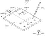
도 1a를 참조하면, 인터페이스 장치(10000)는 전자 장치(1000) 및 입력 장치(2000)를 포함할 수 있다. 전자 장치(1000)는 입력 장치(2000)에 의한 입력을 감지할 수 있다. 이에 대해서는 후술된다.Referring to FIG. 1A , an
전자 장치(1000)는 전기적 신호에 따라 활성화되는 장치일 수 있다. 예를 들어, 전자 장치(1000)는 휴대폰, 태블릿, 자동차 내비게이션, 게임기, 또는 웨어러블 장치일 수 있으나, 이에 제한되는 것은 아니다. 도 1a에서는 전자 장치(1000)가 휴대폰인 것을 예시적으로 도시하였다.The
전자 장치(1000)는 액티브 영역(1000A)을 통해 영상을 표시할 수 있다. 액티브 영역(1000A)은 제1 방향(DR1) 및 제2 방향(DR2)에 의해 정의된 면을 포함할 수 있다. 전자 장치(1000)의 두께 방향은 제1 방향(DR1) 및 제2 방향(DR2)과 교차하는 제3 방향(DR3)과 나란할 수 있다. 따라서, 전자 장치(1000)를 구성하는 부재들의 전면(또는 상면)과 배면(또는 하면)은 제3 방향(DR3)을 기준으로 정의될 수 있다.The
전자 장치(1000)는 외부에서 인가되는 입력들을 감지할 수 있다. 외부 입력은 사용자의 입력일 수 있다. 사용자의 입력은 사용자 신체의 일부, 입력 장치(2000), 광, 열, 또는 압력 등 다양한 형태의 외부 입력들을 포함할 수 있다. 도 1a에서는 입력 장치(2000)을 예시적으로 도시하였다. 전자 장치(1000)는 전자 장치(1000) 내부에서 발생된 자기장과 입력 장치(2000) 사이에 발생하는 전자기 유도에 의한 공명(Electro Magnetic Resonance, EMR)에 의해 외부 입력을 감지할 수 있다.The
도 1b는 본 발명의 일 실시예에 따른 인터페이스 장치의 사시도이다. 도 1b를 설명함에 있어서 도 1a를 통해 설명된 구성 요소에 대해서는 동일한 도면 부호를 병기하고 이에 대한 설명은 생략된다.1B is a perspective view of an interface device according to an embodiment of the present invention. In the description of FIG. 1B , the same reference numerals are used for components described through FIG. 1A , and descriptions thereof are omitted.
도 1b를 참조하면, 인터페이스 장치(10000-1)는 전자 장치(1000-1) 및 입력 장치(2000)를 포함할 수 있다.Referring to FIG. 1B , an interface device 10000-1 may include an electronic device 1000-1 and an
전자 장치(1000-1)는 폴더블 전자 장치일 수 있다. 전자 장치(1000-1)에는 제1 방향(DR1)을 따라 순차적으로 배열된 제1 비폴딩 영역(1000NF1), 폴딩 영역(1000F), 및 제2 비폴딩 영역(1000NF2)이 정의될 수 있다. 즉, 폴딩 영역(1000F)은 제1 비폴딩 영역(1000NF1) 및 제2 비폴딩 영역(1000NF2) 사이에 정의될 수 있다.The electronic device 1000-1 may be a foldable electronic device. In the electronic device 1000-1, a first non-folding area 1000NF1, a
도 1b에서는 하나의 폴딩 영역(1000F)과 제1 및 제2 비폴딩 영역(1000NF1, 1000NF2)이 도시되었으나, 폴딩 영역(1000F)과 제1 및 제2 비폴딩 영역(1000NF1, 1000NF2)의 개수는 이에 한정되지 않는다. 예를 들어, 전자 장치(1000-1)는 2개보다 많은 복수의 비폴딩 영역들 및 비폴딩 영역들 사이에 배치된 폴딩 영역들을 포함할 수도 있다.Although one
전자 장치(1000-1)는 액티브 영역(1000A-1)을 통해 영상을 표시할 수 있다.The electronic device 1000-1 may display an image through the
전자 장치(1000-1)가 폴딩되면, 제1 비폴딩 영역(1000NF1)의 표시면 및 제2 비폴딩 영역(1000NF2)의 표시면은 서로 마주할 수 있다. 따라서, 전자 장치(1000-1)가 완전히 폴딩된 상태에서 액티브 영역(1000A-1)은 외부에 노출되지 않을 수 있다. 이는 인폴딩으로 지칭될 수 있다. 다만, 이는 예시적인 것으로 본 발명이 이에 제한되는 것은 아니다. 예를 들어, 전자 장치(1000-1)가 폴딩되면, 제1 비폴딩 영역(1000NF1)의 표시면 및 제2 비폴딩 영역(1000NF2)의 표시면은 서로 대향할 수 있다. 따라서, 폴딩된 상태에서 액티브 영역(1000A-1)은 외부에 노출될 수 있다. 이는 아웃폴딩으로 지칭될 수 있다. 또는, 전자 장치(1000-1)는 인폴딩 및 아웃폴딩이 모두 가능할 수 있다. 예를 들어, 하나의 폴딩 영역(1000F)이 인폴딩 및 아웃폴딩될 수 있다. 또는, 전자 장치(1000-1)는 복수의 폴딩 영역들을 포함하고, 그 중 일부는 인폴딩, 다른 일부는 아웃 폴딩될 수 있다.When the electronic device 1000-1 is folded, the display surface of the first non-folding area 1000NF1 and the display surface of the second non-folding area 1000NF2 may face each other. Accordingly, the
도 2는 본 발명의 일 실시예에 따른 전자 장치의 개략적인 단면도이다.2 is a schematic cross-sectional view of an electronic device according to an embodiment of the present invention.
도 2를 참조하면, 전자 장치(1000)는 윈도우(WP), 접착층들(OCA1, OCA2), 반사 방지층(RPP), 센서층(200), 표시층(100), 쿠션층(CSH), 감지층(300), 신호 차폐층(FR), 방열 시트(GP), 및 커버층(CU)을 포함할 수 있다.Referring to FIG. 2 , the
윈도우(WP)는 전자 장치(1000)의 외관을 구성할 수 있다. 윈도우(WP)는 외부 충격으로부터 전자 장치(1000)의 내부 구성들을 보호하며, 실질적으로 전자 장치(1000)의 액티브 영역(1000A)을 제공하는 구성일 수 있다. 예를 들어, 윈도우(WP)는 유리 기판, 사파이어 기판, 또는 플라스틱 필름을 포함할 수 있다. 윈도우(WP)는 다층 또는 단층 구조를 가질 수 있다. 예를 들어, 윈도우(WP)는 접착제로 결합된 복수 개의 플라스틱 필름의 적층 구조를 가지거나, 접착제로 결합된 유리 기판과 플라스틱 필름의 적층 구조를 가질 수 있다.The window WP may configure the exterior of the
제1 접착층(OCA1)은 윈도우(WP)의 아래에 배치될 수 있다. 제1 접착층(OCA1)에 의해 윈도우(WP) 및 반사 방지층(RPP)이 결합될 수 있다. 제1 접착층(OCA1)은 통상의 접착제 또는 점착제를 포함할 수 있다. 예를 들어, 제1 접착층(OCA1)은 광학투명접착필름(Optically Clear Adhesive film), 광학투명접착수지(Optically Clear Resin), 또는 감압접착필름(Pressure Sensitive Adhesive film)일 수 있다.The first adhesive layer OCA1 may be disposed below the window WP. The window WP and the anti-reflection layer RPP may be combined by the first adhesive layer OCA1. The first adhesive layer OCA1 may include a general adhesive or pressure-sensitive adhesive. For example, the first adhesive layer OCA1 may be an optically clear adhesive film, an optically clear resin, or a pressure sensitive adhesive film.
반사 방지층(RPP)은 윈도우(WP)의 아래에 배치될 수 있다. 반사 방지층(RPP)은 윈도우(WP)의 위로부터 입사되는 자연광(또는 태양광)의 반사율을 감소시킬 수 있다.The anti-reflection layer RPP may be disposed below the window WP. The anti-reflection layer RPP may reduce reflectance of natural light (or sunlight) incident from above the window WP.
본 발명의 일 실시예에 따른 반사 방지층(RPP)은 위상지연자(retarder) 및 편광자(polarizer)를 포함할 수 있다. 위상지연자는 필름타입 또는 액정 코팅타입일 수 있고,

제2 접착층(OCA2)은 반사 방지층(RPP)의 아래에 배치될 수 있다. 제2 접착층(OCA2)에 의해 반사 방지층(RPP) 및 센서층(200)이 결합될 수 있다. 제2 접착층(OCA2)은 제1 접착층(OCA1)과 실질적으로 동일한 물질을 포함할 수 있다.The second adhesive layer OCA2 may be disposed under the anti-reflection layer RPP. The anti-reflection layer RPP and the
센서층(200)은 외부 입력의 좌표 정보를 획득할 수 있다. 본 발명의 일 실시예에 따른 센서층(200)은 표시층(100)의 일면에 직접 배치될 수 있다. 예를 들어, 센서층(200)은 온 셀(On-Cell) 방식으로 표시층(100)과 일체화될 수 있다. 센서층(200)은 표시층(100)과 연속 공정에 의해 제조될 수 있다. 단, 이에 제한되는 것은 아니며 센서층(200)은 별도의 공정에 의해 제조되어, 표시층(100)에 접착될 수 있다. 센서층(200)은 터치 패널을 포함할 수 있다.The
표시층(100)은 센서층(200) 아래에 배치될 수 있다. 표시층(100)은 영상을 실질적으로 생성하는 구성일 수 있다. 표시층(100)은 발광형 표시층일 수 있고, 특별히 제한되지 않는다. 예를 들어, 표시층(100)은 유기 발광 표시층, 퀀텀닷 표시층, 마이크로 엘이디 표시층, 또는 나노 엘이디 표시층을 포함할 수 있다. 표시층(100)은 베이스층(110), 회로층(120), 발광 소자층(130), 및 봉지층(140)을 포함할 수 있다. 이에 대해서는 후술된다.The
쿠션층(CSH)은 표시층(100)의 아래에 배치될 수 있다. 쿠션층(CSH)은 외부에서 가해지는 압력을 완화시키는 기능을 가질 수 있다. 쿠션층(CSH)은 스펀지, 발포 폼, 또는 우레탄 수지 등을 포함할 수 있다.The cushion layer CSH may be disposed below the
감지층(300)은 쿠션층(CSH) 아래에 배치될 수 있다. 다만, 이는 예시적인 것으로 본 발명의 일 실시예에 따른 감지층(300)의 배치 관계는 이에 제한되지 않는다. 예를 들어, 감지층(300)은 표시층(100) 위에 배치될 수도 있다. 이 경우, 감지층(300)은 투명한 물질을 포함하는 복수의 코일들을 포함할 수 있다.The
감지층(300)은 센서층(200)이 감지하는 외부 입력과 상이한 외부 입력을 감지할 수 있다. 예를 들어, 감지층(300)은 입력 장치(2000, 도 1a 참조)에 의해 전달된 신호를 감지할 수 있다. 즉, 본 실시예에서 외부 입력의 형태에 따라 감지하는 센서의 위치가 다를 수 있다. 감지층(300)은 전자기 유도에 의한 공명(Electro Magnetic Resonance, EMR)을 이용한 방식으로 구동될 수 있다. 감지층(300)은 액티브 영역(1000A, 도 1a 참조)에 인가되는 입력 장치(2000, 도 1a 참조)의 위치나 세기를 감지할 수 있다.The
전자기 공명(EMR) 방식은 입력 장치(2000, 도 1a 참조) 내부에 구성된 공진 회로에서 자계를 발생시키고, 진동하는 자계는 감지층(300) 각각에 포함된 복수의 코일들에 신호를 유도하고, 코일들에 유도된 신호를 통해 입력 장치(2000, 도 1a 참조)의 위치를 검출할 수 있다. 감지층(300)은 디지타이저를 포함할 수 있다.The electromagnetic resonance (EMR) method generates a magnetic field in a resonance circuit configured inside the input device (2000, see FIG. 1A), and the oscillating magnetic field induces a signal in a plurality of coils included in each of the
신호 차폐층(FR)은 감지층(300) 아래에 배치될 수 있다. 신호 차폐층(FR)은 신호 간섭을 방지할 수 있다. 신호 차폐층(FP)은 산화철을 포함하는 자성체를 포함할 수 있다. 예를 들어, 신호 차폐층(FP)은 페라이트(Ferrite)를 포함할 수 있다.The signal shielding layer FR may be disposed below the
방열 시트(GP)는 신호 차폐층(FR) 아래에 배치될 수 있다. 방열 시트(GP)는 표시층(100) 및 감지층(300)에서 발생하는 열의 방출을 유도할 수 있다. 예를 들어, 방열 시트(GP)는 그라파이트(graphite) 시트를 포함할 수 있다.The heat dissipation sheet GP may be disposed under the signal shielding layer FR. The heat dissipation sheet GP may induce the release of heat generated from the
커버층(CU)은 방열 시트(GP) 아래에 배치될 수 있다. 커버층(CU)은 도전성을 가질 수 있다. 예를 들어 커버층(CU)은 구리(Cu)를 포함할 수 있다. 예를 들어, 커버층(CU)은 구리 테이프(Cu tape)일 수 있다. 다만, 특별히 이에 제한되지는 않는다.The cover layer CU may be disposed under the heat dissipation sheet GP. The cover layer CU may have conductivity. For example, the cover layer CU may include copper (Cu). For example, the cover layer CU may be a copper tape. However, it is not particularly limited thereto.
도 3은 본 발명의 일 실시예에 따른 전자 장치의 일부분의 단면도이다.3 is a cross-sectional view of a portion of an electronic device according to an embodiment of the present invention.
도 3을 참조하면, 표시층(100)은 베이스층(110), 회로층(120), 발광 소자층(130), 및 봉지층(140)을 포함할 수 있다.Referring to FIG. 3 , the
베이스층(110)은 회로층(120)이 배치되는 베이스 면을 제공하는 부재일 수 있다. 베이스층(110)은 유리 기판, 금속 기판, 또는 고분자 기판 등일 수 있다. 하지만, 실시예가 이에 한정되는 것은 아니며, 베이스층(110)은 무기층, 유기층 또는 복합재료층일 수 있다.The
베이스층(110)은 다층 구조를 가질 수 있다. 예를 들어, 베이스층(110)은 제1 합성 수지층, 상기 제1 합성 수지층 위에 배치된 실리콘 옥사이드(SiOx)층, 상기 실리콘 옥사이드층 위에 배치된 아몰퍼스 실리콘(a-Si)층, 및 상기 아몰퍼스 실리콘층 위에 배치된 제2 합성 수지층을 포함할 수 있다. 상기 실리콘 옥사이드층 및 상기 아몰퍼스 실리콘층은 베이스 배리어층이라 지칭될 수 있다.The
상기 제1 및 제2 합성 수지층들 각각은 폴리이미드(polyimide)계 수지를 포함하는 것일 수 있다. 또한, 상기 제1 및 제2 합성 수지층들 각각은 아크릴(acrylate)계 수지, 메타크릴(methacrylate)계 수지, 폴리아이소프렌(polyisoprene)계 수지, 비닐(vinyl)계 수지, 에폭시(epoxy)계 수지, 우레탄(urethane)계 수지, 셀룰로오스(cellulose)계 수지, 실록산(siloxane)계 수지, 폴리아미드(polyamide)계 수지 및 페릴렌(perylene)계 수지 중 적어도 하나를 포함하는 것일 수 있다. 한편, 본 명세서에서 "~~" 계 수지는 "~~" 의 작용기를 포함하는 것을 의미한다.Each of the first and second synthetic resin layers may include a polyimide-based resin. In addition, each of the first and second synthetic resin layers may be an acrylate-based resin, a methacrylate-based resin, a polyisoprene-based resin, a vinyl-based resin, or an epoxy-based resin. , It may include at least one of a urethane-based resin, a cellulose-based resin, a siloxane-based resin, a polyamide-based resin, and a perylene-based resin. Meanwhile, in the present specification, a "~~"-based resin means one containing a functional group of "~~".
베이스층(110)의 상면에 적어도 하나의 무기층이 형성된다. 무기층은 알루미늄옥사이드, 티타늄옥사이드, 실리콘옥사이드, 실리콘나이트라이드, 실리콘옥시나이트라이드, 지르코늄옥사이드, 및 하프늄옥사이드 중 적어도 하나를 포함할 수 있다. 무기층은 다층으로 형성될 수 있다. 다층의 무기층들은 배리어층 및/또는 버퍼층을 구성할 수 있다. 본 실시예에서 표시층(100)은 버퍼층(BFL)을 포함하는 것으로 도시되었다.At least one inorganic layer is formed on the upper surface of the
버퍼층(BFL)은 베이스층(110)과 반도체 패턴 사이의 결합력을 향상시킬 수 있다. 버퍼층(BFL)은 실리콘옥사이드, 실리콘나이트라이드, 및 실리콘옥시나이트라이드 중 적어도 하나를 포함할 수 있다. 예를 들어, 버퍼층(BFL)은 실리콘옥사이드층과 실리콘나이트라이드층이 교대로 적층된 구조를 포함할 수 있다.The buffer layer BFL may improve bonding strength between the
반도체 패턴은 버퍼층(BFL) 위에 배치될 수 있다. 반도체 패턴은 폴리실리콘을 포함할 수 있다. 그러나 이에 제한되지 않고, 반도체 패턴은 비정질실리콘, 저온다결정실리콘, 또는 산화물반도체를 포함할 수도 있다.A semiconductor pattern may be disposed on the buffer layer BFL. The semiconductor pattern may include polysilicon. However, it is not limited thereto, and the semiconductor pattern may include amorphous silicon, low-temperature polycrystalline silicon, or an oxide semiconductor.
도 3은 일부의 반도체 패턴을 도시한 것일 뿐이고, 다른 영역에 반도체 패턴이 더 배치될 수 있다. 반도체 패턴은 화소들에 걸쳐 특정한 규칙으로 배열될 수 있다. 반도체 패턴은 도핑 여부에 따라 전기적 성질이 다를 수 있다. 반도체 패턴은 전도율이 높은 제1 영역과 전도율이 낮은 제2 영역을 포함할 수 있다. 제1 영역은 N형 도판트 또는 P형 도판트로 도핑될 수 있다. P타입의 트랜지스터는 P형 도판트로 도핑된 도핑영역을 포함하고, N타입의 트랜지스터는 N형 도판트로 도핑된 도핑영역을 포함할 수 있다. 제2 영역은 비-도핑 영역이거나, 제1 영역 대비 낮은 농도로 도핑된 영역일 수 있다.3 only shows a portion of the semiconductor pattern, and semiconductor patterns may be further disposed in other regions. The semiconductor pattern may be arranged in a specific rule across the pixels. The semiconductor pattern may have different electrical properties depending on whether it is doped or not. The semiconductor pattern may include a first region having high conductivity and a second region having low conductivity. The first region may be doped with an N-type dopant or a P-type dopant. A P-type transistor may include a doped region doped with a P-type dopant, and an N-type transistor may include a doped region doped with an N-type dopant. The second region may be a non-doped region or a region doped at a lower concentration than the first region.
제1 영역의 전도성은 제2 영역의 전도성보다 크고, 실질적으로 전극 또는 신호 라인의 역할을 할 수 있다. 제2 영역은 실질적으로 트랜지스터의 액티브 영역에 해당할 수 있다. 다시 말해, 반도체 패턴의 일부분은 트랜지스터의 액티브 영역일수 있고, 다른 일부분은 트랜지스터의 소스 영역 또는 드레인 영역일 수 있고, 또 다른 일부분은 연결 전극 또는 연결 신호라인일 수 있다.Conductivity of the first region is greater than that of the second region, and may substantially serve as an electrode or a signal line. The second region may substantially correspond to an active region of the transistor. In other words, a portion of the semiconductor pattern may be an active region of a transistor, another portion may be a source region or drain region of a transistor, and another portion may be a connection electrode or a connection signal line.
화소들 각각은 7개의 트랜지스터들, 하나의 커패시터, 및 발광 소자를 포함하는 등가회로를 가질 수 있으며, 화소의 등가회로도는 다양한 형태로 변형될 수 있다. 도 5에서는 화소에 포함되는 하나의 트랜지스터(100PC) 및 발광 소자(100PE)를 예시적으로 도시하였다.Each of the pixels may have an equivalent circuit including seven transistors, one capacitor, and a light emitting device, and the equivalent circuit diagram of the pixel may be modified in various forms. In FIG. 5 , one transistor 100PC and a light emitting element 100PE included in a pixel are illustrated as an example.
트랜지스터(100PC)의 소스 영역(SC), 액티브 영역(AL), 및 드레인 영역(DR)이 반도체 패턴으로부터 형성될 수 있다. 소스 영역(SC) 및 드레인 영역(DR)은 단면 상에서 액티브 영역(AL)로부터 서로 반대 방향으로 연장될 수 있다. 도 5에는 반도체 패턴으로부터 형성된 연결 신호 배선(SCL)의 일부분을 도시하였다. 별도로 도시하지 않았으나, 연결 신호 배선(SCL)은 평면 상에서 트랜지스터(100PC)의 드레인 영역(DR)에 연결될 수 있다.The source region SC, the active region AL, and the drain region DR of the transistor 100PC may be formed from a semiconductor pattern. The source region SC and the drain region DR may extend in opposite directions from the active region AL on a cross section. 5 illustrates a portion of a connection signal line SCL formed from a semiconductor pattern. Although not separately shown, the connection signal line SCL may be connected to the drain region DR of the transistor 100PC on a plane.
제1 절연층(10)은 버퍼층(BFL) 위에 배치될 수 있다. 제1 절연층(10)은 복수 개의 화소들에 공통으로 중첩하며, 반도체 패턴을 커버할 수 있다. 제1 절연층(10)은 무기층 및/또는 유기층일 수 있으며, 단층 또는 다층 구조를 가질 수 있다. 제1 절연층(10)은 알루미늄옥사이드, 티타늄옥사이드, 실리콘옥사이드, 실리콘나이트라이드, 실리콘옥시나이트라이드, 지르코늄옥사이드, 및 하프늄옥사이드 중 적어도 하나를 포함할 수 있다. 본 실시예에서 제1 절연층(10)은 단층의 실리콘옥사이드층일 수 있다. 제1 절연층(10)뿐만 아니라 후술하는 회로층(120)의 절연층은 무기층 및/또는 유기층일 있으며, 단층 또는 다층 구조를 가질 수 있다. 무기층은 상술한 물질 중 적어도 하나를 포함할 수 있으나, 이에 제한되는 것은 아니다.The first insulating
트랜지스터(100PC)의 게이트(GT)는 제1 절연층(10) 위에 배치된다. 게이트(GT)는 금속 패턴의 일부분일 수 있다. 게이트(GT)는 액티브 영역(AL)에 중첩한다. 반도체 패턴을 도핑하는 공정에서 게이트(GT)는 마스크로 기능할 수 있다.A gate GT of the transistor 100PC is disposed on the first insulating
제2 절연층(20)은 제1 절연층(10) 위에 배치되며, 게이트(GT)를 커버할 수 있다. 제2 절연층(20)은 화소들에 공통으로 중첩할 수 있다. 제2 절연층(20)은 무기층 및/또는 유기층일 수 있으며, 단층 또는 다층 구조를 가질 수 있다. 제2 절연층(20)은 실리콘옥사이드, 실리콘나이트라이드, 및 실리콘옥시나이트라이드 중 적어도 하나를 포함할 수 있다. 본 실시예에서, 제2 절연층(20)은 실리콘옥사이드층 및 실리콘나이트라이드층을 포함하는 다층 구조를 가질 수 있다.The second insulating
제3 절연층(30)은 제2 절연층(20) 위에 배치될 수 있다. 제3 절연층(30)은 단층 또는 다층 구조를 가질 수 있다. 예를 들어, 제3 절연층(30)은 실리콘옥사이드층 및 실리콘나이트라이드층을 포함하는 다층 구조를 가질 수 있다.The third insulating
제1 연결 전극(CNE1)은 제3 절연층(30) 위에 배치될 수 있다. 제1 연결 전극(CNE1)은 제1, 제2, 및 제3 절연층(10, 20, 30)을 관통하는 컨택홀(CNT-1)을 통해 연결 신호 배선(SCL)에 접속될 수 있다.The first connection electrode CNE1 may be disposed on the third insulating
제4 절연층(40)은 제3 절연층(30) 위에 배치될 수 있다. 제4 절연층(40)은 단층의 실리콘 옥사이드층일 수 있다. 제5 절연층(50)은 제4 절연층(40) 위에 배치될 수 있다. 제5 절연층(50)은 유기층일 수 있다.The fourth insulating
제2 연결 전극(CNE2)은 제5 절연층(50) 위에 배치될 수 있다. 제2 연결 전극(CNE2)은 제4 절연층(40) 및 제5 절연층(50)을 관통하는 컨택홀(CNT-2)을 통해 제1 연결 전극(CNE1)에 접속될 수 있다.The second connection electrode CNE2 may be disposed on the fifth insulating
제6 절연층(60)은 제5 절연층(50) 위에 배치되며, 제2 연결 전극(CNE2)을 커버할 수 있다. 제6 절연층(60)은 유기층일 수 있다.The sixth insulating
발광 소자층(130)은 회로층(120) 위에 배치될 수 있다. 발광 소자층(130)은 발광 소자(100PE)를 포함할 수 있다. 예를 들어, 발광 소자층(130)은 유기 발광 물질, 퀀텀닷, 퀀텀 로드, 마이크로 엘이디, 또는 나노 엘이디를 포함할 수 있다. 이하에서, 발광 소자(100PE)가 유기 발광 소자인 것을 예로 들어 설명하나, 특별히 이에 제한되는 것은 아니다.The light emitting
발광 소자(100PE)는 제1 전극(AE), 발광층(EL), 및 제2 전극(CE)을 포함할 수 있다.The light emitting element 100PE may include a first electrode AE, a light emitting layer EL, and a second electrode CE.
제1 전극(AE)은 제6 절연층(60) 위에 배치될 수 있다. 제1 전극(AE)은 제6 절연층(60)을 관통하는 컨택홀(CNT-3)을 통해 제2 연결 전극(CNE2)에 접속될 수 있다.The first electrode AE may be disposed on the sixth insulating
화소 정의막(70)은 제6 절연층(60) 위에 배치되며, 제1 전극(AE)의 일부분을 커버할 수 있다. 화소 정의막(70)에는 개구부(70-OP)가 정의된다. 화소 정의막(70)의 개구부(70-OP)는 제1 전극(AE)의 적어도 일부분을 노출시킨다.The
액티브 영역(1000A, 도 1a 참조)은 발광 영역(PXA)과 발광 영역(PXA)에 인접한 비발광 영역(NPXA)을 포함할 수 있다. 비발광 영역(NPXA)은 발광 영역(PXA)을 에워쌀 수 있다. 본 실시예에서 발광 영역(PXA)은 개구부(70-OP)에 의해 노출된 제1 전극(AE)의 일부 영역에 대응하게 정의되었다.The
발광층(EL)은 제1 전극(AE) 위에 배치될 수 있다. 발광층(EL)은 개구부(70-OP)에 대응하는 영역에 배치될 수 있다. 즉, 발광층(EL)은 화소들 각각에 분리되어 형성될 수 있다. 발광층(EL)이 화소들 각각에 분리되어 형성된 경우, 발광층들(EL) 각각은 청색, 적색, 및 녹색 중 적어도 하나의 색의 광을 발광할 수 있다. 다만, 이에 제한되는 것은 아니며, 발광층(EL)은 화소들에 연결되어 공통으로 제공될 수도 있다. 이 경우, 발광층(EL)은 청색 광을 제공하거나, 백색 광을 제공할 수도 있다.The light emitting layer EL may be disposed on the first electrode AE. The light emitting layer EL may be disposed in an area corresponding to the opening 70 -OP. That is, the light emitting layer EL may be formed separately from each of the pixels. When the light emitting layer EL is separately formed in each of the pixels, each of the light emitting layers EL may emit light of at least one of blue, red, and green. However, it is not limited thereto, and the light emitting layer EL may be connected to the pixels and provided in common. In this case, the light emitting layer EL may provide blue light or white light.
제2 전극(CE)은 발광층(EL) 위에 배치될 수 있다. 제2 전극(CE)은 일체의 형상을 갖고, 복수 개의 화소들에 공통적으로 배치될 수 있다.The second electrode CE may be disposed on the light emitting layer EL. The second electrode CE has an integral shape and may be commonly disposed in a plurality of pixels.
도시되지 않았으나, 제1 전극(AE)과 발광층(EL) 사이에는 정공 제어층이 배치될 수 있다. 정공 제어층은 발광 영역(PXA)과 비발광 영역(NPXA)에 공통으로 배치될 수 있다. 정공 제어층은 정공 수송층을 포함하고, 정공 주입층을 더 포함할 수 있다. 발광층(EL)과 제2 전극(CE) 사이에는 전자 제어층이 배치될 수 있다. 전자 제어층은 전자 수송층을 포함하고, 전자 주입층을 더 포함할 수 있다. 정공 제어층과 전자 제어층은 오픈 마스크를 이용하여 복수 개의 화소들에 공통으로 형성될 수 있다.Although not shown, a hole control layer may be disposed between the first electrode AE and the light emitting layer EL. The hole control layer may be disposed in common in the emission area PXA and the non-emission area NPXA. The hole control layer may include a hole transport layer and may further include a hole injection layer. An electronic control layer may be disposed between the light emitting layer EL and the second electrode CE. The electron control layer includes an electron transport layer and may further include an electron injection layer. The hole control layer and the electron control layer may be commonly formed in a plurality of pixels using an open mask.
봉지층(140)은 발광 소자층(130) 위에 배치될 수 있다. 봉지층(140)은 순차적으로 적층된 무기층, 유기층, 및 무기층을 포함할 수 있으나, 봉지층(140)을 구성하는 층들이 이에 제한되는 것은 아니다.The
무기층들은 수분 및 산소로부터 발광 소자층(130)을 보호하고, 유기층은 먼지 입자와 같은 이물질로부터 발광 소자층(130)을 보호할 수 있다. 무기층들은 실리콘나이트라이드층, 실리콘옥시나이트라이드층, 실리콘옥사이드층, 티타늄옥사이드층, 또는 알루미늄옥사이드층 등을 포함할 수 있다. 유기층은 아크릴 계열 유기층을 포함할 수 있고, 이에 제한되지 않는다.The inorganic layers may protect the light emitting
센서층(200)은 베이스층(201), 제1 도전층(202), 감지 절연층(203), 제2 도전층(204), 및 커버 절연층(205)을 포함할 수 있다.The
베이스층(201)은 실리콘나이트라이드, 실리콘옥시나이트라이드, 및 실리콘옥사이드 중 적어도 어느 하나를 포함하는 무기층일 수 있다. 또는 베이스층(201)은 에폭시 수지, 아크릴 수지, 또는 이미드 계열 수지를 포함하는 유기층일 수도 있다. 베이스층(201)은 단층 구조를 갖거나, 제3 방향(DR3)을 따라 적층된 다층 구조를 가질 수 있다.The
제1 도전층(202) 및 제2 도전층(204) 각각은 단층구조를 갖거나, 제3 방향(DR3)을 따라 적층된 다층 구조를 가질 수 있다.Each of the first
단층구조의 도전층은 금속층 또는 투명 도전층을 포함할 수 있다. 금속층은 몰리브덴, 은, 티타늄, 구리, 알루미늄, 또는 이들의 합금을 포함할 수 있다. 투명 도전층은 인듐주석산화물(indium tin oxide, ITO), 인듐아연산화물(indium zinc oxide, IZO), 산화아연(zinc oxide, ZnO), 또는 인듐아연주석산화물(indium zinc tin oxide, IZTO) 등과 같은 투명한 전도성산화물을 포함할 수 있다. 그밖에 투명 도전층은 PEDOT과 같은 전도성 고분자, 금속 나노 와이어, 그라핀 등을 포함할 수 있다.The conductive layer of the single-layer structure may include a metal layer or a transparent conductive layer. The metal layer may include molybdenum, silver, titanium, copper, aluminum, or an alloy thereof. The transparent conductive layer may include indium tin oxide (ITO), indium zinc oxide (IZO), zinc oxide (ZnO), or indium zinc tin oxide (IZTO). A transparent conductive oxide may be included. In addition, the transparent conductive layer may include conductive polymers such as PEDOT, metal nanowires, graphene, and the like.
다층구조의 도전층은 금속층들을 포함할 수 있다. 금속층들은 예컨대 티타늄/알루미늄/티타늄의 3층 구조를 가질 수 있다. 다층구조의 도전층은 적어도 하나의 금속층 및 적어도 하나의 투명 도전층을 포함할 수 있다.The conductive layer of the multilayer structure may include metal layers. The metal layers may have, for example, a three-layer structure of titanium/aluminum/titanium. The multi-layered conductive layer may include at least one metal layer and at least one transparent conductive layer.
감지 절연층(203) 및 커버 절연층(205) 중 적어도 어느 하나는 무기막을 포함할 수 있다. 무기막은 알루미늄옥사이드, 티타늄옥사이드, 실리콘옥사이드, 실리콘나이트라이드, 실리콘옥시나이트라이드, 지르코늄옥사이드, 및 하프늄옥사이드 중 적어도 하나를 포함할 수 있다.At least one of the sensing insulating
감지 절연층(203) 및 커버 절연층(205) 중 적어도 어느 하나는 유기막을 포함할 수 있다. 유기막은 아크릴계 수지, 메타크릴계 수지, 폴리이소프렌, 비닐계 수지, 에폭시계 수지, 우레탄계 수지, 셀룰로오스계 수지, 실록산계 수지, 폴리이미드계 수지, 폴리아미드계 수지 및 페릴렌계 수지 중 적어도 어느 하나를 포함할 수 있다.At least one of the sensing insulating
도 4는 본 발명의 일 실시예에 따른 감지층의 구성을 간략히 도시한 평면도이다.4 is a plan view schematically illustrating the configuration of a sensing layer according to an embodiment of the present invention.
도 4를 참조하면, 감지층(300)은 복수의 제1 코일들(311) 및 복수의 제2 코일들(312)을 포함할 수 있다. 복수의 제1 코일들(311)은 구동 코일들로 지칭될 수 있고, 복수의 제2 코일들(312)은 감지 코일들로 지칭될 수 있다.Referring to FIG. 4 , the
복수의 제1 코일들(311) 각각은 제1 방향(DR1)을 따라 연장될 수 있다. 복수의 제1 코일들(311)은 제2 방향(DR2)으로 서로 이격되어 배열될 수 있다. 복수의 제2 코일들(312) 각각은 제2 방향(DR2)을 따라 연장될 수 있다. 복수의 제2 코일들(312)은 제1 방향(DR1)으로 서로 이격되어 배열될 수 있다.Each of the plurality of
입력 장치(2000, 도 1a 참조)를 감지하기 위해 복수의 제1 코일들(311)의 제1 단자들(311t)로 교류 신호가 순차적으로 제공될 수 있다. 복수의 제1 코일들(311)은 폐곡선 형태로 형성될 수 있다. 복수의 제1 코일들(311)에 전류가 흐르면, 복수의 제1 코일들(311) 및 복수의 제2 코일들(312) 사이에 자기력선이 유도될 수 있다. 복수의 제2 코일들(312)은 입력 장치(2000, 도 1a 참조)에서 방출된 유도 전자기력을 감지한 신호를 복수의 제2 코일들(312)의 제2 단자들(312t)로 출력할 수 있다.AC signals may be sequentially provided to the
도 4에서는 감지층(300)의 구성을 예시적으로 도시하였으나, 이에 한정되는 것은 아니다. 또한, 복수의 제1 코일들(311) 및 복수의 제2 코일들(312)의 배열관계는 도 4에 도시되 것에 제한되지 않으며 다양하게 변형될 수 있다.4 shows the configuration of the
도 5는 본 발명의 일 실시예에 따른 입력 장치의 블록도이다.5 is a block diagram of an input device according to an embodiment of the present invention.
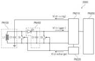
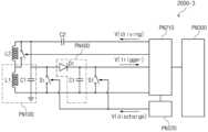
도 5를 참조하면, 입력 장치(2000)는 하우징(PNH), 펜 팁(PNT), 공진 회로부(PN100), 제어부(PN200), 및 전원부(PN300)를 포함할 수 있다.Referring to FIG. 5 , the
하우징(PNH)은 펜 형상을 가질 수 있다. 하우징(PNH)의 내부에는 수용 공간이 형성될 수 있다. 하우징(PNH) 내부에 정의된 수용 공간에는 공진 회로부(PN100), 제어부(PN200), 및 전원부(PN300)이 수용될 수 있다.The housing PNH may have a pen shape. An accommodation space may be formed inside the housing PNH. The resonance circuit unit PN100, the control unit PN200, and the power supply unit PN300 may be accommodated in the accommodating space defined inside the housing PNH.
펜 팁(PNT)은 하우징(PNH)의 단부에 배치될 수 있다. 예를 들어, 펜 팁(PNT)의 일부분은 하우징(PNH)의 외부로 노출되고, 펜 팁(PNT)의 나머지 부분은 하우징(PNH) 내부에 삽입될 수 있다.The pen tip PNT may be disposed at an end of the housing PNH. For example, a portion of the pen tip PNT may be exposed to the outside of the housing PNH, and the remaining portion of the pen tip PNT may be inserted into the housing PNH.
공진 회로부(PN100)는 신호(또는 검출신호, Tx 신호 또는 송신 신호)를 생성하는 구성일 수 있다. 공진 회로부(PN100)는 특정 용도 집적 회로 또는 오실레이터를 포함할 수 있다. 공진 회로부(PN100)는 소정의 값을 갖는 주파수의 교류 신호를 출력할 수 있다.The resonance circuit unit PN100 may be a component that generates a signal (or a detection signal, a Tx signal, or a transmission signal). The resonance circuit unit PN100 may include a specific purpose integrated circuit or an oscillator. The resonance circuit unit PN100 may output an AC signal having a frequency having a predetermined value.
공진 회로부(PN100)에는 전자 장치(1000)로부터 제1 구동 신호(S1, 도 8 참조)에 의해 제1 유도 전류가 생성되고, 상기 제1 유도 전류에 의해 공진하여 제1 자기장이 생성될 수 있다.A first induced current is generated in the resonance circuit unit PN100 by a first driving signal S1 (see FIG. 8 ) from the
제어부(PN200)는 공진 회로부(PN100)를 제어할 수 있다. 제어부(PN200)는 전원부(PN300)의 전원을 근거로 제2 구동 신호(S2, 도 8 참조)를 생성할 수 있다.The control unit PN200 may control the resonance circuit unit PN100. The control unit PN200 may generate the second driving signal S2 (refer to FIG. 8 ) based on the power of the power supply unit PN300.
공진 회로부(PN100)에는 제어부(PN200)로부터 제2 구동 신호(S2, 도 8 참조)에 의해 제2 유도 전류가 생성되고, 상기 제2 유도 전류에 의해 공진하여 제2 자기장이 생성될 수 있다. 감지층(300, 도 2 참조)은 상기 제2 자기장을 근거로 입력 장치(2000)에 의한 입력을 감지할 수 있다.A second induced current may be generated in the resonant circuit unit PN100 by a second driving signal S2 (see FIG. 8 ) from the control unit PN200, and a second magnetic field may be generated by resonating with the second induced current. The sensing layer 300 (see FIG. 2 ) may detect an input by the
전원부(PN300)는 제어부(PN200)에 전원을 공급할 수 있다. 전원부(PN300)는 배터리 또는 고용량 커패시터를 포함할 수 있다.The power supply unit PN300 may supply power to the control unit PN200. The power supply unit PN300 may include a battery or a high-capacity capacitor.
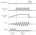
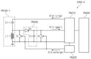
도 6은 본 발명의 일 실시예에 따른 인터페이스 장치의 구동 방법을 도시한 흐름도이고, 도 7은 본 발명의 일 실시예에 따른 입력 장치를 도시한 것이며, 도 8은 본 발명의 일 실시예에 따른 신호를 도시한 것이다. 도 6 내지 도 8을 설명함에 있어서, 도 5를 통해 설명된 구성 요소에 대해서는 동일한 도면 부호를 병기하고 이에 대한 설명은 생략된다.6 is a flowchart illustrating a method of driving an interface device according to an embodiment of the present invention, FIG. 7 illustrates an input device according to an embodiment of the present invention, and FIG. The following signal is shown. In the description of FIGS. 6 to 8 , the same reference numerals are given to the components described through FIG. 5 , and descriptions thereof are omitted.
도 6 내지 도 8을 참조하면, 공진 회로부(PN100)는 제1 커패시터(C1) 및 제1 인덕터(L1)를 포함할 수 있다. 제1 커패시터(C1)는 제1 구동 신호(S1) 또는 제2 구동 신호(S2)에 의한 전류의 흐름을 전기장으로 저장할 수 있다. 제1 인덕터(L1)는 제1 커패시터(C1)와 전기적으로 연결될 수 있다. 제1 인덕터(L1)는 제1 커패시터(C1)와 병렬 연결될 수 있다. 제1 인덕터(L1)는 제1 구동 신호(S1) 또는 제2 구동 신호(S2)에 의한 전류의 흐름을 자기장으로 저장할 수 있다.Referring to FIGS. 6 to 8 , the resonance circuit unit PN100 may include a first capacitor C1 and a first inductor L1. The first capacitor C1 may store the flow of current caused by the first driving signal S1 or the second driving signal S2 as an electric field. The first inductor L1 may be electrically connected to the first capacitor C1. The first inductor L1 may be connected in parallel with the first capacitor C1. The first inductor L1 may store the flow of current caused by the first driving signal S1 or the second driving signal S2 as a magnetic field.
전자 장치(1000, 도 1a 참조)의 감지층(300, 도 2 참조)은 제1 구동 신호(S1)를 입력 장치(2000)에 송신할 수 있다(S100).The sensing layer 300 (see FIG. 2) of the electronic device 1000 (see FIG. 1A) may transmit the first driving signal S1 to the input device 2000 (S100).
공진 회로부(PN100)는 제1 구동 신호(S1)에 의해 충전될 수 있다(S200). 공진 회로부(PN100)는 제1 구동 신호(S1)를 근거로 제1 자기장이 생성될 수 있다.The resonance circuit unit PN100 may be charged by the first driving signal S1 (S200). The resonance circuit unit PN100 may generate a first magnetic field based on the first driving signal S1.
본 발명과 달리, 공진 회로부(PN100)가 제1 구동 신호(S1)에 의해 충전되는 단계를 제공하지 않는 경우, 입력 장치는 별도의 통신부를 구비할 수 있다. 상기 통신부는 감지층(300, 도 2 참조) 또는 센서층(200, 도 2 참조)과 동기화하기 위한 신호를 주고 받을 수 있다. 전자 장치 및 상기 입력 장치는 동기화를 위한 통신 시간이 요구될 수 있다. 다만, 본 발명에 따르면, 공진 회로부(PN100)는 감지층(300, 도 2 참조)의 제1 구동 신호(S1)에 의해 충전될 수 있다. 입력 장치(2000)는 충전된 공진 회로부(PN100)를 근거로 전자 장치(1000, 도 1a 참조)와 통신할 수 있다. 전자 장치(1000, 도 1a 참조) 및 입력 장치(2000)는 동기화를 위한 통신 시간이 불요할 수 있다. 즉, 전자 장치(1000, 도 1a 참조) 및 입력 장치(2000) 사이의 통신 시간이 감소될 수 있다. 인터페이스 장치(10000, 도 1a 참조)는 높은 리포트 레이트(report rate)를 가질 수 있다. 따라서, 인터페이스 장치(10000, 도 1a 참조)는 충분한 리포트 레이트를 확보할 수 있다.Unlike the present invention, when the step of charging the resonance circuit unit PN100 by the first driving signal S1 is not provided, the input device may include a separate communication unit. The communication unit may send and receive signals for synchronization with the sensing layer (300, see FIG. 2) or the sensor layer (200, see FIG. 2). The electronic device and the input device may require communication time for synchronization. However, according to the present invention, the resonance circuit unit PN100 may be charged by the first driving signal S1 of the sensing layer 300 (see FIG. 2). The
입력 장치(2000)는 정류 회로(PN400)를 더 포함할 수 있다. 정류 회로(PN400)는 정류 다이오드(Dt) 및 정류 커패시터(Ct)를 포함할 수 있다. 정류 다이오드(Dt)는 공진 회로부(PN100)의 공진으로 승압된 전압을 정류할 수 있다. 상기 정류된 전압은 정류 커패시터(Ct)에 누적될 수 있다. 상기 누적된 전압은 트리거 신호(Str)로 지칭될 수 있다. 즉, 트리거 신호(Str)는 공진 회로부(PN100)의 충전을 근거로 레벨이 변화될 수 있다.The
공진 회로부(PN100)가 충전됨에 따라 트리거 신호(Str)의 전위는 상승될 수 있다. 트리거 신호(Str)가 소정의 레벨에 도달하면 제어부(PN200)가 동작할 수 있다.As the resonance circuit unit PN100 is charged, the potential of the trigger signal Str may rise. When the trigger signal Str reaches a predetermined level, the controller PN200 may operate.
제어부(PN200, 도 5 참조)는 구동 제어부(PN210) 및 방전 제어부(PN220)를 포함할 수 있다.The control unit PN200 (refer to FIG. 5 ) may include a driving control unit PN210 and a discharge control unit PN220.
구동 제어부(PN210)는 전원을 근거로 제2 구동 신호(S2)를 생성할 수 있다(S300). 구동 제어부(PN210)는 공진 회로부(PN100)에 제2 구동 신호(S2)를 송신할 수 있다.The driving controller PN210 may generate the second driving signal S2 based on power (S300). The driving controller PN210 may transmit the second driving signal S2 to the resonance circuit unit PN100.
공진 회로부(PN100)는 제2 구동 신호(S2)에 의해 충전될 수 있다(S400). 공진 회로부(PN100)는 제2 구동 신호(S2)를 근거로 제2 자기장이 생성될 수 있다.The resonance circuit unit PN100 may be charged by the second driving signal S2 (S400). The resonant circuit unit PN100 may generate a second magnetic field based on the second driving signal S2.
전자 장치(1000, 도 1a 참조)는 공진 회로부(PN100)에 충전된 제2 구동 신호(S2)를 근거로 입력 장치(2000)에 의한 입력(S3)을 감지할 수 있다(S500).The electronic device 1000 (see FIG. 1A ) may detect an input S3 by the
본 발명과 달리, 공진 회로부(PN100)가 제2 구동 신호(S2)에 의해 충전되는 단계를 제공하지 않는 경우, 공진 회로부(PN100)가 충분히 충전되기 위해 제1 구동 신호(S1)에 의해 충전되는 시간이 증가할 수 있다. 감지층(300, 도 2 참조)은 제1 구동 신호(S1)를 지속적으로 제공하고, 전자 장치(1000, 도 1a 참조)의 전력 소모가 증가할 수 있다. 다만, 본 발명에 따르면, 입력 장치(2000)는 트리거 신호(Str)가 소정의 레벨에 도달하면 구동 제어부(PN210)는 전원을 근거로 제2 구동 신호(S2)를 생성할 수 있다. 즉, 공진 회로부(PN100)는 제1 구동 신호(S1)에 의해 충분히 충전되지 않더라도 제2 구동 신호(S2)를 통해 충전될 수 있다. 감지층(300, 도 2 참조)의 제1 구동 신호(S1)를 제공하는 시간이 단축될 수 있다. 인터페이스 장치(10000, 도 1a 참조)는 높은 리포트 레이트(report rate)를 가질 수 있다. 따라서, 인터페이스 장치(10000, 도 1a 참조)는 충분한 리포트 레이트를 확보할 수 있다. 또한, 전자 장치(1000, 도 1a 참조)의 전력 소모가 감소될 수 있다.Unlike the present invention, when the step of charging the resonance circuit unit PN100 by the second driving signal S2 is not provided, the resonance circuit unit PN100 is charged by the first driving signal S1 to be sufficiently charged. time may increase. The sensing layer 300 (see FIG. 2) continuously provides the first driving signal S1, and power consumption of the electronic device 1000 (see FIG. 1A) may increase. However, according to the present invention, when the trigger signal Str of the
또한, 본 발명과 달리, 전자 장치(1000, 도 1a 참조)가 공진 회로부(PN100)에 충전된 용량을 근거로 입력 장치에 의한 입력을 감지하는 경우, 감지하는 시간이 지날수록 충전된 용량이 소모되어 입력의 출력이 감소되고, 입력 장치에 대한 전자 장치의 감도가 감소될 수 있다. 하지만, 본 발명에 따르면, 공진 회로부(PN100)는 제2 구동 신호(S2)에 의해 충전될 수 있다. 제2 구동 신호(S2)는 전원부(PN300)로부터 제공된 전원을 근거로 생성될 수 있다. 입력 장치(2000)에 의한 입력의 출력이 전원이 공급됨에 따라 일정하게 유지될 수 있다. 따라서, 입력 장치(2000)에 대한 전자 장치(1000, 도 1a 참조)의 감도가 향상될 수 있다.Also, unlike the present invention, when the electronic device 1000 (see FIG. 1A) detects an input by an input device based on the capacity charged in the resonance circuit unit PN100, the charged capacity is consumed as the sensing time passes. Accordingly, the output of the input may be reduced, and the sensitivity of the electronic device to the input device may be reduced. However, according to the present invention, the resonance circuit unit PN100 may be charged by the second driving signal S2. The second driving signal S2 may be generated based on power supplied from the power supply unit PN300. The output of the input by the
방전 제어부(PN220)는 트리거 신호(Str)를 방전시킬 수 있다. 방전된 트리거 신호(Str)를 근거로 구동 제어부(PN210)는 제2 구동 신호(S2)의 생성을 종료할 수 있다. 방전 제어부(PN220)는 제1 방전 스위치(St)를 제어하여 트리거 신호(Str)가 방전되도록 할 수 있다.The discharge controller PN220 may discharge the trigger signal Str. Based on the discharged trigger signal Str, the drive control unit PN210 may end generation of the second drive signal S2. The discharge controller PN220 may control the first discharge switch St to discharge the trigger signal Str.
방전 제어부(PN220)는 공진 회로부(PN100)를 방전시킬 수 있다. 방전 제어부(PN220)에 의해 공진 회로부(PN100)는 제1 구동 신호(S1)에 의한 충전을 대기할 수 있다. 방전 제어부(PN220)는 제2 방전 스위치(Sr)를 제어하여 공진 회로부(PN100)가 방전되도록 할 수 있다.The discharge controller PN220 may discharge the resonance circuit unit PN100. The resonance circuit unit PN100 may wait for charging by the first driving signal S1 by the discharge control unit PN220. The discharge controller PN220 may control the second discharge switch Sr to discharge the resonance circuit unit PN100.
방전 제어부(PN220)는 트리거 신호(Str) 및 공진 회로부(PN100)를 방전시켜 감지층(300, 도 2 참조)의 다음 제1 구동 신호(S1)를 수신하기 위한 준비를 할 수 있다.The discharge control unit PN220 may prepare to receive the next first driving signal S1 of the sensing layer 300 (see FIG. 2) by discharging the trigger signal Str and the resonance circuit unit PN100.
도 9는 본 발명의 일 실시예에 따른 입력 장치를 도시한 것이고, 도 10은 본 발명의 일 실시예에 따른 제어부의 동작을 도시한 흐름도이다. 도 9를 설명함에 있어서, 도 7을 통해 설명된 구성 요소에 대해서는 동일한 도면 부호를 병기하고 이에 대한 설명은 생략된다.9 illustrates an input device according to an embodiment of the present invention, and FIG. 10 is a flowchart illustrating the operation of a control unit according to an embodiment of the present invention. In the description of FIG. 9 , the same reference numerals are used for components described through FIG. 7 , and descriptions thereof are omitted.
도 9 및 도 10을 참조하면, 입력 장치(2000-1)는 공진 회로부(PN100), 제어부(PN200), 전원부(PN300), 및 정류 회로(PN400)를 포함할 수 있다. 제어부(PN200)는 레벨 쉬프터(LS), 카운터(CT), 펄스 생성부(PG), 및 논리 소자(AG)를 포함할 수 있다.Referring to FIGS. 9 and 10 , the input device 2000-1 may include a resonance circuit unit PN100, a control unit PN200, a power supply unit PN300, and a rectifier circuit PN400. The controller PN200 may include a level shifter LS, a counter CT, a pulse generator PG, and a logic element AG.
레벨 쉬프터(LS)는 개시 신호를 수신할 수 있다(S310). 레벨 쉬프터(LS)는 공진 회로부(PN100)와 전기적으로 연결될 수 있다. 레벨 쉬프터(LS)는 공진 회로부(PN100)로부터의 입력 신호를 제어부(PN200)에서 처리할 수 있는 전압 레벨을 갖는 신호로 변환할 수 있다.The level shifter LS may receive a start signal (S310). The level shifter LS may be electrically connected to the resonance circuit unit PN100. The level shifter LS can convert an input signal from the resonance circuit unit PN100 into a signal having a voltage level that can be processed by the control unit PN200.
카운터(CT)는 레벨 쉬프터(LS)와 연결될 수 있다. 카운터(CT)는 상기 개시 신호를 수신하면 카운팅을 개시할 수 있다(S320).The counter CT may be connected to the level shifter LS. The counter CT may start counting upon receiving the start signal (S320).
펄스 생성부(PG)는 카운터(CT) 및 펄스 생성부(PG)와 연결될 수 있다. 펄스 생성부(PG)는 복수의 펄스들을 생성할 수 있다(S330). 복수의 펄스들은 제2 구동 신호(S2, 도 8 참조)를 구성할 수 있다.The pulse generator PG may be connected to the counter CT and the pulse generator PG. The pulse generator PG may generate a plurality of pulses (S330). A plurality of pulses may constitute the second driving signal (S2, see FIG. 8).
논리 소자(AG)는 레벨 쉬프터(LS), 카운터(CT), 및 펄스 생성부(PG)를 연결할 수 있다. 논리 소자(AG)는 논리곱 소자(AND gate), 부정논리곱 소자(NAND gate), 및 부정 소자(NOT gate)를 포함할 수 있다.The logic device AG may connect the level shifter LS, the counter CT, and the pulse generator PG. The logic element AG may include an AND gate, a NAND gate, and a NOT gate.
예를 들어, 레벨 쉬프터(LS) 출력 및 부정논리곱 소자의 출력은 논리곱 소자의 입력으로 제공되어 상기 논리곱 소자의 출력은 펄스 생성부(PG)에 연결될 수 있다. 카운터(CT)의 출력 및 한계값(LF)은 부정논리곱 소자의 입력으로 제공되어 부정 소자의 입력에 출력될 수 있다.For example, the output of the level shifter LS and the output of the negative AND element may be provided as an input of the AND element, and the output of the AND element may be connected to the pulse generator PG. The output of the counter CT and the limit value LF may be provided as inputs of the negative AND element and output to the input of the negative element.
레벨 쉬프터(LS), 카운터(CT), 펄스 생성부(PG), 상기 논리곱 소자, 및 상기 부정논리곱 소자는 구동 제어부(PN210)를 구성할 수 있다. 카운터(CT), 상기 부정논리곱 소자, 및 상기 부정 소자는 방전 제어부(PN220)를 구성할 수 있다.The level shifter LS, the counter CT, the pulse generator PG, the AND element, and the negative AND element may configure the driving controller PN210. The counter CT, the negative AND element, and the negative element may constitute a discharge controller PN220.
카운터(CT)의 상기 카운팅이 한계값(LF)에 도달한 경우, 상기 카운팅을 중지할 수 있다(S340). 상기 카운팅이 중지되면 펄스 생성부(PG)는 펄스 생성을 중지할 수 있다. 즉, 제2 구동 신호(S2, 도 8 참조)가 종료될 수 있다.When the counting of the counter CT reaches the threshold value LF, the counting may be stopped (S340). When the counting is stopped, the pulse generating unit PG may stop generating pulses. That is, the second driving signal (S2, see FIG. 8) may end.
상기 카운팅이 중지된 경우, 제어부(PN200)는 공진 회로부(PN100)를 방전시킬 수 있다(S600).When the counting is stopped, the control unit PN200 may discharge the resonance circuit unit PN100 (S600).
도 11은 본 발명의 일 실시예에 따른 입력 장치를 도시한 것이다. 도 11을 설명함에 있어서, 도 7을 통해 설명된 구성 요소에 대해서는 동일한 도면 부호를 병기하고 이에 대한 설명은 생략된다.11 illustrates an input device according to an embodiment of the present invention. In the description of FIG. 11, the same reference numerals are used for components described with reference to FIG. 7, and descriptions thereof are omitted.
도 8 및 도 11을 참조하면, 입력 장치(2000-2)는 공진 회로부(PN100), 구동 제어부(PN210), 방전 제어부(PN220), 전원부(PN300), 정류 회로(PN400), 및 제2 커패시터(C2)를 포함할 수 있다.8 and 11, the input device 2000-2 includes a resonance circuit unit PN100, a drive control unit PN210, a discharge control unit PN220, a power supply unit PN300, a rectifier circuit PN400, and a second capacitor. (C2) may be included.
제2 커패시터(C2)는 공진 회로부(PN100) 및 구동 제어부(PN210) 사이에 전기적으로 연결될 수 있다. 예를 들어, 제2 커패시터(C2)는 공진 회로부(PN100) 및 구동 제어부(PN210) 사이에 직렬 연결될 수 있다.The second capacitor C2 may be electrically connected between the resonance circuit unit PN100 and the drive control unit PN210. For example, the second capacitor C2 may be connected in series between the resonance circuit unit PN100 and the driving control unit PN210.
본 발명에 따르면, 제2 커패시터(C2)에 의해 제2 자기장에 의해 공진 회로부(PN100) 및 제2 커패시터(C2)에 생성되는 전압은 제2 구동 신호(S2)의 전압보다 승압될 수 있다. 입력 장치(2000-3)의 입력(S3)에 대한 전자 장치(1000, 도 1a 참조)의 센싱 감도가 향상될 수 있다. 따라서, 신뢰성이 향상된 인터페이스 장치(10000, 도 1a 참조)를 제공할 수 있다.According to the present invention, the voltage generated in the resonant circuit unit PN100 and the second capacitor C2 by the second magnetic field by the second capacitor C2 may be boosted higher than the voltage of the second driving signal S2. Sensing sensitivity of the electronic device 1000 (see FIG. 1A ) to the input S3 of the input device 2000 - 3 may be improved. Accordingly, it is possible to provide an interface device (10000, see FIG. 1A) with improved reliability.
공진 회로부(PN100)가 제1 구동 신호(S1)에 의해 충전될 때, 공진 회로부(PN100)는 제1 주파수로 공진될 수 있다. 예를 들어, 상기 제1 주파수는 수식 1을 만족할 수 있다.When the resonance circuit unit PN100 is charged by the first driving signal S1, the resonance circuit unit PN100 may resonate with the first frequency. For example, the first frequency may satisfy
[수식 1][Formula 1]

공진 회로부(PN100)가 제2 구동 신호(S2)에 의해 충전될 때, 공진 회로부(PN100) 및 제2 커패시터(C2)는 상기 제1 주파수와 상이한 제2 주파수로 공진될 수 있다. 상기 제2 주파수는 상기 제1 주파수보다 낮을 수 있다. 예를 들어, 상기 제2 주파수는 수식 2를 만족할 수 있다.When the resonance circuit unit PN100 is charged by the second driving signal S2, the resonance circuit unit PN100 and the second capacitor C2 may resonate at a second frequency different from the first frequency. The second frequency may be lower than the first frequency. For example, the second frequency may satisfy
[수식 2][Equation 2]

도 12는 본 발명의 일 실시예에 따른 입력 장치를 도시한 것이다. 도 12를 설명함에 있어서, 도 11을 통해 설명된 구성 요소에 대해서는 동일한 도면 부호를 병기하고 이에 대한 설명은 생략된다.12 illustrates an input device according to an embodiment of the present invention. In the description of FIG. 12, the same reference numerals are used for components described through FIG. 11, and descriptions thereof are omitted.
도 8 및 도 12를 참조하면, 입력 장치(2000-3)는 공진 회로부(PN100), 구동 제어부(PN210), 방전 제어부(PN220), 전원부(PN300), 정류 회로(PN400), 제2 커패시터(C2), 및 제2 인덕터(L2)를 포함할 수 있다.8 and 12, the input device 2000-3 includes a resonance circuit unit PN100, a drive control unit PN210, a discharge control unit PN220, a power supply unit PN300, a rectifier circuit PN400, and a second capacitor ( C2), and a second inductor L2.
제2 인덕터(L2)는 공진 회로부(PN100) 및 구동 제어부(PN210) 사이에 전기적으로 연결될 수 있다. 예를 들어, 제2 인덕터(L2)는 제1 인덕터(L1)와 직렬 연결될 수 있다.The second inductor L2 may be electrically connected between the resonance circuit unit PN100 and the drive control unit PN210. For example, the second inductor L2 may be connected in series with the first inductor L1.
본 발명에 따르면, 제2 커패시터(C2)에 의해 제2 자기장에 의해 공진 회로부(PN100) 및 제2 커패시터(C2)에 생성되는 전압은 제2 구동 신호(S2)의 전압보다 승압될 수 있다. 입력 장치(2000-3)의 입력(S3)에 대한 전자 장치(1000, 도 1a 참조)의 센싱 감도가 향상될 수 있다. 따라서, 신뢰성이 향상된 인터페이스 장치(10000, 도 1a 참조)를 제공할 수 있다.According to the present invention, the voltage generated in the resonant circuit unit PN100 and the second capacitor C2 by the second magnetic field by the second capacitor C2 may be boosted higher than the voltage of the second driving signal S2. Sensing sensitivity of the electronic device 1000 (see FIG. 1A ) to the input S3 of the input device 2000 - 3 may be improved. Accordingly, it is possible to provide an interface device (10000, see FIG. 1A) with improved reliability.
감지층(300, 도 2 참조)으로부터 제1 구동 신호(S1)가 제공되는 경우, 제2 인덕터(L2)는 공진 회로부(PN100)와 전기적으로 연결될 수 있다. 공진 회로부(PN100)가 제1 구동 신호(S1)에 의해 충전될 때, 공진 회로부(PN100) 및 제2 인덕터(L2)는 제3 주파수로 공진될 수 있다. 예를 들어, 상기 제3 주파수는 수식 3을 만족할 수 있다.When the first driving signal S1 is provided from the sensing layer 300 (see FIG. 2 ), the second inductor L2 may be electrically connected to the resonance circuit unit PN100. When the resonance circuit unit PN100 is charged by the first driving signal S1, the resonance circuit unit PN100 and the second inductor L2 may resonate at a third frequency. For example, the third frequency may satisfy
[수식 3][Formula 3]

구동 제어부(PN210)로부터 제2 구동 신호(S2)가 제공되는 경우, 제2 인덕터(L2)는 공진 회로부(PN100)와 전기적으로 절연될 수 있다. 예를 들어, 제2 인덕터(L2)와 병렬 연결된 스위치는 구동 제어부(PN210)로부터 제2 구동 신호(S2)가 제공되는 경우 온(on) 상태가 되어 공진 회로부(PN100)와 제2 인덕터(L2)가 전기적으로 연결되지 않도록 제어할 수 있다.When the second driving signal S2 is provided from the driving control unit PN210, the second inductor L2 may be electrically insulated from the resonance circuit unit PN100. For example, the switch connected in parallel with the second inductor L2 is turned on when the second driving signal S2 is provided from the driving control unit PN210, and the resonance circuit unit PN100 and the second inductor L2 are turned on. ) can be controlled so that it is not electrically connected.
공진 회로부(PN100)가 제2 구동 신호(S2)에 의해 충전될 때, 공진 회로부(PN100) 및 제2 커패시터(C2)는 제4 주파수로 공진될 수 있다. 예를 들어, 상기 제4 주파수는 수식 4를 만족할 수 있다.When the resonance circuit unit PN100 is charged by the second driving signal S2, the resonance circuit unit PN100 and the second capacitor C2 may resonate at the fourth frequency. For example, the fourth frequency may satisfy Equation 4.
[수식 4][Formula 4]

상기 제3 주파수 및 상기 제4 주파수는 동일한 값을 가질 수 있다. 즉, 제2 인덕터(L2) 및 제2 커패시터(C2) 각각의 값은 ((L1+L2)*C1)과 (L1*(C1+C2))의 값들이 동일하도록 정의될 수 있다.The third frequency and the fourth frequency may have the same value. That is, the values of ((L1 + L2) * C1) and (L1 * (C1 + C2)) of each of the second inductor L2 and the second capacitor C2 may be defined to be the same.
도 13은 본 발명의 일 실시예에 따른 입력 장치를 도시한 것이다. 도 13을 설명함에 있어서, 도 7을 통해 설명된 구성 요소에 대해서는 동일한 도면 부호를 병기하고 이에 대한 설명은 생략된다.13 illustrates an input device according to an embodiment of the present invention. In the description of FIG. 13 , the same reference numerals are used for components described with reference to FIG. 7 , and description thereof is omitted.
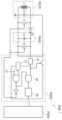
도 8 및 도 13을 참조하면, 입력 장치(2000-4)는 공진 회로부(PN100-1), 구동 제어부(PN210), 방전 제어부(PN220), 전원부(PN300), 및 정류 회로(PN400)를 포함할 수 있다.8 and 13, the input device 2000-4 includes a resonance circuit unit PN100-1, a drive control unit PN210, a discharge control unit PN220, a power supply unit PN300, and a rectifier circuit PN400. can do.
공진 회로부(PN100-1)는 제1 커패시터(C1-1) 및 제1 인덕터(L1-1)를 포함할 수 있다. 제1 커패시터(C1-1)는 제1 구동 신호(S1) 또는 제2 구동 신호(S2)에 의한 전류의 흐름을 전기장으로 저장할 수 있다. 제1 인덕터(L1-1)는 제1 커패시터(C1-1)와 전기적으로 연결될 수 있다. 제1 커패시터(C1)는 구동 제어부(PN210) 및 제1 인덕터(L1-1) 사이에 직렬 연결될 수 있다. 제1 인덕터(L1-1)는 제1 구동 신호(S1) 또는 제2 구동 신호(S2)에 의한 전류의 흐름을 자기장으로 저장할 수 있다.The resonance circuit unit PN100-1 may include a first capacitor C1-1 and a first inductor L1-1. The first capacitor C1-1 may store the flow of current caused by the first driving signal S1 or the second driving signal S2 as an electric field. The first inductor L1-1 may be electrically connected to the first capacitor C1-1. The first capacitor C1 may be connected in series between the drive controller PN210 and the first inductor L1-1. The first inductor L1 - 1 may store the flow of current caused by the first driving signal S1 or the second driving signal S2 as a magnetic field.
펄스 생성부(PG, 도 9 참조)가 펄스 생성을 중지하였을 때 펄스 생성부(PG, 도 9 참조)의 출력은 그라운드 전극에 연결될 수 있다.When the pulse generator (PG, see FIG. 9) stops generating pulses, an output of the pulse generator (PG, see FIG. 9) may be connected to the ground electrode.
공진 회로부(PN100)가 제1 구동 신호(S1)에 의해 충전될 때, 공진되는 주파수는 공진 회로부(PN100)가 제2 구동 신호(S2)에 의해 충전될 때, 공진되는 주파수와 동일할 수 있다.When the resonance circuit unit PN100 is charged by the first driving signal S1, the resonance frequency may be the same as the resonance frequency when the resonance circuit unit PN100 is charged by the second driving signal S2. .
도 14는 본 발명의 일 실시예에 따른 입력 장치를 도시한 것이다. 도 14 를 설명함에 있어서, 도 13을 통해 설명된 구성 요소에 대해서는 동일한 도면 부호를 병기하고 이에 대한 설명은 생략된다.14 illustrates an input device according to an embodiment of the present invention. In the description of FIG. 14, the same reference numerals are used for the components described through FIG. 13, and descriptions thereof are omitted.
도 8 및 도 14를 참조하면, 입력 장치(2000-5)는 공진 회로부(PN100-2), 구동 제어부(PN210-1), 방전 제어부(PN220), 전원부(PN300), 및 정류 회로(PN400)를 포함할 수 있다.8 and 14, the input device 2000-5 includes a resonance circuit unit PN100-2, a drive control unit PN210-1, a discharge control unit PN220, a power supply unit PN300, and a rectifier circuit PN400. can include
공진 회로부(PN100-2)는 제1 커패시터(C1-2) 및 제1 인덕터(L1-1)를 포함할 수 있다. 제1 커패시터(C1-2)는 가변 커패시터일 수 있다.The resonance circuit unit PN100-2 may include a first capacitor C1-2 and a first inductor L1-1. The first capacitor C1 - 2 may be a variable capacitor.
구동 제어부(PN210-1)는 커패시턴스 제어부(CC)를 더 포함할 수 있다. 커패시턴스 제어부(CC)는 제1 커패시터(C1-2)의 커패시턴스를 조절할 수 있다.The driving controller PN210-1 may further include a capacitance controller CC. The capacitance controller CC may adjust the capacitance of the first capacitor C1-2.
커패시턴스 제어부(CC)에 의해 입력 장치(2000-5)에 의한 입력(S3)의 공진 주파수가 가변될 수 있다. 전자 장치(1000, 도 1a 참조)는 가변된 공진 주파수를 근거로 입력(S3)으로부터 정보를 추출할 수 있다.The resonance frequency of the input S3 of the input device 2000-5 may be varied by the capacitance controller CC. The electronic device 1000 (see FIG. 1A ) may extract information from the input S3 based on the changed resonant frequency.
예를 들어, 입력 장치(2000-5)는 버튼을 더 포함할 수 있고, 상기 정보는 상기 버튼의 조작에 대한 정보를 포함할 수 있다. 상기 버튼은 입력 장치(2000-5)를 사용하는 사용자에 의해 조작될 수 있다. 상기 정보에 의해 입력 장치(2000-5)는 펜 입력 모드, 우측 클릭 모드, 또는 지우개 모드 등으로 전환될 수 있다.For example, the input device 2000-5 may further include a button, and the information may include information about manipulation of the button. The button may be manipulated by a user using the input device 2000-5. Based on the above information, the input device 2000-5 can be switched to a pen input mode, a right-click mode, or an eraser mode.
또는 상기 정보는 필압에 대한 정보를 포함할 수 있다. 커패시턴스 제어부(CC)는 펜 팁(PNT, 도 4 참조)에 적용되는 압력을 감지하여 공진 주파수를 가변시킬 수 있다.Alternatively, the information may include information on pen pressure. The capacitance control unit CC may change the resonance frequency by detecting pressure applied to the pen tip (PNT, see FIG. 4).
도 15a 및 도 15b는 본 발명의 일 실시예에 따른 입력 장치를 도시한 것들이다. 도 15a 및 도 15b를 설명함에 있어서, 도 9를 통해 설명된 구성 요소에 대해서는 동일한 도면 부호를 병기하고 이에 대한 설명은 생략된다.15A and 15B show an input device according to an embodiment of the present invention. In the description of FIGS. 15A and 15B , the same reference numerals are used for components described through FIG. 9 , and descriptions thereof are omitted.
도 8 및 도 15a를 참조하면, 입력 장치(2000-6)는 공진 회로부(PN100), 제어부(PN200-1), 전원부(PN300), 및 정류 회로(PN400)를 포함할 수 있다.Referring to FIGS. 8 and 15A , the input device 2000-6 may include a resonance circuit unit PN100, a control unit PN200-1, a power supply unit PN300, and a rectifier circuit PN400.
제어부(PN200-1)는 펄스 조절부(PC)를 더 포함할 수 있다. 펄스 조절부(PC)는 펄스 생성부(PG)와 연결될 수 있다. 펄스 조절부(PC)는 제2 구동 신호(S2)의 위상 및 주파수를 변화시킬 수 있다.The control unit PN200-1 may further include a pulse control unit (PC). The pulse controller PC may be connected to the pulse generator PG. The pulse control unit PC may change the phase and frequency of the second driving signal S2.
공진 회로부(PN100)는 제2 구동 신호(S2)에 의해 충전될 수 있다. 공진 회로부(PN100)는 제2 구동 신호(S2)를 근거로 제2 자기장이 생성될 수 있다. 전자 장치(1000, 도 1a 참조)는 공진 회로부(PN100)에 충전된 제2 구동 신호(S2)를 근거로 입력 장치(2000-5)에 의한 입력(S3)을 감지할 수 있다.The resonance circuit unit PN100 may be charged by the second driving signal S2. The resonant circuit unit PN100 may generate a second magnetic field based on the second driving signal S2. The electronic device 1000 (see FIG. 1A ) may detect an input S3 by the input device 2000 - 5 based on the second driving signal S2 charged in the resonance circuit unit PN100 .
전자 장치(1000, 도 1a 참조)는 지연된 위상을 근거로 입력(S3)으로부터 정보를 추출할 수 있다.The electronic device 1000 (see FIG. 1A ) may extract information from the input S3 based on the delayed phase.
도 8 및 도 15b를 참조하면, 입력 장치(2000-7)는 공진 회로부(PN100), 제어부(PN200-2), 전원부(PN300), 및 정류 회로(PN400)를 포함할 수 있다.Referring to FIGS. 8 and 15B , the input device 2000-7 may include a resonance circuit unit PN100, a control unit PN200-2, a power supply unit PN300, and a rectifier circuit PN400.
제어부(PN200-2)는 카운팅부(CI)를 더 포함할 수 있다. 카운팅부(CI)는 카운터(CT)와 연결될 수 있다. 카운팅부(CI)는 제2 구동 신호(S2)의 펄스의 개수를 변화시킬 수 있다.The control unit PN200-2 may further include a counting unit CI. The counting unit CI may be connected to the counter CT. The counting unit CI may change the number of pulses of the second driving signal S2.
공진 회로부(PN100)는 제2 구동 신호(S2)에 의해 충전될 수 있다. 공진 회로부(PN100)는 제2 구동 신호(S2)를 근거로 제2 자기장이 생성될 수 있다. 전자 장치(1000, 도 1a 참조)는 공진 회로부(PN100)에 충전된 제2 구동 신호(S2)를 근거로 입력 장치(2000-6)에 의한 입력(S3)을 감지할 수 있다.The resonance circuit unit PN100 may be charged by the second driving signal S2. The resonant circuit unit PN100 may generate a second magnetic field based on the second driving signal S2. The electronic device 1000 (see FIG. 1A ) may detect an input S3 by the input device 2000 - 6 based on the second driving signal S2 charged in the resonance circuit unit PN100 .
전자 장치(1000, 도 1a 참조)는 제2 구동 신호(S2)의 펄스의 개수를 근거로 입력(S3)으로부터 정보를 추출할 수 있다.The electronic device 1000 (see FIG. 1A ) may extract information from the input S3 based on the number of pulses of the second driving signal S2 .
이상에서는 본 발명의 바람직한 실시예를 참조하여 설명하였지만, 해당 기술 분야의 숙련된 당업자 또는 해당 기술 분야에 통상의 지식을 갖는 자라면, 후술될 특허청구범위에 기재된 본 발명의 사상 및 기술 영역으로부터 벗어나지 않는 범위 내에서 본 발명을 다양하게 수정 및 변경시킬 수 있음을 이해할 수 있을 것이다. 따라서, 본 발명의 기술적 범위는 명세서의 상세한 설명에 기재된 내용으로 한정되는 것이 아니라 특허청구범위에 의해 정하여져야만 할 것이다.Although the above has been described with reference to preferred embodiments of the present invention, those skilled in the art or those having ordinary knowledge in the art do not deviate from the spirit and technical scope of the present invention described in the claims to be described later. It will be understood that the present invention can be variously modified and changed within the scope not specified. Therefore, the technical scope of the present invention is not limited to the contents described in the detailed description of the specification, but should be defined by the claims.
10000: 인터페이스 장치1000: 전자 장치
2000: 입력 장치100: 표시층
300: 감지층PN100: 공진 회로부
PN200: 제어부PN300: 전원부10000: interface device 1000: electronic device
2000: input device 100: display layer
300: sensing layer PN100: resonance circuit
PN200: control part PN300: power part
Claims (20)
Translated fromKorean상기 전자 장치는,
표시층; 및
상기 표시층 아래에 배치되고, 상기 입력 장치에 제1 구동 신호를 송신하며, 상기 입력 장치에 의한 입력을 감지하는 감지층을 포함하고,
상기 입력 장치는,
상기 제1 구동 신호를 근거로 제1 자기장이 생성되는 공진 회로부;
상기 공진 회로부를 제어하는 제어부; 및
상기 제어부에 전원을 제공하는 전원부를 포함하고,
상기 공진 회로부에는 상기 전원에 의해 제2 자기장이 생성되고,
상기 감지층은 제2 자기장을 근거로 상기 입력을 감지하는 인터페이스 장치.an electronic device and an input device in communication with the electronic device;
The electronic device,
display layer; and
a sensing layer disposed below the display layer, transmitting a first driving signal to the input device, and sensing an input by the input device;
The input device,
a resonant circuit unit generating a first magnetic field based on the first driving signal;
a control unit controlling the resonant circuit unit; and
A power supply unit providing power to the control unit;
A second magnetic field is generated in the resonant circuit unit by the power supply,
The sensing layer senses the input based on a second magnetic field.
상기 제어부는,
상기 공진 회로부에 상기 전원을 근거로 생성된 제2 구동 신호를 송신하는 구동 제어부; 및
상기 공진 회로부를 방전시키는 방전 제어부를 포함하는 인터페이스 장치.According to claim 1,
The control unit,
a driving control unit transmitting a second driving signal generated based on the power to the resonance circuit unit; and
Interface device including a discharge control unit for discharging the resonant circuit unit.
상기 제어부는,
개시 신호를 수신하고, 상기 공진 회로부와 연결된 레벨 쉬프터(level shifter);
상기 레벨 쉬프터와 연결되고, 상기 개시 신호를 수신하면 카운팅을 개시하는 카운터;
상기 카운터 및 상기 레벨 쉬프터와 연결되고, 상기 제2 구동 신호를 생성하는 펄스 생성부; 및
상기 레벨 쉬프터, 상기 카운터, 및 상기 펄스 생성부를 연결하는 논리 소자를 포함하는 인터페이스 장치.According to claim 2,
The control unit,
a level shifter that receives a start signal and is connected to the resonant circuit unit;
a counter connected to the level shifter and starting counting when receiving the start signal;
a pulse generator connected to the counter and the level shifter and configured to generate the second driving signal; and
An interface device including a logic element connecting the level shifter, the counter, and the pulse generator.
상기 제어부는 상기 제2 구동 신호의 위상 및 주파수를 변화시키고 상기 펄스 생성부와 연결된 펄스 조절부를 더 포함하는 인터페이스 장치.According to claim 3,
wherein the control unit changes a phase and frequency of the second driving signal and further comprises a pulse control unit connected to the pulse generator.
상기 제어부는 상기 제2 구동 신호의 펄스의 개수를 변화시키고 카운터와 연결된 카운팅부를 더 포함하는 인터페이스 장치.According to claim 3,
wherein the control unit changes the number of pulses of the second driving signal and further comprises a counting unit connected to a counter.
상기 제2 자기장은 상기 제2 구동 신호를 근거로 생성되는 인터페이스 장치.According to claim 2,
The second magnetic field is generated based on the second driving signal interface device.
상기 공진 회로부는,
상기 제1 구동 신호 및 상기 제2 구동 신호에 의한 전류의 흐름을 전기장으로 저장하는 제1 커패시터; 및
상기 제1 커패시터와 전기적으로 연결되고, 상기 제1 구동 신호 및 상기 제2 구동 신호에 의한 전류의 흐름을 자기장으로 저장하는 제1 인덕터를 포함하는 인터페이스 장치.According to claim 2,
The resonant circuit part,
a first capacitor that stores the flow of current caused by the first driving signal and the second driving signal as an electric field; and
and a first inductor electrically connected to the first capacitor and storing a flow of current caused by the first driving signal and the second driving signal as a magnetic field.
상기 입력 장치는 상기 공진 회로부 및 상기 구동 제어부 사이에 전기적으로 연결된 제2 커패시터를 더 포함하는 인터페이스 장치.According to claim 7,
The input device further comprises a second capacitor electrically connected between the resonant circuit unit and the driving control unit.
상기 입력 장치는 상기 공진 회로부 및 상기 구동 제어부 사이에 전기적으로 연결된 제2 인덕터를 더 포함하는 인터페이스 장치.According to claim 8,
The input device further comprises a second inductor electrically connected between the resonant circuit unit and the driving control unit.
상기 감지층으로부터 상기 제1 구동 신호가 제공되는 경우 상기 제2 인덕터는 상기 공진 회로부와 전기적으로 연결되고,
상기 구동 제어부로부터 상기 제2 구동 신호가 제공되는 경우 상기 제2 인덕터는 상기 공진 회로부와 전기적으로 절연되는 인터페이스 장치.According to claim 9,
When the first driving signal is provided from the sensing layer, the second inductor is electrically connected to the resonance circuit unit,
When the second driving signal is provided from the driving controller, the second inductor is electrically insulated from the resonant circuit unit.
상기 제1 커패시터는 상기 구동 제어부 및 상기 제1 인덕터 사이에 직렬 연결되는 인터페이스 장치.According to claim 7,
The first capacitor is connected in series between the driving control unit and the first inductor.
상기 제2 커패시터는 가변 커패시터인 인터페이스 장치.According to claim 8,
The second capacitor is a variable capacitor interface device.
상기 감지층은 디지타이저를 포함하는 인터페이스 장치.According to claim 1,
The sensing layer interface device including a digitizer.
상기 전자 장치가 제1 구동 신호를 상기 입력 장치에 송신하는 단계;
상기 공진 회로부가 상기 제1 구동 신호에 의해 충전되는 단계;
상기 입력 장치가 제2 구동 신호를 생성하는 단계;
상기 공진 회로부가 상기 제2 구동 신호에 의해 충전되는 단계; 및
상기 전자 장치가 상기 공진 회로부에 충전된 상기 제2 구동 신호를 근거로 상기 입력 장치에 의한 입력을 감지하는 단계를 포함하는 인터페이스 장치 구동 방법.providing an input device and an electronic device including a control unit and a resonant circuit unit;
transmitting, by the electronic device, a first driving signal to the input device;
charging the resonant circuit part by the first driving signal;
generating a second drive signal by the input device;
charging the resonant circuit part by the second driving signal; and
and sensing, by the electronic device, an input by the input device based on the second driving signal charged in the resonant circuit unit.
상기 제2 구동 신호를 생성하는 단계는,
카운팅을 개시하는 단계;
펄스를 생성하는 단계; 및
상기 카운팅이 한계값에 도달하는 경우 상기 카운팅을 중지하는 단계를 포함하는 인터페이스 장치 구동 방법.According to claim 14,
Generating the second driving signal,
initiating counting;
generating a pulse; and
and stopping the counting when the counting reaches a threshold value.
상기 공진 회로부가 방전되는 단계를 더 포함하고,
상기 공진 회로부가 방전되는 단계는 상기 전자 장치가 상기 입력을 감지하는 단계 이후에 진행되는 인터페이스 장치 구동 방법.According to claim 15,
Further comprising the step of discharging the resonant circuit unit,
The step of discharging the resonance circuit unit is performed after the step of sensing the input by the electronic device.
상기 공진 회로부가 방전되는 단계는 상기 카운팅을 중지하는 단계 이후에 진행되는 인터페이스 장치 구동 방법.According to claim 16,
The step of discharging the resonance circuit unit is performed after the step of stopping the counting.
상기 공진 회로부가 제1 구동 신호에 의해 충전되는 단계는 상기 공진 회로부가 제1 주파수로 공진되는 단계를 포함하고,
상기 공진 회로부가 제2 구동 신호에 의해 충전되는 단계는 상기 공진 회로부가 상기 제1 주파수와 상이한 제2 주파수로 공진되는 단계를 포함하는 인터페이스 장치 구동 방법.According to claim 14,
The step of charging the resonance circuit unit by the first driving signal includes resonating the resonance circuit unit at a first frequency,
The step of charging the resonance circuit unit by the second driving signal includes resonating the resonance circuit unit at a second frequency different from the first frequency.
트리거 신호가 소정의 레벨에 도달하면 상기 제어부가 동작하는 단계를 더 포함하고,
상기 트리거 신호는 상기 공진 회로부의 충전을 근거로 레벨이 변화하는 인터페이스 장치 구동 방법.According to claim 14.
Further comprising operating the control unit when the trigger signal reaches a predetermined level,
A method of driving an interface device in which a level of the trigger signal is changed based on charging of the resonant circuit unit.
상기 제어부가 동작하는 단계는 상기 공진 회로부가 제1 구동 신호에 의해 충전되는 단계 및 상기 제2 구동 신호를 생성하는 단계 사이에 진행되는 인터페이스 장치 구동 방법.
According to claim 19,
The operation of the control unit is performed between charging the resonant circuit unit by the first driving signal and generating the second driving signal.
Priority Applications (3)
| Application Number | Priority Date | Filing Date | Title |
|---|---|---|---|
| KR1020210095373AKR20230014899A (en) | 2021-07-21 | 2021-07-21 | Interface device and interface device driving method using the same |
| US17/659,437US11755145B2 (en) | 2021-07-21 | 2022-04-15 | Interface device including a sensing layer transmitting a driving signal and interface device driving method using the same |
| CN202210853284.3ACN115686257A (en) | 2021-07-21 | 2022-07-08 | Interface device and interface device driving method |
Applications Claiming Priority (1)
| Application Number | Priority Date | Filing Date | Title |
|---|---|---|---|
| KR1020210095373AKR20230014899A (en) | 2021-07-21 | 2021-07-21 | Interface device and interface device driving method using the same |
Publications (1)
| Publication Number | Publication Date |
|---|---|
| KR20230014899Atrue KR20230014899A (en) | 2023-01-31 |
Family
ID=84977632
Family Applications (1)
| Application Number | Title | Priority Date | Filing Date |
|---|---|---|---|
| KR1020210095373APendingKR20230014899A (en) | 2021-07-21 | 2021-07-21 | Interface device and interface device driving method using the same |
Country Status (3)
| Country | Link |
|---|---|
| US (1) | US11755145B2 (en) |
| KR (1) | KR20230014899A (en) |
| CN (1) | CN115686257A (en) |
Cited By (1)
| Publication number | Priority date | Publication date | Assignee | Title |
|---|---|---|---|---|
| WO2024258017A1 (en)* | 2023-06-16 | 2024-12-19 | 삼성전자주식회사 | Digital pen capable of frequency switching |
Families Citing this family (1)
| Publication number | Priority date | Publication date | Assignee | Title |
|---|---|---|---|---|
| JP2020187427A (en)* | 2019-05-10 | 2020-11-19 | 株式会社ジャパンディスプレイ | Sensor device |
Family Cites Families (6)
| Publication number | Priority date | Publication date | Assignee | Title |
|---|---|---|---|---|
| KR101975596B1 (en)* | 2012-08-29 | 2019-05-07 | 삼성전자주식회사 | Touch screen device for compensating distortion of input sensing signal |
| CN103606360B (en) | 2013-11-25 | 2016-03-09 | 深圳市华星光电技术有限公司 | Liquid crystal panel drive circuit, driving method and liquid crystal display |
| JP6215672B2 (en) | 2013-11-27 | 2017-10-18 | 株式会社ワコム | Electrostatic stylus pen |
| KR102318806B1 (en)* | 2017-05-11 | 2021-10-28 | 삼성전자주식회사 | Method for charging pen and an electronic device thereof |
| KR102592900B1 (en) | 2018-07-09 | 2023-10-24 | 삼성전자주식회사 | Electronic device for charging battery of external electronic device and method thereof |
| KR102227274B1 (en) | 2018-08-09 | 2021-03-15 | 삼성전자주식회사 | Electronic pen device including a button, method for operation in the electronic pen device and system |
- 2021
- 2021-07-21KRKR1020210095373Apatent/KR20230014899A/enactivePending
- 2022
- 2022-04-15USUS17/659,437patent/US11755145B2/enactiveActive
- 2022-07-08CNCN202210853284.3Apatent/CN115686257A/enactivePending
Cited By (1)
| Publication number | Priority date | Publication date | Assignee | Title |
|---|---|---|---|---|
| WO2024258017A1 (en)* | 2023-06-16 | 2024-12-19 | 삼성전자주식회사 | Digital pen capable of frequency switching |
Also Published As
| Publication number | Publication date |
|---|---|
| US20230025138A1 (en) | 2023-01-26 |
| US11755145B2 (en) | 2023-09-12 |
| CN115686257A (en) | 2023-02-03 |
Similar Documents
| Publication | Publication Date | Title |
|---|---|---|
| EP3786761A1 (en) | Sensing panel having fingerprint sensing pixel and electronic pen sensing pixel and display device having the sensing panel | |
| CN108021282A (en) | Electronic equipment with power touch function | |
| US11600805B2 (en) | Display device | |
| KR102794080B1 (en) | Display device | |
| KR20230014899A (en) | Interface device and interface device driving method using the same | |
| KR20230006742A (en) | Electronic device | |
| KR20220043964A (en) | Electronic device and interface device including the same | |
| CN118363498A (en) | Electronic devices for sensing touch | |
| EP4083764B1 (en) | Electronic device and interface system including the same | |
| US11663968B2 (en) | Display device and driving method thereof | |
| KR102413395B1 (en) | Display device with integrated touch screen | |
| US12229369B2 (en) | Electronic device capable of determining placement into a pocket and method of driving electronic device | |
| KR102840044B1 (en) | Electronic pen and interface device including the same | |
| KR20230148472A (en) | Electronic device | |
| CN113970980A (en) | Input device and interface device including the same | |
| KR20220046044A (en) | Electronic device | |
| US11928280B2 (en) | Electronic device | |
| US20250261525A1 (en) | Electronic device including an electronic module and a manufacturing method thereof | |
| US12216868B2 (en) | Input sensing unit and display device including the same | |
| US20230168781A1 (en) | Electronic device | |
| KR20230105715A (en) | Input device and electronic device comprising the same | |
| CN116708620A (en) | Electronic device | |
| CN115223474A (en) | Display device and proximity sensing method using input sensor | |
| CN120076616A (en) | Light-emitting display device | |
| KR20220094295A (en) | Display device |
Legal Events
| Date | Code | Title | Description |
|---|---|---|---|
| PA0109 | Patent application | Patent event code:PA01091R01D Comment text:Patent Application Patent event date:20210721 | |
| PG1501 | Laying open of application | ||
| PA0201 | Request for examination | Patent event code:PA02012R01D Patent event date:20240625 Comment text:Request for Examination of Application |