KR20230012016A - Pattern measurement method - Google Patents
Pattern measurement methodDownload PDFInfo
- Publication number
- KR20230012016A KR20230012016AKR1020227043907AKR20227043907AKR20230012016AKR 20230012016 AKR20230012016 AKR 20230012016AKR 1020227043907 AKR1020227043907 AKR 1020227043907AKR 20227043907 AKR20227043907 AKR 20227043907AKR 20230012016 AKR20230012016 AKR 20230012016A
- Authority
- KR
- South Korea
- Prior art keywords
- pattern
- cad
- edge
- measurement
- actual
- Prior art date
- Legal status (The legal status is an assumption and is not a legal conclusion. Google has not performed a legal analysis and makes no representation as to the accuracy of the status listed.)
- Pending
Links
Images


Classifications
- G—PHYSICS
- G06—COMPUTING OR CALCULATING; COUNTING
- G06T—IMAGE DATA PROCESSING OR GENERATION, IN GENERAL
- G06T7/00—Image analysis
- G06T7/0002—Inspection of images, e.g. flaw detection
- G06T7/0004—Industrial image inspection
- G06T7/001—Industrial image inspection using an image reference approach
- H—ELECTRICITY
- H01—ELECTRIC ELEMENTS
- H01L—SEMICONDUCTOR DEVICES NOT COVERED BY CLASS H10
- H01L22/00—Testing or measuring during manufacture or treatment; Reliability measurements, i.e. testing of parts without further processing to modify the parts as such; Structural arrangements therefor
- H01L22/10—Measuring as part of the manufacturing process
- H01L22/12—Measuring as part of the manufacturing process for structural parameters, e.g. thickness, line width, refractive index, temperature, warp, bond strength, defects, optical inspection, electrical measurement of structural dimensions, metallurgic measurement of diffusions
- G—PHYSICS
- G06—COMPUTING OR CALCULATING; COUNTING
- G06T—IMAGE DATA PROCESSING OR GENERATION, IN GENERAL
- G06T7/00—Image analysis
- G06T7/10—Segmentation; Edge detection
- G06T7/13—Edge detection
- G—PHYSICS
- G06—COMPUTING OR CALCULATING; COUNTING
- G06T—IMAGE DATA PROCESSING OR GENERATION, IN GENERAL
- G06T7/00—Image analysis
- G06T7/30—Determination of transform parameters for the alignment of images, i.e. image registration
- G06T7/33—Determination of transform parameters for the alignment of images, i.e. image registration using feature-based methods
- G06T7/337—Determination of transform parameters for the alignment of images, i.e. image registration using feature-based methods involving reference images or patches
- G—PHYSICS
- G06—COMPUTING OR CALCULATING; COUNTING
- G06T—IMAGE DATA PROCESSING OR GENERATION, IN GENERAL
- G06T7/00—Image analysis
- G06T7/60—Analysis of geometric attributes
- G—PHYSICS
- G06—COMPUTING OR CALCULATING; COUNTING
- G06T—IMAGE DATA PROCESSING OR GENERATION, IN GENERAL
- G06T7/00—Image analysis
- G06T7/60—Analysis of geometric attributes
- G06T7/62—Analysis of geometric attributes of area, perimeter, diameter or volume
- G—PHYSICS
- G06—COMPUTING OR CALCULATING; COUNTING
- G06T—IMAGE DATA PROCESSING OR GENERATION, IN GENERAL
- G06T7/00—Image analysis
- G06T7/70—Determining position or orientation of objects or cameras
- H—ELECTRICITY
- H01—ELECTRIC ELEMENTS
- H01L—SEMICONDUCTOR DEVICES NOT COVERED BY CLASS H10
- H01L22/00—Testing or measuring during manufacture or treatment; Reliability measurements, i.e. testing of parts without further processing to modify the parts as such; Structural arrangements therefor
- H—ELECTRICITY
- H01—ELECTRIC ELEMENTS
- H01L—SEMICONDUCTOR DEVICES NOT COVERED BY CLASS H10
- H01L22/00—Testing or measuring during manufacture or treatment; Reliability measurements, i.e. testing of parts without further processing to modify the parts as such; Structural arrangements therefor
- H01L22/20—Sequence of activities consisting of a plurality of measurements, corrections, marking or sorting steps
- G—PHYSICS
- G01—MEASURING; TESTING
- G01N—INVESTIGATING OR ANALYSING MATERIALS BY DETERMINING THEIR CHEMICAL OR PHYSICAL PROPERTIES
- G01N2223/00—Investigating materials by wave or particle radiation
- G01N2223/40—Imaging
- G01N2223/421—Imaging digitised image, analysed in real time (recognition algorithms)
- G—PHYSICS
- G01—MEASURING; TESTING
- G01N—INVESTIGATING OR ANALYSING MATERIALS BY DETERMINING THEIR CHEMICAL OR PHYSICAL PROPERTIES
- G01N2223/00—Investigating materials by wave or particle radiation
- G01N2223/60—Specific applications or type of materials
- G01N2223/611—Specific applications or type of materials patterned objects; electronic devices
- G—PHYSICS
- G01—MEASURING; TESTING
- G01N—INVESTIGATING OR ANALYSING MATERIALS BY DETERMINING THEIR CHEMICAL OR PHYSICAL PROPERTIES
- G01N23/00—Investigating or analysing materials by the use of wave or particle radiation, e.g. X-rays or neutrons, not covered by groups G01N3/00 – G01N17/00, G01N21/00 or G01N22/00
- G01N23/22—Investigating or analysing materials by the use of wave or particle radiation, e.g. X-rays or neutrons, not covered by groups G01N3/00 – G01N17/00, G01N21/00 or G01N22/00 by measuring secondary emission from the material
- G01N23/225—Investigating or analysing materials by the use of wave or particle radiation, e.g. X-rays or neutrons, not covered by groups G01N3/00 – G01N17/00, G01N21/00 or G01N22/00 by measuring secondary emission from the material using electron or ion
- G01N23/2251—Investigating or analysing materials by the use of wave or particle radiation, e.g. X-rays or neutrons, not covered by groups G01N3/00 – G01N17/00, G01N21/00 or G01N22/00 by measuring secondary emission from the material using electron or ion using incident electron beams, e.g. scanning electron microscopy [SEM]
- G—PHYSICS
- G06—COMPUTING OR CALCULATING; COUNTING
- G06T—IMAGE DATA PROCESSING OR GENERATION, IN GENERAL
- G06T2207/00—Indexing scheme for image analysis or image enhancement
- G06T2207/10—Image acquisition modality
- G06T2207/10056—Microscopic image
- G06T2207/10061—Microscopic image from scanning electron microscope
- G—PHYSICS
- G06—COMPUTING OR CALCULATING; COUNTING
- G06T—IMAGE DATA PROCESSING OR GENERATION, IN GENERAL
- G06T2207/00—Indexing scheme for image analysis or image enhancement
- G06T2207/30—Subject of image; Context of image processing
- G06T2207/30108—Industrial image inspection
- G06T2207/30148—Semiconductor; IC; Wafer
- G—PHYSICS
- G06—COMPUTING OR CALCULATING; COUNTING
- G06T—IMAGE DATA PROCESSING OR GENERATION, IN GENERAL
- G06T2207/00—Indexing scheme for image analysis or image enhancement
- G06T2207/30—Subject of image; Context of image processing
- G06T2207/30108—Industrial image inspection
- G06T2207/30164—Workpiece; Machine component
Landscapes
- Engineering & Computer Science (AREA)
- Physics & Mathematics (AREA)
- Theoretical Computer Science (AREA)
- Computer Vision & Pattern Recognition (AREA)
- General Physics & Mathematics (AREA)
- Manufacturing & Machinery (AREA)
- Computer Hardware Design (AREA)
- Microelectronics & Electronic Packaging (AREA)
- Power Engineering (AREA)
- Geometry (AREA)
- Quality & Reliability (AREA)
- Length-Measuring Devices Using Wave Or Particle Radiation (AREA)
- Testing Or Measuring Of Semiconductors Or The Like (AREA)
Abstract
Translated fromKoreanDescription
Translated fromKorean본 발명은, 주사 전자 현미경 등의 화상 생성 장치에 의해 생성된 화상 상의 패턴의 치수(Critical Dimension) 등의 특징량을 측정하는 방법에 관한 것으로, 특히 웨이퍼, 마스크, 패널, 기판 등의 워크피스에 형성된 패턴의 치수 등의 특징량의 측정 레시피를 자동적으로 결정하는 방법에 관한 것이다.The present invention relates to a method for measuring feature quantities such as critical dimensions of a pattern on an image generated by an image generating device such as a scanning electron microscope, and particularly to workpieces such as wafers, masks, panels, and substrates. It relates to a method of automatically determining a measurement recipe for characteristic quantities such as the dimensions of formed patterns.
웨이퍼, 마스크, 패널, 기판 등의 워크피스에 형성된 패턴은, 통상, 직선적인 에지나 코너 에지 등의 다양한 형상의 에지를 갖고 있다. 패턴은, 설계 데이터(CAD 데이터라고도 함)에 따라서 워크피스의 표면에 형성된다. CD(Critical Dimension) 측정에서는, 워크피스 상에 형성된 패턴의 화상을 주사 전자 현미경으로 생성하고, 화상 상의 패턴의 치수를 측정한다.Patterns formed on workpieces such as wafers, masks, panels, and substrates usually have edges of various shapes such as straight edges and corner edges. A pattern is formed on the surface of the workpiece according to design data (also referred to as CAD data). In CD (Critical Dimension) measurement, an image of a pattern formed on a workpiece is created with a scanning electron microscope, and the dimension of the pattern on the image is measured.
치수의 측정은, 패턴 결함이 일어나기 쉬운 많은 측정점에서 실시된다. 이들 측정점은, 설계 데이터 내에 정의된 좌표계 상에 특정된다. 이러한 치수 측정에서는, 측정 대상으로 되는 패턴에 적합한 측정 레시피가 측정점마다 수동으로 설정된다.Measurement of dimensions is performed at many measurement points where pattern defects tend to occur. These measurement points are specified on a coordinate system defined in the design data. In such dimension measurement, a measurement recipe suitable for a pattern to be measured is manually set for each measurement point.
프로세스의 미세화에 수반하여, 측정의 정밀도를 올리기 위하여 다수의 측정점에 있어서 패턴 치수를 측정하는 것이 요구되고 있다. 그러나, 종래의 측정 방법에서는, 모든 측정점에 대하여 수동으로 측정 레시피의 설정이 필요하게 되고, 치수 측정을 위한 준비에 방대한 시간이 걸린다.With the miniaturization of the process, it is required to measure the pattern dimensions at a large number of measurement points in order to increase the accuracy of the measurement. However, in the conventional measurement method, it is necessary to manually set a measurement recipe for all measurement points, and it takes a great deal of time to prepare for dimension measurement.
그래서, 본 발명은, 패턴의 폭 치수 등의 특징량의 측정 레시피를 자동적으로 결정할 수 있는 패턴 측정 방법을 제공한다.Then, the present invention provides a pattern measuring method capable of automatically determining a measurement recipe for characteristic quantities such as the width of a pattern.
일 양태에서는, 설계 데이터 내에 정의된 좌표계 상의 측정점과 CAD 패턴의 상대 위치 및 상기 CAD 패턴의 면적에 기초하여 상기 CAD 패턴의 타입 및 측정 레시피를 결정하고, 상기 CAD 패턴에 대응하는 화상 상의 실제 패턴과, 상기 CAD 패턴의 위치 정렬을 행하여, 상기 결정된 측정 레시피에 따라서 상기 실제 패턴의 특징량을 측정하는, 방법이 제공된다.In one aspect, the type and measurement recipe of the CAD pattern are determined based on the relative position of the CAD pattern and the measurement point on the coordinate system defined in the design data, and the area of the CAD pattern, and the actual pattern on the image corresponding to the CAD pattern and , performing positional alignment of the CAD pattern, and measuring the feature amount of the actual pattern according to the determined measurement recipe.
일 양태에서는, 상기 CAD 패턴의 타입은 고립 패턴, 직선 패턴, 곡선 패턴 및 종단부 패턴을 적어도 포함하는 복수의 타입에서 선택된 하나이다.In one aspect, the type of the CAD pattern is one selected from a plurality of types including at least an isolated pattern, a straight line pattern, a curved pattern, and an end pattern.
일 양태에서는, 상기 측정 레시피는, 상기 화상 상의 실제 패턴의 폭의 측정, 상기 화상 상의 실제 패턴 사이의 거리의 측정 및 상기 화상 상의 실제 패턴의 에지의 위치 어긋남의 측정을 적어도 포함하는 복수의 측정 레시피에서 선택된 하나이다.In one aspect, the measurement recipe includes a plurality of measurement recipes including at least measurement of a width of an actual pattern on the image, measurement of a distance between actual patterns on the image, and measurement of a misalignment of an edge of the actual pattern on the image. one selected from
일 양태에서는, 상기 CAD 패턴의 면적이 미리 정해진 면적보다도 작을 때는, 상기 CAD 패턴은 고립 패턴이라고 결정된다.In one aspect, when the area of the CAD pattern is smaller than a predetermined area, the CAD pattern is determined to be an isolated pattern.
일 양태에서는, 상기 측정점에 가장 가까운 상기 CAD 패턴의 제1 에지와, 상기 측정점을 넘어서 상기 제1 에지와는 반대측에 있는 제2 에지가 소정의 탐색 영역 내에 있어서 정점을 갖고 있지 않을 때는, 상기 CAD 패턴은 직선 패턴이라고 결정된다.In one aspect, when a first edge of the CAD pattern closest to the measurement point and a second edge on the opposite side of the first edge beyond the measurement point are within a predetermined search area and do not have a vertex, the CAD The pattern is determined to be a straight line pattern.
일 양태에서는, 상기 제1 에지 및 상기 제2 에지 중 적어도 한쪽이 상기 소정의 탐색 영역 내에 있어서 정점을 갖고 있을 때는, 상기 CAD 패턴은 곡선 패턴이라고 결정된다.In one aspect, when at least one of the first edge and the second edge has a vertex within the predetermined search area, the CAD pattern is determined to be a curve pattern.
일 양태에서는, 상기 측정점에 가장 가까운 상기 CAD 패턴의 에지의 길이가 소정의 길이보다도 짧고, 또한 상기 CAD 패턴의 면적이 미리 정해진 면적보다도 클 때는, 상기 CAD 패턴은 종단부 패턴이라고 결정된다.In one aspect, when the length of the edge of the CAD pattern closest to the measuring point is shorter than a predetermined length and the area of the CAD pattern is larger than a predetermined area, the CAD pattern is determined to be an end pattern.
본 발명에 따르면, 설계 데이터 상의 측정점과 CAD 패턴의 상대 위치 및 CAD 패턴의 면적에 기초하여, CAD 패턴의 타입을 결정하고, 또한 최적의 측정 레시피를 결정할 수 있다.According to the present invention, based on the relative position of the CAD pattern and the measurement point on the design data, and the area of the CAD pattern, the type of CAD pattern can be determined, and an optimal measurement recipe can be determined.
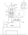
도 1은, 화상 생성 시스템의 일 실시 형태를 도시하는 모식도이다.
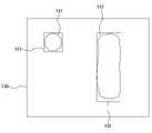
도 2는, 설계 데이터 내에 정의된 좌표계 상의 측정점과 CAD 패턴의 일례를 도시하는 모식도이다.
도 3은, CAD 패턴에 대응하는 워크피스 상의 실제 패턴의 화상을 도시하는 모식도이다.
도 4는, CAD 패턴과, 화상 상의 대응하는 실제 패턴의 위치 정렬을 설명하는 모식도이다.
도 5a는, 고립 패턴 사이의 거리를 측정하는 일 실시 형태를 도시하는 모식도이다.
도 5b는, 고립 패턴 사이의 거리를 측정하는 일 실시 형태를 도시하는 모식도이다.
도 6은, 직선 패턴의 폭을 측정하는 일 실시 형태를 설명하는 모식도이다.
도 7은, 직선 패턴 사이의 거리를 측정하는 일 실시 형태를 설명하는 모식도이다.
도 8은, 곡선 패턴의 폭을 측정하는 일 실시 형태를 설명하는 모식도이다.
도 9는, 곡선 패턴의 측정 개소와 측정 방향을 결정하는 방법의 일 실시 형태를 설명하는 모식도이다.
도 10은, 곡선 패턴 사이의 거리를 측정하는 일 실시 형태를 설명하는 모식도이다.
도 11은, 종단부 패턴의 에지 위치 어긋남을 측정하는 일례를 설명하는 모식도이다.
도 12는, 상술한 CAD 패턴의 타입 및 측정 레시피의 결정을 설명하는 흐름도이다.1 is a schematic diagram showing an embodiment of an image generating system.
2 : is a schematic diagram which shows an example of the measurement point and CAD pattern on the coordinate system defined in design data.
3 is a schematic diagram showing an image of an actual pattern on a workpiece corresponding to a CAD pattern.
Fig. 4 is a schematic diagram explaining positional alignment of a CAD pattern and a corresponding actual pattern on an image.
5A is a schematic diagram showing an embodiment of measuring the distance between isolated patterns.
5B is a schematic diagram showing an embodiment of measuring the distance between isolated patterns.
Fig. 6 is a schematic diagram explaining one embodiment of measuring the width of a straight line pattern.
Fig. 7 is a schematic diagram explaining one embodiment of measuring the distance between straight line patterns.
Fig. 8 is a schematic diagram explaining one embodiment of measuring the width of a curved pattern.
9 is a schematic diagram for explaining one embodiment of a method for determining a measurement location and a measurement direction of a curve pattern.
Fig. 10 is a schematic diagram for explaining an embodiment of measuring the distance between curve patterns.
Fig. 11 is a schematic diagram for explaining an example of measuring the displacement of the edge of the end pattern.
Fig. 12 is a flowchart explaining the determination of the type of CAD pattern and the measurement recipe described above.
이하, 본 발명의 실시 형태에 대하여 도면을 참조하여 설명한다.EMBODIMENT OF THE INVENTION Hereinafter, embodiment of this invention is described with reference to drawings.
도 1은, 화상 생성 시스템의 일 실시 형태를 도시하는 모식도이다. 화상 생성 시스템은, 워크피스 W의 화상을 생성하는 주사 전자 현미경(1)과, 주사 전자 현미경(1)의 동작을 제어하는 동작 제어부(5)를 구비하고 있다. 워크피스 W의 예로서는, 반도체 디바이스의 제조에 사용되는 웨이퍼, 마스크, 패널, 기판 등을 들 수 있다.1 is a schematic diagram showing an embodiment of an image generating system. The image generating system includes a scanning electron microscope 1 that generates an image of the workpiece W and an
동작 제어부(5)는, 적어도 1대의 컴퓨터로 구성된다. 동작 제어부(5)는, 프로그램이 저장된 기억 장치(5a)와, 프로그램에 포함되는 명령에 따라 연산을 실행하는 처리 장치(5b)를 구비하고 있다. 기억 장치(5a)는, 랜덤 액세스 메모리(RAM) 등의 주 기억 장치와, 하드디스크 드라이브(HDD), 솔리드 스테이트 드라이브(SSD) 등의 보조 기억 장치를 구비하고 있다. 처리 장치(5b)의 예로서는, CPU(중앙 처리 장치), GPU(그래픽 프로세싱 유닛)를 들 수 있다. 단, 동작 제어부(5)의 구체적 구성은 이들의 예에 한정되지 않는다.The
주사 전자 현미경(1)은, 전자 빔을 방출하는 전자총(15), 전자총(15)으로부터 방출된 전자 빔을 집속하는 집속 렌즈(16), 전자 빔을 X 방향으로 편향하는 X 편향기(17), 전자 빔을 Y 방향으로 편향하는 Y 편향기(18), 전자 빔을 시료의 일례인 워크피스 W에 포커스시키는 대물 렌즈(20), 워크피스 W를 지지하는 스테이지(31)를 갖는다.The scanning electron microscope 1 includes an
전자총(15)으로부터 방출된 전자 빔은 집속 렌즈(16)에서 집속된 후에, X 편향기(17), Y 편향기(18)에서 편향되면서 대물 렌즈(20)에 의해 집속되어 워크피스 W의 표면에 조사된다. 워크피스 W에 전자 빔의 1차 전자가 조사되면, 워크피스 W로부터는 2차 전자 및 반사 전자 등의 전자가 방출된다. 워크피스 W로부터 방출된 전자는 전자 검출기(26)에 의해 검출된다. 전자 검출기(26)의 전자 검출 신호는, 화상 취득 장치(28)에 입력되어 화상으로 변환된다. 이와 같이 하여, 주사 전자 현미경(1)은, 워크피스 W의 표면의 화상을 생성한다. 화상 취득 장치(28)는 동작 제어부(5)에 접속되어 있고, 워크피스 W의 화상은 동작 제어부(5)에 보내진다.The electron beam emitted from the
이하, 주사 전자 현미경(1)에 의해 생성된 화상 상의 실제 패턴의 특징량을 측정하는 방법에 대해서 설명한다. 이하의 설명에서는, 워크피스 W 상의 패턴은, 설계 데이터(CAD 데이터라고도 함)에 기초하여 형성되어 있다. CAD는, 컴퓨터 지원 설계(computer-aided design)의 약어이다. 이하에 설명하는 바와 같이, 화상 상의 실제 패턴의 특징량의 예로서는, 실제 패턴의 폭의 치수, 실제 패턴 사이의 거리, 실제 패턴의 에지의 위치 어긋남, 실제 패턴 전체의 위치 어긋남, 실제 패턴(특히 고립 패턴)의 면적, 실제 패턴(특히 고립 패턴)의 편평율, 실제 패턴(특히 직선 패턴 또는 곡선 패턴)의 라인 에지 러프니스, 실제 패턴(특히 곡선 패턴)의 곡률 등을 들 수 있다.Hereinafter, a method of measuring the feature amount of an actual pattern on an image generated by the scanning electron microscope 1 will be described. In the following description, the pattern on the workpiece W is formed based on design data (also referred to as CAD data). CAD is an acronym for computer-aided design. As will be described below, examples of the feature amount of the actual pattern on the image include the dimension of the width of the actual pattern, the distance between the actual patterns, the displacement of the edge of the actual pattern, the displacement of the entire actual pattern, and the actual pattern (especially isolated pattern), flatness of actual pattern (particularly isolated pattern), line edge roughness of actual pattern (particularly straight pattern or curved pattern), curvature of actual pattern (particularly curved pattern), and the like.
워크피스 W에 형성되어 있는 패턴의 설계 데이터는, 기억 장치(5a)에 미리 기억되어 있다. 설계 데이터는, 워크피스 W 상에 형성된 패턴의 정점의 좌표, 패턴의 위치, 형상 및 크기, 패턴이 속하는 층의 번호 등의 패턴의 설계 정보를 포함한다. 동작 제어부(5)는, 기억 장치(5a)로부터 패턴의 설계 데이터를 읽어내는 것이 가능하다.The design data of the pattern formed on the workpiece W is previously stored in the
설계 데이터는, 워크피스 W에 형성된 패턴의 설계 정보를 포함하는 데이터이다. 이하에 설명하는 설계 데이터 상의 CAD 패턴은, 설계 데이터에 포함되는 패턴의 설계 정보에 의해 정의되는 가상 패턴이고, 폴리곤 형상을 갖고 있다. 이하의 설명에서는, 워크피스 W에 실제로 형성되어 있는 패턴을 실제 패턴이라고 하는 경우가 있다.The design data is data including design information of a pattern formed on the workpiece W. The CAD pattern on the design data described below is a virtual pattern defined by the design information of the pattern included in the design data, and has a polygonal shape. In the following description, a pattern actually formed on the workpiece W is sometimes referred to as an actual pattern.
화상 상의 패턴의 특징량의 측정 위치를 특정하기 위한 측정점은, 동작 제어부(5)에 입력되어, 기억 장치(5a) 내에 기억된다. 일 실시 형태에서는, 측정점은, 워크피스 W에 형성된 패턴의 결함이 발생하기 쉬운 점이다. 예를 들어, 측정점에 있어서의 패턴의 폭의 치수(CD 또는 Critical Dimension)가 너무 긴, 또는 너무 짧은 경우에는, 동작 제어부(5)는 패턴에 결함이 있다고 판단할 수 있다.A measurement point for specifying a measurement position of a feature amount of a pattern on an image is input to the
측정점의 위치는, 설계 데이터 내에 정의된 좌표계 상의 점을 나타내는 좌표(X 좌표, Y 좌표)에 의해 특정된다. 설계 데이터 상의 CAD 패턴의 위치, 형상 및 크기도, 상기 좌표계 상의 CAD 패턴의 정점에 의해 특정할 수 있다. 통상, 다수의 측정점이 상기 좌표계 상에 설정된다.The location of the measurement point is specified by coordinates (X coordinate, Y coordinate) representing the point on the coordinate system defined in the design data. The position, shape, and size of the CAD pattern on the design data can also be specified by the vertices of the CAD pattern on the coordinate system. Usually, a number of measurement points are set on the coordinate system.
동작 제어부(5)는, 설계 데이터 내에 정의된 좌표계 상의 측정점과 CAD 패턴의 상대 위치 및 CAD 패턴의 면적에 기초하여 CAD 패턴의 타입 및 측정 레시피를 결정하도록 구성되어 있다. CAD 패턴의 타입에는, 고립 패턴, 직선 패턴, 곡선 패턴 및 종단부 패턴이 적어도 포함된다.The
도 2는, 설계 데이터 내에 정의된 좌표계 상의 측정점과 CAD 패턴의 일례를 도시하는 모식도이다. CAD 패턴(101)은, 고립 패턴의 일례인 홀 패턴이고, CAD 패턴(102)은, 직선 패턴이다. 도 2에 도시하는 예에서는, 3개의 측정점(111, 112, 113)이 설정되어, 좌표계 상에 플롯되어 있다.2 : is a schematic diagram which shows an example of the measurement point and CAD pattern on the coordinate system defined in design data. The
주사 전자 현미경(1)은, 상기 CAD 패턴(101, 102)에 대응하는 실제 패턴의 화상을 생성한다. 도 3은, CAD 패턴(101, 102)에 대응하는 워크피스 W 상의 실제 패턴(121, 122)의 화상(130)을 도시하는 모식도이다. 대응하는 실제 패턴(121, 122)은, 상기 CAD 패턴(101, 102)에 따라서 워크피스 W에 실제로 형성된 패턴이다. 실제 패턴(121, 122)의 화상(130)은 동작 제어부(5)에 송신된다.A scanning electron microscope (1) generates images of actual patterns corresponding to the CAD patterns (101, 102). FIG. 3 is a schematic diagram showing an
도 4에 도시하는 바와 같이, 동작 제어부(5)는, CAD 패턴(101, 102)과, 워크피스 W의 화상(130) 상의 대응하는 실제 패턴(121, 122)의 위치 정렬을 행한다. 위치 정렬을 행함으로써, 화상 생성 시에 일어나는 위치 어긋남을 수정하고, 측정점의 좌표에서 지정된 정확한 위치에서의 특징량 측정이 가능해진다. 화상(130) 상의 실제 패턴(121, 122)과, CAD 패턴(101, 102)의 위치 정렬에는, 공지된 패턴 매칭의 기술을 사용할 수 있다.As shown in FIG. 4 , the
동작 제어부(5)는, 좌표계 상의 측정점과 CAD 패턴의 상대 위치 및 CAD 패턴의 면적에 기초하여 CAD 패턴의 타입 및 측정 레시피를 결정하고, 결정된 측정 레시피에 따라서 화상 상의 실제 패턴의 특징량의 측정을 실행한다. 이하, CAD 패턴의 타입 및 측정 레시피를 결정하는 방법의 일 실시 형태를 설명한다.The
도 2에 도시하는 예에 있어서, 동작 제어부(5)는, 먼저, 주어진 측정점(111, 112, 113)이, 설계 데이터 상의 CAD 패턴(101, 102)의 내측에 있는지의 여부를 판별한다. 도 2에서는, 측정점(111, 113)은, CAD 패턴(101, 102)의 내측에 각각 위치하고 있고, 측정점(112)은 이들 CAD 패턴(101, 102)의 외측에 있다.In the example shown in FIG. 2 , the
동작 제어부(5)는, CAD 패턴(101, 102)의 면적을 산정한다. 동작 제어부(5)는, CAD 패턴의 면적이 미리 정해진 면적보다도 작을 때는, 그 CAD 패턴은 고립 패턴이라고 결정한다. 도 2에 도시하는 예에서는, CAD 패턴(101)의 면적은 미리 정해진 면적보다도 작고, 따라서 동작 제어부(5)는, CAD 패턴(101)은 고립 패턴이라고 결정한다. 이에 비해, CAD 패턴(102)의 면적은 미리 정해진 면적보다도 크고, 따라서 동작 제어부(5)는, CAD 패턴(102)은 고립 패턴은 아니라고 결정한다.The
동작 제어부(5)는, 고립 패턴이라고 결정된 CAD 패턴(101)에 대응하는 실제 패턴의 폭을 측정한다. 구체적으로는, 도 3에 도시하는 화면(130) 상의 실제 패턴(121)(도 2의 CAD 패턴(101)에 대응함)의 폭의 치수(Critical Dimension)를 측정한다. 일 실시 형태에서는, 동작 제어부(5)는, 패턴의 특징량으로서 실제 패턴(121)의 면적 및/또는 편평율을 또한 산정해도 된다. 또한, 일 실시 형태에서는, 동작 제어부(5)는, 패턴의 특징량으로서, 실제 패턴(121)의 전체의 위치 어긋남, 즉, 실제 패턴(121)과, 대응하는 CAD 패턴(101)의 어긋남양을 측정해도 된다.The
도 5a 및 도 5b는, 특징량으로서 고립 패턴 사이의 거리를 측정하는 일 실시 형태를 도시하는 모식도이다. 도 5a에 도시하는 바와 같이, 측정점(211)이 CAD 패턴(212, 213, 214, 215)의 외측에 있는 경우, 동작 제어부(5)는, 측정점(211)을 중심으로 하는 소정의 반경 R의 원형의 영역(220) 내에 위치하는 CAD 패턴(212, 213, 214)을 결정한다. 동작 제어부(5)는, 영역(220) 내에 있는 CAD 패턴(212, 213, 214)의 면적을 각각 산정한다. 도 5a에 도시하는 예에서는, 측정점(211)은, CAD 패턴(212, 213) 사이에 위치하고, CAD 패턴(213, 214) 사이에 위치하고, 또한 CAD 패턴(214, 212) 사이에 위치한다.5A and 5B are schematic diagrams showing an embodiment in which a distance between isolated patterns is measured as a characteristic quantity. As shown in FIG. 5A , when the
CAD 패턴(212, 213, 214)의 면적의 각각이, 미리 정해진 면적보다도 작은 경우에는, 동작 제어부(5)는, CAD 패턴(212, 213, 214)을 고립 패턴 사이의 거리 측정 대상의 CAD 패턴으로 결정한다. 이어서, 동작 제어부(5)는, 도 5b에 도시하는 바와 같이, CAD 패턴(212, 213, 214)의 무게 중심 위치 G1, G2, G3을 구하고, 또한 각 무게 중심 위치 G1, G2, G3 사이를 연결하는 선분 상의 중점(222, 223, 224)을 구한다. 동작 제어부(5)는, 측정점(211)으로부터 중점(222, 223, 224)까지의 거리 L1, L2, L3을 측정한다. 측정된 거리가, 미리 정해진 거리보다도 짧은 경우, 동작 제어부(5)는, 그 중점을 포함하는 선분의 양단에 위치하는 CAD 패턴에 대응하는 화상 상의 실제 패턴 사이의 거리를 측정한다.When each of the areas of the
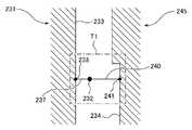
도 6은, 특징량으로서 직선 패턴의 폭을 측정하는 일 실시 형태를 설명하는 모식도이다. 동작 제어부(5)는, CAD 패턴(231)의 면적이, 미리 정해진 면적보다도 클 때는, CAD 패턴(231)은 고립 패턴이 아니라고 결정한다. 동작 제어부(5)는, 측정점(232)에 가장 가까운 설계 데이터 상의 CAD 패턴(231)의 제1 에지(233)를 결정한다. 또한, 동작 제어부(5)는, 측정점(232)을 넘어서 제1 에지(233)와는 반대측에 있는 제2 에지(234)를 결정한다. 제2 에지(234)는, 제1 에지(233)와 평행하다. 측정점(232)은, 제1 에지(233)와 제2 에지(234) 사이에 위치한다.Fig. 6 is a schematic diagram for explaining an embodiment in which the width of a straight line pattern is measured as a feature. The
제1 에지(233)와 제2 에지(234)의 거리 L5가 역치보다도 짧고, 또한 소정의 탐색 영역 T1 내에 제1 에지(233) 및 제2 에지(234)가 정점을 갖고 있지 않을 때는, 동작 제어부(5)는, CAD 패턴(231)은 직선 패턴이라고 결정한다. 탐색 영역 T1은, 측정점(232)으로부터 연장되고, 제1 에지(233)에 수직인 제1 수선(237)과, 제1 에지(233)의 제1 교점(238)을 둘러싸고, 또한, 측정점(232)으로부터 연장되고, 제2 에지(234)에 수직인 제2 수선(240)과, 제2 에지(234)의 제2 교점(241)을 둘러싸는 영역이다. 탐색 영역 T1의 사이즈는, 파라미터로서 설정할 수 있다.When the distance L5 between the
동작 제어부(5)는, 측정점(232)이 CAD 패턴(231) 내에 있는 것을 결정하고, 또한, 직선 패턴인 CAD 패턴(231)에 대응하는 화상 상의 실제 패턴의 폭의 치수(Critical Dimension)를 측정한다. 일 실시 형태에서는, 동작 제어부(5)는, 패턴의 특징량으로서 실제 패턴의 라인 에지 러프니스를 또한 산정해도 된다. 또한, 일 실시 형태에서는, 동작 제어부(5)는, 패턴의 특징량으로서, 실제 패턴의 전체의 위치 어긋남, 즉, 실제 패턴과, 대응하는 CAD 패턴(231)의 어긋남양을 측정해도 된다.The
설계 데이터 상의 에지에는, 반도체 디바이스 설계의 보정 과정에서 생성되는 미세한 단차(243)가 존재하는 경우가 있다. 동작 제어부(5)는, 에지의 정점 유무를 판정할 때에 미리 정해진 크기보다도 작은 단차를 무시하도록 구성되어 있다. 따라서, 미소한 단차가 에지에 있는 경우에는, CAD 패턴은 직선 패턴이라고 결정된다.In some cases,
도 7은, 특징량으로서 직선 패턴 사이의 거리를 측정하는 일 실시 형태를 설명하는 모식도이다. 특별히 설명하지 않는 본 실시 형태의 동작은, 도 6을 참조하여 설명한 실시 형태와 동일하므로, 그 중복하는 설명을 생략한다. 도 7에 도시하는 본 실시 형태에서는, 동작 제어부(5)는, 측정점(232)이 설계 데이터 상의 CAD 패턴(231, 245)의 외측에 위치하고, 또한, CAD 패턴(231, 245) 사이에 위치하는 것을 결정하고, 또한, CAD 패턴(231, 245)에 대응하는 화상 상의 실제 패턴 사이의 거리를 측정한다.Fig. 7 is a schematic diagram for explaining an embodiment in which a distance between straight line patterns is measured as a feature. Operations of the present embodiment, which are not particularly described, are the same as those of the embodiment described with reference to FIG. 6, and therefore, overlapping descriptions thereof are omitted. In the present embodiment shown in FIG. 7 , the
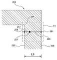
도 8은, 특징량으로서 곡선 패턴의 폭을 측정하는 일 실시 형태를 설명하는 모식도이다. 동작 제어부(5)는, 측정점(251)에 가장 가까운 설계 데이터 상의 CAD 패턴(252)의 제1 에지(253)를 결정한다. 동작 제어부(5)는, 측정점(251)을 넘어서 제1 에지(253)와는 반대측에 있는 제2 에지(255)를 결정한다. 제2 에지(255)는, 제1 에지(253)와 평행하다. 측정점(251)은, 제1 에지(253)와 제2 에지(255) 사이에 위치한다.Fig. 8 is a schematic diagram for explaining an embodiment in which the width of a curve pattern is measured as a feature. The
제1 에지(253)와 제2 에지(255)의 거리 L6이 역치보다도 짧고, 또한 소정의 탐색 영역 T2 내에 제1 에지(253) 및 제2 에지(255) 중 적어도 한쪽이 정점을 갖고 있을 때는, 동작 제어부(5)는, CAD 패턴(252)은 곡선 패턴이라고 결정한다. 탐색 영역 T2는, 측정점(251)으로부터 연장되고, 제1 에지(253)에 수직인 제1 수선(257)과, 제1 에지(253)의 제1 교점(258)을 둘러싸고, 또한, 측정점(251)으로부터 연장되고, 제2 에지(255)에 수직인 제2 수선(260)과, 제2 에지(255)의 제2 교점(261)을 둘러싸는 영역이다. 탐색 영역 T2의 사이즈는, 파라미터로서 설정할 수 있다. 도 8에 도시하는 실시 형태에서는, 제1 에지(253)는, 탐색 영역 T2 내에 정점(264)을 갖고 있으므로, 동작 제어부(5)는, CAD 패턴(252)은 곡선 패턴이라고 결정한다.When the distance L6 between the
도 9는, 곡선 패턴의 측정 개소와 측정 방향을 결정하는 방법의 일 실시 형태를 설명하는 모식도이다. 웨이퍼 등의 워크피스에 형성되는 실제 패턴은, 노광이나 에칭 등의 프로세스에 의해, 둥글게 된 형상의 코너 에지를 갖는다. 이 형상을 모방하기 위해, 도 9의 부호 267, 268에 나타내는 바와 같은 라운딩 처리를 CAD 패턴(252)에 대하여 실시한다. 이 라운딩 처리에는, 원호, 베지에 곡선 등을 사용한다.9 is a schematic diagram for explaining one embodiment of a method for determining a measurement location and a measurement direction of a curve pattern. An actual pattern formed on a workpiece such as a wafer has corner edges rounded by a process such as exposure or etching. In order to imitate this shape, the
동작 제어부(5)는, 측정점(251)으로부터 곡선(267)까지의 거리가 가장 짧은 최단점(270)을 결정한다. 동작 제어부(5)는, 최단점(270)으로부터 곡선(267)의 법선(271)을 긋고, 대향하는 곡선(268)과 법선(271)의 교점(275)을 결정한다. 동작 제어부(5)는, 법선(271)이 연장하는 방향에 있어서의 실제 패턴의 폭을 측정한다. 일 실시 형태에서는, 동작 제어부(5)는, 패턴의 특징량으로서 실제 패턴의 곡률 및/또는 라인 에지 러프니스를 또한 산정해도 된다.The
도 10은, 특징량으로서 곡선 패턴 사이의 거리를 측정하는 일례를 설명하는 모식도이다. 특별히 설명하지 않는 본 실시 형태의 동작은, 도 8 및 도 9를 참조하여 설명한 실시 형태와 동일하므로, 그 중복하는 설명을 생략한다. 도 10에 도시하는 본 실시 형태에서는, 동작 제어부(5)는, 측정점(251)이 설계 데이터 상의 CAD 패턴(252, 278)의 외측에 위치하고, 또한 CAD 패턴(252, 278) 사이에 위치하는 것을 결정하고, 또한 CAD 패턴(252, 278)에 대응하는 화상 상의 실제 패턴 사이의 거리를 측정한다.Fig. 10 is a schematic diagram for explaining an example of measuring the distance between curve patterns as a feature. Operations of the present embodiment, which are not specifically described, are the same as those of the embodiment described with reference to Figs. In this embodiment shown in FIG. 10 , the
도 11은, 특징량으로서 종단부 패턴의 에지의 위치 어긋남을 측정하는 일례를 설명하는 모식도이다. 측정점(281)의 가장 가까이에 위치하는 CAD 패턴(283)이 상기한 어느 타입에도 해당하지 않았을 경우, 동작 제어부(5)는, 이하의 판정 방법으로 CAD 패턴(283)이 종단부 패턴인지 아닌지의 판정을 행한다. 즉, 동작 제어부(5)는, 측정점(281)의 가장 가까이에 위치하는 CAD 패턴(283)의 에지(284)를 결정한다. 에지(284)의 길이 L7이 소정의 길이보다도 짧고, 또한 CAD 패턴(283)의 면적이 미리 정해진 면적보다도 클 때는, 동작 제어부(5)는, CAD 패턴(283)은 종단부 패턴이라고 결정한다.Fig. 11 is a schematic diagram for explaining an example of measuring the displacement of the edge of the end pattern as a characteristic amount. When the
동작 제어부(5)는, 종단부 패턴인 CAD 패턴(283)의 에지(284)에 대응하는 화상 상의 실제 패턴의 에지를 검출하고, 실제 패턴의 에지의 위치 어긋남, 즉 실제 패턴의 에지와 CAD 패턴(283)의 에지(284)의 거리를 측정한다.The
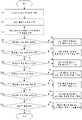
도 12는, 상술한 CAD 패턴의 타입 및 측정 레시피의 결정을 설명하는 흐름도이다.Fig. 12 is a flowchart explaining the determination of the type of CAD pattern and the measurement recipe described above.
스텝 S1에서는, 화상 상의 패턴의 특징량(예를 들어 치수)의 측정 위치를 특정하기 위한 측정점은, 동작 제어부(5)에 입력된다. 측정점은, 측정 대상의 실제 패턴에 대응하는 CAD 패턴 내 또는 그 근방에 위치한다. 측정점은 기억 장치(5a) 내에 기억된다.In step S1, a measurement point for specifying a measurement position of a characteristic amount (for example, a dimension) of a pattern on an image is input to the
스텝 S2에서는, 동작 제어부(5)는, 주사 전자 현미경(1)에 명령을 발하여, CAD 패턴에 대응하는 실제 패턴의 화상을 생성시킨다. 동작 제어부(5)는, 주사 전자 현미경(1)으로부터 실제 패턴의 화상을 취득한다.In step S2, the
스텝 S3에서는, 동작 제어부(5)는, CAD 패턴에 대응하는 화상 상의 실제 패턴과, CAD 패턴의 위치 정렬을 행한다. 화상 상의 실제 패턴과, CAD 패턴의 위치 정렬에는, 공지된 패턴 매칭의 기술을 사용할 수 있다.In step S3, the
스텝 S4에서는, 동작 제어부(5)는, CAD 패턴의 면적이 미리 정해진 면적보다도 작을 때는, CAD 패턴은 고립 패턴이라고 결정한다. 또한, 동작 제어부(5)는, 측정점이 CAD 패턴 내에 있는지의 여부를 판단한다. 측정점이 CAD 패턴 내에 위치하고 있는 경우에는, 스텝 S5에 있어서, 동작 제어부(5)는, 고립 패턴인 CAD 패턴에 대응하는 화상 상의 실제 패턴의 폭을 측정한다. 일 실시 형태에서는, 동작 제어부(5)는, 패턴의 특징량으로서 실제 패턴의 면적 및/또는 편평율을 또한 산정해도 된다. 또한, 일 실시 형태에서는, 동작 제어부(5)는, 패턴의 특징량으로서, 실제 패턴의 전체의 위치 어긋남, 즉, 실제 패턴과, 대응하는 CAD 패턴의 어긋남양을 측정해도 된다.In step S4, the
스텝 S6에서는, 측정점이 고립 패턴 사이에 위치하고 있는지의 여부를 판정한다. 측정점이 고립 패턴 사이에 위치하고 있는 경우에는, 스텝 S7에 있어서, 동작 제어부(5)는, 고립 패턴인 CAD 패턴에 대응하는 화상 상의 실제 패턴 사이의 거리를 측정한다.In step S6, it is determined whether or not the measurement point is located between the isolated patterns. When the measurement point is located between the isolated patterns, in step S7, the
CAD 패턴이 고립 패턴이 아닌 경우, 동작 제어부(5)는, CAD 패턴이 직선 패턴인지의 여부를 판정한다. 즉, 동작 제어부(5)는, 스텝 S8에 있어서, 측정점에 가장 가까운 CAD 패턴의 제1 에지와, 측정점을 넘어서 제1 에지와는 반대측에 있는 제2 에지가 소정의 탐색 영역 내에 있어서 정점을 갖고 있지 않을 때는, 동작 제어부(5)는, CAD 패턴은 직선 패턴이라고 결정한다. 또한, 동작 제어부(5)는, 측정점이 CAD 패턴 내에 있는지의 여부를 판단한다. 측정점이 CAD 패턴 내에 위치하고 있는 경우에는, 스텝 S9에 있어서, 동작 제어부(5)는, 직선 패턴인 CAD 패턴에 대응하는 화상 상의 실제 패턴의 폭을 측정한다. 일 실시 형태에서는, 동작 제어부(5)는, 패턴의 특징량으로서 실제 패턴의 라인 에지 러프니스를 또한 산정해도 된다. 또한, 일 실시 형태에서는, 동작 제어부(5)는, 패턴의 특징량으로서, 실제 패턴의 전체의 위치 어긋남, 즉, 실제 패턴과, 대응하는 CAD 패턴의 어긋남양을 측정해도 된다.When the CAD pattern is not an isolated pattern, the
스텝 S10에서는, 측정점이 직선 패턴 사이에 위치하고 있는지의 여부를 판정한다. 측정점이 직선 패턴 사이에 위치하고 있는 경우에는, 스텝 S11에 있어서, 동작 제어부(5)는, 직선 패턴인 CAD 패턴에 대응하는 화상 상의 실제 패턴 사이의 거리를 측정한다.In step S10, it is determined whether or not the measurement point is located between the straight line patterns. In the case where the measurement point is located between the straight line patterns, in step S11, the
스텝 S12에서는, 상기 제1 에지 및 상기 제2 에지 중 적어도 한쪽이 소정의 탐색 영역 내에 있어서 정점을 갖고 있을 때는, 동작 제어부(5)는, CAD 패턴은 곡선 패턴이라고 결정한다. 또한, 동작 제어부(5)는, 측정점이 CAD 패턴 내에 있는지의 여부를 판단한다. 측정점이 CAD 패턴 내에 위치하고 있는 경우에는, 스텝 S13에 있어서, 동작 제어부(5)는, 곡선 패턴인 CAD 패턴에 대응하는 화상 상의 실제 패턴의 폭을 측정한다. 일 실시 형태에서는, 동작 제어부(5)는, 패턴의 특징량으로서 실제 패턴의 곡률 및/또는 라인 에지 러프니스를 또한 산정해도 된다.In step S12, when at least one of the first edge and the second edge has a vertex within a predetermined search area, the
스텝 S14에서는, 측정점이 곡선 패턴 사이에 위치하고 있는지의 여부를 판정한다. 측정점이 곡선 패턴 사이에 위치하고 있는 경우에는, 스텝 S15에 있어서, 동작 제어부(5)는, 곡선 패턴인 CAD 패턴에 대응하는 화상 상의 실제 패턴 사이의 거리를 측정한다.In step S14, it is determined whether or not the measurement point is located between the curve patterns. In the case where the measurement point is located between the curve patterns, in step S15, the
스텝 S16에서는, 측정점에 가장 가까운 CAD 패턴의 에지의 길이가 소정의 길이보다도 짧고, 또한 CAD 패턴의 면적이 미리 정해진 면적보다도 클 때는, 동작 제어부(5)는, CAD 패턴은 종단부 패턴이라고 결정한다.In step S16, when the length of the edge of the CAD pattern closest to the measuring point is shorter than the predetermined length and the area of the CAD pattern is larger than the predetermined area, the
스텝 S17에서는, 동작 제어부(5)는, 종단부 패턴인 CAD 패턴의 에지에 대응하는 화상 상의 실제 패턴의 에지를 검출하고, 실제 패턴의 에지의 위치 어긋남, 즉 실제 패턴의 에지와 CAD 패턴의 에지의 거리를 측정한다.In step S17, the
CAD 패턴이 고립 패턴, 직선 패턴, 곡선 패턴 및 종단부 패턴의 어느 것에도 해당하지 않는 경우에는, 동작 제어부(5)는, 특징량 측정 동작을 종료한다.When the CAD pattern does not correspond to any of the isolated pattern, the straight line pattern, the curved pattern, and the end pattern, the
상술한 실시 형태에 따르면, 설계 데이터 상의 측정점과 CAD 패턴의 상대 위치 및 CAD 패턴의 면적에 기초하여, 최적의 측정 레시피를 결정할 수 있다.According to the embodiment described above, an optimal measurement recipe can be determined based on the relative position of the CAD pattern and the measurement point on the design data, and the area of the CAD pattern.
상술한 실시 형태는, 본 발명이 속하는 기술분야에 있어서의 통상의 지식을 가진 자가 본 발명을 실시할 수 있는 것을 목적으로 하여 기재된 것이다. 상기 실시 형태의 다양한 변형예는, 당업자라면 당연히 이룰 수 있는 것이고, 본 발명의 기술적 사상은 다른 실시 형태에도 적용할 수 있다. 따라서, 본 발명은 기재된 실시 형태에 한정되지 않고, 특허 청구 범위에 의해 정의되는 기술적 사상을 따른 가장 넓은 범위로 해석되는 것이다.The embodiments described above are described for the purpose of being able to implement the present invention by those skilled in the art in the technical field to which the present invention belongs. Various modified examples of the above embodiments can naturally be made by those skilled in the art, and the technical idea of the present invention can be applied to other embodiments as well. Therefore, the present invention is not limited to the described embodiments, but is to be construed in the widest range along the technical idea defined by the claims.
본 발명은, 주사 전자 현미경 등의 화상 생성 장치에 의해 생성된 화상 상의 패턴의 치수(Critical Dimension) 등의 특징량을 측정하는 방법에 관한 것으로, 특히 웨이퍼, 마스크, 패널, 기판 등의 워크피스에 형성된 패턴의 치수 등의 특징량의 측정 레시피를 자동적으로 결정하는 방법에 이용 가능하다.The present invention relates to a method for measuring feature quantities such as critical dimensions of a pattern on an image generated by an image generating device such as a scanning electron microscope, and particularly to workpieces such as wafers, masks, panels, and substrates. It can be used for a method of automatically determining a measurement recipe for characteristic quantities such as the dimensions of formed patterns.
1: 주사 전자 현미경
5: 동작 제어부
15: 전자총
16: 집속 렌즈
17: X 편향기
18: Y 편향기
20: 대물 렌즈
26: 전자 검출기
31: 스테이지1: scanning electron microscope
5: motion control
15: electron gun
16: focusing lens
17: X deflector
18: Y deflector
20: objective lens
26: electronic detector
31: Stage
Claims (7)
Translated fromKorean상기 측정점과 상기 CAD 패턴의 상대 위치 및 상기 CAD 패턴의 면적에 기초하여 상기 CAD 패턴의 타입 및 측정 레시피를 결정하고,
상기 CAD 패턴에 대응하는 화상 상의 실제 패턴과, 상기 CAD 패턴의 위치 정렬을 행하고,
상기 결정된 측정 레시피에 따라서 상기 실제 패턴의 특징량을 측정하는, 방법.determining whether a measurement point on a coordinate system defined in the design data is within the CAD pattern;
Determine the type and measurement recipe of the CAD pattern based on the relative position of the measurement point and the CAD pattern and the area of the CAD pattern;
aligning the actual pattern on the image corresponding to the CAD pattern with the CAD pattern;
The method of measuring the feature amount of the actual pattern according to the determined measurement recipe.
Applications Claiming Priority (3)
| Application Number | Priority Date | Filing Date | Title |
|---|---|---|---|
| JPJP-P-2020-088016 | 2020-05-20 | ||
| JP2020088016AJP7303155B2 (en) | 2020-05-20 | 2020-05-20 | Pattern measurement method |
| PCT/JP2021/017356WO2021235227A1 (en) | 2020-05-20 | 2021-05-06 | Pattern measurement method |
Publications (1)
| Publication Number | Publication Date |
|---|---|
| KR20230012016Atrue KR20230012016A (en) | 2023-01-25 |
Family
ID=78606786
Family Applications (1)
| Application Number | Title | Priority Date | Filing Date |
|---|---|---|---|
| KR1020227043907APendingKR20230012016A (en) | 2020-05-20 | 2021-05-06 | Pattern measurement method |
Country Status (6)
| Country | Link |
|---|---|
| US (1) | US20230186459A1 (en) |
| JP (1) | JP7303155B2 (en) |
| KR (1) | KR20230012016A (en) |
| CN (1) | CN115699278A (en) |
| TW (1) | TW202201590A (en) |
| WO (1) | WO2021235227A1 (en) |
Families Citing this family (2)
| Publication number | Priority date | Publication date | Assignee | Title |
|---|---|---|---|---|
| JP7574157B2 (en)* | 2021-08-27 | 2024-10-28 | 株式会社ニューフレアテクノロジー | Inspection apparatus and reference image generating method |
| WO2025197587A1 (en)* | 2024-03-21 | 2025-09-25 | 東レエンジニアリング先端半導体Miテクノロジー株式会社 | Pattern measuring method and pattern measuring device |
Citations (2)
| Publication number | Priority date | Publication date | Assignee | Title |
|---|---|---|---|---|
| JP2008235575A (en) | 2007-03-20 | 2008-10-02 | Toshiba Corp | Pattern measuring method, pattern measuring device and program |
| JP2013092440A (en) | 2011-10-26 | 2013-05-16 | Advantest Corp | Pattern measurement device and pattern measurement method |
Family Cites Families (5)
| Publication number | Priority date | Publication date | Assignee | Title |
|---|---|---|---|---|
| JP4787673B2 (en)* | 2005-05-19 | 2011-10-05 | 株式会社Ngr | Pattern inspection apparatus and method |
| JP5530601B2 (en)* | 2008-03-31 | 2014-06-25 | 株式会社日立ハイテクノロジーズ | Circuit pattern dimension measuring apparatus and method using scanning electron microscope |
| JP2011137901A (en)* | 2009-12-28 | 2011-07-14 | Hitachi High-Technologies Corp | Apparatus for setting pattern measuring condition |
| JP2011191296A (en)* | 2010-03-16 | 2011-09-29 | Ngr Inc | Pattern inspection device and method |
| JP6001945B2 (en)* | 2012-07-24 | 2016-10-05 | 株式会社日立ハイテクノロジーズ | Pattern measuring apparatus and method |
- 2020
- 2020-05-20JPJP2020088016Apatent/JP7303155B2/enactiveActive
- 2021
- 2021-05-06KRKR1020227043907Apatent/KR20230012016A/enactivePending
- 2021-05-06CNCN202180035695.5Apatent/CN115699278A/enactivePending
- 2021-05-06USUS17/925,810patent/US20230186459A1/enactivePending
- 2021-05-06WOPCT/JP2021/017356patent/WO2021235227A1/ennot_activeCeased
- 2021-05-14TWTW110117504Apatent/TW202201590A/enunknown
Patent Citations (2)
| Publication number | Priority date | Publication date | Assignee | Title |
|---|---|---|---|---|
| JP2008235575A (en) | 2007-03-20 | 2008-10-02 | Toshiba Corp | Pattern measuring method, pattern measuring device and program |
| JP2013092440A (en) | 2011-10-26 | 2013-05-16 | Advantest Corp | Pattern measurement device and pattern measurement method |
Also Published As
| Publication number | Publication date |
|---|---|
| TW202201590A (en) | 2022-01-01 |
| JP7303155B2 (en) | 2023-07-04 |
| JP2021182601A (en) | 2021-11-25 |
| US20230186459A1 (en) | 2023-06-15 |
| WO2021235227A1 (en) | 2021-11-25 |
| CN115699278A (en) | 2023-02-03 |
Similar Documents
| Publication | Publication Date | Title |
|---|---|---|
| US8507856B2 (en) | Pattern measuring method and pattern measuring device | |
| US7894660B2 (en) | Image processing alignment method and method of manufacturing semiconductor device | |
| KR101828124B1 (en) | Pattern evaluation method and pattern evaluation device | |
| US8295584B2 (en) | Pattern measurement methods and pattern measurement equipment | |
| JP3971937B2 (en) | Exposure condition monitoring method and apparatus, and semiconductor device manufacturing method | |
| US9000365B2 (en) | Pattern measuring apparatus and computer program | |
| US8835881B2 (en) | Drift correction method and pattern writing data generation method | |
| US20150136976A1 (en) | Overlay error measuring device and computer program | |
| KR102521799B1 (en) | Pattern measurement device and pattern measurement method | |
| KR100378269B1 (en) | Method of measuring micropattern, micropattern measurement unit and recorded media recording micropattern measurement program | |
| JP2007248087A (en) | Sample size measuring method and sample size measuring device | |
| JP2009252959A (en) | Pattern inspection apparatus, pattern inspection method, and method of manufacturing semiconductor device | |
| KR20230012016A (en) | Pattern measurement method | |
| EP0947828A2 (en) | Method and apparatus for improved inspection measurements | |
| US20070114461A1 (en) | Charged beam drawing apparatus and charged beam drawing method | |
| US11468555B2 (en) | Method and apparatus for generating a correction line indicating relationship between deviation of an edge of a wafer pattern from an edge of a reference pattern and space width of the reference pattern, and a computer-readable recording medium | |
| JP2001189263A (en) | Misalignment inspection method and charged beam exposure method | |
| US5608226A (en) | Electron-beam exposure method and system | |
| JPH05190435A (en) | Electron beam drawing method for semiconductor device | |
| CN117350997A (en) | Mask pattern optimization extraction method and device and computer equipment | |
| US8212990B2 (en) | Exposure apparatus, information processing apparatus, and method of manufacturing device | |
| WO2019188296A1 (en) | Image generating method | |
| US20240219845A1 (en) | Overlay measurement method and method of manufacturing semiconductor device using the same | |
| US12422386B2 (en) | Pattern measurement device | |
| JPH06120304A (en) | Alignment method |
Legal Events
| Date | Code | Title | Description |
|---|---|---|---|
| PA0105 | International application | St.27 status event code:A-0-1-A10-A15-nap-PA0105 | |
| PG1501 | Laying open of application | St.27 status event code:A-1-1-Q10-Q12-nap-PG1501 | |
| PA0201 | Request for examination | St.27 status event code:A-1-2-D10-D11-exm-PA0201 | |
| PE0902 | Notice of grounds for rejection | St.27 status event code:A-1-2-D10-D21-exm-PE0902 |