KR20230003839A - Touch panel and touch display device comprising the same - Google Patents
Touch panel and touch display device comprising the sameDownload PDFInfo
- Publication number
- KR20230003839A KR20230003839AKR1020210085409AKR20210085409AKR20230003839AKR 20230003839 AKR20230003839 AKR 20230003839AKR 1020210085409 AKR1020210085409 AKR 1020210085409AKR 20210085409 AKR20210085409 AKR 20210085409AKR 20230003839 AKR20230003839 AKR 20230003839A
- Authority
- KR
- South Korea
- Prior art keywords
- touch
- insulating film
- insulating
- disposed
- layer
- Prior art date
- Legal status (The legal status is an assumption and is not a legal conclusion. Google has not performed a legal analysis and makes no representation as to the accuracy of the status listed.)
- Pending
Links
Images


Classifications
- G—PHYSICS
- G06—COMPUTING OR CALCULATING; COUNTING
- G06F—ELECTRIC DIGITAL DATA PROCESSING
- G06F3/00—Input arrangements for transferring data to be processed into a form capable of being handled by the computer; Output arrangements for transferring data from processing unit to output unit, e.g. interface arrangements
- G06F3/01—Input arrangements or combined input and output arrangements for interaction between user and computer
- G06F3/03—Arrangements for converting the position or the displacement of a member into a coded form
- G06F3/041—Digitisers, e.g. for touch screens or touch pads, characterised by the transducing means
- G06F3/044—Digitisers, e.g. for touch screens or touch pads, characterised by the transducing means by capacitive means
- G06F3/0446—Digitisers, e.g. for touch screens or touch pads, characterised by the transducing means by capacitive means using a grid-like structure of electrodes in at least two directions, e.g. using row and column electrodes
- G—PHYSICS
- G06—COMPUTING OR CALCULATING; COUNTING
- G06F—ELECTRIC DIGITAL DATA PROCESSING
- G06F3/00—Input arrangements for transferring data to be processed into a form capable of being handled by the computer; Output arrangements for transferring data from processing unit to output unit, e.g. interface arrangements
- G06F3/01—Input arrangements or combined input and output arrangements for interaction between user and computer
- G06F3/03—Arrangements for converting the position or the displacement of a member into a coded form
- G06F3/041—Digitisers, e.g. for touch screens or touch pads, characterised by the transducing means
- G06F3/044—Digitisers, e.g. for touch screens or touch pads, characterised by the transducing means by capacitive means
- G06F3/0443—Digitisers, e.g. for touch screens or touch pads, characterised by the transducing means by capacitive means using a single layer of sensing electrodes
- G—PHYSICS
- G02—OPTICS
- G02B—OPTICAL ELEMENTS, SYSTEMS OR APPARATUS
- G02B1/00—Optical elements characterised by the material of which they are made; Optical coatings for optical elements
- G02B1/10—Optical coatings produced by application to, or surface treatment of, optical elements
- G02B1/11—Anti-reflection coatings
- G—PHYSICS
- G06—COMPUTING OR CALCULATING; COUNTING
- G06F—ELECTRIC DIGITAL DATA PROCESSING
- G06F3/00—Input arrangements for transferring data to be processed into a form capable of being handled by the computer; Output arrangements for transferring data from processing unit to output unit, e.g. interface arrangements
- G06F3/01—Input arrangements or combined input and output arrangements for interaction between user and computer
- G06F3/03—Arrangements for converting the position or the displacement of a member into a coded form
- G06F3/041—Digitisers, e.g. for touch screens or touch pads, characterised by the transducing means
- G06F3/0412—Digitisers structurally integrated in a display
- G—PHYSICS
- G06—COMPUTING OR CALCULATING; COUNTING
- G06F—ELECTRIC DIGITAL DATA PROCESSING
- G06F3/00—Input arrangements for transferring data to be processed into a form capable of being handled by the computer; Output arrangements for transferring data from processing unit to output unit, e.g. interface arrangements
- G06F3/01—Input arrangements or combined input and output arrangements for interaction between user and computer
- G06F3/03—Arrangements for converting the position or the displacement of a member into a coded form
- G06F3/041—Digitisers, e.g. for touch screens or touch pads, characterised by the transducing means
- G06F3/044—Digitisers, e.g. for touch screens or touch pads, characterised by the transducing means by capacitive means
- G06F3/0445—Digitisers, e.g. for touch screens or touch pads, characterised by the transducing means by capacitive means using two or more layers of sensing electrodes, e.g. using two layers of electrodes separated by a dielectric layer
- H01L27/323—
- H01L27/3258—
- H01L51/5253—
- H—ELECTRICITY
- H10—SEMICONDUCTOR DEVICES; ELECTRIC SOLID-STATE DEVICES NOT OTHERWISE PROVIDED FOR
- H10K—ORGANIC ELECTRIC SOLID-STATE DEVICES
- H10K50/00—Organic light-emitting devices
- H10K50/80—Constructional details
- H10K50/84—Passivation; Containers; Encapsulations
- H10K50/844—Encapsulations
- H—ELECTRICITY
- H10—SEMICONDUCTOR DEVICES; ELECTRIC SOLID-STATE DEVICES NOT OTHERWISE PROVIDED FOR
- H10K—ORGANIC ELECTRIC SOLID-STATE DEVICES
- H10K59/00—Integrated devices, or assemblies of multiple devices, comprising at least one organic light-emitting element covered by group H10K50/00
- H10K59/10—OLED displays
- H10K59/12—Active-matrix OLED [AMOLED] displays
- H10K59/124—Insulating layers formed between TFT elements and OLED elements
- H—ELECTRICITY
- H10—SEMICONDUCTOR DEVICES; ELECTRIC SOLID-STATE DEVICES NOT OTHERWISE PROVIDED FOR
- H10K—ORGANIC ELECTRIC SOLID-STATE DEVICES
- H10K59/00—Integrated devices, or assemblies of multiple devices, comprising at least one organic light-emitting element covered by group H10K50/00
- H10K59/40—OLEDs integrated with touch screens
- G—PHYSICS
- G06—COMPUTING OR CALCULATING; COUNTING
- G06F—ELECTRIC DIGITAL DATA PROCESSING
- G06F2203/00—Indexing scheme relating to G06F3/00 - G06F3/048
- G06F2203/041—Indexing scheme relating to G06F3/041 - G06F3/045
- G06F2203/04107—Shielding in digitiser, i.e. guard or shielding arrangements, mostly for capacitive touchscreens, e.g. driven shields, driven grounds
Landscapes
- Engineering & Computer Science (AREA)
- General Engineering & Computer Science (AREA)
- Theoretical Computer Science (AREA)
- Physics & Mathematics (AREA)
- General Physics & Mathematics (AREA)
- Human Computer Interaction (AREA)
- Optics & Photonics (AREA)
- Microelectronics & Electronic Packaging (AREA)
- Position Input By Displaying (AREA)
Abstract
Description
Translated fromKorean본 명세서는 터치 패널 및 이를 포함하는 터치표시장치에 관한 것으로서, 보다 상세하게는 시야각 특성이 우수한 터치 패널 및 이를 포함하는 터치표시장치를 제공하는 것이다.The present specification relates to a touch panel and a touch display device including the same, and more particularly, to providing a touch panel having excellent viewing angle characteristics and a touch display device including the same.
터치표시장치는 영상을 표시하는 표시패널과, 사용자의 터치를 입력받기 위한 터치패널을 포함할 수 있다.The touch display device may include a display panel for displaying an image and a touch panel for receiving a user's touch.
표시패널은 액정표시패널, 플라즈마 표시패널 및 전계발광 표시패널(예: 유기발광 표시패널)과 같은 여러가지 표시패널이 활용될 수 있다. 특히, 전계발광 표시패널은 시야각, 대조비 등이 우수하며, 별도의 라이트가 필요하지 않아 경량 박형이 가능하며, 소비전력이 유리한 장점이 있다.As the display panel, various display panels such as a liquid crystal display panel, a plasma display panel, and an electroluminescence display panel (eg, an organic light emitting display panel) may be used. In particular, the electroluminescent display panel has an excellent viewing angle, contrast ratio, etc., is lightweight and thin as it does not require a separate light, and has advantages in power consumption.
그리고, 터치패널은 사용자의 손 또는 물체에 의한 입력신호를 감지할 수 있는 구성이다.And, the touch panel is a component capable of detecting an input signal by a user's hand or an object.
터치표시장치의 표시패널이 전계발광 표시패널인 경우, 외광 반사로 인해 시인성이 저하될 수 있는 문제가 있다. 특히, 터치 패널에서 반사되는 외광이 무지개 색상으로 시인되는 문제가 있다.When the display panel of the touch display device is an electroluminescent display panel, there is a problem in that visibility may be deteriorated due to external light reflection. In particular, there is a problem in that external light reflected from the touch panel is recognized as rainbow colors.
이에, 본 명세서의 발명자들은 터치표시장의 표시패널로 전계발광 표시패널을 사용하더라도, 시인성이 향상될 수 있는 터치 패널 및 이를 포함하는 터치표시장치의 새로운 구조를 발명하였다.Accordingly, the inventors of the present specification invented a new structure of a touch panel and a touch display device including the touch panel capable of improving visibility even when an electroluminescent display panel is used as a display panel of a touch display device.
본 명세서의 실시예들에 따른 해결 과제는 시인성을 향상시킬 수 있는 터치 패널 및 이를 포함하는 터치표시장치를 제공하는 것이다.A problem to be solved according to embodiments of the present specification is to provide a touch display device including a touch panel capable of improving visibility and the same.
본 명세서의 실시예들에 따른 해결 과제는 외광 반사율을 낮출 수 있는 터치 패널 및 이를 포함하는 터치표시장치를 제공하는 것이다.A problem to be solved according to embodiments of the present specification is to provide a touch display device including a touch panel capable of lowering external light reflectance and the same.
본 명세서의 실시예들에 따른 해결 과제는 표시 패널과 터치 패널을 부착 시 부착 불량이 발생하는 것을 방지할 수 있는 터치 패널 및 이를 포함하는 터치표시장치를 제공하는 것이다.An object to be solved according to the embodiments of the present specification is to provide a touch panel and a touch display device including the touch panel capable of preventing attachment failure when the display panel and the touch panel are attached.
본 명세서의 실시예들에 따른 해결 과제들은 이상에서 언급한 과제들로 제한되지 않으며, 언급되지 않은 또 다른 과제들은 아래의 기재로부터 당업자에게 명확하게 이해될 수 있을 것이다.Solved problems according to the embodiments of the present specification are not limited to the above-mentioned problems, and other problems not mentioned above will be clearly understood by those skilled in the art from the description below.
본 명세서의 실시예들에 따른 시인성 향상 및 외광 반사율 저감이 가능한 터치표시장치가 제공된다.A touch display device capable of improving visibility and reducing external light reflectance according to embodiments of the present specification is provided.
액티브 영역 및 액티브 영역을 둘러싸는 넌-액티브 영역을 포함하는 표시 패널 상에 제1 절연막이 배치되고, 제1 절연막 상에 제2 절연막이 배치되며, 제2 절연막 상에 제3 절연막이 배치된다.A first insulating layer is disposed on the display panel including an active region and a non-active region surrounding the active region, a second insulating layer is disposed on the first insulating layer, and a third insulating layer is disposed on the second insulating layer.
터치표시장치는 제1 절연막과 제2 절연막 사이에 배치된 다수의 제1 터치 전극 및 제2 절연막과 상기 제3 절연막 사이에 배치된 다수의 제2 터치 전극을 포함하고, 다수의 제1 터치 전극 각각과 다수의 제2 터치 전극 각각은 서로 중첩되며, 제1 절연막, 제2 절연막 및 제3 절연막 각각의 굴절률은 서로 대응된다.The touch display device includes a plurality of first touch electrodes disposed between a first insulating film and a second insulating film, and a plurality of second touch electrodes disposed between a second insulating film and the third insulating film, and a plurality of first touch electrodes. Each of the plurality of second touch electrodes overlaps each other, and refractive indices of the first insulating film, the second insulating film, and the third insulating film correspond to each other.
본 명세서의 실시예들에 따른 시인성 향상 및 외광 반사율 저감이 가능한 터치 패널이 제공된다.A touch panel capable of improving visibility and reducing external light reflectance according to embodiments of the present specification is provided.
제1 절연막 상에 배치된 다수의 제1 터치 전극, 다수의 제1 터치 전극 및 제1 절연막 상에 배치된 제2 절연막, 제2 절연막 상에 배치된 다수의 제2 터치 전극 및 다수의 제2 터치 전극 및 제2 절연막 상에 배치된 제3 절연막을 포함하고, 제1 절연막, 제2 절연막 및 제3 절연막 각각의 굴절률은 서로 대응된다.A plurality of first touch electrodes disposed on the first insulating film, a plurality of first touch electrodes and a second insulating film disposed on the first insulating film, a plurality of second touch electrodes disposed on the second insulating film, and a plurality of second touch electrodes disposed on the second insulating film. It includes a third insulating layer disposed on the touch electrode and the second insulating layer, and refractive indices of the first insulating layer, the second insulating layer, and the third insulating layer correspond to each other.
본 명세서의 실시예들에 따라 굴절률이 서로 대응되는 제1 내지 제3 절연막을 포함함으로써, 외광이 터치 패널 내에서 반사되어 무지개 색상의 광이 사용자에게 시인되는 것을 방지하여 시인성을 향상시킬 수 있는 효과가 있다.By including the first to third insulating films having refractive indices corresponding to each other according to the embodiments of the present specification, it is possible to improve visibility by preventing external light from being reflected in the touch panel to prevent rainbow-colored light from being recognized by the user. there is
또한, 본 명세서의 실시예들에 따라 외광이 터치표시장치 내에서 흡수되거나, 터치표시장치 내에 갇혀 외부로 출사되지 못함에 따라, 외광 반사율을 낮출 수 있는 효과가 있다.In addition, according to the embodiments of the present specification, as external light is absorbed in the touch display device or is trapped in the touch display device and cannot be emitted to the outside, the external light reflectance can be reduced.
또한, 본 명세서의 실시예들에 따라 표시 패널 상에 배치된 절연막과 접촉되는 터치 패널의 제1 절연막의 표면이 편평하게 이루어짐으로써, 표시 패널과 터치 패널을 부착 시 부착 불량이 발생하는 것을 방지할 수 있는 효과가 있다.In addition, since the surface of the first insulating film of the touch panel in contact with the insulating film disposed on the display panel is made flat according to the embodiments of the present specification, it is possible to prevent adhesion failure when attaching the display panel and the touch panel. There are possible effects.
본 명세서의 효과는 이상에서 언급한 효과에 제한되지 않으며, 언급되지 않은 또 다른 효과는 아래의 기재로부터 당업자에게 명확하게 이해될 수 있을 것이다.Effects of the present specification are not limited to the effects mentioned above, and other effects not mentioned will be clearly understood by those skilled in the art from the description below.
도 1은 본 명세서의 실시예들에 따른 터치표시장치의 시스템 구성도이다.
도 2는 본 명세서의 실시예들에 따른 터치표시장치에서 다수의 터치 센싱 전극을 포함하는 터치 패널의 구조를 개략적으로 도시한 도면이다.
도 3은 본 명세서의 실시예들에 따른 표시 패널 및 터치 패널의 배치 관계를 나타낸 도면이다.
도 4는 본 명세서의 실시예들에 따른 터치표시장치의 표시 패널의 액티브 영역의 구체적인 구조와 표시 패널 상에 배치된 터치 패널의 구조를 도시한 도면이다.
도 5는 본 명세서의 실시예들에 따른 터치 패널의 구조를 개략적으로 도시한 도면이다.
도 6은 도 5의 A-B를 따라 절단한 단면도이다.
도 7 및 도 8은 본 발명의 실시예들에 따른 터치표시장치의 단면도이다.
도 9 및 도 10은 본 실시예들의 표시 패널의 액티브 영역의 일부 및 넌 액티브 영역의 일부에 대응되는 영역에 대한 터치표시장치의 단면도이다.
도 11은 시야각에 따른 본 명세서의 실시예들의 터치표시장치의 반사광도를 나타낸 도면이다.1 is a system configuration diagram of a touch display device according to embodiments of the present specification.
2 is a diagram schematically illustrating the structure of a touch panel including a plurality of touch sensing electrodes in a touch display device according to embodiments of the present specification.
3 is a diagram illustrating a disposition relationship between a display panel and a touch panel according to embodiments of the present specification.
4 is a diagram illustrating a specific structure of an active area of a display panel of a touch display device according to embodiments of the present specification and a structure of a touch panel disposed on the display panel.
5 is a diagram schematically illustrating a structure of a touch panel according to embodiments of the present specification.
6 is a cross-sectional view taken along line AB of FIG. 5 .
7 and 8 are cross-sectional views of a touch display device according to example embodiments.
9 and 10 are cross-sectional views of a touch display device of an area corresponding to a part of an active area and a part of a non-active area of a display panel according to example embodiments.
11 is a view showing reflected light intensity of a touch display device according to embodiments of the present specification according to a viewing angle.
본 명세서의 이점 및 특징, 그리고 그것들을 달성하는 방법은 첨부되는 도면과 함께 상세하게 후술되어 있는 실시예들을 참조하면 명확해질 것이다. 그러나 본 명세서는 이하에서 개시되는 실시예들에 한정되는 것이 아니라 서로 다른 다양한 형태로 구현될 것이며, 단지 본 실시예들은 본 명세서의 개시가 완전하도록 하며, 본 명세서가 속하는 기술분야에서 통상의 지식을 가진 자에게 발명의 범주를 완전하게 알려주기 위해 제공되는 것이며, 본 명세서는 청구항의 범주에 의해 정의될 뿐이다.Advantages and features of this specification, and methods of achieving them, will become clear with reference to embodiments described below in detail in conjunction with the accompanying drawings. However, this specification is not limited to the embodiments disclosed below, but will be implemented in various different forms, and only these embodiments make the disclosure of this specification complete, and common knowledge in the art to which this specification belongs. It is provided to fully inform the owner of the scope of the invention, and this specification is only defined by the scope of the claims.
본 명세서의 실시예를 설명하기 위한 도면에 개시된 형상, 크기, 비율, 각도, 개수 등은 예시적인 것이므로 본 명세서가 도시된 사항에 한정되는 것은 아니다. 명세서 전체에 걸쳐 동일 참조 부호는 동일 구성 요소를 지칭한다. 또한, 본 명세서를 설명함에 있어서, 관련된 공지 기술에 대한 구체적인 설명이 본 명세서의 요지를 불필요하게 흐릴 수 있다고 판단되는 경우 그 상세한 설명은 생략한다. 본 명세서 상에서 언급된 '포함한다', '갖는다', '이루어진다' 등이 사용되는 경우 '~만'이 사용되지 않는 이상 다른 부분이 추가될 수 있다. 구성 요소를 단수로 표현한 경우에 특별히 명시적인 기재 사항이 없는 한 복수를 포함하는 경우를 포함한다.The shapes, sizes, ratios, angles, numbers, etc. disclosed in the drawings for explaining the embodiments of this specification are illustrative, so this specification is not limited to the matters shown. Like reference numbers designate like elements throughout the specification. In addition, in describing the present specification, if it is determined that a detailed description of a related known technology may unnecessarily obscure the subject matter of the present specification, the detailed description will be omitted. When 'includes', 'has', 'consists of', etc. mentioned in this specification is used, other parts may be added unless 'only' is used. In the case where a component is expressed in the singular, the case including the plural is included unless otherwise explicitly stated.
구성 요소를 해석함에 있어서, 별도의 명시적 기재가 없더라도 오차 범위를 포함하는 것으로 해석한다.In interpreting the components, even if there is no separate explicit description, it is interpreted as including the error range.
위치 관계에 대한 설명일 경우, 예를 들어, '~상에', '~상부에', '~하부에', '~옆에' 등으로 두 부분의 위치 관계가 설명되는 경우, '바로' 또는 '직접'이 사용되지 않는 이상 두 부분 사이에 하나 이상의 다른 부분이 위치할 수도 있다.In the case of a description of a positional relationship, for example, 'on top of', 'on top of', 'at the bottom of', 'next to', etc. Or, unless 'directly' is used, one or more other parts may be located between the two parts.
시간 관계에 대한 설명일 경우, 예를 들어, '~후에', '~에 이어서', '~다음에', '~전에' 등으로 시간 적 선후 관계가 설명되는 경우, '바로' 또는 '직접'이 사용되지 않는 이상 연속적이지 않은 경우도 포함할 수 있다.In the case of a description of a temporal relationship, for example, when a temporal precedence relationship is described as 'after', 'continue to', 'after ~', 'before', etc., 'immediately' or 'directly' As long as ' is not used, non-continuous cases may also be included.
제1, 제2 등이 다양한 구성요소들을 서술하기 위해서 사용되나, 이들 구성요소들은 이들 용어에 의해 제한되지 않는다. 이들 용어들은 단지 하나의 구성요소를 다른 구성요소와 구별하기 위하여 사용하는 것이다. 따라서, 이하에서 언급되는 제1 구성요소는 본 명세서의 기술적 사상 내에서 제2 구성요소일 수도 있다.Although first, second, etc. are used to describe various components, these components are not limited by these terms. These terms are only used to distinguish one component from another. Therefore, the first component mentioned below may be the second component within the technical spirit of the present specification.
본 명세서의 여러 실시예들의 각각 특징들이 부분적으로 또는 전체적으로 서로 결합 또는 조합 가능하고, 기술적으로 다양한 연동 및 구동이 가능하며, 각 실시예들이 서로에 대하여 독립적으로 실시 가능할 수도 있고 연관 관계로 함께 실시할 수도 있다.Each feature of the various embodiments of the present specification can be partially or entirely combined or combined with each other, technically various interlocking and driving are possible, and each embodiment can be implemented independently of each other or can be implemented together in an association relationship. may be
이하, 첨부된 도면을 참조하여 본 명세서의 다양한 실시예들을 상세히 설명한다.Hereinafter, various embodiments of the present specification will be described in detail with reference to the accompanying drawings.
도 1은 본 명세서의 실시예들에 따른 터치표시장치의 시스템 구성도이다.1 is a system configuration diagram of a touch display device according to embodiments of the present specification.
도 1을 참조하면, 본 명세서의 실시예들에 따른 터치표시장치는 영상을 표시하기 위한 영상 표시 기능과, 사용자의 터치를 센싱하는 터치 센싱 기능을 제공할 수 있다.Referring to FIG. 1 , a touch display device according to embodiments of the present specification may provide an image display function for displaying an image and a touch sensing function for sensing a user's touch.
본 명세서의 실시예들에 따른 터치표시장치(100)는 영상 표시를 위해, 데이터 라인들과 게이트 라인들이 배치되는 표시 패널(DISP)과, 표시 패널(DISP)을 구동하기 위한 디스플레이 구동 회로 등을 포함할 수 있다.The
디스플레이 구동 회로는, 데이터 라인들을 구동하기 위한 데이터 구동 회로(DDC)와, 게이트 라인들을 구동하기 위한 게이트 구동 회로(GDC)와, 데이터 구동 회로(DDC) 및 게이트 구동 회로(GDC)를 제어하기 위한 디스플레이 컨트롤러(D-CTR) 등을 포함할 수 있다.The display driving circuit includes a data driving circuit (DDC) for driving data lines, a gate driving circuit (GDC) for driving gate lines, and a data driving circuit (DDC) for controlling the gate driving circuit (GDC). A display controller (D-CTR) and the like may be included.
본 명세서의 실시예들에 따른 터치표시장치(100)는, 터치 센싱을 위해, 터치 센서(Touch Sensor)로서 다수의 터치 전극들이 배치된 터치 패널(120)과, 터치 패널(120)의 구동 및 센싱 처리를 수행하는 터치 센싱 회로(TSC) 등을 포함할 수 있다.The
터치 센싱 회로(TSC)는 터치 패널(120)을 구동하기 위하여 터치 패널(120)로 구동 신호를 공급하고, 터치 패널(120)로부터 센싱 신호를 검출하고, 이를 토대로, 터치유무 및/또는 터치위치(터치좌표)를 센싱한다.The touch sensing circuit (TSC) supplies a driving signal to the
이러한 터치 센싱 회로(TSC)는 구동 신호를 공급하고 센싱 신호를 수신하는 터치 구동 회로(TDC)와, 터치유무 및/또는 터치위치(터치좌표)를 산출하는 터치 컨트롤러(T-CTR) 등을 포함하여 구현될 수도 있다.The touch sensing circuit (TSC) includes a touch driving circuit (TDC) that supplies driving signals and receives sensing signals, and a touch controller (T-CTR) that calculates whether there is a touch and/or a touch position (touch coordinates). may be implemented.
터치 센싱 회로(TSC)는 하나 또는 둘 이상의 부품(예: 집적회로)으로 구현될 수 있으며, 디스플레이 구동 회로와 별도로 구현될 수도 있다.The touch sensing circuit TSC may be implemented with one or more components (eg, an integrated circuit), or may be implemented separately from a display driving circuit.
또한, 터치 센싱 회로(TSC)의 전체 또는 일부는, 디스플레이 구동 회로 또는 그 내부 회로 중 하나 이상과 통합되어 구현될 수 있다. 예를 들어, 터치 센싱 회로(TSC)의 터치 구동 회로(TDC)는 디스플레이 구동 회로의 데이터 구동 회로(DDC)와 함께 집적회로로 구현될 수 있다.In addition, all or part of the touch sensing circuit TSC may be integrated with one or more of the display driving circuit or its internal circuit. For example, the touch driving circuit TDC of the touch sensing circuit TSC may be implemented as an integrated circuit together with the data driving circuit DDC of the display driving circuit.
한편, 본 명세서의 실시예들에 따른 터치표시장치(100)는 터치 센싱 전극들(TE)에 형성되는 캐패시턴스(Capacitance)에 기반하여 터치를 센싱할 수 있다.Meanwhile, the
일 예로, 본 명세서의 실시예들에 따른 터치표시장치(100)는 캐패시턴스 기반의 터치 센싱 방식으로서, 정전 용량(mutual-capacitance) 및/또는 자가 정전 용량(self-capacitance) 기반의 터치 센싱 방식으로 터치를 센싱할 수 있다. 다만, 후술하는 설명에서는 설명의 편의를 위하여 본 명세서의 실시예들에 따른 터치표시장치(100)가 정전 용량 기반의 터치 센싱 방식인 구성을 중심으로 설명한다.For example, the
도 2는 본 명세서의 실시예들에 따른 터치표시장치에서 다수의 터치 센싱 전극을 포함하는 터치 패널의 구조를 개략적으로 도시한 도면이다. 도 3은 본 명세서의 실시예들에 따른 표시 패널 및 터치 패널의 배치 관계를 나타낸 도면이다.2 is a diagram schematically illustrating the structure of a touch panel including a plurality of touch sensing electrodes in a touch display device according to embodiments of the present specification. 3 is a diagram illustrating a disposition relationship between a display panel and a touch panel according to embodiments of the present specification.
먼저, 도 2를 참조하면, 터치 패널(120)에는 다수의 터치 전극들(TE)이 배치되며, 이러한 터치 전극들(TE)과 터치회로(130)를 전기적으로 연결해주기 위한 터치 라인들(TL)이 배치될 수 있다.First, referring to FIG. 2 , a plurality of touch electrodes TE are disposed on the
다수의 터치 전극들(TE)들은 다수의 개구부(OP)를 포함하는 메쉬(mesh) 형태로 이루어질 수 있다.The plurality of touch electrodes TE may have a mesh shape including a plurality of openings OP.
또한, 터치 패널(120)에는, 터치 라인들(TL)과 터치 센싱 회로(TSC)를 전기적으로 연결해주기 위하여, 터치 센싱 회로(TSC)가 접촉하는 터치패드들이 존재할 수도 있다.Also, in the
터치 전극들(TE) 및 터치 라인들(TL)은 동일한 층에 존재할 수도 있고 서로 다른 층에 존재할 수도 있다.The touch electrodes TE and the touch lines TL may exist on the same layer or on different layers.
한편, 전술한 터치표시장치(100)가 뮤추얼-캐패시턴스 기반의 터치 센싱 방식을 채택하고 있는 경우, 동일한 행 (또는 동일한 열)에 배치되는 둘 이상의 터치 전극(TE)은 전기적으로 연결되어 하나의 구동 터치 전극 라인(Driving TE Line)을 형성할 수 있다. 동일한 열 (또는 동일한 행)에 배치되는 둘 이상의 터치 전극(TE)은 전기적으로 연결되어 하나의 센싱 터치 전극 라인(Sensing TE Line)을 형성할 수 있다.Meanwhile, when the above-described
도 2의 예시에서는, 하나의 구동 터치 전극 라인(Driving TE Line)을 형성하는 둘 이상의 터치 전극(TE)은 일체화 되어 전기적으로 연결되어 있고, 하나의 센싱 터치 전극 라인(Sensing TE Line)을 형성하는 둘 이상의 터치 전극(TE) 역시 일체화 되어 전기적으로 연결될 수 있다.In the example of FIG. 2 , two or more touch electrodes TE forming one driving touch electrode line (Driving TE Line) are integrated and electrically connected, and forming one sensing touch electrode line (Sensing TE Line) Two or more touch electrodes TE may also be integrated and electrically connected.
여기서, 하나의 구동 터치 전극 라인(Driving TE Line)을 형성하는 둘 이상의 터치 전극은 구동 터치 전극(Driving TE, TE1)이라고 한다. 하나의 센싱 터치 전극 라인(Sensing TE Line)을 형성하는 둘 이상의 터치 전극(TE)은 센싱 터치 전극(Sensing TE, TE2)이라고 한다.Here, two or more touch electrodes forming one driving touch electrode line (Driving TE Line) are referred to as driving touch electrodes (Driving TE, TE1). Two or more touch electrodes TE forming one sensing touch electrode line (Sensing TE Line) are referred to as sensing touch electrodes (Sensing TE, TE2).
하나의 구동 터치 전극 라인마다 적어도 하나의 터치 라인(TL)이 연결되고, 하나의 센싱 터치 전극 라인마다 적어도 하나의 터치 라인(TL)이 연결될 수 있다.At least one touch line TL may be connected to each driving touch electrode line, and at least one touch line TL may be connected to each sensing touch electrode line.
하나의 구동 터치 전극 라인마다 연결되는 적어도 하나의 터치 라인(TL)을 구동 터치 라인(Driving TL)이라고 한다. 하나의 센싱 터치 전극 라인마다 연결되는 적어도 하나의 터치 라인(TL)을 센싱 터치 라인(Sensing TL)이라고 한다.At least one touch line TL connected to each driving touch electrode line is referred to as a driving touch line TL. At least one touch line TL connected to each sensing touch electrode line is referred to as a sensing touch line (Sensing TL).
하나의 터치 라인(TL)마다 하나의 터치패드(TP)가 연결될 수 있다.One touch pad TP may be connected to each touch line TL.
도 2를 참조하면, 다수의 터치 전극들(TE) 각각은, 일 예로, 외곽의 윤곽을 볼 때, 마름모형일 수 있으며, 경우에 따라서는, 직사각형 (정사각형을 포함할 수 있음)일 수도 있으며, 이뿐만 아니라 다양한 모양으로 되어 있을 수도 있다.Referring to FIG. 2 , each of the plurality of touch electrodes TE may, for example, have a rhombic shape when looking at the outline of the outer perimeter, and in some cases, may have a rectangular shape (including a square), Not only this, but it can also be of various shapes.
터치표시장치(100)의 디스플레이 성능 및 터치 성능을 고려하여, 터치 전극(TE)의 형상을 다양하게 설계할 수 있다.Considering the display performance and touch performance of the
터치 패널(120)에 배치된 다수의 터치 전극(TE)은 서로 다른 층에 배치된 제1 터치 전극(260)과 제2 터치 전극(270)이 적어도 한 층의 절연막(IL1)을 사이에 두고 중첩된 구조일 수 있다.The plurality of touch electrodes TE disposed on the
도 2에 예시된 터치 패널(120)는 열 방향으로 길게 도시되어 있으나, 터치표시장치(100)의 종류(예: TV, 모니터, 모바일 단말 등) 또는 디자인 등에 따라서, 행 방향으로 길게 설계될 수도 있다.The
실시예들에 따른 터치 패널(120)은 표시 패널(110)의 외부에 존재할 수도 있지만(외장형), 표시 패널(110)의 내부에 존재할 수도 있다(내장형).The
터치 패널(120)이 외장형인 경우, 터치 패널(120)과 표시 패널(110)은 서로 다른 패널 제작 공정을 통해 따로 만들어진 이후, 본딩될 수 있다.When the
터치 패널(120)이 내장형인 경우, 터치 패널(120)과 표시 패널(110)은 한번의 패널 제작 공정을 통해 함께 만들어질 수 있다.When the
도 2 및 도 3을 참조하면, 표시 패널(110)은 영상이 표시되는 액티브 영역(A/A)과, 액티브 영역(A/A)의 바깥 영역인 넌-액티브 영역(N/A)을 포함할 수 있다. 여기서, 액티브 영역(A/A)은 표시 영역이라고도 하고, 넌-액티브 영역(N/A)은 비 표시 영역이라고도 한다. 2 and 3 , the
액티브 영역(A/A)에는 데이터 라인들과 게이트 라인들에 의해 정의되는 다수의 서브픽셀들이 배열될 수 있다.A plurality of subpixels defined by data lines and gate lines may be arranged in the active area A/A.
넌-액티브 영역(A/A)에는 액티브 영역(A/A)에서의 데이터 라인들, 게이트 라인들 및 각종 신호배선들을 디스플레이 구동 회로와 연결시켜주기 위한 배선들 및 패드들이 존재할 수 있다.Wires and pads for connecting data lines, gate lines, and various signal wires in the active area A/A to the display driving circuit may be present in the non-active area A/A.
터치 패널(120)에는 다수의 터치 전극들(TE) 및 다수의 터치 라인들(TL)이 배치될 수 있다.A plurality of touch electrodes TE and a plurality of touch lines TL may be disposed on the
다수의 터치 전극들(270)은 표시 패널(110)의 액티브 영역(A/A)에 대응되어 위치할 수 있다.The plurality of
다수의 터치 라인들(TL)은 표시 패널(110)의 넌-액티브 영역(N/A)에 대응되어 위치할 수 있다.The plurality of touch lines TL may be positioned to correspond to the non-active area N/A of the
즉, 다수의 터치 라인들(TL)은 다수의 터치 전극들(TE)이 배치되는 터치 전극 영역(액티브 영역(A/A) 또는 그 대응 영역)의 외곽에 존재한다.That is, the plurality of touch lines TL exist outside the touch electrode area (the active area A/A or its corresponding area) where the plurality of touch electrodes TE are disposed.
터치 패널(120)은 표시 패널(110)에 내장되거나 외장 될 수 있다.The
전술한 바와 같이, 표시 패널(110)의 액티브 영역(A/A)에 터치 전극들(270)이 배치되고, 표시 패널(110)의 넌-액티브 영역(N/A)에 터치 라인들(TL)이 배치됨으로써, 화면 표시 상태와 매칭 되는 터치 센싱을 제공할 수 있다.As described above, the
또한, 도 2를 참조하면, 다수의 터치 라인들(TL) 각각은 터치 회로(130)와 전기적으로 연결된다.Also, referring to FIG. 2 , each of the plurality of touch lines TL is electrically connected to the touch circuit 130 .
한편, 본 명세서의 실시예들에 따른 터치 패널에 포함된 전극들의 구조가 도 2에 도시된 구조에 한정되는 것은 아니다.Meanwhile, the structure of electrodes included in the touch panel according to the embodiments of the present specification is not limited to the structure shown in FIG. 2 .
터치 패널(120) 아래에는 표시 패널(110)이 배치될 수 있다.A
표시 패널(110)의 구조를 도 4를 참조하여 검토하면 다음과 같다.The structure of the
도 4는 본 명세서의 실시예들에 따른 터치표시장치의 표시 패널의 액티브 영역의 구체적인 구조와 표시 패널 상에 배치된 터치 패널의 구조를 도시한 도면이다.4 is a diagram illustrating a specific structure of an active area of a display panel of a touch display device according to embodiments of the present specification and a structure of a touch panel disposed on the display panel.
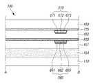
도 4를 참조하면, 표시 패널(110)은 기판(410), 트랜지스터(420), 전계 발광 소자(430) 및 봉지부(440)를 포함할 수 있다.Referring to FIG. 4 , the
기판(410)은 굽힘 또는 접힘 가능한 특성을 가지는 물질로 구성될 수 있다.The
일 예로, 기판(410)은 폴리에테르술폰 (polyethersulphone), 폴리아크릴레이트(polyacrylate), 폴리에테르 이미드(polyetherimide), 폴리에틸렌 나프탈레이트(polyethyelenen napthalate), 폴리에틸렌 테레프탈레이드(polyethyeleneterepthalate), 폴리페닐렌설파이드(polyphenylene sulfide), 폴리아릴레이트(polyallylate), 폴리이미드(polyimide), 폴리카보네이트(polycarbonate), 포토아크릴(photoacrylic) 또는 셀룰로오스 아세테이트 프로피오네이트(cellulose acetatepropionate, CAP)와 같은 고분자 수지를 포함할 수 있다. 다만, 본 명세서에 따른 기판(410)의 물질이 이에 한정되는 것은 아니며, 기판(410)은 유리 또는 절연 처리된 금속 박막으로 구성되는 것도 가능하다.For example, the
기판(410) 상에는 적어도 하나의 트랜지스터(420)가 배치될 수 있다. 도 4의 트랜지스터(420)는 전계 발광 소자(430)와 전기적으로 연결된 구동 트랜지스터일 수 있다.At least one
트랜지스터(420)는 액티브층(421), 게이트 전극(423), 소스 전극(425) 및 드래인 전극(426)을 포함할 수 있다.The
구체적으로, 기판(410) 상에는 적어도 한 층의 액티브층(421)이 배치될 수 있다.Specifically, at least one
도면에는 도시하지 않았으나, 기판(410)과 액티브층(421) 사이에는 적어도 한 층의 버퍼층이 더 배치될 수도 있다.Although not shown in the drawings, at least one buffer layer may be further disposed between the
액티브층(421) 상에는 무기절연물질을 포함하는 게이트 절연막(422)이 배치될 수 있다.A
게이트 절연막(422) 상에는 게이트 전극(423)이 배치될 수 있다. 도 4에 게이트 전극(423)이 단일층인 구성을 도시하였으나, 본 명세서에 따른 게이트 전극(423)은 2중층 이상의 다층 구조일 수도 있다.A
게이트 전극(423) 상에는 무기절연물질을 포함하는 층간 절연막(424)이 배치될 수 있다.An interlayer insulating
층간 절연막 상에는 소스 전극(425) 및 드레인 전극(426)이 서로 이격하여 배치될 수 있다. 도 4에 소스 전극(425)과 드레인 전극(426)이 단일층인 구성을 도시하였으나, 본 명세서에 따른 소스 전극(425)과 드레인 전극(426)의 구조가 이에 한정되는 것은 아니며, 본 명세서에 따른 소스 전극(425)과 드레인 전극(426)은 2중층 이상의 다층 구조일 수도 있다.A
소스 전극(425)과 드레인 전극(426) 각각은 층간 절연막(424)과 게이트 절연막(422)에 구비된 컨택홀을 통해 액티브층(521)과 컨택될 수 있다.Each of the
소스 전극(425)과 드레인 전극(426) 상에는 유기절연물질을 포함하는 평탄화층(429)이 배치될 수 있다.A
도면에는 도시하지 않았으나, 소스 전극(425) 및 드레인 전극(426)과, 평탄화층(429) 사이에는 무기절연물질을 포함하는 보호막이 더 배치될 수도 있다.Although not shown in the drawing, a protective film containing an inorganic insulating material may be further disposed between the
전계 발광 소자(430)는 제1 전극(431), 발광층(432) 및 제2 전극(433)을 포함할 수 있다. 여기서, 제1 전극(431)은 전계 발광 소자(430)의 애노드(anode)이고, 제2 전극(433)은 전계 발광 소자(430)의 캐소드(cathode)일 수 있다. 다만, 본 명세서의 구성이 이에 한정되는 것은 아니며, 제1 전극(431)이 전계 발광 소자(430)의 캐소드이고, 제2 전극(433)이 전계 발광 소자(430)의 애노드일 수도 있다.The
다만, 후술하는 설명에서는 설명의 편의를 위하서, 전계 발광 소자(430)의 제1 전극(431)이 애노드이고, 제2 전극(433)이 캐소드인 구성을 중심으로 설명한다.However, in the description to be described later, for convenience of description, a configuration in which the
표시 패널(110)의 액티브 영역(A/A)에서, 평탄화층(429) 상에는 다수의 제1 전극(431)이 서로 이격하여 배치될 수 있다.In the active area A/A of the
그리고 각각의 제1 전극(431)은 평탄화막(429)에 구비된 컨택홀을 통해 하나의 트랜지스터(420)의 소스 전극(425)과 전기적으로 연결될 수 있다.Also, each
한편, 도 4에서는 전계 발광 소자(430)의 제1 전극(431)이 트랜지스터(420)의 소스 전극(425)과 연결되는 구조를 도시하였으나, 본 명세서에 따른 구조가 이에 한정되는 것은 아니며, 제1 전극(431)은 트랜지스터(420)의 드레인 전극(426)과 연결될 수도 있다.Meanwhile, although FIG. 4 shows a structure in which the
제1 전극(431)의 상면의 일부 및 평탄화층(429)의 상면의 일부에는 뱅크(434)가 배치될 수 있다.A
뱅크(434)는 표시 패널(110)의 액티브 영역(A/A)에서 발광영역(EA)과 비 발광영역(NEA)을 정의할 수 있다. 구체적으로, 액티브 영역(A/A)에서 뱅크(434)가 배치된 영역은 비 발광영역(NEA)에 해당하고, 뱅크(434)가 미 배치된 영역은 발광영역(EA)에 해당할 수 있다.The
뱅크(434)와 미 중첩된 제1 전극(431)의 상면에는 발광층(432)이 배치될 수 있다. 발광층(432)은 단층 또는 2중층 이상의 구조로 이루어질 수 있다. 예를 들면, 발광층(432)은 정공 수송층, 전자 수송층 등을 더 포함하도록 구성될 수 있다. 발광층(432)은 액티브 영역(A/A)에 포함되는 각 서브 픽셀의 고유한 색상을 표시하기 위해서 서브 픽셀의 색상에 대응되는 발광 물질을 포함할 수 있다.An
발광층(432)이 유기 물질일 경우, 전계 발광 소자(430)는 유기 발광 다이오드(organic light emitting diode)로 지칭될 수 있으며, 발광층(432)이 무기 절연 물질일 경우, 전계 발광 소자(430)는 무기 발광 다이오드(inorganic light emitting diode)로 지칭될 수 있다. 예를 들어 퀀텀닷(quantum-dot) 물질을 이용하여 무기 발광 다이오드를 형성할 경우, 전계 발광 소자(430)는 퀀텀닷 다이오드(quantum-dot light emitting diode)로 지칭될 수 있다.When the
발광층(432)은 각 서브 화소의 고유한 색상에 따라 개별적으로 배치될 수 있다. 단, 본 명세서에 따른 발광층(432)의 구성이 이에 한정되지 않으며, 모든 서브 픽셀의 색상이 백색일 경우, 발광층은 공통층으로 형성될 수 있다. 공통층이란, 액티브 영역(A/A)의 모든 영역에 배치된 층을 의미할 수 있다.The
제2 전극(433)은 발광층(532) 및 뱅크(434)이 배치될 수 있다.The light emitting layer 532 and the
제2 전극(433)은 액티브 영역(A/A)에 배치된 다수의 제1 전극(431)과 중첩되도록 배치될 수 있다. 다시 말해, 액티브 영역(A/A)에 배치된 제1 전극(431)들은 하나의 제2 전극(433)을 공유하는 구조일 수 있다.The
제2 전극(433) 상에는 전계 발광 소자(430)에 수분 또는 이물이 침투하는 것을 방지할 수 있는 봉지부(440)가 배치될 수 있다. 이러한 봉지부(440)는 무기절연물질을 포함하는 적어도 두 층의 봉지층 및 유기절연물질을 포함하는 적어도 한 층의 봉지층을 포함할 수 있다.An
구체적으로, 봉지부(440)는 제1 봉지층(441), 제2 봉지층(442) 및 제3 봉지층(443)을 포함할 수 있다.Specifically, the
제1 봉지층(441)은 제2 전극(433) 상에 배치될 수 있으며, 무기절연물질을 포함할 수 있다.The
제2 봉지층(442)은 제1 봉지층(441) 상에 배치될 수 있으며, 유기절연물질을 포함할 수 있다.The
제3 봉지층(443)은 제2 봉지층(442) 상에 배치될 수 있으며, 무기절연물질을 포함할 수 있다.The third encapsulation layer 443 may be disposed on the
제3 봉지층(443) 상에는 터치 패널(120)이 배치될 수 있다.The
터치 패널(120)은 접착성을 갖는 절연막(454)을 통해 제3 봉지층(443) 상에 부착될 수 있다.The
터치 패널(120)은 제1 절연막(451), 제2 절연막(452), 제3 절연막(453), 제1 터치 전극(260) 및 제2 터치 전극(270)을 포함할 수 있다.The
구체적으로, 접착성을 갖는 절연막(454) 상에는 제1 절연막(451)이 배치되고, 제1 절연막(451) 상에는 다수의 제1 터치 전극(260)이 배치될 수 있다.Specifically, a first
제1 터치 전극(260)과 제1 절연막(451) 상에는 제2 절연막(452)이 배치될 수 있다.A second insulating
제2 절연막(452)의 상에는 다수의 제2 터치 전극(270)이 배치될 수 있다.A plurality of
제2 터치 전극(270)과 제2 절연막(452) 상에는 제3 절연막(453)이 배치될 수 있다.A third insulating
도 4에서는 다수의 제1 터치 전극(260) 및 다수의 제2 터치 전극(270)이 단일층인 구조로 도시하였으나, 본 명세서의 실시예들에 따른 제1 및 제2 터치 전극(260, 270)의 구조가 이에 한정되는 것은 아니다. 예를 들면, 다수의 제1 및 제2 터치 전극(260, 270)은 2층 이상의 다중층 구조로 이루어질 수도 있다.Although FIG. 4 shows a structure in which the plurality of
제1 내지 제3 절연막(451, 452, 453) 각각은 유기 절연 물질을 포함할 수 있다.Each of the first to third insulating
제1 절연막(451)의 상면과 배면은 평탄한 형상일 수 있다. 특히, 제1 절연막(451)의 상면에 다수의 제1 터치 전극(260)이 배치되더라도, 제1 절연막(451)의 상면은 단차 없이 평탄한 형상일 수 있다.The top and bottom surfaces of the first insulating
제2 절연막(452)의 상면과 배면은 평탄한 형상일 수 있다. 제2 절연막(452) 배면에 다수의 제1 터치 전극(260)이 배치되더라도, 제2 절연막(452)의 배면은 단차 없이 평탄한 형상일 수 있다. 또한, 제2 절연막(452)의 상면에 다수의 제2 터치 전극(270)이 배치되더라도, 제2 절연막(452)의 상면은 단차 없이 평탄한 형상일 수 있다.Upper and lower surfaces of the second insulating
제3 절연막(453)의 상면과 배면은 평탄한 형상일 수 있다. 특히, 제3 절연막(453)의 배면에 다수의 제2 터치 전극(270)이 배치되더라도, 제3 절연막(453)의 배면은 단차 없이 평탄한 형상일 수 있다.Upper and lower surfaces of the third insulating
이에, 제1 내지 제3 절연막(451, 452, 453), 다수의 제1 터치 전극(260) 및 다수의 제2 터치 전극(270)을 포함하는 터치 패널(120)이 접착성을 갖는 절연막(454)을 통해 표시 패널(110)에 부착되는 경우, 단차에 의해 발생되는 기포 없이 부착될 수 있다. Accordingly, the
따라서, 기포 발생에 의한 접착 불량 및 시인성 불량의 문제를 해소할 수 있다.Therefore, it is possible to solve the problems of poor adhesion and poor visibility due to the generation of air bubbles.
도 5는 본 명세서의 실시예들에 따른 터치 패널의 구조를 개략적으로 도시한 도면이다.5 is a diagram schematically illustrating a structure of a touch panel according to embodiments of the present specification.
본 실시예를 설명함에 있어 이전 실시예와 동일 또는 대응되는 구성요소에 대한 설명은 생략하기로 한다. 이하, 이를 참조하여 본 실시예에 따른 터치 패널에 대해 설명하기로 한다.In describing the present embodiment, descriptions of components identical to or corresponding to those of the previous embodiment will be omitted. Hereinafter, the touch panel according to the present embodiment will be described with reference to this.
도 5를 참조하면, 터치표시장치(100)의 터치 패널(120)은 다수의 제1 터치 전극(260, 또는 제1 터치 전극) 및 다수의 제2 터치 전극(270, 또는 제2 터치 전극)을 포함한다. 이러한 터치 패널(120)은 제1 터치 전극(260)과 제2 터치 전극(270) 상호 간에 형성되는 캐피시턴스(capacitance) 변화량을 감지하는 방식으로 구동될 수 있다.Referring to FIG. 5 , the
그리고, 제1 터치 전극(260)과 제2 터치 전극(270)은 터치 패널(120)의 적어도 일부 영역에서 서로 중첩되도록 배치될 수 있다.Also, the
서로 중첩된 제1 터치 전극(260)과 제2 터치 전극(270)은 제1 방향으로 연장될 수 있다.The
또한, 서로 중첩된 제1 터치 전극(260)과 제2 터치 전극(270)의 다른 일부는 제1 방향과 교차하는 방향인 제2 방향으로 연장될 수 있다. 그리고, 제2 방향으로 연장되는 서로 중첩된 제1 터치 전극(260) 및 제2 터치 전극(270)은, 제2 방향으로 연장되는 서로 중첩된 다른 제1 터치 전극(260) 및 제2 터치 전극(270)과 적어도 두번 교차될 수 있다.In addition, other portions of the
서로 중첩된 제1 터치 전극(260) 및 제2 터치 전극(270)과 인접한 다른 제1 터치 전극(260) 및 제2 터치 전극(270)의 교차 지점 사이에 개구부(510)가 마련될 수 있다.An
이에, 터치 패널(120)에는 다수의 개구부(510)가 존재할 수 있다. 여기서, 다수의 개구부(510)는 서로 중첩된 제1 터치 전극(260)과 제2 터치 전극(270)이 서로 다른 제1 터치 전극(260)과 제2 터치 전극(270)과 교차하여 형성된 것일 수 있다.Accordingly, a plurality of
다만, 본 명세서의 제1 및 제2 터치 전극(260, 270)의 구조가 이에 한정되는 것은 아니며, 다수의 개구부(510) 중 일부는 적어도 두 개의 제1 터치 전극(260)이 서로 교차하여 형성되거나, 적어도 두 개의 제2 터치 전극(270)이 서로 교차하여 형성된 영역일 수도 있다.However, the structures of the first and
평면 상으로, 다수의 개구부(510)의 형상은 마름모 또는 다이아몬드 형상일 수 있으나, 본 명세서의 실시예들에 따른 다수의 개구부(510)의 형상이 이에 한정되는 것은 아니며, 다각형, 타원형, 원형 등 다양한 형상으로 변형되어 실시될 수 있다.On a plane, the shape of the plurality of
또한, 다수의 터치 패널(120)은 적어도 하나의 단선부(520)를 포함할 수 있다.Also, the plurality of
단선부(520)는 제1 터치 전극(260)과 제2 터치 전극(270) 중 적어도 하나의 일부가 끊어져 인접한 다른 제1 터치 전극(260) 또는 제2 터치 전극(270)과 단선된 영역일 수 있다.The disconnected
일 예로, 터치 패널(120)에 포함된 제1 터치 전극(260) 전체가 전기적으로 연결되고, 및 제2 터치 전극(270) 전체가 전기적으로 연결될 때, 제1 터치 전극(260)의 일부와 제2 터치 전극(270)의 일부에 불량이 발생하는 경우, 터치 패널(120) 전체가 동작하지 않을 수 있다.For example, when all of the
그러나, 본 실시예에서는, 제1 터치 전극(260)과 제2 터치 전극(270) 중 적어도 하나의 일부가 단선되는 영역인 단선부(520)를 포함함으로써, 불량이 발생한 제1 터치 전극(260)이나 제2 터치 전극(270)과 단선된 다른 제2 터치 전극(270)이 구동 될 수 있고, 이에, 터치 패널(120)의 터치 감도가 저하되는 것을 방지할 수 있다.However, in this embodiment, at least one part of the
또한, 터치 패널(120)이 다수의 단선부(520)를 포함하는 경우, 터치 패널(120)은 적어도 하나의 더미 패턴(580)을 포함할 수 있다.Also, when the
더미 패턴(580)은 제1 터치 전극(260)으로부터 끊어진 일부분이거나, 제2 터치 전극(270)으로부터 끊어진 일부분일 수 있다. 또한, 더미 패턴(580)은 제1 터치 전극(260)과 제2 터치 전극(270) 각각이 끊어진 일부분일 수도 있으며, 이 경우, 더미 패턴(580)은 제1 터치 전극(260)의 일부분과 제2 터치 전극(270)의 일부분이 중첩된 구조일 수 있다.The
도 5의 더미 패턴(580)의 위치 및 형상은 일 예로 도시된 것일뿐, 더미 패턴(580)의 위치 및 형상은 다양하게 변경될 수 있다.The position and shape of the
또한, 하나의 제2 터치 전극(270) 또는 제1 터치 전극(260)의 크기에 대해여 더미 패턴(580)이 차지하는 영역의 비율(더미 패턴 비율)도 다양하게 변경될 수 있다.Also, the ratio of the area occupied by the
한편, 터치 패널(120)에 더미 패턴(580)이 존재하지 않고 다수의 제1 터치 전극(260) 및 다수의 제2 터치 전극(270)이 다른 제1 터치 전극(260) 및 제2 터치 전극(270)과 교차하여 배치되는 경우, 화면 상에 제1 터치 전극(260)과 제2 터치 전극(270)의 윤곽이 보이는 시인성 문제가 발생할 수 있다.Meanwhile, the
하지만, 터치 패널(120)에 더미 패턴(580)을 하나 이상 배치함으로써, 제1 터치 전극(260) 과 제2 터치 전극(270)이 메쉬 형태로 패터닝 된 경우에 발생할 수 있는 시인성 문제가 해소될 수 있다.However, by disposing one or
또한, 각 제2 터치 전극(270) 별로 더미 패턴(580)의 존재 유무 또는 개수(더미 패턴 비율)을 조절함으로써, 각 제2 터치 전극(270) 별로 캐패시턴스의 크기를 조절하여 터치 감도를 향상시킬 수도 있다.In addition, by adjusting the existence or number (dummy pattern ratio) of
이러한 터치 패널(120)을 포함하는 터치표시장치(100)에 외광이 입사되는 경우, 터치 패널(120)에 입사된 외광이 터치 패널(120)의 절연막들의 계면에서 반사되어 사용자에게 무지개 색상의 광이 시인되어 터치표시장치(100)의 시인성이 저하될 수 있다.When external light is incident on the
구체적으로, 터치 패널(120)에 적층된 절연막들의 굴절률이 상이하여 절연막들의 경계에서 외광의 반사가 일어나는 경우, 외광이 난반사되는 것과 유사하게 광의 경로가 일정하지 않게 되므로, 터치 패널(120)의 절연막들의 경계에서 반사된 외광은 무지개 색상으로 시인된다.Specifically, when reflection of external light occurs at the boundary of the insulating films due to different refractive indices of the insulating films stacked on the
예를 들어, 도 4의 제3 절연막(453)의 굴절률이 제2 절연막(452)의 굴절률 보다 작은 경우, 제3 절연막(453)을 통과한 외광이 제3 절연막(453)과 제2 절연막(452)의 경계에서 반사되어 외부로 추출될 수 있다. 이 때, 광의 파장별로 반사되는 각도가 달라짐으로써, 각 파장대의 광의 경로가 일정하지 않게되어 가시광선 파장대에 포함되는 색상들의 광이 사용자에게 시인될 수 있다. 즉, 외광이 무지개 색상으로 시인되어 시인성이 떨어질 수 있다.For example, when the refractive index of the third
또한, 도 4의 제2 절연막(452)의 굴절률이 제1 절연막(451)의 굴절률보다 작은 경우, 제3 및 제2 절연막(453, 452)을 통과한 광이 제2 절연막(452)과 제1 절연막(451)의 경계에서 반사되어 외부로 추출될 수 있으며, 이 경우에도, 가시광선 파장대에 포함되는 색상들의 광이 사용자에게 시인되어, 터치표시장치(100)의 시인성이 저하될 수 있다.In addition, when the refractive index of the second
또한, 도 4의 제1 절연막(451)의 굴절률이 절연막(454)의 굴절률보다 작은 경우, 제1 내지 제3 절연막(451, 452, 453)을 통과한 광이 제1 절연막(451)과 절연막(454)의 경계에서 반사됨으로써, 가시광선 파장대에 포함되는 색상들의 광이 사용자에게 시인되어, 터치표시장치(100)의 시인성이 저하될 수 있다.In addition, when the refractive index of the first insulating
특히, 터치표시장치(100)를 측면 방향(예: 터치 패널의 표면에 대해 수직한 방향을 제외한 나머지 방향)에서 바라볼 때, 터치표시장치(100)의 터치 패널(120)에 의해 반사된 외광이 터치 패널(120)에 포함된 구성들로 인한 굴절로 인해 시인성이 크게 떨어질 수 있다.In particular, external light reflected by the
이에, 본 명세서의 실시예들에 따른 터치 패널(120)은 사용자가 터치표시장치(100)를 측면에서 바라보더라도 시인성이 우수한 구조를 갖는 터치 패널을 제공한다.Accordingly, the
도 6은 도 5의 A-B를 따라 절단한 단면도이다.6 is a cross-sectional view taken along line A-B of FIG. 5;
본 실시예를 설명함에 있어 이전 실시예와 동일 또는 대응되는 구성요소에 대한 설명은 생략하기로 한다. 이하, 이를 참조하여 본 실시예에 따른 터치표시장치에 대해 설명하기로 한다.In describing the present embodiment, descriptions of components identical to or corresponding to those of the previous embodiment will be omitted. Hereinafter, the touch display device according to the present embodiment will be described with reference to this.
예를 들면, 도 6을 참조로 본 실시예의 터치표시장치(100)를 구성하는 표시 패널(110), 터치 패널(120)의 제1 내지 제3 절연막(451, 452, 453)은 앞서 도 4를 참조로 설명한 표시 패널(110), 터치 패널(120)의 제1 내지 제3 절연막(451, 452, 453)과 동일할 수 있다.For example, referring to FIG. 6 , the first to third insulating
터치표시장치(100)는 표시 패널(110) 상에 배치된 터치 패널(120)을 포함하고, 터치 패널(120)은 접착성을 갖는 절연막(454, 이하 제4 절연막이라 명명함)를 통해, 표시 패널(110)의 일면에 부착될 수 있다.The
터치 패널(120)은 표시 패널(110)로부터 광이 출사되는 방향에 배치될 수 있다.The
표시 패널(110)의 일 면에는 제4 절연막(454)이 배치되고, 제4 절연막(454)의 일 면에는 터치 패널(120)의 제1 절연막(451)이 배치될 수 있다.A fourth insulating
제1 절연막(451) 상에는 제2 절연막(452)이 배치될 수 있다.A second insulating
제1 절연막(451)과 제2 절연막(452) 사이에는 다수의 제1 터치 전극(260)이 배치될 수 있다.A plurality of
제1 터치 전극(260)은 제1 전극층(661), 제1 전극층(661) 상에 배치된 제2 전극층(662) 및 제2 전극층(662) 상에 배치된 제3 전극층(663)을 포함할 수 있다.The
제1 내지 제3 전극층(661, 662, 663) 각각은 전도성 금속을 포함할 수 있다. 제1 내지 제3 전극층(661, 662, 663) 각각은 알루미늄(Al), 금(Au), 은(Ag), 구리(Cu), 텅스텐(W), 몰리브덴(Mo), 크롬(Cr), 탄탈륨(Ta), 티타늄(Ti) 등의 금속 또는 이들의 합금 중 어느 하나를 포함할 수 있으나, 본 실시예들이 이에 한정되는 것은 아니다.Each of the first to third electrode layers 661, 662, and 663 may include a conductive metal. Each of the first to third electrode layers 661, 662, and 663 includes aluminum (Al), gold (Au), silver (Ag), copper (Cu), tungsten (W), molybdenum (Mo), chromium (Cr), Metals such as tantalum (Ta) and titanium (Ti) or alloys thereof may be included, but the present embodiments are not limited thereto.
제1 내지 제3 전극층(661, 662, 663) 각각이 상술한 전도성 금속을 포함하는 경우, 다수의 제1 터치 전극(260)의 저항이 낮아질 수 있으므로, 대면적의 터치표시장치(100)에 적용이 유리할 수 있다.When each of the first to third electrode layers 661, 662, and 663 includes the above-described conductive metal, the resistance of the plurality of
제1 내지 제3 전극층(661, 662, 663) 중 적어도 하나는 투명 도전 물질을 포함할 수도 있다. 예를 들면, 제1 내지 제3 전극층(661, 662, 663) 중 적어도 하나는 ITO(Indium Tin Oxide), IZO(Indium Zinc Oxide), ZnO(zinc oxide) 및 ITZO(indium tin zinc oxide) 또는 IGZO(Indium Gallium Zinc Oxide) 중 적어도 하나를 포함할 수도 있으나, 본 실시예들이 이에 한정되는 것은 아니다.At least one of the first to third electrode layers 661, 662, and 663 may include a transparent conductive material. For example, at least one of the first to third electrode layers 661, 662, and 663 may include indium tin oxide (ITO), indium zinc oxide (IZO), zinc oxide (ZnO), indium tin zinc oxide (ITZO), or IGZO. (Indium Gallium Zinc Oxide), but the present embodiments are not limited thereto.
제1 내지 제3 전극층(661, 662, 663)가 투명 도전 물질을 포함하는 경우, 제1 내지 제3 전극층(661, 662, 663)이 공정 오차에 의해 발광영역(EA)의 일부와 중첩하더라도, 터치표시장치(100)의 휘도를 유지할 수 있는 효과가 있다.When the first to third electrode layers 661, 662, and 663 include a transparent conductive material, even if the first to third electrode layers 661, 662, and 663 overlap a part of the light emitting area EA due to a process error, , there is an effect of maintaining the luminance of the
제2 절연막(452) 상에는 제3 절연막(453)이 배치될 수 있다.A third insulating
제2 절연막(452)과 제3 절연막(453) 사이에는 다수의 제2 터치 전극(270)이 배치될 수 있다.A plurality of
제2 터치 전극(270)은 제4 전극층(671), 제4 전극층(671) 상에 배치된 제5 전극층(672) 및 제5 전극층(672) 상에 배치된 제6 전극층(673)을 포함할 수 있다.The
제4 내지 제6 전극층(671, 672, 673) 각각은 전도성 금속을 포함할 수 있다. 제4 내지 제6 전극층(671, 672, 673) 각각은 알루미늄(Al), 금(Au), 은(Ag), 구리(Cu), 텅스텐(W), 몰리브덴(Mo), 크롬(Cr), 탄탈륨(Ta), 티타늄(Ti) 등의 금속 또는 이들의 합금 중 어느 하나를 포함할 수 있으나, 본 실시예들이 이에 한정되는 것은 아니다.Each of the fourth to sixth electrode layers 671, 672, and 673 may include a conductive metal. Each of the fourth to sixth electrode layers 671, 672, and 673 includes aluminum (Al), gold (Au), silver (Ag), copper (Cu), tungsten (W), molybdenum (Mo), chromium (Cr), Metals such as tantalum (Ta) and titanium (Ti) or alloys thereof may be included, but the present embodiments are not limited thereto.
제4 내지 제6 전극층(671, 672, 673) 각각이 상술한 전도성 금속을 포함하는 경우, 다수의 제2 터치 전극(270)의 저항이 낮아질 수 있으므로, 대면적의 터치표시장치(100)에 적용이 유리할 수 있다.When each of the fourth to sixth electrode layers 671, 672, and 673 includes the above-described conductive metal, the resistance of the plurality of
제4 내지 제6 전극층(671, 672, 673) 중 적어도 하나는 투명 도전 물질을 포함할 수 있다. 예를 들면, 제4 내지 제6 전극층(671, 672, 673) 중 적어도 하나는 ITO(Indium Tin Oxide), IZO(Indium Zinc Oxide), ZnO(zinc oxide) 및 ITZO(indium tin zinc oxide) 또는 IGZO(Indium Gallium Zinc Oxide) 중 적어도 하나를 포함할 수도 있으나, 본 실시예들이 이에 한정되는 것은 아니다.At least one of the fourth to sixth electrode layers 671, 672, and 673 may include a transparent conductive material. For example, at least one of the fourth to sixth electrode layers 671, 672, and 673 may include indium tin oxide (ITO), indium zinc oxide (IZO), zinc oxide (ZnO), indium tin zinc oxide (ITZO), or IGZO. (Indium Gallium Zinc Oxide), but the present embodiments are not limited thereto.
제4 내지 제6 전극층(671, 672, 673)가 투명 도전 물질을 포함하는 경우, 제4 내지 제6 전극층(671, 672, 673)이 공정 오차에 의해 발광영역(EA)의 일부와 중첩하더라도, 터치표시장치(100)의 휘도를 유지할 수 있는 효과가 있다.When the fourth to sixth electrode layers 671, 672, and 673 include a transparent conductive material, even if the fourth to sixth electrode layers 671, 672, and 673 overlap part of the light emitting area EA due to a process error, , there is an effect of maintaining the luminance of the
표시 패널(110)에서 터치 패널(120)이 적층되는 방향을 기준으로, 다수의 제1 터치 전극(260) 및 제2 터치 전극(270)의 측면은 역테이퍼 형상으로 이루어질 수 있다.Based on the direction in which the
본 실시예들에 따른 터치표시장치(100)는 표시 패널(110)과 터치 패널(120)을 각각 제조한 후, 제4 절연막(454)을 통해 접착하는 공정을 통해 형성될 수 있다.The
여기서, 터치 패널(120)은 제3 절연막(453) 상에 다수의 제2 터치 전극(270)을 배치하고, 다수의 제2 터치 전극(270)과 제3 절연막(453) 상에 제2 절연막(452)을 배치하며, 제2 절연막(452) 상에 다수의 제1 터치 전극(260)을 배치하고, 다수의 제1 터치 전극(260)과 제2 절연막(452) 상에 제1 절연막(451)을 배치하는 공정을 통해 마련될 수 있다.Here, in the
그리고, 제1 절연막(451)의 일 면이 제4 절연막(454)을 통해 표시 패널(120)의 일면에 부착됨으로써, 터치 패널(120)를 형성하는 공정 순서와는 반대로 표시 패널(120) 상에 적층되므로, 다수의 제1 터치 전극(260)과 다수의 제2 터치 전극(270)의 측면의 형상은 표시 패널(110) 상에 터치 패널(120)이 적층되는 방향에 대해 역테이퍼 형상으로 이루어질 수 있다. In addition, one surface of the first insulating
제3 절연막(453) 상에 다수의 제2 터치 전극(270)이 배치되고, 다수의 제2 터치 전극(270)과 제3 절연막(453) 상에 제2 절연막(452)이 배치되더라도, 제2 절연막(452)의 일 면(제2 터치 전극과 접촉하는 반대 면)은 다수의 제2 터치 전극(270)에 의한 단차 없이 편평하게 이루어질 수 있다.Even if the plurality of
또한, 다수의 제2 터치 전극(270)과 접촉하는 제2 절연막(452)의 일 면의 반대 면에 다수의 제1 터치 전극(260)이 배치되고, 다수의 제1 터치 전극(260)과 제2 절연막(452) 상에 제1 절연막(451)이 배치되더라도, 제1 절연막(451)의 일 면(제1 터치 전극과 접촉하는 반대 면)은 다수의 제1 터치 전극(270)에 의한 단차 없이 편평하게 이루어질 수 있다.In addition, a plurality of
제4 절연막(454)은 유기 절연 물질을 포함할 수 있다. 그리고, 제4 절연막(454)은 접착성을 가질 수 있다.The fourth insulating
이로써, 제1 절연막(451)의 편평한 면(즉, 터치 전극들에 의한 단차가 없는 면)이 제4 절연막(454)에 부착됨으로써, 제1 절연막(451)과 제4 절연막(454) 사이에 기포 등이 생기는 부착 불량 현상이 저감될 수 있다.As a result, the flat surface of the first insulating film 451 (that is, the non-stepped surface by the touch electrodes) is attached to the fourth insulating
터치 패널(120)의 제1 내지 제3 절연막(451, 452, 453) 각각의 굴절률은 서로 대응될 수 있다. 따라서, 터치 패널(120)의 외부에서 입사된 광은 제1 절연막(451)과 제2 절연막(452)의 계면 및 제2 절연막(452)과 제3 절연막(453)의 계면에서 반사가 일어나지 않게 되므로, 사용자에게 무지개 색상의 광이 시인되지 않을 수 있다.The refractive indices of each of the first to third insulating
그리고, 표시 패널(110)과 터치 패널(120) 사이에 배치된 제4 절연막(453)의 굴절률은 제1 내지 제3 절연막(451, 452, 453) 각각의 굴절률과 대응되거나, 제1 내지 제3 절연막(451, 452, 453) 각각의 굴절률보다 낮을 수 있다.Also, the refractive index of the fourth insulating
이에, 터치 패널(120)의 외부로부터 입사된 광은 제1 절연막(451)과 제4 절연막(454)의 계면에서 반사되지 않음으로써, 사용자에게 무지개 색상의 광이 시인되는 것을 방지하고, 터치표시장치(100)의 시인성을 향상시킬 수 있는 효과를 가질 수 있다.Accordingly, the light incident from the outside of the
제1 내지 제3 절연막(451, 452, 453)의 굴절률은 1.45 내지 1.5의 범위에서 선택될 수 있으나, 본 실시예들이 이에 한정되는 것은 아니다.The refractive indices of the first to third insulating
제4 절연막(454)의 굴절률은 1.4 내지 1.5의 범위에서 선택될 수 있으나, 본 실시예들이 이에 한정되는 것은 아니다.The refractive index of the fourth insulating
따라서, 터치 패널(120)로 입사된 외광은 제1 내지 제3 절연막(451, 452, 453)을 거치면서 경로가 꺾이지 않을 수 있다. 그리고, 제1 절연막(451)과 제4 절연막(454)의 계면에서도 외광의 경로가 꺾이지 않거나, 또는 굴절되어 표시 장치(100)로 입사될 수 있다.Accordingly, the path of external light incident to the
표시 패널(110)에 입사된 외광의 일부는 표시 패널(110) 내의 구성들에 의해 흡수되거나 표시 패널(110) 내의 서로 다른 굴절률을 갖는 다수의 절연막들의 경계에 갇힘으로써, 터치표시장치(100) 외부로 출사되는 양이 저감되어 외광 반사에 의한 시인성이 떨어지는 현상을 막을 수 있다.A part of the external light incident on the
제1 내지 제3 절연막(451, 452, 453)은 유기 절연 물질을 포함할 수 있다. 예를 들면, 제1 내지 제3 절연막(451, 452, 453)은 서로 대응되는 유기 절연 물질을 포함할 수 있다. 예를 들면, 아크릴계 유기절연물질(예: 포토아크릴(photoacrylic))을 포함하거나, 폴리스티렌(polystyrene), 폴리메틸메타아크릴레이트(PMMA, Polymethylmethacrylate), 폴리아크릴로니트릴(PAN, Polyacrylonitrile), 폴리아미드(PA, Polyamide), 폴리이미드(PI, Polyimide), 폴리아릴에테르(PAE, Polyarylether), 헤테로사이클릭 폴리머(Heterocyclic Polymer), 파릴렌(Parylene), 에폭시 수지(Epoxy resin), 벤조시클로부텐(BCB, Benzocyclobutene), 실록산계 수지(Siloxane based resin) 및 실란계 수지(Silane based resin) 중 적어도 하나를 포함할 수 있으나, 본 실시예들이 이에 한정되는 것은 아니다.The first to third insulating
또한, 제1 절연막(451)과 제2 절연막(452) 및 제2 절연막(452)과 제3 절연막(453) 간의 부착력 향상을 위해, 제1 절연막(451)과 제2 절연막(452)의 계면과 제2 절연막(452)과 제3 절연막(453)의 계면에 플라즈마를 통한 표면처리가 될 수 있으나, 본 실시예들이 이에 한정되는 것은 아니다.In addition, to improve adhesion between the first insulating
본 실시예들에 따른 터치표시장치는 이에 한정되지 않는다.The touch display device according to the present embodiments is not limited thereto.
도 7 및 도 8은 본 발명의 실시예들에 따른 터치표시장치의 단면도이다.7 and 8 are cross-sectional views of a touch display device according to example embodiments.
본 실시예들을 설명함에 있어 이전 실시예와 동일 또는 대응되는 구성요소에 대한 설명은 생략하기로 한다. 이하, 이를 참조하여 본 실시예들에 따른 터치표시장치에 대해 설명하기로 한다.In describing the present embodiments, descriptions of components identical to or corresponding to those of the previous embodiments will be omitted. Hereinafter, a touch display device according to the present exemplary embodiments will be described with reference to this.
예를 들면, 도 7 및 도 8을 참조로 본 실시예의 터치표시장치(100)를 구성하는 표시 패널(110), 제4 절연막(454), 터치 패널(120)의 제1 내지 제3 절연막(451, 452, 453) 및 다수의 제1 및 제2 터치 전극(260, 270)은 앞서 도 6을 참조로 설명한 표시 패널(110), 제4 절연막(454), 터치 패널(120)의 제1 내지 제3 절연막(451, 452, 453) 및 다수의 제1 및 제2 터치 전극(260, 270)과 동일할 수 있다.For example, referring to FIGS. 7 and 8 , the
도 7을 참조하면, 도 6에 도시된 터치 패널(120)의 제2 절연막(452)과 제3 절연막(453) 사이에 제5 절연막(755)이 배치될 수 있습니다.Referring to FIG. 7 , a fifth insulating
구체적으로, 제5 절연막(755)은 제3 절연막(453)과 다수의 제2 터치 전극(270) 사이에 배치될 수 있다.Specifically, the fifth insulating
제1 절연막 내지 제3 절연막(451, 452, 453) 각각은 유기 절연 물질을 포함할 수 있다.Each of the first to third insulating
제5 절연막(755)은 무기 절연 물질을 포함할 수 있다. 예를 들면, 제5 절연막(755)은 실리콘 옥사이드(SiOx)일 수 있으나, 본 발명이 이에 한정되는 것은 아니다. The fifth insulating
제1 내지 제3 절연막(451, 452, 453)이 유기 절연 물질을 포함하고, 제5 절연막(755)이 무기 절연 물질을 포함함으로써, 제5 절연막(755)의 두께는 제1 내지 제3 절연막(451, 452, 453) 각각의 두께보다 얇을 수 있다.Since the first to third insulating
이와 같이, 유기 절연 물질을 포함하는 제2 절연막(452)과 제3 절연막(453) 사이에 무기 절연 물질을 포함하는 제5 절연막(755)이 배치됨으로써, 터치 패널(120)에 포함된 다수의 제1 및 제2 터치 전극(260, 270)에 수분이 침투하는 것을 방지할 수 있다.As such, the fifth insulating
특히, 제1 및 제2 터치 전극(260, 270)이 도 6에서 예시로 설명한 전도성 금속을 포함하는 경우, 터치 패널(120)에 구비된 다수의 제1 및 제2 터치 전극(260, 270)은 수분에 취약할 수 있다.In particular, when the first and
본 실시예에서는, 제2 절연막(452), 제5 절연막(755) 및 제3 절연막(453)이 적층됨으로써, 봉지층 역할을 하여, 다수의 제1 및 제2 터치 전극(260, 270)에 수분의 침투하여, 전극들의 특성이 저하되는 것을 방지할 수 있다.In this embodiment, the second
상술한 바와 같이, 제2 및 제3 절연막(452, 453) 각각은 유기 절연 물질을 포함하고, 제2 절연막(452)과 제3 절연막(453) 사이에 배치된 제5 절연막(755)이 무기 절연 물질을 포함함으로써, 제2 및 제3 절연막(452, 453)과 제5 절연막(755)은 표시 패널(110)에 포함된 봉지층의 역할을 할 수 있다.As described above, each of the second and third insulating
또한, 제1 내지 제3 절연막(451, 452, 453) 각각의 굴절률은 서로 대응될 수 있다. 그리고, 제5 절연막(755)의 굴절률은 제1 내지 제3 절연막(451, 452, 453) 각각의 굴절률과 대응되거나, 제1 내지 제3 절연막(451, 452, 453) 각각의 굴절률보다 낮을 수 있다.In addition, refractive indices of each of the first to third insulating
예를 들면, 제1 내지 제3 절연막(451, 452, 453) 각각의 굴절률은 1.45 내지 1.5일 수 있고, 제5 절연막(755)의 굴절률은 1.4 내지 1.45일 수 있으나, 본 발명이 이에 한정되는 것은 아니다.For example, the refractive index of each of the first to third insulating
제1 내지 제3 절연막(451, 452, 453) 각각의 굴절률과 제5 절연막(755)의 굴절률이 대응되는 경우, 터치 패널(120)로 입사된 외광은 제1 내지 제3 절연막(451, 452, 453)과 제5 절연막(755) 사이의 게면들에서 경로가 꺽이지 않을 수 있다. 그리고, 제1 절연막(451)을 통과한 광은 제4 절연막(454)의 계면을 경로 변화 없이 통과하거나, 굴절되어 통과 함으로써, 최종적으로 표시 패널(120)에 입사되고, 표시 패널(110)에 입사된 외광의 일부는 표시 패널(110) 내의 구성들에 의해 흡수되고, 다른 일부는 표시 패널(110) 내의 서로 다른 굴절률을 갖는 다수의 절연막들의 경계에 갇힐 수 있다.When the refractive index of each of the first to third insulating
제5 절연막(755)의 굴절률이 제1 내지 제3 절연막(451, 452, 453) 각각의 굴절률보다 낮은 경우, 터치 패널(120)로 입사된 외광은 제3 절연막(453)과 제5 절연막(755)의 계면에서 굴절되어 제5 절연막(755)에 입사되고, 제5 절연막(755)과 제2 절연막(452)의 계면에서 또 한번의 굴절이 일어면서 제2 절연막(452)에 입사될 수 있다.When the refractive index of the fifth insulating
그리고, 제2 절연막(452)과 제1 절연막(451)을 경로의 변화 없이 차례로 통과한 외광은 제1 절연막(451)과 제4 절연막(454)의 계면에서 경로 변화 없이 제4 절연막(454)을 통과하거나, 굴절되어 제4 절연막(454)을 통과 함으로써, 최종적으로 표시 패널(120)에 입사될 수 있다. 표시 패널(110)에 입사된 외광의 일부는 표시 패널(110) 내의 구성들에 의해 흡수될 수 있고, 다른 일부는 표시 패널(110) 내의 서로 다른 굴절률을 갖는 다수의 절연막들의 경계에 갇힐 수 있다.In addition, the external light passing through the second
따라서, 표시 패널(110)로 입사된 외광은 터치표시장치(100) 외부로 출사되지 않음으로써, 외광 반사에 의한 시인성이 떨어지는 현상을 막을 수 있다.Therefore, external light incident on the
터치 패널(120) 제조 시, 제3 절연막(453) 상에 제5 절연막(755)이 배치되고, 제5 절연막(755) 상에 다수의 제2 터치 전극(270)이 배치될 수 있다. 따라서, 제5 절연막(755)은 다수의 제2 터치 전극(270)에 의한 단차 없이 상면 및 배면이 편평하게 이루어지 수 있다.When manufacturing the
한편, 본 실시예들에 따른 터치 패널(120)의 구조는 이에 한정되지 않으며, 다수의 제1 및 제2 터치 전극(260, 270)에 수분이 침투하는 것을 방지하기 위해 추가 절연막을 더 포함할 수 있다.Meanwhile, the structure of the
도 8을 참조하면, 도 7의 터치 패널(120)에서 터치 패널(120)의 제1 절연막(451)과 제2 절연막(452) 사이에 제6 절연막(855)이 배치될 수 있다.Referring to FIG. 8 , in the
구체적으로, 제6 절연막(855)은 제2 절연막(452)과 다수의 제1 터치 전극(260) 사이에 배치될 수 있따.Specifically, the sixth insulating
제6 절연막(855)은 무기 절연 물질을 포함할 수 있다. 예를 들면, 제6 절연막(855)은 실리콘 옥사이드(SiOx)일 수 있으나, 본 발명이 이에 한정되는 것은 아니다.The sixth
제1 내지 제3 절연막(451, 452, 453)이 유기 절연 물질을 포함하고, 제6 절연막(855)이 무기 절연 물질을 포함함으로써, 제6 절연막(855)의 두께는 제1 내지 제3 절연막(451, 452, 453) 각각의 두께보다 얇을 수 있다.Since the first to third insulating
이와 같이, 유기 절연 물질을 포함하는 제2 절연막(452)과 제3 절연막(453) 사이에 무기 절연 물질을 포함하는 제5 절연막(755)이 배치되고, 제2 절연막(452)과 유기 절연 물질을 포함하는 제1 절연막(451) 사이에 무기 절연 물질을 포함하는 제6 절연막(855)이 배치됨으로써, 터치 패널(120)에 포함된 다수의 제1 및 제2 터치 전극(260, 270)에 수분이 침투하는 것을 방지할 수 있다.As described above, the fifth insulating
구체적으로, 터치 패널(120)은 유기 절연 물질을 포함하는 절연막과 무기 절연 물질을 포함하는 절연막이 교번하여 적층된 구조를 가짐으로써, 다수의 제1 및 제2 터치 전극(260, 270)에 수분이 침투하는 것을 방지할 수 있다.Specifically, the
제6 절연막(855)의 굴절률은 제1 내지 제3 절연막(451, 452, 453) 각각의 굴절률과 대응되거나, 제1 내지 제3 절연막(451, 452, 453) 각각의 굴절률보다 낮을 수 있다.The refractive index of the sixth insulating
제6 절연막(855)의 굴절률은 제5 절연막(755)의 굴절률과 대응될 수 있다.The refractive index of the sixth insulating
예를 들면, 제1 내지 제3 절연막(451, 452, 453) 각각의 굴절률은 1.45 내지 1.5일 수 있고, 제5 및 제6 절연막(755, 855)의 굴절률은 1.4 내지 1.45일 수 있으나, 본 발명이 이에 한정되는 것은 아니다.For example, each of the first to third insulating
제1 내지 제3 절연막(451, 452, 453) 각각의 굴절률과 제5 및 제6 절연막(755, 855)의 굴절률이 대응되는 경우, 터치 패널(120)로 입사된 외광은 제1 내지 제3 절연막(451, 452, 453)과 제5 절연막(755) 사이의 게면들에서 경로가 꺽이지 않을 수 있다. 그리고, 제1 내지 제3 절연막(451, 452, 453)과 제5 및 제6 절연막(755, 855)을 통과한 광은 제1 절연막(451)과 제4 절연막(454)의 계면에서 경로 변화 없이 통과하거나, 굴절되어 통과 함으로써, 최종적으로 표시 패널(120)에 입사될 수 있다. 그리고, 표시 패널(110)에 입사된 외광의 일부는 표시 패널(110) 내의 구성들에 의해 흡수 될 수 있고, 다른 일부는 표시 패널(110) 내의 서로 다른 굴절률을 갖는 다수의 절연막들의 경계에 갇힐 수 있다.When the refractive indices of the first to third insulating
제6 절연막(855)의 굴절률이 제1 내지 제3 절연막(451, 452, 453) 각각의 굴절률보다 낮은 경우, 터치 패널(120)로 입사된 외광은 제3 절연막(453)과 제5 절연막(755)의 계면에서 굴절되어 제5 절연막(755)에 입사되고 제5 절연막(755)과 제2 절연막(452)의 계면에서 또 한번의 굴절이 일어나면서, 제2 절연막(452)에 입사될 수 있다.When the refractive index of the sixth
그리고, 제2 절연막(452)과 제6 절연막(855)의 계면에서 굴절이 일어나고, 제6 절연막(855)과 제1 절연막(451)의 계면에서도 굴절이 일어나면서 제1 절연막(451)에 입사될 수 있다.Further, refraction occurs at the interface between the second
제2 절연막(452)과 제1 절연막(451)을 차례로 통과한 광은 제1 절연막(451)과 제4 절연막(454)의 계면에서 경로 변화 없이 제4 절연막(454)을 통과하거나, 굴절되어 제4 절연막(454)을 통과 함으로써, 최종적으로 표시 패널(120)에 입사되고, 표시 패널(110)에 입사된 외광의 일부는 표시 패널(110) 내의 구성들에 의해 흡수될 수 있고, 다른 일부는 표시 패널(110) 내의 서로 다른 굴절률을 갖는 다수의 절연막들의 경계에 갇힐 수 있다.Light passing through the second
따라서, 표시 패널(110)로 입사된 외광은 터치표시장치(100) 외부로 출사되지 않음으로써, 외광 반사에 의한 시인성이 떨어지는 현상을 막을 수 있는 동시에, 제1 및 제2 터치 전극(260, 270)이 수분에 의해 부식되는 것을 방지할 수 있다Therefore, since the external light incident on the
터치 패널(120) 제조 시, 제2 절연막(452) 상에 제6 절연막(855)이 배치되고, 제6 절연막(855) 상에 다수의 제1 터치 전극(260)이 배치될 수 있다. 따라서, 제6 절연막(855)은 다수의 제1 터치 전극(280)에 의한 단차 없이 상면 및 배면이 편평하게 이루어지 수 있다. 특히, 제6 절연막(855)의 아래에 배치된 제2 절연막(452)의 일 면(제2 터치 전극과 접촉한 면의 반대 면)이 다수의 제2 터치 전극(270)에 의한 단차 없이 편평한 구조를 가지므로, 제2 절연막(452)의 일 면 상에 배치된 제6 절연막(855)의 상면과 배면 역시 단차가 존재하지 않을 수 있다.When the
따라서, 도 7 및 도 8에 도시된 바와 같이, 터치 패널이 제5 및 제6 절연막(755, 855)을 추가로 포함하더라도, 제4 절연막(454)에 부착되는 제1 절연막(451)의 일 면이 편평한 구조를 가지므로, 터치 패널(120)을 제4 절연막(454)에 부착할 시에, 단차에 의해 발생되는 기포 없이 부착 가능하므로, 접착 불량이 일어나는 것을 방지할 수 있다.Therefore, as shown in FIGS. 7 and 8 , even if the touch panel further includes the fifth and sixth insulating
이러한 본 명세서의 실시예들에 따른 터치 패널(120)은 표시 패널(110)의 액티브 영역(AA)과 대응되는 영역 및 넌 액티브 영역(NA)과 대응되는 영역을 포함할 수 있다.The
표시 패널(110)의 액티브 영역(AA)과 대응되는 터치 패널(120)의 영역에는 다수의 제1 및 제2 터치 전극(260, 270)이 배치될 수 있다.A plurality of first and
표시 패널(110)의 넌 액티브 영역(NA)과 대응되는 터치 패널(120)의 영역에는 적어도 하나의 패드 전극이 배치될 수 있다.At least one pad electrode may be disposed in an area of the
이러한 구조를 도 9 및 도 10을 참조하여 구체적으로 설명하면 다음과 같다.This structure is described in detail with reference to FIGS. 9 and 10 as follows.
도 9 및 도 10은 본 실시예들의 표시 패널의 액티브 영역의 일부 및 넌 액티브 영역의 일부에 대응되는 영역에 대한 터치표시장치의 단면도이다.9 and 10 are cross-sectional views of a touch display device of an area corresponding to a part of an active area and a part of a non-active area of a display panel according to example embodiments.
본 실시예들을 설명함에 있어 이전 실시예와 동일 또는 대응되는 구성요소에 대한 설명은 생략하기로 한다. 이하, 이를 참조하여 본 실시예들에 따른 터치표시장치에 대해 설명하기로 한다.In describing the present embodiments, descriptions of components identical to or corresponding to those of the previous embodiments will be omitted. Hereinafter, a touch display device according to the present exemplary embodiments will be described with reference to this.
예를 들면, 도 9를 참조로 본 실시예의 터치표시장치(100)를 구성하는 표시패널(100), 제4 절연막(454), 터치 패널(120)의 제1 내지 제3 절연막(451, 452, 453) 및 다수의 제1 및 제2 터치 전극(260, 270)은 앞서 도 6을 참조로 설명한 표시패널(100), 제4 절연막(454), 터치 패널(120)의 제1 내지 제3 절연막(451, 452, 453) 및 다수의 제1 및 제2 터치 전극(260, 270)과 동일할 수 있다.For example, referring to FIG. 9 , the
도 10을 참조로 본 실시예의 터치표시장치(100)를 구성하는 표시패널(100), 제4 절연막(454), 터치 패널(120)의 제1 내지 제3 절연막(451, 452, 453), 제5 절연막(755) 및 다수의 제1 및 제2 터치 전극(260, 270)은 도 7의 표시패널(100), 제4 절연막(454), 터치 패널(120)의 제1 내지 제3 절연막(451, 452, 453), 제5 절연막(755) 및 다수의 제1 및 제2 터치 전극(260, 270)과 동일할 수 있다.Referring to FIG. 10 , the
또한, 도 10을 참조로 본 실시예의 터치표시장치(100)를 구성하는 제1 터치 패드 전극(960) 및 제2 터치 패드 전극(970)은 도 9의 제1 터치 패드 전극(960) 및 제2 터치 패드 전극(970)과 동일할 수 있다.Also, referring to FIG. 10 , the first
먼저, 도 9를 참조하면, 표시 패널(110)의 액티브 영역(AA)과 대응되는 터치 패널(120)의 영역에는 다수의 제1 및 제2 터치 전극(260, 270)이 배치될 수 있다.First, referring to FIG. 9 , a plurality of first and
표시 패널(110)의 넌 액티브 영역(NA)과 대응되는 터치 패널(120)의 영역에는 터치 패트 영역이 구비되고, 터치 패드 영역에는 적어도 하나의 터치 패드 전극(980)이 배치될 수 있다.A touch pad area may be provided in an area of the
적어도 하나의 터치 패드 전극(980)은 제1 터치 패드 전극(960) 및 제2 터치 패드 전극(970)을 포함할 수 있다.At least one
제1 터치 패드 전극(960)은 다수의 제1 터치 전극(260)과 동일 층에 배치될 수 있다.The first
구체적으로, 제1 터치 패드 전극(960)은 제1 절연막(451)과 제2 절연막(452) 사이에 배치될 수 있다.Specifically, the first
제1 터치 패드 전극(960)은 제1 도전층(961), 제1 도전층(961) 상에 배치된 제2 도전층(962) 및 제2 도전층(962) 상에 배치된 제3 도전층(963)을 포함할 수 있다.The first
제1 전극층(661)과 제1 도전층(961)은 동일 층에 배치되고, 제2 전극층(662)과 제2 도전층(962)은 동일 층에 배치되며, 제3 전극층(663)과 제3 도전층(963)은 동일 층에 배치될 수 있다.The
즉, 다수의 제1 터치 전극(260)과 제1 터치 패드 전극(960)을 동일 공정으로 형성할 수 있게 되므로, 공정을 간단하게 할 수 있는 효과가 있다.That is, since the plurality of
제1 내지 제3 도전층(961, 962, 963) 각각은 전도성 금속을 포함할 수 있다. 제1 내지 제3 도전층(961, 962, 963) 각각은 알루미늄(Al), 금(Au), 은(Ag), 구리(Cu), 텅스텐(W), 몰리브덴(Mo), 크롬(Cr), 탄탈륨(Ta), 티타늄(Ti) 등의 금속 또는 이들의 합금 중 어느 하나를 포함할 수 있으나, 본 실시예들이 이에 한정되는 것은 아니다.Each of the first to third
제1 내지 제3 도전층(961, 962, 963) 중 적어도 하나는 투명 도전 물질을 포함할 수도 있다. 예를 들면, 제1 내지 제3 도전층(961, 962, 963) 중 적어도 하나는 ITO(Indium Tin Oxide), IZO(Indium Zinc Oxide), ZnO(zinc oxide) 및 ITZO(indium tin zinc oxide) 또는 IGZO(Indium Gallium Zinc Oxide) 중 적어도 하나를 포함할 수도 있으나, 본 실시예들이 이에 한정되는 것은 아니다.At least one of the first to third
제2 터치 패드 전극(970)은 다수의 제2 터치 전극(260)과 동일 층에 배치될 수 있다.The second
구체적으로, 제2 터치 패드 전극(970)은 제2 절연막(451)과 제3 절연막(453) 사이에 배치될 수 있다.Specifically, the second
제2 터치 패드 전극(970)은 제4 도전층(971), 제4 도전층(971) 상에 배치된 제5 도전층(972) 및 제5 도전층(972) 상에 배치된 제6 도전층(973)을 포함할 수 있다.The second
제4 전극층(671)과 제4 도전층(971)은 동일 층에 배치되고, 제5 전극층(672)과 제5 도전층(972)은 동일 층에 배치되며, 제6 전극층(673)과 제6 도전층(973)은 동일 층에 배치될 수 있다.The
도 9에서는 제1 및 제2 터치 전극(260, 270)과 제1 및 제2 터치 패드 전극(960, 970)이 3중층인 구조를 도시하였으나, 본 실시예들이 이에 한정되는 것은 아니다.Although FIG. 9 illustrates a structure in which the first and
제1 및 제2 터치 전극(260, 270)과 제1 및 제2 터치 패드 전극(960, 970) 중 적어도 하나가 단일층이거나, 2중층 또는 4중층 이상으로 이루어질 수도 있다.At least one of the first and
제1 터치 패드 전극(960)은 제2 절연막(452)에 구비된 제1 홀(H1)을 통해 제2 터치 패드 전극(970)의 일부와 접촉될 수 있다.The first
제2 터치 패드 전극(970)은 제3 절연막(453)에 구비된 제2 홀(H2)을 통해 일 면(제1 터치 패드 전극이 접촉된 면의 반대 면)의 적어도 일부가 노출될 수 있다.At least a portion of one surface of the second touch pad electrode 970 (a surface opposite to the surface contacted with the first touch pad electrode) may be exposed through the second hole H2 provided in the third insulating
제2 홀(H2)을 통해 노출된 제2 터치 패드 전극(970)의 부분은 터치 구동 회로가 실정된 회로 기판과 연결될 수 있다.A portion of the second
제 2 절연막(452)은 제2 홀(H2)의 일부와 중첩될 수 있다. 터치 패널(120)을 형성할 때, 제2 절연막(452) 상에 제1 터치 패드 전극(960)을 형성하는데, 제2 절연막(452)이 제2 홀(H2)과 미 중첩되는 경우(즉, 제2 절연막이 제2 홀의 주변에만 배치되는 경우), 제2 홀(H2)의 주변에서 제2 절연막(452)에 의한 단차로 인해, 제1 터치 패드 전극(960)의 단선이 발생할 수 있다. 다시 말해, 제2 홀(H2)의 주변에서, 제2 절연막(452)이 배치된 부분과 제2 절연막(452)이 배치되지 않은 부분의 경계에서 발생하는 단차로 인해, 제1 터치 패드 전극(960)의 단선이 발생할 수 있다.The second
제1 절연막(451)은 제1 홀(H1) 및 제2 홀(H2)이 중첩된 영역에 배치될 수 있다. 구체적으로, 다수의 홀들로 인해 제1 터치 패드 전극(960)의 단차가 발생한 부분에 제1 절연막(451)이 채워질 수 있다. 이에, 제1 절연막(451)은 제1 홀(H1)과 제2 홀(H2)로 인해 제1 절연막(451)의 일 면(제1 터치 패드 전극과 접촉하는 면의 반대면)이 단차 없이 편평하게 형성될 수 있다.The first insulating
이로써, 제1 절연막(451)의 편평한 면(즉, 터치 패드 전극들 및 홀에 의한 단차가 없는 면)이 제4 절연막(454)에 부착됨으로써, 제1 절연막(451)과 제4 절연막(454) 사이에 기포 등이 생기는 부착 불량 현상이 저감될 수 있다.As a result, the flat surface of the first insulating film 451 (that is, the surface without a step due to the touch pad electrodes and holes) is attached to the fourth insulating
한편, 본 실시예들에 따른 터치 패널(120)의 구조는 이에 한정되지 않는다.Meanwhile, the structure of the
도 10을 참조하면, 도 9에 도시된 터치 패널(120)의 제2 절연막(452)과 제3 절연막(453) 사이에 제5 절연막(755)이 배치될 수 있다.Referring to FIG. 10 , a fifth insulating
표시 패널(110)의 넌 액티브 영역(NA)과 대응되는 터치 패널(120)의 영역에는 터치 패트 영역이 구비되고, 터치 패드 영역에는 적어도 하나의 터치 패드 전극(980)이 배치될 수 있다.A touch pad area may be provided in an area of the
적어도 하나의 터치 패드 전극(980)은 제1 터치 패드 전극(960), 제2 터치 패드 전극(970) 및 제3 터치 패드 전극(1090)을 포함할 수 있다.At least one
제1 터치 패드 전극(960)은 다수의 제1 터치 전극(260)과 동일 층에 배치될 수 있으며, 제1 절연막(451)과 제2 절연막(452) 사이에 배치될 수 있다.The first
제2 터치 패드 전극(970)은 다수의 제2 터치 전극(260)과 동일 층에 배치될 수 있다.The second
구체적으로, 제2 터치 패드 전극(970)은 제2 절연막(451)과 제5 절연막(755) 사이에 배치될 수 있다.Specifically, the second
제3 터치 패드 전극(1090)은 제5 절연막(755)과 제3 절연막(453) 사이에 배치될 수 있다.The third
제3 터치 패드 전극(1090)은 제7 도전층(1091), 제7 도전층(1091) 상에 배치된 제8 도전층(1092) 및 제8 도전층(1092) 상에 배치된 제9 도전층(1093)을 포함할 수 있다.The third
제7 내지 제9 도전층(1091, 1092, 1093) 각각은 전도성 금속을 포함할 수 있다. 제7 내지 제9 도전층(1091, 1092, 1093) 각각은 알루미늄(Al), 금(Au), 은(Ag), 구리(Cu), 텅스텐(W), 몰리브덴(Mo), 크롬(Cr), 탄탈륨(Ta), 티타늄(Ti) 등의 금속 또는 이들의 합금 중 어느 하나를 포함할 수 있으나, 본 실시예들이 이에 한정되는 것은 아니다.Each of the seventh to ninth
제7 내지 제9 도전층(1091, 1092, 1093) 중 적어도 하나는 투명 도전 물질을 포함할 수도 있다. 예를 들면, 제7 내지 제9 도전층(1091, 1092, 1093) 중 적어도 하나는 ITO(Indium Tin Oxide), IZO(Indium Zinc Oxide), ZnO(zinc oxide) 및 ITZO(indium tin zinc oxide) 또는 IGZO(Indium Gallium Zinc Oxide) 중 적어도 하나를 포함할 수도 있으나, 본 실시예들이 이에 한정되는 것은 아니다.At least one of the seventh to ninth
도 10에서는 제3 터치 패드 전극(1090)이 3중층인 구조를 도시하였으나, 본 실시예들이 이에 한정되는 것은 아니다.Although FIG. 10 shows a structure in which the third
적어도 하나의 제3 터치 패드 전극(1090)이 단일층이거나, 2중층 또는 4중층 이상으로 이루어질 수도 있다.At least one third
제1 터치 패드 전극(960)은 제2 절연막(452)에 구비된 제1 홀(H1)을 통해 제2 터치 패드 전극(970)의 일부와 접촉될 수 있다.The first
제2 터치 패드 전극(970)은 제5 절연막(755)에 구비된 제3 홀(H3)을 통해 제3 터치 패드 전극(1090)의 일부와 접촉될 수 있다.The second
제3 터치 패드 전극(1090)은 제3 절연막(453)에 구비된 제2 홀(H2)을 통해 일 면(제2 터치 패드 전극이 접촉된 면의 반대 면)의 적어도 일부가 노출될 수 있다.At least a portion of one surface of the third touch pad electrode 1090 (a surface opposite to the surface contacted with the second touch pad electrode) may be exposed through the second hole H2 provided in the third insulating
제2 홀(H2)을 통해 노출된 제2 터치 패드 전극(970)의 부분은 터치 구동 회로가 실정된 회로 기판과 연결될 수 있다.A portion of the second
제 2 절연막(452)은 제3 홀 (H3)의 일부와 중첩될 수 있다. 터치 패널(120)을 형성할 때, 제2 절연막(452) 상에 제1 터치 패드 전극(960)을 형성하는데, 제2 절연막(452)이 제3 홀(H3)과 미 중첩되는 경우(즉, 제2 절연막이 제3 홀의 주변에만 배치되는 경우), 제3 홀(H3)의 주변에서 제2 절연막(452)에 의한 단차로 인해, 제1 터치 패드 전극(960)의 단선이 발생할 수 있다.The second
또한, 제5 절연막(755)은 제2 홀(H2)의 일부와 중첩될 수 있다. 터치 패널(120)을 형성할 때, 제5 절연막(755) 상에 제2 터치 패드 전극(970)을 형성하는데, 제5 절연막(755)이 제2 홀(H2)과 미 중첩되는 경우(즉, 제5 절연막이 제2 홀의 주변에만 배치되는 경우), 제2 홀(H2)의 주변에서 제5 절연막(755)에 의한 단차로 인해, 제2 터치 패드 전극(970)의 단선이 발생할 수 있다.Also, the fifth insulating
제1 절연막(451)은 제1 홀(H1), 제2 홀(H2) 및 제3 홀(H3)이 중첩된 영역에 배치될 수 있다. 구체적으로, 다수의 홀들로 인해 제1 터치 패드 전극(960)의 단차가 발생한 부분에 제1 절연막(451)이 채워질 수 있다. 이에, 제1 절연막(451)은 제1 홀(H1), 제2 홀(H2) 및 제3 홀(H3)로 인해 제1 절연막(451)의 일 면(제1 터치 패드 전극과 접촉하는 면의 반대면)이 단차 없이 편평하게 형성될 수 있다.The first insulating
이로써, 제1 절연막(451)의 편평한 면(즉, 터치 패드 전극들 및 홀에 의한 단차가 없는 면)이 제4 절연막(454)에 부착됨으로써, 제1 절연막(451)과 제4 절연막(454) 사이에 기포 등이 생기는 부착 불량 현상이 저감될 수 있다.As a result, the flat surface of the first insulating film 451 (that is, the surface without a step due to the touch pad electrodes and holes) is attached to the fourth insulating
본 명세서의 실시예들에 따른 터치 패드 영역의 구조가 도 9 및 도 10에 한정되는 것은 아니다. 예를 들어, 터치표시장치(100)가 도 8에 도시된 제6 절연막(855)을 더 포함하는 경우, 도 10의 터치표시장치(100)의 터치 패드 영역에서도 제1 및 제2 절연막(451, 452) 사이에 제6 절연막(855)이 더 배치될 수 있다. 이 때, 제6 절연막(855)은 제1 홀(H1)과 대응되는 영역에 홀을 구비할 수 있으며, 이를 통해, 제1 터치 패드 전극(960)과 제2 터치 패드 전극(970)이 전기적으로 연결될 수 있다.The structure of the touch pad area according to the embodiments of the present specification is not limited to FIGS. 9 and 10 . For example, when the
도 11은 시야각에 따른 본 명세서의 실시예들의 터치표시장치의 반사광도를 나타낸 도면이다.11 is a view showing reflected light intensity of a touch display device according to embodiments of the present specification according to a viewing angle.
도 11에서, 실시예 1은 도 6에 도시된 터치표시장치의 구조를 포함하고, 실시예 2는 도 7에 도시된 터치표시장치의 구조를 포함한다.11, Embodiment 1 includes the structure of the touch display device shown in FIG. 6, and Embodiment 2 includes the structure of the touch display device shown in FIG.
도 11의 반사광도는 터치표시장치의 정면(표시패널의 기판의 표면과 수직한 방향)을 기준으로, 12o 및 42o의 위치에서의 반사광도를 나타낸다.The reflected light intensity of FIG. 11 represents the reflected lightintensity at positions 12o and42o with respect to the front of the touch display device (direction perpendicular to the surface of the substrate of the display panel).
도 11을 참조하면, 실시예 1은 시야각이 12o일 때, 반사광도가 0.02cd이고, 시야각이 42o일 때, 반사광도가 0.0002cd인 것을 알 수 있다. 또한, 실시예 2는 시야각이 12o일 때, 반사광도가 0.01cd이고, 시야각이 42o일 때, 반사광도가 0.0001cd인 것을 알 수 있다.Referring to FIG. 11 , it can be seen that Example 1 has a reflected light intensity of 0.02 cd when the viewing angle is 12° and a reflected light intensity of 0.0002 cd when the viewing angle is 42° . In addition, in Example 2, it can be seen that the reflected light intensity is 0.01 cd when the viewing angle is 12degrees , and the reflected light intensity is 0.0001cd when the viewing angle is 42 degrees.
특히, 도 11에 도시된 바와 같이, 실시예 1 및 실시예 2의 구조에서 시야각이 12o 및 42o일 때, 터치 패널에서 반사된 외광이 무기재 색상으로 시인되는 현상이 없음을 알 수 있다.In particular, as shown in FIG. 11, when the viewing angles are 12° and 42° in the structures of Examples 1 and 2, it can be seen that there is no phenomenon in which external light reflected from the touch panel is recognized as an inorganic color. .
본 명세서의 터치표시장치(100)는 액티브 영역(AA) 및 액티브 영역(AA)을 둘러싸는 넌-액티브 영역(NA)을 포함하는 표시 패널(110), 표시 패널(110) 상에 배치된 제1 절연막(451), 제1 절연막(451) 상에 배치된 제2 절연막(452), 제2 절연막(452) 상에 배치된 제3 절연막(453), 제1 절연막(451)과 제2 절연막(452) 사이에 배치된 다수의 제1 터치 전극(260) 및 제2 절연막(452)과 제3 절연막(453) 사이에 배치된 다수의 제2 터치 전극(270)을 포함하고, 다수의 제1 터치 전극(260) 각각과 다수의 제2 터치 전극(270) 각각은 서로 중첩되고, 제1 절연막(451), 제2 절연막(452) 및 제3 절연막(453) 각각의 굴절률은 서로 대응된다.The
터치표시장치(100)는 표시패널(110)과 제1 절연막(451) 사이에 배치된 제4 절연막(454)을 더 포함하고, 제4 절연막(454)의 굴절률은 제1 내지 제3 절연막(451, 452, 453) 각각의 굴절률과 대응되거나, 제1 내지 제3 절연막(451, 452, 453) 각각의 굴절률보다 낮을 수 있다.The
제1 내지 제4 절연막(451, 452, 453, 454)은 유기 절연 물질을 포함할 수 있다.The first to fourth insulating
제2 절연막(452)과 제3 절연막(453) 사이에 배치된 제5 절연막(755)을 더 포함하고, 제5 절연막(755)의 굴절률은 제1 내지 제3 절연막(451, 452, 453) 각각의 굴절률과 대응되거나, 제1 내지 제3 절연막(451, 452, 453) 각각의 굴절률보다 낮을 수 있다.A fifth insulating
제1 내지 제3 절연막(451, 452, 453)은 유기 절연 물질을 포함하고, 제5 절연막(755)은 무기 절연 물질을 포함할 수 있다.The first to third insulating
제1 절연막(451)과 제2 절연막(452) 사이에 배치된 제6 절연막(855)을 더 포함하고, 제6 절연막(855)의 굴절률은 제1 내지 제3 절연막(451, 452, 453) 각각의 굴절률과 대응되거나, 제1 내지 제3 절연막(451, 452, 453) 각각의 굴절률보다 낮을 수 있다.A sixth insulating
제6 절연막(855)은 무기 절연 물질을 포함하고, 제5 절연막(755)의 굴절률과 제6 절연막(855)의 굴절률은 서로 대응될 수 있다.The sixth
표시 패널(110)의 액티브 영역(AA)은 발광영역(EA) 및 비 발광영역(NEA)을 포함하고, 다수의 제1 터치 전극(260) 및 다수의 제2 터치 전극(270)은 비 발광영역(NEA)과 중첩될 수 있다.The active area AA of the
본 명세서의 실시예들에 따른 터치표시장치(100)는 넌 액티브 영역(NA)과 중첩된 터치 패드영역을 포함하고, 터치 패드영역에는 적어도 하나의 제1 터치 패드 전극(960) 및 적어도 하나의 제2 터치 패드 전극(970)이 배치되며, 제1 터치 패드 전극(960)은 다수의 제1 터치 전극(260)과 동일 층에 배치되고, 제2 터치 패드 전극(970)은 다수의 제2 터치 전극(270)과 동일 층에 배치될 수 있다.The
제1 터치 패드 전극(960)은 제1 절연막(451)과 제2 절연막(452) 사이에 배치되고, 제2 터치 패드 전극(970)은 제2 절연막(452)과 제3 절연막(453) 사이에 배치될 수 있다.The first
제1 터치 패드 전극(960)은 제2 절연막(452)의 홀(H1)을 통해 제2 터치 패드 전극(970)과 접촉될 수 있다.The first
제3 절연막(453)의 홀(H2)과 중첩되는 영역에서 제2 터치 패드 전극(970)은 터치 구동회로가 실장된 회로 기판과 연결될 수 있다.In an area overlapping the hole H2 of the third insulating
터치 패드영역에 배치된 제3 터치 패드 전극(1090)을 더 포함하고, 제1 터치 패드 전극(960) 상에 제2 터치 패드 전극(970)이 배치되고, 제2 터치 패드 전극(970) 상에 제3 터치 패드 전극(1090)이 배치될 수 있다.It further includes a third
제2 절연막(452)과 제3 절연막(453) 사이에 배치된 제5 절연막(755)을 더 포함하고, 제1 터치 패드 전극(960)은 제1 절연막(451)과 제2 절연막(452) 사이에 배치되고, 제2 터치 패드 전극(970)은 제2 절연막(452)과 제5 절연막(755) 사이에 배치되며, 제3 터치 패드 전극(1090)은 제5 절연막(755)과 제3 절연막(453) 사이에 배치될 수 있다.It further includes a fifth
제1 터치 패드 전극(960)은 제2 절연막(452)의 홀(H1)을 통해 제2 터치 패드 전극(970)과 접촉되고, 제2 터치 패드 전극(970)은 제5 절연막(755)의 홀(H3)을 통해 제3 터치 패드 전극(1090)과 접촉될 수 있다.The first
제3 절연막(453)의 홀(H2)과 중첩되는 영역에서 제3 터치 패드 전극(1090)은 터치 구동회로가 실장된 회로 기판과 연결될 수 있다.In an area overlapping the hole H2 of the third insulating
서로 중첩된 제1 및 제2 터치 전극(260, 270)은 인접한 다른 제1 및 제2 터치 전극(260, 270)과 적어도 두 번 교차되고, 제1 및 제2 터치 전극(260, 270)과 인접한 다른 제1 및 제2 터치 전극의 교차 지점 사이에 개구부가 마련될 수 있다.The first and
다수의 제1 터치 전극(260)과 접촉된 제1 절연막(451)의 일 면과 반대 면은 편평한 형상이고, 다수의 제2 터치 전극(270)과 접촉된 제2 절연막(452)의 일 면과 반대 면은 편평한 형상일 수 있다.One surface of the first insulating
본 명세서의 실시예들에 따른 터치 패널(120)은 제1 절연막(451) 상에 배치된 다수의 제1 터치 전극(260), 다수의 제1 터치 전극(260) 및 제1 절연막(451) 상에 배치된 제2 절연막(452), 제2 절연막(452) 상에 배치된 다수의 제2 터치 전극(270) 및 다수의 제2 터치 전극(270)과 제2 절연막(452) 상에 배치된 제3 절연막(453)을 포함하고, 제1 절연막(451), 제2 절연막(452) 및 제3 절연막(453) 각각의 굴절률은 서로 대응된다.The
또한, 터치 패널(120)의 제2 절연막(452)과 제3 절연막(453) 사이에 배치된 제5 절연막(755)을 더 포함하고, 제5 절연막(755)의 굴절률은 제1 내지 제3 절연막(451, 452, 453) 각각의 굴절률과 대응되거나, 제1 내지 제3 절연막(451, 452, 453) 각각의 굴절률보다 낮을 수 있다.In addition, a fifth
이와 같이, 본 명세서의 실시예들에 따라 굴절률이 서로 대응되는 제1 내지 제3 절연막을 포함함으로써, 외광이 터치 패널 내에서 반사되어 무지개 색상의 광이 사용자에게 시인되는 것을 방지하여 시인성을 향상시킬 수 있는 효과가 있다.As such, by including the first to third insulating films having refractive indices corresponding to each other according to embodiments of the present specification, external light is reflected within the touch panel to prevent rainbow-colored light from being recognized by the user, thereby improving visibility. There are possible effects.
또한, 본 명세서의 실시예들에 따라 외광이 터치표시장치 내에서 흡수되거나, 터치표시장치 내에 갇혀 외부로 출사되지 못함에 따라, 외광 반사율을 낮출 수 있는 효과가 있다.In addition, according to the embodiments of the present specification, as external light is absorbed in the touch display device or is trapped in the touch display device and cannot be emitted to the outside, the external light reflectance can be reduced.
또한, 본 명세서의 실시예들에 따라 표시 패널 상에 배치된 절연막과 접촉되는 터치 패널의 제1 절연막의 표면이 편평하게 이루어짐으로써, 표시 패널과 터치 패널을 부착 시 부착 불량이 발생하는 것을 방지할 수 있는 효과가 있다.In addition, since the surface of the first insulating film of the touch panel in contact with the insulating film disposed on the display panel is made flat according to the embodiments of the present specification, it is possible to prevent adhesion failure when attaching the display panel and the touch panel. There are possible effects.
이상 첨부된 도면을 참조하여 본 명세서의 실시예들을 더욱 상세하게 설명하였으나, 본 명세서는 반드시 이러한 실시예로 국한되는 것은 아니고, 본 명세서의 기술사상을 벗어나지 않는 범위 내에서 다양하게 변형 실시될 수 있다. 따라서, 본 명세서에 개시된 실시예들은 본 명세서의 기술 사상을 한정하기 위한 것이 아니라 설명하기 위한 것이고, 이러한 실시예에 의하여 본 명세서의 기술 사상의 범위가 한정되는 것은 아니다. 그러므로, 이상에서 기술한 실시예들은 모든 면에서 예시적인 것이며 한정적이 아닌 것으로 이해해야만 한다. 본 명세서의 보호 범위는 청구범위에 의하여 해석되어야 하며, 그와 동등한 범위 내에 있는 모든 기술 사상은 본 명세서의 권리범위에 포함되는 것으로 해석되어야 할 것이다.Although the embodiments of the present specification have been described in more detail with reference to the accompanying drawings, the present specification is not necessarily limited to these embodiments, and may be variously modified and implemented without departing from the technical spirit of the present specification. . Therefore, the embodiments disclosed in this specification are not intended to limit the technical spirit of the present specification, but to explain, and the scope of the technical spirit of the present specification is not limited by these embodiments. Therefore, it should be understood that the embodiments described above are illustrative in all respects and not restrictive. The protection scope of this specification should be construed according to the claims, and all technical ideas within the equivalent range should be construed as being included in the scope of this specification.
110: 표시 패널
120: 터치 패널
260: 제1 터치 전극
270: 제2 터치 전극
451: 제1 절연막
452: 제2 절연막
453: 제3 절연막
454: 제4 절연막
755: 제5 절연막
855: 제6 절연막
960: 제1 터치 패드 전극
970: 제2 터치 패드 전극
1090: 제3 터치 패드 전극110: display panel
120: touch panel
260: first touch electrode
270: second touch electrode
451: first insulating film
452: second insulating film
453 third insulating film
454 fourth insulating film
755 fifth insulating film
855: sixth insulating film
960: first touch pad electrode
970: second touch pad electrode
1090: third touch pad electrode
Claims (20)
Translated fromKorean상기 표시 패널 상에 배치된 제1 절연막;
상기 제1 절연막 상에 배치된 제2 절연막;
상기 제2 절연막 상에 배치된 제3 절연막;
상기 제1 절연막과 상기 제2 절연막 사이에 배치된 다수의 제1 터치 전극; 및
상기 제2 절연막과 상기 제3 절연막 사이에 배치된 다수의 제2 터치 전극을 포함하고,
상기 다수의 제1 터치 전극 각각과 상기 다수의 제2 터치 전극 각각은 서로 중첩되고,
상기 제1 절연막, 상기 제2 절연막 및 상기 제3 절연막 각각의 굴절률은 서로 대응되는 터치표시장치.a display panel including an active area and a non-active area surrounding the active area;
a first insulating layer disposed on the display panel;
a second insulating film disposed on the first insulating film;
a third insulating film disposed on the second insulating film;
a plurality of first touch electrodes disposed between the first insulating layer and the second insulating layer; and
A plurality of second touch electrodes disposed between the second insulating film and the third insulating film;
Each of the plurality of first touch electrodes and each of the plurality of second touch electrodes overlap each other;
A refractive index of each of the first insulating film, the second insulating film, and the third insulating film corresponds to each other.
상기 표시패널과 상기 제1 절연막 사이에 배치된 제4 절연막을 더 포함하고,
상기 제4 절연막의 굴절률은 상기 제1 내지 제3 절연막 각각의 굴절률과 대응되거나, 상기 제1 내지 제3 절연막 각각의 굴절률보다 낮은 터치표시장치.According to claim 1,
a fourth insulating layer disposed between the display panel and the first insulating layer;
A refractive index of the fourth insulating film corresponds to a refractive index of each of the first to third insulating films or is lower than a refractive index of each of the first to third insulating films.
상기 제1 내지 제4 절연막은 유기 절연 물질을 포함하는 터치표시장치.According to claim 2,
The first to fourth insulating layers include an organic insulating material.
상기 제2 절연막과 상기 제3 절연막 사이에 배치된 제5 절연막을 더 포함하고,
상기 제5 절연막의 굴절률은 상기 제1 내지 제3 절연막 각각의 굴절률과 대응되거나, 상기 제1 내지 제3 절연막 각각의 굴절률보다 낮은 터치표시장치.According to claim 1,
Further comprising a fifth insulating film disposed between the second insulating film and the third insulating film,
A refractive index of the fifth insulating film corresponds to a refractive index of each of the first to third insulating films or is lower than a refractive index of each of the first to third insulating films.
상기 제1 내지 제3 절연막은 유기 절연 물질을 포함하고,
상기 제5 절연막은 무기 절연 물질을 포함하는 터치표시장치.According to claim 4,
The first to third insulating films include an organic insulating material,
The fifth insulating layer includes an inorganic insulating material.
상기 제1 절연막과 상기 제2 절연막 사이에 배치된 제6 절연막을 더 포함하고,
상기 제6 절연막의 굴절률은 상기 제1 내지 제3 절연막 각각의 굴절률과 대응되거나, 상기 제1 내지 제3 절연막 각각의 굴절률보다 낮은 터치표시장치.According to claim 4,
Further comprising a sixth insulating film disposed between the first insulating film and the second insulating film,
A refractive index of the sixth insulating film corresponds to a refractive index of each of the first to third insulating films or is lower than a refractive index of each of the first to third insulating films.
상기 제6 절연막은 무기 절연 물질을 포함하고,
상기 제5 절연막의 굴절률과 상기 제6 절연막의 굴절률은 서로 대응되는 터치표시장치.According to claim 6,
The sixth insulating layer includes an inorganic insulating material,
A refractive index of the fifth insulating film and a refractive index of the sixth insulating film correspond to each other.
상기 표시 패널의 상기 액티브 영역은 발광영역 및 비 발광영역을 포함하고,
상기 다수의 제1 터치 전극 및 상기 다수의 제2 터치 전극은 상기 비 발광영역과 중첩된 터치표시장치.According to claim 1,
The active area of the display panel includes an emission area and a non-emission area;
The plurality of first touch electrodes and the plurality of second touch electrodes overlap the non-emission area.
상기 터치표시장치는 상기 넌 액티브 영역과 중첩된 터치 패드영역을 포함하고,
상기 터치 패드영역에는 적어도 하나의 제1 터치 패드 전극 및 적어도 하나의 제2 터치 패드 전극이 배치되며,
상기 제1 터치 패드 전극은 상기 다수의 제1 터치 전극과 동일 층에 배치되고, 상기 제2 터치 패드 전극은 상기 다수의 제2 터치 전극과 동일 층에 배치된 터치표시장치.According to claim 1,
The touch display device includes a touch pad area overlapping the non-active area,
At least one first touch pad electrode and at least one second touch pad electrode are disposed in the touch pad area;
The first touch pad electrode is disposed on the same layer as the plurality of first touch electrodes, and the second touch pad electrode is disposed on the same layer as the plurality of second touch electrodes.
상기 제1 터치 패드 전극은 상기 제1 절연막과 상기 제2 절연막 사이에 배치되고,
상기 제2 터치 패드 전극은 상기 제2 절연막과 상기 제3 절연막 사이에 배치된 터치표시장치.According to claim 9,
The first touch pad electrode is disposed between the first insulating layer and the second insulating layer,
The second touch pad electrode is disposed between the second insulating layer and the third insulating layer.
상기 제1 터치 패드 전극은 상기 제2 절연막의 홀을 통해 상기 제2 터치 패드 전극과 접촉된 터치표시장치.According to claim 10,
The first touch pad electrode contacts the second touch pad electrode through a hole in the second insulating film.
상기 제3 절연막의 홀과 중첩되는 영역에서 상기 제2 터치 패드 전극은 터치 구동회로가 실장된 회로 기판과 연결된 터치표시장치.According to claim 11,
The touch display device of claim 1 , wherein the second touch pad electrode is connected to a circuit board on which a touch driving circuit is mounted in an area overlapping a hole of the third insulating film.
상기 터치 패드영역에 배치된 제3 터치 패드 전극을 더 포함하고,
상기 제1 터치 패드 전극 상에 상기 제2 터치 패드 전극이 배치되고, 상기 제2 터치 패드 전극 상에 상기 제3 터치 패드 전극이 배치된 터치표시장치.According to claim 9,
a third touch pad electrode disposed in the touch pad area;
The touch display device, wherein the second touch pad electrode is disposed on the first touch pad electrode, and the third touch pad electrode is disposed on the second touch pad electrode.
상기 제2 절연막과 상기 제3 절연막 사이에 배치된 제5 절연막을 더 포함하고,
상기 제1 터치 패드 전극은 상기 제1 절연막과 상기 제2 절연막 사이에 배치되고,
상기 제2 터치 패드 전극은 상기 제2 절연막과 제5 절연막 사이에 배치되며,
상기 제3 터치 패드 전극은 상기 제5 절연막과 상기 제3 절연막 사이에 배치된 터치표시장치.According to claim 13,
Further comprising a fifth insulating film disposed between the second insulating film and the third insulating film,
The first touch pad electrode is disposed between the first insulating layer and the second insulating layer,
The second touch pad electrode is disposed between the second insulating layer and the fifth insulating layer,
The third touch pad electrode is disposed between the fifth insulating layer and the third insulating layer.
상기 제1 터치 패드 전극은 상기 제2 절연막의 홀을 통해 상기 제2 터치 패드 전극과 접촉되고,
상기 제2 터치 패드 전극은 상기 제5 절연막의 홀을 통해 상기 제3 터치 패드 전극과 접촉된 터치표시장치.According to claim 13,
The first touch pad electrode is in contact with the second touch pad electrode through a hole in the second insulating film;
The second touch pad electrode contacts the third touch pad electrode through a hole in the fifth insulating film.
상기 제3 절연막의 홀과 중첩되는 영역에서 상기 제3 터치 패드 전극은 터치 구동회로가 실장된 회로 기판과 연결된 터치표시장치.According to claim 14,
The touch display device of claim 1 , wherein the third touch pad electrode in an area overlapping the hole of the third insulating film is connected to a circuit board on which a touch driving circuit is mounted.
서로 중첩된 상기 제1 및 제2 터치 전극은 인접한 다른 상기 제1 및 제2 터치 전극과 적어도 두 번 교차되고,
상기 제1 및 제2 터치 전극과 상기 인접한 다른 제1 및 제2 터치 전극의 교차 지점 사이에 개구부가 마련된 터치표시장치.According to claim 1,
The first and second touch electrodes overlapping each other cross the other adjacent first and second touch electrodes at least twice;
A touch display device comprising an opening between an intersection of the first and second touch electrodes and the adjacent other first and second touch electrodes.
상기 다수의 제1 터치 전극과 접촉된 상기 제1 절연막의 일 면과 반대 면은 편평한 형상이고,
상기 다수의 제2 터치 전극과 접촉된 제2 절연막의 일 면과 반대 면은 편평한 형상인 터치표시장치.According to claim 1,
One surface and an opposite surface of the first insulating film in contact with the plurality of first touch electrodes are flat,
The touch display device of claim 1 , wherein one surface and an opposite surface of the second insulating film in contact with the plurality of second touch electrodes have a flat shape.
상기 제1 절연막 상에 배치된 다수의 제1 터치 전극;
상기 다수의 제1 터치 전극 및 상기 제1 절연막 상에 배치된 제2 절연막;
상기 제2 절연막 상에 배치된 다수의 제2 터치 전극; 및
상기 다수의 제2 터치 전극과 상기 제2 절연막 상에 배치된 제3 절연막을 포함하고,
상기 제1 절연막, 상기 제2 절연막 및 상기 제3 절연막 각각의 굴절률은 서로 대응되는 터치 패널.a first insulating film;
a plurality of first touch electrodes disposed on the first insulating layer;
a second insulating layer disposed on the plurality of first touch electrodes and the first insulating layer;
a plurality of second touch electrodes disposed on the second insulating layer; and
a third insulating film disposed on the plurality of second touch electrodes and the second insulating film;
A refractive index of each of the first insulating film, the second insulating film, and the third insulating film corresponds to each other.
상기 제2 절연막과 상기 제3 절연막 사이에 배치된 제5 절연막을 더 포함하고,
상기 제5 절연막의 굴절률은 상기 제1 내지 제3 절연막 각각의 굴절률과 대응되거나, 상기 제1 내지 제3 절연막 각각의 굴절률보다 낮은 터치 패널.According to claim 19,
Further comprising a fifth insulating film disposed between the second insulating film and the third insulating film,
A refractive index of the fifth insulating film corresponds to a refractive index of each of the first to third insulating films or is lower than a refractive index of each of the first to third insulating films.
Priority Applications (4)
| Application Number | Priority Date | Filing Date | Title |
|---|---|---|---|
| KR1020210085409AKR20230003839A (en) | 2021-06-30 | 2021-06-30 | Touch panel and touch display device comprising the same |
| US17/851,700US11995279B2 (en) | 2021-06-30 | 2022-06-28 | Touch panel and touch display device comprising the same |
| CN202210748526.2ACN115562519A (en) | 2021-06-30 | 2022-06-29 | Touch panel and touch display device including the same |
| US18/655,116US20240288974A1 (en) | 2021-06-30 | 2024-05-03 | Touch panel and touch display device comprising the same |
Applications Claiming Priority (1)
| Application Number | Priority Date | Filing Date | Title |
|---|---|---|---|
| KR1020210085409AKR20230003839A (en) | 2021-06-30 | 2021-06-30 | Touch panel and touch display device comprising the same |
Publications (1)
| Publication Number | Publication Date |
|---|---|
| KR20230003839Atrue KR20230003839A (en) | 2023-01-06 |
Family
ID=84736553
Family Applications (1)
| Application Number | Title | Priority Date | Filing Date |
|---|---|---|---|
| KR1020210085409APendingKR20230003839A (en) | 2021-06-30 | 2021-06-30 | Touch panel and touch display device comprising the same |
Country Status (3)
| Country | Link |
|---|---|
| US (2) | US11995279B2 (en) |
| KR (1) | KR20230003839A (en) |
| CN (1) | CN115562519A (en) |
Families Citing this family (1)
| Publication number | Priority date | Publication date | Assignee | Title |
|---|---|---|---|---|
| KR20250116796A (en)* | 2024-01-24 | 2025-08-04 | 삼성디스플레이 주식회사 | Electronic device |
Family Cites Families (11)
| Publication number | Priority date | Publication date | Assignee | Title |
|---|---|---|---|---|
| JP5138529B2 (en)* | 2008-10-03 | 2013-02-06 | 株式会社ジャパンディスプレイイースト | Touch panel |
| US20150123911A1 (en)* | 2013-11-06 | 2015-05-07 | Light Polymers Holding | Index matching and touch panel improvements in display devices |
| TWI515628B (en)* | 2014-06-17 | 2016-01-01 | 恆顥科技股份有限公司 | Touch display |
| US10430000B2 (en)* | 2016-08-05 | 2019-10-01 | Innolux Corporation | Touch display device |
| US20190377456A1 (en)* | 2017-02-24 | 2019-12-12 | Intel Corporation | Flexible nanowire touch screen |
| KR102526215B1 (en)* | 2017-10-27 | 2023-04-26 | 엘지디스플레이 주식회사 | Touch panel and display device including the same |
| JP7054345B2 (en)* | 2018-01-12 | 2022-04-13 | 株式会社ジャパンディスプレイ | Display device |
| KR102648676B1 (en)* | 2018-04-27 | 2024-03-18 | 삼성디스플레이 주식회사 | Touch sensing device and display device including the same |
| US11188178B2 (en)* | 2018-12-17 | 2021-11-30 | Wuhan China Star Optofi Fctronics Semiconductor Display Technology Co., Ltd. | Touch display panel, manufacturing method thereof, and touch display device |
| KR20210011529A (en)* | 2019-07-22 | 2021-02-02 | 삼성디스플레이 주식회사 | Display device and method for manufacturing the same |
| US11462718B2 (en)* | 2019-10-23 | 2022-10-04 | Samsung Display Co., Ltd. | Display device |
- 2021
- 2021-06-30KRKR1020210085409Apatent/KR20230003839A/enactivePending
- 2022
- 2022-06-28USUS17/851,700patent/US11995279B2/enactiveActive
- 2022-06-29CNCN202210748526.2Apatent/CN115562519A/enactivePending
- 2024
- 2024-05-03USUS18/655,116patent/US20240288974A1/enactivePending
Also Published As
| Publication number | Publication date |
|---|---|
| US11995279B2 (en) | 2024-05-28 |
| US20240288974A1 (en) | 2024-08-29 |
| CN115562519A (en) | 2023-01-03 |
| US20230004257A1 (en) | 2023-01-05 |
Similar Documents
| Publication | Publication Date | Title |
|---|---|---|
| US11416094B2 (en) | Touch sensor and display device having the same | |
| US11342389B2 (en) | Display panel including touch sensor, display panel comprising the same and method for detecting defect thereof | |
| CN112783360B (en) | Touch display device | |
| US11093065B2 (en) | Display device | |
| US20130194204A1 (en) | Display device integrated with touch screen panel | |
| KR102709634B1 (en) | Display device | |
| KR102719511B1 (en) | Touch display device | |
| US12248641B2 (en) | Touch panel and touch display device comprising the same | |
| US11513650B2 (en) | Transparent touch display device | |
| KR20230046341A (en) | Touch sensing unit and display device including the same | |
| US20240288974A1 (en) | Touch panel and touch display device comprising the same | |
| KR20220136547A (en) | Display device | |
| KR102819888B1 (en) | Touch sensor and image display device including the same | |
| KR102873918B1 (en) | Touch display device | |
| KR20210077954A (en) | Organic Light Emitting Display Apparatus | |
| KR20250092383A (en) | Display device | |
| KR20250131528A (en) | Display apparatus | |
| KR20240047022A (en) | Display apparatus | |
| KR20250078661A (en) | Display device and electronic device |
Legal Events
| Date | Code | Title | Description |
|---|---|---|---|
| PA0109 | Patent application | St.27 status event code:A-0-1-A10-A12-nap-PA0109 | |
| P11-X000 | Amendment of application requested | St.27 status event code:A-2-2-P10-P11-nap-X000 | |
| P13-X000 | Application amended | St.27 status event code:A-2-2-P10-P13-nap-X000 | |
| PG1501 | Laying open of application | St.27 status event code:A-1-1-Q10-Q12-nap-PG1501 | |
| P22-X000 | Classification modified | St.27 status event code:A-2-2-P10-P22-nap-X000 | |
| A201 | Request for examination | ||
| PA0201 | Request for examination | St.27 status event code:A-1-2-D10-D11-exm-PA0201 | |
| E902 | Notification of reason for refusal | ||
| PE0902 | Notice of grounds for rejection | St.27 status event code:A-1-2-D10-D21-exm-PE0902 | |
| P11-X000 | Amendment of application requested | St.27 status event code:A-2-2-P10-P11-nap-X000 |