KR20220163661A - Memory system and operating method of memory system - Google Patents
Memory system and operating method of memory systemDownload PDFInfo
- Publication number
- KR20220163661A KR20220163661AKR1020210072086AKR20210072086AKR20220163661AKR 20220163661 AKR20220163661 AKR 20220163661AKR 1020210072086 AKR1020210072086 AKR 1020210072086AKR 20210072086 AKR20210072086 AKR 20210072086AKR 20220163661 AKR20220163661 AKR 20220163661A
- Authority
- KR
- South Korea
- Prior art keywords
- data
- memory
- super
- write data
- target write
- Prior art date
- Legal status (The legal status is an assumption and is not a legal conclusion. Google has not performed a legal analysis and makes no representation as to the accuracy of the status listed.)
- Withdrawn
Links
Images


Classifications
- G—PHYSICS
- G06—COMPUTING OR CALCULATING; COUNTING
- G06F—ELECTRIC DIGITAL DATA PROCESSING
- G06F3/00—Input arrangements for transferring data to be processed into a form capable of being handled by the computer; Output arrangements for transferring data from processing unit to output unit, e.g. interface arrangements
- G06F3/06—Digital input from, or digital output to, record carriers, e.g. RAID, emulated record carriers or networked record carriers
- G06F3/0601—Interfaces specially adapted for storage systems
- G06F3/0628—Interfaces specially adapted for storage systems making use of a particular technique
- G06F3/0655—Vertical data movement, i.e. input-output transfer; data movement between one or more hosts and one or more storage devices
- G06F3/0659—Command handling arrangements, e.g. command buffers, queues, command scheduling
- G—PHYSICS
- G11—INFORMATION STORAGE
- G11C—STATIC STORES
- G11C16/00—Erasable programmable read-only memories
- G11C16/02—Erasable programmable read-only memories electrically programmable
- G11C16/06—Auxiliary circuits, e.g. for writing into memory
- G11C16/10—Programming or data input circuits
- G—PHYSICS
- G06—COMPUTING OR CALCULATING; COUNTING
- G06F—ELECTRIC DIGITAL DATA PROCESSING
- G06F12/00—Accessing, addressing or allocating within memory systems or architectures
- G06F12/02—Addressing or allocation; Relocation
- G06F12/0223—User address space allocation, e.g. contiguous or non contiguous base addressing
- G06F12/023—Free address space management
- G06F12/0238—Memory management in non-volatile memory, e.g. resistive RAM or ferroelectric memory
- G06F12/0246—Memory management in non-volatile memory, e.g. resistive RAM or ferroelectric memory in block erasable memory, e.g. flash memory
- G—PHYSICS
- G06—COMPUTING OR CALCULATING; COUNTING
- G06F—ELECTRIC DIGITAL DATA PROCESSING
- G06F13/00—Interconnection of, or transfer of information or other signals between, memories, input/output devices or central processing units
- G06F13/14—Handling requests for interconnection or transfer
- G06F13/16—Handling requests for interconnection or transfer for access to memory bus
- G06F13/1668—Details of memory controller
- G06F13/1673—Details of memory controller using buffers
- G—PHYSICS
- G06—COMPUTING OR CALCULATING; COUNTING
- G06F—ELECTRIC DIGITAL DATA PROCESSING
- G06F3/00—Input arrangements for transferring data to be processed into a form capable of being handled by the computer; Output arrangements for transferring data from processing unit to output unit, e.g. interface arrangements
- G06F3/06—Digital input from, or digital output to, record carriers, e.g. RAID, emulated record carriers or networked record carriers
- G06F3/0601—Interfaces specially adapted for storage systems
- G06F3/0602—Interfaces specially adapted for storage systems specifically adapted to achieve a particular effect
- G06F3/0604—Improving or facilitating administration, e.g. storage management
- G—PHYSICS
- G06—COMPUTING OR CALCULATING; COUNTING
- G06F—ELECTRIC DIGITAL DATA PROCESSING
- G06F3/00—Input arrangements for transferring data to be processed into a form capable of being handled by the computer; Output arrangements for transferring data from processing unit to output unit, e.g. interface arrangements
- G06F3/06—Digital input from, or digital output to, record carriers, e.g. RAID, emulated record carriers or networked record carriers
- G06F3/0601—Interfaces specially adapted for storage systems
- G06F3/0602—Interfaces specially adapted for storage systems specifically adapted to achieve a particular effect
- G06F3/0614—Improving the reliability of storage systems
- G06F3/0619—Improving the reliability of storage systems in relation to data integrity, e.g. data losses, bit errors
- G—PHYSICS
- G06—COMPUTING OR CALCULATING; COUNTING
- G06F—ELECTRIC DIGITAL DATA PROCESSING
- G06F3/00—Input arrangements for transferring data to be processed into a form capable of being handled by the computer; Output arrangements for transferring data from processing unit to output unit, e.g. interface arrangements
- G06F3/06—Digital input from, or digital output to, record carriers, e.g. RAID, emulated record carriers or networked record carriers
- G06F3/0601—Interfaces specially adapted for storage systems
- G06F3/0628—Interfaces specially adapted for storage systems making use of a particular technique
- G06F3/0638—Organizing or formatting or addressing of data
- G06F3/064—Management of blocks
- G—PHYSICS
- G06—COMPUTING OR CALCULATING; COUNTING
- G06F—ELECTRIC DIGITAL DATA PROCESSING
- G06F3/00—Input arrangements for transferring data to be processed into a form capable of being handled by the computer; Output arrangements for transferring data from processing unit to output unit, e.g. interface arrangements
- G06F3/06—Digital input from, or digital output to, record carriers, e.g. RAID, emulated record carriers or networked record carriers
- G06F3/0601—Interfaces specially adapted for storage systems
- G06F3/0628—Interfaces specially adapted for storage systems making use of a particular technique
- G06F3/0655—Vertical data movement, i.e. input-output transfer; data movement between one or more hosts and one or more storage devices
- G06F3/0658—Controller construction arrangements
- G—PHYSICS
- G06—COMPUTING OR CALCULATING; COUNTING
- G06F—ELECTRIC DIGITAL DATA PROCESSING
- G06F3/00—Input arrangements for transferring data to be processed into a form capable of being handled by the computer; Output arrangements for transferring data from processing unit to output unit, e.g. interface arrangements
- G06F3/06—Digital input from, or digital output to, record carriers, e.g. RAID, emulated record carriers or networked record carriers
- G06F3/0601—Interfaces specially adapted for storage systems
- G06F3/0668—Interfaces specially adapted for storage systems adopting a particular infrastructure
- G06F3/0671—In-line storage system
- G06F3/0673—Single storage device
- G06F3/0679—Non-volatile semiconductor memory device, e.g. flash memory, one time programmable memory [OTP]
- G—PHYSICS
- G11—INFORMATION STORAGE
- G11C—STATIC STORES
- G11C11/00—Digital stores characterised by the use of particular electric or magnetic storage elements; Storage elements therefor
- G11C11/21—Digital stores characterised by the use of particular electric or magnetic storage elements; Storage elements therefor using electric elements
- G11C11/34—Digital stores characterised by the use of particular electric or magnetic storage elements; Storage elements therefor using electric elements using semiconductor devices
- G11C11/40—Digital stores characterised by the use of particular electric or magnetic storage elements; Storage elements therefor using electric elements using semiconductor devices using transistors
- G11C11/401—Digital stores characterised by the use of particular electric or magnetic storage elements; Storage elements therefor using electric elements using semiconductor devices using transistors forming cells needing refreshing or charge regeneration, i.e. dynamic cells
- G11C11/4063—Auxiliary circuits, e.g. for addressing, decoding, driving, writing, sensing or timing
- G11C11/407—Auxiliary circuits, e.g. for addressing, decoding, driving, writing, sensing or timing for memory cells of the field-effect type
- G11C11/408—Address circuits
- G11C11/4085—Word line control circuits, e.g. word line drivers, - boosters, - pull-up, - pull-down, - precharge
- G—PHYSICS
- G06—COMPUTING OR CALCULATING; COUNTING
- G06F—ELECTRIC DIGITAL DATA PROCESSING
- G06F2212/00—Indexing scheme relating to accessing, addressing or allocation within memory systems or architectures
- G06F2212/72—Details relating to flash memory management
- G06F2212/7201—Logical to physical mapping or translation of blocks or pages
- G—PHYSICS
- G11—INFORMATION STORAGE
- G11C—STATIC STORES
- G11C16/00—Erasable programmable read-only memories
- G11C16/02—Erasable programmable read-only memories electrically programmable
- G11C16/06—Auxiliary circuits, e.g. for writing into memory
- G11C16/08—Address circuits; Decoders; Word-line control circuits
- G—PHYSICS
- G11—INFORMATION STORAGE
- G11C—STATIC STORES
- G11C8/00—Arrangements for selecting an address in a digital store
- G11C8/12—Group selection circuits, e.g. for memory block selection, chip selection, array selection
- Y—GENERAL TAGGING OF NEW TECHNOLOGICAL DEVELOPMENTS; GENERAL TAGGING OF CROSS-SECTIONAL TECHNOLOGIES SPANNING OVER SEVERAL SECTIONS OF THE IPC; TECHNICAL SUBJECTS COVERED BY FORMER USPC CROSS-REFERENCE ART COLLECTIONS [XRACs] AND DIGESTS
- Y02—TECHNOLOGIES OR APPLICATIONS FOR MITIGATION OR ADAPTATION AGAINST CLIMATE CHANGE
- Y02D—CLIMATE CHANGE MITIGATION TECHNOLOGIES IN INFORMATION AND COMMUNICATION TECHNOLOGIES [ICT], I.E. INFORMATION AND COMMUNICATION TECHNOLOGIES AIMING AT THE REDUCTION OF THEIR OWN ENERGY USE
- Y02D10/00—Energy efficient computing, e.g. low power processors, power management or thermal management
Landscapes
- Engineering & Computer Science (AREA)
- Theoretical Computer Science (AREA)
- Physics & Mathematics (AREA)
- General Engineering & Computer Science (AREA)
- General Physics & Mathematics (AREA)
- Human Computer Interaction (AREA)
- Computer Security & Cryptography (AREA)
- Microelectronics & Electronic Packaging (AREA)
- Computer Hardware Design (AREA)
- Techniques For Improving Reliability Of Storages (AREA)
Abstract
Description
Translated fromKorean본 발명의 실시예들은 메모리 시스템 및 메모리 시스템의 동작 방법에 관한 것이다.Embodiments of the present invention relate to a memory system and a method of operating the memory system.
저장 장치에 해당하는 메모리 시스템은 컴퓨터와, 스마트 폰, 태블릿 등의 모바일 단말, 또는 각종 전자 기기와 같은 호스트(host)의 요청을 기초로 데이터를 저장하는 장치이다. 메모리 시스템은 하드 디스크 드라이브(HDD: Hard Disk Drive)와 같이 자기 디스크에 데이터를 저장하는 장치뿐 아니라, 솔리드 스테이트 드라이브(SSD: Solid State Drive), UFS(Universal Flash Storage) 장치, eMMC(embedded MMC) 장치 등과 같이 비휘발성 메모리에 데이터를 저장하는 장치 등을 포함할 수 있다.A memory system corresponding to a storage device is a device that stores data based on a request from a host such as a computer, a mobile terminal such as a smart phone or tablet, or various electronic devices. Memory systems include devices that store data on magnetic disks, such as hard disk drives (HDDs), solid state drives (SSDs), universal flash storage (UFS) devices, and embedded MMCs (eMMC). It may include a device that stores data in a non-volatile memory, such as a device, and the like.
메모리 시스템은 메모리 장치(e.g. 휘발성 메모리/비휘발성 메모리)를 제어하기 위한 메모리 컨트롤러를 더 포함할 수 있으며, 이러한 메모리 컨트롤러는 호스트로부터 커맨드(Command)를 입력 받아, 입력 받은 커맨드에 기초하여 메모리 시스템에 포함된 메모리 장치에 데이터를 리드(Read), 라이트(Write), 또는 소거(Erase) 하기 위한 동작들을 실행하거나 제어할 수 있다. 그리고 메모리 컨트롤러는 이러한 동작들을 실행하거나 제어하기 위한 논리 연산을 수행하기 위한 펌웨어를 구동할 수 있다.The memory system may further include a memory controller for controlling a memory device (e.g. volatile memory/non-volatile memory). Operations for reading, writing, or erasing data in the included memory device may be executed or controlled. And the memory controller may drive firmware for performing logic operations to execute or control these operations.
한편, 메모리 시스템에 포함된 메모리 장치는 복수의 메모리 블록들을 포함할 수 있다. 이때, 하나의 메모리 블록 안에 포함되는 워드 라인의 개수는 증가하는 추세이다.Meanwhile, a memory device included in a memory system may include a plurality of memory blocks. At this time, the number of word lines included in one memory block tends to increase.
본 발명의 실시예들은 배드 워드 라인이 포함된 슈퍼 메모리 블록을 보다 효율적으로 사용할 수 있는 메모리 시스템 및 메모리 시스템의 동작 방법을 제공할 수 있다.Embodiments of the present invention may provide a memory system capable of more efficiently using a super memory block including a bad word line and an operating method of the memory system.
또한, 본 발명의 실시예들은 배드 워드 라인으로 인하여 발생할 수 있는 라이트 성능 저하를 최소화할 수 있는 메모리 시스템 및 메모리 시스템의 동작 방법을 제공할 수 있다.In addition, embodiments of the present invention may provide a memory system capable of minimizing deterioration in write performance that may occur due to a bad word line and an operating method of the memory system.
일 측면에서, 본 발명의 실시예들은 복수의 메모리 블록들을 포함하는 메모리 장치 및 메모리 장치와 통신하고 메모리 장치를 제어하는 메모리 컨트롤러를 포함하는 메모리 시스템을 제공할 수 있다.In one aspect, embodiments of the present invention may provide a memory system including a memory device including a plurality of memory blocks and a memory controller communicating with the memory device and controlling the memory device.
메모리 컨트롤러는, 복수의 메모리 블록들 중 하나 이상을 포함하는, 복수의 슈퍼 메모리 블록들 중 어느 하나에 라이트될 데이터인 타깃 라이트 데이터를 결정할 수 있다.The memory controller may determine target write data, which is data to be written in one of a plurality of super memory blocks including one or more of the plurality of memory blocks.
그리고 메모리 컨트롤러는, 타깃 라이트 데이터를, 타깃 라이트 데이터의 크기에 따라, 배드 워드 라인을 하나 이상 포함하는 제1 슈퍼 메모리 블록 또는 배드 워드 라인을 포함하지 않는 제2 슈퍼 메모리 블록에 라이트할 수 있다.Also, the memory controller may write target write data to a first super memory block including one or more bad word lines or a second super memory block not including bad word lines, according to the size of the target write data.
메모리 컨트롤러는, 타깃 라이트 데이터의 크기가 설정된 임계 크기 이하일 때 상기 제1 슈퍼 메모리 블록에 상기 타깃 라이트 데이터를 라이트하고, 타깃 라이트 데이터의 크기가 임계 크기를 초과할 때 상기 제2 슈퍼 메모리 블록에 상기 타깃 라이트 데이터를 라이트할 수 있다.The memory controller writes the target write data to the first super memory block when the size of the target write data is less than or equal to a set threshold size, and writes the target write data to the second super memory block when the size of the target write data exceeds the threshold size. Target light data can be written.
다른 측면에서, 본 발명의 실시예들은 복수의 메모리 블록들을 포함하는 메모리 장치를 포함하는 메모리 시스템의 동작 방법을 제공할 수 있다.In another aspect, embodiments of the inventive concept may provide a method of operating a memory system including a memory device including a plurality of memory blocks.
메모리 시스템의 동작 방법은, 복수의 메모리 블록들 중 하나 이상을 포함하는, 복수의 슈퍼 메모리 블록들을 설정하는 단계를 포함할 수 있다.A method of operating a memory system may include setting a plurality of super memory blocks including at least one of a plurality of memory blocks.
메모리 시스템의 동작 방법은, 복수의 슈퍼 메모리 블록들 중 어느 하나에 라이트될 데이터인 타깃 라이트 데이터를 결정하는 단계를 포함할 수 있다.A method of operating a memory system may include determining target write data, which is data to be written in one of a plurality of super memory blocks.
메모리 시스템의 동작 방법은, 타깃 라이트 데이터를, 타깃 라이트 데이터의 크기에 따라, 배드 워드 라인을 하나 이상 포함하는 제1 슈퍼 메모리 블록 또는 배드 워드 라인을 포함하지 않는 제2 슈퍼 메모리 블록에 라이트하는 단계를 포함할 수 있다.The method of operating a memory system includes writing target write data into a first super memory block including one or more bad word lines or a second super memory block not including bad word lines, according to the size of the target write data. can include
타깃 라이트 데이터를, 타깃 라이트 데이터의 크기에 따라, 제1 슈퍼 메모리 블록 또는 제2 슈퍼 메모리 블록에 라이트하는 단계는, 타깃 라이트 데이터의 크기가 설정된 임계 크기 이하일 때 제1 슈퍼 메모리 블록에 타깃 라이트 데이터를 라이트하고, 타깃 라이트 데이터의 크기가 임계 크기를 초과할 때 제2 슈퍼 메모리 블록에 타깃 라이트 데이터를 라이트하는 단계를 포함할 수 있다.The writing of the target write data to the first super memory block or the second super memory block according to the size of the target write data may include writing the target write data to the first super memory block when the size of the target write data is equal to or less than a set threshold size. and writing the target write data to a second super memory block when the size of the target write data exceeds a critical size.
본 발명의 실시예들에 의하면, 배드 워드 라인이 포함된 슈퍼 메모리 블록을 보다 효율적으로 사용하고, 배드 워드 라인으로 인하여 발생할 수 있는 라이트 성능 저하를 최소화할 수 있다.According to the exemplary embodiments of the present invention, a super memory block including a bad word line can be more efficiently used and write performance deterioration that may occur due to the bad word line can be minimized.
도 1은 본 발명의 실시예들에 따른 메모리 시스템의 개략적인 구성도이다.
도 2는 본 발명의 실시예들에 따른 메모리 장치를 개략적으로 나타낸 블록도이다.
도 3은 본 발명의 실시예들에 따른 메모리 장치의 워드 라인 및 비트 라인의 구조를 나타낸 도면이다.
도 4는 본 발명의 실시예들에 따른 메모리 시스템의 개략적인 동작을 나타낸 도면이다.
도 5는 본 발명의 실시예들에 따른 메모리 시스템이 타깃 라이트 데이터를 메모리 장치에 라이트하는 동작의 일 예를 나타낸 도면이다.
도 6은 본 발명의 실시예들에 따른 타깃 라이트 데이터의 일 예를 나타낸 도면이다.
도 7은 본 발명의 실시예들에 따른 타깃 라이트 데이터의 다른 예를 나타낸 도면이다.
도 8은 본 발명의 실시예들에 따른 메모리 시스템이 도 7에서 설명한 타깃 라이트 데이터를 결정하는 동작의 일 예를 나타낸 도면이다.
도 9는 본 발명의 실시예들에 따른 메모리 시스템이 타깃 라이트 데이터를 라이트할 슈퍼 메모리 블록을 결정하는 동작을 나타낸 흐름도이다.
도 10은 본 발명의 실시예들에 따른 메모리 시스템이 도 9에서 설명한 임계 크기를 결정하는 동작을 나타낸 도면이다.
도 11은 본 발명의 실시예들에 따른 메모리 시스템이 도 9에서 설명한 임계 크기를 도 10에서 설명한 타깃 슈퍼 페이지를 기초로 결정하는 동작을 나타낸 도면이다.
도 12는 본 발명의 실시예들에 따른 메모리 시스템의 동작 방법을 나타낸 도면이다.
도 13은 본 발명의 실시예들에 따른 컴퓨팅 시스템의 구성도이다.1 is a schematic configuration diagram of a memory system according to example embodiments.
2 is a schematic block diagram of a memory device according to example embodiments.
3 is a diagram illustrating structures of word lines and bit lines of a memory device according to example embodiments.
4 is a diagram illustrating a schematic operation of a memory system according to example embodiments.
5 is a diagram illustrating an example of an operation of writing target write data to a memory device by a memory system according to example embodiments.
6 is a diagram illustrating an example of target light data according to embodiments of the present invention.
7 is a diagram illustrating another example of target light data according to embodiments of the present invention.
FIG. 8 is a diagram illustrating an example of an operation of determining target write data described in FIG. 7 by a memory system according to example embodiments.
9 is a flowchart illustrating an operation of determining a super memory block in which to write target write data by a memory system according to example embodiments.
FIG. 10 is a diagram illustrating an operation of determining the threshold size described in FIG. 9 by a memory system according to example embodiments.
FIG. 11 is a diagram illustrating an operation of determining the threshold size described in FIG. 9 based on the target super page described in FIG. 10 by a memory system according to embodiments of the present invention.
12 is a diagram illustrating an operating method of a memory system according to example embodiments.
13 is a configuration diagram of a computing system according to embodiments of the present invention.
이하에서는, 본 발명의 실시예들을 첨부된 도면을 참조하여 상세히 설명한다.Hereinafter, embodiments of the present invention will be described in detail with reference to the accompanying drawings.
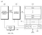
도 1은 본 발명의 실시예들에 따른 메모리 시스템(100)의 개략적인 구성도이다.1 is a schematic configuration diagram of a
도 1을 참조하면, 본 발명의 실시예들에 따른 메모리 시스템(100)은 데이터를 저장하는 메모리 장치(110)와, 메모리 장치(110)를 제어하는 메모리 컨트롤러(120) 등을 포함할 수 있다.Referring to FIG. 1 , a
메모리 장치(110)는 다수의 메모리 블록(Memory Block)을 포함하며, 메모리 컨트롤러(120)의 제어에 응답하여 동작한다. 여기서, 메모리 장치(110)의 동작은 일 예로, 리드 동작(Read Operation), 프로그램 동작(Program Operation; "Write Operation" 이라고도 함) 및 소거 동작(Erasure Operation) 등을 포함할 수 있다.The
메모리 장치(110)는 데이터를 저장하는 복수의 메모리 셀(Memory Cell; 간단히 줄여서 "셀" 이라고도 함)을 포함하는 메모리 셀 어레이(Memory Cell Array)를 포함할 수 있다. 이러한 메모리 셀 어레이는 메모리 블록 내에 존재할 수 있다.The
예를 들어, 메모리 장치(110)는 DDR SDRAM(Double Data Rate Synchronous Dynamic Random Access Memory), LPDDR4(Low Power Double Data Rate4) SDRAM, GDDR(Graphics Double Data Rate) SDRAM, LPDDR(Low Power DDR), RDRAM(Rambus Dynamic Random Access Memory), 낸드 플래시 메모리(NAND Flash Memory), 3차원 낸드 플래시 메모리(3D NAND Flash Memory), 노아 플래시 메모리(NOR Flash memory), 저항성 램(Resistive Random Access Memory: RRAM), 상변화 메모리(Phase-Change Memory: PRAM), 자기저항 메모리(Magnetoresistive Random Access Memory: MRAM), 강유전체 메모리(Ferroelectric Random Access Memory: FRAM), 또는 스핀주입 자화반전 메모리(Spin Transfer Torque Random Access Memory: STT-RAM) 등으로 다양한 타입으로 구현될 수 있다.For example, the
한편, 메모리 장치(110)는 3차원 어레이 구조(three-Dimensional Array structure)로 구현될 수 있다. 본 발명의 실시예들은 전하 저장층이 전도성 부유 게이트(Floating Gate)로 구성된 플래시 메모리 장치는 물론, 전하 저장층이 절연막으로 구성된 차지 트랩형 플래시(Charge Trap Flash; CTF)에도 적용될 수 있다.Meanwhile, the
메모리 장치(110)는 메모리 컨트롤러(120)로부터 커맨드 및 어드레스 등을 수신하고, 메모리 셀 어레이 중 어드레스에 의해 선택된 영역을 액세스하도록 구성된다. 즉, 메모리 장치(110)는 어드레스에 의해 선택된 영역에 대해 커맨드에 해당하는 동작을 수행할 수 있다.The
예를 들면, 메모리 장치(110)는 프로그램 동작, 리드 동작 및 소거 동작 등을 수행할 수 있다. 이와 관련하여, 프로그램 동작 시, 메모리 장치(110)는 어드레스에 의해 선택된 영역에 데이터를 프로그램 할 것이다. 리드 동작 시, 메모리 장치(110)는 어드레스에 의해 선택된 영역으로부터 데이터를 읽을 것이다. 소거 동작 시, 메모리 장치(110)는 어드레스에 의해 선택된 영역에 저장된 데이터를 소거할 것이다.For example, the
메모리 컨트롤러(120)는 메모리 장치(110)에 대한 쓰기(프로그램), 읽기, 소거 및 백그라운드(background) 동작을 제어할 수 있다. 여기서, 백그라운드 동작은 일 예로 가비지 컬렉션(GC, Garbage Collection), 웨어 레벨링(WL, Wear Leveling), 또는 배드 블록 관리(BBM, Bad Block Management) 동작 등 중 하나 이상을 포함할 수 있다.The
메모리 컨트롤러(120)는 호스트(HOST)의 요청에 따라 메모리 장치(110)의 동작을 제어할 수 있다. 이와 다르게, 메모리 컨트롤러(120)는 호스트(HOST)의 요청과 무관하게 메모리 장치(110)의 동작을 제어할 수도 있다.The
한편, 메모리 컨트롤러(120)와 호스트(HOST)는 서로 분리된 장치일 수도 있다. 경우에 따라서, 메모리 컨트롤러(120)와 호스트(HOST)는 하나의 장치로 통합되어 구현될 수도 있다. 아래에서는, 설명의 편의를 위하여, 메모리 컨트롤러(120)와 호스트(HOST)가 서로 분리된 장치인 것을 예로 들어 설명한다.Meanwhile, the
도 1을 참조하면, 메모리 컨트롤러(120)는 메모리 인터페이스(122) 및 제어 회로(123) 등을 포함할 수 있으며, 호스트 인터페이스(121) 등을 더 포함할 수 있다.Referring to FIG. 1 , the
호스트 인터페이스(121)는 호스트(HOST)와의 통신을 위한 인터페이스를 제공한다.The
제어 회로(123)는 호스트(HOST)로부터 커맨드를 수신할 때, 호스트 인터페이스(121)를 통해서 커맨드를 수신하여, 수신된 커맨드를 처리하는 동작을 수행할 수 있다.When receiving a command from the host HOST, the
메모리 인터페이스(122)는, 메모리 장치(110)와 연결되어 메모리 장치(110)와의 통신을 위한 인터페이스를 제공한다. 즉, 메모리 인터페이스(122)는 제어 회로(123)의 제어에 응답하여 메모리 장치(110)와 메모리 컨트롤러(120)를 인터페이스를 제공하도록 구성될 수 있다.The
제어 회로(123)는 메모리 컨트롤러(120)의 전반적인 제어 동작을 수행하여 메모리 장치(110)의 동작을 제어한다. 이를 위해, 일 예로, 제어 회로(123)는 프로세서(124), 워킹 메모리(125) 등 중 하나 이상을 포함할 수 있으며, 경우에 따라서, 에러 검출 및 정정 회로(ECC Circuit, 126) 등을 더 포함할 수 있다.The
프로세서(124)는 메모리 컨트롤러(120)의 제반 동작을 제어하고, 논리 연산을 수행할 수 있다. 프로세서(124)는 호스트 인터페이스(121)를 통해 호스트(HOST)와 통신하고, 메모리 인터페이스(122)를 통해 메모리 장치(110)와 통신할 수 있다.The
프로세서(124)는 플래시 변환 계층(FTL: Flash Translation Layer)의 기능을 수행할 수 있다. 프로세서(124)는 플래시 변환 계층(FTL)을 통해 호스트가 제공한 논리 블록 어드레스(LBA, logical block address)를 물리 블록 어드레스(PBA, physical block address)로 변환할 수 있다. 플래시 변환 계층(FTL)은 매핑 테이블을 이용하여 논리 블록 어드레스(LBA)를 입력 받아, 물리 블록 어드레스(PBA)로 변환시킬 수 있다.The
플래시 변환 계층의 주소 맵핑 방법에는 맵핑 단위에 따라 여러 가지가 있다. 대표적인 어드레스 맵핑 방법에는 페이지 맵핑 방법(Page mapping method), 블록 맵핑 방법(Block mapping method), 그리고 혼합 맵핑 방법(Hybrid mapping method)이 있다.There are several methods of address mapping of the flash translation layer depending on the mapping unit. Representative address mapping methods include a page mapping method, a block mapping method, and a hybrid mapping method.
프로세서(124)는 호스트(HOST)로부터 수신된 데이터를 랜더마이즈하도록 구성된다. 예를 들면, 프로세서(124)는 랜더마이징 시드(seed)를 이용하여 호스트(HOST)로부터 수신된 데이터를 랜더마이즈할 것이다. 랜더마이즈된 데이터는 저장될 데이터로서 메모리 장치(110)에 제공되어 메모리 셀 어레이에 프로그램 된다.The
프로세서(124)는 리드 동작 시 메모리 장치(110)로부터 수신된 데이터를 디랜더마이즈하도록 구성된다. 예를 들면, 프로세서(124)는 디랜더마이징 시드를 이용하여 메모리 장치(110)로부터 수신된 데이터를 디랜더마이즈할 것이다. 디랜더마이즈된 데이터는 호스트(HOST)로 출력될 것이다.The
프로세서(124)는 펌웨어(FirmWare)를 실행하여 메모리 컨트롤러(120)의 동작을 제어할 수 있다. 다시 말해, 프로세서(124)는, 메모리 컨트롤러(120)의 제반 동작을 제어하고, 논리 연산을 수행하기 위하여, 부팅 시 워킹 메모리(125)에 로딩 된 펌웨어를 실행(구동)할 수 있다.The
펌웨어(FirmWare)는 메모리 시스템(100) 내에서 실행되는 프로그램으로서, 다양한 기능적 계층들을 포함할 수 있다.Firmware is a program executed in the
예를 들어, 펌웨어는, 호스트(HOST)에서 메모리 시스템(100)에 요구하는 논리 주소(Logical Address)와 메모리 장치(110)의 물리 주소(Physical Address) 간의 변환 기능을 하는 플래시 변환 계층(FTL: Flash Translation Layer)와, 호스트(HOST)에서 저장 장치인 메모리 시스템(100)에 요구하는 커맨드를 해석하여 플래시 변환 계층(FTL)에 전달하는 역할을 하는 호스트 인터페이스 계층(HIL: Host Interface Layer)와, 플래시 변환 계층(FTL)에서 지시하는 커맨드를 메모리 장치(110)로 전달하는 플래시 인터페이스 계층(FIL: Flash Interface Layer) 등 중 하나 이상을 포함할 수 있다.For example, the firmware is a flash translation layer (FTL: Flash Translation Layer) and a host interface layer (HIL: Host Interface Layer) that interprets commands requested by the host (HOST) to the
이러한 펌웨어는, 일 예로, 메모리 장치(110)에 저장되어 있다가 워킹 메모리(125)에 로딩 될 수 있다.Such firmware, for example, may be stored in the
워킹 메모리(125)는 메모리 컨트롤러(120)를 구동하기 위해 필요한 펌웨어, 프로그램 코드, 커맨드 또는 데이터들을 저장할 수 있다. 이러한 워킹 메모리(125)는, 일 예로, 휘발성 메모리로서, SRAM (Static RAM), DRAM (Dynamic RAM) 및 SDRAM(Synchronous DRAM) 등 중 하나 이상을 포함할 수 있다.The working
에러 검출 및 정정 회로(126)는 에러 정정 코드(Error Correction Code)를 이용하여 확인 대상 데이터의 에러 비트를 검출하고, 검출된 에러 비트를 정정하도록 구성될 수 있다. 여기서, 확인 대상 데이터는, 일 예로, 워킹 메모리(125)에 저장된 데이터이거나, 메모리 장치(110)로부터 읽어온 데이터 등일 수 있다.The error detection and
에러 검출 및 정정 회로(126)는 에러 정정 코드로 데이터를 디코딩하도록 구현될 수 있다. 에러 검출 및 정정 회로(126)는 다양한 코드 디코더로 구현될 수 있다. 예를 들어, 비체계적 코드 디코딩을 수행하는 디코더 또는 체계적 코드 디코딩을 수행하는 디코더가 이용될 수 있다.Error detection and
예를 들면, 에러 검출 및 정정 회로(126)는 읽기 데이터들 각각에 대해 섹터(Sector) 단위로 에러 비트를 검출할 수 있다. 즉, 각각의 읽기 데이터는 복수의 섹터(Sector)로 구성될 수 있다. 섹터(Sector)는 플래시 메모리의 읽기 단위인 페이지(Page)보다 더 작은 데이터 단위를 의미할 수 있다. 각각의 읽기 데이터를 구성하는 섹터들은 어드레스를 매개로 서로 대응될 수 있다.For example, the error detection and
에러 검출 및 정정 회로(126)는 비트 에러율(Bit Error Rate, BER)을 산출하고, 섹터 단위로 정정 가능 여부를 판단할 수 있다. 에러 검출 및 정정 회로(126)는 예를 들어, 비트 에러율(BER)이 기준값(reference value)보다 높은 경우 해당 섹터를 정정 불가능(Uncorrectable or Fail)으로 판단할 것이다. 반면에, 비트 에러율(BER)이 기준값보다 낮은 경우 해당 섹터를 정정 가능(Correctable or Pass)으로 판단할 것이다.The error detection and
에러 검출 및 정정 회로(126)는 모든 읽기 데이터들에 대해 순차적으로 에러 검출 및 정정 동작을 수행할 수 있다. 에러 검출 및 정정 회로(126)는 읽기 데이터에 포함된 섹터가 정정 가능한 경우 다음 읽기 데이터에 대해서는 해당 섹터에 대한 에러 검출 및 정정 동작을 생략할 수 있다. 이렇게 모든 읽기 데이터들에 대한 에러 검출 및 정정 동작이 종료되면, 에러 검출 및 정정 회로(126)는 마지막까지 정정 불가능으로 판단된 섹터를 검출할 수 있다. 정정 불가능한 것으로 판단된 섹터는 하나 또는 그 이상일 수 있다. 에러 검출 및 정정 회로(126)는 정정 불가능으로 판단된 섹터에 대한 정보(ex. 어드레스 정보)를 프로세서(124)로 전달할 수 있다.The error detection and
버스(127)는 메모리 컨트롤러(120)의 구성 요소들(121, 122, 124, 125, 126) 사이의 채널(Channel)을 제공하도록 구성될 수 있다. 이러한 버스(127)는, 일 예로, 각종 제어 신호, 커맨드 등을 전달하기 위한 제어 버스와, 각종 데이터를 전달하기 위한 데이터 버스 등을 포함할 수 있다.The
메모리 컨트롤러(120)의 전술한 구성 요소들(121, 122, 124, 125, 126)은 예시일 뿐이다. 메모리 컨트롤러(120)의 전술한 구성 요소들(121, 122, 124, 125, 126) 중 일부의 구성 요소는 삭제되거나, 메모리 컨트롤러(120)의 전술한 구성 요소들 (121, 122, 124, 125, 126) 중 몇몇 구성 요소들이 하나로 통합될 수 있다. 경우에 따라, 메모리 컨트롤러(120)의 전술한 구성 요소들 이외에 하나 이상의 다른 구성 요소가 추가될 수도 있다.The
아래에서는, 도 2를 참조하여 메모리 장치(110)에 대하여 더욱 상세하게 설명한다.Below, the
도 2는 본 발명의 실시예들에 따른 메모리 장치(110)를 개략적으로 나타낸 블록도다.2 is a schematic block diagram of a
도 2를 참조하면, 본 발명의 실시예들에 따른 메모리 장치(110)는, 메모리 셀 어레이(Memory Cell Array, 210), 어드레스 디코더(Address Decoder, 220), 읽기 및 쓰기 회로(Read and Write Circuit, 230), 제어 로직(Control Logic, 240) 및 전압 생성 회로(Voltage Generation Circuit, 250) 등을 포함할 수 있다.Referring to FIG. 2 , a
메모리 셀 어레이(210)는 다수의 메모리 블록(BLK1~BLKz, z는 2 이상의 자연수)을 포함할 수 있다.The
다수의 메모리 블록(BLK1~BLKz)에는, 다수의 워드 라인(WL)과 다수의 비트 라인(BL)이 배치되며, 다수의 메모리 셀(MC)이 배열될 수 있다.A plurality of word lines WL and a plurality of bit lines BL may be disposed in the plurality of memory blocks BLK1 to BLKz, and a plurality of memory cells MC may be arranged.
다수의 메모리 블록(BLK1~BLKz)은 다수의 워드 라인(WL)을 통해 어드레스 디코더(220)와 연결될 수 있다. 다수의 메모리 블록(BLK1~BLKz)은 다수의 비트 라인(BL)을 통해 읽기 및 쓰기 회로(230)와 연결될 수 있다.A plurality of memory blocks BLK1 to BLKz may be connected to the
다수의 메모리 블록(BLK1~BLKz) 각각은 다수의 메모리 셀을 포함할 수 있다. 예를 들어, 다수의 메모리 셀은 불휘발성 메모리 셀들이며, 수직 채널 구조를 갖는 불휘발성 메모리 셀들로 구성될 수 있다.Each of the plurality of memory blocks BLK1 to BLKz may include a plurality of memory cells. For example, the plurality of memory cells are nonvolatile memory cells, and may include nonvolatile memory cells having a vertical channel structure.
메모리 셀 어레이(210)는 2차원 구조의 메모리 셀 어레이로 구성될 수 있으며, 경우에 따라서는, 3차원 구조의 메모리 셀 어레이로 구성될 수도 있다.The
한편, 메모리 셀 어레이(210)에 포함되는 복수의 메모리 셀 각각은 적어도 1비트의 데이터를 저장할 수 있다. 일 예로, 메모리 셀 어레이(210)에 포함되는 복수의 메모리 셀 각각은 1비트의 데이터를 저장하는 싱글-레벨 셀(SLC: Single-Level Cell)일 수 있다. 다른 예로, 메모리 셀 어레이(210)에 포함되는 복수의 메모리 셀 각각은 2비트의 데이터를 저장하는 멀티-레벨 셀(MLC: Multi-Level Cell)일 수 있다. 또 다른 예로, 메모리 셀 어레이(210)에 포함되는 복수의 메모리 셀 각각은 3비트의 데이터를 저장하는 트리플-레벨 셀(TLC: Triple-Level Cell)일 수 있다. 또 다른 예로, 메모리 셀 어레이(210)에 포함되는 복수의 메모리 셀 각각은 4비트의 데이터를 저장하는 쿼드-레벨 셀(QLC: Quad-Level Cell)일 수 있다. 또 다른 예로, 메모리 셀 어레이(210)는 5비트 이상의 데이터를 각각 저장하는 복수의 메모리 셀을 포함할 수도 있다.Meanwhile, each of a plurality of memory cells included in the
도 2를 참조하면, 어드레스 디코더(220), 읽기 및 쓰기 회로(230), 제어 로직(240) 및 전압 생성 회로(250) 등은 메모리 셀 어레이(210)를 구동하는 주변 회로로서 동작할 수 있다.Referring to FIG. 2 , the
어드레스 디코더(220)는 다수의 워드 라인(WL)을 통해 메모리 셀 어레이(210)에 연결될 수 있다.The
어드레스 디코더(220)는 제어 로직(240)의 제어에 응답하여 동작하도록 구성될 수 있다.The
어드레스 디코더(220)는 메모리 장치(110) 내부의 입출력 버퍼를 통해 어드레스(Address)를 수신할 수 있다. 어드레스 디코더(220)는 수신된 어드레스 중 블록 어드레스(Block Address)를 디코딩하도록 구성될 수 있다. 어드레스 디코더(220)는 디코딩된 블록 어드레스에 따라 적어도 하나의 메모리 블록을 선택할 수 있다.The
어드레스 디코더(220)는 전압 생성 회로(250)로부터 읽기 전압(Vread) 및 패스 전압(Vpass)을 입력 받을 수 있다.The
어드레스 디코더(220)는 리드 동작 중 읽기 전압 인가 동작 시, 선택된 메모리 블록 내 선택된 워드 라인(WL)으로 읽기 전압(Vread)를 인가하고, 나머지 비 선택된 워드 라인들(WL)에는 패스 전압(Vpass)을 인가할 수 있다.When the
어드레스 디코더(220)는 프로그램 검증 동작 시, 선택된 메모리 블록 내 선택된 워드 라인(WL)에 전압 생성 회로(250)에서 발생된 검증 전압을 인가하고, 나머지 비 선택된 워드 라인들(WL)에 패스 전압(Vpass)을 인가할 수 있다.During a program verify operation, the
어드레스 디코더(220)는 수신된 어드레스 중 열 어드레스를 디코딩 하도록 구성될 수 있다. 어드레스 디코더(220)는 디코딩 된 열 어드레스를 읽기 및 쓰기 회로(230)에 전송할 수 있다.The
메모리 장치(110)의 리드 동작 및 프로그램 동작은 페이지 단위로 수행될 수 있다. 리드 동작 및 프로그램 동작 요청 시에 수신되는 어드레스는 블록 어드레스, 행 어드레스 및 열 어드레스 중 하나 이상을 포함할 수 있다.A read operation and a program operation of the
어드레스 디코더(220)는 블록 어드레스 및 행 어드레스에 따라 하나의 메모리 블록 및 하나의 워드 라인을 선택할 수 있다. 열 어드레스는 어드레스 디코더(220)에 의해 디코딩 되어 읽기 및 쓰기 회로(230)에 제공될 수 있다.The
어드레스 디코더(220)는 블록 디코더, 행 디코더, 열 디코더 및 어드레스 버퍼 등 중 하나 이상을 포함할 수 있다.The
읽기 및 쓰기 회로(230)는 다수의 페이지 버퍼(PB)를 포함할 수 있다. 읽기 및 쓰기 회로(230)는 메모리 셀 어레이(210)의 리드 동작(Read Operation) 시에는 "읽기 회로(Read Circuit)"로 동작하고, 쓰기 동작(Write Operation) 시에는 "쓰기 회로(Write Circuit)"로 동작할 수 있다.The read and write
전술한 읽기 및 쓰기 회로(230)는 다수의 페이지 버퍼(PB)를 포함하는 페이지 버퍼 회로(Page Buffer Circuit) 또는 데이터 레지스터 회로(Data Register Circuit)라고도 한다. 여기서, 읽기 및 쓰기 회로(230)는 데이터 처리 기능을 담당하는 데이터 버퍼(Data Buffer)를 포함할 수 있고, 경우에 따라서, 캐싱 기능을 담당하는 캐쉬 버퍼(Cache Buffer)를 추가로 더 포함할 수 있다.The above-described read and write
다수의 페이지 버퍼(PB)는 다수의 비트 라인(BL)을 통해 메모리 셀 어레이(210)에 연결될 수 있다. 다수의 페이지 버퍼(PB)는 리드 동작 및 프로그램 검증 동작 시, 메모리 셀들의 문턱전압(Vth)을 센싱하기 위하여, 메모리 셀들과 연결된 비트 라인들(BL)에 센싱 전류를 계속적으로 공급하면서, 대응하는 메모리 셀의 프로그램 상태에 따라 흐르는 전류량이 변화되는 것을 센싱 노드를 통해 감지하여 센싱 데이터로 래치할 수 있다.A plurality of page buffers PB may be connected to the
읽기 및 쓰기 회로(230)는 제어 로직(240)에서 출력되는 페이지 버퍼 제어 신호들에 응답하여 동작할 수 있다.The read/
읽기 및 쓰기 회로(230)는 리드 동작 시, 메모리 셀의 데이터를 센싱하여 독출 데이터를 임시 저장한 후, 메모리 장치(110)의 입출력 버퍼로 데이터(DATA)를 출력한다. 예시적인 실시 예로서, 읽기 및 쓰기 회로(230)는 페이지 버퍼들(PB) 또는 페이지 레지스터들 이외에도, 열 선택 회로 등을 포함할 수 있다.During a read operation, the read/
제어 로직(240)은 어드레스 디코더(220), 읽기 및 쓰기 회로(230), 및 전압 생성 회로(250) 등과 연결될 수 있다. 제어 로직(240)은 메모리 장치(110)의 입출력 버퍼를 통해 커맨드(CMD) 및 제어 신호(CTRL)를 수신할 수 있다.The
제어 로직(240)은 제어 신호(CTRL)에 응답하여 메모리 장치(110)의 제반 동작을 제어하도록 구성될 수 있다. 제어 로직(240)은 다수의 페이지 버퍼(PB)의 센싱 노드의 프리 차지 전위 레벨을 조절하기 위한 제어 신호를 출력할 수 있다.The
제어 로직(240)은 메모리 셀 어레이(210)의 리드 동작을 수행하도록 읽기 및 쓰기 회로(230)를 제어할 수 있다. 전압 생성 회로(250)는, 제어 로직(240)에서 출력되는 전압 생성 회로 제어 신호에 응답하여, 리드 동작 시, 이용되는 읽기 전압(Vread) 및 패스 전압(Vpass)을 생성할 수 있다.The
한편, 전술한 메모리 장치(110)의 메모리 블록 각각은 다수의 워드 라인(WL)과 대응되는 다수의 페이지와 다수의 비트 라인(BL)과 대응되는 다수의 스트링으로 구성될 수 있다.Meanwhile, each memory block of the above-described
메모리 블록(BLK)에는 다수의 워드 라인(WL)과 다수의 비트 라인(BL)이 교차하면서 배치될 수 있다. 예를 들어, 다수의 워드 라인(WL) 각각은 행 방향으로 배치되고, 다수의 비트 라인(BL) 각각은 열 방향으로 배치될 수 있다. 다른 예를 들어, 다수의 워드 라인(WL) 각각은 열 방향으로 배치되고, 다수의 비트 라인(BL) 각각은 행 방향으로 배치될 수 있다.A plurality of word lines WL and a plurality of bit lines BL may be disposed in the memory block BLK while crossing each other. For example, each of the plurality of word lines WL may be disposed in a row direction, and each of the plurality of bit lines BL may be disposed in a column direction. For another example, each of the plurality of word lines WL may be disposed in a column direction, and each of the plurality of bit lines BL may be disposed in a row direction.
다수의 워드 라인(WL) 중 하나와 다수의 비트 라인(BL) 중 하나에 연결되는 메모리 셀이 정의될 수 있다. 각 메모리 셀에는 트랜지스터가 배치될 수 있다.A memory cell connected to one of the plurality of word lines WL and one of the plurality of bit lines BL may be defined. A transistor may be disposed in each memory cell.
예를 들어, 메모리 셀(MC)에 배치된 트랜지스터는 드레인, 소스 및 게이트 등을 포함할 수 있다. 트랜지스터의 드레인(또는 소스)은 해당 비트 라인(BL)과 직접 또는 다른 트랜지스터를 경유하여 연결될 수 있다. 트랜지스터의 소스(또는 드레인)는 소스 라인(그라운드일 수 있음)과 직접 또는 다른 트랜지스터를 경유하여 연결될 수 있다. 트랜지스터의 게이트는 절연체에 둘러싸인 플로팅 게이트(Floating Gate)와 워드 라인(WL)으로부터 게이트 전압이 인가되는 컨트롤 게이트(Control Gate)를 포함할 수 있다.For example, a transistor disposed in the memory cell MC may include a drain, a source, and a gate. A drain (or source) of a transistor may be connected directly to a corresponding bit line BL or via another transistor. The source (or drain) of a transistor may be connected directly to a source line (which may be ground) or via another transistor. The gate of the transistor may include a floating gate surrounded by an insulator and a control gate to which a gate voltage is applied from the word line WL.
각 메모리 블록에는, 2개의 최외곽 워드 라인 중 읽기 및 쓰기 회로(230)와 더 인접한 제1 최외곽 워드 라인의 바깥쪽에 제1 선택 라인(소스 선택 라인 또는 드레인 선택 라인이라고도 함)이 더 배치될 수 있으며, 다른 제2 최외곽 워드 라인의 바깥쪽에 제2 선택 라인(드레인 선택 라인 또는 소스 선택 라인이라고도 함)이 더 배치될 수 있다.In each memory block, a first selection line (also referred to as a source selection line or a drain selection line) may be further disposed outside the first outermost word line which is more adjacent to the read and write
경우에 따라서, 제1 최외곽 워드 라인과 제1 선택 라인 사이에는 하나 이상의 더미 워드 라인이 더 배치될 수 있다. 또한, 제2 최외곽 워드 라인과 제2 선택 라인 사이에도 하나 이상의 더미 워드 라인이 더 배치될 수 있다.In some cases, one or more dummy word lines may be further disposed between the first outermost word line and the first selection line. In addition, one or more dummy word lines may be further disposed between the second outermost word line and the second selection line.
전술한 메모리 블록의 리드 동작 및 프로그램 동작(쓰기 동작)은 페이지 단위로 수행될 수 있으며, 소거(Erasure) 동작은 메모리 블록 단위로 수행될 수 있다.The above-described read operation and program operation (write operation) of a memory block may be performed in units of pages, and an erase operation may be performed in units of memory blocks.
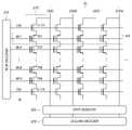
도 3는 본 발명의 실시예들에 따른 메모리 장치(110)의 워드 라인(WL) 및 비트 라인(BL)의 구조를 나타낸 도면이다.3 is a diagram illustrating structures of word lines WL and bit lines BL of the
도 3를 참조하면, 메모리 장치(110)에는, 메모리 셀들(MC)이 모여 있는 핵심 영역과 이 핵심 영역의 나머지 영역에 해당하며 메모리 셀 어레이(210)의 동작을 위해 서포트(Support)해주는 보조 영역이 존재한다.Referring to FIG. 3 , in the
핵심 영역은 페이지들(PG)과 스트링들(STR)으로 구성될 수 있다. 이러한 핵심 영역에는, 다수의 워드 라인(WL1 ~ WL9)과 다수의 비트 라인(BL)이 교차하면서 배치된다.The core area may be composed of pages PG and strings STR. In this core region, a plurality of word lines WL1 to WL9 and a plurality of bit lines BL are disposed while crossing each other.
다수의 워드 라인(WL1 ~ WL9)은 행 디코더(310)와 연결되고, 다수의 비트 라인(BL)은 열 디코더(320)와 연결될 수 있다. 다수의 비트 라인(BL)와 열 디코더(420) 사이에는 읽기 및 쓰기 회로(230)에 해당하는 데이터 레지스터(330)가 존재할 수 있다.A plurality of word lines WL1 to WL9 may be connected to the
다수의 워드 라인(WL1 ~ WL9)은 다수의 페이지(PG)와 대응된다.A plurality of word lines WL1 to WL9 correspond to a plurality of pages PG.
예를 들어, 도 3와 같이 다수의 워드 라인(WL1 ~ WL9) 각각은 하나의 페이지(PG)와 대응될 수 있다. 이와 다르게, 다수의 워드 라인(WL1 ~ WL9) 각각이 사이즈가 큰 경우, 다수의 워드 라인(WL1 ~ WL9) 각각은 둘 이상(예: 2개 또는 4개)의 페이지(PG)와 대응될 수도 있다. 페이지(PG)는 프로그램 동작과 리드 동작을 진행하는데 있어서 최소 단위가 되며, 프로그램 동작 및 리드 동작 시, 동일 페이지(PG) 내에서의 모든 메모리 셀(MC)은 동시 동작을 수행할 수 있다.For example, as shown in FIG. 3 , each of the plurality of word lines WL1 to WL9 may correspond to one page PG. Alternatively, when each of the plurality of word lines WL1 to WL9 is large in size, each of the plurality of word lines WL1 to WL9 may correspond to two or more (eg, two or four) pages PG. have. A page PG is a minimum unit for performing a program operation and a read operation, and during the program and read operations, all memory cells MC within the same page PG can perform concurrent operations.
다수의 비트 라인(BL)은 홀수 번째 비트 라인(BL)과 짝수 번째 비트 라인(BL)을 구분되면서 열 디코더(320)와 연결될 수 있다.The plurality of bit lines BL may be connected to the
메모리 셀(MC)에 액세스 하기 위해서는, 주소가 먼저 입출력 단을 거쳐 행 디코더(310)와 열 디코더(320)를 통하여 핵심 영역으로 들어와서, 타깃 메모리 셀을 지정할 수 있다. 타깃 메모리 셀을 지정한다는 것은 행 디코더(310)와 연결된 워드 라인들(WL1 ~ WL9)과 열 디코더(320)와 연결된 비트 라인들(BL)의 교차되는 사이트에 있는 메모리 셀(MC)에 데이터를 프로그램 하거나 프로그램 된 데이터를 읽어 내기 위하여 액세스 한다는 것을 의미한다.In order to access the memory cell MC, the address first enters the core region through the
메모리 장치(110)의 데이터 처리 모두는, 데이터 레지스터(330)를 경유하여 프로그램 및 읽기가 되므로, 데이터 레지스터(330)는 중추적 역할을 한다. 데이터 레지스터(330)의 데이터 처리가 늦어지면 다른 모든 영역에서는 데이터 레지스터(330)가 데이터 처리를 완료할 때까지 기다려야 한다. 또한, 데이터 레지스터(330)의 성능이 저하되면, 메모리 장치(110)의 전체 성능을 저하시킬 수 있다.Since all data processing of the
도 3의 예시를 참조하면, 1개의 스트링(STR)에는, 다수의 워드 라인(WL1 ~ WL9)과 연결되는 다수의 트랜지스터(TR1 ~ TR9)가 존재할 수 있다. 다수의 트랜지스터(TR1 ~ TR9)가 존재하는 영역들이 메모리 셀들(MC)에 해당한다. 여기서, 다수의 트랜지스터(TR1 ~ TR9)는 전술한 바와 같이, 제어 게이트 (CG)와 플로팅 게이트(FG)를 포함하는 트랜지스터들이다.Referring to the example of FIG. 3 , a plurality of transistors TR1 to TR9 connected to a plurality of word lines WL1 to WL9 may exist in one string STR. Regions in which the plurality of transistors TR1 to TR9 are present correspond to memory cells MC. Here, the plurality of transistors TR1 to TR9 are transistors including a control gate CG and a floating gate FG, as described above.
다수의 워드 라인(WL1 ~ WL9)은 2개의 최외곽 워드 라인(WL1, WL9)을 포함한다. 2개의 최외곽 워드 라인(WL1, WL9) 중 신호 경로적 측면에서 데이터 레지스터(330)와 더 인접한 제1 최외곽 워드 라인(WL1)의 바깥쪽에는 제1 선택 라인(DSL)이 더 배치되고, 다른 제2 최외곽 워드 라인(WL9)의 바깥쪽에는 제2 선택 라인(SSL)이 더 배치될 수 있다.The plurality of word lines WL1 to WL9 include two outermost word lines WL1 and WL9. Among the two outermost word lines WL1 and WL9, a first selection line DSL is further disposed outside the first outermost word line WL1, which is more adjacent to the data register 330 in terms of signal path, A second selection line SSL may be further disposed outside the second outermost word line WL9 .
제1 선택 라인(DSL)에 의해 온-오프가 제어되는 제1 선택 트랜지스터(D-TR)는 제1 선택 라인(DSL)과 연결된 게이트 전극을 가지고 있을 뿐, 플로팅 게이트(FG)를 포함하지 않는 트랜지스터이다. 제2 선택 라인(SSL)에 의해 온-오프가 제어되는 제2 선택 트랜지스터(S-TR)는 제2 선택 라인(SSL)과 연결된 게이트 전극을 가지고 있을 뿐, 플로팅 게이트(FG)를 포함하지 않는 트랜지스터이다.The first selection transistor D-TR whose on-off is controlled by the first selection line DSL only has a gate electrode connected to the first selection line DSL, but does not include a floating gate FG. it is a transistor The second selection transistor S-TR whose on-off is controlled by the second selection line SSL has a gate electrode connected to the second selection line SSL, but does not include a floating gate FG. it is a transistor
제1 선택 트랜지스터(D-TR)는 해당 스트링(STR)과 데이터 레지스터(430) 간의 연결을 온 또는 오프 시키는 스위치 역할을 한다. 제2 선택 트랜지스터(S-TR)는 해당 스트링(STR)과 소스 라인(SL) 간의 연결을 온 또는 오프 시켜주는 스위치 역할을 한다. 즉, 제1 선택 트랜지스터(D-TR) 및 제2 선택 트랜지스터(S-TR)는 해당 스트링(STR)의 양쪽 끝에 있으면서, 신호를 이어주고 끊어내는 문지기 역할을 한다.The first selection transistor D-TR serves as a switch to turn on or off the connection between the corresponding string STR and the data register 430. The second selection transistor S-TR serves as a switch to turn on or off the connection between the corresponding string STR and the source line SL. That is, the first selection transistor D-TR and the second selection transistor S-TR are located at both ends of the corresponding string STR and serve as gatekeepers for connecting and disconnecting signals.
메모리 시스템(100)은, 프로그램 동작 시, 프로그램 할 비트 라인(BL)의 타깃 메모리 셀(MC)에 전자를 채워야 하기 때문에, 제1 선택 트랜지스터(D-TR)의 게이트 전극에 소정의 턴-온 전압(Vcc)를 인가하여 제1 선택 트랜지스터(D-TR)를 턴-온 시키고, 제2 선택 트랜지스터(S-TR)의 게이트 전극에는 소정의 턴-오프 전압(예: 0V)을 인가하여 제2 선택 트랜지스터(S-TR)를 턴-오프 시킨다.Since the
메모리 시스템(100)은, 리드 동작 또는 검증(Verification) 동작 시, 제1 선택 트랜지스터(D-TR) 및 제2 선택 트랜지스터(S-TR)를 모두 턴-온 시켜준다. 이에 따라, 전류가 해당 스트링(STR)을 관통하여 그라운드에 해당하는 소스 라인(SL)으로 빠질 수 있어서, 비트 라인(BL)의 전압 레벨이 측정될 수 있다. 다만, 리드 동작 시, 제1 선택 트랜지스터(D-TR) 및 제2 선택 트랜지스터(S-TR)의 온-오프 타이밍의 시간 차이가 있을 수 있다.The
메모리 시스템(100)은, 소거(Erasure) 동작 시, 소스 라인(SL)을 통하여 기판(Substrate)에 소정 전압(예: +20V)를 공급하기도 한다. 메모리 시스템(100)은, 소거(Erasure) 동작 시, 제1 선택 트랜지스터(D-TR) 및 제2 선택 트랜지스터(S-TR)를 모두 플로팅(Floating) 시켜서 무한대의 저항을 만들어 준다. 이에 따라, 제1 선택 트랜지스터(D-TR) 및 제2 선택 트랜지스터(S-TR)의 역할이 없도록 해주고, 플로팅 게이트(FG)와 기판(Substrate) 사이에서만 전위 차이에 의한 전자(electron)가 동작할 수 있도록 구조화 되어 있다.The
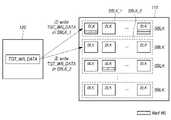
도 4는 본 발명의 실시예들에 따른 메모리 시스템(100)의 개략적인 동작을 나타낸 도면이다.4 is a diagram illustrating a schematic operation of the
도 4를 참조하면, 메모리 시스템(100)의 메모리 컨트롤러(120)는, 메모리 장치(110)에 포함된 복수의 슈퍼 메모리 블록들(SBLK) 중 어느 하나에 라이트될 데이터인 타깃 라이트 데이터(TGT_WR_DATA)를 결정할 수 있다.Referring to FIG. 4 , the
메모리 컨트롤러(120)는 메모리 장치(110)에 포함된 복수의 메모리 블록들(BLK)을 복수의 슈퍼 메모리 블록들(SBLK)으로 그룹화할 수 있다.The
복수의 슈퍼 메모리 블록들(SBLK) 각각은 메모리 장치(110)에 포함된 복수의 메모리 블록들(BLK) 중 하나 이상을 포함할 수 있다.Each of the plurality of super memory blocks SBLK may include one or more of the plurality of memory blocks BLK included in the
이때, 하나의 슈퍼 메모리 블록(SBLK)에 포함되는 메모리 블록들(BLK)은 특정한 조건에 따라 선택될 수 있다.In this case, memory blocks BLK included in one super memory block SBLK may be selected according to a specific condition.
일 예로, 하나의 슈퍼 메모리 블록(SBLK)에 포함된 메모리 블록들(BLK)은, 각각 메모리 장치(110) 내의 서로 다른 메모리 다이(memory die) 상에 위치하거나 또는 동일한 메모리 다이 내의 서로 다른 플래인(plane) 상에 위치할 수 있다.For example, the memory blocks BLK included in one super memory block SBLK are located on different memory dies within the
다른 예로, 하나의 슈퍼 메모리 블록(SBLK)에 포함된 메모리 블록들(BLK)은, 모두 동일한 인덱스 값을 가질 수 있다.As another example, all memory blocks BLK included in one super memory block SBLK may have the same index value.
또 다른 예로, 하나의 슈퍼 메모리 블록(SBLK)에 포함된 메모리 블록들(BLK)은, 메모리 장치(110)에 포함된 복수의 메모리 블록들(BLK) 중에서 랜덤하게 선택될 수 있다.As another example, the memory blocks BLK included in one super memory block SBLK may be randomly selected from among the plurality of memory blocks BLK included in the
이하, 도 5에서, 메모리 시스템(100)이 타깃 라이트 데이터(TGT_WR_DATA)를 메모리 장치(110)에 포함된 복수의 슈퍼 메모리 블록들(SBLK) 중 어느 하나에 라이트하는 동작을 설명한다.Hereinafter, an operation in which the
도 5는 본 발명의 실시예들에 따른 메모리 시스템(100)이 타깃 라이트 데이터(TGT_WR_DATA)를 메모리 장치(110)에 라이트하는 동작의 일 예를 나타낸 도면이다.5 is a diagram illustrating an example of an operation of writing target write data TGT_WR_DATA to the
도 5를 참조하면, 메모리 시스템(100)의 메모리 컨트롤러(120)는, 타깃 라이트 데이터(TGT_WR_DATA)를 제1 슈퍼 메모리 블록(SBLK_1) 또는 제2 슈퍼 메모리 블록(SBLK_2)에 라이트할 수 있다.Referring to FIG. 5 , the
제1 슈퍼 메모리 블록(SBLK_1)은 배드 워드 라인을 하나 이상 포함하는 슈퍼 메모리 블록(SBLK)이다. 배드 워드 라인은 제1 슈퍼 메모리 블록(SBLK_1)에 포함된 메모리 블록(BLK) 중 어느 하나에 포함될 수 있다.The first super memory block SBLK_1 is a super memory block SBLK including one or more bad word lines. The bad word line may be included in any one of the memory blocks BLK included in the first super memory block SBLK_1.
배드 워드 라인은, 대응하는 페이지에 데이터를 프로그램하는 동작 또는 해당 페이지로부터 데이터를 리드하는 동작 중 페일이 발생할 수 있다고 판단된 워드 라인을 의미한다. 배드 워드 라인은 메모리 시스템(100)이 생산되는 시점에 생성될 수도 있고, 메모리 컨트롤러(120)가 메모리 장치(110)에 리드, 라이트 또는 소거 동작을 실행하는 중에 생성될 수도 있다. 메모리 컨트롤러(120)는 메모리 장치(110)에 존재하는 배드 워드 라인의 정보가 기록된 별도의 자료 구조(e.g. 테이블)를 통해 메모리 장치(110)에 존재하는 배드 워드 라인을 관리할 수 있다.The bad word line refers to a word line determined to be likely to fail during an operation of programming data into a corresponding page or an operation of reading data from the corresponding page. The bad word line may be generated when the
슈퍼 메모리 블록(SBLK)은 복수의 페이지들(미도시)을 포함할 수 있는데, 복수의 페이지들은 배드 워드 라인에 대응하는 페이지 또는 배드 워드 라인이 아닌 정상적인 워드 라인에 대응하는 페이지일 수 있다. 이하, 배드 워드 라인에 대응하는 페이지는 배드 페이지(bad page)로 호칭될 수 있으며, 정상적인 워드 라인에 대응하는 페이지는 정상 페이지(normal page)로 호칭될 수 있다.The super memory block SBLK may include a plurality of pages (not shown), and the plurality of pages may be pages corresponding to bad word lines or pages corresponding to normal word lines other than bad word lines. Hereinafter, a page corresponding to a bad word line may be referred to as a bad page, and a page corresponding to a normal word line may be referred to as a normal page.
만약 배드 워드 라인에 대응하는 페이지에 데이터가 라이트되면, 이후에 해당 배드 워드 라인에 대응하는 페이지에 저장된 데이터를 액세스하는 과정에서 정정 불가능한 에러가 발생할 가능성이 높다.If data is written in a page corresponding to a bad word line, there is a high possibility that an uncorrectable error will occur in a process of accessing data stored in a page corresponding to the bad word line.
따라서, 메모리 컨트롤러(120)는 메모리 장치(110)의 제1 슈퍼 메모리 블록(SBLK_1)에 데이터가 라이트될 때, 배드 워드 라인에 대응하는 페이지에는 해당 데이터가 라이트되지 않도록 메모리 장치(110)를 제어할 수 있다.Accordingly, when data is written to the first super memory block SBLK_1 of the
반면, 제2 슈퍼 메모리 블록(SBLK_2)은 배드 워드 라인을 포함하지 않는 슈퍼 메모리 블록(SBLK)이다. 제2 슈퍼 메모리 블록(SBLK_2)에 포함된 페이지들은 모두 정상 페이지일 수 있다. 어떤 데이터가 제2 슈퍼 메모리 블록(SBLK_2)에 라이트될 때, 해당 데이터는 제2 슈퍼 메모리 블록(SBLK_2)에 포함된 어떤 페이지에도 라이트될 수 있다.On the other hand, the second super memory block SBLK_2 is a super memory block SBLK that does not include a bad word line. All pages included in the second super memory block SBLK_2 may be normal pages. When certain data is written to the second super memory block SBLK_2, the corresponding data can be written to any page included in the second super memory block SBLK_2.
본 발명의 실시예들에서 메모리 컨트롤러(120)는, 타깃 라이트 데이터(TGT_WR_DATA)를 타깃 라이트 데이터(TGT_WR_DATA)의 크기에 따라 제1 슈퍼 메모리 블록(SBLK_1)에 라이트하거나(①) 또는 제2 슈퍼 메모리 블록(SBLK_2)에 라이트(②)할 수 있다.In embodiments of the present invention, the
이처럼, 메모리 컨트롤러(120)가 타깃 라이트 데이터(TGT_WR_DATA)의 크기에 따라, 타깃 라이트 데이터(TGT_WR_DATA)가 라이트될 슈퍼 메모리 블록(SBLK)을 결정하는 이유는 다음과 같다.As such, the reason why the
슈퍼 메모리 블록(SBLK)에 데이터가 라이트될 때, 메모리 장치(110)는 라이트 성능을 최대한 높이기 위해서 데이터를 인터리빙(interleaving) 방식으로 라이트할 수 있다.When data is written to the super memory block SBLK, the
인터리빙 방식이란, 데이터를 슈퍼 메모리 블록(SBLK)에 포함된 복수의 메모리 블록들(BLK) 각각에 설정된 크기(e.g. 페이지 크기)로 분산하여 병렬적으로 라이트하는 방식을 의미한다. 메모리 장치(110)가 데이터를 슈퍼 메모리 블록(SBLK)에 인터리빙 방식으로 라이트하게 되면, 슈퍼 메모리 블록(SBLK)에 포함된 복수의 메모리 블록들(BLK)에 동시에 데이터가 라이트될 수 있어, 데이터 라이트 성능이 향상될 수 있다.The interleaving method refers to a method of distributing data in a set size (e.g. page size) to each of the plurality of memory blocks BLK included in the super memory block SBLK and writing them in parallel. When the
그러나 데이터가 슈퍼 메모리 블록(SBLK)에 인터리빙 방식으로 라이트될 때 배드 워드 라인에 대응하는 페이지에 데이터가 라이트되면, 전술한 바와 같이 이후 라이트된 데이터를 액세스하는 과정에서 페일이 발생할 수 있다. 따라서, 메모리 컨트롤러(120)는 데이터를 라이트하는 동작 중에 배드 워드 라인에 대응하는 페이지에 데이터가 라이트되지 않도록 메모리 장치(110)를 제어할 필요가 있다.However, if data is written to a page corresponding to a bad word line when data is written to the super memory block SBLK in an interleaved manner, a fail may occur in the process of accessing the written data as described above. Accordingly, the
이를 위해서, 일 예로, 메모리 컨트롤러(120)는 슈퍼 메모리 블록(SBLK)에 포함된 복수의 메모리 블록들(BLK) 중에서, 배드 워드 라인을 포함하는 메모리 블록을 배드 메모리 블록으로 설정함으로써, 배드 메모리 블록에는 데이터가 라이트되지 않도록 할 수 있다.To this end, for example, the
그러나 이 경우 배드 메모리 블록 내에서 데이터를 정상적으로 라이트할 수 있는 페이지까지 사용할 수 없게 되어, 슈퍼 메모리 블록(SBLK)을 비효율적으로 사용하게 되는 문제가 발생할 수 있다. 그리고 배드 메모리 블록이 오버-프로비저닝(over-provisioning) 영역에 존재하는 다른 메모리 블록으로 대체됨으로써, 결과적으로 메모리 시스템(100)의 수명이 감소할 수 있다.However, in this case, a page in which data can be normally written cannot be used in the bad memory block, and thus the super memory block SBLK is used inefficiently. Also, as the bad memory block is replaced with another memory block existing in an over-provisioning area, the lifetime of the
또한, 데이터가 슈퍼 메모리 블록(SBLK)에 인터리빙 방식으로 라이트될 때 동시에 데이터가 라이트되는 메모리 블록들의 개수가 감소함으로써, 슈퍼 메모리 블록(SBLK)에 동시에 라이트되는 데이터의 크기가 감소하고 결과적으로 데이터 라이트 성능이 전반적으로 저하될 수 있다.In addition, when data is written to the super memory block SBLK in an interleaved manner, the number of memory blocks to which data is simultaneously written decreases, thereby reducing the size of data simultaneously written to the super memory block SBLK, and consequently writing data. Performance may be degraded overall.
이처럼, 배드 워드 라인을 포함한 슈퍼 메모리 블록(SBLK)에 타깃 라이트 데이터(TGT_WR_DATA)를 인터리빙 방식으로 라이트할 때 발생하는 문제를 해결하기 위해서, 메모리 컨트롤러(120)는 타깃 라이트 데이터(TGT_WR_DATA)를 배드 워드 라인을 포함한 슈퍼 메모리 블록(SBLK)에 인터리빙 방식으로 라이트해도 무방한지를 먼저 판단할 수 있다.As such, in order to solve a problem that occurs when the target write data TGT_WR_DATA is written to the super memory block SBLK including the bad word line in an interleaved manner, the
타깃 라이트 데이터(TGT_WR_DATA)를 배드 워드 라인을 포함한 슈퍼 메모리 블록(SBLK)에 인터리빙 방식으로 라이트하여도 무방한 경우에는, 메모리 컨트롤러(120)는 배드 워드 라인을 포함한 슈퍼 메모리 블록(SBLK)에 타깃 라이트 데이터(TGT_WR_DATA)를 라이트할 수 있다. When it is okay to write the target write data TGT_WR_DATA to the super memory block SBLK including the bad word line in an interleaved manner, the
반면, 배드 워드 라인을 포함한 슈퍼 메모리 블록(SBLK)에 인터리빙 방식으로 라이트할 때 문제가 발생할 수 있는 경우에는, 메모리 컨트롤러(120)는 배드 워드 라인을 포함하지 않는 슈퍼 메모리 블록(SBLK)에 타깃 라이트 데이터(TGT_WR_DATA)를 라이트할 수 있다.On the other hand, if a problem may occur when writing to the super memory block SBLK including the bad word line in an interleaved manner, the
구체적으로, 메모리 컨트롤러(120)는 배드 워드 라인을 포함하는 제1 슈퍼 메모리 블록(SBLK_1)에 타깃 라이트 데이터(TGT_WR_DATA)를 인터리빙 방식으로 라이트할 수 있는 경우에는 제1 슈퍼 메모리 블록(SBLK_1)에 타깃 라이트 데이터(TGT_WR_DATA)를 라이트할 수 있다. 메모리 컨트롤러(120)는 배드 워드 라인이 존재하는 메모리 블록에서 정상적으로 라이트 가능한 페이지만을 사용함으로써, 슈퍼 메모리 블록(SBLK)을 보다 효율적으로 사용할 수 있으며, 인터리빙 방식으로 타깃 라이트 데이터(TGT_WR_DATA)를 라이트할 때 동시에 데이터가 라이트되는 메모리 블록들의 개수를 증가시켜 데이터 라이트 성능을 높일 수 있다.Specifically, when the
반면, 메모리 컨트롤러(120)는 배드 워드 라인으로 인하여 제1 슈퍼 메모리 블록(SBLK_1)에 타깃 라이트 데이터(TGT_WR_DATA)를 인터리빙 방식으로 라이트할 수 없는 경우에는 제2 슈퍼 메모리 블록(SBLK_2)에 타깃 라이트 데이터(TGT_WR_DATA)를 라이트함으로써, 타깃 라이트 데이터(TGT_WR_DATA)를 인터리빙 방식으로 라이트하는 과정에서 배드 워드 라인으로 인해 정정 불가능한 에러가 발생할 위험을 방지할 수 있다.On the other hand, when the
이때, 배드 워드 라인으로 인하여 제1 슈퍼 메모리 블록(SBLK_1)에 타깃 라이트 데이터(TGT_WR_DATA)를 인터리빙 방식으로 라이트할 수 있는지 여부는, 타깃 라이트 데이터(TGT_WR_DATA)의 크기가 제1 슈퍼 메모리 블록(SBLK_1)에 인터리빙 방식으로 라이트할 수 있는 데이터 크기의 최대값 이하인지 여부에 따라 결정될 수 있다. 따라서, 메모리 컨트롤러(120)는 타깃 라이트 데이터(TGT_WR_DATA)의 크기에 따라, 타깃 라이트 데이터(TGT_WR_DATA)가 라이트될 슈퍼 메모리 블록(SBLK)을 결정할 수 있다.At this time, whether or not the target write data TGT_WR_DATA can be written to the first super memory block SBLK_1 in an interleaved manner due to the bad word line is determined by the size of the target write data TGT_WR_DATA relative to the first super memory block SBLK_1 It may be determined according to whether it is less than or equal to the maximum value of the data size that can be written in the interleaving method. Accordingly, the
이상에서, 메모리 시스템(100)의 메모리 컨트롤러(120)가 타깃 라이트 데이터(TGT_WR_DATA)를 메모리 장치(110) 내의 슈퍼 메모리 블록(SBLK)에 라이트할 때, 타깃 라이트 데이터(TGT_WR_DATA)가 라이트되는 슈퍼 메모리 블록(SBLK)을 결정하는 동작에 대해 설명하였다.As described above, when the
이하, 이에 대한 상세한 실시예를 설명한다. 먼저, 전술한 타깃 라이트 데이터(TGT_WR_DATA)의 구체적인 예를 설명한다.Hereinafter, a detailed embodiment thereof will be described. First, a specific example of the aforementioned target write data (TGT_WR_DATA) will be described.
본 발명의 실시예들에서, 타깃 라이트 데이터(TGT_WR_DATA)는 메타 데이터일 수 있다. 메타 데이터는 메모리 장치(110)에 저장되는 유저 데이터를 관리하기 위해 필요한 메타 정보를 저장하는 데이터이다. 메타 데이터는 메모리 장치(110) 내의 스페어 영역(spare area)에 저장될 수 있다.In embodiments of the present invention, the target write data TGT_WR_DATA may be meta data. Meta data is data that stores meta information necessary for managing user data stored in the
메타 데이터는, 일 예로, 메모리 장치(110)에 저장된 데이터, 메모리 장치(110)에서 수정된 데이터 또는 메모리 장치(110)에서 삭제된 데이터에 대한 로그(log) 데이터 또는 히스토리(history) 데이터를 포함할 수 있다.Meta data includes, for example, log data or history data for data stored in the
메타 데이터는, 다른 예로, 논리 주소(LA)와 물리 주소(PA) 간의 매핑 정보를 포함하는 맵 데이터일 수 있다.As another example, the meta data may be map data including mapping information between logical addresses (LA) and physical addresses (PA).
도 6은 본 발명의 실시예들에 따른 타깃 라이트 데이터(TGT_WR_DATA)의 일 예를 나타낸 도면이다.6 is a diagram illustrating an example of target write data TGT_WR_DATA according to embodiments of the present invention.
도 6을 참조하면, 타깃 라이트 데이터(TGT_WR_DATA)는, 논리 주소(LA)와 물리 주소(PA) 간의 매핑 정보를 포함하는 맵 데이터일 수 있다. 맵 데이터는, 메모리 컨트롤러(120)가, 전술한 플래시 변환 계층(FTL)을 통해 호스트가 제공한 논리 주소(LA)를 메모리 장치(110)를 액세스하기 위한 물리 주소(PA)로 변환하기 위해 사용된다. 메모리 컨트롤러(120)는 데이터를 라이트하는 동작 또는 백그라운드 동작(e.g. 가비지 컬렉션, 웨어 레벨링, 리드 리클레임) 등이 실행되어 특정한 논리 주소(LA)와 물리 주소(PA) 간의 매핑 정보가 변경될 경우, 변경된 매핑 정보를 포함하는 맵 데이터를 메모리 장치(110)에 라이트할 수 있다.Referring to FIG. 6 , the target write data TGT_WR_DATA may be map data including mapping information between logical addresses LA and physical addresses PA. The map data is used by the
이때, 맵 데이터의 포맷은 미리 설정되어 있으므로, 메모리 컨트롤러(120)는, 메모리 장치(110)에 라이트할 맵 데이터의 크기를 미리 알 수 있다. 따라서, 메모리 컨트롤러(120)는 메모리 장치(110)에 라이트할 맵 데이터의 크기에 따라, 해당 맵 데이터를 어떤 슈퍼 메모리 블록에 라이트할 지 결정할 수 있다.At this time, since the format of the map data is set in advance, the
도 7은 본 발명의 실시예들에 따른 타깃 라이트 데이터(TGT_WR_DATA)의 다른 예를 나타낸 도면이다.7 is a diagram illustrating another example of target write data TGT_WR_DATA according to embodiments of the present invention.
도 7을 참조하면, 타깃 라이트 데이터(TGT_WR_DATA)는 호스트(HOST)로부터 수신한 유저 데이터의 전체 또는 일부일 수 있다.Referring to FIG. 7 , the target write data TGT_WR_DATA may be all or part of user data received from the host HOST.
호스트(HOST)는 유저 데이터를 메모리 시스템(100)에 라이트하기 위해서, 유저 데이터를 라이트할 것을 요청하는 커맨드 및 유저 데이터를 메모리 시스템(100)의 메모리 컨트롤러(120)로 전송할 수 있다.In order to write user data to the
메모리 컨트롤러(120)는 호스트(HOST)로부터 수신한 유저 데이터를 내부의 버퍼(BUF)에 임시로 저장한 후에 메모리 장치(110)에 라이트할 수 있다. 버퍼(BUF)는, 일 예로, 도 1에서 설명한 워킹 메모리(125) 내부의 메모리 영역일 수 있다.The
이 경우, 메모리 컨트롤러(120)는 호스트(HOST)로부터 수신한 유저 데이터를 즉시 메모리 장치(110)에 라이트하는 대신에, 특정한 조건이 만족될 때까지 호스트(HOST)로부터 수신한 유저 데이터를 버퍼(BUF)에 임시로 저장하는 동작을 수행할 수 있다.In this case, instead of immediately writing the user data received from the host HOST to the
따라서, 메모리 컨트롤러(120)가 호스트(HOST)로부터 수신한 유저 데이터를 버퍼(BUF)에 임시로 저장하는 중에는, 메모리 장치(110)에 라이트할 타깃 라이트 데이터(TGT_WR_DATA)를 결정할 수 없다. 메모리 컨트롤러(120)는 특정한 조건이 만족될 때 타깃 라이트 데이터(TGT_WR_DATA)를 결정할 수 있다.Therefore, target write data TGT_WR_DATA to be written to the
일 예로, 메모리 컨트롤러(120)는 버퍼(BUF)에 임시로 저장된 유저 데이터의 크기가 설정된 기준 크기 이상이 될 때, 타깃 라이트 데이터(TGT_WR_DATA)를 결정할 수 있다. 이때, 기준 크기는 도 4에서 전술한 슈퍼 메모리 블록(SBLK)에 데이터가 라이트될 수 있는 단위이고, 타깃 라이트 데이터(TGT_WR_DATA)의 크기는 기준 크기일 수 있다.For example, the
다른 예로, 메모리 컨트롤러(120)는 버퍼(BUF)에 임시로 저장된 유저 데이터의 크기가 설정된 기준 크기 미만임에도 불구하고, 호스트(HOST)로부터 수신한 커맨드에 따라 타깃 라이트 데이터(TGT_WR_DATA)를 결정할 수도 있다. 이하, 도 8에서 이에 대해 설명한다.As another example, the
도 8은 본 발명의 실시예들에 따른 메모리 시스템(100)이 도 7에서 설명한 타깃 라이트 데이터(TGT_WR_DATA)를 결정하는 동작의 일 예를 나타낸 도면이다.FIG. 8 is a diagram illustrating an example of an operation of determining the target write data TGT_WR_DATA described in FIG. 7 by the
도 8을 참조하면, 메모리 시스템(100)의 메모리 컨트롤러(120)는 호스트(HOST)로부터 플러시(flush) 커맨드, 배리어(barrier) 커맨드 또는 동기화(sync) 커맨드를 수신할 때, 호스트(HOST)로부터 수신한 유저 데이터 내에서 타깃 라이트 데이터(TGT_WR_DATA)를 결정할 수 있다.Referring to FIG. 8 , the
플러시 커맨드는, 메모리 시스템(100)이, 호스트(HOST)가 플러시 커맨드를 메모리 시스템(100)으로 전송하기 이전에 라이트 요청한 데이터 중에서 아직 메모리 장치(110)에 라이트하지 않고 메모리 컨트롤러(120) 내부의 버퍼(BUF)에 임시로 저장 중인 데이터를 메모리 장치(110)에 강제로 라이트할 것을 지시하는 커맨드이다.The flush command is the internal data of the
배리어 커맨드는, 메모리 시스템(100)이, 호스트(HOST)가 해당 배리어 커맨드를 메모리 시스템(100)으로 전송하기 이전에 라이트 요청한 데이터와, 호스트(HOST)가 해당 배리어 커맨드를 메모리 시스템(100)으로 전송한 이후에 라이트 요청한 데이터 사이에 대하여 메모리 장치(110)에 라이트되는 순서를 지시하는 커맨드이다. 이 경우, 호스트(HOST)가 해당 배리어 커맨드를 메모리 시스템(100)으로 전송하기 이전에 라이트 요청한 데이터는, 호스트(HOST)가 해당 배리어 커맨드를 메모리 시스템(100)으로 전송한 이후에 라이트 요청한 데이터보다 반드시 메모리 장치(110)에 먼저 라이트되어야 한다.The barrier command includes data requested by the
동기화 커맨드는, 메모리 시스템(100)이, 호스트(HOST)가 라이트 요청한 데이터와 메모리 장치(110)에 실제로 라이트된 데이터를 동기화할 것을 지시하는 커맨드이다.The synchronization command is a command instructing the
메모리 컨트롤러(120)가 플래시 커맨드, 배리어 커맨드 또는 동기화 커맨드를 수신할 때, 메모리 컨트롤러(120)는, 이후에 호스트(HOST)로부터 추가로 유저 데이터를 기다리지 않고, 내부의 버퍼(BUF)에 임시로 저장한 유저 데이터를 즉시 메모리 장치(110)에 라이트한다. 따라서, 메모리 컨트롤러(120)는 메모리 장치(110)에 라이트될 타깃 라이트 데이터(TGT_WR_DATA)를 결정할 수 있다.When the
이상에서, 메모리 컨트롤러(120)가 타깃 라이트 데이터(TGT_WR_DATA)를 결정하는 구체적인 방법을 설명하였다.In the above, a specific method for the
이하, 메모리 컨트롤러(120)가 타깃 라이트 데이터(TGT_WR_DATA)를 라이트할 슈퍼 메모리 블록(SBLK)을 결정하는 구체적인 방법에 대해 설명한다.Hereinafter, a detailed method of determining the super memory block SBLK in which the
도 9는 본 발명의 실시예들에 따른 메모리 시스템(100)이 타깃 라이트 데이터(TGT_WR_DATA)를 라이트할 슈퍼 메모리 블록(SBLK)을 결정하는 동작을 나타낸 흐름도이다.9 is a flowchart illustrating an operation in which the
도 9를 참조하면, 먼저 메모리 시스템(100)의 메모리 컨트롤러(120)는 메모리 장치(110)에 라이트할 타깃 라이트 데이터(TGT_WR_DATA)의 크기를 확인할 수 있다(S910).Referring to FIG. 9 , first, the
메모리 컨트롤러(120)는 확인한 타깃 라이트 데이터(TGT_WR_DATA)의 크기가 설정된 임계 크기 이하인지 여부를 판단한다(S920).The
타깃 라이트 데이터(TGT_WR_DATA)의 크기가 임계 크기 이하일 때(S920-Y), 메모리 컨트롤러(120)는 타깃 라이트 데이터(TGT_WR_DATA)를 도 5에서 설명한 제1 슈퍼 메모리 블록(SBLK_1)에 라이트할 수 있다(S930).When the size of the target write data TGT_WR_DATA is less than or equal to the critical size (S920-Y), the
반면, 타깃 라이트 데이터(TGT_WR_DATA)의 크기가 임계 크기 이상일 때(S920-N), 메모리 컨트롤러(120)는 타깃 라이트 데이터(TGT_WR_DATA)를 도 5에서 설명한 제2 슈퍼 메모리 블록(SBLK_2)에 라이트할 수 있다(S940).On the other hand, when the size of the target write data TGT_WR_DATA is equal to or greater than the critical size (S920-N), the
즉, 메모리 컨트롤러(120)는 임계 크기를 기준으로 하여 타깃 라이트 데이터(TGT_WR_DATA)가 라이트될 슈퍼 메모리 블록을 결정할 수 있다. 따라서, 임계 크기의 값이 메모리 컨트롤러(120)가 타깃 라이트 데이터(TGT_WR_DATA)가 라이트될 슈퍼 메모리 블록을 결정하는 과정에 영향을 미친다.That is, the
도 10은 본 발명의 실시예들에 따른 메모리 시스템(100)이 도 9에서 설명한 임계 크기를 결정하는 동작을 나타낸 도면이다.FIG. 10 is a diagram illustrating an operation of determining the threshold size described in FIG. 9 by the
도 10을 참조하면, 메모리 시스템(100)의 메모리 컨트롤러(120)는, 임계 크기를, 제1 슈퍼 메모리 블록(SBLK_1)에 포함된 복수의 슈퍼 페이지들(SPG) 중에서 제1 슈퍼 메모리 블록(SBLK_1)에 라이트될 데이터가 라이트되는 타깃인 타깃 슈퍼 페이지(TGT_SPG)를 기초로 결정할 수 있다.Referring to FIG. 10 , the
본 발명의 실시예들에서, 하나의 슈퍼 메모리 블록(SBLK)은 복수의 슈퍼 페이지들(SPG)을 포함할 수 있다. 슈퍼 페이지(SPG)는 슈퍼 메모리 블록(SBLK)에 포함된 둘 이상의 페이지들(PG)을 포함할 수 있으며, 슈퍼 메모리 블록(SBLK)에 데이터가 라이트되는 크기의 단위일 수 있다. 제1 슈퍼 메모리 블록(SBLK_1) 역시 복수의 슈퍼 페이지들(SPG)을 포함할 수 있다.In example embodiments, one super memory block SBLK may include a plurality of super pages SPG. The super page SPG may include two or more pages PG included in the super memory block SBLK, and may be a size unit in which data is written in the super memory block SBLK. The first super memory block SBLK_1 may also include a plurality of super pages SPG.
제1 슈퍼 메모리 블록(SBLK_1)에 포함된 복수의 슈퍼 페이지들(SPG) 각각은, 제1 슈퍼 메모리 블록(SBLK_1)에 포함된 둘 이상의 페이지들(PG)을 포함할 수 있다. 메모리 컨트롤러(120)는 제1 슈퍼 메모리 블록(SBLK_1)에 데이터를 라이트할 때 슈퍼 페이지(SPG) 단위로 데이터가 라이트되도록 메모리 장치(110)를 제어할 수 있다.Each of the plurality of super pages SPG included in the first super memory block SBLK_1 may include two or more pages PG included in the first super memory block SBLK_1. When data is written to the first super memory block SBLK_1, the
이때, 하나의 슈퍼 페이지(SPG)에 포함된 페이지들(PG) 각각은, 일 예로, 서로 다른 메모리 블록(BLK)에 포함된 페이지일 수 있다. 그리고 하나의 슈퍼 페이지(SPG)에 포함된 페이지들(PG) 각각에 대응하는 워드 라인의 인덱스는 서로 동일할 수 있다.In this case, each of the pages PG included in one super page SPG may be, for example, a page included in different memory blocks BLK. Also, indexes of word lines corresponding to pages PG included in one super page SPG may be identical to each other.
제1 슈퍼 메모리 블록(SBLK_1)에 포함된 복수의 슈퍼 페이지들(SPG) 중에서 일부는 이미 유효한(valid) 또는 유효하지 않은(invalid) 데이터가 라이트된 슈퍼 페이지이고, 나머지는 새로운 데이터를 라이트할 수 있는 소거 상태인 슈퍼 페이지일 수 있다.Some of the plurality of super pages SPG included in the first super memory block SBLK_1 are super pages to which valid or invalid data has already been written, and new data can be written to the rest. It may be a super page that is in an erased state.
메모리 컨트롤러(120)는 제1 슈퍼 메모리 블록(SBLK_1)에 포함된 복수의 슈퍼 페이지들(SPG) 중에서, 이미 데이터가 라이트된 슈퍼 페이지를 제외한 나머지 슈퍼 페이지들(SPG) 중에서 다음에 데이터가 라이트될 슈퍼 페이지(SPG)인 타깃 슈퍼 페이지(TGT_SPG)를 선택할 수 있다. 타깃 슈퍼 페이지(TGT_SPG)는, 제1 슈퍼 메모리 블록(SBLK_1)에 데이터가 라이트됨에 따라서 변경될 수 있다.The
메모리 컨트롤러(120)는, 임계 크기를, 타깃 슈퍼 페이지(TGT_SPG)에 라이트 가능한 데이터 크기의 최대값으로 결정할 수 있다. 만약, 타깃 라이트 데이터(TGT_WR_DATA)의 크기가 타깃 슈퍼 페이지(TGT_SPG)에 라이트 가능한 데이터 크기의 최대값을 초과한다면, 타깃 라이트 데이터(TGT_WR_DATA)는 제1 슈퍼 메모리 블록(SBLK_1)에 라이트될 수 없으므로 메모리 컨트롤러(120)는 타깃 라이트 데이터(TGT_WR_DATA)를 제2 슈퍼 메모리 블록(SBLK_2)에 라이트할 수 있다.The
반면, 타깃 라이트 데이터(TGT_WR_DATA)의 크기가 타깃 슈퍼 페이지(TGT_SPG)에 라이트 가능한 데이터 크기의 최대값 이하라면, 타깃 라이트 데이터(TGT_WR_DATA)는 제1 슈퍼 메모리 블록(SBLK_1)에 라이트될 수 있으므로 메모리 컨트롤러(120)는 타깃 라이트 데이터(TGT_WR_DATA)를 제1 슈퍼 메모리 블록(SBLK_1)에 라이트할 수 있다.On the other hand, if the size of the target write data TGT_WR_DATA is equal to or less than the maximum value of the data size that can be written to the target super page TGT_SPG, the target write data TGT_WR_DATA can be written to the first super memory block SBLK_1, and thus the
도 11은 본 발명의 실시예들에 따른 메모리 시스템(100)이 도 9에서 설명한 임계 크기를 도 10에서 설명한 타깃 슈퍼 페이지(TGT_SPG)를 기초로 결정하는 동작을 나타낸 도면이다.FIG. 11 is a diagram illustrating an operation in which the
도 11을 참조하면, 메모리 시스템(100)의 메모리 컨트롤러(120)는, 타깃 슈퍼 페이지(TGT_SPG)에 포함된 페이지(PG)들 중에서 배드 워드 라인에 대응하는 페이지를 제외한 나머지 정상 페이지(normal PG)의 개수 및 정상 페이지(normal PG)의 저장 용량을 기초로, 임계 크기를 결정할 수 있다.Referring to FIG. 11 , the
타깃 슈퍼 페이지(TGT_SPG) 중 배드 워드 라인에 대응하는 페이지가 존재하는 경우에, 배드 워드 라인에 대응하는 페이지에는 데이터를 라이트되지 않는다. 배드 워드 라인에 대응하는 페이지에 데이터를 라이트하는 과정에서 페일이 발생할 수 있기 때문이다.When a page corresponding to a bad word line exists among the target super pages TGT_SPG, data is not written to the page corresponding to the bad word line. This is because a failure may occur in the process of writing data to a page corresponding to a bad word line.
따라서, 메모리 컨트롤러(120)는 타깃 슈퍼 페이지(TGT_SPG) 중에서 배드 워드 라인에 대응하는 페이지를 제외한 나머지 정상 페이지에 라이트할 수 있는 데이터 크기의 최대값을 임계 크기로 결정할 수 있다.Accordingly, the
예를 들어, 타깃 슈퍼 페이지(TGT_SPG)가 4개의 페이지(PG)를 포함하고, 각 페이지(PG)의 저장 용량은 4KB라고 가정한다.For example, it is assumed that the target super page (TGT_SPG) includes 4 pages (PG) and the storage capacity of each page (PG) is 4 KB.
일 예로, 타깃 슈퍼 페이지(TGT_SPG)에 포함된 페이지들 중 2개의 페이지(PG)가 배드 워드 라인에 대응하는 페이지라면, 임계 크기는 타깃 슈퍼 페이지(TGT_SPG) 중에서 배드 워드 라인에 대응하는 페이지를 제외한 나머지 페이지의 개수 2(=4-2)와 각 페이지(PG)의 저장 용량 4KB를 곱한 값인 8KB가 된다.For example, if two pages (PG) among pages included in the target super page (TGT_SPG) are pages corresponding to bad word lines, the critical size excludes pages corresponding to bad word lines from among the target super pages (TGT_SPG). 8KB is obtained by multiplying the number of remaining pages 2 (= 4-2) and the storage capacity of each page (PG) by 4KB.
다른 예로, 타깃 슈퍼 페이지(TGT_SPG)에 포함된 페이지들 중 1개의 페이지(PG)가 배드 워드 라인에 대응하는 페이지라면, 임계 크기는 타깃 슈퍼 페이지(TGT_SPG) 중에서 배드 워드 라인에 대응하는 페이지를 제외한 나머지 페이지의 개수 3(=4-1)과 각 페이지(PG)의 저장 용량 4KB를 곱한 값인 12KB가 된다.As another example, if one page PG among pages included in the target super page TGT_SPG is a page corresponding to a bad word line, the critical size excludes pages corresponding to the bad word line from among the target super page TGT_SPG. 12KB is obtained by multiplying the number of remaining pages 3 (= 4-1) and the storage capacity of each page (PG) by 4KB.
도 12는 본 발명의 실시예들에 따른 메모리 시스템(100)의 동작 방법을 나타낸 도면이다.12 is a diagram illustrating an operating method of the
도 12를 참조하면, 메모리 시스템(100)의 동작 방법은, 메모리 장치(110)에 포함된 복수의 메모리 블록들(BLK) 중 하나 이상을 포함하는, 복수의 슈퍼 메모리 블록들(SBLK)을 설정하는 단계(S1210)를 포함할 수 있다.Referring to FIG. 12 , the operating method of the
그리고 메모리 시스템(100)의 동작 방법은, 설정된 복수의 슈퍼 메모리 블록들(SBLK) 중에서 어느 하나에 라이트될 데이터인 타깃 라이트 데이터(TGT_WR_DATA)를 결정하는 단계(S1220)를 포함할 수 있다.The operating method of the
이때, 타깃 라이트 데이터(TGT_WR_DATA)는, 일 예로, 논리 주소와 물리 주소 간의 매핑 정보를 포함하는 맵 데이터일 수 있다.In this case, the target write data TGT_WR_DATA may be, for example, map data including mapping information between logical addresses and physical addresses.
다른 예로, 타깃 라이트 데이터(TGT_WR_DATA)는, 타깃 라이트 데이터(TGT_WR_DATA)를 라이트할 것을 요청하는 호스트(HOST)로부터 수신한 유저 데이터의 전체 또는 일부일 수 있다. 메모리 시스템(100)은 호스트(HOST)로부터 플러시 커맨드, 배리어 커맨드 또는 동기화 커맨드를 수신할 때 호스트(HOST)로부터 수신한 유저 데이터 내에서 타깃 라이트 데이터(TGT_WR_DATA)를 결정할 수 있다.As another example, the target write data TGT_WR_DATA may be all or part of user data received from the host HOST requesting to write the target write data TGT_WR_DATA. When the
그리고 메모리 시스템(100)의 동작 방법은, 결정된 타깃 라이트 데이터(TGT_WR_DATA)를, 타깃 라이트 데이터(TGT_WR_DATA)의 크기에 따라, 배드 워드 라인을 하나 이상 포함하는 제1 슈퍼 메모리 블록(SBLK_1) 또는 배드 워드 라인을 포함하지 않는 제2 슈퍼 메모리 블록(SBLK_2)에 라이트하는 단계(S1230)를 포함할 수 있다.Further, the operating method of the
메모리 시스템(100)은, 타깃 라이트 데이터(TGT_WR_DATA)의 크기가 설정된 임계 크기 이하일 때 제1 슈퍼 메모리 블록(SBLK_1)에 타깃 라이트 데이터(TGT_WR_DATA)를 라이트하고, 타깃 라이트 데이터(TGT_WR_DATA)의 크기가 설정된 임계 크기를 초과할 때 제2 슈퍼 메모리 블록(SBLK_2)에 타깃 라이트 데이터(TGT_WR_DATA)를 라이트할 수 있다.The
이때, 타깃 라이트 데이터(TGT_WR_DATA)를 타깃 라이트 데이터(TGT_WR_DATA)의 크기에 따라 제1 슈퍼 메모리 블록(SBLK_1) 또는 제2 슈퍼 메모리 블록(SBLK_2)에 라이트하는 단계는, 임계 크기를, 제1 슈퍼 메모리 블록(SBLK_1)에 포함된 둘 이상의 페이지(PG)들을 포함하는 복수의 슈퍼 페이지들(SPG) 중에서, 제1 슈퍼 메모리 블록(SBLK_1)에 라이트될 데이터가 라이트되는 타깃인 타깃 슈퍼 페이지(TGT_SPG)를 기초로 결정하는 단계를 추가로 포함할 수 있다.In this case, in the step of writing the target write data TGT_WR_DATA into the first super memory block SBLK_1 or the second super memory block SBLK_2 according to the size of the target write data TGT_WR_DATA, the threshold size is set to the first super memory block SBLK_1. Among the plurality of super pages SPG including two or more pages PG included in the block SBLK_1, a target super page TGT_SPG, which is a target to which data to be written to the first super memory block SBLK_1 is written, is selected. It may further include a step of determining based on.
임계 크기는, 타깃 슈퍼 페이지(TGT_SPG)에 포함된 페이지들 중 배드 워드 라인에 대응하는 페이지를 제외한 나머지 정상 페이지의 개수 및 정상 페이지의 저장 용량을 기초로 결정될 수 있다.The threshold size may be determined based on the number of normal pages other than the page corresponding to the bad word line among pages included in the target super page TGT_SPG and the storage capacity of the normal pages.
도 13은 본 발명의 실시예들에 따른 컴퓨팅 시스템(1300)의 구성도이다.13 is a configuration diagram of a
도 13을 참조하면, 본 발명의 실시예들에 따른 컴퓨팅 시스템(1300)은 시스템 버스(1360)에 전기적으로 연결되는 메모리 시스템(100), 컴퓨팅 시스템(1300)의 전반적인 동작을 제어하는 중앙처리장치(CPU, 1310), 컴퓨팅 시스템(1300)의 동작과 관련한 데이터 및 정보를 저장하는 램(RAM, 1320), 사용자에게 사용 환경을 제공하기 위한 UI/UX (User Interface/User Experience) 모듈(1330), 외부 장치와 유선 및/또는 무선 방식으로 통신하기 위한 통신 모듈(1340), 컴퓨팅 시스템(1300)이 사용하는 파워를 관리하는 파워 관리 모듈(1350) 등을 포함할 수 있다.Referring to FIG. 13 , a
컴퓨팅 시스템(1300)은 PC(Personal Computer)이거나, 스마트 폰, 태블릿 등의 모바일 단말, 또는 각종 전자 기기 등을 포함할 수 있다.The
컴퓨팅 시스템(1300)은, 동작 전압을 공급하기 위한 배터리를 더 포함할 수 있으며, 응용 칩셋(Application Chipset), 그래픽 관련 모듈, 카메라 이미지 프로세서(Camera Image Processor), 디램 등을 더 포함할 수도 있다. 이외에도, 이 분야의 통상적인 지식을 습득한 자들에게 자명하다.The
한편, 메모리 시스템(100)은, 하드 디스크 드라이브(HDD: Hard Disk Drive)와 같이 자기 디스크에 데이터를 저장하는 장치뿐 아니라, 솔리드 스테이트 드라이브(SSD: Solid State Drive), UFS(Universal Flash Storage) 장치, eMMC(embedded MMC) 장치 등과 같이 비휘발성 메모리에 데이터를 저장하는 장치 등을 포함할 수 있다. 비휘발성 메모리는 ROM(Read Only Memory), PROM(Programmable ROM), EPROM (Electrically Programmable ROM), EEPROM(Electrically Erasable and Programmable ROM), 플래시 메모리, PRAM(Phase-change RAM), MRAM(Magnetic RAM), RRAM(Resistive RAM), FRAM(Ferroelectric RAM) 등을 포함할 수 있다. 이뿐만 아니라, 메모리 시스템(100)은 다양한 형태의 저장 장치로 구현되어, 다양한 전자 기기 내에 탑재될 수 있다.On the other hand, the
이상의 설명은 본 발명의 기술 사상을 예시적으로 설명한 것에 불과한 것으로서, 본 발명이 속하는 기술 분야에서 통상의 지식을 가진 자라면 본 발명의 본질적인 특성에서 벗어나지 않는 범위에서 다양한 수정 및 변형이 가능할 것이다. 또한, 본 발명에 개시된 실시예들은 본 발명의 기술 사상을 한정하기 위한 것이 아니라 설명하기 위한 것이므로 이러한 실시예에 의하여 본 발명의 기술 사상의 범위가 한정되는 것은 아니다. 본 발명의 보호 범위는 아래의 청구범위에 의하여 해석되어야 하며, 그와 동등한 범위 내에 있는 모든 기술 사상은 본 발명의 권리 범위에 포함되는 것으로 해석되어야 할 것이다.The above description is merely an example of the technical idea of the present invention, and various modifications and variations can be made to those skilled in the art without departing from the essential characteristics of the present invention. In addition, the embodiments disclosed in the present invention are not intended to limit the technical idea of the present invention, but to explain, so the scope of the technical idea of the present invention is not limited by these embodiments. The protection scope of the present invention should be construed according to the claims below, and all technical ideas within the equivalent range should be construed as being included in the scope of the present invention.
100: 메모리 시스템110: 메모리 장치
120: 메모리 컨트롤러121: 호스트 인터페이스
122: 메모리 인터페이스123: 제어 회로
124: 프로세서125: 워킹 메모리
126: 에러 검출 및 정정 회로
210: 메모리 셀 어레이220: 어드레스 디코더
230: 리드 앤 라이트 회로240: 제어 로직
250: 전압 생성 회로100: memory system 110: memory device
120: memory controller 121: host interface
122
124: processor 125: working memory
126: error detection and correction circuit
210: memory cell array 220: address decoder
230: read and write circuit 240: control logic
250: voltage generating circuit
Claims (16)
Translated fromKorean상기 메모리 장치와 통신하고, 상기 메모리 장치를 제어하는 메모리 컨트롤러를 포함하고,
상기 메모리 컨트롤러는,
상기 복수의 메모리 블록들 중 하나 이상을 포함하는, 복수의 슈퍼 메모리 블록들 중 어느 하나에 라이트될 데이터인 타깃 라이트 데이터를 결정하고,
상기 타깃 라이트 데이터를, 상기 타깃 라이트 데이터의 크기에 따라, 배드 워드 라인을 하나 이상 포함하는 제1 슈퍼 메모리 블록 또는 배드 워드 라인을 포함하지 않는 제2 슈퍼 메모리 블록에 라이트하는 메모리 시스템.
a memory device including a plurality of memory blocks; and
a memory controller communicating with the memory device and controlling the memory device;
The memory controller,
determining target write data, which is data to be written in one of a plurality of super memory blocks, including one or more of the plurality of memory blocks;
and writing the target write data to a first super memory block including at least one bad word line or a second super memory block not including a bad word line, according to a size of the target write data.
상기 타깃 라이트 데이터는, 메타 데이터인 메모리 시스템.
According to claim 1,
The target write data is meta data.
상기 타깃 라이트 데이터는, 논리 주소와 물리 주소 간의 매핑 정보를 포함하는 맵 데이터인 메모리 시스템.
According to claim 2,
The target write data is map data including mapping information between logical addresses and physical addresses.
상기 타깃 라이트 데이터는, 상기 타깃 라이트 데이터를 라이트할 것을 요청하는 호스트로부터 수신한 유저 데이터의 전체 또는 일부인 메모리 시스템.
According to claim 1,
The target write data is all or part of user data received from a host requesting to write the target write data.
상기 메모리 컨트롤러는,
상기 호스트로부터 플러시 커맨드, 배리어 커맨드 또는 동기화 커맨드를 수신할 때, 상기 호스트로부터 수신한 유저 데이터 내에서 상기 타깃 라이트 데이터를 결정하는 메모리 시스템.
According to claim 4,
The memory controller,
determining the target write data from among user data received from the host when receiving a flush command, a barrier command, or a synchronization command from the host.
상기 메모리 컨트롤러는,
상기 타깃 라이트 데이터의 크기가 설정된 임계 크기 이하일 때 상기 제1 슈퍼 메모리 블록에 상기 타깃 라이트 데이터를 라이트하고,
상기 타깃 라이트 데이터의 크기가 상기 임계 크기를 초과할 때 상기 제2 슈퍼 메모리 블록에 상기 타깃 라이트 데이터를 라이트하는 메모리 시스템.
According to claim 1,
The memory controller,
writing the target write data to the first super memory block when the size of the target write data is less than or equal to a set threshold size;
and writing the target write data to the second super memory block when the size of the target write data exceeds the threshold size.
상기 메모리 컨트롤러는,
상기 임계 크기를,
상기 제1 슈퍼 메모리 블록에 포함된 둘 이상의 페이지들을 포함하는 복수의 슈퍼 페이지들 중에서, 상기 제1 슈퍼 메모리 블록에 라이트될 데이터가 라이트되는 타깃인 타깃 슈퍼 페이지를 기초로 결정하는 메모리 시스템.
According to claim 6,
The memory controller,
the critical size,
Among a plurality of super pages including two or more pages included in the first super memory block, the memory system determines based on a target super page to which data to be written in the first super memory block is written.
상기 메모리 컨트롤러는,
상기 타깃 슈퍼 페이지에 포함된 페이지들 중 배드 워드 라인에 대응하는 페이지를 제외한 나머지 정상 페이지의 개수 및 상기 정상 페이지의 저장 용량을 기초로, 상기 임계 크기를 결정하는 메모리 시스템.
According to claim 7,
The memory controller,
The memory system of claim 1 , wherein the threshold size is determined based on the number of normal pages other than a page corresponding to a bad word line among pages included in the target super page and a storage capacity of the normal pages.
상기 복수의 메모리 블록들 중 하나 이상을 포함하는, 복수의 슈퍼 메모리 블록들을 설정하는 단계;
상기 복수의 슈퍼 메모리 블록들 중 어느 하나에 라이트될 데이터인 타깃 라이트 데이터를 결정하는 단계; 및
상기 타깃 라이트 데이터를, 상기 타깃 라이트 데이터의 크기에 따라, 배드 워드 라인을 하나 이상 포함하는 제1 슈퍼 메모리 블록 또는 배드 워드 라인을 포함하지 않는 제2 슈퍼 메모리 블록에 라이트하는 단계를 포함하는 메모리 시스템의 동작 방법.
A method of operating a memory system including a memory device including a plurality of memory blocks,
setting a plurality of super memory blocks including one or more of the plurality of memory blocks;
determining target write data, which is data to be written in one of the plurality of super memory blocks; and
and writing the target write data to a first super memory block including at least one bad word line or a second super memory block not including a bad word line, according to a size of the target write data. how it works.
상기 타깃 라이트 데이터는, 메타 데이터인 메모리 시스템의 동작 방법.
According to claim 9,
The target write data is meta data.
상기 타깃 라이트 데이터는, 논리 주소와 물리 주소 간의 매핑 정보를 포함하는 맵 데이터인 메모리 시스템의 동작 방법.
According to claim 10,
The target write data is map data including mapping information between logical addresses and physical addresses.
상기 타깃 라이트 데이터는, 상기 타깃 라이트 데이터를 라이트할 것을 요청하는 호스트로부터 수신한 유저 데이터의 전체 또는 일부인 메모리 시스템의 동작 방법.
According to claim 9,
The target write data is all or part of user data received from a host requesting to write the target write data.
상기 타깃 라이트 데이터를 결정하는 단계는,
상기 호스트로부터 플러시 커맨드, 배리어 커맨드 또는 동기화 커맨드를 수신할 때, 상기 호스트로부터 수신한 유저 데이터 내에서 상기 타깃 라이트 데이터를 결정하는 메모리 시스템의 동작 방법.
According to claim 12,
The step of determining the target light data,
determining the target write data from user data received from the host when receiving a flush command, a barrier command, or a synchronization command from the host.
상기 타깃 라이트 데이터를, 상기 타깃 라이트 데이터의 크기에 따라, 상기 제1 슈퍼 메모리 블록 또는 상기 제2 슈퍼 메모리 블록에 라이트하는 단계는,
상기 타깃 라이트 데이터의 크기가 설정된 임계 크기 이하일 때 상기 제1 슈퍼 메모리 블록에 상기 타깃 라이트 데이터를 라이트하고,
상기 타깃 라이트 데이터의 크기가 상기 임계 크기를 초과할 때 상기 제2 슈퍼 메모리 블록에 상기 타깃 라이트 데이터를 라이트하는 단계를 포함하는 메모리 시스템의 동작 방법.
According to claim 9,
The writing of the target write data to the first super memory block or the second super memory block according to the size of the target write data may include:
writing the target write data to the first super memory block when the size of the target write data is less than or equal to a set threshold size;
and writing the target write data to the second super memory block when the size of the target write data exceeds the threshold size.
상기 타깃 라이트 데이터를 상기 타깃 라이트 데이터의 크기에 따라 상기 제1 슈퍼 메모리 블록 또는 상기 제2 슈퍼 메모리 블록에 라이트하는 단계는,
상기 임계 크기를, 상기 제1 슈퍼 메모리 블록에 포함된 둘 이상의 페이지들을 포함하는 복수의 슈퍼 페이지들 중에서, 상기 제1 슈퍼 메모리 블록에 라이트될 데이터가 라이트되는 타깃인 타깃 슈퍼 페이지를 기초로 결정하는 단계를 추가로 포함하는 메모리 시스템의 동작 방법.
According to claim 14,
The step of writing the target write data to the first super memory block or the second super memory block according to the size of the target write data,
Determining the threshold size based on a target super page to which data to be written to the first super memory block is written, among a plurality of super pages including two or more pages included in the first super memory block A method of operating a memory system further comprising the step.
상기 임계 크기는, 상기 타깃 슈퍼 페이지에 포함된 페이지들 중 배드 워드 라인에 대응하는 페이지를 제외한 나머지 정상 페이지의 개수 및 상기 정상 페이지의 저장 용량을 기초로 결정되는 메모리 시스템의 동작 방법.According to claim 15,
The threshold size is determined based on the number of normal pages excluding pages corresponding to bad word lines among pages included in the target super page and the storage capacity of the normal pages.
Priority Applications (3)
| Application Number | Priority Date | Filing Date | Title |
|---|---|---|---|
| KR1020210072086AKR20220163661A (en) | 2021-06-03 | 2021-06-03 | Memory system and operating method of memory system |
| US17/499,263US11822819B2 (en) | 2021-06-03 | 2021-10-12 | Memory system and operating method thereof |
| CN202111624772.9ACN115437968A (en) | 2021-06-03 | 2021-12-28 | Memory system and operation method of memory system |
Applications Claiming Priority (1)
| Application Number | Priority Date | Filing Date | Title |
|---|---|---|---|
| KR1020210072086AKR20220163661A (en) | 2021-06-03 | 2021-06-03 | Memory system and operating method of memory system |
Publications (1)
| Publication Number | Publication Date |
|---|---|
| KR20220163661Atrue KR20220163661A (en) | 2022-12-12 |
Family
ID=84272274
Family Applications (1)
| Application Number | Title | Priority Date | Filing Date |
|---|---|---|---|
| KR1020210072086AWithdrawnKR20220163661A (en) | 2021-06-03 | 2021-06-03 | Memory system and operating method of memory system |
Country Status (3)
| Country | Link |
|---|---|
| US (1) | US11822819B2 (en) |
| KR (1) | KR20220163661A (en) |
| CN (1) | CN115437968A (en) |
Family Cites Families (5)
| Publication number | Priority date | Publication date | Assignee | Title |
|---|---|---|---|---|
| US10229751B2 (en)* | 2017-05-01 | 2019-03-12 | Western Digital Technologies, Inc. | Storage system and method for bad block recycling |
| KR102447152B1 (en)* | 2017-12-26 | 2022-09-26 | 삼성전자주식회사 | Nonvolatile memory devices, methods of operating the same and storage devices includng the same |
| KR102691784B1 (en) | 2018-12-26 | 2024-08-06 | 에스케이하이닉스 주식회사 | Memory system and operating method thereof |
| KR102713986B1 (en) | 2019-07-25 | 2024-10-10 | 에스케이하이닉스 주식회사 | Controller, memory system and operating method thereof |
| US11537484B2 (en)* | 2020-08-27 | 2022-12-27 | Micron Technology, Inc. | Salvaging bad blocks in a memory device |
- 2021
- 2021-06-03KRKR1020210072086Apatent/KR20220163661A/ennot_activeWithdrawn
- 2021-10-12USUS17/499,263patent/US11822819B2/enactiveActive
- 2021-12-28CNCN202111624772.9Apatent/CN115437968A/ennot_activeWithdrawn
Also Published As
| Publication number | Publication date |
|---|---|
| CN115437968A (en) | 2022-12-06 |
| US20220391139A1 (en) | 2022-12-08 |
| US11822819B2 (en) | 2023-11-21 |
Similar Documents
| Publication | Publication Date | Title |
|---|---|---|
| KR20220013661A (en) | Memory system, memory device, and operating method of memory device | |
| KR20220105303A (en) | Memory system and operating method of memory system | |
| KR20210097353A (en) | Memory system, memory controller, and operating method of memory system | |
| KR20230031425A (en) | Memory system and operating method of memory system | |
| US12072809B2 (en) | Memory system, memory controller, and operation method of memory system for loading and updating mapping information to host memory area | |
| KR102838945B1 (en) | Memory system, memory controller, and operating method thereof | |
| KR20220105304A (en) | System and operating method of system | |
| KR20220070989A (en) | Memory system and operating method of memory system | |
| KR20210152706A (en) | Memory device, memory system, and operating method of memory device | |
| KR20210017181A (en) | Memory system, memory controller, and operating method | |
| KR20230072196A (en) | Memory system and operating method of memory system | |
| KR20230094622A (en) | Memory system executing target operation based on program state of super memory block and operating method thereof | |
| KR20230072062A (en) | Memory system, memory controller and operating method of memory system | |
| KR20230069642A (en) | Storage device share system and operating method thereof | |
| KR20220168510A (en) | Memory system and operating method of memory system | |
| KR20220049109A (en) | Memory system and operating method of memory system | |
| KR20220025405A (en) | Memory system, memory controller, and operating method of memory system | |
| KR20220001137A (en) | Memory system, memory device, and operating method of memory device | |
| KR20210079552A (en) | Memory system and memory controller | |
| US11704050B2 (en) | Memory system for determining a memory area in which a journal is stored according to a number of free memory blocks | |
| US11507509B2 (en) | Memory system, memory controller and method for operating memory system for determining whether to perform direct write based on reference write size | |
| KR102771648B1 (en) | Memory system and operating method of memory system | |
| KR20230094588A (en) | Memory system managing data corresponding to multiple zones and operating method thereof | |
| KR20230049858A (en) | Memory controller and operating method of memory controller | |
| KR20220118011A (en) | Memory device and operating method of memory device |
Legal Events
| Date | Code | Title | Description |
|---|---|---|---|
| PA0109 | Patent application | St.27 status event code:A-0-1-A10-A12-nap-PA0109 | |
| PG1501 | Laying open of application | St.27 status event code:A-1-1-Q10-Q12-nap-PG1501 | |
| PC1203 | Withdrawal of no request for examination | St.27 status event code:N-1-6-B10-B12-nap-PC1203 |