KR20220147514A - Substrate processing method and substrate processing apparatus - Google Patents
Substrate processing method and substrate processing apparatusDownload PDFInfo
- Publication number
- KR20220147514A KR20220147514AKR1020220046476AKR20220046476AKR20220147514AKR 20220147514 AKR20220147514 AKR 20220147514AKR 1020220046476 AKR1020220046476 AKR 1020220046476AKR 20220046476 AKR20220046476 AKR 20220046476AKR 20220147514 AKR20220147514 AKR 20220147514A
- Authority
- KR
- South Korea
- Prior art keywords
- region
- deposit
- substrate
- gas
- processing apparatus
- Prior art date
- Legal status (The legal status is an assumption and is not a legal conclusion. Google has not performed a legal analysis and makes no representation as to the accuracy of the status listed.)
- Pending
Links
Images


Classifications
- H—ELECTRICITY
- H01—ELECTRIC ELEMENTS
- H01L—SEMICONDUCTOR DEVICES NOT COVERED BY CLASS H10
- H01L21/00—Processes or apparatus adapted for the manufacture or treatment of semiconductor or solid state devices or of parts thereof
- H01L21/02—Manufacture or treatment of semiconductor devices or of parts thereof
- H01L21/04—Manufacture or treatment of semiconductor devices or of parts thereof the devices having potential barriers, e.g. a PN junction, depletion layer or carrier concentration layer
- H01L21/18—Manufacture or treatment of semiconductor devices or of parts thereof the devices having potential barriers, e.g. a PN junction, depletion layer or carrier concentration layer the devices having semiconductor bodies comprising elements of Group IV of the Periodic Table or AIIIBV compounds with or without impurities, e.g. doping materials
- H01L21/30—Treatment of semiconductor bodies using processes or apparatus not provided for in groups H01L21/20 - H01L21/26
- H01L21/31—Treatment of semiconductor bodies using processes or apparatus not provided for in groups H01L21/20 - H01L21/26 to form insulating layers thereon, e.g. for masking or by using photolithographic techniques; After treatment of these layers; Selection of materials for these layers
- H01L21/3105—After-treatment
- H01L21/311—Etching the insulating layers by chemical or physical means
- H01L21/31144—Etching the insulating layers by chemical or physical means using masks
- H—ELECTRICITY
- H01—ELECTRIC ELEMENTS
- H01J—ELECTRIC DISCHARGE TUBES OR DISCHARGE LAMPS
- H01J37/00—Discharge tubes with provision for introducing objects or material to be exposed to the discharge, e.g. for the purpose of examination or processing thereof
- H01J37/32—Gas-filled discharge tubes
- H01J37/32009—Arrangements for generation of plasma specially adapted for examination or treatment of objects, e.g. plasma sources
- H01J37/32082—Radio frequency generated discharge
- H01J37/32091—Radio frequency generated discharge the radio frequency energy being capacitively coupled to the plasma
- C—CHEMISTRY; METALLURGY
- C23—COATING METALLIC MATERIAL; COATING MATERIAL WITH METALLIC MATERIAL; CHEMICAL SURFACE TREATMENT; DIFFUSION TREATMENT OF METALLIC MATERIAL; COATING BY VACUUM EVAPORATION, BY SPUTTERING, BY ION IMPLANTATION OR BY CHEMICAL VAPOUR DEPOSITION, IN GENERAL; INHIBITING CORROSION OF METALLIC MATERIAL OR INCRUSTATION IN GENERAL
- C23C—COATING METALLIC MATERIAL; COATING MATERIAL WITH METALLIC MATERIAL; SURFACE TREATMENT OF METALLIC MATERIAL BY DIFFUSION INTO THE SURFACE, BY CHEMICAL CONVERSION OR SUBSTITUTION; COATING BY VACUUM EVAPORATION, BY SPUTTERING, BY ION IMPLANTATION OR BY CHEMICAL VAPOUR DEPOSITION, IN GENERAL
- C23C16/00—Chemical coating by decomposition of gaseous compounds, without leaving reaction products of surface material in the coating, i.e. chemical vapour deposition [CVD] processes
- C23C16/44—Chemical coating by decomposition of gaseous compounds, without leaving reaction products of surface material in the coating, i.e. chemical vapour deposition [CVD] processes characterised by the method of coating
- C23C16/50—Chemical coating by decomposition of gaseous compounds, without leaving reaction products of surface material in the coating, i.e. chemical vapour deposition [CVD] processes characterised by the method of coating using electric discharges
- C23C16/503—Chemical coating by decomposition of gaseous compounds, without leaving reaction products of surface material in the coating, i.e. chemical vapour deposition [CVD] processes characterised by the method of coating using electric discharges using DC or AC discharges
- C—CHEMISTRY; METALLURGY
- C23—COATING METALLIC MATERIAL; COATING MATERIAL WITH METALLIC MATERIAL; CHEMICAL SURFACE TREATMENT; DIFFUSION TREATMENT OF METALLIC MATERIAL; COATING BY VACUUM EVAPORATION, BY SPUTTERING, BY ION IMPLANTATION OR BY CHEMICAL VAPOUR DEPOSITION, IN GENERAL; INHIBITING CORROSION OF METALLIC MATERIAL OR INCRUSTATION IN GENERAL
- C23C—COATING METALLIC MATERIAL; COATING MATERIAL WITH METALLIC MATERIAL; SURFACE TREATMENT OF METALLIC MATERIAL BY DIFFUSION INTO THE SURFACE, BY CHEMICAL CONVERSION OR SUBSTITUTION; COATING BY VACUUM EVAPORATION, BY SPUTTERING, BY ION IMPLANTATION OR BY CHEMICAL VAPOUR DEPOSITION, IN GENERAL
- C23C16/00—Chemical coating by decomposition of gaseous compounds, without leaving reaction products of surface material in the coating, i.e. chemical vapour deposition [CVD] processes
- C23C16/04—Coating on selected surface areas, e.g. using masks
- C—CHEMISTRY; METALLURGY
- C23—COATING METALLIC MATERIAL; COATING MATERIAL WITH METALLIC MATERIAL; CHEMICAL SURFACE TREATMENT; DIFFUSION TREATMENT OF METALLIC MATERIAL; COATING BY VACUUM EVAPORATION, BY SPUTTERING, BY ION IMPLANTATION OR BY CHEMICAL VAPOUR DEPOSITION, IN GENERAL; INHIBITING CORROSION OF METALLIC MATERIAL OR INCRUSTATION IN GENERAL
- C23C—COATING METALLIC MATERIAL; COATING MATERIAL WITH METALLIC MATERIAL; SURFACE TREATMENT OF METALLIC MATERIAL BY DIFFUSION INTO THE SURFACE, BY CHEMICAL CONVERSION OR SUBSTITUTION; COATING BY VACUUM EVAPORATION, BY SPUTTERING, BY ION IMPLANTATION OR BY CHEMICAL VAPOUR DEPOSITION, IN GENERAL
- C23C16/00—Chemical coating by decomposition of gaseous compounds, without leaving reaction products of surface material in the coating, i.e. chemical vapour deposition [CVD] processes
- C23C16/22—Chemical coating by decomposition of gaseous compounds, without leaving reaction products of surface material in the coating, i.e. chemical vapour deposition [CVD] processes characterised by the deposition of inorganic material, other than metallic material
- C23C16/30—Deposition of compounds, mixtures or solid solutions, e.g. borides, carbides, nitrides
- C23C16/34—Nitrides
- C23C16/345—Silicon nitride
- C—CHEMISTRY; METALLURGY
- C23—COATING METALLIC MATERIAL; COATING MATERIAL WITH METALLIC MATERIAL; CHEMICAL SURFACE TREATMENT; DIFFUSION TREATMENT OF METALLIC MATERIAL; COATING BY VACUUM EVAPORATION, BY SPUTTERING, BY ION IMPLANTATION OR BY CHEMICAL VAPOUR DEPOSITION, IN GENERAL; INHIBITING CORROSION OF METALLIC MATERIAL OR INCRUSTATION IN GENERAL
- C23C—COATING METALLIC MATERIAL; COATING MATERIAL WITH METALLIC MATERIAL; SURFACE TREATMENT OF METALLIC MATERIAL BY DIFFUSION INTO THE SURFACE, BY CHEMICAL CONVERSION OR SUBSTITUTION; COATING BY VACUUM EVAPORATION, BY SPUTTERING, BY ION IMPLANTATION OR BY CHEMICAL VAPOUR DEPOSITION, IN GENERAL
- C23C16/00—Chemical coating by decomposition of gaseous compounds, without leaving reaction products of surface material in the coating, i.e. chemical vapour deposition [CVD] processes
- C23C16/22—Chemical coating by decomposition of gaseous compounds, without leaving reaction products of surface material in the coating, i.e. chemical vapour deposition [CVD] processes characterised by the deposition of inorganic material, other than metallic material
- C23C16/30—Deposition of compounds, mixtures or solid solutions, e.g. borides, carbides, nitrides
- C23C16/40—Oxides
- C23C16/401—Oxides containing silicon
- C23C16/402—Silicon dioxide
- C—CHEMISTRY; METALLURGY
- C23—COATING METALLIC MATERIAL; COATING MATERIAL WITH METALLIC MATERIAL; CHEMICAL SURFACE TREATMENT; DIFFUSION TREATMENT OF METALLIC MATERIAL; COATING BY VACUUM EVAPORATION, BY SPUTTERING, BY ION IMPLANTATION OR BY CHEMICAL VAPOUR DEPOSITION, IN GENERAL; INHIBITING CORROSION OF METALLIC MATERIAL OR INCRUSTATION IN GENERAL
- C23C—COATING METALLIC MATERIAL; COATING MATERIAL WITH METALLIC MATERIAL; SURFACE TREATMENT OF METALLIC MATERIAL BY DIFFUSION INTO THE SURFACE, BY CHEMICAL CONVERSION OR SUBSTITUTION; COATING BY VACUUM EVAPORATION, BY SPUTTERING, BY ION IMPLANTATION OR BY CHEMICAL VAPOUR DEPOSITION, IN GENERAL
- C23C16/00—Chemical coating by decomposition of gaseous compounds, without leaving reaction products of surface material in the coating, i.e. chemical vapour deposition [CVD] processes
- C23C16/44—Chemical coating by decomposition of gaseous compounds, without leaving reaction products of surface material in the coating, i.e. chemical vapour deposition [CVD] processes characterised by the method of coating
- C23C16/50—Chemical coating by decomposition of gaseous compounds, without leaving reaction products of surface material in the coating, i.e. chemical vapour deposition [CVD] processes characterised by the method of coating using electric discharges
- C23C16/505—Chemical coating by decomposition of gaseous compounds, without leaving reaction products of surface material in the coating, i.e. chemical vapour deposition [CVD] processes characterised by the method of coating using electric discharges using radio frequency discharges
- C23C16/509—Chemical coating by decomposition of gaseous compounds, without leaving reaction products of surface material in the coating, i.e. chemical vapour deposition [CVD] processes characterised by the method of coating using electric discharges using radio frequency discharges using internal electrodes
- C23C16/5096—Flat-bed apparatus
- C—CHEMISTRY; METALLURGY
- C23—COATING METALLIC MATERIAL; COATING MATERIAL WITH METALLIC MATERIAL; CHEMICAL SURFACE TREATMENT; DIFFUSION TREATMENT OF METALLIC MATERIAL; COATING BY VACUUM EVAPORATION, BY SPUTTERING, BY ION IMPLANTATION OR BY CHEMICAL VAPOUR DEPOSITION, IN GENERAL; INHIBITING CORROSION OF METALLIC MATERIAL OR INCRUSTATION IN GENERAL
- C23C—COATING METALLIC MATERIAL; COATING MATERIAL WITH METALLIC MATERIAL; SURFACE TREATMENT OF METALLIC MATERIAL BY DIFFUSION INTO THE SURFACE, BY CHEMICAL CONVERSION OR SUBSTITUTION; COATING BY VACUUM EVAPORATION, BY SPUTTERING, BY ION IMPLANTATION OR BY CHEMICAL VAPOUR DEPOSITION, IN GENERAL
- C23C16/00—Chemical coating by decomposition of gaseous compounds, without leaving reaction products of surface material in the coating, i.e. chemical vapour deposition [CVD] processes
- C23C16/44—Chemical coating by decomposition of gaseous compounds, without leaving reaction products of surface material in the coating, i.e. chemical vapour deposition [CVD] processes characterised by the method of coating
- C23C16/52—Controlling or regulating the coating process
- H—ELECTRICITY
- H01—ELECTRIC ELEMENTS
- H01J—ELECTRIC DISCHARGE TUBES OR DISCHARGE LAMPS
- H01J37/00—Discharge tubes with provision for introducing objects or material to be exposed to the discharge, e.g. for the purpose of examination or processing thereof
- H01J37/32—Gas-filled discharge tubes
- H01J37/32009—Arrangements for generation of plasma specially adapted for examination or treatment of objects, e.g. plasma sources
- H01J37/32082—Radio frequency generated discharge
- H01J37/321—Radio frequency generated discharge the radio frequency energy being inductively coupled to the plasma
- H—ELECTRICITY
- H01—ELECTRIC ELEMENTS
- H01J—ELECTRIC DISCHARGE TUBES OR DISCHARGE LAMPS
- H01J37/00—Discharge tubes with provision for introducing objects or material to be exposed to the discharge, e.g. for the purpose of examination or processing thereof
- H01J37/32—Gas-filled discharge tubes
- H01J37/32431—Constructional details of the reactor
- H01J37/3244—Gas supply means
- H01J37/32449—Gas control, e.g. control of the gas flow
- H—ELECTRICITY
- H01—ELECTRIC ELEMENTS
- H01L—SEMICONDUCTOR DEVICES NOT COVERED BY CLASS H10
- H01L21/00—Processes or apparatus adapted for the manufacture or treatment of semiconductor or solid state devices or of parts thereof
- H01L21/02—Manufacture or treatment of semiconductor devices or of parts thereof
- H01L21/02104—Forming layers
- H01L21/02107—Forming insulating materials on a substrate
- H01L21/02109—Forming insulating materials on a substrate characterised by the type of layer, e.g. type of material, porous/non-porous, pre-cursors, mixtures or laminates
- H01L21/02112—Forming insulating materials on a substrate characterised by the type of layer, e.g. type of material, porous/non-porous, pre-cursors, mixtures or laminates characterised by the material of the layer
- H01L21/02118—Forming insulating materials on a substrate characterised by the type of layer, e.g. type of material, porous/non-porous, pre-cursors, mixtures or laminates characterised by the material of the layer carbon based polymeric organic or inorganic material, e.g. polyimides, poly cyclobutene or PVC
- H01L21/0212—Forming insulating materials on a substrate characterised by the type of layer, e.g. type of material, porous/non-porous, pre-cursors, mixtures or laminates characterised by the material of the layer carbon based polymeric organic or inorganic material, e.g. polyimides, poly cyclobutene or PVC the material being fluoro carbon compounds, e.g.(CFx) n, (CHxFy) n or polytetrafluoroethylene
- H—ELECTRICITY
- H01—ELECTRIC ELEMENTS
- H01L—SEMICONDUCTOR DEVICES NOT COVERED BY CLASS H10
- H01L21/00—Processes or apparatus adapted for the manufacture or treatment of semiconductor or solid state devices or of parts thereof
- H01L21/02—Manufacture or treatment of semiconductor devices or of parts thereof
- H01L21/02104—Forming layers
- H01L21/02107—Forming insulating materials on a substrate
- H01L21/02225—Forming insulating materials on a substrate characterised by the process for the formation of the insulating layer
- H01L21/0226—Forming insulating materials on a substrate characterised by the process for the formation of the insulating layer formation by a deposition process
- H01L21/02263—Forming insulating materials on a substrate characterised by the process for the formation of the insulating layer formation by a deposition process deposition from the gas or vapour phase
- H01L21/02271—Forming insulating materials on a substrate characterised by the process for the formation of the insulating layer formation by a deposition process deposition from the gas or vapour phase deposition by decomposition or reaction of gaseous or vapour phase compounds, i.e. chemical vapour deposition
- H01L21/02274—Forming insulating materials on a substrate characterised by the process for the formation of the insulating layer formation by a deposition process deposition from the gas or vapour phase deposition by decomposition or reaction of gaseous or vapour phase compounds, i.e. chemical vapour deposition in the presence of a plasma [PECVD]
- H—ELECTRICITY
- H01—ELECTRIC ELEMENTS
- H01L—SEMICONDUCTOR DEVICES NOT COVERED BY CLASS H10
- H01L21/00—Processes or apparatus adapted for the manufacture or treatment of semiconductor or solid state devices or of parts thereof
- H01L21/02—Manufacture or treatment of semiconductor devices or of parts thereof
- H01L21/027—Making masks on semiconductor bodies for further photolithographic processing not provided for in group H01L21/18 or H01L21/34
- H01L21/033—Making masks on semiconductor bodies for further photolithographic processing not provided for in group H01L21/18 or H01L21/34 comprising inorganic layers
- H01L21/0334—Making masks on semiconductor bodies for further photolithographic processing not provided for in group H01L21/18 or H01L21/34 comprising inorganic layers characterised by their size, orientation, disposition, behaviour, shape, in horizontal or vertical plane
- H01L21/0337—Making masks on semiconductor bodies for further photolithographic processing not provided for in group H01L21/18 or H01L21/34 comprising inorganic layers characterised by their size, orientation, disposition, behaviour, shape, in horizontal or vertical plane characterised by the process involved to create the mask, e.g. lift-off masks, sidewalls, or to modify the mask, e.g. pre-treatment, post-treatment
- H—ELECTRICITY
- H01—ELECTRIC ELEMENTS
- H01L—SEMICONDUCTOR DEVICES NOT COVERED BY CLASS H10
- H01L21/00—Processes or apparatus adapted for the manufacture or treatment of semiconductor or solid state devices or of parts thereof
- H01L21/02—Manufacture or treatment of semiconductor devices or of parts thereof
- H01L21/04—Manufacture or treatment of semiconductor devices or of parts thereof the devices having potential barriers, e.g. a PN junction, depletion layer or carrier concentration layer
- H01L21/18—Manufacture or treatment of semiconductor devices or of parts thereof the devices having potential barriers, e.g. a PN junction, depletion layer or carrier concentration layer the devices having semiconductor bodies comprising elements of Group IV of the Periodic Table or AIIIBV compounds with or without impurities, e.g. doping materials
- H01L21/30—Treatment of semiconductor bodies using processes or apparatus not provided for in groups H01L21/20 - H01L21/26
- H01L21/302—Treatment of semiconductor bodies using processes or apparatus not provided for in groups H01L21/20 - H01L21/26 to change their surface-physical characteristics or shape, e.g. etching, polishing, cutting
- H01L21/306—Chemical or electrical treatment, e.g. electrolytic etching
- H01L21/3065—Plasma etching; Reactive-ion etching
- H—ELECTRICITY
- H01—ELECTRIC ELEMENTS
- H01L—SEMICONDUCTOR DEVICES NOT COVERED BY CLASS H10
- H01L21/00—Processes or apparatus adapted for the manufacture or treatment of semiconductor or solid state devices or of parts thereof
- H01L21/02—Manufacture or treatment of semiconductor devices or of parts thereof
- H01L21/04—Manufacture or treatment of semiconductor devices or of parts thereof the devices having potential barriers, e.g. a PN junction, depletion layer or carrier concentration layer
- H01L21/18—Manufacture or treatment of semiconductor devices or of parts thereof the devices having potential barriers, e.g. a PN junction, depletion layer or carrier concentration layer the devices having semiconductor bodies comprising elements of Group IV of the Periodic Table or AIIIBV compounds with or without impurities, e.g. doping materials
- H01L21/30—Treatment of semiconductor bodies using processes or apparatus not provided for in groups H01L21/20 - H01L21/26
- H01L21/31—Treatment of semiconductor bodies using processes or apparatus not provided for in groups H01L21/20 - H01L21/26 to form insulating layers thereon, e.g. for masking or by using photolithographic techniques; After treatment of these layers; Selection of materials for these layers
- H01L21/3105—After-treatment
- H01L21/311—Etching the insulating layers by chemical or physical means
- H01L21/31105—Etching inorganic layers
- H01L21/31111—Etching inorganic layers by chemical means
- H01L21/31116—Etching inorganic layers by chemical means by dry-etching
- H—ELECTRICITY
- H01—ELECTRIC ELEMENTS
- H01L—SEMICONDUCTOR DEVICES NOT COVERED BY CLASS H10
- H01L21/00—Processes or apparatus adapted for the manufacture or treatment of semiconductor or solid state devices or of parts thereof
- H01L21/67—Apparatus specially adapted for handling semiconductor or electric solid state devices during manufacture or treatment thereof; Apparatus specially adapted for handling wafers during manufacture or treatment of semiconductor or electric solid state devices or components ; Apparatus not specifically provided for elsewhere
- H01L21/67005—Apparatus not specifically provided for elsewhere
- H01L21/67011—Apparatus for manufacture or treatment
- H01L21/67017—Apparatus for fluid treatment
- H01L21/67063—Apparatus for fluid treatment for etching
- H01L21/67069—Apparatus for fluid treatment for etching for drying etching
- H—ELECTRICITY
- H01—ELECTRIC ELEMENTS
- H01J—ELECTRIC DISCHARGE TUBES OR DISCHARGE LAMPS
- H01J2237/00—Discharge tubes exposing object to beam, e.g. for analysis treatment, etching, imaging
- H01J2237/32—Processing objects by plasma generation
- H01J2237/33—Processing objects by plasma generation characterised by the type of processing
- H01J2237/332—Coating
- H01J2237/3321—CVD [Chemical Vapor Deposition]
- H—ELECTRICITY
- H01—ELECTRIC ELEMENTS
- H01J—ELECTRIC DISCHARGE TUBES OR DISCHARGE LAMPS
- H01J2237/00—Discharge tubes exposing object to beam, e.g. for analysis treatment, etching, imaging
- H01J2237/32—Processing objects by plasma generation
- H01J2237/33—Processing objects by plasma generation characterised by the type of processing
- H01J2237/334—Etching
- H—ELECTRICITY
- H01—ELECTRIC ELEMENTS
- H01L—SEMICONDUCTOR DEVICES NOT COVERED BY CLASS H10
- H01L21/00—Processes or apparatus adapted for the manufacture or treatment of semiconductor or solid state devices or of parts thereof
- H01L21/02—Manufacture or treatment of semiconductor devices or of parts thereof
- H01L21/02104—Forming layers
- H01L21/02107—Forming insulating materials on a substrate
- H01L21/02109—Forming insulating materials on a substrate characterised by the type of layer, e.g. type of material, porous/non-porous, pre-cursors, mixtures or laminates
- H01L21/02112—Forming insulating materials on a substrate characterised by the type of layer, e.g. type of material, porous/non-porous, pre-cursors, mixtures or laminates characterised by the material of the layer
- H01L21/02115—Forming insulating materials on a substrate characterised by the type of layer, e.g. type of material, porous/non-porous, pre-cursors, mixtures or laminates characterised by the material of the layer the material being carbon, e.g. alpha-C, diamond or hydrogen doped carbon
Landscapes
- Chemical & Material Sciences (AREA)
- Engineering & Computer Science (AREA)
- Physics & Mathematics (AREA)
- Plasma & Fusion (AREA)
- Chemical Kinetics & Catalysis (AREA)
- Condensed Matter Physics & Semiconductors (AREA)
- Power Engineering (AREA)
- Microelectronics & Electronic Packaging (AREA)
- Computer Hardware Design (AREA)
- Manufacturing & Machinery (AREA)
- General Physics & Mathematics (AREA)
- General Chemical & Material Sciences (AREA)
- Analytical Chemistry (AREA)
- Inorganic Chemistry (AREA)
- Organic Chemistry (AREA)
- Metallurgy (AREA)
- Mechanical Engineering (AREA)
- Materials Engineering (AREA)
- Drying Of Semiconductors (AREA)
- Chemical Vapour Deposition (AREA)
Abstract
Description
Translated fromKorean본 출원은 2021년 4월 27일 출원된 미국 임시 특허 출원 번호 제63/180,274호와 관련되고, 그 전체 내용은 본원에 참고로 포함된다.This application is related to U.S. Provisional Patent Application No. 63/180,274, filed April 27, 2021, the entire contents of which are incorporated herein by reference.
본 개시 내용은 기판의 제2 영역을 에칭하면서 기판의 제1 영역을 선택적으로 보호하기 위한 기판 처리 방법, 기판 처리 장치, 및 기판 처리 시스템에 관한 것이다.The present disclosure relates to a substrate processing method, a substrate processing apparatus, and a substrate processing system for selectively protecting a first region of a substrate while etching a second region of the substrate.
통상적으로, 전자 디바이스의 제조는 선택적 기판 에칭을 수행한다. 기판의 제1 영역이 보호되는 동안, 기판의 제2 영역은 선택적으로 에칭될 수 있다. 일부 공정에서, 실리콘 산화물로 형성된 제2 영역은 실리콘 질화물로 형성된 제1 영역에 대해 선택적으로 에칭된다. 이들 공정은 기판의 제1 영역과 제2 영역에 퇴적된 플루오로카본을 사용한다. 제1 영역 상에 퇴적된 플루오로카본은 제1 영역을 보호하기 위해 사용되며, 제2 영역 상에 퇴적된 플루오로카본은 제2 영역을 에칭하기 위해 사용된다.Typically, the manufacture of electronic devices performs selective substrate etching. While the first region of the substrate is protected, the second region of the substrate may be selectively etched. In some processes, a second region formed of silicon oxide is selectively etched with respect to a first region formed of silicon nitride. These processes use fluorocarbons deposited in first and second regions of a substrate. The fluorocarbon deposited on the first region is used to protect the first region, and the fluorocarbon deposited on the second region is used to etch the second region.
본 개시 내용의 예시적인 구현예에서, 서로 다른 조성을 갖는 제1 영역 및 제2 영역을 포함하는 기판을 처리하기 위한 기판 처리 방법이 제공된다. 기판 처리 방법은, (a) 기판 처리 장치에 의해, 제1 영역 상에 제1 퇴적물을 우선적으로 형성하는 단계; (b) 단계 (a) 이후에, 제2 영역 상에 제2 퇴적물을 형성하는 단계 ― 제2 퇴적물은 불소를 함유하며, 제2 퇴적물은 제1 퇴적물과는 서로 상이함 ―; 및 (c) 단계 (b) 이후에, 제2 퇴적물과 제2 영역의 적어도 일부를 제거하는 단계를 포함하고, 단계 (a) 내지 (c)는, 정지 조건이 충족되지 않는 경우, 순서대로 반복된다.In an exemplary embodiment of the present disclosure, a method of processing a substrate for processing a substrate comprising a first region and a second region having different compositions is provided. A method of processing a substrate comprises the steps of: (a) preferentially forming, by a substrate processing apparatus, a first deposit on a first region; (b) after step (a), forming a second deposit on the second region, the second deposit containing fluorine, the second deposit different from the first deposit; and (c) after step (b), removing the second deposit and at least a portion of the second region, wherein steps (a) to (c) are repeated in order if the stopping condition is not met. do.
도 1a는 제1 영역 및 제2 영역을 갖되 이들 간에 리세스의 깊이가 형성되어 있는 기판을 도시한 것이다.
도 1b는, 도 1a에 도시되고 비교 공정에 따라 에칭된 기판의 제1 영역에서의 퇴적물 양과 리세스의 깊이를 비교한 차트이다.
도 1c는, 도 1a에 도시되고 본 개시 내용에 따른 공정에 따라 에칭된 기판의 제1 영역에서의 퇴적물 양과 리세스의 깊이를 비교한 차트이다.
도 2는 상부 전극 근처의 직류 중첩(direct current superposition)(DCS)을 위한 예시적인 조건을 도시한 것이다.
도 3a는 예시적인 실시예에 따른 에칭 방법의 플로우차트이다.
도 3b는 도 3a에 도시된 에칭 방법에 포함될 수 있는 예시적인 실시예의 단계 STx에 대한 플로우차트이다.
도 3c는 도 3a에 도시된 에칭 방법에 포함될 수 있는 예시적인 실시예의 단계 STc에 대한 플로우차트이다.
도 4는 도 3a 및 도 3c의 단계 STc에서 기판(W) 상에 퇴적물을 형성하기 위한 타이밍 차트를 도시한 것이다.
도 5a는 도 3a의 단계 STa에서 제공된 예시적인 기판을 도시한 것이다.
도 5b는 도 3a의 단계 STb에서 기판의 제1 영역 내에 형성된 제1 퇴적물(DP)을 도시한 것이다.
도 5c는 도 3a의 단계 STy에서 제1 퇴적물(DP) 상에 형성된 실리콘 함유 퇴적물(DPS)을 도시한 것이다.
도 5d는 도 3a의 단계 STz1에서 실리콘 함유 퇴적물(DPS) 상에 선택적으로 형성된 제2 퇴적물(DPC)을 도시한 것이다.
도 5e는 도 3a의 단계 STz2에서 이온의 노출 이후에 생성된 기판을 도시한 것이다.
도 5f는 도 3c의 단계 STcx에서 제1 영역 상에 선택적으로 형성된 제1 퇴적물(DP)을 도시한 것이다.
도 5g는 정지 조건이 충족될 때까지 단계 STcx, STc1 및 STc2를 반복한 후 생성된 기판을 도시한 것이다.
도 5h는 제2 영역(R2)의 에칭이 완료된 후 애싱에 의한 퇴적물의 제거를 도시한 것이다.
도 6a는 도 3a의 단계 STa에서 제공된 예시적인 기판을 도시한 것이다.
도 6b는 도 3b의 단계 STx1에서 기판 상에 형성된 퇴적물(DPC)을 도시한 것이다.
도 6c는 도 3b의 단계 STx2에서 이온의 노출 이후에 생성된 기판을 도시한 것이다.
도 6d는 도 3c의 단계 STcx 단계에서 제1 영역 상에 우선적으로 형성된 제1 퇴적물(DP)을 도시한 것이다.
도 7은 본 개시 내용에 따른 예시적인 기판 처리 장치를 도시한 것이다.
도 8은 본 개시 내용에 따른 컴퓨터 기반 동작을 수행하는 예시적인 처리 회로부를 도시한 것이다.1A illustrates a substrate having a first region and a second region, with a depth of a recess formed therebetween.
FIG. 1B is a chart comparing the depth of the recess and the amount of deposit in a first region of the substrate shown in FIG. 1A and etched according to the comparative process.
1C is a chart comparing the depth of a recess to the amount of deposit in a first region of a substrate shown in FIG. 1A and etched according to a process according to the present disclosure.
2 shows exemplary conditions for direct current superposition (DCS) near the upper electrode.
3A is a flowchart of an etching method according to an exemplary embodiment.
3B is a flowchart for step STx of an exemplary embodiment that may be included in the etching method shown in FIG. 3A .
FIG. 3C is a flowchart for step STc of an exemplary embodiment that may be included in the etching method shown in FIG. 3A .
Fig. 4 shows a timing chart for forming a deposit on the substrate W in step STc of Figs. 3A and 3C.
5A illustrates an exemplary substrate provided in step STa of FIG. 3A .
FIG. 5B shows a first deposit DP formed in a first region of the substrate in step STb of FIG. 3A .
FIG. 5C shows a silicon-containing deposit DPS formed on the first deposit DP in step STy of FIG. 3A .
FIG. 5D shows a second deposit DPC selectively formed on the silicon-containing deposit DPS in step STz1 of FIG. 3A .
Fig. 5e shows the substrate produced after exposure of ions in step STz2 of Fig. 3a.
FIG. 5F shows a first deposit DP selectively formed on the first region in step STcx of FIG. 3C .
5G shows the resulting substrate after repeating steps STcx, STc1 and STc2 until the stop condition is satisfied.
FIG. 5H illustrates the removal of deposits by ashing after the etching of the second region R2 is completed.
6A illustrates an exemplary substrate provided in step STa of FIG. 3A .
Figure 6b shows the deposit (DPC) formed on the substrate in step STx1 of Figure 3b.
Fig. 6c shows the substrate produced after exposure of ions in step STx2 of Fig. 3b.
FIG. 6D shows a first deposit DP preferentially formed on the first region in step STcx of FIG. 3C .
7 illustrates an exemplary substrate processing apparatus in accordance with the present disclosure.
8 illustrates exemplary processing circuitry for performing computer-based operations in accordance with the present disclosure.
이제 도면을 참조하여 예시적인 실시예를 상세히 기술할 것이다. 도면에서, 유사하거나 대응하는 컴포넌트는 유사한 참조 번호로 표시된다. 실시예는, 달리 표시되지 않는 한 스케일링되지 않는 첨부 도면에서 제한이 아닌 예시의 방식으로 예시된다.Exemplary embodiments will now be described in detail with reference to the drawings. In the drawings, like or corresponding components are denoted by like reference numerals. The embodiments are illustrated by way of example and not limitation in the accompanying drawings, which are not to scale unless otherwise indicated.
본 명세서 전체에 걸쳐 "일 실시예" 또는 "실시예"에 대한 언급은 실시예와 관련하여 기술되는 특정의 특징, 구조, 특성, 동작, 또는 기능이 개시된 발명의 적어도 하나의 실시예에 포함된다는 것을 의미한다. 따라서, 본 명세서에서 "일 실시예에서" 또는 "실시예에서"라는 문구의 출현은 반드시 동일한 실시예를 지칭하는 것은 아니다. 또한, 특정의 특징, 구조, 특성, 동작, 또는 기능은 하나 이상의 실시예에서 임의의 적합한 방식으로 조합될 수 있다. 또한, 개시된 발명의 실시예는 기술된 실시예의 수정 및 변형을 커버할 수 있고 커버하도록 의도된다.Reference throughout this specification to “one embodiment” or “an embodiment” indicates that a particular feature, structure, characteristic, operation, or function described in connection with the embodiment is included in at least one embodiment of the disclosed invention. means that Thus, the appearances of the phrases "in one embodiment" or "in an embodiment" herein are not necessarily referring to the same embodiment. Moreover, the particular features, structures, characteristics, operations, or functions may be combined in any suitable manner in one or more embodiments. Further, the disclosed embodiments of the invention may and are intended to cover modifications and variations of the described embodiments.
주목해야 하는 것은, 본 명세서 및 첨부된 청구항에 사용된 바와 같이, 단수 형태의 문구가 문맥 상 명백하게 달리 지시하지 않는 한 복수의 대상을 포함한다는 것이다. 즉, 명확하게 달리 지정되지 않는 한, 본원에서 사용된 단수 형태의 단어는 "하나 이상"의 의미를 가지고 있다. 추가적으로, 이해되어야 하는 것은 본원에서 사용될 수 있는 "좌측", "우측", "상단", "하단", "전면", "후면", "측면", "높이", "길이", "폭", "상부", "하부", "내부", "외부", "내측", "외측" 등과 같은 용어가 단지 참조 포인트를 기술하는 것에 불과할 뿐, 개시된 발명의 실시예를 임의의 특정 방향 또는 구성으로 반드시 제한하는 것은 아니라는 것이다. 또한, "제1", "제2", "제3" 등과 같은 용어는 본원에 기술된 바와 같은 다수의 부분, 컴포넌트, 참조 포인트, 동작, 및/또는 기능 중 하나를 식별할 뿐이고, 마찬가지로 개시된 발명의 실시예를 임의의 특정 구성 또는 방향으로 반드시 제한하는 것은 아니다.It should be noted that, as used in this specification and the appended claims, the phrases in the singular include the plural unless the context clearly dictates otherwise. That is, unless expressly indicated otherwise, as used herein, the singular form of the word has the meaning of "one or more." Additionally, it should be understood that “left”, “right”, “top”, “bottom”, “front”, “rear”, “side”, “height”, “length”, “width” as may be used herein. Terms such as , "upper", "lower", "inner", "outer", "inner", "outer" and the like merely delineate points of reference and may refer to embodiments of the disclosed subject matter in any particular orientation or configuration. is not necessarily limited to . Also, terms such as “first,” “second,” “third,” etc. only identify one of a number of parts, components, reference points, operations, and/or functions as described herein, and likewise disclosed It does not necessarily limit the embodiment of the invention to any particular configuration or orientation.
본 개시 내용은 본 개시 내용의 전체에 걸쳐 에칭된 피처의 타입으로서 "리세스"를 사용하고, 두 개의 용어(리세스 및 에칭된 피처)는 본원에서 상호 교환적으로 사용될 것이다. 또한, "리세스"라는 용어는 제한적이지 않으며, 에칭되는 기판 재료 내의 홀(hole), 슬릿(slit), 그루브(groove), 오목한 공극(concave void), 또는 다른 타입의 음각 패턴일 수 있다.This disclosure uses “recess” as the type of feature etched throughout this disclosure, and the two terms (recess and etched feature) will be used interchangeably herein. Also, the term “recess” is not limiting and may be a hole, slit, groove, concave void, or other type of intaglio pattern in the substrate material being etched.
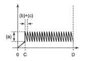
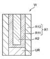
도 1a는 제1 영역 및 제2 영역을 갖되 이들 간에 리세스의 깊이가 형성되어 있는 예시적인 기판을 도시한 것이다. 특히, 기판(SW)은 제1 영역(R1) 및 제2 영역(R2)을 포함한다. 예시적인 구현예에서, 제1 영역(R1)은 실리콘 질화물로 형성되고, 제2 영역(R2)은 실리콘 산화물로 형성된다.1A illustrates an exemplary substrate having a first region and a second region with a depth of a recess formed therebetween. In particular, the substrate SW includes a first region R1 and a second region R2 . In an exemplary embodiment, the first region R1 is formed of silicon nitride, and the second region R2 is formed of silicon oxide.
제1 영역(R1) 상에는 퇴적물(DP)이 형성되고, 제1 영역(R1)과 제2 영역(R2) 사이에는 리세스(RC)가 형성된다. 리세스(RC)의 리세스 깊이 d가 도시되어 있다. 일 예시적인 구현예에서, CO 가스와 Ar 가스의 혼합물을 공정 가스로 사용하여 기판(SW) 상에 퇴적물(DP)을 형성한다. 다른 구현예에서, CH3F 가스와 Ar 가스의 혼합물을 사용하여 기판(SW) 상에 퇴적물(DP)을 형성할 수 있다.A deposit DP is formed on the first region R1 , and a recess RC is formed between the first region R1 and the second region R2 . The recess depth d of the recess RC is shown. In one exemplary embodiment, a mixture of CO gas and Ar gas is used as a process gas to form a deposit DP on the substrate SW. In another embodiment, the deposit DP may be formed on the substrate SW using a mixture of CH3 F gas and Ar gas.
도 1b는 비교 공정에 따라 에칭된 기판(SW)의 제1 영역(R1)에서의 퇴적물 양과 리세스의 깊이 d(㎚)를 비교한 차트이다. 도 1b에 도시된 바와 같이, 기판(SW)이 비교 공정에 따라 에칭되는 경우, 리세스의 깊이 d(㎚)는 제1 영역(R1)에서의 퇴적물 양과 비교된다.FIG. 1B is a chart comparing the amount of deposits in the first region R1 of the substrate SW etched according to a comparison process and the depth d (nm) of the recess. As shown in FIG. 1B , when the substrate SW is etched according to the comparison process, the depth d (nm) of the recess is compared with the deposit amount in the first region R1 .
비교 공정에서는 리세스(RC)의 깊이 A가 에칭된다. 예시적인 구현예에서, 리세스(RC)의 깊이 A는 20 내지 40㎚로 에칭된다. 그 후, 기판(SW)에 희가스 이온을 공급하는 것과 교대로 기판(SW) 상에 퇴적물(DP)을 반복적으로 형성한다. 예시적인 구현예에서, 기판(SW) 상에 형성된 퇴적물(DP)은 불소를 함유하고 있다.In the comparison process, the depth A of the recess RC is etched. In an exemplary embodiment, the depth A of the recess RC is etched between 20 and 40 nm. Thereafter, deposits DP are repeatedly formed on the substrate SW alternately with the supply of rare gas ions to the substrate SW. In the exemplary embodiment, the deposit DP formed on the substrate SW contains fluorine.
그 후, 리세스(RC)는 예시적인 구현예에서 50 내지 80㎚인 깊이 B까지 에칭된다. 리세스(RC)를 깊이 B까지 에칭하기 위해, 다음의 단계: 즉 (i) 제1 영역(R1) 상에 제1 퇴적물을 (5㎚ 이상으로) 형성하는 단계, 및 그 후 (ii) 희가스로부터 플라즈마를 생성하고 이 플라즈마를 기판(SW)에 공급하는 것과 교대로 기판(SW) 상에 불소를 함유하는 제2 퇴적물을 형성하는 단계가 수행된다. 단계 (i) 및 (ii)는 공정이 완료될 때까지 한 번 이상의 횟수로 반복될 수 있다. 리세스(RC)를 선택적으로 처리 및 에칭하는 단계는 120 내지 180℃에서 수행되지만, 이러한 범위에 제한되는 것은 아니다. 일 예에서, 단계는 150℃에서 수행된다.The recess RC is then etched to depth B, which is 50-80 nm in the exemplary embodiment. To etch the recess RC to depth B, the following steps: (i) forming a first deposit (at least 5 nm) on the first region R1, and thereafter (ii) a rare gas A step of forming a second deposit containing fluorine on the substrate SW is performed alternately with generating plasma from and supplying the plasma to the substrate SW. Steps (i) and (ii) may be repeated one or more times until the process is complete. The selectively processing and etching the recess RC is performed at 120 to 180° C., but is not limited thereto. In one example, the step is performed at 150°C.
도 1c는, 도 1a에 도시되고 본 개시 내용에 따른 예시적인 공정에 따라 에칭된 기판(SW)의 제1 영역에서의 퇴적물 양과 리세스의 깊이 d를 비교한 차트를 도시한 것이다. 본 개시 내용에 따른 예시적인 공정에서, 도 1c에 도시된 바와 같이, 기판(SW)이 예시적인 공정에 따라 에칭되는 경우, 리세스의 깊이 d(㎚)는 제1 영역(R1)에서의 퇴적물 양과 비교된다.FIG. 1C illustrates a chart comparing the depth d of a recess to the amount of deposit in a first region of a substrate SW that has been etched according to the exemplary process shown in FIG. 1A and according to the present disclosure. In an exemplary process according to the present disclosure, as shown in FIG. 1C , when the substrate SW is etched according to the exemplary process, the depth d (nm) of the recess is the deposit in the first region R1 . compared to the quantity.
예시적인 공정에서, 리세스(RC)의 깊이 C가 먼저 에칭된다. 예시적인 구현예에서, 리세스(RC)의 깊이 C는 10 내지 20㎚가 되도록 에칭되지만, 이에 제한되지는 않는다. 그 후, 기판(SW)에 희가스 이온을 공급하는 것과 교대로 기판(SW) 상에 퇴적물(DP)을 반복적으로 형성한다. 예시적인 구현예에서, 기판(SW) 상에 형성된 퇴적물(DP)은 불소를 함유하고 있다.In the exemplary process, the depth C of the recess RC is etched first. In an exemplary embodiment, the depth C of the recess RC is etched to be between 10 and 20 nm, but is not limited thereto. Thereafter, deposits DP are repeatedly formed on the substrate SW alternately with the supply of rare gas ions to the substrate SW. In the exemplary embodiment, the deposit DP formed on the substrate SW contains fluorine.
그 후, 리세스(RC)는 예시적인 구현예에서 80 내지 100㎚인 깊이 D까지 에칭된다. 리세스(RC)를 깊이 D까지 에칭하기 위해, (a) 제1 영역(R1) 상에 제1 퇴적물을 형성하는 단계가 수행된다. 이러한 제1 퇴적물은 비교 공정의 (i)에서 형성된 제1 퇴적물보다 얇게 형성된다. 그 후, (b) 기판(SW) 상에 불소를 함유하는 제2 퇴적물을 형성하는 단계, 및 그 후 (C) 희가스로부터 플라즈마를 생성하고 이 플라즈마를 기판(SW)에 공급하는 단계가 수행된다. 단계 (a), (b) 및 (C)는 이러한 순서로 반복된다. 리세스(RC)를 선택적으로 처리 및 에칭하는 단계는 150 내지 200℃에서 수행되지만, 이러한 범위에 제한되는 것은 아니다. 일 예에서, 단계는 170℃에서 수행된다.The recess RC is then etched to a depth D which is 80-100 nm in an exemplary embodiment. In order to etch the recess RC to a depth D, (a) forming a first deposit on the first region R1 is performed. This first deposit is formed thinner than the first deposit formed in (i) of the comparative process. Thereafter, (b) forming a second deposit containing fluorine on the substrate SW, and thereafter (C) generating plasma from the noble gas and supplying the plasma to the substrate SW are performed . Steps (a), (b) and (C) are repeated in this order. The selectively processing and etching the recess RC is performed at 150 to 200° C., but is not limited thereto. In one example, the step is performed at 170°C.
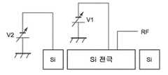
도 2는 후술할 도 7에 도시된 상부 전극(3)과 같은 상부 전극 근처에서 직류 중첩(DCS)을 위한 예시적인 조건을 도시한 것이다.FIG. 2 shows exemplary conditions for direct current superposition (DCS) near an upper electrode, such as the
도 2에 도시된 바와 같이, Si 전극에는 V1 전압과 RF가 모두 공급되지만, Si에는 V2 전압이 인가된다. 예시적인 구현예에서, DCS를 위한 조건은 다음과 같이 제공된다:As shown in FIG. 2 , both voltage V1 and RF are supplied to the Si electrode, but voltage V2 is applied to Si. In an exemplary embodiment, the conditions for DCS are provided as follows:
가스: 희가스(예컨대, Ar) + H2(선택 사항);Gas: noble gas (eg Ar) + H2 (optional);
전력: 내부 V1 = -800V 및 외부 V2 = -200V(예컨대, V1 < V2 < 0(V)) ; 그리고Power: internal V1 = -800V and external V2 = -200V (eg, V1 < V2 < 0(V)) ; and
압력: 10 내지 100mTorr(예컨대, 20mTorr).Pressure: 10 to 100 mTorr (eg 20 mTorr).
도 2에 대한 추가 논의는 나중에 도 5c 및 단계 STy와 관련하여 제공될 것이다.Further discussion of FIG. 2 will be provided later in relation to FIG. 5C and step STy.
도 3a는 예시적인 실시예에 따른 에칭 방법의 플로우차트이다. 도 3a에 도시된 에칭 방법(이하, 방법 NIT라 지칭함)은 단계 STa로부터 시작된다. 단계 STa에서는, 기판 처리 장치 내의 기판 지지체 상에 기판(SW)을 배치한다. 기판 지지체는 기판 처리 장치의 챔버 내에 수용된다. 기판 처리 장치는 도 7에 도시되어 있다.3A is a flowchart of an etching method according to an exemplary embodiment. The etching method shown in FIG. 3A (hereinafter referred to as method NIT) starts from step STa. In step STa, the substrate SW is placed on the substrate support in the substrate processing apparatus. A substrate support is received within a chamber of a substrate processing apparatus. The substrate processing apparatus is shown in FIG. 7 .
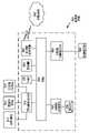
도 7은 본 개시 내용에 따른 예시적인 기판 처리 장치를 도시한 것이다.7 illustrates an exemplary substrate processing apparatus in accordance with the present disclosure.
특히, 도 7은 기판 처리 장치(200), 예컨대, 용량성 결합 플라즈마(capacitively coupled plasma)(CCP) 플라즈마 시스템을 도시한 것이다. CCP 시스템이 일 예로서 도시되어 있지만, 유도성 결합 플라즈마(inductively coupled plasma)(ICP) 장치 등과 같은 임의의 다른 에칭 장치가 또한 사용될 수 있다. 기판 처리 장치(200)는, 형상이 대략 원통형이고, 예를 들어, 알루미늄으로 형성된 반응 챔버(1)를 포함한다. 반응 챔버(1)는 접지 전위에 연결되어 있다. 반응 챔버(1)의 내벽 표면 상에는 내플라즈마성의 막이 형성되며, 이러한 내플라즈마성의 막은 양극 산화 처리에 의해 형성된 막 또는 이트륨 산화물로 형성된 막과 같은 세라믹 막일 수 있다. 상부 전극(3) 및 베이스(4)(반응 챔버(1)에서 플라즈마를 생성하기 위한 하부 전극의 역할을 함) 중 적어도 하나에 RF 전력이 공급되면, 상부 전극(3)과 베이스(4) 사이에 플라즈마(2)가 발생되어, 상부 전극(3)과 베이스(4) 사이에서 기판(W)이 처리된다. 플라즈마(2)는 기판(W)에 근접하게 형성되고, 기판(W)은 정전 척(5)의 상부 표면 상에 유지되며, 이는 아래에서 더 상세히 논의될 것이다. 베이스(4)는 대략 디스크 형상을 가지며 전도성이다.In particular, FIG. 7 illustrates a
가스 소스(8)는 해당하는 일련의 유량 제어기를 통해 제어되는 복수의 가스 소스를 포함한다. 가스 소스(8)는 하나 이상의 가스 라인을 통해 반응 챔버(1)에 가스를 제공한다.The
기판 처리 장치(200)는, 27MHz 내지 100MHz의 범위를 포함하되, 60MHz를 예시적인 주파수로 갖는 RF 에너지를 생성하는 제1 RF 전력 공급 장치(6)를 더 포함한다. 제1 RF 전력 공급 장치(6)는 매칭 회로를 통해 상부 전극(3)에 연결되며, 매칭 회로는 제1 RF 전력 공급 장치(6)의 출력 임피던스와 상부 전극(3)의 임피던스를 매칭시킨다.The
기판 처리 장치(200)는 기판(W)으로 이온을 끌어 당기기 위한 바이어스 목적으로 RF 에너지를 생성하는 제2 RF 전력 공급 장치(7)를 더 포함한다. 제2 RF 전력 공급 장치(7)의 동작 주파수는 제1 RF 전력 공급 장치(6)에 대한 동작 주파수보다 낮고, 전형적으로는 300 KHz 내지 13.56 MHz의 범위이다. 대안적인 실시예에서, 다수의 RF 전력 공급 장치(6 및 7)는 동일한 전극(하부 전극(4))에 연결될 수 있다.The
상부 전극(3)은 가변 직류(DC) 전력 공급 장치(10)인 제2 전력 공급 장치를 갖는다. 가변 DC 전력 공급 장치(10)는 또한 제1 RF 전력 공급 장치(6)로부터 상부 전극에 인가되는 RF 에너지에 대한 DC 바이어스로서 역할을 할 수 있다. DC 전력 공급 장치(10)의 가변성을 통해, 수행되는 공정에 따라 에칭 레이트를 제어할 수 있는 이온 에너지에 대한 작동 제어가 가능하게 된다.The
RF 전력 공급 장치(7)에 의해 생성된 RF 에너지는 펄스화될 수 있다. 베이스/하부 전극에 바이어스 전력이 공급되면, 에칭이 주로 발생된다. 베이스/하부 전극에 바이어스 전력이 공급되지 않으면, 퇴적이 주로 발생된다. 펄스화 바이어스를 통해 에칭 단계를 퇴적 단계와 분리할 수 있다. 에칭은 보호 막이 형성된 후에 발생하며, 리세스의 측벽은 사이드 에칭으로부터 보호된다. 추가적으로, 펄스의 듀티(바이어스 온 시간/(바이어스 온 시간 + 바이어스 오프 시간))의 변화를 통해 에칭/퇴적 균형을 제어할 수 있다. 바이어스 오프(bias off) 시간이 길수록 보호 막이 더 두껍게 형성되어 더 많은 보호를 받을 수 있다. 바이어스 온(bias on) 시간이 길수록 에칭 레이트는 증가한다.The RF energy generated by the
일 실시예에서, 기판 처리 장치(200)는 도 8에 도시된 처리 회로부와 같은 전용 제어 회로부를 가질 수 있다. 제어 회로부는 메모리에 저장된 제어 프로그램을 실행하고, 저장 디바이스에 저장된 레시피 데이터에 기반하여 기판 처리 장치(200)의 각 컴포넌트를 제어한다.In an embodiment, the
기판 처리 장치(200)는 반응 챔버(1)의 내부 대기에 연결된 배기 디바이스(9)를 포함한다. 배기 디바이스(9)는 반응 챔버(1)를 제어 가능하게 감압하고 반응 챔버(1)로부터의 가스를 배기하기 위해, 자동 압력 제어 밸브와 같은 압력 제어기 및 진공 펌프(예컨대, 터보 분자 펌프)를 포함한다.The
기판 처리 장치(200)에서, 상부 전극(3)은 플라즈마 생성을 위한 RF 전력을 수신한다. 일부 실시예에서, 베이스(4)는 RF 전력을 수신할 수 있다. 본 개시 내용에 따른 방법은 또한 CCP 플라즈마 처리 장치와는 다른 기판 처리 장치에도 적용 가능하다. 보다 구체적으로, 방법은 마이크로웨이브와 같은 표면파를 사용하여 플라즈마를 생성하는 플라즈마 처리 장치 또는 유도성 결합 플라즈마 처리 장치와 같은 임의의 플라즈마 처리 장치를 사용하여 구현될 수 있다.In the
도 3a의 논의로 돌아가서, 기판(W)은 제1 영역(R1) 및 제2 영역(R2)을 포함한다. 예시적인 구현예에서, 제1 영역(R1)은 제2 영역(R2)의 재료와는 다른 재료로 형성된다. 제1 영역(R1)의 재료는 산소를 포함하지 않고, 실리콘 질화물을 함유할 수 있다. 제2 영역(R2)의 재료는 실리콘 및 산소를 함유하고, 실리콘 산화물을 함유할 수 있다. 제2 영역(R2)의 재료는 실리콘, 탄소, 산소, 및 수소를 함유하는 저유전상수 재료를 포함할 수 있다.Returning to the discussion of FIG. 3A , the substrate W includes a first region R1 and a second region R2 . In an exemplary embodiment, the first region R1 is formed of a material different from that of the second region R2 . The material of the first region R1 may not contain oxygen and may contain silicon nitride. The material of the second region R2 contains silicon and oxygen, and may contain silicon oxide. The material of the second region R2 may include a low-k material containing silicon, carbon, oxygen, and hydrogen.
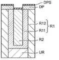
도 5a는 도 3a에 도시된 에칭 방법으로 처리될 예시적인 기판(W)의 부분 확대 단면도이다. 도 5a에 도시된 기판(W)은 제1 영역(R1) 및 제2 영역(R2)을 포함한다. 기판(W)은 기저 영역(UR)을 더 포함할 수 있다. 도 5a에 도시된 기판(W)의 제1 영역(R1)은 영역(R11)과 영역(R12)을 포함한다. 영역(R11)은 실리콘 질화물로 형성되고, 리세스를 규정한다. 영역(R11)은 기저 영역(UR) 상에 있다. 영역(R12)은 영역(R11)의 양측 상에 뻗어 있다. 영역(R12)은 실리콘 질화물 또는 실리콘 탄화물로 형성된다. 도 5a에 도시된 기판(W)의 제2 영역(R2)은 실리콘 산화물로 형성되고, 영역(R11)에 의해 규정된 리세스 내에 함유된다. 다시 말해서, 제2 영역(R2)은 제1 영역(R1)에 의해 둘러싸여 있다. 도 5a에 도시된 기판(W)이 방법(MT)으로 처리될 때, 제2 영역(R2)은 자기 정렬 방식으로 에칭된다.5A is a partially enlarged cross-sectional view of an exemplary substrate W to be processed with the etching method shown in FIG. 3A . The substrate W shown in FIG. 5A includes a first region R1 and a second region R2. The substrate W may further include a base region UR. The first region R1 of the substrate W illustrated in FIG. 5A includes a region R11 and a region R12. The region R11 is formed of silicon nitride and defines a recess. The region R11 is on the base region UR. Region R12 extends on both sides of region R11. The region R12 is formed of silicon nitride or silicon carbide. The second region R2 of the substrate W shown in Fig. 5A is formed of silicon oxide and contained in a recess defined by the region R11. In other words, the second region R2 is surrounded by the first region R1 . When the substrate W shown in FIG. 5A is processed by the method MT, the second region R2 is etched in a self-aligned manner.
방법(MT)에 포함된 단계 STa 이후의 단계는 이제 기판(W)을 참조하여 기술될 것이다.Steps after step STa included in method MT will now be described with reference to substrate W.
일부 실시예에서, 단계 STx는 단계 STa 다음에 수행될 수 있다. 다른 실시예에서, 단계 Stx는 수행되지 않고, 공정은 단계 STb로 이동한다. 단계 STx에서, 미리 결정된 종횡비 이상에 도달될 때까지 제1 영역(R1)을 에칭한다. 단계 STx의 추가 논의는 나중에 도 3b 및 도 6a 내지 도 6d와 관련하여 논의될 것이다.In some embodiments, step STx may be performed after step STa. In another embodiment, step Stx is not performed and the process moves to step STb. In step STx, the first region R1 is etched until a predetermined aspect ratio or more is reached. Further discussion of step STx will be discussed later with respect to FIGS. 3B and 6A-6D.
단계 STb에서, 도 5b에 도시된 바와 같이, 제1 영역(R1) 상에 퇴적물(DP)을 우선적으로 형성한다.In step STb, as shown in FIG. 5B , a deposit DP is preferentially formed on the first region R1.
도 5b는 도 3a의 단계 STb에서 기판의 제1 영역 내에 형성된 제1 퇴적물(DP)을 도시한 것이다. 제1 퇴적물(DP)은 탄소를 함유한다. 예시적인 구현예에서, 제1 퇴적물(DP)은, 탄소를 함유하고 불소는 포함하지 않는 공정 가스로부터 생성된 플라즈마를 사용하여 형성된다.FIG. 5B shows a first deposit DP formed in a first region of the substrate in step STb of FIG. 3A . The first deposit DP contains carbon. In an exemplary embodiment, the first deposit DP is formed using a plasma generated from a process gas containing carbon and no fluorine.
단계 STb에서, 기판 처리 장치(200)의 챔버 내에서 공정 가스로부터 플라즈마를 생성한다.In step STb, plasma is generated from the process gas in the chamber of the
예시적인 구현예에서, 단계 STb에서 사용되는 공정 가스는 제1 가스 및 제2 가스를 함유할 수 있다. 공정 가스는 아르곤 가스 또는 헬륨 가스와 같은 희가스를 더 함유할 수 있다.In an exemplary embodiment, the process gas used in step STb may contain a first gas and a second gas. The process gas may further contain a noble gas such as argon gas or helium gas.
제1 가스는 탄소를 함유하고, 불소는 포함하지 않는다. 제1 가스의 예는 CO 가스, COS 가스, C2H2 가스, C2H4 가스, CH4 가스, C2H6 가스, H2 가스를 포함한다.The first gas contains carbon and no fluorine. Examples of the first gas include CO gas, COS gas, C2 H2 gas, C2 H4 gas, CH4 gas, C2 H6 gas, H2 gas.
제1 가스는 수소를 포함하지 않을 수 있다. 제1 가스는 탄소 함유 불소 불포함 가스로서, 예를 들어, 일산화탄소 가스(CO 가스) 또는 카르보닐 황화물 가스(COS 가스)를 함유할 수 있다.The first gas may not include hydrogen. The first gas is a carbon-containing fluorine-free gas, and may contain, for example, carbon monoxide gas (CO gas) or carbonyl sulfide gas (COS gas).
제2 가스는 탄소 및 불소 또는 수소를 함유할 수 있다. 이러한 제2 가스의 예는 하이드로플루오로카본 가스, 플루오로카본 가스 및 탄화수소 가스를 포함한다. 하이드로플루오로카본 가스는, 예를 들어, CHF3 가스, CH3F 가스, 또는 CH2F2 가스를 포함할 수 있다. 플루오로카본 가스는, 예를 들어, C4F6 가스를 포함할 수 있다. 탄소 및 수소를 함유하는 제2 가스는, 예를 들어, CH4 가스를 포함할 수 있다.The second gas may contain carbon and fluorine or hydrogen. Examples of such a second gas include a hydrofluorocarbon gas, a fluorocarbon gas, and a hydrocarbon gas. The hydrofluorocarbon gas may include, for example, CHF3 gas, CH3 F gas, or CH2 F2 gas. The fluorocarbon gas may include, for example, C4 F6 gas. The second gas containing carbon and hydrogen may include, for example, CH4 gas.
제1 가스는 제2 가스보다 높은 유량을 가질 수 있다. 제2 가스는 제1 가스의 유량에 대해 0.2 이하의 유량 비율을 갖는다. 제1 가스는 30 내지 200 sccm의 유량을 갖는 탄소 함유 불소 불포함 가스(carbon-containing fluorine-free gas)를 함유할 수 있다. 제1 가스는 90 내지 130 sccm의 유량을 갖는 탄소 함유 불소 불포함 가스를 포함할 수 있다. 공정 가스는 0 내지 1,000sccm의 유량을 갖는 희가스를 함유할 수 있다. 공정 가스는 350sccm 이하의 유량을 갖는 희가스를 함유할 수 있다.The first gas may have a higher flow rate than the second gas. The second gas has a flow rate ratio of 0.2 or less to the flow rate of the first gas. The first gas may contain a carbon-containing fluorine-free gas having a flow rate of 30 to 200 sccm. The first gas may include a carbon-containing fluorine-free gas having a flow rate of 90 to 130 sccm. The process gas may contain a noble gas having a flow rate of 0 to 1,000 sccm. The process gas may contain a noble gas having a flow rate of 350 sccm or less.
공정 가스에 포함된 각 가스의 유량은 챔버(10)의 내부 공간(IDS)의 볼륨 또는 다른 요인에 따라 결정될 수 있다. 단계 STb에서, 플라즈마에 함유된 화학종(탄소 화학종)은 기판에 공급된다. 공급된 화학종은, 도 5b에 도시된 바와 같이, 제1 영역(R1) 상에 탄소를 함유하는 퇴적물(DP)을 우선적으로 형성한다.The flow rate of each gas included in the process gas may be determined according to the volume of the internal space IDS of the
공정 가스를 사용한 단계 STb에서는 제1 영역(R1) 상에 우선적으로 형성된 퇴적물(DP) 외에도, 리세스를 규정하는 측벽 상에 얇은 보호막을 형성한다. 따라서 측벽은 플라즈마로부터 보호된다.In step STb using the process gas, in addition to the deposit DP preferentially formed on the first region R1, a thin protective film is formed on the sidewall defining the recess. The sidewall is thus protected from plasma.
단계 STb에서 사용되는 공정 가스는 CO 가스와 수소 가스(H2 가스)를 함유하는 혼합물일 수 있다. 이러한 공정 가스를 통해, 퇴적물(DP)은 제1 영역(R1) 상에 우선적으로 형성될 수 있다. 퇴적물(DP)은 단계 STc에서 에칭에 대한 내성이 높은 보호막 역할을 한다. 공정 가스에 포함된 CO 가스 및 H2 가스의 총 유량에 대한 H2 가스의 유량의 비율은 1/19 내지 2/17일 수 있다. 이러한 비율을 갖는 공정 가스를 사용하는 경우, 제1 영역(R1) 상에 형성되는 퇴적물(DP)은 보다 높은 수직도의 측면을 갖는다.The process gas used in step STb may be a mixture containing CO gas and hydrogen gas (H2 gas). Through the process gas, the deposit DP may be preferentially formed on the first region R1 . The deposit DP serves as a protective film with high resistance to etching in step STc. A ratio of the flow rate of the H2 gas to the total flow rate of the CO gas and the H2 gas included in the process gas may be 1/19 to 2/17. When a process gas having such a ratio is used, the deposit DP formed on the first region R1 has a higher verticality side.
단계 STb에서, 기판(W)에 공급되는 이온은 0 내지 70eV의 에너지를 가질 수 있다. 이 경우, 퇴적물(DP)은 리세스의 개구부를 좁힐 가능성이 적다.In step STb, ions supplied to the substrate W may have an energy of 0 to 70 eV. In this case, the deposit DP is less likely to narrow the opening of the recess.
일 실시예에서, 단계 STb에서 사용되는 기판 처리 장치는 용량성 결합 플라즈마 처리 장치일 수 있다. 용량성 결합 플라즈마 처리 장치를 사용하는 경우, 플라즈마를 생성하기 위한 무선 주파수(RF) 전력이 상부 전극에 제공될 수 있다. 이 경우, 플라즈마는 기판(W)으로부터 멀리 떨어진 구역에 형성될 수 있다. RF 전력은 60MHz 이상의 주파수를 가질 수 있다. 다른 실시예에서, 단계 STb에서 사용되는 기판 처리 장치는 유도성 결합 플라즈마 처리 장치일 수 있다.In one embodiment, the substrate processing apparatus used in step STb may be a capacitively coupled plasma processing apparatus. When using a capacitively coupled plasma processing apparatus, radio frequency (RF) power to generate plasma may be provided to the upper electrode. In this case, the plasma may be formed in a region remote from the substrate W. The RF power may have a frequency of 60 MHz or higher. In another embodiment, the substrate processing apparatus used in step STb may be an inductively coupled plasma processing apparatus.
단계 STb에서는 제1 영역(R1) 상에 퇴적물(DP)을 우선적으로 형성한다. 따라서, 단계 STb는 적어도 기판(W)의 제1 영역(R1) 및 제2 영역(R2)에 의해 규정된 리세스가 4 이하의 종횡비를 가질 때 수행될 수 있다.In step STb, the deposit DP is preferentially formed on the first region R1. Accordingly, step STb may be performed when at least the recess defined by the first region R1 and the second region R2 of the substrate W has an aspect ratio of 4 or less.
방법(MT)에 포함된 단계 STb의 공정 가스로부터 생성된 탄소 화학종은 제1 영역(R1) 상에 선택적으로 퇴적된다. 공정 가스로부터 생성된 탄소 화학종은 산소를 함유하는 제2 영역(R2) 상에 퇴적될 가능성이 적다. 방법(MT)을 사용하여 제2 영역(R2)을 에칭하지만 제1 영역(R1) 상에는 퇴적물(DP)이 선택적으로 유지된다. 따라서 방법(MT)을 통해, 제2 영역(R2)을 에칭하지만 제2 영역(R2)에 대해 선택적으로 제1 영역(R1)을 보호한다. 방법(MT)을 사용하여 제1 영역(R1) 상에 퇴적물(DP)을 우선적으로 형성한다. 이는 제1 영역(R1) 및 제2 영역(R2)에 의해 규정되는 리세스의 개구부의 막힘을 감소시킨다.Carbon species generated from the process gas of step STb included in the method MT are selectively deposited on the first region R1. Carbon species generated from the process gas are less likely to be deposited on the oxygen-containing second region R2. The method MT is used to etch the second region R2 but the deposit DP is selectively retained on the first region R1 . Accordingly, through the method MT, the second region R2 is etched, but the first region R1 is selectively protected with respect to the second region R2 . A deposit DP is preferentially formed on the first region R1 by using the method MT. This reduces clogging of the opening of the recess defined by the first region R1 and the second region R2.
단계 STb에서 CO 가스로부터 생성된 탄소 화학종은 이온성이다. CH4 가스 또는 CH3F 가스는 CH2 또는 CHF와 같은 라디칼을 발생시키는 경향이 있다. 이들 라디칼은 반응성이 높아 기판(W)의 표면 상에 등방성으로 쉽게 퇴적된다. 이에 반해, 이온성 화학종은 기판(W) 상에 이방성으로 퇴적된다. 다시 말해서, 이온성 화학종은 리세스를 규정하는 벽면보다 제1 영역(R1)의 상부 표면에 더 많이 부착된다. 기판(W)의 표면으로부터 일산화탄소가 방출될 가능성이 높다. 기판(W)의 표면 상에 일산화탄소를 흡착시키도록 하기 위해서는 이온을 기판(W)의 표면에 충돌시켜 기판(W)의 표면에서 산소를 제거해야 한다. 또한, 구조가 단순한 일산화탄소는 가교가 어렵다. 일산화탄소를 기판(W)의 표면 상에 퇴적시키도록 하기 위해서는 기판(W)의 표면 상에 댕글링 본드(dangling bond)를 형성해야 한다. 단계 STb에서 CO 가스로부터 생성된 탄소 화학종은 이온성이다. 따라서 화학종은 제1 영역(R1)의 상부 표면에서 산소를 제거하고, 상부 표면 상에 댕글링 본드를 형성하고, 그리고 제1 영역(R1) 상에 선택적으로 퇴적될 수 있다.The carbon species produced from the CO gas in step STb is ionic. CH4 gas or CH3 F gas tends to generate radicals such as CH2 or CHF. These radicals are highly reactive and easily deposited isotropically on the surface of the substrate W. In contrast, ionic species are anisotropically deposited on the substrate W. In other words, more ionic species are attached to the upper surface of the first region R1 than to the wall defining the recess. There is a high possibility that carbon monoxide is emitted from the surface of the substrate W. In order to adsorb carbon monoxide on the surface of the substrate W, ions must collide with the surface of the substrate W to remove oxygen from the surface of the substrate W. In addition, carbon monoxide having a simple structure is difficult to crosslink. In order to deposit carbon monoxide on the surface of the substrate W, a dangling bond must be formed on the surface of the substrate W. The carbon species produced from the CO gas in step STb is ionic. Thus, the chemical species may remove oxygen from the upper surface of the first region R1 , form dangling bonds on the upper surface, and selectively deposit on the first region R1 .
일부 실시예에서, 단계 STy는 단계 STb 다음에 수행될 수 있다. 다른 실시예에서, 단계 STy는 수행되지 않고, 공정은 단계 Stz1로 이동한다. 단계 STy에서, 도 5c에 도시된 바와 같이, 실리콘 함유 퇴적물(DPS)을 제1 퇴적물(DP) 및 제2 영역(R2) 상에 형성한다.In some embodiments, step STy may be performed after step STb. In another embodiment, step STy is not performed and the process moves to step Stz1. In step STy, as shown in FIG. 5C , a silicon-containing deposit DPS is formed on the first deposit DP and the second region R2.
일부 실시예에서, 실리콘 함유 퇴적물(DPS)은 도 2에 도시된 바와 같이, 상부 전극 근처에 직류 중첩(DCS)을 사용함으로써 단계 STy에서 형성될 수 있다. Si 함유 상부 전극은 불활성 가스(예컨대, Ar)를 챔버에 공급하면서 상부 전극에 DC를 인가함으로써 생성된 희가스 내의 이온에 의해 스퍼터링된다. Si 및 2차 전자가 생성된다. 기판 표면은 생성된 Si 및 2차 전자에 노출되어 실리콘 함유 퇴적물(DPS)을 형성한다.In some embodiments, a silicon-containing deposit (DPS) may be formed in step STy by using direct current superposition (DCS) near the top electrode, as shown in FIG. 2 . The Si-containing upper electrode is sputtered by ions in the noble gas generated by applying DC to the upper electrode while supplying an inert gas (eg, Ar) to the chamber. Si and secondary electrons are generated. The substrate surface is exposed to the generated Si and secondary electrons to form a silicon-containing deposit (DPS).
일부 다른 실시예에서, 실리콘 함유 퇴적물(DPS)은 플라즈마 강화 화학 기상 증착(PECVD)을 사용함으로써 단계 STy에서 형성될 수 있다. 실리콘 함유 가스(예컨대, SiCl4)를 챔버에 공급하면서 플라즈마를 생성하기 위해 무선 주파수(RF) 전력을 제공함으로써 제1 퇴적물(DP) 상에 실리콘 함유 퇴적물(DPS)을 형성한다.In some other embodiments, a silicon containing deposit (DPS) may be formed in step STy by using plasma enhanced chemical vapor deposition (PECVD). A silicon-containing deposit DPS is formed on the first deposit DP by providing radio frequency (RF) power to generate a plasma while supplying a silicon-containing gas (eg, SiCl4 ) to the chamber.
단계 STz1에서, 도 5d에 도시된 바와 같이, 불소 함유 제2 퇴적물(DPC)을 기판(W) 상에 형성한다. 예시적인 구현예에서, 단계 STy가 수행될 때 제1 영역(R1) 및 제2 영역(R2)의 실리콘 함유 퇴적물(DPS) 상에 제2 퇴적물(DPC)을 형성한다. 다른 구현예에서, 단계 STy가 수행되지 않을 때 제2 영역(R2)의 실리콘 산화물 막 뿐만 아니라 영역(R1)에서의 퇴적물(DP) 상에 제2 퇴적물(DPC)을 형성한다. 예시적인 구현예에서, 제2 퇴적물(DPC)은 불소를 함유한다.In step STz1 , as shown in FIG. 5D , a fluorine-containing second deposit DPC is formed on the substrate W . In an exemplary embodiment, a second deposit DPC is formed on the silicon-containing deposit DPS in the first region R1 and the second region R2 when step STy is performed. In another embodiment, the second deposit DPC is formed on the deposit DP in the region R1 as well as the silicon oxide film in the second region R2 when step STy is not performed. In an exemplary embodiment, the second deposit (DPC) contains fluorine.
제2 퇴적물(DPC)은 기판 처리 장치(200)의 챔버 내에서 플루오로카본 가스로부터 생성된 플라즈마를 사용하여 형성될 수 있다. 플루오로카본 가스의 예는 CF4 가스, C4F6 가스 및 C4F8 가스를 포함하지만, 이에 제한되지는 않는다. 공정 가스는 아르곤 가스 또는 헬륨 가스와 같은 희가스를 더 함유할 수 있다.The second deposit DPC may be formed using plasma generated from a fluorocarbon gas in a chamber of the
단계 STz2에서는, 도 5e에 도시된 바와 같이, 챔버 내의 희가스로부터 플라즈마를 생성하고, 기판(W)에 공급된 희가스 이온을 사용하여 제2 영역(R2)의 일부를 제거한다. 특히, 희가스 내의 이온을 기판(W)에 공급하여, 제2 영역(R2) 상의 제2 퇴적물(DPC)을 타격하여 제2 퇴적물(DPC)을 활성화시킨다. 제2 퇴적물(DPC)의 활성 종은 제2 영역(R2)과 반응하여 제2 영역(R2)의 일부를 제거한다.In step STz2 , as shown in FIG. 5E , plasma is generated from the rare gas in the chamber, and a part of the second region R2 is removed using the rare gas ions supplied to the substrate W . In particular, ions in the rare gas are supplied to the substrate W to strike the second deposit DPC on the second region R2 to activate the second deposit DPC. Active species of the second deposit DPC react with the second region R2 to remove a portion of the second region R2.
제1 영역(R1) 상의 실리콘 함유 퇴적물(DPS) 및 제2 퇴적물(DPC)도 또한 제거한다. 제1 영역(R1) 상의 제1 퇴적물(DP)도 또한 부분적으로 제거한다. 예시적인 구현예에서, 희가스는 Ar 가스이지만, Ar 가스가 아닌 다른 가스일 수 있다. 단계 STz2는 제1 영역(R1) 상의 퇴적물(DP)이 완전히 소모되지 않을 때까지 계속된다.The silicon-containing deposit DPS and the second deposit DPC on the first region R1 are also removed. The first deposit DP on the first region R1 is also partially removed. In an exemplary embodiment, the noble gas is Ar gas, but may be a gas other than Ar gas. Step STz2 continues until the deposit DP on the first region R1 is not completely consumed.
단계 STz2의 수행 후, 공정은 단계 STc로 진행한다. STc 단계에서, 제1 영역(R1)에 대해 제2 영역(R2)을 선택적으로 에칭한다. 특히, 기판(W)에 공급된 희가스 이온을 사용하여 제2 영역(R2)을 선택적으로 에칭한다. 일 실시예에서, 에칭 가스로부터 생성된 플라즈마 내에 함유된 화학종을 사용하여 제2 영역(R2)을 에칭한다. 이 경우, 기판 처리 장치의 챔버 내의 에칭 가스로부터 플라즈마를 생성한다. 에칭 가스는 제2 영역(R2)의 재료에 따라 선택된다. 에칭 가스는, 예를 들어, 플루오로카본 가스를 함유할 수 있다. 에칭 가스는 아르곤 가스와 같은 희가스 및 산소 가스와 같은 산소 함유 가스를 더 함유할 수 있다.After performing step STz2, the process proceeds to step STc. In step STc, the second region R2 is selectively etched with respect to the first region R1. In particular, the second region R2 is selectively etched using rare gas ions supplied to the substrate W. As shown in FIG. In one embodiment, the second region R2 is etched using a chemical species contained in plasma generated from the etching gas. In this case, plasma is generated from the etching gas in the chamber of the substrate processing apparatus. The etching gas is selected according to the material of the second region R2. The etching gas may contain, for example, a fluorocarbon gas. The etching gas may further contain a noble gas such as argon gas and an oxygen-containing gas such as oxygen gas.
단계 STc에서 사용되는 에칭 장치로서 단계 STb에서 사용된 기판 처리 장치를 사용할 수도 있다. 이 경우, 기판 처리 장치의 챔버로부터 기판(W)을 제거하지 않고 단계 STb 및 STc를 수행한다. 일부 실시예에서, 단계 STb에서 사용된 기판 처리 장치는 단계 STc에서 사용되는 기판 처리 장치와 상이할 수 있다. 이 경우, 기판(W)은 단계 STb에서 사용된 기판 처리 장치로부터 단계 STc에서 사용되는 기판 처리 장치로, 단계 STb와 STc 사이에서의 진공을 통해서만 이송된다.As the etching apparatus used in step STc, the substrate processing apparatus used in step STb may be used. In this case, steps STb and STc are performed without removing the substrate W from the chamber of the substrate processing apparatus. In some embodiments, the substrate processing apparatus used in step STb may be different from the substrate processing apparatus used in step STc. In this case, the substrate W is transferred from the substrate processing apparatus used in step STb to the substrate processing apparatus used in step STc only through the vacuum between steps STb and STc.
단계 STc에 대한 추가 논의는 도 3c와 관련하여 제공될 것이다.Further discussion of step STc will be provided with respect to FIG. 3C .
마지막으로, 방법(MT)은 단계 STJ로 진행하며, 이 단계에서 정지 조건이 충족되는지 여부를 결정한다. 예시적인 구현예에서, 처리 회로부는 이러한 결정을 수행한다. 처리 회로부의 상세한 설명은 나중에 도 8과 관련하여 제공될 것이다.Finally, the method MT proceeds to step STJ, where it is determined whether the stop condition is met. In an exemplary implementation, processing circuitry makes this determination. A detailed description of the processing circuitry will be provided later with respect to FIG. 8 .
단계 STJ에서 정지 조건이 충족되지 않는다고 결정되는 경우, 공정은 단계 STc로 복귀하여 단계 STc를 반복한다. 정지 조건이 충족되었다고 결정되면, 방법(MT)이 완료된다.If it is determined in step STJ that the stop condition is not satisfied, the process returns to step STc and repeats step STc. If it is determined that the stop condition has been met, the method MT is complete.
단계 STJ의 예시적인 구현예에서, 단계 STc의 공정 카운트가 카운트 임계치에 도달할 때 정지 조건이 충족된다. 카운트 임계치는 미리 결정된 수일 수 있거나 사용자 입력 또는 다른 파라미터에 기반하여 설정될 수 있다. 단계 STJ에서 정지 조건이 충족되지 않으면, 공정은 STc로 복귀하여 단계 STc를 반복한다. 특히, 단계 STc는, 도 5f 내지 도 5g에 도시되고 도 3c와 관련하여 기술된 바와 같이, 제2 영역(R2)을 에칭하기 위해 다시 수행된다.In an exemplary implementation of step STJ, the stop condition is satisfied when the process count of step STc reaches a count threshold. The count threshold may be a predetermined number or may be set based on user input or other parameters. If the stop condition is not satisfied in step STJ, the process returns to STc and repeats step STc. In particular, step STc is again performed to etch the second region R2 , as shown in FIGS. 5F to 5G and described in relation to FIG. 3C .
이제 도 3b에 상세히 도시된 단계 STx에 대한 설명으로 돌아갈 것이다. 단계 STx는 단계 STa에서 기판(W)이 제공된 후에 수행된다. 이러한 기판(W)은 도 6a에 도시되어 있으며, 이는 도 5a에 도시된 기판(W)에 대응한다.We will now return to the description of step STx shown in detail in Fig. 3b. Step STx is performed after the substrate W is provided in step STa. This substrate W is shown in Fig. 6A, which corresponds to the substrate W shown in Fig. 5A.
단계 STx의 공정은 단계 STx1에서 시작되며, 이 단계에서는 도 6b에 도시된 바와 같이, 기판(W) 상에 불소 함유 퇴적물(DPC)을 형성한다. 이러한 불소 함유 퇴적물(DPC)은, 단계 STz1에서 사용되고 도 5d에 도시된 퇴적물(DPC)과 동일한 재료일 수 있다. 예시적인 구현예에서, 불소 함유 퇴적물(DPC)은 제1 영역(R1) 및 제2 영역(R2) 내에 형성된다. 불소 함유 퇴적물(DPC)은 기판 처리 장치의 챔버 내에서 플루오로카본 가스로부터 생성된 플라즈마를 사용하여 형성될 수 있다. 플루오로카본 가스의 예는 CF4 가스, C4F6 가스 및 C4F8 가스를 포함하지만, 이에 제한되지는 않는다. 공정 가스는 아르곤 가스 또는 헬륨 가스와 같은 희가스를 더 함유할 수 있다.The process of step STx starts at step STx1, in which a fluorine-containing deposit (DPC) is formed on the substrate W, as shown in FIG. 6B . This fluorine-containing deposit (DPC) may be the same material as the deposit (DPC) used in step STz1 and shown in FIG. 5D . In an exemplary embodiment, a fluorine-containing deposit (DPC) is formed in the first region R1 and the second region R2. A fluorine-containing deposit (DPC) may be formed using a plasma generated from a fluorocarbon gas within a chamber of a substrate processing apparatus. Examples of fluorocarbon gases include, but are not limited to, CF4 gas, C4 F6 gas, and C4 F8 gas. The process gas may further contain a noble gas such as argon gas or helium gas.
단계 STx1이 기판 처리 장치(200)에서 실행될 때, 공정 가스는 가스 소스(8)로부터 반응 챔버(1) 내에 공급된다. 또한, 단계 STx1에서, 제2 RF 전력 공급 장치(7)로부터의 고주파 전력이 베이스(4)에 공급된다. 또한, 단계 STx1에서, 반응 챔버(1) 내의 공간의 압력은 미리 설정된 압력으로 설정된다. 예를 들어, 반응 챔버(1) 내의 공간의 압력은 5mTorr(0.6667Pa) 내지 80mTorr(10.67Pa)의 범위로 설정되지만, 다른 압력도 또한 설정될 수 있다. 또한, 단계 sTx1에서, 상부 전극(3)과 베이스(4)의 상부 표면 간의 거리는 20mm 내지 90mm의 범위로 설정된다. 따라서, 반응 챔버(1) 내에서 공정 가스의 플라즈마가 발생되고, 베이스(4) 상에 탑재된 기판(W)이 플라즈마에 노출된다. 또한, 단계 STx1에서, 전력 공급 장치(10)로부터의 전압이 상부 전극(3)에 인가될 수 있다. 전력 공급 장치(10)로부터 상부 전극(3)으로 인가되는 전압은 -150V 이하일 수 있다. 즉, 전력 공급 장치(10)로부터 상부 전극(3)으로 인가되는 전압은 150V 이상의 절대값을 갖는 음의 전압일 수 있다. 단계 STx1이 수행되는 동안, 기판 처리 장치(200)의 각 컴포넌트의 동작은 도 8을 참조하여 논의될 처리 회로부에 의해 제어될 수 있다.When step STx1 is executed in the
단계 STx1의 시작에서, 플루오로카본으로부터 생성된 원자 및/또는 분자의 활성종, 예를 들어, 불소의 활성종은 기판(W)의 제1 영역(R1) 및 제2 영역(R2)과 충돌한다. 따라서, 불소를 포함하는 퇴적물(DPC)은 제1 영역(R1) 및 제2 영역(R2) 상에 형성된다. 단계 STx1의 처리 시간이 길어짐에 따라 퇴적물(DPC)의 막 두께는 증가된다.At the beginning of step STx1, active species of atoms and/or molecules generated from fluorocarbon, for example active species of fluorine, collide with the first region R1 and the second region R2 of the substrate W do. Accordingly, the fluorine-containing deposit DPC is formed on the first region R1 and the second region R2. As the processing time of step STx1 becomes longer, the film thickness of the deposit DPC increases.
단계 STx1 후에, 단계 STx2가 수행된다. 단계 STx2에서, 기판(W)에 공급되는 희가스 이온을 사용하여 제2 영역(R2)을 제거한다. 이것은 도 6c에 도시되어 있다. 예시적인 구현예에서, 희가스의 이온은 제2 영역(R2)의 퇴적물(DPC)과 충돌하여 제2 영역(R2) 내의 퇴적물(DPC)을 활성화시킨다. 퇴적물(DPC)로부터의 활성 종은 제2 영역(R2)과 반응하여 제2 영역(R2)을 제거한다. 일부 실시예에서, 제1 영역(R1) 상의 퇴적물(DPC)은 부분적으로 또는 전체적으로 제거될 수 있다. 희가스는, 예를 들어, Ar 가스이지만, Ar 가스가 아닌 다른 가스일 수 있다.After step STx1, step STx2 is performed. In step STx2 , the second region R2 is removed using rare gas ions supplied to the substrate W . This is shown in Figure 6c. In the exemplary embodiment, ions of the noble gas collide with the deposit DPC in the second region R2 to activate the deposit DPC in the second region R2 . Active species from the sediment DPC reacts with the second region R2 to remove the second region R2. In some embodiments, the deposit DPC on the first region R1 may be partially or wholly removed. The noble gas is, for example, Ar gas, but may be a gas other than Ar gas.
단계 STx2의 처리 시간 및 단계 STx1의 처리 시간은 적절하게 설정될 수 있다. 예시적인 실시예에서, 단계 STx1의 처리 시간은 단계 STx1 및 단계 STx2의 총 처리 시간의 30% 내지 70% 범위의 비율을 갖도록 설정될 수 있다. 그러나, 다른 비율이 사용될 수 있다.The processing time of step STx2 and the processing time of step STx1 can be appropriately set. In an exemplary embodiment, the processing time of step STx1 may be set to have a ratio in the range of 30% to 70% of the total processing time of steps STx1 and STx2. However, other ratios may be used.
단계 STx2에서, 고주파 전력은 단계 STx1에서와 같이 RF 전력 공급 장치(7)으로부터 베이스(4)에 인가된다. 또한, 단계 STx2에서, 반응 챔버(1) 내의 공간의 압력은 단계 STx1에서와 같이 설정된다. 또한, 단계 sTx2에서, 상부 전극(3)과 베이스(4)의 상부 표면 간의 거리는 단계 STx1에서와 같이 설정된다. 따라서, 반응 챔버(1) 내에서 플라즈마가 발생되고, 베이스(4) 상에 탑재된 기판(W)이 플라즈마에 노출된다. 또한, 단계 STx2에서, 전력 공급 장치(10)로부터의 전압은 단계 STx1에서와 같이 상부 전극(3)에 인가될 수 있다.In step STx2, high-frequency power is applied to the
단계 STx2에서, 활성종, 예를 들어, 희가스 원자의 이온이 퇴적물(DP)에 충돌한다. 그 결과, 도 6c에 도시된 바와 같이, 제2 영역(R2)은 퇴적물(DP) 내의 플루오로카본 라디칼을 사용하여 에칭된다. 또한, 단계 STx2를 통해 퇴적물(DP)의 막 두께를 감소시킨다. 또한, 단계 STx2에서는, 도 6c에 도시된 바와 같이, 제1 영역(R1) 상의 퇴적물(DPC)의 막 두께도 또한 감소시킨다.In step STx2, active species, for example ions of noble gas atoms, collide with the sediment DP. As a result, as shown in FIG. 6C , the second region R2 is etched using fluorocarbon radicals in the deposit DP. Also, the film thickness of the deposit DP is reduced through step STx2. Further, in step STx2, as shown in FIG. 6C, the film thickness of the deposit DPC on the first region R1 is also reduced.
단계 STx2 후에, 단계 STx3가 수행된다. 단계 STx3에서, 제1 영역(R1)이 제2 영역(R2)에 대해 미리 결정된 종횡비를 달성했는지 여부를 결정한다. 예시적인 구현예에서, 도 8에 예시된 처리 회로부는 이러한 결정을 수행한다.After step STx2, step STx3 is performed. In step STx3, it is determined whether the first region R1 has achieved a predetermined aspect ratio with respect to the second region R2. In an exemplary implementation, the processing circuitry illustrated in FIG. 8 makes this determination.
단계 STx3에서 미리 결정된 종횡비가 달성되지 않은 것으로 결정되는 경우, 공정은 단계 STx1로 복귀하여 단계 STx1 및 STx2를 반복한다. 미리 결정된 종횡비가 달성된 것으로 결정되는 경우, 단계 STx가 완료되고, 방법(MT)은 단계 STb로 진행한다.If it is determined in step STx3 that the predetermined aspect ratio has not been achieved, the process returns to step STx1 and repeats steps STx1 and STx2. If it is determined that the predetermined aspect ratio has been achieved, step STx is complete, and the method MT proceeds to step STb.
도 6d는 단계 STx의 완료에 이어 단계 STb가 완료된 후의 기판(W)의 상태를 도시한 것이다. 도 6d에 도시된 바와 같이, 제2 영역(R2)에 대하여 미리 결정된 종횡비 이상을 달성한 제1 영역(R1) 상에 제1 퇴적물(DP)을 우선적으로 형성한다.FIG. 6D shows the state of the substrate W after completion of step STx followed by completion of step STb. As shown in FIG. 6D , the first deposit DP is preferentially formed on the first region R1 that has achieved a predetermined aspect ratio or more with respect to the second region R2 .
단계 STx가 수행될 때의 제1 영역(R1)의 선택도는 단계 STx가 수행되지 않을 때의 제1 영역(R1)의 선택도보다 더 높다. 특히, 제1 영역(R1)과 제2 영역(R2) 간의 최종적인 미리 결정된 종횡비로 인해 단계 STx가 수행될 때의 제1 영역(R1)의 선택도가 더 높다. 다시 말해서, 단계 STx가 수행될 때 제1 퇴적물(DP)은 제1 영역(R1)보다 제2 영역(R2) 상에서 덜 형성된다.The selectivity of the first region R1 when step STx is performed is higher than the selectivity of the first region R1 when step STx is not performed. In particular, the selectivity of the first region R1 is higher when step STx is performed due to the final predetermined aspect ratio between the first region R1 and the second region R2. In other words, when step STx is performed, less of the first deposit DP is formed on the second region R2 than on the first region R1 .
이제 도 3c에 상세히 도시된 단계 STc에 대한 설명으로 돌아갈 것이다. 단계 STc는 단계 STz2 후에 수행된다. 추가적으로, 단계 STJ에서 정지 조건이 충족되지 않는 것으로 결정되면 단계 STc가 반복될 수 있다. 이러한 기판(W)은 도 5e에 도시되어 있다.We will now return to the description of step STc shown in detail in Fig. 3C. Step STc is performed after step STz2. Additionally, if it is determined in step STJ that the stop condition is not satisfied, step STc may be repeated. Such a substrate W is shown in FIG. 5E.
단계 STc의 공정은 단계 STcx에서 시작되며, 이 단계에서는, 도 5f에 도시된 바와 같이, 제1 영역(R1) 상에 제1 퇴적물(DP)을 우선적으로 형성한다. 이 단계에서 제1 퇴적물(DP)은 단계 STb 및 도 5b를 참조하여 기술된 퇴적물(DP)과 동일한 재료로 형성될 수 있다. 그러나, STcx 단계에서 퇴적된 제1 퇴적물(DP)은 도 5b에 도시되고 단계 STb에서 퇴적된 퇴적물(DP)과는 상이한 두께를 가질 수 있다. 추가적으로, 단계 STcx의 처리는 단계 STb가 수행된 조건과는 상이한 압력 조건 및/또는 처리 지속 시간을 사용하여 수행될 수 있다.The process of step STc starts at step STcx, in which, as shown in FIG. 5F , a first deposit DP is preferentially formed on the first region R1 . In this step, the first deposit DP may be formed of the same material as the deposit DP described in step STb and with reference to FIG. 5B . However, the first deposit DP deposited in step STcx may have a different thickness from that of the deposit DP deposited in step STb as shown in FIG. 5B . Additionally, the treatment of step STcx may be performed using different pressure conditions and/or treatment durations from the conditions under which step STb was performed.
단계 STcx의 완료 후, 단계 STcy가 수행될 수 있다. 단계 STcy는, 단계 STcx에서 형성된 제1 퇴적물(DP) 상에 실리콘 함유 퇴적물(DPS)을 우선적으로 형성하는 선택적 단계이다. 그러나, 일부 구현예에서, 단계 STcy는 생략되고, 실리콘 함유 퇴적물(DPS)은 제1 퇴적물(DP) 상에 형성되지 않는다.After completion of step STcx, step STcy may be performed. Step STcy is an optional step of preferentially forming a silicon-containing deposit DPS on the first deposit DP formed in step STcx. However, in some embodiments, step STcy is omitted, and the silicon-containing deposit DPS is not formed on the first deposit DP.
다음으로, 공정은 단계 STc1로 진행되며, 이 단계에서는, 도 5g에 도시된 바와 같이, 기판(W) 상에 불소 함유 제2 퇴적물(DPC)을 형성한다. 불소 함유 퇴적물(DPC)은 제1 영역(R1) 내 및 제2 영역(R2) 내 모두에 형성된다. 단계 STcy에서 제1 퇴적물(DP) 상에 실리콘 함유 퇴적물(DPS)을 형성하는 구현예에서, 실리콘 함유 퇴적물(DPS) 상에 불소 함유 퇴적물(DPC)을 형성한다. 단계 STcy가 생략되고 실리콘 함유 퇴적물(DPS)이 형성되지 않는 구현예에서, 제1 영역(R1) 내의 제1 퇴적물(DP) 상에 불소 함유 퇴적물(DPC)을 형성한다.Next, the process proceeds to step STc1, in which a fluorine-containing second deposit DPC is formed on the substrate W, as shown in FIG. 5G . Fluorine-containing deposits DPC are formed both in the first region R1 and in the second region R2. In an embodiment in which the silicon-containing deposit (DPS) is formed on the first deposit (DP) in step STcy, a fluorine-containing deposit (DPC) is formed on the silicon-containing deposit (DPS). In an embodiment in which step STcy is omitted and no silicon-containing deposit DPS is formed, a fluorine-containing deposit DPC is formed on the first deposit DP in the first region R1.
다음으로, 공정은 단계 STc2로 진행하며, 이 단계에서는 기판(W)에 공급되는 희가스 이온을 사용하여 제2 영역(R2)을 에칭한다. 특히, 기판(W)에 공급되는 희가스 이온을 사용하여 제1 영역(R1)에 대해 제2 영역(R2)을 선택적으로 에칭한다.Next, the process proceeds to step STc2, in which the second region R2 is etched using rare gas ions supplied to the substrate W. In particular, the second region R2 is selectively etched with respect to the first region R1 using rare gas ions supplied to the substrate W. As shown in FIG.
단계 STc2의 완료 후, 단계 STc가 완료되고 방법(MT)은 단계 STJ로 진행한다. 이전에 논의된 바와 같이, 단계 STJ에서 정지 조건이 충족되지 않는다고 결정할 수 있다. 정지 조건이 충족하지 않으면, 단계 STc가 반복되어 영역(R2)에 대한 추가 에칭이 발생된다.After completion of step STc2, step STc is completed and the method MT proceeds to step STJ. As previously discussed, it may be determined that the stop condition is not met in step STJ. If the stop condition is not satisfied, step STc is repeated to generate additional etching for the region R2.
도 5h는 애싱에 의해 퇴적물(DP)을 제거한 후의 기판(W)을 도시한 것이다. 일부 구현예에서, 퇴적물(DP)은 제2 영역(R2)의 에칭이 완료된 후 애싱에 의해 제1 영역(R1)으로부터 제거될 수 있다. 이 단계는 STJ 단계 후에 선택적으로 수행될 수 있다. 일 실시예에서, 퇴적물(DP)은 애싱 가스로부터 생성된 플라즈마에 함유된 화학종을 사용하는 에칭에 의해 제거된다. 이 경우, 애싱 장치의 챔버 내의 애싱 가스로부터 플라즈마가 생성된다. 애싱 가스는 산소 가스와 같은 산소 함유 가스를 함유할 수 있다. 애싱 가스는 N2 가스와 H2 가스를 포함하는 혼합물일 수 있다.5H shows the substrate W after removal of the deposit DP by ashing. In some embodiments, the deposit DP may be removed from the first region R1 by ashing after etching of the second region R2 is completed. This step may optionally be performed after the STJ step. In one embodiment, the deposit DP is removed by etching using chemical species contained in plasma generated from the ashing gas. In this case, plasma is generated from the ashing gas in the chamber of the ashing apparatus. The ashing gas may contain an oxygen-containing gas such as oxygen gas. The ashing gas may be a mixture including N2 gas and H2 gas.
도 4는 도 3a 및 도 3c의 단계 STc에서 기판(W) 상에 퇴적물을 형성하기 위한 타이밍 차트를 도시한 것이다. 도 4에 도시된 바와 같이, 단계 STcx, STc1 및 STc2 동안 다양한 가스 및 RF 바이어스의 공급이 턴온 및 턴오프된다. 단계 STc의 모든 기간 동안 Ar 가스의 공급은 온(ON) 상태로 유지된다.Fig. 4 shows a timing chart for forming a deposit on the substrate W in step STc of Figs. 3A and 3C. As shown in Figure 4, the supply of various gases and RF bias is turned on and off during steps STcx, STc1 and STc2. The supply of Ar gas is maintained in an ON state for all periods of step STc.
STcx 단계에서 제1 영역(R1) 내에 제1 퇴적물(DP)을 형성하는 동안 CO 가스의 공급은 온 상태에 있다. 그 후, CO 가스의 공급은 단계 STc1 및 STc2 이전에 그리고 그 기간 동안 턴오프된다. 그 후, CO 가스의 공급은 단계 STc의 반복 시에 단계 STcx 이전에 그리고 그 기간 동안 다시 턴온된다.The supply of CO gas is in an on state while forming the first deposit DP in the first region R1 in the STcx step. Then, the supply of CO gas is turned off before and during steps STc1 and STc2. Then, the supply of CO gas is turned on again before and during step STcx upon repetition of step STc.
CxFy 가스의 공급은 단계 STcx 동안 오프(OFF) 상태에 있다. 그 후, CxFy 가스의 공급은 단계 STc1의 기간 동안 턴온되고, 그 후 단계 STc2 이전에 그리고 그 기간 동안 CxFy 가스의 공급이 턴오프된다. CxFy 가스의 공급은 단계 STc의 임의의 반복 시에 단계 STcx 동안 턴오프 상태로 유지된다.The supply of CxFy gas is in an OFF state during step STcx. Then, the supply of the CxFy gas is turned on during the period of step STc1, and then the supply of the CxFy gas is turned off before and during the period of step STc2. The supply of CxFy gas remains turned off during step STcx at any repetition of step STc.
100MHz에서 100 내지1000W의 RF (HF)가 단계 STcx, STc1, 및 STc2 각각의 지속 시간 동안 인가된다. RF는 각 단계 사이에서는 중지되고 각 단계의 시작 시 그리고 해당 단계의 지속 시간 동안 다시 인가된다.An RF (HF) of 100 to 1000 W at 100 MHz is applied for the duration of each of steps STcx, STc1, and STc2. The RF is stopped between each phase and re-applied at the beginning of each phase and for the duration of that phase.
40MHz에서 0 내지 300W의 RF 바이어스가 단계 STcx 및 STc1 각각의 지속 시간 동안 인가된다. RF 바이어스는 각 단계 사이에서는 중지된다. 40MHz에서 100 내지 600W의 RF 바이어스가 단계 STc2의 지속 시간 동안 인가되고, 단계 STc2의 종료 후 단계 STc의 임의의 반복이 시작되기 전에 중지된다.An RF bias of 0 to 300 W at 40 MHz is applied for the duration of each of steps STcx and STc1. The RF bias is stopped between each step. An RF bias of 100 to 600 W at 40 MHz is applied for the duration of step STc2, and is stopped after the end of step STc2 before any repetition of step STc begins.
도 8은 본원에 기술된 컴퓨터 기반 동작을 수행하기 위한 처리 회로부의 블록 다이어그램이다. 도 8은 임의의 컴퓨터 기반 및 클라우드 기반 제어 공정을 제어하는 데 사용될 수 있는 처리 회로부(300)를 도시하며, 플로우차트 내의 설명 또는 블록은 공정 내의 특정 논리 기능 또는 단계를 구현하기 위한 하나 이상의 실행 가능한 인스트럭션을 포함하는 코드의 모듈, 세그먼트, 또는 부분을 나타내는 것으로 이해될 수 있으며, 그리고 본 발명의 예시적인 실시예의 범위 내에는 대안의 구현예가 포함되며, 이 구현예에서의 기능은, 관련된 기능에 따라, 실질적으로 동시에 또는 역순을 포함하여, 도시되거나 논의된 순서와는 다르게 실행될 수 있으며, 이러한 것은 본 기술 분야의 기술자에 의해 이해될 것이다. 본원에 기술된 다양한 요소, 특징, 및 공정은 서로 독립적으로 사용될 수 있거나 다양한 방식으로 조합될 수 있다. 모든 이용 가능한 조합 및 서브 조합은 본 개시 내용의 범위 내에 속하는 것으로 의도된다.8 is a block diagram of processing circuitry for performing the computer-based operations described herein. 8 depicts
도 8에서, 처리 회로부(300)는 위에서/아래에서 기술되는 하나 이상의 제어 공정을 수행하는 CPU(301)를 포함한다. 공정 데이터 및 인스트럭션은 메모리(302)에 저장될 수 있다. 이들 공정 및 인스트럭션은 또한 하드 드라이브(HDD) 또는 휴대용 저장 매체와 같은 저장 매체 디스크(304)에 저장될 수 있거나 원격에 저장될 수 있다.In FIG. 8 , the
또한, 청구된 발명은 본 발명의 공정의 인스트럭션이 저장되는 컴퓨터 판독 가능 매체의 형태에 의해 제한되지는 않는다. 예를 들어, 인스트럭션은 CD, DVD, 플래시 메모리, RAM, ROM, PROM, EPROM, EEPROM, 하드 디스크, 또는 처리 회로부(300)가 통신하는 서버 또는 컴퓨터와 같은 임의의 다른 정보 처리 디바이스에 저장될 수 있다. 공정은 또한 네트워크 기반 스토리지, 클라우드 기반 스토리지, 또는 다른 원격 액세스 가능한 스토리지에 저장될 수 있고, 처리 회로부(300)에 의해 실행될 수 있다.Furthermore, the claimed invention is not limited by the form of computer readable media on which the instructions of the inventive process are stored. For example, the instructions may be stored on a CD, DVD, flash memory, RAM, ROM, PROM, EPROM, EEPROM, hard disk, or any other information processing device such as a server or computer with which
또한, 청구된 발명은, CPU(301) 및 Microsoft Windows, UNIX, Solaris, LINUX, Apple MAC-OS와 같은 운영 체제 및 본 기술 분야의 기술자에 의해 알려진 다른 운영 체제와 함께 실행되는 유틸리티 개시물, 백그라운드 데몬, 또는 운영 체제의 컴포넌트, 또는 이들의 조합으로서 제공될 수 있다.In addition, the claimed invention relates to a
처리 회로부(300)를 달성하기 위한 하드웨어 요소는 다양한 회로부 요소에 의해 실현될 수 있다. 또한, 전술한 실시예의 각각의 기능은 하나 이상의 처리 회로를 포함하는 회로부에 의해 구현될 수 있다. 처리 회로는 도 8에 도시된 바와 같이, 특별히 프로그램된 프로세서, 예를 들어, 프로세서(CPU)(301)를 포함한다. 처리 회로는 또한 주문형 집적 회로(ASIC)와 같은 디바이스 및 열거된 기능을 수행하도록 배열된 기존의 회로 컴포넌트를 포함한다.The hardware elements for achieving the
도 8에서, 처리 회로부(300)는 위에 기술된 공정을 수행하는 CPU(301)를 포함한다. 처리 회로부(300)는 범용 컴퓨터 또는 특정 특수 목적 머신일 수 있다. 일 실시예에서, 처리 회로부(300)는, 프로세서(301)가 반응 챔버(1)를 외부 대기에 노출시키지 않고 전압 및 로봇 암을 제어하여 ESC를 대체함으로써 ESC 인시츄 대체(ESC in-situ replacement)를 수행하도록 프로그래밍될 때, 특정 특수 목적 머신이 된다. 처리 회로부(300)는 기판 처리 장치(200) 내에 있을 수 있거나 또는 기판 처리 장치(200)와 로컬로 통신가능할 수 있다. 일부 실시예에서, 처리 회로부(300)는 기판 처리 장치(200)로부터 원격일 수 있으므로, 네트워크(550)를 통해 기판 처리 장치(200)에 처리 인스트럭션을 제공할 수 있다.In Fig. 8, the
대안적으로, 또는 추가적으로, CPU(301)는 본 기술 분야의 기술자가 인식하는 바와 같이, FPGA, ASIC, PLD 상에서 또는 개별 로직 회로를 사용하여 구현될 수 있다. 또한, CPU(301)는 위에서 기술된 본 발명의 공정의 인스트럭션을 수행하기 위해 병렬로 협력적으로 작용하는 다중 프로세서로서 구현될 수 있다.Alternatively, or additionally,
도 8의 처리 회로부(300)는 또한 네트워크(550)와 인터페이싱하기 위한 네트워크 제어기(306), 예를 들어, 미국의 인텔 코포레이션의 인텔 이더넷 PRO 네트워크 인터페이스 카드를 포함한다. 이해될 수 있는 바와 같이, 네트워크(550)는 인터넷과 같은 공용 네트워크, 또는 LAN 또는 WAN 네트워크와 같은 사설 네트워크, 또는 이들의 임의의 조합일 수 있고, 또한 PSTN 또는 ISDN 서브 네트워크를 포함할 수 있다. 네트워크(550)는 또한 이더넷 네트워크와 같은 유선일 수 있거나, EDGE, 3G 및 4G 무선 셀룰러 시스템을 포함하는 셀룰러 네트워크와 같은 무선일 수 있다. 무선 네트워크는 또한 Wi-Fi, 블루투스(Bluetooth), 또는 임의의 알려진 다른 무선 통신 형태일 수 있다.The
처리 회로부(300)는 모니터와 같은 디스플레이(309)와 인터페이싱하기 위한 그래픽 카드 또는 그래픽 어댑터와 같은 디스플레이 제어기(308)를 더 포함한다. 범용 I/O 인터페이스(312)는 디스플레이(309) 상의 또는 디스플레이(309)와 분리된 터치 스크린 패널(316) 뿐만 아니라 키보드 및/또는 마우스(314)와 인터페이싱한다. 범용 I/O 인터페이스는 또한 프린터 및 스캐너를 포함하는 다양한 주변 장치(318)에 연결된다.The
범용 스토리지 제어기(324)는 처리 회로부(300)의 모든 컴포넌트를 상호 연결하기 위해, ISA, EISA, VESA, PCI 등일 수 있는 통신 버스(326)와 저장 매체 디스크(304)를 연결한다. 디스플레이(309), 키보드 및/또는 마우스(314) 뿐만 아니라, 디스플레이 제어기(308), 스토리지 제어기(324), 네트워크 제어기(306), 및 범용 I/O 인터페이스(312)의 일반적인 특징 및 기능에 대한 설명은 이들 특징이 알려져 있으므로 여기에서는 간결성을 위해 생략된다.The general purpose storage controller 324 connects the storage medium disk 304 and the
본 개시 내용의 맥락에서 기술된 예시적인 회로 요소는 본원에 제공된 예와는 다른 요소로 대체될 수 있고, 상이하게 구성될 수 있다. 더욱이, 본원에 기술된 특징을 수행하도록 구성된 회로부는 다수의 회로 유닛(예컨대, 칩)으로 구현될 수 있거나, 이들 특징은 단일 칩셋 상의 회로부에서 조합될 수 있다.Exemplary circuit elements described in the context of this disclosure may be substituted for elements other than the examples provided herein, and may be configured differently. Moreover, circuitry configured to perform features described herein may be implemented in multiple circuit units (eg, chips), or these features may be combined in circuitry on a single chipset.
본원에 기술된 기능 및 특징은 또한 시스템의 다양한 분산 컴포넌트에 의해 실행될 수 있다. 예를 들어, 하나 이상의 프로세서는 이러한 시스템 기능을 실행할 수 있으며, 여기서 이들 프로세서는 네트워크로 통신하는 다수의 컴포넌트에 걸쳐 분산된다. 분산된 컴포넌트는 다양한 휴먼 인터페이스 및 통신 디바이스(예컨대, 디스플레이 모니터, 스마트폰, 태블릿, 개인 휴대 정보 단말기(PDA)) 외에도, 처리를 공유할 수 있는 하나 이상의 클라이언트 및 서버 머신을 포함할 수 있다. 네트워크는 LAN 또는 WAN과 같은 사설 네트워크일 수 있거나, 인터넷과 같은 공용 네트워크일 수 있다. 시스템에 대한 입력은 직접 사용자 입력을 통해 수신될 수 있으며, 실시간으로 또는 뱃치 공정(batch process)으로서 원격으로 수신될 수 있다. 추가적으로, 일부 구현예는 기술된 것과 동일하지 않은 모듈 또는 하드웨어 상에서 수행될 수 있다. 따라서, 다른 구현예는 청구될 수 있는 범위 내에 속한다.The functions and features described herein may also be implemented by various distributed components of the system. For example, one or more processors may execute such system functions, wherein the processors are distributed across multiple components communicating in a network. Distributed components may include one or more client and server machines that may share processing, in addition to various human interface and communication devices (eg, display monitors, smartphones, tablets, personal digital assistants (PDAs)). The network may be a private network such as a LAN or WAN, or it may be a public network such as the Internet. Inputs to the system may be received via direct user input, in real time or remotely as a batch process. Additionally, some implementations may be performed on modules or hardware other than those described. Accordingly, other implementations are within the scope of what may be claimed.
US 2015/0243522, US 2018/0151333 및 JP 2021-029988의 개시 내용은 그 전체가 참고로 포함된다.The disclosures of US 2015/0243522, US 2018/0151333 and JP 2021-029988 are incorporated by reference in their entirety.
이제까지 개시된 발명의 실시예를 설명했지만, 전술한 내용은 단지 예시에 불과할 뿐이고 제한적이지 않은 예로서만 제시되었다는 것이 본 기술 분야의 기술자에게는 명백하다. 따라서, 비록 특정 구성이 본원에서 논의되었지만, 다른 구성이 또한 이용될 수 있다. 수많은 수정 및 다른 실시예(예컨대, 조합, 재배열 등)는 본 개시 내용에 의해 가능하게 되고, 본 기술 분야의 통상의 기술 범위 내에 속하고, 개시된 발명의 대상 및 그 임의의 균등물의 범위 내에 속하는 것으로 간주된다. 개시된 실시예의 특징은 추가적인 실시예를 생성하기 위해 본 발명의 범위 내에서 조합, 재배열, 생략 등이 수행될 수 있다. 더욱이, 특정 특징은 다른 특징의 상응하는 사용 없이도 때때로 유리하게 사용될 수 있다. 따라서, 출원인(들)은 개시된 발명의 사상 및 범위 내에 속하는 그러한 모든 대안, 수정, 균등물 및 변형을 포함하고자 한다.Although embodiments of the disclosed invention have been described, it will be apparent to those skilled in the art that the foregoing has been presented by way of example only and not limitation. Thus, although specific configurations are discussed herein, other configurations may also be utilized. Numerous modifications and other embodiments (eg, combinations, rearrangements, etc.) are made possible by this disclosure, and are within the ordinary skill of the art, and are within the scope of the disclosed subject matter and any equivalents thereof. considered to be Features of the disclosed embodiments may be combined, rearranged, omitted, etc. within the scope of the present invention to produce additional embodiments. Moreover, certain features may sometimes be advantageously used without the corresponding use of other features. Accordingly, Applicant(s) intends to cover all such alternatives, modifications, equivalents and variations that fall within the spirit and scope of the disclosed invention.
Claims (21)
Translated fromKorean(a) 기판 처리 장치에 의해, 상기 제1 영역 상에 제1 퇴적물을 우선적으로 형성하는 단계;
(b) 단계 (a) 이후에, 상기 제2 영역 상에 제2 퇴적물을 형성하는 단계 ― 상기 제2 퇴적물은 불소를 함유하고, 상기 제2 퇴적물은 상기 제1 퇴적물과는 상이함 ―; 및
(c) 단계 (b) 이후에, 상기 제2 퇴적물, 및 상기 제2 영역의 적어도 일부를 제거하는 단계를 포함하고,
상기 단계 (a) 내지 (c)는 정지 조건이 충족되지 않는 경우 순서대로 반복되는 것인, 기판 처리 방법.A substrate processing method for processing a substrate comprising a first region and a second region having different compositions, the substrate processing method comprising:
(a) preferentially forming, by a substrate processing apparatus, a first deposit on the first region;
(b) after step (a), forming a second deposit on said second region, said second deposit containing fluorine, said second deposit different from said first deposit; and
(c) after step (b), removing the second deposit and at least a portion of the second region;
Wherein the steps (a) to (c) are repeated in sequence when the stopping condition is not satisfied.
상기 기판 처리 장치의 처리 회로부에 의해, 상기 정지 조건이 충족되는지 여부를 결정하는 단계; 및
상기 처리 회로부가 상기 정지 조건이 충족되지 않는다고 결정하는 경우, 상기 단계 (a) 내지 (c)를 순서대로 반복하는 단계를 더 포함하는, 기판 처리 방법.According to claim 1,
determining, by processing circuitry of the substrate processing apparatus, whether the stop condition is satisfied; and
and repeating the steps (a) to (c) in order when the processing circuitry determines that the stop condition is not met.
상기 단계 (a) 이후 및 단계 (b) 이전에, 상부 전극에 직류(DC) 전압을 인가하는 단계를 더 포함하는, 기판 처리 방법.According to claim 1,
After step (a) and before step (b), the method further comprising the step of applying a direct current (DC) voltage to the upper electrode.
상기 DC 전압은 용량성 결합 플라즈마(capacitively coupled plasma, CCP) 처리 장치를 사용하여 인가되는 것인, 기판 처리 방법.4. The method of claim 3,
wherein the DC voltage is applied using a capacitively coupled plasma (CCP) processing apparatus.
상기 제1 영역은 SiN 또는 Si를 함유하고,
상기 제2 영역은 SiO2를 함유하는 것인, 기판 처리 방법.According to claim 1,
The first region contains SiN or Si,
wherein the second region contains SiO2 .
상기 단계 (a) 또는 (b)는 플라즈마 강화 화학 기상 증착(plasma-enhanced chemical vapor deposition, PECVD)에 의해 수행되는 것인, 기판 처리 방법.According to claim 1,
wherein step (a) or (b) is performed by plasma-enhanced chemical vapor deposition (PECVD).
상기 단계 (c)는 희가스로부터 생성된 플라즈마를 사용하여 수행되는 것인, 기판 처리 방법.According to claim 1,
Wherein the step (c) is performed using a plasma generated from a noble gas.
상기 단계 (a) 동안 탄소 함유 가스를 공급하는 단계를 더 포함하는, 기판 처리 방법.According to claim 1,
and supplying a carbon-containing gas during step (a).
상기 탄소 함유 가스는 CO 가스인 것인, 기판 처리 방법.9. The method of claim 8,
wherein the carbon-containing gas is a CO gas.
상기 단계 (b) 동안 플루오로카본 가스가 공급되는 것인, 기판 처리 방법.According to claim 1,
A method for processing a substrate, wherein a fluorocarbon gas is supplied during step (b).
상기 기판 처리 방법의 첫 번째 사이클의 단계 (a)에서 형성된 제1 퇴적물은 상기 기판 처리 방법의 다른 사이클의 단계 (a)의 후속 수행에서 형성된 다른 제1 퇴적물보다 두꺼운 두께를 갖는 것인, 기판 처리 방법.According to claim 1,
wherein the first deposit formed in step (a) of a first cycle of the method of processing a substrate has a greater thickness than other first deposits formed in subsequent performance of step (a) of another cycle of the method of processing the substrate. Way.
상기 기판 처리 방법의 각 사이클마다 단계 (a), 단계 (b), 및 단계 (c) 중 어느 하나의 지속 시간이 조정되는 것인, 기판 처리 방법.According to claim 1,
and the duration of any one of steps (a), (b), and (c) is adjusted for each cycle of the method of processing a substrate.
(N+1) 번째 사이클의 단계 (a)에서 형성된 제1 퇴적물은 N 번째 사이클의 단계 (a)에서 형성된 다른 제1 퇴적물보다 두꺼운 두께를 가지며, N은 자연수인 것인, 기판 처리 방법.13. The method of claim 12,
wherein the first deposit formed in step (a) of the (N+1) th cycle has a greater thickness than the other first deposits formed in step (a) of the Nth cycle, and N is a natural number.
(N+1) 번째 사이클의 단계 (a)의 지속 시간은 N 번째 사이클의 단계 (a)의 지속 시간보다 긴 것인, 기판 처리 방법.13. The method of claim 12,
wherein the duration of step (a) of the (N+1)th cycle is longer than the duration of step (a) of the Nth cycle.
상기 단계 (a)의 수행은 상기 기판의 상기 제1 영역 및 상기 제2 영역에 의해 규정된 리세스가 1 이상의 종횡비를 달성하는 것에 응답하여 시작되는 것인, 기판 처리 방법.According to claim 1,
wherein the performance of step (a) is initiated in response to the recess defined by the first region and the second region of the substrate achieving an aspect ratio of at least one.
(N+1) 번째 사이클에서의 바이어스 전력은 N 번째 사이클에서의 다른 바이어스 전력보다 큰 것인, 기판 처리 방법.According to claim 1,
and the bias power in the (N+1)th cycle is greater than the other bias powers in the Nth cycle.
상기 단계 (a), (b), 및 (c)는 동일한 챔버 내에서 수행되는 것인, 기판 처리 방법.According to claim 1,
wherein the steps (a), (b), and (c) are performed in the same chamber.
상기 단계 (b) 및 (c)는 상기 단계 (a)의 수행 동안 사용되는 챔버와는 상이한 챔버 내에서 수행되는 것인, 기판 처리 방법.According to claim 1,
wherein steps (b) and (c) are performed in a chamber different from the chamber used during the performance of step (a).
유도성 결합 플라즈마(inductively coupled plasma, ICP) 처리 장치가 사용되는 것인, 기판 처리 방법.According to claim 1,
An inductively coupled plasma (ICP) processing apparatus is used.
처리 회로부를 포함하며, 상기 처리 회로부는:
(a) 상기 제1 영역 상에 제1 퇴적물을 우선적으로 형성하는 것을 제어하도록;
(b) (a) 이후에, 상기 제2 영역 상에 제2 퇴적물을 형성하는 것을 제어하도록 ― 상기 제2 퇴적물은 불소를 함유하고, 상기 제2 퇴적물은 상기 제1 퇴적물과는 상이함 ―; 그리고
(c) (b) 이후에, 상기 제2 퇴적물, 및 상기 제2 영역의 적어도 일부를 제거하는 것을 제어하도록 구성되고,
상기 처리 회로부는 또한, 정지 조건이 충족되지 않는 경우, (a) 내지 (c)를 순서대로 반복하도록 구성되는 것인, 기판 처리 장치.A substrate processing apparatus for processing a substrate comprising a first region and a second region having different compositions, the substrate processing apparatus comprising:
A processing circuitry comprising: a processing circuitry comprising:
(a) to control preferential formation of a first deposit on the first region;
(b) after (a), to control formation of a second deposit on the second region, wherein the second deposit contains fluorine, and wherein the second deposit is different from the first deposit; and
(c) after (b), control removal of the second deposit and at least a portion of the second region;
and the processing circuit unit is further configured to repeat (a) to (c) in order when the stop condition is not satisfied.
서로 다른 조성을 갖는 제1 영역 및 제2 영역을 포함하는 기판을 처리하기 위한 기판 처리 장치; 및
처리 회로부를 포함하며, 상기 처리 회로부는:
(a) 상기 기판 처리 장치를 제어하여, 상기 제1 영역 상에 제1 퇴적물을 우선적으로 형성하도록;
(b) (a) 이후에, 상기 기판 처리 장치를 제어하여, 상기 제2 영역 상에 제2 퇴적물을 형성하도록 ― 상기 제2 퇴적물은 불소를 함유하고, 상기 제2 퇴적물은 상기 제1 퇴적물과는 상이함 ―; 그리고
(c) (b) 이후에, 상기 기판 처리 장치를 제어하여, 상기 제2 퇴적물, 및 상기 제2 영역의 적어도 일부를 제거하도록 구성되고,
상기 처리 회로부는 또한, 정지 조건이 충족되지 않는 경우, (a) 내지 (c)를 순서대로 반복하도록 구성되는 것인, 기판 처리 시스템.A substrate processing system comprising:
a substrate processing apparatus for processing a substrate including a first region and a second region having different compositions; and
A processing circuitry comprising: a processing circuitry comprising:
(a) controlling the substrate processing apparatus to preferentially form a first deposit on the first region;
(b) after (a), controlling the substrate processing apparatus to form a second deposit on the second region, wherein the second deposit contains fluorine, and the second deposit is combined with the first deposit is different ―; and
(c) after (b), control the substrate processing apparatus to remove the second deposit and at least a portion of the second region;
and the processing circuitry is further configured to repeat (a) to (c) in order when the stop condition is not met.
Applications Claiming Priority (4)
| Application Number | Priority Date | Filing Date | Title |
|---|---|---|---|
| US202163180274P | 2021-04-27 | 2021-04-27 | |
| US63/180,274 | 2021-04-27 | ||
| US17/532,026 | 2021-11-22 | ||
| US17/532,026US12347645B2 (en) | 2021-04-27 | 2021-11-22 | Substrate processing method and substrate processing apparatus |
Publications (1)
| Publication Number | Publication Date |
|---|---|
| KR20220147514Atrue KR20220147514A (en) | 2022-11-03 |
Family
ID=83693462
Family Applications (1)
| Application Number | Title | Priority Date | Filing Date |
|---|---|---|---|
| KR1020220046476APendingKR20220147514A (en) | 2021-04-27 | 2022-04-14 | Substrate processing method and substrate processing apparatus |
Country Status (5)
| Country | Link |
|---|---|
| US (1) | US12347645B2 (en) |
| JP (1) | JP7728227B2 (en) |
| KR (1) | KR20220147514A (en) |
| CN (1) | CN115247260A (en) |
| TW (1) | TW202249087A (en) |
Cited By (1)
| Publication number | Priority date | Publication date | Assignee | Title |
|---|---|---|---|---|
| KR20240133284A (en)* | 2023-02-28 | 2024-09-04 | 광운대학교 산학협력단 | Plasma etching method using sidewall passivation layer |
Family Cites Families (12)
| Publication number | Priority date | Publication date | Assignee | Title |
|---|---|---|---|---|
| KR100327346B1 (en)* | 1999-07-20 | 2002-03-06 | 윤종용 | Plasma etching method using selective polymer deposition and method for forming contact hole using the plasma etching method |
| JP5323306B2 (en)* | 2006-07-12 | 2013-10-23 | 東京エレクトロン株式会社 | Plasma etching method and computer-readable storage medium |
| JP5981106B2 (en)* | 2011-07-12 | 2016-08-31 | 東京エレクトロン株式会社 | Plasma etching method |
| JP6550278B2 (en)* | 2015-06-24 | 2019-07-24 | 東京エレクトロン株式会社 | Etching method |
| JP6592400B2 (en)* | 2016-05-19 | 2019-10-16 | 東京エレクトロン株式会社 | Etching method |
| JP6840041B2 (en)* | 2017-06-21 | 2021-03-10 | 東京エレクトロン株式会社 | Etching method |
| JP7162190B2 (en) | 2018-07-17 | 2022-10-28 | パナソニックIpマネジメント株式会社 | ANTIBODY BINDING INFLUENZA VIRUS NUCLEAR PROTEIN, COMPLEX, DETECTION DEVICE AND DETECTION METHOD USING THE SAME |
| JP7198609B2 (en)* | 2018-08-21 | 2023-01-04 | 東京エレクトロン株式会社 | Etching method and plasma processing apparatus |
| JP7110034B2 (en)* | 2018-08-24 | 2022-08-01 | 東京エレクトロン株式会社 | Etching method and plasma processing apparatus |
| JP7174634B2 (en) | 2019-01-18 | 2022-11-17 | 東京エレクトロン株式会社 | Method for etching a film |
| JP7398915B2 (en)* | 2019-10-01 | 2023-12-15 | 東京エレクトロン株式会社 | Substrate processing method, semiconductor device manufacturing method, and plasma processing apparatus |
| CN117577524A (en)* | 2020-09-18 | 2024-02-20 | 东京毅力科创株式会社 | Etching method and plasma processing apparatus |
- 2021
- 2021-11-22USUS17/532,026patent/US12347645B2/enactiveActive
- 2022
- 2022-04-13TWTW111114007Apatent/TW202249087A/enunknown
- 2022-04-14KRKR1020220046476Apatent/KR20220147514A/enactivePending
- 2022-04-20CNCN202210418291.0Apatent/CN115247260A/enactivePending
- 2022-04-22JPJP2022071065Apatent/JP7728227B2/enactiveActive
Cited By (1)
| Publication number | Priority date | Publication date | Assignee | Title |
|---|---|---|---|---|
| KR20240133284A (en)* | 2023-02-28 | 2024-09-04 | 광운대학교 산학협력단 | Plasma etching method using sidewall passivation layer |
Also Published As
| Publication number | Publication date |
|---|---|
| TW202249087A (en) | 2022-12-16 |
| US12347645B2 (en) | 2025-07-01 |
| JP7728227B2 (en) | 2025-08-22 |
| US20220344128A1 (en) | 2022-10-27 |
| CN115247260A (en) | 2022-10-28 |
| JP2022169464A (en) | 2022-11-09 |
Similar Documents
| Publication | Publication Date | Title |
|---|---|---|
| CN109219867B (en) | etching method | |
| US20220157610A1 (en) | Etching method | |
| CN108140573B (en) | Methods for Atomic Level Resolution and Control of Plasma Processing | |
| TWI753906B (en) | Etching method | |
| JP5085997B2 (en) | Method and apparatus for enhancing plasma etching performance | |
| US6833325B2 (en) | Method for plasma etching performance enhancement | |
| TWI618145B (en) | Plasma etching method and plasma etching device | |
| TWI596669B (en) | Method of tungsten etching | |
| TWI596671B (en) | Etching with mixed mode pulsation | |
| WO2006096528A2 (en) | Stabilized photoresist structure for etching process | |
| KR101540816B1 (en) | Plasma etching method, computer storage medium and plasma etching apparatus | |
| CN113035708B (en) | Substrate processing method and substrate processing device | |
| CN118571739A (en) | Plasma etching tool for high aspect ratio etching | |
| TW201820388A (en) | Silicon-based deposition for semiconductor processing | |
| TWI806871B (en) | Porous low-k dielectric etch | |
| TW201304001A (en) | Method for providing high etch rate | |
| JP7728227B2 (en) | Substrate processing method and substrate processing apparatus | |
| US11404279B2 (en) | Etching method and substrate processing apparatus | |
| TWI571928B (en) | Method of hard mask cd control by ar sputtering | |
| US20220375764A1 (en) | Method and apparatus for controlling a shape of a pattern over a substrate | |
| JP7573501B2 (en) | Method and apparatus for controlling thickness of protective film on substrate | |
| TWI899308B (en) | Method and device for controlling a thickness of a protective film on a substrate |
Legal Events
| Date | Code | Title | Description |
|---|---|---|---|
| PA0109 | Patent application | Patent event code:PA01091R01D Comment text:Patent Application Patent event date:20220414 | |
| PG1501 | Laying open of application | ||
| A201 | Request for examination | ||
| PA0201 | Request for examination | Patent event code:PA02012R01D Patent event date:20250114 Comment text:Request for Examination of Application |