KR20220138756A - Power device and method of manufacturing the same - Google Patents
Power device and method of manufacturing the sameDownload PDFInfo
- Publication number
- KR20220138756A KR20220138756AKR1020210044869AKR20210044869AKR20220138756AKR 20220138756 AKR20220138756 AKR 20220138756AKR 1020210044869 AKR1020210044869 AKR 1020210044869AKR 20210044869 AKR20210044869 AKR 20210044869AKR 20220138756 AKR20220138756 AKR 20220138756A
- Authority
- KR
- South Korea
- Prior art keywords
- layer
- forming
- field plates
- drain
- gate
- Prior art date
- Legal status (The legal status is an assumption and is not a legal conclusion. Google has not performed a legal analysis and makes no representation as to the accuracy of the status listed.)
- Pending
Links
Images


Classifications
- H—ELECTRICITY
- H10—SEMICONDUCTOR DEVICES; ELECTRIC SOLID-STATE DEVICES NOT OTHERWISE PROVIDED FOR
- H10D—INORGANIC ELECTRIC SEMICONDUCTOR DEVICES
- H10D30/00—Field-effect transistors [FET]
- H10D30/40—FETs having zero-dimensional [0D], one-dimensional [1D] or two-dimensional [2D] charge carrier gas channels
- H10D30/47—FETs having zero-dimensional [0D], one-dimensional [1D] or two-dimensional [2D] charge carrier gas channels having 2D charge carrier gas channels, e.g. nanoribbon FETs or high electron mobility transistors [HEMT]
- H10D30/471—High electron mobility transistors [HEMT] or high hole mobility transistors [HHMT]
- H10D30/475—High electron mobility transistors [HEMT] or high hole mobility transistors [HHMT] having wider bandgap layer formed on top of lower bandgap active layer, e.g. undoped barrier HEMTs such as i-AlGaN/GaN HEMTs
- H01L29/7786—
- H—ELECTRICITY
- H01—ELECTRIC ELEMENTS
- H01L—SEMICONDUCTOR DEVICES NOT COVERED BY CLASS H10
- H01L23/00—Details of semiconductor or other solid state devices
- H01L23/28—Encapsulations, e.g. encapsulating layers, coatings, e.g. for protection
- H01L23/31—Encapsulations, e.g. encapsulating layers, coatings, e.g. for protection characterised by the arrangement or shape
- H01L23/3157—Partial encapsulation or coating
- H01L23/3192—Multilayer coating
- H01L29/2003—
- H01L29/402—
- H01L29/66462—
- H—ELECTRICITY
- H10—SEMICONDUCTOR DEVICES; ELECTRIC SOLID-STATE DEVICES NOT OTHERWISE PROVIDED FOR
- H10D—INORGANIC ELECTRIC SEMICONDUCTOR DEVICES
- H10D30/00—Field-effect transistors [FET]
- H10D30/01—Manufacture or treatment
- H10D30/015—Manufacture or treatment of FETs having heterojunction interface channels or heterojunction gate electrodes, e.g. HEMT
- H—ELECTRICITY
- H10—SEMICONDUCTOR DEVICES; ELECTRIC SOLID-STATE DEVICES NOT OTHERWISE PROVIDED FOR
- H10D—INORGANIC ELECTRIC SEMICONDUCTOR DEVICES
- H10D64/00—Electrodes of devices having potential barriers
- H10D64/01—Manufacture or treatment
- H—ELECTRICITY
- H10—SEMICONDUCTOR DEVICES; ELECTRIC SOLID-STATE DEVICES NOT OTHERWISE PROVIDED FOR
- H10D—INORGANIC ELECTRIC SEMICONDUCTOR DEVICES
- H10D64/00—Electrodes of devices having potential barriers
- H10D64/111—Field plates
- H—ELECTRICITY
- H10—SEMICONDUCTOR DEVICES; ELECTRIC SOLID-STATE DEVICES NOT OTHERWISE PROVIDED FOR
- H10D—INORGANIC ELECTRIC SEMICONDUCTOR DEVICES
- H10D64/00—Electrodes of devices having potential barriers
- H10D64/111—Field plates
- H10D64/112—Field plates comprising multiple field plate segments
- H—ELECTRICITY
- H10—SEMICONDUCTOR DEVICES; ELECTRIC SOLID-STATE DEVICES NOT OTHERWISE PROVIDED FOR
- H10D—INORGANIC ELECTRIC SEMICONDUCTOR DEVICES
- H10D64/00—Electrodes of devices having potential barriers
- H10D64/111—Field plates
- H10D64/117—Recessed field plates, e.g. trench field plates or buried field plates
- H—ELECTRICITY
- H10—SEMICONDUCTOR DEVICES; ELECTRIC SOLID-STATE DEVICES NOT OTHERWISE PROVIDED FOR
- H10D—INORGANIC ELECTRIC SEMICONDUCTOR DEVICES
- H10D62/00—Semiconductor bodies, or regions thereof, of devices having potential barriers
- H10D62/10—Shapes, relative sizes or dispositions of the regions of the semiconductor bodies; Shapes of the semiconductor bodies
- H10D62/17—Semiconductor regions connected to electrodes not carrying current to be rectified, amplified or switched, e.g. channel regions
- H10D62/343—Gate regions of field-effect devices having PN junction gates
- H—ELECTRICITY
- H10—SEMICONDUCTOR DEVICES; ELECTRIC SOLID-STATE DEVICES NOT OTHERWISE PROVIDED FOR
- H10D—INORGANIC ELECTRIC SEMICONDUCTOR DEVICES
- H10D62/00—Semiconductor bodies, or regions thereof, of devices having potential barriers
- H10D62/80—Semiconductor bodies, or regions thereof, of devices having potential barriers characterised by the materials
- H10D62/85—Semiconductor bodies, or regions thereof, of devices having potential barriers characterised by the materials being Group III-V materials, e.g. GaAs
- H10D62/8503—Nitride Group III-V materials, e.g. AlN or GaN
Landscapes
- Physics & Mathematics (AREA)
- Condensed Matter Physics & Semiconductors (AREA)
- General Physics & Mathematics (AREA)
- Engineering & Computer Science (AREA)
- Computer Hardware Design (AREA)
- Microelectronics & Electronic Packaging (AREA)
- Power Engineering (AREA)
- Junction Field-Effect Transistors (AREA)
Abstract
Description
Translated fromKorean본 개시는 파워 소자 및 그 제조방법에 관한 것이다.The present disclosure relates to a power device and a method for manufacturing the same.
다양한 전력 변환 시스템에는 온/오프(ON/OFF) 스위칭을 통해 전류의 흐름을 제어하는 소자, 즉, 파워소자(power device)가 요구된다. 전력 변환 시스템에서 파워소자의 효율이 전체 시스템의 효율을 좌우할 수 있다.Various power conversion systems require a device that controls the flow of current through ON/OFF switching, that is, a power device. In a power conversion system, the efficiency of a power device may influence the efficiency of the entire system.
실리콘(Si)을 기반으로 하는 파워 소자는 실리콘의 물성 한계와 제조공정의 한계 등으로 인해 효율을 증가시키는 것이 어려워지고 있다. 이러한 한계를 극복하기 위해, GaN 등과 같은 Ⅲ-Ⅴ족 계열의 화합물 반도체를 파워소자에 적용하여 변환 효율을 높이려는 연구나 개발이 진행되고 있다. 최근에는 화합물 반도체의 이종접합(heterojunction) 구조를 이용하는 고 전자 이동도 트랜지스터(HEMT; High Electron Mobility Transistor)가 연구되고 있다.It is becoming difficult to increase the efficiency of silicon (Si)-based power devices due to limitations in physical properties of silicon and limitations in manufacturing processes. In order to overcome this limitation, research or development is being conducted to increase conversion efficiency by applying a III-V series compound semiconductor such as GaN to a power device. Recently, a high electron mobility transistor (HEMT) using a heterojunction structure of a compound semiconductor has been studied.
예시적인 실시예는 파워 소자 및 그 제조방법을 제공한다.Exemplary embodiments provide a power device and a method of manufacturing the same.
일 측면에 있어서,In one aspect,
채널층;channel layer;
상기 채널층의 양측에 마련되는 소스 및 드레인;a source and a drain provided on both sides of the channel layer;
상기 소스 및 상기 드레인 사이의 상기 채널층에 마련되는 게이트;a gate provided in the channel layer between the source and the drain;
상기 소스, 드레인 및 게이트를 덮도록 마련되는 패시베이션층; 및a passivation layer provided to cover the source, drain and gate; and
상기 패시베이션층에 서로 다른 두께를 가지도록 마련되는 복수의 필드 플레이트;를 포함하고,a plurality of field plates provided to have different thicknesses on the passivation layer;
상기 복수의 필드 플레이트는 폭 및 패턴 형태 중 적어도 하나가 다른 파워 소자가 제공된다.The plurality of field plates are provided with power devices having different widths and at least one pattern shape.
상기 복수의 필드 플레이트는 상기 게이트에서 상기 드레인 쪽 방향으로 가면서 상기 채널층으로부터의 거리가 점점 증가하도록 마련될 수 있다.The plurality of field plates may be provided such that a distance from the channel layer gradually increases from the gate to the drain.
상기 복수의 필드 플레이트는 상기 게이트에서 상기 드레인 쪽 방향으로 가면서 점점 좁은 폭을 가지도록 마련될 수 있다.The plurality of field plates may be provided to have gradually narrower widths from the gate to the drain.
상기 복수의 필드 플레이트 각각은 적어도 하나의 서브 플레이트(sub plate)를 포함하며, 상기 서브 플레이트는 상기 게이트에서 상기 드레인 쪽 방향으로 가면서 점점 작은 크기를 가지도록 마련될 수 있다.Each of the plurality of field plates includes at least one sub-plate, and the sub-plate may be provided to have a smaller size from the gate to the drain.
상기 복수의 필드 플레이트는 각각 수 ㎛ 이하의 폭을 가질 수 있다.Each of the plurality of field plates may have a width of several μm or less.
상기 파워 소자는 상기 채널층에 마련되며, 상기 채널층에 2차원 전자가스(2DEG; 2-Dimensional Electron Gas)를 유발하는 베리어층; 및The power device may include a barrier layer provided on the channel layer and for inducing 2-dimensional electron gas (2DEG) in the channel layer; and
상기 베리어층과 상기 게이트 사이에 마련되며, 상기 2차원 전자가스에 디플리션 영역(depletion region)을 형성하는 디플리션 형성층;을 더 포함할 수 있다.The method may further include a depletion forming layer disposed between the barrier layer and the gate and forming a depletion region in the two-dimensional electron gas.
상기 채널층은 GaN계 물질을 포함하고, 상기 베리어층은 Al, Ga, In 및 B 중 적어도 하나를 포함하는 질화물을 포함할 수 있다.The channel layer may include a GaN-based material, and the barrier layer may include a nitride including at least one of Al, Ga, In, and B.
상기 디플리션 형성층은 p형 Ⅲ-Ⅴ족 계열의 질화물 반도체를 포함할 수 있다.The depletion forming layer may include a p-type III-V series nitride semiconductor.
다른 측면에 있어서,In another aspect,
채널층의 양측에 소스 및 드레인을 형성하고, 상기 소스 및 상기 드레인 사이의 상기 채널층에 게이트를 형성하는 단계;forming a source and a drain on both sides of a channel layer, and forming a gate in the channel layer between the source and the drain;
상기 소스, 드레인 및 게이트를 덮도록 패시베이션층을 형성하는 단계; 및forming a passivation layer to cover the source, drain and gate; and
상기 패시베이션층에 복수의 필드 플레이트를 서로 다른 두께로 형성하는 단계;를 포함하고,Including; forming a plurality of field plates with different thicknesses on the passivation layer;
상기 복수의 필드 플레이트는 폭 및 패턴 형태 중 적어도 하나가 다르게 형성되는 파워 소자의 제조방법이 제공된다.There is provided a method of manufacturing a power device in which the plurality of field plates are formed to have at least one of a different width and a different pattern shape.
상기 복수의 필드 플레이트를 형성하는 단계는,The forming of the plurality of field plates comprises:
상기 패시베이션층에 폭 및 패턴 형태 중 적어도 하나가 다른 복수의 식각 패턴을 포함하는 포토레지스트층을 형성하는 단계;forming a photoresist layer including a plurality of etching patterns having different widths and different pattern shapes on the passivation layer;
상기 복수의 식각 패턴을 통해 상기 패시베이션층을 식각하여 서로 다른 깊이의 복수의 트렌치를 형성하는 단계;forming a plurality of trenches having different depths by etching the passivation layer through the plurality of etching patterns;
상기 복수의 트렌치를 채우도록 상기 패시베이션층에 도전성 금속층을 형성하는 단계; 및forming a conductive metal layer on the passivation layer to fill the plurality of trenches; and
상기 도전성 금속층에 펑탄화 공정을 수행하여 서로 다른 두께의 상기 복수의 필드 플레이트를 형성하는 단계;를 포함할 수 있다.and forming the plurality of field plates having different thicknesses by performing a puncture process on the conductive metal layer.
상기 복수의 트렌치는 상기 패시베이션층을 건식 식각함으로써 형성될 수 있다.The plurality of trenches may be formed by dry etching the passivation layer.
상기 복수의 트렌치는 마이크로로딩 효과(microloading effect)에 의해 서로 다른 깊이로 형성될 수 있다.The plurality of trenches may be formed to have different depths due to a microloading effect.
상기 복수의 트렌치는 각각 수 ㎛ 이하의 폭을 가지도록 형성될 수 있다.Each of the plurality of trenches may be formed to have a width of several μm or less.
상기 복수의 트렌치는 상기 게이트에서 상기 드레인 쪽 방향으로 가면서 점점 낮은 깊이로 형성될 수 있다.The plurality of trenches may be formed to have a gradually lower depth from the gate toward the drain.
상기 복수의 필드 플레이트를 형성하는 단계는,The forming of the plurality of field plates comprises:
상기 패시베이션층 내부에 적어도 하나의 식각 정지층을 형성하는 단계;forming at least one etch stop layer inside the passivation layer;
상기 패시베이션층에 폭 및 패턴 형태 중 적어도 하나가 다른 복수의 식각 패턴을 포함하는 포토레지스트층을 형성하는 단계;forming a photoresist layer including a plurality of etching patterns having different widths and different pattern shapes on the passivation layer;
상기 복수의 식각 패턴을 통해 상기 패시베이션층을 식각하고 상기 식각 정지층은 선택적으로 식각함으로써 서로 다른 깊이의 복수의 트렌치를 형성하는 단계;forming a plurality of trenches having different depths by etching the passivation layer through the plurality of etch patterns and selectively etching the etch stop layer;
상기 복수의 트렌치를 채우도록 상기 패시베이션층에 도전성 금속층을 형성하는 단계; 및forming a conductive metal layer on the passivation layer to fill the plurality of trenches; and
상기 도전성 금속층에 펑탄화 공정을 수행하여 서로 다른 두께의 상기 복수의 필드 플레이트를 형성하는 단계;를 포함할 수 있다.and forming the plurality of field plates having different thicknesses by performing a puncture process on the conductive metal layer.
상기 패시베이션층의 식각은 건식 식각에 의해 수행되며, 상기 식각 정지층의 선택적 식각은 건식 또는 습식 식각에 의해 수행될 수 있다.The passivation layer may be etched by dry etching, and the etch stop layer may be selectively etched by dry or wet etching.
상기 복수의 트렌치는 상기 게이트에서 상기 드레인 쪽 방향으로 가면서 점점 낮은 깊이로 형성될 수 있다.The plurality of trenches may be formed to have a gradually lower depth from the gate toward the drain.
상기 파워 소자의 제조방법은 상기 채널층에 2차원 전자가스(2DEG)를 유발하는 베리어층을 형성하는 단계; 및 상기 베리어층과 상기 게이트 사이에 상기 2차원 전자가스의 디플리션 영역을 형성하는 디플리션 형성층을 형성하는 단계;를 더 포함할 수 있다.The method of manufacturing the power device includes: forming a barrier layer inducing a two-dimensional electron gas (2DEG) in the channel layer; and forming a depletion forming layer forming a depletion region of the two-dimensional electron gas between the barrier layer and the gate.
상기 채널층은 GaN계 물질을 포함하고, 상기 베리어층은 Al, Ga, In 및 B 중 적어도 하나를 포함하는 질화물을 포함할 수 있다.The channel layer may include a GaN-based material, and the barrier layer may include a nitride including at least one of Al, Ga, In, and B.
상기 디플리션 형성층은 p형 Ⅲ-Ⅴ족 계열의 질화물 반도체를 포함할 수 있다.The depletion forming layer may include a p-type III-V series nitride semiconductor.
예시적인 실시예에 의하면, 게이트에서 드레인 사이의 패시베이션층에 서로 다른 두께를 가지는 복수의 필드 플레이트를 마련함으로써 파워 소자의 항복 전압을 향상시킬 수 있다. 또한, 마이크로로딩 효과를 이용한 식각 공정을 이용하여 서로 다른 두께의 필드 플레이트를 패시베이션층 내의 원하는 위치에 동시에 형성함으로써 파워 소자의 제작 공정을 단순화할 수 있다.According to an exemplary embodiment, the breakdown voltage of the power device may be improved by providing a plurality of field plates having different thicknesses in the passivation layer between the gate and the drain. In addition, it is possible to simplify the manufacturing process of the power device by simultaneously forming field plates of different thicknesses at desired positions in the passivation layer using an etching process using the microloading effect.
도 1은 예시적인 실시예에 따른 파워 소자를 개략적으로 도시한 평면도이다.
도 2는 도 1의 Ⅱ-Ⅱ'선을 따라 본 단면도이다.
도 3은 다른 예시적인 실시예에 따른 파워 소자를 개략적으로 도시한 평면도이다.
도 4는 도 3의 Ⅳ-Ⅳ'선을 따라 본 단면도이다.
도 5는 또 다른 예시적인 실시예에 따른 파워 소자를 개략적으로 도시한 평면도이다.
도 6은 도 5의 Ⅵ-Ⅵ'선을 따라 본 단면도이다.
도 7 내지 도 10은 예시적인 실시예에 따른 파워 소자의 제조방법을 설명하기 위한 도면들이다.
도 11 내지 도 16은 다른 예시적인 실시예에 따른 파워 소자의 제조방법을 설명하기 위한 도면들이다.
도 17 내지 도 21은 또 다른 예시적인 실시예에 따른 파워 소자의 제조방법을 설명하기 위한 도면들이다.1 is a plan view schematically illustrating a power device according to an exemplary embodiment.
FIG. 2 is a cross-sectional view taken along line II-II' of FIG. 1 .
3 is a plan view schematically illustrating a power device according to another exemplary embodiment.
FIG. 4 is a cross-sectional view taken along line IV-IV' of FIG. 3 .
5 is a plan view schematically illustrating a power device according to another exemplary embodiment.
6 is a cross-sectional view taken along the line VI-VI' of FIG. 5 .
7 to 10 are diagrams for explaining a method of manufacturing a power device according to an exemplary embodiment.
11 to 16 are diagrams for explaining a method of manufacturing a power device according to another exemplary embodiment.
17 to 21 are diagrams for explaining a method of manufacturing a power device according to another exemplary embodiment.
이하, 첨부된 도면을 참조하여 예시적인 실시예들에 대해 상세히 설명하기로 한다. 이하의 도면들에서 동일한 참조부호는 동일한 구성요소를 지칭하며, 도면상에서 각 구성요소의 크기는 설명의 명료성과 편의상 과장되어 있을 수 있다. 한편, 이하에 설명되는 실시예는 단지 예시적인 것에 불과하며, 이러한 실시예들로부터 다양한 변형이 가능하다.Hereinafter, exemplary embodiments will be described in detail with reference to the accompanying drawings. In the following drawings, the same reference numerals refer to the same components, and the size of each component in the drawings may be exaggerated for clarity and convenience of description. Meanwhile, the embodiments described below are merely exemplary, and various modifications are possible from these embodiments.
이하에서, "상부" 나 "상"이라고 기재된 것은 접촉하여 바로 위, 아래, 좌, 우에 있는 것뿐만 아니라 비접촉으로 위, 아래, 좌, 우에 있는 것도 포함할 수 있다. 단수의 표현은 문맥상 명백하게 다르게 뜻하지 않는 한, 복수의 표현을 포함한다. 또한 어떤 부분이 어떤 구성요소를 "포함"한다고 할 때, 이는 특별히 반대되는 기재가 없는 한 다른 구성요소를 제외하는 것이 아니라 다른 구성요소를 더 포함할 수 있는 것을 의미한다.Hereinafter, what is described as "upper" or "upper" may include not only being directly above, below, left, and right in contact, but also above, below, left, and right in a non-contact manner. The singular expression includes the plural expression unless the context clearly dictates otherwise. Also, when a part "includes" a certain component, it means that other components may be further included, rather than excluding other components, unless otherwise stated.
“상기”의 용어 및 이와 유사한 지시 용어의 사용은 단수 및 복수 모두에 해당하는 것일 수 있다. 방법을 구성하는 단계들에 대하여 명백하게 순서를 기재하거나 반하는 기재가 없다면, 이러한 단계들은 적당한 순서로 행해질 수 있으며, 반드시 기재된 순서에 한정되는 것은 아니다.The use of the term “above” and similar referential terms may be used in both the singular and the plural. The steps constituting the method may be performed in an appropriate order, and are not necessarily limited to the order described, unless the order is explicitly stated or contrary to the description.
또한, 명세서에 기재된 “...부”, “모듈” 등의 용어는 적어도 하나의 기능이나 동작을 처리하는 단위를 의미하며, 이는 하드웨어 또는 소프트웨어로 구현되거나 하드웨어와 소프트웨어의 결합으로 구현될 수 있다.In addition, terms such as “…unit” and “module” described in the specification mean a unit that processes at least one function or operation, which may be implemented as hardware or software, or a combination of hardware and software. .
도면에 도시된 구성 요소들 간의 선들의 연결 또는 연결 부재들은 기능적인 연결 및/또는 물리적 또는 회로적 연결들을 예시적으로 나타낸 것으로서, 실제 장치에서는 대체 가능하거나 추가의 다양한 기능적인 연결, 물리적인 연결, 또는 회로 연결들로서 나타내어질 수 있다.The connections or connecting members of lines between the components shown in the drawings exemplify functional connections and/or physical or circuit connections, and in an actual device, various functional connections, physical connections, or circuit connections.
모든 예들 또는 예시적인 용어의 사용은 단순히 기술적 사상을 상세히 설명하기 위한 것으로서 청구범위에 의해 한정되지 않는 이상 이러한 예들 또는 예시적인 용어로 인해 범위가 한정되는 것은 아니다.The use of all examples or exemplary terms is merely for describing the technical idea in detail, and the scope is not limited by these examples or exemplary terms unless limited by the claims.
이하의 예시적인 실시예들는 파워 소자로서 고 전자 이동도 트랜지스터(HEMT)를 예로 들어 설명하지만 반드시 이에 한정되는 것은 아니다.The following exemplary embodiments take a high electron mobility transistor (HEMT) as an example as a power device, but are not limited thereto.
고 전자 이동도 트랜지스터(HEMT)는 전기적 분극(polarization) 특성이 서로 다른 반도체층들을 포함한다. 고 전자 이동도 트랜지스터에서는 상대적으로 큰 분극률을 갖는 반도체층이 이와 접합된 다른 반도체층에 2차원 전자가스(2DEG; 2-Dimensional Electron Gas)를 유발(induction)할 수 있으며, 이러한 2차원 전자가스는 매우 높은 전자이동도(electron mobility)를 가질 수 있다.A high electron mobility transistor (HEMT) includes semiconductor layers having different electrical polarization characteristics. In a high electron mobility transistor, a semiconductor layer having a relatively large polarization rate may induce 2-dimensional electron gas (2DEG) in another semiconductor layer bonded thereto, and the two-dimensional electron gas may have very high electron mobility.
한편, 고 전자 이동도 트랜지스터에서 게이트 전압이 0V일 때 드레인 전극과 소스 전극 사이의 낮은 저항으로 인해 전류가 흐르게 되는 노멀리-온(Normally-On) 상태가 되면, 전류 및 파워 소모가 발생할 수 있으며, 드레인 전극과 소스 전극 사이의 전류를 오프 상태로 만들기 위해서는 게이트 전극에 음의 전압(negative voltage)을 가해야 하는 문제가 있다. 이러한 문제들을 해결하기 위한 방안으로 디플리션(depletion) 형성층을 구비함으로써 게이트 전압이 0V일 때 드레인 전극과 소스 전극 사이의 전류가 오프 상태인 노멀리-오프(Normally-Off) 특성을 구현할 수 있다.On the other hand, in a high electron mobility transistor, when the gate voltage is 0V, when the normally-on state in which current flows due to the low resistance between the drain electrode and the source electrode, current and power consumption may occur. , there is a problem in that a negative voltage must be applied to the gate electrode in order to turn off the current between the drain electrode and the source electrode. As a solution to these problems, a normally-off characteristic in which the current between the drain electrode and the source electrode is off when the gate voltage is 0V can be implemented by providing a depletion forming layer. .
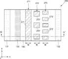
도 1은 예시적인 실시예에 따른 파워 소자를 개략적으로 도시한 평면도이고, 도 2는 도 1의 Ⅱ-Ⅱ'선을 따라 본 단면도이다.FIG. 1 is a plan view schematically illustrating a power device according to an exemplary embodiment, and FIG. 2 is a cross-sectional view taken along line II-II′ of FIG. 1 .
도 1 및 도 2를 참조하면, 파워 소자(100)는 채널층(110), 소스 및 드레인(131,132), 게이트(150), 패시베이션층(passivation layer, 160) 및 복수의 필드 플레이트(171,172,173)를 포함한다. 소스 및 드레인(131,132)은 채널층(110)의 양측에 마련되어 있으며, 소스 및 드레인(131,132) 사이의 채널층(110)에는 게이트(150)가 마련되어 있다. 패시베이션층(160)은 소스, 드레인 및 게이트(131,132,150)를 덮도록 마련되어 있으며, 이 패시베이션층(160) 내에 복수의 필드 플레이트(171,172,173)가 마련되어 있다.1 and 2 , the
채널층(110)은 기판(미도시)에 마련될 수 있다. 기판은 예를 들면, 사파이어(sapphire), Si, SiC 또는 GaN 등을 포함할 수 있지만 이에 한정되는 것은 아니며, 이외에도 다른 다양한 물질을 포함할 수 있다.The
채널층(110)은 제1 반도체 물질을 포함할 수 있다. 여기서, 제1 반도체 물질은 Ⅲ-Ⅴ족 계열의 화합물 반도체 물질이 될 수 있지만, 반드시 이에 한정되는 것은 아니다. 예를 들면, 채널층(110)은 GaN계 물질층, 구체적인 예로서 GaN층이 될 수 있다. 이 경우, 채널층(110)은 미도핑된(undoped) GaN층이 될 수 있으며, 경우에 따라서는 소정의 불순물이 도핑된(doped) GaN층이 될 수도 있다.The
채널층(110)과 기판 사이에는 버퍼층(미도시)이 더 마련될 수도 있다. 버퍼층은 기판과 채널층(110) 사이의 격자상수 및 열팽창계수의 차이를 완화시키기 위한 것이다. 버퍼층은 Al, Ga, In 및 B 중 적어도 하나를 포함하는 질화물을 포함하며, 단층 또는 다층 구조를 가질 수 있다. 예를 들면, 버퍼층은 AlN, GaN, AlGaN, InGaN, AlInN 및 AlGaInN으로 이루어진 물질들 중 적어도 하나를 포함할 수 있다. 기판(110)과 버퍼층 사이에는 버퍼층의 성장을 위한 시드층(seed layer)(미도시)이 더 마련될 수도 있다.A buffer layer (not shown) may be further provided between the
채널층(110)에는 베리어층(120)이 마련될 수 있다. 베리어층(120)은 채널층(110)에 2차원 전자가스(2DEG; 2-Dimensional Electron Gas)를 유발할 수 있다. 여기서, 2차원 전자가스(2DEG)는 채널층(110)과 베리어층(120)의 계면 아래의 채널층(110) 내에 형성될 수 있다. 베리어층(120)은 채널층(110)을 이루는 제1 반도체 물질과는 다른 제2 반도체 물질을 포함할 수 있다. 제2 반도체 물질은 제1 반도체 물질과 분극 특성, 에너지 밴드갭(bandgap) 및 격자상수 중 적어도 하나가 다를 수 있다.A
제2 반도체 물질은 제1 반도체 물질 보다 분극률과 에너지 밴드갭 중 적어도 하나가 제1 반도체 물질보다 클 수 있다. 베리어층(120)은 예를 들면, Al, Ga, In 및 B 중 적어도 하나를 포함하는 질화물을 포함할 수 있으며, 단층 또는 다층 구조를 가질 수 있다. 구체적인 예로서, 베리어층(120)은 AlGaN, AlInN, InGaN, AlN 및 AlInGaN 중 적어도 하나를 포함할 수 있다. 하지만, 이에 한정되는 것은 아니다. 베리어층(120)은 미도핑된(undoped) 층일 수 있지만, 소정의 불순물이 도핑된 층일 수도 있다.At least one of a polarizability and an energy bandgap of the second semiconductor material may be greater than that of the first semiconductor material. The
베리어층(120) 양측의 채널층(110)에는 소스 및 드레인(131,132)이 마련되어 있다. 소스 및 드레인(131,132)은 서로 나란하게 y축 방향을 따라 연장되도록 마련될 수 있다. 소스 및 드레인(131,132)은 예를 들면, Ti, Al 등과 같은 도전성 물질을 포함할 수 있다. 소스 및 드레인(131,132)은 2차원 전자가스(2DEG)와 전기적으로 연결될 수 있다. 한편, 소스 및 드레인(131,132)은 베리어층(120)에 마련될 수도 있다.Sources and drains 131 and 132 are provided in the
소스와 드레인(131,132) 사이의 베리어층(120)에는 디플리션 형성층(depletion forming layer,140)이 마련되어 있다. 디플리션 형성층(140)은 p형 반도체 물질을 포함할 수 있다. 즉, 디플리션 형성층(140)은 p형 불순물로 도핑된 반도체층이 될 수 있다. 디플리션 형성층(140)은 Ⅲ-Ⅴ족 계열의 질화물 반도체를 포함할 수 있다. 디플리션 형성층(140)은 예를 들면, GaN, AlGaN, InN, AlInN, InGaN 및 AlInGaN 중 적어도 하나에 p형 불순물이 도핑된 물질을 포함할 수 있다. 구체적인 예로서, 디플리션 형성층(140)은 p-GaN층일 수 있다.A
디플리션 형성층(140))은 그 아래에 위치하는 베리어층(120) 부분의 에너지 밴드갭(energy bandgap)을 높일 수 있으므로, 디플리션 형성층(140)에 대응하는 채널층(110) 부분에 2차원 전자가스(2DEG)의 디플리션 영역이 형성될 수 있다. 이에 따라, 2차원 전자가스(2DEG) 중 디플리션 형성층(140)에 대응하는 부분은 끊어지거나 또는 나머지 부분과는 다른 특성(예를 들면, 전자 농도 등)을 가질 수 있다. 2차원 전자가스(2DEG)가 끊어진 영역을 '단절 영역'이라 할 수 있으며, 이러한 단절 영역에 의해 파워 소자는 게이트 전압이 0V일 때 드레인(132) 과 소스(131) 사이의 전류가 오프 상태인 노멀리-오프(normally-off) 특성을 가질 수 있다.Since the depletion-forming layer 140) can increase the energy bandgap of the portion of the
디플리션 형성층(140)에는 게이트(150)가 마련되어 있다. 게이트(150)는 소스 및 드레인(131,132)과 나란하게 y축 방향을 따라 연장되도록 마련될 수 있다. 게이트(150)는 금속 물질 또는 금속 화합물 등과 같은 도전성 물질을 포함할 수 있다. 예를 들어, 게이트(150)는 Ti, Al, TiN, TiAl, 또는 W 등을 포함할 수 있지만, 이에 한정되지는 않는다.A
패시베이션층(160)은 소스, 드레인 및 게이트(131,132,150)를 덮도록 베리어층(120)에 마련되어 있다. 여기서, 패시베이션층(160)은 일체형으로 형성된 하나의 유전체층이 될 수 있다. 패시베이션층(160)은 예를 들면, 실리콘 산화물, 실리콘 질화물, 유기 폴리머 등을 포함할 수 있지만, 이에 한정되지는 않는다.The
복수의 필드 플레이트(171,172,173)는 패시베이션층(160) 내에 마련되어 있다. 복수의 필드 플레이트(171,172,173)는 금속과 같은 도전성 물질을 포함할 수 있다. 도 1 및 도 2에서 x축 방향, y축 방향 및 z축 방향은 각각 필드 플레이트(171,172,173)의 폭 방향, 길이 방향 및 두께 방향을 나타내며, 이하에서도 동일하다.The plurality of
복수의 필드 플레이트(171,172,173)는 게이트(150)와 드레인(132) 사이의 패시베이션층(160) 내에 위치하며, 서로 다른 폭을 가지도록 마련될 수 있다. 구체적으로, 복수의 필드 플레이트(171,172,173)는 게이트(150)에서 드레인(132) 쪽으로 갈수록 폭이 점점 작아지도록 마련될 수 있다. 예를 들면, 복수의 필드 플레이트(171,172,173)는 각각 수 ㎛ 이하의 폭을 가질 수 있다. 구체적인 예로서, 복수의 필드 플레이트(171,172,173)는 각각 3㎛ 이하의 폭을 가질 수 있지만 이에 한정되는 것은 아니다.The plurality of
복수의 필드 플레이트(171,172,173)는 패시베이션층(160) 내에 서로 다른 두께를 가지도록 마련될 수 있다. 구체적으로, 복수의 필드 플레이트(171,172,173)는 게이트(150)에서 드레인(132) 쪽으로 갈수록 패시베이션층(160)의 상면으로부터 깊이 방향으로 두께가 작아지도록 마련될 수있다. 이에 따라, 복수의 필드 플레이트(171,172,173)는 게이트(150)에서 드레인(132) 쪽으로 가면서 채널층(110)으로부터의 거리가 멀어지도록 마련될 수 있다.The plurality of
복수의 필드 플레이트(171,172,173)는 소스(131)와 전기적으로 연결되도록 마련되거나 또는 게이트(150)와 전기적으로 연결되도록 마련될 수 있다. 또한, 복수의 필드 플레이트(171,172,173)는 서로 전기적으로 연결되도록 마련되어 복수의 필드 플레이트(171,172,173)에 동일한 전압이 인가될 수 있으며, 또는 복수의 필드 플레이트(171,172,173) 각각에 독립적으로 전압이 인가될 수도 있다.The plurality of
이와 같이, 패시베이션층(160) 내에 게이트(150)에서 드레인(132) 쪽으로 갈수록 채널층(110)으로부터의 거리가 멀어지는 복수의 필드 플레이트(171,172,173)가 마련됨으로써 게이트(150)와 드레인(132) 사이에 형성되는 전기장을 보다 효과적으로 조절할 수 있으며, 이에 따라 항복 전압(breakdown voltage)을 향상시킬 수 있다. 또한, 복수의 필드 플레이트(171,172,173)는 가리움 효과(shielding effect)로 인해 게이트(150)와 드레인(132) 사이의 커패시턴스를 감소시킬 수 있고, 고전력 및 고주파 특성을 향상시킬 수 있다.As described above, a plurality of
도 1 및 도 2에는 복수의 필드 플레이트(171,172,173)가 제1, 제2 및 제3 필드 플레이트(171,172,173)를 포함하는 경우가 예시적으로 도시되어 있다. 제1, 제2 및 제3 필드 플레이트(171,172,173)는 서로 나란하게 길이 방향, 즉 y축 방향을 따라 연장되도록 마련될 수 있다.1 and 2 , a case in which the plurality of
제1 필드 플레이트(171)의 폭 및 두께는 각각 W1 및 D1가 될 수 있으며, 제2 필드 플레이트(172)의 폭 및 두께는 각각 W2(<W1) 및 D2(<D1)가 될 수 있고, 제3 필드 플레이트(173)의 폭 및 두께는 W3(<W2) 폭 및 D3(<D2)가 될 수 있다. 여기서, D1, D2 및 D3는 패시베이션층(160)의 상면으로부터 깊이 방향으로 제1, 제2 및 제3 필드 플레이트(171,172,173)의 두께를 나타낸다. 이에 따라, 제1, 제2 및 제3 필드 플레이트(171,172,173)는 게이트(150)에서 드레인(132) 쪽으로 갈수록 채널층(110)으로부터의 거리가 점점 증가하도록 마련될 수 있다.The width and thickness of the
이와 같이, 제1, 제2 및 제3 필드 플레이트(171,172,173)는 게이트(150)에서 드레인(132) 쪽으로 갈수록 점점 좁은 폭을 가지도록 마련될 수 있다. 또한, 제1, 제2 및 제3 필드 플레이트(171,172,173)는 게이트(150)에서 드레인(132) 쪽으로 갈수록 패시베이션층(160)의 상면으로부터 깊이 방향으로 두께가 점점 작아지도록 마련될 수 있다. 제1, 제2 및 제3 필드 플레이트(171,172,173)는 후술하는 바와 같이 식각 공정에서 발생되는 마이크로로딩 효과(microloading effect)를 이용함으로써 서로 다른 두께를 가지도록 형성될 수 있다.As such, the first, second, and
이상에서는 복수의 필드 플레이트(171,172,173)가 3개로 구성된 경우를 예로 들어 설명되었으나, 이는 단지 예시적인 것으로, 복수의 필드 플레이트(171,172,173)는 2개로 구성되거나 또는 4개 이상으로 구성될 수도 있다.In the above description, a case in which the plurality of
도 3은 다른 예시적인 실시예에 따른 파워 소자를 개략적으로 도시한 평면도이고, 도 4는 도 3의 Ⅳ-Ⅳ'선을 따라 본 단면도이다. 도 3 및 도 4에 도시된 파워 소자(200)는 제1, 제2 및 제3 필드 플레이트(271,272,273)의 폭 및 패턴 형태를 제외하면 도 1 및 도 2에 도시된 파워 소자(100)와 유사하다.3 is a plan view schematically illustrating a power device according to another exemplary embodiment, and FIG. 4 is a cross-sectional view taken along line IV-IV' of FIG. 3 . The
도 3 및 도 4를 참조하면, 제1, 제2 및 제3 필드 플레이트(271,272,273)는 동일한 폭(W)을 가지도록 마련될 수 있다. 제1, 제2 및 제3 필드 플레이트(271,272,273)는 각각 수 ㎛ 이하의 폭을 가질 수 있다. 구체적인 예로서, 제1, 제2 및 제3 필드 플레이트(271,272,273)는 각각 3㎛ 이하의 폭을 가질 수 있지만 이에 한정되는 것은 아니다.3 and 4 , the first, second, and third field plates 271,272 and 273 may be provided to have the same width W. As shown in FIG. Each of the first, second, and third field plates 271,272 and 273 may have a width of several μm or less. As a specific example, each of the first, second, and third field plates 271,272 and 273 may have a width of 3 μm or less, but is not limited thereto.
제1, 제2 및 제3 필드 플레이트(271,272,273)는 서로 다른 패턴 형태를 가지도록 마련될 수 있다. 구체적으로, 제1, 제2 및 제3 필드 플레이트(271,272,273)는 각각 적어도 하나의 서브 플레이트(sub plate)를 포함할 수 있다. 예를 들면, 제1 필드 플레이트(271)는 일체로 형성된 하나의 제1 서브 플레이트(271')를 포함하고, 제2 필드 플레이트(272)는 서로 이격되게 마련된 복수의 제2 서브 플레이트(272')를 포함하며, 제3 필드 플레이트(273)는 서로 이격되게 마련된 복수의 제3 서브 플레이트(273')를 포함한다. 여기서, 제2 서브 플레이트(272')는 제1 서브 플레이트(271') 보다 작은 크기를 가지며, 제3 서브 플레이트(273')는 제2 서브 플레이트(272')보다 작은 크기를 가질 수 있다. 복수의 제2 서브 플레이트(272')는 서로 전기적으로 연결될 수 있으며, 복수의 제3 서브 플레이트(273')는 서로 전기적으로 연결되도록 마련될 수 있다. 또한, 제1, 제2 및 제3 필드 플레이트(271,272,273)가 서로 전기적으로 연결되도록 마련될 수도 있다.The first, second, and third field plates 271,272 and 273 may be provided to have different pattern shapes. Specifically, each of the first, second, and third field plates 271,272 and 273 may include at least one sub-plate. For example, the
도 3 및 도 4에는 제1 필드 플레이트(271)가 일체로 형성된 하나의 제1 서브 플레이트(271')를 포함하는 경우가 예시적으로 도시되어 있으나, 이에 한정되지 않고 제1 필드 플레이트(271)는 복수의 제1 서브 플레이트(미도시)를 포함할 수도 있다. 또한, 제1, 제2 및 제3 서브 플레이트(271',272',273') 각각의 형태는 다양하게 변형될 수 있다. 3 and 4 , a case in which the
제1, 제2 및 제3 필드 플레이트(271,272,273)는 패시베이션층(160) 내에 서로 다른 두께(D1,D2,D3)를 가지도록 마련될 수 있다. 구체적으로, 제1, 제2 및 제3 필드 플레이트(271,272,273)는 게이트(150)에서 드레인(132) 쪽으로 갈수록 패시베이션층(160)의 상면으로부터 깊이 방향으로 두께가 작아지도록 마련될 수있다. 이에 따라, 제1, 제2 및 제3 필드 플레이트(271,272,273)는 게이트(150)에서 드레인(132) 쪽으로 가면서 채널층(110)으로부터의 거리가 멀어지도록 마련될 수 있다.The first, second, and third field plates 271,272 and 273 may be provided to have different thicknesses D1 , D2 , and D3 in the
도 5는 또 다른 예시적인 실시예에 따른 파워 소자를 개략적으로 도시한 평면도이고, 도 6은 도 5의 Ⅵ-Ⅵ'선을 따라 본 단면도이다. 도 5 및 도 6에 도시된 파워 소자는 제1, 제2 및 제3 필드 플레이트(371,372,373)의 패턴 형태를 제외하면 도 1 및 도 2에 도시된 파워 소자와 유사하다.5 is a plan view schematically illustrating a power device according to another exemplary embodiment, and FIG. 6 is a cross-sectional view taken along line VI-VI' of FIG. 5 . The power device shown in FIGS. 5 and 6 is similar to the power device shown in FIGS. 1 and 2 except for the pattern shape of the first, second, and
도 5 및 도 6을 참조하면, 제1, 제2 및 제3 필드 플레이트(371,372,373)는 게이트(150)에서 드레인(132) 쪽으로 갈수록 점점 작은 폭(W1,W2,W3)을 가지도록 마련될 수 있다. 제1, 제2 및 제3 필드 플레이트(371,372,373)는 각각 수 ㎛ 이하의 폭을 가질 수 있다.5 and 6 , the first, second, and
제1, 제2 및 제3 필드 플레이트(371,372,373)는 서로 다른 패턴 형태를 가지도록 마련될 수 있다. 구체적으로, 제1, 제2 및 제3 필드 플레이트(271,272,273)는 각각 적어도 하나의 서브 플레이트(371,372,373)를 포함할 수 있다. 예를 들면, 제1 필드 플레이트(371)는 일체로 형성된 하나의 제1 서브 플레이트(371')를 포함하고, 제2 필드 플레이트(372)는 서로 이격되게 마련된 복수의 제2 서브 플레이트(372')를 포함하며, 제3 필드 플레이트(373)는 서로 이격되게 마련된 복수의 제3 서브 플레이트(373')를 포함한다. 여기서, 제2 서브 플레이트(372')는 제1 서브 플레이트(371') 보다 작은 크기를 가지며, 제3 서브 플레이트(373')는 제2 서브 플레이트(372')보다 작은 크기를 가질 수 있다. 복수의 제2 서브 플레이트(372')는 서로 전기적으로 연결될 수 있으며, 복수의 제3 서브 플레이트(373')는 서로 전기적으로 연결되도록 마련될 수 있다. 또한, 제1, 제2 및 제3 필드 플레이트(371,372,373)가 서로 전기적으로 연결되도록 마련될 수도 있다.The first, second, and
도 5 및 도 6에는 제1 필드 플레이트(371)가 일체로 형성된 하나의 제1 서브 플레이트(371')를 포함하는 경우가 예시적으로 도시되어 있으나, 이에 한정되지 않고 제1 필드 플레이트(371)는 복수의 제1 서브 플레이트(미도시)를 포함할 수도 있다. 또한, 제1, 제2 및 제3 서브 플레이트(371',372',373') 각각의 형태는 다양하게 변형될 수 있다. 5 and 6 illustrate a case in which the
제1, 제2 및 제3 필드 플레이트(371,372,373)는 패시베이션층(160) 내에 서로 다른 두께(D1,D2,D3)를 가지도록 마련될 수 있다. 구체적으로, 제1, 제2 및 제3 필드 플레이트(371,372,373)는 게이트(150)에서 드레인(132) 쪽으로 갈수록 패시베이션층(160)의 상면으로부터 깊이 방향으로 두께가 작아지도록 마련될 수있다. 이에 따라, 제1, 제2 및 제3 필드 플레이트(371,372,373)는 게이트(150)에서 드레인(132) 쪽으로 가면서 채널층(110)으로부터의 거리가 멀어지도록 마련될 수 있다.The first, second, and
도 7 내지 도 10은 예시적인 실시예에 따른 파워 소자의 제조방법을 설명하기 위한 도면들이다. 여기서는 복수의 필드 플레이트가 3개의 제1, 제2 및 제3 필드 플레이트로 구성된 경우를 예로 들어 설명한다.7 to 10 are diagrams for explaining a method of manufacturing a power device according to an exemplary embodiment. Herein, a case in which the plurality of field plates are composed of three first, second, and third field plates will be described as an example.
도 7을 참조하면, 채널층(110)에 베리어층(120)을 형성하고, 채널층(110)의 양측에는 소스(131) 및 드레인(132)을 형성한다. 채널층(110)은 기판(미도시)에 형성될 수 있다. 기판은 예를 들면, 사파이어(sapphire), Si, SiC 또는 GaN 등을 포함할 수 있지만 이에 한정되는 것은 아니며, 이외에도 다른 다양한 물질을 포함할 수 있다.Referring to FIG. 7 , a
채널층(110)은 제1 반도체 물질을 포함할 수 있다. 여기서, 제1 반도체 물질은 Ⅲ-Ⅴ족 계열 화합물 반도체 물질이 될 수 있지만, 반드시 이에 한정되는 것은 아니다. 예를 들면, 채널층(110)은 GaN계 물질층, 구체적인 예로서 GaN층이 될 수 있다. 이 경우, 채널층(110)은 미도핑된(undoped) GaN층이 될 수 있으며, 경우에 따라서는 소정의 불순물이 도핑된(doped) GaN층이 될 수도 있다.The
채널층(110)과 기판 사이에 버퍼층(미도시)을 더 형성할 수도 있다. 버퍼층은 Al, Ga, In 및 B 중 적어도 하나를 포함하는 질화물을 포함하며, 단층 또는 다층 구조를 가질 수 있다. 예를 들면, 버퍼층은 AlN, GaN, AlGaN, InGaN, AlInN 및 AlGaInN으로 이루어진 물질들 중 적어도 하나를 포함할 수 있다. 기판(110)과 버퍼층 사이에 버퍼층의 성장을 위한 시드층(seed layer)(미도시)을 더 형성할 수도 있다.A buffer layer (not shown) may be further formed between the
채널층(110)에 형성되는 베리어층(120)은 채널층(110)을 이루는 제1 반도체 물질과는 다른 제2 반도체 물질을 포함할 수 있다. 제2 반도체 물질은 제1 반도체 물질과 분극 특성, 에너지 밴드갭(bandgap) 및 격자상수 중 적어도 하나가 다를 수 있다. 베리어층(120)은 예를 들면, Al, Ga, In 및 B 중 적어도 하나를 포함하는 질화물을 포함할 수 있으며, 단층 또는 다층 구조를 가질 수 있다. 구체적인 예로서, 베리어층(120)은 AlGaN, AlInN, InGaN, AlN 및 AlInGaN 중 적어도 하나를 포함할 수 있다. 하지만, 이에 한정되는 것은 아니다. 베리어층(120)은 미도핑된(undoped) 층일 수 있지만, 소정의 불순물이 도핑된 층일 수도 있다. 채널층(110)의 양측에 형성되는 소스 및 드레인(131,132)은 예를 들면, Ti, Al 등과 같은 도전성 물질을 포함할 수 있다.The
이어서, 소스(131)와 드레인(132) 사이의 베리어층(120)에 디플리션 형성층(140)을 형성한다. 디플리션 형성층(140)은 p형 반도체 물질을 포함할 수 있다. 디플리션 형성층(140)은 Ⅲ-Ⅴ족 계열의 질화물 반도체를 포함할 수 있다. 디플리션 형성층(140)은 예를 들면, GaN, AlGaN, InN, AlInN, InGaN 및 AlInGaN 중 적어도 하나에 p형 불순물이 도핑된 물질을 포함할 수 있다. 구체적인 예로서, 디플리션 형성층(140)은 p-GaN층일 수 있다.디플리션 형성층(140)에 게이트(150)를 형성한다. 게이트(150)는 금속 물질 또는 금속 화합물 등과 같은 도전성 물질을 포함할 수 있다. 예를 들어, 게이트(150)는 Ti, Al, TiN, TiAl, 또는 W 등을 포함할 수 있지만, 이에 한정되지는 않는다.Next, a
다음으로, 베리어층(120)에 소스, 드레인 및 게이트(131,132,150)를 덮도록 패시베이션층(160)을 형성한다. 여기서, 패시베이션층(160)은 일체로 형성된 하나의 유전체층이 될 수 있다. 패시베이션층(160)은 예를 들면, 실리콘 산화물, 실리콘 질화물, 유기 폴리머 등을 포함할 수 있지만, 이에 한정되지는 않는다.Next, a
이어서, 패시베이션층(160)의 상면에 포토리소그래피(photolithography) 공정을 이용하여 제1, 제2 및 제3 식각 패턴(481,482,483)을 포함하는 포토레지스트층(photoresist layer)을 형성한다.Next, a photoresist layer including the first, second, and
제1, 제2 및 제3 식각 패턴(481,482,483)은 각각 도 1에 도시된 제1, 제2 및 제3 필드 플레이트(171,172,173)에 대응되는 형상을 가질 수 있다. 따라서, 제1, 제2 및 제3 식각 패턴(481,482,483)은 게이트(150)에서 드레인(132) 쪽으로 갈수록 점점 작아지는 폭을 가질 수 있다. 구체적으로, 제1 식각 패턴(481)은 W1 폭을 가질 수 있으며, 제2 식각 패턴(482)은 W2(<W1) 폭을 가질 수 있고, 제3 식각 패턴(483)은 W3(<W2) 폭을 가질 수 있다. 예를 들어, 제1, 제2 및 제3 식각 패턴(481,482,483)은 각각 수 ㎛ 이하의 폭을 가질 수 있다. 구체적인 예로서, 제1, 제2 및 제3 식각 패턴(481,482,483)은 각각 3㎛ 이하의 폭을 가질 수 있지만 이에 한정되는 것은 아니다.The first, second, and
도 8을 참조하면, 제1, 제2 및 제3 식각 패턴(481,482,483)을 통해 노출된 패시베이션층(160)을 소정 깊이로 식각함으로써 제1, 제2 및 제3 트렌치(461.462.463)를 형성한다. 여기서, 제1, 제2 및 제3 트렌치(461.462.463)는 건식 식각(dry etching) 공정을 이용하여 패시베이션층을 이방성(anisotropic) 식각함으로써 형성될 수 있다. 제1, 제2 및 제3 트렌치(461.462.463)는 게이트(150)에서 드레인(132) 쪽으로 갈수록 폭 및 깊이가 점점 작아지도록 형성될 수 있다. 구체적으로, 제1 트렌치(461)는 제1 식각 패턴(481)을 통해 W1 폭 및 D1 깊이를 가지도록 형성될 수 있으며, 제2 트렌치(462)는 제2 식각 패턴(482)을 통해 W2 폭 및 D2(<D1) 깊이를 가지도록 형성될 수 있고, 제3 트렌치(463)는 제3 식각 패턴(483)을 통해 W3 폭 및 D3(<D2) 깊이를 가지도록 형성될 수 있다. 이와 같은 서로 다른 깊이를 가지는 트렌치들(461.462.463)은 식각 공정에서 발생되는 마이크로로딩 효과(microloading effect)를 이용함으로써 형성될 수 있다. 이어서, 패시베이션층(160)의 상면에 남아 있는 포토레지스트층(480)을 제거한다.Referring to FIG. 8 , first, second, and third trenches 461.462.463 are formed by etching the
도 9를 참조하면, 제1, 제2 및 제3 트렌치(461.462.463)를 채우도록 패시베이션층(160)의 상면에 도전성 금속층(470)을 형성한다. 다음으로, 도 10을 참조하면, 도전성 금속층(470)에 평탄화 공정, 예를 들면 CMP(Chemical Mechanical Planarization) 공정을 수행함으로써 제1, 제2 및 제3 트렌치(461.462.463) 내에 제1, 제2 및 제3 필드 플레이트(471.472.473)를 형성한다.Referring to FIG. 9 , a
제1, 제2 및 제3 필드 플레이트(471.472.473)는 게이트(150)에서 드레인(132) 쪽으로 갈수록 폭 및 깊이가 점점 작아지도록 형성될 수 있다. 구체적으로, 제1 필드 플레이트(471)는 W1 폭 및 D1 깊이를 가지도록 형성될 수 있으며, 제2 필드 플레이트(472)는 W2 폭 및 D2 깊이를 가지도록 형성될 수 있고, 제3 필드 플레이트(473)는 W3 폭 및 D3 깊이를 가지도록 형성될 수 있다. 여기서, 필드 플레이트들(471.472.473)의 폭(W1,W2,W3)은 필드 플레이트들(471.472.473)의 패턴 사이즈 또는 임계 치수(CD; Critical Dimension)을 의미할 수 있다.The first, second, and third field plates 471.472.473 may be formed to gradually decrease in width and depth from the
이상에서는 제1, 제2 및 제3 식각 패턴(481,482,483)이 도 1에 도시된 제1, 제2 및 제3 필드 플레이트(171,172,173)에 대응되는 형태를 가지는 경우가 예시적으로 설명되었다. 그러나, 이에 한정되지 않고 제1, 제2 및 제3 식각 패턴(481,482,483)은 도 3에 도시된 제1, 제2 및 제3 필드 플레이트(271,272,273)에 대응되는 형태를 가지거나 또는 도 5에 도시된 제1, 제2 및 제3 필드 플레이트(371,372,373)에 대응되는 형태를 가질 수도 있다. 제1, 제2 및 제3 식각 패턴(481,482,483)이 도 3에 도시된 제1, 제2 및 제3 필드 플레이트(271,272,273)에 대응되는 형태를 가지는 경우에는 도 3 및 도 4에 도시된 제1, 제2 및 제3 필드 플레이트(271,272,273)가 형성될 수 있다. 또한, 제1, 제2 및 제3 식각 패턴(481,482,483)이 도 5에 도시된 제1, 제2 및 제3 필드 플레이트(371,372,373)에 대응되는 형태를 가지는 경우에는 도 5 및 도 6에 도시된 제1, 제2 및 제3 필드 플레이트(371,372,373)가 형성될 수 있다.In the above, the case in which the first, second, and
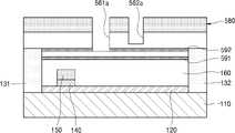
도 11 내지 도 16은 다른 예시적인 실시예에 따른 파워 소자의 제조방법을 설명하기 위한 도면들이다. 여기서는 복수의 필드 플레이트가 2개의 제1 및 제2 필드 플레이트를 포함하는 경우를 예로 들어 설명한다. 이하에서는 전술한 실시예와 다른 점을 중심으로 설명한다.11 to 16 are diagrams for explaining a method of manufacturing a power device according to another exemplary embodiment. Here, a case in which the plurality of field plates includes two first and second field plates will be described as an example. Hereinafter, different points from the above-described embodiment will be mainly described.
도 11을 참조하면, 베리어층(120)에 소스, 드레인 및 게이트(131,132,150)를 덮도록 패시베이션층(160)을 형성한다. 여기서, 패시베이션층(160) 내에 제1 및 제2 식각 정지층(591,592)을 서로 이격되게 형성한다. 제1 식각 정지층(591)의 상면은 패시베이션층(160)의 상면으로부터 D1 깊이에 형성될 수 있으며, 제2 식각 정지층(592)의 상면은 패시베이션층(160)의 상면으로부터 D2(<D1) 깊이에 형성될 수 있다.Referring to FIG. 11 , a
제1 및 제2 식각 정지층(591,592)은 패시베이션층(160)에 대해 식각 선택성(etch selectivity)을 가지는 물질을 포함할 수 있다. 예를 들면, 패시베이션층(160)이 실리콘 산화물을 포함하는 경우에 제1 및 제2 식각 정지층(591,592)은 실리콘 질화물을 포함할 수 있다. 하지만, 이는 단지 예시적인 것이다.The first and second etch stop layers 591 and 592 may include a material having etch selectivity with respect to the
이어서, 패시베이션층(160)의 상면에 제1 및 제2 식각 패턴(581,582)을 포함하는 포토레지스트층(580)을 형성한다. 제1 식각 패턴(581)은 W1 폭을 가질 수 있으며, 제2 식각 패턴(582)은 W2(<W1) 폭을 가질 수 있다.Next, a
도 12를 참조하면, 제1 및 제2 식각 패턴(581,582)을 통해 노출된 패시베이션층(160)을 건식 식각하여 제1 및 제2 예비 트렌치(pre-trench, 561a,562a)를 형성한다. 이러한 식각 공정은 제1 예비 트렌치(561a)가 제2 식각 정지층(592)을 노출시킬 때까지 수행될 수 있다. 여기서, 제2 예비 트렌치(562a)는 제1 예비 트렌치(561a) 보다 작은 깊이로 형성될 수 있다.Referring to FIG. 12 , the
도 13을 참조하면, 제1 예비 트렌치(561a)를 통해 노출된 제2 식각 정지층(592)만을 선택적으로 식각한다. 예를 들어, 패시베이션층(160)이 실리콘 산화물을 포함하고 제2 식각 정지층(592)이 실리콘 질화물을 포함하는 경우에는 인산(H3PO4)을 식각액(etchant)으로 이용함으로써 제1 예비 트렌치(561a)를 통해 제2 식각 정지층(592)만을 선택적으로 식각할 수 있다. 이에 따라, 제1 예비 트렌치(561a)는 제2 식각 정지층(592)의 두께 만큼의 깊이가 증가하게 되며, 이 제1 예비 트렌치(561a)를 통해 제2 식각 정지층(592) 아래의 패시베이션층(160)이 노출된다. 이 과정에서 제2 예비 트렌치(562a)는 깊이가 변화하지 않는다.Referring to FIG. 13 , only the second
이상에서는 제2 식각 정지층(592)이 습식 식각 방법에 의해 선택적으로 식각되는 경우가 설명되었으나 이에 한정되지 않고 건식 식각 방법을 이용하여 제2 식각 정지층(592)을 선택적으로 식각할 수도 있다.Although the case in which the second
도 14를 참조하면, 제1 및 제2 예비 트렌치(561a,562a)를 통해 노출된 패시베이션층(160)을 건식 식각하여 제1 및 제2 트렌치(561,562)를 형성한다. 이러한 식각 공정은 제1 트렌치(561)가 제1 식각 정지층(591)을 노출시키고, 제2 트렌치(562)가 제2 식각 정지층(592)을 노출시킬 때까지 수행될 수 있다. 이에 따라, 제1 트렌치(561)는 D1 깊이로 형성될 수 있으며, 제2 트렌치(562)는 D2 깊이로 형성될 수 있다. 그리고, 제1 및 제2 트렌치(561,562)는 각각 W1 폭 및 W2 폭으로 형성될 수 있다. 이어서, 패시베이션층(160)의 상면에 남아 있는 포토레지스트층(580)을 제거한다.Referring to FIG. 14 , the
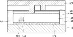
도 15를 참조하면, 제1 및 제2 트렌치(561.562)를 채우도록 패시베이션층(160)의 상면에 도전성 금속층(570)을 형성한다. 다음으로, 도 16을 참조하면, 도전성 금속층(570)에 평탄화 공정(예를 들면, CMP 공정)을 수행함으로써 제1 및 제2 트렌치(561.562) 내에 제1 및 제2 필드 플레이트(571.572)를 형성한다.Referring to FIG. 15 , a
제1 및 제2 필드 플레이트(571.572)는 게이트(150)에서 드레인(132) 쪽으로 갈수록 두께가 점점 작아지도록 형성될 수 있다. 본 실시예에서는 패시베이션층(160) 내에 제1 및 제2 식각 정지층(591,592)을 마련함으로써 제1 및 제2 필드 플레이트(571,5712)를 보다 정확한 깊이로 형성할 수 있다. 전술한 제1 및 제2 식각 패턴(581,582)은 도 3에 도시된 필드 플레이트들에 대응하는 형상을 가지거나 또는 도 5에 도시된 필드 플레이트들에 대응하는 형상을 가지는 것도 가능하다.The first and second field plates 571.572 may be formed to gradually decrease in thickness from the
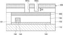
도 17 내지 도 21은 또 다른 예시적인 실시예에 따른 파워 소자의 제조방법을 설명하기 위한 도면들이다. 여기서는 복수의 필드 플레이트가 2개의 제1 및 제2 필드 플레이트를 포함하는 경우를 예로 들어 설명한다. 이하에서는 전술한 실시예와 다른 점을 중심으로 설명한다.17 to 21 are diagrams for explaining a method of manufacturing a power device according to another exemplary embodiment. Here, a case in which the plurality of field plates includes two first and second field plates will be described as an example. Hereinafter, different points from the above-described embodiment will be mainly described.
도 17을 참조하면, 베리어층(120)에 소스, 드레인 및 게이트(131,132,150)를 덮도록 패시베이션층(160)을 형성한다. 여기서, 패시베이션층(160) 내에 식각 정지층(690)을 형성한다. 여기서, 식각 정지층(690)의 하면은 패시베이션층(160)의 상면으로부터 D1 깊이에 형성될 수 있다. 식각 정지층(690)은 패시베이션층(160)에 대해 식각 선택성을 가지는 물질을 포함할 수 있다.Referring to FIG. 17 , a
이어서, 패시베이션층(160)의 상면에 제1 및 제2 식각 패턴(681,682)을 포함하는 포토레지스트층(680)을 형성한다. 제1 식각 패턴(681)은 W1 폭을 가질 수 있으며, 제2 식각 패턴(682)은 W2(<W1) 폭을 가질 수 있다.Next, a
도 18을 참조하면, 제1 및 제2 식각 패턴(681,682)을 통해 노출된 패시베이션층(160)을 건식 식각하여 제1 및 제2 예비 트렌치(661a,662a)를 형성한다. 이러한 식각 공정은 제1 예비 트렌치(661a)가 식각 정지층(690)을 노출시킬 때까지 수행될 수 있다. 여기서, 제2 예비 트렌치(662a)는 제1 예비 트렌치(661a) 보다 작은 D2 깊이로 형성될 수 있다.Referring to FIG. 18 , the
도 19를 참조하면, 제1 예비 트렌치(661a)를 통해 노출된 식각 정지층(690)만을 선택적으로 식각한다. 이러한 식각 정지층(690)의 선택적 식각은 습식 식각 또는 건식 식각에 의해 수행될 수 있다. 이에 따라, 제1 트렌치(661)가 D1 깊이로 형성될 수 있으며, 제2 트렌치(662)는제2 예비 트렌치(662a)와 동일한 D2 깊이로 형성될 수 있다. 그리고, 제1 및 제2 트렌치(661,662)는 각각 W1 폭 및 W2 폭으로 형성될 수 있다. 이어서, 패시베이션층(160)의 상면에 남아 있는 포토레지스트층(680)을 제거한다.Referring to FIG. 19 , only the
도 20을 참조하면, 제1 및 제2 트렌치(661.662)를 채우도록 패시베이션층(160)의 상면에 도전성 금속층(670)을 형성한다. 다음으로, 도 21을 참조하면, 도전성 금속층(670)에 평탄화 공정을 수행함으로써 제1 및 제2 트렌치(661.662) 내에 제1 및 제2 필드 플레이트(671.672)를 형성한다. 여기서, 제1 및 제2 필드 플레이트(671.672)는 게이트(150)에서 드레인(132) 쪽으로 갈수록 두께가 점점 작아지도록 형성될 수 있다.Referring to FIG. 20 , a
이상의 예시적인 실시예에 의하면, 게이트에서 드레인 사이의 패시베이션층에 서로 다른 두께를 가지는 복수의 필드 플레이트를 마련함으로써 파워 소자의 항복 전압을 향상시킬 수 있다. 또한, 마이크로로딩 효과를 이용한 식각 공정을 이용하여 서로 다른 두께의 필드 플레이트를 패시베이션층 내의 원하는 위치에 동시에 형성함으로써 파워 소자의 제작 공정을 단순화할 수 있다. 이상에서 실시예가 설명되었으나, 이는 예시적인 것에 불과하며, 당해 분야에서 통상적 지식을 가진 자라면 이로부터 다양한 변형이 가능하다.According to the above exemplary embodiment, the breakdown voltage of the power device may be improved by providing a plurality of field plates having different thicknesses in the passivation layer between the gate and the drain. In addition, it is possible to simplify the manufacturing process of the power device by simultaneously forming field plates of different thicknesses at desired positions in the passivation layer using an etching process using the microloading effect. Although the embodiment has been described above, this is merely exemplary, and various modifications are possible therefrom by those skilled in the art.
100,200,300.. 파워 소자
110.. 채널층
120.. 베리어층
131.. 소스
132.. 드레인
140.. 디플리션 형성층
150.. 게이트
160.. 패시베이션층
171,271,371,471.. 제1 필드 플레이트
172,272,372,472.. 제2 필드 플레이트
173,273,373,473.. 제3 필트 플레이트
461,561,661.. 제1 트렌치
462,562,662.. 제2 트렌치
463.. 제3 트렌치
470,570,670.. 도전성 금속층
480,580,680.. 포토레지스트층
481,581,681.. 제1 식각 패턴
482,582,682.. 제2 식각 패턴
483.. 제3 식각 패턴
591.. 제1 식각 정지층
592.. 제2 식각 정지층
690.. 식각 정지층100,200,300.. Power element
110. Channel layer
120. barrier layer
131. Source
132. Drain
140. Depletion cambium
150.. Gate
160. Passivation layer
171,271,371,471.. first field plate
172,272,372,472.. second field plate
173,273,373,473.. 3rd filter plate
461,561,661.. First trench
462,562,662.. 2nd trench
463.. 3rd Trench
470,570,670. Conductive metal layer
480,580,680.. Photoresist layer
481,581,681.. first etch pattern
482,582,682.. second etch pattern
483. Third etch pattern
591. First etch stop layer
592. Second etch stop layer
690. Etch stop layer
Claims (20)
Translated fromKorean상기 채널층의 양측에 마련되는 소스 및 드레인;
상기 소스 및 상기 드레인 사이의 상기 채널층에 마련되는 게이트;
상기 소스, 드레인 및 게이트를 덮도록 마련되는 패시베이션층; 및
상기 패시베이션층에 서로 다른 두께를 가지도록 마련되는 복수의 필드 플레이트;를 포함하고,
상기 복수의 필드 플레이트는 폭 및 패턴 형태 중 적어도 하나가 다른 파워 소자.channel layer;
a source and a drain provided on both sides of the channel layer;
a gate provided in the channel layer between the source and the drain;
a passivation layer provided to cover the source, drain and gate; and
a plurality of field plates provided to have different thicknesses on the passivation layer;
The plurality of field plates are different from each other in at least one of a width and a pattern shape.
상기 복수의 필드 플레이트는 상기 게이트에서 상기 드레인 쪽 방향으로 가면서 상기 채널층으로부터의 거리가 점점 증가하도록 마련되는 파워 소자.The method of claim 1,
The plurality of field plates are provided such that a distance from the channel layer gradually increases from the gate to the drain.
상기 복수의 필드 플레이트는 상기 게이트에서 상기 드레인 쪽 방향으로 가면서 점점 좁은 폭을 가지도록 마련되는 파워 소자.3. The method of claim 2,
The plurality of field plates are provided to have increasingly narrow widths from the gate to the drain.
상기 복수의 필드 플레이트 각각은 적어도 하나의 서브 플레이트(sub plate)를 포함하며, 상기 서브 플레이트는 상기 게이트에서 상기 드레인 쪽 방향으로 가면서 점점 작은 크기를 가지도록 마련되는 파워 소자.3. The method of claim 2,
Each of the plurality of field plates includes at least one sub-plate, wherein the sub-plate is provided to gradually decrease in size from the gate to the drain.
상기 복수의 필드 플레이트는 각각 수 ㎛ 이하의 폭을 가지는 파워 소자.The method of claim 1,
The plurality of field plates each have a width of several μm or less.
상기 채널층에 마련되며, 상기 채널층에 2차원 전자가스(2DEG; 2-Dimensional Electron Gas)를 유발하는 베리어층; 및
상기 베리어층과 상기 게이트 사이에 마련되며, 상기 2차원 전자가스에 디플리션 영역(depletion region)을 형성하는 디플리션 형성층;을 더 포함하는 파워 소자.The method of claim 1,
a barrier layer that is provided on the channel layer and induces a two-dimensional electron gas (2DEG) in the channel layer; and
and a depletion forming layer provided between the barrier layer and the gate and forming a depletion region in the two-dimensional electron gas.
상기 채널층은 GaN계 물질을 포함하고, 상기 베리어층은 Al, Ga, In 및 B 중 적어도 하나를 포함하는 질화물을 포함하는 파워 소자.7. The method of claim 6,
The channel layer includes a GaN-based material, and the barrier layer includes a nitride including at least one of Al, Ga, In, and B.
상기 디플리션 형성층은 p형 Ⅲ-Ⅴ족 계열의 질화물 반도체를 포함하는 파워 소자.8. The method of claim 7,
The depletion forming layer is a power device including a p-type III-V series nitride semiconductor.
상기 소스, 드레인 및 게이트를 덮도록 패시베이션층을 형성하는 단계; 및
상기 패시베이션층에 복수의 필드 플레이트를 서로 다른 두께로 형성하는 단계;를 포함하고,
상기 복수의 필드 플레이트는 폭 및 패턴 형태 중 적어도 하나가 다르게 형성되는 파워 소자의 제조방법.forming a source and a drain on both sides of a channel layer, and forming a gate in the channel layer between the source and the drain;
forming a passivation layer to cover the source, drain and gate; and
Including; forming a plurality of field plates with different thicknesses on the passivation layer;
The method of manufacturing a power device wherein the plurality of field plates are formed to have at least one of a different width and a different pattern shape.
상기 복수의 필드 플레이트를 형성하는 단계는,
상기 패시베이션층에 폭 및 패턴 형태 중 적어도 하나가 다른 복수의 식각 패턴을 포함하는 포토레지스트층을 형성하는 단계;
상기 복수의 식각 패턴을 통해 상기 패시베이션층을 식각하여 서로 다른 깊이의 복수의 트렌치를 형성하는 단계;
상기 복수의 트렌치를 채우도록 상기 패시베이션층에 도전성 금속층을 형성하는 단계; 및
상기 도전성 금속층에 펑탄화 공정을 수행하여 서로 다른 두께의 상기 복수의 필드 플레이트를 형성하는 단계;를 포함하는 파워 소자의 제조방법.10. The method of claim 9,
The forming of the plurality of field plates comprises:
forming a photoresist layer including a plurality of etching patterns having different widths and different pattern shapes on the passivation layer;
forming a plurality of trenches having different depths by etching the passivation layer through the plurality of etching patterns;
forming a conductive metal layer on the passivation layer to fill the plurality of trenches; and
and forming the plurality of field plates having different thicknesses by performing a puncture process on the conductive metal layer.
상기 복수의 트렌치는 상기 패시베이션층을 건식 식각함으로써 형성되는 파워 소자의 제조방법.11. The method of claim 10,
The plurality of trenches are formed by dry etching the passivation layer.
상기 복수의 트렌치는 마이크로로딩 효과(microloading effect)에 의해 서로 다른 깊이로 형성되는 파워 소자의 제조방법.11. The method of claim 10,
The method of manufacturing a power device wherein the plurality of trenches are formed to have different depths by a microloading effect.
상기 복수의 트렌치는 각각 수 ㎛ 이하의 폭을 가지도록 형성되는 파워 소자의 제조방법.13. The method of claim 12,
The method of manufacturing a power device in which the plurality of trenches are each formed to have a width of several μm or less.
상기 복수의 트렌치는 상기 게이트에서 상기 드레인 쪽 방향으로 가면서 점점 낮은 깊이로 형성되는 파워 소자의 제조방법.13. The method of claim 12,
The method of manufacturing a power device wherein the plurality of trenches are formed to have a gradually lower depth from the gate toward the drain.
상기 복수의 필드 플레이트를 형성하는 단계는,
상기 패시베이션층 내부에 적어도 하나의 식각 정지층을 형성하는 단계;
상기 패시베이션층에 폭 및 패턴 형태 중 적어도 하나가 다른 복수의 식각 패턴을 포함하는 포토레지스트층을 형성하는 단계;
상기 복수의 식각 패턴을 통해 상기 패시베이션층을 식각하고 상기 식각 정지층은 선택적으로 식각함으로써 서로 다른 깊이의 복수의 트렌치를 형성하는 단계;
상기 복수의 트렌치를 채우도록 상기 패시베이션층에 도전성 금속층을 형성하는 단계; 및
상기 도전성 금속층에 펑탄화 공정을 수행하여 서로 다른 두께의 상기 복수의 필드 플레이트를 형성하는 단계;를 포함하는 파워 소자의 제조방법.10. The method of claim 9,
The forming of the plurality of field plates comprises:
forming at least one etch stop layer inside the passivation layer;
forming a photoresist layer including a plurality of etching patterns having different widths and different pattern shapes on the passivation layer;
forming a plurality of trenches having different depths by etching the passivation layer through the plurality of etch patterns and selectively etching the etch stop layer;
forming a conductive metal layer on the passivation layer to fill the plurality of trenches; and
and forming the plurality of field plates having different thicknesses by performing a puncture process on the conductive metal layer.
상기 패시베이션층의 식각은 건식 식각에 의해 수행되며, 상기 식각 정지층의 선택적 식각은 건식 또는 습식 식각에 의해 수행되는 파워 소자의 제조방법.16. The method of claim 15,
The etching of the passivation layer is performed by dry etching, and the selective etching of the etch stop layer is performed by dry or wet etching.
상기 복수의 트렌치는 상기 게이트에서 상기 드레인 쪽 방향으로 가면서 점점 낮은 깊이로 형성되는 파워 소자의 제조방법.16. The method of claim 15,
The method of manufacturing a power device wherein the plurality of trenches are formed to have a gradually lower depth from the gate toward the drain.
상기 채널층에 2차원 전자가스(2DEG)를 유발하는 베리어층을 형성하는 단계; 및
상기 베리어층과 상기 게이트 사이에 상기 2차원 전자가스의 디플리션 영역을 형성하는 디플리션 형성층을 형성하는 단계;를 더 포함하는 파워 소자의 제조방법.10. The method of claim 9,
forming a barrier layer inducing a two-dimensional electron gas (2DEG) on the channel layer; and
and forming a depletion forming layer forming a depletion region of the two-dimensional electron gas between the barrier layer and the gate.
상기 채널층은 GaN계 물질을 포함하고, 상기 베리어층은 Al, Ga, In 및 B 중 적어도 하나를 포함하는 질화물을 포함하는 파워 소자의 제조방법.19. The method of claim 18,
The channel layer includes a GaN-based material, and the barrier layer includes a nitride including at least one of Al, Ga, In and B.
상기 디플리션 형성층은 p형 Ⅲ-Ⅴ족 계열의 질화물 반도체를 포함하는 파워 소자의 제조방법.
20. The method of claim 19,
The method of manufacturing a power device wherein the depletion forming layer includes a p-type III-V series nitride semiconductor.
Priority Applications (5)
| Application Number | Priority Date | Filing Date | Title |
|---|---|---|---|
| KR1020210044869AKR20220138756A (en) | 2021-04-06 | 2021-04-06 | Power device and method of manufacturing the same |
| US17/398,407US12040391B2 (en) | 2021-04-06 | 2021-08-10 | Power device and method of manufacturing the same |
| EP21193464.1AEP4071828A1 (en) | 2021-04-06 | 2021-08-27 | Power device and method of manufacturing the same |
| CN202111419130.5ACN115207099A (en) | 2021-04-06 | 2021-11-26 | Power device and method of manufacturing the same |
| US18/635,617US20240258419A1 (en) | 2021-04-06 | 2024-04-15 | Power device and method of manufacturing the same |
Applications Claiming Priority (1)
| Application Number | Priority Date | Filing Date | Title |
|---|---|---|---|
| KR1020210044869AKR20220138756A (en) | 2021-04-06 | 2021-04-06 | Power device and method of manufacturing the same |
Publications (1)
| Publication Number | Publication Date |
|---|---|
| KR20220138756Atrue KR20220138756A (en) | 2022-10-13 |
Family
ID=77520555
Family Applications (1)
| Application Number | Title | Priority Date | Filing Date |
|---|---|---|---|
| KR1020210044869APendingKR20220138756A (en) | 2021-04-06 | 2021-04-06 | Power device and method of manufacturing the same |
Country Status (4)
| Country | Link |
|---|---|
| US (2) | US12040391B2 (en) |
| EP (1) | EP4071828A1 (en) |
| KR (1) | KR20220138756A (en) |
| CN (1) | CN115207099A (en) |
Families Citing this family (3)
| Publication number | Priority date | Publication date | Assignee | Title |
|---|---|---|---|---|
| KR20230059494A (en)* | 2021-10-26 | 2023-05-03 | 에스케이하이닉스 주식회사 | Semiconductor device and method for fabricating the same |
| CN115732563A (en)* | 2022-11-29 | 2023-03-03 | 西安电子科技大学 | Thermoelectric optimized fin type gallium oxide MOSFET structure and manufacturing method thereof |
| CN116913963A (en)* | 2023-09-06 | 2023-10-20 | 深圳智芯微电子科技有限公司 | GaN devices |
Family Cites Families (30)
| Publication number | Priority date | Publication date | Assignee | Title |
|---|---|---|---|---|
| JP4433664B2 (en)* | 2002-08-30 | 2010-03-17 | セイコーエプソン株式会社 | Ink composition and inkjet recording method |
| JP5332168B2 (en)* | 2006-11-17 | 2013-11-06 | 住友電気工業株式会社 | Method for producing group III nitride crystal |
| JP5371381B2 (en)* | 2008-11-05 | 2013-12-18 | ラピスセミコンダクタ株式会社 | Semiconductor device and manufacturing method of semiconductor device |
| US8227339B2 (en)* | 2009-11-02 | 2012-07-24 | International Business Machines Corporation | Creation of vias and trenches with different depths |
| EP2502275A1 (en)* | 2009-11-19 | 2012-09-26 | Freescale Semiconductor, Inc. | Lateral power transistor device and method of manufacturing the same |
| US8716141B2 (en)* | 2011-03-04 | 2014-05-06 | Transphorm Inc. | Electrode configurations for semiconductor devices |
| US8759912B2 (en)* | 2011-08-01 | 2014-06-24 | Monolithic Power Systems, Inc. | High-voltage transistor device |
| US8884308B2 (en)* | 2011-11-29 | 2014-11-11 | Taiwan Semiconductor Manufacturing Company, Ltd. | High electron mobility transistor structure with improved breakdown voltage performance |
| US8530978B1 (en)* | 2011-12-06 | 2013-09-10 | Hrl Laboratories, Llc | High current high voltage GaN field effect transistors and method of fabricating same |
| US8680535B2 (en)* | 2011-12-23 | 2014-03-25 | Taiwan Semiconductor Manufacturing Company, Ltd. | High electron mobility transistor structure with improved breakdown voltage performance |
| CN105164811B (en)* | 2013-02-15 | 2018-08-31 | 创世舫电子有限公司 | Electrode of semiconductor devices and forming method thereof |
| US9087718B2 (en)* | 2013-03-13 | 2015-07-21 | Transphorm Inc. | Enhancement-mode III-nitride devices |
| KR102065113B1 (en)* | 2013-05-01 | 2020-01-10 | 삼성전자주식회사 | High electron mobility transistor and method of driving the same |
| US9590048B2 (en)* | 2013-10-31 | 2017-03-07 | Infineon Technologies Austria Ag | Electronic device |
| US9437724B2 (en)* | 2014-04-21 | 2016-09-06 | Panasonic Intellectual Property Management Co., Ltd. | Semiconductor device and method of manufacturing the semiconductor device |
| US9257513B1 (en)* | 2014-08-05 | 2016-02-09 | Semiconductor Components Industries, Llc | Semiconductor component and method |
| CN104332498B (en)* | 2014-09-01 | 2018-01-05 | 苏州捷芯威半导体有限公司 | A kind of tiltedly preparation method of field plate power device and oblique field plate power device |
| JP6879662B2 (en)* | 2014-12-23 | 2021-06-02 | パワー・インテグレーションズ・インコーポレーテッド | High electron mobility transistor |
| ITUB20155536A1 (en)* | 2015-11-12 | 2017-05-12 | St Microelectronics Srl | NORMALLY OFF TYPE HEMT TRANSISTOR INCLUDING A TRINCE CONTAINING A REGION OF GATE AND FORMER AT LEAST ONE STEP, AND ITS PROCESS OF MANUFACTURE |
| US10553689B2 (en) | 2015-12-23 | 2020-02-04 | Intel Corporation | Multiple stacked field-plated GaN transistor and interlayer dielectrics to improve breakdown voltage and reduce parasitic capacitances |
| US9722063B1 (en)* | 2016-04-11 | 2017-08-01 | Power Integrations, Inc. | Protective insulator for HFET devices |
| EP3252824B1 (en)* | 2016-05-30 | 2021-10-20 | STMicroelectronics S.r.l. | High-power and high-frequency heterostructure field-effect transistor |
| US9720863B1 (en)* | 2016-10-21 | 2017-08-01 | International Business Machines Corporation | Migrating MMIO from a source I/O adapter of a source computing system to a destination I/O adapter of a destination computing system |
| US9720862B1 (en)* | 2016-10-21 | 2017-08-01 | International Business Machines Corporation | Migrating interrupts from a source I/O adapter of a computing system to a destination I/O adapter of the computing system |
| TWI613814B (en)* | 2016-11-29 | 2018-02-01 | 新唐科技股份有限公司 | Enhancement mode hemt device |
| CN110034186B (en)* | 2018-01-12 | 2021-03-16 | 中国科学院苏州纳米技术与纳米仿生研究所 | Group III-nitride-enhanced HEMT based on composite barrier structure and its fabrication method |
| US10756207B2 (en)* | 2018-10-12 | 2020-08-25 | Transphorm Technology, Inc. | Lateral III-nitride devices including a vertical gate module |
| EP3942609A4 (en)* | 2019-03-21 | 2023-06-07 | Transphorm Technology, Inc. | INTEGRATED DESIGN FOR NITRIDE III DEVICES |
| CN111128962B (en) | 2019-12-20 | 2021-08-24 | 华虹半导体(无锡)有限公司 | LDMOS device and method of making the same |
| US11749656B2 (en)* | 2020-06-16 | 2023-09-05 | Transphorm Technology, Inc. | Module configurations for integrated III-Nitride devices |
- 2021
- 2021-04-06KRKR1020210044869Apatent/KR20220138756A/enactivePending
- 2021-08-10USUS17/398,407patent/US12040391B2/enactiveActive
- 2021-08-27EPEP21193464.1Apatent/EP4071828A1/enactivePending
- 2021-11-26CNCN202111419130.5Apatent/CN115207099A/enactivePending
- 2024
- 2024-04-15USUS18/635,617patent/US20240258419A1/enactivePending
Also Published As
| Publication number | Publication date |
|---|---|
| CN115207099A (en) | 2022-10-18 |
| US20240258419A1 (en) | 2024-08-01 |
| US12040391B2 (en) | 2024-07-16 |
| US20220320327A1 (en) | 2022-10-06 |
| EP4071828A1 (en) | 2022-10-12 |
Similar Documents
| Publication | Publication Date | Title |
|---|---|---|
| KR101922122B1 (en) | Normally off high electron mobility transistor | |
| TWI671908B (en) | Semiconductor device, electrical machine, bi-directional field effect transistor and mounting structure | |
| KR101927408B1 (en) | High electron mobility transistor and method of manufacturing the same | |
| US9166048B2 (en) | Lateral/vertical semiconductor device | |
| KR20210131793A (en) | High Electron Mobility Transistor and method of manufacturing the same | |
| KR20220138756A (en) | Power device and method of manufacturing the same | |
| JP2019512886A (en) | Transistor with bypassed gate structure | |
| US20230036698A1 (en) | Reverse blocking gallium nitride high electron mobility transistor | |
| KR101729653B1 (en) | Nitride semiconductor device | |
| KR101946008B1 (en) | High electron mobility transistor and method of manufacturing the same | |
| CN108649071A (en) | Semiconductor devices and its manufacturing method | |
| CN114586176B (en) | Nitrogen-based bidirectional switch device and manufacturing method thereof | |
| KR20230138822A (en) | Power device and method of manufacturing the same | |
| CN114256229A (en) | Resistor with gallium nitride structure, resistive transistor logic circuit and manufacturing method thereof | |
| KR102784000B1 (en) | High Electron Mobility Transistor and method of manufacturing the same | |
| CN103811541A (en) | Power semiconductor device | |
| KR20210158252A (en) | High electron mobility transistor and method of manufacturing the same | |
| KR101869045B1 (en) | High electron mobility transistor and method of manufacturing the same | |
| KR20140020043A (en) | High electron mobility transistor | |
| KR20140115585A (en) | Multiple field plate transistor and manufacturing method thereof | |
| US20110186861A1 (en) | Semiconductor device and method of manufacturing the same | |
| CN108352408B (en) | Semiconductor device, electronic component, electronic apparatus, and method for manufacturing semiconductor device | |
| US11728419B2 (en) | High electron mobility transistor | |
| KR20150017546A (en) | Power Semiconductor Device | |
| CN115810663A (en) | High electron mobility transistor and manufacturing method thereof |
Legal Events
| Date | Code | Title | Description |
|---|---|---|---|
| PA0109 | Patent application | Patent event code:PA01091R01D Comment text:Patent Application Patent event date:20210406 | |
| PG1501 | Laying open of application | ||
| A201 | Request for examination | ||
| PA0201 | Request for examination | Patent event code:PA02012R01D Patent event date:20240401 Comment text:Request for Examination of Application Patent event code:PA02011R01I Patent event date:20210406 Comment text:Patent Application | |
| E902 | Notification of reason for refusal | ||
| PE0902 | Notice of grounds for rejection | Comment text:Notification of reason for refusal Patent event date:20250210 Patent event code:PE09021S01D |