KR20220118943A - Antenna for inductively coupled plasma excitation, antenna unit for inductively coupled plasma excitation, and plasma processing apparatus - Google Patents
Antenna for inductively coupled plasma excitation, antenna unit for inductively coupled plasma excitation, and plasma processing apparatusDownload PDFInfo
- Publication number
- KR20220118943A KR20220118943AKR1020220021328AKR20220021328AKR20220118943AKR 20220118943 AKR20220118943 AKR 20220118943AKR 1020220021328 AKR1020220021328 AKR 1020220021328AKR 20220021328 AKR20220021328 AKR 20220021328AKR 20220118943 AKR20220118943 AKR 20220118943A
- Authority
- KR
- South Korea
- Prior art keywords
- coil
- antenna
- terminal
- inductively coupled
- coupled plasma
- Prior art date
- Legal status (The legal status is an assumption and is not a legal conclusion. Google has not performed a legal analysis and makes no representation as to the accuracy of the status listed.)
- Pending
Links
- 238000009616inductively coupled plasmaMethods0.000titleclaimsabstractdescription39
- 230000005284excitationEffects0.000titleclaimsabstractdescription36
- 238000012545processingMethods0.000titleclaimsdescription69
- 230000000712assemblyEffects0.000claimsabstractdescription36
- 238000000429assemblyMethods0.000claimsabstractdescription36
- 238000000034methodMethods0.000claimsdescription29
- 239000011810insulating materialSubstances0.000claimsdescription5
- 239000004020conductorSubstances0.000claimsdescription4
- 239000007789gasSubstances0.000description65
- 239000000758substrateSubstances0.000description29
- 238000002347injectionMethods0.000description26
- 239000007924injectionSubstances0.000description26
- 239000003990capacitorSubstances0.000description24
- 230000000694effectsEffects0.000description9
- 238000009826distributionMethods0.000description6
- 230000008569processEffects0.000description6
- 230000004048modificationEffects0.000description5
- 238000012986modificationMethods0.000description5
- 230000000052comparative effectEffects0.000description4
- 230000005684electric fieldEffects0.000description4
- 239000010453quartzSubstances0.000description4
- VYPSYNLAJGMNEJ-UHFFFAOYSA-Nsilicon dioxideInorganic materialsO=[Si]=OVYPSYNLAJGMNEJ-UHFFFAOYSA-N0.000description4
- 238000004891communicationMethods0.000description3
- 230000008878couplingEffects0.000description3
- 238000010168coupling processMethods0.000description3
- 238000005859coupling reactionMethods0.000description3
- 238000005530etchingMethods0.000description3
- 230000001939inductive effectEffects0.000description3
- 150000002500ionsChemical class0.000description3
- 239000004065semiconductorSubstances0.000description3
- 238000003860storageMethods0.000description3
- 238000012546transferMethods0.000description3
- 230000009471actionEffects0.000description2
- 229910010293ceramic materialInorganic materials0.000description2
- 230000007423decreaseEffects0.000description2
- 230000006870functionEffects0.000description2
- 230000006698inductionEffects0.000description2
- 230000001105regulatory effectEffects0.000description2
- 238000004804windingMethods0.000description2
- 238000005513bias potentialMethods0.000description1
- 239000012267brineSubstances0.000description1
- 230000008859changeEffects0.000description1
- 230000001276controlling effectEffects0.000description1
- 238000007667floatingMethods0.000description1
- 239000013529heat transfer fluidSubstances0.000description1
- 238000004519manufacturing processMethods0.000description1
- 238000009832plasma treatmentMethods0.000description1
- HPALAKNZSZLMCH-UHFFFAOYSA-Msodium;chloride;hydrateChemical compoundO.[Na+].[Cl-]HPALAKNZSZLMCH-UHFFFAOYSA-M0.000description1
- 239000007787solidSubstances0.000description1
Images


Classifications
- H—ELECTRICITY
- H01—ELECTRIC ELEMENTS
- H01J—ELECTRIC DISCHARGE TUBES OR DISCHARGE LAMPS
- H01J37/00—Discharge tubes with provision for introducing objects or material to be exposed to the discharge, e.g. for the purpose of examination or processing thereof
- H01J37/32—Gas-filled discharge tubes
- H01J37/32009—Arrangements for generation of plasma specially adapted for examination or treatment of objects, e.g. plasma sources
- H01J37/32082—Radio frequency generated discharge
- H01J37/321—Radio frequency generated discharge the radio frequency energy being inductively coupled to the plasma
- H01J37/3211—Antennas, e.g. particular shapes of coils
- H—ELECTRICITY
- H01—ELECTRIC ELEMENTS
- H01J—ELECTRIC DISCHARGE TUBES OR DISCHARGE LAMPS
- H01J37/00—Discharge tubes with provision for introducing objects or material to be exposed to the discharge, e.g. for the purpose of examination or processing thereof
- H01J37/32—Gas-filled discharge tubes
- H01J37/32431—Constructional details of the reactor
- H01J37/32623—Mechanical discharge control means
- H—ELECTRICITY
- H01—ELECTRIC ELEMENTS
- H01Q—ANTENNAS, i.e. RADIO AERIALS
- H01Q1/00—Details of, or arrangements associated with, antennas
- H01Q1/36—Structural form of radiating elements, e.g. cone, spiral, umbrella; Particular materials used therewith
- H01Q1/362—Structural form of radiating elements, e.g. cone, spiral, umbrella; Particular materials used therewith for broadside radiating helical antennas
- H—ELECTRICITY
- H05—ELECTRIC TECHNIQUES NOT OTHERWISE PROVIDED FOR
- H05H—PLASMA TECHNIQUE; PRODUCTION OF ACCELERATED ELECTRICALLY-CHARGED PARTICLES OR OF NEUTRONS; PRODUCTION OR ACCELERATION OF NEUTRAL MOLECULAR OR ATOMIC BEAMS
- H05H1/00—Generating plasma; Handling plasma
- H05H1/24—Generating plasma
- H05H1/2406—Generating plasma using dielectric barrier discharges, i.e. with a dielectric interposed between the electrodes
- H05H1/2443—Generating plasma using dielectric barrier discharges, i.e. with a dielectric interposed between the electrodes the plasma fluid flowing through a dielectric tube
- H05H1/2465—Generating plasma using dielectric barrier discharges, i.e. with a dielectric interposed between the electrodes the plasma fluid flowing through a dielectric tube the plasma being activated by inductive coupling, e.g. using coiled electrodes
- H—ELECTRICITY
- H01—ELECTRIC ELEMENTS
- H01J—ELECTRIC DISCHARGE TUBES OR DISCHARGE LAMPS
- H01J2237/00—Discharge tubes exposing object to beam, e.g. for analysis treatment, etching, imaging
- H01J2237/32—Processing objects by plasma generation
- H01J2237/327—Arrangements for generating the plasma
- H—ELECTRICITY
- H01—ELECTRIC ELEMENTS
- H01J—ELECTRIC DISCHARGE TUBES OR DISCHARGE LAMPS
- H01J2237/00—Discharge tubes exposing object to beam, e.g. for analysis treatment, etching, imaging
- H01J2237/32—Processing objects by plasma generation
- H01J2237/33—Processing objects by plasma generation characterised by the type of processing
- H01J2237/332—Coating
- H01J2237/3321—CVD [Chemical Vapor Deposition]
- H—ELECTRICITY
- H01—ELECTRIC ELEMENTS
- H01J—ELECTRIC DISCHARGE TUBES OR DISCHARGE LAMPS
- H01J2237/00—Discharge tubes exposing object to beam, e.g. for analysis treatment, etching, imaging
- H01J2237/32—Processing objects by plasma generation
- H01J2237/33—Processing objects by plasma generation characterised by the type of processing
- H01J2237/334—Etching
Landscapes
- Physics & Mathematics (AREA)
- Engineering & Computer Science (AREA)
- Plasma & Fusion (AREA)
- Chemical & Material Sciences (AREA)
- Analytical Chemistry (AREA)
- Fluid Mechanics (AREA)
- Spectroscopy & Molecular Physics (AREA)
- Plasma Technology (AREA)
- Chemical Vapour Deposition (AREA)
- Drying Of Semiconductors (AREA)
Abstract
Translated fromKoreanDescription
Translated fromKorean본 개시는 유도 결합 플라즈마 여기용 안테나, 유도 결합 플라즈마 여기용 안테나 유닛 및 플라즈마 처리 장치에 관한 것이다.The present disclosure relates to an antenna for inductively coupled plasma excitation, an antenna unit for inductively coupled plasma excitation, and a plasma processing apparatus.
특허문헌 1에는, 처리 챔버 내에서 플라즈마를 생성하기 위한 안테나가 개시되어 있다. 안테나는 중앙 코일 턴과 외측 코일 턴의 2개의 환상 코일 턴을 갖는다. 중앙 코일 턴과 외측 코일 턴은, 반경방향 경로 또는 원호 형상 경로로 연장되는 복수의 도체로 접속된다. 중앙 코일 턴에는, RF원 및 RF 매치 네트워크를 포함하는 RF 생성 시스템이 접속되고, 안테나 접속에 의해 중앙 코일 턴에 RF 전력이 공급된다. 외측 코일 턴은 접지 접속에 의해 접지된다.
특허문헌 2에는, RF 플라즈마원 전력을 플라즈마에 유도 결합하는 유도 코일 안테나가 개시되어 있다. 유도 코일 안테나는, 공통의 안테나 중심으로부터 복수의 래디얼 아암에 의해 접속된 복수의 권선을 갖는다. 안테나 중심은, 임피던스 정합 회로를 거쳐서 RF 플라즈마원 발전기에 의해 구동된다. 권선의 복수의 외측 단부는 접지된다.
본 개시에 따른 기술은, 유도 결합 플라즈마 여기용 안테나를 이용하여 플라즈마를 여기할 때, 상기 안테나에 의한 자계의 생성 효율을 향상시키면서, 자계 강도의 둘레방향 균일성을 향상시킨다.The technique according to the present disclosure improves the circumferential uniformity of magnetic field strength while improving the efficiency of generating a magnetic field by the antenna when excitation of plasma using an antenna for inductively coupled plasma excitation.
본 개시의 일 태양은, 유도 결합 플라즈마 여기용 안테나에 있어서, 복수의 코일 어셈블리와, 상기 복수의 코일 어셈블리에 접속되며, 중앙 개구부와, 적어도 1개의 플레이트 단자를 갖는 도전성 플레이트를 구비한다.One aspect of the present disclosure is an antenna for inductively coupled plasma excitation, comprising: a plurality of coil assemblies; and a conductive plate connected to the plurality of coil assemblies, the conductive plate having a central opening and at least one plate terminal.
본 개시에 의하면, 유도 결합 플라즈마 여기용 안테나를 이용하여 플라즈마를 여기했을 때, 상기 안테나에 의한 자계의 생성 효율을 향상시키면서, 자계 강도의 둘레방향 균일성을 향상시킬 수 있다.According to the present disclosure, when plasma is excited using an antenna for inductively coupled plasma excitation, it is possible to improve the circumferential uniformity of magnetic field intensity while improving the efficiency of generating a magnetic field by the antenna.
도 1은 플라즈마 처리 시스템의 구성의 개략을 도시하는 단면도이다.
도 2는 제 1 실시형태에 따른 안테나 유닛의 구성의 개략을 도시하는 하방으로부터 본 평면도이다.
도 3은 제 1 실시형태에 따른 안테나 유닛의 구성의 개략을 도시하는 단면도이다.
도 4는 제 1 실시형태에 따른 안테나 유닛의 구성의 개략을 모식적으로 도시하는 사시도이다.
도 5는 제 2 실시형태에 따른 안테나 유닛의 구성의 개략을 도시하는 단면도이다.
도 6은 제 2 실시형태에 따른 안테나 유닛의 구성의 개략을 모식적으로 도시하는 사시도이다.
도 7은 제 2 실시형태에 따른 서브 안테나의 구성의 개략을 도시하는 상방으로부터 본 사시도이다.
도 8은 제 2 실시형태에 따른 서브 안테나의 구성의 개략을 도시하는 상방으로부터 본 사시도이다.
도 9는 제 2 실시형태에 따른 서브 안테나의 구성의 개략을 도시하는 하방으로부터 본 사시도이다.
도 10은 제 2 실시형태의 변형예에 따른 서브 안테나의 구성의 개략을 도시하는 상방으로부터 본 사시도이다.
도 11a는 제 2 실시형태에 있어서 도전성 플레이트에 흐르는 전류를 도시하는 설명도이다.
도 11b는 제 2 실시형태에 있어서 도전성 플레이트에 흐르는 전류를 도시하는 설명도이다.
도 11c는 제 2 실시형태에 있어서 도전성 플레이트에 흐르는 전류를 도시하는 설명도이다.
도 11d는 제 2 실시형태에 있어서 도전성 플레이트에 흐르는 전류를 도시하는 설명도이다.
도 12는 제 2 실시형태의 변형예에 따른 서브 안테나의 구성의 개략을 도시하는 상방으로부터 본 사시도이다.
도 13은 제 3 실시형태에 따른 안테나 유닛의 구성의 개략을 모식적으로 도시하는 사시도이다.
도 14는 제 4 실시형태에 따른 안테나 유닛의 구성의 개략을 모식적으로 도시하는 사시도이다.BRIEF DESCRIPTION OF THE DRAWINGS It is sectional drawing which shows the outline of the structure of a plasma processing system.
Fig. 2 is a plan view from below showing the outline of the configuration of the antenna unit according to the first embodiment.
Fig. 3 is a cross-sectional view schematically showing the configuration of the antenna unit according to the first embodiment.
Fig. 4 is a perspective view schematically showing the outline of the configuration of the antenna unit according to the first embodiment.
5 is a cross-sectional view schematically showing the configuration of the antenna unit according to the second embodiment.
6 is a perspective view schematically showing the outline of the configuration of the antenna unit according to the second embodiment.
Fig. 7 is a perspective view from above showing the outline of the configuration of the sub-antenna according to the second embodiment.
Fig. 8 is a perspective view from above showing the outline of the configuration of the sub-antenna according to the second embodiment.
Fig. 9 is a perspective view from below showing the outline of the configuration of the sub-antenna according to the second embodiment.
Fig. 10 is a perspective view from above showing the outline of a configuration of a sub-antenna according to a modification of the second embodiment.
It is explanatory drawing which shows the electric current which flows through an electroconductive plate in 2nd Embodiment.
It is explanatory drawing which shows the electric current which flows through an electroconductive plate in 2nd Embodiment.
It is explanatory drawing which shows the electric current which flows through an electroconductive plate in 2nd Embodiment.
It is explanatory drawing which shows the electric current which flows through an electroconductive plate in 2nd Embodiment.
Fig. 12 is a perspective view from above showing the outline of a configuration of a sub-antenna according to a modification of the second embodiment.
13 is a perspective view schematically showing the outline of the configuration of the antenna unit according to the third embodiment.
14 is a perspective view schematically showing the outline of the configuration of the antenna unit according to the fourth embodiment.
반도체 디바이스의 제조 공정에서는, 반도체 기판에 대해 에칭이나 성막 처리 등의 플라즈마 처리가 실행된다. 플라즈마 처리에서는, 처리 가스를 여기시키는 것에 의해, 플라즈마를 생성하고, 상기 플라즈마에 의해 반도체 기판을 처리한다.In the manufacturing process of a semiconductor device, plasma processing, such as an etching and a film-forming process, is performed with respect to a semiconductor substrate. In plasma processing, plasma is generated by exciting a processing gas, and the semiconductor substrate is processed by the plasma.
플라즈마원 중 하나로서, 예를 들면 유도 결합 플라즈마(ICP: Inductively Coupled Plasma)를 이용할 수 있다. 상술한 특허문헌 1, 2에 개시의 안테나는, 이 유도 결합 플라즈마를 여기하기 위한 안테나로서, 복수의 코일을 포함한다.As one of the plasma sources, for example, inductively coupled plasma (ICP) may be used. The antenna disclosed in
안테나에 접속되는 RF 전원이나 임피던스 정합 회로는 고가이다. 그래서, 종래, 예를 들면 특허문헌 1, 2에 개시되어 있는 바와 같이, RF 전원이나 임피던스 정합 회로로부터의 RF 전력의 공급은 안테나 중심의 1개소로 하고, 전류는 상기 안테나 중심으로부터 분기선을 거쳐서 복수의 코일로 분기된다. 이러한 경우, 안테나 중심의 분기부에서는, 각 코일로의 분기선이 근접하기 때문에, 서로 유도 결합하여 전류 배분 비율의 편향이 생긴다. 유도 결합은, 예를 들면 RF 전력의 공급선과 분기선이 유도 결합하는 경우나, 분기선끼리가 유도 결합하는 경우가 포함된다. 그리고, 그 결과, 안테나에 의해 생성되는 자계 강도의 둘레방향 균일성이 악화된다.An RF power supply or impedance matching circuit connected to the antenna is expensive. Therefore, conventionally, as disclosed in, for example,
또한, 안테나 중심에는 예를 들면, 처리 가스의 통로인 중앙 가스 주입부(CGI: Center Gas Injector) 등을 삽통시키기 위한 개구부가 형성되는 경우가 있다. 이러한 경우, 안테나 중심의 개구부에 자력선이 생겨, 유전 기전력이 발생하기 때문에, 안테나에 의한 자계의 생성 효율이 저하한다.In addition, in the center of the antenna, for example, an opening for passing a center gas injector (CGI) or the like, which is a passage for processing gas, may be formed. In this case, a magnetic field line is generated in the opening in the center of the antenna, and a dielectric electromotive force is generated, so that the efficiency of generating a magnetic field by the antenna decreases.
본 개시에 따른 기술은, 유도 결합 플라즈마 여기용 안테나를 이용하여 플라즈마를 여기할 때, 상기 안테나에 의한 자계의 생성 효율을 향상시키면서, 자계 강도의 둘레방향 균일성을 향상시킨다. 이하, 본 실시형태에 따른 플라즈마 처리 장치 및 유도 결합 플라즈마 여기용 안테나에 대해, 도면을 참조하면서 설명한다. 또한, 본 명세서 및 도면에 있어서, 실질적으로 동일한 기능 구성을 갖는 요소에 있어서는, 동일한 부호를 부여하는 것에 의해, 중복 설명을 생략한다.The technique according to the present disclosure improves the circumferential uniformity of magnetic field strength while improving the efficiency of generating a magnetic field by the antenna when excitation of plasma using an antenna for inductively coupled plasma excitation. Hereinafter, a plasma processing apparatus and an antenna for inductively coupled plasma excitation according to the present embodiment will be described with reference to the drawings. In addition, in this specification and drawing, in the element which has substantially the same functional structure, the same code|symbol is attached|subjected, and overlapping description is abbreviate|omitted.
<플라즈마 처리 시스템의 구성><Configuration of plasma treatment system>
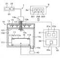
이하에, 플라즈마 처리 시스템의 구성예에 대해 설명한다. 도 1은 플라즈마 처리 시스템의 구성의 개략을 도시하는 단면도이다. 본 실시형태의 플라즈마 처리 시스템에서는, 유도 결합 플라즈마를 이용하여 기판(웨이퍼)(W)에 플라즈마 처리를 실행한다. 또한, 플라즈마 처리 대상의 기판(W)은 웨이퍼로 한정되는 것은 아니다.Hereinafter, a configuration example of the plasma processing system will be described. BRIEF DESCRIPTION OF THE DRAWINGS It is sectional drawing which shows the outline of the structure of a plasma processing system. In the plasma processing system of the present embodiment, plasma processing is performed on the substrate (wafer) W using inductively coupled plasma. In addition, the substrate W to be plasma-processed is not limited to a wafer.
플라즈마 처리 시스템은 유도 결합 플라즈마 처리 장치(1) 및 제어부(2)를 포함한다. 유도 결합 플라즈마 처리 장치(1)는 플라즈마 처리 챔버(10), 가스 공급부(20), 전원(30) 및 배기 시스템(40)을 포함한다. 플라즈마 처리 챔버(10)는 유전체 창(101) 및 측벽(102)을 포함한다. 또한, 플라즈마 처리 장치(1)는 기판 지지부(11), 가스 도입부, 안테나 유닛(유도 결합 플라즈마 여기용 안테나)(14) 및 도체판(15)을 포함한다. 기판 지지부(11)는 플라즈마 처리 챔버(10) 내에 배치된다. 안테나 유닛(14)은 후술하는 중앙 가스 주입부(13)를 둘러싸도록 플라즈마 처리 챔버(10) 상 또는 그 상방(즉, 유전체 창(101) 상방 또는 그 상방)에 배치된다. 또한, 안테나 유닛(14)은 EPD 창 등과 같은 다른 중공 부재를 둘러싸도록 배치되어도 좋다. 이 경우, 다른 중공 부재의 일부 또는 전부는 석영과 같은 절연 재료로 제작된다. 또한, 절연 재료는 석영 이외의 세라믹 재료여도 좋다. 도체판(15)은 안테나 유닛(14)의 상방에 배치된다. 플라즈마 처리 챔버(10)는 유전체 창(101), 측벽(102) 및 기판 지지부(11)에 의해 규정된 플라즈마 처리 공간(10s)을 갖는다. 플라즈마 처리 챔버(10)는, 적어도 1개의 처리 가스를 플라즈마 처리 공간(10s)에 공급하기 위한 적어도 1개의 가스 공급구와, 플라즈마 처리 공간으로부터 가스를 배출하기 위한 적어도 1개의 가스 배출구를 갖는다.The plasma processing system includes an inductively coupled
기판 지지부(11)는 본체부(111) 및 링 어셈블리(112)를 포함한다. 본체부(111)는 기판(W)을 지지하기 위한 중앙 영역(기판 지지면)(111a)과, 링 어셈블리(112)를 지지하기 위한 환상 영역(링 지지면)(111b)을 갖는다. 본체부(111)의 환상 영역(111b)은 평면에서 보아 본체부(111)의 중앙 영역(111a)을 둘러싸고 있다. 기판(W)은 본체부(111)의 중앙 영역(111a) 상에 배치되며, 링 어셈블리(112)는, 본체부(111)의 중앙 영역(111a) 상의 기판(W)을 둘러싸도록 본체부(111)의 환상 영역(111b) 상에 배치된다. 일 실시형태에 있어서, 본체부(111)는 기대 및 정전 척을 포함한다. 기대는 도전성 부재를 포함한다. 기대의 도전성 부재는 하부 전극으로서 기능한다. 정전 척은 기대 상에 배치된다. 정전 척의 상면은 기판 지지면(111a)을 갖는다. 링 어셈블리(112)는 하나 또는 복수의 환상 부재를 포함한다. 하나 또는 복수의 환상 부재 중 적어도 하나는 에지 링이다. 또한, 도시는 생략하지만, 기판 지지부(11)는 정전 척, 링 어셈블리(112) 및 기판(W) 중 적어도 1개를 타겟 온도로 조절하도록 구성되는 온조 모듈을 포함하여도 좋다. 온조 모듈은 히터, 전열 매체, 유로, 또는 이들 조합을 포함하여도 좋다. 유로에는, 브라인(brine)이나 가스와 같은 전열 유체가 흐른다. 또한, 기판 지지부(11)는 기판(W)의 이면과 기판 지지면(111a) 사이에 전열 가스를 공급하도록 구성된 전열 가스 공급부를 포함하여도 좋다.The
가스 도입부는, 가스 공급부(20)로부터 적어도 1개의 처리 가스를 플라즈마 처리 공간(10s) 내에 도입하도록 구성된다. 일 실시형태에 있어서, 가스 도입부는, 중공 부재인 중앙 가스 주입부(CGI: Center Gas Injector)(13)를 포함한다. 일 실시형태에 있어서, 중앙 가스 주입부(13)의 일부 또는 전부는 석영과 같은 절연 재료로 제작된다. 또한, 절연 재료는 석영 이외의 세라믹 재료여도 좋다. 중앙 가스 주입부(13)는 기판 지지부(11)의 상방에 배치되며, 유전체 창(101)에 형성된 중앙 개구부에 장착된다. 중앙 가스 주입부(13)는 적어도 1개의 가스 공급구(13a), 적어도 1개의 가스 유로(13b), 및 적어도 1개의 가스 도입구(13c)를 갖는다. 가스 공급구(13a)에 공급된 처리 가스는, 가스 유로(13b)를 통과하여 가스 도입구(13c)로부터 플라즈마 처리 공간(10s) 내에 도입된다. 또한, 가스 도입부는, 중앙 가스 주입부(13)에 부가하여, 또는 그 대신, 측벽(102)에 형성된 하나 또는 복수의 개구부에 장착되는 하나 또는 복수의 사이드 가스 주입부(SGI: Side Gas Injector)를 포함하여도 좋다.The gas introduction unit is configured to introduce at least one processing gas from the
가스 공급부(20)는, 적어도 1개의 가스 소스(21) 및 적어도 1개의 유량 제어기(22)를 포함하여도 좋다. 일 실시형태에 있어서, 가스 공급부(20)는 적어도 1개의 처리 가스를, 각각에 대응하는 가스 소스(21)로부터 각각에 대응하는 유량 제어기(22)를 거쳐서 중앙 가스 주입부(13)에 공급하도록 구성된다. 각각의 유량 제어기(22)는, 예를 들면 매스 플로우 컨트롤러 또는 압력 제어식의 유량 제어기를 포함하여도 좋다. 또한, 가스 공급부(20)는, 적어도 1개의 처리 가스의 유량을 변조 또는 펄스화하는 하나 또는 그 이상의 유량 변조 디바이스를 포함하여도 좋다.The
전원(30)은 적어도 1개의 임피던스 정합 회로를 거쳐서 플라즈마 처리 챔버(10)에 결합되는 RF 전원(31)을 포함한다. RF 전원(31)은 소스 RF 신호 및 바이어스 RF 신호와 같은 적어도 1개의 RF 신호(RF 전력)를, 기판 지지부(11)의 도전성 부재 및 안테나 유닛(14)에 공급하도록 구성된다. 이에 의해, 플라즈마 처리 공간(10s)에 공급된 적어도 1개의 처리 가스로부터 플라즈마가 형성된다. 따라서, RF 전원(31)은, 플라즈마 처리 챔버(10)에 있어서, 하나 또는 그 이상의 처리 가스로부터 플라즈마를 생성하도록 구성되는 플라즈마 생성부의 적어도 일부로서 기능할 수 있다. 또한, 바이어스 RF 신호를 기판 지지부(11)의 도전성 부재에 공급하는 것에 의해, 기판(W)에 바이어스 전위가 발생하고, 형성된 플라즈마 중의 이온을 기판(W)으로 인입할 수 있다.
일 실시형태에 있어서, RF 전원(31)은 제 1 RF 생성부(31a) 및 제 2 RF 생성부(31b)를 포함한다. 제 1 RF 생성부(31a)는 안테나 유닛(14)에 결합되며, 적어도 1개의 임피던스 정합 회로를 거쳐서 플라즈마 생성용의 소스 RF 신호(소스 RF 전력)를 생성하도록 구성된다. 일 실시형태에 있어서, 소스 RF 신호는 13㎒ 내지 150㎒의 범위 내의 주파수를 갖는다. 일 실시형태에 있어서, 제 1 RF 생성부(31a)는, 상이한 주파수를 갖는 복수의 소스 RF 신호를 생성하도록 구성되어도 좋다. 생성된 하나 또는 복수의 소스 RF 신호는 안테나 유닛(14)에 공급된다. 제 2 RF 생성부(31b)는, 적어도 1개의 임피던스 정합 회로를 거쳐서 기판 지지부(11)의 도전성 부재에 결합되어, 바이어스 RF 신호(바이어스 RF 전력)를 생성하도록 구성된다. 일 실시형태에 있어서, 바이어스 RF 신호는 소스 RF 신호보다 낮은 주파수를 갖는다. 일 실시형태에 있어서, 바이어스 RF 신호는 400㎑ 내지 13.56㎒의 범위 내의 주파수를 갖는다. 일 실시형태에 있어서, 제 2 RF 생성부(31b)는 상이한 주파수를 갖는 복수의 바이어스 RF 신호를 생성하도록 구성되어도 좋다. 생성된 하나 또는 복수의 바이어스 RF 신호는 기판 지지부(11)의 도전성 부재에 공급된다. 또한, 여러 가지의 실시형태에 있어서, 소스 RF 신호 및 바이어스 RF 신호 중 적어도 1개가 펄스화되어도 좋다.In one embodiment, the
또한, 전원(30)은 플라즈마 처리 챔버(10)에 결합되는 DC 전원(32)을 포함하여도 좋다. DC 전원(32)은 바이어스 DC 생성부(32a)를 포함한다. 일 실시형태에 있어서, 바이어스 DC 생성부(32a)는 기판 지지부(11)의 도전성 부재에 접속되며, 바이어스 DC 신호를 생성하도록 구성된다. 생성된 바이어스 DC 신호는 기판 지지부(11)의 도전성 부재에 인가된다. 일 실시형태에 있어서, 바이어스 DC 신호가 정전 척 내의 전극과 같은 다른 전극에 인가되어도 좋다. 여러 가지의 실시형태에 있어서, 바이어스 DC 신호는 펄스화되어도 좋다. 또한, 바이어스 DC 생성부(32a)는, RF 전원(31)에 부가하여 마련되어도 좋으며, 제 2 RF 생성부(31b)를 대신하여 마련되어도 좋다.
배기 시스템(40)은, 예를 들면 플라즈마 처리 챔버(10)의 바닥부에 마련된 가스 배출구(10e)에 접속될 수 있다. 배기 시스템(40)은 압력 조정 밸브 및 진공 펌프를 포함하여도 좋다. 압력 조정 밸브에 의해, 플라즈마 처리 공간(10s) 내의 압력이 조정된다. 진공 펌프는 터보 분자 펌프, 드라이 펌프 또는 이들 조합을 포함하여도 좋다.The
제어부(2)는 본 개시에 있어서, 설명하는 여러 가지의 공정을 플라즈마 처리 장치(1)에 실행시키는 컴퓨터 실행 가능한 명령을 처리한다. 제어부(2)는, 여기에서 설명하는 여러 가지의 공정을 실행하도록 플라즈마 처리 장치(1)의 각 요소를 제어하도록 구성될 수 있다. 일 실시형태에 있어서, 제어부(2)의 일부 또는 전체가 플라즈마 처리 장치(1)에 포함되어도 좋다. 제어부(2)는, 예를 들면 컴퓨터(2a)를 포함하여도 좋다. 컴퓨터(2a)는 예를 들면, 처리부(CPU: Central Processing Unit)(2a1), 기억부(2a2), 및 통신 인터페이스(2a3)를 포함하여도 좋다. 처리부(2a1)는 기억부(2a2)에 격납된 프로그램에 근거하여 여러 가지의 제어 동작을 실행하도록 구성될 수 있다. 기억부(2a2)는 RAM(Random Access Memory), ROM(Read Only Memory), HDD(Hard Disk Drive), SSD(Solid State Drive), 또는 이들 조합을 포함하여도 좋다. 통신 인터페이스(2a3)는 LAN(Local Area Network) 등의 통신 회선을 거쳐서 플라즈마 처리 장치(1)와의 사이에서 통신하여도 좋다.The
<제 1 실시형태><First embodiment>
다음에, 제 1 실시형태에 따른 안테나 유닛(14)의 구성예에 대해 설명한다. 도 2는 안테나 유닛(14)의 구성의 개략을 도시하는 하방으로부터 본 평면도이다. 도 3은 안테나 유닛(14)의 구성의 개략을 도시하는 단면도이다. 도 4는 안테나 유닛(14)의 구성의 개략을 모식적으로 도시하는 사시도이다.Next, a configuration example of the
안테나 유닛(14)은 적어도 1개의 안테나를 포함한다. 본 실시형태에 있어서는, 안테나 유닛(14)은 복수의 코일 어셈블리(200), 내측 도전성 플레이트(210), 외측 도전성 플레이트(220) 및 도전성 원통(도전성 중공 부재)(230)을 갖는 안테나를 포함한다.The
또한, 도시의 예에서는, 4개의 코일 어셈블리(200)가 도시되어 있지만, 코일 어셈블리(200)의 수는 특별히 한정되는 것은 아니다. 복수의 코일 어셈블리(200)는, 유전체 창(101)의 상방에 배치된다. 또한, 복수의 코일 어셈블리(200)는 내측 도전성 플레이트(210)의 중심에 대해 축 대칭으로 배치된다.Also, in the illustrated example, four
각 코일 어셈블리(200)는 코일 세그먼트(201)와 연직 코일 세그먼트(202, 203)를 갖는다. 코일 세그먼트(201)는 수평방향으로 연신하거나, 또는, 수평방향에 대해 비스듬하게 연신하며, 코일 어셈블리(200)의 바닥부에 배치된다. 또한, 코일 세그먼트(201)는 플라즈마 처리 공간(10s)에 대향하는 방향으로 연신하는 플라즈마 대향 세그먼트라고도 한다. 하나의 연직 코일 세그먼트(202)는 코일 세그먼트(201)로부터 상방으로 연신하며, 코일 단자(200a)를 거쳐서 내측 도전성 플레이트(210)의 하면에 접속된다. 또한, 하나의 연직 코일 세그먼트(202)는 내측 도전성 플레이트(210)의 상면에 접속되어도 좋다. 다른 연직 코일 세그먼트(203)는, 코일 세그먼트(201)로부터 상방으로 연신하며, 코일 단자(200b)를 거쳐서 외측 도전성 플레이트(220)의 하면에 접속된다. 또한, 다른 연직 코일 세그먼트(203)는 외측 도전성 플레이트(220)의 상면에 접속되어도 좋다. 즉, 코일 어셈블리(200)는 내측 도전성 플레이트(210)와 외측 도전성 플레이트(220)를 접속한다.Each
내측 도전성 플레이트(210)는 복수의 코일 어셈블리(200)의 상방, 즉 플라즈마가 생성되는 플라즈마 처리 공간(10s)으로부터 이격되어 배치되며, 또한 도체판(15)에 근접하여 배치된다. 또한, 내측 도전성 플레이트(210)는 대략 원통형상의 중앙 가스 주입부(13)를 둘러싸도록 중앙 가스 주입부(13)의 주위에 배치된다. 내측 도전성 플레이트(210)는 평면에서 보아 대략 원형상을 가지며, 중앙 개구부(211)가 형성된다. 또한, 내측 도전성 플레이트(210)의 형상은 특별히 한정되는 것은 아니며, 예를 들면 직사각형상이어도 좋다. 중앙 개구부(211)의 내측에는 중앙 가스 주입부(13)가 삽통된다. 내측 도전성 플레이트(210)의 상면에는, 중앙 플레이트 단자(210a)가 마련된다. 또한, 중앙 플레이트 단자(210a)는 내측 도전성 플레이트(210)의 하면에 마련되어도 좋다. 중앙 플레이트 단자(210a)는 전원(30)의 제 1 RF 생성부(31a)에 접속되며, 즉 RF 전위에 접속된다. 또한, 중앙 플레이트 단자(210a)는 RF 전위에 직접 접속되어도 좋으며, 콘덴서나 코일 등의 전기 소자를 거쳐서 RF 전위에 접속되어도 좋다. 즉, 중앙 플레이트 단자(210a)는 RF 전위에 직접적으로 또는 간접적으로 접속된다.The inner
외측 도전성 플레이트(220)는 내측 도전성 플레이트(210)를 둘러싸도록 내측 도전성 플레이트(210)의 주위에 배치된다. 외측 도전성 플레이트(220)는 평면에서 보아 환상 형상을 갖는다. 외측 도전성 플레이트(220)의 상면에는 외측 플레이트 단자(220a)가 마련된다. 또한, 외측 플레이트 단자(220a)는 외측 도전성 플레이트(220)의 하면에 마련되어도 좋다. 외측 플레이트 단자(220a)는 콘덴서(221)를 거쳐서 그라운드에 접속되며, 즉 그라운드 전위에 접속된다. 콘덴서(221)는 가변 용량 콘덴서여도 좋다. 또한, 외측 플레이트 단자(220a)는 그라운드 전위에 직접 접속되어도 좋으며, 코일 등의 다른 전기 소자를 거쳐서 그라운드 전위에 접속되어도 좋다. 즉, 외측 플레이트 단자(220a)는 그라운드 전위에 직접적으로 또는 간접적으로 접속된다. 또한, 외측 플레이트 단자(220a)와 콘덴서(221)는 각각 복수 마련되어 있어도 좋다. 또한, 콘덴서(221)는 본 제 1 실시형태로 한정되지 않으며, 고정된 용량을 갖는 콘덴서여도 좋으며, 가변 용량 콘덴서 및/또는 고정 용량 콘덴서를 포함하는 복수의 콘덴서를 포함하여도 좋다. 또한, 외측 플레이트 단자(220a)는 다른 안테나 세그먼트에 접속되어도 좋다.The outer
도전성 원통(230)은 중앙 개구부(211)의 내측에 있어서, 중앙 가스 주입부(13)를 둘러싸도록 중앙 가스 주입부(13)의 주위에 배치된다. 도전성 원통(230)은 중앙 개구부(211)로부터 유전체 창(101) 상 또는 그 하방까지 연신한다. 도전성 원통(230)은 내측 도전성 플레이트(210)에 접속되어도 좋으며, 내측 도전성 플레이트(210)와 접속되지 않는, 즉 내측 도전성 플레이트(210)로부터 이격되어 있어도 좋다. 또한, 도전성 원통(230)은 중앙 가스 주입부(13)의 일부여도 좋다.The
[안테나의 작용][Action of the antenna]
이상과 같이 구성된 안테나 유닛(14)에서는, 전원(30)의 제 1 RF 생성부(31a)로부터 공급된 RF 전력이 중앙 플레이트 단자(210a)를 거쳐서 내측 도전성 플레이트(210)에 공급된다. 이에 의해, 전류가 내측 도전성 플레이트(210)로부터 복수의 코일 어셈블리(200)에 분기하여 흐른다. 이 전류에 의해, 연직 축방향으로 자계가 발생하고, 발생한 자계에 의해, 플라즈마 처리 챔버(10) 내에 유도 전계가 발생한다. 플라즈마 처리 챔버(10) 내에 발생한 유도 전계에 의해, 중앙 가스 주입부(13)로부터 플라즈마 처리 챔버(10) 내에 공급된 처리 가스가 플라즈마화된다. 그리고, 플라즈마에 포함되는 이온이나 활성종에 의해, 중앙 영역(111a) 상의 기판(W)에 대해, 에칭이나 성막 처리 등의 플라즈마 처리가 실시된다.In the
[안테나의 효과 1][Antenna Effect 1]
여기에서 종래, 상술한 바와 같이, 안테나 중심으로부터 분기선을 거쳐서 복수의 코일로 전류를 분기시키는 경우, 자력선이 코일의 사이를 자유롭게 통과하기 때문에, 유전 기전력이 발생하여, 안테나에 의한 자계의 생성 효율이 저하한다. 한편, 본 제 1 실시형태의 안테나 유닛(14)에 의하면, 판형상의 내측 도전성 플레이트(210)가 자력선을 통과시키지 않기 때문에, 여분의 자력선의 유입을 억제할 수 있다. 즉, 내측 도전성 플레이트(210)를 코일로서 기능시키지 않도록 할 수 있다. 따라서, 자계의 생성 효율을 향상시킬 수 있다.Here, as described above, when the current is branched from the center of the antenna to a plurality of coils via the branch line, the magnetic field lines freely pass between the coils, so that a dielectric electromotive force is generated and the efficiency of generating a magnetic field by the antenna is reduced. lowers On the other hand, according to the
내측 도전성 플레이트(210)는 도체판(15)에 근접하여 배치된다. 예를 들면, 내측 도전성 플레이트(210)와 도체판(15) 사이의 거리는, 중앙 개구부(211)의 직경보다 작다. 이 때문에, 자력선의 유입을 더욱 억제할 수 있다.The inner
중앙 개구부(211)에 있어서, 내측 도전성 플레이트(210)의 내단부와 중앙 가스 주입부(13)의 간극은 자력선의 유입을 억제하는 관점에서 작은 것이 바람직하며, 본 제 1 실시형태에서는 20㎜ 이내이다. 이 20㎜는 통상 필요하게 되는 코일의 내압, 예를 들면 20㎸를 확보하기 위해서 필요한 거리이다.In the
또한, 내측 도전성 플레이트(210)와 외측 도전성 플레이트(220)의 간극도 자력선의 유입을 억제하는 관점에서 작은 것이 바람직하다.In addition, it is preferable that the gap between the inner
중앙 개구부(211)에는 도전성 원통(230)이 마련되어 있으므로, 중앙 개구부(211)의 간극을 작게 할 수 있어서, 자력선의 유입을 더욱 억제할 수 있다.Since the
[안테나의 효과 2][Antenna Effect 2]
여기에서 종래, 상술한 바와 같이, 안테나 중심으로부터 분기선을 거쳐서 복수의 코일로 분기시키는 경우, 안테나 중심의 분기부에서는 분기선이 근접하기 때문에, 서로 유도 결합하여 전류 배분 비율의 편향이 생기고, 그 결과, 안테나에 의해 생성되는 자계의 강도의 둘레방향 균일성이 악화된다. 이 점, 본 제 1 실시형태의 안테나 유닛(14)에 의하면, 전류의 분기부가 판형상의 내측 도전성 플레이트(210)이기 때문에, 상기와 같은 유도 결합이 생기지 않으며, 각 코일 어셈블리(200)로의 전류 배분 비율에 편향이 생기지 않는다. 따라서, 자계 강도의 둘레방향 균일성을 향상시킬 수 있다Here, as described above, in the case of branching from the antenna center into a plurality of coils via a branch line, since the branch lines are close to each other at the branching part of the center of the antenna, they are inductively coupled to each other and the current distribution ratio is deflected, as a result, The circumferential uniformity of the intensity of the magnetic field generated by the antenna deteriorates. In this regard, according to the
복수의 코일 어셈블리(200)는 내측 도전성 플레이트(210)의 중심에 대해 축대칭으로 배치된다. 이러한 경우, 코일 어셈블리(200)로의 전류 배분 비율의 편향을 더욱 억제할 수 있다.The plurality of
<제 2 실시형태><Second embodiment>
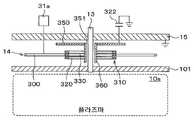
다음에, 제 2 실시형태에 따른 안테나 유닛(14)의 구성예에 대해 설명한다. 도 5는 안테나 유닛(14)의 구성의 개략을 도시하는 단면도이다. 도 6은 안테나 유닛(14)의 구성의 개략을 모식적으로 도시하는 사시도이다.Next, a configuration example of the
안테나 유닛(14)은 적어도 1개의 안테나를 포함한다. 일 실시형태에 있어서, 안테나 유닛(14)은 메인 안테나와 서브 안테나(310)를 포함한다. 메인 안테나는 적어도 1개의 메인 코일을 포함한다. 도 5, 도 6의 예에서는, 메인 안테나는 1개의 메인 코일(300)을 포함한다. 메인 코일(300)과 서브 안테나(310)는 각각 유전체 창(101)의 상방에 배치된다. 또한, 서브 안테나(310)는 유전체 창(101)으로부터 이격되어 있는 것으로 한정되지 않는다. 예를 들면, 서브 안테나(310)는 유전체 창(101)의 상면에 접하고 있어도 좋다.The
서브 안테나(310)는, 대략 원통형상의 중앙 가스 주입부(13)를 둘러싸도록 중앙 가스 주입부(13)의 주위에 마련되며, 또한 메인 코일(300)의 직경방향 내측에 마련된다. 즉, 서브 안테나(310)는 중앙 가스 주입부(13)와 메인 코일(300) 사이에 배치된다. 메인 코일(300)은, 중앙 가스 주입부(13) 및 메인 코일(300)을 둘러싸도록 중앙 가스 주입부(13) 및 메인 코일(300)의 주위에 마련된다. 메인 코일(300)의 외형과 서브 안테나(310)의 외형은 각각 평면에서 보아 대략 원형으로 형성된다. 그리고, 메인 코일(300)과 서브 안테나(310)는 각각의 외형이 동심원이 되도록 배치된다.The sub-antenna 310 is provided around the central
메인 코일(300)은 2주(2周) 이상, 대략 원형의 소용돌이 형상으로 형성되며, 메인 코일(300)의 외형의 중심축이 연직축에 일치하도록 배치된다. 또한, 메인 코일(300)은 수평방향으로 연신하거나, 또는 수평방향에 대해 비스듬하게 연신하는 평면 코일이다.The
메인 코일(300)을 구성하는 선로의 양단은 개방되어 있다. 또한, 메인 코일(300)을 구성하는 선로의 중점 또는 상기 중점의 근방에는, 급전 단자(300a)가 마련된다. 급전 단자(300a)는, 전원(30)의 제 1 RF 생성부(31a)가 접속되며, 즉 RF 전위에 접속된다. 또한, 메인 코일(300)을 구성하는 선로의 중점의 근방에는, 접지 단자(300b)가 마련된다. 접지 단자(300b)는 그라운드에 접속되며, 즉 그라운드 전위에 접속된다. 메인 코일(300)은 제 1 RF 생성부(31a)로부터 공급된 RF 전력의 파장 λ에 대해, λ/2로 공진하도록 구성되어 있다. 메인 코일(300)을 구성하는 선로에 발생하는 전압은, 선로의 중점 부근에서 최소가 되고, 선로의 양단에서 최대가 되도록 분포한다. 또한, 메인 코일(300)을 구성하는 선로에 발생하는 전류는 선로의 중점 부근에서 최대가 되고, 선로의 양단에서 최소가 되도록 분포된다. 메인 코일(300)에 RF 전력을 공급하는 제 1 RF 생성부(31a)는 주파수 및 전력의 변경이 가능하다.Both ends of the line constituting the
도 7 및 도 8은 각각 서브 안테나(310)의 구성의 개략을 도시하는 상방으로부터 본 사시도이다. 도 9는 서브 안테나(310)의 구성의 개략을 도시하는 하방으로부터 본 사시도이다.7 and 8 are perspective views viewed from above each showing the outline of the configuration of the sub-antenna 310. As shown in FIG. 9 is a perspective view from below showing the outline of the configuration of the sub-antenna 310 .
서브 안테나(310)는 제 1 코일 어셈블리(320), 제 2 코일 어셈블리(330), 접속 부재(340 내지 343), 도전성 플레이트(350) 및 도전성 원통(360)을 갖는다.The sub-antenna 310 includes a
제 1 코일 어셈블리(320)와 제 2 코일 어셈블리(330)는 각각 나선 구조를 갖는다. 제 1 코일 어셈블리(320)는 1 이상의 턴을 가지며, 제 2 코일 어셈블리(330)는 1 이상의 턴을 갖는다. 제 1 코일 어셈블리(320)의 각 턴과 제 2 코일 어셈블리(330)의 각 턴은 측면에서 보아 연직방향으로 교대로 배치되어 있다. 제 1 코일 어셈블리(320)의 외형의 중심축과 제 2 코일 어셈블리(330)의 외형의 중심축은 각각 연직축에 일치하며, 제 1 코일 어셈블리(320)와 제 2 코일 어셈블리(330)는 동축 상에 배치되어 있다. 제 1 코일 어셈블리(320)와 제 2 코일 어셈블리(330)는 각각 평면에서 보아 대략 원형으로 형성되어 있다. 또한, 제 1 코일 어셈블리(320)의 각 턴의 직경은 동일하며, 제 2 코일 어셈블리(330)의 각 턴의 직경은 동일하다. 이와 같이 서브 안테나(310)는 대략 원통형의 2중 나선 구조를 갖고 있다.The
또한, 도시의 예에 있어서는, 제 1 코일 어셈블리(320)와 제 2 코일 어셈블리(330)의 턴 수(권취 수)는 1.5턴이지만, 이것으로 한정되지 않으며, 1 이상의 임의의 턴 수로 설정할 수 있다. 예를 들면, 제 1 코일 어셈블리(320)와 제 2 코일 어셈블리(330)의 턴 수는 2턴 이상이어도 좋다.In addition, in the illustrated example, the number of turns (the number of turns) of the
제 1 코일 어셈블리(320)는 제 1 코일 세그먼트(321)와 제 1 나선형상 코일 세그먼트(322)를 갖는다. 제 1 코일 세그먼트(321)는 수평방향으로 연신하거나, 또는, 수평방향에 대해 비스듬하게 연신하며, 제 1 코일 어셈블리(320)의 바닥부에 배치된다. 제 1 나선형상 코일 세그먼트(322)는 제 1 코일 세그먼트(321)로부터 연직방향으로 나선형상으로 마련된다. 제 1 코일 어셈블리(320)의 상단부(제 1 나선형상 코일 세그먼트(322)의 단부)에는 제 1 상측 코일 단자(320a)가 마련되며, 제 1 코일 어셈블리(320)의 하단부(제 1 코일 세그먼트(321)의 단부)에는 제 1 하측 코일 단자(320b)가 마련된다.The
제 2 코일 어셈블리(330)는 제 2 코일 세그먼트(331)와 제 2 나선형상 코일 세그먼트(332)를 갖는다. 제 2 코일 세그먼트(331)는 수평방향으로 연신하거나, 또는 수평방향에 대해 비스듬하게 연신하며, 제 2 코일 어셈블리(330)의 바닥부에 배치된다. 제 2 나선형상 코일 세그먼트(332)는 제 2 코일 세그먼트(331)로부터 연직방향으로 나선형상으로 마련된다. 제 2 코일 어셈블리(330)의 상단부(제 2 나선형상 코일 세그먼트(332)의 단부)에는 제 2 상측 코일 단자(330a)가 마련되며, 제 1 코일 어셈블리(320)의 하단부(제 1 코일 세그먼트(321)의 단부)에는 제 2 하측 코일 단자(330b)가 마련된다.The
제 1 상측 코일 단자(320a)와 제 2 상측 코일 단자(330a)는 서브 안테나(310)의 중심에 대해 대칭 위치, 즉 인접하는 상측 코일 단자의 중심각이 약 180도의 위치에 배치되어 있다. 또한, 제 1 상측 코일 단자(320a)와 제 2 상측 코일 단자(330a)는 후술하는 플레이트 단자(350a)에 대해서도 축대칭으로 배치된다. 즉, 제 1 상측 코일 단자(320a)와 플레이트 단자(350a)의 거리와, 제 2 상측 코일 단자(330a)와 플레이트 단자(350a)의 거리는 동일하다. 제 1 하측 코일 단자(320b)와 제 2 하측 코일 단자(330b)도 서브 안테나(310)의 중심에 대해 대칭 위치, 즉 인접하는 하측 코일 단자의 중심각이 약 180도의 위치에 배치되어 있다.The first
제 1 상측 코일 단자(320a)는 접속 부재(340)를 거쳐서 도전성 플레이트(350)의 하면에 접속된다. 제 2 상측 코일 단자(330a)도 접속 부재(341)를 거쳐서 도전성 플레이트(350)의 하면에 접속된다. 또한, 제 1 상측 코일 단자(320a) 및 제 2 상측 코일 단자(330a)는 도전성 플레이트(350)의 상면에 접속되어도 좋다.The first
제 1 하측 코일 단자(320b)는 접속 부재(342)를 거쳐서 그라운드에 접속되며, 즉 그라운드 전위에 접속된다. 제 2 하측 코일 단자(330b)는 접속 부재(343)를 거쳐서 그라운드에 접속되며, 즉 그라운드 전위에 접속된다. 이와 같이 서브 안테나(310)는 전원(30)에 접속되어 있지 않으며, 따라서 상기 서브 안테나(310)에는 RF 전력이 직접 공급되지 않는다.The first
또한, 평면에서 보아 제 1 상측 코일 단자(320a) 및 제 2 상측 코일 단자(330a)와, 제 1 하측 코일 단자(320b) 및 제 2 하측 코일 단자(330b)의 배치는 특별히 한정되지 않는다. 단, 제 1 상측 코일 단자(320a) 및 제 2 상측 코일 단자(330a)와, 제 1 하측 코일 단자(320b) 및 제 2 하측 코일 단자(330b) 사이에서는 전압차가 크기 때문에, 실용 상은 어느 정도의 간격을 유지하는 것이 바람직하다.In addition, the arrangement of the first
도전성 플레이트(350)는, 제 1 코일 어셈블리(320) 및 제 2 코일 어셈블리(330)의 상방, 즉 플라즈마가 생성되는 플라즈마 처리 공간(10s)으로부터 이격되어 배치되며, 또한 도체판(15)에 근접하여 배치된다. 또한, 도전성 플레이트(350)는, 대략 원통형상의 중앙 가스 주입부(13)를 둘러싸도록 중앙 가스 주입부(13)의 주위에 배치된다. 도전성 플레이트(350)는 평면에서 보아 대략 원형상을 가지며, 중앙 개구부(351)가 형성된다. 또한, 도전성 플레이트(350)의 형상은 특별히 한정되는 것은 아니며, 예를 들면 직사각형상이어도 좋다. 중앙 개구부(351)의 내측에는 중앙 가스 주입부(13)가 삽통된다. 도전성 플레이트(350)의 상면에는 플레이트 단자(350a)가 마련된다. 또한, 플레이트 단자(350a)는 도전성 플레이트(350)의 하면에 마련되어도 좋다. 플레이트 단자(350a)는 콘덴서(352)를 거쳐서 그라운드에 접속되며, 즉 그라운드 전위에 접속된다. 또한, 플레이트 단자(350a)는 그라운드 전위에 직접 접속되어도 좋으며, 코일 등의 다른 전기 소자를 거쳐서 그라운드 전위에 접속되어도 좋다. 즉, 플레이트 단자(350a)는 그라운드 전위에 직접적으로 또는 간접적으로 접속된다. 콘덴서(352)는 가변 용량 콘덴서를 포함한다. 또한, 콘덴서(352)는 본 제 2 실시형태로 한정되지 않으며, 고정 용량을 갖는 콘덴서여도 좋으며, 가변 용량 콘덴서 및/또는 고정 용량 콘덴서를 포함하는 복수의 콘덴서를 포함하여도 좋다. 또한, 상기의 실시형태에서는, 플레이트 단자(350a) 및 하측 코일 단자(320b, 330b)는 콘덴서(352)를 거쳐서 그라운드 전위에 접속되어 있다. 한편, 플레이트 단자(350a) 및 하측 코일 단자(320b, 330b)는 다른 도전성 플레이트를 거쳐서 그라운드 전위에 접속되어도 좋다. 이 경우에 있어서도, 상기 실시형태와 마찬가지의 효과를 얻을 수 있다.The
도전성 원통(360)은 상기 제 1 실시형태의 도전성 원통(230)과 마찬가지의 구성을 갖는다. 즉, 도전성 원통(360)은 중앙 개구부(351)의 내측에 있어서, 중앙 가스 주입부(13)를 둘러싸도록 중앙 가스 주입부(13)의 주위에 배치된다. 도전성 원통(360)은 중앙 개구부(351)로부터 유전체 창(101) 상 또는 상방까지 하방으로 연신한다. 도전성 원통(360)은 도전성 플레이트(350)에 접속되어 마련되어도 좋으며, 도전성 플레이트(350)와 접속되지 않고 독립하여 마련되어도 좋다.The
서브 안테나(310)는 메인 코일(300)과 유도 결합하고, 서브 안테나(310)에는, 메인 코일(300)에 흐르는 전류에 의해 발생한 자계를 없애는 방향의 전류가 흐른다. 콘덴서(352)의 용량을 제어하는 것에 의해, 메인 코일(300)에 흐르는 전류에 대해 서브 안테나(310)에 흐르는 전류의 방향이나 크기를 제어할 수 있다.The sub-antenna 310 is inductively coupled to the
[안테나의 작용][Action of the antenna]
이상과 같이 구성된 안테나 유닛(14)에서는, 메인 코일(300)에 흐르는 전류와, 서브 안테나(310)에 흐르는 전류에 의해, 연직 축방향으로 자계가 발생하고, 발생한 자계에 의해, 플라즈마 처리 챔버(10) 내에 유도 전계가 발생한다. 플라즈마 처리 챔버(10) 내에 발생한 유도 전계에 의해, 중앙 가스 주입부(13)로부터 플라즈마 처리 챔버(10) 내에 공급된 처리 가스가 플라즈마화된다. 그리고, 플라즈마에 포함되는 이온이나 활성종에 의해, 중앙 영역(111a) 상의 기판(W)에 대해, 에칭이나 성막 처리 등의 플라즈마 처리가 실시된다.In the
[안테나의 효과][Antenna Effect]
여기에서, 비교예에 있어서, 서브 안테나(310)의 구성에서 도전성 플레이트(350)가 마련되지 않고, 접속 부재(340, 341)가 연결되고, 콘덴서(352)를 거쳐서 그라운드에 접속되는 경우, 종래의 안테나와 같은 과제가 생긴다. 즉, 비교예에 있어서는, 제 1 코일 어셈블리(320)와 제 2 코일 어셈블리(330)로의 전류 배분 비율의 편향이 생기고, 그 결과, 자계 강도의 둘레방향 균일성이 악화된다. 이 점, 본 제 2 실시형태의 안테나 유닛(14)에 의하면, 전류의 분기부가 판형상의 도전성 플레이트(350)이기 때문에, 상기와 같은 유도 결합이 생기지 않아, 각 제 1 코일 어셈블리(320)와 제 2 코일 어셈블리(330)로의 전류 배분 비율에 편향이 생기지 않는다. 따라서, 자계 강도의 둘레방향 균일성을 향상시킬 수 있다.Here, in the comparative example, when the
또한, 비교예에 있어서는, 자력선이 제 1 코일 어셈블리(320)와 제 2 코일 어셈블리(330)의 사이를 자유롭게 통과하기 때문에, 유전 기전력이 발생하여, 자계의 생성 효율이 저하한다. 이 점, 본 제 2 실시형태의 안테나 유닛(14)에 의하면, 판형상의 도전성 플레이트(350)가 자력선을 통과시키지 않기 때문에, 여분의 자력선의 유입을 억제할 수 있다. 그 결과, 자계의 생성 효율을 향상시킬 수 있다. 또한, 제 2 실시형태에서는, 비교예보다 자계의 생성 효율을 향상시킬 수 있지만, 도전성 플레이트(350)의 중앙 개구부(351)가 형성되어 있기 때문에, 그 자계의 생성 효율의 향상 효과는 작은 경우가 있다. 이 점, 후술의 변형예와 같이 도전성 플레이트(350)에 슬릿(370)을 마련하는 것에 의해, 자계의 생성 효율의 향상 효과를 크게 할 수 있다.In addition, in the comparative example, since the magnetic force line freely passes between the
<제 2 실시형태의 변형예><Modification of the second embodiment>
도 10에 도시하는 바와 같이, 본 제 2 실시형태의 서브 안테나(310)에 있어서, 도전성 플레이트(350)에는, 중앙 개구부(211)로부터 도전성 플레이트(350)의 외단부(외주연부)까지 직경방향으로 연신하는 슬릿(370)이 형성되어도 좋다. 슬릿(370)은 도전성 플레이트(350)를 분리하도록 형성되며, 후술하는 바와 같이 슬릿(370)에 의해 도전성 플레이트(350)에 있어서의 전류가 변화한다.As shown in FIG. 10 , in the
본 발명자들이 예의 검토한 바, 이와 같이 슬릿(370)을 형성하면, 슬릿(370)을 형성하지 않는 경우에 비해, 자계 강도의 둘레방향 균일성이 약간 낮아지지만, 자계의 생성 효율을 향상시킬 수 있는 것을 알았다. 또한, 도전성 플레이트(350)에 있어서의 슬릿(370)의 위치에 의해, 자계 강도의 둘레방향 균일성과 자계의 생성 효율에 변동이 있는 것을 알았다.As the present inventors have intensively studied, when the
도 11a 내지 도 11d를 이용하여, 이와 같은 자계 강도의 둘레방향 균일성과 자계의 생성 효율의 변동에 대해 설명한다. 도 11a 내지 도 11d는 도전성 플레이트(350)에 있어서의 슬릿(370)의 유무 및 위치에 따른 전류를 도시하는 설명도이다. 또한, 이하에서는, 자계 강도의 둘레방향 균일성은 편향(B)으로 하여 설명한다. 편향(B)은 1주(360도)의 자계 분포에 있어서, 자계의 평균값에 대한 최대값과 최소값의 차분의 비율을 나타낸다. 또한, 자계의 생성 효율은 효율(E)로 하여 설명한다. 효율(E)은 서브 안테나(310)가 플라즈마 중에 생성되는 자계의 단위 길이 당의 강함을 나타낸다.The circumferential uniformity of the magnetic field intensity and the variation in the magnetic field generation efficiency will be described with reference to Figs. 11A to 11D. 11A to 11D are explanatory views showing the presence or absence of the
[패턴 1][Pattern 1]
패턴 1은 도 11a에 도시하는 바와 같이, 도전성 플레이트(350)에 슬릿(370)이 형성되지 않은 패턴이다. 패턴 1에서는, 제 1 코일 어셈블리(320)와 제 2 코일 어셈블리(330)에 흐르는 전류(P)에 대해, 도전성 플레이트(350)에 유도 전류(Q1)가 흐른다. 이러한 경우, 편향(B1)은 작게 억제할 수 있다. 그렇지만, 전류(P)에 대해 유도 전류(Q1)가 없어지도록 흐르므로, 효율(E1)이 작아진다.
[패턴 2][Pattern 2]
패턴 2는 도 11b에 도시하는 바와 같이 평면에서 보아, 슬릿(370)이 제 1 상측 코일 단자(320a)와 제 2 상측 코일 단자(330a) 사이에 형성되며, 또한 플레이트 단자(350a)의 반대측에 형성되는 패턴이다. 이러한 경우, 슬릿(370)이 형성되어 있는 것에 의해, 유도 전류(Q2)는 도전성 플레이트(350)를 주회하지 않고, 패턴 1의 유도 전류(Q1)에 비해 작아진다. 이 때문에, 패턴 1의 효율(E1)보다 패턴 2의 효율(E2)은 커진다. 단, 패턴 2의 편향(B2)은 패턴 1의 편향(B1)보다 커진다.In
[패턴 3][Pattern 3]
패턴 3은 도 11c에 도시하는 바와 같이, 평면에서 보아, 슬릿(370)이 플레이트 단자(350a)의 근방에 형성되는 패턴이다. 이러한 경우, 전체 유도 전류(Q3)가 전류(P)와 동일한 방향이기 때문에, 효율(E3)은 커진다. 단, 패턴 3의 편향(B3)은 패턴 2의 편향(B2)보다 더 커진다.The pattern 3 is a pattern in which the
[패턴 4][Pattern 4]
패턴 4는 도 11d에 도시하는 바와 같이, 평면에서 보아, 슬릿(370)이 플레이트 단자(350a)와 제 1 상측 코일 단자(320a) 사이에 형성되는 패턴이다. 이러한 경우, 전체 유도 전류(Q4)가 전류(P)와 반대방향이기 때문에, 효율(E4)은 작아진다. 그러나, 패턴 4의 편향(B4)은 작게 억제할 수 있다.Pattern 4 is a pattern in which a
이상의 결과를 정리하면, 편향(B)에 대해서는, B1<B4<B2<B3이 된다. 한편, 효율(E)에 대해서는, E3>E2>E4>E1이 된다. 슬릿(370)의 유무와 위치는 이들 편향(B)과 효율(E)이 사양에 합치하도록 적절히 설계된다.Summarizing the above results, for the bias B, B1<B4<B2<B3. On the other hand, for the efficiency E, E3>E2>E4>E1. The presence and location of the
또한, 본 제 2 실시형태에서 도전성 플레이트(350)에 형성한 슬릿(370)은 제 1 실시형태의 내측 도전성 플레이트(210)에 형성하여도 좋다. 내측 도전성 플레이트(210)에 슬릿을 형성한 경우여도, 상기와 마찬가지의 효과를 누릴 수 있다.Note that the
<제 2 실시형태의 변형예><Modification of the second embodiment>
이상의 제 2 실시형태에서는, 제 1 하측 코일 단자(320b)와 제 2 하측 코일 단자(330b)는 각각 그라운드에 접속되어 있었지만, 도 12에 도시하는 바와 같이, 이들 제 1 하측 코일 단자(320b)와 제 2 하측 코일 단자(330b)는 콘덴서(380)를 거쳐서 접속되어 있어도 좋다. 콘덴서(380)는 가변 용량 콘덴서를 포함한다.In the above second embodiment, the first
또한, 제 1 하측 코일 단자(320b)와 제 2 하측 코일 단자(330b)는 각각 플로팅 상태여도 좋다.In addition, each of the first
또한, 제 1 하측 코일 단자(320b)와 제 2 하측 코일 단자(330b)는 각각 RF 전위에 접속되어도 좋다. 이러한 경우, 제 1 코일 어셈블리(320)와 제 2 코일 어셈블리(330)를 각각 단체로 사용하는 것도 가능해진다.Further, the first
<제 2 실시형태의 변형예><Modification of the second embodiment>
이상의 제 2 실시형태에서는, 서브 안테나(310)는 메인 코일(300)의 직경방향 내측에 배치되어 있었지만, 직경방향 외측에 배치되어 있어도 좋다. 또한, 서브 안테나(310)는, 메인 코일(300)의 직경방향 내측과 직경방향 외측의 쌍방에 배치되어 있어도 좋다. 즉, 안테나 어셈블리는, 메인 코일(300)의 직경방향 내측에 배치되는 제 1 서브 안테나와 직경방향 외측에 배치되는 제 1 서브 안테나를 가져도 좋다. 또한, 서브 안테나(310)는 메인 코일(300)의 하방 및/또는 상방에 배치되어 있어도 좋다.In the above second embodiment, the sub-antenna 310 is disposed radially inside the
<제 3 실시형태><Third embodiment>
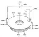
다음에, 제 3 실시형태에 따른 안테나 유닛(14)의 구성예에 대해 설명한다. 도 13은 안테나 유닛(14)의 구성의 개략을 모식적으로 도시하는 사시도이다.Next, a configuration example of the
안테나 유닛(14)은 코일 어셈블리(400), 도전성 플레이트(410) 및 도전성 원통(도시하지 않음)을 갖는다. 도전성 원통은 상기 제 1 실시형태의 도전성 원통(230)과 마찬가지의 구성을 갖는다.The
코일 어셈블리(400)는 복수 마련되어 있다. 또한, 도시의 예에서는, 코일 어셈블리(400)는 4개 마련되어 있지만, 코일 어셈블리(400)의 수는 특별히 한정되는 것은 아니다. 복수의 코일 어셈블리(400)는 유전체 창(101)의 상방에 배치된다.A plurality of
각 코일 어셈블리(400)는 제 1 코일 세그먼트(401), 연직 코일 세그먼트(402) 및 제 2 코일 세그먼트(403)를 갖는다. 제 1 코일 세그먼트(401)는 수평방향으로 연신하거나, 또는 수평방향에 대해 비스듬하게 연신하며, 코일 단자(400a)를 거쳐서 도전성 플레이트(410)의 측면에 접속된다. 연직 코일 세그먼트(402)는 제 1 코일 세그먼트(401)로부터 연직 하방으로 연신한다. 제 2 코일 세그먼트(403)는 연직 코일 세그먼트(402)로부터 수평방향으로 연신하거나, 또는 상기 수평방향에 대해 비스듬하게 대략 원형으로 연신하며, 코일 어셈블리(400)의 바닥부에 배치된다. 제 2 코일 세그먼트(403)의 단부에는, 코일 단자(400b)가 마련된다. 코일 단자(400b)의 접속처는 임의이지만, 예를 들면 그라운드 전위에 접속된다.Each
복수의 코일 어셈블리(400)는 도전성 플레이트(410)의 중심에 대해 축대칭으로 배치된다. 즉, 복수의 코일 단자(400a)는 도전성 플레이트(410)의 중앙 개구부(411)를 중심으로 둘레방향으로 등간격으로 배치된다. 마찬가지로, 복수의 코일 단자(400b)도 중앙 개구부(411)를 중심으로 둘레방향으로 등간격으로 배치된다.The plurality of
도전성 플레이트(410)는 제 1 실시형태의 내측 도전성 플레이트(210)와 마찬가지의 구성을 갖는다. 도전성 플레이트(410)에는, 중앙 가스 주입부(13)가 삽통되는 중앙 개구부(411)가 형성된다. 도전성 플레이트(410)의 측면에는 플레이트 단자(410a)가 마련된다. 플레이트 단자(410a)는 전원(30)의 제 1 RF 생성부(31a)에 접속되며, 즉 RF 전위에 접속된다.The
본 제 3 실시형태에 있어서도, 상기 제 1 실시형태와 마찬가지의 효과를 누릴 수 있다.Also in this 3rd Embodiment, the effect similar to the said 1st Embodiment can be enjoyed.
<제 4 실시형태><Fourth embodiment>
다음에, 제 4 실시형태에 따른 안테나 유닛(14)의 구성예에 대해 설명한다. 도 14는 안테나 유닛(14)의 구성의 개략을 모식적으로 도시하는 사시도이다.Next, a configuration example of the
안테나 유닛(14)은 코일 어셈블리(500), 도전성 플레이트(510) 및 도전성 원통(도시하지 않음)을 갖는다. 도전성 원통은 상기 제 1 실시형태의 도전성 원통(230)과 마찬가지의 구성을 갖는다.The
코일 어셈블리(500)는 복수 마련되어 있다. 또한, 도시의 예에서는, 코일 어셈블리(500)는 4개 마련되어 있지만, 코일 어셈블리(500)의 수는 특별히 한정되는 것은 아니다. 복수의 코일 어셈블리(500)는 유전체 창(101)의 상방에 배치된다.A plurality of
각 코일 어셈블리(500)는, 도전성 플레이트(510)와 동일 평면에 있어서, 수평방향으로 연신하거나, 또는 수평방향에 대해 비스듬하게 연신하며, 2주 이상, 대략 원형의 소용돌이 형상으로 형성된다. 코일 어셈블리(500)의 일 단부에 마련된 코일 단자(500a)는 도전성 플레이트(510)의 측면에 접속된다. 코일 어셈블리(500)의 타 단부에 마련된 코일 단자(500b)의 접속처는 임의이지만, 예를 들면 그라운드 전위에 접속된다.Each
복수의 코일 어셈블리(500)는 도전성 플레이트(510)의 중심에 대해 축대칭으로 배치된다. 즉, 복수의 코일 단자(500a)는 도전성 플레이트(510)의 중앙 개구부(511)를 중심으로 둘레방향으로 등간격으로 배치된다. 마찬가지로, 복수의 코일 단자(500b)도 중앙 개구부(511)를 중심으로 둘레방향으로 등간격으로 배치된다.The plurality of
도전성 플레이트(510)는 제 1 실시형태의 내측 도전성 플레이트(210)와 마찬가지의 구성을 갖는다. 도전성 플레이트(510)에는, 중앙 가스 주입부(13)가 삽통되는 중앙 개구부(511)가 형성된다. 도전성 플레이트(510)의 상면에는 플레이트 단자(510a)가 마련된다. 또한, 플레이트 단자(510a)는 도전성 플레이트(510)의 상면에 마련되어도 좋다. 플레이트 단자(510a)는 전원(30)의 제 1 RF 생성부(31a)에 접속되며, 즉 RF 전위에 접속된다.The
본 제 4 실시형태에 있어서도, 상기 제 1 실시형태와 마찬가지의 효과를 누릴 수 있다.Also in this 4th embodiment, the effect similar to the said 1st Embodiment can be enjoyed.
금회 개시된 실시형태는 모든 점에서 예시이며, 제한적인 것은 아니라고 고려되어야 한다. 상기의 실시형태는, 첨부의 청구범위 및 그 주지를 일탈하는 일이 없이, 여러가지 형태로 생략, 치환, 변경되어도 좋다.It should be considered that embodiment disclosed this time is an illustration in every point, and is not restrictive. The above embodiments may be omitted, replaced, or changed in various forms without departing from the appended claims and the gist thereof.
14: 안테나 유닛
200: 코일 어셈블리
210: 내측 도전성 플레이트
210a: 중앙 플레이트 단자
211: 중앙 개구부14: antenna unit
200: coil assembly
210: inner conductive plate
210a: center plate terminal
211: central opening
Claims (24)
Translated fromKorean복수의 코일 어셈블리와,
상기 복수의 코일 어셈블리에 접속되며, 중앙 개구부와, 적어도 1개의 플레이트 단자를 갖는 도전성 플레이트를 구비하는
유도 결합 플라즈마 여기용 안테나.An antenna for inductively coupled plasma excitation, comprising:
a plurality of coil assemblies;
a conductive plate connected to the plurality of coil assemblies, the conductive plate having a central opening and at least one plate terminal;
Antenna for inductively coupled plasma excitation.
상기 플레이트 단자는 그라운드 전위 또는 RF 전위에 직접적으로 또는 간접적으로 접속되는
유도 결합 플라즈마 여기용 안테나.The method of claim 1,
The plate terminal is connected directly or indirectly to a ground potential or an RF potential.
Antenna for inductively coupled plasma excitation.
상기 중앙 개구부 또는 그 근방으로부터 하방으로 연신하는 도전성 원통을 더 구비하는
유도 결합 플라즈마 여기용 안테나.3. The method of claim 1 or 2,
Further comprising a conductive cylinder extending downward from the central opening or its vicinity
Antenna for inductively coupled plasma excitation.
상기 복수의 코일 어셈블리의 각각은, 수평방향으로 연신하거나, 또는 수평방향에 대하여 비스듬하게 연신하는 코일 세그먼트를 가지며,
상기 도전성 플레이트는 상기 적어도 1개의 플레이트 단자를 갖는 상면과, 상기 복수의 코일 어셈블리에 접속되는 하면을 갖는
유도 결합 플라즈마 여기용 안테나.4. The method according to any one of claims 1 to 3,
Each of the plurality of coil assemblies has a coil segment extending in a horizontal direction or extending at an angle with respect to the horizontal direction,
The conductive plate has an upper surface having the at least one plate terminal and a lower surface connected to the plurality of coil assemblies.
Antenna for inductively coupled plasma excitation.
상기 코일 세그먼트는 상기 코일 어셈블리의 바닥부에 배치되는
유도 결합 플라즈마 여기용 안테나.5. The method of claim 4,
wherein the coil segment is disposed at the bottom of the coil assembly.
Antenna for inductively coupled plasma excitation.
상기 도전성 플레이트의 주위에 배치되며, 적어도 1개의 다른 플레이트 단자를 갖는 다른 도전성 플레이트를 더 구비하고,
상기 복수의 코일 어셈블리는 상기 도전성 플레이트와 상기 다른 도전성 플레이트를 접속하는
유도 결합 플라즈마 여기용 안테나.6. The method according to any one of claims 1 to 5,
and another conductive plate disposed around the conductive plate and having at least one other plate terminal;
The plurality of coil assemblies are configured to connect the conductive plate and the other conductive plate.
Antenna for inductively coupled plasma excitation.
상기 복수의 코일 어셈블리는,
수평방향으로 연신하거나, 또는 수평방향에 대해 비스듬하게 연신하는 제 1 코일 세그먼트와, 제 1 코일 단자를 갖는 제 1 코일 어셈블리와,
수평방향으로 연신하거나, 또는 수평방향에 대해 비스듬하게 연신하는 제 2 코일 세그먼트와, 제 2 코일 단자를 갖는 제 2 코일 어셈블리를 포함하는
유도 결합 플라즈마 여기용 안테나.6. The method according to any one of claims 1 to 5,
The plurality of coil assemblies,
A first coil assembly having a first coil segment extending in a horizontal direction or obliquely extending in a horizontal direction, and a first coil terminal;
A second coil assembly comprising a second coil segment extending in a horizontal direction or obliquely extending with respect to the horizontal direction, and a second coil assembly having a second coil terminal
Antenna for inductively coupled plasma excitation.
상기 도전성 플레이트는 상기 도전성 플레이트의 외주연부로부터 상기 중앙 개구부까지 연신하는 슬릿을 갖는
유도 결합 플라즈마 여기용 안테나.8. The method of claim 7,
The conductive plate has a slit extending from an outer periphery of the conductive plate to the central opening.
Antenna for inductively coupled plasma excitation.
상기 슬릿은 평면에서 보아, 상기 제 1 코일 단자와 상기 제 2 코일 단자 사이에 형성되는
유도 결합 플라즈마 여기용 안테나.9. The method of claim 8,
The slit is formed between the first coil terminal and the second coil terminal in a plan view.
Antenna for inductively coupled plasma excitation.
상기 슬릿은 평면에서 보아, 상기 제 1 코일 단자와 상기 제 2 코일 단자에 대해 상기 플레이트 단자의 반대측에 형성되는
유도 결합 플라즈마 여기용 안테나.10. The method according to claim 8 or 9,
The slit is formed on opposite sides of the plate terminal with respect to the first coil terminal and the second coil terminal in a plan view.
Antenna for inductively coupled plasma excitation.
상기 슬릿은 평면에서 보아, 상기 플레이트 단자의 근방에 형성되는
유도 결합 플라즈마 여기용 안테나.10. The method according to claim 8 or 9,
The slit is formed in the vicinity of the plate terminal in a plan view.
Antenna for inductively coupled plasma excitation.
상기 슬릿은 평면에서 보아, 상기 플레이트 단자와 상기 제 1 코일 단자 사이에 형성되는
유도 결합 플라즈마 여기용 안테나.10. The method according to claim 8 or 9,
The slit is formed between the plate terminal and the first coil terminal in a plan view.
Antenna for inductively coupled plasma excitation.
상기 복수의 코일 어셈블리는 각각에 대응하는 복수의 코일 단자를 가지며, 각 코일 단자는 그라운드 전위 또는 RF 전위에 직접적으로 또는 간접적으로 접속되는
유도 결합 플라즈마 여기용 안테나.4. The method according to any one of claims 1 to 3,
The plurality of coil assemblies have a plurality of coil terminals corresponding to each, and each coil terminal is directly or indirectly connected to a ground potential or an RF potential.
Antenna for inductively coupled plasma excitation.
상기 복수의 코일 단자는 상기 중앙 개구부를 중심으로 둘레방향으로 등간격으로 배치되는
유도 결합 플라즈마 여기용 안테나.14. The method of claim 13,
The plurality of coil terminals are arranged at equal intervals in the circumferential direction around the central opening.
Antenna for inductively coupled plasma excitation.
RF 전위에 접속되는 급전 단자를 갖는 메인 안테나와,
상기 메인 안테나의 내측 또는 외측에 배치되는 서브 안테나를 구비하며,
상기 서브 안테나는,
복수의 코일 어셈블리와,
상기 복수의 코일 어셈블리에 접속되며, 중앙 개구부와, 적어도 1개의 플레이트 단자를 갖는 도전성 플레이트를 구비하는
유도 결합 플라즈마 여기용 안테나 유닛.An antenna unit for inductively coupled plasma excitation, comprising:
a main antenna having a feed terminal connected to an RF potential;
and a sub-antenna disposed inside or outside the main antenna;
The sub-antenna is
a plurality of coil assemblies;
a conductive plate connected to the plurality of coil assemblies, the conductive plate having a central opening and at least one plate terminal;
Antenna unit for inductively coupled plasma excitation.
상기 복수의 코일 어셈블리는,
수평방향으로 연신하거나, 또는 수평방향에 대해 비스듬하게 연신하는 제 1 코일 세그먼트와, 제 1 코일 단자를 갖는 제 1 코일 어셈블리와,
수평방향으로 연신하거나, 또는 수평방향에 대해 비스듬하게 연신하는 제 2 코일 세그먼트와, 제 2 코일 단자를 갖는 제 2 코일 어셈블리를 포함하는
유도 결합 플라즈마 여기용 안테나 유닛.16. The method of claim 15,
The plurality of coil assemblies,
A first coil assembly having a first coil segment extending in a horizontal direction or obliquely extending in a horizontal direction, and a first coil terminal;
A second coil assembly comprising a second coil segment extending in a horizontal direction or obliquely extending with respect to the horizontal direction, and a second coil assembly having a second coil terminal
Antenna unit for inductively coupled plasma excitation.
상기 제 1 코일 세그먼트는 상기 제 1 코일 어셈블리의 바닥부에 배치되며,
상기 제 2 코일 세그먼트는 상기 제 2 코일 어셈블리의 바닥부에 배치되는
유도 결합 플라즈마 여기용 안테나 유닛.17. The method of claim 16,
the first coil segment is disposed at the bottom of the first coil assembly;
wherein the second coil segment is disposed at the bottom of the second coil assembly.
Antenna unit for inductively coupled plasma excitation.
상기 도전성 플레이트는 상기 도전성 플레이트의 외주연부로부터 상기 중앙 개구부까지 연신하는 슬릿을 갖는
유도 결합 플라즈마 여기용 안테나 유닛.18. The method according to any one of claims 15 to 17,
The conductive plate has a slit extending from an outer periphery of the conductive plate to the central opening.
Antenna unit for inductively coupled plasma excitation.
상기 복수의 코일 어셈블리의 각각은 그라운드 전위에 접속되는 다른 코일 단자를 가지며,
상기 적어도 1개의 플레이트 단자는 그라운드 전위에 접속되는
유도 결합 플라즈마 여기용 안테나 유닛.19. The method according to any one of claims 15 to 18,
each of the plurality of coil assemblies has a different coil terminal connected to a ground potential;
wherein the at least one plate terminal is connected to a ground potential
Antenna unit for inductively coupled plasma excitation.
상기 복수의 코일 어셈블리의 각각은, 상기 플레이트 단자에 직접적으로 또는 간접적으로 접속되는 다른 코일 단자를 갖는
유도 결합 플라즈마 여기용 안테나 유닛.19. The method according to any one of claims 15 to 18,
each of the plurality of coil assemblies having another coil terminal directly or indirectly connected to the plate terminal;
Antenna unit for inductively coupled plasma excitation.
상기 플라즈마 처리 챔버에 장착되는 중공 부재와,
상기 중공 부재를 둘러싸도록 상기 플라즈마 처리 챔버 상 또는 상기 플라즈마 처리 챔버의 상방에 배치되는 안테나를 구비하고,
상기 안테나는,
복수의 코일 어셈블리와,
상기 복수의 코일 어셈블리에 접속되며, 중앙 개구부와, 적어도 1개의 플레이트 단자를 갖는 도전성 플레이트를 구비하는
플라즈마 처리 장치.a plasma processing chamber;
a hollow member mounted to the plasma processing chamber;
and an antenna disposed on the plasma processing chamber or above the plasma processing chamber so as to surround the hollow member,
The antenna is
a plurality of coil assemblies;
a conductive plate connected to the plurality of coil assemblies, the conductive plate having a central opening and at least one plate terminal;
Plasma processing device.
상기 안테나의 상방에 배치되는 도체판을 더 구비하는
플라즈마 처리 장치.22. The method of claim 21,
Further comprising a conductor plate disposed above the antenna
Plasma processing device.
상기 중공 부재의 일부 또는 전부는 절연 재료로 제작되는
플라즈마 처리 장치.23. The method of claim 21 or 22,
Some or all of the hollow member is made of an insulating material
Plasma processing device.
상기 안테나와 상기 중공 부재 사이에 배치되는 도전성 중공 부재를 구비하는
플라즈마 처리 장치.24. The method according to any one of claims 21 to 23,
and a conductive hollow member disposed between the antenna and the hollow member.
Plasma processing device.
Applications Claiming Priority (2)
| Application Number | Priority Date | Filing Date | Title |
|---|---|---|---|
| JPJP-P-2021-025292 | 2021-02-19 | ||
| JP2021025292AJP7530845B2 (en) | 2021-02-19 | 2021-02-19 | Inductively coupled plasma excitation antenna, inductively coupled plasma excitation antenna unit, and plasma processing apparatus |
Publications (1)
| Publication Number | Publication Date |
|---|---|
| KR20220118943Atrue KR20220118943A (en) | 2022-08-26 |
Family
ID=82900856
Family Applications (1)
| Application Number | Title | Priority Date | Filing Date |
|---|---|---|---|
| KR1020220021328APendingKR20220118943A (en) | 2021-02-19 | 2022-02-18 | Antenna for inductively coupled plasma excitation, antenna unit for inductively coupled plasma excitation, and plasma processing apparatus |
Country Status (5)
| Country | Link |
|---|---|
| US (1) | US20220270851A1 (en) |
| JP (1) | JP7530845B2 (en) |
| KR (1) | KR20220118943A (en) |
| CN (1) | CN114975058A (en) |
| TW (1) | TW202236390A (en) |
Families Citing this family (1)
| Publication number | Priority date | Publication date | Assignee | Title |
|---|---|---|---|---|
| TW202405869A (en)* | 2022-04-20 | 2024-02-01 | 日商東京威力科創股份有限公司 | Antenna for inductively coupled plasma excitation, antenna unit for inductively coupled plasma excitation, and plasma processing apparatus |
Citations (2)
| Publication number | Priority date | Publication date | Assignee | Title |
|---|---|---|---|---|
| US5944902A (en) | 1997-02-10 | 1999-08-31 | Applied Materials, Inc. | Plasma source for HDP-CVD chamber |
| US6401652B1 (en) | 2000-05-04 | 2002-06-11 | Applied Materials, Inc. | Plasma reactor inductive coil antenna with flat surface facing the plasma |
Family Cites Families (19)
| Publication number | Priority date | Publication date | Assignee | Title |
|---|---|---|---|---|
| TW312815B (en)* | 1995-12-15 | 1997-08-11 | Hitachi Ltd | |
| JP4069966B2 (en)* | 1998-04-10 | 2008-04-02 | 東京エレクトロン株式会社 | Method and apparatus for forming silicon oxide film |
| TW445540B (en)* | 2000-08-07 | 2001-07-11 | Nano Architect Res Corp | Bundle concentrating type multi-chamber plasma reacting system |
| JP4598253B2 (en) | 2000-09-26 | 2010-12-15 | 東京エレクトロン株式会社 | Plasma device |
| KR20100030806A (en)* | 2008-09-11 | 2010-03-19 | 삼성전자주식회사 | Plasma generating apparatus |
| SG10201502985TA (en) | 2010-04-20 | 2015-05-28 | Lam Res Corp | Methods and apparatus for an induction coil arrangement in a plasma processing system |
| WO2012082854A2 (en)* | 2010-12-17 | 2012-06-21 | Mattson Technology, Inc. | Inductively coupled plasma source for plasma processing |
| JP5800547B2 (en)* | 2011-03-29 | 2015-10-28 | 東京エレクトロン株式会社 | Plasma processing apparatus and plasma processing method |
| JP5878771B2 (en) | 2012-02-07 | 2016-03-08 | 東京エレクトロン株式会社 | Inductively coupled plasma processing method and inductively coupled plasma processing apparatus |
| US10170279B2 (en)* | 2012-07-20 | 2019-01-01 | Applied Materials, Inc. | Multiple coil inductively coupled plasma source with offset frequencies and double-walled shielding |
| US10249470B2 (en)* | 2012-07-20 | 2019-04-02 | Applied Materials, Inc. | Symmetrical inductively coupled plasma source with coaxial RF feed and coaxial shielding |
| US9082590B2 (en)* | 2012-07-20 | 2015-07-14 | Applied Materials, Inc. | Symmetrical inductively coupled plasma source with side RF feeds and RF distribution plates |
| US9928987B2 (en)* | 2012-07-20 | 2018-03-27 | Applied Materials, Inc. | Inductively coupled plasma source with symmetrical RF feed |
| US9896769B2 (en)* | 2012-07-20 | 2018-02-20 | Applied Materials, Inc. | Inductively coupled plasma source with multiple dielectric windows and window-supporting structure |
| CN107369602B (en)* | 2016-05-12 | 2019-02-19 | 北京北方华创微电子装备有限公司 | Reaction chamber and semiconductor processing equipment |
| WO2020146189A1 (en) | 2019-01-09 | 2020-07-16 | Lam Research Corporation | Fibonacci coil for plasma processing chamber |
| WO2020223127A1 (en) | 2019-04-30 | 2020-11-05 | Lam Research Corporation | Dual-frequency, direct-drive inductively coupled plasma source |
| KR20220045895A (en)* | 2020-10-06 | 2022-04-13 | 도쿄엘렉트론가부시키가이샤 | Plasma processing apparatus and plasma processing coil |
| KR20240115170A (en)* | 2023-01-18 | 2024-07-25 | 도쿄엘렉트론가부시키가이샤 | Plasma processing apparatus |
- 2021
- 2021-02-19JPJP2021025292Apatent/JP7530845B2/enactiveActive
- 2022
- 2022-02-07TWTW111104233Apatent/TW202236390A/enunknown
- 2022-02-09CNCN202210121035.5Apatent/CN114975058A/enactivePending
- 2022-02-18KRKR1020220021328Apatent/KR20220118943A/enactivePending
- 2022-02-18USUS17/675,228patent/US20220270851A1/enactivePending
Patent Citations (2)
| Publication number | Priority date | Publication date | Assignee | Title |
|---|---|---|---|---|
| US5944902A (en) | 1997-02-10 | 1999-08-31 | Applied Materials, Inc. | Plasma source for HDP-CVD chamber |
| US6401652B1 (en) | 2000-05-04 | 2002-06-11 | Applied Materials, Inc. | Plasma reactor inductive coil antenna with flat surface facing the plasma |
Also Published As
| Publication number | Publication date |
|---|---|
| US20220270851A1 (en) | 2022-08-25 |
| JP7530845B2 (en) | 2024-08-08 |
| CN114975058A (en) | 2022-08-30 |
| TW202236390A (en) | 2022-09-16 |
| JP2022127248A (en) | 2022-08-31 |
Similar Documents
| Publication | Publication Date | Title |
|---|---|---|
| JP5851682B2 (en) | Plasma processing equipment | |
| US20220108871A1 (en) | Plasma processing apparatus and plasma processing coil | |
| US7632375B2 (en) | Electrically enhancing the confinement of plasma | |
| TW200833181A (en) | Apparatus and method for plasma processing | |
| US20230054430A1 (en) | Apparatus for Plasma Processing | |
| KR20220118943A (en) | Antenna for inductively coupled plasma excitation, antenna unit for inductively coupled plasma excitation, and plasma processing apparatus | |
| JP7677862B2 (en) | Plasma Processing Equipment | |
| JP2022061463A (en) | Plasma processing equipment and plasma processing coil | |
| KR20220111192A (en) | Filter circuit and plasma processing apparatus | |
| US20230343553A1 (en) | Antenna for inductively coupled plasma excitation, antenna unit for inductively coupled plasma excitation, and plasma processing apparatus | |
| JP2023159862A (en) | Antenna for inductive coupling plasma excitation, antenna unit for inductive coupling plasma excitation, and plasma processing apparatus | |
| US12074390B2 (en) | Parallel resonance antenna for radial plasma control | |
| CN116914424A (en) | Antenna for inductively coupled plasma excitation, antenna unit for inductively coupled plasma excitation and plasma processing device | |
| KR101853737B1 (en) | Inductively Coupled Plasma Processing Apparatus | |
| TW202447692A (en) | Plasma processing device and dielectric window | |
| KR20250040969A (en) | Plasma treatment device and plasma treatment method | |
| KR20250134064A (en) | plasma treatment device | |
| WO2025101770A1 (en) | Inductively coupled plasma source with radial coil network | |
| WO2023023289A1 (en) | Apparatus for plasma processing | |
| WO2024257401A1 (en) | Plasma processing device | |
| KR20050023946A (en) | Antenna apparatus for generating inductively coupled plasma of which configuration can be modified |
Legal Events
| Date | Code | Title | Description |
|---|---|---|---|
| PA0109 | Patent application | Patent event code:PA01091R01D Comment text:Patent Application Patent event date:20220218 | |
| PG1501 | Laying open of application | ||
| A201 | Request for examination | ||
| PA0201 | Request for examination | Patent event code:PA02012R01D Patent event date:20241118 Comment text:Request for Examination of Application |