KR20220118367A - Apparatus for measuring condition of electroplating cell components and associated methods - Google Patents
Apparatus for measuring condition of electroplating cell components and associated methodsDownload PDFInfo
- Publication number
- KR20220118367A KR20220118367AKR1020220099688AKR20220099688AKR20220118367AKR 20220118367 AKR20220118367 AKR 20220118367AKR 1020220099688 AKR1020220099688 AKR 1020220099688AKR 20220099688 AKR20220099688 AKR 20220099688AKR 20220118367 AKR20220118367 AKR 20220118367A
- Authority
- KR
- South Korea
- Prior art keywords
- conductive pads
- terminal
- measurement
- electrical
- wafer
- Prior art date
- Legal status (The legal status is an assumption and is not a legal conclusion. Google has not performed a legal analysis and makes no representation as to the accuracy of the status listed.)
- Granted
Links
Images


Classifications
- H—ELECTRICITY
- H01—ELECTRIC ELEMENTS
- H01L—SEMICONDUCTOR DEVICES NOT COVERED BY CLASS H10
- H01L22/00—Testing or measuring during manufacture or treatment; Reliability measurements, i.e. testing of parts without further processing to modify the parts as such; Structural arrangements therefor
- H01L22/30—Structural arrangements specially adapted for testing or measuring during manufacture or treatment, or specially adapted for reliability measurements
- H01L22/34—Circuits for electrically characterising or monitoring manufacturing processes, e. g. whole test die, wafers filled with test structures, on-board-devices incorporated on each die, process control monitors or pad structures thereof, devices in scribe line
- G—PHYSICS
- G01—MEASURING; TESTING
- G01R—MEASURING ELECTRIC VARIABLES; MEASURING MAGNETIC VARIABLES
- G01R31/00—Arrangements for testing electric properties; Arrangements for locating electric faults; Arrangements for electrical testing characterised by what is being tested not provided for elsewhere
- G01R31/26—Testing of individual semiconductor devices
- G01R31/2601—Apparatus or methods therefor
- G—PHYSICS
- G01—MEASURING; TESTING
- G01R—MEASURING ELECTRIC VARIABLES; MEASURING MAGNETIC VARIABLES
- G01R31/00—Arrangements for testing electric properties; Arrangements for locating electric faults; Arrangements for electrical testing characterised by what is being tested not provided for elsewhere
- C—CHEMISTRY; METALLURGY
- C25—ELECTROLYTIC OR ELECTROPHORETIC PROCESSES; APPARATUS THEREFOR
- C25D—PROCESSES FOR THE ELECTROLYTIC OR ELECTROPHORETIC PRODUCTION OF COATINGS; ELECTROFORMING; APPARATUS THEREFOR
- C25D17/00—Constructional parts, or assemblies thereof, of cells for electrolytic coating
- C25D17/001—Apparatus specially adapted for electrolytic coating of wafers, e.g. semiconductors or solar cells
- C—CHEMISTRY; METALLURGY
- C25—ELECTROLYTIC OR ELECTROPHORETIC PROCESSES; APPARATUS THEREFOR
- C25D—PROCESSES FOR THE ELECTROLYTIC OR ELECTROPHORETIC PRODUCTION OF COATINGS; ELECTROFORMING; APPARATUS THEREFOR
- C25D17/00—Constructional parts, or assemblies thereof, of cells for electrolytic coating
- C25D17/005—Contacting devices
- C—CHEMISTRY; METALLURGY
- C25—ELECTROLYTIC OR ELECTROPHORETIC PROCESSES; APPARATUS THEREFOR
- C25D—PROCESSES FOR THE ELECTROLYTIC OR ELECTROPHORETIC PRODUCTION OF COATINGS; ELECTROFORMING; APPARATUS THEREFOR
- C25D17/00—Constructional parts, or assemblies thereof, of cells for electrolytic coating
- C25D17/06—Suspending or supporting devices for articles to be coated
- C—CHEMISTRY; METALLURGY
- C25—ELECTROLYTIC OR ELECTROPHORETIC PROCESSES; APPARATUS THEREFOR
- C25D—PROCESSES FOR THE ELECTROLYTIC OR ELECTROPHORETIC PRODUCTION OF COATINGS; ELECTROFORMING; APPARATUS THEREFOR
- C25D21/00—Processes for servicing or operating cells for electrolytic coating
- C25D21/12—Process control or regulation
- G—PHYSICS
- G01—MEASURING; TESTING
- G01R—MEASURING ELECTRIC VARIABLES; MEASURING MAGNETIC VARIABLES
- G01R31/00—Arrangements for testing electric properties; Arrangements for locating electric faults; Arrangements for electrical testing characterised by what is being tested not provided for elsewhere
- G01R31/26—Testing of individual semiconductor devices
- G01R31/2607—Circuits therefor
- G—PHYSICS
- G01—MEASURING; TESTING
- G01R—MEASURING ELECTRIC VARIABLES; MEASURING MAGNETIC VARIABLES
- G01R31/00—Arrangements for testing electric properties; Arrangements for locating electric faults; Arrangements for electrical testing characterised by what is being tested not provided for elsewhere
- G01R31/44—Testing lamps
- H—ELECTRICITY
- H01—ELECTRIC ELEMENTS
- H01L—SEMICONDUCTOR DEVICES NOT COVERED BY CLASS H10
- H01L22/00—Testing or measuring during manufacture or treatment; Reliability measurements, i.e. testing of parts without further processing to modify the parts as such; Structural arrangements therefor
- H01L22/10—Measuring as part of the manufacturing process
- H01L22/14—Measuring as part of the manufacturing process for electrical parameters, e.g. resistance, deep-levels, CV, diffusions by electrical means
Landscapes
- Chemical & Material Sciences (AREA)
- Engineering & Computer Science (AREA)
- Chemical Kinetics & Catalysis (AREA)
- Electrochemistry (AREA)
- Organic Chemistry (AREA)
- Materials Engineering (AREA)
- Metallurgy (AREA)
- General Physics & Mathematics (AREA)
- Physics & Mathematics (AREA)
- Manufacturing & Machinery (AREA)
- Automation & Control Theory (AREA)
- Life Sciences & Earth Sciences (AREA)
- Sustainable Development (AREA)
- Computer Hardware Design (AREA)
- Microelectronics & Electronic Packaging (AREA)
- Power Engineering (AREA)
- Testing Or Measuring Of Semiconductors Or The Like (AREA)
- Health & Medical Sciences (AREA)
- Analytical Chemistry (AREA)
- Biochemistry (AREA)
- General Health & Medical Sciences (AREA)
- Immunology (AREA)
- Pathology (AREA)
- Condensed Matter Physics & Semiconductors (AREA)
Abstract
Translated fromKoreanDescription
Translated fromKorean본 발명은 반도체 디바이스 제조에 관한 것이다.The present invention relates to semiconductor device fabrication.
일부 반도체 디바이스 제조 프로세스들은 반도체 웨이퍼 (이하에 "웨이퍼") 상으로의 재료의 전기도금을 포함한다. 전기도금은, 상부에 전기적으로 전도성 씨드 층이 존재하는 웨이퍼가 웨이퍼의 주변 주위에 포지셔닝된 복수의 전기적 콘택트들과 물리적으로 콘택트하도록 포지셔닝되는 전기도금 셀 내에서 행해질 수 있다. 또한, 일부 구성들에서, 웨이퍼가 복수의 전기적 콘택트들과 물리적으로 콘택트하도록 포지셔닝될 때, 웨이퍼는 또한 가능한 한 많은 전기도금 용액이 복수의 전기적 콘택트들에 도달하는 것을 방지하기 위해 웨이퍼의 주변 부분이 립 시일 부재와 물리적으로 콘택트하게 되도록 포지셔닝될 수도 있다. 이러한 구성들에서, 웨이퍼와 립 시일 부재 사이의 시일은 완벽하지 않을 수도 있고 그리고 복수의 전기도금 사이클들 동안 열화될 수도 있고, 이에 따라 부정적으로 일부 양의 전기도금 용액으로 하여금 전기적 콘택트들의 일부에 도달하게 한다.Some semiconductor device manufacturing processes involve electroplating of material onto a semiconductor wafer (hereinafter "wafer"). Electroplating may be performed in an electroplating cell in which a wafer having an electrically conductive seed layer thereon is positioned to physically contact a plurality of electrical contacts positioned around a periphery of the wafer. Further, in some configurations, when the wafer is positioned to physically contact the plurality of electrical contacts, the wafer also has a peripheral portion of the wafer to prevent as much of the electroplating solution as possible from reaching the plurality of electrical contacts. It may be positioned to be in physical contact with the lip seal member. In such configurations, the seal between the wafer and the lip seal member may not be perfect and may deteriorate over multiple electroplating cycles, thereby negatively allowing some amount of electroplating solution to reach some of the electrical contacts. make it
전류는, 웨이퍼 상에 존재하는 씨드 층에 전기가 통하게 하고 그리고 이에 따라 웨이퍼 상에서 재료의 전기도금을 발생시키는 반응들을 유도하는 제어된 방식으로 복수의 전기적 콘택트들로 전달된다. 증가된 수의 전기도금 사이클들에 대해, 도금 재료는 전기적 콘택트들의 일부 상에 그리고/또는 립 시일 부재 상에 구축될 수도 있고 그리고 웨이퍼로 연장하는 하나 이상의 전기 전도 경로들을 따른 전기 저항의 변화를 유발할 수도 있다. 웨이퍼로의 미리 결정된 전기 전도 경로를 따른 전기 저항의 변화는 웨이퍼 상의 전기도금 결과들에 영향을 줄 수 있다. 예를 들어, 웨이퍼로의 미리 결정된 전기 전도 경로를 따른 증가된 전기 저항은 미리 결정된 전기 전도 경로를 따른 전류 플로우의 양을 감소시킬 수 있고 그리고 미리 결정된 전기 전도 경로에 대응하는 물리적 콘택트 위치 근방의 웨이퍼 상의 전기도금된 재료의 양, 예를 들어, 두께의 국부적 감소를 유발할 수 있다.Current is delivered to the plurality of electrical contacts in a controlled manner that induces reactions that energize the seed layer present on the wafer and thus result in electroplating of material on the wafer. For an increased number of electroplating cycles, plating material may build up on some of the electrical contacts and/or on the lip seal member and cause a change in electrical resistance along one or more electrically conductive paths extending into the wafer. may be A change in electrical resistance along a predetermined electrically conductive path to the wafer may affect electroplating results on the wafer. For example, increased electrical resistance along a predetermined electrically conductive path to the wafer may reduce an amount of current flow along the predetermined electrically conductive path and the wafer near a physical contact location corresponding to the predetermined electrically conductive path. It may cause a local decrease in the amount of electroplated material on the phase, eg thickness.
전술한 바를 고려해볼 때, 어느 복수의 전기적 콘택트들 및/또는 어느 립 시일 부재의 부분이, 대응하는 전기 전도 경로(들)를 따른 전기 저항의 변화들이 웨이퍼 상의 전기도금 결과들에 부정적으로 영향을 줄 수 있는 정도로 바람직하지 않은 전기도금을 겪는지를 식별하는 요구가 존재한다는 것이 이해되어야 한다. 본 발명은 이 맥락 내에서 발생한다.In view of the foregoing, it can be concluded that any plurality of electrical contacts and/or any portion of any lip seal member may cause changes in electrical resistance along the corresponding electrically conductive path(s) to negatively affect the electroplating results on the wafer. It should be understood that there is a need to identify whether it suffers from undesirable electroplating to a detrimental extent. The invention arises within this context.
예시적인 실시예에서, 반도체 프로세싱 장치 내에서 전기 전도 경로들의 전기적 특성들을 측정하기 위한 디바이스가 개시된다. 반도체 프로세싱 장치는 웨이퍼 상에서 프로세스를 수행할 때 웨이퍼의 표면에 전기 전도 경로들을 전기적으로 연결하도록 구성된다. 디바이스는 웨이퍼의 외경과 실질적으로 같은 외경을 가진 디스크-형상의 구조체를 포함한다. 디스크-형상의 구조체는 웨이퍼의 전체 두께와 실질적으로 유사한 전체 두께를 갖는다. 디바이스는 디스크-형상의 구조체의 제 1 측면의 외측 주변부를 따라 형성된 복수의 전도성 패드들을 포함한다. 복수의 전도성 패드들 중 인접하게 포지셔닝된 전도성 패드들은 서로 전기적으로 절연된다. 복수의 전도성 패드들은 디스크-형상의 구조체의 제 1 측면의 외측 주변부를 전체적으로 (collectively) 둘러싼다. 디바이스는 제 1 단자 및 제 2 단자를 가진 전력 소스를 포함한다. 전력 소스는 디스크-형상의 구조체가 반도체 프로세싱 장치 내에 포지셔닝될 때 제 1 단자와 제 2 단자 사이에서 연장하는 전기적으로 전도성 경로를 통해 그리고 반도체 프로세싱 장치의 부분을 통해 전력을 공급하도록 구성된다. 제 1 단자는 복수의 전도성 패드들 중 적어도 하나의 전도성 패드의 제 1 세트에 전기적으로 연결된다. 제 2 단자는 복수의 전도성 패드들 중 적어도 하나의 전도성 패드의 제 2 세트에 전기적으로 연결된다. 복수의 전도성 패드들의 제 2 세트는 복수의 전도성 패드들의 제 1 세트를 제외한다. 복수의 전도성 패드들의 제 1 세트 및 복수의 전도성 패드들의 제 2 세트는 제 1 단자와 제 2 단자 사이에서 연장하는 전기적으로 전도성 경로의 일부를 형성한다. 디바이스는 제 1 입력 단자 및 제 2 입력 단자를 가진 측정 회로를 포함한다. 측정 회로의 제 1 입력 단자는 복수의 전도성 패드들 중 제 1 선택된 전도성 패드에 전기적으로 연결된다. 측정 회로의 제 2 입력 단자는 복수의 전도성 패드들 중 제 2 선택된 전도성 패드에 전기적으로 연결된다. 측정 회로는 복수의 전도성 패드들 중 제 1 선택된 전도성 패드 및 제 2 선택된 전도성 패드에 존재하는 전기적 신호들에 기초하여 전기적 파라미터의 값을 결정하도록 구성된다. 디바이스는 또한 디스크-형상의 구조체 상에 배치된 전력 공급부를 포함한다. 전력 공급부는 디스크-형상의 구조체 상의 모든 전력 공급된 컴포넌트들 (components) 에 전력을 공급하도록 연결된다.In an exemplary embodiment, a device for measuring electrical properties of electrically conductive paths within a semiconductor processing apparatus is disclosed. A semiconductor processing apparatus is configured to electrically connect electrically conductive paths to a surface of a wafer when performing a process on the wafer. The device includes a disk-shaped structure having an outer diameter substantially equal to the outer diameter of the wafer. The disk-shaped structure has an overall thickness substantially similar to the overall thickness of the wafer. The device includes a plurality of conductive pads formed along an outer perimeter of a first side of the disk-shaped structure. Adjacently positioned conductive pads of the plurality of conductive pads are electrically insulated from each other. A plurality of conductive pads collectively surround an outer perimeter of the first side of the disk-shaped structure. The device includes a power source having a first terminal and a second terminal. The power source is configured to supply power through an electrically conductive path extending between the first terminal and the second terminal and through a portion of the semiconductor processing apparatus when the disk-shaped structure is positioned within the semiconductor processing apparatus. The first terminal is electrically connected to a first set of at least one conductive pad of the plurality of conductive pads. The second terminal is electrically connected to a second set of at least one conductive pad of the plurality of conductive pads. The second set of the plurality of conductive pads excludes the first set of the plurality of conductive pads. The first set of the plurality of conductive pads and the second set of the plurality of conductive pads form part of an electrically conductive path extending between the first terminal and the second terminal. The device includes a measurement circuit having a first input terminal and a second input terminal. A first input terminal of the measurement circuit is electrically connected to a first selected one of the plurality of conductive pads. A second input terminal of the measurement circuit is electrically connected to a second selected one of the plurality of conductive pads. The measurement circuit is configured to determine a value of the electrical parameter based on electrical signals present at a first selected conductive pad and a second selected conductive pad of the plurality of conductive pads. The device also includes a power supply disposed on the disk-shaped structure. A power supply is connected to supply power to all powered components on the disk-shaped structure.
예시적인 실시예에서, 반도체 프로세싱 장치 내에서 전기 전도 경로들의 전기적 특성들을 측정하기 위한 방법이 개시된다. 반도체 프로세싱 장치는 웨이퍼 상에서 프로세스를 수행할 때 웨이퍼의 표면에 전기 전도 경로들을 전기적으로 연결하도록 구성된다. 방법은 반도체 프로세싱 장치 내에 측정 디바이스를 포지셔닝하는 단계를 포함한다. 측정 디바이스는 웨이퍼의 외경과 실질적으로 같은 외경을 갖고 그리고 웨이퍼의 전체 두께와 실질적으로 유사한 전체 두께를 가진 디스크-형상의 구조체를 갖는다. 측정 디바이스의 제 1 측면의 외측 주변부를 따라 형성된 복수의 전도성 패드들이 반도체 프로세싱 장치 내에서 전기적 콘택트들과 물리적으로 콘택트하도록 측정 디바이스가 반도체 프로세싱 장치 내에 포지셔닝된다. 복수의 전도성 패드들 중 인접하게 포지셔닝된 전도성 패드들은 측정 디바이스 상에서 서로 전기적으로 절연된다. 복수의 전도성 패드들은 측정 디바이스의 제 1 측면의 외측 주변부를 전체적으로 둘러싼다. 방법은 복수의 전도성 패드들 중 적어도 하나의 전도성 패드의 제 1 세트 및 복수의 전도성 패드들 중 적어도 하나의 전도성 패드의 제 2 세트를 포함하는 전기적으로 전도성 경로를 통해 전력을 공급하도록 측정 디바이스를 동작시키는 단계를 포함한다. 복수의 전도성 패드들의 제 2 세트는 복수의 전도성 패드들의 제 1 세트를 제외한다. 방법은 복수의 전도성 패드들 중 제 1 선택된 전도성 패드 및 복수의 전도성 패드들 중 제 2 선택된 전도성 패드에 존재하는 전기적 신호들을 측정하도록 측정 디바이스를 동작시키는 단계를 포함한다. 방법은 또한 측정된 전기적 신호들을 사용하여 복수의 전도성 패드들 중 제 1 선택된 전도성 패드 및 복수의 전도성 패드들 중 제 2 선택된 전도성 패드를 포함하고 그리고 반도체 프로세싱 장치의 부분을 통해 연장하는 전기 전도 경로에 대한 특성화 파라미터를 결정하도록 측정 디바이스를 동작시키는 단계를 포함한다.In an exemplary embodiment, a method for measuring electrical properties of electrically conductive paths within a semiconductor processing apparatus is disclosed. A semiconductor processing apparatus is configured to electrically connect electrically conductive paths to a surface of a wafer when performing a process on the wafer. The method includes positioning a measurement device within a semiconductor processing apparatus. The measuring device has a disk-shaped structure having an outer diameter substantially equal to the outer diameter of the wafer and having an overall thickness substantially similar to the overall thickness of the wafer. A measurement device is positioned within the semiconductor processing apparatus such that a plurality of conductive pads formed along an outer perimeter of the first side of the measurement device are in physical contact with electrical contacts within the semiconductor processing apparatus. Adjacently positioned conductive pads of the plurality of conductive pads are electrically insulated from each other on the measurement device. The plurality of conductive pads entirely surround an outer perimeter of the first side of the measurement device. The method operates the measurement device to supply power via an electrically conductive path comprising a first set of at least one conductive pad of the plurality of conductive pads and a second set of conductive pads of at least one of the plurality of conductive pads. including the step of making The second set of the plurality of conductive pads excludes the first set of the plurality of conductive pads. The method includes operating the measurement device to measure electrical signals present at a first selected one of the plurality of conductive pads and a second selected one of the plurality of conductive pads. The method also uses the measured electrical signals to provide an electrically conductive path that includes a first selected one of the plurality of conductive pads and a second selected one of the plurality of conductive pads and extends through a portion of the semiconductor processing apparatus. operating the measurement device to determine a characterization parameter for
예시적인 실시예에서, 반도체 프로세싱 장치 내에서 전기 전도 경로들의 전기적 특성들을 측정하기 위한 시스템이 개시된다. 반도체 프로세싱 장치는 웨이퍼 상에서 프로세스를 수행할 때 웨이퍼의 표면에 전기 전도 경로들을 전기적으로 연결하도록 구성된다. 시스템은 웨이퍼의 외경과 실질적으로 같은 외경을 갖고 그리고 웨이퍼의 전체 두께와 실질적으로 유사한 전체 두께를 가진 디스크-형상의 구조체를 가진 측정 디바이스를 포함한다. 측정 디바이스는 디스크-형상의 구조체의 제 1 측면의 외측 주변부를 따라 형성된 복수의 전도성 패드들을 포함한다. 복수의 전도성 패드들 중 인접하게 포지셔닝된 전도성 패드들은 서로 전기적으로 절연된다. 복수의 전도성 패드들은 디스크-형상의 구조체의 제 1 측면의 외측 주변부를 전체적으로 둘러싼다. 측정 디바이스는 제 1 단자 및 제 2 단자를 가진 전력 소스를 포함한다. 전력 소스는 측정 디바이스가 반도체 프로세싱 장치 내에 포지셔닝될 때 제 1 단자와 제 2 단자 사이에서 연장하는 전기적으로 전도성 경로를 통해 그리고 반도체 프로세싱 장치의 부분을 통해 전력을 공급하도록 구성된다. 제 1 단자는 복수의 전도성 패드들 중 적어도 하나의 전도성 패드의 제 1 세트에 전기적으로 연결된다. 제 2 단자는 복수의 전도성 패드들 중 적어도 하나의 전도성 패드의 제 2 세트에 전기적으로 연결된다. 복수의 전도성 패드들의 제 2 세트는 복수의 전도성 패드들의 제 1 세트를 제외한다. 복수의 전도성 패드들의 제 1 세트 및 복수의 전도성 패드들의 제 2 세트는 제 1 단자와 제 2 단자 사이에서 연장하는 전기적으로 전도성 경로의 일부를 형성한다. 측정 디바이스는 또한 제 1 입력 단자 및 제 2 입력 단자를 가진 측정 회로를 포함한다. 측정 회로의 제 1 입력 단자는 복수의 전도성 패드들 중 제 1 선택된 전도성 패드에 전기적으로 연결된다. 측정 회로의 제 2 입력 단자는 복수의 전도성 패드들 중 제 2 선택된 전도성 패드에 전기적으로 연결된다. 측정 회로는 복수의 전도성 패드들 중 제 1 선택된 전도성 패드 및 제 2 선택된 전도성 패드에 존재하는 전기적 신호들에 기초하여 전기적 파라미터의 값을 결정하도록 구성된다. 측정 디바이스는 측정 회로에 의해 결정된 전기적 파라미터의 값을 나타내는 데이터를 전달하도록 구성된 통신 모듈을 포함한다. 측정 디바이스는 또한 측정 디바이스 상의 모든 전력 공급된 컴포넌트들에 전력을 공급하도록 연결된 전력 공급부를 포함한다.In an exemplary embodiment, a system for measuring electrical properties of electrically conductive paths within a semiconductor processing apparatus is disclosed. A semiconductor processing apparatus is configured to electrically connect electrically conductive paths to a surface of a wafer when performing a process on the wafer. The system includes a measurement device having a disk-shaped structure having an outer diameter substantially equal to the outer diameter of the wafer and having an overall thickness substantially similar to the overall thickness of the wafer. The measurement device includes a plurality of conductive pads formed along an outer perimeter of the first side of the disk-shaped structure. Adjacently positioned conductive pads of the plurality of conductive pads are electrically insulated from each other. The plurality of conductive pads entirely surround the outer perimeter of the first side of the disk-shaped structure. The measurement device includes a power source having a first terminal and a second terminal. The power source is configured to supply power through an electrically conductive path extending between the first terminal and the second terminal and through a portion of the semiconductor processing apparatus when the measurement device is positioned within the semiconductor processing apparatus. The first terminal is electrically connected to a first set of at least one conductive pad of the plurality of conductive pads. The second terminal is electrically connected to a second set of at least one conductive pad of the plurality of conductive pads. The second set of the plurality of conductive pads excludes the first set of the plurality of conductive pads. The first set of the plurality of conductive pads and the second set of the plurality of conductive pads form part of an electrically conductive path extending between the first terminal and the second terminal. The measuring device also comprises a measuring circuit having a first input terminal and a second input terminal. A first input terminal of the measurement circuit is electrically connected to a first selected one of the plurality of conductive pads. A second input terminal of the measurement circuit is electrically connected to a second selected one of the plurality of conductive pads. The measurement circuit is configured to determine a value of the electrical parameter based on electrical signals present at a first selected conductive pad and a second selected conductive pad of the plurality of conductive pads. The measuring device comprises a communication module configured to communicate data indicative of a value of an electrical parameter determined by the measuring circuit. The measurement device also includes a power supply connected to power all powered components on the measurement device.
예시적인 실시예에서, 방법은 웨이퍼가 반도체 프로세싱 장치 내에 포지셔닝되는 동일한 방식으로 측정 디바이스를 반도체 프로세싱 장치 내에 포지셔닝하는 단계를 포함한다. 웨이퍼 상에서 프로세스를 수행할 때 반도체 프로세싱 장치는 웨이퍼의 표면에 하나 이상의 전기 전도 경로들을 전기적으로 연결하도록 구성된다. 측정 디바이스는 웨이퍼의 외경과 실질적으로 같은 외경을 갖고 그리고 웨이퍼의 전체 두께와 실질적으로 유사한 전체 두께를 가진 디스크-형상의 구조체를 갖는다. 측정 디바이스의 제 1 측면의 외측 주변부를 따라 형성된 복수의 전도성 패드들이 반도체 프로세싱 장치 내에서 전기적 콘택트들과 물리적으로 콘택트하도록 측정 디바이스가 반도체 프로세싱 장치 내에 포지셔닝된다. 방법은 또한 복수의 전도성 패드들 중 적어도 하나의 전도성 패드의 제 1 세트 및 복수의 전도성 패드들 중 적어도 하나의 전도성 패드의 제 2 세트를 포함하는 전기적으로 전도성 경로를 통해 전력을 공급하도록 측정 디바이스를 동작시키는 단계를 포함한다. 복수의 전도성 패드들의 제 2 세트는 복수의 전도성 패드들의 제 1 세트를 제외한다. 방법은 또한 반도체 프로세싱 장치의 부분을 통해 연장하는 전기 전도 경로에 대한 특성화 파라미터를 결정하도록 복수의 전도성 패드들 중 제 1 선택된 전도성 패드 및 복수의 전도성 패드들 중 제 2 선택된 전도성 패드에 존재하는 전기적 신호들을 측정하도록 측정 디바이스를 동작시키는 단계를 포함한다. 방법은 또한 측정 디바이스를 반도체 프로세싱 장치로부터 제거하는 단계를 포함한다.In an exemplary embodiment, the method includes positioning the measurement device in the semiconductor processing apparatus in the same way that the wafer is positioned in the semiconductor processing apparatus. When performing a process on a wafer, the semiconductor processing apparatus is configured to electrically couple one or more electrically conductive paths to a surface of the wafer. The measuring device has a disk-shaped structure having an outer diameter substantially equal to the outer diameter of the wafer and having an overall thickness substantially similar to the overall thickness of the wafer. A measurement device is positioned within the semiconductor processing apparatus such that a plurality of conductive pads formed along an outer perimeter of the first side of the measurement device are in physical contact with electrical contacts within the semiconductor processing apparatus. The method also includes configuring the measurement device to supply power via an electrically conductive path comprising a first set of at least one conductive pad of the plurality of conductive pads and a second set of conductive pads of at least one of the plurality of conductive pads. operating step. The second set of the plurality of conductive pads excludes the first set of the plurality of conductive pads. The method also includes an electrical signal present in a first selected one of the plurality of conductive pads and a second selected one of the plurality of conductive pads to determine a characterization parameter for an electrically conductive path extending through a portion of the semiconductor processing apparatus. operating the measurement device to measure them. The method also includes removing the measurement device from the semiconductor processing apparatus.
본 발명의 다른 양태들 및 이점들은 본 발명의 예로서 예시하는, 첨부된 도면들과 함께 취해진, 다음의 상세한 기술로부터 보다 분명해질 것이다.Other aspects and advantages of the invention will become more apparent from the following detailed description, taken in conjunction with the accompanying drawings, which illustrate by way of example the invention.
도 1a는 본 발명의 일부 실시예들에 따른, 웨이퍼를 전기도금하기 위한 전기도금 장치의 수직 단면의 일반화된 도면을 도시한다.
도 1b는 본 발명의 일부 실시예들에 따른, 립 시일 부재의 시일링 표면에 대고 웨이퍼의 하측으로 향하는 주변 구역을 누르도록, 콘 부재가 웨이퍼와 인터페이싱하게 하측으로 이동되는, 도 1a의 도면을 도시한다.
도 2a는 본 발명의 일부 실시예들에 따른, 핑거 콘택트들의 평면도를 도시한다.
도 2b는 본 발명의 일부 실시예들에 따른, 핑거 콘택트들 중 일 핑거 콘택트를 통한, 도 2a에 참조로 표시된 바와 같은 수직 단면 뷰 (view), "A-A 뷰"를 도시한다.
도 3a는 본 발명의 예시적인 실시예에 따른, 웨이퍼의 미리 결정된 반경을 따른 방위각의 함수로서 도금된 두께 및 핑거 콘택트 전기 저항의 예시적인 플롯들을 도시하고, 여기서 모든 핑거 콘택트들은 용인 가능한 전기 저항을 갖는다.
도 3b는 본 발명의 예시적인 실시예에 따른, 일 웨이퍼에 대해 모든 양호한 상태의 핑거 콘택트들을 사용하여 그리고 다른 웨이퍼에 대해 불량한 상태의 일부 핑거 콘택트들을 사용하여, 2 개의 웨이퍼들에 대해 획득된 도금된 두께의 플롯들을 도시한다.
도 3c는 본 발명의 예시적인 실시예에 따른, 미리 결정된 반경에서 방위각의 함수로서 도금을 위해 사용된 핑거 콘택트들의 전기 저항의 플롯과 함께, 도 3b에 도시된 바와 같이 미리 결정된 반경에서 방위각의 함수로서 일부 변색된 핑거 콘택트들을 사용하여 도금된 웨이퍼에 대한 도금 두께의 플롯을 도시한다.
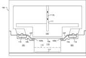
도 4a는 본 발명의 일부 실시예들에 따른, 전기도금 장치 내의 핑거 콘택트들 및 립 시일 부재의 전기적 상태들을 측정하기 위한 디바이스의 평면도를 도시한다.
도 4b는 본 발명의 일부 실시예들에 따른, 보다 상세히 도시된 스위칭 회로를 가진 도 4a로부터의 디바이스를 도시한다.
도 5는 본 발명의 일부 실시예들에 따른, 전류 스위치 모듈에 대한 전기적 연결을 갖고 그리고 측정 스위치 모듈에 대한 전기적 연결을 가진 미리 결정된 전도성 패드의 전기 배선도 (electrical diagram) 를 도시한다.
도 6a는 본 발명의 일부 실시예들에 따른, 핑거 콘택트들의 지지 표면들 (107C) 상에 놓이도록 포지셔닝된 디바이스의 도면을 도시한다.
도 6b는 본 발명의 일부 실시예들에 따른, 디바이스 및 핑거 콘택트들을 통한, 도 6a에 참조로 표시된 바와 같은 수직 단면 뷰, "B-B 뷰"를 도시한다.
도 7은 본 발명의 일부 실시예들에 따른, 전류를 제 1 전도성 패드에 공급하도록 전류 소스의 연결 그리고 전류를 다시 전류 소스로 싱크하도록 (sink) 제 2 전도성 패드에 대한 연결을 나타내는 전기 회로도를 도시한다.
도 8은 본 발명의 일부 실시예들에 따른, 전기도금 장치 내에서 전기적 콘택트들의 전기적 특성들을 측정하기 위한 방법의 흐름도를 도시한다.
도 9는 본 발명의 일부 실시예들에 따른, 자동화된 전기도금 셀 평가를 구현하도록 전기도금 장치를 동작시키기 위한 방법의 흐름도를 도시한다.
도 10은 본 발명의 일부 실시예들에 따른, 반도체 프로세싱 장치의 상태를 평가하기 위한 방법의 흐름도를 도시한다.1A shows a generalized view of a vertical cross-section of an electroplating apparatus for electroplating a wafer, in accordance with some embodiments of the present invention.
1B shows the view of FIG. 1A, wherein the cone member is moved downward to interface with the wafer, to press the downwardly directed peripheral region of the wafer against the sealing surface of the lip seal member, in accordance with some embodiments of the present invention; show
2A shows a top view of finger contacts, in accordance with some embodiments of the present invention.
FIG. 2B shows a vertical cross-sectional view, “AA view,” as indicated with reference to FIG. 2A , through one of the finger contacts, in accordance with some embodiments of the present invention.
3A shows exemplary plots of plated thickness and finger contact electrical resistance as a function of azimuth along a predetermined radius of a wafer, wherein all finger contacts exhibit an acceptable electrical resistance, in accordance with an exemplary embodiment of the present invention. have
3B shows plating obtained for two wafers using all finger contacts in good condition for one wafer and some finger contacts in poor condition for another wafer, in accordance with an exemplary embodiment of the present invention. Plots of thickness are shown.
3C is a function of azimuth at a predetermined radius as shown in FIG. 3B, along with a plot of the electrical resistance of finger contacts used for plating as a function of azimuth at a predetermined radius, in accordance with an exemplary embodiment of the present invention; shows a plot of plating thickness for a wafer plated using some discolored finger contacts as .
4A shows a top view of a device for measuring electrical states of a lip seal member and finger contacts in an electroplating apparatus, in accordance with some embodiments of the present invention.
4B shows the device from FIG. 4A with a switching circuit shown in greater detail, in accordance with some embodiments of the present invention.
5 shows an electrical diagram of a predetermined conductive pad with an electrical connection to a current switch module and with an electrical connection to a measurement switch module, in accordance with some embodiments of the present invention.
6A shows a diagram of a device positioned to rest on support surfaces 107C of finger contacts, in accordance with some embodiments of the present invention.
6B shows a vertical cross-sectional view, “BB view,” as indicated with reference to FIG. 6A , through device and finger contacts, in accordance with some embodiments of the present invention.
7 is an electrical circuit diagram illustrating a connection of a current source to supply current to a first conductive pad and a connection to a second conductive pad to sink current back to the current source, in accordance with some embodiments of the invention; show
8 shows a flow diagram of a method for measuring electrical properties of electrical contacts in an electroplating apparatus, in accordance with some embodiments of the present invention.
9 shows a flow diagram of a method for operating an electroplating apparatus to implement automated electroplating cell evaluation, in accordance with some embodiments of the present invention.
10 shows a flowchart of a method for evaluating a state of a semiconductor processing apparatus, in accordance with some embodiments of the present invention.
다음의 기술에서, 수많은 구체적인 상세들이 제공된 발명의 완전한 이해를 제공하도록 제시된다. 그러나, 본 발명은 이들 구체적인 상세들의 일부 또는 전부 없이 실시될 수도 있다는 것이 당업자에게 자명할 것이다. 다른 예들에서, 공지된 프로세스 동작들은 본 발명을 불필요하게 모호하게 하지 않도록 상세히 기술되지 않았다.In the following description, numerous specific details are set forth in order to provide a thorough understanding of the presented invention. However, it will be apparent to one skilled in the art that the present invention may be practiced without some or all of these specific details. In other instances, well-known process operations have not been described in detail so as not to unnecessarily obscure the present invention.
도 1a는 본 발명의 일부 실시예들에 따른, 웨이퍼 (109) 를 전기도금하기 위한 전기도금 장치 (100) 의 수직 단면의 일반화된 도면을 도시한다. 예시적인 실시예에서, 본 명세서에서 사용되는 바와 같은 용어 웨이퍼는 반도체 웨이퍼를 지칭한다. 또한, 다양한 실시예들에서, 본 명세서에서 지칭되는 바와 같은 웨이퍼는 형태, 형상, 및/또는 사이즈가 가변할 수도 있다. 예를 들어, 일부 실시예들에서, 본 명세서에서 지칭되는 바와 같은 웨이퍼는 200 ㎜ (millimeters) 반도체 웨이퍼, 300 ㎜ 반도체 웨이퍼, 또는 450 ㎜ 반도체 웨이퍼에 대응할 수도 있다.1A shows a generalized view of a vertical cross-section of an
전기도금 장치 (100) 는 컵 부재 (101) 및 콘 부재 (103) 를 포함한다. 전기도금 장치 (100) 는 또한 컵 부재 (101) 의 상단과 인게이지하도록 구성된 립 시일 컴포넌트 (105) 를 포함한다. 복수의 핑거 콘택트들 (107) 은 립 시일 컴포넌트 (105) 의 상단 상에 배치된다. 핑거 콘택트들 (107) 은 프로세싱될 웨이퍼 (109) 의 주변 에지 구역에 실질적으로 균일한 지지를 제공하도록 원형 구성으로 배치된다.The
도 2a는 본 발명의 일부 실시예들에 따른, 핑거 콘택트들 (107) 의 평면도를 도시한다. 도 2b는 본 발명의 일부 실시예들에 따른, 핑거 콘택트들 (107) 중 일 핑거 콘택트를 통한, 도 2a에 참조로 표시된 바와 같은 수직 단면 뷰, "A-A 뷰"를 도시한다. 도 2a에 도시된 바와 같이, 복수의 핑거 콘택트들 (107) 은 링 형상의 전도성 스트립 (107A), 예를 들어, 금속성 스트립과 연결되어 일체형으로 형성된다. 핑거 콘택트들 (107) 및 전도성 스트립 (107A) 양자는 전기적으로 전도성이다. 다양한 실시예들에서, 핑거 콘택트들 (107) 및 전도성 스트립 (107A) 은, 전기도금 프로세스의 수행을 위해 충분한 전기 전도를 제공하고 그리고 전기도금 프로세스 동안 웨이퍼 (109) 를 지지하기 위한 충분한 기계적 특성들을 갖고 그리고 전기도금 프로세스 동안 노출되는 환경 및 재료들과 화학적으로 양립가능한, 임의의 전기적으로 전도성 재료로 형성될 수 있다는 것이 이해되어야 한다.2A shows a top view of
도 2b 및 도 1a에 도시된 바와 같이, 핑거 콘택트 (107) 는 립 시일 부재 (105) 의 상단의 상부 윤곽을 따라 아래로 벤딩되도록 (bend down) 성형된다. 그리고, 전도성 스트립 (107A) 의 원주 구성에 대해, 핑거 콘택트 (107) 의 내부 단부 섹션 (107B) 은 웨이퍼 (109) 에 지지 표면 (107C) 을 제공하도록 상측으로 터닝된다. 보다 구체적으로, 전기도금 프로세스 동안, 웨이퍼 (109) 는 핑거 콘택트들 (107) 의 지지 표면들 (107C) 상에 포지셔닝되고, 전기도금될 웨이퍼 (109) 의 표면은 핑거 콘택트들 (107) 의 지지 표면들 (107C) 과 물리적으로 콘택트하도록 하측으로 향한다.2B and 1A , the
콘 부재 (103) 는 화살표 (111A) 로 나타낸 바와 같이, 컵 부재 (101) 에 대해 위 아래로 이동하도록 구성되는 샤프트 (111) 에 부착된다. 전기도금 프로세스 동안, 핑거 콘택트들 (107) 의 내부 단부 섹션들 (107B) 을 립 시일 부재 (105) 를 향하여 하측으로 플렉싱하도록 (flex), 그리고 립 시일 부재 (105) 의 시일링 표면 (105A) 에 대고 웨이퍼 (109) 의 하측으로 향하는 주변 구역을 누르도록, 콘 부재 (103) 는 웨이퍼 (109) 와 인터페이싱하고 그리고 핑거 콘택트들 (107) 의 지지 표면들 (107C) 상에 웨이퍼 (109) 를 누르게 이동된다. 도 1b는 본 발명의 일부 실시예들에 따른, 립 시일 부재 (105) 의 시일링 표면 (105A) 에 대고 웨이퍼 (109) 의 하측으로 향하는 주변 구역을 누르도록, 화살표 (111B) 로 나타낸 바와 같이, 콘 부재 (103) 가 웨이퍼 (109) 와 인터페이싱하게 하측으로 이동되는, 도 1a의 도면을 도시한다.The
컵 (101) 의 내부 구역은 전기도금 용액을 담기 위한 배스 볼륨 (bath volume) (113) 을 형성한다. 웨이퍼 (109) 가 콘 (103) 에 의해 가해진 하향 힘에 의해 립 시일 부재 (105) 의 시일링 표면 (105A) 에 대고 눌러질 때, 전기도금 용액이 웨이퍼 (109) 와 립 시일 부재 (105) 의 시일링 표면 (105A) 사이의 콘택트 위치를 통과하지 못할 것이고, 이에 따라 핑거 콘택트들 (107) 로부터 이격되게 전기도금 용액을 유지하도록, 시일이 웨이퍼 (109) 와 시일링 표면 (105A) 사이에 형성된다.The inner region of the
전기도금 장치 (100) 는 또한 전도성 스트립 (107A) 과 물리적으로 콘택트하도록 배치된 버스 바 (115) 를 포함하고, 이에 따라 버스 바 (115) 와 핑거 콘택트들 (107) 사이에 전기적 연결을 확립한다. 버스 바는 웨이퍼 (109) 의 주변 주위의 방위각 전기도금 균일성의 개선을 위해 금속의 단단한 피스로 형성된다.The
배스 볼륨 (113) 은 애노드 부재 (117) 를 포함한다. 일부 실시예들에서, 애노드 부재 (117) 는 구리로 형성된다. 그러나, 다른 실시예들에서, 애노드 부재 (117) 는 수행될 특정한 전기도금 프로세스에 적합한 다른 전기적으로 전도성 재료들로 형성될 수 있다. 일부 실시예들에서, 멤브레인 (118) 은 멤브레인 (118) 아래의 애노드 구역을 멤브레인 (118) 위의 캐소드 구역으로부터 물리적으로 분리하도록 배스 볼륨 (113) 내에 배치된다. 멤브레인 (118) 이 애노드 구역과 캐소드 구역 사이의 전해액 (전기도금 용액) 의 대량 전달을 방지하도록 구성되지만, 애노드 구역과 캐소드 구역 사이의 이온 전달을 허용한다. 일부 실시예들에서, 멤브레인 (118) 은 이온 선택적인 멤브레인이다.The
전기도금 프로세스 동안, DC (direct current) 전력 공급부의 양 단자는 애노드 부재 (117) 에 전기적으로 연결되고, 그리고 DC 전력 공급부의 음 단자는 버스 바 (115) 에 전기적으로 연결된다. 이 방식으로, 전류 플로우 경로는 전기도금 용액을 통한 애노드 부재 (117) 로부터 전기도금 용액에 노출된 웨이퍼 (109) 의 표면으로, 그리고 웨이퍼 (109) 의 표면으로부터 핑거 콘택트들 (107) 로, 그리고 핑거 콘택트들 (107) 로부터 버스 바 (115) 로 확립된다. 통상적으로, 전기도금 프로세스 전에, 전도성 씨드 층은 도금될 웨이퍼 (109) 의 표면 상에 형성되고, 이에 따라 웨이퍼 (109) 에 걸쳐 최초의 전기 전도성을 제공한다. 따라서, 전기도금 프로세스 동안 재료가 웨이퍼 (109) 상에 디포짓되고/성장될 때, 디포짓된 재료는 웨이퍼 (109) 에 걸친 전기 전도성에 기여한다.During the electroplating process, a positive terminal of a direct current (DC) power supply is electrically connected to the
수많은 전기도금 프로세스 사이클들 동안, 일부 전기도금 용액은 웨이퍼 (109) 와 립 시일 부재 (105) 의 시일링 표면 (105A) 사이의 콘택트 위치를 지나 침투할 수도 있고 그리고 핑거 콘택트들 (107) 에 도달할 수도 있다. 이것이 발생할 때, 일부 재료는 핑거 콘택트들 (107) 상에 그리고/또는 립 시일 부재 (105) 상에 도금될 수도 있다. 재료가 핑거 콘택트들 (107) 상에 그리고/또는 립 시일 부재 (105) 상에 도금될 때, 도금된 핑거 콘택트들 (107) 및/또는 립 시일 부재 (105) 의 도금된 부분(들)의 변화된 전기적 특성들에 의해 전기적으로 영향을 받은 위치들에서 웨이퍼 (109) 상에 부정적인 도금 결과들을 유발하도록, 이들 도금된 핑거 콘택트들 (107) 및/또는 립 시일 부재 (105) 의 도금된 부분(들)의 전기적 특성들이 변화할 것이다. 예를 들어, 웨이퍼 (109) 상의 부정적인 도금 결과들은 보다 얇은 도금된 재료 두께의 구역들에 나타날 수도 있고, 이는 결국 웨이퍼 (109) 에 걸친 도금 불균일성을 도입하고, 이는 결국 반도체 디바이스 제조 어려움 및/또는 디펙트들을 야기할 수 있다.During numerous electroplating process cycles, some electroplating solution may penetrate past the contact location between the sealing
도 3a는 본 발명의 예시적인 실시예에 따른, 웨이퍼 (109) 의 미리 결정된 반경을 따른 방위각의 함수로서 도금된 두께 및 핑거 콘택트 (107) 전기 저항의 예시적인 플롯들을 도시하고, 여기서 모든 핑거 콘택트들 (107) 은 용인 가능한 전기 저항을 갖는다. 도금된 두께는 ㎛의 단위들로 제시된다. 핑거 콘택트 (107) 전기 저항은 mΩ의 단위들로 제시된다. 방위각은 웨이퍼 (109) 의 상단 표면과 하단 표면에 대해 수직으로 그리고 웨이퍼 (109) 의 중심 점을 통해 연장하는 웨이퍼 (109) 의 중심 축을 중심으로 측정된다. 도 3a에 도시된 바와 같이, 양호한 상태의 핑거 콘택트들 (107) 을 사용하여, 재료의 도금된 두께는 웨이퍼 (109) 의 미리 결정된 반경을 따라 실질적으로 균일하고, 이는 목표된 도금 결과이다.3A shows exemplary plots of plated thickness and
도 3b는 본 발명의 예시적인 실시예에 따른, 일 웨이퍼 (109) 에 대해 모든 양호한 상태의 핑거 콘택트들 (107) 을 사용하여 그리고 다른 웨이퍼 (109) 에 대해 불량한 상태의 일부 핑거 콘택트들 (107) 을 사용하여, 2 개의 웨이퍼들 (109) 에 대해 획득된 도금된 두께의 플롯들을 도시한다. 도 3b의 도금된 두께 플롯들은 2 개의 웨이퍼들 (109) 의 미리 결정된 반경을 따른 방위각의 함수로서 도시된다. 불량한 상태의 핑거 콘택트들 (107) 은 웨이퍼 (109) 와 립 시일 부재 (105) 의 시일링 표면 (105A) 사이의 콘택트 위치를 지나는 전기도금 용액 누설에 기인하여 바람직하지 않은 전기도금을 겪게 된다. 불량한 상태의 핑거 콘택트들 (107) 상의 전기도금이 다소 변색을 유발하기 때문에, 불량한 상태의 이들 핑거 콘택트들 (107) 은 변색된 콘택트들로서 지칭되고 그리고 용인 가능한 사양들 밖의 전기적 특성들, 예를 들어, 전기 저항을 갖는다. 도 3b에 도시된 바와 같이, 도금 두께의 일탈 (aberration) 에 기초하여, 변색된 핑거 콘택트들 (107) 은 약 130 도의 방위각 내지 약 188 도의 방위각 사이에 위치되는 것으로 보인다.3B shows using all
도 3c는 본 발명의 예시적인 실시예에 따른, 방위각의 함수로서 도금을 위해 사용된 핑거 콘택트들 (107) 의 전기 저항의 플롯과 함께, 도 3b에 도시된 바와 같이 미리 결정된 반경에서 방위각의 함수로서 다소 변색된 핑거 콘택트들 (107) 을 사용하여 도금된 웨이퍼 (109) 에 대한 도금 두께의 플롯을 도시한다. 도 3c는 도금 두께가 불균일한 방위각 위치들에서, 대응하는 변색된 핑거 콘택트들 (107) 이 다른 핑거 콘택트들 (107) 에 비해 고 전기 저항을 갖는다는 것을 도시하고, 이는 변색된 핑거 콘택트들 (107) 상의 재료의 바람직하지 않은 도금을 나타낸다.3C is a function of azimuth at a predetermined radius as shown in FIG. 3B , along with a plot of the electrical resistance of
전술한 바를 고려하여, 도금 두께 및 균일성의 면에서 용인 가능한 전기도금 결과들을 유지하는 것은 핑거 콘택트들 (107) 및 립 시일 부재 (105) 의 양호한 상태를 유지하는 것에 의존한다는 것이 이해되어야 한다. 그리고, 핑거 콘택트들 (107) 및 립 시일 부재 (105) 의 양호한 상태를 유지하기 위해, 전기도금이 핑거 콘택트들 (107) 및/또는 립 시일 부재 (105) 상에 발생하는지의 여부 그리고 어느 정도로 발생하는지를 모니터링하는 것이 필요하다. 또한, 이 모니터링은 전기도금 장치 (100) 의 유효성에 상당히 영향을 주지 않는 방식으로 행해져야 한다.In view of the foregoing, it should be understood that maintaining acceptable electroplating results in terms of plating thickness and uniformity depends on maintaining good condition of the
도 4a는 본 발명의 일부 실시예들에 따른, 전기도금 장치 (100) 내의 핑거 콘택트들 (107) 및 립 시일 부재 (105) 의 전기적 상태들을 측정하기 위한 디바이스 (400) (측정 디바이스 (400)) 의 평면도를 도시한다. 디바이스 (400) 는 웨이퍼 (109) 의 형태 인자와 유사한 형태 인자를 가진 인쇄 회로 기판을 포함한다. 따라서, 디바이스 (400) 는 웨이퍼 (109) 와 동일한 방식으로 핸들링될 (handled) 수 있고 그리고 웨이퍼 (109) 와 동일한 방식으로 전기도금 장치 (100) 내에 포지셔닝될 수 있다. 또한, 디바이스 (400) 는 제조 설비 내에서 임의의 웨이퍼 핸들링 장비를 사용하여 임의의 웨이퍼와 같이 여기저기 이동될 수 있다. 부가적으로, 디바이스 (400) 는 임의의 웨이퍼와 같이 저장될 수 있다. 일부 실시예들에서, 디바이스 (400) 는, 핑거 콘택트들 (107) 및/또는 립 시일 부재 (105) 의 전기적 특성들의 디바이스 (400) 에 의한 측정을 제공하도록, 전기도금 툴의 동반 웨이퍼 슬롯 내에 저장되고 그리고 웨이퍼 핸들링 로봇에 의해 전기도금 장치 (100) 내에 배치된다. 그러나, 일부 실시예들에서, 디바이스 (400) 는 핑거 콘택트들 (107) 및/또는 립 시일 부재 (105) 의 전기적 특성들의 디바이스 (400) 에 의한 측정을 제공하도록 손으로 전기도금 장치 (100) 내에 포지셔닝될 수 있다는 것이 이해되어야 한다.4A is a device 400 (measurement device 400) for measuring electrical states of
디바이스 (400) 는 디바이스 (400) 의 외측 방사상 구역을 따라 포지셔닝된 복수의 노출된 전기적으로 전도성 패드들 (401) 을 포함한다. 이웃한 쌍의 전도성 패드들 (401) 각각은 절연 부재 (403), 예를 들어, 전기적 절연체 재료에 의해 서로 전기적으로 절연된다. 전도성 패드 (401) 각각은 전력 소스 (405) 에 대한 전기적 연결 (404) 및 측정 회로 (407) 에 대한 전기적 연결 (406) 을 포함한다. 일부 실시예들에서, 전력 소스 (405) 는 전력 소스 (405) 의 제 1 단자 (405A) 와 전력 소스 (405) 의 제 2 단자 (405B) 사이에서 연장하는 전기적으로 전도성 경로를 통해 제어된 전류량을 공급하도록 구성될 수 있다. 일부 실시예들에서, 전력 소스 (405) 는 전력 소스 (405) 의 제 1 단자 (405A) 와 전력 소스 (405) 의 제 2 단자 (405B) 사이에 제어된 전압량을 공급하도록 구성된다. 전류 및/또는 전압이 미리 결정된 시간에 임의의 하나 이상의 전도성 패드들 (401) 에 공급될 수 있도록, 모든 전도성 패드들 (401) 의 전기적 연결들 (404) 이 스위칭 회로 (409) 를 통해 전력 소스 (405) 로 이루어진다. 그리고, 임의의 하나 이상의 전도성 패드들 (401) 상에 존재하는 전기적 파라미터가 미리 결정된 시간에 측정될 수 있도록, 모든 전도성 패드들 (401) 의 전기적 연결들 (406) 이 스위칭 회로 (409) 를 통해 측정 회로 (407) 로 이루어진다. 일부 실시예들에서, 측정 회로 (407) 는 측정된 아날로그 전기적 파라미터들을 디지털 포맷으로 변환하기 위한 아날로그-투-디지털 변환 회로를 포함한다. 측정 회로 (407) 는 또한 측정된 전기적 파라미터들을 디지털 포맷으로 저장하기 위한 메모리 모듈 (413) 을 포함한다.
전력 소스 (405), 측정 회로 (407), 및 스위칭 회로 (409) 각각은 제어 모듈 (411) 의 지시 하에서 동작하도록 구성된다. 이 방식으로, 미리 결정된 시간에, 제어 모듈 (411) 은 전도성 패드들 (401) 중 특정한 하나 (또는 그 이상) 를 전력 소스 (405) 에 연결하고 그리고 전도성 패드들 (401) 중 특정한 하나 (또는 그 이상) 를 측정 회로 (407) 에 연결하게 스위칭 회로 (409) 에 지시하도록 동작한다. 또한, 전력 소스 (405), 측정 회로 (407), 및 스위칭 회로 (409) 각각은 전력 공급부 (415) 로부터 전력을 수용하도록 연결된다. 일부 실시예들에서, 전력 공급부 (415) 는 배터리이다. 일부 실시예들에서, 전력 공급부 (415) 는 재충전되는 배터리이다.Each of the
또한, 디바이스 (400) 는 측정 회로 (407) 에 의해 측정된 전기적 파라미터들에 대응하는 디지털 데이터 및/또는 디바이스 (400) 의 상태에 대응하는 디지털 데이터를 전달하도록 구성된 통신 모듈 (417) 을 포함한다. 일부 실시예들에서, 통신 모듈 (417) 은 디바이스 (400) 의 범위 내의 무선 수신기로 디지털 데이터를 무선으로 전송하도록 구성된다. 그리고, 일부 실시예들에서, 통신 모듈 (417) 은 디지털 데이터가 전송될 수 있는, 디바이스 (400) 로의 유선 연결을 지원하도록 구성된다. 그리고, 일부 실시예들에서, 통신 모듈 (417) 은 무선 통신 모드 및 유선 통신 모드 양자를 지원하도록 구성된다. 통신 모듈 (417) 은 전력 공급부 (415) 로부터 전력을 수용하도록 연결된다. 따라서, 통신 모듈 (417) 이 무선 통신 모드를 지원하도록 구성되는 경우에, 디바이스 (400) 가 웨이퍼 (109) 와 동일한 방식으로 제조 설비를 통해 그리고 전기도금 툴을 통해 이동될 수 있도록, 디바이스 (400) 는 완전히 독자적인 방식 및 의존적인 방식으로 동작할 수 있다.The
부가적으로, 제어 모듈 (411) 은 전력 소스 (405) 및 측정 회로 (407) 를 사용하여 임의의 규정된 형태의 측정의 수행을 지시하도록 통신 모듈 (417) 을 통해 프로그래밍될 수 있다. 따라서, 제어 모듈 (411) 이 제어 신호들을 통신 모듈 (417), 전력 소스 (405), 측정 회로 (407), 메모리 모듈 (413), 전력 공급부 (415), 및 스위칭 회로 (409) 각각으로 전달하도록 그리고 데이터 신호들을 통신 모듈 (417), 전력 소스 (405), 측정 회로 (407), 메모리 모듈 (413), 전력 공급부 (415), 및 스위칭 회로 (409) 각각으로부터 수신하도록 연결된다는 것이 이해되어야 한다.Additionally,
도 4b는 본 발명의 일부 실시예들에 따른, 보다 상세히 도시된 스위칭 회로 (409) 를 가진 도 4a로부터의 디바이스 (400) 를 도시한다. 도 4b의 특정한 스위칭 회로 (409) 구성은 예로서 제공된다는 것이 이해되어야 한다. 다른 실시예들에서, 스위칭 회로 (409) 는 도 4b의 예에 도시된 것과 상이하게 구성될 수 있다. 보다 구체적으로, 다른 실시예들에서, 미리 결정된 시간에 전도성 패드들 (401) 중 선택된 하나 이상의 전도성 패드들을 전력 소스 (405) 에 전기적으로 연결하고 그리고 미리 결정된 시간에 전도성 패드들 (401) 중 선택된 하나 이상의 전도성 패드들을 측정 회로 (407) 에 전기적으로 연결하는 기능이 존재하는 한, 스위칭 회로 (409) 는 본질적으로 임의의 방식으로 구성될 수 있다. 또한, 디바이스 (400) 에 관하여 본 명세서에 도시되거나 기술된 임의의 전기적 연결은 본질적으로 어떤 적절한 구성의 전기적 트레이스들을 사용하여 디바이스 (400) 의 인쇄 회로 기판 내/상에서 구현될 수 있다는 것이 이해되어야 한다. 그리고, 일부 실시예들에서, 디바이스의 인쇄 회로 기판 (400) 은 전기적 트레이스들의 복수의 층들을 포함할 수 있고, 전기적 트레이스들의 이웃한 층들은 유전체 재료에 의해 서로 분리되고, 그리고 비아 전도체들은 필요하다면 상이한 층들에서 전기적 트레이스들을 연결하도록 사용된다.4B shows the
도 4b의 스위칭 회로 (409) 구성에서, 전기적 연결 (404) 각각은 대응하는 전도성 패드 (401) 로부터 대응하는 전류 스위치 모듈 (419) 로 연장한다. 그리고, 전기적 연결 (406) 각각은 대응하는 전도성 패드 (401) 로부터 대응하는 측정 스위치 모듈 (421) 로 연장한다. 따라서, 전도성 패드들 (401) 각각은 대응하는 전류 스위치 모듈 (419) 및 대응하는 측정 스위치 모듈 (421) 을 갖는다.In the
전력 버스 (423) 는 각각의 전류 스위치 모듈들 (419) 과의 연결을 위해 제공된다. 그리고, 기준 접지 버스 (425) 는 각각의 전류 스위치 모듈들 (419) 과의 연결을 위해 제공된다. 전류 소스가 제어 모듈 (411) 의 제어 하에서, 전류를 전력 버스 (423) 로 공급하고 그리고 전류를 기준 접지 버스 (425) 로부터 싱크하게 동작될 수 있도록, 전력 버스 (423) 및 기준 접지 버스 (425) 양자는 전력 소스 (405) 에 전기적으로 연결된다.A
제 1 측정 버스 (427) 는 각각의 측정 스위치 모듈들 (421) 과의 연결을 위해 제공된다. 그리고, 제 2 측정 버스 (429) 는 각각의 측정 스위치 모듈들 (421) 과의 연결을 위해 제공된다. 제 1 측정 버스 (427) 및 제 2 측정 버스 (429) 양자는 측정 회로 (407) 에 전기적으로 연결된다. 제어 모듈 (411) 의 제어 하에서, 측정 회로 (407) 는 미리 결정된 시간에 제 1 측정 버스 (427) 상의 전기적 신호 및/또는 제 2 측정 버스 (429) 상의 전기적 신호를 센싱하도록 동작될 수 있다.A
도 5는 본 발명의 일부 실시예들에 따른, 전류 스위치 모듈 (419) 에 대한 전기적 연결 (404) 을 갖고 그리고 측정 스위치 모듈 (421) 에 대한 전기적 연결 (406) 을 가진 미리 결정된 전도성 패드 (401) 의 전기 배선도 (electrical diagram) 를 도시한다. 전류 스위치 모듈 (419) 내에서, 전기적 연결 (404) 이 한 쌍의 스위치 디바이스들 (501 및 503) 에 연결된다. 일부 실시예들에서, 스위치 디바이스 (501 및 503) 각각은 집적 회로 스위칭 디바이스로서 구현된다. 그러나, 일부 실시예들에서, 스위치 디바이스들 (501 및 503) 은 아날로그 스위칭 디바이스들로서 구현될 수 있다. 스위치 디바이스 (501 및 503) 각각은 연결들 (505 및 507) 로 각각 나타낸 바와 같이 제어 모듈 (411) 의 제어 하에 있다. 스위치 디바이스 (501) 는 이전에 논의된 바와 같이 결국 전력 소스 (405) 에 연결되는 전력 버스 (423) 에 연결된 단자를 갖는다. 그리고, 스위치 디바이스 (503) 는 이전에 논의된 바와 같이 결국 전력 소스 (405) 에 연결되는 기준 접지 버스 (425) 에 연결된 단자를 갖는다. 이 구성을 사용하여, 제어 모듈 (411) 은 전도성 패드 (401) 를 전력 버스 (423) 또는 기준 접지 버스 (425) 에 전기적으로 연결하도록 스위치 디바이스들 (501 및 503) 을 동작시킬 수 있다. 이 방식으로, 전류 스위치 모듈 (419) 내의 스위치 디바이스들 (501 및 503) 의 설정들에 따라, 전류 및/또는 전압은 미리 결정된 시간에 전력 소스 (405) 로부터 특정한 전도성 패드 (401) 로 인가될 수 있거나, 특정한 전도성 패드 (401) 는 미리 결정된 시간에 기준 접지 전위에 전기적으로 연결될 수 있다.5 shows a predetermined
측정 스위치 모듈 (421) 내에서, 전기적 연결 (406) 은 한 쌍의 스위치 디바이스들 (509 및 511) 에 연결된다. 일부 실시예들에서, 스위치 디바이스 (509 및 511) 각각은 집적 회로 스위칭 디바이스로서 구현된다. 그러나, 일부 실시예들에서, 스위치 디바이스들 (509 및 511) 은 아날로그 스위칭 디바이스들로서 구현될 수 있다. 스위치 디바이스 (509 및 511) 각각은 연결들 (513 및 515) 로 각각 나타낸 바와 같이 제어 모듈 (411) 의 제어 하에 있다. 스위치 디바이스 (509) 는 이전에 논의된 바와 같이 결국 측정 회로 (407) 에 연결되는 제 1 측정 버스 (427) 에 연결된 단자를 갖는다. 그리고, 스위치 디바이스 (511) 는 이전에 논의된 바와 같이 결국 측정 회로 (421) 에 연결되는 제 2 측정 버스 (429) 에 연결된 단자를 갖는다. 이 구성을 사용하여, 제어 모듈 (411) 은 전도성 패드 (401) 를 제 1 측정 버스 (427) 또는 제 2 측정 버스 (429) 에 전기적으로 연결하도록 스위치 디바이스들 (509 및 511) 을 동작시킬 수 있다. 이 방식으로, 전류 스위치 모듈 (421) 내의 스위치 디바이스들 (509 및 511) 의 설정들에 따라, 측정 회로 (407) 는 미리 결정된 시간에 특정한 전도성 패드 (401) 에서 고 전류 및/또는 전압을 센싱하거나, 미리 결정된 시간에 특정한 전도성 패드 (401) 에서 저 전류 및/또는 전압을 센싱하도록 연결될 수 있다.Within the
도 6a는 본 발명의 일부 실시예들에 따른, 핑거 콘택트들 (107) 의 지지 표면들 (107C) 상에 놓이도록 포지셔닝된 디바이스 (400) 의 도면을 도시한다. 도 6a에 도시된 뷰는 콘 부재 (103) 를 향하여 상측으로 본 배스 볼륨 (113) 내부의 관점으로부터의 뷰이다. 도 6a에 도시된 바와 같이, 전도성 패드 (401) 각각과 전도성 패드 (401) 와 물리적으로 콘택트하는 핑거 콘택트들 (107) 의 대응하는 서브세트 사이에 전기 전도 경로를 확립하도록, 전도성 패드들 (401) 은 핑거 콘택트들 (107) 의 지지 표면들 (107C) 과 콘택트한다. 이 방식으로, 전도성 패드들 (401) 각각은 핑거 콘택트들 (107) 의 상이한 서브세트와 전기적으로 연결된다.FIG. 6A shows a diagram of a
도 6b는 본 발명의 일부 실시예들에 따른, 디바이스 (400) 및 핑거 콘택트들 (107) 을 통한, 도 6a에 참조로 표시된 바와 같은 수직 단면 뷰, "B-B 뷰"를 도시한다. 도 6a에 도시된 바와 같이, 전도성 패드들 (401) 이 핑거 콘택트들 (107) 의 지지 표면들 (107C) 상에 놓이도록 디바이스 (400) 가 포지셔닝된다. 전기도금 프로세싱을 겪는 웨이퍼 (109) 와 마찬가지로, 디바이스 (400) 는 정밀하게 제어된 양의 하향 힘을 사용하여 핑거 콘택트들 (107) 의 지지 표면들 (107C) 상으로 전도성 패드들 (401) 을 누르도록 콘 부재 (103) 에 의해 콘택트될 수 있다. 또한, 핑거 콘택트들 (107) 의 어떤 서브세트가 전도성 패드들 (401) 중 특정한 전도성 패드와 물리적으로 콘택트하는지를 알도록, 디바이스 (400) 의 회전 포지션이 전기도금 장치 (100) 에 대해 인덱싱될 (indexed) 수 있다는 것이 이해되어야 한다. 디바이스 (400) 가 웨이퍼 (109) 의 형태 인자와 유사한 형태 인자를 갖기 때문에, 디바이스 (400) 는 전기도금 장치 (100) 가 연결되는 제조 스테이션에서 이용 가능한 표준 웨이퍼 정렬기 디바이스를 사용하여 전기도금 장치 (100) 에 대해 회전하여 인덱싱될 수 있다.6B shows a vertical cross-sectional view, “B-B view,” as indicated with reference to FIG. 6A , through
스위칭 회로 (409) 의 적절한 설정을 사용하여, 전류 및/또는 전압은 전력 소스 (405) 로부터 미리 결정된 전도성 패드 (401) 를 통해 미리 결정된 전도성 패드와 물리적으로 연결된 핑거 콘택트들 (107) 의 특정한 서브세트로 지향될 수 있다. 그리고, 스위칭 회로 (409) 의 적절한 설정을 사용하여, 미리 결정된 전도성 패드 (401) 와 물리적으로 연결된 핑거 콘택트들 (107) 의 특정한 서브세트는 기준 접지 전위에 전기적으로 연결될 수 있다. 이 방식으로, 제어 모듈 (411) 및 스위칭 회로 (409) 의 동작을 통해, 정밀하게 제어된 전류는, 디바이스 (400) 의 주변 주위의 제 1 방위각 위치에서의 제 1 전도성 패드 (401) 내로, 그리고 제 1 전도성 패드 (401) 와 물리적으로 콘택트하는 핑거 콘택트들 (107) 의 제 1 특정한 서브세트를 통해, 그리고 핑거 콘택트들 (107) 의 제 1 특정한 서브세트로부터 전도성 스트립 (107A) 을 통해 (그리고 가능하게는 버스 바 (115) 와 같은 전도성 스트립 (107A) 과 콘택트하는 다른 전기적으로 전도성 컴포넌트들을 통해) 디바이스 (400) 의 주변 주위의 제 2 방위각 위치에서의 핑거 콘택트들 (107) 의 제 2 특정한 서브세트로, 그리고 핑거 콘택트들 (107) 의 제 2 특정한 서브세트로부터 디바이스 (400) 의 주변 주위의 제 2 방위각 위치에서의 제 2 전도성 패드 (401) 로, 그리고 제 2 전도성 패드 (401) 로부터 기준 접지 전위로 흐르도록 지향될 수 있다. 그리고, 유사하게, 제어 모듈 (411) 및 스위칭 회로 (409) 의 동작을 통해, 정밀하게 제어된 전압은 디바이스 (400) 의 주변 주위의 제 1 방위각 위치에서의 제 1 전도성 패드 (401) 와 디바이스 (400) 의 주변 주위의 제 2 방위각 위치에서의 제 2 전도성 패드 (401) 사이에 인가될 수 있다.Using the appropriate setting of the
제어 모듈 (411) 은 제 1 방위각 위치에 대해 임의의 전도성 패드들 (401) 그리고 제 2 방위각 위치에 대해 임의의 전도성 패드들 (401) 을 선택하기 위해 스위칭 회로 (409) 의 동작을 지시하도록 프로그래밍될 수 있다. 일부 실시예들에서, 제 2 방위각 위치는 제 1 전도성 패드 (401) 옆에 포지셔닝되는 전도성 패드 (401) 에 대응하고, 여기서 제 1 전도성 패드 (401) 는 제 1 방위각 위치에 대응한다. 일부 실시예들에서, 복수의 전도성 패드들 (401) 은 복수의 제 2 방위각 위치들을 제공하도록 선택된다. 예를 들어, 일부 실시예들에서, 복수의 제 2 방위각 위치들은 제 1 전도성 패드 (401) 의 측면 각각 상에 각각 포지셔닝된 2 개의 전도성 패드들 (401) 에 대응한다. 이 특정한 예에서, 전류는 제 1 전도성 패드 (401) 내로 흐를 것이고 제 1 전도성 패드 (401) 에 이웃한 2 개의 전도성 패드들 (401) 양자를 다시 통과할 수 있다.The
정밀하게 제어된 전류의 플로우를 제 1 방위각 위치에서의 핑거 콘택트들 (107) 의 제 1 서브세트 내로 그리고 다시 제 2 방위각 위치에서의 핑거 콘택트들 (107) 의 제 2 서브세트로부터 지향시키도록 디바이스 (400) 를 동작시키는 것과 함께, 제어 모듈 (411) 은 측정 회로 (407) 를 제 1 방위각 위치에서의 제 1 전도성 패드 (401) 및 제 2 방위각 위치에서의 제 2 전도성 패드 (401) 중 하나 또는 양자에 연결하도록 스위칭 회로 (409) 에 지시하게 프로그래밍될 수 있고, 이에 따라 제 1 방위각 위치에서의 제 1 전도성 패드 (401) 및 제 2 방위각 위치에서의 제 2 전도성 패드 (401) 중 하나 또는 양자에서 전압 및/또는 전류의 측정을 제공한다.device to direct a precisely controlled flow of current into a first subset of
디바이스 (400) 내의 전도성 경로들, 예를 들어, 트레이스들의 전기 저항은 디바이스 (400) 의 제작시 신중히 측정된다. 따라서, 정밀하게 제어된 전류가 핑거 콘택트들 (107) 의 제 1 서브세트 내로 그리고 다시 핑거 콘택트들 (107) 의 제 2 서브세트로부터 흐를 때, 핑거 콘택트들 (107) 의 제 1 서브세트와 핑거 콘택트들 (107) 의 제 2 서브세트 사이의 전기 전도 경로를 따른 전기 저항이 측정될 수 있고 그리고 부정적인 전기 도금이 핑거 콘택트들 (107) 의 제 1 서브세트와 핑거 콘택트들 (107) 의 제 2 서브세트 사이의 전기 전도 경로를 따라 발생하는지를 결정하도록 허용 가능한 범위의 전기 저항과 비교될 수 있다. 이 방식으로, 디바이스 (400) 는 부정적인 전기도금이 핑거 콘택트들 (107) 중 특정한 핑거 콘택트들 상에서 발생하는지의 여부를 식별하고 그리고 핑거 콘택트들 (107) 전체의 전기 저항을 완전히 특징짓도록 디바이스 (400) 의 전체 주변 주위의 핑거 콘택트들 (107) 의 상이한 서브세트들 사이의 전기 저항을 측정하기 위해 동작될 수 있다.The electrical resistance of the conductive paths, eg, traces, within the
도 7은 본 발명의 일부 실시예들에 따른, 전류를 제 1 전도성 패드 (401A) 에 공급하도록 전력 소스 (405) 의 연결 그리고 전류를 다시 전력 소스 (405) 로 싱크하도록 제 2 전도성 패드 (401B) 에 대한 연결을 나타내는 전기 회로도를 도시한다. 전력 소스 (405) 는 전류를 제 1 단자 (405A) 에서 공급하고 그리고 전류를 제 2 단자 (405B) 에서 싱크하도록 구성된다. 전력 소스 (405) 는 전류를 전기적 연결 (701) 을 통해 제 1 전도성 패드 (401A) 로 공급하도록 연결된다. 도 5에 관해 이전에 논의된 바와 같이, 전기적 연결 (701) 은 스위칭 회로 (409) 를 통해 제 1 전도성 패드 (401A) 로 라우팅된다 (routed). 전기적 연결 (701) 을 따른 전기 저항 (711) 이 측정되고 공지된다. 전력 소스 (405) 는 전류를 제 2 전도성 패드 (401B) 로부터 전기적 연결 (703) 을 통해 싱크하도록 연결된다. 도 5에 관해 이전에 논의된 바와 같이, 전기적 연결 (703) 은 스위칭 회로 (409) 를 통해 제 2 전도성 패드 (401B) 로 라우팅된다. 전기적 연결 (703) 을 따른 전기 저항 (713) 이 측정되고 공지된다.7 illustrates connection of a
도 7은 또한 제 1 전도성 패드 (401A) 와 전기적으로 연결된 핑거 콘택트들 (107) 의 제 1 서브세트 (107-1), 및 제 2 전도성 패드 (401B) 와 전기적으로 연결된 핑거 콘택트들 (107) 의 제 2 서브세트 (107-2) 를 도시한다. 핑거 콘택트들 (107) 의 제 1 서브세트 (107-1) 내의 핑거 콘택트 (107) 각각은 전도성 스트립 (107A) 을 통해 핑거 콘택트들 (107) 의 제 2 서브세트 (107-2) 내의 핑거 콘택트 (107) 각각에 전기적으로 연결된다. 핑거 콘택트들 (107) 의 제 1 서브세트 (107-1) 와 핑거 콘택트들 (107) 의 제 2 서브세트 (107-2) 사이의 전도성 스트립 (107A) 의 부분을 따른 전기 저항 (709) 이 측정되고 공지된다. 또한, 전도성 스트립 (107A) 은 버스 바 (115) 와 전기적으로 연결된다. 핑거 콘택트들 (107) 의 제 1 서브세트 (107-1) 와 핑거 콘택트들 (107) 의 제 2 서브세트 (107-2) 사이의 버스 바 (115) 의 부분을 따른 전기 저항 (715) 이 측정되고 공지된다. 또한, 전도성 스트립 (107A) 은 립 시일 부재 (105) 와 전기적으로 연결된다. 핑거 콘택트들 (107) 의 제 1 서브세트 (107-1) 와 핑거 콘택트들 (107) 의 제 2 서브세트 (107-2) 사이의 립 시일 부재 (105) 의 부분을 따른 전기 저항 (717) 은 립 시일 부재 (105) 상에 도금된 재료를 가질 가능성 때문에 공지되지 않는다.7 also shows a first subset 107-1 of
측정 회로 (407) 는 측정 회로 (407) 의 제 1 입력부 (407A) 로 라우팅된 전기적 연결 (705) 을 통해 제 1 전도성 패드 (401A) 상에 존재하는, 전기적 특성, 예를 들어, 전류 및/또는 전압을 측정하도록 연결된다. 도 5에 관해 이전에 논의된 바와 같이, 전기적 연결 (705) 은 스위칭 회로 (409) 를 통해 제 1 전도성 패드 (401A) 로 라우팅된다. 전기적 연결 (705) 을 따른 전기 저항 (719) 이 측정되고 공지된다. 측정 회로 (407) 는 또한 측정 회로 (407) 의 제 2 입력부 (407B) 로 라우팅된 전기적 연결 (707) 을 통해 제 2 전도성 패드 (401B) 상에 존재하는, 전기적 특성, 예를 들어, 전류 및/또는 전압을 측정하도록 연결된다. 도 5에 관해 이전에 논의된 바와 같이, 전기적 연결 (707) 은 스위칭 회로 (409) 를 통해 제 2 전도성 패드 (401B) 로 라우팅된다. 전기적 연결 (707) 을 따른 전기 저항 (721) 이 측정되고 공지된다.The
전력 소스 (405) 와 제 1 전도성 패드 (401A) 및 제 2 전도성 패드 (401B) 각각 사이의 다양한 전기 저항들 및 다른 전기적 특성들이 공지된다. 그리고, 측정 회로 (407) 와 제 1 전도성 패드 (401A) 및 제 2 전도성 패드 (401B) 각각 사이의 다양한 전기 저항들 및 다른 전기적 특성들이 공지된다. 또한, 핑거 콘택트들 (107) 의 제 1 서브세트 (107-1) 와 핑거 콘택트들 (107) 의 제 2 서브세트 (107-2) 사이의 전도성 스트립 (107A) 을 따른 전기 저항 및 다른 전기적 특성들이 공지된다. 또한, 핑거 콘택트들 (107) 의 제 1 서브세트 (107-1) 와 핑거 콘택트들 (107) 의 제 2 서브세트 (107-2) 사이의 버스 바 (115) 를 따른 전기 저항 및 다른 전기적 특성들이 공지된다. 따라서, 도 7의 회로에서, 핑거 콘택트들 (107) 의 제 1 서브세트 (107-1) 및 핑거 콘택트들 (107) 의 제 2 서브세트 (107-2) 의 다양한 핑거 콘택트들 (107) 을 통한, 그리고 핑거 콘택트들 (107) 의 제 1 서브세트 (107-1) 와 핑거 콘택트들 (107) 의 제 2 서브세트 (107-2) 사이에서 연장하는 립 시일 부재 (105) 의 부분을 통한 통합된 전기 저항은 핑거 콘택트들 (107) 상에 그리고/또는 립 시일 부재 (105) 상에 도금된 재료가 존재할 가능성 때문에 공지되지 않는다.Various electrical resistances and other electrical properties between the
제 1 전도성 패드 (401A) 및 제 2 전도성 패드 (401B) 각각에서 전압 및/또는 전류를 측정하도록 측정 회로 (407) 를 동작시키는 것과 함께, 정밀하게 제어된 전류를 제 1 전도성 패드 (401A) 에 인가함으로써 그리고 인가된 전류를 제 2 전도성 패드 (401B) 로부터 싱크함으로써, 상기 언급된 통합된 전기 저항이 측정될 수 있고 그리고 부정적인 전기도금이 핑거 콘택트들 (107) 의 제 1 서브세트 (107-1) 및/또는 핑거 콘택트들 (107) 의 제 2 서브세트 (107-2) 내에서 그리고/또는 핑거 콘택트들 (107) 의 제 1 서브세트 (107-1) 와 핑거 콘택트들 (107) 의 제 2 서브세트 (107-2) 사이에서 연장하는 립 시일 부재 (105) 의 부분을 통해 발생하는지를 결정하도록 평가될 수 있다. 일부 실시예들에서, 측정 회로 (407) 는 전기도금 장치 (100) 의 선택된 방위각 섹션을 따라 핑거 콘택트들 (107) 및 립 시일 부재 (105) 를 통해 전기 저항을 측정하도록 전력 소스 (405) 와 결합하여 전력 공급부 (415) 에 의해 전력 공급된 션트 레지스터를 포함한다. 디바이스 (400) 는 전기도금 장치 (100) 의 임의의 선택된 방위각 섹션을 따라 핑거 콘택트들 (107) 의 전기 저항 및 립 시일 부재 (105) 의 전기 저항을 제공한다는 것이 이해되어야 한다.A precisely controlled current is passed to the first
핑거 콘택트들 (107) 및 립 시일 부재 (105) 의 전기적 특성들의 모니터링을 통해, 핑거 콘택트들 (107) 및/또는 립 시일 부재 (105) 의 상태가 부정적인 전기도금 결과를 생성할 가능성을 나타낼 경우에 전기도금 장치 (100) 의 알람을 서비스로 울리는 것이 가능하다. 또한, 일부 실시예들에서, 부가적인 센서들, 예컨대, 광학 센서들은 핑거 콘택트들 (107) 의 그룹 및 립 시일 부재 (105) 의 대응하는 방위각 섹션들의 그룹의 육안 관찰을 제공하도록 디바이스 (400) 내에서 구현될 수 있다.Through monitoring the electrical properties of the
일부 실시예들에서, 디바이스 (400) 는 전기도금 툴 상의 동반 웨이퍼 슬롯 내에 저장되고 그리고 사용자 상호작용이 요구되지 않도록 측정들이 이루어지는 전기도금 장치 (100) 로 로봇으로 이동되게 스케쥴링된다. 일단 측정들이 완료된다면, 디바이스 (400) 는 디바이스 (400) 가 로깅 및 분석을 위해 취해진 측정 데이터를 전기도금 툴로 이송하는 시간에 동반 웨이퍼 슬롯으로 리턴된다 (return). 핑거 콘택트 (107) 전기 저항 및 립 시일 부재 (105) 기능의 추세들은 컴포넌트들의 연차로 로깅될 수 있다.In some embodiments,
전술한 바를 고려하여, 본 명세서에 개시된 디바이스 (400) 는 전기도금 장치, 예컨대, 전기도금 장치 (100) 내에서 전기적 콘택트들의 전기적 특성들을 측정하기 위해 제공되고, 여기서 전기도금 장치는 웨이퍼 (109) 상에서 전기도금 프로세스를 수행하도록 구성된다는 것이 이해되어야 한다. 그러나, 일반적으로 본 명세서에 개시된 디바이스 (400) 는 반도체 프로세싱 장치 (전기도금 장치일 수도 있거나 전기도금 장치가 아닐 수도 있음) 내에서 전기 전도 경로들의 전기적 특성들을 측정하기 위해 사용될 수 있고, 여기서 반도체 프로세싱 장치는 웨이퍼 (109) 상에서 프로세스를 수행할 때 웨이퍼 (109) 의 표면에 전기 전도 경로들을 전기적으로 연결하도록 구성된다는 것이 또한 이해되어야 한다. 디바이스 (400) 는 웨이퍼 (109) 의 외경과 실질적으로 같은 외경을 가진 디스크-형상의 구조체를 포함한다. 일부 실시예들에서, 디바이스 (400) 의 디스크-형상의 구조체는 인쇄 회로 기판이다. 디바이스 (400) 의 디스크-형상의 구조체는 웨이퍼 (109) 의 전체 두께와 실질적으로 유사한 전체 두께를 갖는다.In view of the foregoing, a
디바이스 (400) 는 디스크-형상의 구조체의 제 1 측면의 외측 주변부를 따라 형성된 복수의 전도성 패드들 (401) 을 포함한다. 복수의 전도성 패드들 (401) 중 인접하게 포지셔닝된 전도성 패드들은 서로 전기적으로 절연된다. 일부 실시예들에서, 디바이스 (400) 의 디스크-형상의 구조체는 전기 절연성 재료로 형성되고, 그리고 복수의 전도성 패드들 (401) 중 인접하게 포지셔닝된 전도성 패드들은 디스크-형상의 구조체의 부분에 의해 서로 분리되고, 이에 따라 복수의 전도성 패드들 (401) 중 인접하게 포지셔닝된 전도성 패드들 사이에 전기적 절연을 제공한다. 일부 실시예들에서, 전기적 절연 구조체들, 예컨대, 절연 부재들 (403) 은 복수의 전도성 패드들 (401) 중 인접하게 포지셔닝된 전도성 패드들을 서로 전기적으로 절연시키도록 디스크-형상의 구조체 상에 배치된다. 복수의 전도성 패드들 (401) 은 디스크-형상의 구조체의 제 1 측면의 외측 주변부를 전체적으로 둘러싼다. 일부 실시예들에서, 복수의 전도성 패드들 (401) 각각은 디바이스 (400) 의 디스크-형상의 구조체의 제 1 측면의 외측 주변부를 따라 측정될 때와 실질적으로 같은 사이즈를 갖는다.
디바이스 (400) 는 제 1 단자 (405A) 및 제 2 단자 (405B) 를 가진 전력 소스 (405) 를 포함한다. 디바이스 (400) 의 디스크-형상의 구조체가 반도체 프로세싱 장치 내에 포지셔닝될 때 전력 소스 (405) 는 제 1 단자 (405A) 와 제 2 단자 (405B) 사이에서 연장하는 전기적으로 전도성 경로를 통해 그리고 반도체 프로세싱 장치의 부분을 통해 전력을 공급하도록 구성된다. 제 1 단자 (405A) 는 복수의 전도성 패드들 (401) 중 적어도 하나의 전도성 패드의 제 1 세트에 전기적으로 연결된다. 제 2 단자 (405B) 는 복수의 전도성 패드들 (401) 중 적어도 하나의 전도성 패드의 제 2 세트에 전기적으로 연결된다. 복수의 전도성 패드들 (401) 의 제 2 세트는 복수의 전도성 패드들 (401) 의 제 1 세트를 제외한다. 복수의 전도성 패드들 (401) 의 제 1 세트 및 제 2 세트는 제 1 단자 (405A) 와 제 2 단자 (405B) 사이에서 연장하는 전기적으로 전도성 경로의 부분을 형성한다. 일부 실시예들에서, 전력 소스는 제 1 단자 (405A) 와 제 2 단자 (405B) 사이에서 연장하는 전기적으로 전도성 경로를 통해 제어된 전류량을 공급하도록 구성된다. 일부 실시예들에서, 전력 소스는 제 1 단자 (405A) 와 제 2 단자 (405B) 사이에 제어된 전압량을 공급하도록 구성된다.
디바이스 (400) 는 또한 제 1 입력 단자 (407A) 및 제 2 입력 단자 (407B) 를 가진 측정 회로 (407) 를 포함한다. 측정 회로 (407) 의 제 1 입력 단자 (407A) 는 복수의 전도성 패드들 (401) 중 제 1 선택된 전도성 패드에 전기적으로 연결된다. 측정 회로 (407) 의 제 2 입력 단자 (407B) 는 복수의 전도성 패드들 (401) 중 제 2 선택된 전도성 패드에 전기적으로 연결된다. 측정 회로 (407) 는 복수의 전도성 패드들 (401) 중 제 1 선택된 전도성 패드 및 제 2 선택된 전도성 패드에 존재하는 전기적 신호들에 기초하여 전기적 파라미터의 값을 결정하도록 구성된다. 일부 실시예들에서, 측정 회로 (407) 는 복수의 전도성 패드들 (401) 중 제 1 선택된 전도성 패드 및 제 2 선택된 전도성 패드에 존재하는 전기적 신호들에 기초하여 전압 및 전류 중 하나 또는 양자를 측정하도록 구성된다. 일부 실시예들에서, 측정 회로 (407) 는 제 1 입력 단자 (407A) 에 존재하는 제 1 측정 신호 및 제 2 입력 단자 (407B) 에 존재하는 제 2 측정 신호에 기초하여 전압을 측정하도록 구성된다. 일부 실시예들에서, 측정 회로 (407) 는 제 1 입력 단자 (407A) 에 존재하는 제 1 측정 신호 및 제 2 입력 단자 (407B) 에 존재하는 제 2 측정 신호에 기초하여 전류를 측정하도록 구성된다.
디바이스 (400) 는 미리 결정된 시간에 전력 소스 (405) 의 제 1 단자 (405A) 를 복수의 전도성 패드들 (401) 중 제 1 선택된 전도성 패드에 연결하도록 구성된 스위칭 회로 (409) 를 포함한다. 스위칭 회로 (409) 는 또한 미리 결정된 시간에 전력 소스 (405) 의 제 2 단자 (405B) 를 복수의 전도성 패드들 (401) 중 제 2 선택된 전도성 패드에 연결하도록 구성된다. 스위칭 회로 (409) 는 또한 미리 결정된 시간에 측정 회로 (407) 의 제 1 입력 단자 (407A) 를 복수의 전도성 패드들 (401) 중 제 1 선택된 전도성 패드에 연결하도록 구성된다. 그리고, 스위칭 회로 (409) 는 미리 결정된 시간에 측정 회로 (407) 의 제 2 입력 단자 (407B) 를 복수의 전도성 패드들 (401) 중 제 2 선택된 전도성 패드에 연결하도록 구성된다. 디바이스 (400) 는 또한 디스크-형상의 구조체 상에 배치된 전력 공급부 (415) 를 포함한다. 전력 공급부 (415) 는 전력을 디스크-형상의 구조체에 온보드된 (on board) 디바이스 (400) 의 모든 전력 공급된 컴포넌트들에 공급하도록 연결된다. 일부 실시예들에서, 전력 공급부 (415) 는 배터리이다.The
일부 실시예들에서, 디바이스 (400) 는 디스크-형상의 구조체 상에 배치된 제어 모듈 (411) 을 포함한다. 제어 모듈 (411) 은 전력 소스 (405) 및 측정 회로 (407) 및 스위칭 회로 (409) 의 동작을 지시하도록 구성된다. 일부 실시예들에서, 제어 모듈 (411) 은 미리 결정된 시간에 복수의 전도성 패드들 (401) 중 특정한 하나 이상의 전도성 패드들을 전력 소스 (405) 의 제 1 단자 (405A) 에 연결하도록 스위칭 회로 (409) 에 지시하게 구성된다. 그리고, 일부 실시예들에서, 제어 모듈 (411) 은 미리 결정된 시간에 복수의 전도성 패드들 (401) 중 특정한 하나 이상의 전도성 패드들을 전력 소스 (405) 의 제 2 단자 (405B) 에 연결하도록 스위칭 회로 (409) 에 지시하게 구성된다. 일부 실시예들에서, 스위칭 회로 (409) 는, 전력 소스 (405) 의 제 1 단자 (405A) 와 제 2 단자 (405B) 사이의 누전을 방지하기 위해, 미리 결정된 시간에 전력 소스 (405) 의 제 2 단자 (405B) 에 전기적으로 연결된 복수의 전도성 패드들 (401) 중 하나 이상의 전도성 패드들이 미리 결정된 시간에 전력 소스 (405) 의 제 1 단자 (405A) 에 전기적으로 연결된 복수의 전도성 패드들 (401) 중 하나 이상의 전도성 패드들과 상이하다는 것을 보장하도록 동작된다.In some embodiments,
일부 실시예들에서, 스위칭 회로 (409) 는 미리 결정된 시간에 복수의 전도성 패드들 (401) 중 임의의 2 개 이상의 전도성 패드들을 측정 회로 (407) 의 제 1 입력 단자 (407A) 에 선택적으로 전기적으로 연결하도록 구성된다. 또한, 일부 실시예들에서, 스위칭 회로 (409) 는 미리 결정된 시간에 복수의 전도성 패드들 (401) 중 임의의 2 개 이상의 전도성 패드들을 측정 회로 (407) 의 제 2 입력 단자 (407B) 에 선택적으로 전기적으로 연결하도록 구성된다. 일부 실시예들에서, 스위칭 회로 (409) 는 미리 결정된 시간에 측정 회로 (407) 의 제 2 입력 단자 (407B) 에 전기적으로 연결된 복수의 전도성 패드들 (401) 중 2 개 이상의 전도성 패드들이 미리 결정된 시간에 측정 회로 (407) 의 제 1 입력 단자 (407A) 에 전기적으로 연결된 복수의 전도성 패드들 (401) 중 2 개 이상의 전도성 패드들과 상이하다는 것을 보장하도록 동작된다.In some embodiments, the
일부 실시예들에서, 디바이스 (400) 는 디스크-형상의 구조체에 온보드된 컴퓨터 메모리로서 규정된 메모리 모듈 (413) 을 갖도록 구성된다. 컴퓨터 메모리는 측정 회로 (407) 에 의해 결정될 때 전기적 파라미터의 값을 나타내는 디지털 데이터를 저장하도록 구성된다. 또한, 일부 실시예들에서, 측정 회로 (407) 는 전기적 파라미터의 값을 전기적 파라미터의 값을 나타내는 디지털 데이터로 변환하기 위한 아날로그-투-디지털 변환 회로를 포함한다. 또한, 일부 실시예들에서, 디바이스 (400) 는 디스크-형상의 구조체에 온보드 배치된 통신 모듈 (417) 을 포함하도록 구성된다. 일부 실시예들에서, 통신 모듈 (417) 은 측정 회로 (407) 에 의해 결정된 전기적 파라미터의 값을 나타내는 데이터를 무선으로 전달하도록 구성된다.In some embodiments,
일부 실시예들에서, 디바이스 (400) 의 디스크-형상의 구조체에 온보드 배치된 제어 모듈 (411) 은 전력 소스 (405), 측정 회로 (407), 스위칭 회로 (409), 전력 공급부 (415), 메모리 모듈 (413), 및 통신 모듈 (417) 의 동작을 지시하도록 구성된다. 일부 실시예들에서, 제어 모듈 (411) 은, 미리 결정된 시간에 복수의 전도성 패드들 (401) 중 특정한 하나 이상의 전도성 패드들을 전력 소스 (405) 의 제 1 단자 (405A) 에 연결하도록, 그리고 미리 결정된 시간에 복수의 전도성 패드들 (401) 중 특정한 하나 이상의 전도성 패드들을 전력 소스 (405) 의 제 2 단자 (405B) 에 연결하도록, 그리고 미리 결정된 시간에 복수의 전도성 패드들 (401) 중 특정한 하나 이상의 전도성 패드들을 측정 회로 (407) 의 제 1 입력 단자 (407A) 에 연결하도록, 그리고 미리 결정된 시간에 복수의 전도성 패드들 (401) 중 특정한 하나 이상의 전도성 패드들을 측정 회로 (407) 의 제 2 입력 단자 (407B) 에 연결하도록 스위칭 회로 (409) 에 지시하게 구성된다.In some embodiments, the
도 8은 본 발명의 일부 실시예들에 따른, 그 중에서도, 반도체 프로세싱 장치, 예컨대, 전기도금 장치 (100) 내에서 전기 전도 경로들의 전기적 특성들을 측정하기 위한 방법의 흐름도를 도시한다. 반도체 프로세싱 장치는 웨이퍼 (109) 상에서 프로세스를 수행할 때 전기 전도 경로들을 웨이퍼 (109) 의 표면에 전기적으로 연결하도록 구성된다. 방법은 반도체 프로세싱 장치 내에 측정 디바이스 (400) 를 포지셔닝하기 위한 동작 801을 포함한다. 측정 디바이스 (400) 는 웨이퍼 (109) 의 외경과 실질적으로 같은 외경을 갖고 그리고 웨이퍼 (109) 의 전체 두께와 실질적으로 유사한 전체 두께를 가진 디스크-형상의 구조체를 갖는다. 측정 디바이스 (400) 의 제 1 측면의 외측 주변부를 따라 형성된 복수의 전도성 패드들 (401) 이 반도체 프로세싱 장치 내에서 전기적 콘택트들 (107) 과 물리적으로 콘택트하도록 측정 디바이스 (400) 가 반도체 프로세싱 장치 내에 포지셔닝된다. 복수의 전도성 패드들 (401) 중 인접하게 포지셔닝된 전도성 패드들은 측정 디바이스 (400) 상에서 서로 전기적으로 절연된다. 그리고, 복수의 전도성 패드들 (401) 은 측정 디바이스 (400) 의 제 1 측면의 외측 주변부를 전체적으로 둘러싼다.8 shows a flow diagram of a method for measuring electrical properties of electrically conductive paths within a semiconductor processing apparatus, such as an
방법은 또한 복수의 전도성 패드들 (401) 중 적어도 하나의 전도성 패드의 제 1 세트 및 복수의 전도성 패드들 (401) 중 적어도 하나의 전도성 패드의 제 2 세트를 포함하는 전기적으로 전도성 경로를 통해 전력을 공급하도록 측정 디바이스 (400) 를 동작시키기 위한 동작 803을 포함하고, 여기서 복수의 전도성 패드들 (401) 의 제 2 세트는 복수의 전도성 패드들 (401) 의 제 1 세트를 제외한다. 방법은 또한 복수의 전도성 패드들 (401) 중 제 1 선택된 전도성 패드 및 복수의 전도성 패드들 (401) 중 제 2 선택된 전도성 패드에 존재하는 전기적 신호들을 측정하도록 측정 디바이스 (400) 를 동작시키기 위한 동작 805를 포함한다.The method also includes a first set of conductive pads of at least one of the plurality of
방법은 또한 측정된 전기적 신호들을 사용하여 복수의 전도성 패드들 (401) 중 제 1 선택된 전도성 패드 및 복수의 전도성 패드들 (401) 중 제 2 선택된 전도성 패드를 포함하고 그리고 반도체 프로세싱 장치의 부분을 통해 연장하는 전기 전도 경로에 대한 특성화 파라미터를 결정하도록 측정 디바이스 (400) 를 동작시키기 위한 동작 807을 포함한다. 방법은 또한 전기 전도 경로에 대한 특성화 파라미터의 값을 나타내는 데이터를 (무선 방식 및/또는 유선 방식으로) 전달하고 그리고/또는 데이터를 저장하도록 측정 디바이스 (400) 를 동작시키는 것을 포함할 수 있다.The method also includes a first selected one of the plurality of
일부 실시예들에서, 반도체 프로세싱 장치의 부분을 통해 연장하는 전기 전도 경로에 대한 특성화 파라미터는 전기 저항 값이다. 예를 들어, 전기도금 장치 (100) 실시예에서, 측정 디바이스 (400) 가 반도체 프로세싱 장치 (전기도금 장치 (100)) 내에 포지셔닝될 때, 반도체 프로세싱 장치 (전기도금 장치 (100)) 내의 전기 전도 경로들은 복수의 전도성 패드들 (401) 과 물리적으로 콘택트하는 전기적 콘택트들 (107) 을 포함할 수 있다. 보다 구체적으로, 전기 저항 값은 복수의 전도성 패드들 (401) 중 제 1 선택된 전도성 패드와 물리적으로 콘택트하는 전기적 콘택트들 (107) 의 전기 저항 및 복수의 전도성 패드들 (401) 중 제 2 선택된 전도성 패드와 물리적으로 콘택트하는 전기적 콘택트들 (107) 의 전기 저항을 포함한다. 그리고, 전기 저항 값은 복수의 전도성 패드들 (401) 중 제 1 선택된 전도성 패드로부터 복수의 전도성 패드들 (401) 중 제 2 선택된 전도성 패드로 연장하는 립 시일 부재 (105) 의 섹션을 통한 전기 저항을 포함할 수 있다. 또한, 전기 저항 값은 복수의 전도성 패드들 (401) 중 제 1 선택된 전도성 패드로부터 복수의 전도성 패드들 (401) 중 제 2 선택된 전도성 패드로 연장하는 버스 바 (115) 의 섹션을 통한 전기 저항을 포함할 수 있다. 또한, 전기 저항 값은 복수의 전도성 패드들 (401) 중 제 1 선택된 전도성 패드로부터 복수의 전도성 패드들 (401) 중 제 2 선택된 전도성 패드로 연장하는 전도성 스트립 (107A) 의 섹션을 통한 전기 저항을 포함할 수 있다.In some embodiments, the characterizing parameter for an electrically conductive path extending through a portion of the semiconductor processing apparatus is an electrical resistance value. For example, in the
일부 실시예들에서, 전기적으로 전도성 경로를 통해 전력을 공급하도록 측정 디바이스 (400) 를 동작시키기 위한 동작 803은, 복수의 전도성 패드들 (401) 중 적어도 하나의 전도성 패드의 제 1 세트 및 복수의 전도성 패드들 (401) 중 적어도 하나의 전도성 패드의 제 2 세트를 통해 전류를 송신하는 것을 포함한다. 다양한 실시예들에서, 방법은 미리 결정된 시간에 복수의 전도성 패드들 (401) 로 전류를 공급하도록 또는 미리 결정된 시간에 복수의 전도성 패드들 (401) 로부터 전류를 싱크하도록, 또는 미리 결정된 시간에 복수의 전도성 패드들 (401) 로 전류를 공급하고 미리 결정된 시간에 상이한 복수의 전도성 패드들 (401) 로부터 전류를 싱크하는 것 양자를 하도록, 측정 디바이스 (400) 를 동작시키는 것을 포함할 수 있다는 것이 이해되어야 한다. 또한, 일부 실시예들에서, 전기적으로 전도성 경로를 통해 전력을 공급하도록 측정 디바이스 (400) 를 동작시키기 위한 동작 803은 복수의 전도성 패드들 (401) 중 적어도 하나의 전도성 패드의 제 1 세트와 복수의 전도성 패드들 (401) 중 적어도 하나의 전도성 패드의 제 2 세트 사이에 전압 차를 인가하는 것을 포함한다.In some embodiments,
부가적으로, 전술한 바를 고려하여, 그 중에서도, 반도체 프로세싱 장치, 예컨대, 전기도금 장치 (100) 내에서 전기 전도 경로들의 전기적 특성들을 측정하기 위한 시스템이 본 명세서에 개시되고, 여기서, 웨이퍼 (109) 상에서 프로세스를 수행할 때 반도체 프로세싱 장치는 전기 전도 경로들을 웨이퍼 (109) 의 표면에 전기적으로 연결하도록 구성된다는 것이 이해되어야 한다. 시스템은 웨이퍼 (109) 의 외경과 실질적으로 같은 외경을 갖고 그리고 웨이퍼 (109) 의 전체 두께와 실질적으로 유사한 전체 두께를 가진 디스크-형상의 구조체를 가진 측정 디바이스 (400) 를 포함한다. 측정 디바이스 (400) 는 디스크-형상의 구조체의 제 1 측면의 외측 주변부를 따라 형성된 복수의 전도성 패드들 (401) 을 포함한다. 복수의 전도성 패드들 (401) 중 인접하게 포지셔닝된 전도성 패드들은 서로 전기적으로 절연된다. 그리고, 복수의 전도성 패드들 (401) 은 디스크-형상의 구조체의 제 1 측면의 외측 주변부를 전체적으로 둘러싼다.Additionally, in view of the foregoing, disclosed herein is a system for measuring electrical properties of electrically conductive paths within a semiconductor processing apparatus, such as an
측정 디바이스 (400) 는 제 1 단자 (405A) 및 제 2 단자 (405B) 를 가진 전력 소스 (405) 를 포함한다. 측정 디바이스 (400) 가 반도체 프로세싱 장치 내에 포지셔닝될 때, 전력 소스 (405) 는 제 1 단자 (405A) 와 제 2 단자 (405B) 사이에서 연장하는 전기적으로 전도성 경로를 통해 그리고 반도체 프로세싱 장치의 부분을 통해 전력을 공급하도록 구성된다. 제 1 단자 (405A) 는 복수의 전도성 패드들 (401) 중 적어도 하나의 전도성 패드의 제 1 세트에 전기적으로 연결된다. 제 2 단자는 복수의 전도성 패드들 (401) 중 적어도 하나의 전도성 패드의 제 2 세트에 전기적으로 연결된다. 복수의 전도성 패드들 (401) 의 제 2 세트는 복수의 전도성 패드들 (401) 의 제 1 세트를 제외한다. 복수의 전도성 패드들 (401) 의 제 1 세트 및 복수의 전도성 패드들 (401) 의 제 2 세트는 제 1 단자 (405A) 와 제 2 단자 (405B) 사이에서 연장하는 전기적으로 전도성 경로의 부분을 형성한다. 측정 디바이스 (400) 는 제 1 입력 단자 (407A) 및 제 2 입력 단자 (407B) 를 가진 측정 회로 (407) 를 포함한다. 측정 회로 (407) 의 제 1 입력 단자 (407A) 는 복수의 전도성 패드들 (401) 중 제 1 선택된 전도성 패드에 전기적으로 연결된다. 측정 회로 (407) 의 제 2 입력 단자 (407B) 는 복수의 전도성 패드들 (401) 중 제 2 선택된 전도성 패드에 전기적으로 연결된다. 측정 회로 (407) 는 복수의 전도성 패드들 (401) 중 제 1 선택된 전도성 패드 및 복수의 전도성 패드들 (401) 중 제 2 선택된 전도성 패드에 존재하는 전기적 신호들에 기초하여 전기적 파라미터의 값을 결정하도록 구성된다.The
측정 디바이스 (400) 는 미리 결정된 시간에 전력 소스 (405) 의 제 1 단자 (405A) 를 복수의 전도성 패드들 (401) 중 적어도 하나의 전도성 패드의 제 1 세트에 연결하도록 구성된 스위칭 회로 (409) 를 포함한다. 스위칭 회로 (409) 는 미리 결정된 시간에 전력 소스 (405) 의 제 2 단자 (405B) 를 복수의 전도성 패드들 (401) 중 적어도 하나의 전도성 패드의 제 2 세트에 연결하도록 구성된다. 스위칭 회로 (409) 는 미리 결정된 시간에 측정 회로 (407) 의 제 1 입력 단자 (407A) 를 복수의 전도성 패드들 (401) 중 제 1 선택된 전도성 패드에 연결하도록 구성된다. 그리고, 스위칭 회로 (409) 는 미리 결정된 시간에 측정 회로 (407) 의 제 2 입력 단자 (407B) 를 복수의 전도성 패드들 (401) 중 제 2 선택된 전도성 패드에 연결하도록 구성된다.The
측정 디바이스 (400) 는 또한 측정 회로 (407) 에 의해 결정된 전기적 파라미터의 값을 나타내는 데이터를 (무선 방식 및/또는 유선 방식으로) 전달하도록 구성된 통신 모듈 (417) 을 포함한다. 측정 디바이스 (400) 는 또한 측정 디바이스 (400) 상의 모든 전력 공급된 컴포넌트들에 전력을 공급하도록 연결된 전력 공급부 (415) 를 포함한다. 부가적으로, 시스템은 전기도금 장치 (100) 와 연관된 컴퓨터 시스템을 포함한다. 컴퓨터 시스템은 측정 디바이스 (400) 의 통신 모듈 (417) 로부터 전달된 데이터를 수신하도록 구성된다. 또한, 측정 디바이스 (400) 는 복수의 전도성 패드들 (401) 중 제 1 선택된 전도성 패드 및 복수의 전도성 패드들 (401) 중 제 2 선택된 전도성 패드에 존재하는 전기적 신호들에 기초하여 결정된 전기적 파라미터의 값을 저장하도록 구성된 데이터 저장 디바이스, 예컨대, 메모리 모듈 (413) 을 포함할 수 있다.The
도 9는 본 발명의 일부 실시예들에 따른, 자동화된 전기도금 셀 평가를 구현하도록 전기도금 장치 (100) 를 동작시키기 위한 방법의 흐름도를 도시한다. 방법은 새로운 웨이퍼 (109) 상에서 전기도금 프로세스를 시작하기 위한 동작 901을 포함한다. 동작 901로부터, 방법은 웨이퍼 (109) 를 전기도금 장치 (100) 내로 로딩하기 위한 동작 903으로 진행된다. 동작 903으로부터, 방법은 웨이퍼 (109) 상에서 전기도금 프로세스를 수행하기 위한 동작 905로 진행된다. 동작 905로부터, 방법은 전기도금 장치 (100) 로부터 웨이퍼 (109) 를 제거하기 위한 동작 907로 진행된다. 전기도금 장치 (100) 로부터 웨이퍼 (109) 를 제거하기 위한 동작 907 후에, 측정 프로세스가 핑거 콘택트들 (107) 상에서 수행될지 수행되지 않을지를 결정하도록 결정 동작 909가 수행된다. 측정 프로세스가 수행되지 않는다면, 방법은 새로운 웨이퍼 (109) 상에서 전기도금 프로세스를 시작하기 위한 동작 901로 다시 되돌아간다.9 shows a flow diagram of a method for operating an
측정 프로세스가 핑거 콘택트들 (107) 상에서 수행된다면, 방법은 측정 디바이스 (400) 를 기상시키기 (wake up) 위해 동작 909로부터 동작 911로 진행된다. 동작 911로부터, 방법은 측정 디바이스 (400) 를 방위각으로 정렬시키기 위한 동작 913으로 진행된다. 측정 디바이스 (400) 의 방위각 정렬은 표준 웨이퍼 정렬기 디바이스 내에서 수행될 수 있다. 동작 913으로부터, 측정 디바이스 (400) 가 핑거 콘택트들 (107) 과 물리적으로 콘택트하는 전도성 패드들 (401) 을 갖게 포지셔닝되도록, 방법은 측정 디바이스 (400) 를 전기도금 장치 (100) 내로 이동시키기 위한 동작 915로 진행된다. 동작 915로부터, 방법은 측정 디바이스 (400) 가 핑거 콘택트들 (107) 및/또는 립 시일 부재 (105) 의 전기적 파라미터들의 측정들을 수행하도록 동작되는 동작 917로 진행된다.If the measurement process is performed on the
동작 917로부터, 방법은 측정 디바이스 (400) 를 린싱하기 위한 동작 919로 진행된다. 이어서, 측정 디바이스 (400) 를 측정 디바이스 (400) 의 저장 위치로 리턴하기 위한 동작 921이 수행된다. 저장 위치에서, 측정 디바이스 (400) 의 전력 공급부 (415) 는 필요하다면 재충전될 수 있다. 일부 실시예들에서, 전력 공급부 (415) 는 외부 콘택트들이 전력 공급부 (415) 를 충전할 필요가 없게 유도 전하를 수용하도록 구성된다. 그러나, 일부 실시예들에서, 측정 디바이스 (400) 는 전력 공급부 (415) 의 충전을 제공하도록 저장 위치에서 전력 소스에 대한 연결을 위한 외부 콘택트들을 구비한다.From
일단 측정 디바이스 (400) 가 측정 디바이스 (400) 의 저장 위치로 리턴된다면, 방법은 측정 디바이스 (400) 에 의해 취해진 측정 데이터를 전기도금 장치 (100) 와 연관된 컴퓨터 시스템으로 전달하기 위한 동작 923으로 진행된다. 방법은 측정 디바이스 (400) 에 의해 측정된 전기적 파라미터 데이터가 용인 가능한 한계값들 내에 있는지 아닌지를 결정하기 위한 동작 925를 포함한다. 전기적 파라미터 데이터가 용인 가능한 한계값들 내에 있다고 결정된다면, 방법은 새로운 웨이퍼 (109) 상에서 전기도금 프로세스를 시작하기 위한 동작 901로 다시 되돌아간다. 전기적 파라미터 데이터가 용인 가능한 한계값들 내에 없다고 결정된다면, 방법은 전기도금 장치 (100) 를 조작하기 위해 (fix) 일부 교정 조치를 개시하기 위한 동작 927로 진행된다. 일부 실시예들에서, 동작 927은 전기도금 장치 (100) 를 셧다운하기 위한 동작 927A를 포함할 수 있다. 그리고, 일부 실시예들에서, 동작 927은 전기도금 장치 (100) 의 부정적인 상태를 알리기 위해 알람을 울리거나 그렇지 않으면 제조 설비 내의 오퍼레이터에게 경보를 발하기 위한 동작 927B를 포함할 수 있다.Once the
도 10은 본 발명의 일부 실시예들에 따른, 반도체 프로세싱 장치의 상태를 평가하기 위한 방법의 흐름도를 도시한다. 방법은 웨이퍼 (109) 가 반도체 프로세싱 장치 내에 포지셔닝되는 동일한 방식으로 반도체 프로세싱 장치 내에 측정 디바이스 (400) 를 포지셔닝하기 위한 동작 1001을 포함한다. 반도체 프로세싱 장치는 웨이퍼 (109) 상에서 프로세스를 수행할 때 웨이퍼 (109) 의 표면에 하나 이상 전기 전도 경로들을 전기적으로 연결하도록 구성된다. 측정 디바이스 (400) 는 웨이퍼 (109) 의 외경과 실질적으로 같은 외경을 갖고 그리고 웨이퍼 (109) 의 전체 두께와 실질적으로 유사한 전체 두께를 가진 디스크-형상의 구조체를 갖는다. 측정 디바이스 (400) 의 제 1 측면의 외측 주변부를 따라 형성된 복수의 전도성 패드들 (401) 이 반도체 프로세싱 장치 내에서 전기적 콘택트들과 물리적으로 콘택트하도록 측정 디바이스 (400) 는 반도체 프로세싱 장치 내에 포지셔닝된다. 방법은 또한 복수의 전도성 패드들 중 적어도 하나의 전도성 패드의 제 1 세트 및 복수의 전도성 패드들 중 적어도 하나의 전도성 패드의 제 2 세트를 포함하는 전기적으로 전도성 경로를 통해 전력을 공급하도록 측정 디바이스 (400) 를 동작시키기 위한 동작 1003을 포함하고, 여기서 복수의 전도성 패드들의 제 2 세트는 복수의 전도성 패드들의 제 1 세트를 제외한다.10 shows a flowchart of a method for evaluating a state of a semiconductor processing apparatus, in accordance with some embodiments of the present invention. The method includes an
방법은 또한 반도체 프로세싱 장치의 부분을 통해 연장하는 전기 전도 경로에 대한 특성화 파라미터를 결정하도록 복수의 전도성 패드들 (401) 중 제 1 선택된 전도성 패드 및 복수의 전도성 패드들 (401) 중 제 2 선택된 전도성 패드에 존재하는 전기적 신호들을 측정하기 위해 측정 디바이스 (400) 를 동작시키기 위한 동작 1005를 포함한다. 방법은 또한 반도체 프로세싱 장치로부터 측정 디바이스 (400) 를 제거하기 위한 동작 1007을 포함한다.The method also includes a first selected conductive pad of the plurality of
도 10의 방법은 또한 전기 전도 경로에 대한 특성화 파라미터가 용인 가능한지 용인 가능하지 않은지를 결정하는 동작을 포함한다. 그리고, 전기 전도 경로에 대한 특성화 파라미터가 용인 가능하지 않다고 결정할 시, 방법은 반도체 프로세싱 장치가 서비스를 필요로 한다는 통지를 제공하는 동작을 포함할 수 있다. 그리고, 전기 전도 경로에 대한 특성화 파라미터가 용인 가능하다고 결정할 시, 방법은 반도체 프로세싱 장치의 정상 동작을 계속하는 동작을 포함할 수 있다. 방법은 또한 반도체 프로세싱 장치에 측정 디바이스 (400) 를 저장하는 것을 포함할 수 있다. 부가적으로, 방법은 반도체 프로세싱 장치에 저장될 때 측정 디바이스 (400) 를 충전하는 것을 포함할 수 있다.The method of FIG. 10 also includes determining whether a characterization parameter for the electrically conductive path is acceptable or unacceptable. And, upon determining that the characterization parameter for the electrically conductive path is unacceptable, the method may include providing a notification that the semiconductor processing apparatus requires service. And, upon determining that the characterization parameter for the electrically conductive path is acceptable, the method may include continuing normal operation of the semiconductor processing apparatus. The method may also include storing the
본 명세서에 개시된 측정 디바이스 (400) 가 측정 디바이스 (400) 와의 사용자 상호작용을 필요로 하지 않고 리모트로 그리고 독자적으로 동작될 수 있다는 것이 이해되어야 한다. 또한, 측정 디바이스 (400) 는 전기도금 장치 (100) 컴포넌트들의 모니터링 및 사용자 상호작용 없이 측정 데이터의 이송을 제공한다. 그리고, 본 명세서에 개시된 측정 디바이스 (400) 는 웨이퍼와 동일한 방식으로 로봇에 의해 전기도금 장치 (100) 내에 배치될 수 있고, 그리고 결과들을 다시 전기도금 툴 및/또는 다른 제어 시스템로 무선으로 보고할 수 있다. 측정 디바이스 (400) 를 사용하여, 핑거 콘택트들 (107) 및/또는 립 시일 부재 (105) 의 전기적 파라미터들의 측정들은 전기도금 장치 (100) 의 정상 동작 스케쥴로 스케쥴링될 수 있다.It should be understood that the
또한, 본 명세서에 개시된 측정 디바이스 (400) 는 핑거 콘택트들 (107) 및/또는 립 시일 부재 (105) 의 특정한 방위각 세그먼트들을 통해 전기 저항을 분석하도록 전도성 스트립 (107A) 또는 버스 바 (115) 의 세그먼트들로의 전기적 분리를 필요로 하지 않는다. 측정 디바이스 (400) 는 전기적으로 동일한 전위에 있는 별개의 컴포넌트들의 전기적 파라미터들의 측정을 제공한다. 측정 디바이스 (400) 는 전기 저항 측정을 위해 핑거 콘택트들 (107) 및 립 시일 부재 (105) 의 특정한 방위각 섹션의 선택을 제공한다. 그리고, 측정 디바이스 (400) 가 핑거 콘택트들 (107) 및/또는 립 시일 부재 (105) 의 모든 미리 결정된 방위각 세그먼트에 존재하는 전기 저항의 측정을 수행하도록 전기도금 장치 (100) 의 버스 바 (115) 또는 임의의 다른 컴포넌트의 디스어셈블리를 필요로 하지 않기 때문에, 핑거 콘택트들 (107) 및/또는 립 시일 부재 (105) 의 상태를 평가하기 위해 서비스 불능인 전기도금 장치 (100) 를 취할 필요가 없고, 이에 따라 전기도금 장치 (100) 의 유효성의 개선 및 제조 설비의 쓰루풋의 대응하는 개선을 제공한다.In addition, the
종래의 전기도금 장치 검사 방법들은 립 시일 부재 (105) 고장에 기인한 총 전기도금 용액 누출들의 증거를 식별하도록 그리고 핑거 콘택트들 (107) 상의 도금을 체크하기 위해 핑거 콘택트들 (107) 의 외관을 평가하도록 육안 검사에 의존한다. 따라서, 종래의 검사 방법들은 본질적으로 정성적이다. 이들 종래의 검사 방법들과 대조적으로, 본 명세서에 개시된 측정 디바이스 (400) 는 핑거 콘택트들 (107) 및 립 시일 부재 (105) 와 같은 전기도금 셀 컴포넌트들의 전기적 파라미터들의 정성 측정을 제공한다는 것이 이해되어야 한다. 부가적으로, 측정 디바이스 (400) 는 종래의 검사 방법들을 사용하여 모니터링되지 않는 전기도금 장치 (100) 컴포넌트들의 총 고장 및 노화의 모니터링을 제공할 수 있다.Conventional electroplating apparatus inspection methods examine the appearance of the
전술한 발명이 이해의 명료성의 목적들을 위해 일부 상세히 기술될지라도, 특정한 변화들 및 수정들이 첨부된 청구항들의 범위 내에서 실행될 수 있다는 것이 분명할 것이다. 따라서, 본 실시예들은 제한적인 것이 아닌 예시적인 것으로서 고려되고, 그리고 본 발명은 본 명세서에 주어진 상세들로 제한되지 않지만, 기술된 실시예들의 범위 및 등가물들 내에서 수정될 수도 있다.Although the foregoing invention has been described in some detail for purposes of clarity of understanding, it will be apparent that certain changes and modifications may be practiced within the scope of the appended claims. Accordingly, the present embodiments are to be considered as illustrative and not restrictive, and the present invention is not limited to the details given herein, but may be modified within the scope and equivalents of the described embodiments.
Claims (20)
Translated fromKorean상기 전기 전도 경로들의 전기적 특성들을 측정하기 위한 디바이스는,
디스크-형상의 구조체;
상기 디스크-형상의 구조체의 제 1 측면의 외측 주변부를 따라 형성된 복수의 도전성 패드들로서, 상기 복수의 도전성 패드들은 서로 전기적으로 절연되는, 상기 복수의 도전성 패드들;
상기 디스크 형상 구조체 상에 배치된 전력 소스로서, 상기 전력 소스는 제 1 단자 및 제 2 단자를 갖고, 상기 제 1 단자는 상기 복수의 전도성 패드들의 제 1 서브세트에 전기적으로 연결되고, 상기 제 2 단자는 상기 복수의 전도성 패드들의 제 2 서브세트에 전기적으로 연결되는, 상기 전력 소스; 및
상기 디스크-형상의 구조체 상에 배치된 측정 회로로서, 상기 측정 회로는 상기 복수의 전도성 패드들 중 선택된 전도성 패드에 전기적으로 연결된 입력 단자를 갖고, 상기 측정 회로는 상기 복수의 전도성 패드들 중 상기 선택된 전도성 패드에 존재하는 전기적 신호들에 기초하여 전기적 파라미터의 값을 결정하도록 구성되는, 상기 측정 회로를 포함하는, 전기 전도 경로들의 전기적 특성들을 측정하기 위한 디바이스.A device for measuring electrical properties of electrically conductive paths in a semiconductor processing apparatus, the semiconductor processing apparatus electrically connecting the electrically conductive paths to a surface of the wafer when performing a process on the wafer;
A device for measuring electrical properties of the electrically conductive paths comprising:
disk-shaped structures;
a plurality of conductive pads formed along an outer periphery of the first side of the disk-shaped structure, the plurality of conductive pads being electrically insulated from each other;
a power source disposed on the disk-shaped structure, the power source having a first terminal and a second terminal, the first terminal electrically connected to the first subset of the plurality of conductive pads, and the second the power source having a terminal electrically connected to the second subset of the plurality of conductive pads; and
a measuring circuit disposed on the disk-shaped structure, the measuring circuit having an input terminal electrically connected to a selected one of the plurality of conductive pads, the measuring circuit including the selected one of the plurality of conductive pads A device for measuring electrical properties of electrically conductive paths, comprising the measuring circuit, configured to determine a value of an electrical parameter based on electrical signals present in a conductive pad.
상기 디스크-형상 구조체는 상기 반도체 프로세싱 장치가 상기 프로세스를 수행하는 상기 웨이퍼의 외측 형상 및 외측 사이즈와 각각 실질적으로 등가인 외측 형상 및 외측 사이즈를 갖는, 전기 전도 경로들의 전기적 특성들을 측정하기 위한 디바이스.The method of claim 1,
wherein the disk-shaped structure has an outer shape and an outer size substantially equivalent to an outer shape and an outer size of the wafer on which the semiconductor processing apparatus performs the process, respectively.
상기 복수의 전도성 패드들 각각은 상기 디스크-형상 구조체의 외측 방사상 에지로 연장하는, 전기 전도 경로들의 전기적 특성들을 측정하기 위한 디바이스.The method of claim 1,
and each of the plurality of conductive pads extends to an outer radial edge of the disk-shaped structure.
상기 복수의 전도성 패드들 중 이웃하는 전도성 패드들 사이에 각각 배치된 전기적 격리 구조체들을 더 포함하는, 전기 전도 경로들의 전기적 특성들을 측정하기 위한 디바이스.The method of claim 1,
The device for measuring electrical properties of electrically conductive paths, further comprising electrically isolating structures each disposed between neighboring ones of the plurality of conductive pads.
상기 측정 회로는 상기 복수의 전도성 패드들 중 상기 선택된 전도성 패드에서 고 전류 및/또는 고 전압을 센싱하도록 구성되는, 전기 전도 경로들의 전기적 특성들을 측정하기 위한 디바이스.The method of claim 1,
and the measurement circuitry is configured to sense a high current and/or a high voltage at the selected one of the plurality of conductive pads.
상기 측정 회로는 상기 복수의 전도성 패드들 중 상기 선택된 전도성 패드에서 저 전류 및/또는 저 전압을 센싱하도록 구성되는, 전기 전도 경로들의 전기적 특성들을 측정하기 위한 디바이스.The method of claim 1,
and the measurement circuitry is configured to sense a low current and/or a low voltage at the selected one of the plurality of conductive pads.
상기 전력 소스는 상기 전력 소스의 상기 제 1 단자에 전류 및/또는 전압을 공급하도록 구성되고, 그리고 상기 전력 소스는 상기 전력 소스의 상기 제 2 단자를 기준 접지 전위에 연결하도록 구성되는, 전기 전도 경로들의 전기적 특성들을 측정하기 위한 디바이스.The method of claim 1,
wherein the power source is configured to supply a current and/or voltage to the first terminal of the power source, and the power source is configured to couple the second terminal of the power source to a reference ground potential. device for measuring the electrical properties of
상기 전력 소스와 상기 복수의 전도성 패드들의 상기 제 1 서브세트 사이에 연결된 제 1 전류 스위치 모듈로서, 상기 제 1 전류 스위치 모듈은 미리 결정된 시간에 상기 복수의 전도성 패드들의 상기 제 1 서브세트의 상기 전력 소스의 상기 제 1 단자 또는 상기 전력 소스의 상기 제 2 단자로의 전기적 연결을 스위칭하도록 제어 가능한, 상기 제 1 전류 스위치 모듈; 및
상기 전력 소스와 상기 복수의 전도성 패드들의 상기 제 2 서브세트 사이에 연결된 제 2 전류 스위치 모듈로서, 상기 제 2 전류 스위치 모듈은 미리 결정된 시간에 상기 복수의 전도성 패드들의 상기 제 2 서브세트의 상기 전력 소스의 상기 제 1 단자 또는 상기 전력 소스의 상기 제 2 단자로의 전기적 연결을 스위칭하도록 제어 가능한, 상기 제 2 전류 스위치 모듈을 더 포함하는, 전기 전도 경로들의 전기적 특성들을 측정하기 위한 디바이스.8. The method of claim 7,
a first current switch module coupled between the power source and the first subset of the plurality of conductive pads, the first current switch module operable to provide the power of the first subset of the plurality of conductive pads at a predetermined time. the first current switch module controllable to switch an electrical connection of a source to the first terminal or to the second terminal of the power source; and
a second current switch module coupled between the power source and the second subset of the plurality of conductive pads, the second current switch module operable to provide the power of the second subset of the plurality of conductive pads at a predetermined time. and the second current switch module controllable to switch an electrical connection of a source to the first terminal or to the second terminal of the power source.
상기 제 1 전류 스위치 모듈은 제 1 집적 회로 스위칭 디바이스이고, 그리고 상기 제 2 전류 스위치 모듈은 제 2 집적 회로 스위칭 디바이스인, 전기 전도 경로들의 전기적 특성들을 측정하기 위한 디바이스.9. The method of claim 8,
wherein the first current switch module is a first integrated circuit switching device and the second current switch module is a second integrated circuit switching device.
상기 디스크-형상의 구조체 상에 배치된 제어 모듈을 더 포함하고, 상기 제어 모듈은 상기 전력 소스 및 상기 측정 회로와 상기 제 1 전류 스위치 모듈 및 상기 제 2 전류 스위치 모듈의 동작을 지시하도록 구성되는, 전기 전도 경로들의 전기적 특성들을 측정하기 위한 디바이스.9. The method of claim 8,
further comprising a control module disposed on the disk-shaped structure, wherein the control module is configured to direct operation of the power source and the measurement circuit and the first current switch module and the second current switch module; A device for measuring electrical properties of electrically conductive paths.
상기 측정 회로의 상기 입력 단자는 상기 측정 회로의 제 1 입력 단자 및 상기 측정 회로의 제 2 입력 단자 중 하나이고, 상기 측정 회로는 상기 측정 회로의 상기 제 1 입력 단자에서 고 전류 및/또는 고 전압을 센싱하도록 구성되고, 상기 측정 회로는 상기 측정 회로의 상기 제 2 입력 단자에서 저 전류 및/또는 저 전압을 센싱하도록 구성되는, 전기 전도 경로들의 전기적 특성들을 측정하기 위한 디바이스.The method of claim 1,
the input terminal of the measuring circuit is one of a first input terminal of the measuring circuit and a second input terminal of the measuring circuit, the measuring circuit having a high current and/or a high voltage at the first input terminal of the measuring circuit A device for measuring electrical characteristics of electrically conductive paths, wherein the measuring circuit is configured to sense a low current and/or a low voltage at the second input terminal of the measuring circuit.
상기 측정 회로와 상기 복수의 전도성 패드들 중 상기 선택된 전도성 패드 사이에 연결된 측정 스위치 모듈을 더 포함하고, 상기 측정 스위치 모듈은 미리 결정된 시간에 상기 복수의 전도성 패드들 중 상기 선택된 전도성 패드의 상기 측정 회로의 상기 제 1 입력 단자 또는 상기 측정 회로의 상기 제 2 입력 단자로의 전기적 연결을 스위칭하도록 제어 가능한, 전기 전도 경로들의 전기적 특성들을 측정하기 위한 디바이스.12. The method of claim 11,
and a measurement switch module coupled between the measurement circuit and the selected one of the plurality of conductive pads, the measurement switch module configured to the measurement circuit of the selected one of the plurality of conductive pads at a predetermined time controllable to switch an electrical connection to the second input terminal of the measuring circuit or the first input terminal of a device for measuring electrical properties of electrically conductive paths.
상기 측정 스위치 모듈은 집적 회로 스위칭 디바이스를 포함하는, 전기 전도 경로들의 전기적 특성들을 측정하기 위한 디바이스.13. The method of claim 12,
wherein the measuring switch module comprises an integrated circuit switching device.
상기 디스크-형상의 구조체 상에 배치된 제어 모듈을 더 포함하고, 상기 제어 모듈은 상기 전력 소스 및 상기 측정 회로와 상기 측정 스위치 모듈의 동작을 지시하도록 구성되는, 전기 전도 경로들의 전기적 특성들을 측정하기 위한 디바이스.13. The method of claim 12,
measuring electrical characteristics of electrically conductive paths, further comprising a control module disposed on the disk-shaped structure, wherein the control module is configured to direct operation of the power source and the measurement circuit and the measurement switch module device for.
상기 디스크-형상의 구조체 상에 배치된 컴퓨터 메모리를 더 포함하고, 상기 컴퓨터 메모리는 상기 측정 회로에 의해 결정될 때 상기 전기적 파라미터의 값을 나타내는 디지털 데이터를 저장하도록 구성되는, 전기 전도 경로들의 전기적 특성들을 측정하기 위한 디바이스.The method of claim 1,
further comprising a computer memory disposed on the disk-shaped structure, wherein the computer memory is configured to store digital data representing a value of the electrical parameter as determined by the measurement circuitry device for measuring.
상기 디스크-형상의 구조체 상에 배치된 통신 모듈을 더 포함하고, 상기 통신 모듈은 상기 측정 회로에 의해 결정될 때 상기 전기적 파라미터의 값을 나타내는 데이터를 무선으로 전달하도록 구성되는, 전기 전도 경로들의 전기적 특성들을 측정하기 위한 디바이스.The method of claim 1,
an electrical characteristic of electrically conductive paths, further comprising a communication module disposed on the disk-shaped structure, wherein the communication module is configured to wirelessly transmit data indicative of a value of the electrical parameter as determined by the measurement circuitry device for measuring them.
상기 디스크-형상의 구조체는 인쇄 회로 기판인, 전기 전도 경로들의 전기적 특성들을 측정하기 위한 디바이스.The method of claim 1,
wherein the disk-shaped structure is a printed circuit board.
상기 복수의 전도성 패드들은 상기 디스크-형상 구조체의 상기 외측 주변부 주위에 실질적으로 균일한 방식으로 분포되는, 전기 전도 경로들의 전기적 특성들을 측정하기 위한 디바이스.The method of claim 1,
wherein the plurality of conductive pads are distributed in a substantially uniform manner around the outer periphery of the disk-shaped structure.
상기 디스크-형상 구조체 상에 배치된 광학 센서를 더 포함하고, 상기 광학 센서는 상기 복수의 전도성 패드들의 일부와 콘택트하는 구조체들의 뷰를 제공하도록 구성되는, 전기 전도 경로들의 전기적 특성들을 측정하기 위한 디바이스.The method of claim 1,
A device for measuring electrical properties of electrically conductive paths, further comprising an optical sensor disposed on the disk-shaped structure, wherein the optical sensor is configured to provide a view of structures in contact with a portion of the plurality of conductive pads .
상기 디스크-형상 구조체 상에 배치된 전력 공급부를 더 포함하는, 전기 전도 경로들의 전기적 특성들을 측정하기 위한 디바이스.The method of claim 1,
A device for measuring electrical properties of electrically conductive paths, further comprising a power supply disposed on the disk-shaped structure.
Applications Claiming Priority (3)
| Application Number | Priority Date | Filing Date | Title |
|---|---|---|---|
| US201662325237P | 2016-04-20 | 2016-04-20 | |
| US62/325,237 | 2016-04-20 | ||
| KR1020170049701AKR102432626B1 (en) | 2016-04-20 | 2017-04-18 | Apparatus for measuring condition of electroplating cell components and associated methods |
Related Parent Applications (1)
| Application Number | Title | Priority Date | Filing Date |
|---|---|---|---|
| KR1020170049701ADivisionKR102432626B1 (en) | 2016-04-20 | 2017-04-18 | Apparatus for measuring condition of electroplating cell components and associated methods |
Publications (2)
| Publication Number | Publication Date |
|---|---|
| KR20220118367Atrue KR20220118367A (en) | 2022-08-25 |
| KR102598276B1 KR102598276B1 (en) | 2023-11-06 |
Family
ID=60089012
Family Applications (2)
| Application Number | Title | Priority Date | Filing Date |
|---|---|---|---|
| KR1020170049701AActiveKR102432626B1 (en) | 2016-04-20 | 2017-04-18 | Apparatus for measuring condition of electroplating cell components and associated methods |
| KR1020220099688AActiveKR102598276B1 (en) | 2016-04-20 | 2022-08-10 | Apparatus for measuring condition of electroplating cell components and associated methods |
Family Applications Before (1)
| Application Number | Title | Priority Date | Filing Date |
|---|---|---|---|
| KR1020170049701AActiveKR102432626B1 (en) | 2016-04-20 | 2017-04-18 | Apparatus for measuring condition of electroplating cell components and associated methods |
Country Status (5)
| Country | Link |
|---|---|
| US (2) | US10436829B2 (en) |
| KR (2) | KR102432626B1 (en) |
| CN (2) | CN107329069B (en) |
| SG (1) | SG10201702885PA (en) |
| TW (1) | TWI735566B (en) |
Families Citing this family (6)
| Publication number | Priority date | Publication date | Assignee | Title |
|---|---|---|---|---|
| SG10201702885PA (en)* | 2016-04-20 | 2017-11-29 | Lam Res Corp | Apparatus for measuring condition of electroplating cell components and associated methods |
| US11169192B2 (en)* | 2018-04-23 | 2021-11-09 | The Government Of The United States, As Represented By The Secretary Of The Army | Trigonometry dependent plot creation |
| CN113785387B (en) | 2019-03-04 | 2025-05-09 | 朗姆研究公司 | Apparatus for automatic calibration of substrate transfer robots |
| CN112068022B (en)* | 2020-09-10 | 2023-01-24 | 浪潮商用机器有限公司 | Current characteristic detection method, system and related components of a DC power supply |
| US20240145251A1 (en)* | 2022-10-26 | 2024-05-02 | Applied Materials, Inc. | Semiconductor film plating perimeter mapping and compensation |
| CN119487387A (en)* | 2024-03-28 | 2025-02-18 | 株式会社荏原制作所 | Detection device and detection method |
Citations (2)
| Publication number | Priority date | Publication date | Assignee | Title |
|---|---|---|---|---|
| KR20060135926A (en)* | 2004-04-29 | 2006-12-29 | 센스어레이 코포레이션 | Integrated Process Condition Sensing Wafer and Data Analysis System |
| KR20150087151A (en)* | 2014-01-21 | 2015-07-29 | 램 리써치 코포레이션 | Methods and Apparatuses for Electroplating and Seed Layer Detection |
Family Cites Families (14)
| Publication number | Priority date | Publication date | Assignee | Title |
|---|---|---|---|---|
| JPH1197494A (en)* | 1997-09-18 | 1999-04-09 | Hitachi Ltd | Semiconductor device and manufacturing method thereof |
| US6563299B1 (en)* | 2000-08-30 | 2003-05-13 | Micron Technology, Inc. | Apparatus for measuring parasitic capacitance and inductance of I/O leads on an electrical component using a network analyzer |
| US6828647B2 (en) | 2001-04-05 | 2004-12-07 | Infineon Technologies Ag | Structure for determining edges of regions in a semiconductor wafer |
| US7344899B2 (en) | 2002-01-22 | 2008-03-18 | Micron Technology, Inc. | Die assembly and method for forming a die on a wafer |
| US6807503B2 (en)* | 2002-11-04 | 2004-10-19 | Brion Technologies, Inc. | Method and apparatus for monitoring integrated circuit fabrication |
| WO2005020297A2 (en)* | 2003-08-25 | 2005-03-03 | Tau-Metrix, Inc. | Technique for evaluating a fabrication of a semiconductor component and wafer |
| CN101329663B (en)* | 2008-07-31 | 2010-04-21 | 炬力集成电路设计有限公司 | Apparatus and method for implementing pin time-sharing multiplexing |
| US8013333B2 (en) | 2008-11-07 | 2011-09-06 | Taiwan Semiconductor Manufacturing Co., Ltd. | Semiconductor test pad structures |
| TWI473223B (en) | 2009-08-19 | 2015-02-11 | Xintec Inc | Chip package and method of manufacturing same |
| CN105244330B (en) | 2010-05-11 | 2019-01-22 | 精材科技股份有限公司 | chip package |
| US20110278054A1 (en)* | 2010-05-14 | 2011-11-17 | I-Tseng Lee | Circuit board with notched conductor pads |
| CN102034683B (en) | 2010-10-14 | 2013-03-20 | 友达光电股份有限公司 | Laser repair machine |
| IN2013MU01206A (en) | 2013-03-28 | 2015-04-10 | Control Tech Ltd | |
| SG10201702885PA (en)* | 2016-04-20 | 2017-11-29 | Lam Res Corp | Apparatus for measuring condition of electroplating cell components and associated methods |
- 2017
- 2017-04-07SGSG10201702885PApatent/SG10201702885PA/enunknown
- 2017-04-17TWTW106112701Apatent/TWI735566B/enactive
- 2017-04-18KRKR1020170049701Apatent/KR102432626B1/enactiveActive
- 2017-04-18USUS15/490,503patent/US10436829B2/enactiveActive
- 2017-04-20CNCN201710261758.4Apatent/CN107329069B/enactiveActive
- 2017-04-20CNCN202010088470.3Apatent/CN111624455B/enactiveActive
- 2019
- 2019-09-17USUS16/573,994patent/US10989747B2/enactiveActive
- 2022
- 2022-08-10KRKR1020220099688Apatent/KR102598276B1/enactiveActive
Patent Citations (3)
| Publication number | Priority date | Publication date | Assignee | Title |
|---|---|---|---|---|
| US20070046284A1 (en)* | 2002-12-03 | 2007-03-01 | Sensarray Corporation | Integrated Process Condition Sensing Wafer and Data Analysis System |
| KR20060135926A (en)* | 2004-04-29 | 2006-12-29 | 센스어레이 코포레이션 | Integrated Process Condition Sensing Wafer and Data Analysis System |
| KR20150087151A (en)* | 2014-01-21 | 2015-07-29 | 램 리써치 코포레이션 | Methods and Apparatuses for Electroplating and Seed Layer Detection |
Also Published As
| Publication number | Publication date |
|---|---|
| TWI735566B (en) | 2021-08-11 |
| TW201802468A (en) | 2018-01-16 |
| US20200011914A1 (en) | 2020-01-09 |
| CN111624455B (en) | 2023-04-04 |
| KR102432626B1 (en) | 2022-08-12 |
| CN111624455A (en) | 2020-09-04 |
| CN107329069B (en) | 2020-03-10 |
| KR20170120034A (en) | 2017-10-30 |
| CN107329069A (en) | 2017-11-07 |
| US20170307554A1 (en) | 2017-10-26 |
| US10436829B2 (en) | 2019-10-08 |
| US10989747B2 (en) | 2021-04-27 |
| SG10201702885PA (en) | 2017-11-29 |
| KR102598276B1 (en) | 2023-11-06 |
Similar Documents
| Publication | Publication Date | Title |
|---|---|---|
| KR102598276B1 (en) | Apparatus for measuring condition of electroplating cell components and associated methods | |
| US7837851B2 (en) | In-situ profile measurement in an electroplating process | |
| KR101667929B1 (en) | Silicon rubber socket | |
| US9395405B2 (en) | Wafer inspection interface and wafer inspection apparatus | |
| US10692754B2 (en) | Device and method for contact state inspection | |
| KR101819569B1 (en) | Probe card | |
| US10495668B2 (en) | Evaluation apparatus for semiconductor device and evaluation method for semiconductor device | |
| EP3029472B1 (en) | Detector for detecting with precision charging current | |
| JP2018119176A (en) | Plating apparatus, substrate holder, resistance measurement module, and method for inspecting substrate holder | |
| CN103888885B (en) | Miniature microphone capacitance test method | |
| KR102156786B1 (en) | Automatic insitu control of an electro-plating processor | |
| US20240393199A1 (en) | Device and method for pressure force inspection | |
| CN113614555A (en) | Impedance standard | |
| US12227095B2 (en) | Base and contact system for recharging energy accumulator in mobile devices | |
| US8143904B2 (en) | System and method for testing an electrostatic chuck | |
| CN112505102B (en) | Resistance measurement method of package substrate and package substrate thereof | |
| US6736699B2 (en) | Electrolytic polishing apparatus, electrolytic polishing method and wafer subject to polishing | |
| KR100826980B1 (en) | Memory test device | |
| US20120241319A1 (en) | Gas Detector Having Bipolar Counter/Reference Electrode | |
| KR102797114B1 (en) | Impedance measurement jig and method of controlling a substrate-processing apparatus using the jig | |
| JP3799792B2 (en) | Semiconductor device | |
| JP2021182584A (en) | Semiconductor device evaluation device and semiconductor device evaluation method | |
| CN111063635A (en) | Method for detecting microenvironment in front-opening wafer transfer box |
Legal Events
| Date | Code | Title | Description |
|---|---|---|---|
| A107 | Divisional application of patent | ||
| PA0107 | Divisional application | Comment text:Divisional Application of Patent Patent event date:20220810 Patent event code:PA01071R01D Filing date:20170418 Application number text:1020170049701 | |
| PA0201 | Request for examination | ||
| PG1501 | Laying open of application | ||
| E902 | Notification of reason for refusal | ||
| PE0902 | Notice of grounds for rejection | Comment text:Notification of reason for refusal Patent event date:20221229 Patent event code:PE09021S01D | |
| E701 | Decision to grant or registration of patent right | ||
| PE0701 | Decision of registration | Patent event code:PE07011S01D Comment text:Decision to Grant Registration Patent event date:20230731 | |
| GRNT | Written decision to grant | ||
| PR0701 | Registration of establishment | Comment text:Registration of Establishment Patent event date:20231031 Patent event code:PR07011E01D | |
| PR1002 | Payment of registration fee | Payment date:20231101 End annual number:3 Start annual number:1 | |
| PG1601 | Publication of registration |