KR20220106561A - Dual side surface mounted device type electronic component assembly and electronic device including thereof - Google Patents
Dual side surface mounted device type electronic component assembly and electronic device including thereofDownload PDFInfo
- Publication number
- KR20220106561A KR20220106561AKR1020210009621AKR20210009621AKR20220106561AKR 20220106561 AKR20220106561 AKR 20220106561AKR 1020210009621 AKR1020210009621 AKR 1020210009621AKR 20210009621 AKR20210009621 AKR 20210009621AKR 20220106561 AKR20220106561 AKR 20220106561A
- Authority
- KR
- South Korea
- Prior art keywords
- circuit board
- electronic component
- disposed
- module
- electronic device
- Prior art date
- Legal status (The legal status is an assumption and is not a legal conclusion. Google has not performed a legal analysis and makes no representation as to the accuracy of the status listed.)
- Pending
Links
Images


Classifications
- H—ELECTRICITY
- H01—ELECTRIC ELEMENTS
- H01L—SEMICONDUCTOR DEVICES NOT COVERED BY CLASS H10
- H01L23/00—Details of semiconductor or other solid state devices
- H01L23/52—Arrangements for conducting electric current within the device in operation from one component to another, i.e. interconnections, e.g. wires, lead frames
- H01L23/538—Arrangements for conducting electric current within the device in operation from one component to another, i.e. interconnections, e.g. wires, lead frames the interconnection structure between a plurality of semiconductor chips being formed on, or in, insulating substrates
- H01L23/5386—Geometry or layout of the interconnection structure
- H—ELECTRICITY
- H05—ELECTRIC TECHNIQUES NOT OTHERWISE PROVIDED FOR
- H05K—PRINTED CIRCUITS; CASINGS OR CONSTRUCTIONAL DETAILS OF ELECTRIC APPARATUS; MANUFACTURE OF ASSEMBLAGES OF ELECTRICAL COMPONENTS
- H05K1/00—Printed circuits
- H05K1/02—Details
- H05K1/14—Structural association of two or more printed circuits
- H05K1/141—One or more single auxiliary printed circuits mounted on a main printed circuit, e.g. modules, adapters
- H—ELECTRICITY
- H05—ELECTRIC TECHNIQUES NOT OTHERWISE PROVIDED FOR
- H05K—PRINTED CIRCUITS; CASINGS OR CONSTRUCTIONAL DETAILS OF ELECTRIC APPARATUS; MANUFACTURE OF ASSEMBLAGES OF ELECTRICAL COMPONENTS
- H05K1/00—Printed circuits
- H05K1/02—Details
- H05K1/14—Structural association of two or more printed circuits
- H05K1/144—Stacked arrangements of planar printed circuit boards
- H—ELECTRICITY
- H01—ELECTRIC ELEMENTS
- H01L—SEMICONDUCTOR DEVICES NOT COVERED BY CLASS H10
- H01L23/00—Details of semiconductor or other solid state devices
- H01L23/12—Mountings, e.g. non-detachable insulating substrates
- H—ELECTRICITY
- H01—ELECTRIC ELEMENTS
- H01L—SEMICONDUCTOR DEVICES NOT COVERED BY CLASS H10
- H01L23/00—Details of semiconductor or other solid state devices
- H01L23/48—Arrangements for conducting electric current to or from the solid state body in operation, e.g. leads, terminal arrangements ; Selection of materials therefor
- H01L23/488—Arrangements for conducting electric current to or from the solid state body in operation, e.g. leads, terminal arrangements ; Selection of materials therefor consisting of soldered or bonded constructions
- H01L23/492—Bases or plates or solder therefor
- H01L23/4924—Bases or plates or solder therefor characterised by the materials
- H—ELECTRICITY
- H01—ELECTRIC ELEMENTS
- H01L—SEMICONDUCTOR DEVICES NOT COVERED BY CLASS H10
- H01L23/00—Details of semiconductor or other solid state devices
- H01L23/58—Structural electrical arrangements for semiconductor devices not otherwise provided for, e.g. in combination with batteries
- H01L23/64—Impedance arrangements
- H01L23/66—High-frequency adaptations
- H—ELECTRICITY
- H01—ELECTRIC ELEMENTS
- H01L—SEMICONDUCTOR DEVICES NOT COVERED BY CLASS H10
- H01L24/00—Arrangements for connecting or disconnecting semiconductor or solid-state bodies; Methods or apparatus related thereto
- H01L24/01—Means for bonding being attached to, or being formed on, the surface to be connected, e.g. chip-to-package, die-attach, "first-level" interconnects; Manufacturing methods related thereto
- H01L24/10—Bump connectors ; Manufacturing methods related thereto
- H01L24/12—Structure, shape, material or disposition of the bump connectors prior to the connecting process
- H01L24/14—Structure, shape, material or disposition of the bump connectors prior to the connecting process of a plurality of bump connectors
- H—ELECTRICITY
- H01—ELECTRIC ELEMENTS
- H01L—SEMICONDUCTOR DEVICES NOT COVERED BY CLASS H10
- H01L24/00—Arrangements for connecting or disconnecting semiconductor or solid-state bodies; Methods or apparatus related thereto
- H01L24/01—Means for bonding being attached to, or being formed on, the surface to be connected, e.g. chip-to-package, die-attach, "first-level" interconnects; Manufacturing methods related thereto
- H01L24/10—Bump connectors ; Manufacturing methods related thereto
- H01L24/15—Structure, shape, material or disposition of the bump connectors after the connecting process
- H01L24/17—Structure, shape, material or disposition of the bump connectors after the connecting process of a plurality of bump connectors
- H—ELECTRICITY
- H01—ELECTRIC ELEMENTS
- H01L—SEMICONDUCTOR DEVICES NOT COVERED BY CLASS H10
- H01L24/00—Arrangements for connecting or disconnecting semiconductor or solid-state bodies; Methods or apparatus related thereto
- H01L24/93—Batch processes
- H01L24/95—Batch processes at chip-level, i.e. with connecting carried out on a plurality of singulated devices, i.e. on diced chips
- H01L24/97—Batch processes at chip-level, i.e. with connecting carried out on a plurality of singulated devices, i.e. on diced chips the devices being connected to a common substrate, e.g. interposer, said common substrate being separable into individual assemblies after connecting
- H—ELECTRICITY
- H01—ELECTRIC ELEMENTS
- H01L—SEMICONDUCTOR DEVICES NOT COVERED BY CLASS H10
- H01L25/00—Assemblies consisting of a plurality of semiconductor or other solid state devices
- H01L25/03—Assemblies consisting of a plurality of semiconductor or other solid state devices all the devices being of a type provided for in a single subclass of subclasses H10B, H10D, H10F, H10H, H10K or H10N, e.g. assemblies of rectifier diodes
- H01L25/10—Assemblies consisting of a plurality of semiconductor or other solid state devices all the devices being of a type provided for in a single subclass of subclasses H10B, H10D, H10F, H10H, H10K or H10N, e.g. assemblies of rectifier diodes the devices having separate containers
- H01L25/105—Assemblies consisting of a plurality of semiconductor or other solid state devices all the devices being of a type provided for in a single subclass of subclasses H10B, H10D, H10F, H10H, H10K or H10N, e.g. assemblies of rectifier diodes the devices having separate containers the devices being integrated devices of class H10
- H—ELECTRICITY
- H01—ELECTRIC ELEMENTS
- H01L—SEMICONDUCTOR DEVICES NOT COVERED BY CLASS H10
- H01L25/00—Assemblies consisting of a plurality of semiconductor or other solid state devices
- H01L25/16—Assemblies consisting of a plurality of semiconductor or other solid state devices the devices being of types provided for in two or more different subclasses of H10B, H10D, H10F, H10H, H10K or H10N, e.g. forming hybrid circuits
- H—ELECTRICITY
- H05—ELECTRIC TECHNIQUES NOT OTHERWISE PROVIDED FOR
- H05K—PRINTED CIRCUITS; CASINGS OR CONSTRUCTIONAL DETAILS OF ELECTRIC APPARATUS; MANUFACTURE OF ASSEMBLAGES OF ELECTRICAL COMPONENTS
- H05K1/00—Printed circuits
- H05K1/02—Details
- H05K1/14—Structural association of two or more printed circuits
- H05K1/145—Arrangements wherein electric components are disposed between and simultaneously connected to two planar printed circuit boards, e.g. Cordwood modules
- H—ELECTRICITY
- H05—ELECTRIC TECHNIQUES NOT OTHERWISE PROVIDED FOR
- H05K—PRINTED CIRCUITS; CASINGS OR CONSTRUCTIONAL DETAILS OF ELECTRIC APPARATUS; MANUFACTURE OF ASSEMBLAGES OF ELECTRICAL COMPONENTS
- H05K1/00—Printed circuits
- H05K1/18—Printed circuits structurally associated with non-printed electric components
- H05K1/181—Printed circuits structurally associated with non-printed electric components associated with surface mounted components
- H—ELECTRICITY
- H05—ELECTRIC TECHNIQUES NOT OTHERWISE PROVIDED FOR
- H05K—PRINTED CIRCUITS; CASINGS OR CONSTRUCTIONAL DETAILS OF ELECTRIC APPARATUS; MANUFACTURE OF ASSEMBLAGES OF ELECTRICAL COMPONENTS
- H05K3/00—Apparatus or processes for manufacturing printed circuits
- H05K3/30—Assembling printed circuits with electric components, e.g. with resistor
- H05K3/32—Assembling printed circuits with electric components, e.g. with resistor electrically connecting electric components or wires to printed circuits
- H05K3/34—Assembling printed circuits with electric components, e.g. with resistor electrically connecting electric components or wires to printed circuits by soldering
- H05K3/3457—Solder materials or compositions; Methods of application thereof
- H—ELECTRICITY
- H01—ELECTRIC ELEMENTS
- H01L—SEMICONDUCTOR DEVICES NOT COVERED BY CLASS H10
- H01L23/00—Details of semiconductor or other solid state devices
- H01L23/48—Arrangements for conducting electric current to or from the solid state body in operation, e.g. leads, terminal arrangements ; Selection of materials therefor
- H01L23/488—Arrangements for conducting electric current to or from the solid state body in operation, e.g. leads, terminal arrangements ; Selection of materials therefor consisting of soldered or bonded constructions
- H01L23/498—Leads, i.e. metallisations or lead-frames on insulating substrates, e.g. chip carriers
- H01L23/49811—Additional leads joined to the metallisation on the insulating substrate, e.g. pins, bumps, wires, flat leads
- H01L23/49816—Spherical bumps on the substrate for external connection, e.g. ball grid arrays [BGA]
- H—ELECTRICITY
- H01—ELECTRIC ELEMENTS
- H01L—SEMICONDUCTOR DEVICES NOT COVERED BY CLASS H10
- H01L23/00—Details of semiconductor or other solid state devices
- H01L23/52—Arrangements for conducting electric current within the device in operation from one component to another, i.e. interconnections, e.g. wires, lead frames
- H01L23/538—Arrangements for conducting electric current within the device in operation from one component to another, i.e. interconnections, e.g. wires, lead frames the interconnection structure between a plurality of semiconductor chips being formed on, or in, insulating substrates
- H01L23/5385—Assembly of a plurality of insulating substrates
- H—ELECTRICITY
- H01—ELECTRIC ELEMENTS
- H01L—SEMICONDUCTOR DEVICES NOT COVERED BY CLASS H10
- H01L23/00—Details of semiconductor or other solid state devices
- H01L23/552—Protection against radiation, e.g. light or electromagnetic waves
- H—ELECTRICITY
- H05—ELECTRIC TECHNIQUES NOT OTHERWISE PROVIDED FOR
- H05K—PRINTED CIRCUITS; CASINGS OR CONSTRUCTIONAL DETAILS OF ELECTRIC APPARATUS; MANUFACTURE OF ASSEMBLAGES OF ELECTRICAL COMPONENTS
- H05K2201/00—Indexing scheme relating to printed circuits covered by H05K1/00
- H05K2201/10—Details of components or other objects attached to or integrated in a printed circuit board
- H05K2201/10007—Types of components
- H05K2201/10098—Components for radio transmission, e.g. radio frequency identification [RFID] tag, printed or non-printed antennas
- H—ELECTRICITY
- H05—ELECTRIC TECHNIQUES NOT OTHERWISE PROVIDED FOR
- H05K—PRINTED CIRCUITS; CASINGS OR CONSTRUCTIONAL DETAILS OF ELECTRIC APPARATUS; MANUFACTURE OF ASSEMBLAGES OF ELECTRICAL COMPONENTS
- H05K2201/00—Indexing scheme relating to printed circuits covered by H05K1/00
- H05K2201/10—Details of components or other objects attached to or integrated in a printed circuit board
- H05K2201/10227—Other objects, e.g. metallic pieces
- H05K2201/10378—Interposers
- H—ELECTRICITY
- H05—ELECTRIC TECHNIQUES NOT OTHERWISE PROVIDED FOR
- H05K—PRINTED CIRCUITS; CASINGS OR CONSTRUCTIONAL DETAILS OF ELECTRIC APPARATUS; MANUFACTURE OF ASSEMBLAGES OF ELECTRICAL COMPONENTS
- H05K2203/00—Indexing scheme relating to apparatus or processes for manufacturing printed circuits covered by H05K3/00
- H05K2203/04—Soldering or other types of metallurgic bonding
- H05K2203/0415—Small preforms other than balls, e.g. discs, cylinders or pillars
Landscapes
- Engineering & Computer Science (AREA)
- Microelectronics & Electronic Packaging (AREA)
- Power Engineering (AREA)
- Computer Hardware Design (AREA)
- Physics & Mathematics (AREA)
- Condensed Matter Physics & Semiconductors (AREA)
- General Physics & Mathematics (AREA)
- Geometry (AREA)
- Manufacturing & Machinery (AREA)
- Transceivers (AREA)
- Combinations Of Printed Boards (AREA)
Abstract
Description
Translated fromKorean본 문서의 다양한 실시예들에서는, 양면 배치형 전자 부품 모듈 및 그를 포함하는 전자장치를 개시한다.Various embodiments of the present document disclose a double-sided arrangement type electronic component module and an electronic device including the same.
휴대폰, MP3 플레이어, PMP(portable multimedia player), 테블릿 PC, 갤럭시텝, 스마트폰, 아이패드, 또는 전자책 단말기와 다양한 전자 장치가 사용자에게 제공되고 있으며, 사용자는 이러한 다양한 전자 장치를 휴대하면서 다양한 콘텐츠를 접할 수 있다. 이러한 전자 장치는 소비자들이 사용하기 편리하고, 고급스러운 디자인을 갖추며, 두께가 얇아지는 등의 디자인적인 추세와 더불어 여러 주파수 대역을 사용하는 여러 종류의 무선 이동 통신 서비스들이 지원되고 있다. 이러한 휴대 전자 장치의 내측에는 각종 전자 부품이 배치되는 기판과, 통신 포트와 같이 데이터 등의 호환을 위해 마련되는 커넥터가 구비될 수 있다.A mobile phone, an MP3 player, a portable multimedia player (PMP), a tablet PC, a Galaxy Tab, a smartphone, an iPad, or an e-book terminal and various electronic devices are provided to users. content can be accessed. These electronic devices are convenient for consumers to use, have a luxurious design, and are supported by various types of wireless mobile communication services using various frequency bands along with design trends such as thinning and the like. A board on which various electronic components are disposed and a connector provided for data compatibility such as a communication port may be provided inside the portable electronic device.
전자 장치는 한정된 공간에 다양한 기능을 구현하기 위한 전자 부품을 수용해야 하는데, 부족한 배치 공간을 효과적으로 활용하기 위해 둘 이상의 기판을 적층한 형태인 적층형 기판 구조가 널리 사용되고 있다. 그리고 기판과 기판을 이어주는 매개체로서도 커넥터가 널리 활용되고 있다.Electronic devices have to accommodate electronic components for implementing various functions in a limited space. In order to effectively utilize insufficient space for arrangement, a laminated substrate structure in which two or more substrates are stacked is widely used. Also, a connector is widely used as a medium connecting the board to the board.
전자 장치 내에 배치되는 다양한 부품(예를 들어, 어플리케이션 프로세서, 커뮤니케이션 프로세서, 또는 커넥터)들은 주로 SMD(surface mounted device) 공정을 통해 인쇄회로기판에 배치될 수 있다. 전자 장치 내에 다양한 부품들을 배치하는데 있어서, 부족한 배치 공간을 효과적으로 활용하기 위해 둘 이상의 기판을 적층한 형태인 적층형 기판 구조(이하 '적층형 PCB 구조'라 함)가 사용될 수 있다. 또한, 적층형 기판 구조의 전기적 접속을 위하여 반도체 칩과 회로 기판 간의 전기적 접속 및/또는 기계적 유연성을 제공하는 인터포저 커넥터가 사용될 수 있다.Various components (eg, an application processor, a communication processor, or a connector) disposed in the electronic device may be disposed on a printed circuit board mainly through a surface mounted device (SMD) process. In disposing various components in an electronic device, a laminated substrate structure (hereinafter referred to as a 'stacked PCB structure') in a form in which two or more substrates are laminated in order to effectively utilize an insufficient arrangement space may be used. In addition, an interposer connector providing electrical connection and/or mechanical flexibility between a semiconductor chip and a circuit board may be used for electrical connection of the laminated substrate structure.
그런데, 상기 적층형 PCB 구조에서 인터포저 커넥터를 사용시 전자 장치의 배치 효율을 일부 향상할 수는 있으나, 인터포저 커넥터를 통해서만 두 기판(예: Master PCB와 Slave PCB)간 신호 전달이 되는 한계가 있으며, 결국에 이러한 신호 전달 경로의 한계로 인해 전자 장치의 배치성 향상에도 제약을 받을 수 있다.However, when the interposer connector is used in the stacked type PCB structure, the arrangement efficiency of the electronic device can be partially improved, but there is a limit in that the signal is transmitted between the two boards (eg, the master PCB and the slave PCB) only through the interposer connector, After all, due to the limitation of the signal transmission path, the improvement of the disposition of the electronic device may be restricted.
본 개시의 다양한 실시예들에 따르면, 인터포저 커넥터를 사용하는 적층형 PCB 구조에서 신호 전달 경로가 추가로 확보되는 양면 배치형 전자 부품 모듈을 제공하고자 한다.According to various embodiments of the present disclosure, an object of the present disclosure is to provide a double-sided arrangement type electronic component module in which a signal transmission path is additionally secured in a stacked PCB structure using an interposer connector.
본 개시의 다양한 실시예들에 따르면, 전자 장치의 배치 효율성을 향상하기 위한 양면 배치형 전자 부품 모듈을 제공하고자 한다.According to various embodiments of the present disclosure, an object of the present disclosure is to provide a double-sided arrangement type electronic component module for improving arrangement efficiency of an electronic device.
본 문서에 개시된 다양한 실시예들에 따르면, 전자 장치에 있어서, 적어도 하나의 양면 배치형 전자 부품 모듈이 배치된 제 1 회로 기판; 상기 제 1 회로 기판 상에 배치된 적어도 하나의 제 1 연결 부재;및 상기 적어도 하나의 제 1 연결 부재 상에 적층된 제 2 회로 기판;을 포함하고, 상기 적어도 하나의 양면 배치형 전자 부품 모듈은 상기 제 1 회로 기판을 대면하는 제 3 회로 기판; 상기 제 3 회로 기판에 배치된 적어도 하나의 제 1 전자 부품; 상기 제 2 회로 기판을 대면하는 제 4 회로 기판; 상기 제 4 회로 기판에 배치된 적어도 하나의 제 2 전자 부품; 상기 제 3 회로 기판의 일 면에 배치되며, 상기 제 1 회로 기판과 제 3 회로 기판을 전기적으로 연결하는 제 1 접점; 및 상기 제 4 회로 기판의 일 면에 배치되며, 상기 제 2 회로 기판과 제 4 회로 기판을 전기적으로 연결하는 제 2 접점;을 포함하는 전자 장치를 제공할 수 있다.According to various embodiments disclosed herein, an electronic device includes: a first circuit board on which at least one double-sided arrangement type electronic component module is disposed; at least one first connecting member disposed on the first circuit board; and a second circuit board stacked on the at least one first connecting member, wherein the at least one double-sided arrangement type electronic component module comprises: a third circuit board facing the first circuit board; at least one first electronic component disposed on the third circuit board; a fourth circuit board facing the second circuit board; at least one second electronic component disposed on the fourth circuit board; a first contact disposed on one surface of the third circuit board and electrically connecting the first circuit board and the third circuit board; and a second contact disposed on one surface of the fourth circuit board and electrically connecting the second circuit board and the fourth circuit board.
본 문서에 개시된 다양한 실시예들에 따르면, 전자 장치에 있어서, 제 1 방향을 향하는 제 1 면과, 상기 제 1 방향과 반대 방향을 향하는 제 2 면을 포함하는 제 1 회로 기판; 상기 제 1 회로 기판의 제 1 면 상에 배치된 적어도 하나의 제 1 연결 부재; 제 1 방향을 향하는 제 3 면과, 상기 제 1 방향과 반대 방향을 향하는 제 4 면을 포함하며, 상기 제 1 연결 부재를 통해 상기 제 1 회로 기판과 적층 연결된 제 2 회로 기판;및 상기 제 1 회로 기판 및 상기 제 2 회로 기판 사이에 게재된 적어도 하나의 양면 배치형 전자 부품 모듈을 포함하고, 상기 양면 배치형 전자 부품 모듈은, 상기 제 1 회로 기판을 대면하는 제 3 회로 기판; 상기 제 3 회로 기판의 일면에 배치된 적어도 하나의 제 1 전자 부품; 상기 제 2 회로 기판을 대면하는 제 4 회로 기판; 상기 제 4 회로 기판에 일면에 배치된 적어도 하나의 제 2 전자 부품; 상기 제 3 회로 기판의 타면에 배치되며, 상기 제 1 회로 기판의 상기 제 1 면에 표면 배치되어 상기 제 1 회로 기판과 제 3 회로 기판을 전기적으로 연결하는 제 1 접점; 상기 제 4 회로 기판의 타면에 배치되며, 상기 제 2 회로 기판의 상기 제 4 면에 표면 배치되어 상기 제 2 회로 기판과 제 4 회로 기판을 전기적으로 연결하는 제 2 접점; 상기 제 3 회로 기판과 상기 제 4 회로 기판을 연결하는 제 2 연결 부재를 포함하고, 상기 제 3 회로 기판과 상기 제 4 회로 기판 사이의 공간에 형성된 몰딩부를 포함하는 전자 장치를 제공할 수 있다.According to various embodiments disclosed herein, an electronic device includes: a first circuit board including a first surface facing a first direction and a second surface facing a direction opposite to the first direction; at least one first connecting member disposed on a first surface of the first circuit board; A second circuit board having a third surface facing a first direction and a fourth surface facing a direction opposite to the first direction, the second circuit board being laminatedly connected to the first circuit board through the first connection member; and the first at least one double-sided arrangement type electronic component module interposed between a circuit board and the second circuit board, wherein the double-sided arrangement type electronic component module includes: a third circuit board facing the first circuit board; at least one first electronic component disposed on one surface of the third circuit board; a fourth circuit board facing the second circuit board; at least one second electronic component disposed on one surface of the fourth circuit board; a first contact disposed on the other surface of the third circuit board and disposed on the first surface of the first circuit board to electrically connect the first circuit board and the third circuit board; a second contact disposed on the other surface of the fourth circuit board and disposed on the fourth surface of the second circuit board to electrically connect the second circuit board and the fourth circuit board; The electronic device may include a second connecting member connecting the third circuit board and the fourth circuit board, and a molding part formed in a space between the third circuit board and the fourth circuit board.
전자 장치에 배치되는 양면 배치형 전자 부품 모듈에 있어서, 상기 전자 장치의 제 1 회로 기판을 대면하는 제 3 회로 기판; 상기 제 3 회로 기판의 일면에 배치된 적어도 하나의 제 1 전자 부품; 상기 전자 장치의 제 2 회로 기판을 대면하는 제 4 회로 기판; 상기 제 4 회로 기판의 일면에 배치된 적어도 하나의 제 2 전자 부품; 상기 제 3 회로 기판의 타면에 배치되며, 상기 제 1 회로 기판의 상기 제 1 면에 표면 배치되어 상기 제 1 회로 기판과 제 3 회로 기판을 전기적으로 연결하는 제 1 접점; 상기 제 4 회로 기판의 타면에 배치되며, 상기 제 2 회로 기판의 상기 제 4 면에 표면 배치되어 상기 제 2 회로 기판과 제 4 회로 기판을 전기적으로 연결하는 제 2 접점; 상기 제 3 회로 기판과 상기 제 4 회로 기판 사이의 공간에 형성된 몰딩부; 및 상기 제 3 회로 기판과 상기 제 4 회로 기판을 연결하는 연결 부재를 포함하는 양면 배치형 전자 부품 모듈을 제공할 수 있다.A double-sided arrangement type electronic component module disposed in an electronic device, comprising: a third circuit board facing a first circuit board of the electronic device; at least one first electronic component disposed on one surface of the third circuit board; a fourth circuit board facing the second circuit board of the electronic device; at least one second electronic component disposed on one surface of the fourth circuit board; a first contact disposed on the other surface of the third circuit board and disposed on the first surface of the first circuit board to electrically connect the first circuit board and the third circuit board; a second contact disposed on the other surface of the fourth circuit board and disposed on the fourth surface of the second circuit board to electrically connect the second circuit board and the fourth circuit board; a molding part formed in a space between the third circuit board and the fourth circuit board; and a connection member connecting the third circuit board and the fourth circuit board to each other.
본 문서에 개시된 다양한 실시예들에 따르면, 적층형 PCB 구조를 포함하는 전자 장치는, 인터포저 커넥터를 통한 신호 전달뿐만 아니라, 양면 배치형 전자 부품 모듈을 통한 신호 전달이 가능하므로 신호 전달 경로를 추가 및 다양하게 설정할 수 있다. 이 밖에, 신호 전달을 위한 배선을 간소화할 수 있는 이점이 있을 수 있다.According to various embodiments disclosed in this document, since an electronic device including a stacked PCB structure can transmit a signal through an interposer connector as well as a signal through a double-sided arrangement type electronic component module, a signal transmission path is added and Various settings can be made. In addition, there may be an advantage of simplifying wiring for signal transmission.
본 문서에 개시된 다양한 실시예들에 따르면, 전자 장치의 제 1 회로 기판과 제 2 회로 기판 사이에 양면 배치형 전자 부품 모듈이 콤팩트하게 배치될 수 있어, 공간 배치 효율성을 향상할 수 있다.According to various embodiments disclosed in this document, the double-sided arrangement type electronic component module may be compactly disposed between the first circuit board and the second circuit board of the electronic device, thereby improving spatial arrangement efficiency.
도 1은, 본 개시의 다양한 실시예들에 따른, 네트워크 환경 내의 전자 장치의 블록도이다.
도 2는, 본 개시의 다양한 실시예들에 따른, 복수개의 셀룰러 네트워크들을 포함하는 네트워크 환경에서의 전자 장치의 블록도이다.
도 3은, 본 개시의 다양한 실시예들에 따른, 안테나 모듈이 포함된 전자 장치의 구조의 내부 개념도이다.
도 4는, 어떤 실시예에 따른, 적층 회로 기판 구조 및 그 위에 배치된 전자 부품들을 나타내는 개념도이다.
도 5는, 본 개시의 다양한 실시예들에 따른, 전자 부품 모듈을 나타내는 도면이다.
도 6은, 본 개시의 일 실시 예에 따른, 양면 배치형 전자 부품 모듈을 나타내는 도면이다.
도 7은, 본 개시의 일 실시 예에 따른, 양면 배치형 전자 부품 모듈 제조 공정을 나타내는 도면이다.
도 8은, 본 개시의 다른 실시예에 따른, 양면 배치형 전자 부품 모듈을 나타내는 도면이다.
도 9는, 본 개시의 다른 실시예에 따른, 양면 배치형 전자 부품 모듈 제조 공정을 나타내는 도면이다.
도 10은, 본 개시의 또 다른 실시예에 따른, 양면 배치형 전자 부품 모듈을 나타내는 도면이다.
도 11은, 본 개시의 또 다른 실시예에 따른, 양면 배치형 전자 부품 모듈 제조 공정을 나타내는 도면이다.
도 12는, 본 개시의 다양한 실시예들에 따른, 제 1 회로 기판 및 제 2 회로 기판 사이에 양면 배치형 전자 부품 모듈이 배치된 모습을 나타내는 도면이다.
도 13은, 본 개시의 다양한 실시예들에 따른, 적층 회로 기판 구조 및 그 위에 배치된 전자 부품들을 나타내는 개념도이다.1 is a block diagram of an electronic device in a network environment, according to various embodiments of the present disclosure;
2 is a block diagram of an electronic device in a network environment including a plurality of cellular networks, according to various embodiments of the present disclosure.
3 is an internal conceptual diagram of a structure of an electronic device including an antenna module, according to various embodiments of the present disclosure.
4 is a conceptual diagram illustrating a structure of a multilayer circuit board and electronic components disposed thereon, according to an exemplary embodiment.
5 is a diagram illustrating an electronic component module according to various embodiments of the present disclosure.
6 is a diagram illustrating a double-sided arrangement type electronic component module according to an embodiment of the present disclosure.
7 is a diagram illustrating a manufacturing process of a double-sided arrangement type electronic component module according to an embodiment of the present disclosure.
8 is a diagram illustrating a double-sided arrangement type electronic component module according to another embodiment of the present disclosure.
9 is a diagram illustrating a manufacturing process of a double-sided arrangement type electronic component module according to another embodiment of the present disclosure.
10 is a diagram illustrating a double-sided arrangement type electronic component module according to another embodiment of the present disclosure.
11 is a diagram illustrating a manufacturing process of a double-sided arrangement type electronic component module according to another embodiment of the present disclosure.
12 is a diagram illustrating a state in which a double-sided arrangement type electronic component module is disposed between a first circuit board and a second circuit board according to various embodiments of the present disclosure;
13 is a conceptual diagram illustrating a structure of a multilayer circuit board and electronic components disposed thereon, according to various embodiments of the present disclosure.
이하, 본 문서의 다양한 실시예들이 첨부된 도면을 참조하여 기재될 수 있다Hereinafter, various embodiments of the present document may be described with reference to the accompanying drawings.
도 1은, 본 개시의 다양한 실시예들에 따른, 네트워크 환경 내의 전자 장치의 블록도이다.1 is a block diagram of an electronic device in a network environment, according to various embodiments of the present disclosure;
도 1은, 다양한 실시예들에 따른, 네트워크 환경(100) 내의 전자 장치(101)의 블록도이다. 도 1을 참조하면, 네트워크 환경(100)에서 전자 장치(101)는 제 1 네트워크(198)(예: 근거리 무선 통신 네트워크)를 통하여 전자 장치(102)와 통신하거나, 또는 제 2 네트워크(199)(예: 원거리 무선 통신 네트워크)를 통하여 전자 장치(104) 또는 서버(108)와 통신할 수 있다. 일 실시 예에 따르면, 전자 장치(101)는 서버(108)를 통하여 전자 장치(104)와 통신할 수 있다. 일 실시 예에 따르면, 전자 장치(101)는 프로세서(120), 메모리(130), 입력 모듈(150), 음향 출력 모듈(155), 디스플레이 모듈(160), 오디오 모듈(170), 센서 모듈(176), 인터페이스(177), 연결 단자(178), 햅틱 모듈(179), 카메라 모듈(180), 전력 관리 모듈(188), 배터리(189), 통신 모듈(190), 가입자 식별 모듈(196), 또는 안테나 모듈(197)을 포함할 수 있다. 어떤 실시예에서는, 전자 장치(101)에는, 이 구성요소들 중 적어도 하나(예: 연결 단자(178))가 생략되거나, 하나 이상의 다른 구성요소가 추가될 수 있다. 어떤 실시예에서는, 이 구성요소들 중 일부들(예: 센서 모듈(176), 카메라 모듈(180), 또는 안테나 모듈(197))은 하나의 구성요소(예: 디스플레이 모듈(160))로 통합될 수 있다.1 is a block diagram of an
프로세서(120)는, 예를 들면, 소프트웨어(예: 프로그램(140))를 실행하여 프로세서(120)에 연결된 전자 장치(101)의 적어도 하나의 다른 구성요소(예: 하드웨어 또는 소프트웨어 구성요소)를 제어할 수 있고, 다양한 데이터 처리 또는 연산을 수행할 수 있다. 일 실시 예에 따르면, 데이터 처리 또는 연산의 적어도 일부로서, 프로세서(120)는 다른 구성요소(예: 센서 모듈(176) 또는 통신 모듈(190))로부터 수신된 명령 또는 데이터를 휘발성 메모리(132)에 저장하고, 휘발성 메모리(132)에 저장된 명령 또는 데이터를 처리하고, 결과 데이터를 비휘발성 메모리(134)에 저장할 수 있다. 일 실시 예에 따르면, 프로세서(120)는 메인 프로세서(121)(예: 중앙 처리 장치 또는 어플리케이션 프로세서) 또는 이와는 독립적으로 또는 함께 운영 가능한 보조 프로세서(123)(예: 그래픽 처리 장치, 신경망 처리 장치(NPU: neural processing unit), 이미지 시그널 프로세서, 센서 허브 프로세서, 또는 커뮤니케이션 프로세서)를 포함할 수 있다. 예를 들어, 전자 장치(101)가 메인 프로세서(121) 및 보조 프로세서(123)를 포함하는 경우, 보조 프로세서(123)는 메인 프로세서(121)보다 저전력을 사용하거나, 지정된 기능에 특화되도록 설정될 수 있다. 보조 프로세서(123)는 메인 프로세서(121)와 별개로, 또는 그 일부로서 구현될 수 있다.The
보조 프로세서(123)는, 예를 들면, 메인 프로세서(121)가 인액티브(예: 슬립) 상태에 있는 동안 메인 프로세서(121)를 대신하여, 또는 메인 프로세서(121)가 액티브(예: 어플리케이션 실행) 상태에 있는 동안 메인 프로세서(121)와 함께, 전자 장치(101)의 구성요소들 중 적어도 하나의 구성요소(예: 디스플레이 모듈(160), 센서 모듈(176), 또는 통신 모듈(190))와 관련된 기능 또는 상태들의 적어도 일부를 제어할 수 있다. 일 실시 예에 따르면, 보조 프로세서(123)(예: 이미지 시그널 프로세서 또는 커뮤니케이션 프로세서)는 기능적으로 관련 있는 다른 구성요소(예: 카메라 모듈(180) 또는 통신 모듈(190))의 일부로서 구현될 수 있다. 일 실시 예에 따르면, 보조 프로세서(123)(예: 신경망 처리 장치)는 인공지능 모델의 처리에 특화된 하드웨어 구조를 포함할 수 있다. 인공지능 모델은 기계 학습을 통해 생성될 수 있다. 이러한 학습은, 예를 들어, 인공지능이 수행되는 전자 장치(101) 자체에서 수행될 수 있고, 별도의 서버(예: 서버(108))를 통해 수행될 수도 있다. 학습 알고리즘은, 예를 들어, 지도형 학습(supervised learning), 비지도형 학습(unsupervised learning), 준지도형 학습(semi-supervised learning) 또는 강화 학습(reinforcement learning)을 포함할 수 있으나, 전술한 예에 한정되지 않는다. 인공지능 모델은, 복수의 인공 신경망 레이어들을 포함할 수 있다. 인공 신경망은 심층 신경망(DNN: deep neural network), CNN(convolutional neural network), RNN(recurrent neural network), RBM(restricted boltzmann machine), DBN(deep belief network), BRDNN(bidirectional recurrent deep neural network), 심층 Q-네트워크(deep Q-networks) 또는 상기 중 둘 이상의 조합 중 하나일 수 있으나, 전술한 예에 한정되지 않는다. 인공지능 모델은 하드웨어 구조 이외에, 추가적으로 또는 대체적으로, 소프트웨어 구조를 포함할 수 있다.The
메모리(130)는, 전자 장치(101)의 적어도 하나의 구성요소(예: 프로세서(120) 또는 센서 모듈(176))에 의해 사용되는 다양한 데이터를 저장할 수 있다. 데이터는, 예를 들어, 소프트웨어(예: 프로그램(140)) 및, 이와 관련된 명령에 대한 입력 데이터 또는 출력 데이터를 포함할 수 있다. 메모리(130)는, 휘발성 메모리(132) 또는 비휘발성 메모리(134)를 포함할 수 있다.The
프로그램(140)은 메모리(130)에 소프트웨어로서 저장될 수 있으며, 예를 들면, 운영 체제(142), 미들 웨어(144) 또는 어플리케이션(146)을 포함할 수 있다.The
입력 모듈(150)은, 전자 장치(101)의 구성요소(예: 프로세서(120))에 사용될 명령 또는 데이터를 전자 장치(101)의 외부(예: 사용자)로부터 수신할 수 있다. 입력 모듈(150)은, 예를 들면, 마이크, 마우스, 키보드, 키(예: 버튼), 또는 디지털 펜(예: 스타일러스 펜)을 포함할 수 있다.The
음향 출력 모듈(155)은 음향 신호를 전자 장치(101)의 외부로 출력할 수 있다. 음향 출력 모듈(155)은, 예를 들면, 스피커 또는 리시버를 포함할 수 있다. 스피커는 멀티미디어 재생 또는 녹음 재생과 같이 일반적인 용도로 사용될 수 있다. 리시버는 착신 전화를 수신하기 위해 사용될 수 있다. 일 실시 예에 따르면, 리시버는 스피커와 별개로, 또는 그 일부로서 구현될 수 있다.The
디스플레이 모듈(160)은 전자 장치(101)의 외부(예: 사용자)로 정보를 시각적으로 제공할 수 있다. 디스플레이 모듈(160)은, 예를 들면, 디스플레이, 홀로그램 장치, 또는 프로젝터 및 해당 장치를 제어하기 위한 제어 회로를 포함할 수 있다. 일 실시 예에 따르면, 디스플레이 모듈(160)은 터치를 감지하도록 설정된 터치 센서, 또는 상기 터치에 의해 발생되는 힘의 세기를 측정하도록 설정된 압력 센서를 포함할 수 있다.The
오디오 모듈(170)은 소리를 전기 신호로 변환시키거나, 반대로 전기 신호를 소리로 변환시킬 수 있다. 일 실시 예에 따르면, 오디오 모듈(170)은, 입력 모듈(150)을 통해 소리를 획득하거나, 음향 출력 모듈(155), 또는 전자 장치(101)와 직접 또는 무선으로 연결된 외부 전자 장치(예: 전자 장치(102))(예: 스피커 또는 헤드폰)를 통해 소리를 출력할 수 있다.The
센서 모듈(176)은 전자 장치(101)의 작동 상태(예: 전력 또는 온도), 또는 외부의 환경 상태(예: 사용자 상태)를 감지하고, 감지된 상태에 대응하는 전기 신호 또는 데이터 값을 생성할 수 있다. 일 실시 예에 따르면, 센서 모듈(176)은, 예를 들면, 제스처 센서, 자이로 센서, 기압 센서, 마그네틱 센서, 가속도 센서, 그립 센서, 근접 센서, 컬러 센서, IR(infrared) 센서, 생체 센서, 온도 센서, 습도 센서, 또는 조도 센서를 포함할 수 있다.The
인터페이스(177)는 전자 장치(101)가 외부 전자 장치(예: 전자 장치(102))와 직접 또는 무선으로 연결되기 위해 사용될 수 있는 하나 이상의 지정된 프로토콜들을 지원할 수 있다. 일 실시 예에 따르면, 인터페이스(177)는, 예를 들면, HDMI(high definition multimedia interface), USB(universal serial bus) 인터페이스, SD카드 인터페이스, 또는 오디오 인터페이스를 포함할 수 있다.The
연결 단자(178)는, 그를 통해서 전자 장치(101)가 외부 전자 장치(예: 전자 장치(102))와 물리적으로 연결될 수 있는 커넥터를 포함할 수 있다. 일 실시 예에 따르면, 연결 단자(178)는, 예를 들면, HDMI 커넥터, USB 커넥터, SD 카드 커넥터, 또는 오디오 커넥터(예: 헤드폰 커넥터)를 포함할 수 있다.The
햅틱 모듈(179)은 전기적 신호를 사용자가 촉각 또는 운동 감각을 통해서 인지할 수 있는 기계적인 자극(예: 진동 또는 움직임) 또는 전기적인 자극으로 변환할 수 있다. 일 실시 예에 따르면, 햅틱 모듈(179)은, 예를 들면, 모터, 압전 소자, 또는 전기 자극 장치를 포함할 수 있다.The
카메라 모듈(180)은 정지 영상 및 동영상을 촬영할 수 있다. 일 실시 예에 따르면, 카메라 모듈(180)은 하나 이상의 렌즈들, 이미지 센서들, 이미지 시그널 프로세서들, 또는 플래시들을 포함할 수 있다.The
전력 관리 모듈(188)은 전자 장치(101)에 공급되는 전력을 관리할 수 있다. 일 실시 예에 따르면, 전력 관리 모듈(188)은, 예를 들면, PMIC(power management integrated circuit)의 적어도 일부로서 구현될 수 있다.The
배터리(189)는 전자 장치(101)의 적어도 하나의 구성요소에 전력을 공급할 수 있다. 일 실시 예에 따르면, 배터리(189)는, 예를 들면, 재충전 불가능한 1차 전지, 재충전 가능한 2차 전지 또는 연료 전지를 포함할 수 있다.The
통신 모듈(190)은 전자 장치(101)와 외부 전자 장치(예: 전자 장치(102), 전자 장치(104), 또는 서버(108)) 간의 직접(예: 유선) 통신 채널 또는 무선 통신 채널의 수립, 및 수립된 통신 채널을 통한 통신 수행을 지원할 수 있다. 통신 모듈(190)은 프로세서(120)(예: 어플리케이션 프로세서)와 독립적으로 운영되고, 직접(예: 유선) 통신 또는 무선 통신을 지원하는 하나 이상의 커뮤니케이션 프로세서를 포함할 수 있다. 일 실시 예에 따르면, 통신 모듈(190)은 무선 통신 모듈(192)(예: 셀룰러 통신 모듈, 근거리 무선 통신 모듈, 또는 GNSS(global navigation satellite system) 통신 모듈) 또는 유선 통신 모듈(194)(예: LAN(local area network) 통신 모듈, 또는 전력선 통신 모듈)을 포함할 수 있다. 이들 통신 모듈 중 해당하는 통신 모듈은 제 1 네트워크(198)(예: 블루투스, WiFi(wireless fidelity) direct 또는 IrDA(infrared data association)와 같은 근거리 통신 네트워크) 또는 제 2 네트워크(199)(예: 레거시 셀룰러 네트워크, 5G 네트워크, 차세대 통신 네트워크, 인터넷, 또는 컴퓨터 네트워크(예: LAN 또는 WAN)와 같은 원거리 통신 네트워크)를 통하여 외부의 전자 장치(104)와 통신할 수 있다. 이런 여러 종류의 통신 모듈들은 하나의 구성요소(예: 단일 칩)로 통합되거나, 또는 서로 별도의 복수의 구성요소들(예: 복수 칩들)로 구현될 수 있다. 무선 통신 모듈(192)은 가입자 식별 모듈(196)에 저장된 가입자 정보(예: 국제 모바일 가입자 식별자(IMSI))를 이용하여 제 1 네트워크(198) 또는 제 2 네트워크(199)와 같은 통신 네트워크 내에서 전자 장치(101)를 확인 또는 인증할 수 있다.The
무선 통신 모듈(192)은 4G 네트워크 이후의 5G 네트워크 및 차세대 통신 기술, 예를 들어, NR 접속 기술(new radio access technology)을 지원할 수 있다. NR 접속 기술은 고용량 데이터의 고속 전송(eMBB(enhanced mobile broadband)), 단말 전력 최소화와 다수 단말의 접속(mMTC(massive machine type communications)), 또는 고신뢰도와 저지연(URLLC(ultra-reliable and low-latency communications))을 지원할 수 있다. 무선 통신 모듈(192)은, 예를 들어, 높은 데이터 전송률 달성을 위해, 고주파 대역(예: mmWave 대역)을 지원할 수 있다. 무선 통신 모듈(192)은 고주파 대역에서의 성능 확보를 위한 다양한 기술들, 예를 들어, 빔포밍(beamforming), 거대 배열 다중 입출력(massive MIMO(multiple-input and multiple-output)), 전차원 다중입출력(FD-MIMO: full dimensional MIMO), 어레이 안테나(array antenna), 아날로그 빔형성(analog beam-forming), 또는 대규모 안테나(large scale antenna)와 같은 기술들을 지원할 수 있다. 무선 통신 모듈(192)은 전자 장치(101), 외부 전자 장치(예: 전자 장치(104)) 또는 네트워크 시스템(예: 제 2 네트워크(199))에 규정되는 다양한 요구사항을 지원할 수 있다. 일 실시 예에 따르면, 무선 통신 모듈(192)은 eMBB 실현을 위한 Peak data rate(예: 20Gbps 이상), mMTC 실현을 위한 손실 Coverage(예: 164dB 이하), 또는 URLLC 실현을 위한 U-plane latency(예: 다운링크(DL) 및 업링크(UL) 각각 0.5ms 이하, 또는 라운드 트립 1ms 이하)를 지원할 수 있다.The
안테나 모듈(197)은 신호 또는 전력을 외부(예: 외부의 전자 장치)로 송신하거나 외부로부터 수신할 수 있다. 일 실시 예에 따르면, 안테나 모듈(197)은 기판(예: PCB) 위에 형성된 도전체 또는 도전성 패턴으로 이루어진 방사체를 포함하는 안테나를 포함할 수 있다. 일 실시 예에 따르면, 안테나 모듈(197)은 복수의 안테나들(예: 어레이 안테나)을 포함할 수 있다. 이런 경우, 제 1 네트워크(198) 또는 제 2 네트워크(199)와 같은 통신 네트워크에서 사용되는 통신 방식에 적합한 적어도 하나의 안테나가, 예를 들면, 통신 모듈(190)에 의하여 상기 복수의 안테나들로부터 선택될 수 있다. 신호 또는 전력은 상기 선택된 적어도 하나의 안테나를 통하여 통신 모듈(190)과 외부의 전자 장치 간에 송신되거나 수신될 수 있다. 어떤 실시예에 따르면, 방사체 이외에 다른 부품(예: RFIC(radio frequency integrated circuit))이 추가로 안테나 모듈(197)의 일부로 형성될 수 있다.The
다양한 실시예에 따르면, 안테나 모듈(197)은 mmWave 안테나 모듈을 형성할 수 있다. 일 실시 예에 따르면, mmWave 안테나 모듈은 인쇄 회로 기판, 상기 인쇄 회로 기판의 제 1 면(예: 아래 면)에 또는 그에 인접하여 배치되고 지정된 고주파 대역(예: mmWave 대역)을 지원할 수 있는 RFIC, 및 상기 인쇄 회로 기판의 제 2 면(예: 윗 면 또는 측 면)에 또는 그에 인접하여 배치되고 상기 지정된 고주파 대역의 신호를 송신 또는 수신할 수 있는 복수의 안테나들(예: 어레이 안테나)을 포함할 수 있다.According to various embodiments, the
상기 구성요소들 중 적어도 일부는 주변 기기들간 통신 방식(예: 버스, GPIO(general purpose input and output), SPI(serial peripheral interface), 또는 MIPI(mobile industry processor interface))을 통해 서로 연결되고 신호(예: 명령 또는 데이터)를 상호간에 교환할 수 있다.At least some of the components are connected to each other through a communication method between peripheral devices (eg, a bus, general purpose input and output (GPIO), serial peripheral interface (SPI), or mobile industry processor interface (MIPI)) and a signal ( e.g. commands or data) can be exchanged with each other.
일 실시 예에 따르면, 명령 또는 데이터는 제 2 네트워크(199)에 연결된 서버(108)를 통해서 전자 장치(101)와 외부의 전자 장치(104)간에 송신 또는 수신될 수 있다. 외부의 전자 장치(102, 또는 104) 각각은 전자 장치(101)와 동일한 또는 다른 종류의 장치일 수 있다. 일 실시 예에 따르면, 전자 장치(101)에서 실행되는 동작들의 전부 또는 일부는 외부의 전자 장치들(102, 104, 또는 108) 중 하나 이상의 외부의 전자 장치들에서 실행될 수 있다. 예를 들면, 전자 장치(101)가 어떤 기능이나 서비스를 자동으로, 또는 사용자 또는 다른 장치로부터의 요청에 반응하여 수행해야 할 경우에, 전자 장치(101)는 기능 또는 서비스를 자체적으로 실행시키는 대신에 또는 추가적으로, 하나 이상의 외부의 전자 장치들에게 그 기능 또는 그 서비스의 적어도 일부를 수행하라고 요청할 수 있다. 상기 요청을 수신한 하나 이상의 외부의 전자 장치들은 요청된 기능 또는 서비스의 적어도 일부, 또는 상기 요청과 관련된 추가 기능 또는 서비스를 실행하고, 그 실행의 결과를 전자 장치(101)로 전달할 수 있다. 전자 장치(101)는 상기 결과를, 그대로 또는 추가적으로 처리하여, 상기 요청에 대한 응답의 적어도 일부로서 제공할 수 있다. 이를 위하여, 예를 들면, 클라우드 컴퓨팅, 분산 컴퓨팅, 모바일 에지 컴퓨팅(MEC: mobile edge computing), 또는 클라이언트-서버 컴퓨팅 기술이 이용될 수 있다. 전자 장치(101)는, 예를 들어, 분산 컴퓨팅 또는 모바일 에지 컴퓨팅을 이용하여 초저지연 서비스를 제공할 수 있다. 다른 실시예에 있어서, 외부의 전자 장치(104)는 IoT(internet of things) 기기를 포함할 수 있다. 서버(108)는 기계 학습 및/또는 신경망을 이용한 지능형 서버일 수 있다. 일 실시 예에 따르면, 외부의 전자 장치(104) 또는 서버(108)는 제 2 네트워크(199) 내에 포함될 수 있다. 전자 장치(101)는 5G 통신 기술 및 IoT 관련 기술을 기반으로 지능형 서비스(예: 스마트 홈, 스마트 시티, 스마트 카, 또는 헬스 케어)에 적용될 수 있다. According to an embodiment, the command or data may be transmitted or received between the
도 2는 다양한 실시예들에 따른, 복수개의 셀룰러 네트워크들을 포함하는 네트워크 환경에서의 전자 장치(101)의 블록도(200)이다.FIG. 2 is a block diagram 200 of an
도 2를 참조하면, 전자 장치(101)는 제 1 커뮤니케이션 프로세서(212), 제 2 커뮤니케이션 프로세서(214), 제 1 radio frequency integrated circuit(RFIC)(222), 제 2 RFIC(224), 제 3 RFIC(226), 제 4 RFIC(228), 제 1 radio frequency front end(RFFE)(232), 제 2 RFFE(234), 제 1 안테나 모듈(242), 제 2 안테나 모듈(244), 및 안테나(248)을 포함할 수 있다. 전자 장치(101)는 프로세서(120) 및 메모리(130)를 더 포함할 수 있다. 제 2 네트워크(199)는 제 1 셀룰러 네트워크(292)와 제 2 셀룰러 네트워크(294)를 포함할 수 있다. 다른 실시예에 따르면, 전자 장치(101)는 도 1에 기재된 부품들 중 적어도 하나의 부품을 더 포함할 수 있고, 제 2 네트워크(199)는 적어도 하나의 다른 네트워크를 더 포함할 수 있다. 일 실시 예에 따르면, 제 1 커뮤니케이션 프로세서(212), 제 2 커뮤니케이션 프로세서(214), 제 1 RFIC(222), 제 2 RFIC(224), 제 4 RFIC(228), 제 1 RFFE(232), 및 제 2 RFFE(234)는 무선 통신 모듈(192)의 적어도 일부를 형성할 수 있다. 다른 실시예에 따르면, 제 4 RFIC(228)는 생략되거나, 제 3 RFIC(226)의 일부로서 포함될 수 있다.Referring to FIG. 2 , the
제 1 커뮤니케이션 프로세서(212)는 제 1 셀룰러 네트워크(292)와의 무선 통신에 사용될 대역의 통신 채널의 수립, 및 수립된 통신 채널을 통한 레거시 네트워크 통신을 지원할 수 있다. 다양한 실시예들에 따르면, 제 1 셀룰러 네트워크는 2세대(2G), 3G, 4G, 또는 long term evolution(LTE) 네트워크를 포함하는 레거시 네트워크일 수 있다. 제 2 커뮤니케이션 프로세서(214)는 제 2 셀룰러 네트워크(294)와의 무선 통신에 사용될 대역 중 지정된 대역(예: 약 6GHz ~ 약 60GHz)에 대응하는 통신 채널의 수립, 및 수립된 통신 채널을 통한 5G 네크워크 통신을 지원할 수 있다. 다양한 실시예들에 따르면, 제 2 셀룰러 네트워크(294)는 3GPP에서 정의하는 5G 네트워크일 수 있다. 추가적으로, 일 실시 예에 따르면, 제 1 커뮤니케이션 프로세서(212) 또는 제 2 커뮤니케이션 프로세서(214)는 제 2 셀룰러 네트워크(294)와의 무선 통신에 사용될 대역 중 다른 지정된 대역(예: 약 6GHz 이하)에 대응하는 통신 채널의 수립, 및 수립된 통신 채널을 통한 5G 네크워크 통신을 지원할 수 있다. 일 실시 예에 따르면, 제 1 커뮤니케이션 프로세서(212)와 제 2 커뮤니케이션 프로세서(214)는 단일(single) 칩 또는 단일 패키지 내에 구현될 수 있다. 다양한 실시예들에 따르면, 제 1 커뮤니케이션 프로세서(212) 또는 제 2 커뮤니케이션 프로세서(214)는 프로세서(120), 보조 프로세서(123), 또는 통신 모듈(190)과 단일 칩 또는 단일 패키지 내에 형성될 수 있다.The
제 1 RFIC(222)는, 송신 시에, 제 1 커뮤니케이션 프로세서(212)에 의해 생성된 기저대역(baseband) 신호를 제 1 셀룰러 네트워크(292)(예: 레거시 네트워크)에 사용되는 약 700MHz 내지 약 3GHz의 라디오 주파수(RF) 신호로 변환할 수 있다. 수신 시에는, RF 신호가 안테나(예: 제 1 안테나 모듈(242))를 통해 제 1 셀룰러 네트워크(292)(예: 레거시 네트워크)로부터 획득되고, RFFE(예: 제 1 RFFE(232))를 통해 전처리(preprocess)될 수 있다. 제 1 RFIC(222)는 전처리된 RF 신호를 제 1 커뮤니케이션 프로세서(212)에 의해 처리될 수 있도록 기저대역 신호로 변환할 수 있다.The
제 2 RFIC(224)는, 송신 시에, 제 1 커뮤니케이션 프로세서(212) 또는 제 2 커뮤니케이션 프로세서(214)에 의해 생성된 기저대역 신호를 제 2 셀룰러 네트워크(294)(예: 5G 네트워크)에 사용되는 Sub6 대역(예: 약 6GHz 이하)의 RF 신호(이하, 5G Sub6 RF 신호)로 변환할 수 있다. 수신 시에는, 5G Sub6 RF 신호가 안테나(예: 제 2 안테나 모듈(244))를 통해 제 2 셀룰러 네트워크(294)(예: 5G 네트워크)로부터 획득되고, RFFE(예: 제 2 RFFE(234))를 통해 전처리될 수 있다. 제 2 RFIC(224)는 전처리된 5G Sub6 RF 신호를 제 1 커뮤니케이션 프로세서(212) 또는 제 2 커뮤니케이션 프로세서(214) 중 대응하는 커뮤니케이션 프로세서에 의해 처리될 수 있도록 기저대역 신호로 변환할 수 있다.The
제 3 RFIC(226)는 제 2 커뮤니케이션 프로세서(214)에 의해 생성된 기저대역 신호를 제 2 셀룰러 네트워크(294)(예: 5G 네트워크)에서 사용될 5G Above6 대역(예: 약 6GHz ~ 약 60GHz)의 RF 신호(이하, 5G Above6 RF 신호)로 변환할 수 있다. 수신 시에는, 5G Above6 RF 신호가 안테나(예: 안테나(248))를 통해 제 2 셀룰러 네트워크(294)(예: 5G 네트워크)로부터 획득되고 제 3 RFFE(236)를 통해 전처리될 수 있다. 제 3 RFIC(226)는 전처리된 5G Above6 RF 신호를 제 2 커뮤니케이션 프로세서(214)에 의해 처리될 수 있도록 기저대역 신호로 변환할 수 있다. 일 실시 예에 따르면, 제 3 RFFE(236)는 제 3 RFIC(226)의 일부로서 형성될 수 있다.The
전자 장치(101)는, 일 실시 예에 따르면, 제 3 RFIC(226)와 별개로 또는 적어도 그 일부로서, 제 4 RFIC(228)를 포함할 수 있다. 이런 경우, 제 4 RFIC(228)는 제 2 커뮤니케이션 프로세서(214)에 의해 생성된 기저대역 신호를 중간(intermediate) 주파수 대역(예: 약 9GHz ~ 약 11GHz)의 RF 신호(이하, IF 신호)로 변환한 뒤, 상기 IF 신호를 제 3 RFIC(226)로 전달할 수 있다. 제 3 RFIC(226)는 IF 신호를 5G Above6 RF 신호로 변환할 수 있다. 수신 시에, 5G Above6 RF 신호가 안테나(예: 안테나(248))를 통해 제 2 셀룰러 네트워크(294)(예: 5G 네트워크)로부터 수신되고 제 3 RFIC(226)에 의해 IF 신호로 변환될 수 있다. 제 4 RFIC(228)는 IF 신호를 제 2 커뮤니케이션 프로세서(214)가 처리할 수 있도록 기저대역 신호로 변환할 수 있다.According to an embodiment, the
일시예에 따르면, 제 1 RFIC(222)와 제 2 RFIC(224)는 단일 칩 또는 단일 패키지의 적어도 일부로 구현될 수 있다. 일 실시 예에 따르면, 제 1 RFFE(232)와 제 2 RFFE(234)는 단일 칩 또는 단일 패키지의 적어도 일부로 구현될 수 있다. 일시예에 따르면, 제 1 안테나 모듈(242) 또는 제 2 안테나 모듈(244)중 적어도 하나의 안테나 모듈은 생략되거나 다른 안테나 모듈과 결합되어 대응하는 복수의 대역들의 RF 신호들을 처리할 수 있다.According to an embodiment, the
일 실시 예에 따르면, 제 3 RFIC(226)와 안테나(248)는 동일한 기판에 배치되어 제 3 안테나 모듈(246)을 형성할 수 있다. 예를 들어, 무선 통신 모듈(192) 또는 프로세서(120)가 제 1 기판(예: main PCB)에 배치될 수 있다. 이런 경우, 제 1 기판와 별도의 제 2 기판(예: sub PCB)의 일부 영역(예: 하면)에 제 3 RFIC(226)가, 다른 일부 영역(예: 상면)에 안테나(248)가 배치되어, 제 3 안테나 모듈(246)이 형성될 수 있다. 제 3 RFIC(226)와 안테나(248)를 동일한 기판에 배치함으로써 그 사이의 전송 선로의 길이를 줄이는 것이 가능하다. 이는, 예를 들면, 5G 네트워크 통신에 사용되는 고주파 대역(예: 약 6GHz ~ 약 60GHz)의 신호가 전송 선로에 의해 손실(예: 감쇄)되는 것을 줄일 수 있다. 이로 인해, 전자 장치(101)는 제 2 셀룰러 네트워크(294)(예: 5G 네트워크)와의 통신의 품질 또는 속도를 향상시킬 수 있다.According to an embodiment, the
일 실시 예에 따르면, 안테나(248)는 빔포밍에 사용될 수 있는 복수개의 안테나 엘레멘트들을 포함하는 안테나 어레이로 형성될 수 있다. 이런 경우, 제 3 RFIC(226)는, 예를 들면, 제 3 RFFE(236)의 일부로서, 복수개의 안테나 엘레멘트들에 대응하는 복수개의 위상 변환기(phase shifter)(238)들을 포함할 수 있다. 송신 시에, 복수개의 위상 변환기(238)들 각각은 대응하는 안테나 엘레멘트를 통해 전자 장치(101)의 외부(예: 5G 네트워크의 베이스 스테이션)로 송신될 5G Above6 RF 신호의 위상을 변환할 수 있다. 수신 시에, 복수개의 위상 변환기(238)들 각각은 대응하는 안테나 엘레멘트를 통해 상기 외부로부터 수신된 5G Above6 RF 신호의 위상을 동일한 또는 실질적으로 동일한 위상으로 변환할 수 있다. 이것은 전자 장치(101)와 상기 외부 간의 빔포밍을 통한 송신 또는 수신을 가능하게 한다.According to an embodiment, the
제 2 셀룰러 네트워크(294)(예: 5G 네트워크)는 제 1 셀룰러 네트워크(292)(예: 레거시 네트워크)와 독립적으로 운영되거나(예: Stand-Alone (SA)), 연결되어 운영될 수 있다(예: Non-Stand Alone (NSA)). 예를 들면, 5G 네트워크에는 액세스 네트워크(예: 5G radio access network(RAN) 또는 next generation RAN(NG RAN))만 있고, 코어 네트워크(예: next generation core(NGC))는 없을 수 있다. 이런 경우, 전자 장치(101)는 5G 네트워크의 액세스 네트워크에 액세스한 후, 레거시 네트워크의 코어 네트워크(예: evolved packed core(EPC))의 제어 하에 외부 네트워크(예: 인터넷)에 액세스할 수 있다. 레거시 네트워크와 통신을 위한 프로토콜 정보(예: LTE 프로토콜 정보) 또는 5G 네트워크와 통신을 위한 프로토콜 정보(예: New Radio(NR) 프로토콜 정보)는 메모리(230)에 저장되어, 다른 부품(예: 프로세서(120), 제 1 커뮤니케이션 프로세서(212), 또는 제 2 커뮤니케이션 프로세서(214))에 의해 액세스될 수 있다.The second cellular network 294 (eg, 5G network) may be operated independently (eg, Stand-Alone (SA)) or connected to the first cellular network 292 (eg, legacy network). Example: Non-Stand Alone (NSA)). For example, the 5G network may have only an access network (eg, 5G radio access network (RAN) or next generation RAN (NG RAN)), and may not have a core network (eg, next generation core (NGC)). In this case, after accessing the access network of the 5G network, the
도 3은, 본 개시의 다양한 실시예들에 따른, 안테나 모듈이 포함된 전자 장치의 구조의 내부 개념도이다. 도 3는, 도 2에 도시된 전자 장치(101)의 구조의 일 실시 예를 도시한다.3 is an internal conceptual diagram of a structure of an electronic device including an antenna module, according to various embodiments of the present disclosure. FIG. 3 illustrates an embodiment of the structure of the
도시된 실시예에서, 상기 전자 장치(300)(예: 도 1의 전자 장치(101))는, 전면 플레이트(미도시), 후면 플레이트(또는 리어 글래스)(미도시) 및 상기 전면 플레이트와 상기 후면 플레이트 사이의 공간을 둘러싸는 측면 부재를 포함하는 하우징(310)을 포함할 수 있다.In the illustrated embodiment, the electronic device 300 (eg, the
상기 전자 장치(300)는, 하우징(310) 내부 공간에, 전면 플레이트를 통하여 보이도록 배치된 디스플레이(미도시), 인쇄회로기판(PCB)(311), 및/또는 중간 플레이트(mid-plate)(미도시)를 포함할 수 있고, 선택적으로 다양한 다른 부품들을 더 포함할 수 있다.The
일 실시 예에 따르면, 상기 전자 장치(300)는, 제 1 레거시 안테나(351), 제 2 레거시 안테나(353), 및/또는 제 3 레거시 안테나(355)를 상기 공간 내에 및/또는 상기 하우징(310)의 일부(예를 들어, 상기 측면부재)에 포함할 수 있다. 상기 제 1 내지 제 3 레거시 안테나들(351 내지 355)은, 예를 들어, 셀룰러 통신(예: 2세대(2G), 3G, 4G, 또는 LTE), 근거리 통신(예: WiFi, Bluetooth, 또는 NFC), 및/또는 GNSS(global navigation satellite system)에 이용될 수 있다.According to an embodiment, the
일 실시 예에 따르면, 상기 전자 장치(300)는, 방향성 빔(directional beam)을 형성하기 위한 제 1 안테나 모듈(361), 제 2 안테나 모듈(363), 및/또는 제 3 안테나 모듈(365)을 포함할 수 있다. 예를 들어, 상기 안테나 모듈들(361, 363, 및 365)은 5G 네트워크(예를 들어, 도 2의 제 2 셀룰러 네트워크(294)) 통신, mmWave 통신, 60 GHz 통신, 또는 WiGig 통신을 위해 사용될 수 있다. 일 실시 예에서, 상기 안테나 모듈들(361 내지 365)은, 상기 전자 장치(101)의 금속 부재(예: 하우징(310), 각종 내부 전자 부품(미도시), 및/또는 제 1 내지 제 3 레거시 안테나들(351 내지 355))와 지정된 간격으로 이격되도록 상기 공간 내에 배치될 수 있다.According to an embodiment, the
도 3에 도시된 실시예에서, 제 1 안테나 모듈(361)은 좌측(예: X축 방향) 상단에 위치하고, 제 2 안테나 모듈(363)은 상단(예: -Y축 방향) 중간에 위치하고, 제 3 안테나 모듈(365)은 우측(예: -X축 방향) 중간에 위치할 수 있다. 도면에 도시되진 않았으나, 다른 실시예에서, 상기 전자 장치(101)는 추가적인 안테나 모듈들을 추가적인 위치(예: 하단(예: +Y축 방향) 중간)에 포함하거나 또는 상기 제 1 내지 제 3 안테나 모듈들(361 내지 365) 중 일부는 생략될 수 있다.In the embodiment shown in Figure 3, the
일 실시 예에 따르면, 제 1 내지 제 3 레거시 안테나들(351 내지 355) 및/또는 제 1 내지 제 3 안테나 모듈들(361 내지 365)은 도전성 라인(또는, 배선, 동축 케이블, FPCB)을 이용하여 인쇄회로기판(311) 상에 있는 적어도 하나의 프로세서(320)(예: 어플리케이션 프로세서, 또는 커뮤니케이션 프로세서)와 전기적으로 연결될 수 있다.According to an embodiment, the first to
예를 들면, 도 3에 도시된 바와 같이 제 3 레거시 안테나(355)는 인쇄회로기판(311) 상에 배치된 제 1 RFFE(341) 및/또는 무선 송수신기(radio frequency transceiver; RF transceiver)(330)를 통해 프로세서(320)와 연결될 수 있고, 제 3 안테나 모듈(365)은 인쇄회로기판(311) 상에 배치된 제 2 RFFE(342) 및 무선 송수신기(330)를 통해 프로세서(320)와 연결될 수 있다. 도면에 도시되진 않았으나 제 1, 제 2 레거시 안테나(351, 353), 또는 제 1, 제 2 안테나 모듈들(361, 363) 또한 RFFE, 또는 무선 송수신기를 통해 프로세서(320)와 연결될 수도 있다.For example, as shown in FIG. 3 , the
도 4는, 어떤 실시예에 따른, 적층 회로 기판 구조(이하 '적층형 PCB 구조'라 함) 및 그 위에 배치된 전자 부품들을 나타내는 개념도이다.4 is a conceptual diagram illustrating a stacked circuit board structure (hereinafter referred to as a 'stacked PCB structure') and electronic components disposed thereon, according to an exemplary embodiment.
도 4에는 무선 통신을 위한 전자 부품들(예: 제 1 RFFE(radio frequency front end)(441), 제 2 RFFE(radio frequency front end)(441) 및 무선 송수신기(430))가 배치된 적층형 PCB 구조가 도시된다.In FIG. 4, electronic components for wireless communication (eg, a first radio frequency front end (RFFE) 441, a second radio frequency front end (RFFE) 441, and a wireless transceiver 430) are disposed on a stacked PCB. The structure is shown.
일 실시 예에서, 적층형 PCB 구조는 제 1 회로 기판(411)과 제 2 회로 기판(412)을 포함할 수 있다. 예를 들어, 제 1 회로 기판(411)은 제 1 안테나(450)와 연결되고 제 2 회로 기판(412)은 제 2 안테나(460)와 전기적으로 연결될 수 있다. 상기 제 1 안테나(450)는 예를 들어, 제 1 내지 제 3 레거시 안테나(예: 도 3의 제 1 내지 제 3 레거시 안테나(351, 353, 355)) 및 제 1 내지 제 3 안테나 모듈(예: 도 3의 제 1 내지 제 3 안테나 모듈(361, 363, 365)) 중 어느 하나를 포함할 수 있다. 상기 제 2 안테나(460)는 예를 들어, 상기 제 1 안테나(450)와 다른 제 1 내지 제 3 레거시 안테나(예: 도 3의 제 1 내지 제 3 레거시 안테나(351, 353, 355)) 및 제 1 내지 제 3 안테나 모듈(예: 도 3의 제 1 내지 제 3 안테나 모듈(361, 363, 365)) 중 어느 하나를 포함할 수 있다.In one embodiment, the stacked PCB structure may include a
일 실시 예에 따르면, 제 1 회로 기판(411)에는 복수 개의 전자 부품들이 배치될 수 있다. 예를 들어, 제 1 회로 기판(411)에는 어플리케이션 프로세서(AP)(421), 커뮤니케이션 프로세서(CP)(422), 무선 송수신기(430) 및/또는 제 1 RFFE(441)가 배치될 수 있다. 일 실시 예에서, 전자 장치(예: 도 3의 전자 장치(300))는 하우징(예: 도 3의 하우징(310)) 내부 배치 공간을 효율적으로 사용하기 위해 제 2 회로 기판(412)을 더 포함할 수 있다. 일 실시 예에서, 제 1 회로 기판(411)과 제 2 회로 기판(412)은 적어도 하나의 연결 부재(413)(예: 인터포저 커넥터)를 통해 연결될 수 있다. 예를 들어, 연결 부재(413)는 기판과 기판 사이의 전기적 연결을 위한 단자부를 절연성 물질(예: 실리콘(Si), 유리(glass) 또는 세라믹(ceramic))로 패키징한 것으로서, 절연성 물질 외부에 차폐 물질(예: 도금층)을 도포하여 차폐 성능을 향상시킨 것일 수 있다. 제 1 회로 기판(411)과 제 2 회로 기판(412)은 상기 연결 부재(413)를 통해 높이 방향(예: +Z축 방향)으로 소정거리 이격되어 형성될 수 있다. 일 실시 예에서, 제 1 회로 기판(411), 또는 제 2 회로 기판(412)에는 적어도 하나의 전자 부품이 배치될 수 있다. 예컨대, 제 1 회로 기판(411)의 일면(411a)에 무선 송수신기(430) 및/또는 제 1 RFFE(441)가 배치되고 제 2 회로 기판(412)의 일면(412a)에 제 2 RFFE(442)가 배치될 수 있다.According to an embodiment, a plurality of electronic components may be disposed on the
일 실시 예에 따르면, 연결 부재(413)(예: 인터포저 커넥터)를 활용하여 적층형 PCB 구조를 제공함으로써, 전자 장치 내 부족한 배치 공간을 효과적으로 활용할 수 있다. 그런데, 이러한 적층형 PCB 구조를 적용하더라도, 연결 부재(413)를 통해서만 두 기판(제 1 회로 기판(411)과 제 2 회로 기판(412)) 간에 신호 전달이 되므로 신호 전달 경로가 제한되고, 이로 인해 전자 장치의 공간 활용성, 부품 배치성, 및/또는 공간 배치 효율성 향상에 제약을 받을 수 있다.According to an embodiment, by providing a stacked PCB structure by using the connecting member 413 (eg, an interposer connector), it is possible to effectively utilize the insufficient arrangement space in the electronic device. However, even when such a stacked PCB structure is applied, since the signal is transmitted between the two boards (the
일 실시 예에 따르면, 어플리케이션 프로세서(AP)(421), 커뮤니케이션 프로세서(CP)(422), 무선 송수신기(430), 제 1 RFFE(441) 또는 제 2 RFFE(442)와 같은 전자 부품은 접점(425, 435, 445)을 통해 기판(예: 제 1 회로 기판(411)과 제 2 회로 기판(412))에 배치되고, 전기적으로 연결될 수 있다. 예를 들어, 어플리케이션 프로세서(AP)(421), 커뮤니케이션 프로세서(CP)(422), 무선 송수신기(430), 제 1 RFFE(441) 또는 제 2 RFFE(442)와 같은 전자 부품은 BGA(ball grid array), 또는 LGA(land grid array)를 통해 기판(예: 제 1 회로 기판(411)과 제 2 회로 기판(412))에 배치될 수 있다.According to an embodiment, an electronic component such as an application processor (AP) 421 , a communication processor (CP) 422 , a
이하, 도 5 내지 도 12에 도시된 실시예들을 통해, 연결 부재(예: 인터포저 커넥터)를 사용하는 적층형 PCB 구조에서 신호 전달 경로가 추가로 확보되고, 전자 장치의 공간 활용성, 부품 배치성, 및/또는 공간 배치 효율성을 향상하기 위한 양면 배치형 전자 부품 모듈(예: 도 6의 양면 배치형 전자 부품 모듈(500), 도 8의 양면 배치형 전자 부품 모듈(600), 도 10의 양면 배치형 전자 부품 모듈(700))를 제공하고자 한다.Hereinafter, through the embodiments shown in FIGS. 5 to 12 , a signal transmission path is additionally secured in a stacked PCB structure using a connection member (eg, an interposer connector), space utilization of an electronic device, and component placement properties , and/or double-sided electronic component module for improving spatial arrangement efficiency (eg, double-sided
도 5는, 본 개시의 다양한 실시예들에 따른, 전자 부품 모듈을 나타내는 도면이다. 도 6은, 본 개시의 일 실시 예에 따른, 양면 배치형 전자 부품 모듈(500)를 나타내는 도면이다.5 is a diagram illustrating an electronic component module according to various embodiments of the present disclosure. 6 is a diagram illustrating a double-sided arrangement type
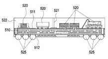
도 5를 참조하면, 전자 부품 모듈은 제 3 회로 기판(510), 상기 제 3 회로 기판(510)의 제 1 면(511)에 배치된 전자 부품(520) 및 제 3 회로 기판(510)의 제 2 면(512)에 배치된 접점(525)을 포함할 수 있다.Referring to FIG. 5 , an electronic component module includes a
본 발명의 다양한 실시 예들에서 전자 부품 모듈에 포함되는 전자 부품(520)의 종류 및 그 형태는 어떤 특정한 것에 제한되지 않는다. 전자 부품(520)에는, 예를 들면, 통신 장치, 프로세서, 메모리, RFFE(radio frequency front end), 무선 송수신기(RF transceiver), 전력 관리 모듈, 무선 통신 회로 및/또는 인터페이스가 포함될 수 있다. 프로세서는, 예를 들어, 중앙처리장치, 어플리케이션 프로세서, 그래픽 처리 장치, 이미지 시그널 프로세서, 센서 허브 프로세서, 또는 커뮤니케이션 프로세서 중 하나 또는 그 이상을 포함할 수 있다. 일 실시 예에 따르면, 상기 프로세서는 적어도 커뮤니케이션 프로세서를 포함하거나, 어플리케이션 프로세서와 커뮤니케이션 프로세서가 통합된 구성일 수 있으며, 상기 무선 송수신기, 상기 전력 관리 모듈, 또는 상기 무선 통신 회로 등을 제어, 또는 구동할 수 있다. 전자 부품 모듈은 적어도 하나의 기능 구현을 위한 복수 개의 전자 부품 또는 소자들을 포함할 수 있다.In various embodiments of the present disclosure, the type and shape of the
다양한 실시예들에 따르면, 전자 부품 모듈의 접점(525)은 전자 장치의 제 1 회로 기판(예: 도 4의 제 1 회로 기판(411))과의 전기적 연결을 위한 구성이며, 접점(525)은 동일한 기능을 가진 복수 개의 접점을 포함하는 패드(PAD) 형태로 구현될 수 있다. 일 실시 예에 따르면, 접점(525)을 통해 전자 부품 모듈은 전자 장치의 제 1 회로 기판(예: 도 4의 제 1 회로 기판(411))에 표면 배치(surface mounted)될 수 있다. 예를 들어, 상기 접점(525)는 제1 회로 기판의 접점 또는 패드와 BGA 또는 LGA를 통해 제 1 회로 기판(예: 도 4의 제 1 회로 기판(411))에 배치되고, 전기적으로 연결될 수 있다.According to various embodiments, the
다양한 실시예들에 따르면, 전자 부품 모듈에 포함된 전자 부품들은 전자 부품 모듈에 포함된 다른 전자 부품들의 자기적 영향으로부터 차폐를 위한 격벽 구조(521)를 포함할 수 있다. 또 다른 예로, 전자 부품 모듈은 전자 부품(520)을 덮어 외부 충격으로부터 보호하며, 기판(510)에의 안정적인 배치를 위한 몰딩부(522)를 포함할 수 있다.According to various embodiments, the electronic components included in the electronic component module may include a
본 개시의 다양한 실시예들에 따르면, 상기 도 5의 전자 부품 모듈이 한 쌍 구비되어 도 6의 양면 배치형 전자 부품 모듈(500)로 구현될 수 있다. 이하의 설명에서 어떤 구성요소와, 다른 구성요소 간의 '연결'은 특별한 언급이 없는 한, 물리적, 전기적 연결을 포함할 수 있고, 간접적인 연결 또는 직접적인 연결을 포함할 수 있다.According to various embodiments of the present disclosure, a pair of the electronic component module of FIG. 5 may be provided to be implemented as the double-sided arrangement type
도 6을 참조하면, 일 실시 예에 따르면, 양면 배치형 전자 부품 모듈(500)은 제 1 회로 기판(예: 도 4의 제 1 회로 기판(411))을 대면하는 제 3 회로 기판(510), 및 제 2 회로 기판(예: 도 4의 제 2 회로 기판(412))을 대면하는 제 4 회로 기판(530)을 포함할 수 있다. 제 3 회로 기판(510)의 제 1 면(511)에는 적어도 하나의 제 1 전자 부품(520)이 배치될 수 있으며, 제 4 회로 기판(530)의 제 3 면(531)에는 적어도 하나의 제 2 전자 부품(540)이 배치될 수 있다. 여기서, 어떤 구성요소가, 다른 구성요소에 '대면'한다는 것은 어떤 구성요소가 다른 구성요소의 에 전체적 또는 부분적으로 맞닿는 것을 포함할 수 있다. 예를 들어, 제 3 회로 기판(510) 및 제 4 회로 기판(530)은 각각 접점(525, 545)을 통해 제 1 회로 기판(예: 도 4의 제 1 회로 기판(411)) 및 제 2 회로 기판(예: 도 4의 제 2 회로 기판(412))에 전체적으로 또는 부분적으로 대면할 수 있다. 일 실시 예에서, 양면 배치형 전자 부품 모듈(500)은 제 3 회로 기판(510)의 제 2 면(512)에 배치되며, 제 1 회로 기판(예: 도 4의 제 1 회로 기판(411)) 및 제 3 회로 기판(510)을 연결하는 제 1 접점(525)을 포함할 수 있다. 또 다른 예로, 전자 부품 모듈(500)은 제 4 회로 기판(530)의 제 4 면(532)에 배치되며, 상기 제 2 회로 기판(예: 도 4의 제 2 회로 기판(412)) 및 제 4 회로 기판(530)을 연결하는 제 2 접점(545)을 포함할 수 있다. 예를 들어, 상기 접점들(525, 545)은 실질적으로 동일한 기능을 가진 복수 개의 패드(PAD) 형태 또는 볼 형태로 구현될 수 있다. 일 실시 예에 따르면, 상기 접점들(525, 545)을 통해 전자 부품 모듈은 전자 장치의 제 1 회로 기판(411) 및 제 2 회로 기판(412)에 표면 배치(surface mounted)될 수 있다.Referring to FIG. 6 , according to an embodiment, the double-sided arrangement type
일 실시 예에 따르면, 제 1 전자 부품(520) 또는 제 2 전자 부품(530)은 단수처럼 사용되나, 복수일 수 있으며, 복수 개의 전자 부품들이 일체로 형성되어 하나 또는 그 이상의 기능을 수행하는 모듈(module) 형태로서 형성될 수도 있다. 적어도 하나의 기능을 수행하기 위한 제 1 전자 부품(520) 또는 제 2 전자 부품(530)은 하나의 부품으로 이루어질 수 있으나, 이와 달리 복수 개의 부품들의 조합을 통해 하나 또는 그 이상의 기능을 수행하도록 형성될 수도 있다. 또한, 상기 제 1 전자 부품(520) 또는 제 2 전자 부품(530)은 모듈 내부에 종류가 다른 전자 부품을 포함할 수도 있다.According to an embodiment, the first
일 실시 예에 따르면, 제 3 회로 기판(510)과 제 3 회로 기판(510) 위에 배치된 제 1 전자 부품(520)은 적어도 하나의 기능을 구현할 수 있다. 제 4 회로 기판(530)과 제 4 회로 기판(530) 위에 배치된 제 2 전자 부품(540) 은 적어도 하나의 기능을 구현할 수 있다. 일 실시 예에 따르면, 제 3 회로 기판(510)과 제 3 회로 기판(510) 위에 배치된 제 1 전자 부품(520)의 기능은 제 4 회로 기판(530)과 제 4 회로 기판(530) 위에 배치된 제 2 전자 부품(540)의 기능과 서로 동일할 수도 또는 상이할 수도 있다.According to an embodiment, the
일 실시 예에 따르면, 양면 배치형 전자 부품 모듈(500)은 몰딩부(550)를 더 포함할 수 있다. 몰딩부(550)는 제 1 전자 부품(520)과 제 2 전자 부품(540) 사이의 공간을 채우며, 제 1 전자 부품(520)과 제 2 전자 부품(540)을 덮어 외부 충격으로부터 보호할 수 있다. 양면 배치형 전자 부품 모듈(500)은 상기 몰딩부(550)에 의해 단일(single) 칩 또는 단일 패키지 형태로 형성될 수 있다.According to an embodiment, the double-sided arrangement type
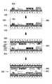
도 7은, 본 개시의 일 실시 예에 따른, 양면 배치형 전자 부품 모듈의 제조 공정을 나타내는 도면이다. 이하, 도 6에 도시된 실시예에 따른 양면 배치형 전자 부품 모듈(500)을 제조하는 방법에 대하여 설명한다.7 is a view illustrating a manufacturing process of a double-sided arrangement type electronic component module according to an embodiment of the present disclosure. Hereinafter, a method of manufacturing the double-sided arrangement type
도 7에 도시된 실시예에 따르면, 제 1 전자 부품(520)이 배치된 제 3 회로 기판(510)과, 제 2 전자 부품(540)이 배치된 제 4 회로 기판(530)이 마련될 수 있다. 일 실시 예에 따르면, 제 1 전자 부품(520)이 배치된 제 3 회로 기판(510)은 제 1 금형(또는 하부 케이스)(601)에 안착되고, 제 2 전자 부품(540)이 배치된 제 4 회로 기판(530)은 제 2 금형(또는 상부 케이스(602))에 안착될 수 있다. 이때, 제 1 전자 부품(520)과 제 2 전자 부품(540)은 서로 이격되며, 제 3 회로 기판(510)과 제 4 회로 기판(530)의 서로 대면 하는 면에 배치될 수 있다. 이 상태에서 상기 제 1 전자 부품(520)과 제 2 전자 부품(540) 사이의 공간에 플라스틱 수지를 용해하여 용융된 소재를 주입시킨 후, 소정의 시간동안 경화 시켜 몰딩부(550)를 형성할 수 있다.According to the embodiment shown in FIG. 7 , a
도 8은, 본 개시의 다른 실시예에 따른, 양면 배치형 전자 부품 모듈(600)을 나타내는 도면이다.8 is a diagram illustrating a double-sided arrangement type
본 개시의 다양한 실시예들에 따르면, 양면 배치형 전자 부품 모듈(600)은 제 1 회로 기판(예: 도 4의 제 1 회로 기판(411))을 대면하는 제 3 회로 기판(610), 및 제 2 회로 기판(예: 도 4의 제 2 회로 기판(412))을 대면하는 제 4 회로 기판(630)을 포함할 수 있다. 제 3 회로 기판(610)에는 적어도 하나의 제 1 전자 부품(620)이 배치될 수 있으며, 제 4 회로 기판(630)에는 적어도 하나의 제 2 전자 부품(640)이 배치될 수 있다. 일 실시 예에서, 양면 배치형 전자 부품 모듈(600)은 제 3 회로 기판(610)의 제 2 면(612)에 배치되며, 제 1 회로 기판(예: 도 4의 제 1 회로 기판(411)) 및 제 3 회로 기판(610)을 연결하는 제 1 접점(625)을 포함할 수 있다. 또 다른 예로, 전자 부품 모듈(600)은 제 4 회로 기판(630)의 제 4 면(632)에 배치되며, 상기 제 2 회로 기판(예: 도 4의 제 2 회로 기판(412)) 및 제 4 회로 기판(630)을 연결하는 제 2 접점(645)을 포함할 수 있다.According to various embodiments of the present disclosure, the double-sided
일 실시 예에 따르면, 제 3 회로 기판(610)과 제 3 회로 기판(610) 위에 배치된 제 1 전자 부품(620)은 적어도 하나의 기능을 구현할 수 있고, 제 4 회로 기판(630)과 제 4 회로 기판(630) 위에 배치된 제 2 전자 부품(640)은 적어도 하나의 기능을 구현할 수 있다. 일 실시 예에 따르면, 제 3 회로 기판(610)과 제 3 회로 기판(610) 위에 배치된 제 1 전자 부품(620)의 기능은 제 4 회로 기판(630)과 제 4 회로 기판(630) 위에 배치된 제 2 전자 부품(640)의 기능과 서로 실질적으로 동일할 수도 또는 상이할 수도 있다.According to an embodiment, the
일 실시 예에 따르면, 양면 배치형 전자 부품 모듈(600)은 몰딩부(650)를 더 포함할 수 있다. 몰딩부(650)는 제 1 전자 부품(620)과 제 2 전자 부품(640) 사이의 공간을 채우며, 제 1 전자 부품(620)과 제 2 전자 부품(640)을 덮어 외부 충격으로부터 보호할 수 있다. 양면 배치형 전자 부품 모듈(600)은 상기 몰딩부(650)에 의해 단일(single) 칩 또는 단일 패키지 형태로 형성될 수 있다.According to an embodiment, the double-sided arrangement type
다양한 실시예들에 따르면, 양면 배치형 전자 부품 모듈(600)은 적어도 하나의 내부 연결 부재(660)를 더 포함할 수 있다. 상기 내부 연결 부재(660)는 일 실시 예에 따르면, Cu pillar 구조로 구현되거나, 다른 실시예에 따르면, Solder bump 구조로 구현될 수 있다. 내부 연결 부재(660)는 예를 들어, 상기 몰딩부(650)의 최외곽 또는 몰딩부(650)의 최외곽으로부터 소정거리 몰딩부(650) 내측으로 인입된 형태를 가질 수 있다. 상기 내부 연결 부재(660)를 통해 양면 배치형 전자 부품 모듈(600)의 제 1 전자 부품(620)과 제 2 전자 부품(640), 그리고 제 3 회로 기판(610)과 제 4 회로 기판(630)은 서로 전기적으로 연결될 수 있다.According to various embodiments, the double-sided arrangement type
일 실시 예에 따르면, 도 8에 도시된 양면 배치형 전자 부품 모듈(600)은 2개의 내부 연결 부재(660)를 포함하고 있으나, 이에 한정되지는 않는다. 예를 들어, 양면 배치형 전자 부품 모듈(600)은 하나 또는 3개 이상의 내부 연결 부재(660)를 포함할 수 도 있다.According to an embodiment, the double-sided arrangement type
도 9는, 본 개시의 다른 실시예에 따른, 양면 배치형 전자 부품 모듈 제조 공정을 나타내는 도면이다.9 is a diagram illustrating a manufacturing process of a double-sided arrangement type electronic component module according to another embodiment of the present disclosure.
도 9에 도시된 실시예에 따르면, 제 1 전자 부품(620)이 배치된 제 3 회로 기판(610)과 제 2 전자 부품(640)이 배치된 제 4 회로 기판(630)이 마련될 수 있다. 일 실시 예에 따르면, 제 3 회로 기판(610) 또는 제 4 회로 기판(630)의 가장 자리 측에 내부 연결 부재(660)가 형성될 수 있다. 도 9에는 제 3 회로 기판(610)의 가장 자리 측에 상기 제 4 회로 기판(630)의 일 측까지 연장되는 내부 연결 부재(660)가 형성된 것이 도시되나 반드시 이에 한정되는 것은 아니다. 예를 들면, 도 9에 도시된 실시예에 따른, 내부 연결 부재(660)는 제 1 전자 부품(620) 보다 높은 높이를 가질 수 있으며, 내부 연결 부재(660) 위로 제 2 전자 부품(640)이 실자된 제 4 회로 기판(630)이 적층될 수 있다. 또 다른 예로, 도면에 도시되진 않았으나, 제 4 회로 기판(630)의 가장 자리 측에 내부 연결 부재가 형성될 수도 있다. 상기 내부연결 부재는 제 2 전자 부품(640) 보다 높은 높이를 가질 수 있으며, 상기 내부 연결 부재 위로 제 1 전자 부품(620)이 배치된 제 3 회로 기판(610)이 적층될 수 있다. 도면에 별도로 도시되진 않았으나, 제 1 전자 부품(620)이 배치된 제 3 회로 기판(610)은 제 1 금형(또는 하부 케이스)(예: 도 7의 601)에 안착되고, 제 2 전자 부품(640)이 배치된 제 4 회로 기판(630)은 제 2 금형(또는 상부 케이스)(예: 도 7의 602)에 안착될 수 있다. 이때, 제 1 전자 부품(620)과 제 2 전자 부품(640)은 서로 이격되어 대면할 수 있다. 이 상태에서 상기 제 1 전자 부품(620)과 제 2 전자 부품(640) 사이의 공간에 플라스틱 수지를 용해하여 용융된 소재를 주입시킨 후, 소정의 시간동안 경화 시켜 몰딩부(650)를 형성할 수 있다.According to the embodiment shown in FIG. 9 , a
도 10은, 본 개시의 또 다른 실시예에 따른, 양면 배치형 전자 부품 모듈(700)를 나타내는 도면이다.10 is a diagram illustrating a double-sided arrangement type
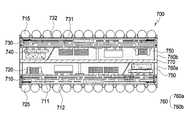
본 개시의 다양한 실시예들에 따르면, 양면 배치형 전자 부품 모듈(700)는 제 1 회로 기판(예: 도 4의 제 1 회로 기판(411))을 대면하는 제 3 회로 기판(710), 및 제 2 회로 기판(예: 도 4의 제 2 회로 기판(412))을 대면하는 제 4 회로 기판(730)을 포함할 수 있다. 제 3 회로 기판(710)에는 적어도 하나의 제 1 전자 부품(720)이 배치될 수 있으며, 제 4 회로 기판(730)에는 적어도 하나의 제 2 전자 부품(740)이 배치될 수 있다. 일 실시 예에서, 양면 배치형 전자 부품 모듈(700)은 제 3 회로 기판(710)의 제 2 면(712)에 배치되며, 제 1 회로 기판(예: 도 4의 제 1 회로 기판(411)) 및 제 3 회로 기판(710)을 연결하는 제 1 접점(725)을 포함할 수 있다. 또 다른 예로, 전자 부품 모듈(700)은 제 4 회로 기판(730)의 제 4 면(732)에 배치되며, 상기 제 2 회로 기판(예: 도 4의 제 2 회로 기판(412)) 및 제 4 회로 기판(730)을 연결하는 제 2 접점(745)을 포함할 수 있다.According to various embodiments of the present disclosure, the double-sided
일 실시 예에 따르면, 제 3 회로 기판(710)과 제 3 회로 기판(710) 위에 배치된 제 1 전자 부품(720)은 적어도 하나의 기능을 구현할 수 있고, 제 4 회로 기판(730)과 제 4 회로 기판(730) 위에 배치된 제 2 전자 부품(740)은 적어도 하나의 기능을 구현할 수 있다. 일 실시 예에 따르면, 제 3 회로 기판(710)과 제 3 회로 기판(710) 위에 배치된 제 1 전자 부품(720)의 기능과 제 4 회로 기판(730)과 제 4 회로 기판(730) 위에 배치된 제 2 전자 부품(740)의 기능은 서로 실질적으로 동일할 수도 또는 상이할 수도 있다.According to an embodiment, the
일 실시 예에 따르면, 양면 배치형 전자 부품 모듈(700)은 몰딩부(750)를 더 포함할 수 있다. 몰딩부(750)는 제 1 전자 부품(720)과 제 2 전자 부품(740) 사이의 공간을 채우며, 제 1 전자 부품(720)과 제 2 전자 부품(740)을 덮어 외부 충격으로부터 보호할 수 있다. 양면 배치형 전자 부품 모듈(700)은 상기 몰딩부(750)에 의해 단일 칩 또는 패키지 형태로 형성될 수 있다.According to an embodiment, the double-sided arrangement type
다양한 실시예들에 따르면, 양면 배치형 전자 부품 모듈(700)는 적어도 하나의 내부 연결 부재(760)를 더 포함할 수 있다. 상기 내부 연결 부재(760)는 일 실시 예에 따르면, Cu pillar 구조로 구현되거나, 다른 실시예에 따르면, Solder bump 구조로 구현될 수 있다. 내부 연결 부재(760)는 예를 들어, 상기 몰딩부(750)의 최외곽 또는 몰딩부(750)의 최외곽으로부터 소정거리 몰딩부(750) 내측으로 인입된 형태를 가질 수 있다. 상기 내부 연결 부재(760)를 통해 양면 배치형 전자 부품 모듈(700)의 제 1 전자 부품(720)과 제 2 전자 부품(740), 그리고 제 3 회로 기판(710)과 제 4 회로 기판(730)은 서로 전기적으로 연결될 수 있다.According to various embodiments, the double-sided arrangement type
다양한 실시예들에 따르면, 양면 배치형 전자 부품 모듈(700)은 제 5 회로 기판(770)을 더 포함할 수 있다. 제 5 회로 기판(770)은 제 3 회로 기판(710)과 제 4 회로 기판(730) 사이에 위치될 수 있다. 일 실시 예에서, 제 5 회로 기판(770)을 통해서도 양면 배치형 전자 부품 모듈(700)의 제 1 전자 부품(720), 제 2 전자 부품(740), 제 3 회로 기판(710), 또는 제 4 회로 기판(730)은 서로 전기적으로 연결될 수 있다. 일 실시 예에 따르면, 내부 연결 부재(760)가 구비된 양면 배치형 전자 부품 모듈(700)에 제 5 회로 기판(770)을 더 포함하면, 내부 연결 부재(760)의 길이를 줄일 수 있게 되어 조립체의 강성을 보강하는 역할을 할 수 있다.According to various embodiments, the double-sided arrangement type
예를 들면, 도 8의 내부 연결 부재(660)의 길이에 비해 도 10의 내부 연결 부재(760)의 길이는 짧을 수 있다. 예를 들어, 도 10의 내부 연결 부재(760) 중 하나(예: 제 1 내부 연결 부재(760a))는 제 3 회로 기판(710)과 제 5 회로 기판(770)을 전기적으로 연결하고, 내부 연결 부재(760) 중 다른 하나(예: 제 2 내부 연결 부재(760b))는 제 4 회로 기판(730)과 제 5 회로 기판(770)을 전기적으로 연결하기 위해 형성될 수 있다. 내부 연결 부재(760)의 총 연장 길이는 상기 제 3 회로 기판(710)의 일측에 구비된 제 1 내부 연결 부재(760a)와 상기 제 4 회로 기판(730)의 일측에 구비된 제 2 내부 연결 부재(760b)의 길이의 합일 수 있다. 따라서, 도 8과 도 10을 참조하면, 적어도 제 5 회로 기판(770)의 두께만큼 내부 연결 부재(760)의 총 연장 길이를 줄일 수 있는 이점이 있다.For example, the length of the inner connecting
도 11은, 본 개시의 또 다른 실시예에 따른, 양면 배치형 전자 부품 모듈 제조 공정을 나타내는 도면이다.11 is a diagram illustrating a manufacturing process of a double-sided arrangement type electronic component module according to another embodiment of the present disclosure.
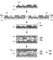
도 11에 도시된 실시예에 따르면, 제 1 전자 부품(720)이 배치된 제 3 회로 기판(710)과 제 2 전자 부품(740)이 배치된 제 4 회로 기판(730)이 마련될 수 있다. 일 실시 예에 따르면, 제 3 회로 기판(710)의 가장 자리 측에 내부 연결 부재(760)가 형성될 수 있다. 또 다른 예로, 제 4 회로 기판(730)의 가장 자리 측에도 내부 연결 부재(760)가 형성될 수 있다. 도 11에 도시된 실시예에 따르면, 제 1 전자 부품(720)이 배치된 제 3 회로 기판(710)에 제 1 내부 연결 부재(760a)가 배치되고, 제 2 전자 부품(740)이 배치된 제 4 회로 기판(730)에 별도의 제 2 내부 연결 부재(760b)가 배치될 수도 있다. 일 실시 예에서, 제 3 회로 기판(710)에 구비된 제 1 내부 연결 부재(760a) 위로 제 5 회로 기판(770)이 적층될 수 있으며, 그 위로 제 2 전자 부품(740)이 배치된 제 4 회로 기판(730)이 적층될 수 있다. 상기 제 5 회로 기판(770)을 매개로 제 1 전자 부품(720), 제 2 전자 부품(740), 제 3 회로 기판(710), 또는 제 4 회로 기판(730) 사이의 전기적인 연결이 가능할 수 있다. 단, 이와 달리, 제 4 회로 기판(730)에 구비된 제 2 내부 연결 부재(760b) 위로 제 5 회로 기판(770)이 적층되고, 그 위로 제 1 전자 부품(720)이 배치된 제 3 회로 기판(710)이 적층되는 것도 가능함을 유의해야 한다.11 , a
또한 도면에 별도로 도시되진 않았으나, 제 1 전자 부품(720)이 배치된 제 3 회로 기판(710)은 제 1 금형(또는 하부 케이스)(예: 도 7의 제 1 금형(또는 하부 케이스)(601))에 안착되고, 제 2 전자 부품(740)이 배치된 제 4 회로 기판(730)은 제 2 금형(또는 상부 케이스)(예: 도 7의 제 2 금형(또는 상부 케이스(602))에 안착될 수 있다. 이때, 제 1 전자 부품(720)과 제 2 전자 부품(640)은 서로 대향할 수 있다. 이 상태에서 상기 제 1 전자 부품(720)과 제 2 전자 부품(740) 사이의 공간에 플라스틱 수지를 용해하여 용융된 소재를 주입시킨 후, 소정의 시간 동안 경화시켜 몰딩부(750)를 형성할 수 있다.In addition, although not shown separately in the drawing, the
도 12는, 본 개시의 다양한 실시예들에 따른, 제 1 회로 기판(411) 및 제 2 회로 기판(412) 사이에 양면 배치형 전자 부품 모듈(600)이 배치된 모습을 나타내는 도면이다. 도 12의 실시예에서는, 내부 연결 부재(660)가 구비된 양면 배치형 전자 부품 모듈(600)를 일 예시로 설명하지만 반드시 이에 한정되는 것은 아니다. 이하에서는, 설명의 편의를 위해, 도 8에 전술한 실시예에 따른 전자 부품 모듈(600)을 예로 들어 설명하지만, 도 6 및 도 10에서 전술한 실시예에 따른, 내부 연결 부재가 구비된 전자 부품 모듈(500, 700)을 도 12의 실시예에 적용할 수 있다.12 is a diagram illustrating a state in which a double-sided arrangement type
본 개시의 다양한 실시예들에 따르면, 전자 장치는, 적어도 하나의 양면 배치형 전자 부품 모듈(600)이 배치된 제 1 회로 기판(411), 상기 제 1 회로 기판(411) 상에 배치된 적어도 하나의 외부 연결 부재(예: 인터포저 커넥터)(이하 '제 1 연결 부재(413)'라 함) 및 상기 적어도 하나의 제 1 연결 부재(413) 상에 적층된 제 2 회로 기판(412)을 포함할 수 있다. 제 1 회로 기판(411)은 제 1 방향(예: +Z축 방향)을 향하는 제 1 면(411a)과 상기 제 1 방향과 반대인 제 2 방향(예: -Z축 방향)을 향하는 제 2 면(411b)을 포함할 수 있다. 제 2 회로 기판(412)은 제 1 방향을 향하는 제 3 면(412a)과 상기 제 1 방향과 반대인 제 2 방향을 향하는 제 4 면(412b)을 포함할 수 있다. 예를 들어, 제 1 방향은 좌표축 +Z와 평행한 방향일 수 있다.According to various embodiments of the present disclosure, the electronic device includes a
도 12를 참조하면, 양면 배치형 전자 부품 모듈(600)의 제 3 회로 기판(610)은 제 1 회로 기판(411)을 향하고, 접점(625)을 통해 제 1 회로 기판(411)과 전기적으로 연결될 수 있다. 또 한 실시예에 따르면, 제 4 회로 기판(630)은 제 2 회로 기판(412)을 향하고, 접점(645)을 통해 제 2 회로 기판(412)과 연결될 수 있다.Referring to FIG. 12 , the
다양한 실시예들에 따르면, 양면 배치형 전자 부품 모듈(600)은 내부 연결 부재(이하 '제 2 연결 부재(660)'라 함)를 통해 제 3 회로 기판(610)과 제 4 회로 기판(630) 간의 전기적 연결도 가능할 수 있다.According to various embodiments, the double-sided arrangement type
다양한 실시예들에 따르면, 제 1 연결 부재(413)는 제 1 회로 기판(411)과 제 2 회로 기판(412) 사이에서 양면 배치형 전자 부품 모듈(600)의 높이와 실질적으로 동일한 높이를 가지도록 형성될 수도 있다. 이에 따라 제 1 회로 기판(411)과 제 2 회로 기판(412) 사이에 양면 배치형 전자 부품 모듈(600)를 콤팩트하게 배치할 수 있게 되므로 공간 활용성 부품 배치성, 및/또는 공간 배치 효율성을 향상할 수 있다.According to various embodiments, the
도 12에 도시된 바와 같이, 일 실시 예에 따른 전자 장치는 제 1 회로 기판(411)과 제 2 회로 기판(412)의 적층형 PCB 구조 사이에 양면 배치형 전자 부품 모듈(600)이 배치되고, 양면 배치형 전자 부품 모듈(600)의 양면이 각각 적층형 PCB 구조와 접점을 이루어 전기적으로 연결될 수 있다. 예를 들어, 양면 배치형 전자 부품 모듈(600)은 제 1 회로 기판(411)과 제 2 회로 기판(412) 사이에 콤패트하게 끼워져 배치되면서, 제 1 회로 기판(411)의 제 1 면(411a)과 제 2 회로 기판(412)의 제 4 면(412b)에 각각 전기적으로 연결될 수 있다.As shown in FIG. 12 , in the electronic device according to an embodiment, a double-sided arrangement type
본 개시의 다양한 실시예들에 따른 전자 장치는, 제 1 회로 기판(411)과 제 2 회로 기판(412)이 제 1 연결 부재(413)에 의해 전기적으로 연결되어 제 1 연결 부재(413)를 따라 제 1 신호 전달 경로(①)가 형성될 수 있다. 또한, 본 개시의 다양한 실시예들에 따른 전자 장치는, 제 3 회로 기판(610)과 제 4 회로 기판(620)이 제 2 연결 부재(660)에 의해 전기적으로 연결되어 제 2 연결 부재(660)를 따라 제 2 신호 전달 경로(②)가 형성될 수도 있다. 예컨대, 전자 장치는 상기 제 1 연결 부재(413) 및/또는 제 2 연결 부재(660)를 통해 신호 전달 경로를 다양하게 선택 및 설정할 수 있는 장점이 있으며, 나아가 신호 전달을 위한 배선을 간소화할 수 있는 효과도 가질 수 있다.In an electronic device according to various embodiments of the present disclosure, a
도 13은, 본 개시의 다양한 실시예들에 따른, 적층 PCB 구조 및 그 위에 배치된 전자 부품들을 나타내는 개념도이다. 도 13은 도 12에서 설명한 실시예를 무선 통신 모듈에 적용한 실시예를 나타낼 수 있다.13 is a conceptual diagram illustrating a stacked PCB structure and electronic components disposed thereon according to various embodiments of the present disclosure. 13 may show an embodiment in which the embodiment described in FIG. 12 is applied to a wireless communication module.
도 13에는 무선 통신을 위한 전자 부품들(예: 제 1 RFFE(441), 제 2 RFFE(442) 및 무선 송수신기(430))이 배치된 적층형 PCB 구조가 도시된다. 적층형 PCB 구조는 제 1 회로 기판(예: 메인 PCB)(411)와 제 2 회로 기판(예: 서브 PCB)(412)를 포함할 수 있다. 한 실시 예에서, 제 1 회로 기판(411)은 제 1 안테나(450)와 연결되고 제 2 회로 기판(412)은 제 2 안테나(460)와 연결될 수 있다. 예를 들어, 제 1 안테나(450)는 제 1 내지 제 3 레거시 안테나(예: 도 3의 제 1 내지 제 3 레거시 안테나(351, 353, 355)) 및 제 1 내지 제 3 안테나 모듈(예: 도 3의 제 1 내지 제 3 안테나 모듈(361, 363, 365)) 중 어느 하나일 수 있다. 또 다른 예로, 상기 제 2 안테나(460)는 상기 제 1 안테나(450)와 다른 제 1 내지 제 3 레거시 안테나(예: 도 3의 제 1 내지 제 3 레거시 안테나(351, 353, 355)) 및 제 1 내지 제 3 안테나 모듈(예: 도 3의 제 1 내지 제 3 안테나 모듈(361, 363, 365)) 중 어느 하나일 수 있다.13 shows a stacked PCB structure in which electronic components for wireless communication (eg, a
도 4에서 전술한 실시예는 제 1 RFFE(441), 제 2 RFFE(442) 및 무선 송수신기(430)가 각각 분리되어 제 1 회로 기판(411)의 제 1 면(411a) 또는 제 2 회로 기판(412)의 제 3 면(412a)에 배치된 적층형 PCB 구조와 전자부품들을 개시하였다. 이와 달리, 도 13에 도시된 실시예에서는, 제 1 회로 기판(411)의 제 1 면(411a)과 제 2 회로 기판(412)의 제 4 면(412b)에 각각 배치되는 양면을 가진 전자 부품 모듈을 개시한다.In the embodiment described above in FIG. 4 , the
도 4에 도시된 실시예와 도 13에 도시된 실시예를 대조하면, 도 4의 제 1 RFFE(441) 및 제 2 RFFE(442)를 도 13에서는 양면 배치형 전자 부품 모듈(예: 도 12의 양면 배치형 전자 부품 모듈(600))로 구현할 수 있다. 예를 들어, 도 12를 다시 참조하여 설명하면, 제 1 RFFE(441)를 제 3 회로 기판(610)과 제 1 전자 부품(620)의 조립체를 통해 구현할 수 있고, 제 2 RFFE(442)를 제 4 회로 기판(630)과 제 2 전자 부품(640)의 조립체를 통해 구현할 수 있다. 도 13에 도시된 실시예에서는 제 2 RFFE(442)를 제 2 회로 기판(412)의 아래에 배치시킬 수 있게 됨으로써 도 4에 도시된 실시예에 비해 전자 장치의 공간 배치 효율성이 향상될 수 있다. 도 13에 도시된 실시예에서는 제 1 연결 부재(413)를 통한 신호 전달 경로뿐만 아니라 도 4에 도시된 실시예에 비해 제 1 RFFE(441)와 제 2 RFFE(442)를 통한 신호 전달 경로가 추가되므로 신호 전달 경로를 다양화할 수 있는 이점이 있다. 도 4에 도시된 실시예에서는, 무선 송수신기(430)와 제 2 RFFE(442) 간의 신호 전달, 또는 제 1 RFFE(441)과 제 2 RFFE(442) 간의 신호 전달이 적층형 PCB 구조의 가장자리에 형성된 제 1 연결 부재(413)(또는 외부 연결 부재)(예: 인터포저 커넥터)를 통해서만 이루어졌으나, 도 13에 도시된 실시예에 따르면, 신호 전달이 제 1 RFFE(441) 및 제 2 RFFE(442)를 통해서도 이루어지므로 신호 전달 경로가 짧아지는 이점도 가질 수 있다. 이러한 이점은 제 1 안테나(450)와 제 2 안테나(460)를 이용한 통신에 유용하게 작용할 수 있다.Contrasting the embodiment shown in FIG. 4 and the embodiment shown in FIG. 13 , the
본 문서에 개시된 다양한 실시예들에 따른 전자 장치는 다양한 형태의 장치가 될 수 있다. 전자 장치는, 예를 들면, 휴대용 통신 장치(예: 스마트폰), 컴퓨터 장치, 휴대용 멀티미디어 장치, 휴대용 의료 기기, 카메라, 웨어러블 장치, 또는 가전 장치를 포함할 수 있다. 본 문서의 실시예에 따른 전자 장치는 전술한 기기들에 한정되지 않는다.The electronic device according to various embodiments disclosed in this document may have various types of devices. The electronic device may include, for example, a portable communication device (eg, a smart phone), a computer device, a portable multimedia device, a portable medical device, a camera, a wearable device, or a home appliance device. The electronic device according to the embodiment of the present document is not limited to the above-described devices.
본 문서의 다양한 실시예들 및 이에 사용된 용어들은 본 문서에 기재된 기술적 특징들을 특정한 실시예들로 한정하려는 것이 아니며, 해당 실시예의 다양한 변경, 균등물, 또는 대체물을 포함하는 것으로 이해되어야 한다. 도면의 설명과 관련하여, 유사한 또는 관련된 구성요소에 대해서는 유사한 참조 부호가 사용될 수 있다. 아이템에 대응하는 명사의 단수 형은 관련된 문맥상 명백하게 다르게 지시하지 않는 한, 상기 아이템 한 개 또는 복수 개를 포함할 수 있다. 본 문서에서, "A 또는 B", "A 및 B 중 적어도 하나", "A 또는 B 중 적어도 하나", "A, B 또는 C", "A, B 및 C 중 적어도 하나", 및 "A, B, 또는 C 중 적어도 하나"와 같은 문구들 각각은 그 문구들 중 해당하는 문구에 함께 나열된 항목들 중 어느 하나, 또는 그들의 모든 가능한 조합을 포함할 수 있다. "제 1", "제 2", 또는 "첫째" 또는 "둘째"와 같은 용어들은 단순히 해당 구성요소를 다른 해당 구성요소와 구분하기 위해 사용될 수 있으며, 해당 구성요소들을 다른 측면(예: 중요성 또는 순서)에서 한정하지 않는다. 어떤(예: 제 1) 구성요소가 다른(예: 제 2) 구성요소에, "기능적으로" 또는 "통신적으로"라는 용어와 함께 또는 이런 용어 없이, "커플드" 또는 "커넥티드"라고 언급된 경우, 그것은 상기 어떤 구성요소가 상기 다른 구성요소에 직접적으로(예: 유선으로), 무선으로, 또는 제 3 구성요소를 통하여 연결될 수 있다는 것을 의미한다.The various embodiments of this document and the terms used therein are not intended to limit the technical features described in this document to specific embodiments, and should be understood to include various modifications, equivalents, or substitutions of the embodiments. In connection with the description of the drawings, like reference numerals may be used for similar or related components. The singular form of the noun corresponding to the item may include one or more of the item, unless the relevant context clearly dictates otherwise. As used herein, "A or B", "at least one of A and B", "at least one of A or B", "A, B or C", "at least one of A, B and C", and "A , B, or C," each of which may include any one of the items listed together in the corresponding one of the phrases, or all possible combinations thereof. Terms such as “first”, “second”, or “first” or “second” may simply be used to distinguish an element from other such elements, and may refer elements to other aspects (e.g., importance or order) is not limited. It is said that one (eg, first) component is “coupled” or “connected” to another (eg, second) component, with or without the terms “functionally” or “communicatively”. When referenced, it means that one component can be connected to the other component directly (eg by wire), wirelessly, or through a third component.
본 문서의 다양한 실시예들에서 사용된 용어 "모듈"은 하드웨어, 소프트웨어 또는 펌웨어로 구현된 유닛을 포함할 수 있으며, 예를 들면, 로직, 논리 블록, 부품, 또는 회로와 같은 용어와 상호 호환적으로 사용될 수 있다. 모듈은, 일체로 구성된 부품 또는 하나 또는 그 이상의 기능을 수행하는, 상기 부품의 최소 단위 또는 그 일부가 될 수 있다. 예를 들면, 일 실시 예에 따르면, 모듈은 ASIC(application-specific integrated circuit)의 형태로 구현될 수 있다.The term “module” used in various embodiments of this document may include a unit implemented in hardware, software, or firmware, and is interchangeable with terms such as, for example, logic, logic block, component, or circuit. can be used as A module may be an integrally formed part or a minimum unit or a part of the part that performs one or more functions. For example, according to an embodiment, the module may be implemented in the form of an application-specific integrated circuit (ASIC).
본 문서의 다양한 실시예들은 기기(machine)(예: 전자 장치(101)) 의해 읽을 수 있는 저장 매체(storage medium)(예: 내장 메모리(136) 또는 외장 메모리(138))에 저장된 하나 이상의 명령어들을 포함하는 소프트웨어(예: 프로그램(140))로서 구현될 수 있다. 예를 들면, 기기(예: 전자 장치(101))의 프로세서(예: 프로세서(120))는, 저장 매체로부터 저장된 하나 이상의 명령어들 중 적어도 하나의 명령을 호출하고, 그것을 실행할 수 있다. 이것은 기기가 상기 호출된 적어도 하나의 명령어에 따라 적어도 하나의 기능을 수행하도록 운영되는 것을 가능하게 한다. 상기 하나 이상의 명령어들은 컴파일러에 의해 생성된 코드 또는 인터프리터에 의해 실행될 수 있는 코드를 포함할 수 있다. 기기로 읽을 수 있는 저장 매체는, 비일시적(non-transitory) 저장 매체의 형태로 제공될 수 있다. 여기서, ‘비일시적’은 저장 매체가 실재(tangible)하는 장치이고, 신호(signal)(예: 전자기파)를 포함하지 않는다는 것을 의미할 뿐이며, 이 용어는 데이터가 저장 매체에 반영구적으로 저장되는 경우와 임시적으로 저장되는 경우를 구분하지 않는다.Various embodiments of the present document include one or more instructions stored in a storage medium (eg,
일 실시 예에 따르면, 본 문서에 개시된 다양한 실시예들에 따른 방법은 컴퓨터 프로그램 제품(computer program product)에 포함되어 제공될 수 있다. 컴퓨터 프로그램 제품은 상품으로서 판매자 및 구매자 간에 거래될 수 있다. 컴퓨터 프로그램 제품은 기기로 읽을 수 있는 저장 매체(예: compact disc read only memory(CD-ROM))의 형태로 배포되거나, 또는 어플리케이션 스토어(예: 플레이 스토어TM)를 통해 또는 두 개의 사용자 장치들(예: 스마트 폰들) 간에 직접, 온라인으로 배포(예: 다운로드 또는 업로드)될 수 있다. 온라인 배포의 경우에, 컴퓨터 프로그램 제품의 적어도 일부는 제조사의 서버, 어플리케이션 스토어의 서버, 또는 중계 서버의 메모리와 같은 기기로 읽을 수 있는 저장 매체에 적어도 일시 저장되거나, 임시적으로 생성될 수 있다.According to an embodiment, the method according to various embodiments disclosed in this document may be included and provided in a computer program product. Computer program products may be traded between sellers and buyers as commodities. The computer program product is distributed in the form of a machine-readable storage medium (eg compact disc read only memory (CD-ROM)), or via an application store (eg Play StoreTM ) or on two user devices ( It can be distributed (eg downloaded or uploaded) directly, online between smartphones (eg: smartphones). In the case of online distribution, at least a part of the computer program product may be temporarily stored or temporarily created in a machine-readable storage medium such as a memory of a server of a manufacturer, a server of an application store, or a relay server.
다양한 실시예들에 따르면, 상기 기술한 구성요소들의 각각의 구성요소(예: 모듈 또는 프로그램)는 단수 또는 복수의 개체를 포함할 수 있으며, 복수의 개체 중 일부는 다른 구성요소에 분리 배치될 수도 있다. 다양한 실시예들에 따르면, 전술한 해당 구성요소들 중 하나 이상의 구성요소들 또는 동작들이 생략되거나, 또는 하나 이상의 다른 구성요소들 또는 동작들이 추가될 수 있다. 대체적으로 또는 추가적으로, 복수의 구성요소들(예: 모듈 또는 프로그램)은 하나의 구성요소로 통합될 수 있다. 이런 경우, 통합된 구성요소는 상기 복수의 구성요소들 각각의 구성요소의 하나 이상의 기능들을 상기 통합 이전에 상기 복수의 구성요소들 중 해당 구성요소에 의해 수행되는 것과 동일 또는 유사하게 수행할 수 있다. 다양한 실시예들에 따르면, 모듈, 프로그램 또는 다른 구성요소에 의해 수행되는 동작들은 순차적으로, 병렬적으로, 반복적으로, 또는 휴리스틱하게 실행되거나, 상기 동작들 중 하나 이상이 다른 순서로 실행되거나, 생략되거나, 또는 하나 이상의 다른 동작들이 추가될 수 있다.According to various embodiments, each component (eg, a module or a program) of the above-described components may include a singular or a plurality of entities, and some of the plurality of entities may be separately disposed in other components. have. According to various embodiments, one or more components or operations among the above-described corresponding components may be omitted, or one or more other components or operations may be added. Alternatively or additionally, a plurality of components (eg, a module or a program) may be integrated into one component. In this case, the integrated component may perform one or more functions of each component of the plurality of components identically or similarly to those performed by the corresponding component among the plurality of components prior to the integration. . According to various embodiments, operations performed by a module, program, or other component are executed sequentially, in parallel, repeatedly, or heuristically, or one or more of the operations are executed in a different order, or omitted. , or one or more other operations may be added.
본 문서에 개시된 다양한 실시예에 따르면, 전자 장치(예: 도 3의 전자 장치(300))에 있어서, 적어도 하나의 양면 배치형 전자 부품 모듈(예: 도 12의 양면 배치형 전자 부품 모듈(600))이 배치된 제 1 회로 기판(예: 도 12의 제 1 회로 기판(411)) 상기 제 1 회로 기판 상에 배치된 적어도 하나의 제 1 연결 부재(예: 도 12의 제 1 연결 부재(413));및 상기 적어도 하나의 제 1 연결 부재 상에 적층된 제 2 회로 기판(예: 도 12의 제 2 회로 기판(412));을 포함하고, 상기 적어도 하나의 양면 배치형 전자 부품 모듈(600)은 상기 제 1 회로 기판을 대면하는 제 3 회로 기판(예: 도 12의 제 3 회로 기판(610)); 상기 제 3 회로 기판에 배치된 적어도 하나의 제 1 전자 부품(예: 도 12의 제 1 전자 부품(620)); 상기 제 2 회로 기판을 대면하는 제 4 회로 기판(예: 도 12의 제 4 회로 기판(630)); 상기 제 4 회로 기판에 배치된 적어도 하나의 제 2 전자 부품(예: 도 12의 제 2 전자 부품(640)); 상기 제 3 회로 기판의 일 면에 배치되며, 상기 제 1 회로 기판과 제 3 회로 기판을 전기적으로 연결하는 제 1 접점(예: 도 12의 제 1 접점(625)); 및 상기 제 4 회로 기판의 일 면에 배치되며, 상기 제 2 회로 기판과 제 4 회로 기판을 전기적으로 연결하는 제 2 접점(예: 도 12의 제 2 접점(645))을 포함하는 전자 장치를 제공할 수 있다.According to various embodiments disclosed herein, in an electronic device (eg, the electronic device 300 of FIG. 3 ), at least one double-sided arrangement type electronic component module (eg, the double-sided arrangement type electronic component module 600 of FIG. 12 ) )) disposed on the first circuit board (eg, the first circuit board 411 of FIG. 12) at least one first connection member (eg, the first connection member ( 413)); and a second circuit board (eg, the second circuit board 412 of FIG. 12 ) stacked on the at least one first connecting member, wherein the at least one double-sided arrangement type electronic component module includes: Reference numeral 600 denotes a third circuit board facing the first circuit board (eg, the third circuit board 610 of FIG. 12 ); at least one first electronic component (eg, the first electronic component 620 of FIG. 12 ) disposed on the third circuit board; a fourth circuit board (eg, the fourth circuit board 630 of FIG. 12 ) facing the second circuit board; at least one second electronic component (eg, the second electronic component 640 of FIG. 12 ) disposed on the fourth circuit board; a first contact (eg, a first contact 625 in FIG. 12 ) disposed on one surface of the third circuit board and electrically connecting the first circuit board and the third circuit board; and a second contact (eg, the second contact 645 of FIG. 12 ) disposed on one surface of the fourth circuit board and electrically connecting the second circuit board and the fourth circuit board. can provide
다양한 실시예들에 따르면, 상기 제 1 연결 부재는 인터포저 커넥터일 수 있다.According to various embodiments,The first connecting member may be an interposer connector.
다양한 실시예들에 따르면, 상기 제 3 회로 기판과 상기 제 4 회로 기판을 연결하는 제 2 연결 부재(예: 도 12의 제 2 연결 부재(660)를 포함할 수 있다.According to various embodiments, a second connection member (eg, the
다양한 실시예들에 따르면, 상기 제 2 연결 부재는 CU pillar 로 구현될 수 있다.According to various embodiments, the second connection member may be implemented as a CU pillar.
다양한 실시예들에 따르면,상기 제 2 연결 부재는 Solder bump 로 구현될 수 있다.According to various embodiments,The second connecting member may be implemented as a solder bump.
다양한 실시예들에 따르면, 상기 제 3 회로 기판 및 상기 제 4 회로 기판 사이에 형성된 몰딩부(예: 도 12의 몰딩부(650))를 더 포함할 수 있다.According to various embodiments, a molding part (eg, the
다양한 실시예들에 따르면, 상기 제 3 회로 기판과 상기 제 4 회로 기판 상에는 상기 제 3 회로 기판과 상기 제 4 회로 기판을 연결하기 위한 제 2 연결 부재가 각각 형성되고, 상기 제 5 회로 기판(예: 도 10의 제 5 회로 기판(770))은 두 개의 제 2 연결 부재 사이에 게재될 수 있다. According to various embodiments, a second connection member for connecting the third circuit board and the fourth circuit board is respectively formed on the third circuit board and the fourth circuit board, and the fifth circuit board (eg, : The
다양한 실시예들에 따르면, 상기 제 5 회로 기판은 상기 제 3 회로 기판과 상기 제 4 회로 기판을 연결하는 제 2 연결 부재 상에 적층될 수 있다.According to various embodiments, the fifth circuit board may be stacked on a second connecting member connecting the third circuit board and the fourth circuit board.
다양한 실시예들에 따르면, 상기 제 1 회로 기판에 연결된 제 1 안테나(예: 도 13의 제 1 안테나(450)) 및 상기 제 2 회로 기판에 연결된 제 2 안테나(예: 도 13의 제 2 안테나(460))를 포함할 수 있다.According to various embodiments, a first antenna connected to the first circuit board (eg, the
다양한 실시예들에 따르면, 상기 적어도 하나의 제 1 전자 부품은 상기 제 1 안테나와 연결된 제 1 RFFE(예: 도 13의 제 1 RFFE(441))를 구성하고, 상기 적어도 하나의 제 2 전자 부품은 상기 제 2 안테나와 연결된 제 2 RFFE(예: 도 12의 제 2 RFFE(442))를 구성할 수 있다.According to various embodiments, the at least one first electronic component constitutes a first RFFE (eg, the
다양한 실시예들에 따르면, 상기 제 1 접점 및 상기 제 2 접점은 SMD(surface mounted device) 타입으로 형성되며, 각각 상기 제 1 회로 기판 및 상기 제 2 회로 기판에 연결될 수 있다.According to various embodiments, the first contact and the second contact may be formed in a surface mounted device (SMD) type, and may be connected to the first circuit board and the second circuit board, respectively.
본 문서에 개시된 다양한 실시예들에 따르면, 전자 장치(예: 도 3의 전자 장치(300))에 있어서, 제 1 방향(예: 도 12의 +Z 방향)을 향하는 제 1 면(예: 도 12의 제 1 면(411a))과, 상기 제 1 방향과 반대 방향을 향하는 제 2 면(예: 도 12의 제 2 면(411b))을 포함하는 제 1 회로 기판(예: 도 12의 제 1 회로 기판(411)); 상기 제 1 회로 기판의 제 1 면 상에 배치된 적어도 하나의 제 1 연결 부재(예: 도 12의 제 1 연결 부재(413)); 제 1 방향(예: 도 12의 +Z 방향)을 향하는 제 3 면(예: 도 12의 제 1 면(412a))과, 상기 제 1 방향과 반대 방향을 향하는 제 4 면(예: 도 12의 제 1 면(412b))을 을 포함하며, 상기 제 1 연결 부재를 통해 상기 제 1 회로 기판과 적층 연결된 제 2 회로 기판(예: 도 12의 제 2 회로 기판(412));및 상기 제 1 회로 기판 및 상기 제 2 회로 기판 사이에 게재된 적어도 하나의 양면 배치형 전자 부품 모듈(예: 도 12의 양면 배치형 전자 부품 모듈(600))을 포함하고, 상기 양면 배치형 전자 부품 모듈은 상기 제 1 회로 기판을 대면하는 제 3 회로 기판(예: 도 12의 제 3 회로 기판(610)); 상기 제 3 회로 기판의 일면에 배치된 적어도 하나의 제 1 전자 부품(예: 도 12의 제 1 전자 부품(620)); 상기 제 2 회로 기판을 대면하는 제 4 회로 기판(예: 도 12의 제 4 회로 기판(630)); 상기 제 4 회로 기판에 일면에 배치된 적어도 하나의 제 2 전자 부품(예: 도 12의 제 2 전자 부품(640)); 상기 제 3 회로 기판의 타면에 배치되며, 상기 제 1 회로 기판의 상기 제 1 면에 표면 배치되어 상기 제 1 회로 기판과 제 3 회로 기판을 연결하는 제 1 접점(예: 도 12의 제 1 접점(625)); 상기 제 4 회로 기판의 타면에 배치되며, 상기 제 2 회로 기판의 상기 제 4 면에 표면 배치되어 상기 제 2 회로 기판과 제 4 회로 기판을 연결하는 제 2 접점(예: 도 12의 제 2 접점(645)); 상기 제 3 회로 기판과 상기 제 4 회로 기판을 연결하는 제 2 연결 부재(예: 도 12의 제 2 연결 부재(660))를 포함하고, 상기 제 3 회로 기판과 상기 제 4 회로 기판 사이의 공간에 형성된 몰딩부(예: 도 12의 몰딩부(650))를 포함하는 전자 장치를 제공할 수 있다.According to various embodiments disclosed in this document, in an electronic device (eg, the electronic device 300 of FIG. 3 ), a first surface (eg, the +Z direction of FIG. 12 ) facing the first direction (eg, FIG. 12 ) A first circuit board (eg, the first surface 411a of FIG. 12 ) including a first surface 411a of 12 ) and a second surface (eg, the second surface 411b of FIG. 12 ) facing in a direction opposite to the first direction 1 circuit board 411); at least one first connecting member (eg, the first connecting member 413 of FIG. 12 ) disposed on the first surface of the first circuit board; A third surface (eg, the first surface 412a of FIG. 12 ) facing the first direction (eg, the +Z direction in FIG. 12 ), and a fourth surface (eg, FIG. 12 ) facing the opposite direction to the first direction a second circuit board (eg, the second circuit board 412 of FIG. 12 ) laminatedly connected to the first circuit board through the first connection member; and the first surface 412b of At least one double-sided arrangement type electronic component module (eg, the double-sided arrangement type electronic component module 600 of FIG. 12 ) interposed between the first circuit board and the second circuit board, wherein the double-sided arrangement type electronic component module comprises: a third circuit board (eg, the third circuit board 610 of FIG. 12 ) facing the first circuit board; at least one first electronic component (eg, the first electronic component 620 of FIG. 12 ) disposed on one surface of the third circuit board; a fourth circuit board (eg, the fourth circuit board 630 of FIG. 12 ) facing the second circuit board; at least one second electronic component (eg, the second electronic component 640 of FIG. 12 ) disposed on one surface of the fourth circuit board; A first contact (eg, the first contact of FIG. 12 ) disposed on the other surface of the third circuit board and disposed on the first surface of the first circuit board to connect the first circuit board and the third circuit board (625)); A second contact (eg, the second contact of FIG. 12 ) disposed on the other surface of the fourth circuit board and disposed on the fourth surface of the second circuit board to connect the second circuit board and the fourth circuit board (645)); a second connection member (eg, the second connection member 660 of FIG. 12 ) connecting the third circuit board and the fourth circuit board, and a space between the third circuit board and the fourth circuit board An electronic device including a molding part (eg, the molding part 650 of FIG. 12 ) formed therein may be provided.
다양한 실시예들에 따르면, 상기 제 1 연결 부재는 인터포저 커넥터일 수 있다.According to various embodiments, the first connection member may be an interposer connector.
다양한 실시예들에 따르면, 상기 제 2 연결 부재는 상기 제 3 회로 기판 및 상기 제 4 회로 기판의 가장자리에 형성될 수 있다.According to various embodiments, the second connection member may be formed on edges of the third circuit board and the fourth circuit board.
다양한 실시예들에 따르면, 상기 제 3 회로 기판 및 상기 제 4 회로 기판 사이에 게재된 제 5 회로 기판을 더 포함할 수 있다.According to various embodiments, a fifth circuit board interposed between the third circuit board and the fourth circuit board may be further included.
다양한 실시예들에 따르면, 상기 제 5 회로 기판은 상기 제 3 회로 기판과 상기 제 4 회로 기판을 연결하는 제 2 연결 부재 상에 적층될 수 있다.According to various embodiments, the fifth circuit board may be stacked on a second connecting member connecting the third circuit board and the fourth circuit board.
다양한 실시예들에 따르면, 상기 제 1 회로 기판에 연결된 제 1 안테나 및 상기 제 2 회로 기판에 연결된 제 2 안테나를 포함할 수 있다.According to various embodiments, a first antenna connected to the first circuit board and a second antenna connected to the second circuit board may be included.
다양한 실시예들에 따르면, 상기 적어도 하나의 제 1 전자 부품은 상기 제 1 안테나와 연결된 제 1 RFFE를 구성하고, 상기 적어도 하나의 제 2 전자 부품은 상기 제 2 안테나와 연결된 제 2 RFFE를 구성할 수 있다.According to various embodiments, the at least one first electronic component constitutes a first RFFE connected to the first antenna, and the at least one second electronic component constitutes a second RFFE connected to the second antenna. can
다양한 실시예들에 따르면, 상기 제 1 접점 및 상기 제 2 접점은 SMD(surface mounted device) 타입으로 형성되며, 각각 상기 제 1 회로 기판 및 상기 제 2 회로 기판에 연결될 수 있다.According to various embodiments, the first contact and the second contact may be formed in a surface mounted device (SMD) type, and may be connected to the first circuit board and the second circuit board, respectively.
본 문서에 개시된 다양한 실시예들에 따르면, 전자 장치에 배치되는 양면 배치형 전자 부품 모듈(예: 도 12의 양면 배치형 전자 부품 모듈(600))에 있어서, 상기 전자 장치의 제 1 회로 기판(예: 도 12의 제 1 회로 기판(411))을 대면하는 제 3 회로 기판(예: 도 12의 제 3 회로 기판(610)); 상기 제 3 회로 기판의 일면에 배치된 적어도 하나의 제 1 전자 부품(예: 도 12의 제 1 전자 부품(620)); 상기 전자 장치의 제 2 회로 기판을 대면하는 제 4 회로 기판(예: 도 12의 제 4 회로 기판(630)); 상기 제 4 회로 기판의 일면에 배치된 적어도 하나의 제 2 전자 부품(예: 도 12의 제 2 전자 부품(640)); 상기 제 3 회로 기판의 타면에 배치되며, 상기 제 1 회로 기판의 상기 제 1 면에 표면 배치되어 상기 제 1 회로 기판과 제 3 회로 기판을 연결하는 제 1 접점(예: 도 12의 제 1 접점(625)); 상기 제 4 회로 기판의 타면에 배치되며, 상기 제 2 회로 기판의 상기 제 4 면에 표면 배치되어 상기 제 2 회로 기판과 제 4 회로 기판을 연결하는 제 2 접점(예: 도 12의 제 2 접점(645)); 상기 제 3 회로 기판과 상기 제 4 회로 기판 사이의 공간에 형성된 몰딩부(예: 도 12의 몰딩부(650)); 및 상기 제 3 회로 기판과 상기 제 4 회로 기판을 연결하는 연결 부재(예: 도 12의 제 2 연결 부재(660))를 포함하는 양면 배치형 전자 부품 모듈을 제공할 수 있다.According to various embodiments disclosed in this document, in a double-sided arrangement type electronic component module (eg, the double-side arrangement type electronic component module 600 of FIG. 12 ) disposed in an electronic device, the first circuit board ( Example: a third circuit board (eg, the third circuit board 610 of FIG. 12 ) facing the first circuit board 411 of FIG. 12 ); at least one first electronic component (eg, the first electronic component 620 of FIG. 12 ) disposed on one surface of the third circuit board; a fourth circuit board (eg, the fourth circuit board 630 of FIG. 12 ) facing the second circuit board of the electronic device; at least one second electronic component (eg, the second electronic component 640 of FIG. 12 ) disposed on one surface of the fourth circuit board; A first contact (eg, the first contact of FIG. 12 ) disposed on the other surface of the third circuit board and disposed on the first surface of the first circuit board to connect the first circuit board and the third circuit board (625)); A second contact (eg, the second contact of FIG. 12 ) disposed on the other surface of the fourth circuit board and disposed on the fourth surface of the second circuit board to connect the second circuit board and the fourth circuit board (645)); a molding part (eg, the molding part 650 of FIG. 12 ) formed in a space between the third circuit board and the fourth circuit board; and a connecting member connecting the third circuit board and the fourth circuit board (eg, the second connecting member 660 of FIG. 12 ).
다양한 실시예들에 따르면, 상기 연결 부재는 CU pillar 로 구현될 수 있다.According to various embodiments, the connection member may be implemented as a CU pillar.
다양한 실시예들에 따르면, 상기 연결 부재는 Solder bump 로 구현될 수 있다.According to various embodiments, the connecting member may be implemented as a solder bump.
이상, 본 발명의 상세한 설명에서는 구체적인 실시예에 관해서 설명하였으나, 본 발명의 범위에서 벗어나지 않는 한도 내에서 여러 가지 변형이 가능함은 당해 분야에서 통상의 지식을 가진 자에게 있어서 자명하다 할 것이다.As mentioned above, although specific embodiments have been described in the detailed description of the present invention, it will be apparent to those of ordinary skill in the art that various modifications are possible without departing from the scope of the present invention.
101, 300: 전자 장치
411 : 제 1 회로 기판(메인 PCB)
412 : 제 2 회로 기판(서브 PCB)
413 : 제 1 연결 부재(또는 외부 연결 부재)(예: 인터포저 커넥터)
420 : 프로세서
430 : 무선 송수신기
441 : 제 1 RFFE
442 : 제 2 RFFE
500, 600, 700 : 양면 배치형 전자 부품 모듈
510, 610, 710 : 제 3 회로 기판
520, 620, 720 : 제 1 전자 부품
525, 625, 725 : 제 1 접점
530, 630, 730 : 제 4 회로 기판
540, 640, 740 : 제 2 전자 부품
545, 645, 745 : 제 2 접점
550, 650, 750 : 몰딩부
560, 660, 760 : 제 2 연결 부재(또는 내부 연결 부재)
760a : 제 1 내부 연결 부재
760b : 제 2 내부 연결 부재
770 : 제 5 회로 기판101, 300: electronic device
411: first circuit board (main PCB)
412: second circuit board (sub PCB)
413: first connecting member (or external connecting member) (eg, interposer connector)
420: processor
430: radio transceiver
441: first RFFE
442: second RFFE
500, 600, 700: double-sided placement type electronic component module
510, 610, 710: third circuit board
520, 620, 720: first electronic component
525, 625, 725: first contact
530, 630, 730: fourth circuit board
540, 640, 740: second electronic component
545, 645, 745: second contact
550, 650, 750: molding part
560, 660, 760: second connecting member (or internal connecting member)
760a: first internal connecting member
760b: second internal connecting member
770: fifth circuit board
Claims (20)
Translated fromKorean적어도 하나의 양면 배치형 전자 부품 모듈이 배치된 제 1 회로 기판;
상기 제 1 회로 기판 상에 배치된 적어도 하나의 제 1 연결 부재;및
상기 적어도 하나의 제 1 연결 부재 상에 적층된 제 2 회로 기판;을 포함하고,
상기 적어도 하나의 양면 배치형 전자 부품 모듈은,
상기 제 1 회로 기판을 대면하는 제 3 회로 기판;
상기 제 3 회로 기판에 배치된 적어도 하나의 제 1 전자 부품;
상기 제 2 회로 기판을 대면하는 제 4 회로 기판;
상기 제 4 회로 기판에 배치된 적어도 하나의 제 2 전자 부품;
상기 제 3 회로 기판의 일 면에 배치되며, 상기 제 1 회로 기판과 제 3 회로 기판을 전기적으로 연결하는 제 1 접점; 및
상기 제 4 회로 기판의 일 면에 배치되며, 상기 제 2 회로 기판과 4 회로 기판을 전기적으로 연결하는 제 2 접점;을 포함하는 전자 장치.
In an electronic device,
a first circuit board on which at least one double-sided arrangement type electronic component module is disposed;
at least one first connecting member disposed on the first circuit board; and
a second circuit board stacked on the at least one first connecting member;
The at least one double-sided arrangement type electronic component module,
a third circuit board facing the first circuit board;
at least one first electronic component disposed on the third circuit board;
a fourth circuit board facing the second circuit board;
at least one second electronic component disposed on the fourth circuit board;
a first contact disposed on one surface of the third circuit board and electrically connecting the first circuit board and the third circuit board; and
and a second contact disposed on one surface of the fourth circuit board and electrically connecting the second circuit board and the fourth circuit board.
상기 제 1 연결 부재는 인터포저 커넥터인 전자 장치.
The method of claim 1,
The first connecting member is an interposer connector.
상기 제 3 회로 기판과 상기 제 4 회로 기판을 연결하는 제 2 연결 부재를 포함하는 전자 장치.
The method of claim 1,
and a second connection member connecting the third circuit board and the fourth circuit board.
상기 제 2 연결 부재는 CU pillar 또는 Solder bump 로 구현되는 전자 장치.
4. The method of claim 3,
The second connecting member is an electronic device implemented as a CU pillar or a solder bump.
상기 제 3 회로 기판 및 상기 제 4 회로 기판 사이에 형성된 몰딩부를 포함하는 전자 장치.
The method of claim 1,
and a molding part formed between the third circuit board and the fourth circuit board.
상기 제 3 회로 기판 및 상기 제 4 회로 기판 사이에 게재된 제 5 회로 기판을 더 포함하는 전자 장치.
The method of claim 1,
The electronic device further comprising a fifth circuit board interposed between the third circuit board and the fourth circuit board.
상기 제 3 회로 기판과 상기 제 4 회로 기판 상에는 상기 제 3 회로 기판과 상기 제 4 회로 기판을 연결하기 위한 제 2 연결 부재가 각각 형성되고, 상기 제 5 회로 기판은 두 개의 제 2 연결 부재 사이에 게재된 전자 장치.
7. The method of claim 6,
A second connecting member for connecting the third circuit board and the fourth circuit board is respectively formed on the third circuit board and the fourth circuit board, and the fifth circuit board is disposed between the two second connecting members Published Electronic Devices.
상기 제 1 회로 기판에 연결된 제 1 안테나 및 상기 제 2 회로 기판에 연결된 제 2 안테나를 포함하는 전자 장치.
The method of claim 1,
and a first antenna coupled to the first circuit board and a second antenna coupled to the second circuit board.
상기 적어도 하나의 제 1 전자 부품은 상기 제 1 안테나와 연결된 제 1 RFFE를 구성하고,
상기 적어도 하나의 제 2 전자 부품은 상기 제 2 안테나와 연결된 제 2 RFFE를 구성하는 전자 장치.
9. The method of claim 8,
The at least one first electronic component constitutes a first RFFE connected to the first antenna,
The at least one second electronic component constitutes a second RFFE connected to the second antenna.
상기 제 1 접점 및 상기 제 2 접점은 SMD(surface mounted device) 타입으로 형성되며, 각각 상기 제 1 회로 기판 및 상기 제 2 회로 기판에 연결된 전자 장치.
The method of claim 1,
The first contact and the second contact are formed in a surface mounted device (SMD) type, and are connected to the first circuit board and the second circuit board, respectively.
제 1 방향을 향하는 제 1 면과, 상기 제 1 방향과 반대 방향을 향하는 제 2 면을 포함하는 제 1 회로 기판;
상기 제 1 회로 기판의 제 1 면 상에 배치된 적어도 하나의 제 1 연결 부재;
제 1 방향을 향하는 제 3 면과, 상기 제 1 방향과 반대 방향을 향하는 제 4 면을 포함하며, 상기 제 1 연결 부재를 통해 상기 제 1 회로 기판과 적층 연결된 제 2 회로 기판;및
상기 제 1 회로 기판 및 상기 제 2 회로 기판 사이에 게재된 적어도 하나의 양면 배치형 전자 부품 모듈을 포함하고, 상기 양면 배치형 전자 부품 모듈은,
상기 제 1 회로 기판을 대면하는 제 3 회로 기판;
상기 제 3 회로 기판의 일면에 배치된 적어도 하나의 제 1 전자 부품;
상기 제 2 회로 기판을 대면하는 제 4 회로 기판;
상기 제 4 회로 기판에 일면에 배치된 적어도 하나의 제 2 전자 부품;
상기 제 3 회로 기판의 타면에 배치되며, 상기 제 1 회로 기판의 상기 제 1 면에 표면 배치되어 상기 제 1 회로 기판과 제 3 회로 기판을 전기적으로 연결하는 제 1 접점;
상기 제 4 회로 기판의 타면에 배치되며, 상기 제 2 회로 기판의 상기 제 4 면에 표면 배치되어 상기 제 2 회로 기판과 제 4 회로 기판을 전기적으로 연결하는 제 2 접점;
상기 제 3 회로 기판과 상기 제 4 회로 기판을 연결하는 제 2 연결 부재를 포함하고,
상기 제 3 회로 기판과 상기 제 4 회로 기판 사이의 공간에 형성된 몰딩부를 포함하는 전자 장치.
In an electronic device,
a first circuit board including a first surface facing a first direction and a second surface facing a direction opposite to the first direction;
at least one first connecting member disposed on a first surface of the first circuit board;
a second circuit board having a third surface facing the first direction and a fourth surface facing in a direction opposite to the first direction, the second circuit board being laminatedly connected to the first circuit board through the first connection member; And
at least one double-sided arrangement type electronic component module interposed between the first circuit board and the second circuit board, wherein the double-sided arrangement type electronic component module comprises:
a third circuit board facing the first circuit board;
at least one first electronic component disposed on one surface of the third circuit board;
a fourth circuit board facing the second circuit board;
at least one second electronic component disposed on one surface of the fourth circuit board;
a first contact disposed on the other surface of the third circuit board and disposed on the first surface of the first circuit board to electrically connect the first circuit board and the third circuit board;
a second contact disposed on the other surface of the fourth circuit board and disposed on the fourth surface of the second circuit board to electrically connect the second circuit board and the fourth circuit board;
a second connecting member connecting the third circuit board and the fourth circuit board;
and a molding part formed in a space between the third circuit board and the fourth circuit board.
상기 제 1 연결 부재는 인터포저 커넥터인 전자 장치.
12. The method of claim 11,
The first connecting member is an interposer connector.
상기 제 2 연결 부재는 상기 제 3 회로 기판 및 상기 제 4 회로 기판의 가장자리에 형성된 전자 장치.
12. The method of claim 11,
The second connection member is formed on edges of the third circuit board and the fourth circuit board.
상기 제 3 회로 기판 및 상기 제 4 회로 기판 사이에 게재된 제 5 회로 기판을 더 포함하는 전자 장치.
12. The method of claim 11,
The electronic device further comprising a fifth circuit board interposed between the third circuit board and the fourth circuit board.
상기 제 5 회로 기판은 상기 제 3 회로 기판과 상기 제 4 회로 기판을 연결하는 제 2 연결 부재 상에 적층된 전자 장치.
15. The method of claim 14,
The fifth circuit board is stacked on a second connecting member connecting the third circuit board and the fourth circuit board.
상기 제 1 회로 기판에 연결된 제 1 안테나 및 상기 제 2 회로 기판에 연결된 제 2 안테나를 포함하는 전자 장치.
12. The method of claim 11,
and a first antenna coupled to the first circuit board and a second antenna coupled to the second circuit board.
상기 적어도 하나의 제 1 전자 부품은 상기 제 1 안테나와 연결된 제 1 RFFE를 구성하고,
상기 적어도 하나의 제 2 전자 부품은 상기 제 2 안테나와 연결된 제 2 RFFE를 구성하는 전자 장치.
17. The method of claim 16,
The at least one first electronic component constitutes a first RFFE connected to the first antenna,
The at least one second electronic component constitutes a second RFFE connected to the second antenna.
상기 제 1 접점 및 상기 제 2 접점은 SMD(surface mounted device) 타입으로 형성되며, 각각 상기 제 1 회로 기판 및 상기 제 2 회로 기판에 연결된 전자 장치.
12. The method of claim 11,
The first contact and the second contact are formed in a surface mounted device (SMD) type, and are connected to the first circuit board and the second circuit board, respectively.
상기 전자 장치의 제 1 회로 기판을 대면하는 제 3 회로 기판;
상기 제 3 회로 기판의 일면에 배치된 적어도 하나의 제 1 전자 부품;
상기 전자 장치의 제 2 회로 기판을 대면하는 제 4 회로 기판;
상기 제 4 회로 기판의 일면에 배치된 적어도 하나의 제 2 전자 부품;
상기 제 3 회로 기판의 타면에 배치되며, 상기 제 1 회로 기판의 상기 제 1 면에 표면 배치되어 상기 제 1 회로 기판과 제 3 회로 기판을 전기적으로 연결하는 제 1 접점;
상기 제 4 회로 기판의 타면에 배치되며, 상기 제 2 회로 기판의 상기 제 4 면에 표면 배치되어 상기 제 2 회로 기판과 제 4 회로 기판을 전기적으로 연결하는 제 2 접점;
상기 제 3 회로 기판과 상기 제 4 회로 기판 사이의 공간에 형성된 몰딩부; 및
상기 제 3 회로 기판과 상기 제 4 회로 기판을 연결하는 연결 부재를 포함하는 양면 배치형 전자 부품 모듈.
A double-sided arrangement type electronic component module disposed in an electronic device, comprising:
a third circuit board facing the first circuit board of the electronic device;
at least one first electronic component disposed on one surface of the third circuit board;
a fourth circuit board facing the second circuit board of the electronic device;
at least one second electronic component disposed on one surface of the fourth circuit board;
a first contact disposed on the other surface of the third circuit board and disposed on the first surface of the first circuit board to electrically connect the first circuit board and the third circuit board;
a second contact disposed on the other surface of the fourth circuit board and disposed on the fourth surface of the second circuit board to electrically connect the second circuit board and the fourth circuit board;
a molding part formed in a space between the third circuit board and the fourth circuit board; and
and a connecting member connecting the third circuit board and the fourth circuit board.
상기 연결 부재는 CU pillar 또는 Solder bump 로 구현되는 양면 배치형 전자 부품 모듈.19. The method of claim 18,
The connecting member is a double-sided arrangement type electronic component module implemented as a CU pillar or a solder bump.
Priority Applications (3)
| Application Number | Priority Date | Filing Date | Title |
|---|---|---|---|
| KR1020210009621AKR20220106561A (en) | 2021-01-22 | 2021-01-22 | Dual side surface mounted device type electronic component assembly and electronic device including thereof |
| PCT/KR2022/001140WO2022158904A1 (en) | 2021-01-22 | 2022-01-21 | Double-sided arrangement type electronic component module and electronic device including same |
| US18/224,929US20230371180A1 (en) | 2021-01-22 | 2023-07-21 | Double-sided arrangement type electronic component module and electronic device including same |
Applications Claiming Priority (1)
| Application Number | Priority Date | Filing Date | Title |
|---|---|---|---|
| KR1020210009621AKR20220106561A (en) | 2021-01-22 | 2021-01-22 | Dual side surface mounted device type electronic component assembly and electronic device including thereof |
Publications (1)
| Publication Number | Publication Date |
|---|---|
| KR20220106561Atrue KR20220106561A (en) | 2022-07-29 |
Family
ID=82548905
Family Applications (1)
| Application Number | Title | Priority Date | Filing Date |
|---|---|---|---|
| KR1020210009621APendingKR20220106561A (en) | 2021-01-22 | 2021-01-22 | Dual side surface mounted device type electronic component assembly and electronic device including thereof |
Country Status (3)
| Country | Link |
|---|---|
| US (1) | US20230371180A1 (en) |
| KR (1) | KR20220106561A (en) |
| WO (1) | WO2022158904A1 (en) |
Families Citing this family (1)
| Publication number | Priority date | Publication date | Assignee | Title |
|---|---|---|---|---|
| CN114582850A (en)* | 2020-11-30 | 2022-06-03 | 上海华为技术有限公司 | Electronic element and electronic equipment |
Family Cites Families (5)
| Publication number | Priority date | Publication date | Assignee | Title |
|---|---|---|---|---|
| US7919871B2 (en)* | 2008-03-21 | 2011-04-05 | Stats Chippac Ltd. | Integrated circuit package system for stackable devices |
| KR20090108393A (en)* | 2008-04-11 | 2009-10-15 | 주식회사 하이닉스반도체 | Memory modules |
| US8816404B2 (en)* | 2011-09-16 | 2014-08-26 | Stats Chippac, Ltd. | Semiconductor device and method of forming stacked semiconductor die and conductive interconnect structure through an encapsulant |
| US10468384B2 (en)* | 2017-09-15 | 2019-11-05 | STATS ChipPAC Pte. Ltd. | Semiconductor device and method of forming embedded die substrate, and system-in-package modules with the same |
| KR102588470B1 (en)* | 2018-12-28 | 2023-10-12 | 삼성전자주식회사 | Antenna module and electronic device including the same |
- 2021
- 2021-01-22KRKR1020210009621Apatent/KR20220106561A/enactivePending
- 2022
- 2022-01-21WOPCT/KR2022/001140patent/WO2022158904A1/ennot_activeCeased
- 2023
- 2023-07-21USUS18/224,929patent/US20230371180A1/enactivePending
Also Published As
| Publication number | Publication date |
|---|---|
| WO2022158904A1 (en) | 2022-07-28 |
| US20230371180A1 (en) | 2023-11-16 |
Similar Documents
| Publication | Publication Date | Title |
|---|---|---|
| KR20220021733A (en) | Structure applying millimeter wave antenna module to foldable electronic device | |
| KR20210153440A (en) | Method for improving the efficiency of mmwave antenna in electronic device comprising the ceramic housing and device thereof | |
| JP2024507491A (en) | Antennas and electronic devices including them | |
| CN116918176A (en) | Antennas and electronic devices including antennas | |
| US20250253520A1 (en) | Antenna module and electronic device comprising antenna module | |
| KR20230045368A (en) | Electronic components assembly and electronic device thereof | |
| US20230371180A1 (en) | Double-sided arrangement type electronic component module and electronic device including same | |
| EP4164061A1 (en) | Dual polarization antenna and electronic device including same | |
| KR20230071000A (en) | Electronic device including antenna | |
| KR20220058225A (en) | Structure applying antenna module to foldable electronic device | |
| KR102830886B1 (en) | Communication circuitry preventing a loss of receive signal and an electronic device comprising the communication circuitry | |
| KR20230132331A (en) | Electronic device comprising a bridge printed circuit board | |
| KR20220118278A (en) | Antenna and electronic device including the same | |
| KR20230175068A (en) | Electronic device including multi channel grip sensor and method for sensing of change of capacitance using the multi channel grip sensor | |
| KR20230040004A (en) | Antenna module and electronic device including the same | |
| KR20220140290A (en) | Package device comprising a capacitor disposed on the opposite side of the die relative to the substrate | |
| CN117178432A (en) | Antenna structure including phase shifter and electronic device including the antenna structure | |
| KR20230052024A (en) | An electronic device comprising an antenna | |
| KR20230060412A (en) | Electronic device inclduding multi-sim | |
| KR20230030813A (en) | Antenna and electronic device including the same | |
| KR20220065630A (en) | An electronic device comprising an antenna | |
| KR20220020088A (en) | electronic device | |
| US20240186681A1 (en) | Mobile communication device comprising antenna | |
| US20240341038A1 (en) | Electronic apparatus including flexible printed circuit board | |
| US20240407097A1 (en) | Printed circuit board assembly comprising spacer having self-alignment function, and electronic device comprising same |
Legal Events
| Date | Code | Title | Description |
|---|---|---|---|
| PA0109 | Patent application | St.27 status event code:A-0-1-A10-A12-nap-PA0109 | |
| PG1501 | Laying open of application | St.27 status event code:A-1-1-Q10-Q12-nap-PG1501 | |
| A201 | Request for examination | ||
| PA0201 | Request for examination | St.27 status event code:A-1-2-D10-D11-exm-PA0201 | |
| E902 | Notification of reason for refusal | ||
| PE0902 | Notice of grounds for rejection | St.27 status event code:A-1-2-D10-D21-exm-PE0902 | |
| E13-X000 | Pre-grant limitation requested | St.27 status event code:A-2-3-E10-E13-lim-X000 | |
| P11-X000 | Amendment of application requested | St.27 status event code:A-2-2-P10-P11-nap-X000 |