KR20220103582A - Semiconductor device and method - Google Patents
Semiconductor device and methodDownload PDFInfo
- Publication number
- KR20220103582A KR20220103582AKR1020210031327AKR20210031327AKR20220103582AKR 20220103582 AKR20220103582 AKR 20220103582AKR 1020210031327 AKR1020210031327 AKR 1020210031327AKR 20210031327 AKR20210031327 AKR 20210031327AKR 20220103582 AKR20220103582 AKR 20220103582A
- Authority
- KR
- South Korea
- Prior art keywords
- dielectric
- fin
- dielectric layer
- void
- dummy
- Prior art date
- Legal status (The legal status is an assumption and is not a legal conclusion. Google has not performed a legal analysis and makes no representation as to the accuracy of the status listed.)
- Granted
Links
- 239000004065semiconductorSubstances0.000titleclaimsabstractdescription101
- 238000000034methodMethods0.000titleclaimsdescription118
- 239000000758substrateSubstances0.000claimsabstractdescription88
- 230000003247decreasing effectEffects0.000claimsabstractdescription8
- 239000000463materialSubstances0.000claimsdescription102
- 239000003989dielectric materialSubstances0.000claimsdescription83
- 239000011810insulating materialSubstances0.000claimsdescription76
- 239000011800void materialSubstances0.000claimsdescription74
- XUIMIQQOPSSXEZ-UHFFFAOYSA-NSiliconChemical compound[Si]XUIMIQQOPSSXEZ-UHFFFAOYSA-N0.000claimsdescription38
- 229910052710siliconInorganic materials0.000claimsdescription38
- 239000010703siliconSubstances0.000claimsdescription38
- VYPSYNLAJGMNEJ-UHFFFAOYSA-NSilicium dioxideChemical compoundO=[Si]=OVYPSYNLAJGMNEJ-UHFFFAOYSA-N0.000claimsdescription21
- 229910052814silicon oxideInorganic materials0.000claimsdescription21
- 238000002955isolationMethods0.000claimsdescription18
- 238000000151depositionMethods0.000claimsdescription15
- 239000010410layerSubstances0.000description242
- 230000008569processEffects0.000description81
- 238000005530etchingMethods0.000description29
- 125000006850spacer groupChemical group0.000description25
- 239000012535impuritySubstances0.000description24
- 238000005229chemical vapour depositionMethods0.000description15
- 229920002120photoresistant polymerPolymers0.000description15
- 229910052581Si3N4Inorganic materials0.000description13
- 230000000694effectsEffects0.000description13
- 238000011068loading methodMethods0.000description13
- HQVNEWCFYHHQES-UHFFFAOYSA-Nsilicon nitrideChemical compoundN12[Si]34N5[Si]62N3[Si]51N64HQVNEWCFYHHQES-UHFFFAOYSA-N0.000description13
- 238000002513implantationMethods0.000description11
- 230000003647oxidationEffects0.000description9
- 238000007254oxidation reactionMethods0.000description9
- 238000000137annealingMethods0.000description8
- 238000011049fillingMethods0.000description8
- 239000007943implantSubstances0.000description8
- 239000002086nanomaterialSubstances0.000description8
- 230000015572biosynthetic processEffects0.000description7
- 238000000206photolithographyMethods0.000description7
- 239000000945fillerSubstances0.000description6
- 238000000059patterningMethods0.000description6
- 239000005360phosphosilicate glassSubstances0.000description6
- 229910000577Silicon-germaniumInorganic materials0.000description5
- LEVVHYCKPQWKOP-UHFFFAOYSA-N[Si].[Ge]Chemical compound[Si].[Ge]LEVVHYCKPQWKOP-UHFFFAOYSA-N0.000description5
- 239000003990capacitorSubstances0.000description5
- 239000004020conductorSubstances0.000description5
- 230000007423decreaseEffects0.000description5
- 230000008021depositionEffects0.000description5
- 230000009969flowable effectEffects0.000description5
- 238000011065in-situ storageMethods0.000description5
- 238000004519manufacturing processMethods0.000description5
- 229910052751metalInorganic materials0.000description5
- 239000002184metalSubstances0.000description5
- 238000000623plasma-assisted chemical vapour depositionMethods0.000description5
- 230000001154acute effectEffects0.000description4
- 229910052782aluminiumInorganic materials0.000description4
- XAGFODPZIPBFFR-UHFFFAOYSA-NaluminiumChemical compound[Al]XAGFODPZIPBFFR-UHFFFAOYSA-N0.000description4
- 229910021417amorphous siliconInorganic materials0.000description4
- 239000005388borosilicate glassSubstances0.000description4
- 150000001875compoundsChemical class0.000description4
- 229910052732germaniumInorganic materials0.000description4
- GNPVGFCGXDBREM-UHFFFAOYSA-Ngermanium atomChemical compound[Ge]GNPVGFCGXDBREM-UHFFFAOYSA-N0.000description4
- 239000012212insulatorSubstances0.000description4
- 230000003071parasitic effectEffects0.000description4
- HBMJWWWQQXIZIP-UHFFFAOYSA-Nsilicon carbideChemical compound[Si+]#[C-]HBMJWWWQQXIZIP-UHFFFAOYSA-N0.000description4
- 229910010271silicon carbideInorganic materials0.000description4
- JBRZTFJDHDCESZ-UHFFFAOYSA-NAsGaChemical compound[As]#[Ga]JBRZTFJDHDCESZ-UHFFFAOYSA-N0.000description3
- ZOXJGFHDIHLPTG-UHFFFAOYSA-NBoronChemical compound[B]ZOXJGFHDIHLPTG-UHFFFAOYSA-N0.000description3
- 229910001218Gallium arsenideInorganic materials0.000description3
- 229910000530Gallium indium arsenideInorganic materials0.000description3
- 229910000673Indium arsenideInorganic materials0.000description3
- GPXJNWSHGFTCBW-UHFFFAOYSA-NIndium phosphideChemical compound[In]#PGPXJNWSHGFTCBW-UHFFFAOYSA-N0.000description3
- RTAQQCXQSZGOHL-UHFFFAOYSA-NTitaniumChemical compound[Ti]RTAQQCXQSZGOHL-UHFFFAOYSA-N0.000description3
- 229910052796boronInorganic materials0.000description3
- 229910044991metal oxideInorganic materials0.000description3
- 150000004706metal oxidesChemical class0.000description3
- -1silicon nitrideChemical class0.000description3
- 239000000126substanceSubstances0.000description3
- 229910052719titaniumInorganic materials0.000description3
- 239000010936titaniumSubstances0.000description3
- IJGRMHOSHXDMSA-UHFFFAOYSA-NAtomic nitrogenChemical compoundN#NIJGRMHOSHXDMSA-UHFFFAOYSA-N0.000description2
- KRHYYFGTRYWZRS-UHFFFAOYSA-NFluoraneChemical compoundFKRHYYFGTRYWZRS-UHFFFAOYSA-N0.000description2
- 229910005540GaPInorganic materials0.000description2
- PXHVJJICTQNCMI-UHFFFAOYSA-NNickelChemical compound[Ni]PXHVJJICTQNCMI-UHFFFAOYSA-N0.000description2
- BPQQTUXANYXVAA-UHFFFAOYSA-NOrthosilicateChemical compound[O-][Si]([O-])([O-])[O-]BPQQTUXANYXVAA-UHFFFAOYSA-N0.000description2
- NRTOMJZYCJJWKI-UHFFFAOYSA-NTitanium nitrideChemical compound[Ti]#NNRTOMJZYCJJWKI-UHFFFAOYSA-N0.000description2
- QCWXUUIWCKQGHC-UHFFFAOYSA-NZirconiumChemical compound[Zr]QCWXUUIWCKQGHC-UHFFFAOYSA-N0.000description2
- 239000002253acidSubstances0.000description2
- 238000004380ashingMethods0.000description2
- QVGXLLKOCUKJST-UHFFFAOYSA-Natomic oxygenChemical compound[O]QVGXLLKOCUKJST-UHFFFAOYSA-N0.000description2
- 229910052788bariumInorganic materials0.000description2
- DSAJWYNOEDNPEQ-UHFFFAOYSA-Nbarium atomChemical compound[Ba]DSAJWYNOEDNPEQ-UHFFFAOYSA-N0.000description2
- 229910017052cobaltInorganic materials0.000description2
- 239000010941cobaltSubstances0.000description2
- GUTLYIVDDKVIGB-UHFFFAOYSA-Ncobalt atomChemical compound[Co]GUTLYIVDDKVIGB-UHFFFAOYSA-N0.000description2
- 239000002019doping agentSubstances0.000description2
- 230000005669field effectEffects0.000description2
- HZXMRANICFIONG-UHFFFAOYSA-Ngallium phosphideChemical compound[Ga]#PHZXMRANICFIONG-UHFFFAOYSA-N0.000description2
- 239000007789gasSubstances0.000description2
- 229910052735hafniumInorganic materials0.000description2
- VBJZVLUMGGDVMO-UHFFFAOYSA-Nhafnium atomChemical compound[Hf]VBJZVLUMGGDVMO-UHFFFAOYSA-N0.000description2
- 229910000040hydrogen fluorideInorganic materials0.000description2
- RPQDHPTXJYYUPQ-UHFFFAOYSA-Nindium arsenideChemical compound[In]#[As]RPQDHPTXJYYUPQ-UHFFFAOYSA-N0.000description2
- 239000011229interlayerSubstances0.000description2
- 229910052746lanthanumInorganic materials0.000description2
- FZLIPJUXYLNCLC-UHFFFAOYSA-Nlanthanum atomChemical compound[La]FZLIPJUXYLNCLC-UHFFFAOYSA-N0.000description2
- WPBNNNQJVZRUHP-UHFFFAOYSA-Lmanganese(2+);methyl n-[[2-(methoxycarbonylcarbamothioylamino)phenyl]carbamothioyl]carbamate;n-[2-(sulfidocarbothioylamino)ethyl]carbamodithioateChemical compound[Mn+2].[S-]C(=S)NCCNC([S-])=S.COC(=O)NC(=S)NC1=CC=CC=C1NC(=S)NC(=O)OCWPBNNNQJVZRUHP-UHFFFAOYSA-L0.000description2
- 229910052914metal silicateInorganic materials0.000description2
- 150000004767nitridesChemical class0.000description2
- 239000001301oxygenSubstances0.000description2
- 229910052760oxygenInorganic materials0.000description2
- 238000005240physical vapour depositionMethods0.000description2
- 238000001020plasma etchingMethods0.000description2
- 238000005498polishingMethods0.000description2
- 229910021420polycrystalline siliconInorganic materials0.000description2
- 230000008439repair processEffects0.000description2
- 239000005368silicate glassSubstances0.000description2
- 229910021332silicideInorganic materials0.000description2
- FVBUAEGBCNSCDD-UHFFFAOYSA-Nsilicide(4-)Chemical compound[Si-4]FVBUAEGBCNSCDD-UHFFFAOYSA-N0.000description2
- 239000002356single layerSubstances0.000description2
- MZLGASXMSKOWSE-UHFFFAOYSA-Ntantalum nitrideChemical compound[Ta]#NMZLGASXMSKOWSE-UHFFFAOYSA-N0.000description2
- WFKWXMTUELFFGS-UHFFFAOYSA-NtungstenChemical compound[W]WFKWXMTUELFFGS-UHFFFAOYSA-N0.000description2
- 229910052721tungstenInorganic materials0.000description2
- 239000010937tungstenSubstances0.000description2
- 229910052726zirconiumInorganic materials0.000description2
- IHGSAQHSAGRWNI-UHFFFAOYSA-N1-(4-bromophenyl)-2,2,2-trifluoroethanoneChemical compoundFC(F)(F)C(=O)C1=CC=C(Br)C=C1IHGSAQHSAGRWNI-UHFFFAOYSA-N0.000description1
- 229910015900BF3Inorganic materials0.000description1
- RYGMFSIKBFXOCR-UHFFFAOYSA-NCopperChemical compound[Cu]RYGMFSIKBFXOCR-UHFFFAOYSA-N0.000description1
- 229910000881Cu alloyInorganic materials0.000description1
- 229910002601GaNInorganic materials0.000description1
- GYHNNYVSQQEPJS-UHFFFAOYSA-NGalliumChemical compound[Ga]GYHNNYVSQQEPJS-UHFFFAOYSA-N0.000description1
- JMASRVWKEDWRBT-UHFFFAOYSA-NGallium nitrideChemical compound[Ga]#NJMASRVWKEDWRBT-UHFFFAOYSA-N0.000description1
- 208000029523Interstitial Lung diseaseDiseases0.000description1
- OAICVXFJPJFONN-UHFFFAOYSA-NPhosphorusChemical compound[P]OAICVXFJPJFONN-UHFFFAOYSA-N0.000description1
- KJTLSVCANCCWHF-UHFFFAOYSA-NRutheniumChemical compound[Ru]KJTLSVCANCCWHF-UHFFFAOYSA-N0.000description1
- BQCADISMDOOEFD-UHFFFAOYSA-NSilverChemical compound[Ag]BQCADISMDOOEFD-UHFFFAOYSA-N0.000description1
- GWEVSGVZZGPLCZ-UHFFFAOYSA-NTitan oxideChemical compoundO=[Ti]=OGWEVSGVZZGPLCZ-UHFFFAOYSA-N0.000description1
- KXNLCSXBJCPWGL-UHFFFAOYSA-N[Ga].[As].[In]Chemical compound[Ga].[As].[In]KXNLCSXBJCPWGL-UHFFFAOYSA-N0.000description1
- 239000012790adhesive layerSubstances0.000description1
- 229910045601alloyInorganic materials0.000description1
- 239000000956alloySubstances0.000description1
- AUCDRFABNLOFRE-UHFFFAOYSA-Nalumane;indiumChemical compound[AlH3].[In]AUCDRFABNLOFRE-UHFFFAOYSA-N0.000description1
- FTWRSWRBSVXQPI-UHFFFAOYSA-Nalumanylidynearsane;gallanylidynearsaneChemical compound[As]#[Al].[As]#[Ga]FTWRSWRBSVXQPI-UHFFFAOYSA-N0.000description1
- LVQULNGDVIKLPK-UHFFFAOYSA-Naluminium antimonideChemical compound[Sb]#[Al]LVQULNGDVIKLPK-UHFFFAOYSA-N0.000description1
- MDPILPRLPQYEEN-UHFFFAOYSA-Naluminium arsenideChemical compound[As]#[Al]MDPILPRLPQYEEN-UHFFFAOYSA-N0.000description1
- AJGDITRVXRPLBY-UHFFFAOYSA-Naluminum indiumChemical compound[Al].[In]AJGDITRVXRPLBY-UHFFFAOYSA-N0.000description1
- 229910052787antimonyInorganic materials0.000description1
- WATWJIUSRGPENY-UHFFFAOYSA-Nantimony atomChemical compound[Sb]WATWJIUSRGPENY-UHFFFAOYSA-N0.000description1
- 229910052785arsenicInorganic materials0.000description1
- RQNWIZPPADIBDY-UHFFFAOYSA-Narsenic atomChemical compound[As]RQNWIZPPADIBDY-UHFFFAOYSA-N0.000description1
- 230000004888barrier functionEffects0.000description1
- 230000000903blocking effectEffects0.000description1
- WTEOIRVLGSZEPR-UHFFFAOYSA-Nboron trifluorideChemical compoundFB(F)FWTEOIRVLGSZEPR-UHFFFAOYSA-N0.000description1
- 238000010276constructionMethods0.000description1
- 239000000109continuous materialSubstances0.000description1
- 229910052802copperInorganic materials0.000description1
- 239000010949copperSubstances0.000description1
- 230000008878couplingEffects0.000description1
- 238000010168coupling processMethods0.000description1
- 238000005859coupling reactionMethods0.000description1
- 238000009792diffusion processMethods0.000description1
- 238000001312dry etchingMethods0.000description1
- 229910052733galliumInorganic materials0.000description1
- VTGARNNDLOTBET-UHFFFAOYSA-Ngallium antimonideChemical compound[Sb]#[Ga]VTGARNNDLOTBET-UHFFFAOYSA-N0.000description1
- IWTIUUVUEKAHRM-UHFFFAOYSA-Ngermanium tinChemical compound[Ge].[Sn]IWTIUUVUEKAHRM-UHFFFAOYSA-N0.000description1
- 239000011521glassSubstances0.000description1
- PCHJSUWPFVWCPO-UHFFFAOYSA-NgoldChemical compound[Au]PCHJSUWPFVWCPO-UHFFFAOYSA-N0.000description1
- 229910052737goldInorganic materials0.000description1
- 239000010931goldSubstances0.000description1
- 229910000449hafnium oxideInorganic materials0.000description1
- WIHZLLGSGQNAGK-UHFFFAOYSA-Nhafnium(4+);oxygen(2-)Chemical group[O-2].[O-2].[Hf+4]WIHZLLGSGQNAGK-UHFFFAOYSA-N0.000description1
- 229910052738indiumInorganic materials0.000description1
- WPYVAWXEWQSOGY-UHFFFAOYSA-Nindium antimonideChemical compound[Sb]#[In]WPYVAWXEWQSOGY-UHFFFAOYSA-N0.000description1
- APFVFJFRJDLVQX-UHFFFAOYSA-Nindium atomChemical compound[In]APFVFJFRJDLVQX-UHFFFAOYSA-N0.000description1
- 230000010354integrationEffects0.000description1
- 238000001459lithographyMethods0.000description1
- 230000000873masking effectEffects0.000description1
- NFFIWVVINABMKP-UHFFFAOYSA-NmethylidynetantalumChemical compound[Ta]#CNFFIWVVINABMKP-UHFFFAOYSA-N0.000description1
- 239000000203mixtureSubstances0.000description1
- 230000004048modificationEffects0.000description1
- 238000012986modificationMethods0.000description1
- 239000002135nanosheetSubstances0.000description1
- 239000002070nanowireSubstances0.000description1
- 230000007935neutral effectEffects0.000description1
- 229910052759nickelInorganic materials0.000description1
- 229910052757nitrogenInorganic materials0.000description1
- 239000012811non-conductive materialSubstances0.000description1
- 230000001590oxidative effectEffects0.000description1
- 229910052698phosphorusInorganic materials0.000description1
- 239000011574phosphorusSubstances0.000description1
- 229920005591polysiliconPolymers0.000description1
- 238000011417postcuringMethods0.000description1
- 230000009467reductionEffects0.000description1
- 229910052707rutheniumInorganic materials0.000description1
- 229910052709silverInorganic materials0.000description1
- 239000004332silverSubstances0.000description1
- 238000004544sputter depositionMethods0.000description1
- 238000006467substitution reactionMethods0.000description1
- 229910003468tantalcarbideInorganic materials0.000description1
- 229910052715tantalumInorganic materials0.000description1
- GUVRBAGPIYLISA-UHFFFAOYSA-Ntantalum atomChemical compound[Ta]GUVRBAGPIYLISA-UHFFFAOYSA-N0.000description1
- OGIDPMRJRNCKJF-UHFFFAOYSA-Ntitanium oxideInorganic materials[Ti]=OOGIDPMRJRNCKJF-UHFFFAOYSA-N0.000description1
Images


Classifications
- H01L21/823878—
- H—ELECTRICITY
- H10—SEMICONDUCTOR DEVICES; ELECTRIC SOLID-STATE DEVICES NOT OTHERWISE PROVIDED FOR
- H10D—INORGANIC ELECTRIC SEMICONDUCTOR DEVICES
- H10D84/00—Integrated devices formed in or on semiconductor substrates that comprise only semiconducting layers, e.g. on Si wafers or on GaAs-on-Si wafers
- H10D84/01—Manufacture or treatment
- H10D84/0123—Integrating together multiple components covered by H10D12/00 or H10D30/00, e.g. integrating multiple IGBTs
- H10D84/0126—Integrating together multiple components covered by H10D12/00 or H10D30/00, e.g. integrating multiple IGBTs the components including insulated gates, e.g. IGFETs
- H10D84/0165—Integrating together multiple components covered by H10D12/00 or H10D30/00, e.g. integrating multiple IGBTs the components including insulated gates, e.g. IGFETs the components including complementary IGFETs, e.g. CMOS devices
- H10D84/0188—Manufacturing their isolation regions
- H—ELECTRICITY
- H10—SEMICONDUCTOR DEVICES; ELECTRIC SOLID-STATE DEVICES NOT OTHERWISE PROVIDED FOR
- H10D—INORGANIC ELECTRIC SEMICONDUCTOR DEVICES
- H10D84/00—Integrated devices formed in or on semiconductor substrates that comprise only semiconducting layers, e.g. on Si wafers or on GaAs-on-Si wafers
- H10D84/01—Manufacture or treatment
- H10D84/0123—Integrating together multiple components covered by H10D12/00 or H10D30/00, e.g. integrating multiple IGBTs
- H10D84/0126—Integrating together multiple components covered by H10D12/00 or H10D30/00, e.g. integrating multiple IGBTs the components including insulated gates, e.g. IGFETs
- H10D84/0158—Integrating together multiple components covered by H10D12/00 or H10D30/00, e.g. integrating multiple IGBTs the components including insulated gates, e.g. IGFETs the components including FinFETs
- H—ELECTRICITY
- H01—ELECTRIC ELEMENTS
- H01L—SEMICONDUCTOR DEVICES NOT COVERED BY CLASS H10
- H01L21/00—Processes or apparatus adapted for the manufacture or treatment of semiconductor or solid state devices or of parts thereof
- H01L21/70—Manufacture or treatment of devices consisting of a plurality of solid state components formed in or on a common substrate or of parts thereof; Manufacture of integrated circuit devices or of parts thereof
- H01L21/71—Manufacture of specific parts of devices defined in group H01L21/70
- H01L21/76—Making of isolation regions between components
- H01L21/764—Air gaps
- H01L21/823821—
- H01L27/0924—
- H01L29/66795—
- H01L29/785—
- H—ELECTRICITY
- H10—SEMICONDUCTOR DEVICES; ELECTRIC SOLID-STATE DEVICES NOT OTHERWISE PROVIDED FOR
- H10D—INORGANIC ELECTRIC SEMICONDUCTOR DEVICES
- H10D30/00—Field-effect transistors [FET]
- H10D30/01—Manufacture or treatment
- H10D30/021—Manufacture or treatment of FETs having insulated gates [IGFET]
- H10D30/024—Manufacture or treatment of FETs having insulated gates [IGFET] of fin field-effect transistors [FinFET]
- H10D30/0243—Manufacture or treatment of FETs having insulated gates [IGFET] of fin field-effect transistors [FinFET] using dummy structures having essentially the same shapes as the semiconductor bodies, e.g. to provide stability
- H—ELECTRICITY
- H10—SEMICONDUCTOR DEVICES; ELECTRIC SOLID-STATE DEVICES NOT OTHERWISE PROVIDED FOR
- H10D—INORGANIC ELECTRIC SEMICONDUCTOR DEVICES
- H10D30/00—Field-effect transistors [FET]
- H10D30/60—Insulated-gate field-effect transistors [IGFET]
- H10D30/62—Fin field-effect transistors [FinFET]
- H—ELECTRICITY
- H10—SEMICONDUCTOR DEVICES; ELECTRIC SOLID-STATE DEVICES NOT OTHERWISE PROVIDED FOR
- H10D—INORGANIC ELECTRIC SEMICONDUCTOR DEVICES
- H10D30/00—Field-effect transistors [FET]
- H10D30/60—Insulated-gate field-effect transistors [IGFET]
- H10D30/67—Thin-film transistors [TFT]
- H10D30/6729—Thin-film transistors [TFT] characterised by the electrodes
- H10D30/673—Thin-film transistors [TFT] characterised by the electrodes characterised by the shapes, relative sizes or dispositions of the gate electrodes
- H10D30/6735—Thin-film transistors [TFT] characterised by the electrodes characterised by the shapes, relative sizes or dispositions of the gate electrodes having gates fully surrounding the channels, e.g. gate-all-around
- H—ELECTRICITY
- H10—SEMICONDUCTOR DEVICES; ELECTRIC SOLID-STATE DEVICES NOT OTHERWISE PROVIDED FOR
- H10D—INORGANIC ELECTRIC SEMICONDUCTOR DEVICES
- H10D30/00—Field-effect transistors [FET]
- H10D30/60—Insulated-gate field-effect transistors [IGFET]
- H10D30/67—Thin-film transistors [TFT]
- H10D30/6757—Thin-film transistors [TFT] characterised by the structure of the channel, e.g. transverse or longitudinal shape or doping profile
- H—ELECTRICITY
- H10—SEMICONDUCTOR DEVICES; ELECTRIC SOLID-STATE DEVICES NOT OTHERWISE PROVIDED FOR
- H10D—INORGANIC ELECTRIC SEMICONDUCTOR DEVICES
- H10D62/00—Semiconductor bodies, or regions thereof, of devices having potential barriers
- H10D62/10—Shapes, relative sizes or dispositions of the regions of the semiconductor bodies; Shapes of the semiconductor bodies
- H10D62/113—Isolations within a component, i.e. internal isolations
- H10D62/115—Dielectric isolations, e.g. air gaps
- H—ELECTRICITY
- H10—SEMICONDUCTOR DEVICES; ELECTRIC SOLID-STATE DEVICES NOT OTHERWISE PROVIDED FOR
- H10D—INORGANIC ELECTRIC SEMICONDUCTOR DEVICES
- H10D62/00—Semiconductor bodies, or regions thereof, of devices having potential barriers
- H10D62/10—Shapes, relative sizes or dispositions of the regions of the semiconductor bodies; Shapes of the semiconductor bodies
- H10D62/117—Shapes of semiconductor bodies
- H10D62/118—Nanostructure semiconductor bodies
- H10D62/119—Nanowire, nanosheet or nanotube semiconductor bodies
- H10D62/121—Nanowire, nanosheet or nanotube semiconductor bodies oriented parallel to substrates
- H—ELECTRICITY
- H10—SEMICONDUCTOR DEVICES; ELECTRIC SOLID-STATE DEVICES NOT OTHERWISE PROVIDED FOR
- H10D—INORGANIC ELECTRIC SEMICONDUCTOR DEVICES
- H10D64/00—Electrodes of devices having potential barriers
- H10D64/01—Manufacture or treatment
- H10D64/021—Manufacture or treatment using multiple gate spacer layers, e.g. bilayered sidewall spacers
- H—ELECTRICITY
- H10—SEMICONDUCTOR DEVICES; ELECTRIC SOLID-STATE DEVICES NOT OTHERWISE PROVIDED FOR
- H10D—INORGANIC ELECTRIC SEMICONDUCTOR DEVICES
- H10D84/00—Integrated devices formed in or on semiconductor substrates that comprise only semiconducting layers, e.g. on Si wafers or on GaAs-on-Si wafers
- H10D84/01—Manufacture or treatment
- H10D84/0123—Integrating together multiple components covered by H10D12/00 or H10D30/00, e.g. integrating multiple IGBTs
- H10D84/0126—Integrating together multiple components covered by H10D12/00 or H10D30/00, e.g. integrating multiple IGBTs the components including insulated gates, e.g. IGFETs
- H10D84/0151—Manufacturing their isolation regions
- H—ELECTRICITY
- H10—SEMICONDUCTOR DEVICES; ELECTRIC SOLID-STATE DEVICES NOT OTHERWISE PROVIDED FOR
- H10D—INORGANIC ELECTRIC SEMICONDUCTOR DEVICES
- H10D84/00—Integrated devices formed in or on semiconductor substrates that comprise only semiconducting layers, e.g. on Si wafers or on GaAs-on-Si wafers
- H10D84/01—Manufacture or treatment
- H10D84/0123—Integrating together multiple components covered by H10D12/00 or H10D30/00, e.g. integrating multiple IGBTs
- H10D84/0126—Integrating together multiple components covered by H10D12/00 or H10D30/00, e.g. integrating multiple IGBTs the components including insulated gates, e.g. IGFETs
- H10D84/0165—Integrating together multiple components covered by H10D12/00 or H10D30/00, e.g. integrating multiple IGBTs the components including insulated gates, e.g. IGFETs the components including complementary IGFETs, e.g. CMOS devices
- H10D84/0193—Integrating together multiple components covered by H10D12/00 or H10D30/00, e.g. integrating multiple IGBTs the components including insulated gates, e.g. IGFETs the components including complementary IGFETs, e.g. CMOS devices the components including FinFETs
- H—ELECTRICITY
- H10—SEMICONDUCTOR DEVICES; ELECTRIC SOLID-STATE DEVICES NOT OTHERWISE PROVIDED FOR
- H10D—INORGANIC ELECTRIC SEMICONDUCTOR DEVICES
- H10D84/00—Integrated devices formed in or on semiconductor substrates that comprise only semiconducting layers, e.g. on Si wafers or on GaAs-on-Si wafers
- H10D84/01—Manufacture or treatment
- H10D84/02—Manufacture or treatment characterised by using material-based technologies
- H10D84/03—Manufacture or treatment characterised by using material-based technologies using Group IV technology, e.g. silicon technology or silicon-carbide [SiC] technology
- H10D84/038—Manufacture or treatment characterised by using material-based technologies using Group IV technology, e.g. silicon technology or silicon-carbide [SiC] technology using silicon technology, e.g. SiGe
- H—ELECTRICITY
- H10—SEMICONDUCTOR DEVICES; ELECTRIC SOLID-STATE DEVICES NOT OTHERWISE PROVIDED FOR
- H10D—INORGANIC ELECTRIC SEMICONDUCTOR DEVICES
- H10D84/00—Integrated devices formed in or on semiconductor substrates that comprise only semiconducting layers, e.g. on Si wafers or on GaAs-on-Si wafers
- H10D84/80—Integrated devices formed in or on semiconductor substrates that comprise only semiconducting layers, e.g. on Si wafers or on GaAs-on-Si wafers characterised by the integration of at least one component covered by groups H10D12/00 or H10D30/00, e.g. integration of IGFETs
- H10D84/82—Integrated devices formed in or on semiconductor substrates that comprise only semiconducting layers, e.g. on Si wafers or on GaAs-on-Si wafers characterised by the integration of at least one component covered by groups H10D12/00 or H10D30/00, e.g. integration of IGFETs of only field-effect components
- H10D84/83—Integrated devices formed in or on semiconductor substrates that comprise only semiconducting layers, e.g. on Si wafers or on GaAs-on-Si wafers characterised by the integration of at least one component covered by groups H10D12/00 or H10D30/00, e.g. integration of IGFETs of only field-effect components of only insulated-gate FETs [IGFET]
- H10D84/834—Integrated devices formed in or on semiconductor substrates that comprise only semiconducting layers, e.g. on Si wafers or on GaAs-on-Si wafers characterised by the integration of at least one component covered by groups H10D12/00 or H10D30/00, e.g. integration of IGFETs of only field-effect components of only insulated-gate FETs [IGFET] comprising FinFETs
- H—ELECTRICITY
- H10—SEMICONDUCTOR DEVICES; ELECTRIC SOLID-STATE DEVICES NOT OTHERWISE PROVIDED FOR
- H10D—INORGANIC ELECTRIC SEMICONDUCTOR DEVICES
- H10D84/00—Integrated devices formed in or on semiconductor substrates that comprise only semiconducting layers, e.g. on Si wafers or on GaAs-on-Si wafers
- H10D84/80—Integrated devices formed in or on semiconductor substrates that comprise only semiconducting layers, e.g. on Si wafers or on GaAs-on-Si wafers characterised by the integration of at least one component covered by groups H10D12/00 or H10D30/00, e.g. integration of IGFETs
- H10D84/82—Integrated devices formed in or on semiconductor substrates that comprise only semiconducting layers, e.g. on Si wafers or on GaAs-on-Si wafers characterised by the integration of at least one component covered by groups H10D12/00 or H10D30/00, e.g. integration of IGFETs of only field-effect components
- H10D84/83—Integrated devices formed in or on semiconductor substrates that comprise only semiconducting layers, e.g. on Si wafers or on GaAs-on-Si wafers characterised by the integration of at least one component covered by groups H10D12/00 or H10D30/00, e.g. integration of IGFETs of only field-effect components of only insulated-gate FETs [IGFET]
- H10D84/85—Complementary IGFETs, e.g. CMOS
- H10D84/853—Complementary IGFETs, e.g. CMOS comprising FinFETs
- H—ELECTRICITY
- H01—ELECTRIC ELEMENTS
- H01L—SEMICONDUCTOR DEVICES NOT COVERED BY CLASS H10
- H01L21/00—Processes or apparatus adapted for the manufacture or treatment of semiconductor or solid state devices or of parts thereof
- H01L21/70—Manufacture or treatment of devices consisting of a plurality of solid state components formed in or on a common substrate or of parts thereof; Manufacture of integrated circuit devices or of parts thereof
- H01L21/71—Manufacture of specific parts of devices defined in group H01L21/70
- H01L21/76—Making of isolation regions between components
- H01L21/762—Dielectric regions, e.g. EPIC dielectric isolation, LOCOS; Trench refilling techniques, SOI technology, use of channel stoppers
- H01L21/76224—Dielectric regions, e.g. EPIC dielectric isolation, LOCOS; Trench refilling techniques, SOI technology, use of channel stoppers using trench refilling with dielectric materials
Landscapes
- Engineering & Computer Science (AREA)
- Physics & Mathematics (AREA)
- Condensed Matter Physics & Semiconductors (AREA)
- General Physics & Mathematics (AREA)
- Manufacturing & Machinery (AREA)
- Computer Hardware Design (AREA)
- Microelectronics & Electronic Packaging (AREA)
- Power Engineering (AREA)
- Insulated Gate Type Field-Effect Transistor (AREA)
- Metal-Oxide And Bipolar Metal-Oxide Semiconductor Integrated Circuits (AREA)
- Thin Film Transistor (AREA)
- Design And Manufacture Of Integrated Circuits (AREA)
Abstract
Translated fromKoreanDescription
Translated fromKorean반도체 디바이스는, 예를 들어, 개인용 컴퓨터, 셀 폰, 디지털 카메라, 및 다른 전자 장비와 같은, 다양한 전자 애플리케이션에서 사용된다. 반도체 디바이스는 전형적으로 반도체 기판 위에 절연 재료 층 또는 유전체 재료 층, 전도성 재료 층, 및 반도체 재료 층을 순차적으로 퇴적하는 것, 및 다양한 재료 층을 리소그래피를 사용하여 패터닝하여 그 상에 회로 컴포넌트 및 요소를 형성하는 것에 의해 제조된다.BACKGROUND Semiconductor devices are used in a variety of electronic applications, such as, for example, personal computers, cell phones, digital cameras, and other electronic equipment. Semiconductor devices typically include sequential deposition of layers of insulating material or dielectric material, layers of conductive material, and layers of semiconductor material over a semiconductor substrate, and lithography patterning the various material layers to form circuit components and elements thereon. produced by forming.
반도체 산업은, 주어진 면적에 더 많은 컴포넌트가 집적될 수 있게 하는, 최소 피처 크기의 지속적인 감소에 의해 다양한 전자 컴포넌트(예를 들면, 트랜지스터, 다이오드, 저항기, 커패시터 등)의 집적 밀도를 계속하여 개선시킨다.The semiconductor industry continues to improve the integration density of various electronic components (e.g., transistors, diodes, resistors, capacitors, etc.) by the continual reduction of minimum feature sizes, allowing more components to be integrated in a given area. .
본 개시의 양태는 첨부 도면을 보면서 읽을 때 이하의 상세한 설명으로부터 가장 잘 이해된다. 업계에서의 표준 관행에 따라, 다양한 피처가 일정한 축척으로 그려져 있지 않음에 유의한다. 실제로, 논의의 명확성을 위해 다양한 피처의 치수가 임의로 증가되거나 감소될 수 있다.
도 1은 일부 실시예에 따른, FinFET의 예를 3차원 뷰로 예시한다.
도 2, 도 3, 도 4, 도 5, 도 6, 도 7, 도 8, 도 9a, 도 9b, 도 9c, 도 9d, 도 10a, 도 10b, 도 10c, 도 11a, 도 11b, 도 11c, 도 12a, 도 12b, 도 12c, 도 13a, 도 13b, 도 13c, 도 14a, 도 14b, 도 14c, 도 15a, 도 15b, 및 도 15c는 일부 실시예에 따른, FinFET의 제조에서의 중간 스테이지의 단면도이다.
도 16은 일부 실시예에 따른, FinFET의 단면도이다.
도 17, 도 18, 도 19, 도 20, 도 21, 도 22, 도 23 및 도 24는 일부 실시예에 따른, FinFET의 제조에서의 중간 스테이지의 단면도이다.
도 25a 및 도 25b는 일부 다른 실시예에 따른, FinFET의 단면도이다.
도 26 및 도 27은 일부 다른 실시예에 따른, FinFET의 단면도이다.
도 28은 일부 실시예에 따른, NSFET의 단면도이다.Aspects of the present disclosure are best understood from the following detailed description when read in conjunction with the accompanying drawings. Note that, in accordance with standard practice in the industry, various features are not drawn to scale. Indeed, the dimensions of the various features may be arbitrarily increased or decreased for clarity of discussion.
1 illustrates an example of a FinFET in a three-dimensional view, in accordance with some embodiments.
2, 3, 4, 5, 6, 7, 8, 9A, 9B, 9C, 9D, 10A, 10B, 10C, 11A, 11B, 11C 12A, 12B, 12C, 13A, 13B, 13C, 14A, 14B, 14C, 15A, 15B, and 15C are intermediate in fabrication of a FinFET, in accordance with some embodiments. A cross-sectional view of the stage.
16 is a cross-sectional view of a FinFET, in accordance with some embodiments.
17 , 18 , 19 , 20 , 21 , 22 , 23 and 24 are cross-sectional views of intermediate stages in the fabrication of FinFETs, in accordance with some embodiments.
25A and 25B are cross-sectional views of a FinFET, in accordance with some other embodiments.
26 and 27 are cross-sectional views of FinFETs, in accordance with some other embodiments.
28 is a cross-sectional view of an NSFET, in accordance with some embodiments.
이하의 개시는 본 발명의 상이한 특징을 구현하기 위한 많은 상이한 실시예 또는 예를 제공한다. 본 개시를 단순화하기 위해 컴포넌트 및 배열의 특정 예가 아래에서 설명된다. 이들은, 물론, 예일 뿐이며 제한하는 것으로 의도되지 않는다. 예를 들어, 이하의 설명에서 제2 피처 위에 또는 제2 피처 상에 제1 피처를 형성하는 것은 제1 피처와 제2 피처가 직접 접촉하게 형성되는 실시예를 포함할 수 있으며, 제1 피처와 제2 피처가 직접 접촉하지 않을 수 있도록, 제1 피처와 제2 피처 사이에 추가적인 피처가 형성될 수 있는 실시예를 또한 포함할 수 있다. 추가적으로, 본 개시는 다양한 예에서 참조 번호 및/또는 문자를 반복할 수 있다. 이러한 반복은 단순함 및 명확함을 위한 것이며, 그 자체로 논의되는 다양한 실시예들 및/또는 구성들 간의 관계에 영향을 미치지 않는다.The following disclosure provides many different embodiments or examples for implementing different features of the invention. Specific examples of components and arrangements are described below to simplify the present disclosure. These are, of course, examples only and are not intended to be limiting. For example, in the description below, forming a first feature over or on a second feature may include embodiments in which the first feature and the second feature are formed in direct contact, wherein the first feature and the second feature are formed in direct contact. Embodiments may also be included in which additional features may be formed between the first and second features, such that the second features may not be in direct contact. Additionally, this disclosure may repeat reference numbers and/or letters in the various examples. This repetition is for simplicity and clarity, and in itself does not affect the relationship between the various embodiments and/or configurations being discussed.
게다가, "밑에(beneath)", "아래에(below)", "하부의(lower)", "위에(above)" "상부의(upper)" 등과 같은, 공간적으로 상대적인 용어(spatially relative term)는, 본 명세서에서 설명의 용이함을 위해, 도면에 예시된 바와 같이 하나의 요소 또는 피처와 다른 요소(들) 또는 피처(들) 간의 관계를 기술하는 데 사용될 수 있다. 공간적으로 상대적인 용어는 도면에 묘사된 배향 외에도 사용 또는 동작 중의 디바이스의 상이한 배향을 포괄하는 것으로 의도된다. 장치는 달리 배향될 수 있고(90도 회전되거나 다른 배향으로 있음), 본 명세서에서 사용되는 공간적으로 상대적인 기술어(spatially relative descriptor)도 마찬가지로 그에 따라 해석될 수 있다.Furthermore, spatially relative terms, such as "beneath", "below", "lower", "above" "upper", etc. may be used herein to describe a relationship between one element or feature and another element(s) or feature(s), as illustrated in the drawings. The spatially relative terms are intended to encompass different orientations of the device in use or operation in addition to the orientation depicted in the figures. The device may be otherwise oriented (rotated 90 degrees or at other orientations), and the spatially relative descriptors used herein may likewise be interpreted accordingly.
일부 실시예에 따르면, FinFET의 활성 핀 사이에 더미 핀(dummy fin)이 형성된다. 더미 핀은 활성 핀과 비슷한 높이를 가지며, FinFET의 형성 동안 패턴 로딩 효과(pattern loading effect)를 감소시키는 데 도움을 줄 수 있다. 게다가, 더미 핀은 보이드를 포함하도록 형성되며, 이는 인접한 FinFET 사이의 전기적 격리(electrical isolation)를 향상시키는 데 도움을 줄 수 있다.According to some embodiments, a dummy fin is formed between the active fins of the FinFET. The dummy fin has a similar height to the active fin, which can help reduce pattern loading effects during the formation of the FinFET. In addition, the dummy fins are formed to contain voids, which may help to improve electrical isolation between adjacent FinFETs.
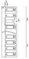
도 1은 일부 실시예에 따른, 단순화된 FinFET(Fin Field-Effect Transistor)의 예를 3차원 뷰로 예시한다. (아래에서 논의되는) FinFET의 일부 다른 피처는 예시 명확성을 위해 생략되었다. 예시된 FinFET은, 예를 들어, 하나의 트랜지스터로서 또는, 4개의 트랜지스터와 같은, 다수의 트랜지스터로서 동작하는 방식으로 전기적으로 결합될 수 있다.1 illustrates an example of a simplified Fin Field-Effect Transistor (FinFET) in a three-dimensional view, in accordance with some embodiments. Some other features of the FinFET (discussed below) have been omitted for illustrative clarity. The illustrated FinFET may be electrically coupled in such a way that it operates as one transistor or as multiple transistors, such as four transistors, for example.
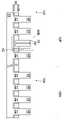
FinFET는 기판(50)으로부터 연장되는 핀(52)을 포함한다. 얕은 트렌치 격리(STI) 영역(66)은 기판(50) 위에 배치되고, 핀(52)은 이웃하는 STI 영역(66) 사이로부터 STI 영역(64)보다 높게 돌출한다. 비록 STI 영역(66)이 기판(50)으로부터 분리되는 것으로 설명/예시되지만, 본 명세서에서 사용되는 바와 같이, "기판"이라는 용어는 반도체 기판만을 지칭하거나 또는 격리 영역을 포함한 반도체 기판을 지칭하기 위해 사용될 수 있다. 추가적으로, 비록 핀(52)이 기판(50)의 단일의 연속적인 재료인 것으로 예시되어 있지만, 핀(52) 및/또는 기판(50)은 단일의 재료 또는 복수의 재료를 포함할 수 있다. 이러한 맥락에서, 핀(52)은 이웃하는 STI 영역(66) 사이에 연장되는 부분을 지칭한다.The FinFET includes a
게이트 구조체(110)는 핀(52)의 채널 영역 위에 있다. 게이트 구조체(110)는 게이트 유전체(112) 및 게이트 전극(114)을 포함한다. 게이트 유전체(112)는 핀(52)의 측벽을 따라 및 핀(62)의 상부 표면 위에 있으며, 게이트 전극(114)은 게이트 유전체(112) 위에 있다. 소스/드레인 영역(98)은 게이트 유전체(112) 및 게이트 전극(114)과 관련하여 핀(52)의 양측에(in opposite sides) 배치된다. 게이트 스페이서(96)는 소스/드레인 영역(98)을 게이트 구조체(110)로부터 분리시킨다. 다수의 트랜지스터가 형성되는 실시예에서, 소스/드레인 영역(98)은 다양한 트랜지스터들 사이에 공유될 수 있다. 하나의 트랜지스터가 다수의 핀(52)으로부터 형성되는 실시예에서, 이웃하는 소스/드레인 영역(98)은, 예컨대, 에피택셜 성장에 의해 소스/드레인 영역(98)을 합체(coalescing)시키는 것을 통해, 또는 소스/드레인 영역(98)을 동일한 소스/드레인 콘택트와 결합시키는 것을 통해, 전기적으로 결합될 수 있다. 하나 이상의 층간 유전체(ILD) 층(들)(아래에서 추가로 논의됨)은 소스/드레인 영역(98) 및/또는 게이트 전극(114) 위에 있으며, 이를 관통하여 소스/드레인 영역(98) 및 게이트 전극(114)에 대한 콘택트(아래에서 추가로 논의됨)가 형성된다.The
도 1은 여러 기준 단면을 추가로 예시한다. 단면 A-A는 게이트 전극(114)의 종축을 따른 것이다. 단면 B/C-B/C는 단면 A-A에 수직이고 핀(52)의 종축을 따른 것이다. 단면 D-D는 단면 A-A에 평행하고 FinFET의 소스/드레인 영역(98)을 통해 연장된다. 후속 도면은 명확성을 위해 이러한 기준 단면을 참조한다.1 further illustrates several reference cross-sections. Sections A-A are along the longitudinal axis of the
본 명세서에서 논의된 일부 실시예는 게이트-라스트 프로세스(gate-last process)를 사용하여 형성되는 FinFET의 맥락에서 논의된다. 다른 실시예에서는, 게이트-퍼스트 프로세스(gate-first process)가 사용될 수 있다. 또한, 일부 실시예는, 평면 FET와 같은, 평면 디바이스에서 사용되는 양상을 고려한다.Some embodiments discussed herein are discussed in the context of a FinFET formed using a gate-last process. In other embodiments, a gate-first process may be used. Also, some embodiments contemplate aspects used in planar devices, such as planar FETs.
도 2 내지 도 15c는 일부 실시예에 따른, FinFET의 제조에서의 중간 스테이지의 단면도이다. 도 2, 도 3, 도 4, 도 6, 도 7, 도 8, 도 9a, 도 10a, 도 11a, 도 12a, 도 13a, 도 14a, 및 도 15a는, 다수의 핀/FinFET를 제외하고는, 도 1에 예시된 기준 단면 A-A를 예시한다. 도 9b, 도 10b, 도 11b, 도 12b, 도 13b, 도 14b 및 도 15b는, 다수의 핀/FinFET를 제외하고는, 도 1에 예시된 기준 단면 B/C-B/C를 예시한다. 도 9c, 도 10c, 도 11c, 도 12c, 도 13c, 도 14c 및 도 15c는, 다수의 핀/FinFET를 제외하고는, 도 8에 예시된 기준 단면 C-C를 예시한다. 도 9d는, 다수의 핀/FinFET를 제외하고는, 도 1에 예시된 기준 단면 D-D를 예시한다.2-15C are cross-sectional views of intermediate stages in the fabrication of FinFETs, in accordance with some embodiments. 2, 3, 4, 6, 7, 8, 9A, 10A, 11A, 12A, 13A, 14A, and 15A are, except for multiple fin/FinFETs, , illustrate the reference section A-A illustrated in FIG. 1 . 9B, 10B, 11B, 12B, 13B, 14B, and 15B illustrate the reference cross-section B/C-B/C illustrated in FIG. 1 , except for multiple Fin/FinFETs. 9C, 10C, 11C, 12C, 13C, 14C, and 15C illustrate the reference cross-section C-C illustrated in FIG. 8, with the exception of multiple Fin/FinFETs. 9D illustrates the reference cross-section D-D illustrated in FIG. 1, with the exception of multiple fins/FinFETs.
도 2에서, 기판(50)이 제공된다. 기판(50)은, (예를 들면, p형 또는 n형 도펀트로) 도핑될 수 있거나 도핑되지 않을 수 있는, 벌크 반도체, SOI(semiconductor-on-insulator) 기판 등과 같은, 반도체 기판일 수 있다. 기판(50)은, 실리콘 웨이퍼와 같은, 웨이퍼일 수 있다. 일반적으로, SOI 기판은 절연체 층 상에 형성되는 반도체 재료의 층이다. 절연체 층은, 예를 들어, 매립 산화물(buried oxide, BOX) 층, 실리콘 산화물 층 등일 수 있다. 절연체 층은 기판, 전형적으로 실리콘 기판 또는 유리 기판 상에 제공된다. 다층 기판(multi-layered substrate) 또는 그레이디언트 기판(gradient substrate)과 같은, 다른 기판이 또한 사용될 수 있다. 일부 실시예에서, 기판(50)의 반도체 재료는 실리콘; 게르마늄; 실리콘 탄화물, 갈륨 비화물, 갈륨 인화물, 인듐 인화물, 인듐 비화물, 및/또는 인듐 안티몬화물을 포함한 화합물 반도체; 실리콘-게르마늄, 갈륨 비소 인화물, 알루미늄 인듐 비화물, 알루미늄 갈륨 비화물, 갈륨 인듐 비화물, 갈륨 인듐 인화물, 및/또는 갈륨 인듐 비소 인화물을 포함한 합금 반도체; 또는 이들의 조합을 포함할 수 있다.2 , a
기판(50)은 n형 영역(50N) 및 p형 영역(50P)을 갖는다. n형 영역(50N)은, NMOS 트랜지스터, 예를 들면, n형 FinFET와 같은, n형 디바이스를 형성하기 위한 것일 수 있다. p형 영역(50P)은, PMOS 트랜지스터, 예를 들면, p형 FinFET와 같은, p형 디바이스를 형성하기 위한 것일 수 있다. n형 영역(50N)은 p형 영역(50P)으로부터 물리적으로 분리될 수 있고, 임의의 개수의 디바이스 피처(예를 들면, 다른 능동 디바이스, 도핑 영역, 격리 구조체 등)가 n형 영역(50N)과 p형 영역(50P) 사이에 배치될 수 있다.The
이어서 핀(52)이 기판(50)에 형성된다. 핀(52)은 반도체 스트립(semiconductor strip)이다. 일부 실시예에서, 핀(52)은 기판(50)에 트렌치를 에칭하는 것에 의해 기판(50)에 형성될 수 있다. 에칭은, 반응성 이온 에칭(RIE), 중성 빔 에칭(NBE) 등, 또는 이들의 조합과 같은, 임의의 허용 가능한 에칭 프로세스일 수 있고, 핀(52)의 패턴을 갖는 마스크(54)에 의해 수행될 수 있다. 에칭은 이방성일 수 있다.
핀은 임의의 적합한 방법에 의해 패터닝될 수 있다. 예를 들어, 핀(52)은, 더블 패터닝(double-patterning) 프로세스 또는 멀티 패터닝(multi-patterning) 프로세스를 포함한, 하나 이상의 포토리소그래피 프로세스를 사용하여 패터닝될 수 있다. 일반적으로, 더블 패터닝 프로세스 또는 멀티 패터닝 프로세스는 포토리소그래피 프로세스와 자기 정렬 프로세스를 조합하여, 예를 들어, 단일의 직접 포토리소그래피 프로세스를 사용하여 다른 방식으로 획득 가능한 것보다 작은 피치를 갖는 패턴이 생성될 수 있게 한다. 예를 들어, 일 실시예에서, 희생 층이 기판 위에 형성되고 포토리소그래피 프로세스를 사용하여 패터닝된다. 자기 정렬 프로세스를 사용하여, 패터닝된 희생 층과 나란히 스페이서가 형성된다. 이어서 희생 층이 제거되고, 이어서 남아 있는 스페이서는 핀을 패터닝하는 데 사용될 수 있다. 일부 실시예에서, 마스크(54)(또는 다른 층)는 핀(52) 상에 남아 있을 수 있다.The pins may be patterned by any suitable method. For example, the
일부 실시예에 따르면, 기판(50)의 일부 영역은 핀(52)으로 패터닝되지 않는다. 예를 들어, 기판(50)의 비활성 영역(50R)은 마스크(54)에 의해 덮이지 않고, 핀을 포함하지 않는다. 비활성 영역(50R)은 디바이스, 예를 들면, FinFET가 요망되지 않거나 형성되지 않는 기판(50)의 임의의 영역일 수 있다. 예시된 실시예에서, 비활성 영역(50R)은 p형 영역(50P)의 일부이고, p형 영역(50P)에서 인접한 p형 FinFET 사이에 배치된다. 다른 실시예(아래에서 추가로 논의됨)에서, 비활성 영역(50R)은 n형 영역(50N)의 일부이고, n형 영역(50N)에서 인접한 n형 FinFET 사이에 배치된다. 또 다른 실시예(아래에서 추가로 논의됨)에서, n형 영역(50N)과 p형 영역(50P) 둘 모두가 비활성 영역(50R)을 포함한다. 비활성 영역(50R)의 폭은 비활성 영역(50R) 외부의 핀(52) 사이의 간격보다 클 수 있다. 예를 들어, 비활성 영역(50R) 외부의 핀(52)은 약 10 nm 내지 약 50 nm의 범위일 수 있는 거리 D1만큼 이격될 수 있는 반면, 비활성 영역(50R)과 접하는 핀(52)은 거리 D1보다 약 2배 내지 약 3배 더 클 수 있는 거리 D2만큼 이격될 수 있다.According to some embodiments, some regions of the
아래에서 추가로 논의되는 바와 같이, 후속 프로세싱에서의 패턴 로딩 효과를 감소시키는 데 도움을 주기 위해 비활성 영역(50R)에 더미 핀이 형성될 것이다. FinFET를 형성하는 데 사용되고 활성 핀 또는 반도체 핀이라고도 지칭되는 핀(52)과는 대조적으로, 더미 핀은 FinFET를 형성하는 데 사용되지 않고 비활성 핀 또는 유전체 핀이라고도 지칭된다. 후속 프로세싱에서의 패턴 로딩 효과를 감소시키는 데 도움을 주는 것 외에도, 더미 핀은 또한 높은 비유전율(relative permittivity)을 갖도록 형성되고 따라서 또한 인접한 디바이스, 예를 들면, 인접한 FinFET를 서로 전기적으로 격리시키는 데 도움을 준다. 단일 비활성 영역(50R)에 단일 더미 핀을 형성하는 것이 예시되어 있지만, 동일한 비활성 영역(50R)에 다수의 더미 핀이 형성될 수 있음이 이해되어야 하고, 또한 다수의 비활성 영역(50R)이 형성될 수 있음이 이해되어야 한다.As discussed further below, dummy fins will be formed in
도 3에서, 절연 재료(64)의 하나 이상의 층(들)이 기판(50) 위에 및 이웃하는 활성 핀(52) 사이에 형성된다. 절연 재료(64)는 실리콘 산화물과 같은 산화물, 실리콘 질화물과 같은 질화물 등, 또는 이들의 조합을 포함하고, 화학적 기상 퇴적(CVD), 고밀도 플라스마 화학적 기상 퇴적(high density plasma chemical vapor deposition, HDP-CVD), 유동성 CVD(flowable CVD, FCVD)(예를 들면, 원격 플라스마(remote plasma) 시스템에서의 CVD 기반 재료 퇴적 및 이를, 산화물과 같은, 다른 재료로 전환(convert)시키기 위한 사후 경화(post curing)) 등, 또는 이들의 조합에 의해 형성될 수 있다. 임의의 허용 가능한 프로세스에 의해 형성되는 다른 절연 재료가 사용될 수 있다. 예시된 실시예에서, 절연 재료(64)는 기판(50)과 활성 핀(52)의 표면 상의 라이너(64A), 및 라이너(64A) 상의 충전 재료(64B)를 포함한다. 라이너(64A)는 ALD 프로세스에 의해 형성되는 비정질 실리콘, 실리콘 산화물, 실리콘 질화물 등일 수 있고, 충전 재료(64B)는 FCVD 프로세스에 의해 형성되는 실리콘 산화물일 수 있다. 다른 실시예에서, 절연 재료(64)의 단일 층이 형성된다. 일단 절연 재료가 형성되면 어닐링 프로세스가 수행될 수 있다. 어닐링 프로세스는 H2 또는 O2를 함유하는 환경에서 수행될 수 있다. 어닐링 이후에, 라이너(64A)가 충전 재료(64B)와 유사한 재료이도록 라이너(64A)가 어닐링 프로세스에 의해 산화될 수 있다. 일 실시예에서, 잉여 절연 재료(64)가 활성 핀(52) 또는 마스크(54)(존재하는 경우)를 덮도록 절연 재료(64)가 형성된다.3 , one or more layer(s) of insulating
절연 재료(64)는 기판(50)에 걸쳐 상이한 두께를 가지며, 모든 활성 핀(52) 사이의 갭을 채우지 않을 수 있다. 구체적으로, 이격 거리(spacing distance) D2가 이격 거리 D1보다 크기 때문에(도 2 참조), 절연 재료(64)가 비활성 영역(50R)을 완전히 채우지는 못할 수 있다. 예를 들어, 절연 재료(64)의 토출량(dispensed volume)이 비활성 영역(50R)을 완전히 채우기에 불충분할 수 있다. 비활성 영역(50R)에서의 절연 재료(64)는 그 대신에 기판(50) 및 비활성 영역(50R)과 접하는 활성 핀(52)의 측벽을 컨포멀하게 라이닝할 수 있다. 따라서 비활성 영역(50R)에서의 절연 재료(64)의 부분은 비활성 영역(50R)과 접하는 활성 핀(52) 사이에 리세스(56)를 포함한다. 리세스(56)의 형상 및 치수는 도 5와 관련하여 아래에서 추가로 논의될 것이다.The insulating
도 4에서, 유전체 층(58)이 절연 재료(64) 상에 형성된다. 유전체 층(58)은 리세스(56)를 라이닝한다. 유전체 층(58)은 실리콘 산질화물, 실리콘 산탄질화물, 실리콘 질화물 등으로 형성될 수 있으며, ALD, CVD 등에 의해 형성될 수 있다. 유전체 층(58)은 절연 재료(64)의 에칭에 대해 높은 에칭 선택도를 갖는 재료로 형성된다. 게다가, 유전체 층(58)의 재료는 절연 재료(64)의 재료(들)보다 큰 비유전율을 갖는다. 예를 들어, 절연 재료(64)는 약 10 내지 약 12의 범위에 있는 비유전율을 갖는 재료로 형성될 수 있고, 유전체 층(58)은 약 4 내지 약 7의 범위에 있는 비유전율을 갖는 재료로 형성될 수 있다. 일부 실시예에서, 유전체 층(58)은 ALD에 의해 형성되는 실리콘 산질화물이다. 다른 실시예에서, 유전체 층(58)의 재료는 절연 재료(64)의 재료(들)보다 작은 비유전율을 갖는다.In FIG. 4 ,
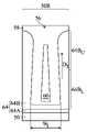
도 5는 도 4로부터의 비활성 영역(50R)의 상세도이다. 리세스(56)의 형상 및 치수가 더 명확하게 예시된다. 절연 재료(64)를 형성하는 방법으로 인해, 리세스(56)는 리엔트런트 프로파일 형상(reentrant profile shape)을 가지며, 여기서 리세스(56)의 폭 W1은 충전 재료(64B)의 바닥으로부터 충전 재료(64B)의 상부로 연장되는 D3 방향을 따라 감소한다. 환언하면, 리세스(56)의 바닥에서의 폭 W1은 리세스(56)의 상부에서의 폭 W1보다 크다. 예를 들어, 폭 W1은 약 10 nm 내지 약 30 nm의 범위일 수 있고, 리세스(56)의 바닥에서의 폭 W1은 리세스(56)의 상부에서의 폭 W1보다 약 0% 내지 약 30% 더 클 수 있다. 충전 재료(64B)가 FCVD 프로세스에 의해 형성되는 실리콘 산화물일 때 리세스(56)는 리엔트런트 프로파일 형상으로 형성될 수 있다.FIG. 5 is a detailed view of the
다른 실시예에서, 충전 재료(64B)는 CVD로 비정질 실리콘을 퇴적하는 것 및 이어서 비정질 실리콘을 산화시켜 실리콘 산화물을 형성하는 것에 의해 형성된다. 산화는 산화가 방향성으로 일어나는 플라스마 산화 프로세스에 의해 이루어질 수 있다. 이에 따라, 충전 재료(64B)의 상부 부분(64BU)은 충전 재료(64B)의 하부 부분(64BL)보다 더 산화된다. 환언하면, 플라스마 산화가 사용될 때, 충전 재료(64B)의 산소 농도는 충전 재료(64B)에 걸쳐 충전 재료(64B)의 바닥으로부터 충전 재료(64B)의 상부로 연장되는 D3 방향으로 증가한다. 실리콘이 산화될 때 실리콘의 체적이 증가된다. 충전 재료(64B)의 상부 부분(64BU)이 충전 재료(64B)의 하부 부분(64BL)보다 더 산화되기 때문에, 산화는 충전 재료(64B)의 상부 부분(64BU)의 체적을 충전 재료(64B)의 하부 부분(64BL)의 체적보다 더 많이 증가시킨다. 따라서 산화 이후에 리세스(56)의 바닥에서의 폭 W1은 리세스(56)의 상부에서의 폭 W1보다 크다. 일부 실시예에서, 산화 이전에 리세스(56)의 바닥에서의 폭 W1은 리세스(56)의 상부에서의 폭 W1보다 작거나 같고, 산화 이후에 리세스(56)의 바닥에서의 폭 W1은 리세스(56)의 상부에서의 폭 W1보다 크다.In another embodiment, fill
리세스(56)가 리엔트런트 프로파일 형상을 갖기 때문에, 유전체 층(58)의 퇴적 동안 리세스(56)의 상부에서 핀치-오프(pinch-off)가 발생한다. 일부 실시예에서, 보이드(60)가 형성될 때까지 절연 재료(64)가 퇴적된다. 보이드(60)는 유전체 층(58)에 의해 채워지지 않은 리세스(56)의 부분을 포함한다. 보이드(60)는 유전체 층(58)의 퇴적 동안 프로세싱 조건에 따라 진공 상태이거나 가스(예를 들면, 공기)로 채워질 수 있다. 보이드(60)는 리세스(56)와 유사한 프로파일 형상, 예를 들면, 리엔트런트 프로파일 형상을 갖는다. 보이드(60)의 형상 및 치수는 도 16과 관련하여 아래에서 추가로 논의될 것이다.Because the
도 6에서, 활성 핀(52) 위의 유전체 층(58) 및 절연 재료(64)의 잉여 부분을 제거하기 위해 유전체 층(58) 및 절연 재료(64)에 제거 프로세스가 적용된다. 일부 실시예에서, 화학적 기계적 폴리싱(CMP), 에치백 프로세스, 이들의 조합 등과 같은 평탄화 프로세스가 이용될 수 있다. 제거 프로세스는 리세스(56)(도 5 참조)에서의 유전체 층(58)의 잔류 부분을 포함하는 더미 핀(62)을 형성한다. 더미 핀(62)은 유전체 스트립이다. 제거 프로세스 이후에, 유전체 층(58)의 일부 부분은 보이드(60) 위에 남아 있고, 따라서 보이드(60)가 파괴되지 않는다. 더미 핀(62)은 비활성 영역(50R)과 접하는 활성 핀(52) 사이에 배치된다. 예시된 실시예에서, 더미 핀(62)은 p형 영역(50P)에서 활성 핀(52) 사이에 배치된다. 평탄화 프로세스가 완료된 후에 활성 핀(52), 더미 핀(62) 및 절연 재료(64)의 상부 표면이 공면(coplanar)이도록 평탄화 프로세스는 활성 핀(52) 및 더미 핀(62)을 노출시킨다. 마스크(54)가 활성 핀(52) 상에 남아 있는 실시예에서, 평탄화 프로세스가 완료된 후에 마스크(54), 더미 핀(62) 및 절연 재료(64)의 상부 표면 또는 활성 핀(52), 더미 핀(62) 및 절연 재료(64)의 상부 표면이 공면이도록 평탄화 프로세스는, 제각기, 마스크(54)를 노출시키거나 마스크(54)를 제거할 수 있다.In FIG. 6 , a removal process is applied to
더미 핀(62)은 인접한 활성 핀(52)으로부터 등거리로 이격되고, 더미 핀(62) 및 활성 핀(52)의 상부 표면은 기판(50)으로부터 동일한 거리에 배치된다. 이에 따라, 더미 핀(62)은 후속 프로세싱에서, 예컨대, 후속 CMP 또는 에칭 프로세스(들)에서 패턴 로딩 효과를 감소시키는 데 도움을 준다. 더미 핀(62)의 형상 및 치수는 도 16과 관련하여 아래에서 추가로 논의될 것이다. 더미 핀(62)은 유전체 층(58) 및 보이드(60)를 포함하고, 유전체 층(58)이 보이드(60)를 둘러싼다. 이 실시예에서, 보이드(60)는 유전체 층(58)에 의해 연속적으로 봉입된다. 보이드(60)는 공기로 채워지거나 진공 상태이고, 따라서 약 1의 비유전율과 같은 낮은 비유전율을 갖는다. 일부 실시예에서, 보이드(60)의 비유전율은 유전체 층(58)의 비유전율 및 STI 영역(66)의 비유전율보다 작다. 보이드(60)를 형성하는 것은 더미 핀(62)의 총 유효 컨덕턴스를 감소시킨다. 따라서 더미 핀(62)은 반도체 재료 또는 단일 유전체 재료로 형성된 더미 핀보다 많은 양의 전기적 격리를 제공한다. 이에 따라, 후속 프로세싱에서 패턴 로딩 효과를 감소시키는 데 도움을 주는 것 외에도, 더미 핀(62)은 또한 인접한 활성 핀(52)(및 그의 결과적인 FinFET)을 서로로부터 전기적으로 격리시키는 데 도움을 준다. 구체적으로, 유전체 층(58) 및 보이드(60)는 비활성 영역(50R)과 접하는 활성 핀(52) 사이에 배치된 기생 커패시터의 네트워크에 대한 유전체 매체로서 작용한다. 보이드(60)를 형성하는 것은 커패시터 네트워크의 유효 커패시턴스를 약 10% 내지 약 14%만큼 감소시키는 데 도움을 줄 수 있다. 따라서 결과적인 FinFET의 기생 커패시턴스가 감소될 수 있고, 이에 의해 FinFET의 성능을 향상시킬 수 있다.The
도 7에서, STI 영역(66)을 형성하기 위해 절연 재료(64)가 리세싱된다. 활성 핀(52) 및 더미 핀(62)의 상부 부분이 이웃하는 STI 영역(66) 사이로부터 STI 영역(66)보다 높게 돌출하도록 절연 재료(64)가 리세싱된다. 게다가, STI 영역(66)의 상부 표면은 예시된 바와 같은 평평한 표면(flat surface), 볼록한 표면(convex surface), (디싱(dishing)과 같은) 오목한 표면(concave surface), 또는 이들의 조합을 가질 수 있다. STI 영역(66)의 상부 표면은 적절한 에칭에 의해 평평하게, 볼록하게, 및/또는 오목하게 형성될 수 있다. STI 영역(66)은, 절연 재료(64)의 재료(들)에 대해 선택적인 것과 같은, 허용 가능한 에칭 프로세스를 사용하여 리세싱될 수 있다. 예를 들어, 예를 들어, 희석 플루오르화 수소(dHF) 산을 사용한 산화물 제거가 사용될 수 있다. 에칭 프로세스는 활성 핀(52) 및 더미 핀(62)의 재료(들)보다 빠른 속도로 절연 재료(64)의 재료(들)를 선택적으로 에칭한다. 예를 들어, 유전체 층(58)의 재료(예를 들면, 실리콘 산질화물) 및 절연 재료(64)의 재료(들)(예를 들면, 실리콘 및 실리콘 산화물)는 에칭 프로세스에 대해 약 20:1 내지 약 1000:1의 범위에 있는 에칭 선택도를 가질 수 있다. 따라서, 유전체 층(58)이 더미 핀(62)의 형성 동안 손상으로부터 보호될 수 있다. 더미 핀(62)은 리세싱 동안 패턴 로딩 효과를 감소시키는 데 도움을 주며, 이에 따라, 더미 핀(62) 주위의 절연 재료(64)의 부분은 활성 핀(52) 주위의 절연 재료(64)의 부분과 동일한 양만큼 리세싱된다.In FIG. 7 , insulating
도 2 내지 도 7과 관련하여 설명된 프로세스는 활성 핀(52)이 형성될 수 있는 방법의 일 예일 뿐이다. 일부 실시예에서, 핀은 에피택셜 성장 프로세스에 의해 형성될 수 있다. 예를 들어, 유전체 층이 기판(50)의 상부 표면 위에 형성될 수 있고, 아래에 놓인 기판(50)을 노출시키기 위해 트렌치가 유전체 층을 관통하여 에칭될 수 있다. 호모에피택셜 구조체(homoepitaxial structure)가 트렌치에 에피택셜적으로 성장될 수 있고, 호모에피택셜 구조체가 활성 핀(52)을 형성하기 위해 유전체 층으로부터 돌출하도록 유전체 층이 리세싱될 수 있다. 추가적으로, 일부 실시예에서, 헤테로에피택셜 구조체(heteroepitaxial structure)가 활성 핀(52)에 사용될 수 있다. 예를 들어, 도 7에서의 활성 핀(52)이 리세싱될 수 있고, 활성 핀(52)과 상이한 재료가 리세싱된 활성 핀(52) 위에 에피택셜적으로 성장될 수 있다. 그러한 실시예에서, 활성 핀(52)은 리세싱된 재료는 물론 리세싱된 재료 위에 배치된 에피택셜적으로 성장된 재료를 포함한다. 추가 실시예에서, 유전체 층이 기판(50)의 상부 표면 위에 형성될 수 있고, 트렌치가 유전체 층을 관통하게 에칭될 수 있다. 이어서 헤테로에피택셜 구조체가 기판(50)과 상이한 재료를 사용하여 트렌치에 에피택셜적으로 성장될 수 있고, 헤테로에피택셜 구조체가 활성 핀(52)을 형성하기 위해 유전체 층으로부터 돌출하도록 유전체 층이 리세싱될 수 있다. 호모에피택셜 또는 헤테로에피택셜 구조체가 에피택셜적으로 성장되는 일부 실시예에서, 에피택셜적으로 성장된 재료는 성장 동안 인시츄(in situ) 도핑될 수 있으며, 이는 선행 주입 및 후속 주입을 제거할 수 있지만, 인시츄 도핑과 주입 도핑이 함께 사용될 수 있다.The process described with respect to FIGS. 2-7 is only one example of how
게다가, p형 영역(50P)(예를 들면, PMOS 영역)에서의 재료와는 상이한 재료를 n형 영역(50N)(예를 들면, NMOS 영역)에 에피택셜적으로 성장시키는 것이 유리할 수 있다. 다양한 실시예에서, 활성 핀(52)의 상부 부분은 실리콘-게르마늄(SixGe1-x, 여기서 x는 0 내지 1의 범위일 수 있음), 실리콘 탄화물, 순 게르마늄(pure germanium) 또는 실질적으로 순 게르마늄(substantially pure germanium), III-V 화합물 반도체, II-VI 화합물 반도체 등으로 형성될 수 있다. 예를 들어, III-V 화합물 반도체를 형성하는 데 이용 가능한 재료는 인듐 비화물, 알루미늄 비화물, 갈륨 비화물, 인듐 인화물, 갈륨 질화물, 인듐 갈륨 비화물, 인듐 알루미늄 비화물, 갈륨 안티몬화물, 알루미늄 안티몬화물, 알루미늄 인화물, 갈륨 인화물 등을 포함하지만, 이에 제한되지 않는다.Furthermore, it may be advantageous to epitaxially grow a material different from the material in p-
게다가 도 7에서, 적절한 웰(well)(도시되지 않음)이 활성 핀(52) 및/또는 기판(50)에 형성될 수 있다. 일부 실시예에서, p형 웰이 n형 영역(50N)에 형성될 수 있고, n형 웰이 p형 영역(50P)에 형성될 수 있다. 일부 실시예에서, p형 웰 또는 n형 웰이 n형 영역(50N)과 p형 영역(50P) 둘 모두에 형성된다.Furthermore, in FIG. 7 , suitable wells (not shown) may be formed in
상이한 웰 유형을 갖는 실시예에서, n형 영역(50N) 및 p형 영역(50P)에 대한 상이한 주입 단계는 포토레지스트 또는 다른 마스크(도시되지 않음)를 사용하여 달성될 수 있다. 예를 들어, n형 영역(50N)에서 활성 핀(52) 및 STI 영역(66) 위에 포토레지스트가 형성될 수 있다. 포토레지스트가 기판(50)의 p형 영역(50P)을 노출시키도록 패터닝된다. 포토레지스트는 스핀-온(spin-on) 기술을 사용하여 형성될 수 있고, 허용 가능한 포토리소그래피 기술을 사용하여 패터닝될 수 있다. 일단 포토레지스트가 패터닝되면, n형 불순물 주입이 p형 영역(50P)에서 수행되고, 포토레지스트는 n형 불순물이 n형 영역(50N) 내로 주입되는 것을 실질적으로 방지하기 위해 마스크로서 작용할 수 있다. n형 불순물은 약 1018 cm-3 이하, 예컨대, 약 1016 cm-3 내지 약 1018 cm-3의 범위에 있는 농도로 해당 영역에 주입되는 인, 비소, 안티몬 등일 수 있다. 주입 이후에, 예컨대, 허용 가능한 애싱 프로세스에 의해, 포토레지스트가 제거된다.In embodiments with different well types, different implantation steps for n-
p형 영역(50P)의 주입 이후에, p형 영역(50P)에서 활성 핀(52) 및 STI 영역(66) 위에 포토레지스트가 형성된다. 포토레지스트는 기판(50)의 n형 영역(50N)을 노출시키도록 패터닝된다. 포토레지스트는 스핀-온 기술을 사용하여 형성될 수 있고, 허용 가능한 포토리소그래피 기술을 사용하여 패터닝될 수 있다. 일단 포토레지스트가 패터닝되면, p형 불순물 주입이 n형 영역(50N)에서 수행될 수 있고, 포토레지스트는 p형 불순물이 p형 영역(50P) 내로 주입되는 것을 실질적으로 방지하기 위해 마스크로서 작용할 수 있다. p형 불순물은 약 1018 cm-3 이하, 예컨대, 약 1016 cm-3 내지 약 1018 cm-3의 범위에 있는 농도로 해당 영역에 주입되는 붕소, 플루오르화 붕소, 인듐 등일 수 있다. 주입 이후에, 포토레지스트는, 예컨대, 허용 가능한 애싱 프로세스에 의해, 제거될 수 있다.After implantation of p-
n형 영역(50N) 및 p형 영역(50P)의 주입 이후에, 주입 손상(implant damage)을 회복(repair)시키기 위해 그리고 주입된 p형 불순물 및/또는 n형 불순물을 활성화시키기 위해 어닐링이 수행될 수 있다. 일부 실시예에서, 에피택셜 핀의 성장된 재료는 성장 동안 인시츄 도핑될 수 있고, 이는 주입을 제거할 수 있지만, 인시츄 도핑과 주입 도핑이 함께 사용될 수 있다.After implantation of n-
일부 실시예에서, 웰을 형성하기 위한 주입은 더미 핀(62)이 형성되기 전에 수행된다. 따라서, 이 프로세싱 단계에서 더미 핀(62)은 주입된 불순물이 없을 수 있다. 그렇지만, 아래에서 더 상세히 논의되는 바와 같이, 나중의 프로세싱 단계에서 더미 핀(62)에 불순물이 주입될 수 있다.In some embodiments, implants to form wells are performed before
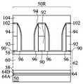
도 8에서, 더미 유전체 층(80)은 활성 핀(52) 및 더미 핀(62) 상에 형성된다. 더미 유전체 층(80)은, 예를 들어, 실리콘 산화물, 실리콘 질화물, 이들의 조합 등일 수 있고, 허용 가능한 기술에 따라 퇴적되거나 열적으로 성장될 수 있다. 더미 유전체 층(80)은 유전체 층(58)의 에칭에 대해 높은 에칭 선택도를 갖는 재료로 형성된다. 더미 게이트 층(82)은 더미 유전체 층(80) 위에 형성되고, 마스크 층(84)은 더미 게이트 층(82) 위에 형성된다. 더미 게이트 층(82)은 더미 유전체 층(80) 위에 퇴적될 수 있고 이어서, 예컨대, CMP에 의해, 평탄화될 수 있다. 더미 핀(62)은 더미 게이트 층(82)의 평탄화 동안 패턴 로딩 효과를 감소시키는 데 도움을 준다. 마스크 층(84)은 더미 게이트 층(82) 위에 퇴적될 수 있다. 더미 게이트 층(82)은 전도성 또는 비-전도성 재료일 수 있고, 비정질 실리콘, 다결정 실리콘(폴리실리콘), 다결정 실리콘-게르마늄(폴리-SiGe), 금속 질화물, 금속 실리사이드, 금속 산화물, 및 금속을 포함한 그룹 중에서 선택될 수 있다. 더미 게이트 층(82)은 물리적 기상 퇴적(PVD), CVD, 스퍼터 퇴적, 또는 선택된 재료를 퇴적시키기 위한 다른 기술에 의해 퇴적될 수 있다. 더미 게이트 층(82)은 격리 영역, 예를 들면, STI 영역(66) 및/또는 더미 유전체 층(80)의 에칭에 대해 높은 에칭 선택도를 갖는 다른 재료로 제조될 수 있다. 마스크 층(84)은, 예를 들어, 실리콘 질화물, 실리콘 산질화물 등의 하나 이상의 층을 포함할 수 있다. 이 예에서, 단일 더미 게이트 층(82) 및 단일 마스크 층(84)이 n형 영역(50N) 및 p형 영역(50P)에 걸쳐 형성된다. 예시된 실시예에서, 더미 유전체 층(80)이 활성 핀(52), 더미 핀(62) 및 STI 영역(66)을 덮어, STI 영역(66) 위에서 더미 게이트 층(82)과 STI 영역(66) 사이에 연장되도록 더미 유전체 층(80)이 퇴적된다. 다른 실시예에서, 예컨대, 더미 유전체 층(80)이 열 성장에 의해 형성될 때, 더미 유전체 층(80)은 활성 핀(52)만을 덮고 더미 핀(62)을 덮지 않는다.In FIG. 8 , a
도 9a 내지 도 15c는 FinFET의 제조에서의 추가 중간 스테이지를 예시한다. 도 9b, 도 10b, 도 11b, 도 12b, 도 13b, 도 14b 및 도 15b는 n형 영역(50N) 및 p형 영역(50P) 중 어느 하나에서의 피처를 예시한다. 예를 들어, 도 9b, 도 10b, 도 11b, 도 12b, 도 13b, 도 14b 및 도 15b에 예시된 구조는 n형 영역(50N) 및 p형 영역(50P) 둘 모두에 적용 가능할 수 있다. 도 9c, 도 10c, 도 11c, 도 12c, 도 13c, 도 14c 및 도 15c는 비활성 영역(50R)에서의 피처를 예시한다. 위에서 언급된 바와 같이, 비활성 영역(50R)은 p형 영역(50P)의 일부 또는 n형 영역(50N)의 일부일 수 있다. n형 영역(50N)과 p형 영역(50P)의 구조의 차이(있는 경우)는 각각의 도면에 부수하는 본문에서 설명된다.9A-15C illustrate a further intermediate stage in the fabrication of a FinFET. 9B, 10B, 11B, 12B, 13B, 14B, and 15B illustrate features in either n-
도 9a 내지 도 9c에서, 마스크 층(84)(도 8 참조)은 마스크(94)를 형성하기 위해 허용 가능한 포토리소그래피 및 에칭 기술을 사용하여 패터닝될 수 있다. 이어서 마스크(94)의 패턴이 더미 게이트(92)를 형성하기 위해 허용 가능한 에칭 기술에 의해 더미 게이트 층(82)으로 전사될 수 있다. 일부 실시예에서, 마스크(94)의 패턴이 또한 더미 유전체(90)를 형성하기 위해 허용 가능한 에칭 기술에 의해 더미 유전체 층(80)으로 전사될 수 있다. 더미 게이트(92)는 더미 핀(62) 및 활성 핀(52)의 각자의 채널 영역(68)을 덮는다. 마스크(94)의 패턴은 더미 게이트(92) 각각을 인접한 더미 게이트로부터 물리적으로 분리시키는 데 사용될 수 있다. 더미 게이트(92)는 또한 각자의 활성 핀(52)/더미 핀(62)의 길이 방향에 실질적으로 수직인 길이 방향을 가질 수 있다.9A-9C , mask layer 84 (see FIG. 8 ) may be patterned using acceptable photolithography and etching techniques to form
게이트 스페이서(96)는 더미 게이트(92) 및 마스크(94)의 측벽을 따라 형성된다. 게이트 스페이서(96)는 절연 재료를 컨포멀하게 퇴적시키고 후속적으로 절연 재료를 이방성으로 에칭하는 것에 의해 형성될 수 있다. 게이트 스페이서(96)의 절연 재료는 실리콘 산화물, 실리콘 질화물, 실리콘 산질화물, 실리콘 탄질화물, 실리콘 산탄질화물, 이들의 조합 등일 수 있다. 예를 들어, 게이트 스페이서(96)는 다수의 실리콘 산탄질화물 층을 포함할 수 있거나, 또는 2개의 실리콘 산화물 층 사이에 실리콘 질화물 층을 포함할 수 있다.
게이트 스페이서(96)의 형성 동안 또는 그 이후에, 저농도로 도핑된 소스/드레인(LDD) 영역에 대한 주입이 수행될 수 있다. 상이한 디바이스 유형을 갖는 실시예에서, 도 7에서 위에서 논의된 주입과 유사하게, 포토레지스트와 같은 마스크가 p형 영역(50P)을 노출시키면서 n형 영역(50N) 위에 형성될 수 있고, 적절한 유형의(예를 들면, p형) 불순물이 p형 영역(50P)에서의 노출된 활성 핀(52) 내로 주입될 수 있다. 이어서 마스크가 제거될 수 있다. 후속적으로, 포토레지스트와 같은 마스크가 n형 영역(50N)을 노출시키면서 p형 영역(50P) 위에 형성될 수 있고, 적절한 유형의(예를 들면, n형) 불순물이 n형 영역(50N)에서의 노출된 활성 핀(52) 내로 주입될 수 있다. 이어서 마스크가 제거될 수 있다. n형 불순물은 이전에 논의된 n형 불순물 중 임의의 것일 수 있고, p형 불순물은 이전에 논의된 p형 불순물 중 임의의 것일 수 있다. 저농도로 도핑된 소스/드레인 영역은 약 1015 cm-3 내지 약 1019 cm-3의 불순물 농도를 가질 수 있다. 주입 손상을 회복시키기 위해 그리고 주입된 불순물을 활성화시키기 위해 어닐링이 사용될 수 있다.During or after formation of the
LDD 영역을 형성하기 위한 주입은 또한 더미 핀(62)에 불순물을 주입할 수 있다. 예를 들어, 더미 핀(62)이 p형 영역(50P)에 형성될 때, 더미 핀(62)의 상부 부분(예를 들면, STI 영역(66)의 표면보다 높은 더미 핀(62)의 부분)에는 p형 영역(50P)에 주입된 p형 불순물이 주입될 수 있다. 마찬가지로, 더미 핀(62)이 n형 영역(50N)에 형성될 때, 더미 핀(62)의 상부 부분(예를 들면, STI 영역(66)의 표면보다 높은 더미 핀(62)의 부분)에는 n형 영역(50N)에 주입된 n형 불순물이 주입될 수 있다.Implantation to form the LDD region may also implant impurities into the
이어서 에피택셜 소스/드레인 영역(98)이 활성 핀(52)에 형성된다. 각각의 더미 게이트(92)가 에피택셜 소스/드레인 영역(98)의 각자의 이웃하는 쌍 사이에 배치되도록 에피택셜 소스/드레인 영역(98)이 활성 핀(52)에 형성된다. 일부 실시예에서, 에피택셜 소스/드레인 영역(98)은 활성 핀(52) 내로 연장될 수 있고 또한 활성 핀(52)을 관통할 수 있다. 일부 실시예에서, 에피택셜 소스/드레인 영역(98)이 결과적인 FinFET의 후속적으로 형성된 게이트를 단락(short out)시키지 않도록, 에피택셜 소스/드레인 영역(98)을 더미 게이트(92)로부터 적절한 측방 거리만큼 분리시키기 위해 게이트 스페이서(96)가 사용된다. 에피택셜 소스/드레인 영역(98)의 재료는 각자의 채널 영역(68)에 응력을 가하여, 이에 의해 성능을 개선시키도록 선택될 수 있다.An epitaxial source/
n형 영역(50N)에서의 에피택셜 소스/드레인 영역(98)은 p형 영역(50P)을 마스킹하고 n형 영역(50N)에서의 활성 핀(52)의 소스/드레인 영역을 에칭하여 활성 핀(52)에 리세스를 형성하는 것에 의해 형성될 수 있다. 더미 핀(62)에 리세스(따라서 에피택셜 소스/드레인 영역)가 형성되지 않도록 에칭이 활성 핀(52)에 대해 선택적이다. 이어서, n형 영역(50N)에서의 에피택셜 소스/드레인 영역(98)이 리세스에 에피택셜적으로 성장된다. 에피택셜 소스/드레인 영역(98)은, n형 FinFET에 적절한 것과 같은, 임의의 허용 가능한 재료를 포함할 수 있다. 예를 들어, 활성 핀(52)이 실리콘인 경우, n형 영역(50N)에서의 에피택셜 소스/드레인 영역(98)은, 실리콘, 실리콘 탄화물, 인 도핑된 실리콘 탄화물, 실리콘 인화물 등과 같은, 각자의 채널 영역(68)에 인장 변형(tensile strain)을 가하는 재료를 포함할 수 있다. n형 영역(50N)에서의 에피택셜 소스/드레인 영역(98)은 활성 핀(52)의 각자의 표면으로부터 융기된 표면을 가질 수 있고 패싯(facet)을 가질 수 있다.The epitaxial source/
p형 영역(50P)에서의 에피택셜 소스/드레인 영역(98)은 n형 영역(50N)을 마스킹하고 p형 영역(50P)에서의 활성 핀(52)의 소스/드레인 영역을 에칭하여 활성 핀(52)에 리세스를 형성하는 것에 의해 형성될 수 있다. 더미 핀(62)에 리세스(따라서 에피택셜 소스/드레인 영역)가 형성되지 않도록 에칭이 활성 핀(52)에 대해 선택적이다. 이어서, p형 영역(50P)에서의 에피택셜 소스/드레인 영역(98)이 리세스에 에피택셜적으로 성장된다. 에피택셜 소스/드레인 영역(98)은, p형 FinFET에 적절한 것과 같은, 임의의 허용가능한 재료를 포함할 수 있다. 예를 들어, 활성 핀(52)이 실리콘인 경우, p형 영역(50P)에서의 에피택셜 소스/드레인 영역(98)은, 실리콘-게르마늄, 붕소 도핑된 실리콘-게르마늄, 게르마늄, 게르마늄 주석 등과 같은, 각자의 채널 영역(68)에 압축 변형(compressive strain)을 가하는 재료를 포함할 수 있다. p형 영역(50P)에서의 에피택셜 소스/드레인 영역(98)은 활성 핀(52)의 각자의 표면으로부터 융기된 표면을 가질 수 있고 패싯을 가질 수 있다.The epitaxial source/
저농도로 도핑된 소스/드레인 영역을 형성하기 위한 이전에 논의된 프로세스와 유사하게, 소스/드레인 영역을 형성하기 위해 에피택셜 소스/드레인 영역(98) 및/또는 활성 핀(52)에 도펀트가 주입될 수 있고, 어닐링이 뒤따를 수 있다. 소스/드레인 영역은 약 1019 cm-3 내지 약 1021 cm-3의 불순물 농도를 가질 수 있다. 소스/드레인 영역에 대한 n형 및/또는 p형 불순물은 이전에 논의된 불순물 중 임의의 것일 수 있다. 일부 실시예에서, 에피택셜 소스/드레인 영역(98)은 성장 동안 인시츄 도핑될 수 있다.Similar to the previously discussed process for forming lightly doped source/drain regions, dopants are implanted into epitaxial source/
n형 영역(50N) 및 p형 영역(50P)에 에피택셜 소스/드레인 영역(98)을 형성하는 데 사용되는 에피택시 프로세스의 결과로서, 에피택셜 소스/드레인 영역의 상부 표면은 활성 핀(52)의 측벽을 넘어 측방으로 바깥쪽으로 팽창하는 패싯을 갖는다. 일부 실시예에서, 이러한 패싯은 동일한 FinFET의 인접한 에피택셜 소스/드레인 영역(98)을 병합시킨다. 일부 실시예에서, 인접한 에피택셜 소스/드레인 영역(98)은 에피택시 프로세스가 완료된 후에 분리된 채로 유지된다. 일부 실시예에서, 도 9d에 예시된 바와 같이, 제1 영역(예를 들면, n형 영역(50N))에서는 동일한 FinFET의 인접한 에피택셜 소스/드레인 영역(98)이 병합되고, 제2 영역(예를 들면, p형 영역(50P))에서는 인접한 에피택셜 소스/드레인 영역(98)이 분리된 채로 유지된다. 도 9d에 예시된 실시예에서, 게이트 스페이서(96)가 STI 영역(66)보다 높게 연장되는 활성 핀(52)의 측벽의 부분을 덮도록 형성되어 이에 의해 에피택셜 성장을 차단한다. 일부 다른 실시예에서, 게이트 스페이서(96)를 형성하는 데 사용되는 스페이서 에칭은 에피택셜적으로 성장된 영역이 STI 영역(66)의 표면까지 연장될 수 있게 하기 위해 스페이서 재료를 제거하도록 조정될 수 있다.As a result of the epitaxial process used to form epitaxial source/
상기 개시가 일반적으로 더미 게이트, 스페이서, LDD 영역, 및 소스/드레인 영역을 형성하는 프로세스를 설명하고 있음에 유의한다. 다른 프로세스 및 시퀀스가 사용될 수 있다. 예를 들어, 더 적은 또는 추가적인 스페이서가 이용될 수 있고, 단계들의 상이한 시퀀스가 이용될 수 있으며, 스페이서가 형성되고 제거될 수 있는 등이다. 게다가, n형 디바이스와 p형 디바이스가 상이한 구조 및 단계를 사용하여 형성될 수 있다.Note that the above disclosure generally describes a process for forming a dummy gate, spacers, LDD regions, and source/drain regions. Other processes and sequences may be used. For example, fewer or additional spacers may be used, different sequences of steps may be used, spacers may be formed and removed, and the like. Furthermore, n-type devices and p-type devices can be formed using different structures and steps.
도 10a 내지 도 10c에서, 제1 층간 유전체(ILD) 층(104)이 에피택셜 소스/드레인 영역(98), 게이트 스페이서(96), 더미 게이트(92) 또는 마스크(94)(존재하는 경우) 및 더미 핀(62) 위에 퇴적된다. 제1 ILD 층(104)은 유전체 재료로 형성될 수 있고, CVD, PECVD(plasma-enhanced CVD), 또는 FCVD와 같은, 임의의 적합한 방법에 의해 퇴적될 수 있다. 유전체 재료는 포스포-실리케이트 유리(PSG), 보로-실리케이트 유리(BSG), 붕소 도핑된 포스포-실리케이트 유리(BPSG), 도핑되지 않은 실리케이트 유리(USG) 등을 포함할 수 있다. 임의의 허용가능한 프로세스에 의해 형성된 다른 절연 재료가 사용될 수 있다. 일부 실시예에서, 제1 ILD 층(104)은 유동성 CVD 방법에 의해 형성된 유동성 막(flowable film)이다. 일부 실시예에서, 콘택트 에칭 스톱 층(contact etch stop layer, CESL)(102)이 제1 ILD 층(104)과 에피택셜 소스/드레인 영역(98), 게이트 스페이서(96), 더미 게이트(92) 또는 마스크(94)(존재하는 경우) 및 더미 핀(62) 사이에 배치된다. CESL(102)은 제1 ILD 층(104)의 재료보다 낮은 에칭 속도를 갖는, 실리콘 질화물, 실리콘 산화물, 실리콘 산질화물 등과 같은, 유전체 재료를 포함할 수 있다. 더미 핀(62)에 에피택셜 소스/드레인 영역이 형성되지 않기 때문에, 따라서 CESL(102)은 인접한 게이트 스페이서(96) 사이에서 더미 핀(62)의 상부 표면을 따라 연장될 수 있다.10A-10C , a first interlayer dielectric (ILD)
도 11a 내지 도 11c에서, 제1 ILD 층(104)의 상부 표면을 더미 게이트(92) 또는 마스크(94)(존재하는 경우)의 상부 표면과 동일한 높이로 레벨링(leveling)하기 위해, CMP와 같은 평탄화 프로세스가 수행될 수 있다. 더미 핀(62)은 제1 ILD 층(104)의 평탄화 동안 패턴 로딩 효과를 감소시키는 데 도움을 준다. 평탄화 프로세스는 또한 더미 게이트(92) 상의 마스크(94)(존재하는 경우), 및 마스크(94)의 측벽을 따라 있는 게이트 스페이서(96)의 부분을 제거할 수 있다. 평탄화 프로세스 이후에, 더미 게이트(92)의 상부 표면, 게이트 스페이서(96)의 상부 표면, 및 제1 ILD 층(104)의 상부 표면은 동일한 높이에 있다(level). 따라서, 더미 게이트(92)의 상부 표면은 제1 ILD 층(104)을 통해 노출된다. 일부 실시예에서, 마스크(94)가 남아 있을 수 있으며, 이 경우에 평탄화 프로세스는 제1 ILD 층(104)의 상부 표면을 마스크(94)의 상부 표면과 동일한 높이로 레벨링한다.11A-11C, to level the top surface of the
도 12a 내지 도 12c에서, 리세스(106)가 형성되도록, 하나 이상의 에칭 단계(들)에서 더미 게이트(92) 및 마스크(94)(존재하는 경우)가 제거된다. 리세스(106)에서의 더미 유전체(90)의 부분이 또한 제거될 수 있다. 일부 실시예에서, 더미 게이트(92)만이 제거되고, 더미 유전체(90)는 남아 있으며 리세스(106)에 의해 노출된다. 일부 실시예에서, 더미 유전체(90)가 다이의 제1 영역(예를 들면, 코어 로직 영역)에서는 리세스(106)로부터 제거되고 다이의 제2 영역(예를 들면, 입/출력 영역)에서는 리세스(106)에 남아 있다. 일부 실시예에서, 더미 게이트(92)는 이방성 건식 에칭 프로세스에 의해 제거된다. 예를 들어, 에칭 프로세스는 제1 ILD 층(104), 게이트 스페이서(96) 및 유전체 층(58)의 재료보다 빠른 속도로 더미 게이트(92)의 재료를 선택적으로 에칭하는 반응 가스(들)를 사용하는 건식 에칭 프로세스를 포함할 수 있다. 각각의 리세스(106)는 활성 핀(52)의 채널 영역(68)을 노출시키고/시키거나 그 위에 놓인다. 각각의 채널 영역(68)은 에피택셜 소스/드레인 영역(98)의 이웃하는 쌍 사이에 배치된다. 각각의 리세스(106)는 또한 더미 핀(62)의 상부 표면 및 더미 핀(62)의 상부 부분(예를 들면, STI 영역(66)의 표면보다 높은 더미 핀(62)의 부분)의 측벽을 노출시킨다. 제거 동안, 더미 게이트(92)가 에칭될 때 더미 유전체(90)는 에칭 스톱 층으로서 사용될 수 있다. 더미 게이트(92)의 제거 이후에 이어서 더미 유전체(90)가 선택적으로 제거될 수 있다.12A-12C ,
도 13a 내지 도 13c에서, 대체 게이트에 대한 게이트 유전체(112) 및 게이트 전극(114)이 형성된다. 게이트 유전체(112)는 리세스(106)에, 예컨대, 활성 핀(52)의 상부 표면 및 측벽 상에, 더미 핀(62)의 상부 표면 및 측벽 상에, 및 게이트 스페이서(96)의 측벽 상에 퇴적된다. 게이트 유전체(112)가 또한 제1 ILD 층(104)의 상부 표면 상에 형성될 수 있다. 일부 실시예에서, 게이트 유전체(112)는 실리콘 산화물, 실리콘 질화물, 금속 산화물, 금속 실리케이트 등의 하나 이상의 층과 같은 하나 이상의 유전체 층을 포함한다. 예를 들어, 일부 실시예에서, 게이트 유전체(112)는 열적 또는 화학적 산화에 의해 형성된 실리콘 산화물의 계면 층 및, 하프늄, 알루미늄, 지르코늄, 란탄, 망간, 바륨, 티타늄, 납 및 이들의 조합의 금속 산화물 또는 실리케이트와 같은, 위에 놓인 하이-k 유전체 재료를 포함한다. 게이트 유전체(112)는 약 7.0보다 큰 k 값을 갖는 유전체 층을 포함할 수 있다. 게이트 유전체(112)의 형성 방법은 MBD(Molecular-Beam Deposition), ALD, PECVD 등을 포함할 수 있다. 더미 게이트(90)의 부분이 리세스(104)에 남아 있는 실시예에서, 게이트 유전체(112)는 더미 유전체(90)의 재료(예를 들면, 실리콘 산화물)를 포함한다.13A-13C, a
게이트 전극(114)은, 제각기, 게이트 유전체(112) 위에 퇴적되고, 리세스(106)의 잔류 부분을 채운다. 게이트 전극(114)은 티타늄 질화물, 티타늄 산화물, 탄탈 질화물, 탄탈 탄화물, 코발트, 루테늄, 알루미늄, 텅스텐, 이들의 조합, 또는 이들의 다중층과 같은 금속 함유 재료를 포함할 수 있다. 예를 들어, 단일층 게이트 전극(114)이 예시되어 있지만, 게이트 전극(114)은 임의의 개수의 라이너 층, 임의의 개수의 일함수 튜닝 층, 및 충전 재료를 포함할 수 있다. 리세스(106)를 채운 후에, 게이트 유전체(112) 및 게이트 전극(114)의 재료의 잉여 부분을 제거하기 위해 CMP와 같은 평탄화 프로세스가 수행될 수 있으며, 이 잉여 부분은 제1 ILD 층(104)의 상부 표면 위에 있다. 더미 핀(62)은 게이트 유전체(112) 및 게이트 전극(114)의 평탄화 동안 패턴 로딩 효과를 감소시키는 데 도움을 준다. 따라서 게이트 유전체(112) 및 게이트 전극(114)의 재료의 잔류 부분은 결과적인 FinFET의 대체 게이트를 형성한다. 게이트 유전체(112) 및 게이트 전극(114)은 집합적으로 게이트 구조체(110) 또는 "게이트 스택"이라고 지칭될 수 있다. 게이트 구조체(110)는 활성 핀(52)의 채널 영역(68)의 상부 표면 및 측벽을 따라 연장된다. 게이트 구조체(110)는 또한 더미 핀(62)의 상부 표면 및 측벽을 따라 연장된다.A
각각의 영역에서의 게이트 유전체(112)가 동일한 재료로 형성되도록 n형 영역(50N) 및 p형 영역(50P)에서의 게이트 유전체(112)의 형성이 동시에 일어날 수 있으며, 각각의 영역에서의 게이트 전극(114)이 동일한 재료로 형성되도록 게이트 전극(114)의 형성이 동시에 일어날 수 있다. 일부 실시예에서, 게이트 유전체(112)가 상이한 재료일 수 있도록, 각각의 영역에서의 게이트 유전체(112)가 별개의 프로세스에 의해 형성될 수 있고/있거나, 게이트 전극(114)이 상이한 재료일 수 있도록, 각각의 영역에서의 게이트 전극(114)이 별개의 프로세스에 의해 형성될 수 있다. 별개의 프로세스를 사용할 때 적절한 영역을 마스킹하고 노출시키기 위해 다양한 마스킹 단계가 사용될 수 있다.The formation of the
도 14a 내지 도 14c에서, 제2 ILD 층(124)이 제1 ILD 층(104) 위에 퇴적된다. 제2 ILD 층(124)은 유전체 재료로 형성될 수 있고, CVD, PECVD(plasma-enhanced CVD), 또는 FCVD와 같은, 임의의 적합한 방법에 의해 퇴적될 수 있다. 유전체 재료는 포스포-실리케이트 유리(PSG), 보로-실리케이트 유리(BSG), 붕소 도핑된 포스포-실리케이트 유리(BPSG), 도핑되지 않은 실리케이트 유리(USG) 등을 포함할 수 있다. 임의의 허용가능한 프로세스에 의해 형성된 다른 절연 재료가 사용될 수 있다. 일부 실시예에서, 제2 ILD 층(124)은 유동성 CVD 방법에 의해 형성된 유동성 막이다. 일부 실시예에서, 에칭 스톱 층(도시되지 않음)이 제2 ILD 층(124)과 제1 ILD 층(104) 사이에 배치된다. 에칭 스톱 층은 제2 ILD 층(124)의 재료보다 낮은 에칭 속도를 갖는, 실리콘 질화물, 실리콘 산화물, 실리콘 산질화물 등과 같은, 유전체 재료를 포함할 수 있다.14A-14C , a
일부 실시예에서, 게이트 마스크(116)가 각자의 게이트 구조체(게이트 유전체(112) 및 대응하는 게이트 전극(114)을 포함함) 위에 형성된다. 게이트 마스크(116)는 게이트 스페이서(96)의 대향 쌍 사이에 배치된다. 일부 실시예에서, 게이트 스페이서(96)의 대향 쌍 사이에 리세스가 형성되도록 게이트 유전체(112) 및 게이트 전극(114)을 리세싱하는 것에 의해 게이트 마스크(116)가 형성된다. 실리콘 질화물, 실리콘 산질화물 등과 같은 유전체 재료의 하나 이상의 층이 리세스에 채워지고, 제1 ILD 층(104) 위로 연장되는 유전체 재료의 잉여 부분을 제거하기 위해 평탄화 프로세스가 수행된다. 게이트 마스크(116)는 유전체 재료의 잔류 부분을 포함한다. 후속적으로 형성된 게이트 콘택트는 리세싱된 게이트 전극(114)의 상부 표면과 접촉하도록 제2 ILD 층(124) 및 게이트 마스크(116)를 관통한다.In some embodiments, a
도 15a 내지 도 15c에서, 에피택셜 소스/드레인 영역(98) 및 게이트 전극(114)에 대해, 제각기, 소스/드레인 콘택트(126) 및 게이트 콘택트(128)가 형성된다. 소스/드레인 콘택트(126)를 위한 개구부는 제2 ILD 층(124), 제1 ILD 층(104) 및 CESL(102)을 관통하여 형성된다. 게이트 콘택트(128)를 위한 개구부는 제2 ILD 층(124) 및 게이트 마스크(116)를 관통하여 형성된다. 개구부는 허용 가능한 포토리소그래피 및 에칭 기술을 사용하여 형성될 수 있다. 확산 장벽 층, 접착 층 등과 같은, 라이너(도시되지 않음), 및 전도성 재료가 개구부에 형성된다. 라이너는 티타늄, 티타늄 질화물, 탄탈, 탄탈 질화물 등을 포함할 수 있다. 전도성 재료는 구리, 구리 합금, 은, 금, 텅스텐, 코발트, 알루미늄, 니켈 등일 수 있다. 제2 ILD 층(124)의 상부 표면으로부터 잉여 재료를 제거하기 위해, CMP와 같은 평탄화 프로세스가 수행될 수 있다. 더미 핀(62)은 제2 ILD 층(124)의 평탄화 동안 패턴 로딩 효과를 감소시키는 데 도움을 준다. 남아 있는 라이너 및 전도성 재료는 개구부에 소스/드레인 콘택트(126) 및 게이트 콘택트(128)를 형성한다. 에피택셜 소스/드레인 영역(98)과 소스/드레인 콘택트(126) 사이의 계면에 실리사이드를 형성하기 위해 어닐링 프로세스가 수행될 수 있다. 소스/드레인 콘택트(126)는 에피택셜 소스/드레인 영역(98)에 물리적으로 및 전기적으로 결합되고, 게이트 콘택트(128)는 게이트 전극(114)에 물리적으로 및 전기적으로 결합된다. 소스/드레인 콘택트(126) 및 게이트 콘택트(128)가 상이한 프로세스에서 형성될 수 있거나, 또는 동일한 프로세스에서 형성될 수 있다. 비록 동일한 단면으로 형성되는 것으로 도시되어 있지만, 소스/드레인 콘택트(126) 및 게이트 콘택트(128) 각각이 상이한 단면으로 형성될 수 있고, 이는 콘택트의 단락을 방지할 수 있음이 이해되어야 한다.15A-15C, for epitaxial source/
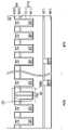
도 16은 도 15a로부터의 영역(16)의 상세도이다. 더미 핀(62)의 형상 및 치수가 더 명확하게 예시된다. 더미 핀(62) 및 보이드(60) 둘 모두는 리세스(56)(도 5 참조)와 유사한 프로파일 형상, 예를 들면, 리엔트런트 프로파일 형상을 갖는다. 이에 따라, 더미 핀(62)의 측벽은 기판(50)의 주 표면에 평행한 평면과 각도 θ1을 형성한다. 각도 θ1은 약 75도 내지 약 100도의 범위일 수 있다. 일부 실시예에서, 각도 θ1은 예각이다. 이와 달리, 활성 핀(52)의 측벽은 기판(50)의 주 표면에 평행한 평면과 각도 θ2를 형성한다. 각도 θ2는 약 80도 내지 약 90도의 범위일 수 있다. 일부 실시예에서, 각도 θ1은 각도 θ2보다 작다. 예를 들어, 각도 θ1은 각도 θ2보다 약 0% 내지 약 10% 더 작을 수 있다.Fig. 16 is a detailed view of the
각도 θ1이 예각이기 때문에, 더미 핀(62)의 폭 W2는 기판(50)으로부터 멀어지게 연장되는 D3 방향을 따라 감소한다. 더미 핀(62)의 폭 W2는 약 10 nm 내지 약 40 nm의 범위일 수 있고, 더미 핀(62)의 바닥에서의 폭 W2는 더미 핀(62)의 상부에서의 폭 W2보다 약 0% 내지 약 30% 더 클 수 있다. 마찬가지로, 보이드(60)의 폭 W3은 D3 방향을 따라 감소한다. 보이드(60)의 폭 W3은 약 1.5 nm 내지 약 2.5 nm의 범위일 수 있고, 보이드(60)의 바닥에서의 폭 W3은 보이드(60)의 상부에서의 폭 W3보다 약 0% 내지 약 30% 더 클 수 있다.Since the angle θ1 is an acute angle, the width W2 of the
위에서 언급된 바와 같이, 더미 핀(62) 및 활성 핀(52)의 상부 표면은 기판(50)으로부터 동일한 거리에 배치된다. 구체적으로, 더미 핀(62) 및 활성 핀(52)의 상부 표면은 기판(50)으로부터 거리 D4에 배치되고, 여기서 거리 D4는 약 73 nm 내지 약 85 nm의 범위일 수 있다. 더미 핀(62)은, 약 48 nm 내지 약 60 nm의 범위일 수 있는, 전체 높이 H1을 갖는다. 더미 핀(62)은 STI 영역(66) 내로 연장되며, 예를 들면, STI 영역(66)은 더미 핀(62)과 기판(50) 사이에 배치된 부분을 갖고, STI 영역(66)은 더미 핀(62) 및 활성 핀(52)의 하부 부분의 측벽을 따라 연장된다. 더미 핀(62)과 기판(50) 사이의 STI 영역(66)의 부분은, 약 15 nm 내지 약 35 nm의 범위일 수 있는, 높이 H2를 갖는다. 거리 D4는 높이 H1과 높이 H2의 합과 동일하다.As mentioned above, the top surfaces of the
유전체 층(58)은, 약 5 nm 내지 약 20 nm의 범위일 수 있는, 보이드(60)의 측벽을 따른 두께 T1을 갖는다. 유전체 층(58)은, 약 2 nm 내지 약 20 nm의 범위일 수 있는, 보이드(60)의 바닥을 따른 두께 T2를 갖는다. 유전체 층(58)은, 약 0 nm 내지 약 20 nm의 범위일 수 있는, 보이드(60)의 상부를 따른 두께 T3을 갖는다. 보이드(60)가, 약 48 nm 내지 약 60 nm의 범위일 수 있는, 큰 높이 H3을 갖도록, 두께 T2 및 두께 T3이 작다. 일부 실시예에서, 높이 H3은 더미 핀(62)의 전체 높이 H1의 약 70% 내지 약 98%이다. 높이 H1은 높이 H3, 두께 T2 및 두께 T3의 합과 동일하다.
위에서 언급된 바와 같이, 더미 핀(62)은 인접한 활성 핀(52)으로부터 등거리로 이격된다. 구체적으로, 더미 핀(62)은, 약 10 nm 내지 약 40 nm의 범위일 수 있는, 거리 D5만큼 인접한 활성 핀(52)으로부터 이격된다. 일부 실시예에서, 거리 D5는 인접한 활성 핀(52) 사이의 거리 D1과 동일하다. 일부 실시예에서, 거리 D5는 거리 D1과 동일하지 않고; 예를 들어, 거리 D5는 거리 D1보다 약 5% 내지 약 30% 더 클 수 있다.As noted above,
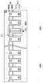
도 17 내지 도 24는 일부 다른 실시예에 따른, FinFET의 제조에서의 중간 스테이지의 단면도이다. 이 실시예에서, 더미 핀(62)은 복수의 유전체 층(58A, 58B, 58C)(도 22 참조) 및 보이드(60)를 포함하고, 여기서 유전체 층(58A, 58B, 58C)은 결합하여 보이드(60)를 둘러싼다. 도 17 내지 도 24는, 다수의 핀/FinFET를 제외하고는, 도 1에 예시된 기준 단면 A-A를 예시한다.17-24 are cross-sectional views of intermediate stages in the fabrication of FinFETs, in accordance with some other embodiments. In this embodiment,
도 17에서, 도 3에 도시된 것과 유사한 구조가 획득된다. 이어서 절연 재료(64) 상에 및 리세스(56)에 제1 유전체 층(58A)이 형성된다. 제1 유전체 층(58A)은 실리콘 산질화물, 실리콘 산탄질화물, 실리콘 질화물 등으로 형성될 수 있고, ALD, CVD 등에 의해 형성될 수 있다. 제1 유전체 층(58A)은 절연 재료(64)의 에칭에 대해 높은 에칭 선택도를 갖는 재료로 형성된다. 게다가, 제1 유전체 층(58A)의 재료는 절연 재료(64)의 재료(들)보다 큰 비유전율을 갖는다. 예를 들어, 절연 재료(64)는 약 10 내지 약 12의 범위에 있는 비유전율을 갖는 재료로 형성될 수 있고, 제1 유전체 층(58A)은 약 4 내지 약 7의 범위에 있는 비유전율을 갖는 재료로 형성될 수 있다. 일부 실시예에서, 제1 유전체 층(58A)은 ALD에 의해 형성된 실리콘 산질화물이다. 다른 실시예에서, 제1 유전체 층(58A)의 재료는 절연 재료(64)의 재료(들)보다 작은 비유전율을 갖는다.In Fig. 17, a structure similar to that shown in Fig. 3 is obtained. A
도 18에서, 리세스(56) 외부의 제1 유전체 층(58A)의 부분을 제거하고 리세스(56) 내부의 제1 유전체 층(58A)의 부분을 리세싱하기 위해 에치백 프로세스가 수행된다. 에치백은, 절연 재료(64)의 재료(들)보다 빠른 속도로 제1 유전체 층(58A)의 재료를 선택적으로 에칭하는 것과 같은, 허용 가능한 에칭 프로세스에 의해 이루어질 수 있다. 도 25a 및 도 25b와 관련하여 아래에서 추가로 논의되는 바와 같이, 에치백 프로세스 이후에, 제1 유전체 층(58A)의 상부 표면은 평평할 수 있거나 경사질 수 있다.In FIG. 18 , an etch-back process is performed to remove a portion of the first
도 19에서, 제1 유전체 층(58A) 및 절연 재료(64) 상에 제2 유전체 층(58B)이 형성된다. 제2 유전체 층(58B)은 하프늄, 알루미늄, 지르코늄, 란탄, 망간, 바륨, 티타늄, 납 및 이들의 조합의 금속 산화물 또는 실리케이트와 같은 하이-k 유전체 재료로 형성될 수 있으며, ALD, CVD 등에 의해 형성될 수 있다. 제2 유전체 층(58B)은 제1 유전체 층(58A) 및 절연 재료(64)의 에칭에 대해 높은 에칭 선택도를 갖는 재료로 형성된다. 게다가, 제2 유전체 층(58B)의 재료는 제1 유전체 층(58A)의 재료보다 큰 비유전율을 갖는다. 예를 들어, 제2 유전체 층(58B)은 약 7 내지 약 35의 범위에 있는 비유전율을 갖는 재료로 형성될 수 있다. 일부 실시예에서, 제2 유전체 층(58B)은 ALD에 의해 형성된 하프늄 산화물이다.19 , a
도 20에서, 리세스(56) 외부의 제2 유전체 층(58B)의 부분을 제거하고 리세스(56) 내부의 제2 유전체 층(58B)의 부분을 리세싱하기 위해 에치백 프로세스가 수행된다. 에치백은, 제1 유전체 층(58A) 및 절연 재료(64)의 재료(들)보다 빠른 속도로 제2 유전체 층(58B)의 재료를 선택적으로 에칭하는 것과 같은, 허용 가능한 에칭 프로세스에 의해 이루어질 수 있다. 도 25a 및 도 25b와 관련하여 아래에서 추가로 논의되는 바와 같이, 에치백 프로세스 이후에, 제2 유전체 층(58B)의 상부 표면은 평평할 수 있거나 경사질 수 있다.In FIG. 20 , an etch-back process is performed to remove a portion of the
도 21에서, 제2 유전체 층(58B) 및 절연 재료(64) 상에 제3 유전체 층(58C)이 형성된다. 제3 유전체 층(58C)은 실리콘 산질화물, 실리콘 산탄질화물, 실리콘 질화물 등으로 형성될 수 있고, ALD, CVD 등에 의해 형성될 수 있다. 제3 유전체 층(58C)은 제2 유전체 층(58B) 및 절연 재료(64)의 에칭에 대해 높은 에칭 선택도를 갖는 재료로 형성된다. 게다가, 제3 유전체 층(58C)의 재료는 제2 유전체 층(58B)의 재료보다 작은 비유전율을 갖는다. 예를 들어, 제3 유전체 층(58C)은 약 4 내지 약 7의 범위에 있는 비유전율을 갖는 재료로 형성될 수 있다. 일부 실시예에서, 제3 유전체 층(58C)은 ALD에 의해 형성된 실리콘 산질화물이다. 제1 유전체 층(58A)과 제3 유전체 층(58C)은 유사할 수 있거나 상이할 수 있다. 일부 실시예에서, 제1 유전체 층(58A) 및 제3 유전체 층(58C) 각각은 상이한 산소 및 질소 조성을 갖는 실리콘 산질화물로 형성된다.In FIG. 21 , a third
도 22에서, 활성 핀(52) 위의 제3 유전체 층(58C) 및 절연 재료(64)의 잉여 부분을 제거하기 위해 제3 유전체 층(58C) 및 절연 재료(64)에 제거 프로세스가 적용된다. 일부 실시예에서, 화학적 기계적 폴리싱(CMP), 에치백 프로세스, 이들의 조합 등과 같은 평탄화 프로세스가 이용될 수 있다. 제거 프로세스는 리세스(56)에 유전체 층(58A, 58B, 58C)의 잔류 부분을 포함하는 더미 핀(62)을 형성한다. 더미 핀(62)은 보이드(60)를 포함한다. 제1 유전체 층(58A)은 보이드(60)의 하부 부분을 둘러싸고, 제2 유전체 층(58B)은 보이드(60)의 중간 부분을 둘러싸며, 제3 유전체 층(58C)은 보이드(60)의 상부 부분을 둘러싼다.22 , a removal process is applied to third
유전체 층(58A, 58B, 58C)은 상이한 비유전율을 갖는 유전체 재료로 형성된다. 일부 실시예에서, 유전체 층(58A, 58B, 58C) 각각의 재료는 절연 재료(64)의 재료(들)보다 큰 비유전율을 갖는다. 유전체 층(58A, 58B, 58C) 및 보이드(60)는 비활성 영역(50R)과 접하는 활성 핀(52) 사이에 배치된 기생 커패시터의 네트워크에 대한 유전체 매체로서 작용한다. 상이한 비유전율을 갖는 유전체 재료의 유전체 층(58A, 58B, 58C)을 형성하는 것은 커패시터 네트워크의 유효 커패시턴스를 약 11% 내지 약 20%만큼 감소시키는 데 도움을 줄 수 있다. 따라서 결과적인 FinFET의 기생 커패시턴스가 추가로 감소될 수 있고, 이에 의해 FinFET의 성능을 향상시킬 수 있다.The
도 23에서, STI 영역(66)을 형성하기 위해 절연 재료(64)가 리세싱된다. 활성 핀(52) 및 더미 핀(62)의 상부 부분이 이웃하는 STI 영역(66) 사이로부터 STI 영역(66)보다 높게 돌출하도록 절연 재료(64)가 리세싱된다. STI 영역(66)은, 절연 재료(64)의 재료(들)에 대해 선택적인 것과 같은, 허용 가능한 에칭 프로세스를 사용하여 리세싱될 수 있다. 유전체 층(58A, 58B, 58C) 각각은 절연 재료(64)의 에칭에 대해 높은 에칭 선택도를 갖는 재료로 형성된다. 예를 들어, 예를 들어, 희석 플루오르화 수소(dHF) 산을 사용한 산화물 제거가 사용될 수 있다. 에칭 프로세스는 활성 핀(52) 및 더미 핀(62)의 재료(들)보다 빠른 속도로 절연 재료(64)의 재료(들)를 선택적으로 에칭한다. 예를 들어, 유전체 층(58A, 58B, 58C) 각각의 재료 및 절연 재료(64)의 재료(들)는 절연 재료(64)를 리세싱하기 위한 에칭 프로세스에 대해 약 20:1 내지 약 1000:1의 범위에 있는 에칭 선택도를 가질 수 있다. 따라서 유전체 층(58A, 58B, 58C)이 더미 핀(62)의 형성 동안 손상으로부터 보호될 수 있다. 일부 실시예에서, 유전체 층(58B, 58C)은 절연 재료(64)를 리세싱하기 위한 에칭 프로세스에 대해 제1 유전체 층(58A)보다 작은 에칭 속도를 갖는다. 예를 들어, 예시된 실시예에서, 제1 유전체 층(58A)은 STI 영역(66)이 형성된 후에 매립된 채로 유지되며, 따라서 절연 재료(64)의 리세싱 동안 에칭되지 않을 수 있다.In FIG. 23 , insulating
도 24에서, 도 8 내지 도 15c와 관련하여 설명된 것과 유사한 프로세싱 단계가 수행될 수 있다. 따라서 FinFET의 형성이 완료될 수 있다.In FIG. 24 , processing steps similar to those described with respect to FIGS. 8-15C may be performed. Accordingly, the formation of the FinFET can be completed.
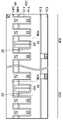
도 25a 및 도 25b는 다양한 실시예에 따른, 도 24로부터의 영역(25)의 상세도이다. 더미 핀(62)의 형상 및 치수가 더 명확하게 예시된다. 더미 핀(62) 및 보이드(60) 둘 모두는 도 16과 관련하여 설명된 실시예와 유사한 프로파일 형상 및 치수를 갖는다. 유전체 층(58A, 58B, 58C) 각각은 상이한 높이를 갖는다. 제1 유전체 층(58A)은 약 8 nm 내지 약 30 nm의 범위에 있는 높이 H4를 가질 수 있고, 제2 유전체 층(58B)은 약 10 nm 내지 약 50 nm의 범위에 있는 높이 H5를 가질 수 있으며, 제3 유전체 층(58C)은 약 2 nm 내지 약 8 nm의 범위에 있는 높이 H6을 가질 수 있다. 높이 H5는 높이 H4 및 높이 H6 각각보다 클 수 있다. 일부 실시예에서, 도 25a에 의해 예시된 바와 같이, 제2 유전체 층(58B)은 리엔트런트 프로파일 형상을 갖는다. 제2 유전체 층(58B)이 리엔트런트 프로파일 형상을 가질 때, 제2 유전체 층(58B)의 상부 표면 및 하부 표면은 기판(50)의 주 표면에 평행하다. 일부 실시예에서, 도 25b에 의해 예시된 바와 같이, 제2 유전체 층(58B)은 셰브런 프로파일 형상(chevron profile shape)을 갖는다. 제2 유전체 층(58B)이 셰브런 프로파일 형상을 가질 때, 제2 유전체 층(58B)의 하부 표면 각각이 기판(50)의 주 표면에 평행한 평면과 예각 θ3을 형성하고, 제2 유전체 층(58B)의 상부 표면 각각이 또한 기판(50)의 주 표면에 평행한 평면과 예각 θ4를 형성한다. 각도 θ3 및 θ4 각각은 약 50도 이하일 수 있다. 일부 실시예에서, 각도 θ3은 각도 θ4보다 작다.25A and 25B are detailed views of
도 26은 일부 다른 실시예에 따른, FinFET의 단면도이다. 도 26은, 다수의 핀/FinFET를 제외하고는, 도 1에 예시된 기준 단면 A-A를 예시한다. 이 실시예에서, 비활성 영역(50R)은 n형 영역(50N)의 일부이고, n형 영역(50N)에서 인접한 n형 FinFET 사이에 배치된다. 비활성 영역(50R)은, 도 16, 도 25a 및 도 25b와 관련하여 설명된 더미 핀 중 임의의 것과 유사할 수 있는, 더미 핀(62)을 포함한다.26 is a cross-sectional view of a FinFET, in accordance with some other embodiments. 26 illustrates the reference cross-section A-A illustrated in FIG. 1, except for the multiple fins/FinFETs. In this embodiment,
도 27은 일부 다른 실시예에 따른, FinFET의 단면도이다. 도 27은, 다수의 핀/FinFET를 제외하고는, 도 1에 예시된 기준 단면 A-A를 예시한다. 이 실시예에서, n형 영역(50N)과 p형 영역(50P) 둘 모두가 비활성 영역(50R)을 포함한다. 비활성 영역(50R) 각각은, 도 16, 도 25a 및 도 25b와 관련하여 설명된 더미 핀 중 임의의 것과 유사할 수 있는, 더미 핀(62)을 포함한다.27 is a cross-sectional view of a FinFET, in accordance with some other embodiments. Fig. 27 illustrates the reference cross section A-A illustrated in Fig. 1, with the exception of multiple fins/FinFETs. In this embodiment, both the n-
개시된 FinFET 실시예는 또한 나노구조(예를 들면, 나노시트, 나노와이어, 게이트 올 어라운드 등) 전계 효과 트랜지스터(NSFET)와 같은 나노구조 디바이스에 적용될 수 있다. 도 28은 일부 다른 실시예에 따른, NSFET의 단면도이다. 도 28은, 핀/FinFET 대신에 나노구조체/NSFET가 도시된 것을 제외하고는, 도 1에 예시된 기준 단면 A-A와 유사한 단면을 예시한다. 이 실시예에서, 활성 핀(52)이 채널 층과 희생 층의 교호 층의 스택을 패터닝하는 것에 의해 형성된 나노구조체(152)로 대체된다. 나노구조체(152)는 기판(50) 위에 형성된 반도체 스트립이고, 더미 핀(62)은 나노구조체들(152) 중 일부 사이의 비활성 영역(50R)에 형성된다. 더미 핀(62)은, 도 16, 도 25a 및 도 25b와 관련하여 설명된 더미 핀 중 임의의 것과 유사할 수 있다. 예시된 실시예에서, 비활성 영역(50R)이 p형 영역(50P)의 일부이지만, 비활성 영역(50R)이 또한 n형 영역(50N)의 일부일 수 있거나, 또는 n형 영역(50N)과 p형 영역(50P) 둘 모두에 비활성 영역(50R)이 있을 수 있다. 더미 게이트 스택 및 소스/드레인 영역은 위에서 설명된 실시예와 유사한 방식으로 형성된다. 더미 게이트 스택이 제거된 후에, 희생 층이 채널 영역(68)에서 부분적으로 또는 완전히 제거될 수 있다. 대체 게이트 구조체는 위에서 설명된 실시예와 유사한 방식으로 형성되고, 대체 게이트 구조체는 희생 층을 제거하는 것에 의해 남겨지는 개구부를 부분적으로 또는 완전히 채울 수 있으며, 대체 게이트 구조체는 더미 핀(62) 및 NSFET 디바이스의 채널 영역(68)에서의 채널 층을 부분적으로 또는 완전히 둘러쌀 수 있다. 대체 게이트 구조체 및 소스/드레인 영역에 대한 ILD 및 콘택트는 위에서 설명된 실시예와 유사한 방식으로 형성될 수 있다. 나노구조 디바이스는, 참조에 의해 그 전체가 본 명세서에 포함되는, 미국 특허 출원 공개 제2016/0365414호에 개시된 바와 같이 형성될 수 있다.The disclosed FinFET embodiments may also be applied to nanostructured devices such as nanostructured (eg, nanosheets, nanowires, gate all around, etc.) field effect transistors (NSFETs). 28 is a cross-sectional view of an NSFET, in accordance with some other embodiments. 28 illustrates a cross-section similar to the reference cross-section A-A illustrated in FIG. 1, except that a nanostructure/NSFET is shown instead of a fin/FinFET. In this embodiment,
실시예는 장점을 달성할 수 있다. 더미 핀(62)을 형성하는 것은 비어 있는 비활성 영역(50R)을 형성하는 것에 의해 그렇지 않았으면 야기될 수 있는 패턴 로딩 효과를 감소시키는 데 도움을 준다. 예를 들어, 후속 CMP 또는 에칭 프로세스(들)에서의 로딩 효과가 감소될 수 있다. 게다가, 보이드(60)를 포함하도록 더미 핀(62)을 형성하는 것은 더미 핀(62)의 비유전율을 감소시키고 더미 핀(62)의 총 유효 컨덕턴스를 감소시키는 데 도움을 줄 수 있다. 이에 따라, 후속 프로세싱에서 패턴 로딩 효과를 감소시키는 데 도움을 주는 것 외에도, 더미 핀(62)은 또한 인접한 FinFET를 서로로부터 전기적으로 격리시키는 데 도움을 준다. 구체적으로, 보이드(60)를 형성하는 것은 인접한 FinFET 사이의 유효 커패시턴스를 약 20% 이하만큼 감소시키는 데 도움을 줄 수 있다.Embodiments may achieve advantages. Forming
일 실시예에서, 디바이스는: 기판으로부터 연장되는 제1 반도체 핀; 기판으로부터 연장되는 제2 반도체 핀; 제1 반도체 핀과 제2 반도체 핀 사이에 배치된 유전체 핀 - 유전체 핀은 보이드를 포함함 -; 및 유전체 핀과 기판 사이에 배치된 격리 영역 - 격리 영역은 유전체 핀의 측벽, 제1 반도체 핀의 측벽, 및 제2 반도체 핀의 측벽을 따라 연장됨 - 을 포함한다.In one embodiment, a device includes: a first semiconductor fin extending from a substrate; a second semiconductor fin extending from the substrate; a dielectric fin disposed between the first semiconductor fin and the second semiconductor fin, the dielectric fin comprising a void; and an isolation region disposed between the dielectric fin and the substrate, the isolation region extending along a sidewall of the dielectric fin, a sidewall of the first semiconductor fin, and a sidewall of the second semiconductor fin.
본 디바이스의 일부 실시예에서, 제1 반도체 핀의 상부 표면, 제2 반도체 핀의 상부 표면, 및 유전체 핀의 상부 표면은 공면이다. 일부 실시예에서, 본 디바이스는: 유전체 핀의 상부 표면과 측벽, 제1 반도체 핀의 상부 표면과 측벽, 및 제2 반도체 핀의 상부 표면과 측벽을 따라 연장되는 게이트 구조체를 더 포함한다. 본 디바이스의 일부 실시예에서, 유전체 핀은 보이드를 둘러싸는 제1 유전체 층을 더 포함하고, 제1 유전체 층은 제1 유전체 재료를 포함하며, 격리 영역은 제2 유전체 재료를 포함하고, 제1 유전체 재료는 제2 유전체 재료와는 상이하다. 본 디바이스의 일부 실시예에서, 제1 유전체 재료는 실리콘 산질화물이고, 제2 유전체 재료는 실리콘 산화물이며, 보이드는 공기로 채워지거나 진공 상태이다. 본 디바이스의 일부 실시예에서, 제1 유전체 재료는 제1 비유전율을 갖고, 제2 유전체 재료는 제2 비유전율을 가지며, 보이드는 제3 비유전율을 갖고, 제3 비유전율은 제2 비유전율보다 작으며, 제2 비유전율은 제1 비유전율보다 작다. 본 디바이스의 일부 실시예에서, 유전체 핀은: 기판 위의 제1 유전체 층 - 제1 유전체 층은 보이드의 하부 부분을 둘러싸고, 제1 유전체 층은 제1 유전체 재료를 포함함 -; 제1 유전체 층 위의 제2 유전체 층 - 제2 유전체 층은 보이드의 중간 부분을 둘러싸고, 제2 유전체 층은 제2 유전체 재료를 포함함 -; 및 제2 유전체 층 위의 제3 유전체 층 - 제3 유전체 층은 보이드의 상부 부분을 둘러싸고, 제3 유전체 층은 제3 유전체 재료를 포함함 - 을 더 포함하고, 여기서 격리 영역은 제4 유전체 재료를 포함하고, 제1 유전체 재료, 제2 유전체 재료, 제3 유전체 재료 및 제4 유전체 재료 각각은 상이하다. 본 디바이스의 일부 실시예에서, 제1 유전체 재료는 실리콘 산질화물이고, 제2 유전체 재료는 하이-k 재료이며, 제3 유전체 재료는 실리콘 산질화물이고, 제4 유전체 재료는 실리콘 산화물이며, 보이드는 공기로 채워지거나 진공 상태이다. 본 디바이스의 일부 실시예에서, 제1 유전체 재료는 제1 비유전율을 갖고, 제2 유전체 재료는 제2 비유전율을 가지며, 제3 유전체 재료는 제3 비유전율을 갖고, 제4 유전체 재료는 제4 비유전율을 가지며, 보이드는 제5 비유전율을 갖고, 제5 비유전율은 제4 비유전율보다 작고, 제4 비유전율은 제1 비유전율, 제2 비유전율 및 제3 비유전율 각각보다 작다.In some embodiments of the present device, the top surface of the first semiconductor fin, the top surface of the second semiconductor fin, and the top surface of the dielectric fin are coplanar. In some embodiments, the device further includes: a gate structure extending along the top surface and sidewalls of the dielectric fin, the top surface and sidewalls of the first semiconductor fin, and the top surface and sidewalls of the second semiconductor fin. In some embodiments of the present device, the dielectric fin further comprises a first dielectric layer surrounding the void, the first dielectric layer comprises a first dielectric material, the isolation region comprises a second dielectric material, and The dielectric material is different from the second dielectric material. In some embodiments of the device, the first dielectric material is silicon oxynitride, the second dielectric material is silicon oxide, and the void is filled with air or in a vacuum. In some embodiments of the device, the first dielectric material has a first relative permittivity, the second dielectric material has a second relative permittivity, the void has a third relative permittivity, and the third relative permittivity is the second relative permittivity. smaller than the first dielectric constant, and the second relative dielectric constant is smaller than the first relative dielectric constant. In some embodiments of the device, the dielectric fin comprises: a first dielectric layer over the substrate, the first dielectric layer surrounding a lower portion of the void, the first dielectric layer comprising a first dielectric material; a second dielectric layer over the first dielectric layer, the second dielectric layer surrounding a middle portion of the void, the second dielectric layer comprising a second dielectric material; and a third dielectric layer over the second dielectric layer, the third dielectric layer surrounding the upper portion of the void, the third dielectric layer comprising a third dielectric material, wherein the isolation region comprises a fourth dielectric material wherein each of the first dielectric material, the second dielectric material, the third dielectric material, and the fourth dielectric material is different. In some embodiments of the device, the first dielectric material is silicon oxynitride, the second dielectric material is a high-k material, the third dielectric material is silicon oxynitride, the fourth dielectric material is silicon oxide, and the voids are It is filled with air or in a vacuum. In some embodiments of the device, the first dielectric material has a first dielectric constant, the second dielectric material has a second dielectric constant, the third dielectric material has a third dielectric constant, and the fourth dielectric material has a second dielectric constant. 4 relative permittivity, the void has a fifth relative permittivity, the fifth relative permittivity is smaller than the fourth relative permittivity, and the fourth relative permittivity is smaller than each of the first relative permittivity, the second relative permittivity, and the third relative permittivity.
일 실시예에서, 디바이스는: 기판 위의 제1 반도체 스트립 - 제1 반도체 스트립은 제1 채널 영역을 포함함 -; 기판 위의 제2 반도체 스트립 - 제2 반도체 스트립은 제2 채널 영역을 포함함 -; 제1 반도체 스트립과 제2 반도체 스트립 사이에 배치된 유전체 스트립 - 유전체 스트립의 폭은 기판으로부터 멀어지게 연장되는 제1 방향을 따라 감소하고, 유전체 스트립은 보이드를 포함함 -; 및 제1 채널 영역을 따라, 제2 채널 영역을 따라, 그리고 유전체 스트립의 상부 표면과 측벽을 따라 연장되는 게이트 구조체를 포함한다.In one embodiment, the device comprises: a first semiconductor strip over a substrate, the first semiconductor strip comprising a first channel region; a second semiconductor strip over the substrate, the second semiconductor strip comprising a second channel region; a dielectric strip disposed between the first semiconductor strip and the second semiconductor strip, the width of the dielectric strip decreasing along a first direction extending away from the substrate, the dielectric strip including the voids; and a gate structure extending along the first channel region, along the second channel region, and along the top surface and sidewalls of the dielectric strip.
본 디바이스의 일부 실시예에서, 제1 반도체 스트립은 기판으로부터 연장되는 제1 핀이고, 제2 반도체 스트립은 기판으로부터 연장되는 제2 핀이다. 본 디바이스의 일부 실시예에서, 제1 반도체 스트립은 기판 위의 제1 나노구조체이고, 제2 반도체 스트립은 기판 위의 제2 나노구조체이다. 본 디바이스의 일부 실시예에서, 보이드의 폭은 제1 방향을 따라 감소한다. 본 디바이스의 일부 실시예에서, 보이드의 폭은 1.5 nm 내지 2.5 nm의 범위에 있다. 본 디바이스의 일부 실시예에서, 보이드의 높이는 48 nm 내지 60 nm의 범위에 있다.In some embodiments of the device, the first semiconductor strip is a first fin extending from the substrate, and the second semiconductor strip is a second fin extending from the substrate. In some embodiments of the device, the first semiconductor strip is a first nanostructure over the substrate, and the second semiconductor strip is a second nanostructure over the substrate. In some embodiments of the device, the width of the void decreases along the first direction. In some embodiments of the present device, the width of the void is in the range of 1.5 nm to 2.5 nm. In some embodiments of the present device, the height of the void is in the range of 48 nm to 60 nm.
일 실시예에서, 방법은: 기판으로부터 멀어지는 제1 방향으로 각각 연장되는 제1 반도체 핀 및 제2 반도체 핀을 형성하는 단계; 제1 반도체 핀과 제2 반도체 핀 사이에 절연 재료를 형성하는 단계 - 절연 재료는 리세스를 가지며, 리세스의 폭은 제1 방향을 따라 감소함 -; 보이드를 형성하기 위해 리세스에 제1 유전체 층을 퇴적하는 단계 - 보이드는 제1 유전체 층에 의해 채워지지 않은 리세스의 부분을 포함함 -; 및 제1 반도체 핀과 제2 반도체 핀 사이에 유전체 핀을 형성하기 위해 절연 재료를 리세싱하는 단계 - 유전체 핀은 보이드 및 리세스 내의 제1 유전체 층의 잔류 부분을 포함하고, 제1 유전체 층의 잔류 부분은 보이드를 둘러싸고 있음 - 를 포함한다.In one embodiment, a method includes: forming a first semiconductor fin and a second semiconductor fin respectively extending in a first direction away from the substrate; forming an insulating material between the first semiconductor fin and the second semiconductor fin, the insulating material having a recess, the width of the recess decreasing along the first direction; depositing a first dielectric layer in the recess to form a void, the void comprising a portion of the recess not filled by the first dielectric layer; and recessing the insulating material to form a dielectric fin between the first semiconductor fin and the second semiconductor fin, the dielectric fin including a void and a residual portion of the first dielectric layer within the recess, Residual portion surrounds the void - including .
본 방법의 일부 실시예에서, 제1 유전체 층은 리세스에 퇴적된 유일한 유전체 층이다. 일부 실시예에서, 본 방법은: 리세스에 제2 유전체 층을 퇴적하는 단계; 및 리세스 내의 제2 유전체 층 상에 제3 유전체 층을 퇴적하는 단계 - 제1 유전체 층은 제3 유전체 층 상에 퇴적됨 - 를 더 포함한다. 일부 실시예에서, 절연 재료를 리세싱하는 단계는: 제1 에칭 프로세스로 절연 재료를 리세싱하는 단계 - 제1 에칭 프로세스는 제1 유전체 층보다 빠른 속도로 절연 재료를 에칭함 - 를 포함한다. 본 방법의 일부 실시예에서, 리세스는 리세스의 바닥에서 제1 폭을 갖고 리세스의 상부에서 제2 폭을 가지며, 제1 폭은 제2 폭보다 0% 내지 30% 더 크다.In some embodiments of the method, the first dielectric layer is the only dielectric layer deposited in the recess. In some embodiments, the method includes: depositing a second dielectric layer in the recess; and depositing a third dielectric layer on the second dielectric layer in the recess, the first dielectric layer being deposited on the third dielectric layer. In some embodiments, recessing the insulating material comprises: recessing the insulating material with a first etch process, wherein the first etch process etches the insulating material at a faster rate than the first dielectric layer. In some embodiments of the method, the recess has a first width at the bottom of the recess and a second width at the top of the recess, the first width being 0% to 30% greater than the second width.
전술한 내용은 본 기술 분야의 통상의 기술자가 본 개시의 양태를 더 잘 이해할 수 있도록 여러 실시예의 특징의 개요를 서술한다. 본 기술 분야의 통상의 기술자라면 본 명세서에서 소개된 실시예의 동일한 목적을 수행하고/하거나 동일한 장점을 달성하기 위해 다른 프로세스 및 구조체를 설계 또는 수정하기 위한 기초로서 본 개시를 용이하게 사용할 수 있음을 이해할 것이다. 본 기술 분야의 통상의 기술자라면 그러한 동등한 구성이 본 개시의 사상 및 범위를 벗어나지 않는다는 것과, 그 구성이 본 개시의 사상 및 범위를 벗어나지 않으면서 본 명세서에 다양한 변경, 대체, 및 수정을 행할 수 있음을 또한 인식할 것이다.The foregoing outlines features of several embodiments so that those skilled in the art may better understand aspects of the present disclosure. Those of ordinary skill in the art will appreciate that they may readily use the present disclosure as a basis for designing or modifying other processes and structures for carrying out the same purposes and/or achieving the same advantages of the embodiments introduced herein. will be. Those skilled in the art can make various changes, substitutions, and modifications herein without departing from the spirit and scope of the present disclosure, and that such equivalent constructions do not depart from the spirit and scope of the present disclosure. will also recognize
[부기][bookkeeping]
1.디바이스로서,One.As a device,
기판으로부터 연장되는 제1 반도체 핀;a first semiconductor fin extending from the substrate;
상기 기판으로부터 연장되는 제2 반도체 핀;a second semiconductor fin extending from the substrate;
상기 제1 반도체 핀과 상기 제2 반도체 핀 사이에 배치된 유전체 핀 - 상기 유전체 핀은 보이드를 포함함 -; 및a dielectric fin disposed between the first semiconductor fin and the second semiconductor fin, the dielectric fin comprising a void; and
상기 유전체 핀과 상기 기판 사이에 배치된 격리 영역 - 상기 격리 영역은 상기 유전체 핀의 측벽, 상기 제1 반도체 핀의 측벽, 및 상기 제2 반도체 핀의 측벽을 따라 연장됨 -an isolation region disposed between the dielectric fin and the substrate, the isolation region extending along a sidewall of the dielectric fin, a sidewall of the first semiconductor fin, and a sidewall of the second semiconductor fin;
을 포함하는, 디바이스.A device comprising a.
2.제1항에 있어서, 상기 제1 반도체 핀의 상부 표면, 상기 제2 반도체 핀의 상부 표면, 및 상기 유전체 핀의 상부 표면은 공면(coplanar)인, 디바이스.2.The device of
3.제2항에 있어서,3.3. The method of claim 2,
상기 유전체 핀의 상기 상부 표면과 상기 측벽, 상기 제1 반도체 핀의 상기 상부 표면과 상기 측벽, 및 상기 제2 반도체 핀의 상기 상부 표면과 상기 측벽을 따라 연장되는 게이트 구조체a gate structure extending along the top surface and the sidewall of the dielectric fin, the top surface and the sidewall of the first semiconductor fin, and the top surface and the sidewall of the second semiconductor fin
를 더 포함하는, 디바이스.Further comprising, the device.
4.제1항에 있어서, 상기 유전체 핀은 상기 보이드를 둘러싸는 제1 유전체 층을 더 포함하고, 상기 제1 유전체 층은 제1 유전체 재료를 포함하며, 상기 격리 영역은 제2 유전체 재료를 포함하고, 상기 제1 유전체 재료는 상기 제2 유전체 재료와는 상이한, 디바이스.4.wherein the dielectric fin further comprises a first dielectric layer surrounding the void, the first dielectric layer comprises a first dielectric material, the isolation region comprises a second dielectric material, wherein the first dielectric material is different from the second dielectric material.
5.제4항에 있어서, 상기 제1 유전체 재료는 실리콘 산질화물이고, 상기 제2 유전체 재료는 실리콘 산화물이며, 상기 보이드는 공기로 채워지거나 진공 상태인, 디바이스.5.5. The device of claim 4, wherein the first dielectric material is silicon oxynitride, the second dielectric material is silicon oxide, and the void is filled with air or in a vacuum.
6.제4항에 있어서, 상기 제1 유전체 재료는 제1 비유전율을 갖고, 상기 제2 유전체 재료는 제2 비유전율을 가지며, 상기 보이드는 제3 비유전율을 갖고, 상기 제3 비유전율은 상기 제2 비유전율보다 작으며, 상기 제2 비유전율은 상기 제1 비유전율보다 작은, 디바이스.6.5. The method of claim 4, wherein the first dielectric material has a first dielectric constant, the second dielectric material has a second dielectric constant, the void has a third dielectric constant, and the third dielectric constant is the second dielectric constant. 2 The device of
7.제1항에 있어서, 상기 유전체 핀은:7.The method of
상기 기판 위의 제1 유전체 층 - 상기 제1 유전체 층은 상기 보이드의 하부 부분을 둘러싸고, 상기 제1 유전체 층은 제1 유전체 재료를 포함함 -;a first dielectric layer over the substrate, the first dielectric layer surrounding a lower portion of the void, the first dielectric layer comprising a first dielectric material;
상기 제1 유전체 층 위의 제2 유전체 층 - 상기 제2 유전체 층은 상기 보이드의 중간 부분을 둘러싸고, 상기 제2 유전체 층은 제2 유전체 재료를 포함함 -; 및a second dielectric layer over the first dielectric layer, the second dielectric layer surrounding a middle portion of the void, the second dielectric layer comprising a second dielectric material; and
상기 제2 유전체 층 위의 제3 유전체 층 - 상기 제3 유전체 층은 상기 보이드의 상부 부분을 둘러싸고, 상기 제3 유전체 층은 제3 유전체 재료를 포함함 - 을 더 포함하고,a third dielectric layer over the second dielectric layer, the third dielectric layer surrounding an upper portion of the void, the third dielectric layer comprising a third dielectric material;
상기 격리 영역은 제4 유전체 재료를 포함하고, 상기 제1 유전체 재료, 상기 제2 유전체 재료, 상기 제3 유전체 재료, 및 상기 제4 유전체 재료 각각은 상이한, 디바이스.wherein the isolation region comprises a fourth dielectric material, each of the first dielectric material, the second dielectric material, the third dielectric material, and the fourth dielectric material being different.
8.제7항에 있어서, 상기 제1 유전체 재료는 실리콘 산질화물이고, 상기 제2 유전체 재료는 하이-k 재료이며, 상기 제3 유전체 재료는 실리콘 산질화물이고, 상기 제4 유전체 재료는 실리콘 산화물이며, 상기 보이드는 공기로 채워지거나 진공 상태인, 디바이스.8.8. The method of claim 7, wherein the first dielectric material is silicon oxynitride, the second dielectric material is a high-k material, the third dielectric material is silicon oxynitride, and the fourth dielectric material is silicon oxide; wherein the void is filled with air or in a vacuum.
9.제7항에 있어서, 상기 제1 유전체 재료는 제1 비유전율을 갖고, 상기 제2 유전체 재료는 제2 비유전율을 가지며, 상기 제3 유전체 재료는 제3 비유전율을 갖고, 상기 제4 유전체 재료는 제4 비유전율을 가지며, 상기 보이드는 제5 비유전율을 갖고, 상기 제5 비유전율은 상기 제4 비유전율보다 작고, 상기 제4 비유전율은 상기 제1 비유전율, 상기 제2 비유전율 및 상기 제3 비유전율 각각보다 작은, 디바이스.9.8. The material of claim 7, wherein the first dielectric material has a first dielectric constant, the second dielectric material has a second dielectric constant, the third dielectric material has a third dielectric constant, and the fourth dielectric material has a fourth relative permittivity, the void has a fifth relative permittivity, the fifth relative permittivity is less than the fourth relative permittivity, and the fourth relative permittivity is the first relative permittivity, the second relative permittivity, and less than each of the third relative dielectric constants.
10.디바이스로서,10.As a device,
기판 위의 제1 반도체 스트립 - 상기 제1 반도체 스트립은 제1 채널 영역을 포함함 -;a first semiconductor strip over a substrate, the first semiconductor strip comprising a first channel region;
상기 기판 위의 제2 반도체 스트립 - 상기 제2 반도체 스트립은 제2 채널 영역을 포함함 -;a second semiconductor strip over the substrate, the second semiconductor strip comprising a second channel region;
상기 제1 반도체 스트립과 상기 제2 반도체 스트립 사이에 배치된 유전체 스트립 - 상기 유전체 스트립의 폭은 상기 기판으로부터 멀어지게 연장되는 제1 방향을 따라 감소하고, 상기 유전체 스트립은 보이드를 포함함 -; 및a dielectric strip disposed between the first semiconductor strip and the second semiconductor strip, the width of the dielectric strip decreasing along a first direction extending away from the substrate, the dielectric strip including a void; and
상기 제1 채널 영역을 따라, 상기 제2 채널 영역을 따라, 그리고 상기 유전체 스트립의 상부 표면과 측벽을 따라 연장되는 게이트 구조체a gate structure extending along the first channel region, along the second channel region, and along a top surface and sidewalls of the dielectric strip
를 포함하는, 디바이스.A device comprising:
11.제10항에 있어서, 상기 제1 반도체 스트립은 상기 기판으로부터 연장되는 제1 핀이고, 상기 제2 반도체 스트립은 상기 기판으로부터 연장되는 제2 핀인, 디바이스.11.The device of claim 10 , wherein the first semiconductor strip is a first fin extending from the substrate and the second semiconductor strip is a second fin extending from the substrate.
12.제10항에 있어서, 상기 제1 반도체 스트립은 상기 기판 위의 제1 나노구조체이고, 상기 제2 반도체 스트립은 상기 기판 위의 제2 나노구조체인, 디바이스.12.The device of claim 10 , wherein the first semiconductor strip is a first nanostructure over the substrate and the second semiconductor strip is a second nanostructure over the substrate.
13.제10항에 있어서, 상기 보이드의 폭은 상기 제1 방향을 따라 감소하는, 디바이스.13.The device of claim 10 , wherein the width of the void decreases along the first direction.
14.제10항에 있어서, 상기 보이드의 폭은 1.5 nm 내지 2.5 nm의 범위에 있는, 디바이스.14.The device of claim 10 , wherein the width of the void is in the range of 1.5 nm to 2.5 nm.
15.제10항에 있어서, 상기 보이드의 높이는 48 nm 내지 60 nm의 범위에 있는, 디바이스.15.The device of claim 10 , wherein the height of the void is in the range of 48 nm to 60 nm.
16.방법으로서,16.As a method,
기판으로부터 멀어지는 제1 방향으로 각각 연장되는 제1 반도체 핀 및 제2 반도체 핀을 형성하는 단계;forming a first semiconductor fin and a second semiconductor fin respectively extending in a first direction away from the substrate;
상기 제1 반도체 핀과 상기 제2 반도체 핀 사이에 절연 재료를 형성하는 단계 - 상기 절연 재료는 리세스를 가지며, 상기 리세스의 폭은 상기 제1 방향을 따라 감소함 -;forming an insulating material between the first semiconductor fin and the second semiconductor fin, the insulating material having a recess, the width of the recess decreasing along the first direction;
보이드를 형성하기 위해 상기 리세스에 제1 유전체 층을 퇴적하는 단계 - 상기 보이드는 상기 제1 유전체 층에 의해 채워지지 않은 상기 리세스의 부분을 포함함 -; 및depositing a first dielectric layer in the recess to form a void, the void comprising a portion of the recess not filled by the first dielectric layer; and
상기 제1 반도체 핀과 상기 제2 반도체 핀 사이에 유전체 핀을 형성하기 위해 상기 절연 재료를 리세싱하는 단계 - 상기 유전체 핀은 상기 보이드 및 상기 리세스 내의 상기 제1 유전체 층의 잔류 부분을 포함하고, 상기 제1 유전체 층의 상기 잔류 부분은 상기 보이드를 둘러쌈 -recessing the insulating material to form a dielectric fin between the first semiconductor fin and the second semiconductor fin, the dielectric fin including the void and a remaining portion of the first dielectric layer within the recess , wherein the remaining portion of the first dielectric layer surrounds the void;
를 포함하는, 방법.A method comprising
17.제16항에 있어서, 상기 보이드는 상기 제1 유전체 층에 의해 연속적으로 봉입되는, 방법.17.17. The method of
18.제16항에 있어서,18.17. The method of
상기 리세스에 제2 유전체 층을 퇴적하는 단계; 및depositing a second dielectric layer in the recess; and
상기 리세스 내의 상기 제2 유전체 층 상에 제3 유전체 층을 퇴적하는 단계 - 상기 제1 유전체 층은 상기 제3 유전체 층 상에 퇴적됨 -depositing a third dielectric layer on the second dielectric layer in the recess, the first dielectric layer being deposited on the third dielectric layer
를 더 포함하는, 방법.A method further comprising:
19.제16항에 있어서, 상기 절연 재료를 리세싱하는 단계는:19.17. The method of
제1 에칭 프로세스로 상기 절연 재료를 리세싱하는 단계 - 상기 제1 에칭 프로세스는 상기 제1 유전체 층보다 빠른 속도로 상기 절연 재료를 에칭함 - 를 포함하는, 방법.recessing the insulating material with a first etch process, wherein the first etch process etches the insulating material at a faster rate than the first dielectric layer.
20.제16항에 있어서, 상기 리세스는 상기 리세스의 바닥에서 제1 폭을 갖고 상기 리세스의 상부에서 제2 폭을 가지며, 상기 제1 폭은 상기 제2 폭보다 0% 내지 30% 더 큰, 방법.20.17. The method of
Claims (10)
Translated fromKorean기판으로부터 연장되는 제1 반도체 핀;
상기 기판으로부터 연장되는 제2 반도체 핀;
상기 제1 반도체 핀과 상기 제2 반도체 핀 사이에 배치된 유전체 핀 - 상기 유전체 핀은 보이드를 포함함 -; 및
상기 유전체 핀과 상기 기판 사이에 배치된 격리 영역 - 상기 격리 영역은 상기 유전체 핀의 측벽, 상기 제1 반도체 핀의 측벽, 및 상기 제2 반도체 핀의 측벽을 따라 연장됨 -
을 포함하는, 디바이스.As a device,
a first semiconductor fin extending from the substrate;
a second semiconductor fin extending from the substrate;
a dielectric fin disposed between the first semiconductor fin and the second semiconductor fin, the dielectric fin comprising a void; and
an isolation region disposed between the dielectric fin and the substrate, the isolation region extending along a sidewall of the dielectric fin, a sidewall of the first semiconductor fin, and a sidewall of the second semiconductor fin;
A device comprising a.
상기 유전체 핀의 상기 상부 표면과 상기 측벽, 상기 제1 반도체 핀의 상기 상부 표면과 상기 측벽, 및 상기 제2 반도체 핀의 상기 상부 표면과 상기 측벽을 따라 연장되는 게이트 구조체
를 더 포함하는, 디바이스.3. The method of claim 2,
a gate structure extending along the top surface and the sidewall of the dielectric fin, the top surface and the sidewall of the first semiconductor fin, and the top surface and the sidewall of the second semiconductor fin
Further comprising, the device.
상기 기판 위의 제1 유전체 층 - 상기 제1 유전체 층은 상기 보이드의 하부 부분을 둘러싸고, 상기 제1 유전체 층은 제1 유전체 재료를 포함함 -;
상기 제1 유전체 층 위의 제2 유전체 층 - 상기 제2 유전체 층은 상기 보이드의 중간 부분을 둘러싸고, 상기 제2 유전체 층은 제2 유전체 재료를 포함함 -; 및
상기 제2 유전체 층 위의 제3 유전체 층 - 상기 제3 유전체 층은 상기 보이드의 상부 부분을 둘러싸고, 상기 제3 유전체 층은 제3 유전체 재료를 포함함 - 을 더 포함하고,
상기 격리 영역은 제4 유전체 재료를 포함하고, 상기 제1 유전체 재료, 상기 제2 유전체 재료, 상기 제3 유전체 재료, 및 상기 제4 유전체 재료 각각은 상이한, 디바이스.The method of claim 1 , wherein the dielectric fin comprises:
a first dielectric layer over the substrate, the first dielectric layer surrounding a lower portion of the void, the first dielectric layer comprising a first dielectric material;
a second dielectric layer over the first dielectric layer, the second dielectric layer surrounding a middle portion of the void, the second dielectric layer comprising a second dielectric material; and
a third dielectric layer over the second dielectric layer, the third dielectric layer surrounding an upper portion of the void, the third dielectric layer comprising a third dielectric material;
wherein the isolation region comprises a fourth dielectric material, each of the first dielectric material, the second dielectric material, the third dielectric material, and the fourth dielectric material being different.
기판 위의 제1 반도체 스트립 - 상기 제1 반도체 스트립은 제1 채널 영역을 포함함 -;
상기 기판 위의 제2 반도체 스트립 - 상기 제2 반도체 스트립은 제2 채널 영역을 포함함 -;
상기 제1 반도체 스트립과 상기 제2 반도체 스트립 사이에 배치된 유전체 스트립 - 상기 유전체 스트립의 폭은 상기 기판으로부터 멀어지게 연장되는 제1 방향을 따라 감소하고, 상기 유전체 스트립은 보이드를 포함함 -; 및
상기 제1 채널 영역을 따라, 상기 제2 채널 영역을 따라, 그리고 상기 유전체 스트립의 상부 표면과 측벽을 따라 연장되는 게이트 구조체
를 포함하는, 디바이스.As a device,
a first semiconductor strip over a substrate, the first semiconductor strip comprising a first channel region;
a second semiconductor strip over the substrate, the second semiconductor strip comprising a second channel region;
a dielectric strip disposed between the first semiconductor strip and the second semiconductor strip, the width of the dielectric strip decreasing along a first direction extending away from the substrate, the dielectric strip including a void; and
a gate structure extending along the first channel region, along the second channel region, and along a top surface and sidewalls of the dielectric strip
A device comprising:
기판으로부터 멀어지는 제1 방향으로 각각 연장되는 제1 반도체 핀 및 제2 반도체 핀을 형성하는 단계;
상기 제1 반도체 핀과 상기 제2 반도체 핀 사이에 절연 재료를 형성하는 단계 - 상기 절연 재료는 리세스를 가지며, 상기 리세스의 폭은 상기 제1 방향을 따라 감소함 -;
보이드를 형성하기 위해 상기 리세스에 제1 유전체 층을 퇴적하는 단계 - 상기 보이드는 상기 제1 유전체 층에 의해 채워지지 않은 상기 리세스의 부분을 포함함 -; 및
상기 제1 반도체 핀과 상기 제2 반도체 핀 사이에 유전체 핀을 형성하기 위해 상기 절연 재료를 리세싱하는 단계 - 상기 유전체 핀은 상기 보이드 및 상기 리세스 내의 상기 제1 유전체 층의 잔류 부분을 포함하고, 상기 제1 유전체 층의 상기 잔류 부분은 상기 보이드를 둘러쌈 -
를 포함하는, 방법.As a method,
forming a first semiconductor fin and a second semiconductor fin each extending in a first direction away from the substrate;
forming an insulating material between the first semiconductor fin and the second semiconductor fin, the insulating material having a recess, the width of the recess decreasing along the first direction;
depositing a first dielectric layer in the recess to form a void, the void comprising a portion of the recess not filled by the first dielectric layer; and
recessing the insulating material to form a dielectric fin between the first semiconductor fin and the second semiconductor fin, the dielectric fin including the void and a remaining portion of the first dielectric layer within the recess , wherein the remaining portion of the first dielectric layer surrounds the void;
A method comprising
Applications Claiming Priority (2)
| Application Number | Priority Date | Filing Date | Title |
|---|---|---|---|
| US17/150,018 | 2021-01-15 | ||
| US17/150,018US11842933B2 (en) | 2021-01-15 | 2021-01-15 | Semiconductor device and method |
Publications (2)
| Publication Number | Publication Date |
|---|---|
| KR20220103582Atrue KR20220103582A (en) | 2022-07-22 |
| KR102610581B1 KR102610581B1 (en) | 2023-12-05 |
Family
ID=81594531
Family Applications (1)
| Application Number | Title | Priority Date | Filing Date |
|---|---|---|---|
| KR1020210031327AActiveKR102610581B1 (en) | 2021-01-15 | 2021-03-10 | Semiconductor device and method |
Country Status (5)
| Country | Link |
|---|---|
| US (2) | US11842933B2 (en) |
| KR (1) | KR102610581B1 (en) |
| CN (1) | CN114520228A (en) |
| DE (1) | DE102021100990A1 (en) |
| TW (1) | TWI829000B (en) |
Families Citing this family (2)
| Publication number | Priority date | Publication date | Assignee | Title |
|---|---|---|---|---|
| US11942532B2 (en)* | 2021-08-30 | 2024-03-26 | Taiwan Semiconductor Manufacturing Company, Ltd. | Fin field-effect transistor and method of forming the same |
| US20240055526A1 (en)* | 2022-08-11 | 2024-02-15 | Taiwan Semiconductor Manufacturing Company, Ltd. | Semiconductor device and method of fabricating a semiconductor device |
Citations (7)
| Publication number | Priority date | Publication date | Assignee | Title |
|---|---|---|---|---|
| US20180350906A1 (en)* | 2015-12-30 | 2018-12-06 | Taiwan Semiconductor Manufacturing Co., Ltd. | Seamless Gap Fill |
| US20190067111A1 (en)* | 2017-08-31 | 2019-02-28 | Taiwan Semiconductor Manufacturing Co., Ltd. | Fin field effect transistor (finfet) device structure with dummy fin structure and method for forming the same |
| KR20190038401A (en)* | 2017-09-29 | 2019-04-08 | 타이완 세미콘덕터 매뉴팩쳐링 컴퍼니 리미티드 | Dummy fin structures and methods of forming same |
| US20190326287A1 (en)* | 2018-04-20 | 2019-10-24 | Taiwan Semiconductor Manufacturing Co., Ltd. | FinFET Devices with Dummy Fins Having Multiple Dielectric Layers |
| KR20200113180A (en)* | 2018-08-31 | 2020-10-06 | 타이완 세미콘덕터 매뉴팩쳐링 컴퍼니 리미티드 | Surface treatment for etch tuning |
| US20200395359A1 (en)* | 2018-08-14 | 2020-12-17 | Taiwan Semiconductor Manufacturing Co., Ltd. | Method for forming a semiconductor device |
| US20200403084A1 (en)* | 2018-09-19 | 2020-12-24 | Taiwan Semiconductor Manufacturing Co., Ltd. | FinFET with Dummy Fins and Methods of Making the Same |
Family Cites Families (17)
| Publication number | Priority date | Publication date | Assignee | Title |
|---|---|---|---|---|
| US7838390B2 (en)* | 2007-10-12 | 2010-11-23 | Samsung Electronics Co., Ltd. | Methods of forming integrated circuit devices having ion-cured electrically insulating layers therein |
| US9105661B2 (en)* | 2011-11-03 | 2015-08-11 | Taiwan Semconductor Manufacturing Company, Ltd. | Fin field effect transistor gate oxide |
| US8987790B2 (en)* | 2012-11-26 | 2015-03-24 | International Business Machines Corporation | Fin isolation in multi-gate field effect transistors |
| US10825738B2 (en) | 2013-11-28 | 2020-11-03 | Institute of Microelectronics, Chinese Academy of Sciences | Semiconductor arrangements and methods of manufacturing the same |
| JP6200818B2 (en)* | 2014-01-21 | 2017-09-20 | ルネサスエレクトロニクス株式会社 | Manufacturing method of semiconductor device |
| US20170053825A1 (en)* | 2015-08-20 | 2017-02-23 | Kang-ill Seo | Semiconductor devices having fin field effect transistors with a single liner pattern in a first region and a dual liner pattern in a second region and methods for manufacturing the same |
| US10026737B1 (en) | 2016-12-30 | 2018-07-17 | Taiwan Semiconductor Manufacturing Co., Ltd. | Semiconductor device and manufacturing method thereof |
| US10535550B2 (en)* | 2017-08-28 | 2020-01-14 | International Business Machines Corporation | Protection of low temperature isolation fill |
| US10403714B2 (en) | 2017-08-29 | 2019-09-03 | Taiwan Semiconductor Manufacturing Co., Ltd. | Fill fins for semiconductor devices |
| US10943830B2 (en)* | 2017-08-30 | 2021-03-09 | Taiwan Semiconductor Manufacturing Co., Ltd. | Self-aligned structure for semiconductor devices |
| US10497577B2 (en)* | 2017-08-31 | 2019-12-03 | Taiwan Semiconductor Manufacturing Company, Ltd. | Fin field-effect transistor device and method |
| US10366915B2 (en)* | 2017-11-15 | 2019-07-30 | Taiwan Semiconductor Manufacturing Co., Ltd. | FinFET devices with embedded air gaps and the fabrication thereof |
| US10546937B2 (en)* | 2017-11-21 | 2020-01-28 | Taiwan Semiconductor Manufacturing Co., Ltd. | Structures and methods for noise isolation in semiconductor devices |
| US10504798B2 (en)* | 2018-02-15 | 2019-12-10 | Globalfoundries Inc. | Gate cut in replacement metal gate process |
| KR102636464B1 (en)* | 2018-06-12 | 2024-02-14 | 삼성전자주식회사 | Semiconductor device having gate isolation layer and method of manufacturing the same |
| US10971391B2 (en)* | 2018-06-13 | 2021-04-06 | Taiwan Semiconductor Manufacturing Company, Ltd. | Dielectric gap fill |
| US11302535B2 (en)* | 2018-06-27 | 2022-04-12 | Taiwan Semiconductor Manufacturing Co., Ltd. | Performing annealing process to improve fin quality of a FinFET semiconductor |
- 2021
- 2021-01-15USUS17/150,018patent/US11842933B2/enactiveActive
- 2021-01-19DEDE102021100990.1Apatent/DE102021100990A1/enactivePending
- 2021-03-10KRKR1020210031327Apatent/KR102610581B1/enactiveActive
- 2021-03-17CNCN202110285205.9Apatent/CN114520228A/enactivePending
- 2021-08-06TWTW110129095Apatent/TWI829000B/enactive
- 2023
- 2023-08-04USUS18/365,654patent/US20230378001A1/enactivePending
Patent Citations (7)
| Publication number | Priority date | Publication date | Assignee | Title |
|---|---|---|---|---|
| US20180350906A1 (en)* | 2015-12-30 | 2018-12-06 | Taiwan Semiconductor Manufacturing Co., Ltd. | Seamless Gap Fill |
| US20190067111A1 (en)* | 2017-08-31 | 2019-02-28 | Taiwan Semiconductor Manufacturing Co., Ltd. | Fin field effect transistor (finfet) device structure with dummy fin structure and method for forming the same |
| KR20190038401A (en)* | 2017-09-29 | 2019-04-08 | 타이완 세미콘덕터 매뉴팩쳐링 컴퍼니 리미티드 | Dummy fin structures and methods of forming same |
| US20190326287A1 (en)* | 2018-04-20 | 2019-10-24 | Taiwan Semiconductor Manufacturing Co., Ltd. | FinFET Devices with Dummy Fins Having Multiple Dielectric Layers |
| US20200395359A1 (en)* | 2018-08-14 | 2020-12-17 | Taiwan Semiconductor Manufacturing Co., Ltd. | Method for forming a semiconductor device |
| KR20200113180A (en)* | 2018-08-31 | 2020-10-06 | 타이완 세미콘덕터 매뉴팩쳐링 컴퍼니 리미티드 | Surface treatment for etch tuning |
| US20200403084A1 (en)* | 2018-09-19 | 2020-12-24 | Taiwan Semiconductor Manufacturing Co., Ltd. | FinFET with Dummy Fins and Methods of Making the Same |
Also Published As
| Publication number | Publication date |
|---|---|
| US11842933B2 (en) | 2023-12-12 |
| DE102021100990A1 (en) | 2022-07-21 |
| TWI829000B (en) | 2024-01-11 |
| KR102610581B1 (en) | 2023-12-05 |
| US20230378001A1 (en) | 2023-11-23 |
| US20220230926A1 (en) | 2022-07-21 |
| CN114520228A (en) | 2022-05-20 |
| TW202230611A (en) | 2022-08-01 |
Similar Documents
| Publication | Publication Date | Title |
|---|---|---|
| CN111081755B (en) | Semiconductor device and method | |
| KR102331059B1 (en) | Semiconductor device and method | |
| KR102538269B1 (en) | Semiconductor device and method | |
| US12382654B2 (en) | Semiconductor devices | |
| US20220352371A1 (en) | Semiconductor Device and Method | |
| US12002717B2 (en) | Semiconductor device and method | |
| US12107149B2 (en) | Air spacer and method of forming same | |
| US20230378001A1 (en) | Semiconductor device and method | |
| US12310091B2 (en) | Semiconductor device and method | |
| US20250151317A1 (en) | Gate structures in transistor devices and methods of forming same | |
| KR20220154598A (en) | Semiconductor device and method of manufacture | |
| US12408419B2 (en) | Semiconductor device and method for forming capacitor structure | |
| KR102442812B1 (en) | Semiconductor device and method | |
| KR20220056088A (en) | Semiconductor device and methods of forming |
Legal Events
| Date | Code | Title | Description |
|---|---|---|---|
| PA0109 | Patent application | Patent event code:PA01091R01D Comment text:Patent Application Patent event date:20210310 | |
| PA0201 | Request for examination | ||
| PG1501 | Laying open of application | ||
| E902 | Notification of reason for refusal | ||
| PE0902 | Notice of grounds for rejection | Comment text:Notification of reason for refusal Patent event date:20220812 Patent event code:PE09021S01D | |
| E902 | Notification of reason for refusal | ||
| PE0902 | Notice of grounds for rejection | Comment text:Notification of reason for refusal Patent event date:20230213 Patent event code:PE09021S01D | |
| E701 | Decision to grant or registration of patent right | ||
| PE0701 | Decision of registration | Patent event code:PE07011S01D Comment text:Decision to Grant Registration Patent event date:20230906 | |
| GRNT | Written decision to grant | ||
| PR0701 | Registration of establishment | Comment text:Registration of Establishment Patent event date:20231201 Patent event code:PR07011E01D | |
| PR1002 | Payment of registration fee | Payment date:20231201 End annual number:3 Start annual number:1 | |
| PG1601 | Publication of registration |