KR20220084053A - Integrated Electro-Optical Flexible Circuit Board - Google Patents
Integrated Electro-Optical Flexible Circuit BoardDownload PDFInfo
- Publication number
- KR20220084053A KR20220084053AKR1020227012697AKR20227012697AKR20220084053AKR 20220084053 AKR20220084053 AKR 20220084053AKR 1020227012697 AKR1020227012697 AKR 1020227012697AKR 20227012697 AKR20227012697 AKR 20227012697AKR 20220084053 AKR20220084053 AKR 20220084053A
- Authority
- KR
- South Korea
- Prior art keywords
- flexible substrate
- thickness
- optical
- substrate
- flexible
- Prior art date
- Legal status (The legal status is an assumption and is not a legal conclusion. Google has not performed a legal analysis and makes no representation as to the accuracy of the status listed.)
- Pending
Links
- 239000000758substrateSubstances0.000claimsabstractdescription123
- 230000003287optical effectEffects0.000claimsabstractdescription69
- 229910052751metalInorganic materials0.000claimsabstractdescription43
- 239000002184metalSubstances0.000claimsabstractdescription43
- 239000012790adhesive layerSubstances0.000claimsabstractdescription9
- 239000011521glassSubstances0.000claimsdescription43
- 239000010410layerSubstances0.000claimsdescription39
- 239000000463materialSubstances0.000claimsdescription39
- RYGMFSIKBFXOCR-UHFFFAOYSA-NCopperChemical compound[Cu]RYGMFSIKBFXOCR-UHFFFAOYSA-N0.000claimsdescription23
- 229910052802copperInorganic materials0.000claimsdescription23
- 239000010949copperSubstances0.000claimsdescription23
- 239000004642PolyimideSubstances0.000claimsdescription21
- 229920001721polyimidePolymers0.000claimsdescription21
- 238000000034methodMethods0.000claimsdescription19
- 239000000853adhesiveSubstances0.000claimsdescription17
- 230000001070adhesive effectEffects0.000claimsdescription17
- 229920000089Cyclic olefin copolymerPolymers0.000claimsdescription12
- 239000004593EpoxySubstances0.000claimsdescription12
- 229920000106Liquid crystal polymerPolymers0.000claimsdescription12
- 239000004977Liquid-crystal polymers (LCPs)Substances0.000claimsdescription12
- 239000004809TeflonSubstances0.000claimsdescription12
- 229920006362Teflon®Polymers0.000claimsdescription12
- 229920000728polyesterPolymers0.000claimsdescription12
- VYPSYNLAJGMNEJ-UHFFFAOYSA-NSilicium dioxideChemical compoundO=[Si]=OVYPSYNLAJGMNEJ-UHFFFAOYSA-N0.000claimsdescription8
- 230000005693optoelectronicsEffects0.000claimsdescription6
- 239000011112polyethylene naphthalateSubstances0.000claimsdescription6
- -1polytetrafluoroethylenePolymers0.000claimsdescription6
- 229910052710siliconInorganic materials0.000claimsdescription6
- 239000010703siliconSubstances0.000claimsdescription6
- JBRZTFJDHDCESZ-UHFFFAOYSA-NAsGaChemical compound[As]#[Ga]JBRZTFJDHDCESZ-UHFFFAOYSA-N0.000claimsdescription4
- 229920001651CyanoacrylatePolymers0.000claimsdescription4
- 229910005540GaPInorganic materials0.000claimsdescription4
- 229910001218Gallium arsenideInorganic materials0.000claimsdescription4
- 229910018104Ni-PInorganic materials0.000claimsdescription4
- 229910018536Ni—PInorganic materials0.000claimsdescription4
- XUIMIQQOPSSXEZ-UHFFFAOYSA-NSiliconChemical compound[Si]XUIMIQQOPSSXEZ-UHFFFAOYSA-N0.000claimsdescription4
- HZXMRANICFIONG-UHFFFAOYSA-Ngallium phosphideChemical compound[Ga]#PHZXMRANICFIONG-UHFFFAOYSA-N0.000claimsdescription4
- 229920000642polymerPolymers0.000claimsdescription4
- 229920001343polytetrafluoroethylenePolymers0.000claimsdescription4
- 239000004810polytetrafluoroethyleneSubstances0.000claimsdescription4
- 229920002635polyurethanePolymers0.000claimsdescription4
- 239000004814polyurethaneSubstances0.000claimsdescription4
- 235000012239silicon dioxideNutrition0.000claimsdescription4
- 239000000377silicon dioxideSubstances0.000claimsdescription4
- 229920002379silicone rubberPolymers0.000claimsdescription4
- MWCLLHOVUTZFKS-UHFFFAOYSA-NMethyl cyanoacrylateChemical compoundCOC(=O)C(=C)C#NMWCLLHOVUTZFKS-UHFFFAOYSA-N0.000claims2
- 238000003848UV Light-CuringMethods0.000claims2
- NIXOWILDQLNWCW-UHFFFAOYSA-Nacrylic acid groupChemical groupC(C=C)(=O)ONIXOWILDQLNWCW-UHFFFAOYSA-N0.000claims2
- 239000010408filmSubstances0.000description16
- 239000011162core materialSubstances0.000description7
- 239000003054catalystSubstances0.000description4
- 230000008021depositionEffects0.000description4
- 229920005575poly(amic acid)Polymers0.000description4
- 230000008878couplingEffects0.000description3
- 238000010168coupling processMethods0.000description3
- 238000005859coupling reactionMethods0.000description3
- 238000005516engineering processMethods0.000description3
- 238000012545processingMethods0.000description3
- 229910018487Ni—CrInorganic materials0.000description2
- BQCADISMDOOEFD-UHFFFAOYSA-NSilverChemical compound[Ag]BQCADISMDOOEFD-UHFFFAOYSA-N0.000description2
- 229920006397acrylic thermoplasticPolymers0.000description2
- 230000005540biological transmissionEffects0.000description2
- 230000015572biosynthetic processEffects0.000description2
- VNNRSPGTAMTISX-UHFFFAOYSA-Nchromium nickelChemical compound[Cr].[Ni]VNNRSPGTAMTISX-UHFFFAOYSA-N0.000description2
- NLCKLZIHJQEMCU-UHFFFAOYSA-Ncyano prop-2-enoateChemical classC=CC(=O)OC#NNLCKLZIHJQEMCU-UHFFFAOYSA-N0.000description2
- 238000009826distributionMethods0.000description2
- 125000003700epoxy groupChemical group0.000description2
- 229910001092metal group alloyInorganic materials0.000description2
- 238000012986modificationMethods0.000description2
- 230000004048modificationEffects0.000description2
- 229920003229poly(methyl methacrylate)Polymers0.000description2
- 229920000647polyepoxidePolymers0.000description2
- 230000008569processEffects0.000description2
- 229910052709silverInorganic materials0.000description2
- 239000004332silverSubstances0.000description2
- 238000005549size reductionMethods0.000description2
- ISXSCDLOGDJUNJ-UHFFFAOYSA-Ntert-butyl prop-2-enoateChemical compoundCC(C)(C)OC(=O)C=CISXSCDLOGDJUNJ-UHFFFAOYSA-N0.000description2
- VGGSQFUCUMXWEO-UHFFFAOYSA-NEtheneChemical compoundC=CVGGSQFUCUMXWEO-UHFFFAOYSA-N0.000description1
- 239000005977EthyleneSubstances0.000description1
- 239000003522acrylic cementSubstances0.000description1
- 239000002313adhesive filmSubstances0.000description1
- 230000015556catabolic processEffects0.000description1
- 238000004891communicationMethods0.000description1
- MPTQRFCYZCXJFQ-UHFFFAOYSA-Lcopper(II) chloride dihydrateChemical compoundO.O.[Cl-].[Cl-].[Cu+2]MPTQRFCYZCXJFQ-UHFFFAOYSA-L0.000description1
- 238000006731degradation reactionMethods0.000description1
- 239000003989dielectric materialSubstances0.000description1
- 239000000835fiberSubstances0.000description1
- 230000010354integrationEffects0.000description1
- 238000004519manufacturing processMethods0.000description1
- 238000004806packaging method and processMethods0.000description1
- 239000004065semiconductorSubstances0.000description1
- BFKJFAAPBSQJPD-UHFFFAOYSA-NtetrafluoroetheneChemical groupFC(F)=C(F)FBFKJFAAPBSQJPD-UHFFFAOYSA-N0.000description1
- 239000010409thin filmSubstances0.000description1
- 238000012546transferMethods0.000description1
Images


Classifications
- G—PHYSICS
- G02—OPTICS
- G02B—OPTICAL ELEMENTS, SYSTEMS OR APPARATUS
- G02B6/00—Light guides; Structural details of arrangements comprising light guides and other optical elements, e.g. couplings
- G02B6/24—Coupling light guides
- G02B6/42—Coupling light guides with opto-electronic elements
- G02B6/4201—Packages, e.g. shape, construction, internal or external details
- G02B6/4274—Electrical aspects
- G02B6/428—Electrical aspects containing printed circuit boards [PCB]
- G02B6/4281—Electrical aspects containing printed circuit boards [PCB] the printed circuit boards being flexible
- H—ELECTRICITY
- H05—ELECTRIC TECHNIQUES NOT OTHERWISE PROVIDED FOR
- H05K—PRINTED CIRCUITS; CASINGS OR CONSTRUCTIONAL DETAILS OF ELECTRIC APPARATUS; MANUFACTURE OF ASSEMBLAGES OF ELECTRICAL COMPONENTS
- H05K1/00—Printed circuits
- H05K1/02—Details
- H05K1/0274—Optical details, e.g. printed circuits comprising integral optical means
- H—ELECTRICITY
- H05—ELECTRIC TECHNIQUES NOT OTHERWISE PROVIDED FOR
- H05K—PRINTED CIRCUITS; CASINGS OR CONSTRUCTIONAL DETAILS OF ELECTRIC APPARATUS; MANUFACTURE OF ASSEMBLAGES OF ELECTRICAL COMPONENTS
- H05K1/00—Printed circuits
- H05K1/02—Details
- H05K1/0277—Bendability or stretchability details
- H05K1/028—Bending or folding regions of flexible printed circuits
- H—ELECTRICITY
- H05—ELECTRIC TECHNIQUES NOT OTHERWISE PROVIDED FOR
- H05K—PRINTED CIRCUITS; CASINGS OR CONSTRUCTIONAL DETAILS OF ELECTRIC APPARATUS; MANUFACTURE OF ASSEMBLAGES OF ELECTRICAL COMPONENTS
- H05K1/00—Printed circuits
- H05K1/02—Details
- H05K1/14—Structural association of two or more printed circuits
- H05K1/141—One or more single auxiliary printed circuits mounted on a main printed circuit, e.g. modules, adapters
- H—ELECTRICITY
- H05—ELECTRIC TECHNIQUES NOT OTHERWISE PROVIDED FOR
- H05K—PRINTED CIRCUITS; CASINGS OR CONSTRUCTIONAL DETAILS OF ELECTRIC APPARATUS; MANUFACTURE OF ASSEMBLAGES OF ELECTRICAL COMPONENTS
- H05K1/00—Printed circuits
- H05K1/02—Details
- H05K1/14—Structural association of two or more printed circuits
- H05K1/147—Structural association of two or more printed circuits at least one of the printed circuits being bent or folded, e.g. by using a flexible printed circuit
- H—ELECTRICITY
- H05—ELECTRIC TECHNIQUES NOT OTHERWISE PROVIDED FOR
- H05K—PRINTED CIRCUITS; CASINGS OR CONSTRUCTIONAL DETAILS OF ELECTRIC APPARATUS; MANUFACTURE OF ASSEMBLAGES OF ELECTRICAL COMPONENTS
- H05K3/00—Apparatus or processes for manufacturing printed circuits
- H05K3/36—Assembling printed circuits with other printed circuits
- H05K3/361—Assembling flexible printed circuits with other printed circuits
- G—PHYSICS
- G02—OPTICS
- G02B—OPTICAL ELEMENTS, SYSTEMS OR APPARATUS
- G02B6/00—Light guides; Structural details of arrangements comprising light guides and other optical elements, e.g. couplings
- G02B6/24—Coupling light guides
- G02B6/42—Coupling light guides with opto-electronic elements
- G02B6/4201—Packages, e.g. shape, construction, internal or external details
- G02B6/4204—Packages, e.g. shape, construction, internal or external details the coupling comprising intermediate optical elements, e.g. lenses, holograms
- G02B6/4214—Packages, e.g. shape, construction, internal or external details the coupling comprising intermediate optical elements, e.g. lenses, holograms the intermediate optical element having redirecting reflective means, e.g. mirrors, prisms for deflecting the radiation from horizontal to down- or upward direction toward a device
- H—ELECTRICITY
- H05—ELECTRIC TECHNIQUES NOT OTHERWISE PROVIDED FOR
- H05K—PRINTED CIRCUITS; CASINGS OR CONSTRUCTIONAL DETAILS OF ELECTRIC APPARATUS; MANUFACTURE OF ASSEMBLAGES OF ELECTRICAL COMPONENTS
- H05K1/00—Printed circuits
- H05K1/18—Printed circuits structurally associated with non-printed electric components
- H05K1/189—Printed circuits structurally associated with non-printed electric components characterised by the use of a flexible or folded printed circuit
- H—ELECTRICITY
- H05—ELECTRIC TECHNIQUES NOT OTHERWISE PROVIDED FOR
- H05K—PRINTED CIRCUITS; CASINGS OR CONSTRUCTIONAL DETAILS OF ELECTRIC APPARATUS; MANUFACTURE OF ASSEMBLAGES OF ELECTRICAL COMPONENTS
- H05K2201/00—Indexing scheme relating to printed circuits covered by H05K1/00
- H05K2201/01—Dielectrics
- H05K2201/0104—Properties and characteristics in general
- H05K2201/0108—Transparent
- H—ELECTRICITY
- H05—ELECTRIC TECHNIQUES NOT OTHERWISE PROVIDED FOR
- H05K—PRINTED CIRCUITS; CASINGS OR CONSTRUCTIONAL DETAILS OF ELECTRIC APPARATUS; MANUFACTURE OF ASSEMBLAGES OF ELECTRICAL COMPONENTS
- H05K2201/00—Indexing scheme relating to printed circuits covered by H05K1/00
- H05K2201/01—Dielectrics
- H05K2201/0137—Materials
- H05K2201/0154—Polyimide
- H—ELECTRICITY
- H05—ELECTRIC TECHNIQUES NOT OTHERWISE PROVIDED FOR
- H05K—PRINTED CIRCUITS; CASINGS OR CONSTRUCTIONAL DETAILS OF ELECTRIC APPARATUS; MANUFACTURE OF ASSEMBLAGES OF ELECTRICAL COMPONENTS
- H05K2201/00—Indexing scheme relating to printed circuits covered by H05K1/00
- H05K2201/04—Assemblies of printed circuits
- H05K2201/045—Hierarchy auxiliary PCB, i.e. more than two levels of hierarchy for daughter PCBs are important
- H—ELECTRICITY
- H05—ELECTRIC TECHNIQUES NOT OTHERWISE PROVIDED FOR
- H05K—PRINTED CIRCUITS; CASINGS OR CONSTRUCTIONAL DETAILS OF ELECTRIC APPARATUS; MANUFACTURE OF ASSEMBLAGES OF ELECTRICAL COMPONENTS
- H05K2201/00—Indexing scheme relating to printed circuits covered by H05K1/00
- H05K2201/05—Flexible printed circuits [FPCs]
- H05K2201/055—Folded back on itself
- H—ELECTRICITY
- H05—ELECTRIC TECHNIQUES NOT OTHERWISE PROVIDED FOR
- H05K—PRINTED CIRCUITS; CASINGS OR CONSTRUCTIONAL DETAILS OF ELECTRIC APPARATUS; MANUFACTURE OF ASSEMBLAGES OF ELECTRICAL COMPONENTS
- H05K2201/00—Indexing scheme relating to printed circuits covered by H05K1/00
- H05K2201/10—Details of components or other objects attached to or integrated in a printed circuit board
- H05K2201/10007—Types of components
- H05K2201/10121—Optical component, e.g. opto-electronic component
- H—ELECTRICITY
- H05—ELECTRIC TECHNIQUES NOT OTHERWISE PROVIDED FOR
- H05K—PRINTED CIRCUITS; CASINGS OR CONSTRUCTIONAL DETAILS OF ELECTRIC APPARATUS; MANUFACTURE OF ASSEMBLAGES OF ELECTRICAL COMPONENTS
- H05K2201/00—Indexing scheme relating to printed circuits covered by H05K1/00
- H05K2201/20—Details of printed circuits not provided for in H05K2201/01 - H05K2201/10
- H05K2201/2054—Light-reflecting surface, e.g. conductors, substrates, coatings, dielectrics
Landscapes
- Engineering & Computer Science (AREA)
- Microelectronics & Electronic Packaging (AREA)
- Physics & Mathematics (AREA)
- Manufacturing & Machinery (AREA)
- General Physics & Mathematics (AREA)
- Optics & Photonics (AREA)
- Optical Integrated Circuits (AREA)
- Structure Of Printed Boards (AREA)
- Optical Couplings Of Light Guides (AREA)
- Production Of Multi-Layered Print Wiring Board (AREA)
Abstract
Translated fromKoreanDescription
Translated fromKorean본 출원은 집적 회로 기판에 관한 것으로, 특히 전기 회로 기판과 광학 회로를 통합하는 것에 관한 것이다. BACKGROUND This application relates to integrated circuit boards, and more particularly, to integrating electrical circuit boards and optical circuits.
고성능 컴퓨팅(HPC)과 같은 고속 및 대용량 데이터 전송의 미래 디바이스를 지원하기 위해 광학 상호연결이 선택되는 기술이다. 구리 상호연결이 있는 기존 전기 회로는 데이터 대역폭 제한 및 신호 무결성 문제로 인해 더 이상 실행 가능하지 않다. 광학 상호연결은 고성능 디바이스에 많은 이점을 제공한다. 전자파 간섭 및 노이즈에 거의 영향을 받지 않으면서 더 낮은 감쇠/손실, 대기 시간 및 전력 손실로 대규모 데이터 전송 속도를 가능하게 한다. 한편, 전기 상호연결은 전력 분배 및 신호 처리 및 제어에 더 적합하다. 전기 상호연결은 또한 업계에서 인프라가 잘 구축된 성숙한 기술이므로 상당한 비용 이점을 제공한다.Optical interconnects are the technology of choice to support future devices of high-speed and large-capacity data transfer, such as high-performance computing (HPC). Conventional electrical circuits with copper interconnects are no longer viable due to data bandwidth limitations and signal integrity issues. Optical interconnects provide many advantages for high-performance devices. It enables large data rates with lower attenuation/loss, latency and power loss while remaining virtually immune to electromagnetic interference and noise. On the other hand, electrical interconnection is more suitable for power distribution and signal processing and control. Electrical interconnect also offers significant cost advantages as it is a mature technology with a well-established infrastructure in the industry.
최근 몇 년 동안 가요성 전자 장치는 인쇄 회로 기판(PCB)의 단단한 대응물에 비해 더 높은 회로 밀도, 더 얇은 프로파일, 더 가벼운 무게 및 형상 일치 기능(접을 수 있고 구부릴 수 있음)을 포함한 수많은 이점을 제공하기 때문에 디바이스 소형화를 위한 유망한 해결방안으로 부상했다. 더 높은 회로 밀도를 위해, 층들 사이의 회로가 신호 전달 물질로 충전된 비아 홀(via hole)을 통해 연결되는 다층 회로가 사용된다.In recent years, flexible electronics have provided numerous advantages over their rigid counterparts on printed circuit boards (PCBs), including higher circuit density, thinner profiles, lighter weight, and shape matching capabilities (collapsible and bendable). It has emerged as a promising solution for device miniaturization. For higher circuit densities, multi-layer circuits are used in which the circuits between the layers are connected through via holes filled with a signal-transmitting material.
광학적 상호연결과 전기적 상호연결을 단일 패키지로 통합함으로써, 두 시스템의 장점을 모두 실현할 수 있다. 이는 슈퍼컴퓨터, 사물인터넷(IoT), 통신 네트워크, 이미지 감지, 스마트 디스플레이 등과 같은 고성능 디바이스의 복잡하고 까다로운 기술 요구 사항을 수용하는 매력적인 해결방안이다.By integrating the optical and electrical interconnects into a single package, the advantages of both systems can be realized. It is an attractive solution to accommodate the complex and demanding technology requirements of high-performance devices such as supercomputers, Internet of Things (IoT), communication networks, image sensing, smart displays, and more.
그러나 두 상호연결 시스템을 결합하여 컴팩트한 패키징 모듈을 달성하는 것은 재료 및 처리 관점에서 엄청난 문제를 야기한다. 광학 회로에서, 광학 신호는 피복 재료로 완전히 둘러싸여야 하는 코어 재료를 통해 전송된다. 내부 전반사의 원리에 따라 광학 신호가 전송되기 때문에, 코어 재료의 굴절률은 피복 재료의 굴절률보다 높아야 한다. 광학 신호를 전달하는 도파관 역할을 하는 코어는 일반적으로 실리콘, III-V, 유리 또는 기타 중합체 재료로 만들어진다. 전기 회로에서, 전자 신호는 일반적으로 절연 유전체 재료 사이의 구리 트레이스를 통해 전송된다. 이전에 언급한 바와 같이, 전기 인터페이스의 형성은 구리가 증착되고, 패턴화되고, 회로를 형성하기 위해 일반적으로 가요성 폴리이미드 재료인 유전체 표면의 상단에 에칭되는 방식으로 잘 확립되어 있다. 각 인터페이스에 대한 요구 사항이 크게 다르기 때문에, 재료 스택의 새로운 조합은 집적 전기 광학 가요성 회로 기판 모듈을 달성하는 열쇠이다. 이와 관련하여 유리는 다양한 고유한 특성으로 인해 광학 및 전기 상호연결 모두에 적용할 수 있는 매력적인 재료로 부상하고 있다. 광학 인터페이스에서, 유리는 상대적으로 낮은 굴절률로 인해 광범위한 코어 재료의 피복 재료로 적합하다. 전기 인터페이스에서, 유리는 구리 트레이스 및 비아 상호연결에 대한 유전 손실이 거의 없는 우수한 절연 특성을 제공한다. 유리는 또한 실리콘과 같은 주류 반도체 재료에 가까운 열팽창 계수로 우수한 열 안정성을 가지고 있다.However, combining the two interconnecting systems to achieve a compact packaging module poses enormous challenges from a material and processing point of view. In optical circuits, optical signals are transmitted through a core material that must be completely surrounded by a covering material. Since the optical signal is transmitted according to the principle of total internal reflection, the refractive index of the core material must be higher than that of the covering material. The core, which acts as a waveguide that carries the optical signal, is usually made of silicon, III-V, glass, or other polymeric material. In electrical circuits, electronic signals are typically transmitted through copper traces between insulating dielectric materials. As previously mentioned, the formation of electrical interfaces is well established in such a way that copper is deposited, patterned, and etched on top of a dielectric surface, typically a flexible polyimide material, to form circuits. Because the requirements for each interface are significantly different, novel combinations of material stacks are the key to achieving integrated electro-optic flexible circuit board modules. In this regard, glass is emerging as an attractive material for both optical and electrical interconnects due to its various unique properties. In optical interfaces, glass is suitable as a covering material for a wide range of core materials due to its relatively low refractive index. At the electrical interface, the glass provides excellent insulating properties with little dielectric loss to the copper traces and via interconnects. Glass also has excellent thermal stability with a coefficient of thermal expansion close to that of mainstream semiconductor materials such as silicon.
다양한 미국 특허에서 광전자 통합, 광학 접착제 및 순순환형 올레핀 중합체에 대해 논의한다. 여기에는 미국 특허 6,910,812(Pommer 등), 9,130,254(Izadian), 9,110,200(Nichol 등) 및 10,089,516(Popovich 등) 및 미국 특허 출원 2018/0138346(Simavoryan 등) 및 2018/0138346(Komanduri 등)이 포함된다.Various US patents discuss optoelectronic integration, optical adhesives, and forward cyclic olefin polymers. These include US Pat. Nos. 6,910,812 (Pommer et al.), 9,130,254 (Izadian), 9,110,200 (Nichol et al.) and 10,089,516 (Popovich et al.), and US Patent Applications 2018/0138346 (Simavoryan et al.) and 2018/0138346 (Komanduri et al.).
본 발명의 주요 목적은 가요성 전기 회로 상에 광학 회로를 내장하는 방법을 제공하는 것이다.It is a primary object of the present invention to provide a method for embedding an optical circuit on a flexible electrical circuit.
본 발명의 다른 목적은 집적 전기 광학 가요성 회로 기판을 제공하는 것이다.Another object of the present invention is to provide an integrated electro-optic flexible circuit board.
본 발명의 또 다른 목적은 전기적 및 광학적 상호연결 모두와 함께 패키징된 집적 전기-광학 가요성 회로 기판을 제공하는 것이다.Another object of the present invention is to provide an integrated electro-optic flexible circuit board packaged with both electrical and optical interconnections.
본 발명의 목적에 따르면, 집적 전기 광학 가요성 회로 기판이 달성된다. 집적 전기 광학 회로 기판은 상단측 및 바닥측을 갖는 제1 가요성 기판, 충전된 비아를 통해 상기 상단 표면에 연결된 상기 제1 가요성 기판의 상기 바닥측 상의 적어도 하나의 제1 광학 회로, 상기 제1 가요성 기판의 상기 상단측 상의 적어도 하나의 제1 금속 트레이스, 상기 제1 가요성 기판의 상기 바닥측을 제2 가요성 기판의 상단측에 연결하는 광학 접착층, 및 충전된 비아에 의해 상기 제2 가요성 기판, 상기 광학 접착층, 및 상기 제1 가요성 기판을 통해 상기 적어도 하나의 제1 금속 트레이스에 연결된 상기 제2 가요성 기판의 바닥측 상의 적어도 하나의 제2 금속 트레이스를 포함한다.According to an object of the present invention, an integrated electro-optic flexible circuit board is achieved. The integrated electro-optical circuit board comprises a first flexible substrate having a top side and a bottom side, at least one first optical circuit on the bottom side of the first flexible substrate connected to the top surface through a filled via, the second at least one first metal trace on the top side of a first flexible substrate, an optical adhesive layer connecting the bottom side of the first flexible substrate to the top side of a second flexible substrate, and a filled via two flexible substrates, the optical adhesive layer, and at least one second metal trace on a bottom side of the second flexible substrate connected to the at least one first metal trace through the first flexible substrate.
또한, 본 발명의 목적에 따르면, 집적 전기 광학 가요성 회로 기판이 달성된다. 집적 전기 광학 회로 기판은 상단측 및 바닥측을 갖는 제1 가요성 기판, 충전된 비아를 통해 상기 상단 표면에 연결된 상기 제1 가요성 기판의 상기 바닥측 상의 적어도 하나의 제1 광학 회로, 상기 제1 가요성 기판의 상기 상단측 상의 적어도 하나의 제1 금속 트레이스, 상기 제1 가요성 기판의 상기 바닥측을 제2 가요성 기판의 상단측에 연결하는 광학 접착층, 및 상기 제2 가요성 기판의 상단측 상의 적어도 하나의 제2 금속 트레이스 및 충전된 비아에 의해 상기 제2 가요성 기판을 통해 상기 적어도 하나의 제2 금속 트레이스에 연결된 상기 제2 가요성 기판의 바닥측 상의 적어도 하나의 제3 금속 트레이스를 포함한다.Further, according to the object of the present invention, an integrated electro-optic flexible circuit board is achieved. The integrated electro-optical circuit board comprises a first flexible substrate having a top side and a bottom side, at least one first optical circuit on the bottom side of the first flexible substrate connected to the top surface through a filled via, the second at least one first metal trace on the top side of 1 flexible substrate, an optical adhesive layer connecting the bottom side of the first flexible substrate to the top side of a second flexible substrate, and at least one second metal trace on the top side and at least one third metal on the bottom side of the second flexible substrate connected to the at least one second metal trace through the second flexible substrate by filled vias Includes traces.
이 설명의 중요한 부분을 형성하는 첨부 도면에는 다음이 표시된다.
도 1은 본 발명의 바람직한 제1 실시예의 등각 투영도이다.
도 2는 본 발명의 바람직한 제2 실시예의 등각 투영도이다.
도 3은 본 발명의 바람직한 제3 실시예의 등각 투영도이다.
도 4는 본 발명의 바람직한 제4 실시예의 등각 투영도이다.
도 5는 본 발명의 바람직한 제5 실시예의 단면도이다.
도 6은 본 발명의 완성된 패키지의 단면도이다.In the accompanying drawings, which form an important part of this description, the following is indicated.
1 is an isometric view of a first preferred embodiment of the present invention;
Fig. 2 is an isometric view of a second preferred embodiment of the present invention;
3 is an isometric view of a third preferred embodiment of the present invention;
Fig. 4 is an isometric view of a fourth preferred embodiment of the present invention;
5 is a cross-sectional view of a fifth preferred embodiment of the present invention.
6 is a cross-sectional view of the finished package of the present invention.
본 발명은 집적 전기 광학 가요성 회로 기판(EOFCB)의 여러 버전을 개시한다. 이러한 회로 기판의 특징에는 전기 및 광학 회로, 가요성 전자 장치 및 유리 재료가 포함된다. 전기 회로는 일반적으로 신호 속도가 낮고 종종 전력 분배에 사용되며 회로 밀도가 더 낮다. 광학 회로는 일반적으로 고속 신호와 더 높은 회로 밀도를 가지고 있다. 가요성 전자 장치는 폼 팩터가 작고 프로파일이 낮다. 이들은 일반적으로 라우팅 밀도가 높으며 접을 수 있고 구부릴 수 있다. 유리 재료는 매끄럽고 투명한 표면과 낮은 유전 신호 손실을 가지고 있다.The present invention discloses several versions of an integrated electro-optic flexible circuit board (EOFCB). Features of such circuit boards include electrical and optical circuits, flexible electronic devices, and glass materials. Electrical circuits generally have lower signal rates, are often used for power distribution, and have lower circuit densities. Optical circuits typically have high-speed signals and higher circuit densities. Flexible electronic devices have small form factors and low profiles. They generally have high routing density and are collapsible and bendable. The glass material has a smooth, transparent surface and low dielectric signal loss.
본 발명의 개념은 가요성 전기 회로에 광학 회로를 내장하는 것이다. 우수한 절연 특성을 제공하기 위해 가요성 전기 회로에 사용되는 것과 동일한 유리 기판에서 제작된다. 광학 접착제는 도파관에 코어 피복 구조를 만드는 데 사용되며 표면 수정은 유리 표면을 구리로 직접 금속화하는 데 사용된다. 본 발명의 EOFCB는 높은 결합 효율과 낮은 광 감쇠를 제공한다. 커플링 효율은 서로 다른 인터페이스/매체 사이를 이동할 때 신호 손실을 의미하는 반면 감쇠는 인터페이스/매체 내에서 전송 중 신호 강도 저하를 나타낸다.The concept of the present invention is to embed an optical circuit in a flexible electrical circuit. It is fabricated from the same glass substrates used in flexible electrical circuits to provide excellent insulating properties. Optical adhesives are used to create core-clad structures in waveguides, and surface modifications are used to directly metallize glass surfaces with copper. The EOFCB of the present invention provides high coupling efficiency and low optical attenuation. Coupling efficiency refers to signal loss as it travels between different interfaces/mediums, while attenuation refers to signal strength degradation during transmission within the interface/medium.
기판의 매끄러운 유리 표면은 박막 가공에 적합하여 투과 손실을 최소화한다. 유리의 고유한 특성으로 인해 배선 및 비아 라우팅(via routing)에서 유전 손실이 최소화된다. 기존의 인쇄 회로 기판(PCB)에 조립하여 상호연결해야 하는 별도의 광학 및 전자 모듈에 비해 고밀도 라우팅 및 다층 스택-업 및 모듈 조립 공정 단순화로 상당한 크기 감소가 있을 것이다. 이러한 다중 조립 단계를 건너뛸 수 있으므로 전체 공정이 단순화된다.The smooth glass surface of the substrate is suitable for thin film processing to minimize transmission loss. Due to the unique properties of glass, dielectric losses in wiring and via routing are minimized. Compared to separate optical and electronic modules that must be assembled and interconnected on a conventional printed circuit board (PCB), there will be significant size reductions due to high-density routing and multi-layer stack-up and simplifying the module assembly process. These multiple assembly steps can be skipped, simplifying the overall process.
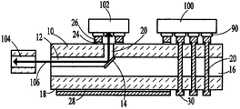
이제 보다 구체적으로 도 1을 참조하여, 본 발명의 바람직한 제1 실시예가 설명될 것이다. 가요성 유리(10)의 베이스 필름 재료가 제공된다. 유리 기판은 약 12.5 내지 100㎛의 두께 범위를 갖는다. 대안적으로, 유리 기판은 더 높은 굽힘성과 가요성을 위해 순환형 올레핀 중합체(COP)로 대체될 수 있다. 코어 도파관 재료는 유리 기판(10) 상에 증착된다. 도파관 재료의 굴절률은 가요성 유리 기판(10)의 굴절률보다 높아야 한다. 도파관 재료에 대한 다양한 대안은 실리콘, 이산화규소, 갈륨 비소, 갈륨 인화물 및 다양한 중합체 유형을 포함한다. 도파관 재료의 두께 범위는 약 4 내지 15㎛이다. Referring now more specifically to FIG. 1 , a first preferred embodiment of the present invention will be described. A base film material of flexible glass (10) is provided. The glass substrate has a thickness ranging from about 12.5 to 100 μm. Alternatively, the glass substrate can be replaced with a cyclic olefin polymer (COP) for higher bendability and flexibility. A core waveguide material is deposited on a
도파관 재료는 광학 회로(12)를 형성하도록 패턴화된다. 45°의 각도를 갖는 테이퍼진 형상이 도파관 측벽의 특정 위치에 형성된다. 45°마이크로 미러(14)는 이 테이퍼진 표면 위에 증착된다.The waveguide material is patterned to form an
광학 접착 재료(16)는 패턴화된 도파관 광학 회로 및 베이스 필름(10) 위에 적층된다. 광학 접착제는 가요성 유리 재료(10)의 굴절률과 정확히 동일한 굴절률을 가져야 한다. 이 광학 접착 재료에 대한 다양한 대안은 에폭시, 폴리우레탄, 실리콘 엘라스토머, UV 경화 아크릴 및 시아노아크릴레이트를 포함한다. 광학 접착제의 두께 범위는 약 25 내지 50㎛이다.An optical
이제, 가요성 유리 또는 순환형 올레핀 중합체(COP)일 수 있는 베이스 필름 재료의 제2 층(18)이 광학 접착제의 다른 면에 적층된다. 이 제2 베이스 필름(18)의 두께는 약 12.5 내지 100㎛ 범위이다.A
관통 유리 비아(TGV)(20, 22)는 지정된 인터페이스를 통해 형성된다. 광학 비아(20)의 경우, TGV는 베이스 필름 인터페이스(10)를 통해서만 수행된다. 이 TGV의 직경은 15 내지 25㎛일 수 있다. 광학 비아(20)를 완전히 채우기 위해 도파관 재료가 선택적으로 증착된다.Through glass vias (TGVs) 20 and 22 are formed through designated interfaces. For
가요성 유리 기판(10, 18) 모두의 외측면은 Si 올리고머 구조를 형성하도록 개질되고, 이어서 오각형 링 조정(ring coordination)에 의해 안정하게 유지되는 Pd 촉매 증착이 뒤따른다. 변형된 가요성 유리 표면에 회로 패턴이 형성되어 구리 회로를 구축할 뿐만 아니라 TGV(22)를 채우고 회로의 한 측면을 다른 측면에 연결한다. 구리 회로의 두께는 4 내지 15㎛이다. 전기 인터페이스는 유리 또는 COP 기판(10, 18)의 외측면에 형성된다. 예컨대, Ni-P 또는 구리, 은 또는 니켈-크롬과 같은 모든 유형 금속 합금의 시드층이 기판(10 및 18)의 외측면에 형성되어 원하는 대로 패턴화될 수 있다. 그런 다음 구리 트레이스가 시드층에 도금될 수 있다. 시드층(24) 및 구리 트레이스(26)는 기판(10)의 외측면에 나타나고 시드층(28) 및 구리 트레이스(30)는 기판(18)의 외측면에 나타난다. 충전된 TGV(22)는 구리 트레이스(30) 중 적어도 하나를 적어도 구리 트레이스(26) 중 하나에 연결한다.The outer surfaces of both
도 2는 본 발명의 바람직한 제2 실시예를 도시한다. 제1 실시예에서와 같이, 가요성 유리(10)의 베이스 필름 재료가 제공된다. 유리 기판은 약 12.5 내지 100㎛의 두께 범위를 갖는다. 코어 도파관 재료는 유리 기판(10) 상에 증착된다. 도파관 재료의 굴절률은 가요성 유리 기판(10)의 굴절률보다 높아야 한다. 도파관 재료에 대한 다양한 대안은 실리콘, 이산화규소, 갈륨 비소, 갈륨 인화물 및 다양한 중합체 유형을 포함한다. 도파관 재료의 두께 범위는 약 4 내지 15㎛이다.2 shows a second preferred embodiment of the present invention. As in the first embodiment, a base film material of
도파관 재료는 광학 회로(12)를 형성하도록 패턴화된다. 45°의 각도를 갖는 테이퍼진 형상이 도파관 측벽의 특정 위치에 형성된다. 45° 마이크로 미러(14)는 이 테이퍼진 표면의 상단에 증착된다.The waveguide material is patterned to form an
이 실시예에서, 약 12.5 내지 100㎛의 두께를 갖는 가요성 유리(18)의 제2 베이스 필름 재료가 제공된다. 도파관 재료(12)와 동일한 코어 도파관 재료가 제2 유리 기판(18) 상에 증착된다. 도파관 재료는 패턴화되어 제2 광학 회로(42)를 형성한다. 45°의 각도를 갖는 테이퍼진 형상이 도파관 측벽의 특정 위치에 형성된다. 제2 45° 마이크로 미러(44)는 이 테이퍼진 표면의 상단에 증착된다.In this embodiment, a second base film material of
유리 기판(10, 18)은 광학 접착 재료(16)와 함께 적층된다. 광학 회로(12, 42)는 서로 대향하고 광학 접착제에 적층된다. 위와 같이 광학 접착제는 가요성 유리 재료(10 및 18)의 굴절률과 정확히 동일한 굴절률을 가져야 한다. 이 광학 접착제 재료에 대한 다양한 대안은 에폭시, 폴리우레탄, 실리콘 엘라스토머, UV 경화 아크릴 및 시아노아크릴레이트를 포함한다. 광학 접착제의 두께 범위는 약 25 내지 50㎛이다.
패키지는 관통 유리 비아(TGV)(20 및 40)에 의해 광학 회로(12 및 42)에 각각 연결하고 TGV(22)는 제1 유리 기판(12) 상의 구리 트레이스(26)를 제2 유리 기판(18) 상의 구리 트레이스(30)에 연결함으로써 제1 실시예에서와 같이 완성된다.The package connects to the
본 발명의 바람직한 제3 실시예에서, 도 3에 도시된 바와 같이, 제2 유리 기판(18)은 폴리이미드(PI), 개질된 폴리이미드(MPI), 액정 중합체(LCP), 폴리에스테르(PET), 폴리에틸렌-나프탈레이트(PEN), 폴리테트라플루오로에틸렌, 또는 에폭시 및 BT와 같은 라미네이트 기판, 또는 테플론 또는 개질된 테플론으로 교체된다. 이러한 제2 베이스 필름(19)의 두께 범위는 12.5 내지 100㎛이다.In a third preferred embodiment of the present invention, as shown in FIG. 3 , the
유리 기판(10)의 바닥측에는 광학 회로(12)와 마이크로 미러(14)가 형성된다. 제2 베이스 필름(19)의 외측면을 개질하여 5 내지 15nm 두께 범위의 폴리아믹산(PAA)층을 형성하고, 이어서 기판층(19)의 상단측에 시드층(51)을 갖는 전기 회로(53) 및 기판층(19)의 바닥측에 시드층(28)을 갖는 금속 트레이스(30)를 형성하기 전에 Pd 촉매 증착이 뒤따른다. 비아 연결부(54)가 기판을 통해 이루어져서 기판(19)의 일측에 있는 금속 트레이스(53) 중 적어도 하나를 기판(19)의 반대측에 있는 금속 트레이스(30) 중 적어도 하나와 연결한다.An
도 4는 본 발명의 바람직한 제4 실시예를 도시한다. 이 실시예는 제2 베이스 기판(18)이 폴리이미드(PI), 개질된 폴리이미드(MPI), 액정 중합체(LCP), 폴리에스테르(PET), 폴리에틸렌-나프탈레이트(PEN), 폴리테트라플루오로에틸렌, 또는 에폭시 및 BT와 같은 라미네이트 기판, 또는 테플론 또는 개질된 테플론 층(19)으로 교체된다. 제4 실시예에서, 단일 기판층(19) 대신에, 전기 인터페이스의 다중 금속층 기판은 인터페이스 사이에 삽입된 접합 필름을 갖는다.4 shows a fourth preferred embodiment of the present invention. In this embodiment, the
제4 바람직한 실시예에서, 광학 회로(12) 및 마이크로 미러(14)는 유리 기판(10)의 바닥측에 형성된다. 시드층(51)을 갖는 금속 트레이스(53)는 기판층(19)의 상단측에 형성되고 시드층(56)을 갖는 금속 트레이스(58)는 기판층(19)의 바닥측에 형성된다. 비아 연결부(54)는 기판(19)을 통해 이루어져서 기판(19)의 일측 상의 금속 트레이스(53) 중 적어도 하나를 기판(19)의 반대측 상의 금속 트레이스(58) 중 적어도 하나와 연결한다. 마찬가지로, 시드층(62)을 갖는 금속 트레이스(64)는 폴리이미드(PI), 개질된 폴리이미드(MPI), 액정 중합체(LCP), 폴리에스테르(PET), 폴리에틸렌-나프탈레이트(PEN), 폴리테트라플루오로에틸렌, 또는 에폭시 및 BT와 같은 라미네이트 기판, 또는 테플론 또는 개질된 테플론 층을 포함하는 제2 기판(49)의 일측 상에 형성된다. 2개의 기판(19, 49)은 그들 사이의 접합층(50)과 함께 적층된다. 접합층은 약 10 내지 50㎛ 범위의 두께를 갖는 에폭시, 시안화물 에스테르, 아크릴 접착제, 에폭시를 사용한 개질된 폴리이미드(MPI) 등과 같은 섬유로 강화된 접착 필름일 수 있으며, 약 10 내지 50㎛ 범위, 바람직하게는 약 25㎛의 두께를 갖는다.In the fourth preferred embodiment, the
다중 금속층 기판(19/50/49)은 전술한 바와 같이 광학 접착제(16)로 베이스 필름 기판(10)에 적층된다. 이제 상단 및 바닥 비아와 트레이스가 형성된다. 관통 유리 비아(20, 22)는 기판(10) 및 광학 접착제(16)를 통해 형성된다. 도파관 재료는 광학 비아(20)를 완전히 채우기 위해 선택적으로 증착된다. 가요성 유리 기판(10)의 외측면은 Si 올리고머 구조를 형성하도록 개질되고, 이어서 오각형 링 조정을 통해 안정적으로 유지되는 Pd 촉매 증착이 뒤따른다. 전기 인터페이스는 유리 기판(10)의 외측면에 형성된다. 예컨대, Ni-P 또는 구리, 은 또는 니켈-크롬과 같은 임의의 유형의 금속 합금의 시드층이 기판(10)의 외측면에 형성되고 원하는 대로 패턴화될 수 있다. 그런 다음 구리 트레이스가 시드층에 도금될 수 있다. 시드층(24) 및 구리 트레이스(26)는 기판의 외측면에 제시되어 있다. 충전된 TGV(22)는 구부릴 수 있는 다중 금속 기판(19) 상의 구리 트레이스(53) 중 적어도 하나에 구리 트레이스(26) 중 적어도 하나를 연결한다.The
마찬가지로, 비아 개구(60, 61)는 구부릴 수 있는 다중 금속 기판의 베이스 필름(49)과 접합 필름(50)을 통해 만들어진다. 외부 베이스 필름(49)의 외측면은 개질되어 5 내지 15nm 범위의 두께를 갖는 폴리아믹산(PAA) 층을 형성하고, 이어서 베이스 필름층(49)의 외측면 상에 시드층(78)을 갖는 전기 회로(80)를 형성하기 전에 Pd 촉매 증착이 뒤따른다.Likewise, via
도 5는 본 발명의 바람직한 제5 실시예를 도시한다. 이 실시예에서, 접힌 가요성 폴리이미드 기판(47)이 있다. 유리 또는 COF 기판(10)은 접힌 가요성 기판(47)의 두 단부들 사이에 놓여 있다. 마이크로 미러(14)를 갖는 도파관 회로(12)가 형성된 기판(10)의 일면 상에서 광학 접착층(14)이 기판(10)을 가요성 기판(47)에 결합시킨다. 기판(10)의 반대 표면에서, 접합 필름(50)은 기판(10)을 가요성 기판(47)의 반대쪽 암에 결합시킨다.5 shows a fifth preferred embodiment of the present invention. In this embodiment, there is a folded
도 6은 집적 전기 광학 가요성 회로 기판을 도시한다. 가요성 회로 기판은 제1 실시예의 도 1과 유사하다. 그러나, 제1 내지 제5 실시예 중 임의의 것이 이제 설명되는 제조 단계에서 사용될 수 있음을 이해할 것이다. 증폭기 및 드라이버 집적 회로(100)와 같은 전자 디바이스는 가요성 회로 기판의 한 외측면에 있는 구리 트레이스(26)의 상단에 장착된다. 수직 공동 표면 발광 레이저(VCSEL) 및 광 검출기(PD) 모듈과 같은 광전자 디바이스(102)는 가요성 회로 기판의 동일한 외측면 상의 구리 트레이스(26) 상에 장착된다. 이들 디바이스(102)는 광학 비아(20)와 정렬된다. 예컨대, 디바이스(100, 102)는 플립 칩 또는 와이어 접합과 같은 표면 장착 기술(SMT)에 의해 표면 장착 디바이스(SMD)(90)가 장착될 수 있다. 광학 인터페이스(104)는 이 패키지 구성에서 설명된 모듈로부터의 나가는 신호 또는 다른 모듈로부터 들어오는 신호(106)를 위한 도파관(매체)이다.6 shows an integrated electro-optic flexible circuit board. The flexible circuit board is similar to FIG. 1 of the first embodiment. However, it will be understood that any of the first to fifth embodiments may be used in the manufacturing steps now described. Electronic devices such as amplifier and driver integrated
본 발명은 집적 전기 광학 가요성 회로 기판의 다양한 실시예를 설명하였다. 본 발명의 EOFCB는 고밀도 라우팅 및 다층 스택 업을 통해 높은 결합 효율 및 낮은 광 감쇠뿐만 아니라 상당한 크기 감소를 제공한다.The present invention has described various embodiments of an integrated electro-optic flexible circuit board. The EOFCB of the present invention provides high coupling efficiency and low optical attenuation as well as significant size reduction through high-density routing and multi-layer stack-up.
이상, 본 발명의 바람직한 실시예를 예시하여 그 형태를 상세히 설명하였지만, 본 발명의 사상 또는 첨부된 청구범위의 범주를 벗어나지 않고 다양한 변형이 가능함은 당업자에 의해 용이하게 이해될 것이다.In the above, although preferred embodiments of the present invention have been described in detail, it will be readily understood by those skilled in the art that various modifications are possible without departing from the spirit of the present invention or the scope of the appended claims.
Claims (22)
Translated fromKorean상단측 및 바닥측을 갖는 제1 가요성 기판;
충전된 비아를 통해 상기 상단 표면에 연결된 상기 제1 가요성 기판의 상기 바닥측 상의 적어도 하나의 제1 광학 회로;
상기 제1 가요성 기판의 상기 상단측 상의 적어도 하나의 제1 금속 트레이스;
상기 제1 가요성 기판의 상기 바닥측을 제2 가요성 기판의 상단측에 연결하는 광학 접착층; 및
충전된 비아에 의해 상기 제2 가요성 기판, 상기 광학 접착층, 및 상기 제1 가요성 기판을 통해 상기 적어도 하나의 제1 금속 트레이스에 연결된 상기 제2 가요성 기판의 바닥측 상의 적어도 하나의 제2 금속 트레이스를 포함하는, 집적 전기 광학 회로 기판.An integrated electro-optic circuit board comprising:
a first flexible substrate having a top side and a bottom side;
at least one first optical circuit on the bottom side of the first flexible substrate connected to the top surface through a filled via;
at least one first metal trace on the top side of the first flexible substrate;
an optical adhesive layer connecting the bottom side of the first flexible substrate to the top side of the second flexible substrate; and
at least one second on the bottom side of the second flexible substrate connected to the at least one first metal trace through the second flexible substrate, the optical adhesive layer, and the first flexible substrate by a filled via. An integrated electro-optic circuit board comprising metal traces.
상기 제1 가요성 기판은 약 12.5 내지 100㎛의 두께를 갖는 유리 또는 순환형 올레핀 중합체(COP)를 포함하는, 디바이스.According to claim 1,
wherein the first flexible substrate comprises glass or a cyclic olefin polymer (COP) having a thickness of about 12.5 to 100 μm.
상기 적어도 하나의 제 1 광학 회로는 약 4 내지 15㎛의 두께와 상기 제1 가요성 기판의 굴절률보다 큰 굴절률을 갖는 실리콘, 이산화규소, 갈륨 비소, 갈륨 인화물 또는 중합체를 포함하는 도파관인, 디바이스.According to claim 1,
wherein the at least one first optical circuit is a waveguide comprising silicon, silicon dioxide, gallium arsenide, gallium phosphide or a polymer having a thickness of about 4 to 15 μm and a refractive index greater than that of the first flexible substrate.
상기 제1 광학 회로와 상기 충전된 비아 사이에 45° 마이크로 미러(micro-mirror)를 더 포함하는, 디바이스.4. The method of claim 3,
and a 45° micro-mirror between the first optical circuit and the filled via.
상기 광학 접착 재료는 약 25 내지 50㎛의 두께 및 상기 제1 굴절률과 동일한 굴절률을 갖는 에폭시, 폴리우레탄, 실리콘 엘라스토머, UV-경화 아크릴, 또는 시아노아크릴레이트(Cyanoacrylate)를 포함하는, 디바이스.According to claim 1,
wherein the optical adhesive material comprises an epoxy, polyurethane, silicone elastomer, UV-curing acrylic, or cyanoacrylate having a thickness of about 25-50 μm and a refractive index equal to the first refractive index.
상기 제1 및 제2 금속 트레이스는 약 4 내지 15㎛의 두께를 갖는 구리 및 약 0.01 내지 0.5㎛의 두께를 갖는 Ni-P의 하부 시드층을 포함하는, 디바이스.According to claim 1,
wherein the first and second metal traces comprise a bottom seed layer of copper having a thickness of about 4 to 15 μm and a lower seed layer of Ni-P having a thickness of about 0.01 to 0.5 μm.
상기 제2 가요성 기판의 상기 상단 표면 상의 적어도 하나의 제2 광학 회로를 더 포함하는, 디바이스.According to claim 1,
and at least one second optical circuit on the top surface of the second flexible substrate.
상기 제2 가요성 기판은 약 12.5 내지 100㎛의 두께를 갖는 가요성 유리 또는 순환형 올레핀 중합체(COP)를 포함하는, 디바이스.According to claim 1,
wherein the second flexible substrate comprises flexible glass or cyclic olefin polymer (COP) having a thickness of about 12.5 to 100 μm.
상기 적어도 하나의 제1 금속 트레이스 상에 장착된 적어도 하나의 전기 디바이스; 및
상기 적어도 하나의 제1 광학 회로 상에 장착된 적어도 하나의 광전자 디바이스를 더 포함하는, 디바이스.According to claim 1,
at least one electrical device mounted on the at least one first metal trace; and
and at least one optoelectronic device mounted on the at least one first optical circuit.
상기 적어도 하나의 전기 디바이스 및 상기 적어도 하나의 광전자 디바이스는 플립 칩 및 와이어 접합을 포함하는 표면 장착 기술(SMT)에 의해 장착되는, 디바이스.10. The method of claim 9,
wherein the at least one electrical device and the at least one optoelectronic device are mounted by a surface mount technique (SMT) comprising flip chip and wire bonding.
상단측 및 바닥측을 갖는 제1 가요성 기판;
충전된 비아를 통해 상기 상단 표면에 연결된 상기 제1 가요성 기판의 상기 바닥측 상의 적어도 하나의 제1 광학 회로;
상기 제1 가요성 기판의 상기 상단측 상의 적어도 하나의 제1 금속 트레이스;
상기 제1 가요성 기판의 상기 바닥측을 제2 가요성 기판의 상단측에 연결하는 광학 접착층; 및
상기 제2 가요성 기판의 상단측 상의 적어도 하나의 제2 금속 트레이스 및 충전된 비아에 의해 상기 제2 가요성 기판을 통해 상기 적어도 하나의 제2 금속 트레이스에 연결된 상기 제2 가요성 기판의 바닥측 상의 적어도 하나의 제3 금속 트레이스를 포함하는, 집적 전기 광학 회로 기판.An integrated electro-optic circuit board comprising:
a first flexible substrate having a top side and a bottom side;
at least one first optical circuit on the bottom side of the first flexible substrate connected to the top surface through a filled via;
at least one first metal trace on the top side of the first flexible substrate;
an optical adhesive layer connecting the bottom side of the first flexible substrate to the top side of the second flexible substrate; and
at least one second metal trace on the top side of the second flexible substrate and the bottom side of the second flexible substrate connected to the at least one second metal trace through the second flexible substrate by a filled via at least one third metal trace on the integrated electro-optic circuit board.
상기 제1 가요성 기판은 약 12.5 내지 100㎛의 두께를 갖는 유리 또는 순환형 올레핀 중합체(COP)를 포함하는, 디바이스.12. The method of claim 11,
wherein the first flexible substrate comprises glass or a cyclic olefin polymer (COP) having a thickness of about 12.5 to 100 μm.
상기 적어도 하나의 제 1 광학 회로는 약 4 내지 15㎛의 두께와 상기 제1 가요성 기판의 굴절률보다 큰 굴절률을 갖는 실리콘, 이산화규소, 갈륨 비소, 갈륨 인화물 또는 중합체를 포함하는 도파관인, 디바이스.12. The method of claim 11,
wherein the at least one first optical circuit is a waveguide comprising silicon, silicon dioxide, gallium arsenide, gallium phosphide or a polymer having a thickness of about 4 to 15 μm and a refractive index greater than that of the first flexible substrate.
상기 제1 광학 회로와 상기 충전된 비아 사이에 45° 마이크로 미러를 더 포함하는, 디바이스.14. The method of claim 13,
and a 45° micro-mirror between the first optical circuit and the filled via.
상기 광학 접착 재료는 약 25 내지 50㎛의 두께 및 상기 제1 굴절률과 동일한 굴절률을 갖는 에폭시, 폴리우레탄, 실리콘 엘라스토머, UV-경화 아크릴, 또는 시아노아크릴레이트를 포함하는, 디바이스.12. The method of claim 11,
wherein the optical adhesive material comprises an epoxy, polyurethane, silicone elastomer, UV-curing acrylic, or cyanoacrylate having a thickness of about 25 to 50 μm and an index of refraction equal to the first index of refraction.
상기 제1, 제2 및 제3 금속 트레이스는 약 4 내지 15㎛의 두께를 갖는 구리 및 약 0.01 내지 0.5㎛의 두께를 갖는 Ni-P의 하부 시드층을 포함하는, 디바이스.12. The method of claim 11,
wherein the first, second and third metal traces comprise a bottom seed layer of copper having a thickness of about 4 to 15 μm and a lower seed layer of Ni-P having a thickness of about 0.01 to 0.5 μm.
상기 제2 가요성 기판은 약 12.5 내지 100㎛의 두께를 갖는 폴리이미드(PI), 개질된 폴리이미드(MPI), 액정 중합체(LCP), 폴리에스테르(PET), 폴리에틸렌-나프탈레이트(PEN), 폴리테트라플루오로에틸렌, 또는 에폭시 및 BT와 같은 라미네이트 기판, 또는 테플론 또는 개질된 테플론을 포함하는, 디바이스.12. The method of claim 11,
The second flexible substrate may include polyimide (PI) having a thickness of about 12.5 to 100 μm, modified polyimide (MPI), liquid crystal polymer (LCP), polyester (PET), polyethylene-naphthalate (PEN), A device comprising polytetrafluoroethylene, or a laminate substrate such as epoxy and BT, or Teflon or modified Teflon.
상기 제2 가요성 기판은 다중 금속층 기판을 포함하는, 디바이스.12. The method of claim 11,
wherein the second flexible substrate comprises a multi-metal layer substrate.
상기 다중 금속층 기판은 접합 필름을 사이에 두고 제3 및 제4 가요성 기판을 포함하고, 제4 및 제5 금속 트레이스는 상기 제3 가요성 기판 상에 그리고 이를 통해 형성되고, 제6 및 제7 금속 트레이스는 상기 제4 가요성 기판 및 상기 접합 필름 상에 그리고 이를 통해 형성되고, 상기 제3 및 제4 가요성 기판은 약 12.5 내지 100㎛의 두께를 갖는 폴리이미드(PI), 개질된 폴리이미드(MPI), 액정 중합체(LCP), 폴리에스테르(PET), 폴리에틸렌-나프탈레이트(PEN), 폴리테트라플루오로에틸렌, 또는 에폭시 및 BT와 같은 라미네이트 기판, 또는 테플론, 또는 개질된 테플론을 포함하는, 디바이스.19. The method of claim 18,
the multi-metal layer substrate includes third and fourth flexible substrates with a bonding film interposed therebetween, fourth and fifth metal traces are formed on and through the third flexible substrate, and sixth and seventh metal traces are formed on and through the third flexible substrate; Metal traces are formed on and through the fourth flexible substrate and the bonding film, wherein the third and fourth flexible substrates are polyimide (PI), modified polyimide having a thickness of about 12.5 to 100 μm. (MPI), liquid crystal polymer (LCP), polyester (PET), polyethylene-naphthalate (PEN), polytetrafluoroethylene, or laminate substrates such as epoxy and BT, or Teflon, or modified Teflon; device.
상기 다중 금속층 기판은 제3 가요성 기판을 포함하고, 상기 제3 가요성 기판은 약 12.5 내지 100㎛의 두께를 갖는 폴리이미드(PI), 개질된 폴리이미드(MPI), 액정 중합체(LCP), 폴리에스테르(PET), 폴리에틸렌-나프탈레이트(PEN), 폴리테트라플루오로에틸렌, 또는 에폭시 및 BT와 같은 라미네이트 기판, 또는 테플론, 또는 개질된 테플론을 포함하고;
제4 금속 트레이스들은 상기 제3 가요성 기판의 제1 반부 상에 그리고 이를 통해 형성되고;
상기 제2 및 제3 금속 트레이스는 상기 제3 가요성 기판의 제2 반부 상에 그리고 이를 통해 형성되고;
접합 필름은 상기 제3 가요성 기판의 상기 제1 반부를 상기 제1 가요성 기판의 상단측에 결합하고;
상기 제1 금속 트레이스들과 상기 제2 금속 트레이스들 사이에 전기적 연결부들이 이루어지며; 그리고
상기 광학 접착제는 상기 제1 가요성 기판의 상기 바닥측을 상기 제3 가요성 기판의 상기 제2 반부에 결합하는, 디바이스.19. The method of claim 18,
wherein the multi-metal layer substrate includes a third flexible substrate, wherein the third flexible substrate includes a polyimide (PI) having a thickness of about 12.5 to 100 μm, a modified polyimide (MPI), a liquid crystal polymer (LCP); polyester (PET), polyethylene-naphthalate (PEN), polytetrafluoroethylene, or laminate substrates such as epoxy and BT, or Teflon, or modified Teflon;
fourth metal traces are formed on and through the first half of the third flexible substrate;
the second and third metal traces are formed on and through the second half of the third flexible substrate;
a bonding film bonding the first half of the third flexible substrate to an upper end of the first flexible substrate;
electrical connections are made between the first metal traces and the second metal traces; and
and the optical adhesive bonds the bottom side of the first flexible substrate to the second half of the third flexible substrate.
상기 적어도 하나의 제1 금속 트레이스 상에 장착된 적어도 하나의 전기 디바이스; 및
상기 적어도 하나의 제1 광학 회로 상에 장착된 적어도 하나의 광전자 디바이스를 더 포함하는, 디바이스.12. The method of claim 11,
at least one electrical device mounted on the at least one first metal trace; and
and at least one optoelectronic device mounted on the at least one first optical circuit.
상기 적어도 하나의 전기 디바이스 및 상기 적어도 하나의 광전자 디바이스는 플립 칩 및 와이어 접합을 포함하는 표면 장착 기술(SMT)에 의해 장착되는, 디바이스.22. The method of claim 21,
wherein the at least one electrical device and the at least one optoelectronic device are mounted by a surface mount technique (SMT) comprising flip chip and wire bonding.
Applications Claiming Priority (3)
| Application Number | Priority Date | Filing Date | Title |
|---|---|---|---|
| US16/654,503US11076491B2 (en) | 2019-10-16 | 2019-10-16 | Integrated electro-optical flexible circuit board |
| US16/654,503 | 2019-10-16 | ||
| PCT/CN2020/000251WO2021072987A1 (en) | 2019-10-16 | 2020-10-16 | Integrated electro-optical flexible circuit board |
Publications (1)
| Publication Number | Publication Date |
|---|---|
| KR20220084053Atrue KR20220084053A (en) | 2022-06-21 |
Family
ID=75491564
Family Applications (1)
| Application Number | Title | Priority Date | Filing Date |
|---|---|---|---|
| KR1020227012697APendingKR20220084053A (en) | 2019-10-16 | 2020-10-16 | Integrated Electro-Optical Flexible Circuit Board |
Country Status (6)
| Country | Link |
|---|---|
| US (2) | US11076491B2 (en) |
| EP (1) | EP4045955A4 (en) |
| JP (1) | JP2022552301A (en) |
| KR (1) | KR20220084053A (en) |
| CN (1) | CN114730054B (en) |
| WO (1) | WO2021072987A1 (en) |
Families Citing this family (10)
| Publication number | Priority date | Publication date | Assignee | Title |
|---|---|---|---|---|
| US11076491B2 (en) | 2019-10-16 | 2021-07-27 | Compass Technology Company Limited | Integrated electro-optical flexible circuit board |
| US12100698B2 (en)* | 2021-08-19 | 2024-09-24 | Taiwan Semiconductor Manufacturing Company, Ltd. | Semiconductor device and manufacturing method thereof |
| US12422615B2 (en)* | 2021-09-13 | 2025-09-23 | Intel Corporation | Nested glass packaging architecture for hybrid electrical and optical communication devices |
| US20230083222A1 (en)* | 2021-09-15 | 2023-03-16 | Intel Corporation | Photonic interconnect and components in glass |
| US12394719B2 (en)* | 2021-09-22 | 2025-08-19 | Intel Corporation | Methods and apparatus to increase glass core thickness |
| US11727891B2 (en)* | 2021-11-16 | 2023-08-15 | Meta Platforms Technologies, Llc | Integrated electronic and photonic backplane architecture for display panels |
| US12345934B2 (en) | 2022-10-04 | 2025-07-01 | Applied Materials, Inc. | Methods for fabrication of optical structures on photonic glass layer substrates |
| WO2024262042A1 (en)* | 2023-06-23 | 2024-12-26 | 株式会社レゾナック | Method for manufacturing photoelectric composite wiring board, photoelectric composite wiring board, semiconductor package, and laminated film |
| WO2025005726A1 (en)* | 2023-06-28 | 2025-01-02 | 엘지이노텍 주식회사 | Flexible circuit board, cof module, and electronic device comprising same |
| CN118139275B (en)* | 2024-05-08 | 2024-06-28 | 国鲸科技(广东横琴粤澳深度合作区)有限公司 | Transparent flexible integrated circuit substrate |
Family Cites Families (27)
| Publication number | Priority date | Publication date | Assignee | Title |
|---|---|---|---|---|
| US5625734A (en)* | 1995-05-31 | 1997-04-29 | Motorola | Optoelectronic interconnect device and method of making |
| JP2002277694A (en)* | 2001-03-19 | 2002-09-25 | Mitsubishi Electric Corp | Substrate having optical waveguide and electric circuit and method of manufacturing the same |
| US6910812B2 (en) | 2001-05-15 | 2005-06-28 | Peregrine Semiconductor Corporation | Small-scale optoelectronic package |
| JP4810958B2 (en)* | 2005-02-28 | 2011-11-09 | ソニー株式会社 | Hybrid circuit device |
| US7429788B2 (en)* | 2006-03-08 | 2008-09-30 | Microelectronics Assembly Technologies, Inc. | Thin multichip flex-module |
| KR100796982B1 (en) | 2006-11-21 | 2008-01-22 | 삼성전기주식회사 | Printed Circuit Board and Manufacturing Method |
| KR100821289B1 (en) | 2007-01-30 | 2008-04-11 | 주식회사 두산 | Flexible Optical Circuit Board and Manufacturing Method Thereof |
| JP2009098432A (en)* | 2007-10-17 | 2009-05-07 | Central Glass Co Ltd | Device for converting laminated multi-channel optical path and method of manufacturing the same |
| JP5384819B2 (en)* | 2007-12-07 | 2014-01-08 | 日本特殊陶業株式会社 | Opto-electric hybrid package, opto-electric hybrid module |
| SG188921A1 (en)* | 2008-04-08 | 2013-04-30 | Univ Arizona | Assemblies and methods for reducing warp and bow of a flexible substrate during semiconductor processing |
| JP4971248B2 (en) | 2008-05-27 | 2012-07-11 | 日東電工株式会社 | Manufacturing method of opto-electric hybrid module |
| JP5278366B2 (en)* | 2010-04-06 | 2013-09-04 | 住友ベークライト株式会社 | Optical waveguide structure and electronic device |
| MX2012012033A (en) | 2010-04-16 | 2013-05-20 | Flex Lighting Ii Llc | Illumination device comprising a film-based lightguide. |
| JP5522088B2 (en)* | 2011-03-02 | 2014-06-18 | 日立金属株式会社 | Photoelectric transmission module |
| US9130254B1 (en) | 2013-03-27 | 2015-09-08 | Google Inc. | Printed waveguide transmission line having layers bonded by conducting and non-conducting adhesives |
| WO2015015138A1 (en) | 2013-07-31 | 2015-02-05 | Milan Momcilo Popovich | Method and apparatus for contact image sensing |
| JP6319762B2 (en)* | 2013-10-31 | 2018-05-09 | 日東電工株式会社 | Opto-electric hybrid board and manufacturing method thereof |
| JP6387729B2 (en)* | 2014-07-31 | 2018-09-12 | 富士通株式会社 | Opto-electric hybrid board, information processing apparatus, and opto-electric hybrid board manufacturing method |
| DE102014219792A1 (en)* | 2014-09-30 | 2016-03-31 | Technische Universität Berlin | Optoelectronic component |
| US9899330B2 (en)* | 2014-10-03 | 2018-02-20 | Mc10, Inc. | Flexible electronic circuits with embedded integrated circuit die |
| KR102241556B1 (en)* | 2014-11-25 | 2021-04-19 | 삼성디스플레이 주식회사 | Display device |
| WO2016183201A1 (en) | 2015-05-12 | 2016-11-17 | Nitto Denko Corporation | Solar energy collection systems utilizing holographic optical elements useful for building integrated photovoltaics |
| CN106249361B (en)* | 2015-06-05 | 2019-06-28 | 胡迪群 | Embedded optical fiber module |
| CN106658946A (en) | 2016-12-26 | 2017-05-10 | 长沙牧泰莱电路技术有限公司 | Flexible composite circuit board and fabrication method thereof |
| US10332443B2 (en) | 2017-02-03 | 2019-06-25 | Abl Ip Holding Llc | Luminaire and lighting system, combining transparent lighting device and display coupled to output image via the transparent lighting device |
| CN109803481B (en)* | 2017-11-17 | 2021-07-06 | 英业达科技有限公司 | Multilayer printed circuit board and method for manufacturing multilayer printed circuit board |
| US11076491B2 (en) | 2019-10-16 | 2021-07-27 | Compass Technology Company Limited | Integrated electro-optical flexible circuit board |
- 2019
- 2019-10-16USUS16/654,503patent/US11076491B2/enactiveActive
- 2020
- 2020-10-16EPEP20875988.6Apatent/EP4045955A4/ennot_activeWithdrawn
- 2020-10-16KRKR1020227012697Apatent/KR20220084053A/enactivePending
- 2020-10-16WOPCT/CN2020/000251patent/WO2021072987A1/ennot_activeCeased
- 2020-10-16JPJP2022521404Apatent/JP2022552301A/enactivePending
- 2020-10-16CNCN202080069087.1Apatent/CN114730054B/enactiveActive
- 2021
- 2021-06-21USUS17/352,562patent/US11553598B2/enactiveActive
Also Published As
| Publication number | Publication date |
|---|---|
| US20210315108A1 (en) | 2021-10-07 |
| WO2021072987A1 (en) | 2021-04-22 |
| US11076491B2 (en) | 2021-07-27 |
| US11553598B2 (en) | 2023-01-10 |
| EP4045955A1 (en) | 2022-08-24 |
| EP4045955A4 (en) | 2023-12-27 |
| US20210120680A1 (en) | 2021-04-22 |
| JP2022552301A (en) | 2022-12-15 |
| CN114730054B (en) | 2025-02-28 |
| CN114730054A (en) | 2022-07-08 |
Similar Documents
| Publication | Publication Date | Title |
|---|---|---|
| US11553598B2 (en) | Integrated electro-optical flexible circuit board | |
| US6829398B2 (en) | Optical waveguide apparatus | |
| US8311375B2 (en) | Optoelectronic wiring board, optical communication device, and method of manufacturing the optical communication device | |
| US7541058B2 (en) | Method of making circuitized substrate with internal optical pathway | |
| US7713767B2 (en) | Method of making circuitized substrate with internal optical pathway using photolithography | |
| JP3833132B2 (en) | Manufacturing method of optical waveguide device | |
| US8989531B2 (en) | Optical-electrical wiring board and optical module | |
| US9075206B2 (en) | Optical waveguide device | |
| JP2011017787A (en) | Optical waveguide layer, opto-electro mixed circuit board and method of fabricating opto-electro circuit board | |
| CN108024446A (en) | Photoelectric flexible interconnection substrate and its manufacturing process | |
| JP5277874B2 (en) | Opto-electric hybrid board and electronic equipment | |
| TW202210885A (en) | Hybrid multi-layered optical flexible printed circuit device and manufacturing method thereof | |
| US7450793B2 (en) | Semiconductor device integrated with opto-electric component and method for fabricating the same | |
| US8861917B2 (en) | Opto-electric circuit board including metal-slotted optical waveguide and opto-electric simultaneous communication system | |
| US20100183267A1 (en) | Optoelectronic interconnection system | |
| WO2007088959A1 (en) | Optical module | |
| JP2003227951A (en) | Optical waveguide device, manufacturing method thereof, and opto-electric hybrid board using the same | |
| US8979372B2 (en) | Circuit board and manufacturing method thereof and electro-optic apparatus having the circuit board | |
| TW202220507A (en) | Integrated electro-optical flexible circuit board | |
| TW202515259A (en) | Flexible printed circuit board with embedded optical waveguide structure | |
| KR20080026212A (en) | Optical waveguide device | |
| Takahara | Optoelectronic packaging technologies for chip-level optical interconnections |
Legal Events
| Date | Code | Title | Description |
|---|---|---|---|
| PA0105 | International application | Patent event date:20220415 Patent event code:PA01051R01D Comment text:International Patent Application | |
| PG1501 | Laying open of application | ||
| E902 | Notification of reason for refusal | ||
| PE0902 | Notice of grounds for rejection | Comment text:Notification of reason for refusal Patent event date:20250224 Patent event code:PE09021S01D |