KR20220083911A - Display device - Google Patents
Display deviceDownload PDFInfo
- Publication number
- KR20220083911A KR20220083911AKR1020200173391AKR20200173391AKR20220083911AKR 20220083911 AKR20220083911 AKR 20220083911AKR 1020200173391 AKR1020200173391 AKR 1020200173391AKR 20200173391 AKR20200173391 AKR 20200173391AKR 20220083911 AKR20220083911 AKR 20220083911A
- Authority
- KR
- South Korea
- Prior art keywords
- display area
- light emitting
- pixel circuit
- display
- circuit unit
- Prior art date
- Legal status (The legal status is an assumption and is not a legal conclusion. Google has not performed a legal analysis and makes no representation as to the accuracy of the status listed.)
- Pending
Links
Images


Classifications
- H01L27/326—
- H—ELECTRICITY
- H10—SEMICONDUCTOR DEVICES; ELECTRIC SOLID-STATE DEVICES NOT OTHERWISE PROVIDED FOR
- H10K—ORGANIC ELECTRIC SOLID-STATE DEVICES
- H10K59/00—Integrated devices, or assemblies of multiple devices, comprising at least one organic light-emitting element covered by group H10K50/00
- H10K59/10—OLED displays
- H10K59/12—Active-matrix OLED [AMOLED] displays
- H10K59/121—Active-matrix OLED [AMOLED] displays characterised by the geometry or disposition of pixel elements
- H—ELECTRICITY
- H10—SEMICONDUCTOR DEVICES; ELECTRIC SOLID-STATE DEVICES NOT OTHERWISE PROVIDED FOR
- H10K—ORGANIC ELECTRIC SOLID-STATE DEVICES
- H10K59/00—Integrated devices, or assemblies of multiple devices, comprising at least one organic light-emitting element covered by group H10K50/00
- H10K59/10—OLED displays
- H10K59/12—Active-matrix OLED [AMOLED] displays
- H10K59/122—Pixel-defining structures or layers, e.g. banks
- H—ELECTRICITY
- H10—SEMICONDUCTOR DEVICES; ELECTRIC SOLID-STATE DEVICES NOT OTHERWISE PROVIDED FOR
- H10K—ORGANIC ELECTRIC SOLID-STATE DEVICES
- H10K59/00—Integrated devices, or assemblies of multiple devices, comprising at least one organic light-emitting element covered by group H10K50/00
- H10K59/10—OLED displays
- H10K59/12—Active-matrix OLED [AMOLED] displays
- H10K59/123—Connection of the pixel electrodes to the thin film transistors [TFT]
- G—PHYSICS
- G06—COMPUTING OR CALCULATING; COUNTING
- G06F—ELECTRIC DIGITAL DATA PROCESSING
- G06F1/00—Details not covered by groups G06F3/00 - G06F13/00 and G06F21/00
- G06F1/16—Constructional details or arrangements
- G06F1/1613—Constructional details or arrangements for portable computers
- G06F1/1633—Constructional details or arrangements of portable computers not specific to the type of enclosures covered by groups G06F1/1615 - G06F1/1626
- G06F1/1637—Details related to the display arrangement, including those related to the mounting of the display in the housing
- G06F1/1652—Details related to the display arrangement, including those related to the mounting of the display in the housing the display being flexible, e.g. mimicking a sheet of paper, or rollable
- G—PHYSICS
- G09—EDUCATION; CRYPTOGRAPHY; DISPLAY; ADVERTISING; SEALS
- G09F—DISPLAYING; ADVERTISING; SIGNS; LABELS OR NAME-PLATES; SEALS
- G09F9/00—Indicating arrangements for variable information in which the information is built-up on a support by selection or combination of individual elements
- G09F9/30—Indicating arrangements for variable information in which the information is built-up on a support by selection or combination of individual elements in which the desired character or characters are formed by combining individual elements
- G09F9/301—Indicating arrangements for variable information in which the information is built-up on a support by selection or combination of individual elements in which the desired character or characters are formed by combining individual elements flexible foldable or roll-able electronic displays, e.g. thin LCD, OLED
- G—PHYSICS
- G09—EDUCATION; CRYPTOGRAPHY; DISPLAY; ADVERTISING; SEALS
- G09G—ARRANGEMENTS OR CIRCUITS FOR CONTROL OF INDICATING DEVICES USING STATIC MEANS TO PRESENT VARIABLE INFORMATION
- G09G3/00—Control arrangements or circuits, of interest only in connection with visual indicators other than cathode-ray tubes
- G09G3/03—Control arrangements or circuits, of interest only in connection with visual indicators other than cathode-ray tubes specially adapted for displays having non-planar surfaces, e.g. curved displays
- G—PHYSICS
- G09—EDUCATION; CRYPTOGRAPHY; DISPLAY; ADVERTISING; SEALS
- G09G—ARRANGEMENTS OR CIRCUITS FOR CONTROL OF INDICATING DEVICES USING STATIC MEANS TO PRESENT VARIABLE INFORMATION
- G09G3/00—Control arrangements or circuits, of interest only in connection with visual indicators other than cathode-ray tubes
- G09G3/20—Control arrangements or circuits, of interest only in connection with visual indicators other than cathode-ray tubes for presentation of an assembly of a number of characters, e.g. a page, by composing the assembly by combination of individual elements arranged in a matrix no fixed position being assigned to or needed to be assigned to the individual characters or partial characters
- G09G3/22—Control arrangements or circuits, of interest only in connection with visual indicators other than cathode-ray tubes for presentation of an assembly of a number of characters, e.g. a page, by composing the assembly by combination of individual elements arranged in a matrix no fixed position being assigned to or needed to be assigned to the individual characters or partial characters using controlled light sources
- G09G3/30—Control arrangements or circuits, of interest only in connection with visual indicators other than cathode-ray tubes for presentation of an assembly of a number of characters, e.g. a page, by composing the assembly by combination of individual elements arranged in a matrix no fixed position being assigned to or needed to be assigned to the individual characters or partial characters using controlled light sources using electroluminescent panels
- G09G3/32—Control arrangements or circuits, of interest only in connection with visual indicators other than cathode-ray tubes for presentation of an assembly of a number of characters, e.g. a page, by composing the assembly by combination of individual elements arranged in a matrix no fixed position being assigned to or needed to be assigned to the individual characters or partial characters using controlled light sources using electroluminescent panels semiconductive, e.g. using light-emitting diodes [LED]
- G09G3/3208—Control arrangements or circuits, of interest only in connection with visual indicators other than cathode-ray tubes for presentation of an assembly of a number of characters, e.g. a page, by composing the assembly by combination of individual elements arranged in a matrix no fixed position being assigned to or needed to be assigned to the individual characters or partial characters using controlled light sources using electroluminescent panels semiconductive, e.g. using light-emitting diodes [LED] organic, e.g. using organic light-emitting diodes [OLED]
- G09G3/3225—Control arrangements or circuits, of interest only in connection with visual indicators other than cathode-ray tubes for presentation of an assembly of a number of characters, e.g. a page, by composing the assembly by combination of individual elements arranged in a matrix no fixed position being assigned to or needed to be assigned to the individual characters or partial characters using controlled light sources using electroluminescent panels semiconductive, e.g. using light-emitting diodes [LED] organic, e.g. using organic light-emitting diodes [OLED] using an active matrix
- H01L27/3248—
- H01L27/3276—
- H01L51/5206—
- H01L51/5253—
- H—ELECTRICITY
- H10—SEMICONDUCTOR DEVICES; ELECTRIC SOLID-STATE DEVICES NOT OTHERWISE PROVIDED FOR
- H10K—ORGANIC ELECTRIC SOLID-STATE DEVICES
- H10K50/00—Organic light-emitting devices
- H10K50/80—Constructional details
- H10K50/84—Passivation; Containers; Encapsulations
- H10K50/844—Encapsulations
- H—ELECTRICITY
- H10—SEMICONDUCTOR DEVICES; ELECTRIC SOLID-STATE DEVICES NOT OTHERWISE PROVIDED FOR
- H10K—ORGANIC ELECTRIC SOLID-STATE DEVICES
- H10K59/00—Integrated devices, or assemblies of multiple devices, comprising at least one organic light-emitting element covered by group H10K50/00
- H10K59/10—OLED displays
- H10K59/12—Active-matrix OLED [AMOLED] displays
- H10K59/121—Active-matrix OLED [AMOLED] displays characterised by the geometry or disposition of pixel elements
- H10K59/1213—Active-matrix OLED [AMOLED] displays characterised by the geometry or disposition of pixel elements the pixel elements being TFTs
- H—ELECTRICITY
- H10—SEMICONDUCTOR DEVICES; ELECTRIC SOLID-STATE DEVICES NOT OTHERWISE PROVIDED FOR
- H10K—ORGANIC ELECTRIC SOLID-STATE DEVICES
- H10K59/00—Integrated devices, or assemblies of multiple devices, comprising at least one organic light-emitting element covered by group H10K50/00
- H10K59/10—OLED displays
- H10K59/12—Active-matrix OLED [AMOLED] displays
- H10K59/131—Interconnections, e.g. wiring lines or terminals
- H10K59/1315—Interconnections, e.g. wiring lines or terminals comprising structures specially adapted for lowering the resistance
- H—ELECTRICITY
- H10—SEMICONDUCTOR DEVICES; ELECTRIC SOLID-STATE DEVICES NOT OTHERWISE PROVIDED FOR
- H10K—ORGANIC ELECTRIC SOLID-STATE DEVICES
- H10K59/00—Integrated devices, or assemblies of multiple devices, comprising at least one organic light-emitting element covered by group H10K50/00
- H10K59/80—Constructional details
- H10K59/87—Passivation; Containers; Encapsulations
- H10K59/873—Encapsulations
- G—PHYSICS
- G09—EDUCATION; CRYPTOGRAPHY; DISPLAY; ADVERTISING; SEALS
- G09G—ARRANGEMENTS OR CIRCUITS FOR CONTROL OF INDICATING DEVICES USING STATIC MEANS TO PRESENT VARIABLE INFORMATION
- G09G2300/00—Aspects of the constitution of display devices
- G09G2300/04—Structural and physical details of display devices
- G09G2300/0421—Structural details of the set of electrodes
- G09G2300/0426—Layout of electrodes and connections
- G—PHYSICS
- G09—EDUCATION; CRYPTOGRAPHY; DISPLAY; ADVERTISING; SEALS
- G09G—ARRANGEMENTS OR CIRCUITS FOR CONTROL OF INDICATING DEVICES USING STATIC MEANS TO PRESENT VARIABLE INFORMATION
- G09G2310/00—Command of the display device
- G09G2310/02—Addressing, scanning or driving the display screen or processing steps related thereto
- G09G2310/0264—Details of driving circuits
- G09G2310/0267—Details of drivers for scan electrodes, other than drivers for liquid crystal, plasma or OLED displays
- G—PHYSICS
- G09—EDUCATION; CRYPTOGRAPHY; DISPLAY; ADVERTISING; SEALS
- G09G—ARRANGEMENTS OR CIRCUITS FOR CONTROL OF INDICATING DEVICES USING STATIC MEANS TO PRESENT VARIABLE INFORMATION
- G09G2310/00—Command of the display device
- G09G2310/02—Addressing, scanning or driving the display screen or processing steps related thereto
- G09G2310/0264—Details of driving circuits
- G09G2310/0275—Details of drivers for data electrodes, other than drivers for liquid crystal, plasma or OLED displays, not related to handling digital grey scale data or to communication of data to the pixels by means of a current
- H01L2251/5338—
- H—ELECTRICITY
- H10—SEMICONDUCTOR DEVICES; ELECTRIC SOLID-STATE DEVICES NOT OTHERWISE PROVIDED FOR
- H10K—ORGANIC ELECTRIC SOLID-STATE DEVICES
- H10K2102/00—Constructional details relating to the organic devices covered by this subclass
- H10K2102/301—Details of OLEDs
- H10K2102/311—Flexible OLED
- H—ELECTRICITY
- H10—SEMICONDUCTOR DEVICES; ELECTRIC SOLID-STATE DEVICES NOT OTHERWISE PROVIDED FOR
- H10K—ORGANIC ELECTRIC SOLID-STATE DEVICES
- H10K59/00—Integrated devices, or assemblies of multiple devices, comprising at least one organic light-emitting element covered by group H10K50/00
- H10K59/80—Constructional details
- H10K59/805—Electrodes
- H10K59/8051—Anodes
- H10K59/80515—Anodes characterised by their shape
- H—ELECTRICITY
- H10—SEMICONDUCTOR DEVICES; ELECTRIC SOLID-STATE DEVICES NOT OTHERWISE PROVIDED FOR
- H10K—ORGANIC ELECTRIC SOLID-STATE DEVICES
- H10K77/00—Constructional details of devices covered by this subclass and not covered by groups H10K10/80, H10K30/80, H10K50/80 or H10K59/80
- H10K77/10—Substrates, e.g. flexible substrates
- H10K77/111—Flexible substrates
Landscapes
- Engineering & Computer Science (AREA)
- Microelectronics & Electronic Packaging (AREA)
- Physics & Mathematics (AREA)
- Theoretical Computer Science (AREA)
- Computer Hardware Design (AREA)
- General Physics & Mathematics (AREA)
- Geometry (AREA)
- Human Computer Interaction (AREA)
- General Engineering & Computer Science (AREA)
- Optics & Photonics (AREA)
- Electroluminescent Light Sources (AREA)
- Devices For Indicating Variable Information By Combining Individual Elements (AREA)
Abstract
Translated fromKoreanDescription
Translated fromKorean본 개시는 표시 장치에 관한 것이다.The present disclosure relates to a display device.
표시 장치는 데이터를 시각적으로 표시하는 장치이다. 이러한 표시 장치는 표시 영역과 비표시 영역으로 구획된 기판을 포함한다. 표시 영역에는 스캔선과 데이터선이 상호 절연되어 배치되고, 복수의 화소들이 포함된다. 또한, 표시 영역에는 화소들 각각에 대응하여 트랜지스터 및 트랜지스터와 전기적으로 연결되는 제1 전극이 배치된다. 표시 영역에는 화소들에 공통으로 구비되는 제2 전극이 배치될 수 있다. 비표시 영역에는 표시 영역에 전기적 신호를 전달하는 다양한 배선들, 스캔 구동부, 데이터 구동부, 제어부 등이 구비될 수 있다.A display device is a device that visually displays data. Such a display device includes a substrate divided into a display area and a non-display area. In the display area, scan lines and data lines are insulated from each other, and a plurality of pixels are included. In addition, a transistor and a first electrode electrically connected to the transistor are disposed in the display area to correspond to each of the pixels. A second electrode commonly provided to the pixels may be disposed in the display area. Various wires, a scan driver, a data driver, a controller, and the like, which transmit electrical signals to the display area, may be provided in the non-display area.
이러한 표시 장치는 그 용도가 다양해지고 있다. 이에 따라, 표시 장치의 주변 영역에 대한 설계가 다양해지고 있다.The use of such a display device is diversifying. Accordingly, the design of the peripheral area of the display device is diversified.
실시예들은 표시 영역이 확장된 표시 장치를 제공하기 위한 것이다.Embodiments provide a display device having an extended display area.
일 실시예에 따른 표시 장치는 제1 표시 영역, 제2 표시 영역 및 비표시 영역을 포함하는 기판, 상기 제1 표시 영역 상에 위치하는 제1 화소 회로부 및 제2 화소 회로부, 상기 제1 화소 회로부와 전기적으로 연결되며, 상기 제1 표시 영역과 중첩하는 제1-1 발광 소자, 그리고 상기 제2 화소 회로부와 전기적으로 연결되며, 상기 제2 표시 영역과 중첩하는 제2 발광 소자를 포함하고, 상기 제1 표시 영역 및 상기 제2 표시 영역은 상기 비표시 영역을 사이에 두고 이격된다.A display device according to an exemplary embodiment includes a substrate including a first display area, a second display area, and a non-display area, a first pixel circuit unit and a second pixel circuit unit positioned on the first display area, and the first pixel circuit unit a first-first light emitting element electrically connected to and overlapping the first display area; and a second light emitting element electrically connected to the second pixel circuit unit and overlapping the second display area; The first display area and the second display area are spaced apart from each other with the non-display area interposed therebetween.
상기 제1 표시 영역 및 상기 제2 표시 영역 사이의 상기 비표시 영역은 벤딩 영역일 수 있다.The non-display area between the first display area and the second display area may be a bending area.
상기 제1 표시 영역은 제1-1 표시 영역 및 제1-2 표시 영역을 포함하고, 상기 제1 화소 회로부 및 상기 제1-1 발광 소자는 상기 제1-1 표시 영역에 위치할 수 있다.The first display area may include a 1-1 display area and a 1-2 display area, and the first pixel circuit unit and the 1-1 light emitting device may be located in the 1-1 display area.
상기 표시 장치는 상기 제1-2 표시 영역에 위치하는 제1-2 발광 소자를 더 포함하고, 상기 제1-2 표시 영역의 적어도 일부는 스캔 구동부와 중첩할 수 있다.The display device may further include a 1-2 th light emitting element positioned in the 1-2 th display area, and at least a portion of the 1-2 th display area may overlap a scan driver.
상기 제1-1 발광 소자는 상기 제1 화소 회로부와 연결되고, 상기 제1-2 발광 소자는 상기 제2 화소 회로부와 연결될 수 있다.The 1-1 light emitting device may be connected to the first pixel circuit unit, and the 1-2 light emitting device may be connected to the second pixel circuit unit.
상기 제2 발광 소자는, 제1 전극, 상기 제1 전극 상에 위치하는 발광층, 그리고 상기 발광층 상에 위치하는 제2 전극을 포함하고, 상기 제1 전극은 상기 제2 화소 회로부와 연결되며, 상기 제1 전극은 상기 벤딩 영역에서 구부러질 수 있다.The second light emitting device includes a first electrode, a light emitting layer disposed on the first electrode, and a second electrode disposed on the light emitting layer, wherein the first electrode is connected to the second pixel circuit unit, and The first electrode may be bent in the bending region.
상기 표시 장치는, 상기 제1 발광 소자 위에 위치하는 제1 봉지층, 그리고 상기 제2 발광 소자 위에 위치하는 제2 봉지층을 포함하고, 상기 제1 봉지층 및 상기 제2 봉지층은 서로 이격될 수 있다.The display device may include a first encapsulation layer positioned on the first light emitting element and a second encapsulation layer positioned on the second light emitting element, wherein the first encapsulation layer and the second encapsulation layer are spaced apart from each other. can
상기 표시 장치는 제1 방향을 따라 연장되는 스캔선을 더 포함하고, 상기 제1 표시 영역 및 상기 제2 표시 영역은 상기 제1 방향을 따라 이격될 수 있다.The display device may further include a scan line extending in a first direction, and the first display area and the second display area may be spaced apart from each other in the first direction.
상기 표시 장치는 제2 방향을 따라 연장되는 데이터선을 더 포함하고, 상기 제1 표시 영역 및 상기 제2 표시 영역은 상기 제2 방향을 따라 이격될 수 있다.The display device may further include a data line extending in a second direction, and the first display area and the second display area may be spaced apart from each other in the second direction.
상기 표시 장치는 비표시 영역에 위치하는 데이터 구동부를 더 포함하고, 상기 제2 방향을 따라 상기 제1 표시 영역, 상기 제2 표시 영역 그리고 상기 데이터 구동부가 위치할 수 있다.The display device may further include a data driver positioned in a non-display area, and the first display area, the second display area, and the data driver may be positioned along the second direction.
상기 표시 장치는 비표시 영역에 위치하는 데이터 구동부를 더 포함하고, 상기 제2 방향을 따라 상기 제2 표시 영역, 상기 제1 표시 영역 그리고 상기 데이터 구동부가 위치할 수 있다.The display device may further include a data driver positioned in a non-display area, and the second display area, the first display area, and the data driver may be positioned along the second direction.
상기 제1 표시 영역은 표시 장치의 전면에 위치하고, 상기 제2 표시 영역은 상기 표시 장치의 배면에 위치할 수 있다.The first display area may be positioned on a front surface of the display device, and the second display area may be positioned on a rear surface of the display device.
일 실시예에 따른 표시 장치는 제1 표시 영역, 제2 표시 영역 및 상기 제1 표시 영역과 상기 제2 표시 영역 사이의 벤딩 영역을 포함하는 기판, 상기 제1 표시 영역 상에 위치하는 제1 화소 회로부 및 제2 화소 회로부, 상기 제1 화소 회로부와 전기적으로 연결되며, 상기 제1 표시 영역과 중첩하는 제1-1 발광 소자, 그리고 상기 제2 화소 회로부와 전기적으로 연결되며, 상기 제2 표시 영역과 중첩하는 제2 발광 소자를 포함하고, 상기 제1 표시 영역은 표시 장치의 전면에 위치하고, 상기 제2 표시 영역은 상기 표시 장치의 배면에 위치한다.A display device according to an exemplary embodiment includes a substrate including a first display area, a second display area, and a bending area between the first display area and the second display area, and a first pixel positioned on the first display area A circuit unit and a second pixel circuit unit, a first-first light emitting device electrically connected to the first pixel circuit unit and overlapping the first display area, and electrically connected to the second pixel circuit unit, the second display area and a second light emitting element overlapping with the display device, wherein the first display region is positioned on a front surface of the display device, and the second display region is positioned on a rear surface of the display device.
상기 제1 표시 영역은 제1-1 표시 영역 및 제1-2 표시 영역을 포함하고, 상기 제1-1 발광 소자는 상기 제1-1 표시 영역에 위치하며, 상기 표시 장치는 상기 제1-2 표시 영역에 위치하는 제1-2 발광 소자를 더 포함할 수 있다.The first display area includes a 1-1 display area and a 1-2 display area, the 1-1 light emitting device is located in the 1-1 display area, and the display device includes the first- The second light emitting device may be further included in the second display area.
상기 표시 장치는 상기 제1-2 표시 영역의 적어도 일부와 중첩하는 스캔 구동부를 더 포함할 수 있다.The display device may further include a scan driver overlapping at least a portion of the first-second display area.
상기 제1-2 발광 소자는 상기 제2 화소 회로부와 중첩할 수 있다.The first-second light emitting device may overlap the second pixel circuit unit.
상기 제2 발광 소자는, 제1 전극, 상기 제1 전극과 중첩하는 발광층, 그리고 상기 발광층과 중첩하는 제2 전극을 포함하고, 상기 제1 전극은 상기 제2 화소 회로부와 전기적으로 연결되며, 상기 벤딩 영역을 가로지를 수 있다.The second light emitting device includes a first electrode, a light emitting layer overlapping the first electrode, and a second electrode overlapping the light emitting layer, wherein the first electrode is electrically connected to the second pixel circuit unit, and the It can cross the bending area.
상기 표시 장치는, 상기 제1 발광 소자와 중첩하는 제1 봉지층, 그리고 상기 제2 발광 소자와 중첩하는 제2 봉지층을 포함하고, 상기 제1 봉지층 및 상기 제2 봉지층은 서로 이격될 수 있다.The display device may include a first encapsulation layer overlapping the first light emitting element and a second encapsulation layer overlapping the second light emitting element, wherein the first encapsulation layer and the second encapsulation layer are spaced apart from each other. can
상기 표시 장치는 제1 방향을 따라 연장되는 스캔선을 더 포함하고, 상기 제1 표시 영역 및 상기 제2 표시 영역은 상기 제1 방향을 따라 이격될 수 있다.The display device may further include a scan line extending in a first direction, and the first display area and the second display area may be spaced apart from each other in the first direction.
상기 표시 장치는 제2 방향을 따라 연장되는 데이터선을 더 포함하고, 상기 제1 표시 영역 및 상기 제2 표시 영역은 상기 제2 방향을 따라 이격될 수 있다.The display device may further include a data line extending in a second direction, and the first display area and the second display area may be spaced apart from each other in the second direction.
실시예들에 따르면 표시 영역이 확장된 표시 장치를 제공할 수 있다.According to embodiments, a display device having an extended display area may be provided.
도 1a는 일 실시예에 따른 표시 장치의 개략적인 평면도이다.
도 1b는 일 실시예에 따른 표시 장치의 사시도이다.
도 2a는 일 실시예에 따른 표시 패널의 평면도이다.
도 2b는 도 2a의 A-A'을 따라 자른 단면도이다.
도 2c는 일 실시예에 따른 화소 회로부의 개략적인 회로도이다.
도 3은 일 실시예에 따른 제1 표시 영역의 단면도이다.
도 4는 일 실시예에 따른 제1 표시 영역, 벤딩 영역 및 제2 표시 영역 일부의 단면도이다.
도 5a는 일 실시예에 따른 표시 장치의 평면도이고, 도 5b는 일 실시예에 따른 표시 장치의 사시도이다.
도 6a는 일 실시예에 따른 표시 패널의 평면도이고, 도 6b는 도 6a의 C-C'를 따라 자른 단면도이다.
도 7a는 일 실시예에 따른 표시 장치의 평면도이고, 도 7b는 일 실시예에 따른 표시 장치의 사시도이다.
도 8a는 일 실시예에 따른 표시 패널의 평면도이고, 도 8b는 도 8a의 D-D'을 따라 자른 단면도이다.1A is a schematic plan view of a display device according to an exemplary embodiment.
1B is a perspective view of a display device according to an exemplary embodiment.
2A is a plan view of a display panel according to an exemplary embodiment.
FIG. 2B is a cross-sectional view taken along line A-A' of FIG. 2A.
2C is a schematic circuit diagram of a pixel circuit unit according to an exemplary embodiment.
3 is a cross-sectional view of a first display area according to an exemplary embodiment.
4 is a cross-sectional view of a portion of a first display area, a bending area, and a second display area according to an exemplary embodiment.
5A is a plan view of a display device according to an exemplary embodiment, and FIG. 5B is a perspective view of the display device according to an exemplary embodiment.
6A is a plan view of a display panel according to an exemplary embodiment, and FIG. 6B is a cross-sectional view taken along line C-C′ of FIG. 6A .
7A is a plan view of a display device according to an exemplary embodiment, and FIG. 7B is a perspective view of the display device according to an exemplary embodiment.
8A is a plan view of a display panel according to an exemplary embodiment, and FIG. 8B is a cross-sectional view taken along line D-D′ of FIG. 8A .
이하, 첨부한 도면을 참고로 하여 본 발명의 여러 실시예들에 대하여 본 발명이 속하는 기술 분야에서 통상의 지식을 가진 자가 용이하게 실시할 수 있도록 상세히 설명한다. 본 발명은 여러 가지 상이한 형태로 구현될 수 있으며 여기에서 설명하는 실시예들에 한정되지 않는다.Hereinafter, with reference to the accompanying drawings, various embodiments of the present invention will be described in detail so that those of ordinary skill in the art to which the present invention pertains can easily implement them. The present invention may be embodied in several different forms and is not limited to the embodiments described herein.
본 발명을 명확하게 설명하기 위해서 설명과 관계없는 부분은 생략하였으며, 명세서 전체를 통하여 동일 또는 유사한 구성요소에 대해서는 동일한 참조 부호를 붙이도록 한다.In order to clearly explain the present invention, parts irrelevant to the description are omitted, and the same reference numerals are assigned to the same or similar components throughout the specification.
또한, 도면에서 나타난 각 구성의 크기 및 두께는 설명의 편의를 위해 임의로 나타내었으므로, 본 발명이 반드시 도시된 바에 한정되지 않는다. 도면에서 여러 층 및 영역을 명확하게 표현하기 위하여 두께를 확대하여 나타내었다. 그리고 도면에서, 설명의 편의를 위해, 일부 층 및 영역의 두께를 과장되게 나타내었다.In addition, since the size and thickness of each component shown in the drawings are arbitrarily indicated for convenience of description, the present invention is not necessarily limited to the illustrated bar. In order to clearly express various layers and regions in the drawings, the thicknesses are enlarged. And in the drawings, for convenience of description, the thickness of some layers and regions are exaggerated.
또한, 층, 막, 영역, 판 등의 부분이 다른 부분 "위에" 또는 "상에" 있다고 할 때, 이는 다른 부분 "바로 위에" 있는 경우뿐 아니라 그 중간에 또 다른 부분이 있는 경우도 포함한다. 반대로 어떤 부분이 다른 부분 "바로 위에" 있다고 할 때에는 중간에 다른 부분이 없는 것을 뜻한다. 또한, 기준이 되는 부분 "위에" 또는 "상에" 있다고 하는 것은 기준이 되는 부분의 위 또는 아래에 위치하는 것이고, 반드시 중력 반대 방향 쪽으로 "위에" 또는 "상에" 위치하는 것을 의미하는 것은 아니다.Further, when a part of a layer, film, region, plate, etc. is said to be “on” or “on” another part, it includes not only cases where it is “directly on” another part, but also cases where another part is in between. . Conversely, when we say that a part is "just above" another part, we mean that there is no other part in the middle. In addition, to be “on” or “on” the reference portion is to be located above or below the reference portion, and does not necessarily mean to be located “on” or “on” the opposite direction of gravity. .
또한, 명세서 전체에서, 어떤 부분이 어떤 구성요소를 "포함" 한다고 할 때, 이는 특별히 반대되는 기재가 없는 한 다른 구성요소를 제외하는 것이 아니라 다른 구성요소를 더 포함할 수 있는 것을 의미한다.In addition, throughout the specification, when a part "includes" a certain component, this means that other components may be further included, rather than excluding other components, unless otherwise stated.
또한, 명세서 전체에서, "평면상"이라 할 때, 이는 대상 부분을 위에서 보았을 때를 의미하며, "단면상"이라 할 때, 이는 대상 부분을 수직으로 자른 단면을 옆에서 보았을 때를 의미한다.In addition, throughout the specification, when referring to "planar", it means when the target part is viewed from above, and "cross-sectional" means when viewed from the side when a cross-section of the target part is vertically cut.
도 1a는 일 실시예에 따른 표시 장치의 개략적인 평면도이고, 도 1b는 일 실시예에 따른 표시 장치의 사시도이다.1A is a schematic plan view of a display device according to an exemplary embodiment, and FIG. 1B is a perspective view of the display device according to an exemplary embodiment.
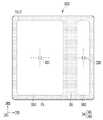
도 1a 내지 도 1b를 참조하면 일 실시예에 따른 표시 장치(1000)는 복수의 발광 소자(ED1, ED2)가 배치되며 이미지가 표시되는 표시 영역(DA), 그리고 표시 영역(DA)에 인접한 비표시 영역(PA)을 포함한다.1A to 1B , in a
표시 영역(DA)은 일 예로 사각 형상일 수 있다. 표시 영역(DA)의 각 모서리(DA-C)는 라운드 형태를 가질 수 있다. 비표시 영역(PA)은 표시 영역(DA)을 둘러싸는 형상을 가질 수 있다. 다만 이에 제한되지 않고 표시 영역(DA) 및 비표시 영역(PA)의 형상은 상대적으로 디자인될 수 있다.The display area DA may have a rectangular shape, for example. Each edge DA-C of the display area DA may have a round shape. The non-display area PA may have a shape surrounding the display area DA. However, the present invention is not limited thereto, and the shapes of the display area DA and the non-display area PA may be relatively designed.
표시 영역(DA)은 제1 표시 영역(DA1), 그리고 제1 표시 영역(DA1)에 인접하며 비표시 영역(PA)을 사이에 두고 이격된 제2 표시 영역(DA2)을 포함할 수 있다. 제2 표시 영역(DA2)은 제1 표시 영역(DA1)의 우측에 위치하는 실시예를 도시하였으나, 이에 제한되지 않고 제1 표시 영역(DA1)의 좌측에 위치하거나, 좌우측 양측에 모두 위치할 수 있다. 제2 표시 영역(DA2)의 면적은 제1 표시 영역(DA1)의 면적보다 작을 수 있으나 이에 제한되지 않는다.The display area DA may include a first display area DA1 and a second display area DA2 adjacent to the first display area DA1 and spaced apart from each other with the non-display area PA interposed therebetween. The second display area DA2 is located on the right side of the first display area DA1 in the exemplary embodiment, but the present invention is not limited thereto. have. The area of the second display area DA2 may be smaller than the area of the first display area DA1, but is not limited thereto.
제1 표시 영역(DA1)에는 제1 발광 소자(ED1)가 위치하고, 제2 표시 영역(DA2)에는 제2 발광 소자(ED2)가 위치할 수 있다. 본 명세서는 제1 발광 소자(ED1) 및 제2 발광 소자(ED2)를 사각 형태로 도시하였으나 하나의 발광 소자를 표현하기 위한 것으로 실제 평면 형태는 이에 제한되지 않는 다각 형태일 수 있다.The first light emitting device ED1 may be positioned in the first display area DA1 , and the second light emitting device ED2 may be positioned in the second display area DA2 . In the present specification, although the first light emitting device ED1 and the second light emitting device ED2 are illustrated in a rectangular shape, it is intended to represent one light emitting device, and the actual planar shape may be a polygonal shape, but is not limited thereto.
비표시 영역(PA)은 이미지가 표시되지 않는 영역이다. 비표시 영역(PA)은 표시 장치(1000)에서 표시 영역(DA) 이외의 영역이다. 특히 제1 표시 영역(DA1)과 제2 표시 영역(DA2) 사이에 위치하는 비표시 영역(PA)은 기판이 벤딩되는 벤딩 영역(BA)일 수 있다.The non-display area PA is an area in which an image is not displayed. The non-display area PA is an area other than the display area DA in the
표시 장치(1000)에서 이미지가 표시되는 일 면은 제1 방향(DR1)과 제2 방향(DR2)이 정의하는 면과 평행한다. 이미지가 표시되는 일 면의 법선 방향, 즉 표시 장치(1000)의 두께 방향은 제3 방향(DR3)이 지시한다. 각 부재들의 전면 (또는 상면)과 배면(또는 하면)은 제3 방향(DR3)에 의해 구분된다. 그러나 제1 내지 제3 방향(DR1, DR2, DR3)이 지시하는 방향은 상대적인 개념으로 다른 방향으로 변환될 수 있다.One surface of the
표시 장치(1000)는 도 1b에 도시된 바와 같이 제2 방향(DR2)에 평행한 벤딩축을 기준으로 아웃-폴딩될 수 있다. 일 실시예에 따른 표시 장치(1000)가 제2 방향(DR2)에 평행한 벤딩축을 기준으로 아웃-폴딩됨에 따라 제1 표시 영역(DA1) 및 제2 표시 영역(DA2)이 모두 외부로 노출될 수 있다. 제1 표시 영역(DA1)은 표시 장치(1000)의 전면에 위치하고, 제2 표시 영역(DA2)은 표시 장치(1000)의 배면에 위치할 수 있다. 일 실시예에 따른 표시 장치(1000)는 전면 및 배면 모두에서 이미지를 표시할 수 있다.The
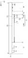
도 2a는 일 실시예에 따른 표시 패널의 평면도이고, 도 2b는 도 2a의 A-A'을 따라 자른 단면도이다.2A is a plan view of a display panel according to an exemplary embodiment, and FIG. 2B is a cross-sectional view taken along line AA′ of FIG. 2A .
도 2a 및 도 2b를 참조하면, 표시 패널(DP)은 도 1에서 설명한 표시 장치(1000)의 표시 영역(DA) 및 비표시 영역(PA)에 대응하는 표시 영역(DA) 및 비표시 영역(PA)을 포함한다. 비표시 영역(PA)은 표시 영역(DA)의 테두리를 따라 정의될 수 있다.2A and 2B , the display panel DP has a display area DA and a non-display area ( ) corresponding to the display area DA and the non-display area PA of the
표시 영역(DA)은 복수의 신호선과 전기적으로 연결된 발광 소자(ED1, ED2)를 포함한다. 각 발광 소자(ED1, ED2)는 예컨대, 적색, 녹색, 청색 또는 백색의 빛을 방출할 수 있다. 표시 영역(DA)은 발광 소자(ED1, ED2)들에서 방출되는 빛을 통해 소정의 이미지를 제공한다. 발광 소자(ED1, ED2)에 의해 표시 영역(DA)이 정의된다. 본 명세서에서 비표시 영역(PA)은 이미지를 제공하지 않는 영역을 나타내며, 발광 소자가 배치되지 않는 영역을 나타낸다.The display area DA includes light emitting devices ED1 and ED2 electrically connected to a plurality of signal lines. Each of the light emitting devices ED1 and ED2 may emit, for example, red, green, blue, or white light. The display area DA provides a predetermined image through light emitted from the light emitting devices ED1 and ED2. The display area DA is defined by the light emitting devices ED1 and ED2 . In the present specification, the non-display area PA represents an area not providing an image, and represents an area in which a light emitting device is not disposed.
일 실시예에 따른 표시 영역(DA)은 제1 표시 영역(DA1) 및 제2 표시 영역(DA2)을 포함한다. 제1 표시 영역(DA1)은 제1 발광 소자(ED1)에 의해 광이 방출되는 영역이고, 제2 표시 영역(DA2)은 제2 발광 소자(ED2)에 의해 광이 방출되는 영역이다. 비표시 영역(PA)은 제1 표시 영역(DA1) 및 제2 표시 영역(DA2)의 외측 영역에 해당한다.The display area DA according to an exemplary embodiment includes a first display area DA1 and a second display area DA2. The first display area DA1 is an area from which light is emitted by the first light emitting device ED1 , and the second display area DA2 is an area from which light is emitted by the second light emitting device ED2 . The non-display area PA corresponds to an area outside the first display area DA1 and the second display area DA2 .
일 실시예에 따른 표시 장치는 기판(SUB) 상에 배치되는 제1 화소 회로부(PC1) 및 제2 화소 회로부(PC2)를 포함한다. 도 2b를 참조하면 제1 화소 회로부(PC1)는 실질적으로 복수의 제1 화소 회로부(PC1)가 행렬 형태로 배열된 영역을 나타낸 것이며, 제2 화소 회로부(PC2)는 실질적으로 복수의 제2 화소 회로부(PC2)가 행렬 형태로 배열된 영역을 나타낸 것이다. 복수의 제1 화소 회로부(PC1)가 차지하는 면적은 복수의 제2 화소 회로부(PC2)가 차지하는 면적 보다 클 수 있다. 각각의 화소 회로부(PC1, PC2)는 하나의 발광 소자(ED1, ED2)와 연결될 수 있다. 복수의 화소 회로부의 배열 형태는 특별히 한정된 것은 아니며, 다양한 형태로 배열될 수 있다. 예를 들면 복수의 화소 회로부는 서로 직교하지 않고 경사진 방향으로 교차할 수도 있다.A display device according to an exemplary embodiment includes a first pixel circuit unit PC1 and a second pixel circuit unit PC2 disposed on a substrate SUB. Referring to FIG. 2B , the first pixel circuit unit PC1 represents a region in which a plurality of first pixel circuit units PC1 are substantially arranged in a matrix form, and the second pixel circuit unit PC2 is substantially a plurality of second pixels. A region in which the circuit unit PC2 is arranged in a matrix form is shown. An area occupied by the plurality of first pixel circuit units PC1 may be larger than an area occupied by the plurality of second pixel circuit units PC2 . Each of the pixel circuit units PC1 and PC2 may be connected to one light emitting device ED1 and ED2. An arrangement form of the plurality of pixel circuit units is not particularly limited and may be arranged in various forms. For example, the plurality of pixel circuit units may not be orthogonal to each other and may intersect in an inclined direction.
하나의 제1 화소 회로부(PC1)와 제2 화소 회로부(PC2)의 면적은 상이할 수 있다. 예를 들어 제1 화소 회로부(PC1)와 제2 화소 회로부(PC2)의 길이가 동일하면, 제1 화소 회로부(PC1)와 제2 화소 회로부(PC2)의 폭이 상이할 수 있다. 또는 제1 화소 회로부(PC1)와 제2 화소 회로부(PC2)의 폭이 동일하면, 제1 화소 회로부(PC1)와 제2 화소 회로부(PC2)의 길이가 상이할 수 있다.One first pixel circuit unit PC1 and the second pixel circuit unit PC2 may have different areas. For example, when the first pixel circuit unit PC1 and the second pixel circuit unit PC2 have the same length, the widths of the first pixel circuit unit PC1 and the second pixel circuit unit PC2 may be different. Alternatively, when the first pixel circuit unit PC1 and the second pixel circuit unit PC2 have the same width, the first pixel circuit unit PC1 and the second pixel circuit unit PC2 may have different lengths.
구동 회로부는 제2 화소 회로부(PC2)에 인접하게 위치하는 구동부 및 신호 배선들을 포함할 수 있다. 일 예로 구동 회로부는 스캔 구동부(20), 데이터 구동부(50), 구동 전압 공급 라인(60), 공통 전압 공급 라인(70) 및 이들과 연결되는 신호 전달 배선 등을 포함할 수 있다.The driving circuit unit may include a driving unit and signal lines positioned adjacent to the second pixel circuit unit PC2 . For example, the driving circuit unit may include a
스캔 구동부(20)는 스캔선(SL)을 통해 발광 소자(ED1, ED2)에 전기적으로 연결되는 화소 회로부(PC1, PC2)에 스캔 신호를 생성하여 전달한다. 일 실시예에 따라 스캔 구동부(20)는 제1 표시 영역(DA1)의 좌측 및 우측에 배치될 수 있다. 본 명세서는 스캔 구동부(20)가 기판(SUB)의 양측에 배치된 구조를 도시하나, 다른 실시예로 스캔 구동부는 기판(SUB)의 일측에만 배치될 수도 있다.The
패드부(40)는 표시 패널(DP)의 일 단부에 배치되며, 복수의 단자(41, 42, 44, 45)를 포함한다. 패드부(40)는 절연층에 의해 덮이지 않고 노출되어 인쇄 회로 기판(PCB)과 전기적으로 연결될 수 있다. 패드부(40)는 인쇄 회로 기판(PCB)의 패드부(PCB_P)와 전기적으로 연결될 수 있다. 인쇄 회로 기판(PCB)은 IC 구동칩(80)의 신호 또는 전원을 패드부(40)로 전달 할 수 있다.The
제어부는 외부에서 전달되는 복수의 영상 신호를 복수의 영상 데이터 신호로 변경하고, 변경된 신호를 단자(41)를 통해 데이터 구동부(50)에 전달한다. 또한, 제어부는 수직동기신호, 수평동기신호, 및 클럭신호를 전달받아 스캔 구동부(20) 및 데이터 구동부(50)의 구동을 제어하기 위한 제어 신호를 생성하여 단자(44, 41)를 통해 각각에 전달할 수 있다. 제어부는 단자(42)를 통해 구동 전압 공급 라인(60)에 구동 전압(ELVDD)을 전달한다. 또한 제어부는 단자(45)를 통해 공통 전압 공급 라인(70) 각각에 공통 전압(ELVSS)을 전달한다.The controller converts the plurality of image signals transmitted from the outside into the plurality of image data signals, and transmits the changed signals to the
데이터 구동부(50)는 비표시 영역(PA) 상에 배치되며, 데이터선(DL)을 통해 각 발광 소자(ED1, ED2)와 연결된 화소 회로부(PC1, PC2)에 데이터 신호를 생성하여 전달한다. 데이터 구동부(50)는 표시 패널(DP)의 일측에 배치될 수 있으며, 예컨대 패드부(40)와 표시 영역(DA) 사이에 배치될 수 있다.The
구동 전압 공급 라인(60)은 비표시 영역(PA) 상에 배치된다. 예컨대, 구동 전압 공급 라인(60)은 데이터 구동부(50) 및 표시 영역(DA) 사이에 배치될 수 있다. 구동 전압 공급 라인(60)은 구동 전압(ELVDD)을 각 발광 소자(ED1, ED2)와 연결된 화소 회로부(PC1, PC2)에 제공한다. 구동 전압 공급 라인(60)은 제1 방향(DR1)으로 배치되며, 제2 방향(DR2)으로 배치된 복수의 구동 전압선(PL)과 연결될 수 있다.The driving
공통 전압 공급 라인(70)은 비표시 영역(PA) 상에 배치된다. 공통 전압 공급 라인(70)은 기판(SUB)을 둘러싸는 형태를 가질 수 있다. 공통 전압 공급 라인(70)은 발광 소자(ED1, ED2)의 일 전극(예컨대, 제2 전극)에 공통 전압(ELVSS)을 전달한다. 본 명세서는 도시하지 않았으나 비표시 영역(PA)에 위치하는 댐을 더 포함할 수 있다.The common
제1 화소 회로부(PC1) 및 제2 화소 회로부(PC2), 그리고 구동 회로부의 적어도 일부 위에는 제1 발광 소자(ED1)가 위치할 수 있다. 제1 발광 소자(ED1)는 제1-1 발광 소자(ED1-1) 및 제1-2 발광 소자(ED1-2)를 포함할 수 있다.The first light emitting device ED1 may be positioned on the first pixel circuit unit PC1 and the second pixel circuit unit PC2 , and at least a portion of the driving circuit unit. The first light emitting device ED1 may include a 1-1 light emitting device ED1-1 and a 1-2 light emitting device ED1-2.
제1 화소 회로부(PC1)는 제1 화소 회로부(PC1) 상측에 배치되는 제1-1 발광 소자(ED1-1)와 전기적으로 연결된다. 제1-1 표시 영역(DA1-1)에는 제1 화소 회로부(PC1) 및 제1-1 발광 소자(ED1-1)가 위치할 수 있다. 제1-1 발광 소자(ED1-1)에 의해 광이 방출되는 영역이 제1-1 표시 영역(DA1-1)이다.The first pixel circuit unit PC1 is electrically connected to the first-first light emitting device ED1-1 disposed above the first pixel circuit unit PC1 . The first pixel circuit unit PC1 and the 1-1 light emitting device ED1-1 may be positioned in the 1-1 display area DA1-1. An area in which light is emitted by the 1-1 light emitting device ED1-1 is the 1-1 display area DA1-1.
제2 화소 회로부(PC2)는 제1-2 발광 소자(ED1-2)와 전기적으로 연결된다. 제1-2 발광 소자(ED1-2)에 의해 광이 방출되는 영역이 제1-2 표시 영역(DA1-2)이다.The second pixel circuit unit PC2 is electrically connected to the 1-2 th light emitting device ED1 - 2 . An area in which light is emitted by the 1-2 light emitting device ED1 - 2 is the 1-2 display area DA1 - 2 .
제1-2 표시 영역(DA1-2)에는 제2 화소 회로부(PC2) 상에 위치하는 제1-2 발광 소자(ED1-2)의 일부가 위치할 수 있다. 또한 제2 화소 회로부(PC2)와 전기적으로 연결되며 스캔 구동부(20) 상에 위치하는 제1-2 발광 소자(ED1-2)가 위치할 수 있다.A part of the 1-2 th light emitting device ED1 - 2 positioned on the second pixel circuit unit PC2 may be positioned in the 1-2 th display area DA1 - 2 . In addition, a 1-2 th light emitting device ED1 - 2 electrically connected to the second pixel circuit unit PC2 and positioned on the
발광 소자(ED1)의 일면과 기판(SUB) 사이에 위치하는 화소 회로부(PC1, PC2), 스캔 구동부(20), 공통 전압 공급 라인(70)과 관련하여, 화소 회로부(PC1, PC2) 이외에 스캔 구동부(20)와 중첩하는 영역임에도 스캔 구동부(20) 상에 위치하는 발광 소자(ED1-2)를 포함함으로써 확장된 면적의 제1-2 표시 영역(DA1-2)을 제공할 수 있다.In relation to the pixel circuit units PC1 and PC2 , the
또한 일 실시예에 따른 표시 장치는 제1-2 표시 영역(DA1-2) 외측으로 위치하는 비표시 영역(PA)과 인접하게 위치하는 제2 표시 영역(DA2)을 더 포함할 수 있다. 제2 표시 영역(DA2)에는 제2 화소 회로부(PC2)와 전기적으로 연결되는 제2 발광 소자(ED2)가 위치할 수 있다. 제2 발광 소자(ED2)에 의해 광이 방출되는 영역이 제2 표시 영역(DA2)이다. 제2 표시 영역(DA2)에는 제2 발광 소자(ED2)와 전기적으로 연결되는 화소 회로부가 위치하지 않는다. 제2 발광 소자(ED2)와 연결되는 제2 화소 회로부(PC2)는 제1 표시 영역(DA1)에 위치할 수 있다. 제2 발광 소자(ED2)는 제1 전극이 연장된 형태를 가질 수 있으며, 이를 통해 제1 표시 영역(DA1)에 위치하는 제2 화소 회로부(PC2)와 연결될 수 있다. 구체적인 구조는 후술하기로 한다.In addition, the display device according to an exemplary embodiment may further include a second display area DA2 positioned adjacent to the non-display area PA positioned outside the 1-2 th display area DA1 - 2 . A second light emitting device ED2 electrically connected to the second pixel circuit unit PC2 may be positioned in the second display area DA2 . An area from which light is emitted by the second light emitting device ED2 is the second display area DA2 . A pixel circuit part electrically connected to the second light emitting device ED2 is not located in the second display area DA2 . The second pixel circuit unit PC2 connected to the second light emitting device ED2 may be located in the first display area DA1 . The second light emitting device ED2 may have an extended first electrode, and may be connected to the second pixel circuit unit PC2 positioned in the first display area DA1 through this. A specific structure will be described later.
본 명세서는 제2 발광 소자(ED2)가 기판(SUB) 상에 위치하는 실시예를 도시하였으나 이는 개략적인 도면이며 제2 발광 소자(ED2)와 기판(SUB) 사이에는 절연층이 위치할 수 있다.Although this specification shows an embodiment in which the second light emitting device ED2 is positioned on the substrate SUB, this is a schematic drawing, and an insulating layer may be positioned between the second light emitting device ED2 and the substrate SUB. .
도 2c를 참조하면 하나의 화소(P)는 일 화소 회로부(PC1, PC2) 및 이와 전기적으로 연결되는 일 발광 소자(ED1, ED2)를 포함할 수 있다. 제1 화소 회로부(PC1) 및 제2 화소 회로부(PC2) 각각은 구동 박막 트랜지스터(Td), 스위칭 박막 트랜지스터(Ts) 및 스토리지 커패시터(Cst)를 포함한다.Referring to FIG. 2C , one pixel P may include one pixel circuit unit PC1 and PC2 and one light emitting device ED1 and ED2 electrically connected thereto. Each of the first pixel circuit unit PC1 and the second pixel circuit unit PC2 includes a driving thin film transistor Td, a switching thin film transistor Ts, and a storage capacitor Cst.
스위칭 박막 트랜지스터(Ts)는 스캔선(SL) 및 데이터선(DL)에 연결되고, 스캔선(SL)을 통해 입력되는 스캔 신호에 따라 데이터선(DL)을 통해 입력된 데이터 신호를 구동 박막 트랜지스터(Td)로 전달한다.The switching thin film transistor Ts is connected to the scan line SL and the data line DL, and drives a data signal input through the data line DL according to the scan signal input through the scan line SL. to (Td).
스토리지 커패시터(Cst)는 스위칭 박막 트랜지스터(Ts) 및 구동 전압선(PL)에 연결되며, 스위칭 박막 트랜지스터(Ts)로부터 전달받은 전압과 구동 전압선(PL)에 공급되는 구동 전압(ELVDD)의 차이에 해당하는 전압을 저장한다.The storage capacitor Cst is connected to the switching thin film transistor Ts and the driving voltage line PL, and corresponds to the difference between the voltage received from the switching thin film transistor Ts and the driving voltage ELVDD supplied to the driving voltage line PL. store the voltage
구동 박막 트랜지스터(Td)는 구동 전압선(PL)과 스토리지 커패시터(Cst)에 연결되며, 스토리지 커패시터(Cst)에 저장된 전압 값에 대응하여 구동 전압선(PL)으로부터 발광 소자(ED)에 흐르는 구동 전류를 제어할 수 있다. 발광 소자(ED1, ED2)는 구동 전류에 의해 소정의 휘도를 갖는 빛을 방출할 수 있다.The driving thin film transistor Td is connected to the driving voltage line PL and the storage capacitor Cst, and receives a driving current flowing from the driving voltage line PL to the light emitting device ED in response to the voltage value stored in the storage capacitor Cst. can be controlled The light emitting devices ED1 and ED2 may emit light having a predetermined luminance by a driving current.
전술한 도면에 도 3 및 도 4를 참조하여 구체적인 적층 구조에 대해 살펴본다. 도 3은 일 실시예에 따른 제1 표시 영역의 단면도이고, 도 4는 일 실시예에 따른 제1 표시 영역, 벤딩 영역 및 제2 표시 영역 일부의 단면도이다. 전술한 구성요소와 동일한 구성에 대한 설명은 생략하기로 한다.A detailed stacked structure will be described with reference to FIGS. 3 and 4 in the above drawings. 3 is a cross-sectional view of a first display area according to an exemplary embodiment, and FIG. 4 is a cross-sectional view of a portion of the first display area, the bending area, and the second display area according to an exemplary embodiment. A description of the same components as those described above will be omitted.
도 3을 참조하면, 제1-1 표시 영역(DA1-1)에 위치하는 제1 화소 회로부(PC1) 및 제1-1 발광 소자(ED1-1)부터 살펴본다.Referring to FIG. 3 , the first pixel circuit unit PC1 and the 1-1 light emitting device ED1-1 positioned in the 1-1 display area DA1-1 will be viewed.
제1 화소 회로부(PC1)는 기판(SUB) 상에 위치하는 반도체층(ACT1)을 포함한다.The first pixel circuit unit PC1 includes a semiconductor layer ACT1 disposed on a substrate SUB.
기판(SUB)은 SiO2를 주성분으로 하는 유리, 금속 또는 유기물과 같은 재질을 포함할 수 있다. 일 실시예에 따르면, 기판(SUB)은 플렉서블한 재질을 포함할 수 있다. 예컨대, 기판(SUB)은 폴리이미드(polyimide)와 같은 플렉서블한 플라스틱 재질을 포함할 수 있으나 이에 한정되지 않는다. 또 다른 실시예로써, 플라스틱 재질은, 폴리에테르술폰(PES, polyethersulphone), 폴리아크릴레이트(PAR, polyacrylate), 폴리에테르 이미드(PEI, polyether imide), 폴리에틸렌 나프탈레이트(PEN, polyethyelenen napthalate), 폴리에틸렌 테레프탈레이드(PET, polyethyeleneterepthalate), 폴리페닐렌 설파이드(polyphenylene sulfide: PPS), 폴리아릴레이트(polyallylate), 폴리이미드(polyimide), 폴리카보네이트(PC), 셀룰로오스 트리 아세테이트(TAC), 셀룰로오스아세테이트 프로피오네이트(cellulose acetate propionate: CAP), 환형 올레핀 고분자(Cyclic olefin polymer), 환형 올레핀 공중합체(Cyclic olefin copolymer)등일 수 있다.The substrate SUB may include a material having SiO2 as a main component, such as glass, metal, or organic material. According to an embodiment, the substrate SUB may include a flexible material. For example, the substrate SUB may include a flexible plastic material such as polyimide, but is not limited thereto. In another embodiment, the plastic material is polyethersulfone (PES, polyethersulphone), polyacrylate (PAR, polyacrylate), polyether imide (PEI, polyether imide), polyethylene naphthalate (PEN, polyethyelenen napthalate), polyethylene Terephthalate (PET, polyethyeleneterepthalate), polyphenylene sulfide (PPS), polyallylate, polyimide, polycarbonate (PC), cellulose triacetate (TAC), cellulose acetate propionate (cellulose acetate propionate: CAP), a cyclic olefin polymer (Cyclic olefin polymer), may be a cyclic olefin copolymer (Cyclic olefin copolymer).
반도체층(ACT1)은 다결정 규소 및 산화물 반도체 중 적어도 하나를 포함할 수 있다. 반도체층(ACT1)은 채널 영역(C1), 소스 영역(S1) 및 드레인 영역(D1)을 포함한다. 소스 영역(S1) 및 드레인 영역(D1)은 각각 채널 영역(C1)의 양 옆에 배치되어 있다. 채널 영역(C1)은 불순물이 거의 도핑되지 않은 반도체를 포함하고, 소스 영역(S1) 및 드레인 영역(D1)은 도전성 불순물이 도핑되어 있는 불순물 반도체를 포함할 수 있다. 반도체층(ACT1)은 산화물 반도체로 이루어질 수도 있으며, 이 경우에는 고온 등의 외부 환경에 취약한 산화물 반도체 물질을 보호하기 위해 별도의 보호층(미도시)이 추가될 수 있다.The semiconductor layer ACT1 may include at least one of polycrystalline silicon and an oxide semiconductor. The semiconductor layer ACT1 includes a channel region C1 , a source region S1 , and a drain region D1 . The source region S1 and the drain region D1 are disposed on both sides of the channel region C1, respectively. The channel region C1 may include a semiconductor that is hardly doped with an impurity, and the source region S1 and the drain region D1 may include an impurity semiconductor doped with a conductive impurity. The semiconductor layer ACT1 may be made of an oxide semiconductor, and in this case, a separate protective layer (not shown) may be added to protect the oxide semiconductor material vulnerable to external environments such as high temperature.
반도체층(ACT1) 위에는 게이트 절연층(IL1)이 위치한다. 게이트 절연층(IL1)은 실리콘질화물(SiNx) 및 실리콘산화물(SiO2) 중 적어도 하나를 포함한 단층 또는 다층일 수 있다. 본 명세서는 게이트 절연층(IL1)이 기판(SUB) 전면에 걸쳐 형성된 실시예를 도시하였으나, 이에 제한되지 않고 게이트 절연층(IL1)이 채널 영역(C1)에서만 중첩하는 형태로 제공될 수 있다.A gate insulating layer IL1 is positioned on the semiconductor layer ACT1 . The gate insulating layer IL1 may be a single layer or a multilayer including at least one of silicon nitride (SiNx ) and silicon oxide (SiO2 ). Although the present specification shows an embodiment in which the gate insulating layer IL1 is formed over the entire surface of the substrate SUB, the present disclosure is not limited thereto, and the gate insulating layer IL1 may be provided to overlap only in the channel region C1 .
채널 영역(C1)과 중첩하는 게이트 절연층(IL1) 상에 게이트 전극(GE)이 위치한다, 게이트 전극(GE)은 구리(Cu), 구리 합금, 알루미늄(Al), 알루미늄 합금, 몰리브덴(Mo), 및 몰리브덴 합금 중 어느 하나를 포함하는 금속막이 적층된 단층 또는 다층막일 수 있다.A gate electrode GE is positioned on the gate insulating layer IL1 overlapping the channel region C1. The gate electrode GE is copper (Cu), a copper alloy, aluminum (Al), an aluminum alloy, or molybdenum (Mo). ), and a metal film including any one of a molybdenum alloy may be a single-layer or multi-layered film stacked.
게이트 전극(GE) 및 게이트 절연층(IL1) 위에는 층간 절연층(IL2)이 위치한다. 층간 절연층(IL2)은 실리콘산화물(SiOx), 실리콘질화물(SiNx), 실리콘질산화물(SiOxNy)을 포함하는 무기 물질을 포함하거나 유기 물질을 포함할 수 있다. 층간 절연층(IL2)은 단일층 또는 다층 구조일 수 있다.An interlayer insulating layer IL2 is positioned on the gate electrode GE and the gate insulating layer IL1. The interlayer insulating layer IL2 may include an inorganic material including silicon oxide (SiOx), silicon nitride (SiNx), or silicon oxynitride (SiOxNy) or an organic material. The interlayer insulating layer IL2 may have a single-layer or multi-layer structure.
층간 절연층(IL2) 위에 소스 전극(SE)과 드레인 전극(DE)이 위치한다. 소스 전극(SE)과 드레인 전극(DE)은 층간 절연층(IL2)에 형성된 접촉 구멍을 통해 반도체층(ACT1)의 소스 영역(S1) 및 드레인 영역(D1)과 각각 연결된다.A source electrode SE and a drain electrode DE are positioned on the interlayer insulating layer IL2. The source electrode SE and the drain electrode DE are respectively connected to the source region S1 and the drain region D1 of the semiconductor layer ACT1 through a contact hole formed in the interlayer insulating layer IL2.
소스 전극(SE) 및 드레인 전극(DE)은 알루미늄(Al), 백금(Pt), 팔라듐(Pd), 은(Ag), 마그네슘(Mg), 금(Au), 니켈(Ni), 네오디뮴(Nd), 이리듐(Ir), 크롬(Cr), 니켈(Ni), 칼슘(Ca), 몰리브덴(Mo), 탄탈륨(Ta), 티타늄(Ti), 텅스텐(W), 및/또는 구리(Cu) 등을 포함할 수 있으며, 이를 포함하는 단일층 또는 다층 구조일 수 있다. 예를 들어, 소스 전극(SE) 및 드레인 전극(DE)은 몰리브덴, 크롬, 탄탈륨 및 티타늄 등 내화성 금속(refractory metal) 또는 이들의 합금을 포함하는 하부막, 비저항이 낮은 알루미늄 계열 금속, 은 계열 금속, 구리 계열 금속을 포함하는 중간막, 몰리브덴, 크롬, 탄탈륨 및 티타늄 등 내화성 금속을 포함하는 상부막의 삼중막 구조일 수 있다.The source electrode SE and the drain electrode DE include aluminum (Al), platinum (Pt), palladium (Pd), silver (Ag), magnesium (Mg), gold (Au), nickel (Ni), and neodymium (Nd). ), iridium (Ir), chromium (Cr), nickel (Ni), calcium (Ca), molybdenum (Mo), tantalum (Ta), titanium (Ti), tungsten (W), and/or copper (Cu), etc. may include, and may have a single-layer or multi-layer structure including the same. For example, the source electrode SE and the drain electrode DE may include a lower layer including a refractory metal such as molybdenum, chromium, tantalum and titanium or an alloy thereof, an aluminum-based metal having a low specific resistance, or a silver-based metal , may have a triple-layer structure of an intermediate layer including a copper-based metal and an upper layer including a refractory metal such as molybdenum, chromium, tantalum, and titanium.
소스 전극(SE) 및 드레인 전극(DE) 위에 제1 절연층(IL3)이 위치한다. 제1 절연층(IL3)은 기판(SUB) 전면과 중첩하도록 위치할 수 있다. 제1 절연층(IL3)은 실리콘질화물(SiNx) 또는 실리콘산화물(SiO2) 등과 같은 무기 물질을 포함하거나 유기 물질을 포함할 수 있다.A first insulating layer IL3 is positioned on the source electrode SE and the drain electrode DE. The first insulating layer IL3 may be positioned to overlap the entire surface of the substrate SUB. The first insulating layer IL3 may include an inorganic material such as silicon nitride (SiNx) or silicon oxide (SiO2 ) or an organic material.
제1 절연층(IL3) 상에 연결 전극(CE)이 위치한다. 연결 전극(CE)은 제1 절연층(IL3)이 가지는 접촉 구멍을 통해 드레인 전극(DE)과 연결될 수 있다. 본 명세서는 연결 전극(CE)에 의해 드레인 전극(DE)과 제1 전극(E1)이 전기적으로 연결되는 구성을 도시하였으나, 이에 제한되지 않고 드레인 전극(DE)과 제1 전극(E1)이 직접 연결될 수도 있음은 물론이다.The connection electrode CE is positioned on the first insulating layer IL3 . The connection electrode CE may be connected to the drain electrode DE through a contact hole of the first insulating layer IL3 . Although the present specification shows a configuration in which the drain electrode DE and the first electrode E1 are electrically connected by the connection electrode CE, the present disclosure is not limited thereto, and the drain electrode DE and the first electrode E1 are directly connected to each other. Of course, it can be connected.
연결 전극(CE) 상에 제2 절연층(IL4)이 위치한다. 제2 절연층(IL4)은 Polymethylmethacrylate(PMMA)나 Polystyrene(PS)과 같은 일반 범용 고분자, 페놀계 그룹을 갖는 고분자 유도체, 아크릴계 고분자, 이미드계 고분자, 폴리이미드, 아크릴계 폴리머, 실록산계 폴리머 등의 유기물, 또는 유기물과 무기물의 적층막 또는 무기막 등으로 만들어질 수 있다.A second insulating layer IL4 is positioned on the connection electrode CE. The second insulating layer IL4 is a general-purpose polymer such as polymethylmethacrylate (PMMA) or polystyrene (PS), a polymer derivative having a phenolic group, an acrylic polymer, an imide-based polymer, polyimide, an acrylic polymer, an organic material such as a siloxane-based polymer , or may be made of a laminated film or an inorganic film of organic and inorganic materials.
제2 절연층(IL4) 상에 제1 전극(E1)이 위치한다. 제1 전극(E1)은 제2 절연층(IL4)의 접촉 구멍을 통해 연결 전극(CE)과 연결되어, 전기적으로 드레인 전극(DE)과 연결된다.The first electrode E1 is positioned on the second insulating layer IL4 . The first electrode E1 is connected to the connection electrode CE through the contact hole of the second insulating layer IL4 and is electrically connected to the drain electrode DE.
게이트 전극(GE), 반도체층(ACT1), 소스 전극(SE) 및 드레인 전극(DE)으로 이루어진 트랜지스터는 제1 전극(E1)에 연결되어 발광 소자(ED1)에 전류를 공급한다.A transistor including the gate electrode GE, the semiconductor layer ACT1, the source electrode SE, and the drain electrode DE is connected to the first electrode E1 to supply current to the light emitting device ED1.
제2 절연층(IL4)과 제1 전극(E1)의 위에는 격벽(IL5)이 위치한다. 격벽(IL5)은 제1 전극(E1)의 적어도 일부와 중첩하고 발광 영역을 정의하는 개구부를 가진다. 개구부는 제1 전극(E1)과 거의 유사한 평면 형태를 가질 수 있다. 개구부는 평면상 마름모 또는 마름모와 유사한 팔각 형상을 가질 수 있으나, 이에 제한되지 않고 사각형, 다각형 등 어떠한 모양도 가질 수 있다.The barrier rib IL5 is positioned on the second insulating layer IL4 and the first electrode E1 . The barrier rib IL5 overlaps at least a portion of the first electrode E1 and has an opening defining a light emitting area. The opening may have a planar shape substantially similar to that of the first electrode E1 . The opening may have a rhombus or an octagonal shape similar to a rhombus in plan view, but is not limited thereto and may have any shape such as a rectangle or a polygon.
격벽(IL5)은 Polymethylmethacrylate(PMMA)나 Polystyrene(PS)과 같은 일반 범용 고분자, 페놀계 그룹을 갖는 고분자 유도체, 아크릴계 고분자, 이미드계 고분자, 폴리이미드, 아크릴계 폴리머, 실록산계 폴리머 등의 유기물 또는 실리카 계열의 무기물을 포함할 수 있다.The barrier rib (IL5) is a general-purpose polymer such as polymethylmethacrylate (PMMA) or polystyrene (PS), a polymer derivative having a phenolic group, an acrylic polymer, an imide-based polymer, a polyimide, an acrylic polymer, an organic material such as a siloxane-based polymer, or a silica-based polymer may contain minerals.
개구부와 중첩하는 제1 전극(E1) 위에는 발광층(EL)이 위치한다. 발광층(EL)은 저분자 유기물 또는 PEDOT(Poly 3,4-ethylenedioxythiophene) 등의 고분자 유기물로 이루어질 수 있다. 또한, 발광층(EL)은 정공 주입층(hole injection layer, HIL), 정공 수송층(hole transporting layer, HTL), 전자 수송층(electron transporting layer, ETL), 및 전자 주입층(electron injection layer, EIL) 중 하나 이상을 더 포함하는 다중막일 수 있다.The light emitting layer EL is positioned on the first electrode E1 overlapping the opening. The light emitting layer EL may be formed of a low molecular weight organic material or a high molecular weight organic material such as poly 3,4-ethylenedioxythiophene (PEDOT). In addition, the light emitting layer EL may include a hole injection layer (HIL), a hole transporting layer (HTL), an electron transporting layer (ETL), and an electron injection layer (EIL). It may be a multi-layer comprising more than one.
발광층(EL)은 대부분 개구부 내에 위치할 수 있고, 격벽(IL5)의 측면 또는 위에도 위치할 수 있다.Most of the light emitting layer EL may be located within the opening, and may also be located on or on the side of the barrier rib IL5 .
발광층(EL) 위에는 제2 전극(E2)이 위치한다. 제2 전극(E2)은 칼슘(Ca), 바륨(Ba), 마그네슘(Mg), 알루미늄(Al), 은(Ag), 백금(Pt), 팔라듐(Pd), 금(Au), 니켈(Ni), 네오디뮴(Nd), 이리듐(Ir), 크롬(Cr), 리튬(Li), 칼슘(Ca) 등을 포함하는 반사성 금속 또는 인듐 주석 산화물(ITO), 인듐 아연 산화물(IZO) 같은 투명 도전성 산화물(TCO)을 포함할 수 있다.The second electrode E2 is positioned on the emission layer EL. The second electrode E2 includes calcium (Ca), barium (Ba), magnesium (Mg), aluminum (Al), silver (Ag), platinum (Pt), palladium (Pd), gold (Au), and nickel (Ni). ), neodymium (Nd), iridium (Ir), chromium (Cr), lithium (Li), calcium (Ca), etc., or a transparent conductive oxide such as indium tin oxide (ITO) or indium zinc oxide (IZO). (TCO) may be included.
제1 전극(E1), 발광층(EL)과 제2 전극(E2)은 제1-1 발광 소자(ED1-1)를 구성할 수 있다. 여기서, 제1 전극(E1)은 정공 주입 전극인 애노드이며, 제2 전극(E2)은 전자 주입 전극인 캐소드 일 수 있다. 그러나 실시예는 반드시 이에 한정되는 것은 아니며, 발광 표시 장치의 구동 방법에 따라 제1 전극(E1)이 캐소드가 되고, 제2 전극(E2)이 애노드가 될 수도 있다.The first electrode E1 , the emission layer EL, and the second electrode E2 may constitute the first-first light-emitting device ED1-1. Here, the first electrode E1 may be an anode that is a hole injection electrode, and the second electrode E2 may be a cathode that is an electron injection electrode. However, the embodiment is not necessarily limited thereto, and the first electrode E1 may be a cathode and the second electrode E2 may be an anode depending on a driving method of the light emitting display device.
제1 전극(E1) 및 제2 전극(E2)으로부터 각각 정공과 전자가 유기 발광층(EL) 내부로 주입되고, 주입된 정공과 전자가 결합한 엑시톤(exciton)이 여기 상태로부터 기저 상태로 떨어질 때 발광이 이루어진다.Holes and electrons from the first electrode E1 and the second electrode E2 are respectively injected into the organic light emitting layer EL, and light is emitted when excitons combined with the injected holes and electrons fall from the excited state to the ground state. this is done
제2 전극(E2) 위에 제1 봉지층(ENC1)이 위치한다. 제1 봉지층(ENC1)은 제1 발광 소자(ED1)의 상부면 뿐만 아니라 측면까지 덮어 밀봉할 수 있다. 발광 소자는 수분과 산소에 매우 취약하므로, 제1 봉지층(ENC1)이 제1 발광 소자(ED1)를 밀봉하여 외부의 수분 및 산소의 유입을 차단한다.A first encapsulation layer ENC1 is positioned on the second electrode E2 . The first encapsulation layer ENC1 may cover and seal not only the top surface of the first light emitting device ED1 but also the side surfaces. Since the light emitting device is very vulnerable to moisture and oxygen, the first encapsulation layer ENC1 seals the first light emitting device ED1 to block the inflow of external moisture and oxygen.
제1 봉지층(ENC1)은 복수의 층을 포함할 수 있고, 그 중 무기층과 유기층을 모두 포함하는 복합막으로 형성될 수 있으며, 일 예로 제1 무기층(EIL1), 유기층(EOL), 제2 무기층(EIL2)이 순차적으로 형성된 3중층으로 형성될 수 있다.The first encapsulation layer ENC1 may include a plurality of layers, and among them, may be formed of a composite film including both an inorganic layer and an organic layer, for example, a first inorganic layer EIL1, an organic layer EOL, The second inorganic layer EIL2 may be formed as a sequentially formed triple layer.
제1 무기층(EIL1)은 제2 전극(E2)을 커버할 수 있다. 제1 무기층(EIL1)은 외부 수분이나 산소가 발광 소자(ED)에 침투하는 것을 방지할 수 있다. 예를 들어, 제1 무기층(EIL1)은 실리콘 질화물, 실리콘 산화물, 또는 이들이 조합된 화합물을 포함할 수 있다. 제1 무기층(EIL1)은 증착 공정을 통해 형성될 수 있다.The first inorganic layer EIL1 may cover the second electrode E2 . The first inorganic layer EIL1 may prevent external moisture or oxygen from penetrating into the light emitting device ED. For example, the first inorganic layer EIL1 may include silicon nitride, silicon oxide, or a combination thereof. The first inorganic layer EIL1 may be formed through a deposition process.
유기층(EOL)은 제1 무기층(EIL1) 상에 배치되어 제1 무기층(EIL1)에 접촉할 수 있다. 제1 무기층(EIL1) 상면에 형성된 굴곡이나 제1 무기층(EIL1) 상에 존재하는 파티클(particle) 등은 유기층(EOL)에 의해 커버되어, 제1 무기층(EIL1)의 상면의 표면 상태가 유기층(EOL)상에 형성되는 구성들에 미치는 영향을 차단할 수 있다. 또한, 유기층(EOL)은 접촉하는 층들 사이의 응력을 완화시킬 수 있다. 유기층(EOL)은 유기물을 포함할 수 있고, 스핀 코팅, 슬릿 코팅, 잉크젯 공정과 같은 용액 공정을 통해 형성될 수 있다.The organic layer EOL may be disposed on the first inorganic layer EIL1 to contact the first inorganic layer EIL1 . The curves formed on the upper surface of the first inorganic layer EIL1 or particles existing on the first inorganic layer EIL1 are covered by the organic layer EOL, and the surface state of the upper surface of the first inorganic layer EIL1 It is possible to block the effect on the components formed on the organic layer (EOL). In addition, the organic layer EOL may relieve stress between the contacting layers. The organic layer EOL may include an organic material and may be formed through a solution process such as spin coating, slit coating, or inkjet process.
제2 무기층(EIL2)은 유기층(EOL) 상에 배치되어 유기층(EOL)을 커버한다. 제2 무기층(EIL2)은 제1 무기층(EIL1)상에 배치되는 것보다 상대적으로 평탄한 면에 안정적으로 형성될 수 있다. 제2 무기층(EIL2)은 유기층(EOL)으로부터 방출되는 수분 등을 봉지하여 외부로 유입되는 것을 방지한다. 제2 무기층(EIL2)은 실리콘 질화물, 실리콘 산화물, 또는 이들이 조합된 화합물을 포함할 수 있다. 제2 무기층(EIL2)은 증착 공정을 통해 형성될 수 있다.The second inorganic layer EIL2 is disposed on the organic layer EOL to cover the organic layer EOL. The second inorganic layer EIL2 may be stably formed on a relatively flat surface than that disposed on the first inorganic layer EIL1 . The second inorganic layer EIL2 seals moisture emitted from the organic layer EOL and prevents it from flowing to the outside. The second inorganic layer EIL2 may include silicon nitride, silicon oxide, or a combination thereof. The second inorganic layer EIL2 may be formed through a deposition process.
본 명세서는 도시하지 않았으나 제2 전극(E2)과 제1 봉지층(ENC1) 사이에 위치하는 캡핑층(capping layer)을 더 포함할 수 있다. 캡핑층은 유기물질을 포함할 수 있다. 캡핑층은 후속의 공정 예컨대 스퍼터링 공정으로부터 제2 전극(E2)을 보호하고, 발광 소자(ED)의 출광 효율을 향상시킨다. 캡핑층은 제1 무기층(EIL1)보다 큰 굴절률을 가질 수 있다.Although not illustrated in the present specification, a capping layer positioned between the second electrode E2 and the first encapsulation layer ENC1 may be further included. The capping layer may include an organic material. The capping layer protects the second electrode E2 from a subsequent process, for example, a sputtering process, and improves the light output efficiency of the light emitting device ED. The capping layer may have a refractive index greater than that of the first inorganic layer EIL1 .
도 3에서 기판(SUB)과 제1-1 발광 소자(ED1-1) 사이에 위치하는 구성요소들이 도 2b에서 설명한 제1 화소 회로부(PC1)에 해당한다. 제1 화소 회로부(PC1)는 제1 화소 회로부(PC1) 상에 위치하는 제1-1 발광 소자(ED1-1)와 연결될 수 있다.In FIG. 3 , components positioned between the substrate SUB and the 1-1 th light emitting device ED1-1 correspond to the first pixel circuit unit PC1 described with reference to FIG. 2B . The first pixel circuit unit PC1 may be connected to the first-first light emitting device ED1-1 positioned on the first pixel circuit unit PC1 .
다음, 제1 화소 회로부(PC1) 외측으로 제2 화소 회로부(PC2)가 위치할 수 있다. 제2 화소 회로부(PC2)의 적층 구조는 제1 화소 회로부(PC1)의 적층 구조와 실질적으로 동일할 수 있으므로 구체적인 설명을 생략하기로 한다.Next, the second pixel circuit unit PC2 may be positioned outside the first pixel circuit unit PC1 . Since the stacked structure of the second pixel circuit unit PC2 may be substantially the same as that of the first pixel circuit unit PC1 , a detailed description thereof will be omitted.
제2 화소 회로부(PC2)에 포함되는 제1 전극(E1)은 기판(SUB)의 가장자리를 향해 연장될 수 있다. 제1-2 발광 소자(ED1-2)에 포함되는 제1 전극(E1)은 제1 방향(DR1)을 따라 외측으로 배치되면서 제1-2 발광 소자(ED1-2)와 연결되는 제2 화소 회로부(PC2)에 비해 기판(SUB)의 가장자리를 향해 위치할 수 있다. 즉, 제1-2 발광 소자(ED1-2)는, 각각의 제1-2 발광 소자(ED1-2)와 연결되는 화소 회로부(PC2)보다 제1 방향(DR1)을 따라 외측에 위치할 수 있다. 일 실시예에 따른 제1-2 발광 소자(ED1-2)는 제2 화소 회로부(PC2)와 중첩하도록 위치하거나, 스캔 구동부(20)와 중첩하도록 위치할 수 있다.The first electrode E1 included in the second pixel circuit unit PC2 may extend toward the edge of the substrate SUB. The first electrode E1 included in the 1-2 th light emitting device ED1 - 2 is disposed outward along the first direction DR1 and is connected to the 1-2 th light emitting device ED1 - 2 as a second pixel Compared to the circuit unit PC2 , it may be positioned toward the edge of the substrate SUB. That is, the 1-2 light emitting devices ED1 - 2 may be located outside the pixel circuit unit PC2 connected to each of the 1-2 light emitting devices ED1 - 2 in the first direction DR1 . have. According to an exemplary embodiment, the first-second light emitting device ED1-2 may be positioned to overlap the second pixel circuit unit PC2 or to overlap the
발광 소자가 위치하는 층을 기준으로, 제1-1 발광 소자(ED1-1)가 위치하는 영역이 제1-1 표시 영역(DA1-1)이다. 또한 발광 소자가 위치하는 층을 기준으로, 제1-2 발광 소자(ED1-2)가 위치하는 영역이 제1-2 표시 영역(DA1-2)이다. 이때 제1-2 표시 영역(DA1-2)은 광을 방출하면서, 발광 소자(ED1-2) 하부에는 스캔 구동부(20)와 같은 화소 회로부가 위치할 수 있다. 표시 영역(DA)이 제1-1 표시 영역(DA1-1)뿐만 아니라 제1-2 표시 영역(DA1-2)을 포함함에 따라 보다 확장된 표시 영역을 제공할 수 있다.Based on the layer in which the light emitting device is positioned, an area in which the 1-1 light emitting device ED1-1 is positioned is the 1-1 display area DA1-1. Also, based on the layer in which the light emitting device is positioned, an area in which the 1-2 th light emitting device ED1 - 2 is positioned is the 1-2 th display area DA1 - 2 . In this case, the pixel circuit unit such as the
다음 도 4를 참조하면, 제1-2 표시 영역(DA1-2) 외측으로 벤딩 영역(BA)에 해당하는 비표시 영역(PA), 그리고 제2 표시 영역(DA2)이 위치할 수 있다.Next, referring to FIG. 4 , a non-display area PA corresponding to the bending area BA and a second display area DA2 may be positioned outside the 1-2 display area DA1 - 2 .
제2 표시 영역(DA2)에는 제1 표시 영역(DA1)으로부터 연장된 게이트 절연층(IL1) 및 층간 절연층(IL2)이 위치할 수 있다.A gate insulating layer IL1 and an interlayer insulating layer IL2 extending from the first display area DA1 may be positioned in the second display area DA2 .
층간 절연층(IL2) 상에는 제1-2 표시 영역(DA1-2)에 위치하는 제2 화소 회로부(PC2)와 연결되며, 제1-2 표시 영역(DA1-2)으로부터 벤딩 영역(BA)을 가로질러 제2 표시 영역(DA2)까지 연장되는 제1 전극(E1)이 위치할 수 있다.On the interlayer insulating layer IL2 , it is connected to the second pixel circuit unit PC2 positioned in the 1-2 th display area DA1 - 2 , and the bending area BA is formed from the 1-2 th display area DA1 - 2 . A first electrode E1 extending across to the second display area DA2 may be positioned.
본 명세서는 제2 표시 영역(DA2)에서 제1 절연층(IL3) 및 제2 절연층(IL4)이 제거된 구조를 도시하였으나 이에 제한되지 않고 독립적으로 제2 표시 영역(DA2)까지 연장되도록 형성될 수 있다.Although the present specification illustrates a structure in which the first insulating layer IL3 and the second insulating layer IL4 are removed from the second display area DA2, the present disclosure is not limited thereto and is formed to extend independently to the second display area DA2. can be
제2 표시 영역(DA2)에 위치하는 제1 전극(E1) 상에는 발광 영역을 정의하는 격벽(IL5)이 위치할 수 있다. 격벽(IL5)은 제1 전극(E1)의 일부와 중첩하고 발광 영역을 정의하는 개구부를 가질 수 있다.A barrier rib IL5 defining a light emitting area may be positioned on the first electrode E1 positioned in the second display area DA2 . The barrier rib IL5 may have an opening overlapping a portion of the first electrode E1 and defining a light emitting area.
격벽(IL5)이 가지는 개구부 내에는 발광층(EL)이 위치할 수 있다. 발광층(EL)은 대부분 개구부 내에 위치할 수 있고, 격벽(IL5)의 측면 또는 위에도 위치할 수 있다.The light emitting layer EL may be positioned in the opening of the barrier rib IL5 . Most of the light emitting layer EL may be located within the opening, and may also be located on or on the side of the barrier rib IL5 .
격벽(IL5) 및 발광층(EL) 상에는 제1 표시 영역(DA1)으로부터 연장된 제2 전극(E2)이 위치할 수 있다. 제2 표시 영역(DA2)에 위치하는 제1 전극(E1), 발광층(EL) 및 제2 전극(E2)은 제2 발광 소자(ED2)를 형성할 수 있다.A second electrode E2 extending from the first display area DA1 may be positioned on the barrier rib IL5 and the emission layer EL. The first electrode E1 , the emission layer EL, and the second electrode E2 positioned in the second display area DA2 may form a second light emitting device ED2 .
일 실시예에 따르면 제2 발광 소자(ED2)가 위치하는 영역과, 제2 발광 소자(ED2)와 전기적으로 연결되는 화소 회로부가 위치하는 영역이 분리될 수 있다. 제2 발광 소자(ED2)가 위치하는 영역을 자유롭게 설계할 수 있다. 또한 제2 표시 영역(DA2)을 제공하기 위해 별도의 트랜지스터를 형성하거나, 별도의 구동칩 등이 필요하지 않을 수 있다.According to an exemplary embodiment, a region in which the second light emitting device ED2 is positioned and a region in which a pixel circuit part electrically connected to the second light emitting device ED2 is positioned may be separated. A region in which the second light emitting device ED2 is positioned may be freely designed. In addition, a separate transistor or a separate driving chip may not be required to provide the second display area DA2 .
제2 발광 소자(ED2) 상에는 제2 봉지층(ENC2)이 위치한다. 제2 봉지층(ENC2)은 제1 무기층(EIL1), 유기층(EOL), 제2 무기층(EIL2)이 적층된 구조를 가질 수 있다. 제1 봉지층(ENC1) 및 제2 봉지층(ENC2)은 동일한 적층 구조를 가질 수 있으나, 벤딩 영역(BA)에서 서로 이격된 형태를 가질 수 있다. 본 명세서는 제1 봉지층(ENC1)과 제2 봉지층(ENC2)이 완전히 이격된 형태를 도시하였으나, 이에 제한되지 않고 제1 무기층(EIL1) 및 제2 무기층(EIL2)은 서로 이격되고 유기층(EOL)은 연결되는 실시예도 가능할 수 있다. 벤딩 영역(BA)에 배치되는 무기층을 제거함으로써 기판(SUB)의 벤딩이 보다 용이할 수 있다.A second encapsulation layer ENC2 is positioned on the second light emitting device ED2 . The second encapsulation layer ENC2 may have a structure in which a first inorganic layer EIL1 , an organic layer EOL, and a second inorganic layer EIL2 are stacked. The first encapsulation layer ENC1 and the second encapsulation layer ENC2 may have the same stacked structure, but may be spaced apart from each other in the bending area BA. In the present specification, although the first encapsulation layer ENC1 and the second encapsulation layer ENC2 are completely spaced apart, the present specification is not limited thereto, and the first inorganic layer EIL1 and the second inorganic layer EIL2 are spaced apart from each other and An embodiment in which the organic layer EOL is connected may also be possible. By removing the inorganic layer disposed in the bending area BA, bending of the substrate SUB may be easier.
일 실시예에 따르면 제2 표시 영역(DA2)은 벤딩 영역(BA)의 벤딩을 통해 제1 표시 영역(DA1)의 배면에 위치할 수 있다. 제1 표시 영역(DA1)과 제2 표시 영역(DA2) 사이의 벤딩 영역(BA)은 무기층(EIL1, EIL2)이 제거된 영역이다. 벤딩에 의한 크랙이 발생할 수 있는 무기층(EIL1, EIL2)은 제거된 상태에서 벤딩될 수 있다. 표시 장치의 벤딩이 용이하며, 제1 표시 영역(DA1)에 위치하는 화소 회로부를 통해 제1 표시 영역(DA1)의 배면에 위치하는 제2 표시 영역(DA2)을 제공할 수 있으므로, 배면 표시 장치의 구현이 용이할 수 있다.According to an exemplary embodiment, the second display area DA2 may be positioned on the rear surface of the first display area DA1 through bending of the bending area BA. The bending area BA between the first display area DA1 and the second display area DA2 is an area from which the inorganic layers EIL1 and EIL2 are removed. The inorganic layers EIL1 and EIL2 in which cracks may occur due to bending may be bent in a removed state. Since the display device can be easily bent and the second display area DA2 positioned on the rear surface of the first display area DA1 can be provided through the pixel circuit part positioned on the first display area DA1, the rear display device may be easy to implement.
또한 제1-2 표시 영역(DA1-2)과 중첩하는 스캔 구동부(20) 등은 복수의 신호선(SL1, SL2, SL3)과 연결 배선(CL1, CL2, CL3)이 연결된 형태를 가질 수 있으며 이에 제한되는 것은 아니다.Also, the
이하에서는 도 5a 내지 도 6b를 참조하여 일 실시예에 따른 표시 장치를 살펴본다. 일 실시예에 따르면 도 5a는 일 실시예에 따른 표시 장치의 평면도이고, 도 5b는 일 실시예에 따른 표시 장치의 사시도이고, 도 6a는 일 실시예에 따른 표시 패널의 평면도이고, 도 6b는 도 6a의 C-C'를 따라 자른 단면도이다. 전술한 구성요소와 동일한 구성요소에 대한 설명은 생략할 수 있다. 각 영역의 단면 구조는 전술한 바와 거의 유사하므로 생략하기로 한다.Hereinafter, a display device according to an exemplary embodiment will be described with reference to FIGS. 5A to 6B . 5A is a plan view of a display device according to an exemplary embodiment, FIG. 5B is a perspective view of the display device according to an exemplary embodiment, FIG. 6A is a plan view of a display panel according to an exemplary embodiment, and FIG. 6B is It is a cross-sectional view taken along line C-C' of FIG. 6A. A description of the same components as the above-described components may be omitted. Since the cross-sectional structure of each region is almost similar to that described above, it will be omitted.
도 5a를 참고하면, 일 실시예에 따른 표시 장치(1000)는 제1 표시 영역(DA1) 및 제2 표시 영역(DA2)을 포함할 수 있다. 표시 장치(1000)가 펼쳐진 상태에서 제1 표시 영역(DA1)과 제2 표시 영역(DA2)은 제2 방향(DR2)을 따라 배열될 수 있다.Referring to FIG. 5A , the
표시 장치(1000)는 도 5b에 도시된 바와 같이 제1 방향(DR1)에 평행한 벤딩축을 기준으로 아웃-폴딩된 형태일 수 있다. 표시 장치(1000)는 제1 표시 영역(DA1) 및 제2 표시 영역(DA2) 모두 외측으로 노출될 수 있다. 제1 표시 영역(DA1)의 배면에 제2 표시 영역(DA2)이 위치할 수 있다. 표시 장치(1000)는 전면 및 배면 모두에서 이미지를 표시할 수 있다.As shown in FIG. 5B , the
도 6a를 참조하면, 일 실시예에 따른 표시 패널(DP)은 제2 방향(DR2)을 따라 배치된 제1 표시 영역(DA1) 및 제2 표시 영역(DA2)을 포함할 수 있다. 제1 표시 영역(DA1)과 제2 표시 영역(DA2) 사이에 벤딩 영역(BA)이 위치할 수 있다. 제2 방향(DR2)을 따라 제1 표시 영역(DA1), 제2 표시 영역(DA2), 구동 전압 공급 라인(60) 및 데이터 구동부(50)가 위치할 수 있다.Referring to FIG. 6A , the display panel DP according to an exemplary embodiment may include a first display area DA1 and a second display area DA2 disposed along the second direction DR2 . A bending area BA may be positioned between the first display area DA1 and the second display area DA2 . A first display area DA1 , a second display area DA2 , a driving
도 6b를 참조하면, 제1 표시 영역(DA1)은 제1-1 발광 소자(ED1-1)가 위치하는 제1-1 표시 영역(DA1-1), 그리고 제1-2 발광 소자(ED1-2)가 위치하는 제1-2 표시 영역(DA1-2)을 포함할 수 있다. 제1-1 발광 소자(ED1-1)는 제1 화소 회로부(PC1)와 연결될 수 있다. 제1-2 발광 소자(ED1-2)는 제2 화소 회로부(PC2)와 연결될 수 있다.Referring to FIG. 6B , the first display area DA1 includes a 1-1 display area DA1-1 in which the 1-1 light emitting device ED1-1 is positioned, and a 1-2 light emitting device ED1- . 2) may include a 1-2-th display area DA1-2 located therein. The 1-1 light emitting device ED1-1 may be connected to the first pixel circuit unit PC1 . The 1-2 th light emitting device ED1 - 2 may be connected to the second pixel circuit unit PC2 .
제2 표시 영역(DA2)은 제2 화소 회로부(PC2)와 연결되는 제2 발광 소자(ED2)가 위치할 수 있다. 제2 표시 영역(DA2)은 화소 회로부의 배치 없이 발광 소자만이 위치하는 영역이므로, 위치 제한이 크지 않을 수 있다. 제2 발광 소자(ED2)는 제2 화소 회로부(PC2)와 연결되며 벤딩 영역(BA)을 가로지는 제1 전극, 발광층 및 제2 전극을 포함할 수 있다.The second light emitting device ED2 connected to the second pixel circuit unit PC2 may be positioned in the second display area DA2 . Since the second display area DA2 is an area in which only the light emitting device is located without disposition of the pixel circuit unit, the location limitation may not be large. The second light emitting device ED2 may include a first electrode, a light emitting layer, and a second electrode connected to the second pixel circuit unit PC2 and crossing the bending area BA.
벤딩 영역(BA) 및 제2 표시 영역(DA2)에서 기판(SUB) 상에는 데이터 구동부(50)와 데이터선(DL)을 연결하는 데이터 전압 전달 배선(CLa) 및 구동 전압 공급 라인(60)과 구동 전압선(PL)을 연결하는 구동 전압 전달 배선(CLa)이 위치할 수 있다. 제2 발광 소자(ED2)는 데이터 전압 전달 배선 및 구동 전압 전달 배선(CLa)과 중첩할 수 있다. 이때 데이터 전압 전달 배선 및 구동 전압 전달 배선(CLa)은 제1 전극(E1) 아래에 적층된 배선들일 수 있다. 따라서 제2 표시 영역(DA2)에서는 데이터 전압 전달 배선 및 구동 전압 전달 배선(CLa) 상에 제2 발광 소자(ED2)가 위치할 수 있다.On the substrate SUB in the bending area BA and the second display area DA2 , the data voltage transfer line CLa connecting the
도 6a 및 도 6b의 실시예에 따른 표시 장치는 가장 큰 면적을 차지하는 비표시 영역(PA)이 제2 표시 영역(DA2) 외측에 위치하게 된다. 벤딩 영역(BA)을 기준으로 제2 표시 영역(DA2) 및 비표시 영역(PA)은 제1 표시 영역(DA1)의 배면에 위치하게 된다. 일 실시예에 따르면 제1 표시 영역(DA1)이 위치하는 전면에서 비표시 영역의 면적을 최소화하면서 후면에서도 표시 영역을 제공하는 것이 가능할 수 있다.In the display device according to the exemplary embodiment of FIGS. 6A and 6B , the non-display area PA occupying the largest area is located outside the second display area DA2 . The second display area DA2 and the non-display area PA are positioned on the rear surface of the first display area DA1 with respect to the bending area BA. According to an embodiment, it may be possible to provide the display area on the rear surface while minimizing the area of the non-display area on the front surface where the first display area DA1 is located.
이하에서는 도 7a 내지 도 8b를 참조하여 일 실시예에 따른 표시 장치에 대해 살펴본다. 도 7a는 일 실시예에 따른 표시 장치의 평면도이고, 도 7b는 일 실시예에 따른 표시 장치의 사시도이고, 도 8a는 일 실시예에 따른 표시 패널의 평면도이고, 도 8b는 도 8a의 D-D'을 따라 자른 단면도이다. 전술한 구성요소와 동일한 구성요소에 대한 설명은 생략할 수 있다. 각 영역의 단면 구조는 전술한 바와 거의 유사하므로 생략하기로 한다.Hereinafter, a display device according to an exemplary embodiment will be described with reference to FIGS. 7A to 8B . 7A is a plan view of a display device according to an exemplary embodiment, FIG. 7B is a perspective view of a display device according to an exemplary embodiment, FIG. 8A is a plan view of a display panel according to an exemplary embodiment, and FIG. 8B is a D- of FIG. 8A It is a cross-sectional view taken along D'. A description of the same components as the above-described components may be omitted. Since the cross-sectional structure of each region is almost similar to that described above, it will be omitted.
도 7a를 참고하면, 일 실시예에 따른 표시 장치(1000)는 제1 표시 영역(DA1) 및 제2 표시 영역(DA2)을 포함할 수 있다. 표시 장치(1000)가 펼쳐진 상태에서 제1 표시 영역(DA1)과 제2 표시 영역(DA2)은 제2 방향(DR2)을 따라 배열될 수 있다. 제2 표시 영역(DA2)은 제1 표시 영역(DA1)의 상측에 위치할 수 있다.Referring to FIG. 7A , the
표시 장치(1000)는 도 7b에 도시된 바와 같이 제1 방향(DR1)에 평행한 벤딩축을 기준으로 아웃-폴딩된 형태일 수 있다. 표시 장치(1000)는 제1 표시 영역(DA1) 및 제2 표시 영역(DA2) 모두 외측으로 노출될 수 있다. 제1 표시 영역(DA1)의 배면에 제2 표시 영역(DA2)이 위치할 수 있다. 특히 제1 표시 영역(DA1)의 상측 배면에 제2 표시 영역(DA2)이 위치할 수 있다. 표시 장치(1000)는 전면 및 배면 모두에서 이미지를 표시할 수 있다.As illustrated in FIG. 7B , the
도 8a를 참조하면, 일 실시예에 따른 표시 패널(DP)은 제2 방향(DR2)을 따라 배치된 제2 표시 영역(DA2), 제1 표시 영역(DA1), 데이터 구동부(50)를 포함할 수 있다. 제1 표시 영역(DA1)과 제2 표시 영역(DA2) 사이에 벤딩 영역(BA)이 위치할 수 있다. 제1 표시 영역(DA1)의 하측에 위치하는 데이터 구동부(50) 및 인쇄 회로 기판(PCB) 등은 기판(SUB)의 배면에 위치하도록 벤딩될 수 있다. 제2 표시 영역(DA2)이 제1 표시 영역(DA1)의 상측에 위치함에 따라 제1 표시 영역(DA1)의 하측 영역의 면적이 과도하게 증가하는 것을 방지할 수 있다.Referring to FIG. 8A , the display panel DP according to an exemplary embodiment includes a second display area DA2 , a first display area DA1 , and a
도 8b를 참조하면, 제1 표시 영역(DA1)은 제1-1 발광 소자(ED1-1)가 위치하는 제1-1 표시 영역(DA1-1), 그리고 제1-2 발광 소자(ED1-2)가 위치하는 제1-2 표시 영역(DA1-2)을 포함할 수 있다. 제1-1 발광 소자(ED1-1)는 제1 화소 회로부(PC1)와 연결될 수 있다. 제1-2 발광 소자(ED1-2)는 제2 화소 회로부(PC2)와 연결될 수 있다. Referring to FIG. 8B , the first display area DA1 includes a 1-1 display area DA1-1 in which the 1-1 light emitting device ED1-1 is positioned, and the 1-2 light emitting device ED1- . 2) may include a 1-2-th display area DA1-2 located therein. The 1-1 light emitting device ED1-1 may be connected to the first pixel circuit unit PC1 . The 1-2 th light emitting device ED1 - 2 may be connected to the second pixel circuit unit PC2 .
제2 표시 영역(DA2)은 제2 화소 회로부(PC2)와 연결되는 제2 발광 소자(ED2)가 위치할 수 있다. 제2 표시 영역(DA2)은 화소 회로부의 배치 없이 발광 소자만이 위치하는 영역이므로, 위치 제한이 크지 않을 수 있다. 제2 발광 소자(ED2)는 제2 화소 회로부(PC2)와 연결되며 벤딩 영역(BA)을 가로지는 제1 전극, 발광층 및 제2 전극을 포함할 수 있다.The second light emitting device ED2 connected to the second pixel circuit unit PC2 may be positioned in the second display area DA2 . Since the second display area DA2 is an area in which only the light emitting device is located without disposition of the pixel circuit unit, the location limitation may not be large. The second light emitting device ED2 may include a first electrode, a light emitting layer, and a second electrode connected to the second pixel circuit unit PC2 and crossing the bending area BA.
일 실시예에 따르면 표시 장치는 제1 표시 영역 이외의 제2 표시 영역을 포함할 수 있다. 제2 표시 영역은 제1 표시 영역에 위치하는 화소 회로부와 연결됨에 따라 발광 소자만이 위치하는 영역일 수 있다. 제2 표시 영역은 기판은 벤딩함에 따라 제1 표시 영역의 배면에 위치할 수 있다. 표시 장치는 전면 및 후면에서 이미지를 표시할 수 있다. 전면 및 후면에서 이미지를 표시하는 경우에도, 후면에서 이미지를 표시하기 위한 트랜지스터가 제1 표시 영역에 위치하므로 표시 장치의 두께가 증가하는 것을 방지하고, 추가적인 IC 칩 배치가 필요 없을 수 있다. 또한 벤딩 영역에 위치하는 봉지층을 제거함으로써 기판의 벤딩이 보다 용이할 수 있다.According to an embodiment, the display device may include a second display area other than the first display area. The second display area may be an area in which only the light emitting device is located as it is connected to the pixel circuit unit located in the first display area. The second display area may be positioned on the rear surface of the first display area as the substrate is bent. The display device may display images from the front and rear sides. Even when images are displayed on the front and rear surfaces, since the transistor for displaying the image on the rear surface is located in the first display area, an increase in the thickness of the display device is prevented, and an additional IC chip arrangement may not be required. In addition, bending of the substrate may be easier by removing the encapsulation layer located in the bending region.
이상에서 본 발명의 실시예에 대하여 상세하게 설명하였지만 본 발명의 권리범위는 이에 한정되는 것은 아니고 다음의 청구범위에서 정의하고 있는 본 발명의 기본 개념을 이용한 당업자의 여러 변형 및 개량 형태 또한 본 발명의 권리범위에 속하는 것이다.Although the embodiments of the present invention have been described in detail above, the scope of the present invention is not limited thereto. is within the scope of the right.
DA1: 제1 표시 영역DA2: 제2 표시 영역
PA: 비표시 영역SUB: 기판
PC1: 제1 화소 회로부PC2: 제2 화소 회로부
ED1-1: 제1-1 발광 소자 ED2: 제2 발광 소자
BA: 벤딩 영역20: 스캔 구동부
E1: 제1 전극EL: 발광층
E2: 제2 전극ENC1: 제1 봉지층
ENC2: 제2 봉지층50: 데이터 구동부DA1: first display area DA2: second display area
PA: Non-display area SUB: Substrate
PC1: first pixel circuit portion PC2: second pixel circuit portion
ED1-1: 1-1 light-emitting element ED2: second light-emitting element
BA: bending area 20: scan driver
E1: first electrode EL: light emitting layer
E2: second electrode ENC1: first encapsulation layer
ENC2: second encapsulation layer 50: data driver
Claims (20)
Translated fromKorean상기 제1 표시 영역 상에 위치하는 제1 화소 회로부 및 제2 화소 회로부,
상기 제1 화소 회로부와 전기적으로 연결되며, 상기 제1 표시 영역과 중첩하는 제1-1 발광 소자, 그리고
상기 제2 화소 회로부와 전기적으로 연결되며, 상기 제2 표시 영역과 중첩하는 제2 발광 소자를 포함하고,
상기 제1 표시 영역 및 상기 제2 표시 영역은 상기 비표시 영역을 사이에 두고 이격되는 표시 장치.a substrate including a first display area, a second display area, and a non-display area;
a first pixel circuit unit and a second pixel circuit unit positioned on the first display area;
a 1-1 light emitting element electrically connected to the first pixel circuit unit and overlapping the first display area; and
a second light emitting device electrically connected to the second pixel circuit unit and overlapping the second display area;
The first display area and the second display area are spaced apart from each other with the non-display area interposed therebetween.
상기 제1 표시 영역 및 상기 제2 표시 영역 사이의 상기 비표시 영역은 벤딩 영역인 표시 장치.In claim 1,
The non-display area between the first display area and the second display area is a bending area.
상기 제1 표시 영역은 제1-1 표시 영역 및 제1-2 표시 영역을 포함하고
상기 제1 화소 회로부 및 상기 제1-1 발광 소자는 상기 제1-1 표시 영역에 위치하는 표시 장치.In claim 1,
The first display area includes a 1-1 display area and a 1-2 display area,
The first pixel circuit unit and the 1-1 light emitting element are positioned in the 1-1 display area.
상기 표시 장치는 상기 제1-2 표시 영역에 위치하는 제1-2 발광 소자를 더 포함하고,
상기 제1-2 표시 영역의 적어도 일부는 스캔 구동부와 중첩하는 표시 장치.In claim 3,
The display device further includes a 1-2 light emitting element positioned in the 1-2 display area,
At least a portion of the 1-2 display area overlaps the scan driver.
상기 제1-1 발광 소자는 상기 제1 화소 회로부와 연결되고,
상기 제1-2 발광 소자는 상기 제2 화소 회로부와 연결되는 표시 장치.In claim 4,
The 1-1 light emitting device is connected to the first pixel circuit unit,
The 1-2 light emitting device is connected to the second pixel circuit unit.
상기 제2 발광 소자는,
제1 전극,
상기 제1 전극 상에 위치하는 발광층, 그리고
상기 발광층 상에 위치하는 제2 전극을 포함하고,
상기 제1 전극은 상기 제2 화소 회로부와 연결되며,
상기 제1 전극은 상기 벤딩 영역에서 구부러지는 표시 장치.In claim 2,
The second light emitting device,
a first electrode;
a light emitting layer positioned on the first electrode, and
a second electrode positioned on the light emitting layer;
The first electrode is connected to the second pixel circuit unit,
The first electrode is bent in the bending region.
상기 표시 장치는,
상기 제1 발광 소자 위에 위치하는 제1 봉지층, 그리고
상기 제2 발광 소자 위에 위치하는 제2 봉지층을 포함하고,
상기 제1 봉지층 및 상기 제2 봉지층은 서로 이격된 표시 장치.In claim 6,
The display device is
a first encapsulation layer positioned on the first light emitting device, and
a second encapsulation layer positioned on the second light emitting device;
The first encapsulation layer and the second encapsulation layer are spaced apart from each other.
상기 표시 장치는 제1 방향을 따라 연장되는 스캔선을 더 포함하고,
상기 제1 표시 영역 및 상기 제2 표시 영역은 상기 제1 방향을 따라 이격된 표시 장치.In claim 1,
The display device further includes a scan line extending in a first direction,
The first display area and the second display area are spaced apart from each other in the first direction.
상기 표시 장치는 제2 방향을 따라 연장되는 데이터선을 더 포함하고,
상기 제1 표시 영역 및 상기 제2 표시 영역은 상기 제2 방향을 따라 이격된 표시 장치.In claim 1,
The display device further includes a data line extending in a second direction;
The first display area and the second display area are spaced apart from each other in the second direction.
상기 표시 장치는 비표시 영역에 위치하는 데이터 구동부를 더 포함하고,
상기 제2 방향을 따라 상기 제1 표시 영역, 상기 제2 표시 영역 그리고 상기 데이터 구동부가 위치하는 표시 장치.In claim 9,
The display device further includes a data driver positioned in a non-display area,
A display device in which the first display area, the second display area, and the data driver are positioned along the second direction.
상기 표시 장치는 비표시 영역에 위치하는 데이터 구동부를 더 포함하고,
상기 제2 방향을 따라 상기 제2 표시 영역, 상기 제1 표시 영역 그리고 상기 데이터 구동부가 위치하는 표시 장치.In claim 9,
The display device further includes a data driver positioned in a non-display area,
A display device in which the second display area, the first display area, and the data driver are positioned along the second direction.
상기 제1 표시 영역은 표시 장치의 전면에 위치하고, 상기 제2 표시 영역은 상기 표시 장치의 배면에 위치하는 표시 장치.In claim 1,
The first display area is located on a front surface of the display apparatus, and the second display area is located on a rear surface of the display apparatus.
상기 제1 표시 영역 상에 위치하는 제1 화소 회로부 및 제2 화소 회로부,
상기 제1 화소 회로부와 전기적으로 연결되며, 상기 제1 표시 영역과 중첩하는 제1-1 발광 소자, 그리고
상기 제2 화소 회로부와 전기적으로 연결되며, 상기 제2 표시 영역과 중첩하는 제2 발광 소자를 포함하고,
상기 제1 표시 영역은 표시 장치의 전면에 위치하고, 상기 제2 표시 영역은 상기 표시 장치의 배면에 위치하는 표시 장치.a substrate including a first display area, a second display area, and a bending area between the first display area and the second display area;
a first pixel circuit unit and a second pixel circuit unit positioned on the first display area;
a 1-1 light emitting element electrically connected to the first pixel circuit unit and overlapping the first display area; and
a second light emitting device electrically connected to the second pixel circuit unit and overlapping the second display area;
The first display area is located on a front surface of the display apparatus, and the second display area is located on a rear surface of the display apparatus.
상기 제1 표시 영역은 제1-1 표시 영역 및 제1-2 표시 영역을 포함하고,
상기 제1-1 발광 소자는 상기 제1-1 표시 영역에 위치하며,
상기 표시 장치는 상기 제1-2 표시 영역에 위치하는 제1-2 발광 소자를 더 포함하는 표시 장치.In claim 13,
The first display area includes a 1-1 display area and a 1-2 display area,
The 1-1 light emitting device is located in the 1-1 display area,
The display device further includes a 1-2 th light emitting element positioned in the 1-2 th display area.
상기 표시 장치는 상기 제1-2 표시 영역의 적어도 일부와 중첩하는 스캔 구동부를 더 포함하는 표시 장치.15. In claim 14,
The display device further includes a scan driver overlapping at least a portion of the first-second display area.
상기 제1-2 발광 소자는 상기 제2 화소 회로부와 중첩하는 표시 장치.15. In claim 14,
The first-second light emitting device overlaps the second pixel circuit unit.
상기 제2 발광 소자는,
제1 전극,
상기 제1 전극과 중첩하는 발광층, 그리고
상기 발광층과 중첩하는 제2 전극을 포함하고,
상기 제1 전극은 상기 제2 화소 회로부와 전기적으로 연결되며, 상기 벤딩 영역을 가로지르는 표시 장치.In claim 13,
The second light emitting device,
a first electrode;
a light emitting layer overlapping the first electrode, and
a second electrode overlapping the light emitting layer;
The first electrode is electrically connected to the second pixel circuit unit and crosses the bending area.
상기 표시 장치는,
상기 제1 발광 소자와 중첩하는 제1 봉지층, 그리고
상기 제2 발광 소자와 중첩하는 제2 봉지층을 포함하고,
상기 제1 봉지층 및 상기 제2 봉지층은 서로 이격된 표시 장치.In claim 13,
The display device is
a first encapsulation layer overlapping the first light emitting device, and
and a second encapsulation layer overlapping the second light emitting device,
The first encapsulation layer and the second encapsulation layer are spaced apart from each other.
상기 표시 장치는 제1 방향을 따라 연장되는 스캔선을 더 포함하고,
상기 제1 표시 영역 및 상기 제2 표시 영역은 상기 제1 방향을 따라 이격된 표시 장치.In claim 13,
The display device further includes a scan line extending in a first direction,
The first display area and the second display area are spaced apart from each other in the first direction.
상기 표시 장치는 제2 방향을 따라 연장되는 데이터선을 더 포함하고,
상기 제1 표시 영역 및 상기 제2 표시 영역은 상기 제2 방향을 따라 이격된 표시 장치.
In claim 13,
The display device further includes a data line extending in a second direction;
The first display area and the second display area are spaced apart from each other in the second direction.
Priority Applications (3)
| Application Number | Priority Date | Filing Date | Title |
|---|---|---|---|
| KR1020200173391AKR20220083911A (en) | 2020-12-11 | 2020-12-11 | Display device |
| US17/487,475US11798449B2 (en) | 2020-12-11 | 2021-09-28 | Display device |
| CN202111496558.XACN114628461A (en) | 2020-12-11 | 2021-12-09 | display device |
Applications Claiming Priority (1)
| Application Number | Priority Date | Filing Date | Title |
|---|---|---|---|
| KR1020200173391AKR20220083911A (en) | 2020-12-11 | 2020-12-11 | Display device |
Publications (1)
| Publication Number | Publication Date |
|---|---|
| KR20220083911Atrue KR20220083911A (en) | 2022-06-21 |
Family
ID=81897898
Family Applications (1)
| Application Number | Title | Priority Date | Filing Date |
|---|---|---|---|
| KR1020200173391APendingKR20220083911A (en) | 2020-12-11 | 2020-12-11 | Display device |
Country Status (3)
| Country | Link |
|---|---|
| US (1) | US11798449B2 (en) |
| KR (1) | KR20220083911A (en) |
| CN (1) | CN114628461A (en) |
Families Citing this family (2)
| Publication number | Priority date | Publication date | Assignee | Title |
|---|---|---|---|---|
| KR20230010081A (en)* | 2021-07-08 | 2023-01-18 | 삼성디스플레이 주식회사 | Display device |
| GB2615633B (en)* | 2021-12-30 | 2025-02-12 | Lg Display Co Ltd | Display device |
Family Cites Families (19)
| Publication number | Priority date | Publication date | Assignee | Title |
|---|---|---|---|---|
| KR100706722B1 (en) | 2000-04-28 | 2007-04-11 | 삼성전자주식회사 | Tape carrier package having metal wiring extension and liquid crystal display module using same |
| JP4926426B2 (en)* | 2005-08-12 | 2012-05-09 | 株式会社半導体エネルギー研究所 | Electronics |
| KR101427584B1 (en)* | 2008-01-22 | 2014-08-08 | 삼성디스플레이 주식회사 | Display device |
| KR101971201B1 (en)* | 2012-08-20 | 2019-04-23 | 삼성디스플레이 주식회사 | Dual display device and method for manufacturing thereof |
| KR102097150B1 (en) | 2013-02-01 | 2020-04-03 | 엘지디스플레이 주식회사 | Flexible display substrate, flexible organic light emitting display device and method for manufacturing the same |
| KR102076838B1 (en) | 2013-06-26 | 2020-02-12 | 엘지디스플레이 주식회사 | Organic Light Emitting Diode Display Device capable of bending bezel area thereof |
| US10582612B2 (en)* | 2014-06-30 | 2020-03-03 | Lg Display Co., Ltd. | Flexible display device with reduced bend stress wires and manufacturing method for the same |
| US10664020B2 (en)* | 2015-04-23 | 2020-05-26 | Semiconductor Energy Laboratory Co., Ltd. | Electronic device |
| KR102552583B1 (en)* | 2015-07-22 | 2023-07-06 | 삼성디스플레이 주식회사 | Display device |
| KR102507128B1 (en) | 2015-08-03 | 2023-03-08 | 삼성디스플레이 주식회사 | Display apparatus and portable terminal |
| KR102611499B1 (en) | 2015-12-15 | 2023-12-06 | 엘지디스플레이 주식회사 | Flexible display device |
| KR102509088B1 (en)* | 2016-03-14 | 2023-03-10 | 삼성디스플레이 주식회사 | Display devcie |
| KR102718848B1 (en) | 2016-08-12 | 2024-10-18 | 삼성디스플레이 주식회사 | Display device |
| CN109686251B (en)* | 2018-12-25 | 2021-12-31 | 厦门天马微电子有限公司 | Flexible display panel and display device |
| KR20200083021A (en) | 2018-12-31 | 2020-07-08 | 엘지디스플레이 주식회사 | Flexible display apparatus |
| US11341878B2 (en)* | 2019-03-21 | 2022-05-24 | Samsung Display Co., Ltd. | Display panel and method of testing display panel |
| US10712862B1 (en)* | 2019-03-22 | 2020-07-14 | Stmicroelectronics Asia Pacific Pte Ltd | Open/close detection of foldable touch screen using touch screen controller |
| US11073869B2 (en)* | 2019-03-29 | 2021-07-27 | Samsung Electronics Co., Ltd. | Electronic device with coating for protection of window |
| KR20210096725A (en)* | 2020-01-28 | 2021-08-06 | 삼성디스플레이 주식회사 | Foldable display device |
- 2020
- 2020-12-11KRKR1020200173391Apatent/KR20220083911A/enactivePending
- 2021
- 2021-09-28USUS17/487,475patent/US11798449B2/enactiveActive
- 2021-12-09CNCN202111496558.XApatent/CN114628461A/enactivePending
Also Published As
| Publication number | Publication date |
|---|---|
| US11798449B2 (en) | 2023-10-24 |
| CN114628461A (en) | 2022-06-14 |
| US20220189358A1 (en) | 2022-06-16 |
Similar Documents
| Publication | Publication Date | Title |
|---|---|---|
| US11171195B2 (en) | Display device including a power supply line that overlaps a driving circuit | |
| US9887256B2 (en) | Display device | |
| US11211443B2 (en) | Display apparatus | |
| US20200013849A1 (en) | Display device | |
| US20210376028A1 (en) | Display device | |
| US11398543B2 (en) | Display device including connective wirings within a display area thereof | |
| KR20200003336A (en) | Display panel and display device including the same | |
| US11737328B2 (en) | Display device | |
| KR20220060607A (en) | Display device | |
| KR102707561B1 (en) | Display apparatus | |
| US11404523B2 (en) | Display device | |
| US11997885B2 (en) | Display device with metal layer between pixel defining layer and opposite electrode | |
| US12419165B2 (en) | Display apparatus | |
| US12382808B2 (en) | Display apparatus including overlapping elements | |
| US11751447B2 (en) | Display apparatus | |
| US11798449B2 (en) | Display device | |
| KR20220155519A (en) | Display apparatus | |
| KR20220070124A (en) | Display device | |
| KR20150019951A (en) | Organic light emitting diode display | |
| KR20240022052A (en) | Display device | |
| KR102247825B1 (en) | Bottom Emission Type Organic Light Emission Diode Display Having Color Filters And Method For Manufacturing The Same | |
| KR102718398B1 (en) | Display apparatus | |
| KR20210149967A (en) | Display device | |
| US20240324350A1 (en) | Display apparatus | |
| US20240324322A1 (en) | Display apparatus |
Legal Events
| Date | Code | Title | Description |
|---|---|---|---|
| PA0109 | Patent application | St.27 status event code:A-0-1-A10-A12-nap-PA0109 | |
| PG1501 | Laying open of application | St.27 status event code:A-1-1-Q10-Q12-nap-PG1501 | |
| P22-X000 | Classification modified | St.27 status event code:A-2-2-P10-P22-nap-X000 | |
| P22-X000 | Classification modified | St.27 status event code:A-2-2-P10-P22-nap-X000 | |
| A201 | Request for examination | ||
| PA0201 | Request for examination | St.27 status event code:A-1-2-D10-D11-exm-PA0201 | |
| E902 | Notification of reason for refusal | ||
| PE0902 | Notice of grounds for rejection | St.27 status event code:A-1-2-D10-D21-exm-PE0902 | |
| E13-X000 | Pre-grant limitation requested | St.27 status event code:A-2-3-E10-E13-lim-X000 | |
| P11-X000 | Amendment of application requested | St.27 status event code:A-2-2-P10-P11-nap-X000 | |
| PE0902 | Notice of grounds for rejection | St.27 status event code:A-1-2-D10-D21-exm-PE0902 |