KR20220082708A - Integrated circuit including connection line - Google Patents
Integrated circuit including connection lineDownload PDFInfo
- Publication number
- KR20220082708A KR20220082708AKR1020210045037AKR20210045037AKR20220082708AKR 20220082708 AKR20220082708 AKR 20220082708AKR 1020210045037 AKR1020210045037 AKR 1020210045037AKR 20210045037 AKR20210045037 AKR 20210045037AKR 20220082708 AKR20220082708 AKR 20220082708A
- Authority
- KR
- South Korea
- Prior art keywords
- cell
- length
- integrated circuit
- distance
- minimum
- Prior art date
- Legal status (The legal status is an assumption and is not a legal conclusion. Google has not performed a legal analysis and makes no representation as to the accuracy of the status listed.)
- Pending
Links
Images


Classifications
- H01L27/0207—
- H—ELECTRICITY
- H10—SEMICONDUCTOR DEVICES; ELECTRIC SOLID-STATE DEVICES NOT OTHERWISE PROVIDED FOR
- H10D—INORGANIC ELECTRIC SEMICONDUCTOR DEVICES
- H10D89/00—Aspects of integrated devices not covered by groups H10D84/00 - H10D88/00
- H10D89/10—Integrated device layouts
- H—ELECTRICITY
- H01—ELECTRIC ELEMENTS
- H01L—SEMICONDUCTOR DEVICES NOT COVERED BY CLASS H10
- H01L23/00—Details of semiconductor or other solid state devices
- H01L23/52—Arrangements for conducting electric current within the device in operation from one component to another, i.e. interconnections, e.g. wires, lead frames
- H01L23/522—Arrangements for conducting electric current within the device in operation from one component to another, i.e. interconnections, e.g. wires, lead frames including external interconnections consisting of a multilayer structure of conductive and insulating layers inseparably formed on the semiconductor body
- H01L23/528—Layout of the interconnection structure
Landscapes
- Physics & Mathematics (AREA)
- Engineering & Computer Science (AREA)
- Geometry (AREA)
- Condensed Matter Physics & Semiconductors (AREA)
- General Physics & Mathematics (AREA)
- Computer Hardware Design (AREA)
- Microelectronics & Electronic Packaging (AREA)
- Power Engineering (AREA)
- General Engineering & Computer Science (AREA)
- Design And Manufacture Of Integrated Circuits (AREA)
- Semiconductor Integrated Circuits (AREA)
Abstract
Translated fromKoreanDescription
Translated fromKorean본 개시의 기술적 사상은 집적 회로에 관한 것으로서, 자세하게는 최단 길이를 갖는 연결 배선을 포함하는 집적 회로 및 그것을 설계하는 방법에 관한 것이다.The technical idea of the present disclosure relates to an integrated circuit, and more particularly, to an integrated circuit including a connection line having the shortest length and a method for designing the same.
집적 회로는 복수의 행들에 따라 정렬된 복수의 셀들을 포함할 수 있다. 복수의 셀들은 연결 배선을 통해 신호를 교환할 수 있고, 연결 배선의 저항은 집적 회로의 성능에 영향을 미칠 수 있다.The integrated circuit may include a plurality of cells arranged according to a plurality of rows. A plurality of cells may exchange signals through a connection line, and a resistance of the connection line may affect performance of an integrated circuit.
한편, 복수의 셀들 간에 신호 교환이 안정적으로 수행되기 위해, 연결 배선의 규격은 미리 결정된 설계 규칙을 만족해야 할 수 있다. 설계 규칙은, 최소 너비 규칙, 최소 길이 규칙, 최소 면적 규칙, 경계 규칙, 간격 규칙 등의 다양한 규칙들을 포함할 수 있다.Meanwhile, in order to stably exchange signals between the plurality of cells, the standard of the connection wiring may have to satisfy a predetermined design rule. The design rule may include various rules such as a minimum width rule, a minimum length rule, a minimum area rule, a boundary rule, and an interval rule.
본 개시의 기술적 사상은 집적 회로에 관한 것으로서, 최단 길이를 갖는 연결 배선을 포함하는 집적 회로 및 이를 설계하는 방법을 제공한다.SUMMARY The present disclosure relates to an integrated circuit, and provides an integrated circuit including a connection line having the shortest length and a method of designing the same.
상기와 같은 목적을 달성하기 위하여, 본 개시의 일 측면에 따른 집적 회로는, 제1 방향으로 연장되는 제1 행에 배치되고 제1 기능을 수행하는 제1 셀, 제1 행에 배치되고 제2 기능을 수행하는 제2 셀, 제1 방향으로 연장되는 제2 행에 배치되고 제1 기능을 수행하는 제3 셀, 제2 행에 배치되고 제2 기능을 수행하는 제4 셀, 제1 셀에 포함되는 제1 비아와, 제2 셀에 포함되는 제2 비아를 연결하는 제1 연결 배선 및 제3 셀에 포함되는 제3 비아와, 제4 셀에 포함되는 제4 비아를 연결하는 제2 연결 배선을 포함하고, 제1 연결 배선의 길이와 제2 연결 배선의 길이는 상이할 수 있다.In order to achieve the above object, an integrated circuit according to an aspect of the present disclosure includes a first cell disposed in a first row extending in a first direction and performing a first function, a first cell disposed in a first row and a second a second cell performing a function, a third cell disposed in a second row extending in a first direction and performing a first function, a fourth cell disposed in a second row and performing a second function, in the first cell A first connection line connecting the first via included in the second cell and the second via included in the second cell, and a second connection connecting the third via included in the third cell and the fourth via included in the fourth cell Including wires, the length of the first connection wire and the length of the second connection wire may be different from each other.
본 개시의 다른 측면에 따른 집적 회로는, 제1 비아를 포함하는 제1 셀, 제2 비아를 포함하는 제2 셀 및 제1 방향으로 연장되고 제1 비아 및 제2 비아를 연결하는 연결 배선을 포함하고, 연결 배선의 길이는, 제1 비아 및 제2 비아 간의 비아 거리, 제1 비아 및 제2 비아의 경계로부터 확장된 영역을 나타내는 최소 경계 거리(minimum enclosure distance)를 기초로 하는 제1 길이와, 설계 규칙에 따른 최소 길이인 제2 길이 중 하나이다.An integrated circuit according to another aspect of the present disclosure includes a first cell including a first via, a second cell including a second via, and a connection line extending in a first direction and connecting the first via and the second via. a first length based on a via distance between the first via and the second via, and a minimum enclosure distance representing an area extended from the boundary of the first via and the second via, wherein the length of the connecting wiring is and a second length that is the minimum length according to the design rule.
본 개시의 일 측면에 따른 집적 회로를 설계하는 방법은, 집적 회로를 정의하는 입력 데이터에 기초하여, 경계 규칙(enclosure rule)에 따른 최소 경계 거리 및 제1 비아의 너비를 기초로 결정되는 길이를 갖는 제1 핀을 포함하는 제1 셀을 배치하는 단계, 입력 데이터에 기초하여, 최소 경계 거리 및 제2 비아의 너비를 기초로 결정되는 길이를 갖는 제2 핀을 포함하는 제2 셀을 배치하는 단계, 설계 규칙을 만족하는 길이를 갖는 연결 배선을 사용하여 제1 핀 및 상기 제2 핀을 연결하는 단계 및 집적 회로의 레이아웃을 정의하는 출력 데이터를 생성하는 단계를 포함하고, 연결 배선의 최단 길이는, 제1 비아 및 제2 비아 간의 비아 거리, 상기 최소 경계 거리(minimum enclosure distance)를 기초로 하는 제1 길이와, 상기 설계 규칙에 따라 설정되는 배선의 최소 길이인 제2 길이 중 하나이다.A method of designing an integrated circuit according to an aspect of the present disclosure includes, based on input data defining an integrated circuit, a length determined based on a minimum boundary distance according to an enclosure rule and a width of a first via disposing a first cell comprising a first fin with A method comprising: connecting a first pin and a second pin using a connecting wire having a length that satisfies a design rule; and generating output data defining a layout of an integrated circuit, the shortest length of the connecting wire is one of a via distance between the first via and the second via, a first length based on the minimum enclosure distance, and a second length that is a minimum length of a wiring set according to the design rule.
본 개시의 예시적 실시 예에 따라, 최단 길이를 갖는 연결 배선을 포함함으로써 배선 저항에 의한 신호 지연이 개선된 집적 회로가 제공될 수 있다.According to an exemplary embodiment of the present disclosure, an integrated circuit having improved signal delay due to wiring resistance by including a connection wiring having the shortest length may be provided.
도 1은 본 개시의 예시적 실시 예에 따른 집적 회로를 설명하기 위한 도면이다.
도 2는 집적 회로에 포함되는 셀을 설명하기 위한 도면이다.
도 3은 도 2의 셀을 포함하는 집적 회로를 설명하는 도면이다.
도 4는 본 개시의 예시적 실시 예에 따른 집적 회로를 나타내는 도면이다.
도 5는 본 개시의 예시적 실시 예에 따른 셀을 설명하는 레이아웃이다.
도 5b는 본 개시의 예시적 실시 예에 따른 다양한 형태의 연결 배선을 설명하는 도면이다.
도 5c는 본 개시의 예시적 실시 예에 따른 연결 배선의 길이를 설명하는 도면이다.
도 6a 내지 6c는 본 개시의 예시적 실시 예에 따른 셀의 구조의 예시들을 나타내는 단면도들이다.
도 7a 및 도 7b는 본 개시의 예시적 실시 예에 따른 집적 회로를 설명하는 도면이다.
도 8은 본 개시의 예시적 실시 예에 따른 셀을 설명하는 레이아웃이다.
도 9a 및 도 9b는 본 개시의 예시적 실시 예에 따른 집적 회로를 설명하는 도면이다.
도 10은 본 개시의 예시적 실시예에 따라 집적 회로(IC)를 제조하기 위한 방법을 나타내는 순서도이다.
도 11은 본 개시의 예시적 실시예에 따른 집적 회로의 설계 방법의 예시를 나타내는 순서도이다.
도 12는 본 개시의 예시적 실시예에 따른 시스템-온-칩(system on chip; SoC)을 나타내는 블록도이다.
도 13은 본 개시의 예시적 실시예에 따른 프로그램을 저장하는 메모리를 포함하는 컴퓨팅 시스템을 나타내는 블록도이다.1 is a diagram for describing an integrated circuit according to an exemplary embodiment of the present disclosure.
2 is a diagram for describing a cell included in an integrated circuit.
FIG. 3 is a diagram illustrating an integrated circuit including the cell of FIG. 2 .
4 is a diagram illustrating an integrated circuit according to an exemplary embodiment of the present disclosure.
5 is a layout for explaining a cell according to an exemplary embodiment of the present disclosure.
5B is a view for explaining various types of connection wiring according to an exemplary embodiment of the present disclosure.
5C is a view for explaining a length of a connection wire according to an exemplary embodiment of the present disclosure.
6A to 6C are cross-sectional views illustrating examples of a structure of a cell according to an exemplary embodiment of the present disclosure.
7A and 7B are diagrams for explaining an integrated circuit according to an exemplary embodiment of the present disclosure.
8 is a layout for explaining a cell according to an exemplary embodiment of the present disclosure.
9A and 9B are diagrams for explaining an integrated circuit according to an exemplary embodiment of the present disclosure.
10 is a flowchart illustrating a method for manufacturing an integrated circuit (IC) in accordance with an exemplary embodiment of the present disclosure.
11 is a flowchart illustrating an example of a method for designing an integrated circuit according to an exemplary embodiment of the present disclosure.
12 is a block diagram illustrating a system on a chip (SoC) according to an exemplary embodiment of the present disclosure.
13 is a block diagram illustrating a computing system including a memory for storing a program according to an exemplary embodiment of the present disclosure.
이하, 본 발명의 다양한 실시 예가 첨부된 도면을 참조하여 기재된다.Hereinafter, various embodiments of the present invention will be described with reference to the accompanying drawings.
본 명세서에서, X축 방향 및 Y축 방향은 제1 방향 및 제2 방향으로 각각 지칭될 수 있고, Z축 방향은 수직 방향으로 지칭될 수 있다. X축 및 Y축으로 이루어진 평면은 수평면으로 지칭될 수 있고, 다른 구성요소보다 상대적으로 +Z방향으로 배치된 구성요소는 다른 구성요소 위에 있는 것으로 지칭될 수 있으며, 다른 구성요소보다 상대적으로 -Z방향으로 배치된 구성요소는 다른 구성요소 아래에 있는 것으로 지칭될 수 있다. 본 명세서의 도면들에서, 배선층의 패턴과 하위 패턴 사이 연결을 나타내기 위하여 비아(via)는 배선층의 패턴 아래에 위치함에도 불구하고 표시될 수 있다.In this specification, the X-axis direction and the Y-axis direction may be referred to as a first direction and a second direction, respectively, and the Z-axis direction may be referred to as a vertical direction. A plane made up of the X and Y axes may be referred to as a horizontal plane, and a component disposed in the +Z direction relative to other components may be referred to as being above other components, and relatively to -Z than other components. A component disposed in a direction may be referred to as being below another component. In the drawings of the present specification, in order to indicate a connection between the pattern of the wiring layer and the sub-pattern, a via may be displayed despite being located under the pattern of the wiring layer.
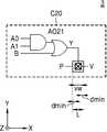
도 1은 본 개시의 예시적 실시 예에 따른 집적 회로를 설명하기 위한 도면이다. 도 1을 참조하면, 집적 회로(1)는 복수의 행들(R1, R2, R3) 중 적어도 하나에 배치되는 제1 내지 4 셀들(C1 내지 C4)을 포함할 수 있다. 집적 회로(1)에 포함되는 행의 개수 및 셀의 개수는 이에 제한되지 않는다. 셀(cell)은 집적 회로에 포함되는 레이아웃의 단위로서, 미리 정의된 기능을 수행하도록 설계될 수 있고, 표준 셀(standard cell)로서 지칭될 수도 있다. 셀은 셀은 부울 로직 기능 또는 저장 기능을 제공하는 임의의 기능성 셀 또는 로직 셀일 수 있다. 예를 들어, 셀(C10)은 NAND, AND, NOR, OR, XOR, 인버터, 가산기(adder), 플립플랍 또는 래치일 수 있다. 집적 회로(1a)는 다수의 다양한 로직 셀들을 포함할 수 있다.1 is a diagram for describing an integrated circuit according to an exemplary embodiment of the present disclosure. Referring to FIG. 1 , the
도 1에서, 제1 내지 4 셀들(C1 내지 C4) 각각은 입력 신호 또는 출력 신호를 전달하는 비아를 포함할 수 있다. 예를 들어, 제1 셀(C1)은 출력 신호를 전달하는 제1 비아(V1)를 포함할 수 있고, 제2 셀(C2)은 입력 신호를 전달하는 제2 비아(V2)를 포함할 수 있고, 제3 셀(C3)은 출력 신호를 전달하는 제3 비아(V3)를 포함할 수 있고, 제4 셀(C4)은 출력 신호를 전달하는 제4 비아(V1)를 포함할 수 있다. 제1 셀(C1)과 제3 셀(C3)은 동일한 기능을 수행하고, 동일한 구조를 갖는 셀일 수 있다. 제2 셀(C2)과 제4 셀(C4)은 동일한 기능을 수행하고, 동일한 구조를 갖는 셀일 수 있다.In FIG. 1 , each of the first to fourth cells C1 to C4 may include a via through which an input signal or an output signal is transmitted. For example, the first cell C1 may include a first via V1 transmitting an output signal, and the second cell C2 may include a second via V2 transmitting an input signal. In addition, the third cell C3 may include a third via V3 transmitting an output signal, and the fourth cell C4 may include a fourth via V1 transmitting an output signal. The first cell C1 and the third cell C3 may be cells that perform the same function and have the same structure. The second cell C2 and the fourth cell C4 may be cells that perform the same function and have the same structure.
제1 비아(V1)와 제2 비아(V2)는 제1 연결 배선(PR1)에 의해 서로 전기적으로 연결될 수 있다. 즉, 제1 셀(C1)의 출력 신호는 제2 셀(C2)의 입력 신호로서 제1 연결 배선(PR1)을 통해 제2 셀(C2)에 전달될 수 있다. 제1 연결 배선(PR1)의 길이 L1은 설계 규칙(Design Rule)을 기초로 결정될 수 있다. 예를 들어, 경계 규칙(Enclosure Rule)에 의해, 제1 연결 배선(PR1)은 제1 비아(V1) 및 제2 비아(V2)의 경계로부터 최소 경계 거리(dmin)만큼 연장된 영역을 포함할 수 있다. 즉, 제1 연결 배선(PR1)의 길이 L1은, 제1 비아(V1)의 좌측면과 제2 비아(V2)의 우측면 사이의 거리와, 최소 경계 거리(dmin)의 2배의 합에 대응하는 값을 가질 수 있다.The first via V1 and the second via V2 may be electrically connected to each other by the first connection line PR1 . That is, the output signal of the first cell C1 may be transmitted as an input signal of the second cell C2 to the second cell C2 through the first connection line PR1 . The length L1 of the first connection line PR1 may be determined based on a design rule. For example, according to an enclosure rule, the first connection line PR1 may include an area extending from the boundary of the first via V1 and the second via V2 by a minimum boundary distance dmin. can That is, the length L1 of the first connection line PR1 corresponds to the sum of the distance between the left surface of the first via V1 and the right surface of the second via V2 and twice the minimum boundary distance dmin. can have a value of
제3 비아(V3)와 제4 비아(V4)는 제2 연결 배선(PR2)에 의해 서로 전기적으로 연결될 수 있다. 즉, 제3 셀(C3)의 출력 신호는 제4 셀(C4)의 입력 신호로서 제2 연결 배선(PR2)을 통해 제4 셀(C4)에 전달될 수 있다. 제2 연결 배선(PR2)의 길이 L2은 설계 규칙(Design Rule)을 기초로 결정될 수 있다. 예를 들어, 최소 길이 규칙(minimum length rule) 또는 최소 면적 규칙(minimum area rule)에 의해, 제2 연결 배선(PR2)의 길이 L2는, 배선 최소 길이 Lmin와 동일할 수 있다. 이 경우, 제2 연결 배선(PR2)은 제1 비아(V1)의 좌측면으로부터 제1 거리(d1)만큼 연장된 영역을 포함하고, 제2 비아(V2)의 우측면으로부터 제2 거리(d2)만큼 연장된 영역을 포함할 수 있다. 즉, 제2 연결 배선(PR2)의 길이 L2은, 제1 비아(V1)의 좌측면과 제2 비아(V2)의 우측면 사이의 거리, 제1 거리(d1), 제2 거리(d2)의 합에 대응하는 값을 가질 수 있고, 이는 설계 규칙에 따른 배선 최소 길이 Lmin과 동일할 수 있다.The third via V3 and the fourth via V4 may be electrically connected to each other by the second connection line PR2 . That is, the output signal of the third cell C3 may be transmitted as an input signal of the fourth cell C4 to the fourth cell C4 through the second connection line PR2 . The length L2 of the second connection line PR2 may be determined based on a design rule. For example, according to a minimum length rule or a minimum area rule, the length L2 of the second connection line PR2 may be equal to the minimum length Lmin of the wiring line. In this case, the second connection line PR2 includes a region extending by a first distance d1 from the left surface of the first via V1 , and a second distance d2 from the right surface of the second via V2 . It may include an area extended by That is, the length L2 of the second connection line PR2 is the distance between the left side of the first via V1 and the right side of the second via V2 , the first distance d1 , and the second distance d2 . It may have a value corresponding to the sum, which may be equal to the minimum wiring length Lmin according to the design rule.
본 개시의 예시적 실시 예에 따르면, 집적 회로(1)에 포함되는 연결 배선들은 입력 신호 또는 출력 신호에 대한 라우팅을 수행하되, 설계 규칙을 만족하는 최소 길이를 가질 수 있으므로, 연결 배선의 저항이 최소화될 수 있고, 이에 따라 집적 회로(1)의 성능이 향상될 수 있다.According to an exemplary embodiment of the present disclosure, the connection wires included in the integrated
도 2는 집적 회로에 포함되는 셀을 설명하기 위한 도면이다. 집적 회로는 셀(C10)을 포함할 수 있다. 셀(C10)이 AO(AND-OR) 21 논리 회로인 것으로 도시되었으나, 셀(C10)은 셀은 부울 로직 기능 또는 저장 기능을 제공하는 임의의 기능성 셀 또는 로직 셀일 수 있다. 예를 들어, 셀(C10)은 NAND, AND, NOR, OR, XOR, 인버터, 가산기(adder), 플립플랍 또는 래치일 수 있다.2 is a diagram for describing a cell included in an integrated circuit. The integrated circuit may include a cell C10. Although cell C10 is shown to be an AO(AND-OR) 21 logic circuit, cell C10 may be any functional cell or logic cell that provides a Boolean logic function or a storage function. For example, cell C10 may be a NAND, AND, NOR, OR, XOR, inverter, adder, flip-flop, or latch.
도 2를 참조하면, 셀(C10)은 복수의 입력 신호들(A0, A1, B)을 수신하고, 출력 신호(Y)를 출력할 수 있다. 출력 신호(Y)는 출력 핀(P)에 전달될 수 있고, 출력 핀(P)은 제1 방향 또는 제2 방향으로 연장됨으로써 다른 셀의 입력 핀 또는 출력 핀과 연결될 수 있다. 도시되지 않았으나, 셀(C10)은 복수의 입력 신호들(A0, A1, B) 각각이 전달되는 입력 핀들을 포함할 수 있고, 후술되는 출력 핀(P)에 대한 설명은 입력 핀들에도 적용될 수 있다. 입력 핀은 입력 신호를 전달하는 비아와 연결되는 배선을 의미할 수 있고, 출력 핀은 출력 신호를 전달하는 비아와 연결되는 배선을 의미할 수 있다.Referring to FIG. 2 , a cell C10 may receive a plurality of input signals A0 , A1 , and B and may output an output signal Y. Referring to FIG. The output signal Y may be transmitted to the output pin P, and the output pin P may be connected to an input pin or an output pin of another cell by extending in the first direction or the second direction. Although not shown, the cell C10 may include input pins to which each of the plurality of input signals A0, A1, and B is transmitted, and the description of the output pin P to be described later may also be applied to the input pins. . The input pin may mean a wire connected to a via that transmits an input signal, and the output pin may mean a wire connected to a via that transmits an output signal.
출력 핀(P)은 비아(V)를 통해 셀(C10)에 포함되는 트랜지스터들과 전기적으로 연결될 수 있다. 예를 들어, 비아(V)는 수직 방향으로 연장됨으로써 트랜지스터들의 소스/드레인 영역과 전기적으로 연결될 수 있다. 도시되지 않았으나, 셀(C10)에 포함되는 입력 핀은 비아를 통해 트랜지스터들과 전기적으로 연결될 수 있고, 입력 핀과 연결된 비아는 수직 방향으로 연장됨으로써 트랜지스터들의 게이트 전극과 전기적으로 연결될 수 있다.The output pin P may be electrically connected to transistors included in the cell C10 through a via V. For example, the via V may be electrically connected to the source/drain regions of the transistors by extending in the vertical direction. Although not shown, the input pin included in the cell C10 may be electrically connected to the transistors through a via, and the via connected to the input pin may extend in a vertical direction to be electrically connected to the gate electrode of the transistors.
출력 핀(P)은 설계 규칙(Design Rule)에 따른 너비를 가질 수 있다. 예를 들어, 출력 핀(P0의 너비는, 배선이 가져야 하는 최소 너비에 대한 최소 너비 규칙(minimum width rule)에 의해 최소 너비(Wmin)로 결정될 수 있다.The output pin P may have a width according to a design rule. For example, the width of the output pin P0 may be determined as the minimum width Wmin according to a minimum width rule with respect to the minimum width that the wiring should have.
출력 핀(P)은 셀(C10)의 좌측(-X축 방향) 또는 우측(+X축 방향)에 배치되는 셀의 핀과 연결될 수 있으므로, 비아(V)의 좌측(-X축 방향)면으로부터 제1 부분 길이(sL1)를 갖고, 비아(V)의 우측(+X축 방향)면으로 제2 부분 길이(sL2)를 가질 수 있다. 출력 핀(P)의 길이(L)는 비아 너비(vw), 제1 부분 길이(sL1) 및 제2 부분 길이(sL2)의 합에 대응될 수 있다.Since the output pin P may be connected to a pin of a cell disposed on the left (-X-axis direction) or right (+X-axis direction) of the cell C10, the left (-X-axis direction) side of the via V It may have a first partial length sL1 from , and a second partial length sL2 in a right (+X-axis direction) side of the via V. The length L of the output pin P may correspond to the sum of the via width vw, the first partial length sL1 and the second partial length sL2.
출력 핀(P)이 셀(C10)의 좌측에 배치되는 셀의 핀과 연결되는 경우, 제2 부분 길이(sL2)에 해당하는 영역은 핀 연결에 불필요한 영역일 수 있다. 따라서, 제2 부분 길이(sL2)에 해당하는 영역에 의해 배선의 저항이 증가할 수 있고, 셀(C10)을 포함하는 집적 회로의 성능이 열화될 수 있다. 한편, 출력 핀(P)이 셀(C10)의 우측에 배치되는 셀의 핀과 연결되는 경우, 제1 부분 길이(sL1)에 해당하는 영역은 핀 연결에 불필요한 영역일 수 있다. 따라서, 제1 부분 길이(sL1)에 해당하는 영역에 의해 배선의 저항이 증가할 수 있고, 셀(C10)을 포함하는 집적 회로의 성능이 열화될 수 있다.When the output pin P is connected to a pin of a cell disposed on the left side of the cell C10 , a region corresponding to the second partial length sL2 may be an unnecessary region for pin connection. Accordingly, the resistance of the wiring may increase due to the region corresponding to the second partial length sL2 , and the performance of the integrated circuit including the cell C10 may deteriorate. Meanwhile, when the output pin P is connected to a pin of a cell disposed on the right side of the cell C10 , the region corresponding to the first partial length sL1 may be an unnecessary region for pin connection. Accordingly, the resistance of the wiring may increase due to the region corresponding to the first partial length sL1 , and the performance of the integrated circuit including the cell C10 may deteriorate.
도 3은 도 2의 셀을 포함하는 집적 회로를 설명하는 도면이다. 도 3을 참조하면, 집적 회로(2)는 제1 방향으로 연장되는 제1 및 2 행(R1, R2)에 배치되는 복수의 셀들(C1 내지 C4)을 포함할 수 있다. 제1, 4 셀(C1, C4)은 도 1을 참조하여 전술된 셀(C10)일 수 있고, 제2, 3 셀(C2, C3)은 셀(C10)과 동일하거나 상이한 기능을 수행하는 셀일 수 있다. 제1 행(R1)은 제1 높이(H1)를 가질 수 있고, 제2 행(R2)은 제2 높이(H2)를 가질 수 있다. 제1 높이(H1) 및 제2 높이(H2)는 동일하거나 상이할 수 있다.FIG. 3 is a diagram illustrating an integrated circuit including the cell of FIG. 2 . Referring to FIG. 3 , the
제1 행(R1)에 제1 셀(C1) 및 제2 셀(C2)이 배치될 수 있다. 제1 셀(C1)의 입력 신호 또는 출력 신호는 제1 비아(V1)에 전달될 수 있고, 제1 비아(V1)는 제1 핀(P1)과 연결될 수 있다. 제2 셀(C2)의 입력 신호 또는 출력 신호는 제2 비아(V2)에 전달될 수 있고, 제2 비아(V2)는 제2 핀(P2)과 연결될 수 있다. 제1 핀(P1)과 제2 핀(P2)은 서로 연결됨으로써 제1 연결 배선(RP1)을 형성할 수 있다.A first cell C1 and a second cell C2 may be disposed in the first row R1 . An input signal or an output signal of the first cell C1 may be transmitted to the first via V1 , and the first via V1 may be connected to the first pin P1 . An input signal or an output signal of the second cell C2 may be transmitted to the second via V2 , and the second via V2 may be connected to the second pin P2 . The first pin P1 and the second pin P2 may be connected to each other to form a first connection line RP1.
제1 연결 배선(RP1)은 제1 길이(L1)를 가질 수 있다. 집적 회로(2)의 배선들은 설계 규칙(Design Rule)에 따른 길이를 가질 수 있다. 설계 규칙(Design Rule)은 최소 면적 규칙(minimum area rule) 또는 최소 길이 규칙(minimum length rule)을 포함할 수 있다. 최소 면적 규칙 또는 최소 길이 규칙에 의해, 제1 길이(L1)는 최소 길이(Lmin)보다 길거나 같을 수 있다. 예를 들어, 제1 길이(L1)가 최소 길이(Lmin)보다 긴 경우, 제1 핀(P1) 중 제1 부분 길이(sL1)에 대응하는 영역은 핀 연결에 불필요한 영역일 수 있고, 제2 핀(P2) 중 제2 부분 길이(sL2)에 대응하는 영역은 핀 연결에 불필요한 영역일 수 있다.The first connection line RP1 may have a first length L1 . The interconnections of the
제2 행(R2)에 제3 셀(C3) 및 제4 셀(C4)이 배치될 수 있다. 제3 셀(C3)의 입력 신호 또는 출력 신호는 제3 비아(V3)에 전달될 수 있고, 제3 비아(V3)는 제3 핀(P3)과 연결될 수 있다. 제4 셀(C4)의 입력 신호 또는 출력 신호는 제4 비아(V4)에 전달될 수 있고, 제4 비아(V4)는 제4 핀(P4)과 연결될 수 있다. 제3 핀(P3)과 제4 핀(P4)은 서로 연결됨으로써 제2 연결 배선(RP2)을 형성할 수 있다.A third cell C3 and a fourth cell C4 may be disposed in the second row R2 . An input signal or an output signal of the third cell C3 may be transmitted to the third via V3 , and the third via V3 may be connected to the third pin P3 . An input signal or an output signal of the fourth cell C4 may be transmitted to the fourth via V4 , and the fourth via V4 may be connected to the fourth pin P4 . The third pin P3 and the fourth pin P4 may be connected to each other to form the second connection line RP2 .
제2 연결 배선(RP2)은 제2 길이(L2)를 가질 수 있다. 일부 실시 예들에서, 최소 면적 규칙 또는 최소 길이 규칙에 의해, 제2 길이(L2)가 최소 길이(Lmin)와 같은 경우, 제3 핀(P3) 중 제1 부분 길이(sL1)에 대응하는 영역은 설계 규칙을 만족시키기 위하여 핀 연결에 필요한 영역일 수 있고, 제4 핀(P4) 중 제2 부분 길이(sL2)에 대응하는 영역은 설계 규칙을 만족시키기 위하여 핀 연결에 필요한 영역일 수 있다.The second connection line RP2 may have a second length L2 . In some embodiments, when the second length L2 is equal to the minimum length Lmin according to the minimum area rule or the minimum length rule, the region corresponding to the first partial length sL1 of the third fins P3 is It may be a region necessary for pin connection to satisfy a design rule, and a region corresponding to the second partial length sL2 of the fourth pin P4 may be a region necessary for pin connection to satisfy a design rule.
도 2및 3을 참조하면, 셀들의 핀들이 연결됨에 따라, 각 셀에 포함되는 입력 핀 또는 출력 핀에는 핀 연결에 불필요한 영역이 발생할 수 있고, 핀 연결에 불필요한 영역에 의해 집적 회로(2)의 성능이 열화될 수 있다.Referring to FIGS. 2 and 3 , as the pins of the cells are connected, an area unnecessary for pin connection may occur in an input pin or an output pin included in each cell. Performance may deteriorate.
도 4는 본 개시의 예시적 실시 예에 따른 집적 회로를 나타내는 도면이다.도 4를 참조하면, 집적 회로(3)는 셀(C20)을 포함할 수 있다. 셀(C20)은 복수의 입력 신호들(A0, A1, B)을 수신하고, 출력 신호(Y)를 출력하는 AO 21 논리 회로로서 동작할 수 있으나, 실시 예는 이에 제한되지 않는다. 이하에서, 출력 신호(Y)를 전달하는 출력 핀(P)에 대한 설명은 복수의 입력 신호들(A0, A1, B)를 전달하는 입력 핀들에도 적용될 수 있다.4 is a diagram illustrating an integrated circuit according to an exemplary embodiment of the present disclosure. Referring to FIG. 4 , the
AO21 논리 회로의 출력 신호(Y)는 수직으로 연장되는 비아(V)로 전달될 수 있고, 비아(V)는 출력 핀(P)과 연결될 수 있다. 출력 핀(P)은 경계 규칙(enclosure rule)에 따라 비아(V)보다 넓은 면적을 갖도록 형성될 수 있다. 예를 들어, 출력 핀(P)의 너비는 비아(V)의 제2 방향의 길이보다 최소 경계 거리(dmin)만큼 넓을 수 있다. 한편, 출력 핀(P)의 길이는 비아(V)의 제1 방향의 길이보다 최소 경계 거리(dmin)만큼 길 수 있다. 출력 핀(P)의 너비는 출력 핀(P)의 제2 방향(Y축 방향)의 길이일 수 있고, 출력 핀(P)의 길이는 제1 방향(X축 방향)의 길이를 의미할 수 있다.The output signal Y of the AO21 logic circuit may be transmitted to a vertically extending via V, and the via V may be connected to the output pin P. The output pin P may be formed to have a larger area than the via V according to an enclosure rule. For example, the width of the output pin P may be wider than the length of the via V in the second direction by the minimum boundary distance dmin. Meanwhile, the length of the output pin P may be longer than the length of the via V in the first direction by the minimum boundary distance dmin. The width of the output pin P may be a length in the second direction (Y-axis direction) of the output pin P, and the length of the output pin P may mean a length in the first direction (X-axis direction). have.
도 2에 도시된 출력 핀(P)의 길이(L)는, 제1 부분 길이(sL1), 제2 부분 길이(sL2) 및 비아 너비(vw)의 합에 대응되는 것과 달리, 도 4의 출력 핀(P)의 길이(L)는, 최소 경계 거리(dmin)의 2배와 비아 너비(vw)의 합에 대응될 수 있다. 최소 경계 거리(dmin)는 제1 부분 길이(sL1) 및 제2 부분 길이(sL2)보다 짧을 수 있다. 즉, 도 4에 도시된 출력 핀(P)은, 경계 규칙(enclosure rule)을 만족하는 길이(L)를 가짐으로써, 셀(C20)과 연결되는 다른 셀이 셀(C20)의 좌우측 어느 곳에 배치되더라도 연결 배선의 길이를 최소화시킬 수 있으므로, 집적 회로(3)의 성능이 향상될 수 있다.Unlike the length L of the output pin P shown in FIG. 2 corresponding to the sum of the first partial length sL1 , the second partial length sL2 and the via width vw, the output of FIG. The length L of the pin P may correspond to the sum of twice the minimum boundary distance dmin and the via width vw. The minimum boundary distance dmin may be shorter than the first partial length sL1 and the second partial length sL2. That is, the output pin P shown in FIG. 4 has a length L that satisfies an enclosure rule, so that other cells connected to the cell C20 are disposed anywhere on the left and right sides of the cell C20 However, since the length of the connecting wiring can be minimized, the performance of the
도 5a는 본 개시의 예시적 실시 예에 따른 셀을 설명하는 레이아웃이다. 구체적으로, 도 5a의 상부는 AO(AND-OR) 21의 회로도를 나타내고, 도 5a의 하부는 AO 21에 대응하는 셀(C20)의 레이아웃을 X축 및 Y축으로 이루어진 평면에서 개략적으로 나타낸다.5A is a layout illustrating a cell according to an exemplary embodiment of the present disclosure. Specifically, the upper part of FIG. 5A shows a circuit diagram of AO(AND-OR) 21 , and the lower part of FIG. 5A schematically shows the layout of the cell C20 corresponding to AO21 in a plane consisting of X-axis and Y-axis.
도 5a에 도시된 바와 같이, 셀(C20)은 제1 방향으로 연장되는 복수의 활성 영역들(RX1, RX2)을 포함할 수 있다. 제1 활성 영역(RX1)은 P타입 활성 영역일 수 있고, 제2 활성 영역(RX2)은 N타입 활성 영역일 수 있다. P타입 활성 영역에 형성되는 트랜지스터는 P형 트랜지스터 또는 PFET(P-type Field Effect Transistor)으로 지칭될 수 있고, N타입 활성 영역에 형성되는 트랜지스터는 N형 트랜지스터 또는 NFET(N-type Field Effect Transistor)으로 지칭될 수 있다. 셀(C20)은 제2 방향으로 연장되는 복수의 게이트 전극들을 포함할 수 있다. 인접하는 게이트 전극들 간의 최소 거리는 제1 피치(CPP)로 정의될 수 있다. 도시되지 않았으나, 각 활성 영역에는 적어도 하나의 활성 패턴(Active Pattern)이 제1 방향으로 연장될 수 있다. 활성 패턴은 제2 방향으로 연장되는 게이트 전극과 교차되어 트랜지스터를 형성할 수 있다. 핀(fin) 형태의 활성 패턴이 제1 방향으로 연장되는 경우, 활성 패턴 및 게이트 전극이 형성하는 트랜지스터는 핀펫(fin field effect transistor; FinFET)으로 지칭될 수 있다. 도 6a 내지 도 6c를 참조하여 후술되는 바와 같이, 본 개시의 예시적 실시예들은 핀펫(FinFET)을 포함하는 셀들을 주로 참조하여 설명될 것이나, 핀펫과 상이한 구조의 트랜지스터를 포함하는 셀들에도 적용될 수 있는 점은 이해될 것이다. 예를 들면, 활성 패턴은, Z축 방향으로 상호 이격되어 제1 방향으로 연장되는 복수의 나노시트들(nanosheets)을 포함할 수 있고, 복수의 나노시트들은 게이트 전극과 함께 MBCFET(multi-bridge channel FET)을 형성할 수 있다. 또한, P형 트랜지스터를 위한 나노시트들 및 N형 트랜지스터를 위한 나노시트들이 유전체 벽(dielectric wall)으로 분리됨으로써 N형 트랜지스터 및 P형 트랜지스터가 보다 근접한 구조를 가지는 ForkFET을 포함할 수도 있다. 또한, 셀은 소스/드레인 영역들이 채널 영역을 사이에 두고 Z축 방향으로 상호 이격되고, 게이트 전극이 채널 영역을 둘러싸는 구조를 가지는 VFET(vertical FET)을 포함할 수 도 있다. 또한, 셀은 CFET(complementary FET), NCFET(negative FET), CNT(carbon nanotube) FET 등과 같은 FET(field effect transistor)를 포함할 수도 있고, 양극성 접합(bipolar junction) 트랜지스터, 기타 3차원 트랜지스터를 포함할 수도 있다.As shown in FIG. 5A , the cell C20 may include a plurality of active regions RX1 and RX2 extending in the first direction. The first active region RX1 may be a P-type active region, and the second active region RX2 may be an N-type active region. The transistor formed in the P-type active region may be referred to as a P-type transistor or P-type Field Effect Transistor (PFET), and the transistor formed in the N-type active region may be an N-type transistor or N-type Field Effect Transistor (NFET). may be referred to as The cell C20 may include a plurality of gate electrodes extending in the second direction. A minimum distance between adjacent gate electrodes may be defined as a first pitch CPP. Although not shown, at least one active pattern may extend in the first direction in each active region. The active pattern may cross the gate electrode extending in the second direction to form a transistor. When the fin-shaped active pattern extends in the first direction, the transistor formed by the active pattern and the gate electrode may be referred to as a fin field effect transistor (FinFET). As will be described later with reference to FIGS. 6A to 6C , exemplary embodiments of the present disclosure will be mainly described with reference to cells including a FinFET, but may also be applied to cells including a transistor having a structure different from that of the FinFET. The point will be understood. For example, the active pattern may include a plurality of nanosheets that are spaced apart from each other in the Z-axis direction and extend in the first direction, and the plurality of nanosheets are multi-bridge channel (MBCFET) together with the gate electrode. FET) can be formed. In addition, since the nanosheets for the P-type transistor and the nanosheets for the N-type transistor are separated by a dielectric wall, the N-type transistor and the P-type transistor may include a ForkFET having a closer structure. In addition, the cell may include a vertical FET (VFET) having a structure in which source/drain regions are spaced apart from each other in the Z-axis direction with a channel region interposed therebetween, and a gate electrode surrounds the channel region. Cells may also include field effect transistors (FETs), such as complementary FETs (CFETs), negative FETs (NCFETs), carbon nanotube (CNT) FETs, and the like, and include bipolar junction transistors and other three-dimensional transistors. You may.
양의 공급 전압(VDD)을 제공하는 전원 라인 및 음의 공급 전원(VSS)을 제공하는 전원 라인은, 셀(C20)의 경계 상에서 제1 방향으로 연장될 수 있다. 양의 공급 전압(VDD)을 제공하는 전원 라인 및 음의 공급 전원(VSS)을 제공하는 전원 라인은 제1 배선층(M1)에 형성될 수 있다.The power line providing the positive supply voltage VDD and the power line providing the negative supply voltage VSS may extend in the first direction on the boundary of the cell C20 . A power line providing a positive supply voltage VDD and a power line providing a negative supply voltage VSS may be formed in the first wiring layer M1 .
셀(C20)은 제2 축 방향으로 연장되는 셀 분리막(Diffusion Break)에 의해 인접하는 셀들과 분리될 수 있다. 즉, 셀(C20)의 경계는 셀 분리막으로 구분될 수 있다. 다만, 셀 분리막은 셀의 경계와 중첩되는 위치에 형성되지 않고, 셀(C20)의 내부에서 전류의 흐름을 차단하기 위한 위치에 형성될 수도 있다. 셀 분리막은 확산(diffusion) 영역을 분리할 수 있고, 절연체로 채워질 수 있다. 일부 실시예들에서, 셀 분리막은 상호 인접한 셀들 사이에서 활성 패턴, 예를 들어, 핀(fin)들을 분리할 수 도 있다.The cell C20 may be separated from adjacent cells by a diffusion break extending in the second axial direction. That is, the boundary of the cell C20 may be divided by a cell separator. However, the cell separator may not be formed at a position overlapping the cell boundary, but may be formed at a position to block the flow of current inside the cell C20 . The cell separator may separate a diffusion region and may be filled with an insulator. In some embodiments, the cell separation layer may separate an active pattern, for example, fins between adjacent cells.
도 5a를 참조하면, AO21은 제1 내지 3 입력 신호들(A0, A1, B) 및 출력 신호(Y)를 가질 수 있고, 4개의 NFET들 및 4개의 PFET들을 포함할 수 있다.Referring to FIG. 5A , AO21 may have first to third input signals A0, A1, B and output signal Y, and may include four NFETs and four PFETs.
도 5a의 하부에 도시된 바와 같이, 셀(C20)은 외부로부터 입력 신호들(A0, A1, B0)을 수신하는 제1 내지 3 핀들(P1 내지 P3), 외부로 출력 신호(Y)를 출력하는 제4 핀(P4)을 포함할 수 있다. 셀(C20)은 내부 신호를 라우팅함으로써 제1 노드(N1)를 형성하는 제1 내부 연결 배선(IP1) 및 제2 노드(N2)를 형성하는 제2 내부 연결 배선(IP2)을 포함할 수 있다.As shown in the lower part of FIG. 5A , the cell C20 outputs the output signal Y to the first to third pins P1 to P3 that receive the input signals A0, A1, and B0 from the outside, and the output signal Y to the outside. and a fourth pin P4 that The cell C20 may include a first internal connection wire IP1 that forms a first node N1 by routing an internal signal, and a second internal connection wire IP2 that forms a second node N2. .
제1 내지 4 핀들(P1 내지 P4) 및 제1 및 2 내부 연결 배선들(IP1, IP2)은 제1 방향으로 연장되는 배선들이 형성되는 제1 배선층(M1)에 배치될 수 있다. 제1 내지 4 핀들(P1 내지 P4) 및 제1 및 2 내부 연결 배선들(IP1, IP2)은 제1 피치(mp) 만큼 상호 이격된 제1 내지 5 트랙들(TR1 내지 TR5) 중 적어도 하나의 트랙을 따라 정렬될 수 있다. 도 6a 내지 6c를 참조하여 후술되는 바와 같이, 입력 핀인 제1 내지 3 핀(P1 내지 P3)은 비아 및 컨택을 통해 게이트 전극과 전기적으로 연결될 수 있고, 출력 핀인 제4 핀(P4)은 비아 및 컨택을 통해 소스/드레인 영역과 전기적으로 연결될 수 있다.The first to fourth pins P1 to P4 and the first and second internal connection lines IP1 and IP2 may be disposed in the first wiring layer M1 in which wirings extending in the first direction are formed. The first to fourth pins P1 to P4 and the first and second internal connection wires IP1 and IP2 are at least one of the first to fifth tracks TR1 to TR5 spaced apart from each other by a first pitch mp. It can be aligned along the track. As will be described later with reference to FIGS. 6A to 6C , the first to third pins P1 to P3 that are input pins may be electrically connected to the gate electrode through vias and contacts, and the fourth pin P4 that is an output pin includes a via and a contact. The contact may be electrically connected to the source/drain region.
제1 내지 4 핀들(P1 내지 P4)은 경계 규칙(enclosure rule)을 만족하는 배선 길이를 가질 수 있다. 예를 들어, 제4 핀(P4)은 비아(VB)의 모든 경계로부터 최소 경계 거리(dmin)만큼 연장된 길이를 가질 수 있다. 즉, 제4 핀(P4)은, 비아 너비(vw)와 최소 경계 거리(dmin)의 2배의 합에 대응하는 길이(L)를 가질 수 있다. 제4 핀(P4)을 기준으로 설명하였으나, 제4 핀(P4)에 대한 설명은 제1 내지 3 핀(P1 내지 P3)에도 적용될 수 있다.The first to fourth pins P1 to P4 may have a wiring length satisfying an enclosure rule. For example, the fourth fin P4 may have a length extending from all boundaries of the vias VB by a minimum boundary distance dmin. That is, the fourth fin P4 may have a length L corresponding to the sum of twice the via width vw and the minimum boundary distance dmin. Although the description is based on the fourth fin P4 , the description of the fourth fin P4 may also be applied to the first to third pins P1 to P3 .
도 5b는 본 개시의 예시적 실시 예에 따른 다양한 형태의 연결 배선을 설명하는 도면이다. 구체적으로, 도 5b의 상부는 경계 규칙을 만족하는 길이를 갖는 제1 내지 4 핀들(P1 내지 P4)을 포함하는 셀(C20)을 나타내고, 도 5b의 하부는 제1 내지 3 셀들(C20a, C20b, C20c)을 포함하는 집적 회로(3a)를 나타낸다. 셀(C20)은 도 5a의 셀(C20)과 동일한 구조를 가질 수 있으나, 설명의 편의를 위하여 간략하게 도시될 수 있고, 제1 내지 3 셀들(C20a, C20b, C20c)은 셀(C20)과 동일한 구조를 갖는 셀일 수 있다. 셀(C20)을 사용하여 배치 및 라우팅(Place & Routing; P&R) 동작이 수행되면 제1 내지 3 셀들(C20a 내지 C20c)을 포함하는 집적 회로(3a)가 형성될 수 있다.5B is a view for explaining various types of connection wiring according to an exemplary embodiment of the present disclosure. Specifically, the upper part of FIG. 5B shows the cell C20 including the first to fourth fins P1 to P4 having a length that satisfies the boundary rule, and the lower part of FIG. 5B shows the first to third cells C20a and C20b , C20c) shows the
배치 동작 시, 제1 내지 3 셀들(C20a 내지 C20c)은, 동일한 행에 배치될 수도 있고, 상이한 행에 배치될 수도 있다. 라우팅 동작 시, 제1 내지 3 셀(C20a 내지 C20c)은, 제1 내지 4 핀들(P1 내지 P4)이 다양한 방향으로 연장된 형태를 갖는 연결 배선들이 형성될 수 있다. 예를 들어, 제2 핀(P2)이 우측으로 연장된 형태를 갖는 연결 배선(PR2a), 제2 핀(P2)이 좌측 및 우측으로 연장된 형태를 갖는 연결 배선(PR2b) 및 제2 핀(P2)이 좌측으로 연장된 형태를 갖는 연결 배선(PR2c)이 형성될 수 있다. 실시 예는 이에 제한되지 않고, 핀은 상측 또는 하측으로 연장될 수도 있다. 도시되지 않았으나, 연결 배선들은 다른 셀에 포함되는 비아와 연결될 수 있다.During the arrangement operation, the first to third cells C20a to C20c may be arranged in the same row or in different rows. During the routing operation, the first to third cells (C20a to C20c), the first to fourth pins (P1 to P4) may be formed with connecting wires having a shape extending in various directions. For example, the connection wiring PR2a in which the second pin P2 extends to the right, the connection wiring PR2b in the form in which the second pin P2 extends to the left and right, and the second pin ( A connection line PR2c having a shape in which P2 is extended to the left may be formed. The embodiment is not limited thereto, and the pin may extend upward or downward. Although not shown, the connection lines may be connected to vias included in other cells.
연결 배선은 설계 규칙에 따른 최소 길이 이상인 길이를 가질 수 있다. 본 개시의 예시적 실시 예에 따르면, 셀(C20)에 포함되는 핀들(P1 내지 P4)은 다양한 방향으로 연장될 수 있고, 배치 및 라우팅 동작을 통해 설계 규칙을 만족하는 연결 배선이 형성될 수 있다.The connecting wire may have a length greater than or equal to a minimum length according to a design rule. According to an exemplary embodiment of the present disclosure, the pins P1 to P4 included in the cell C20 may extend in various directions, and a connection line satisfying a design rule may be formed through arrangement and routing operations. .
도 5c는 본 개시의 예시적 실시 예에 따른 연결 배선의 길이를 설명하는 도면이다. 구체적으로, 도 5c의 상부는 노멀 핀을 포함하는 셀(C10)을 이용하여 연결 배선의 길이를 설명하는 도면이고, 도 5c의 하부는 가변 핀을 포함하는 셀(C20)을 이용하여 연결 배선의 길이를 설명하는 도면이다. 노멀 핀은 설계 규칙에 따른 최소 길이 이상의 길이를 갖는 핀을 지칭할 수 있다. 가변 핀은 도 5a를 참조하여 전술된 바와 같이, 경계 규칙에 따른 최소 경계 거리를 기초로 결정되는 길이를 갖는 핀을 지칭할 수 있다. 셀(C10)과 셀(C20)은 동일한 기능을 수행하는 셀일 수 있다.5C is a view for explaining a length of a connection wire according to an exemplary embodiment of the present disclosure. Specifically, the upper part of FIG. 5C is a view for explaining the length of the connection wiring using the cell C10 including the normal pin, and the lower part of FIG. 5C is the connection wiring using the cell C20 including the variable pin. It is a drawing explaining the length. A normal fin may refer to a fin having a length greater than or equal to a minimum length according to a design rule. The variable pin may refer to a pin having a length determined based on a minimum boundary distance according to a boundary rule, as described above with reference to FIG. 5A . The cell C10 and the cell C20 may be cells performing the same function.
도 5c의 상부를 참조하면, 셀(C10)에 포함되는 노멀 핀들(P11 내지 P14)의 길이는 설계 규칙에 따른 최소 길이 이상일 수 있다. 셀(C10)과 동일한 구조를 갖는 셀들(C10a, C10b)에 대한 배치 및 라우팅 동작이 수행될 수 있고, 연결 배선(RP1)을 통해 셀(C10a)과 셀(C10b)이 상호 연결될 수 있다. 연결 배선(RP1)은 셀(C10a)의 제4 비아(V14a)와 셀(C10b)의 제2 비아(V12b)를 연결할 수 있다. 연결 배선(RP1)의 길이는 제1 길이(L1)일 수 있다. 설명의 편의를 위하여 연결 배선(RP1)만 도시되었으나, 다른 비아들과 연결되는 연결 배선들이 형성될 수 있음은 자명하다.Referring to the upper part of FIG. 5C , the length of the normal fins P11 to P14 included in the cell C10 may be greater than or equal to the minimum length according to the design rule. Arrangement and routing operations for the cells C10a and C10b having the same structure as the cell C10 may be performed, and the cell C10a and the cell C10b may be interconnected through the connection line RP1. The connection line RP1 may connect the fourth via V14a of the cell C10a and the second via V12b of the cell C10b. The length of the connection line RP1 may be the first length L1 . Although only the connection line RP1 is illustrated for convenience of description, it is obvious that connection lines connected to other vias may be formed.
도 5c의 하부를 참조하면, 셀(C20)에 포함되는 가변 핀들(P11 내지 P14)의 길이는, 도 5a를 참조하여 전술된 바와 같이, 경계 규칙을 만족하는 길이일 수 있다. 셀(C20)과 동일한 구조를 갖는 셀들(C20a, C20b)에 대한 배치 및 라우팅 동작이 수행될 수 있고, 연결 배선(RP2)을 통해 셀(C20a)과 셀(C20b)이 상호 연결될 수 있다. 연결 배선(RP2)은 셀(C20a)의 제4 비아(V24a)와 셀(C20b)의 제2 비아(V22b)를 연결할 수 있다. 연결 배선(RP2)의 길이는 제2 길이(L2)일 수 있다. 제2 길이(L2)는 설계 규칙에 따른 최소 길이 이상일 수 있다. 설명의 편의를 위하여 연결 배선(RP2)만 도시되었으나, 다른 비아들과 연결되는 연결 배선들이 형성될 수 있음은 자명하다.Referring to the lower part of FIG. 5C , the length of the variable pins P11 to P14 included in the cell C20 may be a length satisfying the boundary rule as described above with reference to FIG. 5A . Arrangement and routing operations for the cells C20a and C20b having the same structure as the cell C20 may be performed, and the cell C20a and the cell C20b may be interconnected through the connection line RP2. The connection line RP2 may connect the fourth via V24a of the cell C20a and the second via V22b of the cell C20b. The length of the connection line RP2 may be the second length L2 . The second length L2 may be equal to or greater than a minimum length according to a design rule. Although only the connection line RP2 is illustrated for convenience of description, it is obvious that connection lines connected to other vias may be formed.
셀(C20)에 포함되는 가변 핀들(P21 내지 P24)은 설계 규칙에 따른 최소 길이보다 짧을 수 있다. 따라서, 배치 및 라우팅 동작 이후에 형성되는 연결 배선(RP2)의 제2 길이(L2)는 제1 길이보다 짧을 수 있다. 즉, 본 개시의 예시적 실시 예에 따르면, 가변 핀들(P21 내지 P24)이 셀(C20)에 포함됨으로써, 배치 및 라우팅 동작 후 연결 배선의 길이가 짧아질 수 있다. 따라서, 셀(C20)을 포함하는 집적 회로의 배선 저항이 낮아지고 집적 회로의 성능이 향상될 수 있다.The variable pins P21 to P24 included in the cell C20 may be shorter than a minimum length according to a design rule. Accordingly, the second length L2 of the connection line RP2 formed after the arrangement and routing operation may be shorter than the first length. That is, according to an exemplary embodiment of the present disclosure, since the variable pins P21 to P24 are included in the cell C20, the length of the connecting wire may be shortened after arrangement and routing operations. Accordingly, the wiring resistance of the integrated circuit including the cell C20 may be reduced and the performance of the integrated circuit may be improved.
도 6a 내지 6c는 본 개시의 예시적 실시 예에 따른 셀의 구조의 예시들을 나타내는 단면도들이다. 구체적으로, 도 6a의 단면도는 도 5a의 X-X'을 따라 셀(C20)을 자른 단면을 나타내고, 도 6b의 단면도는 도 5a의 Y1-Y1'을 따라 셀(C20)을 자른 단면을 나타내고, 도 6c의 단면도는 도 5a의 Y2-Y2'을 따라 셀(C20)을 자른 단면을 나타낸다. 비록 도 6a 내지 도 6c에 도시되지 아니하였으나, 게이트 전극의 측면에 게이트 스페이서가 형성될 수 있고, 게이트 전극 및 게이트 스페이서 사이 그리고 게이트 전극의 하면 상에 게이트 유전막이 형성될 수 있다. 또한, 컨택 및/또는 비아의 표면에 베리어 막이 형성될 수 있다. 이하에서 도 6a 내지 도 6c는 도 5a를 참조하여 설명될 것이며, 도 6a 내지 도 6c에 대한 설명 중 상호 중복되는 내용은 생략될 것이다.6A to 6C are cross-sectional views illustrating examples of a structure of a cell according to an exemplary embodiment of the present disclosure. Specifically, the cross-sectional view of FIG. 6A shows a cross-section taken along X-X' of FIG. 5A, and the cross-sectional view of FIG. 6B shows a cross-section of the cell C20 taken along Y1-Y1' of FIG. 5A. , the cross-sectional view of FIG. 6C is a cross-sectional view taken along the Y2-Y2' of FIG. 5A through the cell C20. Although not shown in FIGS. 6A to 6C , a gate spacer may be formed on a side surface of the gate electrode, and a gate dielectric layer may be formed between the gate electrode and the gate spacer and on a lower surface of the gate electrode. In addition, a barrier film may be formed on the surfaces of the contacts and/or vias. Hereinafter, FIGS. 6A to 6C will be described with reference to FIG. 5A, and content overlapping each other in the description of FIGS. 6A to 6C will be omitted.
도 6a를 참조하면, 기판(10)은 벌크 실리콘 또는 SOI(silicon-on-insulator)일 수 있고, 비제한적인 예시로서 SiGe, SGOI(silicon germanium on insulator), InSb, PbTe 화합물, InAs, 인화물, GaAs 또는 GaSb 등을 포함할 수도 있다. 기판(10) 상에서 핀(F)이 X축 방향으로 연장될 수 있고, 핀(F)에서 제1 내지 제6 소스/드레인 영역(SD1 내지 SD6)이 형성될 수 있다. 핀(4) 상에서 제1 내지 제4 층간 절연막(31 내지 34)이 형성될 수 있다. 제1 및 제2 소스/드레인 영역(SD1, SD2)은 제1 게이트 전극(G1)과 트랜지스터, 즉 PFET(p-type field effect transistor)를 형성할 수 있고, 제2 및 제3 소스 드레인 영역(SD2, SD3)은 제2 게이트 전극(G2)과 PFET를 형성할 수 있고, 제3 및 제4 소스 드레인 영역(SD3, SD4)은 제3 게이트 전극(G3)과 PFET를 형성할 수 있고 제5 및 제6 소스 드레인 영역(SD5, SD6)은 제5 게이트 전극(G5)과 PFET를 형성할 수 있다.Referring to FIG. 6A , the
제1 내지 제6 소스/드레인 컨택(CA1 내지 CA6)은 제2 층간 절연막(32)을 관통하여 제1 내지 제6 소스/드레인 영역(SD1 내지 SD6)과 연결될 수 있다. 일부 실시예들에서, 제1 내지 제6 소스/드레인 컨택(CA1 내지 CA6) 중 적어도 하나는, 제1 층간 절연막(31)을 관통하는 하부 소스/드레인 컨택 및 제2 층간 절연막(32)을 관통하는 상부 소스/드레인 컨택으로 형성될 수도 있다. 제1 게이트 컨택(CB1)은 제2 층간 절연막(32)을 관통하여 제1 게이트 전극(G1)에 연결될 수도 있다. 제1 게이트 비아(VB1)는 제3 층간 절연막(33)을 관통하여 제1 게이트 컨택(CB1)에 연결될 수 있고, 제1 배선층(M1)에 형성된 제1 핀(P1)에 연결될 수 있다. 도 4를 참조하여 전술된 바와 같이, 제1 핀(P1)의 길이(L)는, 게이트 비아(VB1)의 제1 방향의 너비(vw)와, 최소 경계 거리(dmin)의 2배의 합에 대응할 수 있다. 제1 게이트 비아(VB1)가 형성된 층은 제1 비아층으로 지칭될 수 있고, 제1 핀(P1)과 제4 층간 절연막(34)이 형성된 층은 제1 배선층(M1)으로 지칭될 수 있다.The first to sixth source/drain contacts CA1 to CA6 may pass through the second
도 6b를 참조하면, 제1 게이트 컨택(CB1)은 제2 층간 절연막(32)을 관통하여 제1 게이트 전극(G1)에 연결될 수 있고, 제1 게이트 비아(VB1)는 제3 층간 절연막(33)을 관통하여 제1 게이트 컨택(CB1) 및 제1 핀(P1)과 연결될 수 있다. 일부 실시예들에서, 도 5b에 도시된 바와 상이하게, 제1 게이트 컨택(CB1)이 생략될 수 있고, 제2 및 제3 층간 절연막(32, 33)을 관통하는 게이트 비아를 통해서 제1 핀(P1)은 제1 게이트 전극(G1)과 전기적으로 연결될 수 있다.Referring to FIG. 6B , the first gate contact CB1 may be connected to the first gate electrode G1 through the second
도 6b를 참조하면, 기판(10) 상에 필드 절연막(20)이 형성될 수 있다. 필드 절연막(20)은, 비제한적인 예시로서 SiO2, SiN, SiON, SiOCN 또는 이들 중 2이상의 조합을 포함할 수 있다. 일부 실시예들에서, 필드 절연막(20)은 도 5b에 도시된 바와 같이, 활성 패턴, 즉 핀의 측면들 중 일부를 둘러쌀 수 있다. 필드 절연막(20)을 관통하는 제1 내지 제4 핀(F1 내지 F4)과 Y축 방향으로 연장되는 제1 게이트 전극(G1)이 교차할 수 있다. 제1 게이트 전극(G1)은, 비제한적인 예시로서 Ti, Ta, W, Al, Co 또는 이들 중 2이상의 조합을 포함할 수도 있고, 금속이 아닌 Si 또는 SiGe 등을 포함할 수도 있다. 또한, 제1 게이트 전극(G1)은 2이상의 전도성 물질들이 적층되어 형성될 수도 있고, 예컨대 TiN, TaN, TiC, TaC, TiAlC 또는 이들 중 2이상의 조합을 포함하는 일함수 조절막, 및 W 또는 Al 등을 포함하는 필링 도전막을 포함할 수 있다.Referring to FIG. 6B , a
도 6c를 참조하면, 필드 절연막(20) 상에 제1 내지 제4 층간 절연막(31 내지 34)이 형성될 수 있다. 제1 내지 제4 핀(F1 내지 F4)이 필드 절연막(20)에서 X축 방향으로 연장될 수 있고, 제1 내지 제4 핀(F1 내지 F4) 상에서 4개의 소스/드레인 영역들(SD1 내지 SD4)이 형성될 수 있다. 제2 핀(F2)과 제3 핀(F3) 사이에서 소자 분리막(ISO)이 X축 방향으로 연장될 수 있다.Referring to FIG. 6C , first to fourth
제1 소스/드레인 컨택(CA1)은 제2 층간 절연막(32)을 관통하여 4개의 소스/드레인 영역들(SD1 내지 SD4)에 연결될 수 있고, 이에 따라 4개의 소스/드레인 영역들(SD1 내지 SD4)은 전기적으로 상호 연결될 수 있다. 제1 소스/드레인 비아(VA1)는 제3 층간 절연막(33)을 관통하여 제1 소스/드레인 컨택(CA1)에 연결될 수 있고, 제4 핀(P4)과 연결될 수 있다.The first source/drain contact CA1 may pass through the second
도 7a 및 도 7b는 본 개시의 예시적 실시 예에 따른 집적 회로를 설명하는 도면이다.7A and 7B are diagrams for explaining an integrated circuit according to an exemplary embodiment of the present disclosure.
도 7a를 참조하면, 집적 회로(4a)는 제1 셀(C30a) 및 제2 셀(C30b)을 포함할 수 있다. 도 7a의 제1 셀(C30a) 및 제2 셀(C30b)은, 도 5의 셀(C20)과 동일한 구조를 가질 수 있으나, 설명의 편의를 위하여 간략하게 도시될 수 있다. 예를 들어, 제1 셀(C30a) 및 제2 셀(C30b)은, 도 5의 셀(C20)의 제1 내지 4 핀들(P1 내지 P4)과 연결된 비아들만 포함하는 것으로 도시될 수 있다. 구체적으로, 제1 셀(C30a)은 입력 신호를 전달받는 제1 내지 3 비아들(V1 내지 V3)을 포함할 수 있고, 출력 신호를 전달받는 제4 비아(V4)를 포함할 수 있다. 제2 셀(C30b)은 입력 신호를 전달받는 제5 내지 7 비아들(V5 내지 V7)을 포함할 수 있고, 출력 신호를 전달받는 제8 비아(V8)를 포함할 수 있다.Referring to FIG. 7A , the
제1 셀(C30a)의 출력 신호를 전달하는 제4 비아(V4)는, 제2 셀(C30b)의 출력 신호를 전달하는 제6 비아(V6)와 제1 연결 배선(RP1)을 통해 연결될 수 있다. 제1 연결 배선(RP1)은 제1 배선층(M1)에 형성될 수 있다. 제1 배선층(M1)에는 제1 방향으로 연장되는 배선들이 형성될 수 있다. 제4 비아(V4)와 제6 비아(V6)는 제1 비아 거리(dvia1)만큼 이격될 수 있다. 제1 연결 배선(PR1)은 제1 길이(L1)를 가질 수 있다. 제1 길이(L1)가 설계 규칙에 따른 최소 길이(Lmin)보다 긴 경우, 제1 연결 배선(RP1)은, 제4 비아(V4)의 좌측으로부터 최소 경계 거리(dmin)만큼 연장되는 영역을 포함할 수 있고, 제6 비아(V6)의 우측으로부터 최소 경계 거리(dmin)만큼 연장되는 영역을 포함할 수 있다. 즉, 제1 길이(L1)는, 제1 비아 거리(dvia1), 제4 비아(V4)의 너비인 제1 너비(vw1), 제6 비아(V6)의 너비인 제2 너비(vw2) 및 최소 경계 거리(dmin)의 2배의 합에 대응하는 값을 가질 수 있다. 제1 연결 배선(RP1)은 설계 규칙을 만족하는 최단 길이를 가질 수 있으므로, 집적 회로(4a)의 성능이 향상될 수 있다.The fourth via V4 transmitting the output signal of the first cell C30a may be connected to the sixth via V6 transmitting the output signal of the second cell C30b through the first connection line RP1. have. The first connection line RP1 may be formed on the first wiring layer M1 . Wires extending in the first direction may be formed in the first wiring layer M1 . The fourth via V4 and the sixth via V6 may be spaced apart from each other by the first via distance dvia1 . The first connection line PR1 may have a first length L1 . When the first length L1 is longer than the minimum length Lmin according to the design rule, the first connection line RP1 includes a region extending from the left side of the fourth via V4 by the minimum boundary distance dmin. and may include a region extending from the right side of the sixth via V6 by the minimum boundary distance dmin. That is, the first length L1 includes the first via distance dvia1 , the first width vw1 that is the width of the fourth via V4 , the second width vw2 that is the width of the sixth via V6 , and It may have a value corresponding to the sum of twice the minimum boundary distance dmin. Since the first connection line RP1 may have the shortest length satisfying the design rule, the performance of the
도 7b를 참조하면, 집적 회로(4b)는 제1 셀(C30a) 및 제2 셀(C30b)을 포함할 수 있다. 도 7b의 제1 셀(C30a) 및 제2 셀(C30b)은, 도 5의 셀(C20)과 동일한 구조를 가질 수 있으나, 설명의 편의를 위하여 간략하게 도시될 수 있다. 예를 들어, 제1 셀(C30a) 및 제2 셀(C30b)은, 도 5의 셀(C20)의 제1 내지 4 핀들(P1 내지 P4)과 연결된 비아들만 포함하는 것으로 도시될 수 있다. 구체적으로, 제1 셀(C30a)은 입력 신호를 전달받는 제1 내지 3 비아들(V1 내지 V3)을 포함할 수 있고, 출력 신호를 전달받는 제4 비아(V4)를 포함할 수 있다. 제2 셀(C30b)은 입력 신호를 전달받는 제5 내지 7 비아들(V5 내지 V7)을 포함할 수 있고, 출력 신호를 전달받는 제8 비아(V8)를 포함할 수 있다.Referring to FIG. 7B , the
제1 셀(C30a)의 출력 신호를 전달하는 제4 비아(V4)는, 제2 셀(C30b)의 출력 신호를 전달하는 제6 비아(V6)와 제2 연결 배선(RP2)을 통해 연결될 수 있다. 제2 연결 배선(RP2)은 제1 배선층(M1)에 형성될 수 있다. 제1 배선층(M1)에는 제1 방향으로 연장되는 배선들이 형성될 수 있다. 제4 비아(V4)와 제6 비아(V6)는 제2 비아 거리(dvia2)만큼 이격될 수 있다. 제2 비아 거리(dvia2)는 도 7a를 참조하여 전술된 제1 비아 거리(dvia)보다 짧을 수 있다. 제2 연결 배선(RP2)은 제2 길이(L2)를 가질 수 있다. 제2 길이(L2)는 설계 규칙에 따른 최소 길이(Lmin)와 동일할 수 있다. 제2 연결 배선(RP2)은, 제4 비아(V4)의 좌측으로부터 제1 거리(d1)만큼 연장되는 영역을 포함할 수 있고, 제6 비아(V6)의 우측으로부터 제2 거리(d2)만큼 연장되는 영역을 포함할 수 있다. 즉, 제2 길이(L2)는, 제2 비아 거리(dvia2), 제1 너비(vw1), 제2 너비(vw2), 제1 거리(d1) 및 제2 거리(d2)의 합에 대응하는 값을 가질 수 있다. 제1 거리(d1) 및 제2 거리(d2) 중 적어도 하나는, 경계 최소 거리(dmin)보다 길 수 있다. 제2 연결 배선(RP2)은 설계 규칙을 만족하는 최단 길이를 가질 수 있으므로, 집적 회로(4b)의 성능이 향상될 수 있다.The fourth via V4 transmitting the output signal of the first cell C30a may be connected to the sixth via V6 transmitting the output signal of the second cell C30b through the second connection line RP2. have. The second connection line RP2 may be formed on the first wiring layer M1 . Wires extending in the first direction may be formed in the first wiring layer M1 . The fourth via V4 and the sixth via V6 may be spaced apart from each other by the second via distance dvia2 . The second via distance dvia2 may be shorter than the first via distance dvia described above with reference to FIG. 7A . The second connection line RP2 may have a second length L2 . The second length L2 may be equal to the minimum length Lmin according to the design rule. The second connection line RP2 may include a region extending from the left side of the fourth via V4 by a first distance d1 and from the right side of the sixth via V6 by a second distance d2 . It may include an extended area. That is, the second length L2 corresponds to the sum of the second via distance dvia2 , the first width vw1 , the second width vw2 , the first distance d1 , and the second distance d2 . can have a value. At least one of the first distance d1 and the second distance d2 may be longer than the boundary minimum distance dmin. Since the second connection line RP2 may have the shortest length satisfying the design rule, the performance of the
도 7a 및 7b를 참조하여 전술된 바와 같이, 연결되는 비아들 간의 거리에 따라 연결 배선의 길이는 달라질 수 있다. 도 6a에 도시된 바와 같이, 제4 비아(V4)와 제6 비아(V6)가 제1 비아 거리(dvia1)만큼 이격된 경우, 제1 연결 배선(RP1)의 제1 길이(L1)는, 제1 비아 거리(dvia1), 제4 비아(V4)의 너비인 제1 너비(vw1), 제6 비아(V6)의 너비인 제2 너비(vw2) 및 최소 경계 거리(dmin)의 2배의 합에 대응하는 값을 가질 수 있다. 도 6b에 도시된 바와 같이, 제4 비아(v4)와 제6 비아(V6)가 제2 비아 거리(dvia2)만큼 이격된 경우, 제2 연결 배선(RP2)의 제2 길이(L2)는, 제2 비아 거리(dvia2), 제1 너비(vw1), 제2 너비(vw2), 제1 거리(d1) 및 제2 거리(d2)의 합에 대응하는 값을 가질 수 있다. 제2 길이(L2)는 최소 길이(Lmin)와 동일할 수 있다.As described above with reference to FIGS. 7A and 7B , the length of the connection line may vary according to a distance between the connected vias. As shown in FIG. 6A , when the fourth via V4 and the sixth via V6 are spaced apart by the first via distance dvia1, the first length L1 of the first connection line RP1 is, twice the first via distance (dvia1), the first width (vw1) that is the width of the fourth via (V4), the second width (vw2) that is the width of the sixth via (V6), and the minimum boundary distance (dmin) It can have a value corresponding to the sum. As shown in FIG. 6B , when the fourth via v4 and the sixth via V6 are spaced apart by the second via distance dvia2, the second length L2 of the second connection line RP2 is, It may have a value corresponding to the sum of the second via distance dvia2 , the first width vw1 , the second width vw2 , the first distance d1 , and the second distance d2 . The second length L2 may be equal to the minimum length Lmin.
즉, 집적 회로(4a, 4b) 내에서 비아들을 연결하는 연결 배선의 길이는, 설계 규칙에 따른 배선의 최소 거리(Lmin)와 동일하거나, 연결되는 비아들 간의 거리, 연결되는 두 비아의 너비들의 합, 최소 경계 거리(dmin)의 2배의 합과 동일할 수 있다. 연결되는 비아들 간의 거리 및 연결되는 두 비아의 너비들의 합은 비아의 위치 및 구조에 따라 결정되는 것이고, 최소 거리(Lmin) 및 최소 경계 거리(dmin)는 설계 규칙에 의해 정의될 수 있으므로, 집적 회로(4a, 4b) 내의 연결 배선의 길이는 최단 길이로 형성될 수 있다.That is, the length of the connection wiring connecting the vias in the
도 8은 본 개시의 예시적 실시 예에 따른 셀을 설명하는 레이아웃이다. 구체적으로, 도 8의 상부는 3개의 입력 신호를 수신하는 AND3의 회로도를 나타내고, 도 8의 하부는 AND3에 대응하는 셀(C40)의 레이아웃을 X축 및 Y축으로 이루어진 평면에서 개략적으로 나타낸다.8 is a layout for explaining a cell according to an exemplary embodiment of the present disclosure. Specifically, the upper part of FIG. 8 shows a circuit diagram of AND3 for receiving three input signals, and the lower part of FIG. 8 schematically shows the layout of the cell C40 corresponding to AND3 in a plane consisting of X-axis and Y-axis.
도 8을 참조하면, AND3는 제1 내지 3 입력 신호들(A, B, C) 및 출력 신호(Y)를 가질 수 있고, 4개의 NFET들 및 4개의 PFET들을 포함할 수 있다.Referring to FIG. 8 , AND3 may have first to third input signals A, B, and C and an output signal Y, and may include four NFETs and four PFETs.
도 8의 하부에 도시된 바와 같이, 셀(C40)은 외부로부터 입력 신호들(A, B, C)을 수신하는 제1 내지 3 핀들(P1 내지 P3), 외부로 출력 신호(Y)를 출력하는 제4 핀(P4)을 포함할 수 있다. 셀(C40)은 내부 신호를 라우팅함으로써 제3 노드(N3)를 형성하는 제3 내부 배선(IP3)을 포함할 수 있다.As shown in the lower part of FIG. 8 , the cell C40 outputs the output signal Y to the first to third pins P1 to P3 that receive the input signals A, B, and C from the outside, and the output signal Y to the outside. and a fourth pin P4 that The cell C40 may include a third internal wiring IP3 that forms a third node N3 by routing internal signals.
제2, 3, 4 핀들(P2, P3, P4)은 외부 셀의 입/출력 핀과 연결되는 경우 제1 배선층(M1)에 형성되고 제1 방향으로 연장될 수 있다. 제2, 3, 4 핀들(P2, P3, P4)은 도 5를 참조하여 전술된 제4 핀(P4)과 같이, 경계 규칙을 만족하는 길이를 가질 수 있고, 셀(C40) 내에 형성될 수 있다.The second, third, and fourth pins P2 , P3 , and P4 may be formed on the first wiring layer M1 and extend in the first direction when connected to the input/output pins of the external cell. The second, third, and fourth fins P2 , P3 , and P4 may have a length satisfying the boundary rule like the fourth fin P4 described above with reference to FIG. 5 , and may be formed in the cell C40 . have.
제1 핀(P1)은 외부 셀의 입/출력 핀과 연결되는 경우 제2 배선층(M2)에 형성되고 제2 방향으로 연장될 수 있다. 다른 핀들과 마찬가지로, 제1 핀(P1) 또한 경계 규칙을 만족하는 길이를 가질 수 있다. 구체적으로, 제1 핀(P1)은, 비아 너비(vw)와 최소 경계 거리(dmin)의 2배의 합에 대응하는 길이(L)를 가질 수 있다.When the first pin P1 is connected to an input/output pin of an external cell, it may be formed on the second wiring layer M2 and extend in the second direction. Like other fins, the first fin P1 may also have a length that satisfies the boundary rule. Specifically, the first fin P1 may have a length L corresponding to the sum of twice the via width vw and the minimum boundary distance dmin.
도 9a 및 도 9b는 본 개시의 예시적 실시 예에 따른 집적 회로를 설명하는 도면이다.9A and 9B are diagrams for explaining an integrated circuit according to an exemplary embodiment of the present disclosure.
도 9a를 참조하면, 집적 회로(5a)는 제1 셀(C40a) 및 제2 셀(C40b)을 포함할 수 있다. 제1 셀(C40a)은 제1 행(R1)에 배치될 수 있고, 제2 셀(C40b)은 제3 행(R3)에 배치될 수 있다. 도 9a의 제1 셀(C40a) 및 제2 셀(C40b)은, 도 8의 셀(C40)과 동일한 구조를 가질 수 있으나, 설명의 편의를 위하여 간략하게 도시될 수 있다. 예를 들어, 제1 셀(40a) 및 제2 셀(C40b)은, 도 8의 셀(C40)의 제 1 내지 4 핀들(P1 내지 P4)과 연결된 비아들만 포함하는 것으로 도시될 수 있다. 구체적으로, 제1 셀(C40a)은 입력 신호를 전달받는 제1 내지 3 비아들(V1 내지 V3)을 포함할 수 있고, 출력 신호(Y)를 전달받는 제4 비아(V4)를 포함할 수 있다. 제2 셀(C40b)은 입력 신호를 전달받는 제5 내지 7 비아들(V5 내지 V7)을 포함할 수 있고, 출력 신호(Y)를 전달받는 제8 비아(V8)를 포함할 수 있다. 설명의 편의를 위하여, 제1 비아(V1)와 제5 비아(V5) 간의 연결 배선만을 도시하였으나, 실시 예는 이에 제한되지 않는다.Referring to FIG. 9A , the
제1 셀(C40a)의 입력 신호를 전달하는 제1 비아(V1)는, 제2 셀(C40b)의 출력 신호를 전달하는 제5 비아(V5)와 제1 연결 배선(RP1)을 통해 연결될 수 있다. 제1 연결 배선(RP1)은 제2 배선층(M2)에 형성될 수 있다. 제2 배선층(M2)에는 제2 방향으로 연장되는 배선들이 형성될 수 있다. 제1 비아(V1)와 제5 비아(V5)는 제1 비아 거리(dvia1)만큼 이격될 수 있다. 제1 연결 배선(RP1)은 제1 길이(L1)를 가질 수 있다. 제1 길이(L1)가 설계 규칙에 따른 최소 길이(Lmin)보다 긴 경우, 제1 연결 배선(RP1)은, 제1 비아(V1)의 상측으로부터 최소 경계 거리(dmin)만큼 연장되는 영역을 포함할 수 있고, 제5 비아(V6)의 하측으로부터 최소 경계 거리(dmin)만큼 연장되는 영역을 포함할 수 있다. 즉, 제1 길이(L1)는, 제1 비아 거리(dvia1), 제1 비아(V1)의 너비인 제1 너비(vw1), 제5 비아(V5)의 너비인 제2 너비(vw2) 및 최소 경계 거리(dmin)의 2배의 합에 대응하는 값을 가질 수 있다. 결과적으로, 제1 연결 배선(RP1)은 설계 규칙을 만족하는 최단 길이를 가질 수 있으므로, 집적 회로(5a)의 성능이 향상될 수 있다.The first via V1 transmitting the input signal of the first cell C40a may be connected to the fifth via V5 transmitting the output signal of the second cell C40b through the first connection line RP1. have. The first connection wiring RP1 may be formed in the second wiring layer M2 . Wirings extending in the second direction may be formed in the second interconnection layer M2 . The first via V1 and the fifth via V5 may be spaced apart from each other by a first via distance dvia1 . The first connection line RP1 may have a first length L1 . When the first length L1 is longer than the minimum length Lmin according to the design rule, the first connection wiring RP1 includes a region extending from the upper side of the first via V1 by the minimum boundary distance dmin. In this case, a region extending from the lower side of the fifth via V6 by the minimum boundary distance dmin may be included. That is, the first length L1 includes a first via distance dvia1 , a first width vw1 that is the width of the first via V1 , a second width vw2 that is the width of the fifth via V5 , and It may have a value corresponding to the sum of twice the minimum boundary distance dmin. As a result, the first connection line RP1 may have the shortest length satisfying the design rule, and thus the performance of the
도 9b를 참조하면, 집적 회로(5b)는 제1 셀(C40a) 및 제2 셀(C40b)을 포함할 수 있다. 제1 셀(C40a)은 제1 행(R1)에 배치될 수 있고, 제2 셀(C40b)은 제2 행(R2)에 배치될 수 있다. 도 9b의 제1 셀(C40a) 및 제2 셀(C40b)은, 도 5의 셀(C20)과 동일한 구조를 가질 수 있으나, 설명의 편의를 위하여 간략하게 도시될 수 있다.Referring to FIG. 9B , the
제1 셀(C40a)의 입력 신호를 전달하는 제1 비아(V1)는, 제2 셀(C40b)의 입력 신호를 전달하는 제5 비아(V5)와 제2 연결 배선(RP2)을 통해 연결될 수 있다. 제2 연결 배선(RP2)은 제2 배선층(M2)에 형성될 수 있다. 제2 배선층(M2)에는 제2 방향으로 연장되는 배선들이 형성될 수 있다. 제1 비아(V1)와 제5 비아(V5)는 제2 비아 거리(dvia2)만큼 이격될 수 있다. 제2 비아 거리(dvia2)는 도 9a를 참조하여 전술된 제1 비아 거리(dvia)보다 짧을 수 있다. 제2 연결 배선(RP2)은 제2 길이(L2)를 가질 수 있다. 제2 길이(L2)는 설계 규칙에 따른 최소 길이(Lmin)와 동일할 수 있다. 제2 연결 배선(RP2)은, 제1 비아(V1)의 상측으로부터 제1 거리(d1)만큼 연장되는 영역을 포함할 수 있고, 제5 비아(V5)의 하측으로부터 제2 거리(d2)만큼 연장되는 영역을 포함할 수 있다. 즉, 제2 길이(L2)는, 제2 비아 거리(dvia2), 제1 너비(vw1), 제2 너비(vw2), 제1 거리(d1) 및 제2 거리(d2)의 합에 대응하는 값을 가질 수 있다. 제1 거리(d1) 및 제2 거리(d2) 중 적어도 하나는, 경계 최소 거리(dmin)보다 길 수 있다. 제2 연결 배선(RP2)은 설계 규칙을 만족하는 최단 길이를 가질 수 있으므로, 집적 회로(5b)의 성능이 향상될 수 있다.The first via V1 transmitting the input signal of the first cell C40a may be connected to the fifth via V5 transmitting the input signal of the second cell C40b through the second connection line RP2. have. The second connection line RP2 may be formed on the second wiring layer M2 . Wirings extending in the second direction may be formed in the second interconnection layer M2 . The first via V1 and the fifth via V5 may be spaced apart from each other by a second via distance dvia2 . The second via distance dvia2 may be shorter than the first via distance dvia described above with reference to FIG. 9A . The second connection line RP2 may have a second length L2 . The second length L2 may be equal to the minimum length Lmin according to the design rule. The second connection line RP2 may include a region extending from the upper side of the first via V1 by a first distance d1 and from the lower side of the fifth via V5 by a second distance d2 . It may include an extended area. That is, the second length L2 corresponds to the sum of the second via distance dvia2 , the first width vw1 , the second width vw2 , the first distance d1 , and the second distance d2 . can have a value. At least one of the first distance d1 and the second distance d2 may be longer than the boundary minimum distance dmin. Since the second connection line RP2 may have the shortest length satisfying the design rule, the performance of the
도 10은 본 개시의 예시적 실시예에 따라 집적 회로(IC)를 제조하기 위한 방법을 나타내는 순서도이다. 셀 라이브러리(또는 표준 셀 라이브러리)(D12)는 셀들에 관한 정보, 예컨대 기능 정보, 특성 정보, 레이아웃 정보 등을 포함할 수 있다. 도 10에 도시된 바와 같이, 셀 라이브러리(D12)는 경계 규칙을 만족하는 입력핀 또는 출력 핀을 포함하는 셀의 레이아웃을 정의하는 데이터(D12_1, D12-2 등)을 포함할 수 있다. 예를 들면, 제1 데이터(D12_1)는 도 5의 셀(C20)과 같이 제1 방향으로 연장되고 경계 규칙을 만족하는 핀을 포함하는 제1 셀의 레이아웃을 정의할 수 있고, 제2 데이터(D12_2)는 도 8의 셀(C40)과 같이 제2 방향으로 연장되고 경계 규칙을 만족하는 핀을 포함하는 제2 셀의 레이아웃을 정의할 수 있다.10 is a flowchart illustrating a method for manufacturing an integrated circuit (IC) in accordance with an exemplary embodiment of the present disclosure. The cell library (or standard cell library) D12 may include information about cells, such as function information, characteristic information, and layout information. As shown in FIG. 10 , the cell library D12 may include data (D12_1, D12-2, etc.) defining a layout of a cell including an input pin or an output pin satisfying the boundary rule. For example, the first data D12_1 may define a layout of a first cell including a pin extending in a first direction and satisfying a boundary rule like the cell C20 of FIG. 5 , and the second data ( Like cell C40 of FIG. 8 , D12_2 ) may define a layout of a second cell including pins extending in the second direction and satisfying a boundary rule.
단계 S10에서, RTL 데이터(D11)로부터 네트리스트 데이터(D13)를 생성하는 논리 합성 동작이 수행될 수 있다. 예를 들면, 반도체 설계 툴(예컨대, 논리 합성 툴)은 VHDL(VHSIC Hardware Description Language) 및 Verilog와 같은 HDL(Hardware Description Language)로서 작성된 RTL 데이터(D11)로부터 셀 라이브러리(D12)를 참조하여 논리 합성을 수행함으로써, 비트스트림(bitstream) 또는 네트리스트를 포함하는 네트리스트 데이터(D13)를 생성할 수 있다. 셀 라이브러리(D12)는 표준 셀의 높이, 표준 셀이 포함하는 핀의 개수, 표준 셀에 대응되는 트랙의 개수 등의 정보를 포함할 수 있고, 논리 합성 과정에서 그러한 정보를 참조하여 제1 셀 및 제2 셀이 집적 회로(IC)에 포함될 수 있다.In operation S10 , a logic synthesis operation for generating the netlist data D13 from the RTL data D11 may be performed. For example, a semiconductor design tool (eg, a logic synthesis tool) refers to the cell library D12 from the RTL data D11 created as VHDL (VHSIC Hardware Description Language) and HDL (Hardware Description Language) such as Verilog to perform logic synthesis. By performing , netlist data D13 including a bitstream or a netlist may be generated. The cell library D12 may include information such as the height of the standard cell, the number of pins included in the standard cell, the number of tracks corresponding to the standard cell, and the like. A second cell may be included in an integrated circuit (IC).
단계 S20에서, 네트리스트 데이터(D13)로부터 레이아웃 데이터(D14)를 생성하는 배치 및 라우팅(Place & Routing; P&R) 동작이 수행될 수 있다. 도 10에 도시된 바와 같이, 배치 및 라우팅 단계(S20)는 복수의 단계들(S21, S22, S23)을 포함할 수 있다.In operation S20 , a Place & Routing (P&R) operation for generating the layout data D14 from the netlist data D13 may be performed. As shown in FIG. 10 , the arrangement and routing step ( S20 ) may include a plurality of steps ( S21 , S22 , S23 ).
단계 S21에서, 셀들을 배치하는 동작이 수행될 수 있다. 예를 들면, 반도체 설계 툴(예컨대, P&R 툴)은 네트리스트 데이터(D13)로부터 셀 라이브러리(D12)를 참조하여 복수의 셀들을 배치할 수 있다. 전술된 바와 같이, 반도체 설계 툴은 제1 셀 및 제2 셀을 배치할 수 있다. 제1 셀 및 제2 셀이 포함하는 입력핀 또는 출력핀은, 연결되는 비아의 경계로부터 최소 경계 거리(dmin)만큼 연장되는 길이를 가질 수 있다.In step S21, an operation of arranging cells may be performed. For example, a semiconductor design tool (eg, a P&R tool) may place a plurality of cells with reference to the cell library D12 from the netlist data D13. As described above, the semiconductor design tool may place the first cell and the second cell. An input pin or an output pin included in the first cell and the second cell may have a length extending by a minimum boundary distance (dmin) from a boundary of a via to be connected.
단계 S22에서, 상호연결(interconnection)들을 생성하는 동작이 수행될 수 있다. 상호연결은 셀의 출력 핀 및 입력 핀을 전기적으로 연결할 수 있고, 예컨대 적어도 하나의 비아 및 적어도 하나의 연결 배선을 포함할 수 있다. 단계 S22에서, 설계 규칙에 따른 최소 길이 이상의 길이를 갖는 연결 배선들이 형성될 수 있다. 예를 들어, 도 7a, 7b, 9a, 9b를 참조하여 전술된 바와 같이, 연결 배선의 길이는, 설계 규칙에 따른 최소 길이(Lmin)와 동일하거나, 연결되는 비아들 간의 거리, 연결되는 두 비아의 너비들의 합 및 최소 경계 거리(dmin)의 2배를 더한 값과 동일할 수 있다.In step S22, an operation of creating interconnections may be performed. The interconnect may electrically connect an output pin and an input pin of the cell, and may include, for example, at least one via and at least one connecting wire. In operation S22, connection wires having a length equal to or greater than the minimum length according to the design rule may be formed. For example, as described above with reference to FIGS. 7A, 7B, 9A, and 9B, the length of the connection wiring is equal to the minimum length Lmin according to the design rule, or the distance between the connected vias, and the two connected vias. It may be equal to the sum of the widths of , and a value obtained by adding twice the minimum boundary distance (dmin).
단계 S23에서, 레이아웃 데이터(D14)를 생성하는 동작이 수행될 수 있다. 레이아웃 데이터(D14)는, 예컨대 GDSII와 같은 포맷을 가질 수 있고, 셀들 및 상호연결들의 기하학적 정보를 포함할 수 있다.In step S23, an operation of generating the layout data D14 may be performed. The layout data D14 may have a format such as, for example, GDSII, and may include geometric information of cells and interconnections.
단계 S30에서, OPC(Optical Proximity Correction)가 수행될 수 있다. OPC는 집적 회로(IC)를 제조하기 위한 반도체 공정에 포함되는 포토리소그래피(photolithography)에서 빛의 특성에 기인하는 굴절 등의 왜곡 현상을 보정함으로써 원하는 모양의 패턴을 형성하기 위한 작업을 지칭할 수 있고, 레이아웃 데이터(D74)에 OPC가 적용됨으로써 마스크상의 패턴이 결정될 수 있다. 일부 실시예들에서, 집적 회로(IC)의 레이아웃은 단계 S30에서 제한적으로 변형될 수 있고, 단계 S30에서 집적 회로(IC)의 제한적으로 변형하는 것은 집적 회로(IC)의 구조를 최적화하기 위한 후처리로서, 디자인 폴리싱(design polishing)으로 지칭될 수 있다.In step S30 , Optical Proximity Correction (OPC) may be performed. OPC may refer to an operation for forming a pattern of a desired shape by correcting a distortion phenomenon such as refraction caused by the characteristics of light in photolithography included in a semiconductor process for manufacturing an integrated circuit (IC). , a pattern on the mask may be determined by applying OPC to the layout data D74 . In some embodiments, the layout of the integrated circuit (IC) may be limitedly modified in step S30, and the limited modification of the integrated circuit (IC) in step S30 is performed after optimizing the structure of the integrated circuit (IC). As a process, it may be referred to as design polishing.
단계 S40에서, 마스크를 제작(manufacturing)하는 동작이 수행될 수 있다. 예를 들면, 레이아웃 데이터(D74)에 OPC를 적용함에 따라 복수의 층들에 형성된 패턴들을 형성하기 위하여 마스크상의 패턴들이 정의될 수 있고, 복수의 층들 각각의 패턴들을 형성하기 위한 적어도 하나의 마스크(또는, 포토마스크)가 제작될 수 있다.In step S40, an operation of manufacturing a mask may be performed. For example, by applying OPC to the layout data D74, patterns on a mask may be defined to form patterns formed on a plurality of layers, and at least one mask (or at least one mask for forming patterns of each of the plurality of layers) , a photomask) can be fabricated.
단계 S50에서, 집적 회로(IC)를 제조(fabricating)하는 동작이 수행될 수 있다. 예를 들면, 단계 S40에서 제작된 적어도 하나의 마스크를 사용하여 복수의 층들이 패터닝됨으로써 집적 회로(IC)가 제조될 수 있다. 도 10에 도시된 바와 같이, 단계 S50은 단계들(S51, S52)을 포함할 수 있다.In step S50, an operation of fabricating an integrated circuit (IC) may be performed. For example, an integrated circuit (IC) may be manufactured by patterning a plurality of layers using the at least one mask manufactured in operation S40 . 10 , step S50 may include steps S51 and S52.
단계 S51에서, FEOL(front-end-of-line) 공정이 수행될 수 있다. FEOL은 집적 회로(IC)의 제조 과정에서 개별 소자들, 예컨대 트랜지스터, 캐패시터, 저항 등을 기판에 형성하는 과정을 지칭할 수 있다. 예를 들면, FEOL은 웨이퍼를 평탄화(planarization)하고 세정(cleaning)하는 단계, 트랜치(trench)를 형성하는 단계, 웰(well)을 형성하는 단계, 게이트(gate) 라인을 형성하는 단계, 소스 및 드레인을 형성하는 단계 등을 포함할 수 있다.In step S51, a front-end-of-line (FEOL) process may be performed. FEOL may refer to a process of forming individual devices, for example, transistors, capacitors, resistors, and the like, on a substrate in a manufacturing process of an integrated circuit (IC). For example, FEOL includes the steps of planarization and cleaning of a wafer, forming a trench, forming a well, forming a gate line, a source and and forming a drain.
단계 S52에서, BEOL(back-end-of-line) 공정이 수행될 수 있다. BEOL은 집적 회로(IC)의 제조 과정에서 개별 소자들, 예컨대 트랜지스터, 캐패시터, 저항 등을 상호연결하는 과정을 지칭할 수 있다. 예를 들면, BEOL은 게이트, 소스 및 드레인 영역을 실리사이드화(silicidation)하는 단계, 유전체를 부가하는 단계, 평탄화 단계, 홀을 형성하는 단계, 금속층을 부가하는 단계, 비아를 형성하는 단계, 패시베이션(passivation)층을 형성하는 단계 등을 포함할 수 있다. 그 다음에, 집적 회로(IC)는 반도체 패키지에 패키징될 수 있고, 다양한 어플리케이션들의 부품으로서 사용될 수 있다.In step S52 , a back-end-of-line (BEOL) process may be performed. BEOL may refer to a process of interconnecting individual devices, such as transistors, capacitors, resistors, and the like, in a manufacturing process of an integrated circuit (IC). For example, BEOL may include silicidation of the gate, source and drain regions, adding a dielectric, planarizing, forming a hole, adding a metal layer, forming a via, passivation ( passivation) forming a layer, and the like. The integrated circuit (IC) can then be packaged in a semiconductor package and used as a component in various applications.
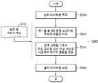
도 11은 본 개시의 예시적 실시예에 따른 집적 회로의 설계 방법의 예시를 나타내는 순서도이다.도 11의 방법은 일련의 명령어들을 실행하는 적어도 하나의 프로세서를 포함하는 컴퓨팅 시스템(예컨대, 도 13의 130)에 의해서 수행될 수 있다. 도 11에 도시된 바와 같이, 집적 회로를 설계하는 방법은 단계 S220, 단계 S240 및 단계 S260을 포함할 수 있다.11 is a flowchart illustrating an example of a method for designing an integrated circuit according to an exemplary embodiment of the present disclosure. The method of FIG. 11 may be performed by a computing system (eg, 130 of FIG. 13 ) including at least one processor that executes a series of instructions. 11 , the method of designing an integrated circuit may include steps S220, S240 and S260.
단계 S220에서, 입력 데이터를 획득하는 동작이 수행될 수 있다. 입력 데이터는 집적 회로를 정의하는 데이터를 지칭할 수 있고, 예컨대 도 10을 참조하여 전술된 네트리스트를 포함할 수 있다. 네트리스트는 집적 회로에 포함되는 셀들 및 연결들에 대한 정보를 포함할 수 있다.In step S220, an operation of obtaining input data may be performed. Input data may refer to data defining an integrated circuit, and may include, for example, the netlist described above with reference to FIG. 10 . The netlist may include information about cells and connections included in the integrated circuit.
단계 S240에서, 셀 라이브러리(D15)에 기초하여 배치 및 라우팅(place and routing; P&R)이 수행될 수 있다. 단계 S240은 복수의 단계들(S241, S242)을 포함할 수 있다. 단계 S241에서, 제1 셀 및 제2 셀을 포함하는 복수의 셀들을 제1 방향으로 연장되는 복수의 행들에 배치하는 동작이 수행될 수 있다. 일부 실시예들에서, 제1 셀은 제1 방향으로 연장되는 배선들이 형성되는 제1 배선층(M1)에 위치하고, 최소 경계 거리(dmin)의 2배 및 제1 방향의 비아 너비(vw)의 합에 대응하는 길이를 갖는 입력 핀 또는 출력 핀을 포함할 수 있다. 일부 실시예들에서, 제2 셀은 제2 방향으로 연장되는 배선들이 형성되는 제2 배선층(M2)에 위치하고, 최소 경계 거리(dmin)의 2배 및 제2 방향의 비아 너비(vw)의 합에 대응하는 길이를 갖는 입력 핀 또는 출력 핀을 포함할 수 있다.In step S240 , placement and routing (P&R) may be performed based on the cell library D15. Step S240 may include a plurality of steps S241 and S242. In operation S241, an operation of arranging a plurality of cells including the first cell and the second cell in a plurality of rows extending in the first direction may be performed. In some embodiments, the first cell is located in the first interconnection layer M1 in which interconnections extending in the first direction are formed, and is the sum of twice the minimum boundary distance dmin and the via width vw in the first direction. It may include an input pin or an output pin having a length corresponding to . In some embodiments, the second cell is located in the second interconnection layer M2 in which interconnections extending in the second direction are formed, and is the sum of twice the minimum boundary distance dmin and the via width vw in the second direction. It may include an input pin or an output pin having a length corresponding to .
단계 242에서, 설계 규칙을 만족하는 최단 길이를 갖는 연결 배선을 사용하여 복수의 셀들을 연결할 수 있다. 구체적으로, 도 7a를 참조하여 전술된 바와 같이, 최소 경계 거리(dmin)의 2배, 제1 비아 너비(vw1), 제2 비아 너비(vw2) 및 비아 거리(dvia1)의 합인 제1 길이(L1)가 최소 길이(Lmin)보다 긴 경우, 설계 규칙을 만족하는 최단 길이는 제1 길이(L1)일 수 있다. 도 7b를 참조하여 전술된 바와 같이, 최소 경계 거리(dmin)의 2배, 제1 비아 너비(vw1), 제2 비아 너비(vw2) 및 비아 거리(dvia1)의 합인 제1 길이(L1)가 최소 길이(Lmin)보다 짧거나 같은 경우, 설계 규칙을 만족하는 최단 길이는 최소 길이(Lmin)일 수 있다.In operation 242 , a plurality of cells may be connected using a connection wire having the shortest length satisfying the design rule. Specifically, as described above with reference to FIG. 7A , the first length ( When L1) is longer than the minimum length Lmin, the shortest length satisfying the design rule may be the first length L1. As described above with reference to FIG. 7B , the first length L1, which is twice the minimum boundary distance dmin, is the sum of the first via width vw1, the second via width vw2, and the via distance dvia1. When shorter than or equal to the minimum length Lmin, the shortest length satisfying the design rule may be the minimum length Lmin.
단계 S260에서, 출력 데이터를 생성하는 동작이 수행될 수 있다. 출력 데이터는 집적 회로의 레이아웃을 정의하는 데이터를 지칭할 수 있고, 예컨대 도 11를 참조하여 전술된 레이아웃 데이터(D14)를 포함할 수 있다. 출력 데이터는 최단 길이를 갖는 연결 배선들을 포함하는 집적 회로의 레이아웃을 정의할 수 있다.In step S260, an operation of generating output data may be performed. The output data may refer to data defining a layout of an integrated circuit, and may include, for example, the layout data D14 described above with reference to FIG. 11 . The output data may define a layout of an integrated circuit including connecting wires having the shortest length.
도 12는 본 개시의 예시적 실시예에 따른 시스템-온-칩(system on chip; SoC)을 나타내는 블록도이다. SoC(120)는 반도체 장치로서, 본 개시의 예시적 실시예에 따른 집적 회로를 포함할 수 있다. SoC(120)는 다양한 기능을 수행하는 IP(intellectual property)와 같은 복잡한 기능 블록들을 하나의 칩에 구현한 것으로서, 본 개시의 예시적 실시예들에 따라 최단 길이를 갖는 연결 배선들이 SoC(120)의 각 기능 블록들에 포함될 수 있고, 이에 따라 디자인 룰 위반을 방지하고 배선 저항이 감소됨으로써 성능이 향상된 SoC(120)가 달성될 수 있다.12 is a block diagram illustrating a system on a chip (SoC) according to an exemplary embodiment of the present disclosure. The SoC 120 is a semiconductor device and may include an integrated circuit according to an exemplary embodiment of the present disclosure. The SoC 120 implements complex functional blocks such as intellectual property (IP) that perform various functions on a single chip. may be included in each functional block of , thereby preventing design rule violation and reducing wiring resistance, thereby achieving improved performance of the SoC 120 .
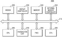
도 12를 참조하면, SoC(120)는 모뎀(122), 디스플레이 컨트롤러(123), 메모리(124), 외부 메모리 컨트롤러(125), CPU(central processing unit)(126), 트랜잭션 유닛(127), PMIC(128) 및 GPU(graphic processing unit)(129)을 포함할 수 있고, SoC(120)의 각 기능 블록들은 시스템 버스(121)를 통해서 서로 통신할 수 있다.12 , the SoC 120 includes a
SoC(120)의 동작을 전반적으로 제어할 수 있는 CPU(126)는 다른 기능 블록들(122, 123, 124, 125, 127, 128, 129)의 동작을 제어할 수 있다. 모뎀(122)은 SoC(120) 외부로부터 수신되는 신호를 복조(demodulation)하거나, SoC(120) 내부에서 생성된 신호를 변조(modulation)하여 외부로 송신할 수 있다. 외부 메모리 컨트롤러(125)는 SoC(120)에 연결된 외부 메모리 장치로부터 데이터를 송수신하는 동작을 제어할 수 있다. 예를 들면, 외부 메모리 장치에 저장된 프로그램 및/또는 데이터는 외부 메모리 컨트롤러(125)의 제어 하에서 CPU(126) 또는 GPU(129)에 제공될 수 있다. GPU(129)는 그래픽 처리와 관련된 프로그램 명령(instruction)들을 실행할 수 있다. GPU(129)는 외부 메모리 컨트롤러(125)를 통해서 그래픽 데이터를 수신할 수도 있고, GPU(129)에 의해서 처리된 그래픽 데이터를 외부 메모리 컨트롤러(125)를 통해서 SoC(120) 외부로 전송할 수도 있다. 트랜잭션 유닛(127)은 각 기능 블록들의 데이터 트랜잭션을 모니터링할 수 있고, PMIC(128)는 트랜잭션 유닛(127)의 제어에 따라 각 기능 블록으로 공급되는 전력을 제어할 수 있다. 디스플레이 컨트롤러(123)는 SoC(120) 외부의 디스플레이(또는 디스플레이 장치)를 제어함으로써 SoC(120) 내부에서 생성된 데이터를 디스플레이에 전송할 수 있다.The CPU 126 , which can control the overall operation of the SoC 120 , may control the operations of other
메모리(124)는, 비휘발성 메모리로서 EEPROM (non-volatile memory such as a Electrically Erasable Programmable Read-Only Memory), 플래시 메모리(flash memory), PRAM(Phase Change Random Access Memory), RRAM(Resistance Random Access Memory), NFGM (Nano Floating Gate Memory), PoRAM(Polymer Random Access Memory), MRAM (Magnetic Random Access Memory), FRAM(Ferroelectric Random Access Memory) 등을 포함할 수도 있고, 휘발성 메모리로서 DRAM(Dynamic Random Access Memory), SRAM(Static Random Access Memory), 모바일 DRAM, DDR SDRAM(Double Data Rate Synchronous Dynamic Random Access Memory), LPDDR (Low Power DDR) SDRAM, GDDR (Graphic DDR) SDRAM, RDRAM(Rambus Dynamic Random Access Memory) 등을 포함할 수도 있다.The memory 124 may include non-volatile memory such as a Electrically Erasable Programmable Read-Only Memory (EEPROM), flash memory, Phase Change Random Access Memory (PRAM), and Resistance Random Access Memory (RRAM) as non-volatile memory. ), NFGM (Nano Floating Gate Memory), PoRAM (Polymer Random Access Memory), MRAM (Magnetic Random Access Memory), FRAM (Ferroelectric Random Access Memory), etc., and may include DRAM (Dynamic Random Access Memory) as a volatile memory , SRAM (Static Random Access Memory), mobile DRAM, DDR SDRAM (Double Data Rate Synchronous Dynamic Random Access Memory), LPDDR (Low Power DDR) SDRAM, GDDR (Graphic DDR) SDRAM, RDRAM (Rambus Dynamic Random Access Memory), etc. may include
도 13은 본 개시의 예시적 실시예에 따른 프로그램을 저장하는 메모리를 포함하는 컴퓨팅 시스템을 나타내는 블록도이다. 본 개시의 예시적 실시예들에 따른, 집적 회로를 제조하기 위한 방법(예컨대, 도 10의 방법)에 포함되는 단계들, 집적 회로를 설계하는 방법(예컨대, 도 11의 방법)에 포함되는 단계들 중 적어도 일부는 컴퓨팅 시스템(130)에서 수행될 수 있다.13 is a block diagram illustrating a computing system including a memory for storing a program according to an exemplary embodiment of the present disclosure. Steps included in a method (eg, the method of FIG. 10 ) for manufacturing an integrated circuit according to exemplary embodiments of the present disclosure, Steps included in a method (eg, the method of FIG. 11 ) of designing an integrated circuit At least some of these may be performed in the computing system 130 .
컴퓨팅 시스템(130)은 데스크탑 컴퓨터, 워크스테이션, 서버 등과 같이 고정형 컴퓨팅 시스템일 수도 있고, 랩탑 컴퓨터 등과 같이 휴대형 컴퓨팅 시스템일 수도 있다. 도 13에 도시된 바와 같이, 컴퓨팅 시스템(130)은 프로세서(131), 입출력 장치들(132), 네트워크 인터페이스(133), RAM(random access memory)(134), ROM(read only memory)(135) 및 저장 장치(136)를 포함할 수 있다. 프로세서(131), 입출력 장치들(132), 네트워크 인터페이스(133), RAM(134), ROM(135) 및 저장 장치(136)는 버스(137)에 연결될 수 있고, 버스(137)를 통해서 서로 통신할 수 있다.Computing system 130 may be a stationary computing system, such as a desktop computer, workstation, server, or the like, or a portable computing system, such as a laptop computer. 13 , the computing system 130 includes a processor 131 , input/output devices 132 , a network interface 133 , a random access memory (RAM) 134 , and a read only memory (ROM) 135 . ) and a storage device 136 . The processor 131 , the input/output devices 132 , the network interface 133 , the RAM 134 , the ROM 135 , and the storage device 136 may be connected to the bus 137 , and may be connected to each other via the bus 137 . can communicate
프로세서(131)는 프로세싱 유닛으로 지칭될 수 있고, 예컨대 마이크로프로세서(micro-processor), AP(application processor), DSP(digital signal processor), GPU(graphic processing unit)과 같이 임의의 명령어 세트(예컨대, IA-32(Intel Architecture-32), 64 비트 확장 IA-32, x86-64, PowerPC, Sparc, MIPS, ARM, IA-64 등)를 실행할 수 있는 적어도 하나의 코어를 포함할 수 있다. 예를 들면, 프로세서(131)는 버스(137)를 통해서 메모리, 즉 RAM(134) 또는 ROM(135)에 액세스할 수 있고, RAM(134) 또는 ROM(135)에 저장된 명령어들을 실행할 수 있다.The processor 131 may be referred to as a processing unit, and may be any instruction set (eg, a micro-processor), an application processor (AP), a digital signal processor (DSP), or a graphic processing unit (GPU). at least one core capable of running IA-32 (Intel Architecture-32), 64-bit extended IA-32, x86-64, PowerPC, Sparc, MIPS, ARM, IA-64, etc.). For example, processor 131 may access memory, ie, RAM 134 or ROM 135 , via bus 137 , and execute instructions stored in RAM 134 or ROM 135 .
RAM(134)은 본 개시의 예시적 실시예에 따른 집적 회로를 제조하기 위한 프로그램(134_1) 또는 그것의 적어도 일부를 저장할 수 있고, 프로그램(134_1)은 프로세서(131)로 하여금, 집적 회로를 제조하기 위한 방법(예컨대, 도 10의 방법)에 포함되는 단계들 및 집적 회로를 설계하는 방법(예컨대, 도 11의 방법)에 포함되는 단계들 중 적어도 일부를 수행하도록 할 수 있다. 즉, 프로그램(134_1)은 프로세서(131)에 의해서 실행 가능한 복수의 명령어들을 포함할 수 있고, 프로그램(134_1)에 포함된 복수의 명령어들은 프로세서(131)로 하여금, 예컨대 도 10 및 도 11을 참조하여 전술된 순서도에 포함된 단계들 중 적어도 일부를 수행하도록 할 수 있다.The RAM 134 may store a program 134_1 or at least a part thereof for manufacturing an integrated circuit according to an exemplary embodiment of the present disclosure, and the program 134_1 causes the processor 131 to manufacture the integrated circuit. At least some of the steps included in the method for (eg, the method of FIG. 10 ) and the steps included in the method (eg, the method of FIG. 11 ) of designing an integrated circuit may be performed. That is, the program 134_1 may include a plurality of instructions executable by the processor 131 , and the plurality of instructions included in the program 134_1 causes the processor 131 to refer, for example, to FIGS. 10 and 11 . to perform at least some of the steps included in the above-described flowchart.
저장 장치(136)는 컴퓨팅 시스템(130)에 공급되는 전력이 차단되더라도 저장된 데이터를 소실하지 아니할 수 있다. 예를 들면, 저장 장치(136)는 비휘발성 메모리 장치를 포함할 수도 있고, 자기 테이프, 광학 디스크, 자기 디스크와 같은 저장 매체를 포함할 수도 있다. 또한, 저장 장치(136)는 컴퓨팅 시스템(130)으로부터 탈착 가능할 수도 있다. 저장 장치(136)는 본 개시의 예시적 실시예에 따른 프로그램(134_1)을 저장할 수도 있으며, 프로그램(134_1)이 프로세서(131)에 의해서 실행되기 이전에 저장 장치(136)로부터 프로그램(134_1) 또는 그것의 적어도 일부가 RAM(134)으로 로딩될 수 있다. 다르게는, 저장 장치(136)는 프로그램 언어로 작성된 파일을 저장할 수 있고, 파일로부터 컴파일러 등에 의해서 생성된 프로그램(134_1) 또는 그것의 적어도 일부가 RAM(134)으로 로딩될 수 있다. 또한, 도 13에 도시된 바와 같이, 저장 장치(136)는 데이터베이스(136_1)를 저장할 수 있고, 데이터베이스(136_1)는 집적 회로를 설계하는데 필요한 정보, 예컨대 도 11의 표준 셀 라이브러리(D12)를 포함할 수 있다.The storage device 136 may not lose stored data even if the power supplied to the computing system 130 is cut off. For example, the storage device 136 may include a non-volatile memory device, and may include a storage medium such as a magnetic tape, an optical disk, or a magnetic disk. Also, the storage device 136 may be removable from the computing system 130 . The storage device 136 may store the program 134_1 according to an exemplary embodiment of the present disclosure, and before the program 134_1 is executed by the processor 131 , the program 134_1 or At least a portion of it may be loaded into RAM 134 . Alternatively, the storage device 136 may store a file written in a programming language, and the program 134_1 generated from the file by a compiler or the like or at least a part thereof may be loaded into the RAM 134 . Also, as shown in FIG. 13 , the storage device 136 may store a database 136_1 , and the database 136_1 includes information necessary for designing an integrated circuit, for example, the standard cell library D12 of FIG. 11 . can do.
저장 장치(136)는 프로세서(131)에 의해서 처리될 데이터 또는 프로세서(131)에 의해서 처리된 데이터를 저장할 수도 있다. 즉, 프로세서(131)는 프로그램(134_1)에 따라, 저장 장치(136)에 저장된 데이터를 처리함으로써 데이터를 생성할 수 있고, 생성된 데이터를 저장 장치(136)에 저장할 수도 있다. 예를 들면, 저장 장치(136)는, 도 10의 RTL 데이터(D11), 네트리스트 데이터(D13) 및/또는 레이아웃 데이터(D14)를 저장할 수 있다.The storage device 136 may store data to be processed by the processor 131 or data processed by the processor 131 . That is, the processor 131 may generate data by processing data stored in the storage device 136 according to the program 134_1 , and may store the generated data in the storage device 136 . For example, the storage device 136 may store the RTL data D11 , the netlist data D13 , and/or the layout data D14 of FIG. 10 .
입출력 장치들(132)은 키보드, 포인팅 장치 등과 같은 입력 장치를 포함할 수 있고, 디스플레이 장치, 프린터 등과 같은 출력 장치를 포함할 수 있다. 예를 들면, 사용자는 입출력 장치들(132)을 통해서, 프로세서(131)에 의해 프로그램(134_1)의 실행을 트리거할 수도 있고, 도 10의 RTL 데이터(D11) 및/또는 네트리스트 데이터(D13)를 입력할 수도 있으며, 도 10의 레이아웃 데이터(D14)를 확인할 수도 있다.The input/output devices 132 may include an input device such as a keyboard and a pointing device, and may include an output device such as a display device and a printer. For example, the user may trigger execution of the program 134_1 by the processor 131 through the input/output devices 132 , and the RTL data D11 and/or netlist data D13 of FIG. 10 . may be input, and the layout data D14 of FIG. 10 may be checked.
네트워크 인터페이스(133)는 컴퓨팅 시스템(130) 외부의 네트워크에 대한 액세스를 제공할 수 있다. 예를 들면, 네트워크는 다수의 컴퓨팅 시스템들 및 통신 링크들을 포함할 수 있고, 통신 링크들은 유선 링크들, 광학 링크들, 무선 링크들 또는 임의의 다른 형태의 링크들을 포함할 수 있다.Network interface 133 may provide access to a network external to computing system 130 . For example, a network may include multiple computing systems and communication links, and the communication links may include wired links, optical links, wireless links, or any other type of links.
이상에서와 같이 도면과 명세서에서 예시적인 실시 예들이 개시되었다. 본 명세서에서 특정한 용어를 사용하여 실시 예들을 설명되었으나, 이는 단지 본 개시의 기술적 사상을 설명하기 위한 목적에서 사용된 것이지 의미 한정이나 특허청구범위에 기재된 본 개시의 범위를 제한하기 위하여 사용된 것은 아니다. 그러므로 본 기술분야의 통상의 지식을 가진 자라면 이로부터 다양한 변형 및 균등한 타 실시 예가 가능하다는 점을 이해할 것이다. 따라서, 본 개시의 진정한 기술적 보호범위는 첨부된 특허청구범위의 기술적 사상에 의해 정해져야 할 것이다.Exemplary embodiments have been disclosed in the drawings and specification as described above. Although embodiments have been described using specific terms in the present specification, these are only used for the purpose of explaining the technical idea of the present disclosure and not used to limit the meaning or the scope of the present disclosure described in the claims . Therefore, those skilled in the art will understand that various modifications and equivalent other embodiments are possible therefrom. Accordingly, the true technical protection scope of the present disclosure should be defined by the technical spirit of the appended claims.
Claims (10)
Translated fromKorean상기 제1 행에 배치되고 제2 기능을 수행하는 제2 셀;
상기 제1 방향으로 연장되는 제2 행에 배치되고 상기 제1 기능을 수행하는 제3 셀;
상기 제2 행에 배치되고 상기 제2 기능을 수행하는 제4 셀;
상기 제1 셀에 포함되는 제1 비아와, 상기 제2 셀에 포함되는 제2 비아를 연결하는 제1 연결 배선; 및
상기 제3 셀에 포함되는 제3 비아와, 상기 제4 셀에 포함되는 제4 비아를 연결하는 제2 연결 배선을 포함하고,
상기 제1 연결 배선의 길이와 상기 제2 연결 배선의 길이는 상이한 것을 특징으로 하는 집적 회로.a first cell disposed in a first row extending in a first direction and performing a first function;
a second cell disposed in the first row and performing a second function;
a third cell disposed in a second row extending in the first direction and performing the first function;
a fourth cell disposed in the second row and performing the second function;
a first connection line connecting a first via included in the first cell and a second via included in the second cell; and
a second connection line connecting a third via included in the third cell and a fourth via included in the fourth cell;
The integrated circuit of claim 1 , wherein a length of the first connection line is different from a length of the second connection line.
상기 제1 연결 배선의 길이는,
경계 규칙(enclosure rule)에 따른 최소 경계 거리의 2배와, 상기 제1 비아와 상기 제2 비아 간의 거리의 합에 대응하는 것을 특징으로 하는 집적 회로.According to claim 1,
The length of the first connection wire is,
An integrated circuit, characterized in that it corresponds to a sum of twice the minimum boundary distance according to an enclosure rule and a distance between the first via and the second via.
상기 제2 연결 배선의 길이는,
설계 규칙에 따른 배선의 최소 길이에 대응하는 것을 특징으로 하는 집적 회로.3. The method of claim 2,
The length of the second connection wire is,
An integrated circuit, characterized in that it corresponds to a minimum length of wiring according to a design rule.
상기 제2 연결 배선의 길이는,
경계 규칙(enclosure rule)에 따른 최소 경계 거리의 2배와, 상기 제3 비아와 상기 제4 비아 간의 거리의 합은, 상기 최소 길이보다 짧은 것을 특징으로 하는 집적 회로.4. The method of claim 3,
The length of the second connection wire is,
The integrated circuit of claim 1, wherein a sum of twice a minimum boundary distance according to an enclosure rule and a distance between the third via and the fourth via is shorter than the minimum length.
상기 제1 방향으로 연장되는 제3 행에 배치되고 제3 기능을 수행하는 제5 셀;
상기 제1 방향으로 연장되는 제4 행에 배치되고 제4 기능을 수행하는 제6 셀;
상기 제3 행에 배치되고 상기 제3 기능을 수행하는 제7 셀;
상기 제4 행에 배치되고 상기 제4 기능을 수행하는 제8 셀;
상기 제5 셀에 포함되는 제5 비아와, 상기 제6 셀에 포함되는 제6 비아를 연결하고, 상기 제1 방향과 수직한 제2 방향으로 연장되는 제3 연결 배선; 및
상기 제7 셀에 포함되는 제7 비아와, 상기 제8 셀에 포함되는 제8 비아를 연결하고, 상기 제2 방향으로 연장되는 제4 연결 배선을 포함하고,
상기 제3 연결 배선의 길이와 상기 제4 연결 배선의 길이는 상이한 것을 특징으로 하는 집적 회로.According to claim 1,
a fifth cell arranged in a third row extending in the first direction and performing a third function;
a sixth cell arranged in a fourth row extending in the first direction and performing a fourth function;
a seventh cell disposed in the third row and performing the third function;
an eighth cell disposed in the fourth row and performing the fourth function;
a third connection line connecting a fifth via included in the fifth cell and a sixth via included in the sixth cell and extending in a second direction perpendicular to the first direction; and
a fourth connection line connecting a seventh via included in the seventh cell and an eighth via included in the eighth cell and extending in the second direction;
The integrated circuit of claim 1 , wherein a length of the third connecting line is different from a length of the fourth connecting line.
상기 제3 연결 배선의 길이는,
경계 규칙(enclosure rule)에 따른 최소 경계 거리의 2배와, 상기 제5 비아와 상기 제6 비아 간의 거리의 합에 대응하는 것을 특징으로 하는 집적 회로.6. The method of claim 5,
The length of the third connecting wire is,
An integrated circuit, characterized in that it corresponds to a sum of twice the minimum boundary distance according to an enclosure rule and a distance between the fifth via and the sixth via.
상기 제4 연결 배선의 길이는,
설계 규칙에 따른 배선의 최소 길이에 대응하는 것을 특징으로 하는 집적 회로.7. The method of claim 6,
The length of the fourth connecting wire is,
An integrated circuit, characterized in that it corresponds to a minimum length of wiring according to a design rule.
제2 비아를 포함하는 제2 셀; 및
제1 방향으로 연장되고 상기 제1 비아 및 상기 제2 비아를 연결하는 연결 배선을 포함하고,
상기 연결 배선의 길이는,
상기 제1 비아 및 제2 비아 간의 비아 거리, 상기 제1 비아 및 상기 제2 비아의 경계로부터 확장된 영역을 나타내는 최소 경계 거리(minimum enclosure distance)를 기초로 하는 제1 길이와, 설계 규칙에 따른 최소 길이인 제2 길이 중 하나인 것을 특징으로 하는 집적 회로.a first cell comprising a first via;
a second cell comprising a second via; and
a connection line extending in a first direction and connecting the first via and the second via;
The length of the connecting wire is,
a first length based on a via distance between the first via and a second via, a minimum enclosure distance representing an area extending from the boundary of the first via and the second via, and one of the second lengths being the minimum length.
상기 제1 길이는,
상기 최소 경계 거리의 2배와, 상기 비아 거리의 합에 대응하는 것을 특징으로 하는 집적 회로.9. The method of claim 8,
The first length is
and corresponding to the sum of twice the minimum boundary distance and the via distance.
상기 입력 데이터에 기초하여, 상기 최소 경계 거리 및 제2 비아의 너비를 기초로 결정되는 길이를 갖는 제2 핀을 포함하는 제2 셀을 배치하는 단계;
설계 규칙을 만족하는 최단 길이를 갖는 연결 배선을 사용하여 상기 제1 핀 및 상기 제2 핀을 연결하는 단계; 및
상기 집적 회로의 레이아웃을 정의하는 출력 데이터를 생성하는 단계를 포함하고,
상기 최단 길이는,
상기 제1 비아 및 제2 비아 간의 비아 거리, 상기 최소 경계 거리를 기초로 하는 제1 길이와, 상기 설계 규칙에 따라 설정되는 배선의 최소 길이인 제2 길이 중 하나인 것을 특징으로 하는 집적 회로를 설계하는 방법.A first cell including a first pin having a length determined based on a width of the first via and a minimum enclosure distance according to an enclosure rule based on input data defining the integrated circuit placing a;
arranging a second cell including a second fin having a length determined based on the minimum boundary distance and a width of a second via based on the input data;
connecting the first pin and the second pin using a connecting wire having a shortest length satisfying a design rule; and
generating output data defining a layout of the integrated circuit;
The shortest length is
An integrated circuit comprising: a via distance between the first via and the second via, a first length based on the minimum boundary distance, and a second length that is a minimum length of a wiring set according to the design rule; How to design.
Priority Applications (2)
| Application Number | Priority Date | Filing Date | Title |
|---|---|---|---|
| US17/545,009US20220189945A1 (en) | 2020-12-10 | 2021-12-08 | Integrated circuit including connection line |
| CN202111496762.1ACN114628380A (en) | 2020-12-10 | 2021-12-09 | Integrated circuit including connecting lines |
Applications Claiming Priority (2)
| Application Number | Priority Date | Filing Date | Title |
|---|---|---|---|
| KR1020200172577 | 2020-12-10 | ||
| KR20200172577 | 2020-12-10 |
Publications (1)
| Publication Number | Publication Date |
|---|---|
| KR20220082708Atrue KR20220082708A (en) | 2022-06-17 |
Family
ID=82268910
Family Applications (1)
| Application Number | Title | Priority Date | Filing Date |
|---|---|---|---|
| KR1020210045037APendingKR20220082708A (en) | 2020-12-10 | 2021-04-07 | Integrated circuit including connection line |
Country Status (1)
| Country | Link |
|---|---|
| KR (1) | KR20220082708A (en) |
- 2021
- 2021-04-07KRKR1020210045037Apatent/KR20220082708A/enactivePending
Similar Documents
| Publication | Publication Date | Title |
|---|---|---|
| US11727184B2 (en) | Integrated circuit including cells of different heights and method of designing the integrated circuit | |
| US11755809B2 (en) | Integrated circuit including asymmetric power line and method of designing the same | |
| KR102599048B1 (en) | Integrated circuit including standard cell and method for manufacturing the same | |
| US11557584B2 (en) | Integrated circuit including simple cell interconnection and method of designing the same | |
| US20220262785A1 (en) | Integrated circuit including signal line and power line and method of designing the same | |
| KR102817953B1 (en) | Integrated circuit including cells with different heights and method for designing the same | |
| US11189639B2 (en) | Integrated circuit including interconnection and method of fabricating the same, the interconnection including a pattern shaped for mitigating electromigration | |
| TW202320231A (en) | Integrated circuit including standard cell and method of fabricating the same | |
| US20250272468A1 (en) | Integrated circuit providing increased pin access points and method of designing the same | |
| TW202247414A (en) | Integrated circuit including standard cell and filler cell | |
| US20220189945A1 (en) | Integrated circuit including connection line | |
| KR20220082708A (en) | Integrated circuit including connection line | |
| KR20220130547A (en) | Integrated circuit providing increased pin access points and method of designing same | |
| US20240243117A1 (en) | Integrated circuit including standard cells and method of designing the same | |
| US11476257B2 (en) | Integrated circuit including memory cell and method of designing the same | |
| US20240250028A1 (en) | Integrated circuit including backside wiring and method of designing the same | |
| KR20250041959A (en) | Integrated circuit including complementary field effect transistor | |
| KR20220015914A (en) | Integrated circuit including a memory cell and method of designating the same | |
| KR20240096315A (en) | Integrated circuit including standard cell |
Legal Events
| Date | Code | Title | Description |
|---|---|---|---|
| PA0109 | Patent application | St.27 status event code:A-0-1-A10-A12-nap-PA0109 | |
| PG1501 | Laying open of application | St.27 status event code:A-1-1-Q10-Q12-nap-PG1501 | |
| A201 | Request for examination | ||
| PA0201 | Request for examination | St.27 status event code:A-1-2-D10-D11-exm-PA0201 | |
| P22-X000 | Classification modified | St.27 status event code:A-2-2-P10-P22-nap-X000 | |
| E902 | Notification of reason for refusal | ||
| PE0902 | Notice of grounds for rejection | St.27 status event code:A-1-2-D10-D21-exm-PE0902 | |
| P11-X000 | Amendment of application requested | St.27 status event code:A-2-2-P10-P11-nap-X000 | |
| P13-X000 | Application amended | St.27 status event code:A-2-2-P10-P13-nap-X000 |