KR20220077574A - Antenna feeding sturcture including flexible printed circuit board and electronic device including the same - Google Patents
Antenna feeding sturcture including flexible printed circuit board and electronic device including the sameDownload PDFInfo
- Publication number
- KR20220077574A KR20220077574AKR1020200166653AKR20200166653AKR20220077574AKR 20220077574 AKR20220077574 AKR 20220077574AKR 1020200166653 AKR1020200166653 AKR 1020200166653AKR 20200166653 AKR20200166653 AKR 20200166653AKR 20220077574 AKR20220077574 AKR 20220077574A
- Authority
- KR
- South Korea
- Prior art keywords
- printed circuit
- circuit board
- flexible printed
- electronic device
- frame
- Prior art date
- Legal status (The legal status is an assumption and is not a legal conclusion. Google has not performed a legal analysis and makes no representation as to the accuracy of the status listed.)
- Pending
Links
Images


Classifications
- H—ELECTRICITY
- H01—ELECTRIC ELEMENTS
- H01Q—ANTENNAS, i.e. RADIO AERIALS
- H01Q1/00—Details of, or arrangements associated with, antennas
- H01Q1/12—Supports; Mounting means
- H01Q1/22—Supports; Mounting means by structural association with other equipment or articles
- H01Q1/24—Supports; Mounting means by structural association with other equipment or articles with receiving set
- H—ELECTRICITY
- H01—ELECTRIC ELEMENTS
- H01Q—ANTENNAS, i.e. RADIO AERIALS
- H01Q1/00—Details of, or arrangements associated with, antennas
- H01Q1/36—Structural form of radiating elements, e.g. cone, spiral, umbrella; Particular materials used therewith
- H01Q1/38—Structural form of radiating elements, e.g. cone, spiral, umbrella; Particular materials used therewith formed by a conductive layer on an insulating support
- H—ELECTRICITY
- H01—ELECTRIC ELEMENTS
- H01Q—ANTENNAS, i.e. RADIO AERIALS
- H01Q1/00—Details of, or arrangements associated with, antennas
- H01Q1/12—Supports; Mounting means
- H01Q1/22—Supports; Mounting means by structural association with other equipment or articles
- H01Q1/2283—Supports; Mounting means by structural association with other equipment or articles mounted in or on the surface of a semiconductor substrate as a chip-type antenna or integrated with other components into an IC package
- H—ELECTRICITY
- H01—ELECTRIC ELEMENTS
- H01Q—ANTENNAS, i.e. RADIO AERIALS
- H01Q1/00—Details of, or arrangements associated with, antennas
- H01Q1/12—Supports; Mounting means
- H01Q1/22—Supports; Mounting means by structural association with other equipment or articles
- H01Q1/24—Supports; Mounting means by structural association with other equipment or articles with receiving set
- H01Q1/241—Supports; Mounting means by structural association with other equipment or articles with receiving set used in mobile communications, e.g. GSM
- H01Q1/242—Supports; Mounting means by structural association with other equipment or articles with receiving set used in mobile communications, e.g. GSM specially adapted for hand-held use
- H01Q1/243—Supports; Mounting means by structural association with other equipment or articles with receiving set used in mobile communications, e.g. GSM specially adapted for hand-held use with built-in antennas
- H—ELECTRICITY
- H01—ELECTRIC ELEMENTS
- H01Q—ANTENNAS, i.e. RADIO AERIALS
- H01Q1/00—Details of, or arrangements associated with, antennas
- H01Q1/44—Details of, or arrangements associated with, antennas using equipment having another main function to serve additionally as an antenna, e.g. means for giving an antenna an aesthetic aspect
- H01Q1/46—Electric supply lines or communication lines
- H—ELECTRICITY
- H01—ELECTRIC ELEMENTS
- H01Q—ANTENNAS, i.e. RADIO AERIALS
- H01Q1/00—Details of, or arrangements associated with, antennas
- H01Q1/48—Earthing means; Earth screens; Counterpoises
- H—ELECTRICITY
- H04—ELECTRIC COMMUNICATION TECHNIQUE
- H04M—TELEPHONIC COMMUNICATION
- H04M1/00—Substation equipment, e.g. for use by subscribers
- H04M1/02—Constructional features of telephone sets
- H04M1/0202—Portable telephone sets, e.g. cordless phones, mobile phones or bar type handsets
- H04M1/026—Details of the structure or mounting of specific components
- H—ELECTRICITY
- H05—ELECTRIC TECHNIQUES NOT OTHERWISE PROVIDED FOR
- H05K—PRINTED CIRCUITS; CASINGS OR CONSTRUCTIONAL DETAILS OF ELECTRIC APPARATUS; MANUFACTURE OF ASSEMBLAGES OF ELECTRICAL COMPONENTS
- H05K1/00—Printed circuits
- H05K1/02—Details
- H05K1/0213—Electrical arrangements not otherwise provided for
- H05K1/0237—High frequency adaptations
- H05K1/0243—Printed circuits associated with mounted high frequency components
- H—ELECTRICITY
- H05—ELECTRIC TECHNIQUES NOT OTHERWISE PROVIDED FOR
- H05K—PRINTED CIRCUITS; CASINGS OR CONSTRUCTIONAL DETAILS OF ELECTRIC APPARATUS; MANUFACTURE OF ASSEMBLAGES OF ELECTRICAL COMPONENTS
- H05K1/00—Printed circuits
- H05K1/02—Details
- H05K1/14—Structural association of two or more printed circuits
- H05K1/147—Structural association of two or more printed circuits at least one of the printed circuits being bent or folded, e.g. by using a flexible printed circuit
- H—ELECTRICITY
- H05—ELECTRIC TECHNIQUES NOT OTHERWISE PROVIDED FOR
- H05K—PRINTED CIRCUITS; CASINGS OR CONSTRUCTIONAL DETAILS OF ELECTRIC APPARATUS; MANUFACTURE OF ASSEMBLAGES OF ELECTRICAL COMPONENTS
- H05K1/00—Printed circuits
- H05K1/18—Printed circuits structurally associated with non-printed electric components
- H05K1/189—Printed circuits structurally associated with non-printed electric components characterised by the use of a flexible or folded printed circuit
- H—ELECTRICITY
- H04—ELECTRIC COMMUNICATION TECHNIQUE
- H04M—TELEPHONIC COMMUNICATION
- H04M1/00—Substation equipment, e.g. for use by subscribers
- H04M1/02—Constructional features of telephone sets
- H04M1/0202—Portable telephone sets, e.g. cordless phones, mobile phones or bar type handsets
- H04M1/026—Details of the structure or mounting of specific components
- H04M1/0277—Details of the structure or mounting of specific components for a printed circuit board assembly
- H—ELECTRICITY
- H05—ELECTRIC TECHNIQUES NOT OTHERWISE PROVIDED FOR
- H05K—PRINTED CIRCUITS; CASINGS OR CONSTRUCTIONAL DETAILS OF ELECTRIC APPARATUS; MANUFACTURE OF ASSEMBLAGES OF ELECTRICAL COMPONENTS
- H05K1/00—Printed circuits
- H05K1/02—Details
- H05K1/0213—Electrical arrangements not otherwise provided for
- H05K1/0215—Grounding of printed circuits by connection to external grounding means
- H—ELECTRICITY
- H05—ELECTRIC TECHNIQUES NOT OTHERWISE PROVIDED FOR
- H05K—PRINTED CIRCUITS; CASINGS OR CONSTRUCTIONAL DETAILS OF ELECTRIC APPARATUS; MANUFACTURE OF ASSEMBLAGES OF ELECTRICAL COMPONENTS
- H05K1/00—Printed circuits
- H05K1/02—Details
- H05K1/0213—Electrical arrangements not otherwise provided for
- H05K1/0216—Reduction of cross-talk, noise or electromagnetic interference
- H05K1/0218—Reduction of cross-talk, noise or electromagnetic interference by printed shielding conductors, ground planes or power plane
- H05K1/0219—Printed shielding conductors for shielding around or between signal conductors, e.g. coplanar or coaxial printed shielding conductors
- H—ELECTRICITY
- H05—ELECTRIC TECHNIQUES NOT OTHERWISE PROVIDED FOR
- H05K—PRINTED CIRCUITS; CASINGS OR CONSTRUCTIONAL DETAILS OF ELECTRIC APPARATUS; MANUFACTURE OF ASSEMBLAGES OF ELECTRICAL COMPONENTS
- H05K1/00—Printed circuits
- H05K1/02—Details
- H05K1/11—Printed elements for providing electric connections to or between printed circuits
- H05K1/111—Pads for surface mounting, e.g. lay-out
- H—ELECTRICITY
- H05—ELECTRIC TECHNIQUES NOT OTHERWISE PROVIDED FOR
- H05K—PRINTED CIRCUITS; CASINGS OR CONSTRUCTIONAL DETAILS OF ELECTRIC APPARATUS; MANUFACTURE OF ASSEMBLAGES OF ELECTRICAL COMPONENTS
- H05K2201/00—Indexing scheme relating to printed circuits covered by H05K1/00
- H05K2201/05—Flexible printed circuits [FPCs]
- H05K2201/056—Folded around rigid support or component
- H—ELECTRICITY
- H05—ELECTRIC TECHNIQUES NOT OTHERWISE PROVIDED FOR
- H05K—PRINTED CIRCUITS; CASINGS OR CONSTRUCTIONAL DETAILS OF ELECTRIC APPARATUS; MANUFACTURE OF ASSEMBLAGES OF ELECTRICAL COMPONENTS
- H05K2201/00—Indexing scheme relating to printed circuits covered by H05K1/00
- H05K2201/09—Shape and layout
- H05K2201/09209—Shape and layout details of conductors
- H05K2201/095—Conductive through-holes or vias
- H05K2201/09618—Via fence, i.e. one-dimensional array of vias
- H—ELECTRICITY
- H05—ELECTRIC TECHNIQUES NOT OTHERWISE PROVIDED FOR
- H05K—PRINTED CIRCUITS; CASINGS OR CONSTRUCTIONAL DETAILS OF ELECTRIC APPARATUS; MANUFACTURE OF ASSEMBLAGES OF ELECTRICAL COMPONENTS
- H05K2201/00—Indexing scheme relating to printed circuits covered by H05K1/00
- H05K2201/10—Details of components or other objects attached to or integrated in a printed circuit board
- H05K2201/10007—Types of components
- H05K2201/10098—Components for radio transmission, e.g. radio frequency identification [RFID] tag, printed or non-printed antennas
- H—ELECTRICITY
- H05—ELECTRIC TECHNIQUES NOT OTHERWISE PROVIDED FOR
- H05K—PRINTED CIRCUITS; CASINGS OR CONSTRUCTIONAL DETAILS OF ELECTRIC APPARATUS; MANUFACTURE OF ASSEMBLAGES OF ELECTRICAL COMPONENTS
- H05K2201/00—Indexing scheme relating to printed circuits covered by H05K1/00
- H05K2201/10—Details of components or other objects attached to or integrated in a printed circuit board
- H05K2201/10007—Types of components
- H05K2201/10189—Non-printed connector
- H—ELECTRICITY
- H05—ELECTRIC TECHNIQUES NOT OTHERWISE PROVIDED FOR
- H05K—PRINTED CIRCUITS; CASINGS OR CONSTRUCTIONAL DETAILS OF ELECTRIC APPARATUS; MANUFACTURE OF ASSEMBLAGES OF ELECTRICAL COMPONENTS
- H05K2201/00—Indexing scheme relating to printed circuits covered by H05K1/00
- H05K2201/10—Details of components or other objects attached to or integrated in a printed circuit board
- H05K2201/10227—Other objects, e.g. metallic pieces
- H05K2201/1028—Thin metal strips as connectors or conductors
- H—ELECTRICITY
- H05—ELECTRIC TECHNIQUES NOT OTHERWISE PROVIDED FOR
- H05K—PRINTED CIRCUITS; CASINGS OR CONSTRUCTIONAL DETAILS OF ELECTRIC APPARATUS; MANUFACTURE OF ASSEMBLAGES OF ELECTRICAL COMPONENTS
- H05K2201/00—Indexing scheme relating to printed circuits covered by H05K1/00
- H05K2201/10—Details of components or other objects attached to or integrated in a printed circuit board
- H05K2201/10227—Other objects, e.g. metallic pieces
- H05K2201/10409—Screws
- H—ELECTRICITY
- H05—ELECTRIC TECHNIQUES NOT OTHERWISE PROVIDED FOR
- H05K—PRINTED CIRCUITS; CASINGS OR CONSTRUCTIONAL DETAILS OF ELECTRIC APPARATUS; MANUFACTURE OF ASSEMBLAGES OF ELECTRICAL COMPONENTS
- H05K2201/00—Indexing scheme relating to printed circuits covered by H05K1/00
- H05K2201/20—Details of printed circuits not provided for in H05K2201/01 - H05K2201/10
- H05K2201/2018—Presence of a frame in a printed circuit or printed circuit assembly
Landscapes
- Engineering & Computer Science (AREA)
- Microelectronics & Electronic Packaging (AREA)
- Computer Networks & Wireless Communication (AREA)
- Signal Processing (AREA)
- Support Of Aerials (AREA)
Abstract
Translated fromKoreanDescription
Translated fromKorean본 문서에 개시된 다양한 실시예들은, 유연 인쇄 회로 기판을 포함하는 안테나 급전 구조와 안테나 급전 구조를 포함하는 전자 장치에 관한 것이다.Various embodiments disclosed in this document relate to an antenna feeding structure including a flexible printed circuit board and an electronic device including the antenna feeding structure.
휴대 전자 장치의 디자인 트렌드로 인해 외관 금속을 적용한 전자 장치의 수요가 증가하고 있다.Due to the design trend of portable electronic devices, the demand for electronic devices to which exterior metal is applied is increasing.
금속 소재의 프레임을 외관으로 갖는 전자 장치의 경우, 프레임 내부에 안테나를 배치하는 것이 제한적일 수 있다. 이를 극복하기 위해 금속 소재의 프레임 자체를 안테나의 방사체로 활용하여 다중 대역의 안테나를 구현하고 방사 성능을 확보하는 방안이 적용되고 있다.In the case of an electronic device having a metal frame as an exterior, disposing of an antenna inside the frame may be limited. In order to overcome this, a method of implementing a multi-band antenna by using a metal frame itself as a radiator of the antenna and securing radiation performance is being applied.
한편, 5G 서비스가 시작되면서 추가적인 서비스 밴드들이 추가될 수 있다. 이 때문에 기존 보다 더 많은 수의 안테나 방사체가 요구될 수 있다.Meanwhile, as the 5G service starts, additional service bands may be added. For this reason, a larger number of antenna radiators may be required than before.
금속 소재의 프레임을 외관으로 갖는 전자 장치에서 프레임을 안테나로 활용하기 위해서는 회로부와 프레임이 전기적으로 연결되어야 한다. 회로부는 일반적인 인쇄 회로 기판에 배치될 수 있다. 일반적인 인쇄 회로 기판은 변형이 어렵다. 따라서, 회로부와 프레임을 연결하기 위해서는 인쇄 회로 기판을 프레임의 내측까지 확장하고, 프레임과 인쇄 회로 기판을 연결하는 구조를 사용하는 것이 일반적이다.In an electronic device having a metal frame as an exterior, in order to use the frame as an antenna, the circuit unit and the frame must be electrically connected. The circuit unit may be disposed on a general printed circuit board. A general printed circuit board is difficult to deform. Therefore, in order to connect the circuit unit and the frame, it is common to use a structure in which the printed circuit board is extended to the inside of the frame and the frame and the printed circuit board are connected.
고용량 데이터의 고속 전송을 위해서는 MIMO(multi input multi output), CA(carrier aggregation), ENDC(e-utran new radio dual connectivity)와 같은 기술의 적용이 필요하며, 이를 구현하기 위해서 안테나의 개수가 증가하게 되었다. 이는 금속 소재 프레임에 연결되는 안테나 개수의 증가의 원인이 된다. 늘어난 안테나와 연결되기 위하여 인쇄 회로 기판이 확장되는 영역도 증가하였는데, 전자 장치 내부 공간의 한계로 이러한 확장에도 제약이 따른다.For high-speed transmission of high-capacity data, it is necessary to apply technologies such as MIMO (multi input multi output), CA (carrier aggregation), and ENDC (e-utran new radio dual connectivity). became This causes an increase in the number of antennas connected to the metal frame. The area in which the printed circuit board is extended in order to be connected to the increased antenna has also increased, but this expansion is also limited due to the limitation of the space inside the electronic device.
본 문서에 개시된 다양한 실시예는, 위와 같은 문제를 해결하고 전자 장치의 내부 공간을 효과적으로 활용할 수 있는 구조의 안테나 급전 구조와 안테나 급전 구조를 포함하는 전자 장치를 제공할 수 있다.Various embodiments disclosed in this document may provide an antenna feeding structure having a structure capable of solving the above problems and effectively utilizing an internal space of the electronic device and an electronic device including the antenna feeding structure.
본 문서에 개시된 다양한 실시예에 따른 전자 장치는, 메인 기판, 적어도 일부분이 상기 전자 장치의 외부로 드러나고 금속 소재로 형성된 프레임, 적어도 일부분이 상기 프레임에 인접하게 배치되는 유연 인쇄 회로 기판(flexible printed circuit board), 상기 유연 인쇄 회로 기판과 상기 메인 기판을 전기적으로 연결시키는 제1 연결부, 절곡 가능하게 형성되어 상기 유연 인쇄 회로 기판과 상기 프레임을 전기적으로 연결시키는 제2 연결부 및 상기 유연 인쇄 회로 기판에 배치되는 회로부(integrated circuit)를 포함할 수 있다.An electronic device according to various embodiments disclosed herein includes a main substrate, a frame at least a portion of which is exposed to the outside of the electronic device and formed of a metal material, and at least a portion of a flexible printed circuit board disposed adjacent to the frame. board), a first connection part electrically connecting the flexible printed circuit board and the main board, a second connection part formed to be bendable and electrically connecting the flexible printed circuit board and the frame, and disposed on the flexible printed circuit board It may include an integrated circuit.
본 문서에 개시된 다양한 실시예에 따른 안테나 급전 구조는, 금속 소재로 형성된 전자 장치의 프레임과 인접하게 배치되는 유연 인쇄 회로 기판(flexible printed circuit board), 상기 유연 인쇄 회로 기판과 상기 전자 장치의 메인 기판을 전기적으로 연결시키는 제1 연결부, 절곡 가능하게 형성되어 상기 유연 인쇄 회로 기판과 상기 전자 장치의 프레임을 전기적으로 연결시키는 제2 연결부 및 상기 유연 인쇄 회로 기판에 배치되는 회로부(integrated circuit)를 포함할 수 있다.The antenna feeding structure according to various embodiments disclosed herein includes a flexible printed circuit board disposed adjacent to a frame of an electronic device formed of a metal material, the flexible printed circuit board, and a main board of the electronic device A first connection part electrically connecting the can
본 문서에 개시된 다양한 실시예에 따르면, 금속 소재의 프레임과 연결되는 회로부를 포함하는 안테나 급전 구조를 전자 장치의 협소한 내부 공간에 효과적으로 배치할 수 있다.According to various embodiments disclosed in this document, an antenna feeding structure including a circuit unit connected to a frame made of a metal material can be effectively disposed in a narrow internal space of an electronic device.
도면의 설명과 관련하여, 동일 또는 유사한 구성 요소에 대해서는 동일 또는 유사한 참조 부호가 사용될 수 있다.
도 1은, 다양한 실시예들에 따른, 네트워크 환경 내의 전자 장치의 블럭도이다.
도 2는, 본 문서에 개시된 다양한 실시예에 따른 안테나 급전 구조의 사시도이다.
도 3a는, 본 문서에 개시된 다양한 실시예에 따른 안테나 급전 구조의 사시도이다.
도 3b는, 도 3a에 도시된 안테나 급전 구조의 전기적 연결 관계를 모식화한 도면이다.
도 3c는, 전자 장치에 도 3a에 도시된 안테나 급전 구조가 배치된 상태의 도면이다.
도 3d는, 도 3a에 도시된 추가 안테나의 성능을 설명하기 위한 도면이다.
도 4a는, 본 문서에 개시된 다양한 실시예에 따른 유연 인쇄 회로 기판의 멀티 레이어 구조를 도시한 도면이다.
도 4b는, 도 4a에 도시된 유연 인쇄 회로 기판의 구조에 따른 성능을 설명하기 위한 도면이다.
도 5a는, 본 문서에 개시된 다양한 실시예에 따른 유연 인쇄 회로 기판의 도면이다.
도 5b는, 도 5a에 도시된 다양한 실시예에 따른 유연 인쇄 회로 기판을 포함하는 안테나 급전 구조의 성능을 설명하기 위한 도면이다.In connection with the description of the drawings, the same or similar reference numerals may be used for the same or similar components.
1 is a block diagram of an electronic device in a network environment, according to various embodiments of the present disclosure;
2 is a perspective view of an antenna feeding structure according to various embodiments disclosed herein.
3A is a perspective view of an antenna feeding structure according to various embodiments disclosed herein.
3B is a diagram schematically illustrating an electrical connection relationship of the antenna feeding structure shown in FIG. 3A.
FIG. 3C is a diagram illustrating a state in which the antenna feeding structure shown in FIG. 3A is disposed in an electronic device.
3D is a diagram for explaining the performance of the additional antenna shown in FIG. 3A.
4A is a diagram illustrating a multi-layer structure of a flexible printed circuit board according to various embodiments disclosed herein.
Figure 4b is a view for explaining the performance according to the structure of the flexible printed circuit board shown in Figure 4a.
5A is a diagram of a flexible printed circuit board in accordance with various embodiments disclosed herein.
FIG. 5B is a view for explaining the performance of an antenna feeding structure including a flexible printed circuit board according to various embodiments shown in FIG. 5A .
본 문서의 다양한 실시 예들 및 이에 사용된 용어들은 본 문서에 기재된 기술적 특징들을 특정한 실시 예들로 한정하려는 것이 아니며, 해당 실시 예의 다양한 변경, 균등물, 또는 대체물을 포함하는 것으로 이해되어야 한다.The various embodiments of this document and the terms used therein are not intended to limit the technical features described in this document to specific embodiments, and should be understood to include various modifications, equivalents, or substitutions of the embodiments.
도면의 설명과 관련하여, 유사한 또는 관련된 구성요소에 대해서는 유사한 참조 부호가 사용될 수 있다. 아이템에 대응하는 명사의 단수 형은 관련된 문맥상 명백하게 다르게 지시하지 않는 한, 상기 아이템 한 개 또는 복수 개를 포함할 수 있다.In connection with the description of the drawings, like reference numerals may be used for similar or related components. The singular form of the noun corresponding to the item may include one or more of the item, unless the relevant context clearly dictates otherwise.
본 문서에서, "A 또는 B", "A 및 B 중 적어도 하나",“또는 B 중 적어도 하나,”"A, B 또는 C," "A, B 및 C 중 적어도 하나,”및 “B, 또는 C 중 적어도 하나"와 같은 문구들 각각은 그 문구들 중 해당하는 문구에 함께 나열된 항목들 중 어느 하나, 또는 그들의 모든 가능한 조합을 포함할 수 있다. "제 1", "제 2", 또는 "첫째" 또는 "둘째"와 같은 용어들은 단순히 해당 구성요소를 다른 해당 구성요소와 구분하기 위해 사용될 수 있으며, 해당 구성요소들을 다른 측면(예: 중요성 또는 순서)에서 한정하지 않는다. 어떤(예: 제 1) 구성요소가 다른(예: 제 2) 구성요소에, “기능적으로” 또는 “통신적으로”라는 용어와 함께 또는 이런 용어 없이, “커플드” 또는 “커넥티드”라고 언급된 경우, 그것은 상기 어떤 구성요소가 상기 다른 구성요소에 직접적으로(예: 유선으로), 무선으로, 또는 제 3 구성요소를 통하여 연결될 수 있다는 것을 의미한다.As used herein, "A or B", "at least one of A and B", "or at least one of B," "A, B or C," "at least one of A, B and C," and "B; or "at least one of C" may include any one of, or all possible combinations of, items listed together in the corresponding one of the phrases. Terms such as "first", "second", or "first" or "second" may be used simply to distinguish the element from other elements in question, and may refer to elements in other aspects (e.g., importance or order) is not limited. that one (eg first) component is “coupled” or “connected” to another (eg, second) component, with or without the terms “functionally” or “communicatively” When referenced, it means that one component can be connected to the other component directly (eg by wire), wirelessly, or through a third component.
도 1은, 다양한 실시예들에 따른, 네트워크 환경(100) 내의 전자 장치(101)의 블록도이다. 도 1을 참조하면, 네트워크 환경(100)에서 전자 장치(101)는 제 1 네트워크(198)(예: 근거리 무선 통신 네트워크)를 통하여 전자 장치(102)와 통신하거나, 또는 제 2 네트워크(199)(예: 원거리 무선 통신 네트워크)를 통하여 전자 장치(104) 또는 서버(108)와 통신할 수 있다. 일실시예에 따르면, 전자 장치(101)는 서버(108)를 통하여 전자 장치(104)와 통신할 수 있다. 일실시예에 따르면, 전자 장치(101)는 프로세서(120), 메모리(130), 입력 모듈(150), 음향 출력 모듈(155), 디스플레이 모듈(160), 오디오 모듈(170), 센서 모듈(176), 인터페이스(177), 연결 단자(178), 햅틱 모듈(179), 카메라 모듈(180), 전력 관리 모듈(188), 배터리(189), 통신 모듈(190), 가입자 식별 모듈(196), 또는 안테나 모듈(197)을 포함할 수 있다. 어떤 실시예에서는, 전자 장치(101)에는, 이 구성요소들 중 적어도 하나(예: 연결 단자(178))가 생략되거나, 하나 이상의 다른 구성요소가 추가될 수 있다. 어떤 실시예에서는, 이 구성요소들 중 일부들(예: 센서 모듈(176), 카메라 모듈(180), 또는 안테나 모듈(197))은 하나의 구성요소(예: 디스플레이 모듈(160))로 통합될 수 있다.1 is a block diagram of an
프로세서(120)는, 예를 들면, 소프트웨어(예: 프로그램(140))를 실행하여 프로세서(120)에 연결된 전자 장치(101)의 적어도 하나의 다른 구성요소(예: 하드웨어 또는 소프트웨어 구성요소)를 제어할 수 있고, 다양한 데이터 처리 또는 연산을 수행할 수 있다. 일실시예에 따르면, 데이터 처리 또는 연산의 적어도 일부로서, 프로세서(120)는 다른 구성요소(예: 센서 모듈(176) 또는 통신 모듈(190))로부터 수신된 명령 또는 데이터를 휘발성 메모리(132)에 저장하고, 휘발성 메모리(132)에 저장된 명령 또는 데이터를 처리하고, 결과 데이터를 비휘발성 메모리(134)에 저장할 수 있다. 일실시예에 따르면, 프로세서(120)는 메인 프로세서(121)(예: 중앙 처리 장치 또는 어플리케이션 프로세서) 또는 이와는 독립적으로 또는 함께 운영 가능한 보조 프로세서(123)(예: 그래픽 처리 장치, 신경망 처리 장치(NPU: neural processing unit), 이미지 시그널 프로세서, 센서 허브 프로세서, 또는 커뮤니케이션 프로세서)를 포함할 수 있다. 예를 들어, 전자 장치(101)가 메인 프로세서(121) 및 보조 프로세서(123)를 포함하는 경우, 보조 프로세서(123)는 메인 프로세서(121)보다 저전력을 사용하거나, 지정된 기능에 특화되도록 설정될 수 있다. 보조 프로세서(123)는 메인 프로세서(121)와 별개로, 또는 그 일부로서 구현될 수 있다.The
보조 프로세서(123)는, 예를 들면, 메인 프로세서(121)가 인액티브(예: 슬립) 상태에 있는 동안 메인 프로세서(121)를 대신하여, 또는 메인 프로세서(121)가 액티브(예: 어플리케이션 실행) 상태에 있는 동안 메인 프로세서(121)와 함께, 전자 장치(101)의 구성요소들 중 적어도 하나의 구성요소(예: 디스플레이 모듈(160), 센서 모듈(176), 또는 통신 모듈(190))와 관련된 기능 또는 상태들의 적어도 일부를 제어할 수 있다. 일실시예에 따르면, 보조 프로세서(123)(예: 이미지 시그널 프로세서 또는 커뮤니케이션 프로세서)는 기능적으로 관련 있는 다른 구성요소(예: 카메라 모듈(180) 또는 통신 모듈(190))의 일부로서 구현될 수 있다. 일실시예에 따르면, 보조 프로세서(123)(예: 신경망 처리 장치)는 인공지능 모델의 처리에 특화된 하드웨어 구조를 포함할 수 있다. 인공지능 모델은 기계 학습을 통해 생성될 수 있다. 이러한 학습은, 예를 들어, 인공지능이 수행되는 전자 장치(101) 자체에서 수행될 수 있고, 별도의 서버(예: 서버(108))를 통해 수행될 수도 있다. 학습 알고리즘은, 예를 들어, 지도형 학습(supervised learning), 비지도형 학습(unsupervised learning), 준지도형 학습(semi-supervised learning) 또는 강화 학습(reinforcement learning)을 포함할 수 있으나, 전술한 예에 한정되지 않는다. 인공지능 모델은, 복수의 인공 신경망 레이어들을 포함할 수 있다. 인공 신경망은 심층 신경망(DNN: deep neural network), CNN(convolutional neural network), RNN(recurrent neural network), RBM(restricted boltzmann machine), DBN(deep belief network), BRDNN(bidirectional recurrent deep neural network), 심층 Q-네트워크(deep Q-networks) 또는 상기 중 둘 이상의 조합 중 하나일 수 있으나, 전술한 예에 한정되지 않는다. 인공지능 모델은 하드웨어 구조 이외에, 추가적으로 또는 대체적으로, 소프트웨어 구조를 포함할 수 있다. The
메모리(130)는, 전자 장치(101)의 적어도 하나의 구성요소(예: 프로세서(120) 또는 센서 모듈(176))에 의해 사용되는 다양한 데이터를 저장할 수 있다. 데이터는, 예를 들어, 소프트웨어(예: 프로그램(140)) 및, 이와 관련된 명령에 대한 입력 데이터 또는 출력 데이터를 포함할 수 있다. 메모리(130)는, 휘발성 메모리(132) 또는 비휘발성 메모리(134)를 포함할 수 있다.The
프로그램(140)은 메모리(130)에 소프트웨어로서 저장될 수 있으며, 예를 들면, 운영 체제(142), 미들 웨어(144) 또는 어플리케이션(146)을 포함할 수 있다.The
입력 모듈(150)은, 전자 장치(101)의 구성요소(예: 프로세서(120))에 사용될 명령 또는 데이터를 전자 장치(101)의 외부(예: 사용자)로부터 수신할 수 있다. 입력 모듈(150)은, 예를 들면, 마이크, 마우스, 키보드, 키(예: 버튼), 또는 디지털 펜(예: 스타일러스 펜)을 포함할 수 있다.The
음향 출력 모듈(155)은 음향 신호를 전자 장치(101)의 외부로 출력할 수 있다. 음향 출력 모듈(155)은, 예를 들면, 스피커 또는 리시버를 포함할 수 있다. 스피커는 멀티미디어 재생 또는 녹음 재생과 같이 일반적인 용도로 사용될 수 있다. 리시버는 착신 전화를 수신하기 위해 사용될 수 있다. 일실시예에 따르면, 리시버는 스피커와 별개로, 또는 그 일부로서 구현될 수 있다.The
디스플레이 모듈(160)은 전자 장치(101)의 외부(예: 사용자)로 정보를 시각적으로 제공할 수 있다. 디스플레이 모듈(160)은, 예를 들면, 디스플레이, 홀로그램 장치, 또는 프로젝터 및 해당 장치를 제어하기 위한 제어 회로를 포함할 수 있다. 일실시예에 따르면, 디스플레이 모듈(160)은 터치를 감지하도록 설정된 터치 센서, 또는 상기 터치에 의해 발생되는 힘의 세기를 측정하도록 설정된 압력 센서를 포함할 수 있다.The
오디오 모듈(170)은 소리를 전기 신호로 변환시키거나, 반대로 전기 신호를 소리로 변환시킬 수 있다. 일실시예에 따르면, 오디오 모듈(170)은, 입력 모듈(150)을 통해 소리를 획득하거나, 음향 출력 모듈(155), 또는 전자 장치(101)와 직접 또는 무선으로 연결된 외부 전자 장치(예: 전자 장치(102))(예: 스피커 또는 헤드폰)를 통해 소리를 출력할 수 있다.The
센서 모듈(176)은 전자 장치(101)의 작동 상태(예: 전력 또는 온도), 또는 외부의 환경 상태(예: 사용자 상태)를 감지하고, 감지된 상태에 대응하는 전기 신호 또는 데이터 값을 생성할 수 있다. 일실시예에 따르면, 센서 모듈(176)은, 예를 들면, 제스처 센서, 자이로 센서, 기압 센서, 마그네틱 센서, 가속도 센서, 그립 센서, 근접 센서, 컬러 센서, IR(infrared) 센서, 생체 센서, 온도 센서, 습도 센서, 또는 조도 센서를 포함할 수 있다.The
인터페이스(177)는 전자 장치(101)가 외부 전자 장치(예: 전자 장치(102))와 직접 또는 무선으로 연결되기 위해 사용될 수 있는 하나 이상의 지정된 프로토콜들을 지원할 수 있다. 일실시예에 따르면, 인터페이스(177)는, 예를 들면, HDMI(high definition multimedia interface), USB(universal serial bus) 인터페이스, SD카드 인터페이스, 또는 오디오 인터페이스를 포함할 수 있다.The
연결 단자(178)는, 그를 통해서 전자 장치(101)가 외부 전자 장치(예: 전자 장치(102))와 물리적으로 연결될 수 있는 커넥터를 포함할 수 있다. 일실시예에 따르면, 연결 단자(178)는, 예를 들면, HDMI 커넥터, USB 커넥터, SD 카드 커넥터, 또는 오디오 커넥터(예: 헤드폰 커넥터)를 포함할 수 있다.The
햅틱 모듈(179)은 전기적 신호를 사용자가 촉각 또는 운동 감각을 통해서 인지할 수 있는 기계적인 자극(예: 진동 또는 움직임) 또는 전기적인 자극으로 변환할 수 있다. 일실시예에 따르면, 햅틱 모듈(179)은, 예를 들면, 모터, 압전 소자, 또는 전기 자극 장치를 포함할 수 있다.The
카메라 모듈(180)은 정지 영상 및 동영상을 촬영할 수 있다. 일실시예에 따르면, 카메라 모듈(180)은 하나 이상의 렌즈들, 이미지 센서들, 이미지 시그널 프로세서들, 또는 플래시들을 포함할 수 있다.The
전력 관리 모듈(188)은 전자 장치(101)에 공급되는 전력을 관리할 수 있다. 일실시예에 따르면, 전력 관리 모듈(188)은, 예를 들면, PMIC(power management integrated circuit)의 적어도 일부로서 구현될 수 있다.The
배터리(189)는 전자 장치(101)의 적어도 하나의 구성요소에 전력을 공급할 수 있다. 일실시예에 따르면, 배터리(189)는, 예를 들면, 재충전 불가능한 1차 전지, 재충전 가능한 2차 전지 또는 연료 전지를 포함할 수 있다.The
통신 모듈(190)은 전자 장치(101)와 외부 전자 장치(예: 전자 장치(102), 전자 장치(104), 또는 서버(108)) 간의 직접(예: 유선) 통신 채널 또는 무선 통신 채널의 수립, 및 수립된 통신 채널을 통한 통신 수행을 지원할 수 있다. 통신 모듈(190)은 프로세서(120)(예: 어플리케이션 프로세서)와 독립적으로 운영되고, 직접(예: 유선) 통신 또는 무선 통신을 지원하는 하나 이상의 커뮤니케이션 프로세서를 포함할 수 있다. 일실시예에 따르면, 통신 모듈(190)은 무선 통신 모듈(192)(예: 셀룰러 통신 모듈, 근거리 무선 통신 모듈, 또는 GNSS(global navigation satellite system) 통신 모듈) 또는 유선 통신 모듈(194)(예: LAN(local area network) 통신 모듈, 또는 전력선 통신 모듈)을 포함할 수 있다. 이들 통신 모듈 중 해당하는 통신 모듈은 제 1 네트워크(198)(예: 블루투스, WiFi(wireless fidelity) direct 또는 IrDA(infrared data association)와 같은 근거리 통신 네트워크) 또는 제 2 네트워크(199)(예: 레거시 셀룰러 네트워크, 5G 네트워크, 차세대 통신 네트워크, 인터넷, 또는 컴퓨터 네트워크(예: LAN 또는 WAN)와 같은 원거리 통신 네트워크)를 통하여 외부의 전자 장치(104)와 통신할 수 있다. 이런 여러 종류의 통신 모듈들은 하나의 구성요소(예: 단일 칩)로 통합되거나, 또는 서로 별도의 복수의 구성요소들(예: 복수 칩들)로 구현될 수 있다. 무선 통신 모듈(192)은 가입자 식별 모듈(196)에 저장된 가입자 정보(예: 국제 모바일 가입자 식별자(IMSI))를 이용하여 제 1 네트워크(198) 또는 제 2 네트워크(199)와 같은 통신 네트워크 내에서 전자 장치(101)를 확인 또는 인증할 수 있다.The
무선 통신 모듈(192)은 4G 네트워크 이후의 5G 네트워크 및 차세대 통신 기술, 예를 들어, NR 접속 기술(new radio access technology)을 지원할 수 있다. NR 접속 기술은 고용량 데이터의 고속 전송(eMBB(enhanced mobile broadband)), 단말 전력 최소화와 다수 단말의 접속(mMTC(massive machine type communications)), 또는 고신뢰도와 저지연(URLLC(ultra-reliable and low-latency communications))을 지원할 수 있다. 무선 통신 모듈(192)은, 예를 들어, 높은 데이터 전송률 달성을 위해, 고주파 대역(예: mmWave 대역)을 지원할 수 있다. 무선 통신 모듈(192)은 고주파 대역에서의 성능 확보를 위한 다양한 기술들, 예를 들어, 빔포밍(beamforming), 거대 배열 다중 입출력(massive MIMO(multiple-input and multiple-output)), 전차원 다중입출력(FD-MIMO: full dimensional MIMO), 어레이 안테나(array antenna), 아날로그 빔형성(analog beam-forming), 또는 대규모 안테나(large scale antenna)와 같은 기술들을 지원할 수 있다. 무선 통신 모듈(192)은 전자 장치(101), 외부 전자 장치(예: 전자 장치(104)) 또는 네트워크 시스템(예: 제 2 네트워크(199))에 규정되는 다양한 요구사항을 지원할 수 있다. 일실시예에 따르면, 무선 통신 모듈(192)은 eMBB 실현을 위한 Peak data rate(예: 20Gbps 이상), mMTC 실현을 위한 손실 Coverage(예: 164dB 이하), 또는 URLLC 실현을 위한 U-plane latency(예: 다운링크(DL) 및 업링크(UL) 각각 0.5ms 이하, 또는 라운드 트립 1ms 이하)를 지원할 수 있다.The
안테나 모듈(197)은 신호 또는 전력을 외부(예: 외부의 전자 장치)로 송신하거나 외부로부터 수신할 수 있다. 일실시예에 따르면, 안테나 모듈(197)은 서브스트레이트(예: PCB) 위에 형성된 도전체 또는 도전성 패턴으로 이루어진 방사체를 포함하는 안테나를 포함할 수 있다. 일실시예에 따르면, 안테나 모듈(197)은 복수의 안테나들(예: 어레이 안테나)을 포함할 수 있다. 이런 경우, 제 1 네트워크(198) 또는 제 2 네트워크(199)와 같은 통신 네트워크에서 사용되는 통신 방식에 적합한 적어도 하나의 안테나가, 예를 들면, 통신 모듈(190)에 의하여 상기 복수의 안테나들로부터 선택될 수 있다. 신호 또는 전력은 상기 선택된 적어도 하나의 안테나를 통하여 통신 모듈(190)과 외부의 전자 장치 간에 송신되거나 수신될 수 있다. 어떤 실시예에 따르면, 방사체 이외에 다른 부품(예: RFIC(radio frequency integrated circuit))이 추가로 안테나 모듈(197)의 일부로 형성될 수 있다.The
다양한 실시예에 따르면, 안테나 모듈(197)은 mmWave 안테나 모듈을 형성할 수 있다. 일실시예에 따르면, mmWave 안테나 모듈은 인쇄 회로 기판, 상기 인쇄 회로 기판의 제 1 면(예: 아래 면)에 또는 그에 인접하여 배치되고 지정된 고주파 대역(예: mmWave 대역)을 지원할 수 있는 RFIC, 및 상기 인쇄 회로 기판의 제 2 면(예: 윗 면 또는 측 면)에 또는 그에 인접하여 배치되고 상기 지정된 고주파 대역의 신호를 송신 또는 수신할 수 있는 복수의 안테나들(예: 어레이 안테나)을 포함할 수 있다.According to various embodiments, the
상기 구성요소들 중 적어도 일부는 주변 기기들간 통신 방식(예: 버스, GPIO(general purpose input and output), SPI(serial peripheral interface), 또는 MIPI(mobile industry processor interface))을 통해 서로 연결되고 신호(예: 명령 또는 데이터)를 상호간에 교환할 수 있다.At least some of the components are connected to each other through a communication method between peripheral devices (eg, a bus, general purpose input and output (GPIO), serial peripheral interface (SPI), or mobile industry processor interface (MIPI)) and a signal ( eg commands or data) can be exchanged with each other.
일실시예에 따르면, 명령 또는 데이터는 제 2 네트워크(199)에 연결된 서버(108)를 통해서 전자 장치(101)와 외부의 전자 장치(104)간에 송신 또는 수신될 수 있다. 외부의 전자 장치(102, 또는 104) 각각은 전자 장치(101)와 동일한 또는 다른 종류의 장치일 수 있다. 일실시예에 따르면, 전자 장치(101)에서 실행되는 동작들의 전부 또는 일부는 외부의 전자 장치들(102, 104, 또는 108) 중 하나 이상의 외부의 전자 장치들에서 실행될 수 있다. 예를 들면, 전자 장치(101)가 어떤 기능이나 서비스를 자동으로, 또는 사용자 또는 다른 장치로부터의 요청에 반응하여 수행해야 할 경우에, 전자 장치(101)는 기능 또는 서비스를 자체적으로 실행시키는 대신에 또는 추가적으로, 하나 이상의 외부의 전자 장치들에게 그 기능 또는 그 서비스의 적어도 일부를 수행하라고 요청할 수 있다. 상기 요청을 수신한 하나 이상의 외부의 전자 장치들은 요청된 기능 또는 서비스의 적어도 일부, 또는 상기 요청과 관련된 추가 기능 또는 서비스를 실행하고, 그 실행의 결과를 전자 장치(101)로 전달할 수 있다. 전자 장치(101)는 상기 결과를, 그대로 또는 추가적으로 처리하여, 상기 요청에 대한 응답의 적어도 일부로서 제공할 수 있다. 이를 위하여, 예를 들면, 클라우드 컴퓨팅, 분산 컴퓨팅, 모바일 에지 컴퓨팅(MEC: mobile edge computing), 또는 클라이언트-서버 컴퓨팅 기술이 이용될 수 있다. 전자 장치(101)는, 예를 들어, 분산 컴퓨팅 또는 모바일 에지 컴퓨팅을 이용하여 초저지연 서비스를 제공할 수 있다. 다른 실시예에 있어서, 외부의 전자 장치(104)는 IoT(internet of things) 기기를 포함할 수 있다. 서버(108)는 기계 학습 및/또는 신경망을 이용한 지능형 서버일 수 있다. 일실시예에 따르면, 외부의 전자 장치(104) 또는 서버(108)는 제 2 네트워크(199) 내에 포함될 수 있다. 전자 장치(101)는 5G 통신 기술 및 IoT 관련 기술을 기반으로 지능형 서비스(예: 스마트 홈, 스마트 시티, 스마트 카, 또는 헬스 케어)에 적용될 수 있다. According to an embodiment, the command or data may be transmitted or received between the
도 2는, 본 문서에 개시된 다양한 실시예에 따른 안테나 급전 구조의 사시도이다.2 is a perspective view of an antenna feeding structure according to various embodiments disclosed herein.
본 문서에 개시된 다양한 실시예에 따른 안테나 급전 구조(200)는, 유연 인쇄 회로 기판(201)(flexible printed circuit board; FPCB), 제1 연결부(210), 제2 연결부(220) 및 회로부(230)(integrated cicuit)을 포함할 수 있다. 이상에서 언급한 안테나 급전 구조(200)의 구성 요소는 예시에 불과하며, 언급된 구성 요소 중 어느 하나가 생략되거나 언급된 구성 요소 이외의 구성 요소가 안테나 급전 구조(200)에 포함될 수 있다.The
다양한 실시예에 따르면, 유연 인쇄 회로 기판(201)은 유연 소재로 형성되고 신호 라인(예: 도 4a의 신호 라인(410))이 배치된 기판일 수 있다. 유연 인쇄 회로 기판(201)은 유연성이 낮은 소재로 형성된 일반적인 인쇄 회로 기판과 다르게 협소한 공간에도 배치될 수 있고, 형태 면에서 제작 자유도가 높다. 따라서, 유연 인쇄 회로 기판(201)은 전자 장치 내부의 협소 공간에 배치되는데 더 유리할 수 있다. 예를 들어, 유연 인쇄 회로 기판(201)은 전자 장치 내부에 배치된 기구물이나 전자 부품 사이 공간에 배치될 수 있는 형태로 제작될 수 있다. 또한, 유연 인쇄 회로 기판(201)은 절곡될 수 있으므로, 단차가 존재하는 표면에도 배치될 수 있다. 유연 인쇄 회로 기판(201)은 본 문서에 개시된 안테나 급전 구조(200)의 베이스로써, 다양한 구성 요소들이 유연 인쇄 회로 기판(201)에 결합되거나 연결될 수 있다.According to various embodiments, the flexible printed
다양한 실시예에 따르면, 유연 인쇄 회로 기판(201)은 FRC(flexible PCB RF cable) 케이블일 수 있다. 예를 들어, 유연 인쇄 회로 기판(201)은 고주파 신호를 전송할 수 있다.According to various embodiments, the flexible printed
다양한 실시예에 따르면, 유연 인쇄 회로 기판(201)에는 RF(radio frequency) 신호를 전송하기 위한 신호 라인(예: 도 4a의 신호 라인(410))이 배치될 수 있다. 또한, 신호 라인 주변에는 그라운드 VIA(예: 도 4a의 그라운드 VIA(420))가 배치될 수 있다. 여기서 그라운드 VIA는, 복수의 층이 적층되어 형성된 유연 인쇄 회로 기판에서, 서로 다른 층에 배치된 그라운드가 적층 방향으로 연결되는 것을 구조를 포함 수 있다. 예를 들어, 유연 인쇄 회로 기판(201)이 복수의 층을 포함하는 경우(예: 도 4a 의 유연 인쇄 회로 기판(400A, 400B))에 신호 라인과 동일한 층에 배치된 그라운드는 신호 라인 주변에 배치될 수 있고, 신호 라인과 다른 층에 배치된 그라운드는 신호 라인과 중첩된 위치에 배치될 수 있다. 서로 다른 층에 배치된 그라운드는 VIA 형태로 상호 연결될 수 있다. 신호 라인을 통해 유연 인쇄 회로 기판(201)과 전기적으로 연결된 통신 모듈(예: 도 1의 통신 모듈(190))에서 생성된 RF 신호가 전달될 수 있고, 안테나를 통해 수신된 RF 신호가 전달될 수 있다. 신호 라인과 그라운드 VIA에 대한 자세한 설명은 후술하도록 한다(도 4a의 설명 참조).According to various embodiments, a signal line (eg, the
다양한 실시예에 따르면, 제1 연결부(210)는 유연 인쇄 회로 기판(201)과 전자 장치의 메인 기판(예: 도 3c의 메인 기판(302))을 전기적으로 연결할 수 있다. 여기서 전자 장치의 메인 기판은 통신 모듈이 배치된 기판 또는 통신 모듈이 배치된 기판과 전기적으로 연결된 기판을 포함할 수 있다. 제1 연결부(210)는 다양한 방식으로 유연 인쇄 회로 기판(201)과 메인 기판을 전기적으로 연결할 수 있다. 제1 연결부(210)는 솔더링 방식, 클립 방식, 소켓 방식, 볼트 방식과 같은 전기적 연결 방법에 의해 유연 인쇄 회로 기판(201)과 메인 기판을 연결할 수 있다. 예를 들어, 제1 연결부(210)는 도 2에 도시된 것과 같이, 소켓에 삽입될 수 있는 형태의 커넥터일 수 있다. 메인 기판에 배치된 통신 모듈에서 생성된 RF 신호는 제1 연결부(210)를 통해 유연 인쇄 회로 기판(201)으로 전달될 수 있다.According to various embodiments, the
다양한 실시예에 따르면, 제2 연결부(220)는 유연 인쇄 회로 기판(201)과 전자 장치의 프레임(예: 도 3c의 프레임(304))을 전기적으로 연결할 수 있다. 전자 장치의 프레임은 적어도 일부분이 전자 장치 외부로 드러날 수 있고, 금속 소재로 형성될 수 있다. 금속 소재로 형성된 프레임은 RF 신호를 송신하거나 수신하는 안테나로 기능할 수 있다. 제2 연결부(220)는, 절곡될 수 있는 영역인 절곡부(221)를 포함할 수 있다. 절곡부(221)를 포함하는 제2 연결부(220)는 프레임과 유연 인쇄 회로 기판(201)의 배치 관계에 따라 일부 변형될 수 있다. 이와 같이, 일부 구간이 변형될 수 있는 형태의 제2 연결부(220)에 의해 프레임과 유연 인쇄 회로 기판(201)이 연결됨에 따라, 유연 인쇄 회로 기판(201)의 배치 자유도가 향상될 수 있다.According to various embodiments, the
다양한 실시예에 따르면, 제2 연결부(220)와 프레임의 전기적 연결은 다양한 방식으로 이루어질 수 있다. 제2 연결부(220)는 솔더링 방식, 클립 방식, 소켓 방식, 볼트 방식과 같은 전기적 연결 방법에 의해 프레임과 전기적으로 연결될 수 있다. 예를 들어, 제2 연결부(220)는 도 2에 도시된 것과 같이, 볼트(223)가 삽입될 수 있는 스크류 홀(222)(screw hole)을 포함할 수 있다. 볼트(223)가 스크류 홀(222)에 삽입되고 프레임에 나사 결합됨으로써, 제2 연결부(220)는 프레임과 전기적으로 연결될 수 있다. 전자 장치 외부에서 충격이 가해지더라도, 제2 연결부(220)와 프레임의 결합상태가 안정적으로 유지될 수 있다. 제2 연결부(220)와 유연 인쇄 회로 기판(201)의 전기적 연결은 다양한 방식으로 이루어질 수 있다. 제2 연결부(220)는 솔더링 방식, 클립 방식, 소켓 방식, 볼트 방식과 같은 전기적 연결 방법에 의해 유연 인쇄 회로 기판(201)과 전기적으로 연결될 수 있다. 예를 들어, 제2 연결부(220)는 솔더링을 통해 유연 인쇄 회로 기판(201)에 전기적으로 연결될 수 있다. 유연 인쇄 회로 기판(201)으로 전달된 RF 신호는 제2 연결부(220)를 통해 프레임으로 전달될 수 있다. 또한, 프레임에서 전달된 RF 신호는 제2 연결부(220)를 통해 유연 인쇄 회로 기판(201)으로 전달될 수 있다.According to various embodiments, electrical connection between the
다양한 실시예에 따르면, 제2 연결부(220)는 도 2에 도시된 것과 같이, 복수 개일 수 있다. 복수의 제2 연결부(220)는 절연 소재(예: 도 3c의 절연 소재(305))에 의해 분절된 프레임(예: 도 3c의 제1 프레임(304A) 및 제2 프레임(304B))과 각각 연결될 수 있다. 또한, 분절되지 않은 하나의 프레임에 복수의 제2 연결부(220)가 연결될 수도 있다.According to various embodiments, as shown in FIG. 2 , the
다양한 실시예에 따르면, 복수의 제2 연결부(220)는 제1 프레임 또는 전자 장치의 그라운드에 연결될 수 있다. 제1 프레임은 안테나로 기능할 수 있으므로, 제1 프레임과 연결된 제2 연결부(220)는 RF 신호를 제1 프레임으로 전송할 수 있다. 후술하는 회로부(230)에 의해 제2 연결부(220)와 연결된 안테나의 길이가 소프트웨어 또는 하드웨어 적으로 증감할 수 있다. 여기서 안테나의 길이가 하드웨어 적으로 증감한다는 것은 회로부(230)에 포함된 스위칭 회로(232)가 서로 분절된 안테나를 전기적으로 연결하는 것을 의미할 수 있다. 전자 장치의 그라운드는 예를 들어, 전자 장치의 내부 프레임 중 하나를 의미하거나, 전자 장치에 포함된 인쇄 회로 기판에 형성된 그라운드 단자를 의미할 수 있다. 제2 연결부(220) 중 적어도 하나는 제1 프레임에 연결되고, 적어도 하나는 그라운드에 연결됨으로써, 안테나는 PIFA(planar Inverted f antenna)가 될 수 있다.According to various embodiments, the plurality of
다양한 실시예에 따르면, 회로부(230)는 유연 인쇄 회로 기판(201)에 배치될 수 있다. 회로부(230)는 예를 들어, 임피던스 매칭을 위한 매칭 회로(231), 안테나 급전 구조(200)가 광대역 특성에 대응하기 위한 스위칭 회로(232)와 같은 다양한 안테나 관련 회로를 포함할 수 있다. 예를 들어, 스위칭 회로(232)는 서로 전기적으로 오픈(open)된 안테나를 단락(short)시켜 안테나의 물리적인 길이를 증가시킬 수 있다. 회로부(230)에 포함될 수 있는 매칭 회로(231)가 전자 장치에서 안테나 기능을 수행하는 프레임과 인접한 유연 인쇄 회로 기판(201)에 배치될 수 있다. 매칭 회로(231)가 프레임과 인접한 위치에 배치되기 때문에 RF 신호의 손실이 감소될 수 있다. 일 실시예에서, 스위칭 회로(232)는 튜너(tuner)일 수 있다.According to various embodiments, the
이상 설명한 회로부(230)의 매칭 회로(231) 및 스위칭 회로(232)는 그 명칭으로 한정 해석되지 않고, 해당 기능을 수행할 수 있는 소자를 포함하는 회로를 포함하는 것으로 이해되어야 한다. 예를 들어, 스위칭 회로(232)는 스위칭 회로부(232)로 호칭될 수 있고, 매칭 회로(231)는 가변 소자부(231)로 호칭될 수 있다.It should be understood that the
다양한 실시예에 따르면, 회로부(230)는 RF IC(radio frequency integrated circuit)일 수 있다. 예를 들어, 회로부(230)는 무선 전송에 적합한 주파수 범위에서 작동하는 회로일 수 있다. 예를 들어, 회로부(230)는 전력 증폭기(power amp), 저잡음 증폭기(low noise amp), 위상 변환기(phase shifter), 및/또는 위상 검출기(phase detector)를 포함할 수 있다.According to various embodiments, the
다양한 실시예에 따르면, 유연 인쇄 회로 기판(201)은 도전성 소재로 형성되어 유연 인쇄 회로 기판(201)에 전기적으로 연결된 적어도 하나의 추가 안테나(240)를 포함할 수 있다. 이 추가 안테나(240)는 예를 들어, 고주파수(GHz 이상의 주파수)의 RF 신호를 송신 또는 수신하는 안테나일 수 있다. 고주파수의 RF 신호를 송신 또는 수신하는 추가 안테나(240)는 금속 소재의 프레임 내측에 배치되더라도 추가 안테나(240) 성능에 영향이 적을 수 있다. 이 때문에 추가 안테나(240)는 프레임 내측에 배치될 수 있다. 경우에 따라서, 유연 인쇄 회로 기판(201)과 연결되는 추가 안테나(240)의 일부는 전자 장치 외부로 노출될 수도 있다. 추가 안테나(240)와 인접한 위치에는 매칭 회로(231)가 배치될 수 있다.According to various embodiments, the flexible printed
도 3a는, 본 문서에 개시된 다양한 실시예에 따른 안테나 급전 구조의 사시도이다. 도 3b는, 도 3a에 도시된 안테나 급전 구조의 전기적 연결 관계를 모식화한 도면이다. 도 3c는, 전자 장치에 도 3a에 도시된 안테나 급전 구조가 배치된 상태의 도면이다. 도 3d는, 도 3a에 도시된 추가 안테나의 성능을 설명하기 위한 도면이다.3A is a perspective view of an antenna feeding structure according to various embodiments disclosed herein. 3B is a diagram schematically illustrating an electrical connection relationship of the antenna feeding structure shown in FIG. 3A. FIG. 3C is a diagram illustrating a state in which the antenna feeding structure shown in FIG. 3A is disposed in an electronic device. 3D is a diagram for explaining the performance of the additional antenna shown in FIG. 3A.
도 3a에 도시된 안테나 급전 구조(300)는 도 2에서 설명된 안테나 급전 구조(300)의 다른 실시예일 수 있다. 앞에서 설명한 안테나 급전 구조(300)와 동일 또는 유사한 구성에 대해서는 자세한 설명을 생략하고 차이점을 중심으로 설명하도록 한다.The
다양한 실시예에 따르면, 안테나 급전 구조(300)는, 유연 인쇄 회로 기판(301), 제1 연결부(310), 제2 연결부(320) 및 회로부(330)를 포함할 수 있다.According to various embodiments, the
다양한 실시예에 따르면, 유연 인쇄 회로 기판(301)은 제1 영역(301A)과 제1 영역(301A)에서 분기되어 연장된 제2 영역(301B)을 포함할 수 있다. 유연 인쇄 회로 기판(301)은 전자 장치 내부에 효율적으로 배치될 수 있도록 일부분이 변형(예: 절곡)될 수 있다. 예를 들어, 유연 인쇄 회로 기판(301)의 일부분은 제1 방향(A)을 바라보고, 유연 인쇄 회로 기판(301)의 일부분은 제1 방향(A)과 다른 제2 방향(B)을 바라보도록 절곡될 수 있다. 이와 같이, 유연 인쇄 회로 기판(301)은 제1 방향(A)를 바라보는 면과 제2 방향(B)를 바라보는 면을 포함할 수 있다.According to various embodiments, the flexible printed
다양한 실시예에 따르면, 회로부(330)는 예를 들어, 임피던스 매칭을 위한 매칭 회로(예: 도 2의 매칭 회로(231)), 안테나 급전 구조(300)가 광대역 특성에 대응하기 위한 스위칭 회로(예: 도 2의 스위칭 회로(232))와 같은 다양한 안테나 관련 회로를 포함할 수 있다. 예를 들어, 스위칭 회로는 서로 전기적으로 오픈(open)된 안테나를 단락(short)시켜 안테나의 물리적인 길이를 증가시킬 수 있다. 회로부(330)는 제1 회로부(330-1), 제2 회로부(330-2) 및 제3 회로부(330-3)를 포함할 수 있다. 예를 들어, 도 3b에 도시된 것과 같이 제1 회로부(330-1)는 제2A 연결부(320-1)와 인접한 위치에 배치될 수 있고, 제2 회로부(330-2)는 제2B 연결부(320-2)와 인접한 위치에 배치될 수 있고, 제3 회로부(330-3)는 안테나 방사체(301B)와 인접한 위치에 배치될 수 있다. 신호가 송신 또는 수신되는 구성(예: 프레임(304), 안테나 방사체(301B))에 회로부(330)가 인접하게 배치되어 RF 신호 손실이 감소할 수 있다. 이 밖에도 회로부(330)의 배치와 개수는 다양하게 변경될 수 있다.According to various embodiments, the
다양한 실시예에 따르면, 제2A 연결부(320-1)과 제2B 연결부(320-2)가 분절되지 않은 하나의 프레임(제1 프레임(304A) 또는 제2 프레임(304B))에 연결된 경우에는 제2 회로부(330-2) 및/또는 제3 회로부(330-3)가 제2A 연결부(320-1) 또는 제2B 연결부(320-2) 중 하나를 프레임에 연결하는 방식으로 안테나의 전체적인 길이를 변경할 수 있다. 또한, 제2A 연결부(320-1)는 프레임과 연결되어 RF 신호를 전송할 수 있고, 제2B 연결부(320-2)는 그라운드와 연결될 수 있다.According to various embodiments, when the 2A connection part 320-1 and the 2B connection part 320-2 are connected to one unsegmented frame (the
다양한 실시예에 따르면, 유연 인쇄 회로 기판(301)에는 복수의 패드(340)가 인쇄 방식으로 배치될 수 있다. 예를 들어, 도 3b에 도시된 것과 같이, 제1 패드(340-1)는 제1 연결부(310)와 전기적으로 연결될 수 있고, 제2 패드(340-2)는 제2A 연결부(320-1)와 전기적으로 연결될 수 있고, 제3 패드(340-3)는 제2B 연결부(320-2)와 전기적으로 연결될 수 있다. 또한, 제4 패드(340-4)는 안테나 방사체(301B)와 전기적으로 연결될 수 있고, 제5 패드(340-5)는 유연 인쇄 회로 기판(301)의 그라운드와 전기적으로 연결될 수 있다. 제5 패드(340-5)는 별도의 연결 부재(미도시)를 통해 전자 장치의 그라운드와 전기적으로 연결될 수 있다. 여기서 제5 패드(340-5)와 전자 장치의 그라운드를 전기적으로 연결하는 연결 부재는 도 3a의 제2 연결부(320)와 유사한 형태일 수 있다. 일 실시예에서, 제2 패드(340-2)는 제1 회로부(330-1)와 전기적으로 연결될 수 있고, 제3 패드(340-3)는 제2 회로부(330-2)와 전기적으로 연결될 수 있고, 제4 패드(340-4)는 제3 회로부(330-3)와 전기적으로 연결될 수 있다.According to various embodiments, a plurality of
다양한 실시예에 따르면, 유연 인쇄 회로 기판(301)에는 전송 선로(350)가 배치될 수 있다. 전송 선로(350)는 전자 장치의 통신 모듈(예: 도 1의 통신 모듈(190))에서 생성된 통신 신호 또는 외부에서 수신된 통신 신호를 전달할 수 있다. 전송 선로(350)는 제1 패드(340-1)와 제1 회로부(330-1)를 연결하는 제1 선로(350-1), 제1 패드(340-1)와 제2 회로부(330-2)를 연결하는 제2 선로(350-2) 및 제1 패드(340-1)와 제3 회로부(330-3)를 연결하는 제3 선로(350-3)를 포함할 수 있다. 전송 선로(350) 주변에는 그라운드가 배치될 수 있다. 전송 선로(350)와 그라운드 배치에 대한 설명은 도 4a를 참조하도록 한다.According to various embodiments, the
다양한 실시예에 따르면, 제2 영역(301B)은 고주파수의 RF 신호를 송신 또는 수신하는 안테나 방사체(301B)로 동작할 수 있다. 제2 영역(301B)은 메인 기판(302)과 전기적으로 될 수 있다. 제2 영역(301B)는, 메인 기판(302)에 배치된 통신 모듈과 연결되어 RF 신호를 송신 또는 수신할 수 있다. 일 실시예에서, 제2 영역(301B)은 제1 영역(301A)과 동일한 유연 인쇄 회로 기판(301)일 수 있다. 제2 영역(301B)에 안테나 패턴이 배치됨으로써, 제2 영역(301B)이 안테나 방사체로 동작할 수 있다. 도 3c에 도시된 것과 같이, 유연 인쇄 회로 기판(301)의 제2 영역(301B)은 금속 소재로 형성된 프레임(304) 내측에서 전자 장치의 플레이트(303)에 적어도 일부분이 지지될 수 있다. 고주파수의 신호를 송신 또는 수신하는 안테나의 경우, 금속 소재의 프레임(304) 내측에 위치하더라도 성능에 영향이 적을 수 있다. 도 3a에 도시된 제2 영역(301B)과 같이, 유연 인쇄 회로 기판(301)의 형태를 일부 변경하여 유연 인쇄 회로 기판(301)의 일부분이 안테나로 기능하도록 할 수 있다. 일 실시예에서, 회로부(330)에 포함될 수 있는 매칭 회로(예: 도 2의 매칭 회로(231))는 제1 영역(301A)에서 제2 영역(301B)이 분기되는 지점과 인접하게 배치될 수 있다. 도 3d를 참조하면, 추가 안테나로 기능하는 제2 영역(301B)은 4800MHz 내지 5200MHz 대역 또는 7000MHz 이상의 대역의 통신 신호를 원활하게 송신 또는 수신할 수 있음을 확인할 수 있다. 제2 영역(301B)에 배치된 안테나 패턴의 길이에 따라 공진 주파수를 다양하게 변경하여 다양한 대역의 주파수를 송신 또는 수신할 수 있다. 예를 들어, 2. 4GHz 또는 1.5GHz 대역의 통신 신호를 송신 또는 수신할 수 있도록 안테나 패턴의 길이를 조절할 수 있다.According to various embodiments, the
다양한 실시예에 따르면, 유연 인쇄 회로 기판(301)은 금속 소재의 프레임(304) 내측에 배치되는 전자 장치의 플레이트(303)에 적어도 일부가 지지될 수 있다. 플레이트(303)는 전자 장치의 다양한 구성 요소들을 지지할 수 있다.According to various embodiments, at least a portion of the flexible printed
다양한 실시예에 따르면, 유연 인쇄 회로 기판(301)은 전자 장치의 프레임(304)에 인접하게 배치될 수 있다. 예를 들어, 유연 인쇄 회로 기판(301)은 전자 장치의 메인 기판(302)과 프레임(304) 사이에 배치될 수 있다. 예를 들어, 유연 인쇄 회로 기판(201)은 전자 장치의 메인 기판(302) 보다 제1 프레임(304)에 더 근접하게 배치될 수 있다. 도 3c에 도시된 것과 같이, 유연 인쇄 회로 기판(301)은 전자 장치의 구성 요소(예: 진동 모터(307), 이어폰 홀(306))을 회피하여 배치될 수 있다. 이와 같이, 유연 인쇄 회로 기판(301)이 변형 가능하므로 유연 인쇄 회로 기판(301)은, 전자 장치 내부의 협소한 공간에서 전자 장치의 다른 구성 요소와의 간섭을 회피하여 배치될 수 있다. 안테나 기능을 담당하는 구성 요소를 유연 인쇄 회로 기판(301)에 배치함으로써, 종래 활용하기 어려웠던 전자 장치의 공간에 안테나 급전 구조(300)의 배치가 가능할 수 있다.According to various embodiments, the flexible printed
다양한 실시예에 따르면, 제1 연결부(310)는 메인 기판(302)과 유연 인쇄 회로 기판(301)을 전기적으로 연결할 수 있다. 전자 장치의 프레임(304)은 절연 소재(305)에 의해 제1 프레임(304A)과 제2 프레임(304B)으로 분절될 수 있다. 분절된 프레임(304A, 304B)의 길이는 전자 장치에서 사용되는 통신 주파수에 따라 변경될 수 있다. 길이가 긴 제1 프레임(304A)은 상대적으로 저주파수의 통신 신호를 위한 안테나로 사용될 수 있고, 길이가 짧은 제2 프레임(304B)은 상대적으로 고주파수의 통신 신호를 위한 안테나로 사용될 수 있다. 예를 들어, 도 3c에 도시된 것과 같이, 프레임(304)은 제1 프레임(304A)과 제2 프레임(304B)으로 분절될 수 있다. 복수의 제2 연결부(제2A 연결부(320-1), 제2B 연결부(320-2))는 분절된 프레임(304A, 304B)을 유연 인쇄 회로 기판(301)에 전기적으로 연결할 수 있다. 도 3c를 참조하면, 제2A 연결부(320-1)는 제1 프레임(304A)과 유연 인쇄 회로 기판(301)을 연결할 수 있고, 제2B 연결부(320-2)는 제2 프레임(304B)과 유연 인쇄 회로 기판(301)을 전기적으로 연결할 수 있다. 유연 인쇄 회로 기판(301)을 통해 전달된 RF 신호 중 일부는 제1 프레임(304A)을 통해 송신되고, 일부는 제2 프레임(304B)을 통해 송신될 수 있다. 경우에 따라서는, 회로부(330)의 스위칭 회로에 의해 제1 프레임(304A)과 제2 프레임(304B)이 단락될 수도 있다. 통신과 관련된 전자 장치의 동작에 또는 상태에 따라서, 제2A 연결부(320-1)를 통해 RF 신호를 제1 프레임(304A)에 전달하여, 제1 프레임(304A)을 안테나로 사용할 수 있고, 제2B 연결부(320-2)를 통해 RF 신호를 제2 프레임(304B)에 전달하여, 제2 프레임(304B)을 안테나로 사용할 수 있다. 또한, 제1 프레임(304A)과 제2 프레임(304B)을 서로 다른 대역의 통신 신호를 전송하는 안테나로 사용할 수 있다. 예를 들어, 제1 프레임(304A)로 저역대(low band) 또는 중역대(mid band)의 RF 신호가 송신될 수 있도록 제2A 연결부(320-1)에서 제1 프레임(304A)에 신호를 전송할 수 있다. 제2 프레임(304B)로 고역대(high band)의 RF 신호가 송신될 수 있도록 제2B(연결부(320-2)에서 제2 프레임(304B)에 신호를 전송할 수 있다. 이와 같이, 서로 단락된 제1 프레임(304A) 및 제2 프레임(304B)을 통해 다양한 방법으로 통신 신호를 전송할 수 있다.According to various embodiments, the
이상에서는, 안테나 급전 구조(300)가 유연 인쇄 회로 기판(301)을 포함하는 것으로 설명하였으나, 안테나 급전 구조(300)는 유연하지 않은 소재의 인쇄 회로 기판을 포함할 수 있다. 또한, 안테나 급전 구조(300)의 일부 영역은 유연한 소재로 형성된 인쇄 회로 기판을 구비하고, 일부 영역은 유연하지 않은 소재의 인쇄 회로 기판을 구비할 수 있다.In the above, the
도 4a는, 본 문서에 개시된 다양한 실시예에 따른 유연 인쇄 회로 기판의 멀티 레이어 구조를 도시한 도면이다. 도 4b는, 도 4a에 도시된 유연 인쇄 회로 기판의 구조에 따른 성능을 설명하기 위한 도면이다. 도 4a 및 도 4b에 도시된 유연 인쇄 회로 기판은 도 2 및 도 3a를 통해 설명한 안테나 급전 구조에 포함된 유연 인쇄 회로 기판의 다양한 예 중 하나일 수 있다.4A is a diagram illustrating a multi-layer structure of a flexible printed circuit board according to various embodiments disclosed herein. Figure 4b is a view for explaining the performance according to the structure of the flexible printed circuit board shown in Figure 4a. The flexible printed circuit board shown in FIGS. 4A and 4B may be one of various examples of the flexible printed circuit board included in the antenna feeding structure described with reference to FIGS. 2 and 3A .
다양한 실시예에 따르면, 유연 인쇄 회로 기판(400A, 400B)은 복수의 레이어를 포함할 수 있다. 예를 들어, 유연 인쇄 회로 기판(400A)은, 도 4a의 (a)에 도시된 것과 같이 네 개의 레이어(401, 402, 403, 404)를 포함할 수 있고, 유연 인쇄 회로 기판(400B)는, 도 4a의 (b)에 도시된 것과 같이, 두 개의 레이어(405, 406)를 포함할 수 있다.According to various embodiments, the flexible printed
도 4a의 (a)를 참조하면, 유연 인쇄 회로 기판(400A)의 레이어 중 하나(401)에는 도전성 패드(440)가 배치될 수 있다. 도전성 패드(440)는 예를 들어, 제1 패드(440-1), 제2 패드(440-2) 및 제3 패드(440-3)를 포함할 수 있다. 제1 패드(440-1)는 유연 인쇄 회로 기판(400A)과 전자 장치의 메인 기판을 연결하는 제1 연결부(예: 도 3a의 제1 연결부(310))와 전기적으로 연결될 수 있다. 제2 패드(440-2)는 도전성 소재로 형성된 전자 장치의 프레임(예: 도 3c의 프레임(304))과 전기적으로 연결될 수 있다. 제2 패드(440-1)는 제2 연결부(예: 도 3a의 제2 연결부(320))에 의해 전자 장치의 프레임과 전기적으로 연결될 수 있다. 제3 패드(440-3)는 유연 인쇄 회로 기판(400A)의 그라운드 VIA(420)와 전기적으로 연결될 수 있다. 제3 패드(440-3)는 연결 부재를 통해 전자 장치의 그라운드와 전기적으로 연결될 수 있다. 제3 패드(440-3)를 전자 장치의 그라운드와 연결하는 연결 부재는 제2 패드(440-2)를 전자 장치의 프레임과 연결시키는 연결 부재(예: 도 3a의 제2 연결부(320))와 유사한 형태일 수 있다.Referring to FIG. 4A (a), a conductive pad 440 may be disposed on one of the
도 4b의 (b)를 참조하면, 유연 인쇄 회로 기판(400B)의 레이어 중 하나(405)에는 도전성 패드(440)가 배치될 수 있다. 도전성 패드(440)는 예를 들어, 제1 패드(440-1) 및 제2 패드(440-2)를 포함할 수 있다. 제1 패드(440-1)는 유연 인쇄 회로 기판(400B)과 전자 장치의 메인 기판을 연결하는 제1 연결부(예: 도 3a의 제1 연결부(310))와 전기적으로 연결될 수 있다. 제2 패드(440-2)는 도전성 소재로 형성된 전자 장치의 프레임(예: 도 3c의 프레임(304))과 전기적으로 연결될 수 있다. 제2 패드(440-2)는 제2 연결부(예: 도 3a의 제2 연결부(320))에 의해 전자 장치의 프레임과 전기적으로 연결될 수 있다.Referring to FIG. 4B (b), a conductive pad 440 may be disposed on one of the
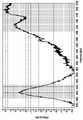
다양한 실시예에 따르면, 복수의 레이어 중 적어도 하나의 레이어(예: 도 4a의 (a)의 레이어(403) 또는 도 4a의 (b)의 레이어(405))에는 적어도 하나의 신호 라인(410)이 배치될 수 있다. 신호 라인(410)을 통해 RF 신호가 전달될 수 있다. 또한, 신호 라인(410) 주변에는 그라운드 VIA(420)가 배치될 수 있다. 그라운드 VIA(420)는 신호 라인(410)의 연장 방향과 수직 방향으로 형성되어 그라운드와 연결될 수 있다. 그라운드 VIA(420)는 복수의 레이어를 관통하여 형성될 수 있다. 신호 라인(410) 주변에 배치된 그라운드 VIA(420)에 의해 신호 라인(410)으로 전달되는 RF 신호가 차폐될 수 있다. 그라운드 VIA(420)는 유연 인쇄 회로 기판(400)과 인접하게 배치된 전자 부품에서 방출될 수 있는 전자기파가 신호 라인(410)에 주는 영향을 감소시킬 수 있다.According to various embodiments, at least one
유연 인쇄 회로 기판의 레이어 구조에 따라 안테나 급전 구조의 방사 효율이 달라질 수 있다. 도 4b를 참조하면, 약 1800MHz 내지 약 2100MHz 대역에서는 두 개의 레이어로 구성된 유연 인쇄 회로 기판(400B)을 포함하는 안테나 급전 구조의 방사 효율이 네 개의 레이어로 구성된 유연 인쇄 회로 기판(400A)을 포함하는 안테나 급전 구조의 방사 효율보다 보다 높고, 약 2200MHz 내지 약 2700MHz 대역에서는 네 개의 레이어로 구성된 유연 인쇄 회로 기판(400A)을 포함하는 안테나 급전 구조의 방사 효율이 두 개의 레이어로 구성된 유연 인쇄 회로 기판(400B)을 포함하는 안테나 급전 구조의 방사 효율보다 보다 높은 것을 확인할 수 있다. 안테나 급전 구조가 주로 송신 또는 수신하는 주파수 대역에 따라 유연 인쇄 회로 기판의 레이어의 개수를 변경할 수 있다.The radiation efficiency of the antenna feeding structure may vary depending on the layer structure of the flexible printed circuit board. Referring to Figure 4b, in the band of about 1800 MHz to about 2100 MHz, the radiation efficiency of the antenna feeding structure including the flexible printed
도 5a는, 본 문서에 개시된 다양한 실시예에 따른 유연 인쇄 회로 기판의 도면이다. 도 5b는, 도 5a에 도시된 다양한 실시예에 따른 유연 인쇄 회로 기판을 포함하는 안테나 급전 구조의 성능을 설명하기 위한 도면이다. 도 5a에 도시된 다양한 유연 인쇄 회로 기판은 도 2 및 도 3a를 통해 설명한 안테나 급전 구조에 포함된 유연 인쇄 회로 기판의 다양한 예일 수 있다.5A is a diagram of a flexible printed circuit board in accordance with various embodiments disclosed herein. FIG. 5B is a view for explaining the performance of an antenna feeding structure including a flexible printed circuit board according to various embodiments shown in FIG. 5A . The various flexible printed circuit boards shown in FIG. 5A may be various examples of the flexible printed circuit boards included in the antenna feeding structure described with reference to FIGS. 2 and 3A .
도 5a의 (a)를 참조하면, 유연 인쇄 회로 기판(501)에는 도전성 패드(540)가 배치될 수 있다. 도전성 패드(540)는 예를 들어, 제1 패드(540-1) 및 제2 패드(540-2)를 포함할 수 있다. 제1 패드(540)는 유연 인쇄 회로 기판(501)과 전자 장치의 메인 기판을 연결하는 제1 연결부(예: 도 3a의 제1 연결부(310))와 전기적으로 연결될 수 있다. 제2 패드(540-2)는 도전성 소재로 형성된 전자 장치의 프레임(예: 도 3c의 프레임(304))과 전기적으로 연결될 수 있다. 제2 패드(540-2)는 제2 연결부(예: 도 3a의 제2 연결부(320))에 의해 전자 장치의 프레임과 전기적으로 연결될 수 있다. 경우에 따라서는, 제2 패드(540-2)에 개구가 형성되고, 제2 패드(540-2)에 형성된 개구에 볼트가 삽입된 뒤, 볼트가 전자 장치의 프레임에 형성된 나사홈에 볼트 결합됨으로써, 제2 패드(540-2)와 전자 장치의 프레임이 전기적으로 연결될 수 있다.Referring to FIG. 5A (a) , a conductive pad 540 may be disposed on the flexible printed
다양한 실시예에 따르면, 유연 인쇄 회로 기판(501)에는 RF 신호를 전달하기 위한 신호 라인(510)과 신호 라인(510) 주변에 배치되는 그라운드 VIA(550)가 배치될 수 있다. 신호 라인(510)은 제1 패드(540-1)와 제2 패드(540-2)를 전기적으로 연결할 수 있다. 이상 설명한 구성 요소들은 앞서 설명한 구성 요소들과 실질적으로 동일하므로 자세한 설명은 생략하도록 한다.According to various embodiments, a
제2 패드(540-2)와 회로부에 포함된 매칭 회로(530)의 거리 또는 유연 인쇄 회로 기판(501)의 그라운드 VIA(550)의 배치를 다양하게 변경할 수 있다. (a)는 제2 패드(540-2)와 매칭 회로(530)를 약 0.5mm 이격시켜 배치한 경우, (b)는 제2 패드(540-2)와 매칭 회로(530)를 약 9mm 이격시켜 배치한 경우, (c)는 (b)와 동일하게 제2 패드(540-2)와 매칭 회로(530)를 약 9mm 이격시켜 배치하되, 제2 패드(540-2)와 매칭 회로(530) 사이에 그라운드 VIA(550)를 배치하지 않은 경우, (d)는 제2 패드(540-2)와 매칭 회로(530)를 약 16mm 이격시켜 배치한 경우, (e)는 (d)와 동일하게 제2 패드(540-2)와 매칭 회로(530)를 약 16mm 이격시켜 배치하되, 제2 패드(540-2)와 매칭 회로(530) 사이에 그라운드 VIA(550)를 배치하지 않은 경우이다.The distance between the second pad 540 - 2 and the
도 5b를 참조하면, 약 1600MHz 내지 약 2800MHz 대역에서 (a)의 경우에 방사 효율이 가장 좋게 나타난 것을 확인할 수 있다. 또한, (b)와 (c)를 비교하면, 제2 패드(540-2)와 매칭 회로(530) 사이에 그라운드 VIA(550)가 존재하지 않는 (c)의 경우가 (b)의 경우보다 비교적 방사 효율이 좋게 나타남을 확인할 수 있다. (d)와 (e)를 비교하는 경우에도, 제2 패드(540-2)와 매칭 회로(530) 사이에 그라운드 VIA(550)가 존재하지 않는 (e)의 경우가 (d)의 경우보다 비교적 방사 효율이 좋게 나타남을 확인할 수 있다. 이러한 실험 결과를 통해, 제2 패드(540-2)와 매칭 회로(530)는 가깝게 배치하고, 제2 패드(540-2)와 매칭 회로(530) 사이에는 그라운드 VIA(550)를 배치하지 않는 것이 방사 효율을 증가시킬 수 있는 설계 요소임을 확인할 수 있다. 따라서, 본 문서에 개시된 안테나 급전 구조를 설계함에 있어서, 매칭 회로(530)는 제2 패드(540-2)와 인접하게 배치하고, 매칭 회로(530)와 제2 패드(540-2) 사이에는 그라운드 VIA(550)를 배치하지 않을 수 있다.Referring to FIG. 5B , it can be seen that the radiation efficiency is the best in the case of (a) in the band of about 1600 MHz to about 2800 MHz. Also, comparing (b) and (c), the case of (c) in which the
본 문서에 개시된 다양한 실시예에 따른 전자 장치는, 메인 기판, 적어도 일부분이 상기 전자 장치의 외부로 드러나고 금속 소재로 형성된 프레임, 적어도 일부분이 상기 프레임에 인접하게 배치되는 유연 인쇄 회로 기판(flexible printed circuit board), 상기 유연 인쇄 회로 기판과 상기 메인 기판을 전기적으로 연결시키는 제1 연결부, 절곡 가능하게 형성되어 상기 유연 인쇄 회로 기판과 상기 프레임을 전기적으로 연결시키는 제2 연결부 및 상기 유연 인쇄 회로 기판에 배치되는 회로부(integrated circuit)를 포함할 수 있다.An electronic device according to various embodiments disclosed herein includes a main substrate, a frame at least a portion of which is exposed to the outside of the electronic device and formed of a metal material, and at least a portion of a flexible printed circuit board disposed adjacent to the frame. board), a first connection part electrically connecting the flexible printed circuit board and the main board, a second connection part formed to be bendable and electrically connecting the flexible printed circuit board and the frame, and disposed on the flexible printed circuit board It may include an integrated circuit.
또한, 상기 제2 연결부는, 도전성 소재로 형성되고 상기 제2 연결부에 형성된 스크류 홀(screw hole)에 삽입된 볼트에 의해 상기 프레임과 결합될 수 있다.Also, the second connection part may be formed of a conductive material and may be coupled to the frame by a bolt inserted into a screw hole formed in the second connection part.
또한, 상기 프레임 내부에 위치하는 플레이트를 더 포함할 수 있고, 상기 유연 인쇄 회로 기판은 적어도 일부분이 상기 플레이트에 의해 지지될 수 있다.In addition, it may further include a plate positioned inside the frame, the flexible printed circuit board at least a portion may be supported by the plate.
또한, 상기 유연 인쇄 회로 기판은, 상기 메인 기판과 상기 프레임 사이 공간에 배치될 수 있는 형태로 형성될 수 있다.In addition, the flexible printed circuit board may be formed in a form that can be disposed in a space between the main board and the frame.
또한, 상기 유연 인쇄 회로 기판은, 상기 제1 연결부와 상기 제2 연결부가 위치하는 제1 영역과, 상기 제1 영역에서 분기되어 연장되는 적어도 하나의 제2 영역을 포함할 수 있고, 상기 유연 인쇄 회로 기판의 적어도 하나의 제2 영역은, RF 신호를 송신 또는 수신하는 안테나 방사체일 수 있다.In addition, the flexible printed circuit board may include a first area in which the first connection part and the second connection part are located, and at least one second area branching and extending from the first area, the flexible printed circuit board At least one second region of the circuit board may be an antenna radiator for transmitting or receiving an RF signal.
또한, 상기 유연 인쇄 회로 기판은, 도전성 소재로 형성되어 상기 유연 인쇄 회로 기판에 전기적으로 연결되고 RF 신호를 송신 또는 수신하는 안테나 방사체를 적어도 하나 포함할 수 있다.In addition, the flexible printed circuit board may include at least one antenna radiator that is formed of a conductive material and is electrically connected to the flexible printed circuit board and transmits or receives an RF signal.
또한, 상기 프레임은, 절연 소재에 의해 제1 영역 및 제2 영역을 포함하는 복수의 영역으로 분절될 수 있다.In addition, the frame may be segmented into a plurality of regions including the first region and the second region by an insulating material.
또한, 상기 제2 연결부는 복수 개 마련될 수 있고, 상기 복수의 제2 연결부 중 적어도 하나는 상기 프레임의 제1 영역과 상기 유연 인쇄 회로 기판을 전기적으로 연결할 수 있고, 상기 복수의 제2 연결부 중 적어도 하나는 상기 프레임의 제2 영역과 상기 유연 인쇄 회로 기판을 전기적으로 연결할 수 있다.In addition, a plurality of the second connection part may be provided, and at least one of the plurality of second connection parts may electrically connect the first region of the frame and the flexible printed circuit board, and among the plurality of second connection parts, At least one may electrically connect the second region of the frame and the flexible printed circuit board.
또한, 상기 유연 인쇄 회로 기판은, 복수의 레이어를 포함할 수 있고, 상기 복수의 레이어 중 적어도 하나에는 RF 신호를 전달하기 위한 신호 라인이 배치될 수 있고, 상기 신호 라인 주위에는 상기 복수의 레이어를 관통하도록 형성된 그라운드 VIA가 배치될 수 있다.In addition, the flexible printed circuit board may include a plurality of layers, and a signal line for transmitting an RF signal may be disposed on at least one of the plurality of layers, and the plurality of layers may be formed around the signal line. A ground VIA formed to penetrate may be disposed.
또한, 상기 회로부는, 임피던스 매칭을 위한 매칭 회로를 포함할 수 있고, 상기 매칭 회로는 상기 제2 연결부와 상기 유연 인쇄 회로 기판이 연결된 부분과 인접한 부분에 배치될 수 있다.In addition, the circuit unit may include a matching circuit for impedance matching, and the matching circuit may be disposed in a portion adjacent to a portion in which the second connection portion and the flexible printed circuit board are connected.
본 문서에 개시된 다양한 실시예에 따른 안테나 급전 구조는, 금속 소재로 형성된 전자 장치의 프레임과 인접하게 배치되는 유연 인쇄 회로 기판(flexible printed circuit board), 상기 유연 인쇄 회로 기판과 상기 전자 장치의 메인 기판을 전기적으로 연결시키는 제1 연결부, 절곡 가능하게 형성되어 상기 유연 인쇄 회로 기판과 상기 전자 장치의 프레임을 전기적으로 연결시키는 제2 연결부 및 상기 유연 인쇄 회로 기판에 배치되는 회로부(integrated circuit)를 포함할 수 있다.The antenna feeding structure according to various embodiments disclosed herein includes a flexible printed circuit board disposed adjacent to a frame of an electronic device formed of a metal material, the flexible printed circuit board, and a main board of the electronic device A first connection part electrically connecting the can
또한, 상기 제2 연결부는, 도전성 소재로 형성되고 상기 제2 연결부에 형성된 스크류 홀(screw hole)에 삽입된 볼트에 의해 상기 전자 장치의 프레임과 결합될 수 있다.Also, the second connection part may be formed of a conductive material and may be coupled to the frame of the electronic device by a bolt inserted into a screw hole formed in the second connection part.
또한, 상기 유연 인쇄 회로 기판은 적어도 일부분이 상기 전자 장치의 프레임 내부에 배치된 플레이트에 의해 지지될 수 있다.Also, at least a portion of the flexible printed circuit board may be supported by a plate disposed inside the frame of the electronic device.
또한, 상기 유연 인쇄 회로 기판은, 상기 전자 장치의 메인 기판과 상기 전자 장치의 프레임 사이 공간에 배치될 수 있는 형태로 형성될 수 있다.In addition, the flexible printed circuit board may be formed in a form that can be disposed in a space between the main board of the electronic device and the frame of the electronic device.
또한, 상기 유연 인쇄 회로 기판은, 상기 제1 연결부와 상기 제2 연결부가 위치하는 제1 영역과, 상기 제1 영역에서 분기되어 연장되는 적어도 하나의 제2 영역을 포함할 수 있고, 상기 유연 인쇄 회로 기판의 적어도 하나의 제2 영역은, RF 신호를 송신 또는 수신하는 안테나 방사체일 수 있다.In addition, the flexible printed circuit board may include a first area in which the first connection part and the second connection part are located, and at least one second area branching and extending from the first area, the flexible printed circuit board At least one second region of the circuit board may be an antenna radiator for transmitting or receiving an RF signal.
또한, 상기 유연 인쇄 회로 기판은, 도전성 소재로 형성되어 상기 유연 인쇄 회로 기판에 전기적으로 연결되고 RF 신호를 송신 또는 수신하는 안테나 방사체를 적어도 하나 포함할 수 있다.In addition, the flexible printed circuit board may include at least one antenna radiator that is formed of a conductive material and is electrically connected to the flexible printed circuit board and transmits or receives an RF signal.
또한, 상기 제2 연결부는 복수 개 마련될 수 있고, 상기 복수의 제2 연결부 중 적어도 하나는, 상기 프레임의 제1 영역과 상기 유연 인쇄 회로 기판을 전기적으로 연결할 수 있고, 상기 복수의 제2 연결부 중 적어도 하나는, 절연 소재에 의해 상기 프레임의 제1 영역과 분절된 제2 영역과 상기 유연 인쇄 회로 기판을 전기적으로 연결할 수 있다.In addition, a plurality of the second connection part may be provided, and at least one of the plurality of second connection parts may electrically connect the first region of the frame and the flexible printed circuit board, and the plurality of second connection parts At least one of them may electrically connect the first region and the second region segmented by the insulating material to the flexible printed circuit board.
또한, 상기 유연 인쇄 회로 기판은, 복수의 레이어를 포함할 수 있고, 상기 복수의 레이어 중 적어도 하나에는 RF 신호를 전달하기 위한 적어도 하나의 신호 라인이 배치될 수 있고, 상기 신호 라인 주위에는 상기 복수의 레이어를 관통하도록 형성된 그라운드 VIA가 배치될 수 있다.In addition, the flexible printed circuit board may include a plurality of layers, and at least one signal line for transmitting an RF signal may be disposed in at least one of the plurality of layers, and the plurality of signal lines are disposed around the signal line. A ground VIA formed to penetrate the layer of may be disposed.
또한, 상기 유연 인쇄 회로 기판에는, 임피던스 매칭을 위한 매칭 회로가 배치될 수 있고, 상기 매칭 회로는 상기 제2 연결부와 상기 유연 인쇄 회로 기판이 연결된 부분과 인접한 부분에 배치될 수 있다.In addition, a matching circuit for impedance matching may be disposed on the flexible printed circuit board, and the matching circuit may be disposed in a portion adjacent to a portion where the second connection portion and the flexible printed circuit board are connected.
또한, 상기 유연 인쇄 회로 기판은, 상기 유연 인쇄 회로 기판은 제1 방향을 바라보는 면과 상기 제1 방향과 다른 제2 방향을 바라보는 면을 포함할 수 있다.In addition, the flexible printed circuit board, the flexible printed circuit board may include a surface facing the first direction and a surface facing the second direction different from the first direction.
이상 설명한 다양한 실시예들은 서로 모순되지 않는 범위 내에서 다양하게 조합될 수 있다.The various embodiments described above may be variously combined within a range that does not contradict each other.
그리고 본 명세서와 도면에 개시된 본 문서에 개시된 실시예들은 본 문서에 개시된 실시예에 따른 기술 내용을 쉽게 설명하고 본 문서에 개시된 실시예의 이해를 돕기 위해 특정 예를 제시한 것일 뿐이며, 본 문서에 개시된 실시예의 범위를 한정하고자 하는 것은 아니다. 따라서 본 문서에 개시된 다양한 실시예의 범위는 여기에 개시된 실시예들 이외에도 본 문서에 개시된 다양한 실시예의 기술적 사상을 바탕으로 도출되는 모든 변경 또는 변형된 형태가 본 문서에 개시된 다양한 실시예의 범위에 포함되는 것으로 해석되어야 한다.And the embodiments disclosed in the present document disclosed in the present specification and drawings are merely presented as specific examples to easily explain the technical content according to the embodiments disclosed in this document and help the understanding of the embodiments disclosed in this document, It is not intended to limit the scope of the embodiment. Accordingly, the scope of the various embodiments disclosed in this document is that, in addition to the embodiments disclosed herein, all changes or modifications derived from the technical ideas of the various embodiments disclosed in this document are included in the scope of the various embodiments disclosed in this document. should be interpreted
200 : 안테나 급전 구조210 : 제1 연결부
220 : 제2 연결부230 : 회로부200: antenna feeding structure 210: first connection part
220: second connection part 230: circuit part
Claims (20)
Translated fromKorean메인 기판;
적어도 일부분이 상기 전자 장치의 외부로 드러나고 금속 소재로 형성된 프레임;
적어도 일부분이 상기 프레임에 인접하게 배치되는 유연 인쇄 회로 기판(flexible printed circuit board);
상기 유연 인쇄 회로 기판과 상기 메인 기판을 전기적으로 연결시키는 제1 연결부;
절곡 가능하게 형성되어 상기 유연 인쇄 회로 기판과 상기 프레임을 전기적으로 연결시키는 제2 연결부; 및
상기 유연 인쇄 회로 기판에 배치되는 회로부(integrated circuit);를 포함하는 전자 장치.In an electronic device,
main board;
a frame at least a portion of which is exposed to the outside of the electronic device and is formed of a metal material;
a flexible printed circuit board, at least a portion of which is disposed adjacent the frame;
a first connection part electrically connecting the flexible printed circuit board and the main board;
a second connection part formed to be bendable and electrically connecting the flexible printed circuit board and the frame; and
and an integrated circuit disposed on the flexible printed circuit board.
상기 제2 연결부는,
도전성 소재로 형성되고 상기 제2 연결부에 형성된 스크류 홀(screw hole)에 삽입된 볼트에 의해 상기 프레임과 결합되는 전자 장치.According to claim 1,
The second connection part,
An electronic device formed of a conductive material and coupled to the frame by a bolt inserted into a screw hole formed in the second connection part.
상기 프레임 내부에 위치하는 플레이트;를 더 포함하고,
상기 유연 인쇄 회로 기판은 적어도 일부분이 상기 플레이트에 의해 지지되는 전자 장치.According to claim 1,
It further includes; a plate located inside the frame;
wherein the flexible printed circuit board is at least partially supported by the plate.
상기 유연 인쇄 회로 기판은,
상기 메인 기판과 상기 프레임 사이 공간에 배치될 수 있는 형태로 형성되는 전자 장치.According to claim 1,
The flexible printed circuit board,
An electronic device formed in a shape that can be disposed in a space between the main substrate and the frame.
상기 유연 인쇄 회로 기판은,
상기 제1 연결부와 상기 제2 연결부가 위치하는 제1 영역과, 상기 제1 영역에서 분기되어 연장되는 적어도 하나의 제2 영역을 포함하고,
상기 유연 인쇄 회로 기판의 적어도 하나의 제2 영역은,
RF 신호를 송신 또는 수신하는 안테나 방사체인 전자 장치.According to claim 1,
The flexible printed circuit board,
a first area in which the first connection part and the second connection part are located; and at least one second area branching and extending from the first area;
at least one second region of the flexible printed circuit board,
An electronic device that is an antenna radiator that transmits or receives RF signals.
상기 유연 인쇄 회로 기판은,
도전성 소재로 형성되어 상기 유연 인쇄 회로 기판에 전기적으로 연결되고 RF 신호를 송신 또는 수신하는 안테나 방사체를 적어도 하나 포함하는 전자 장치.According to claim 1,
The flexible printed circuit board,
An electronic device comprising at least one antenna radiator formed of a conductive material, electrically connected to the flexible printed circuit board, and transmitting or receiving an RF signal.
상기 프레임은,
절연 소재에 의해 제1 영역 및 제2 영역을 포함하는 복수의 영역으로 분절되는 전자 장치.According to claim 1,
The frame is
An electronic device segmented into a plurality of regions including a first region and a second region by an insulating material.
상기 제2 연결부는 복수 개 마련되고,
상기 복수의 제2 연결부 중 적어도 하나는 상기 프레임의 제1 영역과 상기 유연 인쇄 회로 기판을 전기적으로 연결하고,
상기 복수의 제2 연결부 중 적어도 하나는 상기 프레임의 제2 영역과 상기 유연 인쇄 회로 기판을 전기적으로 연결하는 전자 장치.8. The method of claim 7,
A plurality of the second connection parts are provided,
At least one of the plurality of second connection parts electrically connects the first region of the frame and the flexible printed circuit board,
At least one of the plurality of second connection parts electrically connects the second region of the frame and the flexible printed circuit board.
상기 유연 인쇄 회로 기판은,
복수의 레이어를 포함하고,
상기 복수의 레이어 중 적어도 하나에는 RF 신호를 전달하기 위한 신호 라인이 배치되고,
상기 신호 라인 주위에는 상기 복수의 레이어를 관통하도록 형성된 그라운드 VIA가 배치되는 전자 장치.According to claim 1,
The flexible printed circuit board,
comprising a plurality of layers;
A signal line for transmitting an RF signal is disposed on at least one of the plurality of layers,
A ground VIA formed to pass through the plurality of layers is disposed around the signal line.
상기 회로부는,
임피던스 매칭을 위한 매칭 회로를 포함하고,
상기 매칭 회로는 상기 제2 연결부와 상기 유연 인쇄 회로 기판이 연결된 부분과 인접한 부분에 배치되는 전자 장치.According to claim 1,
The circuit unit,
A matching circuit for impedance matching,
The matching circuit is disposed in a portion adjacent to a portion where the second connection portion and the flexible printed circuit board are connected.
금속 소재로 형성된 전자 장치의 프레임과 인접하게 배치되는 유연 인쇄 회로 기판(flexible printed circuit board);
상기 유연 인쇄 회로 기판과 상기 전자 장치의 메인 기판을 전기적으로 연결시키는 제1 연결부;
절곡 가능하게 형성되어 상기 유연 인쇄 회로 기판과 상기 전자 장치의 프레임을 전기적으로 연결시키는 제2 연결부; 및
상기 유연 인쇄 회로 기판에 배치되는 회로부(integrated circuit);를 포함하는 안테나 급전 구조.In the antenna feeding structure,
a flexible printed circuit board disposed adjacent to a frame of an electronic device formed of a metal material;
a first connection part electrically connecting the flexible printed circuit board and the main board of the electronic device;
a second connection part formed to be bendable and electrically connecting the flexible printed circuit board and the frame of the electronic device; and
Antenna feeding structure comprising a; circuit portion (integrated circuit) disposed on the flexible printed circuit board.
상기 제2 연결부는,
도전성 소재로 형성되고 상기 제2 연결부에 형성된 스크류 홀(screw hole)에 삽입된 볼트에 의해 상기 전자 장치의 프레임과 결합되는 안테나 급전 구조.12. The method of claim 11,
The second connection part,
An antenna feeding structure formed of a conductive material and coupled to the frame of the electronic device by a bolt inserted into a screw hole formed in the second connection part.
상기 유연 인쇄 회로 기판은 적어도 일부분이 상기 전자 장치의 프레임 내부에 배치된 플레이트에 의해 지지되는 안테나 급전 구조.12. The method of claim 11,
wherein the flexible printed circuit board is at least partially supported by a plate disposed inside the frame of the electronic device.
상기 유연 인쇄 회로 기판은,
상기 전자 장치의 메인 기판과 상기 전자 장치의 프레임 사이 공간에 배치될 수 있는 형태로 형성되는 안테나 급전 구조.12. The method of claim 11,
The flexible printed circuit board,
An antenna feeding structure formed in a shape that can be disposed in a space between the main board of the electronic device and the frame of the electronic device.
상기 유연 인쇄 회로 기판은,
상기 제1 연결부와 상기 제2 연결부가 위치하는 제1 영역과, 상기 제1 영역에서 분기되어 연장되는 적어도 하나의 제2 영역을 포함하고,
상기 유연 인쇄 회로 기판의 적어도 하나의 제2 영역은,
RF 신호를 송신 또는 수신하는 안테나 방사체인 안테나 급전 구조.12. The method of claim 11,
The flexible printed circuit board,
a first area in which the first connection part and the second connection part are located; and at least one second area branching and extending from the first area;
at least one second region of the flexible printed circuit board,
Antenna feed structure, which is an antenna radiator that transmits or receives RF signals.
상기 유연 인쇄 회로 기판은,
도전성 소재로 형성되어 상기 유연 인쇄 회로 기판에 전기적으로 연결되고 RF 신호를 송신 또는 수신하는 안테나 방사체를 적어도 하나 포함하는 안테나 급전 구조.12. The method of claim 11,
The flexible printed circuit board,
Antenna feeding structure comprising at least one antenna radiator formed of a conductive material, electrically connected to the flexible printed circuit board, and transmitting or receiving an RF signal.
상기 제2 연결부는 복수 개 마련되고,
상기 복수의 제2 연결부 중 적어도 하나는, 상기 프레임의 제1 영역과 상기 유연 인쇄 회로 기판을 전기적으로 연결하고,
상기 복수의 제2 연결부 중 적어도 하나는, 절연 소재에 의해 상기 프레임의 제1 영역과 분절된 제2 영역과 상기 유연 인쇄 회로 기판을 전기적으로 연결하는 안테나 급전 구조.12. The method of claim 11,
A plurality of the second connection parts are provided,
At least one of the plurality of second connection parts electrically connects the first region of the frame and the flexible printed circuit board,
At least one of the plurality of second connection parts is an antenna feeding structure for electrically connecting the flexible printed circuit board to a second region segmented from the first region of the frame by an insulating material.
상기 유연 인쇄 회로 기판은,
복수의 레이어를 포함하고,
상기 복수의 레이어 중 적어도 하나에는 RF 신호를 전달하기 위한 적어도 하나의 신호 라인이 배치되고,
상기 신호 라인 주위에는 상기 복수의 레이어를 관통하도록 형성된 그라운드 VIA가 배치되는 안테나 급전 구조.12. The method of claim 11,
The flexible printed circuit board,
comprising a plurality of layers;
At least one signal line for transmitting an RF signal is disposed on at least one of the plurality of layers,
An antenna feeding structure in which a ground VIA formed to pass through the plurality of layers is disposed around the signal line.
상기 유연 인쇄 회로 기판에는,
임피던스 매칭을 위한 매칭 회로가 배치되고,
상기 매칭 회로는 상기 제2 연결부와 상기 유연 인쇄 회로 기판이 연결된 부분과 인접한 부분에 배치되는 안테나 급전 구조.12. The method of claim 11,
In the flexible printed circuit board,
A matching circuit for impedance matching is disposed,
The matching circuit is an antenna feeding structure disposed in a portion adjacent to a portion where the second connection portion and the flexible printed circuit board are connected.
상기 유연 인쇄 회로 기판은,
상기 유연 인쇄 회로 기판은 제1 방향을 바라보는 면과 상기 제1 방향과 다른 제2 방향을 바라보는 면을 포함하는 안테나 급전 구조.
12. The method of claim 11,
The flexible printed circuit board,
The flexible printed circuit board is an antenna feeding structure comprising a surface facing a first direction and a surface facing a second direction different from the first direction.
Priority Applications (4)
| Application Number | Priority Date | Filing Date | Title |
|---|---|---|---|
| KR1020200166653AKR20220077574A (en) | 2020-12-02 | 2020-12-02 | Antenna feeding sturcture including flexible printed circuit board and electronic device including the same |
| PCT/KR2021/017381WO2022119224A1 (en) | 2020-12-02 | 2021-11-24 | Antenna power feeding structure comprising flexible printed circuit board, and electronic device comprising same |
| EP21900912.3AEP4239794A4 (en) | 2020-12-02 | 2021-11-24 | ANTENNA POWER SUPPLY STRUCTURE WITH FLEXIBLE CIRCUIT BOARD AND ELECTRONIC DEVICE THEREFOR |
| US18/327,369US20230307821A1 (en) | 2020-12-02 | 2023-06-01 | Antenna power feeding structure comprising flexible printed circuit board, and electronic device comprising same |
Applications Claiming Priority (1)
| Application Number | Priority Date | Filing Date | Title |
|---|---|---|---|
| KR1020200166653AKR20220077574A (en) | 2020-12-02 | 2020-12-02 | Antenna feeding sturcture including flexible printed circuit board and electronic device including the same |
Publications (1)
| Publication Number | Publication Date |
|---|---|
| KR20220077574Atrue KR20220077574A (en) | 2022-06-09 |
Family
ID=81854187
Family Applications (1)
| Application Number | Title | Priority Date | Filing Date |
|---|---|---|---|
| KR1020200166653APendingKR20220077574A (en) | 2020-12-02 | 2020-12-02 | Antenna feeding sturcture including flexible printed circuit board and electronic device including the same |
Country Status (4)
| Country | Link |
|---|---|
| US (1) | US20230307821A1 (en) |
| EP (1) | EP4239794A4 (en) |
| KR (1) | KR20220077574A (en) |
| WO (1) | WO2022119224A1 (en) |
Cited By (1)
| Publication number | Priority date | Publication date | Assignee | Title |
|---|---|---|---|---|
| US12316018B2 (en) | 2021-07-06 | 2025-05-27 | Samsung Electronics Co., Ltd. | Antenna and electronic device including the same |
Family Cites Families (6)
| Publication number | Priority date | Publication date | Assignee | Title |
|---|---|---|---|---|
| US8693204B2 (en)* | 2011-01-10 | 2014-04-08 | Apple Inc. | Electronic devices having multi-purpose cowling structures and a compass mounted on a flex circuit |
| US8836587B2 (en)* | 2012-03-30 | 2014-09-16 | Apple Inc. | Antenna having flexible feed structure with components |
| US10367570B2 (en)* | 2017-09-11 | 2019-07-30 | Apple Inc. | Electronic devices having printed circuits for antennas |
| KR102461704B1 (en)* | 2018-06-15 | 2022-11-02 | 삼성전자주식회사 | Electronic device for including flexible printed circuit board adjacent to antenna |
| KR102499260B1 (en)* | 2018-07-18 | 2023-02-13 | 삼성전자 주식회사 | Electronic device including electronic component for sharing flexible printed circuit board |
| KR102781204B1 (en)* | 2019-04-12 | 2025-03-12 | 동우 화인켐 주식회사 | Flexible Printed Circuit Board |
- 2020
- 2020-12-02KRKR1020200166653Apatent/KR20220077574A/enactivePending
- 2021
- 2021-11-24WOPCT/KR2021/017381patent/WO2022119224A1/ennot_activeCeased
- 2021-11-24EPEP21900912.3Apatent/EP4239794A4/enactivePending
- 2023
- 2023-06-01USUS18/327,369patent/US20230307821A1/enactivePending
Cited By (1)
| Publication number | Priority date | Publication date | Assignee | Title |
|---|---|---|---|---|
| US12316018B2 (en) | 2021-07-06 | 2025-05-27 | Samsung Electronics Co., Ltd. | Antenna and electronic device including the same |
Also Published As
| Publication number | Publication date |
|---|---|
| EP4239794A1 (en) | 2023-09-06 |
| US20230307821A1 (en) | 2023-09-28 |
| EP4239794A4 (en) | 2024-05-01 |
| WO2022119224A1 (en) | 2022-06-09 |
Similar Documents
| Publication | Publication Date | Title |
|---|---|---|
| KR102796000B1 (en) | Printed circuit board for transmitting signals in the high frequency band and electronic device including the same | |
| US12418098B2 (en) | Antenna and electronic device including the same | |
| KR102825638B1 (en) | Antenna and electronic device including the same | |
| CN116918176A (en) | Antennas and electronic devices including antennas | |
| US12034225B2 (en) | Antenna and electronic device including the same | |
| US11974401B2 (en) | Electronic device including antenna connecting structure including flexible printed circuit board | |
| KR20230071000A (en) | Electronic device including antenna | |
| US20230307821A1 (en) | Antenna power feeding structure comprising flexible printed circuit board, and electronic device comprising same | |
| US20240039171A1 (en) | Antenna structure including phase shifter and electronic device including same | |
| KR20220058225A (en) | Structure applying antenna module to foldable electronic device | |
| KR102861549B1 (en) | Electronic device including antenna connecting sturcture including flexible printed circuit board | |
| KR20230030813A (en) | Antenna and electronic device including the same | |
| KR20220102930A (en) | Electronic device comprising antenna | |
| KR20230052024A (en) | An electronic device comprising an antenna | |
| US12155124B2 (en) | Electronic device having an antenna | |
| US11942704B2 (en) | Antenna and electronic device including the same | |
| US20240306354A1 (en) | Electronic device including shielding structure for reducing mounting volume of component | |
| US20230387616A1 (en) | Connector and electronic device including the same | |
| KR20230071693A (en) | Electronic device including an antenna | |
| KR20240044273A (en) | Electornic device comprising connection structure for antenna | |
| KR20230040625A (en) | Electronic device including antenna | |
| KR20230063222A (en) | Electronic device including antenna | |
| KR20230047642A (en) | Antenna and electronic device including the same | |
| KR20220153384A (en) | wiring structure for power and millimeter wave band signal transmission | |
| KR20230057231A (en) | A heat dissipation structure and electronic device including the same |
Legal Events
| Date | Code | Title | Description |
|---|---|---|---|
| PA0109 | Patent application | St.27 status event code:A-0-1-A10-A12-nap-PA0109 | |
| PG1501 | Laying open of application | St.27 status event code:A-1-1-Q10-Q12-nap-PG1501 | |
| A201 | Request for examination | ||
| PA0201 | Request for examination | St.27 status event code:A-1-2-D10-D11-exm-PA0201 | |
| E902 | Notification of reason for refusal | ||
| PE0902 | Notice of grounds for rejection | St.27 status event code:A-1-2-D10-D21-exm-PE0902 | |
| P11-X000 | Amendment of application requested | St.27 status event code:A-2-2-P10-P11-nap-X000 | |
| P13-X000 | Application amended | St.27 status event code:A-2-2-P10-P13-nap-X000 | |
| PE0701 | Decision of registration | St.27 status event code:A-1-2-D10-D22-exm-PE0701 |