KR20220046464A - Data compensating circuit, display device including the same, method of compensating data using the same - Google Patents
Data compensating circuit, display device including the same, method of compensating data using the sameDownload PDFInfo
- Publication number
- KR20220046464A KR20220046464AKR1020210111174AKR20210111174AKR20220046464AKR 20220046464 AKR20220046464 AKR 20220046464AKR 1020210111174 AKR1020210111174 AKR 1020210111174AKR 20210111174 AKR20210111174 AKR 20210111174AKR 20220046464 AKR20220046464 AKR 20220046464A
- Authority
- KR
- South Korea
- Prior art keywords
- data
- compensation
- reference frame
- stress
- image data
- Prior art date
- Legal status (The legal status is an assumption and is not a legal conclusion. Google has not performed a legal analysis and makes no representation as to the accuracy of the status listed.)
- Granted
Links
Images


Classifications
- G—PHYSICS
- G09—EDUCATION; CRYPTOGRAPHY; DISPLAY; ADVERTISING; SEALS
- G09G—ARRANGEMENTS OR CIRCUITS FOR CONTROL OF INDICATING DEVICES USING STATIC MEANS TO PRESENT VARIABLE INFORMATION
- G09G3/00—Control arrangements or circuits, of interest only in connection with visual indicators other than cathode-ray tubes
- G09G3/20—Control arrangements or circuits, of interest only in connection with visual indicators other than cathode-ray tubes for presentation of an assembly of a number of characters, e.g. a page, by composing the assembly by combination of individual elements arranged in a matrix no fixed position being assigned to or needed to be assigned to the individual characters or partial characters
- G09G3/22—Control arrangements or circuits, of interest only in connection with visual indicators other than cathode-ray tubes for presentation of an assembly of a number of characters, e.g. a page, by composing the assembly by combination of individual elements arranged in a matrix no fixed position being assigned to or needed to be assigned to the individual characters or partial characters using controlled light sources
- G09G3/30—Control arrangements or circuits, of interest only in connection with visual indicators other than cathode-ray tubes for presentation of an assembly of a number of characters, e.g. a page, by composing the assembly by combination of individual elements arranged in a matrix no fixed position being assigned to or needed to be assigned to the individual characters or partial characters using controlled light sources using electroluminescent panels
- G09G3/32—Control arrangements or circuits, of interest only in connection with visual indicators other than cathode-ray tubes for presentation of an assembly of a number of characters, e.g. a page, by composing the assembly by combination of individual elements arranged in a matrix no fixed position being assigned to or needed to be assigned to the individual characters or partial characters using controlled light sources using electroluminescent panels semiconductive, e.g. using light-emitting diodes [LED]
- G09G3/3208—Control arrangements or circuits, of interest only in connection with visual indicators other than cathode-ray tubes for presentation of an assembly of a number of characters, e.g. a page, by composing the assembly by combination of individual elements arranged in a matrix no fixed position being assigned to or needed to be assigned to the individual characters or partial characters using controlled light sources using electroluminescent panels semiconductive, e.g. using light-emitting diodes [LED] organic, e.g. using organic light-emitting diodes [OLED]
- G09G3/3225—Control arrangements or circuits, of interest only in connection with visual indicators other than cathode-ray tubes for presentation of an assembly of a number of characters, e.g. a page, by composing the assembly by combination of individual elements arranged in a matrix no fixed position being assigned to or needed to be assigned to the individual characters or partial characters using controlled light sources using electroluminescent panels semiconductive, e.g. using light-emitting diodes [LED] organic, e.g. using organic light-emitting diodes [OLED] using an active matrix
- G—PHYSICS
- G09—EDUCATION; CRYPTOGRAPHY; DISPLAY; ADVERTISING; SEALS
- G09G—ARRANGEMENTS OR CIRCUITS FOR CONTROL OF INDICATING DEVICES USING STATIC MEANS TO PRESENT VARIABLE INFORMATION
- G09G2320/00—Control of display operating conditions
- G09G2320/02—Improving the quality of display appearance
- G09G2320/0233—Improving the luminance or brightness uniformity across the screen
- G—PHYSICS
- G09—EDUCATION; CRYPTOGRAPHY; DISPLAY; ADVERTISING; SEALS
- G09G—ARRANGEMENTS OR CIRCUITS FOR CONTROL OF INDICATING DEVICES USING STATIC MEANS TO PRESENT VARIABLE INFORMATION
- G09G2320/00—Control of display operating conditions
- G09G2320/02—Improving the quality of display appearance
- G09G2320/0257—Reduction of after-image effects
- G—PHYSICS
- G09—EDUCATION; CRYPTOGRAPHY; DISPLAY; ADVERTISING; SEALS
- G09G—ARRANGEMENTS OR CIRCUITS FOR CONTROL OF INDICATING DEVICES USING STATIC MEANS TO PRESENT VARIABLE INFORMATION
- G09G2360/00—Aspects of the architecture of display systems
- G09G2360/12—Frame memory handling
Landscapes
- Engineering & Computer Science (AREA)
- Physics & Mathematics (AREA)
- Computer Hardware Design (AREA)
- General Physics & Mathematics (AREA)
- Theoretical Computer Science (AREA)
- Control Of Indicators Other Than Cathode Ray Tubes (AREA)
Abstract
Translated fromKoreanDescription
Translated fromKorean본 발명은 데이터 보상에 관한 것이다. 보다 상세하게는, 본 발명은 순간 잔상 보상을 수행하는 데이터 보상 회로, 이를 포함하는 표시 장치 및 이를 이용한 데이터 보상 방법에 관한 것이다.The present invention relates to data compensation. More particularly, the present invention relates to a data compensation circuit for performing instantaneous afterimage compensation, a display device including the same, and a data compensation method using the same.
표시 장치는 복수의 화소들을 포함하여 영상을 표시할 수 있다. 화소들 각각은 구동 트랜지스터를 포함하는 복수의 트랜지스터들 및 트랜지스터들에 전기적으로 연결되는 발광 소자를 포함할 수 있다. 각 화소에 포함된 구동 트랜지스터는 구동 전류를 생성하고, 각 화소에 포함된 발광 소자는 구동 전류의 크기에 상응하는 휘도로 발광할 수 있다. 다만, 구동 트랜지스터의 전압-전류 특성은 이전 표시 프레임에서의 구동 트랜지스터의 동작 상태에 따라 달라질 수 있다. 다시 말해, 화소들에 포함된 구동 트랜지스터들은 히스테리시스(hysteresis)를 가질 수 있다.The display device may display an image including a plurality of pixels. Each of the pixels may include a plurality of transistors including a driving transistor and a light emitting device electrically connected to the transistors. A driving transistor included in each pixel may generate a driving current, and a light emitting device included in each pixel may emit light with a luminance corresponding to the magnitude of the driving current. However, the voltage-current characteristics of the driving transistor may vary depending on the operating state of the driving transistor in the previous display frame. In other words, the driving transistors included in the pixels may have hysteresis.
이러한 구동 트랜지스터의 히스테리시스에 의해, 표시 장치의 표시 영역들이 이전 표시 프레임들에서 서로 다른 계조로 구동된 경우에, 다음 표시 프레임들에서 동일한 계조로 구동되더라도 표시 영역들이 일정 시간 동안 서로 다른 휘도로 발광하는 순간 잔상이 발생될 수 있다.Due to the hysteresis of the driving transistor, when the display regions of the display device are driven with different gradations in previous display frames, the display regions emit light with different luminance for a certain period of time even when the display regions are driven with the same gradation in subsequent display frames. Instantaneous afterimages may occur.
본 발명의 일 목적은 각 화소들의 순간 잔상을 감소시킴으로써 사용자의 휘도 차이 시인을 감소시킬 수 있는 데이터 보상 회로를 제공하는 것이다.SUMMARY OF THE INVENTION One object of the present invention is to provide a data compensation circuit capable of reducing a user's perception of a luminance difference by reducing an instantaneous afterimage of each pixel.
본 발명의 다른 목적은 상기 데이터 보상 회로를 포함하여, 표시 패널 내부의 각 화소들의 순간 잔상을 감소시킴으로써 사용자의 휘도 차이 시인을 감소시킬 수 있는 표시 장치를 제공하는 것이다.Another object of the present invention is to provide a display device capable of reducing a user's recognition of a luminance difference by reducing an instantaneous afterimage of each pixel in a display panel, including the data compensation circuit.
본 발명의 또 다른 목적은 각 화소들의 순간 잔상을 감소시킴으로써 사용자의 휘도 차이 시인을 감소시킬 수 있는 데이터 보상 방법을 제공하는 것이다.Another object of the present invention is to provide a data compensation method capable of reducing the user's recognition of a luminance difference by reducing the instantaneous afterimage of each pixel.
다만, 본 발명의 목적은 상술한 목적들로 한정되는 것이 아니며, 본 발명의 사상 및 영역으로부터 벗어나지 않는 범위에서 다양하게 확장될 수 있을 것이다.However, the object of the present invention is not limited to the above-described objects, and may be expanded in various ways without departing from the spirit and scope of the present invention.
본 발명의 일 목적을 달성하기 위하여, 본 발명의 실시예들에 따른 데이터 보상 회로는 기준 프레임 데이터를 저장하는 기준 프레임 메모리 장치, 각 화소에 대한 누적 스트레스 데이터를 저장하는 누적 스트레스 메모리 장치, 출력 영상 데이터와 상기 기준 프레임 데이터를 비교하여 각 화소에 대한 스트레스 데이터를 생성하는 스트레스 데이터 생성부, 상기 누적 스트레스 데이터에 상기 스트레스 데이터를 가산하여 상기 누적 스트레스 데이터를 갱신하는 메모리 제어부, 및 상기 누적 스트레스 데이터에 기초하여 각 화소에 대한 잔상 보상 데이터를 생성하고, 상기 잔상 보상 데이터에 기초하여 입력 영상 데이터를 보상함으로써 상기 출력 영상 데이터를 생성하는 보상부를 포함할 수 있다.In order to achieve one object of the present invention, a data compensation circuit according to embodiments of the present invention includes a reference frame memory device for storing reference frame data, a cumulative stress memory device for storing accumulated stress data for each pixel, and an output image A stress data generator for generating stress data for each pixel by comparing data with the reference frame data, a memory controller for updating the accumulated stress data by adding the stress data to the accumulated stress data, and the accumulated stress data. and a compensator configured to generate afterimage compensation data for each pixel based on the image and compensate input image data based on the residual image compensation data to generate the output image data.
일 실시예에 의하면, 상기 스트레스 데이터 생성부는 상기 출력 영상 데이터에 따른 제1 계조값과 상기 기준 프레임 데이터에 따른 기준 계조값의 차이를 기초로 각 화소에 대한 스트레스를 계산하여 상기 스트레스 데이터를 생성할 수 있다.According to an embodiment, the stress data generator may generate the stress data by calculating a stress for each pixel based on a difference between a first grayscale value according to the output image data and a reference grayscale value according to the reference frame data. can
일 실시예에 의하면, 상기 스트레스 데이터는 SD = A1*[(-MaxStress/ZeroStX)*A0*DDO + MaxStress](단, SD는 상기 스트레스 데이터를 나타내고, A0 및 A1은 스트레스 보정 계수들을 나타내며, DDO는 상기 제1 계조값과 상기 기준 계조값의 차이를 나타내고, MaxStress는 상기 스트레스의 최대값을 나타내며, ZeroStX는 상기 스트레스가 0일 때의 DDO의 값을 나타낸다)으로 계산될 수 있다.According to an embodiment, the stress data is SD = A1*[(-MaxStress/ZeroStX)*A0*DDO + MaxStress] (where SD represents the stress data, A0 and A1 represent stress correction coefficients, DDO denotes a difference between the first grayscale value and the reference grayscale value, MaxStress denotes the maximum value of the stress, and ZeroStX denotes a DDO value when the stress is 0).
일 실시예에 의하면, 상기 스트레스 데이터는 상기 제1 계조값과 상기 기준 계조값이 동일한 값을 가질 때 최대값을 가지고, 상기 제1 계조값과 상기 기준 계조값의 상기 차이가 커질수록 감소할 수 있다.According to an embodiment, the stress data may have a maximum value when the first grayscale value and the reference grayscale value have the same value, and may decrease as the difference between the first grayscale value and the reference grayscale value increases. there is.
일 실시예에 의하면, 상기 누적 스트레스 데이터는 상기 제1 계조값과 상기 기준 계조값의 상기 차이가 유지되는 시간에 비례하여 증가할 수 있다.According to an embodiment, the accumulated stress data may increase in proportion to a time during which the difference between the first grayscale value and the reference grayscale value is maintained.
일 실시예에 의하면, 상기 보상부는 상기 누적 스트레스 데이터 및 상기 입력 영상 데이터에 따른 제2 계조값과 상기 기준 계조값의 차이를 기초로 상기 잔상 보상 데이터의 휘도 보상량을 결정할 수 있다.According to an embodiment, the compensator may determine a luminance compensation amount of the afterimage compensation data based on a difference between a second grayscale value according to the accumulated stress data and the input image data and the reference grayscale value.
일 실시예에 의하면, 상기 보상부는 상기 제2 계조값이 상기 기준 계조값보다 큰 경우 상기 입력 영상 데이터의 휘도를 감소시키기 위한 상기 잔상 보상 데이터를 생성할 수 있다.According to an embodiment, the compensator may generate the afterimage compensation data for reducing the luminance of the input image data when the second grayscale value is greater than the reference grayscale value.
일 실시예에 의하면, 상기 보상부는 상기 제2 계조값이 상기 기준 계조값보다 작은 경우 상기 입력 영상 데이터의 휘도를 증가시키기 위한 상기 잔상 보상 데이터를 생성할 수 있다.According to an embodiment, the compensator may generate the afterimage compensation data for increasing the luminance of the input image data when the second grayscale value is smaller than the reference grayscale value.
일 실시예에 의하면, 상기 보상부는 상기 잔상 보상 데이터의 상기 휘도 보상량의 크기가 0이 될 때, 상기 기준 프레임 데이터를 상기 입력 영상 데이터로 갱신할 수 있다.According to an embodiment, the compensator may update the reference frame data to the input image data when the magnitude of the luminance compensation amount of the afterimage compensation data becomes 0.
일 실시예에 의하면, 상기 스트레스 데이터 생성부는 상기 입력 영상 데이터의 휘도 데이터를 반영하여 휘도 보정 상수를 산출하고, 상기 휘도 보정 상수를 기초로 휘도 보정 스트레스 데이터를 생성할 수 있다.According to an embodiment, the stress data generator may calculate a luminance correction constant by reflecting luminance data of the input image data, and generate luminance correction stress data based on the luminance correction constant.
본 발명의 다른 목적을 달성하기 위하여, 본 발명의 실시예들에 따른 표시 장치는 복수의 화소들을 포함하는 표시 패널, 상기 표시 패널에 데이터 신호를 제공하는 데이터 구동 회로, 상기 표시 패널에 스캔 신호를 제공하는 스캔 구동 회로, 입력 영상 데이터를 보상하여 상기 데이터 신호에 상응하는 출력 영상 데이터를 생성하는 데이터 보상 회로, 및 상기 데이터 구동 회로, 상기 스캔 구동 회로 및 상기 데이터 보상 회로를 제어하는 타이밍 제어 회로를 포함할 수 있다. 이 때, 상기 데이터 보상 회로는 기준 프레임 데이터를 저장하는 기준 프레임 메모리 장치, 각 화소에 대한 누적 스트레스 데이터를 저장하는 누적 스트레스 메모리 장치, 출력 영상 데이터와 상기 기준 프레임 데이터를 비교하여 각 화소에 대한 스트레스 데이터를 생성하는 스트레스 데이터 생성부, 상기 누적 스트레스 데이터에 상기 스트레스 데이터를 가산하여 상기 누적 스트레스 데이터를 갱신하는 메모리 제어부, 및 상기 누적 스트레스 데이터에 기초하여 각 화소에 대한 잔상 보상 데이터를 생성하고, 상기 잔상 보상 데이터에 기초하여 상기 입력 영상 데이터를 보상함으로써 상기 출력 영상 데이터를 생성하는 보상부를 포함할 수 있다.In order to achieve another object of the present invention, a display device according to an embodiment of the present invention provides a display panel including a plurality of pixels, a data driving circuit providing a data signal to the display panel, and a scan signal to the display panel. a scan driving circuit providing a scan driving circuit, a data compensation circuit generating output image data corresponding to the data signal by compensating for input image data, and a timing control circuit controlling the data driving circuit, the scan driving circuit, and the data compensation circuit; may include In this case, the data compensation circuit compares the reference frame memory device for storing the reference frame data, the cumulative stress memory device for storing the cumulative stress data for each pixel, and the output image data with the reference frame data to put the stress on each pixel. A stress data generator generating data, a memory controller updating the accumulated stress data by adding the stress data to the accumulated stress data, and generating afterimage compensation data for each pixel based on the accumulated stress data, and a compensator configured to generate the output image data by compensating the input image data based on the residual image compensation data.
일 실시예에 의하면, 상기 스트레스 데이터 생성부는 상기 출력 영상 데이터에 따른 제1 계조값과 상기 기준 프레임 데이터에 따른 기준 계조값의 차이를 기초로 각 화소에 대한 스트레스를 계산하여 상기 스트레스 데이터를 생성할 수 있다.According to an embodiment, the stress data generator may generate the stress data by calculating a stress for each pixel based on a difference between a first grayscale value according to the output image data and a reference grayscale value according to the reference frame data. can
일 실시예에 의하면, 상기 스트레스 데이터는 상기 제1 계조값과 상기 기준 계조값이 동일한 값을 가질 때 최대값을 가지고, 상기 제1 계조값과 상기 기준 계조값의 상기 차이가 커질수록 감소할 수 있다.According to an embodiment, the stress data may have a maximum value when the first grayscale value and the reference grayscale value have the same value, and may decrease as the difference between the first grayscale value and the reference grayscale value increases. there is.
일 실시예에 의하면, 상기 누적 스트레스 데이터는 상기 제1 계조값과 상기 기준 계조값의 상기 차이가 유지되는 시간에 비례하여 증가할 수 있다.According to an embodiment, the accumulated stress data may increase in proportion to a time during which the difference between the first grayscale value and the reference grayscale value is maintained.
일 실시예에 의하면, 상기 보상부는 상기 누적 스트레스 데이터 및 상기 입력 영상 데이터에 따른 제2 계조값과 상기 기준 계조값의 차이를 기초로 상기 잔상 보상 데이터의 휘도 보상량을 결정할 수 있다.According to an embodiment, the compensator may determine a luminance compensation amount of the afterimage compensation data based on a difference between a second grayscale value according to the accumulated stress data and the input image data and the reference grayscale value.
일 실시예에 의하면, 상기 보상부는 상기 잔상 보상 데이터의 상기 휘도 보상량의 크기가 0이 될 때, 상기 기준 프레임 데이터를 상기 입력 영상 데이터로 갱신할 수 있다.According to an embodiment, the compensator may update the reference frame data to the input image data when the magnitude of the luminance compensation amount of the afterimage compensation data becomes 0.
일 실시예에 의하면, 상기 스트레스 데이터 생성부는 상기 입력 영상 데이터의 휘도 데이터를 반영하여 휘도 보정 상수를 산출하고, 상기 휘도 보정 상수를 기초로 휘도 보정 스트레스 데이터를 생성할 수 있다.According to an embodiment, the stress data generator may calculate a luminance correction constant by reflecting luminance data of the input image data, and generate luminance correction stress data based on the luminance correction constant.
본 발명의 또 다른 목적을 달성하기 위하여, 본 발명의 실시예들에 따른 데이터 보상 방법은 기준 프레임 데이터를 저장하는 단계, 각 화소에 대한 누적 스트레스 데이터를 저장하는 단계, 출력 영상 데이터와 상기 기준 프레임 데이터를 비교하여 각 화소에 대한 스트레스 데이터를 생성하는 단계, 상기 누적 스트레스 데이터에 상기 스트레스 데이터를 가산하여 상기 누적 스트레스 데이터를 갱신하는 단계, 상기 누적 스트레스 데이터에 기초하여 각 화소에 대한 잔상 보상 데이터를 생성하는 단계, 및 상기 잔상 보상 데이터에 기초하여 입력 영상 데이터의 휘도를 보상함으로써 상기 출력 영상 데이터를 생성하는 단계를 포함할 수 있다.In order to achieve another object of the present invention, a data compensation method according to embodiments of the present invention includes the steps of storing reference frame data, storing accumulated stress data for each pixel, output image data and the reference frame. generating stress data for each pixel by comparing data; updating the accumulated stress data by adding the stress data to the accumulated stress data; and generating residual image compensation data for each pixel based on the accumulated stress data. generating, and generating the output image data by compensating for luminance of the input image data based on the afterimage compensation data.
일 실시예에 의하면, 상기 스트레스 데이터를 생성하는 단계는 상기 출력 영상 데이터에 따른 제1 계조값과 상기 기준 프레임 데이터에 따른 기준 계조값의 차이를 기초로 각 화소에 대한 스트레스를 계산하는 단계를 포함할 수 있다.According to an embodiment, the generating of the stress data includes calculating the stress for each pixel based on a difference between a first grayscale value according to the output image data and a reference grayscale value according to the reference frame data. can do.
일 실시예에 의하면, 상기 잔상 보상 데이터를 생성하는 단계는 상기 누적 스트레스 데이터 및 상기 입력 영상 데이터에 따른 제2 계조값과 상기 기준 계조값의 차이를 기초로 상기 잔상 보상 데이터의 휘도 보상량을 결정하는 단계 및 상기 잔상 보상 데이터의 상기 휘도 보상량의 크기가 0이 될 때 상기 기준 프레임 데이터를 상기 입력 영상 데이터로 갱신하는 단계를 포함할 수 있다.According to an embodiment, the generating of the afterimage compensation data may include determining a luminance compensation amount of the afterimage compensation data based on a difference between a second grayscale value according to the accumulated stress data and the input image data and the reference grayscale value. and updating the reference frame data to the input image data when the magnitude of the luminance compensation amount of the afterimage compensation data becomes 0.
본 발명의 일 목적을 달성하기 위하여, 본 발명의 실시예들에 따른 데이터 보상 회로는 제i-1(단, i는 2이상의 정수) 표시 프레임에서 생성된 제i-1 기준 프레임 데이터 및 제i 표시 프레임에서 상기 제i-1 기준 프레임 데이터를 기초로 생성되는 제i 출력 영상 데이터에 기초하여 제i 기준 프레임 데이터를 생성하는 기준 프레임 데이터 생성부, 상기 제i 표시 프레임에서 상기 제i 기준 프레임 데이터가 생성되면 상기 제i 기준 프레임 데이터를 저장하고, 제i+1 표시 프레임에서 상기 제i 기준 프레임 데이터를 제공하는 기준 프레임 메모리 장치, 상기 기준 프레임 메모리 장치를 제어하는 메모리 제어부, 및 상기 제i 표시 프레임에서 입력되는 제i 입력 영상 데이터에 기초하여 제i 변환 영상 데이터를 생성하고, 상기 제i 변환 영상 데이터와 상기 제i-1 기준 프레임 데이터에 기초하여 각 화소에 대한 잔상 보상 데이터를 생성하며, 상기 잔상 보상 데이터에 기초하여 상기 제i 입력 영상 데이터를 보상함으로써 상기 제i 출력 영상 데이터를 생성하는 보상부를 포함할 수 있다.In order to achieve one object of the present invention, the data compensation circuit according to the embodiments of the present invention includes the i-1th reference frame data and the i-th reference frame data generated from the i-1th (where i is an integer greater than or equal to 2) display frame. a reference frame data generator configured to generate i-th reference frame data based on i-th output image data generated based on the i-1th reference frame data in a display frame, and the i-th reference frame data in the i-th display frame When is generated, a reference frame memory device that stores the i-th reference frame data and provides the i-th reference frame data in an i+1th display frame, a memory controller that controls the reference frame memory device, and the i-th display generating i-th transformed image data based on the i-th input image data input from the frame, and generating residual image compensation data for each pixel based on the i-th transformed image data and the i-1th reference frame data; and a compensator configured to generate the ith output image data by compensating for the ith input image data based on the afterimage compensation data.
일 실시예에 의하면, 상기 제i 변환 영상 데이터는 CND[i] = M1*IND[i](단, CND[i]는 상기 제i 변환 영상 데이터를 나타내고, IND[i]는 상기 제i 입력 영상 데이터를 나타내며, M1은 데이터 보정 계수를 나타낸다.)로 계산될 수 있다.According to an embodiment, the i-th transformed image data is CND[i] = M1*IND[i] (where CND[i] represents the i-th transformed image data, and IND[i] is the i-th input represents image data, and M1 represents a data correction factor).
일 실시예에 의하면, 상기 제i 기준 프레임 데이터는 RFD[i] = M2*RFD[i-1] + M3*OUTD[i](단, RFD[i]은 상기 제i 표시 프레임에서 생성되는 상기 제i 기준 프레임 데이터를 나타내고, RFD[i-1]는 상기 제i-1 표시 프레임에서 생성된 상기 제i-1 기준 프레임 데이터를 나타내며, OUTD[i]는 상기 제i 표시 프레임에서 생성되는 상기 제i 출력 영상 데이터를 나타내고, M2는 누적 보정 계수를 나타내고, M3는 휘도 보정 계수를 나타낸다.)으로 계산될 수 있다.According to an embodiment, the i-th reference frame data is RFD[i] = M2*RFD[i-1] + M3*OUTD[i] (provided that RFD[i] is generated in the i-th display frame. represents the ith reference frame data, RFD[i-1] represents the i-1th reference frame data generated in the i-1th display frame, and OUTD[i] is the represents the ith output image data, M2 represents the cumulative correction coefficient, and M3 represents the luminance correction coefficient).
일 실시예에 의하면, 상기 보상부는 상기 제i 변환 영상 데이터에 따른 계조값과 상기 제i-1 기준 프레임 데이터에 따른 기준 계조값의 차이를 기초로 상기 잔상 보상 데이터의 휘도 보상량을 결정할 수 있다.According to an embodiment, the compensator may determine the luminance compensation amount of the afterimage compensation data based on a difference between a grayscale value according to the i-th converted image data and a reference grayscale value according to the i-1th reference frame data. .
일 실시예에 의하면, 상기 보상부는 상기 계조값이 상기 기준 계조값보다 큰 경우 상기 제i 입력 영상 데이터의 휘도를 감소시키기 위한 상기 잔상 보상 데이터를 생성하고, 상기 계조값이 상기 기준 계조값보다 작은 경우 상기 제i 입력 영상 데이터의 상기 휘도를 증가시키기 위한 상기 잔상 보상 데이터를 생성하며, 상기 계조값이 상기 기준 계조값과 같은 경우 상기 제i 입력 영상 데이터의 상기 휘도를 조절하지 않는 상기 잔상 보상 데이터를 생성할 수 있다.In an embodiment, the compensator generates the afterimage compensation data for reducing the luminance of the i-th input image data when the grayscale value is greater than the reference grayscale value, and the grayscale value is smaller than the reference grayscale value. In the case of generating the residual image compensation data for increasing the luminance of the i-th input image data, when the gray scale value is the same as the reference gray scale value, the residual image compensation data for not adjusting the luminance of the i-th input image data can create
일 실시예에 의하면, 상기 잔상 보상 데이터는 CD[i] = B*MaxCompN*DDI[i], DDI[i] > 0, CD[i] = C*MaxCompP*DDI[i], DDI[i] < 0, 및 CD[i] = 0, DDI[i] = 0(단, CD[i]는 상기 잔상 보상 데이터를 나타내고, DDI[i]는 상기 제i 변환 영상 데이터에 따른 상기 계조값과 상기 제i-1 기준 프레임 데이터에 따른 상기 기준 계조값의 차이를 나타내며, MaxcompN은 DDI[i] > 0일 때 상기 잔상 보상 데이터의 최대값을 나타내고, MaxcompP는 DDI[i] < 0일 때 상기 잔상 보상 데이터의 최대값을 나타내며, B는 DDI[i] > 0일 때의 잔상 보상 보정 계수를 나타내고, C는 DDI[i] < 0일 때의 잔상 보상 보정 계수를 나타낸다.)으로 계산될 수 있다.According to an embodiment, the afterimage compensation data is CD[i] = B*MaxCompN*DDI[i], DDI[i] > 0, CD[i] = C*MaxCompP*DDI[i], DDI[i] < 0, and CD[i] = 0, DDI[i] = 0 (where CD[i] represents the residual image compensation data, and DDI[i] represents the grayscale value according to the i-th converted image data and the represents the difference between the reference grayscale values according to the i-1th reference frame data, MaxcompN represents the maximum value of the residual image compensation data when DDI[i] > 0, and MaxcompP represents the residual image when DDI[i] < 0 represents the maximum value of the compensation data, B represents the residual image compensation correction coefficient when DDI[i] > 0, and C represents the residual image compensation correction coefficient when DDI[i] < 0). .
본 발명의 다른 목적을 달성하기 위하여, 본 발명의 실시예들에 따른 표시 장치는 복수의 화소들을 포함하는 표시 패널, 상기 표시 패널에 데이터 신호를 제공하는 데이터 구동 회로, 상기 표시 패널에 스캔 신호를 제공하는 스캔 구동 회로, 입력 영상 데이터를 보상하여 상기 데이터 신호에 상응하는 출력 영상 데이터를 생성하는 데이터 보상 회로, 및 상기 데이터 구동 회로, 상기 스캔 구동 회로 및 상기 데이터 보상 회로를 제어하는 타이밍 제어 회로를 포함할 수 있다. 이 때, 상기 데이터 보상 회로는 제i-1(단, i는 2이상의 정수) 표시 프레임에서 생성된 제i-1 기준 프레임 데이터 및 제i 표시 프레임에서 상기 제i-1 기준 프레임 데이터를 기초로 생성되는 제i 출력 영상 데이터에 기초하여 제i 기준 프레임 데이터를 생성하는 기준 프레임 데이터 생성부, 상기 제i 표시 프레임에서 상기 제i 기준 프레임 데이터가 생성되면 상기 제i 기준 프레임 데이터를 저장하고, 제i+1 표시 프레임에서 상기 제i 기준 프레임 데이터를 제공하는 기준 프레임 메모리 장치, 상기 기준 프레임 메모리 장치를 제어하는 메모리 제어부, 및 상기 제i 표시 프레임에서 입력되는 제i 입력 영상 데이터에 기초하여 제i 변환 영상 데이터를 생성하고, 상기 제i 변환 영상 데이터와 상기 제i-1 기준 프레임 데이터에 기초하여 각 화소에 대한 잔상 보상 데이터를 생성하며, 상기 잔상 보상 데이터에 기초하여 상기 제i 입력 영상 데이터를 보상함으로써 상기 제i 출력 영상 데이터를 생성하는 보상부를 포함할 수 있다.In order to achieve another object of the present invention, a display device according to an embodiment of the present invention provides a display panel including a plurality of pixels, a data driving circuit providing a data signal to the display panel, and a scan signal to the display panel. a scan driving circuit providing a scan driving circuit, a data compensation circuit generating output image data corresponding to the data signal by compensating for input image data, and a timing control circuit controlling the data driving circuit, the scan driving circuit, and the data compensation circuit; may include In this case, the data compensating circuit is configured based on the i-1th reference frame data generated in the i-1th display frame (where i is an integer greater than or equal to 2) and the i-1th reference frame data in the ith display frame. a reference frame data generating unit generating i-th reference frame data based on the generated i-th output image data, and storing the i-th reference frame data when the i-th reference frame data is generated in the i-th display frame; A reference frame memory device providing the ith reference frame data in an i+1 display frame, a memory controller controlling the reference frame memory device, and an ith input image data inputted from the ith display frame Generates transformed image data, generates residual image compensation data for each pixel based on the i-th transformed image data and the i-1th reference frame data, and generates the i-th input image data based on the residual image compensation data and a compensator configured to generate the i-th output image data by compensating.
일 실시예에 의하면, 상기 제i 변환 영상 데이터는 CND[i] = M1*IND[i](단, CND[i]는 상기 제i 변환 영상 데이터를 나타내고, IND[i]는 상기 제i 입력 영상 데이터를 나타내며, M1은 데이터 보정 계수를 나타낸다.)으로 계산될 수 있다.According to an embodiment, the i-th transformed image data is CND[i] = M1*IND[i] (where CND[i] represents the i-th transformed image data, and IND[i] is the i-th input represents image data, and M1 represents a data correction factor).
일 실시예에 의하면, 상기 제i 기준 프레임 데이터는 RFD[i] = M2*RFD[i-1] + M3*OUTD[i](단, RFD[i]은 상기 제i 표시 프레임에서 생성되는 상기 제i 기준 프레임 데이터를 나타내고, RFD[i-1]는 상기 제i-1 표시 프레임에서 생성된 상기 제i-1 기준 프레임 데이터를 나타내며, OUTD[i]는 상기 제i 표시 프레임에서 생성되는 상기 제i 출력 영상 데이터를 나타내고, M2는 누적 보정 계수를 나타내고, M3는 휘도 보정 계수를 나타낸다.)으로 계산될 수 있다.According to an embodiment, the i-th reference frame data is RFD[i] = M2*RFD[i-1] + M3*OUTD[i] (provided that RFD[i] is generated in the i-th display frame. represents the ith reference frame data, RFD[i-1] represents the i-1th reference frame data generated in the i-1th display frame, and OUTD[i] is the represents the ith output image data, M2 represents the cumulative correction coefficient, and M3 represents the luminance correction coefficient).
일 실시예에 의하면, 상기 잔상 보상 데이터는 CD[i] = B*MaxCompN*DDI[i], DDI[i] > 0, CD[i] = C*MaxCompP*DDI[i], DDI[i] < 0, 및 CD[i] = 0, DDI[i] = 0(단, CD[i]는 상기 잔상 보상 데이터를 나타내고, DDI[i]는 상기 제i 변환 영상 데이터에 따른 계조값과 상기 제i-1 기준 프레임 데이터에 따른 기준 계조값의 차이를 나타내며, MaxcompN은 DDI[i] > 0일 때 상기 잔상 보상 데이터의 최대값을 나타내고, MaxcompP는 DDI[i] < 0일 때 상기 잔상 보상 데이터의 최대값을 나타내며, B는 DDI[i] > 0일 때의 잔상 보상 보정 계수를 나타내고, C는 DDI[i] < 0일 때의 잔상 보상 보정 계수를 나타낸다.)으로 계산될 수 있다.According to an embodiment, the afterimage compensation data is CD[i] = B*MaxCompN*DDI[i], DDI[i] > 0, CD[i] = C*MaxCompP*DDI[i], DDI[i] < 0, and CD[i] = 0, DDI[i] = 0 (provided that CD[i] represents the residual image compensation data, and DDI[i] represents the gradation value according to the i-th converted image data and the i-1 represents a difference in reference grayscale values according to reference frame data, MaxcompN represents the maximum value of the residual image compensation data when DDI[i] > 0, and MaxcompP represents the residual image compensation data when DDI[i] < 0 represents the maximum value of , B represents the residual image compensation correction coefficient when DDI[i] > 0, and C represents the residual image compensation correction coefficient when DDI[i] < 0).
본 발명의 실시예들에 따른 데이터 보상 회로는 기준 프레임 데이터를 저장하는 기준 프레임 메모리 장치, 각 화소에 대한 누적 스트레스 데이터를 저장하는 누적 스트레스 메모리 장치, 출력 영상 데이터와 상기 기준 프레임 데이터를 비교하여 각 화소에 대한 스트레스 데이터를 생성하는 스트레스 데이터 생성부, 상기 누적 스트레스 데이터에 상기 스트레스 데이터를 가산하여 상기 누적 스트레스 데이터를 갱신하는 메모리 제어부, 및 상기 누적 스트레스 데이터에 기초하여 각 화소에 대한 잔상 보상 데이터를 생성하고, 상기 잔상 보상 데이터에 기초하여 입력 영상 데이터를 보상함으로써 상기 출력 영상 데이터를 생성하는 보상부를 포함할 수 있다. 데이터 보상 회로는 이러한 데이터 보상으로 각 화소들에 포함된 제1 트랜지스터의 히스테리시스를 개선할 수 있고, 이에 따라, 제1 트랜지스터의 히스테리시스에 기인한 표시 장치의 순간 잔상이 개선될 수 있다.A data compensation circuit according to embodiments of the present invention includes a reference frame memory device for storing reference frame data, a cumulative stress memory device for storing cumulative stress data for each pixel, and output image data by comparing the reference frame data with each other. A stress data generator for generating stress data for a pixel, a memory controller for updating the accumulated stress data by adding the stress data to the accumulated stress data, and afterimage compensation data for each pixel based on the accumulated stress data and a compensator configured to generate the output image data by compensating the input image data based on the afterimage compensation data. The data compensation circuit may improve the hysteresis of the first transistor included in each pixel through the data compensation, and accordingly, an instantaneous afterimage of the display device due to the hysteresis of the first transistor may be improved.
본 발명의 실시예들에 따른 데이터 보상 회로는 제i-1(단, i는 2이상의 정수) 표시 프레임에서 생성된 제i-1 기준 프레임 데이터 및 제i 표시 프레임에서 제i-1 기준 프레임 데이터를 기초로 생성되는 제i 출력 영상 데이터에 기초하여 제i 기준 프레임 데이터를 생성하는 기준 프레임 데이터 생성부, 제i 표시 프레임에서 제i 기준 프레임 데이터가 생성되면 제i 기준 프레임 데이터를 저장하고, 제i+1 표시 프레임에서 제i 기준 프레임 데이터를 제공하는 기준 프레임 메모리 장치, 기준 프레임 메모리 장치를 제어하는 메모리 제어부, 및 제i 표시 프레임에서 입력되는 제i 입력 영상 데이터에 기초하여 제i 변환 영상 데이터를 생성하고, 제i 변환 영상 데이터와 제i-1 기준 프레임 데이터에 기초하여 각 화소에 대한 잔상 보상 데이터를 생성하며, 잔상 보상 데이터에 기초하여 제i 입력 영상 데이터를 보상함으로써 제i 출력 영상 데이터를 생성하는 보상부를 포함할 수 있다. 데이터 보상 회로는 이러한 데이터 보상으로 각 화소들에 포함된 제1 트랜지스터의 히스테리시스를 개선할 수 있고, 이에 따라, 제1 트랜지스터의 히스테리시스에 기인한 표시 장치의 순간 잔상이 개선될 수 있다.The data compensation circuit according to embodiments of the present invention includes i-1 th reference frame data generated in the i-1 th display frame (where i is an integer greater than or equal to 2) and i-1 th reference frame data in the i-th display frame a reference frame data generator that generates i-th reference frame data based on the i-th output image data generated based on The i-th converted image data based on the reference frame memory device providing the i-th reference frame data in the i+1 display frame, the memory controller controlling the reference frame memory device, and the i-th input image data input from the i-th display frame , generates residual image compensation data for each pixel based on the i-th transformed image data and the i-1th reference frame data, and compensates the i-th input image data based on the residual image compensation data to obtain the ith output image data. It may include a compensation unit for generating The data compensation circuit may improve the hysteresis of the first transistor included in each pixel through the data compensation, and accordingly, an instantaneous afterimage of the display device due to the hysteresis of the first transistor may be improved.
본 발명의 실시예들에 따른 표시 장치는 상기 데이터 보상 회로들을 포함함으로써, 각 화소들에 포함된 제1 트랜지스터의 히스테리시스를 개선할 수 있고, 이에 따라, 제1 트랜지스터의 히스테리시스에 기인한 표시 장치의 순간 잔상이 개선될 수 있다.By including the data compensation circuits in the display device according to the exemplary embodiments of the present invention, the hysteresis of the first transistor included in each pixel may be improved, and accordingly, the display device due to the hysteresis of the first transistor Instantaneous afterimage may be improved.
다만, 본 발명의 효과는 상술한 효과들로 한정되는 것이 아니며, 본 발명의 사상 및 영역으로부터 벗어나지 않는 범위에서 다양하게 확장될 수 있을 것이다.However, the effects of the present invention are not limited to the above-described effects, and may be variously expanded without departing from the spirit and scope of the present invention.
도 1는 화소를 나타내는 회로도이다.
도 2는 도 1의 화소에 인가되는 입력 신호들을 나타내는 타이밍도이다.
도 3은 본 발명의 실시예들에 따른 데이터 보상 회로를 나타내는 블록도이다.
도 4a 및 도 4b는 도 3의 데이터 보상 회로의 데이터 보상 전과 후를 비교하는 도면들이다.
도 5는 도 3의 데이터 보상 회로가 동작하는 순서도이다.
도 6은 본 발명의 일 실시예에 따른 스트레스 데이터를 나타내는 그래프이다.
도 7은 본 발명의 일 실시예에 따른 잔상 보상 데이터를 나타내는 그래프이다.
도 8은 본 발명의 실시예들에 따른 데이터 보상 회로를 나타내는 블록도이다.
도 9a는 도 8의 데이터 보상 회로가 입력 영상 데이터를 보상하여 출력 영상 데이터를 생성하는 것을 설명하기 위한 도면이다.
도 9b는 도 8의 데이터 보상 회로가 기준 프레임 데이터를 생성(즉, 갱신)하는 것을 설명하기 위한 도면이다.
도 10은 본 발명의 실시예들에 따른 표시 장치를 나타내는 블록도이다.
도 11은 본 발명의 실시예들에 따른 전자 기기를 나타내는 블록도이다.
도 12는 도 11의 전자 기기가 스마트폰으로 구현된 일 예를 나타내는 도면이다.1 is a circuit diagram illustrating a pixel.
FIG. 2 is a timing diagram illustrating input signals applied to the pixel of FIG. 1 .
3 is a block diagram illustrating a data compensation circuit according to embodiments of the present invention.
4A and 4B are diagrams comparing before and after data compensation of the data compensation circuit of FIG. 3 .
5 is a flowchart illustrating an operation of the data compensation circuit of FIG. 3 .
6 is a graph showing stress data according to an embodiment of the present invention.
7 is a graph showing afterimage compensation data according to an embodiment of the present invention.
8 is a block diagram illustrating a data compensation circuit according to embodiments of the present invention.
FIG. 9A is a diagram for explaining that the data compensation circuit of FIG. 8 generates output image data by compensating for input image data.
FIG. 9B is a diagram for explaining that the data compensation circuit of FIG. 8 generates (ie, updates) reference frame data.
10 is a block diagram illustrating a display device according to example embodiments.
11 is a block diagram illustrating an electronic device according to embodiments of the present invention.
12 is a diagram illustrating an example in which the electronic device of FIG. 11 is implemented as a smartphone.
이하, 첨부한 도면들을 참조하여, 본 발명의 실시예들을 보다 상세하게 설명하고자 한다. 도면 상의 동일한 구성 요소에 대해서는 동일한 참조 부호를 사용하고 동일한 구성 요소에 대해서 중복된 설명은 생략하기로 한다.Hereinafter, embodiments of the present invention will be described in more detail with reference to the accompanying drawings. The same reference numerals are used for the same components in the drawings, and repeated descriptions of the same components will be omitted.
도 1는 화소를 나타내는 회로도이다. 도 2는 도 1의 화소에 인가되는 입력 신호들을 나타내는 타이밍도이다.1 is a circuit diagram illustrating a pixel. FIG. 2 is a timing diagram illustrating input signals applied to the pixel of FIG. 1 .
도 1 내지 도 2을 참조하면, 복수의 화소들은 각각 유기 발광 소자(OLED)를 포함할 수 있다.1 to 2 , each of the plurality of pixels may include an organic light emitting diode (OLED).
화소들은 데이터 기입 게이트 신호(GW), 데이터 초기화 게이트 신호(GI), 유기 발광 소자 초기화 게이트 신호(GB), 데이터 전압(VDATA) 및 에미션 신호(EM)를 입력 받아, 데이터 전압(VDATA)의 레벨에 따라 유기 발광 소자(OLED)를 발광시켜 영상을 표시할 수 있다.The pixels receive the data write gate signal GW, the data initialization gate signal GI, the organic light emitting device initialization gate signal GB, the data voltage VDATA, and the emission signal EM, and receive the data voltage VDATA. An image may be displayed by emitting light from an organic light emitting diode (OLED) according to a level.
화소들 중 적어도 하나는 제1 내지 제7 트랜지스터(T1 내지 T7), 스토리지 캐패시터(CST) 및 유기 발광 소자(OLED)를 포함할 수 있다.At least one of the pixels may include first to seventh transistors T1 to T7 , a storage capacitor CST, and an organic light emitting diode OLED.
제1 트랜지스터(T1)는 제1 노드(N1)에 연결되는 제어 전극, 제2 노드(N2)에 연결되는 제1 전극 및 제3 노드(N3)에 연결되는 제2 전극을 포함할 수 있다.The first transistor T1 may include a control electrode connected to the first node N1 , a first electrode connected to the second node N2 , and a second electrode connected to the third node N3 .
예를 들어, 제1 트랜지스터(T1)는 P형 박막 트랜지스터일 수 있다. 제1 트랜지스터(T1)의 제어 전극은 게이트 전극, 제1 트랜지스터(T1)의 제1 전극은 소스 전극, 제1 트랜지스터(T1)의 제2 전극은 드레인 전극일 수 있다.For example, the first transistor T1 may be a P-type thin film transistor. A control electrode of the first transistor T1 may be a gate electrode, a first electrode of the first transistor T1 may be a source electrode, and a second electrode of the first transistor T1 may be a drain electrode.
제2 트랜지스터(T2)는 데이터 기입 게이트 신호(GW)가 인가되는 제어 전극, 데이터 전압(VDATA)이 인가되는 제1 전극 및 제2 노드(N2)에 연결되는 제2 전극을 포함할 수 있다.The second transistor T2 may include a control electrode to which the data write gate signal GW is applied, a first electrode to which the data voltage VDATA is applied, and a second electrode connected to the second node N2 .
예를 들어, 제2 트랜지스터(T2)는 P형 박막 트랜지스터일 수 있다. 제2 트랜지스터(T2)의 제어 전극은 게이트 전극, 제2 트랜지스터(T2)의 제1 전극은 소스 전극, 제2 트랜지스터(T2)의 제2 전극은 드레인 전극일 수 있다.For example, the second transistor T2 may be a P-type thin film transistor. A control electrode of the second transistor T2 may be a gate electrode, a first electrode of the second transistor T2 may be a source electrode, and a second electrode of the second transistor T2 may be a drain electrode.
제3 트랜지스터(T3)는 데이터 기입 게이트 신호(GW)가 인가되는 제어 전극, 제1 노드(N1)에 연결되는 제1 전극 및 제3 노드(N3)에 연결되는 제2 전극을 포함할 수 있다.The third transistor T3 may include a control electrode to which the data write gate signal GW is applied, a first electrode connected to the first node N1 , and a second electrode connected to the third node N3 . .
예를 들어, 제3 트랜지스터(T3)는 P형 박막 트랜지스터일 수 있다. 제3 트랜지스터(T3)의 제어 전극은 게이트 전극, 제3 트랜지스터(T3)의 제1 전극은 소스 전극, 제3 트랜지스터(T3)의 제2 전극은 드레인 전극일 수 있다.For example, the third transistor T3 may be a P-type thin film transistor. A control electrode of the third transistor T3 may be a gate electrode, a first electrode of the third transistor T3 may be a source electrode, and a second electrode of the third transistor T3 may be a drain electrode.
제4 트랜지스터(T4)는 데이터 초기화 게이트 신호(GI)가 인가되는 제어 전극, 초기화 신호(VI)가 인가되는 제1 전극 및 제1 노드(N1)에 연결되는 제2 전극을 포함할 수 있다.The fourth transistor T4 may include a control electrode to which the data initialization gate signal GI is applied, a first electrode to which the initialization signal VI is applied, and a second electrode connected to the first node N1 .
예를 들어, 제4 트랜지스터(T4)는 P형 박막 트랜지스터일 수 있다. 제4 트랜지스터(T4)의 제어 전극은 게이트 전극, 제4 트랜지스터(T4)의 제1 전극은 소스 전극, 제4 트랜지스터(T4)의 제2 전극은 드레인 전극일 수 있다.For example, the fourth transistor T4 may be a P-type thin film transistor. A control electrode of the fourth transistor T4 may be a gate electrode, a first electrode of the fourth transistor T4 may be a source electrode, and a second electrode of the fourth transistor T4 may be a drain electrode.
제5 트랜지스터(T5)는 에미션 신호(EM)가 인가되는 제어 전극, 하이 전원 전압(ELVDD)이 인가되는 제1 전극 및 제2 노드(N2)에 연결되는 제2 전극을 포함할 수 있다.The fifth transistor T5 may include a control electrode to which the emission signal EM is applied, a first electrode to which the high power voltage ELVDD is applied, and a second electrode connected to the second node N2 .
예를 들어, 제5 트랜지스터(T5)는 P형 박막 트랜지스터일 수 있다. 제5 트랜지스터(T5)의 제어 전극은 게이트 전극, 제5 트랜지스터(T5)의 제1 전극은 소스 전극, 제5 트랜지스터(T5)의 제2 전극은 드레인 전극일 수 있다.For example, the fifth transistor T5 may be a P-type thin film transistor. A control electrode of the fifth transistor T5 may be a gate electrode, a first electrode of the fifth transistor T5 may be a source electrode, and a second electrode of the fifth transistor T5 may be a drain electrode.
제6 트랜지스터(T6)는 에미션 신호(EM)가 인가되는 제어 전극, 제3 노드(N3)에 연결되는 제1 전극 및 유기 발광 소자(OLED)의 애노드 전극에 연결되는 제2 전극을 포함할 수 있다.The sixth transistor T6 may include a control electrode to which the emission signal EM is applied, a first electrode connected to the third node N3 , and a second electrode connected to the anode electrode of the organic light emitting diode OLED. can
예를 들어, 제6 트랜지스터(T6)는 P형 박막 트랜지스터일 수 있다. 제6 트랜지스터(T6)의 제어 전극은 게이트 전극, 제6 트랜지스터(T6)의 제1 전극은 소스 전극, 제6 트랜지스터(T6)의 제2 전극은 드레인 전극일 수 있다.For example, the sixth transistor T6 may be a P-type thin film transistor. A control electrode of the sixth transistor T6 may be a gate electrode, a first electrode of the sixth transistor T6 may be a source electrode, and a second electrode of the sixth transistor T6 may be a drain electrode.
제7 트랜지스터(T7)는 유기 발광 소자 초기화 게이트 신호(GB)가 인가되는 제어 전극, 초기화 신호(VI)가 인가되는 제1 전극 및 유기 발광 소자의 애노드 전극에 연결되는 제2 전극을 포함할 수 있다.The seventh transistor T7 may include a control electrode to which the organic light emitting device initialization gate signal GB is applied, a first electrode to which the initialization signal VI is applied, and a second electrode connected to the anode electrode of the organic light emitting device. there is.
예를 들어, 제7 트랜지스터(T7)는 P형 박막 트랜지스터일 수 있다. 제7 트랜지스터(T7)의 제어 전극은 게이트 전극, 제7 트랜지스터(T7)의 제1 전극은 소스 전극, 제7 트랜지스터(T7)의 제2 전극은 드레인 전극일 수 있다.For example, the seventh transistor T7 may be a P-type thin film transistor. A control electrode of the seventh transistor T7 may be a gate electrode, a first electrode of the seventh transistor T7 may be a source electrode, and a second electrode of the seventh transistor T7 may be a drain electrode.
제1 내지 제7 트랜지스터들(T1, T2, T3, T4, T5, T6, T7)은 동일한 종류의 트랜지스터일 수 있다. 상기한 바와 같이, 제1 내지 제7 트랜지스터들(T1, T2, T3, T4, T5, T6, T7) 각각은 P형 박막 트랜지스터일 수 있다. 그러나, 본 발명은 이에 한정되는 것이 아니며, 다른 실시예에 있어서, 제1 내지 제7 트랜지스터들(T1, T2, T3, T4, T5, T6, T7) 각각은 N형 박막 트랜지스터일 수도 있다.The first to seventh transistors T1 , T2 , T3 , T4 , T5 , T6 , and T7 may be the same type of transistor. As described above, each of the first to seventh transistors T1 , T2 , T3 , T4 , T5 , T6 , and T7 may be a P-type thin film transistor. However, the present invention is not limited thereto, and in another embodiment, each of the first to seventh transistors T1 , T2 , T3 , T4 , T5 , T6 , and T7 may be an N-type thin film transistor.
스토리지 캐패시터(CST)는 하이 전원 전압(ELVDD)이 인가되는 제1 전극 및 제1 노드(N1)에 연결되는 제2 전극을 포함할 수 있다.The storage capacitor CST may include a first electrode to which the high power voltage ELVDD is applied and a second electrode connected to the first node N1 .
유기 발광 소자(OLED)는 애노드 전극 및 로우 전원 전압(ELVSS)이 인가되는 캐소드 전극을 포함할 수 있다.The organic light emitting diode OLED may include an anode electrode and a cathode electrode to which the low power voltage ELVSS is applied.
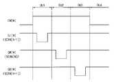
도 2를 보면, 제1 구간(DU1) 동안 데이터 초기화 게이트 신호(GI)에 의해 제1 노드(N1) 및 스토리지 캐패시터(CST)가 초기화 된다. 제2 구간(DU2) 동안 데이터 기입 게이트 신호(GW)에 의해 제1 트랜지스터(T1)의 쓰레스홀드 전압(

제1 구간(DU1)에 데이터 초기화 게이트 신호(GI)가 활성화 레벨을 가질 수 있다. 예를 들어, 데이터 초기화 게이트 신호(GI)의 활성화 레벨은 로우 레벨일 수 있다. 데이터 초기화 게이트 신호(GI)가 활성화 레벨을 가질 때, 제4 트랜지스터(T4)가 턴 온되어, 초기화 신호(VI)가 제1 노드(N1)에 인가될 수 있다. 현재 스테이지의 데이터 초기화 게이트 신호(GI[N])는 이전 스테이지의 스캔 신호(SCAN[N-1])일 수 있다.In the first period DU1 , the data initialization gate signal GI may have an activation level. For example, the activation level of the data initialization gate signal GI may be a low level. When the data initialization gate signal GI has an activation level, the fourth transistor T4 is turned on and the initialization signal VI may be applied to the first node N1 . The data initialization gate signal GI[N] of the current stage may be the scan signal SCAN[N-1] of the previous stage.
제2 구간(DU2)에는 데이터 기입 게이트 신호(GW)가 활성화 레벨을 가질 수 있다. 예를 들어, 데이터 기입 게이트 신호(GW)의 활성화 레벨은 로우 레벨일 수 있다. 데이터 기입 게이트 신호(GW)가 활성화 레벨을 가질 때, 제2 트랜지스터(T2) 및 제3 트랜지스터(T3)가 턴 온된다. 또한, 초기화 신호(VI)에 의해 제1 트랜지스터(T1)도 턴 온된다. 현재 스테이지의 데이터 기입 게이트 신호(GW[N])는 현재 스테이지의 스캔 신호(SCAN[N])일 수 있다.In the second period DU2 , the data write gate signal GW may have an activation level. For example, the activation level of the data write gate signal GW may be a low level. When the data write gate signal GW has an activation level, the second transistor T2 and the third transistor T3 are turned on. Also, the first transistor T1 is turned on by the initialization signal VI. The data write gate signal GW[N] of the current stage may be the scan signal SCAN[N] of the current stage.
턴 온된 제1 내지 제3 트랜지스터(T1, T2, T3)에 의해 형성된 경로를 따라, 제1 노드(N1)에는 데이터 전압(VDATA)에서 제1 트랜지스터(T1)의 쓰레스홀드 전압의 절대값(
제3 구간(DU3)에는 유기 발광 소자 초기화 게이트 신호(GB)가 활성화 레벨을 가질 수 있다. 예를 들어, 유기 발광 소자 초기화 게이트 신호(GB)의 활성화 레벨은 로우 레벨일 수 있다. 유기 발광 소자 초기화 게이트 신호(GB)가 활성화 레벨을 가질 때, 제7 트랜지스터(T7)가 턴 온되어, 초기화 신호(VI)가 유기 발광 소자(OLED)의 애노드 전극에 인가될 수 있다. 현재 스테이지의 유기 발광 소자 초기화 게이트 신호(GB[N])는 다음 스테이지의 스캔 신호(SCAN[N+1])일 수 있다.In the third period DU3 , the organic light emitting diode initialization gate signal GB may have an activation level. For example, the activation level of the organic light emitting device initialization gate signal GB may be a low level. When the organic light emitting device initialization gate signal GB has an activation level, the seventh transistor T7 is turned on and the initialization signal VI may be applied to the anode electrode of the organic light emitting device OLED. The organic light emitting device initialization gate signal GB[N] of the current stage may be the scan signal SCAN[N+1] of the next stage.
제4 구간(DU4)에는 에미션 신호(EM)가 활성화 레벨을 가질 수 있다. 예를 들어, 에미션 신호(EM)의 활성화 레벨은 로우 레벨일 수 있다. 에미션 신호(EM)가 활성화 레벨을 가질 때, 제5 트랜지스터(T5) 및 제6 트랜지스터(T6)가 턴 온된다. 또한, 데이터 전압(VDATA)에 의해 제1 트랜지스터(T1)도 턴 온된다.In the fourth period DU4 , the emission signal EM may have an activation level. For example, the activation level of the emission signal EM may be a low level. When the emission signal EM has an activation level, the fifth transistor T5 and the sixth transistor T6 are turned on. Also, the first transistor T1 is turned on by the data voltage VDATA.
구동 전류는 제5 트랜지스터(T5), 제1 트랜지스터(T1) 및 제6 트랜지스터(T6) 순서로 흘러 유기 발광 소자(OLED)를 구동할 수 있다. 구동 전류의 세기는 데이터 전압(VDATA)의 레벨에 의해 결정될 수 있다. 유기 발광 소자(OLED)의 휘도는 구동 전류의 세기에 의해 결정될 수 있다. 제1 트랜지스터(T1)의 제1 전극으로부터 제2 전극에 형성되는 경로를 따라 흐르는 구동 전류(ISD)는 이하의 수식 1과 같이 나타낼 수 있다.The driving current may flow in the order of the fifth transistor T5 , the first transistor T1 , and the sixth transistor T6 to drive the organic light emitting diode OLED. The intensity of the driving current may be determined by the level of the data voltage VDATA. The luminance of the organic light emitting diode OLED may be determined by the intensity of the driving current. The driving current ISD flowing along a path formed from the first electrode to the second electrode of the first transistor T1 may be expressed by
[수식 1][Formula 1]

수식 1에서 u는 제1 트랜지스터(T1)의 이동도이고, Cox는 제1 트랜지스터(T1)의 단위 면적당 정전 용량이며, W/L은 제1 트랜지스터(T1)의 폭과 길이의 비를 나타내고, VSG는 제1 트랜지스터(T1)의 제1 전극(N2)과 제어 전극(N1) 간의 전압을 의미하며,
제2 구간(DU2)에서 쓰레스홀드 전압(
[수식 2][Equation 2]

제4 구간(DU4)에서 유기 발광 소자(OLED)가 발광할 때, 구동 전압(VOV) 및 구동 전류(ISD)는 아래 수식 3 및 수식 4로 나타낼 수 있다. 수식 3에서 VS는 제2 노드(N2)의 전압이다.When the organic light emitting diode OLED emits light in the fourth period DU4 , the driving voltage VOV and the driving current ISD may be expressed by Equations 3 and 4 below. In Equation 3, VS is the voltage of the second node N2.
[수식 3][Equation 3]

[수식 4][Equation 4]

제2 구간(DU2)에서 쓰레스홀드 전압(

이와 같이 각 화소에 포함된 제1 트랜지스터(T1)는 구동 전류를 흐르게 하고, 각 화소에 포함된 유기 발광 소자(OLED)는 구동 전류의 크기에 상응하는 휘도로 발광할 수 있다. 이 때, 제1 트랜지스터(T1)의 전압-전류 특성은 이전 표시 프레임에서의 제1 트랜지스터(T1)의 동작 상태에 따라 달라질 수 있다. 즉, 화소들에 포함된 제1 트랜지스터(T1)는 히스테리시스(hysteresis)를 가질 수 있다.As described above, the first transistor T1 included in each pixel allows a driving current to flow, and the organic light emitting diode OLED included in each pixel may emit light with a luminance corresponding to the magnitude of the driving current. In this case, the voltage-current characteristic of the first transistor T1 may vary depending on the operating state of the first transistor T1 in the previous display frame. That is, the first transistor T1 included in the pixels may have hysteresis.
이러한 제1 트랜지스터(T1)의 히스테리시스에 의해, 표시 패널의 각 화소들이 이전 표시 프레임들에서 서로 다른 계조로 구동된 경우에, 다음 표시 프레임들에서 동일한 계조로 구동되더라도 각 화소들이 일정 시간 동안 서로 다른 휘도로 발광하는 순간 잔상이 발생될 수 있다. 상기 순간 잔상은 데이터 보상을 통하여 각 화소들 간 휘도 차이를 감소시킴으로써 개선될 수 있다. 이하 본 발명의 순간 잔상 개선을 위한 데이터 보상 회로에 대해 설명한다.Due to the hysteresis of the first transistor T1 , when each pixel of the display panel is driven with a different gray level in previous display frames, even if the pixels are driven with the same gray level in subsequent display frames, the pixels are different from each other for a predetermined time. An afterimage may be generated when light is emitted with luminance. The instantaneous afterimage may be improved by reducing a difference in luminance between pixels through data compensation. Hereinafter, a data compensation circuit for instantaneous afterimage improvement according to the present invention will be described.
도 3은 본 발명의 실시예들에 따른 데이터 보상 회로(10)를 나타내는 블록도이다. 도 4a 및 도 4b는 도 3의 데이터 보상 회로(10)의 데이터 보상 전과 후를 비교하는 도면들이다.3 is a block diagram illustrating a
도 3을 참조하면, 데이터 보상 회로(10)는 기준 프레임 메모리 장치(100), 누적 스트레스 메모리 장치(400), 스트레스 데이터 생성부(200), 메모리 제어부(300) 및 보상부(500)를 포함할 수 있다.Referring to FIG. 3 , the
기준 프레임 메모리 장치(100)는 기준 프레임 데이터(RFD)를 저장할 수 있다. 기준 프레임 데이터(RFD)는 스트레스 데이터(SD) 생성 및 잔상 보상 데이터(CD) 생성의 기준이 될 수 있다. 예를 들어, 기준 프레임 데이터(RFD)는 입력 영상 데이터(IND)의 시작 프레임 데이터일 수 있다. 기준 프레임 메모리 장치(100)에 저장된 기준 프레임 데이터(RFD)는 메모리 제어부(300)를 통해 스트레스 데이터 생성부(200)에 전달될 수 있다. 기준 프레임 메모리 장치(100)에 저장된 기준 프레임 데이터(RFD)는 메모리 제어부(300)를 통해 보상부(500)에 전달될 수 있다. 한편, 기준 프레임 메모리 장치(100)는 보상부(500)로부터 보상부(500)에서 갱신된 새로운 기준 프레임 데이터(UD-RFD)를 입력받고, 기존의 기준 프레임 데이터(RFD) 대신에 새로운 기준 프레임 데이터(UD-RFD)를 저장할 수 있다.The reference
누적 스트레스 메모리 장치(400)는 각 화소에 대한 누적 스트레스 데이터(ASD)를 저장할 수 있다. 이 때, 메모리 제어부(300)가 스트레스 데이터(SD)를 누적 스트레스 메모리 장치(400)에 전달하면, 누적 스트레스 메모리 장치(400)는 갱신된 누적 스트레스 데이터(ASD)를 저장할 수 있다. 한편, 누적 스트레스 메모리 장치(400)에 저장된 누적 스트레스 데이터(ASD)는 메모리 제어부(300)를 통해 보상부(500)에 전달될 수 있다.The accumulated
스트레스 데이터 생성부(200)는 출력 영상 데이터(OUTD)와 상기 기준 프레임 데이터(RFD)를 비교하여 각 화소에 대한 스트레스 데이터(SD)를 생성할 수 있다. 이 때, 출력 영상 데이터(OUTD) 및 기준 프레임 데이터(RFD) 각각은 0 ~ 255의 계조를 가질 수 있다. 스트레스 데이터 생성부(200)는 출력 영상 데이터(OUTD)에 따른 제1 계조값과 기준 프레임 데이터(RFD)에 따른 기준 계조값의 차이를 나타내는 제1 파라미터(DDO)를 기초로 각 화소에 대한 휘도 스트레스를 계산하여 스트레스 데이터(SD)를 생성할 수 있다. 일 실시예에 있어서 스트레스 데이터 생성부(200)는 스트레스 데이터(SD)를 계산하기 위한 특정 수식을 저장할 수 있다. 스트레스 데이터 생성부(200)는 이러한 수식을 기초로 스트레스 데이터(SD)를 산출할 수 있다.The
한편, 스트레스 데이터 생성부(200)는 입력 영상 데이터(IND)의 휘도 데이터(DBV)를 반영하여 휘도 보정 상수를 산출하고, 휘도 보정 상수를 기초로 휘도 보정 스트레스 데이터를 생성할 수 있다.Meanwhile, the
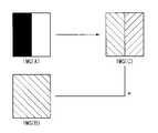
도 4a를 참조하면, 표시 패널에 포함된 복수의 화소들이 IMG(A)와 같이 이전 표시 프레임들에서 서로 다른 계조(예컨대, 블랙과 화이트)로 구동된 경우, 스트레스 데이터 생성부(200)는 각 화소에 대한 스트레스 데이터(SD)를 산출할 수 있다. 이러한 스트레스 데이터(SD)들은 누적 스트레스 메모리 장치(400)에 가산되어 누적될 수 있다. 따라서, IMG(B)와 같이 다음 표시 프레임들에서 동일한 계조(예컨대, 그레이)로 구동되더라도, 각 화소들이 일정 시간 동안 서로 다른 휘도로 발광하게 될 수 있다. 즉, 데이터 보정이 이루어지지 않은 경우, IMG(C)와 같이 순간 잔상이 발생하고 사용자에게 각 화소에 대한 휘도 차이가 시인될 수 있다.Referring to FIG. 4A , when a plurality of pixels included in the display panel are driven with different grayscales (eg, black and white) in previous display frames, such as the IMG(A), the
메모리 제어부(300)는 각 화소에 대한 스트레스 데이터(SD)를 누적 스트레스 메모리 장치(400)에 가산하여 각 화소에 대한 누적 스트레스 데이터(ASD)를 갱신할 수 있다. 메모리 제어부(300)는 누적 스트레스 메모리 장치(400)의 동작 속도에 상응하는 누적 레이트로 각 화소에 대한 스트레스 데이터(SD)를 누적 스트레스 메모리 장치(400)에 누적시킬 수 있다. 한편, 메모리 제어부(300)는 보상부(500)로부터 새로운 기준 프레임 데이터(UD-RFD)를 전달받을 수 있다. 메모리 제어부(300)는 기존의 기준 프레임 데이터(RFD)를 보상부(500)에서 갱신된 새로운 기준 프레임 데이터(UD-RFD)로 갱신하고, 새로운 기준 프레임 데이터(UD-RFD)를 스트레스 데이터 생성부(200)로 전달할 수 있다. 이 때, 스트레스 데이터 생성부(200)는 새로운 기준 프레임 데이터(UD-RFD)를 기초로 스트레스 데이터(SD)를 생성할 수 있다.The
보상부(500)는 누적 스트레스 데이터(ASD)에 기초하여 각 화소에 대한 잔상 보상 데이터(CD)를 생성하고, 잔상 보상 데이터(CD)에 기초하여 입력 영상 데이터(IND)를 보상함으로써 상기 출력 영상 데이터(OUTD)를 생성할 수 있다. 구체적으로, 보상부(500)는 누적 스트레스 메모리 장치(400)로부터 각 화소에 대한 누적 스트레스 데이터(ASD)를 수신하고, 각 화소에 대한 누적 스트레스 데이터(ASD) 및 입력 영상 데이터(IND)에 따른 제2 계조값과 기준 계조값의 차이를 기초로 잔상 보상 데이터(CD)를 생성할 수 있다. 예를 들어, 보상부(500)는 각 화소에 대한 누적 스트레스 데이터(ASD)를 수식 또는 룩업테이블(Look Up Table)에 적용하여 각 화소에 대한 휘도 드롭량을 도출하고, 각 화소에 대한 휘도 드롭량에 대응되는 각 화소에 대한 휘도 보상량을 계산함으로써, 잔상 보상을 수행하기 위한 각 화소에 대한 잔상 보상 데이터(CD)를 생성할 수 있다. 이 때, 보상부(500)는 잔상 보상 데이터(CD)를 계산하기 위한 특정 수식을 저장할 수 있다. 구체적으로, 보상부(500)는 제2 계조값과 기준 계조값의 차이를 나타내는 제2 파라미터(DDI)를 기준으로 잔상 보상 데이터(CD)를 생성하는 수식을 저장할 수 있다.The
도 4a 및 도 4b를 참조하면, 표시 패널에 포함된 복수의 화소들이 IMG(A)와 같이 이전 표시 프레임들에서 서로 다른 계조(예컨대, 블랙과 화이트)로 구동된 경우, 누적 스트레스 메모리 장치(400)에 스트레스 데이터(SD)가 누적될 수 있다. 따라서, IMG(B)와 같이 다음 표시 프레임들에서 동일한 계조(예컨대, 그레이)로 구동되더라도, 각 화소들이 일정 시간 동안 서로 다른 휘도로 발광하게 될 수 있다. 이 때, 보상부(500)에서 데이터 보정이 이루어지는 경우, 각 화소들은 타겟 영상과 휘도가 동일한 출력 영상을 표시할 수 있다. 구체적으로, 보상부(500)에서 누적 스트레스 데이터(ASD)에 기초하여 각 화소에 대한 잔상 보상 데이터(CD)를 생성하고, 잔상 보상 데이터(CD)에 기초하여 입력 영상 데이터(IND)를 보상함으로써 IMG(D)와 같이 타겟 영상(IMG(B))과 휘도가 동일한 출력 영상을 표시할 수 있다. 데이터 보상 회로(10)는 이러한 데이터 보상으로 제1 트랜지스터(T1)의 히스테리시스를 개선할 수 있고, 이에 따라, 제1 트랜지스터(T1)의 히스테리시스에 기인한 표시 장치의 순간 잔상이 개선될 수 있다.4A and 4B , when a plurality of pixels included in the display panel are driven with different grayscales (eg, black and white) in previous display frames, such as IMG(A), the cumulative stress memory device 400 ), the stress data SD may be accumulated. Accordingly, even if the pixels are driven with the same gray level (eg, gray) in subsequent display frames as in the IMG(B), each pixel may emit light with different luminance for a predetermined time. In this case, when data correction is performed by the
한편, 보상부(500)는 잔상 보상 데이터(CD)의 휘도 보상량의 크기가 0이 될 때, 기준 프레임 데이터(RFD)를 갱신하여 새로운 기준 프레임 데이터(UD-RFD)를 메모리 제어부(300)에 전달할 수 있다. 이하 데이터 보상 회로(10)의 구체적인 동작에 대해서 도 5 내지 도 7을 참조하여 설명한다.Meanwhile, the
도 5는 도 3의 데이터 보상 회로(10)가 동작하는 순서도이다. 도 6은 본 발명의 일 실시예에 따른 스트레스 데이터(SD)를 나타내는 그래프이다. 도 7은 본 발명의 일 실시예에 따른 잔상 보상 데이터(CD)를 나타내는 그래프이다.5 is a flowchart illustrating an operation of the
도 5 내지 도 7을 참조하면, 기준 프레임 메모리 장치(100)는 기준 프레임 데이터(RFD)를 저장(단계 S100)할 수 있다. 스트레스 데이터 생성부(200)는 출력 영상 데이터(OUTD)와 기준 프레임 데이터(RFD)를 비교하여 스트레스 데이터(SD)를 생성(단계 S200)할 수 있다. 누적 스트레스 메모리 장치(400)는 각 화소에 대한 누적 스트레스 데이터(ASD)를 저장(단계 S300)할 수 있다. 메모리 제어부(300)는 누적 스트레스 데이터(ASD)에 스트레스 데이터(SD)를 가산하여 누적 스트레스 데이터(ASD)를 갱신(단계 S400)할 수 있다. 보상부(500)는 누적 스트레스 데이터(ASD) 및 입력 영상 데이터(IND)를 기초로 잔상 보상 데이터(CD)를 생성(S500)할 수 있다. 이때, 보상부(500)는 잔상 보상 데이터(CD)의 휘도 보상량이 0이 아닌 경우, 입력 영상 데이터(IND)의 휘도를 보상하여 출력 영상 데이터(OUTD)를 생성(단계 S700)할 수 있다. 보상부(500)는 잔상 보상 데이터(CD)의 휘도 보상량이 0인 경우, 입력 영상 데이터(IND)를 새로운 기준 프레임 데이터(UD-RFD)로 갱신(단계 S800)할 수 있다.5 to 7 , the reference
기준 프레임 메모리 장치(100)는 기준 프레임 데이터(RFD)를 저장(단계 S100)할 수 있다. 기준 프레임 데이터(RFD)는 스트레스 데이터(SD) 생성 및 잔상 보상 데이터(CD) 생성의 기준이 될 수 있다. 예를 들어, 기준 프레임 데이터(RFD)는 입력 영상 데이터(IND)의 시작 프레임 데이터일 수 있다. 기준 프레임 메모리 장치(100)에 저장된 기준 프레임 데이터(RFD)는 스트레스 데이터 생성부(200)에 전달될 수 있다. 구체적으로, 스트레스 데이터 생성부(200)가 스트레스 데이터(SD)를 생성할 때, 스트레스 데이터 생성부(200)는 기준 프레임 메모리 장치(100)에 저장된 기준 프레임 데이터(RFD)를 전달받고, 출력 영상 데이터(OUTD)와 기준 프레임 데이터(RFD)를 비교할 수 있다. 메모리 제어부(300)는 기준 프레임 데이터(RFD)를 보상부(500)에 전달할 수 있다. 구체적으로, 보상부(500)가 잔상 보상 데이터(CD)를 생성할 때, 보상부(500)는 메모리 제어부(300)로부터 기준 프레임 메모리 장치(100)에 저장된 기준 프레임 데이터(RFD)를 전달받고, 입력 영상 데이터(IND)와 기준 프레임 데이터(RFD)를 비교할 수 있다. 한편, 메모리 제어부(300)는 보상부(500)로부터 보상부(500)에서 갱신된 새로운 기준 프레임 데이터(UD-RFD)를 입력받고, 기존의 기준 프레임 데이터(RFD)를 새로운 기준 프레임 데이터(UD-RFD)로 갱신할 수 있다.The reference
스트레스 데이터 생성부(200)는 출력 영상 데이터(OUTD)와 기준 프레임 데이터(RFD)를 비교하여 스트레스 데이터(SD)를 생성(단계 S200)할 수 있다. 스트레스 데이터 생성부(200)는 출력 영상 데이터(OUTD)와 상기 기준 프레임 데이터(RFD)를 비교하여 프레임 레이트(또는 표시 레이트)(예를 들어, 60Hz~120Hz)로 각 화소에 대한 스트레스 데이터(SD)를 생성할 수 있다. 이 때, 출력 영상 데이터(OUTD) 및 기준 프레임 데이터(RFD) 각각은 0 ~ 255의 계조를 가질 수 있다. 구체적으로, 스트레스 데이터 생성부(200)는 출력 영상 데이터(OUTD)에 따른 제1 계조값과 기준 프레임 데이터(RFD)에 따른 기준 계조값의 차이를 나타내는 제1 파라미터(DDO)를 기초로 각 화소에 대한 스트레스를 계산하여 스트레스 데이터(SD)를 생성할 수 있다. 예를 들어, 각 화소에 대한 스트레스 데이터(SD)는 출력 영상 데이터(OUTD)의 각 화소에 대한 휘도에 상응하는 값일 수 있고, 각 화소에 대한 누적 스트레스 데이터(ASD)는 출력 영상 데이터(OUTD)의 각 화소에 대한 휘도에 상응하는 값이 누적되어 생성되는 값일 수 있다. 다른 예를 들어, 각 화소에 대한 스트레스 데이터(SD)는 출력 영상 데이터(OUTD)의 각 화소에 대한 계조에 상응하는 값일 수 있고, 각 화소에 대한 누적 스트레스 데이터(ASD)는 출력 영상 데이터(OUTD)의 각 화소에 대한 계조에 상응하는 값이 누적되어 생성되는 값일 수 있다. 다만, 이것은 예시적인 것으로서, 각 화소에 대한 스트레스 데이터(SD) 및 각 화소에 대한 누적 스트레스 데이터(ASD)는 다양한 조건들(예를 들어, 시간, 온도, 휘도, 전류 등)을 고려하여 생성될 수 있다.The
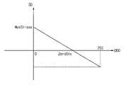
도 6을 참조하면, 일 실시예에 있어서, 스트레스 데이터 생성부(200)는 스트레스 데이터(SD)를 계산하기 위한 특정 수식을 저장할 수 있다. 구체적으로, 스트레스 데이터 생성부(200)는 출력 영상 데이터(OUTD)에 따른 제1 계조값과 기준 계조값의 차이를 나타내는 제1 파라미터(DDO)를 기준으로 스트레스 데이터(SD)를 생성하는 수식을 저장할 수 있다. 예를 들어, 스트레스 데이터 생성부(200)는 스트레스 데이터(SD)를 아래 수식 5에 따라 계산할 수 있다.Referring to FIG. 6 , according to an embodiment, the
[수식 5][Equation 5]

이 때, DDO는 제1 파라미터(DDO)를 나타내고, A0 및 A1은 스트레스 보정 계수를 나타내며, MaxStress는 스트레스 데이터(SD)의 최대값을 나타내고, ZeroStX는 스트레스 데이터(SD)의 값이 0일 때 제1 파라미터(DDO)의 값을 나타낸다. 출력 영상 데이터(OUTD)와 기준 프레임 데이터(RFD)가 동일한 값을 가질 때(예컨대, 제1 계조값 = 기준 계조값) 제1 파라미터(DDO)의 값은 0이 되므로 스트레스 데이터(SD)는 최대값을 가질 수 있다. 즉, 출력 영상 데이터(OUTD)와 기준 프레임 데이터(RFD)가 동일한 계조값을 가지는 것은 제1 트랜지스터(T1)에 전기적 스트레스가 가해지는 것을 의미할 수 있다. 반대로, 출력 영상 데이터(OUTD)의 계조값과 기준 프레임 데이터(RFD) 계조값의 차이가 커지는 것은 제1 트랜지스터(T1)에 가해지는 전기적 스트레스가 작아지는 것을 의미할 수 있다.In this case, DDO denotes the first parameter DDO, A0 and A1 denote stress correction coefficients, MaxStress denotes the maximum value of the stress data SD, and ZeroStX denotes the value of the stress data SD when the value of the stress data SD is 0. It represents the value of the first parameter DDO. When the output image data OUTD and the reference frame data RFD have the same value (eg, the first grayscale value = the reference grayscale value), the value of the first parameter DDO becomes 0, so that the stress data SD is the maximum can have a value. That is, when the output image data OUTD and the reference frame data RFD have the same grayscale value, it may mean that electrical stress is applied to the first transistor T1 . Conversely, an increase in the difference between the grayscale value of the output image data OUTD and the grayscale value of the reference frame data RFD may mean that the electrical stress applied to the first transistor T1 decreases.
일 실시예에 있어서, 스트레스 데이터 생성부(200)는 입력 영상 데이터(IND)의 휘도 데이터(DBV)를 반영하여 휘도 보정 상수를 산출하고, 휘도 보정 상수를 기초로 휘도 보정 스트레스 데이터를 생성할 수 있다. 구체적으로, 상기 휘도 보정 스트레스 데이터는 스트레스 데이터(SD)에 휘도 보정 상수를 곱한 값일 수 있다. 휘도 보정 상수는 기준 프레임 데이터(RFD)의 휘도를 기준으로 출력 영상 데이터(OUTD)의 휘도의 차이를 나타내는 파라미터일 수 있다. 즉, 휘도 보정 상수는 스트레스 데이터(SD) 산출에 있어서, 기준 프레임 데이터(RFD)와 출력 영상 데이터(OUTD)의 휘도 차이를 반영하기 위한 파라미터일 수 있다. 예를 들어, 기준 프레임 데이터(RFD)의 휘도가 400니트(nit)일 때와 기준 프레임 데이터(RFD)의 휘도가 700니트일 때는 서로 스트레스 데이터(SD)가 차이날 수 있다. 따라서 상기 휘도 보정 스트레스 데이터는 스트레스 데이터(SD)를 산출할 때, 출력 영상 데이터(OUTD)와 기준 프레임 데이터(RFD)의 계조값의 차이뿐만 아니라 출력 영상 데이터(OUTD)와 기준 프레임 데이터(RFD)의 휘도값의 차이도 반영할 수 있다. 한편, 스트레스 데이터 생성부(200)는 상기 휘도 보정 스트레스 데이터를 누적 스트레스 메모리 장치(400)로 전달할 수 있다. 누적 스트레스 메모리 장치(400)는 상기 휘도 보정 스트레스 데이터를 누적 스트레스 데이터(ASD)에 가산하여 저장할 수 있다. 보상부(500)는 메모리 제어부(300)로부터 누적 스트레스 메모리 장치(400)에 저장된 상기 휘도 보정 스트레스 데이터가 누적된 누적 스트레스 데이터(ASD)를 전달받고, 이를 기초로 기준 프레임 데이터(RFD)와 출력 영상 데이터(OUTD)의 휘도 차이가 반영된 잔상 보상 데이터(CD)를 생성할 수 있다.In an embodiment, the stress
한편, 출력 영상 데이터(OUTD)의 계조값과 기준 프레임 데이터(RFD) 계조값의 차이가 특정 값 이상으로 커지는 경우(예컨대, 제1 파라미터(DDO)의 값이 수식 5의 ZeroStX 이상으로 커지는 경우), 스트레스 데이터(SD)는 음의 값을 가질 수 있다. 이 경우, 제1 트랜지스터(T1)가 받는 전기적 스트레스가 릴리스(release)되므로, 각 화소에 대한 누적 스트레스가 감소할 수 있다.On the other hand, when the difference between the grayscale value of the output image data OUTD and the reference frame data RFD grayscale value becomes greater than a specific value (eg, when the value of the first parameter DDO becomes greater than ZeroStX of Equation 5) , the stress data SD may have a negative value. In this case, since the electrical stress applied to the first transistor T1 is released, the accumulated stress for each pixel may be reduced.
누적 스트레스 메모리 장치(400)는 각 화소에 대한 누적 스트레스 데이터(ASD)를 저장(단계 S300)할 수 있다. 구체적으로, 누적 스트레스 데이터(ASD)는 스트레스 데이터 생성부(200)에서 생성된 스트레스 데이터(SD)가 시간에 따라 가산되면서 메모리 제어부(300)에 갱신될 수 있다. 이 때, 메모리 제어부(300)가 누적 스트레스 데이터(ASD)를 누적 스트레스 메모리 장치(400)에 전달하면, 누적 스트레스 메모리 장치(400)는 갱신된 누적 스트레스 데이터(ASD)를 저장할 수 있다. 한편, 누적 스트레스 메모리 장치(400)에 저장된 누적 스트레스 데이터(ASD)는 보상부(500)에 전달될 수 있다. 구체적으로, 보상부(500)가 잔상 보상 데이터(CD)를 생성할 때, 보상부(500)는 메모리 제어부(300)로부터 누적 스트레스 메모리 장치(400)에 저장된 누적 스트레스 데이터(ASD)를 전달받고, 수식 또는 룩업테이블(Look Up Table)에 따라 누적 스트레스 데이터(ASD)에 비례하는 잔상 보상 데이터(CD)를 생성할 수 있다.The accumulated
일 실시예에 있어서, 누적 스트레스 데이터(ASD)는 제1 계조값과 기준 계조값의 차이가 유지되는 시간에 비례하여 증가할 수 있다. 구체적으로, 출력 영상 데이터(OUTD)의 계조값과 기준 프레임 데이터(RFD)의 계조값의 차이가 유지되는 시간이 증가할수록 제1 트랜지스터(T1)가 받는 전기적 스트레스가 증가할 수 있다. 따라서, 제1 계조값과 기준 계조값의 차이가 유지되는 시간이 길수록, 보상부(500)에서 생성하는 잔상 보상 데이터(CD)의 휘도 보상량이 커질 수 있다. 예를 들어, 누적 스트레스 데이터(ASD)는 스트레스 데이터(SD)와 단위 시간(예를 들어, 1/120sec~1/60sec)의 곱들의 합으로 산출될 수 있다. 이는, 아래와 같이 수식 6으로 나타낼 수 있다.In an embodiment, the accumulated stress data ASD may increase in proportion to a time during which the difference between the first grayscale value and the reference grayscale value is maintained. In detail, as the time for maintaining the difference between the grayscale value of the output image data OUTD and the grayscale value of the reference frame data RFD increases, the electrical stress applied to the first transistor T1 may increase. Accordingly, the longer the time for which the difference between the first grayscale value and the reference grayscale value is maintained, the greater the luminance compensation amount of the afterimage compensation data CD generated by the
[수식 6][Equation 6]

이 때, t는 단위 시간을 나타내고, SD_Release는 스트레스 데이터(SD)의 시간에 따른 릴리스 값을 나타낸다. 즉, 누적 스트레스 데이터(ASD)는 스트레스 데이터(SD)와 시간에 비례하여 증가하고, 스트레스 데이터(SD)의 릴리스만큼 감소할 수 있다.In this case, t represents a unit time, and SD_Release represents a time-dependent release value of the stress data SD. That is, the accumulated stress data ASD may increase in proportion to the stress data SD and time, and may decrease by the release of the stress data SD.
메모리 제어부(300)는 각 화소에 대한 스트레스 데이터(SD)를 누적 스트레스 메모리 장치(400)에 가산하여 각 화소에 대한 누적 스트레스 데이터(ASD)를 갱신(단계 S400)할 수 있다. 구체적으로, 메모리 제어부(300)는 스트레스 데이터 생성부(200)로부터 프레임 레이트(또는 표시 레이트)로 각 화소에 대한 스트레스 데이터(SD)를 전달받을 수 있다. 메모리 제어부(300)는 누적 스트레스 메모리 장치(400)의 동작 속도에 상응하는 누적 레이트(예를 들어, 1Hz 미만)로 각 화소에 대한 스트레스 데이터(SD)를 누적 스트레스 메모리 장치(400)에 누적시킬 수 있다.The
한편, 메모리 제어부(300)는 보상부(500)로부터 새로운 기준 프레임 데이터(UD-RFD)를 전달받을 수 있다. 메모리 제어부(300)는 기존의 기준 프레임 데이터(RFD)를 보상부(500)에서 갱신된 새로운 기준 프레임 데이터(UD-RFD)로 갱신하고, 새로운 기준 프레임 데이터(UD-RFD)를 스트레스 데이터 생성부(200)로 전달할 수 있다. 이 때, 스트레스 데이터 생성부(200)는 새로운 기준 프레임 데이터(UD-RFD)를 기초로 스트레스 데이터(SD)를 생성할 수 있다.Meanwhile, the
보상부(500)는 누적 스트레스 데이터(ASD) 및 입력 영상 데이터(IND)를 기초로 잔상 보상 데이터(CD)를 생성(S500)할 수 있다. 이때, 보상부(500)는 잔상 보상 데이터(CD)의 휘도 보상량이 0이 아닌 경우, 입력 영상 데이터(IND)의 휘도를 보상하여 출력 영상 데이터(OUTD)를 생성(단계 S700)할 수 있다. 구체적으로, 보상부(500)는 누적 스트레스 메모리 장치(400)로부터 각 화소에 대한 누적 스트레스 데이터(ASD)를 수신하고, 각 화소에 대한 누적 스트레스 데이터(ASD) 및 입력 영상 데이터(IND)에 따른 제2 계조값과 기준 계조값의 차이를 기초로 잔상 보상 데이터(CD)를 생성할 수 있다. 예를 들어, 보상부(500)는 각 화소에 대한 누적 스트레스 데이터(ASD)를 수식 또는 룩업테이블(Look Up Table)에 적용하여 각 화소에 대한 휘도 드롭량을 도출하고, 각 화소에 대한 휘도 드롭량에 대응되는 각 화소에 대한 휘도 보상량을 계산함으로써, 잔상 보상을 수행하기 위한 각 화소에 대한 잔상 보상 데이터(CD)를 생성할 수 있다.The
일 실시예에 있어서, 보상부(500)는 입력 영상 데이터(IND)와 상기 기준 프레임 데이터(RFD)를 비교하여 프레임 레이트(또는 표시 레이트)(예를 들어, 60Hz~120Hz)로 각 화소에 대한 잔상 보상 데이터(CD)의 휘도 보상량을 결정할 수 있다. 이 때, 입력 영상 데이터(IND) 및 기준 프레임 데이터(RFD) 각각은 0 ~ 255의 계조를 가질 수 있다. 구체적으로, 보상부(500)는 입력 영상 데이터(IND)에 따른 제2 계조값과 기준 계조값의 차이를 나타내는 제2 파라미터(DDI)를 기초로 잔상 보상 데이터(CD)를 생성하고, 잔상 보상 데이터(CD)에 기초하여 입력 영상 데이터(IND)를 보상함으로써 출력 영상 데이터(OUTD)를 생성할 수 있다.In an embodiment, the
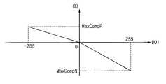
도 7을 참조하면, 일 실시예에 있어서, 보상부(500)는 잔상 보상 데이터(CD)를 계산하기 위한 특정 수식을 저장할 수 있다. 구체적으로, 보상부(500)는 제2 계조값과 기준 계조값의 차이를 나타내는 제2 파라미터(DDI)를 기준으로 잔상 보상 데이터(CD)를 생성하는 수식을 저장할 수 있다. 예를 들어, 보상부(500)는 잔상 보상 데이터(CD)를 아래 수식 7에 따라 계산할 수 있다.Referring to FIG. 7 , according to an embodiment, the
[수식 7][Equation 7]

이 때, DDI는 제2 파라미터(DDI)를 나타내고, A2은 잔상 보상 보정 계수를 나타내며, MaxComp는 잔상 보상 데이터(CD)의 최대값을 나타내고, ASD는 누적 스트레스 데이터(ASD)의 값을 나타낸다. 잔상 보상 보정 계수는 누적 스트레스 데이터(ASD)의 바이어스 조건에 따라 휘도 증가 보상 또는 휘도 감소 보상 여부가 결정될 수 있다. 잔상 보상 데이터(CD)의 최대값 역시, 누적 스트레스 데이터(ASD)의 바이어스 조건에 따라 휘도 증가 보상 또는 휘도 감소 보상 여부가 결정될 수 있다.In this case, DDI denotes the second parameter DDI, A2 denotes a residual image compensation correction coefficient, MaxComp denotes the maximum value of the residual image compensation data CD, and ASD denotes a value of the accumulated stress data ASD. As for the afterimage compensation correction coefficient, whether to compensate for luminance increase or decrease luminance may be determined according to a bias condition of the accumulated stress data ASD. As for the maximum value of the afterimage compensation data CD, whether to compensate the luminance increase or decrease the luminance may be determined according to the bias condition of the accumulated stress data ASD.
일 실시예에 있어서, 보상부(500)는 제2 계조값이 기준 계조값보다 큰 경우 입력 영상 데이터(IND)의 휘도를 감소시키기 위한 잔상 보상 데이터(CD)를 생성할 수 있다. 다른 실시예에 있어서, 보상부(500)는 제2 계조값이 기준 계조값보다 작은 경우 입력 영상 데이터(IND)의 휘도를 증가시키기 위한 잔상 보상 데이터(CD)를 생성할 수 있다. 예를 들어, 제2 파라미터(DDI)가 0보다 큰 경우는 누적 스트레스 데이터(ASD)가 낮은 휘도의 바이어스 조건에서 유지되는 경우로 가정할 수 있다. 이 때, 출력 영상 데이터(OUTD)는 입력 영상 데이터(IND)보다 휘도가 높게 표시될 수 있다. 따라서, 이 경우 잔상 보상 데이터(CD)는 입력 영상 데이터(IND)의 휘도를 감소시키는 데이터 보상을 할 수 있다. 다른 예를 들어, 제2 파라미터(DDI)가 0보다 작은 경우는 누적 스트레스 데이터(ASD)가 높은 휘도의 바이어스 조건에서 유지되는 경우로 가정할 수 있다. 이 때, 출력 영상 데이터(OUTD)는 입력 영상 데이터(IND)보다 휘도가 낮게 표시될 수 있다. 따라서, 이 경우 잔상 보상 데이터(CD)는 입력 영상 데이터(IND)의 휘도를 증가시키는 데이터 보상을 할 수 있다.In an embodiment, when the second grayscale value is greater than the reference grayscale value, the
한편, 보상부(500)는 잔상 보상 데이터(CD)의 휘도 보상량의 크기가 0이 될 때, 입력 영상 데이터(IND)를 새로운 기준 프레임 데이터(UD-RFD)로 갱신(단계 S800)하여 새로운 기준 프레임 데이터(UD-RFD)를 메모리 제어부(300)에 전달할 수 있다. 구체적으로, 입력 영상 데이터(IND)와 기준 프레임 데이터(RFD)가 동일한 값을 가질 때(예컨대, 제2 계조값 = 기준 계조값), 제2 파라미터(DDI)의 값은 0이 되므로 잔상 보상 데이터(CD)는 최소값(예컨대, 0)을 가질 수 있다. 이 때, 보상부(500)는 잔상 보상 데이터(CD)가 최소값이 될 때의 입력 영상 데이터(IND)를 새로운 기준 프레임 데이터(UD-RFD)로 갱신할 수 있다. 메모리 제어부(300)는 보상부(500)로부터 새로운 기준 프레임 데이터(UD-RFD)를 전달받고, 새로운 기준 프레임 데이터(UD-RFD)를 기준 프레임 데이터(RFD)로 갱신할 수 있다. 데이터 보상 회로(10)는 새로운 기준 프레임 데이터(UD-RFD)를 이용하여 다음 데이터 보상 동작을 반복할 수 있다. 데이터 보상 회로(10)는 이러한 데이터 보상으로 제1 트랜지스터(T1)의 히스테리시스를 개선할 수 있고, 이에 따라, 제1 트랜지스터(T1)의 히스테리시스에 기인한 표시 장치의 순간 잔상이 개선될 수 있다.On the other hand, the
도 8은 본 발명의 실시예들에 따른 데이터 보상 회로를 나타내는 블록도이고, 도 9a는 도 8의 데이터 보상 회로가 입력 영상 데이터를 보상하여 출력 영상 데이터를 생성하는 것을 설명하기 위한 도면이며, 도 9b는 도 8의 데이터 보상 회로가 기준 프레임 데이터를 생성(즉, 갱신)하는 것을 설명하기 위한 도면이다.8 is a block diagram illustrating a data compensation circuit according to embodiments of the present invention, and FIG. 9A is a diagram for explaining that the data compensation circuit of FIG. 8 generates output image data by compensating for input image data, and FIG. 9B is a diagram for explaining that the data compensation circuit of FIG. 8 generates (ie, updates) reference frame data.
도 8 내지 도 9b를 참조하면, 데이터 보상 회로(11)는 기준 프레임 메모리 장치(110), 기준 프레임 데이터 생성부(210), 메모리 제어부(310) 및 보상부(510)를 포함할 수 있다. 즉, 데이터 보상 회로(11)는 도 3의 데이터 보상 회로(10)와는 달리 각 화소에 대한 스트레스 데이터(SD)를 생성하지 않으므로, 스트레스 데이터 생성부(200) 및 누적 스트레스 메모리 장치(400)에 상응하는 구성들을 포함하지 않을 수 있다. 대신에, 데이터 보상 회로(11)는 기준 프레임 데이터(RFD)를 매 표시 프레임마다 누적하여 생성(즉, 갱신)하므로, 이러한 동작을 수행하기 위한 기준 프레임 데이터 생성부(210)를 포함할 수 있다.8 to 9B , the
기준 프레임 메모리 장치(110)는 기준 프레임 데이터(RFD)를 저장할 수 있다. 기준 프레임 데이터(RFD)는 잔상 보상 데이터(CD) 생성 및 출력 영상 데이터(OUTD) 생성의 기준이 되고, 기준 프레임 데이터 생성부(210)에 의해 매 표시 프레임마다 누적하여 생성(즉, 갱신)될 수 있다. 구체적으로, 기준 프레임 메모리 장치(110)는 제i(단, i는 2이상의 정수) 표시 프레임에서 제i 기준 프레임 데이터(RFD[i])가 생성되면 기존에 저장되어 있던 제i-1 기준 프레임 데이터(RFD[i-1]) 대신에 제i 기준 프레임 데이터(RFD[i])를 저장하고, 제i+1 표시 프레임에서 제i 기준 프레임 데이터(RFD[i])를 제공할 수 있다. 예를 들어, 제2 표시 프레임에서 제2 출력 영상 데이터(OUTD[2]) 및 제1 기준 프레임 데이터(RFD[1])에 기초하여 제2 기준 프레임 데이터(RFD[2])(이 때, 제2 기준 프레임 데이터(RFD[2])는 제3 표시 프레임에서 제3 출력 영상 데이터(OUTD[3])를 생성하기 위해 사용됨)가 생성되면, 기준 프레임 메모리 장치(110)는 기존에 저장되어 있던 제1 기준 프레임 데이터(RFD[1]) 대신에 제2 기준 프레임 데이터(RFD[2])를 저장하고, 제3 표시 프레임에서 제2 기준 프레임 데이터(RFD[2])를 메모리 제어부(310)를 거쳐 보상부(510)에 제공할 수 있다. 또한, 제3 표시 프레임에서 제3 출력 영상 데이터(OUTD[3]) 및 제2 기준 프레임 데이터(RFD[2])에 기초하여 제3 기준 프레임 데이터(RFD[3])(이 때, 제3 기준 프레임 데이터(RFD[3])는 제4 표시 프레임에서 제4 출력 영상 데이터(OUTD[4])를 생성하기 위해 사용됨)가 생성되면, 기준 프레임 메모리 장치(110)는 기존에 저장되어 있던 제2 기준 프레임 데이터(RFD[2]) 대신에 제3 기준 프레임 데이터(RFD[3])를 저장하고, 제4 표시 프레임에서 제3 기준 프레임 데이터(RFD[3])를 메모리 제어부(310)를 통해 보상부(510)에 제공할 수 있다. 일 실시예에서, 최초 기준 프레임 데이터(RFD)는 0으로 설정될 수 있다.The reference
기준 프레임 데이터 생성부(210)는 제i-1 표시 프레임에서 생성된 제i-1 기준 프레임 데이터(RFD[i-1]) 및 제i 표시 프레임에서 제i-1 기준 프레임 데이터(RFD[i-1])를 기초로 생성되는 제i 출력 영상 데이터(OUTD[i])에 기초하여 제i 기준 프레임 데이터(RFD[i])를 생성할 수 있다. 즉, 기준 프레임 데이터 생성부(210)는 다음 표시 프레임에서 사용될 다음 기준 프레임 데이터(RFD)를 현재 표시 프레임에서 사용되는 현재 기준 프레임 데이터(RFD)(이 때, 현재 기준 프레임 데이터(RFD)는 이전 표시 프레임에서 생성됨) 및 현재 표시 프레임에서 생성되는 현재 출력 영상 데이터(OUTD)에 기초하여 생성할 수 있다. 예를 들어, 제2 기준 프레임 데이터(RFD[2])는 제2 표시 프레임에서 제2 출력 영상 데이터(OUTD[2])와 제1 기준 프레임 데이터(RFD[1])를 기초로 생성되어 저장될 수 있다. 이 때, 제2 기준 프레임 데이터(RFD[2])는 제3 표시 프레임에서 잔상 보상 데이터(CD[3])를 생성(그에 따라, 제3 출력 영상 데이터(OUTD[3])를 생성)하기 위해 사용될 수 있다. 또한, 제3 기준 프레임 데이터(RFD[3])는 제3 표시 프레임에서 제3 출력 영상 데이터(OUTD[3])와 제2 기준 프레임 데이터(RFD[2])를 기초로 생성되어 저장될 수 있다. 이 때, 제3 기준 프레임 데이터(RFD[3])는 제4 표시 프레임에서 잔상 보상 데이터(CD[4])를 생성(그에 따라, 제4 출력 영상 데이터(OUTD[4])를 생성)하기 위해 사용될 수 있다. 상술한 바와 같이, 최초 기준 프레임 데이터(RFD)는 0으로 설정될 수 있다.The reference
도 9a에 도시된 바와 같이, 기준 프레임 데이터 생성부(210)는 제i-1 표시 프레임에서 생성된(즉, 제i 표시 프레임에서 사용되는) 제i-1 기준 프레임 데이터(RFD[i-1]) 및 제i 표시 프레임에서 제i-1 기준 프레임 데이터(RFD[i-1])를 기초로 생성되는 제i 출력 영상 데이터(OUTD[i])에 기초하여 제i 기준 프레임 데이터(RFD[i])를 생성할 수 있다. 또한, 제i 표시 프레임에서 생성된 제i 기준 프레임 데이터(RFD[i])는 기준 프레임 메모리 장치(110)에 저장될 수 있다. 일 실시예에서, 기준 프레임 데이터 생성부(210)는 제i 표시 프레임에서 아래 수식 8에 따라 제i 기준 프레임 데이터(RFD[i])를 생성할 수 있다.As shown in FIG. 9A , the reference
[수식 8][Equation 8]
RFD[i] = M2*RFD[i-1] + M3*OUTD[i]RFD[i] = M2*RFD[i-1] + M3*OUTD[i]
이 때, RFD[i]은 제i 표시 프레임에서 생성되는 제i 기준 프레임 데이터를 나타내고, RFD[i-1]는 제i-1 표시 프레임에서 생성된 제i-1 기준 프레임 데이터를 나타내며, OUTD[i]는 제i 표시 프레임에서 생성되는 제i 출력 영상 데이터를 나타내고, M2는 누적 보정 계수를 나타내고, M3는 휘도 보정 계수를 나타낸다. 한편, 누적 보정 계수(M2)는 제i 기준 프레임 데이터(RFD[i])를 계산함에 있어 제i-1 기준 프레임 데이터(RFD[i-1])를 얼마나 반영할지를 결정하는 값으로서 1이하의 값을 가질 수 있다. 또한, 휘도 보정 계수(M3)는 제i 출력 영상 데이터(OUTD[i])에 곱해지는 값으로서 디밍(dimming) 등과 같은 휘도에 영향을 주는 요소들을 종합적으로 고려하여 결정될 수 있다.In this case, RFD[i] represents the ith reference frame data generated in the i-th display frame, RFD[i-1] represents the i-1th reference frame data generated in the i-1th display frame, and OUTD [i] denotes the ith output image data generated in the ith display frame, M2 denotes a cumulative correction coefficient, and M3 denotes a luminance correction coefficient. On the other hand, the cumulative correction coefficient M2 is a value that determines how much the i-1th reference frame data RFD[i-1] is reflected in calculating the i-th reference frame data RFD[i], and has a value of 1 or less. can have a value. Also, the luminance correction coefficient M3 is a value multiplied by the ith output image data OUTD[i] and may be determined by comprehensively considering factors affecting luminance, such as dimming.
메모리 제어부(310)는 기준 프레임 메모리 장치(110)를 제어할 수 있다. 예를 들어, 제i 표시 프레임에서, 기준 프레임 데이터 생성부(210)가 제i 기준 프레임 데이터(RFD[i])를 생성하면, 메모리 제어부(310)는 제i 기준 프레임 데이터(RFD[i])를 기준 프레임 메모리 장치(110)로 전달하여 기준 프레임 메모리 장치(110)로 하여금 기존에 저장되어 있던 제i-1 기준 프레임 데이터(RFD[i-1]) 대신에 제i 기준 프레임 데이터(RFD[i])를 저장하게 할 수 있다. 또한, 메모리 제어부(310)는 제i+1 표시 프레임이 시작될 때 제i+1 표시 프레임에서 사용될 제i 기준 프레임 데이터(RFD[i])를 보상부(510) 및 기준 프레임 데이터 생성부(210)에 제공할 수 있다.The
보상부(510)는 제i 표시 프레임에서 입력되는 제i 입력 영상 데이터(IND[i])에 기초하여 제i 변환 영상 데이터(CND[i])를 생성하고, 제i 변환 영상 데이터(CND[i])와 제i-1 기준 프레임 데이터(RFD[i-1])에 기초하여 각 화소에 대한 잔상 보상 데이터(CD[i])를 생성하며, 상기 잔상 보상 데이터(CD[i])에 기초하여 제i 입력 영상 데이터(IND[i])를 보상함으로써 제i 출력 영상 데이터(OUTD[i])를 생성할 수 있다. 예를 들어, 보상부(510)는 제i 변환 영상 데이터(CND[i]) 및 제i-1 기준 프레임 데이터(RFD[i-1])에 기초하여 각 화소에 대한 휘도 드롭량을 도출하고, 각 화소에 대한 휘도 드롭량에 대응되는 각 화소에 대한 휘도 보상량을 계산함으로써, 잔상 보상을 수행하기 위한 각 화소에 대한 잔상 보상 데이터(CD[i])를 생성할 수 있다. 이 때, 보상부(510)는 상기 잔상 보상 데이터(CD[i])의 휘도 보상량이 0이 아닌 경우, 제i 입력 영상 데이터(IND[i])의 휘도를 보상하여 제i 출력 영상 데이터(OUTD[i])를 생성할 수 있다. 구체적으로, 제i 표시 프레임에서, 보상부(510)는 기준 프레임 메모리 장치(110)로부터 제i-1 기준 프레임 데이터(RFD[i-1])를 수신하고, 제i 입력 영상 데이터(IND[i])에 기초하여 제i 변환 영상 데이터(CND[i])를 생성하며, 제i 변환 영상 데이터(CND[i])에 따른 계조값과 제i-1 기준 프레임 데이터(RFD[i-1])에 따른 기준 계조값의 차이를 기초로 각 화소에 대한 잔상 보상 데이터(CD[i])를 생성할 수 있다. 예를 들어, 보상부(510)는 각 화소에 대한 잔상 보상 데이터(CD)를 계산하기 위한 특정 수식(또는 룩업 테이블)을 저장하고, 상기 수식을 적용하여 각 화소에 대한 휘도 드롭량을 도출하며, 각 화소에 대한 휘도 드롭량에 대응되는 각 화소에 대한 휘도 보상량을 계산함으로써, 잔상 보상을 수행하기 위한 상기 잔상 보상 데이터(CD)를 생성할 수 있다.The
일 실시예에서, 보상부(510)는 아래 수식 9에 따라 제i 변환 영상 데이터를 생성할 수 있다.In an embodiment, the
[수식 9][Equation 9]
CND[i] = M1*IND[i]CND[i] = M1*IND[i]
이 때, CND[i]는 제i 변환 영상 데이터를 나타내고, IND[i]는 제i 입력 영상 데이터를 나타내며, M1은 데이터 보정 계수를 나타낸다. 예를 들어, 데이터 보정 계수(M1)는 제i 입력 영상 데이터(IND[i])에 곱해지는 값으로서, 디밍 등과 같은 휘도에 영향을 주는 요소들을 종합적으로 고려하여 결정되는 휘도 보정 계수(M3)(즉, 제i 기준 프레임 데이터(RFD[i])를 생성하기 위해 제i 출력 영상 데이터(OUTD[i])에 곱해지는 휘도 보정 계수)에 비례할 수 있다.In this case, CND[i] represents the i-th transformed image data, IND[i] represents the ith input image data, and M1 represents the data correction coefficient. For example, the data correction coefficient M1 is a value multiplied by the i-th input image data IND[i], and is determined by comprehensively considering factors affecting luminance such as dimming. (ie, a luminance correction coefficient multiplied by the ith output image data OUTD[i] to generate the ith reference frame data RFD[i]).
한편, 제i 표시 프레임에서, 보상부(510)는 제i 변환 영상 데이터(CND[i])에 따른 계조값이 제i-1 기준 프레임 데이터(RFD[i-1])에 따른 기준 계조값보다 큰 경우 제i 입력 영상 데이터(IND[i])의 휘도를 감소시키기 위한 잔상 보상 데이터(CD[i])를 생성하고, 제i 변환 영상 데이터(CND[i])에 따른 계조값이 제i-1 기준 프레임 데이터(RFD[i-1])에 따른 기준 계조값보다 작은 경우 제i 입력 영상 데이터(IND[i])의 휘도를 증가시키기 위한 잔상 보상 데이터(CD[i])를 생성하며, 제i 변환 영상 데이터(CND[i])에 따른 계조값이 제i-1 기준 프레임 데이터(RFD[i-1])에 따른 기준 계조값과 같은 경우 제i 입력 영상 데이터(IND[i])의 휘도를 조절하지 않는 잔상 보상 데이터(CD[i])를 생성할 수 있다. 예를 들어, 제i 변환 영상 데이터(CND[i])에 따른 계조값이 제i-1 기준 프레임 데이터(RFD[i-1])에 따른 기준 계조값보다 큰 경우는 낮은 휘도의 바이어스 조건에 해당하므로, 제i 출력 영상 데이터(OUTD[i])가 제i 입력 영상 데이터(IND[i])보다 휘도가 높게 표시될 수 있다. 따라서, 이 경우에는 잔상 보상 데이터(CD[i])가 제i 입력 영상 데이터(IND[i])의 휘도를 감소시키는 데이터 보상을 할 수 있다. 반면에, 제i 변환 영상 데이터(CND[i])에 따른 계조값이 제i-1 기준 프레임 데이터(RFD[i-1])에 따른 기준 계조값보다 작은 경우는 높은 휘도의 바이어스 조건에 해당하므로, 제i 출력 영상 데이터(OUTD[i])가 제i 입력 영상 데이터(IND[i])보다 휘도가 낮게 표시될 수 있다. 따라서, 이 경우에는 잔상 보상 데이터(CD[i])가 제i 입력 영상 데이터(IND[i])의 휘도를 증가시키는 데이터 보상을 할 수 있다. 또한, 제i 변환 영상 데이터(CND[i])에 따른 계조값이 제i-1 기준 프레임 데이터(RFD[i-1])에 따른 기준 계조값과 같은 경우에는 제i 출력 영상 데이터(OUTD[i])가 제i 입력 영상 데이터(IND[i])와 휘도가 동일하게 표시되므로, 이 경우에는 잔상 보상 데이터(CD[i])가 제i 입력 영상 데이터(IND[i])의 휘도를 증가시키거나 감소시키는 데이터 보상을 하지 않을 수 있다.Meanwhile, in the ith display frame, the
일 실시예에서, 보상부(510)는 아래 수식 10, 수식 11, 수식 12에 따라 각 화소에 대한 잔상 보상 데이터(CD[i])를 생성할 수 있다.In an embodiment, the
[수식 10][Equation 10]
CD[i] = B*MaxCompN*DDI[i], DDI[i] > 0,CD[i] = B*MaxCompN*DDI[i], DDI[i] > 0,
[수식 11][Equation 11]
CD[i] = C*MaxCompP*DDI[i], DDI[i] < 0,CD[i] = C*MaxCompP*DDI[i], DDI[i] < 0,
[수식 12][Equation 12]
CD[i] = 0, DDI[i] = 0CD[i] = 0, DDI[i] = 0
이 때, CD[i]는 각 화소에 대한 잔상 보상 데이터를 나타내고, DDI[i]는 제i 변환 영상 데이터(CND[i])에 따른 계조값과 제i-1 기준 프레임 데이터(RFD[i-1])에 따른 기준 계조값의 차이를 나타내며, MaxcompN은 DDI[i] > 0일 때 상기 잔상 보상 데이터(CD[i])의 최대값을 나타내고(즉, 도 7에 표시된 MaxcompN), MaxcompP는 DDI[i] < 0일 때 상기 잔상 보상 데이터(CD[i])의 최대값을 나타내며(즉, 도 7에 표시된 MaxcompP), B는 DDI[i] > 0일 때의 잔상 보상 보정 계수를 나타내고, C는 DDI[i] < 0일 때의 잔상 보상 보정 계수를 나타낸다. 한편, 잔상 보상 보정 계수(B, C)는 바이어스 조건에 따라 휘도 증가 보상 또는 휘도 감소 보상을 수행하기 위한 값으로 결정될 수 있다. 또한, 잔상 보상 데이터(CD[i])의 최대값(MaxcompN, MaxcompP)도 바이어스 조건에 따라 휘도 증가 보상 또는 휘도 감소 보상을 수행하기 위한 값으로 결정될 수 있다. 이후, 보상부(510)는 상기 잔상 보상 데이터(CD[i])에 기초하여 제i 입력 영상 데이터(IND[i])를 보상함으로써 제i 출력 영상 데이터(OUTD[i])를 생성할 수 있다.In this case, CD[i] represents residual image compensation data for each pixel, and DDI[i] represents a grayscale value according to the i-th converted image data CND[i] and the i-1th reference frame data RFD[i]. -1]), MaxcompN represents the maximum value of the afterimage compensation data CD[i] when DDI[i] > 0 (ie, MaxcompN shown in FIG. 7), MaxcompP denotes the maximum value of the residual image compensation data CD[i] when DDI[i] < 0 (ie, MaxcompP shown in FIG. 7), and B denotes the residual image compensation correction coefficient when DDI[i] > 0 , and C denotes an afterimage compensation correction coefficient when DDI[i] < 0. Meanwhile, the afterimage compensation correction coefficients B and C may be determined as values for performing luminance increase compensation or luminance decrease compensation according to bias conditions. In addition, the maximum values MaxcompN and MaxcompP of the afterimage compensation data CD[i] may also be determined as values for performing luminance increase compensation or luminance decrease compensation according to bias conditions. Thereafter, the
이와 같이, 데이터 보상 회로(11)는 이러한 데이터 보상으로 제1 트랜지스터(T1)의 히스테리시스를 개선할 수 있고, 이에 따라, 제1 트랜지스터(T1)의 히스테리시스에 기인한 표시 장치의 순간 잔상이 개선될 수 있다. 또한, 데이터 보상 회로(11)는 도 3의 데이터 보상 회로(10)와는 달리 각 화소에 대한 스트레스 데이터를 생성하지 않으므로, 상기 스트레스 데이터를 생성하기 위한 구성들을 포함하지 않아 구조가 간소화될 수 있고, 해당 구성들을 구동하기 위한 로드(load)가 없어 상대적으로 빠르게 동작할 수 있다.As described above, the
도 10은 본 발명의 실시예들에 따른 표시 장치를 나타내는 블록도이다.10 is a block diagram illustrating a display device according to example embodiments.
도 10을 참조하면, 표시 장치(600)는 표시 패널(610) 및 표시 패널 구동 회로(620)를 포함할 수 있다. 한편, 표시 장치(600)는 유기 발광 표시 장치일 수 있으나, 표시 장치(600)가 그에 한정되지는 않는다.Referring to FIG. 10 , the
표시 패널(610)은 화소(P)들을 포함할 수 있다. 이 때, 화소(P)들은 적색 표시 화소들, 녹색 표시 화소들 및 청색 표시 화소들을 포함할 수 있다. 표시 패널 구동 회로(620)는 표시 패널(610)을 구동할 수 있다. 이 때, 표시 패널 구동 회로(620)는 데이터 구동 회로(621), 스캔 구동 회로(622), 데이터 보상 회로(623) 및 타이밍 제어 회로(624)를 포함할 수 있다. 표시 패널(610)은 데이터 라인들을 통해 데이터 구동 회로(621)에 연결되고, 스캔 라인들을 통해 스캔 구동 회로(622)에 연결될 수 있다. 데이터 구동 회로(621)는 데이터 라인들을 통해 표시 패널(610)에 데이터 신호(DS)를 제공할 수 있다. 즉, 데이터 구동 회로(621)는 화소(P)들에 데이터 신호(DS)를 제공할 수 있다. 스캔 구동 회로(622)는 스캔 라인들을 통해 표시 패널(610)에 스캔 신호(SS)를 제공할 수 있다. 즉, 스캔 구동 회로(622)는 화소(P)들에 스캔 신호(SS)를 제공할 수 있다. 데이터 보상 회로(623)는 입력 영상 데이터(IND)를 보상하여 데이터 신호(DS)에 상응하는 출력 영상 데이터(OUTD)를 생성할 수 있다. 이 때, 데이터 보상 회로(623)는 입력 영상 데이터(IND)에 대해 순간 잔상 보상을 수행할 수 있다. 일 실시예에 있어서, 도 10에 도시된 바와 같이, 데이터 보상 회로(623)는 타이밍 제어 회로(624)의 외부에 독립적으로 구현되고, 외부 구성 요소(예를 들어, 그래픽 처리 유닛(graphic processing unit; GPU) 등)에서 생성되는 입력 영상 데이터(IND)를 타이밍 제어 회로(624)를 거쳐 수신할 수 있다. 다른 실시예에서, 데이터 보상 회로(623)는 타이밍 제어 회로(624)의 내부에 구현되고, 외부 구성 요소에서 생성되는 입력 영상 데이터(IND)를 직접 수신할 수 있다. 타이밍 제어 회로(624)는 복수의 제어 신호들(CTL1, CTL2, CTL3)을 생성하여 데이터 구동 회로(621), 스캔 구동 회로(622) 및 데이터 보상 회로(623)에 제공함으로써 데이터 구동 회로(621), 스캔 구동 회로(622) 및 데이터 보상 회로(623)를 제어할 수 있다.The
일 실시예에 있어서, 데이터 보상 회로(623)는 기준 프레임 데이터를 저장하는 기준 프레임 메모리 장치, 각 화소(P)에 대한 누적 스트레스 데이터를 저장하는 누적 스트레스 메모리 장치, 출력 영상 데이터(OUTD)와 상기 기준 프레임 데이터를 비교하여 각 화소(P)에 대한 스트레스 데이터를 생성하는 스트레스 데이터 생성부, 상기 누적 스트레스 데이터에 상기 스트레스 데이터를 가산하여 상기 누적 스트레스 데이터를 갱신하는 메모리 제어부, 및 상기 누적 스트레스 데이터에 기초하여 각 화소(P)에 대한 잔상 보상 데이터를 생성하고, 상기 잔상 보상 데이터에 기초하여 입력 영상 데이터(IND)를 보상함으로써 상기 출력 영상 데이터(OUTD)를 생성하는 보상부를 포함할 수 있다. 데이터 보상 회로(623)는 이러한 데이터 보상으로 각 화소(P)들에 포함된 제1 트랜지스터(T1)의 히스테리시스를 개선할 수 있고, 이에 따라, 제1 트랜지스터(T1)의 히스테리시스에 기인한 표시 장치(600)의 순간 잔상이 개선될 수 있다. 다만, 이에 대해서는 도 3 내지 도 7을 참조하여 상술한 바 있으므로, 그에 대한 중복되는 설명은 생략하기로 한다.In an embodiment, the
다른 실시예에 있어서, 데이터 보상 회로(623)는 제i-1 표시 프레임에서 생성된(즉, 제i 표시 프레임에서 사용되는) 제i-1 기준 프레임 데이터 및 제i 표시 프레임에서 제i-1 기준 프레임 데이터를 기초로 생성되는 제i 출력 영상 데이터(OUTD)에 기초하여 제i 기준 프레임 데이터를 생성하는 기준 프레임 데이터 생성부, 제i 표시 프레임에서 제i 기준 프레임 데이터가 생성되면 제i 기준 프레임 데이터를 저장하고, 제i+1 표시 프레임에서 제i 기준 프레임 데이터를 제공하는 기준 프레임 메모리 장치, 기준 프레임 메모리 장치를 제어하는 메모리 제어부, 및 제i 표시 프레임에서 입력되는 제i 입력 영상 데이터(IND)에 기초하여 제i 변환 영상 데이터를 생성하고, 제i 변환 영상 데이터와 제i-1 기준 프레임 데이터에 기초하여 각 화소(P)에 대한 잔상 보상 데이터를 생성하며, 상기 잔상 보상 데이터에 기초하여 제i 입력 영상 데이터(IND)를 보상함으로써 제i 출력 영상 데이터(OUTD)를 생성하는 보상부를 포함할 수 있다. 데이터 보상 회로(623)는 이러한 데이터 보상으로 각 화소(P)들에 포함된 제1 트랜지스터(T1)의 히스테리시스를 개선할 수 있고, 이에 따라, 제1 트랜지스터(T1)의 히스테리시스에 기인한 표시 장치(600)의 순간 잔상이 개선될 수 있다. 다만, 이에 대해서는 도 8 내지 도 9b를 참조하여 상술한 바 있으므로, 그에 대한 중복되는 설명은 생략하기로 한다.In another embodiment, the
도 11은 본 발명의 실시예들에 따른 전자 기기(1000)를 나타내는 블록도이다. 도 12는 도 10의 전자 기기(1000)가 스마트폰으로 구현된 일 예를 나타내는 도면이다.11 is a block diagram illustrating an
도 11 및 도 12를 참조하면, 전자 기기(1000)는 프로세서(1010), 메모리 장치(1020), 스토리지 장치(1030), 입출력 장치(1040), 파워 서플라이(1050) 및 표시 장치(1060)를 포함할 수 있다. 이 때, 표시 장치(1060)는 도 10의 표시 장치(600)일 수 있다. 또한, 전자 기기(1000)는 비디오 카드, 사운드 카드, 메모리 카드, USB 장치 등과 통신하거나, 또는 다른 시스템들과 통신할 수 있는 여러 포트(port)들을 더 포함할 수 있다. 일 실시예에 있어서, 도 12에 도시된 바와 같이, 전자 기기(1000)는 스마트폰으로 구현될 수 있다. 다만, 이것은 예시적인 것으로서, 전자 기기(1000)가 그에 한정되지는 않는다. 예를 들어, 전자 기기(1000)는 휴대폰, 비디오폰, 스마트패드, 스마트 워치, 태블릿 PC, 차량용 네비게이션, 컴퓨터 모니터, 노트북, 헤드 마운트 디스플레이 장치 등으로 구현될 수도 있다.11 and 12 , the
프로세서(1010)는 특정 계산들 또는 태스크(task)들을 수행할 수 있다. 실시예에 따라, 프로세서(1010)는 마이크로프로세서(micro processor), 중앙 처리 유닛(central processing unit), 어플리케이션 프로세서(application processor) 등일 수 있다. 프로세서(1010)는 어드레스 버스(address bus), 제어 버스(control bus) 및 데이터 버스(data bus) 등을 통해 다른 구성 요소들에 연결될 수 있다. 실시예에 따라, 프로세서(1010)는 주변 구성 요소 상호 연결(Peripheral Component Interconnect; PCI) 버스와 같은 확장 버스에도 연결될 수 있다. 메모리 장치(1020)는 전자 기기(1000)의 동작에 필요한 데이터들을 저장할 수 있다. 예를 들어, 메모리 장치(1020)는 이피롬(Erasable Programmable Read-Only Memory; EPROM) 장치, 이이피롬(Electrically Erasable Programmable Read-Only Memory; EEPROM) 장치, 플래시 메모리 장치(flash memory device), 피램(Phase Change Random Access Memory; PRAM) 장치, 알램(Resistance Random Access Memory; RRAM) 장치, 엔에프지엠(Nano Floating Gate Memory; NFGM) 장치, 폴리머램(Polymer Random Access Memory; PoRAM) 장치, 엠램(Magnetic Random Access Memory; MRAM), 에프램(Ferroelectric Random Access Memory; FRAM) 장치 등과 같은 비휘발성 메모리 장치 및/또는 디램(Dynamic Random Access Memory; DRAM) 장치, 에스램(Static Random Access Memory; SRAM) 장치, 모바일 DRAM 장치 등과 같은 휘발성 메모리 장치를 포함할 수 있다. 스토리지 장치(1030)는 솔리드 스테이트 드라이브(Solid State Drive; SSD), 하드 디스크 드라이브(Hard Disk Drive; HDD), 씨디롬(CD-ROM) 등을 포함할 수 있다. 입출력 장치(1040)는 키보드, 키패드, 터치패드, 터치스크린, 마우스 등과 같은 입력 수단 및 스피커, 프린터 등과 같은 출력 수단을 포함할 수 있다. 실시예에 따라, 표시 장치(1060)가 입출력 장치(1040)에 포함될 수도 있다. 파워 서플라이(1050)는 전자 기기(1000)의 동작에 필요한 파워를 공급할 수 있다. 표시 장치(1060)는 버스들 또는 다른 통신 링크를 통해서 다른 구성 요소들에 연결될 수 있다. 표시 장치(1060)는 전자 기기(1000)의 시각적 정보에 해당하는 이미지를 표시할 수 있다. 이를 위해, 표시 장치(1060)는 화소들을 포함하는 표시 패널, 표시 패널에 스캔 신호를 제공하는 스캔 구동 회로(또는 스캔 드라이버), 표시 패널에 데이터 신호를 제공하는 데이터 구동 회로(또는 데이터 드라이버), 데이터 구동 회로에 감마 기준 전압을 제공하는 감마 기준 전압 생성 회로, 스캔 구동 회로, 데이터 구동 회로 및 감마 기준 전압 생성 회로를 제어하는 타이밍 제어 회로 등을 포함할 수 있다.The
이 때, 표시 장치(1060)는 데이터 보상 회로를 더 포함할 수 있다. 일 실시예에 있어서, 표시 장치(1060)에 포함된 데이터 보상 회로는 기준 프레임 데이터를 저장하는 기준 프레임 메모리 장치, 각 화소에 대한 누적 스트레스 데이터를 저장하는 누적 스트레스 메모리 장치, 출력 영상 데이터와 상기 기준 프레임 데이터를 비교하여 각 화소에 대한 스트레스 데이터를 생성하는 스트레스 데이터 생성부, 상기 누적 스트레스 데이터에 상기 스트레스 데이터를 가산하여 상기 누적 스트레스 데이터를 갱신하는 메모리 제어부 및 상기 누적 스트레스 데이터에 기초하여 각 화소에 대한 잔상 보상 데이터를 생성하고, 상기 잔상 보상 데이터에 기초하여 입력 영상 데이터를 보상함으로써 상기 출력 영상 데이터를 생성하는 보상부를 포함할 수 있다. 다른 실시예에 있어서, 표시 장치(1060)에 포함된 데이터 보상 회로는 제i-1 표시 프레임에서 생성된(즉, 제i 표시 프레임에서 사용되는) 제i-1 기준 프레임 데이터 및 제i 표시 프레임에서 제i-1 기준 프레임 데이터를 기초로 생성되는 제i 출력 영상 데이터에 기초하여 제i 기준 프레임 데이터를 생성하는 기준 프레임 데이터 생성부, 제i 표시 프레임에서 제i 기준 프레임 데이터가 생성되면 제i 기준 프레임 데이터를 저장하고, 제i+1 표시 프레임에서 제i 기준 프레임 데이터를 제공하는 기준 프레임 메모리 장치, 기준 프레임 메모리 장치를 제어하는 메모리 제어부, 및 제i 표시 프레임에서 입력되는 제i 입력 영상 데이터에 기초하여 제i 변환 영상 데이터를 생성하고, 제i 변환 영상 데이터와 제i-1 기준 프레임 데이터에 기초하여 각 화소에 대한 잔상 보상 데이터를 생성하며, 상기 잔상 보상 데이터에 기초하여 제i 입력 영상 데이터를 보상함으로써 제i 출력 영상 데이터를 생성하는 보상부를 포함할 수 있다. 이에, 표시 장치(1060)에 포함된 데이터 보상 회로는 이러한 데이터 보상으로 각 화소들에 포함된 제1 트랜지스터(T1)의 히스테리시스를 개선할 수 있고, 이에 따라, 제1 트랜지스터(T1)의 히스테리시스에 기인한 표시 장치의 순간 잔상이 개선될 수 있다. 다만, 이에 대해서는 상술한 바 있으므로, 그에 대한 중복되는 설명은 생략하기로 한다.In this case, the
본 발명은 표시 장치 및 이를 포함하는 전자 기기에 적용될 수 있다. 예를 들어, 본 발명은 휴대폰, 스마트폰, 비디오폰, 스마트패드, 스마트 워치(smart watch), 태블릿(tablet) PC, 차량용 네비게이션 시스템, 텔레비전, 컴퓨터 모니터, 노트북, 헤드 마운트 디스플레이(head mounted display; HMD) 장치, MP3 플레이어 등에 적용될 수 있다.The present invention can be applied to a display device and an electronic device including the same. For example, the present invention includes a mobile phone, a smart phone, a video phone, a smart pad, a smart watch, a tablet PC, a vehicle navigation system, a television, a computer monitor, a notebook computer, a head mounted display; HMD) devices, MP3 players, and the like.
이상에서는 본 발명의 예시적인 실시예들을 참조하여 설명하였지만, 해당 기술 분야에서 통상의 지식을 가진 자라면 하기의 특허 청구의 범위에 기재된 본 발명의 사상 및 영역으로부터 벗어나지 않는 범위 내에서 본 발명을 다양하게 수정 및 변경시킬 수 있음을 이해할 수 있을 것이다.Although the above has been described with reference to exemplary embodiments of the present invention, those of ordinary skill in the art may vary the present invention within the scope without departing from the spirit and scope of the present invention described in the claims below. It will be understood that modifications and changes can be made to
10: 데이터 보상 회로100: 기준 프레임 메모리 장치
200: 스트레스 데이터 생성부300: 메모리 제어부
400: 누적 스트레스 메모리 장치500: 보상부
600: 표시 장치610: 표시 패널
620: 표시 패널 구동 회로621: 데이터 구동 회로
622: 스캔 구동 회로623: 데이터 보상 회로
624: 타이밍 제어 회로1000: 전자 기기
1010: 프로세서1020: 메모리 장치
1030: 스토리지 장치1040: 입출력 장치
1050: 파워 서플라이1060: 표시 장치10: data compensation circuit 100: reference frame memory device
200: stress data generation unit 300: memory control unit
400: cumulative stress memory device 500: compensation unit
600: display device 610: display panel
620: display panel driving circuit 621: data driving circuit
622: scan driving circuit 623: data compensation circuit
624: timing control circuit 1000: electronic device
1010: processor 1020: memory device
1030: storage device 1040: input/output device
1050: power supply 1060: display device
Claims (30)
Translated fromKorean각 화소에 대한 누적 스트레스 데이터를 저장하는 누적 스트레스 메모리 장치;
출력 영상 데이터와 상기 기준 프레임 데이터를 비교하여 각 화소에 대한 스트레스 데이터를 생성하는 스트레스 데이터 생성부;
상기 누적 스트레스 데이터에 상기 스트레스 데이터를 가산하여 상기 누적 스트레스 데이터를 갱신하는 메모리 제어부; 및
상기 누적 스트레스 데이터에 기초하여 각 화소에 대한 잔상 보상 데이터를 생성하고, 상기 잔상 보상 데이터에 기초하여 입력 영상 데이터를 보상함으로써 상기 출력 영상 데이터를 생성하는 보상부를 포함하는 데이터 보상 회로.a reference frame memory device for storing reference frame data;
a cumulative stress memory device for storing cumulative stress data for each pixel;
a stress data generator that compares the output image data with the reference frame data to generate stress data for each pixel;
a memory controller configured to update the accumulated stress data by adding the stress data to the accumulated stress data; and
and a compensator configured to generate afterimage compensation data for each pixel based on the accumulated stress data and to generate the output image data by compensating for input image data based on the residual image compensation data.
상기 출력 영상 데이터에 따른 제1 계조값과 상기 기준 프레임 데이터에 따른 기준 계조값의 차이를 기초로 각 화소에 대한 스트레스를 계산하여 상기 스트레스 데이터를 생성하는 것을 특징으로 하는 데이터 보상 회로.According to claim 1, wherein the stress data generating unit
and generating the stress data by calculating a stress for each pixel based on a difference between a first grayscale value according to the output image data and a reference grayscale value according to the reference frame data.
[수학식 1]
SD = A1*[(-MaxStress/ZeroStX)*A0*DDO + MaxStress]
(단, SD는 상기 스트레스 데이터를 나타내고, A0 및 A1은 스트레스 보정 계수들을 나타내며, DDO는 상기 제1 계조값과 상기 기준 계조값의 상기 차이를 나타내고, MaxStress는 상기 스트레스의 최대값을 나타내며, ZeroStX는 상기 스트레스가 0일 때의 DDO의 값을 나타낸다)
으로 계산되는 것을 특징으로 하는 데이터 보상 회로.The method of claim 2, wherein the stress data is
[Equation 1]
SD = A1*[(-MaxStress/ZeroStX)*A0*DDO + MaxStress]
(Where SD represents the stress data, A0 and A1 represent stress correction coefficients, DDO represents the difference between the first grayscale value and the reference grayscale value, MaxStress represents the maximum value of the stress, ZeroStX represents the value of DDO when the stress is 0)
Data compensation circuit, characterized in that calculated as.
상기 제1 계조값과 상기 기준 계조값이 동일한 값을 가질 때 최대값을 가지고, 상기 제1 계조값과 상기 기준 계조값의 상기 차이가 커질수록 감소하는 것을 특징으로 하는 데이터 보상 회로.The method of claim 2, wherein the stress data is
The data compensation circuit of claim 1 , wherein the first grayscale value and the reference grayscale value have a maximum value when they have the same value, and decrease as the difference between the first grayscale value and the reference grayscale value increases.
상기 제1 계조값과 상기 기준 계조값의 상기 차이가 유지되는 시간에 비례하여 증가하는 것을 특징으로 하는 데이터 보상 회로.The method of claim 2, wherein the cumulative stress data is
The data compensation circuit of claim 1, wherein the difference between the first grayscale value and the reference grayscale value increases in proportion to a time for which the difference is maintained.
상기 누적 스트레스 데이터 및 상기 입력 영상 데이터에 따른 제2 계조값과 상기 기준 계조값의 차이를 기초로 상기 잔상 보상 데이터의 휘도 보상량을 결정하는 것을 특징으로 하는 데이터 보상 회로.The method of claim 5, wherein the compensation unit
and determining a luminance compensation amount of the afterimage compensation data based on a difference between a second grayscale value according to the accumulated stress data and the input image data and the reference grayscale value.
상기 제2 계조값이 상기 기준 계조값보다 큰 경우 상기 입력 영상 데이터의 휘도를 감소시키기 위한 상기 잔상 보상 데이터를 생성하는 것을 특징으로 하는 데이터 보상 회로.The method of claim 6, wherein the compensation unit
and generating the afterimage compensation data for reducing the luminance of the input image data when the second grayscale value is greater than the reference grayscale value.
상기 제2 계조값이 상기 기준 계조값보다 작은 경우 상기 입력 영상 데이터의 휘도를 증가시키기 위한 상기 잔상 보상 데이터를 생성하는 것을 특징으로 하는 데이터 보상 회로.The method of claim 6, wherein the compensation unit
and generating the afterimage compensation data for increasing the luminance of the input image data when the second grayscale value is smaller than the reference grayscale value.
상기 잔상 보상 데이터의 상기 휘도 보상량의 크기가 0이 될 때, 상기 기준 프레임 데이터를 상기 입력 영상 데이터로 갱신하는 것을 특징으로 하는 데이터 보상 회로.The method of claim 6, wherein the compensation unit
and updating the reference frame data to the input image data when the magnitude of the luminance compensation amount of the residual image compensation data becomes 0.
상기 입력 영상 데이터의 휘도 데이터를 반영하여 휘도 보정 상수를 산출하고, 상기 휘도 보정 상수를 기초로 휘도 보정 스트레스 데이터를 생성하는 것을 특징으로 하는 데이터 보상 회로.The method of claim 6, wherein the stress data generating unit
and calculating a luminance correction constant by reflecting luminance data of the input image data, and generating luminance correction stress data based on the luminance correction constant.
상기 표시 패널에 데이터 신호를 제공하는 데이터 구동 회로;
상기 표시 패널에 스캔 신호를 제공하는 스캔 구동 회로;
입력 영상 데이터를 보상하여 상기 데이터 신호에 상응하는 출력 영상 데이터를 생성하는 데이터 보상 회로; 및
상기 데이터 구동 회로, 상기 스캔 구동 회로 및 상기 데이터 보상 회로를 제어하는 타이밍 제어 회로를 포함하고,
상기 데이터 보상 회로는
기준 프레임 데이터를 저장하는 기준 프레임 메모리 장치;
각 화소에 대한 누적 스트레스 데이터를 저장하는 누적 스트레스 메모리 장치;
출력 영상 데이터와 상기 기준 프레임 데이터를 비교하여 각 화소에 대한 스트레스 데이터를 생성하는 스트레스 데이터 생성부;
상기 누적 스트레스 데이터에 상기 스트레스 데이터를 가산하여 상기 누적 스트레스 데이터를 갱신하는 메모리 제어부; 및
상기 누적 스트레스 데이터에 기초하여 각 화소에 대한 잔상 보상 데이터를 생성하고, 상기 잔상 보상 데이터에 기초하여 상기 입력 영상 데이터를 보상함으로써 상기 출력 영상 데이터를 생성하는 보상부를 포함하는 것을 특징으로 하는 표시 장치.a display panel including a plurality of pixels;
a data driving circuit providing a data signal to the display panel;
a scan driving circuit providing a scan signal to the display panel;
a data compensation circuit for compensating input image data to generate output image data corresponding to the data signal; and
a timing control circuit for controlling the data driving circuit, the scan driving circuit, and the data compensation circuit;
The data compensation circuit is
a reference frame memory device for storing reference frame data;
a cumulative stress memory device for storing cumulative stress data for each pixel;
a stress data generator that compares the output image data with the reference frame data to generate stress data for each pixel;
a memory controller configured to update the accumulated stress data by adding the stress data to the accumulated stress data; and
and a compensator configured to generate afterimage compensation data for each pixel based on the accumulated stress data and to generate the output image data by compensating for the input image data based on the residual image compensation data.
상기 출력 영상 데이터에 따른 제1 계조값과 상기 기준 프레임 데이터에 따른 기준 계조값의 차이를 기초로 각 화소에 대한 스트레스를 계산하여 상기 스트레스 데이터를 생성하는 것을 특징으로 하는 표시 장치.The method of claim 11, wherein the stress data generator
and generating the stress data by calculating a stress for each pixel based on a difference between a first grayscale value according to the output image data and a reference grayscale value according to the reference frame data.
상기 제1 계조값과 상기 기준 계조값이 동일한 값을 가질 때 최대값을 가지고, 상기 제1 계조값과 상기 기준 계조값의 상기 차이가 커질수록 감소하는 것을 특징으로 하는 표시 장치.The method of claim 12, wherein the stress data is
The display device of claim 1 , wherein the first grayscale value and the reference grayscale value have a maximum value when they have the same value, and decrease as the difference between the first grayscale value and the reference grayscale value increases.
상기 제1 계조값과 상기 기준 계조값의 상기 차이가 유지되는 시간에 비례하여 증가하는 것을 특징으로 하는 표시 장치.13. The method of claim 12, wherein the cumulative stress data is
The display device of claim 1, wherein the difference between the first grayscale value and the reference grayscale value increases in proportion to a time period for which the difference is maintained.
상기 누적 스트레스 데이터 및 상기 입력 영상 데이터에 따른 제2 계조값과 상기 기준 계조값의 차이를 기초로 상기 잔상 보상 데이터의 휘도 보상량을 결정하는 것을 특징으로 하는 표시 장치.15. The method of claim 14, wherein the compensation unit
and determining a luminance compensation amount of the afterimage compensation data based on a difference between a second grayscale value according to the accumulated stress data and the input image data and the reference grayscale value.
상기 잔상 보상 데이터의 상기 휘도 보상량의 크기가 0이 될 때, 상기 기준 프레임 데이터를 상기 입력 영상 데이터로 갱신하는 것을 특징으로 하는 표시 장치.16. The method of claim 15, wherein the compensation unit
and updating the reference frame data to the input image data when the magnitude of the luminance compensation amount of the afterimage compensation data becomes 0.
상기 입력 영상 데이터의 휘도 데이터를 반영하여 휘도 보정 상수를 산출하고, 상기 휘도 보정 상수를 기초로 휘도 보정 스트레스 데이터를 생성하는 것을 특징으로 하는 표시 장치.The method of claim 15, wherein the stress data generator
and calculating a luminance correction constant by reflecting luminance data of the input image data, and generating luminance correction stress data based on the luminance correction constant.
각 화소에 대한 누적 스트레스 데이터를 저장하는 단계;
출력 영상 데이터와 상기 기준 프레임 데이터를 비교하여 각 화소에 대한 스트레스 데이터를 생성하는 단계;
상기 누적 스트레스 데이터에 상기 스트레스 데이터를 가산하여 상기 누적 스트레스 데이터를 갱신하는 단계;
상기 누적 스트레스 데이터에 기초하여 각 화소에 대한 잔상 보상 데이터를 생성하는 단계; 및
상기 잔상 보상 데이터에 기초하여 입력 영상 데이터의 휘도를 보상함으로써 상기 출력 영상 데이터를 생성하는 단계를 포함하는 데이터 보상 방법.storing reference frame data;
storing accumulated stress data for each pixel;
generating stress data for each pixel by comparing the output image data with the reference frame data;
updating the accumulated stress data by adding the stress data to the accumulated stress data;
generating afterimage compensation data for each pixel based on the accumulated stress data; and
and generating the output image data by compensating for luminance of input image data based on the residual image compensation data.
상기 출력 영상 데이터에 따른 제1 계조값과 상기 기준 프레임 데이터에 따른 기준 계조값의 차이를 기초로 각 화소에 대한 스트레스를 계산하는 단계를 포함하는 것을 특징으로 하는 데이터 보상 방법.The method of claim 18, wherein the generating of the stress data comprises:
and calculating a stress for each pixel based on a difference between a first grayscale value according to the output image data and a reference grayscale value according to the reference frame data.
상기 누적 스트레스 데이터, 및 상기 입력 영상 데이터에 따른 제2 계조값과 상기 기준 계조값의 차이를 기초로 상기 잔상 보상 데이터의 휘도 보상량을 결정하는 단계 및 상기 잔상 보상 데이터의 상기 휘도 보상량의 크기가 0이 될 때 상기 기준 프레임 데이터를 상기 입력 영상 데이터로 갱신하는 단계를 포함하는 것을 특징으로 하는 데이터 보상 방법.The method of claim 19, wherein the generating of the residual image compensation data comprises:
determining a luminance compensation amount of the afterimage compensation data based on the accumulated stress data and a difference between a second grayscale value according to the input image data and the reference grayscale value, and a magnitude of the luminance compensation amount of the afterimage compensation data and updating the reference frame data to the input image data when is 0.
상기 제i 표시 프레임에서 상기 제i 기준 프레임 데이터가 생성되면 상기 제i 기준 프레임 데이터를 저장하고, 제i+1 표시 프레임에서 상기 제i 기준 프레임 데이터를 제공하는 기준 프레임 메모리 장치;
상기 기준 프레임 메모리 장치를 제어하는 메모리 제어부; 및
상기 제i 표시 프레임에서 입력되는 제i 입력 영상 데이터에 기초하여 제i 변환 영상 데이터를 생성하고, 상기 제i 변환 영상 데이터와 상기 제i-1 기준 프레임 데이터에 기초하여 각 화소에 대한 잔상 보상 데이터를 생성하며, 상기 잔상 보상 데이터에 기초하여 상기 제i 입력 영상 데이터를 보상함으로써 상기 제i 출력 영상 데이터를 생성하는 보상부를 포함하는 데이터 보상 회로.In the ith output image data generated based on the i-1 th reference frame data generated in the i-1 th display frame (where i is an integer greater than or equal to 2) and the i-1 th reference frame data in the ith display frame, a reference frame data generation unit generating ith reference frame data based on the ith reference frame data;
a reference frame memory device that stores the ith reference frame data when the ith reference frame data is generated in the ith display frame and provides the ith reference frame data in an i+1th display frame;
a memory controller for controlling the reference frame memory device; and
i-th transformed image data is generated based on the i-th input image data input from the i-th display frame, and residual image compensation data for each pixel based on the i-th transformed image data and the i-1th reference frame data and a compensator configured to generate the ith output image data by compensating for the ith input image data based on the afterimage compensation data.
[수학식 2]
CND[i] = M1*IND[i]
(단, CND[i]는 상기 제i 변환 영상 데이터를 나타내고, IND[i]는 상기 제i 입력 영상 데이터를 나타내며, M1은 데이터 보정 계수를 나타낸다.)
으로 계산되는 것을 특징으로 하는 데이터 보상 회로.The method of claim 21, wherein the i-th transformed image data is
[Equation 2]
CND[i] = M1*IND[i]
(However, CND[i] represents the i-th transformed image data, IND[i] represents the i-th input image data, and M1 represents a data correction coefficient.)
Data compensation circuit, characterized in that calculated as.
[수학식 3]
RFD[i] = M2*RFD[i-1] + M3*OUTD[i]
(단, RFD[i]은 상기 제i 표시 프레임에서 생성되는 상기 제i 기준 프레임 데이터를 나타내고, RFD[i-1]는 상기 제i-1 표시 프레임에서 생성된 상기 제i-1 기준 프레임 데이터를 나타내며, OUTD[i]는 상기 제i 표시 프레임에서 생성되는 상기 제i 출력 영상 데이터를 나타내고, M2는 누적 보정 계수를 나타내고, M3는 휘도 보정 계수를 나타낸다.)
으로 계산되는 것을 특징으로 하는 데이터 보상 회로.22. The method of claim 21, wherein the i-th reference frame data is
[Equation 3]
RFD[i] = M2*RFD[i-1] + M3*OUTD[i]
(However, RFD[i] represents the i-th reference frame data generated in the i-th display frame, and RFD[i-1] is the i-1th reference frame data generated in the i-1th display frame , OUTD[i] represents the i-th output image data generated in the i-th display frame, M2 represents a cumulative correction coefficient, and M3 represents a luminance correction coefficient.)
Data compensation circuit, characterized in that calculated as.
[수학식 4]
CD[i] = B*MaxCompN*DDI[i], DDI[i] > 0,
[수학식 5]
CD[i] = C*MaxCompP*DDI[i], DDI[i] < 0, 및
[수학식 6]
CD[i] = 0, DDI[i] = 0
(단, CD[i]는 상기 잔상 보상 데이터를 나타내고, DDI[i]는 상기 제i 변환 영상 데이터에 따른 상기 계조값과 상기 제i-1 기준 프레임 데이터에 따른 상기 기준 계조값의 차이를 나타내며, MaxcompN은 DDI[i] > 0일 때 상기 잔상 보상 데이터의 최대값을 나타내고, MaxcompP는 DDI[i] < 0일 때 상기 잔상 보상 데이터의 최대값을 나타내며, B는 DDI[i] > 0일 때의 잔상 보상 보정 계수를 나타내고, C는 DDI[i] < 0일 때의 잔상 보상 보정 계수를 나타낸다.)
으로 계산되는 것을 특징으로 하는 데이터 보상 회로.The method of claim 25, wherein the afterimage compensation data is
[Equation 4]
CD[i] = B*MaxCompN*DDI[i], DDI[i] > 0,
[Equation 5]
CD[i] = C*MaxCompP*DDI[i], DDI[i] < 0, and
[Equation 6]
CD[i] = 0, DDI[i] = 0
(However, CD[i] represents the residual image compensation data, and DDI[i] represents the difference between the grayscale value according to the i-th converted image data and the reference grayscale value according to the i-1th reference frame data. , MaxcompN represents the maximum value of the residual image compensation data when DDI[i] > 0, MaxcompP represents the maximum value of the residual image compensation data when DDI[i] < 0, B is DDI[i] > 0 represents the residual image compensation correction coefficient when DDI[i] < 0.)
Data compensation circuit, characterized in that calculated as.
상기 표시 패널에 데이터 신호를 제공하는 데이터 구동 회로;
상기 표시 패널에 스캔 신호를 제공하는 스캔 구동 회로;
입력 영상 데이터를 보상하여 상기 데이터 신호에 상응하는 출력 영상 데이터를 생성하는 데이터 보상 회로; 및
상기 데이터 구동 회로, 상기 스캔 구동 회로 및 상기 데이터 보상 회로를 제어하는 타이밍 제어 회로를 포함하고,
상기 데이터 보상 회로는
제i-1(단, i는 2이상의 정수) 표시 프레임에서 생성된 제i-1 기준 프레임 데이터 및 제i 표시 프레임에서 상기 제i-1 기준 프레임 데이터를 기초로 생성되는 제i 출력 영상 데이터에 기초하여 제i 기준 프레임 데이터를 생성하는 기준 프레임 데이터 생성부;
상기 제i 표시 프레임에서 상기 제i 기준 프레임 데이터가 생성되면 상기 제i 기준 프레임 데이터를 저장하고, 제i+1 표시 프레임에서 상기 제i 기준 프레임 데이터를 제공하는 기준 프레임 메모리 장치;
상기 기준 프레임 메모리 장치를 제어하는 메모리 제어부; 및
상기 제i 표시 프레임에서 입력되는 제i 입력 영상 데이터에 기초하여 제i 변환 영상 데이터를 생성하고, 상기 제i 변환 영상 데이터와 상기 제i-1 기준 프레임 데이터에 기초하여 각 화소에 대한 잔상 보상 데이터를 생성하며, 상기 잔상 보상 데이터에 기초하여 상기 제i 입력 영상 데이터를 보상함으로써 상기 제i 출력 영상 데이터를 생성하는 보상부를 포함하는 것을 특징으로 하는 표시 장치.a display panel including a plurality of pixels;
a data driving circuit providing a data signal to the display panel;
a scan driving circuit providing a scan signal to the display panel;
a data compensation circuit for compensating input image data to generate output image data corresponding to the data signal; and
a timing control circuit for controlling the data driving circuit, the scan driving circuit, and the data compensation circuit;
The data compensation circuit is
In the ith output image data generated based on the i-1 th reference frame data generated in the i-1 th display frame (where i is an integer greater than or equal to 2) and the i-1 th reference frame data in the ith display frame, a reference frame data generation unit generating ith reference frame data based on the ith reference frame data;
a reference frame memory device that stores the ith reference frame data when the ith reference frame data is generated in the ith display frame and provides the ith reference frame data in an i+1th display frame;
a memory controller for controlling the reference frame memory device; and
i-th transformed image data is generated based on the i-th input image data input from the i-th display frame, and residual image compensation data for each pixel based on the i-th transformed image data and the i-1th reference frame data and a compensator configured to generate the ith output image data by compensating for the ith input image data based on the afterimage compensation data.
[수학식 2]
CND[i] = M1*IND[i]
(단, CND[i]는 상기 제i 변환 영상 데이터를 나타내고, IND[i]는 상기 제i 입력 영상 데이터를 나타내며, M1은 데이터 보정 계수를 나타낸다.)
으로 계산되는 것을 특징으로 하는 표시 장치.The method of claim 27, wherein the i-th transformed image data is
[Equation 2]
CND[i] = M1*IND[i]
(However, CND[i] represents the i-th transformed image data, IND[i] represents the i-th input image data, and M1 represents a data correction coefficient.)
A display device, characterized in that calculated as.
[수학식 3]
RFD[i] = M2*RFD[i-1] + M3*OUTD[i]
(단, RFD[i]은 상기 제i 표시 프레임에서 생성되는 상기 제i 기준 프레임 데이터를 나타내고, RFD[i-1]는 상기 제i-1 표시 프레임에서 생성된 상기 제i-1 기준 프레임 데이터를 나타내며, OUTD[i]는 상기 제i 표시 프레임에서 생성되는 상기 제i 출력 영상 데이터를 나타내고, M2는 누적 보정 계수를 나타내고, M3는 휘도 보정 계수를 나타낸다.)
으로 계산되는 것을 특징으로 하는 표시 장치.28. The method of claim 27, wherein the i-th reference frame data is
[Equation 3]
RFD[i] = M2*RFD[i-1] + M3*OUTD[i]
(However, RFD[i] represents the i-th reference frame data generated in the i-th display frame, and RFD[i-1] is the i-1th reference frame data generated in the i-1th display frame , OUTD[i] represents the i-th output image data generated in the i-th display frame, M2 represents a cumulative correction coefficient, and M3 represents a luminance correction coefficient.)
A display device, characterized in that calculated as.
[수학식 4]
CD[i] = B*MaxCompN*DDI[i], DDI[i] > 0,
[수학식 5]
CD[i] = C*MaxCompP*DDI[i], DDI[i] < 0, 및
[수학식 6]
CD[i] = 0, DDI[i] = 0
(단, CD[i]는 상기 잔상 보상 데이터를 나타내고, DDI[i]는 상기 제i 변환 영상 데이터에 따른 계조값과 상기 제i-1 기준 프레임 데이터에 따른 기준 계조값의 차이를 나타내며, MaxcompN은 DDI[i] > 0일 때 상기 잔상 보상 데이터의 최대값을 나타내고, MaxcompP는 DDI[i] < 0일 때 상기 잔상 보상 데이터의 최대값을 나타내며, B는 DDI[i] > 0일 때의 잔상 보상 보정 계수를 나타내고, C는 DDI[i] < 0일 때의 잔상 보상 보정 계수를 나타낸다.)
으로 계산되는 것을 특징으로 하는 표시 장치.28. The method of claim 27, wherein the afterimage compensation data is
[Equation 4]
CD[i] = B*MaxCompN*DDI[i], DDI[i] > 0,
[Equation 5]
CD[i] = C*MaxCompP*DDI[i], DDI[i] < 0, and
[Equation 6]
CD[i] = 0, DDI[i] = 0
(However, CD[i] represents the residual image compensation data, DDI[i] represents the difference between the grayscale value according to the i-th converted image data and the reference grayscale value according to the i-1th reference frame data, MaxcompN denotes the maximum value of the residual image compensation data when DDI[i] > 0, MaxcompP denotes the maximum value of the residual image compensation data when DDI[i] < 0, and B denotes the maximum value of the residual image compensation data when DDI[i] > 0 It represents the residual image compensation correction coefficient, and C denotes the residual image compensation correction coefficient when DDI[i] < 0).
A display device, characterized in that calculated as.
Priority Applications (3)
| Application Number | Priority Date | Filing Date | Title |
|---|---|---|---|
| US17/493,097US12277916B2 (en) | 2020-10-06 | 2021-10-04 | Data compensating circuit, display device including the same, and method of compensating data using the same |
| CN202111171901.3ACN114387916A (en) | 2020-10-06 | 2021-10-08 | Data compensation circuit, display device including the same, and method of compensating data |
| US19/072,503US20250201210A1 (en) | 2020-10-06 | 2025-03-06 | Data compensating circuit, display device including the same, and method of compensating data using the same |
Applications Claiming Priority (2)
| Application Number | Priority Date | Filing Date | Title |
|---|---|---|---|
| KR20200128862 | 2020-10-06 | ||
| KR1020200128862 | 2020-10-06 |
Publications (2)
| Publication Number | Publication Date |
|---|---|
| KR20220046464Atrue KR20220046464A (en) | 2022-04-14 |
| KR102852267B1 KR102852267B1 (en) | 2025-09-01 |
Family
ID=81211449
Family Applications (1)
| Application Number | Title | Priority Date | Filing Date |
|---|---|---|---|
| KR1020210111174AActiveKR102852267B1 (en) | 2020-10-06 | 2021-08-23 | Data compensating circuit, display device including the same, method of compensating data using the same |
Country Status (1)
| Country | Link |
|---|---|
| KR (1) | KR102852267B1 (en) |
Cited By (2)
| Publication number | Priority date | Publication date | Assignee | Title |
|---|---|---|---|---|
| US11875736B2 (en) | 2022-03-04 | 2024-01-16 | Samsung Display Co., Ltd. | Driving controller, display device including the same and operating method of display device |
| US12340723B2 (en) | 2023-10-26 | 2025-06-24 | Samsung Display Co., Ltd. | Display device and driving method thereof |
Citations (4)
| Publication number | Priority date | Publication date | Assignee | Title |
|---|---|---|---|---|
| US20060279490A1 (en)* | 2005-06-10 | 2006-12-14 | Samsung Electronics Co., Ltd. | Display device and driving method thereof |
| US20070164946A1 (en)* | 2004-01-16 | 2007-07-19 | Sharp Kabushiki Kaisha | Liquid crystal display device, signal processing unit for use in liquid crystal display device, program and storage medium thereof, and liquid crystal display control method |
| KR20180032720A (en)* | 2016-09-22 | 2018-04-02 | 삼성디스플레이 주식회사 | Display Device |
| KR20200076993A (en)* | 2018-12-20 | 2020-06-30 | 엘지디스플레이 주식회사 | Electroluminescence display and methode of driving the same |
- 2021
- 2021-08-23KRKR1020210111174Apatent/KR102852267B1/enactiveActive
Patent Citations (4)
| Publication number | Priority date | Publication date | Assignee | Title |
|---|---|---|---|---|
| US20070164946A1 (en)* | 2004-01-16 | 2007-07-19 | Sharp Kabushiki Kaisha | Liquid crystal display device, signal processing unit for use in liquid crystal display device, program and storage medium thereof, and liquid crystal display control method |
| US20060279490A1 (en)* | 2005-06-10 | 2006-12-14 | Samsung Electronics Co., Ltd. | Display device and driving method thereof |
| KR20180032720A (en)* | 2016-09-22 | 2018-04-02 | 삼성디스플레이 주식회사 | Display Device |
| KR20200076993A (en)* | 2018-12-20 | 2020-06-30 | 엘지디스플레이 주식회사 | Electroluminescence display and methode of driving the same |
Cited By (2)
| Publication number | Priority date | Publication date | Assignee | Title |
|---|---|---|---|---|
| US11875736B2 (en) | 2022-03-04 | 2024-01-16 | Samsung Display Co., Ltd. | Driving controller, display device including the same and operating method of display device |
| US12340723B2 (en) | 2023-10-26 | 2025-06-24 | Samsung Display Co., Ltd. | Display device and driving method thereof |
Also Published As
| Publication number | Publication date |
|---|---|
| KR102852267B1 (en) | 2025-09-01 |
Similar Documents
| Publication | Publication Date | Title |
|---|---|---|
| KR102684184B1 (en) | Organic light emitting display device | |
| KR102663527B1 (en) | Organic light emitting diode display device performing low frequency driving | |
| KR102552948B1 (en) | Display device and method for improving image quality thereof | |
| KR102083299B1 (en) | Display device and luminance control method thereof | |
| KR102766490B1 (en) | Display device and method for driving the same | |
| CN104424885B (en) | Display device and its brightness control method | |
| WO2020052163A1 (en) | Pixel compensation-based image display method and device, display device and medium | |
| CN106875921A (en) | Brightness controlling device and the display device including it | |
| US12277916B2 (en) | Data compensating circuit, display device including the same, and method of compensating data using the same | |
| KR20210149944A (en) | Pixel of an organic light emitting diode display device, and organic light emitting diode display device | |
| KR102423587B1 (en) | Organic light emitting diode display device | |
| JP2019095504A (en) | Display driver, display device and unevenness correction method | |
| KR20180002948A (en) | Display device and methd for controlling peak luminance of the same | |
| KR102854058B1 (en) | Pixel, display device, and method of operating display device | |
| KR102417424B1 (en) | Tiled display and luminance compensation method thereof | |
| KR20230016771A (en) | Display device | |
| KR102852267B1 (en) | Data compensating circuit, display device including the same, method of compensating data using the same | |
| KR20150075605A (en) | Organic light emitting display device and method for driving thereof | |
| KR20160110816A (en) | Data compensation device and display device having the same | |
| KR20220011835A (en) | Display device performing image sticking compensation, and method of compensating image sticking in a display device | |
| KR20190102113A (en) | Display device and method of driving the same | |
| KR20240174922A (en) | Display device, method of driving the same, and electronic device having the same | |
| KR102567956B1 (en) | Display apparatus and driving method thereof | |
| CN113066441B (en) | Display device and data processing method thereof | |
| KR20230074322A (en) | Data compensator, display device, and method of driving display device |
Legal Events
| Date | Code | Title | Description |
|---|---|---|---|
| PA0109 | Patent application | St.27 status event code:A-0-1-A10-A12-nap-PA0109 | |
| PG1501 | Laying open of application | St.27 status event code:A-1-1-Q10-Q12-nap-PG1501 | |
| A201 | Request for examination | ||
| P11-X000 | Amendment of application requested | St.27 status event code:A-2-2-P10-P11-nap-X000 | |
| P13-X000 | Application amended | St.27 status event code:A-2-2-P10-P13-nap-X000 | |
| PA0201 | Request for examination | St.27 status event code:A-1-2-D10-D11-exm-PA0201 | |
| E902 | Notification of reason for refusal | ||
| PE0902 | Notice of grounds for rejection | St.27 status event code:A-1-2-D10-D21-exm-PE0902 | |
| E13-X000 | Pre-grant limitation requested | St.27 status event code:A-2-3-E10-E13-lim-X000 | |
| P11-X000 | Amendment of application requested | St.27 status event code:A-2-2-P10-P11-nap-X000 | |
| PE0701 | Decision of registration | St.27 status event code:A-1-2-D10-D22-exm-PE0701 | |
| PR0701 | Registration of establishment | St.27 status event code:A-2-4-F10-F11-exm-PR0701 | |
| PR1002 | Payment of registration fee | St.27 status event code:A-2-2-U10-U11-oth-PR1002 Fee payment year number:1 | |
| PG1601 | Publication of registration | St.27 status event code:A-4-4-Q10-Q13-nap-PG1601 |