KR20220021985A - Display device and tiled display device including the same - Google Patents
Display device and tiled display device including the sameDownload PDFInfo
- Publication number
- KR20220021985A KR20220021985AKR1020200102369AKR20200102369AKR20220021985AKR 20220021985 AKR20220021985 AKR 20220021985AKR 1020200102369 AKR1020200102369 AKR 1020200102369AKR 20200102369 AKR20200102369 AKR 20200102369AKR 20220021985 AKR20220021985 AKR 20220021985A
- Authority
- KR
- South Korea
- Prior art keywords
- disposed
- layer
- hole
- light emitting
- substrate
- Prior art date
- Legal status (The legal status is an assumption and is not a legal conclusion. Google has not performed a legal analysis and makes no representation as to the accuracy of the status listed.)
- Ceased
Links
Images


Classifications
- H—ELECTRICITY
- H01—ELECTRIC ELEMENTS
- H01L—SEMICONDUCTOR DEVICES NOT COVERED BY CLASS H10
- H01L25/00—Assemblies consisting of a plurality of semiconductor or other solid state devices
- H01L25/03—Assemblies consisting of a plurality of semiconductor or other solid state devices all the devices being of a type provided for in a single subclass of subclasses H10B, H10D, H10F, H10H, H10K or H10N, e.g. assemblies of rectifier diodes
- H01L25/04—Assemblies consisting of a plurality of semiconductor or other solid state devices all the devices being of a type provided for in a single subclass of subclasses H10B, H10D, H10F, H10H, H10K or H10N, e.g. assemblies of rectifier diodes the devices not having separate containers
- H01L25/065—Assemblies consisting of a plurality of semiconductor or other solid state devices all the devices being of a type provided for in a single subclass of subclasses H10B, H10D, H10F, H10H, H10K or H10N, e.g. assemblies of rectifier diodes the devices not having separate containers the devices being of a type provided for in group H10D89/00
- H01L25/0657—Stacked arrangements of devices
- H—ELECTRICITY
- H10—SEMICONDUCTOR DEVICES; ELECTRIC SOLID-STATE DEVICES NOT OTHERWISE PROVIDED FOR
- H10H—INORGANIC LIGHT-EMITTING SEMICONDUCTOR DEVICES HAVING POTENTIAL BARRIERS
- H10H20/00—Individual inorganic light-emitting semiconductor devices having potential barriers, e.g. light-emitting diodes [LED]
- H10H20/80—Constructional details
- H10H20/85—Packages
- H10H20/857—Interconnections, e.g. lead-frames, bond wires or solder balls
- H—ELECTRICITY
- H01—ELECTRIC ELEMENTS
- H01L—SEMICONDUCTOR DEVICES NOT COVERED BY CLASS H10
- H01L25/00—Assemblies consisting of a plurality of semiconductor or other solid state devices
- H01L25/03—Assemblies consisting of a plurality of semiconductor or other solid state devices all the devices being of a type provided for in a single subclass of subclasses H10B, H10D, H10F, H10H, H10K or H10N, e.g. assemblies of rectifier diodes
- H01L25/04—Assemblies consisting of a plurality of semiconductor or other solid state devices all the devices being of a type provided for in a single subclass of subclasses H10B, H10D, H10F, H10H, H10K or H10N, e.g. assemblies of rectifier diodes the devices not having separate containers
- H01L25/075—Assemblies consisting of a plurality of semiconductor or other solid state devices all the devices being of a type provided for in a single subclass of subclasses H10B, H10D, H10F, H10H, H10K or H10N, e.g. assemblies of rectifier diodes the devices not having separate containers the devices being of a type provided for in group H10H20/00
- H01L25/0753—Assemblies consisting of a plurality of semiconductor or other solid state devices all the devices being of a type provided for in a single subclass of subclasses H10B, H10D, H10F, H10H, H10K or H10N, e.g. assemblies of rectifier diodes the devices not having separate containers the devices being of a type provided for in group H10H20/00 the devices being arranged next to each other
- H—ELECTRICITY
- H10—SEMICONDUCTOR DEVICES; ELECTRIC SOLID-STATE DEVICES NOT OTHERWISE PROVIDED FOR
- H10K—ORGANIC ELECTRIC SOLID-STATE DEVICES
- H10K59/00—Integrated devices, or assemblies of multiple devices, comprising at least one organic light-emitting element covered by group H10K50/00
- H10K59/10—OLED displays
- H10K59/12—Active-matrix OLED [AMOLED] displays
- H10K59/131—Interconnections, e.g. wiring lines or terminals
- G—PHYSICS
- G09—EDUCATION; CRYPTOGRAPHY; DISPLAY; ADVERTISING; SEALS
- G09F—DISPLAYING; ADVERTISING; SIGNS; LABELS OR NAME-PLATES; SEALS
- G09F9/00—Indicating arrangements for variable information in which the information is built-up on a support by selection or combination of individual elements
- G09F9/30—Indicating arrangements for variable information in which the information is built-up on a support by selection or combination of individual elements in which the desired character or characters are formed by combining individual elements
- G09F9/302—Indicating arrangements for variable information in which the information is built-up on a support by selection or combination of individual elements in which the desired character or characters are formed by combining individual elements characterised by the form or geometrical disposition of the individual elements
- G—PHYSICS
- G09—EDUCATION; CRYPTOGRAPHY; DISPLAY; ADVERTISING; SEALS
- G09F—DISPLAYING; ADVERTISING; SIGNS; LABELS OR NAME-PLATES; SEALS
- G09F9/00—Indicating arrangements for variable information in which the information is built-up on a support by selection or combination of individual elements
- G09F9/30—Indicating arrangements for variable information in which the information is built-up on a support by selection or combination of individual elements in which the desired character or characters are formed by combining individual elements
- G09F9/33—Indicating arrangements for variable information in which the information is built-up on a support by selection or combination of individual elements in which the desired character or characters are formed by combining individual elements being semiconductor devices, e.g. diodes
- H—ELECTRICITY
- H01—ELECTRIC ELEMENTS
- H01L—SEMICONDUCTOR DEVICES NOT COVERED BY CLASS H10
- H01L23/00—Details of semiconductor or other solid state devices
- H01L23/48—Arrangements for conducting electric current to or from the solid state body in operation, e.g. leads, terminal arrangements ; Selection of materials therefor
- H01L23/481—Internal lead connections, e.g. via connections, feedthrough structures
- H—ELECTRICITY
- H01—ELECTRIC ELEMENTS
- H01L—SEMICONDUCTOR DEVICES NOT COVERED BY CLASS H10
- H01L23/00—Details of semiconductor or other solid state devices
- H01L23/544—Marks applied to semiconductor devices or parts, e.g. registration marks, alignment structures, wafer maps
- H01L27/1218—
- H01L27/124—
- H—ELECTRICITY
- H10—SEMICONDUCTOR DEVICES; ELECTRIC SOLID-STATE DEVICES NOT OTHERWISE PROVIDED FOR
- H10D—INORGANIC ELECTRIC SEMICONDUCTOR DEVICES
- H10D86/00—Integrated devices formed in or on insulating or conducting substrates, e.g. formed in silicon-on-insulator [SOI] substrates or on stainless steel or glass substrates
- H10D86/40—Integrated devices formed in or on insulating or conducting substrates, e.g. formed in silicon-on-insulator [SOI] substrates or on stainless steel or glass substrates characterised by multiple TFTs
- H10D86/411—Integrated devices formed in or on insulating or conducting substrates, e.g. formed in silicon-on-insulator [SOI] substrates or on stainless steel or glass substrates characterised by multiple TFTs characterised by materials, geometry or structure of the substrates
- H—ELECTRICITY
- H10—SEMICONDUCTOR DEVICES; ELECTRIC SOLID-STATE DEVICES NOT OTHERWISE PROVIDED FOR
- H10D—INORGANIC ELECTRIC SEMICONDUCTOR DEVICES
- H10D86/00—Integrated devices formed in or on insulating or conducting substrates, e.g. formed in silicon-on-insulator [SOI] substrates or on stainless steel or glass substrates
- H10D86/40—Integrated devices formed in or on insulating or conducting substrates, e.g. formed in silicon-on-insulator [SOI] substrates or on stainless steel or glass substrates characterised by multiple TFTs
- H10D86/441—Interconnections, e.g. scanning lines
- H—ELECTRICITY
- H10—SEMICONDUCTOR DEVICES; ELECTRIC SOLID-STATE DEVICES NOT OTHERWISE PROVIDED FOR
- H10H—INORGANIC LIGHT-EMITTING SEMICONDUCTOR DEVICES HAVING POTENTIAL BARRIERS
- H10H20/00—Individual inorganic light-emitting semiconductor devices having potential barriers, e.g. light-emitting diodes [LED]
- H10H20/80—Constructional details
- H10H20/85—Packages
- H10H20/851—Wavelength conversion means
- H—ELECTRICITY
- H10—SEMICONDUCTOR DEVICES; ELECTRIC SOLID-STATE DEVICES NOT OTHERWISE PROVIDED FOR
- H10H—INORGANIC LIGHT-EMITTING SEMICONDUCTOR DEVICES HAVING POTENTIAL BARRIERS
- H10H29/00—Integrated devices, or assemblies of multiple devices, comprising at least one light-emitting semiconductor element covered by group H10H20/00
- H10H29/10—Integrated devices comprising at least one light-emitting semiconductor component covered by group H10H20/00
- H10H29/14—Integrated devices comprising at least one light-emitting semiconductor component covered by group H10H20/00 comprising multiple light-emitting semiconductor components
- H10H29/142—Two-dimensional arrangements, e.g. asymmetric LED layout
- H—ELECTRICITY
- H10—SEMICONDUCTOR DEVICES; ELECTRIC SOLID-STATE DEVICES NOT OTHERWISE PROVIDED FOR
- H10K—ORGANIC ELECTRIC SOLID-STATE DEVICES
- H10K59/00—Integrated devices, or assemblies of multiple devices, comprising at least one organic light-emitting element covered by group H10K50/00
- H10K59/10—OLED displays
- H10K59/12—Active-matrix OLED [AMOLED] displays
- H10K59/131—Interconnections, e.g. wiring lines or terminals
- H10K59/1315—Interconnections, e.g. wiring lines or terminals comprising structures specially adapted for lowering the resistance
- H—ELECTRICITY
- H10—SEMICONDUCTOR DEVICES; ELECTRIC SOLID-STATE DEVICES NOT OTHERWISE PROVIDED FOR
- H10K—ORGANIC ELECTRIC SOLID-STATE DEVICES
- H10K59/00—Integrated devices, or assemblies of multiple devices, comprising at least one organic light-emitting element covered by group H10K50/00
- H10K59/30—Devices specially adapted for multicolour light emission
- H10K59/38—Devices specially adapted for multicolour light emission comprising colour filters or colour changing media [CCM]
- H—ELECTRICITY
- H01—ELECTRIC ELEMENTS
- H01L—SEMICONDUCTOR DEVICES NOT COVERED BY CLASS H10
- H01L2223/00—Details relating to semiconductor or other solid state devices covered by the group H01L23/00
- H01L2223/544—Marks applied to semiconductor devices or parts
- H01L2223/54426—Marks applied to semiconductor devices or parts for alignment
- H—ELECTRICITY
- H01—ELECTRIC ELEMENTS
- H01L—SEMICONDUCTOR DEVICES NOT COVERED BY CLASS H10
- H01L25/00—Assemblies consisting of a plurality of semiconductor or other solid state devices
- H01L25/16—Assemblies consisting of a plurality of semiconductor or other solid state devices the devices being of types provided for in two or more different subclasses of H10B, H10D, H10F, H10H, H10K or H10N, e.g. forming hybrid circuits
- H01L25/167—Assemblies consisting of a plurality of semiconductor or other solid state devices the devices being of types provided for in two or more different subclasses of H10B, H10D, H10F, H10H, H10K or H10N, e.g. forming hybrid circuits comprising optoelectronic devices, e.g. LED, photodiodes
- H—ELECTRICITY
- H10—SEMICONDUCTOR DEVICES; ELECTRIC SOLID-STATE DEVICES NOT OTHERWISE PROVIDED FOR
- H10H—INORGANIC LIGHT-EMITTING SEMICONDUCTOR DEVICES HAVING POTENTIAL BARRIERS
- H10H20/00—Individual inorganic light-emitting semiconductor devices having potential barriers, e.g. light-emitting diodes [LED]
- H10H20/80—Constructional details
- H10H20/84—Coatings, e.g. passivation layers or antireflective coatings
- H—ELECTRICITY
- H10—SEMICONDUCTOR DEVICES; ELECTRIC SOLID-STATE DEVICES NOT OTHERWISE PROVIDED FOR
- H10H—INORGANIC LIGHT-EMITTING SEMICONDUCTOR DEVICES HAVING POTENTIAL BARRIERS
- H10H20/00—Individual inorganic light-emitting semiconductor devices having potential barriers, e.g. light-emitting diodes [LED]
- H10H20/80—Constructional details
- H10H20/85—Packages
- H10H20/851—Wavelength conversion means
- H10H20/8515—Wavelength conversion means not being in contact with the bodies
Landscapes
- Engineering & Computer Science (AREA)
- Microelectronics & Electronic Packaging (AREA)
- Physics & Mathematics (AREA)
- General Physics & Mathematics (AREA)
- Power Engineering (AREA)
- Condensed Matter Physics & Semiconductors (AREA)
- Computer Hardware Design (AREA)
- Theoretical Computer Science (AREA)
- Electroluminescent Light Sources (AREA)
- Devices For Indicating Variable Information By Combining Individual Elements (AREA)
Abstract
Description
Translated fromKorean본 발명은 표시 장치 및 이를 포함하는 타일형 표시 장치에 관한 것이다.The present invention relates to a display device and a tile-type display device including the same.
정보화 사회가 발전함에 따라 영상을 표시하기 위한 표시 장치에 대한 요구가 다양한 형태로 증가하고 있다. 예를 들어, 표시 장치는 스마트폰, 디지털 카메라, 노트북 컴퓨터, 네비게이션, 및 스마트 텔레비전과 같이 다양한 전자기기에 적용되고 있다. 표시 장치는 액정 표시 장치(Liquid Crystal Display Device), 전계 방출 표시 장치(Field Emission Display Device), 유기 발광 표시 장치(Organic Light Emitting Display Device) 등과 같은 평판 표시 장치일 수 있다. 이러한 평판 표시 장치 중에서 발광 표시 장치는 표시 패널의 화소들 각각이 스스로 발광할 수 있는 발광 소자를 포함함으로써, 표시 패널에 광을 제공하는 백라이트 유닛 없이도 화상을 표시할 수 있다.As the information society develops, the demand for a display device for displaying an image is increasing in various forms. For example, the display device is applied to various electronic devices such as a smart phone, a digital camera, a notebook computer, a navigation system, and a smart television. The display device may be a flat panel display device such as a liquid crystal display device, a field emission display device, or an organic light emitting display device. Among the flat panel display devices, the light emitting display device includes a light emitting element in which each pixel of the display panel can emit light by itself, so that an image can be displayed without a backlight unit providing light to the display panel.
표시 장치를 대형 크기로 제조하는 경우, 화소 개수의 증가로 인하여 발광 소자의 불량률이 증가할 수 있고, 생산성 또는 신뢰성이 저하될 수 있다. 이를 해결하기 위해, 타일형 표시 장치는 상대적으로 작은 크기를 갖는 복수의 표시 장치를 연결하여 대형 크기의 화면을 구현할 수 있다. 타일형 표시 장치는 서로 인접한 복수의 표시 장치 각각의 비표시 영역 또는 베젤 영역으로 인하여, 복수의 표시 장치 사이의 심(Seam)이라는 경계 부분을 포함할 수 있다. 복수의 표시 장치 사이의 경계 부분은 전체 화면에 하나의 영상을 표시할 경우 전체 화면에 단절감을 주게 되어 영상의 몰입도를 저하시킨다.When a display device is manufactured in a large size, a defect rate of a light emitting device may increase due to an increase in the number of pixels, and productivity or reliability may decrease. To solve this problem, the tile-type display device may realize a large-sized screen by connecting a plurality of display devices having a relatively small size. The tile-type display device may include a boundary portion called a seam between the plurality of display devices due to the non-display area or the bezel area of each of the plurality of display devices adjacent to each other. When one image is displayed on the entire screen, the boundary portion between the plurality of display devices gives a sense of disconnection to the entire screen, thereby degrading the immersion of the image.
본 발명이 해결하고자 하는 과제는 복수의 표시 장치 사이의 경계 부분 또는 비표시 영역이 인지되는 것을 방지함으로써, 복수의 표시 장치 사이의 단절감을 제거하고 영상의 몰입도를 향상시킬 수 있는 타일형 표시 장치를 제공하고자 하는 것이다.An object of the present invention is to prevent a boundary portion or a non-display area between a plurality of display devices from being recognized, thereby eliminating a sense of disconnection between a plurality of display devices and improving immersion in an image. is intended to provide.
본 발명이 해결하고자 하는 과제는 복수의 표시 장치 각각의 기판을 관통하는 관통홀의 공정 정밀도를 향상시켜, 신뢰성을 향상시킬 수 있는 타일형 표시 장치를 제공하고자 하는 것이다.SUMMARY OF THE INVENTION An object of the present invention is to provide a tile-type display device capable of improving reliability by improving process precision of a through hole penetrating a substrate of each of a plurality of display devices.
본 발명의 과제들은 이상에서 언급한 과제로 제한되지 않으며, 언급되지 않은 또 다른 기술적 과제들은 아래의 기재로부터 당업자에게 명확하게 이해될 수 있을 것이다.The problems of the present invention are not limited to the problems mentioned above, and other technical problems not mentioned will be clearly understood by those skilled in the art from the following description.
상기 과제를 해결하기 위한 일 실시예의 표시 장치는 표시 영역 및 비표시 영역을 포함하고, 상기 표시 영역에서 두께 방향으로 관통되는 관통홀의 제1 부분을 구비한 기판, 상기 기판의 일면에 배치되고, 상기 관통홀의 제1 부분의 일단에 연결된 관통홀의 제2 부분을 구비한 에칭 스토퍼, 상기 에칭 스토퍼의 일면에 배치되고, 상기 관통홀의 제2 부분 상에 배치된 접속 배선을 구비한 표시층, 상기 기판의 일면에 반대되는 타면에 배치되고, 상기 관통홀의 제1 부분의 일단과 반대되는 타단에 연결된 관통홀의 제3 부분을 구비한 절연막, 및 상기 절연막의 타면에 배치되고 상기 관통홀을 통해 상기 접속 배선에 접속되는 패드부를 포함한다.A display device according to an exemplary embodiment includes a substrate including a display area and a non-display area, the substrate having a first portion of a through hole penetrating through the display area in a thickness direction, the substrate being disposed on one surface of the substrate, An etching stopper having a second portion of the through hole connected to one end of the first portion of the through hole, a display layer disposed on one surface of the etching stopper and having a connection line disposed on the second portion of the through hole, the substrate An insulating film disposed on the other surface opposite to one surface and having a third portion of a through hole connected to the other end opposite to one end of the first portion of the through hole, and an insulating film disposed on the other surface of the insulating film and connected to the connection wiring through the through hole It includes a pad to be connected.
상기 절연막은 상기 기판의 표시 영역과 중첩되고 상기 관통홀의 제3 부분을 둘러싸는 마스크부, 및 상기 기판의 비표시 영역과 중첩되는 얼라인 마크부를 포함할 수 있다.The insulating layer may include a mask portion overlapping the display area of the substrate and surrounding the third portion of the through hole, and an alignment mark portion overlapping the non-display area of the substrate.
상기 얼라인 마크부는 상기 마스크부로부터 이격되고, 상기 마스크부의 복수의 모서리 각각에 인접하게 배치될 수 있다.The alignment mark part may be spaced apart from the mask part and disposed adjacent to each of a plurality of corners of the mask part.
상기 얼라인 마크부는 상기 마스크부의 복수의 모서리 각각으로부터 돌출될 수 있다.The alignment mark part may protrude from each of a plurality of corners of the mask part.
상기 표시 장치는 상기 절연막의 타면에 배치되어 상기 패드부에 접속되는 연성 필름, 및 상기 연성 필름 상에 배치되는 소스 구동부를 더 포함할 수 있다.The display device may further include a flexible film disposed on the other surface of the insulating layer and connected to the pad part, and a source driver disposed on the flexible film.
상기 표시 영역은 복수의 화소 및 상기 복수의 화소 각각에 접속되는 적어도 하나의 배선을 포함하고, 상기 접속 배선은 상기 적어도 하나의 배선에 접속될 수 있다.The display area may include a plurality of pixels and at least one wiring connected to each of the plurality of pixels, and the connection wiring may be connected to the at least one wiring.
상기 표시층은 복수의 데이터 라인, 및 복수의 접속 배선을 포함하고,The display layer includes a plurality of data lines and a plurality of connection wires,
상기 복수의 데이터 라인 각각은 복수의 관통홀 각각에 대응되는 복수의 접속 배선에 접속될 수 있다.Each of the plurality of data lines may be connected to a plurality of connection lines corresponding to each of the plurality of through holes.
상기 복수의 데이터 라인 중 서로 인접한 데이터 라인들에 대응되는 관통홀들은 서로 엇갈리게 배치될 수 있다.Through-holes corresponding to adjacent data lines among the plurality of data lines may be alternately disposed.
상기 에칭 스토퍼는 복수의 관통홀 중 일부의 관통홀에 대응되는 제1 에칭 스토퍼, 및 상기 제1 에칭 스토퍼와 이격되어 상기 복수의 관통홀 중 다른 일부의 관통홀에 대응되는 제2 에칭 스토퍼를 포함할 수 있다.The etching stopper includes a first etching stopper corresponding to some of the plurality of through-holes, and a second etching stopper spaced apart from the first etching stopper and corresponding to the other through-holes of the plurality of through-holes. can do.
상기 에칭 스토퍼는 일체로 형성되어 상기 표시 영역과 중첩될 수 있다.The etching stopper may be integrally formed to overlap the display area.
상기 표시층은 상기 에칭 스토퍼 상에 배치된 버퍼층, 상기 버퍼층 상에 배치된 박막 트랜지스터층, 및 상기 박막 트랜지스터층 상에 배치되어 상기 표시 영역의 복수의 발광 영역에 대응되는 복수의 발광 부재를 구비한 발광 소자층을 포함할 수 있다.The display layer may include a buffer layer disposed on the etching stopper, a thin film transistor layer disposed on the buffer layer, and a plurality of light emitting members disposed on the thin film transistor layer and corresponding to the plurality of light emitting areas of the display area. It may include a light emitting device layer.
상기 표시층은 상기 발광 소자층의 상면을 평탄화시키는 제1 평탄화층, 상기 평탄화층 상에 배치되고 상기 복수의 발광 영역 중 일부의 발광 영역에 대응되는 파장 변환부, 상기 평탄화층 상에 배치되고 상기 복수의 발광 영역 중 다른 일부의 발광 영역에 대응되는 광 투과부, 상기 파장 변환부 및 상기 광 투과부의 상면을 평탄화시키는 제2 평탄화층, 및 상기 제2 평탄화층 상에 배치되고 상기 복수의 발광 영역에 대응되는 복수의 컬러 필터를 더 포함할 수 있다.The display layer may include a first planarization layer for planarizing an upper surface of the light emitting device layer, a wavelength converter disposed on the planarization layer and corresponding to a portion of the light emitting regions among the plurality of light emitting regions, and on the planarization layer. A light transmitting part corresponding to a light emitting area of another part of the plurality of light emitting areas, a second planarization layer for planarizing upper surfaces of the wavelength converter and the light transmitting part, and the second planarization layer disposed on the plurality of light emitting areas It may further include a plurality of corresponding color filters.
상기 과제를 해결하기 위한 일 실시예의 타일형 표시 장치는 복수의 화소를 구비한 표시 영역, 및 상기 표시 영역을 둘러싸는 비표시 영역을 포함하는 복수의 표시 장치, 및 상기 복수의 표시 장치를 결합시키는 결합 부재를 포함하고, 상기 복수의 표시 장치 각각은 상기 표시 영역에서 두께 방향으로 관통되는 관통홀의 제1 부분을 구비한 기판, 상기 기판의 일면에 배치되고, 상기 관통홀의 제1 부분의 일단에 연결된 관통홀의 제2 부분을 구비한 에칭 스토퍼, 상기 에칭 스토퍼의 일면에 배치되고, 상기 관통홀의 제2 부분 상에 배치된 접속 배선을 구비한 표시층, 상기 기판의 일면에 반대되는 타면에 배치되고, 상기 관통홀의 제1 부분의 일단과 반대되는 타단에 연결된 관통홀의 제3 부분을 구비한 절연막, 및 상기 절연막의 타면에 배치되고 상기 관통홀을 통해 상기 접속 배선에 접속되는 패드부를 포함한다.A tile-type display device according to an exemplary embodiment includes a plurality of display devices including a display area including a plurality of pixels and a non-display area surrounding the display area, and a method for coupling the plurality of display devices to each other. a substrate including a coupling member, each of the plurality of display devices having a first portion of a through hole passing through the display area in a thickness direction, disposed on one surface of the substrate, and connected to one end of the first portion of the through hole An etching stopper having a second portion of the through hole, a display layer disposed on one surface of the etching stopper and having a connection wiring disposed on the second portion of the through hole, disposed on the other surface opposite to one surface of the substrate, and an insulating film having a third portion of the through hole connected to the other end opposite to one end of the first portion of the through hole, and a pad portion disposed on the other surface of the insulating film and connected to the connection wiring through the through hole.
상기 절연막은 상기 기판의 표시 영역과 중첩되고 상기 관통홀의 제3 부분을 둘러싸는 마스크부, 및 상기 기판의 비표시 영역과 중첩되는 얼라인 마크부를 포함할 수 있다.The insulating layer may include a mask portion overlapping the display area of the substrate and surrounding the third portion of the through hole, and an alignment mark portion overlapping the non-display area of the substrate.
상기 얼라인 마크부는 상기 마스크부로부터 이격되고, 상기 마스크부의 복수의 모서리 각각에 인접하게 배치될 수 있다.The alignment mark part may be spaced apart from the mask part and disposed adjacent to each of a plurality of corners of the mask part.
상기 얼라인 마크부는 상기 마스크부의 복수의 모서리 각각으로부터 돌출될 수 있다.The alignment mark part may protrude from each of a plurality of corners of the mask part.
상기 복수의 표시 장치 각각은 상기 절연막의 타면에 배치되어 상기 패드부에 접속되는 연성 필름, 및 상기 연성 필름 상에 배치되는 소스 구동부를 더 포함할 수 있다.Each of the plurality of display devices may further include a flexible film disposed on the other surface of the insulating layer and connected to the pad part, and a source driver disposed on the flexible film.
상기 표시 영역은 상기 복수의 화소 각각에 접속되는 적어도 하나의 배선을 포함하고, 상기 접속 배선은 상기 적어도 하나의 배선에 접속될 수 있다.The display area may include at least one wiring connected to each of the plurality of pixels, and the connection wiring may be connected to the at least one wiring.
상기 표시층은 복수의 데이터 라인, 및 복수의 접속 배선을 포함하고, 상기 복수의 데이터 라인 각각은 복수의 관통홀을 통해 복수의 접속 배선에 접속될 수 있다.The display layer may include a plurality of data lines and a plurality of connection wirings, and each of the plurality of data lines may be connected to a plurality of connection wirings through a plurality of through holes.
상기 복수의 데이터 라인 중 서로 인접한 데이터 라인들에 대응되는 관통홀들은 서로 엇갈리게 배치될 수 있다.Through-holes corresponding to adjacent data lines among the plurality of data lines may be alternately disposed.
기타 실시예의 구체적인 사항들은 상세한 설명 및 도면들에 포함되어 있다.Details of other embodiments are included in the detailed description and drawings.
실시예들에 따른 표시 장치 및 이를 포함하는 타일형 표시 장치에 의하면, 표시 장치는 기판의 하면에 배치되고 마스크부 및 얼라인 마크부를 구비한 절연막을 포함함으로써, 관통홀의 위치를 정밀하게 조정할 수 있고, 관통홀의 크기를 최소화할 수 있다. 절연막의 마스크부는 기판의 습식 에칭 공정에서, 기판의 하면 중 관통홀이 형성되지 않을 영역을 보호할 수 있다. 절연막의 마스크부는 기판의 개질 영역 형성 공정에서 사용된 후, 관통홀의 형성 공정에도 사용됨으로써, 공정의 시간과 비용을 절감할 수 있다. 따라서, 타일형 표시 장치는 복수의 표시 장치 사이의 비표시 영역 또는 경계 부분이 인지되는 것을 방지함으로써, 복수의 표시 장치 사이의 단절감을 제거하고 영상의 몰입도를 향상시킬 수 있다.According to the display device according to the exemplary embodiment and the tile-type display device including the same, the display device includes an insulating layer disposed on a lower surface of a substrate and having a mask part and an alignment mark part, so that the position of the through hole can be precisely adjusted, , it is possible to minimize the size of the through hole. The mask portion of the insulating layer may protect a region of the lower surface of the substrate in which the through hole is not to be formed in the wet etching process of the substrate. After the mask portion of the insulating film is used in the process of forming the modified region of the substrate, it is also used in the process of forming the through hole, thereby reducing the time and cost of the process. Accordingly, the tile-type display device may prevent a non-display area or boundary portion between the plurality of display devices from being recognized, thereby removing a sense of disconnection between the plurality of display devices and improving image immersion.
실시예들에 따른 효과는 이상에서 예시된 내용에 의해 제한되지 않으며, 더욱 다양한 효과들이 본 명세서 내에 포함되어 있다.Effects according to the embodiments are not limited by the contents exemplified above, and more various effects are included in the present specification.
도 1은 일 실시예에 따른 타일형 표시 장치를 나타내는 평면도이다.
도 2는 일 실시예에 따른 표시 장치를 나타내는 평면도이다.
도 3은 도 2의 절단선 I-I'을 따라 자른 단면도이다.
도 4는 일 실시예에 따른 표시 장치의 화소를 나타내는 평면도이다.
도 5는 도 4의 절단선 II-II'을 따라 자른 단면도이다.
도 6은 일 실시예에 따른 발광 소자를 나타내는 도면이다.
도 7은 일 실시예에 따른 타일형 표시 장치의 결합 구조를 나타내는 평면도이다.
도 8은 도 7의 절단선 III-III'을 따라 자른 단면도이다.
도 9는 일 실시예에 따른 표시 장치의 제조 과정의 제1 단계를 나타내는 사시도이다.
도 10은 도 9의 절단선 IV-IV'을 따라 자른 단면도이다.
도 11은 일 실시예에 따른 표시 장치의 제조 과정의 제2 단계를 나타내는 사시도이다.
도 12는 일 실시예에 따른 표시 장치의 제조 과정의 제3 단계를 나타내는 사시도이다.
도 13은 도 12의 절단선 V-V'을 따라 자른 단면도이다.
도 14는 일 실시예에 따른 표시 장치의 제조 과정의 제4 단계를 나타내는 사시도이다.
도 15는 도 14의 절단선 VI-VI'을 따라 자른 단면도이다.
도 16은 일 실시예에 따른 표시 장치의 제조 과정의 제5 단계를 나타내는 단면도이다.
도 17은 일 실시예에 따른 표시 장치의 제조 과정의 제6 단계를 나타내는 단면도이다.
도 18은 일 실시예에 따른 표시 장치의 제조 과정의 제7 단계를 나타내는 단면도이다.
도 19는 일 실시예에 따른 표시 장치의 제조 과정의 제8 단계를 나타내는 단면도이다.
도 20은 일 실시예에 따른 표시 장치의 제조 과정의 제9 단계를 나타내는 단면도이다.
도 21은 일 실시예에 따른 표시 장치를 나타내는 배면도이다.
도 22는 일 실시예에 따른 표시 장치의 절연막 및 관통홀을 나타내는 평면도이다.
도 23은 다른 실시예에 따른 표시 장치의 절연막 및 관통홀을 나타내는 평면도이다.
도 24는 또 다른 실시예에 따른 표시 장치의 에칭 스토퍼 및 관통홀을 나타내는 사시도이다.
도 25는 또 다른 실시예에 따른 표시 장치의 절연막 및 관통홀을 나타내는 평면도이다.1 is a plan view illustrating a tile-type display device according to an exemplary embodiment.
2 is a plan view illustrating a display device according to an exemplary embodiment.
3 is a cross-sectional view taken along the cutting line I-I' of FIG. 2 .
4 is a plan view illustrating a pixel of a display device according to an exemplary embodiment.
FIG. 5 is a cross-sectional view taken along line II-II' of FIG. 4 .
6 is a diagram illustrating a light emitting device according to an exemplary embodiment.
7 is a plan view illustrating a coupling structure of a tile-type display device according to an exemplary embodiment.
FIG. 8 is a cross-sectional view taken along line III-III' of FIG. 7 .
9 is a perspective view illustrating a first step of a manufacturing process of a display device according to an exemplary embodiment.
FIG. 10 is a cross-sectional view taken along line IV-IV' of FIG. 9 .
11 is a perspective view illustrating a second step of a manufacturing process of a display device according to an exemplary embodiment.
12 is a perspective view illustrating a third step of a manufacturing process of a display device according to an exemplary embodiment.
13 is a cross-sectional view taken along line V-V' of FIG. 12 .
14 is a perspective view illustrating a fourth step of a manufacturing process of a display device according to an exemplary embodiment.
15 is a cross-sectional view taken along line VI-VI' of FIG. 14 .
16 is a cross-sectional view illustrating a fifth step of a manufacturing process of a display device according to an exemplary embodiment.
17 is a cross-sectional view illustrating a sixth step of a manufacturing process of a display device according to an exemplary embodiment.
18 is a cross-sectional view illustrating a seventh step of a manufacturing process of a display device according to an exemplary embodiment.
19 is a cross-sectional view illustrating an eighth step of a manufacturing process of a display device according to an exemplary embodiment.
20 is a cross-sectional view illustrating a ninth step of a manufacturing process of a display device according to an exemplary embodiment.
21 is a rear view illustrating a display device according to an exemplary embodiment.
22 is a plan view illustrating an insulating layer and a through hole of a display device according to an exemplary embodiment.
23 is a plan view illustrating an insulating layer and a through hole of a display device according to another exemplary embodiment.
24 is a perspective view illustrating an etching stopper and a through hole of a display device according to another exemplary embodiment.
25 is a plan view illustrating an insulating layer and a through hole of a display device according to another exemplary embodiment.
본 발명의 이점 및 특징, 그리고 그것들을 달성하는 방법은 첨부되는 도면과 함께 상세하게 후술되어 있는 실시예들을 참조하면 명확해질 것이다. 그러나 본 발명은 이하에서 개시되는 실시예들에 한정되는 것이 아니라 서로 다른 다양한 형태로 구현될 것이며, 단지 본 실시예들은 본 발명의 개시가 완전하도록 하며, 본 발명이 속하는 기술분야에서 통상의 지식을 가진 자에게 발명의 범주를 완전하게 알려주기 위해 제공되는 것이며, 본 발명은 청구항의 범주에 의해 정의될 뿐이다.Advantages and features of the present invention and methods of achieving them will become apparent with reference to the embodiments described below in detail in conjunction with the accompanying drawings. However, the present invention is not limited to the embodiments disclosed below, but will be implemented in a variety of different forms, and only these embodiments allow the disclosure of the present invention to be complete, and common knowledge in the technical field to which the present invention belongs It is provided to fully inform the possessor of the scope of the invention, and the present invention is only defined by the scope of the claims.
소자(elements) 또는 층이 다른 소자 또는 층의 "상(on)"으로 지칭되는 것은 다른 소자 바로 위에 또는 중간에 다른 층 또는 다른 소자를 개재한 경우를 모두 포함한다. 명세서 전체에 걸쳐 동일 참조 부호는 동일 구성 요소를 지칭한다. 실시예들을 설명하기 위한 도면에 개시된 형상, 크기, 비율, 각도, 개수 등은 예시적인 것이므로 본 발명이 도시된 사항에 한정되는 것은 아니다.Reference to an element or layer "on" of another element or layer includes any intervening layer or other element directly on or in the middle of the other element or layer. Like reference numerals refer to like elements throughout. The shapes, sizes, proportions, angles, numbers, etc. disclosed in the drawings for explaining the embodiments are exemplary, and thus the present invention is not limited to the illustrated matters.
비록 제1, 제2 등이 다양한 구성요소들을 서술하기 위해서 사용되나, 이들 구성요소들은 이들 용어에 의해 제한되지 않음은 물론이다. 이들 용어들은 단지 하나의 구성요소를 다른 구성요소와 구별하기 위하여 사용하는 것이다. 따라서, 이하에서 언급되는 제1 구성요소는 본 발명의 기술적 사상 내에서 제2 구성요소일 수도 있음은 물론이다.Although the first, second, etc. are used to describe various elements, these elements are not limited by these terms, of course. These terms are only used to distinguish one component from another. Accordingly, it goes without saying that the first component mentioned below may be the second component within the spirit of the present invention.
본 발명의 여러 실시예들의 각각 특징들이 부분적으로 또는 전체적으로 서로 결합 또는 조합 가능하고, 기술적으로 다양한 연동 및 구동이 가능하며, 각 실시예들이 서로에 대하여 독립적으로 실시 가능할 수도 있고 연관 관계로 함께 실시할 수도 있다.Each feature of the various embodiments of the present invention can be partially or wholly combined or combined with each other, technically various interlocking and driving are possible, and each of the embodiments may be independently implemented with respect to each other or implemented together in a related relationship. may be
이하 첨부된 도면을 참조하여 구체적인 실시예들에 대해 설명한다.Hereinafter, specific embodiments will be described with reference to the accompanying drawings.
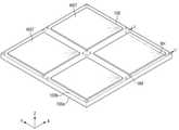
도 1은 일 실시예에 따른 타일형 표시 장치를 나타내는 평면도이다.1 is a plan view illustrating a tile-type display device according to an exemplary embodiment.
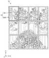
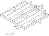
도 1을 참조하면, 타일형 표시 장치(TD)는 복수의 표시 장치(10)를 포함할 수 있다. 복수의 표시 장치(10)는 격자형으로 배열될 수 있으나, 이에 한정되지 않는다. 복수의 표시 장치(10)는 제1 방향(X축 방향) 또는 제2 방향(Y축 방향)으로 연결될 수 있고, 타일형 표시 장치(TD)는 특정 형상을 가질 수 있다. 예를 들어, 복수의 표시 장치(10) 각각은 서로 동일한 크기를 가질 수 있으나, 이에 한정되지 않는다. 다른 예를 들어, 복수의 표시 장치(10)는 서로 다른 크기를 가질 수 있다.Referring to FIG. 1 , a tile-type display device TD may include a plurality of
복수의 표시 장치(10) 각각은 장변과 단변을 포함하는 직사각형 형상일 수 있다. 복수의 표시 장치(10)는 장변 또는 단변이 서로 연결되며 배치될 수 있다. 일부의 표시 장치(10)는 타일형 표시 장치(TD)의 가장자리에 배치되어, 타일형 표시 장치(TD)의 일변을 이룰 수 있다. 일부의 표시 장치(10)는 타일형 표시 장치(TD)의 모서리에 배치될 수 있고, 타일형 표시 장치(TD)의 인접한 두 개의 변을 형성할 수 있다. 다른 일부의 표시 장치(10)는 타일형 표시 장치(TD)의 내부에 배치될 수 있고, 다른 표시 장치들(10)에 의해 둘러싸일 수 있다.Each of the plurality of
복수의 표시 장치(10) 각각은 표시 영역(DA) 및 비표시 영역(NDA)을 포함할 수 있다. 표시 영역(DA)은 복수의 화소를 포함하여 영상을 표시할 수 있다. 비표시 영역(NDA)은 표시 영역(DA)의 주변에 배치되어 표시 영역(DA)을 둘러쌀 수 있고, 영상을 표시하지 않을 수 있다. Each of the plurality of
타일형 표시 장치(TD)는 전체적으로 평면적 형상을 가질 수 있으나, 이에 한정되지 않는다. 타일형 표시 장치(TD)는 입체적 형상을 가짐으로써, 사용자에게 입체감을 줄 수 있다. 예를 들어, 타일형 표시 장치(TD)가 입체적 형상을 갖는 경우, 복수의 표시 장치(10) 중 적어도 일부의 표시 장치(10)는 커브드(Curved) 형상을 가질 수 있다. 다른 예를 들어, 복수의 표시 장치(10) 각각은 평면 형상을 갖고 서로 소정의 각도로 연결됨으로써, 타일형 표시 장치(TD)는 입체적 형상을 가질 수 있다.The tile-type display device TD may have an overall planar shape, but is not limited thereto. The tile-type display device TD has a three-dimensional shape, thereby providing a three-dimensional effect to the user. For example, when the tile-type display device TD has a three-dimensional shape, at least some of the
타일형 표시 장치(TD)는 인접한 표시 장치들(10) 각각의 비표시 영역(NDA)이 연결되어 형성될 수 있다. 복수의 표시 장치(10)는 연결 부재 또는 접착 부재를 통해 서로 연결될 수 있다. 따라서, 복수의 표시 장치(10) 사이의 비표시 영역(NDA)은 인접한 표시 영역들(DA)에 의해 둘러싸일 수 있다. 복수의 표시 장치(10) 각각의 표시 영역(DA) 사이의 거리는 복수의 표시 장치(10) 사이의 비표시 영역(NDA) 또는 복수의 표시 장치(10) 사이의 경계 부분이 사용자에게 인지되지 않을 정도로 가까울 수 있다. 또한, 복수의 표시 장치(10) 각각의 표시 영역(DA)의 외광 반사율과 복수의 표시 장치(10) 사이의 비표시 영역(NDA)의 외광 반사율은 실질적으로 동일할 수 있다. 따라서, 타일형 표시 장치(TD)는 복수의 표시 장치(10) 사이의 비표시 영역(NDA) 또는 경계 부분이 인지되는 것을 방지함으로써, 복수의 표시 장치(10) 사이의 단절감을 제거하고 영상의 몰입도를 향상시킬 수 있다.The tile-type display device TD may be formed by connecting each of the non-display areas NDA of the
도 2는 일 실시예에 따른 표시 장치를 나타내는 평면도이다.2 is a plan view illustrating a display device according to an exemplary embodiment.
도 2를 참조하면, 표시 장치(10)는 표시 영역(DA)에서 복수의 행과 열을 따라 배열된 복수의 화소를 포함할 수 있다. 복수의 화소 각각은 화소 정의막에 의해 정의되는 발광 영역(LA)을 포함할 수 있고, 발광 영역(LA)을 통해 소정의 피크 파장을 갖는 광을 방출할 수 있다. 예를 들어, 표시 장치(10)의 표시 영역(DA)은 제1 내지 제3 발광 영역(LA1, LA2, LA3)을 포함할 수 있다. 제1 내지 제3 발광 영역(LA1, LA2, LA3) 각각은 표시 장치(10)의 발광 소자에서 생성된 광이 표시 장치(10)의 외부로 방출되는 영역일 수 있다.Referring to FIG. 2 , the
제1 내지 제3 발광 영역(LA1, LA2, LA3)은 소정의 피크 파장을 갖는 광을 표시 장치(10)의 외부로 방출할 수 있다. 제1 발광 영역(LA1)은 제1 색의 광을 방출할 수 있고, 제2 발광 영역(LA2)은 제2 색의 광을 방출할 수 있으며, 제3 발광 영역(LA3)은 제3 색의 광을 방출할 수 있다. 예를 들어, 제1 색의 광은 610nm 내지 650nm 범위의 피크 파장을 갖는 적색 광일 수 있고, 제2 색의 광은 510nm 내지 550nm 범위의 피크 파장을 갖는 녹색 광일 수 있으며, 제3 색의 광은 440nm 내지 480nm 범위의 피크 파장을 갖는 청색 광일 수 있으나, 이에 한정되지 않는다.The first to third light emitting areas LA1 , LA2 , and LA3 may emit light having a predetermined peak wavelength to the outside of the
제1 내지 제3 발광 영역(LA1, LA2, LA3)은 표시 영역(DA)의 제1 방향(X축 방향)을 따라 순차적으로 반복 배치될 수 있다. 예를 들어, 제1 발광 영역(LA1)의 제1 방향(X축 방향)의 폭은 제2 발광 영역(LA2)의 제1 방향의 폭보다 넓을 수 있고, 제2 발광 영역(LA2)의 제1 방향의 폭은 제3 발광 영역(LA3)의 제1 방향의 폭보다 넓을 수 있다. 다른 예를 들어, 제1 발광 영역(LA1)의 제1 방향(X축 방향)의 폭, 제2 발광 영역(LA2)의 제1 방향의 폭, 및 제3 발광 영역(LA3)의 제1 방향의 폭은 실질적으로 동일할 수 있다.The first to third light emitting areas LA1 , LA2 , and LA3 may be sequentially and repeatedly disposed along the first direction (X-axis direction) of the display area DA. For example, the width of the first light emitting area LA1 in the first direction (X-axis direction) may be wider than the width of the second light emitting area LA2 in the first direction, and the width of the second light emitting area LA2 may be greater than that of the second light emitting area LA2. The width in the first direction may be wider than the width in the first direction of the third light emitting area LA3 . As another example, the width of the first light-emitting area LA1 in the first direction (X-axis direction), the width of the second light-emitting area LA2 in the first direction, and the third light-emitting area LA3 in the first direction may have substantially the same width.
예를 들어, 제1 발광 영역(LA1)의 면적은 제2 발광 영역(LA2)의 면적보다 넓을 수 있고, 제2 발광 영역(LA2)의 면적은 제3 발광 영역(LA3)의 면적보다 넓을 수 있다. 다른 예를 들어, 제1 발광 영역(LA1)의 면적, 제2 발광 영역(LA2)의 면적, 및 제3 발광 영역(LA3)의 면적은 실질적으로 동일할 수 있다.For example, the area of the first light-emitting area LA1 may be larger than that of the second light-emitting area LA2 , and the area of the second light-emitting area LA2 may be larger than the area of the third light-emitting area LA3 . there is. As another example, the area of the first light emitting area LA1 , the area of the second light emitting area LA2 , and the area of the third light emitting area LA3 may be substantially the same.
표시 장치(10)의 표시 영역(DA)은 복수의 발광 영역(LA)을 둘러싸는 복수의 차광 영역(BA)을 포함할 수 있다. 예를 들어, 표시 영역(DA)은 제1 내지 제3 차광 영역(BA1, BA2, BA3)을 포함할 수 있다. 제1 내지 제3 차광 영역(BA1, BA2, BA3) 각각은 제1 내지 제3 발광 영역(LA1, LA2, LA3) 각각의 일측에 배치될 수 있고, 제1 내지 제3 발광 영역(LA1, LA2, LA3)에서 방출되는 광들의 혼색을 방지할 수 있다.The display area DA of the
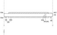
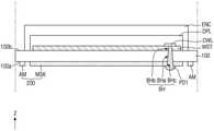
도 3은 도 2의 절단선 I-I'을 따라 자른 단면도이다.3 is a cross-sectional view taken along the cutting line I-I' of FIG. 2 .
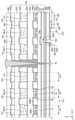
도 3을 참조하면, 표시 장치(10)의 표시 영역(DA)은 제1 내지 제3 발광 영역(LA1, LA2, LA3)을 포함할 수 있다. 제1 내지 제3 발광 영역(LA1, LA2, LA3) 각각은 표시 장치(10)의 발광 소자에서 생성된 광이 표시 장치(10)의 외부로 방출되는 영역일 수 있다.Referring to FIG. 3 , the display area DA of the
표시 장치(10)는 기판(100), 버퍼층(BF), 박막 트랜지스터층(TFTL), 및 발광 소자층(EML)을 포함할 수 있다.The
기판(100)은 베이스 기판 또는 베이스 부재일 수 있고, 고분자 수지 등의 절연 물질로 이루어질 수 있다. 예를 들어, 기판(100)은 리지드(Rigid) 기판일 수 있다. 기판(100)가 리지드 기판인 경우, 기판(100)은 글라스 재질 또는 금속 재질을 포함할 수 있으나, 이에 한정되지 않는다. 다른 예를 들어, 기판(100)은 벤딩(Bending), 폴딩(Folding), 롤링(Rolling) 등이 가능한 플렉서블(Flexible) 기판일 수 있다. 기판(100)가 플렉서블 기판인 경우, 기판(100)은 폴리이미드(PI)를 포함할 수 있으나, 이에 한정되지 않는다.The
버퍼층(BF)은 기판(100) 상에 배치될 수 있다. 버퍼층(BF)은 공기 또는 수분의 침투를 방지할 수 있는 무기막으로 이루어질 수 있다. 예를 들어, 버퍼층(BF)은 교번하여 적층된 복수의 무기막을 포함할 수 있다.The buffer layer BF may be disposed on the
박막 트랜지스터층(TFTL)은 박막 트랜지스터(TFT), 게이트 절연막(GI), 층간 절연막(ILD), 제1 보호층(PAS1), 및 제1 평탄화층(OC1)을 포함할 수 있다.The thin film transistor layer TFTL may include a thin film transistor TFT, a gate insulating layer GI, an interlayer insulating layer ILD, a first passivation layer PAS1 , and a first planarization layer OC1 .
박막 트랜지스터(TFT)는 버퍼층(BF) 상에 배치될 수 있고, 복수의 화소 각각의 화소 회로를 구성할 수 있다. 예를 들어, 박막 트랜지스터(TFT)는 화소 회로의 구동 트랜지스터 또는 스위칭 트랜지스터일 수 있다. 박막 트랜지스터(TFT)는 반도체층(ACT), 게이트 전극(GE), 소스 전극(SE), 및 드레인 전극(DE)을 포함할 수 있다.The thin film transistor TFT may be disposed on the buffer layer BF, and may constitute a pixel circuit of each of the plurality of pixels. For example, the thin film transistor TFT may be a driving transistor or a switching transistor of a pixel circuit. The thin film transistor TFT may include a semiconductor layer ACT, a gate electrode GE, a source electrode SE, and a drain electrode DE.
반도체층(ACT)은 버퍼층(BF) 상에 마련될 수 있다. 반도체층(ACT)은 게이트 전극(GE), 소스 전극(SE), 및 드레인 전극(DE)과 중첩될 수 있다. 반도체층(ACT)은 소스 전극(SE) 및 드레인 전극(DE)과 직접 접촉될 수 있고, 게이트 절연막(GI)을 사이에 두고 게이트 전극(GE)과 마주할 수 있다.The semiconductor layer ACT may be provided on the buffer layer BF. The semiconductor layer ACT may overlap the gate electrode GE, the source electrode SE, and the drain electrode DE. The semiconductor layer ACT may directly contact the source electrode SE and the drain electrode DE, and may face the gate electrode GE with the gate insulating layer GI interposed therebetween.
게이트 전극(GE)은 게이트 절연막(GI)의 상부에 배치될 수 있다. 게이트 전극(GE)은 게이트 절연막(GI)을 사이에 두고, 반도체층(ACT)과 중첩될 수 있다.The gate electrode GE may be disposed on the gate insulating layer GI. The gate electrode GE may overlap the semiconductor layer ACT with the gate insulating layer GI interposed therebetween.
소스 전극(SE) 및 드레인 전극(DE)은 층간 절연막(ILD) 상에서 서로 이격되어 배치될 수 있다. 소스 전극(SE)은 게이트 절연막(GI) 및 층간 절연막(ILD)에 마련된 컨택홀을 통해 반도체층(ACT)의 일단과 접촉될 수 있다. 드레인 전극(DE)은 게이트 절연막(GI) 및 층간 절연막(ILD)에 마련된 컨택홀을 통해 반도체층(ACT)의 타단과 접촉될 수 있다. 드레인 전극(DE)은 제1 보호층(PAS1) 및 제1 평탄화층(OC1)에 마련된 컨택홀을 통해 발광 부재(EL)의 제1 전극(AE)과 접속될 수 있다.The source electrode SE and the drain electrode DE may be disposed to be spaced apart from each other on the interlayer insulating layer ILD. The source electrode SE may contact one end of the semiconductor layer ACT through a contact hole provided in the gate insulating layer GI and the interlayer insulating layer ILD. The drain electrode DE may contact the other end of the semiconductor layer ACT through a contact hole provided in the gate insulating layer GI and the interlayer insulating layer ILD. The drain electrode DE may be connected to the first electrode AE of the light emitting member EL through a contact hole provided in the first passivation layer PAS1 and the first planarization layer OC1 .
게이트 절연막(GI)은 반도체층(ACT)의 상부에 마련될 수 있다. 예를 들어, 게이트 절연막(GI)은 반도체층(ACT) 및 버퍼층(BF)의 상부에 배치될 수 있고, 반도체층(ACT)과 게이트 전극(GE)을 절연시킬 수 있다. 게이트 절연막(GI)은 소스 전극(SE)이 관통하는 컨택홀 및 드레인 전극(DE)이 관통하는 컨택홀을 포함할 수 있다.The gate insulating layer GI may be provided on the semiconductor layer ACT. For example, the gate insulating layer GI may be disposed on the semiconductor layer ACT and the buffer layer BF, and may insulate the semiconductor layer ACT and the gate electrode GE. The gate insulating layer GI may include a contact hole through which the source electrode SE passes and a contact hole through which the drain electrode DE passes.
층간 절연막(ILD)은 게이트 전극(GE)의 상부에 배치될 수 있다. 예를 들어, 층간 절연막(ILD)은 소스 전극(SE)이 관통하는 컨택홀 및 드레인 전극(DE)이 관통하는 컨택홀을 포함할 수 있다. 여기에서, 층간 절연막(ILD)의 컨택홀은 게이트 절연막(GI)의 컨택홀과 연결될 수 있다.The interlayer insulating layer ILD may be disposed on the gate electrode GE. For example, the interlayer insulating layer ILD may include a contact hole through which the source electrode SE passes and a contact hole through which the drain electrode DE passes. Here, the contact hole of the interlayer insulating layer ILD may be connected to the contact hole of the gate insulating layer GI.
제1 보호층(PAS1)은 박막 트랜지스터(TFT)의 상부에 마련되어, 박막 트랜지스터(TFT)를 보호할 수 있다. 예를 들어, 제1 보호층(PAS1)은 제1 전극(AE)이 관통하는 컨택홀을 포함할 수 있다.The first passivation layer PAS1 may be provided on the thin film transistor TFT to protect the thin film transistor TFT. For example, the first passivation layer PAS1 may include a contact hole through which the first electrode AE passes.
제1 평탄화층(OC1)은 제1 보호층(PAS1)의 상부에 마련되어, 박막 트랜지스터(TFT)의 상단을 평탄화시킬 수 있다. 예를 들어, 제1 평탄화층(OC1)은 발광 부재(EL)의 제1 전극(AE)이 관통하는 컨택홀을 포함할 수 있다. 여기에서, 제1 평탄화층(OC1)의 컨택홀은 제1 보호층(PAS1)의 컨택홀과 연결될 수 있다.The first planarization layer OC1 may be provided on the first passivation layer PAS1 to planarize an upper end of the thin film transistor TFT. For example, the first planarization layer OC1 may include a contact hole through which the first electrode AE of the light emitting member EL passes. Here, the contact hole of the first planarization layer OC1 may be connected to the contact hole of the first passivation layer PAS1 .
발광 소자층(EML)은 발광 부재(EL), 제1 뱅크(BNK1), 제2 뱅크(BNK2), 및 제2 보호층(PAS2)을 포함할 수 있다.The light emitting device layer EML may include a light emitting member EL, a first bank BNK1 , a second bank BNK2 , and a second passivation layer PAS2 .
발광 부재(EL)는 박막 트랜지스터(TFT) 상에 마련될 수 있다. 발광 부재(EL)는 제1 전극(AE), 제2 전극(CE), 및 발광 소자(ED)를 포함할 수 있다.The light emitting member EL may be provided on the thin film transistor TFT. The light emitting member EL may include a first electrode AE, a second electrode CE, and a light emitting device ED.
제1 전극(AE)은 제1 평탄화층(OC1)의 상부에 마련될 수 있다. 예를 들어, 제1 전극(AE)은 제1 평탄화층(OC1) 상에 배치된 제1 뱅크(BNK1) 상에 배치되어 제1 뱅크(BNK1)를 덮을 수 있다. 제1 전극(AE)은 제2 뱅크(BNK2)에 의해 정의되는 제1 내지 제3 발광 영역(LA1, LA2, LA3) 중 하나의 발광 영역과 중첩되게 배치될 수 있다. 그리고, 제1 전극(AE)은 박막 트랜지스터(TFT)의 드레인 전극(DE)에 접속될 수 있다. 제1 전극(AE)은 발광 소자(ED)의 애노드 전극일 수 있으나, 이에 한정되지 않는다.The first electrode AE may be provided on the first planarization layer OC1 . For example, the first electrode AE may be disposed on the first bank BNK1 disposed on the first planarization layer OC1 to cover the first bank BNK1 . The first electrode AE may be disposed to overlap one of the first to third light emitting areas LA1 , LA2 , and LA3 defined by the second bank BNK2 . In addition, the first electrode AE may be connected to the drain electrode DE of the thin film transistor TFT. The first electrode AE may be an anode electrode of the light emitting device ED, but is not limited thereto.
제2 전극(CE)은 제1 평탄화층(OC1)의 상부에 마련될 수 있다. 예를 들어, 제2 전극(CE)은 제1 평탄화층(OC1) 상에 배치된 제1 뱅크(BNK1) 상에 배치되어 제1 뱅크(BNK1)를 덮을 수 있다. 제2 전극(CE)은 제2 뱅크(BNK2)에 의해 정의되는 제1 내지 제3 발광 영역(LA1, LA2, LA3) 중 하나의 발광 영역과 중첩되게 배치될 수 있다. 예를 들어, 제2 전극(CE)은 전체 화소에 공급되는 공통 전압을 수신할 수 있다. 제2 전극(CE)은 발광 소자(ED)의 캐소드 전극일 수 있으나, 이에 한정되지 않는다.The second electrode CE may be provided on the first planarization layer OC1 . For example, the second electrode CE may be disposed on the first bank BNK1 disposed on the first planarization layer OC1 to cover the first bank BNK1 . The second electrode CE may be disposed to overlap one of the first to third light emitting areas LA1 , LA2 , and LA3 defined by the second bank BNK2 . For example, the second electrode CE may receive a common voltage supplied to all pixels. The second electrode CE may be a cathode electrode of the light emitting device ED, but is not limited thereto.
제1 절연층(IL1)은 서로 인접한 제1 전극(AE)의 일부와 제2 전극(CE)의 일부를 덮을 수 있고, 제1 전극(AE)과 제2 전극(CE)을 절연시킬 수 있다.The first insulating layer IL1 may cover a portion of the first electrode AE and a portion of the second electrode CE adjacent to each other, and may insulate the first electrode AE and the second electrode CE. .
발광 소자(ED)는 제1 평탄화층(OC1)의 상부에서 제1 전극(AE) 및 제2 전극(CE) 사이에 배치될 수 있다. 발광 소자(ED)는 제1 절연층(IL1) 상에 배치될 수 있다. 발광 소자(ED)의 일단은 제1 전극(AE)에 접속될 수 있고, 발광 소자(ED)의 타단은 제2 전극(CE)에 접속될 수 있다. 예를 들어, 복수의 발광 소자(ED)는 동일 물질을 갖는 활성층을 포함하여, 동일 파장대의 광, 또는 동일 색의 광을 방출할 수 있다. 제1 내지 제3 발광 영역(LA1, LA2, LA3) 각각에서 방출되는 광은 동일 색을 가질 수 있다. 예를 들어, 복수의 발광 소자(ED)는 440nm 내지 480nm 범위의 피크 파장을 갖는 제3 색의 광 또는 청색 광을 방출할 수 있다. 따라서, 발광 소자층(EML)은 제3 색의 광 또는 청색 광을 방출할 수 있다.The light emitting device ED may be disposed on the first planarization layer OC1 between the first electrode AE and the second electrode CE. The light emitting device ED may be disposed on the first insulating layer IL1 . One end of the light emitting element ED may be connected to the first electrode AE, and the other end of the light emitting element ED may be connected to the second electrode CE. For example, the plurality of light emitting devices ED may include an active layer having the same material to emit light of the same wavelength band or light of the same color. Light emitted from each of the first to third light emitting areas LA1 , LA2 , and LA3 may have the same color. For example, the plurality of light emitting devices ED may emit light of a third color or blue light having a peak wavelength in a range of 440 nm to 480 nm. Accordingly, the light emitting device layer EML may emit light of the third color or blue light.
제2 뱅크(BNK2)은 제1 평탄화층(OC1) 상에 배치되어 제1 내지 제3 발광 영역(LA1, LA2, LA3)을 정의할 수 있다. 예를 들어, 제2 뱅크(BNK2)는 제1 내지 제3 발광 영역(LA1, LA2, LA3) 각각을 둘러쌀 수 있으나, 이에 한정되지 않는다. 제2 뱅크(BNK2)은 복수의 발광 부재(EL) 각각의 제1 전극(AE) 또는 제2 전극(CE)을 이격 및 절연시킬 수 있다. 제2 뱅크(BNK2)는 제1 내지 제3 차광 영역(BA1, BA2, BA3)에 배치될 수 있다.The second bank BNK2 may be disposed on the first planarization layer OC1 to define first to third light emitting regions LA1 , LA2 , and LA3 . For example, the second bank BNK2 may surround each of the first to third light emitting areas LA1 , LA2 , and LA3 , but is not limited thereto. The second bank BNK2 may separate and insulate the first electrode AE or the second electrode CE of each of the plurality of light emitting members EL. The second bank BNK2 may be disposed in the first to third light blocking areas BA1 , BA2 , and BA3 .
제2 보호층(PAS2)은 복수의 발광 부재(EL) 및 제2 뱅크(BNK2) 상에 배치될 수 있다. 제2 보호층(PAS2)은 복수의 발광 부재(EL)를 덮을 수 있고, 복수의 발광 부재(EL)를 보호할 수 있다. 제2 보호층(PAS2)은 외부로부터 수분 또는 공기 등 불순물의 침투를 방지하여 복수의 발광 부재(EL)의 손상을 방지할 수 있다.The second passivation layer PAS2 may be disposed on the plurality of light emitting members EL and the second bank BNK2 . The second passivation layer PAS2 may cover the plurality of light emitting members EL and may protect the plurality of light emitting members EL. The second passivation layer PAS2 may prevent penetration of impurities such as moisture or air from the outside, thereby preventing damage to the plurality of light emitting members EL.
표시 장치(10)는 제2 평탄화층(OC2), 제1 캡핑층(CAP1), 제1 차광 부재(BK1), 제1 파장 변환부(WLC1), 제2 파장 변환부(WLC2), 광 투과부(LTU), 제2 캡핑층(CAP2), 제3 평탄화층(OC3), 제2 차광 부재(BK2), 제1 내지 제3 컬러 필터(CF1, CF2, CF3), 제3 보호층(PAS3), 및 봉지층(ENC)을 더 포함할 수 있다.The
제2 평탄화층(OC2)은 발광 소자층(EML)의 상부에 마련되어, 발광 소자층(EML)의 상단을 평탄화시킬 수 있다. 제2 평탄화층(OC2)은 유기 물질을 포함할 수 있다. 예를 들어, 제2 평탄화층(OC2)은 아크릴 수지(Acryl Resin), 에폭시 수지(Epoxy Resin), 페놀 수지(Phenolic Resin), 폴리아미드 수지(Polyamide Resin), 및 폴리이미드 수지(Polyimide Resin) 중 적어도 하나를 포함할 수 있다.The second planarization layer OC2 may be provided on the light emitting device layer EML to planarize an upper end of the light emitting device layer EML. The second planarization layer OC2 may include an organic material. For example, the second planarization layer OC2 may include an acrylic resin, an epoxy resin, a phenolic resin, a polyamide resin, and a polyimide resin. It may include at least one.
제1 캡핑층(CAP1)은 제2 평탄화층(OC2) 상에 배치될 수 있다. 제1 캡핑층(CAP1)은 제1 및 제2 파장 변환부(WLC1, WLC2)와 광 투과부(LTU)의 하면을 밀봉할 수 있다. 제1 캡핑층(CAP1)은 무기 물질을 포함할 수 있다. 예를 들어, 제1 캡핑층(CAP1)은 실리콘 질화물, 알루미늄 질화물, 지르코늄 질화물, 티타늄 질화물, 하프늄 질화물, 탄탈륨 질화물, 실리콘 산화물, 알루미늄 산화물, 티타늄 산화물, 주석 산화물, 세륨 산화물, 및 실리콘 산질화물 중 적어도 하나를 포함할 수 있다.The first capping layer CAP1 may be disposed on the second planarization layer OC2 . The first capping layer CAP1 may seal lower surfaces of the first and second wavelength converters WLC1 and WLC2 and the light transmitting part LTU. The first capping layer CAP1 may include an inorganic material. For example, the first capping layer CAP1 may include silicon nitride, aluminum nitride, zirconium nitride, titanium nitride, hafnium nitride, tantalum nitride, silicon oxide, aluminum oxide, titanium oxide, tin oxide, cerium oxide, and silicon oxynitride. It may include at least one.
제1 차광 부재(BK1)는 제1 캡핑층(CAP1) 상의 제1 내지 제3 차광 영역(BA1, BA2, BA3)에 배치될 수 있다. 제1 차광 부재(BK1)는 제2 뱅크(BNK2)와 두께 방향으로 중첩될 수 있다. 제1 차광 부재(BK1)는 광의 투과를 차단할 수 있다. 제1 차광 부재(BK1)는 제1 내지 제3 발광 영역(LA1, LA2, LA3) 간에 광이 침범하여 혼색되는 것을 방지함으로써, 색 재현율을 향상시킬 수 있다. 제1 차광 부재(BK1)는 평면 상에서 제1 내지 제3 발광 영역(LA1, LA2, LA3)을 둘러싸는 격자 형태로 배치될 수 있다.The first light blocking member BK1 may be disposed in the first to third light blocking areas BA1 , BA2 , and BA3 on the first capping layer CAP1 . The first light blocking member BK1 may overlap the second bank BNK2 in the thickness direction. The first light blocking member BK1 may block light transmission. The first light blocking member BK1 may prevent light from penetrating and mixing colors between the first to third light emitting areas LA1 , LA2 , and LA3 , thereby improving color gamut. The first light blocking member BK1 may be disposed in a grid shape surrounding the first to third light emitting areas LA1 , LA2 , and LA3 on a plane surface.
제1 차광 부재(BK1)는 유기 차광 물질과 발액 성분을 포함할 수 있다. 여기에서, 발액 성분은 불소 함유 단량체 또는 불소 함유 중합체로 이루어질 수 있고, 구체적으로 불소 함유 지방족 폴리카보네이트를 포함할 수 있다. 예를 들어, 제1 차광 부재(BK1)는 발액 성분을 포함한 블랙 유기 물질로 이루어질 수 있다. 제1 차광 부재(BK1)는 발액 성분을 포함한 유기 차광 물질의 코팅 및 노광 공정 등을 통해 형성될 수 있다.The first light blocking member BK1 may include an organic light blocking material and a liquid repellent component. Here, the liquid repellent component may be made of a fluorine-containing monomer or a fluorine-containing polymer, and specifically may include a fluorine-containing aliphatic polycarbonate. For example, the first light blocking member BK1 may be formed of a black organic material including a liquid repellent component. The first light blocking member BK1 may be formed by coating and exposing an organic light blocking material including a liquid repellent component.
제1 차광 부재(BK1)는 발액 성분을 포함함으로써, 제1 및 제2 파장 변환부(WLC1, WLC2)와 광 투과부(LTU)를 대응되는 발광 영역(LA)으로 분리시킬 수 있다. 예를 들어, 제1 및 제2 파장 변환부(WLC1, WLC2)와 광 투과부(LTU)가 잉크젯 방식으로 형성되는 경우, 잉크 조성물이 제1 차광 부재(BK1)의 상면에 흐를 수 있다. 이 경우, 제1 차광 부재(BK1)는 발액 성분을 포함함으로써, 잉크 조성물이 각각의 투과 영역으로 흘러가도록 유도할 수 있다. 따라서, 제1 차광 부재(BK1)는 잉크 조성물이 혼합되는 것을 방지할 수 있다.Since the first light blocking member BK1 includes a liquid repellent component, the first and second wavelength converters WLC1 and WLC2 and the light transmitting part LTU may be separated into a corresponding light emitting area LA. For example, when the first and second wavelength converters WLC1 and WLC2 and the light transmitting part LTU are formed by an inkjet method, an ink composition may flow on the upper surface of the first light blocking member BK1 . In this case, the first light blocking member BK1 may include a liquid repellent component, thereby guiding the ink composition to flow into each of the transmissive regions. Accordingly, the first light blocking member BK1 may prevent the ink composition from being mixed.
제1 파장 변환부(WLC1)는 제1 캡핑층(CAP1) 상의 제1 발광 영역(LA1)에 배치될 수 있다. 제1 파장 변환부(WLC1)는 제1 차광 부재(BK1)에 의해 둘러싸일 수 있다. 제1 파장 변환부(WLC1)는 제1 베이스 수지(BS1), 제1 산란체(SCT1) 및 제1 파장 시프터(WLS1)를 포함할 수 있다.The first wavelength converter WLC1 may be disposed in the first light emitting area LA1 on the first capping layer CAP1 . The first wavelength converter WLC1 may be surrounded by the first light blocking member BK1 . The first wavelength converter WLC1 may include a first base resin BS1 , a first scatterer SCT1 , and a first wavelength shifter WLS1 .
제1 베이스 수지(BS1)는 광 투과율이 상대적으로 높은 물질을 포함할 수 있다. 제1 베이스 수지(BS1)는 투명 유기 물질로 이루어질 수 있다. 예를 들어, 제1 베이스 수지(BS1)는 에폭시계 수지, 아크릴계 수지, 카도계 수지 및 이미드계 수지 등의 유기 물질 중 적어도 하나를 포함할 수 있다.The first base resin BS1 may include a material having a relatively high light transmittance. The first base resin BS1 may be formed of a transparent organic material. For example, the first base resin BS1 may include at least one of an organic material such as an epoxy-based resin, an acrylic resin, a cardo-based resin, and an imide-based resin.
제1 산란체(SCT1)는 제1 베이스 수지(BS1)와 상이한 굴절률을 가질 수 있고, 제1 베이스 수지(BS1)와 광학 계면을 형성할 수 있다. 예를 들어, 제1 산란체(SCT1)는 투과광의 적어도 일부를 산란시키는 광 산란 물질 또는 광 산란 입자를 포함할 수 있다. 예를 들어, 제1 산란체(SCT1)는 산화 티타늄(TiO2), 산화 지르코늄(ZrO2), 산화 알루미늄(Al2O3), 산화 인듐(In2O3), 산화 아연(ZnO) 또는 산화 주석(SnO2) 등과 같은 금속 산화물을 포함하거나, 아크릴계 수지 또는 우레탄계 수지 등의 유기 입자를 포함할 수 있다. 제1 산란체(SCT1)는 입사광의 피크 파장을 실질적으로 변환시키지 않으면서, 입사광의 입사 방향과 무관하게 광을 랜덤 방향으로 산란시킬 수 있다.The first scatterer SCT1 may have a refractive index different from that of the first base resin BS1 , and may form an optical interface with the first base resin BS1 . For example, the first scatterer SCT1 may include a light scattering material or light scattering particles that scatter at least a portion of transmitted light. For example, the first scatterer SCT1 may include a metal such as titanium oxide (TiO2), zirconium oxide (ZrO2), aluminum oxide (Al2O3), indium oxide (In2O3), zinc oxide (ZnO), or tin oxide (SnO2). It may include an oxide or organic particles such as an acrylic resin or a urethane-based resin. The first scatterer SCT1 may scatter light in a random direction irrespective of the incident direction of the incident light, without substantially converting the peak wavelength of the incident light.
제1 파장 시프터(WLS1)는 입사광의 피크 파장을 제1 피크 파장으로 변환 또는 시프트시킬 수 있다. 예를 들어, 제1 파장 시프터(WLS1)는 표시 장치(10)에서 제공된 청색 광을 610nm 내지 650nm 범위의 단일 피크 파장을 갖는 적색 광으로 변환하여 방출할 수 있다. 제1 파장 시프터(WLS1)는 양자점, 양자 막대 또는 형광체일 수 있다. 양자점은 전자가 전도대에서 가전자대로 전이하면서 특정한 색을 방출하는 입자상 물질일 수 있다.The first wavelength shifter WLS1 may convert or shift the peak wavelength of the incident light into the first peak wavelength. For example, the first wavelength shifter WLS1 may convert blue light provided from the
예를 들어, 양자점은 반도체 나노 결정 물질일 수 있다. 양자점은 그 조성 및 크기에 따라 특정 밴드 갭을 가져 빛을 흡수한 후 고유의 파장을 갖는 광을 방출할 수 있다. 양자점의 반도체 나노 결정의 예로는 IV족계 나노 결정, II-VI족계 화합물 나노 결정, III-V족계 화합물 나노 결정, IV-VI족계 나노 결정 또는 이들의 조합 등을 들 수 있다.For example, the quantum dots may be semiconductor nanocrystalline materials. Quantum dots have a specific band gap depending on their composition and size to absorb light and then emit light having a unique wavelength. Examples of semiconductor nanocrystals of quantum dots include group IV nanocrystals, group II-VI compound nanocrystals, group III-V compound nanocrystals, group IV-VI nanocrystals, or a combination thereof.
II-VI족 화합물은 CdSe, CdTe, ZnS, ZnSe, ZnTe, ZnO, HgS, HgSe, HgTe, MgSe, MgS 및 이들의 혼합물로 이루어진 군에서 선택되는 이원소 화합물; InZnP, AgInS, CuInS, CdSeS, CdSeTe, CdSTe, ZnSeS, ZnSeTe, ZnSTe, HgSeS, HgSeTe, HgSTe, CdZnS, CdZnSe, CdZnTe, CdHgS, CdHgSe, CdHgTe, HgZnS, HgZnSe, HgZnTe, MgZnSe, MgZnS 및 이들의 혼합물로 이루어진 군에서 선택되는 삼원소 화합물; 및 HgZnTeS, CdZnSeS, CdZnSeTe, CdZnSTe, CdHgSeS, CdHgSeTe, CdHgSTe, HgZnSeS, HgZnSeTe, HgZnSTe 및 이들의 혼합물로 이루어진 군에서 선택되는 사원소 화합물로 이루어진 군에서 선택될 수 있다.The group II-VI compound is a binary compound selected from the group consisting of CdSe, CdTe, ZnS, ZnSe, ZnTe, ZnO, HgS, HgSe, HgTe, MgSe, MgS, and mixtures thereof; InZnP, AgInS, CuInS, CdSeS, CdSeTe, CdSTe, ZnSeS, ZnSeTe, ZnSTe, HgSeS, HgSeTe, HgSTe, CdZnS, CdZnSe, CdZnTe, CdHgS, CdHgSe, HgZnTe, HgSe, HgZnSgTe, HgZnTe, HgSe and mixtures of these. a ternary compound selected from the group consisting of; and HgZnTeS, CdZnSeS, CdZnSeTe, CdZnSTe, CdHgSeS, CdHgSeTe, CdHgSTe, HgZnSeS, HgZnSeTe, HgZnSTe, and mixtures thereof.
III-V족 화합물은 GaN, GaP, GaAs, GaSb, AlN, AlP, AlAs, AlSb, InN, InP, InAs, InSb 및 이들의 혼합물로 이루어진 군에서 선택되는 이원소 화합물; GaNP, GaNAs, GaNSb, GaPAs, GaPSb, AlNP, AlNAs, AlNSb, AlPAs, AlPSb, InGaP, InNP, InAlP, InNAs, InNSb, InPAs, InPSb, GaAlNP 및 이들의 혼합물로 이루어진 군에서 선택되는 삼원소 화합물; 및 GaAlNAs, GaAlNSb, GaAlPAs, GaAlPSb, GaInNP, GaInNAs, GaInNSb, GaInPAs, GaInPSb, InAlNP, InAlNAs, InAlNSb, InAlPAs, InAlPSb 및 이들의 혼합물로 이루어진 군에서 선택되는 사원소 화합물로 이루어진 군에서 선택될 수 있다.The group III-V compound is a binary compound selected from the group consisting of GaN, GaP, GaAs, GaSb, AlN, AlP, AlAs, AlSb, InN, InP, InAs, InSb, and mixtures thereof; a ternary compound selected from the group consisting of GaNP, GaNAs, GaNSb, GaPAs, GaPSb, AlNP, AlNAs, AlNSb, AlPAs, AlPSb, InGaP, InNP, InAlP, InNAs, InNSb, InPAs, InPSb, GaAlNP, and mixtures thereof; and GaAlNAs, GaAlNSb, GaAlPAs, GaAlPSb, GaInNP, GaInNAs, GaInNSb, GaInPAs, GaInPSb, InAlNP, InAlNAs, InAlNSb, InAlPAs, InAlPSb, and mixtures thereof.
IV-VI족 화합물은 SnS, SnSe, SnTe, PbS, PbSe, PbTe 및 이들의 혼합물로 이루어진 군에서 선택되는 이원소 화합물; SnSeS, SnSeTe, SnSTe, PbSeS, PbSeTe, PbSTe, SnPbS, SnPbSe, SnPbTe 및 이들의 혼합물로 이루어진 군에서 선택되는 삼원소 화합물; 및 SnPbSSe, SnPbSeTe, SnPbSTe 및 이들의 혼합물로 이루어진 군에서 선택되는 사원소 화합물로 이루어진 군에서 선택될 수 있다. IV족 원소로는 Si, Ge 및 이들의 혼합물로 이루어진 군에서 선택될 수 있다. IV족 화합물로는 SiC, SiGe 및 이들의 혼합물로 이루어진 군에서 선택되는 이원소 화합물일 수 있다.The group IV-VI compound is a binary compound selected from the group consisting of SnS, SnSe, SnTe, PbS, PbSe, PbTe, and mixtures thereof; a ternary compound selected from the group consisting of SnSeS, SnSeTe, SnSTe, PbSeS, PbSeTe, PbSTe, SnPbS, SnPbSe, SnPbTe, and mixtures thereof; and a quaternary compound selected from the group consisting of SnPbSSe, SnPbSeTe, SnPbSTe, and mixtures thereof. The group IV element may be selected from the group consisting of Si, Ge, and mixtures thereof. The group IV compound may be a binary compound selected from the group consisting of SiC, SiGe, and mixtures thereof.
예를 들어, 이원소 화합물, 삼원소 화합물 또는 사원소 화합물은 균일한 농도로 입자 내에 존재하거나, 농도 분포가 부분적으로 다른 상태로 나누어져 동일 입자 내에 존재할 수 있다.For example, a binary compound, a ternary compound, or a quaternary compound may be present in the particle at a uniform concentration, or may be present in the same particle due to a partially different concentration distribution.
예를 들어, 양자점은 전술한 나노 결정을 포함하는 코어 및 상기 코어를 둘러싸는 쉘을 포함하는 코어-쉘 구조를 가질 수 있다. 양자점의 쉘은 코어의 화학적 변성을 방지하여 반도체 특성을 유지하기 위한 보호층 역할과, 양자점에 전기 영동 특성을 부여하기 위한 차징층(Charging Layer)의 역할을 수행할 수 있다. 쉘은 단층 또는 다중층일 수 있다. 코어와 쉘의 계면은 쉘에 존재하는 원소의 농도가 중심으로 갈수록 낮아지는 농도 구배(Gradient)를 가질 수 있다. 양자점의 쉘은 금속 또는 비금속의 산화물, 반도체 화합물 또는 이들의 조합 등으로 이루어질 수 있다.For example, the quantum dot may have a core-shell structure including a core including the aforementioned nanocrystals and a shell surrounding the core. The shell of the quantum dot may serve as a protective layer for maintaining semiconductor properties by preventing chemical modification of the core, and as a charging layer for imparting electrophoretic properties to the quantum dot. The shell may be single-layered or multi-layered. The interface between the core and the shell may have a concentration gradient in which the concentration of elements present in the shell decreases toward the center. The shell of the quantum dot may be formed of a metal or non-metal oxide, a semiconductor compound, or a combination thereof.
예를 들어, 금속 또는 비금속의 산화물은 SiO2, Al2O3, TiO2, ZnO, MnO, Mn2O3, Mn3O4, CuO, FeO, Fe2O3, Fe3O4, CoO, Co3O4, NiO 등의 이원소 화합물, 또는 MgAl2O4, CoFe2O4, NiFe2O4, CoMn2O4등의 삼원소 화합물을 예시할 수 있으나 본 발명이 이에 제한되는 것은 아니다.For example, an oxide of a metal or a non-metal is a binary compound such as SiO2, Al2O3, TiO2, ZnO, MnO, Mn2O3, Mn3O4, CuO, FeO, Fe2O3, Fe3O4, CoO, Co3O4, NiO, or MgAl2O4, CoFe2O4, NiFe2O4, Three-element compounds such as CoMn2O4 may be exemplified, but the present invention is not limited thereto.
또한, 반도체 화합물은 CdS, CdSe, CdTe, ZnS, ZnSe, ZnTe, ZnSeS, ZnTeS, GaAs, GaP, GaSb, HgS, HgSe, HgTe, InAs, InP, InGaP, InSb, AlAs, AlP, AlSb등을 예시할 수 있으나 본 발명이 이에 제한되는 것은 아니다.In addition, the semiconductor compound may be exemplified by CdS, CdSe, CdTe, ZnS, ZnSe, ZnTe, ZnSeS, ZnTeS, GaAs, GaP, GaSb, HgS, HgSe, HgTe, InAs, InP, InGaP, InSb, AlAs, AlP, AlSb, etc. However, the present invention is not limited thereto.
제1 파장 시프터(WLS1)가 방출하는 광은 45nm 이하, 또는 40nm 이하, 또는 30nm 이하의 발광 파장 스펙트럼 반치폭(Full Width of Half Maximum, FWHM)을 가질 수 있고, 표시 장치(10)가 표시하는 색의 색 순도와 색 재현성을 더욱 개선할 수 있다. 제1 파장 시프터(WLS1)가 방출하는 광은 입사광의 입사 방향과 무관하게 여러 방향을 향하여 방출될 수 있다. 따라서, 제1 발광 영역(LA1)에서 표시되는 적색의 측면 시인성을 향상시킬 수 있다.Light emitted by the first wavelength shifter WLS1 may have a full width of half maximum (FWHM) of an emission wavelength spectrum of 45 nm or less, or 40 nm or less, or 30 nm or less, and a color displayed by the
발광 소자층(EML)에서 제공된 청색 광의 일부는 제1 파장 시프터(WLS1)에 의해 적색 광으로 변환되지 않고 제1 파장 변환부(WLC1)를 투과할 수 있다. 발광 소자층(EML)에서 제공된 청색 광 중 제1 파장 변환부(WLC1)에 의해 변환되지 않고 제1 컬러 필터(CF1)에 입사한 광은 제1 컬러 필터(CF1)에 의해 차단될 수 있다. 그리고, 표시 장치(10)에서 제공된 청색 광 중 제1 파장 변환부(WLC1)에 의해 변환된 적색 광은 제1 컬러 필터(CF1)를 투과하여 외부로 출사될 수 있다. 따라서, 제1 발광 영역(LA1)은 적색 광을 방출할 수 있다.A portion of the blue light provided from the light emitting device layer EML may pass through the first wavelength converter WLC1 without being converted into red light by the first wavelength shifter WLS1 . Among the blue light provided from the light emitting device layer EML, light incident to the first color filter CF1 without being converted by the first wavelength converter WLC1 may be blocked by the first color filter CF1 . In addition, the red light converted by the first wavelength converter WLC1 among the blue light provided by the
제2 파장 변환부(WLC2)는 제1 캡핑층(CAP1) 상의 제2 발광 영역(LA2)에 배치될 수 있다. 제2 파장 변환부(WLC2)는 제1 차광 부재(BK1)에 의해 둘러싸일 수 있다. 제2 파장 변환부(WLC2)는 제2 베이스 수지(BS2), 제2 산란체(SCT2) 및 제2 파장 시프터(WLS2)를 포함할 수 있다.The second wavelength converter WLC2 may be disposed in the second light emitting area LA2 on the first capping layer CAP1 . The second wavelength converter WLC2 may be surrounded by the first light blocking member BK1 . The second wavelength converter WLC2 may include a second base resin BS2 , a second scatterer SCT2 , and a second wavelength shifter WLS2 .
제2 베이스 수지(BS2)는 광 투과율이 상대적으로 높은 물질을 포함할 수 있다. 제2 베이스 수지(BS2)는 투명 유기 물질로 이루어질 수 있다. 예를 들어, 제2 베이스 수지(BS2)는 제1 베이스 수지(BS1)와 동일 물질로 이루어지거나, 제1 베이스 수지(BS1)에서 예시된 물질로 이루어질 수 있다.The second base resin BS2 may include a material having a relatively high light transmittance. The second base resin BS2 may be formed of a transparent organic material. For example, the second base resin BS2 may be made of the same material as the first base resin BS1 or may be made of the material exemplified in the first base resin BS1 .
제2 산란체(SCT2)는 제2 베이스 수지(BS2)와 상이한 굴절률을 가질 수 있고, 제2 베이스 수지(BS2)와 광학 계면을 형성할 수 있다. 예를 들어, 제2 산란체(SCT2)는 투과광의 적어도 일부를 산란시키는 광 산란 물질 또는 광 산란 입자를 포함할 수 있다. 예를 들어, 제2 산란체(SCT2)는 제1 산란체(SCT1)와 동일 물질로 이루어지거나, 제1 산란체(SCT1)에서 예시된 물질로 이루어질 수 있다. 제2 산란체(SCT2)는 입사광의 피크 파장을 실질적으로 변환시키지 않으면서, 입사광의 입사 방향과 무관하게 광을 랜덤 방향으로 산란시킬 수 있다.The second scatterer SCT2 may have a refractive index different from that of the second base resin BS2 , and may form an optical interface with the second base resin BS2 . For example, the second scatterer SCT2 may include a light scattering material or light scattering particles that scatter at least a portion of transmitted light. For example, the second scatterer SCT2 may be made of the same material as the first scatterer SCT1 or may be made of the material exemplified in the first scatterer SCT1 . The second scatterer SCT2 may scatter light in a random direction irrespective of the incident direction of the incident light while substantially not converting the peak wavelength of the incident light.
제2 파장 시프터(WLS2)는 입사광의 피크 파장을 제1 파장 시프터(WLS1)의 제1 피크 파장과 다른 제2 피크 파장으로 변환 또는 시프트시킬 수 있다. 예를 들어, 제2 파장 시프터(WLS2)는 표시 장치(10)에서 제공된 청색 광을 510nm 내지 550nm 범위의 단일 피크 파장을 갖는 녹색 광으로 변환하여 방출할 수 있다. 제2 파장 시프터(WLS2)는 양자점, 양자 막대 또는 형광체일 수 있다. 제2 파장 시프터(WLS2)는 제1 파장 시프터(WLS1)에서 예시된 물질과 동일 취지의 물질을 포함할 수 있다. 제2 파장 시프터(WLS2)의 파장 변환 범위는 제1 파장 시프터(WLS1)의 파장 변환 범위와 다르도록 양자점, 양자 막대 또는 형광체로 이루어질 수 있다.The second wavelength shifter WLS2 may convert or shift the peak wavelength of the incident light into a second peak wavelength different from the first peak wavelength of the first wavelength shifter WLS1 . For example, the second wavelength shifter WLS2 may convert blue light provided from the
광 투과부(LTU)는 제1 캡핑층(CAP1) 상의 제3 발광 영역(LA3)에 배치될 수 있다. 광 투과부(LTU)는 제1 차광 부재(BK1)에 의해 둘러싸일 수 있다. 광 투과부(LTU)는 입사광의 피크 파장을 유지하여 투과시킬 수 있다. 광 투과부(LTU)는 제3 베이스 수지(BS3) 및 제3 산란체(SCT3)를 포함할 수 있다.The light transmitting part LTU may be disposed in the third light emitting area LA3 on the first capping layer CAP1 . The light transmitting part LTU may be surrounded by the first light blocking member BK1 . The light transmitting unit LTU may transmit the incident light while maintaining the peak wavelength. The light transmitting part LTU may include a third base resin BS3 and a third scattering body SCT3.
제3 베이스 수지(BS3)는 광 투과율이 상대적으로 높은 물질을 포함할 수 있다. 제3 베이스 수지(BS3)는 투명 유기 물질로 이루어질 수 있다. 예를 들어, 제3 베이스 수지(BS3)는 제1 또는 제2 베이스 수지(BS1, BS2)와 동일 물질로 이루어지거나, 제1 또는 제2 베이스 수지(BS1, BS2)에서 예시된 물질로 이루어질 수 있다.The third base resin BS3 may include a material having a relatively high light transmittance. The third base resin BS3 may be formed of a transparent organic material. For example, the third base resin BS3 may be made of the same material as the first or second base resins BS1 and BS2, or may be made of the materials exemplified in the first or second base resins BS1 and BS2. there is.
제3 산란체(SCT3)는 제3 베이스 수지(BS3)와 상이한 굴절률을 가질 수 있고, 제3 베이스 수지(BS3)와 광학 계면을 형성할 수 있다. 예를 들어, 제3 산란체(SCT3)는 투과광의 적어도 일부를 산란시키는 광 산란 물질 또는 광 산란 입자를 포함할 수 있다. 예를 들어, 제3 산란체(SCT3)는 제1 또는 제2 산란체(SCT1, SCT2)와 동일 물질로 이루어지거나, 제1 또는 제2 산란체(SCT1, SCT2)에서 예시된 물질로 이루어질 수 있다. 제3 산란체(SCT3)는 입사광의 피크 파장을 실질적으로 변환시키지 않으면서, 입사광의 입사 방향과 무관하게 광을 랜덤 방향으로 산란시킬 수 있다.The third scattering body SCT3 may have a refractive index different from that of the third base resin BS3 , and may form an optical interface with the third base resin BS3 . For example, the third scatterer SCT3 may include a light scattering material or light scattering particles that scatter at least a portion of transmitted light. For example, the third scatterers SCT3 may be made of the same material as the first or second scatterers SCT1 and SCT2, or may be made of the materials exemplified in the first or second scatterers SCT1 and SCT2. there is. The third scatterer SCT3 may scatter light in a random direction irrespective of the incident direction of the incident light, without substantially converting the peak wavelength of the incident light.
제1 및 제2 파장 변환부(WLC1, WLC2)와 광 투과부(LTU)는 제2 평탄화층(OC2) 및 제1 캡핑층(CAP1)을 통해 발광 소자층(EML) 상에 배치됨으로써, 표시 장치(10)는 제1 및 제2 파장 변환부(WLC1, WLC2)와 광 투과부(LTU)를 위한 별도의 기판을 필요로 하지 않을 수 있다. 따라서, 제1 및 제2 파장 변환부(WLC1, WLC2)와 광 투과부(LTU)는 제1 내지 제3 발광 영역(LA1, LA2, LA3) 각각에 용이하게 얼라인될 수 있고, 표시 장치(10)의 두께가 상대적으로 감소될 수 있다.The first and second wavelength converters WLC1 and WLC2 and the light transmitting part LTU are disposed on the light emitting element layer EML through the second planarization layer OC2 and the first capping layer CAP1, so that the display
제2 캡핑층(CAP2)은 제1 및 제2 파장 변환부(WLC1, WLC2), 광 투과부(LTU), 및 제1 차광 부재(BK1)를 덮을 수 있다. 예를 들어, 제2 캡핑층(CAP2)은 제1 및 제2 파장 변환부(WLC1, WLC2)와 광 투과부(LTU)를 밀봉하여 제1 및 제2 파장 변환부(WLC1, WLC2)와 광 투과부(LTU)의 손상 또는 오염을 방지할 수 있다. 제2 캡핑층(CAP2)은 제1 캡핑층(CAP1)과 동일 물질로 이루어지거나, 제1 캡핑층(CAP1)에서 예시된 물질로 이루어질 수 있다.The second capping layer CAP2 may cover the first and second wavelength converters WLC1 and WLC2 , the light transmitting part LTU, and the first light blocking member BK1 . For example, the second capping layer CAP2 seals the first and second wavelength converters WLC1 and WLC2 and the light transmitting unit LTU, so that the first and second wavelength converting units WLC1 and WLC2 and the light transmitting unit are sealed. (LTU) damage or contamination can be prevented. The second capping layer CAP2 may be made of the same material as the first capping layer CAP1 , or may be made of the material exemplified in the first capping layer CAP1 .
제3 평탄화층(OC3)은 제2 캡핑층(CAP2)의 상부에 배치되어, 제1 및 제2 파장 변환부(WLC1, WLC2)와 광 투과부(LTU)의 상단을 평탄화시킬 수 있다. 제3 평탄화층(OC3)은 유기 물질을 포함할 수 있다. 예를 들어, 제3 평탄화층(OC3)은 아크릴 수지(Acryl Resin), 에폭시 수지(Epoxy Resin), 페놀 수지(Phenolic Resin), 폴리아미드 수지(Polyamide Resin), 및 폴리이미드 수지(Polyimide Resin) 중 적어도 하나를 포함할 수 있다.The third planarization layer OC3 may be disposed on the second capping layer CAP2 to planarize upper ends of the first and second wavelength converters WLC1 and WLC2 and the light transmitting part LTU. The third planarization layer OC3 may include an organic material. For example, the third planarization layer OC3 may include an acrylic resin, an epoxy resin, a phenolic resin, a polyamide resin, and a polyimide resin. It may include at least one.
제2 차광 부재(BK2)는 제3 평탄화층(OC3) 상의 제1 내지 제3 차광 영역(BA1, BA2, BA3)에 배치될 수 있다. 제2 차광 부재(BK2)는 제1 차광 부재(BK1) 또는 제2 뱅크(BNK2)와 두께 방향으로 중첩될 수 있다. 제2 차광 부재(BK2)는 광의 투과를 차단할 수 있다. 제2 차광 부재(BK2)는 제1 내지 제3 발광 영역(LA1, LA2, LA3) 간에 광이 침범하여 혼색되는 것을 방지함으로써, 색 재현율을 향상시킬 수 있다. 제2 차광 부재(BK2)는 평면 상에서 제1 내지 제3 발광 영역(LA1, LA2, LA3)을 둘러싸는 격자 형태로 배치될 수 있다.The second light blocking member BK2 may be disposed in the first to third light blocking areas BA1 , BA2 , and BA3 on the third planarization layer OC3 . The second light blocking member BK2 may overlap the first light blocking member BK1 or the second bank BNK2 in the thickness direction. The second light blocking member BK2 may block light transmission. The second light blocking member BK2 may prevent light from penetrating and mixing colors between the first to third light emitting areas LA1 , LA2 , and LA3 , thereby improving color gamut. The second light blocking member BK2 may be disposed in a grid shape surrounding the first to third light emitting areas LA1 , LA2 , and LA3 on a plane surface.
제1 컬러 필터(CF1)는 제3 평탄화층(OC3) 상의 제1 발광 영역(LA1)에 배치될 수 있다. 제1 컬러 필터(CF1)는 제2 차광 부재(BK2)에 의해 둘러싸일 수 있다. 제1 컬러 필터(CF1)는 제1 파장 변환부(WLC1)와 두께 방향으로 중첩될 수 있다. 제1 컬러 필터(CF1)는 제1 색의 광(예를 들어, 적색 광)을 선택적으로 투과시키고, 제2 색의 광(예를 들어, 녹색 광) 및 제3 색의 광(예를 들어, 청색 광)을 차단하거나 흡수할 수 있다. 예를 들어, 제1 컬러 필터(CF1)는 적색 컬러 필터일 수 있으며, 적색의 색재(Red Colorant)를 포함할 수 있다. 적색의 색재(Red Colorant)는 적색 염료(Red Dye) 또는 적색 안료(Red Pigment)로 이루어질 수 있다.The first color filter CF1 may be disposed in the first emission area LA1 on the third planarization layer OC3 . The first color filter CF1 may be surrounded by the second light blocking member BK2 . The first color filter CF1 may overlap the first wavelength converter WLC1 in the thickness direction. The first color filter CF1 selectively transmits light of a first color (eg, red light), and light of a second color (eg, green light) and light of a third color (eg, light) , blue light) can be blocked or absorbed. For example, the first color filter CF1 may be a red color filter and may include a red colorant. The red colorant may be formed of a red dye or a red pigment.
제2 컬러 필터(CF2)는 제3 평탄화층(OC3) 상의 제2 발광 영역(LA2)에 배치될 수 있다. 제2 컬러 필터(CF2)는 제2 차광 부재(BK2)에 의해 둘러싸일 수 있다. 제2 컬러 필터(CF2)는 제2 파장 변환부(WLC2)와 두께 방향으로 중첩될 수 있다. 제2 컬러 필터(CF2)는 제2 색의 광(예를 들어, 녹색 광)을 선택적으로 투과시키고, 제1 색의 광(예를 들어, 적색 광) 및 제3 색의 광(예를 들어, 청색 광)을 차단하거나 흡수할 수 있다. 예를 들어, 제2 컬러 필터(CF2)는 녹색 컬러 필터일 수 있으며, 녹색의 색재(Green Colorant)를 포함할 수 있다. 녹색의 색재(Green Colorant)는 녹색 염료(Green Dye) 또는 녹색 안료(Green Pigment)로 이루어질 수 있다.The second color filter CF2 may be disposed in the second light emitting area LA2 on the third planarization layer OC3 . The second color filter CF2 may be surrounded by the second light blocking member BK2 . The second color filter CF2 may overlap the second wavelength converter WLC2 in the thickness direction. The second color filter CF2 selectively transmits light of a second color (eg, green light), and light of a first color (eg, red light) and light of a third color (eg, light) , blue light) can be blocked or absorbed. For example, the second color filter CF2 may be a green color filter and may include a green colorant. The green colorant may be formed of a green dye or a green pigment.
제3 컬러 필터(CF3)는 제3 평탄화층(OC3) 상의 제3 발광 영역(LA3)에 배치될 수 있다. 제3 컬러 필터(CF3)는 제2 차광 부재(BK2)에 의해 둘러싸일 수 있다. 제3 컬러 필터(CF3)는 광 투과부(LTU)와 두께 방향으로 중첩될 수 있다. 제3 컬러 필터(CF3)는 제3 색의 광(예를 들어, 청색 광)을 선택적으로 투과시키고, 제1 색의 광(예를 들어, 적색 광) 및 제2 색의 광(예를 들어, 녹색 광)을 차단하거나 흡수할 수 있다. 예를 들어, 제3 컬러 필터(CF3)는 청색 컬러 필터일 수 있으며, 청색의 색재(Blue Colorant)를 포함할 수 있다. 청색의 색재(Blue Colorant)는 청색 염료(Blue Dye) 또는 청색 안료(Blue Pigment)로 이루어질 수 있다.The third color filter CF3 may be disposed in the third light emitting area LA3 on the third planarization layer OC3 . The third color filter CF3 may be surrounded by the second light blocking member BK2 . The third color filter CF3 may overlap the light transmitting part LTU in a thickness direction. The third color filter CF3 selectively transmits light of a third color (eg, blue light), and light of a first color (eg, red light) and light of a second color (eg, light) , green light) can be blocked or absorbed. For example, the third color filter CF3 may be a blue color filter and may include a blue colorant. The blue colorant may be formed of blue dye or blue pigment.
제1 내지 제3 컬러 필터(CF1, CF2, CF3)는 표시 장치(10)의 외부에서 유입되는 광의 일부를 흡수하여 외광에 의한 반사광을 저감시킬 수 있다. 따라서, 제1 내지 제3 컬러 필터(CF1, CF2, CF3)는 외광 반사에 의한 색의 왜곡을 방지할 수 있다.The first to third color filters CF1 , CF2 , and CF3 may absorb a portion of light introduced from the outside of the
제1 내지 제3 컬러 필터(CF1, CF2, CF3)는 제3 평탄화층(OC3)을 통해 제1 및 제2 파장 변환부(WLC1, WLC2)와 광 투과부(LTU) 상에 배치됨으로써, 표시 장치(10)는 제1 내지 제3 컬러 필터(CF1, CF2, CF3)를 위한 별도의 기판을 필요로 하지 않을 수 있다. 따라서, 표시 장치(10)의 두께가 상대적으로 감소될 수 있다.The first to third color filters CF1 , CF2 , and CF3 are disposed on the first and second wavelength converters WLC1 and WLC2 and the light transmitting part LTU through the third planarization layer OC3 , thereby forming a display
제3 보호층(PAS3)은 제1 내지 제3 컬러 필터(CF1, CF2, CF3)를 덮을 수 있다. 제3 보호층(PAS3)은 제1 내지 제3 컬러 필터(CF1, CF2, CF3)를 보호할 수 있다.The third passivation layer PAS3 may cover the first to third color filters CF1 , CF2 , and CF3 . The third passivation layer PAS3 may protect the first to third color filters CF1 , CF2 , and CF3 .
봉지층(ENC)은 제3 보호층(PAS3) 상에 배치될 수 있다. 예를 들어, 봉지층(ENC)은 적어도 하나의 무기막을 포함하여, 산소 또는 수분이 침투되는 것을 방지할 수 있다. 또한, 봉지층(ENC)은 적어도 하나의 유기막을 포함하여, 표시 장치(10)를 먼지와 같은 이물질로부터 보호할 수 있다.The encapsulation layer ENC may be disposed on the third passivation layer PAS3 . For example, the encapsulation layer ENC may include at least one inorganic layer to prevent penetration of oxygen or moisture. Also, the encapsulation layer ENC may include at least one organic layer to protect the
도 4는 일 실시예에 따른 표시 장치의 화소를 나타내는 평면도이다.4 is a plan view illustrating a pixel of a display device according to an exemplary embodiment.
도 4를 참조하면, 복수의 화소(SP) 각각은 제1 내지 제3 서브 화소(SP1, SP2, SP3)를 포함할 수 있다. 제1 내지 제3 서브 화소(SP1, SP2, SP3) 각각은 제1 내지 제3 발광 영역(LA1, LA2, LA3) 각각에 대응될 수 있다. 제1 내지 제3 서브 화소(SP1, SP2, SP3) 각각의 발광 소자(ED)는 제1 내지 제3 발광 영역(LA1, LA2, LA3)을 통해 광을 방출할 수 있다.Referring to FIG. 4 , each of the plurality of pixels SP may include first to third sub-pixels SP1 , SP2 , and SP3 . Each of the first to third sub-pixels SP1 , SP2 , and SP3 may correspond to each of the first to third light-emitting areas LA1 , LA2 , and LA3 . The light emitting device ED of each of the first to third sub-pixels SP1 , SP2 , and SP3 may emit light through the first to third light emitting areas LA1 , LA2 , and LA3 .
제1 내지 제3 서브 화소(SP1, SP2, SP3) 각각은 동일 색의 광을 방출할 수 있다. 예를 들어, 제1 내지 제3 서브 화소(SP1, SP2, SP3) 각각은 동일 종류의 발광 소자(ED)를 포함할 수 있고, 제3 색의 광 또는 청색 광을 방출할 수 있다. 다른 예를 들어, 제1 서브 화소(SP1)는 제1 색의 광 또는 적색 광을 방출할 수 있고, 제2 서브 화소(SP2)는 제2 색의 광 또는 녹색 광을 방출할 수 있으며, 제3 서브 화소(SP3)는 제3 색의 광 또는 청색 광을 방출할 수 있다.Each of the first to third sub-pixels SP1 , SP2 , and SP3 may emit light of the same color. For example, each of the first to third sub-pixels SP1 , SP2 , and SP3 may include the same type of light emitting device ED and may emit light of a third color or blue light. As another example, the first sub-pixel SP1 may emit light of a first color or red light, and the second sub-pixel SP2 may emit light of a second color or green light, and The third sub-pixel SP3 may emit light of a third color or blue light.
제1 내지 제3 서브 화소(SP1, SP2, SP3) 각각은 제1 및 제2 전극(AE, CE), 발광 소자(ED), 복수의 접촉 전극(CTE), 및 복수의 제2 뱅크(BNK2)를 포함할 수 있다.Each of the first to third sub-pixels SP1 , SP2 , and SP3 includes first and second electrodes AE and CE, a light emitting device ED, a plurality of contact electrodes CTE, and a plurality of second banks BNK2 . ) may be included.
제1 및 제2 전극(AE, CE)은 발광 소자(ED)와 전기적으로 연결되어 소정의 전압을 인가받을 수 있고, 발광 소자(ED)는 특정 파장대의 광을 방출할 수 있다. 제1 및 제2 전극(AE, CE)의 적어도 일부는 화소(SP) 내에 전기장을 형성할 수 있고, 발광 소자(ED)는 전기장에 의해 정렬될 수 있다.The first and second electrodes AE and CE may be electrically connected to the light emitting device ED to receive a predetermined voltage, and the light emitting device ED may emit light in a specific wavelength band. At least a portion of the first and second electrodes AE and CE may form an electric field in the pixel SP, and the light emitting device ED may be aligned by the electric field.
예를 들어, 제1 전극(AE)은 제1 내지 제3 서브 화소(SP1, SP2, SP3) 마다 분리된 화소 전극일 수 있고, 제2 전극(CE)은 제1 내지 제3 서브 화소(SP1, SP2, SP3)에 공통으로 연결된 공통 전극일 수 있다. 제1 전극(AE)과 제2 전극(CE) 중 어느 하나는 발광 소자(ED)의 애노드(Anode) 전극일 수 있고, 다른 하나는 발광 소자(ED)의 캐소드(Cathode) 전극일 수 있다.For example, the first electrode AE may be a pixel electrode separated for each of the first to third sub-pixels SP1 , SP2 , and SP3 , and the second electrode CE is the first to third sub-pixels SP1 . , SP2, SP3) may be a common electrode connected in common. One of the first electrode AE and the second electrode CE may be an anode electrode of the light emitting device ED, and the other may be a cathode electrode of the light emitting device ED.
제1 전극(AE)은 제1 방향(X축 방향)으로 연장되는 제1 전극 줄기부(AE1), 및 제1 전극 줄기부(AE1)로부터 분지되어 제2 방향(Y축 방향)으로 연장된 적어도 하나의 제1 전극 가지부(AE2)를 포함할 수 있다.The first electrode AE includes a first electrode stem AE1 extending in a first direction (X-axis direction), and branching from the first electrode stem AE1 and extending in a second direction (Y-axis direction). At least one first electrode branch AE2 may be included.
제1 내지 제3 서브 화소(SP1, SP2, SP3) 각각의 제1 전극 줄기부(AE1)는 인접한 서브 화소의 제1 전극 줄기부(AE1)와 이격될 수 있고, 제1 전극 줄기부(AE1)는 제1 방향(X축 방향)으로 인접한 서브 화소의 제1 전극 줄기부(AE1)와 가상의 연장 선 상에 배치될 수 있다. 제1 내지 제3 서브 화소(SP1, SP2, SP3) 각각의 제1 전극 줄기부(AE1)는 서로 다른 신호를 인가받을 수 있고, 독립적으로 구동될 수 있다.The first electrode stem portion AE1 of each of the first to third sub-pixels SP1 , SP2 , and SP3 may be spaced apart from the first electrode stem portion AE1 of the adjacent sub-pixel, and the first electrode stem portion AE1 ) may be disposed on an imaginary extension line with the first electrode stem AE1 of the sub-pixel adjacent in the first direction (X-axis direction). The first electrode stem portion AE1 of each of the first to third sub-pixels SP1 , SP2 , and SP3 may receive different signals and may be independently driven.
제1 전극 가지부(AE2)는 제1 전극 줄기부(AE1)로부터 분지되어 제2 방향(Y축 방향)으로 연장될 수 있다. 제1 전극 가지부(AE2)의 일단은 제1 전극 줄기부(AE1)에 연결될 수 있고, 제1 전극 가지부(AE2)의 타단은 제1 전극 줄기부(AE1)와 대향하는 제2 전극 줄기부(CE1)와 이격될 수 있다.The first electrode branch AE2 may branch from the first electrode stem AE1 and extend in the second direction (Y-axis direction). One end of the first electrode branch AE2 may be connected to the first electrode stem AE1 , and the other end of the first electrode branch AE2 is a second electrode string facing the first electrode stem AE1 . It may be spaced apart from the base CE1.
제2 전극(CE)은 제1 방향(X축 방향)으로 연장되는 제2 전극 줄기부(CE1), 및 제2 전극 줄기부(CE1)로부터 분지되어 제2 방향(Y축 방향)으로 연장된 제2 전극 가지부(CE2)를 포함할 수 있다. 제1 내지 제3 서브 화소(SP1, SP2, SP3) 각각의 제2 전극 줄기부(CE1)는 인접한 서브 화소의 제2 전극 줄기부(CE1)와 접속될 수 있다. 제2 전극 줄기부(CE1)는 제1 방향(X축 방향)으로 연장되어 복수의 화소(SP)를 가로지를 수 있다. 제2 전극 줄기부(CE1)는 표시 영역(DA)의 외곽부, 또는 비표시 영역(NDA)에서 일 방향으로 연장된 부분과 연결될 수 있다.The second electrode CE has a second electrode stem CE1 extending in a first direction (X-axis direction), and branching from the second electrode stem CE1 and extending in a second direction (Y-axis direction). The second electrode branch CE2 may be included. The second electrode stem CE1 of each of the first to third sub-pixels SP1 , SP2 , and SP3 may be connected to the second electrode stem CE1 of an adjacent sub-pixel. The second electrode stem CE1 may extend in the first direction (X-axis direction) to cross the plurality of pixels SP. The second electrode stem CE1 may be connected to an outer portion of the display area DA or a portion extending in one direction from the non-display area NDA.
제2 전극 가지부(CE2)는 제1 전극 가지부(AE2)와 이격되어 대향할 수 있다. 제2 전극 가지부(CE2)의 일단은 제2 전극 줄기부(CE1)에 연결될 수 있고, 제2 전극 가지부(CE2)의 타단은 제1 전극 줄기부(AE1)와 이격될 수 있다.The second electrode branch CE2 may be spaced apart from the first electrode branch AE2 to face each other. One end of the second electrode branch CE2 may be connected to the second electrode stem CE1 , and the other end of the second electrode branch CE2 may be spaced apart from the first electrode stem AE1 .
제1 전극(AE)은 제1 컨택홀(CNT1)을 통해 표시 장치(10)의 박막 트랜지스터층(TFTL)과 전기적으로 연결될 수 있고, 제2 전극(CE)은 제2 컨택홀(CNT2)을 통해 표시 장치(10)의 박막 트랜지스터층(TFTL)과 전기적으로 연결될 수 있다. 예를 들어, 제1 컨택홀(CNT1)은 복수의 제1 전극 줄기부(AE1) 각각에 배치될 수 있고, 제2 컨택홀(CNT2)은 제2 전극 줄기부(CE1)에 배치될 수 있으나, 이에 한정되지 않는다.The first electrode AE may be electrically connected to the thin film transistor layer TFTL of the
제2 뱅크(BNK2)는 복수의 화소(SP) 간의 경계에 배치될 수 있다. 복수의 제1 전극 줄기부(AE1)는 제2 뱅크(BNK2)를 기준으로 서로 이격될 수 있다. 제2 뱅크(BNK2)는 제2 방향(Y축 방향)으로 연장될 수 있고, 제1 방향(X축 방향)으로 배열된 화소들(SP)의 경계에 배치될 수 있다. 추가적으로, 제2 뱅크(BNK2)는 제2 방향(Y축 방향)으로 배열된 화소들(SP)의 경계에도 배치될 수 있다. 제2 뱅크(BNK2)는 복수의 화소(SP)의 경계를 정의할 수 있다.The second bank BNK2 may be disposed at a boundary between the plurality of pixels SP. The plurality of first electrode stem portions AE1 may be spaced apart from each other based on the second bank BNK2 . The second bank BNK2 may extend in the second direction (Y-axis direction) and may be disposed at a boundary between the pixels SP arranged in the first direction (X-axis direction). Additionally, the second bank BNK2 may also be disposed at the boundary of the pixels SP arranged in the second direction (the Y-axis direction). The second bank BNK2 may define a boundary between the plurality of pixels SP.
제2 뱅크(BNK2)는 표시 장치(10)의 제조 시, 발광 소자(ED)가 분산된 잉크를 분사할 때 잉크가 화소들(SP)의 경계를 넘는 것을 방지할 수 있다. 제2 뱅크(BNK2)는 서로 다른 발광 소자들(ED)이 분산된 잉크가 서로 혼합되지 않도록 이들을 분리시킬 수 있다.The second bank BNK2 may prevent the ink from crossing the boundary between the pixels SP when the light emitting device ED ejects the dispersed ink when the
발광 소자(ED)는 제1 전극(AE) 및 제2 전극(CE) 사이에 배치될 수 있다. 발광 소자(ED)의 일단은 제1 전극(AE)에 접속될 수 있고, 발광 소자(ED)의 타단은 제2 전극(CE)에 접속될 수 있다. 예를 들어, 발광 소자(ED)는 제1 접촉 전극(CTE1)을 통해 제1 전극(AE)에 접속될 수 있고, 제2 접촉 전극(CTE2)을 통해 제2 전극(CE)에 접속될 수 있다.The light emitting device ED may be disposed between the first electrode AE and the second electrode CE. One end of the light emitting element ED may be connected to the first electrode AE, and the other end of the light emitting element ED may be connected to the second electrode CE. For example, the light emitting element ED may be connected to the first electrode AE through the first contact electrode CTE1 and may be connected to the second electrode CE through the second contact electrode CTE2 . there is.
복수의 발광 소자(ED)는 서로 이격되게 배치될 수 있고, 실질적으로 상호 평행하게 정렬될 수 있다. 발광 소자들(ED)이 이격되는 간격은 특별히 제한되지 않는다. 복수의 발광 소자(ED) 중 일부의 발광 소자들(ED)은 인접하게 배치될 수 있고, 다른 일부의 발광 소자들(ED)은 일정 간격으로 이격될 수 있으며, 또 다른 일부의 발광 소자들(ED)은 불균일한 밀집도를 가지되 특정 방향으로 정렬될 수 있다. 예를 들어, 복수의 발광 소자(ED) 각각은 제1 전극 가지부(AE2) 또는 제2 전극 가지부(CE2)가 연장된 방향과 수직한 방향으로 배치될 수 있다. 다른 예를 들어, 복수의 발광 소자(ED) 각각은 제1 전극 가지부(AE2) 또는 제2 전극 가지부(CE2)가 연장된 방향과 비스듬한 방향으로 배치될 수도 있다.The plurality of light emitting devices ED may be disposed to be spaced apart from each other, and may be aligned substantially parallel to each other. An interval at which the light emitting elements ED are spaced apart is not particularly limited. Among the plurality of light emitting devices ED, some of the light emitting devices ED may be disposed adjacent to each other, some of the light emitting devices ED may be spaced apart from each other at regular intervals, and some of the light emitting devices ED may be spaced apart from each other. ED) has a non-uniform density but can be aligned in a specific direction. For example, each of the plurality of light emitting devices ED may be disposed in a direction perpendicular to a direction in which the first electrode branch AE2 or the second electrode branch CE2 extends. As another example, each of the plurality of light emitting devices ED may be disposed in a direction oblique to the extending direction of the first electrode branch AE2 or the second electrode branch CE2 .
복수의 발광 소자(ED)는 동일 물질을 갖는 활성층을 포함하여, 동일 파장대의 광 또는 동일 색의 광을 방출할 수 있다. 제1 내지 제3 서브 화소(SP1, SP2, SP3)는 동일 색의 광을 방출할 있다. 예를 들어, 복수의 발광 소자(ED)는 440nm 내지 480nm 범위의 피크 파장을 갖는 제3 색의 광 또는 청색 광을 방출할 수 있다. 따라서, 표시 장치(10)의 발광 소자층(EML)은 제3 색의 광 또는 청색 광을 방출할 수 있다. 다른 예를 들어, 제1 내지 제3 서브 화소(SP1, SP2, SP3) 각각은 서로 다른 활성층을 갖는 발광 소자(ED)를 포함하여 서로 다른 색의 광을 방출할 수 있다.The plurality of light emitting devices ED may include an active layer having the same material to emit light of the same wavelength band or light of the same color. The first to third sub-pixels SP1 , SP2 , and SP3 may emit light of the same color. For example, the plurality of light emitting devices ED may emit light of a third color or blue light having a peak wavelength in a range of 440 nm to 480 nm. Accordingly, the light emitting element layer EML of the
접촉 전극(CTE)은 제1 및 제2 접촉 전극(CTE1, CTE2)을 포함할 수 있다. 제1 접촉 전극(CTE1)은 제1 전극 가지부(AE2)와 발광 소자(ED)의 일부를 덮을 수 있고, 제1 전극 가지부(AE2)와 발광 소자(ED)를 전기적으로 연결시킬 수 있다. 제2 접촉 전극(CTE2)은 제2 전극 가지부(CE2)와 발광 소자(ED)의 다른 일부를 덮을 수 있고, 제2 전극 가지부(CE2)와 발광 소자(ED)를 전기적으로 연결시킬 수 있다.The contact electrode CTE may include first and second contact electrodes CTE1 and CTE2 . The first contact electrode CTE1 may cover a portion of the first electrode branch AE2 and the light emitting device ED, and may electrically connect the first electrode branch AE2 and the light emitting device ED. . The second contact electrode CTE2 may cover another portion of the second electrode branch CE2 and the light emitting device ED, and may electrically connect the second electrode branch CE2 and the light emitting device ED. there is.
제1 접촉 전극(CTE1)은 제1 전극 가지부(AE2) 상에 배치되어 제2 방향(Y축 방향)으로 연장될 수 있다. 제1 접촉 전극(CTE1)은 발광 소자(ED)의 일단과 접촉될 수 있다. 발광 소자(ED)는 제1 접촉 전극(CTE1)을 통해 제1 전극(AE)과 전기적으로 연결될 수 있다.The first contact electrode CTE1 may be disposed on the first electrode branch AE2 and extend in the second direction (Y-axis direction). The first contact electrode CTE1 may be in contact with one end of the light emitting device ED. The light emitting element ED may be electrically connected to the first electrode AE through the first contact electrode CTE1 .
제2 접촉 전극(CTE2)은 제2 전극 가지부(CE2) 상에 배치되어 제2 방향(Y축 방향)으로 연장될 수 있다. 제2 접촉 전극(CTE2)은 제1 접촉 전극(CTE1)과 제1 방향(X축 방향)으로 이격될 수 있다. 제2 접촉 전극(CTE2)은 발광 소자(ED)의 타단과 접촉될 수 있다. 발광 소자(ED)는 제2 접촉 전극(CTE2)을 통해 제2 전극(CE)과 전기적으로 연결될 수 있다.The second contact electrode CTE2 may be disposed on the second electrode branch CE2 and extend in the second direction (Y-axis direction). The second contact electrode CTE2 may be spaced apart from the first contact electrode CTE1 in the first direction (X-axis direction). The second contact electrode CTE2 may be in contact with the other end of the light emitting device ED. The light emitting device ED may be electrically connected to the second electrode CE through the second contact electrode CTE2 .
예를 들어, 제1 및 제2 접촉 전극(CTE1, CTE2) 각각의 폭은 제1 및 제2 전극 가지부(AE2, CE2) 각각의 폭보다 클 수 있다. 다른 예를 들어, 제1 및 제2 접촉 전극(CTE1, CTE2) 각각은 제1 및 제2 전극 가지부(AE2, CE2) 각각의 일측을 덮을 수 있다.For example, a width of each of the first and second contact electrodes CTE1 and CTE2 may be greater than a width of each of the first and second electrode branch portions AE2 and CE2 . As another example, each of the first and second contact electrodes CTE1 and CTE2 may cover one side of each of the first and second electrode branch portions AE2 and CE2 .
도 5는 도 4의 절단선 II-II'을 따라 자른 단면도이다.FIG. 5 is a cross-sectional view taken along line II-II' of FIG. 4 .
도 5를 참조하면, 표시 장치(10)의 발광 소자층(EML)은 박막 트랜지스터층(TFTL) 상에 배치될 수 있고, 제1 내지 제3 절연층(IL1, IL2, IL3)을 포함할 수 있다.Referring to FIG. 5 , the light emitting element layer EML of the
복수의 제1 뱅크(BNK1)는 제1 내지 제3 발광 영역(LA1, LA2, LA3) 각각에 배치될 수 있다. 복수의 제1 뱅크(BNK1) 각각은 제1 전극(AE) 또는 제2 전극(CE)에 대응될 수 있다. 제1 및 제2 전극(AE, CE) 각각은 대응되는 제1 뱅크(BNK1) 상에 배치될 수 있다. 예를 들어, 제1 및 제2 전극 가지부(AE2, CE2) 각각은 대응되는 제1 뱅크(BNK1) 상에 배치될 수 있다. 제1 뱅크(BNK1)는 폴리이미드(PI)를 포함할 수 있으나, 이에 한정되지 않는다.The plurality of first banks BNK1 may be disposed in each of the first to third light emitting areas LA1 , LA2 , and LA3 . Each of the plurality of first banks BNK1 may correspond to the first electrode AE or the second electrode CE. Each of the first and second electrodes AE and CE may be disposed on a corresponding first bank BNK1 . For example, each of the first and second electrode branch portions AE2 and CE2 may be disposed on a corresponding first bank BNK1 . The first bank BNK1 may include, but is not limited to, polyimide PI.
복수의 제1 뱅크(BNK1)는 제1 평탄화층(OC1) 상에 배치될 수 있고, 복수의 제1 뱅크(BNK1) 각각의 측면은 제1 평탄화층(OC1)으로부터 경사질 수 있다. 제1 뱅크(BNK1)의 경사면은 발광 소자(ED)에서 방출된 광을 반사시킬 수 있다. 예를 들어, 제1 및 제2 전극(AE, CE) 각각은 반사율이 높은 물질을 포함할 수 있고, 제1 뱅크(BNK1)의 경사면 상에 배치되어 발광 소자(ED)에서 방출된 광을 표시 장치(10)의 상부 방향으로 반사시킬 수 있다.The plurality of first banks BNK1 may be disposed on the first planarization layer OC1 , and a side surface of each of the plurality of first banks BNK1 may be inclined from the first planarization layer OC1 . The inclined surface of the first bank BNK1 may reflect light emitted from the light emitting device ED. For example, each of the first and second electrodes AE and CE may include a material having high reflectivity, and is disposed on an inclined surface of the first bank BNK1 to display light emitted from the light emitting device ED. It can be reflected in the upward direction of the
도 5를 도 4에 결부하면, 제1 전극 줄기부(AE1)는 제1 평탄화층(OC1)을 관통하는 제1 컨택홀(CNT1)을 포함할 수 있다. 제1 전극 줄기부(AE1)는 제1 컨택홀(CNT1)을 통해 박막 트랜지스터(TFT)와 전기적으로 연결될 수 있다. 따라서, 제1 전극(AE)은 박막 트랜지스터(TFT)로부터 소정의 전기 신호를 수신할 수 있다.Referring to FIG. 5 , the first electrode stem AE1 may include a first contact hole CNT1 penetrating the first planarization layer OC1 . The first electrode stem AE1 may be electrically connected to the thin film transistor TFT through the first contact hole CNT1 . Accordingly, the first electrode AE may receive a predetermined electrical signal from the thin film transistor TFT.
제2 전극 줄기부(CE1)는 제1 방향(X축 방향)으로 연장될 수 있고, 발광 소자(ED)가 배치되지 않는 비발광 영역에도 배치될 수 있다. 제2 전극 줄기부(CE1)는 제1 평탄화층(OC1)을 관통하는 제2 컨택홀(CNT2)을 포함할 수 있다. 제2 전극 줄기부(CE1)는 제2 컨택홀(CNT2)을 통해 전원 전극과 전기적으로 연결될 수 있다. 제2 전극(CE)은 전원 전극으로부터 소정의 전기 신호를 수신할 수 있다.The second electrode stem CE1 may extend in the first direction (X-axis direction) and may be disposed in a non-emission area where the light emitting device ED is not disposed. The second electrode stem CE1 may include a second contact hole CNT2 penetrating the first planarization layer OC1 . The second electrode stem CE1 may be electrically connected to the power electrode through the second contact hole CNT2 . The second electrode CE may receive a predetermined electrical signal from the power electrode.
제1 및 제2 전극(AE, CE)은 투명 전도성 물질을 포함할 수 있다. 예를 들어, 제1 및 제2 전극(AE, CE) 각각은 ITO(Indium Tin Oxide), IZO(Indium Zinc Oxide), 및 ITZO(Indium Tin-Zinc Oxide) 중 적어도 하나를 포함할 수 있으나, 이에 한정되지 않는다.The first and second electrodes AE and CE may include a transparent conductive material. For example, each of the first and second electrodes AE and CE may include at least one of Indium Tin Oxide (ITO), Indium Zinc Oxide (IZO), and Indium Tin-Zinc Oxide (ITZO). not limited
제1 및 제2 전극(AE, CE)은 반사율이 높은 전도성 물질을 포함할 수 있다. 예를 들어, 제1 및 제2 전극(AE, CE)은 반사율이 높은 은(Ag), 구리(Cu), 알루미늄(Al) 등과 같은 금속을 포함할 수 있다. 제1 및 제2 전극(AE, CE)은 발광 소자(ED)로부터 입사되는 광을 표시 장치(10)의 상부로 반사시킬 수 있다.The first and second electrodes AE and CE may include a conductive material having high reflectance. For example, the first and second electrodes AE and CE may include a metal having high reflectivity, such as silver (Ag), copper (Cu), or aluminum (Al). The first and second electrodes AE and CE may reflect light incident from the light emitting device ED to an upper portion of the
제1 및 제2 전극(AE, CE)은 투명 전도성 물질과 반사율이 높은 금속 각각이 한층 이상 적층된 구조를 이루거나, 이들을 포함하여 하나의 층으로 형성될 수 있다. 예를 들어, 제1 및 제2 전극(AE, CE)은 ITO/은(Ag)/ITO/IZO의 적층 구조를 갖거나, 알루미늄(Al), 니켈(Ni), 란타늄(La) 등을 포함하는 합금일 수 있으나, 이에 한정되지 않는다.The first and second electrodes AE and CE may have a structure in which a transparent conductive material and a metal having high reflectivity are respectively stacked in one or more layers, or may be formed as a single layer including them. For example, the first and second electrodes AE and CE have a stacked structure of ITO/silver (Ag)/ITO/IZO, or include aluminum (Al), nickel (Ni), lanthanum (La), etc. It may be an alloy, but is not limited thereto.
제1 절연층(IL1)은 제1 평탄화층(OC1), 제1 전극(AE), 및 제2 전극(CE) 상에 배치될 수 있다. 제1 절연층(IL1)은 제1 및 제2 전극(AE, CE) 각각의 일부를 덮을 수 있다. 예를 들어, 제1 절연층(IL1)은 제1 및 제2 전극(AE, CE) 중 제1 뱅크(BNK1)의 상면에 대응되는 부분을 노출시킬 수 있고, 제1 및 제2 전극(AE, CE) 중 상면에 대응되지 않는 일부를 덮을 수 있다. 따라서, 제1 절연층(IL1)은 제1 뱅크(BNK1)의 상면에 대응되는 제1 및 제2 전극(AE, CE)의 일부를 노출시키는 개구부를 포함할 수 있다.The first insulating layer IL1 may be disposed on the first planarization layer OC1 , the first electrode AE, and the second electrode CE. The first insulating layer IL1 may cover a portion of each of the first and second electrodes AE and CE. For example, the first insulating layer IL1 may expose a portion corresponding to the top surface of the first bank BNK1 among the first and second electrodes AE and CE, and the first and second electrodes AE and AE , CE) may cover a part that does not correspond to the upper surface. Accordingly, the first insulating layer IL1 may include an opening through which portions of the first and second electrodes AE and CE corresponding to the top surface of the first bank BNK1 are exposed.
예를 들어, 제1 절연층(IL1)은 무기 절연성 물질을 포함할 수 있고, 제1 및 제2 전극(AE, CE)의 사이에서 함몰된 단차를 포함할 수 있다. 제2 절연층(IL2)은 제1 절연층(IL1)의 함몰된 단차를 채울 수 있다. 따라서, 제2 절연층(IL2)은 제1 절연층(IL1)의 상면을 평탄화시킬 수 있고, 발광 소자(ED)는 제1 및 제2 절연층(IL1, IL2) 상에 배치될 수 있다.For example, the first insulating layer IL1 may include an inorganic insulating material, and may include a recessed step between the first and second electrodes AE and CE. The second insulating layer IL2 may fill the recessed step difference of the first insulating layer IL1 . Accordingly, the second insulating layer IL2 may planarize a top surface of the first insulating layer IL1 , and the light emitting device ED may be disposed on the first and second insulating layers IL1 and IL2 .
제1 절연층(IL1)은 제1 및 제2 전극(AE, CE)을 보호할 수 있고, 제1 및 제2 전극(AE, CE)을 상호 절연시킬 수 있다. 제1 절연층(IL1)은 발광 소자(ED)가 다른 부재들과 직접 접촉하여 손상되는 것을 방지할 수 있다.The first insulating layer IL1 may protect the first and second electrodes AE and CE, and may insulate the first and second electrodes AE and CE from each other. The first insulating layer IL1 may prevent the light emitting device ED from being damaged by direct contact with other members.
발광 소자(ED)는 제1 및 제2 절연층(IL1, IL2) 상에서, 제1 전극(AE) 및 제2 전극(CE) 사이에 배치될 수 있다. 발광 소자(ED)의 일단은 제1 전극(AE)에 접속될 수 있고, 발광 소자(ED)의 타단은 제2 전극(CE)에 접속될 수 있다. 예를 들어, 발광 소자(ED)는 제1 접촉 전극(CTE1)을 통해 제1 전극(AE)에 접속될 수 있고, 제2 접촉 전극(CTE2)을 통해 제2 전극(CE)에 접속될 수 있다.The light emitting device ED may be disposed between the first electrode AE and the second electrode CE on the first and second insulating layers IL1 and IL2 . One end of the light emitting element ED may be connected to the first electrode AE, and the other end of the light emitting element ED may be connected to the second electrode CE. For example, the light emitting element ED may be connected to the first electrode AE through the first contact electrode CTE1 and may be connected to the second electrode CE through the second contact electrode CTE2 . there is.
제3 절연층(IL3)은 제1 및 제2 전극(AE, CE) 사이에 배치된 발광 소자(ED) 상에 부분적으로 배치될 수 있다. 제3 절연층(IL3)은 발광 소자(ED)의 외면을 부분적으로 감쌀 수 있다. 제3 절연층(IL3)은 발광 소자(ED)를 보호할 수 있다. 제3 절연층(IL3)은 발광 소자(ED)의 외면을 감쌀 수 있다.The third insulating layer IL3 may be partially disposed on the light emitting device ED disposed between the first and second electrodes AE and CE. The third insulating layer IL3 may partially cover the outer surface of the light emitting device ED. The third insulating layer IL3 may protect the light emitting device ED. The third insulating layer IL3 may surround the outer surface of the light emitting device ED.
접촉 전극(CTE)은 제1 및 제2 접촉 전극(CTE1, CTE2)을 포함할 수 있다. 제1 접촉 전극(CTE1)은 제1 전극 가지부(AE2)와 발광 소자(ED)의 일부를 덮을 수 있고, 제1 전극 가지부(AE2)와 발광 소자(ED)를 전기적으로 연결시킬 수 있다. 제2 접촉 전극(CTE2)은 제2 전극 가지부(CE2)와 발광 소자(ED)의 다른 일부를 덮을 수 있고, 제2 전극 가지부(CE2)와 발광 소자(ED)를 전기적으로 연결시킬 수 있다.The contact electrode CTE may include first and second contact electrodes CTE1 and CTE2 . The first contact electrode CTE1 may cover a portion of the first electrode branch AE2 and the light emitting device ED, and may electrically connect the first electrode branch AE2 and the light emitting device ED. . The second contact electrode CTE2 may cover another portion of the second electrode branch CE2 and the light emitting device ED, and may electrically connect the second electrode branch CE2 and the light emitting device ED. there is.
제1 접촉 전극(CTE1)은 제1 전극 가지부(AE2) 상에 배치되어 제2 방향(Y축 방향)으로 연장될 수 있다. 제1 접촉 전극(CTE1)은 발광 소자(ED)의 일단과 접촉될 수 있다. 발광 소자(ED)는 제1 접촉 전극(CTE1)을 통해 제1 전극(AE)과 전기적으로 연결될 수 있다.The first contact electrode CTE1 may be disposed on the first electrode branch AE2 and extend in the second direction (Y-axis direction). The first contact electrode CTE1 may be in contact with one end of the light emitting device ED. The light emitting element ED may be electrically connected to the first electrode AE through the first contact electrode CTE1 .
제2 접촉 전극(CTE2)은 제2 전극 가지부(CE2) 상에 배치되어 제2 방향(Y축 방향)으로 연장될 수 있다. 제2 접촉 전극(CTE2)은 제1 접촉 전극(CTE1)과 제1 방향(X축 방향)으로 이격될 수 있다. 제2 접촉 전극(CTE2)은 발광 소자(ED)의 타단과 접촉될 수 있다. 발광 소자(ED)는 제2 접촉 전극(CTE2)을 통해 제2 전극(CE)과 전기적으로 연결될 수 있다.The second contact electrode CTE2 may be disposed on the second electrode branch CE2 and extend in the second direction (Y-axis direction). The second contact electrode CTE2 may be spaced apart from the first contact electrode CTE1 in the first direction (X-axis direction). The second contact electrode CTE2 may be in contact with the other end of the light emitting device ED. The light emitting device ED may be electrically connected to the second electrode CE through the second contact electrode CTE2 .
접촉 전극(CTE)은 전도성 물질을 포함할 수 있다. 예를 들어, 접촉 전극(CTE)은 ITO, IZO, ITZO, 알루미늄(Al) 등을 포함할 수 있으나, 이에 한정되지 않는다.The contact electrode CTE may include a conductive material. For example, the contact electrode CTE may include, but is not limited to, ITO, IZO, ITZO, aluminum (Al), or the like.
도 6은 일 실시예에 따른 발광 소자를 나타내는 도면이다.6 is a diagram illustrating a light emitting device according to an exemplary embodiment.
도 6을 참조하면, 발광 소자(ED)는 발광 다이오드(Light Emitting diode)일 수 있다. 예를 들어, 발광 소자(ED)는 마이크로 미터(Micro-meter) 또는 나노 미터(Nano-meter) 단위의 크기를 가질 수 있고, 무기물을 포함하는 무기 발광 다이오드일 수 있다. 무기 발광 다이오드는 서로 대향하는 두 전극들 사이에 특정 방향으로 형성된 전계에 따라 두 전극 사이에서 정렬될 수 있다.Referring to FIG. 6 , the light emitting device ED may be a light emitting diode. For example, the light emitting device ED may have a size of a micro-meter or a nano-meter unit, and may be an inorganic light emitting diode including an inorganic material. The inorganic light emitting diode may be aligned between the two electrodes according to an electric field formed between the two electrodes facing each other in a specific direction.
발광 소자(ED)는 일 방향으로 연장된 형상을 가질 수 있다. 발광 소자(ED)는 로드, 와이어, 튜브 등의 형상을 가질 수 있다. 예를 들어, 발광 소자(ED)는 원통형 또는 로드형(Rod)일 수 있다. 다른 예를 들어, 발광 소자(ED)는 정육면체, 직육면체, 육각기둥형 등 다각기둥의 형상을 갖거나, 일 방향으로 연장되되 부분적으로 경사진 형상을 갖는 등 다양한 형태를 가질 수 있다. 발광 소자(ED)의 복수의 반도체는 일 방향을 따라 순차적으로 배치되거나 적층된 구조를 가질 수 있다.The light emitting device ED may have a shape extending in one direction. The light emitting device ED may have a shape such as a rod, a wire, or a tube. For example, the light emitting device ED may have a cylindrical shape or a rod shape. For another example, the light emitting device ED may have various shapes, such as having a polygonal prism shape, such as a cube, a rectangular parallelepiped, or a hexagonal prism shape, or extending in one direction but having a partially inclined shape. The plurality of semiconductors of the light emitting device ED may be sequentially disposed in one direction or have a stacked structure.
발광 소자(ED)는 제1 반도체층(111), 제2 반도체층(113), 활성층(115), 전극층(117), 및 절연막(118)을 포함할 수 있다.The light emitting device ED may include a
제1 반도체층(111)은 n형 반도체일 수 있다. 예를 들어, 발광 소자(ED)가 청색 광을 방출하는 경우, 제1 반도체층(111)은 AlxGayIn1-x-yN(0≤x≤1, 0≤y≤1, 0≤x+y≤1)의 화학식을 갖는 반도체 물질을 포함할 수 있다. 제1 반도체층(111)은 n형으로 도핑된 AlGaInN, GaN, AlGaN, InGaN, AlN 및 InN 중 적어도 하나의 반도체 물질을 포함할 수 있다. 제1 반도체층(111)은 Si, Ge, Sn 등의 n형 도펀트가 도핑될 수 있다. 제1 반도체층(111)은 n형 Si로 도핑된 n-GaN일 수 있다. 제1 반도체층(111)의 길이는 1.5㎛ 내지 5㎛의 범위를 가질 수 있으나, 이에 한정되지 않는다.The
제2 반도체층(113)은 활성층(115) 상에 배치될 수 있다. 예를 들어, 발광 소자(ED)가 청색 또는 녹색 광을 방출하는 경우, 제2 반도체층(113)은 AlxGayIn1-x-yN(0≤x≤1, 0≤y≤1, 0≤x+y≤1)의 화학식을 갖는 반도체 물질을 포함할 수 있다. 예를 들어, 제2 반도체층(113)은 p형으로 도핑된 AlGaInN, GaN, AlGaN, InGaN, AlN 및 InN 중 적어도 하나의 반도체 물질을 포함할 수 있다. 제2 반도체층(113)은 Mg, Zn, Ca, Se, Ba 등의 p형 도펀트가 도핑될 수 있다. 제2 반도체층(113)은 p형 Mg로 도핑된 p-GaN일 수 있다. 제2 반도체층(113)의 길이는 0.05㎛ 내지 0.10㎛의 범위를 가질 수 있으나, 이에 한정되지 않는다.The
제1 및 제2 반도체층(111, 113) 각각은 하나의 층으로 구성될 수 있으나, 이에 한정되지 않는다. 예를 들어, 제1 및 제2 반도체층(111, 113) 각각은 클래드층(clad layer) 또는 TSBR(Tensile Strain Barrier Reducing)층을 더 포함하여 복수의 층을 가질 수 있다.Each of the first and second semiconductor layers 111 and 113 may consist of one layer, but is not limited thereto. For example, each of the first and second semiconductor layers 111 and 113 may further include a clad layer or a Tensile Strain Barrier Reducing (TSBR) layer to have a plurality of layers.
활성층(115)은 제1 및 제2 반도체층(111, 113) 사이에 배치될 수 있다. 활성층(115)은 단일 또는 다중 양자 우물 구조의 물질을 포함할 수 있다. 활성층(115)이 다중 양자 우물 구조의 물질을 포함하는 경우, 양자층(Quantum layer)과 우물층(Well layer)이 서로 교번적으로 복수 개 적층될 수 있다. 활성층(115)은 제1 및 제2 반도체층(111, 113)을 통해 인가되는 전기 신호에 따라 전자-정공 쌍의 결합에 의해 발광할 수 있다. 예를 들어, 활성층(115)이 청색 광을 방출하는 경우, AlGaN, AlGaInN 등의 물질을 포함할 수 있다. 활성층(115)이 다중 양자 우물 구조로 양자층과 우물층이 교번적으로 적층된 구조인 경우, 양자층은 AlGaN 또는 AlGaInN 등의 물질을 포함할 수 있고, 우물층은 GaN 또는 AlInN 등의 물질을 포함할 수 있다. 활성층(115)은 양자층으로 AlGaInN를, 우물층으로 AlInN를 포함함으로써, 청색 광을 방출할 수 있다.The
다른 예를 들어, 활성층(115)은 밴드 갭(Band gap) 에너지가 큰 종류의 반도체 물질과 밴드 갭 에너지가 작은 반도체 물질이 서로 교번적으로 적층된 구조를 가질 수 있고, 방출하는 광의 파장대에 따라 3족 내지 5족 반도체 물질들을 포함할 수 있다. 활성층(115)이 방출하는 광은 청색 광으로 제한되지 않고, 경우에 따라 적색 또는 녹색의 광을 방출할 수 있다. 활성층(115)의 길이는 0.05㎛ 내지 0.10㎛의 범위를 가질 수 있으나, 이에 한정되지 않는다.As another example, the
활성층(115)에서 방출되는 광은 발광 소자(ED)의 길이 방향으로 방출될 수 있고, 양 측면으로도 방출될 수 있다. 활성층(115)에서 방출되는 광은 방향성이 제한되지 않을 수 있다.Light emitted from the
전극층(117)은 오믹(Ohmic) 접촉 전극일 수 있다. 다른 예를 들어, 전극층(117)은 쇼트키(Schottky) 접촉 전극일 수도 있다. 발광 소자(ED)는 적어도 하나의 전극층(117)을 포함할 수 있다. 전극층(117)은 발광 소자(ED)가 전극 또는 접촉 전극(CTE)과 전기적으로 연결될 때, 발광 소자(ED)와 전극 또는 접촉 전극(CTE) 사이의 저항을 감소시킬 수 있다. 전극층(117)은 전도성이 있는 금속을 포함할 수 있다. 예를 들어, 전극층(117)은 알루미늄(Al), 티타늄(Ti), 인듐(In), 금(Au), 은(Ag), ITO(Indium Tin Oxide), IZO(Indium Zinc Oxide) 및 ITZO(Indium Tin-Zinc Oxide) 중 적어도 하나를 포함할 수 있다. 전극층(117)은 n형 또는 p형으로 도핑된 반도체 물질을 포함할 수도 있다.The
절연막(118)은 복수의 반도체층 및 전극층들의 외면을 둘러쌀 수 있다. 절연막(118)은 활성층(115)의 외면을 둘러쌀 수 있고, 발광 소자(ED)가 연장된 방향으로 연장될 수 있다. 절연막(118)은 발광 소자(ED)를 보호할 수 있다. 예를 들어, 절연막(118)은 발광 소자(ED)의 측면을 둘러쌀 수 있고, 발광 소자(ED)의 길이 방향의 양 단을 노출시킬 수 있다.The insulating
절연막(118)은 절연 특성을 가진 물질들, 예를 들어, 실리콘 산화물(Silicon oxide, SiOx), 실리콘 질화물(Silicon nitride, SiNx), 산질화 실리콘(SiOxNy), 질화알루미늄(Aluminum nitride, AlN), 산화알루미늄(Aluminum oxide, Al2O3) 등을 포함할 수 있다. 따라서, 절연막(118)은 활성층(115)이 발광 소자(ED)에 전기 신호가 전달되는 전극과 직접 접촉하는 경우 발생할 수 있는 전기적 단락을 방지할 수 있다. 또한, 절연막(118)은 활성층(115)을 포함하여 발광 소자(ED)의 외면을 보호함으로써, 발광 효율의 저하를 방지할 수 있다.The insulating
절연막(118)의 외면은 표면 처리될 수 있다. 발광 소자(ED)는 표시 장치(10)의 제조 시, 소정의 잉크 내에서 분산된 상태로 전극 상에 분사되어 정렬될 수 있다. 절연막(118)의 표면은 소수성 또는 친수성 처리됨으로써, 발광 소자(ED)는 잉크 내에서 인접한 다른 발광 소자(ED)와 응집되지 않고 분산된 상태를 유지할 수 있다.The outer surface of the insulating
도 7은 일 실시예에 따른 타일형 표시 장치의 결합 구조를 나타내는 평면도이고, 도 8은 도 7의 절단선 III-III'을 따라 자른 단면도이다. 이하에서, 전술한 구성과 동일한 구성은 간략히 설명하거나 생략하기로 한다.7 is a plan view illustrating a coupling structure of a tile-type display device according to an exemplary embodiment, and FIG. 8 is a cross-sectional view taken along line III-III′ of FIG. 7 . Hereinafter, the same configuration as the above-described configuration will be briefly described or omitted.
도 7 및 도 8을 참조하면, 타일형 표시 장치(TD)는 복수의 표시 장치(10) 및 복수의 표시 장치(10)를 결합시키는 결합 부재(20)를 포함할 수 있다. 예를 들어, 타일형 표시 장치(TD)는 제1 내지 제4 표시 장치(10-1~10-4)를 포함할 수 있으나, 표시 장치(10)의 개수는 도 7의 실시예에 한정되지 않는다. 표시 장치(10)의 개수는 표시 장치(10) 및 타일형 표시 장치(TD) 각각의 크기에 따라 결정될 수 있다.7 and 8 , the tile-type display device TD may include a plurality of
타일형 표시 장치(TD)는 복수의 표시 장치(10)의 사이마다 배치된 결합 부재(20)를 이용하여 인접한 표시 장치들(10)의 측면을 서로 결합시킬 수 있다. 결합 부재(20)는 격자 형태로 배열된 제1 내지 제4 표시 장치(10-1~10-4)를 측면끼리 연결함으로써, 타일형 표시 장치(TD)를 구현할 수 있다. 결합 부재(20)는 서로 인접한 표시 장치들(10) 각각의 기판(100) 및 봉지층(ENC)의 측면을 결합시킬 수 있다. 도 8에서, 결합 부재(20)는 제1 및 제2 표시 장치(10-1, 10-2)의 봉지층(ENC)의 측면, 기판(100)의 측면, 및 절연막의 마스크부(MSK)의 측면을 결합시킬 수 있다.In the tile-type display device TD, side surfaces of
예를 들어, 결합 부재(20)는 상대적으로 얇은 두께를 갖는 접착제 또는 양면 테이프로 이루어짐으로써, 복수의 표시 장치(10) 사이의 간격을 최소화할 수 있다. 다른 예를 들어, 결합 부재(20)는 상대적으로 얇은 두께를 갖는 결합 프레임으로 이루어짐으로써, 복수의 표시 장치(10) 사이의 간격을 최소화할 수 있다. 따라서, 타일형 표시 장치(TD)는 사용자가 복수의 표시 장치(10) 사이의 비표시 영역(NDA) 또는 경계 부분을 인지하는 것을 방지할 수 있다.For example, the
표시 장치(10)는 기판(100), 에칭 스토퍼(WST), 표시층(DPL), 봉지층(ENC), 및 절연막의 마스크부(MSK)를 포함할 수 있다.The
기판(100)은 베이스 기판 또는 베이스 부재일 수 있고, 고분자 수지 등의 절연 물질로 이루어질 수 있다. 예를 들어, 기판(100)은 리지드(Rigid) 기판일 수 있다. 기판(100)가 리지드 기판인 경우, 기판(100)은 글라스 재질 또는 금속 재질을 포함할 수 있으나, 이에 한정되지 않는다. 다른 예를 들어, 기판(100)은 벤딩(Bending), 폴딩(Folding), 롤링(Rolling) 등이 가능한 플렉서블(Flexible) 기판일 수 있다. 기판(100)가 플렉서블 기판인 경우, 기판(100)은 폴리이미드(PI)를 포함할 수 있으나, 이에 한정되지 않는다.The
관통홀(BH)의 제1 부분(BHa)은 기판(100)을 관통하여 형성될 수 있다. 관통홀(BH)의 제1 부분(BHa)은 기판(100)의 표시 영역(DA)에 배치될 수 있다. 예를 들어, 관통홀(BH)의 제1 부분(BHa)은 복수의 차광 영역(BA)과 두께 방향으로 중첩될 수 있다. 다른 예를 들어, 관통홀(BH)의 제1 부분(BHa)은 복수의 발광 영역(LA)과 두께 방향으로 중첩될 수 있다. 관통홀(BH)의 제1 부분(BHa)은 에칭 스토퍼(WST)에 형성된 관통홀(BH)의 제2 부분(BHb), 및 절연막의 마스크부(MSK)에 형성된 관통홀(BH)의 제3 부분(BHc)에 연결될 수 있다.The first portion BHa of the through hole BH may be formed through the
에칭 스토퍼(WST)는 기판(100)의 상면에 배치될 수 있다. 에칭 스토퍼(WST)는 기판(100)과 표시층(DPL)의 사이에 배치될 수 있다. 예를 들어, 에칭 스토퍼(WST)는 기판(100)의 표시 영역(DA)의 전체 면에 배치될 수 있다. 다른 예를 들어, 에칭 스토퍼(WST)는 기판(100)의 표시 영역(DA) 중 관통홀(BH)에 대응되는 영역에 배치될 수 있다. 관통홀(BH)의 제2 부분(BHb)은 에칭 스토퍼(WST)를 관통하여 형성될 수 있다. 관통홀(BH)의 제2 부분(BHb)은 기판(100)에 형성된 관통홀(BH)의 제1 부분(BHa), 및 절연막의 마스크부(MSK)에 형성된 관통홀(BH)의 제3 부분(BHc)에 연결될 수 있다.The etching stopper WST may be disposed on the upper surface of the
에칭 스토퍼(WST)는 무기 절연 물질 또는 유기 절연 물질을 포함할 수 있다. 예를 들어, 에칭 스토퍼(WST)는 실리콘 질화물, 알루미늄 질화물, 지르코늄 질화물, 티타늄 질화물, 하프늄 질화물, 탄탈륨 질화물, 실리콘 산화물, 알루미늄 산화물, 티타늄 산화물, 주석 산화물, 세륨 산화물, 및 실리콘 산질화물 중 적어도 하나를 포함할 수 있다. 다른 예를 들어, 에칭 스토퍼(WST)는 아크릴 수지(Acryl Resin), 에폭시 수지(Epoxy Resin), 페놀 수지(Phenolic Resin), 폴리아미드 수지(Polyamide Resin), 및 폴리이미드 수지(Polyimide Resin) 중 적어도 하나를 포함할 수 있다. 에칭 스토퍼(WST)는 기판(100)을 관통하는 관통홀(BH)의 제1 부분(BHa)의 형성 과정에서, 에칭 용액이 표시층(DPL)으로 확산되는 것을 방지할 수 있다.The etching stopper WST may include an inorganic insulating material or an organic insulating material. For example, the etch stopper WST may include at least one of silicon nitride, aluminum nitride, zirconium nitride, titanium nitride, hafnium nitride, tantalum nitride, silicon oxide, aluminum oxide, titanium oxide, tin oxide, cerium oxide, and silicon oxynitride. may include For another example, the etching stopper (WST) is at least one of an acrylic resin (Acryl Resin), an epoxy resin (Epoxy Resin), a phenolic resin (Phenolic Resin), a polyamide resin (Polyamide Resin), and a polyimide resin (Polyimide Resin) may contain one. The etching stopper WST may prevent the etching solution from diffusing into the display layer DPL during the formation of the first portion BHa of the through hole BH penetrating the
표시층(DPL)은 에칭 스토퍼(WST) 상에 배치될 수 있다. 표시층(DPL)은 도 3에 도시된 버퍼층(BF), 박막 트랜지스터층(TFTL), 발광 소자층(EML), 제2 평탄화층(OC2), 제1 캡핑층(CAP1), 제1 차광 부재(BK1), 제1 파장 변환부(WLC1), 제2 파장 변환부(WLC2), 광 투과부(LTU), 제2 캡핑층(CAP2), 제3 평탄화층(OC3), 제2 차광 부재(BK2), 제1 내지 제3 컬러 필터(CF1, CF2, CF3), 및 제3 보호층(PAS3)을 포함할 수 있다. 따라서, 표시층(DPL)은 에칭 스토퍼(WST)와 봉지층(ENC) 사이에 배치된 모든 구성들에 해당할 수 있다. 이하에서, 도 3에서 전술한 구성의 설명은 생략하기로 한다.The display layer DPL may be disposed on the etching stopper WST. The display layer DPL includes the buffer layer BF, the thin film transistor layer TFTL, the light emitting device layer EML, the second planarization layer OC2, the first capping layer CAP1, and the first light blocking member illustrated in FIG. 3 . (BK1), first wavelength converter WLC1, second wavelength converter WLC2, light transmitting part LTU, second capping layer CAP2, third planarization layer OC3, second light blocking member BK2 ), first to third color filters CF1 , CF2 , and CF3 , and a third passivation layer PAS3 . Accordingly, the display layer DPL may correspond to all components disposed between the etch stopper WST and the encapsulation layer ENC. Hereinafter, a description of the configuration described above in FIG. 3 will be omitted.
표시층(DPL)은 접속 배선(CWL)을 더 포함할 수 있다. 접속 배선(CWL)은 제3 컨택홀(CNT3)을 통해 표시층(DPL)의 하단에 노출될 수 있고, 관통홀(BH)을 통해 에칭 스토퍼(WST)의 상단에 노출된 제1 패드부(PD1)에 접속될 수 있다. 접속 배선(CWL)은 복수의 데이터 라인에 접속되어 데이터 전압을 공급할 수 있고, 복수의 스캔 라인에 접속되어 스캔 신호를 공급할 수 있다. 예를 들어, 접속 배선(CWL)은 박막 트랜지스터(TFT)의 소스 전극(SE) 또는 드레인 전극(DE)과 동일 층에서 동일 물질로 형성될 수 있으나, 이에 한정되지 않는다. 다른 예를 들어, 접속 배선(CWL)은 박막 트랜지스터(TFT)의 게이트 전극(GE)과 동일 층에서 동일 물질로 형성될 수 있다.The display layer DPL may further include a connection line CWL. The connection wiring CWL may be exposed at the lower end of the display layer DPL through the third contact hole CNT3 , and the first pad portion exposed at the upper end of the etching stopper WST through the through hole BH. PD1) can be connected. The connection line CWL may be connected to a plurality of data lines to supply a data voltage, and may be connected to a plurality of scan lines to supply a scan signal. For example, the connection wiring CWL may be formed of the same material on the same layer as the source electrode SE or the drain electrode DE of the thin film transistor TFT, but is not limited thereto. As another example, the connection line CWL may be formed of the same material on the same layer as the gate electrode GE of the thin film transistor TFT.
접속 배선(CWL)은 복수의 발광 영역(LA) 사이에 배치될 수 있다. 접속 배선(CWL)은 복수의 차광 영역(BA)과 두께 방향으로 중첩될 수 있다. 도 8에서, 접속 배선(CWL)은 제2 뱅크(BNK2), 제2 뱅크(BNK2)에 대응되는 제1 차광 부재(BK1), 및 제1 차광 부재(BK1)에 대응되는 제2 차광 부재(BK2)와 두께 방향으로 중첩될 수 있다. 접속 배선(CWL)은 표시 영역(DA)의 복수의 발광 영역(LA) 사이에 배치됨으로써, 표시 장치(10)는 최외곽에 배치된 별도의 패드부를 포함하지 않을 수 있고, 표시 장치(10)의 베젤 영역 또는 데드 스페이스를 최소화할 수 있다. 따라서, 접속 배선(CWL)이 표시 영역(DA) 내에 배치되고 연성 필름(210)이 표시 장치(10)의 하면에 배치됨으로써, 표시 기판의 최외곽에 패드부가 배치되는 경우 또는 표시 기판의 측면에 연성 필름이 배치되는 경우보다 복수의 표시 장치(10) 간의 간격이 더욱 감소될 수 있다.The connection line CWL may be disposed between the plurality of light emitting areas LA. The connection line CWL may overlap the plurality of light blocking areas BA in a thickness direction. In FIG. 8 , the connection wiring CWL includes a second bank BNK2 , a first light blocking member BK1 corresponding to the second bank BNK2 , and a second light blocking member corresponding to the first light blocking member BK1 . BK2) and may overlap in the thickness direction. The connection wiring CWL is disposed between the plurality of light emitting areas LA of the display area DA, so that the
절연막의 마스크부(MSK)는 기판(100)의 하면에 배치될 수 있다. 예를 들어, 절연막의 마스크부(MSK)는 기판(100)의 표시 영역(DA)의 전체 면에 배치될 수 있다. 관통홀(BH)의 제3 부분(BHc)은 절연막의 마스크부(MSK)를 관통하여 형성될 수 있다. 관통홀(BH)의 제3 부분(BHc)은 기판(100)에 형성된 관통홀(BH)의 제1 부분(BHa), 및 에칭 스토퍼(WST)에 형성된 관통홀(BH)의 제2 부분(BHb)에 연결될 수 있다.The mask part MSK of the insulating layer may be disposed on the lower surface of the
절연막의 마스크부(MSK)는 무기 절연 물질 또는 유기 절연 물질을 포함할 수 있다. 예를 들어, 절연막의 마스크부(MSK)는 실리콘 질화물, 알루미늄 질화물, 지르코늄 질화물, 티타늄 질화물, 하프늄 질화물, 탄탈륨 질화물, 실리콘 산화물, 알루미늄 산화물, 티타늄 산화물, 주석 산화물, 세륨 산화물, 및 실리콘 산질화물 중 적어도 하나를 포함할 수 있다. 다른 예를 들어, 절연막의 마스크부(MSK)는 아크릴 수지(Acryl Resin), 에폭시 수지(Epoxy Resin), 페놀 수지(Phenolic Resin), 폴리아미드 수지(Polyamide Resin), 및 폴리이미드 수지(Polyimide Resin) 중 적어도 하나를 포함할 수 있다.The mask part MSK of the insulating layer may include an inorganic insulating material or an organic insulating material. For example, the mask portion MSK of the insulating film may include silicon nitride, aluminum nitride, zirconium nitride, titanium nitride, hafnium nitride, tantalum nitride, silicon oxide, aluminum oxide, titanium oxide, tin oxide, cerium oxide, and silicon oxynitride. It may include at least one. For another example, the mask part (MSK) of the insulating film may include an acrylic resin, an epoxy resin, a phenolic resin, a polyamide resin, and a polyimide resin. may include at least one of
절연막의 마스크부(MSK)는 관통홀(BH)의 위치 및 크기를 결정할 수 있다. 절연막의 마스크부(MSK)는 기판(100)의 일부에 개질 영역을 형성하는 과정에서, 개질 영역의 위치 및 크기를 결정할 수 있다. 예를 들어, 레이저는 절연막의 마스크부(MSK)에 형성된 관통홀(BH)의 제3 부분(BHc)을 통해 기판(100)의 하면에 조사될 수 있다. 기판(100)에 형성된 개질 영역은 습식 에칭(Wet Etching) 공정을 통해 관통홀(BH)의 제1 부분(BHa)으로 형성될 수 있다. 따라서, 절연막의 마스크부(MSK)는 관통홀(BH)의 위치를 정밀하게 조정할 수 있고, 관통홀(BH)의 크기를 최소화할 수 있다. 또한, 절연막의 마스크부(MSK)는 기판(100)의 습식 에칭 공정에서, 기판(100)의 하면 중 관통홀(BH)이 형성되지 않을 영역을 보호할 수 있다.The mask part MSK of the insulating layer may determine the position and size of the through hole BH. The mask portion MSK of the insulating layer may determine the position and size of the modified region in the process of forming the modified region on a portion of the
기판(100)에 형성된 관통홀(BH)의 제1 부분(BHa)의 면적은 에칭 스토퍼(WST)를 마주하는 기판(100)의 상면으로부터 마스크부(MSK)를 마주하는 기판(100)의 하면으로 갈수록 증가될 수 있다. 즉, 마스크부(MSK)에 형성된 관통홀(BH)의 제3 부분(BHc)의 면적은 에칭 스토퍼(WST)에 형성된 관통홀(BH)의 제2 부분(BHb)의 면적보다 클 수 있다. 기판(100)에 관통홀(BH)의 제1 부분(BHa)을 형성하는 습식 에칭 공정은 기판(100)의 하면을 관통홀(BH)의 제3 부분(BHc)을 통해 에칭 용액에 노출시켜 수행될 수 있다. 예를 들어, 기판(100)이 0.5mm의 두께를 갖는 경우, 기판(100)의 하면에 형성된 관통홀(BH)의 제2 부분(BHb)의 면적은 100㎛ 이하일 수 있고, 기판(100)의 상면에 형성된 관통홀(BH)의 제2 부분(BHb)의 면적은 50㎛ 이하일 수 있다. 따라서, 절연막의 마스크부(MSK)는 관통홀(BH)의 위치를 정밀하게 조정할 수 있고, 관통홀(BH)의 크기를 최소화할 수 있다. 또한, 절연막의 마스크부(MSK)는 기판(100)의 개질 영역 형성 공정에서 사용된 후, 기판(100)의 관통홀(BH)의 제1 부분(BHa)의 형성 공정에도 사용됨으로써, 공정의 시간과 비용을 절감할 수 있다.The area of the first portion BHa of the through hole BH formed in the
제1 패드부(PD1)는 절연막의 마스크부(MSK)의 하면에 배치될 수 있다. 제1 패드부(PD1)는 절연막의 마스크부(MSK), 기판(100), 및 에칭 스토퍼(WST)를 관통하는 관통홀(BH)을 통해 에칭 스토퍼(WST)의 상단에 노출될 수 있고, 제3 컨택홀(CNT3)을 통해 표시층(DPL)의 하단에 노출된 접속 배선(CWL)에 접속될 수 있다. 도 8에서, 제1 패드부(PD1)는 접속 배선(CWL), 접속 배선(CWL)에 대응되는 제2 뱅크(BNK2), 제2 뱅크(BNK2)에 대응되는 제1 차광 부재(BK1), 및 제1 차광 부재(BK1)에 대응되는 제2 차광 부재(BK2)와 두께 방향으로 중첩될 수 있다. 제1 패드부(PD1)가 관통하는 관통홀(BH) 및 접속 배선(CWL)이 관통하는 제3 컨택홀(CNT3)은 서로 연결될 수 있다.The first pad part PD1 may be disposed on the lower surface of the mask part MSK of the insulating layer. The first pad part PD1 may be exposed on the upper end of the etching stopper WST through the through hole BH penetrating the mask part MSK of the insulating layer, the
제2 패드부(PD2)는 절연막의 마스크부(MSK)의 하면에 배치될 수 있고, 제1 패드부(PD1)와 이격될 수 있다. 제2 패드부(PD2)는 리드 라인(LDL)을 통해 제1 패드부(PD1)에 접속될 수 있다. 제2 패드부(PD2)는 연성 필름(210)으로부터 각종 전압 또는 신호를 수신할 수 있고, 해당 전압 또는 신호를 제1 패드부(PD1) 및 접속 배선(CWL)에 공급할 수 있다.The second pad part PD2 may be disposed on the lower surface of the mask part MSK of the insulating layer and may be spaced apart from the first pad part PD1 . The second pad part PD2 may be connected to the first pad part PD1 through the lead line LDL. The second pad unit PD2 may receive various voltages or signals from the
접속 필름(ACF)은 연성 필름(210)을 제2 패드부(PD2)에 부착시킬 수 있다. 접속 필름(ACF)의 일면은 제2 패드부(PD2)에 부착되고, 접속 필름(ACF)의 타면은 연성 필름(210)에 부착될 수 있다. 예를 들어, 접속 필름(ACF)은 제2 패드부(PD2) 전체를 덮을 수 있으나, 이에 한정되는 것은 아니다.The connection film ACF may attach the
접속 필름(ACF)은 이방성 도전 필름(Anisotropic Conductive Film)을 포함할 수 있다. 접속 필름(ACF)이 이방성 도전 필름을 포함하는 경우, 접속 필름(ACF)은 제2 패드부(PD2)와 연성 필름(210)의 컨택 패드가 접촉되는 영역에서 도전성을 가질 수 있고, 연성 필름(210)을 제2 패드부(PD2)에 전기적으로 연결시킬 수 있다.The connection film ACF may include an anisotropic conductive film. When the connection film ACF includes the anisotropic conductive film, the connection film ACF may have conductivity in a region in which the second pad part PD2 and the contact pad of the
연성 필름(210)은 절연막의 마스크부(MSK)의 하면에 배치될 수 있다. 연성 필름(210)은 일측은 제2 패드부(PD2)에 접속될 수 있고, 연성 필름(210)의 타측은 표시 장치(10)의 하면에서 소스 회로 보드에 접속될 수 있다. 연성 필름(210)은 소스 구동부(220)의 신호를 표시 장치(10)에 전송할 수 있다. 예를 들어, 소스 구동부(220)는 집적 회로(Integrated Circuit, IC)일 수 있다. 소스 구동부(220)는 타이밍 제어부의 소스 제어 신호를 기초로 디지털 비디오 데이터를 아날로그 데이터 전압으로 변환할 수 있고, 연성 필름을 통해 표시 영역(DA)의 데이터 라인에 공급할 수 있다.The
도 9는 일 실시예에 따른 표시 장치의 제조 과정의 제1 단계를 나타내는 사시도이고, 도 10은 도 9의 절단선 IV-IV'을 따라 자른 단면도이다.9 is a perspective view illustrating a first step of a manufacturing process of a display device according to an exemplary embodiment, and FIG. 10 is a cross-sectional view taken along line IV-IV' of FIG. 9 .
도 9 및 도 10을 참조하면, 표시 장치(10)의 제조 과정에서, 하나의 기판(100)은 복수의 표시 장치(10) 각각의 기판(100)이 될 수 있는 모기판의 역할을 수행할 수 있다. 예를 들어, 모기판으로 사용되는 하나의 기판(100)은 복수의 표시 장치(10) 각각의 표시층(DPL)이 형성된 후 절단 또는 커팅됨으로써, 복수의 표시 장치(10) 각각의 기판(100)으로서 사용될 수 있다.9 and 10 , during the manufacturing process of the
절연막(200)은 기판(100)의 일면(100a)에 배치될 수 있다. 절연막(200)을 이루는 물질은 기판(100)의 일면에 도포된 후 패터닝될 수 있다. 절연막(200)을 이루는 물질은 기판(100)의 일면(100a)에 배치될 수 있고, 포토 레지스트 공정을 이용하여 패터닝될 수 있다. 예를 들어, 절연막(200)을 이루는 물질은 네거티브 포토 레지스트(Negative Photoresist)일 수 있다. 절연막(200)을 이루는 물질은 기판(100)의 일면(100a)에 광범위하게 마련될 수 있고, 마스크 부재가 마스크부(MSK) 및 얼라인 마크부(AM)가 마련될 영역을 제외하여 배치될 수 있다. 광이 마스크 부재와 절연막(200)을 향하여 조사되면, 마스크부(MSK) 및 얼라인 마크부(AM) 이외의 영역이 용해됨으로써, 마스크부(MSK) 및 얼라인 마크부(AM)가 마련될 수 있다.The insulating
다른 예를 들어, 절연막(200)을 이루는 물질은 포지티브 포토 레지스트(Positive Photoresist)일 수 있다. 마스크 부재는 마스크부(MSK) 및 얼라인 마크부(AM)가 마련될 영역에 배치될 수 있다. 광이 마스크 부재와 절연막(200)을 향하여 조사되면, 마스크부(MSK) 및 얼라인 마크부(AM) 이외의 영역이 용해됨으로써, 마스크부(MSK) 및 얼라인 마크부(AM)가 마련될 수 있다.As another example, the material forming the insulating
절연막(200)은 무기 절연 물질 또는 유기 절연 물질을 포함할 수 있다. 예를 들어, 절연막(200)은 실리콘 질화물, 알루미늄 질화물, 지르코늄 질화물, 티타늄 질화물, 하프늄 질화물, 탄탈륨 질화물, 실리콘 산화물, 알루미늄 산화물, 티타늄 산화물, 주석 산화물, 세륨 산화물, 및 실리콘 산질화물 중 적어도 하나를 포함할 수 있다. 다른 예를 들어, 절연막(200)은 아크릴 수지(Acryl Resin), 에폭시 수지(Epoxy Resin), 페놀 수지(Phenolic Resin), 폴리아미드 수지(Polyamide Resin), 및 폴리이미드 수지(Polyimide Resin) 중 적어도 하나를 포함할 수 있다. 패터닝된 절연막(200)은 마스크부(MSK) 및 얼라인 마크부(AM)를 포함할 수 있고, 관통홀(BH)의 제3 부분(BHc)이 마스크부(MSK)의 일부 영역에 형성될 수 있다.The insulating
마스크부(MSK)는 기판(100)의 표시 영역(DA)과 중첩될 수 있고, 적어도 하나의 관통홀(BH)의 제3 부분(BHc)을 둘러쌀 수 있다. 예를 들어, 마스크부(MSK)는 기판(100)의 표시 영역(DA)의 전체 면에 배치될 수 있다. 절연막의 마스크부(MSK)는 관통홀(BH)의 위치 및 크기를 결정할 수 있다. 마스크부(MSK)는 기판(100)의 일부에 개질 영역을 형성하는 과정에서, 개질 영역의 위치 및 크기를 결정할 수 있다. 예를 들어, 레이저는 마스크부(MSK)에 형성된 관통홀(BH)의 제3 부분(BHc)을 통해 기판(100)의 일면(100a)에 조사될 수 있다. 기판(100)에 형성된 개질 영역은 습식 에칭(Wet Etching) 공정을 통해 관통홀(BH)의 제1 부분(BHa)으로 형성될 수 있다. 따라서, 마스크부(MSK)는 관통홀(BH)의 위치를 정밀하게 조정할 수 있고, 관통홀(BH)의 크기를 최소화할 수 있다. 또한, 마스크부(MSK)는 기판(100)의 습식 에칭 공정에서, 기판(100)의 하면 중 관통홀(BH)이 형성되지 않을 영역을 보호할 수 있다.The mask part MSK may overlap the display area DA of the
얼라인 마크부(AM)는 기판(100)의 비표시 영역(NDA)과 중첩될 수 있다. 얼라인 마크부(AM)는 마스크부(MSK)로부터 이격될 수 있고, 마스크부(MSK)의 복수의 모서리 각각에 인접하게 배치될 수 있다. 얼라인 마크부(AM)는 표시 장치(10)의 표시층(DPL)을 형성하는 과정에서, 공정 정밀도를 향상시킬 수 있다. 예를 들어, 얼라인 마크부(AM)는 표시층(DPL)의 박막 트랜지스터층(TFTL), 발광 소자층(EML), 제1 차광 부재(BK1), 제1 파장 변환부(WLC1), 제2 파장 변환부(WLC2), 광 투과부(LTU), 제2 차광 부재(BK2), 및 제1 내지 제3 컬러 필터(CF1, CF2, CF3)를 형성하는 공정에서 사용될 수 있다. 따라서, 표시 장치(10)는 마스크부(MSK)와 동일 층에서 동일 물질로 이루어진 얼라인 마크부(AM)를 포함함으로써, 별도의 얼라인 마크를 사용하지 않고 표시층(DPL)의 공정 정밀도를 향상시킬 수 있다.The alignment mark part AM may overlap the non-display area NDA of the
얼라인 마크부(AM)의 형상은 도 9에 도시된 형상에 한정되지 않는다. 얼라인 마크부(AM)의 형상은 설계 조건 및 필요에 의해 변경되어 얼라인 기능을 유지할 수 있다.The shape of the alignment mark portion AM is not limited to the shape shown in FIG. 9 . The shape of the alignment mark portion AM may be changed according to design conditions and needs to maintain the alignment function.
도 11은 일 실시예에 따른 표시 장치의 제조 과정의 제2 단계를 나타내는 사시도이다.11 is a perspective view illustrating a second step of a manufacturing process of a display device according to an exemplary embodiment.
도 11을 참조하면, 마스크부(MSK)는 기판(100)의 일부에 개질 영역(RFM)을 형성하는 과정에서, 개질 영역(RFM)의 위치 및 크기를 결정할 수 있다. 레이저(Laser)는 마스크부(MSK)에 형성된 관통홀(BH)의 제3 부분(BHc)을 통해 기판(100)의 일면(100a)에 조사될 수 있고, 레이저(Laser)에 노출된 기판(100)의 일부는 개질 영역(RFM)으로 변형될 수 있다. 예를 들어, 기판(100)이 글라스 재질을 포함하는 경우, 개질 영역(RFM)은 기판(100)의 유리의 Si-O의 결합이 끊어짐으로써 형성될 수 있다. 이러한 개질 영역(RFM)은 습식 에칭(Wet Etching) 공정을 통해 제거됨으로써, 관통홀(BH)의 제1 부분(BHa)이 형성될 수 있다.Referring to FIG. 11 , the mask unit MSK may determine the position and size of the modified region RFM in the process of forming the modified region RFM on a portion of the
도 12는 일 실시예에 따른 표시 장치의 제조 과정의 제3 단계를 나타내는 사시도이고, 도 13은 도 12의 절단선 V-V'을 따라 자른 단면도이다.12 is a perspective view illustrating a third step of a manufacturing process of a display device according to an exemplary embodiment, and FIG. 13 is a cross-sectional view taken along line V-V′ of FIG. 12 .
도 12 및 도 13을 참조하면, 에칭 스토퍼(WST)는 기판(100)의 타면(100b)에 배치될 수 있다. 에칭 스토퍼(WST)는 기판(100)의 타면(100b)에서 표시 영역(DA)과 중첩되게 배치될 수 있다. 예를 들어, 에칭 스토퍼(WST)는 일체로 형성되어 마스크부(MSK)에 마련된 복수의 관통홀(BH)의 제3 부분(BHc)과 중첩될 수 있다. 에칭 스토퍼(WST)는 일체로 형성되어 기판(100)에 마련된 복수의 개질 영역(RFM)의 일면을 덮을 수 있다.12 and 13 , the etching stopper WST may be disposed on the
에칭 스토퍼(WST)는 무기 절연 물질 또는 유기 절연 물질을 포함할 수 있다. 예를 들어, 에칭 스토퍼(WST)는 실리콘 질화물, 알루미늄 질화물, 지르코늄 질화물, 티타늄 질화물, 하프늄 질화물, 탄탈륨 질화물, 실리콘 산화물, 알루미늄 산화물, 티타늄 산화물, 주석 산화물, 세륨 산화물, 및 실리콘 산질화물 중 적어도 하나를 포함할 수 있다. 다른 예를 들어, 에칭 스토퍼(WST)는 아크릴 수지(Acryl Resin), 에폭시 수지(Epoxy Resin), 페놀 수지(Phenolic Resin), 폴리아미드 수지(Polyamide Resin), 및 폴리이미드 수지(Polyimide Resin) 중 적어도 하나를 포함할 수 있다. 에칭 스토퍼(WST)는 기판(100)을 관통하는 관통홀(BH)의 제1 부분(BHa)의 형성 과정에서, 에칭 용액이 표시층(DPL)으로 확산되는 것을 방지할 수 있다.The etching stopper WST may include an inorganic insulating material or an organic insulating material. For example, the etch stopper WST may include at least one of silicon nitride, aluminum nitride, zirconium nitride, titanium nitride, hafnium nitride, tantalum nitride, silicon oxide, aluminum oxide, titanium oxide, tin oxide, cerium oxide, and silicon oxynitride. may include For another example, the etching stopper (WST) is at least one of an acrylic resin (Acryl Resin), an epoxy resin (Epoxy Resin), a phenolic resin (Phenolic Resin), a polyamide resin (Polyamide Resin), and a polyimide resin (Polyimide Resin) may contain one. The etching stopper WST may prevent the etching solution from diffusing into the display layer DPL during the formation of the first portion BHa of the through hole BH penetrating the
도 14는 일 실시예에 따른 표시 장치의 제조 과정의 제4 단계를 나타내는 사시도이고, 도 15는 도 14의 절단선 VI-VI'을 따라 자른 단면도이다.14 is a perspective view illustrating a fourth step of a manufacturing process of a display device according to an exemplary embodiment, and FIG. 15 is a cross-sectional view taken along line VI-VI' of FIG. 14 .
도 14 및 도 15를 참조하면, 표시층(DPL)은 에칭 스토퍼(WST) 상에 배치될 수 있고, 봉지층(ENC)은 표시층(DPL)의 측면 및 기판(100)의 상면을 덮을 수 있다. 표시층(DPL)은 도 3에 도시된 버퍼층(BF), 박막 트랜지스터층(TFTL), 발광 소자층(EML), 제2 평탄화층(OC2), 제1 캡핑층(CAP1), 제1 차광 부재(BK1), 제1 파장 변환부(WLC1), 제2 파장 변환부(WLC2), 광 투과부(LTU), 제2 캡핑층(CAP2), 제3 평탄화층(OC3), 제2 차광 부재(BK2), 제1 내지 제3 컬러 필터(CF1, CF2, CF3), 및 제3 보호층(PAS3)을 포함할 수 있다.14 and 15 , the display layer DPL may be disposed on the etch stopper WST, and the encapsulation layer ENC may cover the side surface of the display layer DPL and the top surface of the
도 16은 일 실시예에 따른 표시 장치의 제조 과정의 제5 단계를 나타내는 단면도이다.16 is a cross-sectional view illustrating a fifth step of a manufacturing process of a display device according to an exemplary embodiment.
도 16을 참조하면, 에칭 마스크(EMK)는 복수의 표시 장치(10)의 상면 및 측면을 덮을 수 있다. 에칭 마스크(EMK)는 절연막(200)이 형성되지 않은 기판(100)의 모든 면을 덮을 수 있다. 에칭 마스크(EMK)는 절연막(200)이 형성된 기판(100)의 일면(100a)을 제외한 다른 면들을 덮을 수 있다. 에칭 마스크(EMK)는 습식 에칭 용액에 대해 반응하지 않는 물질을 포함할 수 있다. 따라서, 에칭 마스크(EMK)는 기판(100)의 일면(100a)을 제외한 다른 면들을 덮고, 절연막(200)의 마스크부(MSK)는 기판(100)의 일면(100a) 중 관통홀(BH)이 형성되지 않는 영역을 덮음으로써, 기판(100)의 습식 에칭 공정에서 기판(100)의 하면 중 관통홀(BH)이 형성되지 않을 영역을 보호할 수 있다. 절연막(200)의 마스크부(MSK)는 기판(100)에 형성되는 관통홀(BH)의 제1 부분(BHa)의 면적을 최소화할 수 있다.Referring to FIG. 16 , the etching mask EMK may cover top surfaces and side surfaces of the plurality of
개질 영역(RFM)은 기판(100)을 이루는 물질의 화학 구조가 변경되어 형성될 수 있다. 개질 영역(RFM)은 습식 에칭(Wet Etching) 공정에서 에칭 용액과 반응하여 제거될 수 있고, 관통홀(BH)의 제1 부분(BHa)이 형성될 수 있다. 예를 들어, 습식 에칭 공정에 사용되는 에칭 용액은 수산화 칼륨(KOH), 수산화 나트륨(NaOH)과 같은 염기성 용액이 사용되거나, 불산(HF)과 같은 산성 용액이 사용될 수 있다.The modified region RFM may be formed by changing a chemical structure of a material constituting the
도 17은 일 실시예에 따른 표시 장치의 제조 과정의 제6 단계를 나타내는 단면도이다.17 is a cross-sectional view illustrating a sixth step of a manufacturing process of a display device according to an exemplary embodiment.
도 17을 참조하면, 관통홀(BH)의 제1 부분(BHa)이 형성되면 관통홀(BH)에 대응되는 에칭 스토퍼(WST)의 하면이 노출될 수 있다. 관통홀(BH)에 대응되는 에칭 스토퍼(WST)의 일부 영역은 건식 에칭(Dry Etching) 공정을 통해 관통홀(BH)의 제3 부분(BHc)으로 형성될 수 있다. 에칭 스토퍼(WST)를 관통하는 관통홀(BH)의 제3 부분(BHc)이 형성되면, 접속 배선(CWL)이 표시층(DPL)의 하단에 노출될 수 있다.Referring to FIG. 17 , when the first portion BHa of the through hole BH is formed, the lower surface of the etching stopper WST corresponding to the through hole BH may be exposed. A portion of the etching stopper WST corresponding to the through hole BH may be formed as the third portion BHc of the through hole BH through a dry etching process. When the third portion BHc of the through hole BH passing through the etching stopper WST is formed, the connection line CWL may be exposed under the display layer DPL.
도 18은 일 실시예에 따른 표시 장치의 제조 과정의 제7 단계를 나타내는 단면도이다.18 is a cross-sectional view illustrating a seventh step of a manufacturing process of a display device according to an exemplary embodiment.
도 18을 참조하면, 제1 패드부(PD1)를 이루는 물질은 관통홀(BH)을 채울 수 있고, 절연막(200)의 하면으로부터 돌출될 수 있다. 예를 들어, 제1 패드부(PD1)는 몰리브덴(Mo), 알루미늄(Al), 크롬(Cr), 금(Au), 티타늄(Ti), 니켈(Ni), 네오디뮴(Nd), 및 구리(Cu) 중 적어도 하나를 포함할 수 있다.Referring to FIG. 18 , the material forming the first pad part PD1 may fill the through hole BH and may protrude from the lower surface of the insulating
도 19는 일 실시예에 따른 표시 장치의 제조 과정의 제8 단계를 나타내는 단면도이다.19 is a cross-sectional view illustrating an eighth step of a manufacturing process of a display device according to an exemplary embodiment.
도 19를 참조하면, 절연막(200)의 하면으로부터 돌출된 제1 패드부(PD1)의 하면은 화학 기계 연마(Chemical Mechanical Polishing, CMP) 공정을 통해 평탄화될 수 있다. 절연막(200)의 마스크부(MSK)는 제1 패드부(PD1)의 화학 기계 연마 공정에서, 기판(100)의 하면이 손상되는 것을 방지할 수 있다.Referring to FIG. 19 , the lower surface of the first pad part PD1 protruding from the lower surface of the insulating
도 20은 일 실시예에 따른 표시 장치의 제조 과정의 제9 단계를 나타내는 단면도이고, 도 21은 일 실시예에 따른 표시 장치를 나타내는 배면도이다.20 is a cross-sectional view illustrating a ninth step of a manufacturing process of a display device according to an exemplary embodiment, and FIG. 21 is a rear view illustrating the display device according to an exemplary embodiment.
도 20 및 도 21을 참조하면, 제1 패드부(PD1)는 절연막의 마스크부(MSK)의 하면에 배치될 수 있다. 제1 패드부(PD1)는 관통홀(BH)을 통해 에칭 스토퍼(WST)의 상단에 노출될 수 있고, 제3 컨택홀(CNT3)을 통해 표시층(DPL)의 하단에 노출된 접속 배선(CWL)에 접속될 수 있다. 제1 패드부(PD1)가 관통하는 관통홀(BH) 및 접속 배선(CWL)이 관통하는 제3 컨택홀(CNT3)은 서로 연결될 수 있다.20 and 21 , the first pad part PD1 may be disposed on the lower surface of the mask part MSK of the insulating layer. The first pad part PD1 may be exposed on the upper end of the etching stopper WST through the through hole BH, and the connection wiring exposed at the lower end of the display layer DPL through the third contact hole CNT3 CWL). The through hole BH through which the first pad part PD1 passes and the third contact hole CNT3 through which the connection line CWL passes may be connected to each other.
제2 패드부(PD2)는 절연막의 마스크부(MSK)의 하면에 배치될 수 있고, 제1 패드부(PD1)와 이격될 수 있다. 제2 패드부(PD2)는 리드 라인(LDL)을 통해 제1 패드부(PD1)에 접속될 수 있다. 제2 패드부(PD2)는 연성 필름(210)으로부터 각종 전압 또는 신호를 수신할 수 있고, 해당 전압 또는 신호를 제1 패드부(PD1) 및 접속 배선(CWL)에 공급할 수 있다.The second pad part PD2 may be disposed on the lower surface of the mask part MSK of the insulating layer and may be spaced apart from the first pad part PD1 . The second pad part PD2 may be connected to the first pad part PD1 through the lead line LDL. The second pad unit PD2 may receive various voltages or signals from the
접속 필름(ACF)은 연성 필름(210)을 제2 패드부(PD2)에 부착시킬 수 있다. 접속 필름(ACF)의 일면은 제2 패드부(PD2)에 부착되고, 접속 필름(ACF)의 타면은 연성 필름(210)에 부착될 수 있다. 예를 들어, 접속 필름(ACF)은 제2 패드부(PD2) 전체를 덮을 수 있으나, 이에 한정되는 것은 아니다.The connection film ACF may attach the
연성 필름(210)은 절연막의 마스크부(MSK)의 하면에 배치될 수 있다. 연성 필름(210)은 일측은 제2 패드부(PD2)에 접속될 수 있고, 연성 필름(210)의 타측은 표시 장치(10)의 하면에서 소스 회로 보드에 접속될 수 있다. 연성 필름(210)은 소스 구동부(220)의 신호를 표시 장치(10)에 전송할 수 있다. 예를 들어, 소스 구동부(220)는 집적 회로(Integrated Circuit, IC)일 수 있다. 소스 구동부(220)는 타이밍 제어부의 소스 제어 신호를 기초로 디지털 비디오 데이터를 아날로그 데이터 전압으로 변환할 수 있고, 연성 필름을 통해 표시 영역(DA)의 데이터 라인에 공급할 수 있다.The
도 22는 일 실시예에 따른 표시 장치의 절연막 및 관통홀을 나타내는 평면도이다.22 is a plan view illustrating an insulating layer and a through hole of a display device according to an exemplary embodiment.
도 22를 참조하면, 표시 영역(DA)은 복수의 화소(SP) 및 복수의 화소(SP) 각각에 접속되는 적어도 하나의 배선을 포함할 수 있다. 적어도 하나의 배선은 데이터 라인(DL) 또는 스캔 라인(미도시)일 수 있다. 데이터 라인(DL) 또는 스캔 라인은 하나의 관통홀(BH)에 대응될 수 있고, 해당 관통홀(BH)에 대응되는 접속 배선(CWL)에 접속될 수 있다. 접속 배선(CWL)은 복수의 데이터 라인(DL)에 접속되어 데이터 전압을 공급할 수 있고, 복수의 스캔 라인에 접속되어 스캔 신호를 공급할 수 있다. 따라서, 제1 패드부(PD1)는 관통홀(BH)을 통해 접속 배선(CWL)에 접속될 수 있고, 연성 필름(210)으로부터 수신된 각종 전압 또는 신호를 접속 배선(CWL)에 공급할 수 있다.Referring to FIG. 22 , the display area DA may include a plurality of pixels SP and at least one wire connected to each of the plurality of pixels SP. The at least one wiring may be a data line DL or a scan line (not shown). The data line DL or the scan line may correspond to one through hole BH, and may be connected to a connection line CWL corresponding to the corresponding through hole BH. The connection line CWL may be connected to the plurality of data lines DL to supply a data voltage, and may be connected to the plurality of scan lines to supply a scan signal. Accordingly, the first pad part PD1 may be connected to the connection wiring CWL through the through hole BH, and various voltages or signals received from the
복수의 데이터 라인(DL) 중 서로 인접한 데이터 라인들(DL)에 대응되는 관통홀들(BH)은 서로 엇갈리게 배치될 수 있다. 복수의 데이터 라인(DL)은 제2 방향(Y축 방향)으로 연장되고, 제1 방향(X축 방향)으로 서로 이격될 수 있다. 이 경우, 제1 방향(X축 방향)으로 인접한 데이터 라인들(DL)에 대응되는 관통홀들(BH)은 제1 방향(X축 방향) 및 제2 방향(Y축 방향) 사이의 대각선 방향으로 이격될 수 있다. 따라서, 표시 장치(10)는 복수의 관통홀(BH)을 포함하더라도 기판(100)의 강성을 유지할 수 있다.The through holes BH corresponding to the data lines DL adjacent to each other among the plurality of data lines DL may be alternately disposed. The plurality of data lines DL may extend in the second direction (Y-axis direction) and may be spaced apart from each other in the first direction (X-axis direction). In this case, the through-holes BH corresponding to the data lines DL adjacent in the first direction (X-axis direction) are in a diagonal direction between the first direction (X-axis direction) and the second direction (Y-axis direction). can be spaced apart. Accordingly, the
도 23은 다른 실시예에 따른 표시 장치의 절연막 및 관통홀을 나타내는 평면도이다.23 is a plan view illustrating an insulating layer and a through hole of a display device according to another exemplary embodiment.
도 23을 참조하면, 표시 영역(DA)은 복수의 화소(SP) 및 복수의 화소(SP) 각각에 접속되는 적어도 하나의 배선을 포함할 수 있다. 적어도 하나의 배선은 데이터 라인(DL) 또는 스캔 라인(미도시)일 수 있다. 하나의 데이터 라인(DL) 또는 스캔 라인은 제1 및 제2 관통홀(BH1, BH2)에 대응될 수 있고, 제1 및 제2 관통홀(BH1, BH2) 각각에 대응되는 접속 배선(CWL)에 접속될 수 있다. 접속 배선(CWL)은 복수의 데이터 라인(DL)에 접속되어 데이터 전압을 공급할 수 있고, 복수의 스캔 라인에 접속되어 스캔 신호를 공급할 수 있다. 따라서, 두 개의 제1 패드부(PD1)는 데이터 라인(DL)의 양측 각각에 접속될 수 있고, 표시 장치(10)는 데이터 라인(DL)의 양측으로 각종 전압 또는 신호를 안정적으로 공급할 수 있다.Referring to FIG. 23 , the display area DA may include a plurality of pixels SP and at least one wire connected to each of the plurality of pixels SP. The at least one wiring may be a data line DL or a scan line (not shown). One data line DL or scan line may correspond to the first and second through-holes BH1 and BH2, and a connection line CWL corresponding to each of the first and second through-holes BH1 and BH2. can be connected to The connection line CWL may be connected to the plurality of data lines DL to supply a data voltage, and may be connected to the plurality of scan lines to supply a scan signal. Accordingly, the two first pad parts PD1 may be connected to both sides of the data line DL, respectively, and the
다른 예를 들어, 하나의 데이터 라인(DL) 또는 스캔 라인은 세 개 이상의 관통홀(BH)에 대응될 수 있고, 복수의 관통홀(BH) 각각에 대응되는 접속 배선(CWL)에 접속될 수 있다.For another example, one data line DL or scan line may correspond to three or more through-holes BH, and may be connected to connection lines CWL corresponding to each of the plurality of through-holes BH. there is.
도 24는 또 다른 실시예에 따른 표시 장치의 에칭 스토퍼 및 관통홀을 나타내는 사시도이다.24 is a perspective view illustrating an etching stopper and a through hole of a display device according to another exemplary embodiment.
도 24를 참조하면, 표시 영역(DA)은 복수의 화소(SP) 및 복수의 화소(SP) 각각에 접속되는 적어도 하나의 배선을 포함할 수 있다. 적어도 하나의 배선은 데이터 라인(DL) 또는 스캔 라인(미도시)일 수 있다. 하나의 데이터 라인(DL) 또는 스캔 라인은 제1 및 제2 관통홀(BH1, BH2)에 대응될 수 있고, 제1 및 제2 관통홀(BH1, BH2) 각각에 대응되는 접속 배선(CWL)에 접속될 수 있다.Referring to FIG. 24 , the display area DA may include a plurality of pixels SP and at least one wire connected to each of the plurality of pixels SP. The at least one wiring may be a data line DL or a scan line (not shown). One data line DL or scan line may correspond to the first and second through-holes BH1 and BH2, and a connection line CWL corresponding to each of the first and second through-holes BH1 and BH2. can be connected to
에칭 스토퍼(WST)는 표시 영역(DA) 중 일부와 중첩될 수 있다. 에칭 스토퍼(WST)는 제1 및 제2 에칭 스토퍼(WST1, WST2)를 포함할 수 있다. 제1 에칭 스토퍼(WST1)는 복수의 관통홀(BH) 중 제1 관통홀(BH1)에 대응될 수 있고, 제2 에칭 스토퍼(WST2)는 복수의 관통홀(BH) 중 제2 관통홀(BH2)에 대응될 수 있다. 제1 및 제2 에칭 스토퍼(WST1, WST2) 각각은 제1 및 제2 관통홀(BH1, BH2) 각각에 대응되는 기판(100)의 타면(100b)을 덮을 수 있다.The etching stopper WST may overlap a portion of the display area DA. The etching stopper WST may include first and second etching stoppers WST1 and WST2 . The first etching stopper WST1 may correspond to the first through hole BH1 among the plurality of through holes BH, and the second etching stopper WST2 may include a second through hole ( It can correspond to BH2). Each of the first and second etching stoppers WST1 and WST2 may cover the
도 25는 또 다른 실시예에 따른 표시 장치의 절연막 및 관통홀을 나타내는 평면도이다.25 is a plan view illustrating an insulating layer and a through hole of a display device according to another exemplary embodiment.
도 25를 참조하면, 절연막(200)은 마스크부(MSK) 및 얼라인 마크부(AM)를 포함할 수 있다. 마스크부(MSK)는 표시 영역(DA)과 중첩될 수 있고, 얼라인 마크부(AM)는 비표시 영역(NDA)과 중첩될 수 있다.Referring to FIG. 25 , the insulating
마스크부(MSK) 및 얼라인 마크부(AM)는 일체로 형성될 수 있다. 얼라인 마크부(AM)는 마스크부(MSK)로부터 돌출될 수 있다. 예를 들어, 얼라인 마크부(AM)는 마스크부(MSK)의 복수의 모서리 각각으로부터 돌출될 수 있다. 표시 장치(10)는 마스크부(MSK)와 동일 층에서 동일 물질로 이루어진 얼라인 마크부(AM)를 포함함으로써, 별도의 얼라인 마크를 사용하지 않고 표시층(DPL)의 공정 정밀도를 향상시킬 수 있다. 또한, 타일형 표시 장치(10)는 얼라인 마크(AM)가 형성되는 비표시 영역(NDA)의 면적을 감소시켜, 복수의 표시 장치(10) 사이의 비표시 영역(NDA) 또는 경계 부분이 인지되는 것을 방지함으로써, 복수의 표시 장치(10) 사이의 단절감을 제거하고 영상의 몰입도를 향상시킬 수 있다.The mask part MSK and the alignment mark part AM may be integrally formed. The alignment mark part AM may protrude from the mask part MSK. For example, the alignment mark part AM may protrude from each of a plurality of corners of the mask part MSK. Since the
이상 첨부된 도면을 참조하여 본 발명의 실시예들을 설명하였지만, 본 발명이 속하는 기술분야에서 통상의 지식을 가진 자는 본 발명의 그 기술적 사상이나 필수적인 특징을 변경하지 않고서 다른 구체적인 형태로 실시될 수 있다는 것을 이해할 수 있을 것이다. 그러므로 이상에서 기술한 실시예들은 모든 면에서 예시적인 것이며 한정적이 아닌 것으로 이해해야만 한다.Although the embodiments of the present invention have been described above with reference to the accompanying drawings, those of ordinary skill in the art to which the present invention pertains may be embodied in other specific forms without changing the technical spirit or essential features of the present invention. you will be able to understand Therefore, it should be understood that the embodiments described above are illustrative in all respects and not restrictive.
TD: 타일형 표시 장치
10: 표시 장치100: 기판
WST: 에칭 스토퍼CWL: 접속 배선
DPL: 표시층ENC: 봉지층
200: 절연막MSK: 마스크부
AM: 얼라인 마크부BH: 관통홀
PD1: 제1 패드부LDL: 리드 라인
PD2: 제2 패드부ACF: 접속 필름
210: 연성 필름220: 소스 구동부TD: Tiled Display
10: display device 100: substrate
WST: Etching stopper CWL: Connection wiring
DPL: display layer ENC: encapsulation layer
200: insulating film MSK: mask part
AM: Alignment mark part BH: Through hole
PD1: first pad part LDL: lead line
PD2: second pad part ACF: connection film
210: flexible film 220: source driving unit
Claims (20)
Translated fromKorean상기 기판의 일면에 배치되고, 상기 관통홀의 제1 부분의 일단에 연결된 관통홀의 제2 부분을 구비한 에칭 스토퍼;
상기 에칭 스토퍼의 일면에 배치되고, 상기 관통홀의 제2 부분 상에 배치된 접속 배선을 구비한 표시층;
상기 기판의 일면에 반대되는 타면에 배치되고, 상기 관통홀의 제1 부분의 일단과 반대되는 타단에 연결된 관통홀의 제3 부분을 구비한 절연막; 및
상기 절연막의 타면에 배치되고 상기 관통홀을 통해 상기 접속 배선에 접속되는 패드부를 포함하는 표시 장치.a substrate including a display area and a non-display area, the substrate having a first portion of a through hole passing through the display area in a thickness direction;
an etching stopper disposed on one surface of the substrate and having a second portion of the through hole connected to one end of the first portion of the through hole;
a display layer disposed on one surface of the etching stopper and having a connection line disposed on a second portion of the through hole;
an insulating film disposed on the other surface opposite to one surface of the substrate and having a third portion of the through hole connected to the other end opposite to one end of the first portion of the through hole; and
and a pad part disposed on the other surface of the insulating layer and connected to the connection line through the through hole.
상기 절연막은,
상기 기판의 표시 영역과 중첩되고 상기 관통홀의 제3 부분을 둘러싸는 마스크부; 및
상기 기판의 비표시 영역과 중첩되는 얼라인 마크부를 포함하는 표시 장치.According to claim 1,
The insulating film is
a mask part overlapping the display area of the substrate and surrounding a third portion of the through hole; and
and an alignment mark portion overlapping the non-display area of the substrate.
상기 얼라인 마크부는 상기 마스크부로부터 이격되고, 상기 마스크부의 복수의 모서리 각각에 인접하게 배치되는 표시 장치.3. The method of claim 2,
The alignment mark part is spaced apart from the mask part and is disposed adjacent to each of a plurality of corners of the mask part.
상기 얼라인 마크부는 상기 마스크부의 복수의 모서리 각각으로부터 돌출되는 표시 장치.3. The method of claim 2,
The alignment mark portion protrudes from each of a plurality of corners of the mask portion.
상기 절연막의 타면에 배치되어 상기 패드부에 접속되는 연성 필름; 및
상기 연성 필름 상에 배치되는 소스 구동부를 더 포함하는 표시 장치.According to claim 1,
a flexible film disposed on the other surface of the insulating film and connected to the pad part; and
The display device further comprising a source driver disposed on the flexible film.
상기 표시 영역은 복수의 화소 및 상기 복수의 화소 각각에 접속되는 적어도 하나의 배선을 포함하고,
상기 접속 배선은 상기 적어도 하나의 배선에 접속되는 표시 장치.According to claim 1,
the display area includes a plurality of pixels and at least one wiring connected to each of the plurality of pixels;
The connection wiring is connected to the at least one wiring.
상기 표시층은 복수의 데이터 라인, 및 복수의 접속 배선을 포함하고,
상기 복수의 데이터 라인 각각은 복수의 관통홀 각각에 대응되는 복수의 접속 배선에 접속되는 표시 장치.According to claim 1,
The display layer includes a plurality of data lines and a plurality of connection wires,
Each of the plurality of data lines is connected to a plurality of connection wirings corresponding to each of the plurality of through holes.
상기 복수의 데이터 라인 중 서로 인접한 데이터 라인들에 대응되는 관통홀들은 서로 엇갈리게 배치되는 표시 장치.8. The method of claim 7,
The through-holes corresponding to adjacent data lines among the plurality of data lines are alternately disposed.
상기 에칭 스토퍼는,
복수의 관통홀 중 일부의 관통홀에 대응되는 제1 에칭 스토퍼; 및
상기 제1 에칭 스토퍼와 이격되어 상기 복수의 관통홀 중 다른 일부의 관통홀에 대응되는 제2 에칭 스토퍼를 포함하는 표시 장치.8. The method of claim 7,
The etching stopper,
a first etching stopper corresponding to some of the plurality of through-holes; and
and a second etching stopper spaced apart from the first etching stopper and corresponding to another portion of the plurality of through-holes.
상기 에칭 스토퍼는 일체로 형성되어 상기 표시 영역과 중첩되는 표시 장치.10. The method of claim 9,
The etching stopper is integrally formed to overlap the display area.
상기 표시층은,
상기 에칭 스토퍼 상에 배치된 버퍼층;
상기 버퍼층 상에 배치된 박막 트랜지스터층; 및
상기 박막 트랜지스터층 상에 배치되어 상기 표시 영역의 복수의 발광 영역에 대응되는 복수의 발광 부재를 구비한 발광 소자층을 포함하는 표시 장치.According to claim 1,
The display layer is
a buffer layer disposed on the etching stopper;
a thin film transistor layer disposed on the buffer layer; and
and a light emitting element layer disposed on the thin film transistor layer and including a plurality of light emitting members corresponding to the plurality of light emitting areas of the display area.
상기 표시층은,
상기 발광 소자층의 상면을 평탄화시키는 제1 평탄화층;
상기 평탄화층 상에 배치되고 상기 복수의 발광 영역 중 일부의 발광 영역에 대응되는 파장 변환부;
상기 평탄화층 상에 배치되고 상기 복수의 발광 영역 중 다른 일부의 발광 영역에 대응되는 광 투과부;
상기 파장 변환부 및 상기 광 투과부의 상면을 평탄화시키는 제2 평탄화층; 및
상기 제2 평탄화층 상에 배치되고 상기 복수의 발광 영역에 대응되는 복수의 컬러 필터를 더 포함하는 표시 장치.12. The method of claim 11,
The display layer is
a first planarization layer for planarizing an upper surface of the light emitting device layer;
a wavelength converter disposed on the planarization layer and corresponding to a portion of the light emitting area among the plurality of light emitting areas;
a light transmitting part disposed on the planarization layer and corresponding to another light emitting area among the plurality of light emitting areas;
a second planarization layer for planarizing upper surfaces of the wavelength converter and the light transmitting part; and
and a plurality of color filters disposed on the second planarization layer and corresponding to the plurality of light emitting regions.
상기 복수의 표시 장치를 결합시키는 결합 부재를 포함하고,
상기 복수의 표시 장치 각각은,
상기 표시 영역에서 두께 방향으로 관통되는 관통홀의 제1 부분을 구비한 기판;
상기 기판의 일면에 배치되고, 상기 관통홀의 제1 부분의 일단에 연결된 관통홀의 제2 부분을 구비한 에칭 스토퍼;
상기 에칭 스토퍼의 일면에 배치되고, 상기 관통홀의 제2 부분 상에 배치된 접속 배선을 구비한 표시층;
상기 기판의 일면에 반대되는 타면에 배치되고, 상기 관통홀의 제1 부분의 일단과 반대되는 타단에 연결된 관통홀의 제3 부분을 구비한 절연막; 및
상기 절연막의 타면에 배치되고 상기 관통홀을 통해 상기 접속 배선에 접속되는 패드부를 포함하는 타일형 표시 장치.a plurality of display devices including a display area including a plurality of pixels and a non-display area surrounding the display area; and
a coupling member for coupling the plurality of display devices;
Each of the plurality of display devices,
a substrate having a first portion of a through hole passing through the display area in a thickness direction;
an etching stopper disposed on one surface of the substrate and having a second portion of the through hole connected to one end of the first portion of the through hole;
a display layer disposed on one surface of the etching stopper and having a connection line disposed on a second portion of the through hole;
an insulating film disposed on the other surface opposite to one surface of the substrate and having a third portion of the through hole connected to the other end opposite to one end of the first portion of the through hole; and
and a pad part disposed on the other surface of the insulating layer and connected to the connection line through the through hole.
상기 절연막은,
상기 기판의 표시 영역과 중첩되고 상기 관통홀의 제3 부분을 둘러싸는 마스크부; 및
상기 기판의 비표시 영역과 중첩되는 얼라인 마크부를 포함하는 타일형 표시 장치.14. The method of claim 13,
The insulating film is
a mask part overlapping the display area of the substrate and surrounding a third portion of the through hole; and
and an alignment mark portion overlapping the non-display area of the substrate.
상기 얼라인 마크부는 상기 마스크부로부터 이격되고, 상기 마스크부의 복수의 모서리 각각에 인접하게 배치되는 타일형 표시 장치.15. The method of claim 14,
The alignment mark part is spaced apart from the mask part and is disposed adjacent to each of a plurality of corners of the mask part.
상기 얼라인 마크부는 상기 마스크부의 복수의 모서리 각각으로부터 돌출되는 타일형 표시 장치.15. The method of claim 14,
The alignment mark portion protrudes from each of a plurality of corners of the mask portion.
상기 복수의 표시 장치 각각은,
상기 절연막의 타면에 배치되어 상기 패드부에 접속되는 연성 필름; 및
상기 연성 필름 상에 배치되는 소스 구동부를 더 포함하는 타일형 표시 장치.14. The method of claim 13,
Each of the plurality of display devices,
a flexible film disposed on the other surface of the insulating film and connected to the pad part; and
The tile-type display device further comprising a source driver disposed on the flexible film.
상기 표시 영역은 상기 복수의 화소 각각에 접속되는 적어도 하나의 배선을 포함하고,
상기 접속 배선은 상기 적어도 하나의 배선에 접속되는 타일형 표시 장치.14. The method of claim 13,
the display area includes at least one wire connected to each of the plurality of pixels;
The connection wiring is connected to the at least one wiring.
상기 표시층은 복수의 데이터 라인, 및 복수의 접속 배선을 포함하고,
상기 복수의 데이터 라인 각각은 복수의 관통홀을 통해 복수의 접속 배선에 접속되는 타일형 표시 장치.14. The method of claim 13,
The display layer includes a plurality of data lines and a plurality of connection wires,
Each of the plurality of data lines is connected to a plurality of connection wirings through a plurality of through holes.
상기 복수의 데이터 라인 중 서로 인접한 데이터 라인들에 대응되는 관통홀들은 서로 엇갈리게 배치되는 타일형 표시 장치.20. The method of claim 19,
A tile-type display device in which through-holes corresponding to adjacent data lines among the plurality of data lines are alternately disposed.
Priority Applications (4)
| Application Number | Priority Date | Filing Date | Title |
|---|---|---|---|
| KR1020200102369AKR20220021985A (en) | 2020-08-14 | 2020-08-14 | Display device and tiled display device including the same |
| US17/362,394US12376437B2 (en) | 2020-08-14 | 2021-06-29 | Display device and tiled display device including the same |
| EP21190468.5AEP3955292B1 (en) | 2020-08-14 | 2021-08-10 | Display device and tiled display device including the same |
| CN202110923344.XACN114078928A (en) | 2020-08-14 | 2021-08-12 | Display device and splicing display device comprising same |
Applications Claiming Priority (1)
| Application Number | Priority Date | Filing Date | Title |
|---|---|---|---|
| KR1020200102369AKR20220021985A (en) | 2020-08-14 | 2020-08-14 | Display device and tiled display device including the same |
Publications (1)
| Publication Number | Publication Date |
|---|---|
| KR20220021985Atrue KR20220021985A (en) | 2022-02-23 |
Family
ID=77499609
Family Applications (1)
| Application Number | Title | Priority Date | Filing Date |
|---|---|---|---|
| KR1020200102369ACeasedKR20220021985A (en) | 2020-08-14 | 2020-08-14 | Display device and tiled display device including the same |
Country Status (4)
| Country | Link |
|---|---|
| US (1) | US12376437B2 (en) |
| EP (1) | EP3955292B1 (en) |
| KR (1) | KR20220021985A (en) |
| CN (1) | CN114078928A (en) |
Families Citing this family (4)
| Publication number | Priority date | Publication date | Assignee | Title |
|---|---|---|---|---|
| KR102821139B1 (en)* | 2020-04-13 | 2025-06-16 | 삼성디스플레이 주식회사 | Tiled display device |
| US11961822B2 (en) | 2022-01-17 | 2024-04-16 | Samsung Display Co., Ltd. | Display device, and tiled display device including the display device |
| TW202404025A (en)* | 2022-07-12 | 2024-01-16 | 聯華電子股份有限公司 | Light-emitting diode structure and method of manufacturing the same |
| KR20240080638A (en)* | 2022-11-30 | 2024-06-07 | 엘지디스플레이 주식회사 | Display device and method of manufacturing the same |
Family Cites Families (11)
| Publication number | Priority date | Publication date | Assignee | Title |
|---|---|---|---|---|
| KR101157425B1 (en) | 2004-12-23 | 2012-06-22 | 엘지디스플레이 주식회사 | Large size display device of tiled method |
| JP6308007B2 (en) | 2013-07-16 | 2018-04-11 | ソニー株式会社 | Wiring board and method for manufacturing wiring board |
| US9367094B2 (en) | 2013-12-17 | 2016-06-14 | Apple Inc. | Display module and system applications |
| KR102557892B1 (en)* | 2016-08-19 | 2023-07-21 | 삼성디스플레이 주식회사 | Display apparatus |
| KR102687577B1 (en) | 2016-12-30 | 2024-07-22 | 엘지디스플레이 주식회사 | Light emitting diode display apparatus and multi screen display apparatus using the same |
| US10892297B2 (en)* | 2017-11-27 | 2021-01-12 | Seoul Viosys Co., Ltd. | Light emitting diode (LED) stack for a display |
| KR102421729B1 (en) | 2017-12-14 | 2022-07-15 | 삼성전자주식회사 | Led lighting device package and display apparatus using the same |
| KR102645335B1 (en) | 2018-06-27 | 2024-03-11 | 삼성디스플레이 주식회사 | Display module, display device and method of manufactirong display module |
| KR102535148B1 (en) | 2018-07-18 | 2023-05-22 | 삼성전자주식회사 | Display panel and large format display apparatus using the same |
| KR102818046B1 (en) | 2018-11-19 | 2025-06-11 | 삼성디스플레이 주식회사 | Display device |
| TWI702579B (en)* | 2019-05-07 | 2020-08-21 | 友達光電股份有限公司 | Flexible display |
- 2020
- 2020-08-14KRKR1020200102369Apatent/KR20220021985A/ennot_activeCeased
- 2021
- 2021-06-29USUS17/362,394patent/US12376437B2/enactiveActive
- 2021-08-10EPEP21190468.5Apatent/EP3955292B1/enactiveActive
- 2021-08-12CNCN202110923344.XApatent/CN114078928A/enactivePending
Also Published As
| Publication number | Publication date |
|---|---|
| CN114078928A (en) | 2022-02-22 |
| EP3955292A1 (en) | 2022-02-16 |
| US20220052240A1 (en) | 2022-02-17 |
| EP3955292B1 (en) | 2023-09-06 |
| US12376437B2 (en) | 2025-07-29 |
Similar Documents
| Publication | Publication Date | Title |
|---|---|---|
| KR102821139B1 (en) | Tiled display device | |
| US11621305B2 (en) | Display device | |
| CN113261128B (en) | Display device | |
| EP3955292B1 (en) | Display device and tiled display device including the same | |
| KR102788991B1 (en) | Tiled display device | |
| US12183768B2 (en) | Display device and tiled display including the same | |
| US12268077B2 (en) | Display device and method for providing the same | |
| KR20200097380A (en) | Color conversion substrate and display device | |
| KR102870512B1 (en) | Display device and tiled display device including the same | |
| US20220367424A1 (en) | Display device | |
| US20230029779A1 (en) | Display device | |
| US20220352242A1 (en) | Display device and method for manufacturing the same |
Legal Events
| Date | Code | Title | Description |
|---|---|---|---|
| PA0109 | Patent application | St.27 status event code:A-0-1-A10-A12-nap-PA0109 | |
| PG1501 | Laying open of application | St.27 status event code:A-1-1-Q10-Q12-nap-PG1501 | |
| PA0201 | Request for examination | St.27 status event code:A-1-2-D10-D11-exm-PA0201 | |
| D13-X000 | Search requested | St.27 status event code:A-1-2-D10-D13-srh-X000 | |
| E902 | Notification of reason for refusal | ||
| PE0902 | Notice of grounds for rejection | St.27 status event code:A-1-2-D10-D21-exm-PE0902 | |
| P22-X000 | Classification modified | St.27 status event code:A-2-2-P10-P22-nap-X000 | |
| P11-X000 | Amendment of application requested | St.27 status event code:A-2-2-P10-P11-nap-X000 | |
| PE0601 | Decision on rejection of patent | St.27 status event code:N-2-6-B10-B15-exm-PE0601 |