KR20220021063A - Input device and interface device including the same - Google Patents
Input device and interface device including the sameDownload PDFInfo
- Publication number
- KR20220021063A KR20220021063AKR1020200101179AKR20200101179AKR20220021063AKR 20220021063 AKR20220021063 AKR 20220021063AKR 1020200101179 AKR1020200101179 AKR 1020200101179AKR 20200101179 AKR20200101179 AKR 20200101179AKR 20220021063 AKR20220021063 AKR 20220021063A
- Authority
- KR
- South Korea
- Prior art keywords
- layer
- pressure sensor
- housing
- sensor
- disposed
- Prior art date
- Legal status (The legal status is an assumption and is not a legal conclusion. Google has not performed a legal analysis and makes no representation as to the accuracy of the status listed.)
- Pending
Links
Images


Classifications
- G—PHYSICS
- G06—COMPUTING OR CALCULATING; COUNTING
- G06F—ELECTRIC DIGITAL DATA PROCESSING
- G06F3/00—Input arrangements for transferring data to be processed into a form capable of being handled by the computer; Output arrangements for transferring data from processing unit to output unit, e.g. interface arrangements
- G06F3/01—Input arrangements or combined input and output arrangements for interaction between user and computer
- G06F3/03—Arrangements for converting the position or the displacement of a member into a coded form
- G06F3/041—Digitisers, e.g. for touch screens or touch pads, characterised by the transducing means
- G06F3/044—Digitisers, e.g. for touch screens or touch pads, characterised by the transducing means by capacitive means
- G06F3/0446—Digitisers, e.g. for touch screens or touch pads, characterised by the transducing means by capacitive means using a grid-like structure of electrodes in at least two directions, e.g. using row and column electrodes
- G—PHYSICS
- G06—COMPUTING OR CALCULATING; COUNTING
- G06F—ELECTRIC DIGITAL DATA PROCESSING
- G06F3/00—Input arrangements for transferring data to be processed into a form capable of being handled by the computer; Output arrangements for transferring data from processing unit to output unit, e.g. interface arrangements
- G06F3/01—Input arrangements or combined input and output arrangements for interaction between user and computer
- G06F3/03—Arrangements for converting the position or the displacement of a member into a coded form
- G06F3/041—Digitisers, e.g. for touch screens or touch pads, characterised by the transducing means
- G06F3/0414—Digitisers, e.g. for touch screens or touch pads, characterised by the transducing means using force sensing means to determine a position
- G06F3/04146—Digitisers, e.g. for touch screens or touch pads, characterised by the transducing means using force sensing means to determine a position using pressure sensitive conductive elements delivering a boolean signal and located between crossing sensing lines, e.g. located between X and Y sensing line layers
- A—HUMAN NECESSITIES
- A61—MEDICAL OR VETERINARY SCIENCE; HYGIENE
- A61B—DIAGNOSIS; SURGERY; IDENTIFICATION
- A61B5/00—Measuring for diagnostic purposes; Identification of persons
- A61B5/02—Detecting, measuring or recording for evaluating the cardiovascular system, e.g. pulse, heart rate, blood pressure or blood flow
- A61B5/021—Measuring pressure in heart or blood vessels
- A61B5/02141—Details of apparatus construction, e.g. pump units or housings therefor, cuff pressurising systems, arrangements of fluid conduits or circuits
- A—HUMAN NECESSITIES
- A61—MEDICAL OR VETERINARY SCIENCE; HYGIENE
- A61B—DIAGNOSIS; SURGERY; IDENTIFICATION
- A61B5/00—Measuring for diagnostic purposes; Identification of persons
- A61B5/02—Detecting, measuring or recording for evaluating the cardiovascular system, e.g. pulse, heart rate, blood pressure or blood flow
- A61B5/021—Measuring pressure in heart or blood vessels
- A61B5/022—Measuring pressure in heart or blood vessels by applying pressure to close blood vessels, e.g. against the skin; Ophthalmodynamometers
- A—HUMAN NECESSITIES
- A61—MEDICAL OR VETERINARY SCIENCE; HYGIENE
- A61B—DIAGNOSIS; SURGERY; IDENTIFICATION
- A61B5/00—Measuring for diagnostic purposes; Identification of persons
- A61B5/02—Detecting, measuring or recording for evaluating the cardiovascular system, e.g. pulse, heart rate, blood pressure or blood flow
- A61B5/024—Measuring pulse rate or heart rate
- A61B5/02416—Measuring pulse rate or heart rate using photoplethysmograph signals, e.g. generated by infrared radiation
- A61B5/02427—Details of sensor
- A61B5/02433—Details of sensor for infrared radiation
- A—HUMAN NECESSITIES
- A61—MEDICAL OR VETERINARY SCIENCE; HYGIENE
- A61B—DIAGNOSIS; SURGERY; IDENTIFICATION
- A61B5/00—Measuring for diagnostic purposes; Identification of persons
- A61B5/145—Measuring characteristics of blood in vivo, e.g. gas concentration or pH-value ; Measuring characteristics of body fluids or tissues, e.g. interstitial fluid or cerebral tissue
- A61B5/1455—Measuring characteristics of blood in vivo, e.g. gas concentration or pH-value ; Measuring characteristics of body fluids or tissues, e.g. interstitial fluid or cerebral tissue using optical sensors, e.g. spectral photometrical oximeters
- A61B5/14551—Measuring characteristics of blood in vivo, e.g. gas concentration or pH-value ; Measuring characteristics of body fluids or tissues, e.g. interstitial fluid or cerebral tissue using optical sensors, e.g. spectral photometrical oximeters for measuring blood gases
- A61B5/14552—Details of sensors specially adapted therefor
- A—HUMAN NECESSITIES
- A61—MEDICAL OR VETERINARY SCIENCE; HYGIENE
- A61B—DIAGNOSIS; SURGERY; IDENTIFICATION
- A61B5/00—Measuring for diagnostic purposes; Identification of persons
- A61B5/68—Arrangements of detecting, measuring or recording means, e.g. sensors, in relation to patient
- A61B5/6887—Arrangements of detecting, measuring or recording means, e.g. sensors, in relation to patient mounted on external non-worn devices, e.g. non-medical devices
- A61B5/6897—Computer input devices, e.g. mice or keyboards
- G—PHYSICS
- G06—COMPUTING OR CALCULATING; COUNTING
- G06F—ELECTRIC DIGITAL DATA PROCESSING
- G06F3/00—Input arrangements for transferring data to be processed into a form capable of being handled by the computer; Output arrangements for transferring data from processing unit to output unit, e.g. interface arrangements
- G06F3/01—Input arrangements or combined input and output arrangements for interaction between user and computer
- G06F3/011—Arrangements for interaction with the human body, e.g. for user immersion in virtual reality
- G06F3/015—Input arrangements based on nervous system activity detection, e.g. brain waves [EEG] detection, electromyograms [EMG] detection, electrodermal response detection
- G—PHYSICS
- G06—COMPUTING OR CALCULATING; COUNTING
- G06F—ELECTRIC DIGITAL DATA PROCESSING
- G06F3/00—Input arrangements for transferring data to be processed into a form capable of being handled by the computer; Output arrangements for transferring data from processing unit to output unit, e.g. interface arrangements
- G06F3/01—Input arrangements or combined input and output arrangements for interaction between user and computer
- G06F3/03—Arrangements for converting the position or the displacement of a member into a coded form
- G06F3/033—Pointing devices displaced or positioned by the user, e.g. mice, trackballs, pens or joysticks; Accessories therefor
- G06F3/0354—Pointing devices displaced or positioned by the user, e.g. mice, trackballs, pens or joysticks; Accessories therefor with detection of 2D relative movements between the device, or an operating part thereof, and a plane or surface, e.g. 2D mice, trackballs, pens or pucks
- G06F3/03545—Pens or stylus
- G—PHYSICS
- G06—COMPUTING OR CALCULATING; COUNTING
- G06F—ELECTRIC DIGITAL DATA PROCESSING
- G06F3/00—Input arrangements for transferring data to be processed into a form capable of being handled by the computer; Output arrangements for transferring data from processing unit to output unit, e.g. interface arrangements
- G06F3/01—Input arrangements or combined input and output arrangements for interaction between user and computer
- G06F3/03—Arrangements for converting the position or the displacement of a member into a coded form
- G06F3/033—Pointing devices displaced or positioned by the user, e.g. mice, trackballs, pens or joysticks; Accessories therefor
- G06F3/038—Control and interface arrangements therefor, e.g. drivers or device-embedded control circuitry
- G06F3/0383—Signal control means within the pointing device
- G—PHYSICS
- G06—COMPUTING OR CALCULATING; COUNTING
- G06F—ELECTRIC DIGITAL DATA PROCESSING
- G06F3/00—Input arrangements for transferring data to be processed into a form capable of being handled by the computer; Output arrangements for transferring data from processing unit to output unit, e.g. interface arrangements
- G06F3/01—Input arrangements or combined input and output arrangements for interaction between user and computer
- G06F3/03—Arrangements for converting the position or the displacement of a member into a coded form
- G06F3/041—Digitisers, e.g. for touch screens or touch pads, characterised by the transducing means
- G06F3/0416—Control or interface arrangements specially adapted for digitisers
- G06F3/04164—Connections between sensors and controllers, e.g. routing lines between electrodes and connection pads
- G—PHYSICS
- G06—COMPUTING OR CALCULATING; COUNTING
- G06F—ELECTRIC DIGITAL DATA PROCESSING
- G06F3/00—Input arrangements for transferring data to be processed into a form capable of being handled by the computer; Output arrangements for transferring data from processing unit to output unit, e.g. interface arrangements
- G06F3/01—Input arrangements or combined input and output arrangements for interaction between user and computer
- G06F3/03—Arrangements for converting the position or the displacement of a member into a coded form
- G06F3/041—Digitisers, e.g. for touch screens or touch pads, characterised by the transducing means
- G06F3/042—Digitisers, e.g. for touch screens or touch pads, characterised by the transducing means by opto-electronic means
- G06F3/0421—Digitisers, e.g. for touch screens or touch pads, characterised by the transducing means by opto-electronic means by interrupting or reflecting a light beam, e.g. optical touch-screen
- G—PHYSICS
- G06—COMPUTING OR CALCULATING; COUNTING
- G06F—ELECTRIC DIGITAL DATA PROCESSING
- G06F3/00—Input arrangements for transferring data to be processed into a form capable of being handled by the computer; Output arrangements for transferring data from processing unit to output unit, e.g. interface arrangements
- G06F3/01—Input arrangements or combined input and output arrangements for interaction between user and computer
- G06F3/03—Arrangements for converting the position or the displacement of a member into a coded form
- G06F3/041—Digitisers, e.g. for touch screens or touch pads, characterised by the transducing means
- G06F3/044—Digitisers, e.g. for touch screens or touch pads, characterised by the transducing means by capacitive means
- G06F3/0441—Digitisers, e.g. for touch screens or touch pads, characterised by the transducing means by capacitive means using active external devices, e.g. active pens, for receiving changes in electrical potential transmitted by the digitiser, e.g. tablet driving signals
- G—PHYSICS
- G06—COMPUTING OR CALCULATING; COUNTING
- G06F—ELECTRIC DIGITAL DATA PROCESSING
- G06F3/00—Input arrangements for transferring data to be processed into a form capable of being handled by the computer; Output arrangements for transferring data from processing unit to output unit, e.g. interface arrangements
- G06F3/01—Input arrangements or combined input and output arrangements for interaction between user and computer
- G06F3/03—Arrangements for converting the position or the displacement of a member into a coded form
- G06F3/041—Digitisers, e.g. for touch screens or touch pads, characterised by the transducing means
- G06F3/044—Digitisers, e.g. for touch screens or touch pads, characterised by the transducing means by capacitive means
- G06F3/0442—Digitisers, e.g. for touch screens or touch pads, characterised by the transducing means by capacitive means using active external devices, e.g. active pens, for transmitting changes in electrical potential to be received by the digitiser
- G—PHYSICS
- G06—COMPUTING OR CALCULATING; COUNTING
- G06F—ELECTRIC DIGITAL DATA PROCESSING
- G06F3/00—Input arrangements for transferring data to be processed into a form capable of being handled by the computer; Output arrangements for transferring data from processing unit to output unit, e.g. interface arrangements
- G06F3/01—Input arrangements or combined input and output arrangements for interaction between user and computer
- G06F3/03—Arrangements for converting the position or the displacement of a member into a coded form
- G06F3/041—Digitisers, e.g. for touch screens or touch pads, characterised by the transducing means
- G06F3/044—Digitisers, e.g. for touch screens or touch pads, characterised by the transducing means by capacitive means
- G06F3/0443—Digitisers, e.g. for touch screens or touch pads, characterised by the transducing means by capacitive means using a single layer of sensing electrodes
- G—PHYSICS
- G06—COMPUTING OR CALCULATING; COUNTING
- G06F—ELECTRIC DIGITAL DATA PROCESSING
- G06F2203/00—Indexing scheme relating to G06F3/00 - G06F3/048
- G06F2203/01—Indexing scheme relating to G06F3/01
- G06F2203/011—Emotion or mood input determined on the basis of sensed human body parameters such as pulse, heart rate or beat, temperature of skin, facial expressions, iris, voice pitch, brain activity patterns
- G—PHYSICS
- G06—COMPUTING OR CALCULATING; COUNTING
- G06F—ELECTRIC DIGITAL DATA PROCESSING
- G06F2203/00—Indexing scheme relating to G06F3/00 - G06F3/048
- G06F2203/038—Indexing scheme relating to G06F3/038
- G06F2203/0384—Wireless input, i.e. hardware and software details of wireless interface arrangements for pointing devices
- G—PHYSICS
- G06—COMPUTING OR CALCULATING; COUNTING
- G06F—ELECTRIC DIGITAL DATA PROCESSING
- G06F2203/00—Indexing scheme relating to G06F3/00 - G06F3/048
- G06F2203/041—Indexing scheme relating to G06F3/041 - G06F3/045
- G06F2203/04111—Cross over in capacitive digitiser, i.e. details of structures for connecting electrodes of the sensing pattern where the connections cross each other, e.g. bridge structures comprising an insulating layer, or vias through substrate
Landscapes
- Engineering & Computer Science (AREA)
- General Engineering & Computer Science (AREA)
- Health & Medical Sciences (AREA)
- Theoretical Computer Science (AREA)
- Physics & Mathematics (AREA)
- Life Sciences & Earth Sciences (AREA)
- General Physics & Mathematics (AREA)
- Human Computer Interaction (AREA)
- General Health & Medical Sciences (AREA)
- Biomedical Technology (AREA)
- Cardiology (AREA)
- Veterinary Medicine (AREA)
- Biophysics (AREA)
- Animal Behavior & Ethology (AREA)
- Molecular Biology (AREA)
- Public Health (AREA)
- Medical Informatics (AREA)
- Surgery (AREA)
- Pathology (AREA)
- Heart & Thoracic Surgery (AREA)
- Physiology (AREA)
- Vascular Medicine (AREA)
- Neurosurgery (AREA)
- Dermatology (AREA)
- Neurology (AREA)
- Spectroscopy & Molecular Physics (AREA)
- Optics & Photonics (AREA)
- Computer Networks & Wireless Communication (AREA)
- Ophthalmology & Optometry (AREA)
- Measuring Pulse, Heart Rate, Blood Pressure Or Blood Flow (AREA)
- User Interface Of Digital Computer (AREA)
- Electroluminescent Light Sources (AREA)
Abstract
Description
Translated fromKorean본 발명은 생체 정보에 대한 센싱이 가능한 입력 장치 및 이를 포함하는 인터페이스 장치에 관한 것이다.The present invention relates to an input device capable of sensing biometric information and an interface device including the same.
텔레비전, 휴대 전화, 태블릿 컴퓨터, 내비게이션, 게임기 등과 같은 멀티미디어 전자 장치들은 영상을 표시하기 위한 표시 장치를 구비한다. 전자 장치들은 버튼, 키보드, 마우스 등의 통상적인 입력 방식 외에 사용자가 손쉽게 정보 혹은 명령을 직관적이고 편리하게 입력할 수 있도록 해주는 터치 기반의 입력 방식을 제공할 수 있는 입력 센서를 구비할 수 있다.BACKGROUND ART Multimedia electronic devices such as televisions, mobile phones, tablet computers, navigation devices, and game machines have a display device for displaying images. Electronic devices may include an input sensor capable of providing a touch-based input method that allows a user to easily and intuitively and conveniently input information or a command in addition to a conventional input method such as a button, a keyboard, or a mouse.
입력 센서는 사용자의 신체를 이용한 터치나 압력을 감지할 수 있다. 한편 필기구를 이용한 정보 입력이 익숙한 사용자 또는 특정 응용 프로그램(예를 들면, 스케치 또는 드로잉을 위한 응용 프로그램)을 위한 세밀한 터치 입력을 위한 액티브 펜의 사용 요구가 증가하고 있다.The input sensor may sense a touch or pressure using the user's body. Meanwhile, there is an increasing demand for the use of an active pen for fine touch input for a user familiar with inputting information using a writing instrument or for a specific application program (eg, an application program for sketching or drawing).
본 발명은 생체 정보에 대한 센싱이 가능한 입력 장치 및 이를 포함하는 인터페이스 장치를 제공하는 것을 목적으로 한다.An object of the present invention is to provide an input device capable of sensing biometric information and an interface device including the same.
본 발명에 따른 입력 장치는 투과부가 정의된 하우징, 상기 하우징 내에 배치되며 외부로 신호를 송수신하는 통신부, 상기 하우징 내에 배치되며 상기 하우징의 내주면을 따라 배치된 압력 센서, 및 상기 하우징 내에 배치되며 상기 투과부와 마주하며 배치된 측정 센서를 포함할 수 있다.The input device according to the present invention includes a housing in which a transmission part is defined, a communication part disposed in the housing and transmitting and receiving signals to the outside, a pressure sensor disposed in the housing and disposed along an inner circumferential surface of the housing, and disposed in the housing and the transmission part and may include a measurement sensor disposed to face the .
상기 투과부와 마주하는 상기 압력 센서의 일부분에는 개구부가 정의될 수 있다.An opening may be defined in a portion of the pressure sensor facing the transmission part.
상기 압력 센서와 마주하는 상기 하우징의 일부분은 고무 또는 플라스틱을 포함할 수 있다.A portion of the housing facing the pressure sensor may include rubber or plastic.
상기 압력 센서를 사이에 두고 상기 하우징의 내주면과 이격된 지지부를 더 포함할 수 있다.It may further include a support portion spaced apart from the inner circumferential surface of the housing with the pressure sensor interposed therebetween.
상기 지지부는 상기 하우징의 내주면의 형상과 대응하는 형상을 갖는 제1 부분, 상기 제1 부분에 의해 에워싸이며 상기 제1 부분을 보강하는 제2 부분을 포함할 수 있다.The support part may include a first part having a shape corresponding to the shape of the inner circumferential surface of the housing, and a second part surrounded by the first part and reinforcing the first part.
상기 압력 센서는 필름형 압력 센서이고, 상기 압력 센서는 플렉서블할 수 있다.The pressure sensor may be a film type pressure sensor, and the pressure sensor may be flexible.
상기 압력 센서는 투명할 수 있다.The pressure sensor may be transparent.
상기 측정 센서는 광을 제공하는 발광부 및 반사된 광을 검출하는 수광부를 포함할 수 있다.The measurement sensor may include a light emitting unit providing light and a light receiving unit detecting the reflected light.
상기 발광부는 적외선을 발광하는 적외선 광원 및 적색광을 발광하는 적색 광원 중 적어도 하나를 포함하고, 상기 수광부는 포토다이오드일 수 있다.The light emitting unit may include at least one of an infrared light source emitting infrared light and a red light source emitting red light, and the light receiving unit may be a photodiode.
상기 측정 센서는 광 혈류 측정 센서이고, 상기 측정 센서는 사용자의 혈압, 산소 포화도, 및 심박수 중 적어도 하나를 측정할 수 있다.The measurement sensor may be an optical blood flow measurement sensor, and the measurement sensor may measure at least one of a user's blood pressure, oxygen saturation, and heart rate.
상기 압력 센서 및 상기 측정 센서로부터 획득된 정보를 표시하는 디스플레이를 더 포함할 수 있다.It may further include a display for displaying information obtained from the pressure sensor and the measurement sensor.
상기 입력 장치는 액티브 펜이고, 상기 통신부는 외부로부터 업링크신호를 수신하고, 다운링크신호를 출력할 수 있다.The input device may be an active pen, and the communication unit may receive an uplink signal from the outside and output a downlink signal.
본 발명의 일 실시예에 따른 인터페이스 장치는 표시층, 및 상기 표시층 위에 배치된 센서층을 포함하는 표시 장치, 및 상기 센서층으로부터 업링크신호를 수신하고, 상기 센서층으로 다운링크신호를 출력하는 입력 장치를 포함하고, 상기 입력 장치는 사용자의 혈압을 측정하기 위한 압력 센서 및 측정 센서를 포함할 수 있다.An interface device according to an embodiment of the present invention includes a display device including a display layer and a sensor layer disposed on the display layer, and receives an uplink signal from the sensor layer, and outputs a downlink signal to the sensor layer and an input device, wherein the input device may include a pressure sensor and a measurement sensor for measuring the user's blood pressure.
상기 입력 장치는 투과부가 정의된 하우징, 상기 하우징 내에 배치된 지지부, 상기 하우징 내에 배치되며 상기 업링크신호를 수신하고, 상기 다운링크신호를 송신하는 통신부, 및 상기 통신부와 전기적으로 연결된 전극을 포함하고, 상기 압력 센서 및 상기 측정 센서는 상기 하우징 내에 배치될 수 있다.The input device includes a housing having a transmissive portion defined therein, a support disposed within the housing, a communication unit disposed within the housing for receiving the uplink signal and transmitting the downlink signal, and an electrode electrically connected to the communication unit, and , the pressure sensor and the measurement sensor may be disposed in the housing.
상기 측정 센서는 상기 투과부와 마주하며 배치될 수 있다.The measurement sensor may be disposed to face the transmission part.
상기 압력 센서는 상기 하우징의 내주면을 따라 배치되며, 상기 투과부와 마주하는 상기 압력 센서의 일부분에는 개구부가 정의될 수 있다.The pressure sensor may be disposed along an inner circumferential surface of the housing, and an opening may be defined in a portion of the pressure sensor facing the transmission part.
상기 압력 센서는 상기 하우징과 상기 지지부 사이에 배치되고, 상기 지지부는 상기 하우징의 내주면의 형상과 대응하는 형상을 갖는 제1 부분 및 상기 제1 부분에 의해 에워싸이면 상기 제1 부분을 보강하는 제2 부분을 포함할 수 있다.The pressure sensor is disposed between the housing and the support part, and the support part has a first part having a shape corresponding to the shape of the inner circumferential surface of the housing and a first part for reinforcing the first part when surrounded by the first part It may contain two parts.
상기 압력 센서와 마주하는 상기 하우징의 일부분은 고무 또는 플라스틱을 포함할 수 있다.A portion of the housing facing the pressure sensor may include rubber or plastic.
상기 측정 센서는 광을 제공하는 발광부 및 반사된 광을 검출하는 수광부를 포함하고, 상기 발광부는 적외선을 발광하는 적외선 광원 및 적색광을 발광하는 적색 광원 중 적어도 하나를 포함하고, 상기 수광부는 포토다이오드일 수 있다.The measurement sensor includes a light emitting unit providing light and a light receiving unit detecting reflected light, wherein the light emitting unit includes at least one of an infrared light source emitting infrared light and a red light source emitting red light, and the light receiving unit is a photodiode can be
상기 압력 센서는 필름형 압력 센서이고, 상기 압력 센서는 플렉서블할 수 있다.The pressure sensor may be a film type pressure sensor, and the pressure sensor may be flexible.
상술한 바에 따르면, 입력 장치는 사용자의 혈압을 측정하기 위한 압력 센서 및 측정 센서를 포함할 수 있다. 따라서, 사용자가 입력 장치를 이용한 작업을 하는 중에 커프와 같은 별도 장비 없이 주기적 또는 비주기적으로 사용자의 혈압이 측정될 수 있다.As described above, the input device may include a pressure sensor and a measurement sensor for measuring the user's blood pressure. Accordingly, the user's blood pressure may be measured periodically or aperiodically without a separate device such as a cuff while the user is working using the input device.
도 1은 본 발명의 일 실시예에 따른 인터페이스 장치의 사시도이다.
도 2a는 본 발명의 일 실시예에 따른 표시 장치의 단면도이다.
도 2b는 본 발명의 일 실시예에 따른 표시 장치의 단면도이다.
도 3은 본 발명의 일 실시예에 따른 표시 장치의 단면도이다.
도 4는 본 발명의 일 실시예에 따른 센서층의 평면도이다.
도 5a 및 도 5b는 센서층의 제1 모드 동작을 설명하기 위한 도면들이다.
도 6은 센서층의 제2 모드 동작을 설명하기 위한 도면이다.
도 7은 본 발명의 일 실시예에 따른 입력 장치의 블록도이다.
도 8은 본 발명의 일 실시예에 따른 입력 장치의 측면도이다.
도 9는 본 발명의 일 실시예에 따른 입력 장치의 단면도이다.
도 10은 본 발명의 일 실시예에 따른 압력 센서의 평면도이다.
도 11은 본 발명의 일 실시예에 따른 측정 센서를 도시한 도면이다.
도 12a 및 도 12b는 본 발명의 일 실시예에 따른 측정 센서를 도시한 도면들이다.
도 13은 본 발명의 일 실시예에 따른 입력 장치의 단면도이다.
도 14는 본 발명의 일 실시예에 따른 입력 장치의 단면도이다.
도 15는 본 발명의 일 실시예에 따른 입력 장치의 단면도이다.
도 16은 본 발명의 일 실시예에 따른 입력 장치를 도시한 도면이다.
도 17은 본 발명의 일 실시예에 따른 압력 센서의 평면도이다.1 is a perspective view of an interface device according to an embodiment of the present invention.
2A is a cross-sectional view of a display device according to an exemplary embodiment.
2B is a cross-sectional view of a display device according to an exemplary embodiment.
3 is a cross-sectional view of a display device according to an exemplary embodiment.
4 is a plan view of a sensor layer according to an embodiment of the present invention.
5A and 5B are diagrams for explaining the first mode operation of the sensor layer.
6 is a view for explaining the second mode operation of the sensor layer.
7 is a block diagram of an input device according to an embodiment of the present invention.
8 is a side view of an input device according to an embodiment of the present invention.
9 is a cross-sectional view of an input device according to an embodiment of the present invention.
10 is a plan view of a pressure sensor according to an embodiment of the present invention.
11 is a diagram illustrating a measurement sensor according to an embodiment of the present invention.
12A and 12B are diagrams illustrating a measurement sensor according to an embodiment of the present invention.
13 is a cross-sectional view of an input device according to an embodiment of the present invention.
14 is a cross-sectional view of an input device according to an embodiment of the present invention.
15 is a cross-sectional view of an input device according to an embodiment of the present invention.
16 is a diagram illustrating an input device according to an embodiment of the present invention.
17 is a plan view of a pressure sensor according to an embodiment of the present invention.
본 명세서에서, 어떤 구성요소(또는 영역, 층, 부분 등)가 다른 구성요소 "상에 있다", "연결 된다", 또는 "결합된다"고 언급되는 경우에 그것은 다른 구성요소 상에 직접 배치/연결/결합될 수 있거나 또는 그들 사이에 제3의 구성요소가 배치될 수도 있다는 것을 의미한다.In this specification, when a component (or region, layer, portion, etc.) is referred to as being “on,” “connected to,” or “coupled to” another component, it is directly disposed/on the other component. It means that it can be connected/coupled or a third component can be placed between them.
동일한 도면부호는 동일한 구성요소를 지칭한다. 또한, 도면들에 있어서, 구성요소들의 두께, 비율, 및 치수는 기술적 내용의 효과적인 설명을 위해 과장된 것이다.Like reference numerals refer to like elements. In addition, in the drawings, thicknesses, ratios, and dimensions of components are exaggerated for effective description of technical content.
"및/또는"은 연관된 구성들이 정의할 수 있는 하나 이상의 조합을 모두 포함한다. “and/or” includes any combination of one or more that the associated configurations may define.
제1, 제2 등의 용어는 다양한 구성요소들을 설명하는데 사용될 수 있지만, 상기 구성요소들은 상기 용어들에 의해 한정되어서는 안 된다. 상기 용어들은 하나의 구성요소를 다른 구성요소로부터 구별하는 목적으로만 사용된다. 예를 들어, 본 발명의 권리 범위를 벗어나지 않으면서 제1 구성요소는 제2 구성요소로 명명될 수 있고, 유사하게 제2 구성요소도 제1 구성요소로 명명될 수 있다. 단수의 표현은 문맥상 명백하게 다르게 뜻하지 않는 한, 복수의 표현을 포함한다.Terms such as first, second, etc. may be used to describe various elements, but the elements should not be limited by the terms. The above terms are used only for the purpose of distinguishing one component from another. For example, without departing from the scope of the present invention, a first component may be referred to as a second component, and similarly, a second component may also be referred to as a first component. The singular expression includes the plural expression unless the context clearly dictates otherwise.
또한, "아래에", "하측에", "위에", "상측에" 등의 용어는 도면에 도시된 구성들의 연관관계를 설명하기 위해 사용된다. 상기 용어들은 상대적인 개념으로, 도면에 표시된 방향을 기준으로 설명된다.In addition, terms such as "below", "below", "above", and "upper side" are used to describe the relationship of the components shown in the drawings. The above terms are relative concepts, and are described based on directions indicated in the drawings.
다르게 정의되지 않는 한, 본 명세서에서 사용된 모든 용어 (기술 용어 및 과학 용어 포함)는 본 발명이 속하는 기술 분야의 당업자에 의해 일반적으로 이해되는 것과 동일한 의미를 갖는다. 또한, 일반적으로 사용되는 사전에서 정의된 용어와 같은 용어는 관련 기술의 맥락에서 사전적 의미와 일치하는 의미를 갖는 것으로 해석되어야 하고, 이상적인 또는 지나치게 형식적인 의미로 해석되지 않는 한, 명시적으로 여기에서 정의될 수 있다.Unless defined otherwise, all terms (including technical and scientific terms) used herein have the same meaning as commonly understood by one of ordinary skill in the art to which this invention belongs. In addition, terms such as terms defined in commonly used dictionaries should be construed as having a meaning consistent with the dictionary meaning in the context of the related art, and unless interpreted in an ideal or overly formal sense, expressly here can be defined in
"포함하다" 또는 "가지다" 등의 용어는 명세서 상에 기재된 특징, 숫자, 단계, 동작, 구성요소, 부품 또는 이들을 조합한 것이 존재함을 지정하려는 것이지, 하나 또는 그 이상의 다른 특징들이나 숫자, 단계, 동작, 구성요소, 부분 또는 이들을 조합한 것들의 존재 또는 부가 가능성을 미리 배제하지 않는 것으로 이해되어야 한다.Terms such as “comprise” or “have” are intended to designate that a feature, number, step, action, component, part, or combination thereof described in the specification is present, and includes one or more other features, number, or step. , it should be understood that it does not preclude in advance the possibility of the existence or addition of an operation, an element, a part, or combinations thereof.
"부(part)", "유닛"이라는 용어는 특정 기능을 수행하는 소프트웨어 구성 요소(component) 또는 하드웨어 구성 요소를 의미한다. 하드웨어 구성 요소는 예를 들어, FPGA(field-programmable gate array) 또는 ASIC(application-specific integrated circuit)을 포함할 수 있다. 소프트웨어 구성 요소는 실행 가능한 코드 및/또는 어드레스 가능 저장 매체 내의 실행 가능 코드에 의해 사용되는 데이터를 지칭할 수 있다. 따라서 소프트웨어 구성 요소들은 예를 들어, 객체 지향 소프트웨어 구성 요소들, 클래스 구성 요소들 및 작업 구성 요소들일 수 있으며, 프로세스들, 기능들, 속성들, 절차들, 서브 루틴들, 프로그램 코드 세그먼트들, 드라이버들, 펌웨어들, 마이크로 코드들, 회로들, 데이터, 데이터베이스, 데이터 구조들, 테이블들, 배열들 또는 변수들을 포함할 수 있다.The terms “part” and “unit” mean a software component or a hardware component that performs a specific function. The hardware component may include, for example, a field-programmable gate array (FPGA) or an application-specific integrated circuit (ASIC). A software component may refer to executable code and/or data used by the executable code in an addressable storage medium. Thus, software components can be, for example, object-oriented software components, class components and task components, including processes, functions, properties, procedures, subroutines, program code segments, driver files, firmware, microcodes, circuits, data, database, data structures, tables, arrangements or variables.
이하, 도면을 참조하여 본 발명의 실시예들을 설명한다.Hereinafter, embodiments of the present invention will be described with reference to the drawings.
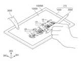
도 1은 본 발명의 일 실시예에 따른 인터페이스 장치의 사시도이다.1 is a perspective view of an interface device according to an embodiment of the present invention.
도 1을 참조하면, 인터페이스 장치(IFS)는 표시 장치(1000) 및 입력 장치(2000)를 포함할 수 있다. 표시 장치(1000)는 입력 장치(2000)에 의한 입력을 감지할 수 있다. 본 명세서에서 표시 장치(1000)와 입력 장치(2000)는 인터페이스 장치(IFS)로 지칭된다. 인터페이스 장치(IFS)는 디지타이저로 지칭될 수도 있다.Referring to FIG. 1 , the interface device IFS may include a
표시 장치(1000)는 전기적 신호에 따라 활성화되는 장치일 수 있다. 예를 들어, 표시 장치(1000)는 휴대폰, 폴더블 휴대폰, 태블릿, 자동차 내비게이션, 게임기, 또는 웨어러블 장치일 수 있으나, 이에 제한되는 것은 아니다. 도 1에서는 표시 장치(1000)가 태블릿인 것을 예시적으로 도시하였다.The
표시 장치(1000)에는 액티브 영역(1000A) 및 주변 영역(1000NA)이 정의될 수 있다. 표시 장치(1000)는 액티브 영역(1000A)을 통해 영상을 표시할 수 있다. 액티브 영역(1000A)은 제1 방향(DR1) 및 제2 방향(DR2)에 의해 정의된 면을 포함할 수 있다. 주변 영역(1000NA)은 액티브 영역(1000A)의 주변을 둘러쌀 수 있다.An
표시 장치(1000)의 두께 방향은 제1 방향(DR1) 및 제2 방향(DR2)과 교차하는 제3 방향(DR3)과 나란할 수 있다. 따라서, 표시 장치(1000)를 구성하는 부재들의 전면(또는 상면)과 배면(또는 하면)은 제3 방향(DR3)을 기준으로 정의될 수 있다.The thickness direction of the
표시 장치(1000)는 표시 장치(1000)의 외부에서 인가되는 입력들을 감지할 수 있다. 예를 들어, 표시 장치(1000)는 입력 장치(2000)에 의한 제1 입력 및 터치(3000)에 의한 제2 입력을 감지할 수 있다. 입력 장치(2000)는 구동 신호를 제공하는 액티브 타입의 입력 수단으로, 예를 들어 액티브 펜일 수 있다. 터치(3000)는 사용자 신체, 패시브 펜과 같이 정전용량에 변화를 제공할 수 있는 입력 수단을 모두 포함할 수 있다.The
표시 장치(1000)와 입력 장치(2000)는 서로 양방향 통신할 수 있다. 표시 장치(1000)는 입력 장치(2000)로 업링크신호를 제공하고, 입력 장치(2000)는 표시 장치(1000)로 다운링크신호를 제공할 수 있다. 예를 들어, 업링크신호는 패널 정보, 프로토콜 버전 등의 정보를 포함할 수 있으나, 특별히 이에 제한되는 것은 아니다. 다운링크신호는 동기화 신호 또는 입력 장치(2000)의 상태 정보를 포함할 수 있다. 예를 들어, 다운링크신호는 입력 장치(2000)의 좌표 정보, 입력 장치(2000)의 배터리 정보, 입력 장치(2000)의 기울기 정보, 및/또는 입력 장치(2000)에 저장된 다양한 정보 등을 포함할 수 있으나, 특별히 이에 제한되는 것은 아니다.The
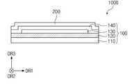
도 2a는 본 발명의 일 실시예에 따른 표시 장치의 단면도이다.2A is a cross-sectional view of a display device according to an exemplary embodiment.
도 2a를 참조하면, 표시 장치(1000)는 표시층(100) 및 센서층(200)을 포함할 수 있다.Referring to FIG. 2A , the
표시층(100)은 영상을 실질적으로 생성하는 구성일 수 있다. 표시층(100)은 발광형 표시층일 수 있으며, 예를 들어, 표시층(100)은 유기발광 표시층, 퀀텀닷 표시층, 마이크로 엘이디 표시층, 또는 나노 엘이디 표시층일 수 있다.The
표시층(100)은 베이스층(110), 회로층(120), 발광 소자층(130), 및 봉지층(140)을 포함할 수 있다.The
베이스층(110)은 회로층(120)이 배치되는 베이스 면을 제공하는 부재일 수 있다. 베이스층(110)은 유리 기판, 금속 기판, 또는 고분자 기판 등일 수 있다. 하지만, 실시예가 이에 한정되는 것은 아니며, 베이스층(110)은 무기층, 유기층 또는 복합재료층일 수 있다.The
베이스층(110)은 다층 구조를 가질 수 있다. 예를 들어, 베이스층(110)은 제1 합성 수지층, 상기 제1 합성 수지층 위에 배치된 실리콘 옥사이드(SiOx)층, 상기 실리콘 옥사이드층 위에 배치된 아몰퍼스 실리콘(a-Si)층, 및 상기 아몰퍼스 실리콘층 위에 배치된 제2 합성 수지층을 포함할 수 있다. 상기 실리콘 옥사이드층 및 상기 아몰퍼스 실리콘층은 베이스 배리어층이라 지칭될 수 있다.The
상기 제1 및 제2 합성 수지층들 각각은 폴리이미드(polyimide)계 수지를 포함하는 것일 수 있다. 또한, 상기 제1 및 제2 합성 수지층들 각각은 아크릴(acrylate)계 수지, 메타크릴(methacrylate)계 수지, 폴리아이소프렌(polyisoprene)계 수지, 비닐(vinyl)계 수지, 에폭시(epoxy)계 수지, 우레탄(urethane)계 수지, 셀룰로오스(cellulose)계 수지, 실록산(siloxane)계 수지, 폴리아미드(polyamide)계 수지, 및 페릴렌(perylene)계 수지 중 적어도 하나를 포함하는 것일 수 있다. 한편, 본 명세서에서 "~~" 계 수지는 "~~" 의 작용기를 포함하는 것을 의미한다.Each of the first and second synthetic resin layers may include a polyimide-based resin. In addition, each of the first and second synthetic resin layers includes an acrylate-based resin, a methacrylate-based resin, a polyisoprene-based resin, a vinyl-based resin, and an epoxy-based resin. , a urethane-based resin, a cellulose-based resin, a siloxane-based resin, a polyamide-based resin, and a perylene-based resin may be included. Meanwhile, in the present specification, "~~"-based resin means including a functional group of "~~".
회로층(120)은 베이스층(110) 위에 배치될 수 있다. 회로층(120)은 절연층, 반도체 패턴, 도전 패턴, 및 신호 라인 등을 포함할 수 있다. 코팅, 증착 등의 방식으로 절연층, 반도체층, 및 도전층이 베이스층(110) 위에 형성되고, 이후, 복수 회의 포토리소그래피 공정을 통해 절연층, 반도체층, 및 도전층이 선택적으로 패터닝될 수 있다. 이 후, 회로층(120)에 포함된 반도체 패턴, 도전 패턴, 및 신호 라인 이 형성될 수 있다.The
발광 소자층(130)은 회로층(120) 위에 배치될 수 있다. 발광 소자층(130)은 발광 소자를 포함할 수 있다. 예를 들어, 발광 소자층(130)은 유기 발광 물질, 퀀텀닷, 퀀텀 로드, 마이크로 엘이디, 또는 나노 엘이디를 포함할 수 있다.The light emitting
봉지층(140)은 발광 소자층(130) 위에 배치될 수 있다. 봉지층(140)은 수분, 산소, 및 먼지 입자와 같은 이물질로부터 발광 소자층(130)을 보호할 수 있다.The
센서층(200)은 표시층(100) 위에 배치될 수 있다. 센서층(200)은 외부에서 인가되는 외부 입력을 감지할 수 있다. 외부 입력은 사용자의 입력일 수 있다. 사용자의 입력은 사용자 신체의 일부, 광, 열, 펜, 또는 압력 등 다양한 형태의 외부 입력들을 포함할 수 있다.The
센서층(200)은 연속된 공정을 통해 표시층(100) 위에 형성될 수 있다. 이 경우, 센서층(200)은 표시층(100) 위에 직접 배치된다고 표현될 수 있다. 직접 배치된다는 것은 센서층(200)과 표시층(100) 사이에 제3 의 구성요소가 배치되지 않는 것을 의미할 수 있다. 즉, 센서층(200)과 표시층(100) 사이에는 별도의 접착 부재가 배치되지 않을 수 있다.The
또는, 센서층(200)은 표시층(100)과 접착 부재를 통해 서로 결합될 수 있다. 접착 부재는 통상의 접착제 또는 점착제를 포함할 수 있다.Alternatively, the
도시되지 않았으나, 표시 장치(1000)는 센서층(200) 위에 배치된 반사 방지층 및 광학층을 더 포함할 수도 있다. 반사 방지층은 표시 장치(1000)의 외부로부터 입사되는 외부광의 반사율을 감소시킬 수 있다. 광학층은 표시층(100)으로부터 입사된 광의 방향을 제어하여 표시 장치(1000)의 정면 휘도를 향상시킬 수 있다.Although not shown, the
도 2b는 본 발명의 일 실시예에 따른 표시 장치의 단면도이다.2B is a cross-sectional view of a display device according to an exemplary embodiment.
도 2b를 참조하면, 표시 장치(1000_1)는 표시층(100_1) 및 센서층(200_1)을 포함할 수 있다. 표시층(100_1)은 베이스 기판(110_1), 회로층(120_1), 발광 소자층(130_1), 봉지 기판(140_1), 및 결합 부재(150_1)를 포함할 수 있다.Referring to FIG. 2B , the display device 1000_1 may include a display layer 100_1 and a sensor layer 200_1 . The display layer 100_1 may include a base substrate 110_1 , a circuit layer 120_1 , a light emitting device layer 130_1 , an encapsulation substrate 140_1 , and a coupling member 150_1 .
베이스 기판(110_1) 및 봉지 기판(140_1) 각각은 유리 기판, 금속 기판, 또는 고분자 기판 등일 수 있으나, 특별히 이에 제한되는 것은 아니다.Each of the base substrate 110_1 and the encapsulation substrate 140_1 may be a glass substrate, a metal substrate, or a polymer substrate, but is not particularly limited thereto.
결합 부재(150_1)는 베이스 기판(110_1)과 봉지 기판(140_1) 사이에 배치될 수 있다. 결합 부재(150_1)는 봉지 기판(140_1)을 베이스 기판(110_1) 또는 회로층(120_1)에 결합시킬 수 있다. 결합 부재(150_1)는 무기물 또는 유기물을 포함할 수 있다. 예를 들어, 무기물은 프릿 실(frit seal)을 포함할 수 있고, 유기물은 광 경화성 수지 또는 광 가소성 수지를 포함할 수 있다. 다만, 결합 부재(150_1)를 구성하는 물질이 상기 예에 제한되는 것은 아니다.The coupling member 150_1 may be disposed between the base substrate 110_1 and the encapsulation substrate 140_1 . The coupling member 150_1 may couple the encapsulation substrate 140_1 to the base substrate 110_1 or the circuit layer 120_1 . The coupling member 150_1 may include an inorganic material or an organic material. For example, the inorganic material may include a frit seal, and the organic material may include a photocurable resin or a photoplastic resin. However, the material constituting the coupling member 150_1 is not limited to the above example.
센서층(200_1)은 봉지 기판(140_1) 위에 직접 배치될 수 있다. 직접 배치된다는 것은 센서층(200_1)과 봉지 기판(140_1) 사이에 제3 의 구성요소가 배치되지 않는 것을 의미할 수 있다. 즉, 센서층(200_1)과 표시층(100_1) 사이에는 별도의 접착 부재가 배치되지 않을 수 있다. 다만, 이에 제한되는 것은 아니며, 센서층(200_1)과 봉지 기판(140_1) 사이에는 접착층이 더 배치될 수도 있다.The sensor layer 200_1 may be directly disposed on the encapsulation substrate 140_1 . Directly disposed may mean that the third component is not disposed between the sensor layer 200_1 and the encapsulation substrate 140_1. That is, a separate adhesive member may not be disposed between the sensor layer 200_1 and the display layer 100_1 . However, the present invention is not limited thereto, and an adhesive layer may be further disposed between the sensor layer 200_1 and the encapsulation substrate 140_1 .
도 3은 본 발명의 일 실시예에 따른 표시 장치의 단면도이다.3 is a cross-sectional view of a display device according to an exemplary embodiment.
도 3를 참조하면, 베이스층(110)의 상면에 적어도 하나의 무기층이 형성된다. 무기층은 알루미늄옥사이드, 티타늄옥사이드, 실리콘옥사이드, 실리콘나이트라이드, 실리콘옥시나이트라이드, 지르코늄옥사이드, 및 하프늄옥사이드 중 적어도 하나를 포함할 수 있다. 무기층은 다층으로 형성될 수 있다. 다층의 무기층들은 배리어층 및/또는 버퍼층을 구성할 수 있다. 본 실시예에서 표시층(100)은 버퍼층(BFL)을 포함하는 것으로 도시되었다.Referring to FIG. 3 , at least one inorganic layer is formed on the upper surface of the
버퍼층(BFL)은 베이스층(110)과 반도체 패턴 사이의 결합력을 향상시킬 수 있다. 버퍼층(BFL)은 실리콘옥사이드, 실리콘나이트라이드, 및 살리콘옥시나이트라이드 중 적어도 하나를 포함할 수 있다. 예를 들어, 버퍼층(BFL)은 실리콘옥사이드층과 실리콘나이트라이드층이 교대로 적층된 구조를 포함할 수 있다.The buffer layer BFL may improve a bonding force between the
반도체 패턴은 버퍼층(BFL) 위에 배치될 수 있다. 반도체 패턴은 폴리실리콘을 포함할 수 있다. 그러나 이에 제한되지 않고, 반도체 패턴은 비정질실리콘, 저온다결정실리콘, 또는 산화물 반도체를 포함할 수도 있다.The semiconductor pattern may be disposed on the buffer layer BFL. The semiconductor pattern may include polysilicon. However, the present invention is not limited thereto, and the semiconductor pattern may include amorphous silicon, low-temperature polycrystalline silicon, or an oxide semiconductor.
도 3는 일부의 반도체 패턴을 도시한 것일 뿐이고, 다른 영역에 반도체 패턴이 더 배치될 수 있다. 반도체 패턴은 화소들에 걸쳐 특정한 규칙으로 배열될 수 있다. 반도체 패턴은 도핑 여부에 따라 전기적 성질이 다를 수 있다. 반도체 패턴은 전도율이 높은 제1 영역과 전도율이 낮은 제2 영역을 포함할 수 있다. 제1 영역은 N형 도판트 또는 P형 도판트로 도핑될 수 있다. P타입의 트랜지스터는 P형 도판트로 도핑된 도핑영역을 포함하고, N타입의 트랜지스터는 N형 도판트로 도핑된 도핑영역을 포함할 수 있다. 제2 영역은 비-도핑 영역이거나, 제1 영역 대비 낮은 농도로 도핑된 영역일 수 있다.FIG. 3 is only a partial diagram of a semiconductor pattern, and a semiconductor pattern may be further disposed in another region. The semiconductor pattern may be arranged in a specific rule across the pixels. The semiconductor pattern may have different electrical properties depending on whether it is doped or not. The semiconductor pattern may include a first region having high conductivity and a second region having low conductivity. The first region may be doped with an N-type dopant or a P-type dopant. The P-type transistor may include a doped region doped with a P-type dopant, and the N-type transistor may include a doped region doped with an N-type dopant. The second region may be a non-doped region or a region doped at a lower concentration than the first region.
제1 영역의 전도성은 제2 영역의 전도성보다 크고, 실질적으로 전극 또는 신호 라인의 역할을 할 수 있다. 제2 영역은 실질적으로 트랜지스터의 액티브(또는 채널)에 해당할 수 있다. 다시 말해, 반도체 패턴의 일부분은 트랜지스터의 액티브일수 있고, 다른 일부분은 트랜지스터의 소스 또는 드레인일 수 있고, 또 다른 일부분은 연결 전극 또는 연결 신호라인일 수 있다.The conductivity of the first region is greater than that of the second region, and may substantially serve as an electrode or a signal line. The second region may substantially correspond to an active (or channel) of the transistor. In other words, a portion of the semiconductor pattern may be an active transistor, another portion may be a source or drain of the transistor, and another portion may be a connection electrode or a connection signal line.
화소들 각각은 7개의 트랜지스터들, 하나의 커패시터, 및 발광 소자를 포함하는 등가회로를 가질 수 있으며, 화소의 등가회로도는 다양한 형태로 변형될 수 있다. 도 3에서는 화소에 포함되는 하나의 트랜지스터(100PC) 및 발광 소자(100PE)를 예시적으로 도시하였다.Each of the pixels may have an equivalent circuit including seven transistors, one capacitor, and a light emitting device, and the equivalent circuit diagram of the pixel may be modified in various forms. 3 exemplarily illustrates one transistor 100PC and a light emitting device 100PE included in a pixel.
트랜지스터(100PC)의 소스(SC), 액티브(AL), 및 드레인(DR)이 반도체 패턴으로부터 형성될 수 있다. 소스(SC) 및 드레인(DR)은 단면 상에서 액티브(AL)로부터 서로 반대 방향으로 연장될 수 있다. 도 3에는 반도체 패턴으로부터 형성된 연결 신호 배선(SCL)의 일부분을 도시하였다. 별도로 도시하지 않았으나, 연결 신호 배선(SCL)은 평면 상에서 트랜지스터(100PC)의 드레인(DR)에 연결될 수 있다.A source SC, an active AL, and a drain DR of the transistor 100PC may be formed from a semiconductor pattern. The source SC and the drain DR may extend in opposite directions from the active AL on a cross-section. 3 illustrates a portion of the connection signal line SCL formed from the semiconductor pattern. Although not shown separately, the connection signal line SCL may be connected to the drain DR of the transistor 100PC on a plane.
제1 절연층(10)은 버퍼층(BFL) 위에 배치될 수 있다. 제1 절연층(10)은 복수 개의 화소들에 공통으로 중첩하며, 반도체 패턴을 커버할 수 있다. 제1 절연층(10)은 무기층 및/또는 유기층일 수 있으며, 단층 또는 다층 구조를 가질 수 있다. 제1 절연층(10)은 알루미늄옥사이드, 티타늄옥사이드, 실리콘옥사이드, 실리콘나이트라이드, 실리콘옥시나이트라이드, 지르코늄옥사이드, 및 하프늄옥사이드 중 적어도 하나를 포함할 수 있다. 본 실시예에서 제1 절연층(10)은 단층의 실리콘옥사이드층일 수 있다. 제1 절연층(10)뿐만 아니라 후술하는 회로층(120)의 절연층은 무기층 및/또는 유기층일 있으며, 단층 또는 다층 구조를 가질 수 있다. 무기층은 상술한 물질 중 적어도 하나를 포함할 수 있으나, 이에 제한되는 것은 아니다.The first insulating
트랜지스터(100PC)의 게이트(GT)는 제1 절연층(10) 위에 배치된다. 게이트(GT)는 금속 패턴의 일부분일 수 있다. 게이트(GT)는 액티브(AL)에 중첩한다. 반도체 패턴을 도핑하는 공정에서 게이트(GT)는 마스크로 기능할 수 있다.The gate GT of the transistor 100PC is disposed on the first insulating
제2 절연층(20)은 제1 절연층(10) 위에 배치되며, 게이트(GT)를 커버할 수 있다. 제2 절연층(20)은 화소들에 공통으로 중첩할 수 있다. 제2 절연층(20)은 무기층 및/또는 유기층일 수 있으며, 단층 또는 다층 구조를 가질 수 있다. 제2 절연층(20)은 실리콘옥사이드, 실리콘나이트라이드, 및 실리콘옥시나이트라이드 중 적어도 하나를 포함할 수 있다. 본 실시예에서, 제2 절연층(20)은 실리콘옥사이드층 및 실리콘나이트라이드층을 포함하는 다층 구조를 가질 수 있다.The second insulating
제3 절연층(30)은 제2 절연층(20) 위에 배치될 수 있다. 제3 절연층(30)은 단층 또는 다층 구조를 가질 수 있다. 예를 들어, 제3 절연층(30)은 실리콘옥사이드층 및 실리콘나이트라이드층을 포함하는 다층 구조를 가질 수 있다.The third insulating
제1 연결 전극(CNE1)은 제3 절연층(30) 위에 배치될 수 있다. 제1 연결 전극(CNE1)은 제1, 제2, 및 제3 절연층(10, 20, 30)을 관통하는 컨택홀(CNT-1)을 통해 연결 신호 배선(SCL)에 접속될 수 있다.The first connection electrode CNE1 may be disposed on the third insulating
제4 절연층(40)은 제3 절연층(30) 위에 배치될 수 있다. 제4 절연층(40)은 단층의 실리콘 옥사이드층일 수 있다. 제5 절연층(50)은 제4 절연층(40) 위에 배치될 수 있다. 제5 절연층(50)은 유기층일 수 있다.The fourth insulating
제2 연결 전극(CNE2)은 제5 절연층(50) 위에 배치될 수 있다. 제2 연결 전극(CNE2)은 제4 절연층(40) 및 제5 절연층(50)을 관통하는 컨택홀(CNT-2)을 통해 제1 연결 전극(CNE1)에 접속될 수 있다.The second connection electrode CNE2 may be disposed on the fifth insulating
제6 절연층(60)은 제5 절연층(50) 위에 배치되며, 제2 연결 전극(CNE2)을 커버할 수 있다. 제6 절연층(60)은 유기층일 수 있다.The sixth insulating
발광 소자층(130)은 회로층(120) 위에 배치될 수 있다. 발광 소자층(130)은 발광 소자(100PE)를 포함할 수 있다. 예를 들어, 발광 소자층(130)은 유기 발광 물질, 퀀텀닷, 퀀텀 로드, 마이크로 엘이디, 또는 나노 엘이디를 포함할 수 있다. 이하에서, 발광 소자(100PE)가 유기 발광 소자인 것을 예로 들어 설명하나, 특별히 이에 제한되는 것은 아니다.The light emitting
발광 소자(100PE)는 제1 전극(AE), 발광층(EL), 및 제2 전극(CE)을 포함할 수 있다.The light emitting device 100PE may include a first electrode AE, an emission layer EL, and a second electrode CE.
제1 전극(AE)은 제6 절연층(60) 위에 배치될 수 있다. 제1 전극(AE)은 제6 절연층(60)을 관통하는 컨택홀(CNT-3)을 통해 제2 연결 전극(CNE2)에 접속될 수 있다.The first electrode AE may be disposed on the sixth insulating
화소 정의막(70)은 제6 절연층(60) 위에 배치되며, 제1 전극(AE)의 일부분을 커버할 수 있다. 화소 정의막(70)에는 개구부(70-OP)가 정의된다. 화소 정의막(70)의 개구부(70-OP)는 제1 전극(AE)의 적어도 일부분을 노출시킨다.The
액티브 영역(1000A, 도 1 참조)은 발광 영역(PXA)과 발광 영역(PXA)에 인접한 비발광 영역(NPXA)을 포함할 수 있다. 비발광 영역(NPXA)은 발광 영역(PXA)을 에워쌀 수 있다. 본 실시예에서 발광 영역(PXA)은 개구부(70-OP)에 의해 노출된 제1 전극(AE)의 일부 영역에 대응하게 정의되었다.The
발광층(EL)은 제1 전극(AE) 위에 배치될 수 있다. 발광층(EL)은 개구부(70-OP)에 대응하는 영역에 배치될 수 있다. 즉, 발광층(EL)은 화소들 각각에 분리되어 형성될 수 있다. 발광층(EL)이 화소들 각각에 분리되어 형성된 경우, 발광층들(EL) 각각은 청색, 적색, 및 녹색 중 적어도 하나의 색의 광을 발광할 수 있다. 다만, 이에 제한되는 것은 아니며, 발광층(EL)은 화소들에 연결되어 공통으로 제공될 수도 있다. 이 경우, 발광층(EL)은 청색 광을 제공하거나, 백색 광을 제공할 수도 있다.The emission layer EL may be disposed on the first electrode AE. The emission layer EL may be disposed in a region corresponding to the opening 70 -OP. That is, the emission layer EL may be formed separately in each of the pixels. When the emission layer EL is separately formed in each of the pixels, each of the emission layers EL may emit light of at least one color among blue, red, and green. However, the present invention is not limited thereto, and the light emitting layer EL may be connected to the pixels and provided in common. In this case, the light emitting layer EL may provide blue light or white light.
제2 전극(CE)은 발광층(EL) 위에 배치될 수 있다. 제2 전극(CE)은 일체의 형상을 갖고, 복수 개의 화소들에 공통적으로 배치될 수 있다.The second electrode CE may be disposed on the emission layer EL. The second electrode CE may have an integral shape and may be commonly disposed in a plurality of pixels.
도시되지 않았으나, 제1 전극(AE)과 발광층(EL) 사이에는 정공 제어층이 배치될 수 있다. 정공 제어층은 발광 영역(PXA)과 비발광 영역(NPXA)에 공통으로 배치될 수 있다. 정공 제어층은 정공 수송층을 포함하고, 정공 주입층을 더 포함할 수 있다. 발광층(EL)과 제2 전극(CE) 사이에는 전자 제어층이 배치될 수 있다. 전자 제어층은 전자 수송층을 포함하고, 전자 주입층을 더 포함할 수 있다. 정공 제어층과 전자 제어층은 오픈 마스크를 이용하여 복수 개의 화소들에 공통으로 형성될 수 있다.Although not shown, a hole control layer may be disposed between the first electrode AE and the emission layer EL. The hole control layer may be commonly disposed in the light emitting area PXA and the non-emission area NPXA. The hole control layer may include a hole transport layer and may further include a hole injection layer. An electronic control layer may be disposed between the emission layer EL and the second electrode CE. The electron control layer may include an electron transport layer and may further include an electron injection layer. The hole control layer and the electron control layer may be formed in common in the plurality of pixels using an open mask.
봉지층(140)은 발광 소자층(130) 위에 배치될 수 있다. 봉지층(140)은 순차적으로 적층된 무기층, 유기층, 및 무기층을 포함할 수 있으나, 봉지층(140)을 구성하는 층들이 이에 제한되는 것은 아니다.The
무기층들은 수분 및 산소로부터 발광 소자층(130)을 보호하고, 유기층은 먼지 입자와 같은 이물질로부터 발광 소자층(130)을 보호할 수 있다. 무기층들은 실리콘나이트라이드층, 실리콘옥시나이트라이드층, 실리콘옥사이드층, 티타늄옥사이드층, 또는 알루미늄옥사이드층 등을 포함할 수 있다. 유기층은 아크릴 계열 유기층을 포함할 수 있고, 이에 제한되지 않는다.The inorganic layers may protect the light emitting
센서층(200)은 베이스층(201), 제1 도전층(202), 감지 절연층(203), 제2 도전층(204), 및 커버 절연층(205)을 포함할 수 있다.The
베이스층(201)은 실리콘나이트라이드, 실리콘옥시나이트라이드, 및 실리콘옥사이드 중 적어도 어느 하나를 포함하는 무기층일 수 있다. 또는 베이스층(201)은 에폭시 수지, 아크릴 수지, 또는 이미드 계열 수지를 포함하는 유기층일 수도 있다. 베이스층(201)은 단층 구조를 갖거나, 제3 방향(DR3)을 따라 적층된 다층 구조를 가질 수 있다.The
제1 도전층(202) 및 제2 도전층(204) 각각은 단층구조를 갖거나, 제3 방향(DR3)을 따라 적층된 다층 구조를 가질 수 있다.Each of the first
단층구조의 도전층은 금속층 또는 투명 도전층을 포함할 수 있다. 금속층은 몰리브덴, 은, 티타늄, 구리, 알루미늄, 또는 이들의 합금을 포함할 수 있다. 투명 도전층은 인듐주석산화물(indium tin oxide, ITO), 인듐아연산화물(indium zinc oxide, IZO), 산화아연(zinc oxide, ZnO), 인듐아연주석산화물 (indium zinc tin oxide, IZTO) 등과 같은 투명한 전도성산화물을 포함할 수 있다. 그밖에 투명 도전층은 PEDOT과 같은 전도성 고분자, 금속 나노 와이어, 그라핀 등을 포함할 수 있다.The single-layered conductive layer may include a metal layer or a transparent conductive layer. The metal layer may include molybdenum, silver, titanium, copper, aluminum, or an alloy thereof. The transparent conductive layer is transparent, such as indium tin oxide (ITO), indium zinc oxide (IZO), zinc oxide (ZnO), indium zinc tin oxide (IZTO), etc. It may include a conductive oxide. In addition, the transparent conductive layer may include a conductive polymer such as PEDOT, metal nanowires, graphene, and the like.
다층구조의 도전층은 금속층들을 포함할 수 있다. 금속층들은 예컨대 티타늄/알루미늄/티타늄의 3층 구조를 가질 수 있다. 다층구조의 도전층은 적어도 하나의 금속층 및 적어도 하나의 투명 도전층을 포함할 수 있다.The multi-layered conductive layer may include metal layers. The metal layers may have, for example, a three-layer structure of titanium/aluminum/titanium. The multi-layered conductive layer may include at least one metal layer and at least one transparent conductive layer.
감지 절연층(203) 및 커버 절연층(205) 중 적어도 어느 하나는 무기막을 포함할 수 있다. 무기막은 알루미늄옥사이드, 티타늄옥사이드, 실리콘옥사이드, 실리콘나이트라이드, 실리콘옥시나이트라이드, 지르코늄옥사이드, 및 하프늄옥사이드 중 적어도 하나를 포함할 수 있다.At least one of the sensing insulating
감지 절연층(203) 및 커버 절연층(205) 중 적어도 어느 하나는 유기막을 포함할 수 있다. 유기막은 아크릴계 수지, 메타크릴계 수지, 폴리이소프렌, 비닐계 수지, 에폭시계 수지, 우레탄계 수지, 셀룰로오스계 수지, 실록산계 수지, 폴리이미드계 수지, 폴리아미드계 수지 및 페릴렌계 수지 중 적어도 어느 하나를 포함할 수 있다.At least one of the sensing insulating
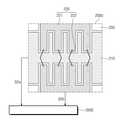
도 4는 본 발명의 일 실시예에 따른 센서층의 평면도이다.4 is a plan view of a sensor layer according to an embodiment of the present invention.
도 4를 참조하면, 센서층(200)에는 감지 영역(200A) 및 주변 영역(200N)이 정의될 수 있다. 감지 영역(200A)은 도 1에 도시된 액티브 영역(1000A)에 대응될 수 있고, 주변 영역(200N)은 도 1에 도시된 주변 영역(1000NA)에 대응될 수 있다.Referring to FIG. 4 , a
센서층(200)은 전극들(210), 교차 전극들(220), 배선들(230), 및 패드들(240)을 포함할 수 있다.The
전극들(210) 각각은 제1 방향(DR1)을 따라 연장되며, 전극들(210)은 제2 방향(DR2)으로 서로 이격되어 배열될 수 있다. 교차 전극들(220) 각각은 제2 방향(DR2)을 따라 연장되며, 교차 전극들(220)은 제1 방향(DR1)으로 서로 이격되어 배열될 수 있다.Each of the
전극들(210) 및 교차 전극들(220) 각각은 배선들(230) 중 대응하는 배선에 전기적으로 연결될 수 있다. 도 4에서는 하나의 전극(210)에 하나의 배선(230)이 연결되고, 하나의 교차 전극(220)에 하나의 배선(230)이 연결된 싱글 라우팅 구조를 예를 들어 도시하였으나, 특별히 이에 제한되는 것은 아니다. 예를 들어, 교차 전극들(220) 각각에는 2개의 배선들(230)이 연결될 수도 있다. 또는, 전극들(210) 각각에도 2 개의 배선들(230)이 연결되고, 교차 전극들(220) 각각에는 2개의 배선들(230)이 연결될 수도 있다.Each of the
패드들(240)은 배선들(230)에 각각 전기적으로 연결될 수 있다. 패드들(240)을 통해 센서층(200)은 센서 구동부(200C, 도 5a 참조)와 전기적으로 연결될 수 있다.The
도 5a 및 도 5b는 센서층의 제1 모드 동작을 설명하기 위한 도면들이다.5A and 5B are diagrams for explaining the first mode operation of the sensor layer.
도 4, 도 5a 및 도 5b를 참조하면, 하나의 전극(210)의 일부분 및 하나의 교차 전극(220)의 일부분은 하나의 센싱 단위(200U)로 정의될 수 있다. 도 5a 및 도 5b 각각에는 하나의 센싱 단위(200U)가 확대되어 도시되었다.4, 5A, and 5B , a portion of one
교차 전극(220)은 교차 패턴들(221) 및 교차 패턴들(221)에 전기적으로 연결된 브릿지 패턴들(222)을 포함할 수 있다. 교차 패턴들(221)은 전극(210)을 사이에 두고 이격될 수 있다. 브릿지 패턴들(222)은 전극(210)과 중첩할 수 있고, 브릿지 패턴들(222)은 전극(210)과 절연 교차할 수 있다.The
교차 패턴들(221) 및 전극(210)은 서로 동일한 층 상에 배치될 수 있고, 브릿지 패턴들(222)은 교차 패턴들(221) 및 전극(210)과 상이한 층 상에 배치될 수 있다. 예를 들어, 교차 패턴들(221) 및 전극(210)은 제2 도전층(204, 도 5 참조)에 포함될 수 있고, 브릿지 패턴들(222)은 제1 도전층(202, 도 3 참조)에 포함될 수 있으며, 이 구조는 바텀 브릿지 구조라 지칭될 수 있다. 하지만, 본 발명이 특별히 이에 제한되는 것은 아니다. 예를 들어, 교차 패턴들(221) 및 전극(210)은 제1 도전층(202, 도 3 참조)에 포함될 수 있고, 브릿지 패턴들(222)은 제2 도전층(204, 도 3 참조)에 포함될 수 있으며, 이 구조는 탑 브릿지 구조라 지칭될 수 있다.The
또한, 센서층(200)은 교차 패턴들(221) 및 전극(210)이 배치되지 않은 영역에 배치된 더미 패턴(250)을 더 포함할 수 있다. 더미 패턴(250)은 외부에서 전극(210) 및 교차 전극(220)이 시인되는 것을 방지하기 위해 제공되는 구성일 수 있으며, 더미 패턴(250)은 전기적으로 플로팅된 패턴일 수 있다. 더미 패턴(250)은 플로팅 패턴 또는 패턴으로 지칭될 수도 있다.In addition, the
교차 패턴들(221), 전극(210), 및 더미 패턴(250) 각각은 메쉬 구조를 가질 수 있다. 이 경우, 교차 패턴들(221), 전극(210), 및 더미 패턴(250) 각각에는 개구가 정의될 수 있다. 다만, 이에 한정되는 것은 아니며, 교차 패턴들(221), 전극(210), 및 더미 패턴(250) 각각은 투명한 통전극으로 구성될 수도 있다.Each of the
도 5a 및 도 5b를 참조하면, 제1 모드는 표시 장치(1000, 도 1 참조)와 입력 장치(2000, 도 1 참조)가 서로 데이터를 송수신하는 모드일 수 있다. 도 5a에 도시된 동작은 표시 장치(1000, 도 1 참조)에서 입력 장치(2000, 도 1 참조)로 업링크신호를 제공하는 동작일 수 있다. 도 5b에 도시된 동작은 입력 장치(2000, 도 1 참조)에서 표시 장치(1000, 도1 참조)로 다운링크신호를 제공하는 동작일 수 있다.5A and 5B , the first mode may be a mode in which the display device 1000 (refer to FIG. 1 ) and the input device 2000 (refer to FIG. 1 ) transmit/receive data to each other. The operation illustrated in FIG. 5A may be an operation of providing an uplink signal from the display device 1000 (refer to FIG. 1 ) to the input device 2000 (refer to FIG. 1 ). The operation illustrated in FIG. 5B may be an operation of providing a downlink signal from the input device 2000 (refer to FIG. 1 ) to the display device 1000 (refer to FIG. 1 ).
도 5a를 참조하면, 전극(210) 및 교차 전극(220) 각각은 센서 구동부(200C)로부터 제공된 업링크신호(S1a, S1b)를 입력 장치(2000, 도 1 참조)로 제공하기 위한 송신 전극으로 활용될 수 있다. 도 5a에서는 전극(210)과 교차 전극(220)이 모두 송신 전극으로 활용되는 것을 일 예로 도시하였으나, 특별히 이에 제한되는 것은 아니다. 예를 들어, 전극(210) 또는 교차 전극(220)이 송신 전극으로 활용될 수도 있다.Referring to FIG. 5A , each of the
도 5b를 참조하면, 전극(210) 및 교차 전극(220) 각각은 입력 장치(2000, 도 1 참조)로부터 유도된 감지 신호들(S2a, S2b)을 센서 구동부(200C)로 전달하기 위한 수신 전극으로 활용될 수 있다. 센서 구동부(200C)는 전극(210)으로부터 제1 감지 신호(S2a)를 수신하고, 교차 전극(220)으로부터 제2 감지 신호(S2b)를 수신할 수 있다.Referring to FIG. 5B , each of the
도 6은 센서층의 제2 모드 동작을 설명하기 위한 도면이다.6 is a view for explaining the second mode operation of the sensor layer.
도 4 및 도 6을 참조하면, 제2 모드에서 센서 구동부(200C)는 터치(3000, 도 1 참조)에 의한 제2 입력을 감지할 수 있다. 제2 모드에서 센서 구동부(200C)는 전극(210)과 교차 전극(220) 사이에 형성된 상호 정전 용량의 변화량을 감지하여 외부 입력을 감지할 수 있다.4 and 6 , in the second mode, the
센서 구동부(200C)는 전극(210)으로 구동 신호(S3)를 제공하고, 센서 구동부(200C)는 교차 전극(220)으로부터 감지 신호(S4)를 수신할 수 있다. 즉, 제2 모드에서 전극(210)은 송신 전극으로 기능할 수 있고, 교차 전극(220)은 수신 전극으로 기능할 수 있다. 하지만, 이에 특별히 제한되는 것은 아니다. 예를 들어, 전극(210)이 수신 전극으로 기능하고, 교차 전극(220)이 송신 전극으로 기능할 수도 있다.The
도 7은 본 발명의 일 실시예에 따른 입력 장치의 블록도이다.7 is a block diagram of an input device according to an embodiment of the present invention.
도 7을 참조하면, 입력 장치(2000)는 하우징(2000H), 전원(2100), 제어부(2200), 통신부(2300), 전극(2400), 측정 센서(2500), 및 압력 센서(2600)을 포함할 수 있다. 다만, 입력 장치(2000)를 구성하는 구성 요소들이 상기 나열된 구성 요소들에 제한되는 것은 아니다. 예를 들어, 입력 장치(2000)는 신호 송신 모드 또는 신호 수신모드로 전환하는 전극 스위치, 소정의 정보를 저장하는 메모리, 또는 회전을 감지하는 회전 센서 등을 더 포함할 수도 있다.Referring to FIG. 7 , the
하우징(2000H)은 펜 형상을 가질 수 있고, 내부에는 수용 공간이 형성될 수 있다. 하우징(2000H) 내부에 정의된 수용 공간에는 전원(2100), 제어부(2200), 통신부(2300), 전극(2400), 측정 센서(2500), 및 압력 센서(2600)가 수용될 수 있다.The
전원(2100)은 제어부(2200), 통신부(2300), 측정 센서(2500), 및 압력 센서(2600)에 전원을 공급할 수 있다. 전원(2100)은 배터리 또는 고용량 커패시터를 포함할 수 있다.The
제어부(2200)는 입력 장치(2000)의 동작을 제어할 수 있다. 제어부(2200)는 주문형 반도체(ASIC, application-specific integrated circuit)일 수 있다. 제어부(2200)는 설계된 프로그램에 따라서 동작하도록 구성될 수 있다.The
통신부(2300)는 수신 회로 및 송신 회로를 포함할 수 있다. 수신 회로는 센서층(200)으로부터 제공된 업링크신호(ULS)를 수신할 수 있다. 수신 회로는 업링크신호(ULS)를 제어부(2200)에서 처리 가능한 신호로 변조할 수 있다. 송신 회로는 제어부(2200)로부터 제공된 신호를 수신하여, 센서층(200)에 의해 센싱 가능한 신호로 변조할 수 있다. 송신 회로는 전극(2400)을 통해 다운링크신호(DLS)를 출력할 수 있다.The
전극(2400)은 펜 팁으로 지칭될 수 있다. 전극(2400)은 통신부(2300)와 전기적으로 연결될 수 있다. 전극(2400)의 일부분은 하우징(2000H)으로부터 돌출될 수 있다. 또는, 입력 장치(2000)는 하우징(2000H)으로부터 노출된 전극(2400)을 커버하는 커버 하우징을 더 포함할 수도 있다. 또는, 전극(2400)은 하우징(2000H) 내부에 내장될 수도 있다.The
측정 센서(2500) 및 압력 센서(2600)는 사용자의 생체 정보를 측정하기 위한 구성들일 수 있다. 예를 들어, 측정 센서(2500)와 압력 센서(2600)는 사용자의 혈압을 측정할 수 있다. 측정 센서(2500)는 광 혈류 측정 (Photoplethysmography, PPG) 센서일 수 있다. 압력 센서(2600)는 필름형 압력 센서일 수 있고, 압력 센서(2600)는 플렉서블할 수 있다.The
압력 센서(2600)는 압력 센서(2600)에 인가된 압력 값과 압력 센서(2600)에 접촉된 사용자의 신체의 일부분의 면적을 획득할 수 있다. 측정 센서(2500)는 혈액량의 변화(또는 혈류량의 변화)를 측정할 수 있다. 제어부(2200)는 압력 센서(2600)로부터 압력 값 및 측정 센서(2500)로부터 혈액량의 변화에 대한 정보를 수신하여 사용자의 혈압을 판독할 수 있다.The
본 발명의 실시예에 따르면, 입력 장치(2000)를 이용하여 사용자의 혈압을 측정한다. 즉, 커프와 같은 별도 장비 없이 입력 장치(2000)에 포함된 압력 센서(2600) 및 측정 센서(2500)를 이용하여 사용자의 혈압을 용이하게 측정할 수 있다. 사용자가 입력 장치(2000)를 이용한 작업을 하는 중에 주기적 또는 비주기적으로 사용자의 혈압이 측정될 수 있다.According to an embodiment of the present invention, the user's blood pressure is measured using the
제어부(2200)는 사용자의 혈압이 이상이 있는 경우, 이에 대한 정보를 통신부(2300)를 통해 표시 장치(1000)로 전송할 수 있다. 표시 장치(1000)는 혈압 이상에 대한 정보를 표시하여 사용자에게 알릴 수 있다.When there is an abnormality in the user's blood pressure, the
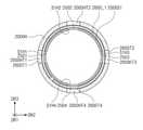
도 8은 본 발명의 일 실시예에 따른 입력 장치의 측면도이다. 도 9는 본 발명의 일 실시예에 따른 입력 장치의 단면도이다.8 is a side view of an input device according to an embodiment of the present invention. 9 is a cross-sectional view of an input device according to an embodiment of the present invention.
도 7, 도 8 및 도 9를 참조하면, 하우징(2000H)에는 투과부(2000HT)가 정의될 수 있다. 투과부(2000HT)는 측정 센서(2500)로부터 제공된 광이 투과 및 사용자로부터 반사된 광이 투과될 수 있는 수준의 투과율을 가질 수 있다.7, 8, and 9 , a transmission part 2000HT may be defined in the
투과부(2000HT)가 정의된 하우징(2000H)의 일부분은 파지 부분(GA)으로 지칭될 수 있다. 파지 부분(GA)은 사용자가 입력 장치(2000)를 사용시 파지하는 영역에 대응될 수 있다. 하우징(2000H)의 파지 부분(GA)은 형상 변형이 가능한 물질을 포함할 수 있다. 예를 들어, 하우징(2000H)의 파지 부분(GA)은 고무 또는 플라스틱을 포함할 수 있다. 따라서, 사용자에 의해 가해지는 압력이 압력 센서(2600)로 용이하게 전달될 수 있다.A portion of the
측정 센서(2500)는 복수로 제공될 수 있다. 예를 들어, 측정 센서(2500)는 제1 측정 센서(2501), 제2 측정 센서(2502), 제3 측정 센서(2503), 및 제4 측정 센서(2504)를 포함할 수 있다. 본 실시예에서, 입력 장치(2000)가 제1 내지 제4 측정 센서들(2501, 2502, 2503, 2504)를 포함하는 것을 예시적으로 도시하였으나, 특별히 이에 제한되는 것은 아니다. 예를 들어, 입력 장치(2000)가 포함하는 측정 센서의 수는 1개, 2개, 3개, 또는 4 개 이상 다양하게 변형될 수 있다.A plurality of
제1 내지 제4 측정 센서들(2501, 2502, 2503, 2504)에 대응하여 제1 내지 제4 투과부들(2000HT1, 2000HT2, 2000HT3, 2000HT4)이 하우징(2000H)에 정의될 수 있다. 제1 내지 제4 측정 센서들(2501, 2502, 2503, 2504)은 제1 내지 제4 투과부들(2000HT1, 2000HT2, 2000HT3, 2000HT4)을 통해 광을 각각 송신 및 수신할 수 있다. 즉, 제1 내지 제4 측정 센서들(2501, 2502, 2503, 2504)은 제1 내지 제4 투과부들(2000HT1, 2000HT2, 2000HT3, 2000HT4)과 각각 마주하며 배치될 수 있다.In response to the first to
제1 내지 제4 투과부들(2000HT1, 2000HT2, 2000HT3, 2000HT4) 각각에는 광투과성 물질이 배치될 수 있다. 예를 들어, 제1 내지 제4 투과부들(2000HT1, 2000HT2, 2000HT3, 2000HT4)에는 투명한 수지 또는 유리 등이 배치될 수 있다. 다만, 이에 제한되는 것은 아니며, 제1 내지 제4 투과부들(2000HT1, 2000HT2, 2000HT3, 2000HT4)은 빈 공간으로 제공될 수도 있다.A light-transmitting material may be disposed on each of the first to fourth transmitting portions 2000HT1, 2000HT2, 2000HT3, and 2000HT4. For example, a transparent resin or glass may be disposed in the first to fourth transmission portions 2000HT1, 2000HT2, 2000HT3, and 2000HT4. However, the present invention is not limited thereto, and the first to fourth transmission parts 2000HT1 , 2000HT2 , 2000HT3 , and 2000HT4 may be provided as empty spaces.
압력 센서(2600)는 하우징(2000H)의 내주면(2000IS)을 따라 배치될 수 있다. 단면 상에서, 하우징(2000H)의 내주면(2000IS)은 원형의 형상을 가질 수 있다. 압력 센서(2600)는 내주면(2000IS)과 마주하며, 내주면(2000IS)을 따라 휘어질 수 있다. 따라서, 압력 센서(2600)는 플렉서블한 필름 형태의 센서일 수 있다. 예를 들어, 압력 센서(2600)는 전도성 폴리머 기반의 촉각센서일 수 있으나, 특별히 이에 제한되지 않는다.The
압력 센서(2600)는 수 마이크로미터에서 나노미터 크기의 전도성 물질을 폴리머 모재에 섞어 만든 압력감응소재를 포함할 수 있다. 압력감응소재는 QTC(Quantum Tunneling Composite), 압력감응고무, 또는 압력감응잉크를 포함할 수 있으나, 특별히 이에 제한되는 것은 아니다.The
제1 내지 제4 측정 센서들(2501, 2502, 2503, 2504)에 대응하여 제1 내지 제4 개구부들(2600T1, 2600T2, 2600T3, 2600T4)이 압력 센서(2600)에 정의될 수 있다. 제1 내지 제4 개구부들(2600T1, 2600T2, 2600T3, 2600T4)은 제1 내지 제4 투과부들(2000HT1, 2000HT2, 2000HT3, 2000HT4)과 각각 마주할 수 있다.First to fourth openings 2600T1 , 2600T2 , 2600T3 , and 2600T4 may be defined in the
제1 내지 제4 측정 센서들(2501, 2502, 2503, 2504), 제1 내지 제4 개구부들(2600T1, 2600T2, 2600T3, 2600T4) 및 제1 내지 제4 투과부들(2000HT1, 2000HT2, 2000HT3, 2000HT4)은 서로 대응하는 구성들끼리 각각 중첩할 수 있다. The first to
입력 장치(2000)는 지지부(2000S)를 더 포함할 수 있다. 지지부(2000S)는 압력 센서(2600)를 사이에 두고 하우징(2000H)의 내주면(2000IS)과 이격될 수 있다. 지지부(2000S)는 하우징(2000H)의 내주면(2000IS)과 대응하는 형상을 가질 수 있다.The
지지부(2000S)는 압력 센서(2600)를 지지하는 구조물일 수 있다. 지지부(2000S)는 하우징(2000H)의 파지 부분(GA)보다 단단한 성질의 물질을 포함할 수 있다. 예를 들어, 지지부(2000S)는 폴리카보네이트를 포함할 수 있으나, 특별히 이에 제한되는 것은 아니다. 지지부(2000S)가 압력 센서(2600)를 지지함에 따라, 압력 센서(2600)의 압력 센싱 정확성은 보다 더 향상될 수 있다.The
도 10은 본 발명의 일 실시예에 따른 압력 센서의 평면도이다.10 is a plan view of a pressure sensor according to an embodiment of the present invention.
도 10을 참조하면, 압력 센서(2600)가 도시되었다. 도 10은 압력 센서(2600)가 하우징(2000H, 도 9 참조)에 수납되기 전에 펼쳐진 형상을 도시한 것이다. 압력 센서(2600)의 일부분들이 제거되어 제1 내지 제4 개구부들(2600T1, 2600T2, 2600T3, 2600T4)이 정의될 수 있다.Referring to FIG. 10 , a
도 10에서는 제1 내지 제4 개구부들(2600T1, 2600T2, 2600T3, 2600T4)이 소정의 방향을 따라 이격되어 정의된 것을 예시적으로 도시하였으나, 본 발명이 이에 제한되는 것은 아니다. 예를 들어, 제1 내지 제4 개구부들(2600T1, 2600T2, 2600T3, 2600T4)은 2 행 2 열의 매트리스 형태로 정의될 수도 있으며, 다양하게 변형될 수 있다.Although FIG. 10 exemplarily illustrates that the first to fourth openings 2600T1 , 2600T2 , 2600T3 , and 2600T4 are defined to be spaced apart along a predetermined direction, the present invention is not limited thereto. For example, the first to fourth openings 2600T1 , 2600T2 , 2600T3 , and 2600T4 may be defined in the form of a matrix of 2 rows and 2 columns, and may be variously modified.
도 11은 본 발명의 일 실시예에 따른 측정 센서를 도시한 도면이다.11 is a diagram illustrating a measurement sensor according to an embodiment of the present invention.
도 9 및 도 11을 참조하면, 제1 내지 제4 측정 센서들(2501, 2502, 2503, 2504) 각각은 측정 센서(2500E)를 포함할 수 있다. 측정 센서(2500E)는 발광부(250E) 및 수광부(250P)를 포함할 수 있다. 발광부(250E)는 적외선을 발광하는 적외선 광원(250I) 및 적색광을 발광하는 적색 광원(250R)을 포함할 수 있다. 수광부(250P)는 포토다이오드일 수 있다.9 and 11 , each of the first to
적외선 광원(250I)에서 출력된 적외선의 파장은 940nm일 수 있고, 적색 광원(250R)에서 출력된 적색광의 파장은 660nm일 수 있다. 혈액 성분 중의 헤모글로빈(Hb)은 적색광의 파장의 빛을 많이 흡수하고, 적외선 파장의 빛은 덜 흡수할 수 있다. 혈액 성분 중의 산화헤모글로빈(HbO2)은 적색광의 파장의 빛은 덜 흡수하고, 적외선 파장의 빛은 더 많이 흡수할 수 있다. 이를 이용하여, 입력 장치(2000, 도 7 참조)는 측정 센서(2500E)를 통해 사용자의 혈압뿐만 아니라, 산소 포화도 및 심박수도 측정할 수 있다.The wavelength of infrared light output from the infrared light source 250I may be 940 nm, and the wavelength of the red light output from the
도 12a 및 도 12b는 본 발명의 일 실시예에 따른 측정 센서를 도시한 도면들이다.12A and 12B are diagrams illustrating a measurement sensor according to an embodiment of the present invention.
도 9, 도 12a, 및 도 12b를 참조하면, 제1 내지 제4 측정 센서들(2501, 2502, 2503, 2504) 각각은 제1 타입 측정 센서(2500_1) 또는 제2 타입 측정 센서(2500_2)를 포함할 수 있다.9, 12A, and 12B, each of the first to
제1 타입 측정 센서(2500_1)는 발광부(250R1) 및 수광부(250P1)를 포함할 수 있다. 발광부(250R1)는 적색광을 발광하는 적색 광원일 수 있고, 수광부(250P1)는 포토다이오드일 수 있다.The first type measurement sensor 2500_1 may include a light emitting unit 250R1 and a light receiving unit 250P1 . The light emitting unit 250R1 may be a red light source emitting red light, and the light receiving unit 250P1 may be a photodiode.
제2 타입 측정 센서(2500_2)는 발광부(250I1) 및 수광부(250P2)를 포함할 수 있다. 발광부(250I1)는 적외선을 발광하는 적외선 광원일 수 있고, 수광부(250P2)는 포토다이오드일 수 있다.The second type measurement sensor 2500_2 may include a light emitting unit 250I1 and a light receiving unit 250P2 . The light emitting unit 250I1 may be an infrared light source emitting infrared light, and the light receiving unit 250P2 may be a photodiode.
도 13은 본 발명의 일 실시예에 따른 입력 장치의 단면도이다.13 is a cross-sectional view of an input device according to an embodiment of the present invention.
도 13에 도시된 실시예는 도 9에 도시된 실시예와 비교하였을 때, 지지부(2000S1)에 차이가 있다. 지지부(2000S1)에는 제1 내지 제4 지지 개구부들(S1H1, S1H2 S1H3 S1H4)이 정의될 수 있다.The embodiment shown in FIG. 13 is different from the embodiment shown in FIG. 9 in the support part 2000S1. First to fourth support openings S1H1 , S1H2 S1H3 S1H4 may be defined in the support part 2000S1 .
제1 내지 제4 지지 개구부들(S1H1, S1H2 S1H3 S1H4)은 제1 내지 제4 투과부들(2000HT1, 2000HT2, 2000HT3, 2000HT4)과 각각 마주할 수 있다. 제1 내지 제4 지지 개구부들(S1H1, S1H2 S1H3 S1H4)은 제1 내지 제4 개구부들(2600T1, 2600T2, 2600T3, 2600T4)과 각각 마주할 수 있다.The first to fourth support openings S1H1 , S1H2 S1H3 S1H4 may face the first to fourth transmission parts 2000HT1 , 2000HT2 , 2000HT3 , and 2000HT4 , respectively. The first to fourth support openings S1H1 , S1H2 S1H3 S1H4 may face the first to fourth openings 2600T1 , 2600T2 , 2600T3 , and 2600T4 , respectively.
제1 내지 제4 측정 센서들(2501, 2502, 2503, 2504), 제1 내지 제4 지지 개구부들(S1H1, S1H2 S1H3 S1H4), 제1 내지 제4 개구부들(2600T1, 2600T2, 2600T3, 2600T4) 및 제1 내지 제4 투과부들(2000HT1, 2000HT2, 2000HT3, 2000HT4)은 서로 대응하는 구성들끼리 각각 중첩할 수 있다.First to
도 14는 본 발명의 일 실시예에 따른 입력 장치의 단면도이다.14 is a cross-sectional view of an input device according to an embodiment of the present invention.
도 14에 도시된 실시예는 도 9에 도시된 실시예와 비교하였을 때, 지지부(2000S2)에 차이가 있다. 지지부(2000S2)는 제1 부분(2000SP1) 및 제2 부분(2000SP2)을 포함할 수 있다.The embodiment shown in FIG. 14 is different from the embodiment shown in FIG. 9 in the support part 2000S2. The support part 2000S2 may include a first part 2000SP1 and a second part 2000SP2.
제1 부분(2000SP1)은 하우징(2000H)의 내주면(2000IS)의 형상과 대응하는 형상을 가질 수 있다. 제2 부분(2000SP2)은 제1 부분(2000SP1)에 의해 에워싸이며, 제1 부분(2000SP1)을 보강하는 역할을 할 수 있다. 도 14에서는 단면 상에서 제2 부분(2000SP2)이 십자 형상을 갖는 것을 예시적으로 도시하였으나, 제2 부분(2000SP2)의 형상이 이에 제한되는 것은 아니다.The first portion 2000SP1 may have a shape corresponding to the shape of the inner circumferential surface 2000IS of the
도 15는 본 발명의 일 실시예에 따른 입력 장치의 단면도이다.15 is a cross-sectional view of an input device according to an embodiment of the present invention.
도 15에 도시된 실시예는 도 13에 도시된 실시예와 비교하였을 때, 압력 센서(2600_1)에 차이가 있다.The embodiment shown in FIG. 15 is different from the embodiment shown in FIG. 13 in the pressure sensor 2600_1.
도 15를 참조하면, 압력 센서(2600_1)는 투명할 수 있다. 이 경우, 압력 센서(2600_1)에는 개구부가 제공되지 않을 수 있다. 제1 내지 제4 측정 센서들(2501, 2502, 2503, 2504)은 제1 내지 제4 투과부들(2000HT1, 2000HT2, 2000HT3, 2000HT4)과 각각 마주할 수 있다.Referring to FIG. 15 , the pressure sensor 2600_1 may be transparent. In this case, the pressure sensor 2600_1 may not have an opening. The first to
측정 센서(2500)로부터 제공된 광 및 사용자로부터 반사된 광은 제1 내지 제4 투과부들(2000HT1, 2000HT2, 2000HT3, 2000HT4) 및 투명한 압력 센서(2600_1)를 투과할 수 있다.The light provided from the
다만, 본 발명이 이에 제한되는 것은 아니며, 압력 센서(2600_1)가 투명한 경우에도, 제1 내지 제4 투과부들(2000HT1, 2000HT2, 2000HT3, 2000HT4)에 대응하여 개구부들이 제공될 수도 있다.However, the present invention is not limited thereto, and even when the pressure sensor 2600_1 is transparent, openings may be provided corresponding to the first to fourth transmission parts 2000HT1 , 2000HT2 , 2000HT3 , and 2000HT4 .
도 16은 본 발명의 일 실시예에 따른 입력 장치를 도시한 도면이다. 도 17은 본 발명의 일 실시예에 따른 압력 센서의 평면도이다.16 is a diagram illustrating an input device according to an embodiment of the present invention. 17 is a plan view of a pressure sensor according to an embodiment of the present invention.
도 16에 도시된 입력 장치(2000_1)는 도 8에 도시된 입력 장치(2000)와 비교하였을 때 조작부(2000BT) 및 디스플레이(2000D)를 더 포함할 수 있다.Compared to the
도 16 및 도 17을 참조하면, 입력 장치(2000_1)의 파지 부분(GA)에 투과부(2000HT_1)가 정의될 수 있다. 투과부(2000HT_1)는 앞서 설명된 측정 센서(2500, 도 7 참조)로부터 제공된 광이 투과하고, 사용자로부터 반사된 광이 투과하는 영역일 수 있다. 압력 센서(2600_2)에는 투과부(2000HT_1)와 대응하는 영역에 개구부(2600_2T1)가 정의될 수 있다.16 and 17 , a transmission portion 2000HT_1 may be defined in the gripping portion GA of the input device 2000_1 . The transmitting part 2000HT_1 may be a region through which the light provided from the above-described measurement sensor 2500 (refer to FIG. 7 ) transmits and the light reflected from the user transmits. In the pressure sensor 2600_2, an opening 2600_2T1 may be defined in a region corresponding to the transmission portion 2000HT_1.
조작부(2000BT)는 투과부(2000HT_1)와 마주하는 영역에 배치될 수 있다. 조작부(2000BT)는 가압 버튼, 또는 터치 버튼을 포함할 수 있으나, 특별히 이에 제한되는 것은 아니다.The manipulation unit 2000BT may be disposed in an area facing the transmission unit 2000HT_1 . The manipulation unit 2000BT may include a press button or a touch button, but is not particularly limited thereto.
디스플레이(2000D)는 측정 센서(2500, 도 7 참조), 및 압력 센서(2600_2)로부터 획득된 정보를 표시할 수 있다. 따라서, 사용자는 입력 장치(2000_1)를 사용하는 동안 실시간으로 본인의 생체정보를 디스플레이(2000D)를 통해 확인할 수 있다.The
이상에서는 본 발명의 바람직한 실시예를 참조하여 설명하였지만, 해당 기술 분야의 숙련된 당업자 또는 해당 기술 분야에 통상의 지식을 갖는 자라면, 후술될 특허청구범위에 기재된 본 발명의 사상 및 기술 영역으로부터 벗어나지 않는 범위 내에서 본 발명을 다양하게 수정 및 변경시킬 수 있음을 이해할 수 있을 것이다. 따라서, 본 발명의 기술적 범위는 명세서의 상세한 설명에 기재된 내용으로 한정되는 것이 아니라 특허청구범위에 의해 정하여져야만 할 것이다.Although the above has been described with reference to the preferred embodiment of the present invention, those skilled in the art or those having ordinary knowledge in the technical field will not depart from the spirit and technical scope of the present invention described in the claims to be described later. It will be understood that various modifications and variations of the present invention can be made without departing from the scope of the present invention. Accordingly, the technical scope of the present invention should not be limited to the content described in the detailed description of the specification, but should be defined by the claims.
1000: 표시 장치2000: 입력 장치
2000H: 하우징2100: 전원
2200: 제어부2300: 통신부
2400: 전극2500: 측정 센서
2600: 압력 센서1000: display device 2000: input device
2000H: Housing 2100: Power
2200: control unit 2300: communication unit
2400: electrode 2500: measuring sensor
2600: pressure sensor
Claims (20)
Translated fromKorean상기 하우징 내에 배치되며 외부로 신호를 송수신하는 통신부;
상기 하우징 내에 배치되며 상기 하우징의 내주면을 따라 배치된 압력 센서; 및
상기 하우징 내에 배치되며 상기 투과부와 마주하며 배치된 측정 센서를 포함하는 입력 장치.a housing in which a permeation portion is defined;
a communication unit disposed in the housing and transmitting and receiving signals to the outside;
a pressure sensor disposed in the housing and disposed along an inner circumferential surface of the housing; and
and a measurement sensor disposed within the housing and disposed to face the transmission part.
상기 투과부와 마주하는 상기 압력 센서의 일부분에는 개구부가 정의된 입력 장치.According to claim 1,
An opening is defined in a portion of the pressure sensor facing the transmission part.
상기 압력 센서와 마주하는 상기 하우징의 일부분은 고무 또는 플라스틱을 포함하는 입력 장치.According to claim 1,
and a portion of the housing facing the pressure sensor includes rubber or plastic.
상기 압력 센서를 사이에 두고 상기 하우징의 내주면과 이격된 지지부를 더 포함하는 입력 장치.According to claim 1,
The input device further comprising a support portion spaced apart from the inner circumferential surface of the housing with the pressure sensor interposed therebetween.
상기 지지부는 상기 하우징의 내주면의 형상과 대응하는 형상을 갖는 제1 부분, 상기 제1 부분에 의해 에워싸이며 상기 제1 부분을 보강하는 제2 부분을 포함하는 입력 장치.5. The method of claim 4,
The input device comprising: a first portion having a shape corresponding to a shape of an inner circumferential surface of the housing; and a second portion surrounded by the first portion and reinforcing the first portion.
상기 압력 센서는 필름형 압력 센서이고, 상기 압력 센서는 플렉서블한 입력 장치.According to claim 1,
The pressure sensor is a film type pressure sensor, and the pressure sensor is a flexible input device.
상기 압력 센서는 투명한 입력 장치.According to claim 1,
The pressure sensor is a transparent input device.
상기 측정 센서는 광을 제공하는 발광부 및 반사된 광을 검출하는 수광부를 포함하는 입력 장치.According to claim 1,
The measurement sensor is an input device including a light emitting unit for providing light and a light receiving unit for detecting the reflected light.
상기 발광부는 적외선을 발광하는 적외선 광원 및 적색광을 발광하는 적색 광원 중 적어도 하나를 포함하고, 상기 수광부는 포토다이오드인 입력 장치.9. The method of claim 8,
The light emitting unit includes at least one of an infrared light source emitting infrared light and a red light source emitting red light, and the light receiving unit is a photodiode.
상기 측정 센서는 광 혈류 측정 센서이고, 상기 측정 센서는 사용자의 혈압, 산소 포화도, 및 심박수 중 적어도 하나를 측정하는 입력 장치.According to claim 1,
The measurement sensor is an optical blood flow measurement sensor, and the measurement sensor is an input device configured to measure at least one of a user's blood pressure, oxygen saturation, and heart rate.
상기 압력 센서 및 상기 측정 센서로부터 획득된 정보를 표시하는 디스플레이를 더 포함하는 입력 장치.According to claim 1,
The input device further comprising a display for displaying information obtained from the pressure sensor and the measurement sensor.
상기 입력 장치는 액티브 펜이고, 상기 통신부는 외부로부터 업링크신호를 수신하고, 다운링크신호를 출력하는 입력 장치.According to claim 1,
The input device is an active pen, and the communication unit receives an uplink signal from the outside and outputs a downlink signal.
상기 센서층으로부터 업링크신호를 수신하고, 상기 센서층으로 다운링크신호를 출력하는 입력 장치를 포함하고,
상기 입력 장치는 사용자의 혈압을 측정하기 위한 압력 센서 및 측정 센서를 포함하는 인터페이스 장치.a display device including a display layer and a sensor layer disposed on the display layer; and
an input device for receiving an uplink signal from the sensor layer and outputting a downlink signal to the sensor layer;
The input device is an interface device including a pressure sensor and a measuring sensor for measuring a user's blood pressure.
상기 입력 장치는,
투과부가 정의된 하우징;
상기 하우징 내에 배치된 지지부;
상기 하우징 내에 배치되며 상기 업링크신호를 수신하고, 상기 다운링크신호를 송신하는 통신부; 및
상기 통신부와 전기적으로 연결된 전극을 포함하고,
상기 압력 센서 및 상기 측정 센서는 상기 하우징 내에 배치된 인터페이스 장치.14. The method of claim 13,
The input device is
a housing in which a permeation portion is defined;
a support disposed within the housing;
a communication unit disposed in the housing and configured to receive the uplink signal and transmit the downlink signal; and
Including an electrode electrically connected to the communication unit,
wherein the pressure sensor and the measurement sensor are disposed within the housing.
상기 측정 센서는 상기 투과부와 마주하며 배치된 인터페이스 장치.15. The method of claim 14,
The measurement sensor is an interface device disposed to face the transmission part.
상기 압력 센서는 상기 하우징의 내주면을 따라 배치되며, 상기 투과부와 마주하는 상기 압력 센서의 일부분에는 개구부가 정의된 인터페이스 장치.15. The method of claim 14,
The pressure sensor is disposed along an inner circumferential surface of the housing, and an opening is defined in a portion of the pressure sensor facing the transmission part.
상기 압력 센서는 상기 하우징과 상기 지지부 사이에 배치되고, 상기 지지부는 상기 하우징의 내주면의 형상과 대응하는 형상을 갖는 제1 부분 및 상기 제1 부분에 의해 에워싸이면 상기 제1 부분을 보강하는 제2 부분을 포함하는 인터페이스 장치.15. The method of claim 14,
The pressure sensor is disposed between the housing and the support part, and the support part has a first part having a shape corresponding to the shape of the inner circumferential surface of the housing and a first part for reinforcing the first part when surrounded by the first part An interface device comprising two parts.
상기 압력 센서와 마주하는 상기 하우징의 일부분은 고무 또는 플라스틱을 포함하는 인터페이스 장치.15. The method of claim 14,
and a portion of the housing facing the pressure sensor includes rubber or plastic.
상기 측정 센서는 광을 제공하는 발광부 및 반사된 광을 검출하는 수광부를 포함하고, 상기 발광부는 적외선을 발광하는 적외선 광원 및 적색광을 발광하는 적색 광원 중 적어도 하나를 포함하고, 상기 수광부는 포토다이오드인 인터페이스 장치.14. The method of claim 13,
The measurement sensor includes a light emitting unit providing light and a light receiving unit detecting reflected light, wherein the light emitting unit includes at least one of an infrared light source emitting infrared light and a red light source emitting red light, and the light receiving unit is a photodiode in-interface device.
상기 압력 센서는 필름형 압력 센서이고, 상기 압력 센서는 플렉서블한 인터페이스 장치.14. The method of claim 13,
The pressure sensor is a film type pressure sensor, and the pressure sensor is a flexible interface device.
Priority Applications (3)
| Application Number | Priority Date | Filing Date | Title |
|---|---|---|---|
| KR1020200101179AKR20220021063A (en) | 2020-08-12 | 2020-08-12 | Input device and interface device including the same |
| US17/219,688US12216837B2 (en) | 2020-08-12 | 2021-03-31 | Input device and interface device including the same |
| CN202110590315.6ACN114077341A (en) | 2020-08-12 | 2021-05-28 | Input device and interface device including the same |
Applications Claiming Priority (1)
| Application Number | Priority Date | Filing Date | Title |
|---|---|---|---|
| KR1020200101179AKR20220021063A (en) | 2020-08-12 | 2020-08-12 | Input device and interface device including the same |
Publications (1)
| Publication Number | Publication Date |
|---|---|
| KR20220021063Atrue KR20220021063A (en) | 2022-02-22 |
Family
ID=80224110
Family Applications (1)
| Application Number | Title | Priority Date | Filing Date |
|---|---|---|---|
| KR1020200101179APendingKR20220021063A (en) | 2020-08-12 | 2020-08-12 | Input device and interface device including the same |
Country Status (3)
| Country | Link |
|---|---|
| US (1) | US12216837B2 (en) |
| KR (1) | KR20220021063A (en) |
| CN (1) | CN114077341A (en) |
Families Citing this family (1)
| Publication number | Priority date | Publication date | Assignee | Title |
|---|---|---|---|---|
| KR20240071450A (en)* | 2022-11-14 | 2024-05-23 | 삼성디스플레이 주식회사 | Display device and input sensing part including the same |
Family Cites Families (32)
| Publication number | Priority date | Publication date | Assignee | Title |
|---|---|---|---|---|
| US4513437A (en)* | 1982-06-30 | 1985-04-23 | International Business Machines Corporation | Data input pen for Signature Verification |
| GB9415627D0 (en)* | 1994-08-01 | 1994-09-21 | Marshall James | Verification apparatus |
| US6539101B1 (en)* | 1998-04-07 | 2003-03-25 | Gerald R. Black | Method for identity verification |
| US6830196B1 (en)* | 1999-05-25 | 2004-12-14 | Silverbrook Research Pty Ltd | Identity-coded surface region |
| AUPQ363299A0 (en)* | 1999-10-25 | 1999-11-18 | Silverbrook Research Pty Ltd | Paper based information inter face |
| AU772145B2 (en)* | 1999-10-25 | 2004-04-08 | Silverbrook Research Pty Ltd | Electronically controllable pen |
| JP4150923B2 (en)* | 2003-12-09 | 2008-09-17 | 富士ゼロックス株式会社 | Data output system and method |
| US20060158440A1 (en)* | 2005-01-19 | 2006-07-20 | Motion Computing Inc. | Active dynamic tactile feedback stylus |
| KR20090079006A (en)* | 2008-01-16 | 2009-07-21 | 삼성전자주식회사 | Biosignal measuring apparatus, biosignal measuring sensor, pulse wave transmission rate measuring apparatus and method |
| GB2466566B (en)* | 2008-12-22 | 2010-12-22 | N trig ltd | Digitizer, stylus and method of synchronization therewith |
| KR101710559B1 (en)* | 2010-09-14 | 2017-02-28 | 삼성디스플레이 주식회사 | active stylus |
| US9122322B2 (en)* | 2011-03-17 | 2015-09-01 | Microsoft Technology Licensing, Llc | Interacting tips for a digitizer stylus |
| US9049998B2 (en) | 2012-06-22 | 2015-06-09 | Fitbit, Inc. | Biometric monitoring device with heart rate measurement activated by a single user-gesture |
| KR101940565B1 (en)* | 2012-08-02 | 2019-01-21 | 삼성전자주식회사 | Stylus pen and electronic device having the same |
| US9063588B2 (en)* | 2013-03-12 | 2015-06-23 | Bby Solutions, Inc. | Grip-enabled touchscreen stylus |
| US20140267184A1 (en)* | 2013-03-14 | 2014-09-18 | Elwha Llc | Multimode Stylus |
| KR102346206B1 (en)* | 2014-01-22 | 2022-01-03 | 가부시키가이샤 와코무 | Position indicator, position detection device, position detection circuit, and position detection method |
| US9632597B2 (en)* | 2014-06-12 | 2017-04-25 | Amazon Technologies, Inc. | Configurable active stylus devices |
| US10517489B2 (en) | 2014-09-08 | 2019-12-31 | Apple Inc. | Wrist worn accelerometer for pulse transit time (PTT) measurements of blood pressure |
| US10702171B2 (en) | 2014-09-08 | 2020-07-07 | Apple Inc. | Systems, devices, and methods for measuring blood pressure of a user |
| US9575573B2 (en)* | 2014-12-18 | 2017-02-21 | Apple Inc. | Stylus with touch sensor |
| CN107209599B (en)* | 2015-02-09 | 2020-10-16 | 株式会社和冠 | Communication method, communication system, sensor controller and touch pen |
| US10168804B2 (en)* | 2015-09-08 | 2019-01-01 | Apple Inc. | Stylus for electronic devices |
| US9740312B2 (en)* | 2015-09-09 | 2017-08-22 | Microsoft Technology Licensing, Llc | Pressure sensitive stylus |
| KR102479462B1 (en) | 2015-12-07 | 2022-12-21 | 삼성전자주식회사 | A flexable electronic device and an operating method thereof |
| US10739870B2 (en)* | 2016-09-21 | 2020-08-11 | Apple Inc. | Stylus for coordinate measuring |
| KR102605897B1 (en)* | 2016-10-25 | 2023-11-23 | 삼성전자주식회사 | Blood pressure measurement apparatus, portable pressure measurement apparatus, and calibration method for blood pressure measurement apparatus |
| KR102560304B1 (en) | 2018-05-25 | 2023-07-26 | 삼성전자주식회사 | Electronic device, blood pressure measuring method of electronic device, blood pressure measuring system |
| US10691209B2 (en)* | 2018-06-19 | 2020-06-23 | Apple Inc. | Stylus with haptic feedback for texture simulation |
| US11009955B2 (en) | 2018-07-30 | 2021-05-18 | Apple Inc. | Stylus with shear force feedback |
| KR102655673B1 (en)* | 2018-09-18 | 2024-04-05 | 삼성전자주식회사 | Blood pressure measurement apparatus and method |
| US10627923B2 (en)* | 2018-09-18 | 2020-04-21 | Apple Inc. | Stylus for electronic devices |
- 2020
- 2020-08-12KRKR1020200101179Apatent/KR20220021063A/enactivePending
- 2021
- 2021-03-31USUS17/219,688patent/US12216837B2/enactiveActive
- 2021-05-28CNCN202110590315.6Apatent/CN114077341A/enactivePending
Also Published As
| Publication number | Publication date |
|---|---|
| CN114077341A (en) | 2022-02-22 |
| US12216837B2 (en) | 2025-02-04 |
| US20220050535A1 (en) | 2022-02-17 |
Similar Documents
| Publication | Publication Date | Title |
|---|---|---|
| KR102814675B1 (en) | Sensor module and display device comprising the same | |
| US12333119B2 (en) | Electronic device | |
| KR20220033558A (en) | Electlonic apparatus | |
| KR20230155062A (en) | Sensing paenl and display device including sensing panel | |
| KR20210118301A (en) | Display device | |
| KR102521628B1 (en) | Display apparatus | |
| KR20240017225A (en) | Display device | |
| US12216837B2 (en) | Input device and interface device including the same | |
| KR20230000039A (en) | Input sensing panel and display apparatus and method for manufacturing the same | |
| KR20220062194A (en) | Display device | |
| KR20230026561A (en) | Electronic apparatus | |
| US12262621B2 (en) | Display device | |
| US11474639B2 (en) | Electronic device | |
| KR20240015228A (en) | Display device | |
| KR20230144151A (en) | Electronic device | |
| KR20220014370A (en) | Input device and the interface device including the same | |
| US12032756B2 (en) | Input device and electronic device comprising the same | |
| US11899866B2 (en) | Display device | |
| KR20230130195A (en) | Electronic device | |
| KR20230174333A (en) | The input sensing panel and the display panel including the same | |
| KR20220165294A (en) | Electronic apparatus and method of manufacturing the same | |
| KR20220140084A (en) | Electronic device | |
| KR20230026595A (en) | Display device | |
| KR20250133518A (en) | Display device | |
| KR20220089741A (en) | Electronic device |
Legal Events
| Date | Code | Title | Description |
|---|---|---|---|
| PA0109 | Patent application | St.27 status event code:A-0-1-A10-A12-nap-PA0109 | |
| PG1501 | Laying open of application | St.27 status event code:A-1-1-Q10-Q12-nap-PG1501 | |
| A201 | Request for examination | ||
| PA0201 | Request for examination | St.27 status event code:A-1-2-D10-D11-exm-PA0201 | |
| E902 | Notification of reason for refusal | ||
| PE0902 | Notice of grounds for rejection | St.27 status event code:A-1-2-D10-D21-exm-PE0902 | |
| E13-X000 | Pre-grant limitation requested | St.27 status event code:A-2-3-E10-E13-lim-X000 | |
| P11-X000 | Amendment of application requested | St.27 status event code:A-2-2-P10-P11-nap-X000 |