KR20220020451A - Nonvolatile memory device and reading method of nonvolatile memory device - Google Patents
Nonvolatile memory device and reading method of nonvolatile memory deviceDownload PDFInfo
- Publication number
- KR20220020451A KR20220020451AKR1020200100381AKR20200100381AKR20220020451AKR 20220020451 AKR20220020451 AKR 20220020451AKR 1020200100381 AKR1020200100381 AKR 1020200100381AKR 20200100381 AKR20200100381 AKR 20200100381AKR 20220020451 AKR20220020451 AKR 20220020451A
- Authority
- KR
- South Korea
- Prior art keywords
- sensing
- latches
- memory cells
- sensing nodes
- voltage
- Prior art date
- Legal status (The legal status is an assumption and is not a legal conclusion. Google has not performed a legal analysis and makes no representation as to the accuracy of the status listed.)
- Pending
Links
Images


Classifications
- G—PHYSICS
- G11—INFORMATION STORAGE
- G11C—STATIC STORES
- G11C16/00—Erasable programmable read-only memories
- G11C16/02—Erasable programmable read-only memories electrically programmable
- G11C16/06—Auxiliary circuits, e.g. for writing into memory
- G11C16/34—Determination of programming status, e.g. threshold voltage, overprogramming or underprogramming, retention
- G11C16/3418—Disturbance prevention or evaluation; Refreshing of disturbed memory data
- G11C16/3427—Circuits or methods to prevent or reduce disturbance of the state of a memory cell when neighbouring cells are read or written
- G—PHYSICS
- G11—INFORMATION STORAGE
- G11C—STATIC STORES
- G11C7/00—Arrangements for writing information into, or reading information out from, a digital store
- G11C7/12—Bit line control circuits, e.g. drivers, boosters, pull-up circuits, pull-down circuits, precharging circuits, equalising circuits, for bit lines
- G—PHYSICS
- G11—INFORMATION STORAGE
- G11C—STATIC STORES
- G11C11/00—Digital stores characterised by the use of particular electric or magnetic storage elements; Storage elements therefor
- G11C11/56—Digital stores characterised by the use of particular electric or magnetic storage elements; Storage elements therefor using storage elements with more than two stable states represented by steps, e.g. of voltage, current, phase, frequency
- G11C11/5621—Digital stores characterised by the use of particular electric or magnetic storage elements; Storage elements therefor using storage elements with more than two stable states represented by steps, e.g. of voltage, current, phase, frequency using charge storage in a floating gate
- G11C11/5642—Sensing or reading circuits; Data output circuits
- G—PHYSICS
- G11—INFORMATION STORAGE
- G11C—STATIC STORES
- G11C16/00—Erasable programmable read-only memories
- G11C16/02—Erasable programmable read-only memories electrically programmable
- G11C16/06—Auxiliary circuits, e.g. for writing into memory
- G11C16/08—Address circuits; Decoders; Word-line control circuits
- G—PHYSICS
- G11—INFORMATION STORAGE
- G11C—STATIC STORES
- G11C16/00—Erasable programmable read-only memories
- G11C16/02—Erasable programmable read-only memories electrically programmable
- G11C16/06—Auxiliary circuits, e.g. for writing into memory
- G11C16/10—Programming or data input circuits
- G—PHYSICS
- G11—INFORMATION STORAGE
- G11C—STATIC STORES
- G11C16/00—Erasable programmable read-only memories
- G11C16/02—Erasable programmable read-only memories electrically programmable
- G11C16/06—Auxiliary circuits, e.g. for writing into memory
- G11C16/24—Bit-line control circuits
- G—PHYSICS
- G11—INFORMATION STORAGE
- G11C—STATIC STORES
- G11C16/00—Erasable programmable read-only memories
- G11C16/02—Erasable programmable read-only memories electrically programmable
- G11C16/06—Auxiliary circuits, e.g. for writing into memory
- G11C16/26—Sensing or reading circuits; Data output circuits
- G—PHYSICS
- G11—INFORMATION STORAGE
- G11C—STATIC STORES
- G11C16/00—Erasable programmable read-only memories
- G11C16/02—Erasable programmable read-only memories electrically programmable
- G11C16/06—Auxiliary circuits, e.g. for writing into memory
- G11C16/34—Determination of programming status, e.g. threshold voltage, overprogramming or underprogramming, retention
- G11C16/3418—Disturbance prevention or evaluation; Refreshing of disturbed memory data
- G—PHYSICS
- G11—INFORMATION STORAGE
- G11C—STATIC STORES
- G11C7/00—Arrangements for writing information into, or reading information out from, a digital store
- G11C7/06—Sense amplifiers; Associated circuits, e.g. timing or triggering circuits
- G11C7/065—Differential amplifiers of latching type
- G—PHYSICS
- G11—INFORMATION STORAGE
- G11C—STATIC STORES
- G11C7/00—Arrangements for writing information into, or reading information out from, a digital store
- G11C7/10—Input/output [I/O] data interface arrangements, e.g. I/O data control circuits, I/O data buffers
- G11C7/1051—Data output circuits, e.g. read-out amplifiers, data output buffers, data output registers, data output level conversion circuits
- G11C7/106—Data output latches
- G—PHYSICS
- G11—INFORMATION STORAGE
- G11C—STATIC STORES
- G11C8/00—Arrangements for selecting an address in a digital store
- G11C8/10—Decoders
- G—PHYSICS
- G11—INFORMATION STORAGE
- G11C—STATIC STORES
- G11C16/00—Erasable programmable read-only memories
- G11C16/02—Erasable programmable read-only memories electrically programmable
- G11C16/04—Erasable programmable read-only memories electrically programmable using variable threshold transistors, e.g. FAMOS
- G11C16/0483—Erasable programmable read-only memories electrically programmable using variable threshold transistors, e.g. FAMOS comprising cells having several storage transistors connected in series
- G—PHYSICS
- G11—INFORMATION STORAGE
- G11C—STATIC STORES
- G11C2211/00—Indexing scheme relating to digital stores characterized by the use of particular electric or magnetic storage elements; Storage elements therefor
- G11C2211/56—Indexing scheme relating to G11C11/56 and sub-groups for features not covered by these groups
- G11C2211/564—Miscellaneous aspects
- G11C2211/5642—Multilevel memory with buffers, latches, registers at input or output
- G—PHYSICS
- G11—INFORMATION STORAGE
- G11C—STATIC STORES
- G11C8/00—Arrangements for selecting an address in a digital store
- G11C8/12—Group selection circuits, e.g. for memory block selection, chip selection, array selection
Landscapes
- Engineering & Computer Science (AREA)
- Microelectronics & Electronic Packaging (AREA)
- Computer Hardware Design (AREA)
- Read Only Memory (AREA)
Abstract
Translated fromKoreanDescription
Translated fromKorean본 발명은 반도체 회로에 관한 것으로, 좀 더 상세하게는 향상된 신뢰성을 갖는 읽기 동작을 지원하고, 더 적은 면적을 갖는 불휘발성 메모리 장치 및 불휘발성 메모리 장치의 읽기 방법에 관한 것이다.The present invention relates to a semiconductor circuit, and more particularly, to a nonvolatile memory device that supports a read operation having improved reliability and has a smaller area, and a read method of the nonvolatile memory device.
불휘발성 메모리 장치는 ROM (Read Only Memory), PROM (Programmable ROM), EPROM (Electrically Programmable ROM), EEPROM (Electrically Erasable and Programmable ROM), 플래시 메모리, PRAM (Phase-change RAM), MRAM (Magnetic RAM), RRAM (Resistive RAM), FRAM (Ferroelectric RAM) 등을 포함한다.Nonvolatile memory devices include ROM (Read Only Memory), PROM (Programmable ROM), EPROM (Electrically Programmable ROM), EEPROM (Electrically Erasable and Programmable ROM), Flash memory, PRAM (Phase-change RAM), MRAM (Magnetic RAM) , RRAM (Resistive RAM), FRAM (Ferroelectric RAM), and the like.
불휘발성 메모리 장치는 메모리 셀들에 데이터를 저장하도록 구성된다. 한 워드라인으로 연결된 메모리 셀들에 데이터가 저장될 때, 이전에 데이터가 저장된 메모리 셀들에 영향을 줄 수 있다. 따라서, 정확도를 제고하기 위해, 인접한 메모리 셀들에 저장된 데이터에 기초하여 불휘발성 메모리 장치의 메모리 셀들을 읽는 방법들이 제안되고 있다.The nonvolatile memory device is configured to store data in memory cells. When data is stored in memory cells connected by one word line, memory cells in which data is previously stored may be affected. Accordingly, in order to improve accuracy, methods of reading memory cells of a nonvolatile memory device based on data stored in adjacent memory cells have been proposed.
본 발명의 목적은 불휘발성 메모리 장치의 메모리 셀들에 저장된 데이터를 향상된 정확도로 읽되, 더 적은 면적을 갖는 불휘발성 메모리 장치 및 불휘발성 메모리 장치의 읽기 방법을 제공하는 데 있다.SUMMARY OF THE INVENTION An object of the present invention is to provide a nonvolatile memory device that reads data stored in memory cells of a nonvolatile memory device with improved accuracy but has a smaller area, and a method of reading the nonvolatile memory device.
본 발명의 일 실시 예에 따른 불휘발성 메모리 장치는 행들 및 열들로 배열된 메모리 셀들을 포함하는 메모리 셀 어레이, 워드라인들을 통해 상기 메모리 셀들의 상기 행들로 연결되고, 그리고 상기 메모리 셀들 중 선택 메모리 셀들에 대한 읽기 동작 시에, 상기 워드라인들 중 상기 선택된 메모리 셀들에 인접한 인접 메모리 셀들에 연결된 제 1 워드라인 및 상기 선택 메모리 셀들에 연결된 제 2 워드라인을 선택하는 행 디코더 회로, 및 비트라인들을 통해 상기 메모리 셀들의 상기 열들로 연결되고, 제 1 래치들 및 제 2 래치들을 포함하는 페이지 버퍼 회로를 포함할 수 있다. 상기 페이지 버퍼 회로는 상기 읽기 동작 시에: 상기 행 디코더 회로에 의해 상기 제 1 워드라인이 선택되면 상기 인접 메모리 셀들에 저장된 데이터에 기초한 제 1 감지 값들을 상기 제 1 래치들에 각각 래치하고, 그리고 상기 행 디코더 회로에 의해 상기 제 2 워드라인이 선택되면 상기 선택 메모리 셀들에 저장된 데이터에 기초한 제 2 감지 값들을 상기 제 2 래치들에 각각 적어도 두 번 래치할 수 있다.A nonvolatile memory device according to an embodiment of the present invention provides a memory cell array including memory cells arranged in rows and columns, connected to the rows of memory cells through word lines, and selected memory cells from among the memory cells. A row decoder circuit for selecting a first word line connected to adjacent memory cells adjacent to the selected memory cells among the word lines and a second word line connected to the selected memory cells from among the word lines, and bit lines and a page buffer circuit connected to the columns of the memory cells and including first latches and second latches. In the read operation, when the first word line is selected by the row decoder circuit, the page buffer circuit latches first sense values based on data stored in the adjacent memory cells to the first latches, respectively, and When the second word line is selected by the row decoder circuit, second sense values based on data stored in the selected memory cells may be respectively latched in the second latches at least twice.
본 발명의 다른 실시 예에 따른 불휘발성 메모리 장치의 읽기 방법은 복수의 메모리 셀들 중 제 1 워드라인에 연결된 제 1 메모리 셀들에 대해 선행 감지를 수행하는 단계, 상기 선행 감지의 결과를 제 1 감지 값들로서 제 1 래치들에 각각 저장하는 단계, 상기 복수의 메모리 셀들 중 상기 제 1 워드라인과는 다른 제 2 워드라인에 연결된 제 2 메모리 셀들에 대해 제 1 감지를 수행하는 단계, 및 상기 제 2 메모리 셀들에 대해 제 2 감지를 수행하는 단계를 포함할 수 있다. 상기 제 1 감지를 수행하는 단계는 상기 제 1 감지의 결과를 제 1 감지 감지 값들로서 제 2 래치들에 래치하는 단계를 포함하고, 그리고 상기 제 2 감지를 수행하는 단계는 상기 제 2 감지의 결과를 상기 제 2 감지 값들로서 상기 제 2 래치들에 다시 래치하는 단계를 포함할 수 있다.A method of reading a nonvolatile memory device according to another embodiment of the present invention includes performing pre-sensing on first memory cells connected to a first word line among a plurality of memory cells, and determining the result of the pre-sensing as a first sensing value. storing data in first latches, performing a first sensing on second memory cells of the plurality of memory cells connected to a second word line different from the first word line, and the second memory performing a second sensing on the cells. Performing the first sensing includes latching a result of the first sensing as first sensing sensing values in second latches, and performing the second sensing includes a result of the second sensing and re-latching in the second latches as the second sensed values.
본 발명의 또 다른 실시 예에 따른 불휘발성 메모리 장치는 제 1 메탈 패드 및 메모리 셀 어레이를 포함하는 메모리 셀 영역 제 2 메탈 패드를 포함하고 그리고 상기 메모리 셀 영역으로 상기 제 1 메탈 패드 및 상기 제 2 메탈 패드에 의해 수직적으로 연결된 주변 회로 영역을 포함할 수 있다. 상기 메모리 셀 어레이는 복수의 메모리 셀들을 포함하는 복수의 셀 스트링들, 상기 복수의 메모리 셀들로 각각 연결된 복수의 워드라인들, 상기 복수의 셀 스트링들로 연결된 복수의 비트라인들, 및 상기 복수의 셀 스트링들에 연결된 접지 선택 라인을 포함할 수 있다. 상기 주변 회로 영역은: 상기 복수의 메모리 셀들 중 선택 메모리 셀들에 대한 읽기 동작 시에, 상기 복수의 워드라인들 중 상기 선택 메모리 셀들에 인접한 인접 메모리 셀들이 연결된 제 1 워드라인 및 상기 선택 메모리 셀들이 연결된 제 2 워드라인을 활성화하는 행 디코더 회로 및 상기 비트라인들로 연결되고, 그리고 제 1 래치들 및 제 2 래치들을 포함하는 페이지 버퍼 회로를 포함할 수 있다. 상기 페이지 버퍼 회로는 상기 읽기 동작 시에: 상기 행 디코더 회로에 의해 상기 제 1 워드라인이 선택되면 상기 인접 메모리 셀들에 저장된 데이터에 기초한 제 1 감지 값들을 상기 제 1 래치들에 각각 래치하고, 그리고 상기 행 디코더 회로에 의해 상기 제 2 워드라인이 선택되면 상기 선택 메모리 셀들에 저장된 데이터에 기초한 제 2 감지 값들을 상기 제 2 래치들에 각각 적어도 두 번 래치할 수 있다.A nonvolatile memory device according to another embodiment of the present invention includes a second metal pad in a memory cell region including a first metal pad and a memory cell array, and as the memory cell region, the first metal pad and the second It may include a peripheral circuit region vertically connected by a metal pad. The memory cell array includes a plurality of cell strings including a plurality of memory cells, a plurality of word lines respectively connected to the plurality of memory cells, a plurality of bit lines connected to the plurality of cell strings, and the plurality of It may include a ground selection line connected to the cell strings. The peripheral circuit region includes: a first word line connected to adjacent memory cells adjacent to the selected memory cells among the plurality of word lines and the selected memory cells during a read operation on selected memory cells among the plurality of memory cells and a row decoder circuit activating the connected second word line and a page buffer circuit connected to the bit lines and including first latches and second latches. In the read operation, when the first word line is selected by the row decoder circuit, the page buffer circuit latches first sense values based on data stored in the adjacent memory cells to the first latches, respectively, and When the second word line is selected by the row decoder circuit, second sense values based on data stored in the selected memory cells may be respectively latched in the second latches at least twice.
본 발명의 일 실시 예에 따르면, 불휘발성 메모리 장치는 인접 메모리 셀들에 대한 감지를 수행하고, 그리고 감지된 결과에 기초하여 선택 메모리 셀들에 대한 감지를 수행할 수 있다. 선택 메모리 셀들에 대한 감지가 수행될 때, 하나의 래치에 선택 메모리 셀들에 대한 감지 결과가 적어도 두 번 래치될 수 있다. 이에 따라 향상된 신뢰성 및 더 적은 면적을 갖는 불휘발성 메모리 장치 및 불휘발성 메모리 장치의 읽기 방법이 제공될 수 있다.According to an embodiment of the present invention, the nonvolatile memory device may perform sensing of adjacent memory cells, and may perform sensing of selected memory cells based on the sensing result. When sensing of the selected memory cells is performed, a result of sensing the selected memory cells may be latched at least twice in one latch. Accordingly, a nonvolatile memory device having improved reliability and a smaller area and a method of reading the nonvolatile memory device may be provided.
도 1은 본 발명의 일 실시 예에 따른 불휘발성 메모리 장치의 블록도를 예시적으로 도시한다.
도 2는 도 1의 메모리 블록 및 페이지 버퍼 회로의 블록도를 좀 더 구체적으로 도시한다.
도 3은 도 2의 페이지 버퍼의 블록도를 좀 더 구체적으로 도시한다.
도 4는 도 3의 페이지 버퍼 회로의 블록도의 일부를 좀 더 구체적으로 도시한다.
도 5a는 본 발명의 일 실시 예에 따라 인접 워드라인이 프로그램되기 전 선택 워드라인에 연결된 선택 메모리 셀들의 문턱 전압 분포들을 예시적으로 도시한다.
도 5b는 본 발명의 일 실시 예에 따라 인접 워드라인에 연결된 인접 메모리 셀들이 프로그램된 후 선택 워드라인에 연결된 선택 메모리 셀들의 문턱 전압 분포들을 예시적으로 도시한다.
도 6은 인접 워드라인에 연결된 인접 메모리 셀들의 문턱 전압 분포들을 예시적으로 도시한다.
도 7a 및 도 7b는 선택 메모리 셀들의 문턱 전압 분포들을 예시적으로 도시한다.
도 8a는 본 발명의 일 실시 예에 따라 선택 메모리 셀들에 대한 읽기 동작이 수행됨에 따른 전압 레벨의 변화를 예시적으로 도시한다.
도 8b는 본 발명의 다른 실시 예에 따라 선택 메모리 셀들에 대한 읽기 동작이 수행됨에 따른 전압 레벨의 변화를 예시적으로 도시한다.
도 9는 본 발명의 일 실시 예에 따른 선택 메모리 셀들에 대한 읽기 방법의 순서도를 예시적으로 도시한다.
도 10은 도 9의 S200 단계를 좀 더 구체적으로 도시한다.
도 11은 도 10의 S215 단계를 좀 더 구체적으로 도시한다.
도 12는 본 발명의 일 실시 예에 따라 선택 메모리 셀들의 문턱 전압 분포들을 예시적으로 도시한다.
도 13은 본 발명의 다른 실시 예에 따라, 도 9의 S200 단계를 좀 더 구체적으로 도시한다.
도 14는 도 13의 S225 단계를 좀 더 구체적으로 도시한다.
도 15a 및 도 15b는 본 발명의 일 실시 예에 따라 선택 메모리 셀들의 문턱 전압 분포들을 예시적으로 도시한다.
도 16은 본 발명의 또 다른 실시 예에 따라, 도 9의 S200 단계를 좀 더 구체적으로 도시한다.
도 17은 도 1의 불휘발성 메모리 장치를 포함하는 스토리지 장치의 블록도를 예시적으로 도시한다.
도 18은 본 발명의 다른 실시 예에 따른 불휘발성 메모리 장치를 예시적으로 도시한다.
도 19는 본 발명의 또 다른 실시 예에 따른 불휘발성 메모리 장치를 예시적으로 도시한다.1 exemplarily shows a block diagram of a nonvolatile memory device according to an embodiment of the present invention.
FIG. 2 shows a block diagram of the memory block and page buffer circuit of FIG. 1 in more detail.
FIG. 3 shows a block diagram of the page buffer of FIG. 2 in more detail.
FIG. 4 shows a portion of a block diagram of the page buffer circuit of FIG. 3 in more detail.
5A exemplarily illustrates threshold voltage distributions of selected memory cells connected to a selected word line before an adjacent word line is programmed according to an embodiment of the present invention.
5B exemplarily illustrates threshold voltage distributions of selected memory cells connected to the selected word line after the adjacent memory cells connected to the adjacent word line are programmed according to an embodiment of the present invention.
6 exemplarily illustrates threshold voltage distributions of adjacent memory cells connected to adjacent word lines.
7A and 7B exemplarily show threshold voltage distributions of selected memory cells.
8A exemplarily illustrates a change in voltage level as a read operation on selected memory cells is performed according to an embodiment of the present invention.
8B exemplarily illustrates a change in voltage level as a read operation on selected memory cells is performed according to another embodiment of the present invention.
9 exemplarily illustrates a flowchart of a method of reading selected memory cells according to an embodiment of the present invention.
FIG. 10 shows step S200 of FIG. 9 in more detail.
FIG. 11 shows step S215 of FIG. 10 in more detail.
12 exemplarily illustrates threshold voltage distributions of selected memory cells according to an embodiment of the present invention.
FIG. 13 shows step S200 of FIG. 9 in more detail according to another embodiment of the present invention.
FIG. 14 shows step S225 of FIG. 13 in more detail.
15A and 15B exemplarily show threshold voltage distributions of selected memory cells according to an embodiment of the present invention.
FIG. 16 shows step S200 of FIG. 9 in more detail according to another embodiment of the present invention.
17 exemplarily illustrates a block diagram of a storage device including the nonvolatile memory device of FIG. 1 .
18 exemplarily illustrates a nonvolatile memory device according to another embodiment of the present invention.
19 exemplarily shows a nonvolatile memory device according to another embodiment of the present invention.
이하에서, 본 발명의 기술 분야에서 통상의 지식을 가진 자가 본 발명을 용이하게 실시할 수 있을 정도로, 본 발명의 실시 예들이 명확하고 상세하게 기재될 것이다.Hereinafter, embodiments of the present invention will be described clearly and in detail to the extent that those skilled in the art can easily practice the present invention.
이하에서, 첨부한 도면들을 참조하여, 본 발명의 바람직한 실시 예를 보다 상세하게 설명하고자 한다. 본 발명을 설명함에 있어 전체적인 이해를 용이하게 하기 위하여 도면상의 유사한 구성요소에 대해서는 유사한 참조부호가 사용되고, 그리고 유사한 구성요소에 대해서 중복된 설명은 생략된다.Hereinafter, preferred embodiments of the present invention will be described in more detail with reference to the accompanying drawings. In order to facilitate the overall understanding in describing the present invention, similar reference numerals are used for similar components in the drawings, and duplicate descriptions of similar components are omitted.
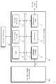
도 1은 본 발명의 일 실시 예에 따른 불휘발성 메모리 장치의 블록도를 예시적으로 도시한다. 도 1을 참조하면, 불휘발성 메모리 장치(100)는 메모리 셀 어레이(110), 행 디코더 회로(120), 페이지 버퍼 회로(130), 제어 로직 회로(150), 및 데이터 입출력 회로(140)를 포함한다.1 exemplarily shows a block diagram of a nonvolatile memory device according to an embodiment of the present invention. Referring to FIG. 1 , the
메모리 셀 어레이(110)는 복수의 메모리 블록들(BLK1~BLKz; z는 양의 정수)을 포함할 수 있다. 복수의 메모리 블록들(BLK1~BLKz) 각각은 복수의 메모리 셀들을 포함할 수 있다. 메모리 블록들(BLK1~BLKz) 각각은 행 디코더 회로(120)로 적어도 하나의 접지 선택 라인(GSL), 워드라인들(WL), 및 적어도 하나의 스트링 선택 라인(SSL)을 통해 연결될 수 있다. 메모리 블록들(BLK1~BLKz) 각각은 복수의 비트라인들(BL)을 통해 페이지 버퍼 회로(130)로 연결될 수 있다. 메모리 블록들(BLK1~BLKz)은 복수의 비트라인들(BL)에 공통으로 연결될 수 있다.The
행 디코더 회로(120)는 메모리 셀 어레이(110)로 접지 선택 라인들(SSL), 워드라인들(WL), 및 접지 선택 라인들(GSL)을 통해 연결될 수 있다. 행 디코더 회로(120)는 제어 로직 회로(150)의 제어 하에 동작할 수 있다.The
행 디코더 회로(120)는 불휘발성 메모리 장치(100)의 외부 장치로부터 수신되는 행 어드레스(RA)를 수신하고 그리고 수신된 행 어드레스(RA)를 디코딩할 수 있다. 행 디코더 회로(120)는 디코딩된 행 어드레스에 기초하여 메모리 셀 어레이(110로 연결된 워드라인들(WL) 중 어느 하나를 선택할 수 있다. 행 디코더 회로(120)는 디코딩된 행 어드레스에 기초하여 스트링 선택 라인들(SSL), 워드라인들(WL), 및 접지 선택 라인들(GSL)로 인가되는 전압들을 조절할 수 있다.The
페이지 버퍼 회로(130)는 메모리 셀 어레이(110)로 복수의 비트라인들(BL)을 통해 연결될 수 있다. 페이지 버퍼 회로(130)는 데이터 입출력 회로(140)로 복수의 데이터 라인들(DL)을 통해 연결될 수 있다. 페이지 버퍼 회로(130)는 제어 로직 회로(150)의 제어 하에 동작할 수 있다.The
예를 들어, 프로그램 동작이 수행될 때, 페이지 버퍼 회로(130)는 메모리 셀 어레이(110)의 메모리 셀들에 쓰여질 데이터를 저장할 수 있다. 페이지 버퍼 회로(130)는 저장된 데이터에 기초하여 복수의 비트라인들(BL)에 전압들을 인가할 수 있다. 읽기 동작이 수행될 때, 또는 프로그램 동작 또는 소거 동작의 검증 읽기 동작이 수행될 때, 페이지 버퍼 회로(130)는 비트라인들(BL)의 전압들을 감지하고, 그리고 감지 결과를 저장할 수 있다.For example, when a program operation is performed, the
데이터 입출력 회로(140)는 페이지 버퍼 회로(130)로 복수의 데이터 라인들(DL)을 통해 연결될 수 있다. 데이터 입출력 회로(140)는 제어 로직 회로(150)의 제어 하에 동작할 수 있다. 데이터 입출력 회로(140)는 열 어드레스(CA)를 불휘발성 메모리 장치(100)의 외부 장치로부터 수신할 수 있다. 데이터 입출력 회로(140)는 열 어드레스(CA)에 대응하는, 페이지 버퍼 회로(130)에 의해 읽힌 데이터를 출력할 수 있다. 데이터 입출력 회로(140)는 열 어드레스(CA)에 기초하여, 불휘발성 메모리 장치(100)의 외부 장치로부터 수신되는 데이터를 페이지 버퍼 회로(130)로 데이터 라인들(DL)을 통해 전송할 수 있다.The data input/
제어 로직 회로(150)는 불휘발성 메모리 장치(100)의 외부 장치(예를 들어, 도 17의 메모리 컨트롤러(10))로부터 커맨드(CMD)를 수신할 수 있다. 제어 로직 회로(150)는 제어 신호(CTRL)를 외부 장치와 교환할 수 있다. 제어 로직 회로(150)는 수신된 커맨드(CMD)를 디코딩할 수 있다. 제어 로직 회로(150)는 디코딩된 커맨드에 기초하여, 행 디코더 회로(120), 페이지 버퍼 회로(130), 및 데이터 입출력 회로(140)를 제어할 수 있다.The
제어 로직 회로(150)는 전압 발생기(151)를 더 포함할 수 있다. 전압 발생기(151)는 외부 장치로부터 구동 전압(VDD)을 수신할 수 있다. 전압 발생기(151)는 불휘발성 메모리 장치(100)의 프로그램 동작, 소거 동작, 또는 읽기 동작에 필요한 다양한 전압들을 구동 전압(VDD)에 기초하여 생성할 수 있다. 전압 발생기(151)는 생성된 전압들을 불휘발성 메모리 장치(100)의 구성 요소들로 각각 제공할 수 있다.The
도 2는 도 1의 메모리 블록 및 페이지 버퍼 회로의 블록도를 좀 더 구체적으로 도시한다. 도 2는 도 1의 메모리 블록들(BLK1~BLKz) 중 메모리 블록(BLKy; y는 1 이상 z 이하의 양의 정수) 및 페이지 버퍼 회로(130)를 예시적으로 도시한다. 도시의 편의 상, 메모리 셀 어레이(110)에 포함된 다른 메모리 블록들 및 불휘발성 메모리 장치(100)의 다른 구성들의 도시가 생략된다.FIG. 2 shows a block diagram of the memory block and page buffer circuit of FIG. 1 in more detail. FIG. 2 exemplarily shows a memory block BLKy (y is a positive integer greater than or equal to 1 and less than or equal to z) among the memory blocks BLK1 to BLKz of FIG. 1 and the
도 1 및 도 2를 참조하면, 메모리 블록(BLKy)은 복수의 비트라인들(BL0~BLn-1)로 각각 연결된 복수의 셀 스트링들을 포함할 수 있다. 각각의 셀 스트링은 스트링 선택 라인(SSL)으로 연결된 스트링 선택 트랜지스터(SST), 복수의 워드라인들(WL0~WLm-1; m은 양의 정수)로 각각 연결된 메모리 셀들(MC), 및 접지 선택 라인(GSL)으로 연결된 접지 선택 트랜지스터(GST)를 포함할 수 있다. 복수의 셀 스트링들에 각각 포함된 접지 선택 트랜지스터들(GST)의 소스 단은 공통 소스 라인(CSL)으로 연결될 수 있다.1 and 2 , the memory block BLKy may include a plurality of cell strings respectively connected to a plurality of bit lines BL0 to BLn-1. Each cell string includes a string select transistor SST connected through a string select line SSL, memory cells MC connected through a plurality of word lines WL0 to WLm-1 (m is a positive integer), and a ground selector. It may include a ground select transistor GST connected to the line GSL. Source terminals of the ground select transistors GST included in each of the plurality of cell strings may be connected to a common source line CSL.
페이지 버퍼 회로(130)는 복수의 비트라인들(BL0~BLn-1; n은 양의 정수)로 각각 연결되는 복수의 페이지 버퍼들(PB0~PBn-1)을 포함할 수 있다. 복수의 페이지 버퍼들(PB0~PBn-1) 각각은 대응하는(또는 연결된) 비트라인으로 전압을 인가할 수 있다. 복수의 페이지 버퍼들(PB0~PBn-1) 각각은 대응하는 비트라인에 연결된 메모리 셀들에 저장된 데이터를 감지할 수 있고, 그리고 감지된 데이터를 저장할 수 있다.The
도 3은 도 2의 페이지 버퍼의 블록도를 좀 더 구체적으로 도시한다. 예를 들어, 페이지 버퍼 회로(130)의 복수의 페이지 버퍼들(PB0~PBn-1) 중 페이지 버퍼(PBr; r은 n보다 작은 음이 아닌 정수)의 구체적인 블록도를 도시한다. 페이지 버퍼(PBr)뿐만 아니라, 나머지 복수의 페이지 버퍼들도 도 3에 도시된 바와 유사하게 구현되고, 그리고 유사하게 동작할 수 있다.FIG. 3 shows a block diagram of the page buffer of FIG. 2 in more detail. For example, a detailed block diagram of a page buffer PBr (r is a non-negative integer less than n) among the plurality of page buffers PB0 to PBn-1 of the
도 1 내지 도 3을 참조하면, 페이지 버퍼(PBr)는 비트라인 선택 블록(310), 비트라인 프리차지 블록(320), 트랜지스터(MPASS), 센싱 노드 프리차지 블록(330), 래치 블록(340), 메인 감지 래치(350), 인접 감지 래치(360), 및 데이터 블록(370)을 포함한다.1 to 3 , the page buffer PBr includes a bit
비트라인 선택 블록(310)은 페이지 버퍼(PBr)에 대응하는 비트라인(BLr) 및 노드(N1) 사이에 연결될 수 있다. 비트라인 선택 블록(310)은 제어 로직 회로(150)로부터 비트라인 선택 신호(BLSLT)를 수신할 수 있다. 비트라인 선택 블록(310)은 비트라인 선택 신호(BLSLT)에 응답하여, 비트라인(BLr)을 노드(N1)와 전기적으로 연결하거나 또는 분리할 수 있다. The bit
비트라인 프리차지 블록(320)은 노드(N1)로 연결될 수 있다. 비트라인 프리차지 블록(320)은 제어 로직 회로(150)로부터 비트라인 프리차지 신호(BLPRE)를 수신할 수 있다. 비트라인 프리차지 블록(320)은 비트라인 프리차지 신호(BLPRE)에 응답하여, 노드(N1)로 비트라인 프리차지 전압(예를 들어, 도 8a의 VPRCG)을 인가할 수 있다. 이에 따라 비트라인 선택 블록(310)에 연결된 비트라인(BLr)이 비트라인 프리차지 전압으로 충전될 수 있다. 비트라인 프리차지 전압은 전압 발생기(151)로부터 공급될 수 있다.The bit line
트랜지스터(MPASS)는 노드(N1)로 연결된 제 1 단(예를 들어, 드레인), 신호(PASS)가 연결되는 게이트, 및 센싱 노드(SO)가 연결되는 제 2 단(예를 들어, 소스)을 포함할 수 있다. 트랜지스터(PASS)는 제어 로직 회로(150)로부터 인가되는 신호(PASS)에 응답하여, 턴-온 되거나 또는 턴-오프될 수 있다. 제어 로직 회로(150)는 신호(PASS)를 생성하여 트랜지스터(MPASS)로 공급함으로써, 페이지 버퍼들(PB0~PBn-1)에 각각 포함된 복수의 센싱 노드들을 각각이 대응하는 비트라인으로 전기적으로 연결하거나 또는 각각이 대응하는 비트라인으로부터 전기적으로 분리(또는 연결 해제)할 수 있다.The transistor MPASS has a first terminal (eg, drain) connected to the node N1 , a gate connected to the signal PASS, and a second terminal (eg, source) connected to the sensing node SO. may include The transistor PASS may be turned on or turned off in response to the signal PASS applied from the
트랜지스터(MPASS)가 턴-온 되면, 비트라인(BLr)이 센싱 노드(SO)로 전기적으로 연결될 수 있다. 이에 따라, 센싱 노드(SO)의 전압 레벨이 비트라인(BLr)의 전압 레벨에 따라 변화할 수 있다. 트랜지스터(PASS)가 턴-오프되면, 비트라인(BLr)은 센싱 노드(SO)와 전기적으로 분리될 수 있다. 이에 따라, 센싱 노드(SO)의 전압 레벨은 비트라인(BLr)의 전압 레벨에 의해 영향을 받지 않을 수 있다.When the transistor MPASS is turned on, the bit line BLr may be electrically connected to the sensing node SO. Accordingly, the voltage level of the sensing node SO may change according to the voltage level of the bit line BLr. When the transistor PASS is turned off, the bit line BLr may be electrically isolated from the sensing node SO. Accordingly, the voltage level of the sensing node SO may not be affected by the voltage level of the bit line BLr.
센싱 노드 프리차지 블록(330)은 센싱 노드(SO)로 연결된다. 센싱 노드 프리차지 블록(330)은 센싱 노드 프리차지 신호(SOPRE)를 제어 로직 회로(150)로부터 수신할 수 있다. 센싱 노드 프리차지 블록(330)은 센싱 노드 프리차지 신호(SOPRE)에 응답하여, 센싱 노드(SO)로 센싱 노드 프리차지 전압을 인가할 수 있다. 이에 따라 센싱 노드(SO)가 센싱 노드 프리차지 전압으로 충전될 수 있다. 센싱 노드 프리차지 전압은 전압 발생기(151)로부터 공급될 수 있다The sensing node
래치 블록(340)은 센싱 노드(SO)에 연결되고, 그리고 메인 감지 래치(350) 및 인접 감지 래치(360)로 연결된다. 래치 블록(340)은 제어 로직 회로(150)로부터 래치 신호(SLAT)를 수신할 수 있다. 래치 블록(340)은 래치 신호(SLAT)에 응답하여, 센싱 노드(SO)의 전압 레벨을 메인 감지 래치(350) 및 인접 감지 래치(360)로 전달할 수 있다. 래치 블록(340)은 래치 신호(SLAT)에 응답하여, 센싱 노드(SO)의 전압 레벨을 기준 전압과 비교할 수 있다.The
일 실시 예에 있어서, 래치 블록(340)은 래치 신호(SLAT)가 인가되는 게이트 및 접지 전압이 인가되는 소스를 갖는 제 1 트랜지스터 및 제 1 트랜지스터의 드레인에 연결되는 소스, 센싱 노드(SO)가 인가되는 게이트 및 노드(NL)로 연결되는 드레인을 포함하는 제 2 트랜지스터를 포함할 수 있다. 하이 레벨의 래치 신호(SLAT)에 응답하여, 제 1 트랜지스터가 턴-온될 수 있다. 기준 전압 이상의 센싱 노드(SO) 전압에 응답하여, 제 2 트랜지스터가 턴-온 될 수 있다. 예를 들어, 기준 전압은 제 2 트랜지스터의 문턱 전압일 수 있다. 래치 블록(340)으로부터 메인 감지 래치(350) 및 인접 감지 래치(360)로 전달되는 전압(즉, 노드(NL)의 전압)은 제 2 트랜지스터가 턴-온되는지 여부에 기초할 수 있다. 이에 따라, 래치 블록(340)은 메인 감지 래치(350) 및 인접 감지 래치(360)를 셋 또는 리셋할 수 있다.In an embodiment, the
메인 감지 래치(350)는 센싱 노드(SO) 및 래치 블록(340)에 연결될 수 있다. 메인 감지 래치(350)는 센싱 노드(SO)의 전압 레벨의 변화에 기초하여, 선택 메모리 셀들에 저장된 데이터를 래치할 수 있다. 예를 들어, 메인 감지 래치(350)는 래치 블록(340)에서 수행되는 비교 결과에 기초하여 제 1 논리 값 또는 제 2 논리 값 중 어느 하나를 노드(NS1)에 래치할 수 있다. 메인 감지 래치(350)는 바이어스 블록(351), 덤프 블록(352), 인버터들(353, 354), 트랜지스터들(355, 356), 및 리셋 블록(357)을 포함할 수 있다.The
바이어스 블록(351)은 센싱 노드(SO) 및 노드(NS1)로 연결될 수 있다. 바이어스 블록(351)은 제어 로직 회로(150)로부터 바이어스 신호(SLBS)를 수신할 수 있다. 바이어스 블록(351)은 수신된 바이어스 신호(SLBS)에 응답하여, 센싱 노드(SO)를 노드(NS1)에 대응하는 데이터에 기초하여 방전(Discharge)시킬 수 있다.The
일 실시 예에 있어서, 바이어스 블록(351)은 센싱 노드(SO)로 연결된 제 1 단(예를 들어, 드레인), 바이어스 신호(SLBS)가 인가되는 게이트, 및 제 2 단(예를 들어, 소스)을 포함하는 바이어스 트랜지스터를 포함할 수 있다. 바이어스 트랜지스터는 바이어스 신호(SLBS)의 전압 레벨에 따라 턴-온되거나 또는 턴-오프될 수 있다. 바이어스 블록(351)은 바이어스 트랜지스터의 제 2 단으로 연결된 제 1 단(예를 들어, 소스), 노드(NS1)로 연결된 게이트, 및 접지 전압으로 연결된 제 2 단(예를 들어, 드레인)을 포함하는 트랜지스터를 포함할 수 있다. 이에 따라, 바이어스 블록(351)은 노드(NS1)에 대응하는 데이터 및 바이어스 신호(SLBS)의 전압 레벨에 기초하여 센싱 노드(SO)의 전압 레벨을 접지 전압으로 방전하거나, 또는 센싱 노드(SO)의 전압 레벨을 방치할 수 있다. 그러나 상술된 실시 예는 예시적인 것으로, 바이어스 블록(351)의 구성은 이에 제한되지 아니한다.In an embodiment, the
덤프 블록(352)은 센싱 노드(SO) 및 노드(NS1)로 연결될 수 있다. 덤프 블록(352)은 덤프 신호(SLDS)에 응답하여, 노드(NS1)에 대응하는 데이터를 데이터 블록(370) 또는 인접 감지 래치(360)로 전달할 수 있다.The
일 실시 예에 있어서, 덤프 블록(352)은 센싱 노드(SO)로 연결되는 제 1 단(예를 들어, 소스), 덤프 신호(SLDS)가 인가되는 게이트, 및 노드(NS1)로 연결되는 제 2 단(예를 들어, 드레인)을 포함하는 덤프 트랜지스터를 포함할 수 있다. 덤프 트랜지스터는 덤프 신호(SLDS)의 전압 레벨에 따라 턴-온되거나 또는 턴-오프될 수 있다. 덤프 트랜지스터의 동작으로 인하여, 노드(NS1)에 저장된 데이터가 센싱 노드(SO)를 거쳐 데이터 블록(370) 또는 인접 감지 래치(360)로 전달될 수 있다. 그러나 상술된 실시 예는 예시적인 것으로, 덤프 블록(352)의 구성은 이에 제한되지 아니한다.In an embodiment, the
인버터들(353, 354) 각각은 노드들(NS0, NS1) 사이에 연결될 수 있다. 인버터(353)의 입력단은 노드(NS0)에 연결될 수 있고, 그리고 인버터(353)의 출력단은 노드(NS1)에 연결될 수 있다. 인버터(354)의 입력단은 노드(NS1)에 연결될 수 있고, 그리고 인버터(354)의 출력단은 노드(NS0)에 연결될 수 있다. 이에 따라, 노드들(NS0, NS1)의 전압 레벨들은 서로 반대되는 논리 값들에 각각 대응할 수 있다. 이하에서, 메인 감지 래치(350)에 래치된 데이터는 바이어스 블록(351)으로 연결된 노드(NS1)에 저장된 데이터에 대응하는 것으로 이해될 것이다.Each of the
셋 트랜지스터(355)는 노드(NS0) 및 래치 블록(340) 사이에 연결될 수 있다. 셋 트랜지스터(355)는 제어 로직 회로(150)로부터 수신되는 셋 신호(SET_S)가 인가되는 게이트를 포함할 수 있다. 셋 신호(SET_S)의 전압 레벨에 응답하여, 셋 트랜지스터(355)가 턴-온 또는 턴-오프될 수 있다. 셋 트랜지스터(355)가 턴-온 되면, 래치 블록(340)으로부터 전달되는 센싱 노드(SO)의 전압 또는 리셋 블록(357)으로부터 전달되는 전압에 기초한 전압이 노드(NS0)로 전달될 수 있다.The
리셋 트랜지스터(356)는 노드(NS1) 및 래치 블록(340) 사이에 연결될 수 있다. 리셋 트랜지스터(356)는 제어 로직 회로(150)로부터 수신되는 리셋 신호(SET_R)가 인가되는 게이트를 포함할 수 있다. 리셋 신호(SET_R)의 전압 레벨에 응답하여, 리셋 트랜지스터(356)가 턴-온 또는 턴-오프될 수 있다. 리셋 트랜지스터(356)가 턴-온 되면, 래치 블록(340)으로부터 전달되는 센싱 노드(SO)의 전압 또는 리셋 블록(357)으로부터 전달되는 전압에 기초한 전압이 노드(NS1)로 전달될 수 있다.The
리셋 블록(357)은 셋 트랜지스터(355) 및 리셋 트랜지스터(356)로 연결될 수 있다. 리셋 블록(357)은 제어 로직 회로(150)로부터 래치 리셋 신호(SRSTS)를 수신할 수 있다. 리셋 블록(357)은 래치 리셋 신호(SRSTS)에 응답하여, 접지 전압을 셋 트랜지스터(355) 및 리셋 트랜지스터(356)로 전달할 수 있다.The
인접 감지 래치(360)는 센싱 노드(SO) 및 래치 블록(340)에 연결될 수 있다. 인접 감지 래치(360)는 센싱 노드(SO)의 전압 레벨의 변화에 기초하여, 인접 메모리 셀들에 저장된 데이터를 래치할 수 있다. 인접 감지 래치(360)는 바이어스 블록(361), 덤프 블록(362), 인버터들(363, 364), 트랜지스터들(365, 366), 및 리셋 블록(367)을 포함할 수 있다. 이하에서, 인접 감지 래치(360)에 래치된 데이터는 바이어스 블록(361)으로 연결된 노드(NF1)에 저장된 데이터에 대응하는 것으로 이해될 것이다.The
인접 감지 래치(360)의 구성 요소들(361~367)은 메인 감지 래치(350)의 구성 요소들(351~357)과 각각 유사한 방식으로 구현될 수 있고, 그리고 유사한 방식으로 동작할 수 있다. 예를 들어, 인접 감지 래치(360)의 바이어스 블록(361), 덤프 블록(362), 인버터들(363, 364), 트랜지스터들(365, 366), 및 리셋 블록(367)은 메인 감지래치(350)의 바이어스 블록(351), 덤프 블록(352), 인버터들(353, 354), 트랜지스터들(355, 356), 및 리셋 블록(357)에 각각 대응할 수 있다. 신호들(SLBS, SLDS, SET_S, RST_S, SRSTS)은 신호들(SLBF, SLDF, SET_F, RST_F, SRSTF)에 각각 대응할 수 있다. 노드들(NS0, NS1)은 각각 노드들(NF0, NF1)에 대응할 수 있다.Components 361 - 367 of
데이터 블록(370)은 센싱 노드(SO)로 연결될 수 있다. 데이터 블록(370)은 메인 감지 래치(350) 및 인접 감지 래치(360)에 저장된 데이터를 센싱 노드(SO)를 통해 수신할 수 있다. 일 실시 예에 있어서, 데이터 블록(370)은 수신된 데이터를 저장할 수 있는 래치로서 구현될 수 있다. 데이터 블록(370)은 수신된 데이터를 래치 데이터 출력 신호(SLD)에 응답하여 데이터 입출력 회로(140)로 전송할 수 있다.The data block 370 may be connected to the sensing node SO. The data block 370 may receive data stored in the
도 3에 도시된 바와 달리, 페이지 버퍼(PBr)는 센싱 노드(SO)로 연결된 둘 이상의 래치들을 더 포함할 수 있다. 일 실시 예에 있어서, 페이지 버퍼(PBr)는 메인 감지 래치(350)에 저장된 데이터를 누적하기 위한 래치를 더 포함할 수 있다. 이때, 덤프 블록들(352, 362)은 센싱 노드(SO)를 통해 도시되지 않은 래치들로 노드들(NS1, NF1)에 대응하는 데이터를 전달할 수 있다. 데이터 블록(370)은 도시되지 않은 래치들로부터 센싱 노드(SO)를 통해 데이터를 수신할 수 있다.3 , the page buffer PBr may further include two or more latches connected to the sensing node SO. In an embodiment, the page buffer PBr may further include a latch for accumulating data stored in the
도 4는 도 3의 페이지 버퍼의 블록도의 일부를 좀 더 구체적으로 도시한다. 도 1 내지 도 4를 참조하면, 도 3의 센싱 노드 프리차지 블록(330a)은 스위치들(SW1, SW2)을 더 포함할 수 있다. 설명의 편의 상, 페이지 버퍼(PBr)의 다른 구성들(예를 들어, 도 3의 비트라인 선택 블록(310) 등)의 도시가 생략된다.FIG. 4 shows a portion of a block diagram of the page buffer of FIG. 3 in more detail. 1 to 4 , the sensing
도 3의 센싱 노드 프리차지 신호(SOPRE) 는 도 4의 센싱 노드 차단 신호들(SOPRE1, SOPRE2)을 포함할 수 있다. 스위치(SW1)는 센싱 노드 차단 신호(SOPRE1)에 응답하여 센싱 노드(SO)로 전압(VCC)을 전달할 수 있다. 스위치(SW2)는 센싱 노드 차단 신호(SOPRE2)에 응답하여 센싱 노드(SO)로 전압(VSS)을 전달할 수 있다. 이에 따라, 센싱 노드 프리차지 블록(330a)은 제어 로직 회로(150)의 제어 하에, 센싱 노드(SO)를 전압(VCC)으로 충전(또는 프리차지)하거나, 또는 전압(VSS)으로 방전시킬 수 있다. 그러나, 센싱 노드 프리차지 블록(330)이 구현되는 방식은 도 4의 센싱 노드 프리차지 블록(330a)의 구성에 제한되지 아니한다.The sensing node precharge signal SOPRE of FIG. 3 may include the sensing node blocking signals SOPRE1 and SOPRE2 of FIG. 4 . The switch SW1 may transmit the voltage VCC to the sensing node SO in response to the sensing node blocking signal SOPRE1 . The switch SW2 may transmit the voltage VSS to the sensing node SO in response to the sensing node blocking signal SOPRE2 . Accordingly, the sensing
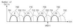
도 5a는 본 발명의 일 실시 예에 따라 인접 워드라인이 프로그램되기 전 선택 워드라인에 연결된 선택 메모리 셀들의 문턱 전압 분포들을 예시적으로 도시한다. 도 5b는 본 발명의 일 실시 예에 따라 인접 워드라인에 연결된 인접 메모리 셀들이 프로그램된 후 선택 워드라인에 연결된 선택 메모리 셀들의 문턱 전압 분포들을 예시적으로 도시한다. 도시된 실시 예에서, 1-비트 데이터가 하나의 메모리 셀에 저장될 수 있으나, 본 발명은 이에 제한되지 아니한다. 예를 들어, 하나의 메모리 셀에는 X-비트(X는 1 이상의 정수)의 데이터가 저장될 수 있다.5A exemplarily illustrates threshold voltage distributions of selected memory cells connected to a selected word line before an adjacent word line is programmed according to an embodiment of the present invention. 5B exemplarily illustrates threshold voltage distributions of selected memory cells connected to a selected word line after adjacent memory cells connected to an adjacent word line are programmed according to an embodiment of the present invention. In the illustrated embodiment, 1-bit data may be stored in one memory cell, but the present invention is not limited thereto. For example, data of X-bits (X is an integer greater than or equal to 1) may be stored in one memory cell.
도 1 내지 도 3, 도 5a 및 도 5b를 참조하면, 곡선들(500, 510)은, 선택 워드라인(WLk)에 연결된 선택 메모리 셀들이 프로그램된 후 및 인접 워드라인(WLk-1)에 연결된 인접 메모리 셀들이 프로그램 되기 전에, 선택 메모리 셀들 중 소거 상태(E)인 메모리 셀들 및 프로그램 상태(P1)인 메모리 셀들의 문턱 전압 산포들을 각각 나타낼 수 있다. 이 경우, 행 디코더 회로(120)에 의해 읽기 전압(VRDi)이 선택 워드라인(WLk)에 인가되면, 상태(E)인 메모리 셀들 및 상태(P1)로 프로그램된 메모리 셀들이 구분될 수 있다.1 to 3 , 5A and 5B , curves 500 and 510 are formed after the selected memory cells connected to the selected word line WLk are programmed and connected to the adjacent word line WLk-1. Before adjacent memory cells are programmed, threshold voltage distributions of memory cells in the erase state (E) and memory cells in the program state (P1) among the selected memory cells may be respectively indicated. In this case, when the read voltage VRDi is applied to the selected word line WLk by the
인접 워드라인(WLk-1)에 연결된 인접 메모리 셀들이 프로그램되면, 선택 메모리 셀들의 문턱 전압 산포가 도 5b에 도시된 바와 같이 변할 수 있다. 예를 들어, 곡선(500)에 속한 메모리 셀들(즉, 상태(E)인 셀들)은 곡선(501) 또는 곡선(502)이 되고, 그리고 곡선(510)에 속한 메모리 셀들(즉, 상태(P1)로 프로그램된 셀들)은 곡선(511) 또는 곡선(512)이 될 수 있다. 이때, 선택 메모리 셀들의 문턱 전압들이 변화되는 정도는 인접 메모리 셀들이 각각 프로그램되는 상태에 영향을 받을 수 있다. 예를 들어, 곡선(500)에 속하는 메모리 셀들 중 인접 메모리 셀들로부터 커플링을 적게 받은 메모리 셀들은 곡선(501)에 속하고, 그리고 인접 메모리 셀들로부터 커플링을 많이 받은 셀들은 곡선(502)에 속할 수 있다.When the adjacent memory cells connected to the adjacent word line WLk-1 are programmed, the threshold voltage distribution of the selected memory cells may be changed as shown in FIG. 5B . For example, memory cells belonging to curve 500 (ie, cells in state E) become
도 5a 및 도 5b를 비교하면, 인접 워드라인(WLk-1)에 연결된 인접 메모리 셀들에 대한 프로그램 동작으로 인해, 선택 메모리 셀들의 문턱 전압 산포들이 넓어질 수 있다. 이에 따라, 인접 워드라인(WLk-1)에 연결된 인접 메모리 셀들에 대한 프로그램 동작이 수행되기 이전과는 달리, 읽기 전압(VRD)을 검증 전압으로서 사용할 경우 읽기 동작의 정확도가 떨어질 수 있다.5A and 5B , the threshold voltage distributions of the selected memory cells may be widened due to a program operation on the adjacent memory cells connected to the adjacent word line WLk-1. Accordingly, unlike before the program operation on the adjacent memory cells connected to the adjacent word line WLk-1 is performed, when the read voltage VRD is used as the verification voltage, the accuracy of the read operation may be deteriorated.
도시된 실시 예에서, 워드라인들(WL)에 각각 연결된 메모리 셀들이 내림차순(또는 오름차순)으로 프로그램될 수 있다. 다시 말해서, 'k'번째 워드라인인 선택 워드라인(WLk)에 연결된 선택 메모리 셀들이 프로그램된 이후에, 'k-1'번째(또는, 'k+1'번째) 워드라인인 인접 워드라인(WLk-1; 또는 WLk+1)에 연결된 인접 메모리 셀들이 프로그램될 수 있다. 이에 따라, 선택 워드라인(WLk)에 연결된 선택 메모리 셀들의 문턱 전압들은 인접 워드라인(WLk-1; 또는 WLk+1)에 연결된 메모리 셀들이 프로그램될 때 선택 메모리 셀들 및 인접 메모리 셀들 사이 전하 커플링 등과 같은 요소들로 인하여 이동할 수 있다. 선택 워드라인(WLk)에 연결된 선택 메모리 셀들의 문턱 전압들에 영향을 주는 워드라인은, 워드라인들(WL)이 프로그램되는 순서에 따라 가변될 수 있다.In the illustrated embodiment, memory cells respectively connected to the word lines WL may be programmed in a descending order (or an ascending order). In other words, after the selected memory cells connected to the selected word line WLk, which is the 'k'th word line, are programmed, the adjacent word line ( The adjacent memory cells connected to WLk-1 (or WLk+1) may be programmed. Accordingly, the threshold voltages of the selected memory cells connected to the selected word line WLk are charge-coupled between the selected memory cells and the adjacent memory cells when the memory cells connected to the adjacent word line WLk-1 (or WLk+1) are programmed. It can move due to factors such as A word line that affects threshold voltages of selected memory cells connected to the selected word line WLk may vary according to the order in which the word lines WL are programmed.
도 6은 인접 워드라인에 연결된 인접 메모리 셀들의 문턱 전압 분포들을 예시적으로 도시한다. 도시된 실시 예에서, 3-비트 데이터가 하나의 메모리 셀에 저장될 수 있으나, 본 발명은 이에 제한되지 아니한다 도 1, 도 2, 도 5a, 도 5b, 및 도 6을 참조하면, 인접 워드라인(WLk-1)에 연결된 인접 메모리 셀들은 상태들(E, P1~P7) 중 어느 한 상태로 각각 프로그램될 수 있다. 곡선들(600, 610, 620, 630, 640, 650, 660, 670)은 소거 상태(E)인 인접 메모리 셀들 및 프로그램 상태들(P1, P2, P3, P4, P5, P6, P7)로 프로그램된 인접 메모리 셀들의 문턱 전압들을 각각 나타낼 수 있다.6 exemplarily illustrates threshold voltage distributions of adjacent memory cells connected to adjacent word lines. In the illustrated embodiment, 3-bit data may be stored in one memory cell, but the present invention is not limited thereto. Referring to FIGS. 1, 2, 5A, 5B, and 6, adjacent wordlines The adjacent memory cells connected to WLk-1 may be programmed into any one of the states E and P1 to P7, respectively.
일 실시 예에 있어서, 인접 워드라인(WLk-1)에 연결된 인접 메모리 셀들은 선택 메모리 셀들에 간섭하는 정도(또는 선택 메모리 셀들에 가해지는 커플링의 정도)에 따라 공격 셀(aggressor cell) 또는 비-공격 셀(non-aggressor cell) 중 어느 하나로 분류될 수 있다. 예를 들어, 공격 셀들은 선택 메모리 셀들에 간섭하는 정도가 비-공격 셀들에 비해 상대적으로 클 수 있다.In an embodiment, the adjacent memory cells connected to the adjacent word line WLk-1 are either an aggressor cell or a non-aggressor cell according to the degree of interference with the selected memory cells (or the degree of coupling applied to the selected memory cells). -Can be classified as any one of aggressor cells (non-aggressor cell). For example, attack cells may have a relatively large degree of interference with selected memory cells compared to non-attack cells.
인접 메모리 셀들 중 문턱 전압이 상대적으로 높게 프로그램되는 셀들은, 프로그램될 때 각각이 연결된 컨트롤 게이트로 인가되는 전압이 상대적으로 더 크다. 따라서, 해당 셀들로부터의 커플링이 문턱 전압이 상대적으로 낮도록 프로그램되는 셀들로부터의 커플링보다 클 수 있다. 이에 따라, 도시된 실시 예에서, 문턱 전압이 전압(VSA)보다 높은 셀들, 즉 곡선들(640~670)에 속한 셀들은 공격 셀들로 분류되고, 그리고 문턱 전압이 전압(VSA)보다 낮은 셀들, 즉 곡선들(600~630)에 속한 셀들은 비-공격 셀들로 분류될 수 있다.Among the adjacent memory cells, cells having a relatively high threshold voltage are programmed to have a relatively higher voltage applied to the connected control gate when programmed. Accordingly, coupling from the corresponding cells may be greater than coupling from cells programmed to have a relatively low threshold voltage. Accordingly, in the illustrated embodiment, cells having a threshold voltage higher than the voltage VSA, that is, cells belonging to the
인접 메모리 셀들이 분류될 수 있는 그룹의 수는 도시된 실시 예에 제한되지 아니한다. 예를 들어, 도시된 바와 달리 2개 이상의 전압을 사용하여 인접 메모리 셀들을 분류할 수도 있다. 이에 따라, 인접 메모리 셀들은 3개 이상의 그룹들(예를 들어, 공격 셀, 중간-공격 셀(intermediate-aggressor cell), 및 비-공격 셀)로 분류될 수 있다.The number of groups into which adjacent memory cells can be classified is not limited to the illustrated embodiment. For example, unlike illustrated, adjacent memory cells may be classified using two or more voltages. Accordingly, adjacent memory cells may be classified into three or more groups (eg, an attack cell, an intermediate-aggressor cell, and a non-attack cell).
전압(VSA)의 레벨 또한 도시된 실시 예에 제한되지 아니한다. 예를 들어, 도시된 바와 달리 전압(VSA)의 레벨은 곡선(640)과 곡선(650) 사이로 결정될 수도 있다. 일 실시 예에 있어서, 인접 메모리 셀들이 분류될 수 있는 그룹의 수 및 인접 메모리 셀들을 분류하는 데 사용되는 전압의 레벨은 제어 로직 회로(150)에 의해 조절될 수 있다.The level of the voltage VSA is also not limited to the illustrated embodiment. For example, unlike illustrated, the level of the voltage VSA may be determined between the
도 7a 및 도 7b는 선택 메모리 셀들의 문턱 전압 분포들을 예시적으로 도시한다. 도시된 실시 예에서, 메모리 셀들 각각은 2-비트 데이터를 저장할 수 있으나, 본 발명은 이에 제한되지 아니한다. 도 1 내지 도 3, 도 5a, 도 5b, 도 6, 도 7a, 및 도 7b를 참조하여 본 발명의 일 실시 예에 따른 불휘발성 메모리 장치(100)의 읽기 동작이 설명될 것이다.7A and 7B exemplarily show threshold voltage distributions of selected memory cells. In the illustrated embodiment, each of the memory cells may store 2-bit data, but the present invention is not limited thereto. A read operation of the
선택 메모리 셀들에 대한 읽기 동작(예를 들어, 데이터 리커버리 읽기 동작)은 인접 메모리 셀들에 대한 읽기 결과를 참조하여 불휘발성 메모리 장치(100)에 의해 수행될 수 있다. 예를 들어, 선택 메모리 셀들에 대한 읽기 동작이 수행될 때, 먼저 인접 메모리 셀들에 저장된 데이터들이 페이지 버퍼 회로(130)에 의해 감지될 수 있다. 인접 메모리 셀들은 각각이 감지된 결과에 기초하여, 도 6에서 설명된 방식과 유사하게, 공격 셀 또는 비-공격 셀 중 어느 하나로 각각 분류될 수 있다. 선택 메모리 셀들에 저장된 데이터는 인접 메모리 셀들이 분류된 결과를 참조하여 페이지 버퍼 회로(130)에 의해 감지될 수 있다.A read operation (eg, a data recovery read operation) on selected memory cells may be performed by the
도시된 실시 예에서, 선택 메모리 셀들은 상태(E, P1~P3) 중 어느 한 상태일 수 있다. 곡선들(700, 710, 720, 730)은 각각 상태들(E, P1, P2, P3)인 메모리 셀들의 문턱 전압 분포를 나타낼 수 있다. 인접 워드라인(WLk-1)에 연결된 인접 메모리 셀들이 프로그램되면, 선택 메모리 셀들의 문턱 전압 산포가 인접 메모리 셀들로부터 받는 영향의 크기에 따라 변할 수 있다. 예를 들어, 곡선(700)에 속한 메모리 셀들은 곡선(701) 또는 곡선(702)이 되고, 곡선(710)에 속한 메모리 셀들은 곡선(711) 또는 곡선(712)이 되고, 곡선(720)에 속한 메모리 셀들은 곡선(721) 또는 곡선(722)으이 되고, 그리고 곡선(730)에 속한 메모리 셀들은 곡선(731) 또는 곡선(732)이 될 수 있다.In the illustrated embodiment, the selected memory cells may be in any one of states E and P1 to P3.
곡선들(701, 711, 721 731)에 속한 메모리 셀들은 인접 메모리 셀들로부터 커플링의 영향을 상대적으로 덜 받은 메모리 셀들이고, 그리고 곡선들(703, 713, 723 733)에 속한 메모리 셀들은 인접 메모리 셀들로부터 커플링의 영향을 상대적으로 더 받은 메모리 셀들일 수 있다. 도시된 실시 예에서, 곡선들(721, 731)에 속한 메모리 셀들은 읽기 전압(VRD11)에 의해 구분될 수 있고, 그리고 곡선들(722, 732)에 속한 메모리 셀들은 읽기 전압(VRD22)에 의해 구분될 수 있다. 따라서, 선택 메모리 셀들 중 비-공격 셀들에 인접한 메모리 셀들(예를 들어, 비-공격 셀들과 비트라인을 공유하는 메모리 셀들; 이하, “비-희생(non-victim) 셀들”)로 연결된 셀들(예를 들어, 도 7a에서 실선으로 표시된 곡선들(701, 711, 721, 731)에 속한 메모리 셀들) 및 공격-셀들에 인접한 메모리 셀들(예를 들어, 도 7b에서 실선으로 표시된 곡선들(702, 712, 722, 732)에 속한 메모리 셀들; 이하, “희생(victim) 셀들”)이 서로 다른 시간에 서로 다른 읽기 전압을 사용하여 각각 감지되면, 불휘발성 메모리 장치(100)의 읽기 동작의 정확도가 개선될 수 있다. Memory cells belonging to
도 8a는 본 발명의 일 실시 예에 따라 선택 메모리 셀들에 대한 읽기 동작이 수행됨에 따른 전압 레벨의 변화를 예시적으로 도시한다. 도 1 내지 도 3, 도 5a, 도 5b, 도6, 도 7a, 도 7b, 및 도 8a를 참조하여, 선택 메모리 셀들에 대한 읽기 동작이 수행됨에 따라 인접 워드라인(WLk-1), 선택 워드라인(WLk), 인접 워드라인이 아닌 워드라인(WLk+1), 및 비트라인들(BL)의 전압 레벨의 시간에 따른 변화가 설명될 것이다. 도시된 실시 예에서, 메모리 셀들 각각은 2-비트 데이터를 저장할 수 있으나, 본 발명은 이에 제한되지 아니한다.8A exemplarily illustrates a change in voltage level as a read operation on selected memory cells is performed according to an embodiment of the present invention. 1 to 3, 5A, 5B, 6, 7A, 7B, and 8A, as a read operation is performed on the selected memory cells, the adjacent word line WLk-1 and the selected word The change with time of the voltage level of the line WLk, the non-adjacent word
선택 메모리 셀들에 대한 읽기 동작을 수행할 때, 불휘발성 메모리 장치(100)는 먼저 인접 메모리 셀들에 저장된 데이터를 읽고, 그리고 인접 메모리 셀들의 읽기 결과에 기초하여 인접 메모리 셀들을 공격 셀 및 비-공격 셀로 분류할 수 있다. 그 다음, 불휘발성 메모리 장치(100)는 선택 메모리 셀들 중 비-공격 셀들이 연결된 비트라인들(이하, “제 1 비트라인들”)로 연결된 셀들(즉, 비-희생 셀들)에 저장된 데이터 및 공격 셀들이 연결된 비트라인들(이하, “제 2 비트라인들”)로 연결된 셀들(즉, 희생 셀들)에 저장된 데이터를 서로 다른 시간에 읽을 수 있다. 또한, 불휘발성 메모리 장치(100)는 선택 메모리 셀들에 대한 읽기 동작이 수행될 때, 페이지 버퍼들(PB0~PBn-1)에 포함된 메인 감지 래치들에 선택 메모리 셀들에 저장된 데이터를 적어도 두 번 래치할 수 있다.When performing a read operation on selected memory cells, the
구간(T0)에서는 인접 메모리 셀들에 저장된 데이터가 감지될 수 있다. 구간(T0)에서, 행 디코더 회로(120)에 의해 워드라인들(WL) 중 인접 워드라인(WLk-1)에 전압(VSA)이 인가되고, 그리고 나머지 워드라인들에는 전압(VREAD)이 인가될 수 있다. 전압(VREAD)은 메모리 셀들의 문턱 전압들보다 높은 레벨을 가질 수 있다. 페이지 버퍼 회로(130)는 모든 비트라인들(BL)을 프리차지할 수 있다. 이에 따라, 비트라인들(BL)의 전압 레벨이 전압(VSS)에서 비트라인 프리차지 전압(VPRCG)으로 상승할 수 있다.In the period T0, data stored in adjacent memory cells may be sensed. In the period T0, the voltage VSA is applied to the adjacent word line WLk-1 among the word lines WL by the
행 디코더 회로(120)에 의해 워드라인들(WL)에 대응하는 전압들이 각각 인가됨에 따라, 비트라인들(BL) 각각의 전압 레벨은 각각이 연결된 메모리 셀이 프로그램된 상태, 즉 각각이 연결된 메모리에 저장된 데이터에 기초하여 비트라인 프리차지 전압(VPRCG)을 유지하거나 또는 점진적으로 하강할 수 있다. 예를 들어, 전압(VSA)보다 높은 문턱 전압의 메모리 셀들로 연결된 제 1 비트라인들의 전압들은 비트라인 프리차지 전압(VPRCG)을 유지할 수 있다. 반면에, 전압(VSA)보다 낮거나 같은 문턱 전압의 메모리 셀들로 연결된 제 2 비트라인들의 전압들은 공통 소스 라인(CSL)으로 제 2 비트라인들에 충전된 전하들이 방전됨에 따라 점진적으로 하강할 수 있다.As voltages corresponding to the word lines WL are respectively applied by the
비트라인들(BL)의 전압 레벨의 변화에 기초하여, 비트라인들(BL)로 연결된 센싱 노드들의 전압 레벨이 변화할 수 있다. 센싱 노드들의 전압 레벨의 변화의 크기에 기초하여, 인접 메모리 셀들에 저장된 데이터가 페이지 버퍼 회로(130)에 래치될 수 있다. 예를 들어, 센싱 노드의 전압 레벨이 기준 전압 이하로 하강되면, 대응하는 비트라인으로 연결된 인접 메모리 셀은 온-셀(on-cell)로 판단될 수 있다. 그렇지 않으면, 대응하는 비트라인으로 연결된 인접 메모리 셀은 오프-셀(off-cell)로 판단될 수 있다.Based on the change in the voltage level of the bit lines BL, the voltage level of the sensing nodes connected to the bit lines BL may change. Data stored in adjacent memory cells may be latched in the
제 1 비트라인들로 연결된 페이지 버퍼들의 센싱 노드들의 전압들은 기준 전압 이하로 하강할 수 있다. 이에 따라, 기준 전압 이하로 하강된 센싱 노드들에 대응하는 인접 감지 래치들로 제 1 논리 값(예를 들어, 논리 “0”)이 인접 감지 값으로서 래치될 수 있다(또는, 초기값인 제 1 논리 값이 유지될 수 있다). 반대로, 제 2 비트라인들로 연결된 페이지 버퍼의 인접 감지 래치들로는 제 2 논리 값(예를 들어, 논리 “1”)이 인접 감지 값으로서 래치될 수 있다. 이 경우, 제 1 논리 값 및 제 2 논리 값은 서로 다를 수 있다. 이하에서는, 온-셀에 대응하는 인접 감지 래치들의 바이어스 블록들로 연결된 노드에는 논리 “0”이, 오프-셀에 대응하는 인접 감지 래치들의 바이어스 블록들로 연결된 노드에는 논리 “1”이 래치되는 것으로 가정될 것이나, 본 발명은 이에 제한되지 아니한다.Voltages of sensing nodes of the page buffers connected to the first bit lines may drop below the reference voltage. Accordingly, a first logic value (eg, logic “0”) may be latched as an adjacent detection value by adjacent detection latches corresponding to the sensing nodes that have dropped below the reference voltage (or, the first logic value that is an initial value). 1 logical value can be maintained). Conversely, a second logical value (eg, logic “1”) may be latched as an adjacent detection value by the adjacent detection latches of the page buffer connected to the second bit lines. In this case, the first logical value and the second logical value may be different from each other. Hereinafter, a logic “0” is latched to a node connected by bias blocks of adjacent sensing latches corresponding to on-cell, and a logic “1” is latched to a node connected to bias blocks of adjacent sensing latches corresponding to off-cell. However, the present invention is not limited thereto.
구간들(T11, T12)에서, 상태(P3)로 프로그램된 선택 메모리 셀들 및 상태(P2)로 프로그램된 선택 메모리 셀들이 인접 메모리 셀들에 저장된 데이터에 기초하여 구분될 수 있다. 예를 들어, 구간(T11)에서, 도 7a의 실선으로 표시된 곡선들(721, 731)에 속한 셀들, 즉 비-희생 셀들의 문턱 전압들이 서로 구분될 수 있다. 구간(T12)에서, 도 7b의 실선으로 표시된 곡선들(722, 732)에 속한 셀들, 즉 희생 셀들의 문턱 전압들이 서로 구분될 수 있다.In sections T11 and T12 , the selected memory cells programmed to the state P3 and the selected memory cells programmed to the state P2 may be distinguished based on data stored in adjacent memory cells. For example, in the period T11 , threshold voltages of cells belonging to the
구간(T11)에서, 행 디코더 회로(120)는 선택 워드라인(WLk)으로 읽기 전압(VRD11)을 인가하고, 그리고 선택 워드라인(WLk)이 아닌 워드라인들(예를 들어, 인접 워드라인(WLk-1), 및 워드라인(WLk+1))로 전압(VREAD)을 인가할 수 있다. 페이지 버퍼 회로(130)는 모든 비트라인들(BL)을 다시 비트라인 프리차지 전압(VPRCG)으로 프리차지할 수 있다. 비트라인들(BL) 각각의 전압 레벨은 각각이 연결된 선택 메모리 셀들에 저장된 데이터에 따라 비트라인 프리차지 전압(VPRCG)으로 유지될 수도 있고, 또는 점진적으로 하강할 수 있다. 예를 들어, 문턱 전압이 전압(VRD11)보다 높은 메모리 셀들, 즉 곡선들(731, 732)에 속한 메모리 셀들 및 곡선(722)에 속한 메모리 셀들 중 문턱 전압이 전압(VRD11)보다 높은 일부 메모리 셀들로 연결된 비트라인들의 전압은 변하지 않을 수 있으나, 나머지 비트라인들의 전압은 하강할 수 있다.In the period T11, the
페이지 버퍼 회로(130)는 센싱 노드들 중 제 1 비트라인들(도시된 실시 예에서, 곡선들(701, 711, 721, 731)에 속한 메모리 셀들로 연결된 비트라인들)에 대응하는 센싱 노드들만을 선택적으로 프리차지할 수 있다. 선택적으로 프리차지된 센싱 노드들의 전압 레벨은 각각이 연결된 비트라인의 전압 레벨의 변화에 따라 변할 수 있다. 페이지 버퍼들(PB0~PBn-1)은 센싱 노드들(예를 들어, 도 3의 센싱 노드(SO))의 전압 변화에 대응하는 데이터 값들을 메인 감지 래치들(예를 들어, 도 3의 메인 감지 래치(350))에 각각 래치할 수 있다.The
제 2 비트라인들(도시된 실시 예에서, 곡선(702, 712, 722, 732)에 속한 메모리 셀들로 연결된 비트라인들)로 연결된 센싱 노드들은 프리차지되지 않을 수 있다. 예를 들어, 프리차지되지 않은 센싱 노드들은 접지 전압(VSS)을 유지할 수 있다. 이때, 제 2 비트라인들 중 곡선(732) 및 곡선(722)에 속한 메모리 셀들 중 문턱 전압이 전압(VRD11)보다 높은 일부 메모리 셀들로 연결된 비트라인들의 전압은 비트라인 프리차지 전압(VPRCG)을 유지할 수 있다. 그러나, 이러한 비트라인들에 충전되어 있는 전압에도 불구하고, 이러한 비트라인들에 대응하는 프리차지되지 않은 센싱 노드들의 전압 레벨은 기준 전압보다 상승하지 않을 수 있다. 따라서 곡선(732) 및 곡선(722)에 속한 메모리 셀들 중 문턱 전압이 전압(VRD11)보다 높은 일부 메모리 셀들은 온-셀로 감지될 수 있다.Sensing nodes connected by second bit lines (in the illustrated embodiment, bit lines connected to memory cells belonging to
예를 들어, (a) 이러한 비트라인들은 공통 소스 라인(CSL)으로 연결되지 않고, (b) 비트라인 프리차지 전압(VPRCG) 및 센싱 노드들의 접지 전압(VSS) 사이의 차가 상대적으로 크지 않고, (c) 센싱 노드들에 기생하는 커패시턴스가 비트라인들에 기생하는 커패시턴스보다 작기 때문에 센싱 노드들 및 비트라인들 사이의 전하 이동량이 상대적으로 적을 수 있다. 또한, 제어 로직 회로(150)는 트랜지스터(MPASS)로 하이 레벨의 신호(PASS)가 인가되는 시간을 조절함으로써 센싱 노드들의 디벨롭 시간을 조절할 수 있다. 이에 따라, 제어 로직 회로(150)는 이러한 비트라인들에 대응하는 센싱 노드들의 전압이 기준 전압보다 상승하지 않도록 제어할 수 있다.For example, (a) these bit lines are not connected to the common source line CSL, (b) the difference between the bit line precharge voltage VPRCG and the ground voltage VSS of the sensing nodes is not relatively large, (c) Since the capacitance parasitic on the sensing nodes is smaller than the capacitance parasitic on the bit lines, the amount of charge transfer between the sensing nodes and the bit lines may be relatively small. In addition, the
결과적으로 곡선(731)에 속한 메모리 셀들로 연결된 페이지 버퍼들의 메인 감지 래치들로 논리 “1”에 대응하는 논리 값이 래치될 수 있다. 반대로, 나머지 메모리 셀들로 연결된 페이지 버퍼들의 메인 감지 래치들에는 논리 “0”에 대응하는 논리 값이 저장될 수 있다. 제 2 비트라인들 중 곡선(732) 및 곡선(722)에 속한 메모리 셀들 중 문턱 전압이 전압(VRD11)보다 높은 일부 메모리 셀들로 연결된 비트라인들의 전압은 프리차지 전압(VPRCG)을 유지할 수 있다. 즉, 제 2 비트라인들 중 곡선(732) 및 곡선(722)에 속한 메모리 셀들 중 문턱 전압이 전압(VRD11)보다 높은 일부 메모리 셀들로 연결된 비트라인들의 전압은 전압(VRD11)을 이용한 읽기에서 배제될 수 있다.As a result, a logic value corresponding to a logic “1” may be latched by the main sensing latches of the page buffers connected to the memory cells belonging to the
구간(T12)에서, 행 디코더 회로(120)는 행 디코더 회로(120)는 선택 워드라인(WLk)으로 읽기 전압(VRD12)을 인가하고, 그리고 선택 워드라인(WLk)이 아닌 워드라인들로 전압(VREAD)을 인가할 수 있다. 이에 따라, 구간(T11)에서 하강되지 않았던 비트라인들의 전압 레벨들 중, 곡선(722)에 속하는 메모리 셀들로 연결된 비트라인들의 전압 레벨들이 점진적으로 하강할 수 있다.In the period T12 , the
페이지 버퍼 회로(130)는 센싱 노드들 중 제 2 비트라인들(도시된 실시 예에서, 곡선들(702, 712, 722, 732)에 속한 메모리 셀들로 연결된 비트 라인들)에 대응하는 센싱 노드들만을 선택적으로 프리차지할 수 있다. 페이지 버퍼들(PB0~PBn-1)들은 센싱 노드들의 전압에 대응하는 데이터 값들을 메인 감지 래치들에 각각 다시 한 번 래치할 수 있다. 이에 따라 곡선(732)에 속한 메모리 셀들에 대응하는 메인 감지 래치들에 논리 “1”이 메인 감지 값으로서 래치될 수 있다. 결과적으로, 곡선들(731, 732)에 속한 메모리 셀들로 연결된 페이지 버퍼들의 메인 감지 래치들은 논리 “1”의 논리 값을 저장할 수 있고, 그리고 나머지 페이지 버퍼들의 메인 감지 래치들은 논리 “0”의 논리 값을 저장할 수 있다. 구간들(T11, T12)에 대해 상술된 방식과 유사한 방식으로, 구간들(T21, T22)에서, 상태(P2)로 프로그램된 선택 메모리 셀들 및 상태(P1)로 프로그램된 선택 메모리 셀들이 인접 메모리 셀들에 저장된 데이터에 기초하여 구분될 수 있다. 마찬가지로, 구간들(T31, T32)에서, 상태(P1)로 프로그램된 선택 메모리 셀들 및 상태(E)로 프로그램된 선택 메모리 셀들이 인접 메모리 셀들에 저장된 데이터에 기초하여 구분될 수 있다. 예를 들어, 구간들(T21, T31)은 구간(T11)에 대응할 수 있고, 그리고 구간들(T22, T32)은 구간(T12)에 대응할 수 있다. 읽기 전압들(VRD21, VRD31)은 읽기 전압(VRD11)에 대응할 수 있고, 그리고 읽기 전압들(VRD22, VRD32)은 읽기 전압(VRD12)에 대응할 수 있다.The
구간(T4)에서, 행 디코더 회로(120)는 모든 워드라인들(WL)로 복원 전압(VRCV)을 인가할 수 있다. 이때, 복원 전압(VRCV)은 접지 전압과 동일하거나 또는 그보다 큰 전압일 수 있다. 비트라인들(BL)의 전압 레벨은 전압(VSS)과 동일할 수 있다.In the period T4 , the
도 8b는 본 발명의 다른 실시 예에 따라 선택 메모리 셀들에 대한 읽기 동작이 수행됨에 따른 전압 레벨의 변화를 예시적으로 도시한다. 도 1 내지 도 3, 도 5a, 도 5b, 도6, 도 7a, 도 7b, 및 도 8a를 참조하여, 도 8a 및 도 8b의 차이점이 이하에서 서술될 것이다.8B exemplarily illustrates a change in voltage level as a read operation on selected memory cells is performed according to another embodiment of the present invention. With reference to Figs. 1 to 3, Figs. 5A, 5B, 6, 7A, 7B, and 8A, the differences between Figs. 8A and 8B will be described below.
도 8a에 도시된 실시 예와는 달리, 도 8b의 구간들(T11, T12)에서, 행 디코더 회로(120)는 읽기 전압(VRD1)을 선택 워드라인(WLk)으로 인가할 수 있다. 읽기 전압(VRD1)은 도 8a의 읽기 전압(VRD11)보다 큰 값일 수 있다. 예를 들어, 읽기 전압(VRD1)은 곡선(722)에 속한 셀들의 문턱 전압들보다는 크고, 그리고 곡선(732)에 속한 셀들의 문턱 전압들보다는 작을 수 있다.Unlike the embodiment illustrated in FIG. 8A , in sections T11 and T12 of FIG. 8B , the
대신에, 구간(T11)의 길이 및 구간(T12)의 길이는 서로 상이할 수 있다. 예를 들어, 구간(T11)의 길이는 구간(T12)의 길이보다 더 짧을 수 있다. 구간(T11)의 길이가 짧기 때문에, 구간(T11)에서 제 1 비트라인들로 연결된 센싱 노드들로 제 1 비트라인들의 전압 레벨의 변화가 충분히 반영되지 않을 수 있다. 다시 말해서, 대응하는 비트라인의 전압 레벨이 하강했더라도, 센싱 노드의 전압 레벨이 그에 대응하여 충분히 하강하지 않을 수 있다.Instead, the length of the section T11 and the length of the section T12 may be different from each other. For example, the length of the section T11 may be shorter than the length of the section T12 . Since the length of the period T11 is short, the change in the voltage level of the first bit lines may not be sufficiently reflected to the sensing nodes connected to the first bit lines in the period T11. In other words, even if the voltage level of the corresponding bit line has dropped, the voltage level of the sensing node may not sufficiently drop correspondingly.
예를 들어, 메모리 셀의 문턱 전압이 읽기 전압(VRD1)보다 작더라도, 문턱 전압이 읽기 전압(VRD1)에 근접할수록 비트라인의 전압 레벨의 변화 폭이 상대적으로 작을 수 있다. 따라서 문턱 전압이 읽기 전압(VRD1)에 근접한 메모리 셀들에 연결된 제 1 비트라인에 대응하는 센싱 노드일수록, 전압 레벨이 충분히 하강하지 않을 수 있다. 이에 따라 문턱 전압이 읽기 전압(VRD1)에 근접한 메모리 셀들에 연결된 제 1 비트라인에 대응하는 센싱 노드로 연결된 메인 감지 래치에는 논리 “0”에 대응하는 논리 값이 아닌 논리 “1”에 대응하는 논리 값이 래치될 수 있다. 결과적으로, 비록 읽기 전압(VRD1)이 선택 워드라인(WLk)으로 인가되었으나, 실질적으로는 도 8a의 읽기 전압(VRD11), 즉 읽기 전압(VRD1)보다 낮은 레벨의 전압이 인가된 것과 동일한 결과가 얻어질 수 있다.For example, even if the threshold voltage of the memory cell is smaller than the read voltage VRD1 , the change width of the voltage level of the bit line may be relatively small as the threshold voltage approaches the read voltage VRD1 . Accordingly, as the sensing node corresponding to the first bit line connected to the memory cells having the threshold voltage close to the read voltage VRD1 increases, the voltage level may not decrease sufficiently. Accordingly, the main sensing latch connected to the sensing node corresponding to the first bit line connected to the memory cells having the threshold voltage close to the read voltage VRD1 has a logic corresponding to a logic “1” rather than a logic value corresponding to a logic “0”. A value can be latched. As a result, although the read voltage VRD1 is applied to the selected word line WLk, substantially the same result as the read voltage VRD11 of FIG. 8A , that is, a voltage lower than the read voltage VRD1 is applied. can be obtained
도 9는 본 발명의 일 실시 예에 따른 선택 메모리 셀들에 대한 읽기 방법의 순서도를 예시적으로 도시한다. 도 1 내지 도 3, 도 6, 도 8b, 및 도 9를 참조하면, 불휘발성 메모리 장치(100)의 선택 메모리 셀들에 대한 읽기 방법은 S100 단계 및 S200 단계를 포함할 수 있다.9 exemplarily illustrates a flowchart of a method of reading selected memory cells according to an embodiment of the present invention. 1 to 3, 6, 8B, and 9 , a method of reading selected memory cells of the
S100 단계에서, 불휘발성 메모리 장치(100)는 인접 워드라인(WLk-1)으로 연결된 인접 메모리 셀들을 읽을 수 있다. 예를 들어, 불휘발성 메모리 장치(100)의 행 디코더 회로(120)는 인접 워드라인(WLk-1)을 선택(또는 활성화)할 수 있다. 불휘발성 메모리 장치(100)의 페이지 버퍼 회로(130)는 인접 메모리 셀들에 저장된 데이터들을 감지하고, 그리고 감지된 데이터들을 대응하는 인접 감지 래치들에 각각 래치할 수 있다.In operation S100 , the
S200 단계에서, 불휘발성 메모리 장치(100)는 선택 워드라인(WLk)으로 연결된 선택 메모리 셀들을 읽을 수 있다. 예를 들어, 불휘발성 메모리 장치(100)는 S100 단계의 결과에 기초하여, S200 단계를 수행할 수 있다. S200 단계는 구체적으로 후술된다.In operation S200 , the
S100 단계는 S101 내지 S105 단계들을 포함할 수 있다. S101 단계에서, 불휘발성 메모리 장치(100)는 페이지 버퍼 회로(130)를 초기화할 수 있다. 예를 들어, 제어 로직 회로(150)로부터 페이지 버퍼 회로(130)의 페이지 버퍼들(PB0~PBn-1)로 수신되는 신호들(예를 들어, 도 3의 BLSLT, BLPRE, SOPRE, SLAT, SLBD, SLDS, SET_S, RST_S, SRSTS, SLBF, SLDF, SET_F, RST_F, SRSTF, SLD 등)에 기초하여, 페이지 버퍼들(PB0~PBn-1)의 구성 요소들이 각각 초기화될 수 있다. 이에 따라, 메인 감지 래치들 및 인접 감지 래치들에 초기값인 논리 “0”이 래치될 수 있다.Step S100 may include steps S101 to S105. In operation S101 , the
S102 단계에서, 불휘발성 메모리 장치(100)는 비트라인들(BL)을 프리차지할 수 있다. 예를 들어, 페이지 버퍼 회로(130)의 페이지 버퍼들(PB0~PBn-1) 각각은 제어 로직 회로(150)로부터 수신되는 하이 레벨의 비트라인 프리차지 신호(BLPRE) 및 하이 레벨의 비트라인 선택 신호(BLSLT)에 응답하여, 대응하는 비트라인을 비트라인 프리차지 전압(VPRCG)으로 충전할 수 있다.In operation S102 , the
S103 단계에서, 불휘발성 메모리 장치(100)는 센싱 노드들을 프리차지할 수 있다. 예를 들어, 페이지 버퍼들(PB0~PBn-1) 각각은 제어 로직 회로(150)로부터 수신되는 하이 레벨의 센싱 노드 프리차지 신호(SOPRE)에 응답하여, 각각에 포함된 센싱 노드(SO)를 센싱 노드 프리차지 전압으로 충전할 수 있다. 불휘발성 메모리 장치(100)는 전압(VSA)을 인접 워드라인(WLk-1)으로 인가할 수 있다.In step S103 , the
S104 단계에서, 불휘발성 메모리 장치(100)는 센싱 노드들을 디벨롭(Develop)할 수 있다. 예를 들어, 페이지 버퍼들(PB0~PBn-1) 각각은 제어 로직 회로(150)로부터 수신되는 신호(PASS)에 응답하여, 각각이 대응하는 비트라인을 각각에 포함된 센싱 노드로 전기적으로 연결할 수 있다. 이에 따라, 센싱 노드들의 전압 레벨들은 각각이 대응하는 비트라인의 전압 레벨의 변화에 따라서 변할 수 있다.In operation S104 , the
S105 단계에서, 불휘발성 메모리 장치(100)는 인접 메모리 셀들에 저장된 데이터를 인접 감지 래치들에 래치할 수 있다. 예를 들어, 페이지 버퍼들(PB0~PBn-1)로 하이 레벨의 셋 신호(SET_F)가 인가될 수 있다. 하이 레벨의 셋 신호(SET_F)에 응답하여, 각각의 인접 감지 래치(예를 들어, 360)는 각각이 대응하는 센싱 노드의 전압 레벨의 변화에 기초하여, 각각이 대응하는 인접 메모리 셀에 저장된 데이터를 감지하고, 그리고 감지된 데이터에 대응하는 논리 값을 인접 감지 결과로서 저장할 수 있다. 이하에서, 인접 감지 결과는 'F'로서 지칭될 수 있다.In operation S105 , the
도 10은 도 9의 S200 단계를 좀 더 구체적으로 도시한다. 도 1 내지 도 3, 도 8b, 도 9, 및 도 10을 참조하면, S200 단계는 S211 내지 S218 단계들을 포함할 수 있다.FIG. 10 shows step S200 of FIG. 9 in more detail. 1 to 3, 8B, 9, and 10 , step S200 may include steps S211 to S218.
구간(Ti1)에서 불휘발성 메모리 장치(100)는 S211 내지 S214 단계들을 수행할 수 있고, 그리고 구간(Ti2)에서 불휘발성 메모리 장치(100)는 S215 내지 S218 단계들을 수행할 수 있다. 예를 들어, 구간(Ti1)은 구간(T11)에 대응할 수 있고, 그리고 구간(Ti2)은 구간(T12)에 대응할 수 있다. 구간(Ti1)에서, 불휘발성 메모리 장치(100)는 구분하고자 하는 상태(예를 들어, 상태(P2); 이하, “목표(target) 상태”) 선택 메모리 셀들 중 제 1 비트라인들로 연결된 메모리 셀들(즉, 비-희생 셀들)에 초점을 두어 읽기 동작을 수행할 수 있다. 구간(Ti2)에서, 불휘발성 메모리 장치(100)는 목표 상태의 선택 메모리 셀들 중 제 2 비트라인들로 연결된 메모리 셀들(즉, 희생 셀들)에 초점을 두어 읽기 동작을 수행할 수 있다. 구간(Ti1)에서는 제 1 비트라인들에 대응하는 센싱 노드들만이 프리차지되고, 그리고 구간(Ti2)에서는 제 2 비트라인들에 대응하는 센싱 노드들만이 프리차지될 수 있다.In the period Ti1 , the
S211 단계에서, 불휘발성 메모리 장치(100)는 비트라인들(BL)을 프리차지할 수 있다. 예를 들어, 불휘발성 메모리 장치(100)는 S101 단계에 대해 상술된 방식과 유사한 방식으로 S211 단계를 수행할 수 있다.In operation S211 , the
S212 단계에서, 불휘발성 메모리 장치(100)는 센싱 노드들 중 제 1 비트라인들에 대응하는 센싱 노드들만을 선택적으로 프리차지할 수 있다. 예를 들어, 페이지 버퍼들(PB0~PBn-1) 각각의 센싱 노드 프리차지 블록(예를 들어, 330)으로 하이 레벨의 센싱 노드 프리차지 신호(SOPRE)가 인가되고, 그리고 인접 감지 래치(예를 들어, 360)의 바이어스 블록(예를 들어, 361)으로 하이 레벨의 바이어스 신호(SLBF)가 인가될 수 있다. 이에 따라, 인접 감지 래치에 저장된 데이터의 논리 값에 기초하여, 센싱 노드들 중 제 2 비트라인들에 대응하는 센싱 노드들(또는, 'F'가 논리 “1”에 대응하는 페이지 버퍼들의 센싱 노드들)은 방전되고, 그리고 제 1 비트라인들에 대응하는 센싱 노드들(또는, 'F'가 논리 “0”에 대응하는 페이지 버퍼들의 센싱 노드들)만이 센싱 노드 프리차지 전압으로 충전될 수 있다.In operation S212 , the
S213 단계에서, 불휘발성 메모리 장치(100)는 센싱 노드들을 디벨롭할 수 있다. 예를 들어, 불휘발성 메모리 장치(100)는 S104 단계에 대해 상술된 방식과 유사한 방식으로 S213 단계를 수행할 수 있다. 이때, S213 단계가 수행되는 시간의 길이는 S104 단계가 수행되는 시간의 길이보다 작을 수 있다. 제어 로직 회로(150)는 신호(MPASS)가 하이 레벨을 갖는 시간을 조절함으로써, S213 단계가 수행되는 시간을 조절할 수 있다.In operation S213 , the
S214 단계에서, 불휘발성 메모리 장치(100)는 선택 메모리 셀들에 저장된 데이터를 메인 감지 래치들에 각각 래치할 수 있다. 예를 들어, 페이지 버퍼들(PB0~PBn-1) 각각의 메인 감지 래치(예를 들어, 350)는 각각이 대응하는 센싱 노드의 전압 레벨의 변화에 기초하여, 각각이 대응하는 선택 메모리 셀에 저장된 데이터를 감지하고, 그리고 감지된 데이터에 대응하는 논리 값을 메인 감지 결과로서 저장할 수 있다. 이하에서, 메인 감지 결과는 'S'로서 지칭될 수 있다.In operation S214 , the
S215 단계에서, 불휘발성 메모리 장치(100)는 인접 감지 래치들에 저장된 데이터들을 덤프할 수 있다. 이에 따라, 불휘발성 메모리 장치(100)는 인접 감지 결과 'F'를 뒤집을 수 있다('~F=F'). 예를 들어, 페이지 버퍼들(PB0~PBn-1)은 인접 감지 래치들에 저장된 데이터들의 논리 값을 뒤집을 수 있다. 이에 따라, 논리 “0”에 대응하던 데이터는 논리 “1”로, 그리고 논리 “1”에 대응하던 데이터는 논리 “0”으로 변할 수 있다. 다시 말해서, 인접 감지 래치들의 인버터들의 양단의 노드들(예를 들어, NF0, NF1)의 전압 레벨들이 서로 바뀔 수 있다.In operation S215 , the
S216 단계에서, 불휘발성 메모리 장치(100)는 센싱 노드들 중 제 2 비트라인들에 대응하는 센싱 노드들만을 선택적으로 프리차지할 수 있다. 예를 들어, S213 단계와 유사한 방식으로, 페이지 버퍼들(PB0~PBn-1)의 센싱 노드 프리차지 블록들로 하이 레벨의 센싱 노드 프리차지 신호(SOPRE)가 인가될 수 있고, 그리고 인접 감지 래치들의 바이어스 블록들로 하이 레벨의 바이어스 신호(SLBF)가 인가될 수 있다. S215 단계로 인하여, S212 단계와 달리, 센싱 노드들 중 제 1 비트라인들에 대응하는 센싱 노드들은 방전되고, 그리고 제 2 비트라인들에 대응하는 센싱 노드들만이 센싱 노드 프리차지 전압으로 충전될 수 있다.In operation S216 , the
S217 단계에서, 불휘발성 메모리 장치(100)는 센싱 노드들을 디벨롭할 수 있다. 예를 들어, 불휘발성 메모리 장치(100)는 S104 단계에 대해 상술된 방식과 유사한 방식으로 S217 단계를 수행할 수 있다. 이때, S217 단계가 수행되는 시간의 길이는 S213 단계가 수행되는 시간의 길이보다 클 수 있다.In operation S217 , the
S218 단계에서, 불휘발성 메모리 장치(100)는 선택 메모리 셀들에 저장된 데이터를 메인 감지 래치들에 각각 래치할 수 있다. 예를 들어, 불휘발성 메모리 장치(100)는 S214 단계와 유사한 방식으로 S218 단계를 수행할 수 있다.In operation S218 , the
본 발명의 일 실시 예에 따르면, 선택 메모리 셀들을 감지한 값들은 어느 비트라인들에 대응하는지 여부에 관계 없이 메인 감지 래치들에 저장될 수 있다. 다시 말해서, 제 1 비트라인들에 대응하는 메인 감지 값들 및 제 2 비트라인들에 대응하는 메인 감지 값들은 동일한 래치에 저장될 수 있다. 이에 따라, 본 발명의 실시 예에 따른 불휘발성 메모리 장치(100)의 페이지 버퍼 회로(130)의 면적이 감소할 수 있다.According to an embodiment of the present invention, values detected by the selected memory cells may be stored in the main sensing latches regardless of which bit lines they correspond to. In other words, the main sensing values corresponding to the first bit lines and the main sensing values corresponding to the second bit lines may be stored in the same latch. Accordingly, the area of the
본 발명의 다른 실시 예에 따르면, 제 1 비트라인들로 연결된 셀들을 감지하는 경우 센싱 노드들을 디벨롭하기 위한 시간은 제 2 비트라인들로 연결된 셀들을 감지하는 경우 센싱 노드들을 디벨롭하기 위한 시간보다 짧을 수 있다. 이에 따라, 실제로 선택 워드라인(WLk)으로 인가되는 읽기 전압보다 낮은 레벨의 전압을 인가한 것과 실질적으로 동일한 효과가 달성될 수 있다. 그러므로, 워드라인에 인가되는 전압을 변경할 필요가 없을 수 있다. 이에 따라 불휘발성 메모리 장치(100)의 읽기 동작의 성능이 개선될 수 있다.According to another embodiment of the present invention, the time for developing the sensing nodes when cells connected through the first bit lines are sensed is the time for developing the sensing nodes when cells connected with the second bit lines are sensed. could be shorter. Accordingly, substantially the same effect as that of applying a voltage of a lower level than the read voltage actually applied to the selected word line WLk may be achieved. Therefore, it may not be necessary to change the voltage applied to the word line. Accordingly, the performance of the read operation of the
도 11은 도 10의 S215 단계를 좀 더 구체적으로 도시한다. 도 1 내지 도 4, 도 8b, 도 10, 및 도 11을 참조하면, S215 단계는 S1101 내지 S1105 단계들을 포함할 수 있다.FIG. 11 shows step S215 of FIG. 10 in more detail. 1 to 4, 8B, 10, and 11 , step S215 may include steps S1101 to S1105.
S1101 단계에서, 불휘발성 메모리 장치(100)는 센싱 노드들을 초기화할 수 있다. 예를 들어, 제어 로직 회로(150)로부터 인가되는 하이 레벨의 신호(SOPRE2)에 응답하여, 센싱 노드들이 전압(VSS)의 레벨로 방전될 수 있다.In step S1101 , the
S1102 단계에서, 불휘발성 메모리 장치(100)는 센싱 노드들을 모두 프리차지할 수 있다. 예를 들어, 제어 로직 회로(150)로부터 인가되는 하이 레벨의 신호(SOPRE1)에 응답하여, 센싱 노드들이 모두 프리차지될 수 있다.In step S1102 , the
S1103 단계에서, 불휘발성 메모리 장치(100)는 센싱 노드들 중 일부를 인접감지 래치들에 저장된 데이터에 기초하여 방전시킬 수 있다. 예를 들어, 제어 로직 회로(150)으로부터 인접 감지 래치들의 바이어스 블록들로 인가되는 하이 레벨의 바이어스 신호(SLBF)에 응답하여, 저장된 인접 감지 결과가 “1”인 인접 감지 래치들로 연결된 센싱 노드들만이 방전될 수 있다.In operation S1103 , the
S1104 단계에서, 불휘발성 메모리 장치(100)는 인접 감지 래치들을 리셋할 수 있다. 예를 들어, 하이 레벨의 래치 리셋 신호(SRSTF) 및 하이 레벨의 리셋 신호(RST_F)에 응답하여, 인접 감지 래치들이 리셋될 수 있다.In operation S1104 , the
S1105 단계에서, 불휘발성 메모리 장치들은 인접 감지 래치들을 셋할 수 있다. 예를 들어, 하이 레벨의 래치 신호(SLAT) 및 하이 레벨의 셋 신호(SET_F)가 제어 로직 회로(150)에 의해 페이지 버퍼 회로(130)의 래치 블록들 및 인접 감지 래치들로 각각 인가될 수 있다. 하이 레벨의 래치 신호(SLAT) 및 셋 신호(SET_F)에 응답하여, 센싱 노드들의 전압 레벨이 인접 감지 래치들로 각각 반영될 수 있다. 이에 따라 S1104 단계가 수행되기 이전에 저장된 인접 감지 결과가 “1”인 인접 감지 래치들로는 논리 “0”이 래치될 수 있고, 그리고 그 역도 마찬가지이다.In operation S1105 , the nonvolatile memory devices may set adjacent sensing latches. For example, the high-level latch signal SLAT and the high-level set signal SET_F may be respectively applied to the latch blocks and the adjacent sensing latches of the
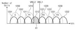
도 12는 본 발명의 일 실시 예에 따라 선택 메모리 셀들의 문턱 전압 분포들을 예시적으로 도시한다. 도시된 실시 예에서, 메모리 셀들 각각은 2-비트 데이터를 저장할 수 있으나, 본 발명은 이에 제한되지 아니한다. 도 1 내지 도 3, 및 도 12를 참조하면, 도 12는 인접 메모리 셀들이 프로그램된 후 선택 메모리 셀들의 문턱 전압 분포들 중 일부를 도시한다. 예를 들어, 도 12는 선택 메모리 셀들 중 소거 상태(E) 또는 상태들(P1, P2, P3) 중 어느 하나로 프로그램된 셀들의 문턱 전압 분포들을 나타낼 수 있다.12 exemplarily illustrates threshold voltage distributions of selected memory cells according to an embodiment of the present invention. In the illustrated embodiment, each of the memory cells may store 2-bit data, but the present invention is not limited thereto. 1 to 3 and 12 , FIG. 12 illustrates some of threshold voltage distributions of selected memory cells after adjacent memory cells are programmed. For example, FIG. 12 may show threshold voltage distributions of cells programmed to one of the erase state E or states P1 , P2 , and P3 among selected memory cells.
곡선들(1200, 1210, 1220, 1230)은 인접 메모리 셀들이 프로그램 되기 전 소거 상태인 선택 메모리 셀들 및 상태들(P1, P2, P3)로 프로그램된 선택 메모리 셀들의 문턱 전압 분포들을 각각 나타낼 수 있다. 인접 메모리 셀들이 프로그램됨에 따라, 곡선(1200)에 속한 메모리 셀들은 곡선들(1201, 1202) 중 어느 하나로 속하게 될 수 있고, 곡선(1210)에 속한 메모리 셀들은 곡선들(1211, 1212) 중 어느 하나로 속하게 될 수 있고, 곡선(1220)에 속한 메모리 셀들은 곡선들(1221, 1222) 중 어느 하나로 속하게 될 수 있고, 그리고 곡선(1230)에 속한 메모리 셀들은 곡선들(1231, 1232) 중 어느 하나로 속하게 될 수 있다.The
도시된 실시 예에서, 전압(VRDj2)이 선택 워드라인에 인가되면, 곡선(1212)에 속한 셀들 중 빗금 친 영역(A1)에 속한 메모리 셀들은 상태(P1)로 프로그램되지 않았다고 오인될 수 있다. 또한, 전압(VRDj1)이 선택 워드라인에 인가되면, 곡선(1221) 중 문턱 전압이 전압(VRDj1)보다 낮은 메모리 셀들은 상태(P1)로 프로그램되었다고 오인될 수 있다.In the illustrated embodiment, when the voltage VRDj2 is applied to the selected word line, memory cells included in the hatched area A1 among the cells included in the
일 실시 예에 있어서, 불휘발성 메모리 장치(100)는 먼저 모든 센싱 노드를 프리차지하고, 그리고 전압(VRDj1)을 선택 워드라인에 인가할 수 있다. 이에 따라, 불휘발성 메모리 장치(100)는 곡선들(1222, 1231, 1232)에 속한 셀들 및 곡선(1221)에 속한 셀들 중 문턱 전압이 전압(VRDj1)보다 높은 셀들을, 곡선들(1201, 1202, 1211, 1212)에 속한 셀들 및 곡선(1221)에 속한 셀들 중 문턱 전압이 전압(VRDj1)보다 낮은 나머지 셀들과 구분할 수 있다. 이후, 불휘발성 메모리 장치(100)는 문턱 전압이 전압(VRDj1)보다 높은 셀들 및 곡선(1211)에 속하는 셀들에 대응하는 센싱 노드들만을 선택적으로 프리차지하고, 그리고 전압(VRDj2)을 선택 워드라인에 인가할 수 있다. 결과적으로, 다른 프로그램 상태로 오인되는 셀들의 수가, 전압들(VRDj1, VRDj2) 중 어느 한 전압만을 사용하는 경우보다 감소될 수 있다.According to an embodiment, the
도 12와 연관된 읽기 동작에 대한 상세한 설명은 도 12 및 도 13을 참조하여 아래에서 후술된다.A detailed description of the read operation associated with FIG. 12 will be described below with reference to FIGS. 12 and 13 .
도 13은 본 발명의 다른 실시 예에 따라, 도 9의 S200 단계를 좀 더 구체적으로 도시한다. 도 1 내지 도 3, 도 8b, 도 9, 도 12, 및 도 13을 참조하면, S200 단계는 S221 내지 S228 단계들을 포함할 수 있다. 구간(Tj1)에서 불휘발성 메모리 장치(100)는 1차 감지를 수행할 수 있고, 그리고 구간(Tj2)에서 불휘발성 메모리 장치(100)는 2차 감지를 수행할 수 있다.FIG. 13 shows step S200 of FIG. 9 in more detail according to another embodiment of the present invention. 1 to 3, 8B, 9, 12, and 13 , step S200 may include steps S221 to S228. In the period Tj1 , the
구간(Tj1)에서 불휘발성 메모리 장치(100)는 S221 내지 S224 단계들을 수행할 수 있고, 그리고 구간(Tj2)에서 불휘발성 메모리 장치(100)는 S225 내지 S228 단계들을 수행할 수 있다. 예시적으로, 구간(Tj1)은 전압(VRDj1)을 이용한 읽기일 수 있다. 구간(Tj2)은 전압(VRDj2)을 이용한 읽기일 수 있다. 또는, 구간(Tj1)에서 행 디코더 회로(120)에 의해 선택 워드라인(WLk)으로 인가되는 전압의 레벨은 구간(Tj2)에서 행 디코더 회로(120)에 의해 선택 워드라인(WLk)으로 인가되는 전압의 레벨과 동일할 수 있다. 예를 들어, 구간들(Tj1, Tj2)에서 곡선(1212)에 속한 메모리 셀들의 문턱 전압보다는 높고, 그리고 곡선(1222)에 속한 메모리 셀들의 문턱 전압보다는 낮은 전압(예를 들어, 전압(VRDj1))이 인가될 수 있다. 선택 워드라인(WLk)으로 인가되는 전압의 레벨은 제어 로직 회로(150)에 의해 조절될 수 있다. 선택 워드라인(WLk)으로 인가되는 전압이 일정할 때, 구간(Tj1)의 디벨롭(예를 들어, S223 단계)의 시간은 구간(Tj2)의 디벨롭(예를 들어, S226 단계)의 시간보다 짧을 수 있다.In the period Tj1 , the
일 실시 예에 있어서, 구간(Tj1)에서 불휘발성 메모리 장치(100)는 목표 상태(예를 들어, 상태(P1))의 선택 메모리 셀들 중 희생 셀들(예를 들어, 곡선(1212)에 속한 셀들)에 초점을 맞추어 읽기 동작을 수행함으로써, 제 1 감지를 수행할 수 있다. 구간(Tj2)에서 불휘발성 메모리 장치(100)는 제 1 감지의 수행 결과에 기초하여, 희생 셀들에 대응하는 센싱 노드들을 제외하고 다시 센싱 노드들을 프리차지할 수 있다. 불휘발성 메모리 장치(100)는 목표 상태의 선택 메모리 셀들 중 비-희생 셀들(예를 들어, 곡선(1211)에 속한 셀들)에 초점을 맞추어 읽기 동작을 수행함으로써, 제 2 감지를 수행할 수 있다.In an embodiment, in the period Tj1 , the
제 2 감지를 수행함에 있어서, 불휘발성 메모리 장치(100)는 제 2 감지를 수행하는 도중에, 제 1 감지 결과 온-셀로 판단된 메모리 셀들의 센싱 노드들의 전압 레벨이 대응하는 비트라인의 영향으로 인해 기준값 이상으로 상승하지 않도록 센싱 노드들의 디벨롭 시간(즉, 하이 레벨의 신호(PASS)가 페이지 버퍼 회로(130)로 인가되는 시간)을 조절할 수 있다. 이에 따라, 목표 상태보다 높은 문턱 전압을 갖도록 프로그램된 메모리 셀들이 목표 상태로 오인되지 않을 수 있다. 결과적으로, 읽기 동작의 정확도가 개선될 수 있다.In performing the second sensing, while the
S221 단계에서, 불휘발성 메모리 장치(100)는 비트라인들(BL)을 프리차지할 수 있다. 예를 들어, 불휘발성 메모리 장치(100)는 S101 단계에 대해 상술된 방식과 유사한 방식으로 S221 단계를 수행할 수 있다.In operation S221 , the
S222 단계에서, 불휘발성 메모리 장치(100)는 센싱 노드들을 모두 프리차지할 수 있다. 예를 들어, 페이지 버퍼들(PB0~PBn-1) 각각의 센싱 노드 프리차지 블록(예를 들어, 330)으로 하이 레벨의 센싱 노드 프리차지 신호(SOPRE) 가 인가되고, 그리고 인접 감지 래치(예를 들어, 360)의 바이어스 블록(예를 들어, 361)으로는 로우 레벨의 바이어스 신호(SLBF)가 인가될 수 있다. 이에 따라 모든 센싱 노드들이 센싱 노드 프리차지 전압으로 충전될 수 있다.In step S222 , the
S223 단계에서, 불휘발성 메모리 장치(100)는 센싱 노드들을 디벨롭할 수 있다. 예를 들어, 불휘발성 메모리 장치(100)는 S104 단계에 대해 상술된 방식과 유사한 방식으로 S223 단계를 수행할 수 있다.In operation S223 , the
S224 단계에서, 불휘발성 메모리 장치(100)는 선택 메모리 셀들에 저장된 데이터를 메인 감지 래치들에 각각 래치할 수 있다. 예를 들어, 불휘발성 메모리 장치(100)는 S214 단계와 유사한 방식으로 S224 단계를 수행할 수 있다.In operation S224 , the
S225 단계에서, 불휘발성 메모리 장치(100)는 인접 감지 결과 'F'를 메인 감지 래치들로 덤프할 수 있다. 이에 따라, 불휘발성 메모리 장치(100)는 인접 감지 결과 'F'가 논리 “0”인 인접 감지 래치들에 대응하는 메인 감지 래치들에 저장된 메인 감지 결과 'S'를 논리 “1”로 셋할 수 있다('~F=S'). S225 단계는 구체적으로 후술된다.In operation S225 , the
S226 단계에서, 불휘발성 메모리 장치(100)는 센싱 노드들 중 일부 센싱 노드들을 선택적으로 다시 프리차지(Reprecharge)할 수 있다. 예를 들어, 불휘발성 메모리 장치(100)는 S215 단계와 유사한 방식으로, 메인 감지 결과 'S'를 뒤집을 수 있다. 페이지 버퍼들(PB0~PBn-1)의 센싱 노드들은 모두 프리차지 된 후 메인 감지 결과 'S'에 기초하여 방전될 수 있고, 그리고 메인 감지 래치들은 리셋된 후 다시 셋될 수 있다. 메인 감지 래치들에 래치된 메인 감지 결과가 뒤집히고 난 후, 페이지 버퍼들(PB0~PBn-1)의 센싱 노드 프리차지 블록들로 하이 레벨의 센싱 노드 프리차지 신호(SOPRE)가 인가될 수 있고, 그리고 메인 감지 래치들로 하이 레벨의 바이어스 신호(SLBS)가 인가될 수 있다. 이에 따라, S225 단계로 인하여, S222 단계와 달리, 센싱 노드들 중 S224 단계에서 저장된 메인 감지 결과가 논리 “0”에 대응하는 메인 감지 래치들로 연결된 센싱 노드들 및 제 2 비트라인들로 연결된 센싱 노드들은 방전되고, 그리고 논리 “1”에 대응하는 메인 감지 래치들로 연결된 센싱 노드들 및 제 1 비트라인들로 연결된 센싱 노드들만이 선택적으로 프리차지될 수 있다.In operation S226 , the
S227 단계에서, 불휘발성 메모리 장치(100)는 메인 감지 래치들을 리셋할 수 있다. 예를 들어, 하이 레벨의 래치 리셋 신호(SRSTS) 및 하이 레벨의 리셋 신호(RST_S)에 응답하여, 메인 감지 래치들이 리셋될 수 있다.In operation S227 , the
S227 단계에서, 불휘발성 메모리 장치(100)는 센싱 노드들을 디벨롭할 수 있다. 예를 들어, 불휘발성 메모리 장치(100)는 S104 단계에 대해 상술된 방식과 유사한 방식으로 S227 단계를 수행할 수 있다. 이때, 도 10의 S213 단계 및 S217 단계와는 달리, S227 단계가 수행되는 시간의 길이는 S223 단계가 수행되는 시간의 길이보다 짧을 수 있다. 따라서, 행 디코더 회로(120)에 의해 실제로 선택 워드라인(WLk)으로 인가되는 전압의 레벨보다 낮은 전압이 행 디코더 회로(120)에 의해 선택 워드라인(WLk)으로 인가되는 경우와 실질적으로 동일한 결과가 달성될 수 있다.S228 단계에서, 불휘발성 메모리 장치(100)는 선택 메모리 셀들에 저장된 데이터를 메인 감지 래치들에 각각 래치할 수 있다. 예를 들어, 불휘발성 메모리 장치(100)는 S214 단계와 유사한 방식으로 S228 단계를 수행할 수 있다.In operation S227 , the
(S224)1st Sensing
(S224)
~F=S
(S335)Dump
~F=S
(S335)
(S226)Inversion
(S226)
0
S266)Recharge
S266)
(S228)2nd Sensing
(S228)
표 1은 일 실시 예에 있어서, 곡선들(1202, 1211, 1212, 1221, 1222)에 속한 메모리 셀들과 관련하여 S100 단계 및 S221 내지 S228 단계를 수행한 결과들을 나타낼 수 있다. S100 단계로 인하여, 제 1 비트라인들에 대응하는 인접 감지 래치들에는 논리 “0”이 래치되고(표 1에서 곡선들(1211, 1221)에 대응하는 인접 감지 결과 'F'), 그리고 제 2 비트라인들에 대응하는 인접 감지 래치들에는 논리 “1”이 래치될 수 있다(표 1에서 곡선들(1211, 1221)에 대응하는 인접 감지 결과 'F').Table 1 may show results of performing steps S100 and S221 to S228 with respect to memory cells belonging to the
S221 내지 S223 단계로 인하여, S224 단계에서 선택 메모리 셀들 중 문턱 전압이 전압(VRDj1)보다 낮은 메모리 셀들에 대응하는 메인 감지 래치들로는 논리 “0”이 래치될 수 있고, 그리고 문턱 전압이 전압(VRDj1)보다 크거나 같은 메모리 셀들에 대응하는 메인 감지 래치들로는 논리 “1”이 래치될 수 있다.Due to steps S221 to S223, logic “0” may be latched to the main sensing latches corresponding to memory cells having a threshold voltage lower than the voltage VRDj1 among the selected memory cells in step S224, and the threshold voltage is the voltage VRDj1 A logic “1” may be latched by main sense latches corresponding to greater than or equal to memory cells.
S225 단계에서, 논리 “1”이 래치된 인접 감지 래치들에 대응하는 메인 감지 래치들 및 논리 “0”이 래치된 인접 감지 래치들에 대응하는 메인 감지 래치들 중 S224 단계에서 논리 “1”이 래치된 메인 감지 래치들은 S224 단계에서 래치된 논리 값들을 유지할 수 있다. 반면에, 논리 “0”이 래치된 인접 감지 래치들에 대응하는 메인 감지 래치들 중 S224 단계에서 논리 “0”이 래치된 메인 감지 래치들에는 논리 “1”이 래치될 수 있다(표 1에서, 곡선(1201) 및 곡선(1212) 중 문턱 전압이 전압(VRDj1)보다 낮은 메모리 셀들에 대응하는 메인 감지 결과 'S').In step S225, among the main sense latches corresponding to the adjacent sense latches latched with logic "1" and the main sense latches corresponding to the adjacent sense latches latched with logic "0", in step S224, the logic "1" is The latched main sensing latches may maintain the latched logic values in step S224. On the other hand, among the main sense latches corresponding to the adjacent sense latches in which the logic "0" is latched, the logic "1" may be latched in the main sense latches in which the logic "0" is latched in step S224 (see Table 1). , the main detection result 'S' corresponding to memory cells having a threshold voltage lower than the voltage VRDj1 among the
S226 단계에서, 페이지 버퍼 회로(130)는 메인 감지 래치들에 래치된 래치 값들을 뒤집을 수 있다. 이후, 페이지 버퍼 회로(130)로 하이 레벨의 센싱 노드 프리차지 신호(SOPRE) 및 메인 감지 래치들에 대한 하이 레벨의 바이어스 신호(SLBS)가 인가될 수 있다. 이에 따라, 반전된 메인 감지 값들이 논리 “1”인 메인 감지 래치들에 대응하는 센싱 노드들은 방전되고(표 1에서, 곡선들(1202, 1212)에 대응하는 센싱 노드들의 “1”), 반전된 메인 감지 값들이 논리 “1”인 메인 감지 래치들에 대응하는 센싱 노드들만이 다시 프리차지된다(표 1에서, 곡선들(1211, 1221, 1222)에 대응하는 센싱 노드들의 “1”).In operation S226 , the
S227 단계에서, 메인 감지 래치들은 리셋되고, 그리고 센싱 노드들이 디벨롭될 수 있다. 이에 따라 S228 단계에서, S226 단계에서 센싱 노드들이 프리차지되지 않은 센싱 노드들에 대응하는 메인 감지 래치들은 논리 “0”을 유지할 수 있다(표 1에서, 곡선들(1202, 1212)에 대응하는 메인 감지 결과 'S'). 또한, S226 단계에서 다시 프리차지된 센싱 노드들에 대응하는 메인 감지 래치들 중 문턱 전압이 전압(VRDj2)보다 작은 메모리 셀들에 대응하는 메인 감지 래치들도 논리 “0”을 유지할 수 있다(표 1에서, 곡선(1211)에 대응하는 메인 감지 결과 'S'). 반면에 S226 단계에서 다시 프리차지된 센싱 노드들에 대응하는 메인 감지 래치들 중 문턱 전압이 전압(VRDj2)보다 크거나 같은 메모리 셀들에 대응하는 메인 감지 래치들로는 논리 “1”이 래치될 수 있다(표 1에서, 곡선들(1221, 1222)에 대응하는 메인 감지 결과 'S'). 결과적으로, 불휘발성 메모리 장치(100)는 S221 내지 S228 단계들을 수행함으로써, 상태(P1)로 프로그램된 선택 메모리 셀들 및 상태(P2)로 프로그램된 선택 메모리 셀들을 높은 정확도로 구분할 수 있다.In step S227 , the main sensing latches may be reset, and sensing nodes may be developed. Accordingly, in step S228, the main sensing latches corresponding to the sensing nodes to which the sensing nodes are not precharged in step S226 may maintain a logic “0” (in Table 1, the main sensing latches corresponding to the
도 14는 도 13의 S225 단계를 좀 더 구체적으로 도시한다. 도 1 내지 도 4, 도 8b, 도 11, 도 13, 및 도 14를 참조하면, S225 단계는 S1401 내지 S1404 단계들을 포함할 수 있다.FIG. 14 shows step S225 of FIG. 13 in more detail. 1 to 4, 8B, 11, 13, and 14 , step S225 may include steps S1401 to S1404.
S1401 단계에서, 불휘발성 메모리 장치(100)는 센싱 노드들을 초기화할 수 있다. 예를 들어, 불휘발성 메모리 장치(100)는 S1101 단계와 유사하게 S1401 단계를 수행할 수 있다.In step S1401 , the
S1402 단계에서, 불휘발성 메모리 장치(100)는 센싱 노드들을 모두 프리차지할 수 있다. 예를 들어, 불휘발성 메모리 장치(100)는 S1102 단계와 유사하게 S1402 단계를 수행할 수 있다.In operation S1402 , the
S1403 단계에서, 불휘발성 메모리 장치(100)는 센싱 노드들 중 일부를 인접감지 래치들에 저장된 데이터에 기초하여 방전시킬 수 있다. 예를 들어, 불휘발성 메모리 장치(100)는 S1103 단계와 유사하게 S1403 단계를 수행할 수 있다.In operation S1403 , the
S1404 단계에서, 불휘발성 메모리 장치(100)는 메인 감지 래치들을 셋할 수 있다. 예를 들어, 하이 레벨의 래치 신호(SLAT) 및 하이 레벨의 셋 신호(SET_S)에 응답하여, 센싱 노드들의 전압 레벨이 메인 감지 래치들로 각각 반영될 수 있다. 이에 따라 인접 감지 결과가 논리 “1”에 대응하는 값으로 저장된 인접 감지 래치들로 연결된 메인 감지 래치들은 S1401 단계가 수행되기 이전에 래치된 메인 감지 결과를 유지할 수 있다. 그러나, 인접 감지 결과가 논리 “0”에 대응하는 값으로 저장된 인접 감지 래치들로 연결된 메인 감지 래치들로는 논리 “1”에 대응하는 값이 다시 래치될 수 있다.In operation S1404, the
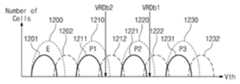
도 15a 및 도 15b는 본 발명의 일 실시 예에 따라 선택 메모리 셀들의 문턱 전압 분포들을 예시적으로 도시한다. 도 1 내지 도 3, 도 12, 도 15a 및 도 15b를 참조하면, 도 15a 및 도 15b는 인접 메모리 셀들이 프로그램된 후 선택 메모리 셀들의 문턱 전압 분포들 중 일부를 도시한다. 도시된 실시 예에서, 전압(VRDa2) 또는 전압(VRDb2)이 선택 워드라인에 인가되면, 곡선(1212)에 속한 셀들 중 문턱 전압이 전압(VRDa2)보다 높은 셀들은 상태(P2)로 프로그램 되었다고 오인될 수 있다.15A and 15B exemplarily show threshold voltage distributions of selected memory cells according to an embodiment of the present invention. 1 to 3, 12, 15A, and 15B, FIGS. 15A and 15B illustrate some of threshold voltage distributions of selected memory cells after adjacent memory cells are programmed. In the illustrated embodiment, when the voltage VRDa2 or the voltage VRDb2 is applied to the selected word line, among the cells belonging to the
일 실시 예에 있어서, 불휘발성 메모리 장치(100)는 전압들(VRDa1, VRDa2)을 사용하여 제 1 감지를 수행하고, 그리고 전압들(VRDb1, VRDb2)을 사용하여 제 2 감지를 수행할 수 있다. 예를 들어, 불휘발성 메모리 장치(100)는 전압(VRDa1)을 선택 워드라인에 인가함으로써 제 1 대단위(Coarse) 감지를 수행할 수 있고, 그리고 전압(VRDa2)을 선택 워드라인에 인가함으로써 제 1 메인 감지를 수행할 수 있다. 불휘발성 메모리 장치(100)는 전압(VRDb1)을 선택 워드라인에 인가함으로써 제 2 대단위(Coarse) 감지를 수행할 수 있고, 그리고 전압(VRDb2)을 선택 워드라인에 인가함으로써 제 2 메인 감지를 수행할 수 있다.In an embodiment, the
다시 말해서, 이러한 실시 예들에서는 도 12 및 도 13에 도시된 실시 예와 달리, 전압들(VRDa1, VRDb1)을 사용하여 제 1 대단위 감지 및 제 2 대단위 감지가 더 수행될 수 있다. 제 1 및 제 2 대단위 감지들이 수행됨으로써, 메인 감지 래치들에 데이터가 래치될 때 오류(또는 노이즈)가 발생할 가능성이 낮아질 수 있다.In other words, in these embodiments, unlike the embodiments illustrated in FIGS. 12 and 13 , the first large-scale detection and the second large-scale detection may be further performed using the voltages VRDa1 and VRDb1 . By performing the first and second large-scale sensing, the possibility of an error (or noise) occurring when data is latched in the main sensing latches may be reduced.
예를 들어, 전압(VRDa2)만을 사용하여 제 1 메인 감지만을 수행한다고 가정하자. 이때, 전압(VRDa2)보다 큰 문턱 전압을 갖는 메모리 셀들에 대응하는 메인 감지 래치들에 실질적으로 동시에 논리 “1”이 래치될 필요가 있을 수 있다. 그러나, 페이지 버퍼들(PB0~PBn-1) 사이 커플링으로 인하여, 메인 감지 래치들에 잘못된 논리 값이 래치(즉, 오류 또는 노이즈가 발생)될 수도 있다. 반면에, 전압(VRDa2)보다 높은 전압(VRDa1)을 사용하여 제 1 대단위 감지를 수행하는 경우에는 실질적으로 동시에 논리 “1”이 래치되어야 하는 메인 감지 래치들의 개수가 감소하기 때문에 커플링의 정도가 감소될 수 있다. 따라서, 메인 감지 래치들에 잘못된 논리 값이 래치될 가능성이 감소될 수 있다. 결과적으로, 불휘발성 메모리 장치(100)의 읽기 동작의 신뢰성이 향상될 수 있다.For example, suppose that only the first main sensing is performed using only the voltage VRDa2. In this case, the logic “1” may need to be latched to the main sense latches corresponding to the memory cells having a threshold voltage greater than the voltage VRDa2 at substantially the same time. However, due to the coupling between the page buffers PB0 to PBn-1, an incorrect logic value may be latched (ie, an error or noise is generated) in the main sense latches. On the other hand, when the first large-scale sensing is performed using a voltage VRDa1 higher than the voltage VRDa2, the degree of coupling decreases because the number of main sensing latches to which logic “1” must be latched substantially simultaneously decreases. can be reduced. Accordingly, the possibility that an incorrect logic value is latched in the main sense latches can be reduced. As a result, the reliability of the read operation of the
도 15a 및 도 15b와 연관된 읽기 동작에 대한 상세한 설명은 도 12 및 도 13을 참조하여 아래에서 후술된다.A detailed description of the read operation associated with FIGS. 15A and 15B will be described below with reference to FIGS. 12 and 13 .
도 16은 본 발명의 또 다른 실시 예에 따라, 도 9의 S200 단계를 좀 더 구체적으로 도시한다. 도 1 내지 도 3, 도 8b, 도 9, 도 12, 도 13, 도 15a, 도 15b, 및 도 16을 참조하면, S200 단계는 S231 내지 S237 단계들 및 S241 내지 S247 단계들을 포함할 수 있다. 구간(Ta1)에서 불휘발성 메모리 장치(100)는 제 1 감지를 수행할 수 있고, 그리고 구간(Ta2)에서 불휘발성 메모리 장치(100)는 제 2 감지를 수행할 수 있다. 예를 들어, 불휘발성 메모리 장치(100)는 4 개의 전압들(예를 들어, VRDa2, VRDa2, VRDb1, VRDb2)을 선택 워드라인에 인가함으로써 각각 제 1 대단위 감지, 제 1 메인 감지, 제 2 대단위 감지 및 제 2 메인 감지를 수행할 수 있다. 선택 워드라인으로 인가되는 전압의 레벨은 제어 로직 회로(150)에 의해 조절될 수 있다.FIG. 16 shows step S200 of FIG. 9 in more detail according to another embodiment of the present invention. 1 to 3, 8B, 9, 12, 13, 15A, 15B, and 16 , step S200 may include steps S231 to S237 and steps S241 to S247. In the period Ta1, the
다른 예를 들어, 불휘발성 메모리 장치(100)는 제 1 대단위 감지 및 제 1 메인 감지를, 동일한 전압을 선택 워드라인에 인가하되 센싱 노드의 디벨롭 시간을 조절함으로써 수행할 수 있다. 유사하게, 불휘발성 메모리 장치(100)는 제 2 대단위 감지 및 제 2 메인 감지를, 서로 동일하나 제 1 대단위 감지 및 제 1 메인 감지에서 선택 워드라인에 인가된 전압과는 상이한 전압을 선택 워드라인에 인가하되 센싱 노드의 디벨롭 시간을 조절함으로써 수행할 수 있다. 센싱 노드의 디벨롭 시간들은 제어 로직 회로(150)에 의해 조절될 수 있다.As another example, the
또 다른 예를 들어, 불휘발성 메모리 장치(100)는 제 1 대단위 감지, 제 1 메인 감지, 제 2 대단위 감지, 및 제 2 메인 감지를, 동일한 전압을 선택 워드라인에 인가하되 센싱 노드의 디벨롭 시간을 조절함으로써 수행할 수 있다.As another example, the
일 실시 예에 있어서, 불휘발성 메모리 장치(100)의 행 디코더 회로(120)는 구간(Ta1)에서 선택 워드라인(WLk)으로 전압(예를 들어, 전압(VRDa1))을 인가할 수 있고, 그리고 구간(Ta2)에서 선택 워드라인(WLk)으로 전압(예를 들어, 전압(VRDb1))을 인가할 수 있다. 행 디코더 회로(120)에 의해 선택 워드라인(WLk)으로 인가되는 전압의 레벨은 제어 로직 회로(150)에 의해 적절하게 조절될 수 있다.In an embodiment, the
S231 단계에서, 불휘발성 메모리 장치(100)는 비트라인들(BL)을 프리차지할 수 있다. 예를 들어, 불휘발성 메모리 장치(100)는 S101 단계에 대해 상술된 방식과 유사한 방식으로 S231 단계를 수행할 수 있다.In operation S231 , the
S232 단계에서, 불휘발성 메모리 장치(100)는 센싱 노드들을 모두 프리차지할 수 있다. 예를 들어, 불휘발성 메모리 장치(100)는 S222 단계에 대해 상술된 방식과 유사한 방식으로 S232 단계를 수행할 수 있다.In step S232 , the
S233 단계에서, 불휘발성 메모리 장치(100)는 센싱 노드들을 디벨롭할 수 있다. 예를 들어, 불휘발성 메모리 장치(100)는 S104 단계에 대해 상술된 방식과 유사한 방식으로 S233 단계를 수행할 수 있다.In operation S233 , the
S234 단계에서, 불휘발성 메모리 장치(100)는 선택 메모리 셀들에 저장된 데이터를 메인 감지 래치들에 각각 래치할 수 있다. 예를 들어, 불휘발성 메모리 장치(100)는 S214 단계와 유사한 방식으로 S234 단계를 수행할 수 있다.In operation S234 , the
S235 단계에서, 불휘발성 메모리 장치(100)는 센싱 노드들 중 일부만을 선택적으로 다시 프리차지할 수 있다. 예를 들어, 페이지 버퍼들(PB0~PBn-1)로 하이 레벨의 센싱 노드 프리차지 신호(SOPRE) 및 하이 레벨의 바이어스 신호(SLBS)가 인가될 수 있다. 이에 따라, 메인 감지 래치들의 바이어스 블록(예를 들어, 361)에 의해, 센싱 노드들 중 S234 단계에서 저장된 메인 감지 결과가 논리 “1”에 대응하는 메인 감지 래치들로 연결된 센싱 노드들은 접지 전압으로 방전되고, 그리고 메인 감지 결과가 논리 “0”에 대응하는 메인 감지 래치들로 연결된 센싱 노드들만이 다시 프리차지될 수 있다. 즉, 제 1 대단위 감지의 결과가 온-셀인 메모리 셀들에 대응하는 센싱 노드들(또는 제 1 대단위 감지 결과가 논리 “0”에 대응하는 페이지 버퍼들의 센싱 노드들)이 다시 프리차지될 수 있다.In operation S235 , the
S236 단계에서, 불휘발성 메모리 장치(100)는 센싱 노드들을 디벨롭할 수 있다. 예를 들어, 불휘발성 메모리 장치(100)는 S104 단계에 대해 상술된 방식과 유사한 방식으로 S236 단계를 수행할 수 있다. 이때, S236 단계가 수행되는 시간의 길이는 S233 단계가 수행되는 시간의 길이보다 짧을 수 있다. 따라서, 행 디코더 회로(120)에 의해 실제로 선택 워드라인(WLk)으로 인가되는 전압(예를 들어, 전압(VRDa1))보다 낮고, 곡선(1221)에 속한 셀들의 문턱 전압보다는 높거나 같은 전압(예를 들어, 전압(VRDa2))이 행 디코더 회로(120)에 의해 선택 워드라인(WLk)으로 인가되는 경우와 실질적으로 동일한 결과가 달성될 수 있다.In operation S236 , the
다른 예를 들어, 제 1 대단위 감지로 인하여 곡선(1221)에 속한 메모리 셀들 중 문턱 전압이 전압(VRDa1)보다 낮은 메모리 셀들로 연결된 비트라인들의 전압은 이미 비트라인 프리차지 전압(VPRCG)보다 하강했을 수 있다. 불휘발성 메모리 장치(100)는 이러한 이미 하강된 비트라인들의 전압에 대응하는 센싱 노드의 전압이 기준값 이하로 떨어지지 않도록 S236 단계가 수행되는 시간의 길이를 조절할 수 있다. 이때, 불휘발성 메모리 장치(100)는 곡선들(1201, 1202, 1211)에 속한 메모리 셀들 및 곡선(1212)에 속한 메모리 셀들 중 전압(VRDa2)보다 문턱 전압이 낮은 셀들에 대응하는 센싱 노드들의 전압이 기준값 이하로 떨어지도록 S236 단계가 수행되는 시간의 길이를 더 조절할 수 있다.As another example, the voltage of the bit lines connected to the memory cells having a threshold voltage lower than the voltage VRDa1 among the memory cells belonging to the
S237 단계에서, 불휘발성 메모리 장치(100)는 선택 메모리 셀들에 저장된 데이터를 메인 감지 래치들에 각각 래치할 수 있다. 예를 들어, 불휘발성 메모리 장치(100)는 S214 단계와 유사한 방식으로 S237 단계를 수행할 수 있다. 도 16의 S237 단계에서는 제 1 대단위 감지가 수행되었기 때문에 도 13의 S224 단계와 달리 논리 “1”로 래치되는 메인 감지 래치들의 수(또는, S234 단계에서는 오프-셀로 판단되었으나 S237 단계에서는 온-셀로 판단되는 메모리 셀들의 수)가 더 적을 수 있다. 이에 따라, 메인 감지 래치들의 노이즈가 감소될 수 있다.In operation S237 , the
S241 단계에서, 불휘발성 메모리 장치(100)는 인접 감지 래치들에 저장된 데이터들을 메인 감지 래치들로 덤프할 수 있다. 이에 따라, 불휘발성 메모리 장치(100)는 인접 감지 결과 'F'가 논리 “0”인 인접 감지 래치들에 대응하는 메인 감지 래치들에 저장된 메인 감지 결과 'S'를 논리 “1”로 셋할 수 있다('~F=S'). 예를 들어, 불휘발성 메모리 장치(100)는 S225 단계와 유사한 방식으로 S241 단계를 수행할 수 있다.In operation S241 , the
S242 단계에서, 불휘발성 메모리 장치(100)는 센싱 노드들 중 일부 센싱 노드들을 선택적으로 다시 프리차지할 수 있다. 예를 들어, S226 단계와 유사한 방식으로, 불휘발성 메모리 장치(100)는 메인 감지 결과 'S'를 뒤집을 수 있다. 이후, 페이지 버퍼들(PB0~PBn-1)의 센싱 노드 프리차지 블록들로 하이 레벨의 센싱 노드 프리차지 신호(SOPRE)가 인가되고, 그리고 메인 감지 래치들의 바이어스 블록들로 하이 레벨의 바이어스 신호(SLBS)가 인가될 수 있다. 이에 따라, S241 단계로 인하여, 센싱 노드들 중 제 1 메인 감지의 결과 온-셀로 감지된 메모리 셀들 및 제 2 비트라인들에 대응하는 메모리 셀들에 대응하는 센싱 노드들은 방전될 수 있다. 그리고, 오프-셀로 감지된 메모리 셀들에 대응하는 센싱 노드들 및 제 1 비트라인들에 대응하는 센싱 노드들(또는, 제 1 메인 감지 결과가 논리 “1”에 대응하는 페이지 버퍼들 및 인접 감지 결과가 논리 “0”에 대응하는 페이지 버퍼들의 센싱 노드들)만이 선택적으로 다시 프리차지될 수 있다.In operation S242 , the
S243 단계에서, 불휘발성 메모리 장치(100)는 센싱 노드들을 디벨롭할 수 있다. 예를 들어, 불휘발성 메모리 장치(100)는 S227 단계에 대해 상술된 방식과 유사한 방식으로 S243 단계를 수행할 수 있다. S227 단계와 유사하게, 불휘발성 메모리 장치(100)는 메인 감지 래치들을 리셋할 수 있다.In operation S243 , the
S244 단계에서, 불휘발성 메모리 장치(100)는 선택 메모리 셀들에 저장된 데이터를 메인 감지 래치들에 각각 래치할 수 있다. 예를 들어, 불휘발성 메모리 장치(100)는 S214 단계와 유사한 방식으로 S244 단계를 수행할 수 있다.In operation S244 , the
S245 단계에서, 불휘발성 메모리 장치(100)는 센싱 노드들 중 일부만을 선택적으로 다시 프리차지할 수 있다. 예를 들어, 불휘발성 메모리 장치(100)는 S235 단계와 유사한 방식으로 S245 단계를 수행할 수 있다. 이에 따라, 제 2 대단위 감지 결과 오프-셀로 감지된 메모리 셀들에 대응하는 센싱 노드들은 방전되고, 그리고 온-셀로 감지된 메모리 셀들에 대응하는 센싱 노드들(또는, 제 2 대단위 감지 결과가 논리 “0”에 대응하는 페이지 버퍼들의 센싱 노드들)이 다시 프리차지될 수 있다.In operation S245 , the
S246 단계에서, 불휘발성 메모리 장치(100)는 센싱 노드들을 디벨롭할 수 있다. 예를 들어, 불휘발성 메모리 장치(100)는 S104 단계에 대해 상술된 방식과 유사한 방식으로 S246 단계를 수행할 수 있다. 이때, S246 단계가 수행되는 시간의 길이는 S243 단계가 수행되는 시간의 길이보다 짧을 수 있다.In operation S246 , the
S247 단계에서, 불휘발성 메모리 장치(100)는 선택 메모리 셀들에 저장된 데이터를 메인 감지 래치들에 각각 래치할 수 있다. 예를 들어, 불휘발성 메모리 장치(100)는 S214 단계와 유사한 방식으로 S247 단계를 수행할 수 있다.In operation S247 , the
도 17은 도 1의 불휘발성 메모리 장치를 포함하는 스토리지 장치의 블록도를 예시적으로 도시한다. 도 1 및 도 17을 참조하면, 스토리지 장치(1)는 메모리 컨트롤러(10), 외부 버퍼(20), 및 도 1의 불휘발성 메모리 장치(100)를 포함할 수 있다.17 exemplarily illustrates a block diagram of a storage device including the nonvolatile memory device of FIG. 1 . 1 and 17 , the
메모리 컨트롤러(10)는 불휘발성 메모리 장치(100)에 데이터를 쓰거나 또는 불휘발성 메모리 장치(100)로부터 데이터를 읽기 위한 다양한 요청들을 외부 호스트 장치로부터 수신할 수 있다. 메모리 컨트롤러(10)는 외부 호스트 장치와 통신되는 데이터 및 스토리지 장치(1)를 관리하기 위한 데이터를 외부 버퍼(20)에 저장할 수 있다.The
메모리 컨트롤러(10)는 호스트 인터페이스(11), 프로세서(12), 메모리 매니저(13), 내부 버퍼(14), 버퍼 컨트롤러(15), ECC(Error Correction Code; 에러 정정 코드) 블록(16), 및 버스(17)를 포함할 수 있다.The
호스트 인터페이스(11)는 외부 호스트 장치로부터 다양한 요청들을 수신할 수 있다. 호스트 인터페이스(11)는 수신된 요청들을 디코딩할 수 있다. 호스트 인터페이스(11)는 디코딩된 요청들을 내부 버퍼(14)에 저장할 수 있다. 호스트 인터페이스(11)는 수신된 다양한 요청들에 응답하여, 외부 호스트 장치로 데이터 신호를 전송할 수 있다.The
프로세서(12)는 메모리 컨트롤러(10)를 구동하기 위한 운영 체제 또는 펌웨어를 구동할 수 있다. 프로세서(12)는 내부 버퍼(14)에 저장된 디코딩된 요청들을 읽을 수 있다. 프로세서(12)는 요청들에 기초하여, 불휘발성 메모리 장치(100)를 제어하기 위한 명령들 및 어드레스들을 생성할 수 있다. 프로세서(12)는 생성된 명령들 및 어드레스들을 메모리 매니저(13)로 전송할 수 있다. 프로세서(12)의 제어 하에, 내부 버퍼(14) 및 외부 버퍼(20)에 저장된 데이터들이 메모리 매니저(13)에 의해 불휘발성 메모리 장치(100)에 저장될 수 있다.The
메모리 매니저(13)는 프로세서(12)의 제어 하에 불휘발성 메모리 장치(100)와 통신할 수 있다. 예를 들어, 메모리 매니저(13)는 프로세서(12)에 의해 생성된 명령들 및 어드레스들, 내부 버퍼(14)에 저장된 데이터들, 및 외부 버퍼(20)에 저장된 데이터들을 채널(CH)을 통해 불휘발성 메모리 장치(100)로 전송할 수 있다. 메모리 매니저(13)는 불휘발성 메모리 장치(100)에 저장된 데이터를 채널(CH)을 통해 수신할 수 있다.The
내부 버퍼(14)는 RAM(Random Access Memory)을 포함할 수 있다. 예를 들어, 내부 버퍼(14)는 SRAM(Static RAM) 또는 DRAM(Dynamic RAM)을 포함할 수 있다. 버퍼 컨트롤러(15)는 프로세서(12)의 제어 하에, 데이터를 외부 버퍼(20)에 쓰거나 또는 외부 버퍼(20)에 저장된 데이터를 읽을 수 있다.The
ECC 블록(16)은 에러 정정 인코딩을 불휘발성 메모리 장치(100)로 전송되는 데이터에 대해 에러 정정 코드(ECC)를 이용하여 수행할 수 있다. ECC 블록(16)은 에러 정정 디코딩을 불휘발성 메모리 장치(100)로부터 수신되는 데이터에 대해 에러 정정 코드(ECC)를 이용하여 수행할 수 있다.The
외부 버퍼(20)는 RAM(Random Access Memory)을 포함할 수 있다. 예를 들어, 외부 버퍼(20)는 DRAM, PRAM(Phase Change RAM), MRAM(Magnetic RAM), RRAM(Resistive RAM) 등을 포함할 수 있다.The
일 실시 예에 있어서, 불휘발성 메모리 장치(100)는 워드라인들 중 선택 워드라인(예를 들어, WLk; k는 m보다 작은 음이 아닌 정수)에 연결된 선택 메모리 셀들에 저장된 데이터에 대한 읽기 동작을 수행할 것을 지시하는 커맨드(CMD)를 메모리 컨트롤러(10)로부터 수신할 수 있다. 이때, 커맨드(CMD)는 일반적인 읽기 동작을 수행할 것을 지시하거나, 또는 데이터 리커버리 읽기 동작을 수행할 것을 지시할 수 있다. 예를 들어, 커맨드(CMD)는 불휘발성 메모리 장치(100)로 하여금 어떤 읽기 동작을 수행할 것인지를 지시하는 디스크립터(Descriptor)를 포함할 수 있다.In an embodiment, the
일반적인 읽기 동작을 수행할 것을 지시하는 커맨드(CMD)가 메모리 컨트롤러(10)로부터 수신되면, 제어 로직 회로(150)는 행 디코더 회로(120)로 하여금 읽기 동작 수행 시에 선택 워드라인을 활성화하도록 제어하고, 그리고 페이지 버퍼 회로(130)로 하여금 복수의 비트라인들을 통해 선택 워드라인으로 연결된 선택 메모리 셀들에 저장된 데이터를 감지하도록 제어할 수 있다.When the command CMD instructing to perform a general read operation is received from the
데이터 리커버리 읽기 동작을 수행할 것을 지시하는 커맨드(CMD)가 메모리 컨트롤러(10)로부터 수신되면, 제어 로직 회로(150)는 행 디코더 회로(120)로 하여금 읽기 동작 수행 시에, 먼저 선택 워드라인에 인접한 인접 워드라인(예를 들어, WLk-1)을 활성화하고, 그 다음에 선택 워드라인을 활성화하도록 제어할 수 있다. 제어 로직 회로(150)는 페이지 버퍼 회로(130)로 하여금, 행 디코더 회로(120)에 의해 인접 워드라인이 활성화되면 인접 메모리 셀들에 저장된 데이터를 감지하도록 제어할 수 있다. 제어 로직 회로(150)는 페이지 버퍼 회로(130)로 하여금, 행 디코더 회로(120)에 의해 선택 워드라인이 활성화되면 인접 메모리 셀들에 대한 감지 결과에 기초하여, 선택 메모리 셀들에 저장된 데이터를 감지하도록 제어할 수 있다.When the command CMD instructing to perform the data recovery read operation is received from the
다른 실시 예에 있어서, 제어 로직 회로(150)는 메모리 컨트롤러(10)로부터 수신되는 커맨드(CMD)에 기초하여 인접 메모리 셀들이 분류될 수 있는 그룹의 수 및 인접 메모리 셀들을 분류하는 데 사용되는 전압의 레벨을 조절할 수 있다.In another embodiment, the
또 다른 실시 예에 있어서, 제어 로직 회로(150)는 메모리 컨트롤러(10)로부터 수신되는 커맨드(CMD)에 기초하여 구간들(T11, T21, T31) 각각의 길이를 조절할 수 있다. 예를 들어, 구간들(T11, T21, T31)의 길이는 하나의 메모리 셀에 저장될 수 있는 데이터의 비트 수, 각각의 메모리 셀들이 프로그램된 상태, 불휘발성 메모리 장치(100)의 기대 수명(예를 들어, 프로그램/소거 사이클), 불휘발성 메모리 장치(100)의 온도 등과 같은 다양한 요소에 기초하여 조절될 수 있다. 또 다른 예를 들어, 구간들(T11, T21, T31)의 길이는 읽기 요청의 대상이 되는 메모리 셀들이 포함되는 메모리 블록이 메모리 블록들(BLK1~BLKz) 중 어느 것인지에 기초하여 조절될 수 있다.In another embodiment, the
또 다른 실시 예에 있어서, 제어 로직 회로(150)는 커맨드(CMD)에 기초하여, 도 13의 구간(Tj1), 및 도 16의 구간들(Ta1, Ta2)에서 행 디코더 회로(120)에 의해 선택 워드라인(WLk)으로 인가되는 전압의 레벨을 조절할 수 있다. 제어 로직 회로(150)는 커맨드(CMD)에 기초하여 도 10의 S213, S217, 도 13의 S223, S227, 및 도 16의 S233, S236, S243, S246 단계들의 센싱 노드의 디벨롭 시간들의 길이를 조절할 수 있다. 예를 들어, 제어 로직 회로(150)는 구간들(T11, T21, T31)의 길이를 조절하는 것과 유사한 방식으로, 다양한 요소들을 고려하여 상술된 전압들의 레벨들 및 센싱 노드의 디벨롭 시간들의 길이를 조절할 수 있다.In another embodiment, the
도 18은 본 발명의 다른 실시 예에 따른 불휘발성 메모리 장치를 예시적으로 도시한다. 도 1 및 도 18을 참조하면, 도 18은 도 1의 메모리 블록들(BLK1~BLKz) 중 메모리 블록(BLKa)을 예시적으로 도시한다. 도시된 실시 예에서, 복수의 셀 스트링들(CS)이 기판(SUB) 위에서 행들 및 열들로 배치될 수 있다. 복수의 셀 스트링들(CS)은 기판(SUB) 상에(또는 안에) 형성되는 공통 소스 라인(CSL)에 공통으로 연결될 수 있다. 기판(SUB)의 위치는 도시된 실시 예에 한정되지 아니할 것이다.18 exemplarily illustrates a nonvolatile memory device according to another embodiment of the present invention. 1 and 18 , FIG. 18 exemplarily shows a memory block BLKa among the memory blocks BLK1 to BLKz of FIG. 1 . In the illustrated embodiment, a plurality of cell strings CS may be arranged in rows and columns on the substrate SUB. The plurality of cell strings CS may be commonly connected to a common source line CSL formed on (or in) the substrate SUB. The position of the substrate SUB is not limited to the illustrated embodiment.
도시된 실시 예에서, 공통 소스 라인(CSL)이 셀 스트링들(CS)의 하단에 연결될 수 있다. 그러나 공통 소스 라인(CSL)은 셀 스트링들(CS)의 하단에 전기적으로 연결되는 것으로 족할 것이다. 따라서 공통 소스 라인(CSL)은 물리적으로 셀 스트링들(CS)의 하단에 위치하는 것으로 한정되지 아니한다. 또한 도시된 실시 예에서, 셀 스트링들(CS)은 4X4로 배열되었으나, 메모리 블록(BLKa)은 더 적은 또는 더 많은 수의 셀 스트링들을 포함할 수 있다.In the illustrated embodiment, the common source line CSL may be connected to the lower ends of the cell strings CS. However, it will be sufficient for the common source line CSL to be electrically connected to the lower ends of the cell strings CS. Therefore, the common source line CSL is not limited to being physically located at the lower end of the cell strings CS. Also, in the illustrated embodiment, the cell strings CS are arranged in a 4X4 configuration, but the memory block BLKa may include a smaller number or a larger number of cell strings.
각 행의 셀 스트링들은 접지 선택 라인(GSL)에 공통으로 연결되고, 그리고 스트링 선택 라인들(SSL1~SSL4) 중 대응하는 스트링 선택 라인에 연결될 수 있다. 각 열의 셀 스트링들은 비트라인들(BL1~BL4) 중 대응하는 비트라인에 연결될 수 있다.The cell strings of each row may be commonly connected to the ground selection line GSL, and may be connected to a corresponding string selection line among the string selection lines SSL1 to SSL4. The cell strings of each column may be connected to a corresponding bit line among the bit lines BL1 to BL4.
셀 스트링들 각각은 접지 선택 라인(GSL)에 연결되는 적어도 하나의 접지 선택 트랜지스터(GST), 워드라인들(WL1~WL8)에 각각 연결되는 메모리 셀들(MC), 스트링 선택 라인들(SSL1~SSL4) 중 대응하는 스트링 선택 라인으로 연결되는 스트링 선택 트랜지스터들(SST)을 포함할 수 있다.Each of the cell strings includes at least one ground selection transistor GST connected to the ground selection line GSL, memory cells MC connected to the word lines WL1 to WL8, respectively, and the string selection lines SSL1 to SSL4. ) of the string select transistors SST connected to a corresponding string select line.
각 셀 스트링에서, 접지 선택 트랜지스터(GST), 메모리 셀들(MC), 그리고 스트링 선택 트랜지스터들(SST)은 기판(SUB)과 수직인 방향을 따라 직렬 연결되고, 기판(SUB)과 수직인 방향을 따라 순차적으로 적층될 수 있다. 각 셀 스트링(CS)에서, 메모리 셀들(MC) 중 적어도 하나가 더미 메모리 셀로 사용될 수 있다. 더미 메모리 셀은 프로그램되지 않거나(예를 들어, 프로그램이 금지되거나) 또는 메모리 셀들(MC1~MC8)과 다르게 프로그램될 수 있다.In each cell string, the ground select transistor GST, the memory cells MC, and the string select transistors SST are connected in series along a direction perpendicular to the substrate SUB, and form a direction perpendicular to the substrate SUB. may be sequentially stacked. In each cell string CS, at least one of the memory cells MC may be used as a dummy memory cell. The dummy memory cell may not be programmed (eg, program is prohibited) or may be programmed differently from the memory cells MC1 to MC8 .
도 19는 본 발명의 또 다른 실시 예에 따른 불휘발성 메모리 장치를 예시적으로 도시한다. 도 19를 참조하면, 불휘발성 메모리 장치(2100)는 C2C(chip to chip) 구조일 수 있다. C2C 구조는 제 1 웨이퍼 상에 셀 영역(CELL)을 포함하는 상부 칩을 제작하고, 제 1 웨이퍼와 다른 제 2 웨이퍼 상에 주변 회로 영역(PERI)을 포함하는 하부 칩을 제작한 후, 상기 상부 칩과 상기 하부 칩을 본딩(bonidng) 방식에 의해 서로 연결하는 것을 의미할 수 있다. 일례로, 상기 본딩 방식은 상부 칩의 최상부 메탈층에 형성된 본딩 메탈과 하부 칩의 최상부 메탈층에 형성된 본딩 메탈을 서로 전기적으로 연결하는 방식을 의미할 수 있다. 예컨대, 상기 본딩 메탈이 구리(Cu)로 형성된 경우, 상기 본딩 방식은 Cu-Cu 본딩 방식일 수 있으며, 상기 본딩 메탈은 알루미늄 혹은 텅스텐으로도 형성될 수 있다.19 exemplarily shows a nonvolatile memory device according to another embodiment of the present invention. Referring to FIG. 19 , the
불휘발성 메모리 장치(2100)의 주변 회로 영역(PERI)과 셀 영역(CELL) 각각은 외부 패드 본딩 영역(PA), 워드라인 본딩 영역(WLBA), 및 비트라인 본딩 영역(BLBA)을 포함할 수 있다.Each of the peripheral circuit area PERI and the cell area CELL of the
주변 회로 영역(PERI)은 제1 기판(2210), 층간 절연층(2215), 제1 기판(2210)에 형성되는 복수의 회로 소자들(2220a, 2220b, 2220c), 복수의 회로 소자들(2220a, 2220b, 2220c) 각각과 연결되는 제1 메탈층(2230a, 2230b, 2230c), 제1 메탈층(2230a, 2230b, 2230c) 상에 형성되는 제2 메탈층(2240a, 2240b, 2240c)을 포함할 수 있다. 일 실시예에서, 제1 메탈층(2230a, 2230b, 2230c)은 상대적으로 저항이 높은 텅스텐으로 형성될 수 있고, 제2 메탈층(2240a, 2240b, 2240c)은 상대적으로 저항이 낮은 구리로 형성될 수 있다.The peripheral circuit region PERI includes a
본 명세서에서는 제1 메탈층(2230a, 2230b, 2230c)과 제2 메탈층(2240a, 2240b, 2240c)만 도시 되고 설명되나, 이에 한정되는 것은 아니고, 제2 메탈층(2240a, 2240b, 2240c) 상에 적어도 하나 이상의 메탈층이 더 형성될 수도 있다. 제2 메탈층(2240a, 2240b, 2240c)의 상부에 형성되는 하나 이상의 메탈층 중 적어도 일부는, 제2 메탈층(2240a, 2240b, 2240c)을 형성하는 구리보다 더 낮은 저항을 갖는 알루미늄 등으로 형성될 수 있다.In this specification, only the
층간 절연층(2215)은 복수의 회로 소자들(2220a, 2220b, 2220c), 제1 메탈층(2230a, 2230b, 2230c), 및 제2 메탈층(2240a, 2240b, 2240c)을 커버하도록 제1 기판(210) 상에 배치되며, 실리콘 산화물, 실리콘 질화물 등과 같은 절연 물질을 포함할 수 있다.The interlayer insulating
워드라인 본딩 영역(WLBA)의 제2 메탈층(2240b) 상에 하부 본딩 메탈(2271b, 2272b)이 형성될 수 있다. 워드라인 본딩 영역(WLBA)에서, 주변 회로 영역(PERI)의 하부 본딩 메탈(2271b, 2272b)은 셀 영역(CELL)의 상부 본딩 메탈(2371b, 2372b)과 본딩 방식에 의해 서로 전기적으로 연결될 수 있으며, 하부 본딩 메탈(2271b, 2272b)과 상부 본딩 메탈(2371b, 2372b)은 알루미늄, 구리, 혹은 텅스텐 등으로 형성될 수 있다.
또한, 셀 영역(CELL) 내의 상부 본딩 메탈(2371b, 2372b)은 제1 메탈 패드로 참조될 수 있고, 그리고 주변 회로 영역(PERI) 내의 하부 본딩 메탈(2271b, 2272b)은 제2 메탈 패드로 참조될 수 있다. 제1 메탈 패드 및 제2 메탈 패드는 앞서 설명된 본딩 방식을 통해 서로 직접 연결될 수 있다.Also, the
셀 영역(CELL)은 적어도 하나의 메모리 블록을 제공할 수 있다. 셀 영역(CELL)은 제2 기판(2310)과 공통 소스 라인(2320)을 포함할 수 있다. 제2 기판(2310) 상에는, 제2 기판(2310)의 상면에 수직하는 방향(Z축 방향)을 따라 복수의 워드라인들(2331~2338; 2330)이 적층될 수 있다. 워드라인들(2330)의 상부 및 하부 각각에는 스트링 선택 라인들과 접지 선택 라인이 배치될 수 있으며, 스트링 선택 라인들과 접지 선택 라인 사이에 복수의 워드라인들(2330)이 배치될 수 있다.The cell region CELL may provide at least one memory block. The cell region CELL may include a
비트라인 본딩 영역(BLBA)에서, 채널 구조체(CH)는 제2 기판(2310)의 상면에 수직하는 방향으로 연장되어 워드라인들(2330), 스트링 선택 라인들, 및 접지 선택 라인을 관통할 수 있다. 채널 구조체(CH)는 데이터 저장층, 채널층, 및 매립 절연층 등을 포함할 수 있으며, 채널층은 제1 메탈층(2350c) 및 제2 메탈층(2360c)과 전기적으로 연결될 수 있다. 예컨대, 제1 메탈층(2350c)은 비트라인 컨택일 수 있고, 제2 메탈층(2360c)은 비트라인일 수 있다. 일 실시예에서, 비트라인(2360c)은 제2 기판(2310)의 상면에 평행한 제1 방향(Y축 방향)을 따라 연장될 수 있다.In the bit line bonding area BLBA, the channel structure CH may extend in a direction perpendicular to the top surface of the
도시된 실시 예에서, 채널 구조체(CH)와 비트라인(2360c) 등이 배치되는 영역이 비트라인 본딩 영역(BLBA)으로 정의될 수 있다. 비트라인(2360c)은 비트라인 본딩 영역(BLBA)에서 주변 회로 영역(PERI)에서 페이지 버퍼(2393)를 제공하는 회로 소자들(2220c)과 전기적으로 연결될 수 있다. 일례로, 비트라인(2360c)은 주변 회로 영역(PERI)에서 상부 본딩 메탈(2371c, 2372c)과 연결되며, 상부 본딩 메탈(2371c, 2372c)은 페이지 버퍼(2393)의 회로 소자들(2220c)에 연결되는 하부 본딩 메탈(2271c, 2272c)과 연결될 수 있다.In the illustrated embodiment, an area in which the channel structure CH and the
워드라인 본딩 영역(WLBA)에서, 워드라인들(2330)은 제2 기판(2310)의 상면에 평행한 제2 방향(X축 방향)을 따라 연장될 수 있으며, 복수의 셀 컨택 플러그들(2341~2347; 2340)과 연결될 수 있다. 워드라인들(2330)과 셀 컨택 플러그들(2340)은, 제2 방향을 따라 워드라인들(2330) 중 적어도 일부가 서로 다른 길이로 연장되어 제공하는 패드들에서 서로 연결될 수 있다. 워드라인들(2330)에 연결되는 셀 컨택 플러그들(2340)의 상부에는 제1 메탈층(2350b)과 제2 메탈층(2360b)이 차례로 연결될 수 있다. 셀 컨택 플러그들(2340)은 워드라인 본딩 영역(WLBA)에서 셀 영역(CELL)의 상부 본딩 메탈(2371b, 2372b)과 주변 회로 영역(PERI)의 하부 본딩 메탈(2271b, 2272b)을 통해 주변 회로 영역(PERI)과 연결될 수 있다.In the word line bonding area WLBA, the
셀 컨택 플러그들(2340)은 주변 회로 영역(PERI)에서 로우 디코더(2394)를 제공하는 회로 소자들(2220b)과 전기적으로 연결될 수 있다. 일 실시예에서, 로우 디코더(2394)를 제공하는 회로 소자들(2220b)의 동작 전압은, 페이지 버퍼(2393)를 제공하는 회로 소자들(2220c)의 동작 전압과 다를 수 있다. 일례로, 페이지 버퍼(2393)를 제공하는 회로 소자들(2220c)의 동작 전압이 로우 디코더(2394)를 제공하는 회로 소자들(2220b)의 동작 전압보다 클 수 있다.The cell contact plugs 2340 may be electrically connected to
외부 패드 본딩 영역(PA)에는 공통 소스 라인 컨택 플러그(2380)가 배치될 수 있다. 공통 소스 라인 컨택 플러그(2380)는 금속, 금속 화합물, 또는 폴리실리콘 등의 도전성 물질로 형성되며, 공통 소스 라인(2320)과 전기적으로 연결될 수 있다. 공통 소스 라인 컨택 플러그(2380) 상부에는 제1 메탈층(2350a)과 제2 메탈층(2360a)이 차례로 적층될 수 있다. 일례로, 공통 소스 라인 컨택 플러그(2380), 제1 메탈층(2350a), 및 제2 메탈층(2360a)이 배치되는 영역은 외부 패드 본딩 영역(PA)으로 정의될 수 있다.A common source
한편 외부 패드 본딩 영역(PA)에는 입출력 패드들(2205, 2305)이 배치될 수 있다. 도 19를 참조하면, 제1 기판(2210)의 하부에는 제1 기판(2210)의 하면을 덮는 하부 절연막(2201) 이 형성될 수 있으며, 하부 절연막(2201) 상에 제1 입출력 패드(2205)가 형성될 수 있다. 제1 입출력 패드(2205)는 제1 입출력 컨택 플러그(2203)를 통해 주변 회로 영역(PERI)에 배치되는 복수의 회로 소자들(2220a, 2220b, 2220c) 중 적어도 하나와 연결되며, 하부 절연막(2201)에 의해 제1 기판(2210)과 분리될 수 있다. 또한, 제1 입출력 컨택 플러그(2203)와 제1 기판(2210) 사이에는 측면 절연막이 배치되어 제1 입출력 컨택 플러그(2203)와 제1 기판(2210)을 전기적으로 분리할 수 있다.Meanwhile, input/
도 19를 참조하면, 제2 기판(2310)의 상부에는 제2 기판(2310)의 상면을 덮는 상부 절연막(2301)이 형성될 수 있으며, 상부 절연막(2301) 상에 제2 입출력 패드(2305)가 배치될 수 있다. 제2 입출력 패드(2305)는 제2 입출력 컨택 플러그(2303) 및 주변 회로 영역(PERI)의 하부 본딩 메탈(2271a, 2271b)을 통해 주변 회로 영역(PERI)에 배치되는 복수의 회로 소자들(2220a, 2220b, 2220c) 중 적어도 하나와 연결될 수 있다.Referring to FIG. 19 , an upper insulating
실시 예들에 따라, 제2 입출력 컨택 플러그(2303)가 배치되는 영역에는 제2 기판(2310) 및 공통 소스 라인(2320) 등이 배치되지 않을 수 있다. 또한, 제2 입출력 패드(2305)는 제3 방향(Z축 방향)에서 워드라인들(2330)과 오버랩되지 않을 수 있다. 도 19를 참조하면, 제2 입출력 컨택 플러그(2303)는 제2 기판(2310)의 상면에 평행한 방향에서 제2 기판(2310)과 분리되며, 셀 영역(CELL)의 층간 절연층(2315)을 관통하여 제2 입출력 패드(2305)에 연결될 수 있다.In some embodiments, the
실시 예들에 따라, 제1 입출력 패드(2205)와 제2 입출력 패드(2305)는 선택적으로 형성될 수 있다. 일례로, 메모리 장치(2100)는 제1 기판(2210)의 상부에 배치되는 제1 입출력 패드(2205)만을 포함하거나, 또는 제2 기판(2310)의 상부에 배치되는 제2 입출력 패드(2305)만을 포함할 수 있다. 또는, 메모리 장치(2100)가 제1 입출력 패드(2205)와 제2 입출력 패드(2305)를 모두 포함할 수도 있다.In some embodiments, the first input/
셀 영역(CELL)과 주변 회로 영역(PERI) 각각에 포함되는 외부 패드 본딩 영역(PA)과 비트라인 본딩 영역(BLBA) 각각에는 최상부 메탈층의 메탈 패턴이 더미 패턴(dummy pattern)으로 존재하거나, 최상부 메탈층이 비어있을 수 있다.In each of the external pad bonding area PA and the bit line bonding area BLBA included in the cell area CELL and the peripheral circuit area PERI, the metal pattern of the uppermost metal layer exists as a dummy pattern, or The uppermost metal layer may be empty.
메모리 장치(2100)는 외부 패드 본딩 영역(PA)에서, 셀 영역(CELL)의 최상부 메탈층에 형성된 상부 메탈 패턴(2372a)에 대응하여 주변 회로 영역(PERI)의 최상부 메탈층에 셀 영역(CELL)의 상부 메탈 패턴(2372a)과 동일한 형태의 하부 메탈 패턴(2273a)을 형성할 수 있다. 주변 회로 영역(PERI)의 최상부 메탈층에 형성된 하부 메탈 패턴(2273a)은 주변 회로 영역(PERI)에서 별도의 콘택과 연결되지 않을 수 있다. 이와 유사하게, 외부 패드 본딩 영역(PA)에서 주변 회로 영역(PERI)의 최상부 메탈층에 형성된 하부 메탈 패턴에 대응하여 셀 영역(CELL)의 상부 메탈층에 주변 회로 영역(PERI)의 하부 메탈 패턴과 동일한 형태의 상부 메탈 패턴을 형성할 수도 있다.In the external pad bonding area PA, the
워드라인 본딩 영역(WLBA)의 제2 메탈층(2240b) 상에는 하부 본딩 메탈(2271b, 2272b)이 형성될 수 있다. 워드라인 본딩 영역(WLBA)에서, 주변 회로 영역(PERI)의 하부 본딩 메탈(2271b, 2272b)은 셀 영역(CELL)의 상부 본딩 메탈(2371b, 2372b)과 본딩 방식에 의해 서로 전기적으로 연결될 수 있다.
또한, 비트라인 본딩 영역(BLBA)에서, 주변 회로 영역(PERI)의 최상부 메탈층에 형성된 하부 메탈 패턴(2252)에 대응하여 셀 영역(CELL)의 최상부 메탈층에 주변 회로 영역(PERI)의 하부 메탈 패턴(2252)과 동일한 형태의 상부 메탈 패턴(2392)을 형성할 수 있다. 셀 영역(CELL)의 최상부 메탈층에 형성된 상부 메탈 패턴(2392) 상에는 콘택을 형성하지 않을 수 있다.In addition, in the bit line bonding area BLBA, the lower part of the peripheral circuit area PERI is located on the uppermost metal layer of the cell area CELL corresponding to the
상술된 내용은 본 발명을 실시하기 위한 구체적인 실시 예들이다. 본 발명은 상술된 실시 예들뿐만 아니라, 단순하게 설계 변경되거나 용이하게 변경할 수 있는 실시 예들 또한 포함할 것이다. 또한, 본 발명은 실시 예들을 이용하여 용이하게 변형하여 실시할 수 있는 기술들도 포함될 것이다. 따라서, 본 발명의 범위는 상술된 실시 예들에 국한되어 정해져서는 안되며 후술하는 특허청구범위뿐만 아니라 이 발명의 특허청구범위와 균등한 것들에 의해 정해져야 할 것이다.The above are specific embodiments for carrying out the present invention. The present invention will include not only the above-described embodiments, but also simple design changes or easily changeable embodiments. In addition, the present invention will include techniques that can be easily modified and implemented using the embodiments. Therefore, the scope of the present invention should not be limited to the above-described embodiments, but should be defined by the claims described below as well as the claims and equivalents of the present invention.
1: 스토리지 장치
100: 불휘발성 메모리 장치
130: 페이지 버퍼 회로
2100: 메모리 장치1: storage device
100: nonvolatile memory device
130: page buffer circuit
2100: memory device
Claims (10)
Translated fromKorean워드라인들을 통해 상기 메모리 셀들의 상기 행들로 연결되고, 그리고 상기 메모리 셀들 중 선택 메모리 셀들에 대한 읽기 동작 시에, 상기 워드라인들 중 상기 선택된 메모리 셀들에 인접한 인접 메모리 셀들에 연결된 제 1 워드라인 및 상기 선택 메모리 셀들에 연결된 제 2 워드라인을 선택하는 행 디코더 회로; 및
비트라인들을 통해 상기 메모리 셀들의 상기 열들로 연결되고, 제 1 래치들 및 제 2 래치들을 포함하는 페이지 버퍼 회로를 포함하되,
상기 페이지 버퍼 회로는 상기 읽기 동작 시에:
상기 행 디코더 회로에 의해 상기 제 1 워드라인이 선택되면 상기 인접 메모리 셀들에 저장된 데이터에 기초한 제 1 감지 값들을 상기 제 1 래치들에 각각 래치하고, 그리고
상기 행 디코더 회로에 의해 상기 제 2 워드라인이 선택되면 상기 선택 메모리 셀들에 저장된 데이터에 기초한 제 2 감지 값들을 상기 제 2 래치들에 각각 적어도 두 번 래치하는 불휘발성 메모리 장치.a memory cell array comprising memory cells arranged in rows and columns;
a first word line connected to the rows of the memory cells through word lines and connected to adjacent memory cells adjacent to the selected memory cells among the word lines during a read operation on selected memory cells among the memory cells; a row decoder circuit for selecting a second word line connected to the selected memory cells; and
a page buffer circuit coupled to the columns of the memory cells through bit lines, the page buffer circuit including first latches and second latches;
In the read operation, the page buffer circuit is configured to:
When the first word line is selected by the row decoder circuit, first sensing values based on data stored in the adjacent memory cells are respectively latched to the first latches, and
and when the second word line is selected by the row decoder circuit, second sense values based on data stored in the selected memory cells are latched in the second latches at least twice, respectively.
상기 페이지 버퍼 회로는 상기 비트라인들, 상기 제 1 래치들 및 상기 제 2 래치들로 각각 연결되는 센싱 노드들을 더 포함하고, 그리고
상기 행 디코더 회로에 의해 상기 제 2 워드 라인이 선택되면:
상기 제 1 래치들에 각각 래치된 상기 제 1 감지 값들에 기초하여 상기 센싱 노드들 중 제 1 그룹의 센싱 노드들을 프리차지하고,
상기 제 1 그룹의 센싱 노드들이 프리차지된 시점부터 제 1 시간 간격 이후에, 상기 센싱 노드들 전압 레벨들에 기초하여 상기 제 2 감지 값들을 상기 제 2 래치들에 래치하고,
상기 제 1 래치들에 각각 래치된 상기 제 1 감지 값들에 기초하여 상기 센싱 노드들(SO) 중 제 2 그룹의 센싱 노드들을 프리차지하고, 그리고
상기 제 2 그룹의 센싱 노드들이 프리차지된 시점으로부터 제 2 시간 간격 이후에, 센싱 노드들의 전압 레벨에 기초하여 상기 제 2 감지 값들을 상기 제 2 래치들에 다시 래치하는 불휘발성 메모리 장치.The method of claim 1,
The page buffer circuit further includes sensing nodes respectively connected to the bit lines, the first latches, and the second latches, and
If the second word line is selected by the row decoder circuit:
Pre-charging a first group of sensing nodes among the sensing nodes based on the first sensing values latched to the first latches, respectively;
After a first time interval from a point in time when the sensing nodes of the first group are precharged, the second sensing values are latched to the second latches based on voltage levels of the sensing nodes,
Precharge a second group of sensing nodes among the sensing nodes SO based on the first sensing values respectively latched in the first latches, and
A nonvolatile memory device configured to re-latch the second sensing values to the second latches based on voltage levels of the sensing nodes after a second time interval from when the sensing nodes of the second group are precharged.
상기 제 1 그룹의 센싱 노드들이 프리차지될 때, 상기 비트라인들은 모두 프리차지되는 불휘발성 메모리 장치.3. The method of claim 2,
All of the bit lines are precharged when the sensing nodes of the first group are precharged.
상기 제 1 그룹의 센싱 노드들은 상기 제1 래치들 중에서 상기 제 1 감지 값들로서 제 1 논리 값이 래치된 제 1 래치들에 대응하고, 그리고
상기 제 2 그룹의 센싱 노드들은 상기 제1 래치들 중에서 상기 제 1 감지 값들로서 제 2 논리 값이 래치된 제 1 래치들에 대응하되,
상기 제 1 논리 값 및 상기 제 2 논리 값은 서로 상이한 불휘발성 메모리 장치.
3. The method of claim 2,
The sensing nodes of the first group correspond to first latches in which a first logical value is latched as the first sensing values among the first latches, and
The sensing nodes of the second group correspond to first latches having a second logic value latched as the first sensing values among the first latches,
The first logical value and the second logical value are different from each other.
상기 페이지 버퍼 회로는 상기 비트라인들로 각각 연결되는 센싱 노드들을 더 포함하고, 그리고
상기 행 디코더 회로에 의해 상기 제 2 워드 라인이 선택되면:
상기 센싱 노드들을 프리차지하고,
상기 센싱 노드들이 프리차지된 시점으로부터 제 1 시간 간격 이후에 상기 센싱 노드들의 전압 레벨의 변화에 기초하여 상기 제 2 감지 값들을 상기 제 2 래치들에 래치하고,
상기 제 2 래치들에 각각 래치된 상기 제 2 감지 값들에 기초하여 상기 센싱 노드들 중 제 1 그룹의 센싱 노드들을 프리차지하고,
상기 제 1 그룹의 센싱 노드들이 프리차지된 시점으로부터 제 2 시간 간격 이후에, 센싱 노드들의 전압 레벨의 변화에 기초하여 상기 제 2 시간 간격 동안 상기 제 2 감지 값들을 상기 제 2 래치들에 다시 래치하고, 그리고
상기 페이지 버퍼 회로는 상기 센싱 노드들이 전부 프리차지된 시점으로부터 상기 제 1 시간 간격 이후에 상기 제 2 감지 값들이 상기 제 2 래치들에 래치된 후에, 상기 제 1 래치들에 각각 래치된 상기 제 1 감지 값들에 더 기초하여 상기 센싱 노드들 중 제 1 그룹의 센싱 노드들을 프리차지하는 불휘발성 메모리 장치.The method of claim 1,
The page buffer circuit further includes sensing nodes each connected to the bit lines, and
If the second word line is selected by the row decoder circuit:
precharge the sensing nodes,
latching the second sensing values to the second latches based on a change in voltage level of the sensing nodes after a first time interval from a point in time when the sensing nodes are precharged;
Precharge the sensing nodes of a first group among the sensing nodes based on the second sensing values respectively latched in the second latches;
After a second time interval from a point in time when the first group of sensing nodes are precharged, the second sensing values are re-latched to the second latches during the second time interval based on a change in voltage level of the sensing nodes. and
In the page buffer circuit, after the first time interval from a point in time when all of the sensing nodes are precharged, the second sensing values are latched in the second latches, and then the first latched first latches respectively. A nonvolatile memory device that precharges the sensing nodes of the first group among the sensing nodes based on the sensing values.
상기 페이지 버퍼 회로는 외부 장치로부터 수신되는 하나의 읽기 커맨드에 응답하여, 상기 제 1 감지 값들을 상기 제 1 래치들에 각각 래치하고 그리고 상기 제 2 감지 값들을 상기 제 2 래치들에 각각 적어도 두 번 래치하는 불휘발성 메모리 장치.The method of claim 1,
In response to one read command received from an external device, the page buffer circuit latches the first sensed values to the first latches, respectively, and applies the second sensed values to the second latches at least twice, respectively A latching nonvolatile memory device.
상기 선행 감지의 결과를 제 1 감지 값들로서 제 1 래치들에 각각 저장하는 단계;
상기 복수의 메모리 셀들 중 상기 제 1 워드라인과는 다른 제 2 워드라인에 연결된 제 2 메모리 셀들에 대해 제 1 감지를 수행하는 단계; 및
상기 제 2 메모리 셀들에 대해 제 2 감지를 수행하는 단계를 포함하되,
상기 제 1 감지를 수행하는 단계는 상기 제 1 감지의 결과를 제 1 감지 감지 값들로서 제 2 래치들에 래치하는 단계를 포함하고, 그리고
상기 제 2 감지를 수행하는 단계는 상기 제 2 감지의 결과를 상기 제 2 감지 값들로서 상기 제 2 래치들에 다시 래치하는 단계를 포함하는 불휘발성 메모리 장치의 읽기 방법.performing pre-sensing on first memory cells connected to a first word line among a plurality of memory cells;
storing the results of the preceding detection as first detection values in first latches, respectively;
performing a first sensing on second memory cells of the plurality of memory cells connected to a second word line different from the first word line; and
performing a second sensing on the second memory cells;
performing the first sensing includes latching the result of the first sensing as first sensing sensing values in second latches, and
The performing of the second sensing includes re-latching a result of the second sensing as the second sensing values in the second latches.
상기 제 1 감지를 수행하는 단계는:
비트라인들을 모두 프리차지하는 단계;
상기 비트라인들로 각각 연결된 센싱 노드들 중 제 1 논리 값의 상기 제 1 감지 값들이 저장된 제 1 래치들에 대응하는 센싱 노드들을 프리차지하는 단계; 및
제 1 시간 간격 동안 상기 센싱 노드들을 디벨롭하는 단계를 더 포함하고,
상기 제 2 감지를 수행하는 단계는:
상기 제 1 래치들에 저장된 상기 제 1 감지 값들에 기초하여, 상기 센싱 노드들 중 제 2 그룹의 센싱 노드들을 프리차지하는 단계; 및
제 2 시간 간격 동안 상기 센싱 노드들을 디벨롭하는 단계를 더 포함하되,
상기 제 1 그룹의 센싱 노드들 및 상기 제 2 그룹의 센싱 노드들은 서로 다른 시간에 프리차지되고, 그리고
상기 제 1 시간 간격은 상기 제 2 시간 간격보다 짧은 불휘발성 메모리 장치의 읽기 방법.8. The method of claim 7,
The step of performing the first sensing includes:
precharging all bitlines;
precharging sensing nodes corresponding to first latches in which the first sensing values of a first logical value are stored among sensing nodes respectively connected to the bit lines; and
further comprising developing the sensing nodes during a first time interval;
The step of performing the second sensing includes:
precharging a second group of sensing nodes among the sensing nodes based on the first sensing values stored in the first latches; and
further comprising developing the sensing nodes during a second time interval,
The first group of sensing nodes and the second group of sensing nodes are precharged at different times, and
The first time interval is shorter than the second time interval.
제 2 메탈 패드를 포함하고 그리고 상기 메모리 셀 영역으로 상기 제 1 메탈 패드 및 상기 제 2 메탈 패드에 의해 수직적으로 연결된 주변 회로 영역을 포함하고,
상기 메모리 셀 어레이는 복수의 메모리 셀들을 포함하는 복수의 셀 스트링들, 상기 복수의 메모리 셀들로 각각 연결된 복수의 워드라인들, 상기 복수의 셀 스트링들로 연결된 복수의 비트라인들, 및 상기 복수의 셀 스트링들에 연결된 접지 선택 라인을 포함하고,
상기 주변 회로 영역은:
상기 복수의 메모리 셀들 중 선택 메모리 셀들에 대한 읽기 동작 시에, 상기 복수의 워드라인들 중 상기 선택 메모리 셀들에 인접한 인접 메모리 셀들이 연결된 제 1 워드라인 및 상기 선택 메모리 셀들이 연결된 제 2 워드라인을 활성화하는 행 디코더 회로; 및
상기 비트라인들로 연결되고, 그리고 제 1 래치들 및 제 2 래치들을 포함하는 페이지 버퍼 회로를 포함하되,
상기 페이지 버퍼 회로는 상기 읽기 동작 시에:
상기 행 디코더 회로에 의해 상기 제 1 워드라인이 선택되면 상기 인접 메모리 셀들에 저장된 데이터에 기초한 제 1 감지 값들을 상기 제 1 래치들에 각각 래치하고, 그리고
상기 행 디코더 회로에 의해 상기 제 2 워드라인이 선택되면 상기 선택 메모리 셀들에 저장된 데이터에 기초한 제 2 감지 값들을 상기 제 2 래치들에 각각 적어도 두 번 래치하는 불휘발성 메모리 장치.a memory cell region including a first metal pad and a memory cell array; and
a peripheral circuit region including a second metal pad and vertically connected to the memory cell region by the first metal pad and the second metal pad;
The memory cell array includes a plurality of cell strings including a plurality of memory cells, a plurality of word lines respectively connected to the plurality of memory cells, a plurality of bit lines connected to the plurality of cell strings, and the plurality of a ground select line connected to the cell strings;
The peripheral circuit area is:
During a read operation on selected memory cells from among the plurality of memory cells, a first word line to which adjacent memory cells adjacent to the selected memory cells are connected from among the plurality of word lines and a second word line to which the selected memory cells are connected activating row decoder circuitry; and
a page buffer circuit coupled to the bit lines and comprising first and second latches;
In the read operation, the page buffer circuit is configured to:
When the first word line is selected by the row decoder circuit, first sensing values based on data stored in the adjacent memory cells are respectively latched to the first latches, and
and when the second word line is selected by the row decoder circuit, second sense values based on data stored in the selected memory cells are latched in the second latches at least twice, respectively.
상기 페이지 버퍼 회로는 상기 비트라인들, 상기 제 1 래치들, 및 상기 제 2 래치들로 각각 연결되는 센싱 노드들을 더 포함하고, 그리고
상기 행 디코더 회로에 의해 상기 제 2 워드 라인이 선택되면:
상기 제 1 래치들에 각각 래치된 상기 제 1 감지 값들에 기초하여 상기 센싱 노드들 중 제 1 그룹의 센싱 노드들을 프리차지하고,
상기 제 1 그룹의 센싱 노드들이 프리차지된 시점부터 제 1 시간 간격 이후에, 상기 센싱 노드들의 전압 레벨에 기초하여 상기 제 2 감지 값들을 상기 제 2 래치들에 래치하고,
상기 제 1 래치들에 각각 래치된 상기 제 1 감지 값들에 기초하여 상기 센싱 노드들 중 제 2 그룹의 센싱 노드들을 프리차지하고, 그리고
상기 제 2 그룹의 센싱 노드들이 프리차지된 시점으로부터 제 2 시간 간격 이후에, 센싱 노드들의 전압 레벨에 기초하여 상기 제 2 감지 값들을 상기 제 2 래치들에 다시 래치하되,
상기 제 1 시간 간격은 상기 제 2 시간 간격보다 짧은 불휘발성 메모리 장치.
10. The method of claim 9,
The page buffer circuit further includes sensing nodes respectively connected to the bit lines, the first latches, and the second latches, and
If the second word line is selected by the row decoder circuit:
Pre-charging a first group of sensing nodes among the sensing nodes based on the first sensing values latched to the first latches, respectively;
After a first time interval from a point in time when the sensing nodes of the first group are precharged, the second sensing values are latched in the second latches based on the voltage levels of the sensing nodes,
precharging a second group of sensing nodes among the sensing nodes based on the first sensing values respectively latched in the first latches; and
After a second time interval from when the sensing nodes of the second group are precharged, the second sensing values are re-latched in the second latches based on the voltage levels of the sensing nodes,
The first time interval is shorter than the second time interval.
Priority Applications (3)
| Application Number | Priority Date | Filing Date | Title |
|---|---|---|---|
| KR1020200100381AKR20220020451A (en) | 2020-08-11 | 2020-08-11 | Nonvolatile memory device and reading method of nonvolatile memory device |
| US17/200,557US11527295B2 (en) | 2020-08-11 | 2021-03-12 | Nonvolatile memory device with page buffer circuit supporting read operation of improved reliabilty |
| CN202110882993.XACN114078536A (en) | 2020-08-11 | 2021-08-02 | Nonvolatile memory device and reading method of nonvolatile memory device |
Applications Claiming Priority (1)
| Application Number | Priority Date | Filing Date | Title |
|---|---|---|---|
| KR1020200100381AKR20220020451A (en) | 2020-08-11 | 2020-08-11 | Nonvolatile memory device and reading method of nonvolatile memory device |
Publications (1)
| Publication Number | Publication Date |
|---|---|
| KR20220020451Atrue KR20220020451A (en) | 2022-02-21 |
Family
ID=80222989
Family Applications (1)
| Application Number | Title | Priority Date | Filing Date |
|---|---|---|---|
| KR1020200100381APendingKR20220020451A (en) | 2020-08-11 | 2020-08-11 | Nonvolatile memory device and reading method of nonvolatile memory device |
Country Status (3)
| Country | Link |
|---|---|
| US (1) | US11527295B2 (en) |
| KR (1) | KR20220020451A (en) |
| CN (1) | CN114078536A (en) |
Families Citing this family (8)
| Publication number | Priority date | Publication date | Assignee | Title |
|---|---|---|---|---|
| KR20220144657A (en)* | 2021-04-20 | 2022-10-27 | 에스케이하이닉스 주식회사 | Memory device and memory system having the memory device, and test operation of the memory device |
| US11568921B2 (en)* | 2021-05-12 | 2023-01-31 | Micron Technology, Inc. | Read-time overhead and power optimizations with command queues in memory device |
| KR20220163204A (en)* | 2021-06-02 | 2022-12-09 | 에스케이하이닉스 주식회사 | Memory device and operating method thereof |
| US11862237B2 (en)* | 2021-07-08 | 2024-01-02 | Changxin Memory Technologies, Inc. | Memory and method for writing memory |
| KR20240072685A (en)* | 2022-11-17 | 2024-05-24 | 에스케이하이닉스 주식회사 | Semiconductor device performing data read operation and controller controlling the same |
| WO2024138879A1 (en)* | 2022-12-30 | 2024-07-04 | Yangtze Memory Technologies Co., Ltd. | Memory device and read operation thereof |
| EP4566058A1 (en) | 2022-12-30 | 2025-06-11 | Yangtze Memory Technologies Co., Ltd. | Memory device and read operation thereof |
| KR20240122180A (en)* | 2023-02-03 | 2024-08-12 | 에스케이하이닉스 주식회사 | Semiconductor memory device performing program operation and operating method thereof |
Family Cites Families (13)
| Publication number | Priority date | Publication date | Assignee | Title |
|---|---|---|---|---|
| US7898863B2 (en) | 2007-08-01 | 2011-03-01 | Micron Technology, Inc. | Method, apparatus, and system for improved read operation in memory |
| KR101468149B1 (en)* | 2008-09-19 | 2014-12-03 | 삼성전자주식회사 | Flash memory device and systems and reading methods thereof |
| KR101552210B1 (en) | 2009-03-10 | 2015-09-10 | 삼성전자주식회사 | Nonvolatile memory device and its reading method |
| KR101039917B1 (en) | 2009-06-30 | 2011-06-09 | 주식회사 하이닉스반도체 | Nonvolatile memory device and read operation method using same |
| US8130544B2 (en) | 2009-08-17 | 2012-03-06 | Skymedi Corporation | Method of reducing bit error rate for a flash memory |
| KR101774471B1 (en) | 2010-11-25 | 2017-09-05 | 삼성전자주식회사 | Non-volatile memory device and read method thereof |
| KR101772951B1 (en) | 2011-03-10 | 2017-09-13 | 삼성전자주식회사 | Non-volatile memory device and read method thereof |
| KR101775660B1 (en)* | 2011-09-29 | 2017-09-07 | 삼성전자주식회사 | Method of reading memory cells with different threshold voltages without variation of word line voltage and nonvolatile memory device using the same |
| KR102620820B1 (en)* | 2016-09-23 | 2024-01-03 | 삼성전자주식회사 | A method of reading data in non-volatile memory devices |
| KR102663813B1 (en)* | 2017-01-13 | 2024-05-07 | 삼성전자주식회사 | Non-volatile memory device for reading operation with optimized read voltage |
| US11158381B2 (en)* | 2017-10-12 | 2021-10-26 | Samsung Electronics Co., Ltd. | Non-volatile memory device and operating method thereof |
| US11295818B2 (en)* | 2018-02-09 | 2022-04-05 | Samsung Electronics Co., Ltd. | Non-volatile memory device, operating method thereof, and storage device having the same |
| US11651829B2 (en)* | 2019-06-17 | 2023-05-16 | Samsung Electronics Co., Ltd. | Nonvolatile memory device and operation method thereof |
- 2020
- 2020-08-11KRKR1020200100381Apatent/KR20220020451A/enactivePending
- 2021
- 2021-03-12USUS17/200,557patent/US11527295B2/enactiveActive
- 2021-08-02CNCN202110882993.XApatent/CN114078536A/enactivePending
Also Published As
| Publication number | Publication date |
|---|---|
| US20220051714A1 (en) | 2022-02-17 |
| US11527295B2 (en) | 2022-12-13 |
| CN114078536A (en) | 2022-02-22 |
Similar Documents
| Publication | Publication Date | Title |
|---|---|---|
| KR20220020451A (en) | Nonvolatile memory device and reading method of nonvolatile memory device | |
| US10957397B2 (en) | Non-volatile memory device, storage device, and programming method thereof for performing an erase detect operation | |
| US11158381B2 (en) | Non-volatile memory device and operating method thereof | |
| KR100899193B1 (en) | Method of reading nand memory to compensate for coupling between storage elements | |
| CN106067322B (en) | Non-volatile memory with two-phase programming | |
| KR101541710B1 (en) | Non-volatile memory and method for sensing with pipelined corrections for neighboring perturbations | |
| EP2370976B1 (en) | Non-volatile memory and method with continuous scanning time-domain sensing | |
| US8374031B2 (en) | Techniques for the fast settling of word lines in NAND flash memory | |
| US9633742B2 (en) | Segmentation of blocks for faster bit line settling/recovery in non-volatile memory devices | |
| US9318204B1 (en) | Non-volatile memory and method with adjusted timing for individual programming pulses | |
| US8582371B2 (en) | Semiconductor memory device and method of operating the same | |
| US11854627B2 (en) | Non-volatile memory device, operating method thereof, and storage device having the same | |
| KR20050084584A (en) | Non-volatile memory and its sensing method | |
| CN112053720B (en) | System and method for reducing sub-block size of 3D non-volatile memory | |
| KR20160096082A (en) | Write scheme for charge trapping memory | |
| US9349458B2 (en) | Biasing of unselected blocks of non-volatile memory to reduce loading | |
| US9595338B2 (en) | Utilizing NAND strings in dummy blocks for faster bit line precharge | |
| US9947395B2 (en) | Programming techniques for non-volatile memories with charge trapping layers | |
| KR20220015245A (en) | Two way precharge during programming in non-volatile memory device | |
| US20250174290A1 (en) | Semiconductor device performing data read operation and controller controlling the same | |
| TWI777715B (en) | semiconductor memory device | |
| US20240412789A1 (en) | Non -volatile memory device and operation method thereof | |
| EP4177891A1 (en) | Memory device and operation method thereof |
Legal Events
| Date | Code | Title | Description |
|---|---|---|---|
| PA0109 | Patent application | Patent event code:PA01091R01D Comment text:Patent Application Patent event date:20200811 | |
| PG1501 | Laying open of application | ||
| E902 | Notification of reason for refusal | ||
| PE0902 | Notice of grounds for rejection | Comment text:Notification of reason for refusal Patent event date:20250430 Patent event code:PE09021S01D |