KR20220006541A - Display devices and electronic devices - Google Patents
Display devices and electronic devicesDownload PDFInfo
- Publication number
- KR20220006541A KR20220006541AKR1020217037349AKR20217037349AKR20220006541AKR 20220006541 AKR20220006541 AKR 20220006541AKR 1020217037349 AKR1020217037349 AKR 1020217037349AKR 20217037349 AKR20217037349 AKR 20217037349AKR 20220006541 AKR20220006541 AKR 20220006541A
- Authority
- KR
- South Korea
- Prior art keywords
- transistor
- electrically connected
- electrode
- wiring
- drain
- Prior art date
- Legal status (The legal status is an assumption and is not a legal conclusion. Google has not performed a legal analysis and makes no representation as to the accuracy of the status listed.)
- Pending
Links
Images


Classifications
- H01L27/3276—
- G—PHYSICS
- G09—EDUCATION; CRYPTOGRAPHY; DISPLAY; ADVERTISING; SEALS
- G09G—ARRANGEMENTS OR CIRCUITS FOR CONTROL OF INDICATING DEVICES USING STATIC MEANS TO PRESENT VARIABLE INFORMATION
- G09G3/00—Control arrangements or circuits, of interest only in connection with visual indicators other than cathode-ray tubes
- G09G3/20—Control arrangements or circuits, of interest only in connection with visual indicators other than cathode-ray tubes for presentation of an assembly of a number of characters, e.g. a page, by composing the assembly by combination of individual elements arranged in a matrix no fixed position being assigned to or needed to be assigned to the individual characters or partial characters
- G09G3/22—Control arrangements or circuits, of interest only in connection with visual indicators other than cathode-ray tubes for presentation of an assembly of a number of characters, e.g. a page, by composing the assembly by combination of individual elements arranged in a matrix no fixed position being assigned to or needed to be assigned to the individual characters or partial characters using controlled light sources
- G09G3/30—Control arrangements or circuits, of interest only in connection with visual indicators other than cathode-ray tubes for presentation of an assembly of a number of characters, e.g. a page, by composing the assembly by combination of individual elements arranged in a matrix no fixed position being assigned to or needed to be assigned to the individual characters or partial characters using controlled light sources using electroluminescent panels
- G09G3/32—Control arrangements or circuits, of interest only in connection with visual indicators other than cathode-ray tubes for presentation of an assembly of a number of characters, e.g. a page, by composing the assembly by combination of individual elements arranged in a matrix no fixed position being assigned to or needed to be assigned to the individual characters or partial characters using controlled light sources using electroluminescent panels semiconductive, e.g. using light-emitting diodes [LED]
- G09G3/3208—Control arrangements or circuits, of interest only in connection with visual indicators other than cathode-ray tubes for presentation of an assembly of a number of characters, e.g. a page, by composing the assembly by combination of individual elements arranged in a matrix no fixed position being assigned to or needed to be assigned to the individual characters or partial characters using controlled light sources using electroluminescent panels semiconductive, e.g. using light-emitting diodes [LED] organic, e.g. using organic light-emitting diodes [OLED]
- G09G3/3225—Control arrangements or circuits, of interest only in connection with visual indicators other than cathode-ray tubes for presentation of an assembly of a number of characters, e.g. a page, by composing the assembly by combination of individual elements arranged in a matrix no fixed position being assigned to or needed to be assigned to the individual characters or partial characters using controlled light sources using electroluminescent panels semiconductive, e.g. using light-emitting diodes [LED] organic, e.g. using organic light-emitting diodes [OLED] using an active matrix
- G09G3/3233—Control arrangements or circuits, of interest only in connection with visual indicators other than cathode-ray tubes for presentation of an assembly of a number of characters, e.g. a page, by composing the assembly by combination of individual elements arranged in a matrix no fixed position being assigned to or needed to be assigned to the individual characters or partial characters using controlled light sources using electroluminescent panels semiconductive, e.g. using light-emitting diodes [LED] organic, e.g. using organic light-emitting diodes [OLED] using an active matrix with pixel circuitry controlling the current through the light-emitting element
- G—PHYSICS
- G09—EDUCATION; CRYPTOGRAPHY; DISPLAY; ADVERTISING; SEALS
- G09F—DISPLAYING; ADVERTISING; SIGNS; LABELS OR NAME-PLATES; SEALS
- G09F9/00—Indicating arrangements for variable information in which the information is built-up on a support by selection or combination of individual elements
- G09F9/30—Indicating arrangements for variable information in which the information is built-up on a support by selection or combination of individual elements in which the desired character or characters are formed by combining individual elements
- G—PHYSICS
- G09—EDUCATION; CRYPTOGRAPHY; DISPLAY; ADVERTISING; SEALS
- G09G—ARRANGEMENTS OR CIRCUITS FOR CONTROL OF INDICATING DEVICES USING STATIC MEANS TO PRESENT VARIABLE INFORMATION
- G09G3/00—Control arrangements or circuits, of interest only in connection with visual indicators other than cathode-ray tubes
- G09G3/20—Control arrangements or circuits, of interest only in connection with visual indicators other than cathode-ray tubes for presentation of an assembly of a number of characters, e.g. a page, by composing the assembly by combination of individual elements arranged in a matrix no fixed position being assigned to or needed to be assigned to the individual characters or partial characters
- G09G3/22—Control arrangements or circuits, of interest only in connection with visual indicators other than cathode-ray tubes for presentation of an assembly of a number of characters, e.g. a page, by composing the assembly by combination of individual elements arranged in a matrix no fixed position being assigned to or needed to be assigned to the individual characters or partial characters using controlled light sources
- G09G3/30—Control arrangements or circuits, of interest only in connection with visual indicators other than cathode-ray tubes for presentation of an assembly of a number of characters, e.g. a page, by composing the assembly by combination of individual elements arranged in a matrix no fixed position being assigned to or needed to be assigned to the individual characters or partial characters using controlled light sources using electroluminescent panels
- G09G3/32—Control arrangements or circuits, of interest only in connection with visual indicators other than cathode-ray tubes for presentation of an assembly of a number of characters, e.g. a page, by composing the assembly by combination of individual elements arranged in a matrix no fixed position being assigned to or needed to be assigned to the individual characters or partial characters using controlled light sources using electroluminescent panels semiconductive, e.g. using light-emitting diodes [LED]
- G09G3/3208—Control arrangements or circuits, of interest only in connection with visual indicators other than cathode-ray tubes for presentation of an assembly of a number of characters, e.g. a page, by composing the assembly by combination of individual elements arranged in a matrix no fixed position being assigned to or needed to be assigned to the individual characters or partial characters using controlled light sources using electroluminescent panels semiconductive, e.g. using light-emitting diodes [LED] organic, e.g. using organic light-emitting diodes [OLED]
- G09G3/3225—Control arrangements or circuits, of interest only in connection with visual indicators other than cathode-ray tubes for presentation of an assembly of a number of characters, e.g. a page, by composing the assembly by combination of individual elements arranged in a matrix no fixed position being assigned to or needed to be assigned to the individual characters or partial characters using controlled light sources using electroluminescent panels semiconductive, e.g. using light-emitting diodes [LED] organic, e.g. using organic light-emitting diodes [OLED] using an active matrix
- H01L27/3234—
- H01L27/326—
- H—ELECTRICITY
- H05—ELECTRIC TECHNIQUES NOT OTHERWISE PROVIDED FOR
- H05B—ELECTRIC HEATING; ELECTRIC LIGHT SOURCES NOT OTHERWISE PROVIDED FOR; CIRCUIT ARRANGEMENTS FOR ELECTRIC LIGHT SOURCES, IN GENERAL
- H05B33/00—Electroluminescent light sources
- H05B33/02—Details
- H—ELECTRICITY
- H10—SEMICONDUCTOR DEVICES; ELECTRIC SOLID-STATE DEVICES NOT OTHERWISE PROVIDED FOR
- H10D—INORGANIC ELECTRIC SEMICONDUCTOR DEVICES
- H10D86/00—Integrated devices formed in or on insulating or conducting substrates, e.g. formed in silicon-on-insulator [SOI] substrates or on stainless steel or glass substrates
- H10D86/40—Integrated devices formed in or on insulating or conducting substrates, e.g. formed in silicon-on-insulator [SOI] substrates or on stainless steel or glass substrates characterised by multiple TFTs
- H10D86/421—Integrated devices formed in or on insulating or conducting substrates, e.g. formed in silicon-on-insulator [SOI] substrates or on stainless steel or glass substrates characterised by multiple TFTs having a particular composition, shape or crystalline structure of the active layer
- H10D86/423—Integrated devices formed in or on insulating or conducting substrates, e.g. formed in silicon-on-insulator [SOI] substrates or on stainless steel or glass substrates characterised by multiple TFTs having a particular composition, shape or crystalline structure of the active layer comprising semiconductor materials not belonging to the Group IV, e.g. InGaZnO
- H—ELECTRICITY
- H10—SEMICONDUCTOR DEVICES; ELECTRIC SOLID-STATE DEVICES NOT OTHERWISE PROVIDED FOR
- H10D—INORGANIC ELECTRIC SEMICONDUCTOR DEVICES
- H10D86/00—Integrated devices formed in or on insulating or conducting substrates, e.g. formed in silicon-on-insulator [SOI] substrates or on stainless steel or glass substrates
- H10D86/40—Integrated devices formed in or on insulating or conducting substrates, e.g. formed in silicon-on-insulator [SOI] substrates or on stainless steel or glass substrates characterised by multiple TFTs
- H10D86/60—Integrated devices formed in or on insulating or conducting substrates, e.g. formed in silicon-on-insulator [SOI] substrates or on stainless steel or glass substrates characterised by multiple TFTs wherein the TFTs are in active matrices
- H—ELECTRICITY
- H10—SEMICONDUCTOR DEVICES; ELECTRIC SOLID-STATE DEVICES NOT OTHERWISE PROVIDED FOR
- H10K—ORGANIC ELECTRIC SOLID-STATE DEVICES
- H10K59/00—Integrated devices, or assemblies of multiple devices, comprising at least one organic light-emitting element covered by group H10K50/00
- H10K59/10—OLED displays
- H10K59/12—Active-matrix OLED [AMOLED] displays
- H10K59/121—Active-matrix OLED [AMOLED] displays characterised by the geometry or disposition of pixel elements
- H10K59/1213—Active-matrix OLED [AMOLED] displays characterised by the geometry or disposition of pixel elements the pixel elements being TFTs
- H—ELECTRICITY
- H10—SEMICONDUCTOR DEVICES; ELECTRIC SOLID-STATE DEVICES NOT OTHERWISE PROVIDED FOR
- H10K—ORGANIC ELECTRIC SOLID-STATE DEVICES
- H10K59/00—Integrated devices, or assemblies of multiple devices, comprising at least one organic light-emitting element covered by group H10K50/00
- H10K59/10—OLED displays
- H10K59/12—Active-matrix OLED [AMOLED] displays
- H10K59/121—Active-matrix OLED [AMOLED] displays characterised by the geometry or disposition of pixel elements
- H10K59/1216—Active-matrix OLED [AMOLED] displays characterised by the geometry or disposition of pixel elements the pixel elements being capacitors
- H—ELECTRICITY
- H10—SEMICONDUCTOR DEVICES; ELECTRIC SOLID-STATE DEVICES NOT OTHERWISE PROVIDED FOR
- H10K—ORGANIC ELECTRIC SOLID-STATE DEVICES
- H10K59/00—Integrated devices, or assemblies of multiple devices, comprising at least one organic light-emitting element covered by group H10K50/00
- H10K59/60—OLEDs integrated with inorganic light-sensitive elements, e.g. with inorganic solar cells or inorganic photodiodes
- H10K59/65—OLEDs integrated with inorganic image sensors
- G—PHYSICS
- G09—EDUCATION; CRYPTOGRAPHY; DISPLAY; ADVERTISING; SEALS
- G09G—ARRANGEMENTS OR CIRCUITS FOR CONTROL OF INDICATING DEVICES USING STATIC MEANS TO PRESENT VARIABLE INFORMATION
- G09G2300/00—Aspects of the constitution of display devices
- G09G2300/08—Active matrix structure, i.e. with use of active elements, inclusive of non-linear two terminal elements, in the pixels together with light emitting or modulating elements
- G09G2300/0809—Several active elements per pixel in active matrix panels
- G09G2300/0842—Several active elements per pixel in active matrix panels forming a memory circuit, e.g. a dynamic memory with one capacitor
- G09G2300/0852—Several active elements per pixel in active matrix panels forming a memory circuit, e.g. a dynamic memory with one capacitor being a dynamic memory with more than one capacitor
- G—PHYSICS
- G09—EDUCATION; CRYPTOGRAPHY; DISPLAY; ADVERTISING; SEALS
- G09G—ARRANGEMENTS OR CIRCUITS FOR CONTROL OF INDICATING DEVICES USING STATIC MEANS TO PRESENT VARIABLE INFORMATION
- G09G2310/00—Command of the display device
- G09G2310/02—Addressing, scanning or driving the display screen or processing steps related thereto
- G09G2310/0262—The addressing of the pixel, in a display other than an active matrix LCD, involving the control of two or more scan electrodes or two or more data electrodes, e.g. pixel voltage dependent on signals of two data electrodes
- H—ELECTRICITY
- H10—SEMICONDUCTOR DEVICES; ELECTRIC SOLID-STATE DEVICES NOT OTHERWISE PROVIDED FOR
- H10K—ORGANIC ELECTRIC SOLID-STATE DEVICES
- H10K59/00—Integrated devices, or assemblies of multiple devices, comprising at least one organic light-emitting element covered by group H10K50/00
- H10K59/10—OLED displays
- H10K59/12—Active-matrix OLED [AMOLED] displays
- H10K59/131—Interconnections, e.g. wiring lines or terminals
Landscapes
- Engineering & Computer Science (AREA)
- Physics & Mathematics (AREA)
- Microelectronics & Electronic Packaging (AREA)
- Geometry (AREA)
- General Physics & Mathematics (AREA)
- Theoretical Computer Science (AREA)
- Computer Hardware Design (AREA)
- Inorganic Chemistry (AREA)
- Chemical & Material Sciences (AREA)
- Life Sciences & Earth Sciences (AREA)
- Sustainable Development (AREA)
- Electroluminescent Light Sources (AREA)
- Control Of Indicators Other Than Cathode Ray Tubes (AREA)
- Control Of El Displays (AREA)
- Thin Film Transistor (AREA)
- Devices For Indicating Variable Information By Combining Individual Elements (AREA)
Abstract
Translated fromKoreanDescription
Translated fromKorean본 발명의 일 형태는 표시 장치에 관한 것이다.One embodiment of the present invention relates to a display device.
또한 본 발명의 일 형태는 상기 기술분야에 한정되지 않는다. 본 명세서 등에 개시(開示)되는 발명의 일 형태의 기술분야는 물건, 방법, 또는 제조 방법에 관한 것이다. 또는 본 발명의 일 형태는 공정(process), 기계(machine), 제품(manufacture), 또는 조성물(composition of matter)에 관한 것이다. 따라서 더 구체적으로 본 명세서에 개시되는 본 발명의 일 형태의 기술분야로서는 반도체 장치, 표시 장치, 액정 표시 장치, 발광 장치, 조명 장치, 축전 장치, 기억 장치, 촬상 장치, 이들의 동작 방법, 또는 이들의 제조 방법을 일례로서 들 수 있다.In addition, one aspect of this invention is not limited to the said technical field. The technical field of one embodiment of the invention disclosed in this specification and the like relates to an article, a method, or a manufacturing method. Or one aspect of the present invention relates to a process, a machine, a product (manufacture), or a composition (composition of matter). Therefore, more specifically, as a technical field of one embodiment of the present invention disclosed herein, a semiconductor device, a display device, a liquid crystal display device, a light emitting device, a lighting device, a power storage device, a memory device, an image pickup device, an operation method thereof, or these The manufacturing method can be mentioned as an example.
또한 본 명세서 등에서 반도체 장치란, 반도체 특성을 이용함으로써 기능할 수 있는 장치 전반을 가리킨다. 트랜지스터, 반도체 회로는 반도체 장치의 일 형태이다. 또한 기억 장치, 표시 장치, 촬상 장치, 전자 기기는 반도체 장치를 가지는 경우가 있다.In addition, in this specification, etc., a semiconductor device refers to the general device which can function by using semiconductor characteristics. A transistor and a semiconductor circuit are one form of a semiconductor device. Moreover, a memory device, a display device, an imaging device, and an electronic device may have a semiconductor device.
기판 위에 형성된 금속 산화물을 사용하여 트랜지스터를 구성하는 기술이 주목을 받고 있다. 예를 들어, 산화 아연 또는 In-Ga-Zn계 산화물을 사용한 트랜지스터를 표시 장치의 화소의 스위칭 소자 등에 사용하는 기술이 특허문헌 1 및 특허문헌 2에 개시되어 있다.A technique for constructing a transistor using a metal oxide formed on a substrate is attracting attention. For example,
또한 오프 전류가 매우 낮은 트랜지스터를 메모리 셀에 사용하는 구성의 기억 장치가 특허문헌 3에 개시되어 있다.Patent Document 3 also discloses a storage device having a configuration in which a transistor with a very low off-state current is used for the memory cell.
표시 장치에서는 고해상도화가 진행되어, 8K4K(화소수: 7680×4320) 해상도 또는 그 이상의 해상도로 표시를 수행할 수 있는 하드웨어가 개발되고 있다. 또한 휘도 조정으로 화상 품질을 높이는 HDR(하이 다이내믹 레인지) 표시 기술의 도입도 진행되고 있다.In display devices, high resolution is progressing, and hardware capable of performing display with resolution of 8K4K (number of pixels: 7680×4320) or higher is being developed. In addition, the introduction of HDR (High Dynamic Range) display technology that improves image quality by adjusting luminance is also in progress.
표시 장치에 의하여 적절한 표시를 수행하기 위해서는 화상 데이터를 표시 장치의 해상도에 맞출 필요가 있다. 예를 들어, 표시 장치의 해상도가 8K4K이고 화상 데이터가 4K2K(화소수: 3840×2160)용인 경우에는 데이터 수를 4배로 변환하지 않으면 전체 화면 표시를 할 수 없다. 반대로, 표시 장치의 해상도가 4K2K이고 화상 데이터가 8K4K용인 경우에는 데이터 수를 1/4로 변환할 필요가 있다.In order to perform proper display by the display device, it is necessary to match the image data to the resolution of the display device. For example, when the resolution of the display device is 8K4K and the image data is for 4K2K (the number of pixels: 3840×2160), the full screen display cannot be performed unless the number of data is converted by 4 times. Conversely, when the resolution of the display device is 4K2K and the image data is for 8K4K, it is necessary to convert the number of data by 1/4.
HDR 처리에 의한 화상 데이터의 생성이나 데이터 수의 변환에는 전용 회로가 필요하므로 소비 전력도 높아진다는 문제가 있다. 적어도 원래의 화상 데이터는 변환하지 않고 표시 장치의 화소에 입력할 수 있는 것이 바람직하다.Since a dedicated circuit is required for generation of image data by HDR processing and conversion of the number of data, there is a problem that power consumption is also increased. It is preferable that at least the original image data can be inputted to the pixels of the display device without conversion.
따라서, 본 발명의 일 형태에서는 화상 품질을 높일 수 있는 표시 장치를 제공하는 것을 목적 중 하나로 한다. 또는 화상 데이터를 변환하지 않고 적절한 표시를 수행할 수 있는 표시 장치를 제공하는 것을 목적 중 하나로 한다. 또는 HDR 표시를 수행할 수 있는 표시 장치를 제공하는 것을 목적 중 하나로 한다. 또는 업컨버트 동작을 수행할 수 있는 표시 장치를 제공하는 것을 목적 중 하나로 한다. 또는 표시 화상의 휘도를 높일 수 있는 표시 장치를 제공하는 것을 목적 중 하나로 한다. 또는 2개의 화상을 겹쳐 표시할 수 있는 표시 장치를 제공하는 것을 목적 중 하나로 한다.Accordingly, one of the objects of the present invention is to provide a display device capable of improving image quality. Another object of the present invention is to provide a display device capable of performing appropriate display without converting image data. Another object of the present invention is to provide a display device capable of performing HDR display. Another object of the present invention is to provide a display device capable of performing an upconversion operation. Another object of the present invention is to provide a display device capable of increasing the luminance of a display image. Another object of the present invention is to provide a display device capable of displaying two images in an overlapping manner.
또는 저소비 전력의 표시 장치를 제공하는 것을 과제 중 하나로 한다. 또는 신뢰성이 높은 표시 장치를 제공하는 것을 목적 중 하나로 한다. 또는 신규 표시 장치 등을 제공하는 것을 목적 중 하나로 한다. 또는 상기 표시 장치의 구동 방법을 제공하는 것을 목적 중 하나로 한다. 또는 신규 반도체 장치 등을 제공하는 것을 목적 중 하나로 한다.Alternatively, one of the problems is to provide a display device with low power consumption. Another object of the present invention is to provide a highly reliable display device. Another object of the present invention is to provide a new display device or the like. Another object of the present invention is to provide a method of driving the display device. Alternatively, one of the objects is to provide a novel semiconductor device or the like.
또한 이들 과제의 기재는 다른 과제의 존재를 방해하는 것은 아니다. 또한 본 발명의 일 형태는 이들 과제 모두를 해결할 필요는 없다. 또한 이들 이외의 과제는 명세서, 도면, 청구항 등의 기재에서 저절로 명백해지는 것이며 명세서, 도면, 청구항 등의 기재에서 이들 이외의 과제를 추출할 수 있다.In addition, the description of these subjects does not impede the existence of other subjects. In addition, one embodiment of the present invention does not need to solve all of these problems. In addition, subjects other than these will become apparent by itself in the description of the specification, drawings, claims, etc., and other subjects can be extracted from the description of the specification, drawings, claims, etc.
본 발명의 일 형태는 발광 소자와, 제 1 트랜지스터와, 제 2 트랜지스터와, 제 3 트랜지스터와, 제 1 용량 소자와, 제 2 용량 소자와, 제 1 배선과, 제 2 배선과, 제 3 배선과, 제 4 배선을 가지는 표시 장치이다. 발광 소자의 한쪽 전극은 제 1 트랜지스터의 소스 및 드레인 중 한쪽과 전기적으로 접속되고, 발광 소자의 한쪽 전극은 제 1 용량 소자의 한쪽 전극과 전기적으로 접속되고, 제 1 트랜지스터의 게이트는 제 2 트랜지스터의 소스 및 드레인 중 한쪽과 전기적으로 접속되고, 제 1 트랜지스터의 게이트는 제 2 용량 소자의 한쪽 전극과 전기적으로 접속되고, 제 2 용량 소자의 다른 쪽 전극은 제 1 용량 소자의 다른 쪽 전극과 전기적으로 접속되고, 제 2 용량 소자의 다른 쪽 전극은 제 3 트랜지스터의 소스 및 드레인 중 한쪽과 전기적으로 접속되고, 제 3 트랜지스터의 게이트는 제 1 배선과 전기적으로 접속되고, 제 2 트랜지스터의 게이트는 제 2 배선과 전기적으로 접속되고, 제 3 트랜지스터의 소스 및 드레인 중 다른 쪽은 제 3 배선과 전기적으로 접속되고, 제 2 트랜지스터의 소스 및 드레인 중 다른 쪽은 제 4 배선과 전기적으로 접속되는 것이 바람직하다.One embodiment of the present invention provides a light emitting element, a first transistor, a second transistor, a third transistor, a first capacitor, a second capacitor, a first wiring, a second wiring, and a third wiring. and a display device having a fourth wiring. One electrode of the light emitting element is electrically connected to one of the source and the drain of the first transistor, one electrode of the light emitting element is electrically connected to one electrode of the first capacitor, and the gate of the first transistor is the second transistor electrically connected to one of the source and the drain, the gate of the first transistor is electrically connected to one electrode of the second capacitor, and the other electrode of the second capacitor is electrically connected to the other electrode of the first capacitor connected, the other electrode of the second capacitor is electrically connected to one of the source and the drain of the third transistor, the gate of the third transistor is electrically connected to the first wiring, and the gate of the second transistor is electrically connected to the second Preferably, it is electrically connected to the wiring, the other of the source and drain of the third transistor is electrically connected to the third wiring, and the other of the source and drain of the second transistor is electrically connected to the fourth wiring.
상술한 표시 장치는 제 4 트랜지스터와, 제 5 배선을 더 가지는 것이 바람직하다. 제 4 트랜지스터의 소스 및 드레인 중 한쪽은 발광 소자의 한쪽 전극과 전기적으로 접속되고, 제 4 트랜지스터의 소스 및 드레인 중 다른 쪽은 제 5 배선과 전기적으로 접속되고, 제 4 트랜지스터의 게이트는 제 1 배선과 전기적으로 접속되는 것이 바람직하다.The above-described display device preferably further includes a fourth transistor and a fifth wiring. One of the source and drain of the fourth transistor is electrically connected to one electrode of the light emitting element, the other of the source and drain of the fourth transistor is electrically connected to the fifth wiring, and the gate of the fourth transistor is electrically connected to the first wiring It is preferable to be electrically connected to
상술한 표시 장치에 있어서, 제 1 트랜지스터의 소스 및 드레인 중 다른 쪽은 고전위 전원선과 전기적으로 접속되고, 발광 소자의 다른 쪽 전극은 저전위 전원선과 전기적으로 접속되는 것이 바람직하다.In the above-described display device, it is preferable that the other of the source and drain of the first transistor is electrically connected to the high potential power line, and the other electrode of the light emitting element is electrically connected to the low potential power line.
본 발명의 일 형태는 발광 소자와, 제 1 트랜지스터와, 제 2 트랜지스터와, 제 3 트랜지스터와, 제 1 용량 소자와, 제 2 용량 소자와, 제 1 배선과, 제 2 배선과, 제 3 배선과, 제 4 배선을 가지는 표시 장치이다. 발광 소자의 한쪽 전극은 제 1 트랜지스터의 소스 및 드레인 중 한쪽과 전기적으로 접속되고, 제 1 트랜지스터의 소스 및 드레인 중 다른 쪽은 제 1 용량 소자의 한쪽 전극과 전기적으로 접속되고, 제 1 트랜지스터의 게이트는 제 2 트랜지스터의 소스 및 드레인 중 한쪽과 전기적으로 접속되고, 제 1 트랜지스터의 게이트는 제 2 용량 소자의 한쪽 전극과 전기적으로 접속되고, 제 2 용량 소자의 다른 쪽 전극은 제 1 용량 소자의 다른 쪽 전극과 전기적으로 접속되고, 제 2 용량 소자의 다른 쪽 전극은 제 3 트랜지스터의 소스 및 드레인 중 한쪽과 전기적으로 접속되고, 제 3 트랜지스터의 게이트는 제 1 배선과 전기적으로 접속되고, 제 2 트랜지스터의 게이트는 제 2 배선과 전기적으로 접속되고, 제 3 트랜지스터의 소스 및 드레인 중 다른 쪽은 제 3 배선과 전기적으로 접속되고, 제 2 트랜지스터의 소스 및 드레인 중 다른 쪽은 제 4 배선과 전기적으로 접속되는 것이 바람직하다.One embodiment of the present invention provides a light emitting element, a first transistor, a second transistor, a third transistor, a first capacitor, a second capacitor, a first wiring, a second wiring, and a third wiring. and a display device having a fourth wiring. One electrode of the light emitting element is electrically connected to one of the source and drain of the first transistor, the other of the source and drain of the first transistor is electrically connected to one electrode of the first capacitor, and the gate of the first transistor is electrically connected to one of the source and drain of the second transistor, the gate of the first transistor is electrically connected to one electrode of the second capacitor, and the other electrode of the second capacitor is connected to the other of the first capacitor. the other electrode is electrically connected to the other electrode, the other electrode of the second capacitor is electrically connected to one of the source and the drain of the third transistor, the gate of the third transistor is electrically connected to the first wiring, and the second transistor a gate of , electrically connected to the second wiring, the other of the source and drain of the third transistor is electrically connected to the third wiring, and the other of the source and drain of the second transistor is electrically connected to the fourth wiring It is preferable to be
상술한 표시 장치에 있어서, 발광 소자의 다른 쪽 전극은 고전위 전원선과 전기적으로 접속되고, 제 1 트랜지스터의 소스 및 드레인 중 다른 쪽은 저전위 전원선과 전기적으로 접속되는 것이 바람직하다.In the above-described display device, it is preferable that the other electrode of the light emitting element is electrically connected to the high potential power line, and the other of the source and drain of the first transistor is electrically connected to the low potential power line.
상술한 표시 장치에 있어서, 제 1 트랜지스터는 백 게이트를 더 가지고, 백 게이트는 제 1 트랜지스터의 게이트와 전기적으로 접속되는 것이 바람직하다.In the above-described display device, it is preferable that the first transistor further has a back gate, and the back gate is electrically connected to the gate of the first transistor.
본 발명의 일 형태는 발광 소자와, 제 1 트랜지스터와, 제 2 트랜지스터와, 제 3 트랜지스터와, 제 4 트랜지스터와, 제 1 용량 소자와, 제 2 용량 소자와, 제 1 배선과, 제 2 배선과, 제 3 배선과, 제 4 배선과, 제 5 배선을 가지는 표시 장치이다. 발광 소자의 한쪽 전극은 제 1 트랜지스터의 소스 및 드레인 중 한쪽과 전기적으로 접속되고, 제 1 트랜지스터의 소스 및 드레인 중 다른 쪽은 제 2 트랜지스터의 소스 및 드레인 중 한쪽과 전기적으로 접속되고, 제 1 트랜지스터의 소스 및 드레인 중 다른 쪽은 제 1 용량 소자의 한쪽 전극과 전기적으로 접속되고, 제 2 트랜지스터의 게이트는 제 3 트랜지스터의 소스 및 드레인 중 한쪽과 전기적으로 접속되고, 제 2 트랜지스터의 게이트는 제 2 용량 소자의 한쪽 전극과 전기적으로 접속되고, 제 2 용량 소자의 다른 쪽 전극은 제 1 용량 소자의 다른 쪽 전극과 전기적으로 접속되고, 제 2 용량 소자의 다른 쪽 전극은 제 4 트랜지스터의 소스 및 드레인 중 한쪽과 전기적으로 접속되고, 제 4 트랜지스터의 게이트는 제 1 배선과 전기적으로 접속되고, 제 3 트랜지스터의 게이트는 제 2 배선과 전기적으로 접속되고, 제 4 트랜지스터의 소스 및 드레인 중 다른 쪽은 제 3 배선과 전기적으로 접속되고, 제 3 트랜지스터의 소스 및 드레인 중 다른 쪽은 제 4 배선과 전기적으로 접속되고, 제 1 트랜지스터의 게이트는 제 5 배선과 전기적으로 접속되는 것이 바람직하다.One embodiment of the present invention provides a light emitting element, a first transistor, a second transistor, a third transistor, a fourth transistor, a first capacitor, a second capacitor, a first wiring, and a second wiring. and a third wiring, a fourth wiring, and a fifth wiring. One electrode of the light emitting element is electrically connected to one of the source and drain of the first transistor, and the other of the source and drain of the first transistor is electrically connected to one of the source and drain of the second transistor, and the first transistor the other of the source and the drain is electrically connected to one electrode of the first capacitor, the gate of the second transistor is electrically connected to one of the source and the drain of the third transistor, and the gate of the second transistor is electrically connected to the second One electrode of the capacitor is electrically connected, the other electrode of the second capacitor is electrically connected to the other electrode of the first capacitor, and the other electrode of the second capacitor is the source and drain of the fourth transistor. one of the transistors, the gate of the fourth transistor is electrically connected to the first wiring, the gate of the third transistor is electrically connected to the second wiring, and the other of the source and the drain of the fourth transistor is connected to the first wiring Preferably, it is electrically connected to the three wirings, the other of the source and drain of the third transistor is electrically connected to the fourth wiring, and the gate of the first transistor is electrically connected to the fifth wiring.
상술한 표시 장치에 있어서, 제 2 트랜지스터의 소스 및 드레인 중 다른 쪽은 고전위 전원선과 전기적으로 접속되고, 발광 소자의 다른 쪽 전극은 저전위 전원선과 전기적으로 접속되는 것이 바람직하다.In the above-described display device, it is preferable that the other of the source and drain of the second transistor is electrically connected to the high potential power line, and the other electrode of the light emitting element is electrically connected to the low potential power line.
상술한 표시 장치에서 제 2 트랜지스터는 백 게이트를 더 가지고, 백 게이트는 제 2 트랜지스터의 게이트와 전기적으로 접속되는 것이 바람직하다.In the above-described display device, it is preferable that the second transistor further includes a back gate, and the back gate is electrically connected to the gate of the second transistor.
상술한 표시 장치에서 발광 소자는 유기 발광 다이오드인 것이 바람직하다.In the above-described display device, the light emitting element is preferably an organic light emitting diode.
상술한 표시 장치에서 제 1 트랜지스터, 제 2 트랜지스터, 및 제 3 트랜지스터는 각각 채널 형성 영역에 금속 산화물을 가지고, 금속 산화물은 인듐, 아연, 및 원소 M(알루미늄, 타이타늄, 갈륨, 저마늄, 이트륨, 지르코늄, 란타넘, 세륨, 주석, 네오디뮴, 및 하프늄 중 하나 이상)을 가지는 것이 바람직하다.In the above-described display device, each of the first transistor, the second transistor, and the third transistor has a metal oxide in the channel forming region, and the metal oxide includes indium, zinc, and elements M (aluminum, titanium, gallium, germanium, yttrium, zirconium, lanthanum, cerium, tin, neodymium, and hafnium).
본 발명의 일 형태는 상술한 표시 장치와 카메라를 가지는 전자 기기이다.One embodiment of the present invention is an electronic device having the above-described display device and camera.
본 발명의 일 형태를 사용함으로써, 화상 품질을 높일 수 있는 표시 장치를 제공할 수 있다. 또는 화상 데이터를 변환하지 않고 적절한 표시를 수행할 수 있는 표시 장치를 제공할 수 있다. 또는 HDR 표시를 수행할 수 있는 표시 장치를 제공할 수 있다. 또는 업컨버트 동작을 수행할 수 있는 표시 장치를 제공할 수 있다. 또는 표시 화상의 휘도를 높일 수 있는 표시 장치를 제공할 수 있다. 또는 2개의 화상을 겹쳐 표시할 수 있는 표시 장치를 제공할 수 있다.By using one embodiment of the present invention, it is possible to provide a display device capable of improving image quality. Alternatively, a display device capable of performing appropriate display without converting image data can be provided. Alternatively, a display device capable of performing HDR display may be provided. Alternatively, a display device capable of performing an upconverting operation may be provided. Alternatively, a display device capable of increasing the luminance of a display image can be provided. Alternatively, a display device capable of overlapping two images can be provided.
또는 저소비 전력의 표시 장치를 제공할 수 있다. 또는 신뢰성이 높은 표시 장치를 제공할 수 있다. 또는 신규 표시 장치 등을 제공할 수 있다. 또는 상기 표시 장치의 구동 방법을 제공할 수 있다. 또는 신규 반도체 장치 등을 제공할 수 있다.Alternatively, a display device with low power consumption may be provided. Alternatively, a highly reliable display device may be provided. Alternatively, a new display device may be provided. Alternatively, a method of driving the display device may be provided. Alternatively, a novel semiconductor device or the like may be provided.
도 1은 화소 회로를 설명하는 도면이다.
도 2는 화소 회로의 동작을 설명하는 타이밍 차트이다.
도 3은 화소 회로를 설명하는 도면이다.
도 4는 화소 회로를 설명하는 도면이다.
도 5의 (A) 및 (B)는 화소 회로를 설명하는 도면이다.
도 6의 (A)는 회로 블록을 설명하는 도면이다. 도 6의 (B) 및 (C)는 화소의 구성을 설명하는 도면이다.
도 7의 (A), (B) 및 (C)는 표시 장치를 설명하는 도면이다.
도 8의 (A) 및 (B)는 터치 패널을 설명하는 도면이다.
도 9는 표시 장치를 설명하는 도면이다.
도 10은 표시 장치를 설명하는 도면이다.
도 11의 (A1), (A2), (B1), (B2), (C1), 및 (C2)는 트랜지스터를 설명하는 도면이다.
도 12의 (A1), (A2), (B1), (B2), (C1), 및 (C2)는 트랜지스터를 설명하는 도면이다.
도 13의 (A1), (A2), (B1), (B2), (C1), 및 (C2)는 트랜지스터를 설명하는 도면이다.
도 14의 (A1), (A2), (B1), (B2), (C1), 및 (C2)는 트랜지스터를 설명하는 도면이다.
도 15의 (A), (B), (C), (D), (E), 및 (F)는 전자 기기를 설명하는 도면이다.
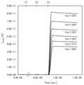
도 16은 시뮬레이션 결과를 설명하는 도면이다.
도 17은 시뮬레이션 결과를 설명하는 도면이다.1 is a diagram for explaining a pixel circuit.
2 is a timing chart for explaining the operation of the pixel circuit.
3 is a diagram for explaining a pixel circuit.
4 is a diagram for explaining a pixel circuit.
5A and 5B are diagrams for explaining a pixel circuit.
Fig. 6A is a diagram for explaining a circuit block. 6B and 6C are diagrams for explaining the configuration of a pixel.
7(A), (B) and (C) are views for explaining a display device.
8A and 8B are diagrams for explaining a touch panel.
9 is a view for explaining a display device.
10 is a diagram for explaining a display device.
11(A1), (A2), (B1), (B2), (C1), and (C2) are diagrams for explaining a transistor.
12 (A1), (A2), (B1), (B2), (C1), and (C2) are diagrams for explaining a transistor.
13 (A1), (A2), (B1), (B2), (C1), and (C2) are diagrams for explaining a transistor.
14 (A1), (A2), (B1), (B2), (C1), and (C2) are diagrams for explaining a transistor.
15(A), (B), (C), (D), (E), and (F) are diagrams for explaining an electronic device.
16 is a diagram for explaining a simulation result.
17 is a diagram for explaining a simulation result.
실시형태에 대해서 도면을 사용하여 자세히 설명한다. 다만 본 발명은 이하의 설명에 한정되지 않으며, 본 발명의 취지 및 그 범위에서 벗어남이 없이 그 형태 및 자세한 사항을 다양하게 변경할 수 있는 것은 통상의 기술자라면 용이하게 이해할 수 있다. 따라서 본 발명은 이하의 실시형태의 기재 내용에 한정하여 해석되는 것은 아니다. 또한 이하에서 설명하는 발명의 구성에서, 동일 부분 또는 같은 기능을 가지는 부분에는 동일한 부호를 다른 도면 간에서 공통적으로 사용하고, 이의 반복적인 설명은 생략하는 경우가 있다. 또한 도면을 구성하는 같은 요소의 해칭을, 상이한 도면 간에서 적절히 생략 또는 변경하는 경우도 있다.EMBODIMENT OF THE INVENTION It demonstrates in detail using drawing about embodiment. However, the present invention is not limited to the following description, and it can be easily understood by those skilled in the art that various changes in form and details can be made without departing from the spirit and scope of the present invention. Therefore, this invention is limited to the description of the following embodiment, and is not interpreted. In addition, in the configuration of the invention described below, the same reference numerals are commonly used between different drawings for the same parts or parts having the same functions, and repeated descriptions thereof are sometimes omitted. Moreover, hatching of the same element which comprises a drawing may be abbreviate|omitted or changed suitably between different drawings.
회로도상에서 단일의 요소로서 도시된 경우에도, 기능적으로 문제가 없으면 상기 요소는 복수로 구성되어도 좋다. 예를 들어 스위치로서 동작하는 트랜지스터는 복수가 직렬 또는 병렬로 접속되어도 좋은 경우가 있다. 또한 커패시터를 분할하여 복수의 위치에 배치하는 경우도 있다.Even when it is shown as a single element on a circuit diagram, if there is no functional problem, the said element may be comprised in plurality. For example, a plurality of transistors operating as a switch may be connected in series or in parallel in some cases. Also, in some cases, capacitors are divided and placed in a plurality of positions.
하나의 도전체가 배선, 전극, 및 단자 등의 복수의 기능을 가지는 경우가 있으며, 본 명세서에서는 동일한 요소에 대하여 복수의 호칭을 사용하는 경우가 있다. 또한 회로도 상에서 요소 간이 직접 접속되는 것처럼 도시된 경우에도, 실제로는 상기 요소 간이 복수의 도전체를 통하여 접속되는 경우가 있고, 본 명세서에서는 이와 같은 구성도 직접 접속의 범주에 포함한다.A single conductor may have a plurality of functions such as wiring, electrodes, and terminals, and in this specification, a plurality of names may be used for the same element. Also, even when elements are shown as being directly connected on a circuit diagram, in reality, elements are connected through a plurality of conductors, and in this specification, such a configuration is also included in the scope of direct connection.
(실시형태 1)(Embodiment 1)
본 실시형태에서는 본 발명의 일 형태인 표시 장치에 대하여 도면을 참조하여 설명한다.In the present embodiment, a display device according to one embodiment of the present invention will be described with reference to the drawings.
본 발명의 일 형태는 화소 내에서 화상 데이터를 보정하는 기능을 가지는 표시 장치이다. 각 화소에는 기억 노드가 제공되고, 상기 기억 노드에 제 1 데이터가 유지될 수 있다. 제 1 데이터는 용량 결합으로 제 2 데이터에 부가되고, 표시 소자에 공급될 수 있다. 또는 상기 기억 노드에 제 2 데이터를 기록한 후에 제 1 데이터를 용량 결합으로 부가할 수도 있다.One embodiment of the present invention is a display device having a function of correcting image data within a pixel. Each pixel may be provided with a storage node, and first data may be held in the storage node. The first data may be added to the second data by capacitive coupling and supplied to the display element. Alternatively, after writing the second data to the storage node, the first data may be added by capacitive coupling.
따라서, 표시 장치에서는 보정된 화상을 표시할 수 있다. 상기 보정에 의하여, 화상의 업컨버트를 수행할 수 있다. 또는 표시 영역에서의 화상의 일부 또는 전체를 보정함으로써 HDR 표시를 수행할 수 있다. 또는 제 1 데이터 및 제 2 데이터로서 같은 화상 데이터를 사용함으로써, 표시 화상의 휘도를 대폭 향상시킬 수 있다. 또는 제 1 데이터 및 제 2 데이터로서 상이한 화상 데이터를 사용함으로써, 임의의 화상을 겹쳐 표시할 수 있다.Accordingly, the display device can display the corrected image. By the above correction, it is possible to upconvert the image. Alternatively, HDR display can be performed by correcting part or all of the image in the display area. Alternatively, by using the same image data as the first data and the second data, the luminance of the displayed image can be significantly improved. Alternatively, arbitrary images can be superimposed and displayed by using different image data as the first data and the second data.
또한 본 발명의 일 형태를 사용함으로써, 고해상도용 및 저해상도용의 2개의 화상 데이터에 대하여 업컨버트 또는 다운컨버트를 수행하는 전용의 회로를 따로 제공하지 않아도 적절한 표시를 수행할 수 있다. 고해상도로 표시하는 경우에는 각 화소가 가지는 제 1 트랜지스터를 경유하여 각 화소에 개별의 데이터를 공급한다. 저해상도로 표시하는 경우에는 복수의 화소와 전기적으로 접속되는 제 2 트랜지스터를 경유하여 상기 복수의 화소에 동일한 데이터를 공급한다.Furthermore, by using one aspect of the present invention, it is possible to perform appropriate display without separately providing a circuit dedicated to up-converting or down-converting two image data for high resolution and low resolution. In the case of high-resolution display, individual data is supplied to each pixel via a first transistor included in each pixel. When displaying at a low resolution, the same data is supplied to the plurality of pixels via a second transistor electrically connected to the plurality of pixels.
여기서, 고해상도용 화상 데이터란, 예를 들어, 8K4K(화소수: 7680×4320)에 대응하는 정보량을 가지는 데이터에 상당한다. 또한 저해상도용 화상 데이터란, 예를 들어, 4K2K(화소수: 3840×2160)에 대응하는 정보량을 가지는 데이터에 상당한다. 즉, 고해상도용 화상 데이터와 저해상도용 화상 데이터의 유효한 데이터양(유효한 화소수에 대응함)의 비율은 4:1인 것을 전제로 한다.Here, the high-resolution image data corresponds to data having an information amount corresponding to, for example, 8K4K (the number of pixels: 7680×4320). Note that the low-resolution image data corresponds to data having an information amount corresponding to, for example, 4K2K (number of pixels: 3840x2160). That is, it is assumed that the ratio of the effective data amount (corresponding to the effective number of pixels) of the high-resolution image data to the low-resolution image data is 4:1.
또한 데이터양(화소수)의 비율이 4:1이면, 상기 예에 한정되지 않고, 고해상도용 화상 데이터가 4K2K에 대응하는 데이터, 저해상도용 화상 데이터가 Full HD(화소수: 1920×1080)에 대응하는 데이터이어도 좋다. 또는 고해상도용 화상 데이터가 16K8K(화소수: 15360×8640)에 대응하는 데이터, 저해상도용 화상 데이터가 8K4K에 대응하는 데이터이어도 좋다.In addition, if the ratio of the data amount (number of pixels) is 4:1, it is not limited to the above example, and the high-resolution image data corresponds to 4K2K data, and the low-resolution image data supports Full HD (the number of pixels: 1920x1080). data may be used. Alternatively, the high-resolution image data may be data corresponding to 16K8K (number of pixels: 15360×8640), and the low-resolution image data may be data corresponding to 8K4K.
또한 본 명세서 등에서 화소란 예를 들어 밝기를 제어할 수 있는 하나의 요소를 나타내는 것으로 한다. 따라서 예를 들어 하나의 화소란 하나의 색 요소를 나타내는 것으로 하고, 그 색 요소 하나로 밝기를 표현한다. 따라서 R(적색) G(녹색) B(청색)의 색 요소로 이루어진 컬러 표시 장치의 경우에는 화상의 최소 단위는 R의 화소와 G의 화소와 B의 화소의 3화소로 구성되는 것으로 한다. 이 경우에는 RGB 각각의 화소를 부화소(서브 화소)라고 부르고, RGB의 부화소를 아울러 화소라고 부르는 경우가 있다.Also, in this specification, for example, a pixel refers to one element capable of controlling brightness. Therefore, for example, it is assumed that one pixel represents one color element, and the brightness is expressed by one color element. Accordingly, in the case of a color display device including color elements of R (red), G (green), and B (blue), the minimum unit of an image is assumed to be composed of three pixels: an R pixel, a G pixel, and a B pixel. In this case, each pixel of RGB may be called a sub-pixel (sub-pixel), and sub-pixel of RGB may be collectively called a pixel.
<구성예 1><Configuration Example 1>
본 발명의 일 형태의 표시 장치에 사용할 수 있는 화소(10)의 구성을 도 1에 나타내었다. 화소(10)는 트랜지스터(101)와, 트랜지스터(102)와, 트랜지스터(103)와, 트랜지스터(104)와, 용량 소자(111)와, 용량 소자(112)와, 발광 소자(114)를 가진다.Fig. 1 shows the configuration of a
발광 소자(114)의 한쪽 전극은 트랜지스터(103)의 소스 및 드레인 중 한쪽과 전기적으로 접속된다. 발광 소자(114)의 한쪽 전극은 용량 소자(112)의 한쪽 전극과 전기적으로 접속된다. 트랜지스터(103)의 게이트는 트랜지스터(102)의 소스 및 드레인 중 한쪽과 전기적으로 접속된다. 트랜지스터(103)의 게이트는 용량 소자(111)의 한쪽 전극과 전기적으로 접속된다. 용량 소자(111)의 다른 쪽 전극은 용량 소자(112)의 다른 쪽 전극과 전기적으로 접속된다. 용량 소자(111)의 다른 쪽 전극은 트랜지스터(101)의 소스 및 드레인 중 한쪽과 전기적으로 접속된다. 또한 발광 소자(114)의 한쪽 전극은 트랜지스터(104)의 소스 및 드레인 중 한쪽과 전기적으로 접속된다.One electrode of the
발광 소자(114)로서 발광 다이오드(LED: Light Emitting Diode), 유기 발광 다이오드(OLED: Organic Light Emitting Diode), 발광층에 퀀텀닷(quantum dot)을 사용한 발광 다이오드(QLED: Quantum-dot Light Emitting Diode), 반도체 레이저 등의, 자발광성 발광 소자를 들 수 있다. 또한 셔터 방식 또는 광 간섭 방식의 MEMS(Micro Electro Mechanical Systems) 소자나, 마이크로캡슐 방식, 전기 영동 방식, 일렉트로 웨팅 방식, 또는 전자 분류체(電子粉流體, Electronic Liquid Powder)(등록 상표) 방식 등을 적용한 표시 소자 등을 사용할 수도 있다.As the
여기서 트랜지스터(102)의 소스 및 드레인 중 한쪽, 용량 소자(111)의 한쪽 전극, 및 트랜지스터(103)의 게이트가 접속되는 배선을 노드 ND1로 한다. 트랜지스터(101)의 소스 및 드레인 중 한쪽, 용량 소자(111)의 다른 쪽 전극, 및 용량 소자(112)의 다른 쪽 전극이 접속되는 배선을 노드 ND2로 한다. 트랜지스터(103)의 소스 및 드레인 중 한쪽, 용량 소자(112)의 한쪽 전극, 및 발광 소자(114)의 한쪽 전극이 접속되는 배선을 노드 ND3으로 한다.Here, a wiring to which one of the source and drain of the
트랜지스터(103)는 발광 소자(114)에 흐르게 하는 전류량을 제어하는 구동 트랜지스터로서 기능한다. 트랜지스터(101) 및 트랜지스터(102)는 화소를 선택하는 선택 트랜지스터로서 기능한다. 트랜지스터(104)는 노드 ND3의 전위가 발광 소자(114)의 문턱 전압 이상이 되는 경우에 발광 소자(114)에 의도하지 않는 전류가 흐른다는 불량 상태가 발생하지 않도록 하는 기능을 가진다. 구체적으로는 트랜지스터(104)는 발광 소자(114)에 전류를 흐르게 하는 기간(발광 기간이라고도 함) 이외의 기간에서 전류가 흐르지 않도록 하기 위한 스위치로서 기능한다.The
트랜지스터(101)의 게이트 및 트랜지스터(104)의 게이트는 배선(121)과 전기적으로 접속된다. 트랜지스터(102)의 게이트는 배선(122)과 전기적으로 접속된다. 트랜지스터(101)의 소스 및 드레인 중 다른 쪽은 배선(131)과 전기적으로 접속된다. 트랜지스터(102)의 소스 및 드레인 중 다른 쪽은 배선(132)과 전기적으로 접속된다. 트랜지스터(104)의 소스 및 드레인 중 다른 쪽은 배선(133)과 전기적으로 접속된다.The gate of the
트랜지스터(103)의 소스 및 드레인 중 다른 쪽은 배선(128)과 전기적으로 접속된다. 발광 소자(114)의 다른 쪽 전극은 배선(129)과 전기적으로 접속된다. 배선(128), 배선(129)은 각각 전원 전위가 공급되는 배선(전원선)으로서 기능한다. 예를 들어 배선(128)은 고전위 전원선으로서 기능시킬 수 있다. 또한 배선(129)은 저전위 전원선으로서 기능시킬 수 있다.The other of the source and drain of the
배선(121) 및 배선(122)은 트랜지스터(101), 트랜지스터(102), 및 트랜지스터(104)의 동작을 제어하기 위한 주사선으로서의 기능을 가진다. 주사선에 공급되는 주사 신호는 화소(10) 내의 스위치로서 기능하는 선택 트랜지스터(트랜지스터(101) 및 트랜지스터(102))의 도통 상태 또는 비도통 상태(온 또는 오프)를 제어하기 위한 신호이다. 또한 주사선에 공급되는 주사 신호는 트랜지스터(104)의 도통 상태 또는 비도통 상태(온 또는 오프)를 제어하기 위한 신호이기도 하다. 배선(132)은 제 1 데이터를 공급하는 데이터선으로서의 기능을 가진다. 데이터선이 전달하는 데이터 신호는 화상의 표시를 수행하기 위한 신호이다. 배선(131)은 제 2 데이터를 공급하는 데이터선으로서의 기능을 가진다. 또한 배선(131)은 화소(10)를 구동시키는 특정의 전위(참조 전압) "Vref"를 공급하는 기능을 가진다. 배선(133)은 정전위(V0)를 공급하는 배선으로서의 기능을 가진다.The
또한 화소는 "Vref" 및 제 1 데이터(예를 들어, 보정 데이터)를 같은 기간에 공급받고, 나중에 설명하는 용량 결합 동작을 수행한다. 그러므로 "Vref"를 신호선으로부터 공급하는 경우에는 적어도 제 1 데이터를 공급하는 신호선과, "Vref" 또는 제 2 데이터(예를 들어, 화상 데이터)를 공급하는 신호선이 필요하게 된다.Also, the pixel is supplied with "Vref" and first data (eg, correction data) in the same period, and performs a capacitive coupling operation described later. Therefore, when "Vref" is supplied from a signal line, at least a signal line for supplying first data and a signal line for supplying "Vref" or second data (eg, image data) are required.
노드 ND1은 기억 노드이고, 트랜지스터(102)를 도통시킴으로써, 배선(132)에 공급된 데이터를 노드 ND1에 기록할 수 있다. 또한 트랜지스터(102)를 비도통으로 함으로써 상기 데이터를 노드 ND1에 유지할 수 있다.The node ND1 is a storage node, and by making the
노드 ND2는 기억 노드이고, 트랜지스터(101)를 도통시킴으로써, 배선(131)에 공급된 데이터를 노드 ND2에 기록할 수 있다. 또한 트랜지스터(101)를 비도통으로 함으로써 상기 데이터를 노드 ND2에 유지할 수 있다.The node ND2 is a storage node, and by making the
노드 ND3은 기억 노드이고, 트랜지스터(104)를 도통시킴으로써, 배선(133)에 공급된 데이터를 노드 ND3에 기록할 수 있다. 또한 트랜지스터(104)를 비도통으로 함으로써 상기 데이터를 노드 ND3에 유지할 수 있다.The node ND3 is a storage node, and by turning the
트랜지스터(101), 트랜지스터(102), 트랜지스터(103), 및 트랜지스터(104) 중 어느 하나 이상에, 오프 전류가 매우 낮은 트랜지스터를 사용하는 것이 바람직하다. 특히, 트랜지스터(101), 트랜지스터(102), 및 트랜지스터(104)에 오프 전류가 매우 낮은 트랜지스터를 사용함으로써, 누설 전류를 억제할 수 있다. 또한 노드 ND1, 노드 ND2, 및 노드 ND3의 전위를 장시간 유지하는 것이 가능하게 된다. 상기 트랜지스터에는 예를 들어 채널 형성 영역에 금속 산화물을 사용한 트랜지스터(이하, OS 트랜지스터)를 적합하게 사용할 수 있다.For one or more of the
또한 트랜지스터(101), 트랜지스터(102), 트랜지스터(103), 및 트랜지스터(104) 모두에 OS 트랜지스터를 적용하는 것이 더 바람직하다. 또한 트랜지스터(101), 트랜지스터(102), 트랜지스터(103), 및 트랜지스터(104) 이외의 트랜지스터에 OS 트랜지스터를 적용하여도 좋다. 또한 누설 전류량의 허용 범위 내에서 동작을 수행하는 경우에는 채널 형성 영역에 실리콘을 가지는 트랜지스터(이하, Si 트랜지스터)를 적용하여도 좋다. 또는 OS 트랜지스터 및 Si 트랜지스터를 병용하여도 좋다. 또한 상기 Si 트랜지스터로서는 비정질 실리콘을 가지는 트랜지스터, 결정성 실리콘(미결정 실리콘, 저온 폴리실리콘, 단결정 실리콘)을 가지는 트랜지스터 등을 들 수 있다. 또한 도 1에 나타낸 트랜지스터는 모두 n채널형 트랜지스터이지만, p채널형 트랜지스터를 사용할 수도 있다.It is also more preferable to apply the OS transistor to all of the
OS 트랜지스터에 사용하는 반도체 재료로서는 에너지 갭이 2eV 이상, 바람직하게는 2.5eV 이상, 더 바람직하게는 3eV 이상인 금속 산화물을 사용할 수 있다. 대표적으로는 인듐을 포함한 산화물 반도체 등이 있고, 예를 들어 후술하는 CAAC-OS(C-Axis Aligned Crystalline Oxide Semiconductor) 또는 CAC-OS(Cloud-Aligned Composite Oxide Semiconductor) 등을 사용할 수 있다. CAAC-OS는 안정적인 결정 구조를 가지고, 신뢰성을 중요시하는 트랜지스터 등에 적합하다. 또한 CAC-OS는 이동도 특성이 높기 때문에, 고속 구동을 수행하는 트랜지스터 등에 적합하다.As the semiconductor material used for the OS transistor, a metal oxide having an energy gap of 2 eV or more, preferably 2.5 eV or more, and more preferably 3 eV or more can be used. Representative examples include an oxide semiconductor including indium, and for example, a C-Axis Aligned Crystalline Oxide Semiconductor (CAAC-OS) or a Cloud-Aligned Composite Oxide Semiconductor (CAC-OS), which will be described later, may be used. CAAC-OS has a stable crystal structure and is suitable for transistors that value reliability. In addition, since the CAC-OS has high mobility, it is suitable for high-speed driving transistors and the like.
OS 트랜지스터는 반도체층의 에너지갭이 크기 때문에 채널 폭 1μm당 오프 전류값이 수yA/μm(y는 10-24)라는 매우 낮은 오프 전류 특성을 나타낼 수 있다. 또한 OS 트랜지스터는 충격 이온화, 애벌란시(avalanche) 항복, 및 단채널 효과 등이 발생하지 않는다는 등 Si 트랜지스터와는 다른 특징을 가지기 때문에, 신뢰성이 높은 회로를 형성할 수 있다. 또한 Si 트랜지스터에서 문제가 되는 결정성의 불균일로 인한 전기 특성의 편차도 OS 트랜지스터에서는 일어나기 어렵다.Since the semiconductor layer has a large energy gap, the OS transistor can exhibit a very low off-current characteristic ofseveral yA/μm (y is 10-24 ) of an off-current value per 1 μm of channel width. In addition, since the OS transistor has characteristics different from those of the Si transistor, such as that shock ionization, avalanche breakdown, and short channel effect do not occur, a circuit with high reliability can be formed. In addition, variation in electrical characteristics due to non-uniformity of crystallinity, which is a problem in Si transistors, is unlikely to occur in OS transistors.
OS 트랜지스터가 가지는 반도체층은 예를 들어 인듐, 아연, 및 M(알루미늄, 타이타늄, 갈륨, 저마늄, 이트륨, 지르코늄, 란타넘, 세륨, 주석, 네오디뮴, 및 하프늄 중 하나 이상)을 포함하는 In-M-Zn계 산화물로 표기되는 막으로 할 수 있다.The semiconductor layer of the OS transistor includes, for example, In- containing indium, zinc, and M (one or more of aluminum, titanium, gallium, germanium, yttrium, zirconium, lanthanum, cerium, tin, neodymium, and hafnium). It can be set as the film|membrane represented by the M-Zn-type oxide.
반도체층을 구성하는 산화물 반도체가 In-M-Zn계 산화물인 경우, In-M-Zn 산화물을 성막하기 위하여 사용되는 스퍼터링 타깃의 금속 원소의 원자수비는 In≥M, Zn≥M을 만족시키는 것이 바람직하다. 이러한 스퍼터링 타깃의 금속 원소의 원자수비로서, In:M:Zn=1:1:1, In:M:Zn=1:1:1.2, In:M:Zn=3:1:2, In:M:Zn=4:2:3, In:M:Zn=4:2:4.1, In:M:Zn=5:1:6, In:M:Zn=5:1:7, In:M:Zn=5:1:8 등이 바람직하다. 또한 성막되는 반도체층의 원자수비는 각각, 상기 스퍼터링 타깃에 포함되는 금속 원소의 원자수비의 ±40%의 변동을 포함한다.When the oxide semiconductor constituting the semiconductor layer is an In-M-Zn-based oxide, the atomic ratio of the metal element of the sputtering target used to form the In-M-Zn oxide satisfies In≥M and Zn≥M. desirable. As the atomic ratio of the metal elements of the sputtering target, In:M:Zn=1:1:1, In:M:Zn=1:1:1.2, In:M:Zn=3:1:2, In:M :Zn=4:2:3, In:M:Zn=4:2:4.1, In:M:Zn=5:1:6, In:M:Zn=5:1:7, In:M:Zn =5:1:8 and the like are preferable. In addition, each of the atomic ratios of the semiconductor layers to be formed includes a variation of ±40% of the atomic ratios of the metal elements contained in the sputtering target.
반도체층으로서는 캐리어 농도가 낮은 산화물 반도체를 사용한다. 예를 들어 반도체층에는 캐리어 농도가 1×10¹⁷/cm3 이하, 바람직하게는 1×10¹⁵/cm3 이하, 더 바람직하게는 1×10¹³/cm3 이하, 더욱 바람직하게는 1×10¹¹/cm3 이하, 더욱더 바람직하게는 1×10¹⁰/cm3 미만이고, 1×10⁻⁹/cm3 이상인 산화물 반도체를 사용할 수 있다. 이와 같은 산화물 반도체를 고순도 진성 또는 실질적으로 고순도 진성의 산화물 반도체라고 한다. 상기 산화물 반도체는 결함 준위 밀도가 낮고, 안정된 특성을 가지는 산화물 반도체라고 할 수 있다.As the semiconductor layer, an oxide semiconductor having a low carrier concentration is used. For example, the semiconductor layer has a carrier concentration of 1×10¹⁷ /cm3 or less, preferably 1×10¹⁵ /cm3 or less, more preferably 1×10¹³ /cm3 or less, still more preferably 1×10¹¹ /cm3 or less, more preferably less than 1×10¹⁰ /cm3 , and 1×10⁻⁹ /cm3 or more can be used. Such an oxide semiconductor is called a high-purity intrinsic or substantially high-purity intrinsic oxide semiconductor. The oxide semiconductor may be an oxide semiconductor having a low density of defect states and stable characteristics.
또한 이들에 한정되지 않고, 필요로 하는 트랜지스터의 반도체 특성 및 전기 특성(전계 효과 이동도, 문턱 전압 등)에 따라 적절한 조성의 것을 사용하면 좋다. 또한 필요로 하는 트랜지스터의 반도체 특성을 얻기 위하여, 반도체층의 캐리어 농도나 불순물 농도, 결함 밀도, 금속 원소와 산소의 원자수비, 원자간 거리, 밀도 등을 적절한 것으로 하는 것이 바람직하다.Moreover, it is not limited to these, It is good to use the thing of an appropriate composition according to the semiconductor characteristic and electrical characteristic (field effect mobility, threshold voltage, etc.) of a required transistor. In addition, in order to obtain the required semiconductor characteristics of the transistor, it is preferable that the carrier concentration, the impurity concentration, the defect density, the atomic ratio of the metal element and oxygen, the interatomic distance, the density, etc. of the semiconductor layer are appropriate.
반도체층을 구성하는 산화물 반도체에 14족 원소의 하나인 실리콘이나 탄소가 포함되면, 산소 결손이 증가되어 n형화된다. 그러므로, 반도체층에서의 실리콘이나 탄소의 농도(이차 이온 질량 분석법에 의하여 얻어지는 농도)를 2×10¹⁸atoms/cm3 이하, 바람직하게는 2×10¹⁷atoms/cm3 이하로 한다.When silicon or carbon, which is one of the group 14 elements, is included in the oxide semiconductor constituting the semiconductor layer, oxygen vacancies are increased and n-type is formed. Therefore, the concentration of silicon or carbon in the semiconductor layer (concentration obtained by secondary ion mass spectrometry) is 2×10¹⁸ atoms/cm3 or less, preferably 2×10¹⁷ atoms/cm3 or less.
알칼리 금속 및 알칼리 토금속은 산화물 반도체에 포함되는 성분과 결합되면 캐리어를 생성하는 경우가 있고, 트랜지스터의 오프 전류가 증대되는 경우가 있다. 그래서 반도체층에서의 알칼리 금속 또는 알칼리 토금속의 농도(이차 이온 질량 분석법에 의하여 얻어지는 농도)를 1×10¹⁸atoms/cm3 이하, 바람직하게는 2×10¹⁶atoms/cm3 이하로 한다.When alkali metals and alkaline earth metals combine with components included in the oxide semiconductor, carriers may be generated, and the off-state current of the transistor may be increased. Therefore, the concentration (concentration obtained by secondary ion mass spectrometry) of the alkali metal or alkaline earth metal in the semiconductor layer is set to 1×10¹⁸ atoms/cm3 or less, preferably 2×10¹⁶ atoms/cm3 or less.
반도체층을 구성하는 산화물 반도체에 질소가 포함되면, 산화물 반도체 중에 캐리어가 되는 전자가 생김으로써 캐리어 농도가 증가되어 n형화되기 쉽다. 이 결과, 질소가 포함되는 산화물 반도체를 사용한 트랜지스터는 노멀리 온 특성을 가지기 쉽다. 그러므로 반도체층에서의 질소 농도(이차 이온 질량 분석법으로 얻어지는 농도)는 5×10¹⁸atoms/cm3 이하로 하는 것이 바람직하다.When nitrogen is contained in the oxide semiconductor constituting the semiconductor layer, electrons serving as carriers are generated in the oxide semiconductor, so that the carrier concentration is increased and the n-type is likely to be formed. As a result, a transistor using an oxide semiconductor containing nitrogen tends to have normally-on characteristics. Therefore, the nitrogen concentration (concentration obtained by secondary ion mass spectrometry) in the semiconductor layeris preferably 5×10 18 atoms/cm3 or less.
반도체층을 구성하는 산화물 반도체에 수소가 포함되면, 산화물 반도체 중에 포함되는 금속 원자와 결합되는 산소와 반응하여 물이 되기 때문에, 산화물 반도체 내에 산소 결손을 형성하는 경우가 있다. 산화물 반도체 내의 채널 형성 영역에 산소 결손이 포함되면, 트랜지스터는 노멀리 온 특성을 가지는 경우가 있다. 또한, 산소 결손에 수소가 들어간 결함은 도너로서 기능하고, 캐리어인 전자가 생성되는 경우가 있다. 또한 수소의 일부가 금속 원자와 결합되는 산소와 결합되어 캐리어인 전자를 생성하는 경우가 있다. 따라서 수소를 많이 포함하는 산화물 반도체를 사용한 트랜지스터는 노멀리 온 특성을 가지기 쉽다.When hydrogen is contained in the oxide semiconductor constituting the semiconductor layer, it reacts with oxygen bound to a metal atom contained in the oxide semiconductor to form water, thereby forming oxygen vacancies in the oxide semiconductor in some cases. When oxygen vacancies are included in the channel formation region in the oxide semiconductor, the transistor may have normally-on characteristics. Moreover, the defect in which hydrogen entered oxygen vacancies functions as a donor, and the electron which is a carrier may generate|occur|produce. In addition, there are cases where a part of hydrogen is combined with oxygen that is bonded to a metal atom to generate electrons as carriers. Therefore, a transistor using an oxide semiconductor containing a lot of hydrogen tends to have a normally-on characteristic.
산소 결손에 수소가 들어간 결함은 산화물 반도체의 도너로서 기능할 수 있다. 그러나 상기 결함을 정량적으로 평가하는 것은 어렵다. 그러므로 산화물 반도체에서는 도너 농도가 아니라 캐리어 농도로 평가되는 경우가 있다. 따라서 본 명세서 등에서는 산화물 반도체의 파라미터로서 도너 농도가 아니라 전계가 인가되지 않는 상태를 상정한 캐리어 농도를 사용하는 경우가 있다. 즉, 본 명세서 등에 기재되는 "캐리어 농도"는 "도너 농도"라고 바꿔 말할 수 있는 경우가 있다.The defect in which hydrogen entered the oxygen vacancy can function as a donor of the oxide semiconductor. However, it is difficult to quantitatively evaluate the defect. Therefore, in an oxide semiconductor, evaluation may be made by the carrier concentration rather than the donor concentration. Therefore, in this specification and the like, there are cases where, as a parameter of the oxide semiconductor, a carrier concentration assuming a state in which no electric field is applied, not a donor concentration, is used. That is, "carrier concentration" described in this specification and the like may be interchangeably referred to as "donor concentration".
그러므로 산화물 반도체 내의 수소는 가능한 한 저감되어 있는 것이 바람직하다. 구체적으로는 이차 이온 질량 분석법(SIMS: Secondary Ion Mass Spectrometry)으로 얻어지는 산화물 반도체의 수소 농도를 1×10²⁰atoms/cm3 미만, 바람직하게는 1×10¹⁹atoms/cm3 미만, 더 바람직하게는 5×10¹⁸atoms/cm3 미만, 더욱 바람직하게는 1×10¹⁸atoms/cm3 미만으로 한다. 수소 등의 불순물이 충분히 저감된 산화물 반도체를 트랜지스터의 채널 형성 영역에 사용함으로써, 안정된 전기 특성을 부여할 수 있다.Therefore, it is preferable that hydrogen in the oxide semiconductor be reduced as much as possible. Specifically, the hydrogen concentration of the oxide semiconductor obtained by secondary ion mass spectrometry (SIMS) isless than 1×10 20 atoms/cm3 , preferably less than 1×10¹⁹ atoms/cm3 , more preferably Less than 5×10¹⁸ atoms/cm3 , more preferably less than 1×10¹⁸ atoms/cm3 . By using an oxide semiconductor in which impurities such as hydrogen have been sufficiently reduced for the channel formation region of the transistor, stable electrical characteristics can be imparted.
산화물 반도체(금속 산화물)는 단결정 산화물 반도체와 그 외의 비단결정 산화물 반도체로 나누어진다. 비단결정 산화물 반도체로서는 예를 들어 CAAC-OS, 다결정 산화물 반도체, nc-OS(nanocrystalline oxide semiconductor), a-like OS(amorphous-like oxide semiconductor), 및 비정질 산화물 반도체 등이 있다. 비단결정 구조에서 비정질 구조는 결함 준위 밀도가 가장 높고, CAAC-OS는 결함 준위 밀도가 가장 낮다.Oxide semiconductors (metal oxides) are divided into single-crystal oxide semiconductors and other non-single-crystal oxide semiconductors. Examples of the non-single crystal oxide semiconductor include CAAC-OS, polycrystalline oxide semiconductor, nc-OS (nanocrystalline oxide semiconductor), a-like OS (amorphous-like oxide semiconductor), and amorphous oxide semiconductor. In the non-single crystal structure, the amorphous structure has the highest density of defect states, and the CAAC-OS has the lowest density of defect states.
비정질 구조를 가지는 산화물 반도체막은 예를 들어 원자 배열이 무질서하고 결정 성분을 가지지 않는다. 또는 비정질 구조를 가지는 산화물막은 예를 들어 완전한 비정질 구조이고 결정부를 가지지 않는다.An oxide semiconductor film having an amorphous structure has, for example, disordered atomic arrangement and no crystalline component. Alternatively, the oxide film having an amorphous structure has, for example, a completely amorphous structure and does not have a crystal part.
또한 반도체층은 비정질 구조의 영역, 미결정 구조의 영역, 다결정 구조의 영역, CAAC-OS의 영역, 단결정 구조의 영역 중 2종류 이상을 가지는 혼합막이어도 좋다. 혼합막은 예를 들어 상술한 영역 중 어느 2종류 이상의 영역을 포함하는 단층 구조 또는 적층 구조를 가지는 경우가 있다.Further, the semiconductor layer may be a mixed film having two or more types of a region of an amorphous structure, a region of a microcrystalline structure, a region of a polycrystalline structure, a region of CAAC-OS, and a region of a single crystal structure. The mixed film may have, for example, a single-layer structure or a laminated structure including any two or more types of regions among the above-mentioned regions.
이하에서는 비단결정의 반도체층의 일 형태인 CAC-OS의 구성에 대하여 설명한다.Hereinafter, the configuration of the CAC-OS, which is one form of a non-single-crystal semiconductor layer, will be described.
CAC-OS란, 예를 들어 산화물 반도체를 구성하는 원소가 0.5nm 이상 10nm 이하, 바람직하게는 1nm 이상 2nm 이하, 또는 그 근방의 크기로 편재(偏在)된 재료의 한 구성을 말한다. 또한 이하에서는 산화물 반도체에서 하나 또는 그 이상의 금속 원소가 편재되고, 상기 금속 원소를 포함하는 영역이 0.5nm 이상 10nm 이하, 바람직하게는 1nm 이상 2nm 이하, 또는 그 근방의 크기로 혼합된 상태를 모자이크 패턴 또는 패치 패턴이라고도 한다.CAC-OS refers to, for example, one configuration of a material in which elements constituting an oxide semiconductor are distributed in a size of 0.5 nm or more and 10 nm or less, preferably 1 nm or more and 2 nm or less, or a size in the vicinity thereof. In addition, in the following, one or more metal elements are ubiquitous in the oxide semiconductor, and the region containing the metal elements is mixed with a size of 0.5 nm or more and 10 nm or less, preferably 1 nm or more and 2 nm or less, or a mosaic pattern. Also called a patch pattern.
또한 산화물 반도체는 적어도 인듐을 포함하는 것이 바람직하다. 특히 인듐 및 아연을 포함하는 것이 바람직하다. 또한 이에 더하여 알루미늄, 갈륨, 이트륨, 구리, 바나듐, 베릴륨, 붕소, 실리콘, 타이타늄, 철, 니켈, 저마늄, 지르코늄, 몰리브데넘, 란타넘, 세륨, 네오디뮴, 하프늄, 탄탈럼, 텅스텐, 및 마그네슘 등 중에서 선택된 1종류 또는 복수 종류가 포함되어도 좋다.Moreover, it is preferable that an oxide semiconductor contains indium at least. It is particularly preferred to include indium and zinc. Also in addition thereto, aluminum, gallium, yttrium, copper, vanadium, beryllium, boron, silicon, titanium, iron, nickel, germanium, zirconium, molybdenum, lanthanum, cerium, neodymium, hafnium, tantalum, tungsten, and magnesium One type or multiple types selected from among others may be included.
예를 들어, In-Ga-Zn 산화물에서의 CAC-OS(CAC-OS 중에서도 In-Ga-Zn 산화물을 특히 CAC-IGZO라고 불러도 좋음)란, 인듐 산화물(이하, InOX1(X1은 0보다 큰 실수)로 함) 또는 인듐 아연 산화물(이하, InX2ZnY2OZ2(X2, Y2, 및 Z2는 0보다 큰 실수)로 함)과, 갈륨 산화물(이하, GaOX3(X3은 0보다 큰 실수)으로 함) 또는 갈륨 아연 산화물(이하, GaX4ZnY4OZ4(X4, Y4, 및 Z4는 0보다 큰 실수)로 함) 등으로 재료가 분리됨으로써 모자이크 패턴이 되고, 모자이크 패턴의 InOX1 또는 InX2ZnY2OZ2가 막 내에 균일하게 분포된 구성(이하, 클라우드상이라고도 함)이다.For example, CAC-OS in In-Ga-Zn oxide (in CAC-OS, In-Ga-Zn oxide in particular may be called CAC-IGZO) is indium oxide (hereinafter, InOX1 (X1 is greater than 0) real number) or indium zinc oxide (hereinafter referred to as InX2 ZnY2 OZ2 (X2, Y2, and Z2 are real numbers greater than 0)) and gallium oxide (hereinafter referred to as GaOX3 (X3 is a real number greater than 0)) ) as hereinafter), or gallium zinc oxide (hereinafter, GaX4 ZnY4 OZ4 (X4, Y4, and Z4 is a material separated as such also as a real number greater than 0)), thereby being a mosaic pattern, a mosaic pattern of InOX1 or InX2 ZnY2 OZ2 is uniformly distributed in the film (hereinafter also referred to as cloud phase).
즉, CAC-OS는 GaOX3이 주성분인 영역과, InX2ZnY2OZ2 또는 InOX1이 주성분인 영역이 혼합된 구성을 가지는 복합 산화물 반도체이다. 또한 본 명세서에서 예를 들어 제 1 영역의 원소 M에 대한 In의 원자수비가, 제 2 영역의 원소 M에 대한 In의 원자수비보다 큰 것을 '제 1 영역은 제 2 영역과 비교하여 In의 농도가 높다'라고 한다.That is, the CAC-OS is a composite oxide semiconductor having a configuration in which a region containingGaO X3 as a main component and a region containing as a main component InX2 ZnY2 OZ2 or InOX1 are mixed. In addition, in the present specification, for example, when the atomic ratio of In to the element M in the first region is greater than the atomic ratio of In to the element M in the second region, 'the first region has a concentration of In compared to the second region. is high'.
또한 IGZO는 통칭이며, In, Ga, Zn, 및 O로 이루어지는 하나의 화합물을 뜻하는 경우가 있다. 대표적인 예로서, InGaO3(ZnO)m1(m1은 자연수임) 또는 In(1+x0)Ga(1-x0)O3(ZnO)m0(-1≤x0≤1, m0은 임의의 수임)으로 나타내어지는 결정성 화합물을 들 수 있다.In addition, IGZO is a generic name, and may mean one compound which consists of In, Ga, Zn, and O. As a representative example, InGaO3 (ZnO)m1 (m1 is a natural number) or In(1+x0) Ga(1-x0) O3 (ZnO)m0 (-1≤x0≤1, m0 is any number) The crystalline compound shown is mentioned.
상기 결정성 화합물은 단결정 구조, 다결정 구조, 또는 CAAC 구조를 가진다. 또한 CAAC 구조란, 복수의 IGZO의 나노 결정이 c축 배향을 가지며 a-b면에서는 배향하지 않고 연결된 결정 구조를 말한다.The crystalline compound has a single crystal structure, a polycrystalline structure, or a CAAC structure. In addition, the CAAC structure refers to a crystal structure in which a plurality of IGZO nanocrystals have a c-axis orientation and are connected without being oriented in the a-b plane.
한편, CAC-OS는 산화물 반도체의 재료 구성에 관한 것이다. CAC-OS란 In, Ga, Zn, 및 O를 포함하는 재료 구성에서, Ga를 주성분으로 하는 나노 입자상의 영역이 일부에서 관찰되고, In을 주성분으로 하는 나노 입자상의 영역이 일부에서 관찰되고, 각각이 모자이크 패턴으로 무작위로 분산된 구성을 말한다. 따라서 CAC-OS에서 결정 구조는 부차적인 요소이다.On the other hand, CAC-OS relates to the material composition of oxide semiconductors. CAC-OS means that in a material composition containing In, Ga, Zn, and O, a region on nanoparticles containing Ga as a main component is observed in a part, and a region on a nanoparticle containing In as a main component is observed in a part, each It refers to a randomly dispersed composition in this mosaic pattern. Therefore, in CAC-OS, the crystal structure is a secondary element.
또한 CAC-OS는 조성이 다른 2종류 이상의 막의 적층 구조를 포함하지 않는 것으로 한다. 예를 들어 In을 주성분으로 하는 막과 Ga를 주성분으로 하는 막의 2층으로 이루어지는 구조는 포함하지 않는다.In addition, it is assumed that the CAC-OS does not include a laminated structure of two or more types of films having different compositions. For example, a structure consisting of two layers of a film containing In as a main component and a film containing Ga as a main component is not included.
또한 GaOX3이 주성분인 영역과, InX2ZnY2OZ2 또는 InOX1이 주성분인 영역 사이에서는 명확한 경계가 관찰되지 않는 경우가 있다.In addition, a clear boundary may not be observed between the area|region whose main component is GaO X3 and the area|region whose main component is InX2 ZnY2 OZ2 or InOX1.
또한 갈륨 대신에 알루미늄, 이트륨, 구리, 바나듐, 베릴륨, 붕소, 실리콘, 타이타늄, 철, 니켈, 저마늄, 지르코늄, 몰리브데넘, 란타넘, 세륨, 네오디뮴, 하프늄, 탄탈럼, 텅스텐, 및 마그네슘 등 중에서 선택된 1종류 또는 복수 종류가 포함되는 경우, CAC-OS란 상기 금속 원소를 주성분으로 하는 나노 입자상의 영역이 일부에서 관찰되고, In을 주성분으로 하는 나노 입자상의 영역이 일부에서 관찰되고, 각각이 모자이크 패턴으로 무작위로 분산된 구성을 말한다.Also, instead of gallium, aluminum, yttrium, copper, vanadium, beryllium, boron, silicon, titanium, iron, nickel, germanium, zirconium, molybdenum, lanthanum, cerium, neodymium, hafnium, tantalum, tungsten, and magnesium, etc. When one type or a plurality of types selected from among are included, CAC-OS means that a region on nanoparticles containing the metal element as a main component is observed in a part, and a region on a nanoparticle containing In as a main component is observed in a part, and each It refers to a randomly distributed composition in a mosaic pattern.
CAC-OS는 예를 들어 기판을 가열하지 않는 조건에서 스퍼터링법으로 형성할 수 있다. 또한 CAC-OS를 스퍼터링법으로 형성하는 경우, 성막 가스로서 불활성 가스(대표적으로는 아르곤), 산소 가스, 및 질소 가스 중에서 선택된 어느 하나 또는 복수를 사용하면 좋다. 또한 성막 시의 성막 가스의 총유량에 대한 산소 가스의 유량비는 낮을수록 바람직하고, 예를 들어 산소 가스의 유량비를 0% 이상 30% 미만, 바람직하게는 0% 이상 10% 이하로 하는 것이 바람직하다.The CAC-OS can be formed, for example, by sputtering under conditions in which the substrate is not heated. In the case of forming the CAC-OS by sputtering, any one or more selected from an inert gas (typically argon), oxygen gas, and nitrogen gas may be used as the film forming gas. In addition, it is preferable that the flow rate ratio of oxygen gas to the total flow rate of the film forming gas during film formation is lower, for example, it is preferable that the flow rate ratio of oxygen gas is 0% or more and less than 30%, preferably 0% or more and 10% or less. .
CAC-OS는 X선 회절(XRD: X-ray Diffraction) 측정법의 하나인 Out-of-plane법에 의한 θ/2θ 스캔을 사용하여 측정하였을 때, 명확한 피크가 관찰되지 않는다는 특징을 가진다. 즉, X선 회절 측정으로부터 측정 영역의 a-b면 방향 및 c축 방향의 배향이 보이지 않는다는 것을 알 수 있다.When CAC-OS is measured using a θ/2θ scan by an out-of-plane method, which is one of X-ray diffraction (XRD) measurement methods, a clear peak is not observed. That is, it can be seen from the X-ray diffraction measurement that the orientation in the a-b plane direction and the c-axis direction of the measurement region is not seen.
CAC-OS는 프로브 직경이 1nm인 전자선(나노 빔 전자선이라고도 함)을 조사함으로써 얻어지는 전자선 회절 패턴에서, 링 형상으로 휘도가 높은 영역(링 영역)이 관측되고, 상기 링 영역에 복수의 휘점이 관측된다. 따라서 전자선 회절 패턴으로부터 CAC-OS의 결정 구조가 평면 방향 및 단면 방향에서 배향성을 가지지 않는 nc(nanocrystal) 구조를 가진다는 것을 알 수 있다.In the CAC-OS electron beam diffraction pattern obtained by irradiating an electron beam with a probe diameter of 1 nm (also referred to as a nanobeam electron beam), a ring-shaped high luminance region (ring region) is observed, and a plurality of bright spots are observed in the ring region. do. Therefore, it can be seen from the electron beam diffraction pattern that the crystal structure of the CAC-OS has a nanocrystal (nc) structure that does not have orientation in the plane direction and the cross-sectional direction.
예를 들어 In-Ga-Zn 산화물에서의 CAC-OS는 에너지 분산형 X선 분광법(EDX: Energy Dispersive X-ray Spectroscopy)을 사용하여 취득한 EDX 매핑으로부터, GaOX3이 주성분인 영역과, InX2ZnY2OZ2 또는 InOX1이 주성분인 영역이 편재되고 혼합된 구조를 가진다는 것을 확인할 수 있다.For example, CAC-OS in In-Ga-Zn oxide is determined from the EDX mapping obtained using Energy Dispersive X-ray Spectroscopy (EDX), the region containing GaO X3 as the main component, and InX2 ZnIt can be seen that the regions in which Y2 OZ2 or InOX1 are the main components have a localized and mixed structure.
CAC-OS는 금속 원소가 균일하게 분포된 IGZO 화합물과는 다른 구조이고, IGZO 화합물과는 다른 성질을 가진다. 즉, CAC-OS는 GaOX3 등이 주성분인 영역과, InX2ZnY2OZ2 또는 InOX1이 주성분인 영역으로 서로 상분리(相分離)되어, 각 원소를 주성분으로 하는 영역이 모자이크 패턴인 구조를 가진다.CAC-OS has a structure different from the IGZO compound in which the metal element is uniformly distributed, and has different properties from the IGZO compound. That is, the CAC-OS is phase-separated from each other into a region mainly composedof GaO X3, etc. and a region containing InX2 ZnY2 OZ2 or InOX1 as a main component. have
여기서, InX2ZnY2OZ2 또는 InOX1이 주성분인 영역은 GaOX3 등이 주성분인 영역과 비교하여 도전성이 높다. 즉, InX2ZnY2OZ2 또는 InOX1이 주성분인 영역을 캐리어가 흐름으로써, 산화물 반도체로서의 도전성이 나타난다. 따라서 InX2ZnY2OZ2 또는 InOX1이 주성분인 영역이 산화물 반도체 내에 클라우드상으로 분포됨으로써, 높은 전계 효과 이동도(μ)를 실현할 수 있다.Here, aregion containing In X2 ZnY2 OZ2 or InOX1 as a main component has higher conductivity than a region containingGaO X3 or the like as a main component. That is,when carriers flow through a region containing In X2 ZnY2 OZ2 or InOX1 as a main component, conductivity as an oxide semiconductor appears. Accordingly, a region containing In X2 ZnY2 OZ2 or InOX1 as a main component is distributed in a cloud form in the oxide semiconductor, thereby realizing a high field effect mobility (μ).
한편, GaOX3 등이 주성분인 영역은 InX2ZnY2OZ2 또는 InOX1이 주성분인 영역과 비교하여 절연성이 높다. 즉, GaOX3 등이 주성분인 영역이 산화물 반도체 내에 분포됨으로써, 누설 전류를 억제하고 양호한 스위칭 동작을 실현할 수 있다.On the other hand, theregion in which GaO X3 or the like is a main component has higher insulating properties than theregion in which In X2 ZnY2 OZ2 or InOX1 is the main component. That is, since theregion in which GaO X 3 or the like is a main component is distributed in the oxide semiconductor, leakage current can be suppressed and good switching operation can be realized.
따라서 CAC-OS를 반도체 소자에 사용한 경우, GaOX3 등에 기인하는 절연성과, InX2ZnY2OZ2 또는 InOX1에 기인하는 도전성이 상보적으로 작용함으로써, 높은 온 전류(Ion) 및 높은 전계 효과 이동도(μ)를 실현할 수 있다.Therefore, when CAC-OS is used for a semiconductor device,the insulation due to GaO X3 and the like and the conductivity due to InX2 ZnY2 OZ2 or InOX1 act complementary, resulting in a high on-current (Ion ) and a high electric field effect. Mobility (μ) can be realized.
또한 CAC-OS를 사용한 반도체 소자는 신뢰성이 높다. 따라서 CAC-OS는 다양한 반도체 장치의 구성 재료로서 적합하다.In addition, semiconductor devices using CAC-OS have high reliability. Therefore, CAC-OS is suitable as a constituent material of various semiconductor devices.
도 2에 나타낸 타이밍 차트를 사용하여, 화상 데이터에 보정 데이터를 부가하는 화소(10)의 동작의 일례에 대하여 설명한다. 또한 이하의 설명에서는 고전위를 "High"로 나타내고, 저전위를 "Low"로 나타낸다. 또한 보정 데이터를 "Vw"로 하고, 화상 데이터를 "Vdata"로 하고, 특정의 전위를 "Vref"로 한다. "Vref"로서 예를 들어 0V, GND 전위, 또는 특정의 기준 전위를 사용할 수 있다. 또한 "Vw"는 임의의 제 1 데이터이고, "Vdata"는 임의의 제 2 데이터라고 할 수도 있다.An example of the operation of the
우선 보정 데이터 "Vw"는 노드 ND1에 기록하는 동작에 대하여 설명한다. 또한 여기서는 전위의 분배, 결합, 또는 손실에서 회로의 구성이나 동작 타이밍 등에 기인하는 자세한 변화는 감안하지 않는다.First, the operation of writing the correction data "Vw" to the node ND1 will be described. In addition, detailed changes due to circuit configuration or operation timing in potential distribution, coupling, or loss are not taken into account here.
시각 T1에서 배선(121)의 전위를 "High"로 하고, 배선(122)의 전위를 "High"로 하고, 배선(131)의 전위를 "Vref"로 하고, 배선(132)의 전위를 "Vw"로 하면 트랜지스터(101), 트랜지스터(102), 및 트랜지스터(104)가 도통되고, 노드 ND1에 배선(132)의 전위 "Vw"가 기록되고, 노드 ND2에 배선(131)의 전위 "Vref"가 기록되고, 노드 ND3에 배선(133)의 전위 "V0"가 기록된다. "V0"는 발광 소자(114)에 전류가 흐르지 않는 전위, 즉 발광 소자(114)의 문턱 전압 이하가 되는 전위로 하는 것이 바람직하다.At time T1, the potential of the
이때, 용량 소자(111)의 양쪽 단부에 인가되는 전위차를 V1로 하면 전위차 V1은 식(1)으로 나타낼 수 있다.In this case, if the potential difference applied to both ends of the
V1=Vw-Vref (1)V1=Vw-Vref (1)
마찬가지로, 용량 소자(112)의 양쪽 단부에 인가되는 전위차를 V2로 하면 전위차 V2는 식(2)으로 나타낼 수 있다.Similarly, if the potential difference applied to both ends of the
V2=Vref-V0 (2)V2=Vref-V0 (2)
여기까지가 보정 데이터 "Vw"의 기록 동작이다. 또한 보정을 수행하지 않는 경우에는 상기 동작에서 보정 데이터 "Vw"로서 "Vref"와 같은 전위를 공급하면 좋다.This is the recording operation of the correction data "Vw". Also, when no correction is performed, a potential equal to "Vref" may be supplied as correction data "Vw" in the above operation.
이어서 화상 데이터 "Vdata"의 보정 동작에 대하여 설명한다.Next, the correction operation of the image data "Vdata" will be described.
시각 T2에서 배선(121)의 전위를 "High"로 하고, 배선(122)의 전위를 "Low"로 하고, 배선(131)의 전위를 "Vdata"로 하면 트랜지스터(102)가 비도통이 되고, 노드 ND1이 플로팅이 된다. 또한 노드 ND2의 전위가 "Vref"에서 "Vdata"로 변화한다.At time T2, when the potential of the
이때, 노드 ND1의 전위를 Vx로 하면 용량 소자(111)의 양쪽 단부에 인가되는 전위차는 식(1)으로 나타낸 값이 유지되기 때문에 Vx는 식(3)으로 나타낼 수 있다.At this time, when the potential of the node ND1 is Vx, the potential difference applied to both ends of the
Vx=Vw-Vref+Vdata (3)Vx=Vw-Vref+Vdata (3)
여기서 Vref를 0V로 하면 식(4)이 얻어진다.Here, when Vref is set to 0V, Equation (4) is obtained.
Vx=Vw+Vdata (4)Vx=Vw+Vdata (4)
식(4)에 나타낸 바와 같이, 노드 ND1의 전위 Vx는 보정 데이터 "Vw"에 화상 데이터 "Vdata"를 더한 값으로 얻어진다. 즉, 메모리 회로에 유지한 신호와, 나중에 기록하는 신호를 더함으로써 화상을 서로 중첩할 수 있다.As shown in Equation (4), the potential Vx of the node ND1 is obtained by adding the image data "Vdata" to the correction data "Vw". That is, images can be superimposed on each other by adding a signal held in the memory circuit and a signal to be recorded later.
여기까지가, 화상 데이터 "Vdata"의 보정 동작에 대한 설명이다.Up to this point, the correction operation of the image data "Vdata" is explained.
이어서 표시 동작에 대하여 설명한다.Next, the display operation will be described.
시각 T3에서 배선(121)의 전위를 "Low"로 하고, 배선(122)의 전위를 "Low"로 하면 트랜지스터(101) 및 트랜지스터(104)가 비도통이 되고, 트랜지스터(103)의 게이트·소스 간 전압 Vgs는 용량 소자(111) 및 용량 소자(112)에 유지되는 전압이 되고, Vgs에 따른 전류가 발광 소자(114)에 흐른다. 이때 노드 ND1의 전위는 "Vw+Vdata+a"가 되고, 노드 ND2의 전위는 "Vdata+a"가 되고, 노드 ND3의 전위는 "V0+a"가 된다. 또한 a는 정수(定數)이고, 발광 소자(114)의 트랜지스터(103)와 접속되는 측의 전극의 전위가 V0에서, Vgs에 따른 전류를 흐르게 하는 데 필요한 전위가 될 때까지의 변동량을 나타낸다.At time T3, when the potential of the
도 2의 동작은 1수평 기간 내에서 연속적으로 수행할 수 있다.The operation of FIG. 2 may be continuously performed within one horizontal period.
이와 같은 화상 데이터와 보정 데이터를 조합함으로써, 업컨버트, HDR 표시, 표시 장치 고유의 표시 불균일의 보정, 화소가 가지는 트랜지스터의 문턱 전압의 보정 등을 수행할 수 있다. 또는 이들을 조합하여 수행할 수 있다.By combining such image data and correction data, upconversion, HDR display, correction of display unevenness inherent in a display device, correction of a threshold voltage of a transistor of a pixel, and the like can be performed. Or it can be performed by combining them.
업컨버트 동작에서는 예를 들어 인접한 4 화소(2 행 2 열분) 모두에 같은 화상 데이터를 공급한다. 공급된 화상 데이터는 각각의 화소에 있어서 상이한 화상 데이터로 보정(변환)되고, 각 화소에서의 표시를 수행할 수 있다. 예를 들어, 8K4K의 화소수를 가지는 표시 장치의 특정의 4 화소에 4K2K용 데이터의 특정의 1 화소에 적용되는 데이터를 입력하고, 상기 4 화소 각각에 상이한 보정 데이터를 입력함으로써, 해상도를 향상시킨 표시를 수행할 수 있다.In the upconversion operation, for example, the same image data is supplied to all four adjacent pixels (2 rows and 2 columns). The supplied image data is corrected (converted) into different image data in each pixel, and display in each pixel can be performed. For example, by inputting data applied to one specific pixel of 4K2K data to 4 specific pixels of a display device having a pixel count of 8K4K, and inputting different correction data to each of the 4 pixels, the resolution is improved. mark can be performed.
본 발명의 일 형태인 표시 장치는 넓은 의미에서는 화상 데이터의 보정이지만, 상이한 화상을 중첩하여 표시시킬 수 있다. 예를 들어 화상 데이터 "Vdata"로 구성되는 제 1 화상과, 보정 데이터 "Vw"로 구성되는 제 2 화상을 중첩한 합성 화상을 표시할 수 있다. 이와 같은 화상 데이터와 보정 데이터의 조합에서는 상이한 화상의 합성 표시 외에, 표시 화상 전체의 휘도 향상 등을 수행할 수 있다. 예를 들어 문자의 삽입이나 AR(Augmented Reality) 표시 등에 적용할 수 있다.The display device of one embodiment of the present invention corrects image data in a broad sense, but can display different images by superimposing them. For example, it is possible to display a composite image in which a first image composed of image data "Vdata" and a second image composed of correction data "Vw" are superimposed. In such a combination of image data and correction data, in addition to the composite display of different images, it is possible to improve the luminance of the entire display image and the like. For example, it can be applied to the insertion of characters or AR (Augmented Reality) display.
본 발명의 일 형태인 표시 장치는 범용의 드라이버 IC를 사용하여도 높은 전압을 표시 소자에 공급할 수 있다. 예를 들어, 발광 소자 등을 구동하기 위하여 드라이버 IC로부터 공급하는 전압을 약 1/2로 할 수 있기 때문에 표시 장치를 저소비 전력화할 수 있다. 또한 예를 들어 같은 화상 데이터를 두 번 기록함으로써, 발광 소자에 흐르게 하는 전류를 크게 할 수 있어 디스플레이의 휘도를 높일 수 있다.The display device of one embodiment of the present invention can supply a high voltage to the display element even using a general-purpose driver IC. For example, since the voltage supplied from the driver IC for driving the light emitting element or the like can be reduced to about 1/2, the power consumption of the display device can be reduced. Also, for example, by writing the same image data twice, the current flowing through the light emitting element can be increased, so that the luminance of the display can be increased.
<구성예 2><Configuration Example 2>
도 1에 나타낸 화소(10)와 다른 구성을 도 3에 나타내었다. 도 3에 나타낸 바와 같이 트랜지스터(101), 트랜지스터(102), 트랜지스터(103), 및 트랜지스터(104)가 각각 백 게이트를 가지는 구성이어도 좋다. 특히, 발광 소자(114)의 구동 트랜지스터로서 기능하는 트랜지스터(103)는 백 게이트를 가지는 것이 바람직하다. 도 3은 백 게이트가 게이트(프런트 게이트라고 부르는 경우가 있음)와 전기적으로 접속된 구성을 나타낸 것이고, 온 전류를 높이는 효과를 가진다. 또한 트랜지스터가 백 게이트를 가짐으로써 트랜지스터의 포화 특성을 높일 수 있다. 또한 백 게이트가 정전위를 공급할 수 있는 배선(도시 생략)과 전기적으로 접속되어 트랜지스터의 문턱 전압을 제어하는 구성으로 할 수도 있다. 또한 도 3에서는 모든 트랜지스터에 백 게이트를 제공한 구성을 나타내었지만 백 게이트가 제공되지 않는 트랜지스터를 가져도 좋다.A configuration different from the
<구성예 3><Configuration Example 3>
도 1에 나타낸 화소(10)와 다른 구성을 도 4에 나타내었다. 도 4에 나타낸 화소(10)에서는 배선(133)을 가지지 않는 점, 트랜지스터(104)의 소스 및 드레인 중 다른 쪽이 트랜지스터(103)의 소스 및 드레인 중 한쪽과 전기적으로 접속되는 점, 트랜지스터(104)의 게이트가 배선(134)과 전기적으로 접속되는 점이, 도 1에 나타낸 화소(10)와 다르다. 배선(134)은 트랜지스터(104)의 도통을 제어하는 신호선으로서의 기능을 가질 수 있다.A configuration different from the
발광 소자(114)의 한쪽 전극은 트랜지스터(104)의 소스 및 드레인 중 한쪽과 전기적으로 접속된다. 트랜지스터(104)의 소스 및 드레인 중 다른 쪽은 트랜지스터(103)의 소스 및 드레인 중 한쪽과 전기적으로 접속된다. 트랜지스터(104)의 소스 및 드레인 중 다른 쪽은 용량 소자(112)의 한쪽 전극과 전기적으로 접속된다. 트랜지스터(103)의 게이트는 트랜지스터(102)의 소스 및 드레인 중 한쪽과 전기적으로 접속된다. 트랜지스터(103)의 게이트는 용량 소자(111)의 한쪽 전극과 전기적으로 접속된다. 용량 소자(111)의 다른 쪽 전극은 용량 소자(112)의 다른 쪽 전극과 전기적으로 접속된다. 용량 소자(111)의 다른 쪽 전극은 트랜지스터(101)의 소스 및 드레인 중 한쪽과 전기적으로 접속된다.One electrode of the
트랜지스터(101)의 게이트는 배선(121)과 전기적으로 접속된다. 트랜지스터(102)의 게이트는 배선(122)과 전기적으로 접속된다. 트랜지스터(101)의 소스 및 드레인 중 다른 쪽은 배선(131)과 전기적으로 접속된다. 트랜지스터(102)의 소스 및 드레인 중 다른 쪽은 배선(132)과 전기적으로 접속된다. 트랜지스터(104)의 게이트는 배선(134)과 전기적으로 접속된다.The gate of the
트랜지스터(103)의 소스 및 드레인 중 다른 쪽은 배선(128)과 전기적으로 접속된다. 발광 소자(114)의 다른 쪽 전극은 배선(129)과 전기적으로 접속된다. 배선(128), 배선(129)은 전원을 공급하는 기능을 가진다. 예를 들어, 배선(128)은 고전위 전원선으로서 기능시킬 수 있다. 또한 배선(129)은 저전위 전원선으로서 기능시킬 수 있다.The other of the source and drain of the
도 4에 나타낸 구성에서는 트랜지스터(104)가 도통되면 발광 소자(114)에 전류가 흐른다. 따라서 보정 데이터 "Vw"와 화상 데이터 "Vdata"를 더한 후에, 임의의 타이밍에서 발광 소자(114)의 발광을 시작할 수 있다.In the configuration shown in FIG. 4 , when the
<구성예 4><Configuration example 4>
도 1에 나타낸 화소(10)와 다른 구성을 도 5의 (A) 및 (B)에 나타내었다.A configuration different from the
도 5의 (A)에 나타낸 화소(10)에서는 트랜지스터(104) 및 배선(133)을 가지지 않는 점이 도 1에 나타낸 화소(10)와 다르다. 상술한 바와 같이 트랜지스터(104)는 노드 ND3의 전위가 발광 소자의 문턱 전압 이상이 되는 경우에 발광 소자(114)에 의도하지 않는 전류가 흐른다는 불량 상태가 발생하지 않도록 하는 기능을 가진다. 다만, 노드 ND3에 기록되는 신호가 발광 소자(114)의 문턱 전압보다 낮은 값으로 한정되어 있으면 트랜지스터(104)를 생략할 수 있다. 도 5의 (A)에 나타낸 구성과 같이 화소당 트랜지스터의 개수를 적게 함으로써, 화소의 점유 면적을 축소할 수 있고, 고정세(高精細)의 표시 장치를 실현할 수 있다. 또한 개구율을 향상시킬 수 있고, 휘도가 높은 표시 장치를 실현할 수 있다.The
도 5의 (B)에 나타낸 화소(10)에서는 발광 소자(114)의 한쪽 전극이 트랜지스터(103)의 소스 및 드레인 중 한쪽과 전기적으로 접속되는 점, 발광 소자(114)의 다른 쪽 전극이 배선(128)과 전기적으로 접속되는 점이, 도 5의 (A)에 나타낸 화소(10)와 다르다.In the
발광 소자(114)의 한쪽 전극은 트랜지스터(103)의 소스 및 드레인 중 한쪽과 전기적으로 접속된다. 트랜지스터(103)의 소스 및 드레인 중 다른 쪽은 용량 소자(112)의 한쪽 전극과 전기적으로 접속된다. 트랜지스터(103)의 게이트는 트랜지스터(102)의 소스 및 드레인 중 한쪽과 전기적으로 접속된다. 트랜지스터(103)의 게이트는 용량 소자(111)의 한쪽 전극과 전기적으로 접속된다. 용량 소자(111)의 다른 쪽 전극은 용량 소자(112)의 다른 쪽 전극과 전기적으로 접속된다. 용량 소자(111)의 다른 쪽 전극은 트랜지스터(101)의 소스 및 드레인 중 한쪽과 전기적으로 접속된다.One electrode of the
트랜지스터(101)의 게이트는 배선(121)과 전기적으로 접속된다. 트랜지스터(102)의 게이트는 배선(122)과 전기적으로 접속된다. 트랜지스터(101)의 소스 및 드레인 중 다른 쪽은 배선(131)과 전기적으로 접속된다. 트랜지스터(102)의 소스 및 드레인 중 다른 쪽은 배선(132)과 전기적으로 접속된다.The gate of the
발광 소자(114)의 다른 쪽 전극은 배선(128)과 전기적으로 접속된다. 트랜지스터(103)의 소스 및 드레인 중 다른 쪽은 배선(129)과 전기적으로 접속된다. 배선(128), 배선(129)은 전원을 공급하는 기능을 가진다. 예를 들어, 배선(128)은 고전위 전원선으로서 기능시킬 수 있다. 또한 배선(129)은 저전위 전원선으로서 기능시킬 수 있다.The other electrode of the
도 5의 (B)에 나타낸 화소(10)는 노드 ND3이 고정 전위를 공급하는 배선(129)에 접속되기 때문에, 보정 데이터 "Vw"와 화상 데이터 "Vdata"를 안정적으로 더할 수 있다.In the
상술한 화소(10)의 구성을 적용한 표시 장치(100)의 블록도를 도 6의 (A)에 나타내었다. 표시 장치(100)는 표시부(150), 게이트 드라이버(130), 및 소스 드라이버(140)를 가진다. 표시부(150)는 화소(10(1, 1)) 내지 화소(10(m, n))의 복수의 화소를 가지고, 각각의 화소는 매트릭스로 배치할 수 있다. m 및 n은 각각 1 이상의 정수이다.A block diagram of the
복수의 화소(10)는 각각, 게이트 드라이버(130)로부터 복수의 배선(배선(121) 등)을 통하여 신호를 공급받아, 구동이 제어된다. 또한 복수의 화소(10)는 각각 소스 드라이버(140)로부터 복수의 배선(배선(131) 등)을 통하여 신호가 공급되어, 구동이 제어된다.Each of the plurality of
컬러 표시를 수행하는 경우, 화소(10)는 도 6의 (B)에 나타낸 바와 같이 R(적), G(녹), B(청)의 3원색의 부화소(10Re), 부화소(10Gr), 부화소(10Bl)에 상당하고, 복수의 부화소를 조합하여 하나의 화소를 구성한다. 또한 부화소의 색의 수, 및 색의 조합은 RGB의 3개에 한정되지 않는다. 도 6의 (C)에 나타낸 바와 같이 R, G, B, W(백)의 4색의 부화소(10Re), 부화소(10Gr), 부화소(10Bl), 부화소(10Wh)를 조합하여 하나의 화소를 구성하는 것도 효과적이다. 또한 R, G, B, Y(황)의 4색의 부화소를 조합하여 하나의 화소를 구성할 수 있다.In the case of performing color display, the
본 실시형태는 다른 실시형태 등에 기재된 구성과 적절히 조합하여 실시할 수 있다.This embodiment can be implemented in appropriate combination with the structures described in other embodiments and the like.
(실시형태 2)(Embodiment 2)
본 실시형태에서는 발광 디바이스를 사용한 표시 장치의 구성예에 대하여 설명한다. 또한 본 실시형태에서는 실시형태 1에서 설명한 표시 장치의 요소, 동작, 및 기능의 설명은 생략한다.In this embodiment, a configuration example of a display device using a light emitting device will be described. In addition, in this embodiment, description of the elements, operation|movement, and function of the display apparatus demonstrated in
본 실시형태에서 설명하는 표시 장치에는 실시형태 1에서 설명한 화소를 사용할 수 있다. 또한 이하에서 설명하는 주사선 구동 회로는 게이트 드라이버에 상당하고, 신호선 구동 회로는 소스 드라이버에 상당한다.The pixels described in the first embodiment can be used for the display device described in this embodiment. Further, the scan line driver circuit described below corresponds to the gate driver, and the signal line driver circuit corresponds to the source driver.
도 7의 (A) 내지 (C)는 본 발명의 일 형태를 사용할 수 있는 표시 장치의 구성을 나타낸 도면이다.7A to 7C are diagrams showing the configuration of a display device in which one embodiment of the present invention can be used.
도 7의 (A)에서, 제 1 기판(4001) 위에 제공된 표시부(215)를 둘러싸도록 실재(4005)가 제공되고, 실재(4005) 및 제 2 기판(4006)으로 표시부(215)가 밀봉되어 있다.In FIG. 7A , a
도 7의 (A)에서 주사선 구동 회로(221a), 신호선 구동 회로(231a), 신호선 구동 회로(232a), 및 공통선 구동 회로(241a)는 각각이 인쇄 기판(4041) 위에 제공된 집적 회로(4042)를 복수로 가진다. 집적 회로(4042)는 단결정 반도체 또는 다결정 반도체로 형성되어 있다. 공통선 구동 회로(241a)는 실시형태 1에 나타낸 배선(129) 등에 규정의 전위를 공급하는 기능을 가진다.In FIG. 7A, the scan
주사선 구동 회로(221a), 공통선 구동 회로(241a), 신호선 구동 회로(231a), 및 신호선 구동 회로(232a)에 공급되는 각종 신호 및 전위는 FPC(Flexible Printed Circuit)(4018)를 통하여 공급된다.Various signals and potentials supplied to the scan
주사선 구동 회로(221a) 및 공통선 구동 회로(241a)가 가지는 집적 회로(4042)는 표시부(215)에 선택 신호를 공급하는 기능을 가진다. 신호선 구동 회로(231a) 및 신호선 구동 회로(232a)가 가지는 집적 회로(4042)는 표시부(215)에 화상 데이터를 공급하는 기능을 가진다. 집적 회로(4042)는 제 1 기판(4001) 위의 실재(4005)로 둘러싸여 있는 영역과는 다른 영역에 실장되어 있다.The
또한 집적 회로(4042)의 접속 방법은 특별히 한정되는 것은 아니고, 와이어 본딩법, COF법, COG법, TCP법 등을 사용할 수 있다.In addition, the connection method of the
도 7의 (B)는 신호선 구동 회로(231a) 및 신호선 구동 회로(232a)에 포함되는 집적 회로(4042)를 COG법으로 실장하는 예를 나타낸 것이다. 또한 구동 회로의 일부 또는 전체를 표시부(215)와 같은 기판 위에 일체로 형성함으로써, 시스템 온 패널(system-on-panel)을 형성할 수 있다.Fig. 7B shows an example in which the signal
도 7의 (B)에서는 주사선 구동 회로(221a) 및 공통선 구동 회로(241a)를 표시부(215)와 같은 기판 위에 형성하는 예를 나타내었다. 구동 회로를 표시부(215) 내의 화소 회로와 동시에 형성함으로써, 부품 점수를 삭감할 수 있다. 따라서 생산성을 높일 수 있다.7B shows an example in which the scan
도 7의 (B)에서는 제 1 기판(4001) 위에 제공된 표시부(215)와, 주사선 구동 회로(221a) 및 공통선 구동 회로(241a)를 둘러싸도록 실재(4005)가 제공되어 있다. 또한 표시부(215), 주사선 구동 회로(221a), 및 공통선 구동 회로(241a) 위에 제 2 기판(4006)이 제공되어 있다. 따라서 표시부(215), 주사선 구동 회로(221a), 및 공통선 구동 회로(241a)는 제 1 기판(4001)과 실재(4005)와 제 2 기판(4006)으로 표시 디바이스와 함께 밀봉되어 있다.In FIG. 7B , a
도 7의 (B)에서는 신호선 구동 회로(231a) 및 신호선 구동 회로(232a)를 별도로 형성하고 제 1 기판(4001)에 실장한 예를 나타내었지만, 이 구성에 한정되지 않는다. 주사선 구동 회로를 별도로 형성하고 실장하여도 좋고, 신호선 구동 회로의 일부 또는 주사선 구동 회로의 일부를 별도로 형성하고 실장하여도 좋다. 또한, 도 7의 (C)에 나타낸 바와 같이, 신호선 구동 회로(231a) 및 신호선 구동 회로(232a)를 표시부(215)와 같은 기판 위에 형성하여도 좋다.7B shows an example in which the signal
표시 장치는 표시 디바이스가 밀봉된 상태에 있는 패널과, 상기 패널에 컨트롤러를 포함하는 IC 등이 실장된 상태에 있는 모듈을 포함하는 경우가 있다.A display apparatus may include a panel in which the display device is sealed, and a module in which an IC including a controller is mounted on the panel.
제 1 기판 위에 제공된 표시부 및 주사선 구동 회로는 트랜지스터를 복수로 가진다. 상기 트랜지스터로서, 실시형태 1에서 설명한 Si 트랜지스터 또는 OS 트랜지스터를 적용할 수 있다.The display section and the scan line driver circuit provided over the first substrate have a plurality of transistors. As the transistor, the Si transistor or OS transistor described in
주변 구동 회로가 가지는 트랜지스터와, 표시부의 화소 회로가 가지는 트랜지스터의 구조는 같아도 좋고 달라도 좋다. 주변 구동 회로가 가지는 트랜지스터는 모두 같은 구조의 트랜지스터이어도 좋고, 2종류 이상의 구조의 트랜지스터를 가져도 좋다. 마찬가지로 화소 회로가 가지는 트랜지스터는 모두 같은 구조의 트랜지스터이어도 좋고, 2종류 이상의 구조의 트랜지스터를 가져도 좋다.The structure of the transistor included in the peripheral driving circuit and the transistor included in the pixel circuit of the display unit may be the same or different. The transistors in the peripheral driving circuit may all have the same structure, or may have two or more types of transistors. Similarly, the transistors included in the pixel circuit may all have the same structure or may have two or more types of transistors.
제 2 기판(4006) 위에는 입력 장치(4200)를 제공할 수 있다. 도 7의 (A) 내지 (C)에 나타낸 표시 장치에 입력 장치(4200)를 제공한 구성은 터치 패널로서 기능시킬 수 있다.An
본 발명의 일 형태의 터치 패널이 가지는 검지 디바이스(센서 소자라고도 함)에 한정은 없다. 손가락이나 스타일러스 등의 피검지체의 근접 또는 접촉을 검지할 수 있는 다양한 센서를 검지 디바이스로서 적용할 수 있다.There is no limitation in the detection device (also called a sensor element) which the touch panel of one embodiment of this invention has. Various sensors capable of detecting proximity or contact of a sensing object such as a finger or a stylus can be applied as the sensing device.
센서의 방식으로서는 예를 들어 정전 용량 방식, 저항막 방식, 표면 탄성파 방식, 적외선 방식, 광학 방식, 감압 방식 등 다양한 방식을 사용할 수 있다.As the method of the sensor, various methods such as a capacitive method, a resistive film method, a surface acoustic wave method, an infrared method, an optical method, and a pressure reduction method can be used, for example.
본 실시형태에서는 정전 용량 방식의 검지 디바이스를 가지는 터치 패널을 예로 들어 설명한다.In this embodiment, the touch panel which has a capacitive type detection device is taken as an example and demonstrated.
정전 용량 방식으로서는 표면형 정전 용량 방식, 투영형 정전 용량 방식 등이 있다. 또한 투영형 정전 용량 방식으로서는 자기 용량 방식, 상호 용량 방식 등이 있다. 상호 용량 방식을 사용하면, 여러 지점을 동시에 검지할 수 있기 때문에 바람직하다.As the capacitive method, there are a surface type capacitive method, a projected capacitive method, and the like. Moreover, as a projection-type capacitive method, there are a self-capacitance method, a mutual capacitance method, and the like. The use of the mutual capacitive method is preferable because several points can be simultaneously detected.
본 발명의 일 형태의 터치 패널에는 따로 제작된 표시 장치와 검지 디바이스를 접합시키는 구성, 표시 디바이스를 지지하는 기판 및 대향 기판 중 한쪽 또는 양쪽에 검지 디바이스를 구성하는 전극 등을 제공하는 구성 등, 다양한 구성을 적용할 수 있다.In the touch panel of one embodiment of the present invention, a configuration in which a separately manufactured display device and a detection device are joined, a configuration in which an electrode constituting the detection device is provided on one or both of a substrate supporting the display device and a counter substrate, etc. configuration can be applied.
도 8의 (A) 및 (B)에 터치 패널의 일례를 나타내었다. 도 8의 (A)는 터치 패널(4210)의 사시도이다. 도 8의 (B)는 입력 장치(4200)의 사시 개략도이다. 또한 명료화를 위하여 대표적인 구성 요소만을 나타내었다.An example of a touch panel is shown to Fig.8 (A) and (B). 8A is a perspective view of the
터치 패널(4210)은 따로 제작된 표시 장치와 검지 디바이스를 접합시킨 구성을 가진다.The
터치 패널(4210)은 입력 장치(4200)와 표시 장치를 가지고, 이들이 중첩되어 제공되어 있다.The
입력 장치(4200)는 기판(4263), 전극(4227), 전극(4228), 복수의 배선(4237), 복수의 배선(4238), 및 복수의 배선(4239)을 가진다. 예를 들어 전극(4227)은 배선(4237) 또는 배선(4239)에 전기적으로 접속될 수 있다. 또한 전극(4228)은 배선(4239)에 전기적으로 접속될 수 있다. FPC(4272b)는 복수의 배선(4237) 및 복수의 배선(4238) 각각에 전기적으로 접속된다. FPC(4272b)에는 IC(4273b)를 제공할 수 있다.The
또는 표시 장치의 제 1 기판(4001)과 제 2 기판(4006) 사이에 터치 센서를 제공하여도 좋다. 제 1 기판(4001)과 제 2 기판(4006) 사이에 터치 센서를 제공하는 경우에는 정전 용량 방식의 터치 센서 외에, 광전 변환 소자를 사용한 광학식 터치 센서를 적용하여도 좋다.Alternatively, a touch sensor may be provided between the
도 9는 도 7의 (B) 중에서 N1-N2의 쇄선으로 나타낸 부분의 단면도이다. 도 9에 나타낸 표시 장치는 전극(4015)을 가지고, 전극(4015)은 FPC(4018)가 가지는 단자와 이방성 도전층(4019)을 통하여 전기적으로 접속되어 있다. 또한 도 9에서, 전극(4015)은 절연층(4112), 절연층(4111), 및 절연층(4110)에 형성된 개구에서 배선(4014)과 전기적으로 접속된다.9 is a cross-sectional view of a portion indicated by a chain line N1-N2 in FIG. 7B . The display device shown in FIG. 9 has an
전극(4015)은 제 1 전극층(4030)과 같은 도전층으로 형성되고, 배선(4014)은 트랜지스터(4010) 및 트랜지스터(4011)의 소스 전극 및 드레인 전극과 같은 도전층으로 형성되어 있다.The
제 1 기판(4001) 위에 제공된 표시부(215)와 주사선 구동 회로(221a)는 트랜지스터를 복수로 가지고, 도 9에서는 표시부(215)에 포함되는 트랜지스터(4010), 및 주사선 구동 회로(221a)에 포함되는 트랜지스터(4011)를 예시하였다. 또한 도 9에서는 트랜지스터(4010) 및 트랜지스터(4011)로서 보텀 게이트형 트랜지스터를 예시하였지만, 톱 게이트형 트랜지스터이어도 좋다.The
도 9에서는 트랜지스터(4010) 및 트랜지스터(4011) 위에 절연층(4112)이 제공되어 있다. 또한 절연층(4112) 위에 격벽(4510)이 형성되어 있다.In FIG. 9 , an insulating
트랜지스터(4010) 및 트랜지스터(4011)는 절연층(4102) 위에 제공되어 있다. 또한 트랜지스터(4010) 및 트랜지스터(4011)는 절연층(4111) 위에 형성된 전극(4017)을 가진다. 전극(4017)은 백 게이트 전극으로서 기능할 수 있다.A
도 9에 나타낸 표시 장치는 커패시터(4020)를 가진다. 커패시터(4020)는 트랜지스터(4010)의 게이트 전극과 같은 공정으로 형성된 전극(4021)과, 소스 전극 및 드레인 전극과 같은 공정으로 형성된 전극을 가진다. 이들 전극은 절연층(4103)을 개재(介在)하여 중첩되어 있다.The display device shown in FIG. 9 has a
일반적으로, 표시 장치의 화소부에 제공되는 용량 소자의 용량값은 화소부에 배치되는 트랜지스터의 누설 전류 등을 고려하여 전하가 소정의 기간 유지될 수 있도록 설정된다.In general, the capacitance value of the capacitor provided in the pixel portion of the display device is set so that the charge can be maintained for a predetermined period in consideration of the leakage current of a transistor disposed in the pixel portion and the like.
표시부(215)에 제공된 트랜지스터(4010)는 표시 디바이스에 전기적으로 접속된다. 도 9는 표시 디바이스로서 발광 디바이스를 사용한 발광 표시 장치('EL 표시 장치'라고도 함)의 일례이다. 표시 디바이스인 발광 디바이스(4513)는 표시부(215)에 제공된 트랜지스터(4010)에 전기적으로 접속되어 있다. 또한 발광 디바이스(4513)의 구성은 제 1 전극층(4030), 발광층(4511), 제 2 전극층(4031)의 적층 구조이지만, 이 구성에 한정되지 않는다. 발광 디바이스(4513)로부터 추출하는 광의 방향 등에 따라 발광 디바이스(4513)의 구성을 적절히 변경할 수 있다.The
도 9에 나타낸 표시 장치는 절연층(4111)과 절연층(4104)을 가진다. 절연층(4111)과 절연층(4104)으로서는 불순물 원소를 투과시키기 어려운 절연층을 사용한다. 절연층(4111)과 절연층(4104) 사이에 트랜지스터의 반도체층을 끼우면, 외부로부터의 불순물의 침입을 방지할 수 있다.The display device shown in FIG. 9 has an insulating
표시 장치에 포함되는 표시 디바이스로서 발광 디바이스를 사용할 수 있다. 발광 디바이스로서는 예를 들어 일렉트로루미네선스를 이용하는 EL 디바이스를 적용할 수 있다. EL 디바이스는 한 쌍의 전극 사이에 발광성 화합물을 포함하는 층("EL층"이라고도 함)을 가진다. EL 디바이스의 문턱 전압보다 큰 전위차를 한 쌍의 전극 사이에 발생시키면, EL층에 양극 측으로부터 정공이 주입되고, 음극 측으로부터 전자가 주입된다. 주입된 전자와 정공은 EL층에서 재결합하고, EL층에 포함되는 발광성 화합물이 발광한다.A light emitting device can be used as a display device included in a display apparatus. As the light emitting device, for example, an EL device using electroluminescence can be applied. The EL device has a layer (also referred to as "EL layer") containing a light emitting compound between a pair of electrodes. When a potential difference greater than the threshold voltage of the EL device is generated between the pair of electrodes, holes are injected into the EL layer from the anode side, and electrons are injected from the cathode side into the EL layer. The injected electrons and holes recombine in the EL layer, and the luminescent compound included in the EL layer emits light.
EL 디바이스는 발광 재료가 유기 화합물인지, 무기 화합물인지에 따라 구별되고, 일반적으로 전자(前者)는 유기 EL 소자, 후자(後者)는 무기 EL 소자라고 불린다. 또한 발광 재료로서 화합물 반도체를 사용하는 LED(마이크로 LED를 포함함)도 EL 디바이스의 하나이다.EL devices are distinguished according to whether the light emitting material is an organic compound or an inorganic compound, and the former is generally called an organic EL element and the latter is called an inorganic EL element. LEDs (including micro LEDs) using a compound semiconductor as a light emitting material are also one of the EL devices.
유기 EL 디바이스에서는 전압을 인가함으로써, 한쪽 전극으로부터 전자가, 다른 쪽 전극으로부터 정공이 각각 EL층에 주입된다. 그리고, 이들 캐리어(전자 및 정공)가 재결합함으로써, 발광성 유기 화합물이 여기 상태를 형성하고, 이 여기 상태가 기저 상태로 되돌아갈 때 상기 유기 화합물은 발광한다. 이와 같은 메커니즘 때문에 이러한 발광 디바이스는 전류 여기형 발광 디바이스라고 불린다.In the organic EL device, by applying a voltage, electrons from one electrode and holes from the other electrode are respectively injected into the EL layer. Then, by recombination of these carriers (electrons and holes), the luminescent organic compound forms an excited state, and when this excited state returns to the ground state, the organic compound emits light. Because of such a mechanism, such a light-emitting device is called a current-excited light-emitting device.
또한 EL층은 발광성 화합물 이외에 정공 주입성이 높은 물질, 정공 수송성이 높은 물질, 정공 블록 재료, 전자 수송성이 높은 물질, 전자 주입성이 높은 물질, 또는 양극성 물질(전자 수송성 및 정공 수송성이 높은 물질) 등을 포함하여도 좋다.In addition to the luminescent compound, the EL layer is a material with high hole injection property, a material with high hole transport property, a hole block material, a material with high electron transport property, a material with high electron injection property, or a bipolar material (a material with high electron transport property and hole transport property). etc. may be included.
EL층은 증착법(진공 증착법을 포함함), 전사법, 인쇄법, 잉크젯법, 도포법 등의 방법으로 형성할 수 있다.The EL layer can be formed by a method such as a vapor deposition method (including a vacuum vapor deposition method), a transfer method, a printing method, an inkjet method, and a coating method.
무기 EL 디바이스는 그 소자 구성에 따라 분산형 무기 EL 디바이스와 박막형 무기 EL 디바이스로 분류된다. 분산형 무기 EL 디바이스는 발광 재료의 입자를 바인더 내로 분산시킨 발광층을 가지는 것이고, 발광 메커니즘은 도너 준위와 억셉터 준위를 이용하는 도너-억셉터 재결합형 발광이다. 박막형 무기 EL 디바이스는 발광층을 유전체층 사이에 끼우고, 또한 이를 전극 사이에 끼운 구조를 가지고, 발광 메커니즘은 금속 이온의 내각 전자 전이(inner-shell electron transition)를 이용하는 국재형 발광이다. 또한 여기서는 발광 디바이스로서 유기 EL 디바이스를 사용하여 설명한다.Inorganic EL devices are classified into dispersion type inorganic EL devices and thin film type inorganic EL devices according to their element configuration. The dispersed inorganic EL device has a light emitting layer in which particles of a light emitting material are dispersed in a binder, and the light emitting mechanism is a donor-acceptor recombination type light emission using a donor level and an acceptor level. The thin film type inorganic EL device has a structure in which a light emitting layer is sandwiched between dielectric layers and also sandwiched between electrodes, and the light emission mechanism is localized light emission using inner-shell electron transition of metal ions. In addition, an organic EL device is used as a light emitting device and demonstrated here.
발광 디바이스는 발광을 추출하기 위하여 적어도 한 쌍의 전극 중 한쪽이 투명하면 좋다. 그리고 기판 위에 트랜지스터 및 발광 디바이스를 형성하고, 상기 기판과는 반대 측의 면으로부터 발광을 추출하는 상면 사출(top emission) 구조나, 기판 측의 면으로부터 발광을 추출하는 하면 사출(bottom emission) 구조나, 양쪽 면으로부터 발광을 추출하는 양면 사출(dual emission) 구조가 있고, 어느 사출 구조의 발광 디바이스도 적용할 수 있다.In the light emitting device, at least one of the pair of electrodes may be transparent in order to extract light emission. And a top emission structure in which a transistor and a light emitting device are formed on a substrate, and light emission is extracted from a surface opposite to the substrate, or a bottom emission structure in which light emission is extracted from a surface on the substrate side; , there is a dual emission structure for extracting light emission from both surfaces, and a light emitting device having any emission structure is applicable.
격벽(4510)은 유기 절연 재료 또는 무기 절연 재료를 사용하여 형성한다. 특히 감광성 수지 재료를 사용하여 제 1 전극층(4030) 위에 개구부를 형성하고, 그 개구부의 측면이 연속된 곡률을 가지는 경사면이 되도록 형성하는 것이 바람직하다.The
발광층(4511)은 단층으로 구성되어도 좋고, 복수의 층이 적층되도록 구성되어도 좋다.The
발광 디바이스(4513)의 발광색은 발광층(4511)을 구성하는 재료에 따라 백색, 적색, 녹색, 청색, 시안, 마젠타, 또는 황색 등으로 할 수 있다.The light emitting color of the
컬러 표시를 실현하는 방법으로서는 발광색이 백색인 발광 디바이스(4513)와 착색층을 조합하는 방법과, 화소마다 발광색이 다른 발광 디바이스(4513)를 제공하는 방법이 있다. 전자의 방법은 후자의 방법보다 생산성이 높다. 한편, 후자의 방법에서는 화소마다 발광층(4511)을 개별적으로 형성할 필요가 있기 때문에, 전자의 방법보다 생산성이 떨어진다. 다만 후자의 방법은 전자의 방법보다 색 순도가 높은 발광색을 얻을 수 있다. 또한 후자의 방법에서, 발광 디바이스(4513)에 마이크로캐비티 구조를 부여함으로써 색 순도를 더 높일 수 있다.As a method of realizing color display, there are a method of combining a
또한 발광층(4511)은 퀀텀닷 등의 무기 화합물을 가져도 좋다. 예를 들어 퀀텀닷을 발광층에 사용함으로써 발광 재료로서 기능시킬 수도 있다.Further, the
산소, 수소, 수분, 이산화 탄소 등이 발광 디바이스(4513)에 들어가지 않도록, 제 2 전극층(4031) 및 격벽(4510) 위에 보호층을 형성하여도 좋다. 보호층으로서는 질화 실리콘, 질화산화 실리콘, 산화 알루미늄, 질화 알루미늄, 산화질화 알루미늄, 질화산화 알루미늄, DLC(Diamond Like Carbon) 등을 형성할 수 있다. 또한 제 1 기판(4001), 제 2 기판(4006), 및 실재(4005)로 밀봉된 공간에는 충전재(4514)가 제공되어 밀봉되어 있다. 이와 같이, 외기에 노출되지 않도록, 기밀성이 높고 탈가스가 적은 보호 필름(접합 필름, 자외선 경화 수지 필름 등)이나 커버 재료로 패키징(봉입)하는 것이 바람직하다.A protective layer may be formed on the
충전재(4514)로서는 질소나 아르곤 등의 불활성 기체 이외에, 자외선 경화 수지 또는 열 경화 수지를 사용할 수 있고, PVC(폴리바이닐클로라이드), 아크릴계 수지, 폴리이미드, 에폭시계 수지, 실리콘(silicone)계 수지, PVB(폴리바이닐뷰티랄), 또는 EVA(에틸렌바이닐아세테이트) 등을 사용할 수 있다. 또한 충전재(4514)에 건조제가 포함되어도 좋다.As the
실재(4005)에는 유리 프릿 등의 유리 재료나, 2액 혼합형 수지 등 상온에서 경화되는 경화 수지, 광 경화성 수지, 열 경화성 수지 등의 수지 재료를 사용할 수 있다. 또한 실재(4005)에 건조제가 포함되어도 좋다.For the
필요에 따라 발광 디바이스의 사출면에 편광판 또는 원편광판(타원편광판을 포함함), 위상차판(λ/4판, λ/2판), 컬러 필터 등의 광학 필름을 적절히 제공하여도 좋다. 또한 편광판 또는 원편광판에 반사 방지막을 제공하여도 좋다. 예를 들어 표면의 요철에 의하여 반사광을 확산시켜 눈부심을 저감할 수 있는 안티글레어 처리를 실시할 수 있다.If necessary, an optical film such as a polarizing plate or a circularly polarizing plate (including an elliptically polarizing plate), a retardation plate (λ/4 plate, λ/2 plate), and a color filter may be appropriately provided on the emission surface of the light emitting device. Further, an antireflection film may be provided on the polarizing plate or the circularly polarizing plate. For example, an antiglare treatment capable of reducing glare by diffusing reflected light by the unevenness of the surface can be applied.
발광 디바이스를 마이크로캐비티 구조로 함으로써, 색 순도가 높은 광을 추출할 수 있다. 또한 마이크로캐비티 구조와 컬러 필터를 조합함으로써, 눈부심이 저감되어 표시 화상의 시인성을 높일 수 있다.By making the light emitting device into a microcavity structure, light with high color purity can be extracted. In addition, by combining the microcavity structure and the color filter, glare is reduced and the visibility of the displayed image can be improved.
표시 디바이스에 전압을 인가하는 제 1 전극층 및 제 2 전극층(화소 전극층, 공통 전극층, 대향 전극층 등이라고도 함)에서는 추출하는 광의 방향, 전극층이 제공되는 장소, 및 전극층의 패턴 구조에 따라 투광성, 반사성을 선택하면 좋다.In the first electrode layer and the second electrode layer (also referred to as a pixel electrode layer, a common electrode layer, a counter electrode layer, etc.) that apply a voltage to the display device, the light transmittance and reflectivity may vary depending on the direction of the extracted light, the location where the electrode layer is provided, and the pattern structure of the electrode layer. good to choose
제 1 전극층(4030), 제 2 전극층(4031)에는 산화 텅스텐을 포함하는 인듐 산화물, 산화 텅스텐을 포함하는 인듐 아연 산화물, 산화 타이타늄을 포함하는 인듐 산화물, 인듐 주석 산화물, 산화 타이타늄을 포함하는 인듐 주석 산화물, 인듐 아연 산화물, 산화 실리콘을 첨가한 인듐 주석 산화물 등 투광성을 가지는 도전성 재료를 사용할 수 있다.The
제 1 전극층(4030), 제 2 전극층(4031)은 텅스텐(W), 몰리브데넘(Mo), 지르코늄(Zr), 하프늄(Hf), 바나듐(V), 나이오븀(Nb), 탄탈럼(Ta), 크로뮴(Cr), 코발트(Co), 니켈(Ni), 타이타늄(Ti), 백금(Pt), 알루미늄(Al), 구리(Cu), 은(Ag) 등의 금속, 그 합금, 및 그 금속 질화물 중에서 1종류 이상을 사용하여 형성될 수 있다.The
제 1 전극층(4030), 제 2 전극층(4031)은 도전성 고분자(도전성 폴리머라고도 함)를 포함하는 도전성 조성물을 사용하여 형성될 수 있다. 도전성 고분자로서는 소위 π전자 공액 도전성 고분자를 사용할 수 있다. 예를 들어 폴리아닐린 또는 그 유도체, 폴리피롤 또는 그 유도체, 폴리싸이오펜 또는 그 유도체, 혹은 아닐린, 피롤, 및 싸이오펜 중 2종류 이상으로 이루어지는 공중합체 또는 그 유도체 등이 있다.The
트랜지스터는 정전기 등으로 인하여 파괴되기 쉽기 때문에, 구동 회로 보호용의 보호 회로를 제공하는 것이 바람직하다. 보호 회로는 비선형 소자를 사용하여 구성되는 것이 바람직하다.Since the transistor is liable to be destroyed due to static electricity or the like, it is desirable to provide a protection circuit for protecting the drive circuit. The protection circuit is preferably constructed using a nonlinear element.
제 1 전극층(4030)과 제 2 전극층(4031) 사이에 스페이서(도시 생략)를 제공하여도 좋다. 스페이서는 제 1 전극층(4030)과 제 2 전극층(4031)의 간격(셀 갭)을 제어하는 기능을 가진다. 스페이서의 형상은 특별히 한정되지 않는다. 스페이서로서 예를 들어 주(柱)상의 스페이서, 구(球)상의 스페이서 등을 사용할 수 있다.A spacer (not shown) may be provided between the
필요에 따라 블랙 매트릭스(차광층), 착색층(컬러 필터), 편광 부재, 위상차 부재, 반사 방지 부재 등의 광학 부재(광학 기판) 등을 적절히 제공하여도 좋다. 예를 들어 편광 기판 및 위상차 기판에 의한 원편광을 사용하여도 좋다.If necessary, an optical member (optical substrate) such as a black matrix (light-shielding layer), a colored layer (color filter), a polarizing member, a retardation member, and an antireflection member may be provided as appropriate. For example, circularly polarized light by a polarizing substrate and a retardation substrate may be used.
또한, 도 10에 나타낸 바와 같이, 트랜지스터나 커패시터가 높이 방향으로 중첩되는 영역을 가지는 적층 구조로 하여도 좋다. 예를 들어 구동 회로를 구성하는 트랜지스터(4011) 및 트랜지스터(4022)를 중첩시켜 배치하면, 슬림 베젤의 표시 장치로 할 수 있다. 또한 화소 회로를 구성하는 트랜지스터(4010), 트랜지스터(4023), 커패시터(4020) 등이 일부라도 중첩되는 영역을 가지도록 배치하면 개구율이나 해상도를 향상시킬 수 있다.Further, as shown in Fig. 10, it is also possible to have a stacked structure in which the transistors and capacitors have overlapping regions in the height direction. For example, if the
화소 회로에서 가시광에 대한 투광성이 높은 투광성 도전막을 전극이나 배선에 사용함으로써, 화소 내의 광의 투과율을 높일 수 있어, 개구율을 실질적으로 향상시킬 수 있다. 또한 OS 트랜지스터를 사용하는 경우에는 반도체층도 투광성을 가지기 때문에 개구율을 더 높일 수 있다. 이들은 트랜지스터 등을 적층 구조로 하지 않는 경우에도 유효하다.In the pixel circuit, by using the translucent conductive film with high transmissivity to visible light for the electrode or wiring, the transmittance of light in the pixel can be increased, and the aperture ratio can be substantially improved. In addition, when the OS transistor is used, the aperture ratio can be further increased because the semiconductor layer also has light-transmitting properties. These are effective even when transistors or the like are not formed in a stacked structure.
본 실시형태는 다른 실시형태 등에 기재된 구성과 적절히 조합하여 실시할 수 있다.This embodiment can be implemented in appropriate combination with the structures described in other embodiments and the like.
(실시형태 3)(Embodiment 3)
본 실시형태에서는 앞의 실시형태에서 설명한 각 트랜지스터 대신에 사용할 수 있는 트랜지스터의 일례에 대하여 도면을 사용하여 설명한다.In this embodiment, an example of a transistor which can be used instead of each transistor demonstrated in the previous embodiment is demonstrated using drawings.
본 발명의 일 형태의 표시 장치는 보텀 게이트형 트랜지스터나 톱 게이트형 트랜지스터 등 다양한 형태의 트랜지스터를 사용하여 제작할 수 있다. 따라서 기존의 제조 라인에 맞추어, 사용하는 반도체층의 재료나 트랜지스터 구조를 용이하게 바꿀 수 있다.The display device of one embodiment of the present invention can be manufactured using various types of transistors, such as bottom-gate transistors and top-gate transistors. Therefore, it is possible to easily change the material of the semiconductor layer and the transistor structure to be used in accordance with the existing manufacturing line.
<보텀 게이트형 트랜지스터><Bottom Gate Transistor>
도 11의 (A1)은 보텀 게이트형 트랜지스터의 일종인 채널 보호형 트랜지스터(810)의 채널 길이 방향의 단면도이다. 도 11의 (A1)에서, 트랜지스터(810)는 기판(771) 위에 형성되어 있다. 또한 트랜지스터(810)는 기판(771) 위에 절연층(772)을 개재하여 전극(746)을 가진다. 또한 전극(746) 위에 절연층(726)을 개재하여 반도체층(742)을 가진다. 전극(746)은 게이트 전극으로서 기능할 수 있다. 절연층(726)은 게이트 절연층으로서 기능할 수 있다.11A1 is a cross-sectional view of a
반도체층(742)의 채널 형성 영역 위에 절연층(741)을 가진다. 또한 반도체층(742)의 일부와 접하여 절연층(726) 위에 전극(744a) 및 전극(744b)을 가진다. 전극(744a)은 소스 전극 및 드레인 전극 중 한쪽으로서 기능할 수 있다. 전극(744b)은 소스 전극 및 드레인 전극 중 다른 쪽으로서 기능할 수 있다. 전극(744a)의 일부 및 전극(744b)의 일부는 절연층(741) 위에 형성된다.An insulating
절연층(741)은 채널 보호층으로서 기능할 수 있다. 채널 형성 영역 위에 절연층(741)을 제공함으로써, 전극(744a) 및 전극(744b)의 형성 시에 반도체층(742)이 노출되는 것을 방지할 수 있다. 따라서 전극(744a) 및 전극(744b)의 형성 시에 반도체층(742)의 채널 형성 영역이 에칭되는 것을 방지할 수 있다. 본 발명의 일 형태에 의하여 전기 특성이 양호한 트랜지스터를 실현할 수 있다.The insulating
트랜지스터(810)는 전극(744a), 전극(744b), 및 절연층(741) 위에 절연층(728)을 가지고, 절연층(728) 위에 절연층(729)을 가진다.The
반도체층(742)에 산화물 반도체를 사용하는 경우, 전극(744a) 및 전극(744b)에서 적어도 반도체층(742)과 접하는 부분에, 반도체층(742)의 일부로부터 산소를 빼앗아 산소 결손을 발생시킬 수 있는 재료를 사용하는 것이 바람직하다. 반도체층(742)에서 산소 결손이 발생한 영역은 캐리어 농도가 증가되므로, 상기 영역은 n형화되어 n형 영역(n+ 영역)이 된다. 따라서 상기 영역은 소스 영역 또는 드레인 영역으로서 기능할 수 있다. 반도체층(742)에 산화물 반도체를 사용하는 경우, 반도체층(742)으로부터 산소를 빼앗아 산소 결손을 발생시킬 수 있는 재료의 일례로서는 텅스텐, 타이타늄 등을 들 수 있다.When an oxide semiconductor is used for the
반도체층(742)에 소스 영역 및 드레인 영역이 형성됨으로써, 전극(744a) 및 전극(744b)과 반도체층(742)의 접촉 저항을 저감할 수 있다. 따라서 전계 효과 이동도나 문턱 전압 등의 트랜지스터의 전기 특성을 양호하게 할 수 있다.By forming the source region and the drain region in the
반도체층(742)에 실리콘 등의 반도체를 사용하는 경우에는 반도체층(742)과 전극(744a) 사이 및 반도체층(742)과 전극(744b) 사이에 n형 반도체 또는 p형 반도체로서 기능하는 층을 제공하는 것이 바람직하다. n형 반도체 또는 p형 반도체로서 기능하는 층은 트랜지스터의 소스 영역 또는 드레인 영역으로서 기능할 수 있다.When a semiconductor such as silicon is used for the
절연층(729)은 외부로부터 트랜지스터로의 불순물의 확산을 방지하거나 또는 저감하는 기능을 가지는 재료를 사용하여 형성되는 것이 바람직하다. 또한 필요에 따라 절연층(729)을 생략할 수도 있다.The insulating
도 11의 (A2)에 나타낸 트랜지스터(811)에서는 절연층(729) 위에 백 게이트 전극으로서 기능할 수 있는 전극(723)을 가진다는 점이 트랜지스터(810)와 다르다. 전극(723)은 전극(746)과 같은 재료 및 방법으로 형성할 수 있다.The
일반적으로 백 게이트 전극은 도전층으로 형성되고, 게이트 전극과 백 게이트 전극 사이에 반도체층의 채널 형성 영역을 끼우도록 배치된다. 따라서 백 게이트 전극은 게이트 전극과 같은 식으로 기능할 수 있다. 백 게이트 전극의 전위는 게이트 전극과 같은 전위로 하여도 좋고, 접지 전위(GND 전위)나 임의의 전위로 하여도 좋다. 또한 백 게이트 전극의 전위를 게이트 전극과 연동시키지 않고 독립적으로 변화시킴으로써, 트랜지스터의 문턱 전압을 변화시킬 수 있다.In general, the back gate electrode is formed of a conductive layer, and is disposed to sandwich the channel forming region of the semiconductor layer between the gate electrode and the back gate electrode. Therefore, the back gate electrode can function in the same way as the gate electrode. The potential of the back gate electrode may be the same as that of the gate electrode, or may be a ground potential (GND potential) or an arbitrary potential. In addition, the threshold voltage of the transistor may be changed by independently changing the potential of the back gate electrode without interlocking with the gate electrode.
전극(746) 및 전극(723)은 모두 게이트 전극으로서 기능할 수 있다. 따라서 절연층(726), 절연층(728), 및 절연층(729)은 각각 게이트 절연층으로서 기능할 수 있다. 또한 전극(723)은 절연층(728)과 절연층(729) 사이에 제공되어도 좋다.Both
또한 전극(746) 및 전극(723) 중 한쪽을 '게이트 전극'이라고 하는 경우, 다른 쪽을 '백 게이트 전극'이라고 한다. 예를 들어 트랜지스터(811)에서 전극(723)을 '게이트 전극'이라고 하는 경우, 전극(746)을 '백 게이트 전극'이라고 한다. 또한 전극(723)을 '게이트 전극'으로서 사용하는 경우에는 트랜지스터(811)를 톱 게이트형 트랜지스터의 일종으로 생각할 수 있다. 또한 전극(746) 및 전극(723) 중 어느 한쪽을 '제 1 게이트 전극'이라고 하고, 다른 쪽을 '제 2 게이트 전극'이라고 하는 경우가 있다.In addition, when one of the
반도체층(742)을 사이에 끼워 전극(746) 및 전극(723)을 제공함으로써, 또한 전극(746) 및 전극(723)을 같은 전위로 함으로써, 반도체층(742)에서 캐리어가 흐르는 영역이 막 두께 방향에서 더 커지기 때문에, 캐리어의 이동량이 증가된다. 이 결과, 트랜지스터(811)의 온 전류가 커짐과 함께, 전계 효과 이동도가 높아진다.By providing the
따라서 트랜지스터(811)는 점유 면적에 대하여 온 전류가 큰 트랜지스터이다. 즉, 요구되는 온 전류에 대하여 트랜지스터(811)의 점유 면적을 작게 할 수 있다. 본 발명의 일 형태에 의하여 트랜지스터의 점유 면적을 작게 할 수 있다. 그러므로 본 발명의 일 형태에 의하여 집적도가 높은 반도체 장치를 실현할 수 있다.Accordingly, the
게이트 전극과 백 게이트 전극은 도전층으로 형성되기 때문에, 트랜지스터의 외부에서 발생하는 전계가 채널이 형성되는 반도체층에 작용하지 않도록 하는 기능(특히, 정전기 등에 대한 전계 차폐 기능)을 가진다. 또한 백 게이트 전극을 반도체층보다 크게 형성하여 백 게이트 전극으로 반도체층을 덮음으로써 전계 차폐 기능을 높일 수 있다.Since the gate electrode and the back gate electrode are formed of a conductive layer, they have a function of preventing an electric field generated outside the transistor from acting on the semiconductor layer in which the channel is formed (especially, electric field shielding function against static electricity). In addition, the electric field shielding function can be improved by forming the back gate electrode larger than the semiconductor layer to cover the semiconductor layer with the back gate electrode.
백 게이트 전극을 차광성을 가지는 도전막으로 형성함으로써, 백 게이트 전극 측으로부터 반도체층에 광이 입사하는 것을 방지할 수 있다. 따라서 반도체층의 광 열화를 방지하고, 트랜지스터의 문턱 전압이 시프트되는 등의 전기 특성의 열화를 방지할 수 있다.By forming the back gate electrode with a light-shielding conductive film, it is possible to prevent light from entering the semiconductor layer from the back gate electrode side. Accordingly, it is possible to prevent optical deterioration of the semiconductor layer and to prevent deterioration of electrical characteristics such as shift of the threshold voltage of the transistor.
본 발명의 일 형태에 의하여 신뢰성이 양호한 트랜지스터를 실현할 수 있다. 또한 신뢰성이 양호한 반도체 장치를 실현할 수 있다.According to one embodiment of the present invention, a transistor with good reliability can be realized. In addition, a semiconductor device with good reliability can be realized.
도 11의 (B1)은 도 11의 (A1)과는 구성이 다른, 채널 보호형 트랜지스터(820)의 채널 길이 방향의 단면도이다. 트랜지스터(820)에서는 트랜지스터(810)와 거의 같은 구조를 가지지만, 절연층(741)이 반도체층(742)의 단부를 덮는다는 점이 상이하다. 또한 반도체층(742)과 중첩되는 절연층(741)의 일부를 선택적으로 제거하여 형성한 개구부에서, 반도체층(742)과 전극(744a)이 전기적으로 접속되어 있다. 또한 반도체층(742)과 중첩되는 절연층(741)의 일부를 선택적으로 제거하여 형성한 다른 개구부에서, 반도체층(742)과 전극(744b)이 전기적으로 접속되어 있다. 절연층(741)에서 채널 형성 영역과 중첩되는 영역은 채널 보호층으로서 기능할 수 있다.11(B1) is a cross-sectional view in the channel length direction of the
도 11의 (B2)에 나타낸 트랜지스터(821)에서는 절연층(729) 위에 백 게이트 전극으로서 기능할 수 있는 전극(723)을 가진다는 점이 트랜지스터(820)와 다르다.The
절연층(741)을 제공함으로써, 전극(744a) 및 전극(744b)의 형성 시에 반도체층(742)이 노출되는 것을 방지할 수 있다. 따라서 전극(744a) 및 전극(744b)의 형성 시에 반도체층(742)이 얇아지는 것을 방지할 수 있다.By providing the insulating
트랜지스터(820) 및 트랜지스터(821)는 트랜지스터(810) 및 트랜지스터(811)보다 전극(744a)과 전극(746) 사이의 거리와, 전극(744b)과 전극(746) 사이의 거리가 길다. 따라서 전극(744a)과 전극(746) 사이에 발생하는 기생 용량을 작게 할 수 있다. 또한 전극(744b)과 전극(746) 사이에 발생하는 기생 용량을 작게 할 수 있다. 본 발명의 일 형태에 의하여 전기 특성이 양호한 트랜지스터를 실현할 수 있다.The
도 11의 (C1)은 보텀 게이트형 트랜지스터의 하나인 채널 에칭형 트랜지스터(825)의 채널 길이 방향의 단면도이다. 트랜지스터(825)에서는 절연층(741)을 사용하지 않고 전극(744a) 및 전극(744b)을 형성한다. 그러므로 전극(744a) 및 전극(744b)의 형성 시에 노출되는 반도체층(742)의 일부가 에칭되는 경우가 있다. 한편, 절연층(741)을 제공하지 않기 때문에, 트랜지스터의 생산성을 높일 수 있다.11C1 is a cross-sectional view in the channel length direction of the
도 11의 (C2)에 나타낸 트랜지스터(826)에서는 절연층(729) 위에 백 게이트 전극으로서 기능할 수 있는 전극(723)을 가진다는 점이 트랜지스터(825)와 다르다.The
도 12의 (A1) 내지 (C2)에 트랜지스터(810), 트랜지스터(811), 트랜지스터(820), 트랜지스터(821), 트랜지스터(825), 트랜지스터(826)의 채널 폭 방향의 단면도를 각각 나타내었다.12 (A1) to (C2) are cross-sectional views of the
도 12의 (B2), (C2)에 나타낸 구조에서는 게이트 전극과 백 게이트 전극이 접속되고, 게이트 전극과 백 게이트 전극의 전위가 동일한 전위가 된다. 또한, 반도체층(742)은 게이트 전극과 백 게이트 전극 사이에 있다.In the structure shown in Figs. 12 (B2) and (C2), the gate electrode and the back gate electrode are connected, and the potentials of the gate electrode and the back gate electrode become the same potential. Also, the
게이트 전극 및 백 게이트 전극의 각각의 채널 폭 방향의 길이는 반도체층(742)의 채널 폭 방향의 길이보다 길고, 반도체층(742)의 채널 폭 방향 전체는 절연층(726, 741, 728, 729)을 개재하여 게이트 전극 또는 백 게이트 전극으로 덮인 구성이다.A length in the channel width direction of each of the gate electrode and the back gate electrode is longer than a length in the channel width direction of the
상기 구성으로 함으로써, 트랜지스터에 포함되는 반도체층(742)을 게이트 전극 및 백 게이트 전극의 전계에 의하여 전기적으로 둘러쌀 수 있다.With the above configuration, the
트랜지스터(821) 또는 트랜지스터(826)와 같이, 게이트 전극 및 백 게이트 전극의 전계에 의하여, 채널 형성 영역이 형성되는 반도체층(742)을 전기적으로 둘러싸는 트랜지스터의 디바이스 구조를 Surrounded channel(S-channel) 구조라고 부를 수 있다.Like the
S-channel 구조로 함으로써, 게이트 전극 및 백 게이트 전극 중 한쪽 또는 양쪽에 의하여 채널을 유발시키기 위한 전계를 반도체층(742)에 효과적으로 인가할 수 있기 때문에, 트랜지스터의 전류 구동 능력이 향상되고 높은 온 전류 특성을 얻을 수 있다. 또한 온 전류를 높일 수 있기 때문에, 트랜지스터를 미세화할 수 있다. 또한 S-channel 구조로 함으로써, 트랜지스터의 기계적 강도를 높일 수 있다.By adopting the S-channel structure, an electric field for inducing a channel by one or both of the gate electrode and the back gate electrode can be effectively applied to the
<톱 게이트형 트랜지스터><Top-Gate Transistor>
도 13의 (A1)에 예시한 트랜지스터(842)는 톱 게이트형 트랜지스터의 하나이다. 전극(744a) 및 전극(744b)은 절연층(728) 및 절연층(729)에 형성한 개구부에서 반도체층(742)에 전기적으로 접속된다.The
전극(746)과 중첩되지 않는 절연층(726)의 일부를 제거하고, 전극(746)과 나머지 절연층(726)을 마스크로서 사용하여 불순물을 반도체층(742)에 도입함으로써, 반도체층(742) 내에 자기 정합(셀프 얼라인먼트)적으로 불순물 영역을 형성할 수 있다. 트랜지스터(842)는 절연층(726)이 전극(746)의 단부를 넘어 연장되는 영역을 가진다. 반도체층(742)에서 절연층(726)을 통하여 불순물이 도입된 영역의 불순물 농도는 절연층(726)을 통하지 않고 불순물이 도입된 영역보다 낮다. 반도체층(742)은 전극(746)과 중첩되지 않는 영역에 LDD(Lightly Doped Drain) 영역이 형성된다.The
도 13의 (A2)에 나타낸 트랜지스터(843)는 전극(723)을 가진다는 점이 트랜지스터(842)와 다르다. 트랜지스터(843)는 기판(771) 위에 형성된 전극(723)을 가진다. 전극(723)은 절연층(772)을 개재하여 반도체층(742)과 중첩되는 영역을 가진다. 전극(723)은 백 게이트 전극으로서 기능할 수 있다.The
도 13의 (B1)에 나타낸 트랜지스터(844) 및 도 13의 (B2)에 나타낸 트랜지스터(845)와 같이, 전극(746)과 중첩되지 않는 영역의 절연층(726)을 모두 제거하여도 좋다. 또한 도 13의 (C1)에 나타낸 트랜지스터(846) 및 도 13의 (C2)에 나타낸 트랜지스터(847)와 같이 절연층(726)을 남겨도 좋다.Like the
트랜지스터(842) 내지 트랜지스터(847)에서도, 전극(746)을 형성한 후에 전극(746)을 마스크로서 사용하여 불순물을 반도체층(742)에 도입함으로써, 반도체층(742)에 자기 정합적으로 불순물 영역을 형성할 수 있다. 본 발명의 일 형태에 의하여 전기 특성이 양호한 트랜지스터를 실현할 수 있다. 또한 본 발명의 일 형태에 의하여 집적도가 높은 반도체 장치를 실현할 수 있다.Also in the
도 14의 (A1) 내지 (C2)에 트랜지스터(842), 트랜지스터(843), 트랜지스터(844), 트랜지스터(845), 트랜지스터(846), 트랜지스터(847)의 채널 폭 방향의 단면도를 각각 나타내었다.Cross-sectional views in the channel width direction of the
트랜지스터(843), 트랜지스터(845), 및 트랜지스터(847)는 각각 앞에서 설명한 S-channel 구조를 가진다. 다만 이에 한정되지 않고, 트랜지스터(843), 트랜지스터(845), 및 트랜지스터(847)를 S-channel 구조로 하지 않아도 된다.The
본 실시형태는 다른 실시형태 등에 기재된 구성과 적절히 조합하여 실시할 수 있다.This embodiment can be implemented in appropriate combination with the structures described in other embodiments and the like.
(실시형태 4)(Embodiment 4)
본 발명의 일 형태에 따른 표시 장치를 사용할 수 있는 전자 기기로서, 표시 기기, 퍼스널 컴퓨터, 기록 매체를 가지는 화상 기억 장치 또는 화상 재생 장치, 휴대 전화기, 휴대용을 포함하는 게임기, 휴대 정보 단말기, 전자책 단말기, 비디오 카메라, 디지털 스틸 카메라 등의 카메라, 고글형 디스플레이(헤드 마운트 디스플레이), 내비게이션 시스템, 음향 재생 장치(카 오디오, 디지털 오디오 플레이어 등), 복사기, 팩시밀리, 프린터, 프린터 복합기, 현금 자동 입출금기(ATM), 자동 판매기 등을 들 수 있다. 이들 전자 기기의 구체적인 예를 도 15의 (A) 내지 (F)에 나타내었다.An electronic device that can use the display device according to one embodiment of the present invention is a display device, a personal computer, an image storage device or an image reproducing device having a recording medium, a mobile phone, a portable game machine, a portable information terminal, and an electronic book. Cameras such as terminals, video cameras, digital still cameras, goggles displays (head mounted displays), navigation systems, sound reproduction devices (car audio, digital audio players, etc.), copiers, facsimiles, printers, printers, multifunction devices, automatic teller machines ATM) and vending machines. Specific examples of these electronic devices are shown in FIGS. 15A to 15F .
도 15의 (A)는 디지털 카메라이고, 하우징(961), 셔터 버튼(962), 마이크로폰(963), 스피커(967), 표시부(965), 조작 키(966), 줌 레버(968), 렌즈(969) 등을 가진다. 표시부(965)에 본 발명의 일 형태의 표시 장치를 사용함으로써 다양한 화상의 표시를 수행할 수 있다.15A is a digital camera,
도 15의 (B)는 휴대 정보 단말기이고, 하우징(911), 표시부(912), 스피커(913), 조작 버튼(914), 카메라(919) 등을 가진다. 표시부(912)가 가지는 터치 패널 기능에 의하여 정보를 입출력할 수 있다. 표시부(912)에 본 발명의 일 형태의 표시 장치를 사용함으로써 다양한 화상의 표시를 수행할 수 있다.FIG. 15B is a portable information terminal, and includes a
도 15의 (C)는 휴대 전화기이고, 하우징(951), 표시부(952), 조작 버튼(953), 외부 접속 포트(954), 스피커(955), 마이크로폰(956), 카메라(957) 등을 가진다. 상기 휴대 전화기는 표시부(952)에 터치 센서를 가진다. 전화를 걸거나, 또는 문자를 입력하는 등의 다양한 조작을 손가락이나 스타일러스 등으로 표시부(952)를 터치함으로써 수행할 수 있다. 또한 하우징(951) 및 표시부(952)는 가요성을 가지고, 도시된 바와 같이 굴곡시켜 사용할 수 있다. 표시부(952)에 본 발명의 일 형태의 표시 장치를 사용함으로써 다양한 화상의 표시를 수행할 수 있다.Fig. 15C is a mobile phone, and includes a
도 15의 (D)는 비디오 카메라이고, 제 1 하우징(901), 제 2 하우징(902), 표시부(903), 조작 키(904), 렌즈(905), 접속부(906), 스피커(907) 등을 가진다. 조작 키(904) 및 렌즈(905)는 제 1 하우징(901)에 제공되고, 표시부(903)는 제 2 하우징(902)에 제공되어 있다. 표시부(903)에 본 발명의 일 형태의 표시 장치를 사용함으로써 다양한 화상의 표시를 수행할 수 있다.15D is a video camera, wherein a
도 15의 (E)는 텔레비전이고, 하우징(971), 표시부(973), 조작 버튼(974), 스피커(975), 통신용 접속 단자(976), 광 센서(977) 등을 가진다. 표시부(973)에는 터치 센서가 제공되고, 입력 조작을 수행할 수도 있다. 표시부(973)에 본 발명의 일 형태의 표시 장치를 사용함으로써 다양한 화상의 표시를 수행할 수 있다.FIG. 15E is a television, and includes a
도 15의 (F)는 디지털 사이니지이고, 대형의 표시부(922)를 가진다. 디지털 사이니지에서는 예를 들어 기둥(921)의 측면에 대형의 표시부(922)가 장착된다. 표시부(922)에 본 발명의 일 형태의 표시 장치를 사용함으로써 표시 품위가 높은 표시를 수행할 수 있다.FIG. 15F is a digital signage, and has a
본 실시형태는 다른 실시형태 등에 기재된 구성과 적절히 조합하여 실시할 수 있다.This embodiment can be implemented in appropriate combination with the structures described in other embodiments and the like.
(실시예)(Example)
본 실시예에서는 회로 시뮬레이션을 사용하여, 도 1에 나타낸 화소 회로의 구성에서, 도 2에 나타낸 타이밍 차트에서 보정 데이터 "Vw"와 화상 데이터 "Vdata"를 더함으로써 얻어지는 출력을 확인하였다.In this embodiment, circuit simulation was used to confirm the output obtained by adding the correction data "Vw" and the image data "Vdata" in the timing chart shown in FIG. 2 in the configuration of the pixel circuit shown in FIG. 1 .
시뮬레이션에서는 트랜지스터는 모두 채널 길이가 200μm이고, 채널 폭이 60μm인 OS 트랜지스터로 하였다. 용량 소자(111) 및 용량 소자(112)의 용량값을, 각각 11fF로 하였다. 배선(121) 및 배선(122)에 공급되는 전압으로서 High를 5V로 하고, Low를 0V로 하였다. 배선(131)은 "Vref"를 0V로 하고, "Vdata"를 0.5V로 하였다. 배선(133)은 "V0"를 0.83V로 하였다. 또한 배선(132)에 공급되는 전압으로서 "Vw"을 1.30V, 1.31V, 1.32V, 1.33V, 1.34V, 및 1.35V 각각으로 하여 시뮬레이션을 수행하였다. 회로 시뮬레이션 소프트웨어에는 SPICE를 사용하였다.In the simulation, all of the transistors were OS transistors with a channel length of 200 µm and a channel width of 60 µm. Capacitance values of the
도 16 및 도 17에 시뮬레이션 결과를 나타내었다. 도 16에서 가로축은 타이밍 차트에 따른 시각(Time)을 나타내고, 세로축은 트랜지스터(103)의 게이트·소스 간 전압(Vgs)을 나타낸다. 도 17에서 가로축은 타이밍 차트에 따른 시각(Time)을 나타내고, 세로축은 발광 소자(114)에 흐르는 전류 IOLED를 나타낸다.The simulation results are shown in FIGS. 16 and 17 . In FIG. 16 , the horizontal axis indicates the time (Time) according to the timing chart, and the vertical axis indicates the gate-source voltage (Vgs) of the
도 16 및 도 17에 나타낸 바와 같이, 보정 데이터 "Vw"에 따라 발광 소자(114)에 흐르는 전류가 높아지는 것이 확인되었다. 즉, 보정 데이터 "Vw"에 따라 발광 소자(114)의 휘도를 향상할 수 있는 것이 확인되었다.16 and 17 , it was confirmed that the current flowing through the
ND1: 노드, ND2: 노드, ND3: 노드, 10: 화소, 10Bl: 부화소, 10Gr: 부화소, 10Re: 부화소, 10Wh: 부화소, 100: 표시 장치, 101: 트랜지스터, 102: 트랜지스터, 103: 트랜지스터, 104: 트랜지스터, 111: 용량 소자, 112: 용량 소자, 114: 발광 소자, 121: 배선, 122: 배선, 128: 배선, 129: 배선, 130: 게이트 드라이버, 131: 배선, 132: 배선, 133: 배선, 134: 배선, 140: 소스 드라이버, 150: 표시부, 215: 표시부, 221a: 주사선 구동 회로, 231a: 신호선 구동 회로, 232a: 신호선 구동 회로, 241a: 공통선 구동 회로, 723: 전극, 726: 절연층, 728: 절연층, 729: 절연층, 741: 절연층, 742: 반도체층, 744a: 전극, 744b: 전극, 746: 전극, 771: 기판, 772: 절연층, 810: 트랜지스터, 811: 트랜지스터, 820: 트랜지스터, 821: 트랜지스터, 825: 트랜지스터, 826: 트랜지스터, 842: 트랜지스터, 843: 트랜지스터, 844: 트랜지스터, 845: 트랜지스터, 846: 트랜지스터, 847: 트랜지스터, 901: 하우징, 902: 하우징, 903: 표시부, 904: 조작 키, 905: 렌즈, 906: 접속부, 907: 스피커, 911: 하우징, 912: 표시부, 913: 스피커, 914: 조작 버튼, 919: 카메라, 921: 기둥, 922: 표시부, 951: 하우징, 952: 표시부, 953: 조작 버튼, 954: 외부 접속 포트, 955: 스피커, 956: 마이크로폰, 957: 카메라, 961: 하우징, 962: 셔터 버튼, 963: 마이크로폰, 965: 표시부, 966: 조작 키, 967: 스피커, 968: 줌 레버, 969: 렌즈, 971: 하우징, 973: 표시부, 974: 조작 버튼, 975: 스피커, 976: 통신용 접속 단자, 977: 광 센서, 4001: 기판, 4005: 실재, 4006: 기판, 4010: 트랜지스터, 4011: 트랜지스터, 4014: 배선, 4015: 전극, 4017: 전극, 4018: FPC, 4019: 이방성 도전층, 4020: 커패시터, 4021: 전극, 4022: 트랜지스터, 4023: 트랜지스터, 4030: 전극층, 4031: 전극층, 4041: 프린트 기판, 4042: 집적 회로, 4102: 절연층, 4103: 절연층, 4104: 절연층, 4110: 절연층, 4111: 절연층, 4112: 절연층, 4200: 입력 장치, 4210: 터치 패널, 4227: 전극, 4228: 전극, 4237: 배선, 4238: 배선, 4239: 배선, 4263: 기판, 4272b: FPC, 4273b: IC, 4510: 격벽, 4511: 발광층, 4513: 발광 디바이스, 4514: 충전재ND1: node, ND2: node, ND3: node, 10: pixel, 10Bl: sub-pixel, 10Gr: sub-pixel, 10Re: sub-pixel, 10Wh: sub-pixel, 100: display device, 101: transistor, 102: transistor, 103 : transistor, 104 transistor, 111 capacitive element, 112 capacitive element, 114 light emitting element, 121 wiring, 122 wiring, 128 wiring, 129 wiring, 130 gate driver, 131 wiring, 132 wiring , 133: wiring, 134: wiring, 140: source driver, 150: display unit, 215: display unit, 221a: scan line driver circuit, 231a: signal line driver circuit, 232a: signal line driver circuit, 241a: common line driver circuit, 723: electrode , 726: insulating layer, 728: insulating layer, 729: insulating layer, 741: insulating layer, 742: semiconductor layer, 744a: electrode, 744b: electrode, 746: electrode, 771: substrate, 772: insulating layer, 810: transistor , 811: transistor, 820: transistor, 821: transistor, 825: transistor, 826: transistor, 842: transistor, 843: transistor, 844: transistor, 845: transistor, 846: transistor, 847: transistor, 901: housing, 902 : housing, 903: display unit, 904: operation key, 905: lens, 906: connection, 907: speaker, 911: housing, 912: display, 913: speaker, 914: operation button, 919: camera, 921: pillar, 922 : display unit, 951 housing, 952 display unit, 953 operation button, 954 external connection port, 955 speaker, 956 microphone, 957 camera, 961 housing, 962 shutter button, 963 microphone, 965 display unit , 966 operation key, 967 speaker, 968 zoom lever, 969 lens, 971 housing, 973 display unit, 974 operation button, 975 speaker, 976 communication terminal, 977 optical sensor, 4001 board , 4005 real, 4006 substrate, 4010 transistor, 4011 transistor, 4014 wiring, 4015 electrode, 4017 electrode, 4018 FPC, 4019 anisotropic conductive layer, 4020 capacitor, 4021 electrode, 4022 transistor, 4023: transistor, 4030: electrode layer, 4031: electrode layer, 4041: printed board, 4042: integrated circuit, 4102: insulating layer, 4103: insulating layer, 4104: insulating layer, 4110: insulating layer, 4111: insulating layer, 4112: insulating Layer, 4200: input device, 4210: touch panel, 4227: electrode, 4228: electrode, 4237: wiring, 4238: wiring, 4239: wiring, 4263: substrate, 4272b: FPC, 4273b: IC, 4510: barrier rib, 4511: Light-emitting layer, 4513: light-emitting device, 4514: filler
Claims (12)
Translated fromKorean발광 소자와, 제 1 트랜지스터와, 제 2 트랜지스터와, 제 3 트랜지스터와, 제 1 용량 소자와, 제 2 용량 소자와, 제 1 배선과, 제 2 배선과, 제 3 배선과, 제 4 배선을 가지고,
상기 발광 소자의 한쪽 전극은 상기 제 1 트랜지스터의 소스 및 드레인 중 한쪽과 전기적으로 접속되고,
상기 발광 소자의 한쪽 전극은 상기 제 1 용량 소자의 한쪽 전극과 전기적으로 접속되고,
상기 제 1 트랜지스터의 게이트는 상기 제 2 트랜지스터의 소스 및 드레인 중 한쪽과 전기적으로 접속되고,
상기 제 1 트랜지스터의 게이트는 상기 제 2 용량 소자의 한쪽 전극과 전기적으로 접속되고,
상기 제 2 용량 소자의 다른 쪽 전극은 상기 제 1 용량 소자의 다른 쪽 전극과 전기적으로 접속되고,
상기 제 2 용량 소자의 다른 쪽 전극은 상기 제 3 트랜지스터의 소스 및 드레인 중 한쪽과 전기적으로 접속되고,
상기 제 3 트랜지스터의 게이트는 상기 제 1 배선과 전기적으로 접속되고,
상기 제 2 트랜지스터의 게이트는 상기 제 2 배선과 전기적으로 접속되고,
상기 제 3 트랜지스터의 소스 및 드레인 중 다른 쪽은 상기 제 3 배선과 전기적으로 접속되고,
상기 제 2 트랜지스터의 소스 및 드레인 중 다른 쪽은 상기 제 4 배선과 전기적으로 접속되는, 표시 장치.A display device comprising:
a light emitting element, a first transistor, a second transistor, a third transistor, a first capacitor, a second capacitor, a first wiring, a second wiring, a third wiring, and a fourth wiring with,
One electrode of the light emitting element is electrically connected to one of the source and the drain of the first transistor,
One electrode of the light emitting element is electrically connected to one electrode of the first capacitive element,
a gate of the first transistor is electrically connected to one of a source and a drain of the second transistor;
a gate of the first transistor is electrically connected to one electrode of the second capacitor,
the other electrode of the second capacitive element is electrically connected to the other electrode of the first capacitive element;
The other electrode of the second capacitor is electrically connected to one of the source and the drain of the third transistor,
a gate of the third transistor is electrically connected to the first wiring;
a gate of the second transistor is electrically connected to the second wiring;
The other of the source and drain of the third transistor is electrically connected to the third wiring,
the other of the source and the drain of the second transistor is electrically connected to the fourth wiring.
제 4 트랜지스터와 제 5 배선을 더 가지고,
상기 제 4 트랜지스터의 소스 및 드레인 중 한쪽은 상기 발광 소자의 한쪽 전극과 전기적으로 접속되고,
상기 제 4 트랜지스터의 소스 및 드레인 중 다른 쪽은 상기 제 5 배선과 전기적으로 접속되고,
상기 제 4 트랜지스터의 게이트는 상기 제 1 배선과 전기적으로 접속되는, 표시 장치.The method of claim 1,
a fourth transistor and a fifth wiring,
One of the source and the drain of the fourth transistor is electrically connected to one electrode of the light emitting element,
The other of the source and drain of the fourth transistor is electrically connected to the fifth wiring,
and a gate of the fourth transistor is electrically connected to the first wiring.
상기 제 1 트랜지스터의 소스 및 드레인 중 다른 쪽은 고전위 전원선과 전기적으로 접속되고,
상기 발광 소자의 다른 쪽 전극은 저전위 전원선과 전기적으로 접속되는, 표시 장치.3. The method according to claim 1 or 2,
The other of the source and drain of the first transistor is electrically connected to a high potential power line,
and the other electrode of the light emitting element is electrically connected to a low potential power line.
발광 소자와, 제 1 트랜지스터와, 제 2 트랜지스터와, 제 3 트랜지스터와, 제 1 용량 소자와, 제 2 용량 소자와, 제 1 배선과, 제 2 배선과, 제 3 배선과, 제 4 배선을 가지고,
상기 발광 소자의 한쪽 전극은 상기 제 1 트랜지스터의 소스 및 드레인 중 한쪽과 전기적으로 접속되고,
상기 제 1 트랜지스터의 소스 및 드레인 중 다른 쪽은 상기 제 1 용량 소자의 한쪽 전극과 전기적으로 접속되고,
상기 제 1 트랜지스터의 게이트는 상기 제 2 트랜지스터의 소스 및 드레인 중 한쪽과 전기적으로 접속되고,
상기 제 1 트랜지스터의 게이트는 상기 제 2 용량 소자의 한쪽 전극과 전기적으로 접속되고,
상기 제 2 용량 소자의 다른 쪽 전극은 상기 제 1 용량 소자의 다른 쪽 전극과 전기적으로 접속되고,
상기 제 2 용량 소자의 다른 쪽 전극은 상기 제 3 트랜지스터의 소스 및 드레인 중 한쪽과 전기적으로 접속되고,
상기 제 3 트랜지스터의 게이트는 상기 제 1 배선과 전기적으로 접속되고,
상기 제 2 트랜지스터의 게이트는 상기 제 2 배선과 전기적으로 접속되고,
상기 제 3 트랜지스터의 소스 및 드레인 중 다른 쪽은 상기 제 3 배선과 전기적으로 접속되고,
상기 제 2 트랜지스터의 소스 및 드레인 중 다른 쪽은 상기 제 4 배선과 전기적으로 접속되는, 표시 장치.A display device comprising:
a light emitting element, a first transistor, a second transistor, a third transistor, a first capacitor, a second capacitor, a first wiring, a second wiring, a third wiring, and a fourth wiring with,
One electrode of the light emitting element is electrically connected to one of the source and the drain of the first transistor,
The other of the source and the drain of the first transistor is electrically connected to one electrode of the first capacitor,
a gate of the first transistor is electrically connected to one of a source and a drain of the second transistor;
a gate of the first transistor is electrically connected to one electrode of the second capacitor,
the other electrode of the second capacitive element is electrically connected to the other electrode of the first capacitive element;
The other electrode of the second capacitor is electrically connected to one of the source and the drain of the third transistor,
a gate of the third transistor is electrically connected to the first wiring;
a gate of the second transistor is electrically connected to the second wiring;
The other of the source and drain of the third transistor is electrically connected to the third wiring,
the other of the source and the drain of the second transistor is electrically connected to the fourth wiring.
상기 발광 소자의 다른 쪽 전극은 고전위 전원선과 전기적으로 접속되고,
상기 제 1 트랜지스터의 소스 및 드레인 중 다른 쪽은 저전위 전원선과 전기적으로 접속되는, 표시 장치.5. The method of claim 4,
The other electrode of the light emitting element is electrically connected to a high potential power line,
The other of the source and the drain of the first transistor is electrically connected to a low potential power line.
상기 제 1 트랜지스터는 백 게이트를 더 가지고,
상기 백 게이트는 상기 제 1 트랜지스터의 게이트와 전기적으로 접속되는, 표시 장치.6. The method according to any one of claims 1 to 5,
the first transistor further has a back gate;
and the back gate is electrically connected to a gate of the first transistor.
발광 소자와, 제 1 트랜지스터와, 제 2 트랜지스터와, 제 3 트랜지스터와, 제 4 트랜지스터와, 제 1 용량 소자와, 제 2 용량 소자와, 제 1 배선과, 제 2 배선과, 제 3 배선과, 제 4 배선과, 제 5 배선을 가지고,
상기 발광 소자의 한쪽 전극은 상기 제 1 트랜지스터의 소스 및 드레인 중 한쪽과 전기적으로 접속되고,
상기 제 1 트랜지스터의 소스 및 드레인 중 다른 쪽은 상기 제 2 트랜지스터의 소스 및 드레인 중 한쪽과 전기적으로 접속되고,
상기 제 1 트랜지스터의 소스 및 드레인 중 다른 쪽은 상기 제 1 용량 소자의 한쪽 전극과 전기적으로 접속되고,
상기 제 2 트랜지스터의 게이트는 상기 제 3 트랜지스터의 소스 및 드레인 중 한쪽과 전기적으로 접속되고,
상기 제 2 트랜지스터의 게이트는 상기 제 2 용량 소자의 한쪽 전극과 전기적으로 접속되고,
상기 제 2 용량 소자의 다른 쪽 전극은 상기 제 1 용량 소자의 다른 쪽 전극과 전기적으로 접속되고,
상기 제 2 용량 소자의 다른 쪽 전극은 상기 제 4 트랜지스터의 소스 및 드레인 중 한쪽과 전기적으로 접속되고,
상기 제 4 트랜지스터의 게이트는 상기 제 1 배선과 전기적으로 접속되고,
상기 제 3 트랜지스터의 게이트는 상기 제 2 배선과 전기적으로 접속되고,
상기 제 4 트랜지스터의 소스 및 드레인 중 다른 쪽은 상기 제 3 배선과 전기적으로 접속되고,
상기 제 3 트랜지스터의 소스 및 드레인 중 다른 쪽은 상기 제 4 배선과 전기적으로 접속되고,
상기 제 1 트랜지스터의 게이트는 상기 제 5 배선과 전기적으로 접속되는, 표시 장치.A display device comprising:
a light emitting element, a first transistor, a second transistor, a third transistor, a fourth transistor, a first capacitor, a second capacitor, a first wiring, a second wiring, a third wiring, , having a fourth wire and a fifth wire,
One electrode of the light emitting element is electrically connected to one of the source and the drain of the first transistor,
The other of the source and the drain of the first transistor is electrically connected to one of the source and the drain of the second transistor,
The other of the source and the drain of the first transistor is electrically connected to one electrode of the first capacitor,
a gate of the second transistor is electrically connected to one of a source and a drain of the third transistor;
a gate of the second transistor is electrically connected to one electrode of the second capacitor;
the other electrode of the second capacitive element is electrically connected to the other electrode of the first capacitive element;
The other electrode of the second capacitor is electrically connected to one of the source and the drain of the fourth transistor,
a gate of the fourth transistor is electrically connected to the first wiring;
a gate of the third transistor is electrically connected to the second wiring;
The other of the source and drain of the fourth transistor is electrically connected to the third wiring,
The other of the source and the drain of the third transistor is electrically connected to the fourth wiring,
and a gate of the first transistor is electrically connected to the fifth wiring.
상기 제 2 트랜지스터의 소스 및 드레인 중 다른 쪽은 고전위 전원선과 전기적으로 접속되고,
상기 발광 소자의 다른 쪽 전극은 저전위 전원선과 전기적으로 접속되는, 표시 장치.5. The method of claim 4,
The other of the source and drain of the second transistor is electrically connected to a high potential power line,
and the other electrode of the light emitting element is electrically connected to a low potential power line.
상기 제 2 트랜지스터는 백 게이트를 더 가지고,
상기 백 게이트는 상기 제 2 트랜지스터의 게이트와 전기적으로 접속되는, 표시 장치.9. The method according to claim 7 or 8,
the second transistor further has a back gate;
and the back gate is electrically connected to a gate of the second transistor.
상기 발광 소자는 유기 발광 다이오드인, 표시 장치.10. The method according to any one of claims 1 to 9,
The light emitting device is an organic light emitting diode.
상기 제 1 트랜지스터, 상기 제 2 트랜지스터, 및 상기 제 3 트랜지스터는 각각 채널 형성 영역에 금속 산화물을 가지고,
상기 금속 산화물은 인듐, 아연, 및 원소 M(알루미늄, 타이타늄, 갈륨, 저마늄, 이트륨, 지르코늄, 란타넘, 세륨, 주석, 네오디뮴 및 하프늄 중 하나 이상)을 가지는, 표시 장치.11. The method according to any one of claims 1 to 10,
the first transistor, the second transistor, and the third transistor each have a metal oxide in a channel formation region;
wherein the metal oxide has indium, zinc, and element M (at least one of aluminum, titanium, gallium, germanium, yttrium, zirconium, lanthanum, cerium, tin, neodymium and hafnium).
제 1 항 내지 제 11 항 중 어느 한 항에 기재된 표시 장치와,
카메라를 가지는, 전자 기기.As an electronic device,
The display device according to any one of claims 1 to 11;
An electronic device with a camera.
Applications Claiming Priority (3)
| Application Number | Priority Date | Filing Date | Title |
|---|---|---|---|
| JPJP-P-2019-089452 | 2019-05-10 | ||
| JP2019089452 | 2019-05-10 | ||
| PCT/IB2020/053908WO2020229911A1 (en) | 2019-05-10 | 2020-04-27 | Display device and electronic device |
Publications (1)
| Publication Number | Publication Date |
|---|---|
| KR20220006541Atrue KR20220006541A (en) | 2022-01-17 |
Family
ID=73289624
Family Applications (1)
| Application Number | Title | Priority Date | Filing Date |
|---|---|---|---|
| KR1020217037349APendingKR20220006541A (en) | 2019-05-10 | 2020-04-27 | Display devices and electronic devices |
Country Status (5)
| Country | Link |
|---|---|
| US (1) | US12089459B2 (en) |
| JP (3) | JP7443354B2 (en) |
| KR (1) | KR20220006541A (en) |
| CN (1) | CN113711295A (en) |
| WO (1) | WO2020229911A1 (en) |
Families Citing this family (1)
| Publication number | Priority date | Publication date | Assignee | Title |
|---|---|---|---|---|
| JPWO2019220275A1 (en)* | 2018-05-18 | 2021-07-08 | 株式会社半導体エネルギー研究所 | Display device and how to drive the display device |
Citations (3)
| Publication number | Priority date | Publication date | Assignee | Title |
|---|---|---|---|---|
| JP2007096055A (en) | 2005-09-29 | 2007-04-12 | Semiconductor Energy Lab Co Ltd | Semiconductor device and manufacturing method of semiconductor device |
| JP2007123861A (en) | 2005-09-29 | 2007-05-17 | Semiconductor Energy Lab Co Ltd | Semiconductor device and manufacturing method thereof |
| JP2011119674A (en) | 2009-10-30 | 2011-06-16 | Semiconductor Energy Lab Co Ltd | Semiconductor device |
Family Cites Families (138)
| Publication number | Priority date | Publication date | Assignee | Title |
|---|---|---|---|---|
| KR100394896B1 (en) | 1995-08-03 | 2003-11-28 | 코닌클리케 필립스 일렉트로닉스 엔.브이. | A semiconductor device including a transparent switching element |
| JP3625598B2 (en) | 1995-12-30 | 2005-03-02 | 三星電子株式会社 | Manufacturing method of liquid crystal display device |
| JP2000150861A (en) | 1998-11-16 | 2000-05-30 | Tdk Corp | Oxide thin film |
| JP3276930B2 (en) | 1998-11-17 | 2002-04-22 | 科学技術振興事業団 | Transistor and semiconductor device |
| TW460731B (en) | 1999-09-03 | 2001-10-21 | Ind Tech Res Inst | Electrode structure and production method of wide viewing angle LCD |
| US6774397B2 (en) | 2000-05-12 | 2004-08-10 | Semiconductor Energy Laboratory Co., Ltd. | Semiconductor device |
| KR20020038482A (en) | 2000-11-15 | 2002-05-23 | 모리시타 요이찌 | Thin film transistor array, method for producing the same, and display panel using the same |
| JP3997731B2 (en) | 2001-03-19 | 2007-10-24 | 富士ゼロックス株式会社 | Method for forming a crystalline semiconductor thin film on a substrate |
| JP4090716B2 (en) | 2001-09-10 | 2008-05-28 | 雅司 川崎 | Thin film transistor and matrix display device |
| WO2003040441A1 (en) | 2001-11-05 | 2003-05-15 | Japan Science And Technology Agency | Natural superlattice homologous single crystal thin film, method for preparation thereof, and device using said single crystal thin film |
| JP3939140B2 (en) | 2001-12-03 | 2007-07-04 | 株式会社日立製作所 | Liquid crystal display |
| JP2003179233A (en) | 2001-12-13 | 2003-06-27 | Fuji Xerox Co Ltd | Thin film transistor and display element having the same |
| JP4083486B2 (en) | 2002-02-21 | 2008-04-30 | 独立行政法人科学技術振興機構 | Method for producing LnCuO (S, Se, Te) single crystal thin film |
| CN1445821A (en) | 2002-03-15 | 2003-10-01 | 三洋电机株式会社 | Forming method of ZnO film and ZnO semiconductor layer, semiconductor element and manufacturing method thereof |
| JP3933591B2 (en) | 2002-03-26 | 2007-06-20 | 淳二 城戸 | Organic electroluminescent device |
| US7339187B2 (en) | 2002-05-21 | 2008-03-04 | State Of Oregon Acting By And Through The Oregon State Board Of Higher Education On Behalf Of Oregon State University | Transistor structures |
| JP2004022625A (en) | 2002-06-13 | 2004-01-22 | Murata Mfg Co Ltd | Semiconductor device and method of manufacturing the semiconductor device |
| US7105868B2 (en) | 2002-06-24 | 2006-09-12 | Cermet, Inc. | High-electron mobility transistor with zinc oxide |
| US7067843B2 (en) | 2002-10-11 | 2006-06-27 | E. I. Du Pont De Nemours And Company | Transparent oxide semiconductor thin film transistors |
| GB0313041D0 (en)* | 2003-06-06 | 2003-07-09 | Koninkl Philips Electronics Nv | Display device having current-driven pixels |
| JP4108633B2 (en) | 2003-06-20 | 2008-06-25 | シャープ株式会社 | THIN FILM TRANSISTOR, MANUFACTURING METHOD THEREOF, AND ELECTRONIC DEVICE |
| JP2005019211A (en) | 2003-06-26 | 2005-01-20 | Casio Comput Co Ltd | EL display panel and method of manufacturing EL display panel |
| US7262463B2 (en) | 2003-07-25 | 2007-08-28 | Hewlett-Packard Development Company, L.P. | Transistor including a deposited channel region having a doped portion |
| CN1998087B (en) | 2004-03-12 | 2014-12-31 | 独立行政法人科学技术振兴机构 | Amorphous oxide and thin film transistor |
| US7282782B2 (en) | 2004-03-12 | 2007-10-16 | Hewlett-Packard Development Company, L.P. | Combined binary oxide semiconductor device |
| US7297977B2 (en) | 2004-03-12 | 2007-11-20 | Hewlett-Packard Development Company, L.P. | Semiconductor device |
| US7145174B2 (en) | 2004-03-12 | 2006-12-05 | Hewlett-Packard Development Company, Lp. | Semiconductor device |
| US7211825B2 (en) | 2004-06-14 | 2007-05-01 | Yi-Chi Shih | Indium oxide-based thin film transistors and circuits |
| JP2006100760A (en) | 2004-09-02 | 2006-04-13 | Casio Comput Co Ltd | Thin film transistor and manufacturing method thereof |
| KR101061850B1 (en) | 2004-09-08 | 2011-09-02 | 삼성전자주식회사 | Thin film transistor array panel and manufacturing method thereof |
| US7285501B2 (en) | 2004-09-17 | 2007-10-23 | Hewlett-Packard Development Company, L.P. | Method of forming a solution processed device |
| US7298084B2 (en) | 2004-11-02 | 2007-11-20 | 3M Innovative Properties Company | Methods and displays utilizing integrated zinc oxide row and column drivers in conjunction with organic light emitting diodes |
| US7829444B2 (en) | 2004-11-10 | 2010-11-09 | Canon Kabushiki Kaisha | Field effect transistor manufacturing method |
| US7863611B2 (en) | 2004-11-10 | 2011-01-04 | Canon Kabushiki Kaisha | Integrated circuits utilizing amorphous oxides |
| AU2005302964B2 (en) | 2004-11-10 | 2010-11-04 | Canon Kabushiki Kaisha | Field effect transistor employing an amorphous oxide |
| US7791072B2 (en) | 2004-11-10 | 2010-09-07 | Canon Kabushiki Kaisha | Display |
| EP2453481B1 (en) | 2004-11-10 | 2017-01-11 | Canon Kabushiki Kaisha | Field effect transistor with amorphous oxide |
| US7453065B2 (en) | 2004-11-10 | 2008-11-18 | Canon Kabushiki Kaisha | Sensor and image pickup device |
| KR100953596B1 (en) | 2004-11-10 | 2010-04-21 | 캐논 가부시끼가이샤 | Light emitting device |
| US7579224B2 (en) | 2005-01-21 | 2009-08-25 | Semiconductor Energy Laboratory Co., Ltd. | Method for manufacturing a thin film semiconductor device |
| TWI505473B (en) | 2005-01-28 | 2015-10-21 | Semiconductor Energy Lab | Semiconductor device, electronic device, and method of manufacturing semiconductor device |
| TWI445178B (en) | 2005-01-28 | 2014-07-11 | Semiconductor Energy Lab | Semiconductor device, electronic device, and method of manufacturing semiconductor device |
| US7858451B2 (en) | 2005-02-03 | 2010-12-28 | Semiconductor Energy Laboratory Co., Ltd. | Electronic device, semiconductor device and manufacturing method thereof |
| US7948171B2 (en) | 2005-02-18 | 2011-05-24 | Semiconductor Energy Laboratory Co., Ltd. | Light emitting device |
| JP5117667B2 (en) | 2005-02-28 | 2013-01-16 | カシオ計算機株式会社 | Thin film transistor panel |
| US20060197092A1 (en) | 2005-03-03 | 2006-09-07 | Randy Hoffman | System and method for forming conductive material on a substrate |
| US8681077B2 (en) | 2005-03-18 | 2014-03-25 | Semiconductor Energy Laboratory Co., Ltd. | Semiconductor device, and display device, driving method and electronic apparatus thereof |
| US7544967B2 (en) | 2005-03-28 | 2009-06-09 | Massachusetts Institute Of Technology | Low voltage flexible organic/transparent transistor for selective gas sensing, photodetecting and CMOS device applications |
| US7645478B2 (en) | 2005-03-31 | 2010-01-12 | 3M Innovative Properties Company | Methods of making displays |
| US8300031B2 (en) | 2005-04-20 | 2012-10-30 | Semiconductor Energy Laboratory Co., Ltd. | Semiconductor device comprising transistor having gate and drain connected through a current-voltage conversion element |
| JP2006344849A (en) | 2005-06-10 | 2006-12-21 | Casio Comput Co Ltd | Thin film transistor |
| US7691666B2 (en) | 2005-06-16 | 2010-04-06 | Eastman Kodak Company | Methods of making thin film transistors comprising zinc-oxide-based semiconductor materials and transistors made thereby |
| US7402506B2 (en) | 2005-06-16 | 2008-07-22 | Eastman Kodak Company | Methods of making thin film transistors comprising zinc-oxide-based semiconductor materials and transistors made thereby |
| US7507618B2 (en) | 2005-06-27 | 2009-03-24 | 3M Innovative Properties Company | Method for making electronic devices using metal oxide nanoparticles |
| KR100711890B1 (en) | 2005-07-28 | 2007-04-25 | 삼성에스디아이 주식회사 | OLED display and manufacturing method thereof |
| JP2007059128A (en) | 2005-08-23 | 2007-03-08 | Canon Inc | Organic EL display device and manufacturing method thereof |
| JP4280736B2 (en) | 2005-09-06 | 2009-06-17 | キヤノン株式会社 | Semiconductor element |
| JP4850457B2 (en) | 2005-09-06 | 2012-01-11 | キヤノン株式会社 | Thin film transistor and thin film diode |
| JP2007073705A (en) | 2005-09-06 | 2007-03-22 | Canon Inc | Oxide semiconductor channel thin film transistor and method for manufacturing the same |
| JP5116225B2 (en) | 2005-09-06 | 2013-01-09 | キヤノン株式会社 | Manufacturing method of oxide semiconductor device |
| KR100729043B1 (en) | 2005-09-14 | 2007-06-14 | 삼성에스디아이 주식회사 | Transparent thin film transistor and method for manufacturing same |
| EP1770788A3 (en) | 2005-09-29 | 2011-09-21 | Semiconductor Energy Laboratory Co., Ltd. | Semiconductor device having oxide semiconductor layer and manufacturing method thereof |
| CN101278403B (en) | 2005-10-14 | 2010-12-01 | 株式会社半导体能源研究所 | Semiconductor device and manufacturing method thereof |
| KR20070041856A (en) | 2005-10-17 | 2007-04-20 | 삼성전자주식회사 | Thin film transistor array panel and manufacturing method thereof |
| JP5037808B2 (en) | 2005-10-20 | 2012-10-03 | キヤノン株式会社 | Field effect transistor using amorphous oxide, and display device using the transistor |
| CN101577231B (en) | 2005-11-15 | 2013-01-02 | 株式会社半导体能源研究所 | Semiconductor device and method of manufacturing the same |
| US7745798B2 (en) | 2005-11-15 | 2010-06-29 | Fujifilm Corporation | Dual-phosphor flat panel radiation detector |
| US9922600B2 (en) | 2005-12-02 | 2018-03-20 | Semiconductor Energy Laboratory Co., Ltd. | Display device |
| KR100732849B1 (en) | 2005-12-21 | 2007-06-27 | 삼성에스디아이 주식회사 | Organic light emitting display |
| TWI292281B (en) | 2005-12-29 | 2008-01-01 | Ind Tech Res Inst | Pixel structure of active organic light emitting diode and method of fabricating the same |
| US7867636B2 (en) | 2006-01-11 | 2011-01-11 | Murata Manufacturing Co., Ltd. | Transparent conductive film and method for manufacturing the same |
| JP4977478B2 (en) | 2006-01-21 | 2012-07-18 | 三星電子株式会社 | ZnO film and method of manufacturing TFT using the same |
| CN102244103A (en) | 2006-01-31 | 2011-11-16 | 出光兴产株式会社 | TFT substrate |
| US7576394B2 (en) | 2006-02-02 | 2009-08-18 | Kochi Industrial Promotion Center | Thin film transistor including low resistance conductive thin films and manufacturing method thereof |
| US7977169B2 (en) | 2006-02-15 | 2011-07-12 | Kochi Industrial Promotion Center | Semiconductor device including active layer made of zinc oxide with controlled orientations and manufacturing method thereof |
| KR20070101595A (en) | 2006-04-11 | 2007-10-17 | 삼성전자주식회사 | ZnO TFT |
| US20070252928A1 (en) | 2006-04-28 | 2007-11-01 | Toppan Printing Co., Ltd. | Structure, transmission type liquid crystal display, reflection type display and manufacturing method thereof |
| JP5028033B2 (en) | 2006-06-13 | 2012-09-19 | キヤノン株式会社 | Oxide semiconductor film dry etching method |
| KR101261609B1 (en) | 2006-07-06 | 2013-05-06 | 삼성디스플레이 주식회사 | Thin film transistor, thin film transistor array panel and method for manufacturing the same |
| JP4999400B2 (en) | 2006-08-09 | 2012-08-15 | キヤノン株式会社 | Oxide semiconductor film dry etching method |
| JP4609797B2 (en) | 2006-08-09 | 2011-01-12 | Nec液晶テクノロジー株式会社 | Thin film device and manufacturing method thereof |
| JP4404881B2 (en) | 2006-08-09 | 2010-01-27 | 日本電気株式会社 | Thin film transistor array, manufacturing method thereof, and liquid crystal display device |
| JP4332545B2 (en) | 2006-09-15 | 2009-09-16 | キヤノン株式会社 | Field effect transistor and manufacturing method thereof |
| JP4274219B2 (en) | 2006-09-27 | 2009-06-03 | セイコーエプソン株式会社 | Electronic devices, organic electroluminescence devices, organic thin film semiconductor devices |
| JP5164357B2 (en) | 2006-09-27 | 2013-03-21 | キヤノン株式会社 | Semiconductor device and manufacturing method of semiconductor device |
| KR100790761B1 (en) | 2006-09-29 | 2008-01-03 | 한국전자통신연구원 | Inverter |
| US7622371B2 (en) | 2006-10-10 | 2009-11-24 | Hewlett-Packard Development Company, L.P. | Fused nanocrystal thin film semiconductor and method |
| TWI442368B (en) | 2006-10-26 | 2014-06-21 | Semiconductor Energy Lab | Electronic device, display device, and semiconductor device, and driving method thereof |
| JP2008129314A (en) | 2006-11-21 | 2008-06-05 | Hitachi Displays Ltd | Image display device and manufacturing method thereof |
| US7772021B2 (en) | 2006-11-29 | 2010-08-10 | Samsung Electronics Co., Ltd. | Flat panel displays comprising a thin-film transistor having a semiconductive oxide in its channel and methods of fabricating the same for use in flat panel displays |
| JP2008140684A (en) | 2006-12-04 | 2008-06-19 | Toppan Printing Co Ltd | Color EL display and manufacturing method thereof |
| KR101303578B1 (en) | 2007-01-05 | 2013-09-09 | 삼성전자주식회사 | Etching method of thin film |
| US8207063B2 (en) | 2007-01-26 | 2012-06-26 | Eastman Kodak Company | Process for atomic layer deposition |
| JP5196870B2 (en) | 2007-05-23 | 2013-05-15 | キヤノン株式会社 | Electronic device using oxide semiconductor and method for manufacturing the same |
| US8436349B2 (en) | 2007-02-20 | 2013-05-07 | Canon Kabushiki Kaisha | Thin-film transistor fabrication process and display device |
| KR100851215B1 (en) | 2007-03-14 | 2008-08-07 | 삼성에스디아이 주식회사 | Thin film transistor and organic light emitting display device using same |
| CN101271869B (en) | 2007-03-22 | 2015-11-25 | 株式会社半导体能源研究所 | The manufacture method of luminescent device |
| KR101453829B1 (en) | 2007-03-23 | 2014-10-22 | 가부시키가이샤 한도오따이 에네루기 켄큐쇼 | Semiconductor device and manufacturing method thereof |
| JP5197058B2 (en) | 2007-04-09 | 2013-05-15 | キヤノン株式会社 | Light emitting device and manufacturing method thereof |
| US7795613B2 (en) | 2007-04-17 | 2010-09-14 | Toppan Printing Co., Ltd. | Structure with transistor |
| KR101325053B1 (en) | 2007-04-18 | 2013-11-05 | 삼성디스플레이 주식회사 | Thin film transistor substrate and manufacturing method thereof |
| KR20080094300A (en) | 2007-04-19 | 2008-10-23 | 삼성전자주식회사 | Thin film transistors and methods of manufacturing the same and flat panel displays comprising thin film transistors |
| KR101334181B1 (en) | 2007-04-20 | 2013-11-28 | 삼성전자주식회사 | Thin Film Transistor having selectively crystallized channel layer and method of manufacturing the same |
| CN101663762B (en) | 2007-04-25 | 2011-09-21 | 佳能株式会社 | Oxynitride semiconductor |
| JP5261979B2 (en) | 2007-05-16 | 2013-08-14 | 凸版印刷株式会社 | Image display device |
| KR101334182B1 (en) | 2007-05-28 | 2013-11-28 | 삼성전자주식회사 | Fabrication method of ZnO family Thin film transistor |
| KR101345376B1 (en) | 2007-05-29 | 2013-12-24 | 삼성전자주식회사 | Fabrication method of ZnO family Thin film transistor |
| KR20100047828A (en) | 2007-06-01 | 2010-05-10 | 노오쓰웨스턴 유니버시티 | Transparent nanowire transistors and methods for fabricating same |
| TW200921226A (en) | 2007-11-06 | 2009-05-16 | Wintek Corp | Panel structure and manufacture method thereof |
| KR101413655B1 (en) | 2007-11-30 | 2014-08-07 | 삼성전자주식회사 | Method for manufacturing oxide semiconductor thin film transistor |
| JP5377940B2 (en) | 2007-12-03 | 2013-12-25 | 株式会社半導体エネルギー研究所 | Semiconductor device |
| US8202365B2 (en) | 2007-12-17 | 2012-06-19 | Fujifilm Corporation | Process for producing oriented inorganic crystalline film, and semiconductor device using the oriented inorganic crystalline film |
| WO2009090969A1 (en) | 2008-01-15 | 2009-07-23 | Semiconductor Energy Laboratory Co., Ltd. | Light-emitting device |
| KR101534012B1 (en) | 2008-05-09 | 2015-07-07 | 삼성디스플레이 주식회사 | Thin film transistor display panel, manufacturing method thereof, and liquid crystal display device |
| US9041202B2 (en) | 2008-05-16 | 2015-05-26 | Semiconductor Energy Laboratory Co., Ltd. | Semiconductor device and manufacturing method of the same |
| KR101499235B1 (en) | 2008-06-23 | 2015-03-06 | 삼성디스플레이 주식회사 | Organic light emitting display and manufacturing method thereof |
| JP5602390B2 (en) | 2008-08-19 | 2014-10-08 | 富士フイルム株式会社 | Thin film transistor, active matrix substrate, and imaging device |
| KR20100030865A (en) | 2008-09-11 | 2010-03-19 | 삼성전자주식회사 | Organic light emitting device and the method thereof |
| JP4623179B2 (en) | 2008-09-18 | 2011-02-02 | ソニー株式会社 | Thin film transistor and manufacturing method thereof |
| JP5451280B2 (en) | 2008-10-09 | 2014-03-26 | キヤノン株式会社 | Wurtzite crystal growth substrate, manufacturing method thereof, and semiconductor device |
| JP5310244B2 (en) | 2009-05-12 | 2013-10-09 | ソニー株式会社 | Display device and display method |
| KR101015339B1 (en) | 2009-06-05 | 2011-02-16 | 삼성모바일디스플레이주식회사 | Pixel and organic light emitting display device using same |
| JP5663231B2 (en) | 2009-08-07 | 2015-02-04 | 株式会社半導体エネルギー研究所 | Light emitting device |
| EP2284891B1 (en) | 2009-08-07 | 2019-07-24 | Semiconductor Energy Laboratory Co, Ltd. | Semiconductor device and manufacturing method thereof |
| TWI634642B (en) | 2009-08-07 | 2018-09-01 | 半導體能源研究所股份有限公司 | Semiconductor device and method of manufacturing same |
| US8115883B2 (en) | 2009-08-27 | 2012-02-14 | Semiconductor Energy Laboratory Co., Ltd. | Display device and method for manufacturing the same |
| WO2011027676A1 (en) | 2009-09-04 | 2011-03-10 | Semiconductor Energy Laboratory Co., Ltd. | Semiconductor device and manufacturing method thereof |
| WO2011027664A1 (en) | 2009-09-04 | 2011-03-10 | Semiconductor Energy Laboratory Co., Ltd. | Liquid crystal display device and method for manufacturing the same |
| CN102498570B (en) | 2009-09-04 | 2016-02-10 | 株式会社半导体能源研究所 | Light emitting device and manufacturing method thereof |
| WO2011027701A1 (en) | 2009-09-04 | 2011-03-10 | Semiconductor Energy Laboratory Co., Ltd. | Light-emitting device and method for manufacturing the same |
| WO2011027702A1 (en) | 2009-09-04 | 2011-03-10 | Semiconductor Energy Laboratory Co., Ltd. | Light-emitting device and method for manufacturing the same |
| KR101296908B1 (en) | 2010-08-26 | 2013-08-14 | 엘지디스플레이 주식회사 | Organic Light Emitting Diode Display And 3D Image Display Device Using The Same |
| JP5804732B2 (en)* | 2011-03-04 | 2015-11-04 | 株式会社Joled | Driving method, display device, and electronic apparatus |
| KR101960971B1 (en) | 2011-08-05 | 2019-03-21 | 가부시키가이샤 한도오따이 에네루기 켄큐쇼 | Display device |
| KR101962097B1 (en) | 2011-10-18 | 2019-03-27 | 가부시키가이샤 한도오따이 에네루기 켄큐쇼 | Semiconductor device |
| CN105096819B (en)* | 2015-04-21 | 2017-11-28 | 北京大学深圳研究生院 | A kind of display device and its image element circuit |
| JP2018093483A (en) | 2016-11-29 | 2018-06-14 | 株式会社半導体エネルギー研究所 | Semiconductor device, display device and electronic apparatus |
| CN106448560B (en)* | 2016-12-21 | 2019-03-12 | 上海天马有机发光显示技术有限公司 | Organic light emitting display panel and its driving method, organic light-emitting display device |
- 2020
- 2020-04-27KRKR1020217037349Apatent/KR20220006541A/enactivePending
- 2020-04-27USUS17/603,067patent/US12089459B2/enactiveActive
- 2020-04-27WOPCT/IB2020/053908patent/WO2020229911A1/ennot_activeCeased
- 2020-04-27CNCN202080029698.3Apatent/CN113711295A/enactivePending
- 2020-04-27JPJP2021519018Apatent/JP7443354B2/enactiveActive
- 2024
- 2024-02-21JPJP2024024435Apatent/JP7562894B2/enactiveActive
- 2024-09-25JPJP2024165980Apatent/JP2025000756A/enactivePending
Patent Citations (3)
| Publication number | Priority date | Publication date | Assignee | Title |
|---|---|---|---|---|
| JP2007096055A (en) | 2005-09-29 | 2007-04-12 | Semiconductor Energy Lab Co Ltd | Semiconductor device and manufacturing method of semiconductor device |
| JP2007123861A (en) | 2005-09-29 | 2007-05-17 | Semiconductor Energy Lab Co Ltd | Semiconductor device and manufacturing method thereof |
| JP2011119674A (en) | 2009-10-30 | 2011-06-16 | Semiconductor Energy Lab Co Ltd | Semiconductor device |
Also Published As
| Publication number | Publication date |
|---|---|
| JP7562894B2 (en) | 2024-10-07 |
| JP7443354B2 (en) | 2024-03-05 |
| US12089459B2 (en) | 2024-09-10 |
| JPWO2020229911A1 (en) | 2020-11-19 |
| CN113711295A (en) | 2021-11-26 |
| US20220181428A1 (en) | 2022-06-09 |
| JP2025000756A (en) | 2025-01-07 |
| JP2024045682A (en) | 2024-04-02 |
| WO2020229911A1 (en) | 2020-11-19 |
Similar Documents
| Publication | Publication Date | Title |
|---|---|---|
| JP7626892B2 (en) | Display device | |
| KR102642601B1 (en) | Display devices and electronic devices | |
| JP2023036819A (en) | Display device | |
| JP7565421B2 (en) | Display device | |
| JP7686695B2 (en) | liquid crystal display device | |
| JP7562894B2 (en) | Display devices and electronic devices | |
| KR102595701B1 (en) | Display devices and electronic devices | |
| JP7682886B2 (en) | display device | |
| US12446309B2 (en) | Display device and electronic device |
Legal Events
| Date | Code | Title | Description |
|---|---|---|---|
| PA0105 | International application | St.27 status event code:A-0-1-A10-A15-nap-PA0105 | |
| PG1501 | Laying open of application | St.27 status event code:A-1-1-Q10-Q12-nap-PG1501 | |
| P22-X000 | Classification modified | St.27 status event code:A-2-2-P10-P22-nap-X000 | |
| P22-X000 | Classification modified | St.27 status event code:A-2-2-P10-P22-nap-X000 | |
| E13-X000 | Pre-grant limitation requested | St.27 status event code:A-2-3-E10-E13-lim-X000 | |
| P11-X000 | Amendment of application requested | St.27 status event code:A-2-2-P10-P11-nap-X000 | |
| P13-X000 | Application amended | St.27 status event code:A-2-2-P10-P13-nap-X000 | |
| PA0201 | Request for examination | St.27 status event code:A-1-2-D10-D11-exm-PA0201 | |
| E902 | Notification of reason for refusal | ||
| PE0902 | Notice of grounds for rejection | St.27 status event code:A-1-2-D10-D21-exm-PE0902 | |
| P11-X000 | Amendment of application requested | St.27 status event code:A-2-2-P10-P11-nap-X000 |