KR20210150606A - Modulated Atomic Layer Deposition - Google Patents
Modulated Atomic Layer DepositionDownload PDFInfo
- Publication number
- KR20210150606A KR20210150606AKR1020217039337AKR20217039337AKR20210150606AKR 20210150606 AKR20210150606 AKR 20210150606AKR 1020217039337 AKR1020217039337 AKR 1020217039337AKR 20217039337 AKR20217039337 AKR 20217039337AKR 20210150606 AKR20210150606 AKR 20210150606A
- Authority
- KR
- South Korea
- Prior art keywords
- plasma
- substrate
- precursor
- cycle
- silicon
- Prior art date
- Legal status (The legal status is an assumption and is not a legal conclusion. Google has not performed a legal analysis and makes no representation as to the accuracy of the status listed.)
- Granted
Links
- 238000000231atomic layer depositionMethods0.000titleclaimsabstractdescription141
- 238000000034methodMethods0.000claimsabstractdescription230
- 230000008569processEffects0.000claimsabstractdescription172
- 238000000151depositionMethods0.000claimsabstractdescription39
- 239000000758substrateSubstances0.000claimsdescription122
- 239000002243precursorSubstances0.000claimsdescription85
- XKRFYHLGVUSROY-UHFFFAOYSA-NArgonChemical compound[Ar]XKRFYHLGVUSROY-UHFFFAOYSA-N0.000claimsdescription76
- 239000007789gasSubstances0.000claimsdescription66
- VYPSYNLAJGMNEJ-UHFFFAOYSA-NSilicium dioxideChemical compoundO=[Si]=OVYPSYNLAJGMNEJ-UHFFFAOYSA-N0.000claimsdescription56
- 229910052814silicon oxideInorganic materials0.000claimsdescription55
- 238000012545processingMethods0.000claimsdescription44
- 239000000376reactantSubstances0.000claimsdescription43
- 239000001301oxygenSubstances0.000claimsdescription41
- 229910052760oxygenInorganic materials0.000claimsdescription41
- QVGXLLKOCUKJST-UHFFFAOYSA-Natomic oxygenChemical compound[O]QVGXLLKOCUKJST-UHFFFAOYSA-N0.000claimsdescription40
- 229910052786argonInorganic materials0.000claimsdescription38
- 229910052710siliconInorganic materials0.000claimsdescription36
- XUIMIQQOPSSXEZ-UHFFFAOYSA-NSiliconChemical compound[Si]XUIMIQQOPSSXEZ-UHFFFAOYSA-N0.000claimsdescription35
- 239000010703siliconSubstances0.000claimsdescription35
- NJPPVKZQTLUDBO-UHFFFAOYSA-NnovaluronChemical compoundC1=C(Cl)C(OC(F)(F)C(OC(F)(F)F)F)=CC=C1NC(=O)NC(=O)C1=C(F)C=CC=C1FNJPPVKZQTLUDBO-UHFFFAOYSA-N0.000claimsdescription34
- 239000000463materialSubstances0.000claimsdescription32
- 239000007800oxidant agentSubstances0.000claimsdescription16
- 230000001590oxidative effectEffects0.000claimsdescription12
- 238000011065in-situ storageMethods0.000claimsdescription8
- 238000003780insertionMethods0.000claimsdescription4
- 230000037431insertionEffects0.000claimsdescription4
- 238000006243chemical reactionMethods0.000abstractdescription156
- 238000010926purgeMethods0.000abstractdescription68
- 230000009466transformationEffects0.000abstractdescription26
- 239000010409thin filmSubstances0.000abstractdescription2
- 210000002381plasmaAnatomy0.000description186
- 239000010408filmSubstances0.000description118
- 239000012071phaseSubstances0.000description72
- 239000012686silicon precursorSubstances0.000description36
- 235000012431wafersNutrition0.000description32
- 230000008021depositionEffects0.000description16
- 239000007788liquidSubstances0.000description16
- 239000012159carrier gasSubstances0.000description13
- 238000004519manufacturing processMethods0.000description12
- 150000002500ionsChemical class0.000description11
- 239000004065semiconductorSubstances0.000description11
- KRHYYFGTRYWZRS-UHFFFAOYSA-NFluoraneChemical compoundFKRHYYFGTRYWZRS-UHFFFAOYSA-N0.000description10
- 230000001276controlling effectEffects0.000description10
- 238000010586diagramMethods0.000description10
- 230000008016vaporizationEffects0.000description10
- 239000011261inert gasSubstances0.000description9
- FZHAPNGMFPVSLP-UHFFFAOYSA-NsilanamineChemical group[SiH3]NFZHAPNGMFPVSLP-UHFFFAOYSA-N0.000description9
- 238000009834vaporizationMethods0.000description9
- 229910052751metalInorganic materials0.000description8
- 239000002184metalSubstances0.000description8
- 238000002156mixingMethods0.000description8
- 239000000203mixtureSubstances0.000description8
- -1other oxidesChemical class0.000description8
- 238000002474experimental methodMethods0.000description7
- 150000003254radicalsChemical class0.000description7
- 238000012546transferMethods0.000description6
- 238000012876topographyMethods0.000description5
- IJGRMHOSHXDMSA-UHFFFAOYSA-NAtomic nitrogenChemical compoundN#NIJGRMHOSHXDMSA-UHFFFAOYSA-N0.000description4
- GQPLMRYTRLFLPF-UHFFFAOYSA-NNitrous OxideChemical compound[O-][N+]#NGQPLMRYTRLFLPF-UHFFFAOYSA-N0.000description4
- 229910052581Si3N4Inorganic materials0.000description4
- 239000006227byproductSubstances0.000description4
- 230000007423decreaseEffects0.000description4
- 238000000678plasma activationMethods0.000description4
- HQVNEWCFYHHQES-UHFFFAOYSA-Nsilicon nitrideChemical compoundN12[Si]34N5[Si]62N3[Si]51N64HQVNEWCFYHHQES-UHFFFAOYSA-N0.000description4
- 238000006557surface reactionMethods0.000description4
- BIVNKSDKIFWKFA-UHFFFAOYSA-NN-propan-2-yl-N-silylpropan-2-amineChemical groupCC(C)N([SiH3])C(C)CBIVNKSDKIFWKFA-UHFFFAOYSA-N0.000description3
- 238000001636atomic emission spectroscopyMethods0.000description3
- KOPOQZFJUQMUML-UHFFFAOYSA-NchlorosilaneChemical classCl[SiH3]KOPOQZFJUQMUML-UHFFFAOYSA-N0.000description3
- 150000001875compoundsChemical class0.000description3
- 238000007598dipping methodMethods0.000description3
- 238000005516engineering processMethods0.000description3
- 239000001307heliumSubstances0.000description3
- 229910052734heliumInorganic materials0.000description3
- SWQJXJOGLNCZEY-UHFFFAOYSA-Nhelium atomChemical compound[He]SWQJXJOGLNCZEY-UHFFFAOYSA-N0.000description3
- 150000001247metal acetylidesChemical class0.000description3
- 150000004767nitridesChemical class0.000description3
- 229910052757nitrogenInorganic materials0.000description3
- 229920002120photoresistant polymerPolymers0.000description3
- 238000003860storageMethods0.000description3
- 239000000126substanceSubstances0.000description3
- 238000011144upstream manufacturingMethods0.000description3
- CURLTUGMZLYLDI-UHFFFAOYSA-NCarbon dioxideChemical compoundO=C=OCURLTUGMZLYLDI-UHFFFAOYSA-N0.000description2
- 239000005046ChlorosilaneSubstances0.000description2
- MHAJPDPJQMAIIY-UHFFFAOYSA-NHydrogen peroxideChemical compoundOOMHAJPDPJQMAIIY-UHFFFAOYSA-N0.000description2
- BLRPTPMANUNPDV-UHFFFAOYSA-NSilaneChemical compound[SiH4]BLRPTPMANUNPDV-UHFFFAOYSA-N0.000description2
- 238000013459approachMethods0.000description2
- 238000010923batch productionMethods0.000description2
- 230000015572biosynthetic processEffects0.000description2
- 230000015556catabolic processEffects0.000description2
- 239000007795chemical reaction productSubstances0.000description2
- 238000004140cleaningMethods0.000description2
- 238000004891communicationMethods0.000description2
- 230000002596correlated effectEffects0.000description2
- DDSWIYVVHBOISO-UHFFFAOYSA-Nctk0i1982Chemical compoundN[SiH](N)NDDSWIYVVHBOISO-UHFFFAOYSA-N0.000description2
- FIRQYUPQXNPTKO-UHFFFAOYSA-Nctk0i2755Chemical compoundN[SiH2]NFIRQYUPQXNPTKO-UHFFFAOYSA-N0.000description2
- 230000007547defectEffects0.000description2
- 230000001419dependent effectEffects0.000description2
- 238000005137deposition processMethods0.000description2
- 239000003989dielectric materialSubstances0.000description2
- 238000009826distributionMethods0.000description2
- 230000000694effectsEffects0.000description2
- 239000012530fluidSubstances0.000description2
- 239000007792gaseous phaseSubstances0.000description2
- 150000004820halidesChemical class0.000description2
- 238000010438heat treatmentMethods0.000description2
- 125000004435hydrogen atomChemical group[H]*0.000description2
- 238000009616inductively coupled plasmaMethods0.000description2
- 238000002347injectionMethods0.000description2
- 239000007924injectionSubstances0.000description2
- 238000001459lithographyMethods0.000description2
- 238000005259measurementMethods0.000description2
- 229910044991metal oxideInorganic materials0.000description2
- 150000004706metal oxidesChemical class0.000description2
- 150000002739metalsChemical class0.000description2
- 239000001272nitrous oxideSubstances0.000description2
- 239000002245particleSubstances0.000description2
- 230000035515penetrationEffects0.000description2
- 238000011112process operationMethods0.000description2
- 239000000523sampleSubstances0.000description2
- 238000012163sequencing techniqueMethods0.000description2
- 229910000077silaneInorganic materials0.000description2
- VUEONHALRNZYJM-UHFFFAOYSA-NsilanetetramineChemical compoundN[Si](N)(N)NVUEONHALRNZYJM-UHFFFAOYSA-N0.000description2
- 229910010271silicon carbideInorganic materials0.000description2
- 238000001179sorption measurementMethods0.000description2
- 230000002123temporal effectEffects0.000description2
- MAYUMUDTQDNZBD-UHFFFAOYSA-N2-chloroethylsilaneChemical compound[SiH3]CCClMAYUMUDTQDNZBD-UHFFFAOYSA-N0.000description1
- VUGMARFZKDASCX-UHFFFAOYSA-N2-methyl-N-silylpropan-2-amineChemical compoundCC(C)(C)N[SiH3]VUGMARFZKDASCX-UHFFFAOYSA-N0.000description1
- MNTMWHBQGOKGDD-UHFFFAOYSA-N3-methylbutylsilaneChemical compoundCC(C)CC[SiH3]MNTMWHBQGOKGDD-UHFFFAOYSA-N0.000description1
- ZCYVEMRRCGMTRW-UHFFFAOYSA-N7553-56-2Chemical compound[I]ZCYVEMRRCGMTRW-UHFFFAOYSA-N0.000description1
- OKTJSMMVPCPJKN-UHFFFAOYSA-NCarbonChemical group[C]OKTJSMMVPCPJKN-UHFFFAOYSA-N0.000description1
- MYMOFIZGZYHOMD-UHFFFAOYSA-NDioxygenChemical compoundO=OMYMOFIZGZYHOMD-UHFFFAOYSA-N0.000description1
- UFHFLCQGNIYNRP-UHFFFAOYSA-NHydrogenChemical compound[H][H]UFHFLCQGNIYNRP-UHFFFAOYSA-N0.000description1
- 238000003848UV Light-CuringMethods0.000description1
- 239000002253acidSubstances0.000description1
- 230000003213activating effectEffects0.000description1
- 238000003491arrayMethods0.000description1
- 230000001174ascending effectEffects0.000description1
- 230000009286beneficial effectEffects0.000description1
- 230000008901benefitEffects0.000description1
- VQPFDLRNOCQMSN-UHFFFAOYSA-NbromosilaneChemical classBr[SiH3]VQPFDLRNOCQMSN-UHFFFAOYSA-N0.000description1
- AUOLYXZHVVMFPD-UHFFFAOYSA-Nbutan-2-yl(chloro)silaneChemical compoundCCC(C)[SiH2]ClAUOLYXZHVVMFPD-UHFFFAOYSA-N0.000description1
- VBLDUBUUQYXSCG-UHFFFAOYSA-Nbutan-2-ylsilaneChemical compoundCCC(C)[SiH3]VBLDUBUUQYXSCG-UHFFFAOYSA-N0.000description1
- 229910002092carbon dioxideInorganic materials0.000description1
- 239000001569carbon dioxideSubstances0.000description1
- CRIVIYPBVUGWSC-UHFFFAOYSA-Nchloro(propan-2-yl)silaneChemical compoundCC(C)[SiH2]ClCRIVIYPBVUGWSC-UHFFFAOYSA-N0.000description1
- YGHUUVGIRWMJGE-UHFFFAOYSA-NchlorodimethylsilaneChemical compoundC[SiH](C)ClYGHUUVGIRWMJGE-UHFFFAOYSA-N0.000description1
- AZFVLHQDIIJLJG-UHFFFAOYSA-NchloromethylsilaneChemical compound[SiH3]CClAZFVLHQDIIJLJG-UHFFFAOYSA-N0.000description1
- 239000004020conductorSubstances0.000description1
- 238000001816coolingMethods0.000description1
- 230000000875corresponding effectEffects0.000description1
- 230000008878couplingEffects0.000description1
- 238000010168coupling processMethods0.000description1
- 238000005859coupling reactionMethods0.000description1
- 238000004132cross linkingMethods0.000description1
- 238000001723curingMethods0.000description1
- 230000000593degrading effectEffects0.000description1
- 238000000280densificationMethods0.000description1
- OSIVBHBGRFWHOS-UHFFFAOYSA-Ndicarboxycarbamic acidChemical compoundOC(=O)N(C(O)=O)C(O)=OOSIVBHBGRFWHOS-UHFFFAOYSA-N0.000description1
- UWGIJJRGSGDBFJ-UHFFFAOYSA-NdichloromethylsilaneChemical compound[SiH3]C(Cl)ClUWGIJJRGSGDBFJ-UHFFFAOYSA-N0.000description1
- MROCJMGDEKINLD-UHFFFAOYSA-NdichlorosilaneChemical compoundCl[SiH2]ClMROCJMGDEKINLD-UHFFFAOYSA-N0.000description1
- UCXUKTLCVSGCNR-UHFFFAOYSA-NdiethylsilaneChemical compoundCC[SiH2]CCUCXUKTLCVSGCNR-UHFFFAOYSA-N0.000description1
- 238000009792diffusion processMethods0.000description1
- UBHZUDXTHNMNLD-UHFFFAOYSA-NdimethylsilaneChemical compoundC[SiH2]CUBHZUDXTHNMNLD-UHFFFAOYSA-N0.000description1
- 229910001882dioxygenInorganic materials0.000description1
- PZPGRFITIJYNEJ-UHFFFAOYSA-NdisilaneChemical compound[SiH3][SiH3]PZPGRFITIJYNEJ-UHFFFAOYSA-N0.000description1
- OGWXFZNXPZTBST-UHFFFAOYSA-Nditert-butyl(chloro)silaneChemical compoundCC(C)(C)[SiH](Cl)C(C)(C)COGWXFZNXPZTBST-UHFFFAOYSA-N0.000description1
- LFLMSLJSSVNEJH-UHFFFAOYSA-Nditert-butyl(silyl)silaneChemical compoundCC(C)(C)[SiH]([SiH3])C(C)(C)CLFLMSLJSSVNEJH-UHFFFAOYSA-N0.000description1
- JTGAUXSVQKWNHO-UHFFFAOYSA-Nditert-butylsiliconChemical compoundCC(C)(C)[Si]C(C)(C)CJTGAUXSVQKWNHO-UHFFFAOYSA-N0.000description1
- 238000005530etchingMethods0.000description1
- KCWYOFZQRFCIIE-UHFFFAOYSA-NethylsilaneChemical compoundCC[SiH3]KCWYOFZQRFCIIE-UHFFFAOYSA-N0.000description1
- 239000003574free electronSubstances0.000description1
- 230000006870functionEffects0.000description1
- 229910052736halogenInorganic materials0.000description1
- 125000005843halogen groupChemical group0.000description1
- 150000002367halogensChemical class0.000description1
- 239000001257hydrogenSubstances0.000description1
- 229910052739hydrogenInorganic materials0.000description1
- 230000006872improvementEffects0.000description1
- 239000012535impuritySubstances0.000description1
- 238000010348incorporationMethods0.000description1
- 229910052740iodineInorganic materials0.000description1
- 239000011630iodineSubstances0.000description1
- 238000005468ion implantationMethods0.000description1
- 239000010410layerSubstances0.000description1
- 239000012705liquid precursorSubstances0.000description1
- 230000007246mechanismEffects0.000description1
- 230000001404mediated effectEffects0.000description1
- 239000012528membraneSubstances0.000description1
- IFVRUKGTKXWWQF-UHFFFAOYSA-NmethylaminosiliconChemical compoundCN[Si]IFVRUKGTKXWWQF-UHFFFAOYSA-N0.000description1
- UIUXUFNYAYAMOE-UHFFFAOYSA-NmethylsilaneChemical compound[SiH3]CUIUXUFNYAYAMOE-UHFFFAOYSA-N0.000description1
- 238000012986modificationMethods0.000description1
- 230000004048modificationEffects0.000description1
- 238000012544monitoring processMethods0.000description1
- VYIRVGYSUZPNLF-UHFFFAOYSA-Nn-(tert-butylamino)silyl-2-methylpropan-2-amineChemical compoundCC(C)(C)N[SiH2]NC(C)(C)CVYIRVGYSUZPNLF-UHFFFAOYSA-N0.000description1
- 230000007935neutral effectEffects0.000description1
- 125000004433nitrogen atomChemical groupN*0.000description1
- QJGQUHMNIGDVPM-UHFFFAOYSA-Nnitrogen groupChemical group[N]QJGQUHMNIGDVPM-UHFFFAOYSA-N0.000description1
- 230000005693optoelectronicsEffects0.000description1
- 238000005240physical vapour depositionMethods0.000description1
- 238000007747platingMethods0.000description1
- 229920000548poly(silane) polymerPolymers0.000description1
- 229910021420polycrystalline siliconInorganic materials0.000description1
- YYVGYULIMDRZMJ-UHFFFAOYSA-Npropan-2-ylsilaneChemical compoundCC(C)[SiH3]YYVGYULIMDRZMJ-UHFFFAOYSA-N0.000description1
- 230000009467reductionEffects0.000description1
- 230000001105regulatory effectEffects0.000description1
- 230000004044responseEffects0.000description1
- 230000000284resting effectEffects0.000description1
- 229920006395saturated elastomerPolymers0.000description1
- 238000004904shorteningMethods0.000description1
- 150000004756silanesChemical class0.000description1
- HBMJWWWQQXIZIP-UHFFFAOYSA-Nsilicon carbideChemical compound[Si+]#[C-]HBMJWWWQQXIZIP-UHFFFAOYSA-N0.000description1
- 239000000377silicon dioxideSubstances0.000description1
- 235000012239silicon dioxideNutrition0.000description1
- LIVNPJMFVYWSIS-UHFFFAOYSA-Nsilicon monoxideChemical class[Si-]#[O+]LIVNPJMFVYWSIS-UHFFFAOYSA-N0.000description1
- FDNAPBUWERUEDA-UHFFFAOYSA-Nsilicon tetrachlorideChemical compoundCl[Si](Cl)(Cl)ClFDNAPBUWERUEDA-UHFFFAOYSA-N0.000description1
- 239000002210silicon-based materialSubstances0.000description1
- 238000003892spreadingMethods0.000description1
- 230000007480spreadingEffects0.000description1
- 238000004544sputter depositionMethods0.000description1
- 230000000087stabilizing effectEffects0.000description1
- 238000010408sweepingMethods0.000description1
- UTYRQCFTOYUATF-UHFFFAOYSA-Ntert-butyl(chloro)silaneChemical compoundCC(C)(C)[SiH2]ClUTYRQCFTOYUATF-UHFFFAOYSA-N0.000description1
- IPGXXWZOPBFRIZ-UHFFFAOYSA-Ntert-butyl(silyl)silaneChemical compoundCC(C)(C)[SiH2][SiH3]IPGXXWZOPBFRIZ-UHFFFAOYSA-N0.000description1
- BCNZYOJHNLTNEZ-UHFFFAOYSA-Ntert-butyldimethylsilyl chlorideChemical compoundCC(C)(C)[Si](C)(C)ClBCNZYOJHNLTNEZ-UHFFFAOYSA-N0.000description1
- KNSVRQSOPKYFJN-UHFFFAOYSA-Ntert-butylsiliconChemical compoundCC(C)(C)[Si]KNSVRQSOPKYFJN-UHFFFAOYSA-N0.000description1
- QIMILRIEUVPAMG-UHFFFAOYSA-Ntert-butylsilyl carbamateChemical compoundC(N)(O[SiH2]C(C)(C)C)=OQIMILRIEUVPAMG-UHFFFAOYSA-N0.000description1
- 230000007704transitionEffects0.000description1
- ZDHXKXAHOVTTAH-UHFFFAOYSA-NtrichlorosilaneChemical compoundCl[SiH](Cl)ClZDHXKXAHOVTTAH-UHFFFAOYSA-N0.000description1
- 239000005052trichlorosilaneSubstances0.000description1
- VOSJXMPCFODQAR-UHFFFAOYSA-Ntrisilylamine groupChemical group[SiH3]N([SiH3])[SiH3]VOSJXMPCFODQAR-UHFFFAOYSA-N0.000description1
- 239000006200vaporizerSubstances0.000description1
- XLYOFNOQVPJJNP-UHFFFAOYSA-NwaterSubstancesOXLYOFNOQVPJJNP-UHFFFAOYSA-N0.000description1
- 229910001868waterInorganic materials0.000description1
Images


Classifications
- H—ELECTRICITY
- H01—ELECTRIC ELEMENTS
- H01L—SEMICONDUCTOR DEVICES NOT COVERED BY CLASS H10
- H01L21/00—Processes or apparatus adapted for the manufacture or treatment of semiconductor or solid state devices or of parts thereof
- H01L21/02—Manufacture or treatment of semiconductor devices or of parts thereof
- H01L21/02104—Forming layers
- H01L21/02107—Forming insulating materials on a substrate
- H01L21/02225—Forming insulating materials on a substrate characterised by the process for the formation of the insulating layer
- H01L21/0226—Forming insulating materials on a substrate characterised by the process for the formation of the insulating layer formation by a deposition process
- H01L21/02263—Forming insulating materials on a substrate characterised by the process for the formation of the insulating layer formation by a deposition process deposition from the gas or vapour phase
- H01L21/02271—Forming insulating materials on a substrate characterised by the process for the formation of the insulating layer formation by a deposition process deposition from the gas or vapour phase deposition by decomposition or reaction of gaseous or vapour phase compounds, i.e. chemical vapour deposition
- H01L21/0228—Forming insulating materials on a substrate characterised by the process for the formation of the insulating layer formation by a deposition process deposition from the gas or vapour phase deposition by decomposition or reaction of gaseous or vapour phase compounds, i.e. chemical vapour deposition deposition by cyclic CVD, e.g. ALD, ALE, pulsed CVD
- H—ELECTRICITY
- H01—ELECTRIC ELEMENTS
- H01L—SEMICONDUCTOR DEVICES NOT COVERED BY CLASS H10
- H01L21/00—Processes or apparatus adapted for the manufacture or treatment of semiconductor or solid state devices or of parts thereof
- H01L21/67—Apparatus specially adapted for handling semiconductor or electric solid state devices during manufacture or treatment thereof; Apparatus specially adapted for handling wafers during manufacture or treatment of semiconductor or electric solid state devices or components ; Apparatus not specifically provided for elsewhere
- H01L21/67005—Apparatus not specifically provided for elsewhere
- H01L21/67011—Apparatus for manufacture or treatment
- H01L21/67155—Apparatus for manufacturing or treating in a plurality of work-stations
- H01L21/67201—Apparatus for manufacturing or treating in a plurality of work-stations characterized by the construction of the load-lock chamber
- C—CHEMISTRY; METALLURGY
- C23—COATING METALLIC MATERIAL; COATING MATERIAL WITH METALLIC MATERIAL; CHEMICAL SURFACE TREATMENT; DIFFUSION TREATMENT OF METALLIC MATERIAL; COATING BY VACUUM EVAPORATION, BY SPUTTERING, BY ION IMPLANTATION OR BY CHEMICAL VAPOUR DEPOSITION, IN GENERAL; INHIBITING CORROSION OF METALLIC MATERIAL OR INCRUSTATION IN GENERAL
- C23C—COATING METALLIC MATERIAL; COATING MATERIAL WITH METALLIC MATERIAL; SURFACE TREATMENT OF METALLIC MATERIAL BY DIFFUSION INTO THE SURFACE, BY CHEMICAL CONVERSION OR SUBSTITUTION; COATING BY VACUUM EVAPORATION, BY SPUTTERING, BY ION IMPLANTATION OR BY CHEMICAL VAPOUR DEPOSITION, IN GENERAL
- C23C16/00—Chemical coating by decomposition of gaseous compounds, without leaving reaction products of surface material in the coating, i.e. chemical vapour deposition [CVD] processes
- C23C16/22—Chemical coating by decomposition of gaseous compounds, without leaving reaction products of surface material in the coating, i.e. chemical vapour deposition [CVD] processes characterised by the deposition of inorganic material, other than metallic material
- C23C16/30—Deposition of compounds, mixtures or solid solutions, e.g. borides, carbides, nitrides
- C23C16/40—Oxides
- C23C16/401—Oxides containing silicon
- C—CHEMISTRY; METALLURGY
- C23—COATING METALLIC MATERIAL; COATING MATERIAL WITH METALLIC MATERIAL; CHEMICAL SURFACE TREATMENT; DIFFUSION TREATMENT OF METALLIC MATERIAL; COATING BY VACUUM EVAPORATION, BY SPUTTERING, BY ION IMPLANTATION OR BY CHEMICAL VAPOUR DEPOSITION, IN GENERAL; INHIBITING CORROSION OF METALLIC MATERIAL OR INCRUSTATION IN GENERAL
- C23C—COATING METALLIC MATERIAL; COATING MATERIAL WITH METALLIC MATERIAL; SURFACE TREATMENT OF METALLIC MATERIAL BY DIFFUSION INTO THE SURFACE, BY CHEMICAL CONVERSION OR SUBSTITUTION; COATING BY VACUUM EVAPORATION, BY SPUTTERING, BY ION IMPLANTATION OR BY CHEMICAL VAPOUR DEPOSITION, IN GENERAL
- C23C16/00—Chemical coating by decomposition of gaseous compounds, without leaving reaction products of surface material in the coating, i.e. chemical vapour deposition [CVD] processes
- C23C16/44—Chemical coating by decomposition of gaseous compounds, without leaving reaction products of surface material in the coating, i.e. chemical vapour deposition [CVD] processes characterised by the method of coating
- C23C16/455—Chemical coating by decomposition of gaseous compounds, without leaving reaction products of surface material in the coating, i.e. chemical vapour deposition [CVD] processes characterised by the method of coating characterised by the method used for introducing gases into reaction chamber or for modifying gas flows in reaction chamber
- C23C16/45523—Pulsed gas flow or change of composition over time
- C23C16/45525—Atomic layer deposition [ALD]
- C23C16/45527—Atomic layer deposition [ALD] characterized by the ALD cycle, e.g. different flows or temperatures during half-reactions, unusual pulsing sequence, use of precursor mixtures or auxiliary reactants or activations
- C23C16/45536—Use of plasma, radiation or electromagnetic fields
- C23C16/45542—Plasma being used non-continuously during the ALD reactions
- C—CHEMISTRY; METALLURGY
- C23—COATING METALLIC MATERIAL; COATING MATERIAL WITH METALLIC MATERIAL; CHEMICAL SURFACE TREATMENT; DIFFUSION TREATMENT OF METALLIC MATERIAL; COATING BY VACUUM EVAPORATION, BY SPUTTERING, BY ION IMPLANTATION OR BY CHEMICAL VAPOUR DEPOSITION, IN GENERAL; INHIBITING CORROSION OF METALLIC MATERIAL OR INCRUSTATION IN GENERAL
- C23C—COATING METALLIC MATERIAL; COATING MATERIAL WITH METALLIC MATERIAL; SURFACE TREATMENT OF METALLIC MATERIAL BY DIFFUSION INTO THE SURFACE, BY CHEMICAL CONVERSION OR SUBSTITUTION; COATING BY VACUUM EVAPORATION, BY SPUTTERING, BY ION IMPLANTATION OR BY CHEMICAL VAPOUR DEPOSITION, IN GENERAL
- C23C16/00—Chemical coating by decomposition of gaseous compounds, without leaving reaction products of surface material in the coating, i.e. chemical vapour deposition [CVD] processes
- C23C16/44—Chemical coating by decomposition of gaseous compounds, without leaving reaction products of surface material in the coating, i.e. chemical vapour deposition [CVD] processes characterised by the method of coating
- C23C16/455—Chemical coating by decomposition of gaseous compounds, without leaving reaction products of surface material in the coating, i.e. chemical vapour deposition [CVD] processes characterised by the method of coating characterised by the method used for introducing gases into reaction chamber or for modifying gas flows in reaction chamber
- C23C16/45523—Pulsed gas flow or change of composition over time
- C23C16/45525—Atomic layer deposition [ALD]
- C23C16/45544—Atomic layer deposition [ALD] characterized by the apparatus
- C—CHEMISTRY; METALLURGY
- C23—COATING METALLIC MATERIAL; COATING MATERIAL WITH METALLIC MATERIAL; CHEMICAL SURFACE TREATMENT; DIFFUSION TREATMENT OF METALLIC MATERIAL; COATING BY VACUUM EVAPORATION, BY SPUTTERING, BY ION IMPLANTATION OR BY CHEMICAL VAPOUR DEPOSITION, IN GENERAL; INHIBITING CORROSION OF METALLIC MATERIAL OR INCRUSTATION IN GENERAL
- C23C—COATING METALLIC MATERIAL; COATING MATERIAL WITH METALLIC MATERIAL; SURFACE TREATMENT OF METALLIC MATERIAL BY DIFFUSION INTO THE SURFACE, BY CHEMICAL CONVERSION OR SUBSTITUTION; COATING BY VACUUM EVAPORATION, BY SPUTTERING, BY ION IMPLANTATION OR BY CHEMICAL VAPOUR DEPOSITION, IN GENERAL
- C23C16/00—Chemical coating by decomposition of gaseous compounds, without leaving reaction products of surface material in the coating, i.e. chemical vapour deposition [CVD] processes
- C23C16/44—Chemical coating by decomposition of gaseous compounds, without leaving reaction products of surface material in the coating, i.e. chemical vapour deposition [CVD] processes characterised by the method of coating
- C23C16/455—Chemical coating by decomposition of gaseous compounds, without leaving reaction products of surface material in the coating, i.e. chemical vapour deposition [CVD] processes characterised by the method of coating characterised by the method used for introducing gases into reaction chamber or for modifying gas flows in reaction chamber
- C23C16/45523—Pulsed gas flow or change of composition over time
- C23C16/45525—Atomic layer deposition [ALD]
- C23C16/45553—Atomic layer deposition [ALD] characterized by the use of precursors specially adapted for ALD
- C—CHEMISTRY; METALLURGY
- C23—COATING METALLIC MATERIAL; COATING MATERIAL WITH METALLIC MATERIAL; CHEMICAL SURFACE TREATMENT; DIFFUSION TREATMENT OF METALLIC MATERIAL; COATING BY VACUUM EVAPORATION, BY SPUTTERING, BY ION IMPLANTATION OR BY CHEMICAL VAPOUR DEPOSITION, IN GENERAL; INHIBITING CORROSION OF METALLIC MATERIAL OR INCRUSTATION IN GENERAL
- C23C—COATING METALLIC MATERIAL; COATING MATERIAL WITH METALLIC MATERIAL; SURFACE TREATMENT OF METALLIC MATERIAL BY DIFFUSION INTO THE SURFACE, BY CHEMICAL CONVERSION OR SUBSTITUTION; COATING BY VACUUM EVAPORATION, BY SPUTTERING, BY ION IMPLANTATION OR BY CHEMICAL VAPOUR DEPOSITION, IN GENERAL
- C23C16/00—Chemical coating by decomposition of gaseous compounds, without leaving reaction products of surface material in the coating, i.e. chemical vapour deposition [CVD] processes
- C23C16/44—Chemical coating by decomposition of gaseous compounds, without leaving reaction products of surface material in the coating, i.e. chemical vapour deposition [CVD] processes characterised by the method of coating
- C23C16/52—Controlling or regulating the coating process
- H—ELECTRICITY
- H01—ELECTRIC ELEMENTS
- H01L—SEMICONDUCTOR DEVICES NOT COVERED BY CLASS H10
- H01L21/00—Processes or apparatus adapted for the manufacture or treatment of semiconductor or solid state devices or of parts thereof
- H01L21/02—Manufacture or treatment of semiconductor devices or of parts thereof
- H01L21/02104—Forming layers
- H01L21/02107—Forming insulating materials on a substrate
- H01L21/02109—Forming insulating materials on a substrate characterised by the type of layer, e.g. type of material, porous/non-porous, pre-cursors, mixtures or laminates
- H01L21/02112—Forming insulating materials on a substrate characterised by the type of layer, e.g. type of material, porous/non-porous, pre-cursors, mixtures or laminates characterised by the material of the layer
- H01L21/02123—Forming insulating materials on a substrate characterised by the type of layer, e.g. type of material, porous/non-porous, pre-cursors, mixtures or laminates characterised by the material of the layer the material containing silicon
- H01L21/02164—Forming insulating materials on a substrate characterised by the type of layer, e.g. type of material, porous/non-porous, pre-cursors, mixtures or laminates characterised by the material of the layer the material containing silicon the material being a silicon oxide, e.g. SiO2
- H—ELECTRICITY
- H01—ELECTRIC ELEMENTS
- H01L—SEMICONDUCTOR DEVICES NOT COVERED BY CLASS H10
- H01L21/00—Processes or apparatus adapted for the manufacture or treatment of semiconductor or solid state devices or of parts thereof
- H01L21/02—Manufacture or treatment of semiconductor devices or of parts thereof
- H01L21/02104—Forming layers
- H01L21/02107—Forming insulating materials on a substrate
- H01L21/02109—Forming insulating materials on a substrate characterised by the type of layer, e.g. type of material, porous/non-porous, pre-cursors, mixtures or laminates
- H01L21/02205—Forming insulating materials on a substrate characterised by the type of layer, e.g. type of material, porous/non-porous, pre-cursors, mixtures or laminates the layer being characterised by the precursor material for deposition
- H01L21/02208—Forming insulating materials on a substrate characterised by the type of layer, e.g. type of material, porous/non-porous, pre-cursors, mixtures or laminates the layer being characterised by the precursor material for deposition the precursor containing a compound comprising Si
- H01L21/02211—Forming insulating materials on a substrate characterised by the type of layer, e.g. type of material, porous/non-porous, pre-cursors, mixtures or laminates the layer being characterised by the precursor material for deposition the precursor containing a compound comprising Si the compound being a silane, e.g. disilane, methylsilane or chlorosilane
- H—ELECTRICITY
- H01—ELECTRIC ELEMENTS
- H01L—SEMICONDUCTOR DEVICES NOT COVERED BY CLASS H10
- H01L21/00—Processes or apparatus adapted for the manufacture or treatment of semiconductor or solid state devices or of parts thereof
- H01L21/02—Manufacture or treatment of semiconductor devices or of parts thereof
- H01L21/02104—Forming layers
- H01L21/02107—Forming insulating materials on a substrate
- H01L21/02109—Forming insulating materials on a substrate characterised by the type of layer, e.g. type of material, porous/non-porous, pre-cursors, mixtures or laminates
- H01L21/02205—Forming insulating materials on a substrate characterised by the type of layer, e.g. type of material, porous/non-porous, pre-cursors, mixtures or laminates the layer being characterised by the precursor material for deposition
- H01L21/02208—Forming insulating materials on a substrate characterised by the type of layer, e.g. type of material, porous/non-porous, pre-cursors, mixtures or laminates the layer being characterised by the precursor material for deposition the precursor containing a compound comprising Si
- H01L21/02219—Forming insulating materials on a substrate characterised by the type of layer, e.g. type of material, porous/non-porous, pre-cursors, mixtures or laminates the layer being characterised by the precursor material for deposition the precursor containing a compound comprising Si the compound comprising silicon and nitrogen
- H—ELECTRICITY
- H01—ELECTRIC ELEMENTS
- H01L—SEMICONDUCTOR DEVICES NOT COVERED BY CLASS H10
- H01L21/00—Processes or apparatus adapted for the manufacture or treatment of semiconductor or solid state devices or of parts thereof
- H01L21/02—Manufacture or treatment of semiconductor devices or of parts thereof
- H01L21/02104—Forming layers
- H01L21/02107—Forming insulating materials on a substrate
- H01L21/02225—Forming insulating materials on a substrate characterised by the process for the formation of the insulating layer
- H01L21/0226—Forming insulating materials on a substrate characterised by the process for the formation of the insulating layer formation by a deposition process
- H01L21/02263—Forming insulating materials on a substrate characterised by the process for the formation of the insulating layer formation by a deposition process deposition from the gas or vapour phase
- H01L21/02271—Forming insulating materials on a substrate characterised by the process for the formation of the insulating layer formation by a deposition process deposition from the gas or vapour phase deposition by decomposition or reaction of gaseous or vapour phase compounds, i.e. chemical vapour deposition
- H01L21/02274—Forming insulating materials on a substrate characterised by the process for the formation of the insulating layer formation by a deposition process deposition from the gas or vapour phase deposition by decomposition or reaction of gaseous or vapour phase compounds, i.e. chemical vapour deposition in the presence of a plasma [PECVD]
- H—ELECTRICITY
- H01—ELECTRIC ELEMENTS
- H01L—SEMICONDUCTOR DEVICES NOT COVERED BY CLASS H10
- H01L21/00—Processes or apparatus adapted for the manufacture or treatment of semiconductor or solid state devices or of parts thereof
- H01L21/67—Apparatus specially adapted for handling semiconductor or electric solid state devices during manufacture or treatment thereof; Apparatus specially adapted for handling wafers during manufacture or treatment of semiconductor or electric solid state devices or components ; Apparatus not specifically provided for elsewhere
- H01L21/67005—Apparatus not specifically provided for elsewhere
- H01L21/67011—Apparatus for manufacture or treatment
- H01L21/67017—Apparatus for fluid treatment
- H—ELECTRICITY
- H01—ELECTRIC ELEMENTS
- H01L—SEMICONDUCTOR DEVICES NOT COVERED BY CLASS H10
- H01L21/00—Processes or apparatus adapted for the manufacture or treatment of semiconductor or solid state devices or of parts thereof
- H01L21/67—Apparatus specially adapted for handling semiconductor or electric solid state devices during manufacture or treatment thereof; Apparatus specially adapted for handling wafers during manufacture or treatment of semiconductor or electric solid state devices or components ; Apparatus not specifically provided for elsewhere
- H01L21/67005—Apparatus not specifically provided for elsewhere
- H01L21/67242—Apparatus for monitoring, sorting or marking
- H01L21/67253—Process monitoring, e.g. flow or thickness monitoring
- H—ELECTRICITY
- H01—ELECTRIC ELEMENTS
- H01L—SEMICONDUCTOR DEVICES NOT COVERED BY CLASS H10
- H01L21/00—Processes or apparatus adapted for the manufacture or treatment of semiconductor or solid state devices or of parts thereof
- H01L21/67—Apparatus specially adapted for handling semiconductor or electric solid state devices during manufacture or treatment thereof; Apparatus specially adapted for handling wafers during manufacture or treatment of semiconductor or electric solid state devices or components ; Apparatus not specifically provided for elsewhere
- H01L21/67005—Apparatus not specifically provided for elsewhere
- H01L21/67242—Apparatus for monitoring, sorting or marking
- H01L21/67276—Production flow monitoring, e.g. for increasing throughput
- H—ELECTRICITY
- H01—ELECTRIC ELEMENTS
- H01L—SEMICONDUCTOR DEVICES NOT COVERED BY CLASS H10
- H01L21/00—Processes or apparatus adapted for the manufacture or treatment of semiconductor or solid state devices or of parts thereof
- H01L21/02—Manufacture or treatment of semiconductor devices or of parts thereof
- H01L21/04—Manufacture or treatment of semiconductor devices or of parts thereof the devices having potential barriers, e.g. a PN junction, depletion layer or carrier concentration layer
- H01L21/18—Manufacture or treatment of semiconductor devices or of parts thereof the devices having potential barriers, e.g. a PN junction, depletion layer or carrier concentration layer the devices having semiconductor bodies comprising elements of Group IV of the Periodic Table or AIIIBV compounds with or without impurities, e.g. doping materials
- H01L21/30—Treatment of semiconductor bodies using processes or apparatus not provided for in groups H01L21/20 - H01L21/26
- H01L21/31—Treatment of semiconductor bodies using processes or apparatus not provided for in groups H01L21/20 - H01L21/26 to form insulating layers thereon, e.g. for masking or by using photolithographic techniques; After treatment of these layers; Selection of materials for these layers
- H01L21/3105—After-treatment
- H01L21/311—Etching the insulating layers by chemical or physical means
- H01L21/31105—Etching inorganic layers
- H01L21/31111—Etching inorganic layers by chemical means
Landscapes
- Chemical & Material Sciences (AREA)
- Engineering & Computer Science (AREA)
- Physics & Mathematics (AREA)
- Chemical Kinetics & Catalysis (AREA)
- Condensed Matter Physics & Semiconductors (AREA)
- Power Engineering (AREA)
- Microelectronics & Electronic Packaging (AREA)
- Computer Hardware Design (AREA)
- Manufacturing & Machinery (AREA)
- General Physics & Mathematics (AREA)
- Mechanical Engineering (AREA)
- Organic Chemistry (AREA)
- Metallurgy (AREA)
- Materials Engineering (AREA)
- General Chemical & Material Sciences (AREA)
- Plasma & Fusion (AREA)
- Electromagnetism (AREA)
- Inorganic Chemistry (AREA)
- Chemical Vapour Deposition (AREA)
- Formation Of Insulating Films (AREA)
- Automation & Control Theory (AREA)
Abstract
Translated fromKorean
Description
Translated fromKorean실리콘 옥사이드 막들을 포함하는 다양한 재료들의 막들은 다양한 적용 예들을 위한 반도체 프로세싱에 사용된다. 실리콘 옥사이드 막들은 플라즈마-강화된 원자 층 증착 (plasma-enhanced atomic layer deposition) 과 같은 상이한 기법들을 사용하여 증착될 수도 있다. 기술 (technology) 이 발전함에 따라, 고품질 막들의 증착이 어려워진다.Films of various materials, including silicon oxide films, are used in semiconductor processing for various applications. Silicon oxide films may be deposited using different techniques, such as plasma-enhanced atomic layer deposition. As technology advances, deposition of high quality films becomes difficult.
본 명세서에 제공된 배경기술 기술 (description) 은 본 개시의 맥락을 일반적으로 제시하기 위한 것이다. 이 배경기술 섹션에 기술된 정도의 본 명세서에 명명된 발명자들의 업적, 뿐만 아니라 출원 시 종래 기술로서 달리 인증되지 않을 수도 있는 본 기술의 양태들은 본 개시에 대한 종래 기술로서 명시적으로나 암시적으로 인정되지 않는다.The background description provided herein is intended to generally present the context of the present disclosure. The achievements of the inventors named herein to the extent described in this background section, as well as aspects of the present technology that may not otherwise be recognized as prior art at the time of filing, are expressly or impliedly admitted as prior art to the present disclosure. doesn't happen
참조로서 포함INCLUDED BY REFERENCE
PCT 신청 양식이 본 출원의 일부로서 본 명세서와 동시에 제출되었다. 본 출원이 동시에 제출된 PCT 신청 양식에서 식별된 바와 같이 우선권 또는 이익을 주장하는 출원 각각은 전체가 모든 목적들을 위해 참조로서 인용되었다.The PCT application form is filed concurrently with this specification as part of this application. Each application claiming priority or interest as identified in the PCT application form to which this application was concurrently filed is hereby incorporated by reference in its entirety for all purposes.
막들을 증착하기 위한 방법들 및 장치들이 본 명세서에 제공된다. 일 실시 예는 막을 증착하는 방법을 수반하고, 방법은 프로세싱 챔버에 기판을 제공하는 단계; 제 1 원자 층 증착 (atomic layer deposition; ALD) 사이클로 기판 위에 제 1 양의 재료를 증착하는 단계로서, 전구체로 하여금 기판의 표면 상에 흡착되게 하는 조건들 하에서 기판을 전구체에 노출시켜, 전구체의 제 1 흡착된 층을 형성하는 단계; 및 제 1 양의 재료를 형성하도록 제 1 지속 기간 동안 전구체의 제 1 흡착된 층을 반응성 종에 노출시키는 단계를 포함하는, 제 1 ALD 사이클로 증착하는 단계; 및 제 2 ALD 사이클을 사용하여 제 1 양의 재료 상에 제 2 양의 재료를 증착하는 단계로서, 전구체로 하여금 기판의 표면 상에 흡착되게 하는 조건들 하에서 기판을 전구체에 노출시켜, 전구체의 제 2 흡착된 층을 형성하는 단계; 및 제 2 양의 재료를 형성하도록 제 2 지속 기간 동안 전구체의 제 2 흡착된 층을 반응성 종에 노출시키는 단계를 포함하는, 상기 제 2 ALD 사이클로 증착하는 단계를 포함하고, 제 1 지속 기간 및 제 2 지속 기간은 상이한 지속 기간들이다.Methods and apparatus for depositing films are provided herein. One embodiment involves a method of depositing a film, the method comprising: providing a substrate to a processing chamber; depositing a first amount of material on a substrate in a first atomic layer deposition (ALD) cycle, exposing the substrate to the precursor under conditions that cause the precursor to adsorb on a surface of the substrate, thereby 1 forming an adsorbed layer; and exposing the first adsorbed layer of the precursor to a reactive species for a first duration to form a first amount of material; and depositing a second amount of material on the first amount of material using a second ALD cycle, exposing the substrate to the precursor under conditions that cause the precursor to adsorb on a surface of the substrate, thereby forming the second amount of the precursor. 2 forming an adsorbed layer; and exposing a second adsorbed layer of precursor to a reactive species for a second duration to form a second amount of material; 2 durations are different durations.
다양한 실시 예들에서, 제 2 지속 기간은 제 1 지속 기간보다 약 1.1 내지 약 15 배 길다.In various embodiments, the second duration is from about 1.1 to about 15 times longer than the first duration.
다양한 실시 예들에서, 제 2 지속 기간은 제 1 지속 기간보다 약 1.1 내지 약 10 배 길다.In various embodiments, the second duration is from about 1.1 to about 10 times longer than the first duration.
다양한 실시 예들에서, 제 2 지속 기간은 제 1 지속 기간보다 약 1.1 내지 약 5 배 길다.In various embodiments, the second duration is from about 1.1 to about 5 times longer than the first duration.
방법은 또한 반응성 종을 생성하도록 플라즈마를 점화하는 단계를 포함할 수도 있다. 플라즈마는 인 시츄로 (in situ) 생성될 수도 있다. 일부 실시 예들에서, 플라즈마는 리모트로 (remotely) 생성된다.The method may also include igniting the plasma to generate the reactive species. The plasma may be generated in situ. In some embodiments, the plasma is generated remotely.
다양한 실시 예들에서, 반응성 종은 아르곤과 함께 도입된다.In various embodiments, the reactive species is introduced with argon.
방법은 또한 제 2 양의 재료를 증착하기 전에 제 1 ALD 사이클을 2 회 이상 반복하는 단계를 포함할 수도 있다.The method may also include repeating the first ALD cycle two or more times prior to depositing the second amount of material.
일부 실시 예들에서, 방법은 또한 제 2 ALD 사이클을 2 회 이상 반복하는 단계를 포함한다.In some embodiments, the method also includes repeating the second ALD cycle two or more times.
방법은 또한 제 1 ALD 사이클과 제 2 ALD 사이클 사이를 교번하는 단계를 포함할 수도 있다.The method may also include alternating between the first ALD cycle and the second ALD cycle.
일부 실시 예들에서, 방법은 또한 제 1 ALD 사이클 및 제 2 ALD 사이클 중 적어도 하나에서 기판을 전구체에 노출시킨 후 퍼지하는 단계를 포함한다.In some embodiments, the method also includes purging after exposing the substrate to the precursor in at least one of the first ALD cycle and the second ALD cycle.
다양한 실시 예들에서, 전구체는 아미노실란이다. 예를 들어, 일부 실시 예들에서, 아미노실란은 디-이소프로필아미노실란 (di-isopropylaminosilane; DIPAS) 이다.In various embodiments, the precursor is an aminosilane. For example, in some embodiments, the aminosilane is di-isopropylaminosilane (DIPAS).
다양한 실시 예들에서, 재료는 실리콘 옥사이드를 포함한다.In various embodiments, the material comprises silicon oxide.
또 다른 양태는 실리콘 옥사이드를 증착하는 방법을 수반하고, 방법은: 프로세스 챔버에 기판을 제공하는 단계; 및 적어도 제 1 PEALD (plasma-enhanced atomic layer deposition) 사이클 및 제 2 PEALD 사이클을 포함하는 2 회 이상의 PEALD 사이클들에 기판을 노출함으로써 기판 위에 컨포멀한 (conformal) 실리콘 옥사이드 막을 증착하는 단계를 포함하고, 제 1 PEALD 사이클은, 기판의 표면 상에 실리콘-함유 전구체의 흡착된 층을 형성하도록 실리콘-함유 전구체를 도입하는 단계, 실리콘-함유 전구체의 흡착된 층을 산소-함유 반응 물질 및 아르곤에 노출하고 제 1 플라즈마 에너지로 제 1 플라즈마를 점화하는 단계를 포함하고, 그리고 제 2 PEALD 사이클은, 기판의 표면 상에 실리콘-함유 전구체의 흡착된 층을 형성하도록 실리콘-함유 전구체를 도입하는 단계, 실리콘-함유 전구체의 흡착된 층을 산소-함유 반응 물질 및 아르곤에 노출하고 제 2 플라즈마 에너지로 제 2 플라즈마를 점화하는 단계를 포함하고, 제 2 플라즈마 에너지는 제 1 플라즈마 에너지보다 적어도 3 배 크다.Another aspect involves a method of depositing silicon oxide, the method comprising: providing a substrate to a process chamber; and depositing a conformal silicon oxide film over the substrate by exposing the substrate to two or more PEALD cycles comprising at least a first plasma-enhanced atomic layer deposition (PEALD) cycle and a second PEALD cycle, , the first PEALD cycle includes introducing a silicon-containing precursor to form an adsorbed layer of the silicon-containing precursor on the surface of the substrate, exposing the adsorbed layer of the silicon-containing precursor to an oxygen-containing reactant and argon and igniting the first plasma with the first plasma energy, and the second PEALD cycle comprises: introducing the silicon-containing precursor to form an adsorbed layer of the silicon-containing precursor on the surface of the substrate; exposing the adsorbed layer of the containing precursor to an oxygen-containing reactant and argon and igniting a second plasma with a second plasma energy, wherein the second plasma energy is at least three times greater than the first plasma energy.
다양한 실시 예들에서, 제 1 플라즈마 에너지는 기판 당 약 200 J 내지 약 500 J이다.In various embodiments, the first plasma energy is from about 200 J to about 500 J per substrate.
다양한 실시 예들에서, 제 1 PEALD 사이클 및 제 2 PEALD 사이클은 순차적으로 교번하는 노출들로 수행된다.In various embodiments, the first PEALD cycle and the second PEALD cycle are performed with sequentially alternating exposures.
다양한 실시 예들에서, 제 2 PEALD 사이클은 제 1 PEALD 사이클이 n 회 반복될 때마다 수행되고, n은 2 이상의 정수이다.In various embodiments, the second PEALD cycle is performed every time the first PEALD cycle is repeated n times, where n is an integer of 2 or greater.
방법은 또한 제 3 플라즈마 에너지에서 수행된 제 3 PEALD 사이클을 더 포함할 수도 있고, 제 1 플라즈마 에너지는 제 2 플라즈마 에너지보다 작고 제 2 플라즈마 에너지는 제 3 플라즈마 에너지보다 작다.The method may also include a third PEALD cycle performed at a third plasma energy, wherein the first plasma energy is less than the second plasma energy and the second plasma energy is less than the third plasma energy.
다양한 실시 예들에서, 제 1 플라즈마 에너지 및 제 2 플라즈마 에너지를 생성하도록 사용된 플라즈마 전력은 동일하다.In various embodiments, the plasma power used to generate the first plasma energy and the second plasma energy is the same.
일부 실시 예들에서, 실리콘-함유 전구체는 아미노실란이다. 예를 들어, 아미노실란은 디-이소프로필아미노실란 (DIPAS) 일 수도 있다.In some embodiments, the silicon-containing precursor is an aminosilane. For example, the aminosilane may be di-isopropylaminosilane (DIPAS).
다양한 실시 예들에서, 제 2 플라즈마는 기판 당 약 125 W 내지 약 1625 W의 플라즈마 전력을 사용하여 생성된다.In various embodiments, the second plasma is generated using a plasma power of about 125 W to about 1625 W per substrate.
일부 실시 예들에서, 컨포멀한 (conformal) 실리콘 옥사이드 막은 200:1 묽은 플루오르화 수소산에서 1 A/sec 미만의 습식 에칭 레이트를 갖는다.In some embodiments, the conformal silicon oxide film has a wet etch rate of less than 1 A/sec in 200:1 dilute hydrofluoric acid.
또 다른 양태는 기판들을 프로세싱하기 위한 장치를 수반하고, 장치는: 하나 이상의 프로세스 챔버들; 하나 이상의 프로세스 챔버들 및 연관된 플로우 제어 하드웨어 내로의 하나 이상의 가스 유입구들; 및 적어도 하나의 프로세서 및 메모리를 갖는 제어기로서, 적어도 하나의 프로세서 및 메모리는 서로 통신 가능하게 연결되고, 적어도 하나의 프로세서는 적어도 플로우 제어 하드웨어와 동작 가능하게 연결되고, 그리고 메모리는 적어도, 하나 이상의 프로세스 챔버들 중 적어도 하나로 기판의 삽입을 유발하고; 제 1 지속 기간 동안 하나 이상의 가스 유입구들을 통해 하나 이상의 프로세스 챔버들 중 적어도 하나 내로 실리콘-함유 전구체 및 산화제의 제 1 세트의 교번하는 플로우들의 도입을 유발하고; 그리고 제 2 지속 기간 동안 하나 이상의 가스 유입구들을 통해 하나 이상의 프로세스 챔버들 중 적어도 하나 내로 실리콘-함유 전구체 및 산화제의 제 2 세트의 교번하는 플로우들의 도입을 유발하도록 플로우 제어 하드웨어를 제어하게 적어도 하나의 프로세서를 제어하기 위한 컴퓨터-실행 가능 인스트럭션들을 저장하고, 그리고 제 2 지속 기간은 제 1 지속 기간보다 적어도 1.1 배 길다.Another aspect involves an apparatus for processing substrates, the apparatus comprising: one or more process chambers; one or more gas inlets into one or more process chambers and associated flow control hardware; and a controller having at least one processor and a memory, wherein the at least one processor and the memory are communicatively coupled to each other, the at least one processor is operatively coupled to at least flow control hardware, and the memory comprises at least one of the one or more processes. causing insertion of the substrate into at least one of the chambers; cause introduction of alternating flows of a first set of silicon-containing precursor and oxidant into at least one of the one or more process chambers through the one or more gas inlets for a first duration; and control the flow control hardware to cause introduction of a second set of alternating flows of a silicon-containing precursor and an oxidant into at least one of the one or more process chambers through the one or more gas inlets for a second duration. and the second duration is at least 1.1 times longer than the first duration.
장치는 또한 플라즈마 생성기를 포함할 수도 있다.The apparatus may also include a plasma generator.
다양한 실시 예들에서, 하나 이상의 프로세스 챔버들 중 적어도 하나는 전력 공급된 샤워헤드 및 기판을 홀딩하기 위한 접지된 페데스탈을 포함한다.In various embodiments, at least one of the one or more process chambers includes a powered showerhead and a grounded pedestal for holding the substrate.
다양한 실시 예들에서, 하나 이상의 프로세스 챔버들 중 적어도 하나는 기판을 홀딩하기 위한 전력 공급된 페데스탈 및 접지된 샤워헤드를 포함한다.In various embodiments, at least one of the one or more process chambers includes a powered pedestal for holding a substrate and a grounded showerhead.
또 다른 양태는 기판들을 프로세싱하기 위한 장치를 수반하고, 장치는: 하나 이상의 프로세스 챔버들; 하나 이상의 프로세스 챔버들 및 연관된 플로우 제어 하드웨어 내로의 하나 이상의 가스 유입구들; 플라즈마 생성기; 및 적어도 하나의 프로세서 및 메모리를 갖는 제어기로서, 적어도 하나의 프로세서 및 메모리는 서로 통신 가능하게 연결되고, 적어도 하나의 프로세서는 적어도 플로우 제어 하드웨어와 동작 가능하게 연결되고, 그리고 메모리는, 하나 이상의 프로세스 챔버들 중 적어도 하나로 기판의 삽입을 유발하고; 하나 이상의 가스 유입구들을 통해 하나 이상의 프로세스 챔버들 중 적어도 하나 내로 실리콘-함유 전구체 및 산화제의 제 1 세트의 교번하는 플로우들의 도입을 유발하고; 컨포멀한 실리콘 옥사이드 재료를 형성하도록 제 1 세트 동안 산화제의 도입을 유발할 때 제 1 플라즈마 에너지를 갖는 플라즈마의 생성을 유발하고; 그리고 하나 이상의 가스 유입구들을 통해 하나 이상의 프로세스 챔버들 중 적어도 하나 내로 실리콘-함유 전구체 및 산화제의 제 2 세트의 교번하는 플로우들의 도입을 유발하고; 그리고 컨포멀한 실리콘 옥사이드 재료를 형성하도록 제 2 세트 동안 산화제를 도입할 때 제 1 플라즈마 에너지보다 적어도 1.1 배 큰 제 2 플라즈마 에너지를 갖는 플라즈마의 생성을 유발하도록 플로우 제어 하드웨어를 제어하도록 적어도 하나의 프로세서를 제어하기 위한 컴퓨터-실행 가능 인스트럭션들을 저장한다.Another aspect involves an apparatus for processing substrates, the apparatus comprising: one or more process chambers; one or more gas inlets into one or more process chambers and associated flow control hardware; plasma generator; and a controller having at least one processor and memory, wherein the at least one processor and memory are communicatively coupled to each other, the at least one processor is operatively coupled to at least flow control hardware, and the memory comprises: one or more process chambers; causing insertion of the substrate into at least one of; cause introduction of alternating flows of a first set of silicon-containing precursor and oxidant into at least one of the one or more process chambers through the one or more gas inlets; causing generation of a plasma having a first plasma energy when causing introduction of an oxidizing agent during a first set to form a conformal silicon oxide material; and causing introduction of alternating flows of a second set of silicon-containing precursor and oxidant into at least one of the one or more process chambers through the one or more gas inlets; and at least one processor to control the flow control hardware to cause generation of a plasma having a second plasma energy that is at least 1.1 times greater than the first plasma energy when introducing the oxidant during the second set to form a conformal silicon oxide material. Stores computer-executable instructions for controlling the
다양한 실시 예들에서, 하나 이상의 프로세스 챔버들 중 적어도 하나는 전력 공급된 샤워헤드 및 기판을 홀딩하기 위한 접지된 페데스탈을 포함한다.In various embodiments, at least one of the one or more process chambers includes a powered showerhead and a grounded pedestal for holding the substrate.
다양한 실시 예들에서, 하나 이상의 프로세스 챔버들 중 적어도 하나는 기판을 홀딩하기 위한 전력 공급된 페데스탈 및 접지된 샤워헤드를 포함한다.In various embodiments, at least one of the one or more process chambers includes a powered pedestal for holding a substrate and a grounded showerhead.
이들 및 다른 양태들은 도면들을 참조하여 이하에 더 기술된다.These and other aspects are further described below with reference to the drawings.
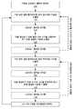
도 1a 및 도 1b는 특정한 개시된 실시 예들에 따라 수행된 방법들에 대한 동작들을 도시하는 프로세스 흐름도들이다.
도 2는 특정한 개시된 실시 예들에 따른 방법의 사이클들의 예를 도시하는 타이밍 시퀀스도이다.
도 3a 및 도 3b는 특정한 개시된 실시 예들에 따른, 방법의 동작들을 도시하는 프로세스 흐름도이다
도 4는 개시된 실시 예들을 수행하기 위한 예시적인 프로세스 챔버의 개략도이다.
도 5는 개시된 실시 예들을 수행하기 위한 예시적인 프로세스 툴의 개략도이다.
도 6은 다양한 플라즈마 에너지들을 사용하여 증착된 실리콘 옥사이드 막들에 대한 습식 에칭 레이트 (wet etch rate) 및 단차 커버리지를 도시하는 그래프이다.
도 7은 미리 결정된 (given) 플라즈마 전력에서 다양한 일정한 시간 및 교번하는 변환 시간에서 상이한 플라즈마-강화된 원자 층 증착 프로세스들을 사용하여 증착된 실리콘 옥사이드 막들에 대한 습식 에칭 레이트를 비교하는 그래프이다.
도 8은 특정한 개시된 실시 예들을 사용하여 증착된 피처들의 하단부, 측면부, 및 상단부에서 막들의 습식 에칭 레이트들을 비교하는 그래프이다.1A and 1B are process flow diagrams illustrating operations for methods performed in accordance with certain disclosed embodiments.
2 is a timing sequence diagram illustrating an example of cycles of a method in accordance with certain disclosed embodiments.
3A and 3B are process flow diagrams illustrating operations of a method, in accordance with certain disclosed embodiments;
4 is a schematic diagram of an exemplary process chamber for carrying out the disclosed embodiments.
5 is a schematic diagram of an example process tool for performing the disclosed embodiments.
6 is a graph showing wet etch rate and step coverage for silicon oxide films deposited using various plasma energies.
7 is a graph comparing wet etch rates for silicon oxide films deposited using different plasma-enhanced atomic layer deposition processes at various constant times and alternating conversion times at a given plasma power.
8 is a graph comparing wet etch rates of films at the bottom, side, and top of features deposited using certain disclosed embodiments.
이하의 기술 (description) 에서, 제시된 실시 예들의 완전한 이해를 제공하기 위해 수많은 구체적 상세들이 제시되었다. 개시된 실시 예들은 이들 구체적인 상세들 중 일부 또는 전부 없이 실시될 수도 있다. 다른 예들에서, 공지된 프로세스 동작들은 개시된 실시 예들을 불필요하게 모호하게 하지 않기 위해 상세히 기술되지 않았다. 개시된 실시 예들이 구체적인 실시 예들과 함께 기술될 것이지만, 이는 개시된 실시 예들을 제한하는 것으로 의도되지 않았다는 것이 이해될 것이다.In the following description, numerous specific details are set forth in order to provide a thorough understanding of the presented embodiments. The disclosed embodiments may be practiced without some or all of these specific details. In other instances, well-known process operations have not been described in detail so as not to unnecessarily obscure the disclosed embodiments. While the disclosed embodiments will be described in conjunction with specific embodiments, it will be understood that this is not intended to limit the disclosed embodiments.
반도체 프로세싱은 고 종횡비 토포그래피 (topography) 를 갖는 패터닝된 기판들을 포함하는 다양한 기판들 상에서 수행된다. 일부 프로세싱 동작들은 다양한 과제들을 제기할 수 있는 막들의 증착을 수반한다. 예를 들어, 기술이 발전함에 따라, 복잡한 토포그래피 위에 고품질 막들을 증착하기 위한 기법들 (techniques) 이 어려워진다. 이러한 토포그래피 상에 고품질 막들을 증착하기 위한 일 특정한 기법은 원자 층 증착 (atomic layer deposition; ALD) 과 같은 컨포멀한 증착을 사용하는 것이다. ALD는 유전체, 금속, 및 다른 막들을 포함하는 상이한 타입들의 재료들을 증착하도록 사용될 수 있다. ALD에 의해 증착될 수도 있는 일 특정한 예시적인 막은 실리콘 옥사이드이다.Semiconductor processing is performed on a variety of substrates, including patterned substrates with high aspect ratio topography. Some processing operations involve the deposition of films, which can pose various challenges. For example, as technology advances, techniques for depositing high quality films over complex topography become difficult. One particular technique for depositing high quality films on such topography is to use conformal deposition, such as atomic layer deposition (ALD). ALD can be used to deposit different types of materials including dielectrics, metals, and other films. One particular exemplary film that may be deposited by ALD is silicon oxide.
실리콘 옥사이드가 ALD에 의해 증착될 수도 있는 특정한 타입의 막으로서 본 명세서에 기술되지만, 다른 타입들의 재료들이 또한 ALD를 사용하여 증착될 수도 있고 실리콘 옥사이드는 단지 예로서 제공된다는 것이 이해될 것이다.Although silicon oxide is described herein as a particular type of film that may be deposited by ALD, it will be understood that other types of materials may also be deposited using ALD and silicon oxide is provided by way of example only.
ALD는 순차적인 자기-제한 반응들을 사용하여 재료의 박층들을 증착하는 기법이다. ALD 프로세스들은 사이클들에서 층 단위 (layer-by-layer basis) 로 막들을 증착하도록 표면-매개 (surface-mediated) 증착 반응들을 사용한다. 예로서, ALD 사이클은 다음 동작들: (i) 전구체의 전달/흡착 (또한 "도즈"로 지칭됨), (ii) 챔버로부터 전구체의 퍼지, (iii) 제 2 반응 물질의 전달 및 선택 가능한 (optional) 플라즈마 생성 (또한 "변환"으로 지칭됨), 및 (iv) 챔버로부터 부산물들의 퍼지를 포함할 수도 있다. 퍼지는 일부 경우에 선택 가능할 수도 있다. 부가적으로, 도즈는 변환 전에 반드시 수행될 필요는 없을 수도 있다; 일부 경우들에서, 제 2 반응 물질의 전달은 전구체를 전달하기 전에 수행될 수도 있다. 본 명세서의 논의 목적들을 위해, ALD 사이클은 도즈, 퍼지, 변환 및 퍼지를 지칭할 것이지만, 다른 변동들이 또한 활용될 수도 있다는 것이 이해될 것이다.ALD is a technique for depositing thin layers of material using sequential self-limiting reactions. ALD processes use surface-mediated deposition reactions to deposit films on a layer-by-layer basis in cycles. As an example, an ALD cycle may include the following operations: (i) delivery/adsorption of a precursor (also referred to as a “dose”), (ii) purging of the precursor from the chamber, (iii) delivery of a second reactant and selectable ( optional) plasma generation (also referred to as “conversion”), and (iv) purging of byproducts from the chamber. Spreading may be selectable in some cases. Additionally, a dose may not necessarily have to be performed prior to conversion; In some cases, delivery of the second reactant may be performed prior to delivery of the precursor. For purposes of discussion herein, an ALD cycle will refer to dose, purge, transform, and purge, although it will be understood that other variations may also be utilized.
플라즈마가 제 2 반응 물질의 전달 동안 사용되는 경우, 프로세스는 PEALD (plasma-enhanced atomic layer deposition) 로 지칭될 수도 있다. 기판의 표면 상에 막을 형성하기 위한 제 2 반응 물질과 흡착된 전구체 사이의 반응은 막 조성 및 특성들, 예컨대 응력, 습식 에칭 레이트, 건식 에칭 레이트, 전기적 특성들 (예를 들어, 유전 상수, 파괴 전압 (breakdown voltage) 및 누설 전류), 불순물의 혼입, 등에 영향을 준다. 부가적으로, 증착된 막의 불균일도가 또한 결정될 수도 있고, 일부 경우들에서, 감소된 불균일성이 목표될 수도 있다.When plasma is used during delivery of the second reactant, the process may be referred to as plasma-enhanced atomic layer deposition (PEALD). The reaction between the adsorbed precursor and the second reactant material to form a film on the surface of the substrate may affect film composition and properties, such as stress, wet etch rate, dry etch rate, electrical properties (e.g., dielectric constant, breakdown voltage (breakdown voltage and leakage current), incorporation of impurities, and the like. Additionally, the non-uniformity of the deposited film may also be determined, and in some cases, reduced non-uniformity may be desired.
ALD 프로세스의 일 특정한 예에서, 표면 활성 사이트들의 집단을 포함하는 기판 표면은 기판을 하우징하는 챔버에 제공된 도즈로 실리콘-함유 전구체와 같은 제 1 전구체의 가스상 (gas phase) 분포에 노출된다. 이 제 1 전구체의 분자들은 제 1 전구체의 화학흡착된 종 및/또는 물리흡착된 분자들을 포함하여, 기판 표면 상으로 흡착된다. 본 명세서에 기술된 바와 같이 화합물이 기판 표면 상에 흡착될 때, 흡착된 층은 화합물뿐만 아니라 화합물의 유도체들을 포함할 수도 있다는 것이 이해될 것이다. 예를 들어, 실리콘-함유 전구체의 흡착된 층은 실리콘-함유 전구체뿐만 아니라 실리콘-함유 전구체의 유도체들을 포함할 수도 있다. 제 1 전구체 도즈 후, 챔버는 대부분 또는 흡착된 종만이 남도록 가스상으로 남아 있는 제 1 전구체의 대부분 또는 전부를 제거하도록 배기될 수도 있다. 예를 들어, 챔버는 가스상의 제 1 전구체의 분압이 반응을 완화시키기에 충분히 낮도록 배기될 수도 있다. 일부 구현 예들에서, 챔버는 완전히 배기되지 않을 수도 있다. 제 2 반응 물질, 예컨대 산소-함유 가스는 이들 제 2 반응 물질 분자들 중 일부가 기판의 표면 상의 흡착된 제 1 전구체와 반응하도록 챔버로 도입된다. 일부 프로세스에서, 제 2 반응 물질은 흡착된 제 1 전구체와 즉시 반응한다. 일부 실시 예들에서, 제 2 반응 물질은 플라즈마와 같은 활성화 소스가 적용된 후에만 반응한다. 이러한 플라즈마 노출은 일시적으로 적용될 수도 있다. 이어서 챔버는 결합되지 않은 제 2 반응 물질 분자들을 제거하기 위해 다시 배기될 수도 있다. 상기 기술된 바와 같이, 일부 실시 예들에서 챔버는 완전히 배기되지 않을 수도 있다. 상기 기술된 노출들은 기판이 시간적으로 분리된 노출들 각각의 노출에 노출되는 시간적 ALD 프로세스의 일부일 수도 있다. 막 두께를 구축하기 위해 부가적인 ALD 사이클들이 사용될 수도 있다.In one particular example of an ALD process, a substrate surface comprising a population of surface active sites is exposed to a gas phase distribution of a first precursor, such as a silicon-containing precursor, at a dose provided to a chamber housing the substrate. Molecules of this first precursor, including chemisorbed species and/or physisorbed molecules of the first precursor, are adsorbed onto the substrate surface. It will be appreciated that when a compound is adsorbed onto a substrate surface as described herein, the adsorbed layer may include the compound as well as derivatives of the compound. For example, the adsorbed layer of a silicon-containing precursor may include a silicon-containing precursor as well as derivatives of the silicon-containing precursor. After the first precursor dose, the chamber may be evacuated to remove most or all of the first precursor remaining in the gaseous phase such that only most or adsorbed species remain. For example, the chamber may be evacuated such that the partial pressure of the first precursor in the gaseous phase is low enough to moderate the reaction. In some implementations, the chamber may not be completely evacuated. A second reactant material, such as an oxygen-containing gas, is introduced into the chamber such that some of these second reactant molecules react with the adsorbed first precursor on the surface of the substrate. In some processes, the second reactant reacts immediately with the adsorbed first precursor. In some embodiments, the second reactant reacts only after an activating source, such as plasma, is applied. Such plasma exposure may be applied temporarily. The chamber may then be evacuated again to remove unbound second reactant molecules. As noted above, in some embodiments the chamber may not be completely evacuated. The exposures described above may be part of a temporal ALD process in which the substrate is exposed to each of the temporally separated exposures. Additional ALD cycles may be used to build up the film thickness.
본 명세서의 실시 예들은 또한 공간적 ALD 프로세스들과 관련될 수도 있다. 공간적 ALD에서, 노출 각각에 사용된 가스들은 프로세스 챔버 내에서 공간적으로 상이한 위치들 또는 "존들"에서 연속적으로 흐른다. 존 각각은 가스들의 주입 지점을 포함한다-예를 들어, 일 존은 제 1 전구체를 포함할 수도 있고, 일 존은 제 1 퍼지 가스들을 포함할 수도 있고, 일 존은 제 2 반응 물질을 포함할 수도 있고, 그리고 제 4 존은 제 2 퍼지 가스를 포함할 수도 있다. 기판은 시간적 ALD에 대해 상기 기술된 표면 반응들을 구현하기 위해 기판 표면을 상이한 노출들에 노출시키도록 존들 사이에서 회전된다. 즉, 노출들을 시간적으로 분리하는 대신, 노출들은 위치별로 분리된다.Embodiments herein may also relate to spatial ALD processes. In spatial ALD, the gases used for each exposure flow continuously at spatially different locations or “zones” within the process chamber. Each zone includes an injection point of gases - eg, a zone may contain a first precursor, a zone may contain first purge gases, and a zone may contain a second reactant material. and the fourth zone may contain the second purge gas. The substrate is rotated between zones to expose the substrate surface to different exposures to implement the surface reactions described above for temporal ALD. That is, instead of separating exposures temporally, exposures are separated by location.
일부 구현 예들에서, ALD 방법들은 플라즈마 활성화를 포함한다. 본 명세서에 기술된 바와 같이, 본 명세서에 기술된 ALD 방법들 및 장치들은 2011 년 4 월 11일 출원되고, 명칭이 "PLASMA ACTIVATED CONFORMAL FILM DEPOSITION"인 미국 특허 출원 번호 제 13/084,399 호 (현재 미국 특허 번호 제 8,728,956 호) 에 포괄적으로 기술된, 컨포멀한 막 증착 (conformal film deposition; CFD) 방법들일 수도 있고, 이는 전체가 참조로서 본 명세서에 인용된다. 플라즈마 활성화는 기판이 하우징되는 챔버 내에서 반응성 종을 생성하도록 인 시츄로, 또는 챔버 내에서 플라즈마를 생성하고 흡착된 전구체들의 기판 표면을 반응성 종과 콘택트함으로써 수행될 수도 있다. 일부 경우들에서, 플라즈마 활성화는 리모트 영역 또는 생성기에서 플라즈마를 생성함으로써 수행될 수도 있고, 이어서 흡착된 전구체들의 표면과 반응성 종이 콘택트하도록 플라즈마로부터의 반응성 종은 기판을 하우징하는 챔버로 전달될 수도 있다. 다양한 실시 예들에서, PEALD에 적합할 수도 있는 플라즈마 생성기는 용량 결합 플라즈마 (capacitively coupled plasma; CCP) 생성기이다. 다양한 실시 예들에서, PEALD에 적합할 수도 있는 플라즈마 생성기는 유도 결합 플라즈마 생성기 (inductively coupled plasma; ICP) 이다. 일부 ALD 및 PEALD 실시 예들이 본 명세서에 기술되지만, 다양한 개시된 실시 예들이 ALD 또는 PEALD 프로세스들에 적용 가능할 수도 있다는 것이 이해될 것이다.In some implementations, ALD methods include plasma activation. As described herein, the ALD methods and apparatus described herein are filed in U.S. Patent Application Serial No. 13/084,399, filed April 11, 2011, and entitled "PLASMA ACTIVATED CONFORMAL FILM DEPOSITION" (now U.S. conformal film deposition (CFD) methods, comprehensively described in Patent No. 8,728,956), which is incorporated herein by reference in its entirety. Plasma activation may be performed in situ to create a reactive species within the chamber in which the substrate is housed, or by creating a plasma within the chamber and contacting the substrate surface of adsorbed precursors with the reactive species. In some cases, plasma activation may be performed by generating a plasma in a remote region or generator, and then the reactive species from the plasma may be delivered to a chamber housing the substrate so that the reactive species contacts the surface of the adsorbed precursors. In various embodiments, a plasma generator that may be suitable for PEALD is a capacitively coupled plasma (CCP) generator. In various embodiments, a plasma generator that may be suitable for PEALD is an inductively coupled plasma (ICP). Although some ALD and PEALD embodiments are described herein, it will be understood that the various disclosed embodiments may be applicable to ALD or PEALD processes.
ALD가 고 종횡비 피처들 내로 박막을 컨포멀하게 증착하도록 사용될 수도 있지만, 일부 ALD 프로세스들은 ALD 사이클 각각의 지속 기간으로 인해 감소된 쓰루풋을 발생시킬 수도 있다. 따라서, 일부 프로세스들은 대량 생산에서 구현하기에는 너무 비용이 많이 들 수도 있다.Although ALD may be used to conformally deposit thin films into high aspect ratio features, some ALD processes may result in reduced throughput due to the duration of each ALD cycle. Therefore, some processes may be too expensive to implement in mass production.
막 치밀화는 변환 동작에서 발생한다. ALD는 층별 성장 프로세스이기 때문에, 반쪽 반응 각각 (흡착 및 변환) 은 목표된 막 품질 및 쓰루풋을 달성하도록 변조될 수 있다. 그러나, 특정한 ALD 프로세스들에 대해 쓰루풋과 목표된 막 특성 사이에 트레이드 오프가 있다; 변환 시간이 보다 길수록 보다 높은 품질의 막들을 발생시킬 수 있지만, 보다 긴 변환 시간은 전체 ALD 사이클 시간을 연장하여, 쓰루풋을 감소시킨다. 유사하게, 쓰루풋이 ALD 사이클의 변환 시간을 감소시킴으로써 개선될 수 있지만, 변환 시간이 보다 짧을수록 보다 낮은 품질의 막들을 발생시킨다.Film densification occurs in the transformation operation. Since ALD is a layer-by-layer growth process, each of the half reactions (adsorption and conversion) can be modulated to achieve the desired film quality and throughput. However, there is a trade-off between throughput and desired film properties for certain ALD processes; Longer conversion times can produce higher quality films, but longer conversion times extend the overall ALD cycle time, reducing throughput. Similarly, although throughput can be improved by reducing the conversion time of an ALD cycle, shorter conversion times result in lower quality films.
특정한 기법들이 대량의 반도체 막들의 프로세싱 동안 쓰루풋을 증가시키도록 사용될 수도 있지만, 일부 기법들은 단점들을 갖는다. 예를 들어, 일 기법은 쓰루풋을 증가시키기 위해 사이클 시간 또는 모든 ALD 사이클에서 사용된 시간을 감소시키는 것이다. 쓰루풋을 증가시키기 위한 기존의 기법들은 모든 ALD 사이클의 도즈, 퍼지, 또는 변환 동작들을 수정한다; 그러나, 매 사이클에서 이들 동작들의 단축은 증착 반응 물질들의 포화에 의해 제한될 수도 있고 불량한 막 품질, 결함 문제들 및/또는 언더필 (underfilling), 및 갭 충진 적용 예들에서 고 종횡비 구조체들에서 보이드들의 존재를 발생시킬 수도 있다. 그 결과, 일부 기존 기법들은 고 쓰루풋을 갖는 고품질 막들의 형성을 달성할 수 없다.Although certain techniques may be used to increase throughput during processing of large amounts of semiconductor films, some techniques have drawbacks. For example, one technique is to decrease the cycle time or the time used in all ALD cycles to increase throughput. Existing techniques to increase throughput modify the dose, purge, or transform operations of every ALD cycle; However, the shortening of these operations in every cycle may be limited by saturation of the deposition reactants and poor film quality, defect issues and/or underfilling, and the presence of voids in high aspect ratio structures in gap fill applications. may cause As a result, some existing techniques cannot achieve the formation of high-quality films with high throughput.
다른 ALD 사이클들에서 짧은 변환 시간을 사용하는 동안 일부 ALD 사이클들에서 긴 변환 시간을 사용하여 총 사이클 시간을 감소시킴으로써 고 쓰루풋을 갖는 고품질 막들을 증착하는 기법들이 본 명세서에 제공된다. 긴 변환 시간은 특정한 바람직한 특성들을 갖는 증착된 막을 발생시킴으로써, 짧은 변환 시간은 막들을 증착하기 위해 사용된 평균 사이클 시간을 감소시킨다. 즉, 짧은 변환 시간을 갖는 ALD 사이클의 N 사이클들은 막 품질 또는 결함 성능을 희생하지 않고 긴 변환 시간을 갖는 것을 제외하고 동일한 ALD 사이클의 M 사이클들로 수행된다. 일반적으로, 다양한 실시 예들에서, M은 N보다 작다.Techniques are provided herein for depositing high quality films with high throughput by using a long conversion time in some ALD cycles to reduce the total cycle time while using a short conversion time in others. A long conversion time results in a deposited film having certain desirable properties, such that a short conversion time reduces the average cycle time used to deposit the films. That is, N cycles of an ALD cycle with a short conversion time are performed as M cycles of the same ALD cycle except with a long conversion time without sacrificing film quality or defect performance. In general, in various embodiments, M is less than N.
본 명세서에 사용된 용어 "변환 시간"은 흡착된 전구체를 실리콘 옥사이드와 같은 막 재료로 변환하기 위해 제 2 반응 물질에 흡착된 전구체의 노출 동안 지속 기간을 지칭하도록 사용된다는 것이 이해될 것이다. 긴 변환 시간 및 짧은 변환 시간은 변환 지속 기간을 지칭하기 위해 본 명세서에서 사용된 상대적인 용어들이다. PEALD 실시 예들에 대해, 긴 변환 시간 및 짧은 변환 시간은 동일한 플라즈마 전력에서 수행된 변환들이다, 즉, 짧은 ALD 변환 시간 사이클들의 N 사이클들 및 긴 ALD 변환 시간 사이클들의 M 사이클들을 갖는 프로세스는 변환 동안 동일한 플라즈마 전력을 사용하여 수행된다-플라즈마 노출의 지속 기간만이 N 사이클과 M 사이클 사이에서 변조된다. 이들은 증착 반응 물질들의 두 번의 분리된 노출들을 수반하는 이진 사이클들에 대한 예들이지만, 특정한 개시된 실시 예들은 3진 (ternary) 사이클들 및 4진 사이클들을 포함하는 다른 타입들의 사이클들로 수행될 수 있다는 것이 이해될 것이다.It will be understood that the term “conversion time” as used herein is used to refer to the duration during exposure of the adsorbed precursor to a second reactant to convert the adsorbed precursor to a film material such as silicon oxide. Long conversion time and short conversion time are relative terms used herein to refer to the conversion duration. For PEALD embodiments, the long conversion time and short conversion time are conversions performed at the same plasma power, ie, a process with N cycles of short ALD conversion time cycles and M cycles of long ALD conversion time cycles is the same during conversion. This is done using plasma power - only the duration of the plasma exposure is modulated between N and M cycles. These are examples for binary cycles involving two separate exposures of the deposition reactants, although certain disclosed embodiments may be performed with other types of cycles, including ternary cycles and quaternary cycles. it will be understood
다양한 실시 예들에서, 긴 변환 시간은 짧은 변환 시간보다 약 1.5 배 내지 약 15 배 길다. 다양한 실시 예들에서, 긴 변환 시간은 짧은 변환 시간보다 약 1.5 배 내지 약 10 배 길다. 다양한 실시 예들에서, 긴 변환 시간은 짧은 변환 시간보다 약 1.5 배 내지 약 5 배 길다. 다양한 실시 예들에서, 긴 변환 시간은 짧은 변환 시간보다 약 1.5 배 길다.In various embodiments, the long conversion time is from about 1.5 times to about 15 times longer than the short conversion time. In various embodiments, the long conversion time is from about 1.5 times to about 10 times longer than the short conversion time. In various embodiments, the long conversion time is about 1.5 times to about 5 times longer than the short conversion time. In various embodiments, the long conversion time is about 1.5 times longer than the short conversion time.
일부 실시 예들에서, 단일 긴 변환 시간 ALD 사이클은 매 1 내지 20 개 이상의 짧은 변환 시간 ALD 사이클들에 대해 사용될 수 있다. 일부 실시 예들에서, 일 긴 변환 시간 ALD 사이클마다 사용될 수도 있는 짧은 변환 시간 ALD 사이클들의 수는 짧은 변환 시간 ALD 사이클에 의해 증착된 막의 두께 및 짧은 변환 시간 및 긴 변환 시간에 사용된 지속 기간에 종속된다, 즉, 일 긴 변환 시간 ALD 사이클마다 수행되는 짧은 변환 시간 ALD 사이클들의 사이클들의 수는 일 긴 변환 시간 ALD에 의해 치밀화될 수 있는 짧은 변환 시간 ALD 사이클에 의해 증착된 막의 최대 두께에 의해 규정된다.In some embodiments, a single long conversion time ALD cycle may be used for every 1 to 20 or more short conversion time ALD cycles. In some embodiments, the number of short conversion time ALD cycles that may be used per one long conversion time ALD cycle depends on the thickness of the film deposited by the short conversion time ALD cycle and the duration used for the short conversion time and the long conversion time. , that is, the number of cycles of short conversion time ALD cycles performed per one long conversion time ALD cycle is defined by the maximum thickness of the film deposited by the short conversion time ALD cycle that can be densified by the one long conversion time ALD cycle.
일부 실시 예들에서, 특정한 긴 변환 시간들 이상에서, 프로세스는 감소된 이점을 가질 수도 있다; 즉, 막 품질이 짧은 변환 시간 ALD 사이클만을 수행하는 것과 비교하여 개선될 수도 있지만, 매우 긴 변환 시간 ALD 사이클들을 사용하는 것은 짧은 변환 시간 ALD 사이클과 비교하여 보다 높은 품질의 막들을 달성하는 동안 보다 적은 프로세스 시간 감소를 나타낼 수도 있다.In some embodiments, above certain long conversion times, the process may have a reduced benefit; That is, although film quality may be improved compared to performing only a short conversion time ALD cycle, using very long conversion time ALD cycles is less effective while achieving higher quality films compared to a short conversion time ALD cycle. It may also indicate a reduction in process time.
일부 실시 예들에서, 블랭킷 막들에 대해, 특정한 변환 지속 기간 이상에서, 습식 에칭 레이트의 조절이 관찰되지 않는 포화 지점이 있을 수 있다. 일부 경우들에서, 이 포화 지점은 특정한 프로세스 조건들에 기초하여, 13.56 ㎒ RF 생성기를 갖는 4-스테이션 챔버 시스템에 대해 0.75 초이다.In some embodiments, for blanket films, above a certain transition duration, there may be a saturation point at which no adjustment of the wet etch rate is observed. In some cases, this saturation point is 0.75 seconds for a 4-station chamber system with a 13.56 MHz RF generator, based on specific process conditions.
특정한 개시된 실시 예들은 열적, 공간적, 또는 플라즈마 강화된 ALD 프로세스들에서 수행될 수도 있다. 일부 실시 예들에서, 모든 ALD 사이클들의 변환 동안 동일한 플라즈마 전력을 유지하면서 변환 시간이 변조된다. 일부 실시 예들에서, 변환 시간뿐만 아니라 목표된 막 특성을 달성하기 위해 플라즈마 전력 및 다른 프로세스 조건들도 변조된다.Certain disclosed embodiments may be performed in thermal, spatial, or plasma enhanced ALD processes. In some embodiments, the conversion time is modulated while maintaining the same plasma power during conversion of all ALD cycles. In some embodiments, the plasma power and other process conditions are modulated to achieve the desired film properties as well as the conversion time.
특정한 개시된 실시 예들은 실리콘 옥사이드, 실리콘 나이트라이드, 금속 옥사이드들, 금속 나이트라이드들, 금속 카바이드들, 다른 옥사이드들, 나이트라이드들, 카바이드들, 옥시나이트라이드들, 옥시카바이드들, 등을 포함하지만 이로 제한되지 않는 다양한 막들을 증착하도록 사용될 수 있다.Certain disclosed embodiments include, but are not limited to, silicon oxide, silicon nitride, metal oxides, metal nitrides, metal carbides, other oxides, nitrides, carbides, oxynitrides, oxycarbides, and the like. It can be used to deposit a variety of non-limiting films.
변환 시간을 변조하는 것은 다양한 타입들의 목표된 막 특성들을 달성하도록 사용될 수 있다. 막 품질은 상이한 메트릭들을 사용하여 결정될 수 있다. 실리콘 옥사이드 막들에 대해, 막 품질에 대한 일 예시적인 메트릭은 기판을 희석된 플루오르화 수소산, 예를 들어, 180 초 동안 200:1 배스에 딥핑함으로써 (dipping) 평가될 수도 있는 습식 에칭 레이트이다. 증가된 변환 시간은 표면 반응이 일어나도록 충분한 시간을 허용하고, 목표된 반응 생성물을 생성하고, 증착된 막을 치밀화한다. 결과적으로, 증착된 막의 습식 에칭 레이트는 감소한다. 두 짧은 변환 ALD 사이클마다 하나의 보다 긴 변환 ALD 사이클을 갖는 효과는 쓰루풋을 상당히 개선하고, 놀랍게도 보다 우수한 막 품질을 달성한다. 실제로, 짧은 변환 시간보다 단지 1.1 배 보다 긴, 보다 긴 변환 시간을 사용하는 것은 사이클 시간을 상당히 감소시키면서 증가된 막 품질의 놀라운 결과를 발생시킨다.Modulating the transform time can be used to achieve various types of desired film properties. Film quality can be determined using different metrics. For silicon oxide films, one exemplary metric for film quality is the wet etch rate, which may be assessed by dipping the substrate into a diluted hydrofluoric acid, eg, a 200:1 bath for 180 seconds. The increased conversion time allows sufficient time for the surface reaction to occur, produce the desired reaction product, and densify the deposited film. As a result, the wet etch rate of the deposited film decreases. The effect of having one longer conversion ALD cycle for every two short conversion ALD cycles significantly improves throughput and surprisingly achieves better film quality. Indeed, using a longer conversion time, which is only 1.1 times longer than the short conversion time, leads to the surprising result of increased film quality while significantly reducing the cycle time.
(실리콘 블랭킷 웨이퍼 또는 필드 영역 상의 막 품질과 상이할 수도 있는) 고 종횡비 구조체의 측벽 상의 막 품질에 대한 다른 메트릭들은 측벽 두께 (단차 커버리지) 또는 측벽 습식 에칭 레이트이다. 단차 커버리지는 트렌치의 하단부, 측벽의 상이한 위치 상에 증착된 막의 평균 두께를 피처 또는 트렌치 상단부 상에 증착된 막의 평균 두께와 비교함으로써 계산될 수도 있다.Other metrics for film quality on the sidewall of a high aspect ratio structure (which may be different from the silicon blanket wafer or film quality on the field region) are sidewall thickness (step coverage) or sidewall wet etch rate. The step coverage may be calculated by comparing the average thickness of the film deposited on different locations of the bottom, sidewall of the trench to the average thickness of the film deposited on the top of the feature or trench.
단차 커버리지의 일 예는 측벽 상에 증착된 막의 평균 두께를 피처의 상단부에 증착된 막의 평균 두께로 나누고 백분율을 얻기 위해 100을 몫에 곱함으로써 계산될 수도 있다. 백분율이 100 %에 가까울수록 피처 내부에서 막이 보다 치밀해진다. 측벽을 따른 막 특성의 단차 커버리지 및 균일성은 많은 요인들 중에서, 증착 전구체, 반응 물질 이온들 및/또는 라디칼들 (예컨대 플라즈마를 사용하여 반응 물질 가스를 점화함으로써 생성된 것들), 및 부산물들에 종속한다. ALD 프로세스의 변환 시간이 증가함에 따라, 단차 커버리지는 개선되고 100 %에 가까워진다. 일부 경우들에서, 측벽 단차 커버리지는 막 품질의 유용한 메트릭일 수도 있지만, 일부 경우들에서, 상이한 방법이 막 품질 또는 밀도의 변화들을 검출하도록 사용될 수도 있다. 이러한 일 방법은 측벽 습식 에칭 레이트를 평가하는 단계를 수반하고, 이는 소량의 샘플 또는 패터닝된 웨이퍼를 희석된 산 배스에 딥핑하고 에칭된 양을 측정함으로써 결정될 수 있다. 주어진 딥핑 시간 동안 에칭된 양이 보다 적을수록, 측벽 막 품질이 보다 우수하다.One example of step coverage may be calculated by dividing the average thickness of the film deposited on the sidewall by the average thickness of the film deposited on top of the feature and multiplying the quotient by 100 to get the percentage. The closer the percentage is to 100%, the denser the film inside the feature. The step coverage and uniformity of film properties along the sidewall is dependent on the deposition precursor, reactant ions and/or radicals (such as those generated by igniting a reactant gas using plasma), and by-products, among many factors. do. As the conversion time of the ALD process increases, the step coverage improves and approaches 100%. In some cases, sidewall step coverage may be a useful metric of film quality, although in some cases a different method may be used to detect changes in film quality or density. One such method involves evaluating the sidewall wet etch rate, which can be determined by dipping a small sample or patterned wafer into a diluted acid bath and measuring the amount etched. The lower the amount etched for a given dipping time, the better the sidewall film quality.
본 명세서에 기술된 특정한 개시된 실시 예들은 배치 (batch) 프로세스에서 몇몇 기판들 상에 실리콘 옥사이드 막들을 증착하기 위한 총 프로세스 시간을 감소시키고 쓰루풋을 증가시킨다. 배치 프로세스는 하나 이상의 스테이션들을 포함할 수도 있는 프로세스 챔버 내에서 복수의 기판들을 순차적으로 프로세싱하는 것으로 본 명세서에서 지칭될 수도 있고, 스테이션 각각은 단일 웨이퍼들이 챔버 각각 내외로 이송되고 일부 실시 예들에서 스테이션들 사이에서 순환되도록 다양한 목적들을 위해 웨이퍼를 프로세싱하기 위해 사용된다. 일부 개시된 실시 예들은 막 품질을 희생하지 않고 플라즈마 변환 동안 산소와 아르곤의 혼합물을 사용하여 PEALD에 의해 두꺼운 실리콘 옥사이드 막들을 증착하는데 적합하다. 일부 개시된 실시 예들은 막 품질을 희생하지 않고 플라즈마 변환 동안 아산화질소, 산소 및 아르곤의 혼합물을 사용하여 PEALD에 의해 두꺼운 실리콘 옥사이드 막들을 증착하는데 적합하다.Certain disclosed embodiments described herein increase throughput and decrease the total process time for depositing silicon oxide films on several substrates in a batch process. A batch process may be referred to herein as sequentially processing a plurality of substrates within a process chamber that may include one or more stations, each station in which a single wafer is transferred into and out of each of the chambers and, in some embodiments, the stations It is used to process wafers for various purposes to cycle between them. Some disclosed embodiments are suitable for depositing thick silicon oxide films by PEALD using a mixture of oxygen and argon during plasma conversion without sacrificing film quality. Some disclosed embodiments are suitable for depositing thick silicon oxide films by PEALD using a mixture of nitrous oxide, oxygen and argon during plasma conversion without sacrificing film quality.
특정한 이론에 얽매이지 않고 특정한 개시된 실시 예들을 사용하여 증착된 실리콘 옥사이드 막들에 대해, 흡착된 실리콘 전구체를 실리콘 옥사이드로 변환하는 변환 동작 동안 형성된 증착된 실리콘 옥사이드의 층 각각에서 결합들을 재배열하기에 불충분한 시간 때문에 보다 짧은 변환 시간을 사용하여 증착된 실리콘 옥사이드 막들이 보다 낮은 품질의 막들을 발생시킨다고 여겨진다. 반대로, 목표된 ALD 반응 생성물을 생성하기 위해 표면 반응이 일어나도록 충분한 시간을 허용하기 때문에, 보다 긴 변환 시간을 사용하여 증착될 때 막들은 보다 높은 품질을 갖는다. 예를 들어, 일 특정한 개선은 보다 높은 품질의 막들이 에칭되지 않고 보다 거친 습식 에칭 레이트 조건들을 견딜 수 있도록, 200:1 플루오르화 수소산에서 감소된 습식 에칭 레이트일 수도 있다.Without wishing to be bound by theory, for silicon oxide films deposited using the particular disclosed embodiments, there is insufficient to rearrange bonds in each layer of deposited silicon oxide formed during a conversion operation to convert the adsorbed silicon precursor to silicon oxide. It is believed that silicon oxide films deposited using shorter conversion times due to one hour result in lower quality films. Conversely, films have a higher quality when deposited using longer conversion times because they allow sufficient time for the surface reaction to occur to produce the desired ALD reaction product. For example, one particular improvement may be a reduced wet etch rate in 200:1 hydrofluoric acid so that higher quality films can withstand harsher wet etch rate conditions without being etched.
PEALD 실시 예들에 대해, 플라즈마 변환 시간은 사이클마다 (from cycle to cycle) 변조될 수도 있다. 플라즈마는 반응성 종을 생성하고, 특성들은 시간의 함수일 수 있다; 따라서, 증가된 플라즈마 변환 시간은 증착된 재료의 층들을 침투하고 증착된 막의 특성들을 변조하기 위해 증착된 재료의 특성들을 개질하거나 결합들을 재 배열하기에 충분한 반응성 종을 생성할 수 있다. 일부 실시 예들에서, 반응성 종의 특성들은 블랭킷 막들의 이온 침투 깊이와 상관될 수도 있다. 일부 실시 예들에서, 반응성 종의 특성들은 플라즈마 에너지와 상관될 수 있다; 즉, 보다 높은 플라즈마 에너지는 예를 들어 상승된 플라즈마 밀도를 갖는 반응성 종을 발생시킬 수도 있다. 일부 실시 예들에서, 동일한 플라즈마 전력이 긴 지속 기간 및 짧은 지속 기간 동안 사용되지만, 지속 기간의 차로 인해, 반응성 종은 상이하게 거동할 수도 있다.For PEALD embodiments, the plasma conversion time may be modulated from cycle to cycle. Plasma creates reactive species, and properties can be a function of time; Thus, the increased plasma conversion time can generate reactive species sufficient to reorder bonds or modify the properties of the deposited material to penetrate the layers of the deposited material and modulate the properties of the deposited film. In some embodiments, the properties of the reactive species may be correlated with the ion penetration depth of the blanket films. In some embodiments, properties of the reactive species may be correlated with plasma energy; That is, higher plasma energy may generate reactive species with, for example, elevated plasma density. In some embodiments, the same plasma power is used for a long duration and a short duration, but due to the difference in duration, the reactive species may behave differently.
열적 및 플라즈마-강화된 ALD 프로세스들 모두에서, 고 종횡비 피처들로의 증착을 위해, 보다 긴 지속 기간은 고 종횡비 피처들 내로 증가된 확산을 발생시킬 수 있고, 이에 따라 피처들 내로 보다 깊은 품질의 막들을 증착한다.In both thermal and plasma-enhanced ALD processes, for deposition into high aspect ratio features, a longer duration can result in increased diffusion into the high aspect ratio features, and thus deeper quality of the features into the features. Deposit the films.
"슈퍼 사이클"은 하나 이상의 긴 변환 시간 ALD 사이클들 및 하나 이상의 짧은 변환 ALD 사이클들을 포함하는 것으로 본 명세서에 기술된다. 슈퍼 사이클은 목표된 막을 증착하기 위해 여러 번 반복될 수도 있다.A “super cycle” is described herein as including one or more long conversion time ALD cycles and one or more short conversion ALD cycles. The super cycle may be repeated several times to deposit the desired film.
변환 지속 기간 변조는 막의 목표된 품질을 개질하도록 사용될 수 있다. 변환 지속 기간 변조의 일 예는 ALD 사이클로부터 ALD 사이클로 짧은 변환 지속 기간과 긴 변환 지속 기간 사이를 스위칭하는 것이다. 긴 변환 지속 기간 ALD 사이클들은 짧은 지속 기간 ALD 사이클 각각 사이에 수행될 수도 있고, 또는 짧은 지속 기간 ALD 사이클들의 매 n 사이클들마다 수행될 수도 있다. 변환 지속 기간 변조의 또 다른 예는 슈퍼 사이클에서 ALD 사이클들의 복수의 변환 지속 기간들을 사용하고, 슈퍼 사이클을 반복하는 것이다. 예를 들어, 일부 실시 예들에서, "구배 (gradient)" 프로세스가 사용될 수도 있고, 구배는 사이클마다 사용되는 변환 지속 기간들의 가변하는 정도를 지칭한다. 이러한 예에서, 슈퍼 사이클은 3 개 이상의 ALD 사이클들을 포함하고, 사이클 각각은 제 1 지속 기간, 제 2 지속 기간 및 제 3 지속 기간을 포함하고, 지속 기간 각각은 이전 사이클과 비교하여 증가한다. 예를 들어, 슈퍼 사이클은 제 1 변환 시간 ALD 사이클, 이어서 제 2, 보다 긴 변환 시간 ALD 사이클 (예컨대, 변환 시간이 제 1 변환 시간의 1.5 배인 ALD 사이클), 이어서 제 3, 훨씬 보다 긴 변환 시간 ALD 사이클 (예컨대 변환 시간이 제 2 변환 시간의 1.5 배인 ALD 사이클) 을 포함할 수도 있다. 변환 시간들의 변동들은 목표된 막 품질 및 프로세스 사이클 시간 허용 오차에 따라 다양한 실시 예들에서 사용될 수도 있다. 추가 구현 예들은 도면들에 대해 이하에 상세히 기술된다.Transform duration modulation can be used to modify the desired quality of the film. One example of conversion duration modulation is to switch between a short conversion duration and a long conversion duration from an ALD cycle to an ALD cycle. Long conversion duration ALD cycles may be performed between each of the short duration ALD cycles, or every n cycles of the short duration ALD cycles may be performed. Another example of transform duration modulation is to use multiple transform durations of ALD cycles in a super cycle, and repeat the super cycle. For example, in some embodiments, a “gradient” process may be used, which refers to a varying degree of transformation durations used from cycle to cycle. In this example, a super cycle comprises three or more ALD cycles, each cycle comprising a first duration, a second duration, and a third duration, each of increasing duration compared to the previous cycle. For example, a super cycle is a first conversion time ALD cycle, followed by a second, longer conversion time ALD cycle (eg, an ALD cycle in which the conversion time is 1.5 times the first conversion time), followed by a third, much longer conversion time. an ALD cycle (eg, an ALD cycle in which the conversion time is 1.5 times the second conversion time). Variations in conversion times may be used in various embodiments depending on the desired film quality and process cycle time tolerance. Further implementation examples are described in detail below with respect to the drawings.
도 1a는 특정한 개시된 실시 예들에 따라 수행된 동작들을 도시하는 프로세스 흐름도이다. 도 1a의 동작들은 하나 이상의 스테이션들을 갖는 프로세스 챔버에서 수행될 수도 있다. 다양한 실시 예들에서, 프로세스 챔버는 4 개의 스테이션들을 갖는다. 적합한 툴들은 이하의 장치 섹션에 더 기술된다.1A is a process flow diagram illustrating operations performed in accordance with certain disclosed embodiments. The operations of FIG. 1A may be performed in a process chamber having one or more stations. In various embodiments, the process chamber has four stations. Suitable tools are further described in the apparatus section below.
도 1a의 동작들은 1 mTorr 내지 약 10 Torr, 또는 1 mTorr 내지 500 mTorr, 또는 약 1 Torr 내지 약 10 Torr의 챔버 압력에서 수행될 수도 있다. 도 1a의 동작들은 약 -50 ℃ 내지 약 900 ℃, 또는 약 100 ℃ 내지 약 400 ℃, 또는 약 200 ℃ 내지 약 300 ℃, 또는 약 400 ℃ 내지 550 ℃, 또는 약 400 ℃ 내지 약 600 ℃, 또는 약 400 ℃ 내지 약 700 ℃ 또는 약 400 ℃ 내지 약 800 ℃의 기판 온도에서 수행될 수도 있다. 기판 온도는 기판을 홀딩하는 페데스탈이 목표된 온도로 기판을 가열하도록 설정되는 온도로서 규정된다는 것이 이해될 것이다.The operations of FIG. 1A may be performed at a chamber pressure of from 1 mTorr to about 10 Torr, alternatively from 1 mTorr to 500 mTorr, or from about 1 Torr to about 10 Torr. The operations of FIG. 1A are from about -50 °C to about 900 °C, or from about 100 °C to about 400 °C, or from about 200 °C to about 300 °C, or from about 400 °C to 550 °C, or from about 400 °C to about 600 °C, or It may be carried out at a substrate temperature of from about 400 °C to about 700 °C or from about 400 °C to about 800 °C. It will be understood that the substrate temperature is defined as the temperature at which the pedestal holding the substrate is set to heat the substrate to a desired temperature.
동작 132에서, 기판이 프로세스 챔버에 제공된다. 기판은 유전체, 도전 또는 반도전 재료와 같은 재료의 하나 이상의 층들이 그 위에 증착된 웨이퍼들을 포함하는, 실리콘 웨이퍼, 예를 들어, 200 ㎜ 웨이퍼, 300 ㎜ 웨이퍼, 또는 450 ㎜ 웨이퍼일 수도 있다. 하부 층들의 비제한적인 예들은 유전체 층들 및 도전 층들, 예를 들어, 실리콘 옥사이드들, 실리콘 나이트라이드들, 실리콘 카바이드들, 금속 옥사이드들, 금속 나이트라이드들, 금속 카바이드들, 및 금속 층들을 포함한다.At
기판은 다양한 실시 예들에서 패터닝될 수도 있다. 패턴은 비아들, 홀들 및 트렌치들을 포함할 수도 있는 토포그래피를 포함할 수도 있다. 이러한 피처들은 고 종횡비를 가질 수도 있다. 예를 들어, 피처들의 종횡비는 적어도 약 5:1, 또는 적어도 약 10:1, 또는 적어도 약 15:1, 또는 적어도 약 170:1, 또는 약 10:1 내지 약 300:1, 예를 들어 약 180:1일 수도 있다. 피처들의 피처 개구부들은 다양한 실시 예들에서 약 10 ㎚ 내지 약 10 ㎛, 또는 약 100 ㎚ 내지 약 10 ㎛, 또는 약 10 ㎚ 미만의 범위일 수도 있다.The substrate may be patterned in various embodiments. The pattern may include a topography that may include vias, holes and trenches. These features may have a high aspect ratio. For example, the aspect ratio of the features is at least about 5:1, or at least about 10:1, or at least about 15:1, or at least about 170:1, or between about 10:1 and about 300:1, such as about It could be 180:1. The feature openings of the features may range from about 10 nm to about 10 μm, or from about 100 nm to about 10 μm, or less than about 10 nm in various embodiments.
동작 133에서, 기판은 전구체의 흡착된 층을 형성하기 위해 기판의 표면 상에 전구체를 흡착시키기에 충분한 지속 기간 동안 전구체에 노출된다.At operation 133 , the substrate is exposed to the precursor for a duration sufficient to adsorb the precursor on the surface of the substrate to form an adsorbed layer of the precursor.
전구체를 흡착하기에 충분한 지속 기간은 사용된 전구체 및 전구체의 분압에 따라 결정된다. 전구체를 흡착하기에 충분한 지속 기간과 관련될 수도 있는 다른 프로세스 조건들은 기판 온도, 챔버 압력, 챔버 내 다른 가스들의 존재, 전구체 플로우 레이트, 선택된 전구체, 기판의 표면 화학 물질, 및 기판의 표면 토포그래피를 포함하지만, 이로 제한되지 않는다.The duration sufficient to adsorb the precursor depends on the precursor used and the partial pressure of the precursor. Other process conditions that may be related to a sufficient duration to adsorb the precursor include the substrate temperature, chamber pressure, presence of other gases in the chamber, precursor flow rate, the selected precursor, the surface chemistry of the substrate, and the surface topography of the substrate. including, but not limited to.
일부 실시 예들에서, 특정한 개시된 실시 예들은 임의의 비 제한적인 동작들: 도즈, 퍼지, 압력, RF 전력 및/또는 RF 에너지의 ALD 사이클들에서 교번하는 짧은 지속 기간 및 긴 지속 기간을 수반할 수도 있다. 특정한 개시된 실시 예들에서, 짧은 변환 지속 기간과 긴 변환 지속 기간 사이에서 교번하는 것은 총 사이클 시간을 감소시키고 목표된 막 특성, 예컨대 긴 변환 시간만을 사용하여 증착된 막들과 일치하는 특성을 획득하는 동안 쓰루풋을 개선하기 위해 ALD 사이클의 다른 동작들과 조합하여 또는 다른 동작들을 변조하지 않고 수행될 수도 있다.In some embodiments, certain disclosed embodiments may involve alternating short and long durations in ALD cycles of any non-limiting operations: dose, purge, pressure, RF power and/or RF energy. . In certain disclosed embodiments, alternating between short and long conversion durations reduces total cycle time and throughput while achieving a desired film property, eg, properties consistent with films deposited using only long conversion times. It may be performed in combination with other operations of the ALD cycle or without modulating the other operations to improve the ALD cycle.
다양한 실시 예들에서, 전구체는 아르곤과 같은 불활성 가스일 수도 있는 캐리어 가스를 사용하여 기판을 하우징하는 프로세스 챔버로 전달될 수도 있다. 일부 실시 예들에서, 캐리어 가스는 챔버 내로 흐르기 전에 방향 전환된다 (divert).In various embodiments, the precursor may be delivered to the process chamber housing the substrate using a carrier gas, which may be an inert gas such as argon. In some embodiments, the carrier gas is diverted prior to flowing into the chamber.
동작 134에서, 프로세스 챔버는 선택 가능하게 (optionally) 퍼지된다. 기판을 하우징하는 프로세스 챔버는 기판 표면 상에 흡착되지 않은 전구체들을 제거하도록 퍼지될 수도 있다. 챔버를 퍼지하는 것은 다른 동작들에서 사용된 캐리어 가스일 수도 있거나 상이한 가스일 수도 있는, 퍼지 가스 또는 스윕핑 가스를 흘리는 것을 수반할 수도 있다. 예시적인 퍼지 가스들은 아르곤, 질소, 수소 및 헬륨을 포함한다. 다양한 실시 예들에서, 퍼지 가스는 불활성 가스이다. 예시적인 불활성 가스들은 아르곤, 질소 및 헬륨을 포함한다. 일부 실시 예들에서, 퍼지는 챔버를 배기하는 것을 수반할 수도 있다. 일부 실시 예들에서, 퍼지 가스는 전구체를 챔버로 전달하도록 사용된 캐리어 가스와 동일하다. 일부 실시 예들에서, 동작 134는 프로세스 챔버를 배기하기 위한 하나 이상의 배기 서브 페이즈들 (subphases) 을 포함할 수도 있다. 대안적으로, 동작 134는 일부 실시 예들에서 생략될 수도 있다는 것이 이해될 것이다. 동작 134는 약 0.1 초 내지 약 2 초와 같은 임의의 적합한 지속기간을 가질 수도 있다.In
동작 135에서, 기판은 흡착된 전구체를 막으로 변환하기 위해 짧은 변환 시간을 사용하여 제 2 반응 물질에 노출된다. 일부 실시 예들에서, 플라즈마는 동작 135 동안 선택 가능하게 생성된다. 다양한 실시 예들에서, 짧은 변환 시간은 약 0.05 초 내지 약 0.3 초이다.In
PEALD의 경우들에서, 반응성 종은 제 2 반응 물질, 예컨대 산소 함유 가스 또는 산화제를 이온들 및 라디칼들 및 제 1 전구체의 흡착된 층과 반응하는 다른 활성화된 종으로 활성화하도록 제공된다. 예를 들어, 플라즈마는 산소 라디칼들 또는 이온들을 형성하도록 산소 함유 가스상 분자들을 직접적으로 또는 간접적으로 활성화할 수도 있다.In the cases of PEALD, a reactive species is provided to activate a second reactant material, such as an oxygen containing gas or an oxidizer, with ions and radicals and other activated species that react with the adsorbed layer of the first precursor. For example, the plasma may directly or indirectly activate oxygen-containing gaseous molecules to form oxygen radicals or ions.
반응성 종은 특정한 플라즈마 에너지를 가질 수도 있고, 이는 무선 주파수 (radio frequency; (RF) 플라즈마가 턴 온되는 지속 기간 (RF 시간) 및 무선 주파수 플라즈마 전력 (RF 전력) 에 의해 결정될 수도 있다. 플라즈마 전력은 4-스테이션 툴에 대해 약 500 W 내지 약 6500 W일 수도 있고; 즉, 기판 당 플라즈마 전력은 약 125 W 내지 약 1625 W일 수도 있다.A reactive species may have a specific plasma energy, which may be determined by the radio frequency (RF) duration for which the plasma is turned on (RF time) and the radio frequency plasma power (RF power). It may be from about 500 W to about 6500 W for a four-station tool; that is, the plasma power per substrate may be from about 125 W to about 1625 W.
동작 135에서, 기판은 짧은 지속 기간 동안 특정한 플라즈마 전력에 노출된다. 플라즈마 전력은 툴의 제한들 및 스퍼터링 위험에 종속될 수 있다. 일 예에서, 13.56 ㎒ 생성기를 사용하여, 0.15 초 동안 2000 W를 인가함으로써 300 J만큼 낮은 안정한 플라즈마 에너지가 생성된다. 저 에너지 플라즈마에 대한 RF 시간은 RF 생성기 및 또한 사용된 RF 전력에 종속되고, 따라서 범위는 이들 파라미터들에 기초하여 가변한다.At
증착 동안 챔버 내에 존재하는 반응성 종의 양은 또한 플라즈마 전력 또는 플라즈마 시간을 변화시킴으로써 조절될 수도 있다. 그러나, PEALD 사이클들이 일 사이클로부터 또 다른 사이클로 변조되는 본 명세서에 기술된 다양한 실시 예들에서, 반응성 종의 양은 쓰루풋을 최대화하기 위해 RF 생성기에 의해 허용 가능한 동일한 최대 RF 전력을 유지하면서 RF 시간만을 변화시킴으로써 변조될 수도 있다는 것이 이해될 것이다.The amount of reactive species present in the chamber during deposition may also be controlled by varying the plasma power or plasma time. However, in various embodiments described herein in which PEALD cycles are modulated from one cycle to another, the amount of reactive species can be increased by varying only the RF time while maintaining the same maximum RF power acceptable by the RF generator to maximize throughput. It will be appreciated that they may be tampered with.
다양한 실시 예들에서, 플라즈마가 챔버 내에서 기판 표면 바로 위에 형성되도록 플라즈마는 인 시츄 (in-situ) 플라즈마이다. 예를 들어, ALD 프로세스들을 위한 플라즈마들은 2 개의 용량 결합된 플레이트들을 사용하여 RF (radio frequency) 필드를 가스에 인가함으로써 생성될 수도 있다. 플라즈마는 반응성 종을 생성한다. 반응성 종은 전자들, 이온들, 라디칼들, 및 중성 종을 포함할 수도 있다. RF 필드에 의한 플레이트들 사이의 가스의 이온화는 플라즈마를 점화하고, 플라즈마 방전 영역에서 자유 전자들을 생성한다. 이들 전자들은 RF 필드에 의해 가속화되고 가스상 반응 물질 분자들과 충돌할 수도 있다. 이들 전자들의 반응 물질 분자들과의 충돌은 증착 프로세스에 참여하는 라디칼 종을 형성할 수도 있다. RF 필드는 임의의 적합한 전극들을 통해 커플링될 수도 있다는 것이 이해될 것이다. 다양한 실시 예들에서, 적어도 약 13.56 ㎒, 또는 적어도 약 27 ㎒, 또는 적어도 약 40 ㎒, 또는 적어도 약 60 ㎒의 주파수를 갖는 고 주파수 플라즈마가 사용된다. 일부 실시 예들에서, 마이크로파-기반 플라즈마가 사용될 수도 있다. 전극들의 비제한적인 예들은 프로세스 가스 분배 샤워헤드들 및 기판 지지부 페데스탈들을 포함한다. 다양한 실시 예들에서, 페데스탈은 전력 공급된 페데스탈이고 챔버는 접지된 샤워헤드를 포함한다. 일부 실시 예들에서, 페데스탈은 접지되고 샤워헤드는 전력 공급된다. ALD 프로세스들을 위한 플라즈마들은 RF 필드를 가스에 용량 결합하는 것 이외의 하나 이상의 적합한 방법들에 의해 형성될 수도 있다는 것이 인식될 것이다. 일부 실시 예들에서, 플라즈마는 제 2 반응 물질이 챔버의 업스트림의 리모트 플라즈마 생성기에서 점화되고, 이어서 기판이 하우징되는 챔버로 전달되도록 리모트 플라즈마이다.In various embodiments, the plasma is an in-situ plasma such that the plasma is formed within the chamber directly over the substrate surface. For example, plasmas for ALD processes may be generated by applying a radio frequency (RF) field to a gas using two capacitively coupled plates. Plasma creates reactive species. Reactive species may include electrons, ions, radicals, and neutral species. Ionization of the gas between the plates by the RF field ignites the plasma and creates free electrons in the plasma discharge region. These electrons are accelerated by the RF field and may collide with gaseous reactant molecules. Collision of these electrons with reactant molecules may form radical species that participate in the deposition process. It will be appreciated that the RF field may be coupled via any suitable electrodes. In various embodiments, a high frequency plasma having a frequency of at least about 13.56 MHz, or at least about 27 MHz, or at least about 40 MHz, or at least about 60 MHz is used. In some embodiments, a microwave-based plasma may be used. Non-limiting examples of electrodes include process gas distribution showerheads and substrate support pedestals. In various embodiments, the pedestal is a powered pedestal and the chamber includes a grounded showerhead. In some embodiments, the pedestal is grounded and the showerhead is powered. It will be appreciated that plasmas for ALD processes may be formed by one or more suitable methods other than capacitively coupling an RF field to a gas. In some embodiments, the plasma is a remote plasma such that a second reactant material is ignited in a remote plasma generator upstream of the chamber and then delivered to the chamber in which the substrate is housed.
일부 실시 예들에서, 변환 동안 제 2 반응 물질에 대한 노출의 지속 기간이 사이클마다 변조되도록 플라즈마가 사용되지 않고 열적 ALD가 대신 수행된다.In some embodiments, no plasma is used and thermal ALD is performed instead such that the duration of exposure to the second reactant during transformation is modulated from cycle to cycle.
일부 실시 예들에서, 동작 135는 변환 시간 대신 또는 변환 시간에 더하여 프로세스 챔버를 조절함으로써 수행될 수도 있다. 즉, 일부 실시 예들에서, 동작 135 동안 저압이 사용되는 한편, 이하에 더 기술되는 동작 145 동안 보다 높은 압력이 사용된다. 동작 135 동안 사용된 저압은 약 1 Torr 내지 약 5 Torr의 프로세스 챔버 압력일 수도 있다. 일부 실시 예들에서, 압력은 사용된 툴에 따라 밀리토르 범위일 수도 있다. 예를 들어, 일부 실시 예들에서, ICP 플라즈마 프로세스 챔버는 약 1 mTorr의 챔버 압력으로 설정될 수도 있다.In some embodiments,
동작 136에서, 프로세스 챔버는 전구체와 제 2 반응 물질 사이의 반응으로부터 모든 과잉 부산물들을 제거하도록 다시 선택 가능하게 퍼지된다. 동작 106에 대한 프로세스 조건들은 동작 104에 대해 상기 기술된 임의의 조건들일 수도 있다. 일부 실시 예들에서, 챔버는 약 5 slm 내지 약 70 slm의 플로우 레이트로 흐르는 불활성 가스를 사용하여 퍼지된다.In
동작 133 및 동작 136은 선택 가능하게 복수 회 반복될 수도 있고, 횟수 각각은 짧은 변환 ALD의 일 사이클을 구성한다. 감소된 습식 에칭 레이트와 같은 목표된 막 특성은 이하에 더 기술된 바와 같이 동작 113 내지 동작 116에 이어 달성된다.
동작 133 내지 동작 136을 반복하는 하나 이상의 사이클들 후에, 동작 143 내지 동작 146이 수행될 수도 있다. 동작 133 내지 동작 136이 도 1의 동작 143 내지 동작 146 전에 발생하는 것으로 도시되지만, 당업자는 동작 143 내지 동작 146이 또한 동작 103 내지 동작 106 전에 수행될 수도 있고 동작 133 내지 동작 136 및 동작 143 내지 동작 146의 임의의 조합이 임의의 순서로 수행될 수도 있다는 것을 이해할 것이다.After one or more cycles of repeating operations 133 to 136, operations 143 to 146 may be performed. Although operations 133 through 136 are shown as occurring before operations 143 through 146 of FIG. 1 , those skilled in the art would recognize that operations 143 through 146 may also be performed before operations 103 through 106 and operations 133 through 136 and 143 through operations. It will be appreciated that any combination of 146 may be performed in any order.
동작 143에서, 기판은 기판 표면 상에 전구체를 흡착하도록 전구체에 노출된다. 이 동작은 상기 기술된 동작 133과 동일할 수도 있다. 동작 144에서, 프로세스 챔버는 선택 가능하게 퍼지된다. 이 동작은 상기 기술된 바와 같은 동작 134와 동일할 수도 있다. 동작 145에서, 기판은 동작 135보다 긴 지속 기간 동안 제 2 반응 물질에 노출된다.At operation 143 , the substrate is exposed to the precursor to adsorb the precursor onto the substrate surface. This operation may be the same as operation 133 described above. At
특정한 이론에 얽매이지 않고, PEALD 실시 예들에 대해, 긴 변환 동작은 결합들을 안정화시키거나 이미 증착된 막의 상당한 깊이에서 교차-결합을 증가시키는데 유리한 에너지를 제공하는 반응성 종 (예를 들어, 이온들 또는 라디칼들) 을 발생시켜, 표면 상의 막 품질을 개선한다다고 여겨진다. 이온들이 반응성 종일 때, 이온 침투 깊이는 이온의 크기에 따라 결정된다―즉, 보다 무거운 이온들이 보다 깊은 깊이를 침투할 수도 있다.Without wishing to be bound by theory, for PEALD embodiments, a long transformation operation provides a beneficial energy for stabilizing bonds or increasing cross-linking at significant depths of an already deposited film (e.g., ions or radicals) to improve the film quality on the surface. When ions are reactive species, the ion penetration depth is determined by the size of the ion - that is, heavier ions may penetrate a greater depth.
긴 변환 시간 사이클이 얼마나 자주 수행되는지는 짧은 변환 시간 ALD 사이클들에 의해 증착된, 보다 낮은 품질의 막의 품질 및 짧은 시간 및 변환 시간의 상대적인 지속 기간에 의해 결정된다.How often a long conversion time cycle is performed is determined by the quality of the lower quality film deposited by the short conversion time ALD cycles and the relative duration of the short time and conversion time.
PEALD 실시 예들에 대해, 증가된 RF 시간은 동작 135에서 사용된 동일한 RF 전력을 사용하여 수행될 수도 있다. 일부 실시 예들에서, 이는 4 개의 기판들에 대해 약 600 J 내지 약 6000 J, 또는 약 1500 J의 범위일 수도 있는 고 플라즈마 에너지를 발생시킬 수도 있다. 일부 경우들에서, 기판은 2000 W RF 전력을 사용하여 0.3 초 내지 3 초의 긴 변환 지속 기간 동안 반응성 종에 노출된다. 다양한 실시 예들에서, 기판 당 고 플라즈마 에너지는 약 150 J 내지 약 1500 J이다. 고 플라즈마 에너지는 RF 시간 및 RF 전력에 대한 툴의 제한들뿐만 아니라 산업적으로 적용 가능한 쓰루풋을 보장하도록 RF 시간에 의해 제한될 수도 있다.For PEALD embodiments, the increased RF time may be performed using the same RF power used in
상기 동작 135와 같이, 일부 실시 예들에서, 동작 145는 변환 시간 대신 또는 변환 시간에 더하여 프로세스 챔버를 조절함으로써 수행될 수도 있다. 즉, 일부 실시 예들에서, 동작 145 동안 고압이 사용되는 한편, 이하에 더 기술되는 동작 135 동안 저압이 사용된다. 동작 145 동안 사용된 고압은 약 10 Torr 내지 약 15 Torr의 프로세스 챔버 압력일 수도 있다. 특정한 이론에 얽매이지 않고, 보다 높은 압력은 라디칼들의 밀도를 증가시키지만 이온 에너지를 감소시킨다고 여겨진다. 따라서, 저압 및 고압 ALD 사이클들, 또는 PEALD 사이클들 사이에서 교번하는 것은 감소된 습식 에칭 레이트와 같은 특정한 목표된 특성을 갖는 막을 발생시킬 수 있다. 일련의 저압 ALD 사이클들에서 고압 ALD 사이클을 수행하는 빈도는 보다 높은 압력 조건들 및 보다 낮은 압력 조건들에 사용된 층들의 수에 종속된다. 일 특정한 예에서, 고압 ALD 사이클은 1 내지 20 저압 ALD 사이클들마다 수행될 수도 있다.Like
동작 146에서, 동작 134에 대해 상기 기술된 바와 같은 동일한 프로세스 조건들 및/또는 화학 물질을 사용할 수도 있는 프로세스 챔버는 다시 선택 가능하게 퍼지된다.In
동작 143 내지 동작 146은 긴 변환 시간 ALD의 복수의 사이클로 반복될 수도 있다. 짧은 변환 시간 ALD의 매 N 사이클들에 대해 사용된 긴 변환 시간 사이클들의 수 (M 개의 사이클들) 는 얼마나 많은 사이클들의 짧은 변환 시간 ALD가 사용되었는지에 종속될 수도 있고, 여기서 N은 1 이상의 임의의 정수이다. 부가적으로, 긴 변환 시간 ALD의 반복된 사이클들 각각에서 사용된 변환 지속 기간은 사이클마다 가변할 수도 있다. 예를 들어, 슈퍼 사이클은 N 개의 짧은 변환 ALD 사이클들, 이어서 짧은 변환의 지속 기간의 1.1 배인 하나의 긴 변환 ALD 사이클, 이어서 N 개의 짧은 변환 ALD 사이클들, 또한 이어서 짧은 변환의 지속 기간의 5 배인 하나의 긴 변환 ALD 사이클, 등을 포함할 수도 있다.Operations 143 to 146 may be repeated with a plurality of cycles of the long conversion time ALD. The number of long conversion time cycles (M cycles) used for every N cycles of short conversion time ALD may depend on how many cycles of short conversion time ALD were used, where N is any one or more is an integer Additionally, the conversion duration used in each of the repeated cycles of long conversion time ALD may vary from cycle to cycle. For example, a super cycle is N short transform ALD cycles followed by one long transform ALD cycle that is 1.1 times the duration of the short transform, followed by N short transform ALD cycles, followed by 5 times the duration of the short transform. It may include one long transform ALD cycle, etc.
도 1b는 특정한 개시된 실시 예들에 따라 변환 시간 PEALD를 교번함으로써 실리콘 옥사이드를 증착하기 위해 수행된 예시적인 동작들을 도시하는 프로세스 흐름도이다. 도 1b의 동작들은 하나 이상의 스테이션들을 갖는 프로세스 챔버에서 수행될 수도 있다. 다양한 실시 예들에서, 프로세스 챔버는 4 개의 스테이션들을 갖는다. 적합한 툴들은 이하의 장치 섹션에 더 기술된다.1B is a process flow diagram illustrating example operations performed to deposit silicon oxide by alternating a conversion time PEALD in accordance with certain disclosed embodiments. The operations of FIG. 1B may be performed in a process chamber having one or more stations. In various embodiments, the process chamber has four stations. Suitable tools are further described in the apparatus section below.
도 1b의 동작들은 약 1 Torr 내지 약 10 Torr의 챔버 압력에서 수행될 수도 있다. 도 1b의 동작들은 약 -50 ℃ 내지 약 900 ℃, 또는 약 100 ℃ 내지 약 400 ℃, 또는 약 200 ℃ 내지 약 300 ℃의 기판 온도에서 수행될 수도 있다.The operations of FIG. 1B may be performed at a chamber pressure of about 1 Torr to about 10 Torr. The operations of FIG. 1B may be performed at a substrate temperature of from about -50 °C to about 900 °C, or from about 100 °C to about 400 °C, or from about 200 °C to about 300 °C.
동작 102에서, 기판이 프로세스 챔버에 제공된다. 기판은 도 1a에 대해 상기 기술된 임의의 기판일 수도 있다.At
동작 103에서, 기판은 전구체의 흡착된 층을 형성하기 위해 기판의 표면 상에 전구체를 흡착시키기에 충분한 지속 기간 동안 실리콘 함유 전구체에 노출된다.At operation 103 , the substrate is exposed to the silicon-containing precursor for a duration sufficient to adsorb the precursor on the surface of the substrate to form an adsorbed layer of the precursor.
개시된 실시 예들에 따라 사용하기에 적합한 실리콘-함유 전구체들은 폴리 실란들 (H3Si-(SiH2)n-SiH3) 을 포함하고, 여기서 n> 0이다. 실란들의 예들은 실란 (SiH4), 디실란 (Si2H6), 및 메틸실란, 에틸실란, 아이소프로필실란, t-부틸실란, 디메틸실란, 디에틸실란, 디-t-부틸실란, 아릴실란,sec-부틸실란, 덱실실란, 아이소아밀실란, t-부틸디실란, 디-t-부틸디실란, 등과 같은 유기실란들이다.Silicon-containing precursors suitable for use in accordance with the disclosed embodiments include polysilanes (H3 Si-(SiH2 )n -SiH3 ), where n> 0. Examples of silanes are silane (SiH4 ), disilane (Si2 H6 ), and methylsilane, ethylsilane, isopropylsilane, t-butylsilane, dimethylsilane, diethylsilane, di-t-butylsilane, aryl organosilanes such as silane,sec -butylsilane, dexylsilane, isoamylsilane, t-butyldisilane, di-t-butyldisilane, and the like.
할로실란은 적어도 하나의 할로겐기를 포함하고 수소기 및/또는 탄소기를 포함할 수도 있고 포함하지 않을 수도 있다. 할로실란들의 예들은 요오드실란들, 브로모실란들, 클로로실란들 및 플루오로실란들이다. 할로실란들, 특히 플루오로실란들이 플라즈마가 스트라이킹될 (strike) 때 실리콘 재료들을 에칭할 수 있는 반응성 할라이드 종을 형성할 수도 있지만, 일부 실시 예들에서 플라즈마가 스트라이킹될 때 할로실란이 챔버로 도입되지 않을 수도 있어서, 할로실란으로부터 반응성 할라이드 종의 형성이 완화될 수도 있다. 특정한 클로로실란들은 테트라클로로실란, 트리클로로실란, 디클로로실란, 모노클로로실란, 클로로아릴실란, 클로로메틸실란, 디클로로메틸실란, 클로로디메틸실란, 클로로에틸실란, t-부틸클로로실란, 디-t-부틸클로로실란, 클로로아이소프로필실란, 클로로-sec-부틸실란, t-부틸디메틸클로로실란, 덱실디메틸클로로실란, 등이다.Halosilane includes at least one halogen group and may or may not include a hydrogen group and/or a carbon group. Examples of halosilanes are iodinesilanes, bromosilanes, chlorosilanes and fluorosilanes. Although halosilanes, particularly fluorosilanes, may form reactive halide species that can etch silicon materials when the plasma is struck, in some embodiments the halosilane will not be introduced into the chamber when the plasma is struck. Alternatively, the formation of reactive halide species from the halosilane may be mitigated. Specific chlorosilanes are tetrachlorosilane, trichlorosilane, dichlorosilane, monochlorosilane, chloroarylsilane, chloromethylsilane, dichloromethylsilane, chlorodimethylsilane, chloroethylsilane, t-butylchlorosilane, di-t-butyl chlorosilane, chloroisopropylsilane, chloro-sec-butylsilane, t-butyldimethylchlorosilane, dexyldimethylchlorosilane, and the like.
아미노실란은 실리콘 원자에 결합된 적어도 하나의 질소 원자를 포함하지만, 또한 수소들, 산소들, 할로겐들 및 탄소들을 포함할 수도 있다. 아미노실란들의 예들은 모노-아미노실란, 디-아미노실란, 트리-아미노실란 및 테트라-아미노실란 (각각 H3Si(NH2), H2Si(NH2)2, HSi(NH2)3 및 Si(NH2)4), 뿐만 아니라 치환된 모노-아미노실란, 디-아미노실란, 트리-아미노실란 및 테트라-아미노실란, 예를 들어, t-부틸아미노실란, 메틸아미노실란, tert-부틸실란아민, 비스(tert-부틸아미노)실란 (SiH2(NHC(CH3)3)2 (BTBAS)), tert-부틸실릴카바메이트, SiH(CH3)-(N(CH3)2)2, SiHCl-(N(CH3)2)2, (Si(CH3)2NH)3 등이다. 아미노실란의 다른 예는 트리실릴아민 (N(SiH3)) 이다.Aminosilane contains at least one nitrogen atom bonded to a silicon atom, but may also contain hydrogens, oxygens, halogens and carbons. Examples of aminosilanes are mono-aminosilane, di-aminosilane, tri-aminosilane and tetra-aminosilane (H3 Si(NH2 ), H2 Si(NH2 )2 , HSi(NH2 )3 and tetra-aminosilane, respectively. Si(NH2 )4 ), as well as substituted mono-aminosilanes, di-aminosilanes, tri-aminosilanes and tetra-aminosilanes such as t-butylaminosilane, methylaminosilane, tert-butylsilane Amine, bis(tert-butylamino)silane (SiH2 (NHC(CH3 )3 )2 (BTBAS)), tert-butylsilylcarbamate, SiH(CH3 )-(N(CH3 )2 )2 , SiHCl-(N(CH3 )2 )2 , (Si(CH3 )2 NH)3 , and the like. Another example of an aminosilane is trisilylamine (N(SiH3 )).
다양한 실시 예들에서, 실리콘 전구체는 디-이소프로필아미노실란 (DIPAS) 이다.In various embodiments, the silicon precursor is di-isopropylaminosilane (DIPAS).
동작 104에서, 프로세스 챔버는 선택 가능하게 퍼지된다. 퍼지는 도 1a의 동작 134에 대해 상기 기술된 임의의 화학 물질들 및 프로세스 조건들을 사용하여 수행될 수도 있다.In
동작 105에서, 기판은 흡착된 실리콘 전구체를 실리콘 옥사이드로 변환하도록 짧은 변환 시간에 불활성 가스를 사용하여 산소-함유 플라즈마에 노출된다. 짧은 변환을 위해 사용된 특정한 변환 시간은 증착될 막의 타입, 사용된 화학 물질들, 그리고 온도 및 압력과 같은 프로세스 조건들에 종속된다. 짧은 변환 시간은 일부 실시 예들에서 약 0.05 초 내지 약 0.3 초일 수도 있다.In
산소 함유 플라즈마는 산화제를 도입하고 플라즈마를 점화함으로써 생성될 수도 있다. 플라즈마는 인 시츄로 또는 리모트 생성기에서 생성될 수도 있다. 반응성 종은 기판 표면 상에 흡착된 실리콘-함유 전구체와 반응하도록 산소-함유 플라즈마에서 기판 표면으로 전달되어 실리콘 옥사이드를 형성할 수도 있다. 예시적인 산화제들은 산소 가스, 물, 이산화탄소, 아산화질소, 과산화수소, 및 이들의 조합들을 포함한다. 다양한 실시 예들에서, 플라즈마가 점화되는 동안 기판은 산화제 및 불활성 가스에 동시에 노출된다. 예를 들어, 일 실시 예에서, 플라즈마가 점화되는 동안 산소와 아르곤의 혼합물이 기판에 도입된다.The oxygen-containing plasma may be created by introducing an oxidizing agent and igniting the plasma. The plasma may be generated in situ or in a remote generator. Reactive species may be delivered to the substrate surface in an oxygen-containing plasma to react with a silicon-containing precursor adsorbed on the substrate surface to form silicon oxide. Exemplary oxidizing agents include oxygen gas, water, carbon dioxide, nitrous oxide, hydrogen peroxide, and combinations thereof. In various embodiments, the substrate is simultaneously exposed to the oxidant and the inert gas while the plasma is ignited. For example, in one embodiment, a mixture of oxygen and argon is introduced to the substrate while the plasma is ignited.
특정한 PEALD 실시 예들에 대해, 동작 105에서 사용된 저 플라즈마 에너지는 약 200 J 내지 약 500 J 또는 일부 실시 예들에서 약 300 J일 수도 있다.For certain PEALD embodiments, the low plasma energy used in
동작 106에서, 프로세스 챔버는 실리콘 전구체와 산소-함유 플라즈마 사이의 반응으로부터 모든 과잉 부산물들을 제거하도록 다시 선택 가능하게 퍼지된다. 퍼지 동안 사용된 프로세스 조건들 및 화학 물질들은 도 1a의 동작 134에 대해 상기 기술된 것들 중 임의의 것일 수 있다.At
동작 103 및 동작 106은 선택 가능하게 복수 회 반복될 수도 있고, 횟수 각각은 짧은 변환 PEALD의 일 사이클을 구성한다. 이러한 층들은 보다 덜 치밀화될 수도 있는 층들을 포함하는 보다 낮은 품질의 실리콘 옥사이드 막들을 발생시킬 수도 있고, 따라서 이 막 단독으로 높은 습식 에칭 레이트를 가질 수도 있다. 그러나, 이들 짧은 변환 PEALD 사이클들은 짧은 사이클 시간을 갖고 쓰루풋을 증가시킨다.
동작 103 내지 동작 106을 반복하는 하나 이상의 사이클들 후에, 동작 113 내지 동작 116이 수행될 수도 있다. 동작 103 내지 동작 106이 도 1의 동작 113 내지 동작 116 전에 발생하는 것으로 도시되지만, 당업자는 동작 113 내지 동작 116이 또한 동작 103 내지 동작 106 전에 수행될 수도 있고 동작 103 내지 동작 106, 및 동작 113 내지 동작 116을 수행하는 임의의 조합이 임의의 순서로 수행될 수도 있다는 것을 이해할 것이다.After one or more cycles of repeating operations 103 to 106, operations 113 to 116 may be performed. Although operations 103 through 106 are shown as occurring before operations 113 through 116 of FIG. 1 , those skilled in the art would appreciate that operations 113 through 116 may also be performed before operations 103 through 106 and operations 103 through 106, and operations 113 through It will be appreciated that any combination of performing
동작 113에서, 기판은 기판 표면 상에 전구체를 흡착하도록 전구체에 노출된다. 이 동작은 상기 기술된 동작 103과 동일할 수도 있다. 동작 114에서, 프로세스 챔버는 선택 가능하게 퍼지된다. 이 동작은 상기 기술된 바와 같은 동작 104와 동일할 수도 있다. 동작 115에서, 기판은 실리콘 옥사이드 막의 전체 품질을 상승시키는 동안 흡착된 실리콘 전구체를 실리콘 옥사이드로 변환하도록 긴 변환 지속 기간 동안 불활성 가스와 함께 산소 함유 플라즈마에 노출된다. 일부 실시 예들에서, 1500 J PEALD의 일 사이클이 매 10 사이클의 300 J PEALD에 대해 수행되도록 300 J에서 약 10 사이클의 저 플라즈마 에너지 PEALD를 사용하여 증착된 10 개의 실리콘 옥사이드 층들에 침투하도록 1500 J의 플라즈마 에너지가 사용되어 1500 J PEALD 사이클들만을 사용하여 증착된 막과 유사한 습식 에칭 레이트 품질들을 갖는 막을 발생시킨다.In operation 113 , the substrate is exposed to the precursor to adsorb the precursor onto the substrate surface. This operation may be the same as operation 103 described above. At
고 플라즈마 에너지는 약 600 J 내지 약 6000 J, 또는 4 개의 기판들에 대해 약 1500 J의 범위일 수도 있다. 이는 2000 W RF 전력에 대해 0.3 초 내지 3 초의 RF 시간 범위로 변환된다. 다양한 실시 예들에서, 기판 당 고 플라즈마 에너지는 약 150 J 내지 약 1500 J이다.The high plasma energy may range from about 600 J to about 6000 J, or about 1500 J for four substrates. This translates to an RF time range of 0.3 seconds to 3 seconds for 2000 W RF power. In various embodiments, the high plasma energy per substrate is between about 150 J and about 1500 J.
일부 경우들에서, 변환 지속 기간이 짧은 변환 지속 기간보다 약 1.1 배 내지 약 15 배 길도록 긴 변환 지속 기간이 사용된다.In some cases, a long transformation duration is used such that the transformation duration is from about 1.1 times to about 15 times longer than the short transformation duration.
동작 116에서, 동작 104에 대해 상기 기술된 바와 같은 동일한 프로세스 조건들 및/또는 화학 물질을 사용할 수도 있는 프로세스 챔버는 다시 선택 가능하게 퍼지된다.In
동작 113 내지 동작 116은 긴 변환 단계 ALD의 복수의 사이클로 반복될 수도 있다. 사용된 긴 변환 시간 사이클들의 수 M 및 긴 변환 시간 사이클들을 수행하는 빈도는 짧은 변환 ALD의 사이클들이 얼마나 많이 사용되었는지에 종속될 수도 있고, 여기서 M은 1 이상의 임의의 정수이다. 부가적으로, 긴 변환 ALD의 반복된 사이클들 각각에서 사용된 변환 지속 기간은 사이클마다 가변할 수도 있다.Operations 113 to 116 may be repeated for a plurality of cycles of the long transformation step ALD. The number of long transform time cycles used M and the frequency of performing long transform time cycles may depend on how many cycles of short transform ALD are used, where M is any integer greater than or equal to one. Additionally, the transform duration used in each of the repeated cycles of long transform ALD may vary from cycle to cycle.
도 2는 특정한 개시된 실시 예들에 따른 방법에서 2 개의 슈퍼 사이클들 (290A 및 290B) 을 갖는 프로세스 (200) 의 예를 도시하는 타이밍 시퀀스도를 도시한다. 슈퍼 사이클 (290A) 은 하나의 짧은 변환 사이클 (230A) 및 하나의 긴 변환 사이클 (240A) 을 포함하는 한편, 슈퍼 사이클 (290B) 은 하나의 짧은 변환 사이클 (230B) 및 하나의 긴 변환 사이클 (240B) 을 포함한다. 이 예에서, 하나의 짧은 변환 사이클 및 하나의 긴 변환 사이클을 갖는 슈퍼 사이클이 반복된다. 그러나, 2 이상의 짧은 변환 사이클 또는 긴 변환 사이클이 단일 슈퍼 사이클에서 사용될 수도 있고, 또한 2 이상의 타입의 변환 지속 기간 사이클 (하나의 특정한 비 제한적인 예로서, 하나 이상의 짧은 변환 사이클들 및 하나 이상의 중간-변환 시간 사이클들 및 하나 이상의 긴 변환 사이클들) 이 사용될 수 있다는 것이 당업자에게 이해될 것이다.2 shows a timing sequence diagram illustrating an example of a
PEALD의 이 특정한 예에서, 짧은 변환 사이클 (230A) 은 4 개의 페이즈들―실리콘 전구체 노출 페이즈 (203A), 퍼지 페이즈 (204A), 짧은 변환 페이즈 (205A), 및 퍼지 페이즈 (206A)―을 포함한다. 실리콘 전구체 노출 페이즈 (203A) 동안, 실리콘 전구체 플로우는 턴 온되고, 아르곤 플로우는 캐리어 가스로서 턴 온되고, 산소 플로우는 턴 오프되고, 플라즈마 전력은 0 W이다. 실리콘 전구체 노출 페이즈 (203A) 는 도 1b의 동작 103에 대응할 수도 있다.In this particular example of PEALD,
퍼지 페이즈 (204A) 동안, 실리콘 전구체 플로우는 턴 오프되고, 아르곤 플로우는 챔버를 퍼지하도록 계속해서 흐르고, 산소 플로우는 오프된 채로 남아 있고, 플라즈마 전력은 0 W로 남아 있다. 퍼지 페이즈 (204A) 는 도 1b의 동작 104에 대응할 수도 있다.During the
짧은 변환 페이즈 (205A) 동안, 실리콘 전구체 플로우는 오프로 남아 있고, 산소 플로우는 턴 온되고, 아르곤 플로우는 온으로 남아 있고, 플라즈마 전력은 특정한 플라즈마 전력으로 턴 온된다. 짧은 변환 페이즈 (205A) 는 도 1b의 동작 105에 대응할 수도 있다.During the
퍼지 페이즈 (206A) 동안, 실리콘 전구체 플로우는 오프된 채로 남아 있고, 아르곤 플로우는 챔버를 퍼지하도록 계속해서 흐르고, 산소 플로우는 턴 오프되고, 플라즈마 전력은 0 W이다. 퍼지 페이즈 (206A) 는 도 1b의 동작 106에 대응할 수도 있다.During the
긴 변환 사이클 (240A) 은 4 개의 페이즈들―실리콘 전구체 노출 페이즈 (213A), 퍼지 페이즈 (214A), 긴 변환 플라즈마 페이즈 (215A), 및 퍼지 페이즈 (216A)―을 포함한다. 실리콘 전구체 노출 페이즈 (213A) 동안, 실리콘 전구체 플로우는 턴 온되고, 아르곤 플로우는 캐리어 가스로서 턴 온되고, 산소 플로우는 턴 오프되고, 플라즈마 전력은 0 W이다. 실리콘 전구체 노출 페이즈 (213A) 는 도 1b의 동작 113에 대응할 수도 있다.
퍼지 페이즈 (214A) 동안, 실리콘 전구체 플로우는 턴 오프되고, 아르곤 플로우는 챔버를 퍼지하도록 계속해서 흐르고, 산소 플로우는 오프된 채로 남아 있고, 플라즈마 전력은 0 W로 남아 있다. 퍼지 페이즈 (214A) 는 도 1b의 동작 114에 대응할 수도 있다.During purge phase 214A, the silicon precursor flow is turned off, the argon flow continues to purge the chamber, the oxygen flow remains off, and the plasma power remains at 0 W. Purge phase 214A may correspond to
긴 변환 플라즈마 페이즈 (215A) 동안, 실리콘 전구체 플로우는 오프로 남아 있고, 산소 플로우는 턴 온되고, 아르곤 플로우는 온으로 남아 있고, 플라즈마 전력은 이 예에서 짧은 변환 페이즈 (205A) 의 플라즈마 전력과 동일한 특정한 플라즈마 전력으로 턴 온되지만, 플라즈마가 온인 시간은 보다 긴 변환 플라즈마에 대응하기 위해 보다 길다. 긴 변환 플라즈마 페이즈 (215A) 는 도 1b의 동작 115에 대응할 수도 있다.During the long
퍼지 페이즈 (216A) 동안, 실리콘 전구체 플로우는 오프된 채로 남아 있고, 아르곤 플로우는 챔버를 퍼지하도록 계속해서 흐르고, 산소 플로우는 턴 오프되고, 플라즈마 전력은 0 W이다. 퍼지 페이즈 (216A) 는 도 1b의 동작 116에 대응할 수도 있다.During the purge phase 216A, the silicon precursor flow remains off, the argon flow continues to purge the chamber, the oxygen flow is turned off, and the plasma power is 0 W. Purge phase 216A may correspond to
짧은 변환 사이클 (230A) 및 긴 변환 사이클 (240A) 은 짧은 변환 사이클 (230B) 및 긴 변환 사이클 (240B) 을 포함하는 제 2 슈퍼 사이클 (290B) 에서 반복된다.
짧은 변환 사이클 (230B) 은 4 개의 페이즈들―실리콘 전구체 노출 페이즈 (203B), 퍼지 페이즈 (204B), 짧은 변환 플라즈마 페이즈 (205B), 및 퍼지 페이즈 (206B)―을 포함한다. 실리콘 전구체 노출 페이즈 (203B) 동안, 실리콘 전구체 플로우는 턴온되고, 아르곤 플로우는 캐리어 가스로서 턴온되고, 산소 플로우는 턴 오프되고, 플라즈마 전력은 0 W이다. 실리콘 전구체 노출 페이즈 (203A) 는 도 1b의 동작 103 내지 동작 116에 대응할 수도 있다.
퍼지 페이즈 (204B) 동안, 실리콘 전구체 플로우는 턴 오프되고, 아르곤 플로우는 챔버를 퍼지하도록 계속해서 흐르고, 산소 플로우는 오프된 채로 남아 있고, 플라즈마 전력은 0 W로 남아 있다. 퍼지 페이즈 (204B) 는 도 1b의 동작 103 내지 동작 116의 반복시 수행된 동작 104에 대응할 수도 있다.During the
짧은 변환 플라즈마 페이즈 (205B) 동안, 실리콘 전구체 플로우는 오프로 남아 있고, 산소 플로우는 턴 온되고, 아르곤 플로우는 온으로 남아 있고, 플라즈마 전력은 특정한 플라즈마 전력으로 턴 온된다. 짧은 변환 플라즈마 페이즈 (205B) 는 도 1b의 동작 103 내지 동작 116의 반복시 수행된 동작 105에 대응할 수도 있다.During the short transform plasma phase 205B, the silicon precursor flow remains off, the oxygen flow is turned on, the argon flow remains on, and the plasma power is turned on at a specified plasma power. Short transform plasma phase 205B may correspond to
퍼지 페이즈 (206B) 동안, 실리콘 전구체 플로우는 오프된 채로 남아 있고, 아르곤 플로우는 챔버를 퍼지하도록 계속해서 흐르고, 산소 플로우는 턴 오프되고, 플라즈마 전력은 0 W이다. 퍼지 페이즈 (206B) 는 도 1b의 동작 103 내지 동작 116의 반복시 수행된 동작 106에 대응할 수도 있다.During the purge phase 206B, the silicon precursor flow remains off, the argon flow continues to purge the chamber, the oxygen flow is turned off, and the plasma power is 0 W. Purge phase 206B may correspond to
긴 변환 사이클 (240B) 은 4 개의 페이즈들―실리콘 전구체 노출 페이즈 (213B), 퍼지 페이즈 (214B), 긴 변환 플라즈마 페이즈 (215B), 및 퍼지 페이즈 (216B)―을 포함한다. 실리콘 전구체 노출 페이즈 (213B) 동안, 실리콘 전구체 플로우는 턴온되고, 아르곤 플로우는 캐리어 가스로서 턴온되고, 산소 플로우는 턴 오프되고, 플라즈마 전력은 0 W이다. 실리콘 전구체 노출 페이즈 (213B) 는 도 1b의 동작 103 내지 동작 116의 반복시 동작 113에 대응할 수도 있다.
퍼지 페이즈 (214B) 동안, 실리콘 전구체 플로우는 턴 오프되고, 아르곤 플로우는 챔버를 퍼지하도록 계속해서 흐르고, 산소 플로우는 오프된 채로 남아 있고, 플라즈마 전력은 0 W로 남아 있다. 퍼지 페이즈 (214B) 는 도 1b의 동작 103 내지 동작 116의 반복시 수행된 동작 114에 대응할 수도 있다.During
긴 변환 플라즈마 페이즈 (215B) 동안, 실리콘 전구체 플로우는 오프로 남아 있고, 산소 플로우는 턴 온되고, 아르곤 플로우는 온으로 남아 있고, 플라즈마 전력은 이 예에서 짧은 변환 플라즈마 페이즈 (205B) 의 플라즈마 전력과 동일한 특정한 플라즈마 전력으로 턴 온되지만, 플라즈마가 온인 시간은 긴 변환 플라즈마에 대응하기 위해 보다 길다. 긴 변환 플라즈마 페이즈 (215B) 는 도 1b의 동작 103 내지 동작 116의 반복시 수행된 동작 115에 대응할 수도 있다.During the long
퍼지 페이즈 (216B) 동안, 실리콘 전구체 플로우는 오프된 채로 남아 있고, 아르곤 플로우는 챔버를 퍼지하도록 계속해서 흐르고, 산소 플로우는 턴 오프되고, 플라즈마 전력은 0 W이다. 퍼지 페이즈 (216B) 는 도 1b의 동작 103 내지 동작 116의 반복시 수행된 동작 116에 대응할 수도 있다.During the purge phase 216B, the silicon precursor flow remains off, the argon flow continues to purge the chamber, the oxygen flow is turned off, and the plasma power is 0 W. Purge phase 216B may correspond to
도 3a 및 도 3b는 특정한 개시된 실시 예들에 따른, 방법의 동작들을 도시하는 프로세스 흐름도이다. 도 3a는 특정한 바람직한 특성들을 갖는 전체 실리콘 옥사이드 층을 형성하도록 변환 동안 상이한 변환 지속 기간들을 사용하여 복수의 실리콘 옥사이드 층들이 증착되는 특정한 개시된 실시 예들의 변형의 예를 도시한다. 이 특정한 예에서, "구배" 플라즈마 전력 스킴이 사용된다. 동작 302에서, 기판이 프로세스 챔버에 제공된다. 이 동작은 도 1b에 대해 상기 기술된 동작 102와 동일할 수도 있다.3A and 3B are process flow diagrams illustrating operations of a method, in accordance with certain disclosed embodiments. 3A shows an example of a variation of certain disclosed embodiments in which a plurality of silicon oxide layers are deposited using different transformation durations during transformation to form an entire silicon oxide layer having certain desirable properties. In this particular example, a “gradient” plasma power scheme is used. At
동작 330에서, 도 1b의 동작 103 내지 동작 106에 대응할 수도 있고 변환 동안 약 0.15 초와 같은 짧은 변환을 사용할 수도 있는 짧은 변환 PEALD에 의해 하나 이상의 실리콘 옥사이드 층들이 증착된다.In
동작 340에서, 예를 들어, 실리콘 전구체의 도입, 선택 가능한 퍼지, 산소 및 아르곤의 도입 및 약 0.45 초의 지속 기간 동안 플라즈마의 점화, 및 선택 가능한 퍼지를 수반할 수도 있는, 중간-변환 시간 PEALD에 의해 하나 이상의 실리콘 옥사이드 층들이 선택 가능하게 증착된다.In
동작 350에서, 도 1b의 동작 113 내지 동작 116에 대응할 수도 있고 변환 동안 약 0.75 초와 같은 긴 변환을 사용할 수도 있는 긴 변환 PEALD에 의해 하나 이상의 실리콘 옥사이드 층들이 증착된다.In
이는 슈퍼 사이클에서 변환 시간을 증가시키는 특정한 예로서 0.15 초, 0.45 초, 및 0.75 초의 증가하는 변환 시간 때문에 본 명세서에서 "구배" 스킴으로서 기술된다. 이어서 동작 330 내지 동작 350은 목표된 바와 같이 복수의 사이클들로 반복될 수도 있다.This is described herein as a "gradient" scheme because of the increasing conversion times of 0.15 seconds, 0.45 seconds, and 0.75 seconds as specific examples of increasing conversion times in the super cycle. Then,
도 3b는 긴 변환 PEALD 사이클이 짧은 변환 PEALD 사이클의 n 번째 사이클마다 수행되는 또 다른 대안적인 실시 예를 도시하고, 여기서 n은 1 이상의 정수이다.3B shows another alternative embodiment in which the long transform PEALD cycle is performed every nth cycle of the short transform PEALD cycle, where n is an integer greater than or equal to 1;
동작 302는 도 3a의 동작 302와 일치한다. 동작 330은 도 3a의 동작 330과 일치한다. 동작 360에서, 하나 이상의 실리콘 옥사이드 층들은 매 n 번째 짧은 변환 PEALD 사이클 동안 긴 변환 PEALD에 의해 증착된다. 일 슈퍼 사이클은 슈퍼 사이클이 복수 회 반복되도록 N 사이클의 짧은 변환 PEALD 및 M 사이클의 긴 변환 PEALD를 포함할 수도 있고, 여기서 N 및 M은 각각 1 이상의 정수이다. 또한, N 및 M은 상이하거나 동일한 정수일 수 있다. 이어서 동작 330 및 동작 360은 사이클들로 반복될 수도 있다.
본 명세서에 기술된 교번하는 변환 시간 ALD 기법들을 사용하여 증착된 실리콘 옥사이드 막들은 180 초 동안 200:1 플루오르화 수소산에서 약 1 Å/분 미만, 또는 약 0.5 내지 약 0.6 Å/분의 습식 에칭 레이트를 달성할 수도 있다.Silicon oxide films deposited using the alternating conversion time ALD techniques described herein have a wet etch rate of less than about 1 Å/min, or between about 0.5 and about 0.6 Å/min in 200:1 hydrofluoric acid for 180 seconds. may be achieved.
실리콘 옥사이드 막들이 본 명세서에 기술되지만, 특정한 개시된 실시 예들의 적용 예들은 실리콘 나이트라이드, 실리콘 카바이드, 실리콘 옥시나이트라이드, 실리콘 카복시나이트라이드, 실리콘 옥시카바이드, 및 폴리-실리콘을 포함하지만 이로 제한되지 않는 다른 실리콘-함유 막들을 증착하기 위해 적용 가능할 수도 있다는 것이 이해될 것이다.Although silicon oxide films are described herein, applications of certain disclosed embodiments include, but are not limited to, silicon nitride, silicon carbide, silicon oxynitride, silicon carboxynitride, silicon oxycarbide, and poly-silicon. It will be appreciated that it may be applicable for depositing other silicon-containing films.
PEALD가 예로서 본 명세서에 기술되지만, 특정한 개시된 실시 예들은 열적 및 공간적 ALD를 포함하는 임의의 ALD 기법에 적용될 수 있고, 또한 변환 시간이 본 명세서에 기술되지만, 도즈, 퍼지, RF 전력 및/또는 압력이 또한 변조될 수 있다.Although PEALD is described herein as an example, certain disclosed embodiments may be applied to any ALD technique, including thermal and spatial ALD, and while conversion times are also described herein, dose, purge, RF power and/or The pressure can also be modulated.
장치Device
도 4는 저압 분위기를 유지하기 위한 프로세스 챔버 바디 (402) 를 갖는 ALD (atomic layer deposition) 프로세스 스테이션 (400) 의 실시 예의 개략적인 예시를 도시한다. 복수의 ALD 프로세스 스테이션들 (400) 이 공통 저압 프로세스 툴 분위기에 포함될 수도 있다. 예를 들어, 도 5는 멀티-스테이션 프로세싱 툴 (500) 의 실시 예를 도시한다. 일부 실시 예들에서, 이하에 상세히 논의된 것을 포함하는, ALD 프로세스 스테이션 (400) 의 하나 이상의 하드웨어 파라미터들이 하나 이상의 제어기들 (450) 에 의해 프로그램적으로 조정될 수도 있다는 것이 인식될 것이다.4 shows a schematic illustration of an embodiment of an atomic layer deposition (ALD)
ALD 프로세스 스테이션 (400) 은 샤워헤드 (406) 로 프로세스 가스들을 전달하기 위해 반응 물질 전달 시스템 (401a) 과 유체로 연통한다. 반응 물질 전달 시스템 (401a) 은 샤워헤드 (406) 로의 전달을 위해, 실리콘 전구체 가스와 같은 프로세스 가스들, 또는 제 2 반응 물질 가스 (예를 들어, 산소 및 아르곤) 를 블렌딩 및/또는 컨디셔닝하기 위한 혼합 용기 (404) 를 포함한다. 하나 이상의 혼합 용기 유입구 밸브들 (420) 은 프로세스 가스들의 혼합 용기 (404) 로의 도입을 제어할 수도 있다. 아르곤 플라즈마는 또한 샤워헤드 (406) 로 전달될 수도 있고 또는 ALD 프로세스 스테이션 (400) 에서 생성될 수도 있다.The
예로서, 도 4의 실시 예는 혼합 용기 (404) 로 공급될 액체 반응 물질을 기화시키기 위한 기화 지점 (403) 을 포함한다. 일부 실시 예들에서, 기화 지점 (403) 은 가열된 기화기일 수도 있다. 이러한 기화기들로부터 생성된 포화된 반응 물질 증기가 다운스트림 전달 파이프에서 응결될 수도 있다. 응결된 반응 물질로의 양립할 수 없는 가스들의 노출은 작은 입자들을 생성할 수도 있다. 이들 작은 입자들은 파이프를 막고, 밸브 동작을 방해하고, 기판들을 오염시키는, 등을 할 수도 있다. 이들 문제들을 해결하기 위한 일부 접근법들은 잔류 반응 물질을 제거하기 위해 전달 파이프를 퍼지 및/또는 배기하는 것을 수반한다. 그러나, 전달 파이프를 퍼지하는 것은 프로세스 스테이션 사이클 시간을 증가시킬 수도 있어, 프로세스 스테이션 쓰루풋을 열화시킨다. 따라서, 일부 실시 예들에서, 기화 지점 (403) 의 다운스트림 전달 파이프는 열 추적될 수도 있다. 일부 예들에서, 혼합 용기 (404) 는 또한 열 추적될 수도 있다. 일 비제한적인 예에서, 기화 지점 (403) 의 다운스트림 파이프는 혼합 용기 (404) 에서 대략 100 ℃로부터 대략 150 ℃로 연장하는 상승하는 온도 프로파일을 갖는다.By way of example, the embodiment of FIG. 4 includes a
일부 실시 예들에서, 액체 전구체 또는 액체 반응 물질은 액체 주입기에서 기화될 수도 있다. 예를 들어, 액체 주입기는 액체 반응 물질의 펄스들을 혼합 용기의 업스트림의 캐리어 가스 스트림 내로 주입할 수도 있다. 일 실시 예에서, 액체 주입기는 보다 높은 압력으로부터 보다 낮은 압력으로 액체를 플래싱 (flashing) 함으로써 반응 물질을 기화할 수도 있다. 또 다른 예에서, 액체 주입기는 가열된 전달 파이프 내에서 나중에 기화되는 분산된 마이크로액적들 (microdroplets) 로 액체를 원자화할 수도 있다. 보다 작은 액적들이 보다 큰 액적들보다 빠르게 기화될 수도 있고, 액체 주입과 완전한 기화 사이의 지연을 감소시킨다. 보다 빠른 기화는 기화 지점 (403) 으로부터 다운스트림의 파이프 길이를 감소시킬 수도 있다. 일 시나리오에서, 액체 주입기는 혼합 용기 (404) 에 바로 장착될 수도 있다. 또 다른 시나리오에서, 액체 주입기는 샤워헤드 (406) 에 바로 장착될 수도 있다.In some embodiments, the liquid precursor or liquid reactant may be vaporized in a liquid injector. For example, a liquid injector may inject pulses of a liquid reactant into a carrier gas stream upstream of the mixing vessel. In one embodiment, the liquid injector may vaporize the reactant by flashing the liquid from a higher pressure to a lower pressure. In another example, the liquid injector may atomize the liquid into dispersed microdroplets that are later vaporized within a heated delivery pipe. Smaller droplets may vaporize faster than larger droplets, reducing the delay between liquid injection and complete vaporization. A faster vaporization may reduce the pipe length downstream from
일부 실시 예들에서, 기화 지점 (403) 의 업스트림의 LFC (Liquid Flow Controller) 가 기화 및 ALD 프로세스 스테이션 (400) 으로의 전달을 위해 액체의 대량 플로우를 제어하기 위해 제공될 수도 있다. 예를 들어, LFC는 LFC의 다운스트림에 위치된 열적 MFM (thermal Mass Flow Meter) 을 포함할 수도 있다. 이어서 LFC의 플런저 밸브가 MFM과 전기적으로 통신하는 PID (proportional-integral-derivative) 제어기에 의해 제공된 피드백 제어 신호들에 응답하여 조정될 수도 있다. 그러나, 이는 피드백 제어를 사용하여 액체 플로우를 안정화시키기 위해 1 초 이상 걸릴 수도 있다. 이는 액체 반응 물질을 도징하기 위한 시간을 연장할 수도 있다. 따라서, 일부 실시 예들에서, LFC는 피드백 제어 모드와 직접 제어 모드 사이에서 동적으로 스위칭될 수도 있다. 일부 실시 예들에서, 이는 LFC 및 PID 제어기의 센스 튜브를 디스에이블함으로써 (disable) 수행될 수도 있다.In some embodiments, a Liquid Flow Controller (LFC) upstream of
샤워헤드 (406) 는 기판 (412) 을 향해 프로세스 가스들을 분배한다. 도 4에 도시된 실시 예에서, 기판 (412) 은 샤워헤드 (406) 밑에 위치되고 페데스탈 (408) 상에 놓인 것으로 도시된다. 샤워헤드 (406) 는 임의의 적합한 형상을 가질 수도 있고, 기판 (412) 으로 프로세스 가스들을 분배하기 위해 임의의 적합한 수 및 배열의 포트들을 가질 수도 있다.The
일부 실시 예들에서, 페데스탈 (408) 은 기판 (412) 과 샤워헤드 (406) 사이의 볼륨에 기판 (412) 을 노출시키도록 상승되거나 하강될 수도 있다. 일부 실시 예들에서, 페데스탈 높이는 제어기 (450) 에 의해 프로그램적으로 조정될 수도 있다는 것이 인식될 것이다.In some embodiments, the
또 다른 시나리오에서, 페데스탈 (408) 의 높이를 조정하는 것은 플라즈마 밀도로 하여금 플라즈마가 점화되는 실시 예들에서 프로세스의 플라즈마 활성화 사이클들 동안 가변하게할 수도 있다. 프로세스 페이즈의 종료시, 페데스탈 (408) 은 페데스탈 (408) 로부터 기판 (412) 의 제거를 허용하도록 또 다른 기판 이송 페이즈 동안 하강될 수도 있다.In another scenario, adjusting the height of the
일부 실시 예들에서, 페데스탈 (408) 은 히터 (410) 를 통해 온도 제어될 수도 있다. 일부 실시 예들에서, 페데스탈 (408) 은 적어도 약 250 ℃, 또는 일부 실시 예들에서, 개시된 실시 예들에 기술된 바와 같이 실리콘 나이트라이드 막들의 증착 동안 약 300 ℃ 미만, 예컨대 약 250 ℃의 온도로 가열될 수도 있다. 일부 실시 예들에서, 페데스탈은 약 -50 ℃ 내지 약 300 ℃, 또는 약 50 ℃ 내지 약 300 ℃의 온도, 예컨대 약 200 ℃ 내지 약 275 ℃의 온도로 설정된다. 일부 실시 예들에서, 페데스탈은 약 50 ℃ 내지 약 300 ℃의 온도로 설정된다. 일부 실시 예들에서, 페데스탈은 약 200 ℃ 내지 약 275 ℃의 온도로 설정된다.In some embodiments, the
또한, 일부 실시 예들에서, ALD 프로세스 스테이션 (400) 에 대한 압력 제어가 버터플라이 밸브 (418) 에 의해 제공될 수도 있다. 도 4의 실시 예에 도시된 바와 같이, 버터플라이 밸브 (418) 는 다운스트림 진공 펌프 (미도시) 에 의해 제공된 진공을 쓰로틀한다 (throttle). 그러나, 일부 실시 예들에서, ALD 프로세스 스테이션 (400) 의 압력 제어는 또한 ALD 프로세스 스테이션 (400) 으로 도입된 하나 이상의 가스들의 플로우 레이트를 가변시킴으로써 조정될 수도 있다.Also, in some embodiments, pressure control for the
일부 실시 예들에서, 샤워헤드 (406) 의 위치는 기판 (412) 과 샤워헤드 (406) 사이의 볼륨을 가변하도록 페데스탈 (408) 에 대해 조정될 수도 있다. 또한, 페데스탈 (408) 및/또는 샤워헤드 (406) 의 수직 위치는 본 개시의 범위 내의 임의의 적합한 메커니즘에 의해 가변될 수도 있다는 것이 인식될 것이다. 일부 실시 예들에서, 페데스탈 (408) 은 기판 (412) 의 배향을 회전시키기 위한 회전 축을 포함할 수도 있다. 일부 실시 예들에서, 이들 예시적인 조정들 중 하나 이상이 하나 이상의 제어기들 (450) 에 의해 프로그램적으로 수행될 수도 있다는 것이 인식될 것이다.In some embodiments, the position of the
상기 논의된 바와 같이 플라즈마가 사용될 수도 있는 일부 실시 예들에서, 샤워헤드 (406) 및 페데스탈 (408) 은 플라즈마에 전력을 공급하기 위해 RF (radio frequency) 전력 공급부 (414) 및 매칭 네트워크 (416) 와 전기적으로 통신한다. 다양한 실시 예들에서, 페데스탈은 전력 공급된 페데스탈이고 챔버는 접지된 샤워헤드를 포함한다. 일부 실시 예들에서, 페데스탈은 접지되고 샤워헤드는 전력 공급된다. 짧은 변환 시간 및 긴 변환 시간에 대한 변환 동안 사용된 플라즈마 지속 기간은 제어기 (450) 를 사용하여 제어될 수도 있다. 일부 실시 예들에서, 플라즈마 에너지는 플라즈마 전력 및 변환 지속 기간의 조합을 사용하여 변조된다. 일부 실시 예들에서, 플라즈마 에너지는 프로세스 스테이션 압력, 가스 농도, RF 소스 전력, RF 소스 주파수, 및 플라즈마 전력 펄스 타이밍 중 하나 이상을 제어함으로써 제어될 수도 있다. 예를 들어, RF 전력 공급부 (414) 및 매칭 네트워크 (416) 는 목표된 조성의 라디칼 종을 갖는 플라즈마를 형성하도록 임의의 적합한 전력에서 동작될 수도 있다. 적합한 전력들의 예들이 상기에 포함되었다. 유사하게, RF 전력 공급부 (414) 는 임의의 적합한 주파수의 RF 전력을 제공할 수도 있다. 일부 실시 예들에서, RF 전력 공급부 (414) 는 고주파수 RF 전력 소스 및 저주파수 RF 전력 소스를 서로 독립적으로 제어하도록 구성될 수도 있다. 예시적인 저주파수 RF 주파수들은, 이로 제한되는 것은 아니지만, 0 ㎑ 내지 500 ㎑의 주파수들을 포함할 수도 있다. 예시적인 고주파수 RF 주파수들은, 이로 제한되는 것은 아니지만, 1.8 ㎒ 내지 2.45 ㎓, 또는 약 13.56 ㎒보다 크거나, 27 ㎒보다 크거나, 40 ㎒보다 크거나, 60 ㎒보다 큰 주파수들을 포함할 수도 있다. 임의의 적합한 파라미터들은 표면 반응들을 개시하도록 이산적으로 또는 연속적으로 조절될 수도 있다는 것이 인식될 것이다.In some embodiments where plasma may be used as discussed above,
일부 실시 예들에서, 플라즈마는 하나 이상의 플라즈마 모니터들에 의해 인 시츄 (in-situ) 모니터링될 수도 있다. 일 시나리오에서, 플라즈마 전력은 하나 이상의 전압 센서, 전류 센서 (예를 들어, VI 프로브들) 에 의해 모니터링될 수도 있다. 또 다른 시나리오에서, 플라즈마 밀도 및/또는 프로세스 가스 농도는 하나 이상의 OES (optical emission spectroscopy) 센서들에 의해 측정될 수도 있다. 일부 실시 예들에서, 하나 이상의 플라즈마 파라미터들은 이러한 인 시츄 플라즈마 모니터들로부터의 측정 값들에 기초하여 프로그램적으로 조정될 수도 있다. 예를 들어, OES 센서는 플라즈마 전력의 프로그램적 제어를 제공하기 위해 피드백 루프에서 사용될 수도 있다. 일부 실시 예들에서, 다른 모니터들이 플라즈마 및 다른 프로세스 특성들을 모니터링하도록 사용될 수도 있다는 것이 인식될 것이다. 이러한 모니터들은 이로 제한되는 것은 아니지만, IR (infrared) 모니터들, 음향 모니터들, 및 압력 트랜스듀서들 (transducers) 을 포함할 수도 있다.In some embodiments, the plasma may be monitored in-situ by one or more plasma monitors. In one scenario, plasma power may be monitored by one or more voltage sensors, current sensors (eg, VI probes). In another scenario, plasma density and/or process gas concentration may be measured by one or more optical emission spectroscopy (OES) sensors. In some embodiments, one or more plasma parameters may be adjusted programmatically based on measurements from such in situ plasma monitors. For example, an OES sensor may be used in a feedback loop to provide programmatic control of plasma power. It will be appreciated that in some embodiments, other monitors may be used to monitor plasma and other process characteristics. Such monitors may include, but are not limited to, infrared (IR) monitors, acoustic monitors, and pressure transducers.
일부 실시 예들에서, 제어기 (450) 에 대한 인스트럭션들은 IOC (input/output control) 시퀀싱 인스트럭션들을 통해 제공될 수도 있다. 일 예에서, 프로세스 페이즈를 위한 조건들을 설정하기 위한 인스트럭션들은 프로세스 레시피의 대응하는 레시피 페이즈에 포함될 수도 있다. 일부 경우들에서, 프로세스 레시피 페이즈들은 프로세스 페이즈에 대한 모든 인스트럭션들이 그 프로세스 페이즈와 동시에 실행되도록 순차적으로 배열될 수도 있다. 일부 실시 예들에서, 하나 이상의 반응기 파라미터들을 설정하기 위한 인스트럭션들은 레시피 페이즈에 포함될 수도 있다. 예를 들어, 제 1 레시피 페이즈는 불활성 및/또는 반응 물질 가스 (예를 들어, 제 1 전구체) 의 플로우 레이트를 설정하기 위한 인스트럭션들, 캐리어 가스 (예컨대 아르곤) 의 플로우 레이트를 설정하기 위한 인스트럭션들, 및 제 1 레시피 페이즈에 대한 시간 지연 인스트럭션들을 포함할 수도 있다. 제 2, 후속하는 레시피 페이즈는 불활성 가스 및/또는 반응 물질 가스의 플로우 레이트를 조절하거나 중단하기 위한 인스트럭션들, 및 캐리어 가스 또는 퍼지 가스의 플로우 레이트를 조절하기 위한 인스트럭션들, 및 제 2 레시피 페이즈에 대한 시간 지연 인스트럭션들을 포함할 수도 있다. 제 3 레시피 페이즈는 제 2 반응 물질 가스의 플로우 레이트를 조절하기 위한 인스트럭션들, 제 2 반응 물질 가스의 플로우의 지속 기간을 변조하기 위한 인스트럭션들, 캐리어 또는 퍼지 가스의 플로우 레이트를 조절하기 위한 인스트럭션들, 및 제 3 레시피 페이즈를 위한 시간 지연 인스트럭션들을 포함할 수도 있다. 제 4, 후속하는 레시피 페이즈는 불활성 가스 및/또는 반응 물질 가스의 플로우 레이트를 조절하거나 중단하기 위한 인스트럭션들, 및 캐리어 가스 또는 퍼지 가스의 플로우 레이트를 설정하기 위한 인스트럭션들, 및 제 4 레시피 페이즈에 대한 시간 지연 인스트럭션들을 포함할 수도 있다. 이들 레시피 페이즈들은 개시된 실시 예들의 범위 내에서 임의의 적합한 방식으로 더 세분되고 그리고/또는 반복될 수도 있다는 것이 인식될 것이다. 일부 실시 예들에서, 제어기 (450) 는 도 5의 시스템 제어기 (550) 에 대해 이하에 기술된 임의의 피처들을 포함할 수도 있다.In some embodiments, instructions for controller 450 may be provided via input/output control (IOC) sequencing instructions. In one example, instructions for setting conditions for a process phase may be included in a corresponding recipe phase of a process recipe. In some cases, process recipe phases may be arranged sequentially such that all instructions for a process phase are executed concurrently with that process phase. In some embodiments, instructions for setting one or more reactor parameters may be included in the recipe phase. For example, the first recipe phase may include instructions to set a flow rate of an inert and/or reactant gas (eg, a first precursor), instructions to set a flow rate of a carrier gas (eg, argon) , and time delay instructions for the first recipe phase. A second, subsequent recipe phase includes instructions for adjusting or stopping the flow rate of the inert gas and/or reactant gas, and instructions for adjusting the flow rate of the carrier gas or purge gas, and in the second recipe phase It may include time delay instructions for The third recipe phase includes instructions for adjusting the flow rate of the second reactant gas, instructions for modulating a duration of the flow of the second reactant gas, and instructions for adjusting the flow rate of the carrier or purge gas , and time delay instructions for the third recipe phase. A fourth, subsequent recipe phase includes instructions for adjusting or stopping the flow rate of the inert gas and/or reactant gas, and instructions for setting the flow rate of the carrier gas or purge gas, and in the fourth recipe phase It may include time delay instructions for It will be appreciated that these recipe phases may be further subdivided and/or repeated in any suitable manner within the scope of the disclosed embodiments. In some embodiments, the controller 450 may include any of the features described below with respect to the
상기 기술된 바와 같이, 하나 이상의 프로세스 스테이션들이 멀티-스테이션 프로세싱 툴에 포함될 수도 있다. 도 5는 인바운드 로드록 (502) 및 아웃바운드 로드록 (504) 을 갖는 멀티-스테이션 프로세싱 툴 (500) 의 실시 예의 개략도를 도시하고, 인바운드 로드록 (502) 및 아웃바운드 로드록 (504) 중 하나 또는 모두는 리모트 플라즈마 소스를 포함할 수도 있다. 대기압에서 로봇 (506) 은, 카세트로부터 포드 (508) 를 통해 로딩된 웨이퍼들을 인바운드 로드록 (502) 으로 대기 포트 (510) 를 통해 이동시키도록 구성된다. 웨이퍼는 인바운드 로드록 (502) 내의 페데스탈 (512) 상에 로봇 (506) 에 의해 배치되고, 대기 포트 (510) 는 폐쇄되고, 로드록은 펌프 다운된다 (pump down). 인바운드 로드록 (502) 이 리모트 플라즈마 소스를 포함하면, 웨이퍼는 프로세싱 챔버 (514) 내로 도입되기 전에 로드록 내에서 리모트 플라즈마 처리에 노출될 수도 있다. 또한, 웨이퍼는 또한 예를 들어, 수분 및 흡착된 가스들을 제거하기 위해 인바운드 로드록 (502) 내에서 또한 가열될 수도 있다. 다음에, 프로세싱 챔버 (514) 로의 챔버 이송 포트 (516) 가 개방되고, 또 다른 로봇 (미도시) 이 프로세싱을 위한 반응기 내에 도시된 제 1 스테이션의 페데스탈 상의 반응기 내로 웨이퍼를 배치한다. 도 5에 도시된 실시 예는 로드록들을 포함하지만, 일부 실시 예들에서, 프로세스 스테이션 내로 웨이퍼의 직접 진입이 제공될 수도 있다는 것이 인식될 것이다.As described above, one or more process stations may be included in a multi-station processing tool. 5 shows a schematic diagram of an embodiment of a
도시된 프로세싱 챔버 (514) 는 도 5에 도시된 실시 예에서 1 내지 4로 번호가 붙여진, 4 개의 프로세스 스테이션들을 포함한다. 스테이션 각각은 가열된 페데스탈 (스테이션 1에 대해 518로 도시됨), 및 가스 라인 유입구들을 갖는다. 일부 실시 예들에서, 프로세스 스테이션 각각이 상이한 목적들 또는 복수의 목적들을 가질 수도 있다는 것이 인식될 것이다. 예를 들어, 일부 실시 예들에서, 프로세스 스테이션은 ALD 프로세스 모드와 PEALD 프로세스 모드 사이에서 스위칭가능할 수도 있다. 부가적으로 또는 대안적으로, 일부 실시 예들에서, 프로세싱 챔버 (514) 는 ALD 및 PEALD 프로세스 스테이션들에서 하나 이상의 매칭된 쌍들을 포함할 수도 있다. 도시된 프로세싱 챔버 (514) 는 4 개의 스테이션들을 포함하지만, 본 개시에 따른 프로세싱 챔버는 임의의 적합한 수의 스테이션들을 가질 수도 있다는 것이 이해될 것이다. 예를 들어, 일부 실시 예들에서, 프로세싱 챔버는 5 개 이상의 스테이션들을 가질 수도 있는 반면, 다른 실시 예들에서 프로세싱 챔버는 3 개 이하의 스테이션들을 가질 수도 있다.The illustrated
도 5는 프로세싱 챔버 (514) 내에서 웨이퍼들을 이송하기 위한 웨이퍼 핸들링 시스템 (590) 의 실시 예를 도시한다. 일부 실시 예들에서, 웨이퍼 핸들링 시스템 (590) 은 다양한 프로세스 스테이션들 사이 그리고/또는 프로세스 스테이션과 로드록 사이에서 웨이퍼들을 이송할 수도 있다. 임의의 적합한 웨이퍼 핸들링 시스템이 채용될 수도 있다는 것이 인식될 것이다. 비-제한적인 예들은 웨이퍼 캐로절들 (carousels) 및 웨이퍼 핸들링 로봇들을 포함한다. 도 5는 또한 멀티-스테이션 프로세싱 툴 (500) 의 프로세스 조건들 및 하드웨어 상태들을 제어하도록 채용된 시스템 제어기 (550) 의 실시 예를 도시한다. 시스템 제어기 (550) 는 하나 이상의 메모리 디바이스들 (556), 하나 이상의 대용량 저장 디바이스들 (554), 및 하나 이상의 프로세서들 (552) 을 포함할 수도 있다. 프로세서 (552) 는 CPU 또는 컴퓨터, 아날로그 입력/출력 연결부 및/또는 디지털 입력/출력 연결부, 스텝퍼 모터 제어 보드들, 등을 포함할 수도 있다.5 shows an embodiment of a wafer handling system 590 for transferring wafers within a
일부 실시 예들에서, 시스템 제어기 (550) 는 멀티-스테이션 프로세싱 툴 (500) 의 모든 액티비티들을 제어한다. 시스템 제어기 (550) 는 대용량 저장 디바이스 (554) 에 저장되고 메모리 디바이스 (556) 내로 로딩되어 프로세서 (552) 상에서 실행되는 시스템 제어 소프트웨어 (558) 를 실행한다. 대안적으로, 제어 로직은 시스템 제어기 (550) 에 하드코딩될 수도 있다. ASIC들 (Applications Specific Integrated Circuits), PLD들 (Programmable Logic Devices) (예를 들어, Field-Programmable Gate Arrays, 또는 FPGA들) 등이 이들 목적들을 위해 사용될 수도 있다. 이하의 논의에서, “소프트웨어” 또는 “코드”가 사용될 때마다, 기능적으로 비슷한 하드코딩된 로직이 그 자리에 사용될 수도 있다. 시스템 제어 소프트웨어 (558) 는 타이밍, 가스의 혼합물, 가스 플로우 레이트들, 챔버 및/또는 스테이션 압력, 챔버 및/또는 스테이션 온도, 웨이퍼 온도, 타겟 전력 레벨들, RF 전력 레벨들, 기판 페데스탈, 척 및/또는 서셉터 (susceptor) 위치를 제어하기 위한 인스트럭션들, 및 멀티-스테이션 프로세싱 툴 (500) 에 의해 수행되는 특정한 프로세스의 다른 파라미터들을 포함할 수도 있다. 시스템 제어 소프트웨어 (558) 는 임의의 적합한 방식으로 구성될 수도 있다. 예를 들어, 다양한 프로세스 툴 프로세스들을 실행하는데 사용된 프로세스 툴 컴포넌트들의 동작을 제어하도록 다양한 프로세스 툴 컴포넌트 서브루틴들 또는 제어 객체들이 작성될 수도 있다. 시스템 제어 소프트웨어 (558) 는 임의의 적합한 컴퓨터 판독가능 프로그래밍 언어로 코딩될 수도 있다.In some embodiments, the
일부 실시 예들에서, 시스템 제어 소프트웨어 (558) 는 상기 기술된 다양한 파라미터들을 제어하기 위한 IOC (Input/Output Control) 시퀀싱 인스트럭션들을 포함할 수도 있다. 시스템 제어기 (550) 와 연관된 대용량 저장 디바이스 (554) 및/또는 메모리 디바이스 (556) 에 저장된 다른 컴퓨터 소프트웨어 및/또는 프로그램들이 일부 실시 예들에서 채용될 수도 있다. 이 목적을 위한 프로그램들 또는 프로그램들의 섹션들의 예들은 기판 포지셔닝 (positioning) 프로그램, 프로세스 가스 제어 프로그램, 압력 제어 프로그램, 히터 제어 프로그램, 및 플라즈마 제어 프로그램을 포함한다.In some embodiments, the
기판 포지셔닝 프로그램은 페데스탈 (518) 상에 기판을 로딩하고 기판과 멀티-스테이션 프로세싱 툴 (500) 의 다른 부분들 사이의 간격을 제어하도록 사용되는 프로세스 툴 컴포넌트들에 대한 프로그램 코드를 포함할 수도 있다.The substrate positioning program may include program code for process tool components used to load a substrate onto the
프로세스 가스 제어 프로그램은 가스 조성 (예를 들어, 본 명세서에 기술된 바와 같은 요오드-함유 실리콘 전구체 가스들, 및 질소-함유 가스들, 캐리어 가스들 및 퍼지 가스들) 및 플로우 레이트들을 제어하기 위한 코드 그리고 선택가능하게 프로세스 스테이션 내 압력을 안정화하기 위해 증착 전에 하나 이상의 프로세스 스테이션들 내로 가스를 흘리기 위한 코드를 포함할 수도 있다. 압력 제어 프로그램이 예를 들어, 프로세스 스테이션의 배기 시스템의 쓰로틀 밸브를 조절함으로써, 프로세스 스테이션 내 압력, 프로세스 스테이션 내로 가스 플로우, 등을 제어하기 위한 코드를 포함할 수도 있다.The process gas control program is code for controlling gas composition (eg, iodine-containing silicon precursor gases as described herein, and nitrogen-containing gases, carrier gases and purge gases) and flow rates. and optionally code for flowing a gas into the one or more process stations prior to deposition to stabilize the pressure in the process station. The pressure control program may include code for controlling the pressure in the process station, gas flow into the process station, etc., for example by regulating a throttle valve of the exhaust system of the process station.
히터 제어 프로그램은 기판을 가열하도록 사용되는 가열 유닛으로의 전류를 제어하기 위한 코드를 포함할 수도 있다. 대안적으로, 히터 제어 프로그램은 (헬륨과 같은) 열 전달 가스의 기판으로의 전달을 제어할 수도 있다.The heater control program may include code for controlling the current to the heating unit used to heat the substrate. Alternatively, the heater control program may control the delivery of a heat transfer gas (such as helium) to the substrate.
플라즈마 제어 프로그램은 본 명세서의 실시 예들에 따라 하나 이상의 프로세스 스테이션들의 프로세스 전극들로 인가된 RF 전력 레벨들을 설정하기 위한 코드를 포함할 수도 있다.The plasma control program may include code for setting RF power levels applied to the process electrodes of one or more process stations in accordance with embodiments herein.
압력 제어 프로그램은 본 명세서의 실시 예에 따라 반응 챔버 내 압력을 유지하기 위한 코드를 포함할 수도 있다.The pressure control program may include code for maintaining the pressure in the reaction chamber according to an embodiment of the present specification.
일부 실시 예들에서, 시스템 제어기 (550) 와 연관된 사용자 인터페이스가 있을 수도 있다. 사용자 인터페이스는 디스플레이 스크린, 장치 및/또는 프로세스 조건들의 그래픽 소프트웨어 디스플레이들, 포인팅 디바이스들, 키보드들, 터치 스크린들, 마이크로폰들, 등과 같은 사용자 입력 디바이스들을 포함할 수도 있다.In some embodiments, there may be a user interface associated with the
일부 실시 예들에서, 시스템 제어기 (550) 에 의해 조정된 파라미터들은 프로세스 조건들에 관련될 수도 있다. 비제한적인 예들은 프로세스 가스 조성 및 플로우 레이트들, 온도, 압력, (RF 바이어스 전력 레벨들과 같은) 플라즈마 조건들, 등을 포함한다. 이들 파라미터들은 사용자 인터페이스를 활용하여 입력될 수도 있는 레시피의 형태로 사용자들에게 제공될 수도 있다.In some embodiments, parameters adjusted by
프로세스를 모니터링하기 위한 신호들은 다양한 프로세스 툴 센서들로부터 시스템 제어기 (550) 의 아날로그 입력 연결부 및/또는 디지털 입력 연결부에 의해 제공될 수도 있다. 프로세스를 제어하기 위한 신호들은 멀티-스테이션 프로세싱 툴 (500) 의 아날로그 출력 연결부 및 디지털 출력 연결부 상에 출력될 수도 있다. 모니터링될 수도 있는 프로세스 툴 센서들의 비한정적인 예들은 질량 플로우 레이트 제어기들, (마노미터들 (manometers) 과 같은) 압력 센서들, 열전대들 (thermocouples), 등을 포함한다. 적절하게 프로그래밍된 피드백 및 제어 알고리즘들이 프로세스 조건들을 유지하기 위해 이들 센서들로부터 데이터로 사용될 수도 있다.Signals for monitoring the process may be provided by analog input connections and/or digital input connections of
시스템 제어기 (550) 는 상기 기술된 증착 프로세스들을 구현하기 위한 프로그램 인스트럭션들을 제공할 수도 있다. 프로그램 인스트럭션들은 DC 전력 레벨, RF 바이어스 전력 레벨, 압력, 온도, 등과 같은 다양한 프로세스 파라미터들을 제어할 수도 있다. 인스트럭션들은 본 명세서에 기술된 다양한 실시 예들에 따라 막 스택들의 인 시츄 증착을 동작시키도록 파라미터들을 제어할 수도 있다.The
시스템 제어기 (550) 는 통상적으로 장치가 개시된 실시 예들에 따른 방법을 수행하도록 인스트럭션들을 실행하게 구성된, 하나 이상의 메모리 디바이스들 (556) 및 하나 이상의 프로세서들을 포함할 것이다. 개시된 실시 예들에 따른 프로세스 동작들을 제어하기 위한 인스트럭션을 담는 머신-판독가능 매체가 시스템 제어기 (550) 에 커플링될 수도 있다.
일부 구현예들에서, 시스템 제어기 (550) 는 상기 기술된 예들의 일부일 수도 있는, 시스템의 일부이다. 이러한 시스템들은, 프로세싱 툴 또는 툴들, 챔버 또는 챔버들, 프로세싱용 플랫폼 또는 플랫폼들, 및/또는 특정 프로세싱 컴포넌트들 (웨이퍼 페데스탈, 가스 플로우 시스템, 등) 을 포함하는, 반도체 프로세싱 장비를 포함할 수 있다. 이들 시스템들은 반도체 웨이퍼 또는 기판의 프로세싱 이전에, 프로세싱 동안에, 그리고 프로세싱 이후에 그들의 동작을 제어하기 위한 전자장치에 통합될 수도 있다. 전자장치는 시스템 또는 시스템들의 다양한 컴포넌트들 또는 하위부분들을 제어할 수도 있는 “제어기”로서 지칭될 수도 있다. 시스템 제어기 (550) 는, 시스템의 프로세싱 조건들 및/또는 타입에 따라서, 프로세싱 가스들의 전달, 온도 설정사항들 (예를 들어, 가열 및/또는 냉각), 압력 설정사항들, 진공 설정사항들, 전력 설정사항들, 무선 주파수 (RF) 생성기 설정사항들, RF 매칭 회로 설정사항들, 주파수 설정사항들, 플로우 레이트 설정사항들, 유체 전달 설정사항들, 위치 및 동작 설정사항들, 툴들 및 다른 이송 툴들 및/또는 특정 시스템과 연결되거나 인터페이싱된 로드록들 내외로의 웨이퍼 이송들을 포함하는, 본 명세서에 개시된 프로세스들 중 임의의 프로세스들을 제어하도록 프로그래밍될 수도 있다.In some implementations, the
일반적으로 말하면, 시스템 제어기 (550) 는 인스트럭션들을 수신하고, 인스트럭션들을 발행하고, 동작을 제어하고, 세정 동작들을 인에이블하고, 엔드 포인트 측정들을 인에이블하는 등을 하는 다양한 집적 회로들, 로직, 메모리, 및/또는 소프트웨어를 갖는 전자장치로서 규정될 수도 있다. 집적 회로들은 프로그램 인스트럭션들을 저장하는 펌웨어의 형태의 칩들, 디지털 신호 프로세서들 (DSPs), ASICs (Application Specific Integrated Circuits) 로서 규정되는 칩들, 및/또는 프로그램 인스트럭션들 (예를 들어, 소프트웨어) 을 실행하는 하나 이상의 마이크로프로세서들, 또는 마이크로제어기들을 포함할 수도 있다. 프로그램 인스트럭션들은 반도체 웨이퍼 상에서 또는 반도체 웨이퍼에 대한 특정 프로세스를 실행하기 위한 동작 파라미터들을 규정하는, 다양한 개별 설정사항들 (또는 프로그램 파일들) 의 형태로 시스템 제어기 (550) 로 또는 시스템으로 전달되는 인스트럭션들일 수도 있다. 일부 실시 예들에서, 동작 파라미터들은 하나 이상의 층들, 재료들, 금속들, 옥사이드들, 실리콘, 실리콘 다이옥사이드, 표면들, 회로들, 및/또는 웨이퍼의 다이들의 제조 동안에 하나 이상의 프로세싱 단계들을 달성하도록 프로세스 엔지니어들에 의해서 규정된 레시피의 일부일 수도 있다.Generally speaking,
시스템 제어기 (550) 는, 일부 구현예들에서, 시스템에 통합되거나, 시스템에 커플링되거나, 이와 달리 시스템에 네트워킹되거나, 또는 이들의 조합인 컴퓨터에 커플링되거나 이의 일부일 수도 있다. 예를 들어, 시스템 제어기 (550) 는 웨이퍼 프로세싱의 원격 액세스를 가능하게할 수 있는 공장 (fab) 호스트 컴퓨터 시스템의 전부 또는 일부이거나 "클라우드" 내에 있을 수도 있다. 컴퓨터는 제조 동작들의 현재 진행을 모니터링하고, 과거 제조 동작들의 이력을 조사하고, 복수의 제조 동작들로부터 경향들 또는 성능 메트릭들을 조사하고, 현재 프로세싱의 파라미터들을 변경하고, 현재 프로세싱에 후속하는 프로세싱 단계들을 설정하고, 또는 새로운 프로세스를 시작하도록 시스템에 대한 원격 액세스를 인에이블할 수도 있다. 일부 예들에서, 원격 컴퓨터 (예를 들어, 서버) 가 로컬 네트워크 또는 인터넷을 포함할 수도 있는 네트워크를 통해 프로세스 레시피들을 시스템에 제공할 수 있다. 원격 컴퓨터는 차후에 원격 컴퓨터로부터 시스템으로 전달될 파라미터들 및/또는 설정사항들의 입력 또는 프로그래밍을 인에이블하는 사용자 인터페이스를 포함할 수도 있다. 일부 예들에서, 시스템 제어기 (550) 는 하나 이상의 동작들 동안에 수행될 프로세스 단계들 각각에 대한 파라미터들을 특정하는, 데이터의 형태의 인스트럭션들을 수신한다. 파라미터들은 시스템 제어기 (550) 가 제어하거나 인터페이싱하도록 구성된 툴의 타입 및 수행될 프로세스의 타입에 특정적일 수도 있다는 것이 이해되어야 한다. 따라서, 상기 기술된 바와 같이, 시스템 제어기 (550) 는 예컨대 본 명세서에 기술된 프로세스들 및 제어들과 같은, 공동의 목적을 향해 함께 네트워킹되고 작동되는 하나 이상의 개별 제어기들을 포함함으로써 분산될 수도 있다. 이러한 목적들을 위한 분산형 제어기의 일 예는 챔버 상의 프로세스를 제어하도록 조합되는 (예컨대 플랫폼 레벨에서 또는 원격 컴퓨터의 일부로서) 원격으로 위치한 하나 이상의 집적 회로들과 통신하는 챔버 상의 하나 이상의 집적 회로들일 것이다.The
비한정적으로, 예시적인 시스템들은 플라즈마 에칭 챔버 또는 모듈, 증착 챔버 또는 모듈, 스핀-린스 챔버 또는 모듈, 금속 도금 챔버 또는 모듈, 세정 챔버 또는 모듈, 베벨 에지 에칭 챔버 또는 모듈, PVD 챔버 또는 모듈, CVD 챔버 또는 모듈, ALD 챔버 또는 모듈, ALE (Atomic Layer Etch) 챔버 또는 모듈, 이온 주입 챔버 또는 모듈, 트랙 (track) 챔버 또는 모듈, 및 반도체 웨이퍼들의 제조 및/또는 제작 시에 사용되거나 연관될 수도 있는 임의의 다른 반도체 프로세싱 시스템들을 포함할 수도 있다.Exemplary systems include, but are not limited to, plasma etch chamber or module, deposition chamber or module, spin-rinse chamber or module, metal plating chamber or module, cleaning chamber or module, bevel edge etch chamber or module, PVD chamber or module, CVD A chamber or module, an ALD chamber or module, an Atomic Layer Etch (ALE) chamber or module, an ion implantation chamber or module, a track chamber or module, and may be used or associated with the fabrication and/or fabrication of semiconductor wafers. may include any other semiconductor processing systems.
상술한 바와 같이, 툴에 의해서 수행될 프로세스 단계 또는 단계들에 따라서, 시스템 제어기 (550) 는, 반도체 제작 공장 내의 툴 위치들 및/또는 로드 포트들로부터/로드 포트들로 웨이퍼들의 컨테이너들을 이동시키는 재료 이송 시에 사용되는, 다른 툴 회로들 또는 모듈들, 다른 툴 컴포넌트들, 클러스터 툴들, 다른 툴 인터페이스들, 인접 툴들, 이웃하는 툴들, 공장 도처에 위치한 툴들, 메인 컴퓨터, 또 다른 제어기 또는 툴들 중 하나 이상과 통신할 수도 있다.As described above, depending on the process step or steps to be performed by the tool, the
본 명세서에 개시된 방법들을 수행하기 위한 적절한 장치는 제 2011 년 4 월 11 일 출원되고 명칭이 "PLASMA ACTIVATED CONFORMAL FILM DEPOSITION"인 미국 특허 출원 번호 제 13/084,399 호 (현재 미국 특허 제 8,728,956 호); 및 2011 년 4 월 11 일 출원되고 명칭이 "SILICON NITRIDE FILMS AND METHODS"인 제 13/084,305 호에 더 논의되고 기술되고, 이들 각각은 그 전체가 본 명세서에 인용된다.Suitable apparatus for performing the methods disclosed herein are disclosed in U.S. Patent Application Serial Nos. 13/084,399 (now U.S. Patent No. 8,728,956), filed April 11, 2011 and entitled "PLASMA ACTIVATED CONFORMAL FILM DEPOSITION; and 13/084,305, filed April 11, 2011 and entitled “SILICON NITRIDE FILMS AND METHODS,” each of which is incorporated herein by reference in its entirety.
본 명세서에 기술된 장치/프로세스는 예를 들어, 반도체 디바이스들, 디스플레이들, LED들, 광전 패널들 등의 제조 또는 제작을 위해 리소그래픽 패터닝 툴들 또는 프로세스들과 함께 사용될 수도 있다. 통상적으로, 반드시 그러한 것은 아니지만, 이러한 툴들/프로세스들은 공통 제조 설비에서 함께 사용되거나 수행될 것이다. 막의 리소그래픽 패터닝은 통상적으로 동작 각각이 다수의 가능한 툴들을 사용하여 인에이블되는 이하의 동작들: (1) 스핀온 (spin-on) 툴 또는 스프레이온 (spray-on) 툴을 사용하여 워크피스, 즉, 기판 상에 포토레지스트를 도포하는 동작; (2) 핫 플레이트 또는 노 또는 UV 경화 툴을 사용하여 포토레지스트를 경화하는 동작; (3) 웨이퍼 스텝퍼와 같은 툴을 사용하여 가시광선 또는 UV 또는 x-선 광에 포토레지스트를 노출시키는 동작; (4) 습식 벤치와 같은 툴을 사용하여 레지스트를 선택적으로 제거하여 레지스트를 패터닝하도록 레지스트를 현상하는 동작; (5) 건식 또는 플라즈마 보조 에칭 툴을 사용함으로써 아래에 놓인 막 또는 워크피스 내로 레지스트 패턴을 전사하는 동작; 및 (6) RF 또는 마이크로파 플라즈마 레지스트 스트립퍼와 같은 툴을 사용하여 레지스트를 제거하는 동작 중 일부 또는 전부를 포함한다.The apparatus/process described herein may be used in conjunction with lithographic patterning tools or processes, for example, for the manufacture or fabrication of semiconductor devices, displays, LEDs, optoelectronic panels, and the like. Typically, though not necessarily, such tools/processes will be used or performed together in a common manufacturing facility. Lithographic patterning of films typically involves the following operations, each of which is enabled using a number of possible tools: (1) a workpiece using a spin-on tool or a spray-on tool. , that is, applying a photoresist on the substrate; (2) curing the photoresist using a hot plate or furnace or UV curing tool; (3) exposing the photoresist to visible or UV or x-ray light using a tool such as a wafer stepper; (4) developing the resist to pattern the resist by selectively removing the resist using a tool such as a wet bench; (5) transferring the resist pattern into an underlying film or workpiece by using a dry or plasma assisted etching tool; and (6) removing the resist using a tool such as an RF or microwave plasma resist stripper.
실험Experiment
실험 1
180 초 동안 200:1 희석된 HF에서 습식 에칭 레이트 비 및 2000 W의 플라즈마 전력에서 단차 커버리지를 평가하기 위해 상이한 변환 시간들에서 증착된 다양한 실리콘 옥사이드 막들에 대해 200 ℃에서 실험이 수행되었다. 결과들은 도 6에 도시된다.Experiments were performed at 200° C. on various silicon oxide films deposited at different conversion times to evaluate the wet etch rate ratio in 200:1 diluted HF for 180 s and step coverage at a plasma power of 2000 W. The results are shown in FIG. 6 .
RF 변환 시간은 RF ON 시간을 가변시킴으로써 변조되었고, 도 6에서 화살표로 증가하는 변환 시간을 나타낸다. 원 (circle) 플롯들은 습식 에칭 레이트 비 (열적 옥사이드의 습식 에칭 레이트에 의해 정규화된 ALD 옥사이드 막의 습식 에칭 레이트) 에 대한 것인 반면, 사각형 플롯들은 단차 커버리지에 대한 것이다. 도시된 바와 같이, RF 변환 시간은 습식 에칭 레이트 비를 감소시키고 우수한 단차 커버리지를 달성하기 위해 약 0.75 초의 포화 지점을 갖고, 보다 짧은 변환 시간 (예를 들어, 보다 낮은 RF 예산들) 에서, 습식 에칭 레이트 비는 보다 높고 단차 커버리지는 실질적으로 100 이상이지만, 100에 보다 가깝다는 것은 개선된 단차 커버리지를 나타낸다. 이들 결과들은 개선된 막 품질이 보다 긴 RF 변환 시간들에서 달성될 수 있다는 것을 시사하지만, 이러한 변환 시간들은 증가된 시간의 대가이다.The RF conversion time was modulated by varying the RF ON time, and the increasing conversion time is indicated by arrows in FIG. 6 . Circle plots are for wet etch rate ratio (wet etch rate of ALD oxide film normalized by wet etch rate of thermal oxide), while square plots are for step coverage. As shown, the RF conversion time has a saturation point of about 0.75 seconds to reduce the wet etch rate ratio and achieve good step coverage, and at shorter conversion times (eg, lower RF budgets), the wet etch The rate ratio is higher and the step coverage is substantially greater than 100, but closer to 100 indicates improved step coverage. These results suggest that improved film quality can be achieved at longer RF conversion times, but these conversion times are at the cost of increased time.
실험 2
실험은 다양한 기법들을 사용하여 증착된 다양한 실리콘 옥사이드 막들의 습식 에칭 레이트들을 비교하기 위해 300 ℃에서 수행되었다. 본 명세서에 사용된 플라즈마는 13 ㎒ 주파수의 플라즈마 생성기를 수반한다.Experiments were performed at 300° C. to compare wet etch rates of various silicon oxide films deposited using various techniques. Plasma as used herein involves a plasma generator with a frequency of 13 MHz.
제 1 실리콘 옥사이드 막 (SiOx #1) 은: DIPAS 도즈, 퍼지, 아르곤과 함께 산소 플라즈마, 퍼지의 반복되는 사이클들을 사용하여 복수의 짧은 변환 사이클들 (일명 저 플라즈마 에너지) PEALD를 사용하여 증착되었다. 아르곤과 함께 산소 플라즈마 동안 RF 변환 시간은 0.15 초이고, RF 전력은 2000 W이다. 일 ALD 사이클의 지속 기간은 0.95 초이다.A first silicon oxide film (SiOx #1) was deposited using multiple short conversion cycles (aka low plasma energy) PEALD using repeated cycles of: DIPAS dose, purge, oxygen plasma with argon, purge. The RF conversion time during oxygen plasma with argon is 0.15 s, and the RF power is 2000 W. The duration of one ALD cycle is 0.95 seconds.
제 2 실리콘 옥사이드 막 (SiOx #2) 은: DIPAS 도즈, 퍼지, 0.15 초의 RF 변환 시간 동안 아르곤과 함께 산소 플라즈마, 퍼지, 0.75 초의 RF 변환 시간 동안 아르곤과 함께 산소 플라즈마, 퍼지의 사이클들을 사용하여 짧은 변환 PEALD와 긴 변환 PEALD 사이에서 교번하는 복수의 사이클들을 사용하여 증착되었다. RF 전력은 2000 W이다. 일 ALD 사이클의 평균 지속 기간은 1.25 초이다.A second silicon oxide film (SiOx #2) was formed using short cycles of: DIPAS dose, purge, oxygen plasma with argon for an RF conversion time of 0.15 sec, purge, oxygen plasma with argon for an RF conversion time of 0.75 sec, purge. It was deposited using multiple cycles alternating between transform PEALD and long transform PEALD. RF power is 2000 W. The average duration of one ALD cycle is 1.25 seconds.
제 3 실리콘 옥사이드 막 (SiOx #3) 은: DIPAS 도즈, 퍼지, 0.45 초의 RF 변환 시간 동안 아르곤과 함께 산소 플라즈마, 퍼지, DIPAS 도즈, 퍼지, 0.75 초의 RF 변환 시간 동안 아르곤과 함께 산소 플라즈마, 퍼지의 사이클들을 사용하여 중간 변환 PEALD와 긴 변환 PEALD 사이에서 교번하는 복수의 사이클들을 사용하여 증착되었다. RF 전력은 2000 W이다. 일 ALD 사이클의 평균 지속 기간은 1.4 초이다.A third silicon oxide film (SiOx #3) was: DIPAS dose, purge, oxygen plasma with argon for a RF conversion time of 0.45 sec, purge, DIPAS dose, purge, oxygen plasma with argon for a RF conversion time of 0.75 sec, purge of It was deposited using a plurality of cycles alternating between medium conversion PEALD and long conversion PEALD using cycles. RF power is 2000 W. The average duration of one ALD cycle is 1.4 seconds.
제 4 실리콘 옥사이드 막 (SiOx #4) 은: 0.75 초의 RF 시간 동안 DIPAS 도즈, 퍼지, 아르곤과 함께 산소 플라즈마, 퍼지의 사이클들을 사용하여 긴 변환 PEALD의 다중 사이클들을 사용하여 증착되었다. RF 전력은 2000 W이다. 일 ALD 사이클의 평균 지속 기간은 1.55 초이다.A fourth silicon oxide film (SiOx #4) was deposited using multiple cycles of long conversion PEALD using cycles of: DIPAS dose, purge, oxygen plasma with argon, purge for an RF time of 0.75 sec. RF power is 2000 W. The average duration of one ALD cycle is 1.55 seconds.
이들 실리콘 옥사이드 막들 각각의 습식 에칭 레이트들은 180 초 동안 200:1 플루오르화 수소산에서 평가되었다. 습식 에칭 레이트 값들의 결과들은 이하의 표 1 및 도 7에 제공된다.Wet etch rates of each of these silicon oxide films were evaluated in 200:1 hydrofluoric acid for 180 seconds. Results of wet etch rate values are provided in Table 1 and FIG. 7 below.

표 1 및 도 7에 도시된 바와 같이, 제 1 기법은 바람직하지 않은 고 습식 에칭 레이트를 발생시킨다. 제 4 기법은 저 습식 에칭 레이트를 달성하지만, 사이클들의 지속 기간을 연장하고 전체적으로 쓰루풋을 감소시키는 긴 변환 (일명 고 RF 예산) 을 사용한다. 제 2 기법 및 제 3 기법은 모든 ALD 사이클에서 긴 변환 시간들을 사용하지 않고 제 4 기법과 필적할만한 저 습식 에칭 레이트들을 달성하고 따라서 전체 프로세스의 지속 기간을 감소시키고 쓰루풋을 증가시킨다. 제 3 기법과 제 4 기법 사이에 상당히 유사한 단차 커버리지를 나타내는 제 3 기법 및 제 4 기법을 사용하여 증착된 실리콘 옥사이드 막들에 대한 단차 커버리지가 획득되고, 이는 교번하는 변환 시간 PEALD 사이클들을 사용하는 필적할만한 고품질 막 결과들을 시사한다.As shown in Table 1 and Figure 7, the first technique results in an undesirably high wet etch rate. A fourth technique achieves a low wet etch rate, but uses a long conversion (aka high RF budget) that extends the duration of cycles and reduces overall throughput. The second and third techniques achieve comparable low wet etch rates to the fourth technique without using long conversion times in every ALD cycle, thus reducing the duration of the overall process and increasing the throughput. Step coverage is obtained for silicon oxide films deposited using the third and fourth techniques, which exhibit significantly similar step coverage between the third and fourth techniques, which is comparable using alternating conversion time PEALD cycles. suggest high quality membrane results.
실험 3
콘택트의 제조를 위해 비아 내로 라이너 막을 증착하도록 실험이 수행되었다. 도즈, 퍼지, 0.25 초 동안 변환, 및 퍼지를 수반하는 ALD의 제 1 사이클; 및 도즈, 퍼지, 1.55 초 동안 변환, 및 퍼지를 수반하는 제 2 사이클의 ALD를 사용하여 막이 증착되었다. 2 개의 사이클들은 4 개의 기판들에 대해 5500 W의 변환 플라즈마 전력을 사용하여 교번되었다. 제 2 막은 도즈, 퍼지, 1.55 초 동안 변환, 및 퍼지를 수반하는 ALD 사이클만을 사용하여 증착된다. 피처들의 하단부, 중간부 및 상단부의 발생되는 습식 에칭 레이트들이 평가되고 도 8에 도시된다.Experiments were conducted to deposit a liner film into vias for fabrication of contacts. first cycle of ALD involving dose, purge, transform for 0.25 seconds, and purge; and a second cycle of ALD involving dose, purge, transform for 1.55 seconds, and purge. The two cycles were alternated using a converted plasma power of 5500 W for the four substrates. The second film is deposited using only ALD cycles with dose, purge, transform for 1.55 seconds, and purge. The resulting wet etch rates of the bottom, middle and top of the features were evaluated and shown in FIG. 8 .
도 8은 1.55 초 사이클만을 사용하여 증착된 막들에 대한 대각선으로 음영 처리된 바들을 도시하고 교번하는 변환 시간 사이클들을 사용하여 증착된 막들에 대해 완전히 음영 처리된 바들을 도시한다. 도시된 바와 같이, 2 개의 막들은 하단부 및 중간부에 대해 유사한 습식 에칭 레이트를 나타내고, 이는 모든 1.55 초 변환 시간들을 사용하고 1.55 초와 0.25 초 사이의 변환 시간들을 교번하여 달성된 유사한 막 품질을 시사하고, 후자는 쓰루풋을 상당히 감소시킬 수 있다.8 shows diagonally shaded bars for films deposited using only a 1.55 second cycle and fully shaded bars for films deposited using alternating transformation time cycles. As shown, the two films show similar wet etch rates for the bottom and middle, suggesting similar film quality achieved by using all 1.55 second conversion times and alternating conversion times between 1.55 and 0.25 seconds. and the latter can significantly reduce throughput.
결론conclusion
전술한 실시 예들이 이해의 명확성의 목적들을 위해 다소 상세히 기술되었지만, 특정한 변화들 및 수정들이 첨부된 청구항들의 범위 내에서 실시될 수도 있다는 것이 자명할 것이다. 본 실시 예들의 프로세스들, 시스템들, 및 장치를 구현하는 많은 대안적인 방식들이 있다는 것을 주의해야 한다. 이에 따라, 본 실시 예들은 예시적이고, 제한적이지 않은 것으로 간주될 것이며, 실시 예들은 본 명세서에 주어진 상세들로 한정되지 않을 것이다.Although the foregoing embodiments have been described in some detail for purposes of clarity of understanding, it will be apparent that certain changes and modifications may be practiced within the scope of the appended claims. It should be noted that there are many alternative ways of implementing the processes, systems, and apparatus of the present embodiments. Accordingly, the present embodiments are to be regarded as illustrative and not restrictive, and the embodiments are not to be limited to the details given herein.
Claims (12)
Translated fromKorean프로세싱 챔버에 기판을 제공하는 단계;
제 1 원자 층 증착 (atomic layer deposition; ALD) 사이클로 상기 기판 위에 제 1 양의 재료를 증착하는 단계로서,
전구체로 하여금 상기 기판의 표면 상에 흡착되게 하는 조건들 하에서 상기 기판을 상기 전구체에 노출시켜, 상기 전구체의 제 1 흡착된 층을 형성하는 단계; 및
상기 제 1 양의 상기 재료를 형성하도록 제 1 지속 기간 동안 상기 전구체의 상기 제 1 흡착된 층을 반응성 종에 노출시키는 단계를 포함하는, 상기 제 1 ALD 사이클로 증착하는 단계; 및
제 2 ALD 사이클로 상기 제 1 양의 재료 상에 제 2 양의 재료를 증착하는 단계로서,
상기 전구체로 하여금 상기 기판의 표면 상에 흡착되게 하는 조건들 하에서 상기 기판을 상기 전구체에 노출시켜, 상기 전구체의 제 2 흡착된 층을 형성하는 단계; 및
상기 제 2 양의 상기 재료를 형성하도록 제 2 지속 기간 동안 상기 전구체의 상기 제 2 흡착된 층을 반응성 종에 노출시키는 단계를 포함하는, 상기 제 2 ALD 사이클로 증착하는 단계를 포함하고,
상기 제 1 지속 기간 및 상기 제 2 지속 기간은 상이한 지속 기간들인, 막을 증착하는 방법.A method for depositing a film, comprising:
providing a substrate to the processing chamber;
depositing a first amount of material over the substrate in a first atomic layer deposition (ALD) cycle;
exposing the substrate to the precursor under conditions that cause the precursor to adsorb on the surface of the substrate to form a first adsorbed layer of the precursor; and
depositing with the first ALD cycle comprising exposing the first adsorbed layer of the precursor to a reactive species for a first duration to form the first amount of the material; and
depositing a second amount of material on the first amount of material in a second ALD cycle,
exposing the substrate to the precursor under conditions that cause the precursor to adsorb on the surface of the substrate to form a second adsorbed layer of the precursor; and
depositing with the second ALD cycle comprising exposing the second adsorbed layer of the precursor to a reactive species for a second duration to form the second amount of the material;
wherein the first duration and the second duration are different durations.
상기 제 2 지속 기간은 상기 제 1 지속 기간보다 약 1.1 내지 약 15 배 긴, 막을 증착하는 방법.The method of claim 1,
wherein the second duration is from about 1.1 to about 15 times longer than the first duration.
상기 반응성 종을 생성하도록 플라즈마를 점화하는 단계를 더 포함하는, 막을 증착하는 방법.The method of claim 1,
and igniting a plasma to generate the reactive species.
상기 플라즈마는 인 시츄로 (in situ) 생성되는, 막을 증착하는 방법.4. The method of claim 3,
wherein the plasma is generated in situ.
프로세스 챔버에 기판을 제공하는 단계; 및
적어도 제 1 PEALD (plasma-enhanced atomic layer deposition) 사이클 및 제 2 PEALD 사이클을 포함하는 2 회 이상의 PEALD 사이클들에 상기 기판을 노출함으로써 상기 기판 위에 컨포멀한 (conformal) 실리콘 옥사이드 막을 증착하는 단계를 포함하고,
제 1 PEALD 사이클은,
상기 기판의 표면 상에 실리콘-함유 전구체의 흡착된 층을 형성하도록 상기 실리콘-함유 전구체를 도입하는 단계,
상기 실리콘-함유 전구체의 상기 흡착된 층을 산소-함유 반응 물질 및 아르곤에 노출하고 제 1 플라즈마 에너지로 제 1 플라즈마를 점화하는 단계를 포함하고, 그리고
제 2 PEALD 사이클은,
상기 기판의 표면 상에 상기 실리콘-함유 전구체의 흡착된 층을 형성하도록 상기 실리콘-함유 전구체를 도입하는 단계,
상기 실리콘-함유 전구체의 상기 흡착된 층을 산소-함유 반응 물질 및 아르곤에 노출하고 제 2 플라즈마 에너지로 제 2 플라즈마를 점화하는 단계를 포함하고,
상기 제 2 플라즈마 에너지는 상기 제 1 플라즈마 에너지보다 적어도 3 배 큰, 실리콘 옥사이드 증착 방법.A method for depositing silicon oxide comprising:
providing a substrate to the process chamber; and
depositing a conformal silicon oxide film over the substrate by exposing the substrate to two or more PEALD cycles comprising at least a first plasma-enhanced atomic layer deposition (PEALD) cycle and a second PEALD cycle; do,
The first PEALD cycle is
introducing the silicon-containing precursor to form an adsorbed layer of the silicon-containing precursor on the surface of the substrate;
exposing the adsorbed layer of the silicon-containing precursor to an oxygen-containing reactant and argon and igniting a first plasma with a first plasma energy; and
The second PEALD cycle is
introducing the silicon-containing precursor to form an adsorbed layer of the silicon-containing precursor on the surface of the substrate;
exposing the adsorbed layer of the silicon-containing precursor to an oxygen-containing reactant and argon and igniting a second plasma with a second plasma energy;
wherein the second plasma energy is at least three times greater than the first plasma energy.
제 3 플라즈마 에너지에서 수행된 제 3 PEALD 사이클을 더 포함하고, 상기 제 1 플라즈마 에너지는 상기 제 2 플라즈마 에너지보다 작고 상기 제 2 플라즈마 에너지는 상기 제 3 플라즈마 에너지보다 작은, 실리콘 옥사이드 증착 방법.6. The method of claim 5,
and a third PEALD cycle performed at a third plasma energy, wherein the first plasma energy is less than the second plasma energy and the second plasma energy is less than the third plasma energy.
상기 제 1 플라즈마 에너지 및 상기 제 2 플라즈마 에너지를 생성하도록 사용된 플라즈마 전력은 동일한, 실리콘 옥사이드 증착 방법.6. The method of claim 5,
wherein the plasma power used to generate the first plasma energy and the second plasma energy is the same.
하나 이상의 프로세스 챔버들;
상기 하나 이상의 프로세스 챔버들 및 연관된 플로우 제어 하드웨어 내로의 하나 이상의 가스 유입구들; 및
적어도 하나의 프로세서 및 메모리를 갖는 제어기를 포함하고, 상기 적어도 하나의 프로세서 및 상기 메모리는 서로 통신 가능하게 연결되고, 상기 적어도 하나의 프로세서는 적어도 상기 플로우 제어 하드웨어와 동작 가능하게 연결되고, 그리고 상기 메모리는 적어도,
상기 하나 이상의 프로세스 챔버들 중 적어도 하나로 기판의 삽입을 유발하고;
제 1 지속 기간 동안 상기 하나 이상의 가스 유입구들을 통해 상기 하나 이상의 프로세스 챔버들 중 상기 적어도 하나 내로 실리콘-함유 전구체 및 산화제의 제 1 세트의 교번하는 플로우들의 도입을 유발하고; 그리고
제 2 지속 기간 동안 상기 하나 이상의 가스 유입구들을 통해 상기 하나 이상의 프로세스 챔버들 중 상기 적어도 하나 내로 상기 실리콘-함유 전구체 및 상기 산화제의 제 2 세트의 교번하는 플로우들의 도입을 유발하도록,
상기 플로우 제어 하드웨어를 제어하게 상기 적어도 하나의 프로세서를 제어하기 위한 컴퓨터-실행 가능 인스트럭션들을 저장하고, 그리고
상기 제 2 지속 기간은 상기 제 1 지속 기간보다 적어도 1.1 배 긴, 기판 프로세싱 장치.An apparatus for processing substrates comprising:
one or more process chambers;
one or more gas inlets into the one or more process chambers and associated flow control hardware; and
a controller having at least one processor and a memory, wherein the at least one processor and the memory are communicatively coupled to each other, the at least one processor is operatively coupled to at least the flow control hardware, and the memory is at least,
cause insertion of a substrate into at least one of the one or more process chambers;
causing introduction of a first set of alternating flows of a silicon-containing precursor and an oxidant into the at least one of the one or more process chambers through the one or more gas inlets for a first duration; and
cause introduction of alternating flows of a second set of the silicon-containing precursor and the oxidant into the at least one of the one or more process chambers through the one or more gas inlets for a second duration;
store computer-executable instructions for controlling the at least one processor to control the flow control hardware; and
and the second duration is at least 1.1 times longer than the first duration.
플라즈마 생성기를 더 포함하는, 기판 프로세싱 장치.9. The method of claim 8,
A substrate processing apparatus, further comprising a plasma generator.
하나 이상의 프로세스 챔버들;
상기 하나 이상의 프로세스 챔버들 및 연관된 플로우 제어 하드웨어 내로의 하나 이상의 가스 유입구들;
플라즈마 생성기; 및
적어도 하나의 프로세서 및 메모리를 갖는 제어기를 포함하고, 상기 적어도 하나의 프로세서 및 상기 메모리는 서로 통신 가능하게 연결되고, 상기 적어도 하나의 프로세서는 적어도 상기 플로우 제어 하드웨어와 동작 가능하게 연결되고, 그리고 상기 메모리는 적어도,
상기 하나 이상의 프로세스 챔버들 중 적어도 하나로 기판의 삽입을 유발하고;
상기 하나 이상의 가스 유입구들을 통해 상기 하나 이상의 프로세스 챔버들 중 상기 적어도 하나 내로 실리콘-함유 전구체 및 산화제의 제 1 세트의 교번하는 플로우들의 도입을 유발하고;
컨포멀한 실리콘 옥사이드 재료를 형성하도록 상기 제 1 세트 동안 상기 산화제의 도입을 유발할 때 제 1 플라즈마 에너지를 갖는 플라즈마의 생성을 유발하고; 그리고
상기 하나 이상의 가스 유입구들을 통해 상기 하나 이상의 프로세스 챔버들 중 상기 적어도 하나 내로 상기 실리콘-함유 전구체 및 상기 산화제의 제 2 세트의 교번하는 플로우들의 도입을 유발하고, 그리고
컨포멀한 실리콘 옥사이드 재료를 형성하도록 상기 제 2 세트 동안 상기 산화제를 도입할 때 상기 제 1 플라즈마 에너지보다 적어도 1.1 배 큰 제 2 플라즈마 에너지를 갖는 플라즈마의 생성을 유발하도록 상기 플로우 제어 하드웨어를 제어하게 상기 적어도 하나의 프로세서를 제어하기 위한 컴퓨터-실행 가능 인스트럭션들을 저장하는, 기판 프로세싱 장치.An apparatus for processing substrates comprising:
one or more process chambers;
one or more gas inlets into the one or more process chambers and associated flow control hardware;
plasma generator; and
a controller having at least one processor and a memory, wherein the at least one processor and the memory are communicatively coupled to each other, the at least one processor is operatively coupled to at least the flow control hardware, and the memory is at least,
cause insertion of a substrate into at least one of the one or more process chambers;
causing introduction of alternating flows of a first set of silicon-containing precursor and oxidant into said at least one of said one or more process chambers through said one or more gas inlets;
causing generation of a plasma having a first plasma energy when causing introduction of the oxidant during the first set to form a conformal silicon oxide material; and
causing introduction of alternating flows of a second set of the silicon-containing precursor and the oxidant into the at least one of the one or more process chambers through the one or more gas inlets, and
control the flow control hardware to cause generation of a plasma having a second plasma energy that is at least 1.1 times greater than the first plasma energy when introducing the oxidant during the second set to form a conformal silicon oxide material. A substrate processing apparatus storing computer-executable instructions for controlling at least one processor.
상기 하나 이상의 프로세스 챔버들 중 상기 적어도 하나는 전력 공급된 샤워헤드 및 상기 기판을 홀딩하기 위한 접지된 페데스탈을 포함하는, 기판 프로세싱 장치.11. The method of claim 8 or 10,
wherein the at least one of the one or more process chambers includes a powered showerhead and a grounded pedestal for holding the substrate.
상기 하나 이상의 프로세스 챔버들 중 상기 적어도 하나는 상기 기판을 홀딩하기 위한 전력 공급된 페데스탈 및 접지된 샤워헤드를 포함하는, 기판 프로세싱 장치.11. The method of claim 8 or 10,
wherein the at least one of the one or more process chambers includes a powered pedestal for holding the substrate and a grounded showerhead.
Priority Applications (1)
| Application Number | Priority Date | Filing Date | Title |
|---|---|---|---|
| KR1020247036444AKR20240160679A (en) | 2019-05-01 | 2019-07-03 | Modulated atomic layer deposition |
Applications Claiming Priority (3)
| Application Number | Priority Date | Filing Date | Title |
|---|---|---|---|
| US201962841463P | 2019-05-01 | 2019-05-01 | |
| US62/841,463 | 2019-05-01 | ||
| PCT/US2019/040648WO2020222853A1 (en) | 2019-05-01 | 2019-07-03 | Modulated atomic layer deposition |
Related Child Applications (1)
| Application Number | Title | Priority Date | Filing Date |
|---|---|---|---|
| KR1020247036444ADivisionKR20240160679A (en) | 2019-05-01 | 2019-07-03 | Modulated atomic layer deposition |
Publications (2)
| Publication Number | Publication Date |
|---|---|
| KR20210150606Atrue KR20210150606A (en) | 2021-12-10 |
| KR102726216B1 KR102726216B1 (en) | 2024-11-04 |
Family
ID=73029063
Family Applications (2)
| Application Number | Title | Priority Date | Filing Date |
|---|---|---|---|
| KR1020217039337AActiveKR102726216B1 (en) | 2019-05-01 | 2019-07-03 | Modulated atomic layer deposition |
| KR1020247036444APendingKR20240160679A (en) | 2019-05-01 | 2019-07-03 | Modulated atomic layer deposition |
Family Applications After (1)
| Application Number | Title | Priority Date | Filing Date |
|---|---|---|---|
| KR1020247036444APendingKR20240160679A (en) | 2019-05-01 | 2019-07-03 | Modulated atomic layer deposition |
Country Status (6)
| Country | Link |
|---|---|
| US (2) | US12040181B2 (en) |
| JP (1) | JP7494209B2 (en) |
| KR (2) | KR102726216B1 (en) |
| SG (1) | SG11202111962QA (en) |
| TW (2) | TW202510047A (en) |
| WO (1) | WO2020222853A1 (en) |
Cited By (1)
| Publication number | Priority date | Publication date | Assignee | Title |
|---|---|---|---|---|
| KR20240104544A (en)* | 2022-12-28 | 2024-07-05 | 에스케이트리켐 주식회사 | Precursor for silicon-containing film deposition, deposition method of silicon-containing film and semiconductor device comprising the same |
Families Citing this family (11)
| Publication number | Priority date | Publication date | Assignee | Title |
|---|---|---|---|---|
| US9257274B2 (en) | 2010-04-15 | 2016-02-09 | Lam Research Corporation | Gapfill of variable aspect ratio features with a composite PEALD and PECVD method |
| JP2022534793A (en) | 2019-06-07 | 2022-08-03 | ラム リサーチ コーポレーション | In situ control of film properties during atomic layer deposition |
| WO2021087132A1 (en)* | 2019-10-29 | 2021-05-06 | Lam Research Corporation | Methods to enable seamless high quality gapfill |
| JP2023512681A (en)* | 2020-02-07 | 2023-03-28 | ラム リサーチ コーポレーション | Precursor for high temperature deposition of silicon-containing films |
| TW202229601A (en)* | 2020-08-27 | 2022-08-01 | 荷蘭商Asm Ip私人控股有限公司 | Method of forming patterned structures, method of manipulating mechanical property, device structure, and substrate processing system |
| US11521971B2 (en)* | 2020-11-13 | 2022-12-06 | Taiwan Semiconductor Manufacturing Company, Ltd. | Gate dielectric having a non-uniform thickness profile |
| JP7563845B2 (en) | 2020-12-16 | 2024-10-08 | 東京エレクトロン株式会社 | Film formation method |
| CN112864280A (en)* | 2021-01-29 | 2021-05-28 | 通威太阳能(安徽)有限公司 | High-reliability double-sided battery and preparation method thereof |
| US11961716B2 (en) | 2021-12-09 | 2024-04-16 | Industrial Technology Research Institute | Atomic layer deposition method |
| US20240332071A1 (en)* | 2023-03-31 | 2024-10-03 | Intel Corporation | Plasma enhanced atomic layer deposition of dielectric material upon oxidizable material |
| US20250299946A1 (en)* | 2024-03-19 | 2025-09-25 | Applied Materials, Inc. | Method for forming conformal silicon oxide thin film |
Citations (7)
| Publication number | Priority date | Publication date | Assignee | Title |
|---|---|---|---|---|
| US20160020092A1 (en)* | 2010-09-23 | 2016-01-21 | Lam Research Corporation | Methods for depositing silicon oxide |
| JP2016063232A (en)* | 2014-09-17 | 2016-04-25 | エーエスエム アイピー ホールディング ビー.ブイ. | Deposition of SiN |
| KR20170007177A (en)* | 2015-07-09 | 2017-01-18 | 램 리써치 코포레이션 | Multi-cycle ald process for film uniformity and thickness profile modulation |
| US20180005814A1 (en)* | 2016-07-01 | 2018-01-04 | Lam Research Corporation | Selective atomic layer deposition with post-dose treatment |
| JP2018011050A (en)* | 2016-06-30 | 2018-01-18 | ラム リサーチ コーポレーションLam Research Corporation | Apparatus and method for deposition and etch in gap fill |
| KR20180028016A (en)* | 2016-09-07 | 2018-03-15 | 램 리써치 코포레이션 | Nitride film formed by plasma-enhanced and thermal atomic layer deposition process |
| US20180108518A1 (en)* | 2016-10-14 | 2018-04-19 | Tokyo Electron Limited | Film forming apparatus, cleaning method for film forming apparatus and recording medium |
Family Cites Families (503)
| Publication number | Priority date | Publication date | Assignee | Title |
|---|---|---|---|---|
| JPS4843472A (en) | 1971-10-04 | 1973-06-23 | ||
| US4500563A (en) | 1982-12-15 | 1985-02-19 | Pacific Western Systems, Inc. | Independently variably controlled pulsed R.F. plasma chemical vapor processing |
| CA1327338C (en) | 1987-02-02 | 1994-03-01 | Chorng-Ping Chang | Process for producing devices containing silicon nitride films |
| JPH0293071A (en) | 1988-09-29 | 1990-04-03 | Toshiba Corp | Method of forming thin film |
| JPH0311635A (en) | 1989-06-08 | 1991-01-18 | Sekiyu Sangyo Katsuseika Center | Method for manufacturing compound semiconductor device |
| US5094984A (en) | 1990-10-12 | 1992-03-10 | Hewlett-Packard Company | Suppression of water vapor absorption in glass encapsulation |
| TW201848B (en) | 1991-11-08 | 1993-03-11 | Advanced Micro Devices Inc | |
| DE4136987A1 (en) | 1991-11-11 | 1993-05-13 | Leybold Ag | METHOD FOR SURFACE PASSIVATION OF SENSORS |
| JPH05226279A (en) | 1992-02-10 | 1993-09-03 | Toshiba Corp | Method for manufacturing semiconductor device |
| US5223443A (en) | 1992-02-19 | 1993-06-29 | Integrated Device Technology, Inc. | Method for determining wafer cleanliness |
| US5286297A (en) | 1992-06-24 | 1994-02-15 | Texas Instruments Incorporated | Multi-electrode plasma processing apparatus |
| JPH06177120A (en) | 1992-10-27 | 1994-06-24 | Sony Corp | Deposition of interlayer dielectric film |
| US5932286A (en) | 1993-03-16 | 1999-08-03 | Applied Materials, Inc. | Deposition of silicon nitride thin films |
| JPH0781271A (en) | 1993-09-20 | 1995-03-28 | Hitachi Ltd | Automatic page turning control method |
| US5496608A (en) | 1993-09-22 | 1996-03-05 | Brother Kogyo Kabushiki Kaisha | Optical recording medium |
| JPH07176084A (en) | 1993-12-20 | 1995-07-14 | Kuraray Co Ltd | Polycarbonate resin for information recording medium and method for manufacturing information recording medium |
| US20010028922A1 (en) | 1995-06-07 | 2001-10-11 | Sandhu Gurtej S. | High throughput ILD fill process for high aspect ratio gap fill |
| JPH09102494A (en) | 1995-10-09 | 1997-04-15 | Toshiba Corp | Protective film for semiconductor device and method for forming the same |
| JPH09167755A (en) | 1995-12-15 | 1997-06-24 | Nec Corp | Plasma oxide film processor |
| US6191026B1 (en) | 1996-01-09 | 2001-02-20 | Applied Materials, Inc. | Method for submicron gap filling on a semiconductor substrate |
| US5593914A (en) | 1996-03-19 | 1997-01-14 | Radiant Technologies, Inc. | Method for constructing ferroelectric capacitor-like structures on silicon dioxide surfaces |
| US6342277B1 (en) | 1996-08-16 | 2002-01-29 | Licensee For Microelectronics: Asm America, Inc. | Sequential chemical vapor deposition |
| US6399221B1 (en) | 1996-06-25 | 2002-06-04 | Northwestern University | Organic light-emitting diodes and methods for assembly and emission control |
| US6156149A (en) | 1997-05-07 | 2000-12-05 | Applied Materials, Inc. | In situ deposition of a dielectric oxide layer and anti-reflective coating |
| US5670432A (en) | 1996-08-01 | 1997-09-23 | Taiwan Semiconductor Manufacturing Company, Ltd. | Thermal treatment to form a void free aluminum metal layer for a semiconductor device |
| US5916365A (en) | 1996-08-16 | 1999-06-29 | Sherman; Arthur | Sequential chemical vapor deposition |
| JPH1098032A (en) | 1996-09-20 | 1998-04-14 | Hitachi Ltd | Thin film forming method and thin film forming apparatus |
| US5994209A (en) | 1996-11-13 | 1999-11-30 | Applied Materials, Inc. | Methods and apparatus for forming ultra-shallow doped regions using doped silicon oxide films |
| US6809421B1 (en) | 1996-12-02 | 2004-10-26 | Kabushiki Kaisha Toshiba | Multichip semiconductor device, chip therefor and method of formation thereof |
| US6069058A (en) | 1997-05-14 | 2000-05-30 | United Semiconductor Corp. | Shallow trench isolation for semiconductor devices |
| US7393561B2 (en) | 1997-08-11 | 2008-07-01 | Applied Materials, Inc. | Method and apparatus for layer by layer deposition of thin films |
| US5874368A (en) | 1997-10-02 | 1999-02-23 | Air Products And Chemicals, Inc. | Silicon nitride from bis(tertiarybutylamino)silane |
| US6861356B2 (en) | 1997-11-05 | 2005-03-01 | Tokyo Electron Limited | Method of forming a barrier film and method of forming wiring structure and electrodes of semiconductor device having a barrier film |
| US5856003A (en) | 1997-11-17 | 1999-01-05 | Taiwan Semiconductor Manufacturing Company, Ltd. | Method for forming pseudo buried layer for sub-micron bipolar or BiCMOS device |
| US6346741B1 (en) | 1997-11-20 | 2002-02-12 | Advanced Technology Materials, Inc. | Compositions and structures for chemical mechanical polishing of FeRAM capacitors and method of fabricating FeRAM capacitors using same |
| US6100202A (en) | 1997-12-08 | 2000-08-08 | Taiwan Semiconductor Manufacturing Company | Pre deposition stabilization method for forming a void free isotropically etched anisotropically patterned doped silicate glass layer |
| US6509601B1 (en) | 1998-07-31 | 2003-01-21 | Samsung Electronics Co., Ltd. | Semiconductor memory device having capacitor protection layer and method for manufacturing the same |
| KR100275738B1 (en) | 1998-08-07 | 2000-12-15 | 윤종용 | Method for producing thin film using atomatic layer deposition |
| US6218293B1 (en) | 1998-11-13 | 2001-04-17 | Micron Technology, Inc. | Batch processing for semiconductor wafers to form aluminum nitride and titanium aluminum nitride |
| DE10080457T1 (en) | 1999-02-12 | 2001-04-26 | Gelest Inc | CVD deposition of tungsten nitride |
| US6200893B1 (en) | 1999-03-11 | 2001-03-13 | Genus, Inc | Radical-assisted sequential CVD |
| KR100420753B1 (en) | 1999-03-17 | 2004-03-02 | 세미컨덕터300 게엠베하 운트 코 카게 | Method for filling gaps on a semiconductor wafer |
| KR100273473B1 (en) | 1999-04-06 | 2000-11-15 | 이경수 | Method for forming a thin film |
| WO2001007967A1 (en) | 1999-07-22 | 2001-02-01 | Corning Incorporated | Extreme ultraviolet soft x-ray projection lithographic method and mask devices |
| US6313042B1 (en) | 1999-09-03 | 2001-11-06 | Applied Materials, Inc. | Cleaning contact with successive fluorine and hydrogen plasmas |
| US6576053B1 (en) | 1999-10-06 | 2003-06-10 | Samsung Electronics Co., Ltd. | Method of forming thin film using atomic layer deposition method |
| KR100356473B1 (en) | 1999-12-29 | 2002-10-18 | 주식회사 하이닉스반도체 | Method of forming a aluminum oxide thin film in a semiconductor device |
| JP3437832B2 (en) | 2000-03-22 | 2003-08-18 | 東京エレクトロン株式会社 | Film forming method and film forming apparatus |
| JP2001274404A (en) | 2000-03-24 | 2001-10-05 | Toshiba Corp | Thin film transistor and method of manufacturing the same |
| US6759325B2 (en) | 2000-05-15 | 2004-07-06 | Asm Microchemistry Oy | Sealing porous structures |
| US20030008070A1 (en) | 2001-06-12 | 2003-01-09 | Applied Materials,Inc | Low-resistivity tungsten from high-pressure chemical vapor deposition using metal-organic precursor |
| JP2002009072A (en) | 2000-06-23 | 2002-01-11 | Tokyo Electron Ltd | Method and apparatus for forming silicon nitride film |
| KR100721503B1 (en) | 2000-06-08 | 2007-05-23 | 에이에스엠지니텍코리아 주식회사 | Thin film formation method |
| EP1292970B1 (en) | 2000-06-08 | 2011-09-28 | Genitech Inc. | Thin film forming method |
| US20050230047A1 (en) | 2000-08-11 | 2005-10-20 | Applied Materials, Inc. | Plasma immersion ion implantation apparatus |
| US6482726B1 (en) | 2000-10-17 | 2002-11-19 | Advanced Micro Devices, Inc. | Control trimming of hard mask for sub-100 nanometer transistor gate |
| JP2002134497A (en) | 2000-10-23 | 2002-05-10 | Sony Corp | Manufacturing method for semiconductor device |
| US6689220B1 (en) | 2000-11-22 | 2004-02-10 | Simplus Systems Corporation | Plasma enhanced pulsed layer deposition |
| JP3437830B2 (en) | 2000-11-28 | 2003-08-18 | 東京エレクトロン株式会社 | Film formation method |
| US6878402B2 (en) | 2000-12-06 | 2005-04-12 | Novellus Systems, Inc. | Method and apparatus for improved temperature control in atomic layer deposition |
| KR100385947B1 (en) | 2000-12-06 | 2003-06-02 | 삼성전자주식회사 | Method of forming thin film by atomic layer deposition |
| US6428859B1 (en) | 2000-12-06 | 2002-08-06 | Angstron Systems, Inc. | Sequential method for depositing a film by modulated ion-induced atomic layer deposition (MII-ALD) |
| US6416822B1 (en) | 2000-12-06 | 2002-07-09 | Angstrom Systems, Inc. | Continuous method for depositing a film by modulated ion-induced atomic layer deposition (MII-ALD) |
| US20020076507A1 (en) | 2000-12-15 | 2002-06-20 | Chiang Tony P. | Process sequence for atomic layer deposition |
| KR20020048617A (en) | 2000-12-18 | 2002-06-24 | 박종섭 | Method for forming ta2o5 dielectric layer by plasma enhanced atomic layer deposition |
| US6951804B2 (en) | 2001-02-02 | 2005-10-04 | Applied Materials, Inc. | Formation of a tantalum-nitride layer |
| KR100408733B1 (en) | 2001-02-02 | 2003-12-11 | 주성엔지니어링(주) | Thin Film Deposition Method |
| AU2002306436A1 (en) | 2001-02-12 | 2002-10-15 | Asm America, Inc. | Improved process for deposition of semiconductor films |
| US6632478B2 (en) | 2001-02-22 | 2003-10-14 | Applied Materials, Inc. | Process for forming a low dielectric constant carbon-containing film |
| JP4406178B2 (en) | 2001-03-28 | 2010-01-27 | 株式会社渡辺商行 | Deposition equipment |
| US7005392B2 (en) | 2001-03-30 | 2006-02-28 | Advanced Technology Materials, Inc. | Source reagent compositions for CVD formation of gate dielectric thin films using amide precursors and method of using same |
| US6448192B1 (en) | 2001-04-16 | 2002-09-10 | Motorola, Inc. | Method for forming a high dielectric constant material |
| US6610169B2 (en) | 2001-04-21 | 2003-08-26 | Simplus Systems Corporation | Semiconductor processing system and method |
| US6528430B2 (en) | 2001-05-01 | 2003-03-04 | Samsung Electronics Co., Ltd. | Method of forming silicon containing thin films by atomic layer deposition utilizing Si2C16 and NH3 |
| CN100355058C (en) | 2001-05-04 | 2007-12-12 | 东京毅力科创株式会社 | Ionized PVD with sequential deposition and etching |
| KR100474847B1 (en) | 2001-05-07 | 2005-03-08 | 삼성전자주식회사 | Thin film comprising multi components and method for forming the same |
| US6828218B2 (en) | 2001-05-31 | 2004-12-07 | Samsung Electronics Co., Ltd. | Method of forming a thin film using atomic layer deposition |
| US6391803B1 (en) | 2001-06-20 | 2002-05-21 | Samsung Electronics Co., Ltd. | Method of forming silicon containing thin films by atomic layer deposition utilizing trisdimethylaminosilane |
| KR100403630B1 (en) | 2001-07-07 | 2003-10-30 | 삼성전자주식회사 | Method for forming inter-layer dielectric film of semiconductor device by HDP CVD |
| US7098131B2 (en) | 2001-07-19 | 2006-08-29 | Samsung Electronics Co., Ltd. | Methods for forming atomic layers and thin films including tantalum nitride and devices including the same |
| JP2003045864A (en) | 2001-08-02 | 2003-02-14 | Hitachi Kokusai Electric Inc | Substrate processing equipment |
| JP4666912B2 (en) | 2001-08-06 | 2011-04-06 | エー・エス・エムジニテックコリア株式会社 | Plasma reinforced atomic layer deposition apparatus and thin film forming method using the same |
| US6756318B2 (en) | 2001-09-10 | 2004-06-29 | Tegal Corporation | Nanolayer thick film processing system and method |
| US20030092280A1 (en) | 2001-11-09 | 2003-05-15 | Applied Materials, Inc. | Method for etching tungsten using NF3 and Cl2 |
| US6551893B1 (en) | 2001-11-27 | 2003-04-22 | Micron Technology, Inc. | Atomic layer deposition of capacitor dielectric |
| US7081271B2 (en) | 2001-12-07 | 2006-07-25 | Applied Materials, Inc. | Cyclical deposition of refractory metal silicon nitride |
| US7108771B2 (en) | 2001-12-13 | 2006-09-19 | Advanced Technology Materials, Inc. | Method for removal of impurities in cyclic siloxanes useful as precursors for low dielectric constant thin films |
| JP2003197615A (en) | 2001-12-26 | 2003-07-11 | Tokyo Electron Ltd | Plasma treatment apparatus and method for cleaning the same |
| DE10208450B4 (en) | 2002-02-27 | 2004-09-16 | Infineon Technologies Ag | Process for the deposition of thin layers by means of ALD / CVD processes in connection with fast thermal processes |
| US6962876B2 (en) | 2002-03-05 | 2005-11-08 | Samsung Electronics Co., Ltd. | Method for forming a low-k dielectric layer for a semiconductor device |
| US7250083B2 (en) | 2002-03-08 | 2007-07-31 | Sundew Technologies, Llc | ALD method and apparatus |
| EP1490529A1 (en) | 2002-03-28 | 2004-12-29 | President And Fellows Of Harvard College | Vapor deposition of silicon dioxide nanolaminates |
| KR20030081144A (en) | 2002-04-11 | 2003-10-17 | 가부시키가이샤 히다치 고쿠사이 덴키 | Vertical semiconductor manufacturing apparatus |
| US6987240B2 (en) | 2002-04-18 | 2006-01-17 | Applied Materials, Inc. | Thermal flux processing by scanning |
| US7374617B2 (en) | 2002-04-25 | 2008-05-20 | Micron Technology, Inc. | Atomic layer deposition methods and chemical vapor deposition methods |
| KR100468729B1 (en) | 2002-04-25 | 2005-01-29 | 삼성전자주식회사 | Method for Atomic Layer Deposition of silicon oxide film using HCD source |
| US6682603B2 (en) | 2002-05-07 | 2004-01-27 | Applied Materials Inc. | Substrate support with extended radio frequency electrode upper surface |
| US6777308B2 (en) | 2002-05-17 | 2004-08-17 | Micron Technology, Inc. | Method of improving HDP fill process |
| US20040129212A1 (en) | 2002-05-20 | 2004-07-08 | Gadgil Pradad N. | Apparatus and method for delivery of reactive chemical precursors to the surface to be treated |
| US7041335B2 (en) | 2002-06-04 | 2006-05-09 | Applied Materials, Inc. | Titanium tantalum nitride silicide layer |
| KR100472777B1 (en) | 2002-06-26 | 2005-03-10 | 동부전자 주식회사 | Thin Film Deposition Method |
| US7294582B2 (en) | 2002-07-19 | 2007-11-13 | Asm International, N.V. | Low temperature silicon compound deposition |
| JP5005170B2 (en) | 2002-07-19 | 2012-08-22 | エーエスエム アメリカ インコーポレイテッド | Method for forming ultra-high quality silicon-containing compound layer |
| KR100542736B1 (en) | 2002-08-17 | 2006-01-11 | 삼성전자주식회사 | Method of forming oxide layer using atomic layer deposition method and method of forming capacitor of semiconductor device using the same |
| US6784049B2 (en) | 2002-08-28 | 2004-08-31 | Micron Technology, Inc. | Method for forming refractory metal oxide layers with tetramethyldisiloxane |
| US6794284B2 (en) | 2002-08-28 | 2004-09-21 | Micron Technology, Inc. | Systems and methods for forming refractory metal nitride layers using disilazanes |
| US6967159B2 (en) | 2002-08-28 | 2005-11-22 | Micron Technology, Inc. | Systems and methods for forming refractory metal nitride layers using organic amines |
| US6730164B2 (en) | 2002-08-28 | 2004-05-04 | Micron Technology, Inc. | Systems and methods for forming strontium- and/or barium-containing layers |
| US6774040B2 (en) | 2002-09-12 | 2004-08-10 | Applied Materials, Inc. | Apparatus and method for surface finishing a silicon film |
| AU2003279751A1 (en) | 2002-10-03 | 2004-04-23 | Pan Jit Americas, Inc. | Method of fabricating semiconductor by nitrogen doping of silicon film |
| US7531679B2 (en) | 2002-11-14 | 2009-05-12 | Advanced Technology Materials, Inc. | Composition and method for low temperature deposition of silicon-containing films such as films including silicon nitride, silicon dioxide and/or silicon-oxynitride |
| KR100496265B1 (en) | 2002-11-29 | 2005-06-17 | 한국전자통신연구원 | Method of forming a thin film in a semiconductor device |
| US7097886B2 (en) | 2002-12-13 | 2006-08-29 | Applied Materials, Inc. | Deposition process for high aspect ratio trenches |
| CN100567564C (en) | 2002-12-20 | 2009-12-09 | 应用材料有限公司 | Method and apparatus for forming high quality low temperature silicon nitride layer |
| US7172792B2 (en) | 2002-12-20 | 2007-02-06 | Applied Materials, Inc. | Method for forming a high quality low temperature silicon nitride film |
| US6890656B2 (en) | 2002-12-20 | 2005-05-10 | General Electric Company | High rate deposition of titanium dioxide |
| KR100546852B1 (en) | 2002-12-28 | 2006-01-25 | 동부아남반도체 주식회사 | Manufacturing Method of Semiconductor Device |
| US7122222B2 (en) | 2003-01-23 | 2006-10-17 | Air Products And Chemicals, Inc. | Precursors for depositing silicon containing films and processes thereof |
| US7713592B2 (en) | 2003-02-04 | 2010-05-11 | Tegal Corporation | Nanolayer deposition process |
| US6930059B2 (en) | 2003-02-27 | 2005-08-16 | Sharp Laboratories Of America, Inc. | Method for depositing a nanolaminate film by atomic layer deposition |
| US7288292B2 (en) | 2003-03-18 | 2007-10-30 | International Business Machines Corporation | Ultra low k (ULK) SiCOH film and method |
| US6930058B2 (en) | 2003-04-21 | 2005-08-16 | Micron Technology, Inc. | Method of depositing a silicon dioxide comprising layer doped with at least one of P, B and Ge |
| CN1777697B (en) | 2003-04-23 | 2011-06-22 | 集勒思公司 | Transient Enhanced Atomic Layer Deposition |
| US7115528B2 (en) | 2003-04-29 | 2006-10-03 | Micron Technology, Inc. | Systems and method for forming silicon oxide layers |
| US6949442B2 (en) | 2003-05-05 | 2005-09-27 | Infineon Technologies Ag | Methods of forming MIM capacitors |
| US6765303B1 (en) | 2003-05-06 | 2004-07-20 | Advanced Micro Devices, Inc. | FinFET-based SRAM cell |
| KR100541195B1 (en) | 2003-05-09 | 2006-01-11 | 주식회사 아이피에스 | Method for cleaning metal oxide film deposition chamber and deposition apparatus for performing the same |
| JP4329403B2 (en) | 2003-05-19 | 2009-09-09 | 東京エレクトロン株式会社 | Plasma processing equipment |
| US7205240B2 (en) | 2003-06-04 | 2007-04-17 | Applied Materials, Inc. | HDP-CVD multistep gapfill process |
| US6930060B2 (en) | 2003-06-18 | 2005-08-16 | International Business Machines Corporation | Method for forming a uniform distribution of nitrogen in silicon oxynitride gate dielectric |
| US7125815B2 (en) | 2003-07-07 | 2006-10-24 | Micron Technology, Inc. | Methods of forming a phosphorous doped silicon dioxide comprising layer |
| US7264849B2 (en) | 2003-07-11 | 2007-09-04 | Optisolar, Inc. | Roll-vortex plasma chemical vapor deposition method |
| US7399388B2 (en) | 2003-07-25 | 2008-07-15 | Applied Materials, Inc. | Sequential gas flow oxide deposition technique |
| US6943097B2 (en) | 2003-08-19 | 2005-09-13 | International Business Machines Corporation | Atomic layer deposition of metallic contacts, gates and diffusion barriers |
| KR100568859B1 (en) | 2003-08-21 | 2006-04-10 | 삼성전자주식회사 | Method for manufacturing transistor of DRAM semiconductor device |
| US7601860B2 (en) | 2003-10-10 | 2009-10-13 | Advanced Technology Materials, Inc. | Composition and method for low temperature chemical vapor deposition of silicon-containing films including silicon carbonitride and silicon oxycarbonitride films |
| KR100500472B1 (en) | 2003-10-13 | 2005-07-12 | 삼성전자주식회사 | Recess gate transistor structure and method therefore |
| JP3999189B2 (en) | 2003-10-31 | 2007-10-31 | 松下電器産業株式会社 | Semiconductor device and manufacturing method thereof |
| US7261919B2 (en) | 2003-11-18 | 2007-08-28 | Flx Micro, Inc. | Silicon carbide and other films and method of deposition |
| US20050109276A1 (en) | 2003-11-25 | 2005-05-26 | Applied Materials, Inc. | Thermal chemical vapor deposition of silicon nitride using BTBAS bis(tertiary-butylamino silane) in a single wafer chamber |
| US7291271B2 (en) | 2003-12-09 | 2007-11-06 | Separation Design Group, Llc | Meso-frequency traveling wave electro-kinetic continuous adsorption system |
| JP2005210076A (en) | 2003-12-25 | 2005-08-04 | Semiconductor Leading Edge Technologies Inc | Method for forming silicon nitride film and method for manufacturing semiconductor device using this method |
| KR100545697B1 (en) | 2003-12-29 | 2006-01-24 | 주식회사 하이닉스반도체 | Trench device isolation method for semiconductor devices |
| KR100560654B1 (en) | 2004-01-08 | 2006-03-16 | 삼성전자주식회사 | Nitrogen compound for forming silicon nitride film and method of forming silicon nitride film using same |
| US20050181535A1 (en) | 2004-02-17 | 2005-08-18 | Yun Sun J. | Method of fabricating passivation layer for organic devices |
| US7088003B2 (en) | 2004-02-19 | 2006-08-08 | International Business Machines Corporation | Structures and methods for integration of ultralow-k dielectrics with improved reliability |
| JP4279176B2 (en) | 2004-03-02 | 2009-06-17 | 株式会社アルバック | Method for forming silicon nitride film |
| KR100538096B1 (en) | 2004-03-16 | 2005-12-21 | 삼성전자주식회사 | Method for forming a capacitor using atomic layer deposition method |
| JP2005310927A (en) | 2004-04-20 | 2005-11-04 | Toshiba Corp | Deposition method of high quality silicon nitride film by ultraviolet irradiation |
| US7259050B2 (en) | 2004-04-29 | 2007-08-21 | Taiwan Semiconductor Manufacturing Company, Ltd. | Semiconductor device and method of making the same |
| US7001844B2 (en) | 2004-04-30 | 2006-02-21 | International Business Machines Corporation | Material for contact etch layer to enhance device performance |
| US7651729B2 (en) | 2004-05-14 | 2010-01-26 | Samsung Electronics Co., Ltd. | Method of fabricating metal silicate layer using atomic layer deposition technique |
| US8119210B2 (en) | 2004-05-21 | 2012-02-21 | Applied Materials, Inc. | Formation of a silicon oxynitride layer on a high-k dielectric material |
| KR100591157B1 (en) | 2004-06-07 | 2006-06-19 | 동부일렉트로닉스 주식회사 | Manufacturing method of semiconductor device |
| US7449345B2 (en) | 2004-06-15 | 2008-11-11 | Headway Technologies, Inc. | Capping structure for enhancing dR/R of the MTJ device |
| JP4396547B2 (en) | 2004-06-28 | 2010-01-13 | 東京エレクトロン株式会社 | Film forming method, film forming apparatus, and storage medium |
| US20050287747A1 (en) | 2004-06-29 | 2005-12-29 | International Business Machines Corporation | Doped nitride film, doped oxide film and other doped films |
| US7488690B2 (en) | 2004-07-06 | 2009-02-10 | Applied Materials, Inc. | Silicon nitride film with stress control |
| JP4595702B2 (en) | 2004-07-15 | 2010-12-08 | 東京エレクトロン株式会社 | Film forming method, film forming apparatus, and storage medium |
| US7241686B2 (en) | 2004-07-20 | 2007-07-10 | Applied Materials, Inc. | Atomic layer deposition of tantalum-containing materials using the tantalum precursor TAIMATA |
| JP4179311B2 (en) | 2004-07-28 | 2008-11-12 | 東京エレクトロン株式会社 | Film forming method, film forming apparatus, and storage medium |
| JP4470023B2 (en) | 2004-08-20 | 2010-06-02 | レール・リキード−ソシエテ・アノニム・プール・レテュード・エ・レクスプロワタシオン・デ・プロセデ・ジョルジュ・クロード | Method for manufacturing silicon nitride film |
| US7629270B2 (en) | 2004-08-27 | 2009-12-08 | Asm America, Inc. | Remote plasma activated nitridation |
| CN101053063B (en) | 2004-09-01 | 2012-10-03 | 艾克塞利斯技术公司 | Apparatus and plasma ashing method for increasing photoresist removal rate |
| US20060084283A1 (en) | 2004-10-20 | 2006-04-20 | Paranjpe Ajit P | Low temperature sin deposition methods |
| US7790633B1 (en) | 2004-10-26 | 2010-09-07 | Novellus Systems, Inc. | Sequential deposition/anneal film densification method |
| US7148155B1 (en) | 2004-10-26 | 2006-12-12 | Novellus Systems, Inc. | Sequential deposition/anneal film densification method |
| JP2006135029A (en) | 2004-11-04 | 2006-05-25 | Sharp Corp | Dry etching equipment |
| US20060105106A1 (en) | 2004-11-16 | 2006-05-18 | Applied Materials, Inc. | Tensile and compressive stressed materials for semiconductors |
| KR100648252B1 (en) | 2004-11-22 | 2006-11-24 | 삼성전자주식회사 | Tungsten film formation method and semiconductor device formation method using the same |
| JP4701691B2 (en) | 2004-11-29 | 2011-06-15 | 東京エレクトロン株式会社 | Etching method |
| US8193096B2 (en) | 2004-12-13 | 2012-06-05 | Novellus Systems, Inc. | High dose implantation strip (HDIS) in H2 base chemistry |
| US7482247B1 (en) | 2004-12-30 | 2009-01-27 | Novellus Systems, Inc. | Conformal nanolaminate dielectric deposition and etch bag gap fill process |
| US7205187B2 (en) | 2005-01-18 | 2007-04-17 | Tokyo Electron Limited | Micro-feature fill process and apparatus using hexachlorodisilane or other chlorine-containing silicon precursor |
| US20060162661A1 (en) | 2005-01-22 | 2006-07-27 | Applied Materials, Inc. | Mixing energized and non-energized gases for silicon nitride deposition |
| US7838072B2 (en) | 2005-01-26 | 2010-11-23 | Tokyo Electron Limited | Method and apparatus for monolayer deposition (MLD) |
| US20060183055A1 (en) | 2005-02-15 | 2006-08-17 | O'neill Mark L | Method for defining a feature on a substrate |
| KR100622609B1 (en) | 2005-02-16 | 2006-09-19 | 주식회사 하이닉스반도체 | Thin Film Formation Method |
| US7629267B2 (en) | 2005-03-07 | 2009-12-08 | Asm International N.V. | High stress nitride film and method for formation thereof |
| CN100554506C (en) | 2005-03-09 | 2009-10-28 | 东京毅力科创株式会社 | Film that semiconductor processes is used and device |
| JP4258518B2 (en) | 2005-03-09 | 2009-04-30 | 東京エレクトロン株式会社 | Film forming method, film forming apparatus, and storage medium |
| US7109129B1 (en) | 2005-03-09 | 2006-09-19 | Novellus Systems, Inc. | Optimal operation of conformal silica deposition reactors |
| KR100640638B1 (en) | 2005-03-10 | 2006-10-31 | 삼성전자주식회사 | A method of forming a high dielectric film by atomic layer deposition and a method of manufacturing a semiconductor device having a high dielectric film |
| JP4506677B2 (en) | 2005-03-11 | 2010-07-21 | 東京エレクトロン株式会社 | Film forming method, film forming apparatus, and storage medium |
| US7608549B2 (en) | 2005-03-15 | 2009-10-27 | Asm America, Inc. | Method of forming non-conformal layers |
| JP2006261434A (en) | 2005-03-17 | 2006-09-28 | L'air Liquide Sa Pour L'etude & L'exploitation Des Procede S Georges Claude | Method for forming silicon oxide film |
| US7435454B2 (en) | 2005-03-21 | 2008-10-14 | Tokyo Electron Limited | Plasma enhanced atomic layer deposition system and method |
| US7314835B2 (en) | 2005-03-21 | 2008-01-01 | Tokyo Electron Limited | Plasma enhanced atomic layer deposition system and method |
| US7341959B2 (en) | 2005-03-21 | 2008-03-11 | Tokyo Electron Limited | Plasma enhanced atomic layer deposition system and method |
| JP4228150B2 (en) | 2005-03-23 | 2009-02-25 | 東京エレクトロン株式会社 | Film forming apparatus, film forming method, and storage medium |
| US7422636B2 (en) | 2005-03-25 | 2008-09-09 | Tokyo Electron Limited | Plasma enhanced atomic layer deposition system having reduced contamination |
| JP4607637B2 (en) | 2005-03-28 | 2011-01-05 | 東京エレクトロン株式会社 | Silicon nitride film forming method, silicon nitride film forming apparatus and program |
| US7687409B2 (en) | 2005-03-29 | 2010-03-30 | Micron Technology, Inc. | Atomic layer deposited titanium silicon oxide films |
| US7365027B2 (en) | 2005-03-29 | 2008-04-29 | Micron Technology, Inc. | ALD of amorphous lanthanide doped TiOx films |
| JP4642528B2 (en) | 2005-03-31 | 2011-03-02 | 東京エレクトロン株式会社 | Plasma processing apparatus and plasma processing method |
| US7361538B2 (en) | 2005-04-14 | 2008-04-22 | Infineon Technologies Ag | Transistors and methods of manufacture thereof |
| US7875556B2 (en) | 2005-05-16 | 2011-01-25 | Air Products And Chemicals, Inc. | Precursors for CVD silicon carbo-nitride and silicon nitride films |
| US7176084B2 (en) | 2005-06-09 | 2007-02-13 | Taiwan Semiconductor Manufacturing Co., Ltd. | Self-aligned conductive spacer process for sidewall control gate of high-speed random access memory |
| US7473655B2 (en) | 2005-06-17 | 2009-01-06 | Applied Materials, Inc. | Method for silicon based dielectric chemical vapor deposition |
| US7651955B2 (en) | 2005-06-21 | 2010-01-26 | Applied Materials, Inc. | Method for forming silicon-containing materials during a photoexcitation deposition process |
| US20060286774A1 (en) | 2005-06-21 | 2006-12-21 | Applied Materials. Inc. | Method for forming silicon-containing materials during a photoexcitation deposition process |
| JP4752349B2 (en) | 2005-06-23 | 2011-08-17 | 大日本印刷株式会社 | Pattern forming body and manufacturing method thereof |
| US7329586B2 (en) | 2005-06-24 | 2008-02-12 | Applied Materials, Inc. | Gapfill using deposition-etch sequence |
| JP2007019145A (en) | 2005-07-06 | 2007-01-25 | Tokyo Electron Ltd | Silicon oxynitride film forming method, silicon oxynitride film forming apparatus and program |
| JP2007043147A (en) | 2005-07-29 | 2007-02-15 | Samsung Electronics Co Ltd | Method for forming silicon-rich nanocrystal structure using atomic layer deposition process and method for manufacturing nonvolatile semiconductor device using the same |
| US7132353B1 (en) | 2005-08-02 | 2006-11-07 | Applied Materials, Inc. | Boron diffusion barrier by nitrogen incorporation in spacer dielectrics |
| JP4305427B2 (en) | 2005-08-02 | 2009-07-29 | 東京エレクトロン株式会社 | Film forming method, film forming apparatus, and storage medium |
| KR100652427B1 (en) | 2005-08-22 | 2006-12-01 | 삼성전자주식회사 | Method for forming conductive polysilicon thin film by ALD and manufacturing method of semiconductor device using same |
| KR100734748B1 (en) | 2005-09-08 | 2007-07-03 | 주식회사 아이피에스 | In-situ nitride thin film deposition method |
| US20070065576A1 (en) | 2005-09-09 | 2007-03-22 | Vikram Singh | Technique for atomic layer deposition |
| US20070087581A1 (en) | 2005-09-09 | 2007-04-19 | Varian Semiconductor Equipment Associates, Inc. | Technique for atomic layer deposition |
| US7785658B2 (en) | 2005-10-07 | 2010-08-31 | Asm Japan K.K. | Method for forming metal wiring structure |
| US7524743B2 (en) | 2005-10-13 | 2009-04-28 | Varian Semiconductor Equipment Associates, Inc. | Conformal doping apparatus and method |
| CN101288162B (en) | 2005-10-14 | 2010-06-09 | 日本电气株式会社 | Semiconductor device manufacturing method and manufacturing device thereof |
| TWI332532B (en) | 2005-11-04 | 2010-11-01 | Applied Materials Inc | Apparatus and process for plasma-enhanced atomic layer deposition |
| US7897217B2 (en) | 2005-11-18 | 2011-03-01 | Tokyo Electron Limited | Method and system for performing plasma enhanced atomic layer deposition |
| KR100891779B1 (en) | 2005-11-28 | 2009-04-07 | 허니웰 인터내셔날 인코포레이티드 | Organometallic precursors and related intermediates for deposition processes, their production and methods of use |
| US7592251B2 (en) | 2005-12-08 | 2009-09-22 | Micron Technology, Inc. | Hafnium tantalum titanium oxide films |
| US7615438B2 (en) | 2005-12-08 | 2009-11-10 | Micron Technology, Inc. | Lanthanide yttrium aluminum oxide dielectric films |
| US7829159B2 (en) | 2005-12-16 | 2010-11-09 | Asm Japan K.K. | Method of forming organosilicon oxide film and multilayer resist structure |
| KR20070066945A (en) | 2005-12-21 | 2007-06-27 | 에이에스엠 저펜 가부시기가이샤 | Thin Film Formation Method by Atomic Layer Growth and Chemical Vapor Deposition |
| JP2007180362A (en) | 2005-12-28 | 2007-07-12 | Toshiba Corp | Semiconductor device |
| JP4434149B2 (en) | 2006-01-16 | 2010-03-17 | 東京エレクトロン株式会社 | Film forming method, film forming apparatus, and storage medium |
| US20070215036A1 (en) | 2006-03-15 | 2007-09-20 | Hyung-Sang Park | Method and apparatus of time and space co-divided atomic layer deposition |
| US20070218701A1 (en) | 2006-03-15 | 2007-09-20 | Asm Japan K.K. | Semiconductor-processing apparatus with rotating susceptor |
| US7959985B2 (en) | 2006-03-20 | 2011-06-14 | Tokyo Electron Limited | Method of integrating PEALD Ta-containing films into Cu metallization |
| US20070238301A1 (en) | 2006-03-28 | 2007-10-11 | Cabral Stephen H | Batch processing system and method for performing chemical oxide removal |
| CN101416293B (en) | 2006-03-31 | 2011-04-20 | 应用材料股份有限公司 | Method to improve the step coverage and pattern loading for dielectric films |
| US7601651B2 (en) | 2006-03-31 | 2009-10-13 | Applied Materials, Inc. | Method to improve the step coverage and pattern loading for dielectric films |
| US7645484B2 (en) | 2006-03-31 | 2010-01-12 | Tokyo Electron Limited | Method of forming a metal carbide or metal carbonitride film having improved adhesion |
| JP4929811B2 (en) | 2006-04-05 | 2012-05-09 | 東京エレクトロン株式会社 | Plasma processing equipment |
| JP2007287889A (en) | 2006-04-14 | 2007-11-01 | Kochi Univ Of Technology | Insulating film forming method, semiconductor device manufacturing method |
| JP2007287890A (en) | 2006-04-14 | 2007-11-01 | Kochi Univ Of Technology | Insulating film forming method, semiconductor device manufacturing method, plasma CVD apparatus |
| US7524750B2 (en) | 2006-04-17 | 2009-04-28 | Applied Materials, Inc. | Integrated process modulation (IPM) a novel solution for gapfill with HDP-CVD |
| US7727413B2 (en) | 2006-04-24 | 2010-06-01 | Applied Materials, Inc. | Dual plasma source process using a variable frequency capacitively coupled source to control plasma ion density |
| FR2900276B1 (en) | 2006-04-25 | 2008-09-12 | St Microelectronics Sa | PEALD DEPOSITION OF A SILICON MATERIAL |
| US7431859B2 (en) | 2006-04-28 | 2008-10-07 | Applied Materials, Inc. | Plasma etch process using polymerizing etch gases with different etch and polymer-deposition rates in different radial gas injection zones with time modulation |
| KR100756809B1 (en) | 2006-04-28 | 2007-09-07 | 주식회사 하이닉스반도체 | Semiconductor device and manufacturing method thereof |
| US7798096B2 (en) | 2006-05-05 | 2010-09-21 | Applied Materials, Inc. | Plasma, UV and ion/neutral assisted ALD or CVD in a batch tool |
| US8530361B2 (en) | 2006-05-23 | 2013-09-10 | Air Products And Chemicals, Inc. | Process for producing silicon and oxide films from organoaminosilane precursors |
| US7498273B2 (en) | 2006-05-30 | 2009-03-03 | Applied Materials, Inc. | Formation of high quality dielectric films of silicon dioxide for STI: usage of different siloxane-based precursors for harp II—remote plasma enhanced deposition processes |
| US20070281106A1 (en) | 2006-05-30 | 2007-12-06 | Applied Materials, Inc. | Process chamber for dielectric gapfill |
| US20090324971A1 (en) | 2006-06-16 | 2009-12-31 | Fujifilm Manufacturing Europe B.V. | Method and apparatus for atomic layer deposition using an atmospheric pressure glow discharge plasma |
| US7625820B1 (en) | 2006-06-21 | 2009-12-01 | Novellus Systems, Inc. | Method of selective coverage of high aspect ratio structures with a conformal film |
| US8232176B2 (en) | 2006-06-22 | 2012-07-31 | Applied Materials, Inc. | Dielectric deposition and etch back processes for bottom up gapfill |
| US20080014759A1 (en) | 2006-07-12 | 2008-01-17 | Applied Materials, Inc. | Method for fabricating a gate dielectric layer utilized in a gate structure |
| US7435684B1 (en) | 2006-07-26 | 2008-10-14 | Novellus Systems, Inc. | Resolving of fluorine loading effect in the vacuum chamber |
| KR100791334B1 (en) | 2006-07-26 | 2008-01-07 | 삼성전자주식회사 | Metal oxide film formation method using atomic layer deposition |
| US7601648B2 (en) | 2006-07-31 | 2009-10-13 | Applied Materials, Inc. | Method for fabricating an integrated gate dielectric layer for field effect transistors |
| US7592231B2 (en) | 2006-08-01 | 2009-09-22 | United Microelectronics Corp. | MOS transistor and fabrication thereof |
| US7749879B2 (en) | 2006-08-03 | 2010-07-06 | Micron Technology, Inc. | ALD of silicon films on germanium |
| JP4929932B2 (en) | 2006-09-01 | 2012-05-09 | 東京エレクトロン株式会社 | Film forming method, film forming apparatus, and storage medium |
| WO2008035678A1 (en) | 2006-09-19 | 2008-03-27 | Tokyo Electron Limited | Plasma cleaning process and plasma cvd method |
| TWI462179B (en) | 2006-09-28 | 2014-11-21 | Tokyo Electron Ltd | Film formation method and apparatus for forming silicon oxide film |
| JP5258229B2 (en) | 2006-09-28 | 2013-08-07 | 東京エレクトロン株式会社 | Film forming method and film forming apparatus |
| US7939455B2 (en) | 2006-09-29 | 2011-05-10 | Tokyo Electron Limited | Method for forming strained silicon nitride films and a device containing such films |
| WO2008042981A2 (en) | 2006-10-05 | 2008-04-10 | Asm America, Inc. | Ald of metal silicate films |
| US20080087890A1 (en) | 2006-10-16 | 2008-04-17 | Micron Technology, Inc. | Methods to form dielectric structures in semiconductor devices and resulting devices |
| US20080139003A1 (en) | 2006-10-26 | 2008-06-12 | Shahid Pirzada | Barrier coating deposition for thin film devices using plasma enhanced chemical vapor deposition process |
| KR100816759B1 (en) | 2006-11-09 | 2008-03-25 | 삼성전자주식회사 | Nonvolatile Memory with Variable Resistance Storage and Operation Method |
| US20080142483A1 (en) | 2006-12-07 | 2008-06-19 | Applied Materials, Inc. | Multi-step dep-etch-dep high density plasma chemical vapor deposition processes for dielectric gapfills |
| US7884025B2 (en) | 2007-01-30 | 2011-02-08 | Applied Materials, Inc. | Plasma process uniformity across a wafer by apportioning ground return path impedances among plural VHF sources |
| CN101657564A (en) | 2007-02-12 | 2010-02-24 | 莲花应用技术有限责任公司 | Prepare matrix material with ald |
| US20080213479A1 (en) | 2007-02-16 | 2008-09-04 | Tokyo Electron Limited | SiCN film formation method and apparatus |
| US20080207007A1 (en) | 2007-02-27 | 2008-08-28 | Air Products And Chemicals, Inc. | Plasma Enhanced Cyclic Chemical Vapor Deposition of Silicon-Containing Films |
| KR100805018B1 (en) | 2007-03-23 | 2008-02-20 | 주식회사 하이닉스반도체 | Manufacturing Method of Semiconductor Device |
| US7651961B2 (en) | 2007-03-30 | 2010-01-26 | Tokyo Electron Limited | Method for forming strained silicon nitride films and a device containing such films |
| US7776733B2 (en) | 2007-05-02 | 2010-08-17 | Tokyo Electron Limited | Method for depositing titanium nitride films for semiconductor manufacturing |
| KR101457656B1 (en) | 2007-05-17 | 2014-11-04 | 가부시키가이샤 한도오따이 에네루기 켄큐쇼 | Method of manufacturing semiconductor device, method of manufacturing display device, semiconductor device, display device and electronic device |
| JP2008294260A (en) | 2007-05-25 | 2008-12-04 | Sony Corp | Semiconductor device and manufacturing method therefor, and laminate insulating film and forming method therefor |
| JP5151260B2 (en) | 2007-06-11 | 2013-02-27 | 東京エレクトロン株式会社 | Film forming method and film forming apparatus |
| US8262920B2 (en) | 2007-06-18 | 2012-09-11 | Lam Research Corporation | Minimization of mask undercut on deep silicon etch |
| KR100956210B1 (en) | 2007-06-19 | 2010-05-04 | 에어 프로덕츠 앤드 케미칼스, 인코오포레이티드 | Plasma Enhanced Cyclic Deposition of Metal Silicon Nitride Thin Films |
| US8017182B2 (en) | 2007-06-21 | 2011-09-13 | Asm International N.V. | Method for depositing thin films by mixed pulsed CVD and ALD |
| US7638170B2 (en) | 2007-06-21 | 2009-12-29 | Asm International N.V. | Low resistivity metal carbonitride thin film deposition by atomic layer deposition |
| EP2011898B1 (en) | 2007-07-03 | 2021-04-07 | Beneq Oy | Method in depositing metal oxide materials |
| US7572052B2 (en) | 2007-07-10 | 2009-08-11 | Applied Materials, Inc. | Method for monitoring and calibrating temperature in semiconductor processing chambers |
| US8197636B2 (en) | 2007-07-12 | 2012-06-12 | Applied Materials, Inc. | Systems for plasma enhanced chemical vapor deposition and bevel edge etching |
| US20090041952A1 (en) | 2007-08-10 | 2009-02-12 | Asm Genitech Korea Ltd. | Method of depositing silicon oxide films |
| JP5098882B2 (en) | 2007-08-31 | 2012-12-12 | 東京エレクトロン株式会社 | Plasma processing equipment |
| US7633125B2 (en) | 2007-08-31 | 2009-12-15 | Intel Corporation | Integration of silicon boron nitride in high voltage and small pitch semiconductors |
| US20090065896A1 (en) | 2007-09-07 | 2009-03-12 | Seoul National University Industry Foundation | CAPACITOR HAVING Ru ELECTRODE AND TiO2 DIELECTRIC LAYER FOR SEMICONDUCTOR DEVICE AND METHOD OF FABRICATING THE SAME |
| CN101889331A (en) | 2007-09-18 | 2010-11-17 | 乔治洛德方法研究和开发液化空气有限公司 | Method for forming silicon-containing film |
| US8119424B2 (en) | 2007-09-28 | 2012-02-21 | Everspin Technologies, Inc. | Electronic device including a magneto-resistive memory device and a process for forming the electronic device |
| US7867923B2 (en) | 2007-10-22 | 2011-01-11 | Applied Materials, Inc. | High quality silicon oxide films by remote plasma CVD from disilane precursors |
| US7651959B2 (en) | 2007-12-03 | 2010-01-26 | Asm Japan K.K. | Method for forming silazane-based dielectric film |
| KR20090057665A (en) | 2007-12-03 | 2009-06-08 | 주식회사 아이피에스 | Method of forming thin film containing metal |
| US20090155606A1 (en) | 2007-12-13 | 2009-06-18 | Asm Genitech Korea Ltd. | Methods of depositing a silicon nitride film |
| KR101221598B1 (en) | 2007-12-18 | 2013-01-14 | 삼성전자주식회사 | Method for forming a dielectric layer pattern and method for manufacturing non-volatile memory device using for the same |
| US7964515B2 (en) | 2007-12-21 | 2011-06-21 | Tokyo Electron Limited | Method of forming high-dielectric constant films for semiconductor devices |
| KR20090067576A (en) | 2007-12-21 | 2009-06-25 | 삼성전자주식회사 | Trench embedding method and formation method of device isolation structure using same |
| JP4935684B2 (en) | 2008-01-12 | 2012-05-23 | 東京エレクトロン株式会社 | Film forming method and film forming apparatus |
| JP4935687B2 (en) | 2008-01-19 | 2012-05-23 | 東京エレクトロン株式会社 | Film forming method and film forming apparatus |
| JP5297048B2 (en) | 2008-01-28 | 2013-09-25 | 三菱重工業株式会社 | Plasma processing method and plasma processing apparatus |
| TWI420722B (en) | 2008-01-30 | 2013-12-21 | Osram Opto Semiconductors Gmbh | Device with package unit |
| JP4959733B2 (en) | 2008-02-01 | 2012-06-27 | 東京エレクトロン株式会社 | Thin film forming method, thin film forming apparatus, and program |
| TWI445083B (en) | 2008-02-08 | 2014-07-11 | Tokyo Electron Ltd | Insulation film formation method, the computer can read the memory media and processing system |
| US20090203197A1 (en) | 2008-02-08 | 2009-08-13 | Hiroji Hanawa | Novel method for conformal plasma immersed ion implantation assisted by atomic layer deposition |
| US8153348B2 (en) | 2008-02-20 | 2012-04-10 | Applied Materials, Inc. | Process sequence for formation of patterned hard mask film (RFP) without need for photoresist or dry etch |
| JP5405031B2 (en) | 2008-03-06 | 2014-02-05 | AzエレクトロニックマテリアルズIp株式会社 | Solution for immersion used in the production of siliceous film and method for producing siliceous film using the same |
| US8247030B2 (en) | 2008-03-07 | 2012-08-21 | Tokyo Electron Limited | Void-free copper filling of recessed features using a smooth non-agglomerated copper seed layer |
| JP2009260151A (en) | 2008-04-18 | 2009-11-05 | Tokyo Electron Ltd | Method of forming metal doped layer, film forming apparatus, and storage medium |
| US8383525B2 (en) | 2008-04-25 | 2013-02-26 | Asm America, Inc. | Plasma-enhanced deposition process for forming a metal oxide thin film and related structures |
| KR101436564B1 (en) | 2008-05-07 | 2014-09-02 | 한국에이에스엠지니텍 주식회사 | Forming method of amorphous silicone thin film |
| US20090286402A1 (en) | 2008-05-13 | 2009-11-19 | Applied Materials, Inc | Method for critical dimension shrink using conformal pecvd films |
| US8133797B2 (en) | 2008-05-16 | 2012-03-13 | Novellus Systems, Inc. | Protective layer to enable damage free gap fill |
| US7622369B1 (en) | 2008-05-30 | 2009-11-24 | Asm Japan K.K. | Device isolation technology on semiconductor substrate |
| US8298628B2 (en) | 2008-06-02 | 2012-10-30 | Air Products And Chemicals, Inc. | Low temperature deposition of silicon-containing films |
| JP5190307B2 (en) | 2008-06-29 | 2013-04-24 | 東京エレクトロン株式会社 | Film forming method, film forming apparatus, and storage medium |
| US8373254B2 (en) | 2008-07-29 | 2013-02-12 | Taiwan Semiconductor Manufacturing Company, Ltd. | Structure for reducing integrated circuit corner peeling |
| ES2335638B1 (en) | 2008-08-01 | 2011-02-09 | Cosentino, S.A. | ARTICLE IN THE FORM OF A TABLE OR Slab MANUFACTURED OF PETREO AGLOMERATE COATED WITH TRANSPARENT THIN SHEETS OF TIO2 OR ZNO THROUGH DRY DEPOSITION TECHNIQUES WITH HIGH RESISTANCE AGAINST SOLAR DEGRADATION. |
| US8129555B2 (en) | 2008-08-12 | 2012-03-06 | Air Products And Chemicals, Inc. | Precursors for depositing silicon-containing films and methods for making and using same |
| US8357617B2 (en) | 2008-08-22 | 2013-01-22 | Taiwan Semiconductor Manufacturing Company, Ltd. | Method of patterning a metal gate of semiconductor device |
| US20100051578A1 (en) | 2008-09-04 | 2010-03-04 | Shuo-Che Chang | Method for fabricating an integrated circuit |
| JP2010103484A (en) | 2008-09-29 | 2010-05-06 | Adeka Corp | Semiconductor device, apparatus and method for manufacturing the same |
| US8303780B2 (en) | 2008-09-30 | 2012-11-06 | Tdk Corporation | Method of forming mask for dry etching and manufacturing method of magnetic head using the same method |
| JP5233562B2 (en) | 2008-10-04 | 2013-07-10 | 東京エレクトロン株式会社 | Film forming method and film forming apparatus |
| US8591661B2 (en) | 2009-12-11 | 2013-11-26 | Novellus Systems, Inc. | Low damage photoresist strip method for low-K dielectrics |
| US7910491B2 (en) | 2008-10-16 | 2011-03-22 | Applied Materials, Inc. | Gapfill improvement with low etch rate dielectric liners |
| US7745346B2 (en) | 2008-10-17 | 2010-06-29 | Novellus Systems, Inc. | Method for improving process control and film conformality of PECVD film |
| US8252653B2 (en) | 2008-10-21 | 2012-08-28 | Applied Materials, Inc. | Method of forming a non-volatile memory having a silicon nitride charge trap layer |
| US20100102417A1 (en) | 2008-10-27 | 2010-04-29 | Applied Materials, Inc. | Vapor deposition method for ternary compounds |
| US8580993B2 (en) | 2008-11-12 | 2013-11-12 | Air Products And Chemicals, Inc. | Amino vinylsilane precursors for stressed SiN films |
| US10378106B2 (en) | 2008-11-14 | 2019-08-13 | Asm Ip Holding B.V. | Method of forming insulation film by modified PEALD |
| US8647722B2 (en) | 2008-11-14 | 2014-02-11 | Asm Japan K.K. | Method of forming insulation film using plasma treatment cycles |
| US7994002B2 (en) | 2008-11-24 | 2011-08-09 | Applied Materials, Inc. | Method and apparatus for trench and via profile modification |
| CN101736326B (en) | 2008-11-26 | 2011-08-10 | 中微半导体设备(上海)有限公司 | Capacitively coupled plasma processing reactor |
| US20100136313A1 (en) | 2008-12-01 | 2010-06-03 | Asm Japan K.K. | Process for forming high resistivity thin metallic film |
| GB0823565D0 (en) | 2008-12-24 | 2009-01-28 | Oxford Instr Plasma Technology | Signal generating system |
| JP5293168B2 (en) | 2008-12-25 | 2013-09-18 | 富士通株式会社 | Resist composition and method for manufacturing semiconductor device using the same |
| JP2010183069A (en) | 2009-01-07 | 2010-08-19 | Hitachi Kokusai Electric Inc | Manufacturing method of semiconductor device and substrate processing apparatus |
| US8142862B2 (en) | 2009-01-21 | 2012-03-27 | Asm Japan K.K. | Method of forming conformal dielectric film having Si-N bonds by PECVD |
| US7919416B2 (en) | 2009-01-21 | 2011-04-05 | Asm Japan K.K. | Method of forming conformal dielectric film having Si-N bonds by PECVD |
| US7972980B2 (en) | 2009-01-21 | 2011-07-05 | Asm Japan K.K. | Method of forming conformal dielectric film having Si-N bonds by PECVD |
| JP2010177652A (en) | 2009-02-02 | 2010-08-12 | Toshiba Corp | Method for manufacturing semiconductor device |
| JP5298938B2 (en) | 2009-02-24 | 2013-09-25 | 住友電気工業株式会社 | Manufacturing method of semiconductor device |
| JP4792097B2 (en) | 2009-03-25 | 2011-10-12 | 株式会社東芝 | Nonvolatile memory device and manufacturing method thereof |
| US8197915B2 (en) | 2009-04-01 | 2012-06-12 | Asm Japan K.K. | Method of depositing silicon oxide film by plasma enhanced atomic layer deposition at low temperature |
| JP2010251654A (en) | 2009-04-20 | 2010-11-04 | Elpida Memory Inc | Deposition method and manufacturing method of semiconductor device |
| KR101114283B1 (en) | 2009-04-24 | 2012-03-05 | (주)제이하라 | Apparatus for generating plazma |
| JP5408483B2 (en) | 2009-07-03 | 2014-02-05 | ルネサスエレクトロニクス株式会社 | Manufacturing method of semiconductor device |
| JP2011023718A (en) | 2009-07-15 | 2011-02-03 | Asm Japan Kk | METHOD FOR FORMING STRESS-TUNED DIELECTRIC FILM HAVING Si-N BOND BY PEALD |
| JP2011023576A (en) | 2009-07-16 | 2011-02-03 | Hitachi Kokusai Electric Inc | Method of manufacturing semiconductor device, and device for treating substrate |
| JP2011023655A (en) | 2009-07-17 | 2011-02-03 | Shimadzu Corp | Silicon nitride thin film depositing method, and silicon nitride thin film depositing device |
| US9548228B2 (en) | 2009-08-04 | 2017-01-17 | Lam Research Corporation | Void free tungsten fill in different sized features |
| US8169024B2 (en) | 2009-08-18 | 2012-05-01 | International Business Machines Corporation | Method of forming extremely thin semiconductor on insulator (ETSOI) device without ion implantation |
| US7989365B2 (en) | 2009-08-18 | 2011-08-02 | Applied Materials, Inc. | Remote plasma source seasoning |
| JP5569153B2 (en) | 2009-09-02 | 2014-08-13 | ソニー株式会社 | Solid-state imaging device and manufacturing method thereof |
| KR101680899B1 (en) | 2009-09-02 | 2016-11-29 | 소니 주식회사 | Solid-state image pickup device and fabrication process thereof |
| KR101732187B1 (en) | 2009-09-03 | 2017-05-02 | 에이에스엠 저펜 가부시기가이샤 | METHOD OF FORMING CONFORMAL DIELECTRIC FILM HAVING Si-N BONDS BY PECVD |
| US8072800B2 (en) | 2009-09-15 | 2011-12-06 | Grandis Inc. | Magnetic element having perpendicular anisotropy with enhanced efficiency |
| US8278224B1 (en) | 2009-09-24 | 2012-10-02 | Novellus Systems, Inc. | Flowable oxide deposition using rapid delivery of process gases |
| JP2011067744A (en) | 2009-09-25 | 2011-04-07 | Dowa Holdings Co Ltd | Hydrogen producing catalyst, hydrogen producing method, hydrogen producing apparatus, and fuel cell system |
| KR101133250B1 (en) | 2009-09-29 | 2012-04-05 | 부산대학교 산학협력단 | manufacturing mathod of transparency electrode using polymer substrate atmosphere plasma treated |
| US8076241B2 (en) | 2009-09-30 | 2011-12-13 | Tokyo Electron Limited | Methods for multi-step copper plating on a continuous ruthenium film in recessed features |
| US8173554B2 (en) | 2009-10-14 | 2012-05-08 | Asm Japan K.K. | Method of depositing dielectric film having Si-N bonds by modified peald method |
| WO2011058947A1 (en) | 2009-11-11 | 2011-05-19 | 日本電気株式会社 | Variable resistance element, semiconductor device, and method for forming variable resistance element |
| US8691675B2 (en) | 2009-11-25 | 2014-04-08 | International Business Machines Corporation | Vapor phase deposition processes for doping silicon |
| WO2011072143A2 (en) | 2009-12-09 | 2011-06-16 | Novellus Systems, Inc. | Novel gap fill integration |
| US20110143548A1 (en) | 2009-12-11 | 2011-06-16 | David Cheung | Ultra low silicon loss high dose implant strip |
| KR20120103719A (en) | 2009-12-22 | 2012-09-19 | 어플라이드 머티어리얼스, 인코포레이티드 | Pecvd multi-step processing with continuous plasma |
| US8662053B2 (en) | 2009-12-22 | 2014-03-04 | Cummins Inc. | Pre-combustion device for an internal combustion engine |
| US8501629B2 (en) | 2009-12-23 | 2013-08-06 | Applied Materials, Inc. | Smooth SiConi etch for silicon-containing films |
| US20110159202A1 (en) | 2009-12-29 | 2011-06-30 | Asm Japan K.K. | Method for Sealing Pores at Surface of Dielectric Layer by UV Light-Assisted CVD |
| JP2011166106A (en) | 2010-01-13 | 2011-08-25 | Renesas Electronics Corp | Semiconductor device manufacturing method and semiconductor device |
| US8703625B2 (en) | 2010-02-04 | 2014-04-22 | Air Products And Chemicals, Inc. | Methods to prepare silicon-containing films |
| JP5514129B2 (en) | 2010-02-15 | 2014-06-04 | 東京エレクトロン株式会社 | Film forming method, film forming apparatus, and method of using film forming apparatus |
| JP5742185B2 (en) | 2010-03-19 | 2015-07-01 | 東京エレクトロン株式会社 | Film forming apparatus, film forming method, rotation speed optimization method, and storage medium |
| US20130078376A1 (en) | 2010-04-01 | 2013-03-28 | L'air Liquide, Societe Anonyme Pour L'etude Et L'exploitation Des Procedes Georges Claude | Metal nitride containing film deposition using combination of amino-metal and halogenated metal precursors |
| US9373500B2 (en) | 2014-02-21 | 2016-06-21 | Lam Research Corporation | Plasma assisted atomic layer deposition titanium oxide for conformal encapsulation and gapfill applications |
| US8956983B2 (en) | 2010-04-15 | 2015-02-17 | Novellus Systems, Inc. | Conformal doping via plasma activated atomic layer deposition and conformal film deposition |
| US9257274B2 (en) | 2010-04-15 | 2016-02-09 | Lam Research Corporation | Gapfill of variable aspect ratio features with a composite PEALD and PECVD method |
| US8637411B2 (en) | 2010-04-15 | 2014-01-28 | Novellus Systems, Inc. | Plasma activated conformal dielectric film deposition |
| US20110256734A1 (en) | 2010-04-15 | 2011-10-20 | Hausmann Dennis M | Silicon nitride films and methods |
| US9390909B2 (en) | 2013-11-07 | 2016-07-12 | Novellus Systems, Inc. | Soft landing nanolaminates for advanced patterning |
| US8993460B2 (en) | 2013-01-10 | 2015-03-31 | Novellus Systems, Inc. | Apparatuses and methods for depositing SiC/SiCN films via cross-metathesis reactions with organometallic co-reactants |
| US9611544B2 (en) | 2010-04-15 | 2017-04-04 | Novellus Systems, Inc. | Plasma activated conformal dielectric film deposition |
| US9892917B2 (en) | 2010-04-15 | 2018-02-13 | Lam Research Corporation | Plasma assisted atomic layer deposition of multi-layer films for patterning applications |
| US9076646B2 (en) | 2010-04-15 | 2015-07-07 | Lam Research Corporation | Plasma enhanced atomic layer deposition with pulsed plasma exposure |
| US9997357B2 (en) | 2010-04-15 | 2018-06-12 | Lam Research Corporation | Capped ALD films for doping fin-shaped channel regions of 3-D IC transistors |
| EP3664165B1 (en) | 2010-05-21 | 2022-06-29 | ASM International N.V. | Method of manufacturing a solar cell |
| US8343881B2 (en) | 2010-06-04 | 2013-01-01 | Applied Materials, Inc. | Silicon dioxide layer deposited with BDEAS |
| KR101710658B1 (en) | 2010-06-18 | 2017-02-27 | 삼성전자 주식회사 | Three dimensional stacked structure semiconductor device having through silicon via and method for signaling thereof |
| KR20160068986A (en) | 2010-07-22 | 2016-06-15 | 비코 에이엘디 인코포레이티드 | Treating surface of substrate using inert gas plasma in atomic layer deposition |
| JP5490753B2 (en) | 2010-07-29 | 2014-05-14 | 東京エレクトロン株式会社 | Trench filling method and film forming system |
| US8669185B2 (en) | 2010-07-30 | 2014-03-11 | Asm Japan K.K. | Method of tailoring conformality of Si-containing film |
| KR101147728B1 (en) | 2010-08-02 | 2012-05-25 | 주식회사 유진테크 | Method of cyclic deposition thin film |
| US8394466B2 (en) | 2010-09-03 | 2013-03-12 | Asm Japan K.K. | Method of forming conformal film having si-N bonds on high-aspect ratio pattern |
| US20120064682A1 (en) | 2010-09-14 | 2012-03-15 | Jang Kyung-Tae | Methods of Manufacturing Three-Dimensional Semiconductor Memory Devices |
| US8101531B1 (en) | 2010-09-23 | 2012-01-24 | Novellus Systems, Inc. | Plasma-activated deposition of conformal films |
| US8524612B2 (en) | 2010-09-23 | 2013-09-03 | Novellus Systems, Inc. | Plasma-activated deposition of conformal films |
| US20120213940A1 (en) | 2010-10-04 | 2012-08-23 | Applied Materials, Inc. | Atomic layer deposition of silicon nitride using dual-source precursor and interleaved plasma |
| TW201224190A (en) | 2010-10-06 | 2012-06-16 | Applied Materials Inc | Atomic layer deposition of photoresist materials and hard mask precursors |
| KR101815527B1 (en) | 2010-10-07 | 2018-01-05 | 삼성전자주식회사 | Semiconductor device and method for manufacturing the same |
| WO2012057889A1 (en) | 2010-10-29 | 2012-05-03 | Applied Materials, Inc. | Atomic layer deposition film with tunable refractive index and absorption coefficient and methods of making |
| US8440571B2 (en) | 2010-11-03 | 2013-05-14 | Applied Materials, Inc. | Methods for deposition of silicon carbide and silicon carbonitride films |
| KR102496406B1 (en) | 2010-11-10 | 2023-02-06 | 나노시스, 인크. | Quantum dot films, lighting devices, and lighting methods |
| US20120164834A1 (en) | 2010-12-22 | 2012-06-28 | Kevin Jennings | Variable-Density Plasma Processing of Semiconductor Substrates |
| US8901016B2 (en) | 2010-12-28 | 2014-12-02 | Asm Japan K.K. | Method of forming metal oxide hardmask |
| JP2012160671A (en) | 2011-02-02 | 2012-08-23 | Toshiba Corp | Magnetic random access memory and method of manufacturing the same |
| JP5661523B2 (en) | 2011-03-18 | 2015-01-28 | 東京エレクトロン株式会社 | Film forming method and film forming apparatus |
| US8647993B2 (en) | 2011-04-11 | 2014-02-11 | Novellus Systems, Inc. | Methods for UV-assisted conformal film deposition |
| US20140120270A1 (en) | 2011-04-25 | 2014-05-01 | James M. Tour | Direct growth of graphene films on non-catalyst surfaces |
| US8771807B2 (en) | 2011-05-24 | 2014-07-08 | Air Products And Chemicals, Inc. | Organoaminosilane precursors and methods for making and using same |
| US9006802B2 (en) | 2011-08-18 | 2015-04-14 | Taiwan Semiconductor Manufacturing Company, Ltd. | Semiconductor device manufacturing methods and methods of forming insulating material layers |
| JP5551129B2 (en) | 2011-09-07 | 2014-07-16 | 株式会社東芝 | Storage device |
| JP2013058521A (en) | 2011-09-07 | 2013-03-28 | Toshiba Corp | Storage device and method for manufacturing the same |
| TW201319299A (en) | 2011-09-13 | 2013-05-16 | Applied Materials Inc | Activated silicon precursors for low temperature plasma enhanced deposition |
| WO2013039881A2 (en) | 2011-09-13 | 2013-03-21 | Applied Materials, Inc. | Carbosilane precursors for low temperature film deposition |
| KR101975071B1 (en) | 2011-09-23 | 2019-05-03 | 노벨러스 시스템즈, 인코포레이티드 | Plasma activated conformal dielectric film deposition |
| US8569184B2 (en) | 2011-09-30 | 2013-10-29 | Asm Japan K.K. | Method for forming single-phase multi-element film by PEALD |
| US8809169B2 (en) | 2011-09-30 | 2014-08-19 | Tokyo Electron Limited | Multi-layer pattern for alternate ALD processes |
| JP6043546B2 (en) | 2011-10-21 | 2016-12-14 | 株式会社日立国際電気 | Semiconductor device manufacturing method, substrate processing method, substrate processing apparatus, and program |
| WO2013065806A1 (en) | 2011-11-02 | 2013-05-10 | 宇部興産株式会社 | Tris (dialkylamide) aluminum compound, and method for producing aluminum-containing thin film using same |
| US9318431B2 (en) | 2011-11-04 | 2016-04-19 | Taiwan Semiconductor Manufacturing Company, Ltd. | Integrated circuit having a MOM capacitor and method of making same |
| US9059263B2 (en) | 2011-11-09 | 2015-06-16 | QUALCOMM Incorpated | Low-K dielectric protection spacer for patterning through substrate vias through a low-K wiring layer |
| KR20130056608A (en) | 2011-11-22 | 2013-05-30 | 에스케이하이닉스 주식회사 | Phase-change random access memory device and method of manufacturing the same |
| KR20200043526A (en) | 2011-12-20 | 2020-04-27 | 인텔 코포레이션 | Conformal low temperature hermetic dielectric diffusion barriers |
| US8592328B2 (en) | 2012-01-20 | 2013-11-26 | Novellus Systems, Inc. | Method for depositing a chlorine-free conformal sin film |
| US9200167B2 (en) | 2012-01-27 | 2015-12-01 | Air Products And Chemicals, Inc. | Alkoxyaminosilane compounds and applications thereof |
| US8728955B2 (en) | 2012-02-14 | 2014-05-20 | Novellus Systems, Inc. | Method of plasma activated deposition of a conformal film on a substrate surface |
| JP5843318B2 (en) | 2012-02-14 | 2016-01-13 | 株式会社Adeka | Raw material for forming aluminum nitride thin film for ALD method and method for producing the thin film |
| US8846484B2 (en) | 2012-02-15 | 2014-09-30 | Intermolecular, Inc. | ReRAM stacks preparation by using single ALD or PVD chamber |
| WO2013137115A1 (en) | 2012-03-15 | 2013-09-19 | 東京エレクトロン株式会社 | Film forming process and film forming apparatus |
| JP5547763B2 (en) | 2012-03-16 | 2014-07-16 | 三井造船株式会社 | Plasma generating method, thin film forming method using the method, and plasma generating apparatus |
| JP6125247B2 (en) | 2012-03-21 | 2017-05-10 | 株式会社日立国際電気 | Semiconductor device manufacturing method, substrate processing method, substrate processing apparatus, and program |
| US8952765B2 (en) | 2012-03-23 | 2015-02-10 | Mks Instruments, Inc. | System and methods of bimodal automatic power and frequency tuning of RF generators |
| TWI602283B (en) | 2012-03-27 | 2017-10-11 | 諾發系統有限公司 | Tungsten feature fill |
| SG195494A1 (en) | 2012-05-18 | 2013-12-30 | Novellus Systems Inc | Carbon deposition-etch-ash gap fill process |
| US8956704B2 (en) | 2012-05-21 | 2015-02-17 | Novellus Systems, Inc. | Methods for modulating step coverage during conformal film deposition |
| US8716149B2 (en) | 2012-05-29 | 2014-05-06 | GlobalFoundries, Inc. | Methods for fabricating integrated circuits having improved spacers |
| US20130320429A1 (en) | 2012-05-31 | 2013-12-05 | Asm Ip Holding B.V. | Processes and structures for dopant profile control in epitaxial trench fill |
| US8962078B2 (en) | 2012-06-22 | 2015-02-24 | Tokyo Electron Limited | Method for depositing dielectric films |
| US20140030444A1 (en) | 2012-07-30 | 2014-01-30 | Novellus Systems, Inc. | High pressure, high power plasma activated conformal film deposition |
| US8795774B2 (en) | 2012-09-23 | 2014-08-05 | Rohm And Haas Electronic Materials Llc | Hardmask |
| KR102207992B1 (en) | 2012-10-23 | 2021-01-26 | 램 리써치 코포레이션 | Sub-saturated atomic layer deposition and conformal film deposition |
| SG2013083241A (en) | 2012-11-08 | 2014-06-27 | Novellus Systems Inc | Conformal film deposition for gapfill |
| JP6538300B2 (en) | 2012-11-08 | 2019-07-03 | ノベラス・システムズ・インコーポレーテッドNovellus Systems Incorporated | Method for depositing a film on a sensitive substrate |
| US10279959B2 (en) | 2012-12-11 | 2019-05-07 | Versum Materials Us, Llc | Alkoxysilylamine compounds and applications thereof |
| US9824881B2 (en) | 2013-03-14 | 2017-11-21 | Asm Ip Holding B.V. | Si precursors for deposition of SiN at low temperatures |
| US8846550B1 (en) | 2013-03-14 | 2014-09-30 | Asm Ip Holding B.V. | Silane or borane treatment of metal thin films |
| US20140271097A1 (en) | 2013-03-15 | 2014-09-18 | Applied Materials, Inc. | Processing systems and methods for halide scavenging |
| US9012336B2 (en) | 2013-04-08 | 2015-04-21 | Applied Materials, Inc. | Method for conformal treatment of dielectric films using inductively coupled plasma |
| JP6230809B2 (en) | 2013-04-22 | 2017-11-15 | 株式会社日立国際電気 | Semiconductor device manufacturing method, substrate processing apparatus, and program |
| JP6494940B2 (en) | 2013-07-25 | 2019-04-03 | ラム リサーチ コーポレーションLam Research Corporation | Void-free tungsten filling to different size features |
| CN104347421A (en) | 2013-08-07 | 2015-02-11 | 中芯国际集成电路制造(北京)有限公司 | Method for forming finned field-effect transistor (FET) |
| KR102081195B1 (en) | 2013-08-28 | 2020-02-25 | 삼성전자주식회사 | Semiconductor Memory Device And Method Of Fabricating The Same |
| US9564361B2 (en) | 2013-09-13 | 2017-02-07 | Qualcomm Incorporated | Reverse self aligned double patterning process for back end of line fabrication of a semiconductor device |
| TWI649803B (en) | 2013-09-30 | 2019-02-01 | 蘭姆研究公司 | Gapfill of variable aspect ratio features with a composite peald and pecvd method |
| US9368348B2 (en) | 2013-10-01 | 2016-06-14 | Taiwan Semiconductor Manufacturing Company, Ltd. | Self-aligned patterning process |
| CA2927191C (en) | 2013-10-17 | 2022-02-15 | Nanosys, Inc. | Light emitting diode (led) devices |
| CN104576506A (en) | 2013-10-22 | 2015-04-29 | 中微半导体设备(上海)有限公司 | Method for etching silicon through hole |
| US10106887B2 (en) | 2013-11-13 | 2018-10-23 | L'Air Liquide, Société Anonyme pour l'Etude et l'Exploitation des Procédés Georges Claude | Group 5 transition metal-containing compounds for vapor deposition of group 5 transition metal-containing films |
| US10179947B2 (en) | 2013-11-26 | 2019-01-15 | Asm Ip Holding B.V. | Method for forming conformal nitrided, oxidized, or carbonized dielectric film by atomic layer deposition |
| TWI480415B (en) | 2013-11-27 | 2015-04-11 | Ind Tech Res Inst | Multimode thin film deposition apparatus and thin film deposition method |
| US20150159271A1 (en) | 2013-12-09 | 2015-06-11 | Veeco Ald Inc. | Deposition of non-isostructural layers for flexible substrate |
| US9401273B2 (en) | 2013-12-11 | 2016-07-26 | Asm Ip Holding B.V. | Atomic layer deposition of silicon carbon nitride based materials |
| WO2015094596A1 (en) | 2013-12-17 | 2015-06-25 | Applied Materials, Inc. | Semiconductor system assemblies and methods of operation |
| US9214334B2 (en) | 2014-02-18 | 2015-12-15 | Lam Research Corporation | High growth rate process for conformal aluminum nitride |
| JP6320248B2 (en) | 2014-03-04 | 2018-05-09 | 東京エレクトロン株式会社 | Plasma etching method |
| CN103928396A (en) | 2014-04-08 | 2014-07-16 | 上海华力微电子有限公司 | Method for expanding opening of groove |
| US9305837B2 (en) | 2014-04-10 | 2016-04-05 | Taiwan Semiconductor Manufacturing Company Limited | Semiconductor arrangement and formation thereof |
| US9543375B2 (en) | 2014-06-27 | 2017-01-10 | Taiwan Semiconductor Manufacturing Co., Ltd. | MIM/RRAM structure with improved capacitance and reduced leakage current |
| US10094018B2 (en) | 2014-10-16 | 2018-10-09 | Lam Research Corporation | Dynamic precursor dosing for atomic layer deposition |
| TWI735912B (en) | 2014-08-22 | 2021-08-11 | 美商蘭姆研究公司 | Plasma system, plasma tool, radio frequency generator, controller, and methods for sub-pulsing during a state |
| JP6512962B2 (en) | 2014-09-17 | 2019-05-15 | 東京エレクトロン株式会社 | Plasma processing system |
| US10115567B2 (en) | 2014-09-17 | 2018-10-30 | Tokyo Electron Limited | Plasma processing apparatus |
| US9214333B1 (en) | 2014-09-24 | 2015-12-15 | Lam Research Corporation | Methods and apparatuses for uniform reduction of the in-feature wet etch rate of a silicon nitride film formed by ALD |
| US9184060B1 (en) | 2014-11-14 | 2015-11-10 | Lam Research Corporation | Plated metal hard mask for vertical NAND hole etch |
| US9564312B2 (en) | 2014-11-24 | 2017-02-07 | Lam Research Corporation | Selective inhibition in atomic layer deposition of silicon-containing films |
| US9589790B2 (en) | 2014-11-24 | 2017-03-07 | Lam Research Corporation | Method of depositing ammonia free and chlorine free conformal silicon nitride film |
| US9997373B2 (en) | 2014-12-04 | 2018-06-12 | Lam Research Corporation | Technique to deposit sidewall passivation for high aspect ratio cylinder etch |
| CN105719954B (en) | 2014-12-04 | 2018-09-07 | 中芯国际集成电路制造(上海)有限公司 | The forming method of semiconductor structure |
| US9620377B2 (en) | 2014-12-04 | 2017-04-11 | Lab Research Corporation | Technique to deposit metal-containing sidewall passivation for high aspect ratio cylinder etch |
| US9496169B2 (en) | 2015-02-12 | 2016-11-15 | Taiwan Semiconductor Manufacturing Company, Ltd. | Method of forming an interconnect structure having an air gap and structure thereof |
| US9502238B2 (en) | 2015-04-03 | 2016-11-22 | Lam Research Corporation | Deposition of conformal films by atomic layer deposition and atomic layer etch |
| US9406693B1 (en) | 2015-04-20 | 2016-08-02 | Sandisk Technologies Llc | Selective removal of charge-trapping layer for select gate transistors and dummy memory cells in 3D stacked memory |
| JP6456764B2 (en) | 2015-04-28 | 2019-01-23 | 株式会社Kokusai Electric | Semiconductor device manufacturing method, substrate processing apparatus, and program |
| US9502428B1 (en) | 2015-04-29 | 2016-11-22 | Sandisk Technologies Llc | Sidewall assisted process for wide and narrow line formation |
| US9299830B1 (en) | 2015-05-07 | 2016-03-29 | Texas Instruments Incorporated | Multiple shielding trench gate fet |
| US20160329206A1 (en) | 2015-05-08 | 2016-11-10 | Lam Research Corporation | Methods of modulating residual stress in thin films |
| US10378107B2 (en) | 2015-05-22 | 2019-08-13 | Lam Research Corporation | Low volume showerhead with faceplate holes for improved flow uniformity |
| US9653571B2 (en) | 2015-06-15 | 2017-05-16 | International Business Machines Corporation | Freestanding spacer having sub-lithographic lateral dimension and method of forming same |
| CN106373880B (en) | 2015-07-22 | 2021-05-25 | 联华电子股份有限公司 | Semiconductor element and method of forming the same |
| US9972504B2 (en) | 2015-08-07 | 2018-05-15 | Lam Research Corporation | Atomic layer etching of tungsten for enhanced tungsten deposition fill |
| US10410857B2 (en) | 2015-08-24 | 2019-09-10 | Asm Ip Holding B.V. | Formation of SiN thin films |
| US9523148B1 (en) | 2015-08-25 | 2016-12-20 | Asm Ip Holdings B.V. | Process for deposition of titanium oxynitride for use in integrated circuit fabrication |
| US9768272B2 (en) | 2015-09-30 | 2017-09-19 | International Business Machines Corporation | Replacement gate FinFET process using a sit process to define source/drain regions, gate spacers and a gate cavity |
| KR102250656B1 (en) | 2015-10-08 | 2021-05-11 | 삼성전자주식회사 | Method of forming patterns for semiconductor device |
| CN205164805U (en) | 2015-11-26 | 2016-04-20 | 醴陵市三塘瓷业有限公司 | Domestic ceramics stock mixes smashes all -in -one |
| US9627221B1 (en) | 2015-12-28 | 2017-04-18 | Asm Ip Holding B.V. | Continuous process incorporating atomic layer etching |
| JP6777754B2 (en) | 2016-02-26 | 2020-10-28 | バーサム マテリアルズ ユーエス,リミティド ライアビリティ カンパニー | Compositions for depositing silicon-containing membranes and methods using them |
| KR101802384B1 (en) | 2016-03-03 | 2017-11-28 | 임경철 | Apparatus and method for deposition |
| US10157736B2 (en) | 2016-05-06 | 2018-12-18 | Lam Research Corporation | Methods of encapsulation |
| US10347547B2 (en) | 2016-08-09 | 2019-07-09 | Lam Research Corporation | Suppressing interfacial reactions by varying the wafer temperature throughout deposition |
| US10037884B2 (en) | 2016-08-31 | 2018-07-31 | Lam Research Corporation | Selective atomic layer deposition for gapfill using sacrificial underlayer |
| US10655221B2 (en) | 2017-02-09 | 2020-05-19 | Asm Ip Holding B.V. | Method for depositing oxide film by thermal ALD and PEALD |
| US10269559B2 (en) | 2017-09-13 | 2019-04-23 | Lam Research Corporation | Dielectric gapfill of high aspect ratio features utilizing a sacrificial etch cap layer |
| US10633740B2 (en) | 2018-03-19 | 2020-04-28 | Applied Materials, Inc. | Methods for depositing coatings on aerospace components |
| WO2020093013A1 (en) | 2018-11-01 | 2020-05-07 | Lam Research Corporation | Method for generating high quality plasma for enhanced atomic layer deposition |
| JP7164789B2 (en) | 2018-12-21 | 2022-11-02 | レール・リキード-ソシエテ・アノニム・プール・レテュード・エ・レクスプロワタシオン・デ・プロセデ・ジョルジュ・クロード | Precursors and processes for depositing Si-containing films using ALD at temperatures above 550°C |
| JP2022534793A (en) | 2019-06-07 | 2022-08-03 | ラム リサーチ コーポレーション | In situ control of film properties during atomic layer deposition |
| US12071688B2 (en) | 2020-03-31 | 2024-08-27 | Entegris, Inc. | Precursors and methods for preparing silicon-containing films |
- 2019
- 2019-07-03KRKR1020217039337Apatent/KR102726216B1/enactiveActive
- 2019-07-03USUS17/594,816patent/US12040181B2/enactiveActive
- 2019-07-03KRKR1020247036444Apatent/KR20240160679A/enactivePending
- 2019-07-03SGSG11202111962QApatent/SG11202111962QA/enunknown
- 2019-07-03WOPCT/US2019/040648patent/WO2020222853A1/ennot_activeCeased
- 2019-07-03JPJP2021564415Apatent/JP7494209B2/enactiveActive
- 2019-07-08TWTW113139927Apatent/TW202510047A/enunknown
- 2019-07-08TWTW108123910Apatent/TWI862503B/enactive
- 2024
- 2024-06-07USUS18/737,855patent/US20240332007A1/enactivePending
Patent Citations (8)
| Publication number | Priority date | Publication date | Assignee | Title |
|---|---|---|---|---|
| US20160020092A1 (en)* | 2010-09-23 | 2016-01-21 | Lam Research Corporation | Methods for depositing silicon oxide |
| KR20160011149A (en)* | 2014-07-18 | 2016-01-29 | 램 리써치 코포레이션 | Methods for depositing silicon oxide |
| JP2016063232A (en)* | 2014-09-17 | 2016-04-25 | エーエスエム アイピー ホールディング ビー.ブイ. | Deposition of SiN |
| KR20170007177A (en)* | 2015-07-09 | 2017-01-18 | 램 리써치 코포레이션 | Multi-cycle ald process for film uniformity and thickness profile modulation |
| JP2018011050A (en)* | 2016-06-30 | 2018-01-18 | ラム リサーチ コーポレーションLam Research Corporation | Apparatus and method for deposition and etch in gap fill |
| US20180005814A1 (en)* | 2016-07-01 | 2018-01-04 | Lam Research Corporation | Selective atomic layer deposition with post-dose treatment |
| KR20180028016A (en)* | 2016-09-07 | 2018-03-15 | 램 리써치 코포레이션 | Nitride film formed by plasma-enhanced and thermal atomic layer deposition process |
| US20180108518A1 (en)* | 2016-10-14 | 2018-04-19 | Tokyo Electron Limited | Film forming apparatus, cleaning method for film forming apparatus and recording medium |
Cited By (1)
| Publication number | Priority date | Publication date | Assignee | Title |
|---|---|---|---|---|
| KR20240104544A (en)* | 2022-12-28 | 2024-07-05 | 에스케이트리켐 주식회사 | Precursor for silicon-containing film deposition, deposition method of silicon-containing film and semiconductor device comprising the same |
Also Published As
| Publication number | Publication date |
|---|---|
| WO2020222853A1 (en) | 2020-11-05 |
| KR20240160679A (en) | 2024-11-11 |
| US20220208543A1 (en) | 2022-06-30 |
| JP7494209B2 (en) | 2024-06-03 |
| SG11202111962QA (en) | 2021-11-29 |
| JP2022543953A (en) | 2022-10-17 |
| US12040181B2 (en) | 2024-07-16 |
| KR102726216B1 (en) | 2024-11-04 |
| TW202042289A (en) | 2020-11-16 |
| TWI862503B (en) | 2024-11-21 |
| TW202510047A (en) | 2025-03-01 |
| US20240332007A1 (en) | 2024-10-03 |
| CN114127890A (en) | 2022-03-01 |
Similar Documents
| Publication | Publication Date | Title |
|---|---|---|
| KR102757602B1 (en) | Selective inhibition in atomic layer deposition of silicon-containing films | |
| KR102726216B1 (en) | Modulated atomic layer deposition | |
| KR102510157B1 (en) | Doped ald films for semiconductor patterning applications | |
| KR102810577B1 (en) | Nitride film formed by plasma-enhanced and thermal atomic layer deposition process | |
| US10679848B2 (en) | Selective atomic layer deposition with post-dose treatment | |
| KR102711787B1 (en) | Geometrically selective deposition of dielectric films | |
| KR102649860B1 (en) | Method for high modulus ald sio2 spacer | |
| KR102474327B1 (en) | High dry etch rate materials for semiconductor patterning applications | |
| KR102514839B1 (en) | Self-aligned multi-patterning process flow with ald gapfill spacer mask | |
| US9502238B2 (en) | Deposition of conformal films by atomic layer deposition and atomic layer etch | |
| KR20220006663A (en) | In-situ control of film properties during atomic layer deposition | |
| CN114127890B (en) | Adjusted Atomic Layer Deposition |
Legal Events
| Date | Code | Title | Description |
|---|---|---|---|
| PA0105 | International application | Patent event date:20211130 Patent event code:PA01051R01D Comment text:International Patent Application | |
| PG1501 | Laying open of application | ||
| PA0201 | Request for examination | Patent event code:PA02012R01D Patent event date:20220701 Comment text:Request for Examination of Application | |
| E902 | Notification of reason for refusal | ||
| PE0902 | Notice of grounds for rejection | Comment text:Notification of reason for refusal Patent event date:20231126 Patent event code:PE09021S01D | |
| E701 | Decision to grant or registration of patent right | ||
| PE0701 | Decision of registration | Patent event code:PE07011S01D Comment text:Decision to Grant Registration Patent event date:20240801 | |
| GRNT | Written decision to grant | ||
| PR0701 | Registration of establishment | Comment text:Registration of Establishment Patent event date:20241031 Patent event code:PR07011E01D | |
| PR1002 | Payment of registration fee | Payment date:20241031 End annual number:3 Start annual number:1 | |
| PG1601 | Publication of registration |