KR20210134913A - Wilkinson Splitter - Google Patents
Wilkinson SplitterDownload PDFInfo
- Publication number
- KR20210134913A KR20210134913AKR1020217029803AKR20217029803AKR20210134913AKR 20210134913 AKR20210134913 AKR 20210134913AKR 1020217029803 AKR1020217029803 AKR 1020217029803AKR 20217029803 AKR20217029803 AKR 20217029803AKR 20210134913 AKR20210134913 AKR 20210134913A
- Authority
- KR
- South Korea
- Prior art keywords
- metal pad
- input
- mmic
- carrier substrate
- input metal
- Prior art date
- Legal status (The legal status is an assumption and is not a legal conclusion. Google has not performed a legal analysis and makes no representation as to the accuracy of the status listed.)
- Granted
Links
Images


Classifications
- H—ELECTRICITY
- H01—ELECTRIC ELEMENTS
- H01P—WAVEGUIDES; RESONATORS, LINES, OR OTHER DEVICES OF THE WAVEGUIDE TYPE
- H01P5/00—Coupling devices of the waveguide type
- H01P5/12—Coupling devices having more than two ports
- H01P5/16—Conjugate devices, i.e. devices having at least one port decoupled from one other port
- H01P5/19—Conjugate devices, i.e. devices having at least one port decoupled from one other port of the junction type
- H—ELECTRICITY
- H01—ELECTRIC ELEMENTS
- H01P—WAVEGUIDES; RESONATORS, LINES, OR OTHER DEVICES OF THE WAVEGUIDE TYPE
- H01P5/00—Coupling devices of the waveguide type
- H01P5/12—Coupling devices having more than two ports
- H01P5/16—Conjugate devices, i.e. devices having at least one port decoupled from one other port
- H—ELECTRICITY
- H01—ELECTRIC ELEMENTS
- H01C—RESISTORS
- H01C7/00—Non-adjustable resistors formed as one or more layers or coatings; Non-adjustable resistors made from powdered conducting material or powdered semi-conducting material with or without insulating material
- H01C7/006—Thin film resistors
- H—ELECTRICITY
- H01—ELECTRIC ELEMENTS
- H01L—SEMICONDUCTOR DEVICES NOT COVERED BY CLASS H10
- H01L23/00—Details of semiconductor or other solid state devices
- H01L23/58—Structural electrical arrangements for semiconductor devices not otherwise provided for, e.g. in combination with batteries
- H01L23/64—Impedance arrangements
- H01L23/66—High-frequency adaptations
- H—ELECTRICITY
- H01—ELECTRIC ELEMENTS
- H01P—WAVEGUIDES; RESONATORS, LINES, OR OTHER DEVICES OF THE WAVEGUIDE TYPE
- H01P5/00—Coupling devices of the waveguide type
- H01P5/02—Coupling devices of the waveguide type with invariable factor of coupling
- H—ELECTRICITY
- H01—ELECTRIC ELEMENTS
- H01Q—ANTENNAS, i.e. RADIO AERIALS
- H01Q21/00—Antenna arrays or systems
- H01Q21/0006—Particular feeding systems
- H—ELECTRICITY
- H01—ELECTRIC ELEMENTS
- H01Q—ANTENNAS, i.e. RADIO AERIALS
- H01Q21/00—Antenna arrays or systems
- H01Q21/0006—Particular feeding systems
- H01Q21/0075—Stripline fed arrays
- H—ELECTRICITY
- H01—ELECTRIC ELEMENTS
- H01Q—ANTENNAS, i.e. RADIO AERIALS
- H01Q21/00—Antenna arrays or systems
- H01Q21/06—Arrays of individually energised antenna units similarly polarised and spaced apart
- H—ELECTRICITY
- H03—ELECTRONIC CIRCUITRY
- H03H—IMPEDANCE NETWORKS, e.g. RESONANT CIRCUITS; RESONATORS
- H03H7/00—Multiple-port networks comprising only passive electrical elements as network components
- H03H7/48—Networks for connecting several sources or loads, working on the same frequency or frequency band, to a common load or source
- H03H7/487—Networks for connecting several sources or loads, working on the same frequency or frequency band, to a common load or source particularly adapted as coupling circuit between transmitters and antennas
- H—ELECTRICITY
- H10—SEMICONDUCTOR DEVICES; ELECTRIC SOLID-STATE DEVICES NOT OTHERWISE PROVIDED FOR
- H10D—INORGANIC ELECTRIC SEMICONDUCTOR DEVICES
- H10D99/00—Subject matter not provided for in other groups of this subclass
- H—ELECTRICITY
- H01—ELECTRIC ELEMENTS
- H01L—SEMICONDUCTOR DEVICES NOT COVERED BY CLASS H10
- H01L2223/00—Details relating to semiconductor or other solid state devices covered by the group H01L23/00
- H01L2223/58—Structural electrical arrangements for semiconductor devices not otherwise provided for
- H01L2223/64—Impedance arrangements
- H01L2223/66—High-frequency adaptations
- H01L2223/6605—High-frequency electrical connections
- H01L2223/6627—Waveguides, e.g. microstrip line, strip line, coplanar line
- H—ELECTRICITY
- H01—ELECTRIC ELEMENTS
- H01L—SEMICONDUCTOR DEVICES NOT COVERED BY CLASS H10
- H01L2223/00—Details relating to semiconductor or other solid state devices covered by the group H01L23/00
- H01L2223/58—Structural electrical arrangements for semiconductor devices not otherwise provided for
- H01L2223/64—Impedance arrangements
- H01L2223/66—High-frequency adaptations
- H01L2223/6683—High-frequency adaptations for monolithic microwave integrated circuit [MMIC]
Landscapes
- Engineering & Computer Science (AREA)
- Microelectronics & Electronic Packaging (AREA)
- Physics & Mathematics (AREA)
- Condensed Matter Physics & Semiconductors (AREA)
- General Physics & Mathematics (AREA)
- Computer Hardware Design (AREA)
- Power Engineering (AREA)
- Electromagnetism (AREA)
- Microwave Amplifiers (AREA)
- Semiconductor Integrated Circuits (AREA)
- Non-Reversible Transmitting Devices (AREA)
Abstract
Translated fromKoreanDescription
Translated fromKorean본 발명은 밀리미터파 장치, 특히 밀리미터파 윌킨슨 분배기(millimeter wave Wilkinson divider) 및 밀리미터파 위상 어레이(phased array)에 관한 것이다.FIELD OF THE INVENTION The present invention relates to millimeter wave devices, particularly millimeter wave Wilkinson dividers and millimeter wave phased arrays.
3-포트 전력 분배기의 사용은 공동(corporate) 또는 병렬 급전 시스템과 같은 전력-분할 네트워크를 활용하는 안테나 어레이 시스템에 특히 중요하다. 공동(corporate)은, 간단하게는, 입력에서 출력 포트까지 동일한 경로 길이를 유지하면서 특정 분배로 n 개의 출력 포트들 간에 전력을 분할하는 장치이다. 이것은 3-포트 전력 분배기가 일반적으로 사용되는 n-웨이 전력 분배기들(n-way power splitters)로 구현할 수 있다.The use of a three-port power divider is particularly important for antenna array systems that utilize power-split networks, such as corporate or parallel feeding systems. A corporation is simply a device that divides power among n output ports in a specific distribution while maintaining the same path length from input to output port. This can be implemented with n-way power splitters where a 3-port power splitter is commonly used.
윌킨슨 전력 분배기는 출력 포트들이 일치할 경우 무손실인 3-포트 네트워크로서, 여기에서는 반사된 전력만 소산된다. 입력 전원은 진폭이 동일한 두 개 이상의 동위상(in-phase) 신호로 분할될 수 있다. 도 1에 도시된 바와 같이, 윌킨슨 분배기 회로는 일단(포트 1)에서 직접 함께 연결된 두 개의 1/4 파장(λ/4) 전송 라인들(TL1 및 TL2)과, 전송 라인들의 타단(포트 1 및 포트 3) 사이에 연결된 저항 Rs를 포함할 수 있다. 저항 Rs는 포트 2와 포트 3을 분리하고 3개의 포트가 모두 일치하도록 한다. 일반적으로, 전송 라인 TL1 및 TL2이 3개의 포트가 모두 일치하는 상태에서 특성 임피던스가 Z0√2이고 집중 절연 저항이 2Z0인 경우, Z0 임피던스 시스템에서의 등-진폭(equal amplitude) 결합기/분배기에 대해, 출력 포트들 간의 높은 절연이 획득된다. 대칭으로 인해, 동일한 진폭, 동위상 결합/분배가 자동으로 보장된다. Z0의 임피던스를 갖는 전송 라인의 부분은 3개의 포트 각각에 추가로 연결될 수 있다. 50Ω 시스템에서 등진폭 결합기/분배기의 경우, 저항의 저항값은 100Ω이고, 두 전송선로 TL1 및 TL2의 특성 임피던스는 50√2Ω(~70.7Ω)이다. 등분할(equal-split)(3dB) 윌킨슨 분배기의 설계는 종종 스트립라인 또는 마이크로스트립 형태로 이루어진다. 절연 저항(Rs)은 일반적으로 현대 인쇄 회로에서 저항용으로 선호되는 기술인 표면 실장 소자(surface mounted device: SMD) 저항과 같은 개별 저항기에 의해 구현된다. SMD 저항은 절연 저항을 부착(납땜)하는 데 필요한 패드들의 상이한 치수를 의미하는 다양한 크기로 이용 가능하다.Wilkinson power dividers are three-port networks that are lossless if the output ports are matched, where only reflected power is dissipated. The input power may be divided into two or more in-phase signals having the same amplitude. As shown in Figure 1, the Wilkinson divider circuit has two quarter-wavelength (λ/4) transmission lines (TL1 and TL2) directly connected together at one end (port 1), and the other end of the transmission lines (
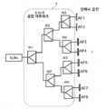
안테나 어레이 또는 위상 어레이 안테나들은 현대 통신 및 레이더 시스템에 종종 사용된다. 당해 기술분야에 잘 알려진 바와 같이, 위상 어레이는 16, 64 또는 256 요소와 같은, 다수의 방사 요소들을 포함한다. 다수의 출력 포트들(다수의 방사 요소들) 간에 단일 입력(하나의 송신기)으로부터 신호 전력을 분할하는 전력 분배 네트워크 또는 급전 네트워크가 제공된다. 기본적으로, 윌킨슨 전력 분배기에서와 같이, 각 전력 분할은 수동형으로 수행될 수 있다. 도 2는 Tx 신호가 제1 윌킨슨 분배기(W1)에 의해 2개의 병렬 1 내지 4 급전 네트워크(W2, W3, W4 및 W2', W3', W4')로 각각 분할되고, 이것은 총 8개의 출력 또는 방사 요소들(AF1-AF8n)을 공급한다. 윌킨슨 분배기 급전 네트워크에는 많은 라우팅이 필요하지만, 반면에, 모든 프런트-엔드들 중에서 신호 진폭과 위상 균일성을 보장한다. 그럼에도 불구하고, 어레이의 크기가 커짐에 따라 라우팅의 양과 급전 네트워크의 크기가 급격히 증가한다.Antenna arrays or phased array antennas are often used in modern communications and radar systems. As is well known in the art, a phased array includes a plurality of radiating elements, such as 16, 64 or 256 elements. A power distribution or feeding network is provided that divides the signal power from a single input (one transmitter) between multiple output ports (multiple radiating elements). Basically, as in the Wilkinson power divider, each power split can be performed passively. 2 shows that the Tx signal is split into two parallel 1-4 feed networks W2, W3, W4 and W2', W3', W4' by a first Wilkinson divider W1, respectively, which has a total of 8 outputs or It supplies radiating elements AF1-AF8n. Wilkinson splitter feed networks require a lot of routing, while ensuring signal amplitude and phase uniformity among all front-ends. Nevertheless, as the size of the array increases, the amount of routing and the size of the feeding network increase dramatically.
밀리미터파 대역은 전통적으로 레이더 시스템에 사용되었다. 최근 GSM(Global System for Mobile Communications) 및 UMTS(Universal Mobile Telecommunications System)와 같은 모바일 셀룰러 시스템에 적용되는 마이크로파 대역은 높은 데이터 전송속도의 트래픽을 지원할 수 없기 때문에, 예를 들어, 60GHz 대역과 같은, 밀리미터파 대역이 더 주목받고 있으며, 이것은 이러한 단거리 통신을 위해 수 GHz의 대역폭을 제공할 수 있다. 또한, 60GHz 대역의 통신은 아날로그 부품 및 안테나의 소형화 가능성과 같은 몇 가지 장점이 있다.The millimeter wave band has traditionally been used in radar systems. Microwave bands applied to mobile cellular systems such as GSM (Global System for Mobile Communications) and UMTS (Universal Mobile Telecommunications System) cannot support high data rate traffic. Wave bands are getting more attention, and they can provide bandwidths of several GHz for such short-range communications. In addition, communication in the 60 GHz band has several advantages, such as the possibility of miniaturization of analog components and antennas.
윌킨슨 분배기 구성은 밀리미터파 안테나 어레이 급전 네트워크에도 사용할 수 있다. 한 가지 접근 방식에 있어, 안테나 어레이를 위한 급전 네트워크는 스트립라인 윌킨슨 분배기를 포함한다. 그러나 PCB 환경상의 문제는 윌킨슨 분배기의 절연 저항을 구현하는 것이다. 60GHz 이상의 주파수에서 SMD 저항과 같은 개별 저항은 고가이며, 대형 어레이의 경우 조립이 용이하지 않을 수도 있다. 대안적인 접근 방식은 "내장(built-in)" 저항을 구비하는 LTCC(low temperature co-fired ceramics: 저온 동시-소성 세라믹) 기술일 수 있지만, LTCC 기술의 가격은 기본적인 PCB 기술의 가격보다 높다.Wilkinson splitter configurations can also be used for millimeter wave antenna array feeding networks. In one approach, the feed network for the antenna array includes a stripline Wilkinson splitter. However, the problem with the PCB environment is to implement the insulation resistance of the Wilkinson divider. At frequencies above 60 GHz, individual resistors, such as SMD resistors, are expensive and may not be easy to assemble for large arrays. An alternative approach could be low temperature co-fired ceramics (LTCC) technology with “built-in” resistors, but the cost of LTCC technology is higher than that of basic PCB technology.
윌킨슨 전력 스플리터는 모놀리식 밀리미터파 집적 회로(Monolithic Millimeter-wave Integrated Circuit: MMIC) 기술로 구현될 수도 있는데, 여기서 패시브 소자들 및 상호 연결부들은 능동형 소자들과 동일한 반도체 기판 상에 제조된다. 이러한 접근 방식의 예는 2016년 12월 간행된, IEEE Transactions On Microwave Theory And Techniques, Vol. 64, No. 12, 4701-4719 페이지의 Samet Zihir 등의 "60-GHz 64- and 256-Elements Wafer-Scale Phased-Array Transmitters Using Full-Reticle and Subreticle Stitching Techniques"라는 명칭의 문서에 개시되어 있다. RF 분배 네트워크, 전력 및 SPI 분배에 동일한 실리콘 웨이퍼가 사용되었으며, 위상-배열 채널 안테나는 실리콘 웨이퍼 상단에 장착된 별도의 석영 웨이퍼 상에 존재하였다. 그러한 1-64 분배 네트워크는 모든 위상 배열 채널에 균등하게 전력을 분배하며, 이들은 동일한 웨이퍼 상에 있어 서로 매우 유사하다.Wilkinson power splitters may be implemented with Monolithic Millimeter-wave Integrated Circuit (MMIC) technology, where passive components and interconnects are fabricated on the same semiconductor substrate as active components. An example of this approach can be found in IEEE Transactions On Microwave Theory And Techniques, Vol. 64, No. 12, in a document entitled "60-GHz 64- and 256-Elements Wafer-Scale Phased-Array Transmitters Using Full-Reticle and Subreticle Stitching Techniques" by Samet Zihir et al. on pp. 12, 4701-4719. The same silicon wafer was used for the RF distribution network, power and SPI distribution, and the phased-array channel antenna was on a separate quartz wafer mounted on top of the silicon wafer. Such a 1-64 distribution network distributes power equally to all phased array channels, which are very similar to each other on the same wafer.
그러나 이러한 온-칩 전력 스플리터의 문제점은 고가의 MMIC 영역을 소모하고, 위상 어레이 셀들 사이에 추가 배선이 필요하기 때문에 추가적인 전력 손실을 초래할 수 있다는 점이다.However, a problem with such an on-chip power splitter is that it consumes an expensive MMIC area and may cause additional power loss because additional wiring is required between the phased array cells.
본 발명의 일 측면은 특히 대규모 어레이 급전 네트워크에서 비용 효율적이고 실현 가능한 구현을 제공하는 밀리미터파 주파수를 위한 새로운 윌킨슨 분배기 설계를 제공하는 것이다. 본 발명의 상기한 측면은 독립항에 기재된 내용을 특징으로 한다. 본 발명의 바람직한 실시 예들은 종속항들에 개시되어 있다.One aspect of the present invention is to provide a novel Wilkinson divider design for millimeter wave frequencies that provides a cost-effective and feasible implementation, particularly in large-scale array feeding networks. Said aspect of the invention is characterized by what is stated in the independent claim. Preferred embodiments of the invention are disclosed in the dependent claims.
본 발명의 일 측면에 따르면, 하이브리드 밀리미터파 윌킨슨 분배기가 제공되는바, 상기 하이브리드 밀리미터파 윌킨슨 분배기는:According to one aspect of the present invention, there is provided a hybrid millimeter wave Wilkinson dispenser, the hybrid millimeter wave Wilkinson dispenser comprising:
캐리어 기판,carrier substrate,
입력 포트, 제1 출력 포트, 제2 출력 포트, 및 상기 입력 포트를 상기 캐리어 기판에서의 전송 라인들에 의해 구현된 상기 제1 및 제2 출력 포트에 연결하는 전송 라인들,an input port, a first output port, a second output port, and transmission lines connecting the input port to the first and second output ports implemented by transmission lines in the carrier substrate;
상기 제1 및 제2 출력 포트 사이에 연결된 절연 저항을 포함하되, 상기 윌킨슨 분배기의 절연 저항은 상기 캐리어 기판 상에 설치된 모놀리식 마이크로파 집적 회로(mono-lithic microwave integrated circuit: MMIC) 칩에 집적되고, 상기 MMIC 칩은 상기 캐리어 기판 상의 제1 및 제2 출력 포트에 각각 연결되는 제1 입력 금속 패드 및 제2 입력 금속 패드를 포함하고, 상기 절연 저항은 상기 MMIC 칩에서 상기 제1 입력 금속 패드와 상기 제2 입력 금속 패드 사이에 연결되고, 그리고 상기 MMIC 칩은 상기 제1 입력 금속 패드의 기생 커패시턴스를 보상하기 위한 제1 병렬 공진 회로, 및 상기 제2 입력 금속 패드의 기생 커패시턴스를 보상하기 위한 제2 병렬 공진 회로를 더 포함한다.an insulation resistance coupled between the first and second output ports, wherein the insulation resistance of the Wilkinson divider is integrated in a mono-lithic microwave integrated circuit (MMIC) chip installed on the carrier substrate; , wherein the MMIC chip includes a first input metal pad and a second input metal pad respectively connected to first and second output ports on the carrier substrate, and the insulation resistance is formed between the first input metal pad and the first input metal pad in the MMIC chip. connected between the second input metal pads, and the MMIC chip includes a first parallel resonant circuit for compensating parasitic capacitance of the first input metal pad, and a first parallel resonant circuit for compensating parasitic capacitance of the second
본 발명의 또 다른 측면에 따르면, 하이브리드 밀리미터파 장치가 제공되는바, 상기 하이브리드 밀리미터파 장치는:According to another aspect of the present invention, there is provided a hybrid millimeter wave device, the hybrid millimeter wave device comprising:
캐리어 기판,carrier substrate,
상기 캐리어 기판 상에 설치된 적어도 하나의 모놀리식 마이크로파 집적 회로(MMIC) 칩,at least one monolithic microwave integrated circuit (MMIC) chip installed on the carrier substrate;
하나의 입력 신호를 다수의 출력들에 공급하도록 구성된 신호 분배 네트워크를 포함하되, 상기 신호 분배 네트워크는 다수의 윌킨슨 분배기들을 포함하고, 상기 다수의 윌킨슨 분배기의 각각은 입력 포트, 제1 출력 포트, 제2 출력 포트, 상기 입력 포트를 상기 제1 및 제2 출력 포트를 연결하는 전송 라인들, 및 상기 제1 및 제2 출력 포트 사이에 연결되는 절연 저항을 포함하고,a signal distribution network configured to supply one input signal to a plurality of outputs, the signal distribution network comprising a plurality of Wilkinson splitters, each of the plurality of Wilkinson splitters comprising an input port, a first output port, a first a second output port, transmission lines connecting the input port to the first and second output ports, and an insulation resistor connected between the first and second output ports;
각각의 윌킨슨 분배기의 전송 라인은 캐리어 기판에 구현되고, 각 윌킨슨 분배기의 절연 저항은 적어도 하나의 MMIC 칩에 직접되며, 및the transmission line of each Wilkinson divider is embodied in a carrier substrate, the insulation resistance of each Wilkinson divider is direct to the at least one MMIC chip, and
상기 MMIC 칩은 캐리어 기판 상의 제1 및 제2 출력 포트에 각각 연결된 제1 입력 금속 패드 및 제2 입력 금속 패드를 포함하고, 상기 절연 저항들은 MMIC 칩에서 제1 입력 금속 패드와 제2 입력 금속 패드 사이에 연결되고, 그리고 상기 MMIC 칩은 상기 제1 입력 금속 패드의 기생 커패시턴스를 보상하기 위한 제1 병렬 공진 회로, 및 상기 제2 입력 금속 패드의 기생 커패시턴스를 보상하기 위한 제2 병렬 공진 회로를 더 포함한다.The MMIC chip includes a first input metal pad and a second input metal pad respectively connected to first and second output ports on a carrier substrate, and the insulation resistors include a first input metal pad and a second input metal pad in the MMIC chip. connected between, and the MMIC chip further includes a first parallel resonant circuit for compensating parasitic capacitance of the first input metal pad, and a second parallel resonant circuit for compensating parasitic capacitance of the second input metal pad include
일 실시 예에서, 상기 신호 분배 네트워크는 1 대 4, 1 대 8, 1 대 16, 1 대 64, 1 대 256, 1 대 512 네트워크, 또는 이들의 조합이다.In one embodiment, the signal distribution network is a 1 to 4, 1 to 8, 1 to 16, 1 to 64, 1 to 256, 1 to 512 network, or a combination thereof.
일 실시 예에서, 제1 병렬 공진 회로는 제1 입력 금속 패드로부터 MMIC 칩의 그라운드에 연결되고 이에 의해 제1 입력 금속 패드의 기생 커패시턴스와 병렬로 연결되는 제1 인덕턴스를 포함하며, 이에 의해 제2 병렬 공진 회로는 제2 입력 금속 패드로부터 MMIC 칩의 그라운드로 연결되고 이에 의해 제2 입력 금속 패드의 기생 커패시턴스와 병렬로 연결되는 제2 인덕턴스를 포함한다.In one embodiment, the first parallel resonant circuit comprises a first inductance coupled from the first input metal pad to the ground of the MMIC chip and thereby coupled in parallel with the parasitic capacitance of the first input metal pad, whereby the second The parallel resonant circuit includes a second inductance coupled from the second input metal pad to the ground of the MMIC chip and thereby coupled in parallel with the parasitic capacitance of the second input metal pad.
일 실시 예에서, 상기 MMIC 칩은 그라운드에 연결된 제3 금속 패드 및 제4 패드를 포함하고, 여기서 상기 제1 인덕턴스는 제1 입력 금속 패드와 제3 금속 패드 사이에 연결되고, 상기 제2 인덕턴스는 제2 입력 금속 패드 및 제4 금속 패드 사이에 연결된다.In one embodiment, the MMIC chip includes a third metal pad and a fourth pad coupled to ground, wherein the first inductance is coupled between the first input metal pad and the third metal pad, and the second inductance is connected between the second input metal pad and the fourth metal pad.
일 실시 예에서, 상기 제3 및 제4 금속 패드는 MMIC 칩과 캐리어 기판 사이에서 그라운드 접촉이 되도록 구성된다.In one embodiment, the third and fourth metal pads are configured to be in ground contact between the MMIC chip and the carrier substrate.
일 실시 예에서, 상기 MMIC 칩은 적어도 하나의 추가적인 집적 요소 및/또는 전자 회로를 더 포함한다. 일 실시 예에서, 캐리어 기판은 인쇄 회로 기판(printed circuit board: PCB) 기술, 저온 동시-소성 세라믹(Low-temperature cofired ceramic: LTCC) 기술, 집적형 패시브 소자(integrated passive device: IPD) 기술, 또는 석영(quartz) 기판에 기초한다. 본 발명의 또 다른 측면은 본 발명의 실시 예들에 따른 적어도 하나 또는 다수의 밀리미터파 윌킨슨 분배기 장치들을 포함하는 밀리미터파 위상 어레이이다.In one embodiment, the MMIC chip further comprises at least one additional integrated element and/or electronic circuitry. In one embodiment, the carrier substrate is printed circuit board (PCB) technology, low-temperature cofired ceramic (LTCC) technology, integrated passive device (IPD) technology, or It is based on a quartz substrate. Another aspect of the present invention is a millimeter wave phased array comprising at least one or more millimeter wave Wilkinson divider devices according to embodiments of the present invention.
본 발명의 또 다른 측면에 따르면 모노리식 마이크로파 집적 회로(MMIC)가 제공되는바, 상기 MMIC 칩은:According to another aspect of the present invention there is provided a monolithic microwave integrated circuit (MMIC), the MMIC chip comprising:
캐리어 기판 상에 MMIC 칩을 실장하기 위한 적어도 하나의 제1 입력 금속 패드 및 제2 입력 금속 패드,at least one first input metal pad and a second input metal pad for mounting the MMIC chip on the carrier substrate;
상기 MMIC 칩이 캐리어 기판에 실장될 때, 제1 및 제2 입력 금속 패드를 통해 캐리어 기판의 전송 라인들에 연결되어 캐리어 기판 전송 라인을 갖는 하이브리드 밀리미터파 윌킨슨 분배기를 형성하도록 구성된 적어도 하나의 집적 절연 저장을 포함하되, 그리고at least one integrated isolation configured to connect to transmission lines of the carrier substrate through first and second input metal pads to form a hybrid millimeter wave Wilkinson distributor having a carrier substrate transmission line when the MMIC chip is mounted to a carrier substrate including storage, and
상기 MMIC 칩은 제1 입력 금속 패드 및 제2 입력 금속 패드의 기생 커패시턴스를 각각 보상하도록 구성된 MMIC 칩 상의 제1 병렬 공진 회로 및 제2 병렬 공진 회로를 포함하고, 상기 제1 병렬 공진 회로는, 바람직하게는, 제1 입력 금속 패드에서 그라운드로 연결되어 이에 의해 제1 입력 금속 패드의 기생 커패시턴스와 병렬로 연결되는 제1 인덕턴스를 포함하고, 그리고 제2 병렬 공진 회로는, 바람직하게는, 제2 입력 금속 패드에서 그라운드로 연결되어 이에 의해 제2 입력 금속 패드의 기생 커패시턴스와 병렬로 연결되는 제2 인덕턴스를 포함한다.wherein the MMIC chip comprises a first parallel resonant circuit and a second parallel resonant circuit on the MMIC chip, each configured to compensate a parasitic capacitance of a first input metal pad and a second input metal pad, wherein the first parallel resonant circuit is preferably preferably comprising a first inductance coupled to ground at the first input metal pad thereby coupled in parallel with a parasitic capacitance of the first input metal pad, and wherein the second parallel resonant circuit preferably comprises a second input and a second inductance coupled from the metal pad to ground thereby coupled in parallel with the parasitic capacitance of the second input metal pad.
일 실시 예에서, 상기 MMIC 칩은 그라운드에 연결된 제3 금속 패드 및 제4 패드를 포함하고, 상기 제1 인덕턴스는 제1 입력 금속 패드와 제3 금속 패드 사이에 연결되고, 상기 제2 인덕턴스는 제2 입력 금속 패드 및 제4 금속 패드 사이에 연결되고, 제3 및 제4 금속 패드는, 바람직하게는, 상기 MMIC 칩과 상기 캐리어 기판 사이의 그라운드 접점이 되도록 구성된다.In an embodiment, the MMIC chip includes a third metal pad and a fourth pad connected to a ground, the first inductance is connected between the first input metal pad and the third metal pad, and the second inductance is a second inductance. connected between the second input metal pad and the fourth metal pad, wherein the third and fourth metal pads are preferably configured to be a ground contact between the MMIC chip and the carrier substrate.
일 실시 예에서, 상기 MMIC 칩은 캐리어 기판의 다수의 전송 라인들에 연결되어 다수의 하이브리드 밀리미터파 윌킨슨 분배기를 형성하는 제1 및 제2 입력 금속 패드의 각각의 쌍을 갖는 다수의 집적된 절연 저항들을 포함하되, 상기 MMIC 칩은 선택적으로, 적어도 하나의 추가적인 집적된 구성요소 및/또는 전자 회로를 포함한다.In one embodiment, the MMIC chip is a plurality of integrated insulation resistors having respective pairs of first and second input metal pads connected to a plurality of transmission lines of a carrier substrate to form a plurality of hybrid millimeter wave Wilkinson dividers. wherein the MMIC chip optionally includes at least one additional integrated component and/or electronic circuitry.
이하에서, 본 발명은 첨부된 도면을 참조하여 예시적인 실시 예에 의해 더 상세히 설명될 것이다.
도 1은 윌킨슨 전력 분배기의 기본 구성을 도시한다.
도 2는 예시적인 1 대 8 급전 네트워크를 도시하는 개략적인 블록도이다.
도 3은 본 발명의 일 실시 예에 따른 하이브리드 윌킨슨 전력 분배기의 평면도를 도시한다.
도 4는 다층 PCB의 부분 단면 투시도를 도시한다.
도 5는 본 발명의 일 실시 예에 따른 하이브리드 윌킨슨 전력 분배기의 예시적인 설계를 도시한다.
도 6은 본 발명의 일 실시 예에 따른 MMIC 칩 저항기의 예시적인 설계를 도시한다.
도 7은 본 발명의 일 실시 예에 따른 3개의 하이브리드 윌킨슨 전력 분배기를 포함하는 1 대 4 급전 네트워크의 예시적인 설계를 도시한다.
도 8은 본 발명의 실시 예뿐만 아니라 다른 회로에 따른 다수의 MMIC 절연 저항들을 포함하는 예시적인 MMIC 칩을 개략적으로 도시한다.
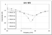
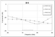
도 9, 10 및 11은, 포트 1이 "IN"이고 포트 2-5가 "AF1-AF4"를 각각 나타내는 급전 네트워크(도 7)에 대하여, 시뮬레이션 된 포트 매칭, 시뮬레이션 된 커플링, 및 신호 주파수(60-90GHz)의 기능에서 시뮬레이션 된 분리를 각각 나타내는 S-파라미터 그래프를 도시한다.Hereinafter, the present invention will be described in more detail by way of exemplary embodiments with reference to the accompanying drawings.
1 shows the basic configuration of a Wilkinson power divider.
2 is a schematic block diagram illustrating an exemplary one-to-eight feed network.
3 shows a plan view of a hybrid Wilkinson power divider according to an embodiment of the present invention.
4 shows a partial cross-sectional perspective view of a multilayer PCB.
5 shows an exemplary design of a hybrid Wilkinson power divider in accordance with an embodiment of the present invention.
6 shows an exemplary design of an MMIC chip resistor in accordance with an embodiment of the present invention.
7 shows an exemplary design of a one-to-four feed network comprising three hybrid Wilkinson power dividers in accordance with an embodiment of the present invention.
8 schematically illustrates an exemplary MMIC chip including a plurality of MMIC insulation resistors according to an embodiment of the present invention as well as another circuit.
Figures 9, 10 and 11 show simulated port matching, simulated coupling, and signal frequency for a feed network (Figure 7) where
본 발명의 일 측면은 전송 라인 라우팅을 위한 캐리어 기판 또는 보드 및 저항 구현을 위한 모놀리식 밀리미터파 집적 회로(MMIC) 기술을 사용하는 하이브리드 윌킨슨 전력 분배기(hybrid Wilkinsion power divider) 또는 스플리터(splitter)이다. 전송 라인은 마이크로스트립 라인, 스트립라인, 공면 도파관(coplanar waveguide: CPW)과 같은 다양한 대체 구조로 구현될 수 있다. 예시적인 실시 예에서, 전송 라인은 대부분 마이크로스트립 라인으로 구현되지만, 본 발명의 실시 예는 마이크로스트립 라인의 사용에만 한정되지 않는다. 본 발명의 실시 예에 적합한 캐리어 기판 또는 보드(RF 플랫폼이라고도 지칭될 수 있음)는 인쇄 회로 기판(PCB), 저온 동시-소성 세라믹(Low-temperature cofired ceramic: TCC), 집적된 패시브 소자(integrated passesive device: IPD), 석영 웨이퍼 등을 포함한다. 여기에 기술된 예시적인 실시 예는 본 발명의 실시 예를 이들 기술로 제한하려는 의도 없이, 예를 들어, PCB 기술을 사용하여 설명되고 예시될 것이다. 새로운 하이브리드, 예컨대, PCB/MMIC 또는 LTCC/MMIC, 윌킨슨 전력 분배기 설계는 라우팅으로 인한 신호 손실의 최소화 및 MMIC 영역 소비의 최소화로 이어질 수 있다. 전송 라인 라우팅에 PCB 기술을 사용하고 매우 작은 MMIC 영역으로 절연 저항을 구현함으로써 기존 설계와 비교하여 매우 비용 효율적인 윌킨슨 설계를 가능하게 한다. 윌킨슨 분배기의 낮은 제조 비용은, 모든 램프 포스트가 수백 개의 방사 요소들을 포함하는 위상 배열 무선 프론트-엔드(들)를 구비할 수도 있는, 5G 통신 응용분야와 같이 대규모의 어레이를 갖는 응용분야에서 특히 유리하다.One aspect of the present invention is a hybrid Wilkinsion power divider or splitter using monolithic millimeter wave integrated circuit (MMIC) technology for resistor implementation and carrier substrate or board for transmission line routing. . The transmission line may be implemented in various alternative structures such as microstrip lines, striplines, and coplanar waveguides (CPWs). In an exemplary embodiment, the transmission line is mostly implemented as a microstrip line, but embodiments of the present invention are not limited to the use of a microstrip line. Suitable carrier substrates or boards (which may also be referred to as RF platforms) for embodiments of the present invention include printed circuit boards (PCBs), low-temperature cofired ceramics (TCCs), integrated passive devices. device: IPD), a quartz wafer, and the like. Exemplary embodiments described herein will be described and illustrated using, for example, PCB technology without intending to limit embodiments of the present invention to these techniques. New hybrid, eg PCB/MMIC or LTCC/MMIC, Wilkinson power divider designs can lead to minimization of signal loss due to routing and minimization of MMIC area consumption. The use of PCB technology for transmission line routing and the implementation of insulation resistance with a very small MMIC area enables Wilkinson designs that are very cost-effective compared to conventional designs. The low manufacturing cost of Wilkinson distributors is particularly advantageous in applications with large arrays, such as 5G communications applications, where every lamp post may have a phased array wireless front-end(s) comprising hundreds of radiating elements. do.
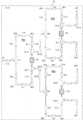
본 발명의 실시 예에 따른 하이브리드 윌킨슨 전력 분배기의 예가 도 3에 도시되어 있다. 예시적인 윌킨슨 분배기(30)는 캐리어 기판(예컨대, 인쇄 회로 기판 PCB)(31)의 하나 또는 다수의 전기 전도성 층들, 예를 들어, 금속층들에서의 마이크로스트립 라인(32) 형태의 전송 라인들 및 라우팅을 갖는다. 일 실시 예에서, 캐리어 기판(31)은 다층 캐리어 기판(예컨대, PCB 또는 LTCC)일 수 있고, 전송 라인 라우팅을 구현하는 마이크로 스트립 라인(32)의 적어도 일부는, 예를 들어, 도 4에 예시된 바와 같이, 유전체 층들(33) 사이의 중간 전기 전도성 층에 제공될 수 있다. 그러나 전도성의 상부 및 하부 층들(34, 35) 및 가능한 다른 층들과 같은, 전도성 층들 중 임의의 하나 또는 다수들이 전송 라인 라우팅에 활용될 수도 있다. 캐리어 기판(31)의 유전체 층들(33)은 임의의 적절한 유전체 재료로 제조될 수 있다. 도 3에서, MMIC 칩 저항(40)은 캐리어 기판(31) 상에 설치되고 출력 포트들(2 및 3) 사이에 연결될 수 있다. 연결을 이루기 위한 접촉 범프들 또는 패드들(41 및 42)이 제공될 수 있다.An example of a hybrid Wilkinson power divider according to an embodiment of the present invention is shown in FIG. 3 . The
본 발명의 실시 예에 따른 하이브리드 윌킨슨 전력 분배기의 예시적인 모델이 도 5에 도시되어 있다. 포트 1은 전송 라인 TL5(예를 들어, 길이 4mm 및 폭 1mm를 갖는 직선 마이크로스트립 라인)에 의해 분기 T 마이크로스트립 라인 SL1(예를 들어, 입력 분기점(3)에서 폭 1mm 및 출력 분기점(1 및 2)에서 폭 2mm를 가짐)에 연결된다. 직선 전송 라인 TL8(예컨대, 길이 1/2mm 및 폭 2mm의 직선 마이크로스트립 라인), 코너 마이크로스트립 라인 SL3(예컨대, 폭 2mm의), 직선 전송 라인 TL6(예컨대, 길이 1mm 및 폭 2mm의 직선 마이크로스트립 라인), 코너 마이크로스트립 라인 SL4(예컨대, 폭 2mm의), 및 직선 전송 라인 TL8(예컨대, 길이 1/2mm 및 폭 2mm의 직선 마이크로스트립 라인)은 분기 T 마이크로스트립 라인 SL61(예컨대, 입력 분기점(1 및 2)에서 폭 2mm 및 출력 분기점(3)에서 폭 3mm의)의 하나의 입력 분기점(예컨대, 분기점 2)에 연결된다. 분기 T 마이크로스트립 라인 SL16의 출력은 코너 마이크로스트립 라인 SL18(예컨대, 폭 3mm의)과 직선 전송 라인 TL10(예컨대, 길이 3mm 및 폭 3mm의 직선 마이크로스트립 라인)의 직렬연결을 통해 윌킨슨 분배기의 포트(2)에 대한 연결된다. 따라서, 도 5에 표시된 윌킨슨 분배기의 상단 부분은 도 3 또는 일반적으로 도 1에 도시된 윌킨슨 분배기의 포트들(1 및 2) 사이의 전송 라인을 나타낼 수 있다. 마찬가지로, 직선 전송 라인 TL12(예컨대, 길이 1/2 mm 및 폭 2 mm의 직선 마이크로스트립 라인), 코너 마이크로스트립 라인 SL2(예컨대, 폭 2 mm의), 직선 전송 라인 TL7(예컨대, 길이 1mm 및 폭 2mm의 직선 마이크로스트립 라인), 코너 마이크로스트립 라인 SL5(예컨대, 폭 2mm의), 및 직선 전송 라인 TL13(예컨대, 길이 1/2mm 및 폭 2mm의 직선 마이크로스트립 라인)의 직렬연결은 분기 T 마이크로스트립 라인 SL17(예컨대, 입력 분기점(1 및 2)에서 폭 2mm 및 출력 분기점(3)에서 3mm인)의 하나의 입력 분기점(예컨대, 분기점 1)에 연결된다. 분기 T 마이크로스트립 라인 SL17의 출력은 코너 마이크로스트립 라인 SL19(예컨대, 폭 3mm의)와 직선 전송 라인 TL10(예컨대, 길이 3mm 및 폭 3mm의 직선 마이크로스트립 라인)의 직렬연결을 통해 윌킨슨 분배기의 포트(3)에 연결된다. 따라서, 도 5에 도시된 윌킨슨 분배기의 하단 부분은 도 3, 또는 일반적으로 도 1에 도시된 윌킨슨 분배기의 포트들(1 및 3) 사이의 전송 라인을 나타낼 수 있다. 또한, 분기 T 마이크로스트립 라인 SL16)의 분기점(1)은 캐리어 기판(31) 상의 RF 패드(42)에 연결되고, 분기 T 마이크로스트립 라인 SL17의 분기점(2)은 캐리어 기판(31) 상의 RF 패드(41)에 연결된다. 절연 저항(Rs)(예컨대, 80 ohm)을 구현하는 MMIC 칩 저항(40)은 RF 패드들(41, 42) 사이에, 따라서 윌킨슨 분배기의 포트들(2 및 3) 사이에 연결된다.An exemplary model of a hybrid Wilkinson power divider according to an embodiment of the present invention is shown in FIG. 5 .
본 발명의 실시 예에 따른 MMIC 칩 저항(40)의 예시적인 모델이 도 6에 도시되어 있다. 상기 예시적인 MMIC 칩 저항(40)은 캐리어 기판(31) 상의 대응하는 RF 패드(42)에 연결 가능한 제1 무선 주파수(RF) 입력 금속 패드(X1), 및 캐리어 기판(31) 상의 대응하는 RF 패드(41)에 연결 가능한 제2 무선 주파수(RF) 입력 금속 패드(X3)를 포함할 수 있다. 상기 예시적인 MMIC 칩(40)은 칩 상에 집적된 절연 저항(Rs)을 더 포함한다. 절연 저항(Rs)은 MMIC 기술에 있어 적용 가능한 모든 형태로 구현될 수 있다. 다른 유형의 MMIC 저항의 예로는 CMOS용 폴리- 및 확산 저항, GaAS용 NiCr 저항 등이 포함된다. 그 재료는 예를 들어, 탄탈륨(tantalum) 또는 질화물(nitride)일 수 있다. 저항(Rs)은 박막 MMIC 저항일 수 있다. 예시적인 실시 예에서, 저항(Rs)은 80 ohm의 탄탈륨 박막 저항일 수 있다. 저항(Rs)은 적절한 수단, 예를 들어, 금속 라인(L2, L3)에 의해 RF 입력 금속 패드들(X1, X3) 사이에 연결된다.An exemplary model of an
RF 입력 금속 패드들(X1, X3)은 그라운드 전위에 대해 기생 커패시턴스(parasitic capacitance)를 가질 수 있다. 일 실시 예에서, RF 입력 금속 패드들(X1, X3)에 의해 야기된 기생 커패시턴스에 대한 보상 회로는 온-칩 저항(Rs)이 캐리어 기판(31) 상의 윌킨슨 분배기의 포트들(2 및 3)에 대한 순수 저항으로 나타나도록 MMIC 칩(40) 상에 제공될 수 있다. 일 실시 예에서, 상기 보상 회로는 기생 커패시턴스의 효과가 공진되도록(resonated out) 각각의 RF 입력 금속 패드(X1 또는 X3)와 병렬 공진 회로를 생성하도록 구성될 수 있다. 일 실시 예에서, 기준 전위 또는 그라운드에 연결된 금속 패드(X2)는 RF 입력 금속 패드(X1)에 인접한 칩 상에 제공될 수 있다. 또한, RF 입력 금속 패드(X1)에 의해 야기되는 기생 커패시터와 병렬적인 금속 패드들(X1, X2) 사이에 인덕터(L1)(예를 들어, 금속 라인)가 연결된다. 이에 의해, RF 입력 금속 패드(X1)의 기생 커패시턴스를 보상하는 병렬 공진 회로가 얻어진다. 마찬가지로, 기준 전위 또는 그라운드에 연결된 금속 패드(X4)가 RF 입력 금속 패드(X3)에 인접한 칩 상에 제공될 수 있다. 또한, RF 입력 금속 패드(X3)에 의한 야기되는 기생 커패시터와 병렬적인 금속 패드들(X3, X4) 사이에 인덕터(L4)(예를 들어, 금속 라인)가 연결될 수 있다. 이에 의해, RF 입력 금속 패드(X3)의 기생 커패시턴스를 보상하는 병렬 공진 회로가 획득된다.The RF input metal pads X1 and X3 may have a parasitic capacitance with respect to a ground potential. In one embodiment, the compensation circuit for the parasitic capacitance caused by the RF input metal pads (X1, X3) is such that the on-chip resistance (Rs) of the Wilkinson distributor ports (2 and 3) on the carrier substrate (31) It may be provided on the
일 실시 예에서, 상기 그라운드 된 금속 패드들(X2, X4)은 MMIC 칩과 캐리어 기판(31) 사이의 그라운드 접촉, 즉, 캐리어 기판(31) 상의 각각의 그라운드 패드들에 접촉하도록 구성된다. 따라서, 금속 패드들(X2, X4)은 MMIC 칩의 국부적 그라운드 및 캐리어 기판(31)의 그라운드 모두에 연결되어 접지되는바, 즉 MMIC 칩과 캐리어 기판(31)은 동일한 그라운드를 공유한다. 결과적으로, 공진 회로의 복귀 전류, 즉 공통 그라운드에 대해 잘 정의된 복귀 경로가 획득될 수 있다.In an embodiment, the grounded metal pads X2 and X4 are configured to be in contact with a ground contact between the MMIC chip and the
본 발명의 실시 예에 따른 하이브리드 윌킨슨 분배기는 도 2에 예시된 1 대 8 급전 네트워크(2)와 같은, 더 큰 급전 네트워크를 구성하기 위한 구성 요소로 사용될 수 있다. 도 7은 본 발명의 실시 예에 따른 3개의 하이브리드 윌킨슨 전력 분배기를 포함하는 1 대 4 급전 네트워크(70)의 예시적인 모델을 도시한다. 상기 급전 네트워크(70)는, 예를 들어, 8개의 출력들 또는 방사 소자들(FA1-FA8)에 각각 급전하는, 2개의 병렬 1 대 4 급전 네트워크들(W2, W3, W4 및 W2', W3', W4')의 각각을 구현할 수 있다. 도 3 내지 7에서, 동일한 참조 기호는 동일하거나 유사한 구조 또는 기능을 나타낸다. 유사하게, 예를 들어, 16, 64, 256 또는 512 요소들에 대해 급전을 제공하기 위해 더 큰 급전 또는 전력 분배기 네트워크들이 제공될 수도 있다.A hybrid Wilkinson distributor according to an embodiment of the present invention may be used as a component for configuring a larger power supply network, such as the 1 to 8
일 실시 예에서, MMIC 칩은 그 MMIC 칩이 탑재될 캐리어 기판 상의 전송 라인 라우팅을 위한 스트립라인들을 갖는 하나의 하이브리드 윌킨슨 분배기에 대한 집적된 절연 저항을 포함한다.In one embodiment, the MMIC chip includes an integrated insulation resistor to one hybrid Wilkinson distributor with striplines for routing transmission lines on the carrier substrate on which the MMIC chip will be mounted.
일 실시 예에서, MMIC 칩은 그 MMIC 칩이 탑재될 캐리어 기판 상의 전송 라인 라우팅을 위한 스트립라인을 갖는 다수의 하이브리드 윌킨슨 분배기들, 즉 둘 이상의 분배기들을 위한 집적된 절연 저항을 포함한다.In one embodiment, the MMIC chip includes an integrated insulation resistor for multiple hybrid Wilkinson distributors, ie two or more distributors, having a stripline for routing transmission lines on a carrier substrate on which the MMIC chip will be mounted.
일 실시 예에서, MMIC 칩은 하나 또는 다수의 집적된 절연 저항들 이외에, 패시브 구성요소, 액티브 구성요소, 아날로그 회로, 디지털 회로, 제어 회로 등 중의 임의의 하나 또는 다수와 같은, 추가적인 MMIC 구성요소들 및/또는 전자 회로들을 포함한다. 본 발명의 실시 예들에 따른 하이브리드 윌킨슨 분배기를 사용하여 절약된 MMIC 영역은 동일한 칩 영역 상에 더 많은 추가 회로를 가능하게 하거나, 더 적은 MMIC 칩 영역으로 동일한 회로를 가능하게 할 수 있다.In one embodiment, the MMIC chip includes, in addition to one or more integrated insulation resistors, additional MMIC components, such as any one or more of a passive component, an active component, an analog circuit, a digital circuit, a control circuit, etc. and/or electronic circuits. The MMIC area saved by using the hybrid Wilkinson divider according to embodiments of the present invention may enable more additional circuitry on the same chip area, or may enable the same circuitry with less MMIC chip area.
도 8은 본 발명의 실시 예들에 따른 다수의 MMIC 절연 저항들(40)을 포함하는 예시적인 MMIC 칩을 개략적으로 도시한다. 상기 MMIC 절연 저항들(40)은 대각선으로 채워진 상태로 도시되어 있다. MMIC 절연 저항들(40)은, 그 MMIC 칩이 장착될 때, 그들이 하부 캐리어 기판 상의 각각의 윌킨슨 분배기의 전송 라인 라우팅에 쉽게 연결될 수 있도록 MMIC 칩(80) 레이아웃 상에 배치될 수 있다. 상기 MMIC 칩(80) 레이아웃 상의 선택적인 그라운드 패드들(X2 및 X4)뿐만 아니라, 각각의 MMIC 절연 저항들(40) 및 관련 접촉 패드들(X1 및 X3)의 배치는 MMIC 칩 영역이 그 칩 상에서 최소한의 라우팅으로써 효과적으로 사용될 수 있도록 할 수 있다. MMIC 절연 저항들(40)의 접촉 패드들(X1, X3)뿐만 아니라 그라운드 접촉 패드들(X2, X3)은, 예를 들어, 도 8에 도시된 바와 같이, MMIC 칩(80)의 모서리에 존재할 수 있다. MMIC 절연 저항들의 접촉 패드들(X1 및 X3)뿐만 아니라 그라운드 접촉 패드들(X2 및 X3)은, 도 8에 또한 도시된 바와 같이, MMIC 칩(80)의 모서리들 외에도, MMIC 칩(80) 상의 MMIC 절연 저항들(40)에 아주 근접할 수 있다. 도 8에 도시된 MMIC 칩(80)은, 예를 들어, 도 2에 도시된 1 대 8 급전 네트워크(2)에 적합할 수도 있다. 상기 MMIC 칩(80)은 또한, 점선으로 된 요소들(81)에 의해 예시된 바와 같이, 추가적인 MMIC 구성요소들 및/또는 전자 회로들을 더 포함할 수 있다. 이러한 요소들은 패시브 구성요소, 액티브 구성요소, 아날로그 회로, 디지털 회로, 제어 회로 등을 포함할 수 있다.8 schematically illustrates an exemplary MMIC chip including a plurality of
도 9, 10 및 11은, 포트 1은 "IN"이고 포트 2-5는 "AF1-AF4"를 나타내는, 1 대 4 급전 네트워크(도 7)에 대해, 신호 주파수(60-90GHz)의 기능에서 시뮬레이션된 포트 정합(Port matching), 시뮬레이션된 커플링(Coupling) 및 시뮬레이션된 분리(Isolation)를 각각 예시하는 S-파라미터 그래프들이다. 상기 시뮬레이션은 본 발명의 실시 예들에 따른 하이브리드 윌킨슨 분배기의 우수한 성능을 보여준다. 본 발명의 실시 예들은 이러한 예시적인 주파수들에 한정되는 것을 의도하지 않으며, 모든 마이크로파 및 밀리미터파 신호, 특히 20GHz보다 높은 주파수에 대해 적용 가능하다.Figures 9, 10 and 11, for a one-to-four feed network (Figure 7), with
본 발명 및 그 실시 예들은 위에서 설명된 예들에 한정되지 않고 후술하는 청구범위의 범위 내에서 변할 수도 있다는 것은 당해 기술분야의 전문가에게 자명할 것이다.It will be apparent to those skilled in the art that the present invention and its embodiments are not limited to the examples described above and may vary within the scope of the claims described below.
Claims (13)
Translated fromKorean캐리어 기판,
입력 포트, 제1 출력 포트, 제2 출력 포트, 및 상기 입력 포트를 상기 캐리어 기판에서의 전송 라인들에 의해 구현된 상기 제1 및 제2 출력 포트에 연결하는 전송 라인들, 및
상기 제1 및 제2 출력 포트 사이에 연결된 절연 저항을 포함하되, 상기 윌킨슨 분배기의 절연 저항은 상기 캐리어 기판 상에 설치된 모놀리식 마이크로파 집적 회로(mono-lithic microwave integrated circuit: MMIC) 칩에 집적되고, 상기 MMIC 칩은 상기 캐리어 기판 상의 제1 및 제2 출력 포트에 각각 연결되는 제1 입력 금속 패드 및 제2 입력 금속 패드를 포함하고, 상기 절연 저항은 상기 MMIC 칩에서 상기 제1 입력 금속 패드와 상기 제2 입력 금속 패드 사이에 연결되고, 그리고 상기 MMIC 칩은 상기 제1 입력 금속 패드의 기생 커패시턴스를 보상하기 위한 제1 병렬 공진 회로, 및 상기 제2 입력 금속 패드의 기생 커패시턴스를 보상하기 위한 제2 병렬 공진 회로를 더 포함하는 하이브리드 밀리미터파 윌킨슨 분배기.
A hybrid millimeter wave Wilkinson divider comprising:
carrier substrate,
an input port, a first output port, a second output port, and transmission lines connecting the input port to the first and second output ports implemented by transmission lines in the carrier substrate, and
an insulation resistance coupled between the first and second output ports, wherein the insulation resistance of the Wilkinson divider is integrated in a mono-lithic microwave integrated circuit (MMIC) chip installed on the carrier substrate; , wherein the MMIC chip includes a first input metal pad and a second input metal pad respectively connected to first and second output ports on the carrier substrate, and the insulation resistance is formed between the first input metal pad and the first input metal pad in the MMIC chip. connected between the second input metal pads, and the MMIC chip includes a first parallel resonant circuit for compensating parasitic capacitance of the first input metal pad, and a first parallel resonant circuit for compensating parasitic capacitance of the second input metal pad 2 A hybrid millimeter wave Wilkinson divider further comprising a parallel resonant circuit.
캐리어 기판,
상기 캐리어 기판 상에 설치된 적어도 하나의 모놀리식 마이크로파 집적 회로(MMIC) 칩,
하나의 입력 신호를 다수의 출력들에 공급하도록 구성된 신호 분배 네트워크를 포함하되, 상기 신호 분배 네트워크는 다수의 윌킨슨 분배기들을 포함하고, 상기 다수의 윌킨슨 분배기들의 각각은 입력 포트, 제1 출력 포트, 제2 출력 포트, 상기 입력 포트를 상기 제1 및 제2 출력 포트를 연결하는 전송 라인들, 및 상기 제1 및 제2 출력 포트 사이에 연결되는 절연 저항을 포함하고,
각각의 윌킨슨 분배기의 전송 라인들은 캐리어 기판에 구현되고, 각 윌킨슨 분배기의 절연 저항은 상기 적어도 하나의 MMIC 칩에 직접되며, 및
상기 MMIC 칩은 캐리어 기판 상의 제1 및 제2 출력 포트들에 각각 연결된 제1 입력 금속 패드 및 제2 입력 금속 패드를 포함하고, 상기 절연 저항들은 상기 MMIC 칩에서 제1 입력 금속 패드와 제2 입력 금속 패드 사이에 연결되고, 그리고 상기 MMIC 칩은 상기 제1 입력 금속 패드의 기생 커패시턴스를 보상하기 위한 제1 병렬 공진 회로, 및 상기 제2 입력 금속 패드의 기생 커패시턴스를 보상하기 위한 제2 병렬 공진 회로를 더 포함하는 하이브리드 밀리미터파 장치.
A hybrid millimeter wave device comprising:
carrier substrate,
at least one monolithic microwave integrated circuit (MMIC) chip installed on the carrier substrate;
a signal distribution network configured to supply one input signal to a plurality of outputs, the signal distribution network comprising a plurality of Wilkinson splitters, each of the plurality of Wilkinson splitters comprising an input port, a first output port, a first a second output port, transmission lines connecting the input port to the first and second output ports, and an insulation resistor connected between the first and second output ports;
the transmission lines of each Wilkinson divider are embodied in a carrier substrate, the insulation resistance of each Wilkinson divider is direct to the at least one MMIC chip, and
The MMIC chip includes a first input metal pad and a second input metal pad respectively connected to first and second output ports on a carrier substrate, and the insulation resistors include a first input metal pad and a second input metal pad in the MMIC chip. connected between metal pads, and the MMIC chip includes a first parallel resonant circuit for compensating parasitic capacitance of the first input metal pad, and a second parallel resonant circuit for compensating parasitic capacitance of the second input metal pad A hybrid millimeter wave device further comprising a.
상기 신호 분배 네트워크는 1 대 4, 1 대 8, 1 대 16, 1 대 64, 1 대 256, 또는 1 대 512 네트워크, 또는 이들의 조합인 것인 장치.
3. The method of claim 2,
wherein the signal distribution network is a 1 to 4, 1 to 8, 1 to 16, 1 to 64, 1 to 256, or 1 to 512 network, or a combination thereof.
상기 제1 병렬 공진 회로는 상기 제1 입력 금속 패드로부터 상기 MMIC 칩의 그라운드에 연결되고 이에 의해 상기 제1 입력 금속 패드의 기생 커패시턴스와 병렬로 연결되는 제1 인덕턴스를 포함하며, 그리고 상기 제2 병렬 공진 회로는 상기 제2 입력 금속 패드로부터 상기 MMIC 칩의 그라운드로 연결되고 이에 의해 상기 제2 입력 금속 패드의 기생 커패시턴스와 병렬로 연결되는 제2 인덕턴스를 포함하는 것인 장치.
4. The method of claim 1, 2 or 3,
the first parallel resonant circuit comprises a first inductance coupled from the first input metal pad to the ground of the MMIC chip thereby coupled in parallel with a parasitic capacitance of the first input metal pad, and the second parallel wherein the resonant circuit comprises a second inductance coupled from the second input metal pad to ground of the MMIC chip and thereby coupled in parallel with a parasitic capacitance of the second input metal pad.
상기 MMIC 칩은 그라운드에 연결되는 제3 금속 패드와 제4 금속 패드를 포함하고, 상기 제1 인덕턴스는 상기 제1 입력 금속 패드와 상기 제3 금속 패드 사이에 연결되고, 상기 제2 인덕턴스는 상기 제2 입력 금속 패드와 상기 제4 금속 패드 사이에 연결되는 것인 장치.
5. The method of claim 4,
The MMIC chip includes a third metal pad and a fourth metal pad connected to a ground, the first inductance is connected between the first input metal pad and the third metal pad, and the second inductance is the second inductance. 2 , connected between the input metal pad and the fourth metal pad.
상기 제3 및 제4 금속 패드들은 상기 MMIC 칩과 상기 PCB 사이의 그라운드 접촉이 되도록 구성되는 것인 장치.
6. The method according to claim 4 or 5,
and the third and fourth metal pads are configured to be a ground contact between the MMIC chip and the PCB.
상기 MMIC 칩은 적어도 하나의 추가적인 집적된 구성요소 및/또는 전자 회로를 더 포함하는 것인 장치.
7. The method according to any one of claims 1 to 6,
wherein the MMIC chip further comprises at least one additional integrated component and/or electronic circuitry.
상기 캐리어 기판은 인쇄 회로 기판(printed circuit board: PCB) 기술, 저온 동시-소성 세라믹(Low-temperature cofired ceramic: LTCC) 기술, 집적 패시브 소자(integrated passive device: IPD) 기술, 또는 석영(quartz) 기판에 기초하는 것인 장치.
8. The method according to any one of claims 1 to 7,
The carrier substrate is a printed circuit board (PCB) technology, a low-temperature cofired ceramic (LTCC) technology, an integrated passive device (IPD) technology, or a quartz substrate. A device that is based on
A millimeter wave phased array comprising a plurality of millimeter wave Wilkinson dividers according to claim 1 .
A millimeter wave phased array comprising at least one millimeter wave device according to claim 1 .
캐리어 기판 상에 MMIC 칩을 실장하기 위한 적어도 하나의 제1 입력 금속 패드 및 제2 입력 금속 패드,
상기 MMIC 칩이 캐리어 기판에 실장될 때, 상기 제1 및 제2 입력 금속 패드를 통해 캐리어 기판의 전송 라인들에 연결되어 캐리어 기판 전송 라인들을 갖는 하이브리드 밀리미터파 윌킨슨 분배기를 형성하도록 구성된 적어도 하나의 집적형 절연 저장을 포함하되, 그리고
상기 MMIC 칩은 상기 제1 입력 금속 패드 및 상기 제2 입력 금속 패드의 기생 커패시턴스를 각각 보상하도록 구성된 MMIC 칩 상의 제1 병렬 공진 회로 및 제2 병렬 공진 회로를 포함하고, 상기 제1 병렬 공진 회로는, 바람직하게는, 제1 입력 금속 패드에서 그라운드로 연결되어 이에 의해 제1 입력 금속 패드의 기생 커패시턴스와 병렬로 연결되는 제1 인덕턴스를 포함하고, 또한 제2 병렬 공진 회로는, 바람직하게는, 제2 입력 금속 패드에서 그라운드로 연결되어 이에 의해 제2 입력 금속 패드의 기생 커패시턴스와 병렬로 연결되는 제2 인덕턴스를 포함하는 것인 모노리식 마이크로파 집적 회로(MMIC) 칩.
A monolithic microwave integrated circuit (MMIC) chip comprising:
at least one first input metal pad and a second input metal pad for mounting the MMIC chip on the carrier substrate;
At least one integrated circuit configured to connect to transmission lines of a carrier substrate through the first and second input metal pads to form a hybrid millimeter wave Wilkinson distributor having carrier substrate transmission lines when the MMIC chip is mounted to a carrier substrate. type insulated storage; and
the MMIC chip comprises a first parallel resonant circuit and a second parallel resonant circuit on the MMIC chip configured to respectively compensate parasitic capacitances of the first input metal pad and the second input metal pad, the first parallel resonant circuit comprising: , preferably comprising a first inductance coupled to ground at the first input metal pad and thereby coupled in parallel with the parasitic capacitance of the first input metal pad, and the second parallel resonant circuit preferably comprises: A monolithic microwave integrated circuit (MMIC) chip comprising a second inductance coupled to ground at the second input metal pad and thereby coupled in parallel with the parasitic capacitance of the second input metal pad.
상기 MMIC 칩은 제3 금속 패드와 그라운드에 연결된 제4 패드를 포함하고, 상기 제1 인덕턴스는 상기 제1 입력 금속 패드와 상기 제3 금속 패드 사이에 연결되고, 상기 제2 인덕턴스는 상기 제2 입력 금속 패드와 상기 제4 금속 패드 사이에 연결되고, 상기 제3 및 제4 금속 패드들은 바람직하게는 상기 MMIC 칩과 상기 캐리어 기판 사이의 그라운드 접촉이 되도록 구성되는 것인 집적 회로(MMIC) 칩.
12. The method of claim 11,
The MMIC chip includes a third metal pad and a fourth pad connected to a ground, the first inductance is connected between the first input metal pad and the third metal pad, and the second inductance is the second input an integrated circuit (MMIC) chip connected between a metal pad and said fourth metal pad, said third and fourth metal pads preferably being configured to be a ground contact between said MMIC chip and said carrier substrate.
상기 MMIC 칩은 캐리어 기판 내의 다수의 전송 라인에 연결되어 다수의 하이브리드 밀리미터파 윌킨슨 분배기들을 형성하는 제1 및 제2 입력 금속 패드들의 각각의 쌍을 갖는 다수의 집적 절연 저항들을 포함하고, 상기 MMIC 칩은 선택적으로 적어도 하나의 추가적인 집적된 구성요소 및/또는 전자 회로를 더 포함하는 것인 집적 회로(MMIC) 칩.13. The method according to any one of claims 10 to 12,
wherein the MMIC chip includes a plurality of integrated insulation resistors having respective pairs of first and second input metal pads coupled to a plurality of transmission lines in a carrier substrate to form a plurality of hybrid millimeter wave Wilkinson dividers, the MMIC chip optionally further comprises at least one additional integrated component and/or electronic circuit.
Applications Claiming Priority (3)
| Application Number | Priority Date | Filing Date | Title |
|---|---|---|---|
| FI20195200AFI130081B (en) | 2019-03-18 | 2019-03-18 | Wilkinson divider |
| FI20195200 | 2019-03-18 | ||
| PCT/FI2020/050165WO2020188146A1 (en) | 2019-03-18 | 2020-03-17 | Wilkinson divider |
Publications (2)
| Publication Number | Publication Date |
|---|---|
| KR20210134913Atrue KR20210134913A (en) | 2021-11-11 |
| KR102819996B1 KR102819996B1 (en) | 2025-06-13 |
Family
ID=70058405
Family Applications (1)
| Application Number | Title | Priority Date | Filing Date |
|---|---|---|---|
| KR1020217029803AActiveKR102819996B1 (en) | 2019-03-18 | 2020-03-17 | Wilkinson distributor |
Country Status (6)
| Country | Link |
|---|---|
| US (1) | US12142808B2 (en) |
| EP (1) | EP3942605A1 (en) |
| KR (1) | KR102819996B1 (en) |
| CN (1) | CN113632224B (en) |
| FI (1) | FI130081B (en) |
| WO (1) | WO2020188146A1 (en) |
Families Citing this family (9)
| Publication number | Priority date | Publication date | Assignee | Title |
|---|---|---|---|---|
| US12374791B2 (en)* | 2019-09-25 | 2025-07-29 | Bdcm A2 Llc | Stripline feed distribution network with embedded resistor plane for millimeter wave applications |
| GB2601175A (en)* | 2020-11-23 | 2022-05-25 | Creo Medical Ltd | Sterilisation apparatus for generating hydroxyl radicals |
| CN112510336B (en)* | 2020-11-27 | 2022-02-01 | 成都天锐星通科技有限公司 | Broadband power divider and electronic equipment |
| FI129416B (en) | 2020-12-15 | 2022-02-15 | Teknologian Tutkimuskeskus Vtt Oy | Millimeter-wave antenna array apparatus |
| CN112821907B (en)* | 2020-12-31 | 2022-06-21 | 锐石创芯(深圳)科技股份有限公司 | Input impedance matching network and radio frequency front end module |
| CN113097679B (en)* | 2021-03-10 | 2021-11-19 | 西安电子科技大学 | Small Wilkinson power divider used in MMIC circuit |
| CN113114153A (en)* | 2021-04-09 | 2021-07-13 | 成都通量科技有限公司 | Broadband high-isolation power divider chip |
| CN116169451B (en)* | 2023-04-03 | 2024-05-07 | 石家庄烽瓷电子技术有限公司 | Three-dimensional packaged miniaturized power divider |
| CN120281282B (en)* | 2025-06-09 | 2025-09-09 | 电子科技大学 | Ultra-wideband high-power load chip based on double-coupling feedback network |
Citations (5)
| Publication number | Priority date | Publication date | Assignee | Title |
|---|---|---|---|---|
| US5528209A (en)* | 1995-04-27 | 1996-06-18 | Hughes Aircraft Company | Monolithic microwave integrated circuit and method |
| KR20000045006A (en)* | 1998-12-30 | 2000-07-15 | 이계철 | Power amplifier having access structure of distributor |
| US6570466B1 (en)* | 2000-09-01 | 2003-05-27 | Tyco Electronics Logistics Ag | Ultra broadband traveling wave divider/combiner |
| KR100779168B1 (en)* | 2006-12-07 | 2007-11-26 | 한국전자통신연구원 | Signal transmission path for millimeter wave band |
| US20180145054A1 (en)* | 2016-11-18 | 2018-05-24 | Samsung Electronics Co., Ltd. | Semiconductor package |
Family Cites Families (13)
| Publication number | Priority date | Publication date | Assignee | Title |
|---|---|---|---|---|
| JPS5349930A (en) | 1976-10-18 | 1978-05-06 | Nec Corp | Ultra-high frequency power distribution/composition circuit |
| JPS63246002A (en)* | 1987-04-01 | 1988-10-13 | Tokyo Keiki Co Ltd | High frequency power distributer |
| JP4234165B2 (en)* | 2005-12-08 | 2009-03-04 | 韓國電子通信研究院 | Band signal transmission device using multiple waveguide structure |
| JP5648295B2 (en) | 2010-02-19 | 2015-01-07 | 富士通株式会社 | Impedance converter, integrated circuit device, amplifier and communication module |
| CN102237165A (en) | 2010-04-28 | 2011-11-09 | 中国科学院微电子研究所 | Manufacturing method of 50 ohm TaN film resistor combined with MMIC process |
| US9373879B2 (en) | 2012-11-15 | 2016-06-21 | Qualcomm Incorporated | Compact power divider/combiner with flexible output spacing |
| JP2015069999A (en)* | 2013-09-26 | 2015-04-13 | 住友電気工業株式会社 | Semiconductor device |
| CN104868212B (en)* | 2014-02-25 | 2017-11-14 | 南京理工大学 | Hybrid integrated active circulator based on GaN MMIC power amplifiers |
| TWI566462B (en)* | 2014-12-30 | 2017-01-11 | 鴻海精密工業股份有限公司 | Power processing circuit, duplex amplified circuit and multiplex amplified circuit |
| JP6625274B2 (en)* | 2017-06-28 | 2019-12-25 | 三菱電機株式会社 | Power distribution combiner |
| US10476125B2 (en)* | 2017-09-29 | 2019-11-12 | Nanning Fugui Precision Industrial Co., Ltd. | Power distribution circuit and multiplex power distribution circuit |
| CN111919338B (en)* | 2018-03-27 | 2022-06-14 | 株式会社村田制作所 | Antenna module |
| TWI730354B (en)* | 2019-07-19 | 2021-06-11 | 國立暨南國際大學 | Power distribution/combination device |
- 2019
- 2019-03-18FIFI20195200Apatent/FI130081B/enactiveIP Right Grant
- 2020
- 2020-03-17EPEP20715940.1Apatent/EP3942605A1/enactivePending
- 2020-03-17USUS17/440,523patent/US12142808B2/enactiveActive
- 2020-03-17CNCN202080021818.5Apatent/CN113632224B/enactiveActive
- 2020-03-17KRKR1020217029803Apatent/KR102819996B1/enactiveActive
- 2020-03-17WOPCT/FI2020/050165patent/WO2020188146A1/ennot_activeCeased
Patent Citations (5)
| Publication number | Priority date | Publication date | Assignee | Title |
|---|---|---|---|---|
| US5528209A (en)* | 1995-04-27 | 1996-06-18 | Hughes Aircraft Company | Monolithic microwave integrated circuit and method |
| KR20000045006A (en)* | 1998-12-30 | 2000-07-15 | 이계철 | Power amplifier having access structure of distributor |
| US6570466B1 (en)* | 2000-09-01 | 2003-05-27 | Tyco Electronics Logistics Ag | Ultra broadband traveling wave divider/combiner |
| KR100779168B1 (en)* | 2006-12-07 | 2007-11-26 | 한국전자통신연구원 | Signal transmission path for millimeter wave band |
| US20180145054A1 (en)* | 2016-11-18 | 2018-05-24 | Samsung Electronics Co., Ltd. | Semiconductor package |
Also Published As
| Publication number | Publication date |
|---|---|
| CN113632224B (en) | 2025-08-26 |
| EP3942605A1 (en) | 2022-01-26 |
| CN113632224A (en) | 2021-11-09 |
| FI130081B (en) | 2023-01-31 |
| KR102819996B1 (en) | 2025-06-13 |
| US12142808B2 (en) | 2024-11-12 |
| WO2020188146A1 (en) | 2020-09-24 |
| US20220166122A1 (en) | 2022-05-26 |
| FI20195200A1 (en) | 2020-09-19 |
Similar Documents
| Publication | Publication Date | Title |
|---|---|---|
| KR102819996B1 (en) | Wilkinson distributor | |
| US11462837B2 (en) | Array antenna | |
| US8558637B2 (en) | Circuit device with signal line transition element | |
| JP3487639B2 (en) | Semiconductor device | |
| US8698577B2 (en) | Three-dimensional microstructures | |
| EP2242103B1 (en) | Chip with field-effect transistors and contact bumps for flip-chip connection | |
| KR102802028B1 (en) | Antenna device having integrated antenna array and low-loss multilayer interposer | |
| US20160276727A1 (en) | Package structures having integrated waveguides for high speed communications between package components | |
| US20020025794A1 (en) | High frequency module | |
| US5832376A (en) | Coplanar mixer assembly | |
| US20100001808A1 (en) | Planar transmission line-to-waveguide transition apparatus and wireless communication module having the same | |
| KR100951552B1 (en) | System-in-Package of Directional Coupler and Duplex Transceiver System Including the Same | |
| JP4681056B2 (en) | High frequency switch | |
| Tabarani et al. | 0.25 µm BiCMOS system-on-chip with four transceivers for Ka-band active reflectarrays | |
| US5966058A (en) | Aperture-coupled multiplanar magic-T junction | |
| US7109823B1 (en) | Image guide coupler switch | |
| Vilenskiy et al. | Wideband reflection-type pin diode phase shifters in GaAs MMIC technology at W-band | |
| US12444858B2 (en) | Antenna apparatus employing coplanar waveguide interconnect between RF components | |
| US20240154320A1 (en) | Antenna apparatus employing coplanar waveguide interconnect between rf components | |
| KR102873900B1 (en) | Integrated antenna array having beamformer IC chips with multiple surface interfaces | |
| US20240395737A1 (en) | Integrated circuit package | |
| FI129416B (en) | Millimeter-wave antenna array apparatus |
Legal Events
| Date | Code | Title | Description |
|---|---|---|---|
| PA0105 | International application | Patent event date:20210915 Patent event code:PA01051R01D Comment text:International Patent Application | |
| PG1501 | Laying open of application | ||
| E902 | Notification of reason for refusal | ||
| PE0902 | Notice of grounds for rejection | Comment text:Notification of reason for refusal Patent event date:20240819 Patent event code:PE09021S01D | |
| E701 | Decision to grant or registration of patent right | ||
| PE0701 | Decision of registration | Patent event code:PE07011S01D Comment text:Decision to Grant Registration Patent event date:20250416 | |
| GRNT | Written decision to grant | ||
| PR0701 | Registration of establishment | Comment text:Registration of Establishment Patent event date:20250609 Patent event code:PR07011E01D | |
| PR1002 | Payment of registration fee | Payment date:20250610 End annual number:3 Start annual number:1 | |
| PG1601 | Publication of registration |