KR20210125452A - Metal oxide, field-effect transistor, and method for producing the same - Google Patents
Metal oxide, field-effect transistor, and method for producing the sameDownload PDFInfo
- Publication number
- KR20210125452A KR20210125452AKR1020210129577AKR20210129577AKR20210125452AKR 20210125452 AKR20210125452 AKR 20210125452AKR 1020210129577 AKR1020210129577 AKR 1020210129577AKR 20210129577 AKR20210129577 AKR 20210129577AKR 20210125452 AKR20210125452 AKR 20210125452A
- Authority
- KR
- South Korea
- Prior art keywords
- etching solution
- insulating layer
- gate insulating
- effect transistor
- group
- Prior art date
- Legal status (The legal status is an assumption and is not a legal conclusion. Google has not performed a legal analysis and makes no representation as to the accuracy of the status listed.)
- Granted
Links
Images


Classifications
- H—ELECTRICITY
- H10—SEMICONDUCTOR DEVICES; ELECTRIC SOLID-STATE DEVICES NOT OTHERWISE PROVIDED FOR
- H10D—INORGANIC ELECTRIC SEMICONDUCTOR DEVICES
- H10D30/00—Field-effect transistors [FET]
- H10D30/60—Insulated-gate field-effect transistors [IGFET]
- H—ELECTRICITY
- H01—ELECTRIC ELEMENTS
- H01L—SEMICONDUCTOR DEVICES NOT COVERED BY CLASS H10
- H01L21/00—Processes or apparatus adapted for the manufacture or treatment of semiconductor or solid state devices or of parts thereof
- H01L21/02—Manufacture or treatment of semiconductor devices or of parts thereof
- H01L21/02104—Forming layers
- H01L21/02107—Forming insulating materials on a substrate
- H01L21/02109—Forming insulating materials on a substrate characterised by the type of layer, e.g. type of material, porous/non-porous, pre-cursors, mixtures or laminates
- H01L21/02112—Forming insulating materials on a substrate characterised by the type of layer, e.g. type of material, porous/non-porous, pre-cursors, mixtures or laminates characterised by the material of the layer
- H01L21/02172—Forming insulating materials on a substrate characterised by the type of layer, e.g. type of material, porous/non-porous, pre-cursors, mixtures or laminates characterised by the material of the layer the material containing at least one metal element, e.g. metal oxides, metal nitrides, metal oxynitrides or metal carbides
- H01L21/02175—Forming insulating materials on a substrate characterised by the type of layer, e.g. type of material, porous/non-porous, pre-cursors, mixtures or laminates characterised by the material of the layer the material containing at least one metal element, e.g. metal oxides, metal nitrides, metal oxynitrides or metal carbides characterised by the metal
- H01L21/02181—Forming insulating materials on a substrate characterised by the type of layer, e.g. type of material, porous/non-porous, pre-cursors, mixtures or laminates characterised by the material of the layer the material containing at least one metal element, e.g. metal oxides, metal nitrides, metal oxynitrides or metal carbides characterised by the metal the material containing hafnium, e.g. HfO2
- H—ELECTRICITY
- H10—SEMICONDUCTOR DEVICES; ELECTRIC SOLID-STATE DEVICES NOT OTHERWISE PROVIDED FOR
- H10D—INORGANIC ELECTRIC SEMICONDUCTOR DEVICES
- H10D30/00—Field-effect transistors [FET]
- H10D30/60—Insulated-gate field-effect transistors [IGFET]
- H10D30/67—Thin-film transistors [TFT]
- H10D30/674—Thin-film transistors [TFT] characterised by the active materials
- H10D30/6755—Oxide semiconductors, e.g. zinc oxide, copper aluminium oxide or cadmium stannate
- H01L29/7869—
- H—ELECTRICITY
- H10—SEMICONDUCTOR DEVICES; ELECTRIC SOLID-STATE DEVICES NOT OTHERWISE PROVIDED FOR
- H10D—INORGANIC ELECTRIC SEMICONDUCTOR DEVICES
- H10D64/00—Electrodes of devices having potential barriers
- H10D64/60—Electrodes characterised by their materials
- H10D64/66—Electrodes having a conductor capacitively coupled to a semiconductor by an insulator, e.g. MIS electrodes
- H10D64/68—Electrodes having a conductor capacitively coupled to a semiconductor by an insulator, e.g. MIS electrodes characterised by the insulator, e.g. by the gate insulator
- H10D64/691—Electrodes having a conductor capacitively coupled to a semiconductor by an insulator, e.g. MIS electrodes characterised by the insulator, e.g. by the gate insulator comprising metallic compounds, e.g. metal oxides or metal silicates
- H—ELECTRICITY
- H01—ELECTRIC ELEMENTS
- H01L—SEMICONDUCTOR DEVICES NOT COVERED BY CLASS H10
- H01L21/00—Processes or apparatus adapted for the manufacture or treatment of semiconductor or solid state devices or of parts thereof
- H01L21/02—Manufacture or treatment of semiconductor devices or of parts thereof
- H01L21/02104—Forming layers
- H01L21/02107—Forming insulating materials on a substrate
- H01L21/02109—Forming insulating materials on a substrate characterised by the type of layer, e.g. type of material, porous/non-porous, pre-cursors, mixtures or laminates
- H01L21/02112—Forming insulating materials on a substrate characterised by the type of layer, e.g. type of material, porous/non-porous, pre-cursors, mixtures or laminates characterised by the material of the layer
- H01L21/02172—Forming insulating materials on a substrate characterised by the type of layer, e.g. type of material, porous/non-porous, pre-cursors, mixtures or laminates characterised by the material of the layer the material containing at least one metal element, e.g. metal oxides, metal nitrides, metal oxynitrides or metal carbides
- H01L21/02175—Forming insulating materials on a substrate characterised by the type of layer, e.g. type of material, porous/non-porous, pre-cursors, mixtures or laminates characterised by the material of the layer the material containing at least one metal element, e.g. metal oxides, metal nitrides, metal oxynitrides or metal carbides characterised by the metal
- H01L21/02192—Forming insulating materials on a substrate characterised by the type of layer, e.g. type of material, porous/non-porous, pre-cursors, mixtures or laminates characterised by the material of the layer the material containing at least one metal element, e.g. metal oxides, metal nitrides, metal oxynitrides or metal carbides characterised by the metal the material containing at least one rare earth metal element, e.g. oxides of lanthanides, scandium or yttrium
- H—ELECTRICITY
- H01—ELECTRIC ELEMENTS
- H01L—SEMICONDUCTOR DEVICES NOT COVERED BY CLASS H10
- H01L21/00—Processes or apparatus adapted for the manufacture or treatment of semiconductor or solid state devices or of parts thereof
- H01L21/02—Manufacture or treatment of semiconductor devices or of parts thereof
- H01L21/02104—Forming layers
- H01L21/02107—Forming insulating materials on a substrate
- H01L21/02109—Forming insulating materials on a substrate characterised by the type of layer, e.g. type of material, porous/non-porous, pre-cursors, mixtures or laminates
- H01L21/02112—Forming insulating materials on a substrate characterised by the type of layer, e.g. type of material, porous/non-porous, pre-cursors, mixtures or laminates characterised by the material of the layer
- H01L21/02172—Forming insulating materials on a substrate characterised by the type of layer, e.g. type of material, porous/non-porous, pre-cursors, mixtures or laminates characterised by the material of the layer the material containing at least one metal element, e.g. metal oxides, metal nitrides, metal oxynitrides or metal carbides
- H01L21/02175—Forming insulating materials on a substrate characterised by the type of layer, e.g. type of material, porous/non-porous, pre-cursors, mixtures or laminates characterised by the material of the layer the material containing at least one metal element, e.g. metal oxides, metal nitrides, metal oxynitrides or metal carbides characterised by the metal
- H01L21/02194—Forming insulating materials on a substrate characterised by the type of layer, e.g. type of material, porous/non-porous, pre-cursors, mixtures or laminates characterised by the material of the layer the material containing at least one metal element, e.g. metal oxides, metal nitrides, metal oxynitrides or metal carbides characterised by the metal the material containing more than one metal element
- H—ELECTRICITY
- H01—ELECTRIC ELEMENTS
- H01L—SEMICONDUCTOR DEVICES NOT COVERED BY CLASS H10
- H01L21/00—Processes or apparatus adapted for the manufacture or treatment of semiconductor or solid state devices or of parts thereof
- H01L21/02—Manufacture or treatment of semiconductor devices or of parts thereof
- H01L21/02104—Forming layers
- H01L21/02107—Forming insulating materials on a substrate
- H01L21/02225—Forming insulating materials on a substrate characterised by the process for the formation of the insulating layer
- H01L21/0226—Forming insulating materials on a substrate characterised by the process for the formation of the insulating layer formation by a deposition process
- H01L21/02282—Forming insulating materials on a substrate characterised by the process for the formation of the insulating layer formation by a deposition process liquid deposition, e.g. spin-coating, sol-gel techniques, spray coating
- H—ELECTRICITY
- H01—ELECTRIC ELEMENTS
- H01L—SEMICONDUCTOR DEVICES NOT COVERED BY CLASS H10
- H01L21/00—Processes or apparatus adapted for the manufacture or treatment of semiconductor or solid state devices or of parts thereof
- H01L21/02—Manufacture or treatment of semiconductor devices or of parts thereof
- H01L21/04—Manufacture or treatment of semiconductor devices or of parts thereof the devices having potential barriers, e.g. a PN junction, depletion layer or carrier concentration layer
- H01L21/18—Manufacture or treatment of semiconductor devices or of parts thereof the devices having potential barriers, e.g. a PN junction, depletion layer or carrier concentration layer the devices having semiconductor bodies comprising elements of Group IV of the Periodic Table or AIIIBV compounds with or without impurities, e.g. doping materials
- H01L21/30—Treatment of semiconductor bodies using processes or apparatus not provided for in groups H01L21/20 - H01L21/26
- H01L21/302—Treatment of semiconductor bodies using processes or apparatus not provided for in groups H01L21/20 - H01L21/26 to change their surface-physical characteristics or shape, e.g. etching, polishing, cutting
- H01L21/306—Chemical or electrical treatment, e.g. electrolytic etching
- H01L21/30604—Chemical etching
- H—ELECTRICITY
- H01—ELECTRIC ELEMENTS
- H01L—SEMICONDUCTOR DEVICES NOT COVERED BY CLASS H10
- H01L21/00—Processes or apparatus adapted for the manufacture or treatment of semiconductor or solid state devices or of parts thereof
- H01L21/02—Manufacture or treatment of semiconductor devices or of parts thereof
- H01L21/04—Manufacture or treatment of semiconductor devices or of parts thereof the devices having potential barriers, e.g. a PN junction, depletion layer or carrier concentration layer
- H01L21/18—Manufacture or treatment of semiconductor devices or of parts thereof the devices having potential barriers, e.g. a PN junction, depletion layer or carrier concentration layer the devices having semiconductor bodies comprising elements of Group IV of the Periodic Table or AIIIBV compounds with or without impurities, e.g. doping materials
- H01L21/30—Treatment of semiconductor bodies using processes or apparatus not provided for in groups H01L21/20 - H01L21/26
- H01L21/31—Treatment of semiconductor bodies using processes or apparatus not provided for in groups H01L21/20 - H01L21/26 to form insulating layers thereon, e.g. for masking or by using photolithographic techniques; After treatment of these layers; Selection of materials for these layers
- H01L21/3105—After-treatment
- H01L21/311—Etching the insulating layers by chemical or physical means
- H01L21/31105—Etching inorganic layers
- H01L21/31111—Etching inorganic layers by chemical means
- H—ELECTRICITY
- H01—ELECTRIC ELEMENTS
- H01L—SEMICONDUCTOR DEVICES NOT COVERED BY CLASS H10
- H01L21/00—Processes or apparatus adapted for the manufacture or treatment of semiconductor or solid state devices or of parts thereof
- H01L21/02—Manufacture or treatment of semiconductor devices or of parts thereof
- H01L21/04—Manufacture or treatment of semiconductor devices or of parts thereof the devices having potential barriers, e.g. a PN junction, depletion layer or carrier concentration layer
- H01L21/34—Manufacture or treatment of semiconductor devices or of parts thereof the devices having potential barriers, e.g. a PN junction, depletion layer or carrier concentration layer the devices having semiconductor bodies not provided for in groups H01L21/18, H10D48/04 and H10D48/07, with or without impurities, e.g. doping materials
- H01L21/46—Treatment of semiconductor bodies using processes or apparatus not provided for in groups H01L21/428
- H01L21/461—Treatment of semiconductor bodies using processes or apparatus not provided for in groups H01L21/428 to change their surface-physical characteristics or shape, e.g. etching, polishing, cutting
- H01L21/469—Treatment of semiconductor bodies using processes or apparatus not provided for in groups H01L21/428 to change their surface-physical characteristics or shape, e.g. etching, polishing, cutting to form insulating layers thereon, e.g. for masking or by using photolithographic techniques; After-treatment of these layers
- H01L21/4757—After-treatment
- H01L21/47573—Etching the layer
- H—ELECTRICITY
- H01—ELECTRIC ELEMENTS
- H01L—SEMICONDUCTOR DEVICES NOT COVERED BY CLASS H10
- H01L21/00—Processes or apparatus adapted for the manufacture or treatment of semiconductor or solid state devices or of parts thereof
- H01L21/02—Manufacture or treatment of semiconductor devices or of parts thereof
- H01L21/04—Manufacture or treatment of semiconductor devices or of parts thereof the devices having potential barriers, e.g. a PN junction, depletion layer or carrier concentration layer
- H01L21/34—Manufacture or treatment of semiconductor devices or of parts thereof the devices having potential barriers, e.g. a PN junction, depletion layer or carrier concentration layer the devices having semiconductor bodies not provided for in groups H01L21/18, H10D48/04 and H10D48/07, with or without impurities, e.g. doping materials
- H01L21/46—Treatment of semiconductor bodies using processes or apparatus not provided for in groups H01L21/428
- H01L21/461—Treatment of semiconductor bodies using processes or apparatus not provided for in groups H01L21/428 to change their surface-physical characteristics or shape, e.g. etching, polishing, cutting
- H01L21/4763—Deposition of non-insulating, e.g. conductive -, resistive -, layers on insulating layers; After-treatment of these layers
- H01L21/47635—After-treatment of these layers
- H01L29/66742—
- H01L29/78606—
- H—ELECTRICITY
- H10—SEMICONDUCTOR DEVICES; ELECTRIC SOLID-STATE DEVICES NOT OTHERWISE PROVIDED FOR
- H10D—INORGANIC ELECTRIC SEMICONDUCTOR DEVICES
- H10D30/00—Field-effect transistors [FET]
- H10D30/01—Manufacture or treatment
- H—ELECTRICITY
- H10—SEMICONDUCTOR DEVICES; ELECTRIC SOLID-STATE DEVICES NOT OTHERWISE PROVIDED FOR
- H10D—INORGANIC ELECTRIC SEMICONDUCTOR DEVICES
- H10D30/00—Field-effect transistors [FET]
- H10D30/01—Manufacture or treatment
- H10D30/021—Manufacture or treatment of FETs having insulated gates [IGFET]
- H10D30/031—Manufacture or treatment of FETs having insulated gates [IGFET] of thin-film transistors [TFT]
- H—ELECTRICITY
- H10—SEMICONDUCTOR DEVICES; ELECTRIC SOLID-STATE DEVICES NOT OTHERWISE PROVIDED FOR
- H10D—INORGANIC ELECTRIC SEMICONDUCTOR DEVICES
- H10D30/00—Field-effect transistors [FET]
- H10D30/60—Insulated-gate field-effect transistors [IGFET]
- H10D30/67—Thin-film transistors [TFT]
- H10D30/6704—Thin-film transistors [TFT] having supplementary regions or layers in the thin films or in the insulated bulk substrates for controlling properties of the device
- H—ELECTRICITY
- H10—SEMICONDUCTOR DEVICES; ELECTRIC SOLID-STATE DEVICES NOT OTHERWISE PROVIDED FOR
- H10D—INORGANIC ELECTRIC SEMICONDUCTOR DEVICES
- H10D30/00—Field-effect transistors [FET]
- H10D30/60—Insulated-gate field-effect transistors [IGFET]
- H10D30/67—Thin-film transistors [TFT]
- H10D30/6729—Thin-film transistors [TFT] characterised by the electrodes
- H10D30/6737—Thin-film transistors [TFT] characterised by the electrodes characterised by the electrode materials
- H10D30/6739—Conductor-insulator-semiconductor electrodes
- H—ELECTRICITY
- H10—SEMICONDUCTOR DEVICES; ELECTRIC SOLID-STATE DEVICES NOT OTHERWISE PROVIDED FOR
- H10D—INORGANIC ELECTRIC SEMICONDUCTOR DEVICES
- H10D64/00—Electrodes of devices having potential barriers
- H10D64/20—Electrodes characterised by their shapes, relative sizes or dispositions
- H—ELECTRICITY
- H10—SEMICONDUCTOR DEVICES; ELECTRIC SOLID-STATE DEVICES NOT OTHERWISE PROVIDED FOR
- H10D—INORGANIC ELECTRIC SEMICONDUCTOR DEVICES
- H10D86/00—Integrated devices formed in or on insulating or conducting substrates, e.g. formed in silicon-on-insulator [SOI] substrates or on stainless steel or glass substrates
- H10D86/40—Integrated devices formed in or on insulating or conducting substrates, e.g. formed in silicon-on-insulator [SOI] substrates or on stainless steel or glass substrates characterised by multiple TFTs
- H10D86/431—Integrated devices formed in or on insulating or conducting substrates, e.g. formed in silicon-on-insulator [SOI] substrates or on stainless steel or glass substrates characterised by multiple TFTs having different compositions, shapes, layouts or thicknesses of gate insulators in different TFTs
- H—ELECTRICITY
- H10—SEMICONDUCTOR DEVICES; ELECTRIC SOLID-STATE DEVICES NOT OTHERWISE PROVIDED FOR
- H10D—INORGANIC ELECTRIC SEMICONDUCTOR DEVICES
- H10D86/00—Integrated devices formed in or on insulating or conducting substrates, e.g. formed in silicon-on-insulator [SOI] substrates or on stainless steel or glass substrates
- H10D86/40—Integrated devices formed in or on insulating or conducting substrates, e.g. formed in silicon-on-insulator [SOI] substrates or on stainless steel or glass substrates characterised by multiple TFTs
- H10D86/60—Integrated devices formed in or on insulating or conducting substrates, e.g. formed in silicon-on-insulator [SOI] substrates or on stainless steel or glass substrates characterised by multiple TFTs wherein the TFTs are in active matrices
- H—ELECTRICITY
- H10—SEMICONDUCTOR DEVICES; ELECTRIC SOLID-STATE DEVICES NOT OTHERWISE PROVIDED FOR
- H10D—INORGANIC ELECTRIC SEMICONDUCTOR DEVICES
- H10D99/00—Subject matter not provided for in other groups of this subclass
Landscapes
- Engineering & Computer Science (AREA)
- Microelectronics & Electronic Packaging (AREA)
- Condensed Matter Physics & Semiconductors (AREA)
- General Physics & Mathematics (AREA)
- Manufacturing & Machinery (AREA)
- Computer Hardware Design (AREA)
- Physics & Mathematics (AREA)
- Power Engineering (AREA)
- Chemical & Material Sciences (AREA)
- Chemical Kinetics & Catalysis (AREA)
- General Chemical & Material Sciences (AREA)
- Inorganic Chemistry (AREA)
- Thin Film Transistor (AREA)
- Weting (AREA)
Abstract
Translated fromKoreanDescription
Translated fromKorean본 개시내용은 금속 산화물, 전계 효과형 트랜지스터, 및 전계 효과형 트랜지스터의 제조 방법에 관한 것이다.The present disclosure relates to metal oxides, field effect transistors, and methods of making field effect transistors.
전계 효과형 트랜지스터(FET)는 낮은 게이트 전류를 나타내고, 평면 구조를 갖는다. 따라서, 이의 제조 및 집적은 양극성 트랜지스터와 비교하여 더 쉽다. 따라서, FET는 전류 전자 장치에서 사용되는 집적 회로에서 필수적인 원소이다.A field effect transistor (FET) exhibits a low gate current and has a planar structure. Therefore, its fabrication and integration are easier compared to bipolar transistors. Thus, FETs are essential elements in integrated circuits used in current electronic devices.
통상적으로, 실리콘계 절연막은 전계 효과형 트랜지스터의 게이트 절연층에 있어서 광범위하게 사용되었다. 그러나, 최근 몇 년간, 고집적 구조 및 낮은 전력 소비을 갖는 전자 장치에 대한 높은 요구가 존재한다. 따라서, 게이트 절연층으로서, 실리콘계 절연막보다 더 높은 유전율을 갖는 물질을 사용하는 기술이 제안되었다. 더 높은 유전율을 갖는 절연 물질로서, 알칼리 토금속 또는 희토류 금속의 금속 산화물이 개시되었다(예를 들면, 일본 미심사 특허 출원 공개 제2015-111653호).Conventionally, a silicon-based insulating film has been widely used in a gate insulating layer of a field effect transistor. However, in recent years, there is a high demand for an electronic device having a highly integrated structure and low power consumption. Therefore, as the gate insulating layer, a technique of using a material having a higher dielectric constant than that of a silicon-based insulating film has been proposed. As an insulating material having a higher dielectric constant, a metal oxide of an alkaline earth metal or a rare earth metal has been disclosed (eg, Japanese Unexamined Patent Application Publication No. 2015-111653).
금속 산화물을 사용하는 전계 효과형 트랜지스터가 제조되는 경우, 가공은 습식 에칭 또는 건식 에칭을 통해 수행된다. 그러나, 배선로서 사용된 금속 물질 및 활성층으로서 산화물 반도체의 조합에 따라, 이들을 조합함으로써 복수의 에칭 용액 및 공정 가스를 사용하는 것이 필요하고, 이는 생산 비용의 증가를 야기한다.When a field-effect transistor using a metal oxide is manufactured, processing is performed through wet etching or dry etching. However, depending on the combination of the metal material used as the wiring and the oxide semiconductor as the active layer, it is necessary to use a plurality of etching solutions and process gases by combining them, which causes an increase in production cost.
본 개시내용의 목적은 낮은 비용으로 금속 산화물로 형성된 게이트 절연층을 포함하는 전계 효과형 트랜지스터를 제조하는 방법을 제공하는 것이다.It is an object of the present disclosure to provide a method for manufacturing a field effect transistor comprising a gate insulating layer formed of a metal oxide at a low cost.
본 개시내용에 따라, 전계 효과형 트랜지스터의 제조 방법은 소스 전극 및 드레인 전극, 게이트 전극, 활성층, 및 게이트 절연층을 포함하고, 방법은 게이트 절연층의 에칭을 포함한다. 게이트 절연층은 A 원소와, B 원소 및 C 원소로 구성되는 군으로부터 선택되는 적어도 하나를 포함하는 금속 산화물이다. A 원소는 Sc, Y, Ln(란탄족 원소), Sb, Bi, 및 Te로 구성되는 군으로부터 선택되는 적어도 하나이다. B 원소는 Ga, Ti, Zr, 및 Hf로 구성되는 군으로부터 선택되는 적어도 하나이다. C 원소는 주기율표에서 2족 원소로 구성되는 군으로부터 선택되는 적어도 하나이다. 에칭 용액 A는 소스 전극 및 드레인 전극, 게이트 전극, 및 활성층으로 구성되는 군으로부터 선택되는 적어도 하나가 형성되는 경우에 사용된다. 에칭 용액 A와 동일한 유형을 갖는 에칭 용액인 에칭 용액 B는 게이트 절연층이 에칭되는 경우에 사용된다.According to the present disclosure, a method of manufacturing a field effect transistor includes a source electrode and a drain electrode, a gate electrode, an active layer, and a gate insulating layer, and the method includes etching the gate insulating layer. The gate insulating layer is a metal oxide containing element A, and at least one selected from the group consisting of element B and element C. The element A is at least one selected from the group consisting of Sc, Y, Ln (lanthanide element), Sb, Bi, and Te. B element is at least one selected from the group consisting of Ga, Ti, Zr, and Hf. Element C is at least one selected from the group consisting of
개시된 기술에 따라, 낮은 비용으로 금속 산화물로 형성된 게이트 절연층을 포함하는 전계 효과형 트랜지스터를 제조하는 것이 가능하다.According to the disclosed technology, it is possible to fabricate a field effect transistor comprising a gate insulating layer formed of a metal oxide at low cost.
도 1은 실시양태에 따른 전계 효과형 트랜지스터(10A)의 도식적 단면도이고;
도 2a는 실시양태(1부)에 따른 전계 효과형 트랜지스터(10A)의 제조 단계를 예시화하는 도면이고;
도 2b는 실시양태(2부)에 따른 전계 효과형 트랜지스터(10A)의 제조 단계를 예시화하는 도면이고;
도 2c는 실시양태(3부)에 따른 전계 효과형 트랜지스터(10A)의 제조 단계를 예시화하는 도면이고;
도 2d는 실시양태(4부)에 따른 전계 효과형 트랜지스터(10A)의 제조 단계를 예시화하는 도면이고;
도 2e는 실시양태(5부)에 따른 전계 효과형 트랜지스터(10A)의 제조 단계를 예시화하는 도면이고;
도 3은 실시양태의 변형 예에 따른 전계 효과형 트랜지스터(10B)를 예시화하는 단면도이고;
도 4a는 실시양태(1부)에 따른 전계 효과형 트랜지스터(10B)의 제조 단계를 예시화하는 도면이고;
도 4b는 실시양태(2부)에 따른 전계 효과형 트랜지스터(10B)의 제조 단계를 예시화하는 도면이고;
도 4c는 실시양태(3부)에 따른 전계 효과형 트랜지스터(10B)의 제조 단계를 예시화하는 도면이고;
도 4d는 실시양태(4부)에 따른 전계 효과형 트랜지스터(10B)의 제조 단계를 예시화하는 도면이고;
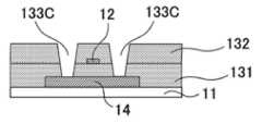
도 4e는 실시양태(5부)에 따른 전계 효과형 트랜지스터(10B)의 제조 단계를 예시화하는 도면이고;
도 5는 실시양태의 변형 예에 따른 전계 효과형 트랜지스터(10C)를 예시화하는 단면도이고;
도 6a는 실시양태(1부)에 따른 전계 효과형 트랜지스터(10C)의 제조 단계를 예시화하는 도면이고;
도 6b는 실시양태(2부)에 따른 전계 효과형 트랜지스터(10C)의 제조 단계를 예시화하는 도면이고;
도 6c는 실시양태(3부)에 따른 전계 효과형 트랜지스터(10C)의 제조 단계를 예시화하는 도면이고;
도 6d는 실시양태(4부)에 따른 전계 효과형 트랜지스터(10C)의 제조 단계를 예시화하는 도면이고;
도 6e는 실시양태(5부)에 따른 전계 효과형 트랜지스터(10C)의 제조 단계를 예시화하는 도면이고;
도 6f는 실시양태(6부)에 따른 전계 효과형 트랜지스터(10C)의 제조 단계를 예시화하는 도면이고;
도 6g는 실시양태(7부)에 따른 전계 효과형 트랜지스터(10C)의 제조 단계를 예시화하는 도면이고;
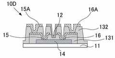
도 7은 실시양태의 변형 예에 따른 전계 효과형 트랜지스터(10D)를 예시화하는 단면도이고;
도 8a는 실시양태(1부)에 따른 전계 효과형 트랜지스터(10D)의 제조 단계를 예시화하는 도면이고;
도 8b는 실시양태(2부)에 따른 전계 효과형 트랜지스터(10D)의 제조 단계를 예시화하는 도면이고;
도 8c는 실시양태(3부)에 따른 전계 효과형 트랜지스터(10D)의 제조 단계를 예시화하는 도면이고;
도 8d는 실시양태(4부)에 따른 전계 효과형 트랜지스터(10D)의 제조 단계를 예시화하는 도면이고;
도 8e는 실시양태(5부)에 따른 전계 효과형 트랜지스터(10D)의 제조 단계를 예시화하는 도면이고;
도 8f는 실시양태(6부)에 따른 전계 효과형 트랜지스터(10D)의 제조 단계를 예시화하는 도면이고;
도 8g는 실시양태(7부)에 따른 전계 효과형 트랜지스터(10D)의 제조 단계를 예시화하는 도면이고;
도 9는 실시양태의 변형 예에 따른 전계 효과형 트랜지스터(10E)를 예시화하는 단면도이고;
도 10a는 실시양태(1부)에 따른 전계 효과형 트랜지스터(10E)의 제조 단계를 예시화하는 도면이고;
도 10b는 실시양태(2부)에 따른 전계 효과형 트랜지스터(10E)의 제조 단계를 예시화하는 도면이고;
도 10c는 실시양태(3부)에 따른 전계 효과형 트랜지스터(10E)의 제조 단계를 예시화하는 도면이고;
도 10d는 실시양태(4부)에 따른 전계 효과형 트랜지스터(10E)의 제조 단계를 예시화하는 도면이고;
도 11은 실시양태의 변형 예에 따른 전계 효과형 트랜지스터(10F)를 예시화하는 단면도이고;
도 12a는 실시양태(1부)에 따른 전계 효과형 트랜지스터(10F)의 제조 단계를 예시화하는 도면이고;
도 12b는 실시양태(2부)에 따른 전계 효과형 트랜지스터(10F)의 제조 단계를 예시화하는 도면이고;
도 12c는 실시양태(3부)에 따른 전계 효과형 트랜지스터(10F)의 제조 단계를 예시화하는 도면이고;
도 12d는 실시양태(4부)에 따른 전계 효과형 트랜지스터(10F)의 제조 단계를 예시화하는 도면이고;
도 13은 실시양태의 변형 예에 따른 전계 효과형 트랜지스터(10G)를 예시화하는 단면도이고;
도 14a는 실시양태(1부)에 따른 전계 효과형 트랜지스터(10G)의 제조 단계를 예시화하는 도면이고;
도 14b는 실시양태(2부)에 따른 전계 효과형 트랜지스터(10G)의 제조 단계를 예시화하는 도면이고;
도 14c는 실시양태(3부)에 따른 전계 효과형 트랜지스터(10G)의 제조 단계를 예시화하는 도면이고;
도 14d는 실시양태(4부)에 따른 전계 효과형 트랜지스터(10G)의 제조 단계를 예시화하는 도면이고;
도 14e는 실시양태(5부)에 따른 전계 효과형 트랜지스터(10G)의 제조 단계를 예시화하는 도면이고;
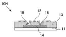
도 15는 실시양태의 변형 예에 따른 전계 효과형 트랜지스터(10H)를 예시화하는 단면도이고;
도 16a는 실시양태(1부)에 따른 전계 효과형 트랜지스터(10H)의 제조 단계를 예시화하는 도면이고;
도 16b는 실시양태(2부)에 따른 전계 효과형 트랜지스터(10H)의 제조 단계를 예시화하는 도면이고;
도 16c는 실시양태(3부)에 따른 전계 효과형 트랜지스터(10H)의 제조 단계를 예시화하는 도면이고;
도 16d는 실시양태(4부)에 따른 전계 효과형 트랜지스터(10H)의 제조 단계를 예시화하는 도면이고;
도 17은 실시양태의 변형 예에 따른 전계 효과형 트랜지스터(10J)를 예시화하는 단면도이고;
도 18a는 실시양태(1부)에 따른 전계 효과형 트랜지스터(10J)의 제조 단계를 예시화하는 도면이고;
도 18b는 실시양태(2부)에 따른 전계 효과형 트랜지스터(10J)의 제조 단계를 예시화하는 도면이고;
도 18c는 실시양태(3부)에 따른 전계 효과형 트랜지스터(10J)의 제조 단계를 예시화하는 도면이고;
도 18d는 실시양태(4부)에 따른 전계 효과형 트랜지스터(10J)의 제조 단계를 예시화하는 도면이고;
도 18e는 실시양태(5부)에 따른 전계 효과형 트랜지스터(10J)의 제조 단계를 예시화하는 도면이고;
도 18f는 실시양태(6부)에 따른 전계 효과형 트랜지스터(10J)의 제조 단계를 예시화하는 도면이고;
도 19는 실시양태의 변형 예에 따른 전계 효과형 트랜지스터(10K)를 예시화하는 단면도이고;
도 20a는 실시양태(1부)에 따른 전계 효과형 트랜지스터(10K)의 제조 단계를 예시화하는 도면이고;
도 20b는 실시양태(2부)에 따른 전계 효과형 트랜지스터(10K)의 제조 단계를 예시화하는 도면이고;
도 20c는 실시양태(3부)에 따른 전계 효과형 트랜지스터(10K)의 제조 단계를 예시화하는 도면이고;
도 20d는 실시양태(4부)에 따른 전계 효과형 트랜지스터(10K)의 제조 단계를 예시화하는 도면이고;
도 20e는 실시양태(5부)에 따른 전계 효과형 트랜지스터(10K)의 제조 단계를 예시화하는 도면이고;
도 20f는 실시양태(6부)에 따른 전계 효과형 트랜지스터(10K)의 제조 단계를 예시화하는 도면이고;
도 20g는 실시양태(7부)에 따른 전계 효과형 트랜지스터(10K)의 제조 단계를 예시화하는 도면이고;
도 21은 또 다른 실시양태에서 텔레비전 장치의 구성의 블록 선도이고;
도 22는 또 다른 실시양태에서 텔레비전 장치의 설명 도표(1)이고;
도 23은 또 다른 실시양태에서 텔레비전 장치의 설명 도표(2)이고;
도 24는 또 다른 실시양태에서 텔레비전 장치의 설명 도표(3)이고;
도 25는 또 다른 실시양태에서 디스플레이 소자의 설명도이고;
도 26은 또 다른 실시양태에서 유기 EL의 설명도이고;
도 27은 또 다른 실시양태에서 텔레비전 장치의 설명 도표(4)이고;
도 28은 또 다른 실시양태에서 또 다른 디스플레이 소자의 설명 도표(1)이고;
도 29는 또 다른 실시양태에서 또 다른 디스플레이 소자의 설명 도표(2)이고;
도 30은 실시예 1-21의 결과의 대표 그래프이다.1 is a schematic cross-sectional view of a
Fig. 2A is a diagram exemplifying the manufacturing steps of a field-
Fig. 2B is a diagram exemplifying the manufacturing steps of the field-
Fig. 2C is a diagram illustrating the manufacturing steps of the field-
Fig. 2D is a diagram illustrating the manufacturing steps of the field-
Fig. 2E is a diagram exemplifying the manufacturing steps of the field-
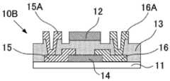
3 is a cross-sectional view illustrating a field-
4A is a diagram illustrating the manufacturing steps of a field-
4B is a diagram exemplifying the manufacturing steps of the field-
4C is a diagram illustrating the manufacturing steps of the field-
4D is a diagram illustrating the manufacturing steps of the field-
Fig. 4E is a diagram illustrating the manufacturing steps of the field-
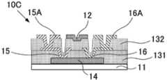
5 is a cross-sectional view illustrating a field-
6A is a diagram illustrating the manufacturing steps of a field-
6B is a diagram illustrating the manufacturing steps of the field-
6C is a diagram illustrating the manufacturing steps of the field-
6D is a diagram illustrating the manufacturing steps of the field-
6E is a diagram illustrating the manufacturing steps of a field-
6F is a diagram illustrating the manufacturing steps of the field-
6G is a diagram illustrating the manufacturing steps of the field-
7 is a cross-sectional view illustrating a field-
8A is a diagram illustrating the manufacturing steps of a field-
8B is a diagram illustrating the manufacturing steps of the field-
8C is a diagram illustrating the manufacturing steps of the field-
8D is a diagram illustrating the manufacturing steps of a field-
8E is a diagram illustrating the manufacturing steps of a field-
8F is a diagram illustrating the manufacturing steps of a field-
8G is a diagram illustrating the manufacturing steps of a field-
9 is a cross-sectional view illustrating a field-
Fig. 10A is a diagram exemplifying the manufacturing steps of a field-
Fig. 10B is a diagram exemplifying the manufacturing steps of the field-
10C is a diagram illustrating the manufacturing steps of the field-
Fig. 10D is a diagram illustrating the manufacturing steps of the field-
11 is a cross-sectional view illustrating a field-
12A is a diagram illustrating the manufacturing steps of a field-
12B is a diagram exemplifying the manufacturing steps of a field-
12C is a diagram illustrating the manufacturing steps of the field-
12D is a diagram illustrating the manufacturing steps of the field-
13 is a cross-sectional view illustrating a field-
14A is a diagram illustrating the manufacturing steps of a field-
14B is a diagram illustrating the manufacturing steps of a field-
14C is a diagram illustrating the manufacturing steps of the field-
14D is a diagram illustrating the manufacturing steps of the field-
14E is a diagram illustrating the manufacturing steps of a field-
15 is a cross-sectional view illustrating a field-
16A is a diagram illustrating the manufacturing steps of a field-
16B is a diagram exemplifying the manufacturing steps of the field-
16C is a diagram illustrating the manufacturing steps of the field-
Fig. 16D is a diagram exemplifying the manufacturing steps of the field-
17 is a cross-sectional view illustrating a field-
Fig. 18A is a diagram exemplifying the manufacturing steps of the field-
Fig. 18B is a diagram exemplifying the manufacturing steps of the field-
18C is a diagram illustrating the manufacturing steps of the field-
Fig. 18D is a diagram exemplifying the manufacturing steps of the field-
Fig. 18E is a diagram exemplifying the manufacturing steps of the field-
18F is a diagram exemplifying the manufacturing steps of the field-
19 is a cross-sectional view illustrating a field-
20A is a diagram illustrating the manufacturing steps of a field-
20B is a diagram illustrating the manufacturing steps of a field-
20C is a diagram illustrating the manufacturing steps of the field-
20D is a diagram illustrating the manufacturing steps of a field-
Fig. 20E is a diagram exemplifying the manufacturing steps of a field-
20F is a diagram illustrating the manufacturing steps of a field-
20G is a diagram illustrating the manufacturing steps of a field-
21 is a block diagram of the configuration of a television device in another embodiment;
22 is an explanatory diagram 1 of a television device in another embodiment;
23 is an explanatory diagram 2 of a television device in another embodiment;
24 is an explanatory diagram 3 of a television device in another embodiment;
25 is an explanatory diagram of a display element in another embodiment;
26 is an explanatory diagram of organic EL in another embodiment;
27 is an explanatory diagram 4 of a television device in another embodiment;
Fig. 28 is an explanatory diagram 1 of another display element in another embodiment;
Fig. 29 is an explanatory diagram (2) of another display element in another embodiment;
30 is a representative graph of the results of Examples 1-21.
(전계 효과형 트랜지스터의 제조 방법 및 전계 효과형 트랜지스터)(Method for manufacturing field-effect transistor and field-effect transistor)
전계 효과형 트랜지스터를 제조하는 본 개시내용의 방법은 소스 전극 및 드레인 전극, 게이트 전극, 활성층(반도체층으로 지칭됨), 및 게이트 절연층을 포함하는 전계 효과형 트랜지스터의 제조 방법이다.The method of the present disclosure for manufacturing a field effect transistor is a method of manufacturing a field effect transistor including a source electrode and a drain electrode, a gate electrode, an active layer (referred to as a semiconductor layer), and a gate insulating layer.
전계 효과형 트랜지스터의 제조 방법은 게이트 절연층의 에칭 단계를 포함한다.A method of manufacturing a field effect transistor includes etching a gate insulating layer.
전계 효과형 트랜지스터에서, 게이트 절연층은 A 원소와, B 원소 및 C 원소로 구성되는 군으로부터 선택되는 적어도 하나를 포함하는 금속 산화물이다.In the field effect transistor, the gate insulating layer is a metal oxide containing element A and at least one selected from the group consisting of element B and element C.
A 원소는 Sc, Y, Ln(란탄족 원소), Sb, Bi, 및 Te로 구성되는 군으로부터 선택되는 적어도 하나이다. Ln(란탄족 원소)의 예는 La(란타늄), Ce(세륨), Pr(프라세오디뮴), Nd(네오디뮴), Pm(프로메튬), Sm(사마륨), Eu(유로퓸), Gd(가돌리늄), Tb(테르븀), Dy(디스프로슘), Ho(홀뮴), Er(에르븀), Tm(툴륨), Yb(이테르븀), 및 Lu(루테튬)를 포함한다.The element A is at least one selected from the group consisting of Sc, Y, Ln (lanthanide element), Sb, Bi, and Te. Examples of Ln (lanthanide elements) are La (lanthanum), Ce (cerium), Pr (praseodymium), Nd (neodymium), Pm (promethium), Sm (samarium), Eu (europium), Gd (gadolinium), Tb (terbium), Dy (dysprosium), Ho (holmium), Er (erbium), Tm (thulium), Yb (ytterbium), and Lu (lutetium).
B 원소는 Ga, Ti, Zr, 및 Hf로 구성되는 군으로부터 선택되는 적어도 하나이다.B element is at least one selected from the group consisting of Ga, Ti, Zr, and Hf.
C 원소는 주기율표의 2족 원소로 구성되는 군으로부터 선택되는 적어도 하나이다.The C element is at least one selected from the group consisting of
전계 효과형 트랜지스터의 제조 방법에서, 에칭 용액 A는 소스 전극 및 드레인 전극, 게이트 전극, 및 활성층으로 구성되는 군으로부터 선택되는 적어도 하나가 형성되는 경우에 사용된다.In the manufacturing method of the field effect transistor, the etching solution A is used when at least one selected from the group consisting of a source electrode and a drain electrode, a gate electrode, and an active layer is formed.
전계 효과형 트랜지스터의 제조 방법에서, 에칭 용액 A와 동일한 유형을 갖는 에칭 용액인 에칭 용액 B는 게이트 절연층이 에칭되는 경우에 사용된다.In the manufacturing method of the field-effect transistor, the etching solution B, which is an etching solution having the same type as the etching solution A, is used when the gate insulating layer is etched.
본 개시내용의 하나의 실시양태의 전계 효과형 트랜지스터는 소스 전극 및 드레인 전극, 게이트 전극, 활성층, 및 게이트 절연층을 포함한다.The field effect transistor of one embodiment of the present disclosure includes a source electrode and a drain electrode, a gate electrode, an active layer, and a gate insulating layer.
전계 효과형 트랜지스터에서, 게이트 절연층은 에칭된다.In field-effect transistors, the gate insulating layer is etched.
전계 효과형 트랜지스터에서, 게이트 절연층은 A 원소와, B 원소 및 C 원소로 구성되는 군으로부터 선택되는 적어도 하나를 포함하는 금속 산화물이다.In the field effect transistor, the gate insulating layer is a metal oxide containing element A and at least one selected from the group consisting of element B and element C.
A 원소는 Sc, Y, Ln(란탄족 원소), Sb, Bi, 및 Te로 구성되는 군으로부터 선택되는 적어도 하나이다.The element A is at least one selected from the group consisting of Sc, Y, Ln (lanthanide element), Sb, Bi, and Te.
B 원소는 Ga, Ti, Zr, 및 Hf로 구성되는 군으로부터 선택되는 적어도 하나이다.B element is at least one selected from the group consisting of Ga, Ti, Zr, and Hf.
C 원소는 주기율표의 2족 원소로 구성되는 군으로부터 선택되는 적어도 하나이다.The C element is at least one selected from the group consisting of
소스 전극 및 드레인 전극, 게이트 전극, 및 활성층으로 구성되는 군으로부터 선택되는 적어도 하나가 에칭 용액 A를 사용하여 형성된다.At least one selected from the group consisting of a source electrode and a drain electrode, a gate electrode, and an active layer is formed using the etching solution A.
게이트 절연층은 에칭 용액 A와 동일한 유형을 갖는 에칭 용액인 에칭 용액 B를 사용하여 에칭된다.The gate insulating layer is etched using etching solution B, which is an etching solution having the same type as etching solution A.
전계 효과형 트랜지스터의 제조에서, 게이트 절연층이 에칭을 통해 형성되는 경우, 소스 전극 및 드레인 전극, 게이트 전극, 및 활성층으로 구성되는 군으로부터 선택되는 적어도 하나를 형성하기 위하여 사용된 에칭 용액 A와 동일한 유형을 갖는 에칭 용액인 에칭 용액 B의 사용은 동일한 폐액 제거 방법으로 에칭 용액 둘 다의 폐액을 제거할 수 있게 만든다. 그 결과, 전계 효과형 트랜지스터의 제조에서 폐액의 제거 장비는 단순화될 수 있고, 폐액의 배치 단계는 단순화될 수 있고, 그 결과 제조 비용의 감소를 야기한다.In the manufacture of the field effect transistor, when the gate insulating layer is formed through etching, the same as the etching solution A used to form at least one selected from the group consisting of a source electrode and a drain electrode, a gate electrode, and an active layer. The use of etching solution B, which is an etching solution having a type, makes it possible to remove the waste liquid of both etching solutions by the same waste liquid removal method. As a result, the equipment for removing the waste liquid in the manufacture of the field effect transistor can be simplified, and the disposing step of the waste liquid can be simplified, resulting in a reduction in the manufacturing cost.
에칭 용액 A의 예는 질산을 포함하는 에칭 용액, 과산화수소를 포함하는 에칭 용액, 및 옥살산을 포함하는 에칭 용액을 포함한다.Examples of the etching solution A include an etching solution containing nitric acid, an etching solution containing hydrogen peroxide, and an etching solution containing oxalic acid.
에칭 용액 A와 동일한 유형을 갖는 에칭 용액인 에칭 용액 B의 예는, 예를 들면, 하기와 같다. 특히, 에칭 용액 A가 질산을 포함하는 에칭 용액인 경우, 에칭 용액 B는 질산을 포함하는 에칭 용액이다. 에칭 용액 A가 과산화수소를 포함하는 에칭 용액인 경우, 에칭 용액 B는 과산화수소를 포함하는 에칭 용액이다. 에칭 용액 A가 옥살산을 포함하는 에칭 용액인 경우, 에칭 용액 B는 옥살산을 포함하는 에칭 용액이다.An example of the etching solution B, which is an etching solution having the same type as the etching solution A, is, for example, as follows. In particular, when the etching solution A is an etching solution containing nitric acid, the etching solution B is an etching solution containing nitric acid. When the etching solution A is an etching solution containing hydrogen peroxide, the etching solution B is an etching solution containing hydrogen peroxide. When the etching solution A is an etching solution containing oxalic acid, the etching solution B is an etching solution containing oxalic acid.
여기서, 상기 기재된 바와 같이, 에칭 용액 A 및 에칭 용액 B가 에칭에 기여하는 동일한 주성물을 갖기만 하면, 에칭 용액 A 및 에칭 용액 B의 농도는 동일하거나 상이할 수 있다. 추가로, 상기 기재된 바와 같이, 에칭 용액 A 및 에칭 용액 B가 에칭에 기여하는 동일한 주성물을 갖기만 하면, 에칭 용액 A 및 에칭 용액 B 중의 다른 구성 성분은 동일하거나 상이할 수 있다.Here, as described above, the concentrations of the etching solution A and the etching solution B may be the same or different, as long as the etching solution A and the etching solution B have the same main substance contributing to the etching. Further, as described above, the other constituents in the etching solution A and the etching solution B may be the same or different, as long as the etching solution A and the etching solution B have the same main constituents contributing to the etching.
에칭 용액 A가 질산을 포함하는 에칭 용액인 경우, 에칭 용액 A는 바람직하게는 인산 및 아세트산을 추가로 포함한다.When the etching solution A is an etching solution containing nitric acid, the etching solution A preferably further contains phosphoric acid and acetic acid.
에칭 용액 B가 질산을 포함하는 에칭 용액인 경우, 에칭 용액 B는 바람직하게는 인산 및 아세트산을 추가로 포함한다.When the etching solution B is an etching solution containing nitric acid, the etching solution B preferably further contains phosphoric acid and acetic acid.
질산을 포함하는 에칭 용액 중의 질산의 농도는, 예를 들면, 5 질량% 이상이지만 30 질량% 이하이다.The concentration of nitric acid in the etching solution containing nitric acid is, for example, 5 mass% or more but 30 mass% or less.
질산을 포함하는 에칭 용액 중의 아세트산의 농도는, 예를 들면, 20 질량% 이상이지만 40 질량% 이하이다.The concentration of acetic acid in the etching solution containing nitric acid is, for example, 20 mass% or more but 40 mass% or less.
질산을 포함하는 에칭 용액 중의 인산의 농도는, 예를 들면, 3 질량% 이상이지만 60 질량% 이하이다. 더 구체적으로, 이의 농도는, 예를 들면, 50 질량%이다.The concentration of phosphoric acid in the etching solution containing nitric acid is, for example, 3 mass% or more, but 60 mass% or less. More specifically, its concentration is, for example, 50% by mass.
질산을 포함하는 에칭 용액의 하나의 예는 6 질량%의 질산, 25 질량%의 아세트산, 및 50 질량%의 인산을 포함한다.One example of the etching solution containing nitric acid contains 6 mass % nitric acid, 25 mass % acetic acid, and 50 mass % phosphoric acid.
질산을 포함하는 에칭 용액의 하나의 예는 25 질량%의 질산, 30 질량%의 아세트산, 및 5 질량%의 인산을 포함한다.One example of the etching solution containing nitric acid contains 25 mass % of nitric acid, 30 mass % of acetic acid, and 5 mass % of phosphoric acid.
에칭 용액 A는, 예를 들면, 적어도 게이트 전극을 형성하는데 사용된다. 이러한 경우, 게이트 전극은 바람직하게는 Al, Mo, Cu, 및 Ag로 구성되는 군으로부터 선택된 하나 이상의 금속; 이의 둘 이상의 원소의 합금; 산화인듐; 및 산화아연으로 구성되는 군으로부터 선택되는 적어도 하나를 포함하는 전도성 막으로 형성된다.The etching solution A is used, for example, to form at least a gate electrode. In this case, the gate electrode is preferably made of at least one metal selected from the group consisting of Al, Mo, Cu, and Ag; alloys of two or more elements thereof; indium oxide; and a conductive film comprising at least one selected from the group consisting of zinc oxide.
에칭 용액 A는, 예를 들면, 적어도 소스 전극 및 드레인 전극을 형성하는데 사용된다. 이 경우, 소스 전극 및 드레인 전극은 바람직하게는 Al, Mo, Cu, 및 Ag로 구성되는 군으로부터 선택된 하나 이상의 금속; 이의 둘 이상의 원소의 합금; 산화인듐; 및 산화아연으로 구성되는 군으로부터 선택되는 적어도 하나를 포함하는 전도성 막으로 형성된다.The etching solution A is used, for example, to form at least a source electrode and a drain electrode. In this case, the source electrode and the drain electrode are preferably at least one metal selected from the group consisting of Al, Mo, Cu, and Ag; alloys of two or more elements thereof; indium oxide; and a conductive film comprising at least one selected from the group consisting of zinc oxide.
에칭 용액 A는, 예를 들면, 적어도 활성층을 형성하는데 사용된다.The etching solution A is used, for example, to form at least the active layer.
에칭 용액 A 중의 게이트 전극의 에칭 속도는 특정하게 제한되지 않으며, 의도된 목적에 따라 적절하게 선택될 수 있다. 그러나, 이의 에칭 속도는 패턴 가공성의 면에서 바람직하게는 0.1 nm/s(초) 이상이지만 20 nm/s 이하이고, 더 바람직하게는 0.1 nm/s 이상이지만 10 nm/s 이하이고, 특히 바람직하게는 0.5 nm/s 이상이지만 5 nm/s 이하이다.The etching rate of the gate electrode in the etching solution A is not particularly limited and may be appropriately selected depending on the intended purpose. However, the etching rate thereof is preferably 0.1 nm/s (sec) or more but 20 nm/s or less, more preferably 0.1 nm/s or more but 10 nm/s or less, particularly preferably is greater than 0.5 nm/s but less than or equal to 5 nm/s.
에칭 용액 A 중의 소스 전극 및 드레인 전극의 에칭 속도는 특정하게 제한되지 않으며, 의도된 목적에 따라 적절하게 선택될 수 있다. 그러나, 이의 에칭 속도는 패턴 가공성의 면에서 바람직하게는 0.1 nm/s 이상이지만 20 nm/s 이하이고, 더 바람직하게는 0.1 nm/s 이상이지만 10 nm/s 이하이고, 특히 바람직하게는 0.5 nm/s 이상이지만 5 nm/s 이하이다.The etching rates of the source electrode and the drain electrode in the etching solution A are not particularly limited and may be appropriately selected depending on the intended purpose. However, the etching rate thereof is preferably 0.1 nm/s or more but 20 nm/s or less, more preferably 0.1 nm/s or more but 10 nm/s or less, particularly preferably 0.5 nm from the viewpoint of pattern workability. /s or more, but less than 5 nm/s.
에칭 용액 A 중의 활성층의 에칭 속도는 특정하게 제한되지 않으며, 의도된 목적에 따라 적절하게 선택될 수 있다. 그러나, 이의 에칭 속도는 패턴 가공성의 면에서 바람직하게는 0.1 nm/s 이상이지만 20 nm/s 이하이고, 더 바람직하게는 0.1 nm/s 이상이지만 10 nm/s 이하이고, 특히 바람직하게는 0.5 nm/s 이상이지만 5 nm/s 이하이다.The etching rate of the active layer in the etching solution A is not particularly limited and may be appropriately selected depending on the intended purpose. However, the etching rate thereof is preferably 0.1 nm/s or more but 20 nm/s or less, more preferably 0.1 nm/s or more but 10 nm/s or less, particularly preferably 0.5 nm from the viewpoint of pattern workability. /s or more, but less than 5 nm/s.
에칭 용액 B 중의 게이트 절연층이 되는 금속 산화물의 에칭 속도는 특정하게 제한되지 않으며, 의도된 목적에 따라 적절하게 선택될 수 있다. 그러나, 이의 에칭 속도는 패턴 가공성의 면에서 바람직하게는 0.1 nm/s 이상이지만 20 nm/s 이하이고, 더 바람직하게는 0.1 nm/s 이상이지만 10 nm/s 이하이고, 특히 바람직하게는 0.5 nm/s 이상이지만 5 nm/s 이하이다.The etching rate of the metal oxide serving as the gate insulating layer in the etching solution B is not particularly limited and may be appropriately selected depending on the intended purpose. However, the etching rate thereof is preferably 0.1 nm/s or more but 20 nm/s or less, more preferably 0.1 nm/s or more but 10 nm/s or less, particularly preferably 0.5 nm from the viewpoint of pattern workability. /s or more, but less than 5 nm/s.
바람직하게는, 금속 산화물은 상유전성 비정질 산화물을 포함하거나, 상유전성 비정질 산화물 그 자체이다.Preferably, the metal oxide comprises a paraelectric amorphous oxide or is a paraelectric amorphous oxide itself.
이하에서, 실시양태의 설명은 도면을 참조하여 기재될 것이다. 각각의 도면에서, 동일한 참조 번호는 동일한 구성 부분에 제공되고, 몇몇 경우에 불필요한 설명이 생락될 수 있다.DETAILED DESCRIPTION OF THE PREFERRED EMBODIMENTS In the following, descriptions of embodiments will be described with reference to the drawings. In each drawing, the same reference numerals are provided to the same constituent parts, and unnecessary descriptions may be omitted in some cases.
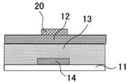
도 1은 본 개시내용에서 제조된 전계 효과형 트랜지스터를 예시화하는 단면도이다.1 is a cross-sectional view illustrating a field effect transistor fabricated in the present disclosure.
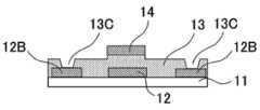
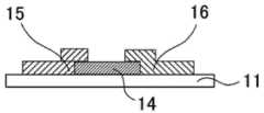
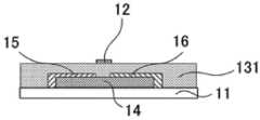
도 1을 참조하여, 전계 효과형 트랜지스터(10A)는 기판(11), 게이트 전극(12), 게이트 절연층(13), 활성층(14), 소스 전극(15), 드레인 전극(16), 및 게이트 전극 패드(12B)를 포함하는 하부 게이트/하부 접촉 전계 효과형 트랜지스터이다. 전계 효과형 트랜지스터(10A)는 본 개시내용에 따른 반도체 장치의 하나의 대표적인 예라는 것을 주의한다.Referring to FIG. 1 , a
전계 효과형 트랜지스터(10A)에서, 게이트 전극(12) 및 2개의 게이트 전극 패드(12B)는 절연 기판(11) 상에 형성된다. 추가로, 게이트 절연층(13)은 게이트 전극(12) 및 2개의 게이트 전극 패드(12B)를 덮기 위하여 형성된다. 활성층(14)은 게이트 절연층(13) 상에 형성되고, 소스 전극(15) 및 드레인 전극(16)은 채널이 활성층(14) 내에 형성되도록 활성층(14) 상에 형성된다. 이하에서, 전계 효과형 트랜지스터(10A)의 각각의 구성 원소가 상세하게 기재될 것이다.In the
본 개시내용의 실시양태에서, 편의상 활성층(14)의 면은 상부 면 또는 하나의 면으로 간주되고, 기판(11)의 면은 하부 면 또는 다른 면으로 간주된다는 것을 주의한다. 활성층(14)과 기판(11) 사이의 각각의 부분에서, 활성층(14)의 면에서 표면은 상부 표면 또는 하나의 표면으로 간주되고, 기판(11)의 면에서 표면은 하부 표면 또는 다른 표면으로 간주된다. 전계 효과형 트랜지스터(10A)는 위아래가 뒤집힌 상태에서 사용될 수 있거나, 어떠한 각도로도 배치될 수 있다는 것을 주의한다. 평면도는 기판(11)의 상부 표면에 대하여 정방향으로 물체를 보는 것을 의미한다. 평면 형상은 기판(11)의 상부 표면에 대하여 정방향으로 본 물체의 형상을 의미한다.Note that in the embodiment of the present disclosure, for convenience, the side of the
<기판><substrate>
기판(11)의 형상, 구조, 및 크기는 특정하게 제한되지 않으며, 의도된 목적에 따라 적절하게 선택될 수 있다. 기판(11)의 물질은 특정하게 제한되지 않으며, 의도된 목적에 따라 적절하게 선택될 수 있다. 물질로서, 유리 기판, 세라믹 기판, 플라스틱 기판, 및 막 기판이 사용될 수 있다.The shape, structure, and size of the
유리 기판은 특정하게 제한되지 않으며, 의도된 목적에 따라 적절하게 선택될 수 있다. 이의 예는 비알칼리성 유리 및 실리카 유리를 포함한다. 플라스틱 기판 및 막 기판은 특정하게 제한되지 않으며, 의도된 목적에 따라 적절하게 선택될 수 있다. 이의 예는 폴리카보네이트(PC), 폴리이미드(PI), 폴리에틸렌 테레프탈레이트(PET), 및 폴리에틸렌 나프탈레이트(PEN)를 포함한다.The glass substrate is not particularly limited and may be appropriately selected depending on the intended purpose. Examples thereof include non-alkaline glass and silica glass. The plastic substrate and the film substrate are not particularly limited and may be appropriately selected depending on the intended purpose. Examples thereof include polycarbonate (PC), polyimide (PI), polyethylene terephthalate (PET), and polyethylene naphthalate (PEN).
<게이트 전극><Gate Electrode>
게이트 전극(12)은, 예를 들면, 기판(11) 상에 예정된 면적으로 형성된다. 게이트 전극(12)은 게이트 전압이 인가되는 전극이다.The
게이트 전극(12)의 물질은 특정하게 제한되지 않으며, 의도된 목적에 따라 적절하게 선택될 수 있다. 예를 들면, 금속(예를 들면, 알루미늄(Al), 플래티늄(Pt), 팔라듐(Pd), 금(Au), 은(Ag), 구리(Cu), 아연(Zn), 니켈(Ni), 크롬(Cr), 탄탈룸(Ta), 몰리브덴(Mo), 및 티탄(Ti)), 이의 합금, 및 이들 금속의 혼합물이 사용될 수 있다. 추가로, 전도성 산화물(예를 들면, 산화인듐, 산화아연, 산화주석, 산화갈륨, 및 산화니오븀), 이의 합성 화합물, 및 이의 혼합물이 사용될 수 있다.The material of the
게이트 전극(12)의 평균 막 두께는 특정하게 제한되지 않으며, 의도된 목적에 따라 적절하게 선택될 수 있다. 이의 평균 막 두께는 바람직하게는 10 nm 내지 1 ㎛, 더 바람직하게는 50 nm 내지 300 nm이다.The average film thickness of the
<게이트 전극 패드><Gate electrode pad>
게이트 전극 패드는 게이트 전극의 것과 동일한 층을 갖고, 게이트 전극과 접촉하기 위하여 전기적 특성이 평가되는 경우에 측정을 위한 프로브로 제공된다.The gate electrode pad has the same layer as that of the gate electrode, and serves as a probe for measurement when electrical properties are evaluated for contact with the gate electrode.
<게이트 절연층><Gate Insulation Layer>
게이트 절연층(13)은 금속 산화물이다.The
하나의 예에서, 게이트 절연층은 게이트 전극(12) 및 활성층(14)을 절연하기 위하여 게이트 전극(12)과 활성층(14) 사이에 제공된다.In one example, a gate insulating layer is provided between the
금속 산화물은 A 원소와, B 원소 및 C 원소로 구성되는 군으로부터 선택되는 적어도 하나를 포함하고, 필요한 경우, 다른 성분을 추가로 포함한다.The metal oxide includes at least one selected from the group consisting of element A, element B and element C, and, if necessary, further includes other components.
A 원소는 Sc, Y, Ln(란탄족 원소), Sb, Bi, 및 Te로 구성되는 군으로부터 선택되는 적어도 하나이다.The element A is at least one selected from the group consisting of Sc, Y, Ln (lanthanide element), Sb, Bi, and Te.
B 원소는 Ga, Ti, Zr, 및 Hf로 구성되는 군으로부터 선택되는 적어도 하나이다.B element is at least one selected from the group consisting of Ga, Ti, Zr, and Hf.
C 원소는 주기율표의 2족 원소로 구성되는 군으로부터 선택되는 적어도 하나이다.The C element is at least one selected from the group consisting of
바람직하게는, 금속 산화물은 상유전성 비정질 산화물을 포함하거나, 상유전성 비정질 산화물 그 자체로 형성된다. 상유전성 비정질 산화물은 공기 중에서 안정한고, 넓은 제제 범위에서 비정질 구조를 안정하게 형성할 수 있다. 여기서, 금속 산화물은 부분적으로 결정을 포함할 수 있다.Preferably, the metal oxide comprises a paraelectric amorphous oxide or is formed as a paraelectric amorphous oxide itself. The paraelectric amorphous oxide is stable in air and can stably form an amorphous structure in a wide formulation range. Here, the metal oxide may partially include a crystal.
알칼리 토류 산화물은 공기 중에서 수분 및 이산화탄소와 쉽게 반응하고, 수산화물 및 카보네이트로 쉽게 변한다. 따라서, 알칼리 토류 산화물 단독은 전자 장치에 대한 응용에 적합하지 않다. 추가로, 예를 들면, Ga, Sc, Y, 및 Ce를 제외한 란탄족 원소의 단순한 산화물은 쉽게 결정으로 변하고, 이는 누설 전류의 발생 면에서 문제가 된다. 그러나, 알칼리 토금속 및 Ga, Sc, Y, 및 Ce를 제외한 란탄족 원소 의 금속 산화물은 공기 중에서 안정하고, 넓은 제제 영역에서 비정질 막을 형성할 수 있다. Ce는 란탄족 원소에서 특히 4가가 되고, 알칼리 토금속과 함께 페로브스카이트 구조를 갖는 결정을 형성한다. 따라서, 비정질 상을 수득하기 위하여, Ce를 제외한 란탄족 원소가 바람직하다.Alkaline earth oxides readily react with moisture and carbon dioxide in air, and are easily converted into hydroxides and carbonates. Therefore, alkaline earth oxides alone are not suitable for applications in electronic devices. In addition, for example, simple oxides of lanthanide elements other than Ga, Sc, Y, and Ce easily turn into crystals, which is a problem in terms of generation of leakage current. However, alkaline earth metals and metal oxides of lanthanide elements other than Ga, Sc, Y, and Ce are stable in air and can form an amorphous film in a wide formulation area. Ce becomes particularly tetravalent in lanthanide elements, and forms crystals having a perovskite structure together with alkaline earth metals. Therefore, in order to obtain an amorphous phase, a lanthanide element other than Ce is preferred.
결정질 상, 예를 들면, 스피넬 구조가 알칼리 토금속과 Ga 산화물 사이에 존재함에도 불구하고, 페로브스카이트 구조를 갖는 결정과 비교하여 유의미하게 높은 온도에서(일반적으로, 1,000℃ 이상에서) 가열되지 않는 한, 이들 결정은 침전되지 않는다. 추가로, 알칼리 토금속의 산화물과 Sc, Y, 및 Ce를 제외한 란탄족 원소의 산화물 사이의 안정한 결정질 상의 존재에 대하여 보고는 나타나지 않았다. 심지어 높은 온도에서 수행된 후속 공정 후, 결정은 비정질 상으로부터 거의 침전되지 않는다. 게다가, 비정질 상은 알칼리 토금속 및 Ga, Sc, Y, 및 Ce를 제외한 란탄족 원소의 금속 산화물이 3개 이상의 이상 금속 원소로 형성되는 경우에 더 안정해진다.Despite the presence of a crystalline phase, e.g., a spinel structure, between the alkaline earth metal and the Ga oxide, it is not heated at significantly higher temperatures (typically above 1,000 °C) compared to crystals with a perovskite structure. As long as these crystals do not precipitate. In addition, there have been no reports of the existence of a stable crystalline phase between oxides of alkaline earth metals and oxides of lanthanide elements except Sc, Y, and Ce. Even after subsequent processes carried out at high temperatures, the crystals hardly precipitate from the amorphous phase. In addition, the amorphous phase becomes more stable when alkaline earth metals and metal oxides of lanthanide elements other than Ga, Sc, Y, and Ce are formed of three or more metal elements.
금속 산화물 중에 함유된 각각의 원소의 양은 특정하게 제한되지 않는다. 그러나, 각각의 원소 군으로부터 선택된 금속 원소는 바람직하게는 금속 산화물이 안정한 비정질 상태를 달성하는 제제를 갖도록 포함된다.The amount of each element contained in the metal oxide is not particularly limited. However, a metal element selected from each element group is preferably included so that the metal oxide has a formulation that achieves a stable amorphous state.
높은 유전율을 갖는 막을 제조하기 위하여, Ba, Sr, Lu, 및 La와 같은 원소의 조성비는 증가하는 것이 바람직하다.In order to produce a film having a high dielectric constant, it is preferable to increase the composition ratio of elements such as Ba, Sr, Lu, and La.
본 실시양태에 따른 금속 산화물은 넓은 제제 범위에서 비정질 막을 형성할 수 있고, 따라서 이의 물리적 성질은 넓게 조절될 수 있다. 예를 들면, 이의 유전율은 SiO2의 것보다 충분히 높지만(즉, 약 6 내지 약 20), 의도된 목적에 따라 제제를 선택함으로써 적합한 값으로 적절하게 조절될 수 있다.The metal oxide according to the present embodiment can form an amorphous film in a wide formulation range, and thus its physical properties can be widely controlled. For example, its dielectric constant issufficiently higher than that of SiO 2 (ie, about 6 to about 20), but can be appropriately adjusted to a suitable value by selecting a formulation according to the intended purpose.
추가로, 금속 산화물의 열 팽창 계수는 배선의 일반적인 물질 및 반도체의 일반적인 물질의 것들(즉, 10-6 내지 10-5)과 유사하다. 게다가, 심지어 가열 단계가 반복되는 경우, 금속 산화물은 10-7 이상이지만 10-6 미만인 열 팽창 계수를 갖는 SiO2와 비교하여 막의 박리와 같은 문제를 덜 야기한다. 특히, 금속 산화물과 산화물 반도체 사이의 바람직한 경계, 예를 들면, a-IGZO가 형성된다.In addition, the coefficient of thermal expansion of the metal oxide is similar tothose of common materials of wiring and semiconductors (ie, 10 -6 to 10-5 ). Moreover, even when the heating step is repeated, the metal oxide causes less problems such as delamination of the film compared toSiO 2 having a coefficient of thermal expansionof 10 −7 or more butless than 10 −6 . In particular, a preferred boundary between the metal oxide and the oxide semiconductor is formed, for example a-IGZO.
따라서, 게이트 절연층(13)에서 본 실시양태에 따른 금속 산화물을 사용하여 높은 성능을 갖는 반도체 장치를 수득하는 것이 가능하다.Accordingly, it is possible to obtain a semiconductor device having high performance by using the metal oxide according to the present embodiment in the
게이트 절연층의 형성 방법은 특정하게 제한되지 않으며, 의도된 목적에 따라 적절하게 선택될 수 있다. 이의 예는 절연층을 형성하기 위한 코팅 액체를 사용하는 하기 형성 방법을 포함한다.The method of forming the gate insulating layer is not particularly limited and may be appropriately selected depending on the intended purpose. Examples thereof include the following forming method using a coating liquid for forming an insulating layer.
<<절연층의 형성을 위한 코팅 액체>><<Coating liquid for formation of insulating layer>>
절연층의 형성을 위한 코팅 액체는, 예를 들면, 적어도 A 원소 포함 화합물; B 원소 포함 화합물 및 C 원소 포함 화합물로 구성되는 군으로부터 선택되는 적어도 하나; 및 용매를 포함하고, 필요한 경우, 다른 성분을 추가로 포함한다.The coating liquid for forming the insulating layer includes, for example, a compound containing at least element A; at least one selected from the group consisting of a compound containing element B and a compound containing element C; and a solvent and, if necessary, further comprising other components.
-A 원소 포함 화합물--A compound containing element-
A 원소 포함 화합물이 Sc, Y, Ln(란탄족 원소), Sb, Bi, 및 Te로 구성되는 군으로부터 선택되는 적어도 하나를 포함하는 화합물인 한, A 원소 포함 화합물은 특정하게 제한되지 않으며, 의도된 목적에 따라 적절하게 선택될 수 있다. 이의 예는 무기 A 원소 화합물 및 유기 A 원소 화합물을 포함한다.As long as the compound containing element A is a compound containing at least one selected from the group consisting of Sc, Y, Ln (lanthanide element), Sb, Bi, and Te, the compound containing element A is not particularly limited, It may be appropriately selected depending on the intended purpose. Examples thereof include inorganic A element compounds and organic element A compounds.
무기 A 원소 화합물의 예는 A 원소의 니트레이트, A 원소의 설페이트, A 원소의 플루오라이드, A 원소의 클로라이드, A 원소의 브로마이드, 및 A 원소의 요오다이드를 포함한다.Examples of the inorganic element A compound include nitrate of element A, sulfate of element A, fluoride of element A, chloride of element A, bromide of element A, and iodide of element A.
A 원소의 니트레이트의 예는 질산스칸듐, 질산이트륨, 질산란타늄, 질산세륨, 질산프라세오디뮴, 질산네오디뮴, 질산사마륨, 질산유로퓸, 질산가돌리늄, 질산테르븀, 질산디스프로슘, 질산홀뮴, 질산에르븀, 질산툴륨, 질산이테르븀, 질산루테튬, 질산안티몬, 질산비스무트, 및 질산텔루륨을 포함한다.Examples of the nitrate of element A include scandium nitrate, yttrium nitrate, lanthanum nitrate, cerium nitrate, praseodymium nitrate, neodymium nitrate, samarium nitrate, europium nitrate, gadolinium nitrate, terbium nitrate, dysprosium nitrate, holmium nitrate, erbium nitrate, thulium nitrate, ytterbium nitrate, lutetium nitrate, antimony nitrate, bismuth nitrate, and tellurium nitrate.
A 원소의 설페이트의 예는 황산갈륨, 황산스칸듐, 황산이트륨, 황산란타늄, 황산세륨, 황산프라세오디뮴, 황산네오디뮴, 황산사마륨, 황산유로퓸, 황산가돌리늄, 황산테르븀, 황산디스프로슘, 황산홀뮴, 황산에르븀, 황산툴륨, 황산이테르븀, 황산루테튬, 황산안티몬, 황산비스무트, 및 황산텔루륨을 포함한다.Examples of the sulfate of element A include gallium sulfate, scandium sulfate, yttrium sulfate, lanthanum sulfate, cerium sulfate, praseodymium sulfate, neodymium sulfate, samarium sulfate, europium sulfate, gadolinium sulfate, terbium sulfate, dysprosium sulfate, holmium sulfate, erbium sulfate, sulfuric acid thulium, ytterbium sulfate, lutetium sulfate, antimony sulfate, bismuth sulfate, and tellurium sulfate.
A 원소의 플루오라이드는 플루오르화스칸듐, 플루오르화이트륨, 플루오르화란타늄, 플루오르화세륨, 플루오르화프라세오디뮴, 플루오르화네오디뮴, 플루오르화사마륨, 플루오르화유로퓸, 플루오르화가돌리늄, 플루오르화테르븀, 플루오르화디스프로슘, 플루오르화홀뮴, 플루오르화에르븀, 플루오르화툴륨, 플루오르화이테르븀, 플루오르화루테튬, 플루오르화안티몬, 플루오르화비스무트, 및 플루오르화텔루륨을 포함한다.The fluorides of element A are scandium fluoride, yttrium fluoride, lanthanum fluoride, cerium fluoride, praseodymium fluoride, neodymium fluoride, samarium fluoride, europium fluoride, dolinium fluoride, terbium fluoride, dysprosium fluoride, holmium fluoride, erbium fluoride, thulium fluoride, ytterbium fluoride, lutetium fluoride, antimony fluoride, bismuth fluoride, and tellurium fluoride.
A 원소의 클로라이드의 예는 염화스칸듐, 염화이트륨, 염화란타늄, 염화세륨, 염화프라세오디뮴, 염화네오디뮴, 염화사마륨, 염화유로퓸, 염화가돌리늄, 염화테르븀, 염화디스프로슘, 염화홀뮴, 염화에르븀, 염화툴륨, 염화이테르븀, 염화루테튬, 염화안티몬, 염화비스무트, 염화텔루륨을 포함한다.Examples of chlorides of element A include scandium chloride, yttrium chloride, lanthanum chloride, cerium chloride, praseodymium chloride, neodymium chloride, samarium chloride, europium chloride, gadolinium chloride, terbium chloride, dysprosium chloride, holmium chloride, erbium chloride, thulium chloride, chloride Ytterbium, lutetium chloride, antimony chloride, bismuth chloride, tellurium chloride.
A 원소의 브로마이드의 예는 브롬화스칸듐, 브롬화이트륨, 브롬화란타늄, 브롬화프라세오디뮴, 브롬화네오디뮴, 브롬화사마륨, 브롬화유로퓸, 브롬화가돌리늄, 브롬화테르븀, 브롬화디스프로슘, 브롬화홀뮴, 브롬화에르븀, 브롬화툴륨, 브롬화이테르븀, 브롬화루테튬, 브롬화안티몬, 브롬화비스무트, 및 브롬화텔루륨을 포함한다.Examples of the bromide of element A include scandium bromide, yttrium bromide, lanthanum bromide, praseodymium bromide, neodymium bromide, samarium bromide, europium bromide, dolinium bromide, terbium bromide, dysprosium bromide, holmium bromide, ytterbium bromide, erbium bromide, thulbium bromide. lutetium, antimony bromide, bismuth bromide, and tellurium bromide.
A 원소의 요오다이드의 예는 요오드화스칸듐, 요오드화이트륨, 요오드화란타늄, 요오드화세륨, 요오드화프라세오디뮴, 요오드화네오디뮴, 요오드화사마륨, 요오드화유로퓸, 요오드화가돌리늄, 요오드화테르븀, 요오드화디스프로슘, 요오드화홀뮴, 요오드화에르븀, 요오드화툴륨, 요오드화이테르븀, 요오드화루테튬, 요오드화안티몬, 요오드화비스무트, 및 요오드화텔루륨을 포함한다.Examples of the iodide of element A are scandium iodide, yttrium iodide, lanthanum iodide, cerium iodide, praseodymium iodide, neodymium iodide, samarium iodide, europium iodide, dolinium iodide, terbium iodide, dysprosium iodide, holmium iodide, erbium iodide, thulium iodide. , ytterbium iodide, lutetium iodide, antimony iodide, bismuth iodide, and tellurium iodide.
유기 A 원소 화합물이 A 원소 및 유기 기를 포함하는 화합물인 한, 유기 A 원소 화합물은 특정하게 제한되지 않으며, 의도된 목적에 따라 적절하게 선택될 수 있다. A 원소 및 유기 기는, 예를 들면, 이온 결합, 공유 결합, 또는 배위 결합을 통해 결합된다.As long as the organic A element compound is a compound containing element A and an organic group, the organic element A compound is not particularly limited and may be appropriately selected depending on the intended purpose. The A element and the organic group are bonded through, for example, an ionic bond, a covalent bond, or a coordination bond.
유기 기는 특정하게 제한되지 않으며, 의도된 목적에 따라 적절하게 선택될 수 있다. 유기 기의 예는 치환기를 가질 수 있는 알킬 기, 치환기를 가질 수 있는 알콕시 기, 치환기를 가질 수 있는 아실옥시 기, 치환기를 가질 수 있는 아세틸 아세토네이트 기, 및 치환기를 가질 수 있는 사이클로펜타디에닐 기를 포함한다. 알킬 기의 예는 1 내지 6개의 탄소 원자를 포함하는 알킬 기를 포함한다. 알콕시 기의 예는 1 내지 6개의 탄소 원자를 포함하는 알콕시 기를 포함한다. 아실옥시 기의 예는 1 내지 10개의 탄소 원자를 포함하는 아실옥시 기를 포함한다.The organic group is not particularly limited and may be appropriately selected depending on the intended purpose. Examples of the organic group include an alkyl group which may have a substituent, an alkoxy group which may have a substituent, an acyloxy group which may have a substituent, an acetylacetonate group which may have a substituent, and cyclopentadienyl which may have a substituent includes the group. Examples of the alkyl group include an alkyl group containing 1 to 6 carbon atoms. Examples of the alkoxy group include an alkoxy group containing 1 to 6 carbon atoms. Examples of acyloxy groups include acyloxy groups containing 1 to 10 carbon atoms.
유기 A 원소 화합물의 예는 아세트산스칸듐, 트리스(사이클로펜타디에닐)스칸듐, 이트륨 이소프로폭사이드, 이트륨 2-에틸헥사노에이트, 트리스(아세틸아세토네이토)이트륨, 트리스(사이클로펜타디에닐)이트륨, 란타늄 이소프로폭사이드, 란타늄 2-에틸헥사노에이트, 트리스(아세틸아세토네이토)란타늄, 트리스(사이클로펜타디에닐)란타늄, 세륨 2-에틸헥사노에이트, 트리스(아세틸아세토네이토)세륨, 트리스(사이클로펜타디에닐)세륨, 프라세오디뮴 이소프로폭사이드, 프라세오디뮴 옥살레이트, 트리스(아세틸아세토네이토)프라세오디뮴, 트리스(사이클로펜타디에닐)프라세오디뮴, 네오디뮴 이소프로폭사이드, 네오디뮴 2-에틸헥사노에이트, 네오디뮴 트리플루오로아세틸아세토네이트, 트리스(이소프로필사이클로펜타디에닐)네오디뮴, 트리스(에틸사이클로펜타디에닐)프로메튬, 사마륨 이소프로폭사이드, 사마륨 2-에틸헥사노에이트, 트리스(아세틸아세토네이토)사마륨, 트리스(사이클로펜타디에닐)사마륨, 유로퓸 2-에틸헥사노에이트, 트리스(아세틸아세토네이토)유로퓸, 트리스(에틸사이클로펜타디에닐)유로퓸, 가돌리늄 이소프로폭사이드, 가돌리늄 2-에틸헥사노에이트, 트리스(아세틸아세토네이토)가돌리늄, 트리스(사이클로펜타디에닐)가돌리늄, 아세트산테르븀, 트리스(아세틸아세토네이토)테르븀, 트리스(사이클로펜타디에닐)테르븀, 디스프로슘 이소프로폭사이드, 아세트산디스프로슘, 트리스(아세틸아세토네이토)디스프로슘, 트리스(에틸사이클로펜타디에닐)디스프로슘, 홀뮴 이소프로폭사이드, 아세트산홀뮴, 트리스(사이클로펜타디에닐)홀뮴, 에르븀 이소프로폭사이드, 아세트산에르븀, 트리스(아세틸아세토네이토)에르븀, 트리스(사이클로펜타디에닐)에르븀, 아세트산툴륨, 트리스(아세틸아세토네이토)툴륨, 트리스(사이클로펜타디에닐)툴륨, 이테르븀 이소프로폭사이드, 아세트산이테르븀, 트리스(아세틸아세토네이토)이테르븀, 트리스(사이클로펜타디에닐)이테르븀, 루테튬 옥살레이트, 및 트리스(에틸사이클로펜타디에닐)루테튬을 포함한다.Examples of the organic element A compound include scandium acetate, tris(cyclopentadienyl)scandium, yttrium isopropoxide, yttrium 2-ethylhexanoate, tris(acetylacetonato)yttrium, tris(cyclopentadienyl)yttrium , lanthanum isopropoxide, lanthanum 2-ethylhexanoate, tris(acetylacetonato)lanthanum, tris(cyclopentadienyl)lanthanum, cerium 2-ethylhexanoate, tris(acetylacetonato)cerium, Tris(cyclopentadienyl)cerium, praseodymium isopropoxide, praseodymium oxalate, tris(acetylacetonato)praseodymium, tris(cyclopentadienyl)praseodymium, neodymium isopropoxide, neodymium 2-ethylhexanoate , neodymium trifluoroacetylacetonate, tris(isopropylcyclopentadienyl)neodymium, tris(ethylcyclopentadienyl)promethium, samarium isopropoxide, samarium 2-ethylhexanoate, tris(acetylacetonato) ) samarium, tris(cyclopentadienyl)samarium, europium 2-ethylhexanoate, tris(acetylacetonato)europium, tris(ethylcyclopentadienyl)europium, gadolinium isopropoxide, gadolinium 2-ethylhexanoate Noate, tris(acetylacetonato)gadolinium, tris(cyclopentadienyl)gadolinium, terbium acetate, tris(acetylacetonato)terbium, tris(cyclopentadienyl)terbium, dysprosium isopropoxide, dysprosium acetate , Tris (acetylacetonato) dysprosium, tris (ethylcyclopentadienyl) dysprosium, holmium isopropoxide, holmium acetate, tris (cyclopentadienyl) holmium, erbium isopropoxide, erbium acetate, tris (acetyl) Acetonato)erbium, tris(cyclopentadienyl)erbium, thulium acetate, tris(acetylacetonato)thulium, tris(cyclopentadienyl)thulium, ytterbium isopropoxide, ytterbium acetate, tris(acetylacetonate) earth)ytterbium, tris(cyclopentadienyl)ytterbium, lutetium oxalate, and tris(ethylcyclopentadienyl)lutetium.
절연층을 형성하기 위한 코팅 액체 중의 A 원소 포함 화합물의 양은 특정하게 제한되지 않으며, 의도된 목적에 따라 적절하게 선택될 수 있다.The amount of the element A-containing compound in the coating liquid for forming the insulating layer is not particularly limited and may be appropriately selected depending on the intended purpose.
-B 원소 포함 화합물--Compounds containing element B-
B 원소 포함 화합물이 Ga, Ti, Zr, 및 Hf로 구성되는 군으로부터 선택되는 적어도 하나를 포함하는 화합물인 한, B 원소 포함 화합물은 특정하게 제한되지 않으며, 의도된 목적에 따라 적절하게 선택될 수 있다. 이의 예는 무기 B 원소 화합물 및 유기 B 원소 화합물을 포함한다.As long as the compound containing element B is a compound containing at least one selected from the group consisting of Ga, Ti, Zr, and Hf, the compound containing element B is not particularly limited, and may be appropriately selected depending on the intended purpose. have. Examples thereof include inorganic B element compounds and organic B element compounds.
무기 B 원소 화합물의 예는 질산갈륨, 황산갈륨, 플루오르화갈륨, 염화갈륨, 브롬화갈륨, 요오드화갈륨, 수산화갈륨, 황화티탄, 플루오르화티탄, 염화티탄, 브롬화티탄, 요오드화티탄, 황산지르코늄, 탄산지르코늄, 플루오르화지르코늄, 염화지르코늄, 브롬화지르코늄, 요오드화지르코늄, 황산하프늄, 플루오르화하프늄, 염화하프늄, 브롬화하프늄, 및 요오드화하프늄을 포함한다.Examples of the inorganic B element compound include gallium nitrate, gallium sulfate, gallium fluoride, gallium chloride, gallium bromide, gallium iodide, gallium hydroxide, titanium sulfide, titanium fluoride, titanium chloride, titanium bromide, titanium iodide, zirconium sulfate, zirconium carbonate. , zirconium fluoride, zirconium chloride, zirconium bromide, zirconium iodide, hafnium sulfate, hafnium fluoride, hafnium chloride, hafnium bromide, and hafnium iodide.
유기 B 원소 화합물이 B 원소 및 유기 기를 포함하는 화합물인 한, 유기 B 원소 화합물은 특정하게 제한되지 않으며, 의도된 목적에 따라 적절하게 선택될 수 있다. B 원소 및 유기 기는, 예를 들면, 이온 결합, 공유 결합, 또는 배위 결합을 통해 결합된다.As long as the organic B element compound is a compound containing element B and an organic group, the organic B element compound is not particularly limited and may be appropriately selected depending on the intended purpose. Element B and the organic group are bonded through, for example, an ionic bond, a covalent bond, or a coordination bond.
유기 기는 특정하게 제한되지 않으며, 의도된 목적에 따라 적절하게 선택될 수 있다. 유기 기의 예는 치환기를 가질 수 있는 알킬 기, 치환기를 가질 수 있는 알콕시 기, 치환기를 가질 수 있는 아실옥시 기, 치환기를 가질 수 있는 아세틸아세토네이트 기, 및 치환기를 가질 수 있는 사이클로펜타디에닐 기를 포함한다. 알킬 기의 예는 1 내지 6개의 탄소 원자를 포함하는 알킬 기를 포함한다. 알콕시 기의 예는 1 내지 6개의 탄소 원자를 포함하는 알콕시 기를 포함한다. 아실옥시 기의 예는 1 내지 10개의 탄소 원자를 포함하는 아릴옥시 기를 포함한다.The organic group is not particularly limited and may be appropriately selected depending on the intended purpose. Examples of the organic group include an alkyl group which may have a substituent, an alkoxy group which may have a substituent, an acyloxy group which may have a substituent, an acetylacetonate group which may have a substituent, and cyclopentadienyl which may have a substituent includes the group. Examples of the alkyl group include an alkyl group containing 1 to 6 carbon atoms. Examples of the alkoxy group include an alkoxy group containing 1 to 6 carbon atoms. Examples of acyloxy groups include aryloxy groups containing 1 to 10 carbon atoms.
유기 B 원소 화합물의 예는 트리스(사이클로펜타디에닐)갈륨, 스칸듐 이소프로폭사이드, 티탄 이소프로폭사이드, 비스(사이클로펜타디에닐)티탄 클로라이드, 지르코늄 부톡사이드, 지르코늄 이소프로폭사이드, 비스(2-에틸헥사노에이트)지르코늄 산화물, 지르코늄 디(n-부톡사이드)비스아세틸아세토네이토, 테트라키스(아세틸아세토네이트)지르코늄, 테트라키스(사이클로펜타디에닐)지르코늄, 하프늄 부톡사이드, 하프늄 이소프로폭사이드, 테트라키스(2-에틸헥사노에이트)하프늄, 하프늄 디(n-부톡사이드)비스아세틸아세토네이토, 테트라키스(아세틸아세토네이트)하프늄, 및 비스(사이클로펜타디에닐)디메틸하프늄을 포함한다.Examples of the organic B element compound include tris(cyclopentadienyl)gallium, scandium isopropoxide, titanium isopropoxide, bis(cyclopentadienyl)titanium chloride, zirconium butoxide, zirconium isopropoxide, bis( 2-ethylhexanoate)zirconium oxide, zirconium di(n-butoxide)bisacetylacetonato, tetrakis(acetylacetonate)zirconium, tetrakis(cyclopentadienyl)zirconium, hafnium butoxide, hafnium isopro including poxide, tetrakis(2-ethylhexanoate)hafnium, hafnium di(n-butoxide)bisacetylacetonato, tetrakis(acetylacetonate)hafnium, and bis(cyclopentadienyl)dimethylhafnium. do.
절연층을 형성하기 위한 코팅 액체 중의 B 원소 포함 화합물의 양은 특정하게 제한되지 않으며, 의도된 목적에 따라 적절하게 선택될 수 있다.The amount of the compound containing element B in the coating liquid for forming the insulating layer is not particularly limited and may be appropriately selected depending on the intended purpose.
-C 원소 포함 화합물--C compound containing element-
C 원소 포함 화합물이 주기율표의 2족 원소로 구성되는 군으로부터 선택되는 적어도 하나를 포함하는 화합물인 한, C 원소 포함 화합물은 특정하게 제한되지 않으며, 의도된 목적에 따라 적절하게 선택될 수 있다. 이의 예는 무기 알칼리 토금속 화합물 및 유기 알칼리 토금속 화합물을 포함한다. 알칼리 토금속 포함 화합물 중의 알칼리 토금속의 예는 Be(베릴륨), Mg(마그네슘), Ca(칼슘), Sr(스트론튬), 및 Ba(바륨)을 포함한다.As long as the compound containing element C is a compound containing at least one selected from the group consisting of elements of
무기 알칼리 토금속 화합물의 예는 알칼리 토금속 니트레이트, 알칼리 토금속 설페이트, 알칼리 토금속 클로라이드, 알칼리 토금속 플루오라이드, 알칼리 토금속 브로마이드, 및 알칼리 토금속 요오다이드를 포함한다.Examples of the inorganic alkaline earth metal compound include alkaline earth metal nitrates, alkaline earth metal sulfates, alkaline earth metal chlorides, alkaline earth metal fluorides, alkaline earth metal bromides, and alkaline earth metal iodides.
알칼리 토금속 니트레이트의 예는 질산마그네슘, 질산칼슘, 질산스트론튬, 및 질산바륨을 포함한다.Examples of the alkaline earth metal nitrate include magnesium nitrate, calcium nitrate, strontium nitrate, and barium nitrate.
알칼리 토금속 설페이트의 예는 황산마그네슘, 황산칼슘, 황산스트론튬, 및 황산바륨을 포함한다.Examples of the alkaline earth metal sulfate include magnesium sulfate, calcium sulfate, strontium sulfate, and barium sulfate.
알칼리 토금속 클로라이드의 예는 염화마그네슘, 염과칼슘, 염화스트론튬, 및 염화바륨을 포함한다.Examples of alkaline earth metal chlorides include magnesium chloride, salts and calcium, strontium chloride, and barium chloride.
알칼리 토금속 플루오라이드의 예는 플루오르화마그네슘, 플루오르화칼슘, 플루오르화스트론튬, 및 플루오르화바륨을 포함한다.Examples of alkaline earth metal fluorides include magnesium fluoride, calcium fluoride, strontium fluoride, and barium fluoride.
알칼리 토금속 브로마이드의 예는 브롬화마그네슘, 브롬화칼슘, 브롬화스트론튬, 및 브롬화바륨을 포함한다.Examples of alkaline earth metal bromides include magnesium bromide, calcium bromide, strontium bromide, and barium bromide.
알칼리 토금속 요오다이드의 예는 요오드화마그네슘, 요오드화칼슘, 요오드화스트론튬, 및 요오드화바륨을 포함한다.Examples of the alkaline earth metal iodide include magnesium iodide, calcium iodide, strontium iodide, and barium iodide.
유기 알칼리 토금속 화합물이 알칼리 토금속 및 유기 기를 포함하는 화합물인 한, 유기 알칼리 토금속 화합물은 특정하게 제한되지 않으며, 의도된 목적에 따라 적절하게 선택될 수 있다. 알칼리 토금속 및 유기 기는, 예를 들면, 이온 결합, 공유 결합, 또는 배위 결합을 통해 결합된다.As long as the organic alkaline earth metal compound is a compound containing an alkaline earth metal and an organic group, the organic alkaline earth metal compound is not particularly limited and may be appropriately selected depending on the intended purpose. Alkaline earth metals and organic groups are bonded through, for example, ionic, covalent, or coordination bonds.
유기 기는 특정하게 제한되지 않으며, 의도된 목적에 따라 적절하게 선택될 수 있다. 유기 기의 예는 치환기를 가질 수 있는 알킬 기, 치환기를 가질 수 있는 알콕시 기, 치환기를 가질 수 있는 아실옥시 기, 치환기를 가질 수 있는 페닐 기, 치환기를 가질 수 있는 아세틸 아세토네이트, 및 치환기를 가질 수 있는 설폰산 기를 포함한다. 알킬 기의 예는 1 내지 6개의 탄소 원자를 포함하는 알킬 기를 포함한다. 알콕시 기의 예는 1 내지 6개의 탄소 원자를 포함하는 알콕시 기를 포함한다. 아실옥시 기의 예는 1 내지 10개의 탄소 원자를 포함하는 아실옥시; 이의 부분이 벤조산과 같은 벤젠 고리로 치환된 아실옥시 기; 이의 부분이 락트산과 같은 하이드록실 기로 치환된 아실옥시 기; 및 옥살산 및 시트르산과 같은 2개 이상의 카보닐 기를 포함하는 아실옥시 기를 포함한다.The organic group is not particularly limited and may be appropriately selected depending on the intended purpose. Examples of the organic group include an alkyl group which may have a substituent, an alkoxy group which may have a substituent, an acyloxy group which may have a substituent, a phenyl group which may have a substituent, acetyl acetonate which may have a substituent, and sulfonic acid groups that may have Examples of the alkyl group include an alkyl group containing 1 to 6 carbon atoms. Examples of the alkoxy group include an alkoxy group containing 1 to 6 carbon atoms. Examples of acyloxy groups include acyloxy containing 1 to 10 carbon atoms; an acyloxy group whose portion is substituted with a benzene ring such as benzoic acid; an acyloxy group in which a portion thereof is substituted with a hydroxyl group such as lactic acid; and acyloxy groups comprising two or more carbonyl groups such as oxalic acid and citric acid.
유기 알칼리 토금속 화합물의 예는 마그네슘 메톡사이드, 마그네슘 에톡사이드, 디에틸 마그네슘, 아세트산마그네슘, 포름산마그네슘, 아세틸아세톤 마그네슘, 마그네슘 2-에틸헥사노에이트, 락트산마그네슘, 마그네슘 나프테네이트, 시트르산마그네슘, 살리실산마그네슘, 벤조산마그네슘, 옥살산마그네슘, 마그네슘 트리플루오로메탄설포네이트, 칼슘 메톡사이드, 칼슘 에톡사이드, 아세트산칼슘 아세테이트, 포름산칼슘, 아세틸아세톤 칼슘, 칼슘 디피발로일 메타네이트, 칼슘 2-에틸헥사노에이트, 락트산칼슘, 칼슘 나프테네이트, 시트르산칼슘, 살리실산칼슘, 칼슘 네오데카노에이트, 벤조산칼슘, 옥살산칼슘, 스트론튬 이소프로폭사이드, 아세트산스트론튬, 포름산스트론튬, 아세틸아세톤 스트론튬, 스트론튬 2-에틸헥사노에이트, 락트산스트론튬, 스트론튬 나프테네이트, 살리실산스트론튬, 옥살산스트론튬, 바륨 에톡사이드, 바륨 이소프로폭사이드, 아세트산바륨, 포름산바륨, 아세틸아세톤 바륨, 바륨 2-에틸헥사노에이트, 락트산바륨, 바륨 나프테네이트, 바륨 네오데카노에이트, 옥살산바륨, 벤조산바륨, 바륨 트리플루오로메탄-설포네이트, 및 비스(아세틸아세토네이토)베릴륨을 포함한다.Examples of the organic alkaline earth metal compound include magnesium methoxide, magnesium ethoxide, diethyl magnesium, magnesium acetate, magnesium formate, magnesium acetylacetone, magnesium 2-ethylhexanoate, magnesium lactate, magnesium naphthenate, magnesium citrate, magnesium salicylate. , magnesium benzoate, magnesium oxalate, magnesium trifluoromethanesulfonate, calcium methoxide, calcium ethoxide, calcium acetate acetate, calcium formate, calcium acetylacetone, calcium dipivaloyl metanate, calcium 2-ethylhexanoate, lactic acid Calcium, calcium naphthenate, calcium citrate, calcium salicylate, calcium neodecanoate, calcium benzoate, calcium oxalate, strontium isopropoxide, strontium acetate, strontium formate, acetylacetone strontium, strontium 2-ethylhexanoate, lactic acid Strontium, strontium naphthenate, strontium salicylate, strontium oxalate, barium ethoxide, barium isopropoxide, barium acetate, barium formate, barium acetylacetone, barium 2-ethylhexanoate, barium lactate, barium naphthenate, barium neodecanoate, barium oxalate, barium benzoate, barium trifluoromethane-sulfonate, and bis(acetylacetonato)beryllium.
절연층을 형성하기 위한 코팅 액체 중의 C 원소 포함 화합물의 양은 특정하게 제한되지 않으며, 의도된 목적에 따라 적절하게 선택될 수 있다.The amount of the compound containing element C in the coating liquid for forming the insulating layer is not particularly limited and may be appropriately selected depending on the intended purpose.
-용매--menstruum-
용매가 상기 다양한 화합물을 안정하게 용해시키거나 분산시킬 수 있는 한, 용매는 특정하게 제한되지 않으며, 의도된 목적에 따라 적절하게 선택될 수 있다. 용매의 예는 톨루엔, 자일렌, 메시틸렌, 시멘, 펜틸벤젠, 도데실벤젠, 비사이클로헥실, 사이클로헥실벤젠, 데칸, 운데칸, 도데칸, 트리데칼, 테트라데칸, 펜타데칸, 테트랄린, 데칼린, 이소프로판올, 에틸 벤조에이트, N,N-디메틸포름아미드, 프로필렌 카보네이트, 2-에틸헥산산, 미네랄 스피리트(mineral spirit), 디메틸프로필렌 우레아, 4-부틸로락톤, 2-메톡시 에탄올, 프로필렌 글리콜, 및 물을 포함한다.As long as the solvent can stably dissolve or disperse the various compounds, the solvent is not particularly limited and may be appropriately selected depending on the intended purpose. Examples of solvents include toluene, xylene, mesitylene, cymene, pentylbenzene, dodecylbenzene, bicyclohexyl, cyclohexylbenzene, decane, undecane, dodecane, tridecal, tetradecane, pentadecane, tetralin, Decalin, isopropanol, ethyl benzoate, N,N-dimethylformamide, propylene carbonate, 2-ethylhexanoic acid, mineral spirit, dimethylpropylene urea, 4-butylolactone, 2-methoxyethanol, propylene glycol , and water.
절연층을 형성하기 위한 코팅 액체 중의 용매의 양은 특정하게 제한되지 않으며, 의도된 목적에 따라 적절하게 선택될 수 있다.The amount of the solvent in the coating liquid for forming the insulating layer is not particularly limited and may be appropriately selected depending on the intended purpose.
-절연층을 형성하기 위한 코팅 액체를 사용하는 게이트 절연층의 형성 방법--Formation method of gate insulating layer using coating liquid for forming insulating layer-
절연층을 형성하기 위한 코팅 액체를 사용하는 게이트 절연층의 형성 방법의 하나의 예가 기재될 것이다. 게이트 절연층의 형성 방법은 코팅 단계 및 열 처리 단계를 포함하고, 필요한 경우, 다른 단계를 추가로 포함한다.One example of a method for forming a gate insulating layer using a coating liquid for forming the insulating layer will be described. The method of forming the gate insulating layer includes a coating step and a heat treatment step, and if necessary, further includes another step.
코팅 단계가 절연층을 형성하기 위한 코팅 액체를 코팅되는 물체 위에 코팅하는 단계인 한, 코팅 단계는 특정하게 제한되지 않으며, 의도된 목적에 따라 적절하게 선택될 수 있다. 코팅 방법은 특정하게 제한되지 않으며, 의도된 목적에 따라 적절하게 선택될 수 있다. 용액 공정의 예는 침지 코팅, 스핀 코팅, 다이 코팅, 및 노즐 인쇄를 포함한다.As long as the coating step is a step of coating a coating liquid for forming an insulating layer on the object to be coated, the coating step is not particularly limited and may be appropriately selected depending on the intended purpose. The coating method is not particularly limited and may be appropriately selected depending on the intended purpose. Examples of solution processes include dip coating, spin coating, die coating, and nozzle printing.
열 처리 단계가 코팅되는 물체 위에 코팅된 절연층을 형성하기 위한 코팅 액체를 열 처리하는 단계인 한, 열 처리 단계는 특정하게 제한되지 않으며, 의도된 목적에 따라 적절하게 선택될 수 있다. 열 처리가 수행되는 경우, 코팅되는 물체 위에 코팅된 절연층을 형성하기 위한 코팅 액체는, 예를 들면, 공기 건조를 통해 건조될 수 있다. 열 처리를 통해, 용매는 건조되고, 금속 산화물은 생성된다.As long as the heat treatment step is a step of heat treatment of a coating liquid for forming a coated insulating layer on the object to be coated, the heat treatment step is not particularly limited and may be appropriately selected depending on the intended purpose. When heat treatment is performed, the coating liquid for forming the coated insulating layer on the object to be coated may be dried through, for example, air drying. Through heat treatment, the solvent is dried and a metal oxide is produced.
열 처리 단계에서, 용매의 건조(이하에서 "건조 처리"로 지칭됨) 및 금속 산화물의 생성(이하에서 "생성 처리"로 지칭됨)은 바람직하게는 상이한 온도에서 수행된다. 즉, 용매의 건조 후, 온도를 상승시켜 금속 산화물을 생성하는 것이 바람직하다. 금속 산화물이 생성되는 경우, 예를 들면, A 원소 포함 화합물, B 원소 포함 화합물, 및 C 원소 포함 화합물 중 적어도 하나가 분해된다.In the heat treatment step, drying of the solvent (hereinafter referred to as "drying treatment") and production of metal oxides (hereinafter referred to as "production treatment") are preferably performed at different temperatures. That is, after drying the solvent, it is preferable to raise the temperature to produce a metal oxide. When a metal oxide is generated, for example, at least one of a compound containing element A, compound containing element B, and compound containing element C is decomposed.
건조 처리의 온도는 특정하게 제한되지 않으며, 함유된 용매에 따라 적절하게 선택될 수 있다. 예를 들면, 건조 처리의 온도는 80℃ 내지 180℃이다. 건조에 관하여, 온도를 감소시키는데 진공 오븐을 사용하는 것이 효과적이다. 건조 처리의 시간은 특정하게 제한되지 않으며, 의도된 목적에 따라 적절하게 선택될 수 있다. 예를 들면, 건조 처리의 시간은 1분 내지 1시간이다.The temperature of the drying treatment is not particularly limited and may be appropriately selected depending on the solvent contained. For example, the temperature of the drying treatment is 80°C to 180°C. Regarding drying, it is effective to use a vacuum oven to reduce the temperature. The time of the drying treatment is not particularly limited and may be appropriately selected depending on the intended purpose. For example, the time of the drying treatment is 1 minute to 1 hour.
생성 처리의 온도는 특정하게 제한되지 않으며, 의도된 목적에 따라 적절하게 선택될 수 있다. 그러나, 생성 처리의 온도는 바람직하게는 100℃ 이상이지만 550℃ 미만이고, 더 바람직하게는 200℃ 내지 500℃이다. 생성 처리의 시간은 특정하게 제한되지 않으며, 의도된 목적에 따라 적절하게 선택될 수 있다. 예를 들면, 생성 처리의 시간은 1시간 내지 5시간이다.The temperature of the production treatment is not particularly limited and may be appropriately selected depending on the intended purpose. However, the temperature of the production treatment is preferably 100°C or higher but less than 550°C, more preferably 200°C to 500°C. The time of the production process is not particularly limited and may be appropriately selected depending on the intended purpose. For example, the time of the production process is 1 hour to 5 hours.
열 처리 단계에서, 건조 처리 및 생성 처리는 연속적으로 수행될 수 있거나 복수의 단계의 분리된 방식으로 수행될 수 있다는 것을 주의한다.Note that, in the heat treatment step, the drying treatment and the production treatment may be performed continuously or may be performed in a separated manner of a plurality of steps.
생성 처리의 온도는 몇몇의 경우에 다양한 에칭 용액의 에칭 속도에 영향을 미칠 수 있다. 따라서, 에칭 속도를 조절하기 위하여, 열 처리는 패턴화 후, 생성 처리의 온도보다 높은 온도에서 수행될 수 있다.The temperature of the production process may, in some cases, affect the etch rate of the various etching solutions. Therefore, in order to control the etching rate, the heat treatment may be performed after patterning at a temperature higher than that of the production treatment.
열 처리의 방법은 특정하게 제한되지 않으며, 의도된 목적에 따라 적절하게 선택될 수 있다. 열 처리의 방법의 예는 코팅되는 물체를 가열하는 방법을 포함한다. 열 처리에서 대기는 특정하게 제한되지 않으며, 의도된 목적에 따라 적절하게 선택될 수 있다. 그러나, 대기는 바람직하게는 산소 대기이다. 열 처리가 산소 대기에서 수행되는 경우, 분해된 생성물은 시스템 밖으로 즉시 배출될 수 있고, 금속 산화물의 생성이 가속화될 수 있다.The method of the heat treatment is not particularly limited and may be appropriately selected depending on the intended purpose. Examples of the method of heat treatment include a method of heating an object to be coated. The atmosphere in the heat treatment is not particularly limited and may be appropriately selected depending on the intended purpose. However, the atmosphere is preferably an oxygen atmosphere. When the heat treatment is performed in an oxygen atmosphere, the decomposed products can be immediately discharged out of the system, and the formation of metal oxides can be accelerated.
열 처리에서, 생성 처리의 감소의 가속화를 고려하여, 400 nm 이하의 파장을 갖는 자외선을 건조 처리를 겪은 물질에 조사하는 것이 효과적이다. 400 nm 이하의 파장을 갖는 자외선의 조사는 건조 처리를 겪은 물질 중에 함유된 유기 물질의 화학 결합을 절단할 수 있고, 유기 물질을 분해할 수 있다. 따라서, 금속 산화물은 효율적으로 형성될 수 있다. 400 nm 이하의 파장을 갖는 자외선은 특정하게 제한되지 않으며, 의도된 목적에 따라 적절하게 선택될 수 있다. 자외선의 예는 엑시머 램프로부터 방출된 222 nm의 파장을 갖는 자외선을 포함한다. 또한 자외선의 조사 대신에 또는 이와 조합으로 오존을 적용하는 것이 바람직하다. 건조 처리를 격은 물질에 오존을 적용하는 것은 금속 산화물의 생성을 가속화한다.In the heat treatment, it is effective to irradiate the material that has undergone the drying treatment with ultraviolet rays having a wavelength of 400 nm or less in consideration of acceleration of reduction in the production treatment. Irradiation of ultraviolet rays having a wavelength of 400 nm or less can break chemical bonds of organic substances contained in substances that have undergone drying treatment, and can decompose organic substances. Accordingly, the metal oxide can be efficiently formed. Ultraviolet rays having a wavelength of 400 nm or less are not particularly limited and may be appropriately selected depending on the intended purpose. Examples of ultraviolet light include ultraviolet light having a wavelength of 222 nm emitted from an excimer lamp. It is also preferred to apply ozone instead of or in combination with ultraviolet irradiation. The application of ozone to materials that have undergone a drying treatment accelerates the formation of metal oxides.
게이트 절연층의 평균 막 두께에 관하여, 전극 상에 형성된 게이트 절연층의 막 두께는 유효범위, 압력 견딤, 및 누설 전류의 면에서 두꺼울 수 있고, 게이트 절연층의 용량의 면에서 절연 성질을 유지할 수 있는 범위 내에서 얇을 수 있다. 이의 막 두께는 의도된 목적에 따라 적절하게 선택될 수 있지만, 바람직하게는 10 nm 내지 3 ㎛, 더 바람직하게는 30 nm 내지 1 ㎛이다.As for the average film thickness of the gate insulating layer, the film thickness of the gate insulating layer formed on the electrode can be thick in terms of effective range, withstand pressure, and leakage current, and can maintain insulating properties in terms of capacitance of the gate insulating layer. It can be as thin as possible. The film thickness thereof may be appropriately selected depending on the intended purpose, but is preferably 10 nm to 3 mu m, more preferably 30 nm to 1 mu m.
게이트 절연층의 막 두께가 큰 경우, 게이트 절연층은 복수의 층을 가질 수 있고, 게이트 절연층의 막은 복수의 층의 각각을 여러 번 분리하여 형성함으로써 형성된다. 게다가, 게이트 절연층은 상기 언급된 막 두께를 만족하기 위하여 적절하게 조절될 수 있다(예를 들면, 도 5에서 게이트 절연층(131) 및 게이트 절연층(132)의 총 값은 이하에서 기재될 것임). 대안적으로, 게이트 절연층(131)은 복수의 층을 가질 수 있고, 상기 언급된 막 두께를 만족하기 위하여 적절하게 조절될 수 있다(예를 들면, 게이트 절연층(131)은 도 9에서 코팅을 통해 여러 번 형성되고, 이는 이하에서 기재될 것이고, 상기 언급된 막 두께를 만족시키기 위하여 조절될 수 있음).When the film thickness of the gate insulating layer is large, the gate insulating layer may have a plurality of layers, and the film of the gate insulating layer is formed by separating and forming each of the plurality of layers several times. Furthermore, the gate insulating layer can be appropriately adjusted to satisfy the above-mentioned film thickness (for example, the total values of the
<활성층><Active layer>
활성층(14)의 물질은 특정하게 제한되지 않으며, 의도된 목적에 따라 적절하게 선택될 수 있다. 이의 예는 유기 반도체, 예를 들면, 다결정 실리콘(p-Si), 비정질 실리콘(a-Si), 산화물 반도체, 및 펜타센을 포함한다. 이들 중에서, 산화물 반도체의 사용은 활성층(14)과 게이트 절연층(13) 사이의 경계의 안전성의 면에서 바람직하다.The material of the
활성층(14)은, 예를 들면, 예정된 전압이 게이트 전극에 인가될 때 소스 전극과 드레인 전극 사이에 채널을 형성하도록 구성된 활성층이다.The
활성층(14)은, 예를 들면, n형 산화물 반도체에 의해 형성될 수 있다.The
활성층(14)을 구성하는 n형 산화물 반도체는 특정하게 제한되지 않으며, 의도된 목적에 따라 적절하게 선택될 수 있다. n형 산화물 반도체는 바람직하게는 인듐(In), Zn, 주석(Sn), 및 Ti로 구성되는 군으로부터 선택되는 적어도 하나; 및 알칼리 토류 원소 또는 희토류 원소를 포함하고, 더 바람직하게는 In 및 알칼리 토류 원소 또는 희토류 원소를 포함한다.The n-type oxide semiconductor constituting the
희토류 원소의 예는 스칸듐(Sc), 이트륨(Y), 란타늄(La), 세륨(Ce), 프라세오디뮴(Pr), 네오디뮴(Nd), 프로메튬(Pm), 사마륨(Sm), 유로퓸(Eu), 가돌리늄(Gd), 테르븀(Tb), 디스프로슘(Dy), 홀뮴(Ho), 에르븀(Er), 툴륨(Tm), 이테르븀(Yb), 및 루테튬(Lu)을 포함한다.Examples of rare earth elements include scandium (Sc), yttrium (Y), lanthanum (La), cerium (Ce), praseodymium (Pr), neodymium (Nd), promethium (Pm), samarium (Sm), europium (Eu), gadolinium (Gd), terbium (Tb), dysprosium (Dy), holmium (Ho), erbium (Er), thulium (Tm), ytterbium (Yb), and lutetium (Lu).
산화인듐은 산소 결핍의 양에 따라 약 1018 cm-3로부터 약 1020 cm-3로 전자 전달체의 농도를 변화시킨다. 여기서, 산화인듐은 산소 결핍을 용이하게 발생시키는 성질을 갖고, 몇몇 경우에 산화물 반도체 막의 형성 후, 후속 공정에서 예상하지 못한 산소 결핍을 발생시킬 수 있다. 산화물은 특히 바람직하게는 주로 2개의 금속, 즉, 인듐; 및 인듐과 비교하여 산소에 더 쉽게 결합하는 알칼리 토류 원소 또는 희토류 원소로 형성된다. 그 이유는 예상하지 못한 산소 결핍이 예방되고, 형성의 조절이 용이해져 전자 전달체의 농도를 적절하게 조절하기 때문이다.Indium oxide changes the concentration of electron transporters from about 1018 cm-3to about 10 20 cm-3 depending on the amount of oxygen deficiency. Here, indium oxide has a property of easily generating oxygen deficiency, and in some cases, after formation of the oxide semiconductor film, may cause unexpected oxygen deficiency in a subsequent process. The oxide is particularly preferably composed of mainly two metals, namely indium; and alkaline earth elements or rare earth elements that bind oxygen more readily compared to indium. The reason is that unexpected oxygen starvation is prevented, and the control of formation is facilitated to properly control the concentration of electron transporters.
바람직하게는, 활성층(14)을 구성하는 n형 산화물 반도체는 2가 양이온, 3가 양이온, 4가 양이온, 5가 양이온, 6가 양이온, 7가 양이온, 및 8가 양이온으로 이루어진 군으로부터 선택된 하나 이상의 도펀트로 치환 도핑을 겪고, 도펀트의 원자가는 n형 산화물 반도체를 구성하는 금속 이온의 원자가보다 크다(단, 도펀트는 금속 이온으로부터 배제됨). 치환 도핑은 n형 도핑으로서 지칭될 수 있다는 것을 주의한다.Preferably, the n-type oxide semiconductor constituting the
<소스 전극 및 드레인 전극><Source electrode and drain electrode>
도 1에서, 소스 전극(15) 및 드레인 전극(16)은 게이트 절연층(13) 상에 형성된다.In FIG. 1 , the
소스 전극(15) 및 드레인 전극(16)은 예정된 간격이 그 사이에 제공되도록 형성된다.The
소스 전극(15) 및 드레인 전극(16)은 게이트 전극(12)에 대한 게이트 전압의 인가에 상응하게 전류를 꺼내도록 구성된 전극이다.The
소스 전극(15) 및 드레인 전극(16)에 연결된 배선은 소스 전극(15) 및 드레인 전극(16)과 함께 동일한 층 상에 형성될 수 있다는 것을 주의한다.Note that the wiring connected to the
소스 전극(15) 및 드레인 전극(16)의 물질은 특정하게 제한되지 않으며, 의도된 목적에 따라 적절하게 선택될 수 있다. 그러나, 이의 물질은 바람직하게는 에칭 용액 B와 동일한 유형을 갖는 에칭 용액 A를 사용하여 에칭할 수 있는 물질이다. 에칭 용액 A를 사용하여 에칭될 수 있는 금속, 합금, 복수의 금속의 혼합물, 전도성 산화물, 합성 화합물, 및 금속 및 전도성 산화물의 적층 막으로 이루어진 군으로부터 선택되는 한, 이러한 물질은 특정하게 제한되지 않으며, 의도된 목적에 따라 적절하게 선택될 수 있다. 예를 들면, 금속, 예를 들면, 알루미늄(Al) 및 몰리브덴(Mo), 이의 합금, 및 이들 금속의 혼합물이 사용될 수 있다. 대안적으로, 전도성 산화물, 예를 들면, 산화인듐 및 산화아연, 이의 합성 화합물, 및 이의 혼합물이 사용될 수 있다.Materials of the
전도성 산화물, 합성 화합물, 이의 혼합물은 다결정인지 비정질인지 여부와 관계없이 사용될 수 있다. 비정질 구조가 동일한 기판 상의 에칭 속도의 변동을 감소시키고 바람직한 정밀함을 갖는 패턴화가 달성될 수 있기 때문에, 전도성 산화물, 합성 화합물, 혼합물은 바람직하게는 패턴화 공정에서 비정질이다. 전극의 전도성 성질을 개선시키기 위하여 이들 물질에 열 처리를 수행하는 것으로 공지되어 있다. 그러나, 열 처리는 바람직하게는 패턴화의 정밀함 면에서 패턴화 후, 수행된다.Conductive oxides, synthetic compounds, and mixtures thereof can be used whether polycrystalline or amorphous. The conductive oxides, synthetic compounds, mixtures are preferably amorphous in the patterning process, since the amorphous structure reduces variations in the etching rate on the same substrate and patterning with desired precision can be achieved. It is known to subject these materials to heat treatment in order to improve the conductive properties of the electrodes. However, the heat treatment is preferably performed after patterning in terms of precision of patterning.
산화인듐을 포함하는 전도성 산화물로서, 주석 도핑된 산화인듐(이하에서 ITO로 지칭됨) 및 In2O3-ZnO 복합 산화물(IZO)은 전도성 산화물로서 널리 공지되어 있다. 그러나, IZO는 이것이 비정질이고 안정하기 때문에 패턴화가 수행되는 경우에 더 바람직하다.As conductive oxides comprising indium oxide, tin-doped indium oxide (hereinafter referred to as ITO) and In2 O3 -ZnO composite oxide (IZO) are well known as conductive oxides. However, IZO is more preferable when patterning is performed because it is amorphous and stable.
전도성 산화물, 합성 화합물, 및 이의 혼합물이 전극에 사용되는 경우, 전극이 후속 공정에서 열 처리를 겪기 때문에 전기 저항은 몇몇 경우에 증가할 수 있다. 따라서, 전도성 산화물, 합성 화합물, 및 이의 혼합물이 전극에 사용되는 경우, 배선의 내성을 고려하면 높은 전도성을 갖는 금속은 바람직하게는 적층된다. 높은 전도성을 갖는 금속의 예는 Ag, Al, 및 Cu를 포함한다. 이러한 경우, 동일한 유형을 갖는 에칭 용액을 사용하여 적층된 전도성 산화물, 합성 화합물, 및 이의 혼합물은 바람직하게는 한번에 에칭된다.When conductive oxides, synthetic compounds, and mixtures thereof are used in the electrode, the electrical resistance may increase in some cases because the electrode is subjected to heat treatment in a subsequent process. Therefore, when a conductive oxide, a synthetic compound, and a mixture thereof are used for the electrode, a metal having high conductivity is preferably laminated in consideration of the resistance of the wiring. Examples of metals having high conductivity include Ag, Al, and Cu. In this case, the conductive oxide, the synthetic compound, and a mixture thereof laminated using an etching solution having the same type are preferably etched at once.
소스 전극(15) 및 드레인 전극(16)의 평균 막 두께는 특정하게 제한되지 않으며, 의도된 목적에 따라 적절하게 선택될 수 있다. 이의 평균 막 두께는 바람직하게는 10 nm 내지 1 ㎛, 더 바람직하게는 50 nm 내지 300 nm이다.The average film thickness of the
형성된 막의 각각의 층의 패턴을 형성하는 방법으로서, 포토리소그래피를 통한 패턴의 형성 및 에칭의 방법이 일반적으로 사용된다. 에칭 방법은 의도된 목적에 따라 건식 에칭 및 습식 에칭으로부터 적절하게 선택될 수 있다. 그러나, 습식 에칭이 제조 비용 면에서 바람직하다. 습식 에칭에서 사용되는 에칭 용액은 각각의 층에 따라 선택될 수 있다. 그러나, 동일한 유형을 갖는 에칭 용액을 사용하여 수득된 층의 수가 클수록 제조 비용이 낮아지고, 이것이 바람직하다. 일반적으로, 진공 공정의 경우에, 오염의 발생을 방지하기 위하여, 각각의 층에 대하여 공정 챔버를 구분하는 것이 필요하다. 따라서, 건식 에칭이 몇몇 에칭 공정에서 사용되는 경우, 사용되는 챔버는 바람직하게는 금속을 위한 챔버 및 산화물을 위한 챔버로 구분된다. 높은 유전율을 갖는 게이트 절연층이 통상적인 Si 기반 공정에서 사용되는 시설로 우회되는 경우, 금속 기반 공정이 그대로 적용될 수 있다. 이 경우, 적어도 게이트 절연층 및 활성층을 에칭하기 위해 사용되는 것들과 동일한 유형을 갖는 에칭 용액은 바람직하게는 습식 에칭을 사용하여 층에 적용된다.As a method of forming a pattern of each layer of the formed film, a method of pattern formation and etching via photolithography is generally used. The etching method may be appropriately selected from dry etching and wet etching according to the intended purpose. However, wet etching is preferable in terms of manufacturing cost. The etching solution used in the wet etching may be selected according to each layer. However, the larger the number of layers obtained by using the etching solution having the same type, the lower the manufacturing cost, which is preferable. In general, in the case of a vacuum process, it is necessary to separate the process chamber for each layer in order to prevent the occurrence of contamination. Accordingly, when dry etching is used in some etching processes, the chamber used is preferably divided into a chamber for metal and a chamber for oxide. If the gate insulating layer having a high dielectric constant is diverted to the facility used in the conventional Si-based process, the metal-based process can be applied as it is. In this case, an etching solution having the same type as those used for etching at least the gate insulating layer and the active layer is applied to the layer, preferably using wet etching.
에칭 용액 A의 예는 질산을 포함하는 에칭 용액, 과산화수소를 포함하는 에칭 용액, 및 옥살산을 포함하는 에칭 용액을 포함한다.Examples of the etching solution A include an etching solution containing nitric acid, an etching solution containing hydrogen peroxide, and an etching solution containing oxalic acid.
에칭 용액 A와 동일한 유형을 갖는 에칭 용액인 에칭 용액 B의 예는, 예를 들면, 하기와 같다. 구체적으로, 에칭 용액 A가 질산을 포함하는 에칭 용액인 경우, 에칭 용액 B는 질산을 포함하는 에칭 용액이다. 에칭 용액 A가 과산화수소를 포함하는 에칭 용액인 경우, 에칭 용액 B는 과산화수소를 포함하는 에칭 용액이다. 에칭 용액 A가 옥살산을 포함하는 에칭 용액인 경우, 에칭 용액 B는 옥살산을 포함하는 에칭 용액이다.An example of the etching solution B, which is an etching solution having the same type as the etching solution A, is, for example, as follows. Specifically, when the etching solution A is an etching solution containing nitric acid, the etching solution B is an etching solution containing nitric acid. When the etching solution A is an etching solution containing hydrogen peroxide, the etching solution B is an etching solution containing hydrogen peroxide. When the etching solution A is an etching solution containing oxalic acid, the etching solution B is an etching solution containing oxalic acid.
여기서, 상기 기재된 바와 같이, 에칭 용액 A 및 에칭 용액 B가 에칭에 기여하는 동일한 주성분을 갖는 한, 에칭 용액 A 및 에칭 용액 B의 농도는 동일하거나 상이할 수 있다. 추가로, 상기 기재된 바와 같이, 에칭 용액 A 및 에칭 용액 B가 에칭에 기여하는 동일한 주성분을 갖는 한, 에칭 용액 A 및 에칭 용액 B 중의 다른 구성 성분은 동일하거나 상이할 수 있다.Here, as described above, as long as the etching solution A and the etching solution B have the same main component contributing to the etching, the concentrations of the etching solution A and the etching solution B may be the same or different. Further, as described above, other components in the etching solution A and the etching solution B may be the same or different as long as the etching solution A and the etching solution B have the same main component contributing to the etching.
에칭 용액 A가 질산을 포함하는 에칭 용액을 포함하는 경우, 에칭 용액 A는 바람직하게는 인산 및 아세트산을 추가로 포함한다.When the etching solution A comprises an etching solution containing nitric acid, the etching solution A preferably further comprises phosphoric acid and acetic acid.
에칭 용액 B가 질산을 포함하는 에칭 용액을 포함하는 경우, 에칭 용액 B는 바람직하게는 인산 및 아세트산을 추가로 포함한다.When the etching solution B comprises an etching solution comprising nitric acid, the etching solution B preferably further comprises phosphoric acid and acetic acid.
(금속 산화물 및 전계 효과형 트랜지스터)(Metal Oxide and Field Effect Transistors)
본 개시내용의 금속 산화물은 전계 효과형 트랜지스터의 게이트 절연층으로서 기능한다.The metal oxide of the present disclosure functions as a gate insulating layer of a field effect transistor.
금속 산화물은 A 원소와, B 원소 및 C 원소로 구성되는 군으로부터 선택되는 적어도 하나를 포함한다.The metal oxide includes at least one selected from the group consisting of element A and element B and element C.
A 원소는 Sc, Y, Ln(란탄족 원소), Sb, Bi, 및 Te로 구성되는 군으로부터 선택되는 적어도 하나이다. A 원소의 세부사항 및 바람직한 측면은 전계 효과형 트랜지스터의 설명에서 세부사항 및 바람직한 측면과 동일하다.The element A is at least one selected from the group consisting of Sc, Y, Ln (lanthanide element), Sb, Bi, and Te. The details and preferred aspects of element A are the same as the details and preferred aspects in the description of the field effect transistor.
B 원소는 Ga, Ti, Zr, 및 Hf로 구성되는 군으로부터 선택되는 적어도 하나이다. B 원소의 세부사항 및 바람직한 측면은 전계 효과형 트랜지스터의 설명에서 세부사항 및 바람직한 측면과 동일하다.B element is at least one selected from the group consisting of Ga, Ti, Zr, and Hf. The details and preferred aspects of element B are the same as the details and preferred aspects in the description of the field effect transistor.
C 원소는 주기율표의 2족 원소로 구성되는 군으로부터 선택되는 적어도 하나이다. C 원소의 세부사항 및 바람직한 측면은 전계 효과형 트랜지스터의 설명에서 세부사항 및 바람직한 측면과 동일하다.The C element is at least one selected from the group consisting of
금속 산화물에 관하여, 질산을 포함하는 습식 에칭 용액 중의 금속 산화물의 에칭 속도는 0.1 nm/s 이상이지만 20 nm/s 이하이고, 바람직하게는 0.1 nm/s 이상이지만 10 nm/s 이하이고, 더 바람직하게는 0.5 nm/s 이상이지만 5 nm/s 이하이다.Regarding the metal oxide, the etching rate of the metal oxide in the wet etching solution containing nitric acid is 0.1 nm/s or more but 20 nm/s or less, preferably 0.1 nm/s or more but 10 nm/s or less, more preferably It is usually greater than 0.5 nm/s but less than or equal to 5 nm/s.
에칭 속도가 본 발명 및 본 명세서에서 결정되는 경우의 조건은 일반적으로 하기와 같다.Conditions when the etching rate is determined in the present invention and herein are generally as follows.
습식 에칭 용액의 온도는 일반적으로 35℃이다.The temperature of the wet etching solution is generally 35°C.
에칭 속도는 일반적으로 금속 산화물이 습식 에칭 용액 중에 함침된 후, 가볍게 교반되는 경우, 수득되는 에칭 속도이다.The etching rate is generally the etching rate obtained when a metal oxide is impregnated in a wet etching solution and then lightly stirred.
에칭 깊이는, 예를 들면, 이를 투과 전자 현미경으로 관찰함으로써 결정될 수 있다. 장치의 제조 공정 동안 최상층을 평가하거나 또는 단일막을 평가하는 경우에, 에칭 깊이는 원자력 현미경을 이용하여 스텝의 형상을 측정함으로써 용이하게 결정될 수 있다.The etch depth can be determined, for example, by observing it with a transmission electron microscope. In the case of evaluating the top layer or single film during the manufacturing process of the device, the etch depth can be easily determined by measuring the shape of the step using an atomic force microscope.
습식 에칭 용액은, 예를 들면, 6 질량%의 질산을 포함하는 습식 에칭 용액이다.The wet etching solution is, for example, a wet etching solution containing 6% by mass of nitric acid.
습식 에칭 용액은, 예를 들면, 6 질량%의 질산, 25 질량%의 아세트산, 및 50 질량%의 인산을 포함하는 습식 에칭 용액이다.The wet etching solution is, for example, a wet etching solution containing 6% by mass of nitric acid, 25% by mass of acetic acid, and 50% by mass of phosphoric acid.
습식 에칭 용액은, 예를 들면, 전계 효과형 트랜지스터의 제조에서 게이트 절연층의 형성 후, 활성층, 게이트 전극, 및 소스 전극 및 드레인 전극으로 구성되는 군으로부터 선택되는 적어도 하나를 형성하는데 사용되는 습식 에칭 용액이다.The wet etching solution is, for example, after the formation of the gate insulating layer in the manufacture of a field effect transistor, the wet etching used to form an active layer, a gate electrode, and at least one selected from the group consisting of a source electrode and a drain electrode. is a solution
여기서, 활성층, 게이트 전극, 및 소스 전극 및 드레인 전극으로 구성되는 군으로부터 선택되는 적어도 하나는 게이트 절연층과 접촉한다.Here, at least one selected from the group consisting of an active layer, a gate electrode, and a source electrode and a drain electrode is in contact with the gate insulating layer.
전계 효과형 트랜지스터의 제조에서, 동일한 유형을 갖는 에칭 용액의 사용은 제조 비용을 감소하기 위한 목적으로 게이트 절연층의 형성 및 활성층, 게이트 전극, 및 소스 전극 및 드레인 전극으로 구성되는 군으로부터 선택되는 적어도 하나의 형성에 효과적이다. 추가로, 에칭 속도는 TAKT 시간 및 가공 형상의 면에서 중요하다. 특히, 게이트 절연층에 관하여, 활성층, 게이트 전극, 및 소스 전극 및 드레인 전극으로 구성되는 군으로부터 선택되는 적어도 하나의 형성에서 에칭 용액 중의 에칭 속도는 간주되는 것으로 바람직하다.In the manufacture of the field-effect transistor, the use of an etching solution having the same type is at least selected from the group consisting of an active layer and an active layer, a gate electrode, and a source electrode and a drain electrode for the purpose of reducing the manufacturing cost. effective in forming one. Additionally, the etch rate is important in terms of TAKT time and machining geometry. In particular, with respect to the gate insulating layer, it is preferable that the etching rate in the etching solution is taken into account in the formation of the active layer, the gate electrode, and at least one selected from the group consisting of source and drain electrodes.
게다가, 금속 산화물에 관하여, 질산을 포함하는 습식 에칭 용액 중의 금속 산화물의 에칭 속도는 0.1 nm/s 이상이다. 예를 들면, 게이트 절연층을 형성하는 경우에, 에칭 속도가 0.1 nm/s 미만인 경우, 잔류물 없이 패턴 형성을 행하기 위하여 일반적으로 약 100 nm 내지 약 300 nm의 막 두께를 갖는 게이트 절연층을 오버에칭하는 경우에 에칭 시간이 연장된다. 그 결과, TAKT 시간이 연장된다. 게이트 절연층이 형성된 후 질산을 포함하는 습식 에칭 용액을 사용하여 게이트 전극을 형성하는 경우에, 에칭 속도가 0.1 nm/s 미만인 경우, 마찬가지로 TAKT 시간이 연장된다.Furthermore, with respect to the metal oxide, the etching rate of the metal oxide in the wet etching solution containing nitric acid is 0.1 nm/s or more. For example, in the case of forming the gate insulating layer, when the etching rate is less than 0.1 nm/s, a gate insulating layer having a film thickness of about 100 nm to about 300 nm is generally used to perform pattern formation without residue. In the case of overetching, the etching time is extended. As a result, the TAKT time is prolonged. When the gate electrode is formed using a wet etching solution containing nitric acid after the gate insulating layer is formed, when the etching rate is less than 0.1 nm/s, the TAKT time is similarly extended.
금속 산화물에 관하여, 질산을 포함하는 습식 에칭 용액 중의 금속 산화물의 에칭 속도는 20 nm/s 이하이다. 예를 들면, 게이트 절연층의 형성 후, 질산을 포함하는 습식 에칭 용액을 이용하여 게이트 전극을 형성하는 경우, 에칭 속도가 20 nm/s를 초과하는 경우, 게이트 절연층의 일부, 게이트 전극 하부의 부분이 게이트 전극과 하부의 게이트 절연층 사이의 경계로부터 상당히 에칭된다. 그 결과, 게이트 전극 하부의 게이트 절연층의 선폭이 게이트 전극의 선폭보다 더 얇아지기 쉽다(언더컷). 극단적인 경우에, 게이트 전극 하부의 부분이 완전히 에칭되고, 그 결과 게이트 전극의 박리와 같은 패턴 형성의 실패가 초래된다. 이하, 이 상태의 발생을 특정 실시예를 참조하여 설명하기로 한다.As for the metal oxide, the etching rate of the metal oxide in the wet etching solution containing nitric acid is 20 nm/s or less. For example, when the gate electrode is formed using a wet etching solution containing nitric acid after the formation of the gate insulating layer, when the etching rate exceeds 20 nm/s, a part of the gate insulating layer, the lower part of the gate electrode A portion is significantly etched from the boundary between the gate electrode and the underlying gate insulating layer. As a result, the line width of the gate insulating layer under the gate electrode tends to be thinner than the line width of the gate electrode (undercut). In an extreme case, the portion under the gate electrode is completely etched, resulting in failure of pattern formation such as peeling of the gate electrode. Hereinafter, the occurrence of this condition will be described with reference to specific embodiments.
전제조건은 다음과 같다. 구체적으로, 게이트 절연층의 에칭 속도가 20 nm/s를 초과하는 경우, 이의 에칭 속도는 일반적으로 게이트 전극의 에칭 속도보다 빠르다.The prerequisites are: Specifically, when the etching rate of the gate insulating layer exceeds 20 nm/s, the etching rate thereof is generally higher than that of the gate electrode.
예를 들면, 6 nm/s의 에칭 속도를 갖는 Mo를 사용하여 100 nm의 막 두께를 갖는 게이트 전극을 형성하는 경우, Mo를 100 nm 에칭하는데 17초가 걸린다. 그러나, Mo의 에칭 불균일 또는 막 두께의 분포를 고려하면 상기 계산된 Mo의 에칭 시간의 1.5배의 시간이 실제로 소요된다[시간: 약 17초×1.5=25초(오버에칭이 약 8초 동안 행해짐)]. 오버에칭 시간이 약 8초이고 게이트 절연층의 에칭 속도가 20 nm/s인 것을 고려하면, 게이트 절연층은 160 nm 에칭된다. 이후, 게이트 전극의 폭의 설계 면에서 간단한 계산이 행해질 것이다.For example, when a gate electrode having a film thickness of 100 nm is formed using Mo having an etching rate of 6 nm/s, it takes 17 seconds to etch 100 nm of Mo. However, considering the etching non-uniformity or film thickness distribution of Mo, it actually takes 1.5 times the calculated Mo etching time [time: about 17 seconds x 1.5 = 25 seconds (overetching is performed for about 8 seconds) )]. Considering that the overetching time is about 8 seconds and the etching rate of the gate insulating layer is 20 nm/s, the gate insulating layer is etched at 160 nm. Thereafter, a simple calculation will be made in terms of designing the width of the gate electrode.
습식 에칭은 등방성 에칭이다. 따라서, 에칭이 막 두께의 방향으로 160 nm 진행될 때, 게이트 전극 하부의 부분도 평면내 방향, 즉 게이트 전극의 패턴의 내측 방향의 방향으로 160 nm 에칭된다. 게이트 전극의 폭이 10 ㎛인 경우, 게이트 전극 하부의 부분인 게이트 절연층의 폭은 다음과 같다: 10 ㎛-0.16 ㎛×2=9.68 ㎛ (에칭이 배선의 양측으로부터 행해지기 때문에 게이트 절연층의 폭에 2를 곱한다). 도 13의 구조가 제조되는 경우, 게이트 절연층의 에칭 잔류물이 활성층에 잔존하지 않도록 오버에칭 시간을 더 연장할 필요가 있다. 요구되는 에칭 시간이 게이트 절연층의 에칭 시간×1.5배라고 하면, 에칭이 상기 에칭 시간에 더하여 약 4초간 행해질 때, 게이트 절연층의 폭은 9.52 ㎛(10 ㎛-0.24 ㎛×2)가 되고 게이트 전극의 폭보다 약 5% 더 얇아진다. 게이트 전극이 Al인 경우에 대해 동일한 계산이 적용되고, 이하의 상황이 일어날 것이다. 구체적으로, Al의 에칭 속도는 Mo의 에칭 속도보다 2배 높다. 따라서, 게이트 전극의 기저부인 게이트 절연층의 폭은 약 9 ㎛이고, 게이트 전극의 폭보다 10% 더 얇아진다. 게이트 전극의 폭의 설계 값이 더 얇은(고정밀) 경우, 심지어 동일한 에칭 시간 동안에도 언더컷이 진행되는 이러한 상태가 발견된다. 결과적으로, 게이트 전극의 패턴의 에지가 올라가거나, 말리거나 휘어지거나 또는 박리된다.Wet etching is isotropic etching. Accordingly, when the etching proceeds 160 nm in the direction of the film thickness, the portion under the gate electrode is also etched by 160 nm in the in-plane direction, that is, in the direction of the inner side of the pattern of the gate electrode. When the width of the gate electrode is 10 mu m, the width of the gate insulating layer, which is the part under the gate electrode, is as follows: 10 mu m - 0.16
상기는 실패를 야기하지 않는 에칭 속도의 상한이 20 nm/s이기 때문이다.This is because the upper limit of the etching rate that does not cause failure is 20 nm/s.
본 발명의 하나의 실시양태의 전계 효과형 트랜지스터에서, 금속 산화물은 게이트 절연층에서 사용된다.In the field effect transistor of one embodiment of the present invention, a metal oxide is used in the gate insulating layer.
<실시양태><Embodiment>
그 다음, 도 1에 나타낸 전계 효과형 트랜지스터의 제조 방법이 기재될 것이다. 도 2a 내지 도 2e는 실시양태에 따른 전계 효과형 트랜지스터(10A)의 제조 단계를 예시화하는 도면이다.Next, the manufacturing method of the field effect transistor shown in FIG. 1 will be described. 2A to 2E are diagrams illustrating the manufacturing steps of the
먼저, 도 2a에 나타낸 단계에서, 예를 들면, 유리 기판으로 형성된 기판(11)이 제공된다. 그 다음, 예를 들면, 알루미늄(Al)으로 형성된 전도성 막은 스퍼터링 방법을 통해 기판(11) 상에 형성되고, 형성된 전도성 막은 포토리소그래피 및 에칭을 통해 패턴화되어 예정된 형상을 갖는 게이트 전극(12) 및 게이트 전극 패드(12B)를 형성한다. 기판(11)의 표면을 세정하고 및 접착성을 개선시키기 위하여, 전처리, 예를 들면, 산소 플라즈마, UV 오존, 또는 UV 방사선 세척이 바람직하게는 게이트 전극(12) 및 게이트 전극 패드(12B)가 형성되기 전에 수행된다. 기판(11), 게이트 전극(12), 및 게이트 전극 패드(12B)의 물질 및 두께는 적절하게 선택될 수 있다.First, in the step shown in Fig. 2A, a
게이트 전극(12) 및 게이트 전극 패드(12B)의 제조 방법은 특정하게 제한되지 않으며, 의도된 목적에 따라 적절하게 선택될 수 있다. 하나의 예시적인 방법은, 예를 들면, 스퍼터링 방법, 진공 증착 방법, 침지 코팅 방법, 스핀 코팅 방법, 또는 다이 코팅 방법을 통해 막을 형성한 다음, 포토리소그래피를 통해 막을 패턴화하는 방법이다. 또 다른 예는, 예를 들면, 인쇄 공정, 예를 들면, 잉크젯 인쇄, 나노임프린팅, 또는 그라비어 인쇄를 통해 목적하는 형상을 갖는 막을 직접적으로 형성하는 방법이다.The manufacturing method of the
그 다음, 도 2b에 나타낸 단계에서, 게이트 전극(12) 및 게이트 전극 패드(12B)를 덮는 게이트 절연층(13)은 기판(11) 상에 형성된다.Then, in the step shown in FIG. 2B , the
게이트 절연층(13)의 형성 방법은 특정하게 제한되지 않으며, 의도된 목적에 따라 적절하게 선택될 수 있다. 이의 예는 진공 공정(예를 들면, 스퍼터링 방법, 펄스 레이저 증착(PLD) 방법, 화학 기상 증착(CVD) 방법, 또는 원자 레이저 증착(ALD) 방법)을 통한 막 형성 단계 또는 용액 공정(예를 들면, 침지 코팅, 스핀 코팅, 또는 다이 코팅)을 통한 막 형성 단계를 포함한다. 이의 또 다른 예는, 예를 들면, 인쇄 공정, 예를 들면, 잉크젯 인쇄, 나노임프린팅, 또는 그라비어 인쇄이다. 게이트 절연층(13)의 물질 및 두께는 상기 기재된 바와 같이 적절하게 선택될 수 있다.A method of forming the
도 2c에 나타낸 단계에서, 쓰루 홀(13C)은 게이트 전극 패드(12B) 상의 게이트 절연층(13)을 에칭함으로써 형성된다. 이 경우, PAN계 에칭 용액(인산, 아세트산, 및 질산을 포함하는 에칭 용액)이 게이트 전극(12)을 습식 에칭하기 위한 에칭 용액과 동일한 형태를 갖는 에칭 용액으로서 사용되는 경우, 전도성 산화물인 다결정질 ITO를 게이트 전극(12)의 최상층 내로 도입함으로써, 게이트 전극(12)과 게이트 절연층(13) 사이의 에칭 선택비를 충분히 수득하는 것이 가능하다.In the step shown in Fig. 2C, the through
도 2c에서 제시된 단계에서, 쓰루 홀(13C)은 게이트 전극 패드(12B) 상의 게이트 절연층(13)을 에칭함으로써 형성된다. 이 경우, PAN계 에칭 용액이 게이트 전극(12)을 습식 에칭하기 위한 에칭 용액과 동일한 형태를 갖는 에칭 용액으로서 사용되는 경우, PAN계 에칭 용액 중의 게이트 전극의 에칭 속도가 큰 경우, 전도성 산화물인 다결정질 ITO를 게이트 전극 패드(12B)의 최상층 내에 포함하거나, 전극 패드(12B)를 보호하기 위하여, 전극 패드(12B)의 최상층에서 Al, Al 합금, Ti, 또는 W를 사용함으로써, 게이트 전극 패드(12B)와 게이트 절연층(13) 사이의 에칭 선택을 충분히 수득하는 것이 가능하다.In the step shown in FIG. 2C , the through
그 다음, 도 2d에 나타낸 단계에서, 산화물 반도체의 막은 게이트 전극 패드(12B), 쓰루 홀(13C), 및 게이트 절연층(13)을 덮기 위하여 형성된다. 형성된 산화물 반도체는 포토리소그래피 및 습식 에칭을 통해 패턴화되어 예정된 형상을 갖는 활성층(14)을 형성한다. 산화물 반도체의 막 형성 방법은 특정하게 제한되지 않으며, 의도된 목적에 따라 적절하게 선택될 수 있다. 이의 예는 진공 공정(예를 들면, 스퍼터링 방법, 펄스 레이저 증착(PLD) 방법, 화학 기상 증착(CVD) 방법, 또는 원자 레이저 증착(ALD) 방법)을 통한 막 형성 단계 또는 용액 공정(예를 들면, 침지 코팅, 스핀 코팅, 또는 다이 코팅)을 통한 막 형성 단계를 포함한다. 산화물 반도체는, 예를 들면, n형 산화물 반도체로 형성될 수 있다. 에칭을 위해 사용된 에칭 용액으로서, 게이트 절연층(13)을 에칭하기 위한 에칭 용액과 동일한 유형을 갖는 에칭 용액이 사용될 수 있다. 그러나, 하기 (i) 또는 (ii)는 산화물 반도체의 에칭 용액 중의 산화물 반도체의 에칭 속도 및 게이트 절연층의 에칭 속도에 따라 유발된다.Then, in the step shown in FIG. 2D , a film of oxide semiconductor is formed to cover the
(i) 게이트 절연층(13) 상에는 단계가 형성되지 않는다.(i) No step is formed on the
(ii) 활성층의 것과 동일한 형상을 갖는 단계, 활성층(14)보다 작은 테이퍼 각도를 갖는 단계, 또는 역 테이퍼의 형상을 갖는 단계가 형성될 수 있지만, 게이트 절연층(13)은 완전히 용해되지 않는다.(ii) a step having the same shape as that of the active layer, a step having a taper angle smaller than that of the
도 2d는 활성층(14)의 것과 동일한 형상을 갖는 단계가 산화물 반도체의 에칭 속도에 따라 게이트 절연층(13) 상에 형성되는 예인 것을 주의한다.Note that FIG. 2D is an example in which a step having the same shape as that of the
형성된 활성층(14)은 결정질 성분 및 비정질 성분을 포함할 수 있다. 그러나, 습식 에칭 상의 게이트 절연층(13)을 완전히 용해시키지 않기 위하여, 활성층(14)과 게이트 절연층(13) 사이의 에칭 속도의 선택비를 수득하는 것을 목적으로 비정질 성분의 양은 패턴 형성시 큰 것이 바람직하다.The formed
도 2e에 나타낸 단계에서, 소스 전극(15) 및 드레인 전극(16)이 되는 전도성 막은 게이트 전극 패드(12B), 쓰루 홀(13C), 게이트 절연층(13), 및 활성층(14) 상의 전체 표면 위에 형성된다. 그 다음, 형성된 전도성 막은 포토리소그래피 및 습식 에칭을 통해 패턴화되어 각각 예정된 형상을 갖는 소스 전극(15) 및 드레인 전극(16)을 형성한다. 게이트 절연층(13)의 표면을 세정하고 접착성을 개선시키기 위하여, 전처리, 예를 들면, 산소 플라즈마, UV 오존, 또는 UV 방사선 세척이 바람직하게는 소스 전극(15) 및 드레인 전극(16)이 되는 전도성 막의 형성 전에 수행된다.In the step shown in FIG. 2E , the conductive film, which becomes the
소스 전극(15) 및 드레인 전극(16)이 되는 전도성 막의 형성 방법은 특정하게 제한되지 않으며, 의도된 목적에 따라 적절하게 선택될 수 있다. 하나의 예시적인 방법은, 예를 들면, 스퍼터링 방법, 진공 증착 방법, 침지 코팅 방법, 스핀 코팅 방법, 또는 다이 코팅 방법을 통해 막을 형성한 다음, 포토리소그래피를 통해 막을 패턴화하는 방법이다. 이의 또 다른 예는, 예를 들면, 인쇄 공정, 예를 들면, 잉크젯 인쇄, 나노임프린팅, 또는 그라비어 인쇄이다. 소스 전극(15) 및 드레인 전극(16)이 되는 물질 및 이의 두께는 소스 전극(15) 및 드레인 전극(16)에 관하여 상기 설명에 기재된 바와 같이 적절하게 선택될 수 있다.The method of forming the conductive films to be the
소스 전극(15) 및 드레인 전극(16)이 되는 전도성 막에 습식 에칭을 수행하는데 사용되는 에칭 용액으로서, 게이트 절연층(13)을 에칭한 에칭 용액과 동일한 유형을 갖는 에칭 용액이 사용될 수 있다. 그러나, 소스 전극(15) 및 드레인 전극(16)의 것과 동일한 형상을 갖는 단계는 소스 전극(15) 및 드레인 전극(16)이 되는 전도성 막의 에칭 속도에 따라 게이트 절연층(13) 상에 생성될 수 있지만, 게이트 절연층(13)은 완전히 용해되지 않는다. 게이트 절연층(13)을 완전히 용해시키기 않기 위하여, 소스 전극(15) 및 드레인 전극(16)의 에칭 속도는 바람직하게는 게이트 절연층(13)의 에칭 속도보다 약 10배 빠르다.As the etching solution used for performing wet etching on the conductive films to become the
활성층(14)은 또한 소스 전극(15) 및 드레인 전극(16)이 형성되는 경우에 에칭된다는 것을 주의한다. 그러나, 사전에 활성층(14)을 열 처리하여 활성층(14)과 소스 전극(15) 및 드레인 전극(16)이 되는 전도성 막 사이의 에칭 속도의 충분한 선택비를 수득하는 것이 바람직하다.Note that the
도 2e에 나타낸 단계에서, 에칭은 소스 전극(15)과 게이트 소스 전극(15)의 측면의 전극 패드(12B) 사이의 전기 연결 및 드레인 전극(16)과 드레인 전극(16)의 측면의 게이트 전극 패드(12B) 사이의 전기 연결을 끊기 위한 목적으로 추가로 수행된다.In the step shown in FIG. 2E , the etching is performed with an electrical connection between the
상기 단계로부터, 하부 게이트/상부 접촉 전계 효과형 트랜지스터(10A)가 제조될 수 잇다.From the above steps, the bottom gate/top contact
<실시양태(1부)의 변형 예><Variation example of embodiment (part 1)>
실시양태(1부)의 변형 예는 상부 게이트/상부 접촉 전계 효과형 트랜지스터의 예를 나타낸다. 실시양태의 변형 예에서, 실시양태에 상기 기재된 것들과 동일한 구성 부분의 설명은 몇몇 경우에 생략될 수 있다.A variant of embodiment (part 1) shows an example of a top gate/top contact field effect transistor. In a modification of the embodiment, description of the same constituent parts as those described above in the embodiment may be omitted in some cases.
도 3은 실시양태의 변형 예에 따라 전계 효과형 트랜지스터를 예시화하는 단면도이다.3 is a cross-sectional view illustrating a field effect transistor according to a variant of the embodiment.
도 3에 관하여, 전계 효과형 트랜지스터(10B)는 상부 게이트/상부 접촉 전계 효과형 트랜지스터이다. 전계 효과형 트랜지스터(10B)는 본 개시내용에 따른 반도체 장치의 하나의 대표적인 예라는 것을 주의한다.Referring to Fig. 3,
전계 효과형 트랜지스터(10B)는 전계 효과형 트랜지스터(10A)의 것과 상이한 층 구조를 갖는다(도 1 참조). 구체적으로, 전계 효과형 트랜지스터(10B)는 기판(11); 기판(11) 상에 형성된 활성층(14); 활성층(14) 상에 형성된 소스 전극(15) 및 드레인 전극(16); 활성층(14), 및 소스 전극(15) 및 드레인 전극(16) 상에 형성된 게이트 절연층(13); 및 게이트 절연층(13) 상에 형성된 게이트 전극(12)을 포함한다. 이 경우, 동일한 유형을 갖는 에칭 용액은 적어도 게이트 절연층(13)이 에칭되는 경우 및 게이트 전극(12)이 형성되는 경우에 사용된다.The field-
그 다음, 도 3에 나타낸 전계 효과형 트랜지스터의 제조 방법이 기재될 것이다. 도 4a 내지 도 4e는 실시양태에 따른 전계 효과형 트랜지스터(10B)의 제조 단계를 예시화한 도면이다.Next, the manufacturing method of the field effect transistor shown in FIG. 3 will be described. 4A to 4E are diagrams exemplifying the manufacturing steps of the field-
먼저, 도 4a에 나타낸 단계에서, 예를 들면, 유리 기판으로 형성된 기판(11)이 제공된다. 그 다음, 산화물 반도체의 막은 기판(11) 상에서 형성되고, 형성된 산화물 반도체는 포토리소그래피 및 습식 에칭을 통해 패턴화되어 예정된 형상을 갖는 활성층(14)을 형성한다.First, in the step shown in Fig. 4A, a
그 다음, 도 4b에 나타낸 단계에서, 소스 전극(15) 및 드레인 전극(16)이 되는 전도성 막은 기판(11) 및 활성층(14) 상의 전체 표면 위에 형성되고, 형성된 전도성 막은 포토리소그래피 및 습식 에칭을 통해 패턴화되어 각각 예정된 형상을 갖는 소스 전극(15) 및 드레인 전극(16)을 형성한다.Then, in the step shown in Fig. 4B, a conductive film to become the
그 다음, 도 4c에 나타낸 단계에서, 기판(11), 활성층(14), 게이트 전극(15), 및 드레인 전극(16)을 덮는 게이트 절연층(13)이 형성된다.Then, in the step shown in FIG. 4C , the
후속적으로, 도 4d에서 제시된 단계에서, 소스 전극(15) 및 드레인 전극(16) 상의 게이트 절연층(13)은 에칭되어 쓰루 홀(13C)을 형성한다. 이 경우, 활성층(14), 또는 소스 전극(15) 및 드레인 전극(16)을 습식 에칭하는 에칭 용액과 동일한 유형을 갖는 에칭 용액이 사용된다.Subsequently, in the step shown in FIG. 4D , the
후속적으로, 도 4e에 나타낸 단계에서, 게이트 전극(12)이 되는 전도성 막, 소스 전극(15)을 외부로 연결하는 소스 배선(15A), 및 드레인 전극(16)을 외부로 연결하는 드레인 배선(16A)은 노출된 소스 전극(15), 노출된 드레인 전극(16), 및 게이트 절연층(13) 상의 전체 표면 위에 형성된다. 형성된 전도성 막은 포토리소그래피 및 습식 에칭을 통해 패턴화되어 각각 예정된 형상을 갖는 게이트 전극(12), 소스 배선(15A), 및 드레인 배선(16A)을 형성한다.Subsequently, in the step shown in Fig. 4E, the conductive film serving as the
도 4e에서 제시된 단계에서, 에칭은 소스 배선(15A)과 게이트 전극(12) 사이의 전기 연결, 및 드레인 배선(16A)과 게이트 전극(12) 사이의 전기 연결을 끊기 위한 목적으로 추가로 수행된다.In the step shown in FIG. 4E, etching is further performed for the purpose of breaking the electrical connection between the
상기 단계로부터, 상부 게이트/상부 접촉 전계 효과형 트랜지스터(10B)는 제조될 수 있다.From the above steps, the top gate/top contact
<실시양태(2부)의 변형 예><Variation example of embodiment (part 2)>
실시양태(2부)의 변형 예는 상부 게이트/상부 접촉 전계 효과형 트랜지스터의 예를 나타낸다. 실시양태의 변형 예에서, 실시양태에 상기 기재된 것들과 동일한 구성 부분의 설명이 몇몇 경우에 생략될 수 있다.A variant of embodiment (part 2) shows an example of a top gate/top contact field effect transistor. In the modification of the embodiment, description of the same constituent parts as those described above in the embodiment may be omitted in some cases.
도 5에 관하여, 전계 효과형 트랜지스터(10C)는 상부 게이트/상부 접촉 전계 효과형 트랜지스터이다. 전계 효과형 트랜지스터(10C)는 본 개시내용에 따른 반도체 장치의 하나의 대표적인 예인 것을 주의한다.Referring to Fig. 5,
전계 효과형 트랜지스터(10C)는 전계 효과형 트랜지스터(10B)의 것들과 상이한 층 구조를 갖는다(도 3 참조). 구체적으로, 전계 효과형 트랜지스터(10C)는 기판(11); 기판(11) 상에 형성된 활성층(14); 활성층(14) 상에 형성된 제1 게이트 절연층(131); 제1 게이트 절연층(131) 상에 형성된, 쓰루 홀(131C)을 통해 활성층(14)과 접촉하는 소스 전극(15) 및 드레인 전극(16); 소스 전극(15) 및 드레인 전극(16) 상에 형성된 제2 게이트 절연층(132); 및 제2 게이트 절연층(132) 상에 형성된 게이트 전극(12)을 포함한다. 이 경우, 동일한 유형을 갖는 에칭 용액은 제1 게이트 절연층(131) 및 제2 게이트 절연층(132) 중 적어도 하나가 에칭되는 경우 및 소스 전극(15) 및 드레인 전극(16), 및 게이트 전극(12) 중 적어도 하나가 형성되는 경우 둘 다에 사용된다.The field-
이러한 예에서, 제1 게이트 절연층(131) 및 제2 게이트 절연층(132)의 적어도 하나는 금속 산화물이다.In this example, at least one of the first
그 다음, 도 5에 나타낸 전계 효과형 트랜지스터의 제조 방법이 기재될 것이다. 도 6a 내지 도 6e는 실시양태에 따른 전계 효과형 트랜지스터(10C)의 제조 단계를 예시화하는 도면이다.Next, the manufacturing method of the field effect transistor shown in FIG. 5 will be described. 6A to 6E are diagrams illustrating manufacturing steps of a field-
먼저, 도 6a에 나타낸 단계에서, 예를 들면, 유리 기판로 형성된 기판(11)이 제공된다. 그 다음, 산화물 반도체의 막은 기판(11) 상에 형성되고, 형성된 산화물 반도체는 포토리소그래피 및 습식 에칭을 통해 패턴화되어 예정된 형상을 갖는 활성층(14)을 형성한다.First, in the step shown in Fig. 6A, a
그 다음, 도 6b에 나타낸 단계에서, 기판(11) 및 활성층(14)을 덮는 제1 게이트 절연층(131)이 형성된다.Then, in the step shown in FIG. 6B , the first
후속적으로, 도 6c에 나타낸 단계에서, 소스 전극(15) 및 드레인 전극(16)을 형성하기 위하여 제1 게이트 절연층(131)은 에칭되어 쓰루 홀(131C)을 형성한다. 이 경우, 예를 들면, 활성층(14), 또는 소스 전극(15) 및 드레인 전극(16)을 습식 에칭하는 에칭 용액과 동일한 유형을 갖는 에칭 용액이 사용된다.Subsequently, in the step shown in FIG. 6C , the first
후속적으로, 도 6d에 나타낸 단계에서, 소스 전극(15) 및 드레인 전극(16)이 되는 전도성 막은 제1 게이트 절연층(131) 및 노출된 활성층(14) 상에 형성된다. 형성된 전도성 막은 포토리소그래피 및 습식 에칭을 통해 패턴화되어 각각 예정된 형상을 갖는 소스 전극(15) 및 드레인 전극(16)을 형성한다.Subsequently, in the step shown in FIG. 6D , conductive films serving as the
도 6e에서 제시된 단계에서, 제2 게이트 절연층(132)은 제1 게이트 절연층(131), 및 소스 전극(15) 및 드레인 전극(16) 상에 형성된다.In the step shown in FIG. 6E , the second
후속적으로, 도 6f에 나타낸 단계에서, 소스 배선(15A) 및 드레인 배선(16A)을 형성하기 위하여, 제2 게이트 절연층(132)은 에칭되어 쓰루 홀(132C)을 형성한다. 이 경우, 예를 들면, 활성층(14), 또는 소스 전극(15) 및 드레인 전극(16)을 습식 에칭하는 에칭 용액과 동일한 유형의 에칭 용액이 사용된다.Subsequently, in the step shown in Fig. 6F, to form the
도 6g에 나타낸 단계에서, 게이트 전극(12), 소스 배선(15A), 및 드레인 배선(16A)이 되는 전도성 막은 노출된 소스 전극(15), 노출된 드레인 전극(16), 및 제2 게이트 절연층(132) 상의 전체 표면 위에 형성된다. 형성된 전도성 막은 포토리소그래피 및 습식 에칭을 통해 패턴화되어 각각 예정된 형상을 갖는 게이트 전극(12), 소스 배선(15A), 및 드레인 배선(16A)을 형성한다.In the step shown in Fig. 6G, the conductive films to become the
도 6g에 나타낸 단계에서, 에칭은 소스 배선(15A)과 게이트 전극(12) 사이의 전기 연결, 및 드레인 배선(16A)과 게이트 전극(12) 사이의 전기 연결을 끊기 위한 목적으로 추가로 수행된다.In the step shown in Fig. 6G, etching is further performed for the purpose of breaking the electrical connection between the
상기 단계로부터, 상부 게이트/상부 접촉 전계 효과형 트랜지스터(10C)가 제조될 수 있다.From the above steps, the top gate/top contact
<실시양태(3부)의 변형 예><Modification of embodiment (3 parts)>
실시양태(3부)의 변형 예는 상부 게이트/상부 접촉 전계 효과형 트랜지스터의 예를 나타낸다. 실시양태의 변형 예에서, 실시양태에 상기 기재된 것들과 동일한 구성 부분의 설명은 몇몇 경우에 생략될 수 있다.A variant of embodiment (part 3) represents an example of a top gate/top contact field effect transistor. In a modification of the embodiment, description of the same constituent parts as those described above in the embodiment may be omitted in some cases.
도 7에 관하여, 전계 효과형 트랜지스터(10D)는 상부 게이트/상부 접촉 전계 효과형 트랜지스터이다. 전계 효과형 트랜지스터(10D)는 본 개시내용에 따른 반도체 장치의 하나의 대표적인 예인 것을 주의한다.Referring to Fig. 7,
전계 효과형 트랜지스터(10D)는 전계 효과형 트랜지스터(10B)의 것과 상이한 층 구조를 갖는다(도 3 참조). 구체적으로, 전계 효과형 트랜지스터(10D)는 기판(11); 기판(11) 상에 형성된 활성층(14); 활성층(14) 상에 형성된 제1 게이트 절연층(131); 제1 게이트 절연층(131) 상에 형성된, 쓰루 홀(131C)을 통해 활성층(14)과 접촉하는 소스 전극(15) 및 드레인 전극(16); 소스 전극(15) 및 드레인 전극(16) 상에 형성된 제2 게이트 절연층(132); 및 제2 게이트 절연층(132) 상에 형성된 게이트 전극(12)을 포함한다. 이 경우, 동일한 형태를 갖는 에칭 용액은 제1 게이트 절연층(131) 및 제2 게이트 절연층(132) 중 하나 이상이 에칭되는 경우 및 소스 전극(15) 및 드레인 전극(16), 및 게이트 전극(12) 중 하나 이상이 형성되는 경우 둘 다에 사용된다.The field-
이러한 예에서, 제1 게이트 절연층(131) 및 제2 게이트 절연층(132) 중 하나 이상은 바람직하게는 금속 산화물이고, 이들 중 둘은 더 바람직하게는 금속 산화물이다.In this example, at least one of the first
그 다음, 도 7에 나타낸 전계 효과형 트랜지스터의 제조 방법이 기재될 것이다. 도 8a 내지 도 8g는 실시양태에 따른 전계 효과형 트랜지스터(10C)의 제조 단계를 예시화하는 도면이다.Next, the manufacturing method of the field effect transistor shown in FIG. 7 will be described. 8A to 8G are diagrams illustrating steps of manufacturing a field-
먼저, 도 8a에 나타낸 단계에서, 예를 들면, 유리 기판으로 형성된 기판(11)이 제공된다. 그 다음, 산화물 반도체의 막은 기판(11) 상에서 형성되고, 형성된 산화물 반도체는 포토리소그래피 및 습식 에칭을 통해 패턴화되어 예정된 형상을 갖는 활성층(14)을 형성한다.First, in the step shown in Fig. 8A, a
그 다음, 도 8b에 나타낸 단계에서, 기판(11) 및 활성층(14)을 덮는 제1 게이트 절연층(131)이 형성된다.Then, in the step shown in FIG. 8B , the first
후속적으로, 도 8c에 나타낸 단계에서, 소스 전극(15) 및 드레인 전극(16)을 형성하기 위하여, 제1 게이트 절연층(131)은 에칭되어 쓰루 홀(131C)을 형성한다. 이 경우, 예를 들면, 활성층(14), 또는 소스 전극(15) 및 드레인 전극(16)을 습식 에칭하는 에칭 용액과 동일한 유형을 갖는 에칭 용액이 사용된다.Subsequently, in the step shown in FIG. 8C , to form the
후속적으로, 도 8d에 나타낸 단계에서, 소스 전극(15) 및 드레인 전극(16)이 되는 전도성 막은 제1 게이트 절연층(131) 및 노출된 활성층(14) 상에 형성된다. 형성된 전도성 막은 포토리소그래피 및 습식 에칭을 통해 패턴화되어 각각 예정된 형상을 갖는 소스 전극(15) 및 드레인 전극(16)을 형성한다.Subsequently, in the step shown in FIG. 8D , conductive films serving as the
도 8d에 나타낸 단계에서, 소스 전극(15) 및 드레인 전극(16)이 형성된다. 이 경우, 활성층(14) 상의 제1 게이트 절연층(131) 및 활성층(14) 외부의 제1 게이트 절연층(131)의 영역은 에칭되어 활성층(14) 및 기판(11)을 노출시킬 수 있다. 대안적으로, 게이트 절연층(131)은 얇게 남아 있을 수 있다. 이 경우, 예를 들면, 활성층(14), 또는 소스 전극(15) 및 드레인 전극(16)을 습식 에칭하는 에칭 용액과 동일한 유형을 갖는 에칭 용액이 사용된다.In the step shown in Fig. 8D, the
그 다음, 도 8e에 나타낸 단계에서, 제2 게이트 절연층(132)은 기판(11), 활성층(14), 및 소스 전극(15) 및 드레인 전극(16) 상에 형성된다.Then, in the step shown in FIG. 8E , the second
도 8f에 나타낸 단계에서, 소스 배선(15A) 및 드레인 배선(16A)을 형성하기 위하여, 제2 게이트 절연층(132)은 에칭되어 쓰루 홀(132C)을 형성한다. 이 경우, 예를 들면, 활성층(14), 또는 소스 전극(15) 및 드레인 전극(16)을 습식 에칭하는 에칭 용액과 동일한 유형을 갖는 에칭 용액이 사용된다.In the step shown in Fig. 8F, to form the
도 8g에 나타낸 단계에서, 게이트 전극(12), 소스 배선(15A), 및 드레인 배선(16A)이 되는 전도성 막은 노출된 소스 전극(15), 노출된 드레인 전극(16), 및 제2 게이트 절연층(132) 상의 전체 표면 위에 형성된다. 형성된 전도성 막은 포토리소그래피 및 습식 에칭을 통해 패턴화되어 각각의 예정된 형상을 갖는 게이트 전극(12), 소스 배선(15A), 및 드레인 배선(16A)을 형성한다.In the step shown in Fig. 8G, the conductive films to become the
도 8g에 나타낸 단계에서, 에칭은 소스 배선(15A)과 게이트 전극(12) 사이의 전기 연결, 및 드레인 배선(16A)과 게이트 전극(12) 사이의 전기 연결을 끊기 위한 목적으로 추가로 수행된다.In the step shown in FIG. 8G, etching is further performed for the purpose of breaking the electrical connection between the
상기 단계로부터, 상부 게이트/상부 접촉 전계 효과형 트랜지스터(10D)가 제조될 수 있다.From the above steps, the top gate/top contact
<실시양태(4부)의 변형 예><Modification of embodiment (part 4)>
실시양태(4부)의 변형 예에서, 도 9는 하부 게이트/상부 접촉 전계 효과형 트랜지스터(10E)의 예를 나타낸다. 실시양태의 변형 예에서, 실시양태에 상기 기재된 것들과 동일한 구성 부분의 설명은 생략된다.In a variant of embodiment (part 4), FIG. 9 shows an example of a bottom gate/top contact
도 9에서, 2개의 게이트 전극 패드(12B) 상에, 소스 전극(15) 및 드레인 전극(16)과 동일한 층을 갖는 게이트 전극 패드(12B)의 캡 층(에칭 마스크 층)이 존재한다.In FIG. 9 , on the two
도 9에 나타낸 전계 효과형 트랜지스터(10E)는, 예를 들면, 도 10a 내지 도 10d에 나타낸 방법을 통해 제조된다. 도 10c에 나타낸 구조가 제조되는 경우, 게이트 절연층(13)은 에칭 용액을 사용하여 에칭된다는 것을 주의한다.The
<실시양태(5부)의 변형 예><Modified example of embodiment (5 parts)>
실시양태(5부)의 변형 예에서, 도 11은 상부 게이트/상부 접촉 전계 효과형 트랜지스터(10F)의 예를 나타낸다. 실시양태의 변형 예에서, 실시양태에 상기 기재된 것들과 동일한 구성 부분의 설명은 몇몇 경우에 생략된다.In a variant of embodiment (part 5), FIG. 11 shows an example of a top gate/top contact
도 11에 나타낸 전계 효과형 트랜지스터(10F)는, 예를 들면, 도 12a 내지 도 12d에 나타낸 방법을 통해 제조된다. 도 12d에 나타낸 구조가 제조되는 경우, 게이트 절연층(13)은 에칭 용액을 사용하여 에칭된다는 것을 주의한다.The
<실시양태(6부)의 변형 예><Modified example of embodiment (6 parts)>
실시양태(6부)의 변형 예에서, 도 13은 상부 게이트/상부 접촉 전계 효과형 트랜지스터(10G)의 예를 나타낸다. 실시양태의 변형 예에서, 실시양태에 상기 기재된 것들과 동일한 구성 부분의 설명은 몇몇 경우에 생략된다.In a variant of embodiment (Part 6), FIG. 13 shows an example of a top gate/top contact
도 13에 나타낸 전계 효과형 트랜지스터(10G)는, 예를 들면, 도 14a 내지 도 14e에 나타낸 방법을 통해 제조된다. 도 14e에 나타낸 구조가 제조되는 경우, 게이트 절연층(13)은 에칭 용액을 사용하여 에칭된다는 것을 주의한다. 도 13 및 도 14e에서, 참조 번호(20)은 전도성을 갖는 게이트 전극(12)의 제1 캡 층을 나타내고, 참조 번호(21)는 소스 전극(15) 및 드레인 전극(16)과 동일한 층을 갖는 게이트 전극(12)의 제2 캡 층을 나타낸다.The
<실시양태(7부)의 변형 예><Modified example of embodiment (7 parts)>
실시양태(7부)의 변형 예에서, 도 15는 상부 게이트/상부 접촉 전계 효과형 트랜지스터(10H)의 예를 나타낸다. 실시양태의 변형 예에서, 실시양태에 상기 기재된 것들과 동일한 구성 부분의 설명은 몇몇 경우에 생략된다.In a variant of the embodiment (part 7), FIG. 15 shows an example of a top gate/top contact
도 15에 나타낸 전계 효과형 트랜지스터(10H)는, 예를 들면, 도 16a 내지 도 16d에 나타낸 방법을 통해 제조된다. 도 16d에 나타낸 구조가 제조되는 경우, 쓰루 홀(13C)을 형성하기 위하여, 게이트 절연층(13)은 에칭 용액을 사용하여 에칭된다는 것을 주의한다.The
<실시양태(8부)의 변형 예><Modified example of embodiment (8 parts)>
실시양태(8부)의 변형 예에서, 도 17은 상부 게이트/상부 접촉 전계 효과형 트랜지스터(10J)의 예를 나타낸다. 실시양태의 변형 예에서, 실시양태에 상기 기재된 것들과 동일한 구성 부분의 설명은 몇몇 경우에 생략된다.In a variant of the embodiment (part 8), FIG. 17 shows an example of a top gate/top contact
도 17에 제시된 전계 효과형 트랜지스터(10J)는, 예를 들면, 도 18a 내지 도 18f에 나타낸 방법을 통해 제조된다. 도 18e에 나타낸 구조가 제조되는 경우, 쓰루 홀(133C)을 제조하기 위하여, 제1 게이트 절연층(131) 및 제2 게이트 절연층(132)은 에칭 용액을 사용하여 에칭된다는 것을 주의한다.The
<실시양태(9부)의 변형 예><Modified example of embodiment (9 parts)>
실시양태(9부)의 변형 예에서, 도 19는 상부 게이트/상부 접촉 전계 효과형 트랜지스터(10K)의 예를 나타낸다. 실시양태의 변형 예에서, 실시양태에 상기 기재된 것들과 동일한 구성 부분의 설명은 몇몇 경우에 생략된다.In a variant of the embodiment (part 9), FIG. 19 shows an example of a top gate/top contact
도 19에 나타낸 전계 효과형 트랜지스터(10K)는, 예를 들면, 도 20a 내지 도 20g에 나타낸 방법을 통해 제조된다. 쓰루 홀(133C)을 제조하기 위하여, 도 20f에 나타낸 구조가 제조되는 경우, 제1 게이트 절연층(131) 및 제2 게이트 절연층(132)은 에칭 용액을 사용하여 에칭된다는 것을 주의한다.The
본 개시내용에 따른 전계 효과형 트랜지스터의 층 구조는 특정하게 제한되지 않으며, 도 1, 3, 5, 7, 9, 11, 13, 15, 17, 및 19에 나타낸 구조는 의도된 목적에 따라 적절하게 선택될 수 있다.The layer structure of the field effect transistor according to the present disclosure is not particularly limited, and the structures shown in Figs. 1, 3, 5, 7, 9, 11, 13, 15, 17, and 19 are suitable for the intended purpose. can be chosen
또 다른 실시양태에서, 실시양태에 따른 전계 효과형 트랜지스터를 사용하는 디스플레이 소자, 이미지 디스플레이 장치, 및 시스템이 제시된다. 이러한 실시양태에서, 실시양태에 상기 기재된 것들과 동일한 구성 부분의 설명은 몇몇 경우에 생략될 수 있다는 것을 주의한다.In another embodiment, a display device, an image display device, and a system using a field effect transistor according to an embodiment are presented. Note that, in this embodiment, descriptions of the same constituent parts as those described above in the embodiments may be omitted in some cases.
(디스플레이 소자)(display element)
또 다른 실시양태에 따른 디스플레이 소자는 적어도 광 제어 소자 및 광 제어 소자를 구동하도록 구성된 구동 회로를 포함하고, 필요한 경우, 다른 성분을 추가로 포함한다.A display element according to another embodiment includes at least a light control element and a driving circuit configured to drive the light control element, and further includes other components, if necessary.
광 제어 소자가 구동 신호에 따른 광 출력을 제어하도록 구성된 소자인 한, 광 제어 소자는 특정하게 제한되지 않으며, 의도된 목적에 따라 적절하게 선택될 수 있다. 광 제어 소자의 예는 전기발광(EL) 소자, 전기변색(EC) 소자, 액정 소자, 전기영동 소자, 및 전기습윤 소자를 포함한다.As long as the light control element is an element configured to control the light output according to the driving signal, the light control element is not particularly limited and may be appropriately selected depending on the intended purpose. Examples of the light control element include an electroluminescent (EL) element, an electrochromic (EC) element, a liquid crystal element, an electrophoretic element, and an electrowetting element.
구동 회로가 실시양태에 따른 전계 효과형 트랜지스터를 포함하는 한, 구동 회로는 특정하게 제한되지 않으며, 의도된 목적에 따라 적절하게 선택될 수 있다. 다른 성분은 특정하게 제한되지 않으며, 의도된 목적에 따라 적절하게 선택될 수 있다.As long as the driving circuit includes the field effect transistor according to the embodiment, the driving circuit is not particularly limited and may be appropriately selected depending on the intended purpose. Other components are not particularly limited and may be appropriately selected depending on the intended purpose.
또 다른 실시양태에 따른 디스플레이 소자는 실시양태에 따른 전계 효과형 트랜지스터를 포함한다. 따라서, 게이트 절연층(13)은 바람직한 전기적 특성을 수득하는 것이 가능하게 만드는 바람직한 절연 성질을 갖는다. 그 결과, 고품질의 디스플레이가 달성될 수 있다.A display device according to another embodiment comprises a field effect transistor according to the embodiment. Accordingly, the
(이미지 디스플레이 장치)(image display device)
또 다른 실시양태에 따른 이미지 디스플레이 장치는 적어도 또 다른 실시양태에 따른 복수의 디스플레이 소자, 복수의 배선, 및 디스플레이 제어 장치를 포함하고, 필요한 경우, 다른 성분을 추가로 포함한다.An image display device according to another embodiment includes at least a plurality of display elements according to another embodiment, a plurality of wirings, and a display control device, and, if necessary, further includes other components.
복수의 디스플레이 소자가 또 다른 실시양태에 따른 매트릭스의 형태로 배열된 복수의 디스플레이 소자인 한, 복수의 디스플레이 소자는 특정하게 제한되지 않으며, 의도된 목적에 따라 적절하게 선택될 수 있다.As long as the plurality of display elements are a plurality of display elements arranged in the form of a matrix according to another embodiment, the plurality of display elements is not particularly limited and may be appropriately selected depending on the intended purpose.
복수의 배선이 복수의 디스플레이 소자에서 전계 효과형 트랜지스터에 개별적으로 게이트 전압 및 이미지 데이터 신호를 인가하는 한, 복수의 배선은 특정하게 제한되지 않으며, 의도된 목적에 따라 적절하게 선택될 수 있다.The plurality of wirings is not particularly limited and may be appropriately selected depending on the intended purpose, as long as the plurality of wirings individually apply the gate voltage and image data signal to the field effect transistors in the plurality of display elements.
디스플레이 제어 장치가 전계 효과형 트랜지스터의 게이트 전압 및 신호 전압을 이미지 데이터에 상응하게 복수의 배선을 통해 개별적으로 제어할 수 있는 한, 디스플레이 제어 장치는 특정하게 제한되지 않으며, 의도된 목적에 따라 적절하게 선택될 수 있다.The display control device is not particularly limited, as long as the display control device can individually control the gate voltage and the signal voltage of the field-effect transistor through a plurality of wirings corresponding to the image data, and may be appropriately selected according to the intended purpose. can be selected.
다른 성분은 특정하게 제한되지 않으며, 의도된 목적에 따라 적절하게 선택될 수 있다.Other components are not particularly limited and may be appropriately selected depending on the intended purpose.
또 다른 실시양태에 따른 이미지 디스플레이 장치는 실시양태에 따른 전계 효과형 트랜지스터를 포함하는 디스플레이 소자를 포함하고, 따라서, 고품질의 이미지가 디스플레이될 수 있다.An image display device according to another embodiment includes a display element including the field-effect transistor according to the embodiment, and thus, a high-quality image can be displayed.
(시스템)(system)
또 다른 실시양태에 따른 시스템은 적어도 또 다른 실시양태에 따른 이미지 디스플레이 장치 및 이미지-데이터-발생 장치를 포함한다.A system according to another embodiment comprises an image display device and an image-data-generating device according to at least another embodiment.
이미지-데이터-발생 장치는 디스플레이되는 이미지 정보를 기반으로 이미지 데이터를 발생시키고 이미지 데이터를 이미지 디스플레이 장치에 출력한다.The image-data-generating device generates image data based on displayed image information and outputs the image data to the image display device.
시스템은 또 다른 실시양태에 따른 이미지 디스플레이 장치를 포함하고, 따라서 이미지 정보는 고화질로 디스플레이될 수 있다.The system includes an image display device according to another embodiment, so that image information can be displayed in high quality.
이하에서, 또 다른 실시양태에 따른 디스플레이 소자, 이미지 디스플레이 장치, 및 시스템은 구체적으로 기재될 것이다.Hereinafter, a display element, an image display apparatus, and a system according to another embodiment will be specifically described.
도 21은 또 다른 실시양태에 따른 시스템으로서 텔레비전 장치(500)의 도식적 구성을 나타낸다. 도 21에서 연결선은 대표적인 신호 또는 정보의 흐름을 나타내고, 블록 사이의 연결 관계 모두를 나타내지 않는다는 것을 주의한다.21 shows a schematic configuration of a television device 500 as a system according to another embodiment. Note that the connecting lines in FIG. 21 represent representative signals or information flows, and do not represent all of the connecting relationships between blocks.
또 다른 실시양태에 따른 텔레비전 장치(500)는, 예를 들면, 주요 제어 장치(501), 튜너(503), AD 컨버터(ADC)(504), 복조 회로(505), 전송 스트림(TS) 디코더(506), 음향 디코더(511), DA 컨버터(DAC)(512), 음향 출력 회로(513), 스피커(514), 이미지 디코더(521), 이미지ㆍOSD 합성 회로(522), 이미지 출력 회로(523), 이미지 디스플레이 장치(524), OSD 드로잉 회로(525), 메모리(531), 조작 장치(532), 드라이브 인터페이스(드라이브 IF)(541), 하드 디스크 장치(542), 광 디스크 장치(543), IR 광검출기(551), 및 통신 제어 유닛(552)을 포함한다.A television device 500 according to another embodiment includes, for example, a main control unit 501 , a
주요 제어 장치(501)는 텔레비전 장치(500)의 전부를 제어하도록 구성되고, 예를 들면, CPU, 플래쉬 ROM, 및 RAM을 포함한다. 플래쉬 ROM은, 예를 들면, CPU로 디코팅될 수 있는 코팅으로 쓰여진 프로그램; 및 CPU로 처리 중에 사용되는 다양한 데이터를 저장한다. 또한, RAM은 동작을 위한 메모리이다.The main control unit 501 is configured to control all of the television apparatus 500, and includes, for example, a CPU, a flash ROM, and a RAM. Flash ROM includes, for example, a program written in a coating that can be decoded by a CPU; and various data used during processing by the CPU. Also, RAM is memory for operation.
튜너(503)는 안테나(610)에 의해 수신되는 방송파로부터 미리 정해진 채널을 선택하도록 구성된다. ADC(504)는 튜너(503)의 출력 신호(아날로그 정보)를 디지털 정보로 전환시키도록 구성된다. 복조 회로(505)는 ADC(504)로부터 디지털 정보를 복조하도록 구성된다.The
TS 디코더(506)는 복조 회로(505)의 출력 신호를 TS 디코딩하여 출력 신호를 음향 정보 및 이미지 정보로 분리하도록 구성된다. 음향 디코더(511)는 TS 디코더(506)로부터 음향 정보를 디코딩하도록 구성된다. DA 컨버터(DAC)(512)는 음향 디코더(511)의 출력 신호를 아날로그 신호로 전환하도록 구성된다.The
음향 출력 회로(513)는 DA 컨버터(DAC)(512)의 출력 신호를 스피커(514)로 출력하도록 구성된다. 이미지 디코더(521)는 이미지 정보를 TS 디코더(506)로부터 디코딩하도록 구성된다. 이미지ㆍOSD 합성 회로(522)는 이미지 디코더(521)의 출력 신호 및 OSD 드로잉 회로(525)의 출력 신호를 합성하도록 구성된다.The
이미지 출력 회로(523)는 이미지ㆍOSD 합성 회로(522)의 출력 신호를 이미지 디스플레이 장치(524)로 출력하도록 구성된다. OSD 드로잉 회로(525)는 이미지 디스플레이 장치(524)의 스크린 상의 문자 또는 그래픽을 표시하도록 구성된 문자 발생기를 포함한다. OSD 드로잉 회로(525)은 조작 장치(532) 및 IR 광검출기(551)로부터의 지시에 따른 디스플레이 정보를 포함하는 신호를 발생시키도록 구성된다.The image output circuit 523 is configured to output the output signal of the image/
메모리(531)는 시청각(AV) 데이터를 일시적으로 저장하도록 구성된다. 조작 장치(532)는 입력 매체(도시되지 않음), 예를 들면, 제어판을 포함한다. 조작 장치(532)는 사용자에 의해 다양한 정보 입력을 주요 제어 장치(501)에 알리도록 구성된다. 드라이브 IF(541)는 양방향 소통 인터페이스이다. 드라이브 IF(541)의 하나의 예는 AT 부착 패킷 인터페이스(ATAPI)에 따른다.The
하드 디스크 장치(542)는, 예를 들면, 하드 디스크 및 하드 디스크를 구동하도록 구성된 구동 장치를 포함한다. 구동 장치는 하드 디스크 상에 데이터를 기록하고 하드 디스크 상에 기록된 데이터를 재생하도록 구성된다. 광 디스크 장치(543)는 광 디스크(예를 들면, DVD) 상에 데이터를 기록하고 광 디스크 상에 기록된 데이터를 재생하도록 구성된다.The
IR 광검출기(551)는 원격 제어 송신기(620)로부터 광신호를 수신하고 수신된 광신호를 주요 제어 장치(501)에 알리도록 구성된다. 통신 제어 유닛(552)은 인터넷과의 소통을 제어하도록 구성된다. 다양한 종류의 정보가 인터넷을 통해 수득될 수 있다.The
하나의 예로서 도 22에 나타낸 바와 같이, 이미지 디스플레이 장치(524)는 디스플레이 유닛(700) 및 디스플레이 제어 장치(780)를 포함한다. 하나의 예로서 도 23에 나타낸 바와 같이, 디스플레이 유닛(700)은 디스플레이(710)를 포함하고, 여기서 복수의 디스플레이 소자(702)는 행렬의 형태(여기서, 숫자 "n" × 숫자 "m")로 배열된다.As an example, as shown in FIG. 22 , the
하나의 예로서 도 24에 나타낸 바와 같이, 디스플레이(710)는 일정한 간격으로 X 축 방향을 따라 배열된 "n" 스캐닝 라인(X0, X1, X2, X3, ..... Xn-2, Xn-1), 일정한 간격으로 Y 축 방향을 따라 배열된 "m" 데이터 라인(Y0, Y1, Y2, Y3, ..... Ym-1), 및 일정한 간격으로 Y 축 방향을 따라 배열된 "m" 전류 공급 라인(Y0i, Y1i, Y2i, Y3i, ... Ym-1i)을 포함한다. 각각의 디스플레이 소자(702)는 각각의 스캐닝 라인 및 각각의 데이터 라인에 의해 확인될 수 있다.As an example, as shown in FIG. 24 , the
하나의 예로서 도 25에 나타낸 바와 같이, 각각의 디스플레이 소자(702)는 유기 전기발광(EL) 소자(750) 및 유기 EL 소자(750)가 발광하도록 구성된 드라이브 회로(720)를 포함한다. 구체적으로, 디스플레이(710)는 소위 액티브 매트릭스 시스템의 유기 EL 디스플레이다. 디스플레이(710)는 32인치 컬러 디스플레이이다. 디스플레이의 크기는 이 크기로 제한되지 않는다는 것을 주의한다.As one example shown in FIG. 25 , each
하나의 예로서 도 26에 나타낸 바와 같이, 유기 EL 소자(750)는 유기 EL 박막층(740), 캐소드(712), 및 애노드(714)를 포함한다.As one example shown in FIG. 26 , the
유기 EL 소자(750)는, 예를 들면, 전계 효과형 트랜지스터 옆에 배열될 수 있다. 이 경우, 유기 EL 소자(750) 및 전계 효과형 트랜지스터는 동일한 기판 상에 형성될 수 있다. 그러나, 유기 EL 소자(750) 및 전계 효과형 트랜지스터의 배열은 상기 배열로 제한되지 않는다. 예를 들면, 유기 EL 소자(750)는 전계 효과형 트랜지스터 상에 배치될 수 있다. 이 경우, 게이트 전극은 투명함을 갖는 것이 필요하다. 따라서, 전도성 투명 산화물(예를 들면, ITO(인듐 주석 산화물), In2O3, SnO2, ZnO, Ga-도핑된 ZnO, Al-도핑된 ZnO, 및 Sb-도핑된 SnO2)은 게이트 전극에 사용된다.The
유기 EL 소자(750)에서, Al은 캐소드(712)에서 사용된다. Mg-Ag 합금, Al-Li 합금, ITO 등이 사용될 수 있다는 것을 주의한다. ITO는 애노드(714)에서 사용된다. 전도성을 갖는 산화물, 예를 들면, In2O3, SnO2, 또는 ZnO 및 Ag-Nd 합금이 사용될 수 있다.In the
유기 EL 박막층(740)은 전자 수송층(742), 발광층(744), 및 홀 수송층(746)을 포함한다. 전자 수송층(742)은 캐소드(712)에 커플링되고, 홀 수송층(746)은 애노드(714)에 커플링된다. 발광층(744)은 예정된 전압이 애노드(714)와 캐소드(712) 사이에 인가될 때 발광한다.The organic EL
도 25에 나타낸 바와 같이, 드라이브 회로(720)는 2개의 전계 효과형 트랜지스터(810 및 820) 및 캐퍼시터(830)를 포함한다. 전계 효과형 트랜지스터(810)는 스위칭 소자로서 작동한다. 게이트 전극(G)은 예정된 스캐닝 라인에 커플링되고, 소스 전극(S)은 예정된 데이터 라인에 커플링된다. 게다가, 드레인 전극(D)은 캐퍼시터(830)의 하나의 말단에 커플링된다.As shown in FIG. 25 , the
캐퍼시터(830)는 전계 효과형 트랜지스터(810)의 상태, 즉, 데이터를 기억하도록 구성된다. 캐퍼시터(830)의 다른 말단은 예정된 전류 공급 라인에 커플링된다.The
전계 효과형 트랜지스터(820)는 유기 EL 소자(750)에 대량의 전류를 공급하도록 구성된다. 게이트 전극(G)는 전계 효과형 트랜지스터(810)의 드레인 전극(D)에 커플링된다. 드레인 전극(D)은 유기 EL 소자(750)의 애노드(714)에 커플링되고, 소스 전극(S)는 예정된 전류 공급 라인에 커플링된다.The
전계 효과형 트랜지스터(810)가 "온(on)" 상태로 바뀌는 경우, 유기 EL 소자(750)는 전계 효과형 트랜지스터(820)에 의해 구동된다.When the field-
하나의 예로서 도 27에 나타낸 바와 같이, 디스플레이 제어 장치(780)는 이미지-데이터-처리 회로(782), 스태닝-라인-구동 회로(784), 및 데이터-라인-구동 회로(786)를 포함한다.As an example, as shown in FIG. 27 , the
이미지-데이터-처리 회로(782)는 이미지 출력 회로(523)의 출력 신호를 기반으로 디스플레이(710)에서 복수의 디스플레이 소자(702)의 휘도를 결정한다. 스태닝-라인-구동 회로(784)는 개별적으로 이미지-데이터-처리 회로(782)의 지시에 따라 전압을 "n" 스캐닝 라인에 인가한다. 데이터-라인-구동 회로(786)는 개별적으로 개별적으로 이미지-데이터-처리 회로(782)의 지시에 따라 전압을 "m" 데이터 라인에 인가한다.The image-data-
상기 설명으로부터 명확한 바와 같이, 본 개시내용의 실시양태에 따른 텔레비전 장치(500)에서, 이미지 디코더(521), 이미지ㆍOSD 합성 회로(522), 이미지 출력 회로(523), 및 OSD 드로잉 회로(525)는 이미지-데이터-발생 장치를 구성한다.As is clear from the above description, in the television device 500 according to the embodiment of the present disclosure, an
상기에서, 광 제어 소자가 유기 EL 소자인 경우가 기재되었다. 그러나, 광 제어 소자는 이에 제한되지 않으며, 액정 소자, 전기변색 소자, 전기영동 소자, 및 전기습윤 소자일 수 있다.In the above, the case where the light control element is an organic EL element has been described. However, the light control element is not limited thereto, and may be a liquid crystal element, an electrochromic element, an electrophoretic element, and an electrowetting element.
예를 들면, 광 제어 소자가 액정 소자인 경우, 액정 디스플레이는 디스플레이(710)로서 사용된다. 이 경우, 도 28에 나타낸 바와 같이, 전류 공급 라인을 디스플레이 소자(703)에 제공하는 것이 필요하지 않다.For example, when the light control element is a liquid crystal element, the liquid crystal display is used as the
이 경우, 하나의 예로서 도 29에 나타낸 바와 같이, 드라이브 회로(730)는 하나의 전계 효과형 트랜지스터(840)와 함께 구성될 수 있고, 이는 도 25에 나타낸 각각의 전계 효과형 트랜지스터(810 및 820)와 유사하다. 전계 효과형 트랜지스터(840), 게이트 전극(G)은 예정된 스캐닝 라인에 커플링되고, 소스 전극(S)는 예정된 데이터 라인에 커플링된다. 게다가, 드레인 전극(D)은 액정 소자(770) 및 캐퍼시터(760)의 픽셀 전극에 커플링된다. 도 29에서, 참조 번호(762)는 캐퍼시터(760)의 상대 전극(공통 전극)을 나타내고, 참조 번호(772)는 액정 원소(770)의 상대 전극(공통 전극)을 나타낸다.In this case, as shown in FIG. 29 as an example, the
상기 실시양태에서, 시스템이 텔레비전 장치인 경우가 기재되었다. 그러나, 시스템은 이에 제한되지 않는다. 즉, 시스템은 이미지 및 정보를 표시하도록 구성된 장치로서 이미지 디스플레이 장치(524)를 포함하는 한, 특정하게 제한되지 않는다. 예를 들면, 시스템은 컴퓨터(개인용 컴퓨터 포함)가 이미지 디스플레이 장치(524)에 커플링된 컴퓨터 시스템일 수 있다.In the above embodiment, the case where the system is a television device has been described. However, the system is not limited thereto. That is, the system is not particularly limited as long as it includes the
이미지 디스플레이 장치(524)는 이동형 정보 장치(예를 들면, 휴대폰, 휴대용 뮤직 플레이어, 휴대용 비디오 플레이어, 전자책, 및 휴대용 정보 단말기(PDA)) 및 카메라 장치(예를 들면, 스틸 카메라 및 비디오 카메라)에서 디스플레이 유닛으로서 사용될 수 있다. 게다가, 이미지 디스플레이 장치(524)는 수송 시스템(예를 들면, 자동차, 항공기, 기차, 및 선박)에서 다양한 정보를 위한 디스플레이 유닛으로서 사용될 수 있다. 추가로, 이미지 디스플레이 장치(524)는 측정 장치, 분석 장치, 의료 기기, 및 광고 매체에서 다양한 정보를 위한 디스플레이 유닛으로서 사용될 수 있다.
상기 기재된 바와 같이, 바람직한 실시양태 등은 상세히 기재되었다. 그러나, 본 개시내용은 상기 언급된 실시양태로 제한되지 않으며, 청구항에 기재된 범위를 벗어나지 않고 다양한 변형 및 치환이 상기 언급된 실시양태에 추가될 수 있다.As described above, preferred embodiments and the like have been described in detail. However, the present disclosure is not limited to the above-mentioned embodiments, and various modifications and substitutions may be made to the above-mentioned embodiments without departing from the scope set forth in the claims.
실시예Example
본 개시내용의 실시예가 하기에 기재될 것이다. 그러나, 본 개시내용은 이들 실시예로 제한되는 것으로 해석되어서는 안된다.Examples of the present disclosure will be described below. However, the present disclosure should not be construed as being limited to these examples.
(실시예 1)(Example 1)
실시예 1에서, 도 1에 나타낸 하부 게이트/상부 접촉 전계 효과형 트랜지스터를 제조하였다.In Example 1, the bottom gate/top contact field effect transistor shown in FIG. 1 was fabricated.
<게이트 전극의 형성><Formation of gate electrode>
스퍼터링 방법을 통해 100 nm 두께를 갖기 위하여 Ti 막을 기판(11) 상에 형성하였다. 형성된 Ti 막 상에서, 레지스트 패턴을 포토리소그래피를 통해 형성하고, 에칭을 건식 에칭을 통해 수행하여 각각의 예정된 형상을 갖는 게이트 전극(12) 및 게이트 전극 패드(12B)를 형성한다(도 2a).A Ti film was formed on the
<게이트 절연층의 형성><Formation of gate insulating layer>
-게이트 절연층의 형성을 위한 코팅 액체의 제조--Preparation of coating liquid for formation of gate insulating layer-
비스무트 2-에틸헥사노에이트 2-에틸헥산산 용액(Bi: 25 질량%) 및 하프늄 2-에틸헥사노에이트 2-에틸헥산산 용액(Hf: 24 질량%)을 각각의 금속 원소의 양이 60 mmol 및 40 mmol이 되도록 제공하고 중량 측정하였다. 그 다음, 이들을 플라스크에서 혼합하였다. 추가로, 용매의 총량이 총 1,000 mL가 되도록 2-에틸헥산산(옥틸산)을 결과물에 가하고, 실온에서 혼합을 통해 용해시켜 게이트 절연층을 형성하기 위한 코팅 액체 1-1를 제조하였다.Bismuth 2-ethylhexanoate 2-ethylhexanoic acid solution (Bi: 25% by mass) and hafnium 2-ethylhexanoate 2-ethylhexanoic acid solution (Hf: 24% by mass) were prepared in an amount of 60 mmol and 40 mmol were given and weighed. Then, they were mixed in a flask. Further, 2-ethylhexanoic acid (octylic acid) was added to the resultant so that the total amount of the solvent was 1,000 mL, and dissolved through mixing at room temperature to prepare a coating liquid 1-1 for forming a gate insulating layer.
게이트 절연층을 형성하기 위한 코팅 액체 1-1(0.6 mL)를 게이트 전극(12) 상에 적가하고, 예정된 조건하에 스핀 코팅을 수행하였다(코팅 액체를 500 rpm으로 5초 동안 회전시키고, 3,000 rpm으로 20초 동안 회전시켰다. 그 다음, 회전 속도가 5초 내에 0 rpm에 도달하도록, 회전을 중단하였다).A coating liquid 1-1 (0.6 mL) for forming a gate insulating layer was added dropwise onto the
후속적으로, 기판을 120℃로 가열된 핫 플레이트 위에서 10분 동안 건조시키고, 400℃에서 1시간 동안 공기 대기에서 베이킹하여 게이트 절연층(13)을 수득하였다(도 2b). 수득된 게이트 절연층(13)의 평균 두께는 약 150 nm이었다.Subsequently, the substrate was dried on a hot plate heated to 120 DEG C for 10 minutes and baked in air atmosphere at 400 DEG C for 1 hour to obtain a gate insulating layer 13 (Fig. 2B). The average thickness of the obtained
후속적으로, 레지스트 패턴을 포토리소그래피를 통해 형성된 게이트 절연층(13) 상에 형성하고, PAN계 에칭 용액을 사용하여 에칭을 수행하여 게이트 전극 패드(12B) 상의 각각의 예정된 형상을 갖는 게이트 절연층(13)의 쓰루 홀(13C)을 형성하였다(도 2c).Subsequently, a resist pattern is formed on the
그 다음, 어닐링을 500℃에서 1시간 동안 공기 대기에서 추가로 수행하였다.Then, annealing was further performed in an air atmosphere at 500° C. for 1 hour.
<활성층의 형성><Formation of active layer>
그 다음, IGZO의 막(20 nm)을 DC 마그네트론 스퍼터링 방법을 통해 게이트 절연층(13) 상에 형성하고, 예정된 형상이 PAN계 에칭 용액을 사용하여 형성되도록, 레지스트 패턴을 포토리소그래피를 통해 형성하였다. 그 다음, 기판을 500℃에서 1시간 동안 공기 대기에서 어닐링하여 활성층(14)을 수득하였다.Then, a film (20 nm) of IGZO was formed on the
<소스 전극 및 드레인 전극의 형성><Formation of source electrode and drain electrode>
스퍼터링 방법을 통해 100 nm 두께를 갖기 위하여 Ti 막을 형성하였다. 형성된 Ti 막 상에서, 레지스트 패턴을 포토리소그래피를 통해 형성하고, 건식 에칭을 통해 에칭을 수행하여 각각의 예정된 형상을 갖는 소스 전극(15) 및 드레인 전극(16)을 형성하였다. 그 다음, 결과물을 300℃에서 1시간 동안 공기 대기에서 어닐링하였다.A Ti film was formed to have a thickness of 100 nm through a sputtering method. On the formed Ti film, a resist pattern was formed through photolithography, and etching was performed through dry etching to form a
상기 기재된 바와 같이, 전계 효과형 트랜지스터를 제조하였다.Field-effect transistors were fabricated as described above.
(실시예 2 내지 4)(Examples 2 to 4)
실시예 2 내지 4에서, 도 1에 나타낸 하부 게이트/상부 접촉 전계 효과형 트랜지스터(10A)를 제조하였다.In Examples 2 to 4, the bottom gate/top contact
표 1-1-1, 표 1-1-2, 표 1-2-1, 표 1-2-2, 및 표 2에 기재된 바와 같은 제조 방법, 각각의 층의 물질, 및 패턴 형성 방법을 사용하였다.Using the manufacturing method, the material of each layer, and the pattern forming method as described in Table 1-1-1, Table 1-1-2, Table 1-2-1, Table 1-2-2, and Table 2 did.
(실시예 5 내지 6)(Examples 5 to 6)
실시예 5 내지 6에서, 도 3에 나타낸 하부 게이트/상부 접촉 전계 효과형 트랜지스터(10B)를 제조하였다.In Examples 5 to 6, the bottom gate/top contact
표 1-1-1, 표 1-1-2, 표 1-2-1, 표 1-2-2, 및 표 2에 기재된 바와 같은 제조 방법, 각각의 층의 물질, 및 패턴 형성 방법을 사용하였다.Using the manufacturing method, the material of each layer, and the pattern forming method as described in Table 1-1-1, Table 1-1-2, Table 1-2-1, Table 1-2-2, and Table 2 did.
(실시예 7 내지 10)(Examples 7 to 10)
실시예 7 내지 10에서, 도 5에 나타낸 하부 게이트/상부 접촉 전계 효과형 트랜지스터(10C)를 제조하였다.In Examples 7 to 10, the bottom gate/top contact
표 1-1-1, 표 1-1-2, 표 1-2-1, 표 1-2-2, 및 표 2에 기재된 바와 같은 제조 방법, 각각의 층의 물질, 및 패턴 형성 방법을 사용하였다.Using the manufacturing method, the material of each layer, and the pattern forming method as described in Table 1-1-1, Table 1-1-2, Table 1-2-1, Table 1-2-2, and Table 2 did.
(실시예 11 및 12)(Examples 11 and 12)
실시예 11 및 12에서, 도 7에 나타낸 하부 게이트/상부 접촉 전계 효과형 트랜지스터(10D)를 제조하였다.In Examples 11 and 12, the bottom gate/top contact
표 1-1-1, 표 1-1-2, 표 1-2-1, 표 1-2-2, 및 표 2에 기재된 바와 같은 제조 방법, 각각의 층의 물질, 및 패턴 형성 방법을 사용하였다.Using the manufacturing method, the material of each layer, and the pattern forming method as described in Table 1-1-1, Table 1-1-2, Table 1-2-1, Table 1-2-2, and Table 2 did.
(실시예 13)(Example 13)
실시예 13에서, 도 9에 나타낸 하부 게이트/상부 접촉 전계 효과형 트랜지스터(10E)를 제조하였다.In Example 13, the bottom gate/top contact
표 1-1-1, 표 1-1-2, 표 1-2-1, 표 1-2-2, 및 표 2에 기재된 바와 같은 제조 방법, 각각의 층의 물질, 및 패턴 형성 방법을 사용하였다.Using the manufacturing method, the material of each layer, and the pattern forming method as described in Table 1-1-1, Table 1-1-2, Table 1-2-1, Table 1-2-2, and Table 2 did.
(실시예 14)(Example 14)
실시예 14에서, 도 11에 나타낸 하부 게이트/상부 접촉 전계 효과형 트랜지스터(10F)를 제조하였다.In Example 14, the bottom gate/top contact
표 1-1-1, 표 1-1-2, 표 1-2-1, 표 1-2-2, 및 표 2에 기재된 바와 같은 제조 방법, 각각의 층의 물질, 및 패턴 형성 방법을 사용하였다.Using the manufacturing method, the material of each layer, and the pattern forming method as described in Table 1-1-1, Table 1-1-2, Table 1-2-1, Table 1-2-2, and Table 2 did.
(실시예 15 및 16)(Examples 15 and 16)
실시예 15 및 16에서, 도 13에 나타낸 하부 게이트/상부 접촉 전계 효과형 트랜지스터(10G)를 제조하였다.In Examples 15 and 16, the bottom gate/top contact
표 1-1-1, 표 1-1-2, 표 1-2-1, 표 1-2-2, 및 표 2에 기재된 바와 같은 제조 방법, 각각의 층의 물질, 및 패턴 형성 방법을 사용하였다.Using the manufacturing method, the material of each layer, and the pattern forming method as described in Table 1-1-1, Table 1-1-2, Table 1-2-1, Table 1-2-2, and Table 2 did.
(실시예 17)(Example 17)
실시예 17에서, 도 15에 나타낸 하부 게이트/상부 접촉 전계 효과형 트랜지스터(10H)를 제조하였다.In Example 17, the bottom gate/top contact
표 1-1-1, 표 1-1-2, 표 1-2-1, 표 1-2-2, 및 표 2에 기재된 바와 같은 제조 방법, 각각의 층의 물질, 및 패턴 형성 방법을 사용하였다.Using the manufacturing method, the material of each layer, and the pattern forming method as described in Table 1-1-1, Table 1-1-2, Table 1-2-1, Table 1-2-2, and Table 2 did.
(실시예 18 및 19)(Examples 18 and 19)
실시예 18 및 19에서, 도 17에 나타낸 하부 게이트/상부 접촉 전계 효과형 트랜지스터(10J)를 제조하였다.In Examples 18 and 19, the bottom gate/top contact
표 1-1-1, 표 1-1-2, 표 1-2-1, 표 1-2-2, 표 1-3, 및 표 2에 기재된 바와 같은 제조 방법, 각각의 층의 물질, 및 패턴 형성 방법을 사용하였다.Preparation methods as described in Table 1-1-1, Table 1-1-2, Table 1-2-1, Table 1-2-2, Table 1-3, and Table 2, the materials of each layer, and A pattern formation method was used.
게이트 절연층(13)의 것과 유사한 베이킹 조건하에 게이트 절연층(13)의 것과 유사한 게이트 절연층을 형성하기 위한 코팅 액체에 의해 층간 절연막(132)을 수득하였다는 것을 주의한다. 게이트 절연층(13) 및 층간 절연막(132)을 한번에 에칭함으로써 게이트 절연층(13) 및 층간 절연막(132)에 형성된 쓰루 홀(133C)을 형성하였다.Note that the
(실시예 20 및 21)(Examples 20 and 21)
실시예 20 및 21에서, 도 19에 나타낸 하부 게이트/상부 접촉 전계 효과형 트랜지스터(10K)를 제조하였다.In Examples 20 and 21, the bottom gate/top contact
표 1-1-1, 표 1-1-2, 표 1-2-1, 표 1-2-2, 표 1-3, 및 표 2에 기재된 바와 같은 제조 방법, 각각의 층의 물질, 및 패턴 형성 방법을 사용하였다.Preparation methods as described in Table 1-1-1, Table 1-1-2, Table 1-2-1, Table 1-2-2, Table 1-3, and Table 2, the materials of each layer, and A pattern formation method was used.
소스 전극(15) 및 드레인 전극(16)의 것과 동일한 형성 조건하에 접촉 전극(15A 및 16A)을 형성하였다는 것을 주의한다.Note that the
게다가, 게이트 절연층(13)의 것과 유사한 베이킹 조건하에 게이트 절연층(13)의 것과 유사한 게이트 절연층을 형성하기 위한 코팅 액체에 의해 층간 절연막(132)을 수득하였다. 게이트 절연층(13) 및 층간 절연막(132)을 한번에 에칭함으로써 게이트 절연층(13) 및 층간 절연막(132)에 형성된 쓰루 홀(133C)을 형성하였다.Furthermore, an
표 1-1-1Table 1-1-1

표 1-1-2Table 1-1-2

표 1-2-1Table 1-2-1

표 1-2-2Table 1-2-2

표 1-3Table 1-3

표 1-1-1, 표 1-1-2, 표 1-2-1, 표 1-2-2, 및 표 1-3에서, "BT"는 하부 게이트/상부 접촉 전계 효과형 트랜지스터를 나타낸다. "TT"는 상부 게이트/상부 접촉 전계 효과형 트랜지스터를 나타낸다. "RT"는 실온을 나타낸다. "PAN계 1"은 질산, 인산, 및 아세트산을 포함하는 에칭 용액(1)을 나타낸다. "PAN계 2"는 질산, 인산, 및 아세트산을 포함하는 에칭 용액(2)(에칭 용액(1)의 것과 상이한 제제화 비를 가짐)을 나타낸다.In Table 1-1-1, Table 1-1-2, Table 1-2-1, Table 1-2-2, and Table 1-3, "BT" denotes a bottom gate/top contact field effect transistor. . "TT" stands for top gate/top contact field effect transistor. "RT" stands for room temperature. "
표 1-1-1, 표 1-1-2, 표 1-2-1, 및 표 1-2-2에서, "IGZO"는 InGaZnO4를 나타내고, "IMAO"는 In2Mg0.99Al0.01O4를 나타낸다.In Table 1-1-1, Table 1-1-2, Table 1-2-1, and Table 1-2-2, "IGZO" represents InGaZnO4 , "IMAO" is In2 Mg0.99 Al0.01 O4 is shown.
표 1-1-1 및 표 1-1-2에서 게이트 절연층의 물품에서, "1st"는 제1 게이트 절연층을 나타내고, "2nd"는 제2 게이트 절연층을 나타낸다.In the articles of the gate insulating layer in Table 1-1-1 and Table 1-1-2, "1st" denotes the first gate insulating layer, and "2nd" denotes the second gate insulating layer.
하기 표 2는 게이트 절연층을 형성하기 위한 각각의 코팅 액체의 제제화를 나타낸다.Table 2 below shows the formulation of each coating liquid for forming the gate insulating layer.
표 2Table 2

표 2에서, 다양한 물질 및 용매의 명칭은 하기와 같다.In Table 2, the names of various substances and solvents are as follows.
<물질 A><Substance A>
Bi(C8H15O2)3: 비스무트 트리스(2-에틸헥사노에이트)Bi(C8 H15 O2 )3 : bismuth tris (2-ethylhexanoate)
Y(NO3)3ㆍ6H2O: 질산이트륨 육수화물Y(NO3 )3 ㆍ6H2 O: yttrium nitrate hexahydrate
Sc(NO3)3ㆍ5H2O: 질산스칸듐 오수화물Sc(NO3 )3 ㆍ5H2 O: scandium nitrate pentahydrate
Sb(C6H5)3: 트리페닐안티몬Sb(C6 H5 )3 : triphenylantimony
La(C8H15O2)3: 란타늄 트리스(2-에틸헥사노에이트)La(C8 H15 O2 )3 : Lanthanum tris (2-ethylhexanoate)
Ce(C8H15O2)3: 세륨 트리스(2-에틸헥사노에이트)Ce(C8 H15 O2 )3 : Cerium tris (2-ethylhexanoate)
TeCl4: 염화텔루륨TeCl4 : Tellurium Chloride
Bi(NO3)3ㆍ5H2O: 질산비스무트 오수화물Bi(NO3 )3 ㆍ5H2 O: bismuth nitrate pentahydrate
Lu(NO3)3ㆍH2O: 질산루테튬 일수화물Lu(NO3 )3 ㆍH2 O: lutetium nitrate monohydrate
<물질 B><substance B>
Hf(C8H15O2)4: 하프늄 테트라(2-에틸헥사노에이트)Hf (C8 H15 O2 )4 : Hafnium tetra (2-ethylhexanoate)
Zr(acac)4: 지르코늄 아세틸아세토네이트Zr (acac)4 : zirconium acetylacetonate
Ti(OC4H9)4: 티탄 테트라부톡사이드Ti(OC4 H9 )4 : Titanium tetrabutoxide
GaCl3: 염화갈륨GaCl3 : Gallium Chloride
ZrO(NO3)2ㆍ2H2O: 산화질산지르코늄 이수화물ZrO(NO3 )2 ㆍ2H2 O: zirconium oxynitrate dihydrate
<물질 C><substance C>
Mg(NO3)2ㆍ6H2O: 질산마그네슘 육수화물Mg(NO3 )2 ㆍ6H2 O: magnesium nitrate hexahydrate
Ba(C10H19O2)2: 바륨 비스(네오데카노에이트)Ba(C10 H19 O2 )2 : barium bis (neodecanoate)
Sr(C10H19O2)2: 스트론튬 비스(네오데카노에이트)Sr(C10 H19 O2 )2 : strontium bis(neodecanoate)
CaCl2ㆍ2H2O: 염화칼슘 이수화물CaCl2 ㆍ2H2 O: calcium chloride dihydrate
<용매 D><Solvent D>
PGME: 프로필렌글리콜 모노메틸 에테르PGME: propylene glycol monomethyl ether
DMF: N,N-디메틸포름아미드DMF: N,N-dimethylformamide
<용매 E><Solvent E>
PG: 프로필렌 글리콜PG: propylene glycol
CHB: 사이클로헥실벤젠CHB: cyclohexylbenzene
EG: 에틸렌 글리콜EG: ethylene glycol
DMI: 1,3-디메틸-2-이미다졸리딘온DMI: 1,3-dimethyl-2-imidazolidinone
<용매 F><solvent F>
H2O: 물H2 O: water
0.2 M-HCl: 0.2 M 염산0.2 M-HCl: 0.2 M hydrochloric acid
0.1 M-HNO3: 0.1 M 질산 수용액0.1 M-HNO3 : 0.1 M nitric acid aqueous solution
코팅 액체 1-1 내지 코팅 액체 1-8 및 각각의 에칭 용액 중의 다른 물질로 형성된 게이트 절연층의 에칭 속도는 표 3-1 및 표 3-2에 나타낸다.The etching rates of the gate insulating layers formed of the coating liquids 1-1 to 1-8 and other materials in the respective etching solutions are shown in Tables 3-1 and 3-2.
에칭 속도는 일반적으로 에칭되는 물체를 습식 에칭 용액 중에 함침시킨 다음, 가볍게 교반할 때 수득된다.Etching rates are generally obtained when the object being etched is immersed in a wet etching solution followed by gentle agitation.
에칭 깊이는 투과 전자 현미경으로 이를 관찰함으로써 결정될 수 있다.The etch depth can be determined by observing it with a transmission electron microscope.
표 3-1Table 3-1

표 3-2Table 3-2

여기서, 각각의 에칭 용액은 하기 제제를 갖는다.Here, each etching solution has the following formulation.
PAN계 1: H3PO4(50 질량%), CH3COOH(25 질량%), 및 HNO3(6 질량%)을 포함하는 수용액PAN system 1:aqueous solution containing H 3 PO4 (50 mass%), CH3 COOH (25 mass%), and HNO3 (6 mass%)
PAN계 2: H3PO4(5 질량%), CH3COOH(30 질량%), 및 HNO3(25 질량%)을 포함하나는 수용액PAN-based 2:aqueous solution containing H 3 PO4 (5 mass %), CH3 COOH (30 mass %), and HNO3 (25 mass %)
과산화수소계: 과산화수소(6 질량%) 및 CH3COOH(25 질량%)를 포함하는 수용액Hydrogen peroxide system: aqueous solution containing hydrogen peroxide (6 mass %) and CH3 COOH (25 mass %)
옥살산계: 옥살산(5 질량%)을 포함하는 수용액Oxalic acid system: aqueous solution containing oxalic acid (5 mass %)
<평가><Evaluation>
-캐리어 이동도 및 온/오프 비--Carrier mobility and on/off non-
반도체 파라미터 분석 장치(애질런트 테크놀로지 재팬 엘티디(Agilent Technologies Japan, Ltd.)로부터 이용 가능한, 반도체 파라미터 분석기 B1500A)를 사용하여, 소스와 드레인 사이의 전압(Vds)이 10 V인 경우, 수득된 전계 효과형 트랜지스터를 게이트 전압(Vgs)과 전류(Ids) 사이의 관계 및 소스과 드레인 사이의 관계에 대하여 결정하였다. 실시예 1-21의 결과의 대표적인 그래프를 도 30에 나타낸다. 도면으로부터, 이는 자기이력을 나타내지 않고 바람직한 트랜지스터 특성을 갖는 것으로 확인되었다. 도 30에서, "e"는 10의 지수를 나타낸다는 것을 주의한다. 예를 들면, "1e-10"은 1×10⁻¹⁰을 나타낸다.Using a semiconductor parameter analyzer (semiconductor parameter analyzer B1500A, available from Agilent Technologies Japan, Ltd.), when the voltage (Vds) between the source and drain is 10 V, the obtained electric field effect The type transistor was determined for the relationship between the gate voltage (Vgs) and the current (Ids) and the relationship between the source and drain. A representative graph of the results of Example 1-21 is shown in FIG. 30 . From the figure, it was confirmed that it did not exhibit hysteresis and had desirable transistor characteristics. Note that in Fig. 30, "e" represents an exponent of 10. For example, "1e-10" represents 1×10⁻¹⁰ .
상기 기재된 바와 같이, 바람직한 실시양태 등은 상세히 기재되었다. 그러나, 본 개시내용은 상기 언급된 실시양태로 제한되지 않으며, 청구항에 기재된 범위를 벗어나지 않고 다양한 변형 및 치환이 상기 언급된 실시양태에 추가될 수 있다.As described above, preferred embodiments and the like have been described in detail. However, the present disclosure is not limited to the above-mentioned embodiments, and various modifications and substitutions may be made to the above-mentioned embodiments without departing from the scope set forth in the claims.
본 개시내용의 측면은, 예를 들면, 하기와 같다.Aspects of the present disclosure are, for example, as follows.
<1> 소스 전극 및 드레인 전극, 게이트 전극, 활성층, 및 게이트 절연층을 포함하는 전계 효과형 트랜지스터의 제조 방법으로서,<1> A method of manufacturing a field effect transistor comprising a source electrode and a drain electrode, a gate electrode, an active layer, and a gate insulating layer,
상기 방법은 게이트 절연층을 에칭하는 단계를 포함하고,The method comprises etching the gate insulating layer,
게이트 절연층이 A 원소와, B 원소 및 C 원소로 구성되는 군으로부터 선택되는 적어도 하나를 포함하는 금속 산화물이고,The gate insulating layer is a metal oxide comprising at least one selected from the group consisting of element A, element B, and element C,
A 원소가 Sc, Y, Ln(란탄족 원소), Sb, Bi, 및 Te로 구성되는 군으로부터 선택되는 적어도 하나이고,A element is at least one selected from the group consisting of Sc, Y, Ln (lanthanide element), Sb, Bi, and Te,
B 원소가 Ga, Ti, Zr, 및 Hf로 구성되는 군으로부터 선택되는 적어도 하나이고,B element is at least one selected from the group consisting of Ga, Ti, Zr, and Hf,
C 원소가 주기율표의 2족 원소로 구성되는 군으로부터 선택되는 적어도 하나이고,C element is at least one selected from the group consisting of elements of
소스 전극 및 드레인 전극, 게이트 전극, 및 활성층으로 구성되는 군으로부터 선택되는 적어도 하나가 형성되는 경우에 에칭 용액 A가 사용되고,Etching solution A is used when at least one selected from the group consisting of a source electrode and a drain electrode, a gate electrode, and an active layer is formed,
게이트 절연층이 에칭되는 경우에 에칭 용액 A와 동일한 유형을 갖는 에칭 용액인 에칭 용액 B가 사용되는, 방법.An etching solution B, which is an etching solution having the same type as the etching solution A, is used when the gate insulating layer is etched.
<2> <1>에 있어서, 적어도 게이트 전극이 에칭 용액 A를 사용하여 형성되는 것인 전계 효과형 트랜지스터의 제조 방법.<2> The method for manufacturing a field-effect transistor according to <1>, wherein at least the gate electrode is formed using the etching solution A.
<3> <1> 또는 <2>에 있어서, 적어도 소스 전극 및 드레인 전극이 에칭 용액 A를 사용하여 형성되는 것인 전계 효과형 트랜지스터의 제조 방법.<3> The method for manufacturing a field effect transistor according to <1> or <2>, wherein at least the source electrode and the drain electrode are formed using the etching solution A.
<4> <1> 내지 <3> 중 어느 하나에 있어서, 적어도 활성층이 에칭 용액 A를 사용하여 형성되는 것인 전계 효과형 트랜지스터의 제조 방법.<4> The method for manufacturing a field effect transistor according to any one of <1> to <3>, wherein at least the active layer is formed using the etching solution A.
<5> <1> 내지 <4> 중 어느 하나에 있어서, 에칭 용액 A가 질산을 포함하는 에칭 용액이고, 에칭 용액 B가 질산을 포함하는 에칭 용액인 전계 효과형 트랜지스터의 제조 방법.<5> The method for manufacturing a field effect transistor according to any one of <1> to <4>, wherein the etching solution A is an etching solution containing nitric acid, and the etching solution B is an etching solution containing nitric acid.
<6> <1> 내지 <5> 중 어느 하나에 있어서, 활성층이 산화물 반도체인 전계 효과형 트랜지스터의 제조 방법.<6> The method for manufacturing a field effect transistor according to any one of <1> to <5>, wherein the active layer is an oxide semiconductor.
<7> <1> 내지 <6> 중 어느 하나에 있어서, 금속 산화물이 B 원소를 포함하는 것인 전계 효과형 트랜지스터의 제조 방법.<7> The method for manufacturing a field effect transistor according to any one of <1> to <6>, wherein the metal oxide contains element B.
<8> <1> 내지 <7> 중 어느 하나에 있어서, 금속 산화물이 C 원소를 포함하는 것인 전계 효과형 트랜지스터의 제조 방법.<8> The method for manufacturing a field effect transistor according to any one of <1> to <7>, wherein the metal oxide contains element C.
<9> <1> 내지 <8> 중 어느 하나에 있어서, 하나 이상의 쓰루 홀이 게이트 절연층의 에칭을 통해 형성되는 것인 전계 효과형 트랜지스터의 제조 방법.<9> The method for manufacturing a field effect transistor according to any one of <1> to <8>, wherein at least one through-hole is formed through etching of the gate insulating layer.
<10> 소스 전극 및 드레인 전극;<10> source electrode and drain electrode;
게이트 전극;gate electrode;
예정된 전압이 게이트 전극에 인가될 때 소스 전극과 드레인 전극 사이의 채널을 형성하도록 구성된 활성층; 및an active layer configured to form a channel between the source electrode and the drain electrode when a predetermined voltage is applied to the gate electrode; and
게이트 전극과 활성층 사이에 제공된 게이트 절연층a gate insulating layer provided between the gate electrode and the active layer
을 포함하는 전계 효과형 트랜지스터로서,As a field effect transistor comprising a,
게이트 절연층이 에칭되고,the gate insulating layer is etched,
게이트 절연층이 A 원소와, B 원소 및 C 원소로 구성되는 군으로부터 선택되는 적어도 하나를 포함하는 금속 산화물이고,The gate insulating layer is a metal oxide comprising at least one selected from the group consisting of element A, element B, and element C,
A 원소가 Sc, Y, Ln(란탄족 원소), Sb, Bi, 및 Te로 구성되는 군으로부터 선택되는 적어도 하나이고,A element is at least one selected from the group consisting of Sc, Y, Ln (lanthanide element), Sb, Bi, and Te,
B 원소가 Ga, Ti, Zr, 및 Hf로 구성되는 군으로부터 선택되는 적어도 하나이고,B element is at least one selected from the group consisting of Ga, Ti, Zr, and Hf,
C 원소가 주기율표의 2족 원소로 구성되는 군으로부터 선택되는 적어도 하나이고,C element is at least one selected from the group consisting of elements of
소스 전극 및 드레인 전극, 게이트 전극, 및 활성층으로 구성되는 군으로부터 선택되는 적어도 하나가 에칭 용액 A를 사용하여 형성되고,at least one selected from the group consisting of a source electrode and a drain electrode, a gate electrode, and an active layer is formed using the etching solution A;
게이트 절연층이 에칭 용액 A와 동일한 유형을 갖는 에칭 용액인 에칭 용액 B를 사용하여 에칭되는, 전계 효과형 트랜지스터.A field effect transistor, wherein the gate insulating layer is etched using an etching solution B, which is an etching solution having the same type as the etching solution A.
<11> 전계 효과형 트랜지스터의 게이트 절연층으로서 기능하는 금속 산화물로서,<11> A metal oxide functioning as a gate insulating layer of a field effect transistor, comprising:
금속 산화물이 A 원소; 및 B 원소 및 C 원소로 구성되는 군으로부터 선택되는 적어도 하나를 포함하고,metal oxide is element A; and at least one selected from the group consisting of element B and element C,
A 원소가 Sc, Y, Ln(란탄족 원소), Sb, Bi, 및 Te로 구성되는 군으로부터 선택되는 적어도 하나이고,A element is at least one selected from the group consisting of Sc, Y, Ln (lanthanide element), Sb, Bi, and Te,
B 원소가 Ga, Ti, Zr, 및 Hf로 구성되는 군으로부터 선택되는 적어도 하나이고,B element is at least one selected from the group consisting of Ga, Ti, Zr, and Hf,
C 원소가 주기율표의 2족 원소로 구성되는 군으로부터 선택되는 적어도 하나이고,C element is at least one selected from the group consisting of elements of
질산을 포함하는 습식 에칭 용액 중의 금속 산화물의 에칭 속도가 0.1 nm/s 이상이지만 20 nm/s 이하인, 금속 산화물.The metal oxide, wherein the etching rate of the metal oxide in the wet etching solution comprising nitric acid is 0.1 nm/s or more but 20 nm/s or less.
<12> <11>에 있어서, 습식 에칭 용액이 6 질량%의 질산을 포함하는 습식 에칭 용액인 금속 산화물.<12> The metal oxide according to <11>, wherein the wet etching solution is a wet etching solution containing 6% by mass of nitric acid.
<13> <11> 또는 <12>에 있어서, 습식 에칭 용액이 50 질량%의 인산을 포함하는 습식 에칭 용액인 금속 산화물.<13> The metal oxide according to <11> or <12>, wherein the wet etching solution is a wet etching solution containing 50% by mass of phosphoric acid.
<14> <13>에 있어서, 습식 에칭 용액이 6 질량%의 질산, 25 질량%의 아세트산, 및 50 질량%의 인산을 포함하는 습식 에칭 용액인 금속 산화물.<14> The metal oxide according to <13>, wherein the wet etching solution is a wet etching solution comprising 6% by mass of nitric acid, 25% by mass of acetic acid, and 50% by mass of phosphoric acid.
<15> <11> 내지 <14> 중 어느 하나에 있어서, 습식 에칭 용액이 전계 효과형 트랜지스터의 제조에서 게이트 절연층의 형성 후, 활성층; 게이트 전극; 및 소스 전극 및 드레인 전극으로 구성되는 군으로부터 선택되는 적어도 하나를 형성하기 위해 사용되는 습식 에칭 용액인 금속 산화물.<15> The method according to any one of <11> to <14>, wherein the wet etching solution is applied to the active layer after formation of the gate insulating layer in the production of the field effect transistor; gate electrode; and a metal oxide that is a wet etching solution used to form at least one selected from the group consisting of a source electrode and a drain electrode.
<16> <15>에 있어서, 활성층, 게이트 전극, 및 소스 전극 및 드레인 전극으로 구성되는 군으로부터 선택되는 적어도 하나가 게이트 절연층과 접촉하는 것인 금속 산화물.<16> The metal oxide according to <15>, wherein at least one selected from the group consisting of an active layer, a gate electrode, and a source electrode and a drain electrode is in contact with the gate insulating layer.
<17> <11> 내지 <16> 중 어느 하나에 따른 금속 산화물을 포함하는 게이트 절연층을 포함하는 전계 효과형 트랜지스터.<17> A field effect transistor comprising a gate insulating layer comprising the metal oxide according to any one of <11> to <16>.
Claims (12)
Translated fromKorean상기 방법은 게이트 절연층을 에칭하는 단계를 포함하고,
게이트 절연층이 A 원소와, B 원소 및 C 원소를 포함하는 금속 산화물이고,
A 원소가 Sc, Y, Ln(란탄족 원소), Sb, Bi, 및 Te로 구성되는 군으로부터 선택되는 적어도 하나이고,
B 원소가 Ga, Ti, Zr, 및 Hf로 구성되는 군으로부터 선택되는 적어도 하나이고,
C 원소가 주기율표의 2족 원소로 구성되는 군으로부터 선택되는 적어도 하나이고,
소스 전극 및 드레인 전극, 게이트 전극, 및 활성층으로 구성되는 군으로부터 선택되는 적어도 하나가 형성되는 경우에 에칭 용액 A가 사용되고,
게이트 절연층이 에칭되는 경우에 에칭 용액 A와 동일한 유형을 갖는 에칭 용액인 에칭 용액 B가 사용되고,
게이트 절연층의 B 원소의 원자의 수는 C 원소의 원자의 수보다 크고,
에칭 용액 A 중의 소스 전극 및 드레인 전극, 게이트 전극, 및 활성층으로 구성되는 군으로부터 선택되는 적어도 하나의 에칭 속도는 0.1 nm/s 이상 20 nm/s 이하이고,
에칭 용액 B 중의 게이트 절연층의 에칭 속도는 0.1 nm/s 이상 20 nm/s 이하이고,
적어도 소스 전극, 드레인 전극 및 활성층이 에칭 용액 A를 사용하여 형성되고,
에칭 용액 A가 질산을 포함하는 에칭 용액이고, 에칭 용액 B가 질산을 포함하는 에칭 용액인 것인,
전계 효과형 트랜지스터의 제조 방법.A method for manufacturing a field effect transistor comprising a source electrode and a drain electrode, a gate electrode, an active layer, and a gate insulating layer, the method comprising:
The method comprises etching the gate insulating layer,
The gate insulating layer is a metal oxide containing element A, element B, and element C;
A element is at least one selected from the group consisting of Sc, Y, Ln (lanthanide element), Sb, Bi, and Te,
B element is at least one selected from the group consisting of Ga, Ti, Zr, and Hf,
C element is at least one selected from the group consisting of elements of group 2 of the periodic table,
Etching solution A is used when at least one selected from the group consisting of a source electrode and a drain electrode, a gate electrode, and an active layer is formed,
When the gate insulating layer is etched, the etching solution B, which is an etching solution having the same type as the etching solution A, is used;
the number of atoms of element B in the gate insulating layer is greater than the number of atoms of element C;
At least one etching rate selected from the group consisting of a source electrode and a drain electrode, a gate electrode, and an active layer in the etching solution A is 0.1 nm/s or more and 20 nm/s or less,
The etching rate of the gate insulating layer in the etching solution B is 0.1 nm/s or more and 20 nm/s or less,
At least the source electrode, the drain electrode and the active layer are formed using the etching solution A;
The etching solution A is an etching solution containing nitric acid, and the etching solution B is an etching solution containing nitric acid,
A method for manufacturing a field-effect transistor.
게이트 전극;
활성층; 및
게이트 절연층
을 포함하는 전계 효과형 트랜지스터로서,
게이트 절연층이 에칭되고,
게이트 절연층이 A 원소, B 원소 및 C 원소를 포함하는 금속 산화물이고,
A 원소가 Sc, Y, Ln(란탄족 원소), Sb, Bi, 및 Te로 구성되는 군으로부터 선택되는 적어도 하나이고,
B 원소가 Ga, Ti, Zr, 및 Hf로 구성되는 군으로부터 선택되는 적어도 하나이고,
C 원소가 주기율표의 2족 원소로 구성되는 군으로부터 선택되는 적어도 하나이고,
소스 전극 및 드레인 전극, 게이트 전극, 및 활성층으로 구성되는 군으로부터 선택되는 적어도 하나가 에칭 용액 A를 사용하여 형성되고,
게이트 절연층이 에칭 용액 A와 동일한 유형을 갖는 에칭 용액인 에칭 용액 B를 사용하여 에칭되고,
게이트 절연층의 B 원소의 원자의 수는 C 원소의 원자의 수보다 크고,
에칭 용액 A 중의 소스 전극 및 드레인 전극, 게이트 전극, 및 활성층으로 구성되는 군으로부터 선택되는 적어도 하나의 에칭 속도는 0.1 nm/s 이상 20 nm/s 이하이고,
에칭 용액 B 중의 게이트 절연층의 에칭 속도는 0.1 nm/s 이상 20 nm/s 이하인,
전계 효과형 트랜지스터.source electrode and drain electrode;
gate electrode;
active layer; and
gate insulating layer
As a field effect transistor comprising a,
the gate insulating layer is etched,
The gate insulating layer is a metal oxide containing element A, element B and element C;
A element is at least one selected from the group consisting of Sc, Y, Ln (lanthanide element), Sb, Bi, and Te,
B element is at least one selected from the group consisting of Ga, Ti, Zr, and Hf,
C element is at least one selected from the group consisting of elements of group 2 of the periodic table,
at least one selected from the group consisting of a source electrode and a drain electrode, a gate electrode, and an active layer is formed using the etching solution A;
the gate insulating layer is etched using etching solution B, which is an etching solution having the same type as etching solution A;
the number of atoms of element B in the gate insulating layer is greater than the number of atoms of element C;
At least one etching rate selected from the group consisting of a source electrode and a drain electrode, a gate electrode, and an active layer in the etching solution A is 0.1 nm/s or more and 20 nm/s or less,
The etching rate of the gate insulating layer in the etching solution B is 0.1 nm/s or more and 20 nm/s or less,
Field Effect Transistor.
금속 산화물이 A 원소; 및 B 원소 및 C 원소를 포함하고,
A 원소가 Sc, Y, Ln(란탄족 원소), Sb, Bi, 및 Te로 구성되는 군으로부터 선택되는 적어도 하나이고,
B 원소가 Ga, Ti, Zr, 및 Hf로 구성되는 군으로부터 선택되는 적어도 하나이고,
C 원소가 주기율표의 2족 원소로 구성되는 군으로부터 선택되는 적어도 하나이고,
게이트 절연층의 B 원소의 원자의 수는 C 원소의 원자의 수보다 크고,
질산을 포함하는 습식 에칭 용액 중의 금속 산화물의 에칭 속도가 0.1 nm/s 이상 20 nm/s 이하인 것인, 금속 산화물.A metal oxide serving as a gate insulating layer of a field effect transistor, comprising:
metal oxide is element A; and elements B and C;
A element is at least one selected from the group consisting of Sc, Y, Ln (lanthanide element), Sb, Bi, and Te,
B element is at least one selected from the group consisting of Ga, Ti, Zr, and Hf,
C element is at least one selected from the group consisting of elements of group 2 of the periodic table,
the number of atoms of element B in the gate insulating layer is greater than the number of atoms of element C;
The metal oxide that the etching rate of the metal oxide in the wet etching solution containing nitric acid is 0.1 nm/s or more and 20 nm/s or less.
Applications Claiming Priority (5)
| Application Number | Priority Date | Filing Date | Title |
|---|---|---|---|
| JP2018137401 | 2018-07-23 | ||
| JPJP-P-2018-137401 | 2018-07-23 | ||
| JPJP-P-2019-132421 | 2019-07-18 | ||
| JP2019132421AJP7476490B2 (en) | 2018-07-23 | 2019-07-18 | Metal oxide, field effect transistor, and method for manufacturing the field effect transistor |
| KR1020190088591AKR20200011025A (en) | 2018-07-23 | 2019-07-22 | Metal oxide, field-effect transistor, and method for producing the same |
Related Parent Applications (1)
| Application Number | Title | Priority Date | Filing Date |
|---|---|---|---|
| KR1020190088591ADivisionKR20200011025A (en) | 2018-07-23 | 2019-07-22 | Metal oxide, field-effect transistor, and method for producing the same |
Publications (2)
| Publication Number | Publication Date |
|---|---|
| KR20210125452Atrue KR20210125452A (en) | 2021-10-18 |
| KR102483109B1 KR102483109B1 (en) | 2022-12-29 |
Family
ID=67438383
Family Applications (2)
| Application Number | Title | Priority Date | Filing Date |
|---|---|---|---|
| KR1020190088591ACeasedKR20200011025A (en) | 2018-07-23 | 2019-07-22 | Metal oxide, field-effect transistor, and method for producing the same |
| KR1020210129577AActiveKR102483109B1 (en) | 2018-07-23 | 2021-09-30 | Metal oxide, field-effect transistor, and method for producing the same |
Family Applications Before (1)
| Application Number | Title | Priority Date | Filing Date |
|---|---|---|---|
| KR1020190088591ACeasedKR20200011025A (en) | 2018-07-23 | 2019-07-22 | Metal oxide, field-effect transistor, and method for producing the same |
Country Status (4)
| Country | Link |
|---|---|
| US (1) | US10818770B2 (en) |
| EP (1) | EP3599646A3 (en) |
| KR (2) | KR20200011025A (en) |
| CN (1) | CN110752255A (en) |
Families Citing this family (2)
| Publication number | Priority date | Publication date | Assignee | Title |
|---|---|---|---|---|
| WO2019226000A1 (en)* | 2018-05-24 | 2019-11-28 | 한양대학교 산학협력단 | Selection element-integrated phase-change memory and method for producing same |
| KR102659176B1 (en) | 2020-12-28 | 2024-04-23 | 삼성디스플레이 주식회사 | Etching composition for thin film containing silver, method for forming pattern and method for manufacturing a display device using the same |
Citations (4)
| Publication number | Priority date | Publication date | Assignee | Title |
|---|---|---|---|---|
| US20060244107A1 (en)* | 2003-06-20 | 2006-11-02 | Toshinori Sugihara | Semiconductor device, manufacturing method, and electronic device |
| US8809154B2 (en)* | 2011-12-27 | 2014-08-19 | Semiconductor Energy Laboratory Co., Ltd. | Semiconductor device and method for manufacturing the same |
| JP2017098536A (en)* | 2015-11-17 | 2017-06-01 | 株式会社リコー | FIELD EFFECT TRANSISTOR, DISPLAY ELEMENT, DISPLAY DEVICE, SYSTEM, AND METHOD FOR MANUFACTURING FIELD EFFECT TRANSISTOR |
| US20170271381A1 (en)* | 2016-03-18 | 2017-09-21 | Ricoh Company, Ltd. | Method for manufacturing a field effect transistor, method for manufacturing a volatile semiconductor memory element, method for manufacturing a non-volatile semiconductor memory element, method for manufacturing a display element, method for manufacturing an image display device, and method for manufacturing a system |
Family Cites Families (16)
| Publication number | Priority date | Publication date | Assignee | Title |
|---|---|---|---|---|
| JP3785900B2 (en)* | 2000-04-28 | 2006-06-14 | 株式会社日立製作所 | Liquid crystal display device and manufacturing method thereof |
| JP5361651B2 (en)* | 2008-10-22 | 2013-12-04 | 株式会社半導体エネルギー研究所 | Method for manufacturing semiconductor device |
| JP6394171B2 (en) | 2013-10-30 | 2018-09-26 | 株式会社リコー | Field effect transistor, display element, image display device, and system |
| JP6582655B2 (en) | 2015-07-14 | 2019-10-02 | 株式会社リコー | Field effect transistor, display element, image display device, and system |
| US10115828B2 (en) | 2015-07-30 | 2018-10-30 | Ricoh Company, Ltd. | Field-effect transistor, display element, image display device, and system |
| US10269293B2 (en) | 2015-10-23 | 2019-04-23 | Ricoh Company, Ltd. | Field-effect transistor (FET) having gate oxide insulating layer including SI and alkaline earth elements, and display element, image display and system including FET |
| US10312373B2 (en) | 2015-11-17 | 2019-06-04 | Ricoh Company, Ltd. | Field-effect transistor (FET) having oxide insulating layer disposed on gate insulating film and between source and drain electrodes, and display element, display and system including said FET, and method of manufacturing said FET |
| US10600916B2 (en) | 2015-12-08 | 2020-03-24 | Ricoh Company, Ltd. | Field-effect transistor, display element, image display device, and system |
| JP6607013B2 (en) | 2015-12-08 | 2019-11-20 | 株式会社リコー | Field effect transistor, display element, image display device, and system |
| JP2017105013A (en) | 2015-12-08 | 2017-06-15 | 株式会社リコー | Gas barrier laminate, semiconductor device, display element, display device, system |
| US10170635B2 (en) | 2015-12-09 | 2019-01-01 | Ricoh Company, Ltd. | Semiconductor device, display device, display apparatus, and system |
| JP6907512B2 (en) | 2015-12-15 | 2021-07-21 | 株式会社リコー | Manufacturing method of field effect transistor |
| JP6665536B2 (en) | 2016-01-12 | 2020-03-13 | 株式会社リコー | Oxide semiconductor |
| JP6701835B2 (en) | 2016-03-11 | 2020-05-27 | 株式会社リコー | Field effect transistor, display element, image display device, and system |
| JP6855848B2 (en) | 2016-03-18 | 2021-04-07 | 株式会社リコー | Field-effect transistor manufacturing method, volatile semiconductor memory device manufacturing method, non-volatile semiconductor memory device manufacturing method, display element manufacturing method, image display device manufacturing method, system manufacturing method |
| CN110024089B (en)* | 2016-11-30 | 2023-06-27 | 株式会社理光 | Oxide or oxynitride insulator film and coating solution for forming same, field effect transistor and manufacturing method thereof |
- 2019
- 2019-07-22CNCN201910662255.7Apatent/CN110752255A/enactivePending
- 2019-07-22USUS16/518,265patent/US10818770B2/enactiveActive
- 2019-07-22KRKR1020190088591Apatent/KR20200011025A/ennot_activeCeased
- 2019-07-22EPEP19187576.4Apatent/EP3599646A3/ennot_activeWithdrawn
- 2021
- 2021-09-30KRKR1020210129577Apatent/KR102483109B1/enactiveActive
Patent Citations (4)
| Publication number | Priority date | Publication date | Assignee | Title |
|---|---|---|---|---|
| US20060244107A1 (en)* | 2003-06-20 | 2006-11-02 | Toshinori Sugihara | Semiconductor device, manufacturing method, and electronic device |
| US8809154B2 (en)* | 2011-12-27 | 2014-08-19 | Semiconductor Energy Laboratory Co., Ltd. | Semiconductor device and method for manufacturing the same |
| JP2017098536A (en)* | 2015-11-17 | 2017-06-01 | 株式会社リコー | FIELD EFFECT TRANSISTOR, DISPLAY ELEMENT, DISPLAY DEVICE, SYSTEM, AND METHOD FOR MANUFACTURING FIELD EFFECT TRANSISTOR |
| US20170271381A1 (en)* | 2016-03-18 | 2017-09-21 | Ricoh Company, Ltd. | Method for manufacturing a field effect transistor, method for manufacturing a volatile semiconductor memory element, method for manufacturing a non-volatile semiconductor memory element, method for manufacturing a display element, method for manufacturing an image display device, and method for manufacturing a system |
Also Published As
| Publication number | Publication date |
|---|---|
| KR20200011025A (en) | 2020-01-31 |
| EP3599646A2 (en) | 2020-01-29 |
| US20200027961A1 (en) | 2020-01-23 |
| CN110752255A (en) | 2020-02-04 |
| US10818770B2 (en) | 2020-10-27 |
| EP3599646A3 (en) | 2020-04-01 |
| KR102483109B1 (en) | 2022-12-29 |
Similar Documents
| Publication | Publication Date | Title |
|---|---|---|
| CN107204291B (en) | Method for manufacturing field effect transistor, memory element, display device, and system | |
| JP6562089B2 (en) | FIELD EFFECT TRANSISTOR AND MANUFACTURING METHOD THEREOF, DISPLAY ELEMENT, DISPLAY DEVICE, AND SYSTEM | |
| TWI783191B (en) | Method for manufacturing a field effect transistor, method for manufacturing a volatile semiconductor memory element, method for manufacturing a non-volatile semiconductor memory element, method for manufacturing a display element, method for manufacturing an image display device, and method for manufacturing a system | |
| KR102483109B1 (en) | Metal oxide, field-effect transistor, and method for producing the same | |
| CN112514078B (en) | Coating liquid for forming metal oxide film, oxide insulator film, field effect transistor, display element, image display device and system | |
| JP6907512B2 (en) | Manufacturing method of field effect transistor | |
| TWI724472B (en) | Metal oxide, field-effect transistor, and method for producing the same | |
| JP2018157210A (en) | Field effect transistor and manufacturing method thereof | |
| KR102363115B1 (en) | Field effect transistor, manufacturing method thereof, display element, display device and system | |
| JP6676990B2 (en) | Method for manufacturing field effect transistor | |
| TWI673874B (en) | Field-effect transistor, method for producing same, display element, display device, and system | |
| JP2018148145A (en) | Field effect transistor, display element, display device, system | |
| JP2017118043A (en) | Field-effect transistor, method for manufacturing the same, display element, display device, system |
Legal Events
| Date | Code | Title | Description |
|---|---|---|---|
| A107 | Divisional application of patent | ||
| PA0107 | Divisional application | Comment text:Divisional Application of Patent Patent event date:20210930 Patent event code:PA01071R01D Filing date:20190722 Application number text:1020190088591 | |
| PA0201 | Request for examination | ||
| PG1501 | Laying open of application | ||
| E902 | Notification of reason for refusal | ||
| PE0902 | Notice of grounds for rejection | Comment text:Notification of reason for refusal Patent event date:20211229 Patent event code:PE09021S01D | |
| AMND | Amendment | ||
| E601 | Decision to refuse application | ||
| PE0601 | Decision on rejection of patent | Patent event date:20220728 Comment text:Decision to Refuse Application Patent event code:PE06012S01D Patent event date:20211229 Comment text:Notification of reason for refusal Patent event code:PE06011S01I | |
| AMND | Amendment | ||
| PX0901 | Re-examination | Patent event code:PX09011S01I Patent event date:20220728 Comment text:Decision to Refuse Application Patent event code:PX09012R01I Patent event date:20220224 Comment text:Amendment to Specification, etc. | |
| PX0701 | Decision of registration after re-examination | Patent event date:20221123 Comment text:Decision to Grant Registration Patent event code:PX07013S01D Patent event date:20221028 Comment text:Amendment to Specification, etc. Patent event code:PX07012R01I Patent event date:20220728 Comment text:Decision to Refuse Application Patent event code:PX07011S01I Patent event date:20220224 Comment text:Amendment to Specification, etc. Patent event code:PX07012R01I | |
| X701 | Decision to grant (after re-examination) | ||
| GRNT | Written decision to grant | ||
| PR0701 | Registration of establishment | Comment text:Registration of Establishment Patent event date:20221227 Patent event code:PR07011E01D | |
| PR1002 | Payment of registration fee | Payment date:20221227 End annual number:3 Start annual number:1 | |
| PG1601 | Publication of registration |