KR20210122946A - Super junction power MOSFET - Google Patents
Super junction power MOSFETDownload PDFInfo
- Publication number
- KR20210122946A KR20210122946AKR1020200039849AKR20200039849AKR20210122946AKR 20210122946 AKR20210122946 AKR 20210122946AKR 1020200039849 AKR1020200039849 AKR 1020200039849AKR 20200039849 AKR20200039849 AKR 20200039849AKR 20210122946 AKR20210122946 AKR 20210122946A
- Authority
- KR
- South Korea
- Prior art keywords
- conductivity
- conductivity type
- type
- conductive
- pillar
- Prior art date
- Legal status (The legal status is an assumption and is not a legal conclusion. Google has not performed a legal analysis and makes no representation as to the accuracy of the status listed.)
- Withdrawn
Links
Images


Classifications
- H01L29/7802—
- H—ELECTRICITY
- H10—SEMICONDUCTOR DEVICES; ELECTRIC SOLID-STATE DEVICES NOT OTHERWISE PROVIDED FOR
- H10D—INORGANIC ELECTRIC SEMICONDUCTOR DEVICES
- H10D30/00—Field-effect transistors [FET]
- H10D30/60—Insulated-gate field-effect transistors [IGFET]
- H10D30/64—Double-diffused metal-oxide semiconductor [DMOS] FETs
- H10D30/66—Vertical DMOS [VDMOS] FETs
- H01L29/0634—
- H01L29/1095—
- H—ELECTRICITY
- H10—SEMICONDUCTOR DEVICES; ELECTRIC SOLID-STATE DEVICES NOT OTHERWISE PROVIDED FOR
- H10D—INORGANIC ELECTRIC SEMICONDUCTOR DEVICES
- H10D62/00—Semiconductor bodies, or regions thereof, of devices having potential barriers
- H10D62/10—Shapes, relative sizes or dispositions of the regions of the semiconductor bodies; Shapes of the semiconductor bodies
- H10D62/102—Constructional design considerations for preventing surface leakage or controlling electric field concentration
- H10D62/103—Constructional design considerations for preventing surface leakage or controlling electric field concentration for increasing or controlling the breakdown voltage of reverse-biased devices
- H10D62/105—Constructional design considerations for preventing surface leakage or controlling electric field concentration for increasing or controlling the breakdown voltage of reverse-biased devices by having particular doping profiles, shapes or arrangements of PN junctions; by having supplementary regions, e.g. junction termination extension [JTE]
- H10D62/109—Reduced surface field [RESURF] PN junction structures
- H10D62/111—Multiple RESURF structures, e.g. double RESURF or 3D-RESURF structures
- H—ELECTRICITY
- H10—SEMICONDUCTOR DEVICES; ELECTRIC SOLID-STATE DEVICES NOT OTHERWISE PROVIDED FOR
- H10D—INORGANIC ELECTRIC SEMICONDUCTOR DEVICES
- H10D62/00—Semiconductor bodies, or regions thereof, of devices having potential barriers
- H10D62/10—Shapes, relative sizes or dispositions of the regions of the semiconductor bodies; Shapes of the semiconductor bodies
- H10D62/17—Semiconductor regions connected to electrodes not carrying current to be rectified, amplified or switched, e.g. channel regions
- H10D62/393—Body regions of DMOS transistors or IGBTs
Landscapes
- Chemical & Material Sciences (AREA)
- Composite Materials (AREA)
- Electrodes Of Semiconductors (AREA)
Abstract
Description
Translated fromKorean본 발명은 파워 반도체에 관한 것이다.The present invention relates to a power semiconductor.
Power MOSFET (metal oxide semiconductor field effect transistor) 소자는 전압 구동 방식으로 동작하는 소자이다. Power MOSFET은, 큰 전력을 제어하기 위해 설계된 스위칭 디바이스로써 전원 공급 장치, 변환기, 모터 제어기 등에 널리 사용된다. 초접합(Super Junction) MOSFET 소자는, 기존의 전력 MOSFET에 높은 농도의 N-필러 영역에 P-필러를 깊게 형성하여, 기존의 trench power MOSFET보다 낮은 온 저항과 높은 항복전압을 얻을 수 있다.A power MOSFET (metal oxide semiconductor field effect transistor) device is a device operated by a voltage driving method. The Power MOSFET is a switching device designed to control large power, and is widely used in power supplies, converters, motor controllers, and the like. A super junction MOSFET device can obtain a lower on-resistance and a higher breakdown voltage than a conventional trench power MOSFET by forming a deep P-pillar in the high-concentration N-pillar region in the conventional power MOSFET.
전기적 특성이 향상된 초접합 파워 MOSFET을 제공하고자 한다.An object of the present invention is to provide a superjunction power MOSFET with improved electrical characteristics.
본 발명의 일측면에 따르면, 전기적 특성이 향상된 초접합 파워 MOSFET이 제공된다. 초접합 파워 MOSFET은, 제1 도전형 기판, 상기 제1 도전형 기판의 상부에 에피택셜 성장된 제1 도전형 드리프트층, 상기 제1 도전형 드리프트층의 상부에 적층되며, 상기 제1 도전형 드리프트층보다 높은 농도로 제1 도전형 불순물로 도핑된 복수의 멀티 에피층, 상기 복수의 멀티 에피층에 수직 방향으로 교번하게 형성된 제1 도전형 필라 및 제2 도전형 필라-여기서, 상기 제2 도전형 필라는 상기 복수의 멀티 에피층보다 높은 농도로 제2 도전형 불순물을 이온 주입하여 형성됨-, 상기 제2 도전형 필라의 상부에 연속되도록 상기 제1 도전형 드리프트층의 상면으로부터 내부를 향해 형성되며, 적어도 일부 영역이 채널을 형성하는 제2 도전형 불순물로 도핑된 제2 도전형 베이스 영역, 상기 복수의 멀티 에피층의 표면으로부터 내부를 향해 형성되어, 상기 제2 도전형 베이스가 그 측면에 배치되며, 인가된 전압에 의해 상기 채널을 형성하도록 하는 트렌치 게이트-여기서 상기 트렌치 게이트는, 게이트 절연막에 의해 상기 제1 도전형 필라 및 상기 제2 도전형 베이스와 전기적으로 절연됨-, 및 상기 제2 도전형 베이스 내에 형성되며, 상기 트렌치 게이트로부터 이격되어 상기 제2 도전형 불순물로 도핑된 제2 도전형 소스 영역 및 상기 트렌치 게이트의 측면과 상기 제2 도전형 소스 영역 사이에 상기 제1 도전형 불순물로 도핑된 제1 도전형 소스 영역을 포함할 수 있다.According to one aspect of the present invention, there is provided a superjunction power MOSFET having improved electrical characteristics. The superjunction power MOSFET is stacked on a first conductivity type substrate, a first conductivity type drift layer epitaxially grown on the first conductivity type substrate, and an upper portion of the first conductivity type drift layer, the first conductivity type A plurality of multi-epithelial layers doped with a first conductivity-type impurity at a concentration higher than that of the drift layer, first conductivity-type pillars and second conductivity-type pillars alternately formed on the plurality of multi-epithelial layers in a vertical direction; The conductivity-type pillar is formed by ion-implanting a second conductivity-type impurity at a concentration higher than that of the plurality of multi-epithelial layers; a second conductivity type base region doped with a second conductivity type impurity forming a channel, at least a portion of the region is formed from the surface of the plurality of multi-epithelial layers toward the inside, so that the second conductivity type base is formed on its side surface a trench gate disposed in a trench gate to form the channel by an applied voltage, wherein the trench gate is electrically insulated from the first conductivity type pillar and the second conductivity type base by a gate insulating film; and A second conductivity type source region formed in a second conductivity type base and spaced apart from the trench gate and doped with the second conductivity type impurity, and the first conductivity type source region between a side surface of the trench gate and the second conductivity type source region It may include a first conductivity type source region doped with type impurities.
여기서, 상기 제1 도전형 필라의 도핑 농도는 3.0e14cm-3이고, 상기 제2 도전형 필라의 도핑 농도는 약 4.5e15cm-3이며, 상기 제2 도전형 베이스의 이온 주입량은 2.5e13 cm2일 수 있다.Here, the doping concentration of the first conductivity type pillar is 3.0e14cm-3 , and the doping concentration of the second conductivity-type pillar is about 4.5e15cm-3 , and the ion implantation amount of the second conductivity-type base may be2.5e13 cm 2 .
일 실시예로, 상기 멀티 에피층의 두께는 15㎛이며, 폭은 1㎛일 수 있다.In one embodiment, the thickness of the multi-epi layer may be 15㎛, the width may be 1㎛.
일 실시예로, 상기 초접합 파워 MOSFET의 셀 하프 피치는 6㎛이고, 전체 두께는 300㎛이고, 상기 게이트의 폭은 1.8㎛이며, 상기 게이트의 두께는 4㎛일 수 있다.In one embodiment, the cell half pitch of the superjunction power MOSFET may be 6 μm, the total thickness may be 300 μm, the width of the gate may be 1.8 μm, and the thickness of the gate may be 4 μm.
본 발명의 실시예에 따른 초접합 파워 MOSFET은 향상된 전기적 특성을 나타낸다.The superjunction power MOSFET according to an embodiment of the present invention exhibits improved electrical characteristics.
이하에서, 본 발명은 첨부된 도면에 도시된 실시예를 참조하여 설명된다. 이해를 돕기 위해, 첨부된 전체 도면에 걸쳐, 동일한 구성 요소에는 동일한 도면 부호가 할당되었다. 첨부된 도면에 도시된 구성은 본 발명을 설명하기 위해 예시적으로 구현된 실시예에 불과하며, 본 발명의 범위를 이에 한정하기 위한 것은 아니다.
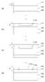
도 1은 초접합 파워 MOSFET을 예시적으로 도시한 단면도이다.
도 2는 초접합 구조를 형성하기 위한 공정을 예시적으로 도시한 도면이다.
도 3은 제1 도전형 필라 및 제2 도전형 필라의 농도 변화에 따른 항복전압 특성을 예시적으로 도시한 그래프이다.
도 4는 은 제1 도전형 필라 및 제2 도전형 필라의 농도 변화에 따른 온 상태 저항 특성을 예시적으로 도시한 그래프이다.
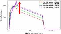
도 5는 제1 도전형 필라의 농도 변화에 따른 전계를 예시적으로 도시한 그래프이다.
도 6은 제2 도전형 필라의 농도 변화에 따른 전계를 예시적으로 도시한 그래프이다.
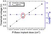
도 7은 제2 도전형 베이스의 이온 주입량에 따른 전기적 특성을 예시적으로 도시한 그래프이다.
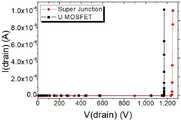
도 8은 본 발명에 따른 초접합 파워 모스펫과 트렌치 파워 모스펫의 문턱전압 특성을 예시적으로 도시한 그래프이다.
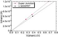
도 9는 본 발명에 따른 초접합 파워 모스펫과 트렌치 파워 모스펫의 온 상태 저항 특성을 예시적으로 도시한 그래프이다.
도 10은 본 발명에 따른 초접합 파워 모스펫과 트렌치 파워 모스펫의 항복 전압 특성을 예시적으로 도시한 그래프이다.DETAILED DESCRIPTION OF THE PREFERRED EMBODIMENTS Hereinafter, the present invention is described with reference to the embodiments shown in the accompanying drawings. For ease of understanding, like elements have been assigned like reference numerals throughout the accompanying drawings. The configuration shown in the accompanying drawings is merely an exemplary embodiment for explaining the present invention, and is not intended to limit the scope of the present invention.
1 is a cross-sectional view illustrating a superjunction power MOSFET by way of example.
2 is a diagram exemplarily illustrating a process for forming a superjunction structure.
3 is a graph exemplarily illustrating breakdown voltage characteristics according to a change in concentration of a first conductivity-type pillar and a second conductivity-type pillar.
FIG. 4 is a graph exemplarily illustrating an on-state resistance characteristic according to a change in concentration of a silver first conductivity type pillar and a second conductivity type pillar.
5 is a graph exemplarily illustrating an electric field according to a change in the concentration of a first conductivity-type pillar.
6 is a graph exemplarily illustrating an electric field according to a change in concentration of a second conductivity-type pillar.
7 is a graph exemplarily illustrating electrical characteristics according to an ion implantation amount of a second conductivity type base.
8 is a graph exemplarily illustrating threshold voltage characteristics of a superjunction power MOSFET and a trench power MOSFET according to the present invention.
9 is a graph exemplarily illustrating on-state resistance characteristics of a superjunction power MOSFET and a trench power MOSFET according to the present invention.
10 is a graph exemplarily illustrating breakdown voltage characteristics of a superjunction power MOSFET and a trench power MOSFET according to the present invention.
본 발명은 다양한 변경을 가할 수 있고 여러 가지 실시예를 가질 수 있는 바, 특정 실시예들을 도면에 예시하고 이를 상세한 설명을 통해 상세히 설명하고자 한다. 그러나, 이는 본 발명을 특정한 실시 형태에 대해 한정하려는 것이 아니며, 본 발명의 사상 및 기술 범위에 포함되는 모든 변경, 균등물 내지 대체물을 포함하는 것으로 이해되어야 한다.Since the present invention can have various changes and can have various embodiments, specific embodiments are illustrated in the drawings and will be described in detail through the detailed description. However, this is not intended to limit the present invention to specific embodiments, and it should be understood to include all modifications, equivalents and substitutes included in the spirit and scope of the present invention.
제1, 제2 등의 용어는 다양한 구성요소들을 설명하는데 사용될 수 있지만, 상기 구성요소들은 상기 용어들에 의해 한정되어서는 안 된다. 상기 용어들은 하나의 구성요소를 다른 구성요소로부터 구별하는 목적으로만 사용된다.Terms such as first, second, etc. may be used to describe various elements, but the elements should not be limited by the terms. The above terms are used only for the purpose of distinguishing one component from another.
본 출원에서 사용한 용어는 단지 특정한 실시예를 설명하기 위해 사용된 것으로, 본 발명을 한정하려는 의도가 아니다. 단수의 표현은 문맥상 명백하게 다르게 뜻하지 않는 한, 복수의 표현을 포함한다. 본 출원에서, "포함하다" 또는 "가지다" 등의 용어는 명세서상에 기재된 특징, 숫자, 단계, 동작, 구성요소, 부품 또는 이들을 조합한 것이 존재함을 지정하려는 것이지, 하나 또는 그 이상의 다른 특징들이나 숫자, 단계, 동작, 구성요소, 부품 또는 이들을 조합한 것들의 존재 또는 부가 가능성을 미리 배제하지 않는 것으로 이해되어야 한다.The terms used in the present application are only used to describe specific embodiments, and are not intended to limit the present invention. The singular expression includes the plural expression unless the context clearly dictates otherwise. In the present application, terms such as “comprise” or “have” are intended to designate that a feature, number, step, operation, component, part, or combination thereof described in the specification exists, but one or more other features It should be understood that this does not preclude the existence or addition of numbers, steps, operations, components, parts, or combinations thereof.
층, 영역 또는 기판과 같은 요소가 다른 요소 "위(on)"에 존재하는 것으로 또는 "위로(onto)" 확장되는 것으로 기술되는 경우, 그 요소는 다른 요소의 직접 위에 있거나 직접 위로 확장될 수 있고, 또는 중간의 개입 요소가 존재할 수도 있다. 반면에, 하나의 요소가 다른 요소 "바로 위(directly on)"에 있거나 "바로 위로(directly onto)" 확장된다고 언급되는 경우, 다른 중간 요소들은 존재하지 않는다. 또한, 하나의 요소가 다른 요소에 "연결(connected)"되거나 "결합(coupled)"된다고 기술되는 경우, 그 요소는 다른 요소에 직접 연결되거나 직접 결합될 수 있고, 또는 중간의 개입 요소가 존재할 수도 있다. 반면에, 하나의 요소가 다른 요소에 "직접 연결(directly connected)"되거나 "직접 결합(directly coupled)"된다고 기술되는 경우에는 다른 중간 요소가 존재하지 않는다.When an element, such as a layer, region, or substrate, is described as being “on” or extending “onto” another element, that element may be directly on or extending directly over the other element and , or an intermediate intervening element may exist. On the other hand, when an element is referred to as being “directly on” or extending “directly onto” another element, the other intermediate elements are absent. Also, when an element is described as being “connected” or “coupled” to another element, that element may be directly connected or coupled directly to the other element, or intervening elements may be present. have. On the other hand, when one element is described as being "directly connected" or "directly coupled" to another element, there is no other intermediate element present.
"아래의(below)" 또는 "위의(above)" 또는 "상부의(upper)" 또는 "하부의(lower)" 또는 "수평의(horizontal)" 또는 "측면의(lateral)" 또는 "수직의(vertical)"와 같은 상대적인 용어들은 여기에서 도면에 도시된 바와 같이 하나의 요소, 층 또는 영역의 다른 요소, 층 또는 영역에 대한 관계를 기술하는데 사용될 수 있다. 이들 용어들은 도면에 묘사된 방향(orientation)에 부가하여 장치의 다른 방향을 포괄하기 위한 의도를 갖는 것으로 이해되어야 한다.“below” or “above” or “upper” or “lower” or “horizontal” or “lateral” or “vertical” Relative terms such as "vertical" may be used herein to describe the relationship of one element, layer or region to another element, layer or region as shown in the figures. It should be understood that these terms are intended to encompass other orientations of the device in addition to the orientation depicted in the drawings.
이하, 본 발명의 실시예에 대해 관련 도면들을 참조하여 상세히 설명하기로 한다.Hereinafter, an embodiment of the present invention will be described in detail with reference to the related drawings.
도 1은 본 발명의 일 실시예에 따른 초접합 파워 MOSFET을 예시적으로 도시한 단면도이다.1 is a cross-sectional view illustrating a superjunction power MOSFET according to an embodiment of the present invention.
도 1을 참조하면, 초접합 MOSFET 소자는, 제1 도전형 기판(100), 제1 도전형 기판(100)의 상부에 형성된 복수의 제1 도전형 필라(115) 및 복수의 제2 도전형 필라(117), 제2 도전형 필라(117)의 상부에 형성된 제2 도전형 베이스(130), 제2 도전형 베이스(130) 내에 형성된 제2 도전형 소스 영역(135) 및 제1 도전형 소스 영역(137), 제1 도전형 필라(115)의 상부에 형성된 게이트(140)를 포함한다. 여기서, 제1 도전형은 N형 불순물로 도핑되며, 제2 도전형은 P형 불순물로 도핑될 수 있으나, 그 반대로 도핑될 수도 있음은 물론이다.Referring to FIG. 1 , a superjunction MOSFET device includes a first
제1 도전형 기판(100)은 제1 도전형 불순물을 도핑하여 형성된다. 제1 도전형 기판(100)의 상부에는 실리콘을 에피택셜 성장시킨 제1 도전형 드리프트층(110)이 형성된다.The first
제1 도전형 필라(115) 및 제2 도전형 필라(117)는, 제1 도전형 드리프트층(110)의 상부에 형성된다. 즉, 제1 도전형 필라(115) 및 제2 도전형 필라(117)는, 제1 도전형 드리프트층(110)의 상방으로 연장되게 형성된다. 제1 도전형 필라(115) 및 제2 도전형 필라(117)는, 측면 방향으로 교번하여 배치될 수 있다. 이로 인해, 제1 도전형 필라(115) 및 제2 도전형 필라(117)의 계면은 pn 접합한다. 제1 도전형 필라(115)는 온 상태에서 전류가 이동하는 경로를 형성하며, 제2 도전형 필라(117)는 역전압 인가시 전계를 분산하는 쉴드 역할을 한다. 제1 도전형 필라(115)의 도핑 농도는, 제1 도전형 드리프트층(110)의 도핑 농도보다 높다. 상세하게, 제1 도전형 필라(115)는, 제1 도전형 드리프트층(110)의 도핑 농도보다 높은 멀티 에피층을, 제1 도전형 드리프트층(110)의 상부에 형성함으로써, 형성될 수 있다. 제2 도전형 필라(117)는, 제2 도전형 불순물, 예를 들어, B를 멀티 에피층에 이온 주입하여 형성될 수 있다.The first
제2 도전형 베이스(130)는 제2 도전형 필라(117)의 상부에 형성된다. 제2 도전형 베이스(130)는 순방향 전압 인가시 채널이 형성되는 영역이다.The second conductivity-
제2 도전형 소스 영역(135) 및 제1 도전형 소스 영역(137)은, 제2 도전형 베이스(130)의 내부에 형성된다. 제2 도전형 소스 영역(135) 및 제1 도전형 소스 영역(137)은, 제2 도전형 베이스(130)의 제2 도전형 베이스(130)의 상면으로부터 제2 도전형 베이스(130)의 내부를 향해 연장되도록 형성된다. 제2 도전형 소스 영역(135) 및 제1 도전형 소스 영역(137)은 소스 메탈층(160)과의 오믹 접촉을 위해 고농도로 도핑된 영역이다. 제2 도전형 소스 영역(135) 및 제1 도전형 소스 영역(137)은 제2 도전형 베이스(130) 상면에 제2 도전형 불순물 및 제1 도전형 불순물을 이온주입하여 형성될 수 있다.The second conductivity
트렌치 게이트(140)는 게이트 절연막(150)에 의해 소자의 다른 영역들로부터 절연된다. 트렌치 게이트(140)는 소자의 상면으로부터 제2 도전형 베이스 영역(110)를 관통하여 제1 도전형 필라(115)까지 연장되게 형성되며, 내부는 금속 또는 폴리 실리콘 등으로 충진된다. 예를 들어, 트렌치 게이트(140)의 피치 Wgate는 약 0.3 ㎛일 수 있다. 게이트 절연막(150)은, 트렌치 게이트(140)를 제1 도전형 필라(115), 제2 도전형 베이스 영역(110), 및 제1 도전형 소스 영역(137)으로부터 전기적으로 절연시킨다.The
소스 메탈층(160) 및 드레인 메탈층(170)는, 전도성 물질, 예를 들어, 금속 또는 합금으로 형성된다. 소스 메탈층(160)은 제2 도전형 소스 영역(137) 및 제1 도전형 소스 영역(135) 상부에 형성되며, 드레인 메탈층(170)은 제1 도전형 기판(100)의 하부에 형성된다.The
상술한 초접합 파워 MOSFET 소자의 온 상태에서, 트렌치 게이트(140)의 측면, 정확히는, 게이트 산화막(150)을 따라 채널이 제2 도전형 베이스 영역(130) 내에 형성되어 제1 도전형 소스 영역(137)-제2 도전형 베이스 영역(130)-제1 도전형 필라(115)-드레인(170)으로 전류가 흐르게 된다. 상술한 초접합 파워 MOSFET 소자의 오프 상태에서, 제1 도전형 필라(115)-제2 도전형 베이스(130)-제1 도전형 소스 영역(137)간 NPN 접합에 의한 결핍 영역이 생성되어 채널이 차단된다.In the on-state of the above-described superjunction power MOSFET device, a channel is formed in the second conductivity
상술한 구조의 초접합 파워 MOSFET 소자의 설계 파라미터는 다음의 표에 예시되어 있다. 예시된 구조 파라미터는, 900 V 초접합 파워 MOSFET의 최적화 결과로, 이하에서는, 예시된 구조 파라미터를 이용하여, 제1 도전형 필라(115)와 제2 도전형 필라(117)간의 전하 균형과 제2 도전형 베이스(130)의 불순물 농도를 변경하면서, 문턱전압 약 4 V, 항복전압 약 1,100 V 이상, 및 낮은 온 저항을 구현하기 위한 실험을 진행하였다. 최적의 전기적 특성을 선택하는 과정을 설명하기로 한다. 여기서, 항복전압은 공정 마진 20%를 고려하여 최대 1,080V를 목표로 설정하였다.The design parameters of the superjunction power MOSFET device of the above structure are exemplified in the following table. The exemplified structural parameters are the results of optimization of the 900 V superjunction power MOSFET. Hereinafter, using the exemplified structural parameters, the charge balance between the first
도 2는 초접합 구조를 형성하기 위한 공정을 예시적으로 도시한 도면이다.2 is a diagram exemplarily illustrating a process for forming a superjunction structure.
초접합 구조를 제작하는 공정으로, 멀티 에피(multi-epitaxial) 공정과 트렌치 필링(trench filling) 공정이 있다. 멀티 에피 공정은, 소자 내부에 제2 도전형 필라(117)를 형성할 때, 에피택셜 공정과 이온주입 공정을 번갈아가면서 진행하여 최종적으로 적층된 제2 도전형 필라(117)를 제작하는 공정 방법이다. 한편, 트렌치 필링 공정은, 우선적으로 N 드리프트 영역에 트렌치를 식각한 후, 그 내부에 제2 도전형 반도체를 채워 넣어 제2 도전형 필라(117)를 형성하는 공정이다. 도 2는, 상술한 두 가지 공정 중, 멀티 에피 공정을 적용하여 트렌치 파워 MOSFET에 제2 도전형 필라(117)를 형성하여 초접합 파워 MOSFET을 제조하는 과정을 나타낸다.As a process for fabricating the superjunction structure, there are a multi-epitaxial process and a trench filling process. In the multi-epi process, when the second
도 2의 (a) 및 (b)에서, 제1 도전형 드리프트층(110)을, 실리콘으로 형성된 제1 도전형 기판(100)의 상면에 에피택셜 성장시킨다. 이후 제1 멀티 에피층(111)을 제1 두께 t1까지 제1 도전형 드리프트층(110)의 상면에 에피택셜 성장시킨 후, 제2 도전형 불순물을 이온 주입하여 제2 도전형 세그먼트(117a)를 형성한다. 제1 멀티 에피층(111)은 제1 도전형 불순물로 도핑되며, 도핑 농도는, 예를 들어, 약 1.0e13cm-3 내지 약 1.0e15cm-3이하일 수 있다. 제2 도전형 세그먼트(117a)는, 제2 도전형 불순물로 도핑되며, 도핑 농도는 약 2.5e15 cm-3 내지 약 7.5e15 cm-3고, 두께 tp는 약 15.0 ㎛이며, 폭 wpillar은 약 1.0 ㎛ 내지 2.5 ㎛일 수 있다.2A and 2B , the first conductivity
도 3의 (c) 및 (d)에서, 제2 도전형 세그먼트(117a)가 형성된 제1 멀티 에피층(111)의 상부에 제2 멀티 에피층(112)을, t2만큼 성장시킨 후, 제2 도전형 불순물을 이온 주입하여 제1 제2 도전형 세그먼트(117a)의 상부에 제2 도전형 세그먼트(117b)를 형성한다. 여기서 t2는, 제2 도전형 세그먼트(117b)의 두께 tp와 실질적으로 동일하거나 이보다 작을 수 있다. 이로 인해, 제2 도전형 세그먼트(117a)와 제2 도전형 세그먼트(117b)가 연결될 수 있다. 이후 (c) 내지 (d) 과정을 반복하여, 제3 멀티 에피층 내지 제10 멀티 에피층이 형성된다. 여기서, 적층되는 멀티 에피층의 수는 멀티 에피층의 두께에 따라 달라질 수 있다.3 (c) and (d), after growing the second
제1 멀티 에피층 내지 제5 멀티 에피층이 형성된 후, 열처리에 의해 주입된 제2 도전형 불순물이 활성화되어 제2 도전형 필라(117)가 형성된다. 제2 도전형 필라(117)의 상부에 에피층을 성장시킨 후, 이온 주입을 통해 제2 도전형 베이스(130)가 형성된다. 제2 도전형 베이스(130) 내에 제1 도전형 불순물 및 제2 도전형 불순물을 이온 주입하여 제2 도전형 소스 영역(135) 및 제1 도전형 소스 영역(137)을 형성한다.After the first to fifth multi-epithelial layers are formed, second conductivity-type impurities implanted by heat treatment are activated to form second conductivity-
도 3은 제1 도전형 필라 및 제2 도전형 필라의 농도 변화에 따른 항복전압 특성을 예시적으로 도시한 그래프이며, 도 4는 은 제1 도전형 필라 및 제2 도전형 필라의 농도 변화에 따른 온 상태 저항 특성을 예시적으로 도시한 그래프이다.3 is a graph exemplarily showing the breakdown voltage characteristics according to changes in the concentrations of the first and second conductivity type pillars, and FIG. 4 is a graph showing changes in the concentrations of the first and second conductivity type pillars. It is a graph exemplarily showing the on-state resistance characteristics according to the following.
기존 파워 MOSFET에 초접합 구조를 적용함으로써, 수평적으로 형성된 P-N접합은 소자 전 영역에 걸쳐 공핍층을 형성하며, 그에 따라서 더욱 높은 항복전압을 얻을 수 있다. 하지만 제1 도전형 필라(115)의 전하량과 제2 도전형 필라(117)의 전하량이 동일한 균형 상태에 있어야만 이론상으로 최대 항복전압을 가질 수 있고 온 저항을 낮출 수 있다. 필라의 낮은 전하량을 사용할 경우, 높은 항복전압은 수평방향의 완벽한 공핍을 통해 달성될 수 있다. 하지만, 낮은 온 저항을 얻기 위해서는 필라의 도핑 농도를 높여야 한다. 높은 항복전압과 낮은 온 저항을 동시에 얻기 위해서, 제1 도전형 필라(115) 및 제2 도전형 필라(117)의 도핑 농도를 변경하면서, 전기적 특성을 측정하였다. 제1 도전형 필라(115)의 도핑 농도는 약 1.0e13cm-3 내지 약 1.0e15cm-3로 변경되며, 제2 도전형 필라(117)의 도핑 농도는 약 2.5e15 cm-3 내지 약 7.5e15 cm-3로 변경될 때 측정한 항복전압 및 온 상태 이 도시되어 있다.By applying the superjunction structure to the existing power MOSFET, the horizontally formed PN junction forms a depletion layer over the entire region of the device, and thus a higher breakdown voltage can be obtained. However, only when the amount of charge of the first
도 3을 참조하면, 제1 도전형 필라(115)의 도핑 농도가 증가할수록 항복전압이 증가하지만, 제1 도전형 필라(115)의 도핑 농도가 일정 값을 초과하면, 전하 균형이 깨져서 항복 전압이 감소하게 된다. 이 현상은 제2 도전형 필라(117)의 도핑 농도에 상관없이 발생하며, 항복전압이 감소하기 시작하는 제1 도전형 필라(115)의 도핑 농도에만 차이가 있다. 즉, 제1 도전형 필라(115)의 도핑 농도가 약 1.0e14cm-3 에서는, 제2 도전형 필라(117)의 도핑 농도에 상관없이 항복전압이 약 1200 V 이상이 유지되었지만, 제1 도전형 필라(115)의 도핑 농도가 약 1.0e14cm-3를 초과하면서, 제2 도전형 필라(117)의 도핑 농도가 낮은 값 2.5e15 cm-3 내지 4.5e15 cm-3 에서 항복 전압이 급격히 감소한다. 따라서 제1 도전형 필라(115)의 도핑 농도는, 약 1.0e14cm-3 내지 약 1.0e15cm-3로, 바람직하게는 약 1.0e14cm-3 내지 약 5.0e14cm-3일 수 있다.Referring to FIG. 3 , the breakdown voltage increases as the doping concentration of the first conductivity-
도 4를 참조하면, 제1 도전형 필라(115)의 도핑 농도를 약 1.0e14cm-3 내지 약 1.0e15cm-3로 변경할 때, 제2 도전형 필라(117)의 도핑 농도가 증가함에 따라 온 상태 저항이 지수적으로 감소하게 된다. 즉, 제1 도전형 필라(115)의 도핑 농도가 작을수록 온 상태 저항의 변화가 크며, 제1 도전형 필라(115)의 도핑 농도가 커질수록 온 상태 저항의 변화가 감소한다.Referring to FIG. 4 , the doping concentration of the first conductivity-
도 5는 제1 도전형 필라의 농도 변화에 따른 전계를 예시적으로 도시한 그래프이며, 도 6은 제2 도전형 필라의 농도 변화에 따른 전계를 예시적으로 도시한 그래프이다.5 is a graph exemplarily illustrating an electric field according to a change in the concentration of the first conductivity-type pillars, and FIG. 6 is a graph exemplarily illustrating an electric field according to a change in the concentration of the second conductivity-type pillars.
도 5를 참조하면, 제1 도전형 필라(115)의 도핑 농도가 증가할수록 전계가 감소한다. 제2 도전형 필라(117)의 도핑 농도를 4.5e15cm-3로 고정하고 제1 도전형 필라(115)의 도핑 농도를 약 2.0e14 cm-3 내지 9.0e14 cm-3로 변경하면, 표면 근처에서 전계가 최대가 깊이는, 제1 도전형 필라(115)의 도핑 농도가 높을수록 얕아지며, 전계의 최대값 역시 제1 도전형 필라(115)의 도핑 농도가 높을수록 작아진다.Referring to FIG. 5 , as the doping concentration of the first conductivity-
도 6을 참조하면, 제2 도전형 필라(117)의 도핑 농도가 증가할수록 전계가 증가한다. 제1 도전형 필라(117)의 도핑 농도를 3.0e14cm-3로 고정하고 제2 도전형 필라(117)의 도핑 농도를 약 250e15 cm-3 내지 7.5e15 cm-3로 변경하면, 표면 근처에서 전계가 최대가 깊이는, 제2 도전형 필라(117)의 도핑 농도가 높을수록 깊어지며, 전계의 최대값 역시 제2 도전형 필라(117)의 도핑 농도가 높을수록 커진다.Referring to FIG. 6 , as the doping concentration of the second conductivity-
도 3 내지 도 6에 도시된 실험 결과를 모두 고려할 때, 제1 도전형 필라(115)의 도핑 농도가 약 3.0e14cm-3이며, 제2 도전형 필라(117)의 도핑 농도가 약 4.5e15cm-3일 때, 약 1,250 V의 항복 전압과 약 16.7 m Ω×cm2의 온 상태 전압 특성을 가짐을 알 수 있다.When all the experimental results shown in FIGS. 3 to 6 are considered, the doping concentration of the first conductivity-
도 7은 제2 도전형 베이스의 이온 주입량에 따른 전기적 특성을 예시적으로 도시한 그래프이다.7 is a graph exemplarily illustrating electrical characteristics according to an ion implantation amount of a second conductivity type base.
도 7을 참조하면, 문턱전압 특성은, 제2 도전형 베이스(130)의 이온 주입량이 증가함에 따라 증가하는 경향을 나타내지만, 온 상태 저항은 거의 변화가 없다. 제2 도전형 베이스(130)의 이온 주입량은, 약 1.5e13 cm2 내지 약 4.0e13 cm2로 변경되었다. 이온 주입량이 증가하면, P형 캐리어가 증가하여, 채널 형성에 필요한 전압이 증가하게 된다. 하지만, 이는 온 상태 저항에는 영향을 주지 않음을 알 수 있다. 문턱 전압을 약 4.3 V로 선택할 때 제2 도전형 베이스(130)로의 이온 주입량은 약 2.5e13 cm2인 것이 바람직하다.Referring to FIG. 7 , the threshold voltage characteristic tends to increase as the ion implantation amount of the second
도 8은 본 발명에 따른 초접합 파워 모스펫과 트렌치 파워 모스펫의 문턱전압 특성을, 도 9는 온 상태 저항 특성을, 그리고, 도 10은 항복 전압 특성을 예시적으로 도시한 그래프이다.8 is a graph illustrating threshold voltage characteristics of a superjunction power MOSFET and a trench power MOSFET according to the present invention, FIG. 9 is an on-state resistance characteristic, and FIG. 10 is a graph illustrating breakdown voltage characteristics.
초접합 파워 모스펫과 트렌치 파워 모스펫은, 동일한 셀 크기를 갖는 900 V급으로 제작되었다. 도 8을 참조하면, 초접합 파워 모스펫의 문턱 전압은 약 4.3 V이며, 트렌치 파워 모스펫의 문턱 전압은 약 4.1 V로, 문턱 전압은 트렌치 파워 모스펫이 약 0.2 V 정도 낮게 측정되었다. 한편, 도 9를 참조하면, 초접합 파워 모스펫의 온 상태 저항은, 16.7 m Ω×cm2이며, 트렌치 파워 모스펫의 온 상태 저항은 19.2 m Ω×cm2로, 온 상태 저항은 초접합 파워 모스펫이 약 2.5 m Ω×cm2의 정도 낮게 측정되었다. 그리고, 초접합 파워 모스펫의 항복 전압은 약 1,250 V이며, 저항 트렌치 파워 모스펫의 항복 전압은 약 1,170 V로, 항복 전압은 초접합 파워 모스펫이 약 80 V 높게 측정되었다.The superjunction power MOSFET and the trench power MOSFET were manufactured in 900 V class with the same cell size. Referring to FIG. 8 , the threshold voltage of the superjunction power MOSFET is about 4.3 V, the threshold voltage of the trench power MOSFET is about 4.1 V, and the threshold voltage of the trench power MOSFET is about 0.2 V lower. Meanwhile, referring to FIG. 9 , the on-state resistance of the superjunction power MOSFET is 16.7 m Ω×cm2 , the on-state resistance of the trench power MOSFET is 19.2 m Ω×cm2 , and the on-state resistance of the superjunction power MOSFET This was measured as low as about 2.5 m Ω×cm2 . In addition, the breakdown voltage of the superjunction power MOSFET is about 1,250 V, the breakdown voltage of the resistive trench power MOSFET is about 1,170 V, and the breakdown voltage of the superjunction power MOSFET is about 80 V higher.
전술한 본 발명의 설명은 예시를 위한 것이며, 본 발명이 속하는 기술분야의 통상의 지식을 가진 자는 본 발명의 기술적 사상이나 필수적인 특징을 변경하지 않고서 다른 구체적인 형태로 쉽게 변형이 가능하다는 것을 이해할 수 있을 것이다. 그러므로 이상에서 기술한 실시 예들은 모든 면에서 예시적인 것이며 한정적이 아닌 것으로 이해해야만 한다.The above description of the present invention is for illustration, and those of ordinary skill in the art to which the present invention pertains can understand that it can be easily modified into other specific forms without changing the technical spirit or essential features of the present invention. will be. Therefore, it should be understood that the embodiments described above are illustrative in all respects and not restrictive.
본 발명의 범위는 상기 상세한 설명보다는 후술하는 특허청구범위에 의하여 나타나며, 특허청구범위의 의미 및 범위 그리고 그 균등 개념으로부터 도출되는 모든 변경 또는 변형된 형태가 본 발명의 범위에 포함되는 것으로 해석되어야 한다.The scope of the present invention is indicated by the following claims rather than the above detailed description, and all changes or modifications derived from the meaning and scope of the claims and their equivalent concepts should be construed as being included in the scope of the present invention. .
Claims (3)
Translated fromKorean상기 제1 도전형 기판의 상부에 에피택셜 성장된 제1 도전형 드리프트층;
상기 제1 도전형 드리프트층의 상부에 적층되며, 상기 제1 도전형 드리프트층보다 높은 농도로 제1 도전형 불순물로 도핑된 복수의 멀티 에피층;
상기 복수의 멀티 에피층에 수직 방향으로 교번하게 형성된 제1 도전형 필라 및 제2 도전형 필라-여기서, 상기 제2 도전형 필라는 상기 복수의 멀티 에피층보다 높은 농도로 제2 도전형 불순물을 이온 주입하여 형성됨;
상기 제2 도전형 필라의 상부에 연속되도록 상기 제1 도전형 드리프트층의 상면으로부터 내부를 향해 형성되며, 적어도 일부 영역이 채널을 형성하는 제2 도전형 불순물로 도핑된 제2 도전형 베이스 영역;
상기 복수의 멀티 에피층의 표면으로부터 내부를 향해 형성되어, 상기 제2 도전형 베이스가 그 측면에 배치되며, 인가된 전압에 의해 상기 채널을 형성하도록 하는 트렌치 게이트-여기서 상기 트렌치 게이트는, 게이트 절연막에 의해 상기 제1 도전형 필라 및 상기 제2 도전형 베이스와 전기적으로 절연됨; 및
상기 제2 도전형 베이스 내에 형성되며, 상기 트렌치 게이트로부터 이격되어 상기 제2 도전형 불순물로 도핑된 제2 도전형 소스 영역 및 상기 트렌치 게이트의 측면과 상기 제2 도전형 소스 영역 사이에 상기 제1 도전형 불순물로 도핑된 제1 도전형 소스 영역을 포함하되,
상기 제1 도전형 필라의 도핑 농도는 3.0e14cm-3이고,
상기 제2 도전형 필라의 도핑 농도는 약 4.5e15cm-3이며,
상기 제2 도전형 베이스의 이온 주입량은 2.5e13 cm2인, 초접합 파워 MOSFET.a first conductive type substrate;
a first conductivity-type drift layer epitaxially grown on the first conductivity-type substrate;
a plurality of multi-epithelial layers stacked on the first conductivity type drift layer and doped with a first conductivity type impurity at a higher concentration than the first conductivity type drift layer;
First conductivity-type pillars and second conductivity-type pillars alternately formed in the plurality of multi-epithelial layers in a vertical direction, wherein the second conductivity-type pillars contain second conductivity-type impurities at a higher concentration than that of the plurality of multi-epithelial layers formed by ion implantation;
a second conductivity-type base region formed from a top surface of the first conductivity-type drift layer toward the inside so as to be continuous on the second conductivity-type pillar and doped with a second conductivity-type impurity forming a channel;
A trench gate formed from the surface of the plurality of multi-epithelial layers toward the inside, the second conductivity type base is disposed on a side thereof, and the channel is formed by an applied voltage, wherein the trench gate is a gate insulating film electrically insulated from the first conductivity-type pillar and the second conductivity-type base by and
A second conductivity type source region formed in the second conductivity type base and spaced apart from the trench gate and doped with the second conductivity type impurity, and the first conductivity type source region between a side surface of the trench gate and the second conductivity type source region A first conductivity type source region doped with a conductivity type impurity,
The doping concentration of the first conductivity type pillar is 3.0e14cm-3 ,
The doping concentration of the second conductivity type pillar is about 4.5e15cm-3 ,
An ion implantation amount of the second conductivity type base is 2.5e13 cm2 , a superjunction power MOSFET.
The superjunction power MOSFET of claim 1 , wherein the cell half pitch of the superjunction power MOSFET is 6 μm, the total thickness is 300 μm, the width of the gate is 1.8 μm, and the thickness of the gate is 4 μm.
Priority Applications (1)
| Application Number | Priority Date | Filing Date | Title |
|---|---|---|---|
| KR1020200039849AKR20210122946A (en) | 2020-04-01 | 2020-04-01 | Super junction power MOSFET |
Applications Claiming Priority (1)
| Application Number | Priority Date | Filing Date | Title |
|---|---|---|---|
| KR1020200039849AKR20210122946A (en) | 2020-04-01 | 2020-04-01 | Super junction power MOSFET |
Publications (1)
| Publication Number | Publication Date |
|---|---|
| KR20210122946Atrue KR20210122946A (en) | 2021-10-13 |
Family
ID=78115082
Family Applications (1)
| Application Number | Title | Priority Date | Filing Date |
|---|---|---|---|
| KR1020200039849AWithdrawnKR20210122946A (en) | 2020-04-01 | 2020-04-01 | Super junction power MOSFET |
Country Status (1)
| Country | Link |
|---|---|
| KR (1) | KR20210122946A (en) |
Cited By (4)
| Publication number | Priority date | Publication date | Assignee | Title |
|---|---|---|---|---|
| CN114023806A (en)* | 2021-10-22 | 2022-02-08 | 华虹半导体(无锡)有限公司 | Superjunction trench gate MOSFET and method of making the same |
| CN114068678A (en)* | 2021-11-25 | 2022-02-18 | 华虹半导体(无锡)有限公司 | Super junction trench gate MOSFET device and manufacturing method thereof |
| KR102532142B1 (en)* | 2021-12-01 | 2023-05-11 | 단국대학교 산학협력단 | Trench Gate MOSFET Based on 4H-SiC with High Breakdown Voltage |
| KR20250022580A (en)* | 2023-08-08 | 2025-02-17 | 한국항공우주연구원 | Semicondector device and manufacturing method thereof |
- 2020
- 2020-04-01KRKR1020200039849Apatent/KR20210122946A/ennot_activeWithdrawn
Cited By (4)
| Publication number | Priority date | Publication date | Assignee | Title |
|---|---|---|---|---|
| CN114023806A (en)* | 2021-10-22 | 2022-02-08 | 华虹半导体(无锡)有限公司 | Superjunction trench gate MOSFET and method of making the same |
| CN114068678A (en)* | 2021-11-25 | 2022-02-18 | 华虹半导体(无锡)有限公司 | Super junction trench gate MOSFET device and manufacturing method thereof |
| KR102532142B1 (en)* | 2021-12-01 | 2023-05-11 | 단국대학교 산학협력단 | Trench Gate MOSFET Based on 4H-SiC with High Breakdown Voltage |
| KR20250022580A (en)* | 2023-08-08 | 2025-02-17 | 한국항공우주연구원 | Semicondector device and manufacturing method thereof |
Similar Documents
| Publication | Publication Date | Title |
|---|---|---|
| JP6817443B2 (en) | Power semiconductor devices with gate trenches and embedded termination structures, and related methods | |
| TWI534902B (en) | Power semiconductor device and method of forming power semiconductor device | |
| US8704292B2 (en) | Vertical capacitive depletion field effect transistor | |
| KR20210122946A (en) | Super junction power MOSFET | |
| CN103165604B (en) | Semiconductor components with space-saving edge structures | |
| KR102246570B1 (en) | Power semiconductor devices | |
| JP2009289904A (en) | Semiconductor device | |
| CN103489913A (en) | Semiconductor device and method for manufacturing same | |
| EP3073531A1 (en) | Composite semiconductor device with different channel widths | |
| JP2009272397A (en) | Semiconductor device | |
| US9806152B2 (en) | Vertical insulated gate turn-off thyristor with intermediate p+ layer in p-base | |
| US9627470B2 (en) | Power semiconductor device and method of manufacturing the same | |
| WO2012017227A1 (en) | Semiconductor device | |
| US20140284715A1 (en) | Method of manufacturing semiconductor device | |
| CN114651335B (en) | Insulated gate bipolar transistor | |
| KR20130119873A (en) | Power device and method for fabricating the same | |
| US9059237B2 (en) | Semiconductor device having an insulated gate bipolar transistor | |
| CN103579296B (en) | Semiconductor device and manufacture method thereof | |
| KR20170070507A (en) | Semiconductor device and method manufacturing the same | |
| KR20210114569A (en) | Super junction MOSFET transistor and method of manufacturing the same | |
| KR102406116B1 (en) | Semiconductor device and method manufacturing the same | |
| KR101550798B1 (en) | Power semiconductor device having structure for preventing latch-up and method of manufacture thereof | |
| JP2021150405A (en) | Silicon carbide semiconductor device | |
| KR101216851B1 (en) | Semiconductor device and method of manufacturing the same | |
| US7741655B2 (en) | Semiconductor device |
Legal Events
| Date | Code | Title | Description |
|---|---|---|---|
| PA0109 | Patent application | St.27 status event code:A-0-1-A10-A12-nap-PA0109 | |
| PG1501 | Laying open of application | St.27 status event code:A-1-1-Q10-Q12-nap-PG1501 | |
| PC1203 | Withdrawal of no request for examination | St.27 status event code:N-1-6-B10-B12-nap-PC1203 | |
| R18-X000 | Changes to party contact information recorded | St.27 status event code:A-3-3-R10-R18-oth-X000 | |
| P22-X000 | Classification modified | St.27 status event code:A-2-2-P10-P22-nap-X000 |