KR20210119618A - Display device - Google Patents
Display deviceDownload PDFInfo
- Publication number
- KR20210119618A KR20210119618AKR1020200035759AKR20200035759AKR20210119618AKR 20210119618 AKR20210119618 AKR 20210119618AKR 1020200035759 AKR1020200035759 AKR 1020200035759AKR 20200035759 AKR20200035759 AKR 20200035759AKR 20210119618 AKR20210119618 AKR 20210119618A
- Authority
- KR
- South Korea
- Prior art keywords
- dummy
- touch
- sub
- touch electrodes
- disposed
- Prior art date
- Legal status (The legal status is an assumption and is not a legal conclusion. Google has not performed a legal analysis and makes no representation as to the accuracy of the status listed.)
- Pending
Links
Images


Classifications
- G—PHYSICS
- G06—COMPUTING OR CALCULATING; COUNTING
- G06F—ELECTRIC DIGITAL DATA PROCESSING
- G06F3/00—Input arrangements for transferring data to be processed into a form capable of being handled by the computer; Output arrangements for transferring data from processing unit to output unit, e.g. interface arrangements
- G06F3/01—Input arrangements or combined input and output arrangements for interaction between user and computer
- G06F3/03—Arrangements for converting the position or the displacement of a member into a coded form
- G06F3/041—Digitisers, e.g. for touch screens or touch pads, characterised by the transducing means
- G06F3/044—Digitisers, e.g. for touch screens or touch pads, characterised by the transducing means by capacitive means
- G06F3/0448—Details of the electrode shape, e.g. for enhancing the detection of touches, for generating specific electric field shapes, for enhancing display quality
- G—PHYSICS
- G06—COMPUTING OR CALCULATING; COUNTING
- G06F—ELECTRIC DIGITAL DATA PROCESSING
- G06F3/00—Input arrangements for transferring data to be processed into a form capable of being handled by the computer; Output arrangements for transferring data from processing unit to output unit, e.g. interface arrangements
- G06F3/01—Input arrangements or combined input and output arrangements for interaction between user and computer
- G06F3/03—Arrangements for converting the position or the displacement of a member into a coded form
- G06F3/041—Digitisers, e.g. for touch screens or touch pads, characterised by the transducing means
- G06F3/0412—Digitisers structurally integrated in a display
- G—PHYSICS
- G06—COMPUTING OR CALCULATING; COUNTING
- G06F—ELECTRIC DIGITAL DATA PROCESSING
- G06F3/00—Input arrangements for transferring data to be processed into a form capable of being handled by the computer; Output arrangements for transferring data from processing unit to output unit, e.g. interface arrangements
- G06F3/01—Input arrangements or combined input and output arrangements for interaction between user and computer
- G06F3/03—Arrangements for converting the position or the displacement of a member into a coded form
- G06F3/041—Digitisers, e.g. for touch screens or touch pads, characterised by the transducing means
- G06F3/0416—Control or interface arrangements specially adapted for digitisers
- G06F3/04164—Connections between sensors and controllers, e.g. routing lines between electrodes and connection pads
- G—PHYSICS
- G06—COMPUTING OR CALCULATING; COUNTING
- G06F—ELECTRIC DIGITAL DATA PROCESSING
- G06F3/00—Input arrangements for transferring data to be processed into a form capable of being handled by the computer; Output arrangements for transferring data from processing unit to output unit, e.g. interface arrangements
- G06F3/01—Input arrangements or combined input and output arrangements for interaction between user and computer
- G06F3/03—Arrangements for converting the position or the displacement of a member into a coded form
- G06F3/041—Digitisers, e.g. for touch screens or touch pads, characterised by the transducing means
- G06F3/044—Digitisers, e.g. for touch screens or touch pads, characterised by the transducing means by capacitive means
- G06F3/0443—Digitisers, e.g. for touch screens or touch pads, characterised by the transducing means by capacitive means using a single layer of sensing electrodes
- G—PHYSICS
- G06—COMPUTING OR CALCULATING; COUNTING
- G06F—ELECTRIC DIGITAL DATA PROCESSING
- G06F3/00—Input arrangements for transferring data to be processed into a form capable of being handled by the computer; Output arrangements for transferring data from processing unit to output unit, e.g. interface arrangements
- G06F3/01—Input arrangements or combined input and output arrangements for interaction between user and computer
- G06F3/03—Arrangements for converting the position or the displacement of a member into a coded form
- G06F3/041—Digitisers, e.g. for touch screens or touch pads, characterised by the transducing means
- G06F3/044—Digitisers, e.g. for touch screens or touch pads, characterised by the transducing means by capacitive means
- G06F3/0446—Digitisers, e.g. for touch screens or touch pads, characterised by the transducing means by capacitive means using a grid-like structure of electrodes in at least two directions, e.g. using row and column electrodes
- G—PHYSICS
- G06—COMPUTING OR CALCULATING; COUNTING
- G06F—ELECTRIC DIGITAL DATA PROCESSING
- G06F2203/00—Indexing scheme relating to G06F3/00 - G06F3/048
- G06F2203/041—Indexing scheme relating to G06F3/041 - G06F3/045
- G06F2203/04111—Cross over in capacitive digitiser, i.e. details of structures for connecting electrodes of the sensing pattern where the connections cross each other, e.g. bridge structures comprising an insulating layer, or vias through substrate
- G—PHYSICS
- G06—COMPUTING OR CALCULATING; COUNTING
- G06F—ELECTRIC DIGITAL DATA PROCESSING
- G06F2203/00—Indexing scheme relating to G06F3/00 - G06F3/048
- G06F2203/041—Indexing scheme relating to G06F3/041 - G06F3/045
- G06F2203/04112—Electrode mesh in capacitive digitiser: electrode for touch sensing is formed of a mesh of very fine, normally metallic, interconnected lines that are almost invisible to see. This provides a quite large but transparent electrode surface, without need for ITO or similar transparent conductive material
Landscapes
- Engineering & Computer Science (AREA)
- General Engineering & Computer Science (AREA)
- Theoretical Computer Science (AREA)
- Human Computer Interaction (AREA)
- Physics & Mathematics (AREA)
- General Physics & Mathematics (AREA)
- Quality & Reliability (AREA)
- Computer Networks & Wireless Communication (AREA)
- Devices For Indicating Variable Information By Combining Individual Elements (AREA)
Abstract
Translated fromKoreanDescription
Translated fromKorean본 발명은 표시 장치에 관한 것이다.The present invention relates to a display device.
사용자에게 영상을 제공하는 스마트 폰, 태블릿 PC, 디지털 카메라, 노트북 컴퓨터, 네비게이션, 및 텔레비전(TV) 등의 전자 기기는 영상을 표시하기 위한 표시 장치를 포함한다. 표시 장치는 영상을 생성하여 표시하는 표시 패널 및 다양한 입력 장치를 포함한다.BACKGROUND Electronic devices, such as smart phones, tablet PCs, digital cameras, notebook computers, navigation systems, and televisions (TVs) that provide images to users, include display devices for displaying images. The display device includes a display panel that generates and displays an image and various input devices.
최근에는 스마트 폰이나 태블릿 PC를 중심으로 터치 입력을 인식하는 터치 감지 유닛이 표시 장치의 입력 장치로 많이 적용되고 있다. 터치 감지 유닛은 사용자의 터치 입력 여부를 판단하고, 해당 위치를 터치 입력 좌표로 산출한다.In recent years, a touch sensing unit for recognizing a touch input, centered on a smart phone or a tablet PC, has been widely applied as an input device of a display device. The touch sensing unit determines whether the user has a touch input, and calculates a corresponding position as touch input coordinates.
터치 감지 유닛은 제1 방향으로 전기적으로 연결된 제1 터치 전극들, 제1 방향과 교차하는 제2 방향으로 전기적으로 연결된 제2 터치 전극들, 제1 터치 전극들에 연결되는 제1 터치 라인들, 및 제2 터치 전극들에 연결되는 제2 터치 라인들을 포함할 수 있다. 이 때, 제1 터치 전극들과 제2 터치 전극들 사이에서 불필요한 커플링이 발생할 수 있고, 이로 인해 터치 감지 유닛의 감도가 악화되거나 구동이 불가능할 수 있다.The touch sensing unit includes first touch electrodes electrically connected in a first direction, second touch electrodes electrically connected in a second direction crossing the first direction, first touch lines connected to the first touch electrodes, and second touch lines connected to the second touch electrodes. In this case, unnecessary coupling may occur between the first touch electrodes and the second touch electrodes, and thus the sensitivity of the touch sensing unit may deteriorate or it may be impossible to drive.
본 발명이 해결하고자 하는 과제는 적어도 하나의 제1 터치 전극 및 적어도 하나의 제2 터치 전극에 의해 둘러싸이는 투과 영역, 및 투과 영역을 둘러싸는 더미부를 포함하는 경우, 더미부에 의해 적어도 하나의 제1 터치 전극 및 적어도 하나의 제2 터치 전극 사이에 불필요한 커플링의 발생을 방지할 수 있는 표시 장치를 제공하고자 하는 것이다.SUMMARY OF THE INVENTION The problem to be solved by the present invention is to provide a transparent area surrounded by at least one first touch electrode and at least one second touch electrode, and a dummy portion surrounding the transparent area. An object of the present invention is to provide a display device capable of preventing unnecessary coupling between a first touch electrode and at least one second touch electrode.
본 발명의 과제들은 이상에서 언급한 과제로 제한되지 않으며, 언급되지 않은 또 다른 기술적 과제들은 아래의 기재로부터 당업자에게 명확하게 이해될 수 있을 것이다.The problems of the present invention are not limited to the problems mentioned above, and other technical problems not mentioned will be clearly understood by those skilled in the art from the following description.
상기 과제를 해결하기 위한 일 실시예의 표시 장치는 복수의 화소를 구비한 표시 영역, 및 표시 영역에 의해 둘러싸이는 투과부, 및 상기 표시 영역을 둘러싸는 비표시 영역을 포함하는 표시 유닛, 및 상기 투과부와 중첩된 투과 영역, 상기 투과부와 중첩되고 상기 투과 영역을 둘러싸는 더미부, 상기 더미부를 둘러싸는 터치 센서 영역, 및 상기 터치 센서 영역을 둘러싸는 터치 주변 영역을 구비한 터치 감지 유닛을 포함하고, 상기 터치 센서 영역은 제1 방향 및 상기 제1 방향과 수직한 제2 방향으로 배열된 제1 터치 전극들, 및 상기 제1 터치 전극들 사이에 배치되고, 상기 제1 방향으로 연결되며 상기 제2 방향으로 서로 이격된 제2 터치 전극들을 포함하며, 상기 더미부는 상기 투과 영역을 직접 둘러싸는 메인 더미, 및 상기 메인 더미를 둘러싸는 적어도 하나의 서브 더미를 포함하고, 상기 제1 터치 전극들 및 상기 제2 터치 전극들과 절연되며, 상기 더미부의 최외곽에 배치된 서브 더미는 상기 제1 및 제2 터치 전극들 중 직접 인접한 제1 및 제2 터치 전극 사이의 간극에 대응되는 제1 커팅부를 포함한다.According to an exemplary embodiment, a display device includes a display unit including a display area including a plurality of pixels, a transmissive part surrounded by the display area, and a non-display area surrounding the display area, and the transmissive part; A touch sensing unit comprising: an overlapping transmissive area; a dummy part overlapping the transmissive part and surrounding the transmissive area; a touch sensor area surrounding the dummy part; and a touch peripheral area surrounding the touch sensor area; The touch sensor area includes first touch electrodes arranged in a first direction and a second direction perpendicular to the first direction, and disposed between the first touch electrodes, connected in the first direction, and connected in the second direction and second touch electrodes spaced apart from each other by a The sub dummy insulated from the two touch electrodes and disposed at the outermost part of the dummy part includes a first cutting part corresponding to a gap between the first and second touch electrodes directly adjacent among the first and second touch electrodes. .
상기 제1 커팅부는 상기 직접 인접한 제1 및 제2 터치 전극 사이의 간극과 최단 거리에 배치될 수 있다.The first cutting part may be disposed at a shortest distance from a gap between the directly adjacent first and second touch electrodes.
상기 터치 감지 유닛은 상기 더미부를 지지하는 베이스 부재를 더 포함할 수 있고, 상기 더미부는 상기 베이스 부재와, 상기 제1 터치 전극들 및 상기 제2 터치 전극들 사이의 층에 배치될 수 있다.The touch sensing unit may further include a base member supporting the dummy part, and the dummy part may be disposed in a layer between the base member and the first touch electrodes and the second touch electrodes.
상기 터치 감지 유닛은 상기 제1 터치 전극들 및 상기 제2 터치 전극들 사이에 배치된 전극 더미부를 더 포함할 수 있다.The touch sensing unit may further include an electrode dummy portion disposed between the first touch electrodes and the second touch electrodes.
상기 제1 커팅부는 상기 직접 인접한 제1 및 제2 터치 전극을 사이에 두고 상기 전극 더미부와 이격될 수 있다.The first cutting part may be spaced apart from the electrode dummy part with the first and second touch electrodes directly adjacent therebetween.
상기 더미부의 최외곽에 배치된 서브 더미는 직접 마주하는 상기 전극 더미부와 상기 제1 및 제2 터치 전극들 중 제1 터치 전극 또는 제2 터치 전극의 사이에 대응되는 제2 커팅부들을 더 포함할 수 있다.The sub dummy disposed at the outermost part of the dummy part further includes second cutting parts corresponding to the electrode dummy part directly facing each other and between the first touch electrode or the second touch electrode among the first and second touch electrodes. can do.
상기 터치 감지 유닛은 상기 더미부의 최외곽에 배치된 서브 더미를 둘러싸고, 상기 제1 및 제2 터치 전극들 중 상기 더미부의 최외곽에 배치된 서브 더미와 직접 마주하는 제1 터치 전극 또는 제2 터치 전극과 컨택되는 컨택 더미부를 더 포함할 수 있다.The touch sensing unit surrounds the sub dummy disposed at the outermost part of the dummy part, and among the first and second touch electrodes, a first touch electrode or a second touch electrode directly facing the sub dummy disposed at the outermost part of the dummy part. It may further include a contact dummy part that is in contact with the electrode.
상기 컨택 더미부의 평면 상 폭은 상기 더미부의 최외곽에 배치된 서브 더미의 평면 상 폭보다 클 수 있다.A width in a plane of the contact dummy part may be greater than a width in a plane of a sub dummy disposed at the outermost part of the dummy part.
상기 컨택 더미부는 상기 제1 및 제2 터치 전극 사이의 간극과 평면 상에서 중첩되는 제7 커팅부를 포함할 수 있다.The contact dummy part may include a seventh cutting part overlapping a gap between the first and second touch electrodes on a plane.
상기 터치 감지 유닛은 상기 제1 터치 전극들 및 상기 제2 터치 전극들 사이에 배치된 전극 더미부를 더 포함하고, 상기 더미부의 최외곽에 배치된 서브 더미의 일부는 상기 컨택 더미부에 의해 둘러싸이고, 상기 더미부의 최외곽에 배치된 서브 더미의 다른 일부는 상기 전극 더미부에 의해 둘러싸일 수 있다.The touch sensing unit further includes an electrode dummy part disposed between the first touch electrodes and the second touch electrodes, and a part of the sub dummy disposed at the outermost part of the dummy part is surrounded by the contact dummy part, , the other part of the sub-dummy disposed at the outermost part of the dummy part may be surrounded by the electrode dummy part.
상기 컨택 더미부의 일단 및 상기 컨택 더미부의 타단 각각은 상기 제2 커팅부들 각각에 대응되게 배치될 수 있다.One end of the contact dummy part and the other end of the contact dummy part may each be disposed to correspond to each of the second cutting parts.
상기 적어도 하나의 서브 더미는 상기 메인 더미를 둘러싸는 제1 서브 더미, 상기 제1 서브 더미를 둘러싸는 제2 서브 더미, 및 상기 제2 서브 더미를 둘러싸고, 상기 직접 인접한 제1 및 제2 터치 전극과 마주하는 제3 서브 더미를 포함하고, 상기 제3 서브 더미는 상기 제1 커팅부를 포함할 수 있다.The at least one sub dummy surrounds a first sub dummy surrounding the main dummy, a second sub dummy surrounding the first sub dummy, and the second sub dummy, and directly adjacent to the first and second touch electrodes and a third sub-dummy facing the . The third sub-dummy may include the first cutting part.
상기 제2 서브 더미는 상기 제1 커팅부와 최단 거리에 배치되는 제3 커팅부를 포함할 수 있다.The second sub-dummy may include a third cutting unit disposed at a shortest distance from the first cutting unit.
상기 직접 인접한 제1 및 제2 터치 전극 사이의 간극, 상기 제1 커팅부, 및 상기 제3 커팅부는 일직선 상에 배치될 수 있다.A gap between the directly adjacent first and second touch electrodes, the first cutting part, and the third cutting part may be disposed on a straight line.
상기 제2 서브 더미는 상기 홀의 중심을 지나 상기 제1 방향으로 연장되는 제1 축, 및 상기 홀의 중심을 지나 상기 제2 방향으로 연장되는 제2 축에 중첩되는 제4 커팅부를 포함할 수 있다.The second sub-dummy may include a first axis extending in the first direction through the center of the hole, and a fourth cutting part overlapping the second axis extending in the second direction through the center of the hole.
상기 제1 서브 더미는 상기 제1 커팅부 또는 상기 제3 커팅부와 최단 거리에 배치되는 제5 커팅부를 포함할 수 있다.The first sub-dummy may include a fifth cutting unit disposed at a shortest distance from the first cutting unit or the third cutting unit.
상기 직접 인접한 제1 및 제2 터치 전극 사이의 간극, 상기 제1 커팅부, 상기 제3 커팅부, 및 상기 제5 커팅부는 일직선 상에 배치될 수 있다.A gap between the directly adjacent first and second touch electrodes, the first cutting part, the third cutting part, and the fifth cutting part may be arranged on a straight line.
상기 제1 서브 더미는 상기 투과 영역의 중심을 지나 상기 제1 방향과 상기 제2 방향 사이의 제3 방향으로 연장되는 제3 축, 및 상기 투과 영역의 중심을 지나 상기 제1 방향의 반대 방향과 상기 제2 방향 사이의 제4 방향으로 연장되는 제4 축에 중첩되는 제6 커팅부를 포함할 수 있다.The first sub-dummy has a third axis extending in a third direction between the first direction and the second direction through the center of the transmission area, and a direction opposite to the first direction through the center of the transmission area A sixth cutting part overlapping a fourth axis extending in a fourth direction between the second directions may be included.
상기 터치 감지 유닛은 상기 제2 방향으로 인접한 상기 제1 터치 전극들 사이에 배치된 터치 섬 전극들, 및 상기 제1 터치 전극들과 상기 터치 섬 전극들을 연결하는 연결 전극들을 더 포함할 수 있다.The touch sensing unit may further include touch island electrodes disposed between the first touch electrodes adjacent in the second direction, and connection electrodes connecting the first touch electrodes and the touch island electrodes.
상기 터치 섬 전극들은 상기 제1 터치 전극들 및 상기 제2 터치 전극들과 동일층에 배치되고, 상기 연결 전극은 상기 더미부와 동일층에 배치될 수 있다.The touch island electrodes may be disposed on the same layer as the first touch electrodes and the second touch electrodes, and the connection electrode may be disposed on the same layer as the dummy part.
상기 과제를 해결하기 위한 일 실시예의 표시 장치는 복수의 화소를 구비한 표시 영역, 상기 표시 영역에 의해 둘러싸이는 제1 비표시 영역, 상기 제1 비표시 영역에 의해 둘러싸이고 일면이 개방된 투과부, 및 상기 표시 영역을 둘러싸는 제2 비표시 영역을 포함하는 표시 유닛, 및 상기 투과부와 중첩된 투과 영역, 상기 제1 비표시 영역과 중첩되고 상기 투과 영역을 둘러싸는 더미부, 상기 더미부를 둘러싸는 터치 센서 영역, 및 상기 터치 센서 영역을 둘러싸는 터치 주변 영역을 포함하는 터치 감지 유닛을 포함하고, 상기 터치 센서 영역은 베이스 부재, 상기 베이스 부재 상에서 제1 방향 및 상기 제1 방향과 수직한 제2 방향으로 배열된 제1 터치 전극들, 및 상기 제1 터치 전극들 사이에 배치되고, 상기 제1 방향으로 연결되며 상기 제2 방향으로 서로 이격된 제2 터치 전극들을 포함하며, 상기 더미부는 상기 투과 영역을 직접 둘러싸는 메인 더미, 및 상기 메인 더미를 둘러싸는 적어도 하나의 서브 더미를 포함하고, 상기 제1 터치 전극들 및 상기 제2 터치 전극들과 절연되며, 상기 더미부의 최외곽에 배치된 서브 더미는 상기 제1 및 제2 터치 전극들 중 직접 인접한 제1 및 제2 터치 전극 사이의 간극에 대응되는 커팅부를 포함한다.A display device according to an exemplary embodiment includes a display area including a plurality of pixels, a first non-display area surrounded by the display area, a transmissive part surrounded by the first non-display area and having an open surface; and a second non-display area surrounding the display area, a transparent area overlapping the transparent portion, a dummy portion overlapping the first non-display area and surrounding the transparent area, and a dummy portion surrounding the dummy portion a touch sensing unit including a touch sensor region and a touch peripheral region surrounding the touch sensor region, wherein the touch sensor region includes a base member, a first direction on the base member, and a second direction perpendicular to the first direction first touch electrodes arranged in a direction, and second touch electrodes disposed between the first touch electrodes, connected in the first direction, and spaced apart from each other in the second direction, wherein the dummy part includes the transmission A sub dummy including a main dummy directly surrounding a region and at least one sub dummy surrounding the main dummy, insulated from the first touch electrodes and the second touch electrodes, and disposed at the outermost part of the dummy part The dummy includes a cutting portion corresponding to a gap between the first and second touch electrodes directly adjacent among the first and second touch electrodes.
기타 실시예의 구체적인 사항들은 상세한 설명 및 도면들에 포함되어 있다.The details of other embodiments are included in the detailed description and drawings.
실시예들에 따른 표시 장치에 의하면, 더미부의 최외곽에 배치된 서브 더미는 제1 및 제2 터치 전극들 중 직접 인접한 제1 및 제2 터치 전극 사이의 간극에 대응되는 커팅부를 포함할 수 있다. 이로 인하여 따라서, 제1 터치 전극들 또는 제2 터치 전극들과 더미부 사이에 의도하지 않은 커플링이 발생하더라도, 제1 터치 전극들 및 제2 터치 전극들 각각과 대응되는 더미부는 전기적으로 절연됨으로써, 제1 및 제2 터치 전극 사이에 불필요한 커플링의 발생을 방지할 수 있고, 터치 감지 유닛의 감도 및 신뢰성을 향상시킬 수 있다.According to display devices according to embodiments, the sub dummy disposed at the outermost portion of the dummy portion may include a cutting portion corresponding to a gap between the first and second touch electrodes directly adjacent among the first and second touch electrodes. . Accordingly, even if unintentional coupling occurs between the first touch electrodes or the second touch electrodes and the dummy portion, the dummy portion corresponding to each of the first and second touch electrodes is electrically insulated. , it is possible to prevent unnecessary coupling between the first and second touch electrodes, and to improve the sensitivity and reliability of the touch sensing unit.
실시예들에 따른 효과는 이상에서 예시된 내용에 의해 제한되지 않으며, 더욱 다양한 효과들이 본 명세서 내에 포함되어 있다.Effects according to the embodiments are not limited by the contents exemplified above, and more various effects are included in the present specification.
도 1은 일 실시예에 따른 표시 장치를 나타내는 사시도이다.
도 2는 일 실시예에 따른 표시 장치를 나타내는 평면도이다.
도 3a는 도 2의 선 I-I'을 따라 자른 단면도의 일 예이다.
도 3b는 도 2의 선 I-I'을 따라 자른 단면도의 다른 예이다.
도 4는 도 3a에 도시된 표시 유닛을 나타내는 평면도이다.
도 5는 도 3a에 도시된 터치 감지 유닛의 일 예를 나타내는 평면도이다.
도 6은 도 5의 A1 영역을 확대한 평면도이다.
도 7은 도 6의 선 II-II'을 따라 자른 단면도이다.
도 8은 도 5의 A2 영역의 일 예를 나타내는 확대 평면도이다.
도 9는 도 8의 선 III-III'을 따라 자른 단면도의 일 예이다.
도 10은 도 8에 도시된 더미부 및 컨택 더미부를 나타내는 도면이다.
도 11은 도 8의 A3 영역을 확대한 평면도이다.
도 12는 도 11의 선 IV-IV'을 따라 자른 단면도이다.
도 13은 도 8의 선 III-III'을 따라 자른 단면도의 다른 예이다.
도 14는 도 5의 A2 영역의 다른 예를 나타내는 확대 평면도이다.
도 15는 도 14에 도시된 더미부 및 컨택 더미부를 나타내는 도면이다.
도 16은 도 14의 A4 영역을 확대한 평면도이다.
도 17은 도 16의 선 V-V'을 따라 자른 단면도이다.
도 18은 도 5의 A2 영역의 또 다른 예를 나타내는 확대 평면도이다.
도 19는 도 18에 도시된 더미부 및 컨택 더미부를 나타내는 도면이다.
도 20은 도 18의 A5 영역을 확대한 평면도이다.
도 21은 도 20의 선 VI-VI'을 따라 자른 단면도이다.
도 22는 도 3a에 도시된 터치 감지 유닛의 다른 예를 나타내는 평면도이다.
도 23은 도 22의 A6 영역을 확대한 평면도이다.
도 24는 도 23에 도시된 더미부 및 컨택 더미부를 나타내는 도면이다.
도 25는 도 23의 A7 영역을 확대한 평면도이다.1 is a perspective view illustrating a display device according to an exemplary embodiment.
2 is a plan view illustrating a display device according to an exemplary embodiment.
3A is an example of a cross-sectional view taken along line I-I' of FIG. 2 .
FIG. 3B is another example of a cross-sectional view taken along line I-I' of FIG. 2 .
4 is a plan view illustrating the display unit shown in FIG. 3A .
5 is a plan view illustrating an example of the touch sensing unit shown in FIG. 3A .
FIG. 6 is an enlarged plan view of area A1 of FIG. 5 .
FIG. 7 is a cross-sectional view taken along line II-II' of FIG. 6 .
8 is an enlarged plan view illustrating an example of area A2 of FIG. 5 .
9 is an example of a cross-sectional view taken along line III-III' of FIG. 8 .
FIG. 10 is a view showing the dummy part and the contact dummy part shown in FIG. 8 .
11 is an enlarged plan view of area A3 of FIG. 8 .
12 is a cross-sectional view taken along line IV-IV' of FIG. 11 .
13 is another example of a cross-sectional view taken along line III-III' of FIG. 8 .
14 is an enlarged plan view illustrating another example of area A2 of FIG. 5 .
FIG. 15 is a view showing the dummy part and the contact dummy part shown in FIG. 14 .
16 is an enlarged plan view of area A4 of FIG. 14 .
17 is a cross-sectional view taken along line V-V' of FIG. 16 .
18 is an enlarged plan view illustrating another example of area A2 of FIG. 5 .
19 is a view showing the dummy part and the contact dummy part shown in FIG. 18 .
20 is an enlarged plan view of area A5 of FIG. 18 .
FIG. 21 is a cross-sectional view taken along line VI-VI' of FIG. 20 .
22 is a plan view illustrating another example of the touch sensing unit shown in FIG. 3A .
23 is an enlarged plan view of area A6 of FIG. 22 .
FIG. 24 is a view showing the dummy part and the contact dummy part shown in FIG. 23 .
25 is an enlarged plan view of area A7 of FIG. 23 .
본 발명의 이점 및 특징, 그리고 그것들을 달성하는 방법은 첨부되는 도면과 함께 상세하게 후술되어 있는 실시예들을 참조하면 명확해질 것이다. 그러나 본 발명은 이하에서 개시되는 실시예들에 한정되는 것이 아니라 서로 다른 다양한 형태로 구현될 것이며, 단지 본 실시예들은 본 발명의 개시가 완전하도록 하며, 본 발명이 속하는 기술분야에서 통상의 지식을 가진 자에게 발명의 범주를 완전하게 알려주기 위해 제공되는 것이며, 본 발명은 청구항의 범주에 의해 정의될 뿐이다.Advantages and features of the present invention and methods of achieving them will become apparent with reference to the embodiments described below in detail in conjunction with the accompanying drawings. However, the present invention is not limited to the embodiments disclosed below, but will be implemented in a variety of different forms, and only these embodiments allow the disclosure of the present invention to be complete, and common knowledge in the technical field to which the present invention belongs It is provided to fully inform the possessor of the scope of the invention, and the present invention is only defined by the scope of the claims.
소자(elements) 또는 층이 다른 소자 또는 층의 "상(on)"으로 지칭되는 것은 다른 소자 바로 위에 또는 중간에 다른 층 또는 다른 소자를 개재한 경우를 모두 포함한다. 명세서 전체에 걸쳐 동일 참조 부호는 동일 구성 요소를 지칭한다. 실시예들을 설명하기 위한 도면에 개시된 형상, 크기, 비율, 각도, 개수 등은 예시적인 것이므로 본 발명이 도시된 사항에 한정되는 것은 아니다.Reference to an element or layer “on” of another element or layer includes any intervening layer or other element directly on or in the middle of the other element or layer. Like reference numerals refer to like elements throughout. The shapes, sizes, proportions, angles, numbers, etc. disclosed in the drawings for explaining the embodiments are illustrative and the present invention is not limited to the illustrated matters.
비록 제1, 제2 등이 다양한 구성요소들을 서술하기 위해서 사용되나, 이들 구성요소들은 이들 용어에 의해 제한되지 않음은 물론이다. 이들 용어들은 단지 하나의 구성요소를 다른 구성요소와 구별하기 위하여 사용하는 것이다. 따라서, 이하에서 언급되는 제1 구성요소는 본 발명의 기술적 사상 내에서 제2 구성요소일 수도 있음은 물론이다.Although the first, second, etc. are used to describe various elements, these elements are not limited by these terms, of course. These terms are only used to distinguish one component from another. Accordingly, it goes without saying that the first component mentioned below may be the second component within the spirit of the present invention.
본 발명의 여러 실시예들의 각각 특징들이 부분적으로 또는 전체적으로 서로 결합 또는 조합 가능하고, 기술적으로 다양한 연동 및 구동이 가능하며, 각 실시예들이 서로에 대하여 독립적으로 실시 가능할 수도 있고 연관 관계로 함께 실시할 수도 있다.Each feature of the various embodiments of the present invention may be partially or wholly combined or combined with each other, technically various interlocking and driving are possible, and each of the embodiments may be implemented independently of each other or may be implemented together in a related relationship. may be
이하 첨부된 도면을 참조하여 구체적인 실시예들에 대해 설명한다.Hereinafter, specific embodiments will be described with reference to the accompanying drawings.
도 1은 일 실시예에 따른 표시 장치를 나타내는 사시도이고, 도 2는 일 실시예에 따른 표시 장치를 나타내는 평면도이다.1 is a perspective view illustrating a display device according to an exemplary embodiment, and FIG. 2 is a plan view illustrating a display device according to an exemplary embodiment.
본 명세서에서, “상부”, “탑”, “상면”은 표시 장치를 기준으로 상부 방향, 즉 Z축 방향을 가리키고, “하부”, “바텀”, “하면”은 표시 장치를 기준으로 하부 방향, 즉 Z축 방향의 반대 방향을 가리킨다. 또한, “좌”, “우”, “상”, “하”는 표시 장치를 평면에서 바라보았을 때의 방향을 가리킨다. 예를 들어, “좌”는 X축 방향의 반대 방향, “우”는 X축 방향, “상”은 Y축 방향, “하”는 Y축 방향의 반대 방향을 가리킨다.In this specification, “top”, “top”, and “top” refer to the upper direction with respect to the display device, that is, the Z-axis direction, and “bottom”, “bottom” and “bottom” refer to the lower direction with respect to the display device. , that is, in a direction opposite to the Z-axis direction. Also, “left”, “right”, “top”, and “bottom” indicate directions when the display device is viewed from a plane. For example, “left” indicates a direction opposite to the X-axis direction, “right” indicates an X-axis direction, “up” indicates a Y-axis direction, and “bottom” indicates a direction opposite to the Y-axis direction.
도 1 및 도 2를 참조하면, 표시 장치(10)는 동영상이나 정지 영상을 표시하는 장치로서, 모바일 폰(Mobile Phone), 스마트 폰(Smart Phone), 태블릿 PC(Tablet PC), 및 스마트 워치(Smart Watch), 워치 폰(Watch Phone), 이동 통신 단말기, 전자 수첩, 전자 책, PMP(Portable Multimedia Player), 네비게이션, UMPC(Ultra Mobile PC) 등과 같은 휴대용 전자 기기뿐만 아니라, 텔레비전, 노트북, 모니터, 광고판, 사물 인터넷(Internet of Things, IOT) 등의 다양한 제품의 표시 화면으로 사용될 수 있다.1 and 2 , the
표시 장치(10)는 평면 상 직사각형 형태로 이루어질 수 있다. 예를 들어, 표시 장치(10)는 제1 방향(X축 방향)의 장변과 제2 방향(Y축 방향)의 단변을 갖는 직사각형의 평면 형태를 가질 수 있다. 제1 방향(X축 방향)의 장변과 제2 방향(Y축 방향)의 단변이 만나는 모서리는 직각으로 형성되거나 소정의 곡률을 갖도록 둥글게 형성될 수 있다. 표시 장치(10)의 평면 형태는 직사각형에 한정되지 않고, 다른 다각형, 원형 또는 타원형으로 형성될 수 있다. 예를 들어, 표시 장치(10)는 평탄하게 형성될 수 있으나, 반드시 이에 한정되는 것은 아니다. 다른 예를 들어, 표시 장치(10)는 소정의 곡률로 구부러지도록 형성될 수 있다.The
표시 장치(10)는 표시 유닛(100), 표시 구동부(200), 표시 회로 보드(300), 터치 구동부(400), 터치 회로 보드(410), 및 터치 감지 유닛(500)을 포함할 수 있다.The
표시 유닛(100)은 영상을 표시하는 화소들을 구비한 표시 영역, 및 표시 영역의 주변에 배치된 비표시 영역을 포함할 수 있다. 표시 유닛(100)의 표시 영역은 복수의 발광 영역(또는 복수의 개구 영역)으로부터 광을 방출할 수 있다. 예를 들어, 표시 유닛(100)은 스위칭 소자 등과 같은 화소 회로, 표시 영역의 발광 영역을 정의하는 화소 정의막, 및 자발광 소자(Self-Light Emitting Element)를 포함할 수 있다.The
예를 들어, 자발광 소자는 유기 발광 다이오드(Organic Light Emitting Diode), 양자점 발광 다이오드(Quantum dot Light Emitting Diode), 무기물 기반의 마이크로 발광 다이오드(예를 들어, Micro LED), 무기물 기반의 나노 발광 다이오드(예를 들어, Nano LED) 중 적어도 하나를 포함할 수 있다. 이하에서는, 자발광 소자가 유기 발광 다이오드인 경우를 예시하여 서술하기로 한다.For example, the self-light emitting device includes an organic light emitting diode (organic light emitting diode), a quantum dot light emitting diode (quantum dot light emitting diode), an inorganic material-based micro light-emitting diode (eg, Micro LED), and an inorganic material-based nano light-emitting diode. (For example, Nano LED) may include at least one of. Hereinafter, a case in which the self-light emitting device is an organic light emitting diode will be exemplified and described.
표시 유닛(100)의 비표시 영역은 기판의 일 측 가장자리에 마련된 표시 전극 패드들을 포함할 수 있다. 표시 전극 패드들은 표시 회로 보드(300)에 전기적으로 연결될 수 있다. 표시 유닛(100)에 대한 자세한 설명은 도 3a 및 도 4를 결부하여 후술한다.The non-display area of the
표시 구동부(200)는 표시 유닛(100)을 구동하기 위한 신호들과 전압들을 출력할 수 있다. 표시 구동부(200)는 데이터 라인들에 데이터 전압들을 공급할 수 있다. 표시 구동부(200)는 전원 라인에 전원 전압을 공급하며, 스캔 구동부에 스캔 제어 신호들을 공급할 수 있다. 표시 구동부(200)는 집적 회로(Integrated Circuit, IC)로 형성되어 COG(Chip on Glass) 방식, COP(Chip on Plastic) 방식, 또는 초음파 접합 방식으로 표시 유닛(100) 상에 접착될 수 있다. 예를 들어, 표시 구동부(200)는 터치 감지 유닛(500)에 의해 덮이지 않고 노출된 표시 유닛(100) 상에 접착될 수 있다. 다른 예를 들어, 표시 구동부(200)는 회로 보드(300) 상에 실장될 수 있다.The
표시 회로 보드(300)는 이방성 도전 필름(Anisotropic Conductive Film, ACF)을 이용하여 표시 유닛(100)의 표시 전극 패드들 상에 부착될 수 있다. 이로 인해, 표시 회로 보드(300)의 리드 라인들은 표시 유닛(100)의 표시 전극 패드들에 전기적으로 연결될 수 있다. 표시 회로 보드(300)는 연성 인쇄 회로 보드(Flexible Printed Circuit Board), 인쇄 회로 보드(Printed Circuit Board) 또는 칩 온 필름(Chip on Film)과 같은 연성 필름(Flexible Film)일 수 있다.The
터치 구동부(400)는 터치 감지 유닛(500)의 터치 전극들에 연결될 수 있다. 터치 구동부(400)는 터치 감지 유닛(500)의 터치 전극들에 터치 구동 신호들을 인가하고 터치 전극들의 정전 용량 값을 측정할 수 있다. 예를 들어, 터치 구동 신호는 복수의 구동 펄스들을 갖는 신호일 수 있다. 터치 구동부(400)는 터치 전극들의 정전 용량 값을 기초로 터치 입력 여부를 판단할 수 있을 뿐만 아니라, 터치가 입력된 터치 좌표들을 산출할 수 있다. 터치 구동부(400)는 집적 회로(IC)로 형성되어 터치 회로 보드(300) 상에 실장될 수 있다.The
터치 회로 보드(410)는 이방성 도전 필름을 이용하여 터치 감지 유닛(500)의 터치 전극 패드들 상에 부착될 수 있다. 이로 인해, 터치 회로 보드(410)의 리드 라인들은 터치 감지 유닛(500)의 터치 전극 패드들에 전기적으로 연결될 수 있다. 터치 회로 보드(410)는 연성 인쇄 회로 보드, 인쇄 회로 보드 또는 칩 온 필름과 같은 연성 필름일 수 있다.The
터치 감지 유닛(500)은 표시 유닛(100) 상에 배치될 수 있다. 터치 감지 유닛(500)은 제1 방향(X축 방향)의 장변과 제2 방향(Y축 방향)의 단변을 갖는 직사각형의 평면 형태를 가질 수 있다. 제1 방향(X축 방향)의 장변과 제2 방향(Y축 방향)의 단변이 만나는 모서리는 직각으로 형성되거나 소정의 곡률을 갖도록 둥글게 형성될 수 있다. 예를 들어, 터치 감지 유닛(500)의 평면 형태는 직사각형에 한정되지 않고, 다른 다각형, 원형 또는 타원형으로 형성될 수 있다. 터치 감지 유닛(500)의 평면 형태는 표시 유닛(100)의 평면 형태와 유사할 수 있다.The
터치 감지 유닛(500)은 평탄하게 형성될 수 있으나, 이에 한정되지 않으며, 좌우측 끝단에 형성된 곡면부를 포함할 수 있다. 이 경우, 곡면부는 일정한 곡률을 갖거나 변화하는 곡률을 가질 수 있다. 또한, 터치 감지 유닛(500)은 표시 유닛(100)과 같이 구부러지거나, 휘어지거나, 벤딩되거나, 접히거나, 말릴 수 있도록 유연하게 형성될 수 있다.The
터치 감지 유닛(500)은 터치 센서 영역에 배치되어 사용자의 터치를 감지하기 위한 터치 전극들과 터치 센서 영역의 주변에 배치된 터치 주변 영역에 배치된 터치 전극 패드들을 포함할 수 있다. 터치 전극 패드들은 터치 감지 유닛(500)의 일 측 가장자리에서 터치 감지 유닛(500) 상에 형성되어 터치 회로 보드(410)에 전기적으로 연결될 수 있다.The
터치 감지 유닛(500)에 대한 자세한 설명은 도 3a 및 도 5를 결부하여 후술한다. 또한, 도 1 및 도 2는 터치 감지 유닛(500)이 표시 유닛(100)과 구분되는 별도의 터치 패널인 것을 예시되었으나, 이에 한정되지 않는다.A detailed description of the
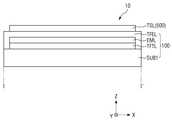
도 3a는 도 2의 선 I-I'을 따라 자른 단면도의 일 예이다.3A is an example of a cross-sectional view taken along line I-I' of FIG. 2 .
도 3a를 참조하면, 표시 장치(10)는 표시 유닛(100), 터치 감지 유닛(500), 및 표시 유닛(100)과 터치 감지 유닛(500)을 합착시키는 접착 부재(SEAL)를 포함할 수 있다.Referring to FIG. 3A , the
표시 유닛(100)은 제1 기판(SUB1), 박막 트랜지스터층(TFTL), 및 발광 소자층(EML)을 포함할 수 있다.The
제1 기판(SUB1)은 베이스 기판 또는 베이스 부재일 수 있고, 고분자 수지 등의 절연 물질로 이루어질 수 있다. 예를 들어, 제1 기판(SUB1)은 리지드(Rigid) 기판일 수 있다. 다른 예를 들어, 제1 기판(SUB1)은 벤딩(Bending), 폴딩(Folding), 롤링(Rolling) 등이 가능한 플렉서블(Flexible) 기판일 수 있다. 제1 기판(SUB1)이 플렉서블 기판인 경우, 폴리이미드(PI)로 형성될 수 있지만, 반드시 이에 한정되는 것은 아니다.The first substrate SUB1 may be a base substrate or a base member, and may be made of an insulating material such as a polymer resin. For example, the first substrate SUB1 may be a rigid substrate. As another example, the first substrate SUB1 may be a flexible substrate capable of bending, folding, rolling, or the like. When the first substrate SUB1 is a flexible substrate, it may be formed of polyimide PI, but is not limited thereto.
박막 트랜지스터층(TFTL)은 제1 기판(SUB1) 상에 배치될 수 있다. 박막 트랜지스터층(TFTL)은 화소들의 화소 회로를 구성하는 박막 트랜지스터들 뿐만 아니라, 스캔 라인들, 데이터 라인들, 전원 라인들, 스캔 제어 라인들, 표시 구동부(200)와 데이터 라인들을 연결하는 데이터 연결 라인들, 표시 구동부(200)와 표시 전극 패드들을 연결하는 패드 연결 라인들 등을 포함할 수 있다. 박막 트랜지스터들 각각은 게이트 전극, 반도체층, 소스 전극, 및 드레인 전극을 포함할 수 있다. 스캔 구동부(110)가 도 4와 같이 표시 유닛(100)의 비표시 영역(NDA)에 형성되는 경우, 스캔 구동부(110)는 박막 트랜지스터들을 포함할 수 있다.The thin film transistor layer TFTL may be disposed on the first substrate SUB1 . The thin film transistor layer TFTL includes not only thin film transistors constituting the pixel circuit of the pixels, but also scan lines, data lines, power lines, scan control lines, and data connections connecting the
박막 트랜지스터층(TFTL)은 표시 영역과 비표시 영역에 배치될 수 있다. 구체적으로, 박막 트랜지스터층(TFTL)의 화소들 각각의 박막 트랜지스터들, 스캔 라인들, 데이터 라인들, 및 전원 라인들은 표시 영역(DA)에 배치될 수 있다. 박막 트랜지스터층(TFTL)의 스캔 제어 라인들, 데이터 연결 라인들, 및 패드 연결 라인들은 비표시 영역에 배치될 수 있다.The thin film transistor layer TFTL may be disposed in the display area and the non-display area. In detail, thin film transistors, scan lines, data lines, and power lines of each of the pixels of the thin film transistor layer TFTL may be disposed in the display area DA. The scan control lines, data connection lines, and pad connection lines of the thin film transistor layer TFTL may be disposed in the non-display area.
발광 소자층(EML)은 박막 트랜지스터층(TFTL) 상에 배치될 수 있다. 발광 소자층(EML)은 제1 전극, 발광층, 및 제2 전극이 순차적으로 적층되어 광을 발광하는 화소들과 화소들을 정의하는 화소 정의막을 포함할 수 있다. 발광 소자층(EML)의 화소들은 표시 영역(DA)에 배치될 수 있다.The light emitting device layer EML may be disposed on the thin film transistor layer TFTL. The light emitting device layer EML may include pixels in which a first electrode, a light emitting layer, and a second electrode are sequentially stacked to emit light and a pixel defining layer defining the pixels. Pixels of the light emitting device layer EML may be disposed in the display area DA.
예를 들어, 발광층은 유기 물질을 포함하는 유기 발광층일 수 있다. 발광층은 정공 수송층(Hole Transporting Layer), 유기 발광층(Organic Light Emitting Layer), 및 전자 수송층(Electron Transporting Layer)을 포함할 수 있다. 제1 전극이 박막 트랜지스터층(TFTL)의 박막 트랜지스터를 통해 소정의 전압을 인가 받고, 제2 전극이 캐소드 전압을 인가 받으면, 정공과 전자가 각각 정공 수송층과 전자 수송층을 통해 유기 발광층으로 이동될 수 있고, 유기 발광층에서 서로 결합하여 발광할 수 있다. 예를 들어, 제1 전극은 애노드 전극이고, 제2 전극은 캐소드 전극일 수 있다.For example, the emission layer may be an organic emission layer including an organic material. The emission layer may include a hole transport layer, an organic light emitting layer, and an electron transport layer. When the first electrode receives a predetermined voltage through the thin film transistor of the thin film transistor layer (TFTL), and the second electrode receives a cathode voltage, holes and electrons move to the organic light emitting layer through the hole transport layer and the electron transport layer, respectively. and may be combined with each other in the organic light emitting layer to emit light. For example, the first electrode may be an anode electrode, and the second electrode may be a cathode electrode.
예를 들어, 에어 갭(VC)은 표시 유닛(100)과 터치 감지 유닛(500) 사이에 배치될 수 있다. 표시 유닛(100)과 터치 감지 유닛(500)이 접착 부재(SEAL)를 통해 합착되는 과정에서, 에어 갭(VC)이 표시 유닛(100)과 터치 감지 유닛(500) 사이에 형성될 수 있다.For example, the air gap VC may be disposed between the
다른 예를 들어, 충진층(미도시)은 표시 유닛(100)과 터치 감지 유닛(500) 사이에 배치될 수 있다. 표시 유닛(100)과 터치 감지 유닛(500)이 접착 부재(SEAL)를 통해 합착되는 과정에서, 충진층은 표시 유닛(100)과 터치 감지 유닛(500) 사이에 주입될 수 있다. 충진층은 에폭시 충전필름 또는 실리콘 충전 필름일 수 있으나, 반드시 이에 한정되는 것은 아니다.As another example, a filling layer (not shown) may be disposed between the
터치 감지 유닛(500)은 제2 기판(SUB2) 및 터치 센서층(TSL)을 포함할 수 있다.The
제2 기판(SUB2)은 베이스 기판 또는 베이스 부재일 수 있고, 고분자 수지 등의 절연 물질로 이루어질 수 있다. 예를 들어, 제2 기판(SUB2)은 리지드(Rigid) 기판일 수 있다. 제2 기판(SUB2)이 리지드 기판인 경우, 제2 기판(SUB2)은 글라스 재질 또는 투명 금속 재질을 포함할 수 있으나, 이에 한정되는 것은 아니다The second substrate SUB2 may be a base substrate or a base member, and may be made of an insulating material such as a polymer resin. For example, the second substrate SUB2 may be a rigid substrate. When the second substrate SUB2 is a rigid substrate, the second substrate SUB2 may include a glass material or a transparent metal material, but is not limited thereto.
터치 센서층(TSL)은 제2 기판(SUB2) 상에 배치될 수 있다. 터치 센서층(TSL)은 정전 용량 방식으로 사용자의 터치를 감지하기 위한 터치 전극들, 터치 전극 패드들, 및 터치 전극 패드들과 터치 전극들을 연결하는 터치 신호 라인들을 포함할 수 있다. 예를 들어, 터치 센서층(TSL)은 자기 정전 용량(Self-Capacitance) 방식 또는 상호 정전 용량(Mutual Capacitance) 방식으로 사용자의 터치를 감지할 수 있다.The touch sensor layer TSL may be disposed on the second substrate SUB2 . The touch sensor layer TSL may include touch electrodes for sensing a user's touch in a capacitive manner, touch electrode pads, and touch signal lines connecting the touch electrode pads and the touch electrodes. For example, the touch sensor layer TSL may sense a user's touch using a self-capacitance method or a mutual capacitance method.
터치 센서층(TSL)의 터치 전극들은 표시 유닛(100)의 표시 영역과 중첩하는 터치 센서 영역에 배치될 수 있다. 터치 센서층(TSL)의 터치 신호 라인들과 터치 전극 패드들은 표시 유닛(100)의 비표시 영역과 중첩하는 터치 주변 영역에 배치될 수 있다.The touch electrodes of the touch sensor layer TSL may be disposed in the touch sensor area overlapping the display area of the
예를 들어, 편광 필름과 커버 윈도우는 터치 센서층(TSL) 상에 추가로 배치될 수 있다. 편광 필름은 터치 센서층(TSL) 상에 배치될 수 있고, 커버 윈도우는 접착 부재에 의해 편광 필름 상에 배치될 수 있다.For example, the polarizing film and the cover window may be additionally disposed on the touch sensor layer TSL. The polarizing film may be disposed on the touch sensor layer TSL, and the cover window may be disposed on the polarizing film by an adhesive member.
접착 부재(SEAL)는 비표시 영역에서 제1 기판(SUB1)의 가장자리와 제2 기판(SUB2)의 가장자리 사이에 개재될 수 있다. 접착 부재(SEAL)는 비표시 영역에서 제1 기판(SUB1)과 제2 기판(SUB2)의 가장자리를 따라 배치되어 에어 갭(VC)을 밀봉할 수 있다. 제1 기판(SUB1)과 제2 기판(SUB2)은 접착 부재(SEAL)를 통해 상호 결합될 수 있다. 예를 들어, 접착 부재(SEAL)는 프릿(Frit) 접착층, 자외선 경화형 수지, 또는 열 경화형 수지일 수 있으나, 반드시 이에 한정되는 것은 아니다.The adhesive member SEAL may be interposed between an edge of the first substrate SUB1 and an edge of the second substrate SUB2 in the non-display area. The adhesive member SEAL may be disposed along edges of the first substrate SUB1 and the second substrate SUB2 in the non-display area to seal the air gap VC. The first substrate SUB1 and the second substrate SUB2 may be coupled to each other through the adhesive member SEAL. For example, the adhesive member SEAL may be a frit adhesive layer, an ultraviolet curable resin, or a thermosetting resin, but is not limited thereto.
도 3b는 도 2의 선 I-I'을 따라 자른 단면도의 다른 예이다. 도 3b의 표시 장치는 도 3a의 표시 장치에서 제2 기판(SUB2)을 생략하고, 표시 유닛(100)을 밀봉하는 봉지층(TFEL)을 더 포함할 수 있다. 이하에서는, 전술한 구성과 동일한 구성은 간략히 설명하거나 생략하기로 한다.FIG. 3B is another example of a cross-sectional view taken along line I-I' of FIG. 2 . The display device of FIG. 3B may omit the second substrate SUB2 from the display device of FIG. 3A and further include an encapsulation layer TFEL for sealing the
도 3b를 참조하면, 표시 장치(10)는 표시 유닛(100) 및 터치 감지 유닛(500)을 포함할 수 있다.Referring to FIG. 3B , the
표시 유닛(100)은 제1 기판(SUB1), 박막 트랜지스터층(TFTL), 발광 소자층(EML), 및 봉지층(TFEL)을 포함할 수 있다.The
제1 기판(SUB1)은 베이스 기판 또는 베이스 부재일 수 있고, 고분자 수지 등의 절연 물질로 이루어질 수 있다. 박막 트랜지스터층(TFTL)은 제1 기판(SUB1) 상에 배치될 수 있다. 발광 소자층(EML)은 박막 트랜지스터층(TFTL) 상에 배치될 수 있다.The first substrate SUB1 may be a base substrate or a base member, and may be made of an insulating material such as a polymer resin. The thin film transistor layer TFTL may be disposed on the first substrate SUB1 . The light emitting device layer EML may be disposed on the thin film transistor layer TFTL.
봉지층(TFEL)은 발광 소자층(EML) 상에 배치되어, 복수의 발광 소자를 덮을 수 있다. 봉지층(TFEL)은 복수의 발광 소자에 산소 또는 수분이 침투하는 것을 방지할 수 있다.The encapsulation layer TFEL may be disposed on the light emitting device layer EML to cover the plurality of light emitting devices. The encapsulation layer TFEL may prevent oxygen or moisture from penetrating into the plurality of light emitting devices.
터치 감지 유닛(500)은 봉지층(TFEL) 상에 배치될 수 있고, 터치 센서층(TSL)을 포함할 수 있다.The
터치 센서층(TSL)은 봉지층(TFEL) 상에 배치될 수 있다. 터치 센서층(TSL)은 정전 용량 방식으로 사용자의 터치를 감지하기 위한 터치 전극들, 터치 전극 패드들, 및 터치 전극 패드들과 터치 전극들을 연결하는 터치 신호 라인들을 포함할 수 있다. 예를 들어, 터치 센서층(TSL)은 자기 정전 용량(Self-Capacitance) 방식 또는 상호 정전 용량(Mutual Capacitance) 방식으로 사용자의 터치를 감지할 수 있다.The touch sensor layer TSL may be disposed on the encapsulation layer TFEL. The touch sensor layer TSL may include touch electrodes for sensing a user's touch in a capacitive manner, touch electrode pads, and touch signal lines connecting the touch electrode pads and the touch electrodes. For example, the touch sensor layer TSL may sense a user's touch using a self-capacitance method or a mutual capacitance method.
도 4는 도 3a에 도시된 표시 유닛을 나타내는 평면도이다.4 is a plan view illustrating the display unit shown in FIG. 3A .
도 4를 참조하면, 표시 유닛(100)은 영상을 표시하는 화소들이 마련된 표시 영역(DA)과, 표시 영역(DA)의 주변 영역인 비표시 영역(NDA)을 포함할 수 있다. 비표시 영역(NDA)은 표시 영역(DA)의 바깥쪽에서부터 표시 유닛(100)의 가장자리까지의 영역으로 정의될 수 있다.Referring to FIG. 4 , the
스캔 라인들(SL), 데이터 라인들(DL), 전원 라인(PL), 및 화소들(P)은 표시 영역(DA)에 배치될 수 있다. 스캔 라인들(SL)은 제1 방향(X축 방향)으로 나란하게 형성될 수 있고, 데이터 라인들(DL)은 제1 방향(X축 방향)과 교차하는 제2 방향(Y축 방향)으로 나란하게 형성될 수 있다. 전원 라인(PL)은 제2 방향(Y축 방향)으로 데이터 라인들(DL)과 나란하게 형성된 적어도 하나의 수직 라인, 및 적어도 하나의 수직 라인으로부터 제1 방향(X축 방향)으로 분지된 복수의 수평 라인들을 포함할 수 있다.The scan lines SL, the data lines DL, the power line PL, and the pixels P may be disposed in the display area DA. The scan lines SL may be formed in parallel in a first direction (X-axis direction), and the data lines DL may be formed in a second direction (Y-axis direction) crossing the first direction (X-axis direction). can be formed side by side. The power line PL includes at least one vertical line formed in parallel with the data lines DL in the second direction (Y-axis direction), and a plurality of branches branched from the at least one vertical line in the first direction (X-axis direction). may include horizontal lines of
화소들(P) 각각은 적어도 하나의 스캔 라인(SL), 데이터 라인(DL), 및 전원 라인(PL)에 접속될 수 있다. 화소들(P) 각각은 구동 트랜지스터와 적어도 하나의 스위칭 트랜지스터를 포함하는 박막 트랜지스터들, 발광 소자, 및 커패시터를 포함할 수 있다. 화소들(P) 각각은 스캔 라인(SL)으로부터 스캔 신호가 인가되는 경우 데이터 라인(DL)의 데이터 전압을 인가 받을 수 있고, 게이트 전극에 인가된 데이터 전압에 따라 발광 소자에 구동 전류를 공급함으로써 발광할 수 있다.Each of the pixels P may be connected to at least one scan line SL, a data line DL, and a power line PL. Each of the pixels P may include thin film transistors including a driving transistor and at least one switching transistor, a light emitting device, and a capacitor. Each of the pixels P may receive a data voltage of the data line DL when a scan signal is applied from the scan line SL, and supply a driving current to the light emitting device according to the data voltage applied to the gate electrode. can emit light.
표시 유닛(100)은 비표시 영역(NDA)에 배치된 스캔 구동부(110), 스캔 제어 라인(SCL), 데이터 연결 라인들(DLL), 및 패드 연결 라인들을 포함할 수 있다. 또한, 표시 구동부(200)는 표시 유닛(100)의 비표시 영역(NDA)에 배치될 수 있다.The
스캔 구동부(110)는 적어도 하나의 스캔 제어 라인(SCL)을 통해 표시 구동부(200)에 접속될 수 있다. 스캔 구동부(110)는 표시 구동부(200)의 스캔 제어 신호를 입력 받을 수 있다. 스캔 구동부(110)는 스캔 제어 신호에 따라 스캔 신호들을 생성하여 스캔 라인들(SL)에 공급할 수 있다.The
예를 들어, 스캔 구동부(110)가 표시 영역(DA)의 일 측 바깥쪽의 비표시 영역(NDA)에 형성될 수 있으나, 반드시 이에 한정되는 것은 아니다. 다른 예를 들어, 스캔 구동부(110)는 표시 영역(DA)의 양 측 바깥쪽의 비표시 영역(NDA)에 형성될 수 있다.For example, the
표시 구동부(200)는 표시 연결 라인들을 통해 표시 패드 영역(DPA)의 표시 전극 패드들(DP)에 접속되어 디지털 비디오 데이터와 타이밍 신호들을 입력 받을 수 있다. 표시 구동부(200)는 디지털 비디오 데이터를 아날로그 정극성/부극성 데이터 전압들로 변환하여 데이터 연결 라인(DLL)들을 통해 데이터 라인들(DL)에 공급할 수 있다. 또한, 표시 구동부(200)는 스캔 제어 라인(SCL)을 통해 스캔 구동부(110)를 제어하기 위한 스캔 제어 신호를 생성하여 공급할 수 있다. 스캔 구동부(110)의 스캔 신호들은 데이터 전압들이 공급될 화소들(P)을 선택할 수 있고, 선택된 화소들(P)은 데이터 전압을 공급 받을 수 있다. 표시 구동부(200)는 집적 회로(IC)로 형성되어 COG(Chip on Glass) 방식, COP(Chip on Plastic) 방식, 또는 초음파 접합 방식으로 제1 기판(SUB1) 상에 부착될 수 있다.The
도 5는 도 3a에 도시된 터치 감지 유닛의 일 예를 나타내는 평면도이다.5 is a plan view illustrating an example of the touch sensing unit shown in FIG. 3A .
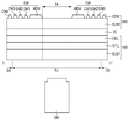
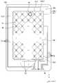
도 5를 참조하면, 터치 감지 유닛(500)은 사용자의 터치를 감지하기 위한 터치 센서 영역(TSA) 및 터치 센서 영역(TSA)의 주변에 배치되는 터치 주변 영역(TPA)을 포함할 수 있다. 터치 센서 영역(TSA)은 표시 유닛(100)의 표시 영역(DA)과 중첩될 수 있고, 터치 주변 영역(TPA)은 표시 유닛(100)의 비표시 영역(NDA)과 중첩될 수 있다.Referring to FIG. 5 , the
제1 터치 전극들(TE)과 제2 터치 전극들(RE)은 터치 센서 영역(TSA)에 배치될 수 있다. 제1 터치 전극들(TE)과 제2 터치 전극들(RE)은 소정의 간격으로 이격되게 배치될 수 있다. 예를 들어, 제1 터치 전극들(TE)은 제1 방향(X축 방향) 및 제2 방향(Y축 방향)으로 배열될 수 있다. 제2 터치 전극들(RE)은 제1 터치 전극들(TE)의 사이에 배치될 수 있고, 제1 방향(X축 방향)으로 연장되며 제2 방향(Y축 방향)으로 서로 이격될 수 있다. 제2 방향(Y축 방향)으로 인접한 제1 터치 전극들(TE)은 터치 섬 전극들에 의해 전기적으로 연결될 수 있다.The first touch electrodes TE and the second touch electrodes RE may be disposed in the touch sensor area TSA. The first touch electrodes TE and the second touch electrodes RE may be spaced apart from each other by a predetermined distance. For example, the first touch electrodes TE may be arranged in a first direction (X-axis direction) and a second direction (Y-axis direction). The second touch electrodes RE may be disposed between the first touch electrodes TE, may extend in a first direction (X-axis direction), and may be spaced apart from each other in a second direction (Y-axis direction). . The first touch electrodes TE adjacent in the second direction (Y-axis direction) may be electrically connected by touch island electrodes.
제1 터치 전극들(TE)과 제2 터치 전극들(RE)은 평면 상 마름모 형태 또는 삼각형 형태로 형성될 수 있다. 예를 들어, 터치 센서 영역(TSA)의 가장자리에 배치된 제1 터치 전극들(TE)과 제2 터치 전극들(RE)은 평면 상 삼각형 형태로 형성될 수 있고, 그 외 제1 터치 전극들(TE)과 제2 터치 전극들(RE)은 평면 상 마름모 형태로 형성될 수 있다. 또한, 표시 장치(10)의 영상을 시청할 때 제1 터치 전극들(TE)과 제2 터치 전극들(RE)에 의해 모아레(Moire) 현상이 발생하는 것을 방지하기 위해, 제1 터치 전극들(TE)과 제2 터치 전극들(RE)은 평면 상 올록볼록한 변들을 가질 수 있다. 다른 예를 들어, 터치 센서 영역(TSA)에 배치된 제1 터치 전극들(TE)과 제2 터치 전극들(RE)의 평면 형태는 도 5에 도시된 바에 한정되지 않는다.The first touch electrodes TE and the second touch electrodes RE may be formed in a rhombus shape or a triangular shape in plan view. For example, the first touch electrodes TE and the second touch electrodes RE disposed at the edge of the touch sensor area TSA may be formed in a triangular shape in plan view, and other first touch electrodes may be formed in a planar shape. The TE and the second touch electrodes RE may be formed in a planar rhombus shape. In addition, in order to prevent a moire phenomenon from occurring due to the first touch electrodes TE and the second touch electrodes RE when viewing an image of the
제2 방향(Y축 방향)으로 인접한 제1 터치 전극들(TE)은 연결 전극을 통해 터치 섬 전극에 전기적으로 연결될 수 있다. 예를 들어, 하나의 제1 터치 전극(TE)은 하나의 연결 전극을 통해 터치 섬 전극에 접속될 수 있고, 터치 섬 전극은 다른 하나의 연결 전극을 통해 다른 하나의 제1 터치 전극(TE)에 접속될 수 있다. 연결 전극은 제1 터치 전극들(TE)과 제2 터치 전극들(RE)과 다른 층에 배치됨으로써, 제1 터치 전극들(TE)과 제2 터치 전극들(RE)이 그들의 교차 영역에서 서로 단락되는 것을 방지할 수 있다. 따라서, 제2 방향(Y축 방향)으로 전기적으로 연결된 제1 터치 전극들(TE)과 제1 방향(X축 방향)으로 전기적으로 연결된 제2 터치 전극들(RE)은 서로 절연될 수 있다.The first touch electrodes TE adjacent in the second direction (the Y-axis direction) may be electrically connected to the touch island electrode through the connection electrode. For example, one first touch electrode TE may be connected to the touch island electrode through one connection electrode, and the touch island electrode may be connected to the other first touch electrode TE through another connection electrode. can be connected to The connection electrode is disposed on a layer different from the first touch electrodes TE and the second touch electrodes RE, so that the first touch electrodes TE and the second touch electrodes RE are connected to each other in their crossing regions. short circuit can be prevented. Accordingly, the first touch electrodes TE electrically connected in the second direction (Y-axis direction) and the second touch electrodes RE electrically connected in the first direction (X-axis direction) may be insulated from each other.
제1 내지 제4 터치 신호 라인들(TL1~TL4) 및 터치 전극 패드들(TP)은 터치 주변 영역(TPA)에 배치될 수 있다.The first to fourth touch signal lines TL1 to TL4 and the touch electrode pads TP may be disposed in the touch peripheral area TPA.
제1 터치 신호 라인들(TL1)의 일 단은 터치 센서 영역(TSA)의 제1 측에 배치된 제1 터치 전극들(TE)에 연결될 수 있다. 터치 센서 영역(TSA)의 제1 측은 터치 센서 영역(TSA)의 네 측들 중 터치 전극 패드들(TP)이 배치되는 터치 패드 영역(TDA)에 가장 인접한 측일 수 있다. 제1 터치 신호 라인들(TL1)의 타 단은 터치 패드 영역(TDA)의 일부의 터치 전극 패드들(TP)에 연결될 수 있다. 따라서, 제1 터치 신호 라인들(TL1)은 터치 센서 영역(TSA)의 제1 측에 배치된 제1 터치 전극들(TE)과 터치 패드 영역(TDA)의 일부의 터치 전극 패드들(TP)을 접속시킬 수 있다.One end of the first touch signal lines TL1 may be connected to the first touch electrodes TE disposed on the first side of the touch sensor area TSA. The first side of the touch sensor area TSA may be the side closest to the touch pad area TDA in which the touch electrode pads TP are disposed among the four sides of the touch sensor area TSA. The other end of the first touch signal lines TL1 may be connected to some touch electrode pads TP of the touch pad area TDA. Accordingly, the first touch signal lines TL1 include the first touch electrodes TE disposed on the first side of the touch sensor area TSA and some of the touch electrode pads TP of the touch pad area TDA. can be connected.
제2 터치 신호 라인들(TL2)의 일 단은 터치 센서 영역(TSA)의 제2 측에 배치된 제1 터치 전극들(TE)에 연결될 수 있다. 터치 센서 영역(TSA)의 제2 측은 터치 센서 영역(TSA)의 제1 측의 반대 측으로서, 터치 패드 영역(TDA)에서 가장 먼 측일 수 있다. 제2 터치 신호 라인들(TL2)의 타 단은 터치 패드 영역(TDA)의 다른 일부의 터치 전극 패드들(TP)에 연결될 수 있다. 예를 들어, 제2 터치 신호 라인들(TL2)은 터치 센서 영역(TSA)의 제1 측 바깥쪽과 제4 측 바깥쪽을 경유하여 터치 센서 영역(TSA)의 제2 측에 배치된 제1 터치 전극들(TE)과 연결될 수 있다. 따라서, 제2 터치 신호 라인들(TL2)은 터치 센서 영역(TSA)의 제2 측에 배치된 제1 터치 전극들(TE)과 터치 패드 영역(TDA)의 다른 일부의 터치 전극 패드들(TP)을 접속시킬 수 있다.One end of the second touch signal lines TL2 may be connected to the first touch electrodes TE disposed on the second side of the touch sensor area TSA. The second side of the touch sensor area TSA is opposite to the first side of the touch sensor area TSA and may be the farthest side from the touch pad area TDA. The other end of the second touch signal lines TL2 may be connected to other portions of the touch electrode pads TP of the touch pad area TDA. For example, the second touch signal lines TL2 are first disposed on the second side of the touch sensor area TSA via the first side outside and the fourth side outside of the touch sensor area TSA. It may be connected to the touch electrodes TE. Accordingly, the second touch signal lines TL2 include the first touch electrodes TE disposed on the second side of the touch sensor area TSA and the other portions of the touch electrode pads TP of the touch pad area TDA. ) can be connected.
제3 터치 신호 라인들(RL)의 일 단은 터치 센서 영역(TSA)의 제3 측에 배치된 제2 터치 전극들(RE)에 연결될 수 있다. 터치 센서 영역(TSA)의 제3 측은 터치 센서 영역(TSA)의 제4 측의 반대 측일 수 있다. 제3 터치 신호 라인들(RL)의 타 단은 터치 패드 영역(TDA)의 나머지 터치 전극 패드들(TP)에 연결될 수 있다. 따라서, 제3 터치 신호 라인들(RL)은 터치 센서 영역(TSA)의 제3 측에 배치된 제2 터치 전극들(RE)과 터치 패드 영역(TDA)의 나머지 터치 전극 패드들(TP)을 접속시킬 수 있다.One end of the third touch signal lines RL may be connected to the second touch electrodes RE disposed on the third side of the touch sensor area TSA. The third side of the touch sensor area TSA may be opposite to the fourth side of the touch sensor area TSA. The other end of the third touch signal lines RL may be connected to the remaining touch electrode pads TP of the touch pad area TDA. Accordingly, the third touch signal lines RL connect the second touch electrodes RE disposed on the third side of the touch sensor area TSA and the remaining touch electrode pads TP of the touch pad area TDA. can be connected.
터치 전극 패드들(TP)은 제2 기판(SUB2)의 일 측에 배치될 수 있다. 터치 전극 패드들(TP) 상에는 이방성 도전 필름을 이용하여 터치 회로 보드(410)가 부착될 수 있다. 이로 인해, 터치 전극 패드들(TP)은 터치 회로 보드(410)에 전기적으로 연결될 수 있다.The touch electrode pads TP may be disposed on one side of the second substrate SUB2 . The
제1 터치 전극들(TE)과 제2 터치 전극들(RE)은 상호 정전 용량 방식 또는 자기 정전 용량 방식으로 구동될 수 있다.The first touch electrodes TE and the second touch electrodes RE may be driven by a mutual capacitance method or a self-capacitance method.
예를 들어, 제1 터치 전극들(TE)과 제2 터치 전극들(RE)이 상호 정전 용량 방식으로 구동되는 경우, 제1 터치 신호 라인들(TL1)과 제2 터치 신호 라인들(TL2)은 제1 터치 전극들(TE)에 터치 구동 신호들을 공급할 수 있고, 상호 정전 용량들이 제1 터치 전극들(TE)과 제2 터치 전극들(RE)의 교차 영역들에 충전될 수 있다. 터치 구동부(400)는 제3 터치 신호 라인들(RL)을 통해 제1 및 제2 터치 전극들(TE, RE) 사이에 형성된 상호 정전 용량들의 차지 변화량을 측정할 수 있고, 상호 정전 용량들의 차지 변화량을 기초로 터치 입력 여부를 판단할 수 있다. 여기에서, 터치 구동 신호는 복수의 터치 구동 펄스를 갖는 신호일 수 있다.For example, when the first touch electrodes TE and the second touch electrodes RE are driven in a mutual capacitance method, the first touch signal lines TL1 and the second touch signal lines TL2 are may supply touch driving signals to the first touch electrodes TE, and mutual capacitances may be charged in intersection regions of the first touch electrodes TE and the second touch electrodes RE. The
다른 예를 들어, 제1 터치 전극들(TE)과 제2 터치 전극들(RE)이 자기 정전 용량 방식으로 구동되는 경우, 제1 내지 제3 터치 신호 라인들(TL1, TL2, RL)은 제1 터치 전극들(TE)과 제2 터치 전극들(RE) 모두에 터치 구동 신호들을 공급할 수 있고, 제1 및 제2 터치 전극들(TE, RE)의 자기 정전 용량이 충전될 수 있다. 터치 구동부(400)는 제1 내지 제3 터치 신호 라인들(TL1, TL2, RL)을 통해 자기 정전 용량들의 차지 변화량을 측정할 수 있고, 자기 정전 용량들의 차지 변화량을 기초로 터치 입력 여부를 판단할 수 있다.As another example, when the first touch electrodes TE and the second touch electrodes RE are driven in a self-capacitance method, the first to third touch signal lines TL1 , TL2 , and RL are Touch driving signals may be supplied to both the first touch electrodes TE and the second touch electrodes RE, and self-capacitance of the first and second touch electrodes TE and RE may be charged. The
이하에서는, 터치 구동부(400)가 제1 터치 전극들(TE)에 복수의 터치 구동 펄스들을 인가하고, 제2 터치 전극들(RE)에 연결된 제3 터치 신호 라인들(RL)을 통해 상호 정전 용량들의 차지 변화량을 측정하는 상호 정전 용량 방식으로 구동되는 것을 중심으로 설명한다. 이 경우, 제1 터치 전극들(TE)은 터치 구동 전극, 제2 터치 전극들(RE)은 터치 감지 전극, 제1 및 제2 터치 신호 라인들(TL1, TL2)은 터치 구동 라인, 제3 터치 신호 라인들(RL)은 터치 감지 라인으로 기능할 수 있다.Hereinafter, the
예를 들어, 제1 내지 제4 가드 라인(GL1, GL2, GL3, GL4), 제1 및 제2 접지 라인(GRL1, GRL2)은 터치 주변 영역(TPA)에 배치될 수 있다.For example, the first to fourth guard lines GL1 , GL2 , GL3 , and GL4 , and the first and second ground lines GRL1 and GRL2 may be disposed in the touch peripheral area TPA.
제1 가드 라인(GL1)은 제3 터치 신호 라인들(RL) 중 가장 외곽에 배치된 제3 터치 신호 라인의 바깥쪽에 배치될 수 있다. 제1 접지 라인(GRL1)은 제1 가드 라인(GL1)의 바깥쪽에 배치될 수 있다. 따라서, 제1 가드 라인(GL1)은 제3 터치 신호 라인들(RL) 중 가장 외곽에 배치된 제3 터치 신호 라인과 제1 접지 라인(GRL1) 사이에 배치됨으로써, 제3 터치 신호 라인(RL)이 제1 접지 라인(GRL1)의 전압 변화의 영향을 받는 것을 최소화할 수 있다. 제1 가드 라인(GL1)의 일 단과 제1 접지 라인(GRL1)의 일 단은 가장 우측에 배치된 터치 전극 패드들에 접속될 수 있다.The first guard line GL1 may be disposed outside the outermost third touch signal line among the third touch signal lines RL. The first ground line GRL1 may be disposed outside the first guard line GL1 . Accordingly, the first guard line GL1 is disposed between the outermost third touch signal line and the first ground line GRL1 among the third touch signal lines RL, and thus the third touch signal line RL ) may be minimized from being affected by a voltage change of the first ground line GRL1 . One end of the first guard line GL1 and one end of the first ground line GRL1 may be connected to rightmost touch electrode pads.
제2 가드 라인(GL2)은 제3 터치 신호 라인들(RL) 중 가장 안쪽에 배치된 제3 터치 신호 라인과 제1 터치 신호 라인들(TL1) 중 가장 우측에 배치된 제1 터치 신호 라인 사이에 배치될 수 있다. 따라서, 제2 가드 라인(GL2)은 제3 터치 신호 라인(RL)과 제1 터치 신호 라인(TL1)의 상호 영향을 최소화할 수 있다. 제2 가드 라인(GL2)의 일 단은 터치 전극 패드들에 접속될 수 있다.The second guard line GL2 is between the innermost third touch signal line among the third touch signal lines RL and the rightmost first touch signal line among the first touch signal lines TL1 . can be placed in Accordingly, the second guard line GL2 may minimize the mutual influence of the third touch signal line RL and the first touch signal line TL1 . One end of the second guard line GL2 may be connected to the touch electrode pads.
제3 가드 라인(GL3)은 제1 터치 신호 라인들(TL1) 중 가장 좌측에 배치된 제1 터치 신호 라인과 제2 터치 신호 라인들(TL2) 중 가장 안쪽에 배치된 제2 터치 신호 라인 사이에 배치될 수 있다. 따라서, 제3 가드 라인(GL3)은 제1 터치 신호 라인들(TL1)과 제2 터치 신호 라인들(TL2)의 상호 영향을 최소화할 수 있다. 제3 가드 라인(GL3)의 일 단은 터치 전극 패드들에 접속될 수 있다.The third guard line GL3 is between the leftmost first touch signal line among the first touch signal lines TL1 and the innermost second touch signal line among the second touch signal lines TL2 . can be placed in Accordingly, the third guard line GL3 may minimize the mutual influence of the first touch signal lines TL1 and the second touch signal lines TL2 . One end of the third guard line GL3 may be connected to touch electrode pads.
제4 가드 라인(GL4)은 제2 터치 신호 라인들(TL2) 중 가장 외곽에 배치된 제2 터치 신호 라인의 바깥쪽에 배치될 수 있다. 제2 접지 라인(GRL2)은 제4 가드 라인(GL4)의 바깥쪽에 배치될 수 있다. 따라서, 제4 가드 라인(GL4)은 제2 터치 신호 라인들(TL2) 중 가장 외곽에 배치된 제2 터치 신호 라인과 제2 접지 라인(GRL2) 사이에 배치되므로, 제2 터치 신호 라인(TL2)이 제2 접지 라인(GRL2)의 전압 변화의 영향을 받는 것을 최소화할 수 있다. 제4 가드 라인(GL4)의 일 단과 제2 접지 라인(GRL2)의 일 단은 가장 좌측에 배치된 터치 전극 패드들에 접속될 수 있다.The fourth guard line GL4 may be disposed outside the outermost second touch signal line among the second touch signal lines TL2 . The second ground line GRL2 may be disposed outside the fourth guard line GL4 . Accordingly, the fourth guard line GL4 is disposed between the outermost second touch signal line and the second ground line GRL2 among the second touch signal lines TL2 , and thus the second touch signal line TL2 ) may be minimized from being affected by the voltage change of the second ground line GRL2 . One end of the fourth guard line GL4 and one end of the second ground line GRL2 may be connected to the leftmost touch electrode pads.
제1 접지 라인(GRL1)은 터치 감지 유닛(500)의 우측에서 가장 외곽에 배치될 수 있고, 제2 접지 라인(GRL2)은 터치 감지 유닛(500)의 하측, 좌측, 및 상측에서 가장 외곽에 배치될 수 있다. 제1 접지 라인(GRL1)과 제2 접지 라인(GRL2)은 접지 전압을 인가 받을 수 있다. 따라서, 외부로부터 정전기가 인가되는 경우, 정전기는 제1 접지 라인(GRL1)과 제2 접지 라인(GRL2)으로 방전될 수 있다.The first ground line GRL1 may be disposed at the outermost side on the right side of the
예를 들어, 제1 터치 전극들(TE)과 제2 터치 전극들(RE)이 상호 정전 용량 방식으로 구동되는 경우, 제1 내지 제4 가드 라인(GL1, GL2, GL3, GL4)은 접지 전압을 인가 받을 수 있다.For example, when the first touch electrodes TE and the second touch electrodes RE are driven in a mutual capacitance method, the first to fourth guard lines GL1 , GL2 , GL3 , and GL4 are connected to the ground voltage can be authorized.
도 6은 도 5의 A1 영역을 확대한 평면도이고, 도 7은 도 6의 선 II-II'을 따라 자른 단면도이다.FIG. 6 is an enlarged plan view of area A1 of FIG. 5 , and FIG. 7 is a cross-sectional view taken along line II-II′ of FIG. 6 .
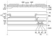
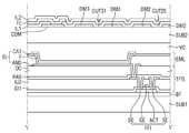
도 6 및 도 7을 참조하면, 제1 기판(SUB1)은 베이스 기판 또는 베이스 부재일 수 있고, 고분자 수지 등의 절연 물질로 이루어질 수 있다.6 and 7 , the first substrate SUB1 may be a base substrate or a base member, and may be made of an insulating material such as a polymer resin.
버퍼층(BF)은 제1 기판(SUB1) 상에 배치될 수 있다. 버퍼층(BF)은 공기 또는 수분의 침투를 방지할 수 있는 무기막으로 이루어질 수 있다. 예를 들어, 버퍼층(BF)은 교번하여 적층된 복수의 무기막을 포함할 수 있다. 버퍼층(BF)은 실리콘 나이트라이드층, 실리콘 옥시 나이트라이드층, 실리콘 옥사이드층, 티타늄옥사이드층, 및 알루미늄옥사이드층 중 적어도 하나의 무기막이 교번하여 적층된 다중막으로 이루어질 수 있으나, 반드시 이에 한정되는 것은 아니다.The buffer layer BF may be disposed on the first substrate SUB1 . The buffer layer BF may be formed of an inorganic layer capable of preventing penetration of air or moisture. For example, the buffer layer BF may include a plurality of inorganic layers alternately stacked. The buffer layer BF may be formed of a multilayer in which at least one inorganic film of a silicon nitride layer, a silicon oxynitride layer, a silicon oxide layer, a titanium oxide layer, and an aluminum oxide layer is alternately stacked, but is not necessarily limited thereto. no.
박막 트랜지스터층(TFTL)은 박막 트랜지스터(TFT), 게이트 절연막(GI), 층간 절연막(ILD), 보호층(PAS), 및 평탄화층(OC)을 포함할 수 있다.The thin film transistor layer TFTL may include a thin film transistor TFT, a gate insulating layer GI, an interlayer insulating layer ILD, a passivation layer PAS, and a planarization layer OC.
박막 트랜지스터(TFT)는 버퍼층(BF) 상에 배치될 수 있고, 복수의 화소 각각의 화소 회로를 구성할 수 있다. 예를 들어, 박막 트랜지스터(TFT)는 화소 회로의 구동 트랜지스터 또는 스위칭 트랜지스터일 수 있다. 박막 트랜지스터(TFT)는 반도체층(ACT), 게이트 전극(GE), 소스 전극(SE), 및 드레인 전극(DE)을 포함할 수 있다.The thin film transistor TFT may be disposed on the buffer layer BF, and may constitute a pixel circuit of each of the plurality of pixels. For example, the thin film transistor TFT may be a driving transistor or a switching transistor of a pixel circuit. The thin film transistor TFT may include a semiconductor layer ACT, a gate electrode GE, a source electrode SE, and a drain electrode DE.
반도체층(ACT)은 버퍼층(BF) 상에 마련될 수 있다. 반도체층(ACT)은 게이트 전극(GE), 소스 전극(SE), 및 드레인 전극(DE)과 중첩될 수 있다. 반도체층(ACT)은 소스 전극(SE) 및 드레인 전극(DE)과 직접 접촉될 수 있고, 게이트 절연막(GI)을 사이에 두고 게이트 전극(GE)과 마주할 수 있다.The semiconductor layer ACT may be provided on the buffer layer BF. The semiconductor layer ACT may overlap the gate electrode GE, the source electrode SE, and the drain electrode DE. The semiconductor layer ACT may directly contact the source electrode SE and the drain electrode DE, and may face the gate electrode GE with the gate insulating layer GI interposed therebetween.
게이트 전극(GE)은 게이트 절연막(GI)의 상부에 배치될 수 있다. 게이트 전극(GE)은 게이트 절연막(GI)을 사이에 두고, 반도체층(ACT)과 중첩될 수 있다.The gate electrode GE may be disposed on the gate insulating layer GI. The gate electrode GE may overlap the semiconductor layer ACT with the gate insulating layer GI interposed therebetween.
소스 전극(SE) 및 드레인 전극(DE)은 층간 절연막(ILD) 상에서 서로 이격되어 배치될 수 있다. 소스 전극(SE)은 게이트 절연막(GI) 및 층간 절연막(ILD)에 마련된 컨택홀을 통해 반도체층(ACT)의 일단과 접촉될 수 있다. 드레인 전극(DE)은 게이트 절연막(GI) 및 층간 절연막(ILD)에 마련된 컨택홀을 통해 반도체층(ACT)의 타단과 접촉될 수 있다. 드레인 전극(DE)은 보호층(PAS) 및 평탄화층(OC)에 마련된 컨택홀을 통해 발광 소자(EL)의 제1 전극(AND)과 접속될 수 있다.The source electrode SE and the drain electrode DE may be disposed to be spaced apart from each other on the interlayer insulating layer ILD. The source electrode SE may contact one end of the semiconductor layer ACT through a contact hole provided in the gate insulating layer GI and the interlayer insulating layer ILD. The drain electrode DE may contact the other end of the semiconductor layer ACT through a contact hole provided in the gate insulating layer GI and the interlayer insulating layer ILD. The drain electrode DE may be connected to the first electrode AND of the light emitting device EL through a contact hole provided in the passivation layer PAS and the planarization layer OC.
게이트 절연막(GI)은 반도체층(ACT)의 상부에 마련될 수 있다. 예를 들어, 게이트 절연막(GI)은 반도체층(ACT) 및 버퍼층(BF)의 상부에 배치될 수 있고, 반도체층(ACT)과 게이트 전극(GE)을 절연시킬 수 있다. 게이트 절연막(GI)은 소스 전극(SE)이 관통하는 컨택홀 및 드레인 전극(DE)이 관통하는 컨택홀을 포함할 수 있다.The gate insulating layer GI may be provided on the semiconductor layer ACT. For example, the gate insulating layer GI may be disposed on the semiconductor layer ACT and the buffer layer BF, and may insulate the semiconductor layer ACT and the gate electrode GE. The gate insulating layer GI may include a contact hole through which the source electrode SE passes and a contact hole through which the drain electrode DE passes.
층간 절연막(ILD)은 게이트 전극(GE)의 상부에 배치될 수 있다. 예를 들어, 층간 절연막(ILD)은 소스 전극(SE)이 관통하는 컨택홀 및 드레인 전극(DE)이 관통하는 컨택홀을 포함할 수 있다. 여기에서, 층간 절연막(ILD)의 컨택홀은 게이트 절연막(GI)의 컨택홀과 연결될 수 있다.The interlayer insulating layer ILD may be disposed on the gate electrode GE. For example, the interlayer insulating layer ILD may include a contact hole through which the source electrode SE passes and a contact hole through which the drain electrode DE passes. Here, the contact hole of the interlayer insulating layer ILD may be connected to the contact hole of the gate insulating layer GI.
보호층(PAS)은 박막 트랜지스터(TFT)의 상부에 마련되어, 박막 트랜지스터(TFT)를 보호할 수 있다. 예를 들어, 보호층(PAS)은 제1 전극(AND)이 관통하는 컨택홀을 포함할 수 있다.The passivation layer PAS may be provided on the thin film transistor TFT to protect the thin film transistor TFT. For example, the protective layer PAS may include a contact hole through which the first electrode AND passes.
다른 예를 들어, 보호층(PAS)은 표시 장치(10)에서 생략될 수 있다. 이 경우, 평탄화층(OC)은 박막 트랜지스터(TFT)의 상부에 마련되어, 박막 트랜지스터(TFT)의 상단을 평탄화시킬 수 있다.As another example, the passivation layer PAS may be omitted from the
평탄화층(OC)은 보호층(PAS)의 상부에 마련되어, 박막 트랜지스터(TFT)의 상단을 평탄화시킬 수 있다. 예를 들어, 평탄화층(OC)은 발광 소자(EL)의 제1 전극(AND)이 관통하는 컨택홀을 포함할 수 있다. 여기에서, 평탄화층(OC)의 컨택홀은 보호층(PAS)의 컨택홀과 연결될 수 있다.The planarization layer OC may be provided on the passivation layer PAS to planarize an upper end of the thin film transistor TFT. For example, the planarization layer OC may include a contact hole through which the first electrode AND of the light emitting device EL passes. Here, the contact hole of the planarization layer OC may be connected to the contact hole of the passivation layer PAS.
발광 소자(EL)는 박막 트랜지스터(TFT) 상에 마련될 수 있다. 발광 소자(EL)는 제1 전극(AND), 발광층(E), 및 제2 전극(CAT)을 포함할 수 있다.The light emitting element EL may be provided on the thin film transistor TFT. The light emitting device EL may include a first electrode AND, an emission layer E, and a second electrode CAT.
제1 전극(AND)은 평탄화층(OC)의 상부에 마련될 수 있다. 예를 들어, 제1 전극(AND)은 화소 정의막에 의해 정의되는 발광 영역 또는 개구 영역과 중첩되게 배치될 수 있다. 그리고, 제1 전극(AND)은 박막 트랜지스터(TFT)의 드레인 전극(DE)에 접속될 수 있다.The first electrode AND may be provided on the planarization layer OC. For example, the first electrode AND may be disposed to overlap the emission area or the opening area defined by the pixel defining layer. In addition, the first electrode AND may be connected to the drain electrode DE of the thin film transistor TFT.
발광층(E)은 제1 전극(AND)의 상부에 마련될 수 있다. 발광층(E)은 정공 주입층, 정공 수송층, 수광층, 전자 저지층, 전자 수송층, 전자 주입층 등을 포함할 수 있다. 예를 들어, 발광층(E)은 유기 물질로 이루어진 유기 발광층일 수 있으나, 반드시 이에 한정되는 것은 아니다. 발광층(E)이 유기 발광층에 해당하는 경우, 박막 트랜지스터(TFT)가 발광 소자(EL)의 제1 전극(AND)에 소정의 전압을 인가하고, 발광 소자(EL)의 제2 전극(CAT)이 공통 전압 또는 캐소드 전압을 수신하면, 정공과 전자 각각이 정공 수송층과 전자 수송층을 통해 유기 발광층(E)으로 이동할 수 있고, 정공과 전자가 유기 발광층(E)에서 서로 결합하여 광을 방출할 수 있다.The emission layer E may be provided on the first electrode AND. The emission layer (E) may include a hole injection layer, a hole transport layer, a light receiving layer, an electron blocking layer, an electron transport layer, an electron injection layer, and the like. For example, the emission layer E may be an organic emission layer made of an organic material, but is not limited thereto. When the light emitting layer E corresponds to the organic light emitting layer, the thin film transistor TFT applies a predetermined voltage to the first electrode AND of the light emitting element EL, and the second electrode CAT of the light emitting element EL Upon receiving this common voltage or cathode voltage, holes and electrons can each move to the organic light emitting layer (E) through the hole transport layer and electron transport layer, and the holes and electrons can combine with each other in the organic light emitting layer (E) to emit light. have.
제2 전극(CAT)은 발광층(E)의 상부에 마련될 수 있다. 예를 들어, 제2 전극(CAT)은 복수의 화소 별로 구분되지 않고 전체 화소에 공통되는 전극 형태로 구현될 수 있다. 제2 전극(CAT)은 발광 영역에서 발광층(E) 상에 배치될 수 있고, 발광 영역을 제외한 영역에서 화소 정의막 상에 배치될 수 있다.The second electrode CAT may be provided on the emission layer E. For example, the second electrode CAT may be implemented in the form of an electrode common to all pixels without being divided into a plurality of pixels. The second electrode CAT may be disposed on the emission layer E in the emission area, and may be disposed on the pixel defining layer in an area other than the emission area.
화소 정의막은 발광 영역 또는 개구 영역을 정의할 수 있다. 화소 정의막은 복수의 발광 소자(EL) 각각의 제1 전극(AND)을 이격 및 절연시킬 수 있다.The pixel defining layer may define an emission area or an opening area. The pixel defining layer may separate and insulate the first electrode AND of each of the plurality of light emitting devices EL.
제2 기판(SUB2)은 표시 유닛(100) 상에 배치될 수 있다. 제2 기판(SUB2)은 베이스 기판일 수 있고, 고분자 수지 등의 절연 물질로 이루어질 수 있다. 제2 기판(SUB2)은 복수의 발광 소자(EL)에 산소 또는 수분이 침투하는 것을 방지할 수 있다.The second substrate SUB2 may be disposed on the
터치 센서층(TSL)은 제2 기판(SUB2) 상에 배치될 수 있다. 터치 센서층(TSL)은 제1 및 제2 터치 전극들(TE, RE), 터치 섬 전극들(TEI), 연결 전극들(CE), 제1 및 제2 절연막(IL1, IL2)을 포함할 수 있다.The touch sensor layer TSL may be disposed on the second substrate SUB2 . The touch sensor layer TSL may include first and second touch electrodes TE and RE, touch island electrodes TEI, connection electrodes CE, and first and second insulating layers IL1 and IL2. can
연결 전극들(CE)은 제2 기판(SUB2) 상에 배치될 수 있다. 연결 전극들(CE) 각각은 제1 터치 전극(TE)과 터치 섬 전극(TEI)을 접속시킬 수 있다. 예를 들어, 연결 전극들(CE) 각각의 일 단은 제1 터치 전극(TE)에 접속될 수 있고, 타 단은 터치 섬 전극(TEI)에 접속될 수 있다.The connection electrodes CE may be disposed on the second substrate SUB2 . Each of the connection electrodes CE may connect the first touch electrode TE and the touch island electrode TEI. For example, one end of each of the connection electrodes CE may be connected to the first touch electrode TE, and the other end may be connected to the touch island electrode TEI.
연결 전극들(CE)은 불투명한 금속 도전층으로 형성될 수 있다. 예를 들어, 연결 전극들(CE)은 몰리브덴(Mo), 알루미늄(Al), 크롬(Cr), 금(Au), 티타늄(Ti), 니켈(Ni), 네오디뮴(Nd) 및 구리(Cu) 중 어느 하나 또는 이들의 합금으로 이루어진 단일층 또는 다중층으로 형성될 수 있다. 예를 들어, 연결 전극들(CE)은 화소(P)의 발광 영역과 중첩되지 않음으로써, 화소(P)의 개구율이 낮아지는 것을 방지할 수 있으나, 반드시 이에 한정되는 것은 아니다. 터치 섬 전극(TEI)은 연결 전극들(CE)의 길이를 최소화하기 위하여 제2 방향(Y축 방향)으로 인접한 제1 터치 전극들(TE) 사이에 배치될 수 있다.The connection electrodes CE may be formed of an opaque metal conductive layer. For example, the connection electrodes CE may include molybdenum (Mo), aluminum (Al), chromium (Cr), gold (Au), titanium (Ti), nickel (Ni), neodymium (Nd), and copper (Cu). It may be formed as a single layer or multiple layers made of any one or an alloy thereof. For example, since the connection electrodes CE do not overlap the emission area of the pixel P, a decrease in the aperture ratio of the pixel P may be prevented, but the present invention is not limited thereto. The touch island electrode TEI may be disposed between the first touch electrodes TE adjacent in the second direction (Y-axis direction) to minimize the length of the connection electrodes CE.
제1 절연막(IL1)은 연결 전극(CE) 및 제2 기판(SUB2)을 덮을 수 있다. 예를 들어, 제1 절연막(IL1)은 무기막, 예를 들어 실리콘 나이트라이드층, 실리콘 옥시 나이트라이드층, 실리콘 옥사이드층, 티타늄 옥사이드층, 또는 알루미늄 옥사이드층으로 이루어질 수 있다.The first insulating layer IL1 may cover the connection electrode CE and the second substrate SUB2 . For example, the first insulating layer IL1 may be formed of an inorganic layer, for example, a silicon nitride layer, a silicon oxynitride layer, a silicon oxide layer, a titanium oxide layer, or an aluminum oxide layer.
제1 터치 전극들(TE), 터치 섬 전극들(TEI), 및 제2 터치 전극들(RE)은 제1 절연막(IL1) 상에 배치될 수 있다. 제1 터치 전극(TE)은 제1 절연막(IL1)을 관통하는 제1 컨택홀(CNT1)을 통해 연결 전극(CE)에 접속될 수 있고, 연결 전극(CE)은 제1 절연막(IL1)을 관통하는 제2 컨택홀(CNT2)을 통해 터치 섬 전극(TEI)에 접속될 수 있다. 따라서, 연결 전극(CE)은 제1 터치 전극(TE)과 터치 섬 전극(TEI)을 전기적으로 연결시킬 수 있다. 따라서, 제2 터치 전극들(RE)을 사이에 두고 제2 방향(Y축 방향)으로 서로 이격된 제1 터치 전극들(TE)은 연결 전극(CE) 및 터치 섬 전극(TEI)을 통해 전기적으로 연결될 수 있다.The first touch electrodes TE, the touch island electrodes TEI, and the second touch electrodes RE may be disposed on the first insulating layer IL1. The first touch electrode TE may be connected to the connection electrode CE through a first contact hole CNT1 penetrating the first insulating layer IL1 , and the connection electrode CE connects the first insulating layer IL1 to It may be connected to the touch island electrode TEI through the penetrating second contact hole CNT2 . Accordingly, the connection electrode CE may electrically connect the first touch electrode TE and the touch island electrode TEI. Accordingly, the first touch electrodes TE spaced apart from each other in the second direction (Y-axis direction) with the second touch electrodes RE interposed therebetween are electrically connected through the connection electrode CE and the touch island electrode TEI. can be connected to
예를 들어, 제1 터치 전극들(TE), 터치 섬 전극들(TEI), 및 제2 터치 전극들(RE)은 광을 투과시킬 수 있는 ITO, IZO와 같은 투명 금속 산화물(TCO)로 형성될 수 있다. 따라서, 제1 터치 전극들(TE), 터치 섬 전극들(TEI), 및 제2 터치 전극들(RE)은 화소들(P)과 중첩되더라도 화소(P)의 개구율을 저하시키지 않을 수 있다.For example, the first touch electrodes TE, the touch island electrodes TEI, and the second touch electrodes RE are formed of a transparent metal oxide (TCO) such as ITO or IZO that can transmit light. can be Accordingly, even if the first touch electrodes TE, the touch island electrodes TEI, and the second touch electrodes RE overlap the pixels P, the aperture ratio of the pixel P may not decrease.
제2 절연막(IL2)은 제1 터치 전극들(TE), 터치 섬 전극들(TEI), 및 제2 터치 전극들(RE)을 덮을 수 있다. 예를 들어, 제2 절연막(IL2)은 무기막, 예를 들어 실리콘 나이트라이드층, 실리콘 옥시 나이트라이드층, 실리콘 옥사이드층, 티타늄 옥사이드층, 또는 알루미늄 옥사이드층으로 형성될 수 있다.The second insulating layer IL2 may cover the first touch electrodes TE, the touch island electrodes TEI, and the second touch electrodes RE. For example, the second insulating layer IL2 may be formed of an inorganic layer, for example, a silicon nitride layer, a silicon oxynitride layer, a silicon oxide layer, a titanium oxide layer, or an aluminum oxide layer.
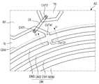
도 8은 도 5의 A2 영역의 일 예를 나타내는 확대 평면도이고, 도 9는 도 8의 선 III-III'을 따라 자른 단면도의 일 예이다. 도 10은 도 8에 도시된 더미부 및 컨택 더미부를 나타내는 도면이고, 도 11은 도 8의 A3 영역을 확대한 평면도이며, 도 12는 도 11의 선 IV-IV'을 따라 자른 단면도이다.FIG. 8 is an enlarged plan view illustrating an example of area A2 of FIG. 5 , and FIG. 9 is an example of a cross-sectional view taken along line III-III′ of FIG. 8 . FIG. 10 is a view showing the dummy part and the contact dummy part shown in FIG. 8 , FIG. 11 is an enlarged plan view of area A3 of FIG. 8 , and FIG. 12 is a cross-sectional view taken along line IV-IV' of FIG. 11 .
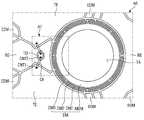
도 8 내지 도 12를 참조하면, 표시 유닛(100)은 표시 영역(DA) 및 투과부(TU)를 포함할 수 있다.8 to 12 , the
표시 영역(DA)은 복수의 화소(P)를 포함할 수 있다. 화소들(P) 각각은 적어도 하나의 스캔 라인(SL), 데이터 라인(DL), 및 전원 라인(PL)에 접속될 수 있다. 화소들(P) 각각은 구동 트랜지스터와 적어도 하나의 스위칭 트랜지스터를 포함하는 박막 트랜지스터들, 발광 소자, 및 커패시터를 포함할 수 있다. 화소들(P) 각각은 스캔 라인(SL)으로부터 스캔 신호가 인가되는 경우 데이터 라인(DL)의 데이터 전압을 인가 받을 수 있고, 게이트 전극에 인가된 데이터 전압에 따라 발광 소자에 구동 전류를 공급함으로써 발광할 수 있다.The display area DA may include a plurality of pixels P. Each of the pixels P may be connected to at least one scan line SL, a data line DL, and a power line PL. Each of the pixels P may include thin film transistors including a driving transistor and at least one switching transistor, a light emitting device, and a capacitor. Each of the pixels P may receive a data voltage of the data line DL when a scan signal is applied from the scan line SL, and supply a driving current to the light emitting device according to the data voltage applied to the gate electrode. can emit light.
투과부(TU)는 평면 상에서 표시 영역(DA)에 의해 둘러싸일 수 있다. 투과부(TU)는 투명한 물질을 포함할 수 있고, 센서 모듈(SM)에 출입하는 광을 투과시킬 수 있다.The transmission part TU may be surrounded by the display area DA on a plane. The transmission unit TU may include a transparent material and transmit light entering and exiting the sensor module SM.
터치 감지 유닛(500)의 터치 센서층(TSL)은 제1 터치 전극들(TE), 제2 터치 전극들(RE), 전극 더미부(EDM), 투과 영역(TA), 더미부(DM), 및 컨택 더미부(CDM)를 포함할 수 있다.The touch sensor layer TSL of the
전극 더미부(EDM)는 제1 터치 전극들(TE) 및 제2 터치 전극들(RE) 사이에 배치되어, 제1 터치 전극들(TE)과 제2 터치 전극들(RE)의 단락을 방지하고, 터치 센서층(TSL)의 기본 정전 용량을 감소시킬 수 있다. 예를 들어, 제1 터치 전극들(TE)과 제2 터치 전극들(RE)이 최소의 거리만큼 이격되어 직접 마주하는 경우, 기본 정전 용량의 크기가 증가하고 터치 민감도가 저하될 수 있다. 전극 더미부(EDM)는 제1 터치 전극들(TE) 및 제2 터치 전극들(RE)과 다른 층에 배치될 수 있으나, 제1 터치 전극들(TE) 및 제2 터치 전극들(RE)과 제3 방향(Z축 방향)으로 중첩되지 않을 수 있다. 따라서, 전극 더미부(EDM)는 제1 터치 전극들(TE)과 제2 터치 전극들(RE) 사이의 이격 거리를 제어할 수 있고, 터치 센서층(TSL)의 기본 정전 용량을 조절하여 상호 정전 용량들의 차지 변화량을 정밀하게 감지할 수 있다. 전극 더미부(EDM)는 제1 터치 전극들(TE) 및 제2 터치 전극들(RE) 사이에 배치됨으로써, 터치 감지 유닛(500)의 터치 감도를 향상시킬 수 있다.The electrode dummy part EDM is disposed between the first touch electrodes TE and the second touch electrodes RE to prevent a short circuit between the first touch electrodes TE and the second touch electrodes RE. and the basic capacitance of the touch sensor layer TSL may be reduced. For example, when the first touch electrodes TE and the second touch electrodes RE are spaced apart from each other by a minimum distance to directly face each other, the size of the basic capacitance may increase and touch sensitivity may decrease. The electrode dummy part EDM may be disposed on a different layer from the first touch electrodes TE and the second touch electrodes RE, but the first touch electrodes TE and the second touch electrodes RE and may not overlap in the third direction (Z-axis direction). Accordingly, the electrode dummy part EDM can control the separation distance between the first touch electrodes TE and the second touch electrodes RE, and adjust the basic capacitance of the touch sensor layer TSL to mutually It is possible to precisely detect a charge change amount of the capacitances. The electrode dummy part EDM is disposed between the first touch electrodes TE and the second touch electrodes RE, and thus the touch sensitivity of the
예를 들어, 제1 터치 전극들(TE)과 제2 터치 전극들(RE)이 평면 상 마름모 형태를 갖는 경우, 전극 더미부(EDM)는 제1 터치 전극들(TE)과 제2 터치 전극들(RE) 사이에 배치될 수 있다. 이 경우, 전극 더미부(EDM)는 제1 터치 전극들(TE)과 제2 터치 전극들(RE) 사이에서 제1 방향(X축 방향)과 제2 방향(Y축 방향) 사이의 제3 방향 또는 제3 방향의 반대 방향으로 연장되거나, 제1 방향(X축 방향)의 반대 방향과 제2 방향(Y축 방향) 사이의 제4 방향 또는 제4 방향의 반대 방향으로 연장될 수 있다. 전극 더미부(EDM)는 제2 방향(Y축 방향)으로 인접한 제1 터치 전극들(TE) 사이에서 제거될 수 있다. 또는, 전극 더미부(EDM)는 제1 터치 전극들(TE) 중 터치 섬 전극(TEI)과 인접한 영역에서 제거될 수 있다. 따라서, 제1 방향(X축 방향)으로 인접한 제1 터치 전극들(TE)은 전극 더미부(EDM)의 영역 만큼 이격되며 서로 절연될 수 있다. 또한, 제2 방향(Y축 방향)으로 인접한 제2 터치 전극들(RE)은 전극 더미부(EDM)의 영역 만큼 이격되며 서로 절연될 수 있다.For example, when the first touch electrodes TE and the second touch electrodes RE have a rhombus shape on a plane, the electrode dummy part EDM may include the first touch electrodes TE and the second touch electrodes. It may be disposed between the REs. In this case, the electrode dummy part EDM is formed in a third direction between the first touch electrodes TE and the second touch electrodes RE in the first direction (X-axis direction) and in the second direction (Y-axis direction). It may extend in a direction opposite to the direction or the third direction, or may extend in a fourth direction or a direction opposite to the fourth direction between a direction opposite to the first direction (X-axis direction) and a second direction (Y-axis direction). The electrode dummy part EDM may be removed between the first touch electrodes TE adjacent in the second direction (Y-axis direction). Alternatively, the electrode dummy portion EDM may be removed from a region adjacent to the touch island electrode TEI among the first touch electrodes TE. Accordingly, the first touch electrodes TE adjacent in the first direction (X-axis direction) may be spaced apart by an area of the electrode dummy part EDM and insulated from each other. In addition, the second touch electrodes RE adjacent in the second direction (Y-axis direction) may be spaced apart by the area of the electrode dummy part EDM and insulated from each other.
예를 들어, 전극 더미부(EDM)는 플로팅되어, 소정의 전압을 인가 받지 않을 수 있으나, 반드시 이에 한정되는 것은 아니다. 다른 예를 들어, 전극 더미부(EDM)는 터치 센서층(TSL)의 정전 용량에 영향을 주지 않을 정도의 소정의 전압을 인가 받을 수 있다. 따라서, 터치 센서 유닛(500)은 전극 더미부(EDM)를 포함함으로써, 제1 및 제2 터치 전극들(TE, RE) 사이의 상호 정전 용량들의 차지 변화량을 민감하게 측정할 수 있다.For example, the electrode dummy part EDM may float and may not receive a predetermined voltage, but is not limited thereto. As another example, the electrode dummy part EDM may be applied with a predetermined voltage that does not affect the capacitance of the touch sensor layer TSL. Accordingly, by including the electrode dummy part EDM, the
전극 더미부(EDM)는 제2 기판(SUB2) 상에 배치되어 제1 절연막(IL1)에 의해 덮일 수 있다. 전극 더미부(EDM)는 제1 터치 전극들(TE) 및 제2 터치 전극들(RE)과 다른 층에 배치될 수 있으나, 제1 터치 전극들(TE) 및 제2 터치 전극들(RE)과 제3 방향(Z축 방향)으로 중첩되지 않을 수 있다. 전극 더미부(EDM)는 불투명한 금속 도전층으로 형성될 수 있으나, 반드시 이에 한정되는 것은 아니다.The electrode dummy part EDM may be disposed on the second substrate SUB2 and covered by the first insulating layer IL1 . The electrode dummy part EDM may be disposed on a different layer from the first touch electrodes TE and the second touch electrodes RE, but the first touch electrodes TE and the second touch electrodes RE and may not overlap in the third direction (Z-axis direction). The electrode dummy part EDM may be formed of an opaque metal conductive layer, but is not limited thereto.
투과 영역(TA)은 터치 센서 영역(TSA)에서 제1 터치 전극들(TE) 중 적어도 하나의 제1 터치 전극, 및 제2 터치 전극들(RE) 중 적어도 하나의 제2 터치 전극에 의해 둘러싸일 수 있다. 예를 들어, 투과 영역(TA)은 표시 유닛(100)의 투과부(TU)와 중첩될 수 있다.The transmission area TA is surrounded by at least one first touch electrode among the first touch electrodes TE and at least one second touch electrode among the second touch electrodes RE in the touch sensor area TSA. can be For example, the transmissive area TA may overlap the transmissive part TU of the
예를 들어, 투과 영역(TA)은 평면 상에서 원형의 형상을 가질 수 있으나, 반드시 이에 한정되는 것은 아니다. 다른 예를 들어, 투과 영역(TA)은 다각 기둥 또는 비정질 기둥의 형상일 수 있다. 이 경우, 투과 영역(TA)은 평면 상 사각형을 포함한 다각 형상이거나 비정형 형상을 가질 수 있다.For example, the transmission area TA may have a circular shape on a plane, but is not limited thereto. As another example, the transmission area TA may have a shape of a polygonal pillar or an amorphous pillar. In this case, the transmission area TA may have a polygonal shape including a quadrangle on a plane or an irregular shape.
표시 유닛(100)은 투과 영역(TA)에 대응되게 배치되는 카메라 모듈 또는 센서 모듈(SM)을 포함할 수 있다. 카메라 모듈 또는 센서 모듈(SM)은 표시 유닛(100)의 하측(또는 표시 유닛(100)의 배면)에 배치될 수 있다. 예를 들어, 센서 모듈(SM)은 조도 센서, 근접 센서, 적외선 센서, 초음파 센서 중 적어도 하나를 포함할 수 있다. 따라서, 표시 장치(10)는 표시 영역(DA)에 의해 둘러싸이는 투과부(TU), 투과부(TU)와 중첩되는 투과 영역(TA), 및 투과 영역(TA)과 중첩되는 카메라 모듈 또는 센서 모듈(SM)을 포함함으로써, 비표시 영역의 일측에 카메라 모듈 또는 센서 모듈이 배치되는 다른 표시 장치에 비하여 데드 스페이스(Dead Space)를 최소화할 수 있다. 또한, 표시 장치(10)는 투과 영역(TA)과 중첩되는 카메라 모듈 또는 센서 모듈(SM)을 포함함으로써, 박형의 표시 장치를 구현할 수 있다.The
더미부(DM)는 표시 유닛(100)의 투과부(TU)와 중첩되어 투과 영역(TA)을 둘러싸고, 제1 및 제2 터치 전극들(TE, RE)과 절연될 수 있다. 더미부(DM)와 중첩되는 표시 유닛(100)의 투과부(TU)는 비표시 영역에 해당할 수 있다. 더미부(DM)는 투과 영역(TA)을 통한 외부 노이즈를 제거할 수 있고, 제1 터치 전극들(TE) 및 제2 터치 전극들(RE) 사이의 커플링(Coupling)을 방지할 수 있다. 예를 들어, 카메라 모듈 또는 센서 모듈(SM)에 의하여 송수신되는 신호가 투과 영역(TA)을 통하여 전송될 수 있고, 해당 신호는 제1 터치 전극들(TE) 또는 제2 터치 전극들(RE) 사이의 커패시턴스에 영향을 줄 수 있다. 투과 영역(TA)을 통하여 전송되는 신호는 터치 센서층(TSL)에 노이즈를 유발할 수 있다. 따라서, 더미부(DM)는 투과 영역(TA)을 둘러쌈으로써, 제1 터치 전극들(TE) 및 제2 터치 전극들(RE)을 투과 영역(TA)로부터 이격시킬 수 있다.The dummy part DM may overlap the transmissive part TU of the
더미부(DM)는 전극 더미부(EDM)와 같이 터치 센서층(TSL)의 기본 정전 용량을 제어할 수 있고, 제1 터치 전극들(TE) 및 제2 터치 전극들(RE) 사이의 커플링(Coupling)을 방지할 수 있다. 예를 들어, 더미부(DM)는 제1 터치 전극들(TE) 및 제2 터치 전극들(RE)과 다른 층에 배치될 수 있으나, 제1 터치 전극들(TE) 및 제2 터치 전극들(RE)과 제3 방향(Z축 방향)으로 중첩되지 않을 수 있다. 따라서, 더미부(DM)는 터치 센서층(TSL)의 기본 정전 용량을 조절할 수 있고, 터치 감지 유닛(500)의 터치 감도를 향상시킬 수 있다.The dummy part DM may control the basic capacitance of the touch sensor layer TSL like the electrode dummy part EDM, and a couple between the first touch electrodes TE and the second touch electrodes RE. Coupling can be prevented. For example, the dummy part DM may be disposed on a different layer from the first touch electrodes TE and the second touch electrodes RE, but the first touch electrodes TE and the second touch electrodes (RE) and the third direction (Z-axis direction) may not overlap. Accordingly, the dummy part DM may adjust the basic capacitance of the touch sensor layer TSL and may improve the touch sensitivity of the
예를 들어, 더미부(DM)는 플로팅되어, 소정의 전압을 인가 받지 않을 수 있으나, 반드시 이에 한정되는 것은 아니다. 다른 예를 들어, 더미부(DM)는 터치 센서층(TSL)의 정전 용량에 영향을 주지 않을 정도의 소정의 전압을 인가 받을 수 있다. 따라서, 터치 센서 유닛(500)은 더미부(DM)를 포함함으로써, 제1 및 제2 터치 전극들(TE, RE) 사이의 상호 정전 용량들의 차지 변화량을 민감하게 측정할 수 있다.For example, the dummy part DM may float and may not receive a predetermined voltage, but is not limited thereto. As another example, the dummy part DM may receive a predetermined voltage that does not affect the capacitance of the touch sensor layer TSL. Accordingly, by including the dummy part DM, the
더미부(DM)는 투과 영역(TA)을 직접 둘러싸는 메인 더미(MDM), 메인 더미(MDM)를 둘러싸는 적어도 하나의 서브 더미를 포함할 수 있다. 예를 들어, 더미부(DM)는 메인 더미(MDM) 및 제1 내지 제3 서브 더미(DM1, DM2, DM3)를 포함할 수 있으나, 서브 더미의 수는 반드시 이에 한정되는 것이 아니다.The dummy part DM may include a main dummy MDM directly surrounding the transmission area TA and at least one sub dummy surrounding the main dummy MDM. For example, the dummy part DM may include the main dummy MDM and the first to third sub dummy DM1 , DM2 , and DM3 , but the number of the sub dummy is not necessarily limited thereto.
메인 더미(MDM)는 투과 영역(TA)을 직접 둘러쌈으로써, 투과 영역(TA)을 통한 외부 노이즈를 차단할 수 있다. 예를 들어, 메인 더미(MDM)는 평면 상 소정의 두께를 갖는 원형의 형상을 가질 수 있다. 메인 더미(MDM)의 평면 상 두께는 제1 내지 제3 서브 더미(DM1, DM2, DM3)의 평면 상 두께의 합보다 클 수 있다. 따라서, 메인 더미(MDM)는 소정의 두께를 가짐으로써, 투과 영역(TA)을 통한 외부 노이즈를 효율적으로 제거할 수 있다.The main dummy MDM may directly surround the transmission area TA, thereby blocking external noise through the transmission area TA. For example, the main dummy MDM may have a circular shape having a predetermined thickness on a plane. A thickness on a plane of the main dummy MDM may be greater than a sum of thicknesses on a plane of the first to third sub dummy DM1 , DM2 , and DM3 . Accordingly, since the main dummy MDM has a predetermined thickness, external noise through the transmission area TA may be efficiently removed.
제1 서브 더미(DM1)는 메인 더미(MDM)를 둘러쌀 수 있고, 제2 서브 더미(DM2)는 제1 서브 더미(DM2)를 둘러쌀 수 있으며, 제3 서브 더미(DM3)는 제2 서브 더미(DM2)를 둘러쌀 수 있다. 제3 서브 더미(DM3)는 더미부(DM)의 최외곽에 배치된 서브 더미일 수 있다. 제1 터치 전극들(TE) 중 적어도 하나의 제1 터치 전극, 및 제2 터치 전극들(RE) 중 적어도 하나의 제2 터치 전극은 투과 영역(TA) 및 더미부(DM)의 위치에 따라 일부가 제거될 수 있다. 일부가 제거된 제1 터치 전극 및 제2 터치 전극은 직접 마주할 수 있다. 또한, 제3 서브 더미(DM3)는 일부가 제거된 제1 터치 전극 및 제2 터치 전극과 평면 상에서 직접 마주할 수 있다.The first sub-dummy DM1 may surround the main dummy MDM, the second sub-dummy DM2 may surround the first sub-dummy DM2 , and the third sub-dummy DM3 may surround the second The sub dummy DM2 may be surrounded. The third sub-dummy DM3 may be a sub-dummy disposed at the outermost portion of the dummy part DM. At least one first touch electrode of the first touch electrodes TE and at least one second touch electrode of the second touch electrodes RE may be formed according to positions of the transmission area TA and the dummy part DM. Some may be removed. The partially removed first and second touch electrodes may directly face each other. In addition, the third sub-dummy DM3 may directly face the first and second touch electrodes from which portions have been removed on a plane.
제1 서브 더미(DM1)는 투과 영역(TA)의 중심(CP)을 지나 제1 방향(X축 방향)으로 연장되는 제1 축(Axis1)에 중첩되는 제1-1 커팅부(CUT11) 및 제1-2 커팅부(CUT12)를 포함할 수 있다. 제1 서브 더미(DM1)는 투과 영역(TA)의 중심(CP)을 지나 제2 방향(Y축 방향)으로 연장되는 제2 축(Axis2)에 중첩되는 제1-3 커팅부(CUT13) 및 제1-4 커팅부(CUT1-4)를 포함할 수 있다. 제1 서브 더미(DM1)는 제1-1 커팅부(CUT11), 제1-2 커팅부(CUT12), 제1-3 커팅부(CUT13), 및 제1-4 커팅부(CUT1-4)를 포함함으로써, 제1 서브 더미(DM1)를 통해 커플링이 발생되는 것을 방지할 수 있다.The first sub-dummy DM1 includes a 1-1 cutting part CUT11 overlapping the first axis Axis1 extending in the first direction (X-axis direction) through the center CP of the transmission area TA; A 1-2 cutting part CUT12 may be included. The first sub-dummy DM1 includes the first 1-3 cutting parts CUT13 overlapping the second axis Axis2 extending in the second direction (Y-axis direction) through the center CP of the transmission area TA; The 1-4 cutting parts CUT1-4 may be included. The first sub-dummy DM1 includes a 1-1 cutting unit CUT11, a 1-2 cutting unit CUT12, a 1-3 cutting unit CUT13, and a 1-4 cutting unit CUT1-4. By including , it is possible to prevent coupling from occurring through the first sub-dummy DM1 .
제2 서브 더미(DM2)는 투과 영역(TA)의 중심(CP)을 지나 제1 방향(X축 방향)과 제2 방향(Y축 방향) 사이의 제3 방향으로 연장되는 제3 축(Axis3)에 중첩되는 제2-1 커팅부(CUT21) 및 제2-2 커팅부(CUT22)를 포함할 수 있다. 제2 서브 더미(DM2)는 투과 영역(TA)의 중심(CP)을 지나 제1 방향(X축 방향)의 반대 방향과 제2 방향(Y축 방향) 사이의 제4 방향으로 연장되는 제4 축(Axis4)에 중첩되는 제2-3 커팅부(CUT23) 및 제2-4 커팅부(CUT2-4)를 포함할 수 있다. 제2 서브 더미(DM2)는 제2-1 커팅부(CUT21), 제2-2 커팅부(CUT22), 제2-3 커팅부(CUT23), 및 제2-4 커팅부(CUT2-4)를 포함함으로써, 제2 서브 더미(DM2)를 통해 커플링이 발생되는 것을 방지할 수 있다.The second sub-dummy DM2 has a third axis Axis3 extending in a third direction between the first direction (X-axis direction) and the second direction (Y-axis direction) through the center CP of the transmission area TA. ) may include a 2-1 th cutting part CUT21 and a 2-2 th cutting part CUT22 overlapping each other. The second sub-dummy DM2 passes through the center CP of the transmission area TA and extends in a fourth direction between a direction opposite to the first direction (X-axis direction) and a second direction (Y-axis direction). A 2-3 th cutting part CUT23 and a 2-4 th cutting part CUT2-4 overlapping the axis Axis4 may be included. The second sub-dummy DM2 includes a 2-1 cutting part CUT21, a 2-2 cutting part CUT22, a 2-3 cutting part CUT23, and a 2-4 cutting part CUT2-4. By including , it is possible to prevent coupling from occurring through the second sub-dummy DM2 .
제3 서브 더미(DM3)는 제1 및 제2 터치 전극들(TE, RE) 중 직접 인접한 제1 및 제2 터치 전극(TE, RE) 사이의 간극에 대응되는 제3-1 커팅부(CUT31)를 포함할 수 있다. 제3-1 커팅부(CUT31)는 제3 서브 더미(DM3) 중 직접 마주하는 제1 및 제2 터치 전극(TE, RE) 사이의 간극에 대응되게 절단 또는 제거된 부분에 해당할 수 있다. 따라서, 제3-1 커팅부(CUT31)를 사이에 둔 제3 서브 더미(DM3)의 양 단은 서로 절연될 수 있다.The third sub-dummy DM3 is a 3-1 cut part CUT31 corresponding to a gap between the first and second touch electrodes TE and RE that are directly adjacent among the first and second touch electrodes TE and RE. ) may be included. The 3-1 cut part CUT31 may correspond to a part cut or removed to correspond to a gap between the first and second touch electrodes TE and RE that directly face each other among the third sub dummy DM3 . Accordingly, both ends of the third sub dummy DM3 with the 3 - 1 cutting part CUT31 interposed therebetween may be insulated from each other.
제3 서브 더미(DM3)는 제1 터치 전극들(TE) 및 제2 터치 전극들(RE)과 제3 방향(Z축 방향)으로 중첩되지 않을 수 있다. 예를 들어, 제1 터치 전극들(TE), 제2 터치 전극들(RE), 및 더미부(DM)의 패터닝 과정에서 오차가 발생하는 경우, 직접 마주하는 제1 터치 전극(TE)과 제3 서브 더미(DM3)가 일부 중첩하거나 상당히 인접할 수 있고, 직접 마주하는 제2 터치 전극(RE)과 제3 서브 더미(DM3)가 일부 중첩하거나 상당히 인접할 수 있다. 이 경우, 직접 마주하는 제1 터치 전극(TE)과 제3 서브 더미(DM3) 사이 또는 직접 마주하는 제2 터치 전극(RE)과 제3 서브 더미(DM3) 사이에 소정의 커플링(Coupling)이 발생할 수 있다. 제1 터치 전극(TE)과 커플링이 발생한 제3 서브 더미(DM3)의 일부와 제2 터치 전극(RE)과 커플링이 발생한 제3 서브 더미(DM3)의 다른 일부가 서로 절연되지 않는 경우, 제1 터치 전극(TE)과 제2 터치 전극(RE) 사이에 불필요한 커플링이 발생되어, 터치 감지 유닛(500)의 감도가 악화되거나 구동이 불가능할 수 있다. 따라서, 제3 서브 더미(DM3)는 제3-1 커팅부(CUT31)를 포함함으로써, 제1 터치 전극(TE)과 직접 마주하는 제3 서브 더미(DM3)의 일부와, 제2 터치 전극(RE)과 직접 마주하는 제3 서브 더미(DM3)의 다른 일부를 절연시킬 수 있다. 제3 서브 더미(DM3)는 제3-1 커팅부(CUT31)를 포함함으로써, 제1 터치 전극(TE)과 제2 터치 전극(RE) 사이의 커플링 발생 가능성을 차단할 수 있다.The third sub-dummy DM3 may not overlap the first touch electrodes TE and the second touch electrodes RE in the third direction (Z-axis direction). For example, when an error occurs in the patterning process of the first touch electrodes TE, the second touch electrodes RE, and the dummy part DM, the first touch electrode TE and the first touch electrode TE directly facing each other The three sub-dummy DM3 may partially overlap or substantially adjacent to each other, and the second touch electrode RE and the third sub-dummy DM3 directly facing each other may partially overlap or substantially adjacent to each other. In this case, a predetermined coupling is performed between the first touch electrode TE and the third sub dummy DM3 directly facing each other or between the second touch electrode RE and the third sub dummy DM3 directly facing each other. This can happen. When a part of the third sub-dummy DM3 in which the first touch electrode TE and the coupling occurs and the other part of the third sub-dummy DM3 in which the coupling occurs with the second touch electrode RE are not insulated from each other , unnecessary coupling is generated between the first touch electrode TE and the second touch electrode RE, and thus the sensitivity of the
예를 들어, 제3 서브 더미(DM3)의 제3-1 커팅부(CUT31)는 직접 인접한 제1 및 제2 터치 전극(TE, RE) 사이의 간극과 최단 거리에 배치될 수 있다. 제3-1 커팅부(CUT31)의 길이는 직접 인접한 제1 및 제2 터치 전극(TE, RE) 사이의 간극보다 길 수 있으나, 반드시 이에 한정되는 것은 아니다. 제1 및 제2 터치 전극(TE, RE) 사이의 간극과 제3 서브 더미(DM3)의 제3-1 커팅부(CUT31)를 잇는 가상의 직선은 투과 영역(TA)의 중심(CP)을 지날 수 있으나, 반드시 이에 한정되는 것은 아니다. 제3 서브 더미(DM3)의 제3-1 커팅부(CUT31)는 제1 터치 전극(TE)과 직접 마주하는 제3 서브 더미(DM3)의 일부와, 제2 터치 전극(RE)과 직접 마주하는 제3 서브 더미(DM3)의 다른 일부를 절연시킬 수 있도록 다양한 방식으로 설계 변경될 수 있다.For example, the 3 - 1 cutting part CUT31 of the third sub dummy DM3 may be disposed at the shortest distance from the gap between the directly adjacent first and second touch electrodes TE and RE. The length of the 3 - 1 cutting part CUT31 may be longer than the gap between the first and second touch electrodes TE and RE that are directly adjacent to each other, but is not limited thereto. An imaginary straight line connecting the gap between the first and second touch electrodes TE and RE and the 3-1 cutting part CUT31 of the third sub dummy DM3 forms the center CP of the transmission area TA. may pass, but is not necessarily limited thereto. The 3 - 1 cutting part CUT31 of the third sub dummy DM3 directly faces a part of the third sub dummy DM3 directly facing the first touch electrode TE and the second touch electrode RE The design may be changed in various ways to insulate another part of the third sub-dummy DM3.
더미부(DM)의 최외곽에 배치된 서브 더미(DM3)는 직접 마주하는 전극 더미부(EDM)와 제1 및 제2 터치 전극들(TE, RE) 중 제1 터치 전극 또는 제2 터치 전극의 사이에 대응되는 제3-2 커팅부(CUT32) 및 제3-3 커팅부(CUT33)를 더 포함할 수 있다. 도 8에서, 더미부(DM)의 우하측은 전극 더미부(EDM)와 직접 마주할 수 있다. 제1 터치 전극(TE)과 제2 터치 전극(RE)은 더미부(DM)와 전극 더미부(EDM)가 직접 마주하는 거리만큼 서로 이격될 수 있다. 제3 서브 더미(DM3)의 일부는 제1 터치 전극(TE)과 제2 터치 전극(RE)에 의해 둘러싸일 수 있고, 제3 서브 더미(DM3)의 다른 일부는 전극 더미부(EDM)에 의해 둘러싸일 수 있다. 또는, 제3 서브 더미(DM3)의 일부는 컨택 더미부(CDM)에 의해 둘러싸일 수 있고, 제3 서브 더미(DM3)의 다른 일부는 전극 더미부(EDM)에 의해 둘러싸일 수 있다. 따라서, 제3 서브 더미(DM3)의 제3-2 커팅부(CUT32)는 직접 마주하는 제1 터치 전극(TE)과 전극 더미부(EDM) 사이에 대응되게 배치될 수 있고, 제3-3 커팅부(CUT33)는 직접 마주하는 제2 터치 전극(RE)과 전극 더미부(EDM) 사이에 대응되게 배치될 수 있다. 따라서, 제3 서브 더미(DM3)는 제3-2 커팅부(CUT32) 및 제3-3 커팅부(CUT33)를 포함함으로써, 제1 터치 전극(TE)과 직접 마주하는 제3 서브 더미(DM3)의 일부와, 제2 터치 전극(RE)과 직접 마주하는 제3 서브 더미(DM3)의 다른 일부를 절연시킬 수 있다. 제3 서브 더미(DM3)는 제3-2 커팅부(CUT32) 및 제3-3 커팅부(CUT33)를 포함함으로써, 제1 터치 전극(TE)과 제2 터치 전극(RE) 사이의 커플링 발생 가능성을 차단할 수 있다.The sub dummy DM3 disposed at the outermost part of the dummy part DM has the electrode dummy part EDM directly facing each other and a first touch electrode or a second touch electrode among the first and second touch electrodes TE and RE. It may further include a 3-2 cutting part CUT32 and a 3-3 cutting part CUT33 corresponding to between . In FIG. 8 , the lower right side of the dummy part DM may directly face the electrode dummy part EDM. The first touch electrode TE and the second touch electrode RE may be spaced apart from each other by a distance where the dummy part DM and the electrode dummy part EDM directly face each other. A part of the third sub-dummy DM3 may be surrounded by the first touch electrode TE and the second touch electrode RE, and the other part of the third sub-dummy DM3 is disposed in the electrode dummy part EDM. may be surrounded by Alternatively, a part of the third sub dummy DM3 may be surrounded by the contact dummy part CDM, and another part of the third sub dummy DM3 may be surrounded by the electrode dummy part EDM. Accordingly, the third-second cutting portion CUT32 of the third sub-dummy DM3 may be disposed to correspond to between the first touch electrode TE and the electrode dummy portion EDM directly facing each other, and the third-third cutting portion CUT32 may be disposed to correspond to the first touch electrode TE and the electrode dummy portion EDM. The cutting part CUT33 may be disposed to correspond between the second touch electrode RE and the electrode dummy part EDM that directly face each other. Accordingly, the third sub dummy DM3 includes the 3-2 cutting part CUT32 and the 3-3 cutting part CUT33 , and thus the third sub dummy DM3 directly facing the first touch electrode TE. ) and another part of the third sub-dummy DM3 directly facing the second touch electrode RE may be insulated. The third sub-dummy DM3 includes the 3-2 cut part CUT32 and the 3-3 cut part CUT33 , thereby coupling the first touch electrode TE and the second touch electrode RE. can block the possibility of occurrence.
더미부(DM)는 제2 기판(SUB2) 상에 배치되어 제1 절연막(IL1)에 의해 덮일 수 있다. 더미부(DM)는 제1 터치 전극들(TE) 및 제2 터치 전극들(RE)과 다른 층에 배치될 수 있으나, 제1 터치 전극들(TE) 및 제2 터치 전극들(RE)과 제3 방향(Z축 방향)으로 중첩되지 않을 수 있다. 더미부(DM)는 불투명한 금속 도전층으로 형성될 수 있으나, 반드시 이에 한정되는 것은 아니다.The dummy part DM may be disposed on the second substrate SUB2 and covered by the first insulating layer IL1 . The dummy part DM may be disposed on a layer different from that of the first touch electrodes TE and the second touch electrodes RE, but may be formed with the first touch electrodes TE and the second touch electrodes RE It may not overlap in the third direction (Z-axis direction). The dummy part DM may be formed of an opaque metal conductive layer, but is not limited thereto.
컨택 더미부(CDM)는 더미부(DM)의 최외곽에 배치된 서브 더미(DM3)를 둘러싸고, 제1 및 제2 터치 전극들(TE, RE) 중 더미부(DM)의 최외곽에 배치된 서브 더미(DM3)와 직접 마주하는 제1 터치 전극(TE) 또는 제2 터치 전극(RE)과 컨택될 수 있다. 제1 터치 전극들(TE) 중 적어도 하나의 제1 터치 전극, 및 제2 터치 전극들(RE) 중 적어도 하나의 제2 터치 전극은 투과 영역(TA) 및 더미부(DM)의 위치에 따라 일부가 제거될 수 있다. 일부가 제거된 제1 터치 전극(TE) 또는 제2 터치 전극(RE)은 제3 서브 더미(DM3)와 직접 마주할 수 있다. 일부가 제거된 제1 터치 전극(TE) 또는 제2 터치 전극(RE)은 다른 제1 터치 전극(TE) 또는 제2 터치 전극(RE) 보다 전극의 면적이 감소할 수 있다. 일부가 제거된 제1 터치 전극(TE) 또는 제2 터치 전극(RE)의 내부 저항은 다른 전극들의 내부 저항보다 감소할 수 있다. 따라서, 제3 서브 더미(DM3)와 직접 마주하는 제1 터치 전극(TE) 또는 제2 터치 전극(RE)은 컨택 더미부(CDM)와 전기적으로 연결됨으로써, 내부 저항을 증가시킬 수 있다. 컨택 더미부(CDM)의 형상 및 크기는 감소된 내부 저항을 보상하기 위하여 설계될 수 있다. 따라서, 제1 터치 전극(TE) 또는 제2 터치 전극(RE)의 제거된 양이 많을수록 컨택 더미부(CDM)의 형상 또는 크기가 증가할 수 있다. 일부가 제거되고 컨택 더미부(CDM)와 접속된 제1 터치 전극(TE) 또는 제2 터치 전극(RE)의 내부 저항은 일부가 제거되지 않은 다른 제1 터치 전극(TE) 또는 제2 터치 전극(RE)의 내부 저항과 동일하게 설계될 수 있다.The contact dummy part CDM surrounds the sub dummy DM3 disposed at the outermost part of the dummy part DM and is disposed at the outermost part of the dummy part DM among the first and second touch electrodes TE and RE. It may be in contact with the first touch electrode TE or the second touch electrode RE directly facing the sub-dummy DM3 . At least one first touch electrode of the first touch electrodes TE and at least one second touch electrode of the second touch electrodes RE may be formed according to positions of the transmission area TA and the dummy part DM. Some may be removed. The partially removed first touch electrode TE or second touch electrode RE may directly face the third sub-dummy DM3 . The area of the first touch electrode TE or the second touch electrode RE from which the part is removed may be smaller than that of the other first touch electrode TE or the second touch electrode RE. The internal resistance of the first touch electrode TE or the second touch electrode RE from which a portion is removed may be lower than the internal resistance of other electrodes. Accordingly, the first touch electrode TE or the second touch electrode RE directly facing the third sub-dummy DM3 may be electrically connected to the contact dummy part CDM, thereby increasing internal resistance. The shape and size of the contact dummy part CDM may be designed to compensate for reduced internal resistance. Accordingly, as the amount of the first touch electrode TE or the second touch electrode RE removed increases, the shape or size of the contact dummy part CDM may increase. The part of the internal resistance of the first touch electrode TE or the second touch electrode RE connected to the contact dummy part CDM is partially removed, and the other first or second touch electrode TE or the second touch electrode from which the part is not removed. It can be designed equal to the internal resistance of (RE).
예를 들어, 컨택 더미부(CDM)의 평면 상 폭은 더미부(DM)의 최외곽에 배치된 서브 더미(DM3)의 평면 상 폭보다 클 수 있다. 다만, 컨택 더미부(CDM)의 평면 상 폭은 투과 영역(TA), 제1 터치 전극(TE), 및 제2 터치 전극(RE)의 설계에 따라 변경될 수 있는 것으로서, 상기 기재에 한정되지 않는다.For example, a width in a plane of the contact dummy part CDM may be greater than a width in a plane of the sub dummy DM3 disposed at the outermost part of the dummy part DM. However, the planar width of the contact dummy part CDM may be changed according to the design of the transmission area TA, the first touch electrode TE, and the second touch electrode RE, and is not limited to the above description. does not
컨택 더미부(CDM)는 제1 및 제2 터치 전극(TE, RE) 사이의 간극과 평면 상에서 중첩되는 제4-1 커팅부(CUT41)를 포함할 수 있다. 컨택 더미부(CDM)의 일부는 직접 마주하는 제1 및 제2 터치 전극(TE, RE) 중 제1 터치 전극(TE)과 접속되고, 컨택 더미부(CDM)의 다른 일부는 직접 마주하는 제1 및 제2 터치 전극(TE, RE) 중 제2 터치 전극(RE)과 접속될 수 있다. 따라서, 컨택 더미부(CDM)는 제4-1 커팅부(CUT41)를 포함함으로써, 제1 터치 전극들(TE) 및 제2 터치 전극들(RE) 사이의 커플링을 방지할 수 있다.The contact dummy part CDM may include a 4-1 th cutting part CUT41 overlapping a gap between the first and second touch electrodes TE and RE on a plane. A part of the contact dummy part CDM is connected to the first touch electrode TE among the first and second touch electrodes TE and RE that directly face each other, and the other part of the contact dummy part CDM is a second part directly facing each other. It may be connected to the second touch electrode RE among the first and second touch electrodes TE and RE. Accordingly, the contact dummy part CDM includes the 4-1 th cutting part CUT41 to prevent coupling between the first touch electrodes TE and the second touch electrodes RE.
예를 들어, 컨택 더미부(CDM)의 제4-1 커팅부(CUT41)는 제3 서브 더미(DM3)의 제3-1 커팅부(CUT31)와 최단 거리에 배치될 수 있다. 제3-1 커팅부(CUT31)의 길이는 컨택 더미부(CDM)의 제4-1 커팅부(CUT41)의 길이보다 길 수 있으나, 반드시 이에 한정되는 것은 아니다. 컨택 더미부(CDM)의 제4-1 커팅부(CUT41)와 제3 서브 더미(DM3)의 제3-1 커팅부(CUT31)를 잇는 가상의 직선은 투과 영역(TA)의 중심(CP)을 지날 수 있으나, 반드시 이에 한정되는 것은 아니다.For example, the 4-1 th cutting part CUT41 of the contact dummy part CDM may be disposed at the shortest distance from the 3-1 th cutting part CUT31 of the third sub dummy DM3 . The length of the 3-1 th cutting part CUT31 may be longer than the length of the 4-1 th cutting part CUT41 of the contact dummy part CDM, but is not limited thereto. An imaginary straight line connecting the 4-1 cut part CUT41 of the contact dummy part CDM and the 3-1 cut part CUT31 of the third sub dummy DM3 is the center CP of the transmission area TA. may pass, but is not necessarily limited thereto.
컨택 더미부(CDM)는 더미부(DM)와 전극 더미부(EDM)가 직접 마주하는 영역에서 제거될 수 있다. 도 8에서, 더미부(DM)의 우하측은 전극 더미부(EDM)와 직접 마주할 수 있다. 이 경우, 컨택 더미부(CDM)의 일단(CDMa)은 직접 마주하는 제1 터치 전극(TE)과 전극 더미부(EDM) 사이에 대응되게 배치될 수 있고, 컨택 더미부(CDM)의 타단(CDMb)은 직접 마주하는 제2 터치 전극(RE)과 전극 더미부(EDM) 사이에 대응되게 배치될 수 있다. 컨택 더미부(CDM)의 일단(CDMa)은 제3 서브 더미(DM3)의 제3-2 커팅부(CUT32)와 대응되게 배치될 수 있고, 컨택 더미부(CDM)의 타단(CDMb)은 제3 서브 더미(DM3)의 제3-3 커팅부(CUT33)와 대응되게 배치될 수 있다. 따라서, 컨택 더미부(CDM)는 일단(CDMa)과 타단(CDMb) 각각이 제3-2 커팅부(CUT32) 또는 제3-3 커팅부(CUT33)에 대응되게 배치됨으로써, 제1 터치 전극(TE)과 제2 터치 전극(RE) 사이의 커플링 발생 가능성을 차단할 수 있다.The contact dummy part CDM may be removed from a region where the dummy part DM and the electrode dummy part EDM directly face each other. In FIG. 8 , the lower right side of the dummy part DM may directly face the electrode dummy part EDM. In this case, one end CDMa of the contact dummy part CDM may be disposed to correspond between the first touch electrode TE and the electrode dummy part EDM that directly face each other, and the other end CDMa of the contact dummy part CDM may be disposed to correspond to the first touch electrode TE and the electrode dummy part EDM. The CDMb may be disposed correspondingly between the second touch electrode RE and the electrode dummy portion EDM that directly face each other. One end CDMa of the contact dummy part CDM may be disposed to correspond to the 3-2 cutting part CUT32 of the third sub dummy DM3 , and the other end CDMb of the contact dummy part CDM may be disposed to correspond to the third sub-dummy part DM3. It may be disposed to correspond to the 3 - 3 cutting part CUT33 of the third sub dummy DM3 . Accordingly, the contact dummy part CDM has one end CDMa and the other end CDMb respectively disposed to correspond to the 3-2 cutting part CUT32 or the 3-3 cutting part CUT33, so that the first touch electrode ( TE) and the possibility of occurrence of coupling between the second touch electrode RE may be blocked.
컨택 더미부(CDM)는 제2 기판(SUB2) 상에 배치되어 제1 절연막(IL1)에 의해 덮일 수 있다. 예를 들어, 컨택 더미부(CDM)는 제1 절연막(IL1)을 관통하는 컨택홀을 통해 제1 터치 전극(TE) 또는 제2 터치 전극(RE)에 접속될 수 있다. 컨택 더미부(CDM)는 불투명한 금속 도전층으로 형성될 수 있으나, 반드시 이에 한정되는 것은 아니다.The contact dummy part CDM may be disposed on the second substrate SUB2 and covered by the first insulating layer IL1 . For example, the contact dummy part CDM may be connected to the first touch electrode TE or the second touch electrode RE through a contact hole penetrating the first insulating layer IL1 . The contact dummy part CDM may be formed of an opaque metal conductive layer, but is not limited thereto.
도 13은 도 8의 선 III-III'을 따라 자른 단면도의 다른 예이다. 도 13의 표시 장치는 도 9의 표시 장치와 투과부(TU)의 구성을 달리하는 것으로서, 전술한 구성과 동일한 구성은 간략히 설명하거나 생략하기로 한다.13 is another example of a cross-sectional view taken along line III-III' of FIG. 8 . The display device of FIG. 13 has a structure different from that of the display device of FIG. 9 , and the same configuration as the above-described configuration will be briefly described or omitted.
도 13을 참조하면, 표시 유닛(100)은 표시 영역(DA)에 의해 둘러싸이는 비표시 영역(NDA) 및 비표시 영역(NDA)에 의해 둘러싸이는 투과부(TU)를 더 포함할 수 있다. 표시 유닛(100)의 투과부(TU)는 터치 감지 유닛(500)의 투과 영역(TA)에 중첩될 수 있다. 표시 유닛(100)의 투과부(TU)를 둘러싸는 비표시 영역(NDA)은 터치 감지 유닛(500)의 더미부(DM)에 중첩될 수 있다. 투과부(TU)는 표시 유닛(100) 중 터치 감지 유닛(500)의 투과 영역(TA)에 대응되는 부분이 제거된 영역에 해당할 수 있다. 예를 들어, 투과부(TU)는 제1 기판(SUB1), 박막 트랜지스터층(TFTL), 및 발광 소자층(EML) 중 투과 영역(TA)에 대응되는 부분이 제거되어 형성될 수 있다. 투과부(TU)는 카메라 모듈 또는 센서 모듈(SM)의 적어도 일부를 수용할 수 있다. 따라서, 표시 장치(10)는 카메라 모듈 또는 센서 모듈(SM)과 중첩되는 레이어를 최소화함으로써, 카메라 모듈 또는 센서 모듈(SM)의 감도를 향상시킬 수 있다.Referring to FIG. 13 , the
도 14는 도 5의 A2 영역의 다른 예를 나타내는 확대 평면도이고, 도 15는 도 14에 도시된 더미부 및 컨택 더미부를 나타내는 도면이다. 도 16은 도 14의 A4 영역을 확대한 평면도이고, 도 17은 도 16의 선 V-V'을 따라 자른 단면도이다. 도 14 내지 도 17의 터치 감지 유닛(500)은 도 8 내지 도 12에 도시된 터치 감지 유닛(500)에서 제2-5 커팅부(CUT25)를 더 포함하는 것으로서, 전술한 구성과 동일한 구성은 간략히 설명하거나 생략하기로 한다.FIG. 14 is an enlarged plan view illustrating another example of area A2 of FIG. 5 , and FIG. 15 is a view showing the dummy part and the contact dummy part shown in FIG. 14 . FIG. 16 is an enlarged plan view of area A4 of FIG. 14 , and FIG. 17 is a cross-sectional view taken along line V-V' of FIG. 16 . The
도 14 내지 도 17을 참조하면, 터치 센서층(TSL)은 제1 터치 전극들(TE), 제2 터치 전극들(RE), 전극 더미부(EDM), 투과 영역(TA), 더미부(DM), 및 컨택 더미부(CDM)를 포함할 수 있다.14 to 17 , the touch sensor layer TSL includes the first touch electrodes TE, the second touch electrodes RE, the electrode dummy part EDM, the transparent area TA, and the dummy part ( DM), and a contact dummy part CDM.
더미부(DM)는 투과 영역(TA)을 직접 둘러싸는 메인 더미(MDM), 메인 더미(MDM)를 둘러싸는 적어도 하나의 서브 더미를 포함할 수 있다. 예를 들어, 더미부(DM)는 메인 더미(MDM) 및 제1 내지 제3 서브 더미(DM1, DM2, DM3)를 포함할 수 있으나, 서브 더미의 수는 반드시 이에 한정되는 것이 아니다.The dummy part DM may include a main dummy MDM directly surrounding the transmission area TA and at least one sub dummy surrounding the main dummy MDM. For example, the dummy part DM may include the main dummy MDM and the first to third sub dummy DM1 , DM2 , and DM3 , but the number of the sub dummy is not necessarily limited thereto.
메인 더미(MDM)는 투과 영역(TA)을 직접 둘러쌈으로써, 투과 영역(TA)을 통한 외부 노이즈를 차단할 수 있다. 예를 들어, 메인 더미(MDM)는 평면 상 소정의 두께를 갖는 원형의 형상을 가질 수 있다. 메인 더미(MDM)의 평면 상 두께는 제1 내지 제3 서브 더미(DM1, DM2, DM3)의 평면 상 두께의 합보다 클 수 있다. 따라서, 메인 더미(MDM)는 소정의 두께를 가짐으로써, 투과 영역(TA)을 통한 외부 노이즈를 효율적으로 제거할 수 있다.The main dummy MDM may directly surround the transmission area TA, thereby blocking external noise through the transmission area TA. For example, the main dummy MDM may have a circular shape having a predetermined thickness on a plane. A thickness on a plane of the main dummy MDM may be greater than a sum of thicknesses on a plane of the first to third sub dummy DM1 , DM2 , and DM3 . Accordingly, since the main dummy MDM has a predetermined thickness, external noise through the transmission area TA may be efficiently removed.
제1 서브 더미(DM1)는 메인 더미(MDM)를 둘러쌀 수 있고, 제2 서브 더미(DM2)는 제1 서브 더미(DM2)를 둘러쌀 수 있으며, 제3 서브 더미(DM3)는 제2 서브 더미(DM2)를 둘러쌀 수 있다. 제3 서브 더미(DM3)는 더미부(DM)의 최외곽에 배치된 서브 더미일 수 있다. 제1 터치 전극들(TE) 중 적어도 하나의 제1 터치 전극, 및 제2 터치 전극들(RE) 중 적어도 하나의 제2 터치 전극은 투과 영역(TA) 및 더미부(DM)의 위치에 따라 일부가 제거될 수 있다. 일부가 제거된 제1 터치 전극 및 제2 터치 전극은 직접 마주할 수 있다. 또한, 제3 서브 더미(DM3)는 일부가 제거된 제1 터치 전극 및 제2 터치 전극과 평면 상에서 직접 마주할 수 있다.The first sub-dummy DM1 may surround the main dummy MDM, the second sub-dummy DM2 may surround the first sub-dummy DM2 , and the third sub-dummy DM3 may surround the second The sub dummy DM2 may be surrounded. The third sub-dummy DM3 may be a sub-dummy disposed at the outermost portion of the dummy part DM. At least one first touch electrode of the first touch electrodes TE and at least one second touch electrode of the second touch electrodes RE may be formed according to positions of the transmission area TA and the dummy part DM. Some may be removed. The partially removed first and second touch electrodes may directly face each other. In addition, the third sub-dummy DM3 may directly face the first and second touch electrodes from which portions have been removed on a plane.
제1 서브 더미(DM1)는 투과 영역(TA)의 중심(CP)을 지나 제1 방향(X축 방향)으로 연장되는 제1 축(Axis1)에 중첩되는 제1-1 커팅부(CUT11) 및 제1-2 커팅부(CUT12)를 포함할 수 있다. 제1 서브 더미(DM1)는 투과 영역(TA)의 중심(CP)을 지나 제2 방향(Y축 방향)으로 연장되는 제2 축(Axis2)에 중첩되는 제1-3 커팅부(CUT13) 및 제1-4 커팅부(CUT1-4)를 포함할 수 있다. 제1 서브 더미(DM1)는 제1-1 커팅부(CUT11), 제1-2 커팅부(CUT12), 제1-3 커팅부(CUT13), 및 제1-4 커팅부(CUT1-4)를 포함함으로써, 제1 서브 더미(DM1)를 통해 커플링이 발생되는 것을 방지할 수 있다.The first sub-dummy DM1 includes a 1-1 cutting part CUT11 overlapping the first axis Axis1 extending in the first direction (X-axis direction) through the center CP of the transmission area TA; A 1-2 cutting part CUT12 may be included. The first sub-dummy DM1 includes the first 1-3 cutting parts CUT13 overlapping the second axis Axis2 extending in the second direction (Y-axis direction) through the center CP of the transmission area TA; The 1-4 cutting parts CUT1-4 may be included. The first sub-dummy DM1 includes a 1-1 cutting unit CUT11, a 1-2 cutting unit CUT12, a 1-3 cutting unit CUT13, and a 1-4 cutting unit CUT1-4. By including , it is possible to prevent coupling from occurring through the first sub-dummy DM1 .
제2 서브 더미(DM2)는 투과 영역(TA)의 중심(CP)을 지나 제1 방향(X축 방향)과 제2 방향(Y축 방향) 사이의 제3 방향으로 연장되는 제3 축(Axis3)에 중첩되는 제2-1 커팅부(CUT21) 및 제2-2 커팅부(CUT22)를 포함할 수 있다. 제2 서브 더미(DM2)는 투과 영역(TA)의 중심(CP)을 지나 제1 방향(X축 방향)의 반대 방향과 제2 방향(Y축 방향) 사이의 제4 방향으로 연장되는 제4 축(Axis4)에 중첩되는 제2-3 커팅부(CUT23) 및 제2-4 커팅부(CUT2-4)를 포함할 수 있다. 제2 서브 더미(DM2)는 제2-1 커팅부(CUT21), 제2-2 커팅부(CUT22), 제2-3 커팅부(CUT23), 및 제2-4 커팅부(CUT2-4)를 포함함으로써, 제2 서브 더미(DM2)를 통해 커플링이 발생되는 것을 방지할 수 있다.The second sub-dummy DM2 has a third axis Axis3 extending in a third direction between the first direction (X-axis direction) and the second direction (Y-axis direction) through the center CP of the transmission area TA. ) may include a 2-1 th cutting part CUT21 and a 2-2 th cutting part CUT22 overlapping each other. The second sub-dummy DM2 passes through the center CP of the transmission area TA and extends in a fourth direction between a direction opposite to the first direction (X-axis direction) and a second direction (Y-axis direction). A 2-3 th cutting part CUT23 and a 2-4 th cutting part CUT2-4 overlapping the axis Axis4 may be included. The second sub-dummy DM2 includes a 2-1 cutting part CUT21, a 2-2 cutting part CUT22, a 2-3 cutting part CUT23, and a 2-4 cutting part CUT2-4. By including , it is possible to prevent coupling from occurring through the second sub-dummy DM2 .
제2 서브 더미(DM2)는 제3-1 커팅부(CUT31)에 대응되는 제2-5 커팅부(CUT25)를 더 포함할 수 있다. 제2-5 커팅부(CUT25)는 제3-1 커팅부(CUT31)와 최단 거리에 배치될 수 있다. 제2-5 커팅부(CUT25)는 제2 서브 더미(DM2) 중 제3-1 커팅부(CUT31)에 대응되게 절단 또는 제거된 부분에 해당할 수 있다. 따라서, 제2-5 커팅부(CUT25)를 사이에 둔 제2 서브 더미(DM2)의 양 단은 서로 절연될 수 있다. 예를 들어, 직접 인접한 제1 및 제2 터치 전극(TE, RE) 사이의 간극, 제3-1 커팅부(CUT31), 및 제2-5 커팅부(CUT25)는 일직선 상에 배치될 수 있다.The second sub-dummy DM2 may further include a 2-5 th cutting part CUT25 corresponding to the 3-1 th cutting part CUT31 . The 2-5th cutting part CUT25 may be disposed at the shortest distance from the 3-1st cutting part CUT31. The 2-5th cutting part CUT25 may correspond to a part cut or removed to correspond to the 3-1st cutting part CUT31 of the second sub-dummy DM2 . Accordingly, both ends of the second sub-dummy DM2 with the 2-5th cutting part CUT25 interposed therebetween may be insulated from each other. For example, the gap between the directly adjacent first and second touch electrodes TE and RE, the 3-1 th cutting part CUT31 , and the 2-5 th cutting part CUT25 may be disposed on a straight line. .
제3 서브 더미(DM3)는 제3-1 커팅부(CUT31)를 포함함으로써, 제1 터치 전극(TE)과 직접 마주하는 제3 서브 더미(DM3)의 일부와, 제2 터치 전극(RE)과 직접 마주하는 제3 서브 더미(DM3)의 다른 일부를 절연시킬 수 있다. 또한, 제2 서브 더미(DM2)는 제2-5 커팅부(CUT25)를 포함함으로써, 제3 서브 더미(DM3)의 일부에 대응되는 제2 서브 더미(DM2)의 일부와, 제3 서브 더미(DM3)의 다른 일부에 대응되는 제2 서브 더미(DM2)의 다른 일부를 절연시킬 수 있다. 따라서, 제3 서브 더미(DM3)는 제3-1 커팅부(CUT31)를 포함하고, 제2 서브 더미(DM2)는 제2-5 커팅부(CUT25)를 포함함으로써, 제1 터치 전극(TE)과 제2 터치 전극(RE) 사이의 커플링 발생 가능성을 차단할 수 있다.The third sub dummy DM3 includes the 3-1 th cutting part CUT31, so that a part of the third sub dummy DM3 directly facing the first touch electrode TE and the second touch electrode RE The other part of the third sub-dummy DM3 directly facing the may be insulated. In addition, since the second sub-dummy DM2 includes the 2-5th cutting part CUT25 , a part of the second sub-dummy DM2 corresponding to a part of the third sub-dummy DM3 and the third sub-dummy are included. Another part of the second sub-dummy DM2 corresponding to the other part of DM3 may be insulated. Accordingly, the third sub dummy DM3 includes the 3-1 th cutting part CUT31 and the second sub dummy DM2 includes the 2-5 th cutting part CUT25, so that the first touch electrode TE ) and the possibility of occurrence of coupling between the second touch electrode RE may be blocked.
더미부(DM)의 최외곽에 배치된 서브 더미(DM3)는 직접 마주하는 전극 더미부(EDM)와 제1 및 제2 터치 전극들(TE, RE) 중 제1 터치 전극 또는 제2 터치 전극의 사이에 대응되는 제3-2 커팅부(CUT32) 및 제3-3 커팅부(CUT33)를 더 포함할 수 있다. 도 14에서, 더미부(DM)의 우하측은 전극 더미부(EDM)와 직접 마주할 수 있다. 제1 터치 전극(TE)과 제2 터치 전극(RE)은 더미부(DM)와 전극 더미부(EDM)가 직접 마주하는 거리만큼 서로 이격될 수 있다. 따라서, 제3 서브 더미(DM3)의 제3-2 커팅부(CUT32)는 직접 마주하는 제1 터치 전극(TE)과 전극 더미부(EDM) 사이에 대응되게 배치될 수 있고, 제3-3 커팅부(CUT33)는 직접 마주하는 제2 터치 전극(RE)과 전극 더미부(EDM) 사이에 대응되게 배치될 수 있다. 따라서, 제3 서브 더미(DM3)는 제3-2 커팅부(CUT32) 및 제3-3 커팅부(CUT33)를 포함함으로써, 제1 터치 전극(TE)과 직접 마주하는 제3 서브 더미(DM3)의 일부와, 제2 터치 전극(RE)과 직접 마주하는 제3 서브 더미(DM3)의 다른 일부를 절연시킬 수 있다. 제3 서브 더미(DM3)는 제3-2 커팅부(CUT32) 및 제3-3 커팅부(CUT33)를 포함함으로써, 제1 터치 전극(TE)과 제2 터치 전극(RE) 사이의 커플링 발생 가능성을 차단할 수 있다.The sub dummy DM3 disposed at the outermost part of the dummy part DM has the electrode dummy part EDM directly facing each other and a first touch electrode or a second touch electrode among the first and second touch electrodes TE and RE. It may further include a 3-2 cutting part CUT32 and a 3-3 cutting part CUT33 corresponding to between . 14 , the lower right side of the dummy part DM may directly face the electrode dummy part EDM. The first touch electrode TE and the second touch electrode RE may be spaced apart from each other by a distance where the dummy part DM and the electrode dummy part EDM directly face each other. Accordingly, the third-second cutting portion CUT32 of the third sub-dummy DM3 may be disposed to correspond to between the first touch electrode TE and the electrode dummy portion EDM directly facing each other, and the third-third cutting portion CUT32 may be disposed to correspond to the first touch electrode TE and the electrode dummy portion EDM. The cutting part CUT33 may be disposed to correspond between the second touch electrode RE and the electrode dummy part EDM that directly face each other. Accordingly, the third sub dummy DM3 includes the 3-2 cutting part CUT32 and the 3-3 cutting part CUT33 , and thus the third sub dummy DM3 directly facing the first touch electrode TE. ) and another part of the third sub-dummy DM3 directly facing the second touch electrode RE may be insulated. The third sub-dummy DM3 includes the 3-2 cut part CUT32 and the 3-3 cut part CUT33 , thereby coupling the first touch electrode TE and the second touch electrode RE. can block the possibility of occurrence.
예를 들어, 컨택 더미부(CDM)의 제4-1 커팅부(CUT41)는 제3 서브 더미(DM3)의 제3-1 커팅부(CUT31)와 최단 거리에 배치될 수 있다. 또한, 컨택 더미부(CDM)의 제4-1 커팅부(CUT41)는 제2 서브 더미(DM2)의 제2-5 커팅부(CUT25)와 최단 거리에 배치될 수 있다. 컨택 더미부(CDM)의 제4-1 커팅부(CUT41), 제3 서브 더미(DM3)의 제3-1 커팅부(CUT31), 및 제2 서브 더미(DM2)의 제2-5 커팅부(CUT25)를 잇는 가상의 직선은 투과 영역(TA)의 중심(CP)을 지날 수 있으나, 반드시 이에 한정되는 것은 아니다.For example, the 4-1 th cutting part CUT41 of the contact dummy part CDM may be disposed at the shortest distance from the 3-1 th cutting part CUT31 of the third sub dummy DM3 . Also, the 4-1 th cutting part CUT41 of the contact dummy part CDM may be disposed at the shortest distance from the 2-5 th cutting part CUT25 of the second sub dummy DM2 . The 4-1 th cutting part CUT41 of the contact dummy part CDM, the 3-1 th cutting part CUT31 of the third sub dummy DM3, and the 2-5th cutting part of the second sub dummy DM2 An imaginary straight line connecting CUT25 may pass through the center CP of the transmission area TA, but is not limited thereto.
도 18은 도 5의 A2 영역의 또 다른 예를 나타내는 확대 평면도이고, 도 19는 도 18에 도시된 더미부 및 컨택 더미부를 나타내는 도면이다. 도 20은 도 18의 A5 영역을 확대한 평면도이고, 도 21은 도 20의 선 VI-VI'을 따라 자른 단면도이다. 도 18 내지 도 21의 터치 감지 유닛(500)은 도 14 내지 도 17에 도시된 터치 감지 유닛(500)에서 제1-5 커팅부(CUT15)를 더 포함하는 것으로서, 전술한 구성과 동일한 구성은 간략히 설명하거나 생략하기로 한다.FIG. 18 is an enlarged plan view illustrating another example of area A2 of FIG. 5 , and FIG. 19 is a view showing the dummy part and the contact dummy part shown in FIG. 18 . 20 is an enlarged plan view of area A5 of FIG. 18 , and FIG. 21 is a cross-sectional view taken along line VI-VI' of FIG. 20 . The
도 18 내지 도 21를 참조하면, 터치 센서층(TSL)은 제1 터치 전극들(TE), 제2 터치 전극들(RE), 전극 더미부(EDM), 투과 영역(TA), 더미부(DM), 및 컨택 더미부(CDM)를 포함할 수 있다.18 to 21 , the touch sensor layer TSL includes the first touch electrodes TE, the second touch electrodes RE, the electrode dummy part EDM, the transparent area TA, and the dummy part ( DM), and a contact dummy part CDM.
더미부(DM)는 투과 영역(TA)을 직접 둘러싸는 메인 더미(MDM), 메인 더미(MDM)를 둘러싸는 적어도 하나의 서브 더미를 포함할 수 있다. 예를 들어, 더미부(DM)는 메인 더미(MDM) 및 제1 내지 제3 서브 더미(DM1, DM2, DM3)를 포함할 수 있으나, 서브 더미의 수는 반드시 이에 한정되는 것이 아니다.The dummy part DM may include a main dummy MDM directly surrounding the transmission area TA and at least one sub dummy surrounding the main dummy MDM. For example, the dummy part DM may include the main dummy MDM and the first to third sub dummy DM1 , DM2 , and DM3 , but the number of the sub dummy is not necessarily limited thereto.
제1 서브 더미(DM1)는 메인 더미(MDM)를 둘러쌀 수 있고, 제2 서브 더미(DM2)는 제1 서브 더미(DM2)를 둘러쌀 수 있으며, 제3 서브 더미(DM3)는 제2 서브 더미(DM2)를 둘러쌀 수 있다. 제3 서브 더미(DM3)는 더미부(DM)의 최외곽에 배치된 서브 더미일 수 있다. 제1 터치 전극들(TE) 중 적어도 하나의 제1 터치 전극, 및 제2 터치 전극들(RE) 중 적어도 하나의 제2 터치 전극은 투과 영역(TA) 및 더미부(DM)의 위치에 따라 일부가 제거될 수 있다. 일부가 제거된 제1 터치 전극 및 제2 터치 전극은 직접 마주할 수 있다. 또한, 제3 서브 더미(DM3)는 일부가 제거된 제1 터치 전극 및 제2 터치 전극과 평면 상에서 직접 마주할 수 있다.The first sub-dummy DM1 may surround the main dummy MDM, the second sub-dummy DM2 may surround the first sub-dummy DM2 , and the third sub-dummy DM3 may surround the second The sub dummy DM2 may be surrounded. The third sub-dummy DM3 may be a sub-dummy disposed at the outermost portion of the dummy part DM. At least one first touch electrode of the first touch electrodes TE and at least one second touch electrode of the second touch electrodes RE may be formed according to positions of the transmission area TA and the dummy part DM. Some may be removed. The partially removed first and second touch electrodes may directly face each other. In addition, the third sub-dummy DM3 may directly face the first and second touch electrodes from which portions have been removed on a plane.
제1 서브 더미(DM1)는 투과 영역(TA)의 중심(CP)을 지나 제1 방향(X축 방향)으로 연장되는 제1 축(Axis1)에 중첩되는 제1-1 커팅부(CUT11) 및 제1-2 커팅부(CUT12)를 포함할 수 있다. 제1 서브 더미(DM1)는 투과 영역(TA)의 중심(CP)을 지나 제2 방향(Y축 방향)으로 연장되는 제2 축(Axis2)에 중첩되는 제1-3 커팅부(CUT13) 및 제1-4 커팅부(CUT1-4)를 포함할 수 있다. 제1 서브 더미(DM1)는 제1-1 커팅부(CUT11), 제1-2 커팅부(CUT12), 제1-3 커팅부(CUT13), 및 제1-4 커팅부(CUT1-4)를 포함함으로써, 제1 서브 더미(DM1)를 통해 커플링이 발생되는 것을 방지할 수 있다.The first sub-dummy DM1 includes a 1-1 cutting part CUT11 overlapping the first axis Axis1 extending in the first direction (X-axis direction) through the center CP of the transmission area TA; A 1-2 cutting part CUT12 may be included. The first sub-dummy DM1 includes the first 1-3 cutting parts CUT13 overlapping the second axis Axis2 extending in the second direction (Y-axis direction) through the center CP of the transmission area TA; The 1-4 cutting parts CUT1-4 may be included. The first sub-dummy DM1 includes a 1-1 cutting unit CUT11, a 1-2 cutting unit CUT12, a 1-3 cutting unit CUT13, and a 1-4 cutting unit CUT1-4. By including , it is possible to prevent coupling from occurring through the first sub-dummy DM1 .
제1 서브 더미(DM1)는 제2-5 커팅부(CUT25)에 대응되는 제1-5 커팅부(CUT15)를 더 포함할 수 있다. 제1-5 커팅부(CUT15)는 제3-1 커팅부(CUT31) 또는 제2-5 커팅부(CUT25)와 최단 거리에 배치될 수 있다. 제1-5 커팅부(CUT15)는 제1 서브 더미(DM1) 중 제2-5 커팅부(CUT25)에 대응되게 절단 또는 제거된 부분에 해당할 수 있다. 따라서, 제1-5 커팅부(CUT15)를 사이에 둔 제1 서브 더미(DM1)의 양 단은 서로 절연될 수 있다. 예를 들어, 직접 인접한 제1 및 제2 터치 전극(TE, RE) 사이의 간극, 제3-1 커팅부(CUT31), 제2-5 커팅부(CUT25), 및 제1-5 커팅부(CUT15)는 일직선 상에 배치될 수 있다.The first sub-dummy DM1 may further include a 1-5 th cutting part CUT15 corresponding to the 2-5 th cutting part CUT25 . The 1-5th cutting part CUT15 may be disposed at the shortest distance from the 3-1st cutting part CUT31 or the 2-5th cutting part CUT25. The 1-5th cutting part CUT15 may correspond to a part cut or removed to correspond to the 2-5th cutting part CUT25 of the first sub-dummy DM1 . Accordingly, both ends of the first sub-dummy DM1 with the 1-5 cutting parts CUT15 interposed therebetween may be insulated from each other. For example, the gap between the directly adjacent first and second touch electrodes TE and RE, the 3-1 cutting part CUT31, the 2-5 cutting part CUT25, and the 1-5 cutting part ( CUT15) may be arranged on a straight line.
제2 서브 더미(DM2)는 투과 영역(TA)의 중심(CP)을 지나 제1 방향(X축 방향)과 제2 방향(Y축 방향) 사이의 제3 방향으로 연장되는 제3 축(Axis3)에 중첩되는 제2-1 커팅부(CUT21) 및 제2-2 커팅부(CUT22)를 포함할 수 있다. 제2 서브 더미(DM2)는 투과 영역(TA)의 중심(CP)을 지나 제1 방향(X축 방향)의 반대 방향과 제2 방향(Y축 방향) 사이의 제4 방향으로 연장되는 제4 축(Axis4)에 중첩되는 제2-3 커팅부(CUT23) 및 제2-4 커팅부(CUT2-4)를 포함할 수 있다. 제2 서브 더미(DM2)는 제2-1 커팅부(CUT21), 제2-2 커팅부(CUT22), 제2-3 커팅부(CUT23), 및 제2-4 커팅부(CUT2-4)를 포함함으로써, 제2 서브 더미(DM2)를 통해 커플링이 발생되는 것을 방지할 수 있다.The second sub-dummy DM2 has a third axis Axis3 extending in a third direction between the first direction (X-axis direction) and the second direction (Y-axis direction) through the center CP of the transmission area TA. ) may include a 2-1 th cutting part CUT21 and a 2-2 th cutting part CUT22 overlapping each other. The second sub-dummy DM2 passes through the center CP of the transmission area TA and extends in a fourth direction between a direction opposite to the first direction (X-axis direction) and a second direction (Y-axis direction). A 2-3 th cutting part CUT23 and a 2-4 th cutting part CUT2-4 overlapping the axis Axis4 may be included. The second sub-dummy DM2 includes a 2-1 cutting part CUT21, a 2-2 cutting part CUT22, a 2-3 cutting part CUT23, and a 2-4 cutting part CUT2-4. By including , it is possible to prevent coupling from occurring through the second sub-dummy DM2 .
제2 서브 더미(DM2)는 제3-1 커팅부(CUT31)에 대응되는 제2-5 커팅부(CUT25)를 더 포함할 수 있다. 제2-5 커팅부(CUT25)는 제3-1 커팅부(CUT31)와 최단 거리에 배치될 수 있다. 제2-5 커팅부(CUT25)는 제2 서브 더미(DM2) 중 제3-1 커팅부(CUT31)에 대응되게 절단 또는 제거된 부분에 해당할 수 있다. 따라서, 제2-5 커팅부(CUT25)를 사이에 둔 제3 서브 더미(DM3)의 양 단은 서로 절연될 수 있다. 예를 들어, 직접 인접한 제1 및 제2 터치 전극(TE, RE) 사이의 간극, 제3-1 커팅부(CUT31), 및 제2-5 커팅부(CUT25)는 일직선 상에 배치될 수 있다.The second sub-dummy DM2 may further include a 2-5 th cutting part CUT25 corresponding to the 3-1 th cutting part CUT31 . The 2-5th cutting part CUT25 may be disposed at the shortest distance from the 3-1st cutting part CUT31. The 2-5th cutting part CUT25 may correspond to a part cut or removed to correspond to the 3-1st cutting part CUT31 of the second sub-dummy DM2 . Accordingly, both ends of the third sub-dummy DM3 with the 2-5th cutting part CUT25 interposed therebetween may be insulated from each other. For example, the gap between the directly adjacent first and second touch electrodes TE and RE, the 3-1 th cutting part CUT31 , and the 2-5 th cutting part CUT25 may be disposed on a straight line. .
제3 서브 더미(DM3)는 제3-1 커팅부(CUT31)를 포함함으로써, 제1 터치 전극(TE)과 직접 마주하는 제3 서브 더미(DM3)의 일부와, 제2 터치 전극(RE)과 직접 마주하는 제3 서브 더미(DM3)의 다른 일부를 절연시킬 수 있다. 또한, 제2 서브 더미(DM2)는 제2-5 커팅부(CUT25)를 포함함으로써, 제3 서브 더미(DM3)의 일부에 대응되는 제2 서브 더미(DM2)의 일부와, 제3 서브 더미(DM3)의 다른 일부에 대응되는 제2 서브 더미(DM2)의 다른 일부를 절연시킬 수 있다. 따라서, 제3 서브 더미(DM3)는 제3-1 커팅부(CUT31)를 포함하고, 제2 서브 더미(DM2)는 제2-5 커팅부(CUT25)를 포함함으로써, 제1 터치 전극(TE)과 제2 터치 전극(RE) 사이의 커플링 발생 가능성을 차단할 수 있다.The third sub dummy DM3 includes the 3-1 th cutting part CUT31, so that a part of the third sub dummy DM3 directly facing the first touch electrode TE and the second touch electrode RE The other part of the third sub-dummy DM3 directly facing the may be insulated. In addition, since the second sub-dummy DM2 includes the 2-5th cutting part CUT25 , a part of the second sub-dummy DM2 corresponding to a part of the third sub-dummy DM3 and the third sub-dummy are included. Another part of the second sub-dummy DM2 corresponding to the other part of DM3 may be insulated. Accordingly, the third sub dummy DM3 includes the 3-1 th cutting part CUT31 and the second sub dummy DM2 includes the 2-5 th cutting part CUT25, so that the first touch electrode TE ) and the possibility of occurrence of coupling between the second touch electrode RE may be blocked.
더미부(DM)의 최외곽에 배치된 서브 더미(DM3)는 직접 마주하는 전극 더미부(EDM)와 제1 및 제2 터치 전극들(TE, RE) 중 제1 터치 전극 또는 제2 터치 전극의 사이에 대응되는 제3-2 커팅부(CUT32) 및 제3-3 커팅부(CUT33)를 더 포함할 수 있다. 도 18에서, 더미부(DM)의 우하측은 전극 더미부(EDM)와 직접 마주할 수 있다. 제1 터치 전극(TE)과 제2 터치 전극(RE)은 더미부(DM)와 전극 더미부(EDM)가 직접 마주하는 거리만큼 서로 이격될 수 있다. 따라서, 제3 서브 더미(DM3)의 제3-2 커팅부(CUT32)는 직접 마주하는 제1 터치 전극(TE)과 전극 더미부(EDM) 사이에 대응되게 배치될 수 있고, 제3-3 커팅부(CUT33)는 직접 마주하는 제2 터치 전극(RE)과 전극 더미부(EDM) 사이에 대응되게 배치될 수 있다. 따라서, 제3 서브 더미(DM3)는 제3-2 커팅부(CUT32) 및 제3-3 커팅부(CUT33)를 포함함으로써, 제1 터치 전극(TE)과 직접 마주하는 제3 서브 더미(DM3)의 일부와, 제2 터치 전극(RE)과 직접 마주하는 제3 서브 더미(DM3)의 다른 일부를 절연시킬 수 있다. 제3 서브 더미(DM3)는 제3-2 커팅부(CUT32) 및 제3-3 커팅부(CUT33)를 포함함으로써, 제1 터치 전극(TE)과 제2 터치 전극(RE) 사이의 커플링 발생 가능성을 차단할 수 있다.The sub dummy DM3 disposed at the outermost part of the dummy part DM has the electrode dummy part EDM directly facing each other and a first touch electrode or a second touch electrode among the first and second touch electrodes TE and RE. It may further include a 3-2 cutting part CUT32 and a 3-3 cutting part CUT33 corresponding to between . 18 , the lower right side of the dummy part DM may directly face the electrode dummy part EDM. The first touch electrode TE and the second touch electrode RE may be spaced apart from each other by a distance where the dummy part DM and the electrode dummy part EDM directly face each other. Accordingly, the third-second cutting portion CUT32 of the third sub-dummy DM3 may be disposed to correspond to between the first touch electrode TE and the electrode dummy portion EDM directly facing each other, and the third-third cutting portion CUT32 may be disposed to correspond to the first touch electrode TE and the electrode dummy portion EDM. The cutting part CUT33 may be disposed to correspond between the second touch electrode RE and the electrode dummy part EDM that directly face each other. Accordingly, the third sub dummy DM3 includes the 3-2 cutting part CUT32 and the 3-3 cutting part CUT33 , and thus the third sub dummy DM3 directly facing the first touch electrode TE. ) and another part of the third sub-dummy DM3 directly facing the second touch electrode RE may be insulated. The third sub-dummy DM3 includes the 3-2 cut part CUT32 and the 3-3 cut part CUT33 , thereby coupling the first touch electrode TE and the second touch electrode RE. can block the possibility of occurrence.
예를 들어, 컨택 더미부(CDM)의 제4-1 커팅부(CUT41)는 제3 서브 더미(DM3)의 제3-1 커팅부(CUT31)와 최단 거리에 배치될 수 있다. 또한, 컨택 더미부(CDM)의 제4-1 커팅부(CUT41)는 제2 서브 더미(DM2)의 제2-5 커팅부(CUT25) 또는 제1 서브 더미(DM1)의 제1-5 커팅부(CUT15)와 최단 거리에 배치될 수 있다. 컨택 더미부(CDM)의 제4-1 커팅부(CUT41), 제3 서브 더미(DM3)의 제3-1 커팅부(CUT31), 제2 서브 더미(DM2)의 제2-5 커팅부(CUT25), 및 제1 서브 더미(DM1)의 제1-5 커팅부(CUT15)를 잇는 가상의 직선은 투과 영역(TA)의 중심(CP)을 지날 수 있으나, 반드시 이에 한정되는 것은 아니다.For example, the 4-1 th cutting part CUT41 of the contact dummy part CDM may be disposed at the shortest distance from the 3-1 th cutting part CUT31 of the third sub dummy DM3 . Also, the 4-1 th cutting part CUT41 of the contact dummy part CDM is the 2-5 th cutting part CUT25 of the second sub dummy DM2 or the 1-5 th cutting part of the first sub dummy DM1 . It may be disposed at the shortest distance from the part CUT15. The 4-1 cutting part CUT41 of the contact dummy part CDM, the 3-1 cutting part CUT31 of the third sub dummy DM3, and the 2-5th cutting part of the second sub dummy DM2 ( CUT25) and the imaginary straight line connecting the 1-5 cutting parts CUT15 of the first sub-dummy DM1 may pass through the center CP of the transmission area TA, but is not limited thereto.
도 22는 도 3a에 도시된 터치 감지 유닛의 다른 예를 나타내는 평면도이고, 도 23은 도 22의 A6 영역을 확대한 평면도이다. 도 24는 도 23에 도시된 더미부 및 컨택 더미부를 나타내는 도면이고, 도 25는 도 23의 A7 영역을 확대한 평면도이다. 도 22 내지 도 25의 터치 감지 유닛은 전술한 터치 감지 유닛과 투과 영역(TA)의 위치를 달리하는 것으로서, 전술한 구성과 동일한 구성은 간략히 설명하거나 생략하기로 한다.22 is a plan view illustrating another example of the touch sensing unit illustrated in FIG. 3A , and FIG. 23 is an enlarged plan view of area A6 of FIG. 22 . FIG. 24 is a view showing the dummy part and the contact dummy part shown in FIG. 23 , and FIG. 25 is an enlarged plan view of area A7 of FIG. 23 . The touch sensing unit of FIGS. 22 to 25 differs from the above-described touch sensing unit in the position of the transmission area TA, and the same configuration as the above-described configuration will be briefly described or omitted.
도 22 내지 도 25을 참조하면, 투과 영역(TA)은 터치 센서 영역(TSA)에서 제1 터치 전극들(TE) 중 적어도 하나의 제1 터치 전극, 및 제2 터치 전극들(RE) 중 적어도 하나의 제2 터치 전극에 의해 둘러싸일 수 있다. 예를 들어, 투과 영역(TA)은 표시 유닛(100)의 투과부(TU)와 중첩될 수 있다. 도 22 및 도 23에서, 투과 영역(TA)은 2개의 제1 터치 전극(TE) 및 하나의 제2 터치 전극(RE)에 의해 둘러싸일 수 있다. 따라서, 투과 영역(TA) 및 더미부(DM)의 위치에 따라 제1 및 제2 터치 전극(TE, RE)이 직접 마주하는 영역이 복수 개일 수 있다.22 to 25 , the transmission area TA may include at least one of the first touch electrodes of the first touch electrodes TE and at least one of the second touch electrodes RE in the touch sensor area TSA. It may be surrounded by one second touch electrode. For example, the transmissive area TA may overlap the transmissive part TU of the
더미부(DM)는 투과 영역(TA)을 직접 둘러싸는 메인 더미(MDM), 메인 더미(MDM)를 둘러싸는 적어도 하나의 서브 더미를 포함할 수 있다. 예를 들어, 더미부(DM)는 메인 더미(MDM) 및 제1 내지 제3 서브 더미(DM1, DM2, DM3)를 포함할 수 있으나, 서브 더미의 수는 반드시 이에 한정되는 것이 아니다.The dummy part DM may include a main dummy MDM directly surrounding the transmission area TA and at least one sub dummy surrounding the main dummy MDM. For example, the dummy part DM may include the main dummy MDM and the first to third sub dummy DM1 , DM2 , and DM3 , but the number of the sub dummy is not necessarily limited thereto.
도 24에서, 제1 서브 더미(DM1)의 제1-1 커팅부(CUT11), 제1-2 커팅부(CUT12), 제1-3 커팅부(CUT13), 및 제1-4 커팅부(CUT1-4)의 위치는 도 8에 도시된 제2 서브 더미(DM2)의 제2-1 커팅부(CUT21), 제2-2 커팅부(CUT22), 제2-3 커팅부(CUT23), 및 제2-4 커팅부(CUT2-4)의 위치에 대응될 수 있다. 도 24에서, 제2 서브 더미(DM2)의 제2-1 커팅부(CUT21), 제2-2 커팅부(CUT22), 제2-3 커팅부(CUT23), 및 제2-4 커팅부(CUT2-4)의 위치는 도 8에 도시된 제1 서브 더미(DM1)의 제1-1 커팅부(CUT11), 제1-2 커팅부(CUT12), 제1-3 커팅부(CUT13), 및 제1-4 커팅부(CUT1-4)의 위치에 대응될 수 있다. 따라서, 제1 및 제2 서브 더미(DM1, DM2)는 복수의 커팅부를 포함함으로써, 제1 및 제2 서브 더미(DM1, DM2)를 통해 커플링이 발생되는 것을 방지할 수 있다.In FIG. 24 , a 1-1 cutting part CUT11, a 1-2 cutting part CUT12, a 1-3 cutting part CUT13, and a 1-4 cutting part CUT11 of the first sub dummy DM1 are shown. The positions of the CUT1-4) are the 2-1 cutting part CUT21, the 2-2 cutting part CUT22, the 2-3 cutting part CUT23 of the second sub dummy DM2 shown in FIG. and the position of the 2-4th cutting part CUT2-4. In FIG. 24 , a 2-1 cutting part CUT21, a 2-2 cutting part CUT22, a 2-3 cutting part CUT23, and a 2-4 cutting part CUT21 of the second sub dummy DM2 are shown. The positions of the CUT2-4 are the 1-1 cutting part CUT11, the 1-2 cutting part CUT12, the 1-3 cutting part CUT13 of the first sub dummy DM1 shown in FIG. 8 . and positions of the 1-4 cutting units CUT1-4. Accordingly, since the first and second sub-dummy DM1 and DM2 include a plurality of cutting parts, coupling through the first and second sub-dummy DM1 and DM2 can be prevented.
도 25의 A7 영역에서, 제3 서브 더미(DM3)는 한 쌍의 직접 마주하는 제1 및 제2 터치 전극(TE, RE)에 대응되는 제3-1 커팅부(CUT31)를 포함할 수 있다. 제3 서브 더미(DM3)는 다른 한 쌍의 직접 마주하는 제1 및 제2 터치 전극(TE, RE)에 대응되는 제3-2 커팅부(CUT32)를 포함할 수 있다. 제3-1 커팅부(CUT31) 및 제3-2 커팅부(CUT32)의 구성 및 효과는 도 8 내지 도 12에서 설명한 제3-1 커팅부(CUT31)의 구성 및 효과와 동일한 취지를 가질 수 있다. 이와 같이, 더미부(DM)의 최외곽에 배치된 서브 더미(DM3)가 구비한 커팅부의 구성은 투과 영역(TA), 더미부(DM), 및 제1 및 제2 터치 전극(TE, RE)의 구성에 따라 설계 변경될 수 있다. 따라서, 더미부(DM)의 최외곽에 배치된 서브 더미(DM3)는 직접 인접한 제1 및 제2 터치 전극(TE, RE) 사이의 간극에 대응되는 적어도 하나의 커팅부를 포함함으로써, 제1 터치 전극들(TE)과 더미부(DM) 사이 또는 제2 터치 전극들(RE)과 더미부(DM) 사이에 의도하지 않은 커플링이 발생하더라도, 제1 터치 전극(TE)에 대응되는 더미부(DM)의 일부와 제2 터치 전극(RE)에 대응되는 더미부(DM)의 다른 일부를 전기적으로 절연시킴으로써, 제1 및 제2 터치 전극(TE, RE) 사이에 불필요한 커플링의 발생을 방지할 수 있다. 표시 장치(10)는 터치 감지 유닛(500)의 감도 및 신뢰성을 향상시킬 수 있다.In the area A7 of FIG. 25 , the third sub-dummy DM3 may include a 3-1 th cutting part CUT31 corresponding to a pair of directly facing first and second touch electrodes TE and RE. . The third sub-dummy DM3 may include a 3-2 th cutting part CUT32 corresponding to the other pair of the first and second directly facing touch electrodes TE and RE. The configuration and effects of the 3-1 cutting part CUT31 and the 3-2 cutting part CUT32 may have the same effect as the configuration and effects of the 3-1 cutting part CUT31 described with reference to FIGS. 8 to 12 . have. As described above, the configuration of the cutting portion provided in the sub-dummy DM3 disposed at the outermost portion of the dummy portion DM includes the transmission area TA, the dummy portion DM, and the first and second touch electrodes TE and RE. ), the design may be changed according to the configuration. Accordingly, the sub-dummy DM3 disposed at the outermost portion of the dummy portion DM includes at least one cutting portion corresponding to a gap between the directly adjacent first and second touch electrodes TE and RE, so that the first touch Even if unintentional coupling occurs between the electrodes TE and the dummy part DM or between the second touch electrodes RE and the dummy part DM, the dummy part corresponding to the first touch electrode TE By electrically insulating a part of the DM and the other part of the dummy part DM corresponding to the second touch electrode RE, unnecessary coupling between the first and second touch electrodes TE and RE is prevented. can be prevented The
이상 첨부된 도면을 참조하여 본 발명의 실시예들을 설명하였지만, 본 발명이 속하는 기술분야에서 통상의 지식을 가진 자는 본 발명의 그 기술적 사상이나 필수적인 특징을 변경하지 않고서 다른 구체적인 형태로 실시될 수 있다는 것을 이해할 수 있을 것이다. 그러므로 이상에서 기술한 실시예들은 모든 면에서 예시적인 것이며 한정적이 아닌 것으로 이해해야만 한다.Although the embodiments of the present invention have been described above with reference to the accompanying drawings, those of ordinary skill in the art to which the present invention pertains may be embodied in other specific forms without changing the technical spirit or essential features of the present invention. you will be able to understand Therefore, it should be understood that the embodiments described above are illustrative in all respects and not restrictive.
10: 표시 장치100: 표시 유닛
SUB1: 제1 기판TFTL: 박막 트랜지스터층
EML: 발광 소자층VC: 진공층
200: 표시 구동부300: 표시 회로 보드
400: 터치 구동부410: 터치 회로 보드
500: 터치 감지 유닛SUB2: 제2 기판
TSL: 터치 센서층TE: 제1 터치 전극들
RE: 제2 터치 전극들EDM: 전극 더미부
TA: 투과 영역DM: 더미부
CDM: 컨택 더미부10: display device 100: display unit
SUB1: first substrate TFTL: thin film transistor layer
EML: light emitting element layer VC: vacuum layer
200: display driving unit 300: display circuit board
400: touch driver 410: touch circuit board
500: touch sensing unit SUB2: second substrate
TSL: touch sensor layer TE: first touch electrodes
RE: second touch electrodes EDM: electrode dummy part
TA: transmission area DM: dummy part
CDM: contact dummy
Claims (21)
Translated fromKorean상기 투과부와 중첩된 투과 영역, 상기 투과부와 중첩되고 상기 투과 영역을 둘러싸는 더미부, 상기 더미부를 둘러싸는 터치 센서 영역, 및 상기 터치 센서 영역을 둘러싸는 터치 주변 영역을 구비한 터치 감지 유닛을 포함하고,
상기 터치 센서 영역은,
제1 방향 및 상기 제1 방향과 수직한 제2 방향으로 배열된 제1 터치 전극들; 및
상기 제1 터치 전극들 사이에 배치되고, 상기 제1 방향으로 연결되며 상기 제2 방향으로 서로 이격된 제2 터치 전극들을 포함하며,
상기 더미부는 상기 투과 영역을 직접 둘러싸는 메인 더미, 및 상기 메인 더미를 둘러싸는 적어도 하나의 서브 더미를 포함하고, 상기 제1 터치 전극들 및 상기 제2 터치 전극들과 절연되며,
상기 더미부의 최외곽에 배치된 서브 더미는 상기 제1 및 제2 터치 전극들 중 직접 인접한 제1 및 제2 터치 전극 사이의 간극에 대응되는 제1 커팅부를 포함하는 표시 장치.a display unit including a display area including a plurality of pixels, a transmissive portion surrounded by the display area, and a non-display area surrounding the display area; and
A touch sensing unit having a transmissive region overlapping the transmissive part, a dummy part overlapping the transmissive part and enclosing the transmissive region, a touch sensor region surrounding the dummy part, and a touch peripheral region surrounding the touch sensor region; do,
The touch sensor area is
first touch electrodes arranged in a first direction and a second direction perpendicular to the first direction; and
and second touch electrodes disposed between the first touch electrodes, connected in the first direction, and spaced apart from each other in the second direction,
The dummy part includes a main dummy directly surrounding the transmission region, and at least one sub dummy surrounding the main dummy, insulated from the first touch electrodes and the second touch electrodes,
The sub-dummy disposed at the outermost part of the dummy part includes a first cutting part corresponding to a gap between the first and second touch electrodes directly adjacent among the first and second touch electrodes.
상기 제1 커팅부는 상기 직접 인접한 제1 및 제2 터치 전극 사이의 간극과 최단 거리에 배치되는 표시 장치.According to claim 1,
The first cutting portion is disposed at a shortest distance from a gap between the directly adjacent first and second touch electrodes.
상기 터치 감지 유닛은 상기 더미부를 지지하는 베이스 부재를 더 포함하고,
상기 더미부는 상기 베이스 부재와, 상기 제1 터치 전극들 및 상기 제2 터치 전극들 사이의 층에 배치되는 표시 장치.According to claim 1,
The touch sensing unit further includes a base member supporting the dummy part,
The dummy part is disposed in a layer between the base member and the first and second touch electrodes.
상기 터치 감지 유닛은 상기 제1 터치 전극들 및 상기 제2 터치 전극들 사이에 배치된 전극 더미부를 더 포함하는 표시 장치.According to claim 1,
The touch sensing unit further includes an electrode dummy portion disposed between the first touch electrodes and the second touch electrodes.
상기 제1 커팅부는 상기 직접 인접한 제1 및 제2 터치 전극을 사이에 두고 상기 전극 더미부와 이격되는 표시 장치.5. The method of claim 4,
The first cutting part is spaced apart from the electrode dummy part with the directly adjacent first and second touch electrodes interposed therebetween.
상기 더미부의 최외곽에 배치된 서브 더미는 직접 마주하는 상기 전극 더미부와 상기 제1 및 제2 터치 전극들 중 제1 터치 전극 또는 제2 터치 전극의 사이에 대응되는 제2 커팅부들을 더 포함하는 표시 장치.5. The method of claim 4,
The sub dummy disposed at the outermost part of the dummy part further includes second cutting parts corresponding to the electrode dummy part directly facing each other and between the first touch electrode or the second touch electrode among the first and second touch electrodes. display device.
상기 터치 감지 유닛은 상기 더미부의 최외곽에 배치된 서브 더미를 둘러싸고, 상기 제1 및 제2 터치 전극들 중 상기 더미부의 최외곽에 배치된 서브 더미와 직접 마주하는 제1 터치 전극 또는 제2 터치 전극과 컨택되는 컨택 더미부를 더 포함하는 표시 장치.5. The method of claim 4,
The touch sensing unit surrounds the sub dummy disposed at the outermost part of the dummy part, and among the first and second touch electrodes, a first touch electrode or a second touch electrode directly facing the sub dummy disposed at the outermost part of the dummy part. The display device further comprising a contact dummy portion in contact with the electrode.
상기 컨택 더미부의 평면 상 폭은 상기 더미부의 최외곽에 배치된 서브 더미의 평면 상 폭보다 큰 표시 장치.8. The method of claim 7,
A width in a plane of the contact dummy part is greater than a width in a plane of a sub dummy disposed at an outermost part of the dummy part.
상기 컨택 더미부는 상기 제1 및 제2 터치 전극 사이의 간극과 평면 상에서 중첩되는 제7 커팅부를 포함하는 표시 장치.8. The method of claim 7,
and a seventh cutting part overlapping a gap between the first and second touch electrodes on a plane surface of the contact dummy part.
상기 터치 감지 유닛은 상기 제1 터치 전극들 및 상기 제2 터치 전극들 사이에 배치된 전극 더미부를 더 포함하고,
상기 더미부의 최외곽에 배치된 서브 더미의 일부는 상기 컨택 더미부에 의해 둘러싸이고, 상기 더미부의 최외곽에 배치된 서브 더미의 다른 일부는 상기 전극 더미부에 의해 둘러싸이는 표시 장치.8. The method of claim 7,
The touch sensing unit further includes an electrode dummy portion disposed between the first touch electrodes and the second touch electrodes,
A portion of the sub-dummy disposed at the outermost portion of the dummy portion is surrounded by the contact dummy portion, and another portion of the sub-dummy disposed at the outermost portion of the dummy portion is surrounded by the electrode dummy portion.
상기 컨택 더미부의 일단 및 상기 컨택 더미부의 타단 각각은 상기 제2 커팅부들 각각에 대응되게 배치되는 표시 장치.8. The method of claim 7,
One end of the contact dummy part and the other end of the contact dummy part are respectively disposed to correspond to each of the second cutting parts.
상기 적어도 하나의 서브 더미는,
상기 메인 더미를 둘러싸는 제1 서브 더미;
상기 제1 서브 더미를 둘러싸는 제2 서브 더미; 및
상기 제2 서브 더미를 둘러싸고, 상기 직접 인접한 제1 및 제2 터치 전극과 마주하는 제3 서브 더미를 포함하고,
상기 제3 서브 더미는 상기 제1 커팅부를 포함하는 표시 장치.According to claim 1,
the at least one sub-dummy,
a first sub dummy surrounding the main dummy;
a second sub-dummy surrounding the first sub-dummy; and
a third sub-dummy surrounding the second sub-dummy and facing the directly adjacent first and second touch electrodes;
The third sub dummy includes the first cutting part.
상기 제2 서브 더미는 상기 제1 커팅부와 최단 거리에 배치되는 제3 커팅부를 포함하는 표시 장치.13. The method of claim 12,
The second sub dummy may include a third cutting unit disposed at a shortest distance from the first cutting unit.
상기 직접 인접한 제1 및 제2 터치 전극 사이의 간극, 상기 제1 커팅부, 및 상기 제3 커팅부는 일직선 상에 배치되는 표시 장치.14. The method of claim 13,
a gap between the directly adjacent first and second touch electrodes, the first cutting part, and the third cutting part are disposed on a straight line.
상기 제2 서브 더미는 상기 투과 영역의 중심을 지나 상기 제1 방향으로 연장되는 제1 축, 및 상기 투과 영역의 중심을 지나 상기 제2 방향으로 연장되는 제2 축에 중첩되는 제4 커팅부를 포함하는 표시 장치.14. The method of claim 13,
The second sub dummy includes a first axis extending in the first direction through the center of the transmission area, and a fourth cutting part overlapping the second axis extending in the second direction through the center of the transmission area display device.
상기 제1 서브 더미는 상기 제1 커팅부 또는 상기 제3 커팅부와 최단 거리에 배치되는 제5 커팅부를 포함하는 표시 장치.14. The method of claim 13,
The first sub-dummy may include a fifth cutting unit disposed at a shortest distance from the first cutting unit or the third cutting unit.
상기 직접 인접한 제1 및 제2 터치 전극 사이의 간극, 상기 제1 커팅부, 상기 제3 커팅부, 및 상기 제5 커팅부는 일직선 상에 배치되는 표시 장치.17. The method of claim 16,
a gap between the directly adjacent first and second touch electrodes, the first cutting part, the third cutting part, and the fifth cutting part are disposed on a straight line.
상기 제1 서브 더미는 상기 투과 영역의 중심을 지나 상기 제1 방향과 상기 제2 방향 사이의 제3 방향으로 연장되는 제3 축, 및 상기 투과 영역의 중심을 지나 상기 제1 방향의 반대 방향과 상기 제2 방향 사이의 제4 방향으로 연장되는 제4 축에 중첩되는 제6 커팅부를 포함하는 표시 장치.14. The method of claim 13,
The first sub-dummy has a third axis extending in a third direction between the first direction and the second direction through the center of the transmission area, and a direction opposite to the first direction through the center of the transmission area and a sixth cutting part overlapping a fourth axis extending in a fourth direction between the second directions.
상기 터치 감지 유닛은,
상기 제2 방향으로 인접한 상기 제1 터치 전극들 사이에 배치된 터치 섬 전극들; 및
상기 제1 터치 전극들과 상기 터치 섬 전극들을 연결하는 연결 전극들을 더 포함하는 표시 장치.According to claim 1,
The touch sensing unit,
touch island electrodes disposed between the first touch electrodes adjacent in the second direction; and
The display device further comprising connection electrodes connecting the first touch electrodes and the touch island electrodes.
상기 터치 섬 전극들은 상기 제1 터치 전극들 및 상기 제2 터치 전극들과 동일층에 배치되고,
상기 연결 전극은 상기 더미부와 동일층에 배치되는 표시 장치.20. The method of claim 19,
the touch island electrodes are disposed on the same layer as the first touch electrodes and the second touch electrodes;
The connection electrode is disposed on the same layer as the dummy part.
상기 투과부와 중첩된 투과 영역, 상기 제1 비표시 영역과 중첩되고 상기 투과 영역을 둘러싸는 더미부, 상기 더미부를 둘러싸는 터치 센서 영역, 및 상기 터치 센서 영역을 둘러싸는 터치 주변 영역을 포함하는 터치 감지 유닛을 포함하고,
상기 터치 센서 영역은,
베이스 부재;
상기 베이스 부재 상에서 제1 방향 및 상기 제1 방향과 수직한 제2 방향으로 배열된 제1 터치 전극들; 및
상기 제1 터치 전극들 사이에 배치되고, 상기 제1 방향으로 연결되며 상기 제2 방향으로 서로 이격된 제2 터치 전극들을 포함하며,
상기 더미부는 상기 투과 영역을 직접 둘러싸는 메인 더미, 및 상기 메인 더미를 둘러싸는 적어도 하나의 서브 더미를 포함하고, 상기 제1 터치 전극들 및 상기 제2 터치 전극들과 절연되며,
상기 더미부의 최외곽에 배치된 서브 더미는 상기 제1 및 제2 터치 전극들 중 직접 인접한 제1 및 제2 터치 전극 사이의 간극에 대응되는 커팅부를 포함하는 표시 장치.A display area including a plurality of pixels, a first non-display area surrounded by the display area, a transmissive portion surrounded by the first non-display area and having an open surface, and a second non-display area surrounding the display area a display unit comprising; and
A touch including a transmissive region overlapping the transmissive part, a dummy part overlapping the first non-display region and surrounding the transmissive region, a touch sensor region surrounding the dummy part, and a touch peripheral region surrounding the touch sensor region a sensing unit;
The touch sensor area is
base member;
first touch electrodes arranged in a first direction and a second direction perpendicular to the first direction on the base member; and
and second touch electrodes disposed between the first touch electrodes, connected in the first direction, and spaced apart from each other in the second direction,
The dummy part includes a main dummy directly surrounding the transmission region, and at least one sub dummy surrounding the main dummy, insulated from the first touch electrodes and the second touch electrodes,
The sub-dummy disposed at the outermost part of the dummy part includes a cutting part corresponding to a gap between the first and second touch electrodes directly adjacent among the first and second touch electrodes.
Priority Applications (4)
| Application Number | Priority Date | Filing Date | Title |
|---|---|---|---|
| KR1020200035759AKR20210119618A (en) | 2020-03-24 | 2020-03-24 | Display device |
| US17/153,763US11550441B2 (en) | 2020-03-24 | 2021-01-20 | Display device |
| CN202110306265.4ACN113448456A (en) | 2020-03-24 | 2021-03-23 | Display device |
| US18/151,927US11861131B2 (en) | 2020-03-24 | 2023-01-09 | Display device |
Applications Claiming Priority (1)
| Application Number | Priority Date | Filing Date | Title |
|---|---|---|---|
| KR1020200035759AKR20210119618A (en) | 2020-03-24 | 2020-03-24 | Display device |
Publications (1)
| Publication Number | Publication Date |
|---|---|
| KR20210119618Atrue KR20210119618A (en) | 2021-10-06 |
Family
ID=77809205
Family Applications (1)
| Application Number | Title | Priority Date | Filing Date |
|---|---|---|---|
| KR1020200035759APendingKR20210119618A (en) | 2020-03-24 | 2020-03-24 | Display device |
Country Status (3)
| Country | Link |
|---|---|
| US (2) | US11550441B2 (en) |
| KR (1) | KR20210119618A (en) |
| CN (1) | CN113448456A (en) |
Families Citing this family (5)
| Publication number | Priority date | Publication date | Assignee | Title |
|---|---|---|---|---|
| CN205068345U (en)* | 2015-10-29 | 2016-03-02 | 合肥鑫晟光电科技有限公司 | Touch -control structure, touch screen and display device |
| CN114730225B (en)* | 2020-09-17 | 2023-02-07 | 京东方科技集团股份有限公司 | Touch panels, touch display panels and electronic devices |
| US11861130B2 (en)* | 2021-01-28 | 2024-01-02 | Boe Technology Group Co., Ltd. | Touch module with alleviated mura phenomenon, manufacturing method thereof, and touch display device comprising the touch module |
| KR20230100485A (en)* | 2021-12-28 | 2023-07-05 | 엘지디스플레이 주식회사 | Display panel and display device comprising the same |
| KR20230146693A (en)* | 2022-04-12 | 2023-10-20 | 삼성디스플레이 주식회사 | Input sensing part and display device including the same |
Family Cites Families (11)
| Publication number | Priority date | Publication date | Assignee | Title |
|---|---|---|---|---|
| KR101082293B1 (en) | 2009-09-04 | 2011-11-09 | 삼성모바일디스플레이주식회사 | Touch Screen Panel |
| KR102101887B1 (en) | 2012-10-05 | 2020-04-21 | 삼성디스플레이 주식회사 | Touch Screen Panel |
| KR102356698B1 (en)* | 2015-07-10 | 2022-01-27 | 삼성디스플레이 주식회사 | Display device of in-cell type |
| KR102490891B1 (en) | 2015-12-04 | 2023-01-25 | 삼성디스플레이 주식회사 | Display device |
| KR102399607B1 (en)* | 2017-08-17 | 2022-05-19 | 삼성디스플레이 주식회사 | Touch sensor and display device having the same |
| KR101957156B1 (en) | 2017-09-05 | 2019-03-14 | (주)코텍 | Touch screen panel |
| KR101976735B1 (en)* | 2017-09-14 | 2019-05-09 | 동우 화인켐 주식회사 | Touch sensor and image display device including the same |
| KR102572136B1 (en) | 2018-01-08 | 2023-08-29 | 삼성디스플레이 주식회사 | Electroluminescent device having window |
| KR102546769B1 (en)* | 2018-06-08 | 2023-06-22 | 삼성디스플레이 주식회사 | Touch sensor and display device |
| KR102639450B1 (en) | 2018-07-02 | 2024-02-23 | 삼성디스플레이 주식회사 | Sensing unit |
| US11521991B2 (en)* | 2019-01-28 | 2022-12-06 | Lg Electronics Inc. | Display module and mobile terminal |
- 2020
- 2020-03-24KRKR1020200035759Apatent/KR20210119618A/enactivePending
- 2021
- 2021-01-20USUS17/153,763patent/US11550441B2/enactiveActive
- 2021-03-23CNCN202110306265.4Apatent/CN113448456A/enactivePending
- 2023
- 2023-01-09USUS18/151,927patent/US11861131B2/enactiveActive
Also Published As
| Publication number | Publication date |
|---|---|
| US20210303104A1 (en) | 2021-09-30 |
| US20230161448A1 (en) | 2023-05-25 |
| CN113448456A (en) | 2021-09-28 |
| US11550441B2 (en) | 2023-01-10 |
| US11861131B2 (en) | 2024-01-02 |
Similar Documents
| Publication | Publication Date | Title |
|---|---|---|
| US11744126B2 (en) | Display device | |
| US10942609B2 (en) | Touch sensing unit with a specific structure of a touch signal line | |
| US11803266B2 (en) | Display device | |
| US11237683B2 (en) | Display device | |
| KR20210119618A (en) | Display device | |
| US11334185B2 (en) | Touch unit and a display device including the same | |
| US11150753B2 (en) | Display device including a touch detecting unit having an insulating pattern | |
| US20250294963A1 (en) | Display device including a dam | |
| US20250103173A1 (en) | Touch sensing unit and display device including the same | |
| US20240419282A1 (en) | Touch detection module and display device including the same | |
| US20230397462A1 (en) | Display device | |
| KR102761169B1 (en) | Touch sensing unit and display device including the same | |
| US20250120282A1 (en) | Display device | |
| US20240061527A1 (en) | Touch sensing module and display device including the same | |
| US11762516B2 (en) | Display device with touch sensing unit | |
| US12201003B2 (en) | Display device and touch input system including the same |
Legal Events
| Date | Code | Title | Description |
|---|---|---|---|
| PA0109 | Patent application | St.27 status event code:A-0-1-A10-A12-nap-PA0109 | |
| PG1501 | Laying open of application | St.27 status event code:A-1-1-Q10-Q12-nap-PG1501 | |
| A201 | Request for examination | ||
| PA0201 | Request for examination | St.27 status event code:A-1-2-D10-D11-exm-PA0201 | |
| D13-X000 | Search requested | St.27 status event code:A-1-2-D10-D13-srh-X000 | |
| D14-X000 | Search report completed | St.27 status event code:A-1-2-D10-D14-srh-X000 | |
| E902 | Notification of reason for refusal | ||
| PE0902 | Notice of grounds for rejection | St.27 status event code:A-1-2-D10-D21-exm-PE0902 | |
| P11-X000 | Amendment of application requested | St.27 status event code:A-2-2-P10-P11-nap-X000 | |
| PE0701 | Decision of registration | St.27 status event code:A-1-2-D10-D22-exm-PE0701 |