KR20210119390A - Virtualization of Reconfigurable Data Processors - Google Patents
Virtualization of Reconfigurable Data ProcessorsDownload PDFInfo
- Publication number
- KR20210119390A KR20210119390AKR1020217022207AKR20217022207AKR20210119390AKR 20210119390 AKR20210119390 AKR 20210119390AKR 1020217022207 AKR1020217022207 AKR 1020217022207AKR 20217022207 AKR20217022207 AKR 20217022207AKR 20210119390 AKR20210119390 AKR 20210119390A
- Authority
- KR
- South Korea
- Prior art keywords
- configurable
- array
- configurable units
- configuration
- units
- Prior art date
- Legal status (The legal status is an assumption and is not a legal conclusion. Google has not performed a legal analysis and makes no representation as to the accuracy of the status listed.)
- Ceased
Links
Images


Classifications
- G—PHYSICS
- G06—COMPUTING OR CALCULATING; COUNTING
- G06F—ELECTRIC DIGITAL DATA PROCESSING
- G06F15/00—Digital computers in general; Data processing equipment in general
- G06F15/76—Architectures of general purpose stored program computers
- G06F15/78—Architectures of general purpose stored program computers comprising a single central processing unit
- G06F15/7867—Architectures of general purpose stored program computers comprising a single central processing unit with reconfigurable architecture
- G—PHYSICS
- G06—COMPUTING OR CALCULATING; COUNTING
- G06F—ELECTRIC DIGITAL DATA PROCESSING
- G06F12/00—Accessing, addressing or allocating within memory systems or architectures
- G06F12/02—Addressing or allocation; Relocation
- G06F12/08—Addressing or allocation; Relocation in hierarchically structured memory systems, e.g. virtual memory systems
- G06F12/10—Address translation
- G—PHYSICS
- G06—COMPUTING OR CALCULATING; COUNTING
- G06F—ELECTRIC DIGITAL DATA PROCESSING
- G06F13/00—Interconnection of, or transfer of information or other signals between, memories, input/output devices or central processing units
- G06F13/14—Handling requests for interconnection or transfer
- G06F13/16—Handling requests for interconnection or transfer for access to memory bus
- G06F13/1668—Details of memory controller
- G—PHYSICS
- G06—COMPUTING OR CALCULATING; COUNTING
- G06F—ELECTRIC DIGITAL DATA PROCESSING
- G06F13/00—Interconnection of, or transfer of information or other signals between, memories, input/output devices or central processing units
- G06F13/38—Information transfer, e.g. on bus
- G06F13/40—Bus structure
- G06F13/4004—Coupling between buses
- G06F13/4027—Coupling between buses using bus bridges
- G—PHYSICS
- G06—COMPUTING OR CALCULATING; COUNTING
- G06F—ELECTRIC DIGITAL DATA PROCESSING
- G06F15/00—Digital computers in general; Data processing equipment in general
- G06F15/76—Architectures of general purpose stored program computers
- G06F15/78—Architectures of general purpose stored program computers comprising a single central processing unit
- G06F15/7839—Architectures of general purpose stored program computers comprising a single central processing unit with memory
- G—PHYSICS
- G06—COMPUTING OR CALCULATING; COUNTING
- G06F—ELECTRIC DIGITAL DATA PROCESSING
- G06F15/00—Digital computers in general; Data processing equipment in general
- G06F15/76—Architectures of general purpose stored program computers
- G06F15/78—Architectures of general purpose stored program computers comprising a single central processing unit
- G06F15/7867—Architectures of general purpose stored program computers comprising a single central processing unit with reconfigurable architecture
- G06F15/7871—Reconfiguration support, e.g. configuration loading, configuration switching, or hardware OS
- G06F15/7882—Reconfiguration support, e.g. configuration loading, configuration switching, or hardware OS for self reconfiguration
- G—PHYSICS
- G06—COMPUTING OR CALCULATING; COUNTING
- G06F—ELECTRIC DIGITAL DATA PROCESSING
- G06F9/00—Arrangements for program control, e.g. control units
- G06F9/06—Arrangements for program control, e.g. control units using stored programs, i.e. using an internal store of processing equipment to receive or retain programs
- G06F9/44—Arrangements for executing specific programs
- G06F9/455—Emulation; Interpretation; Software simulation, e.g. virtualisation or emulation of application or operating system execution engines
- G06F9/45533—Hypervisors; Virtual machine monitors
- G—PHYSICS
- G06—COMPUTING OR CALCULATING; COUNTING
- G06F—ELECTRIC DIGITAL DATA PROCESSING
- G06F2212/00—Indexing scheme relating to accessing, addressing or allocation within memory systems or architectures
- G06F2212/65—Details of virtual memory and virtual address translation
- G06F2212/657—Virtual address space management
- Y—GENERAL TAGGING OF NEW TECHNOLOGICAL DEVELOPMENTS; GENERAL TAGGING OF CROSS-SECTIONAL TECHNOLOGIES SPANNING OVER SEVERAL SECTIONS OF THE IPC; TECHNICAL SUBJECTS COVERED BY FORMER USPC CROSS-REFERENCE ART COLLECTIONS [XRACs] AND DIGESTS
- Y02—TECHNOLOGIES OR APPLICATIONS FOR MITIGATION OR ADAPTATION AGAINST CLIMATE CHANGE
- Y02D—CLIMATE CHANGE MITIGATION TECHNOLOGIES IN INFORMATION AND COMMUNICATION TECHNOLOGIES [ICT], I.E. INFORMATION AND COMMUNICATION TECHNOLOGIES AIMING AT THE REDUCTION OF THEIR OWN ENERGY USE
- Y02D10/00—Energy efficient computing, e.g. low power processors, power management or thermal management
Landscapes
- Engineering & Computer Science (AREA)
- Theoretical Computer Science (AREA)
- General Engineering & Computer Science (AREA)
- Physics & Mathematics (AREA)
- General Physics & Mathematics (AREA)
- Computer Hardware Design (AREA)
- Software Systems (AREA)
- Logic Circuits (AREA)
- Multi Processors (AREA)
- Stored Programmes (AREA)
- Memory System Of A Hierarchy Structure (AREA)
- Hardware Redundancy (AREA)
Abstract
Translated fromKorean
Description
Translated fromKorean우선권 적용Priority applies
이 출원은 2019 년 1 월 3 일자로 출원된 미국 정규 출원 제 16/239,252 호 (대리인 문서 번호 SBNV 1001-1) 의 이익을 주장하고, 이 출원은 참조에 의해 본원에 통합된다.This application claims the benefit of U.S. Regular Application No. 16/239,252 (Attorney Docket No. SBNV 1001-1), filed on January 3, 2019, which application is incorporated herein by reference.
기술 분야technical field
본 기술은 재구성가능한 아키텍처들의 가상화에 관한 것이고, 코오스-그레인 재구성가능한 아키텍처들에 특히 적용될 수 있다.The present technology relates to virtualization of reconfigurable architectures, and is particularly applicable to coarse-grain reconfigurable architectures.
관련 기술의 설명Description of related technology
필드 프로그래머블 게이트 어레이 (FPGA) 들을 포함하는 재구성가능한 프로세서들은 컴퓨터 프로그램을 실행하는 범용 프로세서를 사용하여 달성될 수 있는 것보다 더 효율적이거나 더 빠르게 다양한 기능들을 구현하도록 구성될 수 있다. 어레이 내의 구성가능한 유닛들이 전형적이고 더 파인-그레인의 FPGA들에서 사용되는 것보다 더 복잡하고, 다양한 클래스들의 기능들의 더 빠르거나 더 효율적인 실행을 가능하게 할 수도 있는, 소위 코오스-그레인 재구성가능한 아키텍처들 (예컨대, CGRA들) 이 개발되고 있다. 예를 들어, 머신 러닝 및 인공 지능 워크로드를 위한 에너지 효율적인 가속기들의 구현을 가능하게 할 수 있는 CGRA들이 제안되었다. Prabhakar 등의 "Plasticine: A Reconfigurable Architecture for Parallel Patterns," ISCA '17, June 24-28, 2017, Toronto, ON, Canada 참조.Reconfigurable processors, including field programmable gate arrays (FPGAs), may be configured to implement various functions more efficiently or faster than can be achieved using a general purpose processor executing a computer program. So-called coarse-grain reconfigurable architectures, where configurable units in an array are more complex than those typically used in more fine-grain FPGAs, and may enable faster or more efficient execution of various classes of functions. (eg, CGRAs) are being developed. For example, CGRAs have been proposed that may enable the implementation of energy-efficient accelerators for machine learning and artificial intelligence workloads. See Prabhakar et al., "Plasticine: A Reconfigurable Architecture for Parallel Patterns," ISCA '17, June 24-28, 2017, Toronto, ON, Canada.
재구성가능한 프로세서들의 구성은, 때때로 비트스트림 또는 비트 파일로서 지칭되는 구성 파일로 표현되는 애플리케이션 그래프를 생성하기 위한 구성 디스크립션의 컴파일, 및 구성 파일을 프로세서 상의 구성가능한 유닛들에 분배하는 것을 수반한다. 애플리케이션 그래프를 사용하여 구현되는 프로세스를 시작하기 위해, 그 프로세스에 대해 구성 파일이 로드되어야만 한다. 애플리케이션 그래프를 사용하여 구현된 프로세스를 변경하기 위해, 구성 파일을 새로운 구성 파일로 교체해야만 한다.The configuration of reconfigurable processors involves compiling the configuration description to produce an application graph represented by a configuration file, sometimes referred to as a bitstream or bit file, and distributing the configuration file to configurable units on the processor. To start a process implemented using the application graph, a configuration file must be loaded for that process. To change a process implemented using the application graph, the configuration file must be replaced with a new configuration file.
구성 파일을 분배하고 로드하기 위한 프로시저들 및 지원 구조들은 복잡할 수 있으며, 그 프로시저들의 실행은 시간 소비적일 수 있다.The procedures and supporting structures for distributing and loading a configuration file can be complex, and execution of the procedures can be time consuming.
일부 환경에서, 단일 재구성가능한 프로세서에서 다수의 애플리케이션 그래프들을 동시에 실행하는 것이 바람직할 수도 있다.In some circumstances, it may be desirable to concurrently run multiple application graphs on a single reconfigurable processor.
따라서, 재구성가능한 프로세서들의 가상화를 지원하는 기술들을 제공하는 것이 또한 바람직하다.Accordingly, it would also be desirable to provide techniques that support virtualization of reconfigurable processors.
코오스-그레인 재구성 어레이 프로세서 및 구성가능한 유닛들의 어레이를 포함하는 다른 유형의 재구성가능한 프로세서들에서 다수의, 관련되지 않은 애플리케이션 그래프들의 실행을 가능하게 하는 기술이 설명된다.Techniques are described that enable execution of multiple, unrelated application graphs on coarse-grain reconfigurable array processors and other types of reconfigurable processors, including arrays of configurable units.
본 명세서에 설명된 기술은, 구성가능한 유닛들의 어레이; 상기 구성가능한 유닛들의 어레이에 연결되어, 상기 구성가능한 유닛들의 어레이를 구성가능한 유닛들의 복수의 세트들로 파티셔닝하고 특정 세트 내의 구성가능한 유닛들과 상기 특정 세트 외부의 구성가능한 유닛들 사이의 상기 버스 시스템을 통한 통신들을 차단하도록 구성가능한 버스 시스템을 포함하는, 재구성가능한 데이터 프로세서를 제공한다. 또한, 버스 시스템에 연결된 메모리 액세스 제어기는, 특정 세트 내로부터 발생하는 대용량 DRAM, SRAM 및 다른 메모리 클래스들과 같은, 구성가능한 유닛들의 어레이 외부의 메모리에 대한 액세스를, 구성가능한 유닛들의 어레이 외부의 메모리 내의 특정 세트에 할당된 메모리 공간으로 한정하도록 구성가능하다.The techniques described herein include an array of configurable units; coupled to the array of configurable units, partitioning the array of configurable units into a plurality of sets of configurable units and the bus system between configurable units within a particular set and configurable units outside the particular set A reconfigurable data processor comprising a bus system configurable to block communications via In addition, a memory access controller coupled to the bus system provides access to memory external to the array of configurable units, such as large-capacity DRAM, SRAM, and other memory classes, originating from within a particular set of memory external to the array of configurable units. It is configurable to limit the memory space allocated to a particular set in
본 명세서에 설명된 실시형태들에서, 복수의 메모리 액세스 제어기들은, 버스 시스템 상의 어드레스가능한 노드들로서 연결되고, 구성가능한 유닛들의 대응하는 세트들 내로부터 발생하는 구성가능한 유닛들의 어레이 외부의 메모리에 대한 액세스를, 대응하는 세트들에 할당된 메모리 공간으로 한정하도록 구성가능한 메모리 액세스 제어기들을 포함한다.In embodiments described herein, a plurality of memory access controllers are coupled as addressable nodes on a bus system, and access to memory external to the array of configurable units originating from within corresponding sets of configurable units. and memory access controllers configurable to limit , to the memory space allocated to the corresponding sets.
버스 시스템의 예는 구성가능한 유닛들의 어레이 내의 구성가능한 유닛들에 연결된 스위치들의 그리드를 포함하고, 그리드 내의 스위치들은 버스 시스템을 파티셔닝하기 위한 회로들을 포함한다. 그리드 내의 스위치들은 포트 파라미터들에 따라 스위치들 상의 포트들을 인에이블 및 디스에이블하는, 포트 파라미터들을 사용하여 구성가능한 회로들을 포함할 수 있다.An example of a bus system includes a grid of switches coupled to configurable units in an array of configurable units, the switches in the grid including circuits for partitioning the bus system. The switches in the grid may include circuits configurable using port parameters to enable and disable ports on the switches according to the port parameters.
구성가능한 유닛들의 복수의 세트들에서 구성가능한 유닛들의 세트는 가상 어드레스를 사용하여 애플리케이션 그래프를 실행하도록 구성가능할 수 있다. 메모리 액세스 제어기는 특정 세트 내에서 실행되는 애플리케이션 그래프로부터 발생하는 요청들에서의 가상 어드레스들을, 특정 세트에 할당된 메모리 공간 내의 어드레스들로 변환하기 위해 구성가능한 테이블을 포함하거나 구성가능한 테이블에 액세스한다. 본 설명의 목적들을 위한 물리적 어드레스는 외부 메모리 내의 메모리 공간 내의 위치들을 식별하는 버스 시스템 상의 메모리 인터페이스에 의해 사용되는 어드레스이고, 가상 어드레스는 메모리 액세스 제어기에 의해서와 같이 물리적 어드레스로 변환되는 특정 가상 머신 내의 애플리케이션 그래프에 의해 사용되는 어드레스이다. 본 명세서에 설명된 디바이스에서, 버스 시스템은 최상위 레벨 네트워크 및 어레이 레벨 네트워크를 포함한다. 최상위 레벨 네트워크는 물리적 어드레스들을 사용하여 어레이 외부의 메모리와 통신하기 위해 외부 데이터 인터페이스에 연결된다. 어레이 레벨 네트워크는 구성가능한 유닛들의 어레이 내의 구성가능한 유닛들에 연결된다. 본 명세서에 설명된 것과 같은 2 레벨 버스 시스템에서, 메모리 액세스 제어기는 어레이 레벨 네트워크 및 최상위 레벨 네트워크에 연결되고, 최상위 레벨 네트워크와 어레이 레벨 네트워크 사이에서 데이터 전송들을 라우팅하기 위한 로직을 포함한다.The set of configurable units in the plurality of sets of configurable units may be configurable to execute the application graph using the virtual address. The memory access controller contains or accesses the configurable table to translate virtual addresses in requests originating from the application graph executing within the particular set into addresses in the memory space allocated to the particular set. A physical address for the purposes of this description is an address used by a memory interface on a bus system to identify locations within memory space within external memory, and a virtual address within a particular virtual machine that is translated into a physical address, such as by a memory access controller. The address used by the application graph. In the device described herein, the bus system includes a top level network and an array level network. The top level network is connected to an external data interface to communicate with memory external to the array using physical addresses. The array level network is coupled to the configurable units within the array of configurable units. In a two level bus system as described herein, the memory access controller is coupled to the array level network and the top level network, and includes logic for routing data transfers between the top level network and the array level network.
어레이 레벨 네트워크는 스위치들의 그리드를 포함할 수 있고, 상기 그리드 내의 스위치들, 구성가능한 유닛들의 어레이 내의 구성가능한 유닛들 및 메모리 액세스 제어기는 어레이 레벨 네트워크 상의 어드레스가능한 노드들이다.The array level network may include a grid of switches, wherein the switches in the grid, the configurable units in the array of configurable units, and the memory access controller are addressable nodes on the array level network.
일부 실시형태들에서, 디바이스는 구성가능한 유닛들의 복수의 타일들을 포함하는 구성가능한 유닛들의 어레이를 포함한다. 이러한 복수의 타일들을 포함하는 디바이스는 단일 집적 회로 또는 단일 멀티칩 모듈 상에 구현될 수 있다. 버스 시스템은 타일 경계들 상에 버스 시스템을 파티셔닝하기 위한 회로들을 포함하는, 타일들 사이의 경계들 상에 스위치들을 포함할 수 있다. 보다 일반적으로, 구성가능한 유닛들의 어레이는, 파티셔닝의 목적들을 위해, 어레이 내의 파티셔닝가능한 그룹들을 포함하는 구성가능한 유닛들의 블록들을 포함할 수 있다. 일부 실시형태들에서, 파티셔닝가능한 그룹은 1 초과의 타입의 구성가능한 유닛을 포함할 수도 있다. 일부 실시형태들에서, 어레이는 가상 머신들을 구성하는데 사용가능한 구성가능한 유닛들의 최소 세트를 포함하는 원자 파티셔닝가능한 그룹들을 포함할 수 있다. 또한, 버스 시스템은 분할가능한 그룹들의 경계들 상에서 어레이 내의 구성가능한 유닛들을 분리하도록 구성될 수 있다.In some embodiments, a device includes an array of configurable units comprising a plurality of tiles of configurable units. A device including a plurality of such tiles may be implemented on a single integrated circuit or a single multichip module. The bus system may include switches on boundaries between tiles, including circuits for partitioning the bus system on the tile boundaries. More generally, an array of configurable units may, for purposes of partitioning, include blocks of configurable units comprising partitionable groups within the array. In some embodiments, a partitionable group may include more than one type of configurable unit. In some embodiments, the array may include atomic partitionable groups comprising a minimal set of configurable units usable to construct virtual machines. Further, the bus system may be configured to separate configurable units in an array on the boundaries of divisible groups.
구성 제어기가 버스 시스템에 연결되고, 구성가능한 유닛들의 세트에서 애플리케이션 그래프들을, 동일한 재구성가능한 프로세서 상의 구성가능한 유닛들의 다른 세트들에서 실행되는 애플리케이션 그래프들과 간섭하지 않고, 스왑하는데 사용될 수 있는, 디바이스가 설명된다. 이러한 구성 제어기를 포함하는 재구성가능한 프로세서는 단일 집적 회로 또는 단일 멀티칩 모듈 상에 구현될 수 있다. 구성 제어기는, 어레이에서 구성가능한 유닛들의 개별 세트들 내의 구성가능한 유닛들에 구성 파일들을 분배하는 것을 포함하는 구성 로드 프로세스를 실행하기 위한 로직을 포함할 수 있고, 여기서 구성가능한 유닛들의 세트들 중 일 세트에서의 애플리케이션 그래프는 구성가능한 유닛들의 다른 세트에서의 구성 로드 프로세스 동안 실행가능하다. 또한, 구성 제어기는, 개별 세트들에서의 구성가능한 유닛들로부터 상태 정보를 언로딩하는 것을 포함하는 구성 언로드 프로세스를 실행하기 위한 로직을 포함할 수 있고, 여기서 구성가능한 유닛들의 세트들 중 일 세트에서의 애플리케이션 그래프는 구성가능한 유닛들의 다른 세트에서의 구성 언로드 프로세스 동안 실행가능하다. 구성 제어기는 구성가능한 유닛들의 다른 세트들과 독립적으로 개별 구성가능한 유닛들에 대해 구성 로드 및 언로드 동작들을 실행할 수 있다.A device having a configuration controller coupled to the bus system and capable of being used to swap application graphs in a set of configurable units without interfering with application graphs running in other sets of configurable units on the same reconfigurable processor explained. A reconfigurable processor including such a configuration controller may be implemented on a single integrated circuit or a single multichip module. The configuration controller may include logic for executing a configuration load process comprising distributing configuration files to configurable units within respective sets of configurable units in the array, wherein one of the sets of configurable units is An application graph in a set is executable during a configuration load process in another set of configurable units. Further, the configuration controller may include logic to execute a configuration unload process comprising unloading state information from the configurable units in the respective sets, wherein in one of the sets of configurable units The application graph of is executable during the configuration unload process on another set of configurable units. The configuration controller may execute configuration load and unload operations on individual configurable units independently of other sets of configurable units.
일반적으로, 구성가능한 유닛들의 어레이 및 구성가능한 유닛들의 어레이에 연결된 버스 시스템을 포함하는 재구성가능한 데이터 프로세서를 구성하기 위한 방법을 포함하는 기술이 설명된다. 그 방법은 특정 세트 내의 구성가능한 유닛들과 특정 세트 외부의 구성가능한 유닛들 사이의 버스 시스템을 통한 통신들을 차단함으로써, 구성가능한 유닛들의 어레이를 구성가능한 유닛들의 복수의 세트들로 파티셔닝하는 단계; 및 특정 세트 내로부터 발생하는 구성가능한 유닛들의 어레이 외부의 메모리에 대한 액세스를, 구성가능한 유닛들의 어레이 외부의 메모리 내의 특정 세트에 할당된 메모리 공간으로 한정하는 단계를 포함할 수도 있다.In general, techniques are described that include a method for configuring a reconfigurable data processor that includes an array of configurable units and a bus system coupled to the array of configurable units. The method includes partitioning an array of configurable units into a plurality of sets of configurable units by blocking communications over a bus system between configurable units within a particular set and configurable units outside the particular set; and limiting access to memory external to the array of configurable units originating from within the particular set to memory space allocated to the particular set in the memory external to the array of configurable units.
본 명세서에 설명된 기술은 CGRA 또는 구성가능한 유닛들의 다른 타입의 어레이의 동적 재구성을 제공한다. 호스트 내의 런타임 애플리케이션 또는 서비스는 재구성가능한 프로세서 내의 리소스들의 할당 및 재할당을 위한 루틴을 포함할 수 있다. 하나의 이러한 루틴에서, 호스트는 구성가능한 유닛들의 개별 세트들 내의 애플리케이션 그래프들을 로딩하고, 복수의 애플리케이션 그래프들이 동시에 또는 병렬로 실행되게 하도록 로딩된 애플리케이션 그래프들을 시작할 수 있다. 실행중인 애플리케이션 그래프를 변경하거나 업데이트하는 것이 바람직할 때, 호스트는 구성가능한 유닛들의 세트들 중 하나에서 선택된 애플리케이션 그래프를 중지 및 언로딩할 수 있고, 세트들 중 상기 하나에서 다른 애플리케이션 그래프를 로딩할 수 있는 한편, 구성가능한 유닛들의 어레이에서 구성가능한 유닛들의 다른 세트들에서의 다른 애플리케이션 그래프들은 계속해서 실행된다.The techniques described herein provide for dynamic reconfiguration of a CGRA or other type of array of configurable units. A runtime application or service in the host may include routines for allocating and reallocating resources within the reconfigurable processor. In one such routine, the host may load application graphs in separate sets of configurable units and start the loaded application graphs to cause a plurality of application graphs to run concurrently or in parallel. When it is desired to change or update a running application graph, the host may stop and unload a selected application graph from one of the sets of configurable units, and load another application graph from said one of the sets. while other application graphs in different sets of configurable units in the array of configurable units continue to run.
본 명세서에 설명된 기술의 다른 양태들 및 이점들은 이하의 도면들, 상세한 설명 및 청구항들의 검토에서 알 수 있다.Other aspects and advantages of the technology described herein can be seen from a review of the following drawings, detailed description, and claims.
도 1 은 호스트, 메모리, 및 재구성가능한 데이터 프로세서를 포함하는 시스템을 나타내는 시스템도이다.
도 2 는 CGRA ((Coarse Grain Reconfigurable Architecture) 의 최상위 레벨 네트워크 및 컴포넌트들의 간략화된 블록도이다.
도 3 은 도 2 의 구성에서 사용할 수 있는 타일 및 어레이 레벨 네트워크의 간략화된 다이어그램이고, 여기서 어레이의 구성가능한 유닛들은 어레이 레벨 네트워크의 노드들이다.
도 3a 는 어레이 레벨 네트워크에서 엘리먼트들을 연결하는 예시적인 스위치 유닛을 나타낸다.
도 4 는 가상 머신들을 구현하는 리소스들 및 구성가능한 유닛들의 어레이를 포함하는 시스템의 블록도이다.
도 5 는 도 4 와 같은 시스템에서 메모리 액세스 제어기에 의해 실행되는 절차의 흐름도이다.
도 6 은 구성가능한 유닛들의 복수의 세트들로 파티셔닝된 구성가능한 유닛들의 어레이의 일부를 도시한다.
도 7 은 다른 실시형태에 따라 구성가능한 유닛들의 복수의 세트들로 파티셔닝된, 복수의 타일들을 포함하는 구성가능한 유닛들의 어레이의 일부를 도시한다.
도 8 은 타일 경계들 상에 구성가능한 유닛들의 복수의 세트들로 파티셔닝된 구성가능한 유닛들의 어레이의 일 예를 도시한다.
도 9 은 구성가능한 유닛들의 복수의 세트들로 파티셔닝된 구성가능한 유닛들의 어레이의 다른 예를 도시한다.
도 10 은 복수의 CGRA 디바이스들에 걸친 가상 머신들의 구현을 예시한다.
도 11 은 구성가능한 유닛들의 어레이에서 가상 머신 리소스들을 할당하기 위한 프로시저의 흐름도이다.
도 12 는 구성가능한 유닛들의 어레이에서 사용가능한 구성가능한 스위치의 일 예를 도시하는 블록도이다.
도 13 는 예시적인 구성가능한 유닛을 나타내는 블록도이다.
도 14 는 구성가능한 유닛에서 유닛 구성 로드 프로세스를 제어하기 위해 사용될 수 있는 상태 머신 다이어그램의 일 예를 나타낸다.
도 15 은 구성가능한 유닛에서의 구성 저장소의 로드를 지원하는 구조의 논리적 표현이다.
도 16 은 재구성가능한 데이터 프로세서에 커플링된 호스트의 동작들을 나타내는 흐름도이다.
도 17 은 마스터 AGCU 의 일부일 수 있거나 그 외에 타일에서의 구성가능한 유닛들의 어레이와 통신할 수 있는 구성 로드 제어기의 동작들을 나타내는 흐름도이다.
도 18 은 구성 파일의 예시적인 조직을 나타낸다.
도 19 은 도 2 및 도 3 의 것과 같은 시스템에 대한 어레이 구성 로드 프로세스를 실행하기 위한 로직의 일 예를 나타내는 상태 머신 다이어그램이다.
도 20 은 도 19 의 것과 같은 분배 시퀀스의 조기 라운드들의 타이밍을 나타내는 타이밍도이다.
도 21 는 구성가능한 유닛에서의 유닛 구성 로드 프로세스를 나타내는 흐름도이다.
도 22 은 도 2 및 도 3 의 것과 같은 시스템에 대한 어레이 구성 언로드 프로세스를 실행하기 위한 로직의 일 예를 도시하는 상태 머신 다이어그램이다.
도 23 는 구성가능한 유닛에서의 유닛 구성 언로드 프로세스를 나타내는 흐름도이다.1 is a system diagram illustrating a system including a host, memory, and a reconfigurable data processor.
2 is a simplified block diagram of the top-level network and components of CGRA (Coarse Grain Reconfigurable Architecture).
FIG. 3 is a simplified diagram of a tile and array level network usable in the configuration of FIG. 2 , wherein the configurable units of the array are nodes of the array level network;
3A illustrates an exemplary switch unit that connects elements in an array level network.
4 is a block diagram of a system including an array of configurable units and resources implementing virtual machines.
FIG. 5 is a flowchart of a procedure executed by a memory access controller in a system such as that of FIG.
6 shows a portion of an array of configurable units partitioned into a plurality of sets of configurable units.
7 shows a portion of an array of configurable units comprising a plurality of tiles, partitioned into a plurality of sets of configurable units in accordance with another embodiment;
8 shows an example of an array of configurable units partitioned into multiple sets of configurable units on tile boundaries.
9 shows another example of an array of configurable units partitioned into multiple sets of configurable units.
10 illustrates an implementation of virtual machines across a plurality of CGRA devices.
11 is a flow diagram of a procedure for allocating virtual machine resources in an array of configurable units.
12 is a block diagram illustrating an example of a configurable switch usable in an array of configurable units.
13 is a block diagram illustrating an example configurable unit.
14 shows an example of a state machine diagram that may be used to control a unit configuration load process in a configurable unit.
15 is a logical representation of an architecture that supports the loading of a configuration repository in a configurable unit.
16 is a flow diagram illustrating operations of a host coupled to a reconfigurable data processor.
17 is a flow diagram illustrating operations of a configuration load controller that may be part of a master AGCU or otherwise communicate with an array of configurable units in a tile.
18 shows an exemplary organization of a configuration file.
19 is a state machine diagram illustrating an example of logic for executing an array configuration load process for a system such as that of FIGS. 2 and 3 ;
FIG. 20 is a timing diagram illustrating the timing of early rounds of a distribution sequence such as that of FIG. 19;
21 is a flow diagram illustrating a unit configuration load process in a configurable unit.
22 is a state machine diagram illustrating an example of logic for executing an array configuration unload process for a system such as that of FIGS. 2 and 3 ;
23 is a flowchart illustrating a unit configuration unload process in a configurable unit.
이하의 설명은 전형적으로 특정 구조적 실시형태들 및 방법들을 참조할 것이다. 본 기술을 구체적으로 개시된 실시형태들 및 방법들로 제한하려는 의도는 없고, 본 기술은 다른 특징들, 엘리먼트들, 방법들 및 실시형태들을 사용하여 실시될 수도 있다는 것이 이해되어야 한다. 바람직한 실시형태들은 청구항들에 의해 정의되는 그것의 범위를 제한하지 않고 본 기술을 예시하기 위해 설명된다. 당업자는 다음의 설명에 대한 다양한 등가의 변형들을 인식할 것이다.The description below will typically refer to specific structural embodiments and methods. It is not intended to limit the subject technology to the specifically disclosed embodiments and methods, and it is to be understood that the subject technology may be practiced using other features, elements, methods, and embodiments. Preferred embodiments are described to illustrate the present technology without limiting its scope as defined by the claims. Those skilled in the art will recognize various equivalent modifications to the following description.
도 1 은 호스트 (120), 메모리 (140), 및 재구성가능한 데이터 프로세서 (110) 를 포함하는 시스템을 나타내는 시스템도이다. 도 1 의 예에 도시된 바와 같이, 재구성가능한 데이터 프로세서 (110) 는 구성가능한 유닛들 (CU들) 의 어레이 (190) 및 가상화 로직 (195) 을 포함한다. 가상화 로직 (195) 은 하나의 다이 또는 하나의 멀티칩 모듈 상의 구성가능한 유닛들의 어레이에서 다수의, 관련되지 않은 애플리케이션 그래프들 (또는 관련된 그래프들) 의 동시 실행을 지원하거나 가능하게 하는 리소스들을 포함할 수 있다. 도면에서, 제 1 애플리케이션 그래프는 구성가능한 유닛들의 특정 세트 (196) 의 가상 머신 (VM1) 에서 구현되고, 제 2 애플리케이션 그래프는 구성가능한 유닛들의 다른 세트 (197) 의 가상 머신 (VM2) 에서 구현된다.1 is a system diagram illustrating a system including a
본 설명의 목적들을 위한 애플리케이션 그래프는 인공 지능 또는 머신 학습 시스템에서의 추론 또는 학습과 같이, 디바이스를 사용하여 미션 기능 프로시저 또는 프로시저들의 세트를 실행하도록 컴파일된 어레이 내의 구성가능한 유닛들에 대한 구성 파일을 포함한다. 이 설명의 목적들을 위한 가상 머신은, 물리적 머신에서 경험되는 바와 같이, 이용가능한 리소스들에 대한 물리적 제약이 있는 경우처럼 애플리케이션 그래프에 나타나는 방식으로 구성가능한 유닛들의 어레이에서 애플리케이션 그래프의 실행을 지원하도록 구성된 리소스들의 세트 (가상화 로직 (195) 및 버스 시스템 (115) 의 엘리먼트들을 포함함) 를 포함한다. 가상 머신은 가상 머신을 사용하는 미션 기능의 애플리케이션 그래프의 일부로서 확립될 수 있거나, 별도의 구성 메커니즘을 사용하여 확립될 수 있다. 본 명세서에 설명된 실시형태들에서, 가상 머신들은 애플리케이션 그래프들에서 또한 사용되는 구성가능한 유닛들의 어레이의 리소스들을 사용하여 구현되고, 따라서 애플리케이션 그래프에 대한 구성 파일은 그의 대응하는 가상 머신에 대한 구성 데이터를 포함하고, 애플리케이션 그래프를 구성가능한 유닛들의 어레이 내의 구성가능한 유닛들의 특정 세트에 링크시킨다.An application graph for purposes of this description is a construct for configurable units in an array compiled to execute a mission function procedure or set of procedures using a device, such as inference or learning in an artificial intelligence or machine learning system. include files. A virtual machine for purposes of this description is a virtual machine configured to support the execution of an application graph in an array of configurable units in such a way that it appears in the application graph as if there were physical constraints on available resources, as experienced in the physical machine. a set of resources (including elements of
가상화 로직 (195) 은, 아래에서 더 상세히 설명되는 바와 같이, 어레이 (190) 를 파티셔닝하기 위한 회로들, 하나 또는 다수의 메모리 액세스 제어기들 및 하나 또는 다수의 구성 로드/언로드 제어기들을 포함하는 다수의 논리 엘리먼트들을 포함할 수 있다.The
구문 "구성 로드/언로드 제어기" 는, 본 명세서에서 사용된 바와 같이, 구성 로드 제어기 및 구성 언로드 제어기의 조합을 지칭한다. 구성 로드 제어기 및 구성 언로드 제어기는 별개의 로직 및 데이터 경로 리소스들 (resources) 을 사용하여 구현될 수도 있거나, 특정 실시형태에 적합하게 공유 로직 및 데이터 경로 리소스들을 사용하여 구현될 수도 있다.The phrase “configure load/unload controller,” as used herein, refers to a combination of a configuration load controller and a configuration unload controller. The configuration load controller and configuration unload controller may be implemented using separate logic and data path resources, or may be implemented using shared logic and data path resources as appropriate for a particular embodiment.
프로세서 (110) 는 단일 집적 회로 다이 또는 멀티칩 모듈 상에 구현될 수 있다. 집적 회로는 단일 칩 모듈 또는 멀티 칩 모듈 (MCM) 로 패키징될 수 있다. MCM 은 단일 디바이스로서 구성된, 단일 패키지로 조립된 다수의 집적 회로 다이로 구성된 전자 패키지이다. MCM 의 다양한 다이는 기판 상에 장착되고, 기판의 베어 다이는 일부 예를 들어 와이어 본딩, 테이프 본딩 또는 플립-칩 본딩을 사용하여 표면에 또는 서로 연결된다.The
프로세서 (110) 는 라인들 (125) 을 통해 호스트 (120) 에 연결된 외부 I/O 인터페이스 (130) 및 메모리 (140) 에 연결된 외부 I/O 인터페이스 (150) 를 포함한다. I/O 인터페이스들 (130, 150) 은 버스 시스템 (115) 을 통해 구성가능한 유닛들의 어레이 (190) 에 그리고 가상화 로직 (195) 에 연결된다. 버스 시스템 (115) 은 데이터의 하나의 청크의 버스 폭을 가질 수도 있으며, 이는 이 예에 대해 128 비트일 수 있다 (전체적으로 128 비트에 대한 참조는 보다 일반적으로 예시적인 청크 사이즈로서 고려될 수 있다). 일반적으로, 구성 파일의 청크는 수 N 의 비트들의 데이터를 가질 수 있고, 버스 시스템은 하나의 버스 사이클에서 N 비트의 데이터를 전송하도록 구성될 수 있으며, 여기서 N 은 임의의 실제 버스 폭이다. 분배 시퀀스에서 분배된 서브-파일은 특정 실시형태에 적합한 하나의 청크, 또는 다른 양들의 데이터로 이루어질 수 있다. 프로시저들은 각각 하나의 데이터 청크로 이루어진 서브-파일들을 사용하는 것으로 본 명세서에서 설명된다. 물론, 본 기술은 예를 들어, 2 개의 버스 사이클들에서 분배된 2 개의 청크들로 이루어질 수도 있는 서브-파일들을 포함하여, 상이한 사이즈들의 서브-파일들을 분배하도록 구성될 수 있다.The
구성가능한 유닛들의 어레이 (190) 에서의 구성가능한 유닛들을 애플리케이션 그래프 및 가상 머신에 대한 구성 파일로 구성하기 위해, 호스트 (120) 는 구성 파일을 재구성가능한 데이터 프로세서 (110) 내의 인터페이스 (130), 버스 시스템 (115) 및 인터페이스 (150) 를 통해 메모리 (140) 에 전송할 수 있다. 구성 파일은 구성가능한 프로세서 (110) 외부의 데이터 경로들에서를 포함하여, 특정 아키텍처에 맞는 많은 방식들로 로딩될 수 있다. 구성 파일은 메모리 인터페이스(150) 를 통해 메모리(140) 로부터 취출될 수 있다. 가상 머신 내의 애플리케이션 그래프에 대한 구성 파일의 청크들은 그 후 가상 머신에 대응하는 어레이 (190) 내의 구성가능한 유닛들의 세트 내의 구성가능한 유닛들로 본 명세서에 설명된 바와 같은 분배 시퀀스로 전송될 수 있는 한편, 구성가능한 유닛들의 다른 세트들 또는 다른 가상 머신들 내의 애플리케이션 그래프들은 계속해서 동시에 실행될 수 있다. 가상화를 지원하기 위해, 구성 파일은 어레이를 파티셔닝하기 위해 회로들에 의해 사용되는 파라미터들 및 메모리 액세스 제어기들에 의해 사용되는 파라미터들 및 특정 가상 머신들에 할당된 구성 로드 및 언로드 로직을 포함할 수 있다.To configure the configurable units in the array of
외부 클럭 생성기 (170) 또는 다른 내부 또는 외부 클럭 신호 소스들은, 구성가능한 유닛들의 어레이(190), 버스 시스템(115), 및 외부 데이터 I/O 인터페이스들을 포함하는, 재구성가능한 데이터 프로세서 (110) 내의 엘리먼트들에 클럭 신호(175) 또는 클럭 신호들을 제공할 수 있다.
도 2 는 단일 집적 회로 다이 상에 또는 멀티칩 모듈 상에 구현될 수 있는 CGRA (Coarse Grain Reconfigurable Architecture) 프로세서의 컴포넌트들의 간략화된 블록도이다. 이 예에서, CGRA 프로세서는 2 개의 타일들 (Tile1, Tile2) 을 갖는다. 타일은 이 예에서 어레이 레벨 네트워크를 포함하는, 버스 시스템에 연결된 구성가능한 유닛들의 세트를 포함한다. 버스 시스템은 타일들을 외부 I/O 인터페이스 (205)(또는 임의의 수의 인터페이스들) 에 연결하는 최상위 레벨 네트워크를 포함한다. 다른 실시형태들에서, 상이한 버스 시스템 구성들이 이용될 수도 있다. 각각의 타일에서의 구성가능한 유닛들은 본 실시형태에서 어레이 레벨 네트워크 상의 어드레스가능한 노드들이다.2 is a simplified block diagram of the components of a Coarse Grain Reconfigurable Architecture (CGRA) processor that may be implemented on a single integrated circuit die or on a multichip module. In this example, the CGRA processor has two tiles (Tile1, Tile2). A tile contains a set of configurable units coupled to a bus system, including an array level network in this example. The bus system includes a top-level network that connects tiles to external I/O interface 205 (or any number of interfaces). In other embodiments, different bus system configurations may be used. The configurable units in each tile are addressable nodes on the array level network in this embodiment.
4 개의 타일들의 각각은 4 개의 AGCU들 (Address Generation and Coalescing Units) (예를 들어, MAGCU1, AGCU12, AGCU13, AGCU14) 을 갖는다. AGCU들은 최상위 레벨 네트워크 상의 노드들 및 어레이 레벨 네트워크들 상의 노드들이고, 각 타일에 최상위 레벨 네트워크 상의 노드들 및 어레이 레벨 네트워크 상의 노드들 사이에 데이터를 라우팅하기 위한 리소스들을 포함한다. 다른 실시형태들에서, 상이한 수의 AGCU들이 사용될 수도 있거나, 또는 이들의 기능은 CGRA 프로세서 내의 다른 컴포넌트들 또는 타일 내의 재구성가능한 엘리먼트들과 결합될 수도 있다.Each of the four tiles has four Address Generation and Coalescing Units (AGCUs) (eg, MAGCU1, AGCU12, AGCU13, AGCU14). AGCUs are nodes on the top-level network and nodes on array-level networks, and each tile includes resources for routing data between nodes on the top-level network and nodes on the array-level network. In other embodiments, a different number of AGCUs may be used, or their functionality may be combined with other components within a CGRA processor or with reconfigurable elements within a tile.
이 예에서 최상위 레벨 네트워크 상의 노드들은 인터페이스 (205) 를 포함하는 하나 이상의 외부 I/O 인터페이스들을 포함한다. 외부 디바이스들에 대한 인터페이스들은 최상위 레벨 네트워크 상의 노드들과 인터페이스들에 연결된 고용량 메모리, 호스트 프로세서들, 기타 CGRA 프로세서들, FPGA 디바이스들 등과 같은 외부 디바이스들 사이에서 데이터를 라우팅하기 위한 리소스들을 포함한다.The nodes on the top level network in this example include one or more external I/O
타일에서의 AGCU들 중 하나는 이 예에서 타일에 대한 어레이 구성 로드/언로드 제어기를 포함하는 마스터 AGCU 이도록 구성된다. 다른 실시형태들에서, 하나보다 많은 어레이 구성 로드/언로드 제어기가 구현될 수 있고, 하나의 어레이 구성 로드/언로드 제어기가 하나보다 많은 AGCU 사이에 분산된 로직에 의해 구현될 수도 있다. 타일 내의 모든 AGCU들은 이 예에서 메모리 액세스 제어기 (MAC) 를 포함한다. 다른 실시형태들에서, 메모리 액세스 제어기는 어레이 레벨 및 최상위 레벨 네트워크들 상의 별개의 노드로서 구현될 수 있고, 그래프를 실행하는 구성가능한 유닛들의 세트와의 통신들을, 최상위 레벨 네트워크를 사용하여 액세스가능한, 구성가능한 유닛들의 세트에 할당된 메모리 공간으로 그리고 옵션적으로 다른 할당된 리소스들로 한정하는, 어레이 레벨과 최상위 레벨 네트워크들 사이의 게이트웨이로서 작용하는 로직을 포함한다. 메모리 액세스 제어기는, 구성가능한 유닛들의 어레이 외부의 메모리에 대한 액세스들을, 액세스들이 발생하는 구성가능한 유닛들의 세트들에 할당된 메모리 공간 또는 구성가능한 유닛들의 어레이 외부의 메모리로부터의 데이터가 지향되는 메모리 공간으로 한정하도록 구성가능한 어드레스 레지스터들 및 어드레스 변환 로직을 포함할 수 있다.One of the AGCUs in the tile is configured to be the master AGCU containing the array configuration load/unload controller for the tile in this example. In other embodiments, more than one array configuration load/unload controller may be implemented, and one array configuration load/unload controller may be implemented by logic distributed among more than one AGCU. All AGCUs in the tile include a memory access controller (MAC) in this example. In other embodiments, the memory access controller may be implemented as a separate node on the array level and top level networks, and communicates with the set of configurable units executing the graph, accessible using the top level network. It contains logic that acts as a gateway between the array level and top level networks, confining the memory space allocated to the set of configurable units and optionally other allocated resources. The memory access controller is configured to provide access to memory external to the array of configurable units, a memory space allocated to the sets of configurable units in which the accesses occur, or a memory space to which data from memory external to the array of configurable units is directed. address registers and address translation logic configurable to
이 예에서, MAGCU1 은 Tile1 에 대한 구성 로드/언로드 제어기를 포함하고, MAGCU2 는 Tile2 에 대한 구성 로드/언로드 제어기를 포함한다. 다른 실시형태들에서, 구성 로드/언로드 제어기는 하나보다 많은 타일의 구성을 로딩 및 언로딩하도록 설계될 수 있다. 다른 실시형태들에서, 하나 초과의 구성 제어기가 단일 타일의 구성을 위해 설계될 수 있다. 또한, 구성 로드/언로드 제어기는 최상위 레벨 네트워크 및 어레이 레벨 네트워크 또는 네트워크들 상의 독립형 노드로서 포함하는, 시스템의 다른 부분들에서 구현될 수 있다.In this example, MAGCU1 contains a configuration load/unload controller for Tile1, and MAGCU2 includes a configuration load/unload controller for Tile2. In other embodiments, the configuration load/unload controller may be designed to load and unload configurations of more than one tile. In other embodiments, more than one configuration controller may be designed for configuration of a single tile. Additionally, the configuration load/unload controller may be implemented in other parts of the system, including as a standalone node on the top level network and the array level network or networks.
최상위 레벨 네트워크는 AGCU들을 포함하는, 최상위 레벨 네트워크 상의 다른 노드들에 뿐만 아니라 서로 연결하는 최상위 레벨 스위치들 (211-216) 및 I/O 인터페이스(205) 를 사용하여 구성된다. 최상위 레벨 네트워크는 최상위 레벨 스위치들을 연결하는 링크들 (예를 들어, L11, L12, L21, L22) 을 포함한다. 데이터는 링크들 상의 최상위 레벨 스위치들 간에, 그리고 스위치들로부터 그 스위치들에 연결된 네트워크 상의 노드들로 패킷들에서 이동한다. 예를 들어, 최상위 레벨 스위치들 (211 및 212) 은 링크 (L11) 에 의해 연결되고, 최상위 레벨 스위치들 (214, 215) 은 링크 (L12) 에 의해 연결되고, 최상위 레벨 스위치들 (211 및 214) 은 링크 (L13) 에 의해 연결되고, 최상위 레벨 스위치들 (212 및 213) 은 링크 (L21) 에 의해 연결된다. 링크들은 하나 이상의 버스들 및 예를 들어 청크-와이드 버스 (벡터 버스) 를 포함하는 지원 제어 라인들을 포함할 수 있다. 예를 들어, 최상위 레벨 네트워크는 AXI 호환가능 프로토콜과 유사한 방식으로 데이터의 전송을 위해 협력하여 동작가능한 데이터, 요청 및 응답 채널들을 포함할 수 있다. AMBA® AXI and ACE Protocol Specification, ARM, 2017 참조.The top level network is constructed using top level switches 211 - 216 and I/
최상위 레벨 스위치들은 AGCU들에 연결될 수 있다. 예를 들어, 최상위 레벨 스위치들 (211, 212, 214 및 215) 은 타일 (Tile1) 내의 MAGCU1, AGCU12, AGCU13 및 AGCU14에 각각 연결된다. 최상위 레벨 스위치들 (212, 213, 215 및 216) 은 타일 (Tile2) 에서의 MAGCU2, AGCU22, AGCU23 및 AGCU24 에 각각 연결된다.Top level switches may be connected to AGCUs. For example, top level switches 211 , 212 , 214 and 215 are respectively connected to MAGCU1 , AGCU12 , AGCU13 and AGCU14 in tile Tile1 . Top level switches 212, 213, 215 and 216 are connected to MAGCU2, AGCU22, AGCU23 and AGCU24 in tile Tile2, respectively.
최상위 레벨 스위치들은 하나 이상의 외부 I/O 인터페이스들 (예를 들어, 인터페이스 (205)) 에 연결될 수 있다.The top level switches may be coupled to one or more external I/O interfaces (eg, interface 205 ).
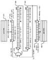
도 3 은 도 2 의 구성에서 사용할 수 있는 타일 및 어레이 레벨 네트워크의 간략화된 다이어그램이고, 여기서 어레이의 구성가능한 유닛들은 어레이 레벨 네트워크의 노드들이다.FIG. 3 is a simplified diagram of a tile and array level network usable in the configuration of FIG. 2 , wherein the configurable units of the array are nodes of the array level network.
이 예에서, 구성가능한 유닛들의 어레이(300) 는 복수의 타입들의 구성가능한 유닛들을 포함한다. 이 예에서 구성가능한 유닛들의 타입들은 패턴 계산 유닛 (PCU), 패턴 메모리 유닛 (PMU), 스위치 유닛 (S), 및 어드레스 생성 및 병합 유닛 (각각 2개의 어드레스 생성기 (AG) 및 공유 CU를 포함) 을 포함한다. 이들 타입들의 구성가능한 유닛들의 기능들의 예에 대해, Prabhakar 등의 "Plasticine: A Reconfigurable Architecture For Parallel Patterns", ISCA '17, June 24-28, 2017, Toronto, ON, Canada 을 참조하며, 이는 본원에 완전히 설명된 바와 같이 참조로 통합된다. 이들 구성가능한 유닛들의 각각은 프로그램을 실행하기 위한 셋업 (setup) 또는 시퀀스 (sequence) 중 어느 일방을 나타내는 레지스터들 또는 플립-플롭들의 세트를 포함하는 구성 저장소를 포함하고, 네스팅된 루프들의 수, 각각의 루프 반복기의 한계들, 각각의 스테이지에 대해 실행될 명령들, 피연산자들의 소스, 및 입력 및 출력 인터페이스들에 대한 네트워크 파라미터들을 포함할 수 있다.In this example, the array of
추가적으로, 이들 구성가능한 유닛들의 각각은 네스팅된 루프들 또는 다른 것에서 프로그레스를 추적하는데 사용가능한 상태를 저장하는 레지스터들 또는 플립-플롭들의 세트를 포함하는 구성 저장소를 포함한다. 구성 파일은 프로그램을 실행하는 컴포넌트들 각각의 초기 구성 또는 시작 상태를 나타내는 비트-스트림을 포함한다. 이러한 비트-스트림은 비트-파일로서 지칭된다. 프로그램 로드는 모든 컴포넌트들이 프로그램(즉, 머신) 을 실행하도록 허용하기 위해 비트 파일의 콘텐츠들에 기초하여 구성가능한 유닛들의 어레이에서 구성 저장소들을 셋업하는 프로세스이다. 프로그램 로드는 또한 모든 PMU 메모리들의 로드를 필요로 할 수도 있다.Additionally, each of these configurable units includes a configuration store that includes a set of registers or flip-flops that store state usable to track progress in nested loops or otherwise. The configuration file contains a bit-stream representing the initial configuration or startup state of each of the components executing the program. This bit-stream is referred to as a bit-file. A program load is the process of setting up configuration stores in an array of configurable units based on the contents of a bit file to allow all components to execute a program (ie, a machine). A program load may also require loading of all PMU memories.
어레이 레벨 네트워크는 어레이에서의 구성가능한 유닛들을 상호연결하는 링크들을 포함한다. 어레이 레벨 네트워크에서의 링크들은 하나 이상, 그리고 이 경우 3가지 종류의 물리적 버스들: 청크-레벨 벡터 버스 (예를 들어, 128 비트의 데이터), 워드-레벨 스칼라 버스 (예를 들어, 32 비트의 데이터), 및 다중 비트-레벨 제어 버스를 포함한다. 실례로, 스위치 유닛들 (311 및 312) 사이의 상호연결부 (321) 는 128 비트의 벡터 버스 폭을 갖는 벡터 버스 상호연결부, 32 비트의 스칼라 버스 폭을 갖는 스칼라 버스 상호연결부, 및 제어 버스 상호연결부를 포함한다.An array level network includes links interconnecting the configurable units in the array. The links in an array level network are one or more, and in this case three kinds of physical buses: a chunk-level vector bus (eg 128 bits of data), a word-level scalar bus (eg 32 bits of data). data), and a multi-bit-level control bus. For example, the
세 종류의 물리적 버스들은 전송되는 데이터의 입도 (granularity) 가 다르다. 일 실시형태에서, 벡터 버스는 그 페이로드로서 16-바이트 (=128 비트) 의 데이터를 포함하는 청크를 반송할 수 있다. 스칼라 버스는 32 비트 페이로드를 가질 수 있고, 스칼라 피연산자들 또는 제어 정보를 반송할 수 있다. 제어 버스는 토큰들 및 다른 신호들과 같은 제어 핸드쉐이크들을 반송할 수 있다. 벡터 및 스칼라 버스들은 각각의 패킷의 목적지를 나타내는 헤더들, 및 패킷들이 비순차적으로 수신될 때 파일을 리어셈블링하는데 사용될 수 있는 시퀀스 넘버들과 같은 다른 정보를 포함하여, 패킷 스위칭될 수 있다. 각각의 패킷 헤더는 목적지 스위치 유닛의 지리적 좌표들 (예를 들어, 어레이에서의 행 및 열) 을 식별하는 목적지 식별자, 및 목적지 유닛에 도달하기 위해 사용되는 목적지 스위치 상의 인터페이스(예를 들어, North(북쪽), South(남쪽), East (동쪽), West (서쪽) 등) 를 식별하는 인터페이스 식별자를 포함할 수 있다. 제어 네트워크는, 예를 들어, 디바이스 내의 타이밍 회로들에 기초하여 회로 스위칭될 수 있다. 구성 로드/언로드 제어기는 128 비트의 구성 데이터의 각각의 청크에 대한 헤더를 생성할 수 있다. 헤더는 헤더 버스 상에서 구성가능한 유닛의 어레이에서의 각각의 구성가능한 유닛으로 송신된다.The three types of physical buses have different granularity of transmitted data. In one embodiment, the vector bus may carry as its payload a chunk containing 16-bytes (=128 bits) of data. A scalar bus may have a 32-bit payload and may carry scalar operands or control information. The control bus may carry control handshakes such as tokens and other signals. Vector and scalar buses can be packet switched, including headers indicating the destination of each packet, and other information such as sequence numbers that can be used to reassemble the file when packets are received out of sequence. Each packet header contains a destination identifier that identifies the geographic coordinates of the destination switch unit (e.g., row and column in the array), and an interface on the destination switch used to reach the destination unit (e.g., North( North), South (south), East (east), West (west), etc.) may include an interface identifier. The control network may be circuit switched based on, for example, timing circuits in the device. The configuration load/unload controller may generate a header for each chunk of 128 bits of configuration data. A header is sent to each configurable unit in the array of configurable units on the header bus.
일 예에서, 128 비트의 데이터의 청크는, 구성가능한 유닛에 대한 벡터 입력들로서 청크를 제공하는 벡터 버스 상에서 송신된다. 벡터 버스는 128 개의 페이로드 라인들, 및 헤더 라인들의 세트를 포함할 수 있다. 헤더는 다음을 포함할 수 있는, 각각의 청크에 대한 시퀀스 ID 를 포함할 수 있다:In one example, a chunk of 128 bits of data is transmitted on a vector bus providing the chunk as vector inputs to the configurable unit. The vector bus may include 128 payload lines, and a set of header lines. The header may contain a sequence ID for each chunk, which may include:
● 청크가 스크래치패드 메모리 또는 구성 저장소 데이터를 포함하는지를 나타내기 위한 비트.● A bit to indicate whether the chunk contains scratchpad memory or configuration store data.
● 청크 넘버를 형성하는 비트들.● The bits that form the chunk number.
● 열 식별자를 나타내는 비트들.● Bits representing the column identifier.
● 행 식별자를 나타내는 비트들.● Bits representing the row identifier.
● 컴포넌트 식별자를 나타내는 비트들.● Bits representing component identifiers.
로드 동작의 경우, 구성 로드 제어기는 N-1 에서 0 의 순서로 구성가능한 유닛에 N 개의 청크들을 전송할 수 있다. 이 예에서, 6 개의 청크들은 청크 5->청크 4->청크 3->청크 2->청크 1-> 청크 0 의 최상위 비트 제 1 순서로 전송된다. (이 최상위 비트 제 1 순서는 청크 5 가 어레이 구성 로드 제어기로부터의 분배 시퀀스의 라운드 0 에 분배되는 것을 초래한다.) 언로드 동작의 경우, 구성 언로드 제어기는 역순서 (out of order) 의 언로드 데이터를 메모리에 기록할 수 있다. 로드 및 언로드 동작들 모두에 대해, 구성가능한 유닛에서의 구성 데이터 저장소에서의 구성 직렬 체인들에서의 시프팅은 LSB(최하위 비트) 로부터 MSB(최상위 비트) 로, 또는 MSB 아웃이 우선이다.For a load operation, the configuration load controller may send N chunks to the configurable unit in the order of N-1 to zero. In this example, 6 chunks are transmitted in the first order of the most significant bit of chunk 5->chunk 4-> chunk 3-> chunk 2-> chunk 1-> chunk 0. (This most significant bit first order results in chunk 5 being distributed in round 0 of the distribution sequence from the array configuration load controller.) For an unload operation, the configuration unload controller sends the unload data out of order. can be written to memory. For both load and unload operations, shifting in configuration serial chains in the configuration data store in a configurable unit takes precedence from LSB (least significant bit) to MSB (most significant bit), or MSB out.
도 3a 는 어레이 레벨 네트워크에서 엘리먼트들을 연결하는 예시적인 스위치 유닛을 나타낸다. 도 3a의 예에 나타낸 바와 같이, 스위치 유닛은 8개의 인터페이스들을 가질 수 있다. 스위치 유닛의 North (북쪽), South (남쪽), East (동쪽) 및 West (서쪽) 인터페이스들은 스위치 유닛들 사이의 연결들을 위해 사용된다. 스위치 유닛의 Northeast (북동쪽), Southeast (남동쪽), Northwest (북서쪽) 및 Southwest (남서쪽) 인터페이스들은 PCU 또는 PMU 인스턴스들에 대한 연결을 만드는 데 각각 사용된다. 각 타일 사분면 내의 2개의 스위치 유닛들의 세트는, 다수의 어드레스 생성 (address generation; AG) 유닛들 및 다수의 어드레스 생성 유닛들에 연결된 병합 유닛 (coalescing unit; CU) 을 포함하는 어드레스 생성 및 병합 유닛 (Address Generation and Coalescing Unit; AGCU) 에 대한 연결들을 갖는다. 병합 유닛 (CU) 은 AG들 사이를 중재하고 메모리 요청들을 처리한다. 스위치 유닛의 8 개의 인터페이스들의 각각은 벡터 인터페이스, 스칼라 인터페이스, 및 벡터 네트워크, 스칼라 네트워크, 및 제어 네트워크와 통신하기 위한 제어 인터페이스를 포함할 수 있다.3A illustrates an exemplary switch unit that connects elements in an array level network. As shown in the example of FIG. 3A , a switch unit may have eight interfaces. The North (north), South (south), East (east) and West (west) interfaces of the switch unit are used for connections between the switch units. The Northeast, Southeast, Northwest, and Southwest interfaces of the switch unit are used to make connections to PCU or PMU instances, respectively. The set of two switch units in each tile quadrant comprises an address generation and merging unit comprising a plurality of address generation (AG) units and a coalescing unit (CU) coupled to the plurality of address generation units ( Address Generation and Coalescing Unit (AGCU). A merging unit (CU) mediates between AGs and handles memory requests. Each of the eight interfaces of the switch unit may include a vector interface, a scalar interface, and a control interface for communicating with the vector network, the scalar network, and the control network.
구성가능한 스위치들의 어레이를 파티셔닝하기 위한 로직의 실시형태에서, 스위치들은 스위치 포트 디스에이블 레지스터 SPDR 및 스위치 라우팅 레지스터 SRR 와 같은 구성 데이터를 포함한다. 일 실시형태에서, 어레이 내의 각각의 스위치는 스위치 상의 스위치 포트들 중 하나 이상을 사용하여 통신들을 차단하기 위해, 구성 로드 및 언로드 프로세스들을 사용하여 구성가능하다. 이에 의해, 구성가능한 유닛들의 세트를 둘러싸는 스위치들의 세트는 타일을 상이한 애플리케이션 그래프 그래프들에 의해 사용가능한, 구성 유닛들의 복수의 세트들로 파티셔닝하도록 구성될 수 있다.In an embodiment of logic for partitioning an array of configurable switches, the switches include configuration data such as a switch port disable register SPDR and a switch routing register SRR. In one embodiment, each switch in the array is configurable using configuration load and unload processes to block communications using one or more of the switch ports on the switch. Thereby, a set of switches surrounding a set of configurable units may be configured to partition a tile into multiple sets of constituent units, usable by different application graph graphs.
다수의 타일들이 존재하는 다른 실시형태에서, 타일들의 외부 행들 및 외부 열들 상의 스위치들만이 구성 로드 및 언로드 프로세스들을 사용하여 구성가능하여, 타일 경계들에 걸쳐 스위치 포트들 중 하나 이상을 사용하여 통신들을 허용하거나 차단하도록 한다. 예를 들어, 스위치 포트 디스에이블 레지스터는 타일 경계들에 걸친 통신을 디스에이블하도록 설정될 수 있다.In another embodiment where there are multiple tiles, only switches on outer rows and outer columns of tiles are configurable using configuration load and unload processes, allowing communications using one or more of the switch ports across tile boundaries. allow or block. For example, a switch port disable register may be set to disable communication across tile boundaries.
구성 후 가상 머신의 실행 동안, 데이터는 어레이 레벨 네트워크 상의 하나 이상의 스위치 유닛들의 벡터 버스 및 벡터 인터페이스(들) 를 사용하여 하나 이상의 유닛 스위치들 및 유닛 스위치들 사이의 하나 이상의 링크들을 통해 구성가능한 유닛들로 전송될 수 있다.During execution of the virtual machine after configuration, data is transferred to the configurable units via the one or more unit switches and one or more links between the unit switches using the vector bus and vector interface(s) of the one or more switch units on the array level network. can be transmitted to
본 명세서에 설명된 실시형태들에서, 타일의 구성 전에, 구성 파일 또는 비트 파일은, 어레이 레벨 네트워크 상의 하나 이상의 스위치 유닛들의 벡터 버스 및 벡터 인터페이스(들) 를 사용하여 구성가능한 유닛에 대해, 유닛 스위치들 사이의 하나 이상의 링크들 및 하나 이상의 유닛 스위치들을 통해, 동일한 벡터 버스를 사용하여 구성 로드 제어기로부터 전송될 수 있다. 실례로, 구성가능한 유닛 PMU(341) 에 특정한 유닛 파일에서의 구성 데이터의 청크는 구성 로드/언로드 제어기 (301) 와 스위치 유닛 (311) 의 West (W) 벡터 인터페이스 사이의 링크 (320), 스위치 유닛 (311), 및 스위치 유닛 (311) 의 Southeast (SE) 벡터 인터페이스와 PMU(341) 사이의 링크 (331) 를 통해 구성 로드/언로드 제어기 (301) 로부터 PMU(341) 로 전송될 수 있다.In the embodiments described herein, prior to configuration of a tile, a configuration file or bit file is, for a unit configurable using a vector bus and vector interface(s) of one or more switch units on an array level network, a unit switch may be sent from the configuration load controller using the same vector bus, via one or more unit switches and one or more links between them. For example, a chunk of configuration data in a unit file specific to the
이 예에서, AGCU들 중 하나는 구성 로드/언로드 제어기 (예를 들어, 301) 를 포함하는 마스터 AGCU 이도록 구성된다. 마스터 AGCU는 호스트 (120, 도 1) 가 레지스터를 통하여, 버스 시스템을 통해 마스터 AGCU 에 커맨드들을 전송할 수 있는 그러한 레지스터를 구현한다. 마스터 AGCU 는 타일 내의 구성가능한 유닛들의 어레이 상의 동작들을 제어하고, 레지스터에 대한 기록들을 통해 호스트로부터 수신하는 커맨드들에 기초하여 타일의 상태를 추적하기 위해 프로그램 제어 상태 머신을 구현한다. 매(every) 상태 전이에 대해, 마스터 AGCU 는 데이지 체인형 커맨드 버스 (daisy chained command bus) 를 통해 타일 상의 모든 컴포넌트들에 커맨드들을 발행한다 (도 4). 그 커맨드들은 타일 내의 구성가능한 유닛들의 어레이에서의 구성가능한 유닛들을 리셋하기 위한 프로그램 리셋 커맨드, 및 구성가능한 유닛들에 구성 파일을 로딩하기 위한 프로그램 로드 커맨드를 포함한다.In this example, one of the AGCUs is configured to be a master AGCU that includes a configuration load/unload controller (eg, 301 ). The master AGCU implements such a register through which the host 120 ( FIG. 1 ) can send commands to the master AGCU via the bus system. The master AGCU implements a program control state machine to control operations on the array of configurable units within the tile and track the state of the tile based on commands it receives from the host via writes to registers. For every state transition, the master AGCU issues commands to all components on the tile via a daisy chained command bus (FIG. 4). The commands include a program reset command to reset the configurable units in the array of configurable units in a tile, and a program load command to load a configuration file into the configurable units.
마스터 AGCU 내의 구성 로드 제어기는 메모리로부터 구성 파일을 판독하고, 구성 데이터를 타일의 매 구성가능한 유닛에 전송하는 것을 담당한다. 마스터 AGCU 는 바람직하게는 최상위 레벨 네트워크의 최대 스루풋에서 메모리로부터 구성 파일을 판독할 수 있다. 메모리로부터 판독된 데이터는 본 명세서에 설명된 분배 시퀀스에 따라 어레이 레벨 네트워크 상의 벡터 인터페이스를 통해 마스터 AGCU 에 의해 대응하는 구성가능한 유닛으로 전송된다.The configuration load controller in the master AGCU is responsible for reading the configuration file from memory and sending the configuration data to every configurable unit of the tile. The master AGCU is preferably able to read the configuration file from memory at the maximum throughput of the top level network. Data read from the memory is transmitted by the master AGCU to the corresponding configurable unit via a vector interface on the array level network according to the distribution sequence described herein.
일 실시형태에서, 구성가능한 유닛 내의 배선 요건들 (wiring requirements) 을 감소시킬 수 있는 방식으로, 구성 로드 프로세스에서 로딩되거나 구성 언로드 프로세스에서 언로딩될 유닛 파일들을 홀딩하는 구성 및 상태 레지스터들은 직렬 체인으로 연결되고, 그 직렬 체인을 통해 비트들을 시프팅하는 프로세스를 통해 로딩될 수 있다. 일부 실시형태들에서, 병렬로 또는 직렬로 배열된 하나 초과의 직렬 체인이 있을 수도 있다. 구성가능한 유닛이 하나의 버스 사이클에서 마스터 AGCU로부터 예를 들어 128 비트의 구성 데이터를 수신할 때, 구성가능한 유닛은 사이클 당 1 비트의 레이트로 그것의 직렬 체인을 통해 이 데이터를 시프트하고, 여기서 시프터 사이클들은 버스 사이클과 동일한 레이트로 실행될 수 있다. 구성가능한 유닛이 벡터 인터페이스를 통해 수신된 128 비트의 데이터로 128 구성 비트를 로딩하기 위해 128 시프터 사이클이 걸릴 것이다. 128 비트의 구성 데이터를 청크라고 지칭한다. 구성가능한 유닛은 모든 그것의 구성 비트들을 로딩하기 위해 다수의 데이터 청크들을 요구할 수 있다. 예시적인 시프트 레지스터 구조가 도 6 에 도시되어 있다.In one embodiment, the configuration and status registers holding the unit files to be loaded in the configuration load process or unloaded in the configuration unload process are serially chained in a way that can reduce wiring requirements within the configurable unit. It can be connected and loaded through the process of shifting bits through its serial chain. In some embodiments, there may be more than one series chain arranged in parallel or in series. When a configurable unit receives, for example, 128 bits of configuration data from the master AGCU in one bus cycle, the configurable unit shifts this data through its serial chain at a rate of 1 bit per cycle, where the shifter Cycles can run at the same rate as a bus cycle. It will take 128 shifter cycles for the configurable unit to load the 128 configuration bits with the 128 bits of data received via the vector interface. The 128 bits of configuration data are referred to as chunks. A configurable unit may require multiple data chunks to load all its configuration bits. An exemplary shift register structure is shown in FIG. 6 .
구성가능한 유닛들은 다수의 메모리 인터페이스들 (150, 도 1) 을 통해 메모리와 인터페이싱한다. 메모리 인터페이스들의 각각은 여러 AGCU들을 사용하여 액세스될 수 있다. 각각의 AGCU는 오프-칩 메모리에 대한 요청들을 생성하기 위해 재구성가능한 스칼라 데이터경로를 포함한다. 각각의 AGCU 는 오프-칩 메모리로부터 발신 커맨드들, 데이터, 및 착신 응답들을 버퍼링하기 위해 데이터를 조직하기 버퍼들을 포함한다.Configurable units interface with memory via a number of memory interfaces 150 ( FIG. 1 ). Each of the memory interfaces can be accessed using multiple AGCUs. Each AGCU includes a reconfigurable scalar datapath for generating requests to off-chip memory. Each AGCU includes buffers to organize data to buffer outgoing commands, data, and incoming responses from off-chip memory.
AGCU들에서의 어드레스 생성기들 (AG들) 은 조밀하거나 (dense) 또는 희소한 (sparse) 메모리 커맨드들을 생성할 수 있다. 조밀한 요청들은 연속적인 오프-칩 메모리 영역들을 대량 전송하는 데 사용될 수 있고, 구성가능한 유닛들의 어레이에서의 구성가능한 유닛들로부터/로 데이터의 청크를 판독 또는 기록하는 데 사용될 수 있다. 조밀한 요청들은 AGCU들에서의 병합 유닛 (CU) 에 의해 다수의 오프-칩 메모리 버스트 요청들로 변환될 수 있다. 희소한 요청들은 어드레스들의 스트림을 병합 유닛 내로 인큐(enqueue)할 수 있다. 병합 유닛은 발행된 오프-칩 메모리 요청들에 대한 메타데이터를 유지하기 위해 병합 캐시를 사용하고, 발행된 오프-칩 메모리 요청들의 수를 최소화하기 위해 동일한 오프-칩 메모리 요청에 속하는 희소 어드레스들을 결합한다.Address generators (AGs) in AGCUs can generate dense or sparse memory commands. Dense requests can be used to bulk transfer contiguous off-chip memory regions, and can be used to read or write chunks of data to/from configurable units in an array of configurable units. Dense requests may be converted into multiple off-chip memory burst requests by a merging unit (CU) in AGCUs. Sparse requests may enqueue a stream of addresses into a merge unit. The merge unit uses a merge cache to maintain metadata for issued off-chip memory requests, and combines sparse addresses belonging to the same off-chip memory request to minimize the number of issued off-chip memory requests. do.
전술한 바와 같이, 예시된 실시형태의 AGCU들 각각은 메모리 액세스 제어기 MAC (301, 302, 303 및 304) 를 포함한다. 메모리 액세스 제어기들 각각은 타일 내의 구성가능한 유닛들 모두에 전용될 수 있다. 대안적으로, 구성 파일에 의해 설정된 상이한 그래프들은 타일에서의 구성가능한 유닛들의 상이한 파티셔닝된 세트들 상에 상주할 수도 있고, 파티셔닝된 세트들 각각은 파티셔닝된 세트 내의 스위치에 연결된 메모리 액세스 제어기들 중 하나에 구성 파일에 의해 할당될 수 있다.As noted above, each of the AGCUs of the illustrated embodiment includes a memory
도 4 는 외부 호스트 (401) 및 외부 메모리 (402) 에 커플링된 CGRA 디바이스 (400) 를 포함하는 시스템을 예시한다. 예를 들어, PCIE 타입 인터페이스들 또는 특정 구현에 적합한 다른 타입들의 인터페이스들을 포함하여, 디바이스 (400) 를 호스트 (401) 에 커플링하는 복수의 인터페이스들 (405) 이 존재할 수 있다. 인터페이스들 (405) 중 하나 이상은 인터넷 기반 네트워크 연결들을 포함하는 네트워크 연결들일 수 있다. 호스트 (401) 는 디바이스 (400) 와 협력하여 런타임 프로그램을 실행할 수 있는 클라우드 기반 시스템을 포함하는 임의의 시스템을 포함할 수 있다.4 illustrates a system including a
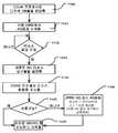
예를 들어, 고밀도 DRAM 메모리로의 연결에 적합한 고속 이중 데이터 레이트 인터페이스들, 또는 특정 구현에 적합한 다른 타입들의 인터페이스들을 포함하여, 디바이스 (400) 를 메모리 (402) 에 커플링하는 복수의 인터페이스들 (406) 이 존재할 수 있다.a plurality of interfaces that
CGRA 디바이스 (400) 는 어레이 레벨 네트워크 (411) 에 커플링되는 구성가능한 유닛들의 어레이 (410) 를 포함한다. 이 예시에서, 어레이는 구성가능한 유닛들 (VM1, VM2, ... VMn) 의 복수의 세트들로 파티셔닝된다. 구성가능한 유닛들의 어레이는 상이한 "형상들" 의 가상 머신들을 지원할 수 있다. 예를 들어, 일부 실시형태들에서, 리소스 요구들이 원자 그룹의 리소스들과 매칭하는 가상 머신을 지원할 수 있는, 구성가능한 유닛들 및 다른 CGRA 리소스들 (원자 그룹) 의 최소-크기 세트가 존재할 수 있다. 더 큰 VM들은 상이한 VM 형상들을 구성하기 위해 원자 그룹의 집합 세트들로 구성될 수 있다. 일 예에서, 원자 그룹은 도 3 에 예시된 바와 같은 타일이고, VM들은 여러 타일들에 걸쳐 있을 수 있다. 다른 실시형태들에서, 원자 그룹은 타일의 부분 (행들 및 열들의 서브세트) 일 수 있고, VM 통신들, 메모리, 및 원자 그룹들의 상이한 구성들로 구성된 VM들의 로드/언로드를 서로 분리하기 위한 로직을 갖는다.The
어레이 레벨 네트워크 (411) 는 또한 하나 이상의 어드레스 생성 및 병합 유닛들 (AGCU들) (420) 에 커플링된다. AGCU들 (420) 은, 외부 호스트 (401) 및 외부 메모리 (402) 를 포함하는 외부 리소스들과의 통신을 위해 인터페이스들 (405, 406) 에 차례로 커플링되는 최상위 레벨 네트워크 (412) 에 커플링된다.The
AGCU들 (420) 은 어레이 레벨 네트워크 (411) 와 최상위 레벨 네트워크 (412) 사이의 게이트웨이로서 동작하는 로직을 포함한다.The
AGCU들의 게이트웨이 기능은 이 예에서, 어레이 (410) 내의 구성가능한 유닛들의 세트들 사이의 통신들을 구성가능한 유닛들의 대응하는 세트들에 의해 구현되는 가상 머신들에 할당된 메모리 내의 영역들로 한정하기 위해 사용되는 가상 머신들 메모리 공간을 맵핑하는 맵핑 테이블 (422) 을 활용하는 메모리 액세스 제어기를 포함한다.The gateway function of the AGCUs is, in this example, to limit communications between sets of configurable units in
일 실시형태에서, AGCU 를 통한 임의의 메모리 액세스들은 맵핑 테이블 (422) 에 의해 필터링된다. 메모리 액세스가 구성가능한 유닛들의 특정 세트에 할당된 메모리 공간 외부의 구성가능한 유닛들의 특정 세트로부터 시도되면, 메모리 액세스는 차단된다. 일부 실시형태들에서, 액세스를 차단하는 것에 부가하여, 구성가능한 유닛들의 세트에서 실행되는 특정 애플리케이션 그래프에 의한 메모리 액세스 위반을 나타내는 예외 메시지가 호스트에 전송될 수 있다.In one embodiment, any memory accesses through the AGCU are filtered by the mapping table 422 . If a memory access is attempted from a particular set of configurable units outside the memory space allocated to the particular set of configurable units, the memory access is blocked. In some embodiments, in addition to blocking access, an exception message may be sent to the host indicating a memory access violation by a specific application graph executing on a set of configurable units.
이 예에서 AGCU들은 또한, 가상 머신들의 지원시, 어레이 내의 구성가능한 유닛들의 대응하는 세트들로부터 그래프들을 로딩 및 언로딩하는데 사용되는 구성 제어기 (421) 를 포함한다.The AGCUs in this example also include a
맵핑 테이블 (422) 은 대응하는 AGCU (420) 에 대한 구성 파일의 일부로서 구성될 수 있다.The mapping table 422 can be configured as part of a configuration file for the
도 5 는 위에서 설명된 시스템들에서 사용될 수 있는 것과 같은, AGCU 내의 메모리 액세스 제어기에 의해 실행되는 로직을 예시하는 흐름도이다. 이 흐름에서, AGCU 를 포함하는 구성가능한 유닛들의 세트에서 애플리케이션 그래프의 실행 동안 AGCU 는 메모리 액세스에 대해 어레이 레벨 네트워크 상의 통신들을 모니터링할 수 있다 (510). 메모리 액세스가 수신되면, 그 요청에서 가상 어드레스 (즉, 특정 가상 머신에서 실행되는 애플리케이션 그래프에 의해 사용되는 어드레스) 가 파싱된다 (511). 요청의 소스는 특정 가상 머신에 매칭된다 (512). 가상 어드레스는 맵핑 테이블 (422) 을 사용하여 물리적 어드레스 (즉, 구성가능한 유닛들의 어레이 외부의 메모리에 대한 어드레스) 로 변환된다. 이는 특정 세트의 구성가능한 유닛들에 할당된 가상 머신의 식별자 (VMID) 를 사용하여 메모리 맵 (MM) 을 검색함으로써 실행될 수 있다 (513). 메모리 액세스 제어기는 액세스가 가상 머신에 할당된 메모리 공간의 경계를 벗어난 물리적 어드레스에 맵핑되는지의 여부를 결정한다 (515). 액세스가 경계를 벗어나지 않으면, 물리적 어드레스를 사용하여 최상위 레벨 네트워크 상에서 메모리 액세스 요청이 발행된다 (516). 액세스가 경계를 벗어나면 최상위 네트워크에서 예외가 발행되고 요청이 드롭된다 (517).5 is a flow diagram illustrating logic executed by a memory access controller within an AGCU, such as may be used in the systems described above. In this flow, the AGCU can monitor communications on the array level network for memory access during execution of the application graph in the set of configurable units that includes the AGCU ( 510 ). When a memory access is received, the virtual address in the request (ie, the address used by the application graph running in the particular virtual machine) is parsed (511). The source of the request is matched to a specific virtual machine (512). The virtual address is translated into a physical address (ie, an address to memory outside the array of configurable units) using a mapping table 422 . This may be done by retrieving the memory map (MM) using the identifier (VMID) of the virtual machine assigned to the particular set of configurable units ( 513 ). The memory access controller determines ( 515 ) whether the access maps to a physical address outside the bounds of the memory space allocated to the virtual machine. If the access does not cross the boundary, a memory access request is issued 516 on the top level network using the physical address. If access is out of bounds, an exception is issued by the top-level network and the request is dropped (517).
이 흐름도는 특정 가상 머신이 실행 중인, 구성가능한 유닛들의 특정 세트 내부로부터의 요청에 대한 로직을 설명한다. 유사한 프로세스가 구성가능한 유닛들의 특정 세트로 향하는 최상위 레벨 네트워크로부터의 데이터 전송들을 위해 실행될 수 있다.This flow diagram describes the logic for a request from within a specific set of configurable units, in which a specific virtual machine is running. A similar process may be executed for data transfers from the top level network destined for a particular set of configurable units.
구성가능한 유닛들의 복수의 세트들 내의 구성가능한 유닛들의 세트들은 가상 어드레스들을 사용하여 애플리케이션 그래프들을 실행하도록 구성가능하고, 메모리 액세스 제어기는 특정 세트 내에서 실행되는 애플리케이션 그래프로부터 발생하는 요청들 내의 가상 어드레스들을 특정 세트에 할당된 메모리 공간 내의 어드레스들로 변환하기 위해 구성가능한 테이블을 포함하거나 그에 대한 액세스를 갖는다. 일부 예들에서, 가상 어드레스들은 어레이 내의 다른 유닛들로부터의 통신들에 응답하여 AGCU 에서 생성된다. 이러한 가상 어드레스들은 메모리 액세스 제어기에서 물리적 어드레스들로 변환된다.The sets of configurable units in the plurality of sets of configurable units are configurable to execute application graphs using virtual addresses, and the memory access controller is configured to execute virtual addresses in requests originating from the application graph executing within the particular set. It contains or has access to a configurable table to translate to addresses in the memory space allocated to a particular set. In some examples, the virtual addresses are generated at the AGCU in response to communications from other units in the array. These virtual addresses are translated into physical addresses in the memory access controller.
일 실시형태에서, 메모리 액세스 제어기는 각각의 애플리케이션 그래프를 다수의 메모리 영역들에 할당하도록 구성가능하다. 맵핑은 베이스/바운드 접근법을 사용하여 할당된 메모리 공간에 포함될 영역들의 최대 수에 따라 구현될 수 있다. 예를 들어, 각각의 애플리케이션 그래프에 할당된 메모리 공간이 최대 16 개의 메모리 영역들을 포함할 수 있다고 가정하면, 컴파일러는 AGCU 내의 어드레스 레지스터들의 비트들 63:60 을 사용하여 영역 ID 를 정적으로 할당할 수 있다.In one embodiment, the memory access controller is configurable to allocate each application graph to multiple memory regions. Mapping can be implemented according to the maximum number of regions to be included in the allocated memory space using a base/bound approach. For example, assuming that the memory space allocated to each application graph can include up to 16 memory regions, the compiler can statically allocate the region ID using bits 63:60 of the address registers in the AGCU. have.
하나의 접근법에서, 컴파일러는 0 의 기본 메모리 어드레스 및 크기를 각각의 영역에 할당한다. 이는 또한 할당된 각 영역의 사용을 검증하기 위한 표시기를 할당한다.In one approach, the compiler assigns each region a base memory address and size of 0. It also assigns an indicator to verify the use of each allocated area.
할당된 영역은 컴파일러에 의해 생성된 구성 파일 내에 포함된다. X 는 정수이고, 각각의 테이블 엔트리가 다음 필드들을 갖는 구조인 X-엔트리 영역 테이블의 형태를 취할 수 있다:The allocated area is included in the configuration file generated by the compiler. X is an integer, and can take the form of an X-entry region table, where each table entry is a structure with the following fields:
유효 - 테이블 엔트리가 할당됨;Valid - table entry assigned;
크기 - 영역의 N 비트 크기; 영역은 크기가 2 의 거듭제곱이 아닐 수도 있음; 및size - N-bit size of the region; A region may not be a power of two in size; and
AGCU 메모리 어드레스 생성기 (카운터/ALU 출력) 를 주어진 영역에 바인딩하는 각 영역에 대한 연결들의 목록.A list of connections to each region that binds the AGCU memory address generator (counter/ALU output) to a given region.
비트파일 로드 시간에서, 영역 테이블로부터의 엔트리들은 애플리케이션 그래프를 구현하는데 사용되는 구성가능한 유닛들의 세트에 링크된 각각의 AGCU 에서 유효, 기본, 및 경계 레지스터들을 프로그래밍하는데 사용된다. 영역 바인딩 메커니즘에 따라, 각각의 AGCU 어드레스 생성기는 또한 특정 영역에 바인딩될 수 있다. 기본 어드레스들은 일부 예들에서 런타임에 의해 할당할 수 있다.At bitfile load time, entries from the region table are used to program the valid, primary, and boundary registers in each AGCU linked to a set of configurable units used to implement the application graph. Depending on the region binding mechanism, each AGCU address generator may also be bound to a specific region. Base addresses may be assigned by runtime in some examples.
AGCU 가 구성가능한 유닛들의 세트 내의 구성가능한 유닛들로부터 발생하는 액세스 요청에 응답하여 메모리 어드레스 및 길이를 생성할 때, 최상위 레벨 네트워크 상의 어드레스와의 트랜잭션을 전송하기 전에, 다음의 동작들이 수행된다.When the AGCU generates a memory address and length in response to an access request originating from the configurable units in the set of configurable units, before sending a transaction with the address on the top level network, the following operations are performed.
이 X 영역 예에서의 Z-비트 어드레스는 2 개의 부분들을 포함할 수 있다. 다수의 상위 비트들 (Z-1:W) 은 영역 액세스 레지스터를 식별한다. 하위 비트들 (W-1:0) 은 영역에서 상대적인 가상 오프셋을 식별한다.The Z-bit address in this X region example may include two parts. A number of high-order bits (Z-1:W) identify the region access register. The low-order bits (W-1:0) identify a relative virtual offset in the region.
AGCU 는 가상 어드레스의 비트들 (Z-1:W) 을 사용하여 물리적 영역의 베이스/경계들을 검색한다. 비트 단위의 오프셋은 실제 DDR 물리적 어드레스를 생성하기 위해 그 영역에 대한 기본 레지스터에 추가된다. 기본 값이 길이만큼 증분되고, 결과적인 범위 어드레스가 제한 레지스터에 대해 체크된다. 범위 어드레스가 한계보다 작거나 같으면, 어드레스 및 요청은 프로세싱을 위해 최상위 레벨 네트워크를 통해 DDR 로 전달된다.The AGCU uses the bits (Z-1:W) of the virtual address to search the base/boundaries of the physical area. An offset in bits is added to the base register for that region to create the actual DDR physical address. The base value is incremented by the length, and the resulting range address is checked against the limit register. If the range address is less than or equal to the limit, the address and request are passed to the DDR through the top-level network for processing.
범위 어드레스가 한계를 초과하면, 런타임 예외가 생성되고, 최상위 레벨 네트워크 요청이 억제되고, AGCU 는 그 어드레스 생성기로부터의 추가 어드레스 요청들을 프로세싱하는 것을 중지한다.If the range address exceeds the limit, a runtime exception is generated, the top level network request is suppressed, and the AGCU stops processing further address requests from that address generator.
대안적인 실시형태에서, 메모리 액세스 제어기는 다른 접근법들을 사용하여 가상 대 물리 변환을 사용하여 가상 어드레스 (VA) 대 물리 어드레스 (PA) 맵핑을 구현할 수 있다. 예를 들어, VA-PA 버퍼 변환 접근법에서, 런타임 소프트웨어는 VA-PA 변환의 프로세스를 통해 컴파일러 생성된 어드레스 영역들을 물리적 메모리 내의 이용가능한 메모리 공간에 맵핑한다. 이렇게 하면 런타임으로 큰 가상 어드레스 공간을 구성가능한 유닛들의 다수의 어레이들에 걸쳐 분산될 수 있는 다수의 물리적 어드레스 공간으로 파티셔닝할 수 있다. 물리적 어드레스 공간은 일부 경우에, 최소 크기 (예를 들어, 1MB) 및 최대 크기 (예를 들어, 1TB) 를 갖는 세그먼트들로 파티셔닝될 수 있다.In an alternative embodiment, the memory access controller may implement virtual address (VA) to physical address (PA) mapping using virtual to physical translation using other approaches. For example, in the VA-PA buffer translation approach, runtime software maps compiler-generated address regions to available memory space in physical memory through the process of VA-PA translation. This allows at runtime to partition a large virtual address space into multiple physical address spaces that can be spread across multiple arrays of configurable units. The physical address space may in some cases be partitioned into segments having a minimum size (eg, 1 MB) and a maximum size (eg, 1 TB).
가상 어드레스를 물리적 어드레스로 효율적으로 변환하기 위해, 각각의 메모리 액세스 제어기는 16 개의 가상 세그먼트들에 대한 맵핑 정보를 보유하는 16 개의 엔트리 VA-PA 버퍼를 구현할 수 있다. 이 예에서 VA-PA 버퍼는 완전히 연관되며, 구성 로드 동안 비트 파일 (구성 파일) 에서 로드된다. 1VA-PA 버퍼의 각각의 엔트리는 또한 레지스터 기록들을 통해 기록될 수 있다. 각각의 VA-PA 버퍼 엔트리는 2 개의 서브-필드들: VSID_PA 및 V_SSIZE 로 구성될 수 있다. 이러한 서브-필드들의 각각이 아래 표에 설명된다:To efficiently translate a virtual address to a physical address, each memory access controller may implement a 16 entry VA-PA buffer that holds mapping information for 16 virtual segments. The VA-PA buffer in this example is fully associative and is loaded from a bit file (config file) during configuration load. Each entry in the 1VA-PA buffer can also be written through register writes. Each VA-PA buffer entry may consist of two sub-fields: VSID_PA and V_SSIZE. Each of these sub-fields is described in the table below:
VSID_PA:VSID_PA:

V_SSIZE:V_SSIZE:

AGCU 는 구성 로드 프로세스에서 비트-파일의 VA-PA 버퍼 구조로부터 VA-PA 버퍼를 채운다.The AGCU fills the VA-PA buffer from the VA-PA buffer structure of the bit-file in the configuration load process.
가상 머신에서의 애플리케이션 그래프의 실행 동안, 가상 어드레스는 AGCU 에 링크된 구성가능한 유닛들의 세트에서의 애플리케이션 그래프에 기초하여 생성된다.During execution of the application graph in the virtual machine, a virtual address is generated based on the application graph in the set of configurable units linked to the AGCU.
메모리 액세스 제어기는 매칭하는 가상 세그먼트에 대한 각각의 VA-PA 버퍼 엔트리를 검색함으로써 가상 어드레스를 변환한다.The memory access controller translates the virtual address by searching each VA-PA buffer entry for a matching virtual segment.
변환 에러들은 예를 들어 다음을 포함하는 메모리 액세스 제어기에 의해 검출될 수 있다:Conversion errors can be detected by, for example, a memory access controller including:
1. 변환 없음: 요청의 VA 가 VA-PA 버퍼 엔트리들 중 임의의 것의 VSID 비트들과 매칭하지 않는다.1. No translation: The VA of the request does not match the VSID bits of any of the VA-PA buffer entries.
2. 다수의 매칭들: 요청의 VA 는 다중 엔트리의 VSID 비트들과 매칭한다.2. Multiple matches: The VA of the request matches the VSID bits of multiple entries.
3. 최대치보다 큰 SSIZE : 매칭하는 엔트리들의 SSIZE 가 설정된 최대치보다 크다.3. SSIZE greater than the maximum value: The SSIZE of the matching entries is greater than the set maximum value.
이들 에러들은 에러를 야기한 VA 와 함께 상태 레지스터에 기록될 수 있다. 또한, 변환 에러에서, 메모리 액세스 제어기는 인터럽트 또는 다른 유형의 통지를 호스트에 전송하고, 에러를 야기한 요청을 드롭하고, 임의의 새로운 요청들의 프로세싱을 중지할 수 있다.These errors can be written to the status register along with the VA that caused the error. Also, in a translation error, the memory access controller may send an interrupt or other type of notification to the host, drop the request that caused the error, and stop processing any new requests.
도 6 은 PCU들, PMU들 및 스위치 유닛들을 포함하는, 도 3 을 참조하여 설명된 것들과 같은 구성가능한 유닛들의 어레이를 예시한다. 어레이 내의 (AGCU들에서와 같은) 다른 어드레스가능한 노드에 구현된 구성 로드 로직 및 메모리 액세스 제어기 로직은 도시되지 않는다. 어레이 레벨 네트워크는, 영역 내의 다른 구성가능한 유닛들에 연결하도록 구성가능한, 스위치들의 그리드를 포함한다.6 illustrates an array of configurable units such as those described with reference to FIG. 3 , including PCUs, PMUs and switch units. Configuration load logic and memory access controller logic implemented at other addressable nodes (such as in AGCUs) within the array are not shown. An array level network includes a grid of switches, configurable to connect to other configurable units within an area.
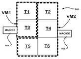
구성 파일은 어레이를 구성가능한 유닛들의 분할된 세트로 파티셔닝하기 위해, 스위치의 선택된 포트로부터의 통신을 차단하도록 스위치들을 구성하는 데 사용될 수 있다. 도 6 에 도시된 예에서, 어레이는 VM1 으로 라벨링된 구성가능한 유닛들의 제 1 세트 및 VM2 로 라벨링된 구성가능한 유닛들의 제 2 세트를 포함하도록 구성된다. 구성가능한 유닛들의 세트들의 경계들 상의 스위치들은 대응하는 세트 내의 유닛들로부터 외부의 유닛들로의 통신들을 차단하도록 구성된다. 예를 들어, 스위치 (600) 는 남서쪽 포트, 서쪽 포트, 북서쪽 포트, 북쪽 포트, 및 북동쪽 포트를 차단하는 한편, 동쪽 포트, 남동쪽 포트, 및 남쪽 포트를 가능하게 하도록 구성될 수 있다. 스위치 (601) 는 남서쪽 포트, 남쪽 포트 및 남동쪽 포트를 차단하는 한편, 스위치 상의 다른 포트들을 가능하게 하도록 구성될 수 있다. 스위치 (602) 는 남동쪽 포트만을 차단하는 한편, 스위치 상의 다른 포트들을 인에이블하도록 구성될 수 있다. 이러한 방식으로, 구성가능한 유닛들의 어레이의 파티션은 구성가능한 유닛들의 분리된 세트들을 형성하도록 구성될 수 있다. 본 명세서에 설명된 실시형태들에서, 분리된 세트들 각각은 전술한 바와 같이 메모리 액세스 제어기 및 구성 제어기에 커플링된다.The configuration file can be used to configure the switches to block communication from selected ports of the switch, in order to partition the array into divided sets of configurable units. In the example shown in FIG. 6 , the array is configured to include a first set of configurable units labeled VM1 and a second set of configurable units labeled VM2 . Switches on the boundaries of sets of configurable units are configured to block communications from units in the corresponding set to units outside. For example, switch 600 may be configured to block the southwest port, west port, northwest port, north port, and northeast port, while enabling the east port, southeast port, and south port.
보다 일반적으로, 구성가능한 유닛들의 어레이는, 파티셔닝의 목적들을 위해, 어레이 내의 파티셔닝가능한 그룹들을 포함하는 구성가능한 유닛들의 블록들을 포함할 수 있다. 일부 실시형태들에서, 파티셔닝가능한 그룹은, 도 3 에 예시된 바와 같이, PMU들, PCU들, 스위치들 및 AGCU들을 포함하는 하나 초과의 타입의 구성가능한 유닛을 포함할 수도 있다. 버스 시스템은 주어진 구현에 적합한 임의의 크기의 어레이 내의 파티션가능한 그룹들의 경계들 상의 구성가능한 유닛들의 세트들로 어레이를 파티셔닝하기 위해 제공하도록 구성될 수 있다.More generally, an array of configurable units may, for purposes of partitioning, include blocks of configurable units comprising partitionable groups within the array. In some embodiments, a partitionable group may include more than one type of configurable unit including PMUs, PCUs, switches, and AGCUs, as illustrated in FIG. 3 . A bus system may be configured to provide for partitioning the array into sets of configurable units on the boundaries of partitionable groups in an array of any size suitable for a given implementation.
도 7 은 PCU들, PMU들 및 스위치 유닛들을 포함하는, 도 3 을 참조하여 설명된 것들과 같은 구성가능한 유닛들의 어레이를 예시한다. 이 예에서, 구성가능한 유닛들의 어레이는 구성가능한 유닛들의 복수의 타일들을 포함한다. 버스 시스템은 타일 경계들 상에 버스 시스템을 파티셔닝하기 위한 회로들을 포함하는 타일들 사이의 경계들 상에 스위치들을 포함한다. 이 예에서, 대응하는 세트들에서 실행되는 특정 가상 머신들 또는 그래프들에 할당될 수 있는 구성가능한 유닛들의 세트들은 타일 경계들 상에서 파티셔닝되고, 하나 이상의 타일들을 포함할 수 있다.7 illustrates an array of configurable units such as those described with reference to FIG. 3 , including PCUs, PMUs and switch units. In this example, the array of configurable units includes a plurality of tiles of configurable units. The bus system includes switches on the boundaries between the tiles including circuits for partitioning the bus system on the tile boundaries. In this example, sets of configurable units that can be assigned to specific virtual machines or graphs running in corresponding sets are partitioned on tile boundaries and can include one or more tiles.
따라서, 도시된 바와 같이, 제 1 가상 머신 (VM1) 은 타일들 (T1 및 T3) 의 적어도 부분들을 포함하는 구성가능한 유닛들의 세트 내에서 분리된다. 제 2 가상 머신 (VM2) 은 타일들 (T2, T4, T5 및 T6) 의 적어도 부분들을 포함하는 구성가능한 유닛들의 세트 내에서 분리된다.Thus, as shown, the first virtual machine VM1 is separated within a set of configurable units comprising at least portions of tiles T1 and T3 . The second virtual machine VM2 is separated within a set of configurable units comprising at least portions of tiles T2, T4, T5 and T6.
어레이 내의 (AGCU들에서와 같은) 다른 어드레스가능한 노드에 구현된 구성 로드 로직 및 메모리 액세스 제어기 로직은 도시되지 않고, 각각의 타일의 적어도 하나를 포함한다.Configuration load logic and memory access controller logic implemented in other addressable nodes (such as in AGCUs) in the array are not shown and include at least one of each tile.
타일 경계들 상의 스위치들은 앞서 논의된 바와 같이 구성 파일을 사용하여 선택된 포트들 상의 통신들을 차단하도록 구성가능한 경계 스위치들로 지칭될 수 있다. 그리드의 다른 스위치들은 포트들을 비활성화하는 능력을 가질 수도 있거나 그렇지 않을 수도 있다. 예를 들어, 스위치 (700) 는 타일 T5 내의 구성가능한 유닛들의 세트로부터 타일 T3 내의 구성가능한 유닛들의 세트로 이어지는 모든 포트들을 차단하도록 구성될 수 있다. 마찬가지로, 스위치 (701) 는 타일들 T5 로부터 T3 로 경계를 가로지르는 포트들을 차단하도록 구성될 수 있다. 이 예시된 실시형태에서, 각각의 타일은 행들 및 열들로 배열된 스위치들의 그리드를 포함한다. 경계 스위치는 각 행의 끝에 배치된다. 각 타일의 상부 및 하부 행에 있는 모든 스위치들은 경계 스위치들일 수 있다. 경계 스위치들은 다음과 같이 서로 라우팅하도록 구성될 수 있다. 각 타일의 최내측 칩 열에서의 스위치는 좌측/우측 이웃에 연결되어 그 이웃하는 타일에 대한 양방향 동쪽/서쪽 링크를 생성하고, 그에 의해 단일 논리 타일로 연합할 수 있다. 유사하게, 각각의 타일에서 최내측 칩 행들을 따른 스위치들은 그들의 북쪽/남쪽 이웃에 결합하여, 북쪽/남쪽 타일 쌍을 단일 타일로 연합할 수 있다. 일부 실시형태들에서, 경계 스위치들의 오직 하나의 행 또는 열만이 예시된 바와 같이 각각의 타일에서 하나의 행 및 하나의 열보다는 타일 경계들 상에 구현될 수 있다.Switches on tile boundaries may be referred to as boundary switches configurable to block communications on selected ports using a configuration file as discussed above. Other switches in the grid may or may not have the ability to disable ports. For example, switch 700 can be configured to block all ports leading from the set of configurable units in tile T5 to the set of configurable units in tile T3. Likewise, switch 701 may be configured to block ports that cross the border from tiles T5 to T3 . In this illustrated embodiment, each tile includes a grid of switches arranged in rows and columns. A boundary switch is placed at the end of each row. All switches in the upper and lower rows of each tile may be boundary switches. Perimeter switches may be configured to route to each other as follows. A switch in each tile's innermost chip row can be coupled to its left/right neighbor to create a bi-directional east/west link to that neighboring tile, thereby uniting into a single logical tile. Similarly, switches along the innermost chip rows in each tile may bind to their north/south neighbors, thus coalescing the north/south tile pair into a single tile. In some embodiments, only one row or column of boundary switches may be implemented on tile boundaries rather than one row and one column in each tile as illustrated.
구성가능한 유닛들의 어레이로 파티셔닝된 구성가능한 유닛들의 세트들은 다양한 구성들을 가질 수 있다. 도 8 은 구성가능한 유닛들의 어레이 (800) 가 복수의 타일들 (T1 내지 T6) 을 포함하고, 경계 스위치들이 타일 경계들 상의 통신을 가능하게 하거나 차단하도록 구성가능한 시스템에서의 예시적인 구성을 도시한다. 이 예에서, 제 1 가상 머신 (VM1) 은 타일들 (T1 및 T3) 내에 구성되고, 제 2 가상 머신 (VM2) 은 타일들 (T2, T4, T5 및 T6) 내에 구성된다. 가상 머신들 (VM1 및 VM2) 로서 구성된 구성가능한 유닛들의 세트들 각각은 구성가능한 유닛들의 세트 내로부터 액세스가능한 어레이 레벨 네트워크 상의 어드레스가능한 노드 상의 메모리 액세스 제어기 (MAC) 및 구성 제어기 (CC) (804, 805) 를 포함한다.Sets of configurable units partitioned into an array of configurable units may have various configurations. 8 shows an example configuration in a system where an array of
도 9 는 구성가능한 유닛들의 어레이가 타일들을 포함하지 않을 수도 있거나, 구성가능한 유닛들의 어레이의 단일 타일 내에 있을 수도 있는 시스템에서의 예시적인 구성을 도시하며, 여기서 어레이 레벨 네트워크 상의 스위치들은 어레이를 더 유연한 경계들을 갖는 복수의 세트들로 파티셔닝하도록 구성된다. 이 예시에서, 가상 머신 (VM1) 은 좌측 상단의 예시된 영역에서 구성가능한 유닛들의 세트로 구현되고, 가상 머신 (VM2) 은 어레이 (900) 의 하단 부분의 예시된 영역에서 구성가능한 유닛들의 세트로 구현된다. 가상 머신들 (VM1 및 VM2) 로서 구성된 구성가능한 유닛들의 세트들 각각은 구성가능한 유닛들의 세트 내로부터 액세스가능한 어레이 레벨 네트워크 상의 어드레스가능한 노드 상의 메모리 액세스 제어기 (MAC) 및 구성 제어기 (CC) (904, 905) 를 포함한다.9 shows an example configuration in a system where the array of configurable units may not include tiles, or may be within a single tile of the array of configurable units, where switches on an array level network make the array more flexible. and partition into a plurality of sets having boundaries. In this example, virtual machine VM1 is implemented with a set of configurable units in the illustrated area at the upper left, and virtual machine VM2 is implemented with a set of configurable units in the illustrated area of the lower portion of
도 10 은 CGRA1 과 CGRA2 에 걸쳐 가상 머신들이 구성될 수 있는, 복수의 CGRA들을 포함하는 시스템을 도시한다. CGRA들은 각각 단일 집적 회로 상에 구현될 수 있다. CGRA들은 도 3 및 다른 도면들과 관련하여 위에서 논의된 것과 같은 구성가능한 유닛들의 어레이, 또는 가상화 로직을 지원하는 구성가능한 유닛들의 세트들로 파티션가능한 구성가능한 유닛들의 임의의 다른 타입의 어레이를 가질 수 있다.10 shows a system comprising a plurality of CGRAs, in which virtual machines may be configured across CGRA1 and CGRA2. Each of the CGRAs may be implemented on a single integrated circuit. CGRAs may have an array of configurable units as discussed above with respect to FIG. 3 and other figures, or any other type of array of configurable units partitionable into sets of configurable units that support virtualization logic. have.
도 10 의 시스템은 런타임 프로그램을 실행하는 호스트 (1000) 를 포함한다. 또한, CGRA1 상에 구현된 구성가능한 유닛들 (1010) 의 제 1 어레이 및 구성가능한 유닛들 (1020) 의 제 2 어레이는 CGRA2 상에 구현된다. CGRA들 각각은 대응하는 메모리 (1110, 1120) 에 커플링된다. 호스트 시스템 버스 (1005) 는 호스트 (1000) 를 2 개의 CGRA들 상의 구성가능한 유닛 (1010, 1020) 의 어레이와 상호연결시킨다. 고속 메모리 인터페이스들 (1015, 1025) 은 CGRA들을 대응하는 메모리 (1110, 1120) 에 커플링한다.The system of FIG. 10 includes a
일부 실시형태들에서, 호스트 (1000) 는 CGRA 에서 최상위 레벨 네트워크를 통해 메모리 (1110) 및 메모리 (1120) 와 통신할 수 있다.In some embodiments,
도 10 에서, 제 1 가상 머신 (VM1) 은 CGRA1 상의 어레이 (1010) 에 한정된 구성가능한 유닛들의 세트로 구성된다. 또한, 제 2 가상 머신 (VM2) 은 CGRA1 상의 어레이 (1010) 내의 구성가능한 유닛들 및 CGRA2 상의 어레이 (1020) 상의 구성가능한 유닛들을 포함하는 구성가능한 유닛들의 세트로 구성된다.In FIG. 10 , a first virtual machine VM1 is configured with a set of configurable units defined in an
도 11 은 시스템 내의 구성가능한 유닛들의 어레이들의 최적의 사용을 위해 리소스 할당 루틴들을 수행하기 위해 본 명세서에 설명된 바와 같은 가상 머신들을 지원하는 시스템의 능력을 예시하는 흐름도이다. 단순화된 흐름도에서, 런타임으로 호스트 상에서 실행되는 애플리케이션 또는 다른 모니터링 서비스는 재구성가능한 프로세서의 구성가능한 유닛들의 어레이에 다수의 VM들 및 대응하는 애플리케이션 그래프들 (AG들) 을 로딩할 수 있다 (1140). 호스트 애플리케이션은 다수의 AG들이 그들 각각의 VM들 내에서 동시에 실행되도록, 로딩된 AG들의 실행을 개시하기 위한 커맨드들을 전송할 수 있다 (1141). AG들이 실행되는 동안, 호스트 애플리케이션은, 예를 들어, 실행중인 AG 가 새로운 AG 로 업데이트될 필요가 있거나 또는 더 높은 우선순위 AG 가 개시될 필요가 있을 때와 같이, 특정 애플리케이션 그래프에 대한 가상 머신을 구현하기 위해 리소스들을 할당하라는 요청을 모니터링할 수 있다 (1142). 그 후에, 서비스는 새로운 AG 를 구현할 수 있는 새로운 가상 머신의 요구들을 결정한다 (1143). 또한, 서비스는 재구성가능한 프로세서 내의 구성가능한 유닛들의 어레이에서의, 더 일반적으로는 시스템 내의 모든 이용가능한 재구성가능한 프로세서들에서의 리소스 활용을 조사할 수 있다 (1144). 새로운 AG 의 요구와 실행중인 AG들에 의한 리소스들의 활용을 비교하여, 요청에 응답하여 할당될 사용가능한 리소스들이 있는지 여부를 결정한다 (1145). 리소스들이 사용가능하지 않으면, 서비스는 더 낮은 우선순위를 갖는 애플리케이션 그래프를 선택하고, 선택된 AG를 (이용가능한 경우 체크포인트를 사용하여) 중지하고, AG 를 언로딩하여 리소스를 해제할 수 있다 (1154). 일부 실시형태들에서, 서비스는 리소스들이 다른 이유들로 이용가능하게 될 때까지 대기할 수 있다. AG들을 실행하기 위한 VM들을 구현하는 시스템들에서, 선택된 AG 가 중지되고 언로딩되는 동안 다른 AG들은 계속 실행될 수 있다. 리소스가 이용가능한 경우, VM 은 구성가능한 유닛들의 새롭게 이용가능한 세트를 사용하여 프로비저닝될 수 있고, 새로운 AG 구성 파일이 로딩되고 시작될 수 있다 (1155).11 is a flow diagram illustrating the ability of a system to support virtual machines as described herein to perform resource allocation routines for optimal use of arrays of configurable units in the system. In a simplified flowchart, an application or other monitoring service executing on a host at runtime may load ( 1140 ) multiple VMs and corresponding application graphs (AGs) into an array of configurable units of a reconfigurable processor. The host application may send commands to initiate execution of the loaded AGs ( 1141 ), such that multiple AGs run concurrently within their respective VMs. While AGs are running, the host application creates a virtual machine for a particular application graph, for example when a running AG needs to be updated with a new AG or a higher priority AG needs to be launched. A request to allocate resources for implementation may be monitored ( 1142 ). Thereafter, the service determines the needs of a new virtual machine capable of implementing the new AG ( 1143 ). The service may also examine ( 1144 ) resource utilization in the array of configurable units within the reconfigurable processor, and more generally at all available reconfigurable processors in the system. By comparing the request of the new AG with the utilization of resources by the running AGs, it is determined whether there are available resources to be allocated in response to the request ( 1145 ). If resources are not available, the service may select an application graph with a lower priority, stop the selected AG (using a checkpoint if available), and unload the AG to release the resource (1154). ). In some embodiments, the service may wait until resources become available for other reasons. In systems implementing VMs for running AGs, other AGs may continue to run while the selected AG is stopped and unloaded. If the resource is available, the VM may be provisioned using the newly available set of configurable units, and a new AG configuration file may be loaded and started ( 1155 ).
일반적으로, 가상화는 애플리케이션 그래프를 실행하는 동안 변경될 수 있는 방식으로 리소스들의 할당 및 재할당을 가능하게 한다. 애플리케이션 그래프를 완전히 체크하기 위해, 애플리케이션 그래프는, 미해결 메모리 또는 호스트 트랜잭션들을 갖지 않고, 타일들 및 칩들 전체에 걸쳐 일관된 방식으로 중지될 수 있는 대기 포인트들로 컴파일될 수 있다. 일 접근법에서, 컴파일러는 그래프 실행시 특정 포인트들에 체크포인트 동작들을 삽입할 수 있다. 이들은 특정 수의 최외측 루프 또는 기타 실행 관련 이벤트들의 완료에 대응할 수도 있다.In general, virtualization enables the allocation and reallocation of resources in a manner that can change during the execution of the application graph. To fully check the application graph, the application graph can be compiled with waiting points that can be paused in a consistent manner across tiles and chips, without having outstanding memory or host transactions. In one approach, the compiler may insert checkpoint operations at specific points in graph execution. They may correspond to the completion of a certain number of outermost loops or other execution related events.
체크포인트에서, 애플리케이션 그래프가 중지되고, 정지된 (paused) 애플리케이션 그래프를 재시작하는데 사용가능한 구성가능한 유닛들의 상태 정보를 포함하는 구성 언로드가 실행될 수 있다. 따라서, 구성 언로드 프로세스는 스크래치패드 메모리 (예를 들어, 플라스티신 (Plastine) 예에서의 PMU 메모리), 파이프라인 및 제어 레지스터 상태, 및 스위치 및 메모리 액세스 제어기 또는 AGCU 상태를 덤핑하는 것을 포함할 수 있다.At a checkpoint, the application graph is stopped, and a configuration unload containing state information of configurable units usable to restart a paused application graph can be executed. Thus, the configuration unload process may include dumping scratchpad memory (eg, PMU memory in the Plastine example), pipeline and control register states, and switch and memory access controller or AGCU states. have.
도 12 는 본 명세서에서 사용된 것과 같이 구성가능한 유닛들의 어레이에서 사용가능한 예시적인 구성가능한 스위치를 도시하는 블록도이다. 구성가능한 스위치는 어레이 레벨 네트워크에서 벡터, 스칼라 및 제어 버스들 중에서의 통신들을 중재하기 위한 회로 (1205) 를 포함한다. 이 실시형태에서, 각각의 스위치는 스위치들의 그리드에서 인접한 스위치들로의 연결을 위해 구성된 북쪽, 남쪽, 동쪽 및 서쪽 포트들을 포함하는 8 개의 포트들을 갖는 회로 (1205) 를 포함한다. 또한, 8 개의 포트들은 PCU들, PMU들, 및 AGCU들 (본 명세서에 설명된 바와 같은 메모리 액세스 제어기들 및 구성 제어기들을 포함할 수 있음) 과 같은 다른 타입들의 구성가능한 유닛들로의 연결을 위해 구성된 북동쪽, 남동쪽, 남서쪽 및 북서쪽 포트들을 포함한다.12 is a block diagram illustrating an exemplary configurable switch usable in an array of configurable units as used herein. The configurable switch includes
어레이를 구성가능한 유닛들의 세트들로 파티셔닝하기 위해, 구성가능한 스위치들은 스위치 포트 디스에이블 레지스터 SPDR[0:7] 를 포함한다. 일 구현에서, SPDR 레지스터는 각각의 방향으로 각각의 북/남/동/서 포트에 대해 1 비트를 포함하고; 비트 할당은 다음과 같다.To partition the array into sets of configurable units, the configurable switches include a switch port disable register SPDR[0:7]. In one implementation, the SPDR register contains 1 bit for each north/south/east/west port in each direction; The bit allocation is as follows.
[0]: '1' 로 설정하는 경우, 북쪽 포트에서 아웃바운드 트랜잭션을 비활성화한다. 임의의 발신 트랜잭션들은 조용히 드롭될 것이다. 그렇지 않으면, 북쪽 포트의 아웃바운드 트랜잭션이 인에이블된다.[0]: If set to '1', disable outbound transactions on the north port. Any outgoing transactions will be silently dropped. Otherwise, outbound transactions on the north port are enabled.
[1]: '1' 로 설정하는 경우, 북쪽 포트에서 인바운드 트랜잭션들을 디스에이블한다. 임의의 인바운드 트랜잭션들은 조용히 드롭될 것이다. 그렇지 않으면, 북쪽 포트의 인바운드 트랜잭션이 인에이블된다.[1]: If set to '1', disables inbound transactions on the north port. Any inbound transactions will be dropped silently. Otherwise, inbound transactions on the north port are enabled.
[2]: '1' 로 설정하는 경우, 남쪽 포트에서 아웃바운드 트랜잭션을 디스에이블한다. 임의의 발신 트랜잭션들은 조용히 드롭될 것이다. 그렇지 않으면, 남쪽 포트의 아웃바운드 트랜잭션이 인에이블된다.[2]: If set to '1', disables outbound transactions on the south port. Any outgoing transactions will be silently dropped. Otherwise, outbound transactions on the south port are enabled.
[3]: '1' 로 설정하는 경우, 남쪽 포트에서 인바운드 트랜잭션을 디스에이블한다. 임의의 인바운드 트랜잭션들은 조용히 드롭될 것이다. 그렇지 않으면, 남쪽 포트의 인바운드 트랜잭션이 인에이블된다.[3]: If set to '1', disables inbound transactions on the south port. Any inbound transactions will be dropped silently. Otherwise, inbound transactions on the south port are enabled.
[4]: '1' 로 설정하는 경우, 동쪽 포트에서 아웃바운드 트랜잭션을 디스에이블한다. 임의의 발신 트랜잭션들은 조용히 드롭될 것이다. 그렇지 않으면, 동쪽 포트의 아웃바운드 트랜잭션이 인에이블된다.[4]: If set to '1', disables outbound transactions on the east port. Any outgoing transactions will be silently dropped. Otherwise, outbound transactions on the east port are enabled.
[5]: '1' 로 설정하는 경우, 동쪽 포트에서 인바운드 트랜잭션을 디스에이블한다. 임의의 인바운드 트랜잭션들은 조용히 드롭될 것이다. 그렇지 않으면, 동쪽 포트의 인바운드 트랜잭션이 인에이블된다.[5]: If set to '1', disables inbound transactions on the east port. Any inbound transactions will be dropped silently. Otherwise, inbound transactions on the east port are enabled.
[6]: '1' 로 설정하는 경우, 서쪽 포트에서 아웃바운드 트랜잭션을 디스에이블한다. 임의의 발신 트랜잭션들은 조용히 드롭될 것이다. 그렇지 않으면, 서쪽 포트의 아웃바운드 트랜잭션이 인에이블된다.[6]: If set to '1', disables outbound transactions on the west port. Any outgoing transactions will be silently dropped. Otherwise, outbound transactions on the west port are enabled.
[7]: '1' 로 설정하는 경우, 서쪽 포트에서 인바운드 트랜잭션을 디스에이블한다. 임의의 인바운드 트랜잭션들은 조용히 드롭될 것이다. 그렇지 않으면, 서쪽 포트의 인바운드 트랜잭션이 인에이블된다.[7]: If set to '1', disables inbound transactions on the west port. Any inbound transactions will be dropped silently. Otherwise, inbound transactions on the west port are enabled.
개별 인바운드 및 아웃바운드 포트 제어가 불필요한 경우, 포트 방향당 단일 비트를 가짐으로써 이 설계를 단순화할 수 있다. 또한, 더 적은 수의 미리 정의된 구성들이 훨씬 더 적은 비트들을 사용하여 구성 레지스터에 표시될 수 있다.If separate inbound and outbound port control is not required, this design can be simplified by having a single bit per port direction. Also, fewer predefined configurations can be represented in the configuration register using much fewer bits.
그리드 내의 구성가능한 스위치들은 대응하는 스위치에 특정한 구성 데이터의 복수의 청크들 (또는 다른 사이즈의 서브-파일들) 을 포함하는 유닛 파일들을 저장하기 위한 구성 데이터 저장소들 (1220) (예를 들어, 포트 디스에이블 레지스터를 포함할 수 있는 직렬 체인들) 을 포함한다. 구성 데이터 저장소 (1220) 는 라인 (1221) 을 통해 회로 (1205) 에 연결된다. 또한, 그리드 내의 구성가능한 스위치들은 각각 라인 (1222) 을 통해 구성 데이터 저장소 (1220) 에 연결된 유닛 구성 로드 로직 (1240) 을 포함한다. 유닛 구성 로드 로직 (1240) 은 유닛 구성 로드 프로세스를 실행한다. 유닛 구성 로드 프로세스는 버스 시스템 (예를 들어, 벡터 입력들) 을 통해, 구성가능한 스위치에 특정한 통일된 청크들을 수신하는 것, 및 수신된 청크들을 구성가능한 스위치의 구성 데이터 저장소 (1220) 에 로딩하는 것을 포함한다. 유닛 구성 로드 프로세스에 대해서는 도 15 를 참조하여 추가로 설명된다.Configurable switches in the grid include configuration data stores 1220 (eg, a port) for storing unit files that include a plurality of chunks (or sub-files of different sizes) of configuration data specific to a corresponding switch. serial chains that may include a disable register).
이 예에서 그리드 내의 구성가능한 스위치들에서의 구성 데이터 저장소들은 래치들의 직렬 체인들을 포함하고, 여기서 래치들은 스위치에서의 리소스들의 구성을 제어하는 비트들을 저장한다. 구성 데이터 저장소에서의 직렬 체인은 구성 데이터에 대한 제 1 시프트 레지스터 체인, 예컨대 포트 인에이블 및 디스에이블 파라미터들, 및 직렬로 연결된 상태 정보 및 카운터 값들에 대한 제 2 시프트 레지스터 체인을 포함할 수 있다.The configuration data stores at the configurable switches in the grid in this example include serial chains of latches, where the latches store bits that control the configuration of resources at the switch. The serial chain in the configuration data store may include a first chain of shift registers for configuration data, such as port enable and disable parameters, and a second chain of shift registers for serially coupled state information and counter values.
구성가능한 스위치의 각각의 포트는 입력 및 출력의 3 개의 대응하는 세트들을 사용하여 스칼라, 벡터 및 제어 버스와 인터페이싱할 수 있다. 또한, 구성가능한 스위치는, 예를 들어, 구성 로드 및 언로드 프로세스들과 연관된 통신들을 포함하는, 스위치로 지향된 통신들을 위해 스칼라, 벡터 및 제어 버스들과 인터페이싱할 수 있다.Each port of the configurable switch can interface with a scalar, vector and control bus using three corresponding sets of inputs and outputs. Further, a configurable switch may interface with scalar, vector and control buses for communications directed to the switch, including, for example, communications associated with configuration load and unload processes.
도시되지 않았지만, 포트들 각각은 스위치들의 그리드에서 패킷-기반 및/또는 루트 기반 통신을 지원하기 위해 FIFO 버퍼들 및 다른 리소스들을 포함할 수 있다.Although not shown, each of the ports may include FIFO buffers and other resources to support packet-based and/or route-based communication in a grid of switches.
이 실시형태에서, 구성 로드 및 언로드 프로세스는, 그리드 내의 구성가능한 스위치들을 구성하기 위한 로드/언로드 커맨드가 완료되는 시기를 표시하기 위해 데이지 체인형 완료 버스를 사용한다. 도 12 의 예에 도시된 바와 같이, 데이지 체인형 완료 버스 (1291) 및 데이지 체인형 명령 버스 (1292) 는 데이지 체인형 로직 (1293) 에 연결된다. 데이지 체인형 로직 (1293) 은 유닛 구성 로드 로직 (1240) 과 통신한다. 데이지 체인형 로직 (1293) 은 아래에서 설명되는 바와 같이 로드 완료 상태 로직을 포함할 수 있다. 데이지 체인형 완료 버스는 아래에서 추가로 설명된다. 제어 입력들은 제어 블록 (1270) 에 의해 수신되고, 제어 출력들은 제어 블록 (1270) 에 의해 제공된다. 커맨드 및 완료 버스들에 대한 다른 토폴로지들이 가능하지만 여기서는 설명되지 않는다.In this embodiment, the configuration load and unload process uses a daisy chained completion bus to indicate when a load/unload command to configure the configurable switches in the grid is complete. As shown in the example of FIG. 12 , a daisy chained
도 13 은 패턴 계산 유닛 (PCU) 과 같은 예시적인 구성가능한 유닛 (1300) 을 나타내는 블록도이다. 구성가능한 유닛들의 어레이에서의 구성가능한 유닛들은 대응하는 구성가능한 유닛들에 특정한 구성 데이터의 복수의 청크들 (또는 다른 사이즈들의 서브-파일들) 을 포함하는 유닛 파일들을 저장하기 위한 구성 데이터 저장소들 (1320) (예를 들어, 직렬 체인들) 을 포함한다. 구성가능한 유닛들의 어레이에서의 구성가능한 유닛들 각각은 유닛 구성 로드 프로세스를 실행하기 위해 라인 (1322) 을 통해 구성 데이터 저장소 (1320) 에 연결된 유닛 구성 로드 로직(1340) 을 포함한다. 유닛 구성 로드 프로세스는 버스 시스템 (예를 들어, 벡터 입력들) 을 통해, 구성가능한 유닛에 특정한 유닛 파일의 청크들을 수신하는 것, 및 수신된 청크들을 구성가능한 유닛의 구성 데이터 저장소 (1320) 에 로딩하는 것을 포함한다. 유닛 구성 로드 프로세스에 대해서는 도 14 를 참조하여 보다 상세히 설명된다.13 is a block diagram illustrating an example
복수의 구성가능한 유닛들에서의 구성가능한 유닛들에서의 구성 데이터 저장소들은 이 예에서 래치들의 직렬 체인들을 포함하고, 여기서 래치들은 구성가능한 유닛에서의 리소스들의 구성을 제어하는 비트들을 저장한다. 구성 데이터 저장소에서의 직렬 체인은 구성 데이터에 대한 제 1 시프트 레지스터 체인, 및 직렬로 연결된 상태 정보 및 카운터 값들에 대한 제 2 시프트 레지스터 체인을 포함할 수 있다. 구성 저장소에 대해서는 도 15 을 참조하여 추가로 설명된다.The configuration data stores in the configurable units in the plurality of configurable units include serial chains of latches in this example, where the latches store bits that control the configuration of resources in the configurable unit. The serial chain in the configuration data store may include a first chain of shift registers for configuration data, and a second chain of shift registers for serially coupled state information and counter values. The configuration repository is further described with reference to FIG. 15 .
구성가능한 유닛은 입력들 및 출력들 (IO) 의 3개의 대응하는 세트들: 스칼라 입력들/출력들, 벡터 입력들/출력들, 및 제어 입력들/출력들을 사용하여 스칼라, 벡터, 및 제어 버스들과 인터페이싱할 수 있다. 스칼라 IO들은 데이터의 단일 워드들 (예를 들어, 32 비트) 을 통신하기 위해 사용될 수 있다. 벡터 IO들은, 유닛 구성 로드 프로세스에서 구성 데이터를 수신하는 것, 및 다수의 PCU들 사이의 긴 파이프라인에 걸쳐 구성 후에 동작 동안 데이터를 송신 및 수신하는 것과 같은 경우들에서, 데이터의 청크들 (예를 들어, 128 비트들) 을 통신하기 위해 사용될 수 있다. 제어 IO들은 구성가능한 유닛의 실행의 시작 또는 종료와 같은 제어 신호들을 통신하기 위해 사용될 수 있다. 제어 입력들은 제어 블록 (1370) 에 의해 수신되고, 제어 출력들은 제어 블록 (1370) 에 의해 제공된다.A configurable unit is a scalar, vector, and control bus using three corresponding sets of inputs and outputs (IO): scalar inputs/outputs, vector inputs/outputs, and control inputs/outputs. can interface with Scalar IOs can be used to communicate single words of data (eg, 32 bits). Vector IOs are capable of handling chunks of data (e.g., receiving configuration data in a unit configuration load process, and sending and receiving data during operation after configuration over a long pipeline between multiple PCUs). for example, 128 bits). Control IOs may be used to communicate control signals such as the start or end of execution of a configurable unit. Control inputs are received by
각각의 벡터 입력은 하나 이상의 벡터 FIFO들을 포함할 수 있는 벡터 FIFO 블록 (1360) 에서의 벡터 FIFO를 사용하여 버퍼링된다. 각각의 스칼라 입력은 스칼라 FIFO (1350) 를 사용하여 버퍼링된다. 입력 FIFO들을 사용하는 것은 데이터 생산자들과 소비자들 사이의 타이밍을 디커플링하고, 입력 지연 불일치들에 대해 강건하게 함으로써 구성가능한 유닛 간 제어 로직을 단순화한다.Each vector input is buffered using a vector FIFO in a
입력 구성 데이터 (1310) 는 벡터 입력들로서 벡터 FIFO에 제공될 수 있고, 그 후, 구성 데이터 저장소 (1320) 에 전송될 수 있다. 출력 구성 데이터 (1330) 는 벡터 출력들을 사용하여 구성 데이터 저장소 (1320) 로부터 언로딩될 수 있다.The
CGRA 는 로드/언로드 커맨드가 완료된 때를 나타내기 위해 데이지 체인형 완료 버스를 사용한다. 마스터 AGCU 는 데이지 체인형 커맨드 버스를 통해 (S0 에서 S1으로 전이하기 위해, 도 14) 구성가능한 유닛들의 어레이에서의 구성가능한 유닛들에 프로그램 로드 및 언로드 커맨드들을 송신한다. 도 13의 예에 도시된 바와 같이, 데이지 체인형 완료 버스(1391) 및 데이지 체인형 커맨드 버스 (1392) 는 유닛 구성 로드 로직(1340) 과 통신하는 데이지 체인 로직 (1393) 에 연결된다. 데이지 체인 로직 (1393) 은 아래에서 설명되는 바와 같이 로드 완료 상태 로직을 포함할 수 있다. 데이지 체인형 완료 버스는 아래에서 추가로 설명된다. 커맨드 및 완료 버스들에 대한 다른 토폴로지들은 분명히 가능하지만 여기서는 설명되지 않는다.CGRA uses a daisy-chained completion bus to indicate when a load/unload command has completed. The master AGCU sends program load and unload commands to the configurable units in the array of configurable units (to transition from S0 to S1, FIG. 14) via a daisy chained command bus. As shown in the example of FIG. 13 , daisy chained
구성가능한 유닛은 블록 (1380) 에서 다수의 재구성가능한 데이터경로들을 포함한다. 구성가능한 유닛에서의 데이터 경로는 다중-스테이지(스테이지 1 ... 스테이지 N), 재구성가능한 SIMD (Single Instruction, Multiple Data) 파이프 라인으로서 구성될 수 있다. 구성가능한 유닛에서의 구성 직렬 체인 내로 푸시된 데이터의 청크들은 구성가능한 유닛에서의 각각의 데이터 경로의 각각의 스테이지에 대한 구성 데이터를 포함한다. 구성 데이터 저장소 (1320) 의 구성 직렬 체인은 라인들 (1321) 을 통해 블록 (1380) 의 다수의 데이터 경로들에 연결된다.The configurable unit includes a number of reconfigurable datapaths at
패턴 메모리 유닛 (예를 들어, PMU) 은 PCU 에서 사용되는 버스 인터페이스들과 함께, 어드레스 계산을 위해 의도된 재구성가능한 스칼라 데이터 경로와 커플링된 스크래치패드 메모리를 포함할 수 있다. PMU들은 재구성가능한 유닛들의 어레이 전체에 걸쳐 온-칩 메모리를 분배하는데 사용될 수 있다. 일 실시형태에서, PMU들에서의 메모리 내의 어드레스 계산은 PMU 데이터 경로에 대해 수행되는 한편, 코어 계산은 PCU 내에서 수행된다.A pattern memory unit (eg, PMU) may include a scratchpad memory coupled with a reconfigurable scalar data path intended for address computation, along with bus interfaces used in the PCU. PMUs can be used to distribute on-chip memory across an array of reconfigurable units. In one embodiment, address calculations in memory in the PMUs are performed on the PMU data path, while core calculations are performed within the PCU.
도 14 는 구성가능한 유닛에서 유닛 구성 로드 프로세스를 제어하는 데 사용될 수 있는 상태 머신의 일 예를 나타낸다. 일반적으로, 유닛 구성 로드 프로세스는 하나의 버스 사이클에서 버스 시스템으로부터 구성가능한 유닛에 특정한 유닛 파일의 제 1 청크 (또는 서브-파일) 를 수신하고, 유닛 파일의 제 2 청크가 수신되기 전에, 버스 사이클들과 동일한 레이트로 발생하는 후속 시프터 사이클들 동안, 수신된 제 1 청크를 직렬 체인 내로 푸시하기 시작한다. 나중의 버스 사이클에서 버스 시스템으로부터 구성가능한 유닛에 특정한 유닛 파일의 제 2 청크를 수신 시, 프로세스는 이전에 수신된 청크를 직렬 체인 내로 푸시한 후에 사이클들 동안, 수신된 제 2 청크를 직렬 체인 내로 푸시하기 시작한다. 구성 로드 프로세스의 일부 또는 모든 라운드들에서, 복수의 순서화된 청크들에서의 (단위 파일의 청크들의 순서에서 다음인) 제 2 청크가 구성가능한 유닛에 의해 수신되기 전에, 제 1 청크가 구성가능한 유닛에서의 유닛 구성 로드 프로세스에 의해 소비될 수 있다.14 illustrates an example of a state machine that may be used to control the unit configuration load process in a configurable unit. In general, the unit configuration load process receives a first chunk (or sub-file) of a unit file specific to a configurable unit from a bus system in one bus cycle, and before a second chunk of the unit file is received, the bus cycle During subsequent shifter cycles, occurring at the same rate as Upon receiving a second chunk of a configurable unit-specific unit file from the bus system from the bus system at a later bus cycle, the process pushes the previously received chunk into the serial chain and then, during cycles, pushes the received second chunk into the serial chain. start to push In some or all rounds of the configuration load process, before the second chunk (next in the order of the chunks of the unit file) in the plurality of ordered chunks is received by the configurable unit, the first chunk is may be consumed by the unit configuration load process in
도 14 의 상태 머신은 6 개의 상태들 (S0 내지 S5) 을 포함한다. 상태 S0 (유휴) 에서, 유닛 구성 로드 프로세스는 마스터 AGCU의 구성 로드/언로드 제어기로부터 구성 로드/언로드 커맨드를 기다린다. 구성 로드/언로드 제어기는 구성가능한 유닛들의 오프-칩 메모리 (140, 도 1) 로부터/로 및 어레이 (190, 도 1) 로부터/로 구성 데이터의 로딩 및 언로딩을 담당한다. 구성 로드/언로드 제어기에서 로드 커맨드가 수신될 때, 유닛 구성 로드 프로세스는 상태 S1 로 진입한다.The state machine of Fig. 14 includes six states (S0 to S5). In state SO (idle), the unit configuration load process waits for a configuration load/unload command from the configuration load/unload controller of the master AGCU. The configuration load/unload controller is responsible for loading and unloading configuration data from/to the off-chip memory 140 ( FIG. 1 ) and from/to the array 190 ( FIG. 1 ) of configurable units. When a load command is received at the configuration load/unload controller, the unit configuration load process enters state S1.
상태 S1 (정지상태 대기) 에서, 다수의 데이터 경로들에서의 기능적 플롭들은 디스에이블되어 그 기능적 플롭들은 사이클링하지 않고, 스칼라 출력들, 벡터 출력들 및 제어 출력들이 턴 오프되어 출력들이 임의의 로드들을 구동하지 않는다. 로드 커맨드가 수신되는 경우에는, 유닛 구성 로드 프로세스는 상태 S2로 진입한다. 언로드 커맨드가 수신될 때, 유닛 구성 로드 프로세스는 상태 S4로 진입한다.In state S1 (Standby Standby), the functional flops in multiple data paths are disabled so that the functional flops do not cycle, and the scalar outputs, vector outputs and control outputs are turned off so that the outputs can handle any loads. does not run When the load command is received, the unit configuration load process enters state S2. When the unload command is received, the unit configuration load process enters state S4.
상태 S2 (입력이 유효할 때까지 대기함) 에서, 유닛 구성 로드 프로세스는 입력 FIFO (1510, 도 15) 가 유효하게 될 때까지 대기한다. 입력 FIFO 가 유효하게 될 때, 입력 FIFO 는 버스 시스템을 통해 구성 파일의 구성 데이터의 청크를 수신하였다. 실례로, 구성 데이터의 청크는 128 비트의 로드 데이터를 포함할 수 있고, 이는 버스 시스템의 벡터 네트워크 상에서 수신되고, 벡터 네트워크는 128 비트의 벡터 버스 폭을 갖는다. 입력 FIFO가 유효하게 될 때, 유닛 구성 로드 프로세스는 상태 S3로 진입한다.In state S2 (wait until input is valid), the unit configuration load process waits until the input FIFO 1510 (FIG. 15) becomes valid. When the Input FIFO becomes valid, the Input FIFO has received a chunk of configuration data from the configuration file via the bus system. For example, a chunk of configuration data may contain load data of 128 bits, which are received on a vector network of a bus system, the vector network having a vector bus width of 128 bits. When the input FIFO becomes valid, the unit configuration load process enters state S3.
상태 S3 (로드 시프트) 에서, 128 비트의 구성 데이터의 청크는 입력 FIFO 로부터 하나의 클럭 사이클에서 먼저 디큐잉되고, 그 다음에, 128 비트의 구성 데이터의 청크는 128 클럭 사이클에서 입력 시프트 레지스터 (1520, 도 15) 내로 시프트된다. 입력 시프트 레지스터는 구성 데이터의 청크와 동일한 길이 (예컨대, 128 비트) 를 가질 수 있고, 구성 데이터의 청크를 구성 데이터의 청크의 길이로서 입력 시프트 레지스터로 시프트하기 위해 동일한 수의 시프터 클럭 사이클들 (예컨대, 128) 을 취한다. 전술한 바와 같이, 시프터 클럭 및 버스 클럭 (또는 버스 사이클들) 은 일부 실시형태들에서 동일한 레이트로 실행될 수 있다.In state S3 (load shift), a chunk of configuration data of 128 bits is first dequeued from the input FIFO in one clock cycle, then a chunk of configuration data of 128 bits is transferred to the
구성가능한 유닛에서의 구성 데이터 저장소는 구성가능한 유닛에 특정한 구성 데이터의 복수의 청크들을 포함하는 유닛 파일을 저장하기 위해 FIFO 체인으로서 구성될 수 있는 구성 직렬 체인 (1530, 1540, 도 15) 을 포함한다. 구성 데이터의 복수의 청크들은 구성 데이터의 제 1 청크 및 구성 데이터의 마지막 청크를 포함한다. 입력 시프트 레지스터에서의 구성 데이터의 청크는 후속 클럭 사이클들에서 구성 데이터 저장소로 추가로 직렬로 시프트된다. 구성 데이터 저장소는 도 15 을 참조하여 추가로 설명된다.A configuration data store in a configurable unit includes a configuration serial chain (1530, 1540, FIG. 15) that can be configured as a FIFO chain to store a unit file containing a plurality of chunks of configuration data specific to the configurable unit. . The plurality of chunks of configuration data includes a first chunk of configuration data and a last chunk of configuration data. The chunk of configuration data in the input shift register is further serially shifted into the configuration data store in subsequent clock cycles. The configuration data store is further described with reference to FIG. 15 .
구성가능한 유닛에 특정한 유닛 파일의 제 1 청크가 상태 S3에서 입력 시프트 레지스터로 시프트된 후에, 유닛 구성 로드 프로세스는 구성 데이터의 제 1 청크가 구성가능한 유닛에 특정한 구성 데이터의 마지막 청크인지 여부를 결정한다. 만약 그렇다면, 구성가능한 유닛에 대한 유닛 파일의 로딩이 완료되고, 유닛 구성 로드 프로세스는 상태 S0로 진입한다. 그렇지 않다면, 유닛 구성 로드 프로세스는 상태 S2로 진입하고, 구성가능한 유닛에 특정한 구성 데이터의 제 2 청크에 대해 입력 FIFO가 유효해지기를 기다린다.After the first chunk of the configurable unit-specific unit file is shifted to the input shift register in state S3, the unit configuration load process determines whether the first chunk of configuration data is the last chunk of configuration data specific to the configurable unit. . If so, the loading of the unit file for the configurable unit is complete, and the unit configuration loading process enters state S0. Otherwise, the unit configuration load process enters state S2 and waits for the input FIFO to become valid for the second chunk of configuration data specific to the configurable unit.
상태 S1 에서 언로드 커맨드가 수신될 때, 유닛 구성 로드 프로세스는 상태 S4로 진입한다.When an unload command is received in state S1, the unit configuration load process enters state S4.
상태 S4 (언로드 시프트) 에서, 구성 데이터 저장소로부터의 구성 데이터의 청크는 출력 시프트 레지스터 (1550, 도 15) 내로 시프트된다. 구성 데이터의 청크는 128 비트의 언로드 데이터를 포함할 수 있다. 출력 시프트 레지스터는 구성 데이터의 청크와 동일한 길이 (예를 들어, 128) 를 가질 수 있고, 구성 데이터의 청크의 길이로서 구성 데이터의 청크를 구성 데이터 저장소로부터 출력 FIFO로 시프트하기 위해 동일한 수의 시프터 클럭 사이클 (예를 들어, 128) 이 걸린다. 구성 데이터의 청크가 출력 시프트 레지스터 내로 시프트될 때, 유닛 구성 로드 프로세스는 상태 S5 (출력 유효 대기) 에 진입한다.In state S4 (Unload Shift), the chunk of configuration data from the configuration data store is shifted into the output shift register 1550 (FIG. 15). A chunk of configuration data may contain 128 bits of unloaded data. The output shift register may have the same length (eg, 128) as the chunk of configuration data, and the same number of shifter clocks to shift the chunk of configuration data from the configuration data store to the output FIFO as the length of the chunk of configuration data. It takes cycles (eg 128). When a chunk of configuration data is shifted into the output shift register, the unit configuration load process enters state S5 (wait for output valid).
상태 S5 (축력이 유효할 때까지 대기) 에서, 유닛 구성 로드 프로세스는 출력 FIFO (1560, 도 15) 가 유효해질 때까지 대기한다. 출력 FIFO가 유효하게 될 때, 출력 시프트 레지스터로부터 128 비트를 갖는 구성 데이터의 청크는 하나의 클럭 사이클에서 출력 FIFO 내로 삽입된다. 출력 FIFO에서의 구성 데이터 청크는 그 다음에 버스 시스템으로 전송될 수 있다 (도 3).In the state S5 (wait until the axial force is valid), the unit configuration load process waits until the output FIFO 1560 (Fig. 15) becomes valid. When the output FIFO becomes valid, a chunk of configuration data with 128 bits from the output shift register is inserted into the output FIFO in one clock cycle. The configuration data chunks in the output FIFO can then be sent to the bus system (FIG. 3).
상태 S5에서 구성 데이터의 제 1 청크가 출력 FIFO로 시프트된 후에, 유닛 구성 로드 프로세스는 구성 데이터의 제 1 청크가 구성 데이터 저장소에서의 구성 데이터의 마지막 청크인지 여부를 결정한다. 만약 그렇다면, 구성가능한 유닛에 대한 구성 데이터의 언로딩이 완료되고, 유닛 구성 로드 프로세스는 상태 S0으로 진입한다. 그렇지 않다면, 유닛 구성 로드 프로세스는 상태 S4로 진입하고, 구성 데이터 저장소로부터의 구성 데이터의 제 2 청크는 출력 시프트 레지스터로 직렬로 시프트된다.After the first chunk of configuration data is shifted to the output FIFO in state S5, the unit configuration load process determines whether the first chunk of configuration data is the last chunk of configuration data in the configuration data store. If so, the unloading of configuration data for the configurable unit is complete, and the unit configuration loading process enters state S0. Otherwise, the unit configuration load process enters state S4, and the second chunk of configuration data from the configuration data store is serially shifted to the output shift register.
도 15 는 구성가능한 유닛에서의 구성 저장소의 논리적 표현이다. 구성가능한 유닛에서의 구성 데이터 저장소 (420, 도 4) 는 제 1 시프트 레지스터 체인 (1530) 및 제 2 시프트 레지스터 체인 (1540) 을 포함하는, 본 실시형태에서의 구성 직렬 체인을 포함한다. 제 1 시프트 레지스터 체인 (1530) 은 레지스터들 또는 래치들의 세트를 포함한다. 제 2 시프트 레지스터 체인 (1540) 은 레지스터들 또는 래치들 (플립-플롭들) 의 다른 세트를 포함한다. 이 실시형태에서 제 1 시프트 레지스터 체인과 제 2 시프트 레지스터 체인은 직렬로 연결되어 단일의 체인을 형성한다.15 is a logical representation of a configuration repository in a configurable unit. Configuration data store 420 ( FIG. 4 ) in a configurable unit includes a serial chain of configurations in this embodiment, including a first
구성 파일은 구성가능한 유닛들의 어레이에서의 복수의 구성가능한 유닛들에서의 각각의 구성가능한 유닛에 대한 구성 데이터의 복수의 청크들을 포함한다. 구성 데이터의 청크들은 각각의 구성가능한 유닛들의 초기 구성 또는 시작 상태를 나타낸다. 이 시스템에서의 구성 로드 동작은 모든 구성가능한 유닛들이 프로그램을 실행할 수 있도록 구성가능한 유닛들의 어레이에서 구성 데이터의 유닛 파일들을 셋업하는 프로세스이다.The configuration file includes a plurality of chunks of configuration data for each configurable unit in the plurality of configurable units in the array of configurable units. Chunks of configuration data represent the initial configuration or starting state of each configurable unit. A configuration load operation in this system is the process of setting up unit files of configuration data in an array of configurable units so that all configurable units can execute programs.
제 1 시프트 레지스터 체인 (1530) 내의 레지스터들의 세트는, 레지스터들을 포함하는 구성가능한 유닛들의 동작의 정의를 포함하는, 프로그램을 실행하기 위한 셋업 또는 시퀀스 중 어느 일방을 나타낼 수 있다. 이들 레지스터들은 네스팅된 루프들의 수, 각각의 루프 반복기의 제한들, 각각의 스테이지에 대해 실행될 명령들, 피연산자들의 소스, 및 입력 및 출력 인터페이스들에 대한 네트워크 파라미터들을 등록할 수 있다. 제 2 시프트 레지스터 체인에서의 레지스터들의 세트는 구성가능한 유닛에서 로딩된 프로그램의 사이클-바이-사이클 실행 상태에 관한 데이터를 포함할 수 있다.The set of registers in the first
도 15 의 예에서 나타낸 바와 같이, 제 1 시프트 레지스터 체인 (1530) 및 제 2 시프트 레지스터 체인 (1540) 은 직렬로 연결되어, 제 1 시프트 레지스터 체인의 MSB (최상위 비트) 는 제 2 시프트 레지스터 체인의 LSB(최하위 비트) 에 연결된다. 로드 신호 또는 언로드 신호는 제 1 시프트 레지스터 체인과 제 2 시프트 레지스터 체인에 대한 로드/언로드 동작을 제어하기 위해 제 1 시프트 레지스터 체인의 LSB와 제 2 시프트 레지스터 체인의 LSB 에 커플링된 시프트 인에이블 신호로서 작용할 수 있다. 입력 FIFO (1510) 는 선택기 (1570) 를 통해 입력 시프트 레지스터 (1520) 에 커플링된다. 선택기 (1570) 는, 로드 신호가 활성일 때, 입력 시프트 레지스터 (1520) 를 구성 데이터 저장소 (제 1 시프트 레지스터 체인 (1530) 의 LSB) 의 입력에 연결한다.As shown in the example of Fig. 15, the first
로드 신호가 활성일 때, 입력 시프트 레지스터 (1520) 내의 구성 데이터는 구성 직렬 체인에서의 제 1 시프트 레지스터 체인 (1530) 및 제 2 시프트 레지스터 체인 (1540) 내로 시프트될 수 있다. 여기서, 로드 신호는 입력 시프트 레지스터, 제 1 시프트 레지스터 체인, 및 제 2 시프트 레지스터 체인에 대해 인에이블 신호로서 작용할 수 있다. 로드 동작은 구성가능한 유닛에 대한 구성 데이터의 모든 청크들이 구성가능한 유닛에서의 구성 데이터 저장소 내로 로딩될 때까지 반복될 수 있다. 직렬 체인의 길이가 정수 개수의 청크들 (또는 서브-파일들) 의 길이와 상이할 때, 직렬의 제 1 청크는 그 차이로 패딩될 수 있고, 마지막 청크가 시프트인될 때 패드 비트들은 체인의 끝까지 시프트아웃될 것이다. 예를 들어, 구성가능한 유닛에서의 구성 데이터 저장소는 760 비트의 사이즈를 갖는 단위 파일을 저장할 수 있다. 유닛 구성 로드 프로세스는 정수 N개의 청크들을 로딩할 수 있다. 이 예에서, N=6 이고, N 개의 청크들은 청크 5, 청크 4, 청크 3, 청크 2, 청크 1 및 청크 0 을 포함한다. 벡터 버스는 128 비트의 벡터 폭을 가지며, 구성 데이터의 청크는 128 비트를 가지며, 청크는 하나의 버스 클럭 사이클에서 구성가능한 유닛으로 전송될 수 있다. N 개의 청크들은 N x 128 = 6 * 128 = 768 비트의 사이즈를 가지며, 이는 760 비트의 유닛 파일 사이즈에 매칭하는 8 패드 비트를 포함한다.When the load signal is active, the configuration data in the
오류를 복구하기 위해, 언로드 동작은 각각의 구성가능한 유닛의 상태를 체크할 수 있다. 언로드 동작은 재시작을 위해 필요한 각각의 구성가능한 유닛의 실행 상태를 저장하고, 에러가 발생할 경우 애플리케이션 그래프가 재시작되도록 할 수 있다. 그것은 또한 구성가능한 유닛들의 상태가 저장되거나 디버그 목적들을 위해 전송되도록 허용한다. 저장될 필요가 있는 상태는 적어도 제 1 또는 제 2 시프트 레지스터들의 일부의 콘텐츠, 및 선택적으로 PMU 메모리들의 콘텐츠를 포함한다. 프로그램 언로드는 또한 제 1 및 제 2 시프트 레지스터들의 전부의 상태를 언로딩하는 것을 필요로 할 수도 있다.To recover from errors, the unload operation may check the status of each configurable unit. The unload operation saves the execution state of each configurable unit needed for restart, and can cause the application graph to be restarted in case of an error. It also allows the state of configurable units to be stored or transmitted for debug purposes. The state that needs to be stored includes at least the contents of a portion of the first or second shift registers, and optionally the contents of the PMU memories. Program unloading may also require unloading the state of all of the first and second shift registers.
출력 FIFO (1560) 는 출력 시프트 레지스터 (1550) 에 커플링되고, 이는 차례로 구성 데이터 저장소 (제 2 시프트 레지스터 체인 (1540) 의 MSB) 의 출력에 커플링된다. 언로드 동작을 위해, 언로드 신호가 활성일 때, 제 2 시프트 레지스터 체인 (1540) 및 제 1 시프트 레지스터 체인 (1530) 에서의 구성 데이터는 출력 시프트 레지스터 (1550) 로 시프트될 수 있다. 출력 FIFO (1560) 가 유효할 때, 출력 시프트 레지스터 (1550) 에서의 구성 데이터 (예를 들어, 128 비트) 는 하나의 클럭 사이클에서 출력 FIFO (1560) 에 삽입될 수 있다. 구성가능한 유닛에서의 구성 데이터 저장소 내의 구성 데이터의 모든 청크들이 출력 FIFO로 언로딩될 때까지 언로드 동작은 반복될 수 있다.The
MAGCU 에서 구성 로드 제어기에 의해 발행된 구성 로드 커맨드들의 완료를 동기화하고 통신하기 위해, 단일 와이어 데이지 체인형 방식이 일 예에서 구현되고, 체인의 각각의 컴포넌트에서 데이지 체인 로직(예컨대, 도 13 에서의 데이지 체인 로직 (1393)) 에 포함된 로직에 의해 지원된다. 이 방식은 매 컴포넌트가 다음의 2 포트들을 가질 필요가 있다:To synchronize and communicate the completion of the configuration load commands issued by the configuration load controller in the MAGCU, a single wire daisy chained scheme is implemented in one example, and daisy chain logic (eg, in FIG. 13 ) is implemented in each component of the chain. daisy chain logic 1393). This way every component needs to have the following 2 ports:
1. PROGRAM_LOAD_DONE_IN 이라고 불리는 입력 포트1. An input port called PROGRAM_LOAD_DONE_IN
2. PROGRAM_LOAD_DONE_OUT 이라고 불리는 출력 포트2. An output port called PROGRAM_LOAD_DONE_OUT
컴포넌트는, 그것이 MAGCU 에 의해 발행된 커맨드의 실행을 완료하고 그것의 PROGRAM_LOAD_DONE_IN 입력이 하이로 구동될 때, 그것의 PROGRAM_LOAD_DONE_OUT 신호를 구동할 것이다. MAGCU는, 그것이 커맨드를 실행하기 위한 모든 필요한 단계들을 완료했을 때, 그것의 PROGRAM_LOAD_DONE_OUT 을 구동함으로써 데이지 체인을 개시할 것이다. 체인에서의 마지막 컴포넌트는 MAGCU의 PROGRAM_LOAD_DONE_IN 에 연결될 그것의 PROGRAM_LOAD_DONE_OUT 을 구동할 것이다. MAGCU 의 PROGRAM_LOAD_DONE_IN 이 하이인 것은 커맨드의 완료를 나타낸다. 모든 컴포넌트들의 모든 청크들에 대응하는 데이터를 전달한 후에, MAGCU 는 그것의 PROGRAM_LOAD_DONE_OUT 포트를 하이로 구동한다. 모든 컴포넌트들은, 그것들이 모든 그들의 구성 비트들의 로딩을 완료했을 때, 그들의 각각의 PROGRAM_LOAD_DONE_OUT 포트들을 하이로 구동할 것이다.A component will drive its PROGRAM_LOAD_DONE_OUT signal when it has finished executing the command issued by the MAGCU and its PROGRAM_LOAD_DONE_IN input is driven high. The MAGCU will initiate the daisy chain by driving its PROGRAM_LOAD_DONE_OUT when it has completed all necessary steps to execute the command. The last component in the chain will drive its PROGRAM_LOAD_DONE_OUT which will be connected to the MAGCU's PROGRAM_LOAD_DONE_IN. When PROGRAM_LOAD_DONE_IN of MAGCU is high, it indicates the completion of the command. After transferring data corresponding to all chunks of all components, the MAGCU drives its PROGRAM_LOAD_DONE_OUT port high. All components will drive their respective PROGRAM_LOAD_DONE_OUT ports high when they have finished loading all their configuration bits.
MAGCUs 입력 포트 PROGRAM_LOAD_DONE_IN이 활성화될 때, 구성 파일 로드가 완료된다.When the MAGCUs input port PROGRAM_LOAD_DONE_IN is enabled, the configuration file load is complete.
도 16 은 재구성가능한 데이터 프로세서에 커플링된 호스트의 동작들을 나타내는 흐름도이다. 단계 (1611) 에서, 호스트 (120, 도 1) 는 PCIE 인터페이스 (130, 도 1) 및 최상위 레벨 네트워크 (115, 도 1) 를 통해 구성가능한 유닛의 어레이에 대한 구성 파일을 오프-칩 메모리 (140, 도 1) 에 전송하거나, 그렇지 않으면, 구성가능한 프로세서에 액세스가능한 메모리에 그 구성 파일을 저장한다.16 is a flow diagram illustrating operations of a host coupled to a reconfigurable data processor. In
단계 (1612) 에서, 메모리에 구성 파일을 로딩하는 것이 완료되면, 호스트 (120) 는 프로세서 내의 구성 로드 제어기 (이 예에서 마스터 AGCU의 일부) 에 구성 로드 커맨드를 전송한다. 마스터 AGCU는, 레지스터를 통해 호스트가 구성 로드 커맨드를 구성 로드 제어기에 전송할 수 있는 그러한 레지스터를 구현할 수 있다. 구성 로드 커맨드는 구성 파일의 위치를 특정하는 구성가능한 프로세서 상의 메모리 인터페이스를 통해 액세스가능한 메모리 내의 위치를 식별할 수 있다. 그 후, 구성 로드 제어기는 구성 파일을 취출하기 위한 커맨드에 응답하여 최상위 레벨 네트워크를 통해 하나 이상의 메모리 액세스 요청들을 생성할 수 있다. 그 다음에, 호스트는 구성 파일이 완전히 로딩되었다는 신호에 대해 구성가능한 프로세서를 모니터링할 수 있다 (1614). 파일 로딩이 완료되면, 호스트는 머신에 의해 실행될 기능을 개시할 수 있다 (1616).At
도 17 은 MAGCU의 일부일 수 있거나 그 외에 타일에서의 구성가능한 유닛들의 어레이와 통신할 수 있는 구성 로드 제어기의 동작들을 나타내는 흐름도이다. 구성 로드 제어기는 오프-칩 메모리 (140, 도 1) 로부터 구성 파일을 판독하고 구성가능한 유닛들의 어레이에서의 매 구성가능한 유닛에 구성 데이터를 전송하는 것을 담당한다. 이 흐름도는 구성 로드 제어기가 구성 로드 커맨드를 기다리는 것으로 시작한다 (1710). 전술한 바와 같이, 구성 로드 커맨드는 구성 파일, 및 프로세서에 액세스가능한 메모리에서의 그것의 로케이션을 식별한다.17 is a flow diagram illustrating operations of a configuration load controller that may be part of a MAGCU or otherwise capable of communicating with an array of configurable units in a tile. The configuration load controller is responsible for reading the configuration file from the off-chip memory 140 (FIG. 1) and transferring the configuration data to every configurable unit in the array of configurable units. The flow diagram begins with the configuration load controller waiting for a configuration load command (1710). As noted above, the load configuration command identifies the configuration file and its location in memory accessible to the processor.
로드 커맨드를 수신 시, 단계 (1711) 에서, 구성 로드 제어기는 재구성가능한 데이터 프로세서 (110, 도 1) 에 연결된 메모리 (140, 도 1) 에 로드 요청들을 발행한다. 단계 (1712) 에서, 구성 로드 제어기는 메모리 인터페이스를 통해 최상위 레벨 네트워크 상에서 구성 파일의 청크들을 취출한다. 단계 (1713) 에서, 구성 로드 제어기는 어레이 레벨 네트워크 상에서 정렬된 라운드들에서의 구성 파일의 청크들을 어레이 내의 구성가능한 유닛들로 분배한다. 구성 파일의 모든 청크들이 수신되고 분배되었을 때, 구성 로드 제어기는 단계 (1714) 에서 분배 완료 신호 (예를 들어, 그것의 PROGRAM_LOAD_DONE_OUT) 를 생성한다. 그 후, 구성 로드 제어기는, 예를 들어, 단계 (1715) 에서 그것의 PROGRAM_LOAD_DONE_IN의 활성화에 의해 표시된, 그들의 각각의 유닛 파일들이 로드되었다는, 구성가능한 유닛들로부터의 확인을 대기한다. 성공적인 구성 로드의 확인시, 구성 로드 제어기는 호스트에 통지할 수 있다 (1716).Upon receiving the load command, at
도 18 은 구성 파일의 하나의 예시적인 조직을 나타낸다. 구성 파일을 로드 및 언로드하기 위한 특정 프로토콜에 맞게 다른 조직들이 역시 배열될 수 있다. 도 9 를 참조하여 설명된 예에서, 구성가능한 유닛들의 어레이에서의 구성가능한 유닛들은 스위치, PCU, PMU, 및 AGCU 를 포함한다. 이들 구성가능한 유닛 각각은 프로그램을 실행하기 위한 셋업 또는 시퀀스를 나타내는 레지스터들의 세트를 포함한다. 이들 레지스터들은 네스팅된 루프들의 수, 각각의 루프 반복기의 제한들, 각각의 스테이지에 대해 실행될 명령들, 피연산자들의 소스, 및 입력 및 출력 인터페이스들에 대한 네트워크 파라미터들과 같은, 그것을 포함하는 구성가능한 유닛의 동작을 정의하기 위한 데이터를 포함한다. 추가적으로, 각 구성 파일들은 각각의 네스팅된 루프에서 진행을 추적하는 카운터들의 세트에서 컨텍스트를 설정하기 위한 데이터를 포함할 수 있다.18 illustrates one exemplary organization of a configuration file. Other organizations may also be arranged to suit specific protocols for loading and unloading configuration files. In the example described with reference to FIG. 9 , the configurable units in the array of configurable units include a switch, a PCU, a PMU, and an AGCU. Each of these configurable units includes a set of registers that represent a setup or sequence for executing a program. These registers are configurable containing them, such as the number of nested loops, the limits of each loop iterator, the instructions to be executed for each stage, the source of the operands, and network parameters for the input and output interfaces. Contains data for defining the operation of the unit. Additionally, each configuration file may contain data to establish a context in a set of counters that track progress in each nested loop.
프로그램 실행가능물은 프로그램을 실행하는 구성가능한 유닛들 각각의 초기 구성, 또는 시작 상태를 나타내는 비트-스트림을 포함한다. 이 비트-스트림은 비트-파일로서 지칭되거나, 또는 본 명세서에서 구성 파일로서 지칭된다. 프로그램 로드는 구성 파일의 콘텐츠에 기초하여 구성가능한 유닛들에서 구성 저장소들을 셋업하여 모든 구성가능한 유닛들이 프로그램을 실행할 수 있도록 하는 프로세스이다. 프로그램 언로드는 구성가능한 유닛들로부터 구성 저장소들을 언로딩하고, 본 명세서에서 언로드 구성 파일이라고 불리는 비트-스트림을 어셈블링(assembling)하는 프로세스이다. 언로드 구성 파일은, 본 명세서에 설명된 예들에서, 동일한 배열 청크들 또는 서브-파일들 및 프로그램 로드를 위해 사용되는 구성 파일을 갖는다.The program executable includes a bit-stream indicating the initial configuration, or starting state, of each of the configurable units executing the program. This bit-stream is referred to as a bit-file, or is referred to herein as a configuration file. Program loading is the process of setting up configuration stores in the configurable units based on the contents of the configuration file so that all configurable units can execute the program. Program unloading is the process of unloading configuration stores from configurable units and assembling a bit-stream, referred to herein as an unload configuration file. The unload configuration file, in the examples described herein, has the same arrangement chunks or sub-files and the configuration file used for program loading.
구성 파일은 구성가능한 유닛들의 어레이에서 각각의 구성가능한 유닛에 대한 구성 데이터의 복수의 청크들을 포함하고, 그 청크들은 그들이 분배될 시퀀스와 매칭하는 방식으로 구성 파일에 배열된다. 이러한 구성 파일의 조직은 어레이 구성 로드 프로세스가 구성 파일에서의 청크의 로케이션들에 기초하여 청크를 구성가능한 유닛들로 라우팅하는 것을 가능하게 한다.The configuration file includes a plurality of chunks of configuration data for each configurable unit in the array of configurable units, the chunks being arranged in the configuration file in a manner that matches the sequence in which they are to be distributed. The organization of this configuration file enables the array configuration load process to route chunks to configurable units based on the chunk's locations in the configuration file.
도 18 에서 예시된 바와 같이, 구성 파일 (및 동일한 방식으로 배열된 언로드 구성 파일) 은 복수의 구성가능한 유닛들에서의 각각의 구성가능한 유닛에 대한 유닛 파일들의 복수의 청크들을 포함하고, 유닛 파일들은 유닛 파일에서 순서 (i) 를 갖는 M 개 (이 예에서 Z4 = 6) 까지의 서브-파일들을 갖는다. 도 9 에서 M은 6이고, 청크들은 첫 번째부터 여섯 번째까지 순서화된다 (즉, 제 1 내지 제 6 청크들은 이 인덱싱에서 청크들 (0) 내지 (5) 와 대응한다). 청크들은, 로드 또는 언로드 구성 파일에서의 모든 유닛 파일들에 대해, 0 에서 M-1 로 진행하는 (i) 에 대한 순서 (i) 의 모든 서브-파일들이, 0 에서 M-1 로 진행하는 (i) 에 대해, 메모리에서의 어드레스 공간의 대응하는 블록 (i) 에 저장되도록 배열된다. 순서 (0) 의 청크들은 어드레스들 (A0 내지 A1-1) 을 포함하는 블록 (0) 에 저장된다. 이 예에서 스위치 유닛들에 대한 순서 (0) 의 청크들은 블록 (0) 내의 연속적인 어드레스들의 그룹에 있다. PCU들에 대한 순서 (0) 의 청크들은 블록 (0) 내의 연속적인 어드레스들의 그룹에 있다. PMU들에 대한 순서 (0) 의 청크들은 블록 (0) 내의 연속적인 어드레스들의 그룹에 있다. AGCU들에 대한 순서 (0) 의 청크들은 연속적인 어드레스들의 그룹에 있다. 순서 (1) 의 청크들은 어드레스들 (A1 내지 A2-1) 을 포함하는 블록 (1) 에 저장된다. 이 예에서 스위치 유닛들에 대한 순서 (1) 의 청크들은 블록 (1) 내의 연속적인 어드레스들의 그룹에 있다. PCU들에 대한 순서 (1) 의 청크들은 블록 (1) 내의 연속적인 어드레스들의 그룹에 있다. PMU들에 대한 순서 (1) 의 청크들은 블록 (1) 내의 연속적인 어드레스들의 그룹에 있다. AGCU들에 대한 순서 (1) 의 청크들은 블록 (1) 내의 연속적인 어드레스들의 그룹에 있다. 3 내지 5 번 순서들의 청크들은 블록들 (2) 내지 (5) 의 패턴에 따라, 도 9 에 도시된 바와 같이 배열된다.As illustrated in FIG. 18 , a configuration file (and an unload configuration file arranged in the same manner) includes a plurality of chunks of unit files for each configurable unit in a plurality of configurable units, the unit files comprising: It has up to M (Z4 = 6 in this example) sub-files with order (i) in the unit file. In FIG. 9 M is 6, and the chunks are ordered from 1st to 6th (ie, 1st to 6th chunks correspond to chunks (0) to (5) in this indexing). Chunks are, for all unit files in the load or unload configuration file, all sub-files in order (i) for (i) going from 0 to M-1, going from 0 to M-1 ( For i), it is arranged to be stored in the corresponding block (i) of the address space in the memory. Chunks of order (0) are stored in block (0) containing addresses (A0 to A1-1). The chunks of order (0) for the switch units in this example are in a group of consecutive addresses in block (0). Order (0) chunks for PCUs are in a group of consecutive addresses in block (0). Order (0) chunks for PMUs are in a group of consecutive addresses in block (0). Order (0) chunks for AGCUs are in a group of consecutive addresses. Chunks of order (1) are stored in block (1) containing addresses A1 to A2-1. The chunks in order (1) for the switch units in this example are in a group of consecutive addresses in block (1). Chunks of order (1) for PCUs are in a group of consecutive addresses in block (1). Chunks of order (1) for PMUs are in a group of consecutive addresses in block (1). Chunks of order (1) for AGCUs are in a group of consecutive addresses in block (1). Chunks of orders 3 to 5 are arranged as shown in FIG. 9 , according to the pattern of blocks (2) to (5).
도시된 바와 같이, 선형 어드레스 공간은 이 예에서 라인 경계들 상의 구성 파일에 대해 블록들 내에 할당된다. 다른 실시형태들에서, 선형 어드레스 공간은 워드 경계들 또는 청크 경계들 상에 할당될 수 있다. 경계들은 사용될 메모리의 효율 특성들에 매칭하도록 선택될 수 있다. 따라서, 이 예에서의 구성 파일은 순차적인 라인 어드레스들을 갖는 메모리의 라인들을 포함한다.As shown, a linear address space is allocated within blocks for the configuration file on line boundaries in this example. In other embodiments, the linear address space may be allocated on word boundaries or chunk boundaries. Boundaries may be chosen to match the efficiency characteristics of the memory to be used. Thus, the configuration file in this example contains lines of memory with sequential line addresses.
또한, 어레이는 하나 초과의 타입의 구성가능한 유닛을 포함하고, 상이한 타입들의 구성가능한 유닛들에 대한 유닛 파일들은 구성 데이터의 상이한 수들의 서브-파일들을 포함하고, 어드레스 공간의 블록 (i) 내에서, 구성가능한 유닛의 각각의 타입에 대한 서브-파일들은 어드레스 공간의 블록 (i) 내의 연속적인 어드레스들의 대응하는 그룹에 저장된다.Further, the array includes more than one type of configurable unit, and the unit files for different types of configurable units include different numbers of sub-files of configuration data, and within block (i) of the address space. , sub-files for each type of configurable unit are stored in a corresponding group of consecutive addresses in block (i) of the address space.
어레이는 하나 초과의 타입의 구성가능한 유닛을 포함할 수 있고, 상이한 타입들의 구성가능한 유닛들에 대한 유닛 파일들은 구성 데이터의 상이한 수들의 청크들을 포함할 수 있다. 실례로, 도 3 에 도시된 바와 같이, 어레이에서의 구성가능한 유닛들의 타입들은 스위치 유닛들, PCU(패턴 계산 유닛), PMU(패턴 메모리 유닛) 및 AGCU(어드레스 생성 및 병합 유닛) 를 포함할 수 있다.An array may include more than one type of configurable unit, and unit files for different types of configurable units may include different numbers of chunks of configuration data. For example, as shown in FIG. 3 , the types of configurable units in the array may include switch units, PCU (Pattern Calculation Unit), PMU (Pattern Memory Unit) and AGCU (Address Generation and Merge Unit). have.
예시적인 구성 파일 조직은 다음을 포함한다:An exemplary configuration file organization includes:
W (예컨대, 도 3 에서 28) 스위치 유닛들, 각 유닛은 구성 비트들의 Z1 청크들을 필요로 함;W (eg, 28 in FIG. 3) switch units, each unit requiring Z1 chunks of configuration bits;
X (예컨대, 9) PCU 유닛들, 각 유닛은 구성 비트들의 Z2 청크들을 필요로 함;X (eg, 9) PCU units, each unit requiring Z2 chunks of configuration bits;
Y (예컨대, 9) PMU 유닛들, 각 유닛은 구성 비트들의 Z3 청크들을 필요로 함;Y (eg 9) PMU units, each unit requiring Z3 chunks of configuration bits;
Z (예컨대, 4) AGCU 유닛들, 각 유닛은 구성 비트들의 Z4 청크들을 필요로 함.Z (eg 4) AGCU units, each unit requiring Z4 chunks of configuration bits.
따라서, 제 1 타입의 구성가능한 유닛에 대한 유닛 파일들은 Z1 청크들을 포함할 수 있고, 제 2 타입의 구성가능한 유닛에 대한 유닛 파일들은 Z2 청크들을 포함하고, 여기서 Z1 은 Z2 보다 적다. 어레이 구성 로드 프로세스는, 0 에서 Z1-1 로 진행하는 (i) 에 대한 Z1 라운드들에서 제 1 타입 및 제 2 타입의 구성가능한 유닛들의 모두에 대해 유닛 파일들의 청크 (i) 를 포함하는 구성 파일의 세그먼트들을 취출하고, 그 다음에, Z1 에서 Z2-1 로 진행하는 (i) 에 대한 Z2 라운드들에서 제 2 타입의 상기 구성가능한 유닛들의 모두에 대해 유닛 파일들의 청크 (i) 를 포함하는 구성 파일의 세그먼트들을 취출하는 것을 포함할 수 있다. 제 3 타입의 구성가능한 유닛에 대한 유닛 파일들은 Z3 청크들을 포함할 수 있고, 제 4 타입의 구성가능한 유닛에 대한 유닛 파일들은 Z4 청크들을 포함하며, 여기서 Z1은 Z2 보다 적고, Z2 는 Z3 보다 적으며, Z3 은 Z4 보다 적다. (i+1) 초과의 청크들을 필요로 하는 모든 상이한 타입들의 구성가능한 유닛들에 대해 각 청크 (i) 에 대해 하나의 라운드로 분배 시퀀스가 이 모드에서 계속될 수 있다.Accordingly, unit files for a configurable unit of a first type may include Z1 chunks, and unit files for a configurable unit of a second type include Z2 chunks, where Z1 is less than Z2. The array configuration load process is a configuration file containing a chunk (i) of unit files for both configurable units of a first type and a second type in Z1 rounds for (i) going from 0 to Z1-1 Construct containing chunks (i) of unit files for all of the configurable units of a second type in Z2 rounds for (i) going from Z1 to Z2-1, then retrieving segments of It may include retrieving segments of the file. The unit files for the third type of configurable unit may include Z3 chunks, and the unit files for the fourth type of configurable unit include Z4 chunks, where Z1 is less than Z2 and Z2 is less than Z3 , and Z3 is less than Z4. The distribution sequence may continue in this mode with one round for each chunk (i) for all different types of configurable units requiring more than (i+1) chunks.
예시적인 구성 파일 조직에서 도시된 바와 같이, 구성 파일에서의 구성 데이터의 청크들은 인터리빙된 방식으로 배열된다:As shown in the example configuration file organization, the chunks of configuration data in the configuration file are arranged in an interleaved manner:
라운드 R(i = 0) 에 대한 스위치 유닛들의 각각에 대한 구성 비트들의 2 개의 청크들의 첫 번째;the first of two chunks of configuration bits for each of the switch units for round R (i = 0);
라운드 R(i = 0) 에 대한 PCU 유닛들의 각각에 대한 구성 비트들의 3 개의 청크들의 첫 번째;the first of three chunks of configuration bits for each of the PCU units for round R (i = 0);
라운드 R(i = 0) 에 대한 PMU 유닛들의 각각에 대한 구성 비트들의 5 개의 청크들의 첫 번째;the first of 5 chunks of configuration bits for each of the PMU units for round R (i = 0);
라운드 R(i = 0) 에 대한 AGCU 유닛들의 각각에 대한 구성 비트들의 6 개의 청크들의 첫 번째;the first of 6 chunks of configuration bits for each of the AGCU units for round R (i = 0);
라운드 R(i = 1) 에 대한 스위치 유닛들의 각각에 대한 구성 비트들의 2 개의 청크들의 두 번째;the second of two chunks of configuration bits for each of the switch units for round R (i = 1);
라운드 R(i = 1) 에 대한 PCU 유닛들의 각각에 대한 구성 비트들의 3 개의 청크들의 두 번째;the second of three chunks of configuration bits for each of the PCU units for round R (i = 1);
라운드 R(i = 1) 에 대한 PMU 유닛들의 각각에 대한 구성 비트들의 5 개의 청크들의 두 번째;second of 5 chunks of configuration bits for each of the PMU units for round R (i = 1);
라운드 R(i = 1) 에 대한 AGCU 유닛들의 각각에 대한 구성 비트들의 6 개의 청크들의 두 번째;the second of 6 chunks of configuration bits for each of the AGCU units for round R (i = 1);
라운드 R(i = 2) 에 대한 PCU 유닛들의 각각에 대한 구성 비트들의 3 개의 청크들의 세 번째;a third of three chunks of configuration bits for each of the PCU units for round R (i = 2);
라운드 R(i = 2) 에 대한 PMU 유닛들의 각각에 대한 구성 비트들의 5 개의 청크들의 세 번째;a third of 5 chunks of configuration bits for each of the PMU units for round R (i = 2);
라운드 R(i = 2) 에 대한 AGCU 유닛들의 각각에 대한 구성 비트들의 6 개의 청크들의 세 번째;a third of 6 chunks of configuration bits for each of the AGCU units for round R (i = 2);
라운드 R(i = 3) 에 대한 PMU 유닛들의 각각에 대한 구성 비트들의 5 개의 청크들의 네 번째;fourth of 5 chunks of configuration bits for each of the PMU units for round R (i = 3);
라운드 R(i = 3) 에 대한 AGCU 유닛들의 각각에 대한 구성 비트들의 6 개의 청크들의 네 번째;fourth of 6 chunks of configuration bits for each of the AGCU units for round R (i = 3);
라운드 R(i = 3) 에 대한 PMU 유닛들의 각각에 대한 구성 비트들의 5 개의 청크들의 다섯 번째;fifth of 5 chunks of configuration bits for each of the PMU units for round R (i = 3);
라운드 R(i = 4) 에 대한 AGCU 유닛들의 각각에 대한 구성 비트들의 6 개의 청크들의 다섯 번째;the fifth of 6 chunks of configuration bits for each of the AGCU units for round R (i = 4);
라운드 R(i = 5) 에 대한 4 개의 AGCU 유닛들의 각각에 대한 구성 비트들의 6 개의 청크들의 여섯 번째.Sixth of 6 chunks of configuration bits for each of the 4 AGCU units for round R (i = 5).
유닛 파일들은 복수의 순서화된 청크들 (또는 다른 사이즈의 서브-파일들) 을 포함하도록 조직될 수 있다. 상이한 구성가능한 유닛들에 특정한 유닛 파일들은 일부 실시형태들에서 상이한 수들의 순서화된 청크들을 가질 수도 있다. 구성가능한 유닛들의 어레이에 대한 구성 파일은 유닛 파일들의 청크들이 다른 유닛 파일들에 대해 동일한 순서의 청크들로 그룹화되도록 배열된다. 또한, 구성 파일은 구성 파일에서의 청크의 로케이션이 청크의 어레이에서의 구성가능한 유닛 및 구성가능한 유닛에 특정한 유닛 파일에서의 그것의 순서를 의미하도록 배열된다.Unit files may be organized to include a plurality of ordered chunks (or sub-files of different sizes). Unit files specific to different configurable units may have different numbers of ordered chunks in some embodiments. A configuration file for an array of configurable units is arranged such that chunks of the unit files are grouped into chunks in the same order for other unit files. Further, the configuration file is arranged such that the location of the chunks in the configuration file means the configurable unit in the array of chunks and their order in the unit file specific to the configurable unit.
어레이 구성 로드 프로세스는, 0 에서 Z1-1 (=1) 로 진행하는 (i) 에 대해, 제 1 타입 (스위치 타입), 제 2 타입 (PCU 타입), 제 3 타입 (PMU 타입) 및 제 4 타입 (AGCU 타입) 의 구성가능한 유닛들의 모두에 대한 유닛 파일들의 청크 (i) 를 포함하는 구성 파일의 세그먼트들을 취출할 수 있다. 4 가지 타입들의 구성가능한 유닛들의 모두에 대한 유닛 파일들의 청크들 (0) 은 제 1 라운드에서 취출되고, 4 가지 타입들의 구성가능한 유닛들의 모두에 대한 유닛 파일들의 청크들 (1) 은 제 2 라운드에서 취출된다. 제 1 및 제 2 라운드 후에, 제 1 타입 (스위치 타입) 의 구성가능한 유닛들의 모두에 대한 유닛 파일들의 모든 (2) 청크들이 취출되었다. 제 1, 제 2, 제 3 및 제 4 타입들의 구성가능한 유닛들의 모두에 대한 유닛 파일들은 각각 0, 1, 3 및 4 개의 청크들이 취출되도록 남아 있다.The array configuration load process is, for (i) going from 0 to Z1-1 (=1), the first type (switch type), the second type (PCU type), the third type (PMU type) and the fourth type Segments of the configuration file containing chunk (i) of unit files for all of the configurable units of type (AGCU type) can be retrieved. Chunks of unit files (0) for all of the four types of configurable units are retrieved in the first round, and chunks of unit files (1) for all of the four types of configurable units are retrieved in the second round is taken out from After the first and second rounds, all (2) chunks of unit files for all of the configurable units of the first type (switch type) were retrieved. The unit files for all of the first, second, third and fourth types of configurable units are left with 0, 1, 3 and 4 chunks retrieved respectively.
그 후, 어레이 구성 로드 프로세스는 제 3 라운드에서 제 2, 제 3 및 제 4 타입들의 구성가능한 유닛들 모두에 대한 유닛 파일들의 청크 (i) 를 포함하는 구성 파일의 세그먼트들을 취출할 수 있다. 제 3 라운드 후에, 제 2 타입 (PCU 타입) 의 구성가능한 유닛들의 모두에 대한 단위 파일들의 모두 (3) 청크들이 취출되었다. 제 0, 제 2, 제 2 및 제 3 타입들의 구성가능한 유닛들의 모두에 대한 유닛 파일들은 각각 0, 0, 2 및 3 개의 청크들이 취출되도록 남아 있다.The array configuration load process may then retrieve segments of the configuration file comprising chunk (i) of unit files for all of the second, third and fourth types of configurable units in a third round. After the third round, all (3) chunks of unit files for all of the configurable units of the second type (PCU type) were retrieved. The unit files for all of the configurable units of the 0th, 2nd, 2nd and 3rd types are left such that 0, 0, 2 and 3 chunks respectively are retrieved.
그 후, 어레이 구성 로드 프로세스는 제 4 라운드에서 제 3 및 제 4 타입들의 구성가능한 유닛들 모두에 대한 유닛 파일들의 청크 (i) 를 포함하는 구성 파일의 세그먼트들을 취출할 수 있다. 제 4 라운드 후에, 제 3 타입 (PMU 타입) 의 구성가능한 유닛들의 모두에 대한 유닛 파일들의 모두 (4) 청크들이 취출되었다. 제 1, 제 2, 제 3 및 제 4 타입들의 구성가능한 유닛들의 모두에 대한 유닛 파일들은 각각 0, 0, 1 및 2 개의 청크들이 취출되도록 남아 있다.The array configuration load process may then retrieve segments of the configuration file including chunk (i) of unit files for both the third and fourth types of configurable units in a fourth round. After the fourth round, all (4) chunks of unit files for all of the configurable units of the third type (PMU type) were retrieved. The unit files for all of the first, second, third and fourth types of configurable units are left with 0, 0, 1 and 2 chunks respectively retrieved.
그 후, 어레이 구성 로드 프로세스는 제 5 및 제 6 라운드들에서, Z3 (=4) 에서 Z4-1 (5) 로 진행하는 (i) 에 대해, 제 3 및 제 4 타입들의 구성가능한 유닛들의 모두에 대한 유닛 파일들의 청크 (i) 를 포함하는 구성 파일의 세그먼트들을 취출할 수 있다. 제 6 라운드 후에, 제 4 타입 (AGCU 타입) 의 구성가능한 유닛들의 모두에 대한 유닛 파일들의 모두 (6) 청크들이 취출되었다. 제 1, 제 2, 제 3 및 제 4 타입들의 구성가능한 유닛들의 모두에 대한 유닛 파일들은 각각 0, 0, 0 및 0 청크들이 취출되도록 남아 있다.Then, the array construction load process proceeds in fifth and sixth rounds, for (i) going from Z3 (=4) to Z4-1 (5), both of the third and fourth types of configurable units Segments of the configuration file containing chunk (i) of unit files for After the sixth round, all (6) chunks of unit files for all of the configurable units of the fourth type (AGCU type) were retrieved. The unit files for all of the first, second, third and fourth types of configurable units are left such that 0, 0, 0 and 0 chunks, respectively, are retrieved.
전술한 방식으로, 어레이 구성 로드 프로세스는, 제 1, 제 2, 제 3 및 제 4 타입들의 구성가능한 유닛들 모두에 대한 유닛 파일들이 취출될 남아있는 청크들을 갖지 않을 때까지 계속될 수 있다.In the manner described above, the array configuration load process may continue until the unit files for all of the first, second, third and fourth types of configurable units have no remaining chunks to be retrieved.
어레이 구성 로드 프로세스는 구성 파일에서의 청크들의 로케이션에 의해 암시되는 (implied) 어드레스들을 사용하여 어레이 레벨 네트워크를 통해 구성가능한 유닛들로 구성 데이터의 청크들을 라우팅한다. 실례로, 198개의 스위치 유닛들의 각각에 대한 구성 데이터의 2개의 청크들 중 제 1 청크는 선형 메모리 어드레스들 012288 을 갖고, 198개의 스위치 유닛들의 각각에 대한 구성 데이터의 2개의 청크들 중 제 2 청크는 선형 메모리 어드레스들 33792-46080을 갖는다.The array configuration load process routes chunks of configuration data to configurable units through the array level network using addresses implied by the location of the chunks in the configuration file. For example, a first chunk of the two chunks of configuration data for each of the 198 switch units has linear memory addresses 012288 and a second chunk of the two chunks of configuration data for each of the 198 switch units has linear memory addresses 33792-46080.
일부 실시형태들에서, 구성 파일의 청크들은 메모리로부터 구성 로드 제어기로 비순차적으로 리턴될 수 있다. 구성 파일에서의 청크들의 로케이션은 청크를 정확한 구성가능한 유닛으로 라우팅하는 데 사용될 수 있다. 배포 시퀀스에서의 라운드들의 조직 때문에, 구성가능한 유닛들은 그것들의 유닛 파일들의 청크들을 순서대로 수신하도록 보장된다.In some embodiments, chunks of the configuration file may be returned out of sequence from memory to the configuration load controller. The location of the chunks in the configuration file can be used to route the chunks to the correct configurable unit. Because of the organization of rounds in the distribution sequence, configurable units are guaranteed to receive chunks of their unit files in order.
도 19 는 도 2 및 도 3의 것과 같은 시스템에 대한 어레이 구성 로드 프로세스를 실행하기 위한 로직의 일 예를 나타내는 상태 머신 다이어그램이며, 구성 파일에서의 유닛 파일들이 복수의 구성가능한 유닛들에서의 구성가능한 유닛들로 분배될 때까지, N 라운드들 (i = 0 내지 N-1 에 대해 R(i)) 의 시퀀스로 순서 (i) 의 하나의 유닛 청크를 버스 시스템을 통해 복수의 구성가능한 유닛들에서 최대 N개의 서브-파일들을 포함하는 구성가능한 유닛들의 모두에 전송함으로써, 어레이에서의 복수의 구성가능한 유닛들에 대한 유닛 파일들을 포함하는 구성 파일을 분배하는 것을 포함하고, 유닛 파일들 각각은 복수의 순서화된 청크들 (또는 서브-파일들) 을 포함한다.19 is a state machine diagram illustrating an example of logic for executing an array configuration load process for a system such as that of FIGS. 2 and 3 , wherein the unit files in the configuration file are configurable in a plurality of configurable units; One unit chunk of order (i) in a sequence of N rounds (R(i) for i = 0 to N-1) in a plurality of configurable units via the bus system until distributed to units distributing a configuration file comprising unit files for a plurality of configurable units in the array by sending to all of the configurable units comprising at most N sub-files, each of the unit files comprising a plurality of Contains ordered chunks (or sub-files).
이 예에서, 상태 머신은 6 개의 상태들 (S1~S6) 을 포함한다. 상태 S1 (유휴) 에서, 구성 로드 제어기는 호스트로부터의 구성 로드 커맨드를 대기한다. 구성 로드 커맨드가 수신될 때, 로드 프로세스는 분배 시퀀스의 제 1 라운드 R(0) 의 실행을 시작하기 위해 상태 S2 로 진입한다. 각각의 라운드는 상태들 S2 내지 S6을 가로지른다. 본 명세서에 설명된 예에서, 어레이에서의 구성가능한 유닛에 분배될 청크들의 최대 수가 6 개이기 때문에 6 라운드들이 존재한다.In this example, the state machine includes six states (S1-S6). In state S1 (idle), the configuration load controller waits for a configuration load command from the host. When a load configuration command is received, the load process enters state S2 to begin execution of the first round R( 0 ) of the distribution sequence. Each round traverses states S2 to S6. In the example described herein, there are six rounds because the maximum number of chunks to be distributed to a configurable unit in the array is six.
상태 S2 (스위치 요청) 에서, 구성 로드 제어기는 각각의 스위치 유닛들에 대한 구성 유닛 파일들의 라운드 R(i) 의 상태 S2에 대한 청크들을 취출하기 위해 최상위 레벨 네트워크를 통해 메모리 액세스 요청들을 생성하고, 취출된 청크들을 각각의 스위치 유닛들에 분배한다. i=0 에 대해, 라운드 R(0) 에서, 구성 로드 제어기는 개별 스위치 유닛들에 대한 다수의 청크들에서 청크 (0) 에 대한 메모리 액세스 요청들을 생성하고, 청크들 (0) 을 개별 스위치 유닛들에 전송한다. i=1 에 대해, 라운드 R(1) 에서, 구성 로드 제어기는 각각의 스위치 유닛들에 대한 다수의 청크들에서 청크 (1) 에 대한 메모리 액세스 요청들을 생성하고, 청크들을 각각의 스위치 유닛들에 전송한다. 라운드 R(i) 에서, 구성 로드 제어기가 각각의 스위치 유닛들에 대한 다수의 청크들에서의 청크들 (i) 에 대한 메모리 액세스 요청들을 생성하고, 모든 스위치 유닛들에 대한 청크들을 분배했을 때, 로드 프로세스는 상태 S3 으로 진입한다.In state S2 (switch request), the configuration load controller generates memory access requests via the top-level network to retrieve chunks for state S2 of round R(i) of configuration unit files for respective switch units, The extracted chunks are distributed to respective switch units. For i=0, in round R(0), the configuration load controller generates memory access requests for chunk (0) in multiple chunks to the individual switch units, and transfers chunks (0) to the individual switch unit. send to the For i=1, in round R(1), the configuration load controller generates memory access requests for
상태 S3 (PCU 요청) 에서, 구성 로드 제어기는 각각의 PCU 유닛들 (패턴 계산 유닛들) 에 대한 구성 유닛 파일들의 라운드 R(i) 에 대한 청크들을 취출하기 위해 최상위 레벨 네트워크를 통해 메모리 액세스 요청들을 생성하고, 취출된 청크들을 각각의 PCU 유닛들에 분배한다. 라운드 R(i) 의 상태 S3에서, 구성 로드 제어기는 각각의 PCU 유닛들에 대한 다수의 청크들에서의 청크들 (i) 에 대한 메모리 액세스 요청들을 생성하고, 그 청크들 (i) 을 각각의 PCU 유닛에 전송한다. 라운드 R(i) 에서, 구성 로드 제어기가 각각의 PCU 유닛들에 대한 다수의 청크들에서의 청크 (i) 에 대한 메모리 액세스 요청들을 생성하고 청크들을 분배했을 때, 로드 프로세스는 상태 S4로 진입한다.In state S3 (PCU request), the configuration load controller issues memory access requests via the top-level network to retrieve chunks for round R(i) of configuration unit files for each PCU units (pattern computation units). and distribute the retrieved chunks to each PCU unit. In state S3 of round R(i), the configuration load controller generates memory access requests for chunks (i) in multiple chunks for each of the PCU units, and assigns the chunks (i) to each transmitted to the PCU unit. In round R(i), when the configuration load controller has generated memory access requests for chunk (i) in multiple chunks for each PCU units and distributed the chunks, the load process enters state S4. .
상태 S4 (PMU 요청) 에서, 구성 로드 제어기는 구성가능한 유닛들의 어레이에서의 각각의 PMU 유닛들 (패턴 메모리 유닛들) 에 대한 구성 유닛 파일들의 청크들을 취출하기 위해 최상위 레벨 네트워크를 통해 메모리 액세스 요청들을 생성하고, 취출된 청크들을 각각의 PMU 유닛들에 전송한다. 라운드 R(i) 의 상태 S4에서, 구성 로드 제어기는 각각의 PMU 유닛들에 대한 다수의 청크들에서의 청크들 (i) 에 대한 메모리 액세스 요청들을 생성하고, 그 청크들 (i) 을 각각의 PMU 유닛들에 전송한다. 실례로, i=0 에 대해, 라운드 R(0) 에서, 구성 로드 제어기는 각각의 PMU 유닛들에 대한 다수의 청크들에서의 청크들 (0) 에 대한 메모리 액세스 요청들을 생성하고, 청크들 (0) 을 각각의 PMU 유닛들에 전송한다. i=1 에 대해, 라운드 R(1) 에서, 구성 로드 제어기는 각각의 PMU 유닛들에 대한 다수의 청크들에서의 청크들 (1) 에 대한 메모리 액세스 요청들을 생성하고, 청크들 (1) 을 각각의 PMU 유닛들에 전송한다. 라운드 R(i) 에서, 구성 로드 제어기가 각각의 PMU 유닛들에 대한 다수의 청크들에서의 청크들 (i) 에 대한 메모리 액세스 요청들을 생성하고 청크들을 분배했을 때, 로드 프로세스는 상태 S5로 진입한다.In state S4 (PMU request), the configuration load controller issues memory access requests through the top-level network to retrieve chunks of configuration unit files for each PMU units (pattern memory units) in the array of configurable units. It generates and transmits the retrieved chunks to each PMU unit. In state S4 of round R(i), the configuration load controller generates memory access requests for chunks (i) in multiple chunks for each PMU units, and assigns the chunks (i) to each to the PMU units. For example, for i=0, in round R(0), the configuration load controller generates memory access requests for chunks (0) in multiple chunks for each PMU units, and 0) to each of the PMU units. For i=1, in round R(1), the configuration load controller generates memory access requests for chunks (1) in multiple chunks for each PMU units, and to each PMU unit. In round R(i), the load process enters state S5 when the configuration load controller has generated and distributed the memory access requests for chunks (i) in multiple chunks for each PMU units. do.
상태 S5 (AGCU 요청) 에서, 구성 로드 제어기는 구성가능한 유닛들의 어레이에서의 각각의 AGCU들 (어드레스 생성 및 병합 유닛들) 에 대한 구성 유닛 파일들의 청크들을 취출하기 위해 최상위 레벨 네트워크를 통해 메모리 액세스 요청들을 생성하고, 취출된 청크들을 각각의 AGCU 유닛들로 전송한다. 라운드 R(i) 의 상태 S5에서, 구성 로드 제어기는 각각의AGCU 유닛들에 대한 다수의 청크들에서의 청크들 (i) 에 대한 메모리 액세스 요청들을 생성하고, 그 청크들 (i) 을 각각의 AGCU 유닛들에 전송한다. 라운드 R(i) 의 상태 S5 에서, 구성 로드 제어기가 각각의 AGCU 유닛들에 대한 다수의 청크들에서의 청크들 (i) 에 대한 메모리 액세스 요청들을 생성하고 청크들을 분배했을 때, 로드 프로세스는 라운드 R(i) 의 상태 S6로 진입한다.In state S5 (AGCU Request), the configuration load controller requests a memory access via the top-level network to retrieve chunks of configuration unit files for each of the AGCUs (address generation and merging units) in the array of configurable units. , and transmits the retrieved chunks to each AGCU unit. In state S5 of round R(i), the configuration load controller generates memory access requests for chunks (i) in multiple chunks for each AGCU units, and assigns the chunks (i) to each to the AGCU units. When, in state S5 of round R(i), the configuration load controller has generated and distributed the memory access requests for chunks (i) in multiple chunks for each AGCU units, the load process enters the round The state S6 of R(i) is entered.
상태 S6(응답 대기) 에서, 구성 로드 제어기는 어레이에서의 구성가능한 유닛들 (스위치, PCU, PMU, AGCU 유닛들) 이 다음 라운드에서 구성 데이터의 더 많은 청크들을 수신할 준비가 되는 것을 보장하기 위해 대기한다. 스위치 유닛들에 대한 모든 청크들이 전송되지 않으면, 로드 프로세스는 증분(i)하고, 상태 S2로 진행하여 다음 라운드 R(i+1) 을 시작한다. 스위치 유닛들에 대한 모든 청크들이 전송되지만 PCU 청크들에 대한 모든 청크들이 전송되지 않으면, 로드 프로세스는 증분(i)하고, 다음 라운드 R(i+1) 를 시작하기 위해 상태 S3 으로 진행한다. 스위치 유닛들 및 PCU 유닛들에 대한 모든 청크들이 전송되지만 PMU 청크들에 대한 모든 청크들이 전송되지 않으면, 로드 프로세스는 증분(i)하고, 다음 라운드 R(i+1) 를 시작하기 위해 상태 S4 로 진행한다. 스위치 유닛들, PCU 유닛들, 및 PMU 유닛들에 대한 모든 청크들이 전송되지만 AGCU 청크들에 대한 모든 청크들이 전송되지 않는 경우, 로드 프로세스는 증분(i)하고 상태 S5 로 진행하여 다음 라운드 R(i+1) 를 시작한다. 모든 구성가능한 유닛들 (스위치, PCU, PMU, AGCU 유닛들) 에 대한 모든 청크들이 전송되면 (즉, 모든 라운드들이 완료되면), 로드 프로세스는 상태 S1 으로 진행한다.In state S6 (waiting for response), the configuration load controller is configured to ensure that the configurable units (switch, PCU, PMU, AGCU units) in the array are ready to receive more chunks of configuration data in the next round. wait If all chunks for the switch units have not been sent, the load process increments (i), proceeds to state S2 and starts the next round R(i+1). If all chunks for switch units are sent but not all chunks for PCU chunks, the load process increments (i) and proceeds to state S3 to start the next round R(i+1). If all chunks for switch units and PCU units are sent but not all chunks for PMU chunks, the load process increments (i) and goes to state S4 to start the next round R(i+1). proceed If all chunks for switch units, PCU units, and PMU units are sent but not all chunks for AGCU chunks, the load process increments (i) and proceeds to state S5 to the next round R(i) +1) starts. When all chunks for all configurable units (switch, PCU, PMU, AGCU units) have been sent (ie, all rounds are complete), the load process proceeds to state S1.
도 20 은 도 10 의 것과 같은 분배 시퀀스의 조기 라운드들의 타이밍을 나타내는 타이밍도이다. 이 예에서, 구성 유닛 파일의 청크는 데이터의 비트 수 B (예를 들어, B = 128) 를 갖고, 분배 시퀀스에서의 라운드는 구성가능한 유닛들의 수 X를 포함할 수 있고, 구성가능한 유닛들의 어레이는 구성가능한 유닛들의 수 Y (예컨대, Y = 148) 를 포함할 수 있다. 라운드 R(0) 에 대해, X는 Y와 동일할 수 있다. 후속 라운드들에서, X는 Y 이하일 수 있다.20 is a timing diagram illustrating the timing of early rounds of a distribution sequence such as that of FIG. In this example, a chunk of the configuration unit file has a number of bits B of data (eg, B = 128), and a round in the distribution sequence can include a number X of configurable units, and an array of configurable units. may include the number of configurable units Y (eg, Y = 148). For round R(0), X may be equal to Y. In subsequent rounds, X may be less than or equal to Y.
이 예에서, 라운드 R(0) 은 Y = 148 개의 구성가능한 유닛들을 포함한다. 라운드들 R(0) 및 R(1) 의 경우, X=Y 이다. 처음 두 라운드들 R(0) 및 R(1) 후에, 스위치 유닛들은 모두 (2) 의 그것들의 청크들을 수신하였고, 따라서 제 3 라운드 R(2) 는 128 개 보다 적은 구성가능한 유닛들을 포함한다.In this example, round R(0) contains Y = 148 configurable units. For rounds R(0) and R(1), X=Y. After the first two rounds R(0) and R(1), the switch units have both received their chunks of (2), and thus the third round R(2) contains less than 128 configurable units.
도 20의 예에서 도시된 바와 같이, 라운드 R(0), 구성 유닛 파일의 제 1 청크 (P11) 는 제 1 버스 사이클(C0) 에서 버스 시스템을 통해 구성가능한 유닛에서 수신된다. 그 후, 제 1 청크는, 라운드의 다른 청크들이 구성 로드 제어기에 의해 다른 구성가능한 유닛들로 분배되는 동안 구성가능한 유닛에서 병렬 태스크 (parallel task) 로 직렬로 시프팅함으로써, 제 1 구성가능한 유닛 "유닛 1"의 구성 저장소에 로딩되고, 제 1 청크 (P11) 내의 데이터의 B 비트들은 B 클럭 사이클들 (버스 클럭과 동일한 레이트로 실행될 수 있음) 로 시프팅된다. 구성 파일의 제 2 청크 (P21) 는 제 2 버스 사이클 (C1) 에서 버스 시스템을 통해 수신된다. 제 2 청크 (P21) 의 데이터의 B 비트를 B 클럭 사이클들로 직렬로 시프팅함으로써, 제 2 청크는 병렬 태스크로 제 2 구성가능한 유닛 "유닛 2" 의 구성 저장소에 로딩된다. 구성 파일의 제 3 청크 (P31) 는 제 3 버스 사이클 (C2) 에서 버스 시스템을 통해 수신된다. 그 후, 제 3 청크 (P31) 는 제 3 청크 (P31) 에서의 B 비트의 데이터를 B 클럭 사이클로 직렬로 시프팅함으로써 제 3 구성가능한 유닛 "유닛 3" 의 구성 저장소에 로딩된다. 이 라운드는 모든 구성가능한 유닛들이 그것들에 특정적인 유닛 파일의 제 1 청크를 수신할 때까지 진행된다.As shown in the example of FIG. 20 , round R( 0 ), the first chunk P11 of the configuration unit file is received at the configurable unit via the bus system in the first bus cycle C0 . The first chunk is then transferred to the first configurable unit by serially shifting from the configurable unit to the parallel task while the other chunks of the round are distributed to the other configurable units by the configuration load controller. It is loaded into the configuration storage of
라운드 R(0) 은 어레이에서의 Y개의 각각의 구성가능한 유닛들 (유닛 1 ... 유닛 Y) 에서 구성 파일 (P11, P21, P31 ... PY1) 의 Y개의 청크들의 제 1 세트를 분배하는 것을 포함한다. 구성 파일의 청크는 데이터의 비트 수 B를 갖고, 구성가능한 유닛들의 어레이는 구성가능한 유닛들의 수 Y를 갖는다. 라운드 R(0) 가 완료되면, 제 1 세트에서의 구성 파일 (P11, P21, P31 ... PY1) 의 Y개의 청크들은 Y개의 버스 사이클들 (C0 내지 CY-1) 에서 어레이에서의 Y개의 구성가능한 유닛들로 수신되었고, 제 1 청크 (P11) 는 B개의 클럭 사이클들에서 제 1 구성가능한 유닛 "유닛 1"의 구성 저장소로 로딩되거나 직렬로 시프트되었다. B 클럭 사이클들은 제 1 청크 (P11) 가 수신되는 제 1 클럭 사이클(C0) 에 후속한다.Round R(0) distributes the first set of Y chunks of the configuration file (P11, P21, P31...PY1) in each of the Y configurable units (
다음 라운드 R(1) 은 어레이에서의 Y개의 각각의 구성가능한 유닛들 (유닛 1... 유닛 Y) 에서 구성 파일 (P12, P22, P32... Py2) 의 Y개의 청크들의 제 2 세트를 수신하는 것을 포함한다. 라운드 R(1) 이 완료되면, 제 2 세트에서의 구성 파일 (P12, P22, P32 ... Py2) 의 Y 청크들은 Y 클럭 사이클(Cy 내지 C2y-1) 에서 어레이에서의 Y 개의 각각의 구성가능한 유닛들로 수신되었다. 라운드 R(1) 이 완료되면, 라운드 R(1) 에서 제 1 클럭 사이클(Cy) 에 후속하는 B 클럭 사이클들에서 제 1 구성 유닛 "유닛 1" 에 대한 제 2 청크 (P12) 가 제 1 구성가능한 유닛 "유닛 1" 의 구성 저장소에 로딩되거나 직렬로 시프트되었다. 또한, 제 2 라운드가 완료되면, 라운드 R(0) 에서 수신된 구성 파일의 Y 청크들의 제 1 세트 내의 마지막 청크 PY1 은 마지막 구성가능한 유닛 "유닛 Y" 의 구성 저장소로 로딩되거나 직렬로 시프트된다.The next round R(1) retrieves the second set of Y chunks of the configuration file (P12, P22, P32...Py2) in each of the Y configurable units (
청크 내의 비트 수 B(128) 가 라운드에서의 구성가능한 유닛들의 수 X보다 적은 한, 구성가능한 유닛은 이전 청크가 로딩된 후에 유닛 구성 파일의 다음 청크를 수신할 것이어서, 구성가능한 유닛들은 시퀀스를 스톨할 필요 없이 준비되어야 한다. 이 예에서, 청크 내의 비트의 수 B는 128이고, 라운드 R(0) 에서의 구성가능한 유닛들의 수 X는 X=Y=148이다. 청크 내의 128 비트를 구성가능한 유닛의 구성 데이터 저장소로 직렬로 시프트하는 데 128 클럭 사이클들이 필요하기 때문에, 시프팅이 수행된 후에 효과적으로 20 (Y-B = 148-128) 버퍼 사이클들이 있을 수 있고, 이는 제 1 구성가능한 유닛 "유닛 1"이 다음 라운드 R(1) 에서 다음 청크 (P12) 를 수용할 준비가 됨을 보장한다. 청크의 비트 수 B가 라운드에서의 구성가능한 유닛들의 수 X보다 큰 경우, 이전 청크가 소비되는 동안 다음 청크가 수신될 수 있다. 여기서 소모된다는 것은 청크 내의 비트들을 구성가능한 유닛의 구성 데이터 저장소 내로 직렬로 시프트하는 것을 지칭한다.As long as the number of bits B 128 in a chunk is less than the number X of configurable units in a round, the configurable unit will receive the next chunk of the unit configuration file after the previous chunk is loaded, so that the configurable units stall the sequence. You should be prepared without having to. In this example, the number B of bits in a chunk is 128, and the number X of configurable units in round R(0) is X=Y=148. Since 128 clock cycles are required to serially shift 128 bits in a chunk into the configuration data store of the configurable unit, there can be effectively 20 (YB = 148-128) buffer cycles after the shifting is performed, which is the first 1 Ensures that the configurable unit “
일반적으로, 유닛 구성 로드 프로세스는, 하나의 버스 사이클에서 버스 시스템으로부터 구성가능한 유닛에 특정한 유닛 파일의 제 1 청크 (또는 서브-파일) 를 수신하고, 다음 라운드에 대한 유닛 파일의 제 2 청크가 수신되기 전에 후속 버스 사이클들 동안, 수신된 제 1 청크를 직렬 체인 내로 푸시하기 시작하고, 나중의 버스 사이클에서 시퀀스의 다음 라운드에 대해 버스 시스템으로부터 구성가능한 유닛에 특정한 유닛 파일의 제 2 청크를 수신하고, 이전에 수신된 청크를 직렬 체인 내로 푸시한 후에 시퀀스의 사이클들 동안, 수신된 제 2 청크를 직렬 체인 내로 푸시하기 시작한다. 일부 라운드들에서, 수신된 모든 청크는 다음 청크가 수신되기 전에 소비될 수 있다.In general, the unit configuration load process receives a first chunk (or sub-file) of a unit file specific to a configurable unit from a bus system in one bus cycle, and a second chunk of the unit file for the next round is received. during subsequent bus cycles before being started pushing the received first chunk into the serial chain, receiving a second chunk of a configurable unit-specific unit file from the bus system for the next round of sequence at a later bus cycle; , starts pushing the second received chunk into the serial chain during cycles of the sequence after pushing the previously received chunk into the serial chain. In some rounds, all received chunks may be consumed before the next chunk is received.
상이한 타입들의 구성가능한 유닛들은 상이한 수의 구성 비트들을 가질 수도 있기 때문에, 구성가능한 유닛들은 다양한 수의 청크들을 필요로 할 수도 있다. 더 적은 수의 청크들을 필요로 하는 구성가능한 유닛들이 그것들의 구성 비트들의 모두를 일단 로드했으면, 구성 로드 제어기는 그것들에 데이터를 전송하는 것을 중지한다. 이렇게 하면 더 적은 구성가능한 유닛들 (X개) 이 인터리빙되는 것을 초래할 수 있고, 구성가능한 유닛들이 이전 청크를 프로세싱하기 전에 새로운 청크를 수신하는 것을 초래할 수 있다. 이는 어레이 레벨 네트워크에 대한 배압(back-pressure)으로 이어질 수 있다.Because different types of configurable units may have different numbers of configuration bits, configurable units may require varying numbers of chunks. Once the configurable units that need fewer chunks have loaded all of their configuration bits, the configuration load controller stops sending data to them. This may result in fewer (X) configurable units being interleaved and may result in configurable units receiving the new chunk before processing the old one. This can lead to back-pressure on the array level network.
배압은 어레이 레벨 네트워크 상의 크레딧 메커니즘을 통해 핸들링될 수 있다. 실례로, 각각의 입력 FIFO는 홉-투-홉 크레딧(hop-to-hop credit) 을 가질 수 있어서, PCU의 입력 FIFO가 채워지면, 그 PCU의 입력 FIFO에 구성 데이터를 전송하려고 시도하는 어레이 레벨 네트워크의 어떤 스위치도 입력 FIFO가 하나의 엔트리를 비우고 전송 스위치에 크레딧을 리턴할 때까지 데이터를 전송할 수 없다. 결국, 배압은 링크들이 분주함에 따라 AGCU가 데이터를 전송하는 것을 정지시킬 수 있다. 그러나, 일단 구성가능한 유닛이 청크의 128 비트 모두를 소비하면, 그것은 하나의 입력 FIFO 엔트리를 비우고, 크레딧이 해제되고, 그 후 전송기는 이용가능한 경우 새로운 청크를 전송할 수 있다.Backpressure can be handled through a credit mechanism on the array level network. For example, each input FIFO may have hop-to-hop credit, so that when a PCU's input FIFO is full, it is an array level that attempts to send configuration data to that PCU's input FIFO. No switch in the network can transmit data until the input FIFO clears one entry and returns a credit to the transmitting switch. Eventually, backpressure can stop the AGCU from sending data as the links become busy. However, once the configurable unit has consumed all 128 bits of a chunk, it frees one input FIFO entry, the credits are released, and then the transmitter can send a new chunk if available.
도 21 는 구성가능한 유닛에서의 유닛 구성 로드 프로세스를 나타내는 흐름도이다. 단계 (2121) 에서, 유닛 구성 로드 프로세스는 입력 FIFO (610, 도 6) 가 유효해질 때까지 대기한다. 유효할 때, 입력 FIFO 는 구성가능한 유닛을 구성하기 위해 버스 시스템을 통해 구성 파일의 구성 데이터의 청크를 수신했다. 입력 FIFO 가 유효한 경우, 플로우는 단계 (2122) 로 진행한다.21 is a flow diagram illustrating a unit configuration load process in a configurable unit. In
단계 (2122) 에서, 입력 FIFO 는 디큐잉된다. 단계 (2123) 에서, 입력 FIFO로부터의 구성 데이터의 청크는 입력 시프트 레지스터 (620, 도 6) 에 병렬로 로딩된다. 단계 (2124) 에서, 입력 시프트 레지스터 내의 구성 데이터의 청크는 구성가능한 유닛의 구성 데이터 저장소에서의 구성 직렬 체인으로 시프트된다.In
단계 (2125) 에서, 유닛 구성 로드 프로세스는 구성 데이터의 로딩된 청크가 구성가능한 유닛에 대한 구성 데이터의 마지막 청크인지 여부를 결정한다. 그러한 경우, 구성가능한 유닛에 대한 구성 데이터 로드가 완료된다. 그렇지 않다면, 플로우는 단계 (2121) 로 진행하고, 유닛 구성 로드 프로세스는 구성 데이터의 다음 청크에 대해 입력 FIFO 가 유효해질 때까지 대기한다. 구성가능한 유닛에서의 유닛 구성 로드 프로세스는 도 14 및 도 15을 참조하여 추가로 설명된다.At
도 22 는 어레이 구성 언로드 프로세스를 실행하는 로직의 일 예에 대한 상태 시스템 다이어그램이다.22 is a state machine diagram of an example of logic for executing an array configuration unload process.
이 예에서, 상태 머신은 3개의 상태들 (S1 내지 S3) 을 포함한다. 상태 S1 (유휴) 에서, 구성 언로드 제어기는 호스트로부터 구성 언로드 커맨드를 기다린다. 구성 언로드 제어기는 어레이 구성 언로드 프로세스를 위해 2 개의 카운트들 "next_unld_req_count" 및 "next_unld_resp_count" 을 구현한다. "next_unld_req_count" 는 다음 언로드 요청 카운트를 추적하는 것을 유지한다. "next_unld_resp_count" 는 다음 언로드 응답 카운트의 추적을 유지한다. 상태 S1 에서, 양 카운트들은 0 과 같은 초기 값으로 리셋된다. 구성 언로드 커맨드가 수신되면, 언로드 프로세스는 상태 S2로 진입한다.In this example, the state machine includes three states (S1 to S3). In state S1 (idle), the configuration unload controller waits for a configuration unload command from the host. The configuration unload controller implements two counts “next_unld_req_count” and “next_unld_resp_count” for the array configuration unload process. "next_unld_req_count" keeps track of the next unload request count. "next_unld_resp_count" keeps track of the next unload response count. In state S1, both counts are reset to an initial value equal to zero. When the configuration unload command is received, the unload process enters state S2.
상태 S2 (요청 생성) 에서, 구성 언로드 제어기는, 어레이에서의 스위치 유닛들, PCU들, PMU들 및 AGCU들을 포함하는 구성가능한 유닛들의 어레이에서의 구성가능한 유닛들의 각각에 대해 언로드 요청들을 생성한다. 카운트 "next_unld_req_count" 는 생성된 각 언로드 요청에 대해 증분된다. 카운트 "next_unld_req_count" 는 구성가능한 유닛들의 어레이에서의 구성가능한 유닛들의 총 수를 나타내는 미리 결정된 수 PROGRAM_UNLOAD_REQ_COUNT 에 대해 비교된다. 카운트 "next_unld_req_count" 가 PROGRAM_UNLOAD_REQ_COUNT 보다 적은 한, 언로드 프로세스는 상태 S2에 머무른다. 카운트 "next_unld_req_count" 가 PROGRAM_UNLOAD_REQ_COUNT 와 동일할 때, 언로드 요청들은 어레이에서의 구성가능한 유닛들 각각에 대해 생성되었고, 언로드 프로세스는 상태 S3로 진입한다.In state S2 (create request), the configuration unload controller generates unload requests for each of the configurable units in the array of configurable units including switch units, PCUs, PMUs and AGCUs in the array. The count "next_unld_req_count" is incremented for each unload request generated. The count “next_unld_req_count” is compared against a predetermined number PROGRAM_UNLOAD_REQ_COUNT indicating the total number of configurable units in the array of configurable units. As long as the count "next_unld_req_count" is less than PROGRAM_UNLOAD_REQ_COUNT, the unloading process stays in state S2. When the count "next_unld_req_count" is equal to PROGRAM_UNLOAD_REQ_COUNT, unload requests have been made for each of the configurable units in the array, and the unload process enters state S3.
상태 S3 (응답 대기) 에서, 구성 언로드 제어기는 어레이에서의 구성가능한 유닛들로부터 수신된 각각의 응답에 대한 카운트 "next_unld_resp_count" 를 증분시킨다. 응답은 구성가능한 유닛에 대한 구성 데이터의 유닛 파일에 청크 (서브 파일) 를 포함한다. 응답은 또한 일부 예들에서 PMU 스크래치패드 데이터를 포함할 수 있다. 언로드 프로세스 동안, 응답은 구성가능한 유닛의 벡터 출력에 제공되고, 벡터 버스 상에서 구성 로드 제어기에 전송된다. 카운트 "next_unld_resp_count" 가 PROGRAM_UNLOAD_REQ_COUNT 보다 적은 한, 언로드 프로세스는 상태 S3 에 머무른다.In state S3 (waiting for response), the configuration unload controller increments a count “next_unld_resp_count” for each response received from the configurable units in the array. The response includes a chunk (sub-file) in the unit file of configuration data for the configurable unit. The response may also include PMU scratchpad data in some examples. During the unload process, a response is provided to the vector output of the configurable unit and sent on the vector bus to the configuration load controller. As long as the count "next_unld_resp_count" is less than PROGRAM_UNLOAD_REQ_COUNT, the unloading process stays in state S3.
상태 S3 에서, 언로드 프로세스는 수신된 각각의 응답에 대한 메모리 어드레스를 생성하고, 최상위 레벨 네트워크 상에서 생성된 메모리 어드레스와 함께 수신된 각각의 응답을 삽입한다. 각 응답은 언로드 청크 및 시퀀스 ID 를 포함한다. 메모리 어드레스는, 시퀀스 ID에서의 청크 넘버, 열 식별자, 행 식별자, 및 컴포넌트 식별자를 포함하는, 어레이 레벨 네트워크에서 청크들을 반송하는 패킷들을 수반하는 헤더들로부터 생성된다. 컴포넌트 식별자는 구성가능한 유닛이 스위치 유닛, PCU 유닛, PMU 유닛 또는 AGCU 유닛인지 여부를 나타낼 수 있다.In state S3, the unload process generates a memory address for each response received, and inserts each response received along with the generated memory address on the top level network. Each response contains an unload chunk and a sequence ID. The memory address is generated from headers that accompany packets carrying chunks in an array level network, including the chunk number in the sequence ID, column identifier, row identifier, and component identifier. The component identifier may indicate whether the configurable unit is a switch unit, a PCU unit, a PMU unit, or an AGCU unit.
카운트 "next_unld_resp_count"가 PROGRAM_UNLOAD_REQ_COUNT와 동일할 때, 응답들은 어레이에서의 구성가능한 유닛들 각각으로부터 수신되고 최상위 레벨 네트워크 상에 삽입되었고, 언로드 프로세스는 상태 S1 로 다시 천이한다.When the count “next_unld_resp_count” is equal to PROGRAM_UNLOAD_REQ_COUNT, responses have been received from each of the configurable units in the array and inserted onto the top level network, and the unload process transitions back to state S1.
일 실시형태에서, 스위치 유닛들에서의 구성 데이터에 대한 선형 메모리 어드레스에 대한 순서는, 스위치 유닛들의 제 1 열 내의 각각의 행의 제 1 청크들, 이어서 스위치 유닛들의 제 2 열 내의 각각의 행의 제 1 청크들, 이어서 스위치 유닛들의 제 3 열 내의 각각의 행의 제 1 청크들, ... 마지막 열 내의 각각의 행의 제 1 청크들까지이다. 이것은 선형 어드레스 공간 내의 모든 스위치 유닛들의 제 1 청크를 그룹화한다. 다른 타입들의 구성가능한 유닛들에 대한 제 1 청크들은 인접한 어드레스 공간의 그룹들에 로딩된다. 그 다음, 순서는, 구성가능한 유닛들의 모든 타입들의 제 2 청크들에 대해, 그 다음에 스위치 유닛들의 제 1 열 내의 각 행의 제 2 청크들, 그 다음에 스위치 유닛들의 제 2 열 내의 각 행의 제 2 청크들, 그 다음에 제 3 열 내의 각 행의 제 2 청크들, 그 다음에 스위치 유닛들의 마지막 열 내의 마지막 행에서의 마지막 청크까지 등이 이어진다.In one embodiment, the order for the linear memory address for the configuration data in the switch units is the first chunks of each row in the first column of switch units, then the first chunks of each row in the second column of switch units. First chunks, then first chunks of each row in the third column of switch units, ... up to the first chunks of each row in the last column. This groups the first chunk of all switch units in the linear address space. First chunks for different types of configurable units are loaded into groups in the contiguous address space. Then the order is, for second chunks of all types of configurable units, then second chunks of each row in the first column of switch units, then each row in the second column of switch units second chunks of , then the second chunks of each row in the third column, then up to the last chunk in the last row in the last column of switch units, and so on.
전술한 바와 같이 스위치 유닛들에서의 구성 데이터에 대한 메모리 어드레스에 대한 순서를 사용하여, 아래의 의사 코드는 스위치 유닛에 대한 선형 메모리 어드레스(comp_switch) 를 생성하는 방법을 예시한다. 의사 코드는 4 개의 입력들을 사용한다:Using the order for the memory address for the configuration data in the switch units as described above, the pseudo code below illustrates how to create a linear memory address (comp_switch) for the switch unit. The pseudocode uses 4 inputs:
comp_id: 컴포넌트 식별자;comp_id: component identifier;
comp_col:열 식별자;comp_col: column identifier;
comp_row:행 식별자;comp_row: row identifier;
comp_chunk:청크 넘버;comp_chunk: chunk number;
그리고 다음과 같이 출력을 생성한다:And it produces output like this:
linear_address:언로드 청크에 대한 선형 메모리 어드레스;linear_address: linear memory address for the unload chunk;
스위치 유닛의 특정 언로드 청크에 대한 선형 메모리 어드레스를 생성하기 위한 의사 코드는 다음과 같다:The pseudo code for generating the linear memory address for a specific unload chunk of the switch unit is as follows:

여기서,here,
●comp_switch 는 스위치 유닛을 나타낸다;●comp_switch represents a switch unit;
●NUM_ROW_SW 는 모든 스위치 유닛들의 행들의 수이다;●NUM_ROW_SW is the number of rows of all switch units;
●COMP_COUNT_ALL 은 모든 구성가능한 단위들의 합이다.●COMP_COUNT_ALL is the sum of all configurable units.
PCU, PMU, 또는 AGCU 유닛의 특정 언로드 청크에 대한 선형 메모리 어드레스를 생성하기 위해, 유사한 코드가 사용될 수 있다. 한 가지 차이점은 모든 스위치 유닛들의 행들의 수가 모든 PCU들의 행들의 수, 모든 PMU들의 행들의 수, 및 모든 AGCU들의 행들의 수와 다르다는 것이다. 또 다른 차이점은 스위치 유닛들에 대한 선형 메모리 어드레스들이 베이스 어드레스(예를 들어, 0) 에서 시작할 수 있는 반면, PCU들, PMU들 및 AGCU들에 대한 선형 메모리 어드레스들은 각각 스위치 유닛들, PCU들 및 PMU들에 대한 마지막 청크 후의 어드레스에서 시작할 수 있다는 것이다.Similar code may be used to generate a linear memory address for a particular unload chunk of a PCU, PMU, or AGCU unit. One difference is that the number of rows of all switch units is different from the number of rows of all PCUs, the number of rows of all PMUs, and the number of rows of all AGCUs. Another difference is that linear memory addresses for switch units may start at a base address (eg, 0), whereas linear memory addresses for PCUs, PMUs, and AGCUs are the switch units, PCUs and AGCUs, respectively. It is possible to start at the address after the last chunk for the PMUs.
도 23 는 구성가능한 유닛에서의 유닛 구성 언로드 프로세스를 나타내는 흐름도이다. 단계 (2331) 에서, 구성 데이터 저장소에서의 구성 직렬 체인으로부터의 구성 데이터의 청크는 출력 시프트 레지스터 (1550, 도 15) 로 직렬로 시프트된다. 플로우는 단계 2332 로 진입한다.23 is a flowchart illustrating a unit configuration unload process in a configurable unit. In
단계 (2332) 에서, 유닛 구성 언로드 프로세스는 출력 FIFO (1560, 도 15) 또는 다른 타입의 출력 버퍼 회로가 유효해지기를 기다린다. 단계 (2333) 에서, 출력 FIFO 가 유효해질 때, 출력 시프트 레지스터로부터의 구성 데이터의 청크가 출력 FIFO 내로 삽입된다. 단계 (2334) 에서, 출력 FIFO 에서의 구성 데이터의 청크는 버스 시스템에 기입된다.At
단계 (2335) 에서, 유닛 구성 언로드 프로세스는 구성 데이터의 제 1 청크가 구성 데이터 저장소 내의 구성 데이터의 마지막 청크인지 여부를 결정한다. 그러한 경우, 구성가능한 유닛에 대한 구성 데이터의 언로드가 완료된다. 그렇지 않은 경우, 플로우는 단계 (2331) 로 다시 천이하고, 구성 데이터 저장소로부터의 구성 데이터의 제 2 청크는 출력 시프트 레지스터로 직렬로 시프트된다. 실행 애플리케이션 그래프들을 일시정지 및 언로딩하는 것을 지원함에 있어서, 유닛 내의 직렬 체인 또는 다른 메모리의 일부와 같은 구성 저장소는, 애플리케이션 그래프가 재로딩되고 재시작되어 실행이 일시 정지되었던 지점에서 또는 그 일시 정지된 지점에 가까운 체크포인트들에서 실행을 픽업할 때, 사용가능한 상태 정보를 저장하는 레지스터들을 포함할 수 있다.At
하나의 다이 상의 구성가능한 유닛들의 어레이에서 다수의, 관련되지 않은 애플리케이션 그래프들의 동시 실행을 가능하게 하는 기술이 본 명세서에서 제공된다. 이는 머신 러닝 기반 인공 지능 시스템에서 사용되는 추론 또는 트레이닝 애플리케이션 그래프와 같은 작은 애플리케이션 그래프의 세트 중에서 다이의 계산 능력을 공유하는 것을 가능하게 하기 위해 특히 매력적이다.Techniques are provided herein that enable concurrent execution of multiple, unrelated application graphs in an array of configurable units on a single die. This is particularly attractive to enable sharing of the computational power of a die among a set of small application graphs, such as inference or training application graphs used in machine learning-based artificial intelligence systems.
여기에 설명된 실시형태들은 타일 레벨로 가상화를 지원한다. 다른 실시형태들에서, 가상화는 서브-타일 레벨로 지원된다. 가상화를 지원하는 기술은 다음 메커니즘 중 하나 이상을 포함한다. Embodiments described herein support virtualization at the tile level. In other embodiments, virtualization is supported at a sub-tile level. Technologies that support virtualization include one or more of the following mechanisms:
a) 인바운드 트래픽을 무시하고, 대응하는 타일들 또는 서브타일들에 대해 아웃바운드 트래픽을 드롭하기 위해, 스위치들 그리고 실시형태들에서 타일 경계 스위치들을 프로그래밍 하는 것. 이것은 구성가능한 유닛들의 임의의 에러있거나 악의적으로 프로그래밍된 세트들이 다른 세트들을 프로빙하거나 간섭하는 것을 방지한다.a) programming the switches and in embodiments the tile border switches to ignore inbound traffic and drop outbound traffic to corresponding tiles or subtiles. This prevents any erroneously or maliciously programmed sets of configurable units from probing or interfering with other sets.
b) 허용된 영역들 내의 주어진 타일 또는 서브-타일 세트 (가상 타일 당 어드레스들임) 로부터의 메모리 바운드 요청들의 메모리 어드레스들을 체크하기 위해, 예를 들어 AGCU 에 구현된 메모리 액세스 제어기를 프로그래밍하는 것, 및 이들 영역들을 프로세서를 공유하는 임의의 다른 프로세스들과 구별되는 물리적 어드레스들에 맵핑하는 것. 이는 타일이 액세스하도록 허용되는 영역들의 세트에 대한 베이스/바운드 레지스터들에 의해, 그리고 가상 어드레스를 그 어드레스 공간에 적합한 물리적 어드레스로 재배치/맵핑하기 위해 각각의 아웃바운드 어드레스에 오프셋을 부가함으로써 달성될 수 있다. b) programming a memory access controller implemented, e.g., in the AGCU, to check memory addresses of memory bound requests from a given tile or sub-tile set (which are addresses per virtual tile) within the allowed areas, and Mapping these regions to physical addresses distinct from any other processes sharing the processor. This can be achieved by base/bound registers for the set of regions that the tile is allowed to access, and by adding an offset to each outbound address to relocate/map the virtual address to a physical address suitable for that address space. have.
c) 다른 타일이 동작하는 동안 구성 비트파일을 로딩함으로써 각 타일을 독립적으로 프로그래밍하는 능력. 예시적인 실시형태에서, 비트파일은 로컬 또는 원격 메모리로부터 또는 적절한 링크를 통해 호스트로부터 로딩될 수 있다.c) The ability to program each tile independently by loading the configuration bitfile while the other tiles are running. In an exemplary embodiment, the bitfile may be loaded from local or remote memory or from the host via an appropriate link.
d) 다른 타일 또는 서브-타일과 독립적으로 타일 또는 서브-타일을 언로딩하는 능력.d) The ability to unload a tile or sub-tile independently of other tiles or sub-tiles.
본 발명이 위에서 설명된 바람직한 실시형태들 및 예들을 참조하여 개시되지만, 이러한 예들은 제한적인 의미보다는 예시적인 것으로 의도되는 것으로 이해되어야 한다. 변형들 및 조합들은 당업자에게 용이하게 일어날 것이며, 이러한 변형들 및 조합들은 본 발명의 사상 및 다음의 청구항들의 범위 내에 있을 것이다.While the present invention has been disclosed with reference to the preferred embodiments and examples described above, it should be understood that these examples are intended to be illustrative rather than restrictive. Variations and combinations will readily occur to those skilled in the art, and such modifications and combinations will fall within the spirit of the invention and the scope of the following claims.
Claims (22)
Translated fromKorean구성가능한 유닛들의 어레이;
상기 구성가능한 유닛들의 어레이에 연결된 버스 시스템으로서, 상기 구성가능한 유닛들의 어레이를 구성가능한 유닛들의 복수의 세트들로 파티셔닝하고 특정 세트 내의 구성가능한 유닛들과 상기 특정 세트 외부의 구성가능한 유닛들 사이의 상기 버스 시스템을 통한 통신들을 차단하도록 구성가능한, 상기 버스 시스템; 및
상기 버스 시스템에 연결되고, 상기 특정 세트 내로부터 발생하는 상기 구성가능한 유닛들의 어레이 외부의 메모리에 대한 액세스를, 상기 구성가능한 유닛들의 어레이 외부의 상기 메모리 내의 상기 특정 세트에 할당된 메모리 공간으로 한정하도록 구성가능한 메모리 액세스 제어기를 포함하는, 재구성가능한 데이터 프로세서.A reconfigurable data processor comprising:
an array of configurable units;
a bus system coupled to the array of configurable units, partitioning the array of configurable units into a plurality of sets of configurable units and providing the space between configurable units within a particular set and configurable units outside the particular set. a bus system configurable to block communications over the bus system; and
to limit access to a memory external to the array of configurable units originating from within the particular set, coupled to the bus system, to a memory space allocated to the particular set in the memory external to the array of configurable units; A reconfigurable data processor comprising a configurable memory access controller.
제 1 의 상기 메모리 액세스 제어기를 포함하는 복수의 메모리 액세스 제어기들을 포함하며, 상기 복수의 메모리 액세스 제어기들 내의 메모리 액세스 제어기들은 상기 버스 시스템 상의 어드레스가능한 노드들이고, 상기 메모리 액세스 제어기들은 상기 구성가능한 유닛들의 복수의 세트들에서 구성가능한 유닛들의 대응하는 세트들 내로부터 발생하는 상기 구성가능한 유닛들의 어레이 외부의 메모리에 대한 액세스를, 상기 대응하는 세트들에 할당된 상기 구성가능한 유닛들의 어레이 외부의 상기 메모리 내의 메모리 공간으로 한정하도록 구성가능한, 재구성가능한 데이터 프로세서.The method of claim 1,
a plurality of memory access controllers including a first said memory access controller, wherein the memory access controllers in the plurality of memory access controllers are addressable nodes on the bus system, the memory access controllers comprising: access to memory external to the array of configurable units originating from within corresponding sets of configurable units in the plurality of sets, within the memory external to the array of configurable units assigned to the corresponding sets. A configurable, reconfigurable data processor configurable to confine to memory space.
상기 구성가능한 유닛들의 복수의 세트들 내의 구성가능한 유닛들의 세트들은 가상 어드레스들을 사용하여 애플리케이션 그래프들을 실행하도록 구성가능하고, 상기 메모리 액세스 제어기는 상기 특정 세트 내에서 실행되는 애플리케이션 그래프로부터 발생하는 요청들 내의 가상 어드레스들을 상기 특정 세트에 할당된 상기 메모리 공간 내의 어드레스들로 변환하기 위해 구성가능한 테이블을 포함하거나 또는 구성가능한 테이블에 대한 액세스를 가지는, 재구성가능한 데이터 프로세서.The method of claim 1,
Sets of configurable units in the plurality of sets of configurable units are configurable to execute application graphs using virtual addresses, and wherein the memory access controller is configured to: A reconfigurable data processor comprising or having access to a configurable table to translate virtual addresses into addresses in the memory space assigned to the particular set.
상기 버스 시스템은 상기 구성가능한 유닛들의 어레이 내의 구성가능한 유닛들에 연결된 스위치들의 그리드를 포함하고, 상기 그리드 내의 스위치들은 상기 버스 시스템을 파티셔닝하기 위한 회로들을 포함하는, 재구성가능한 데이터 프로세서.The method of claim 1,
wherein the bus system comprises a grid of switches coupled to configurable units in the array of configurable units, the switches in the grid comprising circuits for partitioning the bus system.
상기 버스 시스템은 상기 구성가능한 유닛들의 어레이 내의 구성가능한 유닛들에 연결된 스위치들의 그리드를 포함하고, 상기 그리드 내의 스위치들은 포트 파라미터들에 따라 상기 스위치들 상의 포트들을 인에이블 및 디스에이블하는, 상기 포트 파라미터들을 사용하여 구성가능한 회로들을 포함하는, 재구성가능한 데이터 프로세서.The method of claim 1,
wherein the bus system includes a grid of switches coupled to configurable units in the array of configurable units, wherein switches in the grid enable and disable ports on the switches according to port parameters. A reconfigurable data processor comprising circuits configurable using
상기 버스 시스템은 최상위 레벨 네트워크 및 어레이 레벨 네트워크를 포함하고,
상기 최상위 레벨 네트워크는 상기 어레이 외부의 메모리와 통신하기 위해 외부 데이터 인터페이스에 연결되고,
상기 어레이 레벨 네트워크는 상기 구성가능한 유닛들의 어레이 내의 구성가능한 유닛들에 연결되며,
상기 메모리 액세스 제어기는 상기 어레이 레벨 네트워크 및 상기 최상위 레벨 네트워크에 연결되고, 상기 최상위 레벨 네트워크와 상기 어레이 레벨 네트워크 사이의 데이터 전송들을 라우팅하기 위한 로직을 포함하는, 재구성가능한 데이터 프로세서.The method of claim 1,
The bus system includes a top-level network and an array-level network,
the top level network is coupled to an external data interface for communicating with a memory external to the array;
the array level network is coupled to configurable units in the array of configurable units;
and the memory access controller is coupled to the array-level network and the top-level network and includes logic for routing data transfers between the top-level network and the array-level network.
상기 어레이 레벨 네트워크는 스위치들의 그리드를 포함하고, 상기 그리드 내의 스위치들, 상기 구성가능한 유닛들의 어레이 내의 상기 구성가능한 유닛들 및 상기 메모리 액세스 제어기는 상기 어레이 레벨 네트워크 상의 어드레스가능한 노드들인, 재구성가능한 데이터 프로세서.7. The method of claim 6,
wherein the array level network comprises a grid of switches, wherein the switches in the grid, the configurable units in the array of configurable units and the memory access controller are addressable nodes on the array level network. .
제 1 의 상기 메모리 액세스 제어기를 포함하는 복수의 메모리 액세스 제어기들을 포함하며, 상기 복수의 메모리 액세스 제어기들 내의 메모리 액세스 제어기들은 상기 어레이 레벨 네트워크 내의 어드레스가능한 노드들인, 재구성가능한 데이터 프로세서.7. The method of claim 6,
a plurality of memory access controllers including a first said memory access controller, wherein the memory access controllers in the plurality of memory access controllers are addressable nodes in the array level network.
상기 어레이 레벨 네트워크는 스위치들의 그리드를 포함하고, 상기 그리드 내의 스위치들, 상기 구성가능한 유닛들의 어레이 내의 상기 구성가능한 유닛들 및 상기 복수의 메모리 액세스 제어기들 내의 상기 메모리 액세스 제어기들은 상기 어레이 레벨 네트워크 상의 어드레스가능한 노드들인, 재구성가능한 데이터 프로세서.9. The method of claim 8,
The array level network includes a grid of switches, the switches in the grid, the configurable units in the array of configurable units, and the memory access controllers in the plurality of memory access controllers address on the array level network. Possible nodes, a reconfigurable data processor.
상기 구성가능한 유닛들의 어레이는 구성가능한 유닛들의 복수의 타일들을 포함하고, 상기 버스 시스템은 타일 경계들 상에 상기 버스 시스템을 파티셔닝하기 위한 회로들을 포함하는, 상기 타일들 사이의 경계들 상에 스위치들을 포함하는, 재구성가능한 데이터 프로세서.The method of claim 1,
wherein the array of configurable units comprises a plurality of tiles of configurable units, wherein the bus system comprises circuits for partitioning the bus system on tile boundaries. comprising a reconfigurable data processor.
제 1 의 상기 메모리 액세스 제어기를 포함하는 복수의 메모리 액세스 제어기들을 포함하며, 상기 복수의 메모리 액세스 제어기들 내의 적어도 하나의 메모리 액세스 제어기는 상기 복수의 타일들 내의 각각의 타일에 동작가능하게 커플링되는, 재구성가능한 데이터 프로세서.11. The method of claim 10,
a plurality of memory access controllers including a first memory access controller, wherein at least one memory access controller in the plurality of memory access controllers is operatively coupled to each tile in the plurality of tiles , a reconfigurable data processor.
상기 버스 시스템에 연결되어, 상기 어레이에서 상기 구성가능한 유닛들의 개별 세트들 내의 구성가능한 유닛들에 구성 파일들을 분배하는 것을 포함하는 구성 로드 프로세스를 실행하기 위한 로직을 포함하는 구성 제어기를 포함하며,
상기 구성가능한 유닛들의 세트들 중 일 세트에서의 애플리케이션 그래프는 구성가능한 유닛들의 다른 세트에서의 상기 구성 로드 프로세스 동안 실행가능한, 재구성가능한 데이터 프로세서.11. The method of any one of claims 1, 4, 5, 6 or 10,
a configuration controller coupled to the bus system, the configuration controller comprising logic for executing a configuration load process comprising distributing configuration files to configurable units in the respective sets of configurable units in the array;
and an application graph in one of the sets of configurable units is executable during the load configuration process in another set of configurable units.
상기 버스 시스템에 연결되어, 개별 세트들 내의 구성가능한 유닛들로부터 상태 정보를 언로딩하는 것을 포함하는 구성 언로드 프로세스를 실행하기 위한 로직을 포함하는 구성 제어기를 포함하며,
상기 구성가능한 유닛들의 세트들 중 일 세트에서의 애플리케이션 그래프는 구성가능한 유닛들의 다른 세트에서의 상기 구성 언로드 프로세스 동안 실행가능한, 재구성가능한 데이터 프로세서.11. The method of any one of claims 1, 4, 5, 6 or 10,
a configuration controller coupled to the bus system comprising logic for executing a configuration unloading process comprising unloading state information from configurable units in respective sets;
and an application graph in one of the sets of configurable units is executable during the configuration unload process in another set of configurable units.
구성가능한 유닛들의 복수의 타일들을 포함하는 구성가능한 유닛들의 어레이;
상기 구성가능한 유닛들의 어레이에 연결된 버스 시스템으로서, 상기 버스 시스템을 타일 경계들 상에 파티셔닝하고, 특정 타일 내의 구성가능한 유닛들과 상기 특정 타일 외부의 구성가능한 유닛들 사이의 상기 버스 시스템을 통한 통신들을 차단하도록 구성가능한 회로들을 포함하는, 상기 타일들 사이의 타일 경계들 상의 경계 스위치들을 포함하는, 상기 버스 시스템; 및
상기 버스 시스템에 연결된 복수의 메모리 액세스 제어기들로서, 상기 복수의 메모리 액세스 제어기들 내의 메모리 액세스 제어기들은 대응하는 타일들 내로부터 발생하는 상기 구성가능한 유닛들의 어레이 외부의 메모리에 대한 액세스를, 상기 구성가능한 유닛들의 어레이 외부의 상기 메모리 내의 상기 대응하는 타일에 할당된 메모리 공간으로 한정하도록 구성가능하며, 상기 복수의 메모리 액세스 제어기들 내의 적어도 하나의 메모리 액세스 제어기는 상기 복수의 타일들 내의 각각의 타일에 동작가능하게 커플링되는, 상기 복수의 메모리 액세스 제어기들을 포함하는, 재구성가능한 데이터 프로세서.A reconfigurable data processor comprising:
an array of configurable units comprising a plurality of tiles of configurable units;
A bus system coupled to the array of configurable units that partitions the bus system on tile boundaries and facilitates communications over the bus system between configurable units within a particular tile and configurable units outside the particular tile. the bus system comprising boundary switches on tile boundaries between the tiles comprising circuits configurable to block; and
a plurality of memory access controllers coupled to the bus system, the memory access controllers within the plurality of memory access controllers providing access to memory external to the array of configurable units originating from within corresponding tiles, the configurable unit configurable to limit the memory space allocated to the corresponding tile in the memory outside the array of tile, wherein at least one memory access controller in the plurality of memory access controllers is operable to each tile in the plurality of tiles and coupled to the memory, the plurality of memory access controllers.
상기 버스 시스템은 최상위 레벨 네트워크 및 어레이 레벨 네트워크를 포함하고,
상기 최상위 레벨 네트워크는 상기 어레이 외부의 메모리와 통신하기 위해 외부 데이터 인터페이스에 연결되고,
상기 어레이 레벨 네트워크는 상기 구성가능한 유닛들의 어레이 내의 구성가능한 유닛들에 연결되며,
상기 복수의 메모리 액세스 제어기들 내의 상기 메모리 액세스 제어기들은 상기 어레이 레벨 네트워크 및 상기 최상위 레벨 네트워크에 연결되고, 상기 최상위 레벨 네트워크와 상기 어레이 레벨 네트워크 사이의 데이터 전송들을 라우팅하기 위한 로직을 포함하는, 재구성가능한 데이터 프로세서.15. The method of claim 14,
The bus system includes a top-level network and an array-level network,
the top level network is coupled to an external data interface for communicating with a memory external to the array;
the array level network is coupled to configurable units in the array of configurable units;
wherein the memory access controllers in the plurality of memory access controllers are coupled to the array level network and the top level network and comprising logic for routing data transfers between the top level network and the array level network. data processor.
상기 어레이 레벨 네트워크는 상기 경계 스위치들을 포함하는 스위치들의 그리드를 포함하고, 상기 그리드 내의 상기 스위치들, 상기 구성가능한 유닛들의 어레이 내의 상기 구성가능한 유닛들 및 상기 메모리 액세스 제어기들은 상기 어레이 레벨 네트워크 상의 어드레스가능한 노드들인, 재구성가능한 데이터 프로세서.16. The method of claim 15,
The array level network comprises a grid of switches comprising the border switches, wherein the switches in the grid, the configurable units in the array of configurable units and the memory access controllers are addressable on the array level network. Nodes, reconfigurable data processors.
상기 버스 시스템에 연결된 구성 제어기를 포함하며,
상기 구성 제어기는,
상기 어레이에서 상기 구성가능한 유닛들의 개별 세트들 내의 구성가능한 유닛들에 구성 파일들을 분배하는 것을 포함하는 구성 로드 프로세스를 실행하기 위한 로직으로서, 상기 구성가능한 유닛들의 세트들 중 일 세트에서의 애플리케이션 그래프는 구성가능한 유닛들의 다른 세트에서의 상기 구성 로드 프로세스 동안 실행가능한, 상기 구성 로드 프로세스를 실행하기 위한 로직; 및
개별 세트들 내의 구성가능한 유닛들로부터 상태 정보를 언로딩하는 것을 포함하는 구성 언로드 프로세스를 실행하기 위한 로직으로서, 상기 구성가능한 유닛들의 세트들 중 일 세트에서의 애플리케이션 그래프는 구성가능한 유닛들의 다른 세트에서의 상기 구성 언로드 프로세스 동안 실행가능한, 상기 구성 언로드 프로세스를 실행하기 위한 로직을 포함하는, 재구성가능한 데이터 프로세서.16. The method of claim 14 or 15,
a configuration controller coupled to the bus system;
The configuration controller,
Logic for executing a configuration load process comprising distributing configuration files to configurable units in respective sets of configurable units in the array, wherein an application graph in one of the sets of configurable units comprises: logic for executing the configuration load process, executable during the configuration load process in another set of configurable units; and
Logic for executing a configuration unload process comprising unloading state information from configurable units in respective sets, wherein an application graph in one of the sets of configurable units is and logic for executing the configuration unload process, executable during the configuration unload process of
특정 세트 내의 구성가능한 유닛들과 상기 특정 세트 외부의 구성가능한 유닛들 사이의 상기 버스 시스템을 통한 통신들을 차단함으로써, 상기 구성가능한 유닛들의 어레이를 구성가능한 유닛들의 복수의 세트들로 파티셔닝하는 단계; 및
상기 특정 세트 내로부터 발생하는 상기 구성가능한 유닛들의 어레이 외부의 메모리에 대한 액세스를, 상기 구성가능한 유닛들의 어레이 외부의 상기 메모리 내의 상기 특정 세트에 할당된 메모리 공간으로 한정하는 단계를 포함하는, 재구성가능한 데이터 프로세서를 구성하는 방법.A method of configuring a reconfigurable data processor comprising an array of configurable units and a bus system coupled to the array of configurable units, the method comprising:
partitioning the array of configurable units into a plurality of sets of configurable units by blocking communications over the bus system between configurable units within a particular set and configurable units outside the particular set; and
limiting access to memory outside the array of configurable units originating from within the specific set to memory space allocated to the specific set within the memory outside the array of configurable units; How to configure a data processor.
경계들에 걸친 통신들을 차단하기 위해 상기 구성가능한 유닛들의 세트들의 경계들 상의 스위치들에 구성 데이터를 로딩함으로써 상기 구성가능한 유닛들의 어레이를 파티셔닝하는 단계를 포함하는, 재구성가능한 데이터 프로세서를 구성하는 방법.19. The method of claim 18,
and partitioning the array of configurable units by loading configuration data into switches on the boundaries of the sets of configurable units to block communications across boundaries.
상기 구성가능한 유닛들의 복수의 세트들 내의 구성가능한 유닛들의 세트들은 가상 어드레스들을 사용하여 애플리케이션 그래프들을 실행하도록 구성가능하고,
상기 특정 세트 내에서 실행되는 애플리케이션 그래프로부터 발생하는 요청들 내의 가상 어드레스들을 상기 특정 세트에 할당된 상기 메모리 공간 내의 어드레스들로 변환함으로써 상기 어레이 외부의 메모리에 대한 액세스를 한정하는 단계를 포함하는, 재구성가능한 데이터 프로세서를 구성하는 방법.19. The method of claim 18,
sets of configurable units in the plurality of sets of configurable units are configurable to execute application graphs using virtual addresses;
limiting access to memory outside the array by translating virtual addresses in requests originating from an application graph executing within the particular set to addresses in the memory space assigned to the particular set. How to construct a possible data processor.
구성가능한 유닛들의 개별 세트들에 애플리케이션 그래프들을 로딩하고, 로딩된 상기 애플리케이션 그래프들을 시작하는 단계; 및
상기 구성가능한 유닛들의 세트들 중 일 세트에서 선택된 애플리케이션 그래프를 중지하고 언로딩하고, 상기 세트들 중 상기 일 세트에 다른 애플리케이션 그래프를 로딩하는 동안 상기 구성가능한 유닛들의 어레이 내의 구성가능한 유닛들의 다른 세트들에서의 다른 애플리케이션 그래프들이 계속해서 실행되는 단계를 포함하는, 재구성가능한 데이터 프로세서를 구성하는 방법.19. The method of claim 18,
loading application graphs into separate sets of configurable units and starting the loaded application graphs; and
other sets of configurable units in the array of configurable units while stopping and unloading a selected application graph in one of the sets of configurable units, and loading another application graph in the one of the sets A method of configuring a reconfigurable data processor comprising the step of continuously executing other application graphs in .
상기 선택된 애플리케이션 그래프는 체크포인트를 포함하고, 상기 선택된 애플리케이션 그래프를 중지하는 것은 상기 체크포인트에 도달할 때까지 대기하는 것을 포함하는, 재구성가능한 데이터 프로세서를 구성하는 방법.22. The method of claim 21,
wherein the selected application graph includes a checkpoint, and stopping the selected application graph comprises waiting until the checkpoint is reached.
Applications Claiming Priority (3)
| Application Number | Priority Date | Filing Date | Title |
|---|---|---|---|
| US16/239,252 | 2019-01-03 | ||
| US16/239,252US10698853B1 (en) | 2019-01-03 | 2019-01-03 | Virtualization of a reconfigurable data processor |
| PCT/US2020/012079WO2020142623A1 (en) | 2019-01-03 | 2020-01-02 | Virtualization of a reconfigurable data processor |
Publications (1)
| Publication Number | Publication Date |
|---|---|
| KR20210119390Atrue KR20210119390A (en) | 2021-10-05 |
Family
ID=69400643
Family Applications (1)
| Application Number | Title | Priority Date | Filing Date |
|---|---|---|---|
| KR1020217022207ACeasedKR20210119390A (en) | 2019-01-03 | 2020-01-02 | Virtualization of Reconfigurable Data Processors |
Country Status (8)
| Country | Link |
|---|---|
| US (4) | US10698853B1 (en) |
| EP (1) | EP3906476A1 (en) |
| JP (1) | JP2022516739A (en) |
| KR (1) | KR20210119390A (en) |
| CN (1) | CN113424168A (en) |
| CA (1) | CA3125707C (en) |
| TW (2) | TWI719788B (en) |
| WO (1) | WO2020142623A1 (en) |
Families Citing this family (37)
| Publication number | Priority date | Publication date | Assignee | Title |
|---|---|---|---|---|
| US20230134744A1 (en)* | 2021-11-01 | 2023-05-04 | SambaNova Systems, Inc. | Execution State Management |
| US10832753B2 (en)* | 2017-07-31 | 2020-11-10 | General Electric Company | Components including structures having decoupled load paths |
| US10831507B2 (en) | 2018-11-21 | 2020-11-10 | SambaNova Systems, Inc. | Configuration load of a reconfigurable data processor |
| US11188497B2 (en) | 2018-11-21 | 2021-11-30 | SambaNova Systems, Inc. | Configuration unload of a reconfigurable data processor |
| US10698853B1 (en) | 2019-01-03 | 2020-06-30 | SambaNova Systems, Inc. | Virtualization of a reconfigurable data processor |
| US11386038B2 (en) | 2019-05-09 | 2022-07-12 | SambaNova Systems, Inc. | Control flow barrier and reconfigurable data processor |
| US11055141B2 (en) | 2019-07-08 | 2021-07-06 | SambaNova Systems, Inc. | Quiesce reconfigurable data processor |
| US11327923B2 (en) | 2019-09-04 | 2022-05-10 | SambaNova Systems, Inc. | Sigmoid function in hardware and a reconfigurable data processor including same |
| US11327713B2 (en) | 2019-10-01 | 2022-05-10 | SambaNova Systems, Inc. | Computation units for functions based on lookup tables |
| US11327717B2 (en) | 2019-11-19 | 2022-05-10 | SambaNova Systems, Inc. | Look-up table with input offsetting |
| US11328038B2 (en) | 2019-11-25 | 2022-05-10 | SambaNova Systems, Inc. | Computational units for batch normalization |
| US11150872B2 (en) | 2019-12-17 | 2021-10-19 | SambaNova Systems, Inc. | Computational units for element approximation |
| US11836629B2 (en) | 2020-01-15 | 2023-12-05 | SambaNova Systems, Inc. | Computationally efficient softmax loss gradient backpropagation |
| US12052370B2 (en)* | 2020-05-04 | 2024-07-30 | Intel Corporation | Managing state in accelerators |
| US11809908B2 (en) | 2020-07-07 | 2023-11-07 | SambaNova Systems, Inc. | Runtime virtualization of reconfigurable data flow resources |
| US11782729B2 (en)* | 2020-08-18 | 2023-10-10 | SambaNova Systems, Inc. | Runtime patching of configuration files |
| US11200096B1 (en) | 2021-03-26 | 2021-12-14 | SambaNova Systems, Inc. | Resource allocation for reconfigurable processors |
| US11556494B1 (en) | 2021-07-16 | 2023-01-17 | SambaNova Systems, Inc. | Defect repair for a reconfigurable data processor for homogeneous subarrays |
| US11327771B1 (en) | 2021-07-16 | 2022-05-10 | SambaNova Systems, Inc. | Defect repair circuits for a reconfigurable data processor |
| US11409540B1 (en)* | 2021-07-16 | 2022-08-09 | SambaNova Systems, Inc. | Routing circuits for defect repair for a reconfigurable data processor |
| US11841823B2 (en)* | 2021-08-16 | 2023-12-12 | Micron Technology, Inc. | Connectivity in coarse grained reconfigurable architecture |
| US11709611B2 (en) | 2021-10-26 | 2023-07-25 | SambaNova Systems, Inc. | Determining and using memory unit partitioning solutions for reconfigurable dataflow computing systems |
| US11892966B2 (en)* | 2021-11-10 | 2024-02-06 | Xilinx, Inc. | Multi-use chip-to-chip interface |
| US11487694B1 (en) | 2021-12-17 | 2022-11-01 | SambaNova Systems, Inc. | Hot-plug events in a pool of reconfigurable data flow resources |
| US12056085B2 (en) | 2022-01-20 | 2024-08-06 | SambaNova Systems, Inc. | Determining internodal processor interconnections in a data-parallel computing system |
| US11983141B2 (en)* | 2022-01-27 | 2024-05-14 | SambaNova Systems, Inc. | System for executing an application on heterogeneous reconfigurable processors |
| US12072836B2 (en)* | 2022-02-09 | 2024-08-27 | SambaNova Systems, Inc. | Fast argument load in a reconfigurable data processor |
| WO2023154411A1 (en) | 2022-02-10 | 2023-08-17 | SambaNova Systems, Inc. | Aribitration for a network in a reconfigurable data processor |
| US12210857B2 (en) | 2022-02-10 | 2025-01-28 | SambaNova Systems, Inc. | Head of line blocking mitigation in a reconfigurable data processor |
| US12242403B2 (en) | 2022-03-18 | 2025-03-04 | SambaNova Systems, Inc. | Direct access to reconfigurable processor memory |
| US12189570B2 (en) | 2022-05-25 | 2025-01-07 | SambaNova Systems, Inc. | Low latency nodes fusion in a reconfigurable data processor |
| US12271333B2 (en) | 2022-07-15 | 2025-04-08 | SambaNova Systems, Inc. | Peer-to-peer route through in a reconfigurable computing system |
| US12143298B2 (en) | 2022-07-15 | 2024-11-12 | SambaNova Systems, Inc. | Peer-to-peer communication between reconfigurable dataflow units |
| US12206579B2 (en) | 2022-07-15 | 2025-01-21 | SambaNova Systems, Inc. | Reconfigurable dataflow unit with remote read/write functionality |
| US12306788B2 (en) | 2022-07-15 | 2025-05-20 | SambaNova Systems, Inc. | Reconfigurable dataflow unit with streaming write functionality |
| US20240069770A1 (en)* | 2022-08-23 | 2024-02-29 | SambaNova Systems, Inc. | Multiple contexts for a memory unit in a reconfigurable data processor |
| CN116257320B (en)* | 2022-12-23 | 2024-03-08 | 中科驭数(北京)科技有限公司 | DPU-based virtualization configuration management method, device, equipment and medium |
Family Cites Families (127)
| Publication number | Priority date | Publication date | Assignee | Title |
|---|---|---|---|---|
| JPS6238075A (en) | 1985-08-13 | 1987-02-19 | Fuji Xerox Co Ltd | Device for processing transposition of matrix data |
| US5963746A (en)* | 1990-11-13 | 1999-10-05 | International Business Machines Corporation | Fully distributed processing memory element |
| US5430850A (en) | 1991-07-22 | 1995-07-04 | Massachusetts Institute Of Technology | Data processing system with synchronization coprocessor for multiple threads |
| US5684980A (en)* | 1992-07-29 | 1997-11-04 | Virtual Computer Corporation | FPGA virtual computer for executing a sequence of program instructions by successively reconfiguring a group of FPGA in response to those instructions |
| US5434995A (en) | 1993-12-10 | 1995-07-18 | Cray Research, Inc. | Barrier synchronization for distributed memory massively parallel processing systems |
| CN1076838C (en) | 1994-08-19 | 2001-12-26 | 财团法人工业技术研究院 | Transpose Memory for Discrete Cosine Transform/Inverse Discrete Cosine Transform Circuit |
| US5794033A (en) | 1995-10-24 | 1998-08-11 | International Business Machines Corporation | Method and system for in-site and on-line reprogramming of hardware logics with remote loading in a network device |
| DE19651075A1 (en)* | 1996-12-09 | 1998-06-10 | Pact Inf Tech Gmbh | Unit for processing numerical and logical operations, for use in processors (CPU's), multi-computer systems, data flow processors (DFP's), digital signal processors (DSP's) or the like |
| DE19654595A1 (en) | 1996-12-20 | 1998-07-02 | Pact Inf Tech Gmbh | I0 and memory bus system for DFPs as well as building blocks with two- or multi-dimensional programmable cell structures |
| US6105119A (en)* | 1997-04-04 | 2000-08-15 | Texas Instruments Incorporated | Data transfer circuitry, DSP wrapper circuitry and improved processor devices, methods and systems |
| US6327634B1 (en)* | 1998-08-25 | 2001-12-04 | Xilinx, Inc. | System and method for compressing and decompressing configuration data for an FPGA |
| US6467009B1 (en)* | 1998-10-14 | 2002-10-15 | Triscend Corporation | Configurable processor system unit |
| US7073069B1 (en)* | 1999-05-07 | 2006-07-04 | Infineon Technologies Ag | Apparatus and method for a programmable security processor |
| WO2000077652A2 (en) | 1999-06-10 | 2000-12-21 | Pact Informationstechnologie Gmbh | Sequence partitioning in cell structures |
| US6845445B2 (en) | 2000-05-12 | 2005-01-18 | Pts Corporation | Methods and apparatus for power control in a scalable array of processor elements |
| US6817005B2 (en) | 2000-05-25 | 2004-11-09 | Xilinx, Inc. | Modular design method and system for programmable logic devices |
| US8058899B2 (en) | 2000-10-06 | 2011-11-15 | Martin Vorbach | Logic cell array and bus system |
| US6990555B2 (en) | 2001-01-09 | 2006-01-24 | Pact Xpp Technologies Ag | Method of hierarchical caching of configuration data having dataflow processors and modules having two- or multidimensional programmable cell structure (FPGAs, DPGAs, etc.) |
| JP2004524617A (en) | 2001-02-14 | 2004-08-12 | クリアスピード・テクノロジー・リミテッド | Clock distribution system |
| US20090300262A1 (en) | 2001-03-05 | 2009-12-03 | Martin Vorbach | Methods and devices for treating and/or processing data |
| US9411532B2 (en) | 2001-09-07 | 2016-08-09 | Pact Xpp Technologies Ag | Methods and systems for transferring data between a processing device and external devices |
| US9170812B2 (en) | 2002-03-21 | 2015-10-27 | Pact Xpp Technologies Ag | Data processing system having integrated pipelined array data processor |
| GB0304628D0 (en)* | 2003-02-28 | 2003-04-02 | Imec Inter Uni Micro Electr | Method for hardware-software multitasking on a reconfigurable computing platform |
| EP1372084A3 (en) | 2002-05-31 | 2011-09-07 | Imec | Method for hardware-software multitasking on a reconfigurable computing platform |
| US7412581B2 (en)* | 2003-10-28 | 2008-08-12 | Renesas Technology America, Inc. | Processor for virtual machines and method therefor |
| US7386703B2 (en) | 2003-11-18 | 2008-06-10 | International Business Machines Corporation | Two dimensional addressing of a matrix-vector register array |
| US7373467B2 (en) | 2004-05-17 | 2008-05-13 | Hewlett-Packard Development Company, L.P. | Storage device flow control |
| JP4547198B2 (en)* | 2004-06-30 | 2010-09-22 | 富士通株式会社 | Arithmetic device, control method of arithmetic device, program, and computer-readable recording medium |
| JP4594666B2 (en) | 2004-07-12 | 2010-12-08 | 富士通株式会社 | Reconfigurable computing device |
| US7224184B1 (en)* | 2004-11-05 | 2007-05-29 | Xilinx, Inc. | High bandwidth reconfigurable on-chip network for reconfigurable systems |
| US8155113B1 (en) | 2004-12-13 | 2012-04-10 | Massachusetts Institute Of Technology | Processing data in a parallel processing environment |
| US20060190517A1 (en) | 2005-02-02 | 2006-08-24 | Guerrero Miguel A | Techniques for transposition of a matrix arranged in a memory as multiple items per word |
| JP6059413B2 (en) | 2005-04-28 | 2017-01-11 | クアルコム,インコーポレイテッド | Reconfigurable instruction cell array |
| JP4804829B2 (en) | 2005-08-24 | 2011-11-02 | 富士通株式会社 | circuit |
| US7571269B2 (en) | 2005-08-25 | 2009-08-04 | Silicon Image, Inc. | Covert channel for conveying supplemental messages in a protocol-defined link for a system of storage devices |
| GB0605349D0 (en) | 2006-03-17 | 2006-04-26 | Imec Inter Uni Micro Electr | Reconfigurable multi-processing coarse-grain array |
| US8456191B2 (en)* | 2006-06-21 | 2013-06-04 | Element Cxi, Llc | Data-driven integrated circuit architecture |
| US8407429B2 (en)* | 2006-06-21 | 2013-03-26 | Element Cxi, Llc | Multi-context configurable memory controller |
| US7797258B1 (en) | 2006-11-02 | 2010-09-14 | Nvidia Corporation | Graphics system transposer read scheduler |
| US8026739B2 (en)* | 2007-04-17 | 2011-09-27 | Cypress Semiconductor Corporation | System level interconnect with programmable switching |
| US7669014B2 (en) | 2007-07-23 | 2010-02-23 | Nokia Corporation | Transpose memory and method thereof |
| JP5089776B2 (en)* | 2007-09-11 | 2012-12-05 | コア ロジック,インコーポレイテッド | Reconfigurable array processor for floating point operations |
| US8156313B2 (en)* | 2007-09-22 | 2012-04-10 | Navosha Corporation | Chained operation of functional units in integrated circuit by writing DONE/complete value and by reading as GO/start value from same memory location |
| US8526422B2 (en)* | 2007-11-27 | 2013-09-03 | International Business Machines Corporation | Network on chip with partitions |
| US7873701B2 (en)* | 2007-11-27 | 2011-01-18 | International Business Machines Corporation | Network on chip with partitions |
| US8001316B2 (en)* | 2007-12-27 | 2011-08-16 | Sandisk Il Ltd. | Controller for one type of NAND flash memory for emulating another type of NAND flash memory |
| US8006021B1 (en)* | 2008-03-27 | 2011-08-23 | Xilinx, Inc. | Processor local bus bridge for an embedded processor block core in an integrated circuit |
| CN101593169A (en) | 2008-05-30 | 2009-12-02 | 国际商业机器公司 | The configuration manager of configurable logic array and collocation method |
| US8045546B1 (en)* | 2008-07-08 | 2011-10-25 | Tilera Corporation | Configuring routing in mesh networks |
| US7952387B1 (en) | 2008-08-13 | 2011-05-31 | Altera Corporation | Securing memory based IP in FPGAs |
| US9152427B2 (en) | 2008-10-15 | 2015-10-06 | Hyperion Core, Inc. | Instruction issue to array of arithmetic cells coupled to load/store cells with associated registers as extended register file |
| US20100191814A1 (en) | 2008-12-23 | 2010-07-29 | Marco Heddes | System-On-A-Chip Employing A Network Of Nodes That Utilize Receive Side Flow Control Over Channels For Messages Communicated Therebetween |
| US20100161309A1 (en) | 2008-12-23 | 2010-06-24 | Scaleo Chip | Apparatus and Methods Thereof for Configuration and Control of a System-On-Chip Emulation Platform |
| CN101485576A (en) | 2008-12-30 | 2009-07-22 | 深圳市蓝韵实业有限公司 | System for unified configuration and management of FPGA chip in equipment |
| KR101581882B1 (en) | 2009-04-20 | 2015-12-31 | 삼성전자주식회사 | Reconfigurable processor and method for reconfiguring the processor |
| US8095700B2 (en) | 2009-05-15 | 2012-01-10 | Lsi Corporation | Controller and method for statistical allocation of multichannel direct memory access bandwidth |
| GB2471067B (en) | 2009-06-12 | 2011-11-30 | Graeme Roy Smith | Shared resource multi-thread array processor |
| US8321618B1 (en) | 2009-07-28 | 2012-11-27 | Nvidia Corporation | Managing conflicts on shared L2 bus |
| US8886899B1 (en)* | 2009-09-21 | 2014-11-11 | Tilera Corporation | Managing memory requests based on priority |
| KR101076869B1 (en) | 2010-03-16 | 2011-10-25 | 광운대학교 산학협력단 | Memory centric communication apparatus in coarse grained reconfigurable array |
| US20110264723A1 (en) | 2010-04-21 | 2011-10-27 | Samsung Electronics Co., Ltd. | System and method for successive matrix transposes |
| US9015436B2 (en) | 2011-08-22 | 2015-04-21 | Intel Corporation | Performing an atomic operation without quiescing an interconnect structure |
| KR101869749B1 (en) | 2011-10-05 | 2018-06-22 | 삼성전자 주식회사 | Coarse-grained reconfigurable array based on a static router |
| CN103168289B (en) | 2011-10-14 | 2016-07-06 | 松下知识产权经营株式会社 | Transposition arithmetic unit and integrated circuit thereof and transposition processing method |
| WO2013100782A1 (en) | 2011-12-29 | 2013-07-04 | Intel Corporation | Method and system for controlling execution of an instruction sequence in a accelerator. |
| KR101978409B1 (en) | 2012-02-28 | 2019-05-14 | 삼성전자 주식회사 | Reconfigurable processor, apparatus and method for converting code |
| US9875105B2 (en) | 2012-05-03 | 2018-01-23 | Nvidia Corporation | Checkpointed buffer for re-entry from runahead |
| US9348792B2 (en) | 2012-05-11 | 2016-05-24 | Samsung Electronics Co., Ltd. | Coarse-grained reconfigurable processor and code decompression method thereof |
| CN104813238B (en) | 2012-11-13 | 2017-07-14 | 惠普深蓝有限责任公司 | Create impressions and images on media |
| US20140149480A1 (en) | 2012-11-28 | 2014-05-29 | Nvidia Corporation | System, method, and computer program product for transposing a matrix |
| US9411715B2 (en)* | 2012-12-12 | 2016-08-09 | Nvidia Corporation | System, method, and computer program product for optimizing the management of thread stack memory |
| CN103906068B (en)* | 2012-12-26 | 2017-07-21 | 华为技术有限公司 | Virtual base station creation method and device |
| US9569214B2 (en) | 2012-12-27 | 2017-02-14 | Nvidia Corporation | Execution pipeline data forwarding |
| JP6092649B2 (en) | 2013-02-15 | 2017-03-08 | キヤノン株式会社 | Arithmetic unit, array type arithmetic unit, control method therefor, and information processing system |
| US10628578B2 (en)* | 2013-03-15 | 2020-04-21 | Imagine Communications Corp. | Systems and methods for determining trust levels for computing components using blockchain |
| KR20140126190A (en) | 2013-04-22 | 2014-10-30 | 삼성전자주식회사 | Memory apparatus for supporting long routing of processor, scheduling apparatus and method using the memory apparatus |
| KR20140131472A (en) | 2013-05-03 | 2014-11-13 | 삼성전자주식회사 | Reconfigurable processor having constant storage register |
| US9588774B2 (en) | 2014-03-18 | 2017-03-07 | International Business Machines Corporation | Common boot sequence for control utility able to be initialized in multiple architectures |
| US9785576B2 (en)* | 2014-03-27 | 2017-10-10 | Intel Corporation | Hardware-assisted virtualization for implementing secure video output path |
| US10140157B2 (en) | 2014-05-29 | 2018-11-27 | Apple Inc. | Multiple process scheduling of threads using process queues |
| TWI570573B (en) | 2014-07-08 | 2017-02-11 | 財團法人工業技術研究院 | Circuit for matrix transpose |
| US20170249282A1 (en)* | 2014-10-08 | 2017-08-31 | Analog Devices, Inc. | Configurable pre-processing array |
| US10025608B2 (en) | 2014-11-17 | 2018-07-17 | International Business Machines Corporation | Quiesce handling in multithreaded environments |
| US10133670B2 (en) | 2014-12-27 | 2018-11-20 | Intel Corporation | Low overhead hierarchical connectivity of cache coherent agents to a coherent fabric |
| US10180908B2 (en)* | 2015-05-13 | 2019-01-15 | Qualcomm Incorporated | Method and apparatus for virtualized control of a shared system cache |
| US10116557B2 (en)* | 2015-05-22 | 2018-10-30 | Gray Research LLC | Directional two-dimensional router and interconnection network for field programmable gate arrays, and other circuits and applications of the router and network |
| US9698790B2 (en)* | 2015-06-26 | 2017-07-04 | Advanced Micro Devices, Inc. | Computer architecture using rapidly reconfigurable circuits and high-bandwidth memory interfaces |
| US20170083313A1 (en) | 2015-09-22 | 2017-03-23 | Qualcomm Incorporated | CONFIGURING COARSE-GRAINED RECONFIGURABLE ARRAYS (CGRAs) FOR DATAFLOW INSTRUCTION BLOCK EXECUTION IN BLOCK-BASED DATAFLOW INSTRUCTION SET ARCHITECTURES (ISAs) |
| US10019234B2 (en) | 2015-10-05 | 2018-07-10 | Altera Corporation | Methods and apparatus for sequencing multiply-accumulate operations |
| US9697318B2 (en) | 2015-10-08 | 2017-07-04 | Altera Corporation | State visibility and manipulation in integrated circuits |
| EP3157172B1 (en) | 2015-10-15 | 2018-11-28 | Menta | System and method for testing and configuration of an fpga |
| US10528356B2 (en) | 2015-11-04 | 2020-01-07 | International Business Machines Corporation | Tightly coupled processor arrays using coarse grained reconfigurable architecture with iteration level commits |
| GB2545170B (en)* | 2015-12-02 | 2020-01-08 | Imagination Tech Ltd | GPU virtualisation |
| US10037227B2 (en) | 2015-12-17 | 2018-07-31 | Intel Corporation | Systems, methods and devices for work placement on processor cores |
| US10230817B2 (en) | 2015-12-21 | 2019-03-12 | Intel Corporation | Scheduling highly parallel applications |
| JP6669961B2 (en) | 2015-12-24 | 2020-03-18 | 富士通株式会社 | Processor, control method of reconfigurable circuit, and program |
| US10516396B2 (en) | 2016-04-29 | 2019-12-24 | University Of Florida Research Foundation, Incorporated | Overlay architecture for programming FPGAs |
| US10067911B2 (en) | 2016-07-26 | 2018-09-04 | Advanced Micro Devices, Inc. | High performance inplace transpose operations |
| DE102016216944A1 (en) | 2016-09-07 | 2018-03-08 | Robert Bosch Gmbh | Method for calculating a neuron layer of a multilayer perceptron model with a simplified activation function |
| US20180089117A1 (en) | 2016-09-26 | 2018-03-29 | Wave Computing, Inc. | Reconfigurable fabric accessing external memory |
| US10223317B2 (en) | 2016-09-28 | 2019-03-05 | Amazon Technologies, Inc. | Configurable logic platform |
| US10459644B2 (en)* | 2016-10-28 | 2019-10-29 | Western Digital Techologies, Inc. | Non-volatile storage system with integrated compute engine and optimized use of local fast memory |
| CN112217746B (en) | 2016-11-09 | 2024-06-18 | 华为技术有限公司 | Method, host and system for message processing in cloud computing system |
| US11487445B2 (en) | 2016-11-22 | 2022-11-01 | Intel Corporation | Programmable integrated circuit with stacked memory die for storing configuration data |
| US10558575B2 (en) | 2016-12-30 | 2020-02-11 | Intel Corporation | Processors, methods, and systems with a configurable spatial accelerator |
| US9952831B1 (en) | 2017-02-16 | 2018-04-24 | Google Llc | Transposing in a matrix-vector processor |
| US10261786B2 (en) | 2017-03-09 | 2019-04-16 | Google Llc | Vector processing unit |
| WO2019005093A1 (en) | 2017-06-30 | 2019-01-03 | Intel Corporation | Modifying processor frequency based on interrupt rate |
| US11256978B2 (en) | 2017-07-14 | 2022-02-22 | Intel Corporation | Hyperbolic functions for machine learning acceleration |
| US11055126B2 (en)* | 2017-08-16 | 2021-07-06 | Royal Bank Of Canada | Machine learning computing model for virtual machine underutilization detection |
| WO2019089816A2 (en)* | 2017-10-31 | 2019-05-09 | Micron Technology, Inc. | System having a hybrid threading processor, a hybrid threading fabric having configurable computing elements, and a hybrid interconnection network |
| GB2568087B (en) | 2017-11-03 | 2022-07-20 | Imagination Tech Ltd | Activation functions for deep neural networks |
| US10599596B2 (en) | 2018-01-08 | 2020-03-24 | Intel Corporation | Management of processor performance based on user interrupts |
| US20190303297A1 (en)* | 2018-04-02 | 2019-10-03 | Intel Corporation | Apparatus, methods, and systems for remote memory access in a configurable spatial accelerator |
| US11048661B2 (en) | 2018-04-16 | 2021-06-29 | Simple Machines Inc. | Systems and methods for stream-dataflow acceleration wherein a delay is implemented so as to equalize arrival times of data packets at a destination functional unit |
| US11200186B2 (en) | 2018-06-30 | 2021-12-14 | Intel Corporation | Apparatuses, methods, and systems for operations in a configurable spatial accelerator |
| GB2575293B (en) | 2018-07-04 | 2020-09-16 | Graphcore Ltd | Data Through Gateway |
| US11188497B2 (en)* | 2018-11-21 | 2021-11-30 | SambaNova Systems, Inc. | Configuration unload of a reconfigurable data processor |
| US10831507B2 (en) | 2018-11-21 | 2020-11-10 | SambaNova Systems, Inc. | Configuration load of a reconfigurable data processor |
| US10698853B1 (en) | 2019-01-03 | 2020-06-30 | SambaNova Systems, Inc. | Virtualization of a reconfigurable data processor |
| US10768899B2 (en) | 2019-01-29 | 2020-09-08 | SambaNova Systems, Inc. | Matrix normal/transpose read and a reconfigurable data processor including same |
| US11055141B2 (en) | 2019-07-08 | 2021-07-06 | SambaNova Systems, Inc. | Quiesce reconfigurable data processor |
| US10886921B1 (en) | 2020-03-20 | 2021-01-05 | Xilinx, Inc. | Multi-chip stacked devices |
| US11741025B2 (en) | 2020-12-01 | 2023-08-29 | Western Digital Technologies, Inc. | Storage system and method for providing a dual-priority credit system |
| US11824791B2 (en) | 2021-09-08 | 2023-11-21 | Nvidia Corporation | Virtual channel starvation-free arbitration for switches |
| US20230244748A1 (en) | 2022-02-01 | 2023-08-03 | SambaNova Systems, Inc. | Matrix Multiplication on Coarse-grained Computing Grids |
| US12271333B2 (en) | 2022-07-15 | 2025-04-08 | SambaNova Systems, Inc. | Peer-to-peer route through in a reconfigurable computing system |
- 2019
- 2019-01-03USUS16/239,252patent/US10698853B1/enactiveActive
- 2019-12-30TWTW108148376Apatent/TWI719788B/enactive
- 2019-12-30TWTW110101760Apatent/TWI789687B/enactive
- 2020
- 2020-01-02CACA3125707Apatent/CA3125707C/enactiveActive
- 2020-01-02KRKR1020217022207Apatent/KR20210119390A/ennot_activeCeased
- 2020-01-02CNCN202080013580.1Apatent/CN113424168A/enactivePending
- 2020-01-02WOPCT/US2020/012079patent/WO2020142623A1/ennot_activeCeased
- 2020-01-02JPJP2021538966Apatent/JP2022516739A/enactivePending
- 2020-01-02EPEP20702939.8Apatent/EP3906476A1/enactivePending
- 2020-04-29USUS16/862,445patent/US11237996B2/enactiveActive
- 2022
- 2022-01-31USUS17/589,467patent/US11681645B2/enactiveActive
- 2023
- 2023-05-18USUS18/199,361patent/US12306783B2/enactiveActive
Also Published As
| Publication number | Publication date |
|---|---|
| EP3906476A1 (en) | 2021-11-10 |
| CN113424168A (en) | 2021-09-21 |
| TWI789687B (en) | 2023-01-11 |
| TW202117547A (en) | 2021-05-01 |
| WO2020142623A1 (en) | 2020-07-09 |
| US12306783B2 (en) | 2025-05-20 |
| US10698853B1 (en) | 2020-06-30 |
| CA3125707C (en) | 2023-07-04 |
| TWI719788B (en) | 2021-02-21 |
| CA3125707A1 (en) | 2020-07-09 |
| US20200218683A1 (en) | 2020-07-09 |
| US11237996B2 (en) | 2022-02-01 |
| US20200257643A1 (en) | 2020-08-13 |
| US20220156213A1 (en) | 2022-05-19 |
| US11681645B2 (en) | 2023-06-20 |
| JP2022516739A (en) | 2022-03-02 |
| US20230289310A1 (en) | 2023-09-14 |
| TW202040368A (en) | 2020-11-01 |
Similar Documents
| Publication | Publication Date | Title |
|---|---|---|
| US11681645B2 (en) | Independent control of multiple concurrent application graphs in a reconfigurable data processor | |
| US11609769B2 (en) | Configuration of a reconfigurable data processor using sub-files | |
| US11983140B2 (en) | Efficient deconfiguration of a reconfigurable data processor | |
| US20220309029A1 (en) | Tensor Partitioning and Partition Access Order | |
| TWI825853B (en) | Defect repair circuits for a reconfigurable data processor | |
| US11366783B1 (en) | Multi-headed multi-buffer for buffering data for processing | |
| TWI766211B (en) | Configuration load and unload of a reconfigurable data processor |
Legal Events
| Date | Code | Title | Description |
|---|---|---|---|
| PA0105 | International application | Patent event date:20210714 Patent event code:PA01051R01D Comment text:International Patent Application | |
| PG1501 | Laying open of application | ||
| PA0201 | Request for examination | Patent event code:PA02012R01D Patent event date:20221026 Comment text:Request for Examination of Application | |
| E902 | Notification of reason for refusal | ||
| PE0902 | Notice of grounds for rejection | Comment text:Notification of reason for refusal Patent event date:20241117 Patent event code:PE09021S01D | |
| E601 | Decision to refuse application | ||
| PE0601 | Decision on rejection of patent | Patent event date:20250212 Comment text:Decision to Refuse Application Patent event code:PE06012S01D |