KR20210111776A - Semiconductor devices using insulator-metal phase change materials - Google Patents
Semiconductor devices using insulator-metal phase change materialsDownload PDFInfo
- Publication number
- KR20210111776A KR20210111776AKR1020217021456AKR20217021456AKR20210111776AKR 20210111776 AKR20210111776 AKR 20210111776AKR 1020217021456 AKR1020217021456 AKR 1020217021456AKR 20217021456 AKR20217021456 AKR 20217021456AKR 20210111776 AKR20210111776 AKR 20210111776A
- Authority
- KR
- South Korea
- Prior art keywords
- phase change
- semiconductor
- metal
- semiconductor channel
- region
- Prior art date
- Legal status (The legal status is an assumption and is not a legal conclusion. Google has not performed a legal analysis and makes no representation as to the accuracy of the status listed.)
- Granted
Links
- 239000004065semiconductorSubstances0.000claimsabstractdescription88
- 229910052751metalInorganic materials0.000claimsabstractdescription59
- 239000002184metalSubstances0.000claimsabstractdescription59
- 239000012782phase change materialSubstances0.000claimsabstractdescription57
- 230000008859changeEffects0.000claimsabstractdescription41
- 239000012212insulatorSubstances0.000claimsabstractdescription37
- 230000007704transitionEffects0.000claimsdescription14
- 230000005669field effectEffects0.000claimsdescription13
- 239000000758substrateSubstances0.000claimsdescription11
- 238000000034methodMethods0.000claimsdescription10
- 239000000463materialSubstances0.000claimsdescription6
- 230000004044responseEffects0.000claimsdescription4
- 230000037074physically activeEffects0.000claimsdescription2
- 239000003989dielectric materialSubstances0.000claims4
- 230000005684electric fieldEffects0.000description17
- 239000010410layerSubstances0.000description17
- 238000004519manufacturing processMethods0.000description8
- 238000010586diagramMethods0.000description5
- XUIMIQQOPSSXEZ-UHFFFAOYSA-NSiliconChemical compound[Si]XUIMIQQOPSSXEZ-UHFFFAOYSA-N0.000description4
- 229910052710siliconInorganic materials0.000description4
- 239000010703siliconSubstances0.000description4
- 229910001218Gallium arsenideInorganic materials0.000description3
- 230000004048modificationEffects0.000description3
- 238000012986modificationMethods0.000description3
- 230000007423decreaseEffects0.000description2
- 238000000151depositionMethods0.000description2
- 230000000694effectsEffects0.000description2
- 229910052594sapphireInorganic materials0.000description2
- 239000010980sapphireSubstances0.000description2
- 230000003068static effectEffects0.000description2
- 229910002601GaNInorganic materials0.000description1
- 229910000530Gallium indium arsenideInorganic materials0.000description1
- 238000007792additionMethods0.000description1
- 229910002065alloy metalInorganic materials0.000description1
- 230000008901benefitEffects0.000description1
- 239000003990capacitorSubstances0.000description1
- 230000003247decreasing effectEffects0.000description1
- 230000001419dependent effectEffects0.000description1
- 230000008021depositionEffects0.000description1
- 230000006872improvementEffects0.000description1
- 150000002739metalsChemical class0.000description1
- 230000003071parasitic effectEffects0.000description1
- 230000010363phase shiftEffects0.000description1
- 230000000704physical effectEffects0.000description1
- 230000008569processEffects0.000description1
- 239000002356single layerSubstances0.000description1
- 238000006467substitution reactionMethods0.000description1
- 239000010409thin filmSubstances0.000description1
Images


Classifications
- H—ELECTRICITY
- H10—SEMICONDUCTOR DEVICES; ELECTRIC SOLID-STATE DEVICES NOT OTHERWISE PROVIDED FOR
- H10N—ELECTRIC SOLID-STATE DEVICES NOT OTHERWISE PROVIDED FOR
- H10N70/00—Solid-state devices having no potential barriers, and specially adapted for rectifying, amplifying, oscillating or switching
- H10N70/20—Multistable switching devices, e.g. memristors
- H10N70/253—Multistable switching devices, e.g. memristors having three or more electrodes, e.g. transistor-like devices
- H01L45/1206—
- H—ELECTRICITY
- H01—ELECTRIC ELEMENTS
- H01L—SEMICONDUCTOR DEVICES NOT COVERED BY CLASS H10
- H01L21/00—Processes or apparatus adapted for the manufacture or treatment of semiconductor or solid state devices or of parts thereof
- H01L21/02—Manufacture or treatment of semiconductor devices or of parts thereof
- H01L21/04—Manufacture or treatment of semiconductor devices or of parts thereof the devices having potential barriers, e.g. a PN junction, depletion layer or carrier concentration layer
- H01L21/18—Manufacture or treatment of semiconductor devices or of parts thereof the devices having potential barriers, e.g. a PN junction, depletion layer or carrier concentration layer the devices having semiconductor bodies comprising elements of Group IV of the Periodic Table or AIIIBV compounds with or without impurities, e.g. doping materials
- H01L21/28—Manufacture of electrodes on semiconductor bodies using processes or apparatus not provided for in groups H01L21/20 - H01L21/268
- H01L21/28008—Making conductor-insulator-semiconductor electrodes
- H01L21/28017—Making conductor-insulator-semiconductor electrodes the insulator being formed after the semiconductor body, the semiconductor being silicon
- H01L21/28026—Making conductor-insulator-semiconductor electrodes the insulator being formed after the semiconductor body, the semiconductor being silicon characterised by the conductor
- H01L21/28088—Making conductor-insulator-semiconductor electrodes the insulator being formed after the semiconductor body, the semiconductor being silicon characterised by the conductor the final conductor layer next to the insulator being a composite, e.g. TiN
- H01L29/0847—
- H01L29/41725—
- H01L29/4966—
- H01L29/78—
- H01L45/065—
- H01L45/1226—
- H01L45/1253—
- H01L45/144—
- H—ELECTRICITY
- H10—SEMICONDUCTOR DEVICES; ELECTRIC SOLID-STATE DEVICES NOT OTHERWISE PROVIDED FOR
- H10D—INORGANIC ELECTRIC SEMICONDUCTOR DEVICES
- H10D30/00—Field-effect transistors [FET]
- H10D30/60—Insulated-gate field-effect transistors [IGFET]
- H—ELECTRICITY
- H10—SEMICONDUCTOR DEVICES; ELECTRIC SOLID-STATE DEVICES NOT OTHERWISE PROVIDED FOR
- H10D—INORGANIC ELECTRIC SEMICONDUCTOR DEVICES
- H10D62/00—Semiconductor bodies, or regions thereof, of devices having potential barriers
- H10D62/10—Shapes, relative sizes or dispositions of the regions of the semiconductor bodies; Shapes of the semiconductor bodies
- H10D62/13—Semiconductor regions connected to electrodes carrying current to be rectified, amplified or switched, e.g. source or drain regions
- H10D62/149—Source or drain regions of field-effect devices
- H10D62/151—Source or drain regions of field-effect devices of IGFETs
- H—ELECTRICITY
- H10—SEMICONDUCTOR DEVICES; ELECTRIC SOLID-STATE DEVICES NOT OTHERWISE PROVIDED FOR
- H10D—INORGANIC ELECTRIC SEMICONDUCTOR DEVICES
- H10D64/00—Electrodes of devices having potential barriers
- H10D64/111—Field plates
- H—ELECTRICITY
- H10—SEMICONDUCTOR DEVICES; ELECTRIC SOLID-STATE DEVICES NOT OTHERWISE PROVIDED FOR
- H10D—INORGANIC ELECTRIC SEMICONDUCTOR DEVICES
- H10D64/00—Electrodes of devices having potential barriers
- H10D64/20—Electrodes characterised by their shapes, relative sizes or dispositions
- H10D64/23—Electrodes carrying the current to be rectified, amplified, oscillated or switched, e.g. sources, drains, anodes or cathodes
- H10D64/251—Source or drain electrodes for field-effect devices
- H—ELECTRICITY
- H10—SEMICONDUCTOR DEVICES; ELECTRIC SOLID-STATE DEVICES NOT OTHERWISE PROVIDED FOR
- H10D—INORGANIC ELECTRIC SEMICONDUCTOR DEVICES
- H10D64/00—Electrodes of devices having potential barriers
- H10D64/60—Electrodes characterised by their materials
- H10D64/66—Electrodes having a conductor capacitively coupled to a semiconductor by an insulator, e.g. MIS electrodes
- H10D64/667—Electrodes having a conductor capacitively coupled to a semiconductor by an insulator, e.g. MIS electrodes the conductor comprising a layer of alloy material, compound material or organic material contacting the insulator, e.g. TiN workfunction layers
- H—ELECTRICITY
- H10—SEMICONDUCTOR DEVICES; ELECTRIC SOLID-STATE DEVICES NOT OTHERWISE PROVIDED FOR
- H10N—ELECTRIC SOLID-STATE DEVICES NOT OTHERWISE PROVIDED FOR
- H10N70/00—Solid-state devices having no potential barriers, and specially adapted for rectifying, amplifying, oscillating or switching
- H10N70/20—Multistable switching devices, e.g. memristors
- H10N70/231—Multistable switching devices, e.g. memristors based on solid-state phase change, e.g. between amorphous and crystalline phases, Ovshinsky effect
- H10N70/235—Multistable switching devices, e.g. memristors based on solid-state phase change, e.g. between amorphous and crystalline phases, Ovshinsky effect between different crystalline phases, e.g. cubic and hexagonal
- H—ELECTRICITY
- H10—SEMICONDUCTOR DEVICES; ELECTRIC SOLID-STATE DEVICES NOT OTHERWISE PROVIDED FOR
- H10N—ELECTRIC SOLID-STATE DEVICES NOT OTHERWISE PROVIDED FOR
- H10N70/00—Solid-state devices having no potential barriers, and specially adapted for rectifying, amplifying, oscillating or switching
- H10N70/801—Constructional details of multistable switching devices
- H10N70/821—Device geometry
- H10N70/823—Device geometry adapted for essentially horizontal current flow, e.g. bridge type devices
- H—ELECTRICITY
- H10—SEMICONDUCTOR DEVICES; ELECTRIC SOLID-STATE DEVICES NOT OTHERWISE PROVIDED FOR
- H10N—ELECTRIC SOLID-STATE DEVICES NOT OTHERWISE PROVIDED FOR
- H10N70/00—Solid-state devices having no potential barriers, and specially adapted for rectifying, amplifying, oscillating or switching
- H10N70/801—Constructional details of multistable switching devices
- H10N70/841—Electrodes
- H—ELECTRICITY
- H10—SEMICONDUCTOR DEVICES; ELECTRIC SOLID-STATE DEVICES NOT OTHERWISE PROVIDED FOR
- H10N—ELECTRIC SOLID-STATE DEVICES NOT OTHERWISE PROVIDED FOR
- H10N70/00—Solid-state devices having no potential barriers, and specially adapted for rectifying, amplifying, oscillating or switching
- H10N70/801—Constructional details of multistable switching devices
- H10N70/881—Switching materials
- H10N70/882—Compounds of sulfur, selenium or tellurium, e.g. chalcogenides
- H10N70/8828—Tellurides, e.g. GeSbTe
Landscapes
- Engineering & Computer Science (AREA)
- Chemical & Material Sciences (AREA)
- Composite Materials (AREA)
- Manufacturing & Machinery (AREA)
- Condensed Matter Physics & Semiconductors (AREA)
- General Physics & Mathematics (AREA)
- Physics & Mathematics (AREA)
- Computer Hardware Design (AREA)
- Microelectronics & Electronic Packaging (AREA)
- Power Engineering (AREA)
- Crystallography & Structural Chemistry (AREA)
- Insulated Gate Type Field-Effect Transistor (AREA)
- Junction Field-Effect Transistors (AREA)
- Electrodes Of Semiconductors (AREA)
- Materials Engineering (AREA)
Abstract
Translated fromKoreanDescription
Translated fromKorean본 발명의 실시예는 일반적으로 반도체 장치에 관한 것으로 보다 구체적으로는 실온에서 반도체와 금속 상 사이의 전계 제어 가능한 상 변화를 갖는 절연체/반도체 상 변화 재료의 영역/층을 사용하는 반도체 장치에 관한 것이다.[0001] Embodiments of the present invention relate generally to semiconductor devices, and more particularly to semiconductor devices using regions/layers of insulator/semiconductor phase change material having an electric field controllable phase change between a semiconductor and a metal phase at room temperature. .
상당한 온도 또는 압력 변화에 반응하여 반도체와 금속 상 사이에서 변화하는 재료가 알려져 있다. 이는 반도체와 절연체 상태 사이의 위상 변화를 유도 및/또는 촉진하기 위해 실온/주변 대기압과 다른 온도/압력에서 작동해야 한다는 명백한 제약을 갖는다.Materials are known that change between semiconductor and metallic phases in response to significant temperature or pressure changes. This has the obvious constraint of operating at a temperature/pressure different from room temperature/ambient atmospheric pressure to induce and/or promote a phase change between the semiconductor and insulator states.
본 발명의 실시예의 하나의 목적은 현재의 대규모 반도체 제조에 쉽게 통합될 수 있는 금속(전도성) 및 절연체 상 사이의 실온 제어 가능한 상 변화를 갖는 반도체를 제공하는 것이다.One object of embodiments of the present invention is to provide semiconductors with room temperature controllable phase changes between metal (conductive) and insulator phases that can be easily integrated into current large-scale semiconductor fabrication.
다른 목적은 반도체의 일반적인 실리콘 대규모 제조와 호환되는 실시예를 제공하는 것이다.Another object is to provide an embodiment compatible with general silicon large-scale fabrication of semiconductors.
예시적인 반도체는 반도체 채널일 수 있거나 제어 단자/게이트의 일부일 수 있는 상 변화 재료 MoxW1-xTe2를 포함한다. 상 변화 재료는 미리 결정된 전기장보다 큰 전압 장이 상 변화 재료에 걸쳐 존재하는지 여부에 따라 금속 및 절연체 상 중 하나로 제어 가능하게 존재한다. 재료의 물리적 특성, 특히 전기 전도도 또는 전도도 부족은 상 변화 재료의 위상에 따라 크게 달라진다.Exemplary semiconductors include a phase change material Mo x W1-x Te2 , which may be a semiconductor channel or may be part of a control terminal/gate. The phase change material is controllably present in one of the metal and insulator phases depending on whether a voltage field greater than a predetermined electric field is present across the phase change material. The physical properties of a material, particularly its electrical conductivity or lack of conductivity, are highly dependent on the phase of the phase change material.
반도체 스위치의 하나의 예시적인 실시예에서, 상 변화 재료는 반도체 채널에 사용되며 여기서 ON 상태는 금속 상에 있는 상 변화 재료에 대응하며 OFF 상태는 절연체 상에 있는 상 변화 재료에 대응한다. 반도체 채널에 걸쳐 적용되는 외부 제어 가능 전압 차동은 상 변화 재료의 위상을 제어하는 필드를 생성한다.In one exemplary embodiment of a semiconductor switch, a phase change material is used in a semiconductor channel wherein the ON state corresponds to the phase change material on the metal and the OFF state corresponds to the phase change material on the insulator. An externally controllable voltage differential applied across the semiconductor channel creates a field that controls the phase of the phase change material.
다른 예시적인 실시예에서, 전계 효과 트랜지스터(FET)는 그 표면 상에 이격된 소스 및 드레인 영역을 갖는 반도체 채널을 갖는다. 유전체 층은 소스와 드레인 영역 사이의 반도체 채널의 표면에 배치되고, 게이트 영역은 유전체 층의 대향하는 표면 상에 배치되며, 게이트 영역은 소스와 드레인 영역 사이에 배치된다. 소스, 게이트 및 드레인 영역은 각각 MoxW1-xTe2 상 변화 재료를 포함하며, 전기 연결을 용이하게 하기 위해 금속 접점이 각각 상에 배치된다. 외부에서 제어 가능한 전압 차동은 상 변화 재료의 위상을 제어하기 위해 상 변화 재료의 적어도 일부에 적용되는 필드를 생성한다.In another exemplary embodiment, a field effect transistor (FET) has a semiconductor channel having spaced apart source and drain regions on its surface. A dielectric layer is disposed on a surface of the semiconductor channel between the source and drain regions, a gate region is disposed on opposite surfaces of the dielectric layer, and a gate region is disposed between the source and drain regions. The source, gate and drain regions each comprise Mox W1-x Te2 phase change material, with metal contacts disposed thereon to facilitate electrical connection. An externally controllable voltage differential creates a field applied to at least a portion of the phase change material to control the phase of the phase change material.
추가적인 예시적인 실시예에서, FET는 게이트와 드레인 사이에 배치된 추가 제어 단자를 포함하고, 여기서 추가 제어 단자는 MoxW1-xTe2 상 변화 재료로 제조된다. 외부에서 제어 가능한 전압 차동은 상 변화 재료에 적용되는 필드를 생성하여 금속과 절연체 상 사이의 상 변화 재료의 위상을 제어한다. 반도체 상의 추가 제어 단자는 게이트 영역과 드레인 영역 사이의 반도체 채널의 표면에서 트랩을 보호하는 차폐 기능을 한다. 절연체 상의 추가 제어 단자는 게이트 영역에 인접한 물리적 활성 영역을 제공하지 않음으로써 FET의 고주파 응답을 향상시킨다.In a further exemplary embodiment, the FET includes an additional control terminal disposed between the gate and the drain, wherein the additional control terminal is made of a Mox W1-x Te2 phase change material. An externally controllable voltage differential creates a field applied to the phase change material to control the phase of the phase change material between the metal and insulator phases. An additional control terminal on the semiconductor serves as a shield protecting the trap at the surface of the semiconductor channel between the gate region and the drain region. The additional control terminals on the insulator improve the high frequency response of the FET by not providing a physically active region adjacent to the gate region.
본 발명의 실시예의 예시적인 구현의 특징은 다음과 같은 설명, 청구 범위 및 첨부 도면으로부터 명백해질 것이다.
도 1은 본 발명에 따른 대표적인 반도체 장치의 실시예의 평면도이다.
도 2는 본 발명에 따른 반도체 장치의 다른 실시예의 측면도이다.
도 3은 제어 전압의 변화에 대한 전류 흐름의 예시적인 변화를 나타내는 그래프이다.
도 4는 제조 공정의 한 지점을 예시하는 본 발명에 따른 실시예의 대표적인 측면도이다.
도 5는 도 4에 나타낸 것보다 나중의 처리 단계에서의 대표적인 측면도이다.
도 6은 도 4에 도시된 실시예의 제조 완료를 나타내는 대표적인 측면도이다.
도 7은 본 발명에 따른 다른 실시예를 예시하는 대표적인 측면도이다.
도 8은 본 발명에 따른 추가 실시예를 예시하는 대표적인 측면도이다.
도 9는 본 발명에 따른 실시예의 제조 단계를 나타내는 흐름도이다.
도 10은 FET 실시예에서 사용되는 상 변화 재료의 위상을 제어하기에 충분한 필드를 생성할 전압 차동을 공급하는데 사용될 수 있는 예시적인 회로를 보여주는 개략도이다.
도 11은 ON/OFF 반도체 스위치로 사용되는 상 변화 재료의 위상을 제어하기에 충분한 필드를 생성할 전압 차동을 공급하는데 사용될 수 있는 예시적인 회로를 보여주는 개략도이다.Features of exemplary implementations of embodiments of the present invention will become apparent from the following description, claims, and accompanying drawings.
1 is a plan view of an embodiment of an exemplary semiconductor device in accordance with the present invention.
2 is a side view of another embodiment of a semiconductor device according to the present invention.
3 is a graph illustrating an exemplary change in current flow with a change in control voltage.
4 is a representative side view of an embodiment according to the present invention illustrating a point in the manufacturing process;
Figure 5 is a representative side view at a later processing step than that shown in Figure 4;
Fig. 6 is a representative side view showing the completion of manufacture of the embodiment shown in Fig. 4;
7 is a representative side view illustrating another embodiment according to the present invention.
8 is a representative side view illustrating a further embodiment according to the present invention.
9 is a flow chart showing the manufacturing steps of an embodiment according to the present invention.
10 is a schematic diagram showing an exemplary circuit that may be used to supply a voltage differential that will create a field sufficient to control the phase of the phase change material used in the FET embodiment.
11 is a schematic diagram showing an exemplary circuit that may be used to supply a voltage differential that will create a field sufficient to control the phase of a phase change material used as an ON/OFF semiconductor switch.
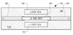
도 1은 대표적인 반도체 스위치 장치(100)의 실시예의 평면도를 도시한다. 예를 들어 전계 효과 트랜지스터(FET)의 제조에 일반적으로 사용되는 실리콘, GaAs, InP, SiC, 사파이어 기판인 종래의 기판(105)은 그 상에 금속 영역(110 및 140)이 배치된다. 금속 접점/상호 연결부(120 및 125)는 기판의 상부 표면에 배치되고 상호 연결부(120 및 125) 사이의 기판의 상부 표면 상에 길이 방향 스트립으로서 배치된 상 변화 영역(130)의 좌측 및 우측 단부와의 전도성 연결을 제공하는 역할을 한다. 금속 영역(110 및 140)은 상 변화 영역(130)과 접촉하지 않고 이로부터 전기적으로 격리된다. 영역(110 및 140)은 상 변화 영역(130)을 가로 질러 전압의 선택적 인가를 용이하게 하여 상 변화 재료가 전류 흐름에 대응하는 금속 또는 절연체 상에 있는지 또는 접점(120)으로부터 접점(125)으로 전류가 흐르지 않는지 여부를 제어한다.1 shows a top view of an embodiment of a representative
금속 영역(110 및 140)은 상 변화 영역(130)의 측면과 함께 이격된 샌드위치(spaced apart sandwich)를 제공한다. 금속 영역(110 및 140)은 요구되는 상 변화 전압과 같거나 더 큰 미리 결정된 전압이 전압원(미도시)에 의해 플레이트에 걸쳐 인가되거나 인가되지 않을 때와 같이 스위치(100)의 ON/OFF 작동을 제어하는 그 사이에 전기장의 존재/부재를 갖는 커패시터의 양극 및 음극 전압 플레이트로서 효과적으로 기능한다. 미리 결정된 전압이 인가될 때 플레이트 사이에서 발생하는 전기장은 대응하는 전기장을 통해 충분한 에너지를 제공하여 상 변화 영역이 절연체와 금속 상 중 하나에서 다른 상으로 변경되도록 한다. 전압(또는 필요한 상 변화 전압보다 낮은 전압)이 플레이트에 인가되지 않으면 다른 상이 존재한다. 상 변화 재료는 절연체 상 또는 금속 상의 안정된 정적 상태를 갖도록 제작될 수 있다. 절연체 상은 스위치가 OFF인 상태에 대응하고 금속 상은 스위치가 ON인 상태에 대응한다. 스위치(100)의 이러한 작동은 스위치 온도가 대략 실온에서 일정하게 유지되는 동안 발생하고 스위치 작동을 용이하게 하기 위해 압력 변화를 필요로 하지 않는다.
상 변화 영역(130)은 바람직하게는 수 볼트, 예를 들어 약 0.5 내지 5 볼트의 전압 차에 의해 생성되는 전기장의 존재 또는 부재에 따라 절연체와 금속 상 사이에서 변할 수 있는 MoxW1-xTe2로 구성된다. 이 작업에는 온도 변경이나 압력 변경이 필요하지 않다. 스위치(100)의 효과적인 작동은 공식에서 x가 0.66과 1.0 사이에서 변하는 MoxW1-xTe2를 사용하여 가능하다. Mo와 W 사이의 비율과 제어 전극 사이의 거리는 위상 변화를 일으키는데 필요한 전기장을 결정한다.The phase change region 130 is preferably Mo x W1-x which can vary between the insulator and the metal phase depending on the presence or absence of an electric field generated by a voltage difference of several volts, for example about 0.5 to 5 volts. It is composed ofTe 2 . No temperature change or pressure change is required for this operation. Effective operation of
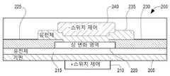
도 2는 본 발명에 따른 스위치(200)의 다른 예시적인 실시예의 측면도이다. 기판(205) 상에 금속 스위치 제어 접점(210)이 배치된다. 유전체 층(215)이 기판(205)의 상부 표면을 덮는다. 상 변화 재료의 영역(220)이 스위치 제어 접점(210)에 실질적으로 대향하는 유전체(215)의 상부 표면 상에 배치된다. 전도성 상호 연결부(225 및 230)는 상 변화 재료(220)의 영역에서 각각 좌우에 연결된다. 이들 상호 연결부는 전도성을 제공하며 외부 구성 요소(미도시)를 갖는 회로의 요소로서 스위치(200)의 연결을 용이하게 한다. 유전체 층(235)은 상 변화 영역(220)의 상부 표면 위에 배치되고 금속 스위치 제어 접점(240)에 대한 지지를 제공한다. 도 1의 실시예에 대해 설명된 동작과 유사하게, 스위치 제어 접점(210 및 240)에 걸쳐 연결된 전압에 의해 유도된 전기장은 상 변화 재료(220)의 위상을 제어하는데 이용될 수 있으며, 이는 스위치가 금속 상에 있는 경우 ON 상태에 있을 지 절연체 상에 있는 경우 OFF 상태에 있을 지를 결정한다. 스위치 제어 접점은 상 변화 영역(220)을 사이에 두고 샌드위치를 형성한다.2 is a side view of another exemplary embodiment of a
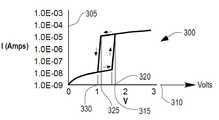
도 3은 MoxW1-xTe2의 위상 변화가 반도체의 OFF/ON 상태를 제어하는데 사용되는 반도체(100)에 대한 x-축(310) 상의 제어 전압의 변화에 대한 y-축(305) 상의 전류 흐름의 예시적인 변화를 설명하는 그래프(300)를 도시한다. 이 예에서, MoxW1-xTe2의 x는 1 내지 0.66 사이일 수 있다.3 shows the y-
제어 전압이 0에서 시작하여 315에서의 전압(약 0.5-5 볼트)까지 증가하면, 각 장치를 통과하는 전류 흐름은 약 10배로 증가하여 1E-08 암페어 초과로 완만하게 증가한다. 그러나, 315에서 320으로의 제어 전압의 매우 작은 추가 증가(약 30-50 밀리볼트 변화)는 전류 흐름이 30배 초과로 약 1E-05 암페어로 증가한다. 제어 전압을 추가로 증가시키면 도시된 바와 같이 추가 전류 흐름이 약간만 발생한다.When the control voltage starts at zero and increases to a voltage at 315 (about 0.5-5 volts), the current flow through each device increases by a factor of about 10, gently increasing over 1E-08 amps. However, a very small further increase in the control voltage from 315 to 320 (about a 30-50 millivolt change) increases the current flow by more than 30 times to about 1E-05 amps. Further increasing the control voltage results in only a small amount of additional current flow as shown.
320 초과의 제어 전압에서 시작하여 325에서의 전압으로 감소하면, 개별 장치를 통과하는 전류 흐름은 도시된 바와 같이 전류 흐름이 완만하게 감소한다. 그러나 제어 전압이 325에서 330으로 매우 작게 추가로 감소하면(약 30-50 밀리볼트 변화) 전류 흐름이 30배 초과로 약 1E-08 암페어로 감소한다. 제어 전압을 추가로 감소시키면 도시된 바와 같이 히스테리 루프가 OFF/ON 및 ON/OFF 위상 전이 사이에 존재한다는 것이 명백할 것이다.Starting at a control voltage greater than 320 and decreasing to a voltage at 325, the current flow through the individual devices gradually decreases as shown. However, a very small further decrease in the control voltage from 325 to 330 (about a 30-50 millivolt change) reduces the current flow by more than 30 times to about 1E-08 amps. Further reducing the control voltage will make it clear that a hysterical loop exists between the OFF/ON and ON/OFF phase transitions as shown.
이러한 실시예에서 설명된 스위치/트랜지스터는 약 30-50 밀리볼트(VGS 또는 스위치(100)에 걸친 전압)/10 배의 전류 변화(IDS 또는 스위치(100)에서 위상 변화 영역을 통한 전류 흐름)의 매우 가파른 스위칭 전이를 제공한다는 것을 이해하는 것이 중요하다. 이는 60 밀리볼트/10 배의 전류 변화보다 큰 스위칭 전이를 갖는 기존 실리콘 FET의 스위칭 전이와 비교하여 스위칭 상태 전이의 더 빠른 속도의 실질적인 개선을 제공한다. 당업자에 의해 이해되는 바와 같이, 장치에 대한 더 빠른 스위칭 시간은, 또한 그러한 장치가 아날로그 RF 증폭기로서 사용될 때와 같이 개선된 더 높은 주파수 성능에 대한 아날로그 주파수 도메인에 대응한다.The switch/transistor described in this embodiment is about 30-50 millivolts (VGS or voltage across switch 100)/10 times the current change (current flow through the phase change region in the IDS or switch 100) It is important to understand that it gives a very steep switching transition of This provides a substantial improvement in the faster rate of switching state transitions compared to the switching transitions of conventional silicon FETs, which have switching transitions greater than 60 millivolts/10 times the current change. As will be appreciated by those skilled in the art, faster switching times for the device also correspond to the analog frequency domain for improved higher frequency performance, such as when such a device is used as an analog RF amplifier.
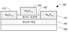
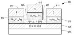
도 4, 5 및 6은 제조 공정의 상이한 단계에서 각각 반도체 장치(400, 500 및 600)을 예시하는 MoxW1-xTe2를 이용하는 반도체 장치의 실시예의 측면도를 도시한다. 도 4의 처리 단계에서 볼 수 있는 바와 같이, 실시예(400)는 Si, GaAs, InP, 사파이어 및 Sic와 같은 기판(408) 상에 배치된 Si, GaAs, InGaAs 또는 GaN과 같은 일반적인 반도체의 반도체 채널(405)을 포함한다. 소스 영역(410) 및 이격된 드레인 영역(415)은 반도체 채널(405)의 상부 표면 상에 증착된다. 유전체(420)는 소스와 드레인 사이의 반도체 채널(405)의 상부에 배치된다. 게이트 영역(425)은 소스 및 드레인 영역과 맞물리지 않는 사이의 유전체(420)의 상부에 증착된다. 소스, 게이트 및 드레인 영역은 MoxW1-x로서 합금 금속 Mo 및 W를 증착하여 각각 형성된다. 이러한 금속은 공동 증착되거나 초격자, 즉 조합의 박막이 차례로 반복되어 형성될 수 있다. 구성에서 “x”를 선택하는 것은 위상 변화를 일으키는데 필요한 전기장의 크기를 제어하는 한 가지 요소이다.4, 5 and 6 show side views of an embodiment of a semiconductor device usingMo x W1-x Te2 illustrating
예시적인 실시예에서, 소스는 예를 들어 0.2-0.3과 같은 더 높은 W 농도를 0.8-0.7의 개별 X 값으로 상 전이를 야기하기 위해 더 낮은 크기의 전기장을 요구하도록 제조된다. 게이트는 예를 들어 0-0.1과 같은 W 농도를 1-0.9의 대응하는 X 값으로 상 전이를 야기하기 위해 더 큰 크기의 전기장을 요구하도록 제조될 수 있다. 드레인은 게이트에 대해 설명된 동일한 비율을 사용하여 위상 전이를 야기하기 위해 더 높은 크기의 전기장을 요구하도록 제조될 수 있다.In an exemplary embodiment, the source is manufactured to require a lower magnitude electric field to cause a phase transition of a higher W concentration, for example 0.2-0.3, to an individual X value of 0.8-0.7. The gate can be made to require an electric field of greater magnitude to cause a phase transition, for example, with a W concentration such as 0-0.1 to a corresponding X value of 1-0.9. The drain can be made to require a higher magnitude electric field to cause a phase shift using the same ratio described for the gate.
도 5는 기화된 농도의 Te에 노출된 소스(410), 게이트(425) 및 드레인(415)을 갖는 반도체 장치(400)로부터 발생하는 반도체 장치(500)를 도시한다. Te의 증기는 400-1200℃의 상승된 온도에서 바람직하게 증착되며, 이는 전기장이 적용되지 않은 실온에서 상을 결정한다. Te가 완전히 반응된 상태에서, 반도체 장치(500)는 소스(510), 게이트(525) 및 드레인(515)을 가질 것이다.5 shows a
도 6은 종래의 금속 층/패드(605, 610 및 615)가 각각 소스(510), 게이트(525) 및 드레인(515) 상에 증착된 반도체 장치(600)를 도시한다. 이들 금속 층은 장치를 외부 회로에 연결하기 위해 반도체 장치(600)의 개별 단자로의 와이어/러너의 부착/결합을 용이하게 한다. 따라서, 반도체 장치(600)는 가파른 전이 디지털 스위치로서 또는 고주파 증폭기로서 아날로그 모드에서 작동할 준비가 된 완성되고 제조된 장치를 예시한다.6 shows a
도 7은 본 발명에 따른 반도체의 다른 실시예(700)의 측면도를 도시한다. 반도체(700)는 설명하는 바와 같이 수정으로 개선된 종래의 반도체 FET를 나타낸다. 종래 기판(705)은 그 위에 반도체 채널을 배치했다. 종래 소스(715) 및 이격된 드레인(720)은 반도체 채널(710)의 상부에 배치된다. 소스와 드레인 사이에는 게이트 유전체(725)가 배치되며, 그 상에 금속 게이트(730)가 소스와 드레인 사이에서 증착되며 드레인 보다 소스에 일반적으로 더 가깝다. 상 변화 재료(735)의 층은 게이트(730)와 드레인(720) 사이에 이격된 게이트 유전체(725)의 상부에 증착된다. 동작 동안, 게이트와 드레인 사이의 변화하는 전기장은 MoxW1-xTe2로 만들어진 상 변화 층(735)이 금속과 절연체 사이를 변환하게 할 것이다. 금속 상에서 이 확장된 차폐 플레이트는 도면에서 xxx로 표시된 것과 같이 게이트와 드레인 사이에 형성될 수 있는 트랩을 차단할 것이다. 절연체 상에서 차폐 플레이트(735)는 더 이상 전기적으로 전도되지 않으며 게이트와 드레인 사이에 완전 금속 차폐 플레이트 층을 사용할 때 일반적으로 나타나는 기생 단채널 효과를 피한다.7 shows a side view of another
도 8은 본 발명에 따른 반도체의 다른 실시예(800)의 측면도를 도시한다. 반도체(800)는 설명될 바와 같이 다른 수정으로 개선된 종래의 FET를 나타낸다. 종래의 기판(805)은 그 상에 반도체 채널(810)을 배치했다. 종래의 소스(815) 및 이격된 드레인(820)은 반도체 채널(810)의 상부에 배치된다. 소스 및 드레인 사이에는 게이트 유전체(825)가 배치되며 그 상에 금속 게이트(830)가 소스 및 드레인 사이에 배치되며 일반적으로 드레인보다 소스에 더 가깝다. 상 변화 재료(835)의 층은 드레인에 가장 가까운 게이트(830)의 에지에 연결되고 드레인(820)을 향해 측방향으로 연장되지만 결합되지 않고 게이트 유전체(825)의 상부에 증착된다. 게이트와 드레인 영역 사이에 적용된 필드는 상 변화 재료(835)에 의해 제공되는 게이트 확장을 키고 끄는데 이용될 수 있다. OFF 상태에서 상 변화 재료는 게이트의 유효 영역을 개선된 고주파 응답을 제공하는 물리적으로 짧은 게이트(830)가 차지하는 영역만으로 만드는 절연체로 기능한다. ON 상태에서 상 변화 재료는 유효 게이트를 상 변화 확장이 채널 표면에서 차폐 트랩으로 기능하여 고장을 개선하고 짧은 채널 효과를 완화하는 더 긴 유효 게이트를 제공하는 게이트(830)와 상 변화 재료(835)의 결합된 조합으로 만드는 금속으로 기능한다.8 shows a side view of another
도 9는 본 발명에 따른 FET 반도체의 실시예의 제조 단계를 나타내는 흐름도를 도시한다. 단계(905)에서 종래의 반도체 FET 구조가 제조되지만 장치의 단자와의 더 쉬운 연결을 위해 증착될 정상적인 금속 접점이 없다. 단계(910)에서 MoxW1-x의 층이 소스, 드레인 및 게이트 영역 상에 증착된다. 이 상 변화 재료는 Mo 및 W의 동시 증착에 의해 증착될 수 있거나, 각각의 얇은 단층이 교대로 증착될 수 있다. W 대 Mo의 비율은 전기장이 적용되지 않은 실온에서 정적 위상을 설정하기 위해 제어될 수 있다. 상 변화 재료에 예를 들어 전압 차동에 의한 것과 같은 적절한 전기장의 적용이 상 변화를 야기할 것이다: 금속에서 절연체로 또는 절연체에서 금속으로. 공식에서 유용한 비율과 대응하는 X 값은 이전에 논의되었다. 단계(915)에서 상 변화 재료의 층은 상승된 온도에서 Te의 증기에 상 변화 재료의 노출된 표면을 노출시킴으로써 그 상에 Te가 증착되었다. 일반적으로 섭씨 400 내지 600도 사이의 온도를 사용하여 증착된 Te는 실온 작동 시 절연 상태를 갖는 상 변화 재료를 생성하고 섭씨 650 내지 1100도 사이의 온도를 사용하여 실온 작동 시 금속 상태를 갖는 상 변화 재료가 생성된다. 최종 단계(920)에서, 금속 층이 소스/드레인/게이트 연결 접촉을 제공하는 상 변화 층 상에 증착된다.Fig. 9 shows a flow chart showing the manufacturing steps of an embodiment of a FET semiconductor according to the present invention. In
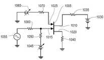
도 10은 FET(1005)에서 사용되는 상 변화 재료의 위상을 제어하기에 충분한 필드를 생성하는 전압 차동을 공급하는데 사용될 수 있는 예시적인 회로의 개략도를 도시한다. FET(1005)는 드레인(1010), 게이트(1015) 및 소스(1020)를 포함한다. 추가적인 제어 게이트/단자(1025)는 본 명세서에 앞서 설명된 바와 같이 상 변화 재료로 만들어진다. 게이트(1025)는 도 7에 도시된 바와 같은 요소(735)의 개략도이다. DC 전압 소스(1030)는 FET(1005)가 활성/ON 상태에 있다고 가정하고 부하(1035)를 통해 드레인(1010)에 전류를 공급한다. 이해되는 바와 같이, 드레인 전류는 FET의 반도체 채널을 통해 흐르고 소스(120)에서 나와 회로 요소(1040)를 통해 접지로 가서 회로를 완성하여 전압 소스(1030)로 되돌아 간다. 가변 DC 전압 소스(1045)는 작동 게이트 전압을 절연 회로 소자(1050)를 통해 게이트(1015)에 제공한다. AC 신호 소스(1055)는 절연 회로 소자(1060)를 통해 게이트(1015)에 연결된다. FET(1005)의 이득에 따라, AC 신호 소스(1055)로부터의 신호는 드레인(1010)에서 증폭된 크기로 나타날 것이다.10 shows a schematic diagram of an exemplary circuit that may be used to provide a voltage differential that creates a field sufficient to control the phase of the phase change material used in
본 발명의 실시예에 따르면, 가변 DC 전압 소스(1065)는 절연 회로 소자(1070)를 통해 상 변화 재료로 만들어진 추가 제어 게이트(1025)에 결합된다. 전압 소스(1065)에 의해 인가되는 전압을 변화시키는 상 변화 재료의 반도체 및 절연체 위상을 제어하는 이점을 도 7 및 도 8을 참조하여 설명된다. DC 전압 소스(1065)는 금속 및 절연체 상 사이에서 상 변화 재료를 전이하는데 필요한 미리 결정된 상 변화 전압 레벨을 제공하기에 충분한 전압 범위를 갖는다.In accordance with an embodiment of the present invention, a variable
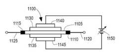
도 11은 ON/OFF 반도체 스위치(1100)로서 사용되는 상 변화 재료의 위상을 제어하기에 충분한 필드를 생성할 전압 차동을 공급하는데 사용될 수 있는 예시적인 회로의 개략도를 도시한다. 이 예시적인 실시예에서, 채널(1105)은 여기에 설명된 상 변화 재료로 만들어진다. 금속 접점(1110 및 1115)은 각각 연결 와이어(1120 및 1125)의 부착을 허용하기 위해 채널(1105)의 각각의 단부에 배치된다. 와이어는 ON/OFF 반도체를 스위치(1100)에 의해 전류의 흐름이 제어되는 다른 외부 회로(미도시)에 연결하는데 사용될 수 있다. 유전체 층(1130 및 1135)은 채널(1105)의 대향하는 측면에 배치된다. 금속 패드(1140 및 1145)는 유전체 층(1130 및 1135) 상에 각각 배치되어 채널(1105)과 샌드위치를 형성한다. 가변 DC 전압 소스(1150)는 금속 패드(1140 및 1145)에 걸쳐 연결되어 소스(1150)에 의해 공급되는 DC 전압이 채널(1150)의 측면에 유도되는 대응하는 내부 전계를 생성한다. 이전에 설명된 바와 같이, 채널(1105)에 사용되는 상 변화 재료는 소스(1150)에 의해 인가되는 전압 없이 금속 및 절연체 상 중 하나에 있을 것이다. 미리 결정된 상 변화 전압 레벨에 도달하기 위해 소스(1150)에 인가된 충분한 전압으로, 채널(1105)에 사용되는 상 변화 재료는 금속 및 절연체 상 중 다른 것으로 전이될 것이다. 따라서, 반도체 스위치(1100)는 채널(1105)이 금속 상에 있을 때 ON 상태와 채널이 절연체 상에 있을 때 OFF 상태 사이에서 제어 가능하게 스위칭될 수 있다. 앞서 설명했듯이, ON/OFF 상태 간의 전이는 실리콘 기술을 기반으로 하는 기존 스위치보다 짧은 시간 프레임 내에 달성될 수 있다.11 shows a schematic diagram of an exemplary circuit that may be used to supply a voltage differential that will create a field sufficient to control the phase of the phase change material used as the ON/
본 발명의 예시적인 구현이 여기에 상세히 묘사되고 설명되었지만, 본 발명의 사상을 벗어나지 않고 다양한 수정, 추가, 대체 등이 이루어질 수 있음은 당업자에게 명백할 것이다.While exemplary implementations of the invention have been described and described in detail herein, it will be apparent to those skilled in the art that various modifications, additions, substitutions, etc. can be made without departing from the spirit of the invention.
본 발명의 범위는 다음 청구 범위에서 정의된다.The scope of the invention is defined in the following claims.
Claims (15)
Translated fromKorean제1 및 제2 대향 단부 및 제1 및 제2 대향 측면을 갖는 반도체 채널 ― 상기 반도체 채널은 반도체 채널이 금속 상에 있는 동안 반도체 채널을 통한 제1 단부로부터 제2 단부로의 전류 흐름을 지원함 ―;
MOxW1-xTe2의 상 변화 재료로 만들어진 반도체 채널;을 포함하며,
상기 상 변화 재료는 제1 및 제2 측면에 걸쳐 전압 차동이 없어서 필드가 존재하지 않을 때 금속 및 절연체 상 중 하나에 있으며, 전압 차동으로 인한 필드가 제1 및 제2 측면에 걸쳐 존재하는 상 변화 전압 차동보다 클 때 금속 및 절연체 상 중 다른 것에 있으며, 반도체 채널이 절연체 상에 있는 동안 제1 단부에서 제2 단부로 실질적인 전류가 흐르지 않는,
반도체.As a semiconductor,
a semiconductor channel having first and second opposing ends and first and second opposing sides, the semiconductor channel supporting current flow from the first end to the second end through the semiconductor channel while the semiconductor channel is on a metal; ;
A semiconductor channel made of a phase change material ofMO x W1-x Te2;
The phase change material is on one of the metal and insulator phases when no field is present due to no voltage differential across the first and second sides, the phase change in which a field due to the voltage differential exists across the first and second sides in the other of the metal and insulator phases when greater than the voltage differential, wherein no substantial current flows from the first end to the second end while the semiconductor channel is on the insulator;
semiconductor.
반도체가 ON/OFF 스위치로서 기능하는 경우, ON 상태는 금속 상에 있는 상 변화 재료에 대응하며 OFF 상태는 절연체 상에 있는 상 변화 재료에 대응하는,
반도체.According to claim 1,
when the semiconductor functions as an ON/OFF switch, the ON state corresponds to the phase change material on the metal and the OFF state corresponds to the phase change material on the insulator;
semiconductor.
반도체 채널을 지지하는 기판;
제1 및 제2 금속 패드;
상기 기판 상에 배치되고 제1 측면에 맞물리는 제1 유전체 재료 ― 상기 제1 유전체 재료는 제1 측면으로부터 제1 금속 패드를 분리시킴 ―;
제2 측면 상에 배치되는 제2 유전체 재료 ― 상기 제2 유전체 재료는 제2 측면으로부터 제2 금속 패드를 분리시킴 ―;를 더 포함하며,
상기 제1 및 제2 금속 패드는 반도체 채널과 함께 샌드위치를 형성하고 제2 금속 패드에 대해 제1 금속 패드에서 설정되는 전압 차동에 따라 반도체 채널에 걸쳐 필드의 적용을 용이하게 하는,
반도체.According to claim 1,
a substrate supporting the semiconductor channel;
first and second metal pads;
a first dielectric material disposed on the substrate and engaging a first side, the first dielectric material separating the first metal pad from the first side;
a second dielectric material disposed on the second side, the second dielectric material separating the second metal pad from the second side;
wherein the first and second metal pads form a sandwich with the semiconductor channel and facilitate application of a field across the semiconductor channel according to a voltage differential established at the first metal pad with respect to the second metal pad;
semiconductor.
상기 반도체와 절연체 상 사이의 전이에 대응하는 ON 및 OFF 상태 사이의 전이는 반도체 채널에 걸쳐 60 밀리볼트의 전압 차동마다 10배 초과의 전류 흐름 속도로 진행하는,
반도체.3. The method of claim 2,
a transition between an ON and OFF state corresponding to a transition between the semiconductor and insulator phases proceeds at a current flow rate of greater than ten times for every 60 millivolt voltage differential across the semiconductor channel;
semiconductor.
ON 및 OFF 상태 사이의 전이는 상 변화 재료를 사용하지 않는 종래의 FET에 비해 반도체 채널에 걸쳐 전압 차동의 각 유닛 변화에 대해 더 큰 전류 흐름 속도로 진행하는,
반도체.5. The method of claim 4,
The transition between the ON and OFF states proceeds with a greater current flow rate for each unit change of voltage differential across the semiconductor channel compared to a conventional FET that does not use a phase change material.
semiconductor.
상기 상 변화 재료는 반도체 채널이 실질적으로 실온에서 유지되는 동안 금속 및 절연체 상 중 하나에서 금속 및 절연체 상 중 다른 것으로 변경되는,
반도체.According to claim 1,
wherein the phase change material changes from one of a metal and an insulator phase to the other of a metal and insulator phase while the semiconductor channel is maintained at substantially room temperature.
semiconductor.
반도체 채널;
상기 반도체 채널의 표면 상에 배치된 이격된 소스 및 드레인 영역;
소스 및 드레인 영역 사이의 반도체 채널의 표면 상에 배치된 유전체 층;
반도체 채널의 표면에 대향하는 유전체 층의 표면 상에 배치되는 게이트 영역 ― 게이트 영역은 소스 및 드레인 영역 사이에 배치됨 ―;
각각 MOxW1-xTe2 상 변화 재료를 포함하는 소스, 게이트 및 드레인 영역;
소스, 게이트 및 드레인 영역과의 전기적 연결을 용이하게 하기 위해 소스, 게이트 및 드레인 영역 각각의 상에 배치되는 금속 접점;을 포함하는,
전계 효과 트랜지스터.A field effect transistor (FET) comprising:
semiconductor channel;
spaced apart source and drain regions disposed on a surface of the semiconductor channel;
a dielectric layer disposed on a surface of the semiconductor channel between the source and drain regions;
a gate region disposed on a surface of the dielectric layer opposite a surface of the semiconductor channel, the gate region disposed between the source and drain regions;
source, gate and drain regions each comprising MOx W1-x Te2 phase change material;
a metal contact disposed on each of the source, gate and drain regions to facilitate electrical connection with the source, gate and drain regions;
field effect transistor.
재료 조성 공식의 x는 1.0 이하의 양수이고, x의 값은 소스 및 게이트 영역에서 사용되는 재료에 따라 다르며, 소스 영역은 게이트 영역에 대한 x 값보다 더 작은 x 값을 갖는,
전계 효과 트랜지스터.8. The method of claim 7,
x in the material composition formula is a positive number less than or equal to 1.0, the value of x depends on the material used in the source and gate regions, the source region having an x value smaller than the x value for the gate region;
field effect transistor.
각 영역에 대한 재료 조성 공식의 x의 값은:
소스 영역에 대해 0.7<x<0.8,
게이트 영역에 대해 0.9<x<1.0,
드레인 영역에 대해 0.9<x<1.0인,
전계 효과 트랜지스터.9. The method of claim 8,
The value of x in the material composition formula for each region is:
0.7<x<0.8 for the source region,
0.9<x<1.0 for the gate area,
0.9<x<1.0 for the drain region,
field effect transistor.
상기 상 변화 재료는 상 변화 재료에 걸쳐 미리 결정된 상 변화 전압보다 큰 전압 차동이 존재하는지에 따라 실온에서 금속 및 절연체 상 중 하나에서 금속 및 절연체 상 중 다른 것으로 변경되는,
전계 효과 트랜지스터.8. The method of claim 7,
wherein the phase change material changes from one of the metal and insulator phases to the other of the metal and insulator phase at room temperature depending on whether a voltage differential greater than a predetermined phase change voltage exists across the phase change material.
field effect transistor.
반도체 채널;
상기 반도체 채널의 표면 상에 배치된 이격된 소스 및 드레인 영역;
소스 및 드레인 영역 사이의 반도체 채널의 표면 상에 배치된 유전체 층;
반도체 채널의 표면에 대향하는 유전체 층의 표면 상에 배치되는 게이트 영역 ― 게이트 영역은 소스 및 드레인 영역 사이에 배치됨 ―;
각각 금속 영역이 있는 소스, 게이트 및 드레인 영역;
게이트 영역 및 드레인 영역 사이에서 유전체 층의 표면 상에 배치된 제어 영역 ― 상기 제어 영역은, 제어 전압 계가 제어 영역에 걸쳐 존재하는지 또는 부재하는지에 기초하여 선택 가능한 반도체 상 및 절연체 상을 갖는 MOxW1-xTe2 상 변화 재료를 포함함 ―;을 포함하며,
상기 반도체 상에서 제어 영역은 게이트 영역 및 드레인 영역 사이의 반도체 채널의 표면에서 트랩을 보호하도록 차폐부로 기능하며,
절연체 상에서 제어 영역은 게이트 영역에 인접한 물리적 활성 영역을 제공하지 않음으로써 FET의 고주파 응답을 향상시키는,
전계 효과 트랜지스터.A field effect transistor (FET) comprising:
semiconductor channel;
spaced apart source and drain regions disposed on a surface of the semiconductor channel;
a dielectric layer disposed on a surface of the semiconductor channel between the source and drain regions;
a gate region disposed on a surface of the dielectric layer opposite a surface of the semiconductor channel, the gate region disposed between the source and drain regions;
source, gate and drain regions each having a metal region;
a control region disposed on a surface of the dielectric layer between the gate region and the drain region, wherein the control region is MOx W having a semiconductor phase and an insulator phase selectable based on whether a control voltmeter is present or absent across the control region.1-x Te2 containing phase change material-;
The control region on the semiconductor functions as a shield to protect the trap at the surface of the semiconductor channel between the gate region and the drain region,
The control region on the insulator improves the high frequency response of the FET by not providing a physically active region adjacent the gate region.
field effect transistor.
금속 조성물 공식에서 x는 1.0 이하의 양수이며, x 값은 xx 및 yy 사이인,
전계 효과 트랜지스터.12. The method of claim 11,
In the metal composition formula, x is a positive number less than or equal to 1.0, and the value of x is between xx and yy;
field effect transistor.
상기 게이트 영역 및 제어 영역은 서로 접하지 않고 이격되는,
전계 효과 트랜지스터.12. The method of claim 11,
The gate region and the control region are spaced apart from each other,
field effect transistor.
상기 게이트 영역 및 제어 영역은 서로 접하지 않고 서로 전기적으로 연결되는,
전계 효과 트랜지스터.12. The method of claim 11,
wherein the gate region and the control region are not in contact with each other and are electrically connected to each other;
field effect transistor.
상기 상 변화 재료는 상 변화 재료에 걸쳐 전압 차동이 존재하는지 여부에 따라 실온에서 금속 및 절연체 상 중 하나로부터 금속 및 절연체 상 중 다른 것으로 변경되는,
전계 효과 트랜지스터.12. The method of claim 11,
wherein the phase change material changes from one of the metal and insulator phases to the other of the metal and insulator phase at room temperature depending on whether a voltage differential exists across the phase change material.
field effect transistor.
Applications Claiming Priority (3)
| Application Number | Priority Date | Filing Date | Title |
|---|---|---|---|
| US16/254,218 | 2019-01-22 | ||
| US16/254,218US10811601B2 (en) | 2019-01-22 | 2019-01-22 | Semiconductor devices using insulator-metal phase change materials and method for fabrication |
| PCT/US2019/062377WO2020154028A1 (en) | 2019-01-22 | 2019-11-20 | Semiconductor devices using insulator-metal phase change materials |
Publications (2)
| Publication Number | Publication Date |
|---|---|
| KR20210111776Atrue KR20210111776A (en) | 2021-09-13 |
| KR102772338B1 KR102772338B1 (en) | 2025-02-21 |
Family
ID=68835387
Family Applications (1)
| Application Number | Title | Priority Date | Filing Date |
|---|---|---|---|
| KR1020217021456AActiveKR102772338B1 (en) | 2019-01-22 | 2019-11-20 | Semiconductor devices using insulator-metal phase change materials |
Country Status (6)
| Country | Link |
|---|---|
| US (2) | US10811601B2 (en) |
| EP (2) | EP4401149A3 (en) |
| JP (2) | JP2022517129A (en) |
| KR (1) | KR102772338B1 (en) |
| SG (1) | SG11202107020WA (en) |
| WO (1) | WO2020154028A1 (en) |
Cited By (1)
| Publication number | Priority date | Publication date | Assignee | Title |
|---|---|---|---|---|
| KR20240038376A (en)* | 2022-09-16 | 2024-03-25 | 한국과학기술원 | Semiconductor device |
Families Citing this family (2)
| Publication number | Priority date | Publication date | Assignee | Title |
|---|---|---|---|---|
| US11805711B2 (en)* | 2020-09-28 | 2023-10-31 | International Business Machines Corporation | Phase-change memory (PCM) including liner reducing resistance drift |
| KR20230170270A (en)* | 2022-06-10 | 2023-12-19 | 한국과학기술원 | Ferroelectric thin film |
Citations (4)
| Publication number | Priority date | Publication date | Assignee | Title |
|---|---|---|---|---|
| JP2006148141A (en)* | 2004-11-24 | 2006-06-08 | Taiwan Semiconductor Manufacturing Co Ltd | Self-aligned double gate device and method for forming the same |
| US20060120148A1 (en)* | 2004-10-26 | 2006-06-08 | Samsung Electronics Co., Ltd. | Semiconductor memory device with stacked memory cell and method of manufacturing the stacked memory cell |
| US20140110765A1 (en)* | 2012-10-22 | 2014-04-24 | International Business Machines Corporation | Field effect transistor having phase transition material incorporated into one or more components for reduced leakage current |
| US20160181516A1 (en)* | 2014-02-21 | 2016-06-23 | Board Of Trustees Of The Leland Stanford Junior University | Phase transformation in transition metal dichalcogenides |
Family Cites Families (9)
| Publication number | Priority date | Publication date | Assignee | Title |
|---|---|---|---|---|
| US5461250A (en) | 1992-08-10 | 1995-10-24 | International Business Machines Corporation | SiGe thin film or SOI MOSFET and method for making the same |
| JP4525928B2 (en) | 2005-12-27 | 2010-08-18 | セイコーエプソン株式会社 | Manufacturing method of semiconductor device |
| JP4669957B2 (en)* | 2007-03-02 | 2011-04-13 | 日本電気株式会社 | Semiconductor device using graphene and method for manufacturing the same |
| JPWO2014128990A1 (en)* | 2013-02-19 | 2017-02-02 | 国立研究開発法人産業技術総合研究所 | Phase change channel transistor and driving method thereof |
| JP6421446B2 (en)* | 2013-06-28 | 2018-11-14 | 株式会社リコー | Field effect transistor, display element, image display apparatus and system |
| US9455343B2 (en)* | 2013-09-27 | 2016-09-27 | Intel Corporation | Hybrid phase field effect transistor |
| TWI686874B (en)* | 2014-12-26 | 2020-03-01 | 日商半導體能源研究所股份有限公司 | Semiconductor device, display device, display module, electronic evice, oxide, and manufacturing method of oxide |
| KR102412965B1 (en) | 2014-12-30 | 2022-06-24 | 삼성전자주식회사 | Electronic device having two dimensional material layer and method of manufacturing the electronic device using inkjet printing |
| US11034847B2 (en)* | 2017-07-14 | 2021-06-15 | Samsung Electronics Co., Ltd. | Hardmask composition, method of forming pattern using hardmask composition, and hardmask formed from hardmask composition |
- 2019
- 2019-01-22USUS16/254,218patent/US10811601B2/enactiveActive
- 2019-11-20EPEP24179818.0Apatent/EP4401149A3/enactivePending
- 2019-11-20SGSG11202107020WApatent/SG11202107020WA/enunknown
- 2019-11-20EPEP19817555.6Apatent/EP3915154B1/enactiveActive
- 2019-11-20KRKR1020217021456Apatent/KR102772338B1/enactiveActive
- 2019-11-20JPJP2021541541Apatent/JP2022517129A/enactivePending
- 2019-11-20WOPCT/US2019/062377patent/WO2020154028A1/ennot_activeCeased
- 2020
- 2020-09-04USUS17/012,400patent/US11018296B1/enactiveActive
- 2023
- 2023-10-03JPJP2023172077Apatent/JP7686717B2/enactiveActive
Patent Citations (4)
| Publication number | Priority date | Publication date | Assignee | Title |
|---|---|---|---|---|
| US20060120148A1 (en)* | 2004-10-26 | 2006-06-08 | Samsung Electronics Co., Ltd. | Semiconductor memory device with stacked memory cell and method of manufacturing the stacked memory cell |
| JP2006148141A (en)* | 2004-11-24 | 2006-06-08 | Taiwan Semiconductor Manufacturing Co Ltd | Self-aligned double gate device and method for forming the same |
| US20140110765A1 (en)* | 2012-10-22 | 2014-04-24 | International Business Machines Corporation | Field effect transistor having phase transition material incorporated into one or more components for reduced leakage current |
| US20160181516A1 (en)* | 2014-02-21 | 2016-06-23 | Board Of Trustees Of The Leland Stanford Junior University | Phase transformation in transition metal dichalcogenides |
Cited By (1)
| Publication number | Priority date | Publication date | Assignee | Title |
|---|---|---|---|---|
| KR20240038376A (en)* | 2022-09-16 | 2024-03-25 | 한국과학기술원 | Semiconductor device |
Also Published As
| Publication number | Publication date |
|---|---|
| US20200235293A1 (en) | 2020-07-23 |
| JP7686717B2 (en) | 2025-06-02 |
| WO2020154028A1 (en) | 2020-07-30 |
| EP3915154A1 (en) | 2021-12-01 |
| JP2022517129A (en) | 2022-03-04 |
| SG11202107020WA (en) | 2021-08-30 |
| US10811601B2 (en) | 2020-10-20 |
| EP3915154B1 (en) | 2024-07-03 |
| KR102772338B1 (en) | 2025-02-21 |
| EP4401149A3 (en) | 2024-10-30 |
| US11018296B1 (en) | 2021-05-25 |
| EP4401149A2 (en) | 2024-07-17 |
| JP2023175906A (en) | 2023-12-12 |
Similar Documents
| Publication | Publication Date | Title |
|---|---|---|
| JP7686717B2 (en) | Semiconductor device using insulator-metal phase change material and method for manufacturing the semiconductor device | |
| US3339128A (en) | Insulated offset gate field effect transistor | |
| KR101680768B1 (en) | Transistor and electronic device including the same | |
| US6100571A (en) | Fet having non-overlapping field control electrode between gate and drain | |
| JP4968068B2 (en) | Field effect transistor | |
| EP2601680B1 (en) | High electron mobility transistors with field plate electrode | |
| US20080272397A1 (en) | Semiconductor device with modulated field element | |
| US20070228401A1 (en) | Semiconductor device | |
| JP7511662B2 (en) | Transistor with resistive field plate | |
| JP7720921B2 (en) | Photoconductive semiconductor switch fabricated laterally alongside a GaN-on-Si field-effect transistor | |
| US9391187B2 (en) | Semiconductor heterojunction device | |
| US3409812A (en) | Space-charge-limited current triode device | |
| EP0481113B1 (en) | Digitally controlled field effect attenuator devices | |
| JP2007208036A (en) | Semiconductor element | |
| HK1007361B (en) | Digitally controlled field effect attenuator devices | |
| JP4272547B2 (en) | Field effect transistor and integrated circuit device and switch circuit using the same | |
| JP3772562B2 (en) | Semiconductor device | |
| CN218299803U (en) | Electronic device and structure of electronic device | |
| JP3137290B2 (en) | Digitally controlled variable attenuator using field effect device | |
| KR102109712B1 (en) | Graphene-Silicon Junction Transistor | |
| US3436619A (en) | Insulated gate field-effect transistor with widening current path between source and drain | |
| KR100765962B1 (en) | Coplanar gate quantum dot transistor manufacturing method | |
| JP2006165021A (en) | Switch integrated circuit device and manufacturing method thereof | |
| JP2006165022A (en) | Switch integrated circuit device and manufacturing method thereof | |
| JP2006165020A (en) | Switch integrated circuit device and manufacturing method thereof |
Legal Events
| Date | Code | Title | Description |
|---|---|---|---|
| PA0105 | International application | Patent event date:20210708 Patent event code:PA01051R01D Comment text:International Patent Application | |
| PG1501 | Laying open of application | ||
| PA0201 | Request for examination | Patent event code:PA02012R01D Patent event date:20221017 Comment text:Request for Examination of Application | |
| E902 | Notification of reason for refusal | ||
| PE0902 | Notice of grounds for rejection | Comment text:Notification of reason for refusal Patent event date:20240430 Patent event code:PE09021S01D | |
| E701 | Decision to grant or registration of patent right | ||
| PE0701 | Decision of registration | Patent event code:PE07011S01D Comment text:Decision to Grant Registration Patent event date:20250122 | |
| GRNT | Written decision to grant | ||
| PR0701 | Registration of establishment | Comment text:Registration of Establishment Patent event date:20250219 Patent event code:PR07011E01D | |
| PR1002 | Payment of registration fee | Payment date:20250219 End annual number:3 Start annual number:1 | |
| PG1601 | Publication of registration |