KR20210107645A - Display devices and electronic devices - Google Patents
Display devices and electronic devicesDownload PDFInfo
- Publication number
- KR20210107645A KR20210107645AKR1020217017596AKR20217017596AKR20210107645AKR 20210107645 AKR20210107645 AKR 20210107645AKR 1020217017596 AKR1020217017596 AKR 1020217017596AKR 20217017596 AKR20217017596 AKR 20217017596AKR 20210107645 AKR20210107645 AKR 20210107645A
- Authority
- KR
- South Korea
- Prior art keywords
- transistor
- circuit
- electrode
- electrically connected
- source
- Prior art date
- Legal status (The legal status is an assumption and is not a legal conclusion. Google has not performed a legal analysis and makes no representation as to the accuracy of the status listed.)
- Ceased
Links
Images


Classifications
- G—PHYSICS
- G09—EDUCATION; CRYPTOGRAPHY; DISPLAY; ADVERTISING; SEALS
- G09G—ARRANGEMENTS OR CIRCUITS FOR CONTROL OF INDICATING DEVICES USING STATIC MEANS TO PRESENT VARIABLE INFORMATION
- G09G3/00—Control arrangements or circuits, of interest only in connection with visual indicators other than cathode-ray tubes
- G09G3/20—Control arrangements or circuits, of interest only in connection with visual indicators other than cathode-ray tubes for presentation of an assembly of a number of characters, e.g. a page, by composing the assembly by combination of individual elements arranged in a matrix no fixed position being assigned to or needed to be assigned to the individual characters or partial characters
- G09G3/34—Control arrangements or circuits, of interest only in connection with visual indicators other than cathode-ray tubes for presentation of an assembly of a number of characters, e.g. a page, by composing the assembly by combination of individual elements arranged in a matrix no fixed position being assigned to or needed to be assigned to the individual characters or partial characters by control of light from an independent source
- G09G3/36—Control arrangements or circuits, of interest only in connection with visual indicators other than cathode-ray tubes for presentation of an assembly of a number of characters, e.g. a page, by composing the assembly by combination of individual elements arranged in a matrix no fixed position being assigned to or needed to be assigned to the individual characters or partial characters by control of light from an independent source using liquid crystals
- G09G3/3611—Control of matrices with row and column drivers
- G09G3/3685—Details of drivers for data electrodes
- G09G3/3688—Details of drivers for data electrodes suitable for active matrices only
- G—PHYSICS
- G02—OPTICS
- G02F—OPTICAL DEVICES OR ARRANGEMENTS FOR THE CONTROL OF LIGHT BY MODIFICATION OF THE OPTICAL PROPERTIES OF THE MEDIA OF THE ELEMENTS INVOLVED THEREIN; NON-LINEAR OPTICS; FREQUENCY-CHANGING OF LIGHT; OPTICAL LOGIC ELEMENTS; OPTICAL ANALOGUE/DIGITAL CONVERTERS
- G02F1/00—Devices or arrangements for the control of the intensity, colour, phase, polarisation or direction of light arriving from an independent light source, e.g. switching, gating or modulating; Non-linear optics
- G02F1/01—Devices or arrangements for the control of the intensity, colour, phase, polarisation or direction of light arriving from an independent light source, e.g. switching, gating or modulating; Non-linear optics for the control of the intensity, phase, polarisation or colour
- G02F1/13—Devices or arrangements for the control of the intensity, colour, phase, polarisation or direction of light arriving from an independent light source, e.g. switching, gating or modulating; Non-linear optics for the control of the intensity, phase, polarisation or colour based on liquid crystals, e.g. single liquid crystal display cells
- G02F1/133—Constructional arrangements; Operation of liquid crystal cells; Circuit arrangements
- G02F1/136—Liquid crystal cells structurally associated with a semi-conducting layer or substrate, e.g. cells forming part of an integrated circuit
- G02F1/1362—Active matrix addressed cells
- G02F1/1368—Active matrix addressed cells in which the switching element is a three-electrode device
- G—PHYSICS
- G09—EDUCATION; CRYPTOGRAPHY; DISPLAY; ADVERTISING; SEALS
- G09F—DISPLAYING; ADVERTISING; SIGNS; LABELS OR NAME-PLATES; SEALS
- G09F9/00—Indicating arrangements for variable information in which the information is built-up on a support by selection or combination of individual elements
- G09F9/30—Indicating arrangements for variable information in which the information is built-up on a support by selection or combination of individual elements in which the desired character or characters are formed by combining individual elements
- G—PHYSICS
- G09—EDUCATION; CRYPTOGRAPHY; DISPLAY; ADVERTISING; SEALS
- G09G—ARRANGEMENTS OR CIRCUITS FOR CONTROL OF INDICATING DEVICES USING STATIC MEANS TO PRESENT VARIABLE INFORMATION
- G09G3/00—Control arrangements or circuits, of interest only in connection with visual indicators other than cathode-ray tubes
- G09G3/20—Control arrangements or circuits, of interest only in connection with visual indicators other than cathode-ray tubes for presentation of an assembly of a number of characters, e.g. a page, by composing the assembly by combination of individual elements arranged in a matrix no fixed position being assigned to or needed to be assigned to the individual characters or partial characters
- G09G3/34—Control arrangements or circuits, of interest only in connection with visual indicators other than cathode-ray tubes for presentation of an assembly of a number of characters, e.g. a page, by composing the assembly by combination of individual elements arranged in a matrix no fixed position being assigned to or needed to be assigned to the individual characters or partial characters by control of light from an independent source
- G09G3/36—Control arrangements or circuits, of interest only in connection with visual indicators other than cathode-ray tubes for presentation of an assembly of a number of characters, e.g. a page, by composing the assembly by combination of individual elements arranged in a matrix no fixed position being assigned to or needed to be assigned to the individual characters or partial characters by control of light from an independent source using liquid crystals
- G09G3/3611—Control of matrices with row and column drivers
- G09G3/3648—Control of matrices with row and column drivers using an active matrix
- G—PHYSICS
- G09—EDUCATION; CRYPTOGRAPHY; DISPLAY; ADVERTISING; SEALS
- G09G—ARRANGEMENTS OR CIRCUITS FOR CONTROL OF INDICATING DEVICES USING STATIC MEANS TO PRESENT VARIABLE INFORMATION
- G09G3/00—Control arrangements or circuits, of interest only in connection with visual indicators other than cathode-ray tubes
- G09G3/20—Control arrangements or circuits, of interest only in connection with visual indicators other than cathode-ray tubes for presentation of an assembly of a number of characters, e.g. a page, by composing the assembly by combination of individual elements arranged in a matrix no fixed position being assigned to or needed to be assigned to the individual characters or partial characters
- G09G3/34—Control arrangements or circuits, of interest only in connection with visual indicators other than cathode-ray tubes for presentation of an assembly of a number of characters, e.g. a page, by composing the assembly by combination of individual elements arranged in a matrix no fixed position being assigned to or needed to be assigned to the individual characters or partial characters by control of light from an independent source
- G09G3/36—Control arrangements or circuits, of interest only in connection with visual indicators other than cathode-ray tubes for presentation of an assembly of a number of characters, e.g. a page, by composing the assembly by combination of individual elements arranged in a matrix no fixed position being assigned to or needed to be assigned to the individual characters or partial characters by control of light from an independent source using liquid crystals
- G09G3/3611—Control of matrices with row and column drivers
- G09G3/3696—Generation of voltages supplied to electrode drivers
- H01L27/32—
- H—ELECTRICITY
- H05—ELECTRIC TECHNIQUES NOT OTHERWISE PROVIDED FOR
- H05B—ELECTRIC HEATING; ELECTRIC LIGHT SOURCES NOT OTHERWISE PROVIDED FOR; CIRCUIT ARRANGEMENTS FOR ELECTRIC LIGHT SOURCES, IN GENERAL
- H05B33/00—Electroluminescent light sources
- H05B33/12—Light sources with substantially two-dimensional radiating surfaces
- H05B33/14—Light sources with substantially two-dimensional radiating surfaces characterised by the chemical or physical composition or the arrangement of the electroluminescent material, or by the simultaneous addition of the electroluminescent material in or onto the light source
- G—PHYSICS
- G09—EDUCATION; CRYPTOGRAPHY; DISPLAY; ADVERTISING; SEALS
- G09G—ARRANGEMENTS OR CIRCUITS FOR CONTROL OF INDICATING DEVICES USING STATIC MEANS TO PRESENT VARIABLE INFORMATION
- G09G2300/00—Aspects of the constitution of display devices
- G09G2300/04—Structural and physical details of display devices
- G09G2300/0421—Structural details of the set of electrodes
- G09G2300/0426—Layout of electrodes and connections
- G—PHYSICS
- G09—EDUCATION; CRYPTOGRAPHY; DISPLAY; ADVERTISING; SEALS
- G09G—ARRANGEMENTS OR CIRCUITS FOR CONTROL OF INDICATING DEVICES USING STATIC MEANS TO PRESENT VARIABLE INFORMATION
- G09G2310/00—Command of the display device
- G09G2310/02—Addressing, scanning or driving the display screen or processing steps related thereto
- G09G2310/0264—Details of driving circuits
- G09G2310/0289—Details of voltage level shifters arranged for use in a driving circuit
- G—PHYSICS
- G09—EDUCATION; CRYPTOGRAPHY; DISPLAY; ADVERTISING; SEALS
- G09G—ARRANGEMENTS OR CIRCUITS FOR CONTROL OF INDICATING DEVICES USING STATIC MEANS TO PRESENT VARIABLE INFORMATION
- G09G2310/00—Command of the display device
- G09G2310/02—Addressing, scanning or driving the display screen or processing steps related thereto
- G09G2310/0264—Details of driving circuits
- G09G2310/0291—Details of output amplifiers or buffers arranged for use in a driving circuit
- G—PHYSICS
- G09—EDUCATION; CRYPTOGRAPHY; DISPLAY; ADVERTISING; SEALS
- G09G—ARRANGEMENTS OR CIRCUITS FOR CONTROL OF INDICATING DEVICES USING STATIC MEANS TO PRESENT VARIABLE INFORMATION
- G09G2310/00—Command of the display device
- G09G2310/02—Addressing, scanning or driving the display screen or processing steps related thereto
- G09G2310/0264—Details of driving circuits
- G09G2310/0297—Special arrangements with multiplexing or demultiplexing of display data in the drivers for data electrodes, in a pre-processing circuitry delivering display data to said drivers or in the matrix panel, e.g. multiplexing plural data signals to one D/A converter or demultiplexing the D/A converter output to multiple columns
- G—PHYSICS
- G09—EDUCATION; CRYPTOGRAPHY; DISPLAY; ADVERTISING; SEALS
- G09G—ARRANGEMENTS OR CIRCUITS FOR CONTROL OF INDICATING DEVICES USING STATIC MEANS TO PRESENT VARIABLE INFORMATION
- G09G2330/00—Aspects of power supply; Aspects of display protection and defect management
- G09G2330/02—Details of power systems and of start or stop of display operation
- G09G2330/021—Power management, e.g. power saving
- H—ELECTRICITY
- H10—SEMICONDUCTOR DEVICES; ELECTRIC SOLID-STATE DEVICES NOT OTHERWISE PROVIDED FOR
- H10K—ORGANIC ELECTRIC SOLID-STATE DEVICES
- H10K59/00—Integrated devices, or assemblies of multiple devices, comprising at least one organic light-emitting element covered by group H10K50/00
- H10K59/10—OLED displays
- H10K59/12—Active-matrix OLED [AMOLED] displays
- H10K59/131—Interconnections, e.g. wiring lines or terminals
Landscapes
- Physics & Mathematics (AREA)
- Engineering & Computer Science (AREA)
- General Physics & Mathematics (AREA)
- Chemical & Material Sciences (AREA)
- Crystallography & Structural Chemistry (AREA)
- Theoretical Computer Science (AREA)
- Computer Hardware Design (AREA)
- Nonlinear Science (AREA)
- Mathematical Physics (AREA)
- Microelectronics & Electronic Packaging (AREA)
- Optics & Photonics (AREA)
- Control Of Indicators Other Than Cathode Ray Tubes (AREA)
- Thin Film Transistor (AREA)
- Liquid Crystal (AREA)
- Liquid Crystal Display Device Control (AREA)
- Devices For Indicating Variable Information By Combining Individual Elements (AREA)
- Control Of El Displays (AREA)
Abstract
Translated fromKoreanDescription
Translated fromKorean본 발명의 일 형태는 표시 장치에 관한 것이다.One embodiment of the present invention relates to a display device.
또한 본 발명의 일 형태는 상기 기술분야에 한정되지 않는다. 본 명세서 등에서 개시(開示)하는 발명의 일 형태의 기술분야는 물건, 방법, 또는 제조 방법에 관한 것이다. 또는 본 발명의 일 형태는 공정(process), 기계(machine), 제품(manufacture), 또는 조성물(composition of matter)에 관한 것이다. 따라서, 더 구체적으로 본 명세서에서 개시하는 본 발명의 일 형태의 기술분야로서는 반도체 장치, 표시 장치, 액정 표시 장치, 발광 장치, 조명 장치, 축전 장치, 기억 장치, 촬상 장치, 이들의 동작 방법, 또는 이들의 제조 방법을 일례로서 들 수 있다.In addition, one aspect of this invention is not limited to the said technical field. The technical field of one embodiment of the invention disclosed in this specification and the like relates to an article, a method, or a manufacturing method. Or one aspect of the present invention relates to a process, a machine, a product (manufacture), or a composition (composition of matter). Therefore, more specifically, as a technical field of one embodiment of the present invention disclosed in this specification, a semiconductor device, a display device, a liquid crystal display device, a light emitting device, a lighting device, a power storage device, a memory device, an imaging device, an operation method thereof, or These manufacturing methods are mentioned as an example.
또한 본 명세서 등에서 반도체 장치란, 반도체 특성을 이용함으로써 기능할 수 있는 장치 전반을 가리킨다. 트랜지스터, 반도체 회로는 반도체 장치의 일 형태이다. 또한 기억 장치, 표시 장치, 촬상 장치, 전자 기기는 반도체 장치를 가지는 경우가 있다.In addition, in this specification, etc., a semiconductor device refers to the whole apparatus which can function by using semiconductor characteristics. A transistor and a semiconductor circuit are one form of a semiconductor device. Moreover, a memory device, a display device, an imaging device, and an electronic device may have a semiconductor device.
기판 위에 형성된 금속 산화물을 사용하여 트랜지스터를 구성하는 기술이 주목을 받고 있다. 예를 들어, 산화 아연 또는 In-Ga-Zn계 산화물을 사용한 트랜지스터를 표시 장치의 화소의 스위칭 소자 등에 사용하는 기술이 특허문헌 1 및 특허문헌 2에 개시되어 있다.A technique for constructing a transistor using a metal oxide formed on a substrate is attracting attention. For example,
또한 오프 전류가 매우 낮은 트랜지스터를 메모리 셀에 사용하는 구성의 기억 장치가 특허문헌 3에 개시되어 있다.Patent Document 3 also discloses a storage device having a configuration in which a transistor with a very low off-state current is used for the memory cell.
표시 장치는 다양한 전자 기기에 사용되고 있다. 전자 기기의 저소비 전력화를 위해서는 표시 장치의 저전압 동작이 하나의 수단이 된다.A display device is used in various electronic devices. In order to reduce power consumption of electronic devices, a low voltage operation of the display device is one means.
표시 장치가 가지는 소스 드라이버는, 고속이며 구동 전압이 낮은 로직부, 및 고내압이며 높은 전압을 출력하는 앰프부를 가진다. 비교적 높은 전원 전압을 필요로 하는 앰프부의 소비 전력은 로직부의 소비 전력보다 높다.The source driver of the display device has a high-speed logic section with a low driving voltage, and an amplifier section with a high withstand voltage and outputting a high voltage. The power consumption of the amplifier unit requiring a relatively high power supply voltage is higher than the power consumption of the logic unit.
소스 드라이버의 출력 전압을 작게 하는 것 즉 앰프부의 전원 전압을 작게 하는 것이 허용될 수 있으면 앰프부를 로직부와 같은 테크놀로지를 기반으로 하여 제작할 수 있다. 앰프부와 로직부의 테크놀로지를 공통화함으로써 소스 드라이버의 소비 전력 및 제조 비용을 저감할 수 있다.If it is acceptable to reduce the output voltage of the source driver, that is, to reduce the power supply voltage of the amplifier section, the amplifier section can be manufactured based on the same technology as the logic section. By commonizing the technology of the amplifier unit and the logic unit, power consumption and manufacturing cost of the source driver can be reduced.
또한 화소에서는 입력 데이터가 저전압이어도 표시 디바이스를 적절히 동작하는 것이 요구된다.In addition, the pixel is required to properly operate the display device even when the input data is a low voltage.
따라서, 본 발명의 일 형태에서는 저소비 전력의 표시 장치를 제공하는 것을 과제 중 하나로 한다. 또는 소스 드라이버의 출력 전압 이상의 전압을 표시 디바이스에 공급할 수 있는 표시 장치를 제공하는 것을 과제 중 하나로 한다. 또는 표시 화상의 휘도를 높일 수 있는 표시 장치를 제공하는 것을 과제 중 하나로 한다. 또는 저비용 드라이버로 동작하는 표시 장치를 제공하는 것을 과제 중 하나로 한다.Accordingly, one of the problems is to provide a display device with low power consumption in one embodiment of the present invention. Another object of the present invention is to provide a display device capable of supplying a voltage equal to or higher than an output voltage of a source driver to a display device. Another object of the present invention is to provide a display device capable of increasing the luminance of a display image. Alternatively, one of the tasks is to provide a display device that operates as a low-cost driver.
또는 신뢰성이 높은 표시 장치를 제공하는 것을 과제 중 하나로 한다. 또는 신규 표시 장치 등을 제공하는 것을 과제 중 하나로 한다. 또는 상기 표시 장치의 동작 방법을 제공하는 것을 과제 중 하나로 한다. 또는 신규 반도체 장치 등을 제공하는 것을 과제 중 하나로 한다.Alternatively, one of the problems is to provide a highly reliable display device. Alternatively, one of the tasks is to provide a new display device or the like. Another object of the present invention is to provide a method of operating the display device. Alternatively, one of the problems is to provide a novel semiconductor device or the like.
또한 이들 과제의 기재는 다른 과제의 존재를 방해하는 것은 아니다. 또한 본 발명의 일 형태는 이들 과제 모두를 해결할 필요는 없는 것으로 한다. 또한 이들 이외의 과제는 명세서, 도면, 청구항 등의 기재로부터 저절로 명백해지는 것이며 명세서, 도면, 청구항 등의 기재로부터 이들 이외의 과제를 추출할 수 있다.In addition, the description of these subjects does not impede the existence of other subjects. In addition, one embodiment of the present invention assumes that it is not necessary to solve all of these problems. In addition, subjects other than these will become apparent by itself from the description of the specification, drawings, claims, etc., and other problems can be extracted from the description of the specification, drawings, claims, and the like.
본 발명의 일 형태는 저소비 전력의 표시 장치에 관한 것이다.One embodiment of the present invention relates to a display device with low power consumption.
본 발명의 일 형태는 제 1 회로와, 제 2 회로와, 화소를 가지는 표시 장치로서, 제 1 회로와 제 2 회로는 전기적으로 접속되고, 제 1 회로와 화소는 전기적으로 접속되고, 제 2 회로와 화소는 전기적으로 접속되고, 제 1 회로는 제 1 데이터를 제 2 회로에 출력하는 기능을 가지고, 제 1 회로는 제 1 데이터를 화소에 출력하는 기능을 가지고, 제 2 회로는 제 1 데이터에 기초하여 제 2 데이터를 화소에 출력하는 기능을 가지고, 제 1 데이터의 전위를 D1로, 제 2 데이터의 전위를 D2로, 기준 전위를 V0으로 한 경우, V0=(D1+D2)/2의 관계에 있고, 화소는 제 1 데이터 및 제 2 데이터에 기초하여 제 3 데이터를 생성하는 기능, 및 제 3 데이터에 따라 표시를 수행하는 기능을 가지는 표시 장치이다.One embodiment of the present invention is a display device having a first circuit, a second circuit, and a pixel, wherein the first circuit and the second circuit are electrically connected, the first circuit and the pixel are electrically connected, and the second circuit and the pixel are electrically connected, the first circuit having a function of outputting the first data to the second circuit, the first circuit having a function of outputting the first data to the pixel, and the second circuit having a function of outputting the first data to the first data When the first data potential is D1, the second data potential is D2, and the reference potential is V0, V0 = (D1+D2)/2. wherein the pixel is a display device having a function of generating third data based on the first data and the second data, and a function of performing display according to the third data.
제 2 회로는 제 3 회로를 더 가질 수 있다. 제 3 회로는 출력 경로의 선택 기능을 가지고, 제 3 회로의 입력 단자는 제 2 회로와 전기적으로 접속되고, 제 3 회로의 출력 단자는 화소와 전기적으로 접속될 수 있다.The second circuit may further have a third circuit. The third circuit may have a function of selecting an output path, an input terminal of the third circuit may be electrically connected to the second circuit, and an output terminal of the third circuit may be electrically connected to the pixel.
화소는 제 1 트랜지스터와, 제 2 트랜지스터와, 제 3 트랜지스터와, 제 1 커패시터와, 제 4 회로를 가지고, 제 1 커패시터의 한쪽 전극은 제 1 트랜지스터의 소스 및 드레인 중 한쪽과 전기적으로 접속되고, 제 1 트랜지스터의 소스 및 드레인 중 한쪽은 제 3 회로와 전기적으로 접속되고, 제 1 커패시터의 다른 쪽 전극은 제 2 트랜지스터의 소스 및 드레인 중 한쪽과 전기적으로 접속되고, 제 2 트랜지스터의 소스 및 드레인 중 한쪽은 제 3 트랜지스터의 소스 및 드레인 중 한쪽과 전기적으로 접속되고, 제 1 트랜지스터의 소스 및 드레인 중 다른 쪽은 제 2 트랜지스터의 소스 및 드레인 중 다른 쪽과 전기적으로 접속되고, 제 2 트랜지스터의 소스 및 드레인 중 다른 쪽은 제 2 회로와 전기적으로 접속되고, 제 2 트랜지스터의 소스 및 드레인 중 다른 쪽은 제 1 회로와 전기적으로 접속되고, 제 3 트랜지스터의 소스 및 드레인 중 다른 쪽은 제 2 회로와 전기적으로 접속되고, 제 4 회로는 표시 디바이스를 가질 수 있다.The pixel has a first transistor, a second transistor, a third transistor, a first capacitor, and a fourth circuit, and one electrode of the first capacitor is electrically connected to one of a source and a drain of the first transistor, One of the source and the drain of the first transistor is electrically connected to the third circuit, the other electrode of the first capacitor is electrically connected to one of the source and the drain of the second transistor, and one of the source and the drain of the second transistor is electrically connected. One side is electrically connected to one of the source and the drain of the third transistor, the other of the source and the drain of the first transistor is electrically connected to the other of the source and the drain of the second transistor, the source and the drain of the second transistor The other of the drains is electrically connected to the second circuit, the other of the source and drain of the second transistor is electrically connected to the first circuit, and the other of the source and drain of the third transistor is electrically connected to the second circuit. , and the fourth circuit may have a display device.
제 3 트랜지스터의 채널 폭은 제 1 트랜지스터의 채널 폭 및 제 2 트랜지스터의 채널 폭보다 작게 할 수 있다.The channel width of the third transistor may be smaller than the channel width of the first transistor and the channel width of the second transistor.
제 4 회로는 표시 디바이스로서 액정 디바이스를 가지고, 액정 디바이스의 한쪽 전극은 제 1 트랜지스터의 소스 및 드레인 중 한쪽과 전기적으로 접속될 수 있다. 또한 제 2 커패시터를 가지고, 제 2 커패시터의 한쪽 전극은 액정 디바이스의 한쪽 전극과 전기적으로 접속되어도 좋다.The fourth circuit has a liquid crystal device as a display device, and one electrode of the liquid crystal device can be electrically connected to one of a source and a drain of the first transistor. Further, the second capacitor may be provided, and one electrode of the second capacitor may be electrically connected to one electrode of the liquid crystal device.
또는 제 4 회로는 제 4 트랜지스터와, 제 3 커패시터와, 표시 디바이스로서 발광 디바이스를 가지고, 제 4 트랜지스터의 게이트는 제 1 트랜지스터의 소스 및 드레인 중 한쪽과 전기적으로 접속되고, 제 4 트랜지스터의 소스 및 드레인 중 한쪽은 발광 디바이스의 한쪽 전극과 전기적으로 접속되고, 발광 디바이스의 한쪽 전극은 제 3 커패시터의 한쪽 전극과 전기적으로 접속되고, 제 3 커패시터의 다른 쪽 전극은 제 4 트랜지스터의 게이트와 전기적으로 접속될 수 있다.or the fourth circuit has a fourth transistor, a third capacitor, and a light emitting device as a display device, wherein a gate of the fourth transistor is electrically connected to one of a source and a drain of the first transistor, and a source of the fourth transistor and one of the drains is electrically connected to one electrode of the light emitting device, one electrode of the light emitting device is electrically connected to one electrode of the third capacitor, and the other electrode of the third capacitor is electrically connected to the gate of the fourth transistor can be
제 2 회로는 제 5 트랜지스터와, 제 6 트랜지스터와, 제 7 트랜지스터와, 제 8 트랜지스터와, 제 9 트랜지스터와, 제 10 트랜지스터와, 제 4 커패시터와, 제 5 커패시터를 가지고, 제 5 트랜지스터의 소스 및 드레인 중 한쪽은 제 4 커패시터의 한쪽 전극과 전기적으로 접속되고, 제 4 커패시터의 한쪽 전극은 제 6 트랜지스터의 소스 및 드레인 중 한쪽과 전기적으로 접속되고, 제 5 트랜지스터의 게이트는 제 7 트랜지스터의 게이트와 전기적으로 접속되고, 제 7 트랜지스터의 소스 및 드레인 중 한쪽은 제 4 커패시터의 다른 쪽 전극과 전기적으로 접속되고, 제 4 커패시터의 다른 쪽 전극은 제 8 트랜지스터의 소스 및 드레인 중 한쪽과 전기적으로 접속되고, 제 8 트랜지스터의 게이트는 제 6 트랜지스터의 게이트와 전기적으로 접속되고, 제 8 트랜지스터의 소스 및 드레인 중 다른 쪽은 제 9 트랜지스터의 게이트와 전기적으로 접속되고, 제 9 트랜지스터의 게이트는 제 5 커패시터의 한쪽 전극과 전기적으로 접속되고, 제 9 트랜지스터의 소스 및 드레인 중 다른 쪽은 제 10 트랜지스터의 소스 및 드레인 중 한쪽과 전기적으로 접속되고, 제 10 트랜지스터의 소스 및 드레인 중 한쪽은 화소와 전기적으로 접속되고, 제 5 트랜지스터의 소스 및 드레인 중 다른 쪽은 제 1 회로와 전기적으로 접속될 수 있다.The second circuit has a fifth transistor, a sixth transistor, a seventh transistor, an eighth transistor, a ninth transistor, a tenth transistor, a fourth capacitor, and a fifth capacitor, and a source of the fifth transistor and one of the drains is electrically connected to one electrode of the fourth capacitor, one electrode of the fourth capacitor is electrically connected to one of the source and the drain of the sixth transistor, and the gate of the fifth transistor is the gate of the seventh transistor one of the source and drain of the seventh transistor is electrically connected with the other electrode of the fourth capacitor, and the other electrode of the fourth capacitor is electrically connected with one of the source and drain of the eighth transistor the gate of the eighth transistor is electrically connected to the gate of the sixth transistor, the other of the source and the drain of the eighth transistor is electrically connected to the gate of the ninth transistor, and the gate of the ninth transistor is electrically connected to the fifth capacitor is electrically connected to one electrode of the ninth transistor, the other of the source and drain of the ninth transistor is electrically connected to one of the source and drain of the tenth transistor, and one of the source and drain of the tenth transistor is electrically connected to the pixel and the other of the source and the drain of the fifth transistor may be electrically connected to the first circuit.
제 2 회로, 제 3 회로, 및 화소가 가지는 트랜지스터는 채널 형성 영역에 금속 산화물을 가지고, 금속 산화물은 In과 Zn과 M(M은 Al, Ti, Ga, Sn, Y, Zr, La, Ce, Nd, 또는 Hf)을 가지는 것이 바람직하다.The transistors of the second circuit, the third circuit, and the pixel have a metal oxide in the channel formation region, and the metal oxide includes In, Zn, and M (M is Al, Ti, Ga, Sn, Y, Zr, La, Ce, Nd, or Hf).
본 발명의 다른 일 형태는 커패시터의 한쪽 전극에 표시 디바이스가 전기적으로 접속된 화소를 가지는 표시 장치의 동작 방법이고, 제 1 데이터와, 특정의 전위를 기준으로 하여 제 1 데이터를 반전한 제 2 데이터를 생성하고, 커패시터의 한쪽 전극에 제 1 데이터를 공급하는 상태에서 커패시터의 다른 쪽 전극에 제 2 데이터를 공급하는 제 1 단계와, 커패시터의 한쪽 전극을 부유 상태로 한 상태에서 커패시터의 다른 쪽 전극에 제 1 데이터를 공급하는 제 2 단계를 가지고, 이 순서대로 동작을 수행한다.Another aspect of the present invention is an operating method of a display apparatus having a pixel electrically connected to a display device to one electrode of a capacitor, wherein first data and second data obtained by inverting the first data based on a specific potential and supplying second data to the other electrode of the capacitor while supplying the first data to one electrode of the capacitor; has a second step of supplying the first data to the , and performs the operations in this order.
본 발명의 일 형태를 사용함으로써, 저소비 전력의 표시 장치를 제공할 수 있다. 또는 소스 드라이버의 출력 전압 이상의 전압을 표시 디바이스에 공급할 수 있는 표시 장치를 제공할 수 있다. 또는 표시 화상의 휘도를 높일 수 있는 표시 장치를 제공할 수 있다. 또는 저비용 드라이버로 동작하는 표시 장치를 제공할 수 있다.By using one embodiment of the present invention, it is possible to provide a display device with low power consumption. Alternatively, a display device capable of supplying a voltage equal to or greater than the output voltage of the source driver to the display device may be provided. Alternatively, a display device capable of increasing the luminance of a display image can be provided. Alternatively, a display device operating as a low-cost driver may be provided.
또는 신뢰성이 높은 표시 장치를 제공할 수 있다. 또는 신규 표시 장치 등을 제공할 수 있다. 또는 상기 표시 장치의 동작 방법을 제공할 수 있다. 또는 신규 반도체 장치 등을 제공할 수 있다.Alternatively, a highly reliable display device may be provided. Alternatively, a new display device may be provided. Alternatively, a method of operating the display device may be provided. Alternatively, a novel semiconductor device or the like may be provided.
도 1은 표시 장치를 설명하는 도면이다.
도 2는 반전 회로 및 화소를 설명하는 도면이다.
도 3은 반전 회로를 설명하는 도면이다.
도 4는 반전 회로를 설명하는 도면이다.
도 5의 (A) 내지 (C)는 표시 장치를 설명하는 도면이다.
도 6의 (A) 내지 (C)는 표시 장치를 설명하는 도면이다.
도 7은 반전 회로의 동작을 설명하는 타이밍 차트이다.
도 8의 (A), (B)는 회로 동작을 설명하는 도면이다.
도 9는 화소의 동작을 설명하는 타이밍 차트이다.
도 10의 (A), (B)는 회로 동작을 설명하는 도면이다.
도 11의 (A)는 반전 회로 및 화소를 설명하는 도면이다. 도 11의 (B)는 반전 회로 및 화소의 동작을 설명하는 타이밍 차트이다.
도 12는 반전 회로, 선택 회로, 및 화소를 설명하는 도면이다.
도 13의 (A), (B)는 회로 동작을 설명하는 도면이다.
도 14는 반전 회로를 생략한 구성을 설명하는 도면이다.
도 15의 (A) 내지 (D)는 표시 디바이스를 가지는 회로를 설명하는 도면이다.
도 16의 (A) 내지 (D)는 표시 디바이스를 가지는 회로를 설명하는 도면이다.
도 17의 (A), (B)는 화소를 설명하는 도면이다.
도 18은 시뮬레이션에 사용한 회로를 설명하는 도면이다.
도 19는 시뮬레이션 결과를 설명하는 도면이다.
도 20의 (A) 내지 (C)는 표시 장치를 설명하는 도면이다.
도 21의 (A), (B)는 터치 패널을 설명하는 도면이다.
도 22의 (A), (B)는 표시 장치를 설명하는 도면이다.
도 23은 표시 장치를 설명하는 도면이다.
도 24의 (A), (B)는 표시 장치를 설명하는 도면이다.
도 25의 (A), (B)는 표시 장치를 설명하는 도면이다.
도 26의 (A) 내지 (E)는 표시 장치를 설명하는 도면이다.
도 27의 (A1) 내지 (C2)는 트랜지스터를 설명하는 도면이다.
도 28의 (A1) 내지 (C2)는 트랜지스터를 설명하는 도면이다.
도 29의 (A1) 내지 (C2)는 트랜지스터를 설명하는 도면이다.
도 30의 (A1) 내지 (C2)는 트랜지스터를 설명하는 도면이다.
도 31의 (A) 내지 (F)는 전자 기기를 설명하는 도면이다.1 is a view for explaining a display device.
2 is a diagram for explaining an inversion circuit and a pixel.
3 is a diagram for explaining an inversion circuit.
4 is a diagram for explaining an inversion circuit.
5A to 5C are diagrams for explaining a display device.
6A to 6C are diagrams for explaining a display device.
7 is a timing chart for explaining the operation of the inverting circuit.
8A and 8B are diagrams for explaining circuit operation.
9 is a timing chart for explaining the operation of the pixel.
10A and 10B are diagrams for explaining circuit operation.
11A is a diagram for explaining an inversion circuit and a pixel. Fig. 11B is a timing chart for explaining the operation of the inversion circuit and the pixel.
12 is a diagram for explaining an inversion circuit, a selection circuit, and a pixel.
13A and 13B are diagrams for explaining circuit operation.
It is a figure explaining the structure which abbreviate|omitted the inversion circuit.
15A to 15D are diagrams for explaining a circuit including a display device.
16A to 16D are diagrams for explaining a circuit including a display device.
17A and 17B are diagrams for explaining a pixel.
It is a figure explaining the circuit used for simulation.
19 is a diagram for explaining a simulation result.
20A to 20C are diagrams for explaining a display device.
21A and 21B are diagrams for explaining the touch panel.
22A and 22B are diagrams for explaining a display device.
23 is a diagram for explaining a display device.
24A and 24B are diagrams for explaining a display device.
25A and 25B are diagrams for explaining a display device.
26A to 26E are views for explaining a display device.
27(A1) to (C2) are diagrams for explaining a transistor.
28A1 to 28C2 are diagrams for explaining a transistor.
29(A1) to (C2) are diagrams for explaining a transistor.
30A1 to 30C2 are diagrams for explaining a transistor.
31A to 31F are diagrams for explaining an electronic device.
실시형태에 대하여 도면을 사용하여 자세히 설명한다. 다만 본 발명은 아래의 설명에 한정되지 않으며, 본 발명의 취지 및 그 범위로부터 벗어남이 없이 그 형태 및 자세한 사항을 다양하게 변경할 수 있다는 것은 통상의 기술자라면 용이하게 이해할 수 있다. 따라서 본 발명은 아래에 기재된 실시형태의 내용에 한정하여 해석되는 것은 아니다. 또한 아래에서 설명하는 발명의 구성에서 동일한 부분 또는 같은 기능을 가지는 부분에는 동일한 부호를 다른 도면 간에서 공통적으로 사용하고, 그 반복 설명은 생략하는 경우가 있다. 또한 도면을 구성하는 같은 요소의 해칭을 다른 도면 간에서 적절히 생략 또는 변경하는 경우도 있다.EMBODIMENT OF THE INVENTION It demonstrates in detail using drawing about embodiment. However, the present invention is not limited to the description below, and it can be easily understood by those skilled in the art that various changes can be made in form and details without departing from the spirit and scope of the present invention. Accordingly, the present invention should not be construed as being limited to the contents of the embodiments described below. In addition, in the configuration of the invention described below, the same reference numerals are commonly used between different drawings for the same parts or parts having the same functions, and repeated descriptions thereof are sometimes omitted. In addition, hatching of the same elements constituting the drawings may be appropriately omitted or changed between different drawings.
또한 회로도상에서는 단일 요소로서 도시된 경우에도 기능적으로 문제가 없으면 상기 요소가 복수로 구성되어도 좋다. 예를 들어 스위치로서 동작하는 트랜지스터는 복수가 직렬 또는 병렬로 접속되어도 좋은 경우가 있다. 또한 커패시터를 분할하여 복수의 위치에 배치하는 경우도 있다.In addition, even when it is shown as a single element on a circuit diagram, if there is no functional problem, the said element may be comprised in plurality. For example, a plurality of transistors operating as a switch may be connected in series or in parallel in some cases. Also, in some cases, capacitors are divided and placed in a plurality of positions.
또한 하나의 도전체가 배선, 전극, 및 단자 등 복수의 기능을 겸비하는 경우가 있고, 본 명세서에서는 동일 요소에 대하여 복수의 호칭을 사용하는 경우가 있다. 또한 회로도상에서 요소 간이 직접 접속되는 것처럼 도시된 경우에도 실제로는 상기 요소 간이 복수의 도전체를 통하여 접속되어 있는 경우가 있고, 본 명세서에서는 이와 같은 구성도 직접 접속의 범주에 포함한다.In addition, one conductor may have a plurality of functions such as wiring, electrode, and terminal, and in this specification, a plurality of names may be used for the same element. In addition, even when elements are shown as being directly connected in the circuit diagram, there are cases in which the elements are actually connected through a plurality of conductors, and in this specification, such a configuration is also included in the scope of direct connection.
(실시형태 1)(Embodiment 1)
본 실시형태에서는 본 발명의 일 형태인 표시 장치에 대하여 도면을 참조하여 설명한다.In the present embodiment, a display device according to one embodiment of the present invention will be described with reference to the drawings.
본 발명의 일 형태는 데이터를 반전하는 기능을 가지는 회로(이하, 반전 회로), 및 데이터를 가산하는 기능을 가지는 화소를 가지는 표시 장치이다.One embodiment of the present invention is a display device having a circuit having a function of inverting data (hereinafter referred to as an inversion circuit) and a pixel having a function of adding data.
반전 회로는 소스 드라이버로부터 공급되는 데이터를 반전하는 기능을 가진다. 또한 화소는 소스 드라이버 및 반전 회로로부터 공급되는 데이터를 가산하는 기능을 가진다. 따라서 화소에서는 소스 드라이버의 출력 전압보다 높은 전압을 생성하고 표시 디바이스에 공급할 수 있다. 상기 구성을 사용함으로써 소스 드라이버의 출력 전압을 작게 할 수 있어, 저소비 전력의 표시 장치를 실현할 수 있다.The inversion circuit has a function of inverting data supplied from the source driver. The pixel also has a function of adding data supplied from the source driver and the inverting circuit. Accordingly, the pixel may generate a voltage higher than the output voltage of the source driver and supply it to the display device. By using the above configuration, the output voltage of the source driver can be reduced, and a display device with low power consumption can be realized.
또한 반전 회로에 의하여 양의 데이터 전위 및 음의 데이터 전위를 생성할 수 있으므로, 소스 드라이버가 출력할 수 있는 전위가 양 전위 및 음 전위 중 어느 쪽이어도, 액정 디바이스의 양극성 동작 및 음극성 동작에 대응할 수 있다. 이 경우, 소스 드라이버의 회로 구성을 단순하게 할 수 있으므로, 칩 면적을 작게 할 수 있다. 따라서 저비용 소스 드라이버로 표시 장치를 구성할 수 있다.In addition, since the inverting circuit can generate a positive data potential and a negative data potential, the potential that the source driver can output is either a positive potential or a negative potential, so that it can respond to the positive and negative operation of the liquid crystal device. can In this case, since the circuit configuration of the source driver can be simplified, the chip area can be reduced. Therefore, a display device can be configured with a low-cost source driver.
또한 데이터의 반전이란 기준 전위와의 차의 절댓값이 같고(또는 실질적으로 같고) 원래의 데이터와는 다른 데이터를 생성하는 것을 뜻한다. 원래의 데이터를 제 1 데이터(D1)로, 반전 후의 데이터를 제 2 데이터(D2)로, 기준 전위(예를 들어 코먼 전위)를 V0으로 한 경우, V0=(D1+D2)/2의 관계에 있다. 본 실시형태에서는, 이해를 쉽게 하기 위하여, 설명의 대부분에서, 기준 전위를 0V로 하고, 제 1 데이터와 제 2 데이터의 절댓값이 같고 극성이 반대인 것으로 하여 설명하지만, 이에 한정되지 않는다. 기준 전위는 설계에 따라 임의로 설정할 수 있고, 상기 식을 만족한다면, 제 1 데이터와 제 2 데이터는 극성이 같아도 좋다. 또한 제 1 데이터와 제 2 데이터는 절댓값이 달라도 좋다.In addition, the inversion of data means that the absolute value of the difference from the reference potential is equal (or substantially equal) and that data different from the original data is generated. When the original data is set to the first data (D1), the data after inversion is set to the second data (D2), and the reference potential (eg, common potential) is set to V0, the relationship of V0=(D1+D2)/2 is in In this embodiment, for the sake of easy understanding, in most of the description, the reference potential is set to 0 V, the absolute values of the first data and the second data are the same and the polarities are opposite, but the description is not limited thereto. The reference potential can be arbitrarily set according to the design, and the first data and the second data may have the same polarity as long as the above formula is satisfied. Further, the first data and the second data may have different absolute values.
<표시 장치><Display device>
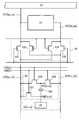
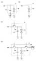
도 1은 본 발명의 일 형태의 표시 장치를 설명하는 도면이다. 표시 장치는 열 방향 및 행 방향으로 배치된 화소(10)를 가지는 표시 영역(15)과, 소스 드라이버(12)와, 게이트 드라이버(13)와, 회로(11)를 가진다. 소스 드라이버(12)는 회로(11) 및 화소(10)와 전기적으로 접속된다. 게이트 드라이버(13)는 화소(10)와 전기적으로 접속된다. 회로(11)는 화소(10)와 전기적으로 접속된다. 또한 소스 드라이버(12) 및 게이트 드라이버(13)는 복수 개 있어도 좋다.BRIEF DESCRIPTION OF THE DRAWINGS It is a figure explaining the display apparatus of one embodiment of this invention. The display device includes a
회로(11)는 예를 들어 화소(10)의 열마다 제공될 수 있고, 같은 열에 배치된 화소(10)와 전기적으로 접속될 수 있다.The
회로(11)는 반전 회로이고, 소스 드라이버(12)로부터 공급되는 아날로그 전위(제 1 데이터)를 반전한 아날로그 전위(제 2 데이터)를 생성하는 기능을 가진다.The
화소(10)는 회로(20) 및 회로(21)를 가진다. 회로(20)는 소스 드라이버(12)로부터 공급되는 제 1 데이터 및 회로(11)로부터 공급되는 제 2 데이터를 용량 결합에 의하여 가산하여 제 3 데이터를 생성하는 기능을 가진다. 회로(21)는 표시 디바이스를 가지고, 회로(20)로부터 공급되는 제 3 데이터에 따라 상기 표시 디바이스를 동작시키는 기능을 가진다.The
도 2는 도 1에 나타낸 표시 장치의 임의의 1열(제 m 열)에 배치된 회로(11) 및 수직 방향(소스선이 연장되는 방향)으로 인접한 화소(10)(화소(10[n, m]), 화소(10[n+1, m])(m, n은 1 이상의 자연수임))를 설명하는 도면이다.FIG. 2 shows
<반전 회로><Inversion circuit>
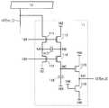
도 3에 회로(11)의 구성의 일례를 나타내었다. 회로(11)는 트랜지스터(111)와, 트랜지스터(112)와, 트랜지스터(113)와, 트랜지스터(114)와, 트랜지스터(115)와, 트랜지스터(116)와, 커패시터(117)와, 커패시터(118)를 가지는 구성으로 할 수 있다.An example of the configuration of the
트랜지스터(111)의 소스 및 드레인 중 한쪽은 커패시터(117)의 한쪽 전극과 전기적으로 접속된다. 커패시터(117)의 한쪽 전극은 트랜지스터(112)의 소스 및 드레인 중 한쪽과 전기적으로 접속된다. 트랜지스터(113)의 소스 및 드레인 중 한쪽은 커패시터(117)의 다른 쪽 전극과 전기적으로 접속된다. 커패시터(117)의 다른 쪽 전극은 트랜지스터(114)의 소스 및 드레인 중 한쪽과 전기적으로 접속된다. 트랜지스터(114)의 소스 및 드레인 중 다른 쪽은 트랜지스터(115)의 게이트와 전기적으로 접속되고, 트랜지스터(115)의 게이트는 커패시터(118)의 한쪽의 전극과 전기적으로 접속된다. 트랜지스터(115)의 소스 및 드레인 중 한쪽은 트랜지스터(116)의 소스 및 드레인 중 한쪽과 전기적으로 접속된다.One of the source and drain of the
상기 구성에서, 트랜지스터(111)의 소스 및 드레인 중 다른 쪽은 입력 단자에 상당하고, 배선(127[m_1])과 전기적으로 접속된다. 또한 트랜지스터(116)의 소스 및 드레인 중 한쪽은 출력 단자에 상당하고, 배선(127[m_2])과 전기적으로 접속된다. 또한 회로(11)는 입력 단자에 상당하는 요소 및 출력 단자에 상당하는 요소를 가지고, 입력 단자에 입력되는 아날로그 전위를 반전하고 출력 단자로부터 출력할 수 있는 구성이면 상기 구성에 한정되지 않는다.In the above configuration, the other of the source and drain of the
트랜지스터(111)의 게이트 및 트랜지스터(113)의 게이트는 배선(128)과 전기적으로 접속된다. 트랜지스터(112)의 게이트 및 트랜지스터(114)의 게이트는 배선(129)과 전기적으로 접속된다. 트랜지스터(112)의 소스 및 드레인 중 다른 쪽은 배선(161)과 전기적으로 접속된다. 트랜지스터(113)의 소스 및 드레인 중 다른 쪽은 배선(162)과 전기적으로 접속된다. 커패시터(118)의 다른 쪽 전극은 배선(163)과 전기적으로 접속된다. 트랜지스터(115)의 소스 및 드레인 중 다른 쪽은 배선(164)과 전기적으로 접속된다. 트랜지스터(116)의 소스 및 드레인 중 다른 쪽은 배선(165)과 전기적으로 접속된다. 트랜지스터(116)의 게이트는 배선(166)과 전기적으로 접속된다.The gate of the
배선(128, 129)은 게이트선으로서의 기능을 가질 수 있다. 예를 들어, 배선(128, 129)은 회로(11)의 동작을 제어하는 회로와 전기적으로 접속될 수 있다. 배선(161, 162, 163, 164, 165)은 전원선으로서의 기능을 가질 수 있다. 예를 들어 배선(161, 163, 165)은 저전위 전원선, 배선(162, 164)은 고전위 전원선으로 할 수 있다. 배선(166)은 정전위를 공급하는 기능을 가진다.The
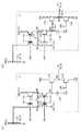
또한 도 4에 나타낸 바와 같이, 복수의 열에 배치된 회로(11)가 트랜지스터(112) 및 트랜지스터(113)를 공유하는 구성으로 하여도 좋다. 도 4에는 3열 이상에서 트랜지스터(112) 및 트랜지스터(113)가 공유되는 예를 나타내었지만, 2열에서 공유되는 구성이어도 좋다. 또한 도 4에서는 트랜지스터(112) 및 트랜지스터(113)가 회로(11) 테두리 밖에 도시되어 있지만, 트랜지스터(112) 및 트랜지스터(113)는 각 회로(11)가 공유하는 요소이다. 상기 구성으로 함으로써 회로(11)의 구성 요소를 줄일 수 있어 내로 베젤화에 유효하다.Further, as shown in Fig. 4, the
<화소 회로><Pixel Circuit>
화소(10)는 화상 데이터를 생성하는 회로(20)와, 표시 동작을 수행하는 회로(21)를 가지는 구성으로 할 수 있다.The
회로(20)는 트랜지스터(101)와, 트랜지스터(102)와, 트랜지스터(103)와, 커패시터(104)를 가지는 구성으로 할 수 있다. 커패시터(104)의 한쪽 전극은 트랜지스터(101)의 소스 및 드레인 중 한쪽과 전기적으로 접속된다. 트랜지스터(101)의 소스 및 드레인 중 한쪽은 회로(21)와 전기적으로 접속된다. 커패시터(104)의 다른 쪽 전극은 트랜지스터(102)의 소스 및 드레인 중 한쪽과 전기적으로 접속된다. 트랜지스터(102)의 소스 및 드레인 중 한쪽은 트랜지스터(103)의 소스 및 드레인 중 한쪽과 전기적으로 접속된다.The
회로(21)는 트랜지스터, 커패시터, 및 표시 디바이스 등을 가지는 구성으로 할 수 있고, 자세한 사항에 대해서는 후술한다.The
회로(11) 및 화소(10) 각각이 가지는 요소와, 각종 배선의 접속에 대하여 설명한다.The connection of the element which each of the
화소(10[n, m])에서, 트랜지스터(101)의 게이트는 배선(126[n])과 전기적으로 접속된다. 트랜지스터(102)의 게이트는 배선(125[n])과 전기적으로 접속된다. 트랜지스터(103)의 게이트는 배선(126[n])과 전기적으로 접속된다. 트랜지스터(101)의 소스 및 드레인 중 다른 쪽은 배선(127[m_1])과 전기적으로 접속된다. 트랜지스터(102)의 소스 및 드레인 중 다른 쪽은 배선(127[m_1])과 전기적으로 접속된다. 트랜지스터(103)의 소스 및 드레인 중 다른 쪽은 배선(127[m_2])과 전기적으로 접속된다.In the pixel 10[n, m], the gate of the
배선(125, 126)은 게이트선으로서의 기능을 가질 수 있다. 배선(125, 126)은 게이트 드라이버(13)와 전기적으로 접속될 수 있다(도 1 참조). 배선(127(127[m_1], 127[m_2]))은 소스선으로서의 기능을 가질 수 있다. 배선(127[m_1])은 소스 드라이버(12)가 가지는 출력 단자와 전기적으로 접속될 수 있다.The
또한 화소(10)와 배선(127[m_1]) 및 배선(127[m_2])의 접속 관계는 상술한 것에 한정되지 않고, 배선(127[m_1])과 배선(127[m_2])이 서로 바뀐 접속 관계에 있어도 좋다.In addition, the connection relationship between the
여기서, 회로(11)에서, 트랜지스터(111)의 소스 및 드레인 중 한쪽과, 커패시터(117)의 한쪽 전극과, 트랜지스터(112)의 소스 및 드레인 중 한쪽을 접속하는 배선을 노드(NA)로 한다. 트랜지스터(113)의 소스 및 드레인 중 한쪽과, 커패시터(117)의 다른 쪽 전극과, 트랜지스터(114)의 소스 및 드레인 중 한쪽을 접속하는 배선을 노드(NB)로 한다. 트랜지스터(114)의 소스 및 드레인 중 다른 쪽과, 트랜지스터(115)의 게이트와, 커패시터(118)의 한쪽 전극을 접속하는 배선을 노드(NC)로 한다. 트랜지스터(115)의 소스 및 드레인 중 한쪽과, 트랜지스터(116)의 소스 및 드레인 중 한쪽과, 배선(127[m_2])을 접속하는 배선을 노드(ND)로 한다.Here, in the
또한 화소(10)에서, 커패시터(104)의 한쪽 전극과, 트랜지스터(101)의 소스 및 드레인 중 한쪽과, 회로(21)를 접속하는 배선을 노드(NM)로 한다. 커패시터(104)의 다른 쪽 전극과, 트랜지스터(102)의 소스 및 드레인 중 한쪽과, 트랜지스터(103)의 소스 및 드레인 중 한쪽을 접속하는 배선을 노드(NE)로 한다.Further, in the
노드(NM)는 부유 상태로 할 수 있고, 회로(21)가 가지는 표시 디바이스는 노드(NM)의 전위에 따라 동작한다.The node NM can be in a floating state, and the display device included in the
<반전 동작의 설명><Description of inversion operation>
회로(11)에서는, 먼저 노드(NA)에 "+D"(제 1 데이터)를, 노드(NB)에 "+V1"(예를 들어 양의 전원 전위)를 기록한다. 이때, 커패시터(117)에는 "+V1-D1"이 유지된다.In the
다음으로, 노드(NB)를 부유 상태로 하고, 노드(NA)에 "-V1"(예를 들어 음의 전원 전위)를 기록한다.Next, the node NB is placed in a floating state, and "-V1" (for example, a negative power supply potential) is written to the node NA.
이때, 커패시터(117)의 용량값을 C117로 하고, 노드(NB)의 용량값을 CNB로 하면, 노드(NB)의 전위는 "+V1+(C117/(C117+CNB))×(-V1-D1)"이 된다. 여기서, C117의 값을 크게 하여 CNB의 값을 무시할 수 있게 되면, 노드(NB)의 전위는 "-D1"이 된다.At this time, if the capacitance value of the capacitor117 is
노드(NB)의 전위는 스위치(트랜지스터(114))를 통하여 노드(NC)에 공급된다. 또한 노드(NC)의 전위는 소스 폴로어 회로(트랜지스터(115, 116))를 통하여 노드(ND)에 출력된다. 즉, 먼저 노드(NA)에 입력된 "+D"의 반전 데이터인 "-D"(제 2 데이터)를 노드(ND)에 출력할 수 있다. 또한 위에서는 제 1 데이터에 양의 전위를 사용한 예를 나타내었지만, 음의 전위이어도 좋다.The potential of the node NB is supplied to the node NC through a switch (transistor 114). Also, the potential of the node NC is output to the node ND through the source follower circuit (
<가산 동작(승압 동작)의 설명><Explanation of addition operation (step-up operation)>
화소(10)에서는, 먼저, 노드(NM)에 "+D"(제 1 데이터)를, 노드(NE)에 "-D"(제 2 데이터)를 서로 겹치는 타이밍에 기록한다. 이때, 커패시터(117)에는 "+D-(-D)=+2D"가 유지된다. 다음으로, 노드(NM)를 부유 상태로 하고, 노드(NE)에 "+D"를 공급한다.In the
이때, 커패시터(117)의 용량값을 C117로 하고, 노드(NM)의 용량값을 CNM로 하면, 노드(NM)의 전위는 "+D1+(C117/(C117+CNM))×(+D-(D))"가 된다. 여기서, C117의 값을 크게 하여 CNM의 값을 무시할 수 있게 되면, 노드(NM)의 전위는 "+D+(+D-(-D))"="+3D"가 된다.At this time, if the capacitance value of the capacitor117 is
즉, 소스 드라이버(12)의 출력의 약 3배의 전위인 제 3 데이터("+3D")를 노드(NM)에 공급할 수 있다.That is, the third data (“+3D”), which is about three times the potential of the output of the
상기 작용에 의하여, 일반적인 액정 디바이스나 발광 디바이스 등을 구동하기 위하여 소스 드라이버(12)로부터 공급하는 전압을 최대 약 1/3까지 저감할 수 있다. 따라서 표시 장치를 저소비 전력화할 수 있다. 또는 범용 드라이버 IC를 사용하여도 높은 전압을 생성할 수 있다. 예를 들어 계조 제어에 높은 전압이 필요한 액정 디바이스 등을 범용 드라이버 IC로 구동할 수 있다.By the above action, the voltage supplied from the
또한 소스 드라이버(12)의 전원 전압을 낮출 수 있으므로 소스 드라이버의 저소비 전력화가 가능하다. 또한 소스 드라이버가 가지는 복수의 회로의 전원 전압을 같게 할 수 있으므로 상기 복수의 회로를 공통의 테크놀로지를 사용하여 제작할 수 있다. 따라서 소스 드라이버의 제작 공정을 삭감할 수 있으므로 저비용화가 가능하다.In addition, since the power supply voltage of the
본 발명의 일 형태에서는, 상술한 바와 같이, 회로(11)에서 생성한 반전 데이터 전위를 특정의 화소(10)에 공급하여 노드(NM)의 전위를 확정시킨다. 이와 같은 동작을 같은 행의 각 화소(10)에 순차적으로 수행함으로써, 각 화소(10)의 노드(NM)의 전위를 확정시킬 수 있다. 즉, 각 화소(10)에 상이한 화상 데이터를 공급할 수 있다.In one embodiment of the present invention, as described above, the inverted data potential generated in the
노드(NA), 노드(NB), 노드(NC), 노드(ND), 노드(NE), 노드(NM)는 기억 노드로서 작용한다. 각 노드에 접속되는 트랜지스터를 도통시킴으로써, 데이터를 각 노드에 기록할 수 있다. 또한 상기 트랜지스터를 비도통으로 함으로써, 상기 데이터를 각 노드에 유지할 수 있다. 상기 트랜지스터에 오프 전류가 매우 낮은 트랜지스터를 사용함으로써, 누설 전류를 억제할 수 있고, 각 노드의 전위가 오랫동안 유지될 수 있다. 상기 트랜지스터에는 예를 들어 금속 산화물을 채널 형성 영역에 사용한 트랜지스터(이하, OS 트랜지스터)를 사용할 수 있다.A node NA, a node NB, a node NC, a node ND, a node NE, and a node NM act as storage nodes. By conducting the transistors connected to each node, data can be written to each node. In addition, by making the transistor non-conductive, the data can be held at each node. By using a transistor having a very low off-state current for the transistor, leakage current can be suppressed, and the potential of each node can be maintained for a long time. For the transistor, for example, a transistor using a metal oxide for the channel formation region (hereinafter referred to as an OS transistor) may be used.
구체적으로는 트랜지스터(101, 102, 103, 111, 112, 113, 114, 115, 116) 중 어느 것 또는 모두에 OS 트랜지스터를 적용하는 것이 바람직하다. 또한 회로(21)가 가지는 요소에 OS 트랜지스터를 적용하여도 좋다. 또한 누설 전류량의 허용 범위에서 동작을 수행하는 경우에는 Si를 채널 형성 영역에 가지는 트랜지스터(이하, Si 트랜지스터)를 적용하여도 좋다. 또는 OS 트랜지스터 및 Si 트랜지스터를 병용하여도 좋다. 또한 상기 Si 트랜지스터로서는 비정질 실리콘을 가지는 트랜지스터, 결정성 실리콘(미결정 실리콘, 저온 폴리실리콘, 단결정 실리콘)을 가지는 트랜지스터 등을 들 수 있다.Specifically, it is preferable to apply an OS transistor to any or all of the
OS 트랜지스터에 사용하는 반도체 재료로서는 에너지 갭이 2eV 이상, 바람직하게는 2.5eV 이상, 더 바람직하게는 3eV 이상인 금속 산화물을 사용할 수 있다. 대표적으로는 인듐을 포함한 산화물 반도체 등이 있고, 예를 들어 후술하는 CAAC-OS 또는 CAC-OS 등을 사용할 수 있다. CAAC-OS는 결정을 구성하는 원자가 안정적이고, 신뢰성을 중시하는 트랜지스터 등에 적합하다. 또한 CAC-OS는 고이동도 특성을 나타내므로, 고속 구동을 수행하는 트랜지스터 등에 적합하다.As the semiconductor material used for the OS transistor, a metal oxide having an energy gap of 2 eV or more, preferably 2.5 eV or more, and more preferably 3 eV or more can be used. Representative examples include oxide semiconductors containing indium, and for example, CAAC-OS or CAC-OS, which will be described later, can be used. CAAC-OS is suitable for transistors where the atoms constituting the crystal are stable and reliability is important. In addition, since the CAC-OS exhibits high mobility, it is suitable for high-speed driving transistors and the like.
OS 트랜지스터는 반도체층의 에너지 갭이 크기 때문에, 수yA/μm(채널 폭 1μm당 전류값)라는 매우 낮은 오프 전류 특성을 나타낼 수 있다. 또한 OS 트랜지스터는 임팩트 이온화, 애벌란시(avalanche) 항복, 및 단채널 효과 등이 일어나지 않는다는 등, Si 트랜지스터와는 상이한 특징을 가지고, 신뢰성이 높은 회로를 형성할 수 있다. 또한 Si 트랜지스터에서 문제가 되는 결정성의 불균일성에 기인하는 전기 특성의 편차도 OS 트랜지스터에서는 일어나기 어렵다.Since the OS transistor has a large energy gap in the semiconductor layer, it can exhibit a very low off-current characteristic of several yA/μm (current value per 1 μm of channel width). In addition, the OS transistor has characteristics different from those of the Si transistor, such as that impact ionization, avalanche breakdown, and short channel effect do not occur, and a circuit with high reliability can be formed. In addition, variations in electrical characteristics due to non-uniformity of crystallinity, which is a problem in Si transistors, do not easily occur in OS transistors.
OS 트랜지스터가 가지는 반도체층은 예를 들어 인듐, 아연, 및 M(알루미늄, 타이타늄, 갈륨, 저마늄, 이트륨, 지르코늄, 란타넘, 세륨, 주석, 네오디뮴, 또는 하프늄 등의 금속)을 포함하는 In-M-Zn계 산화물로 표기되는 막으로 할 수 있다. In-M-Zn계 산화물은, 예를 들어 스퍼터링법, ALD(Atomic layer deposition)법, 또는 MOCVD(Metal organic chemical vapor deposition)법 등을 사용하여 형성할 수 있다.The semiconductor layer of the OS transistor includes, for example, indium, zinc, and M (a metal such as aluminum, titanium, gallium, germanium, yttrium, zirconium, lanthanum, cerium, tin, neodymium, or hafnium). It can be set as the film|membrane represented by M-Zn-type oxide. The In-M-Zn-based oxide may be formed using, for example, a sputtering method, an atomic layer deposition (ALD) method, or a metal organic chemical vapor deposition (MOCVD) method.
In-M-Zn계 산화물을 스퍼터링법으로 성막하는 경우, 스퍼터링 타깃의 금속 원소의 원자수비는 In≥M, Zn≥M을 만족시키는 것이 바람직하다. 이와 같은 스퍼터링 타깃의 금속 원소의 원자수비로서는, In:M:Zn=1:1:1, In:M:Zn=1:1:1.2, In:M:Zn=3:1:2, In:M:Zn=4:2:3, In:M:Zn=4:2:4.1, In:M:Zn=5:1:6, In:M:Zn=5:1:7, In:M:Zn=5:1:8 등이 바람직하다. 또한 성막되는 반도체층의 원자수비는 각각 상기 스퍼터링 타깃에 포함되는 금속 원소의 원자수비의 ±40%의 변동을 포함한다.When an In-M-Zn-based oxide is formed by sputtering, it is preferable that the atomic ratio of the metal element of the sputtering target satisfies In≧M and Zn≧M. As an atomic ratio of the metal elements of such a sputtering target, In:M:Zn=1:1:1, In:M:Zn=1:1:1.2, In:M:Zn=3:1:2, In: M:Zn=4:2:3, In:M:Zn=4:2:4.1, In:M:Zn=5:1:6, In:M:Zn=5:1:7, In:M: Zn=5:1:8 or the like is preferable. In addition, the atomic ratio of the semiconductor layer to be formed includes a variation of ±40% of the atomic ratio of the metal elements contained in the sputtering target, respectively.
반도체층에는 캐리어 농도가 낮은 산화물 반도체를 사용한다. 예를 들어 반도체층에는 캐리어 농도가 1×10¹⁷/cm3 이하, 바람직하게는 1×10¹⁵/cm3 이하, 더 바람직하게는 1×10¹³/cm3 이하, 더욱 바람직하게는 1×10¹¹/cm3 이하, 더욱더 바람직하게는 1×10¹⁰/cm3 미만이고, 1×10⁻⁹/cm3 이상인 산화물 반도체를 사용할 수 있다. 이와 같은 산화물 반도체를 고순도 진성 또는 실질적으로 고순도 진성인 산화물 반도체라고 부른다. 상기 산화물 반도체는 결함 준위 밀도가 낮고, 안정된 특성을 가지는 산화물 반도체라고 할 수 있다.An oxide semiconductor having a low carrier concentration is used for the semiconductor layer. For example, the semiconductor layer has a carrier concentration of 1×10¹⁷ /cm3 or less, preferably 1×10¹⁵ /cm3 or less, more preferably 1×10¹³ /cm3 or less, still more preferably 1×10¹¹ /cm3 or less, more preferably less than 1×10¹⁰ /cm3 , and 1×10⁻⁹ /cm3 or more can be used. Such an oxide semiconductor is called a high-purity intrinsic or substantially high-purity intrinsic oxide semiconductor. The oxide semiconductor may be an oxide semiconductor having a low density of defect states and stable characteristics.
또한 이들에 한정되지 않고, 필요로 하는 트랜지스터의 반도체 특성 및 전기 특성(전계 효과 이동도, 문턱 전압 등)에 따라 적절한 조성의 것을 사용하면 좋다. 또한 필요로 하는 트랜지스터의 반도체 특성을 얻기 위하여, 반도체층의 캐리어 농도나 불순물 농도, 결함 밀도, 금속 원소와 산소의 원자수비, 원자 간 거리, 밀도 등을 적절한 것으로 하는 것이 바람직하다.Moreover, it is not limited to these, What is necessary is just to use the thing of the suitable composition according to the semiconductor characteristic and electrical characteristic (field effect mobility, threshold voltage, etc.) of a required transistor. In addition, in order to obtain the required semiconductor characteristics of the transistor, it is preferable that the carrier concentration, the impurity concentration, the defect density, the atomic ratio of the metal element and oxygen, the distance between the atoms, the density, etc. of the semiconductor layer be appropriate.
반도체층을 구성하는 산화물 반도체에 14족 원소의 하나인 실리콘이나 탄소가 포함되면, 산소 결손이 증가되어 n형화된다. 그러므로 반도체층에서의 실리콘이나 탄소의 농도(2차 이온 질량 분석법으로 얻어지는 농도)를 2×10¹⁸atoms/cm3 이하, 바람직하게는 2×10¹⁷atoms/cm3 이하로 한다.When silicon or carbon, which is one of the group 14 elements, is included in the oxide semiconductor constituting the semiconductor layer, oxygen vacancies are increased and n-type is formed. Therefore, the concentration of silicon or carbon in the semiconductor layer (concentration obtained by secondary ion mass spectrometry) is 2×10¹⁸ atoms/cm3 or less, preferably 2×10¹⁷ atoms/cm3 or less.
또한 알칼리 금속 및 알칼리 토금속은 산화물 반도체와 결합하면 캐리어를 생성하는 경우가 있고, 트랜지스터의 오프 전류가 증대되는 경우가 있다. 그러므로 반도체층에서의 알칼리 금속 또는 알칼리 토금속의 농도(2차 이온 질량 분석법으로 얻어지는 농도)를 1×10¹⁸atoms/cm3 이하, 바람직하게는 2×10¹⁶atoms/cm3 이하로 한다.In addition, when alkali metals and alkaline earth metals combine with an oxide semiconductor, carriers may be generated, and the off-state current of the transistor may be increased. Therefore, the concentration (concentration obtained by secondary ion mass spectrometry) of the alkali metal or alkaline earth metal in the semiconductor layer is set to 1×10¹⁸ atoms/cm3 or less, preferably 2×10¹⁶ atoms/cm3 or less.
또한 반도체층을 구성하는 산화물 반도체에 질소가 포함되면, 캐리어인 전자가 생기고 캐리어 농도가 증가되어 n형화되기 쉽다. 이 결과, 질소가 포함되는 산화물 반도체를 사용한 트랜지스터는 노멀리 온 특성이 되기 쉽다. 그러므로 반도체층에서의 질소 농도(2차 이온 질량 분석법으로 얻어지는 농도)는 5×10¹⁸atoms/cm3 이하로 하는 것이 바람직하다.In addition, when nitrogen is contained in the oxide semiconductor constituting the semiconductor layer, electrons as carriers are generated, and the carrier concentration is increased, and thus the n-type is likely to be formed. As a result, a transistor using an oxide semiconductor containing nitrogen tends to have normally-on characteristics. Therefore, the nitrogen concentration (concentration obtained by secondary ion mass spectrometry) in the semiconductor layeris preferably 5×10 18 atoms/cm3 or less.
또한 반도체층을 구성하는 산화물 반도체에 수소가 포함되면 금속 원자와 결합하는 산소와 반응하여 물이 되기 때문에 산화물 반도체 내에 산소 결손을 형성하는 경우가 있다. 산화물 반도체 내의 채널 형성 영역에 산소 결손이 포함되면, 트랜지스터는 노멀리 온 특성이 되는 경우가 있다. 또한 산소 결손에 수소가 들어간 결함은 도너로서 기능하고, 캐리어인 전자가 생성되는 경우가 있다. 또한 수소의 일부가 금속 원자와 결합하는 산소와 결합하여, 캐리어인 전자가 생성되는 경우가 있다. 따라서 수소가 많이 포함되어 있는 산화물 반도체를 사용한 트랜지스터는 노멀리 온 특성이 되기 쉽다.In addition, when hydrogen is contained in the oxide semiconductor constituting the semiconductor layer, oxygen vacancies may be formed in the oxide semiconductor because it reacts with oxygen bonded to a metal atom to form water. When oxygen vacancies are included in the channel formation region in the oxide semiconductor, the transistor may have normally-on characteristics. Moreover, the defect in which hydrogen entered oxygen vacancies functions as a donor, and the electron which is a carrier may generate|occur|produce. In addition, a part of hydrogen bonds with oxygen bonded to a metal atom to generate electrons as carriers. Therefore, a transistor using an oxide semiconductor containing a lot of hydrogen tends to have normally-on characteristics.
산소 결손에 수소가 들어간 결함은 산화물 반도체의 도너로서 기능할 수 있다. 그러나 상기 결함을 정량적으로 평가하는 것은 어렵다. 그러므로 산화물 반도체에서는 도너 농도가 아니라 캐리어 농도로 평가되는 경우가 있다. 따라서 본 명세서 등에서는 산화물 반도체의 파라미터로서 도너 농도가 아니라 전계가 인가되지 않는 상태를 상정한 캐리어 농도를 사용하는 경우가 있다. 즉 본 명세서 등에 기재된 "캐리어 농도"는 "도너 농도"로 바꿔 말할 수 있는 경우가 있다.Defects in which hydrogen enters oxygen vacancies can function as donors of the oxide semiconductor. However, it is difficult to quantitatively evaluate the defect. Therefore, in an oxide semiconductor, it is evaluated by the carrier concentration rather than the donor concentration in some cases. Therefore, in this specification and the like, as a parameter of the oxide semiconductor, not the donor concentration, but the carrier concentration assuming a state in which no electric field is applied may be used. That is, "carrier concentration" described in this specification and the like may be interchangeably referred to as "donor concentration".
따라서 산화물 반도체 내의 수소는 가능한 한 저감되어 있는 것이 바람직하다. 구체적으로는, 산화물 반도체에서 2차 이온 질량 분석법(SIMS: Secondary Ion Mass Spectrometry)으로 얻어지는 수소 농도를 1×10²⁰atoms/cm3 미만, 바람직하게는 1×10¹⁹atoms/cm3 미만, 더 바람직하게는 5×10¹⁸atoms/cm3 미만, 더 바람직하게는 1×10¹⁸atoms/cm3 미만으로 한다. 수소 등의 불순물이 충분히 저감된 산화물 반도체를 트랜지스터의 채널 형성 영역에 사용함으로써, 안정된 전기 특성을 부여할 수 있다.Therefore, it is preferable that hydrogen in the oxide semiconductor is reduced as much as possible. Specifically, the hydrogen concentration obtained by Secondary Ion Mass Spectrometry (SIMS) in the oxide semiconductor isless than 1×10 20 atoms/cm3 , preferably less than 1×10¹⁹ atoms/cm3 , more preferably Preferably less than 5×10¹⁸ atoms/cm3 , more preferably less than 1×10¹⁸ atoms/cm3 . By using an oxide semiconductor in which impurities such as hydrogen have been sufficiently reduced for the channel formation region of the transistor, stable electrical characteristics can be imparted.
또한 산화물 반도체(금속 산화물)는 단결정 산화물 반도체와, 이 외의 비단결정 산화물 반도체로 나누어진다. 비단결정 산화물 반도체로서는, 예를 들어 CAAC-OS(C-Axis Aligned Crystalline Oxide Semiconductor), 다결정 산화물 반도체, nc-OS(nanocrystalline oxide semiconductor), a-like OS(amorphous-like oxide semiconductor), 및 비정질 산화물 반도체 등이 있다. 비단결정 구조에서 비정질 구조는 결함 준위 밀도가 가장 높고, CAAC-OS는 결함 준위 밀도가 가장 낮다.In addition, oxide semiconductors (metal oxides) are divided into single crystal oxide semiconductors and other non-single crystal oxide semiconductors. As the non-single crystal oxide semiconductor, for example, CAAC-OS (C-Axis Aligned Crystalline Oxide Semiconductor), polycrystalline oxide semiconductor, nc-OS (nanocrystalline oxide semiconductor), a-like OS (amorphous-like oxide semiconductor), and amorphous oxide semiconductors, etc. In the non-single crystal structure, the amorphous structure has the highest density of defect states, and the CAAC-OS has the lowest density of defect states.
비정질 구조의 산화물 반도체막은 예를 들어 원자 배열이 무질서하며 결정 성분을 가지지 않는다. 또는 비정질 구조의 산화물막은 예를 들어 완전한 비정질 구조이며, 결정부를 가지지 않는다.The oxide semiconductor film having an amorphous structure, for example, has a disordered atomic arrangement and does not have a crystalline component. Alternatively, the oxide film having an amorphous structure has, for example, a completely amorphous structure and does not have a crystal part.
또한 반도체층이 비정질 구조의 영역, 미결정 구조의 영역, 다결정 구조의 영역, CAAC-OS의 영역, 단결정 구조의 영역 중 2종류 이상을 가지는 혼합막이어도 좋다. 혼합막은 예를 들어 상술한 영역 중 어느 2종류 이상의 영역을 포함하는 단층 구조 또는 적층 구조를 가지는 경우가 있다.Furthermore, the semiconductor layer may be a mixed film having two or more types of a region of an amorphous structure, a region of a microcrystalline structure, a region of a polycrystalline structure, a region of CAAC-OS, and a region of a single crystal structure. The mixed film may have, for example, a single-layer structure or a laminated structure including any two or more types of regions among the above-mentioned regions.
아래에서는, 비단결정의 반도체층의 일 형태인 CAC(Cloud-Aligned Composite)-OS의 구성에 대하여 설명한다.Hereinafter, a configuration of a Cloud-Aligned Composite (CAC)-OS, which is one form of a non-single crystal semiconductor layer, will be described.
CAC-OS란, 예를 들어 산화물 반도체를 구성하는 원소가 0.5nm 이상 10nm 이하, 바람직하게는 1nm 이상 2nm 이하, 또는 그 근방의 크기로 편재한 재료의 하나의 구성이다. 또한 아래에서는 산화물 반도체에서 하나 또는 그 이상의 금속 원소가 편재하고, 상기 금속 원소를 가지는 영역이 0.5nm 이상 10nm 이하, 바람직하게는 1nm 이상 2nm 이하, 또는 그 근방의 크기로 혼합된 상태를 모자이크 패턴 또는 패치 패턴이라고도 한다.The CAC-OS is, for example, one configuration of a material in which the elements constituting the oxide semiconductor are unevenly distributed in size of 0.5 nm or more and 10 nm or less, preferably 1 nm or more and 2 nm or less, or a size in the vicinity thereof. In addition, in the following, one or more metal elements are ubiquitous in the oxide semiconductor, and the region having the metal elements is 0.5 nm or more and 10 nm or less, preferably 1 nm or more and 2 nm or less, or a mixed state with a size of a mosaic pattern or Also called patch pattern.
또한 산화물 반도체는 적어도 인듐을 포함하는 것이 바람직하다. 특히 인듐 및 아연을 포함하는 것이 바람직하다. 또한 이들에 더하여 알루미늄, 갈륨, 이트륨, 구리, 바나듐, 베릴륨, 붕소, 실리콘, 타이타늄, 철, 니켈, 저마늄, 지르코늄, 몰리브데넘, 란타넘, 세륨, 네오디뮴, 하프늄, 탄탈럼, 텅스텐, 및 마그네슘 등 중에서 선택된 1종류 또는 복수 종류가 포함되어도 좋다.Moreover, it is preferable that an oxide semiconductor contains at least indium. It is particularly preferred to include indium and zinc. Also in addition to these are aluminum, gallium, yttrium, copper, vanadium, beryllium, boron, silicon, titanium, iron, nickel, germanium, zirconium, molybdenum, lanthanum, cerium, neodymium, hafnium, tantalum, tungsten, and One type or multiple types selected from magnesium etc. may be contained.
예를 들어 In-Ga-Zn 산화물에서의 CAC-OS(CAC-OS 중에서도 In-Ga-Zn 산화물을 특히 CAC-IGZO라고 불러도 좋음)란, 인듐 산화물(이하, InOX1(X1은 0보다 큰 실수(實數))로 함) 또는 인듐 아연 산화물(이하, InX2ZnY2OZ2(X2, Y2, 및 Z2는 0보다 큰 실수)로 함)과, 갈륨 산화물(이하, GaOX3(X3은 0보다 큰 실수)으로 함) 또는 갈륨 아연 산화물(이하, GaX4ZnY4OZ4(X4, Y4, 및 Z4는 0보다 큰 실수)로 함) 등으로 재료가 분리함으로써 모자이크 패턴이 되고, 모자이크 패턴의 InOX1 또는 InX2ZnY2OZ2가 막 내에 균일하게 분포된 구성(이하, 클라우드상(cloud-like)이라고도 함)이다.For example, CAC-OS in In-Ga-Zn oxide (in CAC-OS, In-Ga-Zn oxide in particular may be called CAC-IGZO) is indium oxide (hereinafter, InOX1 (X1 is a real number greater than 0) (實數)) or indium zinc oxide (hereinafter referred to as InX2 ZnY2 OZ2 (X2, Y2, and Z2 are real numbers greater than 0)) and gallium oxide (hereinafter referred to as GaOX3 (X3 is greater than 0)) large real number) or gallium zinc oxide (hereinafter referred to as GaX4 ZnY4 OZ4 (X4, Y4, and Z4 are real numbers greater than 0)), etc.X1 or InX2 ZnY2 OZ2 is uniformly distributed in the film (hereinafter also referred to as cloud-like).
즉 CAC-OS는 GaOX3이 주성분인 영역과, InX2ZnY2OZ2 또는 InOX1이 주성분인 영역이 혼합되는 구성을 가지는 복합 산화물 반도체이다. 또한 본 명세서에서 예를 들어 제 1 영역의 원소 M에 대한 In의 원자수비가 제 2 영역의 원소 M에 대한 In의 원자수비보다 큰 것을, 제 1 영역은 제 2 영역과 비교하여 In의 농도가 높다고 한다.That is, the CAC-OS is a composite oxide semiconductor having a configuration in which a region containingGaO X3 as a main component and a region containing as a main component of InX2 ZnY2 OZ2 or InOX1 are mixed. Also, in the present specification, for example, the atomic ratio of In to the element M in the first region is greater than the atomic ratio of In to the element M in the second region, and the first region has a higher concentration of In compared to that of the second region. said to be high
또한 IGZO는 통칭이며, In, Ga, Zn, 및 O로 이루어지는 하나의 화합물을 말하는 경우가 있다. 대표적인 예로서, InGaO3(ZnO)m1(m1은 자연수임) 또는 In(1+x0)Ga(1-x0)O3(ZnO)m0(-1≤x0≤1, m0은 임의의 수임)으로 나타내어지는 결정성 화합물을 들 수 있다.In addition, IGZO is a common name, and may say one compound which consists of In, Ga, Zn, and O. As a representative example, InGaO3 (ZnO)m1 (m1 is a natural number) or In(1+x0) Ga(1-x0) O3 (ZnO)m0 (-1≤x0≤1, m0 is any number) The crystalline compound shown is mentioned.
상기 결정성 화합물은 단결정 구조, 다결정 구조, 또는 CAAC 구조를 가진다. 또한 CAAC 구조는 복수의 IGZO의 나노 결정이 c축 배향을 가지고 또한 a-b면에서는 배향하지 않고 연결된 결정 구조이다.The crystalline compound has a single crystal structure, a polycrystalline structure, or a CAAC structure. In addition, the CAAC structure is a crystal structure in which a plurality of IGZO nanocrystals have c-axis orientation and are connected without orientation in the a-b plane.
한편, CAC-OS는 산화물 반도체의 재료 구성에 관한 것이다. CAC-OS란 In, Ga, Zn, 및 O를 포함한 재료 구성에서, 일부에 Ga를 주성분으로 하는 나노 입자상으로 관찰되는 영역과, 일부에 In을 주성분으로 하는 나노 입자상으로 관찰되는 영역이 각각 모자이크 패턴으로 무작위로 분산되어 있는 구성을 말한다. 따라서 CAC-OS에서 결정 구조는 부차적인 요소이다.On the other hand, CAC-OS relates to the material composition of oxide semiconductors. CAC-OS means that, in a material composition containing In, Ga, Zn, and O, a region observed in the form of nanoparticles containing Ga as a main component in part and a region in the form of nanoparticles containing as a main component in In part is a mosaic pattern, respectively. is a randomly distributed configuration. Therefore, the crystal structure is a secondary element in CAC-OS.
또한 CAC-OS는 조성이 상이한 2종류 이상의 막의 적층 구조를 포함하지 않는 것으로 한다. 예를 들어 In을 주성분으로 하는 막과, Ga를 주성분으로 하는 막의 2층으로 이루어지는 구조는 포함하지 않는다.In addition, it is assumed that the CAC-OS does not include a laminated structure of two or more types of films having different compositions. For example, a structure consisting of two layers of a film containing In as a main component and a film containing Ga as a main component is not included.
또한 GaOX3이 주성분인 영역과, InX2ZnY2OZ2 또는 InOX1이 주성분인 영역에서는, 명확한 경계를 관찰할 수 없는 경우가 있다.In addition, a clear boundary may not be observed in the area|region whose main component is GaO X3 and the area|region whose main component is InX2 ZnY2 OZ2 or InOX1.
또한 갈륨 대신에 알루미늄, 이트륨, 구리, 바나듐, 베릴륨, 붕소, 실리콘, 타이타늄, 철, 니켈, 저마늄, 지르코늄, 몰리브데넘, 란타넘, 세륨, 네오디뮴, 하프늄, 탄탈럼, 텅스텐, 및 마그네슘 등 중에서 선택된 1종류 또는 복수 종류가 포함되는 경우, CAC-OS는 일부에 상기 금속 원소를 주성분으로 하는 나노 입자상으로 관찰되는 영역과, 일부에 In을 주성분으로 하는 나노 입자상으로 관찰되는 영역이 각각 모자이크 패턴으로 무작위로 분산되어 있는 구성을 말한다.Also, instead of gallium, aluminum, yttrium, copper, vanadium, beryllium, boron, silicon, titanium, iron, nickel, germanium, zirconium, molybdenum, lanthanum, cerium, neodymium, hafnium, tantalum, tungsten, and magnesium, etc. When one or more types selected from among are included, the CAC-OS has a mosaic pattern of a region observed in the form of nanoparticles having the metal element as a main component in a part and a region observed in the form of nanoparticles having In as a main component in a part, respectively. is a randomly distributed configuration.
CAC-OS는 예를 들어 기판을 의도적으로 가열하지 않는 조건하에서 스퍼터링법으로 형성할 수 있다. 또한 CAC-OS를 스퍼터링법으로 형성하는 경우, 성막 가스로서 불활성 가스(대표적으로는 아르곤), 산소 가스, 및 질소 가스 중에서 선택된 어느 하나 또는 복수를 사용하면 좋다. 또한 성막 시의 성막 가스의 총유량에 대한 산소 가스의 유량비는 낮을수록 바람직하고, 예를 들어 산소 가스의 유량비를 0% 이상 30% 미만, 바람직하게는 0% 이상 10% 이하로 하는 것이 바람직하다.The CAC-OS can be formed, for example, by sputtering under conditions in which the substrate is not intentionally heated. In the case of forming the CAC-OS by sputtering, one or more selected from an inert gas (typically argon), oxygen gas, and nitrogen gas may be used as the film forming gas. In addition, it is preferable that the flow ratio of oxygen gas to the total flow rate of the film forming gas during film formation is lower, for example, it is preferable that the flow ratio of oxygen gas is 0% or more and less than 30%, preferably 0% or more and 10% or less. .
CAC-OS는 X선 회절(XRD: X-ray diffraction) 측정법의 하나인 Out-of-plane법에 의한 θ/2θ 스캔을 사용하여 측정하였을 때 명확한 피크가 관찰되지 않는다는 특징을 가진다. 즉 X선 회절 측정으로부터 측정 영역의 a-b면 방향 및 c축 방향의 배향이 보이지 않는 것을 알 수 있다.CAC-OS has a characteristic that no clear peak is observed when measured using a θ/2θ scan by an out-of-plane method, which is one of X-ray diffraction (XRD) measurement methods. That is, it can be seen from the X-ray diffraction measurement that the orientation in the a-b plane direction and the c-axis direction of the measurement region is not observed.
또한 CAC-OS는 프로브 직경이 1nm인 전자선(나노 빔 전자선이라고도 함)을 조사함으로써 얻어지는 전자선 회절 패턴에서, 링 형상으로 휘도가 높은 영역(링 영역)과, 상기 링 영역에 복수의 휘점이 관측된다. 따라서 전자선 회절 패턴으로부터 CAC-OS의 결정 구조가 평면 방향 및 단면 방향에서 배향성을 가지지 않는 nc(nano-crystal) 구조를 가지는 것을 알 수 있다.In the CAC-OS, an electron beam diffraction pattern obtained by irradiating an electron beam with a probe diameter of 1 nm (also called a nanobeam electron beam), a ring-shaped high luminance region (ring region) and a plurality of bright spots are observed in the ring region . Therefore, it can be seen from the electron beam diffraction pattern that the crystal structure of the CAC-OS has an nc (nano-crystal) structure that does not have orientation in the plane direction and the cross-sectional direction.
또한 예를 들어 In-Ga-Zn 산화물에서의 CAC-OS에서는 에너지 분산형 X선 분광법(EDX: Energy Dispersive X-ray spectroscopy)을 사용하여 취득한 EDX 매핑에 의하여, GaOX3이 주성분인 영역과, InX2ZnY2OZ2 또는 InOX1이 주성분인 영역이 편재되고 혼합된 구조를 가지는 것을 확인할 수 있다.Also, for example, in CAC-OS in In-Ga-Zn oxide, by EDX mapping obtained using Energy Dispersive X-ray spectroscopy (EDX), a region in which GaO X3 is the main component, and InIt can be seen that the regions in which X2 ZnY2 OZ2 or InOX1 are the main components are localized and have a mixed structure.
CAC-OS는 금속 원소가 균일하게 분포된 IGZO 화합물과는 상이한 구조이고, IGZO 화합물과는 상이한 성질을 가진다. 즉 CAC-OS는 GaOX3 등이 주성분인 영역과, InX2ZnY2OZ2 또는 InOX1이 주성분인 영역으로 서로 상분리(相分離)되어, 각 원소를 주성분으로 하는 영역이 모자이크 패턴인 구조를 가진다.CAC-OS has a structure different from the IGZO compound in which the metal element is uniformly distributed, and has different properties from the IGZO compound. That is, the CAC-OS isphase-separated from each other into a region mainly composed of GaO X3, etc. and a region containing InX2 ZnY2 OZ2 or InOX1 as a main component, and has a structure in which the region containing each element as a main component has a mosaic pattern. .
여기서, InX2ZnY2OZ2 또는 InOX1이 주성분인 영역은 GaOX3 등이 주성분인 영역과 비교하여 도전성이 높은 영역이다. 즉 InX2ZnY2OZ2 또는 InOX1이 주성분인 영역을 캐리어가 흐름으로써, 산화물 반도체로서의 도전성이 발현된다. 따라서 InX2ZnY2OZ2 또는 InOX1이 주성분인 영역이 산화물 반도체 내에 클라우드상으로 분포됨으로써 높은 전계 효과 이동도(μ)를 실현할 수 있다.Here, theregion containing In X2 ZnY2 OZ2 or InOX1 as a main component is a region having high conductivity compared to a region containingGaO X3 or the like as a main component. Thatis, when carriers flow through a region containing In X2 ZnY2 OZ2 or InOX1 as a main component, conductivity as an oxide semiconductor is expressed. Accordingly, a region containing In X2 ZnY2 OZ2 or InOX1 as a main component is distributed in the form of a cloud in the oxide semiconductor, thereby realizing a high field effect mobility (μ).
한편, GaOX3 등이 주성분인 영역은 InX2ZnY2OZ2 또는 InOX1이 주성분인 영역과 비교하여 절연성이 높은 영역이다. 즉, GaOX3 등이 주성분인 영역이 산화물 반도체 내에 분포됨으로써 누설 전류가 억제되어 양호한 스위칭 동작을 실현할 수 있다.On the other hand, theregion in which GaO X3 or the like is a main component is a region in which insulation is higher than thatin the region in which In X2 ZnY2 OZ2 or InOX1 is the main component. That is, since theregion containing GaO X 3 or the like as a main component is distributed in the oxide semiconductor, the leakage current is suppressed and good switching operation can be realized.
따라서 CAC-OS를 반도체 소자에 사용한 경우, GaOX3 등에 기인하는 절연성과, InX2ZnY2OZ2 또는 InOX1에 기인하는 도전성이 상보적으로 작용함으로써, 높은 온 전류(Ion) 및 높은 전계 효과 이동도(μ)를 실현할 수 있다.Therefore, when CAC-OS is used for a semiconductor device,the insulation due to GaO X3 and the like and the conductivity due to InX2 ZnY2 OZ2 or InOX1 complementarily act, resulting in high on-current (Ion ) and high electric field effect. Mobility (μ) can be realized.
또한 CAC-OS를 사용한 반도체 소자는 신뢰성이 높다. 따라서 CAC-OS는 다양한 반도체 장치의 구성 재료로서 적합하다.In addition, semiconductor devices using CAC-OS have high reliability. Therefore, CAC-OS is suitable as a constituent material of various semiconductor devices.
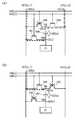
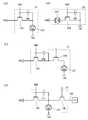
또한 본 발명의 일 형태의 표시 장치에서는, 도 5의 (A)에 나타낸 바와 같이, 회로(11)가 소스 드라이버(12)에 포함되어도 좋다. 또는 소스 드라이버(12)와 회로(11)가 중첩되는 영역을 가지는 스택 구조로 하여도 좋다. 상기 구성으로 함으로써, 내로 베젤화가 가능하다. 또한 소스 드라이버(12)에는 외장형 IC칩을 사용할 수 있다. 또는 기판 위에 화소 회로와 함께 모놀리식화되어 있어도 좋다.Further, in the display device of one embodiment of the present invention, the
또한 도 1에는 열마다 회로(11)를 제공하는 예를 나타내었지만, 도 5의 (B)에 나타낸 바와 같이, 소스 드라이버(12)와 화소(10) 사이에 선택 회로(16)를 제공하고, 회로(11)와 화소(10) 사이에 선택 회로(17)를 제공하여도 좋다. 상기 구성으로 함으로써 복수의 열의 화소에 대한 데이터 기록을 하나의 회로(11)에 의하여 수행할 수 있다. 또한 회로(11)의 개수를 삭감할 수 있으므로 내로 베젤화가 가능하다. 또한 도 5의 (B)에서는, 하나의 회로(11)에 의하여 3열분의 화소(10)(화소([m] 내지 [m+2]))에 기록을 수행하는 예를 나타내었지만, 이에 한정되지 않고, 기록 시간의 허용 범위에서 열수를 결정하면 좋다.In addition, although an example of providing
또한 도 5의 (B)의 구성을 변형하여, 도 5의 (C)에 나타낸 바와 같이, 선택 회로(18)를 통하여 회로(11)에 데이터를 공급하는 구성으로 하여도 좋다. 또한 도 5의 (B), (C)의 구성에 대하여 도 5의 (A)의 구성을 적용하여도 좋다.Further, the configuration of FIG. 5B may be modified to provide a configuration in which data is supplied to the
회로(11)가 가지는 트랜지스터(111 내지 116)는 표시 영역(15)(도 1 참조) 외측에 제공되기 때문에, 트랜지스터의 점유 면적의 제약을 받기 어려워, 화소(10)에 제공되는 트랜지스터보다 채널 폭을 크게 하는 것이 용이하다. 채널 폭이 큰 트랜지스터를 사용함으로써, 배선(127)에 대한 충방전 시간을 단축할 수 있어, 프레임 주파수를 높이기 쉽다. 또한 화소수가 많고 수평 기간이 짧은 고정세(高精細) 디스플레이에도 적용하기 쉽다.Since the
또한 트랜지스터(111 내지 116)로서 OS 트랜지스터를 사용함으로써, 회로(11)의 신뢰성을 높일 수 있고, 비교적 높은 전압으로도 안정된 동작을 수행할 수 있다. 또한 트랜지스터(111 내지 116)를 IC칩 내에 제공된 Si 트랜지스터로 하는 경우에는, 보다 고속으로 동작할 수 있다. 또한 IC칩 내에 트랜지스터(111 내지 116)를 제공하는 경우에도, 상기 트랜지스터를 OS 트랜지스터로 하여도 좋다.In addition, by using OS transistors as the
<표시 장치의 변형예><Modified example of display device>
도 6의 (A), (B), (C)에 나타낸 바와 같이, 소스 드라이버(12) 및 회로(11)는 표시 영역(15)의 한쪽 단부 측뿐만 아니라, 대향하는 다른 쪽 단부 측에도 제공하여도 좋다.6(A), (B), and (C), the
여기서, 표시 영역(15)의 한쪽 단부 측에 제공된 회로(11)를 회로(11A)로 한다. 회로(11A)는 소스 드라이버(12A)와 전기적으로 접속된다. 또한 표시 영역(15)의 다른 쪽 단부 측에 제공된 회로(11)를 회로(11B)로 한다. 회로(11B)는 소스 드라이버(12B)와 전기적으로 접속된다.Here, the
이와 같은 구성으로 함으로써, 배선(127[1], 127[2])을 고속으로 충방전할 수 있어, 화소수가 많고 수평 기간이 짧은 표시 장치, 배선(127)의 기생 용량이 큰 대형 표시 장치 등에 대응하기 쉽다.With such a configuration, the wirings 127[1] and 127[2] can be charged and discharged at high speed, such as a display device having a large number of pixels and a short horizontal period, a large-sized display device having a large parasitic capacitance of the
또는 도 6의 (B)에 나타낸 바와 같이, 화소(10[1]) 내지 화소(10[x])(x는 2 이상의 자연수이고, 예를 들어 실질적인 행의 중앙 값 등)에 소스 드라이버(12A) 및 회로(11A)를 전기적으로 접속하고, 화소(10[x+1]) 내지 화소(10[y])(y는 행의 마지막 값)에 소스 드라이버(12B) 및 회로(11B)를 전기적으로 접속하여도 좋다.Alternatively, as shown in FIG. 6B, the
소스 드라이버(12A) 및 회로(11A)는 배선(127[1a], 127[2a])의 충방전을 수행하고, 소스 드라이버(12B) 및 회로(11B)는 배선(127[1b], 127[2b])의 충방전을 수행한다. 이와 같이 배선(127)을 분할함으로써 배선(127)의 충방전을 고속으로 수행할 수 있으므로 고속 구동에 대응하기 쉽다.The
또한 도 6의 (C)에 나타낸 바와 같이, 복수의 게이트 드라이버(게이트 드라이버(13A, 13B))를 제공하여도 좋다. 복수의 소스 드라이버 및 복수의 게이트 드라이버를 사용함으로써, 분할한 배선(127) 각각에 대하여 병행하여 충방전을 수행할 수 있으므로 기록 시간을 확보하기 쉽다.Further, as shown in Fig. 6C, a plurality of gate drivers (
도 6의 (B), (C)는 소위 분할 구동을 수행하는 구성이고, 화소 수가 많고 수평 기간이 짧은 표시 장치이어도 데이터의 기록을 수행하기 쉽다.6(B) and 6(C) are so-called divisional driving configurations, and even in a display device having a large number of pixels and a short horizontal period, data writing is easy to perform.
<반전 회로의 동작 예><Example of operation of inverting circuit>
다음으로, 도 7에 나타낸 타이밍 차트 및 도 8의 (A), (B)에 나타낸 회로 동작의 설명도를 사용하여, 회로(11)에서의 반전 동작의 자세한 내용에 대하여 설명한다.Next, the detailed content of the inversion operation in the
또한 아래의 설명에서 고전위를 "H"로, 저전위를 "L"로 나타낸다. 또한 소스 드라이버(12)로부터 공급되는 제 1 데이터를 "+D"로, 배선(161)으로부터 공급되는 음의 전원 전위를 "-V1"로, 배선(162)으로부터 공급되는 양의 전원 전위를 "+V1"로 한다. 또한 "+D[n]"은 제 n 행의 화소 데이터를, "+D[n+1]"은 제 n+1 행의 화소 데이터를 뜻한다.Also, in the following description, a high potential is denoted by "H" and a low potential is denoted by "L". In addition, the first data supplied from the
또한 여기서는 전위의 분배, 결합, 또는 손실에서 회로의 구성이나 동작 타이밍 등에 기인하는 자세한 변화는 감안하지 않는다. 또한 커패시터를 사용한 용량 결합에 의한 전위의 변화는 상기 커패시터와, 접속되는 요소의 용량비에 의존하지만, 설명의 명료화를 위하여 상기 요소의 용량값은 충분히 작은 값으로 가정한다.In addition, detailed changes due to circuit configuration or operation timing in potential distribution, coupling, or loss are not taken into account here. In addition, although the change in potential due to capacitive coupling using a capacitor depends on the capacitance ratio between the capacitor and the element to be connected, it is assumed that the capacitance value of the element is sufficiently small for clarity of explanation.
시각 T1에서, 배선(127[m_1])에 "+D[n]"을 공급하고, 배선(128)의 전위를 "H"로 하고, 배선(129[n])"의 전위를 "L"로 하면, 트랜지스터(111, 113)가 도통되고, 노드(NA)의 전위는 "+D[n]"이 되고, 노드(NB)의 전위는 "+V1"이 된다(도 8의 (A) 참조). 이때, 커패시터(117)에는 "+V1-D[n]"이 유지된다.At time T1, "+D[n]" is supplied to the wiring 127[m_1], the potential of the
시각 T2에서, 배선(128)의 전위를 "L"로 하고, 배선(129)"의 전위를 "H"로 하면, 트랜지스터(111, 113)가 비도통이 되고, 트랜지스터(112, 114)가 도통된다. 이때, 노드(NA)의 전위는 "-V1"이 되고, 커패시터(117)의 용량 결합에 의하여 노드(NB)의 전위는 "+V1+(-V1-D[n])"="-D[n]"이 된다.At time T2, when the potential of the
또한 트랜지스터(114)를 통하여 노드(NC)의 전위는 "-D[n]"이 된다. 노드(NC)의 전위는 트랜지스터(115) 및 트랜지스터(116)로 구성되는 소스 폴로어 회로에 의하여 노드(ND)에 판독된다. 즉 회로(11)는 배선(127[m_1])으로부터 입력된 "+D[n]"(제 1 데이터)를 반전한 "-D[n]"(제 2 데이터)를 배선(127[m_2])으로 출력할 수 있다(도 8의 (B) 참조).Also, the potential of the node NC through the
시각 T3에서, 배선(128)의 전위를 "L"로 하고, 배선(129)의 전위를 "L"로 하면, 트랜지스터(112, 114)가 비도통이 되고, 노드(NC)의 전위가 유지된다. 즉 배선(127[m_2])에 출력된 "-D[n]"은 유지된다.At time T3, when the potential of the
시각 T4 내지 시각 T6에서, 배선(127[m_1])에 "+D[n+1]"을 공급하여 반전 데이터 "-D[n+1]"을 생성하는 동작을 수행한다. 위에서 설명된 바와 같이, 회로(11)에서는 입력 데이터의 반전 데이터를 생성할 수 있다.From time T4 to time T6, an operation for generating inversion data "-D[n+1]" is performed by supplying "+D[n+1]" to the wiring 127[m_1]. As described above, the
<화소 회로의 동작 예><Example of operation of pixel circuit>
다음으로, 도 9에 나타낸 타이밍 차트 및 도 10의 (A), (B)에 나타낸 회로 동작의 설명도를 사용하여, 소스 드라이버(12)가 출력하는 데이터 전위의 약 3배의 데이터 전위를 화소(10)의 표시 디바이스에 공급하는 방법을 설명한다. 또한 화소(10)에 공급되는 제 2 데이터의 생성 동작에 대한 설명은 생략한다.Next, using the timing chart shown in Fig. 9 and the circuit operation explanatory diagrams shown in Figs. 10A and 10B, a data potential of about three times the data potential output by the
시각 T1에서, 배선(127[m, 1])에 "+D[n]"을 공급하고, 배선(127[m, 2])에 "-D[n]"을 공급하고, 배선(125[n])의 전위를 "L"로 하고, 배선(126[n])의 전위를 "H"로 하면, 트랜지스터(101, 103)가 도통되고, 노드(NM)의 전위는 "+D[n]"이 되고, 노드(NE)의 전위는 "-D[n]"이 된다. 이때, 커패시터(104)에는 "+2D[n]"이 유지된다(도 10의 (A) 참조).At time T1, "+D[n]" is supplied to the wiring 127[m, 1], "-D[n]" is supplied to the wiring 127[m, 2], and the wiring 125[ n]) is set to "L" and the potential of the wiring 126[n] is set to "H", the
시각 T2에서, 배선(125[n])의 전위를 "H"로 하고, 배선(126[n])의 전위를 "L"로 하면, 트랜지스터(101)가 비도통이 되고, 노드(NM)가 부유 상태가 된다. 또한 트랜지스터(103)가 비도통이 되고, 트랜지스터(102)가 도통되면, 노드(NE)의 전위는 "-D[n]"으로부터 "+D[n]"으로 재기록된다. 그 변화량이 커패시터(104)와 노드(NM)의 용량비에 따라 노드(NM)의 전위에 가산되므로, 노드(NM)의 전위는 "+D[n]+(+D[n]-(-D[n])"="+3D[n]"이 된다(도 10의 (B) 참조).At time T2, when the potential of the wiring 125[n] is set to “H” and the potential of the wiring 126[n] is set to “L”, the
시각 T3에서, 배선(125[n])의 전위를 "L"로 하고, 배선(126[n])의 전위를 "L"로 하면, 트랜지스터(102)가 비도통이 되고, 노드(NE) 및 노드(NM)의 전위는 유지된다.At time T3, when the potential of the wiring 125[n] is set to “L” and the potential of the wiring 126[n] is set to “L”, the
시각 T4 내지 시각 T6에서는, 배선(127[m, 1])에 "+D[n+1]"을 공급하고, 배선(127[m, 2])에 "-D[n+1]"을 공급하고, 상기와 같은 동작을 수행함으로써, 화소([n+1, m])의 기록 동작을 수행한다.From time T4 to time T6, "+D[n+1]" is supplied to the wiring 127[m, 1], and "-D[n+1]" is supplied to the wiring 127[m, 2]. A write operation is performed on the pixel ([n+1, m]) by performing the above operation.
상술한 동작에 의하여, 화소(10)에서는 소스 드라이버(12)로부터 공급된 전압의 약 3배의 전압을 표시 디바이스에 공급할 수 있다.By the above-described operation, the
<변형예 1><
도 11의 (A)에 나타낸 구성은 화소(10)와 2개의 소스선의 접속 관계를 바꾼 구성이다. 배선(127[m_1])에는 트랜지스터(103)의 소스 및 드레인 중 다른 쪽이 전기적으로 접속된다. 배선(127[m_2])에는 트랜지스터(101)의 소스 및 드레인 중 다른 쪽 및 트랜지스터(102)의 소스 및 드레인 중 다른 쪽이 전기적으로 접속된다.The configuration shown in Fig. 11A is a configuration in which the connection relationship between the
도 2에 나타낸 구성의 화소(10)의 기록 동작은, 첫 번째 동작에서 소스 드라이버(12)로부터 공급되는 제 1 데이터와 회로(11)로부터 공급되는 제 2 데이터를 동시에 기록하고, 두 번째 동작에서 제 1 데이터를 다시 기록한다. 이 경우, 두 번째 동작까지 제 1 데이터의 출력을 유지할 필요가 있으므로 회로(11)가 대기하는 기간이 생긴다.In the write operation of the
한편, 도 11의 (A)에 나타낸 구성의 화소(10)의 기록 동작은, 첫 번째 동작에서 제 1 데이터와 제 2 데이터를 동시에 기록하고, 두 번째 동작에서 제 2 데이터를 기록한다. 상기 구성에서는, 도 11의 (B)의 타이밍 차트에 나타낸 바와 같이, 제 n 행의 화소에 대한 데이터 기록 시간과, 회로(11)에서 제 n+1 행의 화소에 대한 반전 데이터를 생성하는 기간을 중복시킬 수 있다. 따라서 화소수가 많고 수평 기간이 짧은 경우에도 기록 시간을 충분히 확보할 수 있다. 바꿔 말하면, 수평 기간을 단축하여도 기록을 수행할 수 있다.On the other hand, in the write operation of the
<변형예 2><
도 12는 소스 드라이버(12) 및 회로(11)와, 화소(10) 사이에 선택 회로(19)가 제공된 구성이다.12 is a configuration in which a
선택 회로(19)는 트랜지스터(131)와, 트랜지스터(132)와, 트랜지스터(133)와, 트랜지스터(134)를 가지는 구성으로 할 수 있다. 트랜지스터(131)의 소스 및 드레인 중 한쪽은 트랜지스터(133)의 소스 및 드레인 중 한쪽과 전기적으로 접속된다. 트랜지스터(133)의 소스 및 드레인 중 다른 쪽은 트랜지스터(132)의 소스 및 드레인 중 한쪽과 전기적으로 접속된다. 트랜지스터(132)의 소스 및 드레인 중 다른 쪽은 트랜지스터(134)의 소스 및 드레인 중 한쪽과 전기적으로 접속된다. 트랜지스터(134)의 소스 및 드레인 중 다른 쪽은 트랜지스터(131)의 소스 및 드레인 중 다른 쪽과 전기적으로 접속된다.The
트랜지스터(131)의 소스 및 드레인 중 한쪽은 배선(127[m_1a])과 전기적으로 접속된다. 배선(127[m_1a])은 소스 드라이버(12)의 출력 단자와 전기적으로 접속된다. 트랜지스터(132)의 소스 및 드레인 중 다른 쪽은 배선(127[m_2a])과 전기적으로 접속된다. 배선(127[m_2a])은 회로(11)의 출력 단자와 전기적으로 접속된다.One of the source and drain of the
선택 회로(19)의 트랜지스터(131, 132)를 도통하고, 트랜지스터(133, 134)를 비도통으로 함으로써, 도 13의 (A)에 나타낸 바와 같이, 배선(127[m_1a])에 출력된 데이터 "+D"를 배선(127[m_1b])에 출력하고, 배선(127[m_2a])에 출력된 데이터 "-D"를 배선(127[m_2b])에 출력할 수 있다.By making the
또는 트랜지스터(131, 132)를 비도통으로 하고, 트랜지스터(133, 134)를 도통함으로써, 도 13의 (B)에 나타낸 바와 같이, 배선(127[m_1a])에 출력된 데이터 "+D"를 배선(127[m_2b])에 출력하고, 배선(127[m_1b])에 출력된 데이터 "-D"를 배선(127[m_2a])에 출력할 수 있다.Alternatively, by making the
상기 동작은 액정 디바이스의 반전 동작(양극성 동작 및 음극성 동작)에 유효하다. 또한 회로(11)에서는 반전 데이터를 생성할 수 있으므로, 소스 드라이버가 출력할 수 있는 전위가 양 전위 및 음 전위 중 어느 쪽이어도 좋다. 따라서 기능이 간략화된 소스 드라이버를 사용할 수 있다. 기능이 간략화된 소스 드라이버는 회로 구성이 간략화될 수 있으므로 제조 비용 및 칩 면적을 작게 할 수 있다. 따라서 표시 장치의 비용을 저감할 수도 있다.The above operation is effective for the inversion operation (positive polarity operation and negative polarity operation) of the liquid crystal device. In addition, since the
<변형예 3><Modification 3>
소스 드라이버(12)가 제 1 데이터와, 그 반전 데이터인 제 2 데이터를 출력할 수 있는 기능을 가지는 경우에는, 도 14에 나타낸 바와 같이, 회로(11)를 생략한 구성으로 하여도 좋다. 또한 상술한 변형예 1 내지 변형예 3을 서로 조합할 수 있다.In the case where the
<회로 21><
도 15의 (A) 내지 (D)는 회로(21)에 적용할 수 있고 표시 디바이스로서 액정 디바이스를 포함하는 구성의 예를 나타낸 것이다.15A to 15D show examples of configurations applicable to the
도 15의 (A)에 나타낸 구성은 커패시터(141) 및 액정 디바이스(142)를 가진다. 액정 디바이스(142)의 한쪽 전극은 커패시터(141)의 한쪽 전극과 전기적으로 접속된다. 커패시터(141)의 한쪽 전극은 노드(NM)에 전기적으로 접속된다.The configuration shown in FIG. 15A has a
커패시터(141)의 다른 쪽 전극은 배선(151)과 전기적으로 접속된다. 액정 디바이스(142)의 다른 쪽 전극은 배선(152)과 전기적으로 접속된다. 배선(151, 152)은 전원을 공급하는 기능을 가진다. 예를 들어, 배선(151, 152)은 GND나 0V 등의 기준 전위나 임의의 전위를 공급할 수 있다.The other electrode of the
또한 도 15의 (B)에 나타낸 바와 같이, 커패시터(141)를 생략한 구성으로 하여도 좋다. 상술한 바와 같이, 노드(NM)와 접속되는 트랜지스터에 OS 트랜지스터를 사용할 수 있다. OS 트랜지스터는 누설 전류가 매우 작기 때문에, 저장 용량으로서 기능하는 커패시터(141)를 생략하여도 표시를 비교적 오랫동안 유지할 수 있다. 또한 트랜지스터의 구성에 한정되지 않고, 필드 시??셜 구동과 같이 고속 동작으로 표시 기간을 짧게 할 수 있는 경우에도 커패시터(141)를 생략하는 것이 유효하다. 커패시터(141)를 생략함으로써 개구율을 향상시킬 수 있다. 또는 화소의 투과율을 향상시킬 수 있다.Moreover, as shown in FIG. 15B, it is good also as a structure in which the
도 15의 (A), (B)의 구성에서는, 노드(NM)의 전위가 액정 디바이스(142)의 동작 문턱값 이상이 되었을 때 액정 디바이스(142)의 동작이 시작된다. 따라서, 노드(NM)의 전위가 확정되기 전에 표시 동작이 시작되는 경우가 있다. 다만, 투과형 액정 표시 장치의 경우에는, 노드(NM)의 전위가 확정될 때까지 백라이트를 소등하는 등의 동작을 병용함으로써, 불필요한 표시 동작이 수행되어도 그것이 시인되는 것을 억제할 수 있다.In the configuration of FIGS. 15A and 15B , the operation of the
도 15의 (C)는 도 15의 (A)의 구성에 트랜지스터(143)를 부가한 구성이다. 트랜지스터(143)의 소스 및 드레인 중 한쪽은 커패시터(141)의 한쪽 전극과 전기적으로 접속된다. 트랜지스터(143)의 소스 및 드레인 중 다른 쪽은 노드(NM)와 전기적으로 접속된다.FIG. 15C is a configuration in which a
상기 구성에서는 트랜지스터(143)의 도통에 따라 액정 디바이스(142)에 노드(NM)의 전위가 인가된다. 따라서 노드(NM)의 전위가 확정된 후의 임의의 타이밍에 액정 디바이스(142)의 동작을 시작할 수 있다.In the above configuration, the potential of the node NM is applied to the
도 15의 (D)는 도 15의 (C)의 구성에 트랜지스터(144)를 부가한 구성이다. 트랜지스터(144)의 소스 및 드레인 중 한쪽은 액정 디바이스(142)의 한쪽 전극과 전기적으로 접속된다. 트랜지스터(144)의 소스 및 드레인 중 다른 쪽은 배선(153)과 전기적으로 접속된다.FIG. 15D is a configuration in which a
배선(153)과 전기적으로 접속되는 회로(170)는 커패시터(141) 및 액정 디바이스(142)에 공급된 전위를 리셋하는 기능을 가질 수 있다.The
도 16의 (A) 내지 (D)는, 회로(21)에 적용할 수 있고 표시 디바이스로서 발광 디바이스를 포함하는 구성의 예를 나타낸 것이다.16A to 16D show examples of configurations applicable to the
도 16의 (A)에 나타낸 구성은 트랜지스터(145)와, 커패시터(146)와, 발광 디바이스(147)를 가진다. 트랜지스터(145)의 소스 및 드레인 중 한쪽은 발광 디바이스(147)의 한쪽 전극과 전기적으로 접속된다. 발광 디바이스(147)의 한쪽 전극은 커패시터(146)의 한쪽 전극과 전기적으로 접속된다. 커패시터(146)의 다른 쪽 전극은 트랜지스터(145)의 게이트와 전기적으로 접속된다. 트랜지스터(145)의 게이트는 노드(NM)에 전기적으로 접속된다.The configuration shown in FIG. 16A includes a
트랜지스터(145)의 소스 및 드레인 중 다른 쪽은 배선(154)과 전기적으로 접속된다. 발광 디바이스(147)의 다른 쪽 전극은 배선(155)과 전기적으로 접속된다. 배선(154, 155)은 전원을 공급하는 기능을 가진다. 예를 들어 배선(154)은 고전위 전원을 공급할 수 있다. 또한 배선(155)은 저전위 전원을 공급할 수 있다.The other of the source and drain of the
도 16의 (A)에 나타낸 구성에서는, 노드(NM)의 전위가 트랜지스터(111)의 문턱 전압 이상이 되었을 때 발광 디바이스(147)에 전류가 흐른다.In the configuration shown in FIG. 16A , a current flows through the
또는 도 16의 (B)에 나타낸 바와 같이, 발광 디바이스(147)의 한쪽 전극을 배선(154)과 전기적으로 접속하고, 발광 디바이스(147)의 다른 쪽 전극을 트랜지스터(145)의 소스 및 드레인 중 다른 쪽과 전기적으로 접속하여도 좋다. 상기 구성은 발광 디바이스(147)를 가지는 다른 회로(21)에도 적용할 수 있다.Alternatively, as shown in FIG. 16B , one electrode of the
도 16의 (C)는 도 16의 (A)의 구성에 트랜지스터(148)를 부가한 구성이다. 트랜지스터(148)의 소스 및 드레인 중 한쪽은 트랜지스터(145)의 소스 및 드레인 중 한쪽과 전기적으로 접속된다. 트랜지스터(148)의 소스 및 드레인 중 다른 쪽은 발광 디바이스(147)의 한쪽 전극과 전기적으로 접속된다.FIG. 16C is a configuration in which a
상기 구성에서는 노드(NM)의 전위가 트랜지스터(111)의 문턱 전압 이상이고 트랜지스터(148)가 도통되었을 때 발광 디바이스(147)에 전류가 흐른다. 따라서 노드(NM)의 전위가 확정된 후의 임의의 타이밍에 발광 디바이스(147)의 발광을 시작할 수 있다.In the above configuration, when the potential of the node NM is equal to or greater than the threshold voltage of the
도 16의 (D)는 도 16의 (A)의 구성에 트랜지스터(149)를 부가한 구성이다. 트랜지스터(149)의 소스 및 드레인 중 한쪽은 트랜지스터(145)의 소스 및 드레인 중 한쪽과 전기적으로 접속된다. 트랜지스터(149)의 소스 및 드레인 중 다른 쪽은 배선(156)과 전기적으로 접속된다.FIG. 16D is a configuration in which a
배선(156)은 기준 전위 등의 특정 전위의 공급원과 전기적으로 접속될 수 있다. 배선(156)으로부터 트랜지스터(145)의 소스 및 드레인 중 한쪽에 특정 전위를 공급함으로써, 화상 데이터의 기록을 안정화시킬 수도 있다. 또한 발광 디바이스(147)의 발광의 타이밍을 제어할 수도 있다.The
또한 배선(156)은 회로(171)와 접속될 수 있고, 모니터선으로서의 기능을 가질 수도 있다. 회로(171)는 상기 특정 전위의 공급원으로서의 기능, 트랜지스터(145)의 전기 특성을 취득하는 기능, 및 보정 데이터를 생성하는 기능 중 하나 이상을 가질 수 있다.Further, the
<트랜지스터의 변형예><Modification of transistor>
또한 도 17의 (A)에 예시한 바와 같이, 본 발명의 일 형태의 회로에서는, 백 게이트가 제공된 트랜지스터를 사용하여도 좋다. 도 17의 (A)는 백 게이트가 프런트 게이트와 전기적으로 접속된 구성을 나타낸 것이고, 온 전류를 높이는 효과를 가진다. 또는 백 게이트가 정전위를 공급할 수 있는 배선과 전기적으로 접속된 구성이어도 좋다. 상기 구성에서는, 트랜지스터의 문턱 전압을 제어할 수 있다. 또한 회로(11) 및 회로(21)가 가지는 트랜지스터에도 백 게이트를 제공하여도 좋다.Further, as illustrated in Fig. 17A, in the circuit of one embodiment of the present invention, a transistor provided with a back gate may be used. 17A shows a configuration in which the back gate is electrically connected to the front gate, and has an effect of increasing the on current. Alternatively, a configuration in which the back gate is electrically connected to a wiring capable of supplying a positive potential may be employed. In the above configuration, the threshold voltage of the transistor can be controlled. In addition, a back gate may be provided for the transistors included in the
또한 화소(10)에서 트랜지스터(101, 102)는 용량값이 비교적 큰 커패시터(104)를 신속히 충방전하는 역할을 한다. 트랜지스터(103)는 커패시터(104)와 회로(21)의 합성 용량(C)을 충전하는 역할을 한다. 합성 용량(C)은 커패시터(104)의 용량값을 C104, 회로(21)의 용량값을 C21로 하였을 때, C104×(C21/(C104+C21))이 되고, C104보다 작은 값이 된다.In addition, in the
따라서 도 17의 (B)에 나타낸 개념도와 같이, 트랜지스터(103)로서는, 트랜지스터(101, 102)보다 전류 공급 능력이 작은 트랜지스터를 사용할 수 있다. 구체적으로는, 트랜지스터(103)의 채널 폭을 트랜지스터(101, 102)의 채널 폭보다 작게 할 수 있다. 따라서 모두 같은 크기의 트랜지스터로 구성하는 경우보다 개구율을 높일 수 있다.Accordingly, as shown in the conceptual diagram of FIG. 17B , a transistor having a smaller current supply capability than the
<시뮬레이션 결과><Simulation result>
다음으로, 화소의 동작에 관한 시뮬레이션 결과에 대하여 설명한다. 도 18에, 시뮬레이션에 사용한 화소(10)의 구성을 나타내었다. 도 2에 나타낸 회로 구성을 기본으로 하고, 회로(21)로서는 액정 디바이스(Clc) 및 커패시터(Cs)를 가지는 구성을 사용하였다. 입력 전압을 약 3배로 하는 동작에서의 노드(NM)의 전압 변화에 관한 시뮬레이션을 수행하였다.Next, the simulation results regarding the operation of the pixel will be described. Fig. 18 shows the configuration of the
시뮬레이션에 사용한 파라미터는 아래와 같고, 트랜지스터 크기는 L/W=3μm/60μm(트랜지스터(Tr1, Tr2)), L/W=3μm/30μm(트랜지스터(Tr3))로 하고, 커패시터(C1)의 용량값은 14.4pF로 하고, 커패시터(Cs)의 용량값은 1.2pF로 하고, 액정 소자(Clc)의 용량값은 1.2pF로 하였다. 게이트선(GL1, GL2)에 인가하는 전압은 "H"로서 +26V로, "L"로서 -21V로 하였다. 또한 VCOM 및 TCOM(코먼 전압)의 전위는 +8V로 하였다. 또한 회로 시뮬레이션 소프트웨어로서는 SPICE를 사용하였다.The parameters used for the simulation are as follows, the transistor size is L/W=3μm/60μm (transistors (Tr1, Tr2)), L/W=3μm/30μm (transistor (Tr3)), and the capacitance value of the capacitor C1 was 14.4 pF, the capacitance of the capacitor Cs was 1.2 pF, and the capacitance of the liquid crystal element Clc was 1.2 pF. The voltages applied to the gate lines GL1 and GL2 were set to +26V as "H" and -21V as "L". In addition, the potentials of VCOM and TCOM (common voltage) were set to +8V. Also, SPICE was used as the circuit simulation software.
도 19는 위에서 나타낸 화소의 타이밍 차트에 따른 동작의 시뮬레이션 결과이고, 가로축은 시간(초)을, 세로축은 화소(10)의 노드(NM)의 전압(V)을 나타낸다. 또한 SL1은 배선(127[m_1])에 상당하고, SL2는 배선(127[m_2])에 상당하고, GL1은 배선(126)에 상당하고, GL2는 배선(125)에 상당한다. 또한 양극성 동작 시에 DATA1은 +16V로, DATA2는 0V로 하였다. 음극성 동작시에 DATA1은 0V로, DATA2는 +16V로 하였다.19 is a simulation result of the operation according to the timing chart of the pixel shown above, the horizontal axis indicates time (seconds), and the vertical axis indicates the voltage (V) of the node NM of the
도 19에 나타낸 바와 같이, 양극성 동작, 음극성 동작의 양쪽 모두가 코먼 전압을 기준으로 하여 약 21V(약 2.6배 이상) 승압할 수 있는 것을 확인할 수 있었다. 트랜지스터의 전기 특성의 향상 및 기생 용량의 저감 등을 수행함으로써 더 높은 전압을 생성할 수 있다.As shown in FIG. 19 , it was confirmed that both of the positive operation and the negative operation could increase the voltage by about 21V (about 2.6 times or more) based on the common voltage. A higher voltage can be generated by improving the electrical characteristics of the transistor and reducing the parasitic capacitance.
상술한 시뮬레이션 결과로부터, 본 발명의 일 형태의 효과를 확인할 수 있었다.From the simulation results described above, the effect of one embodiment of the present invention was confirmed.
본 실시형태는 다른 실시형태 등에 기재된 구성과 적절히 조합하여 실시할 수 있다.This embodiment can be implemented in appropriate combination with the structures described in other embodiments and the like.
(실시형태 2)(Embodiment 2)
본 실시형태에서는, 액정 디바이스를 사용한 표시 장치의 구성예와, 발광 디바이스를 사용한 표시 장치의 구성예에 대하여 설명한다. 또한 본 실시형태에서는 실시형태 1에서 설명한 표시 장치의 요소, 동작, 및 기능에 대한 설명은 생략한다.In the present embodiment, a configuration example of a display device using a liquid crystal device and a configuration example of a display device using a light emitting device will be described. In addition, in this embodiment, the description of the elements, operation|movement, and function of the display apparatus demonstrated in
본 실시형태에서 설명하는 표시 장치에는, 실시형태 1에서 설명한 화소를 사용할 수 있다. 또한 아래에서 설명하는 주사선 구동 회로는 게이트 드라이버에 상당하고, 신호선 구동 회로는 소스 드라이버에 상당한다.For the display device described in this embodiment, the pixels described in the first embodiment can be used. Further, the scan line driver circuit described below corresponds to the gate driver, and the signal line driver circuit corresponds to the source driver.
도 20의 (A) 내지 (C)는 본 발명의 일 형태를 사용할 수 있는 표시 장치의 구성을 나타낸 도면이다.20A to 20C are diagrams showing the configuration of a display device in which one embodiment of the present invention can be used.
도 20의 (A)에서, 제 1 기판(4001) 위에 제공된 표시부(215)를 둘러싸도록 밀봉재(4005)가 제공되고, 밀봉재(4005) 및 제 2 기판(4006)으로 표시부(215)가 밀봉되어 있다.In FIG. 20A , a sealing
도 20의 (A)에서, 주사선 구동 회로(221a), 신호선 구동 회로(231a), 신호선 구동 회로(232a), 및 공통선 구동 회로(241a)는 각각이 인쇄 기판(4041) 위에 제공된 집적 회로(4042)를 복수로 가진다. 집적 회로(4042)는 단결정 반도체 또는 다결정 반도체로 형성되어 있다. 공통선 구동 회로(241a)는 실시형태 1에 나타낸 배선(151, 152, 129, 154, 155) 등에 규정의 전위를 공급하는 기능을 가진다.In Fig. 20A, a scan
주사선 구동 회로(221a), 공통선 구동 회로(241a), 신호선 구동 회로(231a), 및 신호선 구동 회로(232a)에 공급되는 각종 신호 및 전위는 FPC(Flexible printed circuit)(4018)를 통하여 공급된다.Various signals and potentials supplied to the scan
주사선 구동 회로(221a) 및 공통선 구동 회로(241a)가 가지는 집적 회로(4042)는 표시부(215)에 선택 신호를 공급하는 기능을 가진다. 신호선 구동 회로(231a) 및 신호선 구동 회로(232a)가 가지는 집적 회로(4042)는 표시부(215)에 화상 데이터를 공급하는 기능을 가진다. 집적 회로(4042)는 제 1 기판(4001) 위의 밀봉재(4005)로 둘러싸여 있는 영역과는 다른 영역에 실장되어 있다.The
또한 집적 회로(4042)의 접속 방법은 특별히 한정되는 것은 아니고, 와이어 본딩법, COF(Chip On Film)법, COG(Chip On Glass)법, TCP(Tape Carrier Package)법 등을 사용할 수 있다.In addition, the method of connecting the
도 20의 (B)는 신호선 구동 회로(231a) 및 신호선 구동 회로(232a)에 포함되는 집적 회로(4042)를 COG법으로 실장하는 예를 나타낸 것이다. 또한 구동 회로의 일부 또는 전체를 표시부(215)와 같은 기판 위에 일체로 형성하여, 시스템 온 패널(system-on-panel)을 형성할 수 있다.Fig. 20B shows an example in which the signal
도 20의 (B)에서는 주사선 구동 회로(221a) 및 공통선 구동 회로(241a)를 표시부(215)와 같은 기판 위에 형성하는 예를 나타내었다. 구동 회로를 표시부(215) 내의 화소 회로와 동시에 형성함으로써 부품 점수를 삭감할 수 있다. 따라서 생산성을 높일 수 있다.20B shows an example in which the scan
또한 도 20의 (B)에서는 제 1 기판(4001) 위에 제공된 표시부(215)와, 주사선 구동 회로(221a) 및 공통선 구동 회로(241a)를 둘러싸도록, 밀봉재(4005)가 제공되어 있다. 또한 표시부(215), 주사선 구동 회로(221a), 및 공통선 구동 회로(241a) 위에 제 2 기판(4006)이 제공되어 있다. 따라서 표시부(215), 주사선 구동 회로(221a), 및 공통선 구동 회로(241a)는 제 1 기판(4001)과 밀봉재(4005)와 제 2 기판(4006)에 의하여 표시 디바이스와 함께 밀봉되어 있다.In addition, in FIG. 20B, a sealing
또한 도 20의 (B)에서는 신호선 구동 회로(231a) 및 신호선 구동 회로(232a)를 별도로 형성하고 제 1 기판(4001)에 실장한 예를 나타내었지만, 이 구성에 한정되지 않는다. 주사선 구동 회로를 별도로 형성하고 실장하여도 좋고, 신호선 구동 회로의 일부 또는 주사선 구동 회로의 일부를 별도로 형성하고 실장하여도 좋다. 또한 도 20의 (C)에 나타낸 바와 같이, 신호선 구동 회로(231a) 및 신호선 구동 회로(232a)를 표시부(215)와 같은 기판 위에 형성하여도 좋다.20B shows an example in which the signal
또한 표시 장치는 표시 디바이스가 밀봉되어 있는 패널과, 상기 패널에 컨트롤러를 포함하는 IC 등이 실장되어 있는 모듈을 포함하는 경우가 있다.In addition, the display apparatus may include a panel in which a display device is sealed, and a module in which an IC including a controller is mounted on the panel.
또한 제 1 기판 위에 제공된 표시부 및 주사선 구동 회로는 트랜지스터를 복수로 가진다. 상기 트랜지스터로서, 실시형태 1에서 나타낸 Si 트랜지스터 또는 OS 트랜지스터를 적용할 수 있다.Further, the display section and the scan line driver circuit provided on the first substrate have a plurality of transistors. As the transistor, the Si transistor or OS transistor shown in
주변 구동 회로가 가지는 트랜지스터와, 표시부의 화소 회로가 가지는 트랜지스터의 구조는 같아도 좋고, 상이하여도 좋다. 주변 구동 회로가 가지는 트랜지스터는 모두 같은 구조의 트랜지스터이어도 좋고, 2종류 이상의 구조의 트랜지스터를 가져도 좋다. 마찬가지로 화소 회로가 가지는 트랜지스터는 모두 같은 구조의 트랜지스터이어도 좋고, 2종류 이상의 구조의 트랜지스터를 가져도 좋다.The structure of the transistor included in the peripheral driving circuit and the transistor included in the pixel circuit of the display unit may be the same or different. The transistors in the peripheral driving circuit may all have the same structure, or may have two or more types of transistors. Similarly, the transistors included in the pixel circuit may all have the same structure, or may have two or more types of transistors.
또한 제 2 기판(4006) 위에는 입력 장치(4200)를 제공할 수 있다. 도 20의 (A) 내지 (C)에 나타낸 표시 장치에 입력 장치(4200)를 제공한 구성은 터치 패널로서 기능시킬 수 있다.Also, an
본 발명의 일 형태의 터치 패널이 가지는 검지 디바이스(센서 소자라고도 함)에 한정은 없다. 손가락이나 스타일러스 등의 피검지체의 근접 또는 접촉을 검지할 수 있는 다양한 센서를 검지 디바이스로서 적용할 수 있다.There is no limitation in the detection device (also called a sensor element) which the touch panel of one embodiment of this invention has. Various sensors capable of detecting proximity or contact of a sensing object such as a finger or a stylus can be applied as the sensing device.
센서의 방식으로서는, 예를 들어 정전 용량 방식, 저항막 방식, 표면 탄성파 방식, 적외선 방식, 광학 방식, 감압 방식 등 다양한 방식을 사용할 수 있다.As the method of the sensor, various methods such as a capacitive method, a resistive film method, a surface acoustic wave method, an infrared method, an optical method, and a pressure reduction method can be used, for example.
본 실시형태에서는 정전 용량 방식의 검지 디바이스를 가지는 터치 패널을 예로 들어 설명한다.In this embodiment, the touch panel which has a capacitive detection device is taken as an example and demonstrated.
정전 용량 방식으로서는 표면형 정전 용량 방식, 투영형 정전 용량 방식 등이 있다. 또한 투영형 정전 용량 방식으로서는 자기 용량 방식, 상호 용량 방식 등이 있다. 상호 용량 방식을 사용하면, 여러 지점을 동시에 검지할 수 있기 때문에 바람직하다.As the capacitive method, there are a surface type capacitive method, a projected capacitive method, and the like. Further, as the projected capacitive method, there are a self-capacitance method, a mutual capacitance method, and the like. The use of the mutual capacitive method is preferable because several points can be simultaneously detected.
본 발명의 일 형태의 터치 패널에는, 따로 제작된 표시 장치와 검지 디바이스를 접합시키는 구성, 표시 디바이스를 지지하는 기판 및 대향 기판 중 한쪽 또는 양쪽에 검지 디바이스를 구성하는 전극 등을 제공하는 구성 등 다양한 구성을 적용할 수 있다.In the touch panel of one embodiment of the present invention, a configuration in which a separately manufactured display device and a detection device are joined, a configuration in which an electrode constituting the detection device is provided on one or both of a substrate supporting the display device and an opposing substrate, etc. configuration can be applied.
도 21의 (A), (B)에 터치 패널의 일례를 나타내었다. 도 21의 (A)는 터치 패널(4210)의 사시도이다. 도 21의 (B)는 입력 장치(4200)의 사시 개략도이다. 또한 명료화를 위하여 대표적인 구성 요소만을 나타내었다.An example of a touch panel is shown to Fig.21 (A), (B). 21A is a perspective view of the
터치 패널(4210)은 따로 제작된 표시 장치와 검지 디바이스를 접합시킨 구성을 가진다.The
터치 패널(4210)은 입력 장치(4200)와 표시 장치를 가지고, 이들이 중첩되어 제공되어 있다.The
입력 장치(4200)는 기판(4263), 전극(4227), 전극(4228), 복수의 배선(4237), 복수의 배선(4238), 및 복수의 배선(4239)을 가진다. 예를 들어 전극(4227)은 배선(4237) 또는 배선(4239)과 전기적으로 접속될 수 있다. 또한 전극(4228)은 배선(4239)과 전기적으로 접속될 수 있다. FPC(4272b)는 복수의 배선(4237) 및 복수의 배선(4238)의 각각과 전기적으로 접속된다. FPC(4272b)에는 IC(4273b)를 제공할 수 있다.The
또는 표시 장치의 제 1 기판(4001)과 제 2 기판(4006) 사이에 터치 센서를 제공하여도 좋다. 제 1 기판(4001)과 제 2 기판(4006) 사이에 터치 센서를 제공하는 경우에는 정전 용량 방식의 터치 센서 외에, 광전 변환 소자를 사용한 광학식 터치 센서를 적용하여도 좋다.Alternatively, a touch sensor may be provided between the
도 22의 (A), (B)는 도 20의 (B)에서 N1-N2의 쇄선으로 나타낸 부분의 단면도이다. 도 22의 (A), (B)에 나타낸 표시 장치는 전극(4015)을 가지고, 전극(4015)은 이방성 도전층(4019)을 통하여 FPC(4018)가 가지는 단자와 전기적으로 접속되어 있다. 또한 도 22의 (A), (B)에서, 전극(4015)은 절연층(4112), 절연층(4111), 및 절연층(4110)에 형성된 개구에서 배선(4014)과 전기적으로 접속되어 있다.22A and 22B are cross-sectional views of portions indicated by dashed lines N1-N2 in FIG. 20B. The display device shown in FIGS. 22A and 22B has an
전극(4015)은 제 1 전극층(4030)과 같은 도전층으로 형성되고, 배선(4014)은 트랜지스터(4010) 및 트랜지스터(4011)의 소스 전극 및 드레인 전극과 같은 도전층으로 형성되어 있다.The
또한 제 1 기판(4001) 위에 제공된 표시부(215)와 주사선 구동 회로(221a)는 트랜지스터를 복수로 가지고, 도 22의 (A), (B)에는 표시부(215)에 포함되는 트랜지스터(4010) 및 주사선 구동 회로(221a)에 포함되는 트랜지스터(4011)를 예시하였다. 또한 도 22의 (A), (B)에서는 트랜지스터(4010) 및 트랜지스터(4011)로서 보텀 게이트형 트랜지스터를 예시하였지만, 톱 게이트형 트랜지스터이어도 좋다.In addition, the
도 22의 (A), (B)에서는 트랜지스터(4010) 및 트랜지스터(4011) 위에 절연층(4112)이 제공되어 있다. 또한 도 22의 (B)에서는 절연층(4112) 위에 격벽(4510)이 형성되어 있다.22A and 22B , an insulating
또한 트랜지스터(4010) 및 트랜지스터(4011)는 절연층(4102) 위에 제공되어 있다. 또한 트랜지스터(4010) 및 트랜지스터(4011)는 절연층(4111) 위에 형성된 전극(4017)을 가진다. 전극(4017)은 백 게이트 전극으로서 기능할 수 있다.A
또한 도 22의 (A), (B)에 나타낸 표시 장치는 커패시터(4020)를 가진다. 커패시터(4020)는 트랜지스터(4010)의 게이트 전극과 같은 공정에서 형성된 전극(4021)과, 절연층(4103)과, 소스 전극 및 드레인 전극과 같은 공정에서 형성된 전극을 가지는 예를 나타내었다. 커패시터(4020)의 구성은 이에 한정되지 않고, 기타 도전층 및 절연층으로 형성되어도 좋다.In addition, the display device shown in FIGS. 22A and 22B includes a
표시부(215)에 제공된 트랜지스터(4010)는 표시 디바이스와 전기적으로 접속된다. 도 22의 (A)는 표시 디바이스로서 액정 디바이스를 사용한 액정 표시 장치의 일례이다. 도 22의 (A)에서 표시 디바이스인 액정 디바이스(4013)는 제 1 전극층(4030), 제 2 전극층(4031), 및 액정층(4008)을 포함한다. 또한 배향막으로서 기능하는 절연층(4032), 절연층(4033)이 액정층(4008)을 끼우도록 제공되어 있다. 제 2 전극층(4031)은 제 2 기판(4006) 측에 제공되고, 제 1 전극층(4030)과 제 2 전극층(4031)은 액정층(4008)을 개재(介在)하여 중첩된다.The
액정 디바이스(4013)로서는, 다양한 모드가 적용된 액정 디바이스를 사용할 수 있다. 예를 들어, VA(Vertical Alignment) 모드, TN(Twisted Nematic) 모드, IPS(In-Plane-Switching) 모드, ASM(Axially Symmetric aligned Micro-cell) 모드, OCB(Optically Compensated Bend) 모드, FLC(Ferroelectric Liquid Crystal) 모드, AFLC(AntiFerroelectric Liquid Crystal) 모드, ECB(Electrically Controlled Birefringence) 모드, VA-IPS 모드, 게스트 호스트 모드 등이 적용된 액정 디바이스를 사용할 수 있다.As the
또한 본 실시형태에서 설명하는 액정 표시 장치에 노멀리 블랙형 액정 표시 장치, 예를 들어 수직 배향(VA) 모드를 채용한 투과형 액정 표시 장치를 적용하여도 좋다. 수직 배향 모드로서는, MVA(Multi-Domain Vertical Alignment) 모드, PVA(Patterned Vertical Alignment) 모드, ASV(Advanced Super View) 모드 등을 사용할 수 있다.Moreover, you may apply the normally black type liquid crystal display device, for example, the transmissive liquid crystal display device which employ|adopted the vertical alignment (VA) mode to the liquid crystal display device demonstrated in this embodiment. As a vertical alignment mode, MVA (Multi-Domain Vertical Alignment) mode, PVA (Patterned Vertical Alignment) mode, ASV (Advanced Super View) mode, etc. can be used.
또한 액정 디바이스는 액정의 광학 변조 작용에 의하여 광의 투과 또는 비투과를 제어하는 디바이스이다. 액정의 광학적 변조 작용은 액정에 가해지는 전계(수평 방향의 전계, 수직 방향의 전계, 또는 비스듬한 방향의 전계를 포함함)에 의하여 제어된다. 액정 디바이스에 사용되는 액정으로서는, 서모트로픽 액정, 저분자 액정, 고분자 액정, 고분자 분산형 액정(PDLC: Polymer Dispersed Liquid Crystal), 강유전성 액정, 반강유전성 액정 등을 사용할 수 있다. 이들 액정 재료는 조건에 따라 콜레스테릭상, 스멕틱상, 큐빅상, 키랄 네마틱상, 등방상 등을 나타낸다.In addition, the liquid crystal device is a device that controls the transmission or non-transmission of light by the optical modulation action of the liquid crystal. The optical modulation action of the liquid crystal is controlled by an electric field (including an electric field in a horizontal direction, an electric field in a vertical direction, or an electric field in an oblique direction) applied to the liquid crystal. As the liquid crystal used in the liquid crystal device, a thermotropic liquid crystal, a low molecular liquid crystal, a polymer liquid crystal, a polymer dispersed liquid crystal (PDLC), a ferroelectric liquid crystal, an antiferroelectric liquid crystal, or the like can be used. These liquid crystal materials exhibit a cholesteric phase, a smectic phase, a cubic phase, a chiral nematic phase, an isotropic phase, etc. depending on conditions.
도 22의 (A)에서는 수직 전계 방식의 액정 디바이스를 가지는 액정 표시 장치의 예를 나타내었지만, 본 발명의 일 형태에는 수평 전계 방식의 액정 디바이스를 가지는 액정 표시 장치를 적용할 수 있다. 수평 전계 방식을 채용하는 경우, 배향막을 사용하지 않는 블루상을 나타내는 액정을 사용하여도 좋다. 블루상은 액정상 중 하나이고, 콜레스테릭 액정을 승온시키면 콜레스테릭상으로부터 등방상으로 전이(轉移)하기 직전에 발현하는 상이다. 블루상은 좁은 온도 범위에서만 발현하기 때문에, 온도 범위를 개선하기 위하여 5중량% 이상의 키랄제를 혼합시킨 액정 조성물을 액정층(4008)에 사용한다. 블루상을 나타내는 액정과 키랄제를 포함하는 액정 조성물은 응답 속도가 빠르고 광학적 등방성을 나타낸다. 또한 블루상을 나타내는 액정과 키랄제를 포함하는 액정 조성물은 배향 처리가 불필요하고 시야각 의존성이 작다. 또한 배향막을 제공할 필요가 없으므로 러빙 처리도 불필요하게 되어, 러빙 처리에 기인한 정전 파괴를 방지할 수 있고, 제작 공정 중에서의 액정 표시 장치의 불량 또는 파손을 경감할 수 있다.22A shows an example of a liquid crystal display device having a liquid crystal device of a vertical electric field system, but a liquid crystal display device having a liquid crystal device of a horizontal electric field system can be applied to one embodiment of the present invention. When a horizontal electric field system is employed, a liquid crystal exhibiting a blue phase without using an alignment film may be used. The blue phase is one of the liquid crystal phases, and when the temperature of the cholesteric liquid crystal is raised, the blue phase is expressed immediately before transition from the cholesteric phase to the isotropic phase. Since the blue phase is expressed only in a narrow temperature range, a liquid crystal composition in which 5 wt% or more of a chiral agent is mixed is used for the
또한 스페이서(4035)는 절연층을 선택적으로 에칭함으로써 얻어지는 기둥 형상의 스페이서이고, 제 1 전극층(4030)과 제 2 전극층(4031) 사이의 간격(셀 갭)을 제어하기 위하여 제공되어 있다. 또한 구(球)상의 스페이서를 사용하여도 좋다.Further, the
또한 필요에 따라, 블랙 매트릭스(차광층), 착색층(컬러 필터), 편광 부재, 위상차 부재, 반사 방지 부재 등의 광학 부재(광학 기판) 등을 적절히 제공하여도 좋다. 예를 들어, 편광 기판 및 위상차 기판에 의한 원편광을 사용하여도 좋다. 또한 광원으로서 백라이트, 사이드 라이트 등을 사용하여도 좋다. 또한 상기 백라이트 및 사이드 라이트로서 마이크로 LED 등을 사용하여도 좋다.Moreover, you may provide optical members (optical board|substrate), such as a black matrix (light-shielding layer), a coloring layer (color filter), a polarizing member, retardation member, antireflection member, etc. suitably as needed. For example, circularly polarized light by a polarizing substrate and a retardation substrate may be used. Moreover, you may use a backlight, a side light, etc. as a light source. Moreover, you may use micro LED etc. as said backlight and a side light.
도 22의 (A)에 나타낸 표시 장치에서는, 제 2 기판(4006)과 제 2 전극층(4031) 사이에 차광층(4132), 착색층(4131), 절연층(4133)이 제공되어 있다.In the display device shown in FIG. 22A , a
차광층으로서 사용할 수 있는 재료로서는 카본 블랙, 타이타늄 블랙, 금속, 금속 산화물, 복수의 금속 산화물의 고용체를 포함하는 복합 산화물 등을 들 수 있다. 차광층은 수지 재료를 포함하는 막이어도 좋고, 금속 등의 무기 재료의 박막이어도 좋다. 또한 차광층에 착색층의 재료를 포함한 막의 적층막을 사용할 수도 있다. 예를 들어, 어떤 색의 광을 투과시키는 착색층에 사용되는 재료를 포함한 막과, 다른 색의 광을 투과시키는 착색층에 사용되는 재료를 포함한 막의 적층 구조를 사용할 수 있다. 착색층과 차광층의 재료를 공통화함으로써, 장치를 공통화할 수 있을 뿐만 아니라 공정도 간략화할 수 있어 바람직하다.Examples of the material that can be used as the light-shielding layer include carbon black, titanium black, metals, metal oxides, and composite oxides containing a solid solution of a plurality of metal oxides. The light-shielding layer may be a film containing a resin material, or may be a thin film of an inorganic material such as a metal. In addition, a laminated film of a film containing a material for a colored layer may be used for the light-shielding layer. For example, a laminated structure of a film containing a material used for a colored layer that transmits light of a certain color and a film containing a material used for a colored layer that transmits light of another color can be used. By commonizing the material of the colored layer and the light-shielding layer, it is preferable because not only the apparatus can be made common, but also the process can be simplified.
착색층에 사용할 수 있는 재료로서는 금속 재료, 수지 재료, 안료 또는 염료가 포함된 수지 재료 등을 들 수 있다. 차광층 및 착색층은 예를 들어 잉크젯법 등을 사용하여 형성할 수 있다.Examples of the material that can be used for the colored layer include a metal material, a resin material, and a resin material containing a pigment or dye. The light-shielding layer and the colored layer can be formed using, for example, an inkjet method or the like.
또한 도 22의 (A), (B)에 나타낸 표시 장치는 절연층(4111)과 절연층(4104)을 가진다. 절연층(4111)과 절연층(4104)으로서, 불순물 원소를 투과시키기 어려운 절연층을 사용한다. 절연층(4111)과 절연층(4104) 사이에 트랜지스터의 반도체층을 끼우면, 외부로부터의 불순물 침입을 방지할 수 있다.In addition, the display device shown in FIGS. 22A and 22B has an insulating
또한 표시 장치에 포함되는 표시 디바이스로서 발광 디바이스를 사용할 수 있다. 발광 디바이스로서는, 예를 들어 일렉트로루미네선스를 이용하는 EL 디바이스를 적용할 수 있다. EL 디바이스는 한 쌍의 전극 사이에 발광성 화합물을 포함한 층("EL층"이라고도 함)을 가진다. EL 디바이스의 문턱 전압보다 큰 전위차를 한 쌍의 전극 사이에 발생시키면, EL층에 양극 측으로부터 정공이 주입되고, 음극 측으로부터 전자가 주입된다. 주입된 전자와 정공은 EL층에서 재결합하고, EL층에 포함되는 발광성 화합물이 발광한다.Moreover, a light emitting device can be used as a display device included in a display apparatus. As the light emitting device, for example, an EL device using electroluminescence can be applied. The EL device has a layer (also referred to as "EL layer") containing a light-emitting compound between a pair of electrodes. When a potential difference greater than the threshold voltage of the EL device is generated between a pair of electrodes, holes are injected into the EL layer from the anode side, and electrons are injected from the cathode side into the EL layer. The injected electrons and holes recombine in the EL layer, and the luminescent compound included in the EL layer emits light.
EL 디바이스로서는, 예를 들어 유기 EL 디바이스 또는 무기 EL 디바이스를 사용할 수 있다. 또한 발광 재료로서 화합물 반도체를 사용하는 LED(마이크로 LED를 포함함)를 사용할 수도 있다.As the EL device, for example, an organic EL device or an inorganic EL device can be used. Furthermore, LEDs (including micro LEDs) using a compound semiconductor as the light emitting material can also be used.
또한 EL층은 발광성 화합물 외에, 정공 주입성이 높은 물질, 정공 수송성이 높은 물질, 정공 블로킹 재료, 전자 수송성이 높은 물질, 전자 주입성이 높은 물질, 또는 양극성 물질(전자 수송성 및 정공 수송성이 높은 물질) 등을 가져도 좋다.In addition to the luminescent compound, the EL layer is made of a material with high hole injection property, a material with high hole transport property, a hole blocking material, a material with high electron transport property, a material with high electron injection property, or a bipolar material (a material with high electron transport property and hole transport property). ), etc. may be taken.
EL층은 증착법(진공 증착법을 포함함), 전사법, 인쇄법, 잉크젯법, 도포법 등의 방법으로 형성할 수 있다.The EL layer can be formed by a method such as a vapor deposition method (including a vacuum vapor deposition method), a transfer method, a printing method, an inkjet method, and a coating method.
무기 EL 디바이스는 그 소자 구성에 따라 분산형 무기 EL 디바이스와 박막형 무기 EL 디바이스로 분류된다. 분산형 무기 EL 디바이스는 발광 재료의 입자를 바인더 내에 분산시킨 발광층을 가지는 것이며, 발광 메커니즘은 도너 준위와 억셉터 준위를 이용하는 도너-억셉터 재결합형 발광이다. 박막형 무기 EL 디바이스는 발광층을 유전체층 사이에 끼우고, 또한 그것을 전극 사이에 끼운 구조를 가지고, 발광 메커니즘은 금속 이온의 내각 전자 전이(inner-shell electron transition)를 이용하는 국재형 발광이다. 또한 여기서는, 발광 디바이스로서 유기 EL 디바이스를 사용하여 설명한다.Inorganic EL devices are classified into dispersion type inorganic EL devices and thin film type inorganic EL devices according to their element configuration. The dispersed inorganic EL device has a light emitting layer in which particles of a light emitting material are dispersed in a binder, and the light emitting mechanism is a donor-acceptor recombination type light emission using a donor level and an acceptor level. The thin film type inorganic EL device has a structure in which a light emitting layer is sandwiched between dielectric layers and the electrode is sandwiched therebetween, and the light emission mechanism is localized light emission using inner-shell electron transition of metal ions. In addition, here, an organic electroluminescent device is used as a light emitting device and it demonstrates.
발광 디바이스는 발광을 추출하기 위하여, 적어도 한 쌍의 전극 중 한쪽이 투명하면 좋다. 그리고, 기판 위에 트랜지스터 및 발광 디바이스를 형성하고, 상기 기판과는 반대쪽의 면으로부터 발광을 추출하는 상면 사출(top emission) 구조나, 기판 측의 면으로부터 발광을 추출하는 하면 사출(bottom emission) 구조나, 양쪽 면으로부터 발광을 추출하는 양면 사출(dual emission) 구조의 발광 디바이스가 있고, 어느 사출 구조를 가지는 발광 디바이스이든 적용할 수 있다.In the light emitting device, in order to extract light emission, at least one of the pair of electrodes may be transparent. In addition, a top emission structure in which a transistor and a light emitting device are formed on a substrate, and light emission is extracted from a surface opposite to the substrate, or a bottom emission structure in which light emission is extracted from a surface on the side of the substrate; , there is a light emitting device having a dual emission structure that extracts light emission from both surfaces, and any light emitting device having any emission structure is applicable.
도 22의 (B)는 표시 디바이스로서 발광 디바이스를 사용한 발광 표시 장치("EL 표시 장치"라고도 함)의 일례이다. 표시 디바이스인 발광 디바이스(4513)는 표시부(215)에 제공된 트랜지스터(4010)와 전기적으로 접속되어 있다. 또한 발광 디바이스(4513)의 구성은 제 1 전극층(4030), 발광층(4511), 제 2 전극층(4031)의 적층 구조이지만, 이 구성에 한정되지 않는다. 발광 디바이스(4513)로부터 추출되는 광의 방향 등에 따라 발광 디바이스(4513)의 구성은 적절히 변경할 수 있다.22B is an example of a light emitting display device (also referred to as an "EL display device") using a light emitting device as a display device. The
격벽(4510)은 유기 절연 재료 또는 무기 절연 재료를 사용하여 형성한다. 특히 감광성 수지 재료를 사용하여 제 1 전극층(4030) 위에 개구부를 형성하고, 그 개구부의 측면이 연속된 곡률을 가지는 경사면이 되도록 형성하는 것이 바람직하다.The
발광층(4511)은 단층으로 구성되어도 좋고, 복수의 층이 적층하도록 구성되어도 좋다.The
발광 디바이스(4513)의 발광색은 발광층(4511)을 구성하는 재료에 따라 백색, 적색, 녹색, 청색, 시안, 마젠타, 또는 황색 등으로 할 수 있다.The light emitting color of the
컬러 표시를 실현하는 방법으로서는, 발광색이 백색인 발광 디바이스(4513)와 착색층을 조합하는 방법과, 화소마다 발광색이 상이한 발광 디바이스(4513)를 제공하는 방법이 있다. 전자의 방법은 후자의 방법보다 생산성이 높다. 한편, 후자의 방법에서는 화소마다 발광층(4511)을 나누어 형성할 필요가 있으므로 전자의 방법보다 생산성이 떨어진다. 다만, 후자의 방법에서는 전자의 방법보다 색 순도가 높은 발광색을 얻을 수 있다. 후자의 방법에 더하여 발광 디바이스(4513)에 마이크로캐비티 구조를 부여함으로써 색 순도를 더 높일 수 있다.As a method of realizing color display, there are a method of combining a
또한 발광층(4511)은 퀀텀닷(quantum dot) 등의 무기 화합물을 가져도 좋다. 예를 들어, 퀀텀닷을 발광층에 사용함으로써 발광 재료로서 기능시킬 수도 있다.Further, the
산소, 수소, 수분, 이산화 탄소 등이 발광 디바이스(4513)에 들어가지 않도록, 제 2 전극층(4031) 및 격벽(4510) 위에 보호층을 형성하여도 좋다. 보호층으로서는 질화 실리콘, 질화산화 실리콘, 산화 알루미늄, 질화 알루미늄, 산화질화 알루미늄, 질화산화 알루미늄, DLC(Diamond Like Carbon) 등을 형성할 수 있다. 또한 제 1 기판(4001), 제 2 기판(4006), 및 밀봉재(4005)로 밀봉된 공간에는 충전재(4514)가 제공되어 밀봉되어 있다. 이와 같이, 외기에 노출되지 않도록, 기밀성이 높고 탈가스가 적은 보호 필름(접합 필름, 자외선 경화 수지 필름 등)이나 커버재로 패키징(봉입)하는 것이 바람직하다.A protective layer may be formed on the
충전재(4514)로서는 질소나 아르곤 등의 불활성 기체 외에, 자외선 경화 수지 또는 열 경화 수지를 사용할 수 있고, PVC(폴리바이닐클로라이드), 아크릴계 수지, 폴리이미드, 에폭시계 수지, 실리콘(silicone)계 수지, PVB(폴리바이닐뷰티랄), 또는 EVA(에틸렌바이닐아세테이트) 등을 사용할 수 있다. 또한 충전재(4514)에 건조제가 포함되어도 좋다.As the
밀봉재(4005)에는 유리 프릿 등의 유리 재료나, 2액 혼합형 수지 등 상온에서 경화되는 경화 수지, 광 경화성 수지, 열 경화성 수지 등의 수지 재료를 사용할 수 있다. 또한 밀봉재(4005)에 건조제가 포함되어도 좋다.As the sealing
또한 필요에 따라 발광 디바이스의 사출면에 편광판 또는 원 편광판(타원 편광판을 포함함), 위상차판(λ/4판, λ/2판), 컬러 필터 등의 광학 필름을 적절히 제공하여도 좋다. 또한 편광판 또는 원 편광판에 반사 방지막을 제공하여도 좋다. 예를 들어, 표면의 요철에 의하여 반사광을 확산시켜 눈부심을 저감할 수 있는 안티글레어 처리를 실시할 수 있다.If necessary, an optical film such as a polarizing plate or a circularly polarizing plate (including an elliptically polarizing plate), a retardation plate (λ/4 plate, λ/2 plate), and a color filter may be appropriately provided on the emission surface of the light emitting device. Moreover, you may provide an antireflection film to a polarizing plate or a circularly polarizing plate. For example, an antiglare treatment capable of reducing glare by diffusing reflected light by the unevenness of the surface can be applied.
또한 발광 디바이스를 마이크로캐비티 구조로 함으로써, 색 순도가 높은 광을 추출할 수 있다. 또한 마이크로캐비티 구조와 컬러 필터를 조합함으로써, 눈부심이 저감되어 표시 화상의 시인성을 높일 수 있다.Moreover, by making the light emitting device into a microcavity structure, light with high color purity can be extracted. In addition, by combining the microcavity structure and the color filter, glare is reduced and the visibility of the displayed image can be improved.
표시 디바이스에 전압을 인가하는 제 1 전극층 및 제 2 전극층(화소 전극층, 공통 전극층, 대향 전극층 등이라고도 함)에서는, 추출하는 광의 방향, 전극층이 제공되는 위치, 및 전극층의 패턴 구조에 따라 투광성, 반사성을 선택하면 좋다.In the first electrode layer and the second electrode layer (also referred to as a pixel electrode layer, a common electrode layer, a counter electrode layer, etc.) for applying a voltage to the display device, the light transmittance and reflectivity depend on the direction of the light to be extracted, the position where the electrode layer is provided, and the pattern structure of the electrode layer. It is good to select
제 1 전극층(4030), 제 2 전극층(4031)에는, 산화 텅스텐을 포함하는 인듐 산화물, 산화 텅스텐을 포함하는 인듐 아연 산화물, 산화 타이타늄을 포함하는 인듐 산화물, 인듐 주석 산화물, 산화 타이타늄을 포함하는 인듐 주석 산화물, 인듐 아연 산화물, 산화 실리콘을 첨가한 인듐 주석 산화물 등의 투광성을 가지는 도전성 재료를 사용할 수 있다.The
또한 제 1 전극층(4030), 제 2 전극층(4031)은 텅스텐(W), 몰리브데넘(Mo), 지르코늄(Zr), 하프늄(Hf), 바나듐(V), 나이오븀(Nb), 탄탈럼(Ta), 크로뮴(Cr), 코발트(Co), 니켈(Ni), 타이타늄(Ti), 백금(Pt), 알루미늄(Al), 구리(Cu), 은(Ag) 등의 금속, 그 합금, 또는 그 금속 질화물로부터 1종류 이상을 사용하여 형성될 수 있다.In addition, the
또한 제 1 전극층(4030), 제 2 전극층(4031)은 도전성 고분자(도전성 폴리머라고도 함)를 포함하는 도전성 조성물을 사용하여 형성될 수 있다. 도전성 고분자로서는 소위 ð전자 공액 도전성 고분자를 사용할 수 있다. 예를 들어, 폴리아닐린 또는 그 유도체, 폴리피롤 또는 그 유도체, 폴리싸이오펜 또는 그 유도체, 혹은 아닐린, 피롤, 및 싸이오펜 중 2종류 이상으로 이루어지는 공중합체 또는 그 유도체 등을 들 수 있다.Also, the
또한 트랜지스터는 정전기 등으로 인하여 파괴되기 쉽기 때문에, 구동 회로 보호용 보호 회로를 제공하는 것이 바람직하다. 보호 회로는 비선형 소자를 사용하여 구성되는 것이 바람직하다.In addition, since the transistor is liable to be destroyed due to static electricity or the like, it is desirable to provide a protection circuit for protecting the driving circuit. The protection circuit is preferably constructed using a non-linear element.
또한 도 23에 나타낸 바와 같이, 트랜지스터나 커패시터가 높이 방향으로 중첩되는 영역을 가지는 스택 구조로 하여도 좋다. 예를 들어, 구동 회로를 구성하는 트랜지스터(4011) 및 트랜지스터(4022)를 중첩시켜 배치하면, 내로 베젤의 표시 장치로 할 수 있다. 또한 화소 회로를 구성하는 트랜지스터(4010), 트랜지스터(4023), 커패시터(4020) 등이 일부라도 중첩되는 영역을 가지도록 배치하면 개구율이나 해상도를 향상시킬 수 있다. 또한 도 23에는 도 22의 (A)에 나타낸 액정 표시 장치에 스택 구조를 응용한 예를 나타내었지만, 도 22의 (B)에 나타낸 EL 표시 장치에 응용하여도 좋다.Moreover, as shown in FIG. 23, it is also possible to have a stacked structure in which transistors and capacitors have overlapping regions in the height direction. For example, by overlapping the
또한 화소 회로에서 전극이나 배선에 가시광에 대한 투광성이 높은 투광성 도전막을 사용함으로써, 화소 내의 광의 투과율을 높일 수 있어, 실질적으로 개구율을 향상시킬 수 있다. 또한 OS 트랜지스터를 사용하는 경우에는 반도체층도 투광성을 가지기 때문에 개구율을 더 높일 수 있다. 이들은 트랜지스터 등을 스택 구조로 하지 않는 경우에도 유효하다.In addition, by using a translucent conductive film having high transmissivity to visible light for electrodes and wiring in the pixel circuit, the transmittance of light in the pixel can be increased, and the aperture ratio can be substantially improved. In addition, when the OS transistor is used, the aperture ratio can be further increased because the semiconductor layer also has light-transmitting properties. These are effective even in the case where the transistor or the like does not have a stack structure.
또한 액정 표시 장치와 발광 장치를 조합하여 표시 장치를 구성하여도 좋다.Further, a display device may be constituted by combining a liquid crystal display device and a light emitting device.
발광 장치는 표시면의 반대쪽 또는 표시면의 단부에 배치된다. 발광 장치는 표시 디바이스에 광을 공급하는 기능을 가진다. 발광 장치는 백라이트라고도 부를 수 있다.The light emitting device is disposed opposite to the display surface or at an end of the display surface. The light emitting device has a function of supplying light to a display device. The light emitting device may also be referred to as a backlight.
여기서 발광 장치는 판 형상 또는 시트 형상의 도광부(도광판이라고도 함)와, 상이한 색의 광을 나타내는 복수의 발광 디바이스를 가질 수 있다. 상기 발광 디바이스를 도광부의 측면 근방에 배치하면 도광부의 측면으로부터 내부로 광을 발할 수 있다. 도광부는 광로를 변경하는 기구(광 추출 기구라고도 함)를 가지고, 이에 의하여 발광 장치는 표시 패널의 화소부에 광을 균일하게 조사할 수 있다. 또는 도광부를 제공하지 않고 화소 직하에 발광 장치를 배치하는 구성으로 하여도 좋다.Here, the light-emitting apparatus may have a plate-shaped or sheet-shaped light guide portion (also referred to as a light guide plate) and a plurality of light-emitting devices that emit light of different colors. If the light emitting device is disposed near the side surface of the light guide portion, light can be emitted from the side surface of the light guide portion to the inside. The light guide portion has a mechanism for changing the light path (also referred to as a light extraction mechanism), whereby the light emitting device can uniformly irradiate light to the pixel portion of the display panel. Alternatively, the light emitting device may be disposed directly under the pixel without providing a light guide portion.
발광 장치는 적색(R), 녹색(G), 청색(B)의 3색의 발광 디바이스를 가지는 것이 바람직하다. 또한 백색(W)의 발광 디바이스를 가져도 좋다. 이들 발광 디바이스로서 발광 다이오드(LED: Light Emitting Diode)를 사용하는 것이 바람직하다.It is preferable that the light emitting device has three color light emitting devices of red (R), green (G), and blue (B). Moreover, you may have a white (W) light emitting device. It is preferable to use a light emitting diode (LED: Light Emitting Diode) as these light emitting devices.
또한 발광 디바이스는 그 발광 스펙트럼의 반치전폭(FWHM: Full Width at Half Maximum)이 50nm 이하, 바람직하게는 40nm 이하, 더 바람직하게는 30nm 이하, 더욱 바람직하게는 20nm 이하인, 색 순도가 매우 높은 발광 디바이스인 것이 바람직하다. 또한 발광 스펙트럼의 반치전폭은 작으면 작을수록 좋고, 예를 들어 1nm 이상으로 할 수 있다. 이에 의하여, 컬러 표시를 수행할 때, 색 재현성이 높고 선명한 표시를 수행할 수 있다.In addition, the light emitting device is a light emitting device having a very high color purity, wherein the full width at half maximum (FWHM) of the emission spectrum is 50 nm or less, preferably 40 nm or less, more preferably 30 nm or less, and still more preferably 20 nm or less. It is preferable to be Moreover, the smaller the full width at half maximum of the emission spectrum, the better, for example, it can be set to 1 nm or more. Thereby, when performing color display, color reproducibility and clear display can be performed.
또한 적색의 발광 디바이스에는 발광 스펙트럼의 피크 파장이 625nm 이상 650nm 이하의 범위 내에 위치하는 소자를 사용하는 것이 바람직하다. 또한 녹색의 발광 디바이스에는 발광 스펙트럼의 피크 파장이 515nm 이상 540nm 이하의 범위 내에 위치하는 소자를 사용하는 것이 바람직하다. 청색의 발광 디바이스에는 발광 스펙트럼의 피크 파장이 445nm 이상 470nm 이하의 범위 내에 위치하는 소자를 사용하는 것이 바람직하다.Moreover, it is preferable to use the element located in the range whose peak wavelength of an emission spectrum is 625 nm or more and 650 nm or less for a red light emitting device. Moreover, it is preferable to use the element located in the range of 515 nm or more and 540 nm or less of the peak wavelength of an emission spectrum for a green light emitting device. For the blue light emitting device, it is preferable to use an element in which the peak wavelength of the emission spectrum is located within the range of 445 nm or more and 470 nm or less.
표시 장치는 3색의 발광 디바이스를 순차적으로 점멸시키면서 이와 동기시켜 화소를 구동하고, 계시 가법 혼색법에 의거하여 컬러 표시를 수행할 수 있다. 상기 구동 방법은 필드 시??셜 구동이라고도 부를 수 있다.The display device can perform color display based on the time-additive color mixing method by driving the pixels in synchronization with the three-color light-emitting devices blinking sequentially. The driving method may also be referred to as field sequential driving.
필드 시??셜 구동에서는 선명한 컬러 화상을 표시할 수 있다. 또한 매끄러운 동영상을 표시할 수 있다. 또한 상기 구동 방법을 사용함으로써, 하나의 화소를 복수의 상이한 색의 부화소로 구성할 필요가 없어, 하나의 화소의 유효 반사 면적(유효 표시 면적, 개구율이라고도 함)을 크게 할 수 있기 때문에 밝은 표시를 수행할 수 있다. 또한 화소에 컬러 필터를 제공할 필요가 없기 때문에 화소의 투과율도 향상시킬 수 있어 더 밝은 표시를 수행할 수 있다. 또한 제작 공정을 간략화할 수 있어 제작 비용을 저감할 수 있다.A clear color image can be displayed in field sequential driving. It can also display smooth video. In addition, by using the above driving method, it is not necessary to configure one pixel with a plurality of sub-pixels of different colors, and the effective reflection area (effective display area, also referred to as aperture ratio) of one pixel can be increased, so that bright display is possible. can be performed. In addition, since there is no need to provide a color filter to the pixel, the transmittance of the pixel can also be improved, so that a brighter display can be performed. Moreover, the manufacturing process can be simplified, and manufacturing cost can be reduced.
도 24의 (A), (B)는 필드 시??셜 구동이 가능한 표시 장치의 단면 개략도의 일례이다. 상기 표시 장치의 제 1 기판(4001) 측에는 RGB 각 색의 발광이 가능한 백라이트 유닛이 제공된다. 또한 필드 시??셜 구동에서는 RGB 각 색의 시분할 발광으로 색을 표현하기 때문에 컬러 필터는 불필요하다.24A and 24B are examples of cross-sectional schematic views of a display device capable of field sequential driving. A backlight unit capable of emitting RGB colors is provided on the
도 24의 (A)에 나타낸 백라이트 유닛(4340a)은 화소 직하에 확산판(4352)을 개재하여 발광 디바이스(4342)가 복수로 제공된 구성이다. 확산판(4352)은 발광 디바이스(4342)로부터 제 1 기판(4001) 측으로 사출된 광을 확산시키고 표시부 면내의 휘도를 균일화하는 기능을 가진다. 발광 디바이스(4342)와 확산판(4352) 사이에는 필요에 따라 편광판을 제공하여도 좋다. 또한 확산판(4352)은 불필요하면 제공하지 않아도 된다. 또한 차광층(4132)을 생략한 구성으로 하여도 좋다.The
백라이트 유닛(4340a)에는 발광 디바이스(4342)를 많이 탑재할 수 있기 때문에 밝은 표시가 가능하다. 또한 도광판은 불필요하고 발광 디바이스(4342)의 광 효율이 저하되기 어렵다는 이점이 있다. 또한 필요에 따라 발광 디바이스(4342)에 광 확산용의 렌즈(4344)를 제공하여도 좋다.Since many light emitting
도 24의 (B)에 나타낸 백라이트 유닛(4340b)은 화소 직하에 확산판(4352)을 개재하여 도광판(4341)이 제공된 구성이다. 도광판(4341)의 단부에는 발광 디바이스(4342)가 복수로 제공된다. 도광판(4341)은 확산판(4352)과 반대쪽에 요철 형상을 가지고, 도파한 광을 상기 요철 형상으로 산란시켜 확산판(4352)의 방향으로 사출할 수 있다.The
발광 디바이스(4342)는 인쇄 기판(4347)에 고정할 수 있다. 또한 도 24의 (B)에서는 RGB 각 색의 발광 디바이스(4342)가 중첩되도록 나타내었지만 깊이 방향으로 RGB 각 색의 발광 디바이스(4342)를 나란히 배치할 수도 있다. 또한 도광판(4341)에서 발광 디바이스(4342)와 반대쪽의 측면에는 가시광을 반사하는 반사층(4348)을 제공하여도 좋다.The
백라이트 유닛(4340b)은 발광 디바이스(4342)를 적게 할 수 있기 때문에 비용을 저감하고 또한 박형으로 할 수 있다.The
또한 액정 디바이스에는 광 산란형 액정 디바이스를 사용하여도 좋다. 광 산란형 액정 디바이스로서는 액정과 고분자의 복합 재료를 가지는 소자를 사용하는 것이 바람직하다. 예를 들어 고분자 분산형 액정 디바이스를 사용할 수 있다. 또는 고분자 네트워크형 액정(PNLC(Polymer Network Liquid Crystal)) 소자를 사용하여도 좋다.In addition, you may use a light-scattering type liquid crystal device for a liquid crystal device. As the light scattering type liquid crystal device, it is preferable to use an element having a liquid crystal and a polymer composite material. For example, a polymer dispersed liquid crystal device can be used. Alternatively, a polymer network liquid crystal (PNLC) device may be used.
광 산란형 액정 디바이스는 한 쌍의 전극 사이에 끼워지는 수지부의 3차원 네트워크 구조 내에 액정부가 제공된 구조이다. 액정부에 사용하는 재료로서는 예를 들어 네마틱 액정을 사용할 수 있다. 또한 수지부로서는 광 경화 수지를 사용할 수 있다. 광 경화 수지는, 예를 들어 아크릴레이트, 메타크릴레이트 등의 단관능(單官能) 모노머, 다이아크릴레이트, 트라이아크릴레이트, 다이메타크릴레이트, 트라이메타크릴레이트 등의 다관능 모노머, 또는 이들을 혼합시킨 중합성 화합물을 사용할 수 있다.The light scattering type liquid crystal device has a structure in which a liquid crystal part is provided in a three-dimensional network structure of a resin part sandwiched between a pair of electrodes. As a material used for a liquid crystal part, a nematic liquid crystal can be used, for example. Moreover, photocurable resin can be used as a resin part. The photocurable resin is, for example, a monofunctional monomer such as acrylate or methacrylate, a polyfunctional monomer such as diacrylate, triacrylate, dimethacrylate or trimethacrylate, or a mixture thereof The polymerizable compound prepared by the above composition can be used.
광 산란형 액정 디바이스는 액정 재료의 굴절률의 이방성을 이용하여 광을 투과 또는 산란시킴으로써 표시를 수행한다. 또한 수지부도 굴절률의 이방성을 가져도 좋다. 광 산란형 액정 디바이스에 인가되는 전압에 따라 액정 분자가 일정 방향으로 배열될 때 액정부와 수지부의 굴절률의 차이가 작아지는 방향이 발생하고, 상기 방향을 따라 입사하는 광은 액정부에서 산란되지 않고 투과한다. 따라서, 광 산란형 액정 디바이스는 상기 방향으로부터는 투명한 상태로 시인된다. 한편, 인가되는 전압에 따라 액정 분자가 무작위하게 배열될 때 액정부와 수지부의 굴절률의 차이에 큰 변화가 생기지 않으므로 입사하는 광은 액정부에서 산란된다. 따라서, 광 산란형 액정 디바이스는 시인 방향에 상관없이 불투명한 상태가 된다.A light scattering type liquid crystal device performs display by transmitting or scattering light using the anisotropy of the refractive index of a liquid crystal material. Moreover, the resin part may also have the anisotropy of refractive index. When the liquid crystal molecules are arranged in a certain direction according to the voltage applied to the light scattering type liquid crystal device, a direction in which the difference in refractive index between the liquid crystal part and the resin part becomes small occurs, and the light incident along the direction is not scattered by the liquid crystal part without penetrating Therefore, the light scattering type liquid crystal device is visually recognized in a transparent state from the above direction. On the other hand, when the liquid crystal molecules are randomly arranged according to the applied voltage, there is no significant change in the difference in refractive index between the liquid crystal part and the resin part, so that incident light is scattered by the liquid crystal part. Therefore, the light scattering type liquid crystal device is in an opaque state regardless of the viewing direction.
도 25의 (A)는 도 24의 (A)의 표시 장치의 액정 디바이스(4013)를 광 산란형 액정 디바이스(4016)로 바꾼 구성이다. 광 산란형 액정 디바이스(4016)는 액정부 및 수지부를 가지는 복합층(4009), 그리고 제 1 전극층(4030) 및 제 2 전극층(4031)을 가진다. 필드 시??셜 구동에 관한 요소는 도 24의 (A)와 동일하지만, 광 산란형 액정 디바이스(4016)를 사용하는 경우에는 배향막 및 편광판이 불필요하다. 또한 스페이서(4035)는 구상 형태로 나타내었지만 기둥 형상이어도 좋다.FIG. 25A shows a configuration in which the
도 25의 (B)는 도 24의 (B)의 표시 장치의 액정 디바이스(4013)를 광 산란형 액정 디바이스(4016)로 바꾼 구성이다. 도 24의 (B)의 구성에서는 광 산란형 액정 디바이스(4016)에 전압을 인가하지 않는 경우에 광을 투과시키고, 전압을 인가한 경우에 광을 산란시키는 모드로 동작하는 구성으로 하는 것이 바람직하다. 상기 구성으로 함으로써 노멀 상태(표시시키지 않는 상태)에서 투명한 표시 장치로 할 수 있다. 이 경우에는 광을 산란시키는 동작을 수행하였을 때 컬러 표시를 수행할 수 있다.FIG. 25B is a configuration in which the
도 25의 (B)에 나타낸 표시 장치의 변형예를 도 26의 (A) 내지 (E)에 나타내었다. 또한 도 26의 (A) 내지 (E)에서는 명료화를 위하여 도 25의 (B)의 일부 요소를 사용하고 다른 요소를 생략하여 나타내었다.Modified examples of the display device shown in FIG. 25B are shown in FIGS. 26A to 26E . Also, in FIGS. 26A to 26E , some elements of FIG. 25B are used and other elements are omitted for clarity.
도 26의 (A)는 제 1 기판(4001)이 도광판으로서의 기능을 가지는 구성이다. 제 1 기판(4001)의 외측 면에는 요철 형상을 제공하여도 좋다. 상기 구성에서는 도광판을 별도로 제공할 필요가 없기 때문에 제조 비용을 저감할 수 있다. 또한 상기 도광판으로 인한 광의 감쇠도 없어져 발광 디바이스(4342)가 사출하는 광을 효율적으로 이용할 수 있다.26A is a configuration in which the
도 26의 (B)는 복합층(4009)의 단부 근방으로부터 광이 입사하는 구성이다. 복합층(4009)과 제 2 기판(4006) 사이의 계면, 및 복합층(4009)과 제 1 기판(4001) 사이의 계면에서의 전반사를 이용하여 광 산란형 액정 디바이스로부터 외부로 광을 사출할 수 있다. 복합층(4009)의 수지부에는 제 1 기판(4001) 및 제 2 기판(4006)보다 굴절률이 큰 재료를 사용한다.26B shows a configuration in which light enters from near the end of the
또한 발광 디바이스(4342)는 표시 장치의 1변에 제공할 뿐만 아니라 도 26의 (C)에 나타낸 바와 같이 대향하는 2변에 제공하여도 좋다. 또한 3변 또는 4변에 제공하여도 좋다. 발광 디바이스(4342)를 복수의 변에 제공함으로써 광의 감쇠를 보완할 수 있고, 대면적 표시 디바이스에도 대응할 수 있다.In addition, the
도 26의 (D)는 발광 디바이스(4342)로부터 사출되는 광이 미러(4345)를 통하여 표시 장치에 도광되는 구성이다. 상기 구성에 의하여 표시 장치에 대하여 일정 각도로부터의 도광을 수행하기 쉬워지기 때문에 전반사광(total reflection light)을 효율적으로 얻을 수 있다.26D shows a configuration in which light emitted from the
도 26의 (E)는 복합층(4009) 위에 층(4003)과 층(4004)의 적층을 가지는 구성이다. 층(4003) 및 층(4004) 중 한쪽은 유리 기판 등의 지지체이고, 다른 쪽은 무기막, 유기 수지의 코팅막 또는 필름 등으로 형성할 수 있다. 복합층(4009)의 수지부에는 층(4004)보다 굴절률이 큰 재료를 사용한다. 또한 층(4004)에는 층(4003)보다 굴절률이 큰 재료를 사용한다.FIG. 26E shows a configuration in which a
복합층(4009)과 층(4004) 사이에는 첫 번째 계면이 형성되고, 층(4004)과 층(4003) 사이에는 두 번째 계면이 형성된다. 상기 구성에 의하여, 첫 번째 계면에서 전반사되지 않고 투과한 광을 두 번째 계면에서 전반사시켜 복합층(4009)으로 되돌릴 수 있다. 따라서, 발광 디바이스(4342)가 사출하는 광을 효율적으로 이용할 수 있다.A first interface is formed between the
또한 도 25의 (B) 및 도 26의 (A) 내지 (E)에서의 구성은 서로 조합할 수 있다.In addition, the structures in Figs. 25B and 26A to 26E can be combined with each other.
본 실시형태는 다른 실시형태 등에 기재된 구성과 적절히 조합하여 실시할 수 있다.This embodiment can be implemented in appropriate combination with the structures described in other embodiments and the like.
(실시형태 3)(Embodiment 3)
본 실시형태에서는, 앞의 실시형태에서 설명한 각 트랜지스터 대신에 사용할 수 있는 트랜지스터의 일례에 대하여 도면을 참조하여 설명한다.In this embodiment, an example of a transistor that can be used instead of each transistor described in the previous embodiment will be described with reference to the drawings.
본 발명의 일 형태의 표시 장치는 보텀 게이트형 트랜지스터나 톱 게이트형 트랜지스터 등 다양한 형태의 트랜지스터를 사용하여 제작할 수 있다. 따라서, 기존의 제조 라인에 맞추어, 사용하는 반도체층의 재료나 트랜지스터 구조를 용이하게 바꿀 수 있다.The display device of one embodiment of the present invention can be manufactured using various types of transistors, such as a bottom-gate transistor and a top-gate transistor. Accordingly, it is possible to easily change the material of the semiconductor layer and the transistor structure to be used in accordance with the existing manufacturing line.
[보텀 게이트형 트랜지스터][Bottom Gate Transistor]
도 27의 (A1)은 보텀 게이트형 트랜지스터의 일종인 채널 보호형 트랜지스터(810)의 채널 길이 방향에서의 단면도이다. 도 27의 (A1)에서, 트랜지스터(810)는 기판(771) 위에 형성된다. 또한 트랜지스터(810)는 기판(771) 위에 절연층(772)을 개재하여 전극(746)을 가진다. 또한 전극(746) 위에 절연층(726)을 개재하여 반도체층(742)을 가진다. 전극(746)은 게이트 전극으로서 기능할 수 있다. 절연층(726)은 게이트 절연층으로서 기능할 수 있다.27A1 is a cross-sectional view in the channel length direction of a channel
또한 반도체층(742)의 채널 형성 영역 위에 절연층(741)을 가진다. 또한 반도체층(742)의 일부와 접촉하여 절연층(726) 위에 전극(744a) 및 전극(744b)을 가진다. 전극(744a)은 소스 전극 및 드레인 전극 중 한쪽으로서 기능할 수 있다. 전극(744b)은 소스 전극 및 드레인 전극 중 다른 쪽으로서 기능할 수 있다. 전극(744a)의 일부 및 전극(744b)의 일부는 절연층(741) 위에 형성된다.In addition, an insulating
절연층(741)은 채널 보호층으로서 기능할 수 있다. 채널 형성 영역 위에 절연층(741)을 제공함으로써, 전극(744a) 및 전극(744b)의 형성 시에 발생하는 반도체층(742)의 노출을 방지할 수 있다. 따라서, 전극(744a) 및 전극(744b)의 형성 시에 반도체층(742)의 채널 형성 영역이 에칭되는 것을 방지할 수 있다. 본 발명의 일 형태에 따르면, 전기 특성이 양호한 트랜지스터를 실현할 수 있다.The insulating
또한 트랜지스터(810)는 전극(744a), 전극(744b), 및 절연층(741) 위에 절연층(728)을 가지고, 절연층(728) 위에 절연층(729)을 가진다.In addition, the
반도체층(742)에 산화물 반도체를 사용하는 경우, 전극(744a) 및 전극(744b)에서 적어도 반도체층(742)과 접촉하는 부분에, 반도체층(742)의 일부로부터 산소를 빼앗아 산소 결손을 발생시킬 수 있는 재료를 사용하는 것이 바람직하다. 반도체층(742)에서 산소 결손이 발생한 영역은 캐리어 농도가 증가되므로, 상기 영역은 n형화되어 n형 영역(n+ 영역)이 된다. 따라서, 상기 영역은 소스 영역 또는 드레인 영역으로서 기능할 수 있다. 반도체층(742)에 산화물 반도체를 사용하는 경우, 반도체층(742)으로부터 산소를 빼앗아 산소 결손을 발생시킬 수 있는 재료의 일례로서 텅스텐, 타이타늄 등을 들 수 있다.When an oxide semiconductor is used for the
반도체층(742)에 소스 영역 및 드레인 영역이 형성됨으로써, 전극(744a) 및 전극(744b)과 반도체층(742)의 접촉 저항을 저감할 수 있다. 따라서, 전계 효과 이동도나 문턱 전압 등의 트랜지스터의 전기 특성을 양호한 것으로 할 수 있다.By forming the source region and the drain region in the
반도체층(742)에 실리콘 등의 반도체를 사용하는 경우에는, 반도체층(742)과 전극(744a) 사이 및 반도체층(742)과 전극(744b) 사이에, n형 반도체 또는 p형 반도체로서 기능하는 층을 제공하는 것이 바람직하다. n형 반도체 또는 p형 반도체로서 기능하는 층은 트랜지스터의 소스 영역 또는 드레인 영역으로서 기능할 수 있다.When a semiconductor such as silicon is used for the
절연층(729)은 외부로부터 트랜지스터로의 불순물의 확산을 방지하거나 저감하는 기능을 가지는 재료를 사용하여 형성되는 것이 바람직하다. 또한 필요에 따라 절연층(729)을 생략할 수도 있다.The insulating
도 27의 (A2)에 나타낸 트랜지스터(811)는 절연층(729) 위에 백 게이트 전극으로서 기능할 수 있는 전극(723)을 가지는 점에서 트랜지스터(810)와 상이하다. 전극(723)은 전극(746)과 같은 재료 및 방법으로 형성할 수 있다.The
일반적으로, 백 게이트 전극은 도전층으로 형성되고, 게이트 전극과 백 게이트 전극으로 반도체층의 채널 형성 영역을 끼우도록 배치된다. 따라서, 백 게이트 전극을 게이트 전극과 같이 기능시킬 수 있다. 백 게이트 전극의 전위는 게이트 전극과 동일한 전위로 하여도 좋고, 접지 전위(GND 전위)나 임의의 전위로 하여도 좋다. 또한 백 게이트 전극의 전위를 게이트 전극과 연동시키지 않고 독립적으로 변화시킴으로써, 트랜지스터의 문턱 전압을 변화시킬 수 있다.In general, the back gate electrode is formed of a conductive layer, and is disposed to sandwich the channel formation region of the semiconductor layer between the gate electrode and the back gate electrode. Therefore, the back gate electrode can function like the gate electrode. The potential of the back gate electrode may be the same as that of the gate electrode, or may be a ground potential (GND potential) or an arbitrary potential. In addition, the threshold voltage of the transistor may be changed by independently changing the potential of the back gate electrode without interlocking with the gate electrode.
전극(746) 및 전극(723)은 모두 게이트 전극으로서 기능할 수 있다. 따라서, 절연층(726), 절연층(728), 및 절연층(729)은 각각 게이트 절연층으로서 기능할 수 있다. 또한 전극(723)은 절연층(728)과 절연층(729) 사이에 제공되어도 좋다.Both
또한 전극(746) 및 전극(723) 중 한쪽을 "게이트 전극"이라고 하는 경우, 다른 쪽을 "백 게이트 전극"이라고 한다. 예를 들어, 트랜지스터(811)에서 전극(723)을 "게이트 전극"이라고 하는 경우에는 전극(746)을 "백 게이트 전극"이라고 한다. 또한 전극(723)을 "게이트 전극"으로서 사용하는 경우에는 트랜지스터(811)를 톱 게이트형 트랜지스터의 일종이라고 생각할 수 있다. 또한 전극(746) 및 전극(723) 중 어느 한쪽을 "제 1 게이트 전극"이라고 하고, 다른 쪽을 "제 2 게이트 전극"이라고 하는 경우가 있다.In addition, when one of the
반도체층(742)을 사이에 끼워 전극(746) 및 전극(723)을 제공함으로써, 또한 전극(746) 및 전극(723)을 동일한 전위로 함으로써, 반도체층(742)에서 캐리어가 흐르는 영역이 막 두께 방향에서 더 커지기 때문에, 캐리어의 이동량이 증가된다. 이 결과, 트랜지스터(811)의 온 전류가 커짐과 함께, 전계 효과 이동도가 높아진다.By providing the
따라서, 트랜지스터(811)는 점유 면적에 대하여 큰 온 전류를 가지는 트랜지스터이다. 즉, 요구되는 온 전류에 대하여 트랜지스터(811)의 점유 면적을 작게 할 수 있다. 본 발명의 일 형태에 따르면, 트랜지스터의 점유 면적을 작게 할 수 있다. 따라서, 본 발명의 일 형태에 따르면, 집적도가 높은 반도체 장치를 실현할 수 있다.Accordingly, the
또한 게이트 전극과 백 게이트 전극은 도전층으로 형성되기 때문에, 트랜지스터의 외부에서 생기는 전계가 채널이 형성되는 반도체층에 작용하지 않도록 하는 기능(특히 정전기 등에 대한 전계 차폐 기능)을 가진다. 또한 백 게이트 전극을 반도체층보다 크게 형성하고, 백 게이트 전극으로 반도체층을 덮음으로써, 전계 차폐 기능을 높일 수 있다.In addition, since the gate electrode and the back gate electrode are formed of a conductive layer, they have a function of preventing an electric field generated outside the transistor from acting on a semiconductor layer in which a channel is formed (especially an electric field shielding function against static electricity). In addition, by forming the back gate electrode larger than the semiconductor layer and covering the semiconductor layer with the back gate electrode, the electric field shielding function can be improved.
또한 백 게이트 전극을 차광성을 가지는 도전막으로 형성함으로써, 백 게이트 전극 측으로부터 반도체층에 광이 입사하는 것을 방지할 수 있다. 따라서, 반도체층의 광 열화를 방지하고, 트랜지스터의 문턱 전압이 시프트되는 등의 전기 특성의 열화를 방지할 수 있다.In addition, by forming the back gate electrode with a light-shielding conductive film, it is possible to prevent light from entering the semiconductor layer from the back gate electrode side. Accordingly, it is possible to prevent optical deterioration of the semiconductor layer and to prevent deterioration of electrical characteristics such as shift in the threshold voltage of the transistor.
본 발명의 일 형태에 따르면, 신뢰성이 양호한 트랜지스터를 실현할 수 있다. 또한 신뢰성이 양호한 반도체 장치를 실현할 수 있다.According to one embodiment of the present invention, a transistor with good reliability can be realized. Furthermore, a semiconductor device with good reliability can be realized.
도 27의 (B1)은, 도 27의 (A1)과는 상이한 구성의 채널 보호형 트랜지스터(820)의 채널 길이 방향에서의 단면도이다. 트랜지스터(820)는 트랜지스터(810)와 거의 같은 구조를 가지지만, 절연층(741)이 반도체층(742)의 단부를 덮는 점에서 상이하다. 또한 반도체층(742)과 중첩되는 절연층(741)의 일부를 선택적으로 제거하여 형성한 개구부에서, 반도체층(742)과 전극(744a)이 전기적으로 접속된다. 또한 반도체층(742)과 중첩되는 절연층(741)의 일부를 선택적으로 제거하여 형성한 다른 개구부에서, 반도체층(742)과 전극(744b)이 전기적으로 접속된다. 절연층(741)에서 채널 형성 영역과 중첩되는 영역은 채널 보호층으로서 기능할 수 있다.FIG. 27B1 is a cross-sectional view in the channel length direction of the
도 27의 (B2)에 나타낸 트랜지스터(821)는 절연층(729) 위에 백 게이트 전극으로서 기능할 수 있는 전극(723)을 가지는 점에서 트랜지스터(820)와 상이하다.The
절연층(741)을 제공함으로써, 전극(744a) 및 전극(744b)의 형성 시에 발생하는 반도체층(742)의 노출을 방지할 수 있다. 따라서, 전극(744a) 및 전극(744b)의 형성 시에 반도체층(742)의 박막화를 방지할 수 있다.By providing the insulating
또한 트랜지스터(820) 및 트랜지스터(821)는 전극(744a)과 전극(746) 사이의 거리와 전극(744b)과 전극(746) 사이의 거리가 트랜지스터(810) 및 트랜지스터(811)보다 길다. 따라서, 전극(744a)과 전극(746) 사이에 발생하는 기생 용량을 작게 할 수 있다. 또한 전극(744b)과 전극(746) 사이에 발생하는 기생 용량을 작게 할 수 있다. 본 발명의 일 형태에 따르면, 전기 특성이 양호한 트랜지스터를 실현할 수 있다.Also, in the
도 27의 (C1)은 보텀 게이트형 트랜지스터 중 하나인 채널 에칭형 트랜지스터(825)의 채널 길이 방향에서의 단면도이다. 트랜지스터(825)는 절연층(741)을 사용하지 않고 전극(744a) 및 전극(744b)을 형성한다. 그러므로, 전극(744a) 및 전극(744b)의 형성 시에 노출되는 반도체층(742)의 일부가 에칭되는 경우가 있다. 한편, 절연층(741)을 제공하지 않기 때문에, 트랜지스터의 생산성을 높일 수 있다.27C1 is a cross-sectional view in the channel length direction of the
도 27의 (C2)에 나타낸 트랜지스터(826)는 절연층(729) 위에 백 게이트 전극으로서 기능할 수 있는 전극(723)을 가지는 점에서 트랜지스터(825)와 상이하다.The
도 28의 (A1) 내지 (C2)에 트랜지스터(810, 811, 820, 821, 825, 826)의 채널 폭 방향에서의 단면도를 각각 나타내었다.Cross-sectional views of the
도 28의 (B2), (C2)에 나타낸 구조에서는, 게이트 전극과 백 게이트 전극이 접속되고, 게이트 전극과 백 게이트 전극의 전위는 동일한 전위가 된다. 또한 반도체층(742)은 게이트 전극과 백 게이트 전극 사이에 끼워져 있다.In the structure shown in FIGS. 28(B2) and (C2), the gate electrode and the back gate electrode are connected, and the potentials of the gate electrode and the back gate electrode become the same potential. In addition, the
게이트 전극 및 백 게이트 전극의 각각의 채널 폭 방향의 길이는 반도체층(742)의 채널 폭 방향의 길이보다 길고, 반도체층(742)의 채널 폭 방향 전체는 절연층(726, 741, 728, 729)을 개재하여 게이트 전극 및 백 게이트 전극으로 덮인 구성이다.The length of each of the gate electrode and the back gate electrode in the channel width direction is longer than the length of the
상기 구성으로 함으로써, 트랜지스터에 포함되는 반도체층(742)을 게이트 전극 및 백 게이트 전극의 전계에 의하여 전기적으로 둘러쌀 수 있다.With the above configuration, the
트랜지스터(821) 또는 트랜지스터(826)와 같이, 게이트 전극 및 백 게이트 전극의 전계에 의하여, 채널 형성 영역이 형성되는 반도체층(742)을 전기적으로 둘러싸는 트랜지스터의 디바이스 구조를 Surrounded channel(S-channel) 구조라고 부를 수 있다.Like the
S-channel 구조로 함으로써, 게이트 전극 및 백 게이트 전극 중 한쪽 또는 양쪽에 의하여 채널을 유발시키기 위한 전계를 효과적으로 반도체층(742)에 인가할 수 있으므로, 트랜지스터의 전류 구동 능력이 향상되어, 높은 온 전류 특성을 얻을 수 있다. 또한 온 전류를 높게 할 수 있으므로, 트랜지스터를 미세화하는 것이 가능하다. 또한 S-channel 구조로 함으로써, 트랜지스터의 기계적 강도를 높일 수 있다.By adopting the S-channel structure, an electric field for inducing a channel by one or both of the gate electrode and the back gate electrode can be effectively applied to the
[톱 게이트형 트랜지스터][Top-Gate Transistor]
도 29의 (A1)에 예시된 트랜지스터(842)는 톱 게이트형 트랜지스터의 하나이다. 전극(744a) 및 전극(744b)은 절연층(728) 및 절연층(729)에 형성한 개구부에서 반도체층(742)과 전기적으로 접속된다.The
또한 전극(746)과 중첩되지 않는 절연층(726)의 일부를 제거하고, 전극(746)과 잔존한 절연층(726)을 마스크로서 사용하여 불순물을 반도체층(742)에 도입함으로써, 반도체층(742) 내에 자기 정합(自己整合)(셀프 얼라인먼트)적으로 불순물 영역을 형성할 수 있다. 트랜지스터(842)는 절연층(726)이 전극(746)의 단부를 넘어 연장되는 영역을 가진다. 반도체층(742)에서 절연층(726)을 통하여 불순물이 도입된 영역의 불순물 농도는 절연층(726)을 통하지 않고 불순물이 도입된 영역보다 낮다. 따라서, 반도체층(742)에서 절연층(726)과 중첩되는 영역이며 전극(746)과 중첩되지 않는 영역에 LDD(Lightly Doped Drain) 영역이 형성된다.Further, a portion of the insulating
도 29의 (A2)에 나타낸 트랜지스터(843)는 전극(723)을 가지는 점에서 트랜지스터(842)와 상이하다. 트랜지스터(843)는 기판(771) 위에 형성된 전극(723)을 가진다. 전극(723)은 절연층(772)을 개재하여 반도체층(742)과 중첩되는 영역을 가진다. 전극(723)은 백 게이트 전극으로서 기능할 수 있다.The
또한 도 29의 (B1)에 나타낸 트랜지스터(844) 및 도 29의 (B2)에 나타낸 트랜지스터(845)와 같이, 전극(746)과 중첩되지 않는 영역의 절연층(726)을 모두 제거하여도 좋다. 또한 도 29의 (C1)에 나타낸 트랜지스터(846) 및 도 29의 (C2)에 나타낸 트랜지스터(847)와 같이 절연층(726)을 잔존시켜도 좋다.Also, like the
트랜지스터(842) 내지 트랜지스터(847)에서도, 전극(746)을 형성한 후에, 전극(746)을 마스크로서 사용하여 불순물을 반도체층(742)에 도입함으로써, 반도체층(742) 내에 자기 정합적으로 불순물 영역을 형성할 수 있다. 본 발명의 일 형태에 따르면, 전기 특성이 양호한 트랜지스터를 실현할 수 있다. 또한 본 발명의 일 형태에 따르면, 집적도가 높은 반도체 장치를 실현할 수 있다.Also in the
도 30의 (A1) 내지 (C2)에 트랜지스터(842, 843, 844, 845, 846, 847)의 채널 폭 방향에서의 단면도를 각각 나타내었다.Cross-sectional views of the
트랜지스터(843), 트랜지스터(845), 및 트랜지스터(847)는 각각 상술한 S-channel 구조를 가진다. 다만, 이에 한정되지 않고, 트랜지스터(843), 트랜지스터(845), 및 트랜지스터(847)를 S-channel 구조로 하지 않아도 된다.The
본 실시형태는 다른 실시형태 등에 기재된 구성과 적절히 조합하여 실시할 수 있다.This embodiment can be implemented in appropriate combination with the structures described in other embodiments and the like.
(실시형태 4)(Embodiment 4)
본 발명의 일 형태에 따른 표시 장치를 사용할 수 있는 전자 기기로서 표시 기기, 퍼스널 컴퓨터, 기록 매체를 가지는 화상 기억 장치 또는 화상 재생 장치, 휴대 전화기, 휴대용을 포함하는 게임기, 휴대 정보 단말기, 전자책 단말기, 비디오 카메라, 디지털 스틸 카메라 등의 카메라, 고글형 디스플레이(헤드 마운트 디스플레이), 내비게이션 시스템, 음향 재생 장치(카 오디오, 디지털 오디오 플레이어 등), 복사기, 팩시밀리, 프린터, 프린터 복합기, 현금 자동 입출금기(ATM), 자동 판매기 등을 들 수 있다. 이들 전자 기기의 구체적인 예를 도 31에 나타내었다.As an electronic device that can use the display device according to one embodiment of the present invention, a display device, a personal computer, an image storage device or an image reproducing device having a recording medium, a mobile phone, a game machine including a portable device, a portable information terminal, and an e-book terminal , video cameras, cameras such as digital still cameras, goggles-type displays (head mounted displays), navigation systems, sound reproduction devices (car audio, digital audio players, etc.), copiers, facsimiles, printers, printers, multifunction printers, automatic teller machines (ATMs) ), and vending machines. A specific example of these electronic devices is shown in FIG. 31 .
도 31의 (A)는 디지털 카메라이고, 하우징(961), 셔터 버튼(962), 마이크로폰(963), 스피커(967), 표시부(965), 조작 키(966), 줌 레버(968), 렌즈(969) 등을 가진다. 표시부(965)에 본 발명의 일 형태의 표시 장치를 사용함으로써, 다양한 화상의 표시를 수행할 수 있다.31A is a digital camera,
도 31의 (B)는 휴대 정보 단말기이고, 하우징(911), 표시부(912), 스피커(913), 조작 버튼(914), 카메라(919) 등을 가진다. 표시부(912)가 가지는 터치 패널 기능에 의하여 정보의 입출력을 수행할 수 있다. 표시부(912)에 본 발명의 일 형태의 표시 장치를 사용함으로써, 다양한 화상의 표시를 수행할 수 있다.Fig. 31B shows a portable information terminal, which includes a
도 31의 (C)는 휴대 전화기이고, 하우징(951), 표시부(952), 조작 버튼(953), 외부 접속 포트(954), 스피커(955), 마이크로폰(956), 카메라(957) 등을 가진다. 상기 휴대 전화기는 표시부(952)에 터치 센서를 가진다. 전화를 걸거나, 또는 문자를 입력하는 등의 모든 조작은 손가락이나 스타일러스 등으로 표시부(952)를 터치함으로써 수행할 수 있다. 또한 하우징(951) 및 표시부(952)는 가요성을 가지고, 도시된 바와 같이 굴곡시켜 사용할 수 있다. 표시부(952)에 본 발명의 일 형태의 표시 장치를 사용함으로써, 다양한 화상의 표시를 수행할 수 있다.Fig. 31C is a mobile phone, and includes a
도 31의 (D)는 비디오 카메라이고, 제 1 하우징(901), 제 2 하우징(902), 표시부(903), 조작 키(904), 렌즈(905), 접속부(906), 스피커(907) 등을 가진다. 조작 키(904) 및 렌즈(905)는 제 1 하우징(901)에 제공되고, 표시부(903)는 제 2 하우징(902)에 제공된다. 표시부(903)에 본 발명의 일 형태의 표시 장치를 사용함으로써, 다양한 화상의 표시를 수행할 수 있다.31D is a video camera, wherein the
도 31의 (E)는 텔레비전이고, 하우징(971), 표시부(973), 조작 버튼(974), 스피커(975), 통신용 접속 단자(976), 광 센서(977) 등을 가진다. 표시부(973)에는 터치 센서가 제공되고, 입력 조작을 수행할 수도 있다. 표시부(973)에 본 발명의 일 형태의 표시 장치를 사용함으로써, 다양한 화상의 표시를 수행할 수 있다.31(E) is a television, and has a
도 31의 (F)는 디지털 사이니지이고, 대형의 표시부(922)를 가진다. 디지털 사이니지는 예를 들어 기둥(921)의 측면에 대형 표시부(922)가 장착된다. 표시부(922)에 본 발명의 일 형태의 표시 장치를 사용함으로써, 표시 품위가 높은 표시를 수행할 수 있다.31(F) is a digital signage, and has a
본 실시형태는 다른 실시형태 등에 기재된 구성과 적절히 조합하여 실시할 수 있다.This embodiment can be implemented in appropriate combination with the structures described in other embodiments and the like.
10: 화소, 11: 회로, 11A: 회로, 11B: 회로, 12: 소스 드라이버, 12A: 소스 드라이버, 12B: 소스 드라이버, 13: 게이트 드라이버, 13A: 게이트 드라이버, 13B: 게이트 드라이버, 15: 표시 영역, 16: 선택 회로, 17: 선택 회로, 18: 선택 회로, 19: 선택 회로, 20: 회로, 21: 회로, 101: 트랜지스터, 102: 트랜지스터, 103: 트랜지스터, 104: 커패시터, 111: 트랜지스터, 112: 트랜지스터, 113: 트랜지스터, 114: 트랜지스터, 115: 트랜지스터, 116: 트랜지스터, 117: 커패시터, 118: 커패시터, 125: 배선, 126: 배선, 127: 배선, 128: 배선, 129: 배선, 131: 트랜지스터, 132: 트랜지스터, 133: 트랜지스터, 134: 트랜지스터, 141: 커패시터, 142: 액정 디바이스, 143: 트랜지스터, 144: 트랜지스터, 145: 트랜지스터, 146: 커패시터, 147: 발광 디바이스, 148: 트랜지스터, 149: 트랜지스터, 151: 배선, 152: 배선, 153: 배선, 154: 배선, 155: 배선, 156: 배선, 161: 배선, 162: 배선, 163: 배선, 164: 배선, 165: 배선, 166: 배선, 170: 회로, 171: 회로, 215: 표시부, 221a: 주사선 구동 회로, 231a: 신호선 구동 회로, 232a: 신호선 구동 회로, 241a: 공통선 구동 회로, 723: 전극, 726: 절연층, 728: 절연층, 729: 절연층, 741: 절연층, 742: 반도체층, 744a: 전극, 744b: 전극, 746: 전극, 771: 기판, 772: 절연층, 810: 트랜지스터, 811: 트랜지스터, 820: 트랜지스터, 821: 트랜지스터, 825: 트랜지스터, 826: 트랜지스터, 842: 트랜지스터, 843: 트랜지스터, 844: 트랜지스터, 845: 트랜지스터, 846: 트랜지스터, 847: 트랜지스터, 901: 하우징, 902: 하우징, 903: 표시부, 904: 조작 키, 905: 렌즈, 906: 접속부, 907: 스피커, 911: 하우징, 912: 표시부, 913: 스피커, 914: 조작 버튼, 919: 카메라, 921: 기둥, 922: 표시부, 951: 하우징, 952: 표시부, 953: 조작 버튼, 954: 외부 접속 포트, 955: 스피커, 956: 마이크로폰, 957: 카메라, 961: 하우징, 962: 셔터 버튼, 963: 마이크로폰, 965: 표시부, 966: 조작 키, 967: 스피커, 968: 줌 레버, 969: 렌즈, 971: 하우징, 973: 표시부, 974: 조작 버튼, 975: 스피커, 976: 통신용 접속 단자, 977: 광 센서, 4001: 기판, 4003: 층, 4004: 층, 4005: 밀봉재, 4006: 기판, 4008: 액정층, 4009: 복합층, 4010: 트랜지스터, 4011: 트랜지스터, 4013: 액정 디바이스, 4014: 배선, 4015: 전극, 4016: 광 산란형 액정 디바이스, 4017: 전극, 4018: FPC, 4019: 이방성 도전층, 4020: 커패시터, 4021: 전극, 4022: 트랜지스터, 4023: 트랜지스터, 4030: 전극층, 4031: 전극층, 4032: 절연층, 4033: 절연층, 4035: 스페이서, 4041: 인쇄 기판, 4042: 집적 회로, 4102: 절연층, 4103: 절연층, 4104: 절연층, 4110: 절연층, 4111: 절연층, 4112: 절연층, 4131: 착색층, 4132: 차광층, 4133: 절연층, 4200: 입력 장치, 4210: 터치 패널, 4227: 전극, 4228: 전극, 4237: 배선, 4238: 배선, 4239: 배선, 4263: 기판, 4272b: FPC, 4273b: IC, 4340a: 백라이트 유닛, 4340b: 백라이트 유닛, 4341: 도광판, 4342: 발광 디바이스, 4344: 렌즈, 4345: 미러, 4347: 인쇄 기판, 4348: 반사층, 4352: 확산판, 4510: 격벽, 4511: 발광층, 4513: 발광 디바이스, 4514: 충전재10: pixel, 11: circuit, 11A: circuit, 11B: circuit, 12: source driver, 12A: source driver, 12B: source driver, 13: gate driver, 13A: gate driver, 13B: gate driver, 15: display area , 16: selection circuit, 17: selection circuit, 18: selection circuit, 19: selection circuit, 20: circuit, 21: circuit, 101: transistor, 102: transistor, 103: transistor, 104: capacitor, 111: transistor, 112 : transistor, 113 transistor, 114 transistor, 115 transistor, 116 transistor, 117 capacitor, 118 capacitor, 125 wiring, 126 wiring, 127 wiring, 128 wiring, 129 wiring, 131 transistor , 132: transistor, 133: transistor, 134: transistor, 141: capacitor, 142: liquid crystal device, 143: transistor, 144: transistor, 145: transistor, 146: capacitor, 147: light emitting device, 148: transistor, 149: transistor , 151: wiring, 152: wiring, 153: wiring, 154: wiring, 155: wiring, 156: wiring, 161: wiring, 162: wiring, 163: wiring, 164: wiring, 165: wiring, 166: wiring, 170 DESCRIPTION OF SYMBOLS Circuit, 171 circuit, 215 display part 221a scan line driving circuit 231a signal line driving circuit 232a signal line driving circuit 241a common line driving circuit 723 electrode 726 insulating layer 728 insulating layer, 729: insulating layer, 741: insulating layer, 742: semiconductor layer, 744a: electrode, 744b: electrode, 746: electrode, 771: substrate, 772: insulating layer, 810: transistor, 811: transistor, 820: transistor, 821: Transistor, 825: Transistor, 826: Transistor, 842: Transistor, 843: Transistor, 844: Transistor, 845: Transistor, 846: Transistor, 847: Transistor, 901: Housing, 902 housing, 903 display unit, 904 operation key, 905 lens, 906 connection unit, 907 speaker, 911 housing, 912 display unit, 913 speaker, 914 operation button, 919 camera, 921 pillar, 922: display unit, 951: housing, 952: display unit, 953: operation button, 954: external connection port, 955: speaker, 956: microphone, 957: camera, 961: housing, 962: shutter button, 963: microphone, 965: Display unit, 966: operation key, 967: speaker, 968: zoom lever, 969: lens, 971: housing, 973: display, 974: operation button, 975: speaker, 976: communication terminal, 977: optical sensor, 4001: Substrate, 4003 layer, 4004 layer, 4005 sealing material, 4006 substrate, 4008 liquid crystal layer, 4009 composite layer, 4010 transistor, 4011 transistor, 4013 liquid crystal device, 4014 wiring, 4015 electrode, 4016 : light scattering liquid crystal device, 4017 electrode, 4018 FPC, 4019 anisotropic conductive layer, 4020 capacitor, 4021 electrode, 4022 transistor, 4023 transistor, 4030 electrode layer, 4031 electrode layer, 4032 insulating layer, 4033 insulating layer, 4035 spacer, 4041 printed board, 4042 integrated circuit, 4102 insulating layer, 4103 insulating layer, 4104 insulating layer, 4110 insulating layer, 4111 insulating layer, 4112 insulating layer, 4131 Reference Signs: colored layer, 4132: light blocking layer, 4133: insulating layer, 4200: input device, 4210: touch panel, 4227: electrode, 4228: electrode, 4237: wiring, 4238: wiring, 4239: wiring, 4263: substrate, 4272b: FPC, 4273b: IC, 4340a: backlight unit, 4340b: backlight unit, 4341: light guide plate, 4342: light emitting device, 4344: lens, 4345: mirror, 4347: printed board, 4348: reflective layer, 4352: optical Scatter plate, 4510 barrier rib, 4511 light emitting layer, 4513 light emitting device, 4514 filler material
Claims (11)
Translated fromKorean상기 제 1 회로와 상기 제 2 회로는 전기적으로 접속되고,
상기 제 1 회로와 상기 화소는 전기적으로 접속되고,
상기 제 2 회로와 상기 화소는 전기적으로 접속되고,
상기 제 1 회로는 제 1 데이터를 상기 제 2 회로에 출력하는 기능을 가지고,
상기 제 1 회로는 상기 제 1 데이터를 상기 화소에 출력하는 기능을 가지고,
상기 제 2 회로는 상기 제 1 데이터에 기초하여 제 2 데이터를 상기 화소에 출력하는 기능을 가지고,
상기 제 1 데이터의 전위를 D1로, 상기 제 2 데이터의 전위를 D2로, 기준 전위를 V0으로 한 경우, V0=(D1+D2)/2의 관계에 있고,
상기 화소는 상기 제 1 데이터 및 상기 제 2 데이터에 기초하여 제 3 데이터를 생성하는 기능, 및 상기 제 3 데이터에 따라 표시를 수행하는 기능을 가지는, 표시 장치.A display device having a first circuit, a second circuit, and a pixel, comprising:
the first circuit and the second circuit are electrically connected,
the first circuit and the pixel are electrically connected,
the second circuit and the pixel are electrically connected,
the first circuit has a function of outputting first data to the second circuit;
the first circuit has a function of outputting the first data to the pixel;
the second circuit has a function of outputting second data to the pixel based on the first data;
When the potential of the first data is D1, the potential of the second data is D2, and the reference potential is V0, V0=(D1+D2)/2,
and the pixel has a function of generating third data based on the first data and the second data, and a function of performing display according to the third data.
제 3 회로를 더 가지고,
상기 제 3 회로는 출력 경로의 선택 기능을 가지고,
상기 제 3 회로의 입력 단자는 상기 제 2 회로와 전기적으로 접속되고,
상기 제 3 회로의 출력 단자는 상기 화소와 전기적으로 접속되는, 표시 장치.The method of claim 1,
have a third circuit more,
the third circuit has a function of selecting an output path,
an input terminal of the third circuit is electrically connected to the second circuit;
and an output terminal of the third circuit is electrically connected to the pixel.
상기 화소는 제 1 트랜지스터와, 제 2 트랜지스터와, 제 3 트랜지스터와, 제 1 커패시터와, 제 4 회로를 가지고,
상기 제 1 커패시터의 한쪽 전극은 상기 제 1 트랜지스터의 소스 및 드레인 중 한쪽과 전기적으로 접속되고,
상기 제 1 트랜지스터의 소스 및 드레인 중 한쪽은 상기 제 3 회로와 전기적으로 접속되고,
상기 제 1 커패시터의 다른 쪽 전극은 상기 제 2 트랜지스터의 소스 및 드레인 중 한쪽과 전기적으로 접속되고,
상기 제 2 트랜지스터의 소스 및 드레인 중 한쪽은 상기 제 3 트랜지스터의 소스 및 드레인 중 한쪽과 전기적으로 접속되고,
상기 제 1 트랜지스터의 소스 및 드레인 중 다른 쪽은 상기 제 2 트랜지스터의 소스 및 드레인 중 다른 쪽과 전기적으로 접속되고,
상기 제 2 트랜지스터의 소스 및 드레인 중 다른 쪽은 상기 제 2 회로와 전기적으로 접속되고,
상기 제 2 트랜지스터의 소스 및 드레인 중 다른 쪽은 상기 제 1 회로와 전기적으로 접속되고,
상기 제 3 트랜지스터의 소스 및 드레인 중 다른 쪽은 상기 제 2 회로와 전기적으로 접속되고,
상기 제 4 회로는 표시 디바이스를 가지는, 표시 장치.3. The method according to claim 1 or 2,
The pixel has a first transistor, a second transistor, a third transistor, a first capacitor, and a fourth circuit;
One electrode of the first capacitor is electrically connected to one of a source and a drain of the first transistor,
one of a source and a drain of the first transistor is electrically connected to the third circuit;
The other electrode of the first capacitor is electrically connected to one of the source and the drain of the second transistor,
one of the source and the drain of the second transistor is electrically connected to one of the source and the drain of the third transistor,
The other of the source and the drain of the first transistor is electrically connected to the other of the source and the drain of the second transistor,
The other of the source and drain of the second transistor is electrically connected to the second circuit,
The other of the source and the drain of the second transistor is electrically connected to the first circuit,
The other of the source and the drain of the third transistor is electrically connected to the second circuit,
and the fourth circuit has a display device.
상기 제 3 트랜지스터의 채널 폭은 상기 제 1 트랜지스터의 채널 폭 및 상기 제 2 트랜지스터의 채널 폭보다 작은, 표시 장치.4. The method of claim 3,
A channel width of the third transistor is smaller than a channel width of the first transistor and a channel width of the second transistor.
상기 제 4 회로는 상기 표시 디바이스로서 액정 디바이스를 가지고,
상기 액정 디바이스의 한쪽 전극은 상기 제 1 트랜지스터의 소스 및 드레인 중 한쪽과 전기적으로 접속되는, 표시 장치.5. The method according to claim 3 or 4,
the fourth circuit has a liquid crystal device as the display device;
and one electrode of the liquid crystal device is electrically connected to one of a source and a drain of the first transistor.
제 2 커패시터를 더 가지고,
상기 제 2 커패시터의 한쪽 전극은 상기 액정 디바이스의 한쪽 전극과 전기적으로 접속되는, 표시 장치.6. The method of claim 5,
having a second capacitor further,
and one electrode of the second capacitor is electrically connected to one electrode of the liquid crystal device.
상기 제 4 회로는 제 4 트랜지스터와, 제 3 커패시터와, 상기 표시 디바이스로서 발광 디바이스를 가지고,
상기 제 4 트랜지스터의 게이트는 상기 제 1 트랜지스터의 소스 및 드레인 중 한쪽과 전기적으로 접속되고,
상기 제 4 트랜지스터의 소스 및 드레인 중 한쪽은 상기 발광 디바이스의 한쪽 전극과 전기적으로 접속되고,
상기 발광 디바이스의 한쪽 전극은 상기 제 3 커패시터의 한쪽 전극과 전기적으로 접속되고,
상기 제 3 커패시터의 다른 쪽 전극은 상기 제 4 트랜지스터의 게이트와 전기적으로 접속되는, 표시 장치.5. The method according to claim 3 or 4,
the fourth circuit has a fourth transistor, a third capacitor, and a light emitting device as the display device;
a gate of the fourth transistor is electrically connected to one of a source and a drain of the first transistor;
one of the source and the drain of the fourth transistor is electrically connected to one electrode of the light emitting device,
one electrode of the light emitting device is electrically connected to one electrode of the third capacitor,
and the other electrode of the third capacitor is electrically connected to a gate of the fourth transistor.
상기 제 2 회로는 제 5 트랜지스터와, 제 6 트랜지스터와, 제 7 트랜지스터와, 제 8 트랜지스터와, 제 9 트랜지스터와, 제 10 트랜지스터와, 제 4 커패시터와, 제 5 커패시터를 가지고,
상기 제 5 트랜지스터의 소스 및 드레인 중 한쪽은 상기 제 4 커패시터의 한쪽 전극과 전기적으로 접속되고,
상기 제 4 커패시터의 한쪽 전극은 상기 제 6 트랜지스터의 소스 및 드레인 중 한쪽과 전기적으로 접속되고,
상기 제 5 트랜지스터의 게이트는 상기 제 7 트랜지스터의 게이트와 전기적으로 접속되고,
상기 제 7 트랜지스터의 소스 및 드레인 중 한쪽은 상기 제 4 커패시터의 다른 쪽 전극과 전기적으로 접속되고,
상기 제 4 커패시터의 다른 쪽 전극은 상기 제 8 트랜지스터의 소스 및 드레인 중 한쪽과 전기적으로 접속되고,
상기 제 8 트랜지스터의 게이트는 상기 제 6 트랜지스터의 게이트와 전기적으로 접속되고,
상기 제 8 트랜지스터의 소스 및 드레인 중 다른 쪽은 상기 제 9 트랜지스터의 게이트와 전기적으로 접속되고,
상기 제 9 트랜지스터의 게이트는 상기 제 5 커패시터의 한쪽 전극과 전기적으로 접속되고,
상기 제 9 트랜지스터의 소스 및 드레인 중 다른 쪽은 상기 제 10 트랜지스터의 소스 및 드레인 중 한쪽과 전기적으로 접속되고,
상기 제 10 트랜지스터의 소스 및 드레인 중 한쪽은 상기 화소와 전기적으로 접속되고,
상기 제 5 트랜지스터의 소스 및 드레인 중 다른 쪽은 상기 제 1 회로와 전기적으로 접속되는, 표시 장치.8. The method according to any one of claims 1 to 7,
the second circuit has a fifth transistor, a sixth transistor, a seventh transistor, an eighth transistor, a ninth transistor, a tenth transistor, a fourth capacitor, and a fifth capacitor;
one of the source and the drain of the fifth transistor is electrically connected to one electrode of the fourth capacitor,
One electrode of the fourth capacitor is electrically connected to one of the source and the drain of the sixth transistor,
a gate of the fifth transistor is electrically connected to a gate of the seventh transistor,
one of the source and the drain of the seventh transistor is electrically connected to the other electrode of the fourth capacitor,
The other electrode of the fourth capacitor is electrically connected to one of the source and the drain of the eighth transistor,
the gate of the eighth transistor is electrically connected to the gate of the sixth transistor,
The other of the source and the drain of the eighth transistor is electrically connected to the gate of the ninth transistor,
a gate of the ninth transistor is electrically connected to one electrode of the fifth capacitor;
The other of the source and the drain of the ninth transistor is electrically connected to one of the source and the drain of the tenth transistor,
one of a source and a drain of the tenth transistor is electrically connected to the pixel;
the other of the source and the drain of the fifth transistor is electrically connected to the first circuit.
상기 제 2 회로, 상기 제 3 회로, 및 상기 화소가 가지는 트랜지스터는 채널 형성 영역에 금속 산화물을 가지고, 상기 금속 산화물은 In과 Zn과 M(M은 Al, Ti, Ga, Sn, Y, Zr, La, Ce, Nd, 또는 Hf)을 가지는, 표시 장치.9. The method according to any one of claims 1 to 8,
The second circuit, the third circuit, and the transistor of the pixel have a metal oxide in a channel formation region, and the metal oxide includes In, Zn, and M (M is Al, Ti, Ga, Sn, Y, Zr, La, Ce, Nd, or Hf).
제 1 데이터와, 특정의 전위를 기준으로 하여 상기 제 1 데이터를 반전한 제 2 데이터를 생성하고,
상기 커패시터의 한쪽 전극에 제 1 데이터를 공급하는 상태에서 상기 커패시터의 다른 쪽 전극에 상기 제 2 데이터를 공급하는 제 1 단계와,
상기 커패시터의 한쪽 전극을 부유 상태로 한 상태에서 상기 커패시터의 다른 쪽 전극에 상기 제 1 데이터를 공급하는 제 2 단계를 가지고,
상기 순서대로 동작을 수행하는, 표시 장치의 동작 방법.A method of operating a display device having a pixel electrically connected to one electrode of a capacitor, the display device comprising:
generating first data and second data obtained by inverting the first data based on a specific potential;
a first step of supplying the second data to the other electrode of the capacitor while supplying the first data to one electrode of the capacitor;
a second step of supplying the first data to the other electrode of the capacitor while one electrode of the capacitor is in a floating state;
and performing the operations in the order described above.
제 1 항 내지 제 9 항 중 어느 한 항에 기재된 표시 장치와, 카메라를 가지는, 전자 기기.As an electronic device,
An electronic device comprising the display device according to any one of claims 1 to 9 and a camera.
Applications Claiming Priority (3)
| Application Number | Priority Date | Filing Date | Title |
|---|---|---|---|
| JP2018242749 | 2018-12-26 | ||
| JPJP-P-2018-242749 | 2018-12-26 | ||
| PCT/IB2019/060823WO2020136494A1 (en) | 2018-12-26 | 2019-12-16 | Display device and electronic device |
Publications (1)
| Publication Number | Publication Date |
|---|---|
| KR20210107645Atrue KR20210107645A (en) | 2021-09-01 |
Family
ID=71127560
Family Applications (1)
| Application Number | Title | Priority Date | Filing Date |
|---|---|---|---|
| KR1020217017596ACeasedKR20210107645A (en) | 2018-12-26 | 2019-12-16 | Display devices and electronic devices |
Country Status (6)
| Country | Link |
|---|---|
| US (3) | US11373610B2 (en) |
| JP (3) | JP7477461B2 (en) |
| KR (1) | KR20210107645A (en) |
| CN (1) | CN113228327A (en) |
| TW (1) | TWI851638B (en) |
| WO (1) | WO2020136494A1 (en) |
Families Citing this family (1)
| Publication number | Priority date | Publication date | Assignee | Title |
|---|---|---|---|---|
| KR20210102249A (en) | 2018-12-19 | 2021-08-19 | 가부시키가이샤 한도오따이 에네루기 켄큐쇼 | Display devices and electronic devices |
Citations (3)
| Publication number | Priority date | Publication date | Assignee | Title |
|---|---|---|---|---|
| JP2007096055A (en) | 2005-09-29 | 2007-04-12 | Semiconductor Energy Lab Co Ltd | Semiconductor device and manufacturing method of semiconductor device |
| JP2007123861A (en) | 2005-09-29 | 2007-05-17 | Semiconductor Energy Lab Co Ltd | Semiconductor device and manufacturing method thereof |
| JP2011119674A (en) | 2009-10-30 | 2011-06-16 | Semiconductor Energy Lab Co Ltd | Semiconductor device |
Family Cites Families (41)
| Publication number | Priority date | Publication date | Assignee | Title |
|---|---|---|---|---|
| JP3311224B2 (en)* | 1994-12-28 | 2002-08-05 | キヤノン株式会社 | Display element inversion signal generation circuit and display device using the same |
| JP3630489B2 (en)* | 1995-02-16 | 2005-03-16 | 株式会社東芝 | Liquid crystal display |
| JP4160141B2 (en)* | 1998-01-08 | 2008-10-01 | エルジー ディスプレイ カンパニー リミテッド | Liquid crystal display |
| JP3705123B2 (en)* | 2000-12-05 | 2005-10-12 | セイコーエプソン株式会社 | Electro-optical device, gradation display method, and electronic apparatus |
| JP4072332B2 (en)* | 2001-01-09 | 2008-04-09 | シャープ株式会社 | Liquid crystal display device and driving method thereof |
| JP3908084B2 (en)* | 2002-04-26 | 2007-04-25 | 株式会社半導体エネルギー研究所 | Light emitting device, electronic equipment |
| WO2004034368A1 (en)* | 2002-10-11 | 2004-04-22 | Mitsubishi Denki Kabushiki Kaisha | Display apparatus |
| GB0318611D0 (en) | 2003-08-08 | 2003-09-10 | Koninkl Philips Electronics Nv | Circuit for signal amplification and use of the same in active matrix devices |
| EP1770788A3 (en) | 2005-09-29 | 2011-09-21 | Semiconductor Energy Laboratory Co., Ltd. | Semiconductor device having oxide semiconductor layer and manufacturing method thereof |
| US8310423B2 (en)* | 2008-03-05 | 2012-11-13 | Epson Imaging Devices Corporation | Liquid crystal display device and head-up display |
| KR101657957B1 (en) | 2008-09-12 | 2016-09-20 | 가부시키가이샤 한도오따이 에네루기 켄큐쇼 | Display device |
| JP5310244B2 (en) | 2009-05-12 | 2013-10-09 | ソニー株式会社 | Display device and display method |
| KR101746198B1 (en)* | 2009-09-04 | 2017-06-12 | 가부시키가이샤 한도오따이 에네루기 켄큐쇼 | Display device and electronic device |
| CN102034443A (en)* | 2009-09-30 | 2011-04-27 | 北京京东方光电科技有限公司 | Method for improving accuracy of pixel electrode voltage and array substrate |
| TWI427606B (en)* | 2009-10-20 | 2014-02-21 | Au Optronics Corp | Liquid crystal display having pixel data self-retaining functionality and still mode operation method thereof |
| KR101761636B1 (en)* | 2010-07-20 | 2017-07-27 | 삼성디스플레이 주식회사 | Organic Light Emitting Display Device |
| JP5804732B2 (en)* | 2011-03-04 | 2015-11-04 | 株式会社Joled | Driving method, display device, and electronic apparatus |
| KR20120110387A (en)* | 2011-03-29 | 2012-10-10 | 삼성전자주식회사 | Pixel circuit and driving method of the same |
| KR101924417B1 (en)* | 2011-11-24 | 2019-02-21 | 삼성디스플레이 주식회사 | Method of driving a display panel and display apparatus for performing the same |
| US9583057B2 (en)* | 2012-01-12 | 2017-02-28 | Sharp Kabushiki Kaisha | Pixel circuit and display device |
| JP6108856B2 (en) | 2012-03-09 | 2017-04-05 | キヤノン株式会社 | Display device, electronic device using the same, and display device driving method |
| KR101970537B1 (en)* | 2012-04-12 | 2019-04-22 | 삼성디스플레이 주식회사 | Display apparatus |
| JP6158588B2 (en)* | 2012-05-31 | 2017-07-05 | 株式会社半導体エネルギー研究所 | Light emitting device |
| TWI483238B (en)* | 2012-12-07 | 2015-05-01 | Au Optronics Corp | Pixel driving circuit and pixel matrix |
| KR20150004554A (en)* | 2013-07-03 | 2015-01-13 | 삼성디스플레이 주식회사 | Pixel and organic light emitting display device using the same |
| KR102131874B1 (en)* | 2013-11-04 | 2020-07-09 | 삼성디스플레이 주식회사 | Liquid crystal display and driving method thereof |
| TWI529694B (en) | 2014-08-19 | 2016-04-11 | 友達光電股份有限公司 | Panel driving circuit, voltage boosting circuit for data of lcd pixel and driving method therefor |
| KR102351664B1 (en)* | 2015-01-14 | 2022-01-14 | 삼성디스플레이 주식회사 | Organic light emitting diode display |
| JP2017027012A (en)* | 2015-07-24 | 2017-02-02 | 株式会社ジャパンディスプレイ | Display device |
| US10140940B2 (en) | 2015-07-24 | 2018-11-27 | Japan Display Inc. | Display device |
| TW201709192A (en)* | 2015-08-31 | 2017-03-01 | 友達光電股份有限公司 | Pixel driving circuit and driving method thereof |
| US10224386B2 (en)* | 2016-09-23 | 2019-03-05 | Apple Inc. | Display with power supply mesh |
| CN106856210B (en)* | 2017-02-16 | 2019-08-02 | 北京京东方光电科技有限公司 | Thin film transistor and its manufacturing method, display base plate and display device |
| US10276105B2 (en)* | 2017-06-07 | 2019-04-30 | Qualcomm Incorporated | Reversible bias organic light-emitting diode (OLED) drive circuit without initialization voltage |
| US11990502B2 (en) | 2017-08-31 | 2024-05-21 | Semiconductor Energy Laboratory Co., Ltd. | Display device and electronic device |
| WO2019053549A1 (en) | 2017-09-15 | 2019-03-21 | Semiconductor Energy Laboratory Co., Ltd. | Display device and electronic device |
| KR102650004B1 (en)* | 2017-12-11 | 2024-03-21 | 엘지디스플레이 주식회사 | Organic light emitting display device with touch sensor and manufacturing method for the same |
| JPWO2019123064A1 (en)* | 2017-12-21 | 2021-01-21 | 株式会社半導体エネルギー研究所 | Display devices and electronic devices |
| JP6669178B2 (en)* | 2018-01-30 | 2020-03-18 | セイコーエプソン株式会社 | Electro-optical devices and electronic equipment |
| KR102612016B1 (en)* | 2018-12-13 | 2023-12-07 | 엘지디스플레이 주식회사 | Organic light emitting display device |
| KR20210102249A (en) | 2018-12-19 | 2021-08-19 | 가부시키가이샤 한도오따이 에네루기 켄큐쇼 | Display devices and electronic devices |
- 2019
- 2019-12-16WOPCT/IB2019/060823patent/WO2020136494A1/ennot_activeCeased
- 2019-12-16KRKR1020217017596Apatent/KR20210107645A/ennot_activeCeased
- 2019-12-16CNCN201980085884.6Apatent/CN113228327A/enactivePending
- 2019-12-16USUS17/298,999patent/US11373610B2/enactiveActive
- 2019-12-16JPJP2020561970Apatent/JP7477461B2/enactiveActive
- 2019-12-23TWTW108147265Apatent/TWI851638B/enactive
- 2022
- 2022-06-21USUS17/844,931patent/US11842705B2/enactiveActive
- 2023
- 2023-12-05USUS18/529,032patent/US20240105138A1/enactivePending
- 2024
- 2024-04-18JPJP2024067237Apatent/JP2024094375A/ennot_activeWithdrawn
- 2025
- 2025-05-08JPJP2025077730Apatent/JP2025109775A/enactivePending
Patent Citations (3)
| Publication number | Priority date | Publication date | Assignee | Title |
|---|---|---|---|---|
| JP2007096055A (en) | 2005-09-29 | 2007-04-12 | Semiconductor Energy Lab Co Ltd | Semiconductor device and manufacturing method of semiconductor device |
| JP2007123861A (en) | 2005-09-29 | 2007-05-17 | Semiconductor Energy Lab Co Ltd | Semiconductor device and manufacturing method thereof |
| JP2011119674A (en) | 2009-10-30 | 2011-06-16 | Semiconductor Energy Lab Co Ltd | Semiconductor device |
Also Published As
| Publication number | Publication date |
|---|---|
| US20240105138A1 (en) | 2024-03-28 |
| WO2020136494A1 (en) | 2020-07-02 |
| JPWO2020136494A1 (en) | 2020-07-02 |
| TW202105347A (en) | 2021-02-01 |
| CN113228327A (en) | 2021-08-06 |
| US11842705B2 (en) | 2023-12-12 |
| US11373610B2 (en) | 2022-06-28 |
| JP7477461B2 (en) | 2024-05-01 |
| TWI851638B (en) | 2024-08-11 |
| JP2024094375A (en) | 2024-07-09 |
| US20220051639A1 (en) | 2022-02-17 |
| JP2025109775A (en) | 2025-07-25 |
| US20220319461A1 (en) | 2022-10-06 |
Similar Documents
| Publication | Publication Date | Title |
|---|---|---|
| JP7488927B2 (en) | Display device | |
| KR102606487B1 (en) | Display devices and electronic devices | |
| JP7689595B2 (en) | display device | |
| KR20210091187A (en) | Display devices and electronic devices | |
| JP7487111B2 (en) | Display devices and electronic devices | |
| JP2025109775A (en) | display device | |
| KR102799415B1 (en) | Display devices and electronic devices | |
| KR102776092B1 (en) | Display devices and electronic devices | |
| JP7618876B2 (en) | Display device | |
| KR102784144B1 (en) | Display devices and electronic devices | |
| KR20210116657A (en) | Display devices and electronic devices |
Legal Events
| Date | Code | Title | Description |
|---|---|---|---|
| PA0105 | International application | St.27 status event code:A-0-1-A10-A15-nap-PA0105 | |
| PG1501 | Laying open of application | St.27 status event code:A-1-1-Q10-Q12-nap-PG1501 | |
| E13-X000 | Pre-grant limitation requested | St.27 status event code:A-2-3-E10-E13-lim-X000 | |
| P11-X000 | Amendment of application requested | St.27 status event code:A-2-2-P10-P11-nap-X000 | |
| P13-X000 | Application amended | St.27 status event code:A-2-2-P10-P13-nap-X000 | |
| PA0201 | Request for examination | St.27 status event code:A-1-2-D10-D11-exm-PA0201 | |
| P22-X000 | Classification modified | St.27 status event code:A-2-2-P10-P22-nap-X000 | |
| P22-X000 | Classification modified | St.27 status event code:A-2-2-P10-P22-nap-X000 | |
| E902 | Notification of reason for refusal | ||
| PE0902 | Notice of grounds for rejection | St.27 status event code:A-1-2-D10-D21-exm-PE0902 | |
| P11-X000 | Amendment of application requested | St.27 status event code:A-2-2-P10-P11-nap-X000 | |
| E601 | Decision to refuse application | ||
| PE0601 | Decision on rejection of patent | St.27 status event code:N-2-6-B10-B15-exm-PE0601 | |
| T11-X000 | Administrative time limit extension requested | St.27 status event code:U-3-3-T10-T11-oth-X000 | |
| T13-X000 | Administrative time limit extension granted | St.27 status event code:U-3-3-T10-T13-oth-X000 | |
| T13-X000 | Administrative time limit extension granted | St.27 status event code:U-3-3-T10-T13-oth-X000 |