KR20210106030A - High density pixelated led and devices and methods thereof - Google Patents
High density pixelated led and devices and methods thereofDownload PDFInfo
- Publication number
- KR20210106030A KR20210106030AKR1020217026409AKR20217026409AKR20210106030AKR 20210106030 AKR20210106030 AKR 20210106030AKR 1020217026409 AKR1020217026409 AKR 1020217026409AKR 20217026409 AKR20217026409 AKR 20217026409AKR 20210106030 AKR20210106030 AKR 20210106030A
- Authority
- KR
- South Korea
- Prior art keywords
- light
- substrate
- led
- leds
- array
- Prior art date
- Legal status (The legal status is an assumption and is not a legal conclusion. Google has not performed a legal analysis and makes no representation as to the accuracy of the status listed.)
- Granted
Links
Images


Classifications
- H—ELECTRICITY
- H01—ELECTRIC ELEMENTS
- H01L—SEMICONDUCTOR DEVICES NOT COVERED BY CLASS H10
- H01L25/00—Assemblies consisting of a plurality of semiconductor or other solid state devices
- H01L25/03—Assemblies consisting of a plurality of semiconductor or other solid state devices all the devices being of a type provided for in a single subclass of subclasses H10B, H10D, H10F, H10H, H10K or H10N, e.g. assemblies of rectifier diodes
- H01L25/04—Assemblies consisting of a plurality of semiconductor or other solid state devices all the devices being of a type provided for in a single subclass of subclasses H10B, H10D, H10F, H10H, H10K or H10N, e.g. assemblies of rectifier diodes the devices not having separate containers
- H01L25/075—Assemblies consisting of a plurality of semiconductor or other solid state devices all the devices being of a type provided for in a single subclass of subclasses H10B, H10D, H10F, H10H, H10K or H10N, e.g. assemblies of rectifier diodes the devices not having separate containers the devices being of a type provided for in group H10H20/00
- H01L25/0753—Assemblies consisting of a plurality of semiconductor or other solid state devices all the devices being of a type provided for in a single subclass of subclasses H10B, H10D, H10F, H10H, H10K or H10N, e.g. assemblies of rectifier diodes the devices not having separate containers the devices being of a type provided for in group H10H20/00 the devices being arranged next to each other
- H—ELECTRICITY
- H01—ELECTRIC ELEMENTS
- H01L—SEMICONDUCTOR DEVICES NOT COVERED BY CLASS H10
- H01L25/00—Assemblies consisting of a plurality of semiconductor or other solid state devices
- H01L25/50—Multistep manufacturing processes of assemblies consisting of devices, the devices being individual devices of subclass H10D or integrated devices of class H10
- H01L27/156—
- H01L33/0093—
- H01L33/382—
- H01L33/46—
- H01L33/504—
- H01L33/508—
- H01L33/60—
- H01L33/62—
- H—ELECTRICITY
- H10—SEMICONDUCTOR DEVICES; ELECTRIC SOLID-STATE DEVICES NOT OTHERWISE PROVIDED FOR
- H10H—INORGANIC LIGHT-EMITTING SEMICONDUCTOR DEVICES HAVING POTENTIAL BARRIERS
- H10H20/00—Individual inorganic light-emitting semiconductor devices having potential barriers, e.g. light-emitting diodes [LED]
- H10H20/01—Manufacture or treatment
- H10H20/011—Manufacture or treatment of bodies, e.g. forming semiconductor layers
- H10H20/018—Bonding of wafers
- H—ELECTRICITY
- H10—SEMICONDUCTOR DEVICES; ELECTRIC SOLID-STATE DEVICES NOT OTHERWISE PROVIDED FOR
- H10H—INORGANIC LIGHT-EMITTING SEMICONDUCTOR DEVICES HAVING POTENTIAL BARRIERS
- H10H20/00—Individual inorganic light-emitting semiconductor devices having potential barriers, e.g. light-emitting diodes [LED]
- H10H20/80—Constructional details
- H10H20/83—Electrodes
- H10H20/831—Electrodes characterised by their shape
- H10H20/8312—Electrodes characterised by their shape extending at least partially through the bodies
- H—ELECTRICITY
- H10—SEMICONDUCTOR DEVICES; ELECTRIC SOLID-STATE DEVICES NOT OTHERWISE PROVIDED FOR
- H10H—INORGANIC LIGHT-EMITTING SEMICONDUCTOR DEVICES HAVING POTENTIAL BARRIERS
- H10H20/00—Individual inorganic light-emitting semiconductor devices having potential barriers, e.g. light-emitting diodes [LED]
- H10H20/80—Constructional details
- H10H20/84—Coatings, e.g. passivation layers or antireflective coatings
- H10H20/841—Reflective coatings, e.g. dielectric Bragg reflectors
- H—ELECTRICITY
- H10—SEMICONDUCTOR DEVICES; ELECTRIC SOLID-STATE DEVICES NOT OTHERWISE PROVIDED FOR
- H10H—INORGANIC LIGHT-EMITTING SEMICONDUCTOR DEVICES HAVING POTENTIAL BARRIERS
- H10H20/00—Individual inorganic light-emitting semiconductor devices having potential barriers, e.g. light-emitting diodes [LED]
- H10H20/80—Constructional details
- H10H20/85—Packages
- H10H20/851—Wavelength conversion means
- H10H20/8511—Wavelength conversion means characterised by their material, e.g. binder
- H10H20/8512—Wavelength conversion materials
- H10H20/8513—Wavelength conversion materials having two or more wavelength conversion materials
- H—ELECTRICITY
- H10—SEMICONDUCTOR DEVICES; ELECTRIC SOLID-STATE DEVICES NOT OTHERWISE PROVIDED FOR
- H10H—INORGANIC LIGHT-EMITTING SEMICONDUCTOR DEVICES HAVING POTENTIAL BARRIERS
- H10H20/00—Individual inorganic light-emitting semiconductor devices having potential barriers, e.g. light-emitting diodes [LED]
- H10H20/80—Constructional details
- H10H20/85—Packages
- H10H20/851—Wavelength conversion means
- H10H20/8516—Wavelength conversion means having a non-uniform spatial arrangement or non-uniform concentration, e.g. patterned wavelength conversion layer or wavelength conversion layer with a concentration gradient
- H—ELECTRICITY
- H10—SEMICONDUCTOR DEVICES; ELECTRIC SOLID-STATE DEVICES NOT OTHERWISE PROVIDED FOR
- H10H—INORGANIC LIGHT-EMITTING SEMICONDUCTOR DEVICES HAVING POTENTIAL BARRIERS
- H10H20/00—Individual inorganic light-emitting semiconductor devices having potential barriers, e.g. light-emitting diodes [LED]
- H10H20/80—Constructional details
- H10H20/85—Packages
- H10H20/855—Optical field-shaping means, e.g. lenses
- H10H20/856—Reflecting means
- H—ELECTRICITY
- H10—SEMICONDUCTOR DEVICES; ELECTRIC SOLID-STATE DEVICES NOT OTHERWISE PROVIDED FOR
- H10H—INORGANIC LIGHT-EMITTING SEMICONDUCTOR DEVICES HAVING POTENTIAL BARRIERS
- H10H20/00—Individual inorganic light-emitting semiconductor devices having potential barriers, e.g. light-emitting diodes [LED]
- H10H20/80—Constructional details
- H10H20/85—Packages
- H10H20/857—Interconnections, e.g. lead-frames, bond wires or solder balls
- H—ELECTRICITY
- H10—SEMICONDUCTOR DEVICES; ELECTRIC SOLID-STATE DEVICES NOT OTHERWISE PROVIDED FOR
- H10H—INORGANIC LIGHT-EMITTING SEMICONDUCTOR DEVICES HAVING POTENTIAL BARRIERS
- H10H29/00—Integrated devices, or assemblies of multiple devices, comprising at least one light-emitting semiconductor element covered by group H10H20/00
- H10H29/10—Integrated devices comprising at least one light-emitting semiconductor component covered by group H10H20/00
- H10H29/14—Integrated devices comprising at least one light-emitting semiconductor component covered by group H10H20/00 comprising multiple light-emitting semiconductor components
- H10H29/142—Two-dimensional arrangements, e.g. asymmetric LED layout
- H—ELECTRICITY
- H10—SEMICONDUCTOR DEVICES; ELECTRIC SOLID-STATE DEVICES NOT OTHERWISE PROVIDED FOR
- H10H—INORGANIC LIGHT-EMITTING SEMICONDUCTOR DEVICES HAVING POTENTIAL BARRIERS
- H10H20/00—Individual inorganic light-emitting semiconductor devices having potential barriers, e.g. light-emitting diodes [LED]
- H10H20/01—Manufacture or treatment
- H10H20/036—Manufacture or treatment of packages
- H10H20/0363—Manufacture or treatment of packages of optical field-shaping means
- H—ELECTRICITY
- H10—SEMICONDUCTOR DEVICES; ELECTRIC SOLID-STATE DEVICES NOT OTHERWISE PROVIDED FOR
- H10H—INORGANIC LIGHT-EMITTING SEMICONDUCTOR DEVICES HAVING POTENTIAL BARRIERS
- H10H20/00—Individual inorganic light-emitting semiconductor devices having potential barriers, e.g. light-emitting diodes [LED]
- H10H20/80—Constructional details
- H10H20/84—Coatings, e.g. passivation layers or antireflective coatings
Landscapes
- Engineering & Computer Science (AREA)
- Microelectronics & Electronic Packaging (AREA)
- Power Engineering (AREA)
- Computer Hardware Design (AREA)
- General Physics & Mathematics (AREA)
- Condensed Matter Physics & Semiconductors (AREA)
- Physics & Mathematics (AREA)
- Manufacturing & Machinery (AREA)
- Led Device Packages (AREA)
- Led Devices (AREA)
- Devices For Indicating Variable Information By Combining Individual Elements (AREA)
- Materials For Photolithography (AREA)
- Electroluminescent Light Sources (AREA)
Abstract
Translated fromKoreanDescription
Translated fromKorean본 발명은 인접한 발광 장치들의 방출 간의 상호 작용이 감소된 어드레스 가능한 발광 다이오드(LED) 어레이 칩, 하나 이상의 LED 어레이 칩을 포함하는 장치, 및 그 같은 장치를 포함하는 LED 디스플레이 및 조명 장치를 포함하는 고체 발광 장치 그리고 관련 제조 방법에 관한 것이다.The present invention relates to addressable light emitting diode (LED) array chips with reduced interaction between the emission of adjacent light emitting devices, devices comprising one or more LED array chips, and solid state lighting devices including LED displays and lighting devices comprising such devices. It relates to a light emitting device and a related manufacturing method.
관련 출원(들)에 대한 참조REFERENCE TO RELATED APPLICATION(S)
본 국제 출원은 2017년 1월 5일자로 출원된 미국 특허 출원 제 15/399,729 호 및 2016년 4월 12일자로 출원된 미국 가출원 번호 제 62/321,514호의 우선 이익을 주장한다. 상기 출원들의 전체 내용은 각각 본 출원에 인용하는 것에 의해 포함된다.This international application claims priority to U.S. Patent Application Serial No. 15/399,729, filed on January 5, 2017, and U.S. Provisional Application No. 62/321,514, filed April 12, 2016. The entire contents of each of these applications are incorporated by reference in this application.
LED는 액정 디스플레이(LCD) 시스템의 조명(예를 들어, 냉음극 형광램프의 대체물) 및 순차적으로 조명되는 LED 디스플레이에 대한 다양한 조명 환경에서 널리 채택되어왔다. LED 어레이를 이용하는 애플리케이션에는 차량용 전조등, 도로 조명, 조명 설비 및 다양한 실내, 실외 및 특수 상황이 포함된다. LED 소자의 바람직한 특성은 높은 발광 효율, 긴 수명 및 넓은 색 영역을 포함한다.LEDs have been widely adopted in various lighting environments for lighting of liquid crystal display (LCD) systems (eg, replacements for cold cathode fluorescent lamps) and sequentially illuminated LED displays. Applications using LED arrays include automotive headlights, road lighting, lighting fixtures, and a variety of indoor, outdoor and special situations. Desirable characteristics of LED devices include high luminous efficiency, long lifetime and wide color gamut.
종래의 LCD 시스템은 본질적으로 광 이용 효율을 감소시키는 컬러 필터 (예를 들어, 적색, 녹색 및 청색)를 필요로 한다. 자체 발광 LED를 사용하고 백라이트 및 컬러 필터가 필요없는 순차적으로 조명되는 LED 디스플레이는 광 이용 효율을 향상시킨다.Conventional LCD systems require color filters (eg, red, green, and blue) that inherently reduce light utilization efficiency. Sequentially illuminated LED displays using self-emitting LEDs and eliminating the need for backlights and color filters improve light utilization efficiency.
순차적으로 조명되는 대형 포맷의 멀티 컬러 LED 디스플레이(일반적으로 풀 컬러 LED 비디오 스크린 포함)는 인접한 픽셀들 간의 거리 또는 "픽셀 피치"에 의해 결정되는 이미지 해상도를 제공하는 복수의 개별 LED 패널, 패키지 그리고/또는 부품을 전형적으로 포함한다. 순차적으로 조명되는 LED 디스플레이에는 적색, 녹색 및 청색 LED가 배열된 "RGB" 3색 디스플레이가 포함되며 "RG" 2색 디스플레이에는 배열된 적색 및 녹색 LED를 포함할 수 있다. 다른 색상 및 색상의 조합이 사용될 수 있다. 원거리에서의 시청을 목적으로 하는 대형 디스플레이(예: 전자 간판 및 경기장 디스플레이)는 일반적으로 상대적으로 큰 픽셀 피치를 가지며 보는 이로 하여금 풀 컬러 픽셀로 보이는 것을 형성하도록 대개 독립적으로 작동할 수 있는 멀티 컬러 (예 : 적색, 녹색 및 청색) LED가 있는 불연속 LED 어레이를 포함한다. 상대적으로 짧은 시야 거리를 갖는 중형 디스플레이는 보다 짧은 픽셀 피치(예: 3mm 이하)를 필요로 하며, LED를 제어하는 드라이버 인쇄회로기판(PCB)에 부착된 단일 전자 장치에 장착된 적색, 녹색 및 청색 LED 부품 배열을 갖는 패널을 포함할 수 있다.Large format, sequentially lit multi-color LED displays (typically including full-color LED video screens) consist of a plurality of individual LED panels, packages and/or panels that provide image resolution determined by the "pixel pitch" or distance between adjacent pixels. or a component. A sequentially illuminated LED display may include an “RGB” tri-color display in which red, green, and blue LEDs are arranged, and an “RG” bi-color display may include an array of red and green LEDs. Other colors and combinations of colors may be used. Large displays intended for viewing from a distance (such as electronic signage and stadium displays) generally have a relatively large pixel pitch and are usually multi-color ( Examples: Red, Green and Blue) Includes a discrete LED array with LEDs. Medium-format displays with relatively short viewing distances require shorter pixel pitches (e.g. 3mm or less), and red, green and blue mounted on a single electronic device attached to a driver printed circuit board (PCB) that controls the LEDs. It may include a panel having an array of LED components.
차량의 전조등뿐만 아니라 매우 짧은 시청 거리에 적합한 고해상도 디스플레이(그러나 이에 한정되는 것은 아님)를 포함하는 다양한 LED 어레이 애플리케이션은 보다 작은 픽셀 피치로부터 이익을 얻을 수 있다. 그러나 실제 고려 사항은 구현을 제한했다. LED 부품 및 패키지를 PCB에 장착하는 데 유용한 기존의 픽 앤 플레이스(pick-and-place) 기술은 픽셀 피치가 작은 고밀도 어레이에서 신뢰성 있는 방식으로 구현하기가 어려울 수 있다. 또한, LED 및 인광 물질 방출(emission)의 무지향성 특성으로 인해, 어레이의 한 LED(예를 들어, 제 1 픽셀)의 방출이 어레이의 다른 LED(예를 들어, 제 2 픽셀)의 방출과 중첩하는 것을 방지하기가 어려울 수 있으며 이는 LED 어레이 장치의 유효 해상도를 저해할 수 있다. 특히 인접한 LED의 방출 사이의 크로스 토크(cross-talk) 또는 빛 누출을 동시에 감소시키면서 동질성을 향상시키기 위해 인접한 LED(예를 들어, 픽셀) 사이에 비 조명 또는 "어두운" 구역을 피하는 것이 어려울 수 있다.A variety of LED array applications, including but not limited to high-resolution displays suitable for very short viewing distances as well as vehicle headlights, can benefit from a smaller pixel pitch. However, practical considerations have limited implementation. Conventional pick-and-place techniques useful for mounting LED components and packages on PCBs can be difficult to implement in a reliable manner on high-density arrays with small pixel pitches. Also, due to the omni-directional nature of the LEDs and phosphor emission, the emission of one LED (eg, a first pixel) of the array overlaps the emission of another LED (eg, a second pixel) of the array. It can be difficult to prevent, which can undermine the effective resolution of the LED array device. It can be difficult to avoid unlit or "dark" areas between adjacent LEDs (e.g. pixels) to improve homogeneity, especially while simultaneously reducing cross-talk or light leakage between the emission of adjacent LEDs. .
업계에서는 종래의 장치 및 제조 방법과 관련된 제한을 극복하면서 작은 픽셀 피치로 개선된 LED 어레이 장치를 계속 추구하고 있다.The industry continues to seek improved LED array devices with smaller pixel pitches while overcoming limitations associated with conventional devices and manufacturing methods.
본 발명은 기판에 의해 지지가 되는 적어도 하나의 LED 어레이를 포함하는 고체 발광 장치에 관한 것으로서, 바람직하게는 적어도 몇몇 LED의 방출을 수신하도록 배열된 하나 이상의 루미포르 물질(lumiphoric material)을 포함하고, 산란 그리고/또는 광학적 크로스토크를 감소함으로써 방출의 픽셀-유사 해상도를 보존하기 위해 다른 LED들 그리고/또는 발광 물질 영역들의 방출 간의 상호작용 감소하도록 구성된 광 격리 요소를 포함한다. 어떤 실시예들에서, LED 칩은 성장 기판 상에 또는 그 위에 배치된 복수의 LED 어레이, 캐리어 기판 그리고/또는 추가 층 또는 기판을 포함하며, LED 어레이의 방출의 픽셀화를 촉진하는 특징을 갖는다. 어떤 실시예들에서, LED 어레이가 플립 칩 구성으로 제공된다.The present invention relates to a solid state light emitting device comprising an array of at least one LED supported by a substrate, comprising at least one lumiphoric material, preferably arranged to receive the emission of at least some LEDs, and a light isolating element configured to reduce interaction between emission of other LEDs and/or regions of luminescent material to preserve pixel-like resolution of emission by reducing scattering and/or optical crosstalk. In some embodiments, the LED chip includes a plurality of LED arrays disposed on or over a growth substrate, a carrier substrate, and/or additional layers or substrates, characterized to promote pixelation of emission of the LED array. In some embodiments, the LED array is provided in a flip chip configuration.
일 양태에서, LED 어레이 칩에 선택적으로 구현되거나 포함하는 고체 발광 장치는, 기판에 의해 지지되고 상기 기판의 복수의 광 - 투과성 영역을 통해 LED 방출을 전달하도록 배치된 LED 어레이; 상기 기판의 광 추출 표면 상에 또는 그 위에 배치되고 상기 LED 방출의 적어도 일부를 수신하고 이에 응답하여 루미포르 방출을 생성하도록 구성되며 상기 복수의 광 투과 영역과 실질적으로 정합하는 복수의 광 출력 영역을 포함하는 적어도 하나의 루미포르 물질; 및 상기 기판 내에 적어도 부분적으로 배치된 복수의 광 격리 요소를 포함하며, 상기 복수의 광 격리 요소의 광 격리 요소들은 상기 복수의 광 투과 영역의 상이한 광 투과 영역들 사이에 배치되고, 상기 복수의 광 격리 요소는 상이한 광 투과 영역들 사이의 LED 방출의 통과를 감소 시키도록 구성된다.In one aspect, a solid state light emitting device optionally embodied in or comprising an LED array chip comprises: an LED array supported by a substrate and arranged to transmit LED emission through a plurality of light-transmissive regions of the substrate; a plurality of light output regions disposed on or over the light extraction surface of the substrate and configured to receive at least a portion of the LED emission and in response generate lumiphor emission in response to the plurality of light output regions substantially matching the plurality of light transmitting regions; at least one lumipor material comprising; and a plurality of light isolating elements disposed at least partially within the substrate, wherein the light isolating elements of the plurality of light isolating elements are disposed between different light transmitting areas of the plurality of light transmitting areas, and wherein the plurality of light transmitting areas are disposed between different light transmitting areas. The isolation element is configured to reduce the passage of LED emission between the different light transmitting areas.
어떤 실시예들에서, 상기 LED 어레이의 각 LED는 플립 칩 구성으로 제공된다. 어떤 실시예들에서, 상기 LED 어레이의 각 LED는 개별적으로 어드레스 가능하다. 어떤 실시예들에서, 상기 복수의 광 격리 요소는 상기 광 추출 표면으로부터 상기 기판의 내부로 연장한다.In some embodiments, each LED of the LED array is provided in a flip chip configuration. In some embodiments, each LED of the LED array is individually addressable. In some embodiments, the plurality of light isolating elements extend from the light extraction surface into the interior of the substrate.
어떤 실시예들에서, 상기 기판은 광 추출 표면의 반대면인 광 주입 표면을 포함하고; 상기 복수의 광 격리 요소는 상기 광 주입 표면으로부터 상기 기판의 내부로 연장된다. 어떤 실시예들에서, 상기 기판은 상기 광 추출 표면의 반대면인 광 주입 표면을 포함하고; 상기 복수의 광 격리 요소의 제 1 그룹의 광 격리 요소는 상기 광 주입 표면으로부터 상기 기판의 내부로 연장하고; 상기 복수의 광 격리 요소의 제 2 그룹의 광 격리 요소는 상기 광 추출 표면으로부터 상기 기판의 내부로 연장한다.In some embodiments, the substrate comprises a light injection surface opposite the light extraction surface; The plurality of light isolating elements extend from the light injection surface into the interior of the substrate. In some embodiments, the substrate comprises a light injection surface opposite the light extraction surface; the light isolating elements of the first group of the plurality of light isolating elements extend from the light injection surface into the interior of the substrate; A second group of light isolating elements of the plurality of light isolating elements extend from the light extraction surface into the interior of the substrate.
어떤 실시예들에서, 상기 복수의 광 격리 요소는 상기 기판의 내부로부터 상기 광 추출 표면까지 연장하는 내부 부분들을 포함하고, 상기 광 추출 표면을 넘어 연장하는 외부 부분들을 포함한다. 어떤 실시예들에서, 상기 고체 발광 장치는 상기 광 추출 표면 및 상기 복수의 광 격리 요소의 상기 외부 부분들에 의해 경계가 정해진 복수의 광 추출 오목부를 더 포함하고, 상기 적어도 하나의 루미포르 물질은 상기 복수의 광 추출 오목부 내에 적어도 부분적으로 배치된다. 어떤 실시예들에서, 상기 외부 부분들은 상기 내부 부분들에 대해 불연속적이다.In some embodiments, the plurality of light isolating elements includes interior portions extending from the interior of the substrate to the light extraction surface and exterior portions extending beyond the light extraction surface. In some embodiments, the solid state light emitting device further comprises a plurality of light extraction recesses bounded by the light extraction surface and the exterior portions of the plurality of light isolation elements, wherein the at least one lumiphor material comprises: disposed at least partially within the plurality of light extraction recesses. In some embodiments, the outer portions are discontinuous with respect to the inner portions.
어떤 실시예들에서, 상기 광 추출 표면은 복수의 광 추출 오목부를 정의하고, 상기 적어도 하나의 루미포르 물질은 상기 광 추출 오목부들 내에 적어도 부분적으로 배치된다.In some embodiments, the light extraction surface defines a plurality of light extraction recesses, and wherein the at least one lumipor material is disposed at least partially within the light extraction recesses.
어떤 실시예들에서, 상기 적어도 하나의 루미포르 물질은 상기 복수의 광 출력 영역의 제 1 광 출력 영역에 대응하는 제 1 루미포르 물질 및 상기 복수의 광 추출 영역의 제 2 광 출력 영역에 대응하는 제 2 루미포르 물질을 포함한다. 어떤 실시예들에서, 상기 제 1 루미포르 물질은 제 1 주 파장을 갖는 루미포르 방출을 생성하도록 배열되고, 상기 제 2 루미포르 물질은 제 2 주 파장을 갖는 루미포르 방출을 생성하도록 배열되며, 상기 제 2 주 파장은 적어도 20nm 만큼 상기 제 1 주 파장과 다르다.In some embodiments, the at least one lumiphor material comprises a first lumiphor material corresponding to a first light output area of the plurality of light output areas and a second light output area corresponding to a second light output area of the plurality of light extraction areas. and a second lumipor material. In some embodiments, the first lumiphor material is arranged to produce lumpor emission having a first dominant wavelength, and the second lumiphor material is arranged to produce lumiphor emission having a second dominant wavelength; The second dominant wavelength differs from the first dominant wavelength by at least 20 nm.
어떤 실시예들에서, 상기 복수의 광 격리 요소는 광 반사 물질을 포함한다. 어떤 실시예들에서, 상기 복수의 광 격리 요소는 광-흡수성 물질을 포함한다.In some embodiments, the plurality of light isolating elements comprises a light reflective material. In some embodiments, the plurality of light isolating elements comprises a light-absorbing material.
어떤 실시예들에서, 상기 광 추출 표면은 상기 기판 밖으로 광의 추출을 증가시키기 위한 변화하는 표면을 제공하도록 패터닝되거나, 거칠게 되거나, 텍스처 처리된다. 어떤 실시예들에서, 상기 복수의 광 격리 요소는 상기 LED 어레이의 적어도 일부 LED들 사이의 경계와 정합한다. 어떤 실시예들에서, 상기 기판은, 상기 LED 어레이의 활성층들이 성장하는 기판인 성장 기판과는 다른 캐리어 기판을 포함한다. 어떤 실시예들에서, 상기 기판은 실질적으로 연속적이다.In some embodiments, the light extraction surface is patterned, roughened, or textured to provide a varying surface to increase extraction of light out of the substrate. In some embodiments, the plurality of light isolating elements mate with a boundary between at least some LEDs of the LED array. In some embodiments, the substrate comprises a carrier substrate different from a growth substrate on which the active layers of the LED array grow. In some embodiments, the substrate is substantially continuous.
어떤 실시예들에서, 상기 고체 발광 장치는 상기 적어도 하나의 루미포르 물질 위에 배치된 복수의 마이크로렌즈를 더 포함하고, 각각의 마이크로렌즈는 상기 복수의 광 출력 영역의 상이한 광 출력 영역 위에 배열된다. 어떤 실시예들에서, 상기 복수의 마이크로렌즈는 상이한 방향의 중심에 광빔을 출력하도록 배열된 상이한 마이크로렌즈를 포함한다.In some embodiments, the solid state light emitting device further comprises a plurality of microlenses disposed over the at least one lumipor material, each microlens arranged over a different light output area of the plurality of light output areas. In some embodiments, the plurality of microlenses comprises different microlenses arranged to output a light beam to a center in different directions.
어떤 실시예들에서, 본 발명은 본 명세서에 개시된 바와 같은 고체 발광 장치를 포함하는 멀티 컬러 연속 조명 LED 디스플레이에 관한 것이다. 어떤 실시예들에서, 본 발명은 본 명세서에 개시된 고체 발광 장치를 포함하는 조명 기구에 관한 것이다. 어떤 실시예들에서, 본 발명은 본 명세서에 개시된 고체 발광 장치를 포함하는 차량용 (예를 들어, 자동차) 전조등에 관한 것이다.In certain embodiments, the present invention relates to a multi color continuous lighting LED display comprising a solid state light emitting device as disclosed herein. In certain embodiments, the present invention relates to a lighting fixture comprising a solid state light emitting device disclosed herein. In certain embodiments, the present invention relates to a vehicle (eg, automotive) headlamp comprising a solid state light emitting device disclosed herein.
어떤 실시예들에서, 루미포르 방출과 조합된 LED 방출은 백색광을 생성하도록 구성된다.In some embodiments, LED emission in combination with Lumpor emission is configured to produce white light.
다른 양태에서, LED 어레이 칩에 선택적으로 구현되거나 포함하는 고체 발광 장치는, 기판의 광 투과 영역을 통해 LED 방출을 전달하도록 배치된 LED 어레이; 상기 기판의 광 추출 표면 상에 또는 그 위에 배치되고 상기 LED 방출의 적어도 일부를 수신하고 이에 응답하여 루미포르 방출을 생성하도록 구성되며 상기 복수의 광 투과 영역과 실질적으로 정합하는 복수의 광 출력 영역을 포함하는 적어도 하나의 루미포르 물질; 및 상기 기판 내에 적어도 부분적으로 배치된 복수의 광 격리 요소를 포함하며, 상기 복수의 광 격리 요소의 광 격리 요소들은 상기 복수의 광 투과 영역의 상이한 광 투과 영역들 사이에 배치되고, 상기 복수의 광 격리 요소는 상이한 광 투과 영역들 사이의 LED 방출의 통과를 감소시키도록 구성된다. 어떤 실시예들에서, 상기 LED 어레이의 각 LED는 플립 칩 LED를 포함한다.In another aspect, a solid state light emitting device optionally embodied on or comprising an LED array chip comprises: an LED array arranged to transmit LED emission through a light transmitting region of a substrate; a plurality of light output regions disposed on or over the light extraction surface of the substrate and configured to receive at least a portion of the LED emission and in response generate lumiphor emission in response to the plurality of light output regions substantially matching the plurality of light transmitting regions; at least one lumipor material comprising; and a plurality of light isolating elements disposed at least partially within the substrate, wherein the light isolating elements of the plurality of light isolating elements are disposed between different light transmitting areas of the plurality of light transmitting areas, and wherein the plurality of light transmitting areas are disposed between different light transmitting areas. The isolation element is configured to reduce the passage of LED emission between the different light transmitting regions. In some embodiments, each LED of the LED array comprises a flip chip LED.
어떤 실시예들에서, 복수의 광 추출 오목부가 상기 복수의 광 격리 요소 상기 및 광 추출 표면에 의해 경계 지어지며, 상기 적어도 하나의 루미포르 물질은 적어도 부분적으로 상기 복수의 광 추출 오목부 내에 배치된다.In some embodiments, a plurality of light extraction recesses is bounded by the plurality of light isolation elements and a light extraction surface, wherein the at least one lumipor material is at least partially disposed within the plurality of light extraction recesses .
어떤 실시예들에서, 상기 광 추출 표면은 복수의 광 추출 오목부를 정의하고, 상기 적어도 하나의 루미포르 물질은 적어도 부분적으로 상기 복수의 광 추출 오목부 내에 배치된다. 어떤 실시예들에서, 상기 복수의 광 격리 요소의 일부는 상기 기판의 내부로 연장한다.In some embodiments, the light extraction surface defines a plurality of light extraction recesses, and wherein the at least one lumipor material is disposed at least partially within the plurality of light extraction recesses. In some embodiments, a portion of the plurality of light isolating elements extends into the interior of the substrate.
어떤 실시예들에서, 상기 적어도 하나의 루미포르 물질은 제 1 루미포르 물질 및 제 2 루미포르 물질을 포함하고, 상기 제 1 루미포르 물질은 상기 광 추출 표면의 제 1 부분을 덮도록 배치되고, 상기 제 2 루미포르 물질은 상기 광 추출 표면의 제 2 부분을 덮도록 배치된다.In some embodiments, the at least one lumipor material comprises a first lumipor material and a second lumipor material, wherein the first lumiphor material is disposed to cover a first portion of the light extraction surface; The second lumipor material is disposed to cover a second portion of the light extraction surface.
다른 양태에서, 본 발명은 LED 어레이 칩 내에 선택적으로 구현되거나 포함하는 고체 발광 장치를 제조하는 방법에 관한 것으로서, 상기 방법은: LED 어레이를 지지하는 광-투과성 기판의 적어도 하나의 표면에, 상기 LED 어레이의 적어도 몇몇 LED 사이의 경계들과 정합하는 복수의 오목부 또는 홈을 정의하고; 상기 기판 내에 적어도 부분적으로 배치된 복수의 제 1 광 격리 요소를 생성하기 위해 상기 복수의 오목부 또는 홈에 광 영향 (예를 들어, 광 반사성 또는 (덜 바람직하게) 광 흡수성) 물질을 증착하고; 상기 기판의 광 추출 표면 상에 또는 그 위에 적어도 하나의 루미포르 물질을 제공함을 포함하며, 상기 복수의 제 1 광 격리 요소는 상기 광 투과 기판의 복수의 광 투과 영역의 상이한 광 투과 영역들 사이에서 LED 방출의 통과를 감소 시키도록 구성된다.In another aspect, the present invention relates to a method of manufacturing a solid state light emitting device optionally embodied or comprising an LED array chip, the method comprising: on at least one surface of a light-transmissive substrate supporting an LED array, the LED define a plurality of recesses or grooves that mate with boundaries between at least some LEDs of the array; depositing a light-affecting (eg, light-reflective or (less preferably) light-absorbing) material in the plurality of recesses or grooves to create a plurality of first light-isolating elements disposed at least partially within the substrate; providing at least one lumipor material on or over the light extraction surface of the substrate, wherein the plurality of first light isolating elements are disposed between different light transmitting areas of the plurality of light transmitting areas of the light transmitting substrate. It is configured to reduce the passage of LED emission.
어떤 실시예들에서, 상기 LED 어레이의 각 LED는 플립 칩 구성으로 제공된다. 어떤 실시예들에서, 상기 복수의 오목부 또는 홈은 기계적 톱질에 의해 정의된다. 어떤 실시예들에서, 상기 복수의 오목부 또는 홈은 식각에 의해 정의된다.In some embodiments, each LED of the LED array is provided in a flip chip configuration. In some embodiments, the plurality of recesses or grooves are defined by mechanical sawing. In some embodiments, the plurality of recesses or grooves are defined by etching.
어떤 실시예들에서, 상기 방법은 상기 광 추출 표면에 복수의 광 추출 오목부를 정의함을 더 포함하고, 상기 광 추출 표면 상에 또는 그 위에 상기 적어도 하나의 루미포르 물질을 제공함은 상기 적어도 하나의 루미포르 물질의 적어도 일부를 상기 복수의 광 추출 오목부에 증착함을 포함한다.In some embodiments, the method further comprises defining a plurality of light extraction recesses in the light extraction surface, wherein providing the at least one lumiphor material on or over the light extraction surface comprises the at least one and depositing at least a portion of the lumipor material into the plurality of light extraction recesses.
어떤 실시예들에서, 상기 적어도 하나의 루미포르 물질은 복수의 광 출력 영역을 포함하고, 상기 방법은 상기 복수의 광 출력 영역을 분리하도록 배치된 복수의 제 2 광 격리 요소를 형성하기 위해 상기 적어도 하나의 루미포르 물질 위에 광 영향(예를 들어 광 반사성 혹은 광 흡수성) 물질을 증착함을 포함한다.In some embodiments, the at least one lumipor material comprises a plurality of light output areas, and the method comprises the at least one light output area to form a second plurality of light isolating elements arranged to separate the plurality of light output areas. Depositing a light-affecting (eg, light-reflective or light-absorbing) material over a single lumpor material.
다른 양태에서, 본 발명은 LED 어레이 칩에 선택적으로 구현되거나 포함하는 고체 발광 장치를 제조하는 방법에 관한 것으로서, 상기 방법은 : LED 어레이를 지지하는 기판의 광 추출 표면에 복수의 광 추출 오목부를 정의하고; 상기 복수의 광 추출 오목부 내에 적어도 부분적으로 배치된 적어도 하나의 루미포르 물질을 제공함을 포함한다.In another aspect, the present invention relates to a method of manufacturing a solid state light emitting device optionally embodied or comprising an LED array chip, the method comprising: defining a plurality of light extraction recesses in a light extraction surface of a substrate supporting an LED array do; and providing at least one lumipor material disposed at least partially within the plurality of light extraction recesses.
어떤 실시예들에서, 상기 LED 어레이의 각 LED는 플립 칩 구성으로 제공된다. 어떤 실시예들에서, 상기 방법은 상기 기판 내에 적어도 부분적으로 배치된 복수의 광 격리 요소를 제공함을 더 포함하고, 상기 복수의 광 격리 요소는 상기 기판의 복수의 광 - 투과성 영역의 상이한 광 - 투과성 영역들간의 LED 방출의 통과를 감소 시키도록 구성된다.In some embodiments, each LED of the LED array is provided in a flip chip configuration. In some embodiments, the method further comprises providing a plurality of light isolating elements disposed at least partially within the substrate, the plurality of light isolating elements being different light-transmitting of the plurality of light-transmitting regions of the substrate configured to reduce the passage of LED emission between the regions.
어떤 실시예들에서, 상기 방법은 상기 광 추출 표면의 적어도 일부 상에 또는 그 위에 복수의 광 격리 요소를 형성함을 더 포함한다. 어떤 실시예들에서, 상기 방법은 상기 적어도 하나의 루미포르 물질의 적어도 일부 상에 또는 그 위에 복수의 광 격리 요소를 형성함을 더 포함한다.In some embodiments, the method further comprises forming a plurality of light isolating elements on or over at least a portion of the light extraction surface. In some embodiments, the method further comprises forming a plurality of light isolating elements on or over at least a portion of the at least one lumipor material.
어떤 실시예들에서, 복수의 광 격리 요소는 상기 LED 어레이의 적어도 몇몇 LED 사이의 경계와 정합한다.In some embodiments, a plurality of light isolating elements mate with a boundary between at least some LEDs of the LED array.
다른 양태에서, 본 발명은 본 명세서에 설명된 바와 같은 단일 발광 장치 또는 복수의 고체 발광 장치를 포함하는 디스플레이 장치에 관한 것이다.In another aspect, the present invention relates to a display device comprising a single light emitting device or a plurality of solid state light emitting devices as described herein.
또 다른 양태에서, 본 발명은 본 명세서에서 설명된 바와 같은 디스플레이 장치를 사용하여 텍스트 및 시각적 이미지 중 적어도 하나를 디스플레이하는 방법에 관한 것이다.In another aspect, the present invention relates to a method of displaying at least one of text and visual images using a display device as described herein.
또 다른 양태에서, 본 발명은 본 명세서에서 설명된 고체 조명 장치를 이용하여, 대상물, 공간 또는 환경을 조명함을 포함하는 방법에 관한 것이다.In another aspect, the present invention relates to a method comprising illuminating an object, space or environment using the solid state lighting device described herein.
다른 양태에서, (LED 어레이 칩에 선택적으로 구현되거나 포함하는) 고체 발광 장치는, 적어도 하나의 기판의 복수의 광 - 투과성 부분을 통해 LED 방출을 전달하도록 배열된 LED의 어레이; 상기 적어도 하나의 기판 내에 적어도 부분적으로 배치된 복수의 광 격리 요소; 복수의 픽셀 간 광 확산 영역을 포함하며, 상기 복수의 광 격리 요소의 광 격리 요소들은 상기 복수의 광 투과 부분의 상이한 광 투과 부분들 사이에 배치되고, 상기 복수의 광 격리 요소는 상이한 광 투과 부분들 사이에서 LED 방출의 통과를 감소시키도록 구성되고, 상기 복수의 광 투과 부분은 상기 LED 어레이에 의해 조명되어 복수의 경계 부분을 포함하는 복수의 픽셀을 정의하도록 구성되며, 상기 복수의 픽셀의 각 픽셀은 상기 복수의 경계 부분 중 적어도 하나의 경계 부분을 포함하며, 상기 픽셀 간 광 확산 영역은 상기 복수의 광 격리 요소와 정합하는 또는 근처의 고체 발광 장치의 광 방출 표면 부분들에서 픽셀 간 조명을 향상시키도록 상기 복수의 경계 부분의 경계 부분들을 통해 광을 투과시키도록 구성된다.In another aspect, a solid state light emitting device (optionally embodied or included in an LED array chip) comprises: an array of LEDs arranged to transmit LED emission through a plurality of light-transmissive portions of at least one substrate; a plurality of light isolating elements disposed at least partially within the at least one substrate; a plurality of inter-pixel light diffusing regions, wherein the light isolating elements of the plurality of light isolating elements are disposed between different light transmitting portions of the plurality of light transmitting portions, the plurality of light isolating elements comprising different light transmitting portions and wherein the plurality of light transmitting portions are configured to be illuminated by the LED array to define a plurality of pixels comprising a plurality of boundary portions, each of the plurality of pixels comprising: A pixel includes at least one boundary portion of the plurality of boundary portions, wherein the inter-pixel light diffusing region provides inter-pixel illumination at light emitting surface portions of a solid-state light emitting device matching or adjacent to the plurality of light isolating elements. and transmit light through boundary portions of the plurality of boundary portions to enhance.
어떤 실시예들에서, 상기 복수의 광 격리 요소는 적어도 하나의 광 영향 (예를 들어, 광 반사성 또는 광 흡수성) 물질을 포함하고, 상기 복수의 픽셀 간 광 확산 영역은 상기 적어도 하나의 광 반사성 또는 광 흡수성 물질과 접촉하여 배치된 적어도 하나의 광 투과 물질을 포함한다.In some embodiments, the plurality of light isolating elements comprises at least one light-affecting (eg, light reflective or light absorbing) material, and wherein the plurality of inter-pixel light diffusing regions include the at least one light reflective or at least one light transmitting material disposed in contact with the light absorbing material.
어떤 실시예들에서, 상기 복수의 광 격리 요소는 상기 적어도 하나의 기판 내에 완전히 배치되고; 상기 복수의 픽셀 간 광 확산 영역은 적어도 부분적으로 상기 적어도 하나의 기판 내에 그리고 상기 복수의 광 격리 요소 위에 배치된 적어도 하나의 광 투과 물질을 포함한다.In some embodiments, the plurality of light isolating elements are disposed entirely within the at least one substrate; The plurality of inter-pixel light diffusing regions includes at least one light transmitting material disposed at least partially within the at least one substrate and over the plurality of light isolating elements.
어떤 실시예들에서, 상기 복수의 픽셀 간 광 확산 영역은 상기 적어도 하나의 기판의 표면에 대해 상승되고 상기 복수의 광 격리 요소와 적어도 부분적으로 정합하는 적어도 하나의 광 투과 물질 영역을 포함한다.In some embodiments, the plurality of inter-pixel light diffusing regions includes at least one region of light transmissive material raised relative to a surface of the at least one substrate and at least partially conforming to the plurality of light isolating elements.
어떤 실시예들에서, 상기 복수의 광 격리 요소는 상기 적어도 하나의 기판의 부분들 내에 복수의 비충진 보이드(unfilled void)를 포함한다.In some embodiments, the plurality of light isolating elements includes a plurality of unfilled voids in portions of the at least one substrate.
어떤 실시예들에서, 상기 고체 발광 장치는 상기 적어도 하나의 기판의 광 추출 표면 상에 또는 그 위에 배치된 적어도 하나의 루미포르 물질을 더 포함하고, 상기 적어도 하나의 루미포르 물질은 LED 방출의 적어도 일부를 수신하고 이에 반응하여 루미포르 방출을 생성한다. 어떤 실시예들에서, 상기 적어도 하나의 루미포르 물질은 상기 복수의 픽셀 간 광 확산 영역 위에 더 배치된다. 어떤 실시예들에서, 상기 적어도 하나의 루미포르 물질은 상기 적어도 하나의 기판의 상기 광 추출 표면 상에 또는 그 위에 부착되는 루미포르 물질막을 포함한다.In some embodiments, the solid-state light emitting device further comprises at least one lumipor material disposed on or over the light extraction surface of the at least one substrate, wherein the at least one lumipor material is at least one of the lumipores of LED emission. It receives a portion and reacts in response to produce a lumipor emission. In some embodiments, the at least one lumipor material is further disposed over the plurality of inter-pixel light diffusing regions. In some embodiments, the at least one Lumpor material comprises a film of Lumpor material deposited on or over the light extraction surface of the at least one substrate.
어떤 실시예들에서, 상기 복수의 픽셀 간 광 확산 영역의 각 픽셀 간 광 확산 영역은 상기 적어도 하나의 기판의 적어도 하나의 파장 선택 광 투과 표면 부분을 포함한다. 어떤 실시예들에서, 상기 복수의 픽셀 간 광 확산 영역의 각 픽셀 간 광 확산 영역은 광학 필터 및 광학 반사기로 이루어진 군으로부터 선택된다.In some embodiments, each inter-pixel light diffusing region of the plurality of inter-pixel light diffusing regions comprises at least one wavelength selective light transmitting surface portion of the at least one substrate. In some embodiments, each inter-pixel light diffusing region of the plurality of inter-pixel light diffusing regions is selected from the group consisting of an optical filter and an optical reflector.
어떤 실시예들에서, 상기 복수의 픽셀 간 광 확산 영역의 각각의 픽셀 간 광 확산 영역은 일방향 거울을 포함한다.In some embodiments, each inter-pixel light diffusion area of the plurality of inter-pixel light diffusion areas comprises a one-way mirror.
어떤 실시예들에서, 상기 적어도 하나의 기판의 상기 복수의 광 투과 부분의 각각의 광 투과 부분은 상기 적어도 하나의 광 투과 부분의 적어도 하나의 다른 광 투과 부분으로부터 간극에 의해 분리되며, 상기 간극은: (i) 폭과 깊이를 가지며, (ii) 상기 복수의 광 격리 요소의 광 격리 요소로 부분적으로 충진되고, (iii) 상기 복수의 픽셀 간 광 확산 영역의 픽셀 간 광 확산 영역을 정의하는 적어도 하나의 광 투과 물질로 부분적으로 채워진다.In some embodiments, each light transmitting portion of said plurality of light transmitting portions of said at least one substrate is separated from at least one other light transmitting portion of said at least one light transmitting portion by a gap, said gap comprising at least: (i) having a width and a depth, (ii) partially filled with the light isolating element of the plurality of light isolation elements, and (iii) defining an inter-pixel light diffusion area of the plurality of inter-pixel light diffusion areas. Partially filled with one light transmitting material.
어떤 실시예들에서, 상기 간극은 상기 광 격리 요소로 채워지는 상기 폭의 제 1 부분과 상기 적어도 하나의 광 투과 물질로 채워지는 상기 폭의 제 2 부분을 포함한다. 어떤 실시예들에서, 상기 간극은 상기 광 격리 요소로 채워지는 상기 깊이의 제 1 부분과 상기 적어도 하나의 광 투과 물질로 채워지는 상기 깊이의 제 2 부분을 포함한다. 어떤 실시예들에서, 상기 고체 발광 장치는 상기 적어도 하나의 기판의 표면에 대해 상승되고 상기 광 격리 요소 또는 상기 픽셀 간 광 확산 영역 중 적어도 하나와 부분적으로 정합하는 적어도 하나의 광 투과 물질 영역을 더 포함한다.In some embodiments, the gap comprises a first portion of the width filled with the light isolating element and a second portion of the width filled with the at least one light transmitting material. In some embodiments, the gap includes a first portion of the depth filled with the light isolating element and a second portion of the depth filled with the at least one light transmitting material. In some embodiments, the solid state light emitting device further comprises at least one region of light transmitting material raised relative to the surface of the at least one substrate and partially matching at least one of the light isolating element or the inter-pixel light diffusing region. include
어떤 실시예들에서, 상기 적어도 하나의 기판의 상기 복수의 광 투과 부분의 각각의 광 투과 부분은 상기 복수의 픽셀 간 광 확산 영역의 픽셀 간 광 확산 영역을 형성하는 적어도 하나의 경사진 에지를 포함한다. 어떤 실시예들에서, 상기 적어도 하나의 기판은 상기 적어도 하나의 경사진 에지를 포함하는 적어도 하나의 광 추출 표면, 및 상기 적어도 하나의 광 추출 표면 상에 또는 그 위에 배치된 적어도 하나의 루미포르 물질을 포함하며, 상기 적어도 하나의 루미포르 물질은 상기 LED 방출의 적어도 일부를 수신하고 이에 응답하여 루미포르 방출을 발생시키도록 구성된다.In some embodiments, each light transmitting portion of the plurality of light transmitting portions of the at least one substrate comprises at least one beveled edge defining an inter-pixel light diffusing area of the plurality of inter-pixel light diffusing areas do. In certain embodiments, the at least one substrate comprises at least one light extraction surface comprising the at least one beveled edge, and at least one lumipor material disposed on or over the at least one light extraction surface. wherein the at least one lumipor material is configured to receive at least a portion of the LED emission and in response generate lumipor emission.
어떤 실시예들에서, 상기 고체 발광 장치는 적어도 하나의 기판 위에 배치된 광 투과 제 2 기판; 그리고, 상기 투광성 제 2 기판과 상기 적어도 하나의 기판 사이에 배치된 루미포르 물질을 더 포함하되, 상기 루미포르 물질은 상기 LED 방출의 적어도 일부를 수신하고 이에 응답하여 루미포르 방출을 생성하도록 구성된다.In some embodiments, the solid-state light emitting device comprises: a light transmitting second substrate disposed over at least one substrate; and a luminophor material disposed between the light-transmissive second substrate and the at least one substrate, wherein the luminophor material is configured to receive at least a portion of the LED emission and in response generate lumiphor emission. .
어떤 실시예들에서, 상기 고체 발광 장치는 상기 광 투과 제 2 기판 상에 배치된 광 산란층을 더 포함한다. 어떤 실시예들에서, 상기 광 투과 제 2 기판은 상기 루미포르 물질과 상기 광 산란층 사이에 배치된다.In some embodiments, the solid-state light emitting device further includes a light scattering layer disposed on the light transmitting second substrate. In some embodiments, the light transmissive second substrate is disposed between the lumipor material and the light scattering layer.
어떤 실시예들에서, 광 투과 제 2 기판은 사파이어 웨이퍼를 포함한다.In some embodiments, the light transmissive second substrate comprises a sapphire wafer.
어떤 실시예들에서, 상기 복수의 픽셀 간 광 확산 영역은 상기 광 투과 제 2 기판 내에 적어도 부분적으로 배치된다.In some embodiments, the plurality of inter-pixel light diffusion regions are disposed at least partially within the light transmissive second substrate.
어떤 실시예들에서, 상기 복수의 픽셀 간 광 확산 영역은 상기 광 투과 제 2 기판 내에 복수의 광 방향 변경 영역을 포함한다. 어떤 실시예들에서, 상기 복수의 광 방향 변경 영역은 상기 광 투과 제 2 기판 내에 정의된 복수의 보이드를 포함한다. 어떤 실시예들에서, 상기 복수의 광 방향 변경 영역의 각각의 광 방향 변경 영역은 상기 광 투과 제 2 기판의 물질과는 조성이 다른 추가의 광 투과 물질을 포함한다.In some embodiments, the plurality of inter-pixel light diffusing regions includes a plurality of light redirecting regions within the light transmissive second substrate. In some embodiments, the plurality of light redirecting regions includes a plurality of voids defined in the light transmitting second substrate. In some embodiments, each light redirecting area of the plurality of light redirecting areas includes an additional light transmitting material that is different in composition from the material of the light transmitting second substrate.
어떤 실시예들에서, 상기 복수의 광 방향 변경 영역의 각각의 광 방향 변경 영역은 직사각형 단면 형상을 포함한다.In some embodiments, each light redirecting area of the plurality of light redirecting areas comprises a rectangular cross-sectional shape.
어떤 실시예들에서, 상기 복수의 광 방향 변경 영역의 각각의 광 방향 변경 영역은 삼각형 단면 형상을 포함하고, 상기 삼각형 단면 형상은 꼭짓점 및 밑변을 포함하고, 상기 꼭짓점은 상기 밑변보다 상기 적어도 하나의 기판에 더 가깝다. 어떤 실시예들에서, 상기 복수의 광 방향 변경 영역의 각각의 광 방향 변경 영역은 삼각형 단면 형상을 포함하고, 상기 삼각형 단면 형상은 꼭짓점 및 밑변을 포함하고, 상기 밑변은 상기 꼭짓점보다 상기 적어도 하나의 기판에 더 가깝다. 어떤 실시예들에서, 복수의 층, 인접한 층들, 복수의 기판 그리고/또는 인접한 기판들은 본 명세서에 설명된 특징구조들을 갖는 전체적인 광 방향 전환 그리고/또는 광 분리 특징구조의 일부를 형성하는 구조와 동일한 구조 또는 상이한 구조를 포함할 수 있다.In some embodiments, each light direction changing region of the plurality of light direction changing regions includes a triangular cross-sectional shape, wherein the triangular cross-sectional shape includes a vertex and a base, wherein the vertex is at least one of the at least one more than the base. closer to the substrate. In some embodiments, each light direction changing region of the plurality of light direction changing regions includes a triangular cross-sectional shape, wherein the triangular cross-sectional shape includes a vertex and a base, wherein the base is at least one of the at least one more than the vertex. closer to the substrate. In some embodiments, the plurality of layers, adjacent layers, plurality of substrates, and/or adjacent substrates are identical to a structure that forms part of an overall light redirecting and/or light isolation feature having the features described herein. structures or different structures.
어떤 실시예들에서, 상기 적어도 하나의 기판은 복수의 기판을 포함하고, 상기 LED 어레이의 각 LED는 상기 복수의 기판 중 상이한 기판에 결합된다.In some embodiments, the at least one substrate comprises a plurality of substrates, and each LED of the LED array is coupled to a different one of the plurality of substrates.
어떤 실시예들에서, 상기 적어도 하나의 기판은 상기 LED 어레이의 각 LED를 지지하는 단일의 연속 기판으로 이루어진다.In some embodiments, the at least one substrate consists of a single continuous substrate supporting each LED of the LED array.
어떤 실시예들에서, 상기 LED의 어레이는 복수의 플립 칩 LED를 포함한다.In some embodiments, the array of LEDs includes a plurality of flip chip LEDs.
다른 양태에서, LED 어레이 칩에 선택적으로 구현되거나 LED 어레이 칩을 포함하는 고체 발광 장치는, 적어도 하나의 기판의 복수의 광 투과 부분을 통해 LED 방출을 전달하도록 배열된 LED의 어레이; 상기 적어도 하나의 기판 내에 적어도 부분적으로 배치된 복수의 광 격리 요소; 상기 적어도 하나의 기판 위에 배치된 광 투과 제 2 기판; 상기 광 투과 제 2 기판과 상기 적어도 하나의 기판 사이에 배치된 루미포르 물질; 그리고 상기 광 투과 제 2 기판 내에 적어도 부분적으로 배치된 복수의 광 방향 변형 영역을 포함하며, 상기 복수의 광 격리 요소의 광 격리 요소들은 상기 복수의 광 투과 부분의 상이한 광 투과 부분들 사이에 배치되고, 상기 복수의 광 격리 요소는 상이한 광 투과 부분들 사이에서 LED 방출의 통과를 감소시키도록 구성되며, 상기 루미포르 물질은 상기 LED 방출의 적어도 일부를 수신하고 이에 응답하여 루미포르 방출을 생성하도록 구성되며, 상기 복수의 광 방향 변경 영역의 각 광 방향 변경 영역은 상기 복수의 광 격리 요소 위에 놓이며 정합하는 상기 고체 발광 장치의 광 방출 표면 부분들의 조명을 향상시키도록 구성된다.In another aspect, a solid state light emitting device optionally implemented on or including an LED array chip comprises: an array of LEDs arranged to transmit LED emission through a plurality of light transmitting portions of at least one substrate; a plurality of light isolating elements disposed at least partially within the at least one substrate; a light transmitting second substrate disposed over the at least one substrate; a lumipor material disposed between the light transmitting second substrate and the at least one substrate; and a plurality of light direction modifying regions disposed at least partially within the light transmitting second substrate, wherein the light isolating elements of the plurality of light isolating elements are disposed between different light transmitting portions of the plurality of light transmitting portions and , wherein the plurality of light isolating elements are configured to reduce passage of LED emission between different light transmitting portions, and wherein the lumipor material is configured to receive at least a portion of the LED emission and in response generate lumiphor emission. wherein each light redirecting area of said plurality of light redirecting areas is configured to enhance illumination of light emitting surface portions of said solid state light emitting device overlying and mating over said plurality of light isolating elements.
어떤 실시예들에서, 상기 복수의 광 격리 요소는 적어도 하나의 광 반사성 혹은 광 흡수성 물질을 포함한다.In some embodiments, the plurality of light isolating elements comprises at least one light reflective or light absorbing material.
어떤 실시예들에서, 상기 고체 발광 장치는 상기 광 투과 제 2 기판 상에 배치된 광 산란 층을 더 포함한다. 어떤 실시예들에서, 상기 광 투과 제 2 기판은 상기 루미포르 물질과 상기 광 산란층 사이에 배치된다.In some embodiments, the solid state light emitting device further comprises a light scattering layer disposed on the light transmitting second substrate. In some embodiments, the light transmissive second substrate is disposed between the lumipor material and the light scattering layer.
어떤 실시예들에서, 각 광 방향 변경 영역의 일부는 상기 루미포르 물질을 함유하는 루미포르 물질 층 내로 또는 이를 통과해 연장된다.In some embodiments, a portion of each light redirecting region extends into or through the layer of lumipor material containing the luminophor material.
어떤 실시예들에서, 상기 광 투과 제 2 기판은 사파이어 웨이퍼를 포함한다.In some embodiments, the light transmissive second substrate comprises a sapphire wafer.
어떤 실시예들에서, 상기 복수의 광 방향 변경 영역은 상기 광 투과 제 2 기판 내에 정의된 복수의 보이드를 포함한다.In some embodiments, the plurality of light redirecting regions includes a plurality of voids defined in the light transmitting second substrate.
어떤 실시예들에서, 상기 복수의 광 방향 변경 영역의 각각의 광 방향 변경 영역은 상기 광 투과 제 2 기판의 물질과는 조성이 다른 추가의 광 투과 물질을 포함한다.In some embodiments, each light redirecting area of the plurality of light redirecting areas includes an additional light transmitting material that is different in composition from the material of the light transmitting second substrate.
어떤 실시예들에서, 상기 복수의 광 방향 변경 영역의 각각의 광 방향 변경 영역은 직사각형 단면 형상을 포함한다.In some embodiments, each light redirecting area of the plurality of light redirecting areas comprises a rectangular cross-sectional shape.
어떤 실시예들에서, 상기 복수의 광 방향 변경 영역의 각각의 광 방향 변경 영역은 삼각형 단면 형상을 포함하고, 상기 삼각형 단면 형상은 꼭짓점 및 밑변을 포함하고, 상기 꼭짓점은 상기 밑변보다 상기 적어도 하나의 기판에 더 가깝다. 어떤 실시예들에서, 상기 복수의 광 방향 변경 영역의 각각의 광 방향 변경 영역은 삼각형 단면 형상을 포함하고, 상기 삼각형 단면 형상은 꼭짓점 및 밑변을 포함하고, 상기 밑변은 상기 꼭짓점보다 상기 적어도 하나의 기판에 더 가깝다.In some embodiments, each light direction changing region of the plurality of light direction changing regions includes a triangular cross-sectional shape, wherein the triangular cross-sectional shape includes a vertex and a base, wherein the vertex is at least one of the at least one more than the base. closer to the substrate. In some embodiments, each light direction changing region of the plurality of light direction changing regions includes a triangular cross-sectional shape, wherein the triangular cross-sectional shape includes a vertex and a base, wherein the base is at least one of the at least one more than the vertex. closer to the substrate.
어떤 실시예들에서, 상기 적어도 하나의 기판은 복수의 기판을 포함하고, 상기 LED 어레이의 각 LED는 상기 복수의 기판 중 상이한 기판에 결합된다.In some embodiments, the at least one substrate comprises a plurality of substrates, and each LED of the LED array is coupled to a different one of the plurality of substrates.
어떤 실시예들에서, 상기 적어도 하나의 기판은 상기 LED 어레이의 각 LED를 지지하는 단일의 연속 기판으로 이루어진다.In some embodiments, the at least one substrate consists of a single continuous substrate supporting each LED of the LED array.
어떤 실시예들에서, 상기 복수의 광 격리 요소는 상기 적어도 하나의 기판 내에 정의된 복수의 비충진 보이드를 포함한다.In some embodiments, the plurality of optical isolating elements includes a plurality of unfilled voids defined within the at least one substrate.
어떤 실시예들에서, 상기 적어도 하나의 기판은 상기 LED의 어레이와 전도성으로 전기 통신하는 복수의 애노드 - 캐소드 쌍을 포함하고 상기 적어도 하나의 기판은 복수의 전극 쌍을 포함하는 캐리어 기판 또는 서브마운트 위에 장착되며, 상기 복수의 애노드 - 캐소드 쌍은 상기 복수의 전극 쌍과 전도성으로 전기 통신한다.In some embodiments, the at least one substrate comprises a plurality of anode-cathode pairs in conductive electrical communication with the array of LEDs and the at least one substrate is over a carrier substrate or submount comprising a plurality of electrode pairs. mounted, wherein the plurality of anode-cathode pairs are in conductive electrical communication with the plurality of electrode pairs.
또 다른 양태에서, (LED 어레이 칩에 선택적으로 구현되거나 LED 어레이 칩을 포함하는) 고체 발광 장치를 제조하는 방법은, LED 어레이를 지지하는 적어도 하나의 기판에 복수의 오목부 또는 홈을 정의하고; 복수의 전극 쌍을 포함하는 캐리어 기판 또는 서브마운트 상에 상기 적어도 하나의 기판을 장착하고; 상기 캐리어 기판 또는 서브마운트 상에 상기 적어도 하나의 기판을 장착한 후에 상기 적어도 하나의 기판을 얇게 하고; 그리고, 적어도 하나의 루미포르 물질을 상기 적어도 하나의 기판 위에 적용함을 포함하며, 상기 복수의 오목부 또는 홈의 오목부들 또는 홈들은 일반적으로 상기 LED 어레이의 LED들 사이에 배치되고, 상기 적어도 하나의 기판은 상기 LED 어레이와 전도성으로 전기 통신하는 복수의 애노드 - 캐소드 쌍을 포함하며, 상기 장착은 상기 복수의 애노드 - 캐소드 쌍과 상기 복수의 전극 쌍 사이에 전기적 전도성 경로를 확립함을 포함하며, 상기 적어도 하나의 루미포르 물질은 상기 LED 어레이의 방출의 적어도 일부분을 수신하고 그에 응답하여 루미포르 방출을 생성하도록 구성된다.In another aspect, a method of manufacturing a solid state light emitting device (optionally implemented in or comprising an LED array chip) includes defining a plurality of recesses or grooves in at least one substrate supporting an LED array; mounting the at least one substrate on a carrier substrate or submount comprising a plurality of electrode pairs; thinning the at least one substrate after mounting the at least one substrate on the carrier substrate or submount; and, applying at least one lumipor material over the at least one substrate, wherein the recesses or grooves of the plurality of recesses or grooves are generally disposed between the LEDs of the LED array, the at least one wherein the substrate comprises a plurality of anode-cathode pairs in conductive electrical communication with the LED array, the mounting comprising establishing an electrically conductive path between the plurality of anode-cathode pairs and the plurality of electrode pairs; The at least one lumiphor material is configured to receive at least a portion of the emission of the LED array and in response generate lumiphor emission.
어떤 실시예들에서, 상기 LED 어레이는 상기 적어도 하나의 기판의 복수의 광 투과 부분을 통해 LED 방출을 전달하도록 배치되고; 상기 방법은 상기 복수의 광 투과 부분의 상이한 광 투과 부분들 사이에서 LED 방출의 통과를 감소시키도록 구성된 복수의 광 격리 요소를 상기 적어도 하나의 기판에 형성함을 더 포함한다.In some embodiments, the LED array is arranged to transmit LED emission through a plurality of light transmitting portions of the at least one substrate; The method further includes forming in the at least one substrate a plurality of light isolating elements configured to reduce passage of LED emission between different light transmitting portions of the plurality of light transmitting portions.
어떤 실시예들에서, 상기 복수의 광 격리 요소를 형성함은 상기 복수의 홈 또는 오목부에 적어도 하나의 광 반사성 물질을 첨가함을 포함한다. 어떤 실시예들에서, 상기 복수의 광 격리 요소를 형성함은 상기 복수의 홈 또는 오목부 내에 복수의 비충진 보이드를 형성함을 포함한다. 어떤 실시예들에서, 상기 복수의 비충진 보이드를 형성함은, 제거 가능한 물질을 상기 복수의 홈 또는 오목부에 증착하고; 및 상기 적어도 하나의 기판 상에 적어도 하나의 루미포르 물질을 도포한 후에, 상기 복수의 홈 또는 오목부로부터 상기 제거 가능한 물질을 제거하여 상기 복수의 비충진 보이드를 생성함을 포함한다. 어떤 실시예들에서, 상기 복수의 홈 또는 오목부로부터 제거 가능한 물질을 제거함은 화학적, 기계적 또는 열적 수단 중 적어도 하나에 의한 제거를 포함한다.In some embodiments, forming the plurality of light isolating elements includes adding at least one light reflective material to the plurality of grooves or recesses. In some embodiments, forming the plurality of light isolating elements comprises forming a plurality of unfilled voids within the plurality of grooves or recesses. In some embodiments, forming the plurality of unfilled voids includes depositing a removable material into the plurality of grooves or recesses; and after applying at least one lumipor material onto the at least one substrate, removing the removable material from the plurality of grooves or recesses to create the plurality of unfilled voids. In some embodiments, removing removable material from the plurality of grooves or recesses comprises removal by at least one of chemical, mechanical, or thermal means.
어떤 실시예들에서, 상기 복수의 광 투과 부분은 상기 LED 어레이에 의해 조명되어 복수의 경계 부분을 포함하는 복수의 픽셀을 정의하도록 구성되며, 상기 복수의 픽셀의 각각의 픽셀은 상기 복수의 경계 부분의 경계 부분의 적어도 하나의 경계 부분을 포함하며; 상기 복수의 픽셀의 각 픽셀은 상기 복수의 경계 부분 중 적어도 하나의 경계 부분을 포함하며, 상기 방법은 복수의 픽셀 간 광 확산 영역을 형성함을 더 포함하고, 상기 픽셀 간 광 확산 영역은 상기 복수의 광 격리 요소와 정합하는 또는 근처의 고체 발광 장치의 광 방출 표면 부분들에서 픽셀 간 조명을 향상시키도록 상기 복수의 경계 부분의 경계 부분들을 통해 광을 투과시키도록 구성된다. 어떤 실시예들에서, 상기 복수의 픽셀 간 광 확산 영역을 형성함은 상기 복수의 홈 또는 오목부에 인접한 상기 적어도 하나의 기판의 경사진 에지 부분을 형성함을 포함한다.In some embodiments, the plurality of light transmitting portions are configured to be illuminated by the LED array to define a plurality of pixels comprising a plurality of boundary portions, each pixel of the plurality of pixels comprising the plurality of boundary portions at least one boundary portion of the boundary portion of Each pixel of the plurality of pixels includes at least one boundary portion of the plurality of boundary portions, the method further comprising forming a plurality of inter-pixel light diffusion regions, wherein the inter-pixel light diffusion regions include the plurality of boundary portions. and transmit light through boundary portions of the plurality of boundary portions to enhance inter-pixel illumination at light emitting surface portions of the solid-state light emitting device that match or proximate the light isolating element of the plurality of boundary portions. In some embodiments, forming the plurality of inter-pixel light diffusion regions includes forming a beveled edge portion of the at least one substrate adjacent the plurality of grooves or recesses.
어떤 실시예들에서, 상기 캐리어 기판 또는 서브마운트는 반도체 웨이퍼를 포함하고, 상기 복수의 전극 쌍은 상기 반도체 웨이퍼 내부, 상에 또는 위에 배치된다. 어떤 실시예들에서, 상기 캐리어 기판 또는 서브마운트는 상기 LED 어레이의 동작을 제어하도록 구성된 적어도 하나의 회로를 포함한다.In some embodiments, the carrier substrate or submount comprises a semiconductor wafer and the plurality of electrode pairs are disposed within, on, or over the semiconductor wafer. In some embodiments, the carrier substrate or submount includes at least one circuit configured to control operation of the LED array.
다른 양태에서, LED 어레이 칩에 선택적으로 구현되거나 LED 어레이 칩을 포함하는 고체 발광 장치는, 적어도 하나의 기판에 의해 지지되는 LED 어레이; 상기 LED 어레이의 상이한 LED들 사이에 배치된 복수의 광 격리 요소; 상기 적어도 하나의 기판에 의해 지지되고 상기 LED 어레이와 전도성으로 전기 통신하는 복수의 애노드 - 캐소드 쌍; 반도체 웨이퍼 및 상기 반도체 웨이퍼 내에, 상에 또는 그 위에 배치된 복수의 전극 쌍을 포함하는 캐리어 기판 또는 서브마운트를 포함하고, 상기 복수의 애노드 - 캐소드 쌍은 상기 복수의 전극 쌍과 전도성으로 전기적으로 통신한다.In another aspect, a solid-state light emitting device selectively implemented on or including an LED array chip includes: an LED array supported by at least one substrate; a plurality of light isolating elements disposed between different LEDs of the LED array; a plurality of anode-cathode pairs supported by the at least one substrate and in conductive electrical communication with the LED array; A carrier substrate or submount comprising a semiconductor wafer and a plurality of electrode pairs disposed in, on, or on the semiconductor wafer, the plurality of anode-cathode pairs conductively and in electrical communication with the plurality of electrode pairs. do.
어떤 실시예들에서, 상기 LED 어레이는 상기 적어도 하나의 기판의 복수의 광 투과 부분을 통해 LED 방출을 전달하도록 배치된다. 어떤 실시예들에서, 상기 LED 어레이는 복수의 플립 칩 LED를 포함한다. 어떤 실시예들에서, 상기 적어도 하나의 기판은 상기 LED 어레이의 각 LED를 지지하는 단일의 연속 기판으로 이루어진다.In some embodiments, the LED array is arranged to transmit LED emission through a plurality of light transmitting portions of the at least one substrate. In some embodiments, the LED array includes a plurality of flip chip LEDs. In some embodiments, the at least one substrate consists of a single continuous substrate supporting each LED of the LED array.
어떤 실시예들에서, 상기 복수의 애노드 - 캐소드 쌍의 각각의 애노드는 상기 복수의 애노드 - 캐소드 쌍의 각각의 캐소드와 상이한 높이를 나타낸다. 어떤 실시예들에서, 상기 캐리어 기판 또는 서브마운트는 상기 LED 어레이의 동작을 제어하도록 구성된 적어도 하나의 회로를 포함한다.In some embodiments, each anode of the plurality of anode-cathode pairs exhibits a different height than each cathode of the plurality of anode-cathode pairs. In some embodiments, the carrier substrate or submount includes at least one circuit configured to control operation of the LED array.
또 다른 양태에서, 본 발명은 멀티-에미터 고체 조명 장치를 제조하는 방법에 관한 것으로, 상기 방법은, 복수의 전극 쌍을 포함하는 인터페이스 요소 위에 기판에 의해 지지되는 LED 어레이를 포함하는 멀티-LED 칩을 장착하고; 상기 장착 후에 상기 기판 상에, 내에 또는 위에 (i) 복수의 광 영향 요소, (ii) 복수의 광 처리 요소 및 (iii) 복수의 광 격리 요소 및 (iv) 복수의 광 조종 구조 중 적어도 하나를 형성함을 포함하며, 상기 멀티-LED 칩은 상기 기판과 상기 인터페이스 요소 사이에 배치된 복수의 애노드-캐소드 쌍을 포함하며, 상기 장착은 상기 복수의 애노드 - 캐소드 쌍과 상기 복수의 전극 쌍 사이에 전기적 전도성 경로를 확립함을 포함한다.In another aspect, the present invention relates to a method of manufacturing a multi-emitter solid state lighting device, the method comprising: a multi-LED comprising an array of LEDs supported by a substrate over an interface element comprising a plurality of electrode pairs mounting the chip; at least one of (i) a plurality of light affecting elements, (ii) a plurality of light processing elements, and (iii) a plurality of light isolating elements, and (iv) a plurality of light steering structures on, in or over the substrate after the mounting; forming, wherein the multi-LED chip comprises a plurality of anode-cathode pairs disposed between the substrate and the interface element, and wherein the mounting is between the plurality of anode-cathode pairs and the plurality of electrode pairs. Establishing an electrically conductive path.
어떤 실시예들에서, 상기 방법은 상기 기판 위에 적어도 하나의 루미포르 물질을 적용함을 더 포함하며, 상기 적어도 하나의 루미포르 물질은 상기 LED 어레이의 방출의 적어도 일부를 수신하여 그 반응으로 루미포르 방출을 생성하도록 구성된다. 어떤 실시예들에서, 상기 방법은 상기 기판과 상기 인터페이스 요소 사이에 언더필 물질을 제공함을 더 포함한다. 어떤 실시예들에서, 인터페이스 요소는 캐리어 기판을 포함하거나 ASIC를 포함한다.In some embodiments, the method further comprises applying at least one lumipor material over the substrate, wherein the at least one lumipor material receives at least a portion of the emission of the LED array and reacts therewith. configured to produce an emission. In some embodiments, the method further comprises providing an underfill material between the substrate and the interface element. In some embodiments, the interface element comprises a carrier substrate or comprises an ASIC.
어떤 실시예들에서, 상기 기판 상에, 내에 또는 위에 (i) 복수의 광 영향 요소, (ii) 복수의 광 처리 요소 및 (iii) 복수의 광 격리 요소 및 (iv) 복수의 광 조종 구조 중 적어도 하나를 형성함은, 상기 기판 내에 적어도 부분적으로 복수의 광 격리 요소를 형성함을 포함하며, 상기 기판 내에 적어도 부분적으로 상기 복수의 광 격리 요소를 형성함은 상기 기판에 복수의 오목부 또는 홈을 정의함을 포함한다. 어떤 실시예들에서, 상기 방법은 상기 복수의 오목부 또는 홈 내에 적어도 하나의 광 영향 물질을 증착함을 더 포함한다.In some embodiments, on, in or on the substrate, of (i) a plurality of light affecting elements, (ii) a plurality of light processing elements, and (iii) a plurality of light isolating elements, and (iv) a plurality of light steering structures. Forming at least one comprises forming a plurality of optically isolating elements at least partially in the substrate, wherein forming the plurality of optically isolating elements at least partially in the substrate comprises a plurality of recesses or grooves in the substrate. includes defining In some embodiments, the method further comprises depositing at least one light-affecting material in the plurality of recesses or grooves.
어떤 실시예들에서, 상기 방법은 상기 장착 후에 상기 기판을 얇게 함을 더 포함한다. 어떤 실시예들에서, 상기 인터페이스 요소는 반도체 웨이퍼를 포함한다.In some embodiments, the method further comprises thinning the substrate after the mounting. In some embodiments, the interface element comprises a semiconductor wafer.
또 다른 양태에서, 본 발명은 기판에 의해 지지되는 LED의 어레이를 포함하는 멀티-LED 칩을 포함하는 멀티-에미터 고체 조명 장치를 제조하는 방법에 관한 것으로서, 상기 방법은, LED 어레이의 LED들의 활성 영역들을 (예를 들어, 식각을 통해, 또는 대안적으로 톱질에 의해 또는 다른 절단 방법을 통해) 분리하기 위해 멀티-LED 칩의 에피택셜 층들의 부분들을 선택적으로 제거하고; 상기 에피택셜 층들의 부분들의 제거 후에, 복수의 전극 쌍을 포함하는 인터페이스 요소 위에 상기 멀티-LED 칩을 장착함을 포함하고, 상기 멀티-LED 칩은 상기 기판과 상기 인터페이스 요소 사이에 배치된 복수의 전극 쌍을 포함하고, 상기 장착은 상기 복수의 애노드-캐소드 쌍과 상기 복수의 전극 쌍 간에 전기 전도성 경로를 확립함을 포함한다.In another aspect, the present invention relates to a method of manufacturing a multi-emitter solid state lighting device comprising a multi-LED chip comprising an array of LEDs supported by a substrate, the method comprising: selectively removing portions of the epitaxial layers of the multi-LED chip to separate the active regions (eg, via etching, or alternatively by sawing or via other cutting methods); after removal of the portions of the epitaxial layers, mounting the multi-LED chip over an interface element comprising a plurality of electrode pairs, wherein the multi-LED chip comprises a plurality of electrodes disposed between the substrate and the interface element. and an electrode pair, wherein the mounting includes establishing an electrically conductive path between the plurality of anode-cathode pairs and the plurality of electrode pairs.
어떤 실시예들에서, 상기 방법은 상기 장착 후에 상기 기판 상에, 내에 또는 위에 (i) 복수의 광 영향 요소, (ii) 복수의 광 처리 요소 및 (iii) 복수의 광 격리 요소 및 (iv) 복수의 광 조종 구조 중 적어도 하나를 형성함을 포함한다.In some embodiments, the method comprises (i) a plurality of light affecting elements, (ii) a plurality of light processing elements and (iii) a plurality of light isolating elements, and (iv) on, in or on the substrate after the mounting. and forming at least one of a plurality of light steering structures.
어떤 실시예들에서, 상기 방법은 상기 기판 위에 적어도 하나의 루미포르 물질을 적용함을 더 포함하며, 상기 적어도 하나의 루미포르 물질은 상기 LED 어레이의 방출의 적어도 일부를 수신하여 그 반응으로 루미포르 방출을 생성하도록 구성된다. 어떤 실시예들에서, 상기 방법은 상기 기판과 상기 인터페이스 요소 사이에 언더필 물질을 제공함을 더 포함한다. 어떤 실시예들에서, 인터페이스 요소는 캐리어 기판을 포함하거나 ASIC를 포함한다.In some embodiments, the method further comprises applying at least one lumipor material over the substrate, wherein the at least one lumipor material receives at least a portion of the emission of the LED array and reacts therewith. configured to produce an emission. In some embodiments, the method further comprises providing an underfill material between the substrate and the interface element. In some embodiments, the interface element comprises a carrier substrate or comprises an ASIC.
어떤 실시예들에서, 상기 방법은 상기 기판에 복수의 오목부 또는 홈을 정의함을 더 포함하며, 상기 복수의 오목부 또는 홈의 적어도 일부 오목부 또는 홈은, 상기 에피택셜 층들이 선택적으로 제거된 상기 멀티-LED 칩의 영역들과 실질적으로 정합한다. 어떤 실시예들에서, 상기 적어도 일부 오목부 또는 홈은 상기 기판의 전체 두께를 통해 연장한다. 다른 실시예에서, 상기 적어도 일부 오목부 또는 홈은 기판의 전체 두께 미만으로 연장된다 (예를 들어, 상기 에피택셜 층들이 선택적으로 제거된 영역들에 인접한 기판 물질의 얇은 웹 또는 멤브레인을 남긴다). 어떤 실시예들에서, 상기 방법은 상기 복수의 오목부 또는 홈 내에 적어도 하나의 광 영향 물질을 증착함을 더 포함한다. 어떤 실시예들에서, 상기 방법은 상기 장착 후에 상기 기판을 얇게 함을 더 포함한다. 어떤 실시예들에서, 상기 인터페이스 요소는 반도체 웨이퍼를 포함한다.In some embodiments, the method further comprises defining a plurality of recesses or grooves in the substrate, wherein at least some recesses or grooves of the plurality of recesses or grooves are selectively removed from the epitaxial layers. substantially match the regions of the multi-LED chip. In some embodiments, the at least some recess or groove extends through the entire thickness of the substrate. In another embodiment, the at least some recesses or grooves extend less than the entire thickness of the substrate (eg, leaving a thin web or membrane of substrate material adjacent regions where the epitaxial layers have been selectively removed). In some embodiments, the method further comprises depositing at least one light-affecting material in the plurality of recesses or grooves. In some embodiments, the method further comprises thinning the substrate after the mounting. In some embodiments, the interface element comprises a semiconductor wafer.
다른 양태에서, 전술한 양태들 그리고/또는 본 명세서에 기술된 바와 같은 다양한 개별적인 양태들 및 특징들 중 임의의 것들이 부가적인 이점을 위해 결합될 수 있다. 여기에 개시된 바와 같은 다양한 특징 및 요소 중 임의의 것이 본 명세서에서 반대로 표시되지 않는 한, 하나 이상의 다른 개시된 특징 및 요소와 결합될 수 있다.In another aspect, any of the foregoing and/or various individual aspects and features as described herein may be combined for additional advantage. Any of the various features and elements disclosed herein may be combined with one or more other disclosed features and elements, unless indicated to the contrary herein.
본 발명의 다른 양태들, 특징들 및 실시예들은 후속하는 개시 및 첨부된 청구 범위로부터 더욱 완전히 명백해질 것이다.Other aspects, features and embodiments of the invention will become more fully apparent from the following disclosure and appended claims.
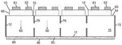
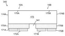
도 1은 LED의 반도체 층들에 근접하여 패터닝된 광 투과 표면을 포함하는 단일 플립 칩 LED의 측 단면을 도시하며, 반도체 층들에 근접하여 다층 반사기를 포함하고, 다층 반사기와 LED의 전기적 콘택트들 간에 보호층을 포함하며, 상기 단일 플립 칩 LED는 본 발명의 실시예들에 다른 플립 칩 LED 어레이들에 사용될 수 있는 플립 칩들 중 대표적인 플립칩이다.
도 2a는 본 발명의 실시예에 따른 플립 칩 어레이에 사용 가능한 투명 기판이 위로 향한 플립 칩 LED의 평면도 사진다.
도 2b는 전극들이 위로 향한 상태의 도 2a의 플립 칩 LED의 평면도 사진이다.
도 3a는 본 발명의 실시예들에서 사용 가능한, 위쪽으로 향한 단일 투명 기판상의 4개의 플립 칩 타입 LED의 어레이를 포함하는 멀티-LED 칩의 평면도 사진이다.
도 3b는 전극들이 위로 향한 상태의 도 3a의 멀티-LED 칩의 평면도 사진이다.
도 4a는 본 발명의 실시예들에서 사용 가능한, 위쪽으로 향한 단일 투명 기판상의 100개의 플립 칩 타입 LED의 어레이를 포함하는 멀티-LED 칩의 평면도 사진이다.
도 4b는 전극들이 위로 향한 상태의 도 4a의 멀티-LED 칩의 평면도 사진이다.
도 5a 내지 도 5c는 본 발명의 어떤 실시예들에 따라, 다양한 제조 단계에서 위로 향하는 단일 투명 기판상의 16개의 플립 칩 LED의 어레이를 포함하는 멀티-LED 칩의 평면도로서, 플립 칩 LED 사이에 홈 또는 오목부를 정의하여 광 추출 표면으로부터 기판의 내부로 연장하는 광 격리 요소를 형성하고, 광 추출 표면 상에 루미포르 물질을 증착하는 제조 단계를 보여준다.
도 5d는 내부에 광 격리 요소의 형성 후에 아래로 향하는 투명 기판의 평면도이다.
도 5e는 본 발명의 어떤 실시예들에 따라, 광 격리 요소들 사이에 도 5d의 기판 상에 형성된 16개의 플립 칩 LED들의 어레이를 포함하는 멀티-LED 칩의 평면도이다.
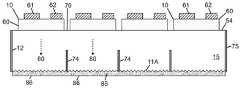
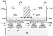
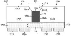
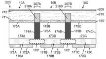
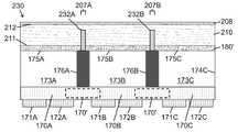
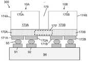
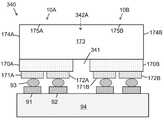
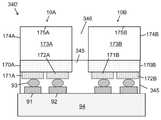
도 6a 내지 도 6c는 본 발명의 어떤 실시예들에 따라, 다양한 제조 단계에서 단일 투명 기판을 위로 한 상태에서의 도 5a 내지 도 5c의 멀티-LED 칩의 측 단면도로서, 광 추출 표면으로부터 기판의 내부로 연장하는 광 격리 요소를 형성하고, 광 추출 표면 상에 루미로르 물질을 증착하는 제조 단계를 보여 준다.
도 7a는 본 발명의 일 실시예에 따라, 광 주입 표면으로부터 기판의 내부로 연장하는 광 격리 요소를 포함하고 광 추출 표면 상에 배치된 루미포르 물질을 포함하는, 아래로 향하는 단일 투명 기판 상에 플립 칩 LED의 어레이를 포함하는 발광 장치(예를 들어, 멀티-LED 칩)의 측 단면도이다.
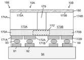
도 7b는 본 발명의 일 실시예에 따라, 텍스처 처리된 광 주입 표면으로부터 기판의 내부로 연장하는 광 격리 요소를 포함하고 광 추출 표면 상에 배치된 루미포르 물질을 포함하는, 아래로 향하는 단일 투명 기판 상에 플립 칩 LED의 어레이를 포함하는 발광 장치(예를 들어, 멀티-LED 칩)의 측 단면도이다.
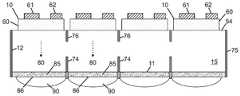
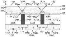
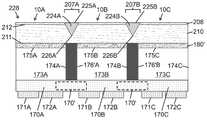
도 7c는 본 발명의 일 실시예에 따라, 제 1 그룹의 광 격리 요소가 광 주입 표면으로부터 기판의 내부로 연장하고 제 2 그룹의 광 격리 요소가 기판의 광 추출 표면으로부터 기판의 내부로 연장하며 광 추출 표면 상에 배치된 루미포르 물질을 포함하는, 아래로 향하는 단일 투명 기판 상에 플립 칩 LED의 어레이를 포함하는 발광 장치(예를 들어, 멀티-LED 칩)의 측 단면도이다.
도 8a 내지 도 8d는 본 발명의 일 실시예에 따라, 다양한 제조 단계에서 기판의 광 추출 표면으로부터 기판의 내부로 연장하는 광 격리 요소를 포함하는, 아래쪽을 향한 단일 투명 기판상의 플립 칩 LED들의 어레이를 포함하는 발광 장치(예를 들어, 멀티-LED 칩)의 측면 단면도로서, 광 추출 표면에 광 추출 오목부들을 형성하고, 광 추출 오목부들에 하나 이상의 루미포르 물질을 증착하고, 광 추출 오목부들에 증착된 하나 이상의 루미포르 물질 위에 렌즈들을 형성하는 단계를 보여준다.
도 9a 내지 도 9c는 본 발명의 일 실시예에 따라, 다양한 제조 단계에서 제 1 그룹의 광 격리 요소가 광 주입 표면으로부터 기판의 내부로 연장하고 제 2 그룹의 광 격리 요소가 기판의 광 추출 표면으로부터 기판의 내부로 연장하며, 아래쪽을 향한 단일 투명 기판상의 플립 칩 LED들의 어레이를 포함하는 발광 장치(예를 들어, 멀티-LED 칩)의 측면 단면도로서, 광 추출 표면상에 돌출 특징구조들을 형성하고, 돌출 특징구조들 사이에 하나 이상의 루미포르 물질을 증착하고, 돌출 특징구조들 사이의 하나 이상의 루미포르 물질 위에 렌즈들을 형성하는 단계를 보여준다.
도 10a 내지 도 10c는 본 발명의 일 실시예에 따라, 다양한 제조 단계에서 제 1 그룹의 광 격리 요소가 광 주입 표면으로부터 기판의 내부로 연장하고 제 2 그룹의 광 격리 요소가 기판의 광 추출 표면으로부터 기판의 내부로 연장하며, 아래쪽을 향한 단일 투명 기판상의 플립 칩 LED들의 어레이를 포함하는 발광 장치(예를 들어, 멀티-LED 칩)의 측면 단면도로서, 광 추출 표면 상에 돌출 특징구조들을 형성하고, 돌출 특징구조들 사이에 하나 이상의 루미포르 물질을 증착하고, 하나 이상의 루미포르 물질 위에 렌즈들을 형성하는 단계를 보여준다.
도 11a는 솔더 범프 및 (주문형 반도체(ASIC) 또는 캐리어 기판 또는 서브마운트에 선택적으로 구현되는) 인터페이스 요소에 인접하게 배치된 도 6c의 멀티-LED 칩의 측 단면 확대도이다.
도 11b는 도 11a의 인터페이스 요소 및 멀티-LED 칩의 측 단면도로서, 솔더 범프 결합 공정 및 멀티-LED 칩과 인터페이스 요소 사이의 언더필 물질의 첨가 후의 상태를 나타내는 측 단면도이다.
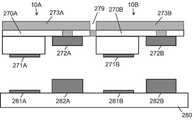
도 12a는 전극이 위로 향하고 있는 단일 투명 기판 상에 16개의 플립 칩 LED의 어레이를 포함하는 발광 장치(예컨대, 멀티-LED 칩)의 평면도이다.
도 12b는 도 12a의 발광 장치용 전기 인터페이스의 하부 층의 평면도로서, 복수의 수평 스트링 직렬 연결 각각이 발광 장치의 애노드와 결합하기 위한 복수의 전기 전도성 비아를 포함하고, 하부 층은 전기 인터페이스의 상부 층에 정의된 전도성 비아의 통과를 허용하는 개구를 더 포함한다.
도 12c는 도 12a의 발광 장치를 위한 전기 인터페이스의 상부 층의 평면도로서, 복수의 수직 스트링 직렬 연결 각각이 발광 장치의 캐소드와 결합하기 위한 복수의 전기 전도성 비아를 포함한다.
도 12d는 도 12a의 발광 장치에서 전기 인터페이스를 형성하기 위해 도 12b의 하부 층 위에 중첩된 도 12c의 상부 층의 평면도이다.
도 12e는 도 12a의 발광 장치와 결합한 도 12d의 전기 인터페이스의 평면도이다.
도 13a는 전극이 위로 향하는 단일 투명 기판 상에 16개의 플립 칩 LED의 어레이를 포함하는 발광 장치(예컨대, 멀티-LED 칩)의 평면도이다.
도 13b는 도 13a의 발광 장치용 전기 인터페이스의 하부 층의 평면도로서, 복수의 수평 스트링 직렬 연결 각각이 발광 장치의 애노드와 결합하기 위한 복수의 전기 전도성 비아를 포함하고, 하부 층은 전기 인터페이스의 상부 층에 정의된 전도성 비아의 통과를 허용하는 개구를 더 포함한다.
도 13c는 도 13a의 발광 장치에 대한 전기 인터페이스의 상부 층의 평면도로서, 수직으로 배열된 복수의 병렬 연결 각각이 발광 장치의 캐소드와 결합하기 위한 복수의 전기 전도성 비아를 포함한다.
도 13d는 도 13a의 발광 장치를 위한 전기 인터페이스를 형성하기 위해 도 13b의 하부 층 위에 중첩된 도 13c의 상부 층의 평면도이다.
도 13e는 본 발명의 일 실시예에 따라 도 13a의 발광 장치와 결합한 도 13d의 전기 인터페이스의 평면도이다.
도 14a는 본 발명의 실시예에 따라 제 1 색 조합을 생성하도록 구성된 어드레스 가능한 멀티-LED 발광 장치(예컨대, 멀티-LED 칩)의 평면도이다.
도 14b는 본 발명의 실시예에 따라 제 2 색 조합을 생성하도록 구성된 어드레스 가능한 멀티-LED 발광 장치(예컨대, 멀티-LED 칩)의 평면도이다.
도 14c는 본 발명의 실시예에 따라 제 3 색 조합을 생성하도록 구성된 어드레스 가능한 멀티-LED 발광 장치(예컨대, 멀티-LED 칩)의 평면도이다.
도 14d는 본 발명의 실시예에 따라 제 4 색 조합을 생성하도록 구성된 어드레스 가능한 멀티-LED 발광 장치(예컨대, 멀티-LED 칩)의 평면도이다.
도 15는 각각이 개별적으로 어드레스 가능한 플립 칩 LED들을 포함하는 2개의 에미터 어레이(예를 들어, 2개의 멀티-LED 칩으로 선택적으로 구현됨)를 포함하는 발광 장치의 구성요소들 간의 상호 접속을 도시하는 간략한 개략도이다.
도 16은 본 발명의 일 실시예에 따른, 아래로 향하고 캐리어 기판에 결합된 단일 투명 기판상의 플립 칩 LED들의 어레이를 포함하는 발광 장치의 측 단면도로서, 제 1 그룹의 광 격리 요소는 기판의 광 주입 표면으로부터 기판의 내부로 연장하고 제 2 그룹의 광 격리 요소는 캐리어 기판의 광 추출 표면으로부터 캐리어 기판의 내부로 연장하며, 캐리어 기판의 광 추출 표면 상에는 루미포르 물질이 배치된다.
도 17은, 본 발명의 일 실시예에 따른, 모두가 캐리어에 접합된, 제 1 투명 기판 상의 제 1 플립 칩 LED 어레이(예를 들어, 제 1 멀티-LED 칩에 구현됨) 및 제 2 투명 기판 상의 제 2 플립 칩 LED 어레이(예를 들어, 제 2 멀티-LED 칩에 구현됨)를 포함하는 발광 장치의 측 단면도로서, 각각의 기판은 기판의 광 주입 표면으로부터 기판의 내부로 연장하는 제 1 그룹의 광 격리 요소와 기판의 광 추출 표면으로부터 기판의 내부로 연장하는 광 격리 요소를 포함하고, 캐리어는 캐리어의 광 주입 표면으로부터 캐리어의 내부로 연장하는 또 다른 그룹의 광 격리 요소를 포함하며, 루미포르 물질이 캐리어의 텍스쳐 처리된 또는 패턴화된 광 추출 표면 상에 배치된다.
도 18은 본 발명의 일 실시예에 따른, 제 1 투명 기판 상의 제 1 플립 칩 LED 어레이(예를 들어, 제 1 멀티-LED 칩에 구현됨) 및 제 2 투명 기판 상의 제 2 플립 칩 LED 어레이(예를 들어, 제 2 멀티-LED 칩에 구현됨), 각 기판의 광 추출 표면과 접촉하도록 배치된 루미포르 물질 층, 그리고 루미포르 물질 층과 각 기판을 지지하도록 배치된 캐리어를 포함하는 발광 장치의 측 단면도로서, 각각의 기판은 기판의 광 주입 표면으로부터 기판의 내부로 연장하는 제 1 그룹의 광 격리 요소와 기판의 광 추출 표면으로부터 기판의 내부로 연장하는 광 격리 요소를 포함하고, 캐리어는 캐리어의 광 주입 표면으로부터 캐리어의 내부로 연장하는 또 다른 그룹의 광 격리 요소를 포함하며, 캐리어는 텍스쳐 처리된 또는 패턴화된 광 추출 표면을 포함한다.
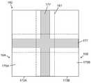
도 19는 본 발명의 일 실시예에 따른, 4개의 개별적으로 어드레스 가능한 발광 장치 어레이(예를 들어, 4개의 멀티-LED 칩으로 구현됨)를 지지하는 캐리어를 포함하는 발광 장치의 평면도로서, 각 어레이는 각각의 LED 사이에 광 격리 요소를 포함한다.
도 20a는 개별 LED 사이의 광 격리 요소가 어두운 그리드를 형성하고 각 LED가 비조명 상태인, 16개의 LED(예를 들어, 16개 픽셀)의 어레이를 포함하는 발광 장치(예를 들어, 멀티-LED 칩)의 디지털 사진 평면도이다.
도 20b는 도 20a의 발광 장치에서 최 우측 컬럼의 개의 LED에 전류가 인가된 상태의 디지털 사진 평면도로서, 4개의 LED의 최우측 컬럼이 조명되고, 그 인접한 LED 컬럼이 광의 스필오버로 인해 부분적으로 조명되며, 조명된 LED에 인접한 LED들 사이에 비-조명 또는 "어두운" 영역이 있다.
도 20c는 도 20b의 디지털 사진의 컬러 반전된 버전이다.
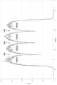
도 21a는 복수의 LED의 어레이를 포함하는 발광 장치(예를 들어, 멀티-LED 칩)의 8- 픽셀 부분의 명암 맵핑 이미지의 상면도이며, 4개의 LED의 가장 왼쪽 컬럼이 조명된 상태를 도시하며, 조명된 가장 왼쪽 컬럼의 LED에 인접한 컬럼의 LED가 조명된 LED의 스필오버로 인해 부분적으로 조명되고, 조명된 LED에 인접한 LED들 사이에 비-조명 또는 "어두운" 영역이 있다.
도 21b는 도 21의 4개의 조명된 LED의 가장 좌측의 컬럼에 대한 상대적인 광 강도 (백분율) 대 위치(밀리미터)의 4개의 중첩된 플롯을 포함한다.
도 22a는 기판의 적어도 일부에 오목부 또는 홈을 형성한 후에 2개의 LED를 포함하는 제조 중에 고체 발광 장치(예를 들어, 멀티-LED 칩)의 일부의 측 단면 모식도이다.
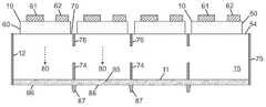
도 22b는 광 격리 요소 및 광 투과 물질을 순차로 오목부 또는 홈에 첨가한 후의 도 22a의 고체 발광 장치 부분의 측 단면 모식도로서, 광 투과 물질은, 조명될 때, LED들 사이의 비 조명 또는 "어두운" 영역의 출현을 감소하기 위해 고체 발광 장치의 광 방출 표면에서 픽셀간 조명을 향상시키는 작용을 한다.
도 22c는 기판 위에 그리고 오목부 혹은 홈 내의 광 투과 물질 위에 루미포르 물질을 적용한 후의 도 22b의 고체 발광 장치 일부분에 대한 측 단면도이다.
도 23a는 기판 및 복수의 LED를 포함하는 고체 발광 장치(예를 들어, 멀티-LED 칩)의 일부의 측 단면 모식도로서, 기판의 적어도 일부에 형성된 오목부 또는 홈에 광 격리 요소 및 광-투과성 물질이 차례로 충진되며, 기판의 표면에 대해 상대적으로 돌출한 영역은 광 투과 영역이고, 기판 위에 그리고 돌출한 광 투과 영역 위에 루미포르 물질이 배치된다.
도 23b는 돌출한 광 투과 물질 영역이 점선으로 표시된, 4개의 LED를 포함하는 도 23a의 고체 발광 장치 부분의 적어도 일부의 평면도이다.
도 24a는 제조 과정 중의 기판 및 복수의 LED를 포함하는 고체 발광 장치(예를 들어, 멀티-LED 칩)의 일부분의 측 단면 모식도로서, 기판은 두꺼우면서 광 분리 기능을 제공하는 제 1 물질 및 광 확산 또는 광 방향 변경 기능을 제공하는 제 2 물질로 순차적으로 충진된 오목부 또는 홈을 포함하는 부분을 구비하며, 캐리어 기판 또는 서브마운트는 아래에 위치하며 고체 발광 장치의 애노드-캐소드 쌍과는 접촉하지 않는 복수의 전극 쌍을 구비한다.
도 24b는, 캐리어 기판 또는 서브마운트의 전극 쌍에 애노드 - 캐소드 쌍을 장착 하고, 기판 및 그 안에 매립된 물질을 박막화하고, 기판 위에 루미포르 물질 층을 형성한 후의 도 24a의 고체 발광 장치 부분의 측 단면 개략도이다.
도 25a는 제조 과정 중의 기판 및 복수의 ED를 포함하는 고체 발광 장치(예를 들어, 멀티-LED 칩)의 일부분의 측 단면 모식도로서, 기판은 두꺼우면서 제거 가능한(예를 들어 희생) 물질로 채워지는 오목부 또는 홈을 구비하고, 복수의 애노드-캐소드 쌍이 인터페이스 요소(예를 들어 ASIC 도는 캐리어 기판 또는 서브마운트)의 복수의 전극 쌍과 전도성 전기 통신을 하도록 장착되며, 멀티-LED 칩과 인터페이스 요소 간에 언더필 물질이 배치된 상태를 도시한다.
도 25b는 기판 및 그 내에 매립된 제거 가능한 물질의 박막화 후의 도 25a의 고체 발광 장치 부분의 측 단면 개략도이다.
도 25c는 기판 위에 루미포르 물질을 형성한 후의, 도 25a의 고체 발광 장치 부분의 측 단면 개략도이다.
도 25d는 기판으로부터 제거 가능한 물질을 제거한 후의, 도 25a의 고체 발광 장치 부분의 측 단면 개략도이다.
도 26a는 인터페이스 요소(예를 들어 ASIC 또는 캐리어 기판 도는 서브마운트) 위에 장착된 기판 및 복수의 LED를 포함하는 고체 발광 장치(예를 들어, 멀티-LED 칩)의 일부의 측 단면 개략도로서, 기판에 비충진 오목부 혹은 홈이 정의되고, 기판 위에 접착 촉진 물질이 배치되고, 기판 및 접착 촉진 물질 위에 루미포르 물질 막이 배치되며, 비충진 물질이 멀티-LED 칩 및 인터페이스 요소 사이에 배치된다.
도 26b는 LED들 사이에 배치된 오목부 또는 홈이 비충진인 상태로, 기판 위에 루미포르 물질 막의 접착 후의 26A의 고체 발광 장치 부분의 측 단면 모식도이다.
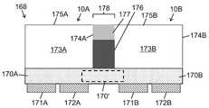
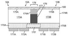
도 27a는 소정의 제조 단계의 수행 이후의 기판 및 3개의 LED를 포함하는 고체 발광 장치(예를 들어, 멀티-LED 칩)의 일부의 측 단면도이며, 오목부 또는 홈이 인접한 LED 사이의 기판의 부분에 정의되고, 각 오목부 또는 홈의 폭의 제 1 부분이 광 격리 요소로 충진된다.
도 27b는 각 오목부 또는 홈의 폭의 제 2 부분을 채우기 위해 적어도 하나의 투광성 물질을 부가한 후의 도 27a의 고체 발광 장치의 일부의 측 단면도로서, 적어도 하나의 투광성 물질은 각각의 오목부 또는 홈 내의 광 격리 요소와 접촉한다.
도 28a는 3개의 LED의 측면 단면도이고, 각각은 기판 부분을 포함하고 그 제 1 측면을 따라 캐리어에 장착된다.
도 28b는 각각의 LED 및 대응하는 기판 부분의 제 2 측면상의 적어도 하나의 광 영향 요소를 형성한 후의 도 28a의 3개의 LED 및 캐리어의 측 단면도이다.
도 28c는 3개의 LED를 캐리어 기판 또는 서브마운트에 장착한 후 그리고 인접한 LED의 측면 사이에 투광성 물질을 형성한 후의 도 28a의 LED를 포함하는 고체 발광 장치의 일부의 측 단면도이다.
도 28d는 각각의 LED의 기판 부분 위에 그리고 인접한 LED들 사이의 적어도 하나의 광 영향 요소 및 투광성 물질 위에 루미포르 물질을 도포한 후의 도 28c의 고체 발광 장치 부분의 측 단면도이다.
도 29a는 2개의 LED 및 광 격리 요소를 함유하는 오목부 또는 홈을 정의하는 기판을 포함하는 고체 발광 장치(예를 들어, 멀티-LED 칩)의 일부의 측 단면도로서, 기판은 광 격리 요소에 인접하여 경사진 에지 부분을 포함한다.
도 29b는 기판, 경사진 에지 부분, 그리고 광 격리 요소 위에 루미포르 물질을 도포한 후의 도 29a의 고체 발광 장치 부분의 측 단면도로서, 경사진 에지 부분은 고체 발광 장치의 광 방출 표면에서 픽셀 간 조명을 향상시켜 LED가 점등될 때 LED 사이의 비 조명 또는 "어두운" 영역의 출현을 감소하는 기능을 한다.
도 30a는 인터페이스 요소(예를 들어, ASIC, 캐리어 기판 또는 서브마운트) 위에 장착된 기판 및 복수의 LED를 포함하는 고체 발광 장치(예를 들어, 멀티-LED 칩)의 일부의 측 단면 개략도로서, 기판 내에 정의된 비충진 오목부 또는 홈, 오목부 또는 홈에 근접한 기판의 경사진 에지 부분 및 멀티-LED 칩과 인터페이스 요소 사이에 배치된 언더필 물질을 포함한다.
도 30b는 기판 위에 접착 촉진 물질을 첨가한 후의 그리고 접착 촉진 물질 위에 루미포르 물질 막의 접착 후의 도 30a의 고체 발광 장치 부분의 측 단면 개략도이다.
도 31은 기판 및 3개의 LED을 포함하는 고체 발광 장치(예를 들어, 멀티-LED 칩)의 일부의 측 단면도로서, 인접한 LED들 사이의 기판 부분에 오목부 또는 홈이 정의되고, 각각의 오목부 또는 홈은 광 격리 요소로 충진되고, 기판 및 광 격리 요소 위에 루미포르 물질 층이 배치되고, 루미포르 물질 층 위에 제 2 기판이 배치되고 루미포르 물질 층에 인접하여 삼각형 형태의 광 방향 변경 영역을 포함하고, 제 2 기판 위에 광 산란 물질이 배치된다.
도 32는 3개의 LED 및 기판을 포함하는 고체 발광 장치(예를 들어, 멀티-LED 칩)의 일부분의 측 단면도로서, 인접한 LED들 사이의 기판 부분에 오목부 또는 홈이 정의되고, 각각의 오목부 또는 홈은 광 격리 요소로 충진되고, 기판 위에 루미포르 물질 층이 배치되고, 제 2 기판이 루미포르 물질 층 위에 배치되고 직사각형 형태의 광 방향 변경 영역을 포함하며 루미포르 물질 층을 통해 연장하며, 광 산란 물질이 제 2 기판 위에 배치되며, 광 방향 변경 영역은 광 격리 요소와 동일한 폭을 가진다.
도 33은 3개의 LED 및 기판을 포함하는 고체 발광 장치(예를 들어, 멀티-LED 칩)의 일부의 측 단면도로서, 인접한 LED들 사이의 기판 부분에 오목부 또는 홈이 정의되고, 각각의 오목부 또는 홈은 광 격리 요소로 충진되고, 기판 및 광 격리 요소 위에 루미포르 물질 층이 배치되고, 루미포르 물질 층 위에 제 2 기판이 배치되고 제 2 기판은 그 내에 삼각형 형태의 광 방향 변경 영역을 포함하며, 광 산란 물질이 제 2 기판 위에 배치되고, 삼각형 형태의 광 방향 변경 영역 각각은 광 산란 물질을 통과해 연장하는 밑변 부분을 포함한다.
도 34는 3개의 LED 및 기판을 포함하는 고체 발광 장치(예를 들어, 멀티-LED 칩)의 일부분의 측 단면도로서, 인접한 LED들 사이의 기판 부분에 오목부 또는 홈이 정의되고, 각각의 오목부 또는 홈은 광 격리 요소로 충진되고 기판을 지나서 연장하며, 광 격리 요소들 사이의 기판 위에 루미포르 물질 층이 배치되고, 제 2 기판이 루미포르 물질 층 위에 배치되고 그 내에 삼각형 형태의 광 방향 변경 영역을 포함하며, 광 산란 물질이 제 2 기판 위에 배치되며, 삼각형 형태의 광 방향 변경 영역 각각은 광 산란 물질을 통과해 연장하는 밑변 부분을 포함한다.
도 35는 3개의 LED 및 기판을 포함하는 고체 발광 장치(예를 들어, 멀티-LED 칩)의 일부분의 측 단면도로서, 인접한 LED들 사이의 기판 부분에 오목부 또는 홈이 정의되고, 각 오목부 또는 홈은 광 격리 요소로 충진되고, 기판 위에 루미포르 물질 층이 배치되고, 제 2 기판이 루미포르 물질 층 위에 배치되고 그 내에 직사각형 형태의 광 방향 변경 영역을 포함하고 루미포르 물질 층을 통해 연장하며, 제 2 기판 위에 광 산란 물질이 배치되며, 광 방향 변경 영역은 광 격리 요소보다 폭이 더 좁다.
도 36은 본 명세서에 개시된 바와 같은 고밀도 LED 어레이(예를 들어, 적어도 하나의 멀티-LED 칩을 구현하는)를 포함하는 고체 발광 장치를 작동시키기 위한 테스트 장치의 캐리어 기판 또는 서브마운트와 회로기판 사이의 상호 접속의 평면도이다.
도 37a는 고밀도 LED를 포함하는 고체발광 장치(예를 들어, 멀티-LED 칩)를 수용하기에 적합하고 테스트 장치의 일 부분으로 사용될 수 있는 직사각형 어레이 장착 영역으로 이르는 복수의 전기적 트레이스를 지지하는 반도체 웨이퍼를 포함하는 캐리어 기판 또는 서브마운트의 평면도이다.
도 37b는 도 37a의 색상 반전된 버전이다.
도 38a는 도 37a 및 도 37b의 캐리어 기판 또는 서브마운트의 확대된 부분이고 도 38b는 도 38a의 색상 반전된 버전이다.
도 39a는 단일 기판과 관련된 두 개의 플립 칩 LED를 포함하는 고체 발광 장치(예를 들어, 선택적으로 하나의 멀티-LED 칩에 구현됨)의 일부분의 개략적인 측 단면도로서, 애노드 및 캐소드는 서로 상이한 높이를 나타내며 캐리어 기판 또는 서브마운트의 상부 표면을 따라 제공된 상이한 높이의 전극들 위에 (접촉 없이) 배치된다.
도 39b는 단일 기판 상에 배열된 2개의 플립 칩 LED를 포함하는 고체 발광 장치(예를 들어, 하나의 멀티-LED 칩에 선택적으로 구현됨)의 일부의 개략적인 측 단면도로서, 애노드 및 캐소드는 서로 상이한 높이를 나타내며 캐리어 기판 또는 서브마운트의 상부 표면을 따라 제공된 전극들 위에 (접촉하지 않고) 배치되고, 전극 쌍 당 하나의 전극은 솔더 범프 물질을 함유하는 경계벽을 포함한다.
도 40a는 인터페이스 요소(예를 들어, ASIC 또는 캐리어 기판 또는 서브마운트) 위에 장착된 기판 및 복수의 LED를 포함하는 고체 발광 장치(예를 들어, 멀티-LED 칩)의 일부의 측 단면도로서, LED들을 연결하는 기판에 오목부 또는 홈을 정의하기 전을 도시한다.
도 40b는 기판에 오목부 또는 홈을 형성한 후의 도 40a의 고체 발광 장치 부분의 측 단면도이다.
도 40c는 제거 가능한 (예를 들어, 희생적인) 물질을 오목부 또는 홈에 부가한 후 그리고 기판 및 제거 가능한 물질 위에 방위 루미포르 층을 형성한 후의 도 40b의 고체 발광 장치 부분의 측 단면 개략도이다.
도 40d는 홈 또는 홈에서 제거 가능한 물질을 제거한 후의 도 40c의 고체 발광 장치 부분의 측 단면 개략도이다.
도 41은 복수의 LED 및 기판을 포함하는 고체 발광 장치(예컨대, 멀티-LED 칩)의 측 단면 모식도로서, 기판은 캐리어 기판 또는 서브마운트에 구현된 제 1 인터페이스 요소 위에 장착되고, 캐리어 기판 또는 서브마운트는 그 사이 전기적인 전도성 비아가 배치되면서 제 1 주 기판 및 제 2 주 기판상에 배치된 전기적인 콘택트를 포함하며, 캐리어 기판 또는 서브마운트가 멀티-LED 칩 및 ASIC 사이에 장착되도록, 캐리어 기판 또는 서브마운트는 ASIC로 구현된 제 2 인터페이스 요소 위에 배치된다.
도 42는 단일 인터페이스 요소(예를 들어, ASIC 또는 캐리어 기판 또는 서브마운트) 위에 장착된 2개의 고체 발광 장치(예를 들어, 멀티-LED 칩)의 측면 단면도로서, 멀티-LED 칩의 기판에 오목부 또는 홈을 정의하기 전을 도시한다.
도 43은 복수의 인터페이스 요소(예를 들어, ASIC 또는 캐리어 기판 또는 서브마운트) 상에 장착된 단일 고체 발광 장치(예를 들어, 멀티-LED 칩)의 측면 단면도로서, 멀티-LED 칩의 LED들을 연결하는 기판에서 오목부 또는 홈을 정의하기 전을 도시한다.
도 44a는 멀티-LED 칩의 상이한 LED들의 에피택셜 층들 사이에 형성된 홈 또는 오목부를 포함하는 고체 발광 장치(예를 들어, 멀티-LED 칩)의 일부의 측 단면 모식도이다.
도 44b는 인터페이스 요소(예를 들어, ASIC, 캐리어 기판 또는 서브마운트) 상에 장착 된 후의 도 44a의 고체 발광 장치 부분의 측 단면 개략도이다.
도 44c는, 멀티-LED 칩과 인터페이스 요소 사이에 언더필 물질을 부가한 후, 기판에 대부분을 통과하지만 기판 전체를 통과하지 않는 오목부 또는 홈을 형성한 후의 도 44b의 고체 발광 장치 부분의 측 단면 개략도이다.
도 44d는 멀티-LED 칩과 인터페이스 요소 사이에 언더필 물질을 첨가한 후에 그리고 언더필 물질에 도달하도록 기판의 전체 두께를 통해 연장하는 오목부 또는 홈을 기판에 형성한 후의 도 44b의 고체 발광 장치 부분의 측 단면 개략도이다.
도 45는 멀티-LED 칩의 인접한 LED들 사이에 형성된 홈 또는 오목부를 포함하는 고체 발광 장치(예를 들어, 멀티-LED 칩)의 일부의 측 단면 모식도로서, 다른 에미터 영역들은 다른 특성을 가진다.1 shows a side cross-section of a single flip chip LED comprising a light transmitting surface patterned proximate to the semiconductor layers of the LED, comprising a multilayer reflector proximate to the semiconductor layers, and protection between the multilayer reflector and the electrical contacts of the LED; layer, wherein the single flip chip LED is representative of flip chips that can be used in flip chip LED arrays according to embodiments of the present invention.
2A is a top view photograph of a flip-chip LED with a transparent substrate facing up, which can be used in a flip-chip array according to an embodiment of the present invention.
FIG. 2B is a top view photograph of the flip chip LED of FIG. 2A with the electrodes facing up.
3A is a top view photograph of a multi-LED chip comprising an array of four flip chip type LEDs on a single transparent substrate facing upwards usable in embodiments of the present invention.
FIG. 3B is a top view photograph of the multi-LED chip of FIG. 3A with the electrodes facing up.
4A is a top view photograph of a multi-LED chip comprising an array of 100 flip chip type LEDs on a single transparent substrate facing upwards usable in embodiments of the present invention.
FIG. 4B is a top view photograph of the multi-LED chip of FIG. 4A with the electrodes facing up.
5A-5C are top views of a multi-LED chip comprising an array of 16 flip-chip LEDs on a single transparent substrate facing upward at various stages of manufacture, in accordance with certain embodiments of the present invention, with grooves between the flip-chip LEDs. or defining a recess to form a light isolating element extending from the light extraction surface into the interior of the substrate, and depositing a lumipor material on the light extraction surface.
5D is a top view of the transparent substrate facing down after formation of a light isolating element therein;
5E is a top view of a multi-LED chip comprising an array of 16 flip chip LEDs formed on the substrate of FIG. 5D between optical isolation elements, in accordance with certain embodiments of the present invention.
6A-6C are cross-sectional side views of the multi-LED chip of FIGS. 5A-5C with a single transparent substrate facing up at various stages of manufacture, in accordance with certain embodiments of the present invention, of the substrate from the light extraction surface; The fabrication steps are shown, forming an inwardly extending light isolating element, and depositing a lumiror material on the light extraction surface.
7A is on a single, downward-facing transparent substrate comprising a light isolation element extending from a light injection surface into the interior of the substrate and comprising a lumpor material disposed on the light extraction surface, in accordance with one embodiment of the present invention. A cross-sectional side view of a light emitting device (eg, a multi-LED chip) including an array of flip chip LEDs.
7B is a single transparent downward facing, comprising a lumipor material disposed on the light extraction surface and including a light isolating element extending from the textured light injection surface into the interior of the substrate, in accordance with one embodiment of the present invention. A cross-sectional side view of a light emitting device (eg, a multi-LED chip) including an array of flip chip LEDs on a substrate.
7C illustrates a first group of light isolating elements extending from a light injection surface into the interior of a substrate and a second group of light isolating elements extending from a light extraction surface of the substrate into the interior of the substrate, in accordance with one embodiment of the present invention; A cross-sectional side view of a light emitting device (eg, a multi-LED chip) comprising an array of flip chip LEDs on a single, downward facing, transparent substrate comprising a lumpor material disposed on a light extraction surface.
8A-8D show an array of flip chip LEDs on a single transparent substrate facing downwards comprising a light isolating element extending from the light extraction surface of the substrate into the interior of the substrate at various stages of fabrication, in accordance with one embodiment of the present invention; A side cross-sectional view of a light emitting device (eg, a multi-LED chip) comprising: forming light extraction recesses in a light extraction surface, depositing one or more lumipor materials in the light extraction recesses; It shows the steps of forming lenses over one or more lumipor materials deposited on the .
9A-9C show, in various stages of fabrication, a first group of light isolating elements extending from a light injection surface into the interior of a substrate and a second group of light isolating elements forming a light extraction surface of the substrate, in accordance with an embodiment of the present invention; A side cross-sectional view of a light emitting device (eg, a multi-LED chip) including an array of flip chip LEDs on a single transparent substrate facing downwards extending into the interior of the substrate, forming protruding features on the light extraction surface and depositing one or more lumipor materials between the protruding features, and forming lenses over the one or more lumipor materials between the protruding features.
10A-10C show that, at various stages of fabrication, a first group of light isolating elements extend from a light injection surface into the interior of a substrate and a second group of light isolating elements form a light extraction surface of the substrate, in accordance with an embodiment of the present invention; A side cross-sectional view of a light emitting device (eg, a multi-LED chip) including an array of flip chip LEDs on a single transparent substrate facing downwards extending into the interior of the substrate, forming protruding features on the light extraction surface and depositing one or more Lumpor materials between the protruding features, and forming lenses over the one or more Lumpor materials.
11A is an enlarged side cross-sectional view of the multi-LED chip of FIG. 6C disposed adjacent a solder bump and an interface element (optionally implemented on an application specific integrated circuit (ASIC) or carrier substrate or submount);
FIG. 11B is a side cross-sectional view of the interface element and the multi-LED chip of FIG. 11A , and is a side cross-sectional view illustrating a state after a solder bump bonding process and addition of an underfill material between the multi-LED chip and the interface element;
12A is a top view of a light emitting device (eg, a multi-LED chip) comprising an array of 16 flip chip LEDs on a single transparent substrate with electrodes facing up.
12B is a plan view of a lower layer of the electrical interface for the light emitting device of FIG. 12A , wherein each of a plurality of horizontal string series connections includes a plurality of electrically conductive vias for coupling with an anode of the light emitting device, the lower layer being the top of the electrical interface; It further includes an opening to allow passage of a conductive via defined in the layer.
12C is a plan view of a top layer of an electrical interface for the light emitting device of FIG. 12A , wherein each of a plurality of vertical string series connections includes a plurality of electrically conductive vias for coupling with a cathode of the light emitting device;
FIG. 12D is a plan view of the top layer of FIG. 12C superposed over the lower layer of FIG. 12B to form an electrical interface in the light emitting device of FIG. 12A ;
12E is a plan view of the electrical interface of FIG. 12D coupled with the light emitting device of FIG. 12A;
13A is a top view of a light emitting device (eg, a multi-LED chip) comprising an array of 16 flip chip LEDs on a single transparent substrate with electrodes facing up.
13B is a plan view of a lower layer of the electrical interface for the light emitting device of FIG. 13A , wherein each of a plurality of horizontal string series connections includes a plurality of electrically conductive vias for coupling with an anode of the light emitting device, the lower layer being the top of the electrical interface; It further includes an opening to allow passage of a conductive via defined in the layer.
13C is a plan view of a top layer of an electrical interface to the light emitting device of FIG. 13A , wherein each of a plurality of vertically arranged parallel connections includes a plurality of electrically conductive vias for coupling with a cathode of the light emitting device;
FIG. 13D is a top view of the top layer of FIG. 13C superposed over the lower layer of FIG. 13B to form an electrical interface for the light emitting device of FIG. 13A ;
13E is a plan view of the electrical interface of FIG. 13D coupled with the light emitting device of FIG. 13A in accordance with an embodiment of the present invention.
14A is a top view of an addressable multi-LED light emitting device (eg, a multi-LED chip) configured to generate a first color combination in accordance with an embodiment of the present invention.
14B is a top view of an addressable multi-LED light emitting device (eg, a multi-LED chip) configured to generate a second color combination in accordance with an embodiment of the present invention.
14C is a top view of an addressable multi-LED light emitting device (eg, a multi-LED chip) configured to generate a third color combination in accordance with an embodiment of the present invention.
14D is a top view of an addressable multi-LED light emitting device (eg, a multi-LED chip) configured to generate a fourth color combination in accordance with an embodiment of the present invention.
15 illustrates interconnections between components of a light emitting device comprising two emitter arrays (eg, optionally implemented with two multi-LED chips) each comprising individually addressable flip chip LEDs. It is a brief schematic diagram showing.
16 is a cross-sectional side view of a light emitting device comprising an array of flip chip LEDs on a single transparent substrate facing down and coupled to a carrier substrate, in accordance with an embodiment of the present invention, wherein a first group of light isolating elements comprises a light emitting device of the substrate; A second group of light isolating elements extending from the injection surface into the interior of the substrate and extending from the light extraction surface of the carrier substrate into the interior of the carrier substrate, the lumipor material disposed on the light extraction surface of the carrier substrate.
17 is a first flip chip LED array (eg, implemented in a first multi-LED chip) and a second transparent on a first transparent substrate, all bonded to a carrier, in accordance with an embodiment of the present invention; A cross-sectional side view of a light emitting device including a second flip chip LED array (eg, embodied in a second multi-LED chip) on a substrate, each substrate extending from a light injection surface of the substrate into the interior of the substrate. a light isolation element extending from a light extraction surface of the substrate into the interior of the substrate, wherein the carrier includes another group of light isolating elements extending from a light injection surface of the carrier into the interior of the carrier; , a lumipor material is disposed on the textured or patterned light extraction surface of the carrier.
18 is a first flip chip LED array (eg, implemented in a first multi-LED chip) on a first transparent substrate and a second flip chip LED array on a second transparent substrate, in accordance with an embodiment of the present invention; (eg, implemented in a second multi-LED chip), a luminescence comprising a layer of lumipor material disposed in contact with a light extraction surface of each substrate, and a carrier disposed to support each substrate with the layer of lumipor material. A cross-sectional side view of the apparatus, wherein each substrate includes a first group of light isolating elements extending from a light injection surface of the substrate into the interior of the substrate and light isolation elements extending from a light extraction surface of the substrate into the interior of the substrate, the carrier comprising: comprises another group of light isolating elements extending from the light injecting surface of the carrier into the interior of the carrier, the carrier comprising a textured or patterned light extracting surface.
19 is a plan view of a light emitting device including a carrier supporting four individually addressable light emitting device arrays (eg, implemented with four multi-LED chips), each light emitting device comprising a carrier in accordance with an embodiment of the present invention; The array includes a light isolating element between each LED.
20A shows a light emitting device (eg, multi-pixel) comprising an array of 16 LEDs (eg, 16 pixels), with light isolating elements between individual LEDs forming a dark grid and each LED being in an unilluminated state. It is a digital photo top view of LED chip).
FIG. 20B is a digital photograph plan view of a state in which current is applied to the LEDs of the rightmost column in the light emitting device of FIG. 20A, wherein the rightmost columns of four LEDs are illuminated, and the adjacent LED columns are partially due to spillover of light; An illuminated, non-illuminated or “dark” area is between the LEDs adjacent to the illuminated LED.
20C is a color-inverted version of the digital photo of FIG. 20B.
21A is a top view of a contrast mapping image of an 8-pixel portion of a light emitting device (eg, a multi-LED chip) including an array of multiple LEDs, with the leftmost column of 4 LEDs illuminated. where the LEDs in the column adjacent to the LEDs in the left most illuminated column are partially illuminated due to spillover of the illuminated LEDs, and there is a non-illuminated or "dark" area between the LEDs adjacent to the illuminated LEDs.
FIG. 21B includes four superimposed plots of relative light intensity (in percent) versus position (in millimeters) for the leftmost column of the four illuminated LEDs of FIG. 21 .
22A is a schematic side cross-sectional view of a portion of a solid-state light emitting device (eg, a multi-LED chip) during manufacture including two LEDs after forming a recess or groove in at least a portion of a substrate.
FIG. 22B is a schematic side cross-sectional view of the portion of the solid light emitting device of FIG. 22A after sequentially adding a light isolating element and a light transmitting material to a recess or groove, wherein the light transmitting material, when illuminated, is either non-illuminated between LEDs or It serves to enhance inter-pixel illumination at the light emitting surface of the solid state light emitting device to reduce the appearance of "dark" areas.
22C is a cross-sectional side view of a portion of the solid state light emitting device of FIG. 22B after application of the Lumipor material over the substrate and over the light transmitting material in the recess or groove.
23A is a schematic side cross-sectional view of a portion of a solid-state light emitting device (eg, a multi-LED chip) including a substrate and a plurality of LEDs, wherein a light-isolating element and a light-transmitting element are formed in a recess or groove formed in at least a portion of the substrate; The material is filled in turn, the area projecting relative to the surface of the substrate is the light transmitting area, and the lumipor material is disposed over the substrate and over the projecting light transmitting area.
FIG. 23B is a plan view of at least a portion of the portion of the solid state light emitting device of FIG. 23A including four LEDs, with the protruding regions of light transmitting material indicated by dashed lines;
24A is a schematic side cross-sectional view of a portion of a solid-state light emitting device (eg, a multi-LED chip) including a substrate and a plurality of LEDs during fabrication, wherein the substrate is thick while providing a light isolation function of a first material and light; having a portion comprising a recess or groove sequentially filled with a second material to provide a diffusing or light redirecting function, the carrier substrate or submount positioned underneath and in contact with the anode-cathode pair of the solid state light emitting device A plurality of electrode pairs not provided are provided.
24B is a view of the portion of the solid-state light emitting device of FIG. 24A after mounting an anode-cathode pair to an electrode pair of a carrier substrate or submount, thinning the substrate and the material embedded therein, and forming a layer of lumpor material on the substrate; It is a schematic cross-sectional side view.
25A is a schematic cross-sectional side view of a portion of a solid-state light emitting device (eg, a multi-LED chip) including a substrate and a plurality of EDs during fabrication, wherein the substrate is thick and not filled with a removable (eg, sacrificial) material; has a recess or groove, wherein a plurality of anode-cathode pairs are mounted in conductive electrical communication with a plurality of electrode pairs of an interface element (eg, an ASIC or carrier substrate or submount), the multi-LED chip and the interface element A state in which an underfill material is disposed between the liver is shown.
25B is a schematic cross-sectional side view of the portion of the solid state light emitting device of FIG. 25A after thinning of the substrate and the removable material embedded therein;
25C is a schematic cross-sectional side view of a portion of the solid state light emitting device of FIG. 25A after forming a lumpor material over a substrate;
25D is a schematic cross-sectional side view of the portion of the solid state light emitting device of FIG. 25A after removal of the removable material from the substrate;
26A is a schematic cross-sectional side view of a portion of a solid state light emitting device (eg, a multi-LED chip) including a plurality of LEDs and a substrate mounted over an interface element (eg, an ASIC or carrier substrate or submount); An unfilled recess or groove is defined in the substrate, an adhesion promoting material is disposed over the substrate, a lumpor material film is disposed over the substrate and the adhesion promoting material, and the unfilled material is disposed between the multi-LED chip and the interface element.
26B is a schematic side cross-sectional side view of a portion of the solid-state light emitting device of 26A after adhesion of a lumipor material film onto a substrate, with the recesses or grooves disposed between the LEDs unfilled;
27A is a cross-sectional side view of a portion of a solid-state light emitting device (eg, a multi-LED chip) including three LEDs and a substrate after performing certain manufacturing steps, wherein recesses or grooves are present in the substrate between adjacent LEDs. defined in the portion, and a first portion of the width of each recess or groove is filled with a light isolating element.
27B is a cross-sectional side view of a portion of the solid-state light emitting device of FIG. 27A after adding at least one light-transmitting material to fill a second portion of the width of each recess or groove, wherein the at least one light-transmitting material comprises each recess or contact the light isolating element in the groove.
28A is a cross-sectional side view of three LEDs, each including a substrate portion and mounted to a carrier along a first side thereof.
28B is a cross-sectional side view of the three LEDs and carrier of FIG. 28A after forming each LED and at least one light affecting element on a second side of a corresponding substrate portion;
28C is a cross-sectional side view of a portion of a solid state light emitting device comprising the LEDs of FIG. 28A after mounting the three LEDs to a carrier substrate or submount and after forming a light-transmissive material between the sides of adjacent LEDs.
FIG. 28D is a cross-sectional side view of the portion of the solid state light emitting device of FIG. 28C after application of the lumipor material over the substrate portion of each LED and over the transmissive material and at least one light affecting element between adjacent LEDs.
29A is a cross-sectional side view of a portion of a solid state light emitting device (eg, a multi-LED chip) including two LEDs and a substrate defining a recess or groove containing the light isolating element, the substrate being in the light isolating element. and an adjacently beveled edge portion.
29B is a cross-sectional side view of the portion of the solid light emitting device of FIG. 29A after application of the lumpor material over the substrate, the beveled edge portion, and the light isolating element, wherein the beveled edge portion is for inter-pixel illumination at the light emitting surface of the solid light emitting device; to reduce the appearance of unilluminated or "dark" areas between the LEDs when the LEDs are lit.
30A is a schematic cross-sectional side view of a portion of a solid state light emitting device (e.g., a multi-LED chip) comprising a plurality of LEDs and a substrate mounted over an interface element (e.g., an ASIC, carrier substrate or submount); an unfilled recess or groove defined in the substrate, a beveled edge portion of the substrate proximate the recess or groove, and an underfill material disposed between the multi-LED chip and the interface element.
FIG. 30B is a schematic side cross-sectional side view of the portion of the solid state light emitting device of FIG. 30A after addition of an adhesion promoter material onto a substrate and after adhesion of a film of lumipor material over the adhesion promoter material;
31 is a cross-sectional side view of a portion of a solid-state light emitting device (eg, a multi-LED chip) including a substrate and three LEDs, in which recesses or grooves are defined in portions of the substrate between adjacent LEDs, each recess; The portion or groove is filled with a light isolating element, a light redirecting region in the form of a triangle is disposed adjacent to the luminophor material layer and a second substrate is disposed over the luminophor material layer and is disposed over the substrate and the light isolating element and a light scattering material disposed on the second substrate.
32 is a cross-sectional side view of a portion of a solid state light emitting device (eg, a multi-LED chip) comprising three LEDs and a substrate, wherein a recess or groove is defined in a portion of the substrate between adjacent LEDs, each recess the portion or groove is filled with a light isolating element, a layer of luminophor material is disposed over the substrate, and a second substrate is disposed over the layer of lumipor material and includes a light redirecting region in the shape of a rectangle and extending through the layer of luminophor material; , a light scattering material is disposed over the second substrate, and the light redirecting region has the same width as the light isolating element.
33 is a cross-sectional side view of a portion of a solid state light emitting device (eg, a multi-LED chip) including three LEDs and a substrate, wherein a recess or groove is defined in a portion of the substrate between adjacent LEDs, each recess The portion or groove is filled with a light isolating element, a substrate and a layer of luminophor material disposed over the light isolation element, a second substrate disposed over the layer of luminophor material, the second substrate defining therein a light redirecting region in the form of a triangle wherein the light scattering material is disposed on the second substrate, and each of the triangular shaped light direction changing regions includes a base portion extending through the light scattering material.
34 is a cross-sectional side view of a portion of a solid state light emitting device (eg, a multi-LED chip) including three LEDs and a substrate, wherein a recess or groove is defined in a portion of the substrate between adjacent LEDs, each recess The portion or groove is filled with the light isolating element and extends beyond the substrate, wherein a layer of lumipor material is disposed over the substrate between the light isolating elements, and a second substrate is disposed over the layer of lumipor material and has a light direction in the form of a triangle therein. an alteration region, wherein a light scattering material is disposed over the second substrate, and each of the triangular shaped light direction alteration regions includes a base portion extending through the light scattering material.
35 is a cross-sectional side view of a portion of a solid-state light emitting device (eg, a multi-LED chip) including three LEDs and a substrate, in which recesses or grooves are defined in portions of the substrate between adjacent LEDs, each recess or the groove is filled with a light isolating element, a layer of luminophor material is disposed over the substrate, and a second substrate is disposed over the layer of lumipor material and includes a light redirecting region in the form of a rectangle therein and extending through the layer of luminophor material and a light scattering material is disposed on the second substrate, and the light direction changing region is narrower than the light isolating element.
36 is between a circuit board and a carrier substrate or submount of a test device for operating a solid state light emitting device comprising a high density LED array (eg, embodying at least one multi-LED chip) as disclosed herein; is a top view of the interconnection of
37A shows a semiconductor supporting a plurality of electrical traces leading to a rectangular array mounting area suitable for housing a solid state light emitting device (eg, a multi-LED chip) including high density LEDs and may be used as part of a test device. A top view of a carrier substrate or submount containing a wafer.
Fig. 37B is a color-inverted version of Fig. 37A.
FIG. 38A is an enlarged portion of the carrier substrate or submount of FIGS. 37A and 37B and FIG. 38B is a color-inverted version of FIG. 38A .
39A is a schematic cross-sectional side view of a portion of a solid state light emitting device (eg, optionally implemented on one multi-LED chip) including two flip chip LEDs associated with a single substrate, wherein the anode and cathode are different from each other; It indicates a height and is disposed (without contact) over electrodes of different heights provided along the upper surface of the carrier substrate or submount.
39B is a schematic cross-sectional side view of a portion of a solid state light emitting device (eg, optionally implemented on one multi-LED chip) including two flip chip LEDs arranged on a single substrate, wherein the anode and cathode are and disposed over (without contacting) the electrodes at different heights and provided along the upper surface of the carrier substrate or submount, one electrode per pair of electrodes comprising a boundary wall containing solder bump material.
40A is a cross-sectional side view of a portion of a solid state light emitting device (eg, a multi-LED chip) including a plurality of LEDs and a substrate mounted over an interface element (eg, an ASIC or carrier substrate or submount); Shown before defining recesses or grooves in the substrate to connect them.
Fig. 40B is a side cross-sectional view of the portion of the solid-state light emitting device of Fig. 40A after forming a recess or groove in the substrate;
FIG. 40C is a schematic cross-sectional side view of the portion of the solid state light emitting device of FIG. 40B after adding removable (eg, sacrificial) material to a recess or groove and after forming an azimuthal lumpor layer over the substrate and removable material. .
FIG. 40D is a schematic cross-sectional side view of the portion of the solid state light emitting device of FIG. 40C after removal of the groove or removable material from the groove.
41 is a schematic side cross-sectional view of a solid-state light emitting device (eg, a multi-LED chip) including a plurality of LEDs and a substrate, the substrate being mounted on a carrier substrate or a first interface element implemented on a submount, the carrier substrate or the sub-mount; The mount includes electrical contacts disposed on a first main substrate and a second main substrate with electrically conductive vias disposed therebetween, such that the carrier substrate or submount is mounted between the multi-LED chip and the ASIC, the carrier substrate or the submount is disposed over the second interface element implemented as an ASIC.
42 is a side cross-sectional view of two solid state light emitting devices (eg, a multi-LED chip) mounted on a single interface element (eg, an ASIC or carrier substrate or submount), recessed into the substrate of the multi-LED chip; Shows before defining a sub or groove.
43 is a side cross-sectional view of a single solid state light emitting device (eg, a multi-LED chip) mounted on a plurality of interface elements (eg, an ASIC or carrier substrate or submount), wherein the LEDs of the multi-LED chip are shown in FIG. Shown before defining recesses or grooves in the connecting substrates.
44A is a schematic side cross-sectional side view of a portion of a solid state light emitting device (eg, a multi-LED chip) including a groove or recess formed between epitaxial layers of different LEDs of a multi-LED chip.
44B is a schematic cross-sectional side view of the portion of the solid state light emitting device of FIG. 44A after mounting on an interface element (eg, an ASIC, carrier substrate, or submount).
FIG. 44C is a cross-sectional side view of the portion of the solid state light emitting device of FIG. 44B after adding an underfill material between the multi-LED chip and the interface element, followed by forming a recess or groove that passes mostly through the substrate but does not pass through the entire substrate; It is a schematic diagram.
44D is a view of the portion of the solid state light emitting device of FIG. 44B after adding an underfill material between the multi-LED chip and the interface element and after forming a recess or groove in the substrate that extends through the entire thickness of the substrate to reach the underfill material; It is a schematic cross-sectional side view.
45 is a cross-sectional side view of a portion of a solid-state light emitting device (eg, a multi-LED chip) including a groove or recess formed between adjacent LEDs of a multi-LED chip, wherein different emitter regions have different characteristics. .
종래의 장치 및 제조 방법과 관련된 한계를 극복하면서, 작은 픽셀 피치를 갖는 개선 된 LED 어레이 장치를 계속 추구하고 있다. 본 명세서에 개시된 다양한 실시예는 기판(선택적으로 멀티-LED 칩으로 구현됨)에 의해 지지되는 적어도 하나의 LED들의 어레이(LED 어레이)를 포함하는 고체 발광 장치에 관한 것으로, 바람직하게는 적어도 일부 플립 칩의 방출(emission)을 수신하도록 배열된 하나 이상의 루미포르 물질(lumiphoric material)을 포함하고, 상이한 LED들 그리고/또는 루미포르 물질 영역들의 방출들 사이의 상호작용을 감소시키도록 구성된 광 격리 요소(light segregation element)들을 포함하여, 산란 그리고/또는 광학적 크로스 토크(crosstalk)를 감소시킴으로써 결과적인 방출들의 픽셀 - 유사 해상도(resolution)를 보존한다. 어떤 실시예들에서, LED 어레이의 각 LED는 플립 칩 구성이다. 어떤 실시예들에서, 광 격리 요소는 복수의 LED(multiple LEDs)를 지지하는 기판 내에 적어도 부분적으로 배치되고, 기판의 상이한 광 투과(light-transmissive) 영역들 사이에 위치한다. 어떤 실시예들에서, 광 격리 요소는 기판의 광 추출 표면(light extraction surface)의 부분들 상에(on) 또는 그 위에(over) 배치되고, LED들 사이의 경계와 전반적으로 정합한다(registered with)(경계에 대응한다). 광 격리 요소가 없으면, LED 그리고/또는 루미포르 방출들의 무지향성(omnidirectional) 특성은 단일 기판(single substrate)에 의해 지지되는 하나 이상의 루미포르 물질로 LED 어레이의 해상도 (예를 들어, 픽셀 해상도)에 악영향을 미친다. 어떤 실시예들에서, LED는 복수의 픽셀을 정의하고, 복수의 픽셀 간 광 확산 영역(inter-pixel light spreading region)은 광 격리 요소들과 정합하는 또는 광 격리 요소들에 인접한 발광 표면 부분들(light-emitting surface portions)에서 픽셀 간 조명을 향상시키기 위해 픽셀의 경계 부분을 통해 광을 전송하도록 구성된다. 어떤 실시예들에서, 복수의 광 방향 변경 영역(light redirecting region)은 광 격리 요소를 포함하는 기판 위에 배치된 루미포르 물질 위에 놓이는 광 - 투과성 제 2 기판 내에 적어도 부분적으로 배치되며, 광 방향 변경 영역은 광 격리 요소들 위에 놓이는 그리고 광 격리 요소들과 정합하는 고체 발광 장치의 발광 표면 부분들의 조명을 향상시킨다. 전술한 픽셀 간 광 확산 영역들 그리고/또는 광 방향 변경 영역들은 LED들이 점등될 때 LED들 사이의 비조명 영역 또는 "어두운" 영역("dark" region)의 출현을 감소시키도록 구성되는 것이 바람직하다. 본 명세서에 개시된 바와 같은 광 격리 요소들을 포함하는 고체 발광 장치(예를 들어, 멀티-LED 칩을 구현하거나 포함하는)는 순차적으로 조명된 LED 디스플레이, 차량 전조등, 도로 조명, 조명 설비 및 다양한 실내, 실외, 특수 상황과 같은 다양한 애플리케이션에 사용될 수 있다. 또한, 고체 발광 장치를 제조하는 방법이 제공된다.While overcoming limitations associated with conventional devices and manufacturing methods, improved LED array devices with small pixel pitch continue to be pursued. Various embodiments disclosed herein relate to a solid state light emitting device comprising an array of at least one LED (LED array) supported by a substrate (optionally implemented as a multi-LED chip), preferably at least some flips. a light isolation element comprising one or more lumiphoric material arranged to receive an emission of the chip and configured to reduce interaction between different LEDs and/or emission of regions of lumiphoric material ( light segregation elements to reduce scattering and/or optical crosstalk to preserve pixel-like resolution of the resulting emissions. In some embodiments, each LED of the LED array is a flip chip configuration. In some embodiments, the light isolating element is disposed at least partially within a substrate supporting a plurality of LEDs (LEDs) and positioned between different light-transmissive regions of the substrate. In some embodiments, the light isolation element is disposed on or over portions of a light extraction surface of the substrate and is generally registered with a boundary between the LEDs. ) (corresponding to the boundary). In the absence of a light isolating element, the omnidirectional nature of the LED and/or Lumipor emissions is dependent on the resolution (eg, pixel resolution) of the LED array with one or more Lumipor materials supported by a single substrate. adversely affect In some embodiments, the LED defines a plurality of pixels, and the plurality of inter-pixel light spreading regions include portions of the light emitting surface matching or adjacent to the light isolating elements ( The light-emitting surface portions are configured to transmit light through the boundary portions of the pixels to enhance inter-pixel illumination. In some embodiments, a plurality of light redirecting regions are disposed at least partially within a light-transmissive second substrate overlying a lumpor material disposed over a substrate comprising a light isolating element, the light redirecting region The silver enhances illumination of the light emitting surface portions of the solid state light emitting device overlying and mating with the light isolating elements. Preferably, the inter-pixel light diffusion regions and/or light redirection regions described above are configured to reduce the appearance of an unilluminated or “dark” region between the LEDs when the LEDs are lit. . Solid state light emitting devices (e.g., implementing or comprising a multi-LED chip) comprising light isolating elements as disclosed herein can be used in sequentially illuminated LED displays, vehicle headlights, road lighting, lighting fixtures and various indoor, It can be used for a variety of applications such as outdoor and special situations. Also provided is a method of manufacturing a solid state light emitting device.
본 명세서에 설명된 실시예들은 통상의 기술자가 실시예를 실시하고 실시예들을 실행하는 최상의 모드를 나타내기 위해 필요한 정보를 나타낸다. 첨부 도면에 비추어 다음의 설명을 읽을 때, 통상의 기술자는 본 발명의 개념을 이해할 것이고, 본 명세서에서 특별히 다루지 않는 이러한 개념의 응용을 인식할 것이다. 이 개념들 및 응용들은 본 발명 및 청구항들의 범위 내에 있다는 것을 이해해야 한다.The embodiments described herein represent information necessary for a person skilled in the art to practice the embodiment and indicate the best mode of carrying out the embodiments. Upon reading the following description in light of the accompanying drawings, those skilled in the art will understand the concepts of the present invention and will recognize applications of these concepts not specifically addressed herein. It is to be understood that these concepts and applications are within the scope of the present invention and claims.
비록 제 1, 제 2 등의 용어가 다양한 요소(element)를 설명하기 위해 여기에서 사용될 수 있지만, 이들 요소는 이들 용어에 의해 제한되어서는 안된다는 것을 이해할 것이다. 이 용어는 하나의 요소를 다른 요소와 구별하기 위해서만 사용된다. 예를 들어, 본 발명의 범위를 벗어나지 않고 제 1 요소는 제 2 요소로 지칭될 수 있고, 마찬가지로, 제 2 요소는 제 1 요소로 지칭될 수 있다. 본 명세서에 사용된 바와 같이, "그리고/또는" 이라는 용어는 관련하여 열거된 하나 이상의 항목의 임의의 및 모든 조합을 포함한다.Although the terms first, second, etc. may be used herein to describe various elements, it will be understood that these elements should not be limited by these terms. This term is only used to distinguish one element from another. For example, a first element may be referred to as a second element, and likewise, a second element may be referred to as a first element without departing from the scope of the present invention. As used herein, the term “and/or” includes any and all combinations of one or more of the related listed items.
층, 영역 또는 기판과 같은 요소가 다른 요소의 "상에" 존재 또는 다른 요소 "상으로" 연장하는 것으로 언급될 때, 이는 다른 요소 상에 직접 존재 또는 상으로 직접 연장할 수 있는 것을 의미하거나 그 사이에 다른 요소 혹은 개재 요소가 있을 수 있다는 것을 의미한다. 대조적으로, 어떤 요소가 다른 요소 "상에 직접적으로" 존재 또는 "상으로 직접적으로" 연장하는 것으로 언급될 때, 개재 요소가 존재하지 않는다. 마찬가지로 층, 영역 또는 기판과 같은 요소가 다른 요소의 "위에" 존재 또는 다른 요소 "위로" 연장하는 것으로 언급될 때, 이는 다른 요소 위에 직접 존재 또는 위로 직접 연장할 수 있는 것을 의미하거나 그 사이에 다른 요소 혹은 개재 요소가 있을 수 있다는 것을 의미한다. 대조적으로, 어떤 요소가 다른 요소 "위에 직접적으로" 존재 또는 "위로 직접적으로" 연장하는 것으로 언급될 때, 개재 요소가 존재하지 않는다. 또한, 어떤 요소가 다른 요소에 "연결" 또는 "결합"되는 것으로 언급될 때, 어떤 요소는 다른 요소에 직접 연결 또는 결합될 수 있거나, 또는 개재 요소가 존재할 수 있다는 것을 이해할 것이다. 대조적으로, 어떤 요소가 다른 요소에 "직접 연결"되거나 "직접 결합"되는 것으로 언급되는 경우, 개재 요소가 존재하지 않는다.When an element, such as a layer, region, or substrate, is referred to as being “on” or extending “on” another element, it means that it can be directly on or extend directly onto the other element or its This means that there may be other elements or intervening elements in between. In contrast, when an element is referred to as being "directly on" or extending "directly onto" another element, there are no intervening elements present. Likewise, when an element, such as a layer, region, or substrate, is referred to as being "on" or extending "over" another element, it means that it may be directly on or extend directly over the other element or other elements in between. This means that there may be elements or intervening elements. In contrast, when an element is referred to as being "directly over" or extending "directly over" another element, there are no intervening elements present. It will also be understood that when an element is referred to as being “connected” or “coupled” to another element, the element may be directly connected or coupled to the other element, or intervening elements may be present. In contrast, when an element is referred to as being “directly connected” or “directly coupled” to another element, there are no intervening elements present.
"아래에", "위에", "상부", "하부", "수평" 또는 "수직"과 같은 상대적인 용어는 본 명세서에서 하나의 요소, 층 또는 영역과 다른 요소, 층 또는 영역과의 관계를 설명하기 위해 사용될 수 있다. 이들 용어 및 위에서 논의된 용어는 도면에 도시된 방위뿐만 아니라 장치의 다른 방위들로 포함하도록 의도된 것으로 이해될 것이다.Relative terms such as “below”, “above”, “top”, “bottom”, “horizontal” or “vertical” are used herein to refer to the relationship of one element, layer or region to another element, layer or region. can be used to describe. It will be understood that these terms and terms discussed above are intended to cover the orientation shown in the drawings as well as other orientations of the device.
본 명세서에서 사용된 용어는 특정 실시예들만을 설명하기 위한 것이며, 본 발명 내용을 한정하려는 것은 아니다. 본 명세서에서 사용된 단수 형태 및 표현은 문맥상 다르게 지시하지 않는 한 복수 표현 및 형태를 포함하는 것이다. 본 명세서에서 사용된 용어 "포함한다", "포함하는", "구비한다" 그리고/또는 "구비하는"은 명시된 특징구조, 정수, 단계, 동작, 요소 그리고/또는 구성부품의 존재를 나타내지만, 하나 이상의 다른 특징구조, 정수, 단계, 동작, 요소, 구성부품 그리고/또는 이들의 그룹의 존재 또는 추가를 배제하지 않는다.The terminology used herein is for the purpose of describing specific embodiments only, and is not intended to limit the content of the present invention. As used herein, the singular forms and forms are intended to include the plural forms and forms unless the context dictates otherwise. As used herein, the terms "comprises", "comprising", "comprising" and/or "comprising" refer to the presence of specified features, integers, steps, operations, elements and/or components, but It does not exclude the presence or addition of one or more other features, integers, steps, operations, elements, components and/or groups thereof.
다르게 정의되지 않는 한, 본 명세서에서 사용되는 모든 용어(기술 및 과학 용어 포함)는 본 발명이 속하는 기술 분야의 통상의 기술자에 의해 일반적으로 이해되는 것과 동일한 의미를 갖는다. 본 명세서에서 사용되는 용어는 본 명세서 및 관련 기술의 문맥에서 그들의 의미와 일치하는 의미를 갖는 것으로 해석되어야 하며, 여기에 명시적으로 정의되지 않는 한, 이상적이거나 지나치게 형식적으로 해석되지 않을 것이다.Unless defined otherwise, all terms (including technical and scientific terms) used herein have the same meaning as commonly understood by one of ordinary skill in the art to which this invention belongs. Terms used herein should be interpreted to have meanings consistent with their meanings in the context of this specification and related art, and shall not be construed as ideal or overly formal unless explicitly defined herein.
본 명세서에 사용된 바와 같이, 고체 발광 장치의 "활성 영역"은 다수 및 소수 전자 캐리어(예를 들어, 정공 및 전자)가 재결합하여 광을 생성하는 영역을 지칭한다. 일반적으로, 여기에 개시된 실시예에 따른 활성 영역은 이중 헤테로 구조 또는 양자 우물 구조와 같은 우물 구조를 포함할 수 있다.As used herein, "active region" of a solid state light emitting device refers to a region in which majority and minority electron carriers (eg, holes and electrons) recombine to produce light. In general, an active region according to embodiments disclosed herein may include a well structure, such as a double heterostructure or quantum well structure.
본 명세서에 개시된 고체 발광 장치는 적어도 하나의 고체 광원 (예를 들어, LED) 및 적어도 하나의 고체 광원의 방출(emission)을 수신하도록 마련된 하나 이상의 루미포르 물질(lumiphoric materials) (본 명세서에서는 루미포르(lumiphors)로도 지칭 됨)을 포함할 수 있다. 루미포르 물질은 형광체(phosphor), 신틸레이터, 루미포르 잉크 (lumiphoric ink), 양자점 물질(quantum dot material), 데이 글로 테이프(day glow tape) 등 중 하나 이상을 포함할 수 있다. 어떤 실시예들에서, 루미포르 물질은 실리콘 또는 유리와 같은 결합제(binder)에 배치된, 단결정 플레이트(single crystalline plate) 또는 층 형태로 배치된, 다결정 플레이트 또는 층 형태로 배치된, 그리고/또는 소결된 플레이트 형태로 배치된, 하나 이상의 형광체 그리고/또는 양자점의 형태일 수 있다. 어떤 실시예들에서, 형광체와 같은 루미포르 물질은 LED 어레이의 표면 상에 스핀 코팅되거나 스프레이 될 수 있다. 어떤 실시예들에서, 루미포르 물질은 LED 어레이의 성장 기판 상에, 에피택 셜층(epitaxial layer) 상에 그리고/또는 캐리어 기판(carrier substrate) 상에 배치될 수 있다. 하나 이상의 루미포르 물질을 포함하는 복수의 픽셀이 단일 플레이트(single plate)에서 제조될 수 있다. 일반적으로, 고체 광원은 제 1 주 파장을 갖는 광을 생성할 수 있다. 고체 광원에 의해 생성된 광의 적어도 일부를 수신하는 적어도 하나의 루미포르는, 제 1 주 파장과 다른 제 2 주 파장을 갖는 광을 재방출 할 수 있다. 고체 광원 및 하나 이상의 루미포르 물질은 그 조합된 출력이 컬러, 컬러 포인트, 세기 등과 같은 하나 이상의 바람직한 특성을 갖는 광을 생성하도록 선택될 수 있다. 어떤 실시예들에서, 하나 이상의 플립 칩 LED의 총 방출(aggregate emission)이, 선택적으로 하나 이상의 루미포르 물질과의 조합된 방출이, 2500K 내지 10,000K의 색 온도 범위와 같은 시원한 백색, 중성 백색 또는 따뜻한 백색 광을 제공하도록 마련된 수 있다. 어떤 실시예들에서, 청록색, 녹색, 호박색, 황색, 오렌지색 그리고/또는 적색 주 파장을 갖는 루미포르 물질이 사용될 수 있다. 어떤 실시예들에서, 루미포르 물질은 스프레이 코팅, 침지, 액체 분배(liquid dispensation), 파우더 코팅, 잉크젯 프린팅 등과 같은 방법에 의해 하나 이상의 방출 표면(예를 들어, 상부 표면 및 하나 이상의 에지 표면)에 첨가될 수 있다. 어떤 실시예들에서, 루미포르 물질은 밀봉제, 접착제 또는 다른 결합 매질(binding medium)에 분산 될 수 있다.The solid-state light emitting device disclosed herein comprises at least one solid-state light source (eg, LED) and one or more lumiphoric materials (herein, lumiphoric materials) arranged to receive the emission of the at least one solid-state light source. (also referred to as lumiphors). The lumipor material may include one or more of a phosphor, a scintillator, a lumiphoric ink, a quantum dot material, a day glow tape, and the like. In some embodiments, the lumipor material is disposed in a single crystalline plate or layer form, disposed in a polycrystalline plate or layer form, and/or sintered, disposed in a binder such as silicon or glass, and/or sintered. It may be in the form of one or more phosphors and/or quantum dots, arranged in the form of a plate. In some embodiments, a lumipor material, such as a phosphor, may be spin coated or sprayed onto the surface of the LED array. In some embodiments, the lumipor material may be disposed on a growth substrate of the LED array, on an epitaxial layer, and/or on a carrier substrate. A plurality of pixels comprising one or more lumipor materials may be fabricated in a single plate. In general, the solid state light source is capable of generating light having a first dominant wavelength. At least one lumipor receiving at least a portion of the light generated by the solid state light source may re-emit light having a second dominant wavelength different from the first dominant wavelength. The solid state light source and one or more lumipor materials may be selected such that their combined output produces light having one or more desirable properties, such as color, color point, intensity, and the like. In some embodiments, the aggregate emission of one or more flip chip LEDs, optionally in combination with one or more lumipor materials, is a cool white, neutral white or It may be arranged to provide warm white light. In some embodiments, a lumipor material having a cyan, green, amber, yellow, orange and/or red dominant wavelength may be used. In some embodiments, the Lumipor material is applied to one or more release surfaces (eg, top surface and one or more edge surfaces) by methods such as spray coating, dipping, liquid dispensation, powder coating, inkjet printing, etc. may be added. In some embodiments, the Lumipor material may be dispersed in a sealant, adhesive or other binding medium.
본 명세서에서 사용된 바와 같이, 발광 장치의 층 또는 영역은 "투명" (transparent) 한 것으로 간주될 수 있는데, 투명 층 또는 영역 상에 침입하는 방출된 방사(emitted radiation)의 적어도 90%가 투명 영역을 통과해 나타날 때 "투명"한 것으로 간주될 수 있다. 또한, 여기에서 사용된 바와 같이, LED의 층 또는 영역은 "반사하는" 또는 "반사기"를 구현하는 것으로 간주될 수 있는데, 층 또는 영역에 침입하는 방출된 방사의 적어도 90%가 반사될 때 "반사하는" 또는 "반사기"를 구현하는 것으로 간주될 수 있다. 예를 들어, 질화갈륨계 청색 그리고/또는 녹색 LED와 관련하여, 은(예를 들어, 적어도 90% 반사)이 반사 물질로 간주될 수 있다. 자외선(UV) LED의 경우에, 적절한 물질이 선택되어 바람직한, 그리고 어떤 실시예들에서는 높은, 반사성을 그리고/또는 바람직한, 그리고 어떤 실시예들에서는 낮은, 흡수성을 제공할 수 있다. 어떤 실시예들에서, "광 투과" 물질은 원하는 파장의 방출된 방사의 적어도 50%를 투과 시키도록 구성될 수 있다.As used herein, a layer or region of a light emitting device may be considered to be “transparent,” wherein at least 90% of the emitted radiation penetrating on the transparent layer or region is the transparent region. can be considered "transparent" when appearing through Also, as used herein, a layer or region of an LED may be considered to embody a “reflecting” or “reflector” when at least 90% of the emitted radiation that penetrates the layer or region is “reflected”. may be considered to implement "reflecting" or "reflector". For example, with respect to gallium nitride based blue and/or green LEDs, silver (eg, at least 90% reflective) may be considered a reflective material. In the case of an ultraviolet (UV) LED, an appropriate material can be selected to provide desirable, and in some embodiments high, reflective and/or desirable, and in some embodiments low, absorption. In some embodiments, the “light transmissive” material may be configured to transmit at least 50% of the emitted radiation of a desired wavelength.
여기에 개시된 어떤 실시예들는 광 투과 기판이 노출된 광 방출 표면을 나타내는 플립 칩 LED 장치의 사용에 관한 것이다. 어떤 실시예들에서, 광 투과 기판은 발광 표면 또는 영역을 형성하는 기판 상에 복수의 LED가 성장하는 LED 성장 기판을 구현하거나 포함한다. 어떤 실시예들에서, 모놀리식 멀티-LED 칩은 동일한 성장 기판 상에 모두 성장된 LED들을 포함하며, LED들은 또한 동일한 n-GaN 층 그리고/또는 다른 기능 층을 공유한다. 어떤 실시예들에서, 성장 기판 그리고/또는 에피택셜층들의 부분들의 하나 이상의 부분(또는 전체)은 얇아지거나 제거될 수 있다. 어떤 실시예들에서, 성장 기판이 부분적으로 또는 완전히 제거되는지에 상관없이, 제 2 기판(캐리어로도 알려짐)이 멀티-LED 칩에 추가될 수 있다. 어떤 실시예들에서, 광 투과 기판은 실리콘 카바이드(SiC), 사파이어 또는 유리를 포함한다. 복수의 LED(예를 들어, 플립 칩 LED들)은 기판 상에 성장되어 발광 장치에 통합될 수 있다. 어떤 실시예들에서, 기판(예컨대, 실리콘)은 그 위에 장착되거나 성장된 LED 칩과 접촉하도록 배치된 비아를 포함할 수 있다. 어떤 실시예들에서, 플립 칩을 사용하는 것에 대한 대안으로서, 개별 LED들 또는 LED 패키지들이 개별적으로 기판 상에 또는 위에 배치 및 장착되어 어레이를 형성할 수 있다. 예를 들어, 복수의 웨이퍼 레벨 패키지 LED들이 LED 어레이들 또는 서브 어레이들을 형성하는데 사용될 수 있다.Certain embodiments disclosed herein relate to the use of flip chip LED devices in which a light transmissive substrate exhibits an exposed light emitting surface. In some embodiments, the light transmissive substrate embodies or comprises an LED growth substrate in which a plurality of LEDs are grown on the substrate forming a light emitting surface or region. In some embodiments, a monolithic multi-LED chip includes LEDs all grown on the same growth substrate, the LEDs also sharing the same n-GaN layer and/or other functional layer. In some embodiments, one or more portions (or all) of portions of the growth substrate and/or epitaxial layers may be thinned or removed. In some embodiments, a second substrate (also known as a carrier) may be added to the multi-LED chip, regardless of whether the growth substrate is partially or completely removed. In some embodiments, the light transmitting substrate comprises silicon carbide (SiC), sapphire or glass. A plurality of LEDs (eg, flip chip LEDs) may be grown on a substrate and integrated into a light emitting device. In some embodiments, a substrate (eg, silicon) may include vias positioned to contact an LED chip mounted or grown thereon. In some embodiments, as an alternative to using a flip chip, individual LEDs or LED packages may be individually placed and mounted on or over a substrate to form an array. For example, a plurality of wafer level packaged LEDs may be used to form LED arrays or sub-arrays.
플립 칩 구성을 구현하는 LED들이 사용될 때, 바람직한 플립 칩 LED는 다층 반사기를 포함하고 반도체 층에 인접한 내부 표면을 따라 패턴화된 광 투과 (바람직하게는 투명) 기판을 포함한다. 플립 칩 LED는 애노드 및 캐소드 콘택트(contact)를 포함하며, 이들 애노드 콘택트 및 캐소드 콘택트는 서로 이격며, 광 투과 (바람직하게는 투명) 기판에 의해 정의된 면에 대향하는 동일한 면을 따라 연장한다. 플립 칩 LED는 LED 칩의 대향면 상에 콘택트를 갖는 수직 구조와는 대조적으로 수평 구조로 지칭될 수 있다. 어떤 실시예들에서, 투명 기판은 내부 반사보다 굴절 확률을 증가시키는 다양한 표면을 제공하여 광 추출을 향상시키기 위해 패턴 처리되거나, 거칠게 처리되거나 또는 텍스처 처리될 수 있다. 기판은, 임의의 적절한 식각액을 사용하여, 선택적으로 하나 이상의 마스크와의 조합을 사용하여 식각(예를 들어, 포토리소그라프 식각)에 의한 나노 스케일 특징구조(feature)의 형성(그러나 이에 한정되는 것은 아니지만)을 포함하여, 업계에 알려진 방법에 의해, 패턴화 되거나 거칠게 처리될 수 있다.When LEDs implementing a flip chip configuration are used, preferred flip chip LEDs include a light transmitting (preferably transparent) substrate that includes a multilayer reflector and is patterned along an interior surface adjacent the semiconductor layer. A flip chip LED includes anode and cathode contacts, the anode and cathode contacts being spaced apart from each other and extending along the same side opposite the side defined by the light transmitting (preferably transparent) substrate. A flip chip LED may be referred to as a horizontal structure as opposed to a vertical structure with contacts on opposite sides of the LED chip. In some embodiments, the transparent substrate may be patterned, roughened, or textured to provide various surfaces that increase the probability of refraction rather than internal reflection to enhance light extraction. The substrate may be subjected to formation of, but not limited to, nanoscale features by etching (eg, photolithographic etching) using any suitable etchant, optionally in combination with one or more masks. may be patterned or roughened by methods known in the art, including but not limited to).
기판의 패턴 처리 또는 텍스처 처리는 광 추출 효율 그리고/또는 픽셀 분리에 영향뿐만 아니라 기판 물질에 의존할 수 있다. 복수의 LED(예를 들어, 플립 칩 LED)를 갖는 실리콘 카바이드 기판이 사용되는 경우, 실리콘 카바이드의 굴절률은 LED의 질화갈륨 기반 활성 영역과 잘 들어맞아서, 활성 영역의 광 방출이 기판에 쉽게 들어간다. 복수의 LED(예를 들어, 플립 칩 LED)를 갖는 사파이어 기판이 사용되는 경우, LED 방출이 기판으로 들어가는 것을 촉진시키기 위해 활성 영역과 기판 사이에 패턴이 있는, 거친 또는 텍스처 구조가 있는 인터페이스를 제공하는 것이 바람직할 수 있다. 기판의 광 추출 표면과 관련하여, 어떤 실시예들에서, 기판으로부터의 광의 추출을 촉진시키기 위해 패턴이 있는, 거친 또는 텍스처 구조가 있는 표면을 제공하는 것이 바람직 할 수 있다.The patterning or texturing of the substrate may depend on the substrate material as well as affecting the light extraction efficiency and/or pixel separation. When a silicon carbide substrate with a plurality of LEDs (eg, flip chip LEDs) is used, the refractive index of silicon carbide matches well with the gallium nitride based active region of the LED, so that light emission from the active region easily enters the substrate. When a sapphire substrate with multiple LEDs (eg flip chip LEDs) is used, it provides a patterned, rough or textured interface between the active area and the substrate to facilitate LED emission into the substrate. It may be desirable to With respect to the light extraction surface of the substrate, in some embodiments it may be desirable to provide a surface with a patterned, rough or textured structure to facilitate extraction of light from the substrate.
어떤 실시예들에서, LED들이 제 1 물질(예를 들어, 실리콘, 실리콘 카바이드 또는 사파이어)의 제 1 기판 상에 성장될 수 있고, 제 1 (성장) 기판은 부분적으로 제거 (예를 들어, 얇게)되거나 완전히 제거될 수 있으며, LED들은 LED 방출들이 투과되는 제 2 물질(예를 들어, 유리, 사파이어 등)의 제 2 기판에 결합(bond)되거나, 장착되거나 그렇지 않으면 제 2 기판에 의해 지지될 수 있으며, 제 2 물질은 제 1 물질 보다 LED 방출들에 대해 더 투과성인 것이 바람직하다. 제 1 (성장) 기판의 제거는, 에너지의 인가(예를 들어, 레이저 래스터링(rastering), 음파, 열, 열 등), 하나 이상의 가열 및 냉각 사이클, 화학적 제거 그리고/또는 기계적 제거 (예를 들어, 하나 이상의 연삭, 랩핑(lapping) 그리고/또는 연마 단계를 포함하는), 또는 임의의 적절한 기술의 조합에 의해, 약화 그리고/또는 분리되는 내부 이형 영역(parting region) 또는 이형 층의 사용과 같은 임의의 적절한 방법에 의해 수행될 수 있다. 특정 실시 양태에서, 하나 이상의 기판은 캐리어에 결합되거나 연결(join)될 수 있다. 기판에 하나 이상의 LED의 결합 또는 캐리어에 기판의 결합 임의의 적합한 방법에 의해 수행될 수 있다. 반데르발스 결합, 수소 결합, 공유 결합, 그리고/또는 기계적 맞물림(interlocking)에 의존할 수 있는 것과 같은 업계에 공지된 임의의 적합한 웨이퍼 결합 기술이 사용될 수 있다. 어떤 실시예들에서, 직접 결합이 사용될 수 있다. 어떤 실시예들에서, 결합 하나 이상의 표면 활성화 단계 (예를 들어, 플라즈마 처리, 화학적 처리 그리고/또는 다른 처리 방법)를 포함하고 이어서 열 그리고/또는 압력의 적용 단계가 뒤따르며, 선택적으로 하나 이상의 어닐링(annealing) 단계를 수반할 수 있다. 어떤 실시예들에서, 하나 이상의 접착 촉진 물질이 추가적으로 또는 대안적으로 사용될 수 있다.In some embodiments, the LEDs may be grown on a first substrate of a first material (eg, silicon, silicon carbide or sapphire), the first (growing) substrate being partially removed (eg, thinly ) or completely removed, the LEDs may be bonded to, mounted to, or otherwise supported by a second substrate of a second material (eg, glass, sapphire, etc.) through which the LED emissions are transmitted. and preferably the second material is more transmissive to LED emissions than the first material. Removal of the first (growth) substrate may include application of energy (eg, laser rastering, sonic, heat, heat, etc.), one or more heating and cooling cycles, chemical removal and/or mechanical removal (eg, such as the use of an internal parting region or release layer that is weakened and/or separated by, for example, one or more grinding, lapping and/or polishing steps), or a combination of any suitable technique It may be performed by any suitable method. In certain embodiments, one or more substrates may be coupled or joined to a carrier. Binding of one or more LEDs to a substrate or binding of a substrate to a carrier may be accomplished by any suitable method. Any suitable wafer bonding technique known in the art may be used, such as may rely on van der Waals bonding, hydrogen bonding, covalent bonding, and/or mechanical interlocking. In some embodiments, direct coupling may be used. In some embodiments, bonding comprises one or more surface activation steps (eg, plasma treatment, chemical treatment and/or other treatment method) followed by application of heat and/or pressure, optionally one or more annealing steps. (annealing) may be involved. In some embodiments, one or more adhesion promoting materials may additionally or alternatively be used.
어떤 실시예들에서, LED 어레이는 모놀리식(monolithic)이며, 단일의 제 1 (또는 성장) 기판 상에 성장된 복수의 플립 칩 LED 및 LED들에 부가된 제 2 기판을 포함하며, 성장 기판은 LED들에서 제거되고 제 2 기판은 하나 이상의 반사층, 비아 및 형광체 층(예를 들어 스핀 코팅된 형광체 층)을 포함한다. 어떤 실시예들에서, LED 어레이는 모놀리식이며 단일 성장 기판 상에 성장된 복수의 플립 칩 LED를 포함하며, 홈(groove), 오목부(recess) 또는 다른 특징구조(feature)가 성장 기판 그리고/또는 캐리어에 정의되며, 개별 LED들 또는 픽셀들 사이에 그리드(grid)를 형성하도록 광-영향 요소(light-affecting element)들을 형성하며 선택적으로 하나 이상의 물질로 채워질 수 있다.In some embodiments, the LED array is monolithic and includes a plurality of flip chip LEDs grown on a single first (or growth) substrate and a second substrate in addition to the LEDs, the growth substrate Silver is removed from the LEDs and the second substrate includes one or more reflective layers, vias and a phosphor layer (eg a spin coated phosphor layer). In some embodiments, the LED array is monolithic and includes a plurality of flip chip LEDs grown on a single growth substrate, wherein grooves, recesses, or other features are formed on the growth substrate and/or or defined in a carrier and optionally filled with one or more materials, forming light-affecting elements to form a grid between individual LEDs or pixels.
플립 칩 LED들 (예를 들어, 단일 멀티-LED 어레이로 구현됨)를 이용하는 어떤 실시예들에서, 광 투과 기판, 복수의 반도체 층, 다층 반사기 및 보호 층이 제공될 수 있다. 광 - 투과성 기판은 바람직하게는 복수의 오목한 특징구조(recessed feature) 그리고/또는 복수의 돌출 특징구조(raised feature)를 포함하는 패터화된 표면을 가지며 투명하다. 복수의 반도체 층은 패터화된 표면에 인접하고, 제 1 타입의 도핑을 포함하는 제 1 반도체 층 및 제 2 타입의 도핑을 포함하는 제 2 반도체 층을 포함하며, 발광 활성 영역은 제 1 반도체 층과 제 2 반도체 층 사이에 배치된다. 복수의 반도체 층에 근접하게 배치된 다층 반사기는 금속 반사기 층 및 유전체 반사기 층을 포함하고, 유전체 반사기 층은 금속 반사기 층과 복수의 반도체 층 사이에 배치된다. 보호 층은 금속 반사기 층과 제 1 및 제 2 전기 콘택트 사이에 배치되며, 제 1 전기 콘택트는 제 1 반도체 층과 전도성 전기 통신하도록(전기적으로 도통하도록) 배치되고, 제 2 전기 콘택트는 제 2 반도체 층과 전도성 전기 통신하도록 배치된다. 어떤 실시예들에서, 전도성 마이크로 콘택트들의 제 1 어레이는 보호 층을 통과해 연장하여 제 1 전기 콘택트와 제 1 반도체 층 사이에 전기적 통신을 제공하고, 전도성 마이크로 콘택트들의 제 2 어레이는 보호 층을 통과해 연장한다. 어떤 실시예들에서, 플립 칩 LED들의 어레이를 형성하고 지지하는데 사용될 수 있는 기판은 사파이어를 포함할 수 있다; 대안적으로, 기판은 실리콘, 실리콘 카바이드, III족 질화물 물질(예를 들어, GaN), 또는 상기 물질들의 임의의 조합 (예를 들어, 사파이어 상의 실리콘 등)을 포함할 수 있다. 플립 칩 LED들의 제조에 관한 더 상세한 내용은 본 명세서에 그 인용으로 전체 내용이 포함되는 미국 가출원 제62/235,908호(Docket No. 1194-308P/P2426US0)에 개시되어있다.In some embodiments using flip chip LEDs (eg, implemented as a single multi-LED array), a light transmissive substrate, multiple semiconductor layers, a multilayer reflector and a protective layer may be provided. The light-transmissive substrate preferably has a patterned surface comprising a plurality of recessed features and/or a plurality of raised features and is transparent. The plurality of semiconductor layers are adjacent the patterned surface and include a first semiconductor layer comprising a first type of doping and a second semiconductor layer comprising a second type of doping, the light emitting active region comprising the first semiconductor layer and the second semiconductor layer. A multilayer reflector disposed proximate the plurality of semiconductor layers includes a metal reflector layer and a dielectric reflector layer, the dielectric reflector layer disposed between the metal reflector layer and the plurality of semiconductor layers. The protective layer is disposed between the metal reflector layer and the first and second electrical contacts, the first electrical contact being disposed in conductive electrical communication (in electrical communication) with the first semiconductor layer, and the second electrical contact being disposed between the second semiconductor layer and the second semiconductor layer. and disposed in conductive electrical communication with the layer. In some embodiments, the first array of conductive microcontacts extends through the protective layer to provide electrical communication between the first electrical contact and the first semiconductor layer, and the second array of conductive microcontacts extends through the protective layer extend the year In some embodiments, a substrate that may be used to form and support an array of flip chip LEDs may include sapphire; Alternatively, the substrate may comprise silicon, silicon carbide, a group III nitride material (eg, GaN), or any combination of the foregoing (eg, silicon on sapphire, etc.). Further details regarding the fabrication of flip chip LEDs are disclosed in U.S. Provisional Application No. 62/235,908 (Docket No. 1194-308P/P2426US0), which is incorporated herein by reference in its entirety.
도 1은 기판(15), 제 1 및 제 2 전기 콘택트(61, 62) 그리고, 그 사이에 배치된 기능성 스택(functional stack)(60)을 포함하는 단일 플립 칩 LED(10)를 나타낸다. 플립 칩 LED(10)는 본 발명에 일 실시예에 따르면 LED(10)의 반도체 층들 근처에 다층 반사기를 포함하여, 반도체 층들에 근처에 (복수의 함몰 그리고/또는 돌출 특징구조(17))로 패턴화된 내부 광-투과성 표면(14)을 포함한다. 광 투과 (바람직하게는 투명) 기판(15)은 외부 주 표면(11), 측면 에지(12)들 그리고 패턴화된 표면(14)을 구비한다. 발광 활성 영역(25)을 사이에 둔 복수의 반도체 층(21, 22)은 패턴화된 표면(14)에 인접하며, 증기상 에피택시 또는 임의의 다른 적절한 증착 프로세스를 통해 증착될 수 있다. 일 구현예에서, 기판(15)에 근접한 제 1 반도체 층(21)은 n- 도핑된 물질(예를 들어, n-GaN)을 구현하고, 제 2 반도체 층(22)은 p- 도핑된 물질(예를 들어, p-GaN)을 구현한다. 활성 영역(25)을 포함하는 복수의 반도체 층(21, 22)의 중심부는 기판(15)으로부터 멀어지는 방향으로 연장하여 보호 물질(예를 들어, 보호 층(50)의 일부인 실리콘 질화물)을 함유하는 적어도 하나의 오목부(39)에 의해 측면 경계가 정의되고(한정되고) 제 1 반도체 층(21)의 표면 연장부(21A)에 의해 수직 경계가 정의되는 메사(mesa)(29)를 형성한다.1 shows a single
다층 반사기는 유전체 반사기 층(40) 및 금속 반사기 층(42)으로 구성된 다층 반사기로 제 2 반도체 층(22)에 근접하여 (예를 들어 제 2 반도체 층(22) 상에) 배치된다. 유전체 반사기 층(40)은 금속 반사기 층(42)과 제 2 반도체 층(22) 사이에 배치된다. 어떤 구현예들에서, 유전체 반사기 층(40)은 실리콘 이산화물을 포함하고, 금속 반사기 층(42)은 은을 포함한다. 복수의 전도성 비아(41-1, 41-2)는 유전체 반사기 층(40)에 정의되고 바람직하게는 제 2 반도체 층(22)과 금속 반사기 층(42)에 접촉한다. 어떤 구현예들에서, 전도성 비아(41-1, 41-2)는 금속 반사기 층(42)과 동일한 물질을 포함한다. 어떤 구현예들에서, 유전체 반사기 층(40) 및 금속 반사기 층(42) 중 적어도 하나 (바람직하게는 둘 다)는 제 2 반도체 층(22)에 의해 종결된 메사(29)의 주 표면 전체에 걸쳐 그 위에 배치된다(예를 들어 제 2 반도체 층(22)의 메사의 주요(예를 들어, 더 낮은) 표면의 적어도 약 90%, 적어도 약 92 % 또는 적어도 약 95%).The multilayer reflector is a multilayer reflector comprised of a
어떤 실시예들에서, 장벽 층(barrier layer)(48)(부분 48-1 및 48-2 포함)은 바람직하게는 금속 반사기 층(42)과 보호 층(50) 사이에 제공된다. 어떤 구현예들에서, 장벽 층(48)은 스퍼터링된 Ti/Pt 및 이어서 증착된 Au를 포함하거나, 스퍼터링된 Ti/Ni 및 이어서 증착된 Ti/Au를 포함한다. 어떤 실시예들에서, 장벽 층(48)은 금속 반사기 층(42)으로부터 금속이 이동하는 것을 방지하는 기능을 할 수 있다. 보호 층(50)은 배리어 층(48)과 (i) 제 1 외부에서 접근가능한(externally accessable) 전기 콘택트(또는 전극)(61) 및 ii) 제 2 외부에서 접근가능한 전기 콘택트(또는 전극)(62)와의 사이에 배치되고, 두 콘택트(61, 62) 모두는 간극(59)에 의해 분리된 플립 칩 LED(10)의 하부면(54)을 따라 배치된다. 어떤 구현예들에서, 보호 층(50)은 실리콘 질화물을 포함한다. 보호 층(50)은 그 내부에 마련된 금속 - 함유 중간층(55)을 포함하며, 중간층(55)은 Al을 포함하거나 또는 다른 적절한 금속을 포함할 수 있다.In some embodiments, a barrier layer 48 (including portions 48-1 and 48-2) is preferably provided between the
LED(10)는 보호 층(50)을 통과해 연장하는 마이크로 콘택트들(63, 64)의 제 1 및 제 2 어레이를 포함하며, 제 1 마이크로 콘택트 어레이(63)는 제 1 전기 콘택트(61) 및 제 1 도핑된(예를 들어 n-도핑된) 반도체 층(21)과의 전도성 전기 통신을 제공하고, 제 2 마이크로 콘택트 어레이(64)는 제 2 전기 콘택트(62) 및 제 2 도핑된(예를 들어, p-도핑된) 반도체 층(22)과의 전도성 전기 통신을 제공한다. 제 1 마이크로 콘택트 어레이(63)는 제 1 전기 콘택트(61)(예를 들어 n-콘택트)로부터 연장하여 보호 층(50)을 통과하고, 중간 층(55)에 정의된 개구들을 통과하고, 장벽 층(48)의 제 1 부분(48-1)에 정의된 개구(52)를 통과하고, 유전체 반사기 층(40)의 제 1 부분(40-1)에 정의된 개구를 통과하고, 제 2 반도체 층(22)을 통과하고, 활성 영역(25)을 통과하여 제 1 반도체 층(21)으로 연장한다. 중간 층(55), 장벽 층(48)의 제 1 부분(48-1), 금속 반사기 층(42)의 제 1 부분(42-1) 그리고 유전체 반사기 층(40)의 제 1 부분(40-1)에 정의된 개구들 내에서 유전체 반사기 층(40)의 유전체 물질이 마이크로 콘택트(63)를 측방향으로 캡슐화하여 마이크로 콘택트(63)와 각 층들(55, 48, 42, 40) 간의 전기적 접촉을 방지한다. 유전체 반사기 층(40)의 제 1 부분(40-1)에 정의된 비아(41-1)들의 세트는 유전체 반사기 층(40) 및 제 2 반도체 층(22)과 접촉하며 이는 활성 영역(25)에서의 전류 확산을 촉진한다. 제 2 마이크로 콘택트 어레이(64)는 제 2 전기 콘택트(65)로부터 연장하여 보호 층(50)을 통과하고, 중간 층(55)에 정의된 개구를 통과해서(i) 장벽 층(48)의 제 2 부분(48-2) 및 (ii) 금속 반사기 층(42)의 제 2 부분(42-2) 중 적어도 하나에 도달하여, 유전체 반사기 층(40)의 제 2 부분(40-2)에 정의된 비아(41-2)들 세트를 통해 금속 반사기 층(42)과 제 2 반도체 층(22) 간의 전기적 통신이 확립된다. 어떤 구현예들에서 비록 마이크로 콘택트(64)들의 제 2 어레이가 바람직하지만, 다른 구현예들에서는, 단일의 제 2 마이크로 콘택트가 마이크로 콘택트(64)들의 제 2 어레이를 대체 할 수 있다. 유사하게, 특정 구현예들에서 복수의 비아(41-2)를 유전체 반사기 층(40)의 제 2 부분(40-2)에 정의하는 것이 바람직하지만, 다른 구현들에서는, 단일 비아 또는 다른 단일 전도성 경로가 복수의 비아(41-2)를 대체할 수 있다.The LED (10) includes first and second arrays of micro-contacts (63, 64) extending through the protective layer (50), the first array of micro-contacts (63) including the first electrical contacts (61) and conductive electrical communication with a first doped (eg n-doped)
보호 층(50)의 형성 후에, 기판(15)의 외부 주 표면(11)과 제 1 반도체 층(21)의 표면 연장부(21A) 사이에서 연장되는 하나 이상의 측부(16)는 보호 물질로 덮이지 않는다. 이러한 측부(16)는 비-보호된 측면을 구현한다.After formation of the
플립 칩 LED(10)의 동작에서, 전류는 제 1 전기 콘택트(예컨대, n-콘택트 또는 캐소드)(61), 마이크로 콘택트들의 제 1 어레이(63) 및 제 1 (n-도핑된) 반도체 층으로부터 활성 영역(25)으로 흘러 발광(광 방출)을 생성한다. 활성 영역(25)으로부터, 전류는 제 2 (p-도핑된) 반도체 층(22), 비아(41-2), 금속 반사기 층 부분(42-2), 장벽 층 부분(48-2) 및 마이크로 콘택트들의 제 2 어레이(64)로 흘러 제 2 전기 콘택트(예를 들어 p-콘택트 혹은 애노드)(62)에 도달한다. 활성 영역(25)에 의해 생성된 방출은 처음에는 모든 방향으로 전파되는데, 기판(15)을 향해 모든 방향으로 방출을 반사시키는 역할을 반사기 층(40, 42)이 한다. 기판(15)과 제 1 반도체 층(21) 사이에 배치된 패턴화된 표면(14)에 방출이 도달하면, 패턴화된 표면(14) 내에 또는 상에 배치된 오목/돌출 특징구조(17)는 패턴화된 표면(14)에서 반사보다는 굴절을 촉진하여, 광자가 제 1 반도체 층(21)으로부터 기판(15)으로 통과하는 기회를 증가시키고 그 이후 외부 주 표면(11) 및 비-보호된 측부(16)를 통과해 LED(10)를 빠져나간다. 어떤 구현예들에서, LED(10)의 하나 이상의 표면은 하나 이상의 루미포르 물질(도시하지 않음)로 덮여져서 LED(10)로부터 방사되는 방출의 적어도 일부가 파장에서 상향 변환되거나 하향 변환되도록 할 수 있다.In operation of the
도 2a 및 도 2b는 도 1의 플립 칩 LED(10)와 구조 및 동작이 유사한 단일 플립 칩 LED(10)의 평면 사진이다. 도 2a를 참조하면, 플립 칩 LED(10)는 LED 방출의 추출을 위해 배열된 외부 주 표면(11)을 포함하고 길이 L 및 폭 W를 갖는 활성 영역을 포함한다. 어떤 실시예들에서, 활성 영역은 길이 L은 약 280㎛이고 폭 (W)이 약 220㎛이며, 기판(15)이 활성 영역을 넘어 연장된다. 도 2b를 참조하면, 플립 칩 LED(10)는 하부 표면(54)을 따라 배치된 캐소드(61) 및 애노드(62)를 포함한다, 어떤 실시예들에서, 캐소드(61)는 길이 약 95㎛, 폭이 약 140㎛의 치수를 나타내고, 애노드(62)는 길이 약 70㎛ 및 폭이 약 170㎛의 치수를 나타낸다.2A and 2B are plan photographs of a single flip-
도 3a 및 도 3b는 단일 투명 기판(15) 상에 4개의 플립 칩 LED(10)의 어레이를 포함하는 멀티-LED 칩의 평면 사진으로서, 각각의 플립 칩 LED(10)는 도 1의 플립 칩 LED(10)와 구조 및 동작이 유사하다. 각각의 플립 칩 LED(10)의 활성 영역은 인접한 플립 칩 LED(10)의 활성 영역과는 간극(예를 들어 길이 방향으로 40㎛ 및 폭 방향으로 30㎛)만큼 이격되어 있다. 각 간극의 중앙부는 기판(15)만을 포함하는 스트리트(street)(70)(예를 들어, 약 10㎛의 폭을 갖는다)를 형성하는 반면, 각 간극의 주변부(스트리트(70)와 LED(10)의 활성 영역 사이의 영역)는 기판(15) 뿐만 아니라 보호 물질(예를 들어, 도 1에 도시된 보호 층(50))를 포함할 수 있다. 각 스트리트(70)는 따라서 인접한 플립 칩 LED(10)들 간의 경계를 나타낸다. 각 플립 칩 LED(10)는 하부 표면(54)을 따라 배치된 캐소드(61) 및 애노드(62)를 포함하고, 각 플립 칩 LED(10)은 기판(15)의 외부 주 표면(11)을 통해 발광한다. 노출된 캐소드(61) 및 애노드(62)는 각각의 플립 칩 LED(10)가 개별적으로 어드레스 가능하고(addressable)(접근 가능하고) 독립적으로 제어될 수 있도록, 각각의 플립 칩 LED(10)에 개별적인 전기적 연결이 가능하도록 한다. 플립 칩 LED(10)을 서로 분리하는 것이 바람직하다면, 그렇게 하는 종래의 방법으로 개별 플립 칩 LED(10)를 산출하기 위해 스트리트(70)를 절단하는 기계적 톱질(mechanical saw)을 이용할 수 있다.3A and 3B are plan photographs of a multi-LED chip comprising an array of four
또한, 도 4a 및 도 4b는 단일 투명 기판(15) 상에 100개의 플립 칩 LED(10)의 어레이를 포함하는 멀티-LED 칩의 평면 사진이며, 각각의 플립 칩 LED(10)는 도 1에 도시된 플립 칩 LED(10)와 구조 및 동작 면에서 유사하다. 플립 칩 LED(10)는 스트리트(70)를 포함하는 간극에 의해 서로 분리된다. 각각의 플립 칩 LED(10)은 LED 방출의 추출을 위해 배열된 외부 주 표면(11)을 포함하고, 하부 표면(54)을 따라 배치된 캐소드(61) 및 애노드(62)를 포함한다. 노출된 캐소드(61) 및 애노드(62)는 각각의 플립 칩 LED(10)가 개별적으로 주조지정 가능하고 독립적으로 제어될 수 있도록 각 플립 칩 LED(10)에 개별적인 전기적 연결이 가능하도록 한다.Also, FIGS. 4A and 4B are plan photographs of a multi-LED chip comprising an array of 100
이전에 언급한 바와 같이, LED 및 형광체 방출의 무지향성 특성은 단일 광-투과성 기판 상에 배치된 플립 칩 LED들의 어레이의 어느 한 LED (예를 들어, 제 1 픽셀)의 방출이 어레이의 다른 LED(예를 들어, 제 2 픽셀)의 방출과 대부분 중첩되게 한다. 복수의 플립 칩 LED를 지지하는 단일 투명 기판은 광빔이 복수의 방향으로 이동하도록 하여, 광 산란 및 기판을 통해 투과된 방출의 픽셀 형 해상도의 손실을 야기한다. 광 산란 및 픽셀형 해상도 손실의 문제는 기판의 광 추출 표면 위에 높인 하나 이상의 루미포르 물질에 의해 더 악화되는데, 루미포르 방출이 무지향성 특성을 나타내기 때문이다. 본 명세서에 개시된 다양한 실시예는 상이한 LED들 그리고/또는 루미포르 물질 영역들의 방출들 사이의 상호작용을 감소시켜 산란 그리고/또는 광학적 크로스토크를 감소키시고 결과적인 방출들의 픽셀형 해상도를 보존함으로써 상기 문제를 해결한다. 어떤 실시예들에서, 광 격리 요소들이 광 주입 표면으로부터 기판으로 연장될 수 있고, 광 추출 표면으로부터 기판으로 연장 될 수 있고, 광 추출 표면으로부터 외측으로 연장될 수 있고, 또는 이들의 임의의 조합을 나타낼 수 있다. 어떤 실시예들에서, 복수의 광 격리 요소는 동일한 기판 그리고/또는 동일한 발광 장치에서 상이한 방법들에 의해 정의될 수 있다. 어떤 실시예들에서, 상이한 크기 그리고/또는 상이한 형상의 광 격리 요소들이 동일한 기판 그리고/또는 동일한 발광 장치에 제공될 수 있다. 예를 들어, 어떤 실시예들에서, 제 1 크기, 형상 그리고/또는 제조 기술을 갖는 광 격리 요소들의 제 1 그룹은 광 주입 표면으로부터 기판의 내부로 연장될 수 있고, 제 2 크기, 형상 그리고/또는 제조 기술을 갖는 광 격리 요소들의 제 2 그룹은 광 주입 표면으로부터 기판의 내부로 연장될 수 있으며, 제 2 크기, 형상 그리고/또는 제조 기술은 제 1 크기, 형상 그리고/또는 제조 기술과 상이하다. 어떤 실시예들에서, 광 격리 요소들은 LED 어레이의 주 발광 표면에 실질적으로 수직인 벽들, 또는 (어레이의 각 픽셀의 방출을 시준하는 것과 같이) 원하는 방식으로 광을 반사하기 위해 LED 어레이의 주 발광 표면에 대해 수직이 아닌 방식으로 각을 이루는 벽들을 포함할 수 있다. 어떤 실시예들에서, 상이한 형태의 광 격리 요소들, 광 방향 변경 요소들 그리고/또는 광 시준(light collimation) 요소들이 LED 어레이를 포함하는 발광 장치의 상이한 층들 상에 위치하거나 또는 그 층들과 일체로 될 수 있다.As mentioned previously, the omnidirectional nature of LED and phosphor emission is such that the emission of one LED (eg, a first pixel) of an array of flip chip LEDs disposed on a single light-transmissive substrate is dependent on the emission of another LED in the array. (e.g., the second pixel) to mostly overlap with the emission. A single transparent substrate supporting multiple flip chip LEDs causes the light beam to travel in multiple directions, resulting in light scattering and loss of pixelated resolution of emission transmitted through the substrate. The problems of light scattering and loss of pixelated resolution are exacerbated by one or more Lumpor materials raised above the light extraction surface of the substrate, since Lumpor emission exhibits an omnidirectional nature. Various embodiments disclosed herein reduce interaction between different LEDs and/or emissions of regions of Lumpor material to reduce scattering and/or optical crosstalk and preserve the pixelated resolution of the resulting emissions. solve the problem In some embodiments, the light isolating elements may extend from the light injection surface to the substrate, from the light extraction surface to the substrate, extend outward from the light extraction surface, or any combination thereof. can indicate In some embodiments, the plurality of light isolating elements may be defined by different methods on the same substrate and/or in the same light emitting device. In some embodiments, light isolating elements of different sizes and/or different shapes may be provided on the same substrate and/or on the same light emitting device. For example, in some embodiments, a first group of light isolating elements having a first size, shape and/or manufacturing technique may extend from the light injection surface into the interior of the substrate, wherein the first group of light isolation elements have a second size, shape and/or manufacturing technique. or a second group of light isolating elements having a manufacturing technique may extend from the light injection surface into the interior of the substrate, wherein the second size, shape and/or manufacturing technique is different from the first size, shape and/or manufacturing technique. . In some embodiments, the light isolating elements include walls that are substantially perpendicular to the main light emitting surface of the LED array, or the main light emitting surface of the LED array to reflect light in a desired manner (such as to collimate the emission of each pixel of the array). It may include walls that are angled in a non-perpendicular manner to the surface. In some embodiments, different types of light isolating elements, light redirecting elements and/or light collimation elements are located on or integral with different layers of a light emitting device comprising an LED array. can be
어떤 실시예들에서, 단일 기판에 의해 지지되는 LED들의 어레이(예를 들어, 멀티-LED 칩)의 각각의 플립 칩 LED는 약 400㎛, 약 300㎛, 또는 약 200㎛보다 크지 않는 가장 큰 측면 치수를 포함한다. 어떤 실시예들에서, 단일 기판에 의해 지지되는 LED들의 어레이의 각 플립 칩 LED는 약 60㎛, 또는 약 50㎛, 또는 약 40㎛, 또는 약 30㎛, 또는 약 20㎛ 또는 약 10㎛보다 크지 않는 칩간 간격을 포함한다. 이 같은 치수 범위는 바람직하게는 작은 픽셀 피치를 제공한다.In some embodiments, each flip chip LED of an array of LEDs (eg, a multi-LED chip) supported by a single substrate has a largest side no greater than about 400 μm, about 300 μm, or about 200 μm. include dimensions. In some embodiments, each flip chip LED of the array of LEDs supported by a single substrate is greater than about 60 μm, or about 50 μm, or about 40 μm, or about 30 μm, or about 20 μm or about 10 μm. Inter-chip spacing is not included. This dimensional range preferably provides for a small pixel pitch.
어떤 실시예들에서, 멀티-LED 칩은 실질적으로 정사각형인 픽셀로서 기능하는 LED를 복수 개 포함한다. 어떤 실시예들에서, 멀티-LED 칩은 각각 직사각형 (정사각형이 아님) 형상을 갖는 픽셀로서 기능하는 LED들을 포함한다. 다른 실시예에서, 각 LED는 6각형, 원형 또는 다른 형상을 갖는 픽셀로서 제공될 수 있다.In some embodiments, a multi-LED chip includes a plurality of LEDs that function as substantially square pixels. In some embodiments, a multi-LED chip includes LEDs that each function as a pixel having a rectangular (non-square) shape. In other embodiments, each LED may be provided as a pixel having a hexagonal, circular or other shape.
어떤 실시예들에서, 멀티-LED 칩은 약 70㎛ 길이 × 70㎛ 폭의 픽셀로서 2차원 어레이로 제공된 LED들을 포함할 수 있으며, 각각은 약 50㎛ 길이 × 50㎛ 폭의 활성 영역을 포함함으로써, 0.0025 mm2/0.0049mm2= .51 (또는 51%)의 전체 면적에 대한 방출 면적의 비율을 제공한다. 어떤 실시예들에서, (도 4b에 도시된 바와 같은) 적어도 100개의 LED의 어레이는 32mm 길이 × 24mm 폭보다 크지 않는 면적으로 제공될 수 있고 여기서 LED 들간의 간격 (픽셀 피치)은 길이 방향으로 40㎛보다 크지 않고 폭 방향으로 30㎛보다 크지 않다. 어떤 실시예들에서, 각 LED는 280㎛ 길이 × 210㎛ 폭 (0.0588 ㎟의 면적)의 방출 면적을 포함할 수 있다. 각 LED에 대해 총 320㎛ 길이 × 240㎛ 폭 (총 면적 0.0768mm2)의 전체 상부 면적을 고려하면, 주 영역(상부 영역)에서 전체 면적(즉, 비방출 면적과 방출 면적을 포함)에 대한 방출 면적의 비율은 76.6%이다. 어떤 실시예들에서, 본 명세서에 개시된 바와 같은 발광 장치는 주 표면(상부 표면)에서 비 방출(또는 어두운) 면적에 대한 방출 면적의 비는 적어도 약 30%, 적어도 약 40%, 적어도 약 50%(즉, 예를 들어, 비-방출(어두운) 면적 대비 방출 면적의 비는 1:1), 적어도 약 55%. 적어도 약 60%, 적어도 약 65%, 적어도 약 70%, 적어도 약 75%, 또는 적어도 약 80%이다. 어떤 실시예들에서, 상기 수치들 중 하나 이상은 선택적으로 상한이 70%, 75%, 80%, 85% 또는 90%보다 크지 않는 범위를 나타낼 수 있다. 어떤 실시예들에서, 적어도 1000개의 LED의 어레이가 제공될 수 있다.In some embodiments, a multi-LED chip may include LEDs provided in a two-dimensional array as pixels about 70 μm long by 70 μm wide, each comprising an active area about 50 μm long by 50 μm wide. and it provides a ratio of 0.0025 mm2 /0.0049mm2 = .51 release of the entire area of the (or 51%) area. In some embodiments, an array of at least 100 LEDs (as shown in FIG. 4B ) may be provided with an area no greater than 32 mm long by 24 mm wide where the spacing between the LEDs (pixel pitch) is 40 in the longitudinal direction. not larger than ㎛ and not larger than 30 ㎛ in the width direction. In some embodiments, each LED may comprise an emission area of 280 μm long by 210 μm wide (an area of 0.0588 mm 2 ). Considering the total top area of a total 320 μm length × 240 μm width (total area 0.0768 mm2 ) for each LED, the total area (i.e., including the non-emitting area and the emitting area) in the main region (top region) is The proportion of the emission area is 76.6%. In some embodiments, a light emitting device as disclosed herein has a ratio of emitting area to non emitting (or dark) area at the major surface (top surface) of at least about 30%, at least about 40%, at least about 50% (ie, for example, the ratio of emitting area to non-emitting (dark) area is 1:1), at least about 55%. at least about 60%, at least about 65%, at least about 70%, at least about 75%, or at least about 80%. In some embodiments, one or more of the numbers may optionally represent a range with an upper limit of no greater than 70%, 75%, 80%, 85% or 90%. In some embodiments, an array of at least 1000 LEDs may be provided.
도 2a, 도 2b, 도 3a, 도 3b, 도 4a 및 도 4b에서 각각의 LED가 2개의 n-콘택트 비아(n-콘택트 또는 캐소드(61)와 정합하는 수직 오프셋 원을 구현)를 포함하는 것이 도시되었지만, 어떤 실시예들에서, n-콘택트들 및 관련된 n-콘택트 비아들은 측 방향으로 이동되고 각 LED의 방출 영역 외측의 어두운 영역에 제공될 수 있다.2a, 2b, 3a, 3b, 4a and 4b each LED comprises two n-contact vias (implementing a vertical offset circle matching the n-contact or cathode 61) Although shown, in some embodiments, the n-contacts and associated n-contact vias may be moved laterally and provided in a dark area outside the emission area of each LED.
어떤 실시예들에서, 하나 이상의 광 격리 요소는 (예를 들어, 멀티-LED 칩으로 구현된) 플립 칩 LED들의 어레이를 지지하는 기판 내에 적어도 부분적으로 배치된다. 어떤 실시예들에서, 플립 칩 LED 어레이(예를 들어, 멀티-LED 칩)를 지지하는 기판은 플립 칩 LED들로부터의 방출을 수신하는 광 주입 표면과, (전체적으로 광 주입 표면에 대향하는) 광 추출 표면을 포함하며, LED 방출은 광 추출 표면을 통과해 기판을 빠져 나간다(예를 들어, 하나 이상의 루미포르 물질에 침입하고 그리고/또는 발광 장치를 빠져나간다). 어떤 실시예들에서, 하나 이상의 광 격리 요소는 기판의 광 추출 표면으로부터 기판의 내부로 연장할 수 있고 그리고/또는 하나 이상의 광 격리 요소는 기판의 광 주입 표면으로부터 기판의 내부로 연장할 수 있다. 바람직한 실시예에서, 광 격리 요소들은 기판의 내부 부분의 전체 두께를 통해 연장되지 않으며, 그래서 기판의 약화 또는 파괴가 방지될 수 있다. 어떤 실시예들에서, 광 격리 요소들의 제 1 그룹은 광 주입 표면으로부터 기판의 내부로 연장하고, 광 격리 요소들의 제 2 그룹은 광 추출 표면으로부터 기판의 내부로 연장한다. 기판의 측면 에지들을 통한 광 손실을 피하기 위해, 이러한 에지들은 광 반사 또는 광 흡수 물질과 같은 광 영향 물질로 추가로 코팅되거나 덮일 수 있다. 사용될 수 있는 광 반사 물질의 한 예는 티타늄 이산화물[TiO2]이며 이는 선택적으로 파우더 형태로 제공되고 실리콘과 같은 결합제에 함유된다. 사용될 수 있는 광 - 흡수성 물질의 한 예는 카본 블랙(carbon black)으로, 이는 선택적으로 파우더 형태로 제공되고 실리콘과 같은 결합제에 함유된다. 다른 광 반사 물질, 광 흡수 물질, 그리고/또는 결합제가 사용될 수 있다.In some embodiments, one or more light isolation elements are disposed at least partially within a substrate supporting an array of flip chip LEDs (eg, implemented as a multi-LED chip). In some embodiments, a substrate supporting a flip chip LED array (eg, a multi-LED chip) includes a light injection surface that receives emission from the flip chip LEDs, and a light injection surface (generally opposite the light injection surface). an extraction surface, wherein the LED emission passes through the light extraction surface and exits the substrate (eg, penetrates one or more lumipor materials and/or exits the light emitting device). In some embodiments, one or more light isolation elements may extend from a light extraction surface of the substrate into the interior of the substrate and/or one or more light isolation elements may extend from a light injection surface of the substrate into the interior of the substrate. In a preferred embodiment, the light isolating elements do not extend through the entire thickness of the inner portion of the substrate, so that weakening or destruction of the substrate can be prevented. In some embodiments, a first group of light isolating elements extends from the light injection surface into the interior of the substrate, and a second group of light isolating elements extends from the light extraction surface into the interior of the substrate. To avoid loss of light through the side edges of the substrate, these edges may be further coated or covered with a light affecting material, such as a light reflective or light absorbing material. One example of a light reflective material that may be used is titanium dioxide [TiO2 ], which is optionally provided in powder form and contained in a binder such as silicon. One example of a light-absorbing material that may be used is carbon black, which is optionally provided in powder form and contained in a binder such as silicone. Other light reflective materials, light absorbing materials, and/or binders may be used.
바람직하게는, 기판 내에 배치된 광 격리 요소들은 기판의 상이한 광 투과 영역들을 적어도 부분적으로 경계 짓고(한정하고), 상이한 광 투과 영역들 사이에서 상이한 플립 칩 LED들에 의해 생성된 LED 방출의 통과를 감소시키도록 구성된다. 기판의 광 추출 표면이 적어도 하나의 루미포르 물질로 덮인 경우, 그러한 물질은 기판의 복수의 광 투과 영역과 실질적으로 정합하는 복수의 광 출력 영역을 포함할 수 있다. 바람직한 실시예에서, 광 격리 요소들은 기판에 의해 지지되는 플립 칩 LED 어레이(예를 들어, 멀티-LED 칩으로 구현됨) 의 적어도 일부 플립 칩 LED 사이에 경계(예를 들어, 스트리트)가 된다.Preferably, the light isolating elements disposed within the substrate at least partially delimit (delimit) different light transmitting regions of the substrate and prevent passage of LED emission generated by the different flip chip LEDs between the different light transmitting regions. designed to reduce When the light extraction surface of the substrate is covered with at least one lumipor material, such material may include a plurality of light output regions substantially conforming to a plurality of light transmitting regions of the substrate. In a preferred embodiment, the light isolation elements are a boundary (eg, a street) between at least some flip chip LEDs of a flip chip LED array (eg implemented as a multi-LED chip) supported by a substrate.
광 격리 요소들을 기판 내에 적어도 부분적으로 형성하기 위해 다양한 방법이 사용될 수 있다. 어떤 실시예들에서, 오목부 또는 홈은 기계적 톱질(예를 들어, 다이아몬드 톱날을 사용)과 같은 기계적 기술, 식각 (선택적으로 포토리소그래피에 의해 수행)과 같은 화학적 기술, 또는 레이저 어블레이션과 같은 열적 기술에 의해 기판의 하나 이상의 주 표면에 형성될 수 있다. 이러한 오목부 또는 홈이 형성된 후에, 하나 이상의 광 영향 (예를 들어, 광 반사 또는 광 흡수) 물질이 임의의 적합한 기술에 의해 오목부 또는 홈 내부에 증착될 수 있다. 어떤 실시예들에서, 오목부 또는 홈은 실질적으로 균일한 폭을 가질 수 있다. 다른 실시예들에서, 오목부 또는 홈은 깊이에 따라 변하는 폭을 가질 수 있다 (예를 들면 톱질 또는 식각에 의해 형성될 수 있음); 이러한 경우에, 오목부 또는 홈은 경사진 측벽 (즉, 하나 이상의 LED의 주 발광 표면에 수직이 아닌 측벽)을 가질 수 있다. 어떤 실시예들에서, 오목부, 홈 또는 다른 특징구조가 식각 또는 톱질에 의해 정의되고, 하나 이상의 광 반사성, 광 흡수성 또는 다른 물질이 오목부, 홈 또는 다른 특징구조에 증착될 수 있다. 이러한 특징구조들은 멀티-LED 칩과 같은 발광 장치의 상이한 LED 또는 픽셀 사이에서 연장하는 그리드(grid)를 형성할 수 있다. 어떤 실시예들에서, 원하는 특징구조들이 제 1 층에 형성될 수 있고, 대응하는 구조 또는 다른 특징구조들이 원하는 특성을 갖는 픽셀 (또는 픽셀 - 정의 구조)을 정의하기 위해 제 1 층과 결합되는 제 2 층에 정의될 수 있다. 어떤 실시예들에서, 복수의 광 격리 요소는 동일한 기판 그리고/또는 발광 장치에서 상이한 제조 기술에 의해 형성될 수 있다. 어떤 실시예들에서, 상이한 크기 그리고/또는 형상의 광 격리 요소가 동일한 기판 그리고/또는 발광 장치에 제공될 수 있다.Various methods may be used to form the light isolating elements at least partially within the substrate. In some embodiments, the recess or groove is formed by a mechanical technique such as mechanical sawing (eg, using a diamond saw blade), a chemical technique such as etching (optionally performed by photolithography), or a thermal technique such as laser ablation. It may be formed on one or more major surfaces of the substrate by techniques. After such recesses or grooves are formed, one or more light-affecting (eg, light reflecting or light absorbing) materials may be deposited into the recesses or grooves by any suitable technique. In some embodiments, the recess or groove may have a substantially uniform width. In other embodiments, the recess or groove may have a width that varies with depth (eg may be formed by sawing or etching); In this case, the recess or groove may have a beveled sidewall (ie, a sidewall that is not perpendicular to the primary light emitting surface of the one or more LEDs). In some embodiments, the recess, groove or other feature is defined by etching or sawing, and one or more light reflective, light absorbing or other material may be deposited in the recess, groove or other feature. These features can form a grid that extends between different LEDs or pixels of a light emitting device, such as a multi-LED chip. In some embodiments, desired features may be formed in a first layer, wherein a corresponding structure or other features are combined with the first layer to define a pixel (or pixel-defining structure) having the desired properties. It can be defined on the second floor. In some embodiments, the plurality of light isolating elements may be formed by different manufacturing techniques on the same substrate and/or light emitting device. In some embodiments, light isolating elements of different sizes and/or shapes may be provided on the same substrate and/or light emitting device.
어떤 실시예들에서, 기판 내에 적어도 부분적으로 배치된 광 격리 요소들의 존재에 대한 추가 또는 대안으로서, 하나 이상의 광 격리 요소가 기판의 광 추출 표면 상에 또는 그 위에 배치될 수 있다. 이러한 광 격리 요소들은 하나 이상의 루미포르 물질 영역 그리고/또는 하나 이상의 마이크로렌즈에 대한 적어도 부분적인 측 방향 경계를 정의할 수 있다. 그러한 경우에, 광 격리 요소들은 하나 이상의 루미포르 물질 영역 그리고/또는 마이크로렌즈를 멀티-LED 칩과 같은 조명 장치에 부가하기 전에 바람직하게 형성된다. 어떤 실시예들에서, 광 격리 요소들은 3차원 인쇄와 같은 기술에 의해, 하나 이상의 층의 추가 및 그 후 추가된 하나 이상의 층에 대한 선택적 제거 (예를 들어, 포토 리소그래피 식각에 의한)에 의해, 또는 미리 조립된 소자의 접착 또는 다른 결합에 의해 기판의 표면 상에 증착 될 수 있다. 바람직하게는, 이러한 광 격리 요소들은 기판(예를 들어, 멀티-LED 칩의 기판)에 의해 지지되는 플립 칩 LED들의 어레이의 적어도 일부 플립 칩 LED 사이의 경계와 실질적으로 정합한다. 어떤 실시예들에서, 광 격리 요소들은 기판 내에 부분적으로 배치될 수 있고, 부분적으로 기판 외부에 배치될 수 있다. 어떤 실시예들에서, 기판 내에 배치된 광 격리 요소들은 기판 외부에 배치된 광 격리 요소들과 불연속적일 수 있다.In some embodiments, as an addition or alternative to the presence of light isolating elements at least partially disposed within the substrate, one or more light isolation elements may be disposed on or over the light extraction surface of the substrate. These light isolating elements may define at least partial lateral boundaries for one or more regions of lumpor material and/or one or more microlenses. In such a case, the light isolating elements are preferably formed prior to adding one or more regions of lumipor material and/or microlenses to a lighting device such as a multi-LED chip. In some embodiments, the light isolating elements are formed by a technique such as three-dimensional printing, by addition of one or more layers and then selective removal of the added one or more layers (eg, by photolithographic etching), Alternatively, it may be deposited on the surface of the substrate by adhesion or other bonding of pre-assembled devices. Preferably, these light isolating elements substantially match a boundary between at least some flip chip LEDs of an array of flip chip LEDs supported by a substrate (eg, a substrate of a multi-LED chip). In some embodiments, the light isolating elements may be disposed partially within the substrate and partially disposed outside the substrate. In some embodiments, the optical isolating elements disposed within the substrate may be discontinuous with the optical isolating elements disposed outside the substrate.
어떤 실시예들에서, 기판 내에 적어도 부분적으로 배치되거나 기판 상에 배치된 광 격리 요소들의 존재에 대한 추가 또는 대안으로서, 하나 이상의 광 격리 요소는 기판에 의해 지지된 하나 이상의 루미포르 물질 상에 또는 그 위에 배치될 수 있다. 어떤 실시예들에서, 광 격리 요소들은 3차원 인쇄와 같은 기술에 의해 또는 미리 제조된 소자의 접착 또는 다른 결합에 의해 하나 이상의 루미포르 물질의 표면 상에 증착 될 수 있다.In some embodiments, in addition to or as an alternative to the presence of light isolating elements disposed at least partially within the substrate or disposed on the substrate, the one or more light isolation elements are disposed on or on the one or more lumipor materials supported by the substrate. can be placed on top. In some embodiments, the light isolating elements may be deposited on the surface of one or more lumipor materials by techniques such as three-dimensional printing or by bonding or other bonding of prefabricated devices.
어떤 실시예들에서, 광학 구조들 또는 특징구조들은 픽셀 사이의 콘트라스트 및 광 분리를 향상시키고 (이에 의해 픽셀화를 개선하고), 그리고/또는 복수의 픽셀을 포함하는 발광 표면의 전체 방출의 균질성을 향상 시키는데 사용될 수 있으며, 다음 열거된 것들 중 적어도 하나를 포함한다: 광 추출 구조들, 광 격리 요소들, 렌즈들, 시준 구조들 (예를 들어 렌즈들 그리고/또는 반사 측벽들 포함), 광 제한 구조들 또는 구획들, 그리고 고 굴절률 물질과 저 굴절률 물질의 조합(선택적으로 인접 층들에 제공됨). 실시예에 따라, 이들 광학 구조물들 또는 특징구조물들은 성장 기판, 에피택셜층, 캐리어 기판(예를 들어, 성장 기판의 반대쪽 또는 성장 기판과 동일한 면의 LED 어레이의 면), 또는 루미포르 물질(예를 들어 루미포르 층) 중 하나 이상에, 하나 이상 상에 형성되거나 제조될 수 있다.In some embodiments, the optical structures or features enhance contrast and light separation between pixels (and thereby improve pixelation), and/or improve homogeneity of overall emission of a light emitting surface comprising a plurality of pixels. can be used to enhance and include at least one of the following listed: light extracting structures, light isolating elements, lenses, collimating structures (including for example lenses and/or reflective sidewalls), light confinement structures or compartments, and a combination of a high and low index material (optionally provided in adjacent layers). Depending on the embodiment, these optical structures or features may be a growth substrate, an epitaxial layer, a carrier substrate (eg, the side of the LED array opposite to the growth substrate or on the same side as the growth substrate), or a lumpor material (eg, a lumpor material). For example, on one or more of the lumipor layers), or on one or more of them.
도 5a 내지 도 5c는 다양한 제조 단계(상태)에서 단일 투명 기판(15)이 위를 향하는 상태에서 단일 투명 기판(15) 상에 16개의 플립 칩 LED(10)의 어레이를 포함하는 멀티-LED 칩을 도시한다. 캐소드(61) 및 애노드(62)는 아래를 향한다. 도 5a에 도시된 바와 같이, 기판(15)은 외부 주 (광 추출) 표면(11)을 따라 임의의 표면 특징구조가 없이 연속적이다. 도 5b는 광 추출 표면(11)으로부터 기판(15) 안으로 연장되는 3개의 길이 방향의 홈 또는 오목부(72)의 형성 이후의 기판(15)을 도시한다. 이러한 홈 또는 오목부는 기계적 톱질을 포함하여 본 명세서에 기술된 임의의 적절한 기술에 의해 형성될 수 있다. 무화과. 도 5c는 광 추출 표면(11)으로부터 기판(15)의 내부로 연장하는 3개의 폭 방향의 홈 또는 오목부(72)의 형성 이후의 기판(15)을 도시한다.5A-5C show a multi-LED chip comprising an array of 16
어떤 실시예들에서, 광 격리 요소들은 LED 어레이의 성장 이전에 기판 내에 형성될 수 있다. 다른 실시예에서, 광 격리 요소들은 LED들 사이의 스트리트의 형성과 실질적으로 동시에 기판 내에 형성될 수 있다. 바람직하게는, LED 어레이의 개별 LED는 복수의 광 격리 요소의 상이한 광 격리 요소들 사이에서 성장된다.In some embodiments, the light isolation elements may be formed in the substrate prior to growth of the LED array. In another embodiment, the light isolating elements may be formed in the substrate substantially simultaneously with the formation of the street between the LEDs. Preferably, individual LEDs of the LED array are grown between different light isolating elements of a plurality of light isolating elements.
도 5d는 기판(15)에 광 격리 요소(74)들을 형성한 후의 아래로 향하는 투명 기판(15)의 평면도이며, 각각의 광 격리 요소(74)는 기판(15)의 광 주입 (하부) 표면(54)으로부터 기판(15)의 내부로 연장한다. 도 5e는 광 격리 요소(74)들 사이의 도 5d의 기판(15) 상에 형성된 16개의 플립 칩 LED(10)의 어레이를 포함하는 멀티-LED 칩의 평면도이다. 각각의 플립 칩 LED(10)는 기판(15)의 광 주입 표면(54)으로 광을 방출하도록 배열된 외부 주 표면(도시되지 않음)을 포함하고, 광 주입 표면(54)을 따라 캐소드(61) 및 애노드(62)를 포함한다. 도 5d는 LED(10)의 성장 이전에 기판(15) 내에 정의된 광 격리 요소(74)들을 도시하지만, 어떤 실시예들에서 광 격리 요소(74)들은 스트리트(도시되지는 않았지만 광 격리 요소(74)와 위치가 일치한다)의 형성과 동시에 성장할 수 있다.5D is a top-down plan view of a
도 6a 내지 도 6c는 다양한 제조 상태에서 아래로 향한 단일 투명 기판(15) 상의 도 5a 내지 도 5c의 멀티-LED 칩의 측 단면도이다. 각각의 플립 칩 LED(10)는 기판(15)에 의해 지지되는 기능성 스택(functional stack)(60) (반도체 층 및 활성 영역 포함) 위에 배치된 캐소드(61) 및 애노드(62)를 포함한다. 플립 칩 LED(10)들은 스트리트(70)를 포함하는 측방 간극에 의해 분리된다. 플립 칩 LED(10)들에 근접한 하부(광 주입) 표면(54)과, 광 주입 표면(54) 반대측에 광 추출 표면(11)을 포함한다. 기판(15)은 또한 측면 에지(12)들을 포함한다. 도 6a에 도시된 바와 같이, 홈 또는 오목부(72)들은 광 추출 표면(11)으로부터 기판(15)의 내부로 연장하고 임의의 적절한 기술 (예를 들어, 기계적 톱질)에 의해 형성될 수 있다. 홈 또는 오목부(72)들의 형성 이후에, 이러한 특징구조들은 도 6b에 도시된 바와 같이 기판(15) 내에 적어도 부분적으로 매립된 광 격리 요소(74)들을 생성하기 위해 적절한 광 영향 (예를 들어, 광 반사 또는 광 흡수) 물질로 채워진다. 선택적으로, 평탄화 그리고/또는 세정 단계가 광 격리 요소(74)들의 형성 이전 그리고/또는 형성 이후에 광 추출 표면(11)에 수행될 수 있다. 추가적으로, 기판(15)의 측면 에지(12)들은 광 - 반사 또는 광 - 흡수 물질(75)로 코팅되거나 덮이어져 플립 칩 LED(10)들에 의해 발생된 LED 방출들의 측면 탈출을 방지한다. 도 6c에 도시된 바와 같이, 광 격리 요소(74)들을 형성한 후에, 광 추출 표면(11) 위에 적어도 하나의 루미포르 물질(85) (복수의 광 출력 영역(86)들을 정의하는 외부 표면)이 광 추출 표면(11) 위에 증착되거나 제공될 수 있다. 광 격리 요소(74)들 사이(또는 광 격리 요소들과 측면 에지(12)들 사이)의 영역들은 LED 방출들을 전달하기에 적합한 기판(15)의 광 투과 영역(80)들을 정의한다. 어떤 실시예들에서, 적어도 하나의 루미포르 물질(85)의 광 출력 영역(86)은 기판(15)의 광 투과 영역(80)과 실질적으로 정합한다. 동작시, 적어도 하나의 루미포르 물질(85)은 광 격리 요소(74)들 사이의 기판(15)을 통과해 전달된 LED 방출을 수신하고, 수신한 LED 방출들의 일부를 다른 파장으로 변환하고, 광 방출 영역(86)들을 통과하는 LED 방출 및 루미포르 방출의 조합을 전송한다.6A-6C are cross-sectional side views of the multi-LED chip of FIGS. 5A-5C on a single
어떤 실시예들에서, 광 격리 요소들은 광 주입 표면으로부터 기판의 내부로 연장될 수 있다. 또한, 어떤 실시예들에서, 기판의 광 추출 표면은 광 추출을 향상시키기 위해 패턴화 되거나 텍스처 처리될 수 있다.In some embodiments, the light isolating elements may extend from the light injection surface into the interior of the substrate. Further, in some embodiments, the light extraction surface of the substrate may be patterned or textured to enhance light extraction.
도 7a는 단일 투명 기판(15) 상에 플립 칩 LED(10)들의 어레이를 포함하는 발광 장치(예를 들어, 멀티-LED 칩)의 측 단면도이다. 각각의 플립 칩 LED(10)는 기판(15)에 의해 지지되는 기능성 스택(60) 상에 마련된 캐소드(61) 및 애노드(62)를 포함하며, 인접한 플립 칩 LED(10)들은 스트리트(70)를 포함하는 측면 간극에 의해 분리된다. 기판(15)은 광 반사성 또는 광 - 흡수성 물질(75)로 코팅된 측면 에지(12)들을 포함하고, 인접한 플립 칩 LED(10)들에 근접하며 광 추출 표면(11) 반대측에 광 주입 표면(54)을 포함한다. 광 주입 표면(54)으로부터 기판(15) 내부로 연장되는 홈들 또는 오목부들이 기판(15) 내에 형성된 후에, 이러한 홈 또는 오목부들은 기판(15) 내에 적어도 부분적으로 매립된 광 격리 요소(76)들을 생성하기 위해 적절한 광 영향 (예를 들어, 광 반사 또는 광 흡수) 물질로 채워진다. 광 격리 요소(76)들 사이의 영역들은 LED 방출을 전달하기에 적합한 기판(15)의 광 투과 영역(80)들을 정의한다. 복수의 광 출력 영역(86)을 정의하는 외부 표면을 갖는 적어도 하나의 루미포르 물질(85)이 광 추출 표면(11) 위에 배치되고 광 출력 영역(86)은 광 투과 영역(80)과 실질적으로 정합한다.7A is a cross-sectional side view of a light emitting device (eg, a multi-LED chip) including an array of
어떤 실시예들에서, 광 격리 요소들은 광 추출 표면으로부터 기판의 내부로 연장될 수 있다. 또한, 어떤 실시예들에서, 기판의 광 추출 표면은 광 추출을 향상시키기 위해 패턴화되거나 텍스처 처리될 수 있다.In some embodiments, the light isolating elements may extend from the light extraction surface into the interior of the substrate. Further, in some embodiments, the light extraction surface of the substrate may be patterned or textured to enhance light extraction.
도 7b는 단일 투명 기판(15) 상에 플립 칩 LED(10)들의 어레이를 포함하는 발광 장치(예를 들어, 멀티-LED 칩)의 측 단면도이다. 각각의 플립 칩 LED(10)는 기판(15)에 의해 지지되는 기능성 스택(60) 위에 배치된 캐소드(61) 및 애노드(62)를 포함하고, 인접한 플립 칩 LED(10)들은 스트리트(70)를 포함하는 측면 간극에 의해 분리된다. 기판(15)은 광 반사성 또는 광 - 흡수성 광 영향 물질(75)로 코팅된 측면 에지(12)를 포함하고, 플립 칩 LED(10)들에 인접하고 패턴화된 또는 텍스처 처리된 광 추출 표면(11A)에 대향하는 광 주입 표면(54)을 포함한다. 이러한 패턴화 된 또는 텍스처 처리된 광 추출 표면(11A)으로부터 기판(15)의 내부로 연장되는 홈들 또는 오목부들이 기판(15) 내에 형성된 후에, 이러한 홈들 또는 오목부들은 적절한 광 영향 (예 : 광 반사 또는 광 흡수) 물질로 채워져서 기판(15) 내에 적어도 부분적으로 매립된 광 격리 요소(74)들을 생성할 수 있다. 광 격리 요소(70)들 사이의 영역은 LED 방출들을 전달하기에 적합한 기판(15)의 광 투과 영역(80)들을 정의한다. 복수의 광 출력 영역(86)들을 정의하는 외부 표면을 갖는 적어도 하나의 루미포르 물질(85)이 광 추출 영역(11A) 위에 배치되며, 광 출력 영역(86)은 광 투과 영역(80)과 실질적으로 정합한다.7B is a cross-sectional side view of a light emitting device (eg, a multi-LED chip) including an array of
어떤 실시예들에서, 제 1 그룹의 광 격리 요소는 기판의 광 주입 표면으로부터 기판의 내부로 연장될 수 있고, 제 2 그룹의 광 격리 요소는 기판의 광 추출 표면으로부터 기판의 내부로 연장될 수 있다.In some embodiments, the first group of light isolating elements may extend from the light injection surface of the substrate into the interior of the substrate, and the second group of light isolating elements may extend from the light extraction surface of the substrate into the interior of the substrate. have.
도 7c는 단일 투명 기판(15) 상에 플립 칩 LED(10)들의 어레이를 포함하는 발광 장치(예를 들어, 멀티-LED 칩)의 측 단면도이다. 각각의 플립 칩 LED(10)는 기판(15)에 의해 지지되는 기능성 스택(60) 위에 배치된 캐소드(61) 및 애노드(62)를 포함하고, 인접한 플립 칩 LED(10)들은 스트리트(70)를 포함하는 측면 간극에 의해 분리된다. 기판(15)은 광 반사성 또는 광 - 흡수성 광 영향 물질(75)로 코팅된 측면 에지(12)를 포함하고, 플립 칩 LED(10)들에 인접하고 패턴화된 또는 텍스처 처리된 광 추출 표면(11A)에 대향하는 광 주입 표면(54)을 포함한다. 제 1 그룹의 광 격리 요소(76)는 광 주입 표면(54)으로부터 기판(15)의 내부로 연장하고, 제 2 그룹의 광 격리 요소(74)는 광 추출 표면(11A)으로부터 기판(15)의 내부로 연장한다. 광 격리 요소들(74, 76)은 LED 방출을 전달하기에 적합한 기판(15)의 광 투과 영역(80)을 한정한다. 복수의 광 출력 영역(86)들을 정의하는 외부 표면을 갖는 적어도 하나의 루미포르 물질(85)이 광 추출 영역(11A) 위에 배치되며, 광 출력 영역(86)은 광 투과 영역(80)과 실질적으로 정합한다.7C is a cross-sectional side view of a light emitting device (eg, a multi-LED chip) including an array of
어떤 실시예들에서, 마이크로렌즈들이 적어도 하나의 루미포르 물질의 상이한 광 출력 영역들 위에 배치될 수 있다. 또한, 어떤 실시예들에서, 광 추출 오목부들이 기판의 광 추출 표면에 형성될 수 있다. 어떤 실시예들에서, 하나의 렌즈가 픽셀마다 제공될 수 있다. 어떤 실시예들에서, 렌즈는 몰딩을 통해 또는 루미포르 물질 또는 기타 물질을 용기 구조(containment structure)에 분배함으로써 각 픽셀에 대해 형성될 수 있다. 렌즈를 제조하는데 사용되는 하나 이상의 물질의 점도는 원하는 렌즈 프로파일 (예를 들어, 오목 렌즈, 볼록 렌즈 또는 기복이 있는 메니스 커스(undulating meniscus))에 따라 조정되어 LED 어레이의 원하는 균질성 및 콘트라스트 특성을 달성할 수 있다. 몰딩이 사용되면, 광 추출 특징구조들, 광 방향 변경 특징구조들 또는 임의의 원하는 광 성형(light shaping) 프로파일이 제공될 수 있다. 어떤 실시예들은 개개의 픽셀을 덮는 오목 렌즈를 제공하며, 여기서 각 렌즈는 픽셀의 에지를 향해 평평해진다.In some embodiments, microlenses may be disposed over different light output areas of the at least one lumipor material. Also, in some embodiments, light extraction recesses may be formed in the light extraction surface of the substrate. In some embodiments, one lens may be provided per pixel. In some embodiments, a lens may be formed for each pixel through molding or by dispensing a lumipor material or other material into a containment structure. The viscosity of one or more materials used to make the lens is adjusted according to the desired lens profile (e.g., a concave lens, a convex lens, or an undulating meniscus) to achieve the desired homogeneity and contrast properties of the LED array. can be achieved If molding is used, light extraction features, light redirecting features or any desired light shaping profile can be provided. Some embodiments provide a concave lens that covers an individual pixel, wherein each lens is flattened towards the edge of the pixel.
어떤 실시예들에서, 용기 그리고/또는 반사 구조는 픽셀의 횡단면의 상부를 향하여 점점 얇아지는 각이 진 측벽을 형성함으로써 각 픽셀의 광을 시준하여 크로스토크를 감소시키면서 픽셀 간의 균질성을 향상시킨다. 이러한 구조는 단일 기판 또는 층에 제공되거나, 본 명세서에서 설명된 바와 같이 전체 단면을 포함하도록 복수의 기판 그리고/또는 층에 형성될 수 있다.In some embodiments, the vessel and/or reflective structure forms angled sidewalls that taper toward the top of the cross-section of the pixel, thereby collimating the light of each pixel to reduce crosstalk while improving inter-pixel homogeneity. Such structures may be provided on a single substrate or layer, or formed on multiple substrates and/or layers to cover the entire cross-section as described herein.
여기에 개시된 임의의 광 격리 요소, 측벽, 용기 특징구조 등은 정반사성 그리고/또는 확산성 반사일 수 있으며, 선형, 구분적 선형(piecewise linear), 만곡 형, 포물선형, 테이퍼형 (예를 들어, 외부 표면으로 갈수록 얇아짐), 또는 다른 원하는 형상을 가질 수 있다. 다양한 광 영향, 광 처리, 광 격리 그리고/또는 광 조향 구조들은 여기에 개시된 발광 장치의 하나 이상의 층 내에 미세 가공, 식각, 형성되거나 층 상에 증착 될 수 있다.Any of the light isolating elements, sidewalls, vessel features, etc. disclosed herein may be specularly and/or diffusely reflective and may be linear, piecewise linear, curved, parabolic, tapered (e.g., , thinner toward the outer surface), or any other desired shape. A variety of light-affecting, light-processing, light-isolating, and/or light-steering structures may be microfabricated, etched, formed in or deposited on one or more layers of the light emitting devices disclosed herein.
도 8a 내지 도 8d는 다양한 제조 상태에서 단일 투명 기판(15) 상에 플립 칩 LED(10)들의 어레이를 포함하는 발광 장치(예를 들어, 멀티-LED 칩)의 측 단면도이다. 광 격리 요소(76)들은 광 주입 표면(54)으로부터 기판(15)의 내부로 연장한다. 각각의 플립 칩 LED(10)는 기판(15)에 의해 지지되는 기능성 스택(60) 위에 마련된 캐소드(61) 및 애노드(62)를 포함하며, 인접한 플립 칩 LED(10)들은 스트리트(70)를 포함하는 측면 간극에 의해 분리된다. 기판(15)은 광 반사성 또는 광 - 흡수성 물질(75)로 코팅된 측면 에지(12)들을 포함한다. 도 8a에 도시된 바와 같이, 포토레지스트(81)가 기판(15)의 외부 표면(11')의 부분들 위에 패터닝 될 수 있다. 도 8a에 도시된 바와 같이, 포토레지스트(81)를 포함하는 영역이 광 격리 요소(76)와 정합할 뿐만 아니라 플립 칩 LED(10)들 간의 경계와도 정합한다. 포토레지스트 패터닝이 완료된 후, 적절한 화학적 식각액이 기판(15)에 적용되어 포토레지스트(81) 영역들 사이에 광 추출 오목부(82)를 정의한다(도 8b). 그 후, 적어도 하나의 루미포르 물질(85)이 도 8c에 도시된 바와 같이 광 추출 오목부(82) 내에 적어도 부분적으로 제공될 수 있다. 적어도 하나의 루미포르 물질(85)은 광 격리 요소(76)들 사이에 배치된 기판(15)의 광 투과 영역(80)과 실질적으로 정합하는 복수의 광 출력 영역(86)을 정의하는 외부 표면을 포함한다. 선택적으로, 마이크로렌즈(90)들이 도 8d에 도시된 바와 같이, 적어도 하나의 루미포르 물질(85)에 의해 정의된 광 출력 영역(86)들 상에 형성될 수 있고 광 투과 영역(80)들과 정합한다(대응하는 위치에 형성된다). 어떤 실시예들에서, 마이크로렌즈들은 3차원 인쇄에 의해 또는 사전 제작된 요소의 결합에 의해 형성될 수 있다. 어떤 실시예들에서, 상이한 형상 그리고/또는 구성의 마이크로렌즈들이 하나 이상의 상이한 특성을 갖는 광빔들을 출력하기 위해 상이한 광 출력 영역들에 제공될 수 있다. 어떤 실시예들에서, 상이한 형상 그리고/또는 구성의 마이크로렌즈들이 상이한 방향으로 중심이 설정된 광빔들을 출력하도록 배열될 수 있다. 렌즈들을 포함하는 광 영향 요소들의 삼차원 인쇄에 관한 더 상세한 내용은 본 명세서에서 완전히 설명되는 것처럼 본 명세서에 인용에 의해 포함되는 미국 특허 제 9,099,575호에 개시되어 있다.8A-8D are cross-sectional side views of a light emitting device (eg, a multi-LED chip) including an array of
어떤 실시예들에서, 기판 내에 적어도 부분적으로 배치된 광 격리 요소들의 존재에 더하여 (예를 들어, 돌출한 특징구조들로서) 하나 이상의 광 격리 요소가 기판의 광 추출 표면 상에 또는 그 위에 배치될 수 있다 .In some embodiments, in addition to the presence of light isolation elements disposed at least partially within the substrate (eg, as protruding features) one or more light isolation elements may be disposed on or over the light extraction surface of the substrate. have .
도 9a 내지 도 9c는 다양한 제조 상태에서 단일 투명 기판(15) 상에 플립 칩 LED(10)들의 어레이를 포함하는 발광 장치(예를 들어, 멀티-LED 칩)의 측면 단면도로서, 각각의 플립 칩 LED(10)는 기판(15)에 의해 지지되는 기능성 스택(60) 위에 배치된 캐소드(61) 및 애노드(62)를 포함하고, 인접한 플립 칩 LED(10)들은 스트리트(70)를 포함하는 측면 간극에 의해 분리된다. 기판(15)은 광 반사성 또는 광 - 흡수성 광 영향 물질(75)로 코팅된 측면 에지(12)를 포함한다. 제 1 그룹의 광 격리 요소(76)는 광 주입 표면(54)으로부터 기판(15)의 내부로 연장하고, 제 2 그룹의 광 격리 요소(74)는 광 추출 표면(11)으로부터 기판(15)의 내부로 연장한다. 또 다른 그룹의 광 격리 요소(84)가 제공될 수 있으며 상기 광 격리 요소(84)는 광 추출 표면(11)을 지나서 연장하는 돌출 특징구조들을 포함하며 제 2 그룹의 광 격리 요소(74)의 연장으로서 제공될 수 있다. 도 9b에 도시된 바와 같이, 적어도 하나의 루미포르 물질(85)이, 돌출된 특징구조들을 포함하는 광 격리 요소(84)에 의해 부분적으로 한정되고 광 추출 표면(11)에 의해 부분적으로 한정되는 오목부들 내에 제공될 수 있다. 적어도 하나의 루미포르 물질의 외부 표면은 복수의 광 출력 영역(86)을 정의한다. 기판(15) 내의 광 격리 요소(74,76) 사이의 영역은 LED 방출을 전달하기에 적합한 기판(15)의 광 투과 영역(80)을 정의한다. 유사하게, 기판(15)을 넘어 연장되는 (그리고 선택적으로 적어도 하나의 루미포르 물질(85)을 넘어서 연장되는) 광 격리 요소(84)들 사이의 영역이 복수의 광 출력 영역(86)의 측면을 둘러싸도록 마련될 수 있다. 복수의 광 출력 영역(86)은 내부의 광 격리 요소(74, 76) 사이의 기판(15)의 광 투과 영역(80)과 실질적으로 정합한다. 선택적으로 마이크로렌즈(90)가 도 9c에 도시된 바와 같이, 적어도 하나의 루미포르 물질(85)에 의해 정의된 광 출력 영역(86) 위에 형성될 수 있고 광 투과 영역(80)과 정합한다9A-9C are side cross-sectional views of a light emitting device (eg, a multi-LED chip) including an array of
어떤 실시예들에서, 하나 이상의 광 격리 요소는 선택적으로 기판 내에 적어도 부분적으로 배치된 하나 이상의 광 격리 요소와 함께, 기판에 의해 지지되는 하나 이상의 루미포르 물질 상에 또는 그 위에 배치될 수 있다.In some embodiments, the one or more light isolating elements may be disposed on or over one or more Lumpor materials supported by the substrate, optionally with one or more light isolating elements disposed at least partially within the substrate.
도 10a 내지 도 10c는 다양한 제조 상태의 단일 투명 기판(15) 상에 플립 칩 LED(10)들의 어레이를 포함하는 발광 장치(예를 들어, 멀티-LED 칩)의 측 단면도로서, 적어도 하나의 루미포르 물질(85) 상에 또는 위에 배치된 광 격리 요소(87)를 포함한다. 각각의 플립 칩 LED(10)는 기판(15)에 의해 지지되는 기능성 스택(60) 위에 마련된 캐소드(61) 및 애노드(62)를 포함하며, 인접한 플립 칩 LED(10)들은 스트리트(70)를 포함하는 측면 간극에 의해 분리된다. 기판(15)은 광 반사성 또는 광 - 흡수성 물질(75)로 코팅된 측면 에지(12)들을 포함한다. 제 1 그룹의 광 격리 요소(76)는 광 주입 표면(54)으로부터 기판(15)의 내부로 연장하고, 제 2 그룹의 광 격리 요소(74)는 광 추출 표면(11)으로부터 기판(15)의 내부로 연장한다. 도 10a에 도시된 바와 같이, 적어도 하나의 루미포르 물질(85)은 기판(15)의 광 격리 요소(74, 76)의 형성 후에 광 추출 표면(11) 위에 제공될 수 있으며 이때 적어도 하나의 루미포르 물질(85)은 광 격리 요소(74, 76) 사이에 배치된 기판(15)의 광 투과 영역(80)과 실질적으로 정합하는 광 출력 영역(86)을 복수개 정의한다. 그 후, 도 10b에 도시된 바와 같이, 광 추출 표면(11)을 넘어 연장하는 돌출 특징구조를 포함하는 또 다른 그룹의 광 격리 요소(87)가 적어도 하나의 루미포르 물질(85) 상에 또는 그 위에 형성될 수 있고 바람직하게는 다른 광 격리 요소(74, 76)와 정합한다. 이러한 광 격리 요소(87)는 3차원 인쇄 또는 사전 제작된 소자의 결합과 같은 다양한 기술에 의해 형성될 수 있다. 선택적으로, 마이크로렌즈(90)들이 도 10c에 도시된 바와 같이, 광 격리 요소(87)들 사이의 적어도 하나의 루미포르 물질(85)에 의해 정의된 광 출력 영역(86) 위에 형성될 수 있으며 광 투과 영역(80)과 정합한다.10A-10C are cross-sectional side views of a light emitting device (eg, a multi-LED chip) including an array of
어떤 실시예들에서, 플립 칩 LED들의 어레이를 포함하는 발광 장치(예를 들어, 멀티-LED 칩)는 예를 들어, 플립 칩 LED들의 어레이의 전극들(캐소드 및 애노드)에 대응하는 전극 본드 패드를 갖는 주문형 집적 회로(ASIC) 칩과 같은 능동 인터페이스 요소에 직접 결합되도록 배열될 수 있다. 이러한 구성에서, ASIC은 바람직하게는 플립 칩 LED 어레이의 개별 칩에 공급되는 전류의 스위칭이 가능하도록 구성된 집적 트랜지스터를 포함한다.In some embodiments, a light emitting device (eg, a multi-LED chip) comprising an array of flip chip LEDs is, for example, an electrode bond pad corresponding to electrodes (cathode and anode) of the array of flip chip LEDs. may be arranged to be directly coupled to an active interface element such as an application specific integrated circuit (ASIC) chip with In this configuration, the ASIC preferably includes integrated transistors configured to enable switching of the current supplied to the individual chips of the flip chip LED array.
어떤 실시예들에서, 플립 칩 LED들의 어레이를 포함하는 발광 장치(예를 들어, 멀티-LED 칩)는 캐리어 또는 서브마운트와 같은 대안적인(예를 들어 수동) 인터페이스 요소와 결합하도록 제공될 수 있으며 여기서 발광 장치와 인터페이스 요소는 전기적으로 연결된다. 어떤 실시예들에서, 인터페이스 요소는 제 1 표면 상에 위치하고 플립 칩 LED들의 어레이(예를 들어 하나 이상의 멀티-LED 칩으로 구현)의 전극들과 접촉하는 본드 패드들 또는 전기적 콘택트들의 제 1 어레이와, 제 2 표면 상에 위치하고 플립 칩 LED 어레이의 개별 칩에 공급되는 전류의 스위칭을 위해 구성된 하나 이상의 ASIC 또는 다른 스위칭 장치의 전극들과 접촉하도록 배치된 본드 패드들 또는 전기 콘택트들의 제 2 어레이를 포함한다. 선택적으로, 전도성 비아들이 인터페이스 요소를 통과해 형성되어 본드 패드 또는 전기 콘택트의 제 1 어레이와 본드 패드 또는 전기 콘택트의 제 2 어레이 사이에 전기적 도전 경로를 제공할 수 있다.In some embodiments, a light emitting device (eg, a multi-LED chip) comprising an array of flip chip LEDs may be provided for coupling with an alternative (eg passive) interface element such as a carrier or submount and Here, the light emitting device and the interface element are electrically connected. In some embodiments, the interface element comprises a first array of bond pads or electrical contacts located on a first surface and in contact with electrodes of an array of flip chip LEDs (eg implemented with one or more multi-LED chips); , comprising a second array of bond pads or electrical contacts disposed on the second surface and disposed to contact electrodes of one or more ASICs or other switching devices configured for switching current supplied to individual chips of the flip chip LED array. do. Optionally, conductive vias may be formed through the interface element to provide an electrically conductive path between the first array of bond pads or electrical contacts and the second array of bond pads or electrical contacts.
도 11a는 인터페이스 요소(94)(예를 들어, 선택적으로 주문형 집적 회로(ASIC) 또는 캐리어 또는 서브마운트에 구현)에 인접하여 배치된 도 6c의 멀티-LED 칩 및 그 사이에 배치된 솔더 범프(93)의 측 단면 분해도이다. 발광 장치는 단일 투명 기판(15) 상에 복수의 플립 칩 LED(10)들을 포함한다. 각각의 플립 칩 LED(10)는 기판(15)에 의해 지지되는 기능성 스택(60) 위에 배치된 음극(61) 및 양극(62)을 포함한다. 발광 장치의 다른 특징구조들은 도 6c와 관련하여 본 명세서에서 설명되었다. 인터페이스 요소(94)는 플립 칩 LED(10)의 캐소드(61) 및 애노드(62) 쌍과 정합하는 전극 쌍(91, 92)을 포함한다. 도 11b는, 솔더 범프 결합 공정과, 멀티-LED 칩 및 인터페이스 요소(94) 사이의 언더필 물질(underfill material)(99)을 추가한 후의, 도 11a의 멀티-LED 칩 및 인터페이스 요소(94)의 측 단면도이다. 솔더 범프 결합 공정은 인터페이스 요소(94)의 전극 쌍(91, 92)과 발광 장치의 캐소드(61) 및 애노드(62) 전극 쌍 간의 전도성 전기적 연결을 생성하기 위해, 솔더 범프(93)의 가열 및 압착을 포함할 수 있다. 예시적인 언더필 물질은 열 팽창 계수(CTE)가 조정될 수 있도록 구형 실리콘 이산화물[SiO2]로 채워진 에폭시를 포함할 수 있다. 다른 언더필 물질이 사용될 수 있고, 바람직하게는 인터페이스 요소와 멀티-LED 칩 사이의 전기 전도성 연결의 단락을 방지하기 위한 유전체 물질을 포함한다.11A shows the multi-LED chip of FIG. 6C disposed adjacent to an interface element 94 (e.g., optionally implemented on an application specific integrated circuit (ASIC) or carrier or submount) and solder bumps disposed therebetween. 93) is an exploded side cross-sectional view. The light emitting device includes a plurality of
어떤 실시예들에서, 플립 칩 LED들의 어레이를 포함하는 발광 장치(예를 들어, 멀티-LED 칩)는 오프-보드 제어기(off-board controller)에 전기적 연결을 제공하는 수동 인터페이스 요소에 연결되도록 배치될 수 있다. 어떤 실시예들에서, 직각으로 배치된 (예를 들어, 수직 및 수평) 도전체들이 격자 패턴으로 행 및 열을 형성하여, 개별 플립 칩 LED(또는 픽셀)가 행 및 열의 각 교차점에 의해 정의된다. 멀티플렉스 시퀀싱은 예컨대 공통 열 애노드 또는 공통 열 캐소드 매트릭스 배열을 활용함으로써 LED 어레이에서 LED 개수보다 적은 개수의 도전체를 사용하면서도 LED 어레이의 각 LED를 개별적으로 제어할 수 있고, 휘도 제어가 펄스 폭 변조에 의해 제공될 수 있다.In some embodiments, a light emitting device (eg, a multi-LED chip) comprising an array of flip chip LEDs is arranged to be coupled to a passive interface element that provides an electrical connection to an off-board controller. can be In some embodiments, orthogonally disposed (eg, vertical and horizontal) conductors form rows and columns in a grid pattern such that an individual flip chip LED (or pixel) is defined by each intersection of the row and column. . Multiplex sequencing allows for individual control of each LED in an LED array while using fewer conductors than the number of LEDs in the LED array, for example by utilizing a common column anode or common column cathode matrix arrangement, luminance control is pulse-width modulated can be provided by
도 12a 내지 도 12e는 플립 칩 LED들의 어레이와 수동적으로 인터페이스 하기위한 제 1 방식을 도시한다. 도 12a는 기판(15)의 하부면(54)뿐만 아니라 캐소드(61) 및 애노드(62)가 위로 향하는 상태에서, 단일 투명 기판(15) 상에 16개의 플립 칩 LED(10)의 어레이를 포함하는 발광 장치(예를 들어, 멀티-LED 칩)의 평면도이다. 도 12b는 도 12a의 발광 장치용 전기 인터페이스의 하부 층의 평면도이다. 제 1 인터페이스 캐리어(101)는, 각각 도 12a의 발광 장치의 애노드(62)와 결합하기 위한 복수의 전기 전도성 비아(102)를 포함하는 복수의 가로 스트링 직렬 연결부(103)를 포함하며, 전기 인터페이스의 상부 층을 형성하는 제 2 인터페이스 캐리어(105) (도 12c에 도시됨) 내에 형성된 전도성 비아(106)들의 통과를 허용하는 개구(104)를 더 포함한다. 도 12c에 도시된 바와 같이, 복수의 세로 스트링 직렬 연결부(107)는 각각 도 12a의 발광 장치의 캐소드(61)와 결합하기 위해 배열된 복수의 전기 전도성 비아(106)를 포함한다. 도 12d는, 도 12a의 발광 장치를 위한 전기적 인터페이스를 형성하는 도 12b의 하부 층 위에 중첩된 도 12c의 상부 층의 평면도이다. 도 12e는 도 12a의 발광 장치와 결합한 도 12d의 전기 인터페이스를 도시하는 평면도로서, 가로 스트링 직렬 연결부(103)들 및 세로 스트링 직렬 연결부(107)들은 어레이의 각 플립 칩 LED(10)가 개별적으로 제어되도록 한다 (예를 들어, 멀티플렉스 시퀀싱을 이용하여).12A-12E show a first scheme for passively interfacing with an array of flip chip LEDs. 12A includes an array of 16
도 13a 내지 도 13e는 어레이의 캐소드에 공급된 신호들의 개별 제어를 포함하여 플립 칩 LED들의 어레이와 수동적으로 인터페이스 하기위한 제 2 방식을 도시한다. 도 13a는 기판(15)의 하부면(54)뿐만 아니라 캐소드(61) 및 애노드(62)가 위를 향하는 상태에서 단일 투명 기판(15) 상에 16개의 플립 칩 LED(10)의 어레이를 포함하는 발광 장치(예를 들어, 멀티-LED 칩)의 평면도이다. 도 13b는 도 13a의 발광 장치용 전기 인터페이스의 하부 층의 평면도이다. 제 1 인터페이스 캐리어(101)는, 각각 도 13a의 발광 장치의 애노드(62)와 결합하기 위한 복수의 전기 전도성 비아(102)를 포함하는 복수의 가로 스트링 직렬 연결부(103)를 포함하며, 전기 인터페이스의 상부 층을 형성하는 제 2 인터페이스 캐리어(105A) (도 13c에 도시됨) 내에 형성된 전도성 비아(106)들의 통과를 허용하는 개구(104)를 더 포함한다. 도 13c는 도 13a의 발광 장치용 전기 인터페이스의 상부 층의 평면도로서, 복수의 세로 스트링 직렬 연결부(107)가 각각 어레이의 캐소드(61)와 결합하기 위한 복수의 전기 전도성 비아(106)를 포함한다. 도 13d는, 도 13a의 발광 장치를 위한 전기적 인터페이스를 형성하는 도 13b의 하부 층 위에 중첩된 도 13c의 상부 층의 평면도이다. 도 13e는 도 13a의 발광 장치와 결합한 도 13d의 전기 인터페이스를 도시하는 평면도로서, 가로 스트링 직렬 연결부(103)들 및 세로 스트링 직렬 연결부(107)들은 어레이의 각 플립 칩 LED(10)가 개별적으로 제어된다.13A-13E illustrate a second scheme for passively interfacing with an array of flip chip LEDs, including individual control of the signals supplied to the cathode of the array. 13A includes an array of 16
전술한 바와 같이, 본 명세서에 개시된 고체 에미터(emitter) 어레이는 상이한 파장의 광을 방출하도록 구성된 고체 발광 장치들 (예를 들어, LED들) 그리고/또는 루미포르들의 다양한 조합을 포함할 수 있어, 에미터 어레이가 복수의 주 파장의 광을 방출하도록 배열될 수 있다. 다양한 응용 분야에서 다양한 색상 조합을 사용할 수 있다.As noted above, the solid-state emitter array disclosed herein may include various combinations of solid-state light-emitting devices (eg, LEDs) and/or lumipors configured to emit light of different wavelengths. , the emitter array may be arranged to emit light of a plurality of dominant wavelengths. Different color combinations are available for different applications.
도 14a 내지 도 14d는 (각각 적어도 하나의 고체 에미터를 포하며, 선택적으로 적어도 하나의 루미포르 물질과 조합되는) 복수의 에미터(110)를 포함하는 어드레스 가능한 발광 장치(예컨대, 멀티-LED 칩)의 평면도로서, 복수의 에미터(110)는 단일 기판(15)에 의해 지지되며 상이한 색상 조합을 생성하도록 구성된다. 이러한 장치는 본 명세서에 개시된 다양한 실시예에 따라 단일 투명 기판 상에 플립 칩 LED들의 어레이를 포함할 수 있다. 본 명세서에 개시된 특정 색상 조합 및 에미터의 개수는 단지 예로서 제공되며, 색상들의 임의의 적절한 조합 및 에미터의 개수가 고려 될 수 있기 때문에 본 발명의 범위를 제한하고자 하는 것은 아니다.14A-14D illustrate an addressable light emitting device (eg, a multi-LED) comprising a plurality of emitters 110 (each including at least one solid emitter and optionally in combination with at least one lumipor material). chip), wherein a plurality of
도 14a는 적색(R), 녹색(G), 청색(B) 및 백색(W) 에미터 4개의 네 개 그룹을 포함하는 발광 장치(예를 들어, 멀티-LED 칩)를 도시하며, 각 에미터는 1열 내지 4열 중 다른 열에 배열되고 A행 내지 D행 중 다른 행에 배열된다. R-G-B-W 에미터 4개를 포함하는 하나의 반복 유닛(112)이 좌상귀에 도시되어 있다. 어떤 실시예들에서, 청색(B) 에미터는 루미포르 물질이 없는 LED를 포함하며; 백색(W) 에미터는 황색 및 적색 루미포르 조합의 방출을 야기하도록 마련된 청색 LED를 포함하고; 녹색(G) 에미터는 녹색 루미포르를 야기하도록 마련된 녹색 LED 또는 청색 LED를 포함하며; 적색(R) 에미터는 적색 루미포르를 야기하도록 마련된 적색 LED 또는 청색 LED를 포함한다. 어떤 실시예들에서, 도 14a의 발광 장치는 컬러 이미지 또는 텍스트 등을 생성하기 위해 순차적으로 조명되는 LED 디스플레이로서 사용될 수 있다.14A shows a light emitting device (eg, a multi-LED chip) comprising four groups of four red (R), green (G), blue (B) and white (W) emitters, each emitter The data is arranged in the other of
도 14b는 단파장의 적색(R1), 녹색(G), 청색(B) 및 장파장의 적색(R2) 에미터 4개의 네 개 그룹을 포함하는 발광 장치(예를 들어, 멀티-LED 칩)를 도시하며, 각 에미터는 1열 내지 4열 중 다른 열에 배열되고 A행 내지 D행 중 다른 행에 배열된다. R1-G-B-R2 에미터 4개를 포함하는 하나의 반복 유닛(112)이 좌상귀에 도시되어 있다. 어떤 실시예들에서, 청색(B) 에미터는 루미포르 물질이 없는 LED를 포함하며; 단파장 적색(R1) 에미터 및 장파장 적색(R2) 에미터는 각각 적색 루미포르의 방출을 야기하도록 마련된 적색 LED 또는 청색 LED를 포함하고; 녹색(G) 에미터는 녹색 루미포르를 야기하도록 마련된 녹색 LED 또는 청색 LED를 포함한다. 일반적으로, 적색 범위에서 상이한 주 파장을 갖는 고체 광원(예를 들어 LED)은 주 파장이 증가함에 따라 발광 효율이 감소하여, 적색 범위에서 짧은 주 파장을 갖는 적색 LED에 비해서 적색 영역에서 적색 범위에서 긴 주 파장을 갖는 적색 LED로부터 동일한 수의 적색 루멘을 생성하는데 상당히 많은 전류가 요구될 수 있다; 그러나 긴 주 파장의 적색 에미터는 높은 선명도의 조명을 생성하는 데 적합하다. 어떤 실시예들에서, 도 14a의 발과 장치는 장파장 적색 에미터의 존재로 인해 매우 선명도가 높은 이미지를 생성하기에 적합한 순차적으로 조명된 LED 디스플레이 또는 광고 게시판으로 사용할 수 있다.14B shows a light emitting device (eg, a multi-LED chip) comprising four groups of four short wavelength red (R1), green (G), blue (B) and long wavelength red (R2) emitters; and each emitter is arranged in a different column among
도 14c는 청색 이동 황색(BSY), 백색(W), 백색(W) 및 호박색(A) 4개 에미터의 네 개 그룹을 포함하는 발광 장치(예를 들어, 멀티-LED 칩)을 도시하며, 각 에미터는 1열 내지 4열 중 다른 열에 배열되고 A행 내지 D행 중 다른 행에 배열된다. BSY-W-W-A 에미터 4개를 포함하는 하나의 반복 유닛(112)이 좌상귀에 도시되어 있다. 어떤 실시예들에서, 청색 이동 황색(BSY) 에미터는 백색 LED보다는 연색성이 떨어지지만 우수한 효율을 제공하는 황색 형광체 방출을 야기하도록 마련된 청색 LED를 포함하고; 백색(W) 에미터는 황색 및 적색 루미포르 조합의 방출을 야기하도록 마련된 청색 LED를 포함하고; 호박색(A) 에미터는 호박색 루미포르를 야기하도록 마련된 호박색 LED 또는 청색 LED를 포함한다. 어떤 실시예들에서, 도 14c의 발광 장치는 차량 전조등 어셈블리에 적용될 수 있으며, 청색 이동 황색(BSY) 에미터는 필요시 낮은 내지 중간 정도의 연색성을 갖는 높은 발광 효율을 제공할 수 있고, 백색(W) 에미터는 필요시 높은 연색 효율로 적당한 발광 효율을 제공할 수 있으며, 호박색(A) 에미터는 통합된 회전 신호 유틸리티(turn signal utility)를 제공할 수 있다.14C shows a light emitting device (eg, a multi-LED chip) comprising four groups of four emitters: blue shifting yellow (BSY), white (W), white (W) and amber (A); , each emitter is arranged in a different one of
도 14d는 청색 이동 황색(BSY), 호박색(A), 적색(R), 및 청색 이동 황색(BSY) 4개 에미터로 구성된 네 개 그룹을 포함하는 발광 장치(예를 들어, 멀티-LED 칩)를 도시하며, 각 에미터는 1열 내지 4열 중 다른 열에 배열되고 A행 내지 D행 중 다른 행에 배열된다. BSY-W-W-A 에미터 4개를 포함하는 하나의 반복 유닛(112)이 좌상귀에 도시되어 있다. 어떤 실시예들에서, 청색 이동 황색(BSY) 에미터는 백색 LED보다는 연색성이 떨어지지만 우수한 효율을 제공하는 황색 형광체 방출을 야기하도록 마련된 청색 LED를 포함하고; 호박색(A) 에미터는 호박색 루미포르를 야기하도록 마련된 호박색 LED 또는 청색 LED를 포함하고; 적색(R) 에미터는 적색 루미포르를 야기하도록 마련된 적색 LED 또는 청색 LED를 포함한다. 어떤 실시예들에서, 도 14d의 발광 장치는 차량 전조등 어셈블리에 적용될 수 있으며, 청색 이동 황색(BSY) 에미터는 낮은 내지 중간 정도의 연색성을 갖는 높은 발광 효율을 제공할 수 있고, BSY 방출을 보충하는 적색(W) 에미터는 필요시 향상된 연색성을 제공할 수 있으며, 호박색(A) 에미터는 통합된 회전 신호 유틸리티(turn signal utility)를 제공할 수 있다.14D shows a light emitting device comprising four groups of four emitters of blue shifting yellow (BSY), amber (A), red (R), and blue shifting yellow (BSY) (e.g., a multi-LED chip; ), and each emitter is arranged in a different column among
어떤 실시예들에서, 발광 장치는 드라이버 회로 그리고/또는 하나 이상의 센서를 포함하거나 또는 이들과 연관될 수 있다.In some embodiments, the light emitting device may include or be associated with driver circuitry and/or one or more sensors.
도 15는 개별적으로 어드레스 가능한 플립 칩 LED들을 포함하는 에미터 어레이 2개(예를 들어, 2개의 멀티-LED 칩으로 선택적으로 구현됨), 드라이버 회로, 하나 이상의 센서를 포함하는 발광 장치의 구성들간 상호접속을 도시하는 간략한 개략도이다. 비록 단순성을 위해 단일 라인이 다양한 구성들을 연결하는 것으로 도시되어 있지만, 슬래시가 있는 각 라인은 복수의 도전체(conductor)를 나타낸다는 것을 알아야 한다. 조명 장치는 제 1 및 제 2 에미터 어레이(120A, 120B) 및 에미터 어레이(120A, 120B)에 연결된 드라이버 회로(126)를 포함한다. 각각의 에미터 어레이(120A, 120B)는 드라이버 회로(126)와 접지 사이에 개별적으로 결합되는 복수의 고체 에미터(예를 들어, 단일 기판에 의해 지지되는 플립 칩 LED들)를 포함함으로써, 각각의 에미터 어레이(120A, 120B)의 각 구성 고체 에미터는 개별적으로 어드레스 가능하고 개별적으로 제어될 수 있다. 각각의 고체 에미터는 드라이버 회로(126)에 의해 제공되는 전류의 인가에 응답하여 방출(예를 들어, 청색광, 녹색광, UV 방출 또는 임의의 다른 적합한 파장 범위)을 생성하도록 구성된다. 각 고체 에미터의 방출은 드라이버 회로(126)가 제공하는 전류에 비례할 수 있다. 각각의 고체 에미터 어레이(120A, 120B)에서, 적어도 일부 고체 에미터(또는 모든 고체 에미터)는 가시광 범위에서 임의의 적절한 파장을 출력하도록 마련된 적어도 하나의 루미포르 물질로 덮이어, 각 에미터 어레이(120A, 120B)의 집합 방출이 루미포르 방출과 고체 에미터 방출의 적어도 일부의 조합을 포함할 수 있다. 각각의 에미터 어레이(120A, 120B)로부터 결과적인 집합 광 출력은 임의의 원하는 컬러 또는 컬러 조합을 포함할 수 있다.15 is a diagram between configurations of a light emitting device including two emitter arrays (eg, optionally implemented with two multi-LED chips) comprising individually addressable flip chip LEDs, driver circuitry, and one or more sensors; A simplified schematic diagram illustrating the interconnections. Although for simplicity a single line is shown connecting the various components, it should be noted that each line with a slash represents a plurality of conductors. The lighting device includes first and
어떤 실시예들에서, 각각의 에미터 어레이(120A, 120B)는 상이한 파장의 광을 방출하도록 구성된 상이한 개별 에미터를 포함하여, 각각의 에미터 어레이(120A, 120B)가 복수의 주 파장의 광을 방출하도록 배열될 수 있다. 예를 들어, 어떤 실시예들에서, 각각의 에미터 어레이(120A, 120B)는 단파장 청색 광, 장파장 청색 광, 청록색 광, 녹색 광, 황색 광, 호박색 광, 주황색 광, 적색 광, 백색 광, 청색 이동 황색 광 및 청색 이동 녹색 광의 둘 이상을 방출하도록 마련될 수 있다. 상이한 주 파장의 고체 에미터들 그리고/또는 상이한 주 파장의 루미포르 물질들이 하나 이상의 에미터 어레이(120A, 120B) 내에 제공되어 상이한 파장의 광의 생성을 가능하게 할 수 있다. 어떤 실시예들에서, 복수의 루미포르 부분은 서로 공간적으로 분리될 수 있고 각각의 고체 광원으로부터의 방출을 수신하도록 배열될 수 있다.In some embodiments, each
드라이버 회로(126)는 전력 변환기 회로(124) 및 제어 회로(122)를 포함한다. 전력 변환기 회로(124)는 직류(DC) 또는 교류(AC) 전력일 수 있는 전력원으로부터 전력을 받아 에미터 어레이(120A, 120B)의 고체 에미터들 중 적어도 하나의 에미터에 필요한 전류를 제공한다. 제어 회로(122)는 에미터 어레이(120A, 120B) 내의 에미터 각각에 제공되는 전류의 양을 제어하기 위해 전력 변환기 회로(124)에 하나 이상의 제어 신호를 제공하여, 각각의 에미터 어레이(120A, 120B)의 개별 에미터(예를 들어 픽셀을 형성함)는 독립적으로 동작한다. 각각의 에미터 어레이(120A, 120B)는 개개의 고체 에미터와 접지 사이에 결합된 스위치 회로를 포함하는 스위치 회로 그룹(128A, 128B)과 관련된다. 어떤 실시예들에서, 스위치 회로 그룹(128A, 128B)은 복수의 금속-산화물-반도체 전계효과트랜지스터(MOSFET)들을 포함하며, 각 전계효과트랜지스터는 대응하는 에미터에 결합한 드레인 콘택트, 접지에 결합한 소스 콘택트 및 제어 회로(122)에 결합한 게이트 콘택트를 포함한다. 이 경우, 제어 회로(122)는, 에미터 어레이(120A, 120B)의 고체 에미터들 각각을 통과하는 전류가 독립적으로 제어되도록, 각 트랜지스터의 게이트 콘택트에 제공되는 전압을 변화 시키도록 구성 될 수 있다.The
어떤 실시예들에서, 제어 회로(122)는 적어도 하나의 센서(130)로부터의 입력에 기초하여 제어 신호를 제공한다. 적어도 하나의 센서(130)는 포토 센서, 레이더 센서, 이미지 센서, 온도 센서, 모션 센서 등을 포함할 수 있다. 다른 실시예에서, 제어 회로(122)는 제어 회로(122)에 제공된 사용자 입력에 기초하여 제어 신호를 제공할 수 있다.In some embodiments, the
어떤 실시예들에서, 각각의 에미터 어레이(120A, 120B)는 상이한 방향으로 중심을 둔 광 빔들을 출력하도록 배치된 복수의 고체 에미터들을 포함한다. 이러한 기능은, 예를 들어 상이한 형상 그리고/또는 구성의 마이크로렌즈들로 제공될 수 있다. 어떤 실시예들에서, 상이한 마이크로렌즈들은 복수의 플립 칩 LED를 지지하는 기판 위에 배치된 적어도 하나의 루미포르 물질의 상이한 광 출력 영역들 위에 배치될 수 있다. 상이한 방향으로 중심을 둔 광 빔들을 출력하는 능력은, 눈부심 없이 또는 다가오는 차량 혹은 인접 차량의 운전자의 시야를 방해함 없이 차량 전방의 상이한 영역들을 선택적으로 조명하고 어둡게 하는 것이 바람직한, 차량 (예 : 자동차) 전조등과 관련하여 유익할 수 있다. 예를 들어, 임의의 적합한 유형 (예를 들어, 레이더 센서, 포토 센서, 이미지 센서, 열 센서 등)의 복수의 센서(130)가 다른 차량, 보행자, 동물 및 다른 대상과 같은 상이한 조명 대상들을 식별하기 위해 사용될 수 있으며, 조명 대상의 특성, 환경 조건, 도로 조건 등에 따라 선택된 조명 대상의 조명을 선택적으로 조명 또는 회피하도록 구성될 수 있다.In some embodiments, each
어떤 실시예들에서, 적어도 하나의 어레이의 방출을 전송하도록 배치된 광 투과 또는 투명 기판(LED가 성장된 기판을 선택적으로 구현)에 의해 지지되는 LED들의 적어도 하나의 어레이는, 어레이에 의해 생성된 방출을 전송하도록 추가로 배치된 광 투과 또는 투명한 캐리어에 의해 더 지지가 될 수 있다. 어떤 실시예들에서, 모듈식 멀티-어레이 발광 장치를 형성하기 위해, 복수의 LED 어레이(예를 들어, 각각 기판을 포함하는 복수의 멀티-LED 칩)가 단일 캐리어에 장착된다. 어떤 실시예들에서, 캐리어는 바람직하게는 기판의 광 격리 요소와 정합하는 내부 그리고/또는 외부 광 격리 요소를 포함할 수 있어서, 캐리어의 광 추출 또는 광 출력 영역은 캐리어에 의해 지지되는 하나 이상의 기판의 광 투과 영역과 정합한다. 어떤 실시예들에서, 캐리어의 광 추출 표면은 광 출력 영역에 대응하는 하나 이상의 텍스쳐 처리된 또는 패턴화된 영역을 포함할 수 있다. 어떤 실시예들에서, 캐리어의 광 추출 표면은 적어도 하나의 루미포르 물질(예를 들어, 전체 광 추출 표면 위에 균일한 방식으로 배열된 하나 이상의 루미포르 물질 또는 광 추출 표면의 상이한 영역들 위에 배열된 상이한 루미포르 물질들)이 덮을 수 있다. 어떤 실시예들에서, 적어도 하나의 루미포르 물질이 하나 이상의 기판과 캐리어 사이에 배치될 수 있다.In some embodiments, at least one array of LEDs supported by a light transmitting or transparent substrate (optionally embodying the substrate on which the LED is grown) arranged to transmit emission of the at least one array comprises: It may be further supported by a light transmitting or transparent carrier further arranged to transmit the emission. In some embodiments, a plurality of LED arrays (eg, a plurality of multi-LED chips each comprising a substrate) are mounted on a single carrier to form a modular multi-array light emitting device. In some embodiments, the carrier may comprise an inner and/or outer light isolating element that preferably mates with the light isolating element of the substrate such that the light extraction or light output area of the carrier is supported by one or more substrates supported by the carrier. match the light-transmitting area of In some embodiments, the light extraction surface of the carrier may include one or more textured or patterned areas corresponding to light output areas. In some embodiments, the light extraction surface of the carrier comprises at least one Lumpor material (eg, one or more Lumpor material arranged in a uniform manner over the entire light extraction surface or arranged over different regions of the light extraction surface) different lumipor materials) can be covered. In some embodiments, at least one lumipor material may be disposed between the one or more substrates and the carrier.
도 16은 광 투과 (또는 투명성) 캐리어(135)에 의해 추가로 지지되는 투명 기판(15)상의 플립 칩 LED(10)들의 어레이를 포함하는 발광 장치의 측 단면도이다. 각각의 플립 칩 LED(10)는 기판(15)에 의해 지지되는 기능성 스택(60) 위에 배치된 캐소드(61) 및 애노드(62)를 포함하고, 인접한 플립 칩 LED(10)들은 스트리트(70)를 포함하는 측면 간극에 의해 분리된다. 기판(15)은 광 반사성 또는 광 - 흡수성 광 영향 물질(75)로 코팅된 측면 에지(12)를 포함하고, 플립 칩 LED(10)들에 인접하고 광 추출 표면(11)에 대향하는 광 주입 표면(54)을 포함한다. 제 1 그룹의 광 격리 요소(76)는 광 주입 표면(54)으로부터 기판(15) 안으로 연장한다. 특히, 광 격리 요소(76)는 균일한 폭(톱질 또는 식각에 의해 생성)을 가지며, 기판(15)의 내부로 갈수록 폭은 좁아진다. 캐리어(135)는 기판(15)에 결합(직접 결합을 통해)하거나 그렇지 않으면 기판(15)에 부착되며, 캐리어(135)의 광 주입 표면(134)은 기판(15)의 광 추출 표면(11)에 인접한다. 캐리어(135)는 패턴화된 또는 텍스처 처리된 광 추출 표면(138)으로부터 캐리어(135)의 내부로 연장하는 광 격리 요소(136)들을 포함하며, 광 격리 요소(136)는 캐리어(135)의 내부로 갈수록 폭이 좁아진다. 적어도 하나의 루미포르 물질(85)이 캐리어(135)의 광 추출 표면(138) 상에 또는 그 위에 배치되고, 적어도 하나의 루미포르 물질(85)은 복수의 광 출력 영역(86)을 정의하는 외부 표면을 포함한다. 추가의 광 격리 요소(139)들이 적어도 하나의 루미포르 물질(85)의 외부 표면 위에 배치될 수 있으며, 이때 추가의 광 격리 요소(139)는 선택적으로 적어도 하나의 루미포르 물질(85)로부터 멀어지면서 점차로 감소하는 폭을 가진다. 기판(15)의 광 격리 요소(76)들 사이 (또는 광 격리 요소(76)들과 측면 에지(12)들 사이)의 영역들 또는 캐리어(135)의 광 격리 요소(136)들 사이의 영역들은 기판(15) 및 캐리어(135)의 광 투과 영역(80)들을 정의하며 이는 LED 방출 전달에 적합하다. 바람직하게는 적어도 하나의 루미포르 물질(85)의 광 출력 영역(86)은 기판(15) 및 캐리어(135)의 광 투과 영역(80)과 실질적으로 정합한다. 동작시, 적어도 하나의 루미포르 물질(85)은 광 격리 요소(76)들 사이의 기판(15)을 통과해서 그리고 광 격리 요소(136)들 사이의 캐리어(135)를 통과해 전달된 LED 방출들을 수신하고, 수신한 LED 방출들의 일부를 다른 파장으로 변환하고, LED 방출들 및 루미포르 방출들의 조합을 광 출력 영역(86)들을 통과해 전달한다. 도 16에는 단 하나의 LED 어레이(10)를 지지하는 단일 기판이 도시되었으나, 어떤 실시예들에서는, 각각 LED 어레이를 포함하는 복수의 기판이 단일 캐리어에 의해 지지될 수 있고 그에 따라 복수의 서브-어레이를 포함하는 큰 어레이를 형성할 수 있다.16 is a cross-sectional side view of a light emitting device comprising an array of
도 17은 제 1 투명 기판(15A)상의 플립 칩 LED(10A)들의 제 1 어레이(예를 들어, 제 1 멀티-LED 칩으로 구현) 및 제 2 투명 기판(15B) 상의 플립 칩 LED(10B)들의 제 2 어레이(10B)(예를 들어 제 2 멀티-LED 칩으로 구현)를 포함하는 발광 장치의 측 단면도로서, 제 1 기판(15A) 및 제 2 기판(15B) 모두가 캐리어(135)에 접합되어 있다. 도 17에 도시된 바와 같이, 플립 칩 LED(10A, 10B)의 각 어레이는 실질적으로 동일하다. 각각의 어레이에서 각 플립 칩 LED(10A, 10B)는 기판(15A, 15B)에 의해 지지되는 기능성 스택(60A, 60B) 위에 배치된 캐소드(61A, 61B) 및 애노드(62A, 62B)를 포함하고, 인접한 플립 칩 LED(10A, 10B)들은 스트리트(70A, 70B)를 포함하는 측면 간극에 의해 분리된다. 각 기판(15A, 15B)은 광 반사성 또는 광 흡수성 물질(75A, 75B)로 코팅된 측면 에지(12A, 12B)를 포함하고, 플립 칩 LED(10A, 10B)들에 인접하고 광 추출 표면(11A, 11B)에 대향하는 광 주입 표면(54A, 54B)을 포함한다. 기판(15A, 15B) 각각은 광 주입 표면(54A, 54B)으로부터 기판(15A, 15B)의 내부로 연장하는 제 1 그룹의 광 격리 요소(76A, 76B)와, 광 추출 표면(11A, 11B)으로부터 기판(15A, 15B)의 내부로 연장하는 제 2 그룹의 광 격리 요소(74A, 74B)를 포함한다. 캐리어(135)는 기판(15A, 15B)에 결합하거나 그렇지 않으면 부착하고, 이때 캐리어(135)의 광 주입 표면(134)이 기판(15A, 15B)의 광 추출 표면(11A, 11B)에 인접한다. 캐리어(135)는 패턴화된 또는 텍스처 처리된 광 추출 표면으로부터 캐리어(135)의 내부로 연장하는 광 격리 요소(136)들을 포함한다. 캐리어(135)의 광 추출 표면은 텍스처 처리되지 않은 (예를 들어, 평평한) 영역(137)들에 의해 격리되는 텍스처 처리된 또는 패턴화된 광 추출 영역(138)을 포함한다. 적어도 하나의 루미포르 물질(85)이 캐리어(135)의 광 추출 표면 상에 또는 위에 제공되고, 적어도 하나의 루미포르 물질(85)은 복수의 광 출력 영역(86)을 정의하는 외부 표면을 포함한다.17 shows a first array of
계속해서 도 17을 참조하면, 기판(15A, 15B)의 광 격리 요소(76A, 76B, 74A, 74B) 사이 (또는 광 격리 요소(76A, 76B, 74A, 74B)와 측면 에지(12A, 12B) 사이)의 영역, 그리고 캐리어(135)의 광 격리 요소(136) 사이의 영역들은 캐리어(135) 및 기판(15A, 15B)의 광 투과 영역(80A, 80B)을 정의하며 이는 LED 방출들의 전달에 적합하다. 바람직하게는, 캐리어(135)의 텍스처 처리되거나 패턴화된 광 추출 영역(138) 및 적어도 하나의 루미포르 물질(85)의 광 출력 영역(86)은 캐리어(135) 및 기판(15A, 15B)의 광 투과 영역(80A, 80B)과 정합한다.With continued reference to FIG. 17 , between optical isolating
도 17의 장치의 작동에서, 적어도 하나의 루미포르 물질(85)은 광 격리 요소(76A, 76B, 74A, 74B) 사이의 판(15A, 15B)을 통해 투과되고 광 격리 요소(136)들 사이의 캐리어(135)를 통해 투과된 LED 방출들을 수신하고, 수신한 LED 방출들의 일부를 다른 파장의 LED 방출로 전환하고 광 출력 영역(86)을 통해 LED 방출들과 루미포르 방출들의 조합을 전달한다. 바람직하게는, 각각의 LED(10A, 10B)는 독립적으로 제어되며, 장치의 어레이에 의해 생성된 픽셀형 해상도 이미지가 초래되는 방출들에서 보존된다.In operation of the device of FIG. 17 , at least one
도 18은 도 17의 장치와 유사한 발광 장치의 측 단면도이나, 적어도 하나의 루미포르 물질이 기판(15A, 15B)과 캐리어(135) 사이의 적어도 하나의 층에 배치된다. 도 18을 참조하면, 발광 장치는 제 1 투명 기판(15A)상의 플립 칩 LED(10A)들의 제 1 어레이(예를 들어, 제 1 멀티-LED 칩으로 구현) 및 제 2 투명 기판(15B) 상의 플립 칩 LED(10B)들의 제 2 어레이(10B)(예를 들어 제 2 멀티-LED 칩으로 구현)를 포함한다. 제 1 기판(15A) 및 제 2 기판(15B) 모두가 캐리어(135)에 접합(예를 들어 결합)되어 있다. 각 어레이는 실질적으로 동일하다. 각각의 어레이에서 각 플립 칩 LED(10A, 10B)는 기판(15A, 15B)에 의해 지지되는 기능성 스택(60A, 60B) 위에 배치된 캐소드(61A, 61B) 및 애노드(62A, 62B)를 포함하고, 인접한 플립 칩 LED(10A, 10B)들은 스트리트(70A, 70B)를 포함하는 측면 간극에 의해 분리된다. 각 기판(15A, 15B)은 광 반사성 또는 광 흡수성 물질(75A, 75B)로 코팅된 측면 에지(12A, 12B)를 포함하고, 플립 칩 LED(10A, 10B)들에 인접하고 광 추출 표면(11A, 11B)에 대향하는 광 주입 표면(54A, 54B)을 포함한다. 기판(15A, 15B) 각각은 광 주입 표면(54A, 54B)으로부터 기판(15A, 15B)의 내부로 연장하는 제 1 그룹의 광 격리 요소(76A, 76B)와, 광 추출 표면(11A, 11B)으로부터 기판(15A, 15B)의 내부로 연장하는 제 2 그룹의 광 격리 요소(74A, 74B)를 포함한다. 적어도 하나의 루미포르 물질(85)은 광 추출 표면(86')을 포함하며, 기판(15A, 15B) 및 캐리어(135) 사이의 적어도 하나의 영역 또는 층에 마련된다. 어떤 실시예들에서, 적어도 하나의 루미포르 물질(85)은 에폭시 또는 실리콘 같이 기판(15A, 15B)과 캐리어(135) 간의 결합을 제공하는 광 투과 접착 물질에 마련될 수 있으며, 이때 캐리어(135)의 광 주입 표면(134)는 적어도 하나의 루미포르 물질(85)에 인접한다.18 is a cross-sectional side view of a light emitting device similar to that of FIG. 17 , but with at least one lumipor material disposed in at least one layer between the
계속해서 도 18을 참조하면, 기판(15A, 15B)의 광 격리 요소(76A, 76B, 74A, 74B) 사이 (또는 광 격리 요소(76A, 76B, 74A, 74B)와 측면 에지(12A, 12B) 사이)의 영역은 과 출력 영역(86')을 갖는 적어도 하나의 루미포르 물질(85) 상에 LED 방출들을 전달하기에 적합한 광 투과 영역(80A, 80B)을 정의한다. 또한, 캐리어(135)의 광 격리 요소(136)들 사이의 영역이, 루미포르 물질에 의한 방출들과 전환되지 않은 LED 방출들의 조합을 전달하기에 적합한 추가의 광 투과 영역(80A', 80B')을 정의하며, 여기서 방출들의 조합은 캐리어(135)의 광 추출 표면의 텍스처 처리된 또는 패턴화된 광 추출 영역(138)을 통해 장치를 빠져나간다. 바람직하게는, 캐리어(135)의 텍스처 처리되거나 패턴화된 광 추출 영역(138) 및 적어도 하나의 루미포르 물질(85)의 광 출력 영역(86')은 기판(15A, 15B)의 광 투과 영역(80A, 80B) 및 캐리어(135)의 추가의 광 투과 영역(80A', 80B')과 정합한다. 또한, 바람직한 실시예들에서, 각 LED(10A, 10B)는 독립적으로 제어되고, 장치의 어레이에 의해 생성되는 픽셀형 해상도의 이미지가 초래되는 방출들에 보존된다.With continued reference to FIG. 18 , between optical isolating
도 19는 서로 근접하게 배치된 광 - 투과성 기판들 (15A-15D)에 의해 지지되고 또한 광 - 투과성 캐리어(135)에 의해 더 지지가 되는 4개의 개별적으로 어드레스 가능한 LED들 (10A-10D)의 어레이들 (또는 서브 어레이들)을 포함하는 발광 장치의 평면도이다. 각각의 어레이(또는 서브 어레이)는, 단일의 기판(15A-15D) 상에 성장된 복수의 LED(10A-10D)를 포함하여 멀티-LED 칩을 산출하는 모놀리식 특성일 수 있다. 도 19에 도시된 바와 같이, LED(10A~10D)의 캐소드(61A~61D) 및 애노드(62A~62D)는 아래를 향하고, 캐리어(135)의 광 추출 표면(138)은 위를 향하고 있다. 각각의 기판(15A-15D)은 다른 기판(15A-15D)과 접할 수 있거나, 바람직하게는 다른 기판(15A~15D)에 의해 지지되는 어레이(10A~10D) 사이에서 동일한, 일정한 픽셀 피치(즉, 개별 LED(10A-10D) 사이의 간격)를 유지하는 방식으로 작은 간극(150)에 의해 서로 분리될 수 있다. 다시 말하면, (각각이 LED(10A-10D)를 지지하는 기판(15A-15D)을 포함하는) 서브 어레이들 사이의 간격은 각각의 서브 어레이 내의 픽셀들 사이의 간격에 근접하게 정합될 수 있다. 각각의 기판(15A-15D) (및 선택적으로 캐리어(135))은 개개의 LED(10A-10D) 사이에 광 격리 요소(74A-74D)를 포함한다. 바람직하게, 적어도 하나의 루미포르 물질(미도시)이 캐리어(135)의 광 추출 표면(138) 상에 또는 광 추출 표면(138)을 따라서 또는 캐리어(135)와 기판들 (15A-15D) 사이에 배치된다. 비록 도 19에는 (기판(15A~15D)에 의해 지지되는) LED(10A-10D)들의 4개의 서브 어레이가 도시되어 있지만, 임의의 적절한 수의 서브 어레이 및 기판이 임의의 원하는 수의 픽셀 (즉, LED(10A-10D))을 갖는 대형 합성 어레이를 형성하기 위해 단일 캐리어(135)에 의해 지지될 수 있다. 바람직하게는, 각각의 LED(10A-10D)는 독립적으로 제어되고, LED(10A-10D)의 복합 어레이 전체에 의해 생성된 이미지의 픽셀형 해상도가 초래되는 광 방출에서 보존된다.19 is a diagram of four individually
어떤 실시예들에서, LED들의 각각의 서브 어레이는 특성이 모놀리식 그리고/또는 동일하다. 복수의 LED 서브 어레이들을 지지하는 캐리어의 사용은 단일의 큰 성장 기판 상에 단일의 큰 어레이의 접합부를 형성함에 있어서 실제적인 어려움 (예를 들어, 수율 및 비용의 관점에서)을 피할 수 있다.In some embodiments, each sub-array of LEDs is monolithic and/or identical in character. The use of carriers supporting a plurality of LED sub-arrays may avoid practical difficulties (eg, from a yield and cost standpoint) in forming a single large array junction on a single large growth substrate.
어떤 애플리케이션들에서, 전체 복합 어레이 그리고/또는 하나 이상의 서브 어레이는 순차적으로 조명되는 LED 디스플레이에 비해서 해상도가 덜 중요한 것일 수 있는 특정 애플리케이션들 (예를 들어, 자동차 전조등)에 대해 1, 2 또는 다른 개수의 비활성 픽셀의 허용오차(tolerance)를 가질 수 있다. 어떤 실시예들에서, 상이한 픽셀이 상이한 주 파장의 광을 출력하도록 배열될 수 있다.In some applications, the entire composite array and/or one or more sub-arrays may be 1, 2, or other numbers for certain applications (eg, automotive headlights) where resolution may be less important compared to sequentially illuminated LED displays. may have a tolerance of inactive pixels of In some embodiments, different pixels may be arranged to output light of different dominant wavelengths.
본 명세서에 개시된 다양한 실시예는 LED 어레이들의 점등영역(lit region)과 비점등영역(nonlit region) 사이의 크로스토크 또는 광 유출을 줄이거나 없애면서 그러한 영역들 사이의 콘트라스트 그리고/또는 선명도를 제공하는 것에 관한 것이다. 그러나 인접한 LED가 점등될 때, 그러한 LED (크로스토크를 줄이거나 없애기 위한) 사이에 광 격리 요소가 존재하면 LED 사이에 비-조명 영역 또는 "어두운" 영역이 생겨 복합 방출의 균질성이 저하될 수 있다. 이후 설명되는 다양한 실시예는 어레이의 인접한 LED가 점등될 때 합성 방출의 균질성을 향상시키면서, LED 어레이의 점등영역과 비점등영역 사이에 강한 콘트라스트 그리고/또는 선명도를 제공하기 위한 것이다. 예를 들어, 어떤 실시예들에서, LED들의 어레이(멀티-LED 칩으로 선택적으로 구현되는)는 복수의 픽셀을 한정하고, 복수의 픽셀 간 광 확산 영역은 픽셀 간 조명을 향상시키기 위해, 복수의 광 격리 요소와 정합하는 또는 그 근방의 발광 표면 부분들에서, 픽셀의 경계 부분을 통해 광을 전송하도록 구성된다. 어떤 실시예들에서, 복수의 광 방향 변경 영역은, 복수의 광 격리 요소를 포함하는 기판 위에 배치된 루미포르 물질을 덮는 광 - 투과성 제 2 기판 내에 적어도 부분적으로 배치되며, 이때 광 방향 변경 영역은 복수의 광 격리 요소를 덮고 복수의 광 격리 요소와 정합하는 고체 발광 장치의 광 방출 표면 부분들의 조명을 향상시킨다. 전술 한 항목들 (예를 들어, 픽셀 간 광 확산 영역 그리고/또는 광 방향 변경 영역)은 LED가 조명될 때 LED들 사이의 비조명 또는 "어두운" 영역 (광 격리 요소에 대응)의 출현을 감소 시키도록 구성되는 것이 바람직하다. 어떤 실시예들에서, 광 격리 요소는 약 10㎛ 내지 30㎛의 범위, 또는 약 15㎛ 내지 약 25㎛의 범위의 폭을 가질 수 있다.Various embodiments disclosed herein reduce or eliminate crosstalk or light leakage between lit and nonlit regions of LED arrays while providing contrast and/or sharpness between such regions. it's about However, when adjacent LEDs are lit, the presence of light isolating elements between those LEDs (to reduce or eliminate crosstalk) can create non-illuminated areas or "dark" areas between the LEDs, which can degrade the homogeneity of the composite emission. . Various embodiments described below are intended to provide strong contrast and/or sharpness between lit and unlit regions of an LED array while improving the homogeneity of the composite emission when adjacent LEDs of the array are lit. For example, in some embodiments, an array of LEDs (optionally implemented as a multi-LED chip) defines a plurality of pixels, and a plurality of inter-pixel light diffusion regions are provided to enhance inter-pixel illumination. and transmit light through the boundary portion of the pixel, at portions of the light emitting surface matching or proximate to the light isolating element. In some embodiments, the plurality of light redirecting regions is disposed at least partially within a light-transmissive second substrate overlying a lumpor material disposed over a substrate comprising a plurality of light isolating elements, wherein the light redirecting region comprises: Improve illumination of light emitting surface portions of the solid state light emitting device that cover and mate with the plurality of light isolating elements. The aforementioned items (eg, inter-pixel light diffusion regions and/or light redirection regions) reduce the appearance of unilluminated or “dark” regions (corresponding to light isolating elements) between LEDs when the LEDs are illuminated. It is preferably configured to do so. In some embodiments, the light isolating element may have a width in the range of about 10 μm to 30 μm, or in the range of about 15 μm to about 25 μm.
멀티-LED 어레이와 관련된 균질성 및 크로스토크 문제는 도 20a~2C를 참조하면 더 잘 이해 될 수 있다. 도 20a는 각각의 LED(예를 들어, LED(155A1~155A4) 사이에 배치되어 어두운 그리드를 형성하는 광 격리 요소(156)를 갖는 16개의 LED(예를 들어, 16개의 픽셀을 형성하는)의 어레이(152)를 포함하는 발광 장치(예를 들어, 멀티-LED 칩)의 평면 디지털 사진으로서, 각 LED가 비조명 상태를 나타낸다. LED들은 4개의 행 (예를 들어, 행 (154A, 154B)을 포함함)으로 배열된다. 광 격리 요소(156)들은 LED 어레이(152)의 발광 표면 부분들 또는 픽셀들을 구현하는 밝은 색의 (예를 들어, 회색) 사각형을 분리하는 어두운 그리드로서 보일 수 있다. 도 20b는 도 20a의 발광 장치의 LED 어레이(152)의 평면 디지털 사진으로서, 최 우측 행(154A)의 4개의 LED(155A1 내지 155A4)에 전류가 공급되어 조명된 상태를 나타낸다. 도시된 바와 같이, 인접한 LED들의 행(154B) (우측에서 두 번째 행)은 LED의 가장 우측의 행(154A)로부터의 빛의 스필오버로 인해 부분적으로 조명되어, 광 격리 요소(156)들에 대응하는 비조명 영역(또는 "어두운") 영역이 인접한 조명된 LED들에 보인다. 도 20c는 도 20b의 디지털 사진의 컬러 반전된 버전이다. 점등영역과 비점등영역 사이의 향상된 콘트라스트 그리고/또는 선명도를 증진시키기 위해, LED(155A1-155A4)의 가장 우측의 행(154A)과 그에 인접하는 LED 행(154B) 사이의 크로스토크 또는 광 스필오버를 제거하거나 적어도 감소시키는 것이 바람직하다. LED 어레이(152)의 복합 방출의 균질성을 증진시키기 위해, LED(155A1~155A4) (이에 한정되지는 않음)를 포함하는 개개의 LED(예컨대, 픽셀) 사이의 광 격리 요소(156)에 대응하는 어두운 그리드를 제거하거나 적어도 감소시키는 것이 바람직하다.The homogeneity and crosstalk issues associated with multi-LED arrays can be better understood with reference to FIGS. 20A-2C . 20A is a diagram of 16 LEDs (eg, forming 16 pixels) with
도 21a는 픽셀을 형성하는 복수의 LED의 어레이(162)를 포함하는 발광 장치(예를 들어, 멀티-LED 칩)의 8-픽셀 부분의 평면도로서, 가장 왼쪽 행(164A)의 4개의 LED(165A1-165A4)가 조명된 상태를 나타낸다. 도시된 바와 같이, 인접한 4개의 LED의 행(164B)은 가장 왼쪽의 LED의 행(164A)로부터의 광의 스필오버로 인해 부분적으로 조명되고, 조명되지 않은 또는 "어두운" 영역이 LED(예 : LED 165A1-165A4) 사이에 제공된 광 격리 요소(166)들에 대응하는 인접하는 LED 사이에 보인다. LED들의 가장 왼쪽 행(164A)의 각 LED(165A1~165A4) 위를 지나는 세로 선(167)들이 보인다. 도 21b는 도 21a의 가장 좌측 행의 4개의 조명된 LED의 에 대한 상대적인 광 강도 (백분율) 대 위치(밀리미터)의 4개의 중첩된 플롯을 포함하며, 각각의 플롯은 도 21a의 LED(165A1-165A4)의 가장 좌측의 행(164A)을 통해 연장되는 4개의 세로 선(167) 중 하나에 대응한다. 도 21b에 도시된 바와 같이, 상대적 광 세기는 광 격리 요소(166)의 존재에 대응하는 LED(165A1-165A4) 사이의 위치에서 급격히 떨어진다 (예를 들어, 약 70%의 감소). 앞서 언급한 바와 같이, LED 어레이의 복합 방출의 균질성을 촉진하기 위해, 개별 LED(예를 들어, 픽셀) 사이의 광 격리 요소(166)에 대응하는 어두운 그리드를 제거하거나 적어도 감소시키는 것이 바람직 할 것이다.21A is a plan view of an 8-pixel portion of a light emitting device (eg, a multi-LED chip) including an
어떤 실시예들에서, 고체 발광 장치는 적어도 하나의 기판의 복수의 광 투과부분을 통해 LED 방출을 전달하도록 배열된 LED들의 어레이, 적어도 하나의 기판 내에 적어도 부분적으로 배치된 복수의 광 격리 요소 및 적어도 하나의 기판의 광 투 부분들에 의해 정의된 픽셀들의 경계 부분들을 통해 광을 투과하도록 구성된 복수의 픽셀간 광 확산 영역을 포함하며, 픽셀간 광 확산 영역들은 광 격리 요소들과 정합하는 또는 인접한 발광 표면 부분들에서 픽셀간 조명을 향상시킨다. 어떤 실시예들에서, 적어도 하나의 기판은 LED들(예를 들어, 기판 상에 또는 기판 위에 복수의 LED를 성장시킴)의 어레이를 지지하는 단일 기판으로 이루어진다. 이러한 경우에, 인접한 LED들은 기판에 형성된 오목부 또는 홈에 의해 분리될 수 있고, (선택적으로 적어도 하나의 광 - 투과성 물질과 조합된) 광 격리 요소들이 오목부 또는 홈 내에 적어도 부분적으로 제공될 수 있다. 다른 실시예에서, 각각의 LED는 대응하는 기판 부분을 포함하여, 적어도 하나의 기판이 단일 서브마운트 또는 다른 장착 표면 상에 선택적으로 장착된 복수의 기판 부분을 구현하도록 하며, 이때 광 격리 요소들(선택적으로 적어도 하나의 광 - 투과성 물질과 조합되어)이 인접한 LED들의 측면들 사이에 그리고/또는 측면들을 따라 제공될 수 있다.In certain embodiments, a solid state light emitting device comprises an array of LEDs arranged to transmit LED emission through a plurality of light transmitting portions of at least one substrate, a plurality of light isolating elements disposed at least partially within the at least one substrate, and at least a plurality of interpixel light diffusing regions configured to transmit light through boundary portions of pixels defined by the light transmitting portions of the substrate, wherein the interpixel light diffusing regions emit light matching or adjacent to the light isolating elements. Improve inter-pixel illumination in surface parts. In some embodiments, at least one substrate consists of a single substrate supporting an array of LEDs (eg, growing a plurality of LEDs on or on a substrate). In this case, adjacent LEDs may be separated by a recess or groove formed in the substrate, and light isolation elements (optionally in combination with at least one light-transmitting material) may be provided at least partially within the recess or groove. have. In another embodiment, each LED includes a corresponding substrate portion, such that at least one substrate implements a plurality of substrate portions selectively mounted on a single submount or other mounting surface, wherein the light isolating elements ( optionally in combination with at least one light-transmissive material) may be provided between and/or along sides of adjacent LEDs.
본 발명 개시의 어떤 실시예들는 고체 발광 장치(예를 들어 멀티-LED 칩)의 적어도 하나의 기판 내에 (예를 들어, 인접한 LED들 사이의 적어도 하나의 기판에 형성된 오목부 또는 홈 내에) 완전히 배치된 복수의 광 격리 요소 및 적어도 하나의 기판 내에 적어도 부분적으로 그리고 상기 광 격리 요소 위에 배치된 적어도 하나의 광 투과 물질을 포함하는 복수의 픽셀 간 광 확산 영역을 포함하는 발광 장치에 대한 것이다. 어떤 실시예들에서, 복수의 오목부 또는 홈은 적어도 하나의 기판 내에 형성될 수 있고, 적어도 하나의 물질(예를 들어, 바람직하게는 은 또는 백색 광 반사 물질, 또는 덜 바람직하게는 카본블랙과 같은 광 흡수 물질)이 오목부들 또는 홈들에 증착되어 복수의 광 격리 요소를 형성할 수 있고, 적어도 하나의 광 투과 물질이 광 격리 요소들 위에 증착되어 적어도 하나의 기판의 광 투과 부분들에 의해 정의된 픽셀들의 경계 부분들을 통해 광을 투과시키는 픽셀 간 광 확산 영역들을 형성할 수 있다. 이후, 적어도 하나의 루미포르 물질이 픽셀 간 광 확산 영역들을 형성하는 적어도 하나의 광 투과 물질뿐만 아니라 적어도 하나의 기판 상에 증착되거나 그렇지 않으면 제공될 수 있다. 어떤 실시예들에서, 오목부들 또는 홈들 단독(즉, 광 반사 또는 광 흡수 물질의 첨가 없이)이 광 격리 성능을 제공할 수 있다.Certain embodiments of the present disclosure are completely disposed within at least one substrate of a solid state light emitting device (eg a multi-LED chip) (eg, within a recess or groove formed in at least one substrate between adjacent LEDs). A light emitting device comprising: a plurality of light isolating elements formed thereon; and a plurality of inter-pixel light diffusing regions comprising at least one light transmitting material disposed at least partially in and over the light isolating element in at least one substrate. In some embodiments, the plurality of indentations or grooves may be formed in at least one substrate, with at least one material (eg, preferably silver or white light reflective material, or less preferably carbon black). the same light absorbing material) may be deposited in the recesses or grooves to form a plurality of light isolating elements, wherein at least one light transmitting material is deposited over the light isolating elements as defined by the light transmitting portions of the at least one substrate Inter-pixel light diffusion regions that transmit light through boundary portions of the pixels may be formed. Thereafter, at least one lumipor material may be deposited or otherwise provided on the at least one substrate as well as the at least one light transmitting material forming the inter-pixel light diffusing regions. In some embodiments, the recesses or grooves alone (ie, without the addition of a light reflective or light absorbing material) may provide light isolation performance.
도 22a 내지 도 22c는 순차적 제조 단계들의 수행한 후의 상술한 바와 같은 특징구조들을 포함하는 고체 발광 장치(168) (예를 들어, 멀티-LED 칩)의 일부를 도시한다. 도 22a는 기판의 적어도 일부(기판 부분(173A, 176B)을 포함함)에 오목부 또는 홈(179)을 형성한 후의, 2개의 LED(10A, 10B)를 포함하는 제조 중에 고체 발광 장치(168)의 부분의 측 단면 모식도이다. 각각의 LED(10A, 10B)는 기판 부분(173A, 173B) 내로 광을 방출하도록 배치된 기능성 스택(170A, 170B)에 인접한 애노드-캐소드 쌍(171A-172A, 171B-172B)을 포함한다. 이와 관련하여, 각각의 LED(10A, 10B)는 플립 칩 LED를 구현할 수 있다. 어떤 실시예들에서, 상이한 LED(10A, 10B)의 기능적 스택(170A, 170B) 그리고/또는 기판 부분(173A, 173B)은 적어도 하나의 상호연결부(170')를 통해 일체로 형성 그리고/또는 연결될 수 있다; 또는, 각각의 LED(10A, 10B)는 서로 물리적 그리고/또는 전기적으로 분리될 수 있다. 각각의 기판 부분(173A, 173B)은 측면(174A, 174B) (오목부 또는 홈(179)을 경계 짓는 측면을 포함)를 포함하고, 주 발광 표면 부분(175A, 175B)을 포함한다.22A-22C show a portion of a solid state light emitting device 168 (eg, a multi-LED chip) including features as described above after performing sequential fabrication steps. 22A shows a solid-state
도 22b는, 광 격리 요소(176)로 작용하는 제 1 물질(예를 들어 광 반사 물질), 광 확산 그리고/또는 광 방향 변경 요소(177) 요소로 작용하는 제 2 물질(예를 들어 광 투과 물질, 선택적으로 용융 실리카, 흄드 실리카(fumed silica) 등과 같은 광 산란 물질을 포함)을 오목부 또는 홈(179) 내에 순차적으로 첨가하여 충진된 오목부(178)를 형성한 후의 도 22a의 고체 발광 장치(168)를 도시한다. 도 22c는, 기판 부분(173A, 173B)의 주 발광 표면 부분(175A, 175B) 및 충진된 오목부(178) 위에 루미포르 물질(180)을 적용한 후의 도 22b의 고체 발광 장치(168)를 도시한다. 어떤 실시예들에서, 루미포르 물질(180)은 적절한 캐리어(예를 들어 실리콘 혹은 에폭시)에 분산된 형광체 입자들을 포함할 수 있으며 적절한 캐리어는 경화되어 루미포르 물질(180)을 기판 부분(173A, 173B)에 접착시킬 수 있다.22B shows a first material (eg a light reflective material) acting as a
고체 발광 장치(168)의 작동시, 애노드 - 캐소드 쌍(171A-172A, 171B-172B)을 통해 LED(10A, 10B)에 전류가 공급되고, 기능성 스택(170A, 170B)에서 LED 방출이 발생한다. 이러한 LED 방출은 기판 부분(173A, 173B)을 통해 전파되며, 대다수는 주 발광 표면 부분(175A, 175B) 위의 루미포르 물질 층(180)에 침입한다. 얕은 각도(shallow angle)(작은 각도) LED 방출은 광 격리 요소(176)에 의해 기판 부분(173A, 173B) 사이의 투과가 차단된다; 그러나, 적당한 각도(moderate angle)의 방출은 광 확산 그리고/또는 광 방향 변경 요소(177)를 통과하여 충진된 오목부(178) (광 격리 요소(176)와 정합함)와 정합하는 루미포르 물질(180)의 부분에 침입할 수 있다. 이러한 방식으로, 광 격리 요소(176)의 전방 영역이 조명되고, 기판 부분(173A, 173B) 사이에서 비조명 영역 또는 어두운 영역이 감소되고, 발광 장치의 발광 균일성이 향상된다.Upon operation of solid state light emitting
도 23a 및 도 23b는 도 22c의 고체 발광 장치(168)와 유사한 고체 발광 장치(182)(예를 들어, 멀티-LED 칩)의 일부를 도시하며, 광 격리 요소(176)와 정합하는 위치(광 격리 요소(176) 위에 중첩한 위치)에 돌출된 광 투과 물질 영역(184)이 제공된다. 어떤 실시예들에서, 돌출된 광 투과 물질 영역(184)은 선택적으로 하나 이상의 확산 물질 또는 다른 물질을 포함하여, 실리콘과 같은 물질의 비드(bead)를 포함한다. 도 23a에 도시된 바와 같이, 발광 장치(182)는 광 격리 요소(176) 및 광 확산 그리고/또는 광 방향 변경 요소(177)를 형성하는 순차적으로 배열된 물질로 채워진 오목부 또는 홈(즉, 간극)에 의해 분리된 두 개의 LED(10A, 10B)를 포함한다. 돌출된 광-투과성 물질 영역(184)은 광 확산 그리고/또는 광 방향 변경 요소(177)의 상향 연장을 구현하고, 돌출된 광 투과 물질 영역(184)이 기판 부분(173A, 173B)의 경계 부분들과 겹치도록 허용하는 폭(185)을 포함하여, 광 격리 요소(176)를 덮는 루미포르 물질의 층의 부분의 조명을 더 향상시킨다. 각각의 LED(10A, 10B)는 기판 부분(173A, 173B) 내로 광을 방출하도록 마련된 기능성 스택(170A, 170B)에 인접하여 애노드-캐소드 쌍(171A-172A, 171B-172B)을 포함한다. 어떤 실시예들에서, 상이한 LED(10A, 10B)의 기능적 스택(170A, 170B) 그리고/또는 기판 부분(173A, 173B)은 적어도 하나의 상호 연결부(170')를 통해 일체로 형성되고 그리고/또는 연결될 수 있다; 대안으로서, 각각의 LED(10A, 10B)는 서로 물리적 그리고/또는 전기적으로 분리될 수 있다. 각각의 기판 부분(173A, 173B)은 측면(174A, 174B) (오목부 또는 홈을 경계 짓는 측면을 포함)을 포함하고, 주 발광 표면(175A, 175B)을 포함한다. 루미포르 물질 층(180)은 기판 부분(173A, 173B)뿐만 아니라 돌출된 광 투과 물질 영역(184) 위에 제공되고 루미포르 물질 층(180)은 돌출된 광-투과성 물질 영역(184)의 돌출 높이를 수용하기 위해 일정한 높이로부터 증가된 높이로의 전이부(181)를 포함한다. 도 23b는 도 23a의 고체 발광 장치 부분의 적어도 일부의 평면도로서, 4개의 LED를 포함하며, 점선이 돌출된 광 - 투과성 물질 영역을 가리킨다. 고체 발광 장치(182)의 동작은 도 23C의 고체 발광 장치(168)의 동작과 실질적으로 유사하다. 대안적인 실시예들에서, 돌출된 광 투과 물질 영역(184)은 루미포르 물질 층(180) 위에 배치될 수 있다.23A and 23B show a portion of a solid state light emitting device 182 (eg, a multi-LED chip) similar to the solid state light emitting
어떤 실시예들에서, 복수의 LED를 지지하는 고체 발광 장치(예를 들어, LED 칩)의 기판 부분은 구부러짐(bowing) 또는 휘어짐(warping)을 피하기 위해 과도한 두께로 제공될 수 있으며, 기판 부분은 캐리어 기판 도는 서브마운트에 장착된 후에 (예를 들어 기계적 화학적 평탄화 기술, 기계적 연마 기술, 화학적 식각 기술 그리고/또는 다른 적절한 연마 기술에 의해) 얇게 되거나 제거될 수 있다. 예를 들어, 기판 부분은 초기에 300㎛ 내지 500㎛ 범위의 두께를 가질 수 있지만, 장착 및 연마 후에, 기판 부분은 약 50㎛ 내지 100㎛ 범위의 최종 두께를 가질 수 있다. 이러한 적용을 위한 바람직한 캐리어 기판 또는 서브마운트는 (예를 들어, 복잡하고, 교차하지 않는 트레이스 패턴(trace pattern)의 형성을 용이하게 하기 위해 기판 위에 높인 절연층 내에, 상에 또는 위에 배치된) 전기적 전도성 트레이스를 갖는 반도체 (예를 들어, 실리콘) 웨이퍼를 포함하여, 종래의 회로 보드 물질(예를 들어, 수지, FR4 등)에 비해 상당히 향상된 평탄도를 제공할 수 있다. 바람직하게는, 캐리어 기판 또는 서브마운트는 복수의 전극 쌍을 포함하고, 장착은 LED의 애노드 - 캐소드 쌍들과 캐리어 기판 또는 서브마운트의 전극 쌍들 사이에 (예를 들어, 솔더 페이스트, 솔더 범프 등을 사용하여) 전기 전도성 경로를 형성한다. 과량의 두께를 가지며 복수의 LED를 갖는 기판 부분을 반도체 물질 기반 캐리어 기판 또는 서브마운트 위에 장착함으로써 신뢰성 있는 전기 접속의 형성을 가능하게 하는 결합 표면의 평탄성을 향상시킨다. 장착이 완료된 후, 광 추출을 향상시키기 위해 기판 부분(들)이 얇아질 수 있다. 이러한 맥락에서, 서브마운트는 LED 칩에 대한 처리를 허용하도록 LED 칩을 지지하는데 사용되어 (예를 들어, 성장 기판의 박형화 또는 제거를 포함하지만 이에 제한되지 않는 가능한 처리), 서브마운트는 캐리어 기판으로 작용한다.In some embodiments, a substrate portion of a solid state light emitting device (eg, an LED chip) supporting a plurality of LEDs may be provided with an excessive thickness to avoid bowing or warping, the substrate portion comprising: After mounting to a carrier substrate or submount, it may be thinned or removed (eg, by mechanical chemical planarization techniques, mechanical polishing techniques, chemical etching techniques, and/or other suitable polishing techniques). For example, the substrate portion may initially have a thickness in the range of 300 μm to 500 μm, but after mounting and polishing, the substrate portion may have a final thickness in the range of about 50 μm to 100 μm. Preferred carrier substrates or submounts for these applications are electrically (eg, disposed in, on, or over an insulating layer raised above the substrate to facilitate the formation of complex, non-intersecting trace patterns). It can provide significantly improved flatness compared to conventional circuit board materials (eg, resin, FR4, etc.), including semiconductor (eg, silicon) wafers with conductive traces. Preferably, the carrier substrate or submount comprises a plurality of electrode pairs, and the mounting is performed between the anode-cathode pairs of the LED and the electrode pairs of the carrier substrate or submount (e.g., using solder paste, solder bumps, etc.). ) to form an electrically conductive path. Mounting a portion of the substrate having an excessive thickness and having a plurality of LEDs on a semiconductor material based carrier substrate or submount improves the flatness of the bonding surface enabling the formation of reliable electrical connections. After mounting is complete, the substrate portion(s) may be thinned to improve light extraction. In this context, the submount is used to support the LED chip to allow for processing to the LED chip (for example, possible treatments including, but not limited to, thinning or removal of the growth substrate), the submount to a carrier substrate. works
도 24a 및 도 24b는 다른 제조 상태의 고체 발광 장치(예를 들어, 멀티-LED 칩)(186)의 일부를 도시하며, 각각의 도면은 과도한 두께를 갖는 기판 부분(도 24a) 및 장착 후, 기판 박막화 그리고 루미포르 물질 증착을 한 후의 기판 부분(도 24b)을 도시한다. 도 24a에 도시된 바와 같이, 고체 발광 장치(186)는 광 격리 요소(176) 및 광 확산 그리고/또는 광 방향 변경 요소(177)를 형성하는 순차적으로 배열된 물질로 채워진 간극(예를 들어, 오목부 또는 홈)에 의해 분리된 두 개의 LED(10A, 10B)를 포함한다. 각 LED(10A, 10B)는 측면(174A, 174B) (즉, 충진된 간극과 경계를 이루는 측면)을 포함하는 기판 부분(173A, 173B) 내로 광을 방출하도록 배치된 기능성 스택(170A, 170B)에 인접한 캐소드- 애노드 쌍(171A-172A, 171B-172B)을 포함한다. 어떤 실시예들에서, 상이한 LED(10A, 10B)의 기능적 스택(170A, 170B) 그리고/또는 기판 부분(173A, 173B)은 적어도 하나의 상호 연결부(170')를 통해 일체로 형성 그리고/또는 연결될 수 있다; 대안으로, 각각의 LED(10A, 10B)는 서로 물리적 그리고/또는 전기적으로 분리될 수 있다. 계속해서도 24a를 참조하면, 애노드-캐소드 쌍들(171A-172A, 171B-172B)은 바람직하게는 반도체 기판을 포함하는 인터페이스 요소(예를 들어, 캐리어 기판 또는 서브마운트) 위에 배치된 전극 쌍들(91, 92) 및 솔더 범프(93)들 위에 접촉하기 않은 채로 배치된다.24A and 24B show a portion of a solid-state light emitting device (e.g., a multi-LED chip) 186 in different fabrication states, each showing a portion of the substrate having an excessive thickness ( FIG. 24A ) and after mounting; A portion of the substrate (FIG. 24B) is shown after substrate thinning and deposition of the lumpor material. As shown in FIG. 24A , the solid state light emitting
도 24b는, 인터페이스 요소(94) 위에 기판 부분(173A, 173B)을 장착(예를 들어 애노드-캐소드 쌍들(171A-172A, 171B-172B)과 전극 쌍들(91, 92) 간의 전기적 연결을 형성함), 기판 부분(173A, 173B)을 얇게 하고 (그리고 동시에 광 확산 그리고/또는 광 방향 변경 요소(177)를 형성하는 물질을 얇게 하고), 그리고 얇게 된 기판 부분(173A, 173B)의 주 발광 표면 부분(175A, 175B) 그리고 광 확산 그리고/또는 광 방향 변경 요소(177) 위에 루미포르 물질(180)을 형성한 후의, 도 24a의 고체 발광 장치의 부분을 도시한다. 어떤 실시예들에서, 루미포르 물질 층은 부유된(suspended) 루미포르 물질(예를 들어, 형광체 입자)를 갖는 캐리어(예를 들어, 실리콘)를 포함하고, 경화시에 대략 30㎛ 내지 45㎛의 두께를 가질 수 있다. 도 24b의 고체 발광 장치(186)의 동작은 도 22c의 고체 발광 장치와 실질적으로 유사하다.24B shows mounting
어떤 실시예들에서, 기판에 형성된 비충진(unfilled) 홈 또는 오목부는 LED 어레이의 상이한 LED 사이의 크로스토크를 감소시키기 위한 광 격리 요소로서 기능 할 수 있다. 특히, 홈 또는 오목부는 본 명세서에 개시된 기술 (예를 들어, 식각과 같은 화학적 수단 또는 와이어 톱질(wire sawing)과 같은 기계적 수단)을 사용하여 기판에 형성될 수 있다. 이러한 홈 또는 오목부의 측벽 또는 경계는 입사광의 입사각에 따라 광을 투과 또는 반사시킬 수 있어, 낮은 각의 광이 반사되고 높은 각의 광이 투과될 수 있다. 그러나 홈 또는 오목부를 정의하는, LED 어레이를 지지하는 기판의 부분들 위에 루미포르 물질을 제공하는 것은 홈 또는 오목부 내로 루미포르 물질이 증착될 수 있고 이로 인해 광 분리를 방해할 수 있다. 이러한 문제점을 극복하기 위한 기술은 도 25a-25D 및 도 26a-26B에 도시되어 있다.In some embodiments, an unfilled groove or recess formed in the substrate may function as a light isolating element to reduce crosstalk between different LEDs in an LED array. In particular, the grooves or recesses may be formed in the substrate using the techniques disclosed herein (eg, chemical means such as etching or mechanical means such as wire sawing). The sidewall or boundary of the groove or concave portion may transmit or reflect light according to the incident angle of the incident light, so that light of a low angle may be reflected and light of a high angle may be transmitted. However, providing the Lumpor material over the portions of the substrate supporting the LED array, which define the grooves or recesses, may deposit the Lumpor material into the grooves or recesses, thereby preventing light separation. Techniques for overcoming this problem are shown in FIGS. 25A-25D and 26A-26B.
도 25a 내지 도 25d는 상이한 제조 단계에서의 고체 발광 장치(188) (예를 들어, 멀티-LED 칩)를 도시하며, 제거 가능한 물질이 제조 중에 기판에 형성된 오목부 또는 홈에 제공되고 이어서 제거되어 기판 부분들 사이의 비충진된 오목부 또는 홈을 형성한다. 제거 가능한 물질은 화학적, 기계적, 또는 열적 수단 중 적어도 하나에 의해 제거될 수 있다. 비-제한적 예로서, 제거 가능한 물질은 수용성 일 수 있고 (예컨대, Disco Corporation, Tokyo, Japan에서 입수할 수 있는 HogoMax 물질), 선택적으로 초음파 처리의 도움으로 물에 노출시킴으로써 제거될 수 있으며, 이로써 제거 가능한 물질은, 노출된 에지로 연장되는 홈 또는 오목부를 통해 기판의 노출된 에지로부터 제거된다.25A-25D illustrate a solid-state light emitting device 188 (eg, a multi-LED chip) at different stages of manufacture, wherein a removable material is provided in a recess or groove formed in a substrate during manufacturing and then removed. An unfilled recess or groove is formed between the substrate portions. The removable material may be removed by at least one of chemical, mechanical, or thermal means. As a non-limiting example, the removable material may be water soluble (eg, HogoMax material available from Disco Corporation, Tokyo, Japan) and optionally removed by exposure to water with the aid of sonication, thereby removing Possible material is removed from the exposed edge of the substrate through a groove or recess extending to the exposed edge.
도 25a에 도시된 바와 같이, 고체 발광 장치(188) (예를 들어, 멀티-LED 칩)는 제거 가능한 물질(189)로 채워지는 오목부 또는 홈에 의해 분리된 2개의 LED(10A, 10B)를 포함한다. 기판 부분(173A, 173B)은 구부러짐 또는 휘어짐을 방지하여 인터페이스 요소(94)에 대한 어레이의 각 LED의 성공적인 전기적 연결 가능성을 향상시키기 위해, 과도한 두께로 제공된다. 각각의 LED(10A, 10B)는 측면(174A, 174B)(즉, 충진된 홈 또는 오목부를 경계 짓는 측면을 포함)을 포함하는 기판 부분(173A, 173B) 내로 광을 방출하도록 마련된 기능 스택(170A, 170B)에 인접한 애노드 - 캐소드 쌍(171A-172A, 171B-172B)을 포함한다. 어떤 실시예들에서, 상이한 LED(10A, 10B)의 기능적 스택(170A, 170B) 그리고/또는 기판 부분(173A, 173B)은 적어도 하나의 상호 접속부(170')를 통해 일체로 형성 그리고/또는 연결될 수 있다; 대안으로, 각각의 LED(10A, 10B)는 서로 물리적 그리고/또는 전기적으로 분리될 수 있다. 계속해서도 25a를 참조하면, 바람직하게는 반도체 웨이퍼를 포함하는 인터페이스 요소(94)의 전극 쌍(91,92)에 애노드 - 캐소드 쌍(171A-172A, 171B-172B)이(예를 들어 솔더 범프(93)를 통해) 장착된다. 비록 솔더 범프(93)가 도시되어 있지만, 임의의 적합한 전기 연결 수단(예를 들어, 솔더 페이스트 또는 다른 수단)이 대신 사용될 수 있다. 도 25a는 또한 고체 발광 장치(188)와 인터페이스 요소(94) 사이에 언더필 물질(99) (예를 들어 선택적으로 SiO2 마이크로스피어(microsphere)로 채워진 에폭시를 포함)를 부가함으로써, 애노드-캐소드 쌍(171A-172A, 171B-172B)과 인터페이스 요소(94)의 전극 쌍(91, 92) 사이의 전기 전도성 전기적 연결을 방해함 없이, 언더필 물질(99)이 전술한 요소들 간의 구조적 지지를 제공할 수 있다.As shown in FIG. 25A , a solid state light emitting device 188 (eg, a multi-LED chip) has two
도 25b는, 광 추출을 향상하기 위해 기판 부분(173A, 173B)을 얇게 하여 주 발광 표면 부분(175A, 175B)을 형성한 후의 도 25a의 고체 발광 장치(188)를 도시한다. 그 같은 기판 부분을 얇게 하는 것은 기판 부분(173A, 173B) 사이에 제공된 제거 가능한 물질(189)의 높이를 감소시킨다. 도 25c는, 제거 가능한 물질(189) 뿐만 아니라 기판 부분(173A, 173B)의 주 발광 표면 부분(175A, 175B) 위에 루미포르 물질의 층(80)을 형성한 후의 도 25b의 고체 발광 장치(188)를 도시한다. 도 25d는, 제거 가능한 물질을 제거하여 루미포르 물질의 층(180)으로 덮인 비충진 오목부 또는 홈을 생성한 후의 도 25c의 고체 발광 장치(188)를 도시한다. 비충진 오목부 또는 홈(179)은 동작 중에 바람직하게는 LED(10A, 10B) 사이의 크로스토크를 방지 또는 제한하는 광 격리 요소로서 작용을 한다. 고체 발광 장치(188)의 동작은 도 22c의 고체 발광 장치(168)의 동작과 실질적으로 유사하다.25B shows the solid state light emitting
도 25d가 기판 부분(173A, 173B)의 전체 두께를 통해 연장되는 비충진 오목부 또는 홈(179)을 도시하지만, 대안 실시예들에서, 오목부 또는 홈의 바닥에 초기에 제거 가능한 물질이 그 후에 광 - 투과성 물질이 형성되어 광 확산 또는 광 방향 변경 요소가 형성되고 광 투과 물질은 제거되지 않는다. 결과적인 구조는 광 격리 기능을 하는 오목부 또는 홈의 비충진 하부와 광 확산 또는 광 방향 변경 기능을 하는 오목부 또는 홈의 상부를 포함할 수 있다.Although FIG. 25D shows an unfilled recess or groove 179 extending through the entire thickness of the
도 26a 및 도 26b는 도 25a 내지 도 25d와 관련하여 설명한 바와 같은 제거 가능한 물을 첨가하고 제거하기 위한 필요성을 제거하기 위해 루미포르 물질 막 (lumiphoric material film)(180') 및 접착 촉진 물질(191)을 이용하는 고체 발광 장치(190)(예를 들어, 멀티-LED 칩)을 도시한다. 도 26a를 참조하면, 고체 발광 장치(190)는 비충진 오목부 또는 홈(179)에 의해 분리된 두 개의 LED(10A, 10B)를 포함한다. 각각의 LED(10A, 10B)는, 측면(174A, 174B)(즉, 비충진 오목부 또는 홈(179)를 경계 짓는 측면 포함) 및 주 발광 표면 부분(175A, 175B)을 포함하는 기판 부분(173A, 173B) 안으로 광을 방출하도록 마련된 기능 스택(170A, 170B)에 근접한 애노드 - 캐소드 쌍(171A-172A, 171B-172B)을 포함한다. 어떤 실시예들에서, 상이한 LED(10A, 10B)의 기능적 스택(170A, 170B) 그리고/또는 기판 부분(173A, 173B)은 적어도 하나의 상호 연결부(170')를 통해 일체로 형성 그리고/또는 연결될 수 있다; 대안으로, 각각의 LED(10A, 10B)는 서로 물리적 그리고/또는 전기적으로 분리될 수 있다. 계속해서 도 26a를 참조하면, 바람직하게는 반도체 웨이퍼를 포함하는 인터페이스 요소(94)의 전극 쌍(91,92)에 애노드 - 캐소드 쌍(171A-172A, 171B-172B)이(예를 들어 솔더 범프(93)를 통해) 장착된다. 도 26a는 또한 고체 발광 장치(190)와 인터페이스 요소(94) 사이에 언더필 물질(99) (예를 들어 선택적으로 SiO2 마이크로스피어(microsphere)로 채워진 에폭시를 포함)를 부가함으로써, 애노드-캐소드 쌍(171A-172A, 171B-172B)과 인터페이스 요소(94)의 전극 쌍(91, 92) 사이의 전기 전도성 전기적 연결을 방해함 없이, 언더필 물질(99)이 전술한 요소들 간의 구조적 지지를 제공할 수 있다. 장착이 완료되면, 기판 부분(173A, 173B)은 얇아진다(이 같은 기판을 얇게 함은 바람직하게는 인터페이스 요소(94) 위에 기판 부분(173A, 173B)을 장착한 후에 이루어진다). 접착 촉진 물질(191) (예를 들어, 실리콘 또는 에폭시)이 기판 부분(173A, 173B)의 주 발광 표면 부분(175A, 175B) 위에 얇은 층으로 제공되는 것이 바람직하다. 도 26b는, 접착 촉진 물질(191)을 사용하여 기판 부분(173A, 173B) 위에 루미포르 물질 막(180')을 접착하여 비충진 오목부 또는 홈(179)을 폐쇄한 후의 도 26a의 고체 발광 장치(190)를 도시한다. 비충진 오목부 또는 홈(179)은 동작 시에 LED(10A, 10B) 사이의 크로스토크를 방지하거나 제한하는 광 격리 요소로 작용한다. 고체 발광 장치(190)의 동작은 도 22c의 고체 발광 장치(168), 도 25d의 고체 발광 장치(188)의 동작과 거의 유사하다.26A and 26B show a lumiphoric material film 180' and an
어떤 실시예들에서, 본 명세서에 개시된 바와 같은 멀티-LED 칩의 각 층 그리고/또는 기판(에피택셜 영역을 포함)은, 원하는 광학 특성 그리고/또는 LED칩의 성능을 갖는 LED 칩의 픽셀형 영역들을 형성하기 위해, 장치의 하나 이상의 부분 내에 또는 상에 식각되거나, 연삭되거나, 톱질되거나, 형성되거나 그리고/또는 증착되는 특징구조들을 포함할 수 있다. 명시적으로 기술된 것과 다른 또는 추가된 층 그리고/또는 기판이 부가적인 특징구조로 포함될 수 있다. 예를 들어, 추가적인 광학적 결합 층들이 제공될 수 있는데, 각 픽셀의 내부 또는 중앙 영역에서 이러한 층들로 덮인 LED 칩의 픽셀화 영역들의 부분들로부터 광 추출을 향상시키는 굴절률을 갖는 결합 층들이 제공될 수 있다. 다른 실시예들에서, 접착층(예를 들어 도 26a 내지 도 26b에 도시된 바와 같은 접착층(191))이 또한 그 같은 목적으로 사용될 수 있고 또는 추가 층들이 사용되어 광학적, 접착제, 구조적 그리고/또는 보호 기능을 제공할 수 있다. 원하는 광학 성능을 제공하기 위해 다른 광 추출 그리고/또는 광 성형이 픽셀 영역 상에 제공되거나 픽셀 영역과 관련(연결)될 수 있다. 어떤 실시예들에서, 층 또는 기판이 그 제 1 면 상에 그러한 특징구조를 포함하는 경우, 층 또는 기판의 제 1 면은 인접한 (예를 들어, 방향에 따라 아래에 놓이거나 위에 놓임) 다른 층 또는 기판에 결합되어 원하는 광학 성능을 달성할 수 있다. 이러한 결합이 완료된 후, 제 1 면 상의 특징구조들을 향상(노출 또는 형성) 그리고/또는 협동하기 위해 층 또는 기판에 추가적인 광학 특징구조들을 형성하고 그리고/또는 층 또는 기판을 얇게 하는 부가적인 가공이 기판 또는 층의 제 2 면 (제 1 면의 반대 면)에 수행될 수 있고 부가적인 가공으로서 여기에 한정되는 것은 아니며, 연삭(grinding), 식각, 톱질을 포함한다. 추가적인 특징구조들은 기판 또는 층의 제 2 면에 대한 가공 전에 또는 후에 층 또는 기판의 제 2 면 상에 증착되거나 형성될 수 있다. 이와 같이, LED 칩의 픽셀 영역을 짜고 또는 경계 짓기 위해 그리고/또는 원하는 광학 특성을 얻기 위해 각 픽셀 영역의 임의의 원하는 영역에 영향을 미치도록, 광학적 특징구조들에 대한 상이한 누적 형상 그리고/또는 광학 특성이 제공될 수 있다. 이러한 특성은 하나의 층 내에 또는 그 상에 제공될 수 있거나, 또는 동일한 그리고/또는 상이한 물질을 포함하여 추가의 그리고/또는 상이한 층(들) 또는 기판(들)의 증착 또는 적층에 의해 제공될 수 있다. 어떤 실시예들에서, 원하는 광학 특성 (예를 들어, 원하는 균질성 및 콘트라스트)은 최종 용도 적용에 따라 변할 수 있다.In some embodiments, each layer and/or substrate (including epitaxial regions) of a multi-LED chip as disclosed herein is a pixelated region of the LED chip having desired optical properties and/or performance of the LED chip. Features may include features that are etched, ground, sawn, formed and/or deposited in or on one or more portions of the device to form the features. Other or additional layers and/or substrates other than those explicitly described may be included as additional features. For example, additional optical coupling layers may be provided, in the inner or central region of each pixel, coupling layers having an index of refraction to enhance light extraction from portions of the pixelated areas of the LED chip covered with these layers. have. In other embodiments, an adhesive layer (eg
본 명세서에 개시된 어떤 실시예들는 상이한 유틸리티 (예를 들어, 광 격리 유틸리티 대 광 확산 그리고/또는 광 방향 변경 유틸리티)를 제공하는 물질을 함유하는 오목부 또는 홈의 상이한 높이 부분을 포함하지만, 다른 실시예에서는 기판 부분들 사이의 오목부 또는 홈은 상이한 폭 부분을 포함할 수 있다. 그러한 실시예의 일 예가 도 27a 및 도 27b에 도시되어 있다. 도 27a는, 몇몇 제조 단계를 거친 후의 기판 및 3개의 LED(10A-10C)를 포함하는 고체 발광 장치(194) (예를 들어, 멀티-LED 칩)의 일부를 도시하며, 오목부 또는 홈(179A-179C)이 기판 부분(173A-173C)을 정의하기 위해 인접한 LED(10A-10C) 사이의 기판 부분들에 정의된다. (네 번째 기판 부분(173Z)이 오목부 또는 홈(179A)을 정의 또는 경계 짓는다) 각 오목부 또는 홈(179A-179C)은 제 1 폭 부분(179A1, 179B1, 179C1) 및 제 2 폭 부분(179A2, 179B2, 179C2)을 포함한다. 도 27a에 도시된 바와 같이, 각각의 오목부 또는 홈(179A-179C)의 제 1 폭 부분(179A1, 179B1, 179C1)은 광 격리 요소(176A-176C)를 포함한다. 이러한 광 격리 요소(176A-176C)는, 예를 들어 유체 욕조에서 기판을 수직으로 배향시키고, 입상 물질을 함유하는 유체를 순환시켜 오목부 또는 홈(179A-179C) 내에 입상 물질을 퇴적시킴으로써 형성될 수 있다. 각각의 오목부 또는 홈(179A-179C)의 제 1 폭 부분(179A1, 179B1, 179C1)에 광 격리 물질을 증착시키기 위해 다른 방법이 사용될 수 있다.While some embodiments disclosed herein include different height portions of recesses or grooves containing materials that provide different utilities (eg, light isolation utility versus light diffusion and/or light redirection utility), other implementations In an example the recesses or grooves between the substrate portions may comprise different width portions. An example of such an embodiment is shown in FIGS. 27A and 27B . 27A shows a portion of a solid state light emitting device 194 (eg, a multi-LED chip) comprising three
도 27a에 도시된 바와 같이, 각각의 LED(10A-10C)는 측면(174A-174C)(즉, 홈 또는 오목부(179A-179C)를 경계 짓는 측면을 포함) 및 주 발광 표면 부분(175A-175C)을 포함하는 기판 부분(173A- 173C) 내로 광을 방출하도록 마련된 기능 스택(170A-170C)에 인접한 애노드 - 캐소드 쌍(171A-172A, 171B-172B, 171C-172C)를 포함한다. 어떤 실시예들에서, 상이한 LED(10A-10C)의 기능적 스택(170A-170C) 그리고/또는 기판 부분(173A-173C)은 적어도 하나의 상호 접속부(170')를 통해 일체로 형성 그리고/또는 연결될 수 있다; 대안으로, 각각의 LED(10A-10C)는 서로 물리적 그리고/또는 전기적으로 분리될 수 있다.As shown in FIG. 27A , each
도 27b는, 오목부 또는 홈(179A-179C; 도 27a)의 제 2 폭 부분(179A2, 179B2, 179C2)에 광 투과 물질을 첨가하여 광 확산 그리고/또는 광 방향 변경 요소(177A-177C)를 형성한 후의 도 27a의 고체 발광 장치(194)를 도시하며, 광 격리 요소(176A-176C) 각각이 대응하는 광 확산 그리고/또는 광 방향 변경 요소(177A-177C)의 전체 폭을 점유하는 대안적인 구성과 비교해서, 광 방향 변경 요소(177A-177C)가 광 격리 요소(176A-176C)에 의해 생성되는 비-조명 또는 어두운 영역을 감소시키는 기능을 한다.27B illustrates light diffusing and/or
어떤 실시예들에서, 파장 선택성 광 투과 영역(예를 들어, 광학 필터 또는 광학 반사기) 또는 일방향 거울과 같은 하나 이상의 광학 요소가 상이한 고체 에미터 기판 부분 사이에 제공되어 LED 어레이의 픽셀들 사이에서 광의 확산을 촉진하고, 따라서 조합된 방출의 균질성을 향상시킨다. 예가 도 28a 내지 도 28d와 관련하여 설명되며, 도 28a 내지 도 28d는 고체 에미터 기판 부분의 측면을 따라 배열된 광학 요소의 사용을 예시한다.In some embodiments, one or more optical elements, such as wavelength-selective light transmitting regions (eg, optical filters or optical reflectors) or one-way mirrors, are provided between different solid emitter substrate portions to provide a channel of light between the pixels of the LED array. It promotes diffusion and thus improves the homogeneity of the combined release. An example is described with respect to FIGS. 28A-28D , which illustrate the use of optical elements arranged along a side of a solid emitter substrate portion.
도 28a는 3개의 LED(10A-10C)의 측 단면도로서 각각이 기판 부분(173A-173C)을 포함하고 각각의 측면(174A-174C)을 따라 캐리어(195)에 장착된 이다. 각각의 LED(10A-10C)는 측면(174A-174C) (즉, 오목부 또는 홈을 경계 짓는 측면을 포함) 및 주 발광 표면 부분(175A-175C)을 포함하는 기판 부분(173A-173C) 내로 광을 방출하도록 배치된 기능성 스택(170A-170C)에 인접한 캐소드- 애노드 쌍(171A-172A, 171B-172B, 171C-172C)을 포함한다. LED(10A-10C)를 캐리어(195)에 장착하는 것은 도 28b에 도시된 바와 같이 LED(10A-10C)의 측면을 따라 광학 요소(196A-196C)를 형성할 수 있게 하기 위한 것이다. 그 후, LED(10A-10C)는 캐리어(195)로부터 제거되고 (픽앤플레이스(pick-and-place) 기술 등을 사용하는 설치를 따라) 인터페이스 요소(94) 위에 장착되어 도 28c에 도시된 바와 같은 고체 발광 장치(200)를 형성한다. 특히, 기판 부분(173A-173C)은, (예를 들어, 솔더 범프(93), 솔더 페이스트 또는 비슷한 수단을 사용하여) 인터페이스 요소(94)의 전극 쌍(91, 92)과 LED(10A-10C)의 애노드 - 캐소드 쌍(171A-172A, 171B-172B, 171A-171C) 간의 전기적인 연결을 형성하면서 인터페이스 요소(94) 위에 장착될 수 있다. 또한, 광 투과 물질이 인접한 LED(10A-10C)의 측면(174A-174C)와 광학 요소(196A-196C) 사이의 간극에 증착되어 광 확산 그리고/또는 광 방향 변경 요소(197A-197C)를 형성할 수 있다. 그리고 난 후, 주 발광 표면 부분(175A-175C), 광학 요소(196A-196C) 및 광 확산 그리고/또는 광 방향 변경 요소(197A-197C)가 도 28d에 도시된 바와 같이, 루미포르 물질의 층(180)으로 덮인다.28A is a cross-sectional side view of three
고체 발광 장치(200)의 동작시, 애노드 - 캐소드 쌍들 (171A-172A, 171B-172B, 171C-172C)을 통해 LED(10A-10C)에 전류가 공급되고, 기능성 스택(170A-170C)에서 LED 방출이 일어난다. 이러한 LED 방출은 기판 부분(173A-173C)을 통해 전파되며, 대부분의 급격한 각도 방출은 주 발광 표면 부분(175A-175C) 위의 루미포르 물질 층(180)에 침투한다. 얕은 각도의 LED 방출은 광학 요소(196A-196C)를 통해 기판 부분(173A-173C) 사이에서 전송되거나 (선택적으로 굴절과 함께) 반사되나, 바람직하게는 광학 요소(196A-196C)와 상호 작용하는 임의의 LED 방출의 적어도 일부는 광 확산 그리고/또는 광 방향 변경 요소(197A-197C)를 통과하여 덮고 있는 루미포르 물질(180) 상에 침입할 수 있다. 이로 인해, 기판 부분(173A-173C) 간의 비조명 또는 어두운 영역이 감소하고, 발광 장치의 발광 균일성을 향상시킬 수 있다.In operation of the solid state light emitting
어떤 실시예들에서, 적어도 하나의 기판의 광 투과 부분은 광 격리 요소 위로 광의 확산을 향상시키기 위한 적어도 하나의 경사진 에지를 포함하고, 따라서 픽셀간 광 확산 영역으로 작용한다. 어떤 실시예들에서, 복수의 픽셀간 광 확산 영역이 멀티-LED 칩에 형성된다. 적어도 하나의 경사진 에지의 각도 범위는 광 추출을 최적화하도록 조정될 수 있다. 그러한 구성의 예가 도 20a 및 도 29b 및 도 30a 및 도 30b와 관련하여 도시된다.In some embodiments, the light transmitting portion of the at least one substrate includes at least one beveled edge for enhancing diffusion of light over the light isolating element, thus acting as an inter-pixel light diffusing region. In some embodiments, a plurality of inter-pixel light diffusion regions are formed in a multi-LED chip. The angular range of the at least one beveled edge may be adjusted to optimize light extraction. Examples of such configurations are shown in connection with FIGS. 20A and 29B and FIGS. 30A and 30B .
도 29a 및 도 29b는 광 격리 요소(176)를 구비하는 오목부 또는 홈(179)을 정의하는 기판(기판 부분(173A, 173B) 포함)과 2개의 LED(10A, 10B)를 포함하는 고체 발광 장치(202) (예를 들어, 멀티-LED 칩)의 일부를 도시하며, 기판 부분(173A, 173B)은 광 격리 요소(176)에 인접하여 마련된 경사진 에지 부분(204A, 204B)을 포함한다. 어떤 실시예들에서, 오목부 또는 홈(179)은 와이어 톱으로 형성될 수 있고, 경사진 에지 부분(204A, 204B)은 각도가 있는 방향으로 이동하도록 배치된 와이어 톱으로 형성될 수 있다. 경사진 에지 부분(204A, 204B)은 광 격리 요소(176)를 구비하는 오목부 또는 홈(179)보다 큰 폭을 갖는 확장된 오목부 부분(179')의 측면을 경계 짓는다(한정한다). 각각의 LED(10A, 10B)는 측면(174A, 174B)(즉, 오목부 또는 홈(179)을 경계 짓는 측면 포함) 및 주 발광 표면 부분(175A, 175B)을 포함하는 기판 부분(173A, 173B) 안으로 광을 방출하도록 마련된 기능 스택(170A, 170B)에 근접한 애노드 - 캐소드 쌍(171A-172A, 171B-172B)을 포함한다. 어떤 실시예들에서, 상이한 LED(10A, 10B)의 기능적 스택(170A, 170B) 그리고/또는 기판 부분(173A, 173B)은 적어도 하나의 상호 연결부(170')를 통해 일체로 형성 그리고/또는 연결될 수 있다; 대안으로, 각각의 LED(10A, 10B)는 서로 물리적 그리고/또는 전기적으로 분리될 수 있다. 도 29b는 기판 부분(173A, 173B) 그리고 광 격리 요소(176) 위에 루미포르 물질의 층(180)을 형성한 후의, 도 29a의 고체 발광 장치(202)를 도시한다.29A and 29B show a solid-state light emitting comprising two
고체 발광 장치(202)의 동작시, 애노드 - 캐소드 쌍들 (171A-172A, 171B-172B)을 통해 LED(10A, 10B)에 전류가 공급되고, 기능성 스택(170A, 170B)에서 LED 방출이 일어난다. 이러한 LED 방출은 기판 부분(173A, 173B)을 통해 전파되며, 대부분은 주 발광 표면 부분(175A, 175B) 위의 루미포르 물질 층(180)에 침투한다. 얕은 각도의 LED 방출은 광 격리 요소(176)에 의해 기판 부분(173A, 173B) 사이의 전달로부터 차단된다; 하지만, 적당한 각도의 방출은 경사진 에지 부분(204A, 204B)(광 확산 그리고/또는 광 방향 변경 영역으로 작용)을 통과하여 확장된 오목부 부분(179') 내의 그리고 광 격리 요소(176)와 정합하는(또는 인접하는) 루미포르 물질(180)의 부분에 침입할 수 있다. 이러한 방식으로, 광 격리 요소(176)의 전방 영역(픽셀간 광 확산 영역(203)에 대응)이 조명되고, 기판 부분(173A, 173B) 사이의 비조명 영역 또는 어두운 영역이 감소되고, 발광 장치(202)의 발광 균일성이 향상된다.In operation of the solid state light emitting
도 30a 및 도 30b는 광 격리 요소로서 기능하는 채워지지 않은 오목부 또는 홈을 포함하고 루미포르 물질 막으로 덮이도록 배치된 또 다른 경사진 에지 실시예를 도시한다. 도 30a를 참조하면, 고체 발광 장치(205)(예를 들어 멀티-칩 LED)는 비충진 오목부 또는 홈(179)에 의해 분리된 두 개의 LED(10A, 10B)를 포함한다. 각각의 LED(10A, 10B)는, 측면(174A, 174B)(즉, 비충진 오목부 또는 홈(179)를 경계 짓는 측면 포함) 및 주 발광 표면 부분(175A, 175B)을 포함하는 기판 부분(173A, 173B) 안으로 광을 방출하도록 마련된 기능 스택(170A, 170B)에 근접한 애노드 - 캐소드 쌍(171A-172A, 171B-172B)을 포함한다. 기판 부분(173A, 173B)은 비충진 오목부 또는 홈(179)에 인접하여 마련된 경사진 에지 부분(204A, 204B)을 포함한다. 경사진 에지 부분(204A, 204B)은 오목부 또는 홈(179)보다 폭이 큰 확장된 오목부 부분(179')의 측면을 한정한다. 어떤 실시예들에서, 상이한 LED(10A, 10B)의 기능적 스택(170A, 170B) 그리고/또는 기판 부분(173A, 173B)은 적어도 하나의 상호 연결부(170')를 통해 일체로 형성 그리고/또는 연결될 수 있다; 대안으로, 각각의 LED(10A, 10B)는 서로 물리적 그리고/또는 전기적으로 분리될 수 있다. 도시된 바와 같이, 바람직하게는 반도체 웨이퍼를 포함하는 인터페이스 요소(94)의 전극 쌍(91,92)에 애노드 - 캐소드 쌍(171A-172A, 171B-172B)이 (예를 들어 솔더 범프(93) 또는 솔더 페이스트 등과 같은 다른 수단을 통해) 장착된다. 또한, 고체 발광 장치(205)와 인터페이스 요소(94) 사이에 언더필 물질(99)이 제공된다.30A and 30B show another beveled edge embodiment comprising an unfilled recess or groove serving as a light isolating element and arranged to be covered with a film of lumpor material. Referring to FIG. 30A , a solid state light emitting device 205 (eg, a multi-chip LED) includes two
도 30b를 참조하면, 접착 촉진 물질(191) (예를 들어, 실리콘 또는 에폭시)이 기판 부분(173A, 173B)의 주 발광 표면 부분(175A, 175B) 위에 얇은 층으로 제공되는 것이 바람직하며, 이에 따라 비충진 오목부 또는 홈(179) 및 확장된 오목부 부분(179')을 폐쇄한다. 비충진 오목부 또는 홈(179)은 바람직하게는 동작 시에 LED(10A, 10B) 사이의 크로스토크를 방지하거나 제한하는 광 격리 요소로 작용하며, 경사진 에지 부분(204A, 204B)은 확장된 오목부 부분(179')을 덮는 루미포르 막(180')의 일부에 침입하는 LED 방출을 야기하는 광 확산 그리고/또는 광 방향 변경 요소로 작용한다. 이로 인해, 비충진 오목부 또는 홈(179)의 전방 영역(픽셀간 광 확산 영역(203)에 대응하는 전방 영역과 함께)이 조명되고, 기판 부분(173A, 173B) 사이의 비조명 영역 또는 어두운 영역이 감소되고, 고체 발광 장치(205)의 발광 균일성이 향상된다.Referring to FIG. 30B , an adhesion promoting material 191 (eg, silicone or epoxy) is preferably provided as a thin layer over the main light emitting
어떤 실시예들에서, 광 격리 요소들은 멀티-LED 어레이(예를 들어, 멀티-LED 칩으로 구현)의 기판의 부분들 사이에 정의될 수 있고, 루미포르 물질 층은 기판 부분들 위에 배치될 수 있으며, 광 확산 소자 그리고/또는 광 방향 변경 영역들을 포함하는 광 투과 제 2 기판은 광 격리 요소들 위에 있는 비조명 영역 또는 어두운 영역의 출현을 감소시키기 위해 루미포르 물질 층 위에 배치될 수 있다. 광 - 투과성 제 2 기판은 사파이어와 같은 패턴화 가능한 웨이퍼 형 물질을 포함할 수 있으며, 광 확산 그리고/또는 광 방향 변경 영역은 포토리소그래피 패터닝 및 선택적 물질 제거, 그리고 이후에 선택적으로 진행되는 선택적 물질 증착 (예를 들어, 루미포르 물질 그리고/또는 광 투과 제 2 기판의 벌크에 대해 다른 굴절률, 산란, 또는 광학 특성을 갖는 물질을 증착)에 의해 형성될 수 있다. 그러한 실시예들의 예가 도 31 내지 도 35와 관련하여 설명된다.In some embodiments, light isolating elements may be defined between portions of a substrate of a multi-LED array (eg, implemented with a multi-LED chip), and a layer of Lumpor material may be disposed over the substrate portions. and a light transmitting second substrate comprising a light diffusing element and/or light redirecting regions may be disposed over the layer of lumpor material to reduce the appearance of unilluminated or dark areas overlying the light isolating elements. The light-transmissive second substrate may comprise a patternable wafer-like material, such as sapphire, wherein the light diffusing and/or light redirecting regions are photolithographic patterning and selective material removal followed by selective material deposition optionally followed by selective material deposition. (eg, depositing a lumipor material and/or a material having a different refractive index, scattering, or optical property with respect to the bulk of the light transmitting second substrate). Examples of such embodiments are described with respect to FIGS. 31-35 .
도 31은 3개의 LED(10A-10C) 및 기판을 포함하는 고체 발광 장치(206)(예를 들어, 멀티-LED 칩)의 일부를 도시하며, 오목부들 또는 홈들이 인접한 LED(10A-10C) 사이의 기판의 부분들에 정의되어 기반 부분(173A-173C)을 정의한다. 각각의 오목부 또는 홈은 광 격리 요소(176A, 176B)로 채워진다. 각각의 LED(10A-10C)는, 측면(174A-174C)(즉, 오목부 또는 홈을 경계 짓는 측면 포함) 및 주 발광 표면 부분(175A-175C)을 포함하는 기판 부분(173A-173C) 안으로 광을 방출하도록 마련된 기능 스택(170A-170C)에 근접한 애노드 - 캐소드 쌍(171A-172A, 171B-172B, 171C-172C)을 포함한다. 어떤 실시예들에서, 상이한 LED(10A-10C)의 기능적 스택(170A-170C) 그리고/또는 기판 부분(173A-173C)은 적어도 하나의 상호 연결부(170')를 통해 일체로 형성 그리고/또는 연결될 수 있다; 대안으로, 각각의 LED(10A-10C)는 서로 물리적 그리고/또는 전기적으로 분리될 수 있다. 루미포르 물질 층(180)이 주 발광 표면 부분(175A-175C) 및 광 격리 요소(176A-176C) 위에 배열된다. 제 2 기판(210)은 루미포르 물질 층(180) 위에 배치되고, 루미포르 물질 층(180)에 인접한 제 2 기판(210)에서 삼각형 광 확산 그리고/또는 광 방향 변경 영역(214A, 214B)을 포함한다. 제 2 기판(210)은 하부 표면(211)과 상부 표면(212)을 포함하며, 하부 표면(211)이 루미포르 물질(180)에 인접한다. 각 광 확산 그리고/또는 광 방향 변경 영역(214A, 214B)은 밑변(215A, 215B) 및 꼭짓점(216A, 216B)을 포함하며, 밑변(215A, 215B)은 꼭짓점(216A, 216B)에 비해 기판 부분(173A-173C)에 더 가까우며 각 꼭짓점(216A, 216B)은 위를 향한다. 광 산란 물질(208)이 제 2 기판(210)의 상부 표면(212) 위에 마련될 수 있다.31 shows a portion of a solid state light emitting device 206 (eg, a multi-LED chip) comprising three
고체 발광 장치(206)의 작동시, 애노드 - 캐소드 쌍(171A-172A, 171B-172B, 171C-172C)을 통해 LED(10A-10C)에 전류가 공급되고, 기능성 스택(170A-170C)에서 LED 방출이 일어난다. 이러한 LED 방출은 기판 부분(173A-173C)을 통해 전파되며, 대부분의 급격한 각도 방출은 주 발광 표면 부분(175A-175C) 위의 루미포르 물질 층(180)에 침입한다. 얕은 각도의 LED 방출은 광 격리 요소(176A, 176B)에 의해 반사될 수 있고 루미포르 물질(180)을 향하여 위쪽으로 방향이 바뀔 수 있다. 기판 부분(173A-173C) 사이의 루미포르 물질(180)의 일부는 광 확산 그리고/또는 광 방향 변경 영역(214A, 214B)으로 직접 방출된다. 이러한 방식으로, 광 격리 요소(176A, 176B)의 전방 영역(픽셀 간 광 확산 영역(207A, 207B)에 대응)이 조명되고, 광 격리 요소(176A, 176B)에 대응하는 기판 부분(173A-173C) 사이의 비조명 또는 어두운 영역의 출현이 감소하고 고체 발광 장치(206)의 광 방출의 균일성이 향상된다.Upon operation of solid state light emitting
도 32는 도 31의 고체 발광 장치(206)와 실질적으로 유사한 다른 고체 발광 장치(220) (예를 들어, 멀티-LED 칩)의 일부를 도시하며, 상이한 형상 및 상이한 위치에 광 확산 그리고/또는 광 방향 변경 영역(218A, 218B)을 구비한다. 특히, 루미포르 물질 층(180') 위에 배치된 제 2 기판(210)은 (막이 불연속이 되도록) 루미포르 물질 층(180')을 통해 연장되어 제 2 기판(210)의 하부를 통해 연장하는 (예를 들어 제 2 기판(210)의 하부 표면(211)을 통과하지만 상부 표면(212)을 통과하지는 않음) 직사각형 광 확산 그리고/또는 광 방향 변경 영역(218A, 218B)을 포함한다. 각각의 광 확산 그리고/또는 광 방향 변경 요소(176A, 176B)는 그 아래의 광 격리 요소(176A, 176B)와 정합하고, 아래의 광 격리 요소(176A, 176B)와 동일한 폭을 가진다. 고체 발광 장치(220)의 동작은, 도 31의 고체 발광 장치(206)의 동작과 실질적으로 유사하다.32 shows a portion of another solid state light emitting device 220 (eg, a multi-LED chip) substantially similar to the solid state light emitting
도 33은 도 31의 고체 발광 장치(206)와 실질적으로 유사한 다른 고체 발광 장치(222) (예를 들어, 멀티-LED 칩)의 일부를 도시하며 (동일한 요소들은 다시 설명되지 않을 것이다), 다르게 배치되고 배향된 광 확산 그리고/또는 광 방향 변경 영역(224A, 224B)을 갖는다. 특히, 루미포르 물질 층(180) 위에 배치된 제 2 기판(210)은 제 2 기판(210)의 상부 표면(212)에 인접한 제 2 기판(210) 부분에 삼각형 광 확산 그리고/또는 광 방향 변경 영역(224A, 224B)을 포함한다. 각 광 확산 그리고/또는 광 방향 변경 영역(224A, 224B)은 밑변(225A, 225B) 및 꼭짓점(226A, 226B)를 포함하며, 꼭짓점(226A, 226B)은 밑변(225A, 225B)보다 기판 부분(173A-173C)에 더 가까우며 각 꼭짓점(226A, 226B)이 아래를 향한다. 또한, 광산란 물질(208)이 제 2 기판(210)의 상부 표면 위에 더 배치되며, 광 확산 그리고/또는 광 방향 변경 영역(224A, 224B)의 밑변(225A, 225B)은 광 산란 물질(208)의 적어도 일부분을 통과해 위쪽으로 연장된다. 고체 발광 장치(220)의 동작은 도 31의 고체 발광 장치(206)의 동작과 실질적으로 유사하다.FIG. 33 shows a portion of another solid-state light-emitting device 222 (eg, a multi-LED chip) substantially similar to the solid-state light-emitting
도 34는 도 31의 고체 발광 장치(206)와 실질적으로 유사한 다른 고체 발광 장치(228) (예를 들어, 멀티-LED 칩)의 일부를 도시하며 (동일한 요소들은 다시 설명되지 않을 것이다), 다르게 배치되고 배향된 광 확산 그리고/또는 광 방향 변경 영역(224A, 224B) 및 길어진 광 격리 요소(176'A, 176'B)를 갖는다. 특히, 각각의 길어진 광 격리 요소(176'A, 176'B)는 기판 부분(173A-173C)을 통과해 위로 연장하고, 루미포르 물질 층(180')의 적어도 일부를 통과한다. 또한 (도 33의 방식과 유사하게), 루미포르 물질 층(180') 위에 제 2 기판(210)은 제 2 기판(210)의 상부 표면(212)에 인접한 제 2 기판(210) 부분에 삼각형 광 확산 그리고/또는 광 방향 변경 영역(224A, 224B)을 포함한다. 각 광 확산 그리고/또는 광 방향 변경 영역(224A, 224B)은 밑변(225A, 225B) 및 꼭짓점(226A, 226B)를 포함하며, 꼭짓점(226A, 226B)은 밑변(225A, 225B)보다 기판 부분(173A-173C)에 더 가까우며 각 꼭짓점(226A, 226B)이 아래를 향한다. 또한, 광산란 물질(208)이 제 2 기판(210)의 상부 표면 위에 더 배치되며, 광 확산 그리고/또는 광 방향 변경 영역(224A, 224B)의 밑변(225A, 225B)은 광 산란 물질(208)의 적어도 일부분을 통과해 위쪽으로 연장된다. 고체 발광 장치(228)의 동작은 도 31의 고체 발광 장치(206)의 동작과 실질적으로 유사하다.34 shows a portion of another solid-state light-emitting device 228 (eg, a multi-LED chip) substantially similar to the solid-state light-emitting
도 35는 도 31의 장치(206) 및 도 32의 장치(220)와 실질적으로 유사한 다른 고체 발광 장치(230)(예를 들어, 멀티-LED 칩)의 일부를 도시하며 (동일 요소들은 다시 설명되지 않을 것임), 상이하게 배치되고, 상이한 치수를 가지며 및 상이하게 배향된 광 확산 그리고/또는 광 방향 변경 영역(232A, 232B)을 갖는다. 루미포르 물질 층(180') 위에 배치된 제 2 기판(210)은 (루미포르 물질 층(180')이 불연속이 되도록) 루미포르 물질 층(180')을 통해 연장하고 제 2 기판(210)의 하부를 통해 연장하는 (즉, 제 2 기판(210)의 하부 표면(211)을 통과하지만 상부 표면(212)을 통과하지는 않음) 직사각형 광 확산 그리고/또는 광 방향 변경 영역(232A, 232B)을 포함한다. 각 광 확산 그리고/또는 광 방향 변경 영역(232A, 232B)은 아래의 광 격리 요소(176A, 176B)와 정합하지만, 그 폭은 더 좁다. 고체 발광 장치(230)의 동작은 도 31의 고체 발광 장치(206) 및 도 32의 고체 발광 장치(220)의 동작과 실질적으로 유사하다.35 shows a portion of another solid-state light emitting device 230 (eg, a multi-LED chip) substantially similar to
도 36은 본 명세서에 개시된 바와 같은 고밀도 LED 어레이를 포함하는 고체 발광 장치(예를 들어, 멀티-LED 칩)를 작동시키기 위한 테스트 장치의 회로 보드(240)와 서브마운트(250) 간의 상호 연결을 도시한다. 회로 기판(240)은 그 일면 또는 양면에 형성될 수 있는 그리고/또는 개재된 유전체층(미도시)을 갖는 순차로 형성된 수많은 (예를 들어, 구리) 전기 트레이스(electrical trace)(243)를 지지하는 (예를 들어, FR-4와 같은 종래의 회로 기판 물질을 포함하는) 기판(241)을 포함한다. 회로 기판(240)은 서브마운트(250)의 상호 연결부(252A-252D)와 신호를 통신하기 위한 리본 케이블(ribbon cable)(244A-244D)을 수용하도록 구성된 4개의 상호 연결부(242A-242D)를 포함하는 멀티 상호연결부를 지지한다. 서브마운트(250)는 바람직하게는 그 위에 배치된 복수의 트레이스(253)를 포함하는 반도체 웨이퍼를 포함한다. 직사각형 어레이 장착 영역(255)은 LED의 어레이를 수용하도록 구성되며, 바람직하게는 LED 어레이의 각 픽셀(LED)이 하나의 애노드 및 하나의 캐소드를 제공함으로써 개별적으로 제어되도록 한다.36 illustrates the interconnection between a
도 37a 및 도 37b는 본 명세서에 개시된 바와 같은 LED 어레이(도시되지 않음)를 수용하도록 구성된 직사각형 어레이 장착 영역(265)으로 라우팅 되는 복수의 전기 트레이스(263)를 지지하는 반도체 웨이퍼(261)를 포함하는 다른 서브마운트(260)를 도시한다. 트레이스(263)들은 서브마운트(260)의 일 에지에 인접한 복수의 콘택트(262)까지 연장된다. 서브마운트(260)는 테스트 장치로 사용될 수 있으며, 직사각형 어레이 장착 영역(265) 내에서 단지 선택된 콘택트 쌍(266) (예를 들어, 도면에서 점선 형태 내의 대략 대각선 방향으로 배열된)은 능동적이며 LED 어레이의 LED를 작동시킬 수 있다. 추가적으로 능동 콘택트 쌍들이, 직사각형 어레이 장착 영역(265) 전체를 점유하는 LED 어레이에서 각 픽셀을 동작시키는 데에 필요할 수 있다. 어떤 실시예들에서, 능동 콘택트 쌍은 본 명세서에 개시된 바와 같은 LED 어레이를 수용하도록 구성된 ASIC (Application Specific Integrated Circuit) 칩의 접근 가능한 표면을 따라 배열될 수 있다. 도 38a는 도 37a 및 도 37b의 서브마운트(260)의 확대된 부분으로, 반도체 웨이퍼(261) 상에 배열된 직사각형 어레이 장착 영역(265) 및 트레이스(263), 그리고 동작 가능한 (점선 형태 내의) 선택된 콘택트 쌍(266)을 보여준다.37A and 37B include a
도 39a는 오목부 또는 홈(279)에 의해 분리된 광 투과 기판 부분(273A, 273B)을 통해 LED 방출을 전달하도록 배치된 2개의 플립 칩 LED(10A, 10B)(예를 들어, Cree, Inc., Durham, NC로부터 입수 가능한 Cree EZ- 시리즈 플립 칩)을 포함하는 고체 발광 장치의 일부의 측단면 개략적인 조립도이다. 각각의 LED(10A, 10B)는 기판 부분(273A, 273B) 내로 광을 방출하도록 마련된 기능성 스택(270A, 270B)에 인접한 애노드 - 캐소드 쌍(271A-272A, 271B-272B)을 포함하며, LED(10A, 10B)는 선택적으로 하나의 멀티-LED 칩 내에 구현된다. 애노드(271A, 271B)는 캐소드(272A, 272B)와는 다른 높이를 가지며, 바람직하게는 반도체 웨이퍼를 포함하는 서브마운트(280)의 전극(281A, 282A, 281B, 282B) 위에 배열된다. 전극(281A, 282A, 281B, 282B)은 전극 쌍들(281A-282A), (281B-282B)으로 마련되며, 각 전극 쌍은 높이가 낮은 전극(281A, 281B)과 높이가 높은 전극(282A, 282B)을 포함하며, 각 전극(281A, 282A, 281B, 282B)은 상보적인 높이의 애노드(271A, 272A) 또는 캐소드(271B, 272B)와 정합하도록 구성된다. 전극 쌍(281A-282A, 281B-282B)은 솔더 페이스트, 솔더 범프 등과 같은 적절한 장착 수단에 의해 애노드 - 캐소드 쌍(271A-272A, 271B-272B)을 수용하도록 배열된다. 상이한 높이의 전극(281A-282A, 281B-282B)을 제공하는 것은, 특히 LED(10A, 10B)가 작은 픽셀 피치를 가질 때(즉 픽셀들이 서로 매우 가까울 때) 문제가 되는, 장착 중 과도한 솔더 페이스트 또는 솔더 플럭스의 유동으로 인해 반대 극성의 전극(또는 애노드 및 캐소드) 사이의 부주의 한 단락의 위험을 감소시킬 수 있다.FIG. 39A shows two
도 39b는 도 39a의 장치와 유사한 고체 발광 장치의 일부의 측 단면 개략적인 조립도로서, 서브마운트를 따라 변형된 전극들의 배열을 포함한다. 도시된 바와 같이, 고체 발광 장치는 오목부 또는 홈(279)에 의해 분리된 광 - 투과성 기판 부분(273A, 273B)을 통해 LED 방출을 전달하도록 배치된 2개의 플립 칩 LED(10A, 10B)를 포함한다. 각 LED(10A, 10B)는 기판 부분(273A, 273B) 내로 광을 방출하도록 배치된 기능성 스택(270A, 270B)에 근접한 캐소드 - 캐소드 쌍(271A-272A, 271B-272B)을 포함한다. 애노드(271A, 271B)는 캐소드(272A, 272B)와는 다른 높이를 가지며, 바람직하게는 반도체 웨이퍼를 포함하는 서브마운트(290)의 전극(281A, 282A, 281B, 282B) 위에 배열된다. 두 전극(292A, 292B)은 납땜 작업 중에 용융될 때 솔더 범프(293)로부터 나올 수 있는 솔더 물질의 측 방향 흐름을 방지하도록 배치된 경계 벽부(295A, 295B)을 포함한다. 솔더 범프(293)의 존재는 또한 솔더 범프(293)보다 얇은 유효 높이를 갖는 솔더 페이스트를 수용하도록 구성될 수 있는 다른 전극(291A, 291B)에 비해 전극(292A, 292B)의 유효 높이를 높인다. 전극 쌍(291A-292A, 291B-292B)은 애노드 - 캐소드 쌍(271A-272A, 271B-272B)을 수용하도록 배열된다. 상이한 높이의 전극(291A-292A, 291B-292B)을 제공하는 것은, 경계 벽부(295A, 295B)를 제공하는 것과 더불어, 특히 LED(10A, 10B)가 작은 픽셀 피치를 가질 때(즉 픽셀들이 서로 매우 가까울 때) 문제가 되는, 장착 중 반대 극성의 전극(또는 애노드 및 캐소드) 사이의 부주의 한 단락의 위험을 감소시킬 수 있다.Fig. 39B is a schematic cross-sectional side view of a portion of a solid state light emitting device similar to that of Fig. 39A, including an arrangement of electrodes deformed along the submount; As shown, the solid state light emitting device comprises two
어떤 실시예들에서, 기판 및 복수의 LED를 포함하는 고체 발광 장치(예를 들어, 멀티-LED 칩)는, LED들을 함유하는 기판에 하나 이상의 오목부 또는 홈이 정의되기 전에, 인터페이스 요소(예를 들어, ASIC 또는 캐리어 기판 또는 서브마운트) 위에 장착될 수 있다. 기판에 오목부들 또는 홈들을 정의하는 것은 기판을 약하게 할 수 있고 그 평탄도에 영향을 줄 수 있다. 기판에 하나 이상의 오목부 또는 홈을 정의하기 전에, 인터페이스 요소에 고체 발광 장치를 장착함으로써, 기판과 인터페이스 요소 사이의 신뢰성 있는 연결을 보장하는 능력이 향상될 수 있다.In some embodiments, a solid-state light emitting device (eg, a multi-LED chip) comprising a substrate and a plurality of LEDs is configured to include an interface element (eg, a multi-LED chip) before one or more recesses or grooves are defined in the substrate containing the LEDs. For example, it can be mounted on an ASIC or carrier substrate or submount). Defining recesses or grooves in the substrate can weaken the substrate and affect its flatness. By mounting the solid-state light emitting device to the interface element prior to defining one or more recesses or grooves in the substrate, the ability to ensure a reliable connection between the substrate and the interface element may be improved.
도 40a 내지 도 40d는 인터페이스 요소(94)(예를 들어, 선택적으로 ASIC, 또는 캐리어 또는 서브마운트로 구현) 위에 장착된 개선된 콘트라스트 및 픽셀 간 균일성을 촉진하는 특징구조들을 갖는 고체 발광 장치(300)의 제조 단계를 설명하는 도면이다. 각각의 LED(10A, 10B)는 기판(173)의 부분들 내로 광을 방출하도록 마련된 기능성 스택(170A, 170B)에 인접한 애노드 - 캐소드 쌍(171A-172A, 171B-172B)을 포함한다. 기판(173)은 측면(174A, 174B) 및 복수의 발광 표면 부분(175A, 175B)으로 분할되는 발광 표면을 포함한다. 어떤 실시예들에서, 상이한 LED(10A, 10B)에 대응하는 기능적 스택(170A, 170B) 그리고/또는 기판(173)의 부분들은 적어도 하나의 상호 연결부(170')를 통해 일체로 형성 그리고/또는 연결될 수 있다; 선택적으로, 각각의 LED(10A, 10B)는 서로 물리적 그리고/또는 전기적으로 분리될 수 있다. 애노드 - 캐소드 쌍(171A-172A, 171B-172B)은 반도체 웨이퍼를 포함할 수 있는 인터페이스 요소(94)의 전극 쌍(91, 92)에 (예를 들어, 솔더 범프(93)를 통해) 장착된다. 솔더 범프(93)가 도시되어 있지만, 임의의 적합한 전기 연결 수단 (예를 들어, 솔더 페이스트 또는 다른 수단)이 대신 사용될 수 있다. 어떤 실시예들에서, 고체 발광 장치(300)와 인터페이스 소자(94) 사이의 결합은 복수의 멀티-LED 칩을 정의하는 웨이퍼와 복수의 인터페이스 요소를 정의하는 웨이퍼 또는 다른 기판의 웨이퍼 레벨 결합을 포함하며, 애노드 - 캐소드 쌍(171A-172A, 171B-172B)과 인터페이스 요소(94)의 전극 쌍(91, 92)은 홈 형성(grooving), 충진(filling) 및 개별화 공정(singulation)과 같은 단계의 완료 전에 적절하게 정렬된다.40A-40D show a solid state light emitting device having features that promote improved contrast and pixel-to-pixel uniformity mounted over an interface element 94 (e.g., optionally implemented as an ASIC, or carrier or submount). 300) is a diagram for explaining the manufacturing steps. Each
도 40b는, 도 40a의 기판(173)에 오목부 또는 홈을 형성하여 각각이 대응하는 발광 표면 부분(175A, 175B)을 갖는 기판 부분(173A, 173B)을 형성한 후의, 도 40a의 고체 발광 장치(300)를 도시한다. 단일의 오목부 또는 홈(179) 및 2개의 LED(10A, 10B)가 도시되어 있지만, 바람직하게는 홈 또는 오목부에 의해 분리된 임의의 적절한 수의 LED가 제공될 수 있으며, LED는 바람직하게는 2차원 배열로 배열된다. 어떤 실시예들에서, 오목부 또는 홈은 기계적인 톱질, 식각, 레이저 절단 또는 다른 방법에 의해 정의될 수 있으며, 기판 부분(173A, 173B)을 생성하기 위해 오목부 또는 홈은 기판의 일부분만을 통해 또는 기판의 전체 두께를 통해 형성될 수 있다.40B is the solid-state light emission of FIG. 40A after forming recesses or grooves in the
도 40c는, 오목부 또는 홈(179)(도 40b에 도시됨)에 제거 가능한(예를 들어 희생) 물질(189)을 첨가하고, 기판 부분(173A, 173B) 및 제거 가능한 물질(189)을 제거한 후의, 도 40b의 고체 발광 장치(300)를 도시한다. 선택적으로 언더필 물질(미도시)이 인터페이스 요소(94)와 고체 발광 장치(300) 사이에 배치될 수 있다.40C shows the addition of a removable (eg, sacrificial)
도 40d는, 기판 부분(173A, 173B)으로부터 제거 가능한 물질(189)(도 40c에 도시됨)을 제거하여 루미포르 물질(180)로 덮인 비충진 오목부 또는 홈을 생성한 후의, 도 40c의 고체 발광 장치(300)를 도시한다. 비충진 오목부 또는 홈(179)은 LED(10A, 10B)가 작동될 때의 LED(10A, 10B) 사이의 크로스토크를 방지 또는 제한하는 격리 요소로 작용한다. 고체 발광 장치(300)의 동작은 도 22c의 고체 발광 장치(168)의 동작과 실질적으로 유사하다.FIG. 40D is a view of FIG. 40C after removing removable material 189 (shown in FIG. 40C ) from
어떤 실시예들에서, 고체 발광 장치(예를 들어, 멀티-LED 칩)는 고체 발광 장치에 구조적 지지를 제공하며 제 2 인터페이스 요소(예를 들어 ASIC로 구현)에 장착하기 위한 관통(pass-through) 전기적 연결부들을 포함하는 제 1 인터페이스 요소(예를 들어, 캐리어 기판 또는 서브마운트에 구현) 위에 장착될 수 있다. 어떤 실시예들에서, 관통 전기 연결부는 제 1 인터페이스 요소의 반대면 상에 형성된 콘택트 패드 사이에 도전 경로를 제공하기 위해 제 1 인터페이스 요소의 내부를 통과하는 전기 전도성 비아를 포함할 수 있다. 어떤 실시예들에서, 멀티-LED 칩은 제 1 인터페이스 요소에 장착되어 하나 이상의 오목부 또는 홈이 정의되기 전에 멀티-LED 칩에 구조적 지지를 제공 할 수 있다. 이러한 지지는 다루기(handling)를 촉진하고 패키지 제약을 해결하는 데 유익할 수 있는데, 왜냐하면, 오목부 또는 홈의 형성이 발광 장치를 매우 약하게 만들고 균열을 일으키기 쉽기 때문이다.In some embodiments, the solid-state light emitting device (eg, a multi-LED chip) provides structural support to the solid-state light emitting device and is pass-through for mounting to a second interface element (eg, implemented as an ASIC). ) may be mounted over a first interface element (eg, implemented on a carrier substrate or submount) comprising electrical connections. In some embodiments, the through electrical connection may include an electrically conductive via passing through the interior of the first interface element to provide a conductive path between contact pads formed on opposite sides of the first interface element. In some embodiments, the multi-LED chip may be mounted to the first interface element to provide structural support to the multi-LED chip before one or more recesses or grooves are defined. Such support may be beneficial in facilitating handling and addressing package constraints, since the formation of recesses or grooves makes the light emitting device very fragile and prone to cracking.
도 41은 캐리어 기판 또는 서브마운트에 구현된 제 1 인터페이스 요소(305) 위에 장착된 기판(173) 및 복수의 LED(10A, 10B)를 포함하는 고체 발광 장치(예를 들어, 멀티-LED 칩)(304)을 개략적으로 도시하는 측단면도이다. 제 1 인터페이스 요소(305)는 제 1 주 표면(306) 상에 배열된 전기 콘택트(311, 312), 제 2 주 표면(308) 상에 배치된 전기 콘택트(315, 316) 및 제 1 및 제 2 주 표면(306, 308) 사이에서 연장하고 대응하는 전기 콘택트(311, 212, 315, 316) 간의 전도성 경로를 제공하는 전기 전도성 비아(309)를 포함한다. 제 1 인터페이스 요소(305)는 ASIC 내에 구현된 (제 2) 인터페이스 요소(94) 위에 위치하여 고체 발광 장치(304)와 제 2 인터페이스 요소(94) 사이에 제 1 인터페이스 요소(305)의 장착이 가능하도록 한다. 제 2 인터페이스 요소(94)는 솔더 범프(93) 또는 다른 수단 (예를 들어, 솔더 페이스트(미도시))을 사용하여 제 1 인터페이스 요소(305)의 제 2 주 표면(308)을 따라 대응하는 전기 콘택트(315, 316)에 전기적으로 연결되도록 마련된 전극 쌍(91, 92)을 포함한다. 기판(173)은 상이한 LED(10A, 10B)와 각각 관련된 기판 부분으로 분할 가능하다. 각각의 LED(10A, 10B)는 기판 부분들 중 대응하는 기판 부분 내로 광을 방출하도록 마련된 기능적 스택(170A, 170B)에 인접한 애노드-캐소드 쌍(171A-172A, 171B-172B)을 포함하며, 각 LED(10A, 10B)는 플립 칩 LED로 구현된다. 어떤 실시예들에서, 기능적 스택(170A, 170B) 그리고/또는 상이한 LED(10A, 10B)의 기판 부분은 적어도 하나의 상호 연결부(170')를 통해 일체로 형성 그리고/또는 연결될 수 있다; 선택적으로, 각각의 LED(10A, 10B)는 서로 물리적 그리고/또는 전기적으로 분리될 수 있다. 각각의 기판 부분은 측면(174A, 174B)을 포함하고 주 발광 표면 부분(175A, 175B)을 포함한다. 도시된 바와 같이, 고체 발광 장치(304)는 LED(10A, 10B) 사이에 임의의 홈 또는 오목부가 없지만, 홈 또는 오목부는 LED(10A, 10B) 사이의 기판(173)의 두께의 일부를 통해 또는 전체 두께를 통해 정의될 수 있으며(오목부 또는 홈으로 인해 기판 부분들이 형성될 수 있으며) 예를 들어 고체 발광 장치(304)를 제 1 인터페이스 요소(305)를 장착한 후 또는 제 1 인터페이스 요소(305)(고체 발광 장치(304)가 마련된 장착된 상태)를 제 2 인터페이스 요소(94) 위에 장착 한 후에 오목부 또는 홈이 정의될 수 있다.41 is a solid state light emitting device (eg, a multi-LED chip) comprising a
어떤 실시예들에서, 선택적으로 2차원 어레이로 배열된 복수의 고체 발광 장치(예를 들어, 멀티 칩 LED)는 ASIC 또는 캐리어 기판 또는 서브마운트와 같은 단일 인터페이스 요소 위에 장착될 수 있으며, 선택적으로 하나 이상의 홈 또는 오목부가 고체 발광 장치의 LED 사이의 기판의 부분에 형성되기 전에 장착될 수 있다. 다른 실시예에서, ASIC 또는 캐리어 기판 또는 서브마운트와 같은 복수의 인터페이스 요소는 단일의 멀티-칩 고체 발광 장치(예를 들어 멀티-칩 LED 칩)에 장착되도록 마련될 수 있으며, 선택적으로 하나 이상의 홈 또는 오목부가 멀티-칩 고체 발광 장치의 부분들에 정의된 오목부 또는 홈을 형성하기 전에 장착되도록 마련될 수 있다. 어떤 실시예들에서, 복수의 개별화된(singulated) LED 어레이 또는 멀티-LED 소자(그 내부에 홈 또는 오목부를 형성하기 전에)가 단일 인터페이스 요소(예를 들어, ASIC 또는 캐리어 기판 또는 서브마운트)에 배치되고 결합 될 수 있다; 대안으로, 다른 실시예들에서, 단일의 LED 어레이가 복수의 개별화된 ASIC 칩을 수용하도록 배열될 수 있다.In some embodiments, a plurality of solid state light emitting devices (eg, multi-chip LEDs), optionally arranged in a two-dimensional array, may be mounted on a single interface element such as an ASIC or carrier substrate or submount, optionally one The above grooves or recesses may be mounted before being formed in the portion of the substrate between the LEDs of the solid-state light emitting device. In another embodiment, a plurality of interface elements, such as an ASIC or carrier substrate or submount, may be arranged for mounting in a single multi-chip solid state light emitting device (eg a multi-chip LED chip), optionally with one or more grooves. Alternatively, the recess may be provided to be mounted prior to forming a defined recess or groove in the portions of the multi-chip solid state light emitting device. In some embodiments, a plurality of singulated LED arrays or multi-LED devices (prior to forming grooves or recesses therein) are integrated into a single interface element (eg, ASIC or carrier substrate or submount). can be placed and combined; Alternatively, in other embodiments, a single LED array may be arranged to accommodate a plurality of individualized ASIC chips.
도 42는 단일 인터페이스 요소(94)(예를 들어, ASIC 또는 캐리어 기판 또는 서브마운트(submount) 위에 장착된 2개의 고체 발광 장치(예컨대, 멀티-LED 칩) (320-1, 320-2)를 도시하는데, 고체 발광 장치(320-1, 320-2)의 기판(173-1, 173-2)에 홈 또는 오목부를 형성하기 전의 상태를 도시한다. 비록 도 42가 고체 발광 장치(320-1, 320-2) 사이의 간극(321)의 존재를 도시하고 있지만, 어떤 실시예들에서 간극(321)은 하나 이상의 물질로 채워지고 그리고/또는 제거될 수 있다(예를 들어 고체 발광 장치(320-1, 320-2)를 서로 맞닿게 하여 그 사이에 공간을 두지 않게 한다). 각각의 고체 발광 장치(320-1, 320-2)는 복수의 LED(10-1A, 10-1B, 10-2A, 10-2B)를 포함하고 각각의 LED(10-1A, 10-1B, 10-2A, 10-2B)은 기판(173-1, 173-2)의 부분들 내로 광을 방출하도록 구성된 기능성 스택(170-1A, 170-1B, 170-2A, 170-2B)에 근접한 애노드 - 캐소드 쌍(171-1A, 172-1B, 171-2A, 172-2B)을 포함한다. 각 기판(173-1, 173-2)은 (예를 들어 도시하지 않은 홈 또는 오목부를 사용하여) 상이한 LED(10-1A, 10-1B, 10-2A, 10-2B)와 각각 관련된 기판 부분으로 나누어질 수 있다. 각각의 기판(173-1, 173-2)은 측면(174-1A, 174-2B) 및 복수의 발광 표면 부분(175-1A, 175-1B, 175-2A)로 분할될 수 있는 주 발광 표면을 포함한다. 어떤 실시예들에서, 기능성 스택(170-1A, 170-1B, 170-2A, 170-2B) 그리고/또는 상이한 LED(10-1A, 10-1B, 10- 2A, 10-2B)의 기판 부분(173-1, 173-2)은 적어도 하나의 상호 연결부(170'-1, 170'-2)를 통해 일체로 형성 그리고/또는 연결될 수 있다; 선택적으로, 각각의 LED(10-1A, 10-1B, 10-2A, 10-2B)는 서로 물리적 그리고/또는 전기적으로 분리될 수 있다. 애노드 - 캐소드 쌍(171-1A, 172-1B, 171-2A, 172-2B)은 반도체 웨이퍼를 포함할 수 있는 인터페이스 요소(94)의 전극 쌍(91, 92)에 (예를 들어, 솔더 범프(93)를 통해) 장착된다. 어떤 실시예들에서, 고체 발광 장치(320-1, 320-2)는, 인터페이스 요소(94)에 장착된 후, 전체 기판(173-1, 173-2)을 얇게 하거나 그리고/또는 점선 화살표 (322-1, 322-2)로 표시된 위치와 같이 LED(10-1A, 10-1B, 10-2A, 10-2B) 사이의 기판(173-1, 173-2)에 홈 또는 오목부를 정의하는 공정을 진행할 수 있다.42 illustrates two solid state light emitting devices (eg, multi-LED chips) 320 - 1 , 320 - 2 mounted on a single interface element 94 (eg, an ASIC or carrier substrate or submount). Although the figure shows the state before formation of grooves or recesses in the substrates 173-1 and 173-2 of the solid-state light-emitting devices 320-1 and 320-2, although Fig. 42 shows the solid-state light-emitting devices 320-1. , 320 - 2 ), in some embodiments the
도 43은 복수의 인터페이스 요소(94-1, 94-2)(예를 들어, ASIC 또는 캐리어 기판 또는 서브마운트) 위에 장착된 고체 발광 장치(330)(예컨대, 멀티-LED 칩)을 도시하며, 고체 발광 장치(330)의 복수의 LED(10A-10D)를 연결하는 기판(173)에 오목부 또는 홈을 정의하기 전의 상태를 도시한다. 각각의 LED(10A-10D)는 서로 다른 LED(10A-10D)와 관련된 기판 부분들로 분리 가능한 기판(173)의 부분들 내로 광을 방출하도록 마련된 기능성 스택(170A-170D)에 인접한 애노드(예를 들어, 애노드(171A))와 캐소드(예를 들어 캐소드(172D)를 포함한다. 특히, 기판(173)은 일반적으로 LED(10A-10D) 사이의 기판(173), 예를 들어 점선 화살표 (332A- 332C)에 의해 표시된 위치에서의 기판의 두께의 일부 또는 전체 두께를 통해 오목부 또는 홈(도시되지 않음)를 정의함으로써 분할될 수 있다. 기판(173)은 측면(174A, 174D) 및 복수의 발광 표면 부분(175A-175D)으로 분할될 수 있는 주 발광 표면을 포함한다. 어떤 실시예들에서, 상이한 LED(10A-10D)에 대응하는 기능적 스택(170A-170D) 그리고/또는 기판(173)의 부분들은 적어도 하나의 상호 연결부(170')를 통해 일체로 형성 그리고/또는 연결될 수 있다; 선택적으로, 각각의 LED(10A-10D)는 서로 물리적 그리고/또는 전기적으로 분리될 수 있다. 애노드-캐소드 쌍(예를 들어 애노드 171A 내지 캐소드 172D를 포함하여)은 예를 들어 솔더 범프(93)를 통해, 반도체 웨이퍼를 포함할 수 있는 인터페이스 요소(94-1, 94-2)의 전극 쌍(91-1, 92-1, 91-2, 92-2)에 장착될 수 있다. 어떤 실시예들에서, 고체 발광 장치(330)는, 인터페이스 요소(94-1, 94-2)에 장착된 후, 전체 기판(173)을 얇게 하거나 그리고/또는 LED(10A-10D) 사이의 기판(173)에 홈 또는 오목부를 정의하는 공정을 진행할 수 있다.43 shows a solid state light emitting device 330 (eg, a multi-LED chip) mounted over a plurality of interface elements 94-1, 94-2 (eg, an ASIC or carrier substrate or submount); The state before defining the recesses or grooves in the
어떤 실시예들에서, 고체 발광 장치(예를 들어, 멀티-LED 칩)의 활성층을 포함하는 에피택셜층 부분들은, 고체 발광 장치를 ASIC, 또는 캐리어 기판 또는 서브마운트와 같은 인터페이스 요소에 장착하기 전에, 선택적으로 제거될 수 있다. 이러한 선택적 제거는 식각, 톱질 또는 다른 수단에 의해 달성될 수 있으며, 에피택셜층을 지지하는 기판의 부분 또는 전체 두께를 통해 연장되는 기판 물질의 선택적 제거가 선택적으로 뒤따른다. 어떤 실시예들에서, 에피택셜층 부분은 LED들 사이에서 선택적으로 제거될 수 있으며, 이는 상이한 LED들 사이의 독립적인 동작 그리고/또는 감소된 열적 통신을 가능하게 하는데 바람직할 수 있다. 어떤 실시예들에서, 하나 이상의 제 1 오목부 또는 홈은 고체 발광 장치의 에피택셜 층 부분을 통해 제 1 방향으로(예를 들어, 전면으로부터) 정의될 수 있으며, 이어서 인터페이스 요소 위에 고체 발광 장치를 장착하고, 이어서 고체 발광 장치의 기판 부분을 통해 제 2 방향 (예를 들어, 후면으로부터)의 하나 이상의 제 2 오목부 또는 홈을 정의할 수 있다. 어떤 실시예들에서, 제 1 오목부 또는 홈은 제 2 오목부 또는 홈과 정합할 수 있으며, 선택적으로 제 1 오목부가 제 2 오목부와 합쳐지거나 또는 얇은 두께를 두고 제 1 오목부와 제 2 오목부가 분리될 수 있다.In some embodiments, portions of an epitaxial layer comprising an active layer of a solid-state light emitting device (eg, a multi-LED chip) may be formed prior to mounting the solid-state light emitting device to an ASIC, or an interface element such as a carrier substrate or submount. , can be selectively removed. This selective removal may be accomplished by etching, sawing or other means, optionally followed by selective removal of the substrate material extending through a portion or the entire thickness of the substrate supporting the epitaxial layer. In some embodiments, portions of the epitaxial layer may be selectively removed between LEDs, which may be desirable to enable independent operation and/or reduced thermal communication between different LEDs. In some embodiments, one or more first recesses or grooves may be defined in a first direction (eg, from the front side) through the epitaxial layer portion of the solid-state light emitting device, followed by placing the solid-state light emitting device over the interface element. mounting, and then defining one or more second recesses or grooves in a second direction (eg, from the back side) through the substrate portion of the solid state light emitting device. In some embodiments, the first recess or groove may mate with a second recess or groove, optionally wherein the first recess merges with the second recess, or at a reduced thickness between the first recess or the second recess. The recess can be separated.
도 44a 내지 도 44c는 인터페이스 요소(94) (예를 들어, ASIC, 캐리어 또는 서브마운트) 상에 장착된, 개선된 콘트라스트 및 픽셀 간 균일성을 촉진하는 특징구조들을 갖는 고체 발광 장치(예컨대, 멀티-LED 칩)(340)를 제조하는 단계를 도시하며, 제 1 오목부 또는 홈(341)은 장착 전에 제 1 방향으로 고체 발광 장치(340) 내에 형성된다.44A-44C illustrate a solid state light emitting device (eg, a multi-colored light emitting device) mounted on an interface element 94 (eg, an ASIC, carrier, or submount) having features that promote improved contrast and inter-pixel uniformity. - LED chip) 340 is shown, wherein a first recess or groove 341 is formed in the solid-state
도 44a는 제 1 (전면) 오목부 또는 홈(341)을 포함하는 고체 발광 장치(예를 들어 멀티-LED 칩)(340)을 도시한다. 제 1 오목부 또는 홈(341)은 고체 발광 장치(340)의 상이한 LED(10A, 10B)의 기능성 스택(170A, 170B)을 형성하는 에피택셜층을 통해 연장한다. 기능성 스택(170A, 170B)은 LED(10A, 10B)의 기판(173)과 애노드 - 캐소드 쌍(171A-172A, 171B-172B) 사이에 마련되며, 기능성 스택(170A, 170B)은 LED(10A, 10B)은 측면(174A, 174B)을 갖는 기판(173)의 주 발광 표면 부분(175A, 175B)를 통해 출사되도록 기판(173)의 부분들 내로 광을 방출한다. 도시된 바와 같이, 제 1 오목부 또는 홈(341)은 에피택셜층을 통해 (예를 들어, 식각 또는 다른 수단에 의해) 정의되어 기능적 스택(170A, 170B)을 분리한다.44A shows a solid state light emitting device (eg a multi-LED chip) 340 including a first (front) recess or
도 44b는, 인터페이스 요소(예를 들어 ASIC, 또는 캐리어 기판 또는 서브마운트) 위에 장착된 후의, 도 44a의 고체 발광 장치(340)를 도시한다. 점선 화살표(342A)는 기판(173)의 적어도 일부분을 통해 제 2 오목부(도시되지 않음)가 정의될 수 있는 위치를 나타낸다. 고체 발광 장치(340)의 애노드 - 캐소드 쌍(171A-172A, 171B-172B)은 반도체 웨이퍼를 포함할 수 있는 인터페이스 요소(94)의 전극 쌍(91, 92)에 (예를 들어, 솔더 범프(93))를 통해, 장착된다. 비록 솔더 범프(93)가 도시되어 있지만, 임의의 적합한 전기 연결 수단 (예를 들어, 솔더 페이스트 또는 다른 수단)이 대신 사용될 수 있다.FIG. 44B shows the solid state light emitting
도 44c는 언더필 물질(345)을 인터페이스 요소(94)와 고체 발광 장치(340) 사이에 추가하고, 기판의 일부를 통해 정의된 제 2 오목부 또는 홈(343)(제 1 오목부 또는 홈(341)이 형성된 제 1 방향과는 반대 방향으로)을 형성하여 기판 부분(173A, 173B)을 형성한 후의, 도 44b의 고체 발광 장치(340)를 도시한다. 도시 된 바와 같이, 제 2 오목부 또는 홈(343)은 제 1 오목부 또는 홈(341)과 정합(즉 정렬)되지만, 각각의 오목부 또는 홈(341, 343)은 기판(173)의 얇은 멤브레인 영역(membrane region)(344)에 의해 분리된다.44C illustrates adding an
도 44d는 도 44c에 도시된 장치(340)와 실질적으로 유사한 고체 발광 장치(340')를 도시하며(동이인 참조번호를 갖는 요소들은 다시 설명하지 않음), 다르게 제 2 오목부 또는 홈(346)이 기판 부분(173A, 173B)의 전체 두께를 통해 연장한다(즉, 제 2 오목부 또는 홈(346)은 인터페이스 요소(94)와 고체 발광 장치(340') 사이에 마련된 언더필 물질(345)의 일부를 노출함).FIG. 44D shows a solid state light emitting device 340' substantially similar to the
도 45는 인접한 LED(10A-10C) 사이에 정의된 오목부 또는 홈을 포함하는 고체 발광 장치(예를 들어 멀티-LED 칩)(350)을 도시하며, 상이한 에미터 영역(351-353)은 상이한 특성을 가진다. 각각의 LED(10A-10C)는 기판 부분(173A-173C) 내로 광을 방출하도록 배치된 기능성 스택(170A-170C)에 근접한 애노드 - 캐소드 쌍(171A-172A, 171B-172B, 171C-172C)을 포함한다. 각각의 LED(10A-10C) 사이에 정의된 오목부 또는 홈은 LED(10A-10C) 사이에 측면(174A-174C)을 야기하고, 기판 부분(173A-173C)의 측 방향 경계를 따라 경사진 에지 부분(204A, 204B-1, 204B-2, 204C)을 야기하여 광 격리 유틸리티 및 필섹간 광 확산 유틸리티를 제공한다. 각각의 LED(10A-10C)에 대한 기판 부분(173A-173C)의 주 발광 표면은 접착 촉진 물질(191) (예를 들어, 에폭시) 및 루미포르 물질(180) 층으로 덮이고, 이는 각 LED(10A-10C)의 위 및 사이에 걸쳐있다. 어떤 실시예들에서, 상이한 LED(10A-10C)의 기능적 스택(170A-170C) 그리고/또는 기판 부분(173A-173C)은 적어도 하나의 상호 연결부(170')를 통해 일체로 형성 그리고/또는 연결될 수 있다; 선택적으로, 각각의 LED(10A-10C)는 서로 물리적 그리고/또는 전기적으로 분리될 수 있다. 광 반사 코팅 (355A, 355C)은 고체 발광 장치의 측 방향 에지를 따라 배치되는 기판 부분(173A, 173C)의 측면 에지에 인접하여 제공될 수 있다. 상이한 에미터 영역(351-353)의 특성은, 고체 발광 장치의 에미터 영역(351-353)의 상대적 위치에 따라 유용할 수 있는 것과 같이, 상이한 특성 (예를 들어, 방향성, 측 방향 차단, 빔 패턴, 색 포인트, 색온도, 강도 등)을 제공하도록 조정될 수 있다.45 shows a solid state light emitting device (eg, a multi-LED chip) 350 including recesses or grooves defined between
본 명세서에 개시된 실시예들은 다음과 같은 유리한 기술적 효과 중 하나 이상을 제공할 수 있다: 작은 픽셀 피치 에미터 어레이를 갖는 고체 상태 발광 장치의 제조 가능; 감소된 산란 그리고/또는 광학 크로스토크 특성을 갖는 작은 픽셀 피치 고체 상태 발광 장치(루미포르 함유 발광 장치 포함)를 제공; 개선된 광학 크로스토크를 제공하면서 동시에 조명의 강화된 균일성을 갖는 작은 픽셀 피치 고체 발광 장치(루미포르- 함유 발광 장치 포함)를 제공; 멀티 컬러 순차적으로 조명된 LED 디스플레이의 제조를 단순화하고 해상도를 향상; 고체 발광 장치의 대형 모듈식 어레이의 제조를 가능; 복수의 조명 영역을 갖는 차세대 차량 전조등의 제조를 단순화하고 선택된 조명 타겟의 조명을 선택적으로 조명 또는 피할 수 있는 능력; 및 목표 조명 면 상에 이미지 또는 정보의 투영을 가능하게 함.Embodiments disclosed herein can provide one or more of the following advantageous technical effects: the possibility of manufacturing a solid state light emitting device with a small pixel pitch emitter array; providing small pixel pitch solid state light emitting devices (including lumipor containing light emitting devices) with reduced scattering and/or optical crosstalk properties; providing small pixel pitch solid state light emitting devices (including lumipor-containing light emitting devices) with enhanced uniformity of illumination while providing improved optical crosstalk; Simplify manufacturing of multi-color sequentially illuminated LED displays and improve resolution; enabling the fabrication of large modular arrays of solid state light emitting devices; the ability to selectively illuminate or avoid illumination of selected illumination targets and simplify the manufacture of next-generation vehicle headlights having multiple illumination zones; and enabling projection of an image or information onto the target illumination plane.
통상의 기술자는 본 명세서 개시의 바람직한 실시예들에 대한 개선 및 수정을 인식할 것이다. 이러한 모든 개선 및 수정은 본 명세서에 개시된 개념 및 다음의 청구 범위의 범주 내에서 고려된다.Those skilled in the art will recognize improvements and modifications to the preferred embodiments of the present disclosure. All such improvements and modifications are considered within the scope of the concepts disclosed herein and the following claims.
Claims (19)
Translated fromKoreanLED 방출들을 생성하도록 마련된 LED들의 어레이;
상기 LED들의 어레이 중 적어도 일부 LED들 사이의 경계에 정합하는 복수의 오목부;
상기 복수의 오목부 내에 마련된 광 반사 제1 물질;
상기 복수의 오목부 내에 그리고 상기 광 반사 제1 물질 상에 마련된 광 산란 제2 물질; 그리고,
상기 LED들의 어레리 위에 마련되고 상기 LED 방출들의 적어도 일부를 수신하고 그에 응답하여 루미포르 방출들을 생성하도록 구성된, 루미포르 물질을 포함하고,
상기 광 산란 제2 물질은 상기 광 반사 제1 물질과 상기 루미포르 물지 f사이에 마련되고,
상기 LED들의 어레이는 복수의 픽셀을 정의하는,
픽셀화된 LED 칩.light transmitting substrate;
an array of LEDs arranged to produce LED emissions;
a plurality of recesses matching a boundary between at least some of the array of LEDs;
a light reflective first material provided in the plurality of recesses;
a light scattering second material provided in the plurality of recesses and on the light reflective first material; and,
a lumipor material provided over the array of LEDs and configured to receive at least a portion of the LED emissions and in response generate lumipor emissions;
The light scattering second material is provided between the light reflective first material and the lumiphor material f,
wherein the array of LEDs defines a plurality of pixels;
Pixelated LED chip.
상기 광 반사 제1 물질은 광 투과 바인더에 함유된 입자 물질을 포함하는,
픽셀화된 LED 칩.According to claim 1,
wherein the light reflective first material comprises a particulate material contained in a light transmitting binder;
Pixelated LED chip.
상기 입자 물질은 티타늄 이산화물을 포함하는,
픽셀화된 LED 칩.3. The method of claim 2,
wherein the particulate material comprises titanium dioxide;
Pixelated LED chip.
상기 광 산란 제2 물질은 용융 실리카 또는 흄드 실리카를 포함하는,
픽셀화된 LED 칩.According to claim 1,
wherein the light scattering second material comprises fused silica or fumed silica;
Pixelated LED chip.
광 투과 기판을 더 포함하고, 상기 복수의 오목부는 상기 광 투과 기판의 내부로 신장하는,
픽셀화된 LED 칩.According to claim 1,
Further comprising a light-transmitting substrate, wherein the plurality of concave portions extend into the interior of the light-transmitting substrate,
Pixelated LED chip.
상기 루미포르 물질은 복수의 광 출력 영역을 포함하고, 상기 복수의 광 출력 영역의 광 출력 영역들 사이의 경계들은 상기 복수의 오목부에 정합하고, 상기 광 출력 영역들 사이의 상기 경계들은 상기 광 출력 영역들 내의 루미포르 물질에 비해 그 양이 감소한 루미포르 물질을 포함하는,
픽셀화된 LED 칩.According to claim 1,
The lumipor material comprises a plurality of light output areas, wherein boundaries between light output areas of the plurality of light output areas conform to the plurality of recesses, and wherein the boundaries between the light output areas are the light output areas. comprising a lumipor material in a reduced amount relative to the lumipor material in the output regions;
Pixelated LED chip.
LED 방출들을 생성하도록 마련된 LED들의 어레이;
적어도 일부 LED들 사이의 경계들에 정합하는 복수의 광 격리 요소; 그리고,
상기 LED 방출들의 적어도 일부를 수신하고 그에 응답하여 루미포르 방출들을 생성하도록 구성된, 루미포르 물질을 포함하며,
상기 복수의 광 격리 요소의 부분들은 상기 광 투과 기판의 내부로 신장하고,
상기 루미포르 물질은 복수의 광 출력 영역을 포함하고, 상기 복수의 광 출력 영역의 광 출력 영역들 사이의 경계들은 상기 복수의 광 격리 요소에 정합하고, 상기 광 출력 영역들 사이의 경계들은 상기 광 출력 영역들 내의 루미포르 물질에 비해 그 양이 감소된 루미포르 물질을 포함하며,
상기 LED들의 어레이는 복수의 픽셀을 정의하는,
픽셀화된 LED 칩.light transmitting substrate;
an array of LEDs arranged to produce LED emissions;
a plurality of light isolating elements matching boundaries between at least some of the LEDs; and,
a luminophor material, configured to receive at least a portion of the LED emissions and in response generate lumiphor emissions;
portions of the plurality of light isolating elements extend into the interior of the light transmissive substrate;
The lumipor material comprises a plurality of light output areas, wherein boundaries between light output areas of the plurality of light output areas match the plurality of light isolating elements, and wherein boundaries between the light output areas are a lumipor material in a reduced amount relative to the lumipor material in the output regions;
wherein the array of LEDs defines a plurality of pixels;
Pixelated LED chip.
상기 광 투과 기판은 복수의 광 추출 오목부를 정의하고, 상기 루미포르 물질은 상기 복수의 광 추출 오목부 내에 적어도 부분적으로 마련되는,
픽셀화된 LED 칩.8. The method of claim 7,
wherein the light transmissive substrate defines a plurality of light extraction recesses, and wherein the lumipor material is provided at least partially within the plurality of light extraction recesses;
Pixelated LED chip.
상기 복수의 LED의 각 LED는 상기 광 투과 기판의 대응하는 기판 부분을 포함하고, 상기 복수의 LED의 적어도 일부 광 격리 요소는 상기 복수의 LED의 인접한 LED들의 기판 부분들의 측면들을 따라서 또는 사이에 제공되는,
픽셀화된 LED 칩.8. The method of claim 7,
Each LED of the plurality of LEDs includes a corresponding substrate portion of the light transmissive substrate, wherein at least some light isolating elements of the plurality of LEDs are provided along or between sides of substrate portions of adjacent LEDs of the plurality of LEDs felled,
Pixelated LED chip.
상기 복수의 광 격리 요소의 각 광 격리 요소는 광 반사 물질을 포함하는,
픽셀화된 LED 칩.8. The method of claim 7,
each light isolating element of the plurality of light isolating elements comprises a light reflective material;
Pixelated LED chip.
상기 복수의 광 격리 요소는 복수의 미충진 보이드를 포함하는,
픽셀화된 LED 칩.8. The method of claim 7,
wherein the plurality of light isolating elements comprises a plurality of unfilled voids;
Pixelated LED chip.
상기 광 투과 기판은 성장 기판을 포함하며, 상기 성장 기판 위에 상기 LED들의 어레이의 활성 층들이 성장한,
픽셀화된 LED 칩.8. The method according to any one of claims 1 to 7,
the light transmitting substrate comprises a growth substrate on which the active layers of the array of LEDs are grown;
Pixelated LED chip.
상기 LED들의 어레시의 각 LED에 대해, 상기 광 투과 기판은 텍스처 처리된 광 추출 표면을 포함하는,
픽세로하된 LED 칩.8. The method according to any one of claims 1 to 7,
for each LED in the array of LEDs, the light transmitting substrate comprises a textured light extraction surface;
A pixelated LED chip.
상기 LED들의 어레이의 각 LED는 플립 칩 구성으로 제공되는,
픽셀화된 LED 칩.8. The method according to any one of claims 1 to 7,
each LED of the array of LEDs is provided in a flip chip configuration;
Pixelated LED chip.
상기 LED들의 어레이의 각 LED는 애노드-캐소드 쌍을 포함하고, 상기 복수의 LED의 각 LED를 위한 상기 애노드-캐소드 쌍은 상기 복수의 LED의 다른 LED의 애노드-캐소드 쌍과 전기적으로 절연되는,
픽셀화된 LED 칩.8. The method according to any one of claims 1 to 7,
each LED of the array of LEDs comprises an anode-cathode pair, wherein the anode-cathode pair for each LED of the plurality of LEDs is electrically isolated from an anode-cathode pair of another LED of the plurality of LEDs;
Pixelated LED chip.
상기 LED들의 어레이의 각 LED는 기판 부분 상에 활성 층과, 상기 활성 층과 전기 통신하는 애노드-캐소드 쌍을 형성하는 애노드 및 캐소드를 포함하며, 상기 LED들의 어레이의 각 LED는 전면 및 상기 전면 반대편의 후면을 포함하고, 상기 각 LED의 상기 기판 부분은 상기 후면 보다 상기 전면에 더 가깝고, 상기 각 LED의 상기 애노드-캐소드 쌍은 상기 후면을 따라 마련되는,
픽셀화된 LED 칩.8. The method according to any one of claims 1 to 7,
Each LED of the array of LEDs includes an active layer on a portion of a substrate, an anode and a cathode forming an anode-cathode pair in electrical communication with the active layer, each LED of the array of LEDs having a front surface and opposite the front surface wherein the substrate portion of each LED is closer to the front surface than the rear surface, and wherein the anode-cathode pair of each LED is provided along the rear surface.
Pixelated LED chip.
상기 복수의 광 출력 영역의 적어도 일부 광 출력 영역들 사이의 경계들에 정합하는 언더필 물질을 더 포함하는,
픽셀화된 LED 칩.8. The method according to any one of claims 1 to 7,
and an underfill material that conforms to boundaries between at least some light output regions of the plurality of light output regions.
Pixelated LED chip.
단일 기판 상에 복수의 LED를 정의하고 - 상기 복수의 LED의 각 LED는 기판 부분 상에 활성 층과, 상기 활성 층과 전기 통신하는 애노드-캐소드 쌍을 형성하는 애노드 및 캐소드를 포함하며, 상기 복수의 LED의 각 LED는 전면 및 상기 전면 반대편의 후면을 포함하고, 상기 각 LED의 상기 기판 부분은 상기 후면 보다 상기 전면에 더 가깝고, 상기 복수의 LED는 복수의 픽셀을 정의하고, 상기 복수의 LED는 LED 방출들을 생성하도록 구성됨 -;
상기 복수의 LED의 적어도 일부 LED들 사이의 경계들에 정합하는 복수의 오목부를 제공하고;
상기 복수의 오목부에 광 반사 제1 물질을 제공하고;
상기 복수의 오목부 내의 상기 광 반사 제1 물질 상에 광 산란 제2 물질을 제공하고; 그리고,
상기 복수의 LED 위에 그리고 상기 광 산란 제2 물질 위에 루미포르 물질을 적용함을 포함하며,
상기 루미포르 물질은 상기 LED 방출들의 적어도 일부를 수신하고 그에 응답하여 루미포르 방출들을 생성하도록 마련되고, 상기 광 산란 제2 물질은 상기 광 반사 제1 물질과 상기 루미포르 물질 사이에 마련되는,
방법.A method of manufacturing a solid state light emitting device, the method comprising:
define a plurality of LEDs on a single substrate, wherein each LED of the plurality of LEDs comprises an active layer on a portion of the substrate, an anode and a cathode forming an anode-cathode pair in electrical communication with the active layer, the plurality of each LED of the LEDs includes a front surface and a rear surface opposite the front surface, the substrate portion of each LED is closer to the front surface than the rear surface, the plurality of LEDs defining a plurality of pixels, the plurality of LEDs is configured to generate LED emissions;
providing a plurality of recesses conforming to boundaries between at least some LEDs of the plurality of LEDs;
providing a light reflective first material to the plurality of recesses;
providing a light scattering second material on the light reflective first material in the plurality of recesses; and,
applying a lumipor material over the plurality of LEDs and over the light scattering second material;
wherein the luminophor material is provided to receive at least a portion of the LED emissions and in response generate luminophor emissions, and wherein the light scattering second material is provided between the light reflective first material and the luminophor material;
Way.
각 기판 부분을 얇게함을 더 포함하는,
방법.
19. The method of claim 18,
further comprising thinning each substrate portion;
Way.
Applications Claiming Priority (6)
| Application Number | Priority Date | Filing Date | Title |
|---|---|---|---|
| US201662321514P | 2016-04-12 | 2016-04-12 | |
| US62/321,514 | 2016-04-12 | ||
| US15/399,729 | 2017-01-05 | ||
| US15/399,729US10529696B2 (en) | 2016-04-12 | 2017-01-05 | High density pixelated LED and devices and methods thereof |
| PCT/US2017/026163WO2017180393A2 (en) | 2016-04-12 | 2017-04-05 | High density pixelated led and devices and methods thereof |
| KR1020187032540AKR102294234B1 (en) | 2016-04-12 | 2017-04-05 | High-density pixel-type multi-LED, device including same, and method for manufacturing same |
Related Parent Applications (1)
| Application Number | Title | Priority Date | Filing Date |
|---|---|---|---|
| KR1020187032540ADivisionKR102294234B1 (en) | 2016-04-12 | 2017-04-05 | High-density pixel-type multi-LED, device including same, and method for manufacturing same |
Publications (2)
| Publication Number | Publication Date |
|---|---|
| KR20210106030Atrue KR20210106030A (en) | 2021-08-27 |
| KR102444686B1 KR102444686B1 (en) | 2022-09-20 |
Family
ID=59998330
Family Applications (2)
| Application Number | Title | Priority Date | Filing Date |
|---|---|---|---|
| KR1020217026409AActiveKR102444686B1 (en) | 2016-04-12 | 2017-04-05 | High density pixelated led and devices and methods thereof |
| KR1020187032540AActiveKR102294234B1 (en) | 2016-04-12 | 2017-04-05 | High-density pixel-type multi-LED, device including same, and method for manufacturing same |
Family Applications After (1)
| Application Number | Title | Priority Date | Filing Date |
|---|---|---|---|
| KR1020187032540AActiveKR102294234B1 (en) | 2016-04-12 | 2017-04-05 | High-density pixel-type multi-LED, device including same, and method for manufacturing same |
Country Status (8)
| Country | Link |
|---|---|
| US (5) | US10529696B2 (en) |
| EP (1) | EP3443593B1 (en) |
| JP (1) | JP2019514217A (en) |
| KR (2) | KR102444686B1 (en) |
| CN (2) | CN117393576A (en) |
| PL (1) | PL3443593T3 (en) |
| TW (2) | TWI676261B (en) |
| WO (1) | WO2017180393A2 (en) |
Families Citing this family (132)
| Publication number | Priority date | Publication date | Assignee | Title |
|---|---|---|---|---|
| US11792898B2 (en) | 2012-07-01 | 2023-10-17 | Ideal Industries Lighting Llc | Enhanced fixtures for area lighting |
| US11160148B2 (en) | 2017-06-13 | 2021-10-26 | Ideal Industries Lighting Llc | Adaptive area lamp |
| CN107408606B (en)* | 2015-03-30 | 2019-12-13 | 索尼半导体解决方案公司 | light emitting element, light emitting unit, light emitting panel device, and method of driving light emitting panel device |
| DE102015109413A1 (en)* | 2015-06-12 | 2016-12-15 | Osram Opto Semiconductors Gmbh | Process for the production of optoelectronic conversion semiconductor chips and combination of conversion semiconductor chips |
| EP3357097B1 (en) | 2015-10-01 | 2020-12-16 | Cree, Inc. | Low optical loss flip chip solid state lighting device |
| WO2017142817A1 (en)* | 2016-02-18 | 2017-08-24 | Sxaymiq Technologies Llc | Backplane structure and process for microdriver and micro led |
| US10529696B2 (en) | 2016-04-12 | 2020-01-07 | Cree, Inc. | High density pixelated LED and devices and methods thereof |
| KR102564805B1 (en)* | 2016-04-25 | 2023-08-10 | 에스케이하이닉스 주식회사 | Image Sensors Having Outer and Inner Address Markers |
| EP3491679B1 (en) | 2016-07-26 | 2023-02-22 | CreeLED, Inc. | Light emitting diodes, components and related methods |
| US10222681B2 (en)* | 2016-11-07 | 2019-03-05 | Limileds LLC | Segmented light or optical power emitting device with fully converting wavelength converting material and methods of operation |
| JP6658677B2 (en)* | 2017-02-28 | 2020-03-04 | 日亜化学工業株式会社 | Light emitting device manufacturing method |
| US10244230B2 (en)* | 2017-03-01 | 2019-03-26 | Avalon Holographics Inc. | Directional pixel for multiple view display |
| DE102017107201A1 (en)* | 2017-04-04 | 2018-10-04 | Osram Opto Semiconductors Gmbh | Method for producing an optoelectronic semiconductor component and optoelectronic semiconductor component |
| US20180301484A1 (en)* | 2017-04-17 | 2018-10-18 | Semiconductor Components Industries, Llc | Image sensors with high dynamic range and autofocusing hexagonal pixels |
| DE102017108580A1 (en)* | 2017-04-21 | 2018-10-25 | Osram Opto Semiconductors Gmbh | Radiation-emitting semiconductor device and tissue |
| TWI631694B (en)* | 2017-06-26 | 2018-08-01 | 錼創科技股份有限公司 | Display panel |
| US11705440B2 (en)* | 2017-06-26 | 2023-07-18 | PlayNitride Inc. | Micro LED display panel |
| JP7290001B2 (en) | 2017-08-03 | 2023-06-13 | クリーエルイーディー・インコーポレーテッド | High-density pixelated LED chips, chip array devices, and methods of making same |
| US10734363B2 (en) | 2017-08-03 | 2020-08-04 | Cree, Inc. | High density pixelated-LED chips and chip array devices |
| US10964851B2 (en) | 2017-08-30 | 2021-03-30 | SemiLEDs Optoelectronics Co., Ltd. | Single light emitting diode (LED) structure |
| KR102418952B1 (en) | 2017-08-31 | 2022-07-08 | 삼성전자주식회사 | Home appliance having voice recognizing function |
| EP3796389B1 (en)* | 2017-10-19 | 2023-08-09 | Tectus Corporation | Ultra-dense led projector |
| US10768515B2 (en)* | 2017-12-12 | 2020-09-08 | Tectus Corporation | Method for manufacturing ultra-dense LED projector using thinned gallium nitride |
| DE102017125276A1 (en)* | 2017-10-27 | 2019-05-02 | Osram Opto Semiconductors Gmbh | Method for producing a plurality of semiconductor chips and semiconductor chip |
| CN107731864B (en)* | 2017-11-20 | 2020-06-12 | 开发晶照明(厦门)有限公司 | Micro light emitting diode display and method of manufacture |
| US20190198564A1 (en)* | 2017-12-20 | 2019-06-27 | Lumileds Llc | Monolithic segmented led array architecture with islanded epitaxial growth |
| US11961875B2 (en)* | 2017-12-20 | 2024-04-16 | Lumileds Llc | Monolithic segmented LED array architecture with islanded epitaxial growth |
| US11557703B2 (en)* | 2017-12-21 | 2023-01-17 | Lumileds Llc | Light intensity adaptive LED sidewalls |
| US10957820B2 (en) | 2017-12-21 | 2021-03-23 | Lumileds Llc | Monolithic, segmented light emitting diode array |
| US11296262B2 (en)* | 2017-12-21 | 2022-04-05 | Lumileds Llc | Monolithic segmented LED array architecture with reduced area phosphor emission surface |
| FI130299B (en)* | 2017-12-28 | 2023-06-09 | Ledfoil Finland Oy | Display construction applicable for ice and outdoor use |
| US11387389B2 (en) | 2018-01-29 | 2022-07-12 | Creeled, Inc. | Reflective layers for light-emitting diodes |
| US11031527B2 (en) | 2018-01-29 | 2021-06-08 | Creeled, Inc. | Reflective layers for light-emitting diodes |
| US11923481B2 (en) | 2018-01-29 | 2024-03-05 | Creeled, Inc. | Reflective layers for light-emitting diodes |
| US10529773B2 (en) | 2018-02-14 | 2020-01-07 | Cree, Inc. | Solid state lighting devices with opposing emission directions |
| EP3543776B1 (en) | 2018-03-23 | 2024-06-26 | Maven Optronics Co., Ltd. | Chip-scale linear light-emitting device |
| TWI688806B (en)* | 2018-03-23 | 2020-03-21 | 行家光電股份有限公司 | Linear beam shaped light emitting device, backlight module using the same |
| US11121298B2 (en) | 2018-05-25 | 2021-09-14 | Creeled, Inc. | Light-emitting diode packages with individually controllable light-emitting diode chips |
| US11101410B2 (en) | 2018-05-30 | 2021-08-24 | Creeled, Inc. | LED systems, apparatuses, and methods |
| WO2019236325A1 (en)* | 2018-06-04 | 2019-12-12 | Cree, Inc. | Led apparatuses, and method |
| TWI881580B (en)* | 2018-06-22 | 2025-04-21 | 晶元光電股份有限公司 | Display apparatus with array of light emitting diodes and method of manufacturing the same |
| DE102018117591A1 (en)* | 2018-07-20 | 2020-01-23 | Osram Opto Semiconductors Gmbh | Optoelectronic component and display device |
| EP3608959B1 (en)* | 2018-08-06 | 2023-11-15 | Nichia Corporation | Light emitting device and method for manufacturing same |
| DE102018120073B4 (en) | 2018-08-17 | 2022-06-15 | OSRAM Opto Semiconductors Gesellschaft mit beschränkter Haftung | OPTOELECTRONIC SEMICONDUCTOR DEVICE AND FLASHING LIGHT |
| US11335833B2 (en) | 2018-08-31 | 2022-05-17 | Creeled, Inc. | Light-emitting diodes, light-emitting diode arrays and related devices |
| US11233183B2 (en) | 2018-08-31 | 2022-01-25 | Creeled, Inc. | Light-emitting diodes, light-emitting diode arrays and related devices |
| US11282984B2 (en) | 2018-10-05 | 2022-03-22 | Seoul Viosys Co., Ltd. | Light emitting device |
| KR20210069050A (en)* | 2018-10-16 | 2021-06-10 | 소니그룹주식회사 | display device |
| US11784288B2 (en) | 2018-10-26 | 2023-10-10 | Google Llc | Light-emitting diodes with integrated optical elements |
| JPWO2020100297A1 (en)* | 2018-11-16 | 2021-10-14 | 堺ディスプレイプロダクト株式会社 | Micro LED device and its manufacturing method |
| KR102697974B1 (en)* | 2018-11-21 | 2024-08-22 | 서울바이오시스 주식회사 | Light emitting device and light emitting module including the same |
| JP7227458B2 (en)* | 2018-11-21 | 2023-02-22 | 日亜化学工業株式会社 | light emitting device |
| US11145689B2 (en)* | 2018-11-29 | 2021-10-12 | Creeled, Inc. | Indicia for light emitting diode chips |
| TWI676286B (en)* | 2018-12-05 | 2019-11-01 | 英屬開曼群島商錼創科技股份有限公司 | Micro led display device and manufacturing method thereof |
| KR102555412B1 (en)* | 2018-12-14 | 2023-07-13 | 엘지디스플레이 주식회사 | Display apparatus having a light-emitting device |
| US10879441B2 (en) | 2018-12-17 | 2020-12-29 | Cree, Inc. | Interconnects for light emitting diode chips |
| TWI682436B (en)* | 2018-12-20 | 2020-01-11 | 茂丞科技股份有限公司 | Massive transferring method of micro leds and light-emitting panel module using the method |
| US10903265B2 (en) | 2018-12-21 | 2021-01-26 | Cree, Inc. | Pixelated-LED chips and chip array devices, and fabrication methods |
| JP7305970B2 (en)* | 2019-01-28 | 2023-07-11 | 市光工業株式会社 | vehicle headlight |
| TWI685098B (en)* | 2019-02-01 | 2020-02-11 | 同泰電子科技股份有限公司 | Spliced led circuit board |
| US11349052B2 (en) | 2019-02-05 | 2022-05-31 | Facebook Technologies, Llc | Bonding interface for hybrid TFT-based micro display projector |
| CN111613711A (en)* | 2019-02-25 | 2020-09-01 | 中节能晶和照明有限公司 | An IC array package module for LED chips |
| US10985294B2 (en)* | 2019-03-19 | 2021-04-20 | Creeled, Inc. | Contact structures for light emitting diode chips |
| US11101411B2 (en) | 2019-06-26 | 2021-08-24 | Creeled, Inc. | Solid-state light emitting devices including light emitting diodes in package structures |
| CN114072721A (en)* | 2019-07-09 | 2022-02-18 | 麻省理工学院 | Methods, apparatus and materials for producing micropixelated LEDs using additive manufacturing |
| JP7368965B2 (en)* | 2019-07-10 | 2023-10-25 | 株式会社ジャパンディスプレイ | LED module and display device including LED module |
| KR102825939B1 (en)* | 2019-07-12 | 2025-06-27 | 엘지이노텍 주식회사 | Lighting device |
| US11094848B2 (en) | 2019-08-16 | 2021-08-17 | Creeled, Inc. | Light-emitting diode chip structures |
| US11248953B2 (en)* | 2019-09-11 | 2022-02-15 | Raytheon Company | Broadband calibrator from visible to long wave infrared |
| US11398462B2 (en)* | 2019-09-18 | 2022-07-26 | Seoul Viosys Co., Ltd. | Light emitting device for display and light emitting package having the same |
| FR3101692B1 (en)* | 2019-10-04 | 2021-10-01 | Valeo Vision | PROCEDURE FOR ADAPTING INSTRUCTIONS FOR A DIGITAL LIGHTING UNIT OF A MOTOR VEHICLE |
| WO2021087109A1 (en)* | 2019-10-29 | 2021-05-06 | Cree, Inc. | Texturing for high density pixelated-led chips |
| EP4062450A1 (en)* | 2019-11-19 | 2022-09-28 | Lumileds LLC | Fan out structure for light-emitting diode (led) device and lighting system |
| US11631594B2 (en) | 2019-11-19 | 2023-04-18 | Lumileds Llc | Fan out structure for light-emitting diode (LED) device and lighting system |
| EP4062461A1 (en)* | 2019-11-19 | 2022-09-28 | Lumileds LLC | Fan out structure for light-emitting diode (led) device and lighting system |
| US11777059B2 (en) | 2019-11-20 | 2023-10-03 | Lumileds Llc | Pixelated light-emitting diode for self-aligned photoresist patterning |
| WO2021102660A1 (en)* | 2019-11-26 | 2021-06-03 | 重庆康佳光电技术研究院有限公司 | Light-emitting diode assembly and preparation method therefor, and display preparation method |
| TWI756602B (en)* | 2019-12-19 | 2022-03-01 | 晶元光電股份有限公司 | Light-emitting diode |
| JP7108196B2 (en) | 2019-12-26 | 2022-07-28 | 日亜化学工業株式会社 | Light-emitting device, method for manufacturing wavelength conversion member, and method for manufacturing light-emitting device |
| US11777066B2 (en)* | 2019-12-27 | 2023-10-03 | Lumileds Llc | Flipchip interconnected light-emitting diode package assembly |
| US11631714B2 (en)* | 2019-12-29 | 2023-04-18 | Seoul Viosys Co., Ltd. | Light emitting device for display and unit pixel having the same |
| US11664347B2 (en) | 2020-01-07 | 2023-05-30 | Lumileds Llc | Ceramic carrier and build up carrier for light-emitting diode (LED) array |
| US20230124169A1 (en)* | 2020-03-05 | 2023-04-20 | Sony Semiconductor Solutions Corporation | Solid-state imaging device and electronic device |
| US11735695B2 (en) | 2020-03-11 | 2023-08-22 | Lumileds Llc | Light emitting diode devices with current spreading layer |
| US11942507B2 (en)* | 2020-03-11 | 2024-03-26 | Lumileds Llc | Light emitting diode devices |
| US11569415B2 (en) | 2020-03-11 | 2023-01-31 | Lumileds Llc | Light emitting diode devices with defined hard mask opening |
| US11848402B2 (en) | 2020-03-11 | 2023-12-19 | Lumileds Llc | Light emitting diode devices with multilayer composite film including current spreading layer |
| CN115428146A (en)* | 2020-04-21 | 2022-12-02 | 赫二虚拟现实控股公司 | Surface mount device including a plurality of pixels and sub-pixels |
| US11133439B1 (en)* | 2020-05-03 | 2021-09-28 | Black Peak LLC | Light emitting device with reflector |
| US11520197B2 (en)* | 2020-05-15 | 2022-12-06 | Omnivision Technologies, Inc. | Active-pixel device assemblies with rough coating for stray-light reduction, and methods for manufacture |
| CN113707038A (en)* | 2020-05-22 | 2021-11-26 | 北京芯海视界三维科技有限公司 | Light-emitting module, display screen and display |
| GB2595685B (en)* | 2020-06-03 | 2024-08-07 | Plessey Semiconductors Ltd | Spacer LED architecture for high efficiency micro LED displays |
| WO2021259923A1 (en)* | 2020-06-23 | 2021-12-30 | Trinamix Gmbh | Projector for diffuse illumination and structured light |
| TWI792031B (en)* | 2020-08-05 | 2023-02-11 | 隆達電子股份有限公司 | Light-emitting device and its display device and backlight device |
| TWM604972U (en)* | 2020-08-19 | 2020-12-01 | 聯嘉光電股份有限公司 | Three-in-one rgb mini-led device |
| JP6803595B1 (en)* | 2020-09-16 | 2020-12-23 | アルディーテック株式会社 | Semiconductor light emitting device chip integration device and its manufacturing method |
| US11437548B2 (en) | 2020-10-23 | 2022-09-06 | Creeled, Inc. | Pixelated-LED chips with inter-pixel underfill materials, and fabrication methods |
| US11901491B2 (en) | 2020-10-29 | 2024-02-13 | Lumileds Llc | Light emitting diode devices |
| US11626538B2 (en) | 2020-10-29 | 2023-04-11 | Lumileds Llc | Light emitting diode device with tunable emission |
| US12040432B2 (en) | 2020-10-30 | 2024-07-16 | Lumileds Llc | Light emitting diode devices with patterned TCO layer including different thicknesses |
| US11705534B2 (en) | 2020-12-01 | 2023-07-18 | Lumileds Llc | Methods of making flip chip micro light emitting diodes |
| US11955583B2 (en) | 2020-12-01 | 2024-04-09 | Lumileds Llc | Flip chip micro light emitting diodes |
| US11600656B2 (en) | 2020-12-14 | 2023-03-07 | Lumileds Llc | Light emitting diode device |
| US12278219B2 (en) | 2020-12-21 | 2025-04-15 | Creeled, Inc. | LED chips and devices with textured light-extracting portions, and fabrication methods |
| JP2022104258A (en)* | 2020-12-28 | 2022-07-08 | 三菱電機株式会社 | Display unit, display device, and manufacturing method of display unit |
| TWI751867B (en)* | 2020-12-29 | 2022-01-01 | 李學能 | Semiconductor device |
| US11665894B2 (en)* | 2021-03-04 | 2023-05-30 | Micron Technology, Inc. | Microelectronic devices, memory devices, and electronic systems |
| KR20220125618A (en)* | 2021-03-05 | 2022-09-14 | 주식회사 루멘스 | Micro LED Panel and method for manufacturing the same |
| US11721796B2 (en) | 2021-03-29 | 2023-08-08 | Tectus Corporation | LED displays fabricated using hybrid bonding |
| US11682752B2 (en)* | 2021-03-31 | 2023-06-20 | Lumileds Llc | Light-emitting device with nano-structured light extraction layer |
| JP2022163949A (en) | 2021-04-15 | 2022-10-27 | 株式会社ジャパンディスプレイ | Wafer for electronic component |
| WO2022229885A1 (en)* | 2021-04-27 | 2022-11-03 | Oti Lumionics Inc. | Opto-electronic device including em radiation transmissive regions between emissive regions |
| US11947236B2 (en)* | 2021-04-27 | 2024-04-02 | GM Global Technology Operations LLC | High contrast transparent display with automatic shading |
| US11405996B1 (en) | 2021-07-23 | 2022-08-02 | Creeled, Inc. | High power light-emitting diode arrays and related devices |
| CN114023778B (en)* | 2021-07-26 | 2025-08-19 | 重庆康佳光电科技有限公司 | Display panel and display screen |
| JPWO2023007804A1 (en)* | 2021-07-30 | 2023-02-02 | ||
| US11870009B2 (en) | 2021-08-06 | 2024-01-09 | Creeled, Inc. | Edge structures for light shaping in light-emitting diode chips |
| CN113763815A (en)* | 2021-09-03 | 2021-12-07 | 深圳市华星光电半导体显示技术有限公司 | Display panel and method of making the same |
| US20230089928A1 (en)* | 2021-09-22 | 2023-03-23 | Ziyin LIN | Semiconductor devices having hollow filler materials |
| US20230106479A1 (en)* | 2021-10-05 | 2023-04-06 | Creeled, Inc. | Lumiphoric material arrangements for multiple-junction light-emitting diodes |
| JP2023076327A (en)* | 2021-11-22 | 2023-06-01 | スタンレー電気株式会社 | Semiconductor light-emitting device and semiconductor light-emitting module |
| US11869923B2 (en)* | 2021-12-14 | 2024-01-09 | Lumileds Llc | Light-emitting array with dielectric light collection structures |
| TWI771248B (en) | 2021-12-15 | 2022-07-11 | 財團法人工業技術研究院 | Display panel |
| WO2023134857A1 (en)* | 2022-01-13 | 2023-07-20 | Ams-Osram International Gmbh | Optoelectronic array and method for manufacturing an optoelectronic array |
| US11862051B2 (en)* | 2022-03-02 | 2024-01-02 | Tcl China Star Optoelectronics Technology Co., Ltd. | Display panel and light board |
| TWI808759B (en)* | 2022-05-13 | 2023-07-11 | 天光材料科技股份有限公司 | Electrode connection structure and method of forming the same |
| TWI829446B (en)* | 2022-06-06 | 2024-01-11 | 同欣電子工業股份有限公司 | Sensor package structure and chip-scale sensor package structure |
| US20240047606A1 (en)* | 2022-08-03 | 2024-02-08 | Creeled, Inc. | Wafer level fabrication for multiple chip light-emitting devices |
| WO2024129842A1 (en)* | 2022-12-15 | 2024-06-20 | Lumileds Llc | Segmented sapphire led with improved luminance confinement |
| CN115986029B (en)* | 2023-01-09 | 2025-08-12 | 江西兆驰半导体有限公司 | Mini-LED chip preparation method and Mini-LED chip |
| JP7741522B2 (en)* | 2023-06-16 | 2025-09-18 | シャープ株式会社 | Display panel |
| KR20250129844A (en)* | 2024-02-22 | 2025-09-01 | 삼성디스플레이 주식회사 | Light emitting diode and display device incouding the same |
Citations (4)
| Publication number | Priority date | Publication date | Assignee | Title |
|---|---|---|---|---|
| JP2011108588A (en)* | 2009-11-20 | 2011-06-02 | Koito Mfg Co Ltd | Light emitting module and vehicle lamp |
| KR20130086109A (en)* | 2012-01-23 | 2013-07-31 | 타이완 세미콘덕터 매뉴팩쳐링 컴퍼니 리미티드 | Sawing underfill in packaging processes |
| US20150340346A1 (en)* | 2014-05-24 | 2015-11-26 | Chen-Fu Chu | Structure of a semiconductor array |
| JP2019016821A (en)* | 2018-11-05 | 2019-01-31 | 日亜化学工業株式会社 | Semiconductor light-emitting device |
Family Cites Families (169)
| Publication number | Priority date | Publication date | Assignee | Title |
|---|---|---|---|---|
| JPS603755B2 (en) | 1979-05-23 | 1985-01-30 | 株式会社明電舎 | Connection conductor of high frequency heating device |
| US5955747A (en) | 1996-07-25 | 1999-09-21 | Oki Electric Industry Co., Ltd. | High-density light-emitting-diode array utilizing a plurality of isolation channels |
| US6120909A (en)* | 1998-08-19 | 2000-09-19 | International Business Machines Corporation | Monolithic silicon-based nitride display device |
| US6160354A (en) | 1999-07-22 | 2000-12-12 | 3Com Corporation | LED matrix current control system |
| KR100700993B1 (en) | 1999-12-03 | 2007-03-30 | 크리, 인코포레이티드 | Light emitting diode having improved light extraction structure and manufacturing method thereof |
| JP5095064B2 (en) | 2000-08-04 | 2012-12-12 | ザ リージェンツ オブ ザ ユニバーシティ オブ カリフォルニア | Semiconductor film having nitride layer deposited on silicon substrate and method for manufacturing the same |
| US6791119B2 (en) | 2001-02-01 | 2004-09-14 | Cree, Inc. | Light emitting diodes including modifications for light extraction |
| JP2003029654A (en) | 2001-07-11 | 2003-01-31 | Sony Corp | Display device |
| US6747298B2 (en) | 2001-07-23 | 2004-06-08 | Cree, Inc. | Collets for bonding of light emitting diodes having shaped substrates |
| US6888167B2 (en) | 2001-07-23 | 2005-05-03 | Cree, Inc. | Flip-chip bonding of light emitting devices and light emitting devices suitable for flip-chip bonding |
| EP1400231A1 (en) | 2002-09-20 | 2004-03-24 | Elephant Edelmetaal B.V. | Aesthetic ceramic veneered dental restoration |
| US7098589B2 (en) | 2003-04-15 | 2006-08-29 | Luminus Devices, Inc. | Light emitting devices with high light collimation |
| DE102004036295A1 (en) | 2003-07-29 | 2005-03-03 | GELcore, LLC (n.d.Ges.d. Staates Delaware), Valley View | Fabrication of flip-chip light emitting diode device by fabricating light emitting diode devices on epitaxial wafer, dicing the epitaxial wafer, flip chip bonding the device die to mount, and reducing thickness of growth substrate |
| WO2005062905A2 (en) | 2003-12-24 | 2005-07-14 | Gelcore Llc | Laser lift-off of sapphire from a nitride flip-chip |
| US7419912B2 (en) | 2004-04-01 | 2008-09-02 | Cree, Inc. | Laser patterning of light emitting devices |
| JP2005353560A (en) | 2004-05-14 | 2005-12-22 | Toyota Industries Corp | Lighting device |
| JP2006008956A (en) | 2004-06-29 | 2006-01-12 | Nitto Denko Corp | Semiconductor sealing resin composition and semiconductor device using the same |
| US7372430B2 (en) | 2004-07-15 | 2008-05-13 | Nittoh Kogaku K.K. | Light emitting device and light receiving and emitting driving circuit |
| CN100483024C (en) | 2004-11-09 | 2009-04-29 | 李学霖 | Heat radiation structure of LED lamp |
| US7754507B2 (en) | 2005-06-09 | 2010-07-13 | Philips Lumileds Lighting Company, Llc | Method of removing the growth substrate of a semiconductor light emitting device |
| US8476648B2 (en) | 2005-06-22 | 2013-07-02 | Seoul Opto Device Co., Ltd. | Light emitting device and method of manufacturing the same |
| KR100661661B1 (en) | 2005-07-01 | 2006-12-26 | 삼성전자주식회사 | Display device and control method |
| KR100652133B1 (en) | 2005-12-20 | 2006-11-30 | 서울옵토디바이스주식회사 | Flip chip structured light emitting device |
| US7211803B1 (en) | 2006-04-24 | 2007-05-01 | Eastman Kodak Company | Wireless X-ray detector for a digital radiography system with remote X-ray event detection |
| CN101438339B (en) | 2006-05-04 | 2012-12-05 | 皇家飞利浦电子股份有限公司 | Lighting device with an array of controlled emitters with shared control and feedback |
| US20080074583A1 (en)* | 2006-07-06 | 2008-03-27 | Intematix Corporation | Photo-luminescence color liquid crystal display |
| JP4291837B2 (en) | 2006-08-30 | 2009-07-08 | 株式会社沖データ | Projection display apparatus and image forming apparatus |
| TWI420691B (en) | 2006-11-20 | 2013-12-21 | 尼康股份有限公司 | LED device and method of manufacturing same |
| JP2010512662A (en) | 2006-12-11 | 2010-04-22 | ザ リージェンツ オブ ザ ユニバーシティ オブ カリフォルニア | Transparent light emitting diode |
| US9178121B2 (en) | 2006-12-15 | 2015-11-03 | Cree, Inc. | Reflective mounting substrates for light emitting diodes |
| TWI440210B (en) | 2007-01-22 | 2014-06-01 | Cree Inc | Illumination device using external interconnection array of light-emitting device and manufacturing method thereof |
| US9159888B2 (en)* | 2007-01-22 | 2015-10-13 | Cree, Inc. | Wafer level phosphor coating method and devices fabricated utilizing method |
| JP2008262993A (en)* | 2007-04-10 | 2008-10-30 | Nikon Corp | Display device |
| JP5158472B2 (en) | 2007-05-24 | 2013-03-06 | スタンレー電気株式会社 | Semiconductor light emitting device |
| KR100891761B1 (en) | 2007-10-19 | 2009-04-07 | 삼성전기주식회사 | Semiconductor light emitting device, manufacturing method thereof and semiconductor light emitting device package using same |
| JP5228441B2 (en)* | 2007-10-29 | 2013-07-03 | 三菱化学株式会社 | Integrated light source and method for manufacturing the same |
| US9754926B2 (en) | 2011-01-31 | 2017-09-05 | Cree, Inc. | Light emitting diode (LED) arrays including direct die attach and related assemblies |
| US8536584B2 (en) | 2007-11-14 | 2013-09-17 | Cree, Inc. | High voltage wire bond free LEDS |
| US8940561B2 (en) | 2008-01-15 | 2015-01-27 | Cree, Inc. | Systems and methods for application of optical materials to optical elements |
| JP5424173B2 (en) | 2008-01-31 | 2014-02-26 | BizMobile株式会社 | Mobile service providing system and providing method |
| US9930756B2 (en) | 2008-03-27 | 2018-03-27 | Cree, Inc. | Apparatus, methods and systems for providing lighting and communication |
| US10539311B2 (en) | 2008-04-14 | 2020-01-21 | Digital Lumens Incorporated | Sensor-based lighting methods, apparatus, and systems |
| US8581174B2 (en) | 2008-08-26 | 2013-11-12 | Omnivision Technologies, Inc. | Image sensor with prismatic de-multiplexing |
| US8228184B2 (en) | 2008-09-03 | 2012-07-24 | Lutron Electronics Co., Inc. | Battery-powered occupancy sensor |
| US8791470B2 (en)* | 2009-10-05 | 2014-07-29 | Zena Technologies, Inc. | Nano structured LEDs |
| US9002522B2 (en) | 2008-09-10 | 2015-04-07 | Enlighted, Inc. | Logical groupings of intelligent building fixtures |
| JP2010087292A (en)* | 2008-09-30 | 2010-04-15 | Toyoda Gosei Co Ltd | Light emitting element |
| JP5123269B2 (en) | 2008-09-30 | 2013-01-23 | ソウル オプト デバイス カンパニー リミテッド | Light emitting device and manufacturing method thereof |
| US20100123386A1 (en)* | 2008-11-13 | 2010-05-20 | Maven Optronics Corp. | Phosphor-Coated Light Extraction Structures for Phosphor-Converted Light Emitting Devices |
| JP4724222B2 (en) | 2008-12-12 | 2011-07-13 | 株式会社東芝 | Method for manufacturing light emitting device |
| DE102008062933B4 (en) | 2008-12-23 | 2021-05-12 | OSRAM Opto Semiconductors Gesellschaft mit beschränkter Haftung | Optoelectronic projection device |
| KR20100080423A (en) | 2008-12-30 | 2010-07-08 | 삼성엘이디 주식회사 | Light emitting device package and method of fabricating thereof |
| KR101533817B1 (en)* | 2008-12-31 | 2015-07-09 | 서울바이오시스 주식회사 | A light emitting device having a plurality of non-polar light emitting cells and a method of manufacturing the same |
| KR101557362B1 (en) | 2008-12-31 | 2015-10-08 | 서울바이오시스 주식회사 | A light emitting device having a plurality of non-polar light emitting cells and a method of manufacturing the same |
| US8536984B2 (en) | 2009-03-20 | 2013-09-17 | Lutron Electronics Co., Inc. | Method of semi-automatic ballast replacement |
| US8791655B2 (en)* | 2009-05-09 | 2014-07-29 | Innosys, Inc. | LED lamp with remote control |
| SG178067A1 (en)* | 2009-07-30 | 2012-03-29 | 3M Innovative Properties Co | Pixelated led |
| US8436362B2 (en) | 2009-08-24 | 2013-05-07 | Micron Technology, Inc. | Solid state lighting devices with selected thermal expansion and/or surface characteristics, and associated methods |
| US8086734B2 (en) | 2009-08-26 | 2011-12-27 | International Business Machines Corporation | Method of autonomic representative selection in local area networks |
| KR100986570B1 (en) | 2009-08-31 | 2010-10-07 | 엘지이노텍 주식회사 | Semiconductor light emitting device and fabrication method thereof |
| US20110049545A1 (en) | 2009-09-02 | 2011-03-03 | Koninklijke Philips Electronics N.V. | Led package with phosphor plate and reflective substrate |
| JP5379615B2 (en) | 2009-09-09 | 2013-12-25 | パナソニック株式会社 | Lighting device |
| KR101007077B1 (en) | 2009-11-06 | 2011-01-10 | 엘지이노텍 주식회사 | Light emitting device, light emitting device package and manufacturing method thereof |
| EP2660883B1 (en) | 2009-12-09 | 2019-03-27 | LG Innotek Co., Ltd. | Light emitting device, light emitting device manufacturing method, light emitting package, and lighting system |
| JP5017399B2 (en) | 2010-03-09 | 2012-09-05 | 株式会社東芝 | Semiconductor light emitting device and method for manufacturing semiconductor light emitting device |
| KR101081135B1 (en) | 2010-03-15 | 2011-11-07 | 엘지이노텍 주식회사 | Light emitting device, method for fabricating the light emitting device and light emitting device package |
| KR20110130851A (en) | 2010-05-28 | 2011-12-06 | 삼성전자주식회사 | Light emitting device, light emitting system including the same, and manufacturing method thereof |
| US8346403B2 (en) | 2010-06-04 | 2013-01-01 | Cooper Technologies Company, Inc. | In-wall occupancy sensor with mode selection features |
| JP5343040B2 (en) | 2010-06-07 | 2013-11-13 | 株式会社東芝 | Semiconductor light emitting device |
| US8471282B2 (en) | 2010-06-07 | 2013-06-25 | Koninklijke Philips Electronics N.V. | Passivation for a semiconductor light emitting device |
| CN101894851B (en) | 2010-06-12 | 2012-05-23 | 无锡晶凯科技有限公司 | Addressable gallium nitride-based LED display microarray and preparation method thereof |
| KR101252032B1 (en) | 2010-07-08 | 2013-04-10 | 삼성전자주식회사 | Semiconductor light emitting device and method of manufacturing the same |
| KR20120006410A (en) | 2010-07-12 | 2012-01-18 | 엘지이노텍 주식회사 | Light emitting device and manufacturing method |
| JP2012058639A (en) | 2010-09-13 | 2012-03-22 | Canon Inc | Organic electroluminescent display device and driving method thereof |
| US9070851B2 (en) | 2010-09-24 | 2015-06-30 | Seoul Semiconductor Co., Ltd. | Wafer-level light emitting diode package and method of fabricating the same |
| JP5777879B2 (en) | 2010-12-27 | 2015-09-09 | ローム株式会社 | Light emitting device, light emitting device unit, and light emitting device package |
| US9136432B2 (en) | 2010-12-28 | 2015-09-15 | Seoul Viosys Co., Ltd. | High efficiency light emitting diode |
| US8212297B1 (en)* | 2011-01-21 | 2012-07-03 | Hong Kong Applied Science and Technology Research Institute Company Limited | High optical efficiency CMOS image sensor |
| US8581287B2 (en) | 2011-01-24 | 2013-11-12 | Stanley Electric Co., Ltd. | Semiconductor light emitting device having a reflective material, wavelength converting layer and optical plate with rough and plane surface regions, and method of manufacturing |
| US9831220B2 (en) | 2011-01-31 | 2017-11-28 | Cree, Inc. | Light emitting diode (LED) arrays including direct die attach and related assemblies |
| JP5925511B2 (en) | 2011-02-11 | 2016-05-25 | 株式会社半導体エネルギー研究所 | Light emitting unit, light emitting device, lighting device |
| JP5050109B2 (en) | 2011-03-14 | 2012-10-17 | 株式会社東芝 | Semiconductor light emitting device |
| JP2012226931A (en) | 2011-04-19 | 2012-11-15 | Canon Inc | Display device |
| JP4989773B1 (en) | 2011-05-16 | 2012-08-01 | 株式会社東芝 | Semiconductor light emitting device |
| US9666764B2 (en) | 2012-04-09 | 2017-05-30 | Cree, Inc. | Wafer level packaging of multiple light emitting diodes (LEDs) on a single carrier die |
| US9653643B2 (en) | 2012-04-09 | 2017-05-16 | Cree, Inc. | Wafer level packaging of light emitting diodes (LEDs) |
| US9728676B2 (en) | 2011-06-24 | 2017-08-08 | Cree, Inc. | High voltage monolithic LED chip |
| US11251348B2 (en) | 2011-06-24 | 2022-02-15 | Creeled, Inc. | Multi-segment monolithic LED chip |
| KR101303168B1 (en) | 2011-07-26 | 2013-09-09 | 안상정 | Conneted body with semiconductor light emitting regions |
| JP5662277B2 (en) | 2011-08-08 | 2015-01-28 | 株式会社東芝 | Semiconductor light emitting device and light emitting module |
| US9269858B2 (en) | 2011-08-31 | 2016-02-23 | Micron Technology, Inc. | Engineered substrates for semiconductor devices and associated systems and methods |
| TWM435045U (en)* | 2011-09-23 | 2012-08-01 | Jenoptik Polymer Systems Gmbh | Surface emitting semiconductor LED |
| KR101902392B1 (en) | 2011-10-26 | 2018-10-01 | 엘지이노텍 주식회사 | Light emitting device |
| KR101868537B1 (en) | 2011-11-07 | 2018-06-19 | 엘지이노텍 주식회사 | Light emitting device and light emitting device package including the device |
| KR101969334B1 (en)* | 2011-11-16 | 2019-04-17 | 엘지이노텍 주식회사 | Light emitting device and light emitting apparatus having the same |
| CN103137803B (en) | 2011-12-03 | 2015-08-26 | 清华大学 | Light-emitting diode |
| JP2013140942A (en) | 2011-12-07 | 2013-07-18 | Toshiba Corp | Semiconductor light-emitting device |
| JP5865695B2 (en) | 2011-12-19 | 2016-02-17 | 昭和電工株式会社 | Light emitting diode and manufacturing method thereof |
| DE102011056888A1 (en) | 2011-12-22 | 2013-06-27 | Osram Opto Semiconductors Gmbh | Display device and method for producing a display device |
| US20130181617A1 (en) | 2012-01-17 | 2013-07-18 | Leviton Manufacturing Company, Inc. | System and method for space vacancy sensing using gas monitoring |
| JP2013179197A (en)* | 2012-02-28 | 2013-09-09 | Sharp Corp | Light-emitting device and manufacturing method thereof |
| DE102012102301B4 (en) | 2012-03-19 | 2021-06-17 | OSRAM Opto Semiconductors Gesellschaft mit beschränkter Haftung | Optoelectronic semiconductor chip and headlight with such a semiconductor chip |
| CN103378244A (en) | 2012-04-27 | 2013-10-30 | 无锡华润华晶微电子有限公司 | Light emitting diode device and manufacturing method thereof |
| TWI535077B (en) | 2012-05-24 | 2016-05-21 | 台達電子工業股份有限公司 | Light emitting unit and light emitting module thereof |
| JP5869961B2 (en) | 2012-05-28 | 2016-02-24 | 株式会社東芝 | Semiconductor light emitting device |
| US11160148B2 (en) | 2017-06-13 | 2021-10-26 | Ideal Industries Lighting Llc | Adaptive area lamp |
| CN102737555B (en)* | 2012-07-19 | 2015-07-08 | 广东威创视讯科技股份有限公司 | Light emitting diode (LED) display screen and manufacturing method thereof |
| US9318529B2 (en) | 2012-09-07 | 2016-04-19 | Seoul Viosys Co., Ltd. | Wafer level light-emitting diode array |
| KR101956101B1 (en) | 2012-09-06 | 2019-03-11 | 엘지이노텍 주식회사 | Light emitting device |
| DE102012109460B4 (en) | 2012-10-04 | 2024-03-07 | OSRAM Opto Semiconductors Gesellschaft mit beschränkter Haftung | Method for producing a light-emitting diode display and light-emitting diode display |
| KR102087933B1 (en) | 2012-11-05 | 2020-04-14 | 엘지이노텍 주식회사 | Light Emitting device and light emitting array |
| JP5915504B2 (en) | 2012-11-06 | 2016-05-11 | 日亜化学工業株式会社 | Semiconductor light emitting device |
| KR20140059985A (en) | 2012-11-09 | 2014-05-19 | 엘지이노텍 주식회사 | Light emitting device |
| JP5971090B2 (en) | 2012-11-14 | 2016-08-17 | 豊田合成株式会社 | Semiconductor light emitting element and light emitting device |
| US8963121B2 (en) | 2012-12-07 | 2015-02-24 | Micron Technology, Inc. | Vertical solid-state transducers and high voltage solid-state transducers having buried contacts and associated systems and methods |
| DE102012112149A1 (en) | 2012-12-12 | 2014-06-26 | Osram Opto Semiconductors Gmbh | Optoelectronic semiconductor component and method for producing an optoelectronic semiconductor component |
| TWI570955B (en) | 2013-01-10 | 2017-02-11 | 晶元光電股份有限公司 | Light-emitting device |
| KR102037865B1 (en) | 2013-02-01 | 2019-10-30 | 삼성전자주식회사 | Semiconductor light emitting device and method thereof |
| JP6118575B2 (en) | 2013-02-12 | 2017-04-19 | 日亜化学工業株式会社 | Light emitting device |
| KR101967837B1 (en) | 2013-03-11 | 2019-04-10 | 삼성전자주식회사 | Semiconductor light-emitting device |
| JP6110217B2 (en) | 2013-06-10 | 2017-04-05 | ソニーセミコンダクタソリューションズ株式会社 | Method for manufacturing light emitting device |
| US9099575B2 (en) | 2013-07-16 | 2015-08-04 | Cree, Inc. | Solid state lighting devices and fabrication methods including deposited light-affecting elements |
| CN105556684B (en) | 2013-07-22 | 2019-10-18 | 亮锐控股有限公司 | Method of separating light emitting device formed on substrate wafer |
| KR101662202B1 (en) | 2013-10-01 | 2016-10-04 | 광주과학기술원 | Light emitting device |
| JP6111461B2 (en) | 2013-10-23 | 2017-04-12 | 株式会社Joled | Display device and electronic device |
| JP6257764B2 (en) | 2013-10-29 | 2018-01-10 | オスラム オプト セミコンダクターズ ゲゼルシャフト ミット ベシュレンクテル ハフツングOsram Opto Semiconductors GmbH | LIGHT EMITTING SEMICONDUCTOR COMPONENT, METHOD FOR MANUFACTURING SAME, AND METHOD FOR MANUFACTURING WAVELENGTH CONVERSION ELEMENT HAVING THE LIGHT EMITTING SEMICONDUCTOR COMPONENT |
| JP6187277B2 (en) | 2014-01-21 | 2017-08-30 | 豊田合成株式会社 | Light emitting device and manufacturing method thereof |
| CN106030836B (en)* | 2014-03-10 | 2019-04-05 | 欧司朗光电半导体有限公司 | Wavelength conversion element, light-emitting semiconductor component, and manufacturing method thereof |
| JP2015173177A (en) | 2014-03-11 | 2015-10-01 | 株式会社東芝 | Semiconductor light emitting device |
| JP6282493B2 (en) | 2014-03-12 | 2018-02-21 | スタンレー電気株式会社 | Semiconductor light emitting device |
| JP5788046B2 (en) | 2014-04-03 | 2015-09-30 | 株式会社東芝 | Semiconductor light emitting device |
| JP2015201473A (en) | 2014-04-04 | 2015-11-12 | スタンレー電気株式会社 | Semiconductor light emitting device and method for manufacturing the same |
| TWI600184B (en) | 2014-04-08 | 2017-09-21 | 晶元光電股份有限公司 | Illuminating device |
| US9620436B2 (en) | 2014-04-09 | 2017-04-11 | Invensas Corporation | Light emitting diode device with reconstituted LED components on substrate |
| US9907138B2 (en) | 2014-06-20 | 2018-02-27 | Rensselaer Polytechnic Institute | Occupancy sensing smart lighting system |
| US9277618B2 (en) | 2014-06-27 | 2016-03-01 | Bridgelux, Inc. | Monolithic LED chip in an integrated control module with active circuitry |
| JP6519311B2 (en)* | 2014-06-27 | 2019-05-29 | 日亜化学工業株式会社 | Light emitting device |
| JP2015026851A (en)* | 2014-09-16 | 2015-02-05 | 株式会社小糸製作所 | Light emitting module |
| JP6428106B2 (en) | 2014-09-29 | 2018-11-28 | 日亜化学工業株式会社 | Light emitting device and manufacturing method thereof |
| EP3213354B1 (en) | 2014-10-27 | 2020-06-17 | Lumileds Holding B.V. | Directional light emitting arrangement and a method of producing the same |
| WO2016079005A1 (en)* | 2014-11-20 | 2016-05-26 | Koninklijke Philips N.V. | Led device having individually addressable led modules |
| US9877374B2 (en) | 2014-11-25 | 2018-01-23 | Cree, Inc. | Lighting apparatus and methods providing variable illumination characteristics based on object detection |
| DE102015103055A1 (en) | 2014-12-04 | 2016-06-09 | Osram Opto Semiconductors Gmbh | Optoelectronic semiconductor component and method for producing an optoelectronic semiconductor component |
| CN104409466B (en) | 2014-12-08 | 2017-08-18 | 厦门市三安光电科技有限公司 | Upside-down mounting baroluminescence device and preparation method thereof |
| JP6544730B2 (en) | 2015-01-30 | 2019-07-17 | オスラム オプト セミコンダクターズ ゲゼルシャフト ミット ベシュレンクテル ハフツングOsram Opto Semiconductors GmbH | Method and semiconductor component for manufacturing semiconductor component |
| US9633982B2 (en) | 2015-02-17 | 2017-04-25 | Chun Yen Chang | Method of manufacturing semiconductor device array |
| KR101688163B1 (en) | 2015-03-30 | 2016-12-20 | 엘지전자 주식회사 | Display device using semiconductor light emitting device and method for manufacturing the same |
| CN113130725B (en) | 2015-03-31 | 2024-09-24 | 科锐Led公司 | Light emitting diode with encapsulation and method |
| US12364074B2 (en) | 2015-03-31 | 2025-07-15 | Creeled, Inc. | Light emitting diodes and methods |
| WO2016188505A1 (en) | 2015-05-22 | 2016-12-01 | Hiphoton Co., Ltd | Structure of a semiconductor array |
| DE102015111574A1 (en) | 2015-07-16 | 2017-01-19 | Osram Opto Semiconductors Gmbh | Optoelectronic arrangement and method for producing an optoelectronic device |
| CN105097023B (en) | 2015-07-22 | 2017-12-12 | 江苏时代全芯存储科技有限公司 | Nonvolatile storage unit and non-volatile memory |
| KR102415331B1 (en) | 2015-08-26 | 2022-06-30 | 삼성전자주식회사 | light emitting diode(LED) package and apparatus including the same |
| CN106558597B (en)* | 2015-09-30 | 2020-03-06 | 三星电子株式会社 | Light emitting device package |
| EP3357097B1 (en) | 2015-10-01 | 2020-12-16 | Cree, Inc. | Low optical loss flip chip solid state lighting device |
| US9690181B2 (en) | 2015-10-08 | 2017-06-27 | Prysm, Inc. | Multilayered screens for scanning beam display systems |
| CN105391490B (en) | 2015-10-20 | 2019-02-05 | 中国人民解放军理工大学 | A Cognitive-Based Satellite Communication Network Selection Algorithm |
| KR20170059068A (en) | 2015-11-19 | 2017-05-30 | 삼성전자주식회사 | Lighting source module, display panel and display apparatus |
| US10312310B2 (en)* | 2016-01-19 | 2019-06-04 | Diftek Lasers, Inc. | OLED display and method of fabrication thereof |
| WO2017146476A1 (en) | 2016-02-26 | 2017-08-31 | 서울반도체주식회사 | Display apparatus and method for producing same |
| CN116469883A (en) | 2016-04-01 | 2023-07-21 | 首尔半导体株式会社 | Display module and display device |
| US10529696B2 (en) | 2016-04-12 | 2020-01-07 | Cree, Inc. | High density pixelated LED and devices and methods thereof |
| WO2017217703A1 (en) | 2016-06-13 | 2017-12-21 | Seoul Semiconductor Co., Ltd | Display apparatus and manufacturing method thereof |
| US10332949B2 (en) | 2016-07-06 | 2019-06-25 | Seoul Semiconductor Co., Ltd. | Display apparatus |
| US11189759B2 (en) | 2017-07-03 | 2021-11-30 | Sharp Kabushiki Kaisha | Light source device and light emitting device |
| US10734363B2 (en) | 2017-08-03 | 2020-08-04 | Cree, Inc. | High density pixelated-LED chips and chip array devices |
| JP7290001B2 (en) | 2017-08-03 | 2023-06-13 | クリーエルイーディー・インコーポレーテッド | High-density pixelated LED chips, chip array devices, and methods of making same |
| US10903265B2 (en) | 2018-12-21 | 2021-01-26 | Cree, Inc. | Pixelated-LED chips and chip array devices, and fabrication methods |
| JP7492328B2 (en)* | 2019-11-18 | 2024-05-29 | シャープ福山レーザー株式会社 | Image display element and method for manufacturing the image display element |
- 2017
- 2017-01-05USUS15/399,729patent/US10529696B2/enactiveActive
- 2017-01-09USUS15/401,240patent/US10312224B2/enactiveActive
- 2017-04-05PLPL17721889.8Tpatent/PL3443593T3/enunknown
- 2017-04-05CNCN202311347260.1Apatent/CN117393576A/enactivePending
- 2017-04-05JPJP2018553935Apatent/JP2019514217A/enactivePending
- 2017-04-05WOPCT/US2017/026163patent/WO2017180393A2/ennot_activeCeased
- 2017-04-05EPEP17721889.8Apatent/EP3443593B1/enactiveActive
- 2017-04-05KRKR1020217026409Apatent/KR102444686B1/enactiveActive
- 2017-04-05KRKR1020187032540Apatent/KR102294234B1/enactiveActive
- 2017-04-05CNCN201780036322.3Apatent/CN109643724B/enactiveActive
- 2017-04-11TWTW108118059Apatent/TWI676261B/enactive
- 2017-04-11TWTW106112033Apatent/TWI668835B/enactive
- 2019
- 2019-05-16USUS16/414,162patent/US10910352B2/enactiveActive
- 2020
- 2020-11-17USUS16/950,142patent/US11387221B2/enactiveActive
- 2022
- 2022-05-10USUS17/740,982patent/US11776938B2/enactiveActive
Patent Citations (4)
| Publication number | Priority date | Publication date | Assignee | Title |
|---|---|---|---|---|
| JP2011108588A (en)* | 2009-11-20 | 2011-06-02 | Koito Mfg Co Ltd | Light emitting module and vehicle lamp |
| KR20130086109A (en)* | 2012-01-23 | 2013-07-31 | 타이완 세미콘덕터 매뉴팩쳐링 컴퍼니 리미티드 | Sawing underfill in packaging processes |
| US20150340346A1 (en)* | 2014-05-24 | 2015-11-26 | Chen-Fu Chu | Structure of a semiconductor array |
| JP2019016821A (en)* | 2018-11-05 | 2019-01-31 | 日亜化学工業株式会社 | Semiconductor light-emitting device |
Also Published As
| Publication number | Publication date |
|---|---|
| CN117393576A (en) | 2024-01-12 |
| WO2017180393A9 (en) | 2017-12-07 |
| US11776938B2 (en) | 2023-10-03 |
| US20190273070A1 (en) | 2019-09-05 |
| EP3443593B1 (en) | 2023-04-05 |
| US20220271017A1 (en) | 2022-08-25 |
| TW201801284A (en) | 2018-01-01 |
| TW201937680A (en) | 2019-09-16 |
| TWI668835B (en) | 2019-08-11 |
| US20210074687A1 (en) | 2021-03-11 |
| PL3443593T3 (en) | 2023-07-24 |
| US10529696B2 (en) | 2020-01-07 |
| WO2017180393A2 (en) | 2017-10-19 |
| US10312224B2 (en) | 2019-06-04 |
| US20170294418A1 (en) | 2017-10-12 |
| CN109643724B (en) | 2023-11-03 |
| US20170294417A1 (en) | 2017-10-12 |
| EP3443593A2 (en) | 2019-02-20 |
| KR102444686B1 (en) | 2022-09-20 |
| TWI676261B (en) | 2019-11-01 |
| WO2017180393A3 (en) | 2018-01-11 |
| CN109643724A (en) | 2019-04-16 |
| JP2019514217A (en) | 2019-05-30 |
| KR20190006176A (en) | 2019-01-17 |
| US10910352B2 (en) | 2021-02-02 |
| KR102294234B1 (en) | 2021-08-26 |
| US11387221B2 (en) | 2022-07-12 |
Similar Documents
| Publication | Publication Date | Title |
|---|---|---|
| KR102294234B1 (en) | High-density pixel-type multi-LED, device including same, and method for manufacturing same | |
| CN113498550B (en) | Pixelated LED chip and chip array device, and method of manufacture | |
| US11417635B2 (en) | High density pixelated-LED chips and chip array devices | |
| US10651357B2 (en) | High density pixelated-led chips and chip array devices | |
| US11817526B2 (en) | Texturing for high density pixelated-LED chips and chip array devices | |
| US20250226363A1 (en) | Led chips and devices with textured light-extracting portions, and fabrication methods |
Legal Events
| Date | Code | Title | Description |
|---|---|---|---|
| A107 | Divisional application of patent | ||
| PA0104 | Divisional application for international application | St.27 status event code:A-0-1-A10-A18-div-PA0104 St.27 status event code:A-0-1-A10-A16-div-PA0104 | |
| PG1501 | Laying open of application | St.27 status event code:A-1-1-Q10-Q12-nap-PG1501 | |
| PA0201 | Request for examination | St.27 status event code:A-1-2-D10-D11-exm-PA0201 | |
| E902 | Notification of reason for refusal | ||
| PE0902 | Notice of grounds for rejection | St.27 status event code:A-1-2-D10-D21-exm-PE0902 | |
| PN2301 | Change of applicant | St.27 status event code:A-3-3-R10-R13-asn-PN2301 St.27 status event code:A-3-3-R10-R11-asn-PN2301 | |
| P11-X000 | Amendment of application requested | St.27 status event code:A-2-2-P10-P11-nap-X000 | |
| P13-X000 | Application amended | St.27 status event code:A-2-2-P10-P13-nap-X000 | |
| E701 | Decision to grant or registration of patent right | ||
| PE0701 | Decision of registration | St.27 status event code:A-1-2-D10-D22-exm-PE0701 | |
| R18-X000 | Changes to party contact information recorded | St.27 status event code:A-3-3-R10-R18-oth-X000 | |
| GRNT | Written decision to grant | ||
| PR0701 | Registration of establishment | St.27 status event code:A-2-4-F10-F11-exm-PR0701 | |
| PR1002 | Payment of registration fee | St.27 status event code:A-2-2-U10-U12-oth-PR1002 Fee payment year number:1 | |
| PG1601 | Publication of registration | St.27 status event code:A-4-4-Q10-Q13-nap-PG1601 | |
| R18-X000 | Changes to party contact information recorded | St.27 status event code:A-5-5-R10-R18-oth-X000 | |
| P22-X000 | Classification modified | St.27 status event code:A-4-4-P10-P22-nap-X000 | |
| R18-X000 | Changes to party contact information recorded | St.27 status event code:A-5-5-R10-R18-oth-X000 | |
| PR1001 | Payment of annual fee | St.27 status event code:A-4-4-U10-U11-oth-PR1001 Fee payment year number:4 |