KR20210100174A - Method and apparatus for providing a single grating layer color holographic waveguide display - Google Patents
Method and apparatus for providing a single grating layer color holographic waveguide displayDownload PDFInfo
- Publication number
- KR20210100174A KR20210100174AKR1020217021670AKR20217021670AKR20210100174AKR 20210100174 AKR20210100174 AKR 20210100174AKR 1020217021670 AKR1020217021670 AKR 1020217021670AKR 20217021670 AKR20217021670 AKR 20217021670AKR 20210100174 AKR20210100174 AKR 20210100174A
- Authority
- KR
- South Korea
- Prior art keywords
- grating
- waveguide
- incident
- light
- coupler
- Prior art date
- Legal status (The legal status is an assumption and is not a legal conclusion. Google has not performed a legal analysis and makes no representation as to the accuracy of the status listed.)
- Granted
Links
Images


Classifications
- G—PHYSICS
- G02—OPTICS
- G02B—OPTICAL ELEMENTS, SYSTEMS OR APPARATUS
- G02B27/00—Optical systems or apparatus not provided for by any of the groups G02B1/00 - G02B26/00, G02B30/00
- G02B27/01—Head-up displays
- G02B27/017—Head mounted
- G02B27/0172—Head mounted characterised by optical features
- G—PHYSICS
- G02—OPTICS
- G02B—OPTICAL ELEMENTS, SYSTEMS OR APPARATUS
- G02B27/00—Optical systems or apparatus not provided for by any of the groups G02B1/00 - G02B26/00, G02B30/00
- G02B27/0081—Optical systems or apparatus not provided for by any of the groups G02B1/00 - G02B26/00, G02B30/00 with means for altering, e.g. enlarging, the entrance or exit pupil
- G—PHYSICS
- G02—OPTICS
- G02B—OPTICAL ELEMENTS, SYSTEMS OR APPARATUS
- G02B27/00—Optical systems or apparatus not provided for by any of the groups G02B1/00 - G02B26/00, G02B30/00
- G02B27/01—Head-up displays
- G02B27/0101—Head-up displays characterised by optical features
- G02B27/0103—Head-up displays characterised by optical features comprising holographic elements
- G—PHYSICS
- G02—OPTICS
- G02B—OPTICAL ELEMENTS, SYSTEMS OR APPARATUS
- G02B6/00—Light guides; Structural details of arrangements comprising light guides and other optical elements, e.g. couplings
- G02B6/24—Coupling light guides
- G02B6/26—Optical coupling means
- G02B6/34—Optical coupling means utilising prism or grating
- G—PHYSICS
- G02—OPTICS
- G02B—OPTICAL ELEMENTS, SYSTEMS OR APPARATUS
- G02B6/00—Light guides; Structural details of arrangements comprising light guides and other optical elements, e.g. couplings
- G02B6/10—Light guides; Structural details of arrangements comprising light guides and other optical elements, e.g. couplings of the optical waveguide type
- G02B6/12—Light guides; Structural details of arrangements comprising light guides and other optical elements, e.g. couplings of the optical waveguide type of the integrated circuit kind
- G02B2006/12083—Constructional arrangements
- G02B2006/12116—Polariser; Birefringent
- G—PHYSICS
- G02—OPTICS
- G02B—OPTICAL ELEMENTS, SYSTEMS OR APPARATUS
- G02B27/00—Optical systems or apparatus not provided for by any of the groups G02B1/00 - G02B26/00, G02B30/00
- G02B27/01—Head-up displays
- G02B27/0101—Head-up displays characterised by optical features
- G02B2027/0112—Head-up displays characterised by optical features comprising device for genereting colour display
- G—PHYSICS
- G02—OPTICS
- G02B—OPTICAL ELEMENTS, SYSTEMS OR APPARATUS
- G02B27/00—Optical systems or apparatus not provided for by any of the groups G02B1/00 - G02B26/00, G02B30/00
- G02B27/01—Head-up displays
- G02B27/0149—Head-up displays characterised by mechanical features
- G02B2027/0165—Head-up displays characterised by mechanical features associated with a head-down display
- G—PHYSICS
- G02—OPTICS
- G02B—OPTICAL ELEMENTS, SYSTEMS OR APPARATUS
- G02B27/00—Optical systems or apparatus not provided for by any of the groups G02B1/00 - G02B26/00, G02B30/00
- G02B27/01—Head-up displays
- G02B27/017—Head mounted
- G02B27/0172—Head mounted characterised by optical features
- G02B2027/0174—Head mounted characterised by optical features holographic
- G—PHYSICS
- G02—OPTICS
- G02B—OPTICAL ELEMENTS, SYSTEMS OR APPARATUS
- G02B27/00—Optical systems or apparatus not provided for by any of the groups G02B1/00 - G02B26/00, G02B30/00
- G02B27/01—Head-up displays
- G02B27/017—Head mounted
Landscapes
- Physics & Mathematics (AREA)
- General Physics & Mathematics (AREA)
- Optics & Photonics (AREA)
- Optical Couplings Of Light Guides (AREA)
- Diffracting Gratings Or Hologram Optical Elements (AREA)
Abstract
Translated fromKoreanDescription
Translated fromKorean본 발명은 일반적으로 도파관 디바이스에 관한 것이고, 특히 컬러 홀로그램 도파관 디스플레이에 관한 것이다.FIELD OF THE INVENTION The present invention relates generally to waveguide devices, and more particularly to color holographic waveguide displays.
도파관은 파를 구속하고 유도하는 능력을 가지는 구조체이다(즉, 파가 전파될 수 있는 공간 영역을 한정함). 도파관의 하나의 클래스는 광 도파관을 포함하는데, 이것은 전자기파를, 통상적으로 가시광 스펙트럼 내의 전자기파를 유도할 수 있는 구조체이다. 도파관 구조체는 파의 전파 경로를 여러 상이한 메커니즘을 사용하여 제어하도록 설계될 수 있다. 예를 들어, 평면 도파관은 입사 광을 회절시키고 도파관 구조체 내로 커플링하도록 회절 격자를 활용하도록 설계될 수 있어서, 인-커플링된 광이 내부 전반사("TIR(total internal reflection)")를 통해 평면 구조체 내에서 이동하도록 진행할 수 있다.A waveguide is a structure that has the ability to confine and guidewaves (ie , define a spatial area through which a wave can propagate). One class of waveguides includes optical waveguides, which are structures capable of directing electromagnetic waves, typically those within the visible light spectrum. A waveguide structure can be designed to control the propagation path of a wave using several different mechanisms. For example, a planar waveguide may be designed to utilize a diffraction grating to diffract incident light and couple it into a waveguide structure, such that in-coupled light is planar through total internal reflection ("TIR"). You can proceed to move within the structure.
도파관을 제조하는 것은 도파관 내에서 홀로그램 광학 요소가 기록되게 하는 재료 시스템을 사용하는 것을 포함할 수 있다. 이러한 재료의 하나의 클래스는 폴리머 분산 액정("PDLC(polymer dispersed liquid crystal)") 혼합물이고, 이것은 광경화성 단위체 및 액정을 포함하는 혼합물이다. 더 나아가 이러한 혼합물의 서브클래스는 홀로그램 폴리머 분산 액정("HPDLC(holographic polymer dispersed liquid crystal)") 혼합물이다. 홀로그램 광학 요소, 예컨대 볼륨 상 격자는 재료를 두 개의 상호 간섭성 레이저 빔으로 조명함으로써 이러한 액체 혼합물 내에 기록될 수 있다. 기록 프로세스 도중에, 단위체가 중합되고, 혼합물은 광경화-유도 상 분리를 거쳐서 선명한 폴리머의 영역이 산재된 액정 마이크로-액적에 의해 조밀하게 파퓰레이션되는 영역을 생성한다. 교번하는 액정-풍부 영역과 액정-결핍 영역들이 격자의 무늬 평면을 형성한다.Fabricating the waveguide may include using a material system that allows a holographic optical element to be recorded within the waveguide. One class of such materials is a polymer dispersed liquid crystal (“PDLC”) mixture, which is a mixture comprising a photocurable unit and a liquid crystal. A further subclass of such mixtures is holographic polymer dispersed liquid crystal (“HPDLC”) mixtures. A holographic optical element, such as a volume phase grating, can be written into this liquid mixture by illuminating the material with two mutually coherent laser beams. During the writing process, the monomers polymerize and the mixture undergoes photocuring-induced phase separation to create regions densely populated by liquid crystal micro-droplets interspersed with regions of clear polymer. Alternating liquid crystal-rich regions and liquid crystal-deficient regions form the lattice fringe plane.
전술된 바와 같은 도파관 광학기는 디스플레이 및 센서 애플리케이션들의 범위에 대해서 고려될 수 있다. 많은 애플리케이션에서, 다수의 광학적 기능을 인코딩하는 하나 이상의 격자층을 포함하는 도파관은 다양한 도파관 아키텍처 및 재료 시스템을 사용하여 실현될 수 있고, 항공 및 도로 수송을 위한 증강 현실("AR(Augmented Reality)") 및 가상 현실("VR(Virtual Reality)"), 콤팩트 헤드업 디스플레이("HUD(Heads Up Display)")를 위한 근안(near-eye) 디스플레이, 및 생체측정 및 레이저 레이더("LIDAR") 애플리케이션을 위한 센서에서 새로운 혁신이 이루어질 수 있게 한다.Waveguide optics as described above may be considered for a range of display and sensor applications. In many applications, waveguides comprising one or more grating layers encoding multiple optical functions can be realized using a variety of waveguide architectures and material systems, and augmented reality ("AR") for air and road transport. ) and virtual reality ("Virtual Reality"), near-eye displays for compact heads-up displays ("HUDs"), and biometric and laser radar ("LIDAR") applications Enables new innovations in sensors for
많은 실시형태들이 2-차원 빔 확장 및 광 추출을 제공할 수 있는 풀 컬러 디스플레이를 구현하도록 구성되는 도파관 디스플레이에 직결된다. 예를 들어, 많은 실시형태들이, 단일 격자층을 지지하는 도파관; 상기 도파관에 광학적으로 커플링되는 데이터-변조된 광의 소스; 광의 제 1 스펙트럼 대역을 상기 소스로부터 제 1 도파관 퓨필 내로 지향시키기 위한 제 1 입사 커플러; 광의 제 2 스펙트럼 대역을 상기 소스로부터 제 2 도파관 퓨필 내로 지향시키기 위한 제 2 입사 커플러; 다중화된 제 1 격자와 제 2 격자를 포함하는 출사 커플러를 포함하는 다양한 컴포넌트들을 가지는 도파관 디스플레이에 직결된다. 추가적으로, 많은 실시형태는 제 1 스펙트럼 대역을 제 1 경로를 따라서 제 1 퓨필로부터 출사 커플러로 지향시키는 적어도 하나의 폴드 격자를 포함하고, 이것이 제 1 빔 확장을 제공한다. 적어도 하나의 폴드 격자는 제 2 스펙트럼 대역을 제 2 경로를 따라서 제 2 퓨필로부터 출사 커플러로 지향시 제 1 빔 확장을 제공하기 위해서 사용될 수 있다. 제 1 다중화된 격자는 상기 제 1 스펙트럼 대역을 상기 제 1 빔 확장에 직교하는 빔 확장으로 상기 도파관으로부터 제 1 방향으로 지향시킬 수 있다. 제 2 다중화된 격자는 상기 제 2 스펙트럼 대역을 상기 제 1 빔 확장에 직교하는 빔 확장으로 상기 도파관으로부터 상기 제 1 방향으로 지향시킬 수 있다.Many embodiments are directed to a waveguide display configured to implement a full color display capable of providing two-dimensional beam expansion and light extraction. For example, many embodiments include a waveguide supporting a single grating layer; a source of data-modulated light optically coupled to the waveguide; a first incident coupler for directing a first spectral band of light from the source into a first waveguide pupil; a second incident coupler for directing a second spectral band of light from the source into a second waveguide pupil; Directly coupled to a waveguide display having various components including an exit coupler comprising a multiplexed first grating and a second grating. Additionally, many embodiments include at least one fold grating that directs a first spectral band along a first path from the first pupil to the exit coupler, which provides a first beam broadening. The at least one fold grating may be used to provide a first beam broadening upon directing a second spectral band along a second path from the second pupil to the exit coupler. The first multiplexed grating may direct the first spectral band in a first direction from the waveguide with a beam extension orthogonal to the first beam extension. A second multiplexed grating may direct the second spectral band in the first direction from the waveguide with a beam extension orthogonal to the first beam extension.
다른 실시형태들에서, 제 1 입사 커플러와 제 2 입사 커플러는 프리즘 및 격자 중 적어도 하나를 각각 포함한다.In other embodiments, the first incidence coupler and the second incidence coupler each include at least one of a prism and a grating.
또 다른 실시형태에서, 상기 제 1 입사 커플러는 제 1 프리즘을 포함하고, 상기 제 2 입사 커플러는 제 2 프리즘을 포함하며, 상기 제 1 프리즘과 제 2 프리즘은 상기 도파관의 전체적인 광 전파 방향을 따라서 배치된다.In yet another embodiment, the first incident coupler comprises a first prism, and the second incident coupler comprises a second prism, wherein the first and second prisms are along the overall direction of light propagation of the waveguide. are placed
또 다른 실시형태에서, 상기 제 1 입사 커플러는 제 1 프리즘을 포함하고, 상기 제 2 광 입사 커플러는 제 2 프리즘을 포함하며, 상기 제 1 프리즘과 제 2 프리즘은 상기 도파관의 전체적인 광 전파 방향에 직교하는 방향을 따라서 배치된다.In another embodiment, the first incident coupler comprises a first prism, the second light incident coupler comprises a second prism, wherein the first prism and the second prism are in the overall light propagation direction of the waveguide. arranged along the orthogonal direction.
또 다른 실시형태에서, 상기 제 1 입사 커플러는 제 1 격자를 포함하고, 상기 제 2 입사 커플러는 제 2 격자를 포함하며, 상기 제 1 격자와 제 2 격자는 상기 도파관의 전체적인 광 전파 방향을 따라서 배치된다.In yet another embodiment, the first incident coupler comprises a first grating, and the second incident coupler comprises a second grating, wherein the first and second gratings are along an overall light propagation direction of the waveguide. are placed
또 다른 실시형태에서, 상기 제 1 입사 커플러는 제 1 격자를 포함하고, 상기 제 2 입사 커플러는 제 2 격자를 포함하며, 상기 제 1 격자와 제 2 격자는 상기 도파관의 전체적인 광 전파 방향과 직교하는 방향을 따라서 배치된다.In yet another embodiment, the first incident coupler comprises a first grating, and the second incident coupler comprises a second grating, wherein the first and second gratings are orthogonal to the overall direction of light propagation of the waveguide. placed along the direction of
또 다른 실시형태에서, 상기 제 1 입사 커플러는 프리즘 및 제 1 격자를 포함하고, 상기 제 2 입사 커플러는 프리즘 및 제 2 격자를 포함하며, 상기 제 1 격자와 제 2 격자는 상기 도파관의 전체적인 광 전파 방향을 따라서 배치된다.In yet another embodiment, the first incident coupler comprises a prism and a first grating, and the second incident coupler comprises a prism and a second grating, wherein the first and second gratings comprise an overall light of the waveguide. arranged along the direction of propagation.
또 다른 실시형태에서, 상기 제 1 입사 커플러는 프리즘 및 제 1 격자를 포함하고, 상기 제 2 입사 커플러는 프리즘 및 제 2 격자를 포함하며, 상기 제 1 격자와 제 2 격자는 상기 도파관의 전체적인 광 전파 방향에 직교하는 방향을 따라서 배치된다.In yet another embodiment, the first incident coupler comprises a prism and a first grating, and the second incident coupler comprises a prism and a second grating, wherein the first and second gratings comprise an overall light of the waveguide. It is arranged along a direction orthogonal to the propagation direction.
또 다른 실시형태에서, 상기 제 1 입사 커플러는 프리즘 및 제 1 격자를 포함하고, 상기 제 2 입사 커플러는 상기 프리즘 및 제 2 격자를 포함하며, 상기 제 1 격자와 제 2 격자는 다중화된다.In yet another embodiment, the first incident coupler comprises a prism and a first grating, and the second incident coupler comprises the prism and a second grating, wherein the first and second gratings are multiplexed.
다른 실시형태들에서, 상기 폴드 격자는 다중화되고, 2-차원 빔 확장 및 도파관으로부터의 광의 추출을 수행하기 위한 규정(prescription)을 가진다.In other embodiments, the fold grating is multiplexed and has a prescription for performing two-dimensional beam expansion and extraction of light from the waveguide.
다른 실시형태들에서, 폴드 격자 각각은 제 1 방향으로 퓨필 확장을 제공하도록 구성되고, 상기 출사 격자는 상기 제 1 방향과 다른 제 2 방향으로 퓨필 확장을 제공하도록 구성된다.In other embodiments, each of the fold gratings is configured to provide pupil expansion in a first direction, and the exit grating is configured to provide pupil expansion in a second direction different from the first direction.
또 다른 실시형태에서, 소스는 적어도 하나의 LED를 포함한다.In another embodiment, the source comprises at least one LED.
또 다른 실시형태에서, 상기 소스는, 제 1 스펙트럼 대역의 피크 파장 쪽으로 바이어스된 스펙트럼 출력을 가지는 적어도 하나의 LED 및 제 2 스펙트럼 대역의 피크 파장 쪽으로 바이어스된 스펙트럼 출력을 가지는 적어도 하나의 LED를 포함한다.In another embodiment, the source comprises at least one LED having a spectral output biased towards a peak wavelength of a first spectral band and at least one LED having a spectral output biased towards a peak wavelength of a second spectral band .
다른 실시형태들에서, 상기 격자 중 적어도 하나는 롤링된(rolled) k-벡터 격자이다.In other embodiments, at least one of the gratings is a rolled k-vector grating.
다른 실시형태들에서, 광은 상기 폴드 격자 중 적어도 하나 내에서 이중 상호작용(dual interaction)을 거친다.In other embodiments, light undergoes dual interaction within at least one of the fold gratings.
또 다른 실시형태에서, 데이터-변조된 광의 소스는 이미지 픽셀을 디스플레이하기 위한 마이크로디스플레이, 및 상기 마이크로디스플레이 패널 상에 디스플레이된 이미지를 상기 마이크로디스플레이 상의 각각의 이미지 픽셀이 상기 제 1 도파관 내에서 고유한 각도 방향으로 변환되도록 투영시키기 위한 시준 광학기를 가진다.In another embodiment, the source of data-modulated light comprises a microdisplay for displaying image pixels, and an image displayed on the microdisplay panel such that each image pixel on the microdisplay is unique within the first waveguide. It has collimating optics for projecting to be transformed in an angular direction.
또 다른 실시형태에서, 적어도 하나의 격자는 공간적으로 변하는 피치를 가진다.In another embodiment, the at least one grating has a spatially varying pitch.
다른 실시형태들에서, 상기 입사 커플러, 폴드 격자, 및 출사 격자 중 적어도 하나는 홀로그램 광중합체, HPDLC 재료 또는 균일 변조 홀로그램 액정 폴리머 재료 내에 기록된 스위칭가능 브래그 격자, 또는 표면 양각 격자 중 하나이다.In other embodiments, at least one of the incident coupler, fold grating, and exit grating is one of a holographic photopolymer, a switchable Bragg grating recorded in a HPDLC material or a uniformly modulated holographic liquid crystal polymer material, or a surface relief grating.
다른 실시형태들에서, 상기 제 1 입사 커플러와 제 2 입사 커플러 각각은 적어도 하나의 격자를 포함하고, 상기 제 1 입사 커플러와 제 2 입사 커플러 각각의 적어도 하나의 격자, 상기 폴드 격자 및 상기 다중화된 제 1 격자와 다중화된 제 2 격자는 단일 격자층 내에 배치된다.In other embodiments, each of the first incident coupler and the second incident coupler comprises at least one grating, each of the at least one grating of the first incident coupler and the second incident coupler, the fold grating and the multiplexed grating The first grating and the multiplexed second grating are disposed within a single grating layer.
다른 실시형태는, 컬러 이미지를 디스플레이하는 방법으로서,Another embodiment provides a method of displaying a color image, comprising:
a)단일 격자층을 지지하는 도파관; 광의 소스; 제 1 입사 커플러; 제 2 입사 커플러; 다중화된 제 1 격자와 제 2 격자를 포함하는 출사 커플러; 제 1 폴드 격자, 및 제 2 폴드 격자를 제공하는 단계;a)a waveguide supporting a single grating layer; source of light; a first incident coupler; a second incident coupler; an emission coupler including a multiplexed first grating and a second grating; providing a first fold grating and a second fold grating;
b)상기 제 1 입사 커플러를 통하여, 제 1 스펙트럼 대역을 상기 소스로부터 제 1 도파관 퓨필 내로 지향시키는 단계;b)directing, through the first incident coupler, a first spectral band from the source into a first waveguide pupil;
c)상기 제 2 입사 커플러를 통하여, 제 2 스펙트럼 대역을 상기 소스로부터 제 2 도파관 퓨필 내로 지향시키는 단계;c)directing, through the second incident coupler, a second spectral band from the source into a second waveguide pupil;
d)제 1 스펙트럼 대역 광을 빔-확장시키고, 제 1 폴드 격자를 이용하여 상기 출사 커플러 상으로 재지향시키는 단계;d)beam-expanding a first spectral band light and redirecting it onto the exit coupler using a first fold grating;
e)제 2 스펙트럼 대역 광을 빔-확장시키고, 제 2 폴드 격자를 이용하여 상기 출사 커플러 상으로 재지향시키는 단계;e)beam-expanding a second spectral band light and redirecting it onto the exit coupler using a second fold grating;
f)제 1 다중화된 격자를 이용하여, 상기 제 1 스펙트럼 대역 광을 빔 확장시키고 상기 도파관으로부터 추출하는 단계; 및f)beam-expanding the first spectral band light using a first multiplexed grating and extracting it from the waveguide; and
g)제 2 다중화된 격자를 이용하여, 상기 제 2 스펙트럼 대역 광을 빔 확장시키고 상기 도파관으로부터 추출하는 단계를 포함하는, 컬러 이미지 디스플레이 방법을 포함한다.g)using a second multiplexed grating, beam-expanding the second spectral band light and extracting it from the waveguide.
다른 실시형태는 단일 격자층을 지지하는 도파관이 있는 도파관 디스플레이를 포함한다. 추가적으로, 도파관 디스플레이는 상기 도파관에 광학적으로 커플링되는, 이미지-변조된 광의 소스, 및 광의 제 1 스펙트럼 대역을 상기 소스로부터 제 1 도파관 퓨필 내로 지향시키기 위한 제 1 입사 커플러를 포함할 수 있다. 도파관 디스플레이는 광의 제 2 스펙트럼 대역을 상기 소스로부터 제 2 도파관 퓨필 내로 지향시키기 위한 제 2 입사 커플러를 더 가질 수 있다. 추가적으로, 상기 제 1 스펙트럼 대역과 제 2 스펙트럼 대역 각각을 회절시키기 위한 제 1 폴드 격자와 제 2 폴드 격자가, 상기 제 1 대역 및 제 2 대역을 상기 도파관으로부터 각각 회절시키기 위한 다중화된 제 1 격자와 제 2 격자를 포함하는 출사 커플러와 함께 사용될 수 있다.Another embodiment includes a waveguide display with a waveguide supporting a single grating layer. Additionally, the waveguide display can include a source of image-modulated light, optically coupled to the waveguide, and a first incident coupler for directing a first spectral band of light from the source into a first waveguide pupil. The waveguide display may further have a second incident coupler for directing a second spectral band of light from the source into a second waveguide pupil. Additionally, a first fold grating and a second fold grating for diffracting each of the first and second spectral bands, a multiplexed first grating for diffracting the first and second bands from the waveguide, respectively; It can be used with an exit coupler that includes a second grating.
다른 실시형태는 많은 실시형태에 있는 것과 같은 제 1 도파관 디스플레이 및 제 2 도파관 디스플레이가 있는 광 필드 디스플레이를 포함한다. 상기 제 1 도파관과 제 2 도파관의 입사 커플러 및 출사 커플러는 중첩하고, 상기 제 1 도파관 디스플레이 내의 적어도 하나의 격자는 상기 제 1 도파관으로부터 추출된 광을 제 1 초점면에 포커싱하기 위한 굴절력(optical power)을 가지며, 상기 제 2 도파관 디스플레이 내의 적어도 하나의 격자는 상기 제 1 도파관으로부터 추출된 광을 제 2 초점면에 포커싱하기 위한 굴절력을 가지고, 상기 제 1 도파관 디스플레이 및 제 2 도파관 디스플레이의 입사 커플러 각각은 회절 및 비-회절 상태 사이에서 스위칭가능한 격자를 가진다.Other embodiments include a light field display with a first waveguide display and a second waveguide display as in many embodiments. The incident coupler and the exit coupler of the first waveguide and the second waveguide overlap, and at least one grating in the first waveguide display provides an optical power for focusing the light extracted from the first waveguide to a first focal plane. ), wherein at least one grating in the second waveguide display has a refractive power for focusing the light extracted from the first waveguide to a second focal plane, each of the incident couplers of the first waveguide display and the second waveguide display Silver has a grating switchable between diffractive and non-diffractive states.
또 다른 실시형태에서, 상기 제 2 도파관 디스플레이의 격자가 그들의 비회절 상태에 있을 때에, 상기 제 1 도파관 디스플레이의 격자는 제 1 초점면에서의 관측(viewing)을 위해서 이미지 변조된 광을 인-커플링(in-coupling)하기 위하여 그들의 회절 상태에 있고, 상기 제 1 도파관 디스플레이의 격자가 그들의 비회절 상태에 있을 때에, 상기 제 2 도파관 디스플레이의 격자는 제 2 초점면에서의 관측을 위해서 제 2 이미지 변조된 광을 인-커플링하기 위하여 그들의 회절 상태에 있다.In yet another embodiment, when the gratings of the second waveguide display are in their non-diffracting state, the gratings of the first waveguide display in-couple the image modulated light for viewing at the first focal plane. When the gratings of the first waveguide display are in their non-diffracting state to in-coupling, the gratings of the second waveguide display display a second image for viewing in a second focal plane. to in-couple the modulated light in their diffractive state.
상세한 설명은 후속하는 도면과 데이터 그래프를 참조하여 더 완전하게 이해될 것인데, 이들은 본 발명의 예시적인 실시형태로서 제공된 것이고, 본 발명의 범위를 완전하게 진술하는 것으로 이해되어서는 안 된다.
도 1은 본 발명의 일 실시형태에 따르는, 프리즘 및 공간적으로 분리된 입사 격자를 포함하는 입사 커플러를 지지하는 단일층 도파관을 가지는 도파관 디스플레이의 개략적인 평면도를 개념적으로 예시한다.
도 2는 본 발명의 일 실시형태에 따르는, 프리즘 및 다중화된 입사 격자를 포함하는 입사 커플러를 지지하는 단일층 도파관을 가지는 도파관 디스플레이의 개략적인 평면도를 개념적으로 예시한다.
도 3은 본 발명의 일 실시형태에 따르는, 공간적으로 분리된 입사 격자를 포함하는 입사 커플러를 지지하는 단일층 도파관을 가지는 도파관 디스플레이의 개략적인 평면도를 개념적으로 예시한다.
도 4는 본 발명의 일 실시형태에 따르는, 다중화된 입사 격자를 포함하는 입사 커플러를 지지하는 단일층 도파관을 가지는 도파관 디스플레이의 개략적인 평면도를 개념적으로 예시한다.
도 5 및 도 6은 본 발명의 다양한 실시형태에 따르는, 제 1 및 제 2 공간적으로 분리된 입사 프리즘을 지지하는 단일층 도파관을 가지는 도파관 디스플레이의 개략적인 평면도를 개념적으로 예시한다.
도 7은 본 발명의 일 실시형태에 따르는, 공간적으로 분리된 입사 격자 및 2-차원 빔 확장 및 도파관으로부터의 빔 추출의 이중 기능을 결합하는 격자들의 다중화된 쌍이 있는 도파관을 가지는 도파관 디스플레이의 개략적인 평면도를 개념적으로 예시한다.
도 8은 본 발명의 일 실시형태에 따르는 단일 격자층을 사용하여 2-차원 빔 확장이 있는 컬러 도파관 디스플레이를 제공하는 방법을 예시하는 흐름도를 개념적으로 예시한다.
도 9는 본 발명의 일 실시형태에 따르는, 단일층 컬러 도파관의 스택을 가지는 광 필드 디스플레이의 개략적인 단면도를 개념적으로 예시한다.
도 10a는 본 발명의 일 실시형태에 따르는, 제 1 거리에서 관측가능한 이미지의 형성에 대응하는 광 필드 디스플레이의 제 1 동작 상태를 보여주는 개략적인 단면도를 개념적으로 예시한다.
도 10b는 본 발명의 일 실시형태에 따르는, 제 2 거리에서 관측가능한 이미지의 형성에 대응하는 광 필드 디스플레이의 제 2 동작 상태를 보여주는 개략적인 단면도를 개념적으로 예시한다.
도 11a 및 도 11b는 본 발명의 일 실시형태에 따르는 격자들의 예시적인 세트의 격자 기하학적 구조를 개념적으로 예시한다.
도 12 및 도 13은 본 발명의 일 실시형태에 따르는, 입사 격자, 폴드 격자, 및 출사 격자를 가지는 단일 격자층을 사용하여 컬러 이미지를 제공하기 위한 도파관의 평면도를 개념적으로 예시한다.
도 14는 본 발명의 일 실시형태에 따르는, 적색, 녹색, 및 청색 소스로부터의 조명을 도파관 안에 커플링시켜서, 조명의 적색-녹색 및 녹색-청색 대역이 도파관 내로 진입할 때 공간적으로 전단되게(sheared) 하기 위한 이색성 프리즘 시스템의 단면도를 개념적으로 예시한다.
도 15는 본 발명의 일 실시형태에 따르는, 일차 조명 컬러를 제공하기 위하여 조합되어 사용되는 유사한 피크 파장의 두 개의 LED의 스펙트럼들을 예시하는 그래프이다.
도 16은 본 발명의 일 실시형태에 따르는, 공간적으로 전단된 조명을 수광하여 적색-녹색 및 청색-대역을 제공하도록 구성되는 롤링된 K-벡터 입사 격자의 개략적인 단면도를 개념적으로 예시한다.BRIEF DESCRIPTION OF THE DRAWINGS The detailed description will be more fully understood with reference to the following drawings and data graphs, which are provided as exemplary embodiments of the present invention and are not to be construed as exhaustive statements of the scope of the present invention.
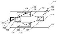
1 conceptually illustrates a schematic top view of a waveguide display having a single layer waveguide supporting an incident coupler comprising a prism and a spatially separated incident grating, in accordance with an embodiment of the present invention.
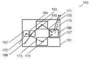
2 conceptually illustrates a schematic top view of a waveguide display having a single layer waveguide supporting an incident coupler comprising a prism and a multiplexed incident grating, in accordance with an embodiment of the present invention.
3 conceptually illustrates a schematic top view of a waveguide display having a single layer waveguide supporting an incident coupler comprising a spatially separated incident grating, in accordance with an embodiment of the present invention.
4 conceptually illustrates a schematic top view of a waveguide display having a single layer waveguide supporting an incident coupler comprising a multiplexed incident grating, in accordance with an embodiment of the present invention.
5 and 6 conceptually illustrate a schematic top view of a waveguide display having a single layer waveguide supporting first and second spatially separated incident prisms, in accordance with various embodiments of the present invention.
7 is a schematic diagram of a waveguide display having a waveguide with a spatially separated incident grating and a multiplexed pair of gratings combining the dual functions of two-dimensional beam expansion and beam extraction from the waveguide, in accordance with an embodiment of the present invention; Conceptually illustrates the floor plan.
8 conceptually illustrates a flow diagram illustrating a method of providing a color waveguide display with two-dimensional beam expansion using a single grating layer in accordance with an embodiment of the present invention.
9 conceptually illustrates a schematic cross-sectional view of a light field display having a stack of single layer color waveguides, in accordance with an embodiment of the present invention.
10A conceptually illustrates a schematic cross-sectional view showing a first operating state of a light field display corresponding to the formation of an image observable at a first distance, according to an embodiment of the present invention;
10B conceptually illustrates a schematic cross-sectional view showing a second operating state of a light field display corresponding to the formation of an image observable at a second distance, according to an embodiment of the present invention.
11A and 11B conceptually illustrate the grating geometry of an exemplary set of gratings in accordance with an embodiment of the present invention.
12 and 13 conceptually illustrate top views of a waveguide for providing a color image using a single grating layer having an incident grating, a fold grating, and an egress grating, in accordance with an embodiment of the present invention.
14 illustrates coupling illumination from red, green, and blue sources into a waveguide such that the red-green and green-blue bands of illumination are spatially sheared as they enter the waveguide, in accordance with an embodiment of the present invention; Sheared) conceptually illustrates a cross-sectional view of a dichroic prism system.
15 is a graph illustrating spectra of two LEDs of similar peak wavelength used in combination to provide a primary illumination color, in accordance with an embodiment of the present invention.
16 conceptually illustrates a schematic cross-sectional view of a rolled K-vector incidence grating configured to receive spatially sheared illumination and provide red-green and blue-bands, in accordance with an embodiment of the present invention.
실시형태를 설명하기 위하여, 광학 디자인 및 시각 디스플레이의 기술의 당업자들에게 알려져 있는 광학 기술의 일부 주지된 피쳐들은 본 발명의 기본적인 원리가 가려지는 것을 피하기 위해서 생략되거나 단순화되었다. 그렇지 않다고 진술되지 않는 한, 광선 또는 빔 방향과 관련하여 "축상(on-axis)"이라는 용어는 본 발명과 관련하여 설명되는 광학 컴포넌트의 표면에 법선인 축과 평행한 전파를 가리킨다. 후속하는 발명을 실시하기 위한 구체적인 내용에서, 광, 광선, 빔 및 방향이라는 용어는 직선 궤적에 따른 광 에너지의 전파 방향을 표시하기 위하여 상호교환가능하도록 그리고 서로 연관되어 사용될 수 있다. 후속하는 설명의 일부는 광학 디자인의 기술의 당업자들에게 일반적으로 채용되는 용어를 사용하여 제공될 것이다. 예시를 위하여, 달리 진술되지 않는 한 도면이 척도에 맞게 도시되지 않는다는 것이 이해되어야 한다. 예를 들어, 특정 도면들에서의 치수는 과장되었다.For the purpose of describing embodiments, some well-known features of optical technology known to those skilled in the art of optical design and visual display have been omitted or simplified in order to avoid obscuring the basic principles of the present invention. Unless stated otherwise, the term “on-axis” with respect to a ray or beam direction refers to propagation parallel to an axis normal to the surface of the optical component described in connection with the present invention. In the specific context for carrying out the following invention, the terms light, ray, beam and direction may be used interchangeably and in conjunction with one another to indicate the direction of propagation of light energy along a straight trajectory. Portions of the description that follow will be presented using terminology commonly employed by those skilled in the art of optical design. For purposes of illustration, it should be understood that the drawings are not drawn to scale unless otherwise stated. For example, dimensions in certain figures are exaggerated.
이제 도면을 참조하면, 컬러 홀로그램 도파관 디스플레이 및 관련된 제조 방법이 설명된다. 도파관 디스플레이는, AR 및 VR을 위한 HMD, 헬멧 탑재 디스플레이, 투영 디스플레이, 헤드업 디스플레이(HUD), 헤드 다운 디스플레이(Heads Down Display; HDD), 무안경(autostereoscopic) 디스플레이, 및 그 외의 3D 디스플레이를 비한정적으로 포함하는 많은 상이한 애플리케이션에서 사용될 수 있다. 또한, 유사한 기술은, 예를 들어 눈 추적기, 지문 스캐너 및 LIDAR 시스템과 같은 도파관 센서에 적용될 수 있다. 도파관 제조, 및 특히 컬러 도파관 제조는 고가이고 여러 인자에 기인하여 수율이 낮을 수 있다. 이것에 기여하는 영향 중 하나는 풀 컬러 디스플레이에서 필요한 적색, 녹색, 청색 도파관 층들을 정렬하는 것이 어렵다는 것이다. 이것은 풀 컬러를 구현하기 위하여 사용되는 도파관 층의 개수를 줄임으로써 상당 부분 완화될 수 있다. 예를 들어, 풀 컬러 도파관 디스플레이는 두 개의 도파관 층을 사용하여 구현될 수 있는데, 하나는 청색-녹색을 투과하고 다른 것은 녹색-적색을 투과한다. 이상적으로, 디스플레이는 가능한 적은 수의 도파관 층을 가져야 한다. 그러나, 브래그 격자의 단일 구성은 통상적으로 전체 시각적 스펙트럼 대역폭에 걸쳐서 효율적으로 동작할 수 없다. 그러므로, 단일 격자층을 사용하여 풀 컬러 디스플레이를 구현하는 것은 어려운 일일 수 있다. 이와 같이, 많은 본 발명의 실시형태는 2-차원 빔 확장 및 광 추출을 제공할 수 있는 풀 컬러 도파관을 구현하기 위하여, 단일 격자층 내의 격자들의 상이한 구조를 활용하는 것에 직결된다.Referring now to the drawings, a color holographic waveguide display and associated manufacturing method are described. Waveguide displays include HMDs for AR and VR, helmet mounted displays, projection displays, heads up displays (HUDs), heads down displays (HDDs), autostereoscopic displays, and other 3D displays. It can be used in many different applications, including but not limited to. Similar techniques may also be applied to waveguide sensors such as, for example, eye trackers, fingerprint scanners and LIDAR systems. Waveguide fabrication, and particularly color waveguide fabrication, is expensive and can have low yields due to several factors. One of the contributing effects to this is the difficulty of aligning the red, green, and blue waveguide layers required in a full color display. This can be largely mitigated by reducing the number of waveguide layers used to realize full color. For example, a full color waveguide display may be implemented using two waveguide layers, one transmitting blue-green and the other transmitting green-red. Ideally, the display should have as few waveguide layers as possible. However, a single configuration of a Bragg grating typically cannot operate efficiently over the entire visual spectral bandwidth. Therefore, it can be difficult to implement a full color display using a single grid layer. As such, many embodiments of the present invention are directed to utilizing different structures of gratings within a single grating layer to implement a full color waveguide that can provide two-dimensional beam broadening and light extraction.
많은 실시형태에서, 도파관 디스플레이는 단일 격자층을 가지는 도파관을 포함하도록 구현된다. 도파관 디스플레이는, 도파관에 광학적으로 커플링되는 데이터-변조된 광의 소스, 광의 제 1 스펙트럼 대역을 소스로부터 제 1 도파관 퓨필 내로 지향시키기 위한 제 1 입사 커플러, 및 광의 제 2 스펙트럼 대역을 소스로부터 제 2 도파관 퓨필 내로 지향시키기 위한 제 2 입사 커플러를 더 포함할 수 있다. 광 소스는 LED 또는 레이저 중 적어도 하나를 포함할 수 있다. 일부 실시형태들에서, 소스는 별개의 적색, 녹색, 및 청색 방출기를 포함한다. 여러 실시형태에서, 도파관 디스플레이는 다중화된 제 1 격자와 제 2 격자, 제 1 스펙트럼 대역을 제 1 경로를 따라서 제 1 퓨필로부터 출사 커플러로 지향시키기 위한 적어도 하나의 폴드 격자, 및 제 2 스펙트럼 대역을 제 2 경로를 따라서 제 2 퓨필로부터 출사 커플러로 지향시키기 위한 적어도 하나의 폴드 격자를 가지는 출사 커플러를 포함한다. 이러한 폴드 격자는 그들 각각의 스펙트럼 대역에 대해서 제 1 빔 확장을 제공하도록 구성될 수 있다. 출사 커플러와 관련하여, 제 1 다중화된 격자는 제 1 스펙트럼 대역을 제 1 빔 확장에 직교하는 빔 확장으로 상기 도파관으로부터 제 1 방향으로 지향시키도록 구성될 수 있고, 제 2 다중화된 격자는 제 2 스펙트럼 대역을 제 1 빔 확장에 직교하는 빔 확장으로 상기 도파관으로부터 제 1 방향으로 지향시키도록 구성될 수 있다.In many embodiments, the waveguide display is implemented to include a waveguide having a single grating layer. The waveguide display includes a source of data-modulated light optically coupled to the waveguide, a first incident coupler for directing a first spectral band of light from the source into a first waveguide pupil, and a second spectral band of light from the source. It may further include a second incident coupler for directing into the waveguide pupil. The light source may include at least one of an LED or a laser. In some embodiments, the source includes separate red, green, and blue emitters. In various embodiments, the waveguide display comprises multiplexed first and second gratings, at least one folded grating for directing the first spectral band from the first pupil to the exit coupler along a first path, and a second spectral band. and an exit coupler having at least one fold grating for directing from the second pupil to the exit coupler along a second path. Such a fold grating may be configured to provide a first beam extension for their respective spectral bands. With respect to the output coupler, the first multiplexed grating may be configured to direct a first spectral band in a first direction from the waveguide with a beam extension orthogonal to the first beam extension, and wherein the second multiplexed grating comprises a second and direct the spectral band in a first direction from the waveguide with a beam extension orthogonal to the first beam extension.
본 발명의 다양한 실시형태에 따르는 도파관 디스플레이는 많은 상이한 방법들로 구현되고 구성될 수 있다. 일부 실시형태들에서, 도파관 디스플레이는 곡선형인 이중-축 빔 확장 도파관으로서 구현된다.A waveguide display in accordance with various embodiments of the present invention may be implemented and configured in many different ways. In some embodiments, the waveguide display is implemented as a curved dual-axis beam expansion waveguide.
단일층 도파관 디스플레이, 컬러 도파관 디스플레이, 재료, 및 관련된 제조 방법이 더 상세히 후술된다.Single layer waveguide displays, color waveguide displays, materials, and related manufacturing methods are described in greater detail below.
도파관 디스플레이waveguide display
본 발명의 다양한 실시형태에 따르는 도파관 디스플레이는 많은 상이한 방법들로 구현되고 구성될 수 있다. 예를 들고 단순화하기 위하여, 본 명세서 전체에서 논의되는 대체적인 전파 방향은 좌측으로부터 우측으로 향한다. 쉽게 이해될 수 있는 바와 같이, 도파관 구조 및 광 전파 방향은 특정한 애플리케이션에 따라서 구성될 수 있다. 본 명세서에서 설명되는 단일층 컬러 도파관 아키텍처는 다중층 아키텍처에 비하여 여러 장점을 가진다. 첫 번째 장점은, 다수의 층들의 조합과 정렬이 요구되지 않아서, 수율이 개선되고 제조 비용이 적어진다는 것이다. 두 번째 장점은 단일 노광 프로세스를 사용한 제작 중에 단일층만이 요구되는 것에 기인하여 제조 복잡도가 줄어든다는 것이다. 그러면 노광 쓰루풋 시간이 감소되고, 따라서 비용이 감소된다. 본 발명의 원리는 HUD 및 HMD를 비한정적으로 포함하는 다양한 도파관 디스플레이 및 센서 애플리케이션에 적용될 수 있다. 비록 본 발명이 단일층 컬러 도파관을 다루고 있지만, 본 명세서에 개시된 실시형태 및 교시내용 중 많은 것들은 흑백 도파관에도 적용될 수 있다.A waveguide display in accordance with various embodiments of the present invention may be implemented and configured in many different ways. For purposes of example and simplicity, the general direction of propagation discussed throughout this specification is from left to right. As can be readily understood, the waveguide structure and light propagation direction can be configured according to a particular application. The single-layer color waveguide architecture described herein has several advantages over multi-layer architectures. The first advantage is that the combination and alignment of multiple layers is not required, resulting in improved yields and lower manufacturing costs. A second advantage is reduced manufacturing complexity due to the fact that only a single layer is required during fabrication using a single exposure process. This reduces the exposure throughput time and thus the cost. The principles of the present invention may be applied to a variety of waveguide display and sensor applications including but not limited to HUDs and HMDs. Although the present invention addresses single-layer color waveguides, many of the embodiments and teachings disclosed herein are also applicable to black and white waveguides.
많은 실시형태에서, 도파관 디스플레이는 광 소스, 입사 커플러, 및 출사 커플러를 포함할 수 있다. 입사 커플러는 프리즘 및 입사 격자 중 적어도 하나를 포함할 수 있다. 여러 실시형태에서, 출사 커플러는 출사 격자들을 사용하여 구현된다. 추가적인 실시형태에서, 도파관 디스플레이는 폴드 격자를 포함할 수 있다. 여러 실시형태에서, 폴드 격자 각각은 제 1 방향으로 퓨필 확장을 제공하고, 광을 내부 전반사를 통해서 출사 격자로 지향시키도록 구성되는데, 여기에서 출사 격자는 인용된 문헌의 실시형태 및 교시내용에 따라서 제 1 방향과 다른 제 2 방향으로 퓨필 확장을 제공하도록 구성된다. 폴드 격자를 사용함으로써, 도파관 디바이스는 바람직하게도 일부 실시형태에 따라서 정보를 디스플레이하는 이전의 시스템 및 방법보다 더 적은 층들을 요구하게 된다. 또한, 폴드 격자를 사용함으로써, 광은 이중 퓨필 확장을 달성하면서 도파관 외면들에 의해 규정되는 단일 직사각형 프리즘 내에서 도파관 내의 내부 전반사에 의해서 이동할 수 있다.In many embodiments, the waveguide display may include a light source, an incident coupler, and an output coupler. The incident coupler may include at least one of a prism and an incident grating. In various embodiments, the exit coupler is implemented using exit gratings. In a further embodiment, the waveguide display may include a fold grating. In various embodiments, each of the fold gratings is configured to provide pupil expansion in a first direction and direct light to the exit grating via total internal reflection, wherein the exit grating is in accordance with the teachings and embodiments of the cited literature. configured to provide pupil expansion in a second direction different from the first direction. By using a fold grating, the waveguide device preferably requires fewer layers than previous systems and methods of displaying information in accordance with some embodiments. Also, by using a fold grating, light can travel by total internal reflection within the waveguide within a single rectangular prism defined by the waveguide outer surfaces while achieving double pupil expansion.
많은 실시형태에서, 입사, 폴드, 또는 출사 격자 중 적어도 하나는 각도 대역폭을 확장시키기 위한 두 개 이상의 각도 회절 규정(angular diffraction prescription)을 조합할 수 있다. 이와 유사하게, 일부 실시형태들에서는 입사, 폴드, 또는 출사 격자의 적어도 하나는 스펙트럼 대역폭을 확장하기 위한 두 개 이상의 스펙트럼 회절 규정을 조합할 수 있다. 예를 들어, 원색 중 두 개 이상을 회절시키기 위해서 컬러 다중화된 격자가 사용될 수 있다.In many embodiments, at least one of the incidence, fold, or exit grating may combine two or more angular diffraction prescriptions to expand the angular bandwidth. Similarly, in some embodiments at least one of the incidence, fold, or exit grating may combine two or more spectral diffraction rules to broaden the spectral bandwidth. For example, a color multiplexed grating can be used to diffract two or more of the primaries.
여러 실시형태에서, 격자층은 함께 적층되어 단일 모재 도파관을 형성하는 입사 커플러, 폴드 격자, 및 출사 격자(또는 부분 그것의)를 포함하는 여러 부분들을 포함한다. 이러한 부분들은 이러한 조각들의 굴절률과 매칭되는 광학 접착제 또는 다른 투명 재료에 의해 분리될 수 있다. 일부 실시형태들에서, 격자층은 소망되는 격자 두께를 생성하고 각각의 셀을 입사 커플러, 폴드 격자, 및 출사 격자 각각에 대한 SBG 재료로 진공 충진함으로써 셀 제작 프로세스를 통해서 형성될 수 있다. 많은 실시형태에서, 셀은 다수의 유리 플레이트를 입사 커플러, 폴드 격자, 및 출사 격자에 대한 소망되는 격자 두께를 규정하는 유리 플레이트들 사이의 갭으로 위치시킴으로써 형성된다. 여러 실시형태에서, 하나의 셀은 별개의 애퍼쳐들이 SBG 재료의 상이한 포켓으로 충진되도록 다수의 애퍼쳐를 가지고 제조될 수 있다. 그러면, 임의의 개재 공간이 분리 재료(예를 들어, 접착제, 오일, 등)에 의해 분리되어 분리 구역을 형성할 수 있다. 일부 실시형태들에서, SBG 재료는 모재 상에 스핀-코팅된 후, 재료의 경화 이후에 제 2 모재에 의해 커버될 수 있다.In various embodiments, the grating layer comprises several portions, including an incident coupler, a folded grating, and an egress grating (or a portion thereof) stacked together to form a single matrix waveguide. These parts may be separated by an optical adhesive or other transparent material that matches the refractive index of these pieces. In some embodiments, the grating layer may be formed through a cell fabrication process by creating a desired grating thickness and vacuum filling each cell with SBG material for each of the incident coupler, fold grating, and egress grating. In many embodiments, a cell is formed by placing a plurality of glass plates into a gap between the glass plates defining a desired grating thickness for the incident coupler, the fold grating, and the egress grating. In various embodiments, a cell may be fabricated with multiple apertures such that distinct apertures are filled with different pockets of SBG material. Any intervening space can then be separated by a separation material (eg, adhesive, oil, etc.) to form a separation zone. In some embodiments, the SBG material may be spin-coated onto a parent material and then covered by a second parent material after curing of the material.
디스플레이 애플리케이션에 관련된 많은 실시형태에서, 폴드 격자는 자신의 격자 벡터가 도파관 평면 내에서 대각 방향으로 있는 상태에서 배향될 수 있다(클로킹(clocked)). 그러면 폴딩된 광에 대한 적당한 각도 대역폭이 보장된다. 그러나, 본 발명의 일부 실시형태는 디스플레이의 인체공학 디자인에서 생길 수 있는 격자의 위치설정에 대한 공간적 제약을 만족시키기 위한 다른 클록 각도를 활용할 수 있다. 격자 벡터 배향 각도는 "클록 각도(clock angle)"라고 불릴 수 있다. 일부 실시형태들에서, 각각의 폴드 격자가 디스플레이 광의 전파 방향에 대하여 대각선에 세팅되도록, 각각의 폴드 격자의 길이 방향 에지는 입사 커플러의 정렬 축에 비스듬하다. 폴드 격자는 입사 커플러로부터의 광이 출사 격자로 재지향되도록 하는 각도를 가진다. 일 예에서, 폴드 격자는 디스플레이 이미지가 입사 커플러로부터 방출되는 방향에 대해 45도 각도로 세팅된다. 이러한 피쳐에 의하여, 폴드 격자 아래에서 전파되는 디스플레이 이미지가 출사 격자 내로 전환되게(turned) 될 수 있다. 예를 들어, 여러 실시형태에서, 폴드 격자는 이미지가 출사 격자 내로 90 도 전환되게 한다. 이러한 방식으로, 단일 도파관은 수평 및 수직 방향 양자 모두에서 이중 축 퓨필 확장을 제공할 수 있다. 여러 실시형태에서, 폴드 격자 각각은 부분적으로 회절형 구조체이다. 출사 격자는 내부 전반사를 통해서 폴드 격자로부터 이미지 광을 수광하고, 제 2 방향으로 퓨필 확장을 제공한다. 출사 격자는 제 1 방향과 다른 제 2 방향으로 퓨필 확장을 제공하고, 광이 제 1 표면 또는 제 2 표면으로부터 도파관을 벗어나게 하도록 구성될 수 있다.In many embodiments related to display applications, the fold grating may be oriented (clocked) with its grating vector being diagonal in the waveguide plane. This ensures an adequate angular bandwidth for the folded light. However, some embodiments of the present invention may utilize other clock angles to satisfy spatial constraints on the positioning of the gratings that may arise in the ergonomic design of the display. The grating vector orientation angle may be referred to as the "clock angle". In some embodiments, the longitudinal edge of each fold grating is oblique to the alignment axis of the incident coupler such that each fold grating is set diagonally with respect to the direction of propagation of the display light. The fold grating is angled such that light from the incident coupler is redirected to the exit grating. In one example, the fold grating is set at a 45 degree angle to the direction in which the display image is emitted from the incident coupler. This feature allows the display image propagating under the fold grating to be turned into the exit grating. For example, in various embodiments, the fold grating causes the image to be turned 90 degrees into the exit grating. In this way, a single waveguide can provide dual axis pupil expansion in both horizontal and vertical directions. In various embodiments, each of the fold gratings is a partially diffractive structure. The exit grating receives image light from the fold grating via total internal reflection and provides pupil expansion in a second direction. The exit grating may be configured to provide pupil expansion in a second direction different from the first direction and to direct light out of the waveguide from either the first surface or the second surface.
많은 실시형태에서, 폴드 격자 각도 대역폭은 유도된 광과 격자의 이중 상호작용을 실현하기 위한 격자 규정을 설계함으로써 향상될 수 있다. 이중 상호작용 폴드 격자의 예시적인 실시형태는 그 내용이 본 명세서에서 원용에 의해 통합되는 미국 특허 출원 번호 제 14/620,969(발명의 명칭 "WAVEGUIDE GRATING DEVICE")에 개시된다. 일부 실시형태들에서, 전술된 원리에 기반한 도파관은 적외선 대역에서 동작한다. 일부 실시형태들에서, 입사, 폴드 또는 출사 격자 중 적어도 하나는 표면 양각 구조체(surface relief structure)에 기반할 수 있다.In many embodiments, the fold grating angular bandwidth can be improved by designing the grating definition to realize the double interaction of the guided light and the grating. Exemplary embodiments of dual interacting fold gratings are disclosed in US Patent Application Serial No. 14/620,969 entitled “WAVEGUIDE GRATING DEVICE”, the contents of which are incorporated herein by reference. In some embodiments, a waveguide based on the principles described above operates in the infrared band. In some embodiments, at least one of the entrance, fold, or exit grating may be based on a surface relief structure.
위에서 논의된 바와 같이, 본 발명의 다양한 실시형태에 따르는 도파관 디스플레이는 광 소스를 포함할 수 있다. 일부 실시형태들에서, 전술된 도파관 실시형태에서 사용되는 데이터-변조된 광의 소스는 마이크로디스플레이를 포함하는 입사 이미지 노드(Input Image Node; IIN)를 포함한다. 입사 격자는, 시준된 광을 IIN으로부터 수광하고 광이 제 1 표면 및 제 2 표면 사이의 내부 전반사를 통해서 도파관 내에서 폴드 격자로 이동하게 하도록 구성될 수 있다. 통상적으로, IIN은 마이크로디스플레이 패널에 추가하여, 광원 및 디스플레이 패널을 조명하고, 반사된 광을 분리하며, 이것을 요구된 FOV 내로 시준하기 위해 필요한 광학 컴포넌트들을 포함한다. 마이크로디스플레이 상의 각각의 이미지 픽셀은 제 1 도파관 내에서 고유한 각도 방향으로 변환될 수 있다. 다양한 마이크로디스플레이 기술 중 임의의 것이 활용될 수 있다. 일부 실시형태들에서, 마이크로디스플레이 패널은 액정 디바이스 또는 마이크로 전기기계 시스템(Micro Electro Mechanical System; MEMS) 디바이스일 수 있다. 여러 실시형태에서, 마이크로디스플레이는 유기 발광 다이오드(Organic Light Emitting Diode; OLED) 기술에 기반할 수 있다. 이러한 방출형 디바이스는 통상적으로 별개의 광원을 요구하지 않을 것이고, 따라서 폼 팩터가 더 작아지는 장점을 제공할 것이다. 여러 실시형태에서, IIN은 스캐닝된 변조된 레이저에 기반할 수 있다. IIN은 마이크로디스플레이 패널 상에 디스플레이된 이미지를, 각각의 디스플레이 픽셀이 일부 실시형태에 따르는 모재 도파관 내에서 고유한 각도 방향으로 변환되도록 투영한다. IIN 내에 포함된 시준 광학기는 렌즈 및 미러를 포함할 수 있고, 이들은 회절형 렌즈 및 미러일 수 있다. 일부 실시형태들에서, IIN은 그 내용이 본 명세서에서 원용에 의해 통합되는 미국 특허 출원 번호 제 13/869,866(발명의 명칭 "HOLOGRAPHIC WIDE ANGLE DISPLAY"), 및 미국 특허 출원 번호 제 13/844,456(발명의 명칭 "TRANSPARENT WAVEGUIDE DISPLAY")에 개시된 실시형태 및 교시내용에 기반할 수 있다. 여러 실시형태에서, IIN은 광을 마이크로디스플레이 상으로 지향시키고 반사된 광을 도파관을 통해 투과시키기 위한 빔 스플리터를 포함한다. 여러 실시형태에서, 빔 스플리터는 HPDLC 내에 기록된 격자이고, 이러한 격자의 내재적 편광 선택성을 사용하여 디스플레이를 조명하는 광과 디스플레이로부터 반사되는 이미지 변조된 광을 분리한다. 일부 실시형태들에서, 빔 스플리터는 편광 빔 스플리터 큐브이다.As discussed above, waveguide displays in accordance with various embodiments of the present invention may include a light source. In some embodiments, the source of data-modulated light used in the waveguide embodiment described above comprises an Input Image Node (IIN) comprising a microdisplay. The incident grating may be configured to receive collimated light from the IIN and cause the light to travel to the fold grating within the waveguide via total internal reflection between the first and second surfaces. Typically, the IIN includes, in addition to the microdisplay panel, a light source and optical components necessary to illuminate the display panel, isolate the reflected light, and collimate it into the required FOV. Each image pixel on the microdisplay can be transformed into a unique angular direction within the first waveguide. Any of a variety of microdisplay technologies may be utilized. In some embodiments, the microdisplay panel may be a liquid crystal device or a Micro Electro Mechanical System (MEMS) device. In various embodiments, the microdisplay may be based on Organic Light Emitting Diode (OLED) technology. Such emissive devices will typically not require a separate light source, thus providing the advantage of a smaller form factor. In various embodiments, IIN may be based on a scanned modulated laser. The IIN projects the image displayed on the microdisplay panel such that each display pixel is transformed into a unique angular direction within the parent waveguide in accordance with some embodiments. The collimating optics contained within the IIN may include lenses and mirrors, which may be diffractive lenses and mirrors. In some embodiments, IIN refers to U.S. Patent Application Serial No. 13/869,866, entitled "HOLOGRAPHIC WIDE ANGLE DISPLAY," and U.S. Patent Application Serial No. 13/844,456, the contents of which are incorporated herein by reference. may be based on the embodiments and teachings disclosed in the title "TRANSPARENT WAVEGUIDE DISPLAY"). In various embodiments, the IIN includes a beam splitter for directing light onto the microdisplay and transmitting the reflected light through the waveguide. In various embodiments, the beam splitter is a grating written within the HPDLC, and uses the intrinsic polarization selectivity of this grating to separate the light illuminating the display and the image modulated light reflected from the display. In some embodiments, the beam splitter is a polarizing beam splitter cube.
많은 실시형태에서, IIN은 스페클 제거기(despeckler)를 포함한다. 바람직하게는, 스페클 제거기는 그 내용이 본 명세서에서 원용에 의해 통합되는 미국 특허 번호 US 8,565,560(발명의 명칭은 "LASER ILLUMINATION DEVICE")의 실시형태 및 교시내용에 기반하는 홀로그램 도파관 디바이스이다. 광원은 레이저 또는 LED일 수 있고, 조명 빔 각도 특성을 변경하기 위한 하나 이상의 렌즈를 포함할 수 있다. 스페클 제거기를 사용하는 것은, 소스가 레이저이고 이미지 소스가 레이저-조명(laser-lit) 마이크로디스플레이 또는 레이저-기반 방출형 디스플레이인 경우에 특히 중요하다. LED가 레이저보다 양호한 균일성을 제공할 것이다. 레이저 조명이 사용된다면, 도파관 출구에서 생기는 조명 밴딩(illumination banding)의 위험성이 존재한다. 일부 실시형태들에서, 도파관 내의 레이저 조명 밴딩은, 그 내용이 본 명세서에서 원용에 의해 통합되는 미국 가특허 출원 번호 제 62/071,277(발명의 명칭은 "METHOD AND APPARATUS FOR GENERATING INPUT IMAGES FOR HOLOGRAPHIC WAVEGUIDE DISPLAYS")에 개시된 기법 및 교시내용을 사용하여 극복될 수 있다. 여러 실시형태에서, 광원으로부터 나오는 광은 편광된다. 여러 실시형태에서, 이미지 소스는 액정 디스플레이(liquid crystal display; LCD) 마이크로 디스플레이 또는 액정 온 실리콘(liquid crystal on silicon; LCoS) 마이크로 디스플레이.In many embodiments, IIN includes a despeckler. Preferably, the speckle eliminator is a holographic waveguide device based on the embodiments and teachings of US Pat. No. 8,565,560, entitled "LASER ILLUMINATION DEVICE", the contents of which are incorporated herein by reference. The light source may be a laser or LED, and may include one or more lenses to alter the illumination beam angular characteristics. Using a speckle eliminator is particularly important when the source is a laser and the image source is a laser-lit microdisplay or laser-based emissive display. LEDs will provide better uniformity than lasers. If laser illumination is used, there is a risk of illumination banding occurring at the exit of the waveguide. In some embodiments, laser illumination banding in a waveguide is described in U.S. Provisional Patent Application No. 62/071,277, entitled “METHOD AND APPARATUS FOR GENERATING INPUT IMAGES FOR HOLOGRAPHIC WAVEGUIDE DISPLAYS, the contents of which are incorporated herein by reference. ") can be overcome using the techniques and teachings disclosed in In various embodiments, the light emanating from the light source is polarized. In various embodiments, the image source is a liquid crystal display (LCD) micro display or a liquid crystal on silicon (LCoS) micro display.
많은 실시형태에서, 도파관 디스플레이는 제 1 입사 커플러와 제 2 입사 커플러를 포함한다. 제 1 입사 커플러와 제 2 입사 커플러는 프리즘 및 격자 중 적어도 하나를 각각 포함할 수 있다. 일부 실시형태들에서, 커플러는 단일 프리즘을 활용하고 제 1 및 제 2 입사 격자의 쌍과 각각 연관되며, 제 1 및 제 2 입사 격자는 도파관의 전체적인 광 전파 방향을 따라서 배치된다. 여러 실시형태에서, 제 1 격자와 제 2 격자는 도파관의 전체적인 광 전파 방향에 직교하는 방향을 따라서 배치된다. 제 1 및 제 2 입사 격자는 도파관 내에 구현되고 많은 상이한 방식으로 구성될 수 있다. 여러 실시형태에서, 입사 격자는 공간적으로 분리된다. 다른 실시형태들에서, 입사 격자는 다중화된 격자로서 구현된다. 다중화된 격자의 교차된 구성(crossed configuration)은 HPDLC 재료 내에 기록된 격자에 대해서 유리할 수 있는데, 그 이유는 격자의 기록 중에 액정 및 단위체 컴포넌트의 효율적인 상 분리가 가능해질 수 있기 때문이다. 도 1 및 도 2는 이러한 차이를 개념적으로 예시한다.In many embodiments, the waveguide display includes a first incident coupler and a second incident coupler. The first incident coupler and the second incident coupler may each include at least one of a prism and a grating. In some embodiments, the coupler utilizes a single prism and is respectively associated with a pair of first and second incidence gratings, the first and second incidence gratings being disposed along the overall direction of light propagation of the waveguide. In various embodiments, the first grating and the second grating are disposed along a direction orthogonal to the overall direction of light propagation of the waveguide. The first and second incidence gratings may be embodied in the waveguide and configured in many different ways. In various embodiments, the incident gratings are spatially separated. In other embodiments, the incident grating is implemented as a multiplexed grating. The crossed configuration of the multiplexed grating may be advantageous for gratings recorded in HPDLC materials, since efficient phase separation of liquid crystal and monomeric components may be possible during writing of the gratings. 1 and 2 conceptually illustrate this difference.
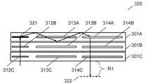
도 1은 본 발명의 일 실시형태에 따르는, 프리즘 및 공간적으로 분리된 입사 격자를 포함하는 입사 커플러를 지지하는 단일층 도파관을 가지는 도파관 디스플레이의 개략적인 평면도를 개념적으로 예시한다. 예시적인 실시형태에서, 도파관 디스플레이(100)는 입사 프리즘(102)을 지지하는 도파관(101)을 포함한다. 도파관(101)은 입사 격자(103, 104), 폴드 격자(105, 106), 및 다중화된 출사 격자(107, 108)를 더 포함한다. 도시된 바와 같이, 격자들은 단일 격자층 내에 배치된다. 입사로부터 도파관에서 추출되기까지의 빔 경로는 입사 격자(103)에 의해 회절된 광선에 대한 광선 경로(109-112) 및 입사 격자(104)에 의해 회절된 광선에 대한 광선 경로(113-116)에 의해 예시된다.1 conceptually illustrates a schematic top view of a waveguide display having a single layer waveguide supporting an incident coupler comprising a prism and a spatially separated incident grating, in accordance with an embodiment of the present invention. In an exemplary embodiment, the
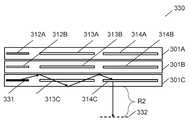
도 2는 본 발명의 일 실시형태에 따르는, 프리즘 및 다중화된 입사 격자를 포함하는 입사 커플러를 지지하는 단일층 도파관을 가지는 도파관 디스플레이의 개략적인 평면도를 개념적으로 예시한다. 도시된 바와 같이, 도파관 디스플레이(120)는 입사 프리즘(122)을 지지하는 도파관(121)을 포함한다. 도파관(121)은 단일 격자층 내에 배치된, 다중화된 입사 격자(123, 124), 폴드 격자(125, 126), 및 다중화된 출사 격자(127, 128)를 더 포함한다. 입사로부터 도파관에서 추출되기까지의 빔 경로는 격자(123)에 의해 회절된 광선에 대한 광선 경로(129-132) 및 격자(124)에 의해 회절된 광선에 대한 광선 경로(133-136)에 의해 예시된다.2 conceptually illustrates a schematic top view of a waveguide display having a single layer waveguide supporting an incident coupler comprising a prism and a multiplexed incident grating, in accordance with an embodiment of the present invention. As shown, the
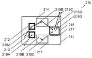
비록 도 1 및 도 2가 특정한 도파관 구조를 예시하지만, 본 발명의 다양한 실시형태에 따르는 도파관 디스플레이는 주어진 애플리케이션의 특정한 요구 사항에 의존하여 많은 상이한 방식으로 구현될 수 있다. 예를 들어, 많은 실시형태에서, 제 1 입사 커플러와 제 2 입사 커플러는 제 1 및 제 2 입사 격자를 각각 포함하고, 도파관 디스플레이는 프리즘이 없이 구현될 수 있다. 추가적인 실시형태에서, 제 1 및 제 2 입사 격자는 도파관의 전체적인 광 전파 방향에 직교하는 방향을 따라서 배치된다. 다른 실시형태들에서, 제 1 및 제 2 입사 격자는 도파관의 전체적인 광 전파 방향을 따라서 배치된다. 도 3 및 도 4는 본 발명의 다양한 실시형태에 따르는, 공간적으로 분리된 입사 격자 및 무-프리즘 입사 커플러를 가지고 구현되는 도파관 디스플레이의 개략적인 평면도를 개념적으로 예시한다. 도시된 바와 같이, 도 3은 입사 격자(142, 143)를 지지하는 도파관(141), 및, 층, 폴드 격자(144, 145) 및 다중화된 출사 격자(146, 147)를 포함하는 도파관 디스플레이(140)를 도시하는데, 격자들 모두는 단일층 내에 배치된다. 입사로부터 도파관에서 추출되기까지의 빔 경로는 입사 격자(142)의 경우에는 광선 경로(148-151), 그리고 입사 격자(143)의 경우에는 광선 경로(152-155)에 의해 예시된다. 이와 유사하게, 도 4는 입사 격자(162, 163)를 지지하는 도파관(161), 및 폴드 격자(164, 165) 및 다중화된 출사 격자(166, 167)를 포함하는 도파관 디스플레이(160)를 도시하는데, 격자들 모두는 단일층 내에 배치된다. 입사로부터 도파관에서 추출되기까지의 빔 경로는 입사 격자(163)의 경우에는 광선 경로(168-171), 그리고 입사 격자(162)의 경우에는 광선 경로(172-175)에 의해 예시된다. 도파관 디스플레이(160)와 도 3에 도시되는 실시형태 사이의 중요한 차이점은 입사 격자의 배열에서 구별될 수 있다-즉 도 4는 제 1 격자와 제 2 격자가 도파관의 전체적인 광 전파 방향을 따라서 배치되는 실시형태를 예시한다. 도 3 및 도 4의 실시형태와 같은 실시형태와 후술되는 실시형태에서, 두 개의 공간적으로 분리된 입사 커플러는 두 개의 별개의 입사 퓨필을 제공할 수 있다.Although Figures 1 and 2 illustrate specific waveguide structures, waveguide displays according to various embodiments of the present invention can be implemented in many different ways depending on the specific requirements of a given application. For example, in many embodiments, the first incident coupler and the second incident coupler include first and second incident gratings, respectively, and the waveguide display may be implemented without a prism. In a further embodiment, the first and second incident gratings are disposed along a direction orthogonal to the overall light propagation direction of the waveguide. In other embodiments, the first and second incident gratings are disposed along the overall direction of light propagation of the waveguide. 3 and 4 conceptually illustrate a schematic top view of a waveguide display implemented with a spatially separated incidence grating and a prism-free incidence coupler, in accordance with various embodiments of the present invention. As shown, FIG. 3 illustrates a waveguide display including a
무-프리즘 입사 커플러에 추가하여, 도파관 디스플레이는 프리즘만을 포함하는 입사 커플러를 구현할 수 있다. 도 5 및 도 6은 본 발명의 다양한 실시형태에 따르는, 입사 격자가 없이 입사 커플러를 구현하는 도파관 디스플레이의 개략적인 평면도를 개념적으로 예시한다. 도시된 바와 같이, 제 1 입사 커플러는 제 1 프리즘을 포함하고, 제 2 광 입사 커플러는 제 2 프리즘을 포함한다. 도 5에서, 제 1 프리즘과 제 2 프리즘은 도파관의 전체적인 광 전파 방향에 직교하는 방향을 따라 배치된다. 도 6에서, 제 1 프리즘과 제 2 프리즘은 도파관의 전체적인 광 전파 방향을 따라 배치된다.In addition to a prism-free incident coupler, a waveguide display may implement an incident coupler comprising only a prism. 5 and 6 conceptually illustrate schematic top views of a waveguide display implementing an incident coupler without an incident grating, in accordance with various embodiments of the present invention. As shown, the first incident coupler comprises a first prism, and the second light incident coupler comprises a second prism. In Fig. 5, the first prism and the second prism are arranged along a direction orthogonal to the overall light propagation direction of the waveguide. In Fig. 6, the first prism and the second prism are arranged along the entire light propagation direction of the waveguide.
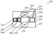
도 5를 참조하면, 도파관 디스플레이(210)는 입사 프리즘(212, 213)을 지지하는 도파관(211)을 포함한다. 도파관(211)은 단일 격자층 내에 배치되는 폴드 격자(214, 215) 및 다중화된 출사 격자(216, 217)를 더 포함한다. 입사로부터 도파관에서 추출되기까지의 빔 경로는 프리즘(213)에 의해 도파관 내에 커플링되는 광선에 대한 광선 경로(219A-219D) 및 프리즘(212)에 의해 도파관 내에 커플링되는 광선에 대한 광선 경로(218A-218D)에 의해 예시된다. 이와 유사하게, 도 6은 입사 프리즘(232, 233)을 지지하는 도파관(231)을 포함하는 도파관 디스플레이(220)를 예시한다. 도파관(231)은 단일 격자층 내에 배치되는 폴드 격자(234, 235) 및 다중화된 출사 격자(236, 237)를 더 포함한다. 입사로부터 도파관에서 추출되기까지의 빔 경로는 프리즘(233)에 의해 도파관 내에 커플링되는 광선에 대한 광선 경로(238-241) 및 프리즘(222)에 의해 도파관 내에 커플링되는 광선에 대한 광선 경로(242-245)에 의해 예시된다. 프리즘에만 기반하는 입사 커플러를 사용하는 실시형태들에서, 예컨대 도 5 및 도 6에 도시된 도파관 디스플레이에서, 격자 상호성(grating reciprocity)은 폴드 및 출사 격자의 피치 및 클록 각도를 사용하여 다뤄질 수 있다.Referring to FIG. 5 , the
앞의 섹션에서 설명된 바와 같이, 입사 커플러는 다양한 상이한 방식으로 구성될 수 있다. 또한, 도파관 디스플레이의 폴드 격자 및 출사 커플러도 많은 상이한 방식으로 구성될 수 있다. 도 7은 본 발명의 일 실시형태에 따르는, 공간적으로 분리된 입사 격자 및 2-차원 빔 확장 및 도파관으로부터의 빔 추출의 이중 기능을 결합하는 격자들의 다중화된 쌍이 있는 도파관을 가지는 도파관 디스플레이의 개략적인 평면도를 개념적으로 예시한다. 도시된 바와 같이, 도파관 디스플레이(190)는 입사 커플링 프리즘(192, 193)을 지지하는 도파관(191)을 포함한다. 도파관(191)은 다중화된 결합형 폴드 및 출사 격자(194-197)를 더 포함한다. 예시적인 실시형태에서, 격자(194, 195)는 프리즘(192)을 통해 도파관(191)에 진입하는 광을 두 차원으로 회절시키고 확장시킨다. 이와 유사하게, 격자(196, 197)는 프리즘(192, 193)을 통해 도파관(191)에 진입하는 광을 두 차원으로 회절시키고 확장시킨다. 입사로부터 도파관에서 추출되기까지의 빔 경로는, 프리즘(192)의 경우에는 광선 경로(198-200), 그리고 프리즘(193)의 경우에는 광선 경로(201-203)에 의해서 예시된다. 비록 네 개의 격자들이 다중화되지만, 두 개의 경로의 각각에 대응하는 격자들의 쌍은 교차하는 브래그 무늬를 가진다. 일부 실시형태들에서, 입사 커플링 프리즘(192, 193)은 격자로 대체될 수 있다.As described in the previous section, the incident coupler can be configured in a variety of different ways. Also, the fold grating and exit coupler of the waveguide display can be configured in many different ways. 7 is a schematic diagram of a waveguide display having a waveguide with a spatially separated incident grating and a multiplexed pair of gratings combining the dual functions of two-dimensional beam expansion and beam extraction from the waveguide, in accordance with an embodiment of the present invention; Conceptually illustrates the floor plan. As shown, the
무편광 광원을 사용하는 디스플레이에 대한 일부 실시형태들에서, 사용되는 입사 격자는 각각의 격자가 입사 무편광 광의 특정 편광을 도파관 경로 내로 회절시키도록 배향되는 격자들을 조합할 수 있다. 이러한 실시형태는 그 전체 내용이 본 명세서에서 원용에 의해 통합되는 Waldern 등에 의한 PCT 출원 PCT/GB2017/000040(발명의 명칭은 "METHOD AND APPARATUS FOR PROVIDING A POLARIZATION SELECTIVE HOLOGRAPHIC WAVGUIDE DEVICE")에 개시된 실시형태 및 교시내용 중 일부를 포함할 수 있다. 출사 격자는, 도파관 경로로부터의 광이 무편광 광으로서 도파관을 벗어나 조합되고 커플링되도록, 유사한 방식으로 구성될 수 있다. 예를 들어, 일부 실시형태들에서 입사 격자 및 출사 격자는 교차된 격자들(crossed gratings)을 직교 편광 상태에 대한 피크 회절 효율로써 각각 조합한다. 여러 실시형태에서, 편광 상태는 S-편광 및 P-편광이다. 여러 실시형태에서, 편광 상태는 원 편광의 반대 개념들이다. 비한정적으로 SBG와 같이 액정 폴리머 시스템 내에 기록된 격자의 장점은, 이러한 관점에서, 그들의 내재적 복굴절에 기인하여, 이들이 강한 편광 선택성을 나타낼 수 있다는 것이다. 그러나, 고유한 편광 상태를 제공하도록 구성될 수 있는 다른 격자 기술들도 역시 사용될 수 있다.In some embodiments for a display using an unpolarized light source, the incident grating used may combine gratings that are oriented such that each grating diffracts a particular polarization of the incident unpolarized light into the waveguide path. These embodiments are those disclosed in PCT application PCT/GB2017/000040 by Waldern et al., entitled "METHOD AND APPARATUS FOR PROVIDING A POLARIZATION SELECTIVE HOLOGRAPHIC WAVGUIDE DEVICE" by Waldern et al., the entire contents of which are incorporated herein by reference, and It may include some of the teaching content. The exit grating may be configured in a similar manner, such that light from the waveguide path is combined and coupled out of the waveguide as unpolarized light. For example, in some embodiments the incidence and exit gratings each combine crossed gratings with peak diffraction efficiency for orthogonal polarization states. In various embodiments, the polarization states are S-polarized and P-polarized. In various embodiments, the polarization state is the opposite of circular polarization. An advantage of gratings recorded in liquid crystal polymer systems, such as but not limited to SBGs, is that, in this respect, due to their inherent birefringence, they can exhibit strong polarization selectivity. However, other grating techniques that may be configured to provide a unique polarization state may also be used.
액정 폴리머 재료 시스템 내에 기록된 격자를 활용하는 실시형태들에서, 폴드 격자, 입사 격자, 또는 출사 격자 중 적어도 하나와 중첩하는 적어도 하나의 편광 제어층이 격자들, 특히 폴드 격자들 중 임의의 것 내의 편광 회전(polarization rotation)을 보상하기 위하여 제공될 수 있다. 많은 실시형태에서, 격자들 모두는 편광 제어층에 의해 오버레이된다. 일부 실시형태들에서, 편광 제어층은 격자의 서브세트에만, 예컨대 폴드 격자에만 적용된다. 편광 제어층은 광 지연 필름(optical retarder film)을 포함할 수 있다. HPDLC 재료에 기반하는 여러 실시형태에서, 격자들의 복굴절은 도파관 디바이스의 편광 속성을 제어하기 위하여 사용될 수 있다. HPDLC 격자, K-벡터, 및 격자 점유공간의 복굴절 텐서(tensor)를 디자인 변수로서 사용하면, 도파관 디바이스의 각도 성능(angular capability) 및 광학 효율을 최적화하기 위한 디자인 공간이 열리게 된다. 일부 실시형태들에서, 도파관의 유리-공기 인터페이스에 배치된 사분파 플레이트는 광선의 편광을 회전시켜서 격자들의 효율적인 커플링을 유지한다. 예를 들어, 일 실시형태에서, 사분파 플레이트는 도파관의 모재에 도포된 코팅이다. 일부 도파관 디스플레이 실시형태에서, 도파관의 모재에 사분파 코팅을 도포하면, 광선이 도파관 내의 스큐 파(skew wave)를 보상함으로써 의도된 관측 축(viewing axis)과의 정렬을 유지하는 것을 도울 수 있다. 여러 실시형태에서, 사분파 플레이트는 다중층 코팅으로서 제공될 수 있다.In embodiments utilizing a grating recorded in a liquid crystal polymer material system, at least one polarization control layer overlapping at least one of a fold grating, an incident grating, or an egress grating is formed within the gratings, particularly any of the fold gratings. It may be provided to compensate for polarization rotation. In many embodiments, all of the gratings are overlaid by a polarization control layer. In some embodiments, the polarization control layer is applied only to a subset of the grating, such as only to the fold grating. The polarization control layer may include an optical retarder film. In various embodiments based on HPDLC materials, the birefringence of the gratings can be used to control the polarization properties of the waveguide device. Using the HPDLC grating, the K-vector, and the birefringent tensor of the grating occupancy as design variables opens a design space for optimizing the angular capability and optical efficiency of the waveguide device. In some embodiments, a quarter wave plate disposed at the glass-air interface of the waveguide rotates the polarization of the ray to maintain efficient coupling of the gratings. For example, in one embodiment, the quarter wave plate is a coating applied to the base material of the waveguide. In some waveguide display embodiments, applying a quarter wave coating to the base material of the waveguide may help light rays maintain alignment with the intended viewing axis by compensating for skew waves in the waveguide. In various embodiments, the quarter wave plate may be provided as a multilayer coating.
도 8은 본 발명의 일 실시형태에 따르는 단일 격자층을 사용하여 2-차원 빔 확장이 있는 컬러 도파관 디스플레이를 제공하는 방법을 예시하는 흐름도를 개념적으로 예시한다. 도시된 바와 같이, 두 개 이상 편광 컴포넌트의 광을 도파관 내로 커플링하는 방법(240)이 제공된다. 흐름도를 참조하면, 방법(240)은 단일 격자층을 지지하는 도파관; 광의 소스; 제 1 입사 커플러; 제 2 입사 커플러; 다중화된 제 1 격자와 제 2 격자를 포함하는 출사 커플러; 제 1 폴드 격자; 및 제 2 폴드 격자를 제공하는 단계(241)를 포함한다. 제 1 스펙트럼 대역은 소스로부터 제 1 도파관 퓨필 내로 제 1 입사 커플러를 통해서 지향될 수 있고(242), 제 2 스펙트럼 대역은 소스로부터 제 2 도파관 퓨필 내로 제 2 입사 커플러를 통해서 지향될 수 있다(243). 제 1 스펙트럼 대역 광은 빔-확장되고 제 1 폴드 격자를 이용하여 출사 커플러 상으로 재지향된다(244). 제 2 스펙트럼 대역 광은 빔-확장되고 제 2 폴드 격자를 이용하여 출사 커플러 상으로 재지향된다(245). 제 1 스펙트럼 대역 광은 빔-확장되고 제 1 다중화된 격자를 이용하여 도파관으로부터 추출된다(246). 제 2 스펙트럼 대역 광은 빔-확장되고 제 2 다중화된 격자를 이용하여 도파관으로부터 추출된다(247).8 conceptually illustrates a flow diagram illustrating a method of providing a color waveguide display with two-dimensional beam expansion using a single grating layer in accordance with an embodiment of the present invention. As shown, a
전술되고 도 1 내지 도 8에 예시된 실시형태는, 분할 퓨필 입사 커플링 또는 다중화된 입사 커플링을 사용하는 입사 퓨필 분기의 원래에 기반하여, 출사 격자로 가는 상하 도파관 경로를 두 개의 공간적으로 분리된 폴드 격자를 사용하여 제공한다. 이러한 접근법을 구현하는 데 있어서의 한 가지 어려운 점은, 두 개의 폴드 격자를 가지게 되면 도파관 크기가 특히 수직으로 눈의 중심점 위로 커질 수 있다는 것이다. 다른 문제점은 효율적인 다중화된 출사 격자를 제작하는 것이다. 이와 같이, 본 발명에 따르는 여러 실시형태는 빔 분기 원리를 사용하지 않는 단일 격자층을 지지하는 단일 도파관 층에 기반하는 컬러 도파관 아키텍처에 직결된다.The embodiment described above and illustrated in FIGS. 1-8 spatially separates the upper and lower waveguide paths to the output grating into two, based on the original of the incident pupil branch using either split pupil incident coupling or multiplexed incident coupling. Provided using an old fold grid. One difficulty in implementing this approach is that having a two fold grating allows the waveguide size to be large, especially vertically above the center point of the eye. Another problem is to fabricate an efficient multiplexed exit grating. As such, various embodiments in accordance with the present invention are directed to a color waveguide architecture based on a single waveguide layer supporting a single grating layer that does not use the beam branching principle.
많은 실시형태에서, 도파관 디스플레이는 무한대의 거리에 이미지를 제공하도록 구현된다. 일부 실시형태들에서, 이미지는 몇 개의 중간 거리에 있을 수 있다. 여러 실시형태에서, 이미지는 인간의 눈의 이완된 관측 거리와 호환되는 거리에 있을 수 있다. 예를 들어, 본 발명의 다양한 실시형태에 따르는 많은 도파관은 약 2 미터로부터 약 10 미터에 달하는 관측 거리를 커버할 수 있다.In many embodiments, the waveguide display is implemented to provide an image at an infinite distance. In some embodiments, the image may be at several intermediate distances. In various embodiments, the image may be at a distance compatible with the relaxed viewing distance of the human eye. For example, many waveguides in accordance with various embodiments of the present invention may cover viewing distances ranging from about 2 meters to about 10 meters.
일부 실시형태들에서, 도파관은 도 3, 도 4, 및 도 7에 도시된 실시형태에 관련하여 전술된 바와 같은, 단일층 격자 도파관을 망라하는 다중층 도파관 아키텍처의 하나의 층을 제공하는데, 여기에서 각각의 도파관은 아이박스(eyebox)로부터 측정된 특정된 관측 범위에 풀 컬러 이미지를 제공한다. 관측 범위는 도파관 내의 격자 중 하나 이상에 인코딩된 굴절력(optical power)에 의해 결정될 수 있다. 여러 실시형태에서, 굴절력은 유도된 광의 최소의 시준해제(decollimation)를 생성하기 위하여, 다중화된 출사 격자 내에만 인코딩될 것이다. 격자 내에 굴절력을 인코딩하기 위한 기법은 당업자들에게 알려져 있다. 다수의 관측 거리(또는 초점면)를 제공하는 디스플레이는 일반적으로 광 필드 디스플레이라고 불릴 수 있다. 많은 실시형태에서, 입사 격자는, 임의의 시점에서 오직 하나의 입사 격자가 그 회절 상태에 있도록(이미지 콘텐츠가 하나의 거리로만 투영되도록), 그들의 회절 상태로 스위칭될 것이다. 투영을 위한 거리는, 양자 모두의 눈을 추적하여 측정된 좌안 및 우안 응시(gaze) 벡터를 삼각측량함으로써 요구된 관측 거리를 결정하는 눈 추적기를 사용하여 결정될 수 있다. 통상적으로는 마이크로디스플레이에 의해 제공되는 이미지 데이터는 각각의 관측 거리에 대해서 업데이트될 수 있다.In some embodiments, the waveguide provides one layer of a multilayer waveguide architecture encompassing a single layer grating waveguide, as described above with respect to the embodiments shown in FIGS. 3 , 4 , and 7 , wherein Each waveguide provides a full color image over a specified viewing range measured from an eyebox. The viewing range may be determined by an optical power encoded in one or more of the gratings in the waveguide. In various embodiments, refractive power will only be encoded within the multiplexed exit grating to produce minimal decollimation of the induced light. Techniques for encoding refractive power in gratings are known to those skilled in the art. A display that provides multiple viewing distances (or focal planes) may generally be referred to as a light field display. In many embodiments, the incident gratings will be switched to their diffraction state such that at any point in time only one incident grating is in its diffraction state (image content is projected only one distance). The distance for projection can be determined using an eye tracker that determines the required viewing distance by triangulating the measured left and right eye gaze vectors by tracking both eyes. Typically the image data provided by the microdisplay can be updated for each viewing distance.
도 9는 본 발명의 일 실시형태에 따르는, 단일층 컬러 도파관(301A-301C)의 스택을 망라하는 광 필드 디스플레이(310)의 개략적인 단면도를 개념적으로 예시한다. 예시적인 실시형태에서, 각각의 도파관은 숫자 312, 313, 314와 도파관 층에 따른 문자 A, B, C에 의해 명명되는 입사, 폴드, 및 다중화된 출사 격자를 포함한다. 각각의 도파관의 입사 격자는 스위칭가능 격자일 수 있다. 많은 실시형태에서, 스위칭가능 격자는 SBG이다. 도 9의 입사 격자는 도 3 내지 도 4 및 도 7 중 임의의 하나에 도시된 두 개의 입사 격자 중 하나에 대응하는데, 각각의 경우에 양자 모두의 입사 격자는 동시에 스위칭된다. 격자층 내의 적어도 하나의 격자는 각각의 도파관이 고유한 관측 거리를 제공하도록, 미리 정의된 거리에 관측가능 이미지를 형성하기 위한 굴절력을 가진다.9 conceptually illustrates a schematic cross-sectional view of a
광 필드 디스플레이의 동작이 도 10a 및 도 10b에 개념적으로 예시한다. 도 10a는 R1으로 명명되는 제 1 거리에 관측가능 이미지(322)를 형성하는 것에 대응하는 도파관의 첫 번째 동작 상태(320)를 보여주는 개략적인 단면도이다. 검정색으로 음영처리되는 입사 격자(312A)는 자신의 회절 상태(321)에 있고, 입사 격자(312B, 312C)는 그들의 비-회절 상태에 있다. 그러므로, 첫 번째 동작 상태에서, 광은 도파관(301A) 내에서만 전파된다. 도 10b는 R2로 명명되는 제 2 거리에 관측가능 이미지(332)를 형성하는 것에 대응하는 도파관의 두 번째 동작 상태(330)를 보여주는 개략적인 단면도이다. 검정색으로 음영처리되는 입사 격자(312C)는 자신의 회절 상태(331)에 있고, 입사 격자(312A, 312B)는 그들의 비-회절 상태에 있다. 그러므로, 두 번째 동작 상태에서는, 광이 도파관(301C) 내에서만 전파된다.The operation of a light field display is conceptually illustrated in FIGS. 10A and 10B . FIG. 10A is a schematic cross-sectional view showing a first
스위칭가능 브래그 격자switchable Bragg grating
도파관 내에 기록된 광학 구조체는 많은 상이한 타입의 광학 요소, 예컨대 비한정적으로 회절 격자를 포함할 수 있다. 많은 실시형태에서, 구현된 격자는 브래그 격자이다(볼륨 격자라고도 불림). 브래그 격자는 광이 높은 차수로 거의 회절되지 않아서 높은 효율을 가질 수 있다. 회절 차수 및 제로 차수에서의 광의 상대량은 격자의 굴절률 변조를 제어함으로써 변할 수 있다; 이것은 큰 퓨필에 걸쳐서 광을 추출하기 위한 손실형(lossy) 도파관 격자를 제조하기 위하여 사용될 수 있는 속성이다. 홀로그램 도파관 디바이스 내에서 사용되는 격자의 하나의 클래스는 스위칭가능 브래그 격자("SBG(Switchable Bragg Grating)")이다. SBG는 우선 광경화성 단위체 및 액정 재료의 혼합물의 박막을 유리 플레이트들 또는 모재들 사이에 배치함으로써 제조될 수 있다. 많은 경우에, 유리 플레이트는 평행한 구성이다. 하나 또는 양자 모두의 유리 플레이트는 통상적으로 투명한 주석 산화물 필름인 전극을, 이러한 필름에 걸쳐서 전기장을 인가하기 위하여 지지할 수 있다. SBG 내의 격자 구조체는 공간 주기성 세기 변조가 있는 간섭성(interferential) 노광을 사용하는 광경화-유도된 상 분리를 통해서 액상 재료(흔히 시럽이라고 불림) 내에 기록될 수 있다. 비한정적으로 조사 세기, 혼합물 내의 재료의 성분 부피 분율, 및 노광 온도와 같은 인자들이 결과적으로 얻어지는 격자 형상(morphology) 및 성능을 결정할 수 있다. 쉽게 이해될 수 있는 바와 같이, 주어진 애플리케이션의 특정한 요구 사항에 따라서 매우 다양한 재료 및 혼합물이 사용될 수 있다. 많은 실시형태에서는 HPDLC 재료가 사용된다. 기록 프로세스 도중에, 단위체는 중합되고 혼합물은 상 분리를 겪는다. LC 분자는 모여서, 광 파장의 스케일에서 폴리머 네트워크 내에 주기적으로 분포되는 이산 또는 응집된(coalesced) 액적을 형성한다. 교번하는 액정-풍부 및 액정-결핍 영역이 격자의 무늬 평면을 형성하고, 이것이 액적 내의 LC 분자의 배향 정렬(ordering)로부터 결과적으로 얻어지는 강한 광학적 편광을 가지는 브래그 회절을 생성할 수 있다. 일부 실시형태들에서, 주어진 층 내의 격자는 기록 레이저 빔을 격자 구역에 걸쳐서 스캐닝 또는 스테핑함으로써 계단식으로 기록된다. 여러 실시형태에서, 격자는 홀로그램 인쇄 산업에서 현재 사용되는 마스터링(mastering) 및 콘택 카핑(copying) 프로세스를 사용하여 기록된다.Optical structures recorded in waveguides may include many different types of optical elements, such as but not limited to diffraction gratings. In many embodiments, the implemented grating is a Bragg grating (also called a volume grating). The Bragg grating can have high efficiency because light is hardly diffracted to a high order. The relative amount of light at the diffraction order and zero order can be changed by controlling the refractive index modulation of the grating; This is a property that can be used to fabricate lossy waveguide gratings for extracting light across a large pupil. One class of gratings used within holographic waveguide devices is the Switchable Bragg Grating (“SBG”). SBG can be prepared by first placing a thin film of a mixture of a photocurable unit and a liquid crystal material between glass plates or base materials. In many cases, the glass plates are of a parallel configuration. One or both glass plates can support an electrode, typically a transparent tin oxide film, to apply an electric field across this film. The grating structures in the SBG can be written into a liquid material (commonly called syrup) through photocuring-induced phase separation using interferential exposure with spatial periodic intensity modulation. Factors such as, but not limited to, irradiation intensity, component volume fractions of materials in the mixture, and exposure temperature can determine the resulting lattice morphology and performance. As will be readily appreciated, a wide variety of materials and mixtures may be used depending on the particular requirements of a given application. In many embodiments, HPDLC materials are used. During the writing process, the monomers polymerize and the mixture undergoes phase separation. The LC molecules aggregate to form discrete or coalesced droplets that are periodically distributed within the polymer network on the scale of the wavelength of light. Alternating liquid crystal-rich and liquid crystal-deficient regions form the fringe plane of the lattice, which can produce Bragg diffraction with strong optical polarization resulting from the ordering of the LC molecules in the droplet. In some embodiments, the grating within a given layer is written stepwise by scanning or stepping the writing laser beam across the grating region. In various embodiments, the gratings are recorded using mastering and contact copying processes currently used in the holographic printing industry.
결과적으로 얻어지는 볼륨 상 격자는 매우 높은 회절 효율을 나타낼 수 있고, 이것은 필름에 걸쳐서 인가되는 전기장의 크기에 의해서 제어될 수 있다. 전기장이 투명 전극을 통하여 격자에 인가되면, LC 액적의 자연적인 배향이 변할 수 있어서, 무늬의 굴절률 변조가 더 낮아지게 하고 홀로그램 회절 효율이 매우 낮은 레벨로 떨어지게 한다. 통상적으로, 전극은 인가된 전기장이 모재에 수직이 되도록 구성된다. 여러 실시형태에서, 전극은 인듐 주석 산화물("ITO")로 제작된다. 전기장이 인가되지 않는 오프 상태에서, 액정의 특이 축(extraordinary axis)은 대체적으로 무늬에 수직으로 정렬된다. 따라서, 격자는 P-편광된 광에 대해서 높은 굴절률 변조 및 높은 회절 효율을 보여준다. 전기장이 HPDLC에 인가되면, 격자는 액정 분자의 특이 축들이 인가된 필드와 나란하게, 즉 모재에 수직으로 정렬하는 ON 상태로 스위칭된다. ON 상태에서, 격자는 S- 및 P-편광된 광 양자 모두에 대해서 더 낮은 굴절률 변조 및 더 낮은 회절 효율을 나타낸다. 따라서, 격자 영역은 광을 더 이상 회절시키지 않는다. 각각의 격자 영역은, 예를 들어 HPDLC 디바이스의 기능에 따르는 픽셀 매트릭스와 같은 다수의 격자 요소로 분할될 수 있다. 통상적으로, 하나의 모재 표면 상의 전극은 균일하고 연속적인 반면, 상반된 모재 표면 상의 전극은 다수의 선택적으로 스위칭가능한 격자 요소에 따라서 패터닝된다.The resulting volumetric grating can exhibit very high diffraction efficiencies, which can be controlled by the magnitude of the electric field applied across the film. When an electric field is applied to the grating through the transparent electrode, the natural orientation of the LC droplet can be changed, causing the refractive index modulation of the fringe to be lower and the holographic diffraction efficiency to drop to very low levels. Typically, the electrode is configured such that the applied electric field is perpendicular to the base material. In various embodiments, the electrode is made of indium tin oxide (“ITO”). In the off state where no electric field is applied, the extraordinary axis of the liquid crystal is generally aligned perpendicular to the fringe. Thus, the grating shows high refractive index modulation and high diffraction efficiency for P-polarized light. When an electric field is applied to the HPDLC, the grating is switched to an ON state in which the singular axes of the liquid crystal molecules are aligned with the applied field, ie perpendicular to the parent material. In the ON state, the grating exhibits lower refractive index modulation and lower diffraction efficiency for both S- and P-polarized light. Thus, the grating region no longer diffracts the light. Each grating region may be divided into a number of grating elements, for example a matrix of pixels depending on the function of the HPDLC device. Typically, electrodes on one substrate surface are uniform and continuous, while electrodes on opposite substrate surfaces are patterned according to a number of selectively switchable grating elements.
통상적으로, SBG 요소는 30 μs 내에 클리어 상태로 스위칭되고, 스위치 ON까지 이완 시간이 더 길다. 디바이스의 회절 효율이 인가된 전압을 이용하여 연속적인 범위에 걸쳐 조절될 수 있다는 것에 주의한다. 많은 경우에, 디바이스는 전압이 인가되지 않으면 100%에 가까운 효율을 보이고, 인가된 전압이 충분히 높으면 본질적으로 제로 효율을 나타낸다. 특정 타입의 HPDLC 디바이스 내에서는, LC 배향을 제어하기 위하여 자기장이 사용될 수 있다. 일부 HPDLC 애플리케이션에서, 폴리머로부터의 LC 재료의 상 분리는 구별가능한 액적 구조체가 결과적으로 나타나지 않게 하는 정도로 달성될 수 있다. 또한, SBG는 수동 격자로서 사용될 수도 있다. 이러한 모드에서, 이것의 주된 이점은 고유하게 높은 굴절률 변조이다. SBG는 자유 공간 애플리케이션에 대하여 투과 또는 반사 격자를 제공하기 위하여 사용될 수 있다. SBG는, HPDLC가 도파관에 가까이 도파관 코어 또는 에버네슨트하게(evanescently) 커플링된 층을 형성하는 도파관 디바이스로서 구현될 수 있다. HPDLC 셀을 형성하기 위하여 사용된 유리 플레이트는 내부 전반사("TIR") 광 유도 구조체를 제공한다. 스위칭가능 격자가 광을 TIR 조건을 넘는 각도로 회절시키면, 광은 SBG를 벗어나게 커플링된다.Typically, the SBG element switches to the clear state within 30 μs, and the relaxation time to switch ON is longer. Note that the diffraction efficiency of the device can be adjusted over a continuous range using an applied voltage. In many cases, the device exhibits an efficiency close to 100% when no voltage is applied, and essentially zero efficiency when the applied voltage is high enough. Within certain types of HPDLC devices, magnetic fields can be used to control the LC orientation. In some HPDLC applications, phase separation of the LC material from the polymer can be achieved to such an extent that no distinguishable droplet structures result in the appearance. SBG may also be used as a passive grating. In this mode, its main advantage is the inherently high refractive index modulation. SBG can be used to provide either a transmissive or reflective grating for free space applications. SBG can be implemented as a waveguide device in which the HPDLC forms a waveguide core or evanescently coupled layer close to the waveguide. The glass plate used to form the HPDLC cell provides a total internal reflection (“TIR”) light directing structure. If the switchable grating diffracts the light at an angle beyond the TIR condition, the light is coupled out of the SBG.
많은 실시형태에서, SBG는 균일한 변조 재료, 예컨대 액체 폴리머 내에 분산된 고체 액정의 매트릭스를 가지는 POLICRYPS 또는 POLIPHEM 내에 기록된다. 예시적인 균일 변조 액정-폴리머 재료 시스템은 양자 모두가 그 전체로서 본 명세서에서 원용에 의해 통합되는, Caputo 등에 의한 미국 상태 특허 출원 공개 번호 제 US2007/0019152 및 Stumpe 등에 의한 PCT 출원 번호 제 PCT/EP2005/006950에 개시된다. 균일 변조 격자는 높은 굴절률 변조(및 그러므로 높은 회절 효율) 및 낮은 산란에 의해서 특징지어진다. 일부 실시형태들에서, 격자들 중 적어도 하나는 반전 모드 HPDLC 재료에 기록된다. 반전 모드 HPDLC는, 전기장이 인가되지 않으면 격자가 수동적이고 전기장이 존재하면 회절형이 된다는 점에서 종래의 HPDLC와 다르다. 반전 모드 HPDLC는 그 내용이 본 명세서에서 원용에 의해 통합되는 PCT 출원 번호 제 PCT/GB2012/000680(발명의 명칭은 "IMPROVEMENTS TO HOLOGRAPHIC POLYMER DISPERSED LIQUID CRYSTAL MATERIALS AND DEVICES")에 개시된 레시피 및 프로세스 중 임의의 것에 기반할 수 있다. 광학적 기록 재료 시스템이 더 상세하게 후술된다.In many embodiments, the SBG is recorded in a uniform modulating material, such as POLICRYPS or POLIPHEM having a matrix of solid liquid crystals dispersed in a liquid polymer. Exemplary uniformly modulating liquid crystal-polymer material systems include US State Patent Application Publication No. US2007/0019152 to Caputo et al. and PCT Application No. PCT/EP2005/ to Stumpe et al., both of which are incorporated herein by reference in their entirety. 006950. Uniformly modulated gratings are characterized by high refractive index modulation (and therefore high diffraction efficiency) and low scattering. In some embodiments, at least one of the gratings is written to the inversion mode HPDLC material. Inverted mode HPDLC differs from conventional HPDLC in that the grating is passive when no electric field is applied and diffractive when an electric field is present. The inverted mode HPDLC may contain any of the recipes and processes disclosed in PCT Application No. PCT/GB2012/000680, entitled "IMPROVEMENTS TO HOLOGRAPHIC POLYMER DISPERSED LIQUID CRYSTAL MATERIALS AND DEVICES," the contents of which are incorporated herein by reference. can be based on The optical recording material system is described below in more detail.
격자 구조체 및 구성Grid structure and construction
도파관 내의 각각의 격자는 3D 공간에서의 격자 벡터(또는 K-벡터)에 의해 특징지어질 수 있는데, 이것은 브래그 격자의 경우 브래그 무늬에 수직인 벡터로서 규정된다. 격자 벡터는 주어진 범위의 입사각 및 회절된 각도에 대한 광 효율을 결정할 수 있다. 본 명세서 전체에서 설명된 격자는 여러 상이한 격자 구성 중 임의의 구성으로 구현될 수 있다. 예를 들어, 일부 실시형태의 입사 및 출사 격자는 공통 표면 격자 피치를 가지도록 설계될 수 있다.Each grating in the waveguide can be characterized by a grating vector (or K-vector) in 3D space, which in the case of a Bragg grating is defined as a vector perpendicular to the Bragg fringes. The grating vector can determine the light efficiency for a given range of angles of incidence and diffracted angles. The gratings described throughout this specification may be implemented in any of several different grating configurations. For example, the entrance and exit gratings of some embodiments may be designed to have a common surface grating pitch.
도 11a 및 도 11b는 본 발명의 일 실시형태에 따르는 격자들의 예시적인 세트의 격자 기하학적 구조를 개념적으로 예시한다. 벡터N은 격자 표면 법선 단위 벡터이다;r1 -r3는 입사 및 회절된 단위 광선 벡터이다;K1,K2는 격자 K-벡터이다(반드시 도면의 평면에 있어야 하는 것은 아님);q1,q2는 홀로그램 무늬에 평행한 단위 벡터이다(격자 클록 각도를 규정함);d1,d2는 격자 피치이다; 그리고λa,λb는 파장이다. 광선r1 -r3에 의해 형성되는 광선 경로에 대한 상호성(reciprocity) 조건은 우선 격자 방정식을 폴드 격자에 적용하고:r1 xN-r2 xN =λa(q1/d1) 그 후에 출사 격자에 적용함으로써 얻어질 수 있다:r2 xN -r3 xN =λb(q2/d2), 이것은 결과적으로 벡터q1 및z의 벡터 내적을 취함으로써 획득되는 관계가 되고q1.z/d1 =q2.z/d2, 여기에서z는, 통상적으로 도파관 내의 평균 빔 전파 방향에 평행한 주된 도파관 차원과 나란한 단위 벡터이다. q-벡터는 도면의 평면에 수직이다.11A and 11B conceptually illustrate the grating geometry of an exemplary set of gratings in accordance with an embodiment of the present invention. vectorN is the grid surface normal unit vector;r1 -r3 are incident and diffracted unit ray vectors;K1 ,K2 are lattice K-vectors (not necessarily in the plane of the drawing);q1 ,q2 are unit vectors parallel to the hologram fringe (which define the lattice clock angle);d1 ,d2 are the grating pitches; Andλa ,λb are the wavelengths. Thereciprocity condition for the ray path formed by the rays r1 -r3 is first applied to the fold lattice equation by the lattice equation:r1 xN -r2 xN =λa(q1 /d1) It can be obtained later by applying to the emission grating:r2 xN -r3 xN =λb (q2 /d2 ), which results in a relation obtained by taking the vector dot productof vectors q1 andzand q1 .z /d1 =q2 .z /d2 , wherez is the unit vector parallel to the principal waveguide dimension, typically parallel to the average beam propagation direction within the waveguide. The q-vector is perpendicular to the plane of the drawing.
많은 실시형태에서, 폴드 격자 및 출사 격자 기능들이 상반된 클록 각도를 가지는 두 개의 중첩하는, 다중화된 폴드 격자 내에서 조합된다. 일부 실시형태들에서, 상반된 클록 각도는 상이한 크기를 가진다. 교차된(crossed) 폴드 격자들은 2-차원 빔 확장 및 도파관으로부터의 광의 추출을 수행하도록 구성될 수 있다. 격자들의 별개의 쌍들이 제 1 및 제 2 경로 각각에 대하여 제공될 수 있다. 그러므로, 많은 실시형태는 단일 도파관 층 내로 다중화되는 총 네 개의 폴드 격자를 포함한다. 폴드 및 출사 격자들을 조합함으로써, 격자 가용 공간의 실질적인 감소가 얻어질 수 있다.In many embodiments, the fold grating and exit grating functions are combined in two overlapping, multiplexed fold gratings with opposite clock angles. In some embodiments, the opposite clock angles have different magnitudes. Crossed fold gratings may be configured to perform two-dimensional beam expansion and extraction of light from the waveguide. Separate pairs of gratings may be provided for each of the first and second paths. Therefore, many embodiments include a total of four fold gratings multiplexed into a single waveguide layer. By combining the fold and exit gratings, a substantial reduction in grating available space can be obtained.
많은 실시형태에서, 도파관은 공간적으로 변하는 피치를 가지는 적어도 하나의 격자를 포함한다. 일부 실시형태들에서, 각각의 격자는 고정된 K 벡터를 가진다. 여러 실시형태에서, 격자들 중 적어도 하나는 롤링된(rolled) k-벡터 격자이다. K-벡터를 롤링하면 도파관 두께를 늘릴 필요가 없이 격자의 각도 대역폭이 확장되게 할 수 있다. 여러 실시형태에서, 롤링된 K-벡터 격자는 상이하게 정렬된 K-벡터를 가지는 이산 격자 요소를 포함하는 도파관 부분을 포함한다. 일부 실시형태들에서, 롤링된 K-벡터 격자는, 그 안에서 K-벡터가 방향에 있어서 부드러운 단조 변화를 겪는 단일 격자 요소를 포함하는 도파관 부분을 포함한다. 비한정적으로 전술된 것과 같은 롤링된 K-벡터 격자의 다양한 구성이 광을 도파관 내로 입사시키기 위해서 사용될 수 있다. 광을 도파관 내로 커플링하기 위해서 프리즘을 사용하는 것은, 롤링된 K-벡터 격자를 사용함으로써 초래되는 상당한 광 손실 및 제한된 각도 대역폭을 피하는 장점을 가진다. 실용적인 롤링된 K-벡터 입사 격자는 통상적으로, 40 도 이상일 수 있는 폴드 격자의 매우 큰 각도 대역폭과 매칭될 수 없다.In many embodiments, the waveguide includes at least one grating having a spatially varying pitch. In some embodiments, each grating has a fixed K vector. In various embodiments, at least one of the gratings is a rolled k-vector grating. Rolling the K-vector allows the angular bandwidth of the grating to expand without the need to increase the waveguide thickness. In various embodiments, the rolled K-vector grating includes a portion of the waveguide comprising discrete grating elements having differently aligned K-vectors. In some embodiments, the rolled K-vector grating comprises a waveguide portion comprising a single grating element within which the K-vector undergoes a smooth monotonic change in direction. Various configurations of rolled K-vector gratings, such as but not limited to those described above, can be used to inject light into the waveguide. Using a prism to couple light into a waveguide has the advantage of avoiding the limited angular bandwidth and significant optical loss caused by using a rolled K-vector grating. A practical rolled K-vector incidence grating cannot typically match the very large angular bandwidth of a folded grating, which can be more than 40 degrees.
도면이 상이한 파장 채널 내의 격자들의 격자 기하학적 구조 및 레이아웃에서 높은 정도의 대칭을 표시하지만, 실제로 격자 규정(grating prescription) 및 점유공간은 상이한 스펙트럼 대역폭에 기인하여 비대칭일 수 있다. 비록 도파관의 상부와 하부 내의 격자가 유사한 면적으로 예시되지만, 두 스펙트럼 대역들은 격자 규정(포함 피치, 경사 각도 및 클록 각도)이 두 개의 광로의 균형을 맞추도록 조절되도록 요구할 수 있다. 대칭적 프리즘 배치, 즉 프리즘이 일반적인 빔 전파 방향에 직교하는 방향을 따라서 정렬된 배치가, 인-라인 배치, 즉 프리즘이 일반적인 빔 전파 방향을 따라서 정렬되는 배치보다 설계하는 것이 더 쉬울 가능성이 있다. 최적 솔루션은 광 효율, 폼 팩터, 및 비용을 고려하도록 요구할 수 있다. 입사, 폴드, 또는 출사 격자의 형상은 도파관 애플리케이션에 따라서 달라질 수 있고, 비한정적으로 요구되는 빔 확장, 출사 빔 기하학적 구조, 빔 균일성, 및 인체공학 인자와 같은 인자에 노출되는 임의의 다각형 기하학적 구조일 수 있다.Although the figure shows a high degree of symmetry in the grating geometry and layout of gratings in different wavelength channels, in practice the grating prescription and footprint may be asymmetric due to different spectral bandwidths. Although the gratings in the top and bottom of the waveguide are illustrated with similar areas, the two spectral bands may require that the grating definition (inclusion pitch, tilt angle and clock angle) be adjusted to balance the two optical paths. It is likely that a symmetrical prism arrangement, i.e. an arrangement in which the prisms are aligned along a direction orthogonal to the general direction of beam propagation, is easier to design than an in-line arrangement, i.e. an arrangement in which the prisms are aligned along the general direction of beam propagation. The optimal solution may require consideration of light efficiency, form factor, and cost. The shape of the incident, fold, or exit grating may vary depending on the waveguide application, and any polygonal geometry that is exposed to factors such as, but not limited to, desired beam expansion, exit beam geometry, beam uniformity, and ergonomic factors. can be
도 12는 롤링된 K-벡터가 있는 하나의 입사 격자(252), 하나의 폴드 격자(253), 및 하나의 출사 격자(254)를 가지는 단일 격자층(251)을 지지하는 도파관(250)의 개략적인 평면도를 개념적으로 예시한다. 일부 실시형태들에서, 폴드 격자 및 출사 격자 중 하나 또는 양자 모두는 롤링된 K-벡터를 가질 수 있다. 도파관의 단면(260)을 도시하는 도 13을 참조하면, 격자층(251)은 상이한 인덱스들n1,n2를 가지는 모재(261, 262)에 의해서 샌드위치되는 것으로 도시된다. 가시광 대역에 걸친 동작은, 적절한 인덱스들n1,n2를 선택하고 입사 격자의 롤링된 K-벡터 규정을 최적화하여 가시광 대역에 걸쳐서 높은 회절 효율을 제공함으로써 달성될 수 있다. 여러 실시형태에서, 출사 격자의 롤링된 K-벡터 규정은 가시광 대역에 걸친 최적화의 일부로서도 조절될 수 있다. 도 12 및 도 13에 기반한 실시형태의 추가적인 세부사항이 다음 문장들과 첨부 도면에서 제공된다. 이러한 접근법의 특징 중 많은 것이 빔 분기 원리(beam bifurcation principle)에 기반한 단일층 컬러 도파관 에도 관련될 수 있다는 것에 주의해야 한다.12 shows a
많은 실시형태에서, 모재 인덱스들은 대략적으로n1 = 1.5 및n2 = 1.7이다. 모재는 유리 또는 플라스틱일 수 있다. 상이한 인덱스들을 가지면 TIR에서의 더 높은 각도에 대하여 도파관 내에서 더 많은 바운스가 생기도록 촉진할 수 있다(TIR에 가까운 더 낮은 각도보다 상호작용이 더 적음). 또한, 상이한 인덱스의 모재를 사용하면 도파관으로부터의 조명 출력의 균일성이 더 촉진될 수 있다. 일부 실시형태들에서, 모재 중 하나에 대해 고굴절률 재료(통상적으로 1.7 또는 그 이상의 인덱스)를 사용하면 도파관의 더 높은 각도 운반 용량(angular carrying capacity)이 지원된다. 더 높은 유리 인덱스가 HPDLC-형성 격자의 평균 인덱스보다 더 큰 굴절률을 가지는 여러 실시형태에서, 격자 재료는 도파관의 각도 운반 용량 한계에 대해 한계를 설정할 수 있다. 여러 실시형태에서, 상부 굴절률은 격자 재료의 평균 레벨보다 약간 높게 설정된다. 이러한 실시형태에서, 높은 도파관 각도 운반 용량을 획득하는 목적은 가시 범위를 확장하는 것이 아니라, 오히려 단일 도파관이 운반할 수 있는 스펙트럼 범위를 확장하는 것이다. 이것은, 더 넓은 스펙트럼 대역을 적색으로부터 청색까지 분산시키면 도파관 내에 더 넓은 각도 범위가 생성되기 때문이다.In many embodiments, the matrix indices are approximatelyn1 = 1.5 andn2 = 1.7. The base material may be glass or plastic. Having different indices can promote more bounce in the waveguide for higher angles at TIR (less interaction than lower angles closer to TIR). Also, the use of substrates of different indices may further promote uniformity of the illumination output from the waveguide. In some embodiments, the use of a high refractive index material (typically an index of 1.7 or higher) for one of the parent materials supports a higher angular carrying capacity of the waveguide. In various embodiments where the higher glass index has a refractive index greater than the average index of the HPDLC-forming grating, the grating material may set a limit on the angular carrying capacity limit of the waveguide. In various embodiments, the upper index of refraction is set slightly above the average level of the grating material. In this embodiment, the goal of obtaining high waveguide angle carrying capacity is not to extend the visible range, but rather to broaden the spectral range that a single waveguide can carry. This is because dispersing a wider spectral band from red to blue creates a wider angular range within the waveguide.
많은 실시형태에서, 컬러 단일층 격자를 획득하기 위해 필요한 롤링된 K-벡터 규정은 입사 퓨필을 이색성 프리즘 배열체를 통해서 전단함으로써(shearing), 롤링된 K-벡터 입사 격자의 공간적 위치를 적색-녹색 및 녹색-청색 대역과 매칭되도록 최적화함으로써 달성될 수 있다. 도 14는 장파장을 반사시키기 위한 반사면 및 단파장을 부분적으로 반사시키고 긴 파장을 투과시키기 위한 이색성 코팅을 포함하는 프리즘 요소를 사용하여, 조명을 RGB 소스로부터 상대적으로 변위된 적색-녹색 및 녹색-청색 대역 내로 전단시키기 위한 이러한 하나의 장치(270)를 도시한다. 도 14에 도시된 바와 같이, 장치(270)는 블록 화살표(275)에 의해 표시되는 대략적인 방향으로 광을 방출하는 적색, 녹색 및 청색 광원(272-274)을 포함하는 조명 모듈(271)을 포함한다. 예시적인 실시형태에서, 조명 모듈(271)은, 단파장 광을 반사하고 장파장 광을 투과시키도록 이색성 코팅이 도포된 내면(277)을 가지는 프리즘(276)을 포함하는 프리즘 시스템에 광학적으로 커플링된다. 내면에 가깝고 나란한 프리즘 면(278)은 장파장 광을 프리즘 안으로 반사할 수 있다. 반대쪽 프리즘 표면(287)은 단파장 및 장파장 광을 페이스(288)를 통해서 프리즘 밖으로 반사하여, 블록 화살표(285, 286)에 의해 표시된 출사 빔을 제공할 수 있다. 이색성 코팅으로부터 반사된 광에 대한 광선 경로가 광선(280, 281, 282)에 의해 표현된다. 표면(278)으로부터 반사된 광선에 대한 광선 경로가 광선(279, 283, 284)에 의해 표현된다. 일부 실시형태들에서, 소스는, 첫 번째 짧은 파장 대역의 피크 파장 쪽으로 바이어스된 스펙트럼 출력을 가지는 적어도 하나의 LED 및 더 긴 파장 대역의 피크 파장 쪽으로 바이어스된 스펙트럼 출력을 가지는 적어도 하나의 LED를 포함한다. 많은 실시형태에서, 긴 파장 대역은 가시적인 스펙트럼의 녹색 내지 적색 영역에 걸쳐 확장되는 광에 대응하고, 짧은 파장은 청색 내지 녹색 영역에 대응한다. 다른 실시형태들에서, 긴 파장 대역은 적색 광에 대응하고, 짧은 파장 대역은 청색 내지 녹색 영역에 걸쳐서 확장되는 광에 대응한다. 도 14를 고려하면, 다른 프리즘 구성들이 광을 두 개의 전단된 스펙트럼 대역 또는 임의로 정의된 스펙트럼 대역폭으로 분리하는 것을 달성하기 위하여 사용될 수 있다는 것이 명백해질 것이다. 일부 실시형태들에서, 도 14의 장치는 출력 스펙트럼 대역의 더 큰 구별을 제공하여, 예를 들어 스펙트럼 대역들 사이의 크로스토크를 감소하기 위해서 미러 코팅, 편광자, 및/또는 스펙트럼 필터링 코팅을 더 채택할 수 있다. 일부 실시형태들에서, 도파관의 연색성(color rendition)은 요구된 원색을 제공하기 위해서 작은 양만큼 상대적으로 변위된 스펙트럼들을 가지는 두 개 이상의 LED를 사용함으로써 개선될 수 있다. 도 15는 두 개의 이러한 LED에 대한 LED 출력 스펙트럼들을 보여주는 그래프(290)를 개념적으로 예시하는데, 291로 명명된 수직 축은 출력 세기에 대응하고, 수평 축(292)은 파장을 나타낸다. 이러한 경우에 LED는 녹색(G) 대역 내에 피크 출력을 가지고, 하나의 LED는 청색(B)을 향해 바이어스된 스펙트럼(293)을 가지고, 다른 LED는 적색(R)을 향해 바이어스된 스펙트럼(294)을 가진다.In many embodiments, the rolled K-vector definition necessary to obtain a colored monolayer grating is by shearing the incident pupil through an arrangement of dichroic prisms, thereby changing the spatial position of the rolled K-vector incident grating to red- This can be achieved by optimizing to match the green and green-blue bands. FIG. 14 illustrates the use of a prism element comprising a reflective surface to reflect long wavelengths and a dichroic coating to partially reflect short wavelengths and transmit long wavelengths to transmit illumination relative to red-green and green-displaced from an RGB source; One
도 16은 가시광 대역에 걸쳐서 스펙트럼적으로-전단된 조명에 의해 조명된 롤링된 K-벡터 입사 격자의 일부를 보여주는 개략적인 단면도(300)를 개념적으로 예시한다. 이러한 격자는 좌에서 우로 연속적으로 감소하는 경사 각도를 가지는 브래그 무늬(302A-302F)를 포함한다. 입사 광은 R, G, 및 B로 명명된 실효 적색, 녹색, 및 청색 소스에 의해 표현되고, 이들은 숫자(301-307)로 명명된 광선을 방출한다. 도파관 내에서 TIR을 겪을 통상적인 회절된 광선은 308로 표시된다. 스펙트럼 전단 때문에, 격자의 좌측에 있는 브래그 무늬, 예컨대 302A는 적색 광선(301) 및 녹색 광선(303)을 회절시킨다. 반면에, 격자의 우측에 있는 브래그 무늬, 예컨대 302F는 녹색 광선(305) 및 청색 광선(307)을 회절시킨다. 비한정적으로 도 14에 설명된 것과 같은 이색성 프리즘 구조를 사용하면, 두 개의 스펙트럼 대역의 계단 함수 오프셋을 생성할 수 있다. 스펙트럼 전단을 제공하기 위하여 다른 기법이 사용될 수 있다. 일부 실시형태들에서, 스펙트럼 전단은 프리즘의 분산 속성을 사용하여, 예를 들어 색상 정정 프리즘들의 쌍을 사용하여 파장의 함수로서 연속적으로 수행된다. 스펙트럼 전단 기법의 장점은 본 명세서에 개시된 바와 같은 컬러 도파관으로 한정되지 않는다. 이러한 기법은 또한, 일반적으로 컬러 도파관 또는 단색 도파관의 성능을, 80 nm 이상의 스펙트럼 대역폭을 가질 수 있는 녹색 LED 방출기를 사용하여 조명된 롤링된 K-벡터 격자를 사용하여 향상시키기 위해서 사용될 수 있다. 여러 실시형태에서, 연속적 스펙트럼 전단이 격자를 이용하여 제공될 수 있다.16 conceptually illustrates a schematic
도 14에 도시되는 시스템의 원리에 기반한 많은 실시형태에서, 더 많은 이색성층이 미세-튜닝을 위하여 사용될 수 있다. 그러나, 그러면 프리즘 제작이 복잡해질 수 있고, 하나의 이색성층이 대부분의 경우에 충분할 가능성이 있다. 일부 실시형태들에서, 이색성 프리즘은 입사 광을 도파관 전파를 위해 적합한 각도로 반사하도록 설계될 수 있다. 여러 실시형태에서, 이색성 프리즘은 높은 입사각(공기 중)에 대해서 가시광 대역 내에 높은 투과를 가져서 주변 필드 뷰를 관측하기 위한 시스루(see through)를 지원할 수 있다. 여러 실시형태에서, 이색성 프리즘은 입사 이미지 프로젝터와 입사 격자의 각도 정렬을 달성하도록 구성될 수도 있다. 이러한 피쳐는 레이크형(raked) 도파관에 대해서 특히 중요할 수 있는데, 이들은 가시 범위 주축에 대한 소정 각도에서 표면 법선을 가지는 도파관이다.In many embodiments based on the principles of the system shown in FIG. 14, more dichroic layers may be used for fine-tuning. However, this can complicate prism fabrication, and it is likely that one dichroic layer will be sufficient in most cases. In some embodiments, the dichroic prism can be designed to reflect incident light at an angle suitable for waveguide propagation. In various embodiments, a dichroic prism may have high transmission in the visible band for high angles of incidence (in air) to support see through for observing a peripheral field view. In various embodiments, the dichroic prism may be configured to achieve angular alignment of the incident image projector and the incident grating. This feature can be particularly important for raked waveguides, which are waveguides that have a surface normal at an angle to the visible range principal axis.
많은 실시형태에서, 도 12 및 도 13의 원리에 따르는 도파관은 약 460 nm 내지 640 nm의 스펙트럼 범위에 걸쳐서 동작할 수 있다. 일부 실시형태들에서, 소스는 LED이다. 다른 실시형태들에서는 레이저가 사용된다. 여러 실시형태에서, 소스로부터의 광은 약 4 mm의 퓨필 크기를 가지는 DLP 피코 프로젝터를 사용하여 변조된다. 여러 실시형태에서, LCoS 또는 다른 피코 프로젝터가 사용될 수 있다. 일부 실시형태들에서, 도파관은 30도의 레이크(rake) 각도를 가지도록 설계된다. 여러 실시형태에서, 입사 광은 프리즘을 사용하여 도파관 내로 커플링된다. 여러 실시형태에서, 도파관은 30-루멘 DLP 프로젝터로부터 표적화된 아이박스에서 1,500 니트(nits)보다 큰 휘도를 제공한다. 일부 실시형태들에서, 도파관의 회절 효율을 제어해서 도파관 출사의 균일성이 더 커지게 하기 위하여 공간적으로 변경된 격자 인덱스 변조가 사용된다. 공간적으로 변경된 격자 인덱스 변조를 위한 방법 및 시스템은 그 내용이 본 명세서에서 원용에 의해 통합되는 미국 특허 출원 번호 제 16/203,071 호(발명의 명칭은 "Systems and Methods for Manufacturing Waveguide Cells")에서 더 상세하게 논의된다. 또는, 입사, 폴드, 및 출사 격자를 포함하는 격자층의 두께를 공간적으로 변경함으로써 동일하거나 유사한 효과가 얻어질 수 있다. 인덱스 변조를 공간적으로 변경하는 것은 단일 두께 격자층이 가능해지는 장점을 가진다. 일부 실시형태들에서, 입사 격자 이후에 배치된 LCP 층은 편광을 회전시켜 입사 격자 재상호작용 아웃-커플링 손실(reinteraction out-coupling loss)을 최소화시키기 위해서 사용될 수 있다. 이러한 타입의 도파관은 다중층 도파관 아키텍처와 비교할 때 상대적으로 작은 가시 범위를 통상적으로 가질 것이다. 여러 실시형태에서, 도파관은 적어도 가로 15 x 세로 15 도의 FOV가 있는 nHD(640x360) 표준의 분해능을 지원한다. 여러 실시형태에서, 가시 범위는 폴드 격자를 틸팅함으로써 개선될 수 있다. 일부 실시형태들에서, 전술된 가시 범위는 가로 18 mm x 세로 14 mm의 아이박스로써 제공된다. 바람직하게는, 격자는 낮은 인덱스(또는 더 선명한 유리)를 통해 노광되어 홀로그램 기록 헤이즈(holographic recording haze)를 최소화할 수 있다. 눈쪽/눈이 아닌 쪽(eye-side/non-eye side)의 도파관 인덱스 장치는 RKV 노광 디자인에 의존할 수 있다.In many embodiments, a waveguide according to the principles of FIGS. 12 and 13 may operate over a spectral range of about 460 nm to 640 nm. In some embodiments, the source is an LED. In other embodiments a laser is used. In various embodiments, the light from the source is modulated using a DLP pico projector having a pupil size of about 4 mm. In various embodiments, an LCoS or other pico projector may be used. In some embodiments, the waveguide is designed to have a rake angle of 30 degrees. In various embodiments, incident light is coupled into the waveguide using a prism. In various embodiments, the waveguide provides greater than 1,500 nits of brightness in an eyebox targeted from a 30-lumen DLP projector. In some embodiments, spatially modified grating index modulation is used to control the diffraction efficiency of the waveguide so that the waveguide output is more uniform. Methods and systems for spatially modified lattice index modulation are described in more detail in US Patent Application Serial No. 16/203,071 entitled "Systems and Methods for Manufacturing Waveguide Cells", the contents of which are incorporated herein by reference. it is discussed Alternatively, the same or similar effect may be obtained by spatially varying the thickness of the grating layer including the incident, fold, and output gratings. Spatially varying the index modulation has the advantage that a single thickness grating layer is possible. In some embodiments, an LCP layer disposed after the incident grating may be used to rotate the polarization to minimize incident grating reinteraction out-coupling loss. This type of waveguide will typically have a relatively small visible range when compared to a multilayer waveguide architecture. In various embodiments, the waveguide supports the resolution of the nHD (640x360) standard with a FOV of at least 15 horizontal x 15 vertical degrees. In various embodiments, the visible range can be improved by tilting the fold grating. In some embodiments, the aforementioned viewing range is provided by an eyebox measuring 18 mm wide by 14 mm long. Preferably, the grating is exposed through a low index (or sharper glass) to minimize holographic recording haze. The eye-side/non-eye side waveguide indexing device may depend on the RKV exposure design.
본 명세서에 개시된 단일층 컬러 도파관 실시형태와 연관되어, 높은 각도 대역폭을 가지는 롤링된 K-벡터 입사 격자를 기록하기 위한 롤링된 K-벡터 노광 방법이 제공된다. 이러한 노광 방법은 그 내용이 본 명세서에서 원용에 의해 통합되는 Waldern 등에 의한 미국 가출원 번호 제 62/614,932(발명의 명칭은 "METHODS FOR FABRICATING OPTICAL WAVEGUIDES"이고 2018 년 1 월 8 일 출원됨)에 개시된 실시형태 및 교시내용 중 많은 것을 포함할 수 있다.In association with the single layer color waveguide embodiments disclosed herein, a rolled K-vector exposure method for writing a rolled K-vector incident grating having a high angular bandwidth is provided. This exposure method is a practice disclosed in U.S. Provisional Application No. 62/614,932, entitled "METHODS FOR FABRICATING OPTICAL WAVEGUIDES," filed on January 8, 2018 by Waldern et al., the contents of which are incorporated herein by reference. It can include many of the forms and teachings.
많은 실시형태에서, 제작 과정에 사용된 마스터 격자는 진폭 격자이다. 롤링된 K-벡터 기록은 통상적으로 노광 빔 경로를 따라 배치되는 원통형 렌즈를 채용한다. 더 넓은 각도 대역폭 증가는 마스터 상의 입사 격자에 대해서 원통형 노광 렌즈를 클로킹(clocking)함으로써 달성될 수 있다. 일부 실시형태들에서, 마스터 상의 입사 격자는 그 내용이 본 명세서에서 원용에 의해 통합되는 미국 가출원 번호 제 62/614,932에 개시된 바와 같은 처핑된(chirped) 격자일 수 있다. 처핑된 격자는 비-평행 기록 빔의 영향과 마스터 및 카피 격자(copy grating) 사이의 한정된 두께를 극복하기 위해서 요구될 수 있다. 다르게 말하면, 카피(copy) 내에서의 일정한 표면 주기를 보장하기 위하여(이것은 최종 도파관 내의 격자 상호성을 만족시키기 위하여 요구될 수 있음), 마스터 기간이 공간적으로 변해야 한다. 많은 실시형태에서, 이러한 마스터링(mastering) 기법을 사용하면, 단일 평면 파면 입사 빔은 원통형 렌즈와 상호작용하여 1D 초점을 제공하고, 그러면 광 중 일부는 처핑된 마스터로부터 회절형 빔을 생성하거나 제로 차수로서 통과하며(감쇄가 있음), 원통형 렌즈의 1D 초점 기능을 보존한다. 일부 실시형태들에서, 로컬 롤링된 K-벡터 격자 각도 대역폭은 위치(예를 들어, 입사 격자가 직교 필드에 대하여 클로킹된다면 입사 격자 구조체 상에서의 높이)의 함수로서 최대화된다. 그러면, 입사 격자 처프 규정(chirp prescription)이 원통형 렌즈로부터의 입사 파면에 대하여 2D에서 변하게 될 것이다.In many embodiments, the master grating used in the fabrication process is an amplitude grating. Rolled K-vector writing typically employs a cylindrical lens positioned along the exposure beam path. A wider angular bandwidth increase can be achieved by clocking the cylindrical exposure lens with respect to the incident grating on the master. In some embodiments, the incident grating on the master may be a chirped grating as disclosed in U.S. Provisional Application No. 62/614,932, the contents of which are incorporated herein by reference. A chirped grating may be required to overcome the effects of non-parallel write beams and the limited thickness between the master and copy gratings. In other words, to ensure a constant surface period within the copy (which may be required to satisfy grating reciprocity in the final waveguide), the master period must vary spatially. In many embodiments, using this mastering technique, a single planar wavefront incident beam interacts with a cylindrical lens to provide a 1D focus, and some of the light then produces a diffracted beam from the chirped master or zero It passes as an order (with attenuation) and preserves the 1D focus function of a cylindrical lens. In some embodiments, the locally rolled K-vector grating angular bandwidth is maximized as a function of position (eg, height over the incident grating structure if the incident grating is clocked for an orthogonal field). The incident grating chirp prescription will then be changed in 2D for the incident wavefront from the cylindrical lens.
바람직하게는, 컬러 균일성을 향상시키기 위하여, 격자는 출사 격자 및 폴드 격자를 통한, 아이박스로부터 입사 격자로의 반전 광선 추적을 사용하여 설계될 수 있다. 이러한 프로세스는 격자, 특히 폴드 격자의 요구된 물리적 범위가 식별되게 할 수 있다. 헤이즈에 기여하는 불필요한 격자 가용 공간이 감소되거나 제거될 수 있다. 광선 경로가 적색, 녹색, 및 청색에 대하여 최적화되는데, 이들 각각은 폴드 격자를 통한 입사 및 출사 격자 사이의 분산 효과 때문에 다소 상이한 경로를 따라간다. 이러한 디자인은, 롤링된 K-벡터 격자 노광 장치 내에 노광 렌즈를 허용하기 위하여, 입사 및 폴드 사이 그리고 폴드 및 출사 사이에 충분한 갭을 허용하여야 한다. 이것은 주로 이상적인 폴드 격자 애퍼쳐 크기 클리핑, 및 따라서 균일성을 최적화하기 위하여 필요한 직접 경로 광선 커플링의 지원의 상실을 방지하기 위한 것이다.Preferably, to improve color uniformity, the grating can be designed using inverted ray tracing from the eyebox to the incident grating, through the exit grating and the fold grating. This process may allow the required physical extent of the grating, particularly the fold grating, to be identified. Unnecessary grating available space contributing to haze can be reduced or eliminated. The ray paths are optimized for red, green, and blue, each of which follows a somewhat different path due to dispersion effects between the entrance and exit gratings through the fold grating. This design should allow sufficient gaps between the incidence and folds and between the folds and exits to allow the exposure lens within the rolled K-vector grating exposure apparatus. This is primarily to prevent ideal fold grating aperture size clipping, and thus loss of support for direct path ray coupling needed to optimize uniformity.
본 명세서에서 설명되는 실시형태 중 임의의 것과 관련하여 사용된 것]과 같이, 격자라는 용어는 격자들의 세트를 포함하는 격자를 망라할 수 있다. 예를 들어, 많은 실시형태에서 입사 격자 및 출사 격자는 단일층 내로 다중화된 두 개 이상의 격자들을 각각 포함한다. 두 개 이상 홀로그램 규정이 단일 홀로그램 층 내로 기록될 수 있다는 것이 홀로그래피의 선행 문헌에 잘 구축되어 있다. 이러한 다중화된 홀로그램을 기록하기 위한 방법은 당업자들에게 잘 알려져 있다. 일부 실시형태들에서, 입사 격자 및 출사 격자는 접촉하거나 이상의 박형 광학 모재에 의해 수직으로 분리되는 두 개의 중첩하는 격자층을 각각 포함할 수 있다. 여러 실시형태에서, 격자층은 유리 또는 플라스틱 모재들 사이에서 샌드위치된다. 여러 실시형태에서, 두 개 이상의 이러한 격자층은, 그 안에서 내부 전반사가 외부 모재 및 에어 인터페이스에서 발생하는 스택을 형성할 수 있다. 일부 실시형태들에서, 도파관은 오직 하나의 격자층을 포함할 수 있다. 여러 실시형태에서, 전극은 모재의 면에 적용되어 격자를 회절 상태와 클리어 상태 사이에서 스위칭할 수 있다. 이러한 스택은 빔분할 코팅 및 환경적 보호층과 같은 추가적인 층을 더 포함할 수 있다.As used in connection with any of the embodiments described herein], the term grating may encompass a grating comprising a set of gratings. For example, in many embodiments the entrance grating and the exit grating each comprise two or more gratings multiplexed into a single layer. It is well established in the prior literature on holography that more than one hologram definition can be recorded into a single hologram layer. Methods for recording such multiplexed holograms are well known to those skilled in the art. In some embodiments, the entrance grating and the exit grating may each include two overlapping grating layers that are in contact or vertically separated by an ideal thin optical matrix. In various embodiments, the grating layer is sandwiched between glass or plastic substrates. In various embodiments, two or more of these grating layers may form a stack within which total internal reflection occurs at the outer matrix and the air interface. In some embodiments, the waveguide may include only one grating layer. In various embodiments, an electrode may be applied to a face of a substrate to switch the grating between a diffractive state and a clear state. Such stacks may further include additional layers such as split beam coatings and environmental protection layers.
디스플레이에 관련된 본 발명의 많은 실시형태에서, 도파관 디스플레이는 눈 추적기와 결합될 수 있다. 하나의 바람직한 실시형태에서, 눈 추적기는 디스플레이 도파관에 오버레이되고, 그 내용이 본 명세서에서 원용에 의해 통합되는 PCT 출원 번호 제 GB2014/000197(발명의 명칭은 "HOLOGRAPHIC WAVEGUIDE EYE TRACKER"), PCT 출원 번호 제 GB2015/000274(발명의 명칭은 "HOLOGRAPHIC WAVEGUIDE OPTICALTRACKER"), 및 PCT 출원 번호 제 GB2013/000210(발명의 명칭은 "APPARATUS FOR EYE TRACKING")의 실시형태 및 교시내용에 기반하고 있는 도파관 디바이스이다. 본 발명의 많은 실시형태는 동적 포커싱 요소를 더 포함할 수 있는 도파관 디스플레이에 관련된다. 동적 포커싱 요소는 그 내용이 본 명세서에서 원용에 의해 통합되는 미국 가특허 출원 번호 제 62/176,572 발명의 명칭은 "ELECTRICALLY FOCUS TUNABLE LENS")의 실시형태 및 교시내용에 기반할 수 있다. 일부 실시형태들에서, 본 발명의 원리에 따른 도파관 디스플레이는 그 내용이 본 명세서에서 원용에 의해 통합되는 미국 가특허 출원 번호 제 62/125,089(발명의 명칭은 "HOLOGRAPHIC WAVEGUIDE LIGHT FIELD DISPLAYS")에 개시된 실시형태 및 교시내용에 기반한 광 필드 디스플레이를 제공하기 위하여 동적 포커싱 요소 및 눈 추적기를 더 포함한다. 본 발명의 일부 실시형태는 그 내용이 본 명세서에서 원용에 의해 통합되는 미국 특허 출원 번호 제 13/869,866(발명의 명칭은 "HOLOGRAPHIC WIDE ANGLE DISPLAY"), 및 미국 특허 출원 번호 제 13/844,456(발명의 명칭은 "TRANSPARENT WAVEGUIDE DISPLAY")의 실시형태 중 일부에 기반한 도파관 디스플레이에 관한 것일 수 있다. 일부 실시형태들에서, 본 발명의 원리에 따른 도파관 장치는 도로 차량 애플리케이션을 위한 윈도우, 예를 들어 앞유리 통합형 HUD 내에 통합될 수 있다. 일부 실시형태들에서, 윈도우-통합형 디스플레이는 그 내용이 본 명세서에서 원용에 의해 통합되는 미국 가특허 출원 번호 제 PCT/GB2016/000005(발명의 명칭은 "ENVIRONMENTALLY ISOLATED WAVEGUIDE DISPLAY")에 개시된 실시형태 및 교시내용에 기반할 수 있다. 일부 실시형태들에서, 도파관 장치는 이미지 콘텐츠를 IIN 및 도파관 사이에서 릴레이하기 위한 그레디언트 인덱스(gradient index; GRIN) 파-유도 컴포넌트를 포함할 수 있다. 예시적인 실시형태는 그 내용이 본 명세서에서 원용에 의해 통합되는 PCT 출원 번호 제 PCT/GB2016/000005(발명의 명칭은 "ENVIRONMENTALLY ISOLATED WAVEGUIDE DISPLAY")에 개시된다. 일부 실시형태들에서, 도파관 장치는 그 내용이 본 명세서에서 원용에 의해 통합되는 미국 가특허 출원 번호 제 62/177,494(발명의 명칭은 "WAVEGUIDE DEVICE INCORPORATING A LIGHT PIPE")에 개시된 실시형태에 기반하여 하나의 방향으로 빔 확장을 제공하기 위한 광 파이프를 포함할 수 있다. 전술된 실시형태 중 임의의 것에 기반한 광학 디바이스는 그 내용이 본 명세서에서 원용에 의해 통합되는 PCT 출원 번호 제 PCT/GB2012/000680(발명의 명칭은 "IMPROVEMENTS TO HOLOGRAPHIC POLYMER DISPERSED LIQUID CRYSTAL MATERIALS AND DEVICES")에 개시된 재료 및 프로세스를 사용하는 플라스틱 모재를 사용함으로써 구현될 수 있다.In many embodiments of the present invention related to displays, the waveguide display may be combined with an eye tracker. In one preferred embodiment, the eye tracker is overlaid on the display waveguide, PCT Application No. GB2014/000197 entitled "HOLOGRAPHIC WAVEGUIDE EYE TRACKER", the contents of which are incorporated herein by reference, PCT Application No. It is a waveguide device based on the embodiments and teachings of No. GB2015/000274 entitled "HOLOGRAPHIC WAVEGUIDE OPTICALTRACKER", and PCT Application No. GB2013/000210 entitled "APPARATUS FOR EYE TRACKING". Many embodiments of the present invention relate to a waveguide display that may further include a dynamic focusing element. The dynamic focusing element may be based on the embodiments and teachings of U.S. Provisional Patent Application No. 62/176,572 entitled "ELECTRICALLY FOCUS TUNABLE LENS", the contents of which are incorporated herein by reference. In some embodiments, a waveguide display in accordance with the principles of the present invention is disclosed in U.S. Provisional Patent Application No. 62/125,089 entitled “HOLOGRAPHIC WAVEGUIDE LIGHT FIELD DISPLAYS,” the contents of which are incorporated herein by reference. It further includes a dynamic focusing element and an eye tracker to provide a light field display based on the embodiments and teachings. Some embodiments of the present invention are disclosed in U.S. Patent Application Serial No. 13/869,866, entitled "HOLOGRAPHIC WIDE ANGLE DISPLAY", the contents of which are incorporated herein by reference, and U.S. Patent Application Serial No. 13/844,456 (Inventions). The name of "TRANSPARENT WAVEGUIDE DISPLAY") may relate to a waveguide display based on some of the embodiments. In some embodiments, a waveguide device according to the principles of the present invention may be integrated into a window for a road vehicle application, eg a windshield integrated HUD. In some embodiments, the window-integrated display includes the embodiment disclosed in U.S. Provisional Patent Application No. PCT/GB2016/000005 entitled "ENVIRONMENTALLY ISOLATED WAVEGUIDE DISPLAY", the contents of which are incorporated herein by reference, and It can be based on the teaching content. In some embodiments, the waveguide device may include a gradient index (GRIN) wave-guiding component for relaying image content between the IIN and the waveguide. Exemplary embodiments are disclosed in PCT Application No. PCT/GB2016/000005 entitled "ENVIRONMENTALLY ISOLATED WAVEGUIDE DISPLAY", the contents of which are incorporated herein by reference. In some embodiments, the waveguide device is based on an embodiment disclosed in U.S. Provisional Patent Application No. 62/177,494 entitled “WAVEGUIDE DEVICE INCORPORATING A LIGHT PIPE,” the contents of which are incorporated herein by reference. It may include a light pipe to provide beam broadening in one direction. An optical device based on any of the foregoing embodiments is disclosed in PCT Application No. PCT/GB2012/000680, the contents of which are incorporated herein by reference, entitled “IMPROVEMENTS TO HOLOGRAPHIC POLYMER DISPERSED LIQUID CRYSTAL MATERIALS AND DEVICES”. It can be implemented by using a plastic base material using the materials and processes disclosed in .
HPDLC 재료 시스템HPDLC material system
본 발명의 다양한 실시형태에 따르는 HPDLC 혼합물은 일반적으로 LC, 단위체, 광개시제(photoinitiator) 염료, 및 공촉매(coinitiator)를 포함한다. 또한, 혼합물(흔히 시럽이라고 불림)은 계면활성제를 빈번하게 포함한다. 본 발명을 설명하기 위하여, 계면활성제는 총 액체 혼합물의 표면 장력을 낮추는 임의의 화학물질 에이전트라고 규정된다. 계면활성제를 HPDLC 혼합물 내에서 사용하는 것이 알려져 있고, 그 시기는 HPDLC에 대한 최초의 연구까지 되돌아간다. 예를 들어, 그 내용이 본 명세서에서 원용에 의해 통합되는 R.L Sutherland 등의 논문인 SPIE Vol. 2689, 158-169, 1996은 계면활성제가 추가될 수 있는 단위체, 광개시제, 공촉매, 체인 확장자(chain extender), 및 LC를 포함하는 PDLC 혼합물을 기술한다. 계면활성제는 그 내용이 본 명세서에서 원용에 의해 통합되는 Natarajan 등의 논문인 Journal of Nonlinear Optical Physics and Materials, Vol. 5 No. l 89-98, 1996 에서도 언급된다. 더욱이, Sutherland 등에 의한 미국 특허 번호 제 7,018,563은: 적어도 하나의 아크릴 산 단위체; 적어도 하나의 타입의 액정 재료; 광개시제 염료; 공촉매; 및 계면활성제를 포함하는 폴리머-분산 액정 광학 요소를 형성하기 위한 폴리머-분산 액정 재료에 대해서 논의한다. 미국 특허 번호 제 7,018,563의 내용은 본 그 전체가 원용되어 본원에 통합된다.HPDLC mixtures according to various embodiments of the present invention generally include an LC, a monomer, a photoinitiator dye, and a coinitiator. Also, mixtures (often called syrups) frequently contain surfactants. For the purposes of the present invention, a surfactant is defined as any chemical agent that lowers the surface tension of the total liquid mixture. The use of surfactants in HPDLC mixtures is known and dates back to the first studies on HPDLC. For example, SPIE Vol. 2689, 158-169, 1996 describe a PDLC mixture comprising a monomer to which a surfactant may be added, a photoinitiator, a cocatalyst, a chain extender, and an LC. Surfactants are described in the Journal of Nonlinear Optical Physics and Materials, Vol. 5 No. l 89-98, 1996. Furthermore, US Pat. No. 7,018,563 to Sutherland et al. discloses: at least one acrylic acid unit; at least one type of liquid crystal material; photoinitiator dyes; co-catalyst; and a polymer-dispersed liquid crystal material for forming a polymer-dispersed liquid crystal optical element comprising a surfactant. The content of US Patent No. 7,018,563 is incorporated herein by reference in its entirety.
특허 및 과학 문헌은 SBG를 제작하기 위하여 사용될 수 있는 재료 시스템 및 프로세스의 많은 예들을 포함하는데, 이것은 이러한 재료 시스템을 높은 회절 효율, 고속 응답 시간, 낮은 드라이브 전압 등을 얻기 위해서 수식화하는 연구를 포함한다. Sutherland에 의한 미국 특허 번호 제 5,942,157 및 Tanaka 등에 의한 미국 특허 번호 5,751,452 양자 모두는 SBG 디바이스를 제작하기에 적합한 단위체 및 액정 재료 조합을 기술한다. 레시피들의 예는 1990년대 초기로 되돌아가는 논문들에서도 발견될 수 있다. 다음을 포함하여 이러한 문헌 중 많은 것이 아크릴레이트 단위체를 사용한다:The patent and scientific literature contains many examples of material systems and processes that can be used to fabricate SBGs, including studies to formulate these material systems to obtain high diffraction efficiencies, fast response times, low drive voltages, etc. . US Pat. No. 5,942,157 to Sutherland and US Pat. No. 5,751,452 to Tanaka et al. both describe monomeric and liquid crystal material combinations suitable for fabricating SBG devices. Examples of recipes can also be found in papers dating back to the early 1990s. Many of these documents use acrylate monomers, including:
●그 내용이 본 명세서에서 원용에 의해 통합되는 R. L. Sutherland 등의 Chem. Mater. 5, 1533 (1993)은 아크릴레이트 폴리머 및 계면활성제를 사용하는 것을 기술한다. 특히, 이러한 레시피는 교차결합(crosslinking) 다기능 아크릴레이트 단위체; 체인 확장기 N-비닐 피롤리디논(pyrrolidinone), LC E7, 광개시제 로즈 벵갈(rose Bengal), 및 공촉매 N-페닐 글리신(glycine)을 포함한다. 계면활성제 옥탄산(octanoic acid)이 특정한 변형물에 첨가되었다.●Chem. R. L. Sutherland et al., the contents of which are incorporated herein by reference. Mater. 5, 1533 (1993) describes the use of acrylate polymers and surfactants. In particular, these recipes include crosslinking multifunctional acrylate monomers; chain extender N-vinyl pyrrolidinone, LC E7, photoinitiator rose Bengal, and cocatalyst N-phenyl glycine. The surfactant octanoic acid was added in certain variants.
●그 내용이 본 명세서에서 원용에 의해 통합되는 Fontecchio 등의 SID 00 Digest 774-776, 2000은 다기능성 아크릴레이트 단위체, LC, 광개시제, 공촉매, 및 체인 종결제(terminator)를 포함하는, 반사성 디스플레이 애플리케이션을 위한 UV 응고성 HPDLC를 기술한다.●SID 00 Digest 774-776, 2000 of Fontecchio et al., the contents of which are incorporated herein by reference, is a reflective display application comprising a multifunctional acrylate monomer, LC, photoinitiator, cocatalyst, and chain terminator. UV-coagulable HPDLC for
●그 내용이 본 명세서에서 원용에 의해 통합되는 Y.H. Cho 등의 Polymer International, 48, 1085-1090, 1999는 아크릴레이트를 포함하는 HPDLC 레시피를 개시한다.●Y.H., the contents of which are incorporated herein by reference. Polymer International, 48, 1085-1090, 1999 by Cho et al. discloses an HPDLC recipe comprising acrylates.
●그 내용이 본 명세서에서 원용에 의해 통합되는 Karasawa 등의 Japanese Journal of Applied Physics, Vol. 36, 6388-6392, 1997은 다양한 기능성 차수(functional order)의 아크릴레이트를 기술한다.●Japanese Journal of Applied Physics, Vol. Karasawa et al., the contents of which are incorporated herein by reference. 36, 6388-6392, 1997 describe acrylates of various functional orders.
●그 내용이 본 명세서에서 원용에 의해 통합되는 T.J. Bunning 등의 Polymer Science: Part B: Polymer Physics, Vol. 35, 2825- 2833, 1997도 다기능 아크릴레이트 단위체를 기술한다.●T.J., the contents of which are incorporated herein by reference. Bunning et al. Polymer Science: Part B: Polymer Physics, Vol. 35, 2825- 2833, 1997 also describe multifunctional acrylate units.
●그 내용이 본 명세서에서 원용에 의해 통합되는 G.S. Iannacchione 등의 Europhysics Letters Vol. 36 (6). 425-430, 1996은 펜타-아크릴레이트 단위체, LC, 체인 확장제, 공촉매, 및 광개시제를 포함하는 PDLC 혼합물을 기술한다.●G.S., the contents of which are incorporated herein by reference. Europhysics Letters Vol. by Iannacchione et al. 36 (6). 425-430, 1996 describe a PDLC mixture comprising a penta-acrylate monomer, an LC, a chain extender, a cocatalyst, and a photoinitiator.
아크릴레이트는 반응이 빠르고, 다른 재료와 잘 혼합되며, 박막 형성 프로세스에 적합하다는 장점을 제공한다. 아크릴레이트가 교차결합되기(cross-linked) 때문에, 이들은 기계적으로 견실하고 탄력적인 경향이 있다. 예를 들어, 기능성 2(다이) 및 3(트라이)의 우레탄 아크릴레이트가 HPDLC 기술을 위하여 광범위하게 사용되어 왔다. 펜타 및 헥사 기능성 분기와 같은 더 높은 기능성 재료들도 역시 사용되어 왔다.Acrylates offer the advantages of being quick to react, well mixed with other materials, and suitable for thin film forming processes. Because acrylates are cross-linked, they tend to be mechanically robust and resilient. For example, functional 2 (die) and 3 (tri) urethane acrylates have been used extensively for HPDLC technology. Higher functional materials such as penta and hexa functional branches have also been used.
투과성 SBG의 알려진 속성 중 하나는, LC 분자가 격자 무늬 평면에 수직인 평균 방향(즉, 격자 또는 K-벡터와 평행임)으로 정렬되는 경향이 있다는 것이다. LC 분자 정렬의 효과는 투과성 SBG가 P 편광된 광(즉, 입사면에 있는 편광 벡터를 가지는 광)은 효율적으로 회절시키지만, S 편광된 광(즉, 입사면에 수직인 편광 벡터를 가지는 광)에 대해서는 거의 제로의 회절 효율을 가진다는 것이다.One of the known properties of permeable SBGs is that the LC moleculestend to align in an average direction perpendicular to the lattice plane (ie , parallel to the lattice or K-vector). The effect of LC molecular alignment is that the transmissive SBGefficiently diffracts P-polarized light (i.e. light with a polarization vector at the incident plane), but S-polarized light (i.e. light with a polarization vector perpendicular to the incident plane). It has almost zero diffraction efficiency.
균등론equality
앞선 설명들이 본 발명의 많은 특정한 실시형태를 포함하지만, 이것은 본 발명의 범위에 대한 한정으로서 이해되어서는 안 되고 본 발명의 일 실시형태의 일 예로서 이해되어야 한다. 비록 본 명세서에서 몇 개의 실시형태만이 상세히 설명되었지만, 많은 변형이 가능하다(예를 들어, 크기, 치수, 구조, 다양한 요소의 형상 및 비율, 파라미터 값, 장착 장치, 재료의 용도, 컬러, 배향 등의 변경). 예를 들어, 요소의 위치는 반전되거나 그렇지 않으면 변할 수 있고, 이산 요소의 속성 또는 개수 또는 위치는 개조되거나 변경될 수 있다. 따라서, 이러한 변형예들은 본 발명의 범위 내에 속하게 되도록 의도된다. 임의의 프로세스 또는 방법 단계의 순서 또는 시퀀스는 대안적인 실시형태에 따라서 변하거나 재정렬될 수 있다. 본 발명의 범위에서 벗어나지 않으면서 예시적인 실시예의 디자인, 동작 조건 및 배열에 있어서 다른 치환, 변경, 변화, 및 생략이 이루어질 수 있다. 그러므로 본 발명이 본 발명의 범위와 사상에서 벗어나지 않으면서, 특정하게 설명된 것과 다른 방식으로 실시될 수 있다는 것이 이해되어야 한다. 따라서, 본 발명의 실시형태는 어떤 경우에도 예시적인 것이지 한정적인 것이 아니라고 간주되어야 한다. 따라서, 발명의 범위는 예시된 실시형태에 의해서가 아니라, 첨부된 청구항과 그들의 균등물에 의해서 결정되어야 한다.While the foregoing description includes many specific embodiments of the present invention, this should not be construed as a limitation on the scope of the present invention, but as an example of one embodiment of the present invention. Although only a few embodiments have been described in detail herein, many variations are possible (eg, size, dimensions, structure, shapes and proportions of various elements, parameter values, mounting devices, uses of materials, colors, orientations). change, etc.). For example, the positions of elements may be inverted or otherwise changed, and the properties or number or positions of discrete elements may be modified or changed. Accordingly, such modifications are intended to fall within the scope of the present invention. The order or sequence of any process or method steps may be varied or rearranged according to alternative embodiments. Other substitutions, changes, changes, and omissions may be made in the design, operating conditions, and arrangement of the exemplary embodiments without departing from the scope of the present invention. Therefore, it should be understood that the invention may be practiced otherwise than as specifically described, without departing from the scope and spirit of the invention. Accordingly, the embodiments of the present invention should in any case be regarded as illustrative and not restrictive. Accordingly, the scope of the invention should be determined not by the illustrated embodiments, but by the appended claims and their equivalents.
Claims (23)
Translated fromKorean전체적인 광 전파 방향을 가지는 단일 격자층을 지지하는 도파관;
상기 도파관에 광학적으로 커플링되는 데이터-변조된 광의 소스;
광의 제 1 스펙트럼 대역을 상기 소스로부터 제 1 도파관 퓨필 내로 지향시키기 위한 제 1 입사 커플러;
광의 제 2 스펙트럼 대역을 상기 소스로부터 제 2 도파관 퓨필 내로 지향시키기 위한 제 2 입사 커플러;
다중화된 제 1 격자와 제 2 격자를 포함하는 출사 커플러;
상기 제 1 스펙트럼 대역을 제 1 경로를 따라서 상기 제 1 퓨필로부터 상기 출사 커플러로 지향시키고, 제 1 빔 확장(beam expansion)을 제공하기 위한 제 1 폴드 격자; 및
상기 제 2 스펙트럼 대역을 제 2 경로를 따라서 상기 제 2 퓨필로부터 상기 출사 커플러로 지향시키고, 제 1 빔 확장을 제공하기 위한 적어도 하나의 제 2 폴드 격자를 포함하고,
상기 제 1 다중화된 격자는 상기 제 1 스펙트럼 대역을 상기 제 1 빔 확장에 직교하는 빔 확장으로 상기 도파관으로부터 제 1 방향으로 지향시키고,
상기 제 2 다중화된 격자는 상기 제 2 스펙트럼 대역을 상기 제 1 빔 확장에 직교하는 빔 확장으로 상기 도파관으로부터 상기 제 1 방향으로 지향시키는, 도파관 디스플레이.A waveguide display comprising:
a waveguide supporting a single grating layer having an overall light propagation direction;
a source of data-modulated light optically coupled to the waveguide;
a first incident coupler for directing a first spectral band of light from the source into a first waveguide pupil;
a second incident coupler for directing a second spectral band of light from the source into a second waveguide pupil;
an emission coupler including a multiplexed first grating and a second grating;
a first fold grating for directing the first spectral band from the first pupil to the exit coupler along a first path and for providing a first beam expansion; and
at least one second fold grating for directing the second spectral band from the second pupil to the exit coupler along a second path and for providing a first beam broadening;
the first multiplexed grating directs the first spectral band in a first direction from the waveguide with a beam extension orthogonal to the first beam extension;
and the second multiplexed grating directs the second spectral band in the first direction from the waveguide with a beam extension orthogonal to the first beam extension.
상기 제 1 입사 커플러와 제 2 입사 커플러는 프리즘 및 격자 중 적어도 하나를 각각 포함하는, 도파관 디스플레이.The method of claim 1,
wherein the first incident coupler and the second incident coupler each include at least one of a prism and a grating.
상기 제 1 입사 커플러는 제 1 프리즘을 포함하고, 상기 제 2 입사 커플러는 제 2 프리즘을 포함하며,
상기 제 1 프리즘과 제 2 프리즘은 상기 도파관의 전체적인 광 전파 방향을 따라서 배치되는, 도파관 디스플레이.The method of claim 1,
The first incident coupler comprises a first prism, the second incident coupler comprises a second prism,
wherein the first prism and the second prism are disposed along an overall light propagation direction of the waveguide.
상기 제 1 입사 커플러는 제 1 프리즘을 포함하고, 상기 제 2 광 입사 커플러는 제 2 프리즘을 포함하며,
상기 제 1 프리즘과 제 2 프리즘은 상기 도파관의 전체적인 광 전파 방향과 직교하는 방향을 따라서 배치되는, 도파관 디스플레이.The method of claim 1,
The first incident coupler comprises a first prism, the second light incident coupler comprises a second prism,
and the first prism and the second prism are disposed along a direction orthogonal to the overall light propagation direction of the waveguide.
상기 제 1 입사 커플러는 제 1 격자를 포함하고, 상기 제 2 입사 커플러는 제 2 격자를 포함하며,
상기 제 1 격자와 제 2 격자는 상기 도파관의 전체적인 광 전파 방향을 따라서 배치되는, 도파관 디스플레이.The method of claim 1,
the first incident coupler comprises a first grating and the second incident coupler comprises a second grating;
wherein the first grating and the second grating are disposed along an overall light propagation direction of the waveguide.
상기 제 1 입사 커플러는 제 1 격자를 포함하고, 상기 제 2 입사 커플러는 제 2 격자를 포함하며,
상기 제 1 격자와 제 2 격자는 상기 도파관의 전체적인 광 전파 방향에 직교하는 방향을 따라서 배치되는, 도파관 디스플레이.The method of claim 1,
the first incident coupler comprises a first grating and the second incident coupler comprises a second grating;
wherein the first grating and the second grating are disposed along a direction orthogonal to the overall light propagation direction of the waveguide.
상기 제 1 입사 커플러는 프리즘 및 제 1 격자를 포함하고, 상기 제 2 입사 커플러는 프리즘 및 제 2 격자를 포함하며,
상기 제 1 격자와 제 2 격자는 상기 도파관의 전체적인 광 전파 방향을 따라서 배치되는, 도파관 디스플레이.The method of claim 1,
the first incident coupler comprises a prism and a first grating, the second incident coupler comprises a prism and a second grating,
wherein the first grating and the second grating are disposed along an overall light propagation direction of the waveguide.
상기 제 1 입사 커플러는 프리즘 및 제 1 격자를 포함하고, 상기 제 2 입사 커플러는 프리즘 및 제 2 격자를 포함하며,
상기 제 1 격자와 제 2 격자는 상기 도파관의 전체적인 광 전파 방향에 직교하는 방향을 따라서 배치되는, 도파관 디스플레이.The method of claim 1,
the first incident coupler comprises a prism and a first grating, the second incident coupler comprises a prism and a second grating,
wherein the first grating and the second grating are disposed along a direction orthogonal to the overall light propagation direction of the waveguide.
상기 제 1 입사 커플러는 제 1 프리즘 및 제 1 격자를 포함하고, 상기 제 2 입사 커플러는 제 2 프리즘 및 제 2 격자를 포함하며,
상기 제 1 격자와 제 2 격자는 다중화되는, 도파관 디스플레이.The method of claim 1,
the first incident coupler comprises a first prism and a first grating, the second incident coupler comprises a second prism and a second grating,
wherein the first grating and the second grating are multiplexed.
상기 폴드 격자는 다중화되고, 2-차원 빔 확장 및 도파관으로부터의 광의 추출을 수행하기 위한 규정(prescription)을 가지는, 도파관 디스플레이.The method of claim 1,
wherein the fold grating is multiplexed and has a prescription for performing two-dimensional beam expansion and extraction of light from the waveguide.
상기 제 1 폴드 격자와 제 2 폴드 격자 각각은 제 1 방향으로 퓨필 확장을 제공하도록 구성되고,
상기 출사 격자는 상기 제 1 방향과 다른 제 2 방향으로 퓨필 확장을 제공하도록 구성되는, 도파관 디스플레이.The method of claim 1,
each of the first fold grating and the second fold grating is configured to provide pupil expansion in a first direction;
and the exit grating is configured to provide pupil expansion in a second direction different from the first direction.
상기 소스는 적어도 하나의 LED를 포함하는, 도파관 디스플레이.The method of claim 1,
wherein the source comprises at least one LED.
상기 소스는,
제 1 스펙트럼 대역의 피크 파장 쪽으로 바이어스된 스펙트럼 출력을 가지는 적어도 하나의 LED 및 제 2 스펙트럼 대역의 피크 파장 쪽으로 바이어스된 스펙트럼 출력을 가지는 적어도 하나의 LED를 포함하는, 도파관 디스플레이.The method of claim 1,
The source is
A waveguide display comprising: at least one LED having a spectral output biased toward a peak wavelength of a first spectral band and at least one LED having a spectral output biased toward a peak wavelength of a second spectral band.
상기 격자 중 적어도 하나는 롤링된(rolled) k-벡터 격자인, 도파관 디스플레이.The method of claim 1,
at least one of the gratings is a rolled k-vector grating.
광은 상기 폴드 격자 중 적어도 하나 내에서 이중 상호작용(dual interaction)을 거치는, 도파관 디스플레이.The method of claim 1,
wherein light undergoes dual interaction within at least one of the fold gratings.
상기 데이터-변조된 광의 소스는,
마이크로디스플레이 패널 - 상기 마이크로디스플레이는 이미지 픽셀을 디스플레이하도록 구성됨 -; 및
시준 광학기가 있는 입사 이미지 노드 - 상기 입사 이미지 노드는 상기 마이크로디스플레이 패널 상의 각각의 이미지 픽셀이 상기 제 1 도파관 내에서 고유한 각도 방향으로 변환되도록, 상기 마이크로디스플레이 패널 상에 디스플레이된 이미지를 투영시킴 -를 포함하는, 도파관 디스플레이.The method of claim 1,
The data-modulated light source comprises:
a microdisplay panel, wherein the microdisplay is configured to display image pixels; and
an incident image node with collimating optics, the incident image node projects an image displayed on the microdisplay panel such that each image pixel on the microdisplay panel is transformed into a unique angular direction within the first waveguide; comprising: a waveguide display.
상기 도파관 디스플레이는,
공간적으로 변하는 피치를 가지는 적어도 하나의 격자를 포함하는, 도파관 디스플레이.The method of claim 1,
The waveguide display is
A waveguide display comprising at least one grating having a spatially varying pitch.
상기 입사 커플러, 폴드 격자, 및 출사 격자 중 적어도 하나는 홀로그램 광중합체, HPDLC 재료 또는 균일 변조 홀로그램 액정 폴리머 재료 내에 기록된 스위칭가능 브래그 격자, 또는 표면 양각 격자 중 하나인, 도파관 디스플레이.The method of claim 1,
wherein at least one of the incident coupler, fold grating, and exit grating is one of a holographic photopolymer, a switchable Bragg grating recorded in a HPDLC material or a uniformly modulated holographic liquid crystal polymer material, or a surface relief grating.
단일 격자층을 지지하는 도파관, 광의 소스, 제 1 입사 커플러, 제 2 입사 커플러, 다중화된 제 1 격자와 제 2 격자를 포함하는 출사 커플러, 제 1 폴드 격자, 및 제 2 폴드 격자를 제공하는 단계;
상기 제 1 입사 커플러를 통하여, 제 1 스펙트럼 대역을 상기 소스로부터 제 1 도파관 퓨필 내로 지향시키는 단계;
상기 제 2 입사 커플러를 통하여, 제 2 스펙트럼 대역을 상기 소스로부터 제 2 도파관 퓨필 내로 지향시키는 단계;
제 1 스펙트럼 대역 광을 빔-확장시키고, 제 1 폴드 격자를 이용하여 상기 출사 커플러 상으로 재지향시키는 단계;
제 2 스펙트럼 대역 광을 빔-확장시키고, 제 2 폴드 격자를 이용하여 상기 출사 커플러 상으로 재지향시키는 단계;
제 1 다중화된 격자를 이용하여, 상기 제 1 스펙트럼 대역 광을 빔 확장시키고 도파관으로부터 추출하는 단계; 및
제 2 다중화된 격자를 이용하여, 상기 제 2 스펙트럼 대역 광을 빔 확장시키고 상기 도파관으로부터 추출하는 단계를 포함하는, 컬러 이미지 디스플레이 방법.A method of displaying a color image, comprising:
providing a waveguide supporting a single grating layer, a source of light, a first incident coupler, a second incident coupler, an outgoing coupler comprising multiplexed first and second gratings, a first fold grating, and a second fold grating. ;
directing, through the first incident coupler, a first spectral band from the source into a first waveguide pupil;
directing, through the second incident coupler, a second spectral band from the source into a second waveguide pupil;
beam-expanding a first spectral band light and redirecting it onto the exit coupler using a first fold grating;
beam-expanding a second spectral band light and redirecting it onto the exit coupler using a second fold grating;
beam-expanding and extracting light in the first spectral band using a first multiplexed grating; and
using a second multiplexed grating, beam-expanding the second spectral band light and extracting it from the waveguide.
단일 격자층을 지지하는 도파관;
상기 도파관에 광학적으로 커플링되는, 이미지-변조된 광의 소스;
광의 제 1 스펙트럼 대역을 상기 소스로부터 제 1 도파관 퓨필 내로 지향시키기 위한 제 1 입사 커플러;
광의 제 2 스펙트럼 대역을 상기 소스로부터 제 2 도파관 퓨필 내로 지향시키기 위한 제 2 입사 커플러;
상기 제 1 스펙트럼 대역과 제 2 스펙트럼 대역 각각을 회절시키기 위한 제 1 폴드 격자와 제 2 폴드 격자; 및
상기 제 1 대역 및 제 2 대역을 상기 도파관으로부터 각각 회절시키기 위한 다중화된 제 1 격자와 제 2 격자를 포함하는 출사 커플러를 포함하는, 도파관 디스플레이.A waveguide display comprising:
a waveguide supporting a single grating layer;
a source of image-modulated light optically coupled to the waveguide;
a first incident coupler for directing a first spectral band of light from the source into a first waveguide pupil;
a second incident coupler for directing a second spectral band of light from the source into a second waveguide pupil;
a first fold grating and a second fold grating for diffracting the first and second spectral bands, respectively; and
and an exit coupler comprising multiplexed first and second gratings for diffracting the first and second bands, respectively, from the waveguide.
상기 제 1 도파관과 제 2 도파관의 입사 커플러 및 출사 커플러는 중첩하고,
상기 제 1 도파관 디스플레이 내의 적어도 하나의 격자는 상기 제 1 도파관으로부터 추출된 광을 제 1 초점면에 포커싱하기 위한 굴절력(optical power)을 가지며,
상기 제 2 도파관 디스플레이 내의 적어도 하나의 격자는 상기 제 1 도파관으로부터 추출된 광을 제 2 초점면에 포커싱하기 위한 굴절력을 가지고,
상기 제 1 도파관 디스플레이 및 제 2 도파관 디스플레이의 입사 커플러 각각은 회절 및 비-회절 상태 사이에서 스위칭가능한 격자를 포함하는, 광 필드 디스플레이.A light field display comprising a first waveguide display as claimed in claim 1 and a second waveguide display as claimed in claim 1 , comprising:
an incident coupler and an outgoing coupler of the first waveguide and the second waveguide overlap;
at least one grating in the first waveguide display has an optical power for focusing the light extracted from the first waveguide to a first focal plane;
at least one grating in the second waveguide display has a refractive power for focusing the light extracted from the first waveguide to a second focal plane;
and each incident coupler of the first waveguide display and the second waveguide display comprises a grating switchable between diffractive and non-diffractive states.
상기 제 2 도파관 디스플레이의 격자가 비회절 상태에 있을 때에, 상기 제 1 도파관 디스플레이의 격자는 제 1 초점면에서의 관측(viewing)을 위해서 이미지 변조된 광을 인-커플링(in-coupling)하기 위하여 회절 상태에 있고,
상기 제 1 도파관 디스플레이의 격자가 비회절 상태에 있을 때에, 상기 제 2 도파관 디스플레이의 격자는 제 2 초점면에서의 관측을 위해서 제 2 이미지 변조된 광을 인-커플링하기 위하여 회절 상태에 있는, 광 필드 디스플레이.22. The method of claim 21,
When the grating of the second waveguide display is in a non-diffracted state, the grating of the first waveguide display is configured to in-coupling image modulated light for viewing in a first focal plane. is in diffraction for
when the grating of the first waveguide display is in a non-diffracted state, the grating of the second waveguide display is in a diffractive state to in-couple a second image modulated light for viewing in a second focal plane; light field display.
상기 제 1 입사 커플러와 제 2 입사 커플러 각각은 적어도 하나의 격자를 포함하고,
상기 제 1 입사 커플러와 제 2 입사 커플러 각각의 적어도 하나의 격자, 상기 폴드 격자 및 상기 다중화된 제 1 격자와 다중화된 제 2 격자는 단일 격자층 내에 배치되는, 도파관 디스플레이.The method of claim 1,
each of the first incident coupler and the second incident coupler comprises at least one grating;
at least one grating of each of the first incident coupler and the second incident coupler, the folded grating and the multiplexed first grating and the multiplexed second grating are disposed within a single grating layer.
Priority Applications (1)
| Application Number | Priority Date | Filing Date | Title |
|---|---|---|---|
| KR1020257025124AKR20250117731A (en) | 2018-12-11 | 2019-12-10 | Methods and apparatuses for providing a single grating layer color holographic waveguide display |
Applications Claiming Priority (3)
| Application Number | Priority Date | Filing Date | Title |
|---|---|---|---|
| US201862778239P | 2018-12-11 | 2018-12-11 | |
| US62/778,239 | 2018-12-11 | ||
| PCT/US2019/065478WO2020123506A1 (en) | 2018-12-11 | 2019-12-10 | Methods and apparatuses for providing a single grating layer color holographic waveguide display |
Related Child Applications (1)
| Application Number | Title | Priority Date | Filing Date |
|---|---|---|---|
| KR1020257025124ADivisionKR20250117731A (en) | 2018-12-11 | 2019-12-10 | Methods and apparatuses for providing a single grating layer color holographic waveguide display |
Publications (2)
| Publication Number | Publication Date |
|---|---|
| KR20210100174Atrue KR20210100174A (en) | 2021-08-13 |
| KR102840443B1 KR102840443B1 (en) | 2025-07-29 |
Family
ID=70971609
Family Applications (2)
| Application Number | Title | Priority Date | Filing Date |
|---|---|---|---|
| KR1020257025124APendingKR20250117731A (en) | 2018-12-11 | 2019-12-10 | Methods and apparatuses for providing a single grating layer color holographic waveguide display |
| KR1020217021670AActiveKR102840443B1 (en) | 2018-12-11 | 2019-12-10 | Method and device for providing a single-grid layer color holographic waveguide display |
Family Applications Before (1)
| Application Number | Title | Priority Date | Filing Date |
|---|---|---|---|
| KR1020257025124APendingKR20250117731A (en) | 2018-12-11 | 2019-12-10 | Methods and apparatuses for providing a single grating layer color holographic waveguide display |
Country Status (6)
| Country | Link |
|---|---|
| US (2) | US20200183163A1 (en) |
| EP (1) | EP3894938A4 (en) |
| JP (1) | JP7461357B2 (en) |
| KR (2) | KR20250117731A (en) |
| CN (2) | CN113424095B (en) |
| WO (1) | WO2020123506A1 (en) |
Cited By (20)
| Publication number | Priority date | Publication date | Assignee | Title |
|---|---|---|---|---|
| US11442222B2 (en) | 2019-08-29 | 2022-09-13 | Digilens Inc. | Evacuated gratings and methods of manufacturing |
| US11448937B2 (en) | 2012-11-16 | 2022-09-20 | Digilens Inc. | Transparent waveguide display for tiling a display having plural optical powers using overlapping and offset FOV tiles |
| US11543594B2 (en) | 2019-02-15 | 2023-01-03 | Digilens Inc. | Methods and apparatuses for providing a holographic waveguide display using integrated gratings |
| US11586046B2 (en) | 2017-01-05 | 2023-02-21 | Digilens Inc. | Wearable heads up displays |
| KR20230058550A (en)* | 2017-10-17 | 2023-05-03 | 매직 립, 인코포레이티드 | Methods and apparatuses for casting polymer products |
| US11703645B2 (en) | 2015-02-12 | 2023-07-18 | Digilens Inc. | Waveguide grating device |
| US11709373B2 (en) | 2014-08-08 | 2023-07-25 | Digilens Inc. | Waveguide laser illuminator incorporating a despeckler |
| US11726332B2 (en) | 2009-04-27 | 2023-08-15 | Digilens Inc. | Diffractive projection apparatus |
| US11740472B2 (en) | 2015-01-12 | 2023-08-29 | Digilens Inc. | Environmentally isolated waveguide display |
| US11747568B2 (en) | 2019-06-07 | 2023-09-05 | Digilens Inc. | Waveguides incorporating transmissive and reflective gratings and related methods of manufacturing |
| US11754842B2 (en) | 2015-10-05 | 2023-09-12 | Digilens Inc. | Apparatus for providing waveguide displays with two-dimensional pupil expansion |
| WO2024181611A1 (en)* | 2023-02-28 | 2024-09-06 | 한국전자기술연구원 | Holographic waveguide display simplified by using angle multiplexing |
| US12140764B2 (en) | 2019-02-15 | 2024-11-12 | Digilens Inc. | Wide angle waveguide display |
| US12158612B2 (en) | 2021-03-05 | 2024-12-03 | Digilens Inc. | Evacuated periodic structures and methods of manufacturing |
| US12210153B2 (en) | 2019-01-14 | 2025-01-28 | Digilens Inc. | Holographic waveguide display with light control layer |
| US12298513B2 (en) | 2016-12-02 | 2025-05-13 | Digilens Inc. | Waveguide device with uniform output illumination |
| US12306585B2 (en) | 2018-01-08 | 2025-05-20 | Digilens Inc. | Methods for fabricating optical waveguides |
| US12366823B2 (en) | 2018-01-08 | 2025-07-22 | Digilens Inc. | Systems and methods for high-throughput recording of holographic gratings in waveguide cells |
| US12399326B2 (en) | 2021-01-07 | 2025-08-26 | Digilens Inc. | Grating structures for color waveguides |
| US12397477B2 (en) | 2019-02-05 | 2025-08-26 | Digilens Inc. | Methods for compensating for optical surface nonuniformity |
Families Citing this family (17)
| Publication number | Priority date | Publication date | Assignee | Title |
|---|---|---|---|---|
| GB0718706D0 (en) | 2007-09-25 | 2007-11-07 | Creative Physics Ltd | Method and apparatus for reducing laser speckle |
| US11300795B1 (en)* | 2009-09-30 | 2022-04-12 | Digilens Inc. | Systems for and methods of using fold gratings coordinated with output couplers for dual axis expansion |
| WO2012136970A1 (en) | 2011-04-07 | 2012-10-11 | Milan Momcilo Popovich | Laser despeckler based on angular diversity |
| WO2016042283A1 (en) | 2014-09-19 | 2016-03-24 | Milan Momcilo Popovich | Method and apparatus for generating input images for holographic waveguide displays |
| US11428938B2 (en)* | 2019-12-23 | 2022-08-30 | Meta Platforms Technologies, Llc | Switchable diffractive optical element and waveguide containing the same |
| CN114078261A (en)* | 2020-08-19 | 2022-02-22 | 华为技术有限公司 | Fingerprint identification system, fingerprint acquisition equipment and electronic equipment |
| US11592681B2 (en) | 2020-09-23 | 2023-02-28 | Meta Platforms Technologies, Llc | Device including diffractive optical element |
| WO2022086002A1 (en)* | 2020-10-20 | 2022-04-28 | Samsung Electronics Co., Ltd. | Waveguide structure with segmented diffractive optical elements and near-eye display apparatus employing the same |
| WO2022099312A1 (en)* | 2020-11-06 | 2022-05-12 | Digilens Inc. | Waveguide based display device |
| CN114911001B (en)* | 2021-02-07 | 2025-09-16 | 上海鲲游科技有限公司 | Diffraction optical waveguide for improving light-emitting uniformity and application thereof |
| WO2022209106A1 (en)* | 2021-03-31 | 2022-10-06 | パナソニックIpマネジメント株式会社 | Light guide plate, light guide plate unit, and display device |
| US20230045957A1 (en)* | 2021-08-12 | 2023-02-16 | Facebook Technologies, Llc | Multi-source light-guiding illuminator |
| US20230236415A1 (en)* | 2022-01-26 | 2023-07-27 | Meta Platforms Technologies, Llc | Image generation and delivery in a display system utilizing a two-dimensional (2d) field of view expander |
| CN114839765A (en)* | 2022-03-09 | 2022-08-02 | 深圳市光舟半导体技术有限公司 | Optical pupil expanding device with large field angle, display device and method |
| TWI793023B (en)* | 2022-05-26 | 2023-02-11 | 友達光電股份有限公司 | Waveguide and display device having the same |
| US11927758B1 (en)* | 2022-08-26 | 2024-03-12 | Meta Platforms Technologies, Llc | Multi-laser illuminated mixed waveguide display with volume Bragg grating (VBG) and mirror |
| CN115494578B (en)* | 2022-11-07 | 2023-10-13 | 杭州光粒科技有限公司 | Optical waveguide device and AR equipment |
Citations (2)
| Publication number | Priority date | Publication date | Assignee | Title |
|---|---|---|---|---|
| WO2017162999A1 (en)* | 2016-03-24 | 2017-09-28 | Popovich Milan Momcilo | Method and apparatus for providing a polarization selective holographic waveguide device |
| JP2018533069A (en)* | 2015-10-05 | 2018-11-08 | ディジレンズ・インコーポレイテッド | Waveguide display |
Family Cites Families (25)
| Publication number | Priority date | Publication date | Assignee | Title |
|---|---|---|---|---|
| US20060132914A1 (en)* | 2003-06-10 | 2006-06-22 | Victor Weiss | Method and system for displaying an informative image against a background image |
| US7418170B2 (en)* | 2004-03-29 | 2008-08-26 | Sony Corporation | Optical device and virtual image display device |
| JP2007219106A (en)* | 2006-02-16 | 2007-08-30 | Konica Minolta Holdings Inc | Optical device for expanding diameter of luminous flux, video display device and head mount display |
| WO2011107831A1 (en)* | 2010-03-04 | 2011-09-09 | Nokia Corporation | Optical apparatus and method for expanding an exit pupil |
| GB201114149D0 (en)* | 2011-08-17 | 2011-10-05 | Bae Systems Plc | Projection display |
| US9551468B2 (en)* | 2013-12-10 | 2017-01-24 | Gary W. Jones | Inverse visible spectrum light and broad spectrum light source for enhanced vision |
| US9494799B2 (en)* | 2014-09-24 | 2016-11-15 | Microsoft Technology Licensing, Llc | Waveguide eye tracking employing switchable diffraction gratings |
| US20180275402A1 (en)* | 2015-01-12 | 2018-09-27 | Digilens, Inc. | Holographic waveguide light field displays |
| US9632226B2 (en)* | 2015-02-12 | 2017-04-25 | Digilens Inc. | Waveguide grating device |
| KR102580771B1 (en)* | 2015-05-04 | 2023-09-19 | 매직 립, 인코포레이티드 | Separated pupil optical systems for virtual and augmented reality and methods for displaying images using the same |
| CN105137598B (en)* | 2015-07-24 | 2018-07-17 | 浙江大学 | Transparent display screen and preparation method thereof, optical system and application |
| US9791696B2 (en)* | 2015-11-10 | 2017-10-17 | Microsoft Technology Licensing, Llc | Waveguide gratings to improve intensity distributions |
| US10359627B2 (en)* | 2015-11-10 | 2019-07-23 | Microsoft Technology Licensing, Llc | Waveguide coatings or substrates to improve intensity distributions having adjacent planar optical component separate from an input, output, or intermediate coupler |
| US20170176747A1 (en)* | 2015-12-21 | 2017-06-22 | Tuomas Heikki Sakari Vallius | Multi-Pupil Display System for Head-Mounted Display Device |
| JP2017156389A (en)* | 2016-02-29 | 2017-09-07 | セイコーエプソン株式会社 | Optical element, illumination device, image display device, and projector |
| US11067797B2 (en)* | 2016-04-07 | 2021-07-20 | Magic Leap, Inc. | Systems and methods for augmented reality |
| US9791703B1 (en)* | 2016-04-13 | 2017-10-17 | Microsoft Technology Licensing, Llc | Waveguides with extended field of view |
| US10663756B2 (en)* | 2016-07-18 | 2020-05-26 | Lumens Co., Ltd. | Display apparatus |
| EP3510321B1 (en)* | 2016-09-07 | 2023-10-25 | Magic Leap, Inc. | Virtual reality, augmented reality, and mixed reality systems including thick media and related methods |
| CN106443867A (en)* | 2016-11-09 | 2017-02-22 | 苏州苏大维格光电科技股份有限公司 | Waveguide device and three-dimensional display device |
| US10698214B2 (en)* | 2017-01-17 | 2020-06-30 | Microsoft Technology Licensing, Llc | Optical device to improve image uniformity |
| CN110300912B (en)* | 2017-02-15 | 2022-09-02 | 奇跃公司 | Projector architecture including artifact mitigation |
| EP3602174A4 (en)* | 2017-03-21 | 2020-04-08 | Magic Leap, Inc. | METHOD AND SYSTEM FOR WAVE GUIDE PROJECTOR WITH A WIDE FIELD OF VIEW |
| US11644669B2 (en)* | 2017-03-22 | 2023-05-09 | Magic Leap, Inc. | Depth based foveated rendering for display systems |
| CN208092344U (en)* | 2018-02-13 | 2018-11-13 | 成都理想境界科技有限公司 | A kind of nearly eye display optical system of simple eye big visual field and head-mounted display apparatus |
- 2019
- 2019-12-10CNCN201980089763.9Apatent/CN113424095B/enactiveActive
- 2019-12-10USUS16/709,517patent/US20200183163A1/ennot_activeAbandoned
- 2019-12-10WOPCT/US2019/065478patent/WO2020123506A1/ennot_activeCeased
- 2019-12-10JPJP2021534290Apatent/JP7461357B2/enactiveActive
- 2019-12-10CNCN202510839806.8Apatent/CN120652682A/enactivePending
- 2019-12-10KRKR1020257025124Apatent/KR20250117731A/enactivePending
- 2019-12-10EPEP19897355.4Apatent/EP3894938A4/enactivePending
- 2019-12-10KRKR1020217021670Apatent/KR102840443B1/enactiveActive
- 2023
- 2023-06-06USUS18/330,256patent/US20240012242A1/enactivePending
Patent Citations (2)
| Publication number | Priority date | Publication date | Assignee | Title |
|---|---|---|---|---|
| JP2018533069A (en)* | 2015-10-05 | 2018-11-08 | ディジレンズ・インコーポレイテッド | Waveguide display |
| WO2017162999A1 (en)* | 2016-03-24 | 2017-09-28 | Popovich Milan Momcilo | Method and apparatus for providing a polarization selective holographic waveguide device |
Cited By (27)
| Publication number | Priority date | Publication date | Assignee | Title |
|---|---|---|---|---|
| US11726332B2 (en) | 2009-04-27 | 2023-08-15 | Digilens Inc. | Diffractive projection apparatus |
| US11448937B2 (en) | 2012-11-16 | 2022-09-20 | Digilens Inc. | Transparent waveguide display for tiling a display having plural optical powers using overlapping and offset FOV tiles |
| US12405507B2 (en) | 2012-11-16 | 2025-09-02 | Digilens Inc. | Transparent waveguide display with grating lamina that both couple and extract modulated light |
| US11709373B2 (en) | 2014-08-08 | 2023-07-25 | Digilens Inc. | Waveguide laser illuminator incorporating a despeckler |
| US11740472B2 (en) | 2015-01-12 | 2023-08-29 | Digilens Inc. | Environmentally isolated waveguide display |
| US12379547B2 (en) | 2015-02-12 | 2025-08-05 | Digilens Inc. | Waveguide grating device |
| US11703645B2 (en) | 2015-02-12 | 2023-07-18 | Digilens Inc. | Waveguide grating device |
| US12405471B2 (en) | 2015-10-05 | 2025-09-02 | Digilens Inc. | Apparatus for providing waveguide displays with two-dimensional pupil expansion |
| US11754842B2 (en) | 2015-10-05 | 2023-09-12 | Digilens Inc. | Apparatus for providing waveguide displays with two-dimensional pupil expansion |
| US12298513B2 (en) | 2016-12-02 | 2025-05-13 | Digilens Inc. | Waveguide device with uniform output illumination |
| US11586046B2 (en) | 2017-01-05 | 2023-02-21 | Digilens Inc. | Wearable heads up displays |
| US12248150B2 (en) | 2017-01-05 | 2025-03-11 | Digilens Inc. | Wearable heads up displays |
| KR20230058550A (en)* | 2017-10-17 | 2023-05-03 | 매직 립, 인코포레이티드 | Methods and apparatuses for casting polymer products |
| US12366823B2 (en) | 2018-01-08 | 2025-07-22 | Digilens Inc. | Systems and methods for high-throughput recording of holographic gratings in waveguide cells |
| US12306585B2 (en) | 2018-01-08 | 2025-05-20 | Digilens Inc. | Methods for fabricating optical waveguides |
| US12210153B2 (en) | 2019-01-14 | 2025-01-28 | Digilens Inc. | Holographic waveguide display with light control layer |
| US12397477B2 (en) | 2019-02-05 | 2025-08-26 | Digilens Inc. | Methods for compensating for optical surface nonuniformity |
| US11543594B2 (en) | 2019-02-15 | 2023-01-03 | Digilens Inc. | Methods and apparatuses for providing a holographic waveguide display using integrated gratings |
| US12140764B2 (en) | 2019-02-15 | 2024-11-12 | Digilens Inc. | Wide angle waveguide display |
| US12271035B2 (en) | 2019-06-07 | 2025-04-08 | Digilens Inc. | Waveguides incorporating transmissive and reflective gratings and related methods of manufacturing |
| US11747568B2 (en) | 2019-06-07 | 2023-09-05 | Digilens Inc. | Waveguides incorporating transmissive and reflective gratings and related methods of manufacturing |
| US11442222B2 (en) | 2019-08-29 | 2022-09-13 | Digilens Inc. | Evacuated gratings and methods of manufacturing |
| US11899238B2 (en) | 2019-08-29 | 2024-02-13 | Digilens Inc. | Evacuated gratings and methods of manufacturing |
| US11592614B2 (en) | 2019-08-29 | 2023-02-28 | Digilens Inc. | Evacuated gratings and methods of manufacturing |
| US12399326B2 (en) | 2021-01-07 | 2025-08-26 | Digilens Inc. | Grating structures for color waveguides |
| US12158612B2 (en) | 2021-03-05 | 2024-12-03 | Digilens Inc. | Evacuated periodic structures and methods of manufacturing |
| WO2024181611A1 (en)* | 2023-02-28 | 2024-09-06 | 한국전자기술연구원 | Holographic waveguide display simplified by using angle multiplexing |
Also Published As
| Publication number | Publication date |
|---|---|
| WO2020123506A1 (en) | 2020-06-18 |
| US20200183163A1 (en) | 2020-06-11 |
| JP7461357B2 (en) | 2024-04-03 |
| JP2022513896A (en) | 2022-02-09 |
| CN113424095B (en) | 2025-06-20 |
| CN113424095A (en) | 2021-09-21 |
| KR20250117731A (en) | 2025-08-05 |
| KR102840443B1 (en) | 2025-07-29 |
| EP3894938A4 (en) | 2022-08-24 |
| CN120652682A (en) | 2025-09-16 |
| EP3894938A1 (en) | 2021-10-20 |
| US20240012242A1 (en) | 2024-01-11 |
Similar Documents
| Publication | Publication Date | Title |
|---|---|---|
| KR102840443B1 (en) | Method and device for providing a single-grid layer color holographic waveguide display | |
| US12306585B2 (en) | Methods for fabricating optical waveguides | |
| US12352960B2 (en) | Waveguide architectures and related methods of manufacturing | |
| US12405471B2 (en) | Apparatus for providing waveguide displays with two-dimensional pupil expansion | |
| US12298513B2 (en) | Waveguide device with uniform output illumination | |
| US11573483B2 (en) | Systems and methods for multiplying the image resolution of a pixelated display | |
| US11543594B2 (en) | Methods and apparatuses for providing a holographic waveguide display using integrated gratings | |
| US20220099898A1 (en) | Waveguides Incorporating Transmissive and Reflective Gratings and Related Methods of Manufacturing | |
| US20200400946A1 (en) | Methods and Apparatuses for Providing a Waveguide Display with Angularly Varying Optical Power | |
| WO2021021926A1 (en) | Methods and apparatus for multiplying the image resolution and field-of-view of a pixelated display |
Legal Events
| Date | Code | Title | Description |
|---|---|---|---|
| PA0105 | International application | St.27 status event code:A-0-1-A10-A15-nap-PA0105 | |
| PG1501 | Laying open of application | St.27 status event code:A-1-1-Q10-Q12-nap-PG1501 | |
| A201 | Request for examination | ||
| PA0201 | Request for examination | St.27 status event code:A-1-2-D10-D11-exm-PA0201 | |
| E902 | Notification of reason for refusal | ||
| PE0902 | Notice of grounds for rejection | St.27 status event code:A-1-2-D10-D21-exm-PE0902 | |
| P11-X000 | Amendment of application requested | St.27 status event code:A-2-2-P10-P11-nap-X000 | |
| E701 | Decision to grant or registration of patent right | ||
| PE0701 | Decision of registration | St.27 status event code:A-1-2-D10-D22-exm-PE0701 | |
| PA0104 | Divisional application for international application | St.27 status event code:A-0-1-A10-A16-div-PA0104 | |
| PR0701 | Registration of establishment | St.27 status event code:A-2-4-F10-F11-exm-PR0701 | |
| PR1002 | Payment of registration fee | St.27 status event code:A-2-2-U10-U12-oth-PR1002 Fee payment year number:1 | |
| PG1601 | Publication of registration | St.27 status event code:A-4-4-Q10-Q13-nap-PG1601 | |
| R17-X000 | Change to representative recorded | St.27 status event code:A-5-5-R10-R17-oth-X000 |