KR20210097353A - Memory system, memory controller, and operating method of memory system - Google Patents
Memory system, memory controller, and operating method of memory systemDownload PDFInfo
- Publication number
- KR20210097353A KR20210097353AKR1020200010942AKR20200010942AKR20210097353AKR 20210097353 AKR20210097353 AKR 20210097353AKR 1020200010942 AKR1020200010942 AKR 1020200010942AKR 20200010942 AKR20200010942 AKR 20200010942AKR 20210097353 AKR20210097353 AKR 20210097353A
- Authority
- KR
- South Korea
- Prior art keywords
- memory
- data
- pool
- data pool
- cold
- Prior art date
- Legal status (The legal status is an assumption and is not a legal conclusion. Google has not performed a legal analysis and makes no representation as to the accuracy of the status listed.)
- Ceased
Links
Images


Classifications
- G—PHYSICS
- G06—COMPUTING OR CALCULATING; COUNTING
- G06F—ELECTRIC DIGITAL DATA PROCESSING
- G06F3/00—Input arrangements for transferring data to be processed into a form capable of being handled by the computer; Output arrangements for transferring data from processing unit to output unit, e.g. interface arrangements
- G06F3/06—Digital input from, or digital output to, record carriers, e.g. RAID, emulated record carriers or networked record carriers
- G06F3/0601—Interfaces specially adapted for storage systems
- G06F3/0628—Interfaces specially adapted for storage systems making use of a particular technique
- G06F3/0655—Vertical data movement, i.e. input-output transfer; data movement between one or more hosts and one or more storage devices
- G06F3/0659—Command handling arrangements, e.g. command buffers, queues, command scheduling
- G—PHYSICS
- G06—COMPUTING OR CALCULATING; COUNTING
- G06F—ELECTRIC DIGITAL DATA PROCESSING
- G06F3/00—Input arrangements for transferring data to be processed into a form capable of being handled by the computer; Output arrangements for transferring data from processing unit to output unit, e.g. interface arrangements
- G06F3/06—Digital input from, or digital output to, record carriers, e.g. RAID, emulated record carriers or networked record carriers
- G06F3/0601—Interfaces specially adapted for storage systems
- G06F3/0602—Interfaces specially adapted for storage systems specifically adapted to achieve a particular effect
- G06F3/0614—Improving the reliability of storage systems
- G06F3/0616—Improving the reliability of storage systems in relation to life time, e.g. increasing Mean Time Between Failures [MTBF]
- G—PHYSICS
- G06—COMPUTING OR CALCULATING; COUNTING
- G06F—ELECTRIC DIGITAL DATA PROCESSING
- G06F12/00—Accessing, addressing or allocating within memory systems or architectures
- G06F12/02—Addressing or allocation; Relocation
- G06F12/0223—User address space allocation, e.g. contiguous or non contiguous base addressing
- G06F12/023—Free address space management
- G06F12/0238—Memory management in non-volatile memory, e.g. resistive RAM or ferroelectric memory
- G06F12/0246—Memory management in non-volatile memory, e.g. resistive RAM or ferroelectric memory in block erasable memory, e.g. flash memory
- G—PHYSICS
- G06—COMPUTING OR CALCULATING; COUNTING
- G06F—ELECTRIC DIGITAL DATA PROCESSING
- G06F12/00—Accessing, addressing or allocating within memory systems or architectures
- G06F12/02—Addressing or allocation; Relocation
- G06F12/0223—User address space allocation, e.g. contiguous or non contiguous base addressing
- G06F12/023—Free address space management
- G06F12/0253—Garbage collection, i.e. reclamation of unreferenced memory
- G—PHYSICS
- G06—COMPUTING OR CALCULATING; COUNTING
- G06F—ELECTRIC DIGITAL DATA PROCESSING
- G06F3/00—Input arrangements for transferring data to be processed into a form capable of being handled by the computer; Output arrangements for transferring data from processing unit to output unit, e.g. interface arrangements
- G06F3/06—Digital input from, or digital output to, record carriers, e.g. RAID, emulated record carriers or networked record carriers
- G06F3/0601—Interfaces specially adapted for storage systems
- G06F3/0602—Interfaces specially adapted for storage systems specifically adapted to achieve a particular effect
- G06F3/061—Improving I/O performance
- G06F3/0611—Improving I/O performance in relation to response time
- G—PHYSICS
- G06—COMPUTING OR CALCULATING; COUNTING
- G06F—ELECTRIC DIGITAL DATA PROCESSING
- G06F3/00—Input arrangements for transferring data to be processed into a form capable of being handled by the computer; Output arrangements for transferring data from processing unit to output unit, e.g. interface arrangements
- G06F3/06—Digital input from, or digital output to, record carriers, e.g. RAID, emulated record carriers or networked record carriers
- G06F3/0601—Interfaces specially adapted for storage systems
- G06F3/0628—Interfaces specially adapted for storage systems making use of a particular technique
- G06F3/0638—Organizing or formatting or addressing of data
- G06F3/064—Management of blocks
- G—PHYSICS
- G06—COMPUTING OR CALCULATING; COUNTING
- G06F—ELECTRIC DIGITAL DATA PROCESSING
- G06F3/00—Input arrangements for transferring data to be processed into a form capable of being handled by the computer; Output arrangements for transferring data from processing unit to output unit, e.g. interface arrangements
- G06F3/06—Digital input from, or digital output to, record carriers, e.g. RAID, emulated record carriers or networked record carriers
- G06F3/0601—Interfaces specially adapted for storage systems
- G06F3/0628—Interfaces specially adapted for storage systems making use of a particular technique
- G06F3/0638—Organizing or formatting or addressing of data
- G06F3/0644—Management of space entities, e.g. partitions, extents, pools
- G—PHYSICS
- G06—COMPUTING OR CALCULATING; COUNTING
- G06F—ELECTRIC DIGITAL DATA PROCESSING
- G06F3/00—Input arrangements for transferring data to be processed into a form capable of being handled by the computer; Output arrangements for transferring data from processing unit to output unit, e.g. interface arrangements
- G06F3/06—Digital input from, or digital output to, record carriers, e.g. RAID, emulated record carriers or networked record carriers
- G06F3/0601—Interfaces specially adapted for storage systems
- G06F3/0628—Interfaces specially adapted for storage systems making use of a particular technique
- G06F3/0646—Horizontal data movement in storage systems, i.e. moving data in between storage devices or systems
- G06F3/0647—Migration mechanisms
- G06F3/0649—Lifecycle management
- G—PHYSICS
- G06—COMPUTING OR CALCULATING; COUNTING
- G06F—ELECTRIC DIGITAL DATA PROCESSING
- G06F3/00—Input arrangements for transferring data to be processed into a form capable of being handled by the computer; Output arrangements for transferring data from processing unit to output unit, e.g. interface arrangements
- G06F3/06—Digital input from, or digital output to, record carriers, e.g. RAID, emulated record carriers or networked record carriers
- G06F3/0601—Interfaces specially adapted for storage systems
- G06F3/0628—Interfaces specially adapted for storage systems making use of a particular technique
- G06F3/0646—Horizontal data movement in storage systems, i.e. moving data in between storage devices or systems
- G06F3/0652—Erasing, e.g. deleting, data cleaning, moving of data to a wastebasket
- G—PHYSICS
- G06—COMPUTING OR CALCULATING; COUNTING
- G06F—ELECTRIC DIGITAL DATA PROCESSING
- G06F3/00—Input arrangements for transferring data to be processed into a form capable of being handled by the computer; Output arrangements for transferring data from processing unit to output unit, e.g. interface arrangements
- G06F3/06—Digital input from, or digital output to, record carriers, e.g. RAID, emulated record carriers or networked record carriers
- G06F3/0601—Interfaces specially adapted for storage systems
- G06F3/0628—Interfaces specially adapted for storage systems making use of a particular technique
- G06F3/0655—Vertical data movement, i.e. input-output transfer; data movement between one or more hosts and one or more storage devices
- G06F3/0658—Controller construction arrangements
- G—PHYSICS
- G06—COMPUTING OR CALCULATING; COUNTING
- G06F—ELECTRIC DIGITAL DATA PROCESSING
- G06F3/00—Input arrangements for transferring data to be processed into a form capable of being handled by the computer; Output arrangements for transferring data from processing unit to output unit, e.g. interface arrangements
- G06F3/06—Digital input from, or digital output to, record carriers, e.g. RAID, emulated record carriers or networked record carriers
- G06F3/0601—Interfaces specially adapted for storage systems
- G06F3/0668—Interfaces specially adapted for storage systems adopting a particular infrastructure
- G06F3/0671—In-line storage system
- G06F3/0673—Single storage device
- G06F3/0679—Non-volatile semiconductor memory device, e.g. flash memory, one time programmable memory [OTP]
- G—PHYSICS
- G06—COMPUTING OR CALCULATING; COUNTING
- G06F—ELECTRIC DIGITAL DATA PROCESSING
- G06F2212/00—Indexing scheme relating to accessing, addressing or allocation within memory systems or architectures
- G06F2212/10—Providing a specific technical effect
- G06F2212/1016—Performance improvement
- G—PHYSICS
- G06—COMPUTING OR CALCULATING; COUNTING
- G06F—ELECTRIC DIGITAL DATA PROCESSING
- G06F2212/00—Indexing scheme relating to accessing, addressing or allocation within memory systems or architectures
- G06F2212/10—Providing a specific technical effect
- G06F2212/1032—Reliability improvement, data loss prevention, degraded operation etc
- G—PHYSICS
- G06—COMPUTING OR CALCULATING; COUNTING
- G06F—ELECTRIC DIGITAL DATA PROCESSING
- G06F2212/00—Indexing scheme relating to accessing, addressing or allocation within memory systems or architectures
- G06F2212/72—Details relating to flash memory management
- G06F2212/7204—Capacity control, e.g. partitioning, end-of-life degradation
- G—PHYSICS
- G06—COMPUTING OR CALCULATING; COUNTING
- G06F—ELECTRIC DIGITAL DATA PROCESSING
- G06F2212/00—Indexing scheme relating to accessing, addressing or allocation within memory systems or architectures
- G06F2212/72—Details relating to flash memory management
- G06F2212/7205—Cleaning, compaction, garbage collection, erase control
- G—PHYSICS
- G06—COMPUTING OR CALCULATING; COUNTING
- G06F—ELECTRIC DIGITAL DATA PROCESSING
- G06F2212/00—Indexing scheme relating to accessing, addressing or allocation within memory systems or architectures
- G06F2212/72—Details relating to flash memory management
- G06F2212/7211—Wear leveling
Landscapes
- Engineering & Computer Science (AREA)
- Theoretical Computer Science (AREA)
- Physics & Mathematics (AREA)
- General Engineering & Computer Science (AREA)
- General Physics & Mathematics (AREA)
- Human Computer Interaction (AREA)
- Techniques For Improving Reliability Of Storages (AREA)
- Read Only Memory (AREA)
Abstract
Description
Translated fromKorean본 발명의 실시예들은 메모리 시스템, 메모리 컨트롤러 및 메모리 시스템의 동작 방법에 관한 것이다.Embodiments of the present invention relate to a memory system, a memory controller, and a method of operating the memory system.
저장 장치에 해당하는 메모리 시스템은 컴퓨터와, 스마트 폰, 태블릿 등의 모바일 단말, 또는 각종 전자 기기와 같은 호스트(host)의 요청을 기초로 데이터를 저장하는 장치이다. 메모리 시스템은 하드 디스크 드라이브(HDD: Hard Disk Drive)와 같이 자기 디스크에 데이터를 저장하는 장치뿐 아니라, 솔리드 스테이트 드라이브(SSD: Solid State Drive), UFS(Universal Flash Storage) 장치, eMMC(embedded MMC) 장치 등과 같이 비휘발성 메모리에 데이터를 저장하는 장치 등을 포함할 수 있다.A memory system corresponding to a storage device is a device for storing data based on a request from a host such as a computer, a mobile terminal such as a smart phone or a tablet, or various electronic devices. Memory systems include devices that store data on magnetic disks, such as hard disk drives (HDDs), solid state drives (SSDs), universal flash storage (UFS) devices, and embedded MMC (eMMC) devices. It may include a device for storing data in a non-volatile memory, such as a device, and the like.
메모리 시스템은 메모리 장치(e.g. 휘발성 메모리/비휘발성 메모리)를 제어하기 위한 메모리 컨트롤러를 더 포함할 수 있으며, 이러한 메모리 컨트롤러는 호스트로부터 커맨드(Command)를 입력 받아, 입력 받은 커맨드에 기초하여 메모리 시스템에 포함된 메모리 장치에 데이터를 리드(Read), 라이트(Write), 또는 소거(Erase) 하기 위한 동작들을 실행하거나 제어할 수 있다. 그리고 메모리 컨트롤러는 이러한 동작들을 실행하거나 제어하기 위한 논리 연산을 수행하기 위한 펌웨어를 구동할 수 있다.The memory system may further include a memory controller for controlling a memory device (eg, volatile memory/non-volatile memory). The memory controller receives a command from a host and sends it to the memory system based on the received command. Operations for reading, writing, or erasing data in the included memory device may be executed or controlled. In addition, the memory controller may drive firmware for performing logical operations for executing or controlling these operations.
한편, 메모리 시스템은 메모리 장치에 라이트되는 데이터를 접근 빈도에 따라 핫 데이터 또는 콜드 데이터로 구분할 수 있다. 핫 데이터는 접근 빈도가 설정된 기준보다 높은 데이터를 의미하고, 콜드 데이터는 접근 빈도가 설정된 기준보다 낮은 데이터를 의미한다. 메모리 시스템은 메모리 장치에 라이트되는 데이터가 핫 데이터인지 콜드 데이터인지 여부에 따라 데이터를 다른 방법으로 처리할 수 있다.Meanwhile, the memory system may classify data written to the memory device into hot data or cold data according to an access frequency. Hot data means data whose access frequency is higher than the set standard, and cold data means data whose access frequency is lower than the set standard. The memory system may process data in different ways depending on whether data written to the memory device is hot data or cold data.
본 발명의 실시예들은, 메모리 장치에 라이트된 이후 갱신되는 빈도가 적은 데이터를 콜드 데이터로 분류할 수 있는 메모리 시스템, 메모리 컨트롤러 및 메모리 시스템의 동작 방법을 제공할 수 있다.Embodiments of the present invention may provide a memory system, a memory controller, and an operating method of a memory system capable of classifying data that is rarely updated after being written to a memory device as cold data.
또한, 본 발명의 실시예들은 가비지 컬렉션 및 웨어 레벨링의 성능을 높일 수 있는 메모리 시스템, 메모리 컨트롤러 및 메모리 시스템의 동작 방법을 제공할 수 있다.Also, embodiments of the present invention may provide a memory system, a memory controller, and an operating method of the memory system capable of increasing performance of garbage collection and wear leveling.
일 측면에서, 본 발명의 실시예들은 다수의 메모리 블록을 포함하는 메모리 장치 및 메모리 장치를 제어하는 메모리 컨트롤러를 포함하는 메모리 시스템을 제공할 수 있다.In one aspect, embodiments of the present invention may provide a memory system including a memory device including a plurality of memory blocks and a memory controller for controlling the memory device.
메모리 컨트롤러는 다수의 메모리 블록 중 하나 이상을 포함하는 핫 데이터 풀과 콜드 데이터 풀을 관리할 수 있다.The memory controller may manage a hot data pool and a cold data pool including one or more of the plurality of memory blocks.
메모리 컨트롤러는 읽기 전용 데이터에 대한 라이트 동작을 지시하는 읽기 전용 라이트 커맨드를 호스트로부터 수신할 때, 읽기 전용 데이터를 콜드 데이터 풀에 라이트할 수 있다.When receiving a read-only write command instructing a write operation on the read-only data from the host, the memory controller may write the read-only data to the cold data pool.
메모리 컨트롤러는 콜드 데이터 풀에 포함된 메모리 블록을 가비지 컬렉션 동작의 대상 블록에서 제외할 수 있다.The memory controller may exclude a memory block included in the cold data pool from a target block of a garbage collection operation.
메모리 컨트롤러는 웨어 레벨링 동작 시에 콜드 데이터 풀에 포함된 메모리 블록 중 하나 이상과 핫 데이터 풀에 포함된 메모리 블록 중 하나 이상을 서로 교체할 지 여부를 결정할 수 있다.The memory controller may determine whether to replace one or more of the memory blocks included in the cold data pool and one or more of the memory blocks included in the hot data pool during the wear leveling operation.
메모리 컨트롤러는 핫 데이터 풀에 포함된 메모리 블록에 대한 소거-쓰기 사이클 카운트의 최대값이 콜드 데이터 풀에 포함된 메모리 블록에 대한 소거-쓰기 사이클 카운트의 최대값보다 클 때, 콜드 데이터 풀에 포함된 메모리 블록 중 하나 이상과 핫 데이터 풀에 포함된 메모리 블록 중 하나 이상을 서로 교체할 수 있다.When the maximum value of the erase-write cycle count for a memory block included in the hot data pool is greater than the maximum value of the erase-write cycle count for the memory block included in the cold data pool, the memory controller One or more of the memory blocks and one or more of the memory blocks included in the hot data pool may be interchanged.
이때, 메모리 컨트롤러는 콜드 데이터 풀에 포함된 메모리 블록 중 최소의 소거-쓰기 사이클 카운트를 가지는 메모리 블록과 핫 데이터 풀에 포함된 메모리 블록 중 최대의 소거-쓰기 사이클 카운트를 가지는 메모리 블록을 서로 교체할 수 있다.At this time, the memory controller may replace the memory block having the smallest erase-write cycle count among the memory blocks included in the cold data pool and the memory block having the largest erase-write cycle count among the memory blocks included in the hot data pool. can
다른 측면에서, 본 발명의 실시예들은, 다수의 메모리 블록을 포함하는 메모리 장치와 통신하기 위한 메모리 인터페이스 및 메모리 장치를 제어하기 위한 제어 회로를 포함하는 메모리 컨트롤러를 제공할 수 있다.In another aspect, embodiments of the present invention may provide a memory controller including a memory interface for communicating with a memory device including a plurality of memory blocks and a control circuit for controlling the memory device.
제어 회로는 다수의 메모리 블록 중 하나 이상을 포함하는 핫 데이터 풀과 콜드 데이터 풀을 관리할 수 있다.The control circuit may manage a hot data pool and a cold data pool including one or more of the plurality of memory blocks.
제어 회로는 읽기 전용 데이터에 대한 라이트 동작을 지시하는 읽기 전용 라이트 커맨드를 호스트로부터 수신할 때, 읽기 전용 데이터를 콜드 데이터 풀에 라이트할 수 있다.The control circuit may write the read-only data to the cold data pool when receiving a read-only write command instructing a write operation on the read-only data from the host.
제어 회로는 콜드 데이터 풀에 포함된 메모리 블록을 가비지 컬렉션 동작의 대상 블록에서 제외할 수 있다.The control circuit may exclude a memory block included in the cold data pool from a target block of a garbage collection operation.
제어 회로는 웨어 레벨링 동작 시에 콜드 데이터 풀에 포함된 메모리 블록 중 하나 이상과 핫 데이터 풀에 포함된 메모리 블록 중 하나 이상을 서로 교체할 지 여부를 결정할 수 있다.The control circuit may determine whether to replace one or more of the memory blocks included in the cold data pool and one or more of the memory blocks included in the hot data pool during the wear leveling operation.
제어 회로는 핫 데이터 풀에 포함된 메모리 블록에 대한 소거-쓰기 사이클 카운트의 최대값이 콜드 데이터 풀에 포함된 메모리 블록에 대한 소거-쓰기 사이클 카운트의 최대값보다 클 때, 콜드 데이터 풀에 포함된 메모리 블록 중 하나 이상과 핫 데이터 풀에 포함된 메모리 블록 중 하나 이상을 서로 교체할 수 있다.The control circuit determines that when the maximum value of the erase-write cycle count for the memory block included in the hot data pool is greater than the maximum value of the erase-write cycle count for the memory block included in the cold data pool, the One or more of the memory blocks and one or more of the memory blocks included in the hot data pool may be interchanged.
이때, 제어 회로는 콜드 데이터 풀에 포함된 메모리 블록 중 최소의 소거-쓰기 사이클 카운트를 가지는 메모리 블록과 핫 데이터 풀에 포함된 메모리 블록 중 최대의 소거-쓰기 사이클 카운트를 가지는 메모리 블록을 서로 교체할 수 있다.At this time, the control circuit is configured to replace the memory block having the smallest erase-write cycle count among the memory blocks included in the cold data pool and the memory block having the largest erase-write cycle count among the memory blocks included in the hot data pool. can
메모리 시스템의 동작 방법은 메모리 장치에 포함된 다수의 메모리 블록 중 하나 이상을 포함하는 핫 데이터 풀과 콜드 데이터 풀을 생성하는 단계를 포함할 수 있다.The method of operating a memory system may include generating a hot data pool and a cold data pool including one or more of a plurality of memory blocks included in a memory device.
그리고 메모리 시스템의 동작 방법은 읽기 전용 데이터에 대한 라이트 동작을 지시하는 읽기 전용 라이트 커맨드를 호스트로부터 수신하는 단계를 포함할 수 있다.The method of operating a memory system may include receiving a read-only write command instructing a write operation on read-only data from a host.
그리고 메모리 시스템의 동작 방법은 읽기 전용 데이터를 콜드 데이터 풀에 라이트하는 단계를 포함할 수 있다.In addition, the method of operating the memory system may include writing read-only data to the cold data pool.
콜드 데이터 풀에 포함된 메모리 블록은 가비지 컬렉션 동작의 대상 블록에서 제외될 수 있다.A memory block included in the cold data pool may be excluded from a target block of a garbage collection operation.
한편, 메모리 시스템의 동작 방법은 웨어 레벨링 동작 시에 콜드 데이터 풀에 포함된 메모리 블록 중 하나 이상과 핫 데이터 풀에 포함된 메모리 블록 중 하나 이상을 서로 교체할 지 여부를 결정하는 단계를 추가로 포함할 수 있다.Meanwhile, the method of operating the memory system further includes determining whether to replace one or more of the memory blocks included in the cold data pool and one or more of the memory blocks included in the hot data pool during the wear leveling operation. can do.
핫 데이터 풀에 포함된 메모리 블록에 대한 소거-쓰기 사이클 카운트의 최대값이 상기 콜드 데이터 풀에 포함된 메모리 블록에 대한 소거-쓰기 사이클 카운트의 최대값보다 클 때, 콜드 데이터 풀에 포함된 메모리 블록 중 하나 이상과 상기 핫 데이터 풀에 포함된 메모리 블록 중 하나 이상이 서로 교체될 수 있다. 이때, 콜드 데이터 풀에 포함된 메모리 블록 중 최소의 소거-쓰기 사이클 카운트를 가지는 메모리 블록과 핫 데이터 풀에 포함된 메모리 블록 중 최대의 소거-쓰기 사이클 카운트를 가지는 메모리 블록이 서로 교체될 수 있다.When the maximum value of the erase-write cycle count for a memory block included in the hot data pool is greater than the maximum value of the erase-write cycle count for the memory block included in the cold data pool, the memory block included in the cold data pool One or more of the memory blocks and one or more of the memory blocks included in the hot data pool may be replaced with each other. In this case, a memory block having a minimum erase-write cycle count among memory blocks included in the cold data pool and a memory block having a maximum erase-write cycle count among memory blocks included in the hot data pool may be replaced with each other.
본 발명의 실시예들에 의하면, 메모리 장치에 라이트된 이후 갱신되는 빈도가 적은 데이터를 콜드 데이터로 분류할 수 있다.According to embodiments of the present invention, data that is rarely updated after being written to the memory device may be classified as cold data.
또한, 본 발명의 실시예들에 의하면, 가비지 컬렉션 및 웨어 레벨링의 성능을 높일 수 있다.Also, according to embodiments of the present invention, performance of garbage collection and wear leveling may be improved.
도 1은 본 발명의 실시예들에 따른 메모리 시스템의 개략적인 구성도이다.
도 2는 본 발명의 실시예들에 따른 메모리 장치를 개략적으로 나타낸 블록도다.
도 3은 본 발명의 실시예들에 따른 메모리 장치의 각 메모리 블록을 개략적으로 나타낸 도면이다.
도 4는 본 발명의 실시예들에 따른 메모리 장치의 워드 라인 및 비트 라인의 구조를 나타낸 도면이다.
도 5는 본 발명의 실시예들에 따른 메모리 시스템의 개략적인 구성을 나타낸 도면이다.
도 6은 본 발명의 실시예들에 따른 메모리 시스템이 읽기 전용 라이트 커맨드를 처리하는 동작을 나타낸 도면이다.
도 7은 본 발명의 실시예들에 따른 메모리 시스템이 가비지 컬렉션을 실행하는 동작을 나타낸 도면이다.
도 8은 본 발명의 실시예들에 따른 메모리 시스템이 웨어 레벨링을 실행하는 동작을 나타낸 도면이다.
도 9는 본 발명의 실시예들에 따른 메모리 시스템이 웨어 레벨링 동작 시에 메모리 블록 교체 여부를 결정하는 방법의 일 예를 나타낸 흐름도이다.
도 10은 본 발명의 실시예들에 따른 메모리 시스템이 핫 데이터 풀과 콜드 데이터 풀 사이의 메모리 블록을 교체하는 조건의 일 예를 나타낸 도면이다.
도 11은 본 발명의 실시예들에 따른 메모리 시스템이 도 10의 조건에서 핫 데이터 풀과 콜드 데이터 풀 사이에서 메모리 블록을 서로 교체하는 동작의 일 예를 나타낸 도면이다.
도 12는 본 발명의 실시예들에 따른 메모리 시스템의 동작 방법을 나타낸 흐름도이다.
도 13는 본 발명의 실시예들에 따른 컴퓨팅 시스템의 구성도이다.1 is a schematic configuration diagram of a memory system according to embodiments of the present invention.
2 is a block diagram schematically illustrating a memory device according to embodiments of the present invention.
3 is a diagram schematically illustrating each memory block of a memory device according to embodiments of the present invention.
4 is a diagram illustrating the structure of a word line and a bit line of a memory device according to embodiments of the present invention.
5 is a diagram illustrating a schematic configuration of a memory system according to embodiments of the present invention.
6 is a diagram illustrating an operation of a memory system processing a read-only write command according to embodiments of the present invention.
7 is a diagram illustrating an operation in which a memory system performs garbage collection according to embodiments of the present invention.
8 is a diagram illustrating an operation in which a memory system performs wear leveling according to embodiments of the present invention.
9 is a flowchart illustrating an example of a method for a memory system to determine whether to replace a memory block during a wear leveling operation according to embodiments of the present invention.
10 is a diagram illustrating an example of a condition in which a memory system replaces a memory block between a hot data pool and a cold data pool according to embodiments of the present invention.
11 is a diagram illustrating an example of an operation in which a memory system according to embodiments of the present invention replaces a memory block between a hot data pool and a cold data pool under the condition of FIG. 10 .
12 is a flowchart illustrating a method of operating a memory system according to embodiments of the present invention.
13 is a block diagram of a computing system according to embodiments of the present invention.
이하에서는, 본 발명의 실시예들을 첨부된 도면을 참조하여 상세히 설명한다.Hereinafter, embodiments of the present invention will be described in detail with reference to the accompanying drawings.
도 1은 본 발명의 실시예들에 따른 메모리 시스템(100)의 개략적인 구성도이다.1 is a schematic configuration diagram of a
도 1을 참조하면, 본 발명의 실시예들에 따른 메모리 시스템(100)은 데이터를 저장하는 메모리 장치(110)와, 메모리 장치(110)를 제어하는 메모리 컨트롤러(120) 등을 포함할 수 있다.Referring to FIG. 1 , a
메모리 장치(110)는 다수의 메모리 블록(Memory Block)을 포함하며, 메모리 컨트롤러(120)의 제어에 응답하여 동작한다. 여기서, 메모리 장치(110)의 동작은 일 예로, 읽기 동작(Read Operation), 프로그램 동작(Program Operation; "Write Operation" 이라고도 함) 및 소거 동작(Erasure Operation) 등을 포함할 수 있다.The
메모리 장치(110)는 데이터를 저장하는 복수의 메모리 셀(Memory Cell; 간단히 줄여서 "셀" 이라고도 함)을 포함하는 메모리 셀 어레이(Memory Cell Array)를 포함할 수 있다. 이러한 메모리 셀 어레이는 메모리 블록 내에 존재할 수 있다.The
예를 들어, 메모리 장치(110)는 DDR SDRAM(Double Data Rate Synchronous Dynamic Random Access Memory), LPDDR4(Low Power Double Data Rate4) SDRAM, GDDR(Graphics Double Data Rate) SDRAM, LPDDR(Low Power DDR), RDRAM(Rambus Dynamic Random Access Memory), 낸드 플래시 메모리(NAND Flash Memory), 3차원 낸드 플래시 메모리(3D NAND Flash Memory), 노아 플래시 메모리(NOR Flash memory), 저항성 램(Resistive Random Access Memory: RRAM), 상변화 메모리(Phase-Change Memory: PRAM), 자기저항 메모리(Magnetoresistive Random Access Memory: MRAM), 강유전체 메모리(Ferroelectric Random Access Memory: FRAM), 또는 스핀주입 자화반전 메모리(Spin Transfer Torque Random Access Memory: STT-RAM) 등으로 다양한 타입으로 구현될 수 있다.For example, the
한편, 메모리 장치(110)는 3차원 어레이 구조(three-Dimensional Array structure)로 구현될 수 있다. 본 발명의 실시예들은 전하 저장층이 전도성 부유 게이트(Floating Gate)로 구성된 플래시 메모리 장치는 물론, 전하 저장층이 절연막으로 구성된 차지 트랩형 플래시(Charge Trap Flash; CTF)에도 적용될 수 있다.Meanwhile, the
메모리 장치(110)는 메모리 컨트롤러(120)로부터 커맨드 및 어드레스 등을 수신하고, 메모리 셀 어레이 중 어드레스에 의해 선택된 영역을 액세스하도록 구성된다. 즉, 메모리 장치(110)는 어드레스에 의해 선택된 영역에 대해 커맨드에 해당하는 동작을 수행할 수 있다.The
예를 들면, 메모리 장치(110)는 프로그램 동작, 읽기 동작 및 소거 동작 등을 수행할 수 있다. 이와 관련하여, 프로그램 동작 시, 메모리 장치(110)는 어드레스에 의해 선택된 영역에 데이터를 프로그램 할 것이다. 읽기 동작 시, 메모리 장치(110)는 어드레스에 의해 선택된 영역으로부터 데이터를 읽을 것이다. 소거 동작 시, 메모리 장치(110)는 어드레스에 의해 선택된 영역에 저장된 데이터를 소거할 것이다.For example, the
메모리 컨트롤러(120)는 메모리 장치(110)에 대한 쓰기(프로그램), 읽기, 소거 및 백그라운드(background) 동작을 제어할 수 있다. 여기서, 백그라운드 동작은 일 예로 가비지 컬렉션(GC, Garbage Collection), 웨어 레벨링(WL, Wear Leveling), 또는 배드 블록 관리(BBM, Bad Block Management) 동작 등 중 하나 이상을 포함할 수 있다.The
메모리 컨트롤러(120)는 호스트(HOST)의 요청에 따라 메모리 장치(110)의 동작을 제어할 수 있다. 이와 다르게, 메모리 컨트롤러(120)는 호스트(HOST)의 요청과 무관하게 메모리 장치(110)의 동작을 제어할 수도 있다.The
한편, 메모리 컨트롤러(120)와 호스트(HOST)는 서로 분리된 장치일 수도 있다. 경우에 따라서, 메모리 컨트롤러(120)와 호스트(HOST)는 하나의 장치로 통합되어 구현될 수도 있다. 아래에서는, 설명의 편의를 위하여, 메모리 컨트롤러(120)와 호스트(HOST)가 서로 분리된 장치인 것을 예로 들어 설명한다.Meanwhile, the
도 1을 참조하면, 메모리 컨트롤러(120)는 메모리 인터페이스(122) 및 제어 회로(123) 등을 포함할 수 있으며, 호스트 인터페이스(121) 등을 더 포함할 수 있다.Referring to FIG. 1 , the
호스트 인터페이스(121)는 호스트(HOST)와의 통신을 위한 인터페이스를 제공한다.The
제어 회로(123)는 호스트(HOST)로부터 커맨드를 수신할 때, 호스트 인터페이스(121)를 통해서 커맨드를 수신하여, 수신된 커맨드를 처리하는 동작을 수행할 수 있다.When receiving a command from the host HOST, the
메모리 인터페이스(122)는, 메모리 장치(110)와 연결되어 메모리 장치(110)와의 통신을 위한 인터페이스를 제공한다. 즉, 메모리 인터페이스(122)는 제어 회로(123)의 제어에 응답하여 메모리 장치(110)와 메모리 컨트롤러(120)를 인터페이스를 제공하도록 구성될 수 있다.The
제어 회로(123)는 메모리 컨트롤러(120)의 전반적인 제어 동작을 수행하여 메모리 장치(110)의 동작을 제어한다. 이를 위해, 일 예로, 제어 회로(123)는 프로세서(124), 워킹 메모리(125) 등 중 하나 이상을 포함할 수 있으며, 경우에 따라서, 에러 검출 및 정정 회로(ECC Circuit, 126) 등을 더 포함할 수 있다.The
프로세서(124)는 메모리 컨트롤러(120)의 제반 동작을 제어하고, 논리 연산을 수행할 수 있다. 프로세서(124)는 호스트 인터페이스(121)를 통해 호스트(HOST)와 통신하고, 메모리 인터페이스(122)를 통해 메모리 장치(110)와 통신할 수 있다.The
프로세서(124)는 플래시 변환 레이어(FTL: Flash Translation Layer)의 기능을 수행할 수 있다. 프로세서(124)는 플래시 변환 계층(FTL)을 통해 호스트가 제공한 논리 블록 어드레스(LBA, logical block address)를 물리 블록 어드레스(PBA, physical block address)로 변환할 수 있다. 플래시 변환 계층(FTL)은 맵핑 테이블을 이용하여 논리 블록 어드레스(LBA)를 입력 받아, 물리 블록 어드레스(PBA)로 변환시킬 수 있다.The
플래시 변환 계층의 주소 맵핑 방법에는 맵핑 단위에 따라 여러 가지가 있다. 대표적인 어드레스 맵핑 방법에는 페이지 맵핑 방법(Page mapping method), 블록 맵핑 방법(Block mapping method), 그리고 혼합 맵핑 방법(Hybrid mapping method)이 있다.There are several methods of address mapping of the flash translation layer depending on the mapping unit. Representative address mapping methods include a page mapping method, a block mapping method, and a hybrid mapping method.
프로세서(124)는 호스트(HOST)로부터 수신된 데이터를 랜더마이즈하도록 구성된다. 예를 들면, 프로세서(124)는 랜더마이징 시드(seed)를 이용하여 호스트(HOST)로부터 수신된 데이터를 랜더마이즈할 것이다. 랜더마이즈된 데이터는 저장될 데이터로서 메모리 장치(110)에 제공되어 메모리 셀 어레이에 프로그램 된다.The
프로세서(124)는 읽기 동작 시 메모리 장치(110)로부터 수신된 데이터를 디랜더마이즈하도록 구성된다. 예를 들면, 프로세서(124)는 디랜더마이징 시드를 이용하여 메모리 장치(110)로부터 수신된 데이터를 디랜더마이즈할 것이다. 디랜더마이즈된 데이터는 호스트(HOST)로 출력될 것이다.The
프로세서(124)는 펌웨어(FirmWare)를 실행하여 메모리 컨트롤러(120)의 동작을 제어할 수 있다. 다시 말해, 프로세서(124)는, 메모리 컨트롤러(120)의 제반 동작을 제어하고, 논리 연산을 수행하기 위하여, 부팅 시 워킹 메모리(125)에 로딩 된 펌웨어를 실행(구동)할 수 있다.The
펌웨어(FirmWare)는 메모리 시스템(100) 내에서 실행되는 프로그램으로서, 다양한 기능적 레이어들을 포함할 수 있다.Firmware is a program executed in the
예를 들어, 펌웨어는, 호스트(HOST)에서 메모리 시스템(100)에 요구하는 논리 주소(Logical Address)와 메모리 장치(110)의 물리주소(Physical Address) 간의 변환 기능을 하는 플래시 변환 레이어(FTL: Flash Translation Layer)와, 호스트(HOST)에서 저장 장치인 메모리 시스템(100)에 요구하는 커맨드를 해석하여 플래시 변환 레이어(FTL)에 전달하는 역할을 하는 호스트 인터페이스 레이어(HIL: Host Interface Layer)와, 플래시 변환 레이어(FTL)에서 지시하는 커맨드를 메모리 장치(110)로 전달하는 플래시 인터페이스 레이어(FIL: Flash Interface Layer) 등 중 하나 이상을 포함할 수 있다.For example, the firmware includes a flash translation layer (FTL) that converts between a logical address requested by the host HOST from the
이러한 펌웨어는, 일 예로, 메모리 장치(110)에 저장되어 있다가 워킹 메모리(125)에 로딩 될 수 있다.Such firmware, for example, may be stored in the
워킹 메모리(125)는 메모리 컨트롤러(120)를 구동하기 위해 필요한 펌웨어, 프로그램 코드, 커맨드 또는 데이터들을 저장할 수 있다. 이러한 워킹 메모리(125)는, 일 예로, 휘발성 메모리로서, SRAM (Static RAM), DRAM (Dynamic RAM) 및 SDRAM(Synchronous DRAM) 등 중 하나 이상을 포함할 수 있다.The working
에러 검출 및 정정 회로(126)는 에러 정정 코드(Error Correction Code)를 이용하여 확인 대상 데이터의 에러 비트를 검출하고, 검출된 에러 비트를 정정하도록 구성될 수 있다. 여기서, 확인 대상 데이터는, 일 예로, 워킹 메모리(125)에 저장된 데이터이거나, 메모리 장치(110)로부터 읽어온 데이터 등일 수 있다.The error detection and
에러 검출 및 정정 회로(126)는 에러 정정 코드로 데이터를 디코딩하도록 구현될 수 있다. 에러 검출 및 정정 회로(126)는 다양한 코드 디코더로 구현될 수 있다. 예를 들어, 비체계적 코드 디코딩을 수행하는 디코더 또는 체계적 코드 디코딩을 수행하는 디코더가 이용될 수 있다.The error detection and
예를 들면, 에러 검출 및 정정 회로(126)는 읽기 데이터들 각각에 대해 섹터(Sector) 단위로 에러 비트를 검출할 수 있다. 즉, 각각의 읽기 데이터는 복수의 섹터(Sector)로 구성될 수 있다. 섹터(Sector)는 플래시 메모리의 읽기 단위인 페이지(Page)보다 더 작은 데이터 단위를 의미할 수 있다. 각각의 읽기 데이터를 구성하는 섹터들은 어드레스를 매개로 서로 대응될 수 있다.For example, the error detection and
에러 검출 및 정정 회로(126)는 비트 에러율(Bit Error Rate, BER)을 산출하고, 섹터 단위로 정정 가능 여부를 판단할 수 있다. 에러 검출 및 정정 회로(126)는 예를 들어, 비트 에러율(BER)이 기준값(reference value)보다 높은 경우 해당 섹터를 정정 불가능(Uncorrectable or Fail)으로 판단할 것이다. 반면에, 비트 에러율(BER)이 기준값보다 낮은 경우 해당 섹터를 정정 가능(Correctable or Pass)으로 판단할 것이다.The error detection and
에러 검출 및 정정 회로(126)는 모든 읽기 데이터들에 대해 순차적으로 에러 검출 및 정정 동작을 수행할 수 있다. 에러 검출 및 정정 회로(126)는 읽기 데이터에 포함된 섹터가 정정 가능한 경우 다음 읽기 데이터에 대해서는 해당 섹터에 대한 에러 검출 및 정정 동작을 생략할 수 있다. 이렇게 모든 읽기 데이터들에 대한 에러 검출 및 정정 동작이 종료되면, 에러 검출 및 정정 회로(126)는 마지막까지 정정 불가능으로 판단된 섹터를 검출할 수 있다. 정정 불가능한 것으로 판단된 섹터는 하나 또는 그 이상일 수 있다. 에러 검출 및 정정 회로(126)는 정정 불가능으로 판단된 섹터에 대한 정보(ex. 어드레스 정보)를 프로세서(124)로 전달할 수 있다.The error detection and
버스(127)는 메모리 컨트롤러(120)의 구성 요소들(121, 122, 124, 125, 126) 사이의 채널(Channel)을 제공하도록 구성될 수 있다. 이러한 버스(127)는, 일 예로, 각종 제어 신호, 커맨드 등을 전달하기 위한 제어 버스와, 각종 데이터를 전달하기 위한 데이터 버스 등을 포함할 수 있다.The
메모리 컨트롤러(120)의 전술한 구성 요소들(121, 122, 124, 125, 126)은 예시일 뿐이다. 메모리 컨트롤러(120)의 전술한 구성 요소들(121, 122, 124, 125, 126) 중 일부의 구성 요소는 삭제되거나, 메모리 컨트롤러(120)의 전술한 구성 요소들 (121, 122, 124, 125, 126) 중 몇몇 구성 요소들이 하나로 통합될 수 있다. 경우에 따라, 메모리 컨트롤러(120)의 전술한 구성 요소들 이외에 하나 이상의 다른 구성 요소가 추가될 수도 있다.The above-described
아래에서는, 도 2를 참조하여 메모리 장치(110)에 대하여 더욱 상세하게 설명한다.Hereinafter, the
도 2는 본 발명의 실시예들에 따른 메모리 장치(110)를 개략적으로 나타낸 블록도다.2 is a block diagram schematically illustrating a
도 2를 참조하면, 본 발명의 실시예들에 따른 메모리 장치(110)는, 메모리 셀 어레이(Memory Cell Array, 210), 어드레스 디코더(Address Decoder, 220), 읽기 및 쓰기 회로(Read and Write Circuit, 230), 제어 로직(Control Logic, 240) 및 전압 생성 회로(Voltage Generation Circuit, 250) 등을 포함할 수 있다.Referring to FIG. 2 , a
메모리 셀 어레이(210)는 다수의 메모리 블록(BLK1~BLKz, z는 2 이상의 자연수)을 포함할 수 있다.The
다수의 메모리 블록(BLK1~BLKz)에는, 다수의 워드 라인(WL)과 다수의 비트 라인(BL)이 배치되며, 다수의 메모리 셀(MC)이 배열될 수 있다.A plurality of word lines WL and a plurality of bit lines BL are disposed in the plurality of memory blocks BLK1 to BLKz, and a plurality of memory cells MC may be disposed.
다수의 메모리 블록(BLK1~BLKz)은 다수의 워드 라인(WL)을 통해 어드레스 디코더(220)와 연결될 수 있다. 다수의 메모리 블록(BLK1~BLKz)은 다수의 비트 라인(BL)을 통해 읽기 및 쓰기 회로(230)와 연결될 수 있다.The plurality of memory blocks BLK1 to BLKz may be connected to the
다수의 메모리 블록(BLK1~BLKz) 각각은 다수의 메모리 셀을 포함할 수 있다. 예를 들어, 다수의 메모리 셀은 불휘발성 메모리 셀들이며, 수직 채널 구조를 갖는 불휘발성 메모리 셀들로 구성될 수 있다.Each of the plurality of memory blocks BLK1 to BLKz may include a plurality of memory cells. For example, the plurality of memory cells are nonvolatile memory cells, and may include nonvolatile memory cells having a vertical channel structure.
메모리 셀 어레이(210)는 2차원 구조의 메모리 셀 어레이로 구성될 수 있으며, 경우에 따라서는, 3차원 구조의 메모리 셀 어레이로 구성될 수도 있다.The
한편, 메모리 셀 어레이(210)에 포함되는 복수의 메모리 셀 각각은 적어도 1비트의 데이터를 저장할 수 있다. 일 예로, 메모리 셀 어레이(210)에 포함되는 복수의 메모리 셀 각각은 1비트의 데이터를 저장하는 싱글-레벨 셀(SLC: Single-Level Cell)일 수 있다. 다른 예로, 메모리 셀 어레이(210)에 포함되는 복수의 메모리 셀 각각은 2비트의 데이터를 저장하는 멀티-레벨 셀(MLC: Multi-Level Cell)일 수 있다. 또 다른 예로, 메모리 셀 어레이(210)에 포함되는 복수의 메모리 셀 각각은 3비트의 데이터를 저장하는 트리플-레벨 셀(TLC: Triple-Level Cell)일 수 있다. 또 다른 예로, 메모리 셀 어레이(210)에 포함되는 복수의 메모리 셀 각각은 4비트의 데이터를 저장하는 쿼드-레벨 셀(QLC: Quad-Level Cell)일 수 있다. 또 다른 예로, 메모리 셀 어레이(210)는 5비트 이상의 데이터를 각각 저장하는 복수의 메모리 셀을 포함할 수도 있다.Meanwhile, each of the plurality of memory cells included in the
도 2를 참조하면, 어드레스 디코더(220), 읽기 및 쓰기 회로(230), 제어 로직(240) 및 전압 생성 회로(250) 등은 메모리 셀 어레이(210)를 구동하는 주변 회로로서 동작할 수 있다.Referring to FIG. 2 , the
어드레스 디코더(220)는 다수의 워드 라인(WL)을 통해 메모리 셀 어레이(210)에 연결될 수 있다.The
어드레스 디코더(220)는 제어 로직(240)의 제어에 응답하여 동작하도록 구성될 수 있다.The
어드레스 디코더(220)는 메모리 장치(110) 내부의 입출력 버퍼를 통해 어드레스(Address)를 수신할 수 있다. 어드레스 디코더(220)는 수신된 어드레스 중 블록 어드레스(Block Address)를 디코딩 하도록 구성될 수 있다. 어드레스 디코더(220)는 디코딩된 블록 어드레스에 따라 적어도 하나의 메모리 블록을 선택할 수 있다.The
어드레스 디코더(220)는 전압 생성 회로(250)로부터 읽기 전압(Vread) 및 패스 전압(Vpass)을 입력 받을 수 있다.The
어드레스 디코더(220)는 읽기 동작 중 읽기 전압 인가 동작 시, 선택된 메모리 블록 내 선택된 워드 라인(WL)으로 읽기 전압(Vread)를 인가하고, 나머지 비 선택된 워드 라인들(WL)에는 패스 전압(Vpass)을 인가할 수 있다.The
어드레스 디코더(220)는 프로그램 검증 동작 시, 선택된 메모리 블록 내 선택된 워드 라인(WL)에 전압 생성 회로(250)에서 발생된 검증 전압을 인가하고, 나머지 비 선택된 워드 라인들(WL)에 패스 전압(Vpass)을 인가할 수 있다.During the program verification operation, the
어드레스 디코더(220)는 수신된 어드레스 중 열 어드레스를 디코딩 하도록 구성될 수 있다. 어드레스 디코더(220)는 디코딩 된 열 어드레스를 읽기 및 쓰기 회로(230)에 전송할 수 있다.The
메모리 장치(110)의 읽기 동작 및 프로그램 동작은 페이지 단위로 수행될 수 있다. 읽기 동작 및 프로그램 동작 요청 시에 수신되는 어드레스는 블록 어드레스, 행 어드레스 및 열 어드레스 중 하나 이상을 포함할 수 있다.A read operation and a program operation of the
어드레스 디코더(220)는 블록 어드레스 및 행 어드레스에 따라 하나의 메모리 블록 및 하나의 워드 라인을 선택할 수 있다. 열 어드레스는 어드레스 디코더(220)에 의해 디코딩 되어 읽기 및 쓰기 회로(230)에 제공될 수 있다.The
어드레스 디코더(220)는 블록 디코더, 행 디코더, 열 디코더 및 어드레스 버퍼 등 중 하나 이상을 포함할 수 있다.The
읽기 및 쓰기 회로(230)는 다수의 페이지 버퍼(PB)를 포함할 수 있다. 읽기 및 쓰기 회로(230)는 메모리 셀 어레이(210)의 읽기 동작(Read Operation) 시에는 "읽기 회로(Read Circuit)"로 동작하고, 쓰기 동작(Write Operation) 시에는 "쓰기 회로(Write Circuit)"로 동작할 수 있다.The read and write
전술한 읽기 및 쓰기 회로(230)는 다수의 페이지 버퍼(PB)를 포함하는 페이지 버퍼 회로(Page Buffer Circuit) 또는 데이터 레지스터 회로(Data Register Circuit)라고도 한다. 여기서, 읽기 및 쓰기 회로(230)는 데이터 처리 기능을 담당하는 데이터 버퍼(Data Buffer)를 포함할 수 있고, 경우에 따라서, 캐싱 기능을 담당하는 캐쉬 버퍼(Cache Buffer)를 추가로 더 포함할 수 있다.The above-described read and write
다수의 페이지 버퍼(PB)는 다수의 비트 라인(BL)을 통해 메모리 셀 어레이(210)에 연결될 수 있다. 다수의 페이지 버퍼(PB)는 읽기 동작 및 프로그램 검증 동작 시, 메모리 셀들의 문턱전압(Vth)을 센싱하기 위하여, 메모리 셀들과 연결된 비트 라인들(BL)에 센싱 전류를 계속적으로 공급하면서, 대응하는 메모리 셀의 프로그램 상태에 따라 흐르는 전류량이 변화되는 것을 센싱 노드를 통해 감지하여 센싱 데이터로 래치할 수 있다.The plurality of page buffers PB may be connected to the
읽기 및 쓰기 회로(230)는 제어 로직(240)에서 출력되는 페이지 버퍼 제어 신호들에 응답하여 동작할 수 있다.The read and write
읽기 및 쓰기 회로(230)는 읽기 동작 시, 메모리 셀의 데이터를 센싱하여 독출 데이터를 임시 저장한 후, 메모리 장치(110)의 입출력 버퍼로 데이터(DATA)를 출력한다. 예시적인 실시 예로서, 읽기 및 쓰기 회로(230)는 페이지 버퍼들(PB) 또는 페이지 레지스터들 이외에도, 열 선택 회로 등을 포함할 수 있다.During a read operation, the read/
제어 로직(240)은 어드레스 디코더(220), 읽기 및 쓰기 회로(230), 및 전압 생성 회로(250) 등과 연결될 수 있다. 제어 로직(240)은 메모리 장치(110)의 입출력 버퍼를 통해 커맨드(CMD) 및 제어 신호(CTRL)를 수신할 수 있다.The
제어 로직(240)은 제어 신호(CTRL)에 응답하여 메모리 장치(110)의 제반 동작을 제어하도록 구성될 수 있다. 제어 로직(240)은 다수의 페이지 버퍼(PB)의 센싱 노드의 프리 차지 전위 레벨을 조절하기 위한 제어 신호를 출력할 수 있다.The
제어 로직(240)은 메모리 셀 어레이(210)의 읽기 동작을 수행하도록 읽기 및 쓰기 회로(230)를 제어할 수 있다. 전압 생성 회로(250)는, 제어 로직(240)에서 출력되는 전압 생성 회로 제어 신호에 응답하여, 읽기 동작 시, 이용되는 읽기 전압(Vread) 및 패스 전압(Vpass)을 생성할 수 있다.The
도 3은 본 발명의 실시예들에 따른 메모리 장치(110)의 각 메모리 블록(BLK) 를 개략적으로 나타낸 도면이다.3 is a diagram schematically illustrating each memory block BLK of the
도 3을 참조하면, 메모리 장치(110)에 포함된 메모리 블록(BLK)은, 일 예로, 다수의 페이지(PG)와 다수의 스트링(STR)이 교차하는 방향으로 배치되어 구성될 수 있다.Referring to FIG. 3 , the memory block BLK included in the
다수의 페이지(PG)는 다수의 워드 라인(WL)과 대응되고, 다수의 스트링(STR)은 다수의 비트 라인(BL)과 대응된다.The plurality of pages PG correspond to the plurality of word lines WL, and the plurality of strings STR correspond to the plurality of bit lines BL.
메모리 블록(BLK)에는 다수의 워드 라인(WL)과 다수의 비트 라인(BL)이 교차하면서 배치될 수 있다. 예를 들어, 다수의 워드 라인(WL) 각각은 행 방향으로 배치되고, 다수의 비트 라인(BL) 각각은 열 방향으로 배치될 수 있다. 다른 예를 들어, 다수의 워드 라인(WL) 각각은 열 방향으로 배치되고, 다수의 비트 라인(BL) 각각은 행 방향으로 배치될 수 있다.A plurality of word lines WL and a plurality of bit lines BL may be disposed to cross each other in the memory block BLK. For example, each of the plurality of word lines WL may be disposed in a row direction, and each of the plurality of bit lines BL may be disposed in a column direction. As another example, each of the plurality of word lines WL may be disposed in a column direction, and each of the plurality of bit lines BL may be disposed in a row direction.
다수의 워드 라인(WL)과 다수의 비트 라인(BL)이 서로 교차하여, 다수의 메모리 셀(MC)이 정의될 수 있다. 각 메모리 셀(MC)에는 트랜지스터(TR)가 배치될 수 있다.A plurality of word lines WL and a plurality of bit lines BL may cross each other to define a plurality of memory cells MC. A transistor TR may be disposed in each memory cell MC.
예를 들어, 각 메모리 셀(MC)에 배치된 트랜지스터(TR)는 드레인, 소스 및 게이트 등을 포함할 수 있다. 트랜지스터(TR)의 드레인(또는 소스)은 해당 비트 라인(BL)과 직접 또는 다른 트랜지스터(TR)를 경유하여 연결될 수 있다. 트랜지스터(TR)의 소스(또는 드레인)는 소스 라인(그라운드일 수 있음)과 직접 또는 다른 트랜지스터(TR)를 경유하여 연결될 수 있다. 트랜지스터(TR)의 게이트는 절연체에 둘러싸인 플로팅 게이트(FG: Floating Gate)와 워드 라인(WL)으로부터 게이트 전압이 인가되는 컨트롤 게이트(CG: Control Gate)를 포함할 수 있다.For example, the transistor TR disposed in each memory cell MC may include a drain, a source, and a gate. The drain (or source) of the transistor TR may be connected to the corresponding bit line BL directly or via another transistor TR. The source (or drain) of the transistor TR may be connected to a source line (which may be a ground) directly or via another transistor TR. The gate of the transistor TR may include a floating gate FG surrounded by an insulator and a control gate CG to which a gate voltage is applied from the word line WL.
다수의 메모리 블록(BLK1~BLKz) 각각에는, 2개의 최외곽 워드 라인 중 읽기 및 쓰기 회로(230)와 더 인접한 제1 최외곽 워드 라인의 바깥쪽에는 제1 선택 라인(소스 선택 라인 또는 드레인 선택 라인이라고도 함)이 더 배치될 수 있으며, 다른 제2 최외곽 워드 라인의 바깥쪽에는 제2 선택 라인(드레인 선택 라인 또는 소스 선택 라인이라고도 함)이 더 배치될 수 있다.In each of the plurality of memory blocks BLK1 to BLKz, a first selection line (a source selection line or a drain selection line) is provided outside the first outermost word line closer to the read and write
경우에 따라서, 제1 최외곽 워드 라인과 제1 선택 라인 사이에는 하나 이상의 더미 워드 라인이 더 배치될 수 있다. 또한, 제2 최외곽 워드 라인과 제2 선택 라인 사이에도 하나 이상의 더미 워드 라인이 더 배치될 수 있다.In some cases, one or more dummy word lines may be further disposed between the first outermost word line and the first selection line. Also, one or more dummy word lines may be further disposed between the second outermost word line and the second selection line.
도 3과 같은 메모리 블록 구조를 가질 때, 읽기 동작 및 프로그램 동작(쓰기 동작)은 페이지 단위로 수행될 수 있으며, 소거(Erasure) 동작은 메모리 블록 단위로 수행될 수 있다.When the memory block structure of FIG. 3 is provided, a read operation and a program operation (write operation) may be performed in units of pages, and an erase operation may be performed in units of memory blocks.
도 4는 본 발명의 실시예들에 따른 메모리 장치(110)의 워드 라인(WL) 및 비트 라인(BL)의 구조를 나타낸 도면이다.4 is a diagram illustrating a structure of a word line WL and a bit line BL of a
도 4를 참조하면, 메모리 장치(110)에는, 메모리 셀들(MC)이 모여 있는 핵심 영역과 이 핵심 영역의 나머지 영역에 해당하며 메모리 셀 어레이(210)의 동작을 위해 서포트(Support) 해주는 보조 영역이 존재한다.Referring to FIG. 4 , in the
핵심 영역은 페이지들(PG)과 스트링들(STR)으로 구성될 수 있다. 이러한 핵심 영역에는, 다수의 워드 라인(WL1 ~ WL9)과 다수의 비트 라인(BL)이 교차하면서 배치된다.The core region may include pages PG and strings STR. In this key region, a plurality of word lines WL1 to WL9 and a plurality of bit lines BL are disposed while crossing each other.
다수의 워드 라인(WL1 ~ WL9)은 행 디코더(410)와 연결되고, 다수의 비트 라인(BL)은 열 디코더(420)와 연결될 수 있다. 다수의 비트 라인(BL)와 열 디코더(420) 사이에는 읽기 및 쓰기 회로(230)에 해당하는 데이터 레지스터(430)가 존재할 수 있다.The plurality of word lines WL1 to WL9 may be connected to the
다수의 워드 라인(WL1 ~ WL9)은 다수의 페이지(PG)와 대응된다.The plurality of word lines WL1 to WL9 correspond to the plurality of pages PG.
예를 들어, 도 4와 같이 다수의 워드 라인(WL1 ~ WL9) 각각은 하나의 페이지(PG)와 대응될 수 있다. 이와 다르게, 다수의 워드 라인(WL1 ~ WL9) 각각이 사이즈가 큰 경우, 다수의 워드 라인(WL1 ~ WL9) 각각은 둘 이상(예: 2개 또는 4개)의 페이지(PG)와 대응될 수도 있다. 페이지(PG)는 프로그램 동작과 읽기 동작을 진행하는데 있어서 최소 단위가 되며, 프로그램 동작 및 읽기 동작 시, 동일 페이지(PG) 내에서의 모든 메모리 셀(MC)은 동시 동작을 수행할 수 있다.For example, as shown in FIG. 4 , each of the plurality of word lines WL1 to WL9 may correspond to one page PG. Alternatively, when each of the plurality of word lines WL1 to WL9 has a large size, each of the plurality of word lines WL1 to WL9 may correspond to two or more (eg, two or four) pages PG. there is. The page PG serves as a minimum unit for performing a program operation and a read operation, and all memory cells MC in the same page PG may perform simultaneous operations during the program operation and the read operation.
다수의 비트 라인(BL)은 홀수 번째 비트 라인(BL)과 짝수 번째 비트 라인(BL)을 구분되면서 열 디코더(420)와 연결될 수 있다.The plurality of bit lines BL may be connected to the
메모리 셀(MC)에 액세스 하기 위해서는, 주소가 먼저 입출력 단을 거쳐 행 디코더(410)와 열 디코더(420)를 통하여 핵심 영역으로 들어와서, 타깃 메모리 셀을 지정할 수 있다. 타깃 메모리 셀을 지정한다는 것은 행 디코더(410)와 연결된 워드 라인들(WL1 ~ WL9)과 열 디코더(420)와 연결된 비트 라인들(BL)의 교차되는 사이트에 있는 메모리 셀(MC)에 데이터를 프로그램 하거나 프로그램 된 데이터를 읽어 내기 위하여 액세스 한다는 것을 의미한다.In order to access the memory cell MC, the address first enters the core region through the
제1 방향(예: X축 방향)의 페이지(PG)는 워드 라인(WL)이란 공통으로 사용하는 라인으로 묶여 있으며, 제2 방향(예: Y축 방향)의 스트링(STR)도 비트 라인(BL)이란 공통 라인으로 묶여(연결되어) 있다. 공통으로 묶여 있다는 것은 구조적으로 동일한 물질로 연결되어 있고, 전압 인가 시에도 모두 동일한 전압이 동시에 인가된다는 것을 의미한다. 물론, 직렬로 연결된 중간 위치나 마지막 위치의 메모리 셀(MC)은 앞의 메모리 셀(MC)의 전압 강하에 의하여, 처음에 위치하는 메모리 셀(MC)과 맨 마지막에 위치하는 메모리 셀(MC)에 인가되는 전압은 약간 다를 수 있다.The pages PG in the first direction (eg, the X-axis direction) are grouped by a line that is commonly used as a word line (WL), and the string STR in the second direction (eg, the Y-axis direction) is also a bit line ( BL) is tied (connected) with a common line. Being tied in common means that they are structurally connected with the same material, and that the same voltage is applied to all of them at the same time even when a voltage is applied. Of course, the memory cell MC at the intermediate or last position connected in series is the first memory cell MC and the last memory cell MC due to the voltage drop of the previous memory cell MC. The voltage applied to it may be slightly different.
메모리 장치(110)의 데이터 처리 모두는, 데이터 레지스터(430)를 경유하여 프로그램 및 읽기가 되므로, 데이터 레지스터(430)는 중추적 역할을 한다. 데이터 레지스터(430)의 데이터 처리가 늦어지면 다른 모든 영역에서는 데이터 레지스터(430)가 데이터 처리를 완료할 때까지 기다려야 한다. 또한, 데이터 레지스터(430)의 성능이 저하되면, 메모리 장치(110)의 전체 성능을 저하시킬 수 있다.Since all data processing of the
도 4의 예시를 참조하면, 1개의 스트링(STR)에는, 다수의 워드 라인(WL1 ~ WL9)과 연결되는 다수의 트랜지스터(TR1 ~ TR9)가 존재할 수 있다. 다수의 트랜지스터(TR1 ~ TR9)가 존재하는 영역들이 메모리 셀들(MC)에 해당한다. 여기서, 다수의 트랜지스터(TR1 ~ TR9)는 전술한 바와 같이, 제어 게이트 (CG)와 플로팅 게이트(FG)를 포함하는 트랜지스터들이다.Referring to the example of FIG. 4 , a plurality of transistors TR1 to TR9 connected to a plurality of word lines WL1 to WL9 may exist in one string STR. Regions in which the plurality of transistors TR1 to TR9 exist correspond to the memory cells MC. Here, the plurality of transistors TR1 to TR9 are transistors including the control gate CG and the floating gate FG, as described above.
다수의 워드 라인(WL1 ~ WL9)은 2개의 최외곽 워드 라인(WL1, WL9)을 포함한다. 2개의 최외곽 워드 라인(WL1, WL9) 중 신호 경로적 측면에서 데이터 레지스터(430)와 더 인접한 제1 최외곽 워드 라인(WL1)의 바깥쪽에는 제1 선택 라인(DSL)이 더 배치되고, 다른 제2 최외곽 워드 라인(WL9)의 바깥쪽에는 제2 선택 라인(SSL)이 더 배치될 수 있다.The plurality of word lines WL1 to WL9 includes two outermost word lines WL1 and WL9. A first selection line DSL is further disposed outside the first outermost word line WL1 which is closer to the data register 430 in terms of a signal path among the two outermost word lines WL1 and WL9, A second selection line SSL may be further disposed outside the other second outermost word line WL9.
제1 선택 라인(DSL)에 의해 온-오프가 제어되는 제1 선택 트랜지스터(D-TR)는 제1 선택 라인(DSL)과 연결된 게이트 전극을 가지고 있을 뿐, 플로팅 게이트(FG)를 포함하지 않는 트랜지스터이다. 제2 선택 라인(SSL)에 의해 온-오프가 제어되는 제2 선택 트랜지스터(S-TR)는 제2 선택 라인(SSL)과 연결된 게이트 전극을 가지고 있을 뿐, 플로팅 게이트(FG)를 포함하지 않는 트랜지스터이다.The first selection transistor D-TR, whose on-off is controlled by the first selection line DSL, has a gate electrode connected to the first selection line DSL and does not include a floating gate FG. It is a transistor. The second selection transistor S-TR, whose on-off is controlled by the second selection line SSL, has a gate electrode connected to the second selection line SSL and does not include a floating gate FG. It is a transistor.
제1 선택 트랜지스터(D-TR)는 해당 스트링(STR)과 데이터 레지스터(430) 간의 연결을 온 또는 오프 시키는 스위치 역할을 한다. 제2 선택 트랜지스터(S-TR)는 해당 스트링(STR)과 소스 라인(SL) 간의 연결을 온 또는 오프 시켜주는 스위치 역할을 한다. 즉, 제1 선택 트랜지스터(D-TR) 및 제2 선택 트랜지스터(S-TR)는 해당 스트링(STR)의 양쪽 끝에 있으면서, 신호를 이어주고 끊어내는 문지기 역할을 한다.The first selection transistor D-TR serves as a switch for turning on or off the connection between the corresponding string STR and the data register 430 . The second selection transistor S-TR serves as a switch that turns on or off the connection between the corresponding string STR and the source line SL. That is, the first selection transistor D-TR and the second selection transistor S-TR are located at both ends of the corresponding string STR and serve as gatekeepers for connecting and disconnecting signals.
메모리 시스템(100)은, 프로그램 동작 시, 프로그램 할 비트 라인(BL)의 타깃 메모리 셀(MC)에 전자를 채워야 하기 때문에, 제1 선택 트랜지스터(D-TR)의 게이트 전극에 소정의 턴-온 전압(Vcc)를 인가하여 제1 선택 트랜지스터(D-TR)를 턴-온 시키고, 제2 선택 트랜지스터(S-TR)의 게이트 전극에는 소정의 턴-오프 전압(예: 0V)을 인가하여 제2 선택 트랜지스터(S-TR)를 턴-오프 시킨다.In the
메모리 시스템(100)은, 읽기 동작 또는 검증(Verification) 동작 시, 제1 선택 트랜지스터(D-TR) 및 제2 선택 트랜지스터(S-TR)를 모두 턴-온 시켜준다. 이에 따라, 전류가 해당 스트링(STR)을 관통하여 그라운드에 해당하는 소스 라인(SL)으로 빠질 수 있어서, 비트 라인(BL)의 전압 레벨이 측정될 수 있다. 다만, 읽기 동작 시, 제1 선택 트랜지스터(D-TR) 및 제2 선택 트랜지스터(S-TR)의 온-오프 타이밍의 시간 차이가 있을 수 있다.The
메모리 시스템(100)은, 소거(Erasure) 동작 시, 소스 라인(SL)을 통하여 기판(Substrate)에 소정 전압(예: +20V)를 공급하기도 한다. 메모리 시스템(100)은, 소거(Erasure) 동작 시, 제1 선택 트랜지스터(D-TR) 및 제2 선택 트랜지스터(S-TR)를 모두 플로팅(Floating) 시켜서 무한대의 저항을 만들어 준다. 이에 따라, 제1 선택 트랜지스터(D-TR) 및 제2 선택 트랜지스터(S-TR)의 역할이 없도록 해주고, 플로팅 게이트(FG)와 기판(Substrate) 사이에서만 전위 차이에 의한 전자(electron)가 동작할 수 있도록 구조화 되어 있다.The
도 5는 본 발명의 실시예들에 따른 메모리 시스템(100)의 개략적인 구성을 나타낸 도면이다.5 is a diagram illustrating a schematic configuration of a
도 5를 참조하면, 메모리 시스템(100)의 메모리 컨트롤러(120)는 핫 데이터 풀(HOT_DATA_POOL)과 콜드 데이터 풀(COLD_DATA_POOL)을 관리할 수 있다. 핫 데이터 풀(HOT_DATA_POOL)은 핫 데이터가 저장되는 메모리 블록을 포함하는 풀이고, 콜드 데이터 풀(COLD_DATA_POOL)은 콜드 데이터가 저장되는 메모리 블록의 풀이다. 핫 데이터 풀(HOT_DATA_POOL)과 콜드 데이터 풀(COLD_DATA_POOL)은 메모리 장치(110)에 포함된 다수의 메모리 블록(BLK) 중 하나 이상을 포함할 수 있다.Referring to FIG. 5 , the
이때, 메모리 컨트롤러(120)는 핫 데이터 풀(HOT_DATA_POOL)과 콜드 데이터 풀(COLD_DATA_POOL)을 슈퍼 메모리 블록 단위로 관리할 수 있다. 슈퍼 메모리 블록은 메모리 장치(110)에 포함된 다수의 메모리 블록(BLK) 중 하나 이상을 포함하는 논리적인 블록이다. 메모리 컨트롤러(120)는 슈퍼 메모리 블록에 데이터를 라이트할 때, 슈퍼 메모리 블록에 포함된 하나 이상의 메모리 블록(BLK)에 데이터를 분산하여 라이트할 수 있다.In this case, the
메모리 컨트롤러(120)는 호스트(HOST)로부터 데이터를 라이트하는 동작을 지시하는 라이트 커맨드를 수신할 수 있다. 메모리 컨트롤러(120)는 라이트 커맨드가 지시하는 데이터를 핫 데이터 풀(HOT_DATA_POOL) 또는 콜드 데이터 풀(COLD_DATA_POOL)에 라이트할 수 있다.The
이때, 메모리 컨트롤러(120)는 라이트 커맨드가 지시하는 데이터를 핫 데이터 풀(HOT_DATA_POOL) 또는 콜드 데이터 풀(COLD_DATA_POOL) 중 어디에 라이트할지 결정할 수 있다.In this case, the
이하, 도 6에서는 라이트 커맨드가 지시하는 정보에 따라 메모리 컨트롤러(120)가 라이트 커맨드가 지시하는 데이터를 핫 데이터 풀(HOT_DATA_POOL) 또는 콜드 데이터 풀(COLD_DATA_POOL) 중 어디에 라이트할지 결정하는 동작을 설명한다.Hereinafter, an operation in which the
도 6은 본 발명의 실시예들에 따른 메모리 시스템(100)이 읽기 전용 라이트 커맨드(RO_WR_CMD)를 처리하는 동작을 나타낸 도면이다.6 is a diagram illustrating an operation of the
읽기 전용 라이트 커맨드(RO_WR_CMD)는 읽기 전용 데이터에 대한 라이트 동작을 지시하는 라이트 커맨드이다. 메모리 시스템(100)의 메모리 컨트롤러(120)는 호스트로부터 수신한 라이트 커맨드에 포함된 동작 코드(OP_CODE)를 기초로 하여, 해당 라이트 커맨드가 읽기 전용 라이트 커맨드(RO_WR_CMD)인지 결정할 수 있다.The read-only write command RO_WR_CMD is a write command instructing a write operation on read-only data. The
이때, 읽기 전용 라이트 커맨드(RO_WR_CMD)에 대응하는 읽기 전용 데이터는 다양한 방법으로 결정될 수 있다.In this case, read-only data corresponding to the read-only write command RO_WR_CMD may be determined in various ways.
일 예로 읽기 전용 데이터는 멀티미디어 파일(e.g. 사진/동영상)에 대한 데이터일 수 있다. 즉, 호스트(HOST)는 멀티미디어 파일에 대한 데이터를 메모리 시스템(100)에 라이트할 때, 읽기 전용 라이트 커맨드(RO_WR_CMD)를 메모리 시스템(100)으로 전송할 수 있다.For example, the read-only data may be data for a multimedia file (e.g. photo/video). That is, the host HOST may transmit the read-only write command RO_WR_CMD to the
다른 예로 읽기 전용 데이터는 운영체제(OS)에 포함되는 파일인 OS 파일에 대한 데이터일 수 있다. OS는 한 번 설치된 이후 오랫동안 변경되지 않으므로, 호스트(HOST)는 OS 파일에 대한 데이터를 메모리 시스템(100)에 라이트할 때 읽기 전용 라이트 커맨드(RO_WR_CMD)를 메모리 시스템(100)으로 전송할 수 있다.As another example, the read-only data may be data about an OS file that is a file included in the operating system (OS). Since the OS is not changed for a long time after being installed once, the host HOST may transmit a read-only write command RO_WR_CMD to the
또 다른 예로 읽기 전용 데이터는 라이브러리 파일(정적 라이브러리 파일/동적 라이브러리 파일)에 대한 데이터일 수 있다. 라이브러리 파일 역시 한 번 설치된 이후 오랫동안 변경되지 않으므로, 호스트(HOST)는 라이브러리 파일에 대한 데이터를 메모리 시스템(100)에 라이트할 때 읽기 전용 라이트 커맨드(RO_WR_CMD)를 메모리 시스템(100)으로 전송할 수 있다.As another example, the read-only data may be data for a library file (static library file/dynamic library file). Since the library file is also not changed for a long time after being installed once, the host HOST may transmit the read-only write command RO_WR_CMD to the
또 다른 예로 읽기 전용 데이터는 읽기 전용 데이터는 메모리 시스템(100)에 라이트된 이후에 갱신되는 빈도가 적다고 호스트(HOST)가 판단한 데이터일 수 있다. 즉, 읽기 전용 데이터는 호스트(HOST)가 설정된 시구간(e.g. 1h) 동안 갱신되는 빈도가 설정된 임계 횟수(e.g. 5회) 이하라고 판단한 데이터일 수 있다. 호스트(HOST)는 이러한 데이터를 메모리 시스템(100)에 라이트할 때, 읽기 전용 라이트 커맨드(RO_WR_CMD)를 메모리 시스템(100)으로 전송하여 해당 데이터가 설정된 시구간 동안 설정된 임계 횟수 이하로 갱신된다는 것을 메모리 시스템(100)에 지시할 수 있다. 이때, 읽기 전용 데이터는 읽기 전용 라이트 커맨드(RO_WR_CMD)에 포함된 논리 블록 주소(LBA) 및 길이(LENGTH) 정보에 의해 지시될 수 있다.As another example, the read-only data may be data determined by the host HOST that the read-only data is rarely updated after being written to the
메모리 컨트롤러(120)는 읽기 전용 라이트 커맨드(RO_WR_CMD)에 대응하는 읽기 전용 데이터를 핫 데이터 풀(HOT_DATA_POOL)에 라이트하는 대신에 콜드 데이터 풀(COLD_DATA_POOL)에 라이트할 수 있다. 메모리 컨트롤러(120)는 읽기 전용 데이터를 콜드 데이터 풀(COLD_DATA_POOL)에 라이트함으로써 읽기 전용 데이터를 콜드 데이터로 관리할 수 있다.The
이와 같이 메모리 컨트롤러(120)가 호스트(HOST)로부터 수신한 라이트 커맨드의 정보를 기초로 하여 데이터가 콜드 데이터 풀(COLD_DATA_POOL)에 라이트될 지 여부를 결정하는 이유는 다음과 같다.The reason why the
일반적으로 데이터가 핫 데이터인지 콜드 데이터인지 여부는 특정 시점에서 해당 데이터의 접근 횟수, 즉 해당 데이터가 리드 또는 라이트된 횟수에 따라 구분될 수 있다. 이때, 데이터의 접근 횟수는 시간이 지나면서 증가하기 때문에, 시간이 지나면 리드 또는 라이트되는 빈도가 낮은 데이터도 핫 데이터로 분류될 수 있다는 문제점이 있다.In general, whether data is hot data or cold data may be classified according to the number of times the data is accessed at a specific point in time, that is, the number of times the data is read or written. In this case, since the number of data accesses increases over time, there is a problem in that even data with a low frequency of being read or written over time may be classified as hot data.
그리고 라이트 이후에 갱신되는 빈도가 낮은 데이터(e.g. 멀티미디어 파일의 데이터)는 메모리 장치(110)에 라이트되는 시점부터 콜드 데이터로 관리하는 것이 가비지 컬렉션이나 웨어 레벨링 동작의 성능을 향상시키는데 유리하다. 해당 데이터가 저장된 메모리 블록을 가비지 컬렉션이나 웨어 레벨링의 대상에서 미리 제외하면 탐색 대상이 되는 메모리 블록의 수가 줄어들어 가비지 컬렉션이나 웨어 레벨링이 더 빠르게 진행될 수 있기 때문이다.In addition, it is advantageous to improve the performance of garbage collection or wear leveling operations to manage data with a low frequency of being updated after writing (eg, data of a multimedia file) as cold data from the time it is written to the
그러나 이러한 데이터의 속성은 호스트(HOST)에서는 확인할 수 있는 반면, 메모리 시스템(100)에서는 확인할 수 없다는 문제가 있다. 따라서, 호스트(HOST)가 메모리 시스템(100)에 데이터를 라이트할 때 데이터의 속성(해당 데이터가 콜드 데이터인지 여부)을 지시함으로써, 메모리 시스템(100)이 해당 데이터를 콜드 데이터로 관리할 수 있도록 한다.However, there is a problem in that the properties of such data can be checked in the host HOST, but cannot be checked in the
메모리 시스템(100)의 메모리 컨트롤러(120)는 콜드 데이터 풀(COLD_DATA_POOL)에 라이트된 데이터는 콜드 데이터로서 이후에 갱신될 가능성이 낮다고 판단할 수 있다.The
이하, 메모리 시스템(100)이 백그라운드 동작(e.g. 가비지 컬렉션/웨어 레벨링) 시에 핫 데이터 풀(HOT_DATA_POOL) 및 콜드 데이터 풀(COLD_DATA_POOL)를 관리하는 동작을 설명한다.Hereinafter, an operation in which the
도 7은 본 발명의 실시예들에 따른 메모리 시스템(100)이 가비지 컬렉션을 실행하는 동작을 나타낸 도면이다.7 is a diagram illustrating an operation in which the
메모리 시스템(100)의 메모리 컨트롤러(120)는 가비지 컬렉션 동작 시에 콜드 데이터 풀(COLD_DATA_POOL)에 포함된 메모리 블록을 가비지 컬렉션 동작의 대상 블록에서 제외할 수 있다. 즉, 메모리 컨트롤러(120)는 가비지 컬렉션의 희생 블록(victim block)을 핫 데이터 풀(HOT_DATA_POOL)에 포함된 메모리 블록 중에서만 선택할 수 있다.The
이처럼 메모리 컨트롤러(120)가 콜드 데이터 풀(COLD_DATA_POOL)에 포함된 메모리 블록을 가비지 컬렉션 동작의 대상 블록에서 제외하는 이유는, 메모리 컨트롤러(120)가 콜드 데이터 풀(COLD_DATA_POOL)에 저장된 데이터는 갱신되는 빈도가 적은 데이터이므로 콜드 데이터 풀(COLD_DATA_POOL)에 포함된 메모리 블록에 포함된 페이지 중 갱신 동작으로 인해 유효하지 않은(invalid) 상태인 페이지 개수가 적다고 판단할 수 있기 때문이다.The reason that the
이와 같이 메모리 컨트롤러(120)는 가비지 컬렉션 동작 시 희생 블록(victim block)을 전체 메모리 블록 중에서 선택하는 대신 핫 데이터 풀(HOT_DATA_POOL)에 포함된 메모리 블록 중에서만 선택하여 가비지 컬렉션 동작에 소요되는 시간을 감소시킬 수 있다. 이를 통해 가비지 컬렉션 동작의 성능이 향상될 수 있다.As such, the
도 8은 본 발명의 실시예들에 따른 메모리 시스템(100)이 웨어 레벨링을 실행하는 동작을 나타낸 도면이다.8 is a diagram illustrating an operation in which the
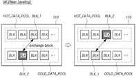
메모리 시스템(100)의 메모리 컨트롤러(120)는 웨어 레벨링 동작 시에 콜드 데이터 풀(COLD_DATA_POOL)에 포함된 메모리 블록 중 하나 이상과 핫 데이터 풀(HOT_DATA_POOL)에 포함된 메모리 블록 중 하나 이상을 서로 교체할 지 여부를 결정할 수 있다.The
핫 데이터 풀(HOT_DATA_POOL)에 데이터가 라이트되는 과정이 반복되면서, 핫 데이터 풀(HOT_DATA_POOL)에 포함된 메모리 블록 중에서 갱신 가능성이 낮은 데이터를 저장한 메모리 블록이 생성될 수 있다. 또한 시간이 지남에 따라 콜드 데이터 풀(COLD_DATA_POOL)에 포함된 메모리 블록 중에서 갱신 가능성이 높은 데이터를 저장한 메모리 블록이 존재할 수도 있다.As the process of writing data to the hot data pool HOT_DATA_POOL is repeated, a memory block storing data having a low update possibility among memory blocks included in the hot data pool HOT_DATA_POOL may be generated. Also, as time goes by, among the memory blocks included in the cold data pool COLD_DATA_POOL, there may be a memory block storing data with a high update possibility.
이러한 경우, 메모리 컨트롤러(120)는 웨어 레벨링 시에 콜드 데이터 풀(COLD_DATA_POOL)에 포함된 메모리 블록 중 하나 이상과 핫 데이터 풀(HOT_DATA_POOL)에 포함된 메모리 블록 중 하나 이상을 서로 교체하여, 갱신 가능성이 높은 데이터는 핫 데이터 풀(HOT_DATA_POOL)에 저장되고 갱신 가능성이 낮은 데이터는 콜드 데이터 풀(COLD_DATA_POOL)에 저장되도록 제어할 수 있다.In this case, the
도 8에서 메모리 컨트롤러(120)는 핫 데이터 풀(HOT_DATA_POOL)에 포함된 메모리 블록(BLK_1)과 콜드 데이터 풀(COLD_DATA_POOL)에 포함된 메모리 블록(BLK_2)를 서로 교체하여, 메모리 블록(BLK_1)은 콜드 데이터 풀(COLD_DATA_POOL)에 포함되고, 메모리 블록(BLK_2)는 핫 데이터 풀(HOT_DATA_POOL)에 포함되도록 제어할 수 있다.In FIG. 8 , the
도 9는 본 발명의 실시예들에 따른 메모리 시스템(100)이 웨어 레벨링 동작 시에 메모리 블록 교체 여부를 결정하는 방법의 일 예를 나타낸 흐름도이다.9 is a flowchart illustrating an example of a method in which the
메모리 시스템(100)의 메모리 컨트롤러(120)는 콜드 데이터 풀(COLD_DATA_POOL)에 포함된 메모리 블록에 대한 소거-쓰기 사이클 카운트의 최대값 A를 탐색할 수 있다(S910).The
메모리 컨트롤러(120)는 콜드 데이터 풀(COLD_DATA_POOL)에 포함된 메모리 블록 중에서 가장 소거-쓰기 사이클 카운트 값이 높은 메모리 블록을 탐색한 후, 탐색된 메모리 블록의 소거-쓰기 사이클 카운트 값을 A로 설정할 수 있다.The
그리고 메모리 시스템(100)의 메모리 컨트롤러(120)는 핫 데이터 풀(HOT_DATA_POOL)에 포함된 메모리 블록에 대한 소거-쓰기 사이클 카운트의 최대값 B를 탐색할 수 있다(S920).In addition, the
메모리 컨트롤러(120)는 핫 데이터 풀(HOT_DATA_POOL)에 포함된 메모리 블록 중에서 가장 소거-쓰기 사이클 카운트 값이 높은 메모리 블록을 탐색한 후, 탐색된 메모리 블록의 소거-쓰기 사이클 카운트 값을 B로 설정할 수 있다.The
한편, 도 9에서는 메모리 컨트롤러(120)가 콜드 데이터 풀(COLD_DATA_POOL)에 포함된 메모리 블록에 대한 소거-쓰기 사이클 카운트의 최대값 A를 핫 데이터 풀(HOT_DATA_POOL)에 포함된 메모리 블록에 대한 소거-쓰기 사이클 카운트의 최대값 B보다 먼저 탐색하는 경우에 대해 설명하였다. 하지만 메모리 컨트롤러(120)는 A와 B를 동시에 탐색할 수도 있고, B를 A보다 먼저 탐색할 수도 있다.Meanwhile, in FIG. 9 , the
메모리 컨트롤러(120)는 S910 단계에서 탐색한 A값과 S920 단계에서 탐색한 B값을 비교하여, B값이 A값보다 큰 지 판단한다(S930). A값과 B값을 비교하는 구체적인 예는 이하 도 10에서 설명한다.The
메모리 컨트롤러(120)는 B값이 A값보다 큰 경우(S930-Y), 즉 핫 데이터 풀(HOT_DATA_POOL)에 포함된 메모리 블록에 대한 소거-쓰기 사이클 카운트의 최대값이 콜드 데이터 풀(COLD_DATA_POOL)에 포함된 메모리 블록에 대한 소거-쓰기 사이클 카운트의 최대값보다 크면, 콜드 데이터 풀(COLD_DATA_POOL)에 포함된 메모리 블록 중 하나 이상과 핫 데이터 풀(HOT_DATA_POOL)에 포함된 메모리 블록 중 하나 이상을 서로 교체할 수 있다(S940). 콜드 데이터 풀(COLD_DATA_POOL)에 포함된 메모리 블록과 핫 데이터 풀(HOT_DATA_POOL)에 포함된 메모리 블록을 교체하는 구체적인 예는 이하 도 11에서 설명한다.When the B value is greater than the A value (S930-Y), that is, the
반면 메모리 컨트롤러(120)는 B값이 A값 이하인 경우(S930-N), 즉 핫 데이터 풀(HOT_DATA_POOL)에 포함된 메모리 블록에 대한 소거-쓰기 사이클 카운트의 최대값이 콜드 데이터 풀(COLD_DATA_POOL)에 포함된 메모리 블록에 대한 소거-쓰기 사이클 카운트의 최대값 이하이면, 콜드 데이터 풀(COLD_DATA_POOL)에 포함된 메모리 블록과 핫 데이터 풀(HOT_DATA_POOL)에 포함된 메모리 블록을 그대로 유지할 수 있다(S950).On the other hand, when the B value is equal to or less than the A value (S930-N), that is, the maximum value of the erase-write cycle count for the memory block included in the hot data pool (HOT_DATA_POOL) is the maximum value of the cold data pool (COLD_DATA_POOL). If it is less than the maximum value of the erase-write cycle count for the included memory block, the memory block included in the cold data pool COLD_DATA_POOL and the memory block included in the hot data pool HOT_DATA_POOL may be maintained ( S950 ).
도 10은 본 발명의 실시예들에 따른 메모리 시스템(100)이 핫 데이터 풀(HOT_DATA_POOL)과 콜드 데이터 풀(COLD_DATA_POOL) 사이의 메모리 블록을 교체하는 조건의 일 예를 나타낸 도면이다.10 is a diagram illustrating an example of a condition in which the
도 10을 참조하면, 핫 데이터 풀(HOT_DATA_POOL)에 포함된 메모리 블록 중 0번 블록의 소거-쓰기 사이클 카운트는 600, 1번 블록의 소거-사이클 카운트는 100, 2번 블록의 소거-쓰기 사이클 카운트는 300, 3번 블록의 소거-사이클 카운트는 550이 된다. 이때, 핫 데이터 풀(HOT_DATA_POOL)에 포함된 메모리 블록에 대한 소거-쓰기 사이클 카운트의 최대값은 0번 블록의 소거-쓰기 사이클 카운트인 600이다. (600 > 550 > 300 > 100)Referring to FIG. 10 , among the memory blocks included in the hot data pool (HOT_DATA_POOL), the erase-write cycle count of
한편 콜드 데이터 풀(COLD_DATA_POOL)에 포함된 메모리 블록 중 100번 블록의 소거-쓰기 사이클 카운트는 150, 101번 블록의 소거-쓰기 사이클 카운트는 100, 102번 블록의 소거-쓰기 사이클 카운트는 130, 103번 블록의 소거-쓰기 사이클 카운트는 599이다. 이때, 콜드 데이터 풀(COLD_DATA_POOL)에 포함된 메모리 블록에 대한 소거-쓰기 사이클 카운트의 최대값은 103번 블록의 소거-쓰기 사이클 카운트인 599이다. (599 > 150 > 130 > 100)Meanwhile, among the memory blocks included in the cold data pool (COLD_DATA_POOL), the erase-write cycle count of
이 경우 핫 데이터 풀(HOT_DATA_POOL)에 포함된 메모리 블록에 대한 소거-쓰기 사이클 카운트의 최대값 600이 콜드 데이터 풀(COLD_DATA_POOL)에 포함된 메모리 블록에 대한 소거-쓰기 사이클 카운트의 최대값 599보다 크기 때문에, 메모리 시스템(100)의 메모리 컨트롤러(120)는 콜드 데이터 풀(COLD_DATA_POOL)에 포함된 메모리 블록 중 하나 이상과 핫 데이터 풀(HOT_DATA_POOL)에 포함된 메모리 블록 중 하나 이상을 교체할 수 있다.In this case, because the maximum value of 600 of the erase-write cycle count for the memory block included in the hot data pool (HOT_DATA_POOL) is greater than the maximum value of 599 of the erase-write cycle count for the memory block included in the cold data pool (COLD_DATA_POOL), , the
이하, 도 11에서는 핫 데이터 풀(HOT_DATA_POOL) 또는 콜드 데이터 풀(COLD_DATA_POOL)에 포함된 메모리 블록 중 어떤 메모리 블록이 교체되는지에 대해 설명한다.Hereinafter, which memory block among the memory blocks included in the hot data pool HOT_DATA_POOL or the cold data pool COLD_DATA_POOL is replaced with reference to FIG. 11 .
도 11은 본 발명의 실시예들에 따른 메모리 시스템(100)이 도 10의 조건에서 핫 데이터 풀(HOT_DATA_POOL)과 콜드 데이터 풀(COLD_DATA_POOL) 사이에서 메모리 블록을 서로 교체하는 동작의 일 예를 나타낸 도면이다.11 is a diagram illustrating an example of an operation in which the
도 11을 참조하면, 메모리 시스템(100)의 메모리 컨트롤러(120)는 콜드 데이터 풀(COLD_DATA_POOL)에 포함된 메모리 블록 중 최소의 소거-쓰기 사이클 카운트를 가지는 메모리 블록과 핫 데이터 풀(HOT_DATA_POOL)에 포함된 메모리 블록 중 최대의 소거-쓰기 사이클 카운트를 가지는 메모리 블록을 서로 교체할 수 있다.Referring to FIG. 11 , the
도 11에서 메모리 컨트롤러(120)는 콜드 데이터 풀(COLD_DATA_POOL)에 포함된 메모리 블록 중 최소의 소거-쓰기 사이클 카운트 100을 가지는 메모리 블록인 101번 메모리 블록과 핫 데이터 풀(HOT_DATA_POOL)에 포함된 메모리 블록 중 최대의 소거-쓰기 사이클 카운트 600을 가지는 0번 메모리 블록을 서로 교체할 수 있다.11 , the
이처럼 101번 메모리 블록과 0번 메모리 블록이 교체되면, 핫 데이터 풀(HOT_DATA_POOL)에 포함된 메모리 블록에 대한 소거-쓰기 사이클 카운트의 최대값은 600에서 550으로 변경된다. 따라서, 핫 데이터 풀(HOT_DATA_POOL)에 포함된 메모리 블록에 대한 소거-쓰기 사이클 카운트의 최대값 550은 콜드 데이터 풀(COLD_DATA_POOL)에 포함된 메모리 블록에 대한 소거-쓰기 사이클 카운트의 최대값 599보다 작아진다. 따라서, 메모리 컨트롤러(120)는 핫 데이터 풀(HOT_DATA_POOL)과 콜드 데이터 풀(COLD_DATA_POOL) 사이에 메모리 블록을 더 이상 교체하지 않는다.As such, when
도 12는 본 발명의 실시예들에 따른 메모리 시스템(100)의 동작 방법을 나타낸 흐름도이다.12 is a flowchart illustrating a method of operating the
메모리 시스템(100)의 동작 방법은 먼저 메모리 장치(110)에 포함된 다수의 메모리 블록 중 하나 이상을 포함하는 핫 데이터 풀(HOT_DATA_POOL)과 콜드 데이터 풀(COLD_DATA_POOL)을 생성하는 단계를 포함할 수 있다(S1210).The method of operating the
그리고 메모리 시스템(100)의 동작 방법은 호스트(HOST)로부터 읽기 전용 라이트 커맨드(RO_WR_CMD)를 수신하는 단계를 포함할 수 있다(S1220). 읽기 전용 라이트 커맨드(RO_WR_CMD)는 읽기 전용 데이터에 대한 라이트 동작을 지시하는 라이트 커맨드이다.In addition, the method of operating the
그리고 메모리 시스템(100)의 동작 방법은 읽기 전용 데이터를 콜드 데이터 풀(COLD_DATA_POOL)에 라이트하는 단계를 포함할 수 있다(S1230).In addition, the method of operating the
콜드 데이터 풀(COLD_DATA_POOL)에 포함된 메모리 블록은 가비지 컬렉션 동작의 대상 블록에서 제외될 수 있다.A memory block included in the cold data pool COLD_DATA_POOL may be excluded from a target block of a garbage collection operation.
한편, 메모리 시스템(100)의 동작 방법은 웨어 레벨링 동작 시에 콜드 데이터 풀(COLD_DATA_POOL)에 포함된 메모리 블록 중 하나 이상과 핫 데이터 풀(HOT_DATA_POOL)에 포함된 메모리 블록 중 하나 이상을 서로 교체할 지 여부를 결정하는 단계를 추가로 포함할 수 있다(S1240).Meanwhile, the operating method of the
S1240 단계에서, 핫 데이터 풀(HOT_DATA_POOL)에 포함된 메모리 블록에 대한 소거-쓰기 사이클 카운트의 최대값이 콜드 데이터 풀(COLD_DATA_POOL)에 포함된 메모리 블록에 대한 소거-쓰기 사이클 카운트의 최대값보다 클 때, 콜드 데이터 풀(COLD_DATA_POOL)에 포함된 메모리 블록 중 하나 이상과 핫 데이터 풀(HOT_DATA_POOL)에 포함된 메모리 블록 중 하나 이상이 서로 교체될 수 있다.In step S1240, when the maximum value of the erase-write cycle count for the memory block included in the hot data pool (HOT_DATA_POOL) is greater than the maximum value of the erase-write cycle count for the memory block included in the cold data pool (COLD_DATA_POOL) , at least one of the memory blocks included in the cold data pool COLD_DATA_POOL and at least one of the memory blocks included in the hot data pool HOT_DATA_POOL may be replaced with each other.
이때, 콜드 데이터 풀(COLD_DATA_POOL)에 포함된 메모리 블록 중 최소의 소거-쓰기 사이클 카운트를 가지는 메모리 블록과 핫 데이터 풀(HOT_DATA_POOL)에 포함된 메모리 블록 중 최대의 소거-쓰기 사이클 카운트를 가지는 메모리 블록이 서로 교체될 수 있다.At this time, the memory block having the minimum erase-write cycle count among the memory blocks included in the cold data pool (COLD_DATA_POOL) and the memory block having the largest erase-write cycle count among the memory blocks included in the hot data pool (HOT_DATA_POOL) can be interchanged with each other.
한편, 이상에서 설명한 메모리 컨트롤러(120)의 동작은 제어 회로(123)에 의해 제어될 수 있으며, 프로세서(124)가 메모리 컨트롤러(120)의 제반 동작이 프로그램된 펌웨어를 실행(구동)하는 방식으로 수행될 수 있다.Meanwhile, the above-described operation of the
도 13은 본 발명의 실시예들에 따른 컴퓨팅 시스템(1300)의 구성도이다.13 is a block diagram of a
도 13을 참조하면, 본 발명의 실시예들에 따른 컴퓨팅 시스템(1300)은 시스템 버스(1360)에 전기적으로 연결되는 메모리 시스템(100), 컴퓨팅 시스템(1300)의 전반적인 동작을 제어하는 중앙처리장치(CPU, 1310), 컴퓨팅 시스템(1300)의 동작과 관련한 데이터 및 정보를 저장하는 램(RAM, 1320), 사용자에게 사용 환경을 제공하기 위한 UI/UX (User Interface/User Experience) 모듈(1330), 외부 장치와 유선 및/또는 무선 방식으로 통신하기 위한 통신 모듈(1340), 컴퓨팅 시스템(1300)이 사용하는 파워를 관리하는 파워 관리 모듈(1350) 등을 포함할 수 있다.Referring to FIG. 13 , a
컴퓨팅 시스템(1300)은 PC(Personal Computer)이거나, 스마트 폰, 태블릿 등의 모바일 단말, 또는 각종 전자 기기 등을 포함할 수 있다.The
컴퓨팅 시스템(1300)은, 동작 전압을 공급하기 위한 배터리를 더 포함할 수 있으며, 응용 칩셋(Application Chipset), 그래픽 관련 모듈, 카메라 이미지 프로세서(Camera Image Processor: CIS), 디램 등을 더 포함할 수도 있다. 이외에도, 이 분야의 통상적인 지식을 습득한 자들에게 자명하다.The
한편, 메모리 시스템(100)은, 하드 디스크 드라이브(HDD: Hard Disk Drive)와 같이 자기 디스크에 데이터를 저장하는 장치뿐 아니라, 솔리드 스테이트 드라이브(SSD: Solid State Drive), UFS(Universal Flash Storage) 장치, eMMC(embedded MMC) 장치 등과 같이 비휘발성 메모리에 데이터를 저장하는 장치 등을 포함할 수 있다. 비휘발성 메모리는 ROM(Read Only Memory), PROM(Programmable ROM), EPROM (Electrically Programmable ROM), EEPROM(Electrically Erasable and Programmable ROM), 플래시 메모리, PRAM(Phase-change RAM), MRAM(Magnetic RAM), RRAM(Resistive RAM), FRAM(Ferroelectric RAM) 등을 포함할 수 있다. 이뿐만 아니라, 메모리 시스템(100)은 다양한 형태의 저장 장치로 구현되어, 다양한 전자 기기 내에 탑재될 수 있다.Meanwhile, the
이상의 설명은 본 발명의 기술 사상을 예시적으로 설명한 것에 불과한 것으로서, 본 발명이 속하는 기술 분야에서 통상의 지식을 가진 자라면 본 발명의 본질적인 특성에서 벗어나지 않는 범위에서 다양한 수정 및 변형이 가능할 것이다. 또한, 본 발명에 개시된 실시예들은 본 발명의 기술 사상을 한정하기 위한 것이 아니라 설명하기 위한 것이므로 이러한 실시예에 의하여 본 발명의 기술 사상의 범위가 한정되는 것은 아니다. 본 발명의 보호 범위는 아래의 청구범위에 의하여 해석되어야 하며, 그와 동등한 범위 내에 있는 모든 기술 사상은 본 발명의 권리 범위에 포함되는 것으로 해석되어야 할 것이다.The above description is merely illustrative of the technical spirit of the present invention, and various modifications and variations will be possible without departing from the essential characteristics of the present invention by those skilled in the art to which the present invention pertains. In addition, the embodiments disclosed in the present invention are not intended to limit the technical spirit of the present invention, but rather to explain, so the scope of the technical spirit of the present invention is not limited by these embodiments. The protection scope of the present invention should be interpreted by the following claims, and all technical ideas within the scope equivalent thereto should be construed as being included in the scope of the present invention.
100: 메모리 시스템110: 메모리 장치
120: 메모리 컨트롤러121: 호스트 인터페이스
122: 메모리 인터페이스123: 제어 회로
124: 프로세서125: 워킹 메모리
126: 에러 검출 및 정정 회로210: 메모리 셀 어레이
220: 어드레스 디코더230: 리드 앤 라이트 회로
240: 제어 로직250: 전압 생성 회로100: memory system 110: memory device
120: memory controller 121: host interface
122: memory interface 123: control circuit
124: processor 125: working memory
126: error detection and correction circuit 210: memory cell array
220: address decoder 230: read and write circuit
240: control logic 250: voltage generation circuit
Claims (17)
Translated fromKorean상기 메모리 장치를 제어하는 메모리 컨트롤러를 포함하고,
상기 메모리 컨트롤러는,
상기 다수의 메모리 블록 중 하나 이상을 포함하는 핫 데이터 풀과 콜드 데이터 풀을 관리하고,
읽기 전용 데이터에 대한 라이트 동작을 지시하는 읽기 전용 라이트 커맨드를 호스트로부터 수신할 때, 상기 읽기 전용 데이터를 상기 콜드 데이터 풀에 라이트하는 메모리 시스템.
a memory device including a plurality of memory blocks; and
a memory controller for controlling the memory device;
The memory controller is
managing a hot data pool and a cold data pool including one or more of the plurality of memory blocks;
A memory system configured to write the read-only data to the cold data pool when a read-only write command instructing a write operation on the read-only data is received from a host.
상기 읽기 전용 데이터는,
멀티미디어 파일, OS 파일 및 라이브러리 파일 중 하나에 대한 데이터인 메모리 시스템.
According to claim 1,
The read-only data is
A memory system that is data for one of multimedia files, OS files, and library files.
상기 읽기 전용 데이터는,
설정된 시구간 동안 설정된 임계 횟수 이하로 갱신된다고 상기 호스트가 판단한 데이터인 메모리 시스템.
According to claim 1,
The read-only data is
A memory system which is data determined by the host to be updated less than or equal to a set threshold number during a set time period.
상기 메모리 컨트롤러는,
상기 콜드 데이터 풀에 포함된 메모리 블록을 가비지 컬렉션 동작의 대상 블록에서 제외하는 메모리 시스템.
According to claim 1,
The memory controller is
A memory system for excluding a memory block included in the cold data pool from a target block of a garbage collection operation.
상기 메모리 컨트롤러는,
웨어 레벨링 동작 시에 상기 콜드 데이터 풀에 포함된 메모리 블록 중 하나 이상과 상기 핫 데이터 풀에 포함된 메모리 블록 중 하나 이상을 서로 교체할지 여부를 결정하는 메모리 시스템.
According to claim 1,
The memory controller is
A memory system that determines whether to replace one or more of the memory blocks included in the cold data pool and one or more of the memory blocks included in the hot data pool during a wear leveling operation.
상기 메모리 컨트롤러는,
상기 핫 데이터 풀에 포함된 메모리 블록에 대한 소거-쓰기 사이클 카운트의 최대값이 상기 콜드 데이터 풀에 포함된 메모리 블록에 대한 소거-쓰기 사이클 카운트의 최대값보다 클 때, 상기 콜드 데이터 풀에 포함된 메모리 블록 중 하나 이상과 상기 핫 데이터 풀에 포함된 메모리 블록 중 하나 이상을 서로 교체하는 메모리 시스템.
6. The method of claim 5,
The memory controller is
When the maximum value of the erase-write cycle count for the memory block included in the hot data pool is greater than the maximum value of the erase-write cycle count for the memory block included in the cold data pool, A memory system for exchanging at least one of the memory blocks and at least one of the memory blocks included in the hot data pool.
상기 메모리 컨트롤러는,
상기 콜드 데이터 풀에 포함된 메모리 블록 중 최소의 소거-쓰기 사이클 카운트를 가지는 메모리 블록과 상기 핫 데이터 풀에 포함된 메모리 블록 중 최대의 소거-쓰기 사이클 카운트를 가지는 메모리 블록을 서로 교체하는 메모리 시스템.
7. The method of claim 6,
The memory controller is
A memory system in which a memory block having a minimum erase-write cycle count among memory blocks included in the cold data pool and a memory block having a maximum erase-write cycle count among memory blocks included in the hot data pool are exchanged with each other.
상기 메모리 장치를 제어하기 위한 제어 회로를 포함하고,
상기 제어 회로는,
상기 다수의 메모리 블록 중 하나 이상을 포함하는 핫 데이터 풀과 콜드 데이터 풀을 관리하고,
읽기 전용 데이터에 대한 라이트 동작을 지시하는 읽기 전용 라이트 커맨드를 호스트로부터 수신할 때, 상기 읽기 전용 데이터를 상기 콜드 데이터 풀에 라이트하는 메모리 컨트롤러.
a memory interface for communicating with a memory device comprising a plurality of memory blocks; and
a control circuit for controlling the memory device;
The control circuit is
managing a hot data pool and a cold data pool including one or more of the plurality of memory blocks;
A memory controller configured to write the read-only data to the cold data pool when a read-only write command instructing a write operation on the read-only data is received from the host.
상기 제어 회로는,
상기 콜드 데이터 풀에 포함된 메모리 블록을 가비지 컬렉션 동작의 대상 블록에서 제외하는 메모리 컨트롤러.
9. The method of claim 8,
The control circuit is
A memory controller that excludes a memory block included in the cold data pool from a target block of a garbage collection operation.
상기 제어 회로는,
웨어 레벨링 동작 시에 상기 콜드 데이터 풀에 포함된 메모리 블록 중 하나 이상과 상기 핫 데이터 풀에 포함된 메모리 블록 중 하나 이상을 서로 교체할지 여부를 결정하는 메모리 컨트롤러.
9. The method of claim 8,
The control circuit is
A memory controller configured to determine whether to replace one or more of the memory blocks included in the cold data pool and one or more of the memory blocks included in the hot data pool during a wear leveling operation.
상기 제어 회로는,
상기 핫 데이터 풀에 포함된 메모리 블록에 대한 소거-쓰기 사이클 카운트의 최대값이 상기 콜드 데이터 풀에 포함된 메모리 블록에 대한 소거-쓰기 사이클 카운트의 최대값보다 클 때, 상기 콜드 데이터 풀에 포함된 메모리 블록 중 하나 이상과 상기 핫 데이터 풀에 포함된 메모리 블록 중 하나 이상을 서로 교체하는 메모리 컨트롤러.
11. The method of claim 10,
The control circuit is
When the maximum value of the erase-write cycle count for the memory block included in the hot data pool is greater than the maximum value of the erase-write cycle count for the memory block included in the cold data pool, A memory controller for exchanging at least one of the memory blocks and at least one of the memory blocks included in the hot data pool.
상기 제어 회로는,
상기 콜드 데이터 풀에 포함된 메모리 블록 중 최소의 소거-쓰기 사이클 카운트를 가지는 메모리 블록과 상기 핫 데이터 풀에 포함된 메모리 블록 중 최대의 소거-쓰기 사이클 카운트를 가지는 메모리 블록을 서로 교체하는 메모리 컨트롤러.
12. The method of claim 11,
The control circuit is
A memory controller for replacing a memory block having a minimum erase-write cycle count among memory blocks included in the cold data pool and a memory block having a maximum erase-write cycle count among memory blocks included in the hot data pool.
읽기 전용 데이터에 대한 라이트 동작을 지시하는 읽기 전용 라이트 커맨드를 호스트로부터 수신하는 단계; 및
상기 읽기 전용 데이터를 상기 콜드 데이터 풀에 라이트하는 단계를 포함하는 메모리 시스템의 동작 방법.
generating a hot data pool and a cold data pool including one or more of a plurality of memory blocks included in a memory device;
receiving a read-only write command instructing a write operation on read-only data from a host; and
and writing the read-only data to the cold data pool.
상기 콜드 데이터 풀에 포함된 메모리 블록은 가비지 컬렉션 동작의 대상 블록에서 제외되는 메모리 시스템의 동작 방법.
14. The method of claim 13,
A method of operating a memory system wherein a memory block included in the cold data pool is excluded from a target block of a garbage collection operation.
웨어 레벨링 동작 시에 상기 콜드 데이터 풀에 포함된 메모리 블록 중 하나 이상과 상기 핫 데이터 풀에 포함된 메모리 블록 중 하나 이상을 서로 교체할지 여부를 결정하는 단계를 추가로 포함하는 메모리 시스템의 동작 방법.
14. The method of claim 13,
The method of operating a memory system, further comprising: determining whether to replace one or more of the memory blocks included in the cold data pool and one or more of the memory blocks included in the hot data pool during a wear leveling operation.
상기 핫 데이터 풀에 포함된 메모리 블록에 대한 소거-쓰기 사이클 카운트의 최대값이 상기 콜드 데이터 풀에 포함된 메모리 블록에 대한 소거-쓰기 사이클 카운트의 최대값보다 클 때, 상기 콜드 데이터 풀에 포함된 메모리 블록 중 하나 이상과 상기 핫 데이터 풀에 포함된 메모리 블록 중 하나 이상이 서로 교체되는 메모리 시스템의 동작 방법.
16. The method of claim 15,
When the maximum value of the erase-write cycle count for the memory block included in the hot data pool is greater than the maximum value of the erase-write cycle count for the memory block included in the cold data pool, An operating method of a memory system in which at least one of the memory blocks and at least one of the memory blocks included in the hot data pool are replaced with each other.
상기 콜드 데이터 풀에 포함된 메모리 블록 중 최소의 소거-쓰기 사이클 카운트를 가지는 메모리 블록과 상기 핫 데이터 풀에 포함된 메모리 블록 중 최대의 소거-쓰기 사이클 카운트를 가지는 메모리 블록이 서로 교체되는 메모리 시스템의 동작 방법.17. The method of claim 16,
A memory system in which a memory block having a minimum erase-write cycle count among memory blocks included in the cold data pool and a memory block having a maximum erase-write cycle count among memory blocks included in the hot data pool are replaced with each other how it works.
Priority Applications (3)
| Application Number | Priority Date | Filing Date | Title |
|---|---|---|---|
| KR1020200010942AKR20210097353A (en) | 2020-01-30 | 2020-01-30 | Memory system, memory controller, and operating method of memory system |
| US16/904,178US11301174B2 (en) | 2020-01-30 | 2020-06-17 | Memory system, memory controller and method for operating memory system |
| CN202010759101.2ACN113204312A (en) | 2020-01-30 | 2020-07-31 | Memory system, memory controller and operation method of memory system |
Applications Claiming Priority (1)
| Application Number | Priority Date | Filing Date | Title |
|---|---|---|---|
| KR1020200010942AKR20210097353A (en) | 2020-01-30 | 2020-01-30 | Memory system, memory controller, and operating method of memory system |
Publications (1)
| Publication Number | Publication Date |
|---|---|
| KR20210097353Atrue KR20210097353A (en) | 2021-08-09 |
Family
ID=77025015
Family Applications (1)
| Application Number | Title | Priority Date | Filing Date |
|---|---|---|---|
| KR1020200010942ACeasedKR20210097353A (en) | 2020-01-30 | 2020-01-30 | Memory system, memory controller, and operating method of memory system |
Country Status (3)
| Country | Link |
|---|---|
| US (1) | US11301174B2 (en) |
| KR (1) | KR20210097353A (en) |
| CN (1) | CN113204312A (en) |
Families Citing this family (4)
| Publication number | Priority date | Publication date | Assignee | Title |
|---|---|---|---|---|
| US11481134B1 (en)* | 2021-05-24 | 2022-10-25 | Sap Se | Adaptive caching for hybrid columnar databases with heterogeneous page sizes |
| US11960753B2 (en)* | 2021-08-25 | 2024-04-16 | Western Digital Technologies, Inc. | Solution for super device imbalance in ZNS SSD |
| US11966618B2 (en)* | 2021-08-25 | 2024-04-23 | Western Digital Technologies, Inc. | Purposeful super device imbalance for ZNS SSD efficiency |
| JP2023044330A (en)* | 2021-09-17 | 2023-03-30 | キオクシア株式会社 | Memory system and control method |
Family Cites Families (8)
| Publication number | Priority date | Publication date | Assignee | Title |
|---|---|---|---|---|
| JP2011128792A (en)* | 2009-12-16 | 2011-06-30 | Toshiba Corp | Memory management device |
| US9146875B1 (en)* | 2010-08-09 | 2015-09-29 | Western Digital Technologies, Inc. | Hybrid drive converting non-volatile semiconductor memory to read only based on life remaining |
| KR101795629B1 (en) | 2011-02-15 | 2017-11-13 | 삼성전자주식회사 | Method for managing file system in host and devices using the method |
| JP2014522066A (en)* | 2011-08-09 | 2014-08-28 | エルエスアイ コーポレーション | Interoperation of I/O devices with computing hosts |
| US10552085B1 (en)* | 2014-09-09 | 2020-02-04 | Radian Memory Systems, Inc. | Techniques for directed data migration |
| JP6403162B2 (en)* | 2015-07-23 | 2018-10-10 | 東芝メモリ株式会社 | Memory system |
| KR102514388B1 (en) | 2016-03-25 | 2023-03-28 | 에스케이하이닉스 주식회사 | Memory system and operating method of memory system |
| US10248333B1 (en)* | 2017-02-07 | 2019-04-02 | Crossbar, Inc. | Write distribution techniques for two-terminal memory wear leveling |
- 2020
- 2020-01-30KRKR1020200010942Apatent/KR20210097353A/ennot_activeCeased
- 2020-06-17USUS16/904,178patent/US11301174B2/enactiveActive
- 2020-07-31CNCN202010759101.2Apatent/CN113204312A/ennot_activeWithdrawn
Also Published As
| Publication number | Publication date |
|---|---|
| CN113204312A (en) | 2021-08-03 |
| US11301174B2 (en) | 2022-04-12 |
| US20210240390A1 (en) | 2021-08-05 |
Similar Documents
| Publication | Publication Date | Title |
|---|---|---|
| KR20220005111A (en) | Memory system, memory controller, and operating method of memory system | |
| US11301174B2 (en) | Memory system, memory controller and method for operating memory system | |
| KR20210065356A (en) | Memory system, memory controller, and operating method thereof | |
| KR20210026431A (en) | Memory system, memory controller, and operating method | |
| KR20220079264A (en) | Memory system and operating method of memory system | |
| KR20230031425A (en) | Memory system and operating method of memory system | |
| US12072809B2 (en) | Memory system, memory controller, and operation method of memory system for loading and updating mapping information to host memory area | |
| CN114530173A (en) | Memory system and operating method thereof | |
| KR102838945B1 (en) | Memory system, memory controller, and operating method thereof | |
| KR20210152706A (en) | Memory device, memory system, and operating method of memory device | |
| KR20210155055A (en) | Memory system, memory controller, and operating method of memory system | |
| KR20210079549A (en) | Memory system, memory controller, and operating method thereof | |
| KR20230072196A (en) | Memory system and operating method of memory system | |
| KR102789969B1 (en) | Memory system, memory device, and operating method of memory device | |
| KR20220049109A (en) | Memory system and operating method of memory system | |
| KR20220025405A (en) | Memory system, memory controller, and operating method of memory system | |
| US11704050B2 (en) | Memory system for determining a memory area in which a journal is stored according to a number of free memory blocks | |
| KR102771648B1 (en) | Memory system and operating method of memory system | |
| US11507509B2 (en) | Memory system, memory controller and method for operating memory system for determining whether to perform direct write based on reference write size | |
| US11137942B2 (en) | Memory system, memory controller, and method of operating a memory system for determining a number of hit and miss requests about map segments in a map cache and determining whether or not to perform data read operation in parallel | |
| KR20230135334A (en) | Memory system, memory controller and operating method thereof for controlling garbage collection | |
| KR20230049858A (en) | Memory controller and operating method of memory controller | |
| KR20230094588A (en) | Memory system managing data corresponding to multiple zones and operating method thereof | |
| KR20220101264A (en) | Memory system and operating method of memory system | |
| KR20220142660A (en) | Memory system and operating method of memory system |
Legal Events
| Date | Code | Title | Description |
|---|---|---|---|
| PA0109 | Patent application | Patent event code:PA01091R01D Comment text:Patent Application Patent event date:20200130 | |
| PG1501 | Laying open of application | ||
| A201 | Request for examination | ||
| PA0201 | Request for examination | Patent event code:PA02012R01D Patent event date:20221220 Comment text:Request for Examination of Application Patent event code:PA02011R01I Patent event date:20200130 Comment text:Patent Application | |
| E902 | Notification of reason for refusal | ||
| PE0902 | Notice of grounds for rejection | Comment text:Notification of reason for refusal Patent event date:20240522 Patent event code:PE09021S01D | |
| E601 | Decision to refuse application | ||
| PE0601 | Decision on rejection of patent | Patent event date:20241014 Comment text:Decision to Refuse Application Patent event code:PE06012S01D | |
| PX0601 | Decision of rejection after re-examination | Comment text:Decision to Refuse Application Patent event code:PX06014S01D Patent event date:20250210 Comment text:Decision to Refuse Application Patent event code:PX06011S01I Patent event date:20250210 | |
| X601 | Decision of rejection after re-examination | ||
| J201 | Request for trial against refusal decision | ||
| PJ0201 | Trial against decision of rejection | Patent event date:20250508 Comment text:Request for Trial against Decision on Refusal Patent event code:PJ02012R01D Appeal kind category:Appeal against decision to decline refusal Appeal identifier:2025101000822 Request date:20250508 |