KR20210096957A - Force sensing device with a common noise reduction and electrical device - Google Patents
Force sensing device with a common noise reduction and electrical deviceDownload PDFInfo
- Publication number
- KR20210096957A KR20210096957AKR1020200010666AKR20200010666AKR20210096957AKR 20210096957 AKR20210096957 AKR 20210096957AKR 1020200010666 AKR1020200010666 AKR 1020200010666AKR 20200010666 AKR20200010666 AKR 20200010666AKR 20210096957 AKR20210096957 AKR 20210096957A
- Authority
- KR
- South Korea
- Prior art keywords
- force
- force member
- count value
- inductor element
- oscillation signal
- Prior art date
- Legal status (The legal status is an assumption and is not a legal conclusion. Google has not performed a legal analysis and makes no representation as to the accuracy of the status listed.)
- Ceased
Links
Images


Classifications
- G—PHYSICS
- G01—MEASURING; TESTING
- G01L—MEASURING FORCE, STRESS, TORQUE, WORK, MECHANICAL POWER, MECHANICAL EFFICIENCY, OR FLUID PRESSURE
- G01L1/00—Measuring force or stress, in general
- G01L1/14—Measuring force or stress, in general by measuring variations in capacitance or inductance of electrical elements, e.g. by measuring variations of frequency of electrical oscillators
- G—PHYSICS
- G06—COMPUTING OR CALCULATING; COUNTING
- G06F—ELECTRIC DIGITAL DATA PROCESSING
- G06F3/00—Input arrangements for transferring data to be processed into a form capable of being handled by the computer; Output arrangements for transferring data from processing unit to output unit, e.g. interface arrangements
- G06F3/01—Input arrangements or combined input and output arrangements for interaction between user and computer
- G06F3/03—Arrangements for converting the position or the displacement of a member into a coded form
- G06F3/041—Digitisers, e.g. for touch screens or touch pads, characterised by the transducing means
- G06F3/0414—Digitisers, e.g. for touch screens or touch pads, characterised by the transducing means using force sensing means to determine a position
- G—PHYSICS
- G06—COMPUTING OR CALCULATING; COUNTING
- G06F—ELECTRIC DIGITAL DATA PROCESSING
- G06F3/00—Input arrangements for transferring data to be processed into a form capable of being handled by the computer; Output arrangements for transferring data from processing unit to output unit, e.g. interface arrangements
- G06F3/01—Input arrangements or combined input and output arrangements for interaction between user and computer
- G06F3/03—Arrangements for converting the position or the displacement of a member into a coded form
- G06F3/041—Digitisers, e.g. for touch screens or touch pads, characterised by the transducing means
- G06F3/0416—Control or interface arrangements specially adapted for digitisers
- G06F3/0418—Control or interface arrangements specially adapted for digitisers for error correction or compensation, e.g. based on parallax, calibration or alignment
- G06F3/04182—Filtering of noise external to the device and not generated by digitiser components
- G—PHYSICS
- G06—COMPUTING OR CALCULATING; COUNTING
- G06F—ELECTRIC DIGITAL DATA PROCESSING
- G06F3/00—Input arrangements for transferring data to be processed into a form capable of being handled by the computer; Output arrangements for transferring data from processing unit to output unit, e.g. interface arrangements
- G06F3/01—Input arrangements or combined input and output arrangements for interaction between user and computer
- G06F3/03—Arrangements for converting the position or the displacement of a member into a coded form
- G06F3/041—Digitisers, e.g. for touch screens or touch pads, characterised by the transducing means
- G06F3/044—Digitisers, e.g. for touch screens or touch pads, characterised by the transducing means by capacitive means
- G—PHYSICS
- G06—COMPUTING OR CALCULATING; COUNTING
- G06F—ELECTRIC DIGITAL DATA PROCESSING
- G06F3/00—Input arrangements for transferring data to be processed into a form capable of being handled by the computer; Output arrangements for transferring data from processing unit to output unit, e.g. interface arrangements
- G06F3/01—Input arrangements or combined input and output arrangements for interaction between user and computer
- G06F3/03—Arrangements for converting the position or the displacement of a member into a coded form
- G06F3/041—Digitisers, e.g. for touch screens or touch pads, characterised by the transducing means
- G06F3/046—Digitisers, e.g. for touch screens or touch pads, characterised by the transducing means by electromagnetic means
- G—PHYSICS
- G06—COMPUTING OR CALCULATING; COUNTING
- G06F—ELECTRIC DIGITAL DATA PROCESSING
- G06F2203/00—Indexing scheme relating to G06F3/00 - G06F3/048
- G06F2203/041—Indexing scheme relating to G06F3/041 - G06F3/045
- G06F2203/04105—Pressure sensors for measuring the pressure or force exerted on the touch surface without providing the touch position
Landscapes
- Engineering & Computer Science (AREA)
- General Engineering & Computer Science (AREA)
- Theoretical Computer Science (AREA)
- Physics & Mathematics (AREA)
- General Physics & Mathematics (AREA)
- Human Computer Interaction (AREA)
- Electromagnetism (AREA)
- Force Measurement Appropriate To Specific Purposes (AREA)
Abstract
Translated fromKoreanDescription
Translated fromKorean본 발명은 공통잡음 저감기능을 갖는 포스 센싱 장치 및 전기 기기에 관한 것이다.The present invention relates to a force sensing device and an electric device having a common noise reduction function.
일반적으로, 웨어러블 기기는 좀더 얇고 심플하면서 깔끔한 디자인이 선호되고 있으며 이에 따라 기존 기계식 스위치가 사라지고 있다. 이는 방진, 방수 기술의 구현이 이루어짐과 더불어, 매끄러운 디자인의 일체감 있는 모델의 개발이 이루어짐에 따라 가능해지고 있다.In general, thinner, simpler, and cleaner designs are preferred for wearable devices, and the existing mechanical switches are disappearing accordingly. This is becoming possible with the implementation of dustproof and waterproof technology and the development of a model with a sense of unity with a smooth design.
현재 메탈 위를 터치하는 ToM(touch On Metal) 기술, 터치 패널을 이용한 커패시터 센싱 기법, MEMS(Micro-Electro-Mechanical-System), 마이크로 스트레인 게이지(Micro Strain Gauge) 등의 기술이 개발되고 있으며 이에 더 나아가 포스 터치기능까지 개발되는 추세이다.Currently, ToM (touch on metal) technology that touches metal, capacitor sensing method using a touch panel, MEMS (Micro-Electro-Mechanical-System), and micro strain gauge are being developed. Furthermore, the force touch function is also being developed.
기존의 기계식 스위치의 경우, 스위치 기능 구현을 위해, 내부적으로 큰 사이즈와 공간이 필요하고, 외관상으로도 외부로 튀어나오는 형태나 외부 케이스와 일체화가 아닌 구조 등으로 인하여 깔끔하지 못한 디자인과 큰 공간이 필요하다는 단점이 있다.In the case of the existing mechanical switch, a large size and space are required internally to realize the switch function, and due to the externally protruding shape or structure that is not integrated with the external case, it has an untidy design and a large space. The downside is that you need it.
또한 전기적으로 연결되는 기계식 스위치의 직접적인 접촉으로 인한 감전의 위험이 있으며, 특히 기계적 스위치의 구조상 방진 방수가 곤란하다는 단점이 있다.In addition, there is a risk of electric shock due to direct contact of the electrically connected mechanical switch, and in particular, there is a disadvantage in that it is difficult to waterproof and dust due to the structure of the mechanical switch.
그리고, 기존의 스위치 장치에서는, 외부 환경적인 요소에 의해서 잡음이나 간섭이 발생할 수 있으며, 이러한 잡음이나 간섭에 대한 해결책이 필요하다.And, in the existing switch device, noise or interference may occur due to external environmental factors, and a solution to such noise or interference is required.
(선행기술문헌)(Prior art literature)
(특허문헌 1) KR 10-2002-0077836 (2002.10.14)(Patent Document 1) KR 10-2002-0077836 (2002.110.14)
(특허문헌 2) KR 10-2009-0120709 (2009.11.25)(Patent Document 2) KR 10-2009-0120709 (2009.11.25)
(특허문헌 3) KR 10-2011-0087014 (2011.08.02)(Patent Document 3) KR 10-2011-0087014 (2011.08.02)
(특허문헌 4) KR 10-2011-0087004 (2011.08.02)(Patent Document 4) KR 10-2011-0087004 (2011.08.02)
(특허문헌 5) KR 10-2018-0046833 (2018.05.09)(Patent Document 5) KR 10-2018-0046833 (2018.05.09)
(특허문헌 6) US 2018-0093695 (2018.04.05)(Patent Document 6) US 2018-0093695 (2018.04.05)
(특허문헌 7) JP 2012-168747 (2012.09.06)(Patent Document 7) JP 2012-168747 (2012.09.06)
(특허문헌 8) JP 2015-095865 (2015.05.18)(Patent Document 8) JP 2015-095865 (2015.05.18)
본 발명의 일 실시 예는, 2개의 포스부재를 포함하는 포스 센싱 장치에서, 2개의 포스부재중 어느 하나의 포스부재에 힘을 인가하는 경우, 힘이 인가된 포스부재에 의한 신호의 주파수가 힘이 인가되지 않은 포스부재에 의한 신호의 주파수와는 서로 반대 방향으로 변하도록 함으로써, 포스 센싱을 보다 정확하게 수행할 수 있는 포스 센싱 장치 및 전기 기기를 제안한다.In an embodiment of the present invention, in a force sensing device including two force members, when a force is applied to any one of the two force members, the frequency of the signal by the force member to which the force is applied is the force A force sensing device and an electric device capable of more accurately performing force sensing by changing the frequency of a signal by an unapplied force member in opposite directions are proposed.
본 발명의 일 실시 예에 의해, 전도성의 하우징에 형성된 제1 포스부재 및 제2 포스부재를 갖는 포스 스위치부를 포함하는 전기 기기에 적용될 수 있는 포스 센싱 장치에 있어서, 상기 하우징의 내측에 배치되고, 상기 제1 포스부재 및 상기 제2 포스부재의 내측면과 이격된 기판; 상기 기판의 일면에 실장되고, 상기 제1 포스부재에 대향하여 이격되며, 상기 제1 포스부재를 누르는 포스입력시 가변되는 인덕턴스를 갖는 제1 인덕터 소자; 상기 기판의 일면에 실장되고, 상기 제2 포스부재에 대향하여 이격되며, 상기 제2 포스부재를 누르는 포스입력시 가변되는 인덕턴스를 갖는 제2 인덕터 소자; 및 상기 제1 인덕터 소자와 상기 제2 인덕터 소자 사이의 상기 기판의 일면에 부착된 일단과, 상기 제1 포스부재와 상기 제2 포스부재 사이의 하우징의 내측면에 부착된 타단을 갖는 지지 부재; 를 포함하는 포스 센싱 장치가 제안된다.According to an embodiment of the present invention, in a force sensing device applicable to an electric device including a force switch unit having a first force member and a second force member formed in a conductive housing, it is disposed inside the housing, a substrate spaced apart from the inner surface of the first force member and the second force member; a first inductor element mounted on one surface of the substrate, spaced apart from the first force member, and having an inductance variable when a force input is applied to press the first force member; a second inductor element mounted on one surface of the substrate, spaced apart from the second force member, and having an inductance that varies when a force input for pressing the second force member; and a support member having one end attached to one surface of the substrate between the first inductor element and the second inductor element, and the other end attached to the inner surface of the housing between the first force member and the second force member; A force sensing device comprising a is proposed.
또한, 본 발명의 다른 일 실시 예에 의해, 전도성의 하우징; 상기 하우징에 형성된 제1 포스부재 및 제2 포스부재를 갖는 포스 스위치부; 상기 하우징의 내측에 배치되고, 상기 제1 포스부재 및 상기 제2 포스부재의 내측면과 이격된 기판; 상기 기판의 일면에 실장되고, 상기 제1 포스부재에 대향하여 이격되며, 상기 제1 포스부재를 누르는 포스입력시 가변되는 인덕턴스를 갖는 제1 인덕터 소자; 상기 기판의 일면에 실장되고, 상기 제2 포스부재에 대향하여 이격되며, 상기 제2 포스부재를 누르는 포스입력시 가변되는 인덕턴스를 갖는 제2 인덕터 소자; 및 상기 제1 인덕터 소자와 상기 제2 인덕터 소자 사이의 상기 기판의 일면에 부착된 일단과, 상기 제1 포스부재와 상기 제2 포스부재 사이의 하우징의 내측면에 부착된 타단을 갖는 지지 부재; 를 포함하는 전기 기기가 제안된다.In addition, according to another embodiment of the present invention, a conductive housing; a force switch unit having a first force member and a second force member formed in the housing; a substrate disposed inside the housing and spaced apart from inner surfaces of the first and second force members; a first inductor element mounted on one surface of the substrate, spaced apart from the first force member, and having an inductance variable when a force input is applied to press the first force member; a second inductor element mounted on one surface of the substrate, spaced apart from the second force member, and having an inductance that varies when a force input for pressing the second force member; and a support member having one end attached to one surface of the substrate between the first inductor element and the second inductor element, and the other end attached to the inner surface of the housing between the first force member and the second force member; An electric device comprising a is proposed.
본 발명의 일 실시 예에 의하면, 2개의 포스부재를 포함하는 포스 센싱 장치에서, 2개의 포스부재중 어느 하나의 포스부재에 힘을 인가하는 경우, 힘이 인가된 포스부재에 의한 공진 주파수가 힘이 인가되지 않은 포스부재에 의한 공진 주파수와는 서로 반대 방향으로 변하도록 함으로써, 포스 센싱 식별력이 개선될 수 있고, 이에 따라 포스 센싱을 보다 정확하게 수행할 수 있다.According to an embodiment of the present invention, in a force sensing device including two force members, when a force is applied to any one of the two force members, the resonance frequency of the force member to which the force is applied is the force. By changing the resonant frequency of the unapplied force member in the opposite direction to each other, the force sensing discrimination power can be improved, and thus the force sensing can be performed more accurately.
도 1은 본 발명의 일 실시 예에 따른 전기 기기의 외관 예시도이다.
도 2는 도 1의 I-I'선 단면구조를 갖는 전기 기기 및 포스 센싱 장치의 예시도이다.
도 3은 도 2의 제1 포스부재에 포스인가시 이격 간격 설명도이다.
도4는 도 2의 제1 포스부재에 포스인가시 이격 간격 설명도이다.
도 5는 발진회로 및 검출회로 예시도이다.
도 6은 발진회로의 내부 회로 예시도이다.
도 7은 검출회로의 내부 구성 예시도이다.
도 8은 도 7의 제1 주파수-디지털 컨버터의 일 예시도이다.
도 9는 도 7의 제2 주파수-디지털 컨버터의 일 예시도이다.도 10은 제1 포스부재에 포스인가시 제1 카운트값 및 제2 카운트값의 그래프이다.
도 11은 제2 포스부재에 포스인가시 제1 카운트값 및 제2 카운트값의 그래프이다.
도 12는 제1 포스부재에 포스인가시 제1 카운트값 및 제2 카운트값의 차분값(Diff)에 대한 그래프이다.
도 13은 제2 포스부재에 포스인가시 제1 카운트값 및 제2 카운트값의 차분값(Diff)에 대한 그래프이다.
도 14는 도 7의 포스 검출 회로의 내부 회로 예시도이다.1 is an external view of an electric device according to an embodiment of the present invention.
FIG. 2 is an exemplary view of an electric device and a force sensing device having a cross-sectional structure taken along line I-I' of FIG. 1 .
FIG. 3 is an explanatory diagram illustrating a separation interval when a force is applied to the first force member of FIG. 2 .
FIG. 4 is an explanatory diagram illustrating a separation interval when a force is applied to the first force member of FIG. 2 .
5 is an exemplary diagram of an oscillation circuit and a detection circuit.
6 is an exemplary internal circuit diagram of the oscillation circuit.
7 is an exemplary diagram of an internal configuration of a detection circuit.
FIG. 8 is an exemplary diagram of the first frequency-digital converter of FIG. 7 .
9 is an exemplary view of the second frequency-digital converter of FIG. 7. FIG. 10 is a graph of a first count value and a second count value when a force is applied to the first force member.
11 is a graph of a first count value and a second count value when a force is applied to the second force member.
12 is a graph of a difference (Diff) between a first count value and a second count value when a force is applied to the first force member.
13 is a graph of a difference (Diff) between a first count value and a second count value when a force is applied to the second force member.
14 is an exemplary internal circuit diagram of the force detection circuit of FIG. 7 .
이하에서는, 본 발명은 설명되는 실시 예에 한정되지 않으며, 본 발명의 정신 및 범위를 벗어나지 않으면서 다양하게 변경될 수 있음이 이해되어야 한다.Hereinafter, it should be understood that the present invention is not limited to the described embodiments, and various modifications may be made without departing from the spirit and scope of the present invention.
또한, 본 발명의 각 실시 예에 있어서, 하나의 예로써 설명되는 구조, 형상 및 수치는 본 발명의 기술적 사항의 이해를 돕기 위한 예에 불과하므로, 이에 한정되는 것이 아니라 본 발명의 정신 및 범위를 벗어나지 않으면서 다양하게 변경될 수 있음이 이해되어야 한다. 본 발명의 실시 예들은 서로 조합되어 여러 가지 새로운 실시 예가 이루어질 수 있다.In addition, in each embodiment of the present invention, the structure, shape, and numerical value described as an example are only examples for helping the understanding of the technical matters of the present invention, and thus the spirit and scope of the present invention are not limited thereto. It should be understood that various changes may be made without departing from it. The embodiments of the present invention may be combined with each other to form various new embodiments.
그리고, 본 발명에 참조된 도면에서 본 발명의 전반적인 내용에 비추어 실질적으로 동일한 구성과 기능을 가진 구성요소들은 동일한 부호를 사용할 것이다.In addition, in the drawings referenced in the present invention, components having substantially the same configuration and function will be denoted by the same reference numerals in light of the overall content of the present invention.
이하에서는, 본 발명이 속하는 기술분야에서 통상의 지식을 가진 자가 본 발명을 용이하게 실시할 수 있도록 하기 위해서, 본 발명의 실시 예를 첨부한 도면을 참조하여 상세히 설명한다.Hereinafter, embodiments of the present invention will be described in detail with reference to the accompanying drawings in order to enable those of ordinary skill in the art to easily practice the present invention.
도 1은 본 발명의 일 실시 예에 따른 전기 기기의 외관 예시도이다.1 is an external view of an electric device according to an embodiment of the present invention.
도 1을 참조하면, 본 발명의 일 실시 예에 따른 전기 기기(10)는 터치 스크린(11), 하우징(500) 및 포스 스위치부(FSW)를 포함할 수 있다.Referring to FIG. 1 , an
상기 포스 스위치부(FSW)는 기계식 버튼을 대체하기 위한 제1 포스부재(FM1) 및 제2 포스부재(FM2)를 포함할 수 있다.The force switch unit FSW may include a first force member FM1 and a second force member FM2 for replacing the mechanical button.
예를 들어, 도 1을 참조하면 상기 전기 기기(10)는 스마트폰 등과 같이, 휴대 가능한 기기가 될 수 있고, 스마트 와치(Watch)와 같이, 웨어러블 기기가 될 수 있으며, 특정한 기기에 한정되지 않고, 휴대 가능하거나 착용 가능한 전기 기기, 또는 동작 제어를 위한 스위치를 갖는 전기 기기가 될 수 있다.For example, referring to FIG. 1 , the
상기 하우징(500)은, 전기 기기(10)의 외부에 노출되는 외측 케이스가 될 수 있다. 일 예로, 상기 포스 센싱 장치가 모바일 기기에 적용되는 경우, 하우징(500)은 모바일 기기의 사이드(측면)에 배치되는 커버일 수 있다. 일 예로, 상기 하우징(500)은 전기 기기(10)의 후면에 배치되는 커버와 일체로 이루어질 수 있거나, 전기 기기(10)의 후면에 배치되는 커버와 별도로 분리되어 이루어질 수 있다.The
상기 포스 스위치부(FSW)는, 힘이 가해지는 포스(Force)를 센싱하기 위해 적어도 2개의 제1 포스부재(FM1) 및 제2 포스부재(FM2)를 포함하여, 상기 전기 기기의 하우징(500)과 일체로 이루어질 수 있다. 도 1을 참조하면, 상기 포스 스위치부(FSW)는 전기 기기(10)의 커버에 배치될 수 있는데, 이 경우 커버는 터치 스크린을 제외한 커버, 예를 들면, 사이드 커버나, 후면 커버나, 전면의 일부에 형성될 수 있는 커버 등이 될 수 있으며, 설명의 편의상 하우징의 일 예시로, 전기 기기(10)의 사이드 커버에 배치된 경우에 대해 설명하지만, 이에 한정되는 것은 아니다.The force switch unit FSW includes at least two first force members FM1 and second force members FM2 to sense a force applied thereto, the
본 발명의 각 도면에 대해, 동일한 부호 및 동일한 기능의 구성요소에 대해서는 가능한 불필요한 중복 설명은 생략될 수 있고, 각 도면에 대해 가능한 차이점에 대한 사항이 설명될 수 있다.For each drawing of the present invention, unnecessary redundant descriptions of the same reference numerals and components having the same function may be omitted, and possible differences may be described for each drawing.
도 2는 도 1의 I-I'선 단면구조를 갖는 전기 기기 및 포스 센싱 장치의 예시도이다.FIG. 2 is an exemplary view of an electric device and a force sensing device having a cross-sectional structure taken along line I-I' of FIG. 1 .
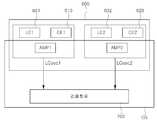
도 1 및 도 2를 참조하면, 상기 전기 기기는, 전도성의 하우징(500)에 형성된 제1 포스부재(FM1) 및 제2 포스부재(FM2)를 갖는 포스 스위치부(FSW)와, 상기 하우징(500)의 내측에 배치되는 포스 센싱 장치(50)를 포함할 수 있다.1 and 2, the electric device includes a force switch unit FSW having a first force member FM1 and a second force member FM2 formed in a
상기 포스 센싱 장치(50)는, 기판(200), 제1 인덕터 소자(LE1), 제2 인덕터 소자(LE2), 지지 부재(400)를 포함할 수 있다.The
상기 기판(200)은, 상기 하우징(500)의 내측에 배치되고, 상기 제1 포스부재(FM1) 및 상기 제2 포스부재(FM2)의 내측면과 이격되어 있다.The
상기 제1 인덕터 소자(LE1)는, 상기 기판(200)의 일면에 실장되고, 상기 제1 포스부재(FM1)에 대향하여 이격되며, 상기 제1 포스부재(FM1)를 누르는 포스입력시 가변되는 인덕턴스를 갖는다.The first inductor element LE1 is mounted on one surface of the
상기 제2 인덕터 소자(LE2)는, 상기 기판(200)의 일면에 실장되고, 상기 제2 포스부재(FM2)에 대향하여 이격되며, 상기 제2 포스부재(FM2)를 누르는 포스입력시 가변되는 인덕턴스를 갖는다.The second inductor element LE2 is mounted on one surface of the
상기 지지 부재(400)는, 상기 제1 인덕터 소자(LE1)와 상기 제2 인덕터 소자(LE2) 사이의 상기 기판(200)의 일면에 부착된 일단과, 상기 제1 포스부재(FM1)와 상기 제2 포스부재(FM2) 사이의 하우징(500)의 내측면에 부착된 타단을 포함할 수 있다.The
상기 제1 포스부재(FM1) 및 상기 제2 포스부재(FM1)중 어느 하나에 포스입력시, 상기 제1 포스부재(FM1)와 상기 제2 포스부재(FM2)는, 상기 지지 부재(400)에 의해, 서로 반대 방향으로 움직인다.When a force is input to any one of the first force member FM1 and the second force member FM1, the first force member FM1 and the second force member FM2 are the
도 2에서, 상기 포스 센싱 장치(50)는, 브라켓(300) 및 회로부(CS)를 포함할 수 있다.In FIG. 2 , the
상기 기판(200)은, 상기 제1 인덕터 소자(LE1)에 전기적으로 병렬로 연결된 제1 커패시터 소자(CE1), 상기 제2 인덕터 소자(LE2)에 전기적으로 병렬로 연결된 제2 커패시터 소자(CE2)를 실장할 수 있고, 발진회로(600) 및 검출 회로(900)를 포함하는 회로부(CS)를 실장할 수 있다.The
상기 브라켓(300)은, 포스가 인가되지 않은 상태에서, 상기 제1 인덕터 소자(LE1)와 상기 제1 포스부재(FM1) 사이의 제1 간격(D1)과, 상기 제2 인덕터 소자(LE2)와 상기 제2 포스부재(FM2) 사이의 제2 간격(D2)을 유지하도록 상기 기판(200)을 지지할 수 있다.The
도 2를 참조하면, 상기 회로부(CS)는 기판(200)의 일면중 어느 한 위치에 실장되어 있으나, 실장되는 위치가 특정될 필요는 업다.Referring to FIG. 2 , the circuit unit CS is mounted at any one position on one surface of the
한편, 도 2를 참조하면, 본 발명의 일 실시 예에 따른 전기 기기는, 제1 인덕티브 센싱 파트(ISS1) 및 제2 인덕티브 센싱 파트(ISS2)를 포함할 수 있다.Meanwhile, referring to FIG. 2 , an electric device according to an embodiment of the present invention may include a first inductive sensing part ISS1 and a second inductive sensing part ISS2.
상기 제1 인덕티브 센싱 파트(ISS1)는, 전기 기기의 하우징(500)에 형성된 제1 포스부재(FM1)와, 상기 제1 포스부재(FM1)의 내측에 배치되어 상기 제1 포스부재(FM1)에 대향하여 제1 간격(D1) 이격되며, 제1 포스부재(FM1)를 통한 포스입력시 가변되는 인덕턴스를 갖는 제1 인덕터 소자(LE1)와, 상기 제1 인덕터 소자(LE1)에 병렬로 접속된 제1 커패시터 소자(CE1)와, 상기 제1 인덕터 소자(LE1)에 기초해 가변되는 공진주파수를 갖는 제1 발진신호를 생성하고, 이 제1 발진신호에 기초해 제1 포스입력을 인식하는 회로부(CS)(예, IC)를 포함할 수 있다.The first inductive sensing part ISS1 includes a first force member FM1 formed in the
상기 제2 인덕티브 센싱 파트(ISS2)는, 전기 기기의 하우징(500)에 형성된 제2 포스부재(FM2)와, 상기 제2 포스부재(FM2)의 내측에 배치되어 상기 제2 포스부재(FM2)에 대향하여 제2 간격(D2) 이격되며, 제2 포스부재(FM2)를 통한 포스입력시 가변되는 인덕턴스를 갖는 제2 인덕터 소자(LE2)와, 상기 제2 인덕터 소자(LE2)에 병렬로 접속된 제2 커패시터 소자(CE2)와, 상기 제2 인덕터 소자(LE2)에 기초해 가변되는 공진주파수를 갖는 제2 발진신호를 생성하고, 이 제2 발진신호에 기초해 제2 포스입력을 인식하는 상기 회로부(CS)를 포함할 수 있다.The second inductive sensing part ISS2 is disposed inside the second force member FM2 formed in the
여기서, 상기 회로부(CS)는 제1 인덕티브 센싱 파트(ISS1) 및 제2 인덕티브 센싱 파트(ISS2)에 공통으로 포함될 수 있다. 한편, 상기 제1 포스부재(FM1)와 제1 인덕터 소자(LE1)와의 제1 간격(D1)은, 상기 제2 포스부재(FM2)와 제2 인덕터 소자(LE2)와의 제2 간격(D2)과 동일하도록 설계될 수 있으며, 구현상 실질적으로 동일하지 않고 다를 수 있다.Here, the circuit part CS may be included in common in the first inductive sensing part ISS1 and the second inductive sensing part ISS2. Meanwhile, the first distance D1 between the first force member FM1 and the first inductor element LE1 is a second distance D2 between the second force member FM2 and the second inductor element LE2. may be designed to be the same as , and may not be substantially the same in implementation and may be different.
먼저, 도 2에 도시된 제1 인덕티브 센싱 파트(ISS1)를 설명하면, 상기 제1 포스부재(FM1)의 내측면과 소정 간격 이격된 제1 인덕터 소자(LE1)는 제1 기판(201)의 일면에 실장되며, 상기 제1 기판(201)의 일면에는 제1 커패시터 소자(CE1) 및 회로부(CS)(예, IC)도 실장될 수 있다. 상기 제1 기판(201)의 타면에는 제1 브라켓(301)이 부착될 수 있다.First, referring to the first inductive sensing part ISS1 illustrated in FIG. 2 , the first inductor element LE1 spaced apart from the inner surface of the first force member FM1 by a predetermined distance is the first substrate 201 . The first capacitor device CE1 and the circuit unit CS (eg, IC) may also be mounted on one surface of the first substrate 201 . A first bracket 301 may be attached to the other surface of the first substrate 201 .
상기 제1 브라켓(301)은 금속과 같은 도전체가 될 수 있고, 포스 센싱 장치가 적용되는 전기 기기의 내부 구조물에 부착될 수 있고, 별도의 지지 부재를 이용하여 지지될 수 있다. 이와 같은 제1 브라켓(301)은 상기 제1 인덕터 소자(LE1)와 제1 포스부재(FM1)가 제1 간격(D1, 도 2)을 유지하는 구조이면 특별한 구조에 한정되지 않는다.The first bracket 301 may be a conductor such as a metal, may be attached to an internal structure of an electric device to which the force sensing device is applied, and may be supported using a separate support member. The first bracket 301 is not limited to a special structure as long as the first inductor element LE1 and the first force member FM1 maintain a first distance D1 ( FIG. 2 ).
부연하면, 상기 제1 기판(201)의 일면에 상기 회로부(CS)(예, IC), 제1 인덕터 소자(LE1), 및 제2 커패시터 소자(CE1)가 배치될 수 있고, 상기 제1 기판(201)을 통해 상기 회로부(CS)(예, IC), 제1 인덕터 소자(LE1), 및 제1 커패시터 소자(CE1)는 전기적으로 연결될 수 있다.In other words, the circuit unit CS (eg, IC), the first inductor element LE1 , and the second capacitor element CE1 may be disposed on one surface of the first substrate 201 , and the first substrate The circuit unit CS (eg, IC), the first inductor element LE1 , and the first capacitor element CE1 may be electrically connected through 201 .
다음, 도 2에 도시된 제2 인덕티브 센싱 파트(ISS2)를 설명하면, 상기 제2 포스부재(FM2)의 내측면과 제2 간격(D2, 도 2) 이격된 제2 인덕터 소자(LE2)는 제2 기판(202)의 일면에 실장되며, 상기 제2 기판(202)의 일면에는 제2 커패시터 소자(CE2)도 실장될 수 있다. 상기 제2 기판(202)의 타면에는 제2 브라켓(302)이 부착될 수 있다.Next, referring to the second inductive sensing part ISS2 illustrated in FIG. 2 , the second inductor element LE2 spaced apart from the inner surface of the second force member FM2 by a second distance D2 ( FIG. 2 ). is mounted on one surface of the second substrate 202 , and the second capacitor device CE2 may also be mounted on one surface of the second substrate 202 . A second bracket 302 may be attached to the other surface of the second substrate 202 .
상기 제2 브라켓(302)은 금속과 같은 도전체가 될 수 있고, 포스 센싱 장치가 적용되는 전기 기기의 내부 구조물에 부착될 수 있고, 별도의 지지 부재를 이용하여 지지될 수 있다. 이와 같은 제2 브라켓(302)은 상기 제2 인덕터 소자(LE2)와 제2 포스부재(FM2)가 제2 간격(D2, 도 2)을 유지하는 구조이면 한 특별한 구조에 한정되지 않는다.The second bracket 302 may be a conductor such as a metal, may be attached to an internal structure of an electric device to which the force sensing device is applied, and may be supported using a separate support member. The second bracket 302 is not limited to a special structure as long as the second inductor element LE2 and the second force member FM2 maintain the second distance D2 ( FIG. 2 ).
부연하면, 상기 제2 기판(201)의 일면에 제2 인덕터 소자(LE2), 및 제2 커패시터 소자(CE2)가 배치될 수 있고, 상기 제2 기판(202) 및 제1 기판(201)을 통해 상기 회로부(CS)(예, IC), 제2 인덕터 소자(LE2), 및 제2 커패시터 소자(CE2)는 전기적으로 연결될 수 있다.In other words, a second inductor element LE2 and a second capacitor element CE2 may be disposed on one surface of the second substrate 201 , and the second substrate 202 and the first substrate 201 may be formed. The circuit unit CS (eg, IC), the second inductor element LE2 , and the second capacitor element CE2 may be electrically connected to each other through the circuit unit CS (eg, IC).
전술한 바와 같은 제1 인덕티브 센싱 파트(ISS1) 및 제2 인덕티브 센싱 파트(ISS2)는 하나의 예시에 불과하므로, 이에 한정되는 것은 아니다.The first inductive sensing part ISS1 and the second inductive sensing part ISS2 as described above are only examples, and thus are not limited thereto.
한편, 도 2 및 도 3을 참조하면, 제1 인덕티브 센싱 파트(ISS1)에서, 제1 포스부재(FM1)는 하우징(500)과 일체로 이루어질 수 있고, 일 예로 알루미늄 또는 메탈로 이루어질 수 있다. 제1 인덕터 소자(LE1)는 브라켓(300)에 의해, 제1 포스부재(FM1)와 제1 간격(D1, 도 2) 만큼 이격되어 배치될 수 있다. 제1 인덕터 소자(LE1)의 하부면은 페라이트 시트(미도시됨)가 배치될 수 있으며, 이는 필수는 아니다. 제1 인덕터 소자(LE1)의 형태는 특별히 정해진 형태일 필요는 없으며 원 또는 사각 등 다양한 패턴이 가능하며, PCB 자체로 플렉시블 PCB(FPCB)로 구성 가능하다. 또한 칩 인더터로 대체 가능하다.Meanwhile, referring to FIGS. 2 and 3 , in the first inductive sensing part ISS1 , the first force member FM1 may be formed integrally with the
또한, 제1 인덕터 소자(LE1)(예, PCB 코일), 및 제1 커패시터 소자(CE1)(예, MLCC)가 배치되어 있는 기판(200)(예, FPCB)은, 브라켓(300)에 탑재되어 하우징(500)에 결합될 수 있으며, 이에 따라 제1 인덕터 소자(LE1)와 제1 포스부재(FM1) 사이의 거리가 브라켓(300)에 의해 사전에 결정된 제1 간격(D1, 도 2)만큼 유지될 수 있다.In addition, the substrate 200 (eg, FPCB) on which the first inductor element LE1 (eg, PCB coil) and the first capacitor element CE1 (eg, MLCC) are disposed is mounted on the
이러한 제1 인덕티브 센싱 파트(ISS1)에 의해서, 하우징(500)의 제1 포스부재(FM1)를 힘으로 누르면 제1 포스부재(FM2)의 눌림으로 인해 제1 포스부재(FM1)와 제1 인덕터 소자(LE1) 사이의 제1 간격(D1)이 좁아지고 인덕턴스가 변하고, 이에 따라, 상기 발진회로(600) 및 검출 회로(700)에 의해, 제1 포스입력이 센싱될 수 있다. 이 경우, 제2 간격(D2)은 제1 간격(D1)과는 반대로 넓어질 수 있다.When the first force member FM1 of the
또한, 도 2 및 도 3을 참조하면, 제2 인덕티브 센싱 파트(ISS2)에서, 제2 포스부재(FM2)는 하우징(500)과 일체로 이루어질 수 있고, 일 예로 알루미늄 또는 메탈로 이루어질 수 있다. 제2 인덕터 소자(LE2)는 브라켓(300)에 의해, 제2 포스부재(FM2)와 제2 간격(D2, 도 2) 만큼 이격되어 배치될 수 있다. 제2 인덕터 소자(LE2)의 하부면은 페라이트 시트(미도시됨)가 배치될 수 있으며, 이는 필수는 아니다. 제2 인덕터 소자(LE2)의 형태는 특별히 정해진 형태일 필요는 없으며 원 또는 사각 등 다양한 패턴이 가능하며, PCB 자체로 플렉시블 PCB(FPCB)로 구성 가능하다. 또한 칩 인더터로 대체 가능하다.Also, referring to FIGS. 2 and 3 , in the second inductive sensing part ISS2 , the second force member FM2 may be formed integrally with the
또한, 제2 인덕터 소자(LE2)(예, PCB 코일), 및 제2 커패시터 소자(CE2)(예, MLCC)가 배치되어 있는 기판(200)(예, FPCB)은, 브라켓(300)에 탑재되어 하우징(500)에 결합될 수 있으며, 이에 따라 제2 인덕터 소자(LE2)와 제2 포스부재(FM2) 사이의 거리가 브라켓(300)에 의해 제2 간격(D2, 도 2)만큼 유지될 수 있다.In addition, the substrate 200 (eg, FPCB) on which the second inductor element LE2 (eg, PCB coil) and the second capacitor element CE2 (eg, MLCC) are disposed is mounted on the
이러한 제2 인덕티브 센싱 파트(ISS2)에 의해서, 하우징(500)의 제2 포스부재(FM2)를 힘으로 누르면 제2 포스부재(FM2)의 눌림으로 인해 제2 포스부재(FM2)와 제2 인덕터 소자(LE2) 사이의 제2 간격(D2)이 좁아지고 인덕턴스가 변하고, 이에 따라, 상기 발진회로(600) 및 검출 회로(700)에 의해, 제2 포스입력이 센싱될 수 있다. 이 경우, 제2 간격(D2)은 제1 간격(D1)과는 반대로 넓어질 수 있다.When the second force member FM2 of the
도 2 및 도 3에 도시된 바와 같은 본 실시 예에 의한 2개의 포스 센싱 구조를 이용하면, 인접하는 서로 다른 포스부재를 갖는 포스 센싱 구조에서, 포스 인가 위치를 보다 정확하게 구별하여 검출할 수 있다.If the two force sensing structures according to the present embodiment as shown in FIGS. 2 and 3 are used, in a force sensing structure having different force members adjacent to each other, the force application position can be more accurately discriminated and detected.
본 서류에서, 포스입력(Force input)은 사람 손과 같은 전도체 또는 플라스틱과 같은 비전도체가 하우징의 제1 포스부재 또는 제2 포스부재를 누르는 힘에 의해, 제1 포스부재와 제1 인덕터 소자간의 거리 변화 또는 제2 포스부재와 제2 인덕터 소자와의 간격이 좁아지고, 이러한 간격 변화에 기인하여 인덕턴스의 변화에 의해서 공진주파수가 변화하는 경우를 의미한다.In this document, force input is a force between a first force member and a first inductor element by a force that a conductor such as a human hand or a non-conductor such as plastic presses the first force member or the second force member of the housing. This refers to a case in which a distance change or a gap between the second force member and the second inductor element is narrowed, and the resonance frequency is changed due to a change in inductance due to a change in the distance.
도 3은 도 2의 제1 포스부재에 포스인가시 이격 간격 설명도이다.FIG. 3 is an explanatory diagram illustrating a separation interval when a force is applied to the first force member of FIG. 2 .
도 3을 참조하면, 상기 제1 포스부재(FM1)에 힘이 가해지면, 상기 지지 부재(400)에 의해서, 상기 제1 포스부재(FM1)와 상기 제1 인덕터 소자(LE1)간의 제1 간격(D1)은 좁아지고, 상기 제2 포스부재(FM2)와 상기 제2 인덕터 소자(LE2)간의 제2 간격(D2)은 넓어질 수 있다.Referring to FIG. 3 , when a force is applied to the first force member FM1 , a first gap between the first force member FM1 and the first inductor element LE1 is performed by the
도4는 도 2의 제1 포스부재에 포스인가시 이격 간격 설명도이다.FIG. 4 is an explanatory diagram illustrating a separation interval when a force is applied to the first force member of FIG. 2 .
도 4를 참조하면, 상기 제2 포스부재(FM2)에 힘이 가해지면, 상기 지지 부재(400)에 의해서, 상기 제1 포스부재(FM1)와 상기 제1 인덕터 소자(LE1)간의 제1 간격(D1)은 넓어질 수 있고, 상기 제2 포스부재(FM2)와 상기 제2 인덕터 소자(LE2)간의 제2 간격(D2)은 좁아질 수 있다.Referring to FIG. 4 , when a force is applied to the second force member FM2 , a first gap between the first force member FM1 and the first inductor element LE1 is performed by the
도 3 및 도 4를 참조하면, 제1 포스부재(FM1)에 포스를 인가하면 제1 간격(D1)이 좁아지고 이때 지지부재(400)가 없으면 제2 간격(D2)도 좁아진다.Referring to FIGS. 3 and 4 , when the force is applied to the first force member FM1 , the first gap D1 is narrowed, and in this case, if the
이와 달리, 본 발명에서는, 지지부재(400)가 있어서, 제1 간격(D1)이 좁아질 때 제2 간격(D2)은 반대로 넓어지고, 또한 제2 간격(D2)이 좁아질 때 제1 간격(D1)은 반대로 넓어진다.On the other hand, in the present invention, in the present invention, in the
도 5는 발진회로 및 검출회로 예시도이다.5 is an exemplary diagram of an oscillation circuit and a detection circuit.
도 5를 참조하면, 포스 센싱 장치(50, 도2)는, 발진회로(600) 및 검출 회로(700)를 포함할 수 있다.Referring to FIG. 5 , the force sensing device 50 ( FIG. 2 ) may include an
상기 발진회로(600)는, 제1 발진회로(601) 및 제2 발진회로(602)를 포함할 수 있다. 상기 제1 발진회로(601)는, 상기 제1 인덕터 소자(LE1)와, 상기 제1 인덕터 소자(LE1)에 병렬로 접속된 제1 커패시터 소자(CE1)와, 제1 증폭기(Amp1)를 포함하여, 상기 제1 인덕터 소자(LE1)의 인덕턴스에 기초한 공진 주파수를 갖는 제1 발진신호(LCosc1)를 생성할 수 있다.The
상기 제2 발진회로(602)는, 상기 제2 인덕터 소자(LE2)와, 상기 제2 인덕터 소자(LE2)에 병렬로 접속된 제2 커패시터 소자(CE2)와, 제2 증폭기(Amp2)를 포함하여, 상기 제2 인덕터 소자(LE2)의 인덕턴스에 기초한 공진주파수를 갖는 제2 발진신호(LCosc2)를 생성할 수 있다.The
또한, 상기 발진회로(600)는, 상기 제1 포스부재(FM1)에 힘이 가해지면 높아진 공진 주파수를 갖는 제1 발진신호(LCosc1)를 생성하고, 낮아진 공진주파수를 갖는 제2 발진신호(LCosc2)를 생성할 수 있다. 그리고, 상기 발진회로(600)는, 상기 제2 포스부재(FM2)에 힘이 가해지면 높아진 공진 주파수를 갖는 제2 발진신호(LCosc2)를 생성하고, 낮아진 공진주파수를 갖는 제1 발진신호(LCosc1)를 생성할 수 있다.In addition, the
상기 검출 회로(700)는, 상기 제1 발진신호(LCosc1) 및 상기 제2 발진신호(LCosc2) 각각을 디지털값으로 변환하여 제1 카운트값(L_CNT1) 및 제2 카운트값(L_CNT2)을 생성하고, 상기 제1 카운트값(L_CNT1) 및 상기 제2 카운트값(L_CNT2)을 감산하여 차분값(Diff)을 구하고, 상기 차분값(Diff)에 기초하여 포스 위치를 검출하여 검출신호를 생성할 수 있다.The
도 6은 발진회로의 내부 회로 예시도이다.6 is an exemplary internal circuit diagram of the oscillation circuit.
도 6을 참조하면, 상기 제1 발진회로(601)는, 제1 인덕턴스 회로(610-1), 제1 커패시턴스 회로(620-1) 및 제1 증폭회로(630-1)를 포함할 수 있다.Referring to FIG. 6 , the
상기 제1 인덕턴스 회로(610-1)는, 상기 제1 포스부재(FM1)의 내측면과 제1 간격(D1) 만큼 이격 배치된 제1 인덕터 소자(LE1)를 포함하여, 제1 포스부재(FM1)를 통한 포스 입력에 기초해 가변되는 인덕턴스를 포함할 수 있다.The first inductance circuit 610 - 1 includes a first inductor element LE1 spaced apart from the inner surface of the first force member FM1 by a first distance D1, and includes a first force member ( It may include an inductance that varies based on the force input through FM1).
상기 제1 커패시턴스 회로(620-1)는, 상기 인덕턴스 회로(610-1)에 연결된 제1 커패시터 소자(CE2)를 포함하고, 커패시턴스를 포함할 수 있다.The first capacitance circuit 620-1 may include a first capacitor device CE2 connected to the inductance circuit 610-1, and may include a capacitance.
상기 제1 증폭회로(630-1)는, 제1 증폭기(Amp1)를 포함하고, 상기 제1 인덕턴스 회로(610-1) 및 제1 커패시턴스 회로(620-1)에 의한 제1 공진주파수(fres1)를 갖는 제1 발진신호(LCosc1)를 생성할 수 있다.The first amplifier circuit 630-1 includes a first amplifier Amp1, and a first resonant frequency fres1 by the first inductance circuit 610-1 and the first capacitance circuit 620-1. ) of the first oscillation signal LCosc1 may be generated.
또한, 상기 제2 발진회로(602)는, 제2 인덕턴스 회로(610-2), 제2 커패시턴스 회로(620-2), 및 제2 증폭회로(630-2)를 포함할 수 있다.In addition, the
제2 인덕턴스 회로(610-2)는, 상기 제2 포스부재(TM2)의 내측면과 제2 간격(D2) 만큼 이격 배치된 제1 인덕터 소자(LE2)를 포함하여, 상기 제2 포스부재(TM2)를 통한 포스 입력에 기초해 가변되는 인덕턴스를 포함할 수 있다.The second inductance circuit 610-2 includes a first inductor element LE2 spaced apart from the inner surface of the second force member TM2 by a second distance D2, and the second force member ( It may include an inductance that varies based on the force input through TM2).
제2 커패시턴스 회로(620-2)는, 상기 제2 인덕턴스 회로(610-2)에 연결된 제2 커패시터 소자(622)를 포함하고, 커패시턴스를 포함할 수 있다.The second capacitance circuit 620-2 includes a second capacitor element 622 connected to the second inductance circuit 610-2, and may include a capacitance.
제2 증폭회로(630-2)는, 제2 증폭기(Amp2)를 포함하고, 상기 제2 인덕턴스 회로(610-2) 및 제2 커패시턴스 회로(620-2)에 의한 제2 공진주파수(fres2)를 갖는 제2 발진신호(LCosc2)를 생성할 수 있다.The second amplifying circuit 630-2 includes a second amplifier Amp2, and a second resonance frequency fres2 by the second inductance circuit 610-2 and the second capacitance circuit 620-2. It is possible to generate the second oscillation signal LCosc2 having
도 6을 참조하여, 제1 포스부재(FM1)에 포스가 인가되는 경우에 대한 제1 발진회로(601)의 동작을 설명한다.An operation of the
일 예로, 제1 발진회로(601)의 제1 공진 주파수(fres1)는 하기 수학식 1과 같이 표현될 수 있다. 또한, 제2 발진회로(602)의 제2 공진 주파수(fres2)는 하기 수학식 2와 같이 표현될 수 있다.As an example, the first resonant frequency fres1 of the
[수학식 1][Equation 1]
fres1 ≒ 1/2π sqrt (Lind * Cext)fres1 ≒ 1/2π sqrt (Lind * Cext)
[수학식 2][Equation 2]
Fres2 ≒ 1/2π sqrt (Lind * Cext)Fres2 ≒ 1/2π sqrt (Lind * Cext)
상기 수학식 1 및 2에서, ≒는 같을 수 있거나 유사하다는 의미이고, 여기서 유사하다는 것은 다른 값이 더 포함될 수 있다는 의미이다.In Equations 1 and 2, ≒ means that it may be the same or that it is similar, where similar means that other values may be further included.
또한, 도 6을 참조하면, 본 발명에서는 전기 기기의 하우징(500)의 제1 포스부재(FM1)의 접촉면을 누르는 포스(압력)가 인가되는 경우, 포스입력을 검출할 수 있다.Also, referring to FIG. 6 , in the present invention, when a force (pressure) pressing the contact surface of the first force member FM1 of the
예를 들어, 포스(압력)가 제1 포스부재(FM1)에 인가되는 경우, 제1 포스부재(FM1)가 눌려져서 내측으로 휘어지면서 제1 포스부재(FM1)와 제1 인덕터 소자(LE1)간의 제1 간격(D1)이 변하고, 제1 인덕터 소자(LE1)에 전류가 흐르는 동안, 주위의 도체인 제1 포스부재(FM1)와의 제1 간격(D1)이 변하여 와전류의 크기가 변하고, 와전류의 크기 변화에 의한 인덕턴스가 감소(Lind-△Lind)하여 제1 공진주파수(Fres1)가 증가하게 되며, 이에 따라 제1 포스 입력을 검출할 수 있다.For example, when a force (pressure) is applied to the first force member FM1, the first force member FM1 is pressed and bent inwardly to the first force member FM1 and the first inductor element LE1. While the first distance D1 between the electrodes changes and a current flows in the first inductor element LE1, the first distance D1 with the first force member FM1, which is a conductor, changes, so that the magnitude of the eddy current changes, and the eddy current As the inductance decreases (Lind-ΔLind) due to a change in the magnitude of , the first resonant frequency Fres1 increases, and accordingly, the first force input can be detected.
또한, 전술한 바와 같은 동작원리로, 포스가 제2 포스부재(FM2)에 인가되면, 포스입력이 검출될 수 있다.In addition, according to the operating principle as described above, when the force is applied to the second force member FM2, the force input may be detected.
예를 들어, 포스(압력)가 제2 포스부재(FM2)에 인가되는 경우, 제2 포스부재(FM1)가 눌려져서 내측으로 휘어지면서 제2 포스부재(FM2)와 제2 인덕터 소자(LE2)간의 제2 간격(D2)이 변하고, 제2 인덕터 소자(LE2)에 전류가 흐르는 동안, 주위의 도체인 제2 포스부재(FM2)와의 제2 간격(D2)이 변하여 와전류의 크가가 변하고, 와전류의 크기 변화에 의한 인덕턴스가 감소(Lind-△Lind)하여 제2 공진주파수(Fres2)가 증가하게 되며, 이에 따라 제2 포스 입력을 검출할 수 있다.For example, when a force (pressure) is applied to the second force member FM2, the second force member FM1 is pressed and bent inwardly to the second force member FM2 and the second inductor element LE2. The second distance D2 between the two is changed, and while the current flows in the second inductor element LE2, the second distance D2 with the second force member FM2, which is a conductor around, changes, so that the magnitude of the eddy current changes, As the inductance decreases (Lind-ΔLind) due to the change in the magnitude of the eddy current, the second resonant frequency Fres2 increases, and accordingly, the second force input may be detected.
도 7은 검출회로의 내부 구성 예시도이다.7 is an exemplary diagram of an internal configuration of a detection circuit.
도 7을 참조하면, 상기 검출 회로(700)는, 제1 주파수-디지털 컨버터(701), 제2 주파수-디지털 컨버터(702), 및 포스 검출 회로(800)를 포함할 수 있다.Referring to FIG. 7 , the
상기 제1 주파수-디지털 컨버터(701)는, 상기 제1 발진신호(LCosc1)를 디지털값으로 변환하여 제1 카운트값(L_CNT1)을 생성할 수 있다.The first frequency-to-
상기 제2 주파수-디지털 컨버터(702)는, 상기 제2 발진신호(LCosc2)를 디지털값으로 변환하여 제2 카운트값(L_CNT2)을 생성할 수 있다.The second frequency-to-
상기 포스 검출 회로(800)는, 상기 제1 카운트값(L_CNT1) 및 상기 제2 카운트값(L_CNT2)을 감산하여 차분값(Diff)을 구하고, 상기 차분값(Diff)에 기초하여 포스 위치를 검출하여 검출신호를 생성할 수 있다.The
도 8은 도 7의 제1 주파수-디지털 컨버터의 일 예시도이다.FIG. 8 is an exemplary diagram of the first frequency-digital converter of FIG. 7 .
도 8을 참조하??, 제1 주파수-디지털 컨버터(701)는 제1 발진신호(LCosc1)를 이용하여 기준클럭신호(CLK_ref)(fref)를 카운트하여, 제1 카운트 값(L_CNT1)을 생성할 수 있다.Referring to FIG. 8 , the first frequency-to-
일 예로, 상기 제1 주파수-디지털 컨버터(FDC1)(701)는, 제1 주파수 다운 컨버터(710-1), 제1 주기 타이머(720-1) 및 제1 CIC(Cascaded Integrator-Comb) 필터회로(730-1)를 포함할 수 있다.For example, the first frequency-to-digital converter (FDC1) 701 includes a first frequency down converter 710-1, a first cycle timer 720-1, and a first cascaded integrator-comb (CIC) filter circuit. (730-1) may be included.
상기 제1 주파수 다운 컨버터(710-1)는, 카운팅 하고자 하는 타이머의 시간주기의 기준이 되는 기준클럭신호(CLK_ref)를 입력받아서 기준클럭신호(CLK_ref)의 주파수를 다운 시킨다.The first frequency down converter 710 - 1 receives the reference clock signal CLK_ref as a reference of the time period of the timer to be counted and reduces the frequency of the reference clock signal CLK_ref.
상기 제1 주기 타이머(720-1)는, 제1 주파수 다운 컨버터(710-1)로부터 입력받은 분주된 기준클럭신호(DOSC_ref1)의 1주기 시간을 제1 발진신호(LCosc1))를 이용하여 카운팅 하여 제1 주기 카운트 값(PCV1)을 생성한다.The first cycle timer 720-1 counts one cycle time of the divided reference clock signal DOSC_ref1 received from the first frequency down converter 710-1 using the first oscillation signal LCosc1). to generate the first cycle count value PCV1.
상기 제1 CIC 필터회로(730-1)는 입력받은 제1 주기 카운트 값(PCV1)에 대해 누적 이득을 이용한 증폭을 수행하여 제1 카운트 값(L_CNT1)을 출력할 수 있다.The first CIC filter circuit 730 - 1 may output the first count value L_CNT1 by amplifying the received first cycle count value PCV1 using the accumulated gain.
일 예로, 상기 제1 CIC 필터회로(730-1)가, 적분회로, 데시메이터 및 미분회로를 포함하는 경우, 적분회로의 스테이지 차수(S), 데시메이터 팩터(R) 및 미분회로의 미분 지연차수(M)에 기초해 상기 누적 이득은 [(R*M)^S]와 같이 구해질 수 있다. 예를 들어, 적분회로의 스테이지 차수(S)가 4, 데시메이터 팩터(R)가 1, 미분회로의 미분 지연차수(M)가 4인 경우, 상기 누적 이득은 256[(1*4)^4]이 될 수 있다.For example, when the first CIC filter circuit 730 - 1 includes an integrating circuit, a decimator and a differential circuit, the stage order (S) of the integrating circuit, the decimator factor (R), and the differential delay of the differential circuit Based on the order (M), the cumulative gain may be obtained as [(R*M)^S]. For example, when the stage order (S) of the integrating circuit is 4, the decimator factor (R) is 1, and the differential delay order (M) of the differential circuit is 4, the accumulated gain is 256[(1*4)^ 4] can be
도 9는 도 7의 제2 주파수-디지털 컨버터의 일 예시도이다.FIG. 9 is an exemplary diagram of the second frequency-digital converter of FIG. 7 .
도 9를 참조하면, 제2 주파수-디지털 컨버터(702)는 제2 발진신호(LCosc2)를 이용하여 기준클럭신호(CLK_ref)(fref)를 카운트하여, 제2 카운트 값(L_CNT2)을 생성할 수 있다.Referring to FIG. 9 , the second frequency-to-
일 예로, 상기 제2 주파수-디지털 컨버터(FDC2)(702)는, 제2 주파수 다운 컨버터(710-2), 제2 주기 타이머(720-2) 및 제2 CIC(Cascaded Integrator-Comb) 필터회로(730-2)를 포함할 수 있다.For example, the second frequency-to-digital converter (FDC2) 702 includes a second frequency down converter 710-2, a second periodic timer 720-2, and a second cascaded integrator-comb (CIC) filter circuit. (730-2) may be included.
상기 제2 주파수 다운 컨버터(710-2)는, 카운팅 하고자 하는 타이머의 시간주기의 기준이 되는 기준클럭신호(CLK_ref)를 입력받아서 기준클럭신호(CLK_ref)의 주파수를 다운 시킨다.The second frequency down converter 710-2 receives the reference clock signal CLK_ref, which is the reference of the time period of the timer to be counted, and reduces the frequency of the reference clock signal CLK_ref.
상기 제2 주기 타이머(720-2)는, 제2 주파수 다운 컨버터(710-2)로부터 입력받은 분주된 기준클럭신호(DOSC_ref1)의 1주기 시간을 제2 발진신호(LCosc2)를 이용하여 카운팅 하여 제2 주기 카운트 값(PCV2)을 생성한다.The second cycle timer 720-2 counts one cycle time of the divided reference clock signal DOSC_ref1 input from the second frequency down converter 710-2 using the second oscillation signal LCosc2. A second period count value PCV2 is generated.
상기 제2 CIC 필터회로(730-2)는 입력받은 제2 주기 카운트 값(PCV2)에 대해 누적 이득을 이용한 증폭을 수행하여 제2 카운트 값(L_CNT2)을 출력할 수 있다.The second CIC filter circuit 730 - 2 may output the second count value L_CNT2 by amplifying the received second cycle count value PCV2 using the accumulated gain.
일 예로, 상기 제2 CIC 필터회로(730-2)가, 적분회로, 데시메이터 및 미분회로를 포함하는 경우, 적분회로의 스테이지 차수(S), 데시메이터 팩터(R) 및 미분회로의 미분 지연차수(M)에 기초해 상기 누적 이득은 [(R*M)^S]와 같이 구해질 수 있다. 예를 들어, 적분회로의 스테이지 차수(S)가 4, 데시메이터 팩터(R)가 1, 미분회로의 미분 지연차수(M)가 4인 경우, 상기 누적 이득은 256[(1*4)^4]이 될 수 있다.For example, when the second CIC filter circuit 730-2 includes an integrating circuit, a decimator and a differential circuit, the stage order (S) of the integrating circuit, the decimator factor (R), and the differential delay of the differential circuit Based on the order (M), the cumulative gain may be obtained as [(R*M)^S]. For example, when the stage order (S) of the integrating circuit is 4, the decimator factor (R) is 1, and the differential delay order (M) of the differential circuit is 4, the accumulated gain is 256[(1*4)^ 4] can be
전술한 바와 같은 제1 주파수-디지털 컨버터(701)는 제1 발진신호(LCosc1)를 이용하여 기준클럭신호(CLK_ref)(fref)를 카운트하여, 제1 카운트 값(L_CNT1)을 생성할 수 있다.As described above, the first frequency-to-
예를 들어, 하기 수학식 3에서 보인 바와 같이, 제1 주파수-디지털 컨버터(701)는 기준클럭신호(fref)를 기준 주파수 분주비(N)로 분주하고, 제1 발진신호(LCosc1)를 센싱 주파수 분주비(M)로 분주하여, 상기 분주된 기준 신호(fref/N)를 상기 분주된 제1 발진신호(LCosc1/M)를 이용하여 카운트할 수 있다. 여기서, 상기 제1 발진신호(LCosc1)는 센싱 주파수 분주비(M)로 분주되지 않을 수 있다.For example, as shown in Equation 3 below, the first frequency-to-
[수학식 3][Equation 3]
L_CNT1 = (N * LCosc1)/(M * fref)L_CNT1 = (N * LCosc1)/(M * fref)
상기 수학식 3에서, LCosc1은 제1 발진신호의 주파수(제1 발진주파수)가 될 수 있고, fref는 기준클럭신호의 주파수이고, N은 기준주파수(예, 32Khz) 분주비이고, M은 발진신호의 분주비이다.In Equation 3, LCosc1 may be the frequency (first oscillation frequency) of the first oscillation signal, fref is the frequency of the reference clock signal, N is the reference frequency (eg, 32Khz) division ratio, and M is the oscillation is the signal division ratio.
상기 수학식 3에 보인 바와 같이, 제1 발진주파수(LCosc1)를 기준 주파수(fref)로 나눈다는 것은, 기준 주파수(fref)의 주기를 제1 발진주파수(LCosc1)를 이용하여 카운트한다는 의미로, 이와 같은 방식으로 상기 제1 카운트 값(L_CNT1)을 구하면, 낮은 기준 주파수(fref)를 이용하는 것이 가능하고, 카운트의 정밀도를 높일 수 있다는 장점이 있다.As shown in Equation 3, dividing the first oscillation frequency (LCosc1) by the reference frequency (fref) means that the period of the reference frequency (fref) is counted using the first oscillation frequency (LCosc1), When the first count value L_CNT1 is obtained in this way, it is possible to use a low reference frequency fref, and there is an advantage in that count precision can be increased.
또한, 도 9를 참조하면, 제2 주파수-디지털 컨버터(702)는, 전술한 제1 주파수-디지털 컨버터(701)와 동일한 구성 및 동작으로, 제2 발진신호(LCosc2)를 이용하여 기준클럭신호를 카운트하여, 제2 카운트 값(L_CNT2)을 생성할 수 있다.Also, referring to FIG. 9 , the second frequency-to-
도 10은 제1 포스부재에 포스인가시 제1 카운트값 및 제2 카운트값의 그래프이다. 도 11은 제2 포스부재에 포스인가시 제1 카운트값 및 제2 카운트값의 그래프이다. 도 12는 제1 포스부재에 포스인가시 제1 카운트값 및 제2 카운트값의 차분값(Diff)에 대한 그래프이다. 그리고, 도 13은 제2 포스부재에 포스인가시 제1 카운트값 및 제2 카운트값의 차분값(Diff)에 대한 그래프이다.10 is a graph of a first count value and a second count value when a force is applied to the first force member. 11 is a graph of a first count value and a second count value when a force is applied to the second force member. 12 is a graph of a difference value (Diff) between a first count value and a second count value when a force is applied to the first force member. And, FIG. 13 is a graph of a difference value (Diff) between the first count value and the second count value when the force is applied to the second force member.
도 10에서, L_CNT1은 제1 카운트값이고, L_CNT2는 제2 카운트값이다.In FIG. 10 , L_CNT1 is a first count value, and L_CNT2 is a second count value.
도 10을 참조하면, 제1 포스부재(FM1)에 포스가 인가되면 도 10에 도시된 바와같이, 포스인가 시점을 기준으로 제1 카운트값(L_CNT1) 증가하고, 제2 카운트값(L_CNT2)은 감소한다.Referring to FIG. 10 , when a force is applied to the first force member FM1 , as shown in FIG. 10 , the first count value L_CNT1 is increased based on the time when the force is applied, and the second count value L_CNT2 is decreases.
도 11을 참조하면, 제2 포스부재(FM2)에 포스가 인가되면 도 11에 도시된 바와같이, 포스인가 시점을 기준으로 제2 카운트값(L_CNT2) 증가하고, 제1 카운트값(L_CNT1)은 감소한다.Referring to FIG. 11 , when a force is applied to the second force member FM2 , as shown in FIG. 11 , a second count value L_CNT2 is increased based on the time when the force is applied, and the first count value L_CNT1 is decreases.
도 12를 참조하면, 제1 포스부재(FM1)에 포스가 인가되면 도 12에 도시된 바와같이, 포스인가 시점을 기준으로 제1 카운트값(L_CNT1) 및 제2 카운트값(L_CNT2)의 차분값(Diff)은, 제1 카운트값(L_CNT1) 및 제2 카운트값(L_CNT2)의 오차 크기만큼 파지티브(positive) 값으로 증가한다.Referring to FIG. 12 , when a force is applied to the first force member FM1 , as shown in FIG. 12 , a difference value between the first count value L_CNT1 and the second count value L_CNT2 based on the time when the force is applied. (Diff) increases to a positive value by the error magnitude of the first count value L_CNT1 and the second count value L_CNT2.
도 12에 도시된 바와같이, 제1 포스부재(FM1)에 포스인가시, 차분값(Diff)은 상기 제1 카운트값(L_CNT1)보다 더 큰 파지티브값이 되므로 보다 확실한 검출이 가능하게 된다.12 , when a force is applied to the first force member FM1 , the difference value Diff becomes a larger positive value than the first count value L_CNT1 , so that more reliable detection is possible.
도 13을 참조하면, 제2 포스부재(FM2)에 포스가 인가되면 도 13에 도시된 바와같이, 포스인가 시점을 기준으로 제1 카운트값(L_CNT1) 및 제2 카운트값(L_CNT2)의 차분값(Diff)은, 제1 카운트값(L_CNT1) 및 제2 카운트값(L_CNT2)의 오차 크기만큼 내가티브(Negative) 값으로 감소한다.Referring to FIG. 13 , when a force is applied to the second force member FM2 , as shown in FIG. 13 , a difference value between the first count value L_CNT1 and the second count value L_CNT2 based on the force application time. (Diff) decreases to a negative value by the error magnitude of the first count value L_CNT1 and the second count value L_CNT2.
도 13에 도시된 바와같이, 제2 포스부재(FM2)에 포스인가시, 차분값(Diff)은 상기 제1 카운트값(L_CNT1)보다 더 작은 네가티브값이 되므로 보다 확실한 검출이 가능하게 된다.As shown in FIG. 13 , when a force is applied to the second force member FM2 , the difference value Diff becomes a smaller negative value than the first count value L_CNT1 , so that more reliable detection is possible.
도 14는 도 7의 포스 검출 회로의 내부 회로 예시도이다.14 is an exemplary internal circuit diagram of the force detection circuit of FIG. 7 .
도 14를 참조하면, 상기 포스 검출 회로(800)는, 감산부(810), 제1 비교부(820), 및 제2 비교부(830)를 포함할 수 있다.Referring to FIG. 14 , the
상기 감산부(810)는, 상기 제1 카운트값(L_CNT1) 및 상기 제2 카운트값(L_CNT2)을 감산하여 차분값(Diff)을 구할 수 있다.The
상기 제1 비교부(820)는, 상기 차분값(Diff)과 제1 기준치(Diff_ref1)와 비교할 수 있다. 일 예로, 상기 제1 비교부(820)는, 상기 차분값(Diff)이 상기 제1 기준치(Diff_ref1)보다 크면 하이레벨의 제1 검출신호(DF1)를 출력할 수 있다.The
상기 제2 비교부(830)는, 상기 차분값(Diff)과 제2 기준치(Diff_ref2)와 비교할 수 있다. 일 예로, 상기 제2 비교부(820)는, 상기 차분값(Diff)이 상기 제2 기준치(Diff_ref2)보다 작으면 하이레벨의 제2 검출신호(DF2)를 출력할 수 있다.The
전술한 본 발명의 실시 예가 모바일 기기에 적용되면, 적어도 2개의 포스부재를 통해 개별적인 포스입력을 인식할 수 있을 뿐만 아니라, 슬라이드 포스 입력을 인식할 수 있으며, 이에 따라 포스 입력을 다양한 용도로 활용가능하게 된다.When the above-described embodiment of the present invention is applied to a mobile device, it is possible to recognize individual force inputs through at least two force members as well as recognize slide force inputs, and thus the force input can be used for various purposes. will do
이상에서는 본 발명을 실시 예로써 설명하였으나, 본 발명은 상기한 실시 예에 한정되지 아니하며, 특허 청구 범위에서 청구하는 본 발명의 요지를 벗어남이 없이 당해 발명이 속하는 분야에서 통상의 지식을 가진 자라면 누구든지 다양한 변형이 가능할 것이다.In the above, the present invention has been described as an embodiment, but the present invention is not limited to the above embodiment, and without departing from the gist of the present invention as claimed in the claims, those of ordinary skill in the art to which the invention pertains Anyone can make various modifications.
10: 모바일 기기
50: 포스 센싱 장치
200: 기판
300: 브라켓
400: 지지 부재
500: 하우징
600: 발진회로
CS: 회로부
700: 검출 회로
FSW: 포스 스위치부10: mobile device
50: force sensing device
200: substrate
300: bracket
400: support member
500: housing
600: oscillation circuit
CS: circuit
700: detection circuit
FSW: Force switch unit
Claims (16)
Translated fromKorean상기 하우징의 내측에 배치되고, 상기 제1 포스부재 및 상기 제2 포스부재의 내측면과 이격된 기판;
상기 기판의 일면에 실장되고, 상기 제1 포스부재에 대향하여 이격되며, 상기 제1 포스부재를 누르는 포스입력시 가변되는 인덕턴스를 갖는 제1 인덕터 소자;
상기 기판의 일면에 실장되고, 상기 제2 포스부재에 대향하여 이격되며, 상기 제2 포스부재를 누르는 포스입력시 가변되는 인덕턴스를 갖는 제2 인덕터 소자; 및
상기 제1 인덕터 소자와 상기 제2 인덕터 소자 사이의 상기 기판의 일면에 부착된 일단과, 상기 제1 포스부재와 상기 제2 포스부재 사이의 하우징의 내측면에 부착된 타단을 갖는 지지 부재;
를 포함하는 포스 센싱 장치.
A force sensing device applicable to an electric device including a force switch unit having a first force member and a second force member formed in a conductive housing, the force sensing device comprising:
a substrate disposed inside the housing and spaced apart from inner surfaces of the first and second force members;
a first inductor element mounted on one surface of the substrate, spaced apart from the first force member, and having an inductance variable when a force input is applied to press the first force member;
a second inductor element mounted on one surface of the substrate, spaced apart from the second force member, and having an inductance that varies when a force input for pressing the second force member; and
a support member having one end attached to one surface of the substrate between the first inductor element and the second inductor element and the other end attached to the inner surface of the housing between the first force member and the second force member;
A force sensing device comprising a.
상기 제1 포스부재 및 상기 제2 포스부재중 어느 하나에 포스입력시, 상기 제1 포스부재와 상기 제2 포스부재는, 서로 반대 방향으로 움직이는
포스 센싱 장치.
According to claim 1,
When a force is input to any one of the first force member and the second force member, the first force member and the second force member move in opposite directions to each other
Force sensing device.
상기 제1 인덕터 소자의 인덕턴스에 기초한 공진 주파수를 갖는 제1 발진신호를 생성하는 제1 발진회로와, 상기 제2 인덕터 소자의 인덕턴스에 기초한 공진주파수를 갖는 제2 발진신호를 생성하는 제2 발진회로를 갖는 발진회로;
를 더 포함하는 포스 센싱 장치.
3. The method of claim 2,
A first oscillation circuit generating a first oscillation signal having a resonant frequency based on the inductance of the first inductor element, and a second oscillation circuit generating a second oscillation signal having a resonant frequency based on the inductance of the second inductor element an oscillation circuit having
A force sensing device further comprising a.
상기 제1 포스부재에 힘이 가해지면 높아진 공진 주파수를 갖는 제1 발진신호를 생성하고, 낮아진 공진주파수를 갖는 제2 발진신호를 생성하고,
상기 제2 포스부재에 힘이 가해지면 높아진 공진 주파수를 갖는 제2 발진신호를 생성하고, 낮아진 공진주파수를 갖는 제1 발진신호를 생성하는
포스 센싱 장치.
The method of claim 3, wherein the oscillation circuit comprises:
When a force is applied to the first force member, a first oscillation signal having an increased resonance frequency is generated, and a second oscillation signal having a lowered resonance frequency is generated,
When a force is applied to the second force member, a second oscillation signal having a higher resonance frequency is generated, and a first oscillation signal having a lowered resonance frequency is generated.
Force sensing device.
상기 제1 발진신호 및 상기 제2 발진신호 각각을 디지털값으로 변환하여 제1 카운트값 및 제2 카운트값을 생성하고, 상기 제1 카운트값 및 상기 제2 카운트값을 감산하여 차분값을 구하고, 상기 차분값에 기초하여 포스 위치를 검출하여 검출신호를 생성하는 검출 회로;
를 더 포함하는 포스 센싱 장치.
5. The method of claim 4,
converting each of the first oscillation signal and the second oscillation signal into a digital value to generate a first count value and a second count value, and subtracting the first count value and the second count value to obtain a difference value; a detection circuit for detecting a force position based on the difference value and generating a detection signal;
A force sensing device further comprising a.
상기 제1 발진신호를 디지털값으로 변환하여 제1 카운트값을 생성하는 제1 주파수-디지털 컨버터;
상기 제2 발진신호를 디지털값으로 변환하여 제2 카운트값을 생성하는 제2 주파수-디지털 컨버터; 및
상기 제1 카운트값 및 상기 제2 카운트값를 감산하여 차분값을 구하고, 상기 차분값에 기초하여 포스 위치를 검출하여 검출신호를 생성하는 포스 검출 회로;
를 포함하는 포스 센싱 장치.
The method of claim 5, wherein the detection circuit comprises:
a first frequency-digital converter converting the first oscillation signal into a digital value to generate a first count value;
a second frequency-digital converter converting the second oscillation signal into a digital value to generate a second count value; and
a force detection circuit for calculating a difference value by subtracting the first count value and the second count value, and detecting a force position based on the difference value to generate a detection signal;
A force sensing device comprising a.
상기 제1 카운트값 및 상기 제2 카운트값를 감산하여 차분값을 구하는 감산부;
상기 차분값과 제1 기준치와 비교하는 제1 비교부; 및
상기 차분값과 제2 기준치와 비교하는 제2 비교부;
를 포함하는 포스 센싱 장치.
The method of claim 6, wherein the force detection circuit,
a subtraction unit to obtain a difference value by subtracting the first count value and the second count value;
a first comparison unit comparing the difference value with a first reference value; and
a second comparison unit comparing the difference value with a second reference value;
A force sensing device comprising a.
포스가 인가되지 않은 상태에서, 상기 제1 인덕터 소자와 상기 제1 포스부재 사이의 제1 간격과, 상기 제2 인덕터 소자와 상기 제2 포스부재 사이의 제2 간격을 유지하도록 상기 기판을 지지하는 브라켓; 를 더 포함하는
포스 센싱 장치.
8. The method of claim 7,
In a state in which no force is applied, supporting the substrate to maintain a first gap between the first inductor element and the first force member and a second gap between the second inductor element and the second force member Brackets; further comprising
Force sensing device.
상기 하우징에 형성된 제1 포스부재 및 제2 포스부재를 갖는 포스 스위치부;
상기 하우징의 내측에 배치되고, 상기 제1 포스부재 및 상기 제2 포스부재의 내측면과 이격된 기판;
상기 기판의 일면에 실장되고, 상기 제1 포스부재에 대향하여 이격되며, 상기 제1 포스부재를 누르는 포스입력시 가변되는 인덕턴스를 갖는 제1 인덕터 소자;
상기 기판의 일면에 실장되고, 상기 제2 포스부재에 대향하여 이격되며, 상기 제2 포스부재를 누르는 포스입력시 가변되는 인덕턴스를 갖는 제2 인덕터 소자; 및
상기 제1 인덕터 소자와 상기 제2 인덕터 소자 사이의 상기 기판의 일면에 부착된 일단과, 상기 제1 포스부재와 상기 제2 포스부재 사이의 하우징의 내측면에 부착된 타단을 갖는 지지 부재; 를 포함하는
전기 기기.
conductive housing;
a force switch unit having a first force member and a second force member formed in the housing;
a substrate disposed inside the housing and spaced apart from inner surfaces of the first and second force members;
a first inductor element mounted on one surface of the substrate, spaced apart from the first force member, and having an inductance variable when a force input is applied to press the first force member;
a second inductor element mounted on one surface of the substrate, spaced apart from the second force member, and having an inductance that varies when a force input for pressing the second force member; and
a support member having one end attached to one surface of the substrate between the first inductor element and the second inductor element and the other end attached to the inner surface of the housing between the first force member and the second force member; containing
electrical appliance.
상기 제1 포스부재 및 상기 제2 포스부재중 어느 하나에 포스입력시, 상기 제1 포스부재와 상기 제2 포스부재는, 서로 반대 방향으로 움직이는
전기 기기.
10. The method of claim 9,
When a force is input to any one of the first force member and the second force member, the first force member and the second force member move in opposite directions to each other
electrical appliance.
상기 제1 인덕터 소자의 인덕턴스에 기초한 공진 주파수를 갖는 제1 발진신호를 생성하는 제1 발진회로와, 상기 제2 인덕터 소자의 인덕턴스에 기초한 공진주파수를 갖는 제2 발진신호를 생성하는 제2 발진회로를 갖는 발진회로;
를 더 포함하는 전기 기기.
11. The method of claim 10,
A first oscillation circuit generating a first oscillation signal having a resonant frequency based on the inductance of the first inductor element, and a second oscillation circuit generating a second oscillation signal having a resonant frequency based on the inductance of the second inductor element an oscillation circuit having
An electrical appliance further comprising a.
상기 제1 포스부재에 힘이 가해지면 높아진 공진 주파수를 갖는 제1 발진신호를 생성하고, 낮아진 공진주파수를 갖는 제2 발진신호를 생성하고,
상기 제2 포스부재에 힘이 가해지면 높아진 공진 주파수를 갖는 제2 발진신호를 생성하고, 낮아진 공진주파수를 갖는 제1 발진신호를 생성하는
전기 기기.
The method of claim 11, wherein the oscillation circuit comprises:
When a force is applied to the first force member, a first oscillation signal having an increased resonance frequency is generated, and a second oscillation signal having a lowered resonance frequency is generated,
When a force is applied to the second force member, a second oscillation signal having a higher resonance frequency is generated, and a first oscillation signal having a lowered resonance frequency is generated.
electrical appliance.
상기 제1 발진신호 및 상기 제2 발진신호 각각을 디지털값으로 변환하여 제1 카운트값 및 제2 카운트값을 생성하고, 상기 제1 카운트값 및 상기 제2 카운트값를 감산하여 차분값을 구하고, 상기 차분값에 기초하여 포스 위치를 검출하여 검출신호를 생성하는 검출 회로;
를 더 포함하는 전기 기기.
13. The method of claim 12,
Each of the first oscillation signal and the second oscillation signal is converted into a digital value to generate a first count value and a second count value, and a difference is obtained by subtracting the first count value and the second count value; a detection circuit that detects a force position based on the difference value and generates a detection signal;
An electrical appliance further comprising a.
상기 제1 발진신호를 디지털값으로 변환하여 제1 카운트값을 생성하는 제1 주파수-디지털 컨버터;
상기 제2 발진신호를 디지털값으로 변환하여 제2 카운트값을 생성하는 제2 주파수-디지털 컨버터; 및
상기 제1 카운트값 및 상기 제2 카운트값를 감산하여 차분값을 구하고, 상기 차분값에 기초하여 포스 위치를 검출하여 검출신호를 생성하는 포스 검출 회로;
를 포함하는 전기 기기.
14. The method of claim 13, wherein the detection circuit,
a first frequency-digital converter converting the first oscillation signal into a digital value to generate a first count value;
a second frequency-digital converter converting the second oscillation signal into a digital value to generate a second count value; and
a force detection circuit for calculating a difference value by subtracting the first count value and the second count value, and detecting a force position based on the difference value to generate a detection signal;
An electrical appliance comprising a.
상기 제1 카운트값 및 상기 제2 카운트값를 감산하여 차분값을 구하는 감산부;
상기 차분값과 제1 기준치와 비교하는 제1 비교부; 및
상기 차분값과 제2 기준치와 비교하는 제2 비교부;
를 포함하는 전기 기기.
15. The method of claim 14, wherein the force detection circuit,
a subtraction unit to obtain a difference value by subtracting the first count value and the second count value;
a first comparison unit comparing the difference value with a first reference value; and
a second comparison unit comparing the difference value with a second reference value;
An electrical appliance comprising a.
포스가 인가되지 않은 상태에서, 상기 제1 인덕터 소자와 상기 제1 포스부재 사이의 제1 간격과, 상기 제2 인덕터 소자와 상기 제2 포스부재 사이의 제2 간격을 유지하도록 상기 기판을 지지하는 브라켓; 를 더 포함하는
전기 기기.16. The method of claim 15,
In a state in which no force is applied, supporting the substrate to maintain a first gap between the first inductor element and the first force member and a second gap between the second inductor element and the second force member Brackets; further comprising
electrical appliance.
Priority Applications (3)
| Application Number | Priority Date | Filing Date | Title |
|---|---|---|---|
| KR1020200010666AKR20210096957A (en) | 2020-01-29 | 2020-01-29 | Force sensing device with a common noise reduction and electrical device |
| US16/885,479US11467047B2 (en) | 2020-01-29 | 2020-05-28 | Force sensing device with common noise reduction and electronic device |
| CN202010751369.1ACN113190134A (en) | 2020-01-29 | 2020-07-30 | Force sensing device and electronic device with common noise reduction function |
Applications Claiming Priority (1)
| Application Number | Priority Date | Filing Date | Title |
|---|---|---|---|
| KR1020200010666AKR20210096957A (en) | 2020-01-29 | 2020-01-29 | Force sensing device with a common noise reduction and electrical device |
Publications (1)
| Publication Number | Publication Date |
|---|---|
| KR20210096957Atrue KR20210096957A (en) | 2021-08-06 |
Family
ID=76969422
Family Applications (1)
| Application Number | Title | Priority Date | Filing Date |
|---|---|---|---|
| KR1020200010666ACeasedKR20210096957A (en) | 2020-01-29 | 2020-01-29 | Force sensing device with a common noise reduction and electrical device |
Country Status (3)
| Country | Link |
|---|---|
| US (1) | US11467047B2 (en) |
| KR (1) | KR20210096957A (en) |
| CN (1) | CN113190134A (en) |
Family Cites Families (19)
| Publication number | Priority date | Publication date | Assignee | Title |
|---|---|---|---|---|
| KR20020077836A (en) | 2002-08-05 | 2002-10-14 | 주식회사 이에스에스디 | Indirect touch switch for electrical apparatus |
| JP4455201B2 (en)* | 2004-07-20 | 2010-04-21 | 富士通マイクロエレクトロニクス株式会社 | Detection circuit |
| KR20090120709A (en) | 2008-05-20 | 2009-11-25 | 주식회사 에스티에프 | Automotive Door Handle Module with Touch Sensor and Automotive Door Handle System with Touch Sensor |
| JP5003740B2 (en)* | 2009-10-02 | 2012-08-15 | 富士通セミコンダクター株式会社 | Detection circuit |
| JP4868051B2 (en)* | 2009-10-23 | 2012-02-01 | ミツミ電機株式会社 | Operation input device and control method thereof |
| KR101105279B1 (en) | 2010-01-25 | 2012-01-17 | (주)토마토엘에스아이 | Touch sensor IC |
| KR20110087004A (en) | 2010-01-25 | 2011-08-02 | 엘지전자 주식회사 | Detection Method of Capacitive Touch Sensor and Capacitive Touch Sensor Device |
| KR101158812B1 (en) | 2010-03-02 | 2012-06-26 | 주식회사 디엔엠 테크놀로지 | Displacement sensor and magnetic bearing system using the same |
| JP5651036B2 (en) | 2011-02-15 | 2015-01-07 | 株式会社日本自動車部品総合研究所 | Operation detection device |
| JP5899667B2 (en)* | 2011-06-07 | 2016-04-06 | ミツミ電機株式会社 | Operation input device and operation device |
| JP2015095865A (en) | 2013-11-14 | 2015-05-18 | 株式会社東芝 | AD converter |
| DE102014016217B4 (en)* | 2014-10-31 | 2024-05-29 | Wenglor sensoric elektronische Geräte GmbH | Inductive proximity switch and control method for its operation |
| JP2018054523A (en) | 2016-09-30 | 2018-04-05 | 国立大学法人九州大学 | Biological approach distance detection device |
| US10451661B2 (en) | 2016-10-28 | 2019-10-22 | Samsung Electro-Mechanics Co., Ltd. | Digital frequency measuring apparatus |
| KR102041662B1 (en) | 2016-10-28 | 2019-11-07 | 삼성전기주식회사 | Digital frequency measuring apparatus |
| KR102340380B1 (en)* | 2018-01-16 | 2021-12-17 | 주식회사 다모아텍 | Apparatus and method for recognizing materials of touch objects |
| KR102163061B1 (en)* | 2019-05-31 | 2020-10-07 | 삼성전기주식회사 | An electronic device touch input sensing apparatus applicable to a housing |
| US11003275B2 (en)* | 2019-08-02 | 2021-05-11 | Samsung Electro-Mechanics Co., Ltd. | Touch sensing and force sensing sensor, touch sensing device including the sensor, and an electronic device including the touch sensing device |
| KR102284130B1 (en)* | 2019-11-26 | 2021-07-30 | 삼성전기주식회사 | Switch operation sensing device with common noise cancellation |
- 2020
- 2020-01-29KRKR1020200010666Apatent/KR20210096957A/ennot_activeCeased
- 2020-05-28USUS16/885,479patent/US11467047B2/enactiveActive
- 2020-07-30CNCN202010751369.1Apatent/CN113190134A/enactivePending
Also Published As
| Publication number | Publication date |
|---|---|
| US20210231509A1 (en) | 2021-07-29 |
| US11467047B2 (en) | 2022-10-11 |
| CN113190134A (en) | 2021-07-30 |
Similar Documents
| Publication | Publication Date | Title |
|---|---|---|
| KR102574421B1 (en) | Force sensing device with slide detecting and electrical device | |
| KR102137092B1 (en) | Switching operatiion sensing device implemented touch sensing and force sensing using a dual sensing structure, and electronic device | |
| US11320941B2 (en) | Sensing device with fingerprint sensor | |
| US11003275B2 (en) | Touch sensing and force sensing sensor, touch sensing device including the sensor, and an electronic device including the touch sensing device | |
| KR102236099B1 (en) | Touch sensing device and electronic device capable of identifying positions of multi-touch | |
| KR102691315B1 (en) | Switching operatiion sensing apparatus capable of identifying a touch object, and electronic devices | |
| US11003280B2 (en) | Switching operation sensing apparatus with low-power dual-sensing structure | |
| KR102284130B1 (en) | Switch operation sensing device with common noise cancellation | |
| KR102414841B1 (en) | Touch input sensing apparatus applicable to a housing of an electric device, and electric device | |
| KR20210096957A (en) | Force sensing device with a common noise reduction and electrical device | |
| KR102218899B1 (en) | Touch sensing device implemented touch sensing and force sensing by one sensor and an electronic device including the same | |
| KR20210015588A (en) | Touch sensing device capable of touch sensing and force sensing using a single sensing structure and an electronic device including the same | |
| KR102404328B1 (en) | Touch sensing device and electronic device with hybrid sensing structure | |
| US11262874B2 (en) | Touch sensing device capable of performing touch sensing and force sensing using single sensing structure and electric device including the same | |
| KR102393220B1 (en) | Touch sensing device and electronic apparatus having a reference signal update function | |
| KR20210004773A (en) | Sensing device using fingerprint sensor | |
| KR102369444B1 (en) | Self ckeck circuit and touch sensing device having the same | |
| KR20210025452A (en) | Touch operation sensing device using impedance change by touch operation |
Legal Events
| Date | Code | Title | Description |
|---|---|---|---|
| PA0109 | Patent application | Patent event code:PA01091R01D Comment text:Patent Application Patent event date:20200129 | |
| PG1501 | Laying open of application | ||
| A201 | Request for examination | ||
| PA0201 | Request for examination | Patent event code:PA02012R01D Patent event date:20221227 Comment text:Request for Examination of Application Patent event code:PA02011R01I Patent event date:20200129 Comment text:Patent Application | |
| E902 | Notification of reason for refusal | ||
| PE0902 | Notice of grounds for rejection | Comment text:Notification of reason for refusal Patent event date:20241125 Patent event code:PE09021S01D | |
| E601 | Decision to refuse application | ||
| PE0601 | Decision on rejection of patent | Patent event date:20250205 Comment text:Decision to Refuse Application Patent event code:PE06012S01D |