KR20210081784A - Display pannel and manufacturing method thereof - Google Patents
Display pannel and manufacturing method thereofDownload PDFInfo
- Publication number
- KR20210081784A KR20210081784AKR1020190174061AKR20190174061AKR20210081784AKR 20210081784 AKR20210081784 AKR 20210081784AKR 1020190174061 AKR1020190174061 AKR 1020190174061AKR 20190174061 AKR20190174061 AKR 20190174061AKR 20210081784 AKR20210081784 AKR 20210081784A
- Authority
- KR
- South Korea
- Prior art keywords
- electrode
- layer
- metal layer
- forming
- display panel
- Prior art date
- Legal status (The legal status is an assumption and is not a legal conclusion. Google has not performed a legal analysis and makes no representation as to the accuracy of the status listed.)
- Pending
Links
Images


Classifications
- H—ELECTRICITY
- H10—SEMICONDUCTOR DEVICES; ELECTRIC SOLID-STATE DEVICES NOT OTHERWISE PROVIDED FOR
- H10K—ORGANIC ELECTRIC SOLID-STATE DEVICES
- H10K59/00—Integrated devices, or assemblies of multiple devices, comprising at least one organic light-emitting element covered by group H10K50/00
- H10K59/10—OLED displays
- H10K59/12—Active-matrix OLED [AMOLED] displays
- H10K59/123—Connection of the pixel electrodes to the thin film transistors [TFT]
- H01L27/3248—
- H01L51/0021—
- H01L51/5203—
- H01L51/56—
- H—ELECTRICITY
- H10—SEMICONDUCTOR DEVICES; ELECTRIC SOLID-STATE DEVICES NOT OTHERWISE PROVIDED FOR
- H10K—ORGANIC ELECTRIC SOLID-STATE DEVICES
- H10K50/00—Organic light-emitting devices
- H10K50/80—Constructional details
- H10K50/805—Electrodes
- H—ELECTRICITY
- H10—SEMICONDUCTOR DEVICES; ELECTRIC SOLID-STATE DEVICES NOT OTHERWISE PROVIDED FOR
- H10K—ORGANIC ELECTRIC SOLID-STATE DEVICES
- H10K71/00—Manufacture or treatment specially adapted for the organic devices covered by this subclass
- H—ELECTRICITY
- H10—SEMICONDUCTOR DEVICES; ELECTRIC SOLID-STATE DEVICES NOT OTHERWISE PROVIDED FOR
- H10K—ORGANIC ELECTRIC SOLID-STATE DEVICES
- H10K71/00—Manufacture or treatment specially adapted for the organic devices covered by this subclass
- H10K71/60—Forming conductive regions or layers, e.g. electrodes
Landscapes
- Engineering & Computer Science (AREA)
- Manufacturing & Machinery (AREA)
- Physics & Mathematics (AREA)
- Optics & Photonics (AREA)
- Microelectronics & Electronic Packaging (AREA)
- Devices For Indicating Variable Information By Combining Individual Elements (AREA)
- Electroluminescent Light Sources (AREA)
Abstract
Translated fromKoreanDescription
Translated fromKorean본 발명은 표시 패널 및 그의 제조 방법에 관한 것이다.The present invention relates to a display panel and a method for manufacturing the same.
현대의 초고밀도 집적회로를 갖는 반도체, 예를 들면 OLED 표시 패널 등은 산화, 포토, 에칭(Etching) 및 증착(Deposition) 등의 공정을 거치며 기판상에 여러 층을 형성함으로써 제조된다.A semiconductor having a modern ultra-high-density integrated circuit, for example, an OLED display panel, is manufactured by forming several layers on a substrate through processes such as oxidation, photo, etching, and deposition.
에칭 공정의 하나인 습식 에칭(Wet Etching)은 등방성(Isotropic) 공정으로서 언더컷(undercut)을 발생시킨다. 언더컷은 에칭이 패턴 모양 아래쪽으로 추가적으로 발생하는 현상을 말한다. 언더컷은 이후 배선 공정에서 도전층(導電層)이 이어지지 않고 일부 단선되어, 전기신호가 올바르게 통하지 못하는 문제를 발생시킨다.Wet etching, which is one of the etching processes, is an isotropic process and generates an undercut. Undercut refers to a phenomenon in which etching occurs additionally below the shape of the pattern. The undercut causes a problem in that the conductive layer is not connected and partly disconnected in the subsequent wiring process, so that the electric signal cannot pass properly.
종래기술은 언더컷을 제거하기 위하여 에칭이후에 오버코트층 일부를 제거하는 오버코트 애싱공정을 수행한다. 즉, 언더컷을 제거하기 위하여 추가적인 공정을 필요로 한다.In the prior art, an overcoat ashing process is performed to remove a portion of the overcoat layer after etching in order to remove the undercut. That is, an additional process is required to remove the undercut.
다양한 실시 예들은 금속층과 애노드 전극 사이에 형성되는 연결전극을 통해 전기신호가 통할 수 있는 표시 패널 및 그 제조 방법을 제공한다.Various embodiments provide a display panel through which an electric signal can pass through a connection electrode formed between a metal layer and an anode electrode, and a method of manufacturing the same.
다양한 실시 예들은 열처리를 통하여 금속층으로부터 돌출된 연결전극이 비아 홀(Via Hole)을 통해 애노드 전극과 접속하도록 구성된 표시 패널 및 그 제조 방법을 제공한다.Various embodiments provide a display panel in which a connection electrode protruding from a metal layer through heat treatment is configured to be connected to an anode electrode through a via hole, and a method of manufacturing the same.
전술한 과제를 해결하기 위하여 본 개시는 아래와 같은 다양한 실시예들을 가진다.In order to solve the above problems, the present disclosure has various embodiments as follows.
일 실시예에 따른 표시 패널은, 표시 패널에 있어서,금속층; 상기 금속층 상에 형성되는 절연막; 및 상기 절연막 상에 형성되는 전극을 포함하고, 상기 금속층은 연결전극을 포함하고, 상기 연결전극은, 상기 절연막을 관통하는 비아 홀(Via Hole)에서 상기 금속층의 일부가 상측으로 돌출되어 형성되고, 상기 비아 홀(Via Hole)을 통해 상기 전극과 접속하도록 구성된 것을 특징으로 한다.According to an exemplary embodiment, a display panel includes: a metal layer; an insulating film formed on the metal layer; and an electrode formed on the insulating film, wherein the metal layer includes a connection electrode, and the connection electrode is formed by protruding a portion of the metal layer upward from a via hole penetrating the insulating film, It is characterized in that it is configured to be connected to the electrode through the via hole.
상기 절연막은 상기 금속층 상에 형성되는 패시베이션 막; 및 상기 패시베이션 막 상에 형성되는 오버코트층을 포함하는 것을 특징으로 한다.The insulating film may include a passivation film formed on the metal layer; and an overcoat layer formed on the passivation film.
상기 연결전극은 상기 금속층에 포함된 금속의 산화물을 포함하는 것을 특징으로 한다.The connection electrode is characterized in that it comprises an oxide of the metal contained in the metal layer.
상기 금속층은 구리를 포함하고, 상기 연결전극은 산화구리를 포함하는 것을 특징으로 한다.The metal layer includes copper, and the connection electrode includes copper oxide.
상기 전극은 상기 비아 홀(Via Hole)에서 상기 금속층의 일부 상에 형성되고, 상기 연결전극은, 상기 금속층의 일부 상에 형성된 전극의 적어도 일부를 덮도록 구성되고, 상기 비아 홀(Via Hole)을 통해 상기 절연막 상에 형성된 전극과 접속하도록 구성된 것을 특징으로 한다.The electrode is formed on a portion of the metal layer in the via hole, and the connection electrode is configured to cover at least a portion of the electrode formed on a portion of the metal layer, and the via hole It is characterized in that it is configured to connect with the electrode formed on the insulating film through the.
상기 표시 패널은 상기 전극 상에 형성되는 발광층; 및 상기 발광층 상에 형성되는 캐소드 전극을 더 포함하는 것을 특징으로 한다.The display panel may include an emission layer formed on the electrode; and a cathode electrode formed on the light emitting layer.
일 실시예에 따른 표시 패널의 제조 방법은, 금속층을 형성하는 단계; 상기 금속층 상에 절연막을 형성하는 단계; 상기 절연막을 관통하는 비아 홀(Via Hole)을 형성하는 단계; 전극을 형성하는 단계; 및 상기 비아 홀(Via Hole)에서 상기 금속층의 일부를 상측으로 돌출되도록 처리하여 연결전극을 형성하는 단계;를 포함하고, 상기 연결전극은, 상기 비아 홀(Via Hole)을 통해 상기 전극과 접속하도록 구성된, 것을 특징으로 한다.According to an exemplary embodiment, a method of manufacturing a display panel includes forming a metal layer; forming an insulating film on the metal layer; forming a via hole penetrating the insulating layer; forming an electrode; and forming a connection electrode by processing a portion of the metal layer to protrude upward from the via hole, wherein the connection electrode is connected to the electrode through the via hole composed, characterized in that
상기 절연막을 형성하는 단계는 상기 금속층 상에 패시베이션막을 형성하는 단계; 및 상기 패시베이션막 상에 오버코트층을 형상하는 단계를 포함하는, 것을 특징으로 한다.The forming of the insulating film may include: forming a passivation film on the metal layer; and forming an overcoat layer on the passivation film.
상기 연결전극을 형성하는 단계는, 상기 금속층을 열처리하여 상기 금속층의 일부를 상측으로 돌출되도록 처리하는 단계를 포함하는, 것을 특징으로 한다.The forming of the connection electrode may include treating a portion of the metal layer to protrude upward by heat-treating the metal layer.
상기 연결전극을 형성하는 단계는, 상기 금속층을 섭씨 150도 이상 섭씨 230도 이하에서 열처리하는 단계를 포함하는, 것을 특징으로 한다.The forming of the connection electrode may include heat-treating the metal layer at 150 degrees Celsius or more and 230 degrees Celsius or less.
상기 연결전극을 형성하는 단계는, 상기 금속층을 30분 이상 60분 이하에서 열처리하는 단계를 포함하는, 것을 특징으로 한다.The forming of the connection electrode may include heat-treating the metal layer for 30 minutes or more and 60 minutes or less.
상기 연결전극은 상기 금속층에 포함된 금속의 산화물을 포함하는, 것을 특징으로 한다.The connection electrode is characterized in that it comprises an oxide of the metal contained in the metal layer.
상기 금속층은 구리를 포함하고, 상기 연결전극은 산화구리를 포함하는, 것을 특징으로 한다.The metal layer includes copper, and the connection electrode includes copper oxide.
상기 전극을 형성하는 단계는, 상기 오버코트층의 일부 상에 전극을 형성하고, 상기 비아 홀(Via Hole)에서 상기 금속층의 일부 상에 전극을 형성하는 단계를 포함하고, 상기 연결전극을 형성하는 단계는, 상기 연결전극이 상기 금속층의 일부 상에 형성된 전극의 적어도 일부를 덮도록 상기 연결전극을 형성하는 단계를 포함하고, 상기 연결전극은, 상기 비아 홀(Via Hole)을 통해 상기 오버코트층 상에 형성된 전극과 접속하도록 구성된, 것을 특징으로 한다.The forming of the electrode includes forming an electrode on a portion of the overcoat layer and forming an electrode on a portion of the metal layer in the via hole, and forming the connection electrode includes forming the connection electrode so that the connection electrode covers at least a portion of the electrode formed on a portion of the metal layer, wherein the connection electrode is formed on the overcoat layer through the via hole. configured to connect with the formed electrode.
상기 표시 패널 제조 방법은 상기 전극 상에 발광층을 형성하는 단계; 및 상기 발광층 상에 캐소드 전극을 형성하는 단계를 더 포함하는, 것을 특징으로 한다.The method of manufacturing the display panel may include forming a light emitting layer on the electrode; and forming a cathode electrode on the light emitting layer.
다양한 실시 예들에 따른 표시 패널 및 그의 제조 방법은 언더컷(undercut)으로 인하여 공정결과 전극과 픽셀 간 단선 불량이 발생하는 문제를 개선할 수 있다.A display panel and a method of manufacturing the same according to various embodiments of the present disclosure may improve a problem in which a disconnection defect occurs between an electrode and a pixel as a result of a process due to an undercut.
다양한 실시 예들은 오버코트층의 애싱(Ashing) 공정이 필요치 않으므로, 공정측면에서 경제적이다.Various embodiments do not require an ashing process of the overcoat layer, so it is economical in terms of process.
일부 실시 예에 따른 표시 패널 및 그의 제조 방법은, 마스크의 설계 변경 만으로도 돌출되는 연결전극(EE)의 요구 크기를 줄이고, 나아가 열처리에 필요한 온도를 낮추거나 소요시간을 줄일 수 있다.A display panel and a method of manufacturing the same according to some exemplary embodiments may reduce the required size of the protruding connection electrode EE only by changing the design of the mask, and further reduce the temperature required for heat treatment or the time required for heat treatment.
도 1은 일 실시 예에 따른 표시 패널의 구성을 나타낸 블록도이다.
도 2는 도 1에 도시된 화소의 일 실시 예를 나타낸 회로도이다.
도 3은 도 1에 도시된 표시 패널의 일 실시 예에 따른 사시도이다.
도 4는 일 실시 예에 따른 표시 패널의 단면도이다.
도 5는 도 4의 표시 패널의 BB 영역을 확대한 도면이다.
도 6a 및 도 6b는 종래의 제조 방법에 따른 표시 패널을 나타낸 도면이다.
도 7은 일 실시예에 따른 표시 패널의 평면도이다.
도 8 및 도 9는 도 7의 일 실시예에 따른 표시 패널의 단면도를 나타낸 도면이다.
도 10는 일 실시예에 따른 표시 패널의 단면도이다.
도 11은 일 실시예에 따른 표시 패널의 제조 방법을 나타낸 흐름도이다.
도 12는 일 실시예에 따른 표시 패널의 단면을 현미경으로 관찰한 모습을 나타낸 도면이다.1 is a block diagram illustrating a configuration of a display panel according to an exemplary embodiment.
FIG. 2 is a circuit diagram illustrating an exemplary embodiment of the pixel illustrated in FIG. 1 .
3 is a perspective view of the display panel shown in FIG. 1 according to an exemplary embodiment;
4 is a cross-sectional view of a display panel according to an exemplary embodiment.
FIG. 5 is an enlarged view of an area BB of the display panel of FIG. 4 .
6A and 6B are views illustrating a display panel according to a conventional manufacturing method.
7 is a plan view of a display panel according to an exemplary embodiment.
8 and 9 are cross-sectional views illustrating a display panel according to the exemplary embodiment of FIG. 7 .
10 is a cross-sectional view of a display panel according to an exemplary embodiment.
11 is a flowchart illustrating a method of manufacturing a display panel according to an exemplary embodiment.
12 is a view illustrating a microscopic view of a cross-section of a display panel according to an exemplary embodiment.
이하, 도면을 참조하여 다양한 실시 예들을 설명한다. 본 명세서에서, 어떤 구성 요소(또는 영역, 층, 부분 등)가 다른 구성 요소 "상에 있다.", "연결된다.", 또는 "결합된다."고 언급되는 경우에 그것은 다른 구성 요소 상에 직접 연결/결합될 수 있거나 또는 그들 사이에 제3의 구성 요소가 배치될 수도 있다는 것을 의미한다.Hereinafter, various embodiments will be described with reference to the drawings. In this specification, when an element (or region, layer, portion, etc.) is referred to as "on," "connected to," or "coupled to," another element, it is on the other element. It means that they can be directly connected/coupled or that a third component can be placed between them.
동일한 도면 부호는 동일한 구성 요소를 지칭한다. 또한, 도면들에 있어서, 구성요소들의 두께, 비율, 및 치수는 기술적 내용의 효과적인 설명을 위해 과장된 것이다. "및/또는"은 연관된 구성들이 정의할 수 있는 하나 이상의 조합을 모두 포함한다.Like reference numerals refer to like components. In addition, in the drawings, thicknesses, ratios, and dimensions of components are exaggerated for effective description of technical content. “and/or” includes any combination of one or more that the associated configurations may define.
제1, 제2 등의 용어는 다양한 구성 요소들을 설명하는데 사용될 수 있지만, 상기 구성 요소들은 상기 용어들에 의해 한정되지 않는다. 상기 용어들은 하나의 구성요소를 다른 구성요소로부터 구별하는 목적으로만 사용된다. 예를 들어, 다양한 실시 예들의 권리 범위를 벗어나지 않으면서 제1 구성 요소는 제2 구성 요소로 명명될 수 있고, 유사하게 제2 구성 요소도 제1 구성 요소로 명명될 수 있다. 단수의 표현은 문맥상 명백하게 다르게 뜻하지 않는 한, 복수의 표현을 포함한다.Terms such as first, second, etc. may be used to describe various elements, but the elements are not limited by the terms. The above terms are used only for the purpose of distinguishing one component from another. For example, a first component may be called a second component without departing from the scope of the rights of various embodiments, and similarly, the second component may also be called a first component. The singular expression includes the plural expression unless the context clearly dictates otherwise.
"아래에", "하측에", "위에", "상측에" 등의 용어는 도면에 도시된 구성들의 연관관계를 설명하기 위해 사용된다. 상기 용어들은 상대적인 개념으로, 도면에 표시된 방향을 기준으로 설명된다.Terms such as "below", "below", "above", "upper" and the like are used to describe the relationship of the components shown in the drawings. The above terms are relative concepts, and are described based on directions indicated in the drawings.
"포함하다." 또는 "가지다." 등의 용어는 명세서 상에 기재된 특징, 숫자, 단계, 동작, 구성요소, 부품 또는 이들을 조합한 것이 존재함을 지정하려는 것이지, 하나 또는 그 이상의 다른 특징들이나 숫자, 단계, 동작, 구성 요소, 부품 또는 이들을 조합한 것들의 존재 또는 부가 가능성을 미리 배제하지 않는 것으로 이해되어야 한다."Comprise." Or "have." The term such as is intended to designate that there is a feature, number, step, action, component, part, or combination thereof described in the specification, but one or more other features or number, step, action, component, part or It should be understood that it does not preclude the possibility of the existence or addition of combinations thereof.
또한, 이하에서 본 개시물의 장치 및 제조 방법은 주로 표시 패널을 예로 들어 설명될 수 있으나, 이에 한정되지 않고, 공통적이거나 균등한 구조를 포함하는 반도체 장치 및 그 제조 방법에 대해서도 적용할 수 있다.In addition, the apparatus and manufacturing method of the present disclosure may be mainly described by taking the display panel as an example, but the present disclosure is not limited thereto, and may also be applied to a semiconductor device including a common or equivalent structure and a manufacturing method thereof.
도 1은 일 실시 예에 따른 표시 장치의 구성을 나타낸 블록도이다.1 is a block diagram illustrating a configuration of a display device according to an exemplary embodiment.
도 1을 참조하면, 표시 장치(1)는 타이밍 제어부(10), 게이트 구동부(20), 데이터 구동부(30), 전원 공급부(40) 및 표시 패널(50)을 포함한다.Referring to FIG. 1 , a
타이밍 제어부(10)는 외부로부터 영상 신호(RGB) 및 제어 신호(CS)를 수신할 수 있다. 영상 신호(RGB)는 복수의 계조 데이터를 포함할 수 있다. 제어 신호(CS)는 예를 들어, 수평 동기 신호, 수직 동기 신호 및 메인 클럭 신호를 포함할 수 있다.The
타이밍 제어부(10)는 영상 신호(RGB) 및 제어 신호(CS)를 표시 패널(50)의 동작 조건에 적합하도록 처리하여, 영상 데이터(DATA), 게이트 구동 제어 신호(CONT1), 데이터 구동 제어 신호(CONT2) 및 전원 공급 제어 신호(CONT3)를 생성 및 출력할 수 있다.The
게이트 구동부(20)는 복수의 게이트 라인들(GL1~GLn)을 통해 표시 패널(50)의 화소(PX)들과 연결될 수 있다. 게이트 구동부(20)는 타이밍 제어부(10)로부터 출력되는 게이트 구동 제어 신호(CONT1)에 기초하여, 게이트 신호들을 생성할 수 있다. 게이트 구동부(20)는 생성된 게이트 신호들을 복수의 게이트 라인들(GL1~GLn)을 통해 화소(PX)들에 제공할 수 있다.The
데이터 구동부(30)는 복수의 데이터 라인들(DL1~DLm)을 통해 표시 패널(50)의 화소(PX)들과 연결될 수 있다. 데이터 구동부(30)는 타이밍 제어부(10)로부터 출력되는 영상 데이터(DATA) 및 데이터 구동 제어 신호(CONT2)에 기초하여, 데이터 신호들을 생성할 수 있다. 데이터 구동부(30)는 생성된 데이터 신호들을 복수의 데이터 라인들(DL1~DLm)을 통해 화소(PX)들에 제공할 수 있다.The
전원 공급부(40)는 복수의 전원 라인들(PL1, PL2)을 통해 표시 패널(50)의 화소(PX)들과 연결될 수 있다. 전원 공급부(40)는 전원 공급 제어 신호(CONT3)에 기초하여 표시 패널(50)에 제공될 구동 전압을 생성할 수 있다. 구동 전압은 예를 들어 고전위 구동 전압(ELVDD) 및 저전위 구동 전압(ELVSS)을 포함할 수 있다. 전원 공급부(40)는 생성된 구동 전압들(ELVDD, ELVSS)을 대응되는 전원 라인(PL1, PL2)을 통해 화소(PX)들에 제공할 수 있다.The
표시 패널(50)에는 복수의 화소(PX)(또는, 서브 화소로 명명됨)들이 배치된다. 화소(PX)들은 예를 들어, 표시 패널(50) 상에 매트릭스 형태로 배열될 수 있다.A plurality of pixels PX (or referred to as sub-pixels) are disposed on the
각각의 화소(PX)는 대응되는 게이트 라인 및 데이터 라인에 전기적으로 연결될 수 있다. 이러한 화소(PX)들은 게이트 라인들(GL1~GLn) 및 데이터 라인들(DL1~DLm)을 통해 공급되는 게이트 신호 및 데이터 신호에 대응하는 휘도로 발광할 수 있다.Each pixel PX may be electrically connected to a corresponding gate line and data line. The pixels PX may emit light with luminance corresponding to the gate signal and the data signal supplied through the gate lines GL1 to GLn and the data lines DL1 to DLm.
각각의 화소(PX)는 제1 내지 제3 색 중 어느 하나의 색을 표시할 수 있다. 일 실시 예에서, 각각의 화소(PX)는 레드, 그린 및 블루 중 어느 하나의 색을 표시할 수 있다. 다른 실시 예에서, 각각의 화소(PX)는 시안, 마젠타 및 옐로우 중 어느 하나의 색을 표시할 수 있다. 다양한 실시 예에서, 화소(PX)들은 4개 이상의 색들 중 어느 하나를 표시하도록 구성될 수 있다. 예를 들어, 각각의 화소(PX)는 레드, 그린, 블루 및 화이트 중 어느 하나의 색을 표시할 수도 있다.Each pixel PX may display any one of the first to third colors. In an embodiment, each pixel PX may display any one of red, green, and blue. In another embodiment, each pixel PX may display any one of cyan, magenta, and yellow. In various embodiments, the pixels PX may be configured to display any one of four or more colors. For example, each pixel PX may display any one of red, green, blue, and white.
타이밍 제어부(10), 게이트 구동부(20), 데이터 구동부(30) 및 전원 공급부(40)는 각각 별개의 집적 회로(Integrated Circuit; IC)로 구성되거나 적어도 일부가 통합된 집적 회로로 구성될 수 있다. 예를 들어, 데이터 구동부(30) 및 전원 공급부(40) 중 적어도 하나가 타이밍 제어부(10)와 통합된 집적 회로로 구성될 수 있다.The
또한, 도 1에서는 게이트 구동부(20)와 데이터 구동부(30)가 표시 패널(50)과 별개의 구성 요소로 도시되지만, 게이트 구동부(20) 및 데이터 구동부(30) 중 적어도 하나는 표시 패널(50)과 일체로 형성되는 인 패널(In Panel) 방식으로 구성될 수 있다. 예를 들어, 게이트 구동부(20)는 게이트 인 패널(Gate In Panel; GIP) 방식에 따라 표시 패널(50)과 일체로 형성될 수 있다.Also, although the
도 2는 도 1에 도시된 화소의 일 실시 예를 나타낸 회로도이다. 도 2는 i번째 게이트 라인(GLi)과 j번째 데이터 라인(DLj)에 연결되는 화소(PXij)를 예로써 도시한다.FIG. 2 is a circuit diagram illustrating an exemplary embodiment of the pixel illustrated in FIG. 1 . FIG. 2 illustrates the pixel PXij connected to the i-th gate line GLi and the j-th data line DLj as an example.
도 2를 참조하면, 화소(PX)는 스위칭 트랜지스터(ST), 구동 트랜지스터(DT), 스토리지 커패시터(Cst) 및 발광 소자(LD)를 포함한다.Referring to FIG. 2 , the pixel PX includes a switching transistor ST, a driving transistor DT, a storage capacitor Cst, and a light emitting device LD.
스위칭 트랜지스터(ST)의 제1 전극(예를 들어, 소스 전극)은 j번째 데이터 라인(DLj)과 전기적으로 연결되고, 제2 전극(예를 들어, 드레인 전극)은 제1 노드(N1)와 전기적으로 연결된다. 스위칭 트랜지스터(ST)의 게이트 전극은 i번째 게이트 라인(GLi)과 전기적으로 연결된다. 스위칭 트랜지스터(ST)는 i번째 게이트 라인(GLi)으로 게이트 온 레벨의 게이트 신호가 인가될 때 턴 온되어, j번째 데이터 라인(DLj)으로 인가되는 데이터 신호를 제1 노드(N1)로 전달한다.The first electrode (eg, the source electrode) of the switching transistor ST is electrically connected to the j-th data line DLj, and the second electrode (eg, the drain electrode) is connected to the first node N1 and electrically connected. The gate electrode of the switching transistor ST is electrically connected to the i-th gate line GLi. The switching transistor ST is turned on when the gate signal of the gate-on level is applied to the i-th gate line GLi and transfers the data signal applied to the j-th data line DLj to the first node N1 . .
스토리지 커패시터(Cst)의 제1 전극은 제1 노드(N1)와 전기적으로 연결되고, 제2 전극은 고전위 구동 전압(ELVDD)을 제공받도록 구성될 수 있다. 스토리지 커패시터(Cst)는 제1 노드(N1)에 인가되는 전압과 고전위 구동 전압(ELVDD) 사이의 차이에 대응하는 전압을 충전할 수 있다.A first electrode of the storage capacitor Cst may be electrically connected to the first node N1 , and a second electrode may be configured to receive the high potential driving voltage ELVDD. The storage capacitor Cst may be charged with a voltage corresponding to a difference between the voltage applied to the first node N1 and the high potential driving voltage ELVDD.
구동 트랜지스터(DT)의 제1 전극(예를 들어, 소스 전극)은 고전위 구동 전압(ELVDD)을 제공받도록 구성되고, 제2 전극(예를 들어, 드레인 전극)은 발광 소자(LD)의 제1 전극(예를 들어, 애노드 전극)에 전기적으로 연결된다. 구동 트랜지스터(DT)의 게이트 전극은 제1 노드(N1)에 전기적으로 연결된다. 구동 트랜지스터(DT)는 제1 노드(N1)를 통해 게이트 온 레벨의 전압이 인가될 때 턴 온되고, 게이트 전극에 제공되는 전압에 대응하여 발광 소자(LD)를 흐르는 구동 전류의 양을 제어할 수 있다.The first electrode (eg, the source electrode) of the driving transistor DT is configured to receive the high potential driving voltage ELVDD, and the second electrode (eg, the drain electrode) of the light emitting element LD is electrically connected to one electrode (eg, an anode electrode). The gate electrode of the driving transistor DT is electrically connected to the first node N1 . The driving transistor DT is turned on when a gate-on level voltage is applied through the first node N1 , and controls the amount of driving current flowing through the light emitting device LD in response to the voltage applied to the gate electrode. can
발광 소자(LD)는 구동 전류에 대응하는 광을 출력한다. 발광 소자(LD)는 레드, 그린 및 블루 중 어느 하나의 색에 대응하는 광을 출력할 수 있다. 발광 소자(LD)는 유기 발광 다이오드(Organic Light Emitting Diode; OLED), 또는 마이크로 내지 나노 스케일 범위의 크기를 가지는 초소형 무기 발광 다이오드일 수 있으나, 본 실시 예가 이에 한정되지 않는다. 이하에서는, 발광 소자(LD)가 유기 발광 다이오드로 구성되는 실시 예를 설명한다.The light emitting element LD outputs light corresponding to the driving current. The light emitting device LD may output light corresponding to any one of red, green, and blue. The light emitting device LD may be an organic light emitting diode (OLED) or an ultra-small inorganic light emitting diode having a size ranging from micro to nano scale, but the present embodiment is not limited thereto. Hereinafter, an embodiment in which the light emitting device LD is formed of an organic light emitting diode will be described.
다양한 실시 예들에서 화소(PX)들의 구조가 도 2에 도시된 것으로 한정되지 않는다. 실시 예에 따라, 화소(PX)들은 구동 트랜지스터(DT)의 문턱 전압을 보상하거나, 구동 트랜지스터(DT)의 게이트 전극의 전압 및/또는 발광 소자(LD)의 애노드 전극의 전압을 초기화하기 위한 적어도 하나의 소자를 더 포함할 수 있다.In various embodiments, the structure of the pixels PX is not limited to that illustrated in FIG. 2 . According to an embodiment, the pixels PX are at least for compensating for the threshold voltage of the driving transistor DT or for initializing the voltage of the gate electrode of the driving transistor DT and/or the voltage of the anode electrode of the light emitting device LD. It may further include one element.
도 2에서는 스위칭 트랜지스터(ST) 및 구동 트랜지스터(DT)가 NMOS 트랜지스터인 예가 도시되지만, 본 실시 예가 이로써 한정되지 않는다. 예를 들어, 각각의 화소(PX)를 구성하는 트랜지스터들 중 적어도 일부 또는 전부는 PMOS 트랜지스터로 구성될 수 있다. 다양한 실시 예에서, 스위칭 트랜지스터(ST) 및 구동 트랜지스터(DT) 각각은 저온 폴리 실리콘(Low Temperature Poly Silicon; LTPS) 박막 트랜지스터, 산화물 박막 트랜지스터 또는 저온 폴리 옥사이드(Low Temperature Polycrystalline Oxide; LTPO) 박막 트랜지스터로 구현될 수 있다.2 illustrates an example in which the switching transistor ST and the driving transistor DT are NMOS transistors, but the present embodiment is not limited thereto. For example, at least some or all of the transistors constituting each pixel PX may be configured as PMOS transistors. In various embodiments, each of the switching transistor ST and the driving transistor DT is a low temperature polysilicon (LTPS) thin film transistor, an oxide thin film transistor, or a low temperature polycrystalline oxide (LTPO) thin film transistor. can be implemented.
도 3은 도 1에 도시된 표시 장치(1)의 일 실시 예에 따른 사시도이다. 도 3을 도 1 및 도 2와 결부하여 표시 패널(50)의 구성 요소들을 보다 구체적으로 설명한다.3 is a perspective view of the
표시 패널(50)은 영상을 표시하기 위한 장치로서, 유기 발광 표시 패널과 같은 자발광성 표시 패널이거나, 액정 표시 패널, 전기 영동 표시 패널(Electro-Phoretic Display; EPD) 및 일렉트로웨팅 표시 패널(Electro-Wetting Display; EWD)와 같은 비발광성 표시 패널일 수 있다.The
표시 패널(50)은 다양한 형태로 구현될 수 있다. 예를 들어, 표시 패널(50)은 직사각형의 판상으로 구현될 수 있다. 그러나 본 실시 예가 이로써 한정되지 않으며, 표시 패널(50)은 정사각형, 원형, 타원형, 다각형 등 다양한 형태를 가질 수 있으며, 모서리 일부가 곡면으로 처리되거나 적어도 일 영역에서 두께가 변하는 형태를 가질 수 있다. 또한, 표시 패널(50)은 전체 또는 일부가 가요성(flexibility)을 가질 수 있다.The
표시 패널(50)은 표시 영역(DA) 및 비표시 영역(NDA)을 포함한다. 표시 영역(DA)은 화소(PX)들이 배치되는 영역으로, 활성 영역(Active Area)으로 명명될 수 있다. 비표시 영역(NDA)은 표시 영역(DA)의 주변에 배치될 수 있다. 예를 들어, 비표시 영역(NDA)은 표시 영역(DA)의 테두리를 따라 배치될 수 있다. 비표시 영역(NDA)은 표시 패널(50) 상에서 표시 영역(DA)을 제외한 나머지 영역을 포괄적으로 의미할 수 있으며, 비활성 영역(Non-Active Area)으로 명명될 수 있다.The
비표시 영역(NDA)에는 화소(PX)를 구동하기 위한 구동부로써, 예를 들어 게이트 구동부(20)가 마련될 수 있다. 게이트 구동부(20)는 비표시 영역(NDA)에서, 표시 영역(DA)의 일측 또는 양측에 인접하게 배치될 수 있다. 게이트 구동부(20)는 도 3에 도시된 것과 같이 표시 패널(50)의 비표시 영역(NDA)에 게이트 인 패널 방식으로 형성될 수 있다. 그러나 다른 실시 예에서, 게이트 구동부(20)는 구동 칩으로 제작되어 연성 필름 등에 실장되고, TAB(Tape Automated Bonding) 방식으로 비표시 영역(NDA)에 부착될 수 있다.As a driver for driving the pixel PX, for example, the
비표시 영역(NDA)에는 복수의 패드(미도시)들이 마련될 수 있다. 패드들은 절연층에 의해 덮이지 않고 표시 패널(50)의 외부로 노출되어, 후술되는 데이터 구동부(30) 및 회로 보드(70) 등과 전기적으로 연결될 수 있다.A plurality of pads (not shown) may be provided in the non-display area NDA. The pads are not covered by the insulating layer and are exposed to the outside of the
표시 패널(50)은 화소(PX)들로 전기적 신호를 공급하기 위한 배선들을 포함할 수 있다. 배선들은 예를 들어, 게이트 라인들(GL1~GLn), 데이터 라인들(DL1~DLm) 및 전원 라인들(PL1, PL2)을 포함할 수 있다.The
전원 라인들(PL1, PL2)은 연결된 패드들을 통해 전원 공급부(40)(또는 타이밍 제어부(10))와 전기적으로 연결되며, 전원 공급부(40)(또는 타이밍 제어부(10))로부터 제공되는 고전위 구동 전원(ELVDD) 및 저전위 구동 전원(ELVSS)을 화소(PX)들에 제공할 수 있다.The power lines PL1 and PL2 are electrically connected to the power supply unit 40 (or the timing control unit 10 ) through the connected pads, and a high potential provided from the power supply unit 40 (or the timing control unit 10 ) The driving power ELVDD and the low potential driving power ELVSS may be provided to the pixels PX.
연성 필름(60)은 일단이 표시 패널(50)의 패드 영역(PA)에 부착되고 타단이 회로 보드(70)에 부착되어, 표시 패널(50)과 회로 보드(70)를 전기적으로 연결할 수 있다. 연성 필름(60)은 패드 영역(PA)에 형성된 패드들과 회로 보드(70)의 배선들을 전기적으로 연결하기 위한 복수의 배선들을 포함할 수 있다. 일 실시 예에서, 연성 필름(60)은 이방성 도전 필름(antisotropic conducting film; ACF)을 통해 패드들 상에 부착될 수 있다.The
데이터 구동부(30)가 구동 칩으로 제작되는 경우, 데이터 구동부(30)는 COF(Chip On Film) 또는 COP(Chip On Plastic) 방식으로 연성 필름(60)에 실장될 수 있다. 데이터 구동부(30)는 타이밍 제어부(10)로부터 수신되는 영상 데이터(DATA) 및 데이터 구동 제어 신호(CONT2)에 기초하여 데이터 신호를 생성하고, 연결된 패드를 통해 데이터 라인들(DL1~DLm)로 출력할 수 있다.When the
회로 보드(70)에는 구동 칩들로 구현된 다수의 회로들이 실장될 수 있다. 회로 보드(70)는 인쇄 회로 보드(printed circuit board) 또는 연성 인쇄 회로 보드(flexible printed circuit board)일 수 있으나, 회로 보드(70)의 종류가 이로써 한정되지는 않는다.A plurality of circuits implemented with driving chips may be mounted on the
회로 보드(70)는 집적 회로 형태로 실장된 타이밍 제어부(10) 및 전원 공급부(40)를 포함할 수 있다. 도 3에서는 타이밍 제어부(10)와 전원 공급부(40)가 별개의 구성 요소인 것으로 도시되지만, 본 실시 예가 이로써 한정되지 않는다. 즉, 다양한 실시 예에서, 전원 공급부(40)는 타이밍 제어부(10)와 일체로 형성되거나 타이밍 제어부(10)가 전원 공급부(40)의 기능을 수행하도록 구성될 수 있다.The
도 4는 일 실시 예에 따른 표시 패널의 단면도이다. 이하에서, 도 1 내지 도 3을 도 4와 결부하여 다양한 실시 예를 설명한다.4 is a cross-sectional view of a display panel according to an exemplary embodiment. Hereinafter, various embodiments will be described in conjunction with FIGS. 1 to 3 and FIG. 4 .
도 4를 참조하며, 표시 패널(50)은 화소(PX)를 구성하는 회로 소자들 및 발광 소자(LD)가 형성되는 화소 영역(PXA)과 화소 영역(PXA)의 주변에 배치되는 비화소 영역(NPXA)을 포함할 수 있다. 비화소 영역(NPXA)은 인접한 화소(PX) 사이의 경계 및/또는 비표시 영역(NDA)을 포함할 수 있다.Referring to FIG. 4 , the
표시 패널(50)은 기판(SUB), 기판(SUB) 상에 형성되는 회로 소자층, 발광 소자층 및 보호층을 포함한다.The
기판(SUB)은 표시 패널(50)의 베이스 기재로서, 투광성 기판일 수 있다. 기판(SUB)은 유리 또는 강화 유리를 포함하는 경성 기판(rigid substrate) 또는 플라스틱 재질의 가요성 기판(flexible substrate)일 수 있다. 예를 들어, 기판(SUB)은 폴리이미드(Polyimide; PI), 폴리에틸렌 테레프탈레이트(polyethylene terephthalate; PET), 폴리에틸렌 나프탈레이트(polyethylene naphthalate; PEN), 폴리카보네이트(polycarbonate; PC) 등의 플라스틱 재료로 형성될 수 있다. 그러나 기판(SUB)의 재질이 이로써 한정되지 않는다.The substrate SUB is a base substrate of the
회로 소자층은 기판(SUB) 상에 형성되며, 화소(PX)를 구성하는 회로 소자들(예를 들어, 트랜지스터(T) 및 커패시터 등) 및 배선들을 포함할 수 있다.The circuit element layer is formed on the substrate SUB and may include circuit elements (eg, a transistor T and a capacitor, etc.) and wirings constituting the pixel PX.
기판(SUB) 상에는 광 차단층(LS) 및 저전위 구동 전압(ELVSS)이 인가되는 제2 전원 라인(PL2)이 배치된다. 광 차단층(LS)은 트랜지스터(T)의 액티브 패턴(ACT), 특히, 채널(CH)과 평면상에서 중첩되도록 배치되어, 외부광으로부터 산화물 반도체 소자를 보호할 수 있다.A second power line PL2 to which the light blocking layer LS and the low potential driving voltage ELVSS are applied is disposed on the substrate SUB. The light blocking layer LS may be disposed to overlap the active pattern ACT of the transistor T, in particular, the channel CH on a plane, to protect the oxide semiconductor device from external light.
이하의 실시 예들에서는, 기판(SUB) 상에 제2 전원 라인(PL2)이 배치되는 것으로 설명하나, 본 실시 예가 이로써 한정되지 않는다. 즉, 다양한 실시 예에서 제2 전원 라인(PL2)은 화소(PX)에 임의의 신호 또는 전원을 인가하기 위한 임의의 전극층으로 대체될 수 있다.In the following embodiments, it will be described that the second power line PL2 is disposed on the substrate SUB, but the present embodiment is not limited thereto. That is, in various embodiments, the second power line PL2 may be replaced with an arbitrary electrode layer for applying an arbitrary signal or power to the pixel PX.
버퍼층(BUF)은 광 차단층(LS) 및 제2 전원 라인(PL2)을 커버하도록 기판(SUB) 상에 배치된다. 버퍼층(BUF)은 기판(SUB)으로부터 이온이나 불순물이 확산되는 것을 방지하고, 수분 침투를 차단할 수 있다. 또한, 버퍼층(BUF)은 기판(SUB)의 표면 평탄도를 향상시킬 수 있다. 버퍼층(BUF)은 산화물 및 질화물 등의 무기물, 유기물 또는 유무기 복합물을 포함할 수 있으며, 단층 또는 다층 구조로 형성될 수 있다. 예를 들어, 버퍼층(BUF)은 실리콘 옥사이드(silicon oxide), 실리콘 나이트라이드(silicon nitride), 실리콘 옥사이드로 이루어진 삼중층 이상의 구조를 가질 수 있다.The buffer layer BUF is disposed on the substrate SUB to cover the light blocking layer LS and the second power line PL2 . The buffer layer BUF may prevent diffusion of ions or impurities from the substrate SUB and may block moisture penetration. In addition, the buffer layer BUF may improve the surface flatness of the substrate SUB. The buffer layer BUF may include an inorganic material such as an oxide and a nitride, an organic material, or an organic/inorganic composite, and may have a single-layer or multi-layer structure. For example, the buffer layer BUF may have a structure of three or more layers made of silicon oxide, silicon nitride, and silicon oxide.
버퍼층(BUF) 상에는 액티브 패턴(ACT)이 형성될 수 있다. 액티브 패턴(ACT)은 실리콘계 반도체 물질 또는 산화물계 반도체 물질로 형성될 수 있다. 실리콘계 반도체 물질로는 비정질 실리콘(Amorphous Silicon) 또는 다결정 실리콘(Polycrystalline Silicon)이 이용될 수 있다. 산화물계 반도체 물질로는 4원계 금속 산화물인 인듐 주석 갈륨 아연 산화물(InSnGaZnO), 3원계 금속 산화물인 인듐 갈륨 아연 산화물(InGaZnO), 인듐 주석 아연 산화물(InSnZnO), 인듐 알루미늄 아연 산화물(InAlZnO), 주석 갈륨 아연 산화물(SnGaZnO), 알루미늄 갈륨 아연 산화물(AlGaZnO), 주석 알루미늄 아연 산화물(SnAlZnO), 2원계 금속 산화물인 인듐 아연 산화물(InZnO), 주석 아연 산화물(SnZnO), 알루미늄 아연 산화물(AlZnO), 아연 마그네슘 산화물(ZnMgO), 주석 마그네슘 산화물(SnMgO), 인듐 마그네슘 산화물(InMgO), 인듐 갈륨 산화물(InGaO), 인듐 산화물(InO), 주석 산화물(SnO), 아연 산화물(ZnO) 등이 이용될 수 있다.An active pattern ACT may be formed on the buffer layer BUF. The active pattern ACT may be formed of a silicon-based semiconductor material or an oxide-based semiconductor material. Amorphous silicon or polycrystalline silicon may be used as the silicon-based semiconductor material. Examples of oxide-based semiconductor materials include indium tin gallium zinc oxide (InSnGaZnO), which is a quaternary metal oxide, indium gallium zinc oxide (InGaZnO), which is a ternary metal oxide, indium tin zinc oxide (InSnZnO), indium aluminum zinc oxide (InAlZnO), and tin. Gallium Zinc Oxide (SnGaZnO), Aluminum Gallium Zinc Oxide (AlGaZnO), Tin Aluminum Zinc Oxide (SnAlZnO), Binary Metal Oxide Indium Zinc Oxide (InZnO), Tin Zinc Oxide (SnZnO), Aluminum Zinc Oxide (AlZnO), Zinc Magnesium oxide (ZnMgO), tin magnesium oxide (SnMgO), indium magnesium oxide (InMgO), indium gallium oxide (InGaO), indium oxide (InO), tin oxide (SnO), zinc oxide (ZnO), etc. may be used. .
액티브 패턴(ACT)은 p형 또는 n형의 불순물을 포함하는 소스 영역(SR)과 드레인 영역(DR), 및 소스 영역(SR) 및 드레인 영역(DR) 사이에 형성된 채널(CH)을 포함할 수 있다.The active pattern ACT may include a source region SR and a drain region DR including p-type or n-type impurities, and a channel CH formed between the source region SR and the drain region DR. can
게이트 절연층(GI)은 후술되는 게이트 전극(GE) 및 제1 연결전극(CN1)이 형성될 영역에 대응하여 배치될 수 있다. 예를 들어, 게이트 절연층(GI)은 액티브 패턴(ACT)의 채널(CH) 상에 형성될 수 있다. 또한, 게이트 절연층(GI)은 버퍼층(BUF) 상에서 제2 전원 라인(PL2)과 인접하거나 적어도 일 영역이 중첩되게 형성될 수 있다. 게이트 절연층(GI)은 실리콘 산화물(SiOx), 실리콘 질화물(SiNx) 또는 이들의 다중층일 수 있다.The gate insulating layer GI may be disposed to correspond to a region where the gate electrode GE and the first connection electrode CN1 to be described later are to be formed. For example, the gate insulating layer GI may be formed on the channel CH of the active pattern ACT. Also, the gate insulating layer GI may be formed to be adjacent to the second power line PL2 or to overlap at least one region on the buffer layer BUF. The gate insulating layer GI may be a silicon oxide (SiOx), a silicon nitride (SiNx), or a multilayer thereof.
게이트 절연층(GI) 상에는 제1 도전층이 배치될 수 있다. 제1 도전층은 제1 게이트층일 수 있다.A first conductive layer may be disposed on the gate insulating layer GI. The first conductive layer may be a first gate layer.
제1 도전층은 게이트 전극(GE)을 포함할 수 있다. 게이트 전극(GE)은 액티브 패턴(ACT)의 채널(CH)에 대응하는 위치에 배치될 수 있다. 게이트 전극(GE)은 몰리브덴(Mo), 알루미늄(Al), 크롬(Cr), 금(Au), 티타늄(Ti), 니켈(Ni), 네오디뮴(Nd) 및 구리(Cu)로 이루어진 군에서 선택된 어느 하나 또는 이들의 합금으로 형성될 수 있다. 또한, 게이트 전극(GE)은 몰리브덴(Mo), 알루미늄(Al), 크롬(Cr), 금(Au), 티타늄(Ti), 니켈(Ni), 네오디뮴(Nd) 및 구리(Cu)로 이루어진 군에서 선택된 어느 하나 또는 이들의 합금으로 이루어진 다중층일 수 있다. 예를 들면, 게이트 전극(GE)은 몰리브덴/알루미늄-네오디뮴 또는 몰리브덴/알루미늄의 2중층일 수 있다.The first conductive layer may include a gate electrode GE. The gate electrode GE may be disposed at a position corresponding to the channel CH of the active pattern ACT. The gate electrode GE is selected from the group consisting of molybdenum (Mo), aluminum (Al), chromium (Cr), gold (Au), titanium (Ti), nickel (Ni), neodymium (Nd), and copper (Cu). It may be formed of any one or an alloy thereof. In addition, the gate electrode GE is a group consisting of molybdenum (Mo), aluminum (Al), chromium (Cr), gold (Au), titanium (Ti), nickel (Ni), neodymium (Nd), and copper (Cu). It may be a multi-layer made of any one selected from or alloys thereof. For example, the gate electrode GE may be a double layer of molybdenum/aluminum-neodymium or molybdenum/aluminum.
제1 도전층은 제1 연결전극(CN1)을 더 포함할 수 있다. 제1 연결전극(CN1)은 제2 전원 라인(PL2)과 인접하거나 적어도 일 영역이 중첩되게 배치될 수 있다. 제1 연결전극(CN1)은 게이트 전극(GE)과 동일한 물질로 구성되고, 게이트 전극(GE)과 동일한 공정을 통해 형성될 수 있다. 그러나 본 발명이 이로써 한정되지 않는다.The first conductive layer may further include a first connection electrode CN1. The first connection electrode CN1 may be disposed to be adjacent to the second power line PL2 or to overlap at least one region. The first connection electrode CN1 may be made of the same material as the gate electrode GE and may be formed through the same process as the gate electrode GE. However, the present invention is not limited thereto.
제1 도전층은 예를 들어, 스토리지 커패시터(Cst)의 하부 전극, 게이트 라인(GL1~GLn) 등과 같은 회로 소자의 전극들 및 구동 라인들을 더 포함할 수 있다.The first conductive layer may further include electrodes and driving lines of circuit devices such as, for example, the lower electrode of the storage capacitor Cst and the gate lines GL1 to GLn.
제1 도전층 상에는 층간 절연층(ILD)이 형성될 수 있다. 층간 절연층(ILD)은 제1 도전층을 구성하는 게이트 전극(GE)과 제1 연결전극(CN1)을 커버한다. 층간 절연층(ILD)은 실리콘 산화막(SiOx), 실리콘 질화막(SiNx) 또는 이들의 다중층일 수 있다.An interlayer insulating layer ILD may be formed on the first conductive layer. The interlayer insulating layer ILD covers the gate electrode GE and the first connection electrode CN1 constituting the first conductive layer. The interlayer insulating layer ILD may be a silicon oxide layer (SiOx), a silicon nitride layer (SiNx), or a multilayer thereof.
다양한 실시 예에서, 층간 절연층(ILD)은 다층으로 구성될 수 있고, 다층의 층간 절연층(ILD)들 사이에 도전층들이 더 형성될 수 있다. 층간 절연층(ILD)들 사이에 형성되는 도전층들은, 예를 들어 트랜지스터(T)의 보조 게이트 전극, 스토리지 커패시터(Cst)의 상부 전극 등과 같은 회로 소자의 전극들 및 구동 라인들을 더 포함할 수 있다.In various embodiments, the interlayer insulating layer ILD may be formed of multiple layers, and conductive layers may be further formed between the multilayered interlayer insulating layers ILD. The conductive layers formed between the interlayer insulating layers ILD may further include electrodes and driving lines of circuit devices such as, for example, an auxiliary gate electrode of the transistor T and an upper electrode of the storage capacitor Cst. have.
층간 절연층(ILD) 상에는 제2 도전층이 형성될 수 있다. 제2 도전층은 소스-드레인층일 수 있다.A second conductive layer may be formed on the interlayer insulating layer ILD. The second conductive layer may be a source-drain layer.
제2 도전층은 소스 전극(SE) 및 드레인 전극(DE)을 포함할 수 있다. 소스 전극(SE) 및 드레인 전극(DE)은 층간 절연층(ILD) 상에 소정 간격 이격되어 배치된다. 소스 전극(SE) 및 드레인 전극(DE)은 층간 절연층(ILD)을 관통하는 컨택홀을 통해 액티브 패턴(ACT)의 소스 영역(SR) 및 드레인 영역(DR)에 각각 연결될 수 있다.The second conductive layer may include a source electrode SE and a drain electrode DE. The source electrode SE and the drain electrode DE are disposed to be spaced apart from each other by a predetermined distance on the interlayer insulating layer ILD. The source electrode SE and the drain electrode DE may be respectively connected to the source region SR and the drain region DR of the active pattern ACT through a contact hole passing through the interlayer insulating layer ILD.
소스 전극(SE) 및 드레인 전극(DE)은 몰리브덴(Mo), 알루미늄(Al), 크롬(Cr), 금(Au), 티타늄(Ti), 니켈(Ni), 네오디뮴(Nd) 및 구리(Cu) 중 어느 하나 또는 이들의 합금으로 이루어진 단일층 또는 다중층으로 형성될 수 있다. 소스 전극(SE) 및 드레인 전극(DE)이 다중층일 경우에는 몰리브덴/알루미늄-네오디뮴의 2중층, 티타늄/알루미늄/티타늄, 몰리브덴/알루미늄/몰리브덴 또는 몰리브덴/알루미늄-네오디뮴/몰리브덴의 3중층으로 이루어질 수 있다.The source electrode SE and the drain electrode DE include molybdenum (Mo), aluminum (Al), chromium (Cr), gold (Au), titanium (Ti), nickel (Ni), neodymium (Nd), and copper (Cu). ) may be formed as a single layer or multiple layers made of any one or an alloy thereof. When the source electrode SE and the drain electrode DE are multi-layered, they may be formed of a double layer of molybdenum/aluminum-neodymium, a triple layer of titanium/aluminum/titanium, molybdenum/aluminum/molybdenum or molybdenum/aluminum-neodymium/molybdenum. have.
소스 전극(SE), 드레인 전극(DE), 게이트 전극(GE) 및 이들에 대응되는 액티브 패턴(ACT)은 트랜지스터(T)를 구성할 수 있다. 트랜지스터(T)는 예를 들어, 구동 트랜지스터(DT) 또는 스위칭 트랜지스터(ST)일 수 있다. 도 4에서는, 드레인 전극(DE)이 발광 소자(LD)의 제1 전극(AE)에 연결되는 구동 트랜지스터(DT)가 예로써 도시되었다.The source electrode SE, the drain electrode DE, the gate electrode GE, and the active pattern ACT corresponding thereto may constitute the transistor T. The transistor T may be, for example, a driving transistor DT or a switching transistor ST. In FIG. 4 , the driving transistor DT in which the drain electrode DE is connected to the first electrode AE of the light emitting device LD is illustrated as an example.
제2 도전층은 제2 연결전극(CN2)을 더 포함할 수 있다. 제2 연결전극(CN2)은 층간 절연층(ILD) 및 버퍼층(BUF)을 관통하는 컨택홀을 통해 제2 전원 라인(PL2)과 접속된다. 도시되진 않았지만, 제2 연결전극(CN2)은 층간 절연층(ILD)을 관통하는 컨택홀을 통해 제1 연결전극(CN1)과 더 접속될 수 있다. 제2 연결전극(CN2)은 소스 전극(SE) 및 드레인 전극(DE)과 동일한 물질로 구성될 수 있으며, 단일층 또는 다중층으로 형성될 수 있다.The second conductive layer may further include a second connection electrode CN2. The second connection electrode CN2 is connected to the second power line PL2 through a contact hole passing through the interlayer insulating layer ILD and the buffer layer BUF. Although not shown, the second connection electrode CN2 may be further connected to the first connection electrode CN1 through a contact hole penetrating the interlayer insulating layer ILD. The second connection electrode CN2 may be made of the same material as the source electrode SE and the drain electrode DE, and may be formed of a single layer or multiple layers.
다양한 실시 예에서, 제2 도전층은 다양한 구동 라인들, 예를 들어 데이터 라인들(DL1~DLm), 전원 라인들(예를 들어, 제1 전원 라인(PL1))을 더 포함할 수 있다.In various embodiments, the second conductive layer may further include various driving lines, for example, data lines DL1 to DLm, and power lines (eg, the first power line PL1 ).
제2 도전층 상에는 제1 패시베이션막(PAS1)이 형성될 수 있다. 제1 패시베이션막(PAS1)은 하부의 소자들을 보호하기 위한 절연막으로, 실리콘 산화막(SiOx), 실리콘 질화막(SiNx) 또는 이들의 다중층일 수 있다.A first passivation layer PAS1 may be formed on the second conductive layer. The first passivation layer PAS1 is an insulating layer for protecting lower devices, and may be a silicon oxide layer (SiOx), a silicon nitride layer (SiNx), or a multilayer thereof.
제1 패시베이션막(PAS1) 상에는 오버코트층(OC)이 형성될 수 있다. 오버코트층(OC)은 하부 구조의 단차를 완화시키기 위한 평탄화막일 수 있으며, 폴리이미드(polyimide), 벤조사이클로부틴계 수지(benzocyclobutene series resin), 아크릴레이트(acrylate) 등의 유기물로 구성될 수 있다.An overcoat layer OC may be formed on the first passivation layer PAS1 . The overcoat layer OC may be a planarization layer for alleviating the step difference of the underlying structure, and may be composed of an organic material such as polyimide, benzocyclobutene series resin, or acrylate.
다양한 실시 예에서, 제1 패시베이션막(PAS1)과 오버코트층(OC) 중 어느 하나는 생략될 수 있다.In various embodiments, any one of the first passivation layer PAS1 and the overcoat layer OC may be omitted.
발광 소자층은 오버코트층(OC) 상에 형성되며, 발광 소자(LD)들을 포함한다. 발광 소자(LD)는 제1 전극(AE), 발광층(EML) 및 제2 전극(CE)을 포함한다. 제1 전극(AE)은 애노드 전극이고 제2 전극(CE)은 캐소드 전극일 수 있다.The light emitting device layer is formed on the overcoat layer OC and includes light emitting devices LDs. The light emitting device LD includes a first electrode AE, an emission layer EML, and a second electrode CE. The first electrode AE may be an anode electrode and the second electrode CE may be a cathode electrode.
제1 전극(AE) 및 제2 전극(CE)은 중 적어도 하나는 투과형 전극이고 적어도 다른 하나는 반사형 전극일 수 있다. 예를 들어, 발광 소자(LD)가 배면 발광형인 경우, 제1 전극(AE)은 투과형 전극이고, 제2 전극(CE)은 반사형 전극일 수 있다. 반대로, 발광 소자(LD)가 전면 발광형인 경우, 제1 전극(AE)은 반사형 전극이고, 제2 전극(CE)은 투과형 전극일 수 있다. 다른 예에서, 발광 소자(LD)가 양면 발광형인 경우, 제1 전극(AE) 및 제2 전극(CE)은 모두 투과형 전극일 수 있다. 이하에서는, 발광 소자(LD)가 전면 발광형인 경우를 예로 들어 발광 소자(LD)의 상세한 구성을 설명한다.At least one of the first electrode AE and the second electrode CE may be a transmissive electrode and at least the other may be a reflective electrode. For example, when the light emitting device LD is a bottom emission type, the first electrode AE may be a transmissive electrode, and the second electrode CE may be a reflective electrode. Conversely, when the light emitting device LD is a top emission type, the first electrode AE may be a reflective electrode, and the second electrode CE may be a transmissive electrode. In another example, when the light emitting device LD is a double-sided emission type, both the first electrode AE and the second electrode CE may be a transmissive electrode. Hereinafter, a detailed configuration of the light emitting device LD will be described by taking the case where the light emitting device LD is a top emission type as an example.
제1 전극(AE)은 오버코트층(OC) 상에 형성된다. 제1 전극(AE)은 오버코트층(OC)과 제1 패시베이션막(PAS1)을 관통하는 비아 홀(Via Hole)을 통해 트랜지스터(T)의 드레인 전극(DE)과 연결된다. 제1 전극(AE)은 ITO(Indium Tin Oxide), IZO(Indium Zinc Oxide) 또는 ZnO(Zinc Oxide) 등의 투명 도전 물질로 구성될 수 있다. 제1 전극(AE)이 반사형 전극일 때, 제1 전극(AE)은 반사층을 포함할 수 있다. 반사층은 알루미늄(Al), 구리(Cu), 은(Ag), 니켈(Ni) 또는 이들의 합금으로 이루어질 수 있다. 일 실시 예에서, 반사층은 APC(은/팔라듐/구리 합금)로 구성될 수 있다.The first electrode AE is formed on the overcoat layer OC. The first electrode AE is connected to the drain electrode DE of the transistor T through a via hole passing through the overcoat layer OC and the first passivation layer PAS1 . The first electrode AE may be formed of a transparent conductive material such as indium tin oxide (ITO), indium zinc oxide (IZO), or zinc oxide (ZnO). When the first electrode AE is a reflective electrode, the first electrode AE may include a reflective layer. The reflective layer may be made of aluminum (Al), copper (Cu), silver (Ag), nickel (Ni), or an alloy thereof. In one embodiment, the reflective layer may be made of APC (silver/palladium/copper alloy).
뱅크(BNK)는 오버코트층(OC) 상에 형성될 수 있다. 뱅크(BNK)는 화소(PX)의 발광 영역(EA)을 정의하는 화소 정의막일 수 있다. 뱅크(BNK)는 제1 전극(AE)의 일부 영역, 예를 들어 중심부를 노출하되, 나머지 영역, 예를 들어 가장자리를 커버하도록 형성될 수 있다. 노출된 제1 전극(AE)의 면적은, 충분한 개구율을 확보할 수 있도록, 가능한 최대치로 설계하는 것이 바람직할 수 있다. 뱅크(BNK)에 의해 커버되지 않은 제1 전극(AE)의 노출 영역이 화소(PX)의 발광 영역(EA)으로 정의될 수 있다. 발광 영역(EA)에서 제1 전극(AE), 발광층(EML) 및 제2 전극(CE)은 직접 접촉되도록 적층된다. 뱅크(BNK)는 아크릴 수지(acryl resin), 에폭시 수지(epoxy resin), 페놀 수지(phenolic resin), 폴리아미드 수지(polyamide resin), 폴리이미드 수지(polyimide resin) 등의 유기막으로 형성될 수 있다.The bank BNK may be formed on the overcoat layer OC. The bank BNK may be a pixel defining layer defining the emission area EA of the pixel PX. The bank BNK may be formed to expose a portion of the first electrode AE, for example, a central portion, but cover the remaining area, for example, an edge. It may be desirable to design the exposed area of the first electrode AE to the maximum possible value so as to secure a sufficient aperture ratio. The exposed area of the first electrode AE not covered by the bank BNK may be defined as the emission area EA of the pixel PX. In the emission area EA, the first electrode AE, the emission layer EML, and the second electrode CE are stacked to be in direct contact with each other. The bank (BNK) may be formed of an organic film such as acryl resin, epoxy resin, phenolic resin, polyamide resin, polyimide resin, etc. .
제1 전극(AE) 상에는 발광층(EML)이 형성된다. 발광층(EML)은 광 생성층을 포함하는 다층 박막 구조를 가질 수 있다. 예를 들어, 발광층(EML)은 정공 수송층(Hole Transport Layer; HTL), 유기 발광층, 및 전자 수송층(Electron Transport Layer; ETL)을 포함할 수 있다. 정공 수송층은 제1 전극(AE)으로부터 주입된 정공을 유기 발광층으로 원활하게 전달하는 역할을 한다. 유기 발광층은 인광 또는 형광 물질을 포함하는 유기물질로 형성될 수 있다. 전자 수송층은 제2 전극(CE)으로부터 주입된 전자를 유기 발광층으로 원활하게 전달하는 역할을 한다. 발광층(EML)은 정공 수송층, 유기발광층, 전자 수송층 이외에, 정공 주입층(Hole Injection Layer; HIL), 정공 저지층(Hole Blocking Layer; HBL), 전자 주입층(Electron Injection Layer; EIL) 및 전자 저지층(Electron Blocking Layer; EBL)을 더 포함할 수 있다.An emission layer EML is formed on the first electrode AE. The emission layer EML may have a multilayer thin film structure including a light generation layer. For example, the emission layer EML may include a hole transport layer (HTL), an organic emission layer, and an electron transport layer (ETL). The hole transport layer serves to smoothly transfer holes injected from the first electrode AE to the organic emission layer. The organic emission layer may be formed of an organic material including a phosphorescent or fluorescent material. The electron transport layer serves to smoothly transfer electrons injected from the second electrode CE to the organic emission layer. The light emitting layer (EML) includes, in addition to the hole transport layer, the organic light emitting layer, and the electron transport layer, a hole injection layer (HIL), a hole blocking layer (HBL), an electron injection layer (EIL) and an electron blocking layer. It may further include an Electron Blocking Layer (EBL).
발광층(EML)은 2 스택(stack) 이상의 탠덤 구조(tandem structure)로 형성될 수 있다. 이 경우, 스택들 각각이 정공 수송층, 유기 발광층, 전자 수송층을 포함할 수 있다. 발광층(EML)이 2 스택 이상의 탠덤 구조로 형성되는 경우, 스택들 사이에는 전하 생성층이 형성될 수 있다. 전하 생성층은 하부 스택과 인접하게 위치하는 n형 전하 생성층과 n형 전하 생성층 상에 형성되어 상부 스택과 인접하게 위치하는 p형 전하 생성층을 포함할 수 있다. n형 전하 생성층은 하부 스택으로 전자(electron)를 주입해주고, p형 전하 생성층은 상부 스택으로 정공(hole)을 주입해준다. n형 전하 생성층은 전자수송능력이 있는 유기 호스트 물질에 리튬(Li), 나트륨(Na), 칼륨(K), 또는 세슘(Cs)과 같은 알칼리 금속, 또는 마그네슘(Mg), 스트론튬(Sr), 바륨(Ba), 또는 라듐(Ra)과 같은 알칼리 토금속이 도핑된 유기층일 수 있다. p형 전하 생성층은 정공 수송 능력이 있는 유기 호스트 물질에 도펀트가 도핑된 유기층일 수 있다.The emission layer EML may be formed in a tandem structure of two or more stacks. In this case, each of the stacks may include a hole transport layer, an organic light emitting layer, and an electron transport layer. When the emission layer EML is formed in a tandem structure of two or more stacks, a charge generation layer may be formed between the stacks. The charge generation layer may include an n-type charge generation layer disposed adjacent to the lower stack and a p-type charge generation layer disposed on the n-type charge generation layer and disposed adjacent to the upper stack. The n-type charge generation layer injects electrons into the lower stack, and the p-type charge generation layer injects holes into the upper stack. The n-type charge generating layer is an organic host material capable of transporting electrons to an alkali metal such as lithium (Li), sodium (Na), potassium (K), or cesium (Cs), or magnesium (Mg), strontium (Sr). The organic layer may be doped with an alkaline earth metal such as , barium (Ba), or radium (Ra). The p-type charge generating layer may be an organic layer in which a dopant is doped into an organic host material having hole transport capability.
광 생성층에서 생성되는 광의 색상은 레드, 그린 및 블루 중 하나일 수 있으나, 본 발명이 이로써 한정되는 것은 아니다. 예를 들어, 발광층(EML)의 광 생성층에서 생성되는 광의 색상은 마젠타, 시안, 옐로 중 하나일 수 있고, 또는 화이트일 수도 있다.The color of the light generated in the light generating layer may be one of red, green, and blue, but the present invention is not limited thereto. For example, the color of light generated in the light generating layer of the emission layer EML may be one of magenta, cyan, and yellow, or may be white.
제2 전극(CE)은 발광층(EML) 상에 형성된다. 제2 전극(CE)은 발광층(EML)을 커버하도록 형성될 수 있다. 제2 전극(CE)은 광을 투과시킬 수 있는 투명한 금속 물질(Transparent Conductive Material; TCO) 또는 몰리브덴(Mo), 텅스텐(W), 은(Ag), 마그네슘(Mg), 알루미늄(Al), 백금(Pt), 팔라듐(Pd), 금(Au), 니켈(Ni), 네오디뮴(Nd), 이리듐(Ir), 크롬(Cr), 리튬(Li), 칼슘(Ca) 및 이들의 합금과 같은 반투과 금속 물질(Semi-transmissive Conductive Material)로 형성될 수 있다. 제2 전극(CE)이 반투과 금속물질로 형성되는 경우, 미세 공진(micro cavity)에 의해 출광 효율이 높아질 수 있다.The second electrode CE is formed on the emission layer EML. The second electrode CE may be formed to cover the emission layer EML. The second electrode CE is formed of a transparent conductive material (TCO) or molybdenum (Mo), tungsten (W), silver (Ag), magnesium (Mg), aluminum (Al), and platinum that can transmit light. half such as (Pt), palladium (Pd), gold (Au), nickel (Ni), neodymium (Nd), iridium (Ir), chromium (Cr), lithium (Li), calcium (Ca) and alloys thereof It may be formed of a semi-transmissive conductive material. When the second electrode CE is formed of a transflective metal material, light output efficiency may be increased due to a micro cavity.
보호층은 제2 전극(CE) 상에 형성된다. 보호층은 발광 소자(LD)에 산소 또는 수분이 침투되는 것을 방지한다. 보호층은 적어도 하나의 무기막과 적어도 하나의 유기막을 포함하는 다층 구조로 형성될 수 있다. 예를 들어, 보호층은 순차적으로 적층된 제2 패시베이션막(PAS2), 커버층(PCL) 및 제3 패시베이션막(PAS3)을 포함할 수 있다.The protective layer is formed on the second electrode CE. The protective layer prevents oxygen or moisture from penetrating into the light emitting element LD. The protective layer may be formed in a multilayer structure including at least one inorganic layer and at least one organic layer. For example, the passivation layer may include a second passivation layer PAS2 , a cover layer PCL, and a third passivation layer PAS3 sequentially stacked.
제2 패시베이션막(PAS2)은 무기막으로서, 실리콘 질화물, 알루미늄 질화물, 지르코늄 질화물, 티타늄 질화물, 하프늄 질화물, 탄탈륨 질화물, 실리콘 산화물, 알루미늄 산화물, 및 티타늄 산화물 중 적어도 하나로 형성될 수 있다.The second passivation layer PAS2 is an inorganic layer and may be formed of at least one of silicon nitride, aluminum nitride, zirconium nitride, titanium nitride, hafnium nitride, tantalum nitride, silicon oxide, aluminum oxide, and titanium oxide.
제2 패시베이션막(PAS2)은 기판(SUB)의 표시 영역(AA) 내에서 넓게 형성될 수 있다.The second passivation layer PAS2 may be widely formed in the display area AA of the substrate SUB.
커버층(PCL)은 유기막으로서, 이물 커버층(particle cover layer)의 역할을 수행하며, 이물들(particles)이 발광층(EML)과 제2 전극(CE)에 침투하는 것을 방지하기 위해 충분한 두께로 형성될 수 있다. 커버층(PCL)은 발광층(EML)에서 출사되는 광을 통과시키기 위해 투명한 물질로 형성될 수 있다. 커버층(PCL)은 발광층(EML)에서 발광된 광을 99% 이상 통과시킬 수 있는 유기 물질 예를 들어, 아크릴 수지(acryl resin), 에폭시 수지(epoxy resin), 페놀 수지(phenolic resin), 폴리아미드 수지(polyamide resin), 벤조사이클로부틴계 수지(benzocyclobutene resin) 또는 폴리이미드 수지(polyimide resin)로 형성될 수 있으며, 이에 한정되는 것은 아니다.The cover layer PCL is an organic layer, which serves as a particle cover layer, and has a sufficient thickness to prevent particles from penetrating into the light emitting layer EML and the second electrode CE. can be formed with The cover layer PCL may be formed of a transparent material to allow light emitted from the emission layer EML to pass therethrough. The cover layer (PCL) is an organic material that can pass 99% or more of the light emitted from the light emitting layer (EML), for example, acrylic resin, epoxy resin, phenolic resin, poly It may be formed of an amide resin, a benzocyclobutene resin, or a polyimide resin, but is not limited thereto.
제3 패시베이션막(PAS3)은 무기막으로서, 제2 패시베이션막(PAS2)과 동일한 물질로 형성될 수 있다. 예를 들어, 제3 패시베이션막(PAS3)은 실리콘 질화물, 알루미늄 질화물, 지르코늄 질화물, 티타늄 질화물, 하프늄 질화물, 탄탈륨 질화물, 실리콘 산화물, 알루미늄 산화물, 및 티타늄 산화물 중 적어도 하나로 형성될 수 있다.The third passivation layer PAS3 is an inorganic layer and may be formed of the same material as the second passivation layer PAS2 . For example, the third passivation layer PAS3 may be formed of at least one of silicon nitride, aluminum nitride, zirconium nitride, titanium nitride, hafnium nitride, tantalum nitride, silicon oxide, aluminum oxide, and titanium oxide.
다양한 실시 예에서, 보호층 상에는 컬러 필터(CF)가 더 형성될 수 있다. 일 실시 예에서, 컬러 필터(CF)는 도시되지 않은 블랙 매트릭스 사이에 배치될 수 있다. 컬러 필터(CF)는 발광 영역(EA)에 대응하는 영역에 배치될 수 있다. 발광층(EML)이 레드, 그린 또는 블루 색상의 광을 방출하는 경우, 컬러 필터(CF)는 생략될 수 있다.In various embodiments, a color filter CF may be further formed on the passivation layer. In an embodiment, the color filter CF may be disposed between black matrices (not shown). The color filter CF may be disposed in an area corresponding to the emission area EA. When the light emitting layer EML emits red, green, or blue light, the color filter CF may be omitted.
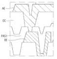
도 5는 도 4의 표시 패널의 BB 영역을 확대한 도면이다. BB영역에 있어서, 드레인 전극(DE) 상에 제1 패시베이션막(PAS1)이 형성될 수 있고, 제1 패시베이션막(PAS1) 상에 오버코트층(OC)이 형성될 수 있고, 오버코트층(OC) 상에 제1 전극(AE)이 형성될 수 있다. 제1 전극(AE)은 오버코트층(OC)과 제1 패시베이션막(PAS1)을 관통하는 비아 홀(Via Hole)을 통해 트랜지스터(T)의 드레인 전극(DE)과 연결될 수 있다. 따라서 도전층(Conductive Layer)인 드레인 전극(DE)과 제1 전극(AE) 간 전기신호가 통할 수 있다. 이하에서 각각의 층에 대하여 설명한다.FIG. 5 is an enlarged view of an area BB of the display panel of FIG. 4 . In the BB region, the first passivation layer PAS1 may be formed on the drain electrode DE, the overcoat layer OC may be formed on the first passivation layer PAS1, and the overcoat layer OC A first electrode AE may be formed thereon. The first electrode AE may be connected to the drain electrode DE of the transistor T through a via hole passing through the overcoat layer OC and the first passivation layer PAS1 . Accordingly, an electrical signal may pass between the drain electrode DE, which is a conductive layer, and the first electrode AE. Each layer will be described below.
드레인 전극(DE)은 몰리브덴(Mo), 알루미늄(Al), 크롬(Cr), 금(Au), 티타늄(Ti), 니켈(Ni), 네오디뮴(Nd) 및 구리(Cu) 중 어느 하나 또는 이들의 합금으로 이루어진 단일층 또는 다중층으로 형성될 수 있다. 드레인 전극(DE)이 다중층일 경우에는 몰리브덴/알루미늄-네오디뮴의 2중층, 티타늄/알루미늄/티타늄, 몰리브덴/알루미늄/몰리브덴 또는 몰리브덴/알루미늄-네오디뮴/몰리브덴의 3중층으로 이루어질 수 있다.The drain electrode DE may include any one of molybdenum (Mo), aluminum (Al), chromium (Cr), gold (Au), titanium (Ti), nickel (Ni), neodymium (Nd), and copper (Cu) or these It may be formed as a single layer or multiple layers made of an alloy of When the drain electrode DE is a multi-layer, it may be formed of a double layer of molybdenum/aluminum-neodymium, a triple layer of titanium/aluminum/titanium, molybdenum/aluminum/molybdenum, or molybdenum/aluminum-neodymium/molybdenum.
드레인 전극(DE) 상에 형성되는 제1 패시베이션막(PAS1)은 하부의 소자들을 보호하기 위한 절연막으로, 실리콘 산화막(SiOx), 실리콘 질화막(SiNx) 또는 이들의 다중층일 수 있다.The first passivation layer PAS1 formed on the drain electrode DE is an insulating layer for protecting lower devices, and may be a silicon oxide layer (SiOx), a silicon nitride layer (SiNx), or a multilayer thereof.
제1 패시베이션막(PAS1) 상에 형성되는 오버코트층(OC)은 하부 구조의 단차를 완화시키기 위한 평탄화막일 수 있으며, 폴리이미드(polyimide), 벤조사이클로부틴계 수지(benzocyclobutene series resin), 아크릴레이트(acrylate) 등의 유기물로 구성될 수 있다.The overcoat layer OC formed on the first passivation film PAS1 may be a planarization film for alleviating the step difference in the underlying structure, and may include polyimide, benzocyclobutene series resin, acrylate ( acrylate) and the like.
오버코트층(OC) 상에 형성되는 제1 전극(AE)은 오버코트층(OC)과 제1 패시베이션막(PAS1)을 관통하는 비아 홀(Via Hole)을 통해 트랜지스터(T)의 드레인 전극(DE)과 연결된다. 제1 전극(AE)은 ITO(Indium Tin Oxide), IZO(Indium Zinc Oxide) 또는 ZnO(Zinc Oxide) 등의 투명 도전 물질로 구성될 수 있다. 제1 전극은 애노드 전극일 수 있다.The first electrode AE formed on the overcoat layer OC is the drain electrode DE of the transistor T through a via hole penetrating the overcoat layer OC and the first passivation layer PAS1. is connected with The first electrode AE may be formed of a transparent conductive material such as indium tin oxide (ITO), indium zinc oxide (IZO), or zinc oxide (ZnO). The first electrode may be an anode electrode.
이하 BB 영역을 제조하는 방법에 대하여 설명한다. 일 실시예에 따른 표시 패널의 제조 방법은, 드레인 전극(DE)을 형성하는 단계, 드레인 전극(DE)상에 제1 패시베이션막(PAS1)을 형성하는 단계, 제1 패시베이션막(PAS1) 상에 오버코트층(OC)을 형성하는 단계를 포함할 수 있다.Hereinafter, a method for manufacturing the BB region will be described. A method of manufacturing a display panel according to an exemplary embodiment includes forming a drain electrode DE, forming a first passivation layer PAS1 on the drain electrode DE, and forming a first passivation layer PAS1 on the first passivation layer PAS1. It may include forming an overcoat layer (OC).
다음으로, 오버코트층(OC)과 제1 패시베이션막(PAS1)을 관통하는 비아 홀(Via Hole)을 형성하는 단계를 수행할 수 있다. 보다 구체적으로, 오버코트층(OC)을 관통하는 비아 홀(Via Hole)을 형성하기 위하여, 오버코트층(OC)에 포토공정을 수행할 수 있다. 오버코트층(OC) 포토공정으로 생겨난 홀 영역에 제1 패시베이션막(PAS1)의 홀을 생성하기 위하여 에칭(Etching)공정을 수행할 수 있다. 에칭공정은, 예를 들면, 습식 에칭(Wet Etching)일 수 있다.Next, a step of forming a via hole penetrating the overcoat layer OC and the first passivation layer PAS1 may be performed. More specifically, in order to form a via hole penetrating the overcoat layer OC, a photo process may be performed on the overcoat layer OC. An etching process may be performed to create a hole of the first passivation layer PAS1 in a hole region generated by the overcoat layer OC photo process. The etching process may be, for example, wet etching.
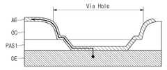
오버코트층(OC) 포토공정과 제1 패시베이션막(PAS1) 에칭공정을 통해 오버코트층(OC)과 제1 패시베이션막(PAS1)을 관통하는 비아 홀(Via Hole)이 형성되면, 오버코트층(OC) 상에 제1 전극(AE)을 형성하는 단계를 수행할 수 있다. 제1 전극(AE)은 오버코트층(OC) 및 비아 홀(Via Hole) 영역의 드레인 전극(DE) 상에 형성될 수 있다. 그 결과 제1 전극(AE)은 비아 홀(Via Hole)을 통해 드레인 전극(DE)과 접속할 수 있게 된다. 도 6a 및 도 6b는 일 실시예에 따른 제조 방법에 따라 생성된 표시 패널의 층 구조를 나타낸 도면이다.When a via hole passing through the overcoat layer (OC) and the first passivation film (PAS1) is formed through the overcoat layer (OC) photo process and the first passivation film (PAS1) etching process, the overcoat layer (OC) The step of forming the first electrode AE may be performed. The first electrode AE may be formed on the overcoat layer OC and the drain electrode DE in the via hole region. As a result, the first electrode AE can be connected to the drain electrode DE through a via hole. 6A and 6B are diagrams illustrating a layer structure of a display panel produced according to a manufacturing method according to an exemplary embodiment.
도 6a는 도 5의 BB 영역의 각 층이 이상적으로 형성된 모습을 나타낸 도면이다. 도6a에서 제1 전극(AE)은 오버코트층(OC)의 상부 뿐만 아니라 제1 패시베이션막(PAS1) 일부 및 드레인 전극(DE)상에 단선 없이 연결되어 있다. 전기신호는 드레인 전극(DE)으로부터 제1 전극(AE)으로, 또는 그 반대방향으로 전달될 수 있다.FIG. 6A is a diagram illustrating an ideally formed state of each layer in a region BB of FIG. 5 . In FIG. 6A , the first electrode AE is connected not only to the upper portion of the overcoat layer OC, but also to a portion of the first passivation layer PAS1 and the drain electrode DE without disconnection. The electrical signal may be transferred from the drain electrode DE to the first electrode AE or in the opposite direction.
BB 영역뿐 아니라 이와 유사한 구조를 갖는 표시 패널 구조, 나아가 유사한 구조의 반도체 장치 구조에서 비아 홀(Via Hole)을 통한 도전층 간 연결의 이상적인 모습은 도6a와 같을 수 있다. BB 영역 외의 구조에서는, 도 6a의 제1 전극(AE) 대신 임의의 도전층(Conductive Layer)인 전극이 포함되고, 드레인 전극(DE) 대신 게이트 전극(GE)이나, 금속을 포함하는 임의의 도전성 층이 포함될 수 있다. 또한, 오버코트층(OC) 및 제1 패시베이션막(PAS1) 대신에 임의의 절연층이 포함될 수 있다.In addition to the BB region, in a display panel structure having a similar structure, and further, in a semiconductor device structure having a similar structure, an ideal view of a connection between conductive layers through a via hole may be as shown in FIG. 6A . In a structure other than the BB region, an electrode that is an arbitrary conductive layer is included instead of the first electrode AE of FIG. 6A , and a gate electrode GE instead of the drain electrode DE, or any conductive material containing a metal Layers may be included. In addition, an arbitrary insulating layer may be included instead of the overcoat layer OC and the first passivation layer PAS1 .
도 6b는 공정상 문제로 인하여 제1 전극(AE)이 올바르게 형성되지 못한 모습을 나타낸 도면이다. 제1 전극(AE)이 오버코트층(OC)과 비아 홀(Via Hole)의 드레인 전극(DE) 각각에는 잘 형성되었으나, 서로 연결되지 않고 단선되어 전기가 통하지 않도록 형성되었다. 이러한 문제는 비아 홀(Via Hole)을 형성하기 위하여 수행되는 패시베이션막 에칭공정에서 기인한다.6B is a diagram illustrating a state in which the first electrode AE is not correctly formed due to a process problem. Although the first electrode AE was well formed on each of the overcoat layer OC and the drain electrode DE of the via hole, it was not connected to each other and was disconnected so that electricity did not pass through. This problem is caused by a passivation film etching process performed to form a via hole.
앞서 설명한 바와 같이, 비아 홀(Via Hole)을 형성하기 위한 하나의 단계로서 제1 패시베이션막(PAS1)에 홀을 생성하기 위하여 에칭(Etching)공정을 수행할 수 있다. 그런데 에칭공정, 특히 습식 에칭의 경우 언더컷(undercut) 현상이 발생하는 문제가 있다. 즉, 패시베이션막(PAS)에 홀을 생성하기 위하여 에칭하는 과정에서 설계한 바 이상으로 패턴 모양 아래쪽 에칭이 추가적으로 발생하는 현상이 발생할 수 있다. 도 6b에서, 언더컷이 발생하여 오버코트층(OC) 아래 제1 패시베이션막(PAS1)이 수직으로 깎이지 않고, 움푹하게 형성되었다. 결국 언더컷 현상 때문에, 이후 제1 전극(AE) 증착과정에서 오버코트층(OC)상의 제1 전극(AE) 부분과 드레인 전극(DE)상의 제1 전극(AE) 부분이 연결되지 못하고 단선되어 전기신호가 전달되지 못하는 단선 불량이 발생할 수 있다.As described above, as one step for forming a via hole, an etching process may be performed to create a hole in the first passivation layer PAS1. However, in the case of an etching process, particularly wet etching, there is a problem in that an undercut phenomenon occurs. That is, in the process of etching to create a hole in the passivation layer PAS, a phenomenon in which etching below the pattern shape is additionally generated may occur more than designed. In FIG. 6B , an undercut occurred so that the first passivation film PAS1 under the overcoat layer OC was not vertically cut, but was dented. After all, due to the undercut phenomenon, during the deposition of the first electrode AE, the first electrode AE on the overcoat layer OC and the first electrode AE on the drain electrode DE are not connected and are disconnected, resulting in an electrical signal. There may be a disconnection defect that cannot be transmitted.
종래에는 언더컷의 영향으로 단선 불량이 발생하는 문제를 해결하기 위하여 오버코트층(OC)을 일부 제거하는 공정을 수행하였다. 오버코트층(OC) 외곽의 일부를 제거하여 비아 홀(Via Hole)의 너비가 상부 층으로 갈수록 점점 넓어지는 구조를 형성함으로써, 제1 전극(AE) 형성과정에서 단선 불량 문제를 해결하는 방식이다. 그러나, 이러한 해결방식은 제1 전극(AE) 증착 공정 전, 오버코트층(OC) 애싱(Ashing)공정이 추가되므로, 제조 시간과 비용이 증가되는 문제가 발생한다.Conventionally, a process of partially removing the overcoat layer (OC) was performed in order to solve a problem in which disconnection occurs due to the influence of the undercut. This is a method of solving the problem of disconnection in the process of forming the first electrode AE by removing a part of the outer portion of the overcoat layer OC to form a structure in which the width of the via hole becomes wider toward the upper layer. However, in this solution, since an ashing process of the overcoat layer OC is added before the deposition process of the first electrode AE, manufacturing time and cost are increased.
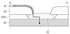
도 7은 일 실시예에 따라 연결전극(EE)이 형성된 표시 패널의 평면도이다. 드레인 전극으로부터 돌출되어 형성된 연결전극(EE)이 오버코트층(OC) 상부의 제1 전극(AE)과 연결되어 전기신호가 전달될 수 있다. 비아 홀(Via Hole)로 노출된 드레인 전극 부분으로부터 연결전극(EE)이 돌출되어 형성되었으므로, 드레인 전극은 평면도 상에서 드러나지 않을 수 있다. 제1 전극은 오버코트층(OC) 상부에 형성될 수도 있고, 도 7에서 점선으로 표현된 것과 같이 드레인 전극 상부에도 형성될 수 있다. 도 8은 일 실시예에 따른 도 7 C-C' 단면, 도 9는 일 실시예에 따른 도 7의 B-B' 단면일 수 있다.7 is a plan view of a display panel on which connection electrodes EE are formed, according to an exemplary embodiment. The connection electrode EE protruding from the drain electrode may be connected to the first electrode AE on the overcoat layer OC to transmit an electrical signal. Since the connection electrode EE is formed to protrude from the portion of the drain electrode exposed through the via hole, the drain electrode may not be exposed in a plan view. The first electrode may be formed on the overcoat layer OC, or may be formed on the drain electrode as indicated by a dotted line in FIG. 7 . 8 may be a cross-section C-C' of FIG. 7 according to an embodiment, and FIG. 9 may be a cross-section B-B' of FIG. 7 according to an embodiment.
도 8은 일 실시예에 따른 연결전극을 포함하는 표시 패널을 나타낸 도면이고, 도 9는 연결전극을 통해 드레인 전극과 제1 전극이 접속된 표시 패널을 나타낸 도면이다. 실시예에서 표시 패널은, 비아 홀(Via Hole)에서 드레인 전극(DE)의 일부가 상측으로 돌출되어 형성된 연결전극(EE)을 포함할 수 있다.8 is a diagram illustrating a display panel including a connection electrode according to an exemplary embodiment, and FIG. 9 is a diagram illustrating a display panel in which a drain electrode and a first electrode are connected through a connection electrode. In an embodiment, the display panel may include a connection electrode EE formed by a portion of the drain electrode DE protruding upward from a via hole.
도 8 및 도 9에서 실시예는 도 5의 BB 영역에 대응되는 표시 패널을 예로 들어 설명하나, 본 발명의 기술적 사상이 이에 한정되는 것은 아니고, 공통적이거나 균등한 구조를 포함하는 표시 패널이나 반도체 장치 및 그 제조 방법에 대해서도 적용될 수 있다. 도 8에서 드레인 전극(DE)이 도시되었으나, BB 영역 외의 다른 표시 패널 영역이나 다른 반도체 장치의 구조에서 드레인 전극(DE)은 금속층일 수 있다. 실시예에서, 드레인 전극(DE) 또는 금속층은 몰리브덴(Mo), 알루미늄(Al), 크롬(Cr), 금(Au), 티타늄(Ti), 니켈(Ni), 네오디뮴(Nd) 및 구리(Cu) 중 어느 하나 또는 이들의 합금으로 이루어진 단일층 또는 다중층으로 형성될 수 있다. 드레인 전극(DE)이 다중층일 경우에는 몰리브덴/알루미늄-네오디뮴의 2중층, 티타늄/알루미늄/티타늄, 몰리브덴/알루미늄/몰리브덴 또는 몰리브덴/알루미늄-네오디뮴/몰리브덴의 3중층으로 이루어질 수 있다.8 and 9 , the embodiment will be described by taking the display panel corresponding to the region BB of FIG. 5 as an example, but the technical spirit of the present invention is not limited thereto, and a display panel or semiconductor device having a common or equivalent structure and its manufacturing method. Although the drain electrode DE is illustrated in FIG. 8 , the drain electrode DE may be a metal layer in a display panel area other than the BB area or in other semiconductor device structures. In an embodiment, the drain electrode DE or the metal layer may include molybdenum (Mo), aluminum (Al), chromium (Cr), gold (Au), titanium (Ti), nickel (Ni), neodymium (Nd), and copper (Cu). ) may be formed as a single layer or multiple layers made of any one or an alloy thereof. When the drain electrode DE is a multi-layer, it may be formed of a double layer of molybdenum/aluminum-neodymium, a triple layer of titanium/aluminum/titanium, molybdenum/aluminum/molybdenum, or molybdenum/aluminum-neodymium/molybdenum.
마찬가지로 도 8에서 최상층 구성으로서 제1 전극(AE) 대신 임의의 도체 또는 반도체인 전극이 포함될 수 있다. 예를 들면 제1 전극(AE)은 ITO(Indium Tin Oxide), IZO(Indium Zinc Oxide) 또는 ZnO(Zinc Oxide) 등의 투명 도전 물질로 구성될 수 있다. 발광 소자(LD)는 제1 전극(AE), 제1 전극 상에 배치된 발광층(EML), 발광층 상에 배치된 제2 전극(CE)을 포함한다. 제1 전극(AE)은 애노드 전극일 수 있고, 제2 전극(CE)은 캐소드 전극일 수 있다. 제1 전극(AE) 및 제2 전극(CE)은 중 적어도 하나는 투과형 전극이고 적어도 다른 하나는 반사형 전극일 수 있다.Similarly, an electrode that is an arbitrary conductor or semiconductor may be included in place of the first electrode AE as the uppermost layer configuration in FIG. 8 . For example, the first electrode AE may be formed of a transparent conductive material such as indium tin oxide (ITO), indium zinc oxide (IZO), or zinc oxide (ZnO). The light emitting device LD includes a first electrode AE, an emission layer EML disposed on the first electrode, and a second electrode CE disposed on the emission layer. The first electrode AE may be an anode electrode, and the second electrode CE may be a cathode electrode. At least one of the first electrode AE and the second electrode CE may be a transmissive electrode and at least the other may be a reflective electrode.
또한, 오버코트층(OC) 및 제1 패시베이션막(PAS1) 대신에 임의의 비도전층(Non-Conductive Layer)이 포함될 수 있다. 오버코트층(OC) 및 제1 패시베이션막(PAS1)은 유사하거나 균등한 성분 및/또는 기능을 가지는 층으로 대체될 수 있다.In addition, an arbitrary non-conductive layer may be included in place of the overcoat layer OC and the first passivation layer PAS1 . The overcoat layer OC and the first passivation layer PAS1 may be replaced with layers having similar or equivalent components and/or functions.
도 8에서 나타난 것과 같이, 일 실시예에 따른 표시 패널은 드레인 전극(DE)으로부터 상측으로 돌출되어 형성된 연결전극(EE)을 포함할 수 있다. 도 8은 일 실시예에 따른 도 7 C-C' 단면일 수 있다. 도 7에서와 같이 C-C' 상에서 연결전극(EE)은, 드레인 전극 상의 제1 전극 상부의 전부 또는 대부분을 덮을 수도 있고, 드레인 전극 상의 제1 전극의 외곽부만을 덮음으로써 중앙부분이 도 8에서와 같이 제1 전극이 드러나도록 형성될 수도 있다.As shown in FIG. 8 , the display panel according to an exemplary embodiment may include a connection electrode EE formed to protrude upward from the drain electrode DE. FIG. 8 may be a cross-section C-C′ of FIG. 7 according to an embodiment. As in FIG. 7 , the connection electrode EE on CC′ may cover all or most of the upper portion of the first electrode on the drain electrode, and by covering only the outer portion of the first electrode on the drain electrode, the central portion is the same as in FIG. 8 . Likewise, the first electrode may be formed to be exposed.
실시예에서, 연결전극(EE)은 비아 홀(Via Hole) 내에서 드레인 전극(DE)으로부터 상측으로 돌출되어 오버코트층(OC) 상부의 제1 전극(AE)과 접속할 수 있다. 도 9에는 일 실시예에 따라 연결전극(EE)이 돌출되어 오버코트층(OC) 상의 제1 전극(AE)과 접속된 표시 패널이 도시되어 있다.In an embodiment, the connection electrode EE may protrude upward from the drain electrode DE in a via hole to be connected to the first electrode AE on the overcoat layer OC. 9 illustrates a display panel in which the connection electrode EE protrudes and is connected to the first electrode AE on the overcoat layer OC, according to an exemplary embodiment.
연결전극(EE)은 전도성을 가지며, 단선된 오버코트층(OC) 상부의 제1 전극(AE) 부분과 드레인 전극(DE) 상의 제1 전극(AE) 부분을 연결하여, 드레인 전극(DE)과 제1 전극(AE) 사이에 전기신호가 통하게 한다. 언더컷 현상으로 인하여 제1 전극이 단선되는 현상에 대한 해결로서, 종래기술과 같이 단선을 방지하는 공정 대신, 연결전극(EE)을 형성하여 단선된 제1 전극을 연결하는 것이다.The connection electrode EE has conductivity and connects a portion of the first electrode AE on the disconnected overcoat layer OC and a portion of the first electrode AE on the drain electrode DE, thereby forming the drain electrode DE and An electrical signal is passed between the first electrodes AE. As a solution to the phenomenon in which the first electrode is disconnected due to the undercut phenomenon, the disconnected first electrode is connected by forming the connecting electrode EE instead of the process of preventing disconnection as in the prior art.
도 10은 일 실시예에 따른 표시 패널의 단면도이다. 제1 전극(AE)과 드레인 전극(DE)이 비아 홀(Via Hole)에서 직접 연결되지 않고, 연결전극(EE)을 통해서 연결되도록 구성되었다. 제조 공정 상에서 제1 전극(AE)과 드레인 전극(DE)이 단선되어도 드레인 전극(DE)의 돌출부인 연결전극(EE)을 통해서 접속되어 문제점을 해결할 수 있다.10 is a cross-sectional view of a display panel according to an exemplary embodiment. The first electrode AE and the drain electrode DE are not directly connected through the via hole, but are connected through the connection electrode EE. Even if the first electrode AE and the drain electrode DE are disconnected during the manufacturing process, they are connected through the connection electrode EE, which is a protrusion of the drain electrode DE, to solve the problem.
연결전극(EE)은 드레인 전극(DE)에 포함된 금속의 산화물을 포함할 수 있다. 예를 들면, 드레인 전극(DE)은 구리(Cu)를 포함하고, 연결전극(EE)은 산화구리(CuOx)를 포함할 수 있다. 여기서 산화구리는 전기가 통할 수 있는 전도성 물질이다. 연결전극(EE)은 드레인 전극(DE) 또는 금속층에 포함되는 구성일 수 있다.The connection electrode EE may include an oxide of a metal included in the drain electrode DE. For example, the drain electrode DE may include copper (Cu), and the connection electrode EE may include copper oxide (CuOx). Here, copper oxide is a conductive material that can conduct electricity. The connection electrode EE may have a configuration included in the drain electrode DE or the metal layer.
일 실시예에 따르면, 연결전극(EE)은 드레인 전극(DE) 또는 표시 패널의 열처리를 통하여 형성될 수 있다. 열처리의 온도는 섭씨 150도 이상 섭씨 230도 이하, 시간은 30분 이상 60분 이하의 처리가 바람직하나, 이에 한정되지 않는다. 열처리를 통하여 드레인 전극(DE)에 포함된 금속, 예를 들면 구리 등은 산화될 수 있고, 산화된 금속이 팽창할 수 있는데, 노출된 비아 홀(Via Hole)을 통하여 드레인 전극(DE)의 상측으로 돌출되어 연결전극(EE)을 형성할 수 있다.According to an embodiment, the connection electrode EE may be formed by heat treatment of the drain electrode DE or the display panel. The temperature of the heat treatment is 150 degrees Celsius or more and 230 degrees Celsius or less, and the time is preferably 30 minutes or more and 60 minutes or less, but is not limited thereto. The metal included in the drain electrode DE, for example, copper, etc., may be oxidized through heat treatment, and the oxidized metal may expand. The upper side of the drain electrode DE through the exposed via hole. may protrude to form a connection electrode EE.
표시 패널 등의 생산 공정에 있어서, 애노드 전극의 증착 후 불순물 제거 등을 위한 열처리 공정이 수행될 수 있다. 본 개시물의 다양한 실시예에서 연결전극(EE)을 형성하기 위한 열처리 공정은, 별도의 추가 공정 없이, 애노드 전극의 증착 후 수행되는 열처리 공정에서 함께 수행될 수 있다. 종래기술이 오버코트층의 애싱공정을 별도로 수행하는 것과 달리, 본 발명은 부가적인 공정이 필요하지 않아 경제적이다.In a production process of a display panel, etc., a heat treatment process for removing impurities or the like may be performed after the deposition of the anode electrode. In various embodiments of the present disclosure, the heat treatment process for forming the connection electrode EE may be performed together in the heat treatment process performed after the deposition of the anode electrode without a separate additional process. Unlike the prior art in which the ashing process of the overcoat layer is separately performed, the present invention is economical because an additional process is not required.
일 실시 예에 따른 표시 패널은, 금속층; 상기 금속층 상에 형성되는 패시베이션막; 상기 패시베이션막 상에 형성되는 오버코트층; 및 상기 오버코트층 상에 형성되는 전극을 포함하고, 상기 금속층은 연결전극을 포함하고, 상기 연결전극은, 상기 패시베이션막 및 상기 오버코트층을 관통하는 비아 홀(Via Hole)에서 상기 금속층의 일부가 상측으로 돌출되어 형성되고, 상기 비아 홀(Via Hole)을 통해 상기 전극과 접속하도록 구성될 수 있다. 나아가, 상기 연결전극은, 상기 금속층이 열처리를 통해 팽창됨으로써 형성될 수 있다. 일 실시예에서, 예를 들면, 금속층은 도 9의 드레인 전극(DE), 패시베이션막은 도면의 제1 패시베이션막(PAS1), 전극은 도면의 제1 전극(AE)일 수 있다.A display panel according to an embodiment includes a metal layer; a passivation film formed on the metal layer; an overcoat layer formed on the passivation film; and an electrode formed on the overcoat layer, wherein the metal layer includes a connection electrode, and the connection electrode includes a portion of the metal layer in a via hole passing through the passivation film and the overcoat layer. It may be formed to protrude from the pole, and may be configured to be connected to the electrode through the via hole. Furthermore, the connection electrode may be formed by expanding the metal layer through heat treatment. In one embodiment, for example, the metal layer may be the drain electrode DE of FIG. 9 , the passivation layer may be the first passivation layer PAS1 of the drawing, and the electrode may be the first electrode AE of the drawing.
일 실시예에 따른 표시 패널에 있어서, 상기 전극은 상기 비아 홀(Via Hole)에서 상기 금속층의 일부 상에 형성되도록 더 구성되고, 상기 연결전극은, 상기 금속층의 일부 상에 형성된 전극의 적어도 일부를 덮도록 구성되며, 상기 비아 홀(Via Hole)을 통해 상기 오버코트층 상에 형성된 전극과 접속하도록 구성될 수 있다.In the display panel according to an embodiment, the electrode is further configured to be formed on a portion of the metal layer in the via hole, and the connection electrode includes at least a portion of the electrode formed on a portion of the metal layer. It may be configured to cover, and may be configured to be connected to an electrode formed on the overcoat layer through the via hole.
일 실시예에서, 제1 전극(AE)은 오버코트층(OC) 상에만 형성되도록 구성될 수도 있고, 비아 홀(Via Hole) 내의 드레인 전극(DE)의 일부에 더 형성되도록 구성될 수 있다. 예를 들어, 제1 전극(AE)은 오버코트층(OC) 뿐 아니라 비아 홀(Via Hole) 내의 드레인 전극(DE) 영역 넓이의 절반정도를 커버하도록 형성될 수 있다. 이 때, 열처리 과정에서, 제1 전극(AE)이 덮고 있는 드레인 전극(DE) 영역은 팽창하지 않거나 팽창을 무시할 수 있고, 제1 전극(AE)이 덮지 않는 드레인 전극(DE) 영역은 팽창하게 된다, 팽창의 결과 드레인 전극(DE)에 포함된 금속은 상측으로 돌출되게 되는데, 돌출부가 제1 전극(AE)을 감싸 덮으면서 타고 올라갈 수 있다. 결국 연결전극(EE)은 드레인 전극(DE) 상에 증착된 제1 전극(AE) 부분의 적어도 일부의 위에 형성되어 오버코트층(OC) 상에 형성된 제1 전극(AE) 부분과 접속될 수 있다.In an embodiment, the first electrode AE may be formed only on the overcoat layer OC, or may be further formed on a portion of the drain electrode DE in a via hole. For example, the first electrode AE may be formed to cover about half of the area of the drain electrode DE in the via hole as well as the overcoat layer OC. In this case, during the heat treatment process, the drain electrode DE region covered by the first electrode AE does not expand or the expansion can be ignored, and the drain electrode DE region not covered by the first electrode AE expands. As a result of the expansion, the metal included in the drain electrode DE protrudes upward, and the protrusion may ride up while surrounding and covering the first electrode AE. As a result, the connection electrode EE may be formed on at least a portion of the portion of the first electrode AE deposited on the drain electrode DE to be connected to the portion of the first electrode AE formed on the overcoat layer OC. .
제1 전극(AE)을 비아 홀(Via Hole)에서 드레인 전극(DE) 상의 일부에 형성함으로써, 드레인 전극(DE) 상에서 열처리에 의해 팽창되어 돌출될 부분과 그렇지 않은 부분이 제어될 수 있다. 나아가, 연결전극(EE)은 오버코트층(OC) 및 제1 패시베이션막(PAS1)의 높이에 상응할 만큼 팽창되어야 하는데, 드레인 전극(DE) 상에 형성된 제1 전극(AE)의 높이만큼 덜 팽창하여도, 오버코트층(OC)상의 제1 전극(AE)에 도달하여 전기신호가 통할 수 있게 된다. 즉, 연결전극(EE)이 높이에 있어서 오버코트층(OC)상의 제1 전극(AE)에 도달하는데 필요한 팽창 정도를 드레인 전극(DE) 상에 형성된 제1 전극(AE)의 높이만큼 줄일 수 있다. 이는 연결전극(EE)이 요구되는 높이로 형성되기 위하여 필요한 열처리 시간을 줄이거나 온도를 낮추어, 비용을 줄이는 효과가 있다.By forming the first electrode AE on a portion of the drain electrode DE in the via hole, a portion to be expanded and protruded by heat treatment on the drain electrode DE and a portion not to be controlled may be controlled. Furthermore, the connection electrode EE needs to expand to correspond to the heights of the overcoat layer OC and the first passivation layer PAS1 , but it expands less by the height of the first electrode AE formed on the drain electrode DE. Even so, the electric signal can pass through the first electrode AE on the overcoat layer OC. That is, the degree of expansion required for the connection electrode EE to reach the first electrode AE on the overcoat layer OC in height can be reduced by the height of the first electrode AE formed on the drain electrode DE. . This has the effect of reducing the cost by reducing the heat treatment time or lowering the temperature required for the connection electrode EE to be formed to a required height.
또한, 드레인 전극(DE) 상의 제1 전극(AE)은, 제1 전극(AE)의 마스크 설계를 일부 변경하여 오버코트층(OC) 상의 제1 전극(AE)과 하나의 공정으로 형성 가능하다. 결국, 추가적인 공정 없이 마스크의 설계 변경 만으로도 돌출되는 연결전극(EE)의 요구 크기를 줄이는 효과가 있고, 궁극적으로 열처리에 필요한 온도를 낮추거나 열처리에 소요되는 시간을 줄일 수 있다.In addition, the first electrode AE on the drain electrode DE may be formed in one process with the first electrode AE on the overcoat layer OC by partially changing the mask design of the first electrode AE. As a result, it is possible to reduce the required size of the protruding connection electrode EE only by changing the design of the mask without an additional process, and ultimately, the temperature required for the heat treatment or the time required for the heat treatment can be reduced.
도 11은 일 실시예에 따른 표시 패널의 제조 방법을 나타낸 흐름도이다. 일 실시 예에 따른 표시 패널의 제조 방법은, 금속층을 형성하는 단계; 상기 금속층 상에 패시베이션막을 형성하는 단계; 상기 패시베이션막 상에 오버코트층을 형성하는 단계; 상기 패시베이션막 및 상기 오버코트층을 관통하는 비아 홀(Via Hole)을 형성하는 단계; 전극을 형성하는 단계; 및 상기 비아 홀(Via Hole)에서 상기 금속층의 일부를 상측으로 돌출되도록 처리하여 연결전극을 형성하는 단계;를 포함하고, 상기 연결전극은, 상기 비아 홀(Via Hole)을 통해 상기 전극과 접속하도록 구성될 수 있다.11 is a flowchart illustrating a method of manufacturing a display panel according to an exemplary embodiment. According to an exemplary embodiment, a method of manufacturing a display panel includes forming a metal layer; forming a passivation film on the metal layer; forming an overcoat layer on the passivation film; forming a via hole penetrating the passivation layer and the overcoat layer; forming an electrode; and forming a connection electrode by processing a portion of the metal layer to protrude upward from the via hole, wherein the connection electrode is connected to the electrode through the via hole can be configured.
먼저, 금속층을 형성하는 단계를 수행할 수 있다(S1110). 앞서 설명한 바와 같이, 금속층은 구리(Cu) 등의 금속을 포함할 수 있다. 금속층은 도전층으로서 연결된 다른 도전층과 전기신호를 통할 수 있다. 예를 들어, 금속층은 도 8의 드레인 전극(DE)일 수 있다.First, a step of forming a metal layer may be performed (S1110). As described above, the metal layer may include a metal such as copper (Cu). The metal layer may conduct an electrical signal with another conductive layer connected as a conductive layer. For example, the metal layer may be the drain electrode DE of FIG. 8 .
다음으로, 금속층 상에 패시베이션막을 형성하는 단계가 수행될 수 있다(S1120). 패시베이션막은 절연막일 수 있다. 예를 들어, 패시베이션막은 도 8의 제1 패시베이션막(PAS1)일 수 있다.Next, a step of forming a passivation film on the metal layer may be performed (S1120). The passivation layer may be an insulating layer. For example, the passivation layer may be the first passivation layer PAS1 of FIG. 8 .
그 다음으로, 패시베이션막 상에 오버코트층을 형성하는 단계가 수행될 수 있다(S1130). 오버코트층은 유기층일 수 있다. 여기서 오버코트층은, 도 8의 오버코트층(OC)일 수 있다.Next, a step of forming an overcoat layer on the passivation film may be performed (S1130). The overcoat layer may be an organic layer. Here, the overcoat layer may be the overcoat layer OC of FIG. 8 .
도 11에서, 표시 패널의 예를 들어, 패시베이션막을 형성하는 단계와 오버코트층을 형성하는 단계로 나누어 설명하였으나, 유사한 구조를 갖는 표시 패널이나 반도체 장치의 제조 방법에 있어서는, 패시베이션막 및 오버코트층에 대응하는 복수의 절연막 층을 형성하는 단계로 각각 대체될 수 있으며, 단수의 층을 형성하는 하나의 단계로 대체될 수도 있다.In FIG. 11, for example, the display panel is divided into a step of forming a passivation film and a step of forming an overcoat layer. However, in the method of manufacturing a display panel or semiconductor device having a similar structure, the passivation film and the overcoat layer may be replaced with the step of forming a plurality of insulating film layers, respectively, or may be replaced with one step of forming a single layer.
다음, 패시베이션 막 및 오버코트층을 관통하는 비아 홀(Via Hole)을 형성하는 단계가 수행될 수 있다(S1140). 비아 홀(Via Hole)은 절연층을 사이에 둔 도전층 사이에 통전(通電)을 위한 배선을 형성하기 위하여 형성되는 구멍(hole)이나 홈을 말하고, 그 모양에 한정되지 않는다.Next, a step of forming a via hole passing through the passivation film and the overcoat layer may be performed (S1140). A via hole refers to a hole or groove formed to form a wiring for electric current between conductive layers having an insulating layer interposed therebetween, and the shape is not limited thereto.
보다 구체적으로 설명하면, 비아 홀(Via Hole)을 형성하기 위하여, 오버코트층에 포토공정을 통하여 오버코트층 상에 홀을 형성할 수 있다. 오버코트층 포토공정으로 형성된 홀 영역에 패시베이션막의 홀을 형성하기 위하여 에칭공정을 수행할 수 있다. 에칭공정은, 예를 들면, 습식 에칭일 수 있다. 에칭공정 과정에서 언더컷이 발생할 수 있다. 오버코트층 및 패시베이션막을 관통하는 비아 홀(Via Hole)이 형성되어 금속층이 노출될 수 있다.More specifically, in order to form a via hole, a hole may be formed on the overcoat layer through a photo process in the overcoat layer. An etching process may be performed to form a hole of the passivation film in the hole region formed by the overcoat layer photo process. The etching process may be, for example, wet etching. Undercuts may occur during the etching process. A via hole passing through the overcoat layer and the passivation layer may be formed to expose the metal layer.
다음으로, 전극을 형성하는 단계를 수행할 수 있다(S1150). 앞서 설명한 바와 같이, 전극은 오버코트층 뿐 아니라 비아 홀(Via Hole)을 통해 노출된 금속층의 일부에도 형성될 수 있다.Next, the step of forming an electrode may be performed (S1150). As described above, the electrode may be formed not only on the overcoat layer but also on a portion of the metal layer exposed through the via hole.
마지막으로, 금속층의 일부를 상측으로 돌출되도록 처리하여 연결전극을 형성하는 단계를 수행할 수 있다(S1160). 여기서 금속층의 일부란, 비아 홀(Via Hole)을 통해 노출된 금속층 중, 전극이 형성되지 않은 영역일 수 있다. 또한, 여기서 처리는 열처리일 수 있다. 연결전극이 형성되도록 금속층을 처리함으로써, 비아 홀(Via Hole)을 통해 금속층과 오버코트층 상의 전극이 접속하여 전기신호가 통할 수 있다.Finally, a step of forming a connection electrode by processing a portion of the metal layer to protrude upward may be performed (S1160). Here, the part of the metal layer may be a region in which an electrode is not formed among the metal layers exposed through a via hole. Also, the treatment here may be a heat treatment. By processing the metal layer to form the connection electrode, the metal layer and the electrode on the overcoat layer are connected through a via hole so that an electrical signal can pass through.
도 12는 일 실시예에 따른 표시 패널의 단면을 현미경으로 관찰한 모습을 나타낸 도면이다. 도 12의 실시예는 구리(Cu)가 포함된 금속층이 노출된 상태에서 섭씨 230도, 60분 열처리 진행하였다. 구리층은 산화되어 연결전극인 산화구리(CuOx)층을 형성하였다. 산화구리층은 패시베이션막(PAS)의 두께 이상으로 부풀어 오른 것을 볼 수 있다. 실시예에서와 같이 금속층을 처리하여 형성된 연결전극은, 패시베이션막(PAS) 두께 이상으로 팽창하므로, 오버코트층 상부의 전극이 단선되어 있더라도 이와 접속할 수 있다.12 is a view illustrating a microscopic view of a cross-section of a display panel according to an exemplary embodiment. In the example of FIG. 12 , heat treatment was performed at 230 degrees Celsius for 60 minutes in a state in which the metal layer containing copper (Cu) was exposed. The copper layer was oxidized to form a copper oxide (CuOx) layer as a connecting electrode. It can be seen that the copper oxide layer swells beyond the thickness of the passivation layer PAS. Since the connection electrode formed by treating the metal layer as in the embodiment expands beyond the thickness of the passivation film (PAS), it can be connected even if the electrode on the overcoat layer is disconnected.
본 발명이 속하는 기술분야의 통상의 지식을 가진 자는 본 발명이 그 기술적 사상이나 필수적인 특징을 변경하지 않고서 다른 구체적인 형태로 실시될 수 있다는 것을 이해할 수 있을 것이다. 그러므로 이상에서 기술한 실시 예들은 모든 면에서 예시적인 것이며 한정적이 아닌 것으로 이해해야만 한다. 본 발명의 범위는 상기 상세한 설명보다는 후술하는 특허청구의 범위에 의하여 나타내어지며, 특허청구의 범위의 의미 및 범위 그리고 그 균등 개념으로부터 도출되는 모든 변경 또는 변형된 형태가 본 발명의 범위에 포함되는 것으로 해석되어야 한다.Those of ordinary skill in the art to which the present invention pertains will understand that the present invention may be embodied in other specific forms without changing the technical spirit or essential features thereof. Therefore, it should be understood that the embodiments described above are illustrative in all respects and not restrictive. The scope of the present invention is indicated by the claims described below rather than the above detailed description, and all changes or modifications derived from the meaning and scope of the claims and their equivalent concepts are included in the scope of the present invention. should be interpreted
1: 표시 장치
10: 타이밍 제어부
20: 게이트 구동부
30: 데이터 구동부
40: 전원 공급부
50: 표시 패널1: display device
10: timing control
20: gate driver
30: data driving unit
40: power supply
50: display panel
Claims (15)
Translated fromKorean금속층;
상기 금속층 상에 형성되는 절연막; 및
상기 절연막 상에 형성되는 전극을 포함하고,
상기 금속층은 연결전극을 포함하고,
상기 연결전극은,
상기 절연막을 관통하는 비아 홀(Via Hole)에서 상기 금속층의 일부가 상측으로 돌출되어 형성되고,
상기 비아 홀(Via Hole)을 통해 상기 전극과 접속하도록 구성된, 표시 패널.
In the display panel,
metal layer;
an insulating film formed on the metal layer; and
an electrode formed on the insulating film;
The metal layer includes a connection electrode,
The connecting electrode is
A portion of the metal layer is formed to protrude upward from a via hole passing through the insulating film,
and a display panel configured to be connected to the electrode through the via hole.
상기 절연막은
상기 금속층 상에 형성되는 패시베이션 막; 및
상기 패시베이션 막 상에 형성되는 오버코트층을 포함하는, 표시 패널According to claim 1,
The insulating film is
a passivation film formed on the metal layer; and
and an overcoat layer formed on the passivation layer;
상기 연결전극은 상기 금속층에 포함된 금속의 산화물을 포함하는, 표시 패널.
According to claim 1,
The connection electrode includes an oxide of a metal included in the metal layer.
상기 금속층은 구리를 포함하고,
상기 연결전극은 산화구리를 포함하는, 표시 패널.
4. The method of claim 3,
The metal layer comprises copper,
and the connection electrode includes copper oxide.
상기 전극은 상기 비아 홀(Via Hole)에서 상기 금속층의 일부 상에 형성되고,
상기 연결전극은,
상기 금속층의 일부 상에 형성된 전극의 적어도 일부를 덮도록 구성되고,
상기 비아 홀(Via Hole)을 통해 상기 절연막 상에 형성된 전극과 접속하도록 구성된, 표시 패널.
According to claim 1,
The electrode is formed on a portion of the metal layer in the via hole,
The connecting electrode is
configured to cover at least a portion of an electrode formed on a portion of the metal layer,
and a display panel configured to be connected to an electrode formed on the insulating layer through the via hole.
상기 전극 상에 형성되는 발광층; 및
상기 발광층 상에 형성되는 캐소드 전극을 더 포함하는, 표시 패널.
According to claim 1,
a light emitting layer formed on the electrode; and
The display panel further comprising a cathode electrode formed on the light emitting layer.
금속층을 형성하는 단계;
상기 금속층 상에 절연막을 형성하는 단계;
상기 절연막을 관통하는 비아 홀(Via Hole)을 형성하는 단계;
전극을 형성하는 단계; 및
상기 비아 홀(Via Hole)에서 상기 금속층의 일부를 상측으로 돌출되도록 처리하여 연결전극을 형성하는 단계;를 포함하고,
상기 연결전극은, 상기 비아 홀(Via Hole)을 통해 상기 전극과 접속하도록 구성된, 표시 패널 제조 방법.
A method for manufacturing a display panel, comprising:
forming a metal layer;
forming an insulating film on the metal layer;
forming a via hole penetrating the insulating layer;
forming an electrode; and
Including; processing a portion of the metal layer to protrude upward from the via hole to form a connection electrode;
The connection electrode is configured to be connected to the electrode through the via hole.
상기 절연막을 형성하는 단계는
상기 금속층 상에 패시베이션막을 형성하는 단계; 및
상기 패시베이션막 상에 오버코트층을 형상하는 단계를 포함하는, 표시 패널 제조 방법.
8. The method of claim 7,
The step of forming the insulating film is
forming a passivation film on the metal layer; and
and forming an overcoat layer on the passivation layer.
상기 연결전극을 형성하는 단계는,
상기 금속층을 열처리하여 상기 금속층의 일부를 상측으로 돌출되도록 처리하는 단계를 포함하는, 표시 패널 제조 방법.
8. The method of claim 7,
The step of forming the connection electrode,
and treating a portion of the metal layer to protrude upward by heat-treating the metal layer.
상기 연결전극을 형성하는 단계는,
상기 금속층을 섭씨 150도 이상 섭씨 230도 이하에서 열처리하는 단계를 포함하는, 표시 패널 제조 방법.
10. The method of claim 9,
The step of forming the connection electrode,
and heat-treating the metal layer at 150 degrees Celsius or more and 230 degrees Celsius or less.
상기 연결전극을 형성하는 단계는,
상기 금속층을 30분 이상 60분 이하에서 열처리하는 단계를 포함하는, 표시 패널 제조 방법.
11. The method of claim 10,
The step of forming the connection electrode,
and heat-treating the metal layer for 30 minutes or more and 60 minutes or less.
상기 연결전극은 상기 금속층에 포함된 금속의 산화물을 포함하는, 표시 패널 제조 방법.
8. The method of claim 7,
and the connection electrode includes an oxide of a metal included in the metal layer.
상기 금속층은 구리를 포함하고,
상기 연결전극은 산화구리를 포함하는, 표시 패널 제조 방법.
13. The method of claim 12,
The metal layer comprises copper,
and the connection electrode includes copper oxide.
상기 전극을 형성하는 단계는,
상기 오버코트층의 일부 상에 전극을 형성하고, 상기 비아 홀(Via Hole)에서 상기 금속층의 일부 상에 전극을 형성하는 단계를 포함하고,
상기 연결전극을 형성하는 단계는,
상기 연결전극이 상기 금속층의 일부 상에 형성된 전극의 적어도 일부를 덮도록 상기 연결전극을 형성하는 단계를 포함하고,
상기 연결전극은,
상기 비아 홀(Via Hole)을 통해 상기 오버코트층 상에 형성된 전극과 접속하도록 구성된, 표시 패널 제조 방법.
9. The method of claim 8,
The step of forming the electrode,
Forming an electrode on a part of the overcoat layer, and forming an electrode on a part of the metal layer in the via hole,
The step of forming the connection electrode,
forming the connection electrode so that the connection electrode covers at least a portion of the electrode formed on a portion of the metal layer;
The connecting electrode is
and to connect to an electrode formed on the overcoat layer through the via hole.
상기 전극 상에 발광층을 형성하는 단계; 및
상기 발광층 상에 캐소드 전극을 형성하는 단계를 더 포함하는, 표시 패널 제조 방법.
8. The method of claim 7,
forming a light emitting layer on the electrode; and
The method of claim 1 , further comprising forming a cathode electrode on the emission layer.
Priority Applications (1)
| Application Number | Priority Date | Filing Date | Title |
|---|---|---|---|
| KR1020190174061AKR20210081784A (en) | 2019-12-24 | 2019-12-24 | Display pannel and manufacturing method thereof |
Applications Claiming Priority (1)
| Application Number | Priority Date | Filing Date | Title |
|---|---|---|---|
| KR1020190174061AKR20210081784A (en) | 2019-12-24 | 2019-12-24 | Display pannel and manufacturing method thereof |
Publications (1)
| Publication Number | Publication Date |
|---|---|
| KR20210081784Atrue KR20210081784A (en) | 2021-07-02 |
Family
ID=76897133
Family Applications (1)
| Application Number | Title | Priority Date | Filing Date |
|---|---|---|---|
| KR1020190174061APendingKR20210081784A (en) | 2019-12-24 | 2019-12-24 | Display pannel and manufacturing method thereof |
Country Status (1)
| Country | Link |
|---|---|
| KR (1) | KR20210081784A (en) |
- 2019
- 2019-12-24KRKR1020190174061Apatent/KR20210081784A/enactivePending
Similar Documents
| Publication | Publication Date | Title |
|---|---|---|
| KR102565907B1 (en) | Display apparatus and electroluminescence display | |
| TWI766481B (en) | Organic light emitting diode display device including touch sensor and manufacturing method of same | |
| KR102722115B1 (en) | Organic light emitting diode display device and method of manufacturing the same | |
| TW202125810A (en) | Display device and manufacturing method of same | |
| TWI782374B (en) | Display panel, display device including display panel, and method of manufacturing display panel | |
| CN113130568B (en) | Display device and manufacturing method thereof | |
| KR20210081784A (en) | Display pannel and manufacturing method thereof | |
| CN113948661A (en) | Display substrate and display device | |
| KR102698317B1 (en) | Organic light emitting diode display device | |
| CN113130570B (en) | Display device and method for manufacturing the same | |
| KR102835161B1 (en) | Display device and method for manufacturing the same | |
| KR102684600B1 (en) | Display device | |
| US20240023385A1 (en) | Electroluminescence Display | |
| US20250228076A1 (en) | Display Device | |
| KR20210086240A (en) | Display device and manufacturing method thereof | |
| KR20240079322A (en) | Display apparatus | |
| KR20240046393A (en) | Display apparatus | |
| KR20230168392A (en) | Top Emission Type Electroluminescence Display | |
| KR20240072383A (en) | Display device and manufacturing method of the same | |
| KR20240043892A (en) | Display apparatus and manufacturing methode thereof | |
| KR20240095549A (en) | Display device and manufacturing method of the same | |
| KR20250096992A (en) | Display apparatus and method of manufacturing the same | |
| KR20240040176A (en) | Display device and method for manufacturing the same | |
| KR20230034826A (en) | Electroluminescent display device |
Legal Events
| Date | Code | Title | Description |
|---|---|---|---|
| PA0109 | Patent application | St.27 status event code:A-0-1-A10-A12-nap-PA0109 | |
| PG1501 | Laying open of application | St.27 status event code:A-1-1-Q10-Q12-nap-PG1501 | |
| A201 | Request for examination | ||
| PA0201 | Request for examination | St.27 status event code:A-1-2-D10-D11-exm-PA0201 | |
| P22-X000 | Classification modified | St.27 status event code:A-2-2-P10-P22-nap-X000 | |
| P22-X000 | Classification modified | St.27 status event code:A-2-2-P10-P22-nap-X000 | |
| E902 | Notification of reason for refusal | ||
| PE0902 | Notice of grounds for rejection | St.27 status event code:A-1-2-D10-D21-exm-PE0902 | |
| E13-X000 | Pre-grant limitation requested | St.27 status event code:A-2-3-E10-E13-lim-X000 | |
| P11-X000 | Amendment of application requested | St.27 status event code:A-2-2-P10-P11-nap-X000 | |
| PE0701 | Decision of registration | St.27 status event code:A-1-2-D10-D22-exm-PE0701 |