KR20210077264A - Image sensing device - Google Patents
Image sensing deviceDownload PDFInfo
- Publication number
- KR20210077264A KR20210077264AKR1020190168712AKR20190168712AKR20210077264AKR 20210077264 AKR20210077264 AKR 20210077264AKR 1020190168712 AKR1020190168712 AKR 1020190168712AKR 20190168712 AKR20190168712 AKR 20190168712AKR 20210077264 AKR20210077264 AKR 20210077264A
- Authority
- KR
- South Korea
- Prior art keywords
- edge
- main
- microlenses
- color filters
- lens
- Prior art date
- Legal status (The legal status is an assumption and is not a legal conclusion. Google has not performed a legal analysis and makes no representation as to the accuracy of the status listed.)
- Abandoned
Links
Images


Classifications
- H01L27/14627—
- H—ELECTRICITY
- H10—SEMICONDUCTOR DEVICES; ELECTRIC SOLID-STATE DEVICES NOT OTHERWISE PROVIDED FOR
- H10F—INORGANIC SEMICONDUCTOR DEVICES SENSITIVE TO INFRARED RADIATION, LIGHT, ELECTROMAGNETIC RADIATION OF SHORTER WAVELENGTH OR CORPUSCULAR RADIATION
- H10F39/00—Integrated devices, or assemblies of multiple devices, comprising at least one element covered by group H10F30/00, e.g. radiation detectors comprising photodiode arrays
- H10F39/80—Constructional details of image sensors
- H10F39/806—Optical elements or arrangements associated with the image sensors
- H10F39/8063—Microlenses
- H01L27/14621—
- H—ELECTRICITY
- H10—SEMICONDUCTOR DEVICES; ELECTRIC SOLID-STATE DEVICES NOT OTHERWISE PROVIDED FOR
- H10F—INORGANIC SEMICONDUCTOR DEVICES SENSITIVE TO INFRARED RADIATION, LIGHT, ELECTROMAGNETIC RADIATION OF SHORTER WAVELENGTH OR CORPUSCULAR RADIATION
- H10F39/00—Integrated devices, or assemblies of multiple devices, comprising at least one element covered by group H10F30/00, e.g. radiation detectors comprising photodiode arrays
- H10F39/80—Constructional details of image sensors
- H10F39/802—Geometry or disposition of elements in pixels, e.g. address-lines or gate electrodes
- H10F39/8023—Disposition of the elements in pixels, e.g. smaller elements in the centre of the imager compared to larger elements at the periphery
- H—ELECTRICITY
- H10—SEMICONDUCTOR DEVICES; ELECTRIC SOLID-STATE DEVICES NOT OTHERWISE PROVIDED FOR
- H10F—INORGANIC SEMICONDUCTOR DEVICES SENSITIVE TO INFRARED RADIATION, LIGHT, ELECTROMAGNETIC RADIATION OF SHORTER WAVELENGTH OR CORPUSCULAR RADIATION
- H10F39/00—Integrated devices, or assemblies of multiple devices, comprising at least one element covered by group H10F30/00, e.g. radiation detectors comprising photodiode arrays
- H10F39/80—Constructional details of image sensors
- H10F39/805—Coatings
- H10F39/8053—Colour filters
- H—ELECTRICITY
- H10—SEMICONDUCTOR DEVICES; ELECTRIC SOLID-STATE DEVICES NOT OTHERWISE PROVIDED FOR
- H10F—INORGANIC SEMICONDUCTOR DEVICES SENSITIVE TO INFRARED RADIATION, LIGHT, ELECTROMAGNETIC RADIATION OF SHORTER WAVELENGTH OR CORPUSCULAR RADIATION
- H10F39/00—Integrated devices, or assemblies of multiple devices, comprising at least one element covered by group H10F30/00, e.g. radiation detectors comprising photodiode arrays
- H10F39/80—Constructional details of image sensors
- H10F39/805—Coatings
- H10F39/8057—Optical shielding
- H—ELECTRICITY
- H10—SEMICONDUCTOR DEVICES; ELECTRIC SOLID-STATE DEVICES NOT OTHERWISE PROVIDED FOR
- H10F—INORGANIC SEMICONDUCTOR DEVICES SENSITIVE TO INFRARED RADIATION, LIGHT, ELECTROMAGNETIC RADIATION OF SHORTER WAVELENGTH OR CORPUSCULAR RADIATION
- H10F39/00—Integrated devices, or assemblies of multiple devices, comprising at least one element covered by group H10F30/00, e.g. radiation detectors comprising photodiode arrays
- H10F39/80—Constructional details of image sensors
- H10F39/806—Optical elements or arrangements associated with the image sensors
- H10F39/8067—Reflectors
- H—ELECTRICITY
- H10—SEMICONDUCTOR DEVICES; ELECTRIC SOLID-STATE DEVICES NOT OTHERWISE PROVIDED FOR
- H10F—INORGANIC SEMICONDUCTOR DEVICES SENSITIVE TO INFRARED RADIATION, LIGHT, ELECTROMAGNETIC RADIATION OF SHORTER WAVELENGTH OR CORPUSCULAR RADIATION
- H10F39/00—Integrated devices, or assemblies of multiple devices, comprising at least one element covered by group H10F30/00, e.g. radiation detectors comprising photodiode arrays
- H10F39/80—Constructional details of image sensors
- H10F39/807—Pixel isolation structures
- H—ELECTRICITY
- H10—SEMICONDUCTOR DEVICES; ELECTRIC SOLID-STATE DEVICES NOT OTHERWISE PROVIDED FOR
- H10F—INORGANIC SEMICONDUCTOR DEVICES SENSITIVE TO INFRARED RADIATION, LIGHT, ELECTROMAGNETIC RADIATION OF SHORTER WAVELENGTH OR CORPUSCULAR RADIATION
- H10F39/00—Integrated devices, or assemblies of multiple devices, comprising at least one element covered by group H10F30/00, e.g. radiation detectors comprising photodiode arrays
- H10F39/10—Integrated devices
- H10F39/12—Image sensors
- H10F39/18—Complementary metal-oxide-semiconductor [CMOS] image sensors; Photodiode array image sensors
Landscapes
- Solid State Image Pick-Up Elements (AREA)
- Transforming Light Signals Into Electric Signals (AREA)
Abstract
Description
Translated fromKorean본 발명은 이미지 센싱 장치에 관한 것이다.The present invention relates to an image sensing device.
이미지 센서(image sensor)는 광학 영상을 전기 신호로 변환시키는 소자이다. 최근 들어, 컴퓨터 산업과 통신 산업의 발달에 따라 디지털 카메라, 캠코더, PCS(Personal Communication System), 게임 기기, 경비용 카메라, 의료용 마이크로 카메라, 로보트 등 다양한 분야에서 집적도 및 성능이 향상된 이미지 센서의 수요가 증대되고 있다.An image sensor is a device that converts an optical image into an electrical signal. Recently, with the development of the computer industry and the communication industry, the demand for image sensors with improved integration and performance in various fields such as digital cameras, camcorders, PCS (Personal Communication System), game devices, security cameras, medical micro cameras, and robots has increased. is increasing
본 발명의 실시예는 인접한 픽셀들 간의 크로스 토크(cross-talk)를 최소화함으로써 광효율을 증가시킬 수 있는 이미지 센싱 장치를 제공하고자 한다.SUMMARY An embodiment of the present invention is to provide an image sensing apparatus capable of increasing light efficiency by minimizing cross-talk between adjacent pixels.
본 발명의 기술적 과제들은 이상에서 언급한 기술적 과제로 제한되지 않으며, 언급되지 않은 또 다른 기술적 과제들은 아래의 기재들로부터 당업자에게 명확하게 이해될 수 있을 것이다.The technical problems of the present invention are not limited to the technical problems mentioned above, and other technical problems not mentioned will be clearly understood by those skilled in the art from the following description.
본 발명의 일 실시예에 따른 이미지 센싱 장치는 입사광에서 가시광을 필터링하는 복수의 컬러 필터들, 상기 복수의 컬러 필터들 사이에 위치하며 인접한 컬러 필터들 간의 광학적 크로스 토크를 방지하는 그리드 구조물들 및 상기 컬러 필터들 및 상기 그리드 구조물들 상부에 위치하며 입사광을 상기 복수의 컬러 필터들로 집광시키는 렌즈층을 포함하며, 상기 렌즈층은 유닛 픽셀 별로 형성되는 메인 마이크로 렌즈들 및 서로 이웃한 상기 메인 마이크로 렌즈들에 공통으로 중첩되게 상기 메인 마이크로 렌즈들과 상기 컬러 필터들 사이에 위치하며, 상기 메인 마이크로 렌즈들에 입사된 광을 굴절시키는 적어도 하나의 에지 마이크로 렌즈를 포함할 수 있다.An image sensing apparatus according to an embodiment of the present invention includes a plurality of color filters for filtering visible light from incident light, grid structures positioned between the plurality of color filters and preventing optical crosstalk between adjacent color filters, and the and a lens layer positioned above the color filters and the grid structures and condensing incident light to the plurality of color filters, wherein the lens layer includes main microlenses formed for each unit pixel and the main microlenses adjacent to each other. At least one edge microlens that is positioned between the main microlenses and the color filters to overlap with each other and refracts light incident on the main microlenses may be included.
본 발명의 다른 실시예에 따른 이미지 센싱 장치는 입사광에서 가시광을 필터링하는 복수의 컬러 필터들, 상기 컬러 필터들과 일대일 대응되게 상기 컬러 필터들의 상부에 각각 위치하는 복수의 메인 마이크로 렌즈들 및 상기 복수의 메인 마이크로 렌즈들에 공통으로 중첩되도록 상기 컬러 필터들과 상기 메인 마이크로 렌즈들 사이에 위치하는 적어도 하나의 에지 마이크로 렌즈를 포함할 수 있다.An image sensing apparatus according to another embodiment of the present invention includes a plurality of color filters for filtering visible light from incident light, a plurality of main microlenses respectively positioned above the color filters to correspond to the color filters one-to-one, and the plurality of colors. and at least one edge microlens positioned between the color filters and the main microlenses so as to overlap the main microlenses of .
본 발명의 실시예에 따른 이미지 센싱 장치는 인접한 픽셀들 간의 크로스 토크를 최소화함으로써 광효율을 증가시킬 수 있다.The image sensing apparatus according to an embodiment of the present invention may increase light efficiency by minimizing crosstalk between adjacent pixels.
도 1은 본 발명의 일 실시예들에 따른 이미지 센싱 장치의 구성을 개략적으로 도시한 블럭도.
도 2는 도 1의 픽셀 어레이에서 유닛 픽셀들의 렌즈층의 구조를 예시적으로 보여주는 평면도.
도 3은 도 2에서 A-A' 의 절취선을 따라 절단한 모습을 예시적으로 보여주는 단면도.
도 4a는 에지 마이크로 렌즈가 존재하지 않는 경우, 메인 마이크로 렌지의 에지 영역으로 입사된 광의 진행 방향을 예시적으로 나타낸 도면.
도 4b는 에지 마이크로 렌즈가 존재하는 경우, 메인 마이크로 렌즈의 에지 영역으로 입사된 광의 진행 방향을 예시적으로 나타낸 도면.
도 5a 내지 도 5c는 도 3에서의 렌즈층을 형성하는 방법을 예시적으로 설명하기 위한 공정 단면도들.
도 6a 내지 도 6f는 도 3에서의 렌즈층을 형성하는 다른 방법을 예시적으로 설명하기 위한 공정 단면도들.
도 7은 도 1의 픽셀 어레이에서 유닛 픽셀들의 렌즈층의 구조를 예시적으로 보여주는 평면도.
도 8은 도 1의 픽셀 어레이에서 유닛 픽셀들의 렌즈층의 구조를 예시적으로 보여주는 평면도.
도 9는 도 1의 픽셀 어레이에서 유닛 픽셀들의 렌즈층의 구조를 예시적으로 보여주는 평면도.1 is a block diagram schematically illustrating a configuration of an image sensing device according to an embodiment of the present invention.
FIG. 2 is a plan view exemplarily showing the structure of a lens layer of unit pixels in the pixel array of FIG. 1 .
FIG. 3 is a cross-sectional view illustrating a state cut along the line AA′ in FIG. 2 .
FIG. 4A is a view exemplarily illustrating a traveling direction of light incident to an edge region of a main micro range when an edge micro lens does not exist; FIG.
FIG. 4B is a view exemplarily illustrating a traveling direction of light incident to an edge region of a main microlens when an edge microlens is present; FIG.
5A to 5C are cross-sectional views for explaining a method of forming the lens layer in FIG. 3 by way of example;
6A to 6F are cross-sectional views illustrating another method of forming the lens layer in FIG. 3 .
7 is a plan view exemplarily illustrating a structure of a lens layer of unit pixels in the pixel array of FIG. 1 ;
FIG. 8 is a plan view exemplarily showing the structure of a lens layer of unit pixels in the pixel array of FIG. 1 .
9 is a plan view exemplarily illustrating a structure of a lens layer of unit pixels in the pixel array of FIG. 1 ;
이하, 본 발명의 일부 실시 예들을 예시적인 도면을 통해 상세하게 설명한다. 각 도면의 구성요소들에 참조부호를 부가함에 있어서, 동일한 구성요소들에 대해서는 비록 다른 도면상에 표시되더라도 가능한 한 동일한 부호를 가지도록 하고 있음에 유의해야 한다. 또한, 본 발명의 실시 예를 설명함에 있어, 관련된 공지 구성 또는 기능에 대한 구체적인 설명이 본 발명의 실시 예에 대한 이해를 방해한다고 판단되는 경우에는 그 상세한 설명은 생략한다.Hereinafter, some embodiments of the present invention will be described in detail with reference to exemplary drawings. In adding reference numerals to the components of each drawing, it should be noted that the same components are given the same reference numerals as much as possible even though they are indicated on different drawings. In addition, in describing the embodiment of the present invention, if it is determined that a detailed description of a related known configuration or function interferes with the understanding of the embodiment of the present invention, the detailed description thereof will be omitted.
도 1은 본 발명의 일 실시예들에 따른 이미지 센싱 장치의 구성을 개략적으로 도시한 블럭도이다.1 is a block diagram schematically illustrating a configuration of an image sensing apparatus according to an embodiment of the present invention.
도 1을 참조하면, 이미지 센싱 장치는 픽셀 어레이(pixel array, 100), 상관 이중 샘플러(correlated double sampler, CDS, 200), 아날로그-디지털 컨버터(analog digital converter, ADC, 300), 버퍼(Buffer, 400), 로우 드라이버(row driver, 500), 타이밍 제너레이터(timing generator, 600), 제어 레지스터(control register, 700) 및 램프 신호 제너레이터(ramp signal generator, 800)를 포함할 수 있다.Referring to FIG. 1 , the image sensing device includes a
픽셀 어레이(100)는 2차원 구조로 연속적으로 배열된(예를 들어, 제 1 방향 및 제 1 방향과 교차되는 제 2 방향으로 연속적으로 배열된) 복수의 유닛 픽셀들(PX)을 포함할 수 있다. 복수의 유닛 픽셀(PX)들은 각각 입사된 광을 그에 대응되는 전기 신호로 변환하여 픽셀 신호를 생성하고 이를 컬럼 라인들(column lines)을 통해 상관 이중 샘플러(200)로 출력할 수 있다. 각 유닛 픽셀(PX)은 기판 내에 형성된 광전변환소자를 포함할 수 있다. 기판은 광이 입사되는 제 1 면 및 제 1 면과 대향되는 제 2 면을 포함하는 반도체 기판을 포함할 수 있다. 기판의 제 1 면의 상부에는 광을 기판의 광전변환소자로 집광하기 위한 렌즈층을 포함할 수 있다. 이때, 렌즈층은 유닛 픽셀(PX)의 에지(edge) 영역으로 입사되는 광이 광전변환소자로 잘 집광되도록 하기 위한 구조를 포함할 수 있다. 이러한 렌즈층의 구조에 대해서는 후술된다.The
상관 이중 샘플러(200)는 픽셀 어레이(100)의 유닛 픽셀(PX)들로부터 수신된 전기적 이미지 신호를 유지(hold) 및 샘플링할 수 있다. 예를 들어, 상관 이중 샘플러(200)는 타이밍 제너레이터(600)로부터 제공된 클럭 신호에 따라 기준 전압 레벨과 수신된 전기적 이미지 신호의 전압 레벨을 샘플링하여 그 차이에 해당하는 아날로그적 신호를 아날로그-디지털 컨버터(300)로 전송할 수 있다.The correlated
아날로그-디지털 컨버터(300)는 램프 신호 제너레이터(800)로부터 출력된 램프 신호와 상관 이중 샘플러(200)로부터 출력되는 샘플링 신호를 서로 비교하여 비교 신호를 출력할 수 있다. 아날로그-디지털 컨버터(300)는 타이밍 제너레이터(600)로부터 제공되는 클럭 신호에 따라 비교 신호의 레벨 전이(transition) 시간을 카운트하고, 카운트 값을 버퍼(400)로 출력할 수 있다.The analog-to-
버퍼(400)는 아날로그-디지털 컨버터(300)로부터 출력된 복수의 디지털 신호 각각을 저장한 후 이들 각각을 감지 증폭하여 출력할 수 있다. 따라서, 버퍼(400)는 메모리(미도시)와 감지증폭기(미도시)를 포함할 수 있다. 메모리는 카운트 값을 저장하기 위한 것이며, 카운트 값은 복수의 유닛 픽셀(PX)들로부터 출력된 신호에 연관된 카운트 값을 의미한다. 감지증폭기는 메모리로부터 출력되는 각각의 카운트 값을 감지하여 증폭할 수 있다.The
로우 드라이버(500)는 타이밍 제너레이터(600)의 신호에 따라 픽셀 어레이(100)를 로우라인(row line) 단위로 구동할 수 있다. 예를 들어, 로우 드라이버(500)는 복수의 로우라인(row line)들 중에서 어느 하나의 로우라인(row line)을 선택할 수 있는 선택 신호를 생성할 수 있다.The
타이밍 제너레이터(600)는 로우 드라이버(500), 상관 이중 샘플링(200), 아날로그-디지털 컨버터(300) 및 램프 신호 제너레이터(800)의 동작을 제어하기 위한 타이밍 신호를 생성할 수 있다.The
제어 레지스터(700)는 램프 신호 제너레이터(800), 타이밍 제너레이터(600) 및 버퍼(400)의 동작을 제어하기 위한 제어 신호들을 생성할 수 있다.The
램프 신호 제너레이터(800)는 제어 레지스터(700)의 제어 신호와 타이밍 제너레이터(600)의 타이밍 신호에 근거하여 버퍼(400)로부터 출력되는 이미지 신호를 제어하기 위한 램프 신호를 생성할 수 있다.The
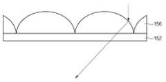
도 2는 도 1의 픽셀 어레이에서 유닛 픽셀들의 렌즈층의 구조를 예시적으로 보여주는 평면도이며, 도 3은 도 2에서 A-A' 의 절취선을 따라 절단한 모습을 예시적으로 보여주는 단면도이다.FIG. 2 is a plan view exemplarily showing the structure of a lens layer of unit pixels in the pixel array of FIG. 1 , and FIG. 3 is a cross-sectional view exemplarily showing a state taken along the line A-A' in FIG. 2 .
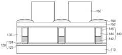
도 2 및 도 3을 참조하면, 이미지 센싱 장치의 픽셀 어레이(100)는 기판(110), 버퍼층(120), 컬러 필터층(130), 그리드 구조물들(140) 및 렌즈층(150)을 포함할 수 있다.2 and 3 , the
기판(110)은 서로 대향되는 제 1 면 및 제 2 면을 갖는 반도체 기판을 포함할 수 있다. 반도체 기판(110)은 단결정 상태(Single crystal state)일 수 있으며, 실리콘 함유 재료를 포함할 수 있다. 반도체 기판(110)은 P형 불순물을 포함할 수 있다. 반도체 기판(110)의 내부에는 광전변환소자들(112)이 형성될 수 있다. 광전변환소자들(112)은 각 유닛 픽셀(PX)별로 형성되며 소자분리막(114)에 의해 아이솔레이션될 수 있다.The
광전변환소자(112)는 유기 또는 무기 포토다이오드를 포함할 수 있다. 광전변환소자(112)는 기판(110) 내에서 수직 방향으로 적층되는 불순물 영역들을 포함할 수 있다. 예를 들어, 광전변환소자(112)는 N형 불순물 영역과 P형 불순물 영역이 수직 방향으로 적층된 포토다이오드(Photo Diode)를 포함할 수 있다. N형 불순물 영역과 P형 불순물 영역은 이온주입공정을 통해 형성될 수 있다. 소자분리막(114)은 DTI(Deep Trench Isolation) 구조를 포함할 수 있다.The
버퍼층(120)은 기판(110)의 제 1 면상에 형성된 단차를 제거하기 위한 평탄화층의 역할을 수행할 수 있다. 또한, 버퍼층(120)은 렌즈층(150) 및 컬러 필터층(130)을 통해 입사되는 광이 광전변환소자(112) 쪽으로 통과되도록 하는 반사 방지막의 역할을 수행할 수 있다. 버퍼층(120)은 굴절율이 서로 다른 물질들이 적층된 다층막으로 형성될 수 있다. 예컨대, 버퍼층(120)은 질화막(122)과 산화막(124)이 적층된 다층막 구조를 포함할 수 있다. 질화막(122)은 실리콘 질화막(SixNy, 여기서 x, y는 자연수) 또는 실리콘 산화 질화막(SixOyNz, 여기서 x, y, z는 자연수)을 포함할 수 있다. 산화막(124)은 단일막 또는 산화막들이 적층된 다층막 구조를 포함할 수 있다. 이러한 산화막(124)은 USG(Undoped Silicate Glass)막과 저온산화(ULTO: ULTRA LOW TEMPERATURE OXIDE)막 중 적어도 어느 하나를 포함할 수 있다. 산화막(124)은 그리드 구조물(140)의 캡핑막(146)이 형성될 때 함께 형성될 수 있다. 예를 들어, 산화막(124)은 그리드 구조물(140)의 캡핑막(146)과 동일한 물질로 형성될 수 있으며, 산화막(124)과 캡핑막(146)은 동일한 증착 공정을 통해 동시에 형성될 수 있다.The
컬러 필터층(130)은 렌즈층(150)을 통해 입사되는 광으로부터 가시광을 필터링하여 통과시킨다. 컬러 필터층(130)은 각 유닛 픽셀(PX)에 대응되게 그리드 구조물들(140) 사이에 갭필된 컬러 필터들을 포함할 수 있다. 예컨대, 컬러 필터층(130)은 가시광에서 적색광만을 통과시키는 복수의 레드 컬러 필터들(R)(red color filters), 가시광에서 녹색광만을 통과시키는 복수의 그린 컬러 필터들(G)(green color filters) 및 가시광에서 청색광만을 통과시키는 복수의 블루 컬러 필터들(B)(blue color filters)을 포함할 수 있다. 컬러 필터들(R, G, B)은 베이어 패턴 형태로 배열될 수 있다. 또는 컬러 필터층(130)은 복수의 사이언 필터들(cyan filters), 복수의 옐로우 필터들(yellow filters), 복수의 마젠타 필터들(magenta filters)을 포함할 수 있다.The
그리드(grid) 구조물들(140)은 인접한 컬러 필터들 사이에 위치하여 컬러 필터들 간의 광학적 크로스 토크(cross-talk)를 방지한다. 그리드 구조물들(140)은 메탈층(142), 메탈층(142) 상부에 위치하는 에어층(144) 및 캡핑막(146)을 포함하는 하이브리드 구조로 형성될 수 있다. 캡핑막(146)은 그리드 구조물(140)의 최외곽에 형성되는 물질막으로서, 메탈층(142) 및 에어층(144)을 캡핑한다. 캡핑막(146)은 컬러 필터들(130)의 하부까지 연장되게 형성될 수 있다. 이때, 컬러 필터들(130)의 하부에 형성된 캡핑막(146)은 버퍼층(120)의 일부(124)가 될 수 있다. 메탈층(142)은 텅스텐을 포함할 수 있다. 도 3에서는 그리드 구조물들(140)이 하이브리드 구조로 형성되는 경우를 도시하였으나, 에어층 없이 메탈층으로만 형성될 수도 있다.
렌즈층(150)은 컬러 필터들(130) 및 그리드 구조물들(140) 상부에 위치하며 입사광을 컬러 필터층(130)의 컬러 필터들로 집광시킨다. 이러한 렌즈층(150)은 오버 코팅층(152), 에지(edge) 마이크로 렌즈(154) 및 메인 마이크로 렌즈(156)를 포함할 수 있다.The lens layer 150 is positioned on the
오버 코팅층(152)은 컬러 필터층(130) 및 그리드 구조물(140)에 의해 형성된 단차를 제거하기 위한 평탄화층의 역할을 수행할 수 있다. 컬러 필터층(130) 및 그리드 구조물(140)의 두께(높이)에 대한 제어가 쉽지 않아 컬러 필터층(130)의 상부면에 단차가 발생될 수 있으며, 컬러 필터층(130)과 그리드 구조물(140) 사이에도 단차가 발생될 수 있다. 따라서, 그러한 단차를 제거하기 위해 컬러 필터층(130) 및 그리드 구조물(140) 상에 오버 코팅층(152)이 형성될 수 있다.The
이러한 오버 코팅층(152)은 메인 마이크로 렌즈(156)와 동일한 물질로 형성될 수 있다. 예를 들어, 오버 코팅층(152)은 포토레지스트 물질 또는 산화막을 포함할 수 있다.The
에지 마이크로 렌즈(154)는 메인 마이크로 렌즈(156)에 입사되는 광들 중 메인 마이크로 렌즈(156)의 에지 영역에 입사되는 광들을 굴절시켜 해당 유닛 픽셀의 광전변환영역(112)에 보다 잘 집광될 수 있도록 해준다.The
수직면상에서 볼 때, 에지 마이크로 렌즈(154)는 메인 마이크로 렌즈(156)와 오버 코팅층(152) 사이에 형성될 수 있다. 예를 들어, 에지 마이크로 렌즈(154)는 메인 마이크로 렌즈(156)의 에지 영역과 수직 방향으로 중첩되도록 메인 마이크로 렌즈(156)와 오버 코팅층(152) 사이에 형성될 수 있다. 에지 마이크로 렌즈들(154)은 바닥면은 평평하고 상부면은 볼록한 곡률을 가지는 돔 형태로 형성될 수 있다.When viewed from a vertical plane, the
수평면상에서 볼 때, 에지 마이크로 렌즈들(154)은 원형 형상으로 형성될 수 있으며, 이웃하는 메인 마이크로 렌즈들(156)의 에지 영역들에 걸쳐지게 그 중심부가 메인 마이크로 렌즈들(156)의 경계 영역에 위치할 수 있다. 예를 들어, 에지 마이크로 렌즈들(154)은 이웃한 컬러 필터들 사이에 위치하는 그리드 구조물(140)과 에지 마이크로 렌즈(154)의 중심부가 수직 방향으로 중첩되도록 제 1 방향(X 방향) 및 제 1 방향과 교차되는 제 2 방향(Y 방향)을 따라 일정 간격으로 이격되게 배치될 수 있다. 즉, 하나의 에지 마이크로 렌즈(154)는 이웃하는 2개의 메인 마이크로 렌즈들(156)의 에지 영역들과 공통으로 중첩될 수 있다.When viewed in a horizontal plane, the
이러한 에지 마이크로 렌즈(154)는 메인 마이크로 렌즈(156) 보다 굴절률이 큰 물질로 형성될 수 있다.The edge microlens 154 may be formed of a material having a higher refractive index than that of the
메인 마이크로 렌즈(156)는 유닛 픽셀 별로 하나씩 형성되어 외부로부터 입사되는 광을 해당 유닛 픽셀의 컬러 필터층(130) 쪽으로 집광시킬 수 있다. 예를 들어, 메인 마이크로 렌즈(156)는 각 유닛 픽셀과 일대일 대응되게 형성되며, 해당 유닛 픽셀 영역에서 오버 코팅층(152) 및 에지 마이크로 렌즈(154)의 상부에 형성될 수 있다.The main
메인 마이크로 렌즈(156)는 센터 영역 및 센터 영역을 둘러싸는 에지 영역으로 구분될 수 있으며, 에지 영역들 중 일부는 에지 마이크로 렌즈(154)와 중첩되게 형성될 수 있다. 예를 들어, 에지 영역 중에서 X 축 및 Y 축과 만나는 에지 영역이 에지 마이크로 렌즈(154)와 중첩되게 형성될 수 있다. 메인 마이크로 렌즈(156)의 중심부는 광전변환소자(112)의 중심부와 수직 방향으로 중첩되게 형성될 수 있다.The
메인 마이크로 렌즈(156)로 입사되는 광들 중 에지 마이크로 렌즈(154)와 중첩되는 에지 영역으로 입사되는 광은 에지 마이크로 렌즈(154)에 의해 굴절된 후 컬러 필터층(130) 쪽으로 진행할 수 있다.Among the lights incident on the main
이러한 메인 마이크로 렌즈(156)는 에지 마이크로 렌즈(154) 보다 굴절률이 작은 광투과성 물질로 형성될 수 있다. 예를 들어, 메인 마이크로 렌즈(156)는 포토레지스트 물질 또는 산화막을 포함할 수 있다.The main
도 4a는 에지 마이크로 렌즈가 존재하지 않는 경우, 메인 마이크로 렌즈의 에지 영역으로 입사된 광의 진행 방향을 예시적으로 나타낸 도면이다. 그리고, 도 4b는 에지 마이크로 렌즈가 존재하는 경우, 메인 마이크로 렌즈의 에지 영역으로 입사된 광의 진행 방향을 예시적으로 나타낸 도면이다.4A is a view exemplarily illustrating a traveling direction of light incident to an edge region of a main microlens when an edge microlens does not exist. And, FIG. 4B is a view exemplarily illustrating a traveling direction of light incident to an edge region of the main microlens when an edge microlens is present.
도 4a 및 도 4b를 참조하여, 본 실시예에서의 에지 마이크로 렌즈의 기능을 설명하면 다음과 같다.With reference to FIGS. 4A and 4B , the function of the edge microlens in this embodiment will be described as follows.
도 4a에서와 같이, 에지 마이크로 렌즈(154)가 존재하지 않는 경우, 메인 마이크로 렌즈(156)의 에지 영역으로 입사된 광은 메인 마이크로 렌즈(156)의 표면에서 굴절된 후 메인 마이크로 렌즈(156)와 오버 코팅층(152)을 투과하게 된다.As in FIG. 4A , when the
반면에, 도 4b에서와 같이, 에지 마이크로 렌즈(154)가 메인 마이크로 렌즈(156)의 에지 영역 하부에 존재하는 경우, 메인 마이크로 렌즈(156)의 에지 영역으로 입사된 광은 메인 마이크로 렌즈(156)에서 1차적으로 굴절된 후 에지 마이크로 렌즈(156)에서 2차 굴절하게 된다.On the other hand, as in FIG. 4B , when the
에지 마이크로 렌즈(154)는 메인 마이크로 렌즈(156) 보다 굴절률이 크며 곡률을 가지기 때문에, 에지 마이크로 렌즈(154)에서 굴절된 광은 메인 마이크로 렌즈(156)만을 투과하는 광에 비해 굴절각이 작아질 수 있다. 이때, 에지 마이크로 렌즈(154)에서 굴절된 광의 굴절각은 에지 마이크로 렌즈(154)의 굴절률 또는 에지 마이크로 렌즈(154)의 곡률 반경 등에 따라 조절될 수 있다.Since the
렌즈층(150)을 투과한 광의 굴절각이 작으면, 굴절각이 큰 경우에 비해, 버퍼층(120) 등에서의 광의 산란을 상대적으로 줄일 수 있다. 따라서, 버퍼층(120)에서의 광의 산란에 의한 크로스 토크를 줄이면서 보다 많은 광이 광전변환소자(112)에 집광되도록 할 수 있다.When the refraction angle of the light passing through the lens layer 150 is small, scattering of light from the
또한, 오버 코팅층(152)이 메인 마이크로 렌즈(156)와 동일한 물질로 이루어진다고 하더라도, 오버 코팅층(152)과 메인 마이크로 렌즈(156)의 경계면에서도 광의 산란이 발생될 수 있다. 그런데, 에지 마이크로 렌즈(154)에 의해 오버 코팅층(152)에 대한 광의 입사각이 작아지면 상대적으로 그러한 산란이 적게 발생될 수 있다. 따라서, 에지 마이크로 렌즈(154)를 사용함으로써 오버 코팅층(152)에 의한 크로스 토크도 상대적으로 줄일 수 있다.Also, even if the
도 5a 내지 도 5c는 도 3에서의 렌즈층을 형성하는 방법을 예시적으로 설명하기 위한 공정 단면도들이다.5A to 5C are cross-sectional views illustrating a method of forming a lens layer in FIG. 3 by way of example.
도 5a를 참조하면, 컬러 필터층(130) 및 그리드 구조물(140)을 포함하는 하부 구조물 상부에 오버 코팅층(152)을 형성한다.Referring to FIG. 5A , an
컬러 필터층(130) 및 그리드 구조물(140)을 형성하는 방법은 종래의 방법들을 사용하여도 무방하므로 본 실시예에서는 이에 대한 설명은 생략한다.As a method of forming the
오버 코팅층(152)은 컬러 필터층(130) 및 그리드 구조물(140)에 의해 형성된 단차를 제거하기 위한 평탄화층으로서, 포토레지스트 물질을 포함할 수 있다.The
이어서, 오버 코팅층(152) 상부에서 에지 마이크로 렌즈들이 형성될 영역에 고굴절 물질 패턴(154′)이 형성된다. 고굴절 물질 패턴(154′)은 후속 공정에서 형성되는 메인 마이크로 렌즈보다 굴절률이 큰 물질을 포함할 수 있다. 예를 들어, 고굴절 물질 패턴(154′)은 폴리머 내에 고굴절율 물질의 미립자(나노 미립자)들이 알갱이 형태로 고르게 분산된 폴리이미드계 수지를 포함할 수 있다. 이때, 고굴절률 물질은 이산화티타늄(TiO2), 산화탄탈(예컨대 TaO2, Ta2O5), 산화지르코늄(ZrO2), 산화아연(ZnO), 산화주석(SnO), 산화알루미늄(Al2O3), 산화란탄(La2O3), 산화세륨(CeO2), 산화이트륨(Y2O3), 실리콘산질화막(SiON) 둥의 고굴절 산화물들을 적어도 하나 포함할 수 있다.Then, a high refractive
도 5b를 참조하면, 열적 리플로우 공정을 통해 고굴절 물질 패턴(154′)을 리플로우시킴으로써 오버 코팅층(152) 상부에 돔 형태의 에지 마이크로 렌즈들(154)을 형성한다.Referring to FIG. 5B , dome-shaped
이어서, 에지 마이크로 렌즈들(154) 사이에 메인 마이크로 렌즈를 형성하기 위한 유기물 패턴(156′)을 형성한다. 예를 들어, 유기물 패턴(156′)은 포토레지스트 패턴을 포함할 수 있다.Next, an
도 5c를 참조하면, 열적 리플로우 공정을 통해 유기물 패턴(156′)을 리플로우시킴으로써 오버 코팅층(152) 및 에지 마이크로 렌즈들(154) 상부에 돔 형태의 메인 마이크로 렌즈들(156)을 형성한다. 이때, 메인 마이크로 렌즈들(156)은 그 에지 영역이 에지 마이크로 렌즈들(154)과 중첩되게 형성될 수 있다.Referring to FIG. 5C , dome-shaped main
도 6a 내지 도 6f는 도 3에서의 렌즈층을 형성하는 다른 방법을 예시적으로 설명하기 위한 공정 단면도들이다.6A to 6F are cross-sectional views illustrating another method of forming the lens layer in FIG. 3 by way of example.
도 6a을 참조하면, 컬러 필터층(130) 및 그리드 구조물(140)을 포함하는 하부 구조물 상부에 오버 코팅층(152)을 형성한다.Referring to FIG. 6A , an
다음에, 오버 코팅층(152) 상부에 고굴절률 물질층(157)을 형성한다. 예를 들어, 고굴절률 물질층(157)은 이산화티타늄(TiO2), 산화탄탈(예컨대 TaO2, Ta2O5), 산화지르코늄(ZrO2), 산화아연(ZnO), 산화주석(SnO), 산화알루미늄(Al2O3), 산화란탄(La2O3), 산화세륨(CeO2), 산화이트륨(Y2O3), 실리콘산질화막(SiON) 둥의 고굴절 산화물들을 적어도 하나 포함할 수 있다.Next, a high refractive
다음에, 고굴절률 물질층(157) 상부에서 에지 마이크로 렌즈들이 형성될 영역에 유기물 패턴(158)을 형성한다. 예를 들어, 유기물 패턴(158)은 포토레지스트 패턴을 포함할 수 있다.Next, an
도 6b를 참조하면, 열적 리플로우 공정을 통해 유기물 패턴(158)을 리플로우시킴으로써 고굴절률 물질층(157) 상부에 돔 형태의 에지렌즈 마스크 패턴(158′)을 형성한다.Referring to FIG. 6B , the dome-shaped edge
도 6c를 참조하면, 에지렌즈 마스크 패턴(158′)을 식각 마스크로 그 하부의 고굴절률 물질층(157)을 식각함으로써 오버 코팅층(152) 상부에 돔 형태의 에지 마이크로 렌즈들(154)을 형성한다.Referring to FIG. 6C , dome-shaped edge
이어서, 오버 코팅층(152) 및 에지 마이크로 렌즈들(154) 상부에 절연막(159)을 형성한다. 이때, 절연막(159)은 에지 마이크로 렌즈(154) 보다 굴절률이 작은 산화막을 포함할 수 있다.Next, an insulating
도 6d를 참조하면, 절연막(159) 상부에서 메인 마이크로 렌즈가 형성될 영역에 유기물 패턴(156′)을 형성한다. 예를 들어, 유기물 패턴(156′)은 포토레지스트 패턴을 포함할 수 있다.Referring to FIG. 6D , an
도 6e를 참조하면, 열적 리플로우 공정을 통해 유기물 패턴(156′)을 리플로우시킴으로써 절연막(159) 상부에 돔 형태의 메인렌즈 마스크 패턴(156″)을 형성한다.Referring to FIG. 6E , a dome-shaped main
도 6f를 참조하면, 메인렌즈 마스크 패턴(156″)을 식각 마스크로 그 하부의 절연막(159)을 식각함으로써 오버 코팅층(152) 및 에지 마이크로 렌즈들(154) 상부에 돔 형태의 메인 마이크로 렌즈들(156)을 형성한다. 이때, 메인 마이크로 렌즈들(156)의 에지 영역은 에지 마이크로 렌즈들(154)과 중첩되게 형성될 수 있다.Referring to FIG. 6F , the main
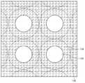
도 7은 도 1의 픽셀 어레이에서 유닛 픽셀들의 렌즈층의 구조를 예시적으로 보여주는 평면도이다.FIG. 7 is a plan view exemplarily illustrating a structure of a lens layer of unit pixels in the pixel array of FIG. 1 .
도 7을 참조하면, 에지 마이크로 렌즈들(154)은 이웃하는 4개의 메인 마이크로 렌즈들(156)의 에지 영역들에 걸쳐지게 그 중심부가 해당 메인 마이크로 렌즈들(156)의 경계 영역에 위치할 수 있다.Referring to FIG. 7 , the
예를 들어, 에지 마이크로 렌즈들(154)은 이웃하는 4개의 메인 마이크로 렌즈들(156) 사이의 경계 영역 즉 데드존(dead zone)에 에지 마이크로 렌즈(154)의 중심부가 위치하면서 해당 4개의 메인 마이크로 렌즈들(156)의 에지 영역들과 부분적으로 중첩되는 원형의 돔 형태로 형성될 수 있다.For example, in the
이때, 에지 마이크로 렌즈들(154)의 중심부는 그리드 구조물(140)에서 X 방향으로 연장되는 그리드 구조물과 Y 방향으로 연장되는 그리드 구조물이 서로 교차되는 영역과 중첩되게 형성될 수 있다.In this case, the center of the
에지 마이크로 렌즈들의 구조 이외의 구성들은 상술한 도 3에서와 동일하므로, 이들에 대한 설명은 생략한다.Configurations other than the structure of the edge microlenses are the same as in FIG. 3 , and thus a description thereof will be omitted.
도 8은 도 1의 픽셀 어레이에서 유닛 픽셀들의 렌즈층의 구조를 예시적으로 보여주는 평면도이다.FIG. 8 is a plan view exemplarily illustrating a structure of a lens layer of unit pixels in the pixel array of FIG. 1 .
도 8을 참조하면, 에지 마이크로 렌즈(154)는 이웃하는 메인 마이크로 렌즈들(156)의 에지 영역들에 걸쳐지게 형성되되, 메인 마이크로 렌즈들(156)의 센터 영역과만 중첩되지 않는 그리드 형태로 형성될 수 있다. 예를 들어, 에지 마이크로 렌즈(154)는 데드존들과 중첩되면서 메인 마이크로 렌즈들(156)에서 센터 영역만을 원형 형태로 남겨두고 에지 영역들과 모두 중첩되는 일체형의 하나의 렌즈 형태로 형성될 수 있다.Referring to FIG. 8 , the
에지 마이크로 렌즈들의 구조 이외의 구성들은 상술한 도 3에서와 동일하므로, 이들에 대한 설명은 생략한다.Configurations other than the structure of the edge microlenses are the same as in FIG. 3 , and thus a description thereof will be omitted.
도 9는 도 1의 픽셀 어레이에서 유닛 픽셀들의 렌즈층의 구조를 예시적으로 보여주는 평면도이다.9 is a plan view exemplarily illustrating a structure of a lens layer of unit pixels in the pixel array of FIG. 1 .
도 9를 참조하면, 에지 마이크로 렌즈(154)는 그리드 구조물(140)과 같은 그리드 형태로 형성되되 그리드 구조물(140) 보다 폭이 넓은 형태로 형성될 수 있다. 예를 들어, 에지 마이크로 렌즈(154)는 데드존들과 중첩되면서 메인 마이크로 렌즈들(156)에서 센터 영역만을 사각형 형태로 남겨두고 에지 영역들과 모두 중첩되는 일체형의 하나의 렌즈 형태로 형성될 수 있다.Referring to FIG. 9 , the
에지 마이크로 렌즈들의 구조 이외의 구성들은 상술한 도 3에서와 동일하므로, 이들에 대한 설명은 생략한다.Configurations other than the structure of the edge microlenses are the same as in FIG. 3 , and thus a description thereof will be omitted.
이상의 설명은 본 발명의 기술 사상을 예시적으로 설명한 것에 불과한 것으로서, 본 발명이 속하는 기술 분야에서 통상의 지식을 가진 자라면 본 발명의 본질적인 특성에서 벗어나지 않는 범위에서 다양한 수정 및 변형이 가능할 것이다.The above description is merely illustrative of the technical spirit of the present invention, and various modifications and variations will be possible without departing from the essential characteristics of the present invention by those skilled in the art to which the present invention pertains.
따라서, 본 발명에 개시된 실시 예들은 본 발명의 기술 사상을 한정하기 위한 것이 아니라 설명하기 위한 것이고, 이러한 실시 예에 의하여 본 발명의 기술 사상의 범위가 한정되는 것은 아니다. 본 발명의 보호 범위는 아래의 청구범위에 의하여 해석되어야 하며, 그와 동등한 범위 내에 있는 모든 기술 사상은 본 발명의 권리범위에 포함되는 것으로 해석되어야 할 것이다.Therefore, the embodiments disclosed in the present invention are not intended to limit the technical spirit of the present invention, but to explain, and the scope of the technical spirit of the present invention is not limited by these embodiments. The protection scope of the present invention should be construed by the following claims, and all technical ideas within the equivalent range should be construed as being included in the scope of the present invention.
100: 픽셀 어레이
110: 기판
120: 버퍼층
130: 컬러 필터층
140: 그리드 구조물
150: 렌즈층
152: 오버 코팅층
154: 에지 마이크로 렌즈
156: 메인 마이크로 렌즈
200: 상관 이중 샘플러
300: 아날로그-디지털 컨버터
400: 버퍼
500: 로우 드라이버
600: 타이밍 제너레이터
700: 제어 레지스터
800: 램프 신호 제너레이터100: pixel array
110: substrate
120: buffer layer
130: color filter layer
140: grid structure
150: lens layer
152: over coating layer
154: edge micro lens
156: main micro lens
200: correlated double sampler
300: analog-to-digital converter
400: buffer
500: low driver
600: timing generator
700: control register
800: ramp signal generator
Claims (18)
Translated fromKorean상기 픽셀 어레이는
상기 입사광에서 가시광을 필터링하는 복수의 컬러 필터들;
상기 복수의 컬러 필터들 사이에 위치하며 인접한 컬러 필터들 간의 광학적 크로스 토크를 방지하는 그리드 구조물들; 및
상기 컬러 필터들 및 상기 그리드 구조물들 상부에 위치하며 입사광을 상기 복수의 컬러 필터들로 집광시키는 렌즈층을 포함하며,
상기 렌즈층은
상기 유닛 픽셀 별로 형성되는 메인 마이크로 렌즈들; 및
서로 이웃한 상기 메인 마이크로 렌즈들에 공통으로 중첩되게 상기 메인 마이크로 렌즈들과 상기 컬러 필터들 사이에 위치하며, 상기 메인 마이크로 렌즈들에 입사된 광을 굴절시키는 적어도 하나의 에지 마이크로 렌즈를 포함하는 이미지 센싱 장치.and a pixel array in which a plurality of unit pixels for converting incident light into an electric signal corresponding thereto are arranged,
the pixel array
a plurality of color filters for filtering visible light from the incident light;
grid structures positioned between the plurality of color filters and preventing optical crosstalk between adjacent color filters; and
and a lens layer positioned above the color filters and the grid structures and condensing incident light to the plurality of color filters,
The lens layer
main micro lenses formed for each unit pixel; and
An image including at least one edge microlens that is positioned between the main microlenses and the color filters to overlap the main microlenses adjacent to each other and refracts light incident on the main microlenses sensing device.
상기 메인 마이크로 렌즈들 각각은 센터 영역 및 상기 센터 영역을 둘러싸는 에지 영역을 포함하며,
상기 적어도 하나의 에지 마이크로 렌즈는 서로 이웃하는 상기 메인 마이크로 렌즈들의 상기 에지 영역들과 공통으로 중첩되도록 위치하는 것을 특징으로 하는 이미지 센싱 장치.The method according to claim 1,
Each of the main micro lenses includes a center area and an edge area surrounding the center area,
The image sensing apparatus according to claim 1, wherein the at least one edge micro lens is positioned to overlap with the edge regions of the main micro lenses adjacent to each other.
이웃하는 2개의 상기 메인 마이크로 렌즈들의 상기 에지 영역들과 공통으로 중첩되도록 그 중심부가 상기 2개의 메인 마이크로 렌즈들의 경계 영역에 위치하는 복수의 에지 마이크로 렌즈들을 포함하는 것을 특징으로 하는 이미지 센싱 장치.The method according to claim 2, wherein the at least one edge micro lens
and a plurality of edge microlenses having a central portion positioned in a boundary region of the two main microlenses so as to overlap the edge regions of the two neighboring main microlenses in common.
이웃하는 4개의 상기 메인 마이크로 렌즈들의 상기 에지 영역들과 공통으로 중첩되도록 그 중심부가 상기 4개의 메인 마이크로 렌즈들의 경계 영역에 위치하는 복수의 에지 마이크로 렌즈들을 포함하는 것을 특징으로 하는 이미지 센싱 장치.The method according to claim 2, wherein the at least one edge micro lens
and a plurality of edge microlenses whose central portions are positioned in boundary regions of the four main microlenses so as to overlap the edge regions of the four neighboring main microlenses in common.
상기 메인 마이크로 렌즈들의 상기 에지 영역들 및 상기 메인 마이크로 렌즈들 사이의 데드존들(dead zones)과 중첩되는 하나의 에지 마이크로 렌즈를 포함하는 것을 특징으로 하는 이미지 센싱 장치.The method according to claim 2, wherein the at least one edge micro lens
and one edge microlens overlapping the edge regions of the main microlenses and dead zones between the main microlenses.
이웃한 컬러 필터들 사이에 위치하는 그리드 구조물과 그 중심부가 중첩되게 위치하는 원형의 돔 형태로 형성되는 것을 특징으로 하는 이미지 센싱 장치.The method according to claim 1, wherein the at least one edge micro-lens is
An image sensing device, characterized in that it is formed in a circular dome shape in which a grid structure positioned between adjacent color filters and a center thereof are overlapped.
중심부가 상기 그리드 구조물에서 X 방향으로 연장되는 그리드 구조물과 Y 방향으로 연장되는 그리드 구조물이 교차되는 영역과 중첩되게 위치하는 원형의 돔 형태로 형성되는 것을 특징으로 하는 이미지 센싱 장치.The method according to claim 1, wherein the at least one edge micro-lens is
The image sensing device, characterized in that the central portion is formed in the form of a circular dome positioned to overlap an area where the grid structure extending in the X direction and the grid structure extending in the Y direction intersect the grid structure.
상기 메인 마이크로 렌즈들 각각은 센터 영역 및 상기 센터 영역을 둘러싸는 에지 영역을 포함하며,
상기 적어도 하나의 에지 마이크로 렌즈는 서로 이웃한 상기 메인 마이크로 렌즈들의 상기 에지 영역들과 부분적으로 중첩되는 것을 특징으로 하는 이미지 센싱 장치.The method according to claim 1,
Each of the main micro lenses includes a center area and an edge area surrounding the center area,
The at least one edge micro lens partially overlaps with the edge regions of the main micro lenses adjacent to each other.
상기 에지 마이크로 렌즈들과 상기 컬러 필터들 사이 그리고 상기 메인 마이크로 렌즈들과 상기 컬러 필터들 사이에 위치하는 오버 코팅층을 더 포함하는 것을 특징으로 하는 이미지 센싱 장치.The method according to claim 1, wherein the lens layer
The image sensing device according to claim 1, further comprising an overcoat layer positioned between the edge microlenses and the color filters and between the main microlenses and the color filters.
상기 메인 마이크로 렌즈보다 굴절률이 큰 물질을 포함하는 것을 특징으로 하는 이미지 센싱 장치.The method according to claim 1, wherein the at least one edge micro-lens is
and a material having a refractive index greater than that of the main micro lens.
메탈층;
상기 메탈층 상부에 위치하는 에어층; 및
상기 메탈층 및 에어층을 캡핑하는 캡핑막을 포함하는 것을 특징으로 하는 이미지 센싱 장치.The method according to claim 1, wherein the grid structure is
metal layer;
an air layer positioned on the metal layer; and
and a capping film for capping the metal layer and the air layer.
상기 유닛 픽셀은 입사광을 그에 대응되는 전기 신호로 변환하는 광전변환소자를 포함하며,
상기 메인 마이크로 렌즈의 중심부는 상기 광전변환소자의 중심부와 중첩되게 위치하는 것을 특징으로 하는 이미지 센싱 장치.The method according to claim 1,
The unit pixel includes a photoelectric conversion element that converts incident light into an electric signal corresponding thereto,
The image sensing device, characterized in that the central portion of the main micro lens is positioned to overlap the central portion of the photoelectric conversion element.
상기 컬러 필터들과 일대일 대응되게 상기 컬러 필터들의 상부에 각각 위치하는 복수의 메인 마이크로 렌즈들; 및
상기 복수의 메인 마이크로 렌즈들에 공통으로 중첩되도록 상기 컬러 필터들과 상기 메인 마이크로 렌즈들 사이에 위치하는 적어도 하나의 에지 마이크로 렌즈를 포함하는 이미지 센싱 장치.a plurality of color filters for filtering visible light from incident light;
a plurality of main micro lenses respectively positioned above the color filters in a one-to-one correspondence with the color filters; and
and at least one edge microlens positioned between the color filters and the main microlenses to overlap the plurality of main microlenses in common.
이웃하는 2개의 상기 메인 마이크로 렌즈들과 공통으로 중첩되는 복수의 에지 마이크로 렌즈들을 포함하는 것을 특징으로 하는 이미지 센싱 장치.14. The method of claim 13, wherein the at least one edge micro lens comprises:
and a plurality of edge microlenses that are commonly overlapped with the two adjacent main microlenses.
이웃하는 4개의 상기 메인 마이크로 렌즈들과 공통으로 중첩되는 복수의 에지 마이크로 렌즈들을 포함하는 것을 특징으로 하는 이미지 센싱 장치.14. The method of claim 13, wherein the at least one edge micro lens comprises:
An image sensing device comprising a plurality of edge microlenses that are commonly overlapped with the four neighboring main microlenses.
중심부가 상기 4개의 상기 메인 마이크로 렌즈들 사이의 데드존(dead zones)에 위치하는 것을 특징으로 하는 이미지 센싱 장치.The method according to claim 15, wherein each of the plurality of edge micro lenses
The image sensing device, characterized in that the central portion is located in the dead zones (dead zones) between the four main micro lenses.
상기 메인 마이크로 렌즈들 각각은 센터 영역 및 상기 센터 영역을 둘러싸는 에지 영역을 포함하며,
상기 적어도 하나의 에지 마이크로 렌즈는 상기 복수의 메인 마이크로 렌즈들의 상기 에지 영역들과 부분적으로 중첩되는 것을 특징으로 하는 이미지 센싱 장치.14. The method of claim 13,
Each of the main micro lenses includes a center area and an edge area surrounding the center area,
The at least one edge micro lens partially overlaps the edge regions of the plurality of main micro lenses.
원형의 돔 형태로 형성되는 것을 특징으로 하는 이미지 센싱 장치.14. The method of claim 13, wherein the at least one edge micro lens comprises:
Image sensing device, characterized in that formed in the shape of a circular dome.
Priority Applications (3)
| Application Number | Priority Date | Filing Date | Title |
|---|---|---|---|
| KR1020190168712AKR20210077264A (en) | 2019-12-17 | 2019-12-17 | Image sensing device |
| CN202010602579.4ACN112992941A (en) | 2019-12-17 | 2020-06-29 | image sensing device |
| US16/925,116US20210183929A1 (en) | 2019-12-17 | 2020-07-09 | Image sensing device |
Applications Claiming Priority (1)
| Application Number | Priority Date | Filing Date | Title |
|---|---|---|---|
| KR1020190168712AKR20210077264A (en) | 2019-12-17 | 2019-12-17 | Image sensing device |
Publications (1)
| Publication Number | Publication Date |
|---|---|
| KR20210077264Atrue KR20210077264A (en) | 2021-06-25 |
Family
ID=76317063
Family Applications (1)
| Application Number | Title | Priority Date | Filing Date |
|---|---|---|---|
| KR1020190168712AAbandonedKR20210077264A (en) | 2019-12-17 | 2019-12-17 | Image sensing device |
Country Status (3)
| Country | Link |
|---|---|
| US (1) | US20210183929A1 (en) |
| KR (1) | KR20210077264A (en) |
| CN (1) | CN112992941A (en) |
Families Citing this family (5)
| Publication number | Priority date | Publication date | Assignee | Title |
|---|---|---|---|---|
| US12408459B2 (en)* | 2021-11-30 | 2025-09-02 | Visera Technologies Company Limited | Image sensor having liquid-lens units and method for detecting images |
| US20250015239A1 (en)* | 2022-05-24 | 2025-01-09 | Boe Technology Group Co., Ltd. | Microlens substrate, display device and method for manufacturing microlens substrate |
| CN117095427A (en)* | 2022-07-14 | 2023-11-21 | 台湾积体电路制造股份有限公司 | Optical fingerprint sensor with enhanced security feature |
| US12096141B2 (en)* | 2023-01-13 | 2024-09-17 | Omnivision Technologies, Inc. | LOFIC circuit for in pixel metal-insulator-metal(MIM) capacitor lag correction and associated correction methods |
| WO2025121577A1 (en)* | 2023-12-06 | 2025-06-12 | 주식회사 엘엑스세미콘 | Image sensor |
Family Cites Families (15)
| Publication number | Priority date | Publication date | Assignee | Title |
|---|---|---|---|---|
| US7768088B2 (en)* | 2004-09-24 | 2010-08-03 | Fujifilm Corporation | Solid-state imaging device that efficiently guides light to a light-receiving part |
| KR100703376B1 (en)* | 2005-05-10 | 2007-04-03 | 삼성전자주식회사 | Image sensor with embedded lens and manufacturing method thereof |
| US7978411B2 (en)* | 2007-05-08 | 2011-07-12 | Micron Technology, Inc. | Tetraform microlenses and method of forming the same |
| US7729055B2 (en)* | 2008-03-20 | 2010-06-01 | Aptina Imaging Corporation | Method and apparatus providing concave microlenses for semiconductor imaging devices |
| JP2011029277A (en)* | 2009-07-22 | 2011-02-10 | Toshiba Corp | Method for manufacturing solid state imaging apparatus, and the solid state imaging apparatus |
| JP2012119377A (en)* | 2010-11-29 | 2012-06-21 | Toshiba Corp | Solid-state imaging device |
| JP2012204354A (en)* | 2011-03-23 | 2012-10-22 | Sony Corp | Solid state imaging device, manufacturing method thereof and electronic apparatus |
| KR102056141B1 (en)* | 2013-02-25 | 2019-12-16 | 삼성전자주식회사 | Image sensor and computing system having the same |
| US9780132B2 (en)* | 2014-09-04 | 2017-10-03 | SK Hynix Inc. | Image sensor and electronic device including the same |
| US9437645B1 (en)* | 2015-03-20 | 2016-09-06 | Taiwan Semiconductor Manufacturing Co., Ltd. | Composite grid structure to reduce cross talk in back side illumination image sensors |
| US9497366B1 (en)* | 2015-05-27 | 2016-11-15 | Semiconductor Components Industries, Llc | Imaging systems with integrated light shield structures |
| US10312280B2 (en)* | 2017-09-28 | 2019-06-04 | Semiconductor Components Industries, Llc | Image sensors with diffractive lenses for stray light control |
| KR102506837B1 (en)* | 2017-11-20 | 2023-03-06 | 삼성전자주식회사 | Image sensor and method for fabricating the same |
| KR102687972B1 (en)* | 2019-06-21 | 2024-07-25 | 삼성전자주식회사 | Image sensor |
| KR20210055145A (en)* | 2019-11-06 | 2021-05-17 | 삼성전자주식회사 | Image Sensor |
- 2019
- 2019-12-17KRKR1020190168712Apatent/KR20210077264A/ennot_activeAbandoned
- 2020
- 2020-06-29CNCN202010602579.4Apatent/CN112992941A/ennot_activeWithdrawn
- 2020-07-09USUS16/925,116patent/US20210183929A1/ennot_activeAbandoned
Also Published As
| Publication number | Publication date |
|---|---|
| US20210183929A1 (en) | 2021-06-17 |
| CN112992941A (en) | 2021-06-18 |
Similar Documents
| Publication | Publication Date | Title |
|---|---|---|
| KR20210077264A (en) | Image sensing device | |
| KR102658571B1 (en) | Image sensing device and manufacturing method of the same | |
| EP3696856B1 (en) | Image sensor including color filter isolation layer and method of manufacturing the same | |
| US9653501B2 (en) | Image sensor including color filter and method of manufacturing the image sensor | |
| US11515348B2 (en) | Image sensor | |
| KR20180004480A (en) | Image Sensors Having a Plurality of Photodiodes Sharing One Color Filter and One Micro-lens | |
| US11557622B2 (en) | Image sensing device | |
| US20230127841A1 (en) | Image sensing device | |
| KR20210028808A (en) | Image sensor and imaging apparatus having the same | |
| US9583522B2 (en) | Image sensor and electronic device including the same | |
| US10115757B2 (en) | Image sensor and electronic device having the same | |
| US9204068B2 (en) | Solid-state photodiode imaging device and method of manufacturing the same | |
| KR20170037053A (en) | Image sensor | |
| US11217616B2 (en) | Image sensing device | |
| US20230170362A1 (en) | Image sensing device including grid structures having different heights | |
| KR102372736B1 (en) | Image sensor having phase difference detection pixel | |
| TWI697111B (en) | Image sensor and electronic device having the same | |
| JP2024096525A (en) | Image sensing device and manufacturing method thereof | |
| US20240222402A1 (en) | Image sensing device | |
| TWI853506B (en) | Light-adjusting device and solid-state image sensor using the same | |
| US20250203228A1 (en) | Imaging element and imaging device | |
| JP2024080697A (en) | Image Sensing Device | |
| KR20240088177A (en) | Image sensing device and manufacturing method of the same |
Legal Events
| Date | Code | Title | Description |
|---|---|---|---|
| PA0109 | Patent application | St.27 status event code:A-0-1-A10-A12-nap-PA0109 | |
| PG1501 | Laying open of application | St.27 status event code:A-1-1-Q10-Q12-nap-PG1501 | |
| A201 | Request for examination | ||
| PA0201 | Request for examination | St.27 status event code:A-1-2-D10-D11-exm-PA0201 | |
| E902 | Notification of reason for refusal | ||
| PE0902 | Notice of grounds for rejection | St.27 status event code:A-1-2-D10-D21-exm-PE0902 | |
| PC1902 | Submission of document of abandonment before decision of registration | St.27 status event code:N-1-6-B10-B11-nap-PC1902 | |
| P22-X000 | Classification modified | St.27 status event code:A-2-2-P10-P22-nap-X000 |