KR20210072198A - Display apparatus - Google Patents
Display apparatusDownload PDFInfo
- Publication number
- KR20210072198A KR20210072198AKR1020190161667AKR20190161667AKR20210072198AKR 20210072198 AKR20210072198 AKR 20210072198AKR 1020190161667 AKR1020190161667 AKR 1020190161667AKR 20190161667 AKR20190161667 AKR 20190161667AKR 20210072198 AKR20210072198 AKR 20210072198A
- Authority
- KR
- South Korea
- Prior art keywords
- layer
- touch
- encapsulation layer
- inorganic encapsulation
- display area
- Prior art date
- Legal status (The legal status is an assumption and is not a legal conclusion. Google has not performed a legal analysis and makes no representation as to the accuracy of the status listed.)
- Pending
Links
Images


Classifications
- H01L27/323—
- G—PHYSICS
- G06—COMPUTING OR CALCULATING; COUNTING
- G06F—ELECTRIC DIGITAL DATA PROCESSING
- G06F3/00—Input arrangements for transferring data to be processed into a form capable of being handled by the computer; Output arrangements for transferring data from processing unit to output unit, e.g. interface arrangements
- G06F3/01—Input arrangements or combined input and output arrangements for interaction between user and computer
- G06F3/03—Arrangements for converting the position or the displacement of a member into a coded form
- G06F3/041—Digitisers, e.g. for touch screens or touch pads, characterised by the transducing means
- G06F3/044—Digitisers, e.g. for touch screens or touch pads, characterised by the transducing means by capacitive means
- G06F3/0446—Digitisers, e.g. for touch screens or touch pads, characterised by the transducing means by capacitive means using a grid-like structure of electrodes in at least two directions, e.g. using row and column electrodes
- G—PHYSICS
- G06—COMPUTING OR CALCULATING; COUNTING
- G06F—ELECTRIC DIGITAL DATA PROCESSING
- G06F3/00—Input arrangements for transferring data to be processed into a form capable of being handled by the computer; Output arrangements for transferring data from processing unit to output unit, e.g. interface arrangements
- G06F3/01—Input arrangements or combined input and output arrangements for interaction between user and computer
- G06F3/03—Arrangements for converting the position or the displacement of a member into a coded form
- G06F3/041—Digitisers, e.g. for touch screens or touch pads, characterised by the transducing means
- G06F3/0412—Digitisers structurally integrated in a display
- G—PHYSICS
- G06—COMPUTING OR CALCULATING; COUNTING
- G06F—ELECTRIC DIGITAL DATA PROCESSING
- G06F3/00—Input arrangements for transferring data to be processed into a form capable of being handled by the computer; Output arrangements for transferring data from processing unit to output unit, e.g. interface arrangements
- G06F3/01—Input arrangements or combined input and output arrangements for interaction between user and computer
- G06F3/03—Arrangements for converting the position or the displacement of a member into a coded form
- G06F3/041—Digitisers, e.g. for touch screens or touch pads, characterised by the transducing means
- G06F3/0416—Control or interface arrangements specially adapted for digitisers
- G06F3/04164—Connections between sensors and controllers, e.g. routing lines between electrodes and connection pads
- H01L27/3276—
- H01L51/5256—
- H—ELECTRICITY
- H10—SEMICONDUCTOR DEVICES; ELECTRIC SOLID-STATE DEVICES NOT OTHERWISE PROVIDED FOR
- H10K—ORGANIC ELECTRIC SOLID-STATE DEVICES
- H10K50/00—Organic light-emitting devices
- H10K50/80—Constructional details
- H10K50/84—Passivation; Containers; Encapsulations
- H10K50/844—Encapsulations
- H—ELECTRICITY
- H10—SEMICONDUCTOR DEVICES; ELECTRIC SOLID-STATE DEVICES NOT OTHERWISE PROVIDED FOR
- H10K—ORGANIC ELECTRIC SOLID-STATE DEVICES
- H10K59/00—Integrated devices, or assemblies of multiple devices, comprising at least one organic light-emitting element covered by group H10K50/00
- H10K59/10—OLED displays
- H10K59/12—Active-matrix OLED [AMOLED] displays
- H10K59/131—Interconnections, e.g. wiring lines or terminals
- H—ELECTRICITY
- H10—SEMICONDUCTOR DEVICES; ELECTRIC SOLID-STATE DEVICES NOT OTHERWISE PROVIDED FOR
- H10K—ORGANIC ELECTRIC SOLID-STATE DEVICES
- H10K59/00—Integrated devices, or assemblies of multiple devices, comprising at least one organic light-emitting element covered by group H10K50/00
- H10K59/40—OLEDs integrated with touch screens
- H—ELECTRICITY
- H10—SEMICONDUCTOR DEVICES; ELECTRIC SOLID-STATE DEVICES NOT OTHERWISE PROVIDED FOR
- H10K—ORGANIC ELECTRIC SOLID-STATE DEVICES
- H10K59/00—Integrated devices, or assemblies of multiple devices, comprising at least one organic light-emitting element covered by group H10K50/00
- H10K59/80—Constructional details
- H10K59/87—Passivation; Containers; Encapsulations
- H10K59/873—Encapsulations
- H10K59/8731—Encapsulations multilayered coatings having a repetitive structure, e.g. having multiple organic-inorganic bilayers
- G—PHYSICS
- G06—COMPUTING OR CALCULATING; COUNTING
- G06F—ELECTRIC DIGITAL DATA PROCESSING
- G06F2203/00—Indexing scheme relating to G06F3/00 - G06F3/048
- G06F2203/041—Indexing scheme relating to G06F3/041 - G06F3/045
- G06F2203/04103—Manufacturing, i.e. details related to manufacturing processes specially suited for touch sensitive devices
- G—PHYSICS
- G06—COMPUTING OR CALCULATING; COUNTING
- G06F—ELECTRIC DIGITAL DATA PROCESSING
- G06F2203/00—Indexing scheme relating to G06F3/00 - G06F3/048
- G06F2203/041—Indexing scheme relating to G06F3/041 - G06F3/045
- G06F2203/04112—Electrode mesh in capacitive digitiser: electrode for touch sensing is formed of a mesh of very fine, normally metallic, interconnected lines that are almost invisible to see. This provides a quite large but transparent electrode surface, without need for ITO or similar transparent conductive material
- H01L2251/30—
- H01L2251/558—
- H—ELECTRICITY
- H10—SEMICONDUCTOR DEVICES; ELECTRIC SOLID-STATE DEVICES NOT OTHERWISE PROVIDED FOR
- H10K—ORGANIC ELECTRIC SOLID-STATE DEVICES
- H10K2102/00—Constructional details relating to the organic devices covered by this subclass
- H—ELECTRICITY
- H10—SEMICONDUCTOR DEVICES; ELECTRIC SOLID-STATE DEVICES NOT OTHERWISE PROVIDED FOR
- H10K—ORGANIC ELECTRIC SOLID-STATE DEVICES
- H10K2102/00—Constructional details relating to the organic devices covered by this subclass
- H10K2102/301—Details of OLEDs
- H10K2102/351—Thickness
- H—ELECTRICITY
- H10—SEMICONDUCTOR DEVICES; ELECTRIC SOLID-STATE DEVICES NOT OTHERWISE PROVIDED FOR
- H10K—ORGANIC ELECTRIC SOLID-STATE DEVICES
- H10K59/00—Integrated devices, or assemblies of multiple devices, comprising at least one organic light-emitting element covered by group H10K50/00
- H10K59/10—OLED displays
- H10K59/12—Active-matrix OLED [AMOLED] displays
- H10K59/122—Pixel-defining structures or layers, e.g. banks
- H—ELECTRICITY
- H10—SEMICONDUCTOR DEVICES; ELECTRIC SOLID-STATE DEVICES NOT OTHERWISE PROVIDED FOR
- H10K—ORGANIC ELECTRIC SOLID-STATE DEVICES
- H10K59/00—Integrated devices, or assemblies of multiple devices, comprising at least one organic light-emitting element covered by group H10K50/00
- H10K59/10—OLED displays
- H10K59/12—Active-matrix OLED [AMOLED] displays
- H10K59/124—Insulating layers formed between TFT elements and OLED elements
Landscapes
- Engineering & Computer Science (AREA)
- Theoretical Computer Science (AREA)
- General Engineering & Computer Science (AREA)
- Physics & Mathematics (AREA)
- General Physics & Mathematics (AREA)
- Human Computer Interaction (AREA)
- Inorganic Chemistry (AREA)
- Chemical & Material Sciences (AREA)
- Microelectronics & Electronic Packaging (AREA)
- Computer Networks & Wireless Communication (AREA)
- Optics & Photonics (AREA)
- Electroluminescent Light Sources (AREA)
- Devices For Indicating Variable Information By Combining Individual Elements (AREA)
Abstract
Translated fromKorean
Description
Translated fromKorean본 발명의 실시예들은 표시 장치에 관한 것으로서, 더 상세하게는 터치 스크린층을 구비한 표시 장치에 관한 것이다.Embodiments of the present invention relate to a display device, and more particularly, to a display device having a touch screen layer.
표시 장치는 데이터를 시각적으로 표시하는 장치이다. 표시 장치는 화소를 포함하는 표시 영역과, 표시 영역 외곽에 단자부, 배선부, 구동 회로부 등의 비표시 요소들이 배치된 비표시 영역을 포함한다. 또한, 표시 영역에는 터치 전극을 포함하는 터치 스크린층이 더 배치될 수 있으며, 비표시 영역에는 터치 스크린층과 연결된 터치 연결배선 및 터치 연결배선이 컨택하는 터치 컨택배선이 더 배치될 수 있다.A display device is a device that visually displays data. The display device includes a display area including pixels and a non-display area in which non-display elements such as a terminal unit, a wiring unit, and a driving circuit unit are disposed outside the display area. In addition, a touch screen layer including a touch electrode may be further disposed in the display area, and a touch connection wiring connected to the touch screen layer and a touch contact wiring contacting the touch connection wiring may be further disposed in the non-display area.
비표시 영역에 터치 스크린층과 연결된 터치 연결배선 및 터치 컨택배선을 더 배치할 경우, 이미지를 구현하지 못하는 데드 스페이스(dead space)가 증가할 수 있다.When the touch connection wiring and the touch contact wiring connected to the touch screen layer are further disposed in the non-display area, a dead space in which an image cannot be realized may increase.
본 발명의 실시예들은 비표시 영역의 데드 스페이스를 최소화 할 수 있는 표시 장치를 제공하고자 한다. 그러나 이러한 과제는 예시적인 것으로, 이에 의해 본 발명의 범위가 한정되는 것은 아니다.SUMMARY Embodiments of the present invention provide a display device capable of minimizing a dead space in a non-display area. However, these problems are exemplary, and the scope of the present invention is not limited thereto.
본 발명의 일 실시예는 복수의 화소를 포함하는 표시 영역과 상기 표시 영역 주변의 비표시 영역;을 포함하는 표시 장치에 있어서, 상기 표시 영역에 위치하고, 제1 무기 봉지층, 유기 봉지층, 제2 무기 봉지층을 포함하고, 상기 제1 무기 봉지층과 상기 제2 무기 봉지층의 길이가 다른, 박막 봉지층; 상기 박막 봉지층 상에 위치한 터치 전극을 포함하는 터치 스크린층; 상기 박막 봉지층과 이격되어 상기 박막 봉지층 외곽에 위치하는 터치 컨택배선; 상기 터치 컨택배선 상에 위치하는 절연층; 상기 절연층에 형성되고, 상기 박막 봉지층과 이격되어 형성된 터치 컨택홀; 및 상기 터치 전극에서 연장되어, 상기 터치 컨택홀을 통해 상기 터치 컨택배선과 연결된 터치 연결배선;을 포함하는 표시 장치를 제공한다.An embodiment of the present invention provides a display device including a display area including a plurality of pixels and a non-display area around the display area, which is positioned in the display area and includes a first inorganic encapsulation layer, an organic encapsulation layer, and a second a thin film encapsulation layer comprising two inorganic encapsulation layers, wherein lengths of the first inorganic encapsulation layer and the second inorganic encapsulation layer are different; a touch screen layer including a touch electrode positioned on the thin film encapsulation layer; a touch contact wiring spaced apart from the thin film encapsulation layer and positioned outside the thin film encapsulation layer; an insulating layer positioned on the touch contact wiring; a touch contact hole formed in the insulating layer and spaced apart from the thin film encapsulation layer; and a touch connection wiring extending from the touch electrode and connected to the touch contact wiring through the touch contact hole.
일 실시예에 있어서, 상기 제2 무기 봉지층의 끝단은 상기 제1 무기봉지층의 끝단보다 상기 터치 컨택배선에 가깝게 위치할 수 있다.In an embodiment, an end of the second inorganic encapsulation layer may be located closer to the touch contact wiring than an end of the first inorganic encapsulation layer.
일 실시예에 있어서, 상기 제1 무기 봉지층은 상기 제2 무기 봉지층보다 두꺼울 수 있다.In an embodiment, the first inorganic encapsulation layer may be thicker than the second inorganic encapsulation layer.
일 실시예에 있어서, 상기 제1 무기 봉지층의 끝단은 상기 제2 무기봉지층의 끝단보다 상기 터치 컨택배선에 가깝게 위치할 수 있다.In an embodiment, an end of the first inorganic encapsulation layer may be located closer to the touch contact wiring than an end of the second inorganic encapsulation layer.
일 실시예에 있어서, 상기 제2 무기 봉지층은 상기 제1 무기 봉지층보다 두꺼울 수 있다.In an embodiment, the second inorganic encapsulation layer may be thicker than the first inorganic encapsulation layer.
일 실시예에 있어서, 상기 터치 전극은 제1 터치 도전층 및 제2 터치 도전층을 포함하고, 상기 터치 스크린층은, 상기 제1 터치 도전층 및 상기 제2 터치 도전층 사이에 위치하는 제1 터치 절연층 및 상기 제2 터치 도전층 상에 위치하는 제2 터치 절연층을 더 포함할 수 있다.In an embodiment, the touch electrode includes a first touch conductive layer and a second touch conductive layer, and the touch screen layer includes a first touch conductive layer positioned between the first touch conductive layer and the second touch conductive layer. A touch insulating layer and a second touch insulating layer positioned on the second touch conductive layer may be further included.
일 실시예에 있어서, 상기 절연층은 상기 제1 터치 절연층에서 연장될 수 있다.In an embodiment, the insulating layer may extend from the first touch insulating layer.
일 실시예에 있어서, 상기 제1 터치 절연층은 무기 절연물을 포함할 수 있다.In an embodiment, the first touch insulating layer may include an inorganic insulating material.
일 실시예에 있어서, 상기 터치 연결배선은 상기 제2 터치 도전층에서 연장될 수 있다.In an embodiment, the touch connection wiring may extend from the second touch conductive layer.
일 실시예에 있어서, 상기 터치 연결배선은 상기 제1 터치 도전층에서 연장될 수 있다.In an embodiment, the touch connection wiring may extend from the first touch conductive layer.
일 실시예에 있어서, 상기 터치 연결배선은, 상기 제1 터치 도전층에서 연장된 제1 터치 연결배선 및 상기 제2 터치 도전층에서 연장된 제2 터치 연결배선을 포함할 수 있다.In an embodiment, the touch connection wiring may include a first touch connection wiring extending from the first touch conductive layer and a second touch connection wiring extending from the second touch conductive layer.
일 실시예에 있어서, 상기 표시 영역 및 상기 비표시 영역에 위치하고 유기 절연물을 포함하는 평탄화막; 및 상기 평탄화막 상에 위치하고 유기 절연물을 화소 정의막;을 더 포함하고, 상기 절연층은 상기 평탄화막 및 상기 화소 정의막과 동일한 재료를 포함할 수 있다.In an embodiment, the display device may include: a planarization layer disposed in the display area and the non-display area and including an organic insulating material; and a pixel defining layer positioned on the planarization layer and including an organic insulating material, wherein the insulating layer may include the same material as the planarization layer and the pixel defining layer.
일 실시예에 있어서, 상기 제1 무기봉지층 및 상기 제2 무기 봉지층의 상면 및 끝단을 상기 터치 연결배선이 커버할 수 있다.In an embodiment, the touch connection wiring may cover upper surfaces and ends of the first inorganic encapsulation layer and the second inorganic encapsulation layer.
일 실시예에 있어서, 상기 비표시 영역과 상기 터치 컨택배선 사이에 위치하고, 상기 화소에 전원 전압을 제공하는 전원 전압선; 상기 전원 전압선과 중첩하도록 위치하는 제1 댐부; 및 상기 제1 댐부 외곽에 위치하는 제2 댐부;를 더 포함할 수 있다.In an embodiment, the display device may further include: a power supply voltage line positioned between the non-display area and the touch contact line and providing a power supply voltage to the pixel; a first dam portion positioned to overlap the power supply voltage line; and a second dam portion positioned outside the first dam portion.
일 실시예에 있어서, 상기 제1 무기 봉지층 및 상기 제2 무기 봉지층의 끝단은 상기 표시 영역과 상기 제2 댐부 사이에 위치할 수 있다.In an embodiment, ends of the first inorganic encapsulation layer and the second inorganic encapsulation layer may be positioned between the display area and the second dam unit.
일 실시예에 있어서, 상기 제1 무기 봉지층 및 상기 제2 무기 봉지층의 끝단은 상기 제2 댐부와 상기 터치 컨택배선 사이에 위치할 수 있다.In an embodiment, ends of the first inorganic encapsulation layer and the second inorganic encapsulation layer may be positioned between the second dam portion and the touch contact wiring.
본 발명의 일 실시예는, 복수의 화소를 포함하는 표시 영역과 상기 표시 영역 주변의 비표시 영역;을 포함하는 표시 장치에 있어서, 상기 표시 영역에 위치하고, 제1 무기 봉지층, 유기 봉지층, 제2 무기 봉지층을 포함하는 박막 봉지층; 상기 박막 봉지층 상에 위치하고, 터치 전극을 포함하는 터치 스크린층; 상기 박막 봉지층과 이격되어 상기 박막 봉지층 외곽에 위치하고, 상기 터치 전극에서 연장된 터치 연결배선과 전기적으로 접속하는 터치 컨택배선;을 포함하고, 상기 제1 무기 봉지층은 상기 제2 무기 봉지층보다 두껍고, 상기 제2 무기 봉지층의 끝단은 상기 제1 무기 봉지층의 끝단보다 상기 터치 컨택배선에 가깝게 위치하는, 표시 장치를 제공한다.An embodiment of the present invention provides a display device including a display area including a plurality of pixels and a non-display area around the display area, the display area being positioned in the display area, a first inorganic encapsulation layer, an organic encapsulation layer; a thin film encapsulation layer including a second inorganic encapsulation layer; a touch screen layer positioned on the thin film encapsulation layer and including a touch electrode; and a touch contact wiring spaced apart from the thin film encapsulation layer, located outside the thin film encapsulation layer, and electrically connected to a touch connection wiring extending from the touch electrode, wherein the first inorganic encapsulation layer includes the second inorganic encapsulation layer and wherein an end of the second inorganic encapsulation layer is located closer to the touch contact wiring than an end of the first inorganic encapsulation layer.
일 실시예에 있어서, 상기 비표시 영역과 상기 터치 컨택배선 사이에 위치하는 제1 댐부; 및 상기 제1 댐부 외곽에 위치하는 제2 댐부;를 더 포함할 수 있다.In an embodiment, the display device may further include: a first dam portion positioned between the non-display area and the touch contact wiring; and a second dam portion positioned outside the first dam portion.
일 실시예에 있어서, 상기 제1 무기 봉지층 및 상기 제2 무기 봉지층의 끝단은 상기 표시 영역과 상기 제2 댐부 사이에 위치할 수 있다.In an embodiment, ends of the first inorganic encapsulation layer and the second inorganic encapsulation layer may be positioned between the display area and the second dam unit.
일 실시예에 있어서, 상기 제1 무기 봉지층 및 상기 제2 무기 봉지층의 끝단은 상기 제2 댐부와 상기 터치 컨택배선 사이에 위치할 수 있다.In an embodiment, ends of the first inorganic encapsulation layer and the second inorganic encapsulation layer may be positioned between the second dam portion and the touch contact wiring.
본 발명의 실시예들에 따르면, 비표시 영역의 데드 스페이스를 줄일 수 있다. 물론 이러한 효과에 의해 본 발명의 범위가 한정되는 것은 아니다.According to embodiments of the present invention, the dead space of the non-display area may be reduced. Of course, the scope of the present invention is not limited by these effects.
도 1은 일 실시예에 따른 표시 장치(1)를 개략적으로 나타낸 평면도이다.
도 2는 도 1의 II-II'를 따라 취한 단면도이다.
도 3은 비교예에 따른 표시 장치(2)를 개략적으로 나타낸 단면도이다.
도 4는 도 2 및 도 3의 제1, 2 박막 봉지층과 터치 컨택배선의 위치관계를 비교한 단면도이다.
도 5는 일 실시예에 따른 표시 장치(3)를 개략적으로 나타낸 단면도이다.
도 6은 일 실시예에 따른 표시 장치(4)를 개략적으로 나타낸 단면도이다.
도 7은 일 실시예에 따른 표시 장치(5)를 개략적으로 나타낸 단면도이다.
도 8은 일 실시예에 따른 표시 장치(6)를 개략적으로 나타낸 단면도이다.
도 9는 일 실시예에 따른 표시 장치(7)를 개략적으로 나타낸 단면도이다.1 is a plan view schematically illustrating a
FIG. 2 is a cross-sectional view taken along II-II′ of FIG. 1 .
3 is a cross-sectional view schematically illustrating a
4 is a cross-sectional view comparing the positional relationship between the first and second thin film encapsulation layers of FIGS. 2 and 3 and the touch contact wiring.
5 is a cross-sectional view schematically illustrating a
6 is a cross-sectional view schematically illustrating a display device 4 according to an exemplary embodiment.
7 is a cross-sectional view schematically illustrating a
8 is a cross-sectional view schematically illustrating a
9 is a cross-sectional view schematically illustrating a
본 발명은 다양한 변환을 가할 수 있고 여러 가지 실시예를 가질 수 있는 바, 특정 실시예들을 도면에 예시하고 상세한 설명에 상세하게 설명하고자 한다. 본 발명의 효과 및 특징, 그리고 그것들을 달성하는 방법은 도면과 함께 상세하게 후술되어 있는 실시예들을 참조하면 명확해질 것이다. 그러나 본 발명은 이하에서 개시되는 실시예들에 한정되는 것이 아니라 다양한 형태로 구현될 수 있다.Since the present invention can apply various transformations and can have various embodiments, specific embodiments are illustrated in the drawings and described in detail in the detailed description. Effects and features of the present invention, and a method of achieving them, will become apparent with reference to the embodiments described below in detail in conjunction with the drawings. However, the present invention is not limited to the embodiments disclosed below and may be implemented in various forms.
이하, 첨부된 도면을 참조하여 본 발명의 실시예들을 상세히 설명하기로 하며, 도면을 참조하여 설명할 때 동일하거나 대응하는 구성 요소는 동일한 도면부호를 부여하고 이에 대한 중복되는 설명은 생략하기로 한다.Hereinafter, embodiments of the present invention will be described in detail with reference to the accompanying drawings, and when described with reference to the drawings, the same or corresponding components are given the same reference numerals, and the overlapping description thereof will be omitted. .
이하의 실시예에서, 제1, 제2 등의 용어는 한정적인 의미가 아니라 하나의 구성 요소를 다른 구성 요소와 구별하는 목적으로 사용되었다.In the following embodiments, terms such as first, second, etc. are used for the purpose of distinguishing one component from another, not in a limiting sense.
이하의 실시예에서, 단수의 표현은 문맥상 명백하게 다르게 뜻하지 않는 한, 복수의 표현을 포함한다.In the following examples, the singular expression includes the plural expression unless the context clearly dictates otherwise.
이하의 실시예에서, 포함하다 또는 가지다 등의 용어는 명세서상에 기재된 특징, 또는 구성요소가 존재함을 의미하는 것이고, 하나 이상의 다른 특징들 또는 구성요소가 부가될 가능성을 미리 배제하는 것은 아니다.In the following embodiments, terms such as include or have means that the features or components described in the specification are present, and the possibility of adding one or more other features or components is not excluded in advance.
이하의 실시예에서, 막, 영역, 구성 요소 등의 부분이 다른 부분 위에 또는 상에 있다고 할 때, 다른 부분의 바로 위에 있는 경우뿐만 아니라, 그 중간에 다른 막, 영역, 구성 요소 등이 개재되어 있는 경우도 포함한다.In the following embodiments, when it is said that a part such as a film, region, or component is on or on another part, it is not only when it is directly on the other part, but also another film, region, component, etc. is interposed therebetween. Including cases where there is
도면에서는 설명의 편의를 위하여 구성 요소들이 그 크기가 과장 또는 축소될 수 있다. 예컨대, 도면에서 나타난 각 구성의 크기 및 두께는 설명의 편의를 위해 임의로 나타내었으므로, 본 발명이 반드시 도시된 바에 한정되지 않는다.In the drawings, the size of the components may be exaggerated or reduced for convenience of description. For example, since the size and thickness of each component shown in the drawings are arbitrarily indicated for convenience of description, the present invention is not necessarily limited to the illustrated bar.
어떤 실시예가 달리 구현 가능한 경우에 특정한 공정 순서는 설명되는 순서와 다르게 수행될 수도 있다. 예를 들어, 연속하여 설명되는 두 공정이 실질적으로 동시에 수행될 수도 있고, 설명되는 순서와 반대의 순서로 진행될 수 있다.Where certain embodiments are otherwise feasible, a specific process sequence may be performed different from the described sequence. For example, two processes described in succession may be performed substantially simultaneously, or may be performed in an order opposite to the order described.
이하의 실시예에서, 막, 영역, 구성 요소 등이 연결되었다고 할 때, 막, 영역, 구성 요소들이 직접적으로 연결된 경우뿐만 아니라 막, 영역, 구성요소들 중간에 다른 막, 영역, 구성 요소들이 개재되어 간접적으로 연결된 경우도 포함한다. 예컨대, 본 명세서에서 막, 영역, 구성 요소 등이 전기적으로 연결되었다고 할 때, 막, 영역, 구성 요소 등이 직접 전기적으로 연결된 경우뿐만 아니라, 그 중간에 다른 막, 영역, 구성 요소 등이 개재되어 간접적으로 전기적 연결된 경우도 포함한다.In the following embodiments, when a film, region, or component is connected, other films, regions, and components are interposed between the films, regions, and components as well as when the films, regions, and components are directly connected. This includes cases where it is indirectly connected. For example, in this specification, when it is said that a film, a region, a component, etc. are electrically connected, not only the case where the film, a region, a component, etc. are directly electrically connected, but also other films, regions, and components are interposed therebetween. Indirect electrical connection is also included.
이하의 실시예에서, x축, y축 및 z축은 직교 좌표계 상의 세 축으로 한정되지 않고, 이를 포함하는 넓은 의미로 해석될 수 있다. 예를 들어, x축, y축 및 z축은 서로 직교할 수도 있지만, 서로 직교하지 않는 서로 다른 방향을 지칭할 수도 있다.In the following embodiments, the x-axis, the y-axis, and the z-axis are not limited to three axes on a Cartesian coordinate system, and may be interpreted in a broad sense including them. For example, the x-axis, y-axis, and z-axis may be orthogonal to each other, but may refer to different directions that are not orthogonal to each other.
표시 장치는 화상을 표시하는 장치로서, 액정 표시 장치(Liquid Crystal Display), 전기영동 표시 장치(Electrophoretic Display), 유기 발광 표시 장치(Organic Light Emitting Display), 무기 EL 표시 장치(Inorganic Light Emitting Display), 전계 방출 표시 장치(Field Emission Display), 표면 전도 전자 방출 표시 장치(Surface-conduction Electron-emitter Display), 플라즈마 표시 장치(Plasma Display), 등 일 수 있다.A display device is a device that displays an image, and includes a liquid crystal display, an electrophoretic display, an organic light emitting display, an inorganic EL display, It may be a field emission display, a surface-conduction electron-emitter display, a plasma display, or the like.
이하에서는, 본 발명의 일 실시예에 따른 표시 장치로서, 유기 발광 표시 장치를 예로 하여 설명하지만, 본 발명의 표시 장치는 이에 제한되지 않으며, 다양한 방식의 표시 장치가 사용될 수 있다.Hereinafter, an organic light emitting diode display will be exemplified as a display device according to an exemplary embodiment, but the display device of the present invention is not limited thereto, and various types of display devices may be used.
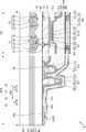
도 1은 일 실시예에 따른 표시 장치(1)를 개략적으로 나타낸 평면도이고, 도 2는 도 1의 II-II'를 따라 취한 단면도이다.1 is a plan view schematically illustrating a
도 1을 참조하면, 표시 장치(1)는 기판(100) 상에 위치하는 복수의 화소에서 방출되는 빛을 통해 이미지를 제공하는 표시 영역(DA)과, 화소들이 배치되지 않아 이미지를 제공하지 않는 비표시 영역(NDA)을 포함한다.Referring to FIG. 1 , the
도 1에서 기판(100)은 직사각 형상으로 도시되어 있으나, 기판(100)의 형상은 원형, 타원형, 다각형 등 다양한 변형이 가능하다.Although the
기판(100) 상의 표시 영역(DA)은 박막 봉지층(400)으로 밀봉되고, 박막 봉지층(400) 상에는 터치 스크린층(700)이 구비될 수 있다.The display area DA on the
도 1에는 도시되어 있지 않으나, 표시 영역(DA)에는 박막 트랜지스터, 유기 발광 소자, 커패시터 등의 소자가 구비되어 있을 수 있다.Although not shown in FIG. 1 , devices such as a thin film transistor, an organic light emitting device, and a capacitor may be provided in the display area DA.
표시 영역(DA)에는 게이트 신호를 전달하는 게이트선과 데이터 신호를 전달하는 데이터선 등의 펄스 신호, 및 구동 전원선, 공통 전원선 등의 직류 신호를 전달하는 신호 배선이 더 포함될 수 있다. 게이트선과 데이터선, 구동 전원선, 공통 전원선에 연결된 박막 트랜지스터, 커패시터, 유기 발광 소자 등의 전기적 결합에 의해 화소에서 화상을 표시할 수 있다.The display area DA may further include a pulse signal such as a gate line transmitting a gate signal and a data line transmitting a data signal, and a signal line transmitting a DC signal such as a driving power line and a common power line. An image may be displayed in a pixel by electrical coupling of a gate line, a data line, a driving power line, a thin film transistor connected to a common power line, a capacitor, an organic light emitting device, and the like.
화소는 복수로 구성될 수 있으며, 복수의 화소는 스트라이프 배열, 펜타일 배열 등 다양한 형태로 배치될 수 있다.A plurality of pixels may be configured, and the plurality of pixels may be arranged in various forms, such as a stripe arrangement or a pentile arrangement.
박막 봉지층(400)은 표시 영역(DA)에 배치되는 표시 소자 등을 덮어 외부의 수분이나 산소로부터 표시 소자 등을 보호하는 역할을 할 수 있다. 박막 봉지층(400)은 표시 영역(DA)을 덮으며 비표시 영역(DA)의 일부를 덮을 수 있다.The thin
봉지층(400) 상에는 터치 기능을 위한 다양한 패턴의 터치 전극(710)을 포함하는 터치 스크린층(700)이 구비된다.A
터치 전극(710)은 제1 방향(X)을 따라 서로 연결된 제1 터치 전극(710a)들과, 제1 방향과 교차하는 제2 방향(Y)을 따라 서로 연결된 제2 터치 전극(710b)들을 포함할 수 있다.The
터치 전극(710)은 터치 스크린층(700) 하부에 배치되는 화소들의 발광영역으로부터 방출된 빛이 투과될 수 있도록 투명전극물질로 형성될 수 있다.The
또는, 터치 전극(710)은 화소들의 발광영역으로부터 방출된 빛이 투과될 수 있도록 메쉬(mesh) 형상을 가질 수 있다. 터치 전극(10)이 메쉬 형상일 경우, 터치 전극(710)은 투명전극물질로 형성될 필요는 없다. 예컨대, 터치 전극(710)은 알루미늄(A1), 구리(Cu), 및/또는 티타늄(Ti) 등을 포함하는 도전물질로 이루어진 단일막 또는 다층막일 수 있다.Alternatively, the
터치 전극(710)은, 터치 전극(710)에 감지되는 신호를 전달하기 위한 제2 터치 연결배선(720)과 연결되며, 제2 터치 연결배선(720)은 박막 봉지층(400) 상부에서부터 박막 봉지층(400)의 일측면을 따라 비표시 영역(NDA)으로 연장될 수 있다.The
비표시 영역(NDA)에는 박막 봉지층(400)의 일부, 구동전압 공급라인(30), 복수의 제2 터치 연결배선들(720), 터치 컨택배선들(730) 및 단자부(20) 등이 배치될 수 있다.In the non-display area NDA, a portion of the thin
단자부(20)는 비표시 영역(NDA)의 일 단부에 배치되며, 복수의 단자(21, 22, 23)를 포함한다. 단자부(20)는 절연층에 의해 덮이지 않고 노출되어, 플렉서블 인쇄회로기판 또는 드라이버 IC 등과 같은 제어부(미도시)와 전기적으로 연결될 수 있다.The
제어부는 외부에서 전달되는 복수의 영상 신호를 복수의 영상 데이터 신호로 변경하고, 변경된 데이터 신호를 제1 단자(21)를 통해 표시 영역(DA)으로 전달할 수 있다. 제어부는 제2 단자(22)를 통해 터치 스크린층(700)에서 감지되는 신호를 수신하거나 터치 제어신호를 터치 스크린층(700)에 전달할 수 있다. 제어부는 제3 단자(23)를 통해 구동전압(ELVDD)을 화소들에 제공할 수 있다.The controller may change the plurality of image signals transmitted from the outside into the plurality of image data signals, and transfer the changed data signals to the display area DA through the
도 1에는 도시되어 있지 않으나, 비표시 영역(NDA)에는 각 화소에 공통전압(ELVSS)를 제공하는 공통전압 공급라인, 각 화소에 스캔 신호를 제공하는 스캔 드라이버, 각 화소에 데이터 신호를 제공하는 데이터 드라이버 등이 더 배치될 수 있다.Although not shown in FIG. 1 , in the non-display area NDA, a common voltage supply line providing a common voltage ELVSS to each pixel, a scan driver providing a scan signal to each pixel, and a data signal providing a data signal to each pixel are provided in the non-display area NDA. A data driver or the like may be further disposed.
도 2의 표시 영역(DA)을 참조하면, 기판(100) 상에 버퍼층(101)이 배치되고, 버퍼층(101) 상에 구동 박막트랜지스터(T1), 스위칭 박막트랜지스터(T2) 및 스토리지 커패시터(Cst)가 배치된다.Referring to the display area DA of FIG. 2 , a
기판(100)은 글라스, 금속 또는 플라스틱 등과 같은 다양한 재료로 형성될 수 있다. 예를 들어, 기판(100)은 폴리에테르술폰(polyethersulphone), 폴리아크릴레이트(polyacrylate), 폴리에테르 이미드(polyetherimide), 폴리에틸렌 나프탈레이트(polyethyelenen napthalate), 폴리에틸렌 테레프탈레이드(polyethyeleneterepthalate), 폴리페닐렌 설파이드(polyphenylene sulfide), 폴리아릴레이트(polyallylate), 폴리이미드(polyimide), 폴리카보네이트(polycarbonate) 또는 셀룰로오스 아세테이트 프로피오네이트(cellulose acetate propionate)와 같은 고분자 수지를 포함하는 플렉서블 기판일 수 있다. 도 2에는 단층 구조의 기판을 도시하고 있으나, 기판(100)은 단층 또는 다층 구조로 형성될 수 있다.The
기판(100)상에는 불순물이 침투하는 것을 방지하기 위해 형성된, 산화 규소(SiOx) 및/또는 질화 규소(SiNx) 등으로 형성된 버퍼층(101)이 구비될 수 있다.A buffer layer 101 formed of, for example, silicon oxide (SiO x ) and/or silicon nitride (SiNx ), which is formed to prevent impurity from penetrating, may be provided on the
구동 박막트랜지스터(T1)는 구동 반도체층(A1) 및 구동 게이트 전극(G1)을 포함하고, 스위칭 박막트랜지스터(T2)는 스위칭 반도체층(A2) 및 스위칭 게이트 전극(G2)을 포함할 수 있다. 구동 반도체층(A1) 및 구동 게이트 전극(G1) 사이, 그리고 스위칭 반도체층(A2) 및 스위칭 게이트 전극(G2) 사이에는 제1 게이트 절연층(103)이 배치된다. 제1 게이트 절연층(103)은 산화 규소(SiOx), 질화 규소(SiNx), 산질화 규소(SiON) 등의 무기 절연물을 포함할 수 있다.The driving thin film transistor T1 may include a driving semiconductor layer A1 and a driving gate electrode G1 , and the switching thin film transistor T2 may include a switching semiconductor layer A2 and a switching gate electrode G2 . The first
구동 반도체층(A1) 및 스위칭 반도체층(A2)은 비정질 실리콘을 포함하거나 다결정 실리콘을 포함할 수 있다. 다른 실시예로, 구동 반도체층(A1) 및 스위칭 반도체층(A2)은 인듐(In), 갈륨(Ga), 스태늄(Sn), 지르코늄(Zr), 바나듐(V), 하프늄(Hf), 카드뮴(Cd), 게르마늄(Ge), 크롬(Cr), 티타늄(Ti) 및 아연(Zn)을 포함하는 군에서 선택된 적어도 하나 이상의 물질의 산화물을 포함할 수 있다.The driving semiconductor layer A1 and the switching semiconductor layer A2 may include amorphous silicon or polycrystalline silicon. In another embodiment, the driving semiconductor layer A1 and the switching semiconductor layer A2 may include indium (In), gallium (Ga), stanium (Sn), zirconium (Zr), vanadium (V), hafnium (Hf), It may include an oxide of at least one material selected from the group including cadmium (Cd), germanium (Ge), chromium (Cr), titanium (Ti), and zinc (Zn).
구동 반도체층(A1)은 구동 게이트 전극(G1)과 중첩하며 불순물이 도핑되지 않은 구동 채널 영역, 및 구동 채널 영역의 양 옆의 불순물이 도핑된 구동 소스 영역 및 구동 드레인 영역을 포함할 수 있다. 구동 소스 영역 및 구동 드레인 영역에는 각각 구동 소스 전극(S1) 및 구동 드레인 전극(D1)이 연결될 수 있다.The driving semiconductor layer A1 may include a driving channel region that overlaps the driving gate electrode G1 and is not doped with impurities, and a driving source region and a driving drain region doped with impurities on both sides of the driving channel region. A driving source electrode S1 and a driving drain electrode D1 may be connected to the driving source region and the driving drain region, respectively.
스위칭 반도체층(A2)은 스위칭 게이트 전극(G2)과 중첩하고 불순물이 도핑되지 않은 스위칭 채널 영역, 및 스위칭 채널 영역의 양 옆의 불순물이 도핑된 스위칭 소스 영역과 스위칭 드레인 영역을 포함할 수 있다. 스위칭 소스 영역 및 스위칭 드레인 영역에는 각각 스위칭 소스 전극(S2) 및 스위칭 드레인 전극(D2)이 연결될 수 있다.The switching semiconductor layer A2 may include a switching channel region overlapping the switching gate electrode G2 and not doped with impurities, and a switching source region and a switching drain region doped with impurities on both sides of the switching channel region. A switching source electrode S2 and a switching drain electrode D2 may be connected to the switching source region and the switching drain region, respectively.
구동 게이트 전극(G1) 및 스위칭 게이트 전극(G2)은 몰리브덴(Mo), 알루미늄(Al), 구리(Cu), 티타늄(Ti) 등을 포함하며, 단층 또는 다층으로 이루어질 수 있다.The driving gate electrode G1 and the switching gate electrode G2 include molybdenum (Mo), aluminum (Al), copper (Cu), titanium (Ti), and the like, and may be formed of a single layer or multiple layers.
일부 실시예에서, 스토리지 커패시터(Cst)는 구동 박막트랜지스터(T1)와 중첩되게 배치될 수 있다. 이 경우, 스토리지 커패시터(Cst) 및 구동 박막트랜지스터(T1)의 면적을 증가시킬 수 있으며, 고품질의 이미지를 제공할 수 있다. 예를 들어, 구동 게이트 전극(G1)은 스토리지 커패시터(Cst)의 제1 스토리지 축전판(CE1)일 수 있다. 제2 스토리지 축전판(CE2)은 제1 스토리지 축전판(CE1)과의 사이에 제2 게이트 절연층(105)을 개재한 채 제1 스토리지 축전판(CE1)과 중첩할 수 있다. 제2 게이트 절연층(105)은 산화 규소(SiOx), 질화 규소(SiNx), 산질화 규소(SiON) 등의 무기 절연물을 포함할 수 있다.In some embodiments, the storage capacitor Cst may be disposed to overlap the driving thin film transistor T1. In this case, the area of the storage capacitor Cst and the driving thin film transistor T1 may be increased, and a high-quality image may be provided. For example, the driving gate electrode G1 may be the first storage capacitor plate CE1 of the storage capacitor Cst. The second storage capacitor plate CE2 may overlap the first storage capacitor plate CE1 with the second
구동 박막트랜지스터(T1), 스위칭 박막트랜지스터(T2) 및 스토리지 커패시터(Cst)는 층간 절연층(107)으로 커버될 수 있다.The driving thin film transistor T1 , the switching thin film transistor T2 , and the storage capacitor Cst may be covered with an interlayer insulating
층간 절연층(107)은 산질화규소(SiON), 산화 규소(SiOx) 및/또는 질화 규소(SiNx)와 같은 무기물 층일 수 있다.The interlayer insulating
층간 절연층(107) 상에는 데이터선(DL)이 배치될 수 있다, 데이터선(DL)은 층간 절연층(107)을 관통하는 콘택홀을 통해 스위칭 박막트랜지스터(T2)의 스위칭 반도체층(A2)과 접속한다. 데이터선(DL)은 스위칭 소스 전극(S2)의 역할을 할 수 있다.A data line DL may be disposed on the
구동 소스 전극(S1), 구동 드레인 전극(D1), 스위칭 소스 전극(S2), 및 스위칭 드레인 전극(D2)은 층간 절연층(107) 상에 배치될 수 있으며, 층간 절연층(107)을 관통하는 콘택홀을 통해 구동 반도체층(A1) 또는 스위칭 반도체층(A2)과 접속할 수 있다.The driving source electrode S1 , the driving drain electrode D1 , the switching source electrode S2 , and the switching drain electrode D2 may be disposed on the
한편, 데이터선(DL), 구동 소스 전극(S1), 구동 드레인 전극(D1), 스위칭 소스 전극(S2), 및 스위칭 드레인 전극(D2)는 무기 보호층(미도시)으로 커버될 수 있다.Meanwhile, the data line DL, the driving source electrode S1 , the driving drain electrode D1 , the switching source electrode S2 , and the switching drain electrode D2 may be covered with an inorganic protective layer (not shown).
무기 보호층(미도시)은 질화실리콘(SiNx)과 산화실리콘(SiOx)의 단일막 또는 다층막일 수 있다. 무기 보호층(미도시)은 비표시 영역(NDA1)에서 노출된 일부 배선들, 예를 들어 데이터선(DL)과 동일한 공정에서 함께 형성된 배선들이 화소 전극(310)의 패터닝시 사용되는 에천트에 의해 손상되는 것을 방지할 수 있다.The inorganic protective layer (not shown) may be a single layer or a multilayer layer ofsilicon nitride (SiN x ) and silicon oxide (SiOx ). In the inorganic protective layer (not shown), some wires exposed in the non-display area NDA1, for example, wires formed together in the same process as the data line DL, are applied to the etchant used when the
구동 전압선(PL)은 데이터선(DL)과 서로 다른 층에 배치될 수 있다. 구동 전압선(PL)과 데이터선(DL) 사이에는 제1 평탄화막(109)이 개재될 수 있고, 구동 전압선(PL)은 제2 평탄화막(111)으로 커버될 수 있다.The driving voltage line PL may be disposed on a different layer from the data line DL. A
구동 전압선(PL)은 알루미늄(Al), 구리(Cu), 티타늄(Ti) 및 이들의 합금 중 적어도 어느 하나를 포함하는 단일막 또는 다층막일 수 있다. 일 실시예로, 구동 전압선(PL)은 Ti/Al/Ti의 3층막일 수 있다.The driving voltage line PL may be a single layer or a multilayer layer including at least one of aluminum (Al), copper (Cu), titanium (Ti), and an alloy thereof. In an embodiment, the driving voltage line PL may be a three-layer film of Ti/Al/Ti.
도 2에는 구동 전압선(PL)이 제1 평탄화막(109) 상에 배치된 구성을 도시하고 있으나, 본 발명은 이에 한정되지 않는다. 다른 실시예로, 구동 전압선(PL)은 제1 평탄화막(109)에 형성된 관통홀(미도시)을 통해 데이터선(DL)과 동일층에 형성된 하부 추가 전압선(미도시)에 접속되어 저항을 감소시킬 수 있다.Although FIG. 2 illustrates a configuration in which the driving voltage line PL is disposed on the
제1 평탄화막(109) 및 제2 평탄화막(111)은 단층 또는 다층막으로 형성될 수 있다.The
제1 평탄화막(109) 및 제2 평탄화막(111)은 유기 절연물을 포함할 수 있다. 일 예로, 유기 절연물은 이미드계 고분자, Polymethylmethacrylate(PMMA)나 Polystylene(PS)과 같은 일반 범용고분자, 페놀계 그룹을 갖는 고분자 유도체, 아크릴계 고분자, 아릴에테르계 고분자, 아마이드계 고분자, 불소계고분자, p-자일렌계 고분자, 비닐알콜계 고분자 등을 포함할 수 있다.The
또한, 제1 평탄화막(109) 및 제2 평탄화막(111)은 무기 절연물을 포함할 수 있다. 일 예로, 무기 절연물은 산질화 규소(SiON), 산화 규소(SiOx), 질화 규소(SiNx) 등을 포함할 수 있다.In addition, the
제2 평탄화막(111) 상에는 화소 전극(310), 대향 전극(330), 및 화소 전극(310)과 대향 전극(330) 사이에 개재되며 발광층을 포함하는 중간층(320)을 구비한 유기 발광 소자(OLED)가 위치할 수 있다.An organic light emitting device including a
화소 전극(310)은 제1 평탄화막(109) 상에 형성된 연결 배선(CL)과 연결되고, 연결 배선(CL)은 구동 박막트랜지스터(T1)의 구동 드레인 전극(D1)과 연결될 수 있다.The
화소 전극(310)은 투명 전극 또는 반사 전극으로 형성될 수 있다.The
화소 전극(310)이 투명 전극으로 형성될 때에는 투명 도전층을 포함할 수 있다. 투명 도전층은 인듐틴옥사이드(ITO), 인듐징크옥사이드(IZO), 징크옥사이드(ZnO), 인듐옥사이드(In2O3), 인듐갈륨옥사이드(IGO), 및 알루미늄징크옥사이드(AZO)을 포함하는 그룹에서 선택된 적어도 어느 하나일 수 있다. 이 경우, 투명 도전층 이외에 광효율을 향상시키기 위한 반투과층을 더 포함할 수 있으며, 반투과층은 수 내지 수십 마이크로미터(㎛)의 박막으로 형성된 은(Ag), 마그네슘(Mg), 알루미늄(Al), 백금(Pt), 팔라듐(Pd), 금(Au), 니켈(Ni), 네오디뮴(Nd), 이리듐(Ir), 크롬(Cr), 리튬(Li), 칼슘(Ca), 및 이테르븀(Yb)를 포함하는 그룹에서 선택된 적어도 하나일 수 있다.When the
화소 전극(310)이 반사형 전극으로 형성될 때에는 Ag, Mg, Al, Pt, Pd, Au, Ni, Nd, Ir, Cr 및 이들의 화합물 등으로 형성된 반사막과, 반사막의 상부 및/또는 하부에 배치된 투명 도전층을 포함할 수 있다. 투명 도전층은 ITO, IZO, ZnO, In2O3, IGO, 및 AZO을 포함하는 그룹에서 선택된 적어도 어느 하나일 수 있다.When the
물론 본 발명이 이에 한정되는 것은 아니고 화소 전극(310)은 다양한 재질로 형성될 수 있으며, 그 구조 또한 단층 또는 다층이 될 수 있는 등 다양한 변형이 가능하다.Of course, the present invention is not limited thereto, and the
화소 전극(310) 상에는 화소 정의막(113)이 배치될 수 있다.A
화소 정의막(113)은 화소 전극(310)을 노출하는 개구를 형성함으로써 화소를 정의하는 역할을 한다. 또한, 화소 정의막(113)은 화소 전극(310)의 가장자리와 대향 전극(330) 사이의 거리를 증가시킴으로써, 화소 전극(310) 단부에서 아크가 발생하는 것을 방지할 수 있다. 화소 정의막(113)은 예를 들어, 폴리이미드 또는 HMDSO(hexamethyldisiloxane) 등과 같은 유기물로 형성될 수 있다.The
중간층(320)은 저분자 또는 고분자 물질을 포함할 수 있다.The
중간층(320)이 저분자 물질을 포함할 경우, 중간층(320)은 홀 주입층(Hole Injection Layer), 홀 수송층(Hole Transport Layer), 발광층(Emission Layer), 전자 수송층(Electron Transport Layer), 전자 주입층(Electron Injection Layer) 등이 적층된 구조일 수 있다. 중간층(320)은 구리 프탈로시아닌(CuPc: copper phthalocyanine), N,N-디(나프탈렌-1-일)-N,N'-디페닐-벤지딘 (N,N'-Di(naphthalene-1-yl)-N,N'-diphenyl-benzidine: NPB) , 트리스-8-하이드록시퀴놀린 알루미늄(tris-8-hydroxyquinoline aluminum)(Alq3) 등을 비롯해 다양한 유기물질을 포함할 수 있다.When the
중간층(320)이 고분자 물질을 포함할 경우, 중간층(320)은 홀 수송층 및 발광층을 포함하는 구조를 가질 수 있다. 이 때, 홀 수송층은 PEDOT을 포함하고, 발광층은 PPV(Poly-Phenylenevinylene)계 및 폴리플루오렌(Polyfluorene)계 등 고분자 물질을 포함할 수 있다.When the
중간층(320)은 복수의 화소 전극(310)에 걸친 일체의(integral) 층으로 형성할 수도 있고, 복수의 화소 전극(310) 각각에 대응하도록 패터닝된 층으로 형성할 수도 있다.The
대향 전극(330)은 중간층(320) 상에 표시 영역(DA)을 덮도록 배치될 수 있다. 즉, 대향 전극(330)은 복수개의 유기 발광 소자(OLED)들을 모두 덮을 수 있도록 일체로 형성될 수 있다.The
대향 전극(330)은 투명 전극 또는 반사형 전극으로 형성될 수 있다.The
대향 전극(330)이 투명 전극으로 형성될 때에는 Ag, Al, Mg, Li, Ca, Cu, LiF/Ca, LiF/Al, MgAg 및 CaAg에서 선택된 하나 이상의 물질을 포함할 수 있으며, 수 내지 수십 마이크로미터(㎛)의 두께를 갖는 박막 형태로 형성될 수 있다.When the
대향 전극(330)이 반사형 전극으로 형성될 때에는 Ag, Al, Mg, Li, Ca, Cu, LiF/Ca, LiF/Al, MgAg 및 CaAg를 포함하는 그룹에서 선택된 적어도 어느 하나로 형성될 수 있다. 물론 대향 전극(330)의 구성 및 재료가 이에 한정되는 것은 아니며 다양한 변형이 가능함은 물론이다.When the
화소 정의막(113) 상에 스페이서(115)가 배치될 수 있다. 스페이서(115)는 화소 정의막(113)으로부터 박막 봉지층(400) 방향으로 돌출되어, 중간층(320)을 증착 마스크를 이용하여 증착하는 공정에서, 증착 마스크와 기판(100)의 이격을 유지하여 증착 공정에서 중간층(320)이 마스크에 의해 찍히거나 뜯기는 불량을 방지할 수 있다.A
스페이서(115)는 폴리이미드 또는 HMDSO(hexamethyldisiloxane) 등과 같은 유기물로 형성될 수 있다. 스페이서(115)는 후술할 제1 및 제2 댐부(110, 120) 가운데 적어도 하나에 배치되어 댐부의 단차를 형성하기 위해 사용될 수 있다.The
유기 발광 소자(OLED)는 외부로부터의 수분이나 산소 등에 의해 쉽게 손상될 수 있으므로, 박막 봉지층(400)으로 덮어 보호될 수 있다.Since the organic light emitting diode OLED may be easily damaged by moisture or oxygen from the outside, it may be protected by covering it with the thin
박막 봉지층(400)은 표시 영역(DA)을 덮으며 표시 영역(DA) 외측까지 연장될 수 있다. 박막 봉지층(400)은 적어도 하나의 유기 봉지층과 적어도 하나의 무기 봉지층을 포함할 수 있다. 일 실시예로, 박막 봉지층(400)은 제1 무기 봉지층(410), 유기 봉지층(420) 및 제2 무기 봉지층(430)을 포함할 수 있다.The thin
제1 무기 봉지층(410)은 대향 전극(330) 전체를 덮고, 산화 규소, 질화규소, 및/또는 산질화규소 등을 포함할 수 있다.The first
필요에 따라 제1 무기 봉지층(410)과 대향 전극(330) 사이에 캐핑층(미도시) 등의 다른 층들이 개재될 수도 있다. 예를 들어, 캐핑층은 광효율을 개선하기 위하여 산화규소(SiO2), 질화규소(SiNx), 산화아연(ZnO2), 산화티타늄(TiO2), 산화지르코늄(ZrO2), 인듐주석산화물(ITO), 인듐아연산화물(IZO), Alq3, CuPc, CBP, a-NPB, 및 ZiO2 중 하나 이상의 유기물 또는 무기물을 포함할 수 있다. 다른 실시예에서, 캐핑층은 유기 발광 소자(OLED)에서 생성하는 광에 대해서 플라즈몬 공명 현상이 발생하게 할 수 있다. 예를 들어, 캐핑층은 나노 입자들을 포함할 수 있다. 한편, 캐핑층은 박막 봉지층(400)를 형성하기 위한 화학 기상 증착(Chemical Vapor Disposition) 공정 또는 스퍼터링(sputtering) 공정에서 발생하는 열, 플라즈마(plasma) 등에 의해 유기 발광 소자(OLED)가 손상되는 것을 방지할 수 있다. 예를 들어, 캐핑층은 비스페놀(bisphenol)형 에폭시(epoxy) 수지, 에폭시화 부타디엔(butadiene) 수지, 플루오렌(fluorine)형 에폭시 수지 및 노볼락(novolac) 에폭시 수지 중 적어도 하나로 형성되는 에폭시 계열의 재료를 포함할 수 있다.If necessary, other layers such as a capping layer (not shown) may be interposed between the first
또한, 필요에 따라 제1 무기 봉지층(410)과 캐핑층 사이에 LiF 등을 포함하는 층(미도시)이 개재될 수도 있다.Also, a layer (not shown) including LiF or the like may be interposed between the first
제1 무기 봉지층(410)은 그 하부의 구조물의 단차를 따라 형성되기에, 상면이 평탄하지 않게 된다. 유기 봉지층(420)은 이러한 제1 무기 봉지층(410)을 덮어 평탄화한다. 유기 봉지층(420)은 표시 영역(DA)에 대응하는 부분에서는 상면이 대략 평탄 할 수 있다.Since the first
유기 봉지층(420)은 폴리에틸렌테레프탈레이트, 폴리에틸렌나프탈레이트, 폴리카보네이트, 폴리이미드, 폴리에틸렌설포네이트, 폴리옥시메틸렌, 폴리아릴레이트, 헥사메틸디실록산, 아크릴계 수지(예를들면, 폴리메틸메타크릴레이트, 폴리아크릴산 등) 또는 이의 임의의 조합을 포함할 수 있다.The
제2 무기 봉지층(430)은 유기 봉지층(420)을 덮으며, 산화규소, 질화규소, 및/또는 산질화규소 등을 포함할 수 있다.The second
박막 봉지층(400) 상에는 터치 전극(710)을 포함하는 터치 스크린층(700)이 배치된다. 터치 스크린층(700) 상에는 터치 스크린층(700)을 보호하는 커버층(미도시)이 더 배치될 수 있다.A
터치 스크린층(700)은 정전 용량 방식일 수 있다. 일 예로 커버층의 터치시 터치 터치 전극(710)들 사이에 형성되는 상호 정전 용량 (mutual capacitance)의 변화가 발생하고, 제어부는 이 변화를 감지함으로써 해당 부분의 접촉 여부를 판단할 수 있다. 또는, 터치 전극(710)과 대향 전극(330) 사이에 정전 용량의 변화가 발생하고, 제어부는 이 변화를 감지함으로써 해당 부분의 접촉 여부를 판단하는 등 다양한 방식으로 접촉 여부를 판단할 수 있다.The
터치 스크린층(700)은 제1 터치 도전층(711) 및 제2 터치 도전층(713)을 포함하는 터치 전극(710)과, 제1 터치 도전층(711)과 제2 터치 도전층(713) 사이에 개재된 제1 터치 절연층(712)과, 제2 터치 도전층(713) 상에 배치된 제2 터치 절연층(714)을 포함할 수 있다.The
일부 실시예에서, 제2 터치 도전층(713)은 접촉 여부를 감지하는 센서부로 작용하고, 제1 터치 도전층(711)은 패터닝된 제2 터치 도전층(713)을 일 방향으로 연결하는 연결부의 역할을 할 수 있다.In some embodiments, the second touch
일부 실시예에서, 제1 터치 도전층(711) 및 제2 터치 도전층(713) 모두 센서부로 작용할 수 있다. 예컨대, 제1 터치 절연층(712)은 제1 터치 도전층(711)의 상면을 노출 시키는 비아홀을 포함하고, 이 비아홀을 통해서 제1 터치 도전층(711)과 제2 터치 도전층(713)이 연결될 수 있다. 이와 같이 제1 터치 도전층(711)과 제2 터치 도전층(713)을 사용함에 따라서, 터치 전극(710)의 저항이 감소하여, 터치 스크린층(700)의 응답 속도가 향상될 수 있다.In some embodiments, both the first touch
일부 실시예에서, 터치 전극(710)은 유기 발광 소자(OLED)로부터 방출되는 빛이 통과할 수 있도록 메쉬구조로 형성될 수 있다. 이에 따라, 터치 전극(710)의 제1 터치 도전층(711) 및 제2 터치 도전층(713)은 유기 발광 소자(OLED)의 발광영역과 중첩되지 않도록 배치될 수 있다.In some embodiments, the
제1 터치 도전층(711) 및 제2 터치 도전층(713)은 각각 전도성이 좋은 도전물질로 이루어진 단일막 또는 다층막일 수 있다. 예를들어, 제1 터치 도전층(711) 및 제2 터치 도전층(713)은 각각 투명 도전층이나 알루미늄(Al), 구리(Cu), 티타늄(Ti) 등을 포함하는 도전 물질로 이루어진 단일막 또는 다층막일 수 있다. 투명 도전층은 ITO, IZO, ZnO, ITZO 등과 같은 투명한 전도성 산화물을 포함할 수 있다. 그밖에 투명 도전층은 PEDOT과 같은 전도성 고분자, 금속 나노 와이어, 그래핀 등을 포함할 수 있다. 일부 실시예에서, 제1 터치 도전층(711) 및 제2 터치 도전층(713)은 각각 Ti/Al/Ti의 적층 구조를 가질 수 있다.Each of the first touch
제1 터치 절연층(712) 및 제2 터치 절연층(714)은 각각 무기물 또는 유기물로 구비될 수 있다. 무기물은 실리콘 질화물, 알루미늄 질화물, 지르코늄 질화물, 티타늄 질화물, 하프늄 질화물, 탄탈륨 질화물, 실리콘 산화물, 알루미늄 산화물, 티타늄 산화물, 주석 산화물, 세륨 산화물 또는 실리콘 산화질화물 중 적어도 어느 하나일 수 있다. 유기물은 아크릴계 수지, 메타크릴계 수지, 폴리이소프렌, 비닐계 수지, 에폭시계 수지, 우레탄계 수지, 셀룰로오스계 수지 및 페릴렌계 수지 중 적어도 어느 하나일 수 있다.Each of the first
도 2에는 도시되지 않았지만, 박막 봉지층(400)과 터치 스크린층(700) 사이에는 터치 버퍼층이 더 구비될 수 있다. 터치 버퍼층은 박막 봉지층(400)의 손상을 방지하며, 터치 스크린층(700)의 구동시 발생할 수 있는 간섭 신호를 차단하기 위한 역할을 할 수 있다. 터치 버퍼층은 실리콘 옥사이드, 실리콘 나이트라이드, 실리콘 옥시나이트라이드, 알루미늄옥사이드, 알루미늄나이트라이드, 티타늄옥사이드 또는 티타늄나이트라이드 등의 무기물이나, 폴리이미드, 폴리에스테르, 아크릴 등의 유기물을 함유할 수 있고, 예시한 재료들 중 복수의 적층체로 형성될 수 있다.Although not shown in FIG. 2 , a touch buffer layer may be further provided between the thin
터치 버퍼층 및/또는 터치 스크린층(700)은 박막 봉지층(400) 상에 증착 등에 의해 직접 형성되므로, 박막 봉지층(400) 상에 별도의 접착층을 필요로 하지 않는다. 따라서, 표시 장치의 두께를 줄일 수 있다.Since the touch buffer layer and/or the
커버층(미도시)은 터치 스크린층(700) 상에 배치되어, 터치스크린층(700)을 보호하는 역할을 할 수 있다. 커버층은 플렉서블한 특성을 갖는 것으로서, 폴리메틸메타아크릴레이트(polymethyl methacrylate), 폴리디메틸실록산(Polydimethylsiloxane), 폴리이미드(Polyimide), 아크릴레이트(Acrylate), 폴리에틸렌테레프탈레이트(Polyethylen terephthalate), 폴리에틸렌나프탈레이트(Polyethylen naphthalate) 등으로 형성될 수 있다.A cover layer (not shown) may be disposed on the
도 2의 비표시 영역(NDA)을 참조하면, 표시 영역(DA)에서 연장된 버퍼층(101), 제1 게이트 절연층(103), 제2 게이트 절연층(105), 층간 절연층(107), 제1 평탄화막(109), 제2 평탄화막(111)이 배치된다.Referring to the non-display area NDA of FIG. 2 , the
일 실시예로, 제1 평탄화막(109) 상에 구동전압 공급라인(30) 및 터치 컨택배선(730)이 배치될 수 있다. 이 때, 구동전압 공급라인(30) 및 터치 컨택배선(730)은 구동 전압선(PL)과 동일한 재료로 형성될 수 있다.In an embodiment, the driving
한편, 도 2에는 구동전압 공급라인(30) 및 터치 컨택배선(730)이 제1 평탄화막(109) 상에 위치하는 경우를 도시하였으나, 본 발명은 이에 한정되지 않는다. 구동전압 공급라인(30) 및 터치 컨택배선(730) 중 적어도 하나 이상은 제1 평탄화막(109) 하부 또는 제2 평탄화막(111) 상부에 위치할 수 있다. 예를 들어, 구동전압 공급라인(30) 및 터치 컨택배선(730) 중 적어도 하나는 데이터 라인(DL)과 동일한 층에 동일한 재료로 형성되거나 화소 전극(310)과 동일한 층에 동일한 재료로 형성 될 수 있다.Meanwhile, although FIG. 2 illustrates a case in which the driving
구동전압 공급라인(30)과 중첩되는 위치에, 표시 영역(DA)에서 기판(100)의 단부 방향으로 제1 댐부(110) 및 제2 댐부(12)가 순차로 배치될 수 있다.The
제1 댐부(110)는 제2 평탄화막(111)과 동일한 재료로 형성된 제1 층(111a), 및 화소 정의막(113)과 동일한 재료로 형성된 제2 층(113a)를 포함할 수 있다. 제1 댐부(110)의 제2 층(113a)은 제1 층(111a)의 상면 및 측면을 클래딩하여 포토리쏘그라피 공정에서 제2 층(113a)의 패터닝 시 공정 마진을 확보하여 제2 층(113a)의 높이를 안정적으로 확보할 수 있다.The
제2 댐부(120)는 제2 평탄화막(111)과 동일한 재료로 형성된 제1 층(111b), 화소 정의막(113)과 동일한 재료로 형성된 제2 층(113b), 및 스페이서(115)와 동일한 재료로 형성된 제3 층(115b)를 포함할 수 있다. 제2 댐부(120)의 제2 층(113b)은 제1 층(111b)의 상면 및 측면을 클래딩하여 포토리쏘그라피 공정에서 제2 층(113b)의 패터닝 시 공정 마진을 확보하여 제2 층(113b)의 높이를 안정적으로 확보할 수 있다. 제2 댐부(130)의 제2 층(113b) 및 제3 층(115b)을 동일한 마스크를 이용한 공정으로 형성할 수 있기 때문에, 제2 층(113b)의 상면 폭과 제3 층(115b)의 하면 폭은 실질적으로 동일하게 형성할 수 있다.The
그리고, 제2 댐부(120)의 높이를 제1 댐부(110)보다 높게 형성하여 유기 봉지층(420)이 제2 댐부(120)를 넘어 에지 테일(edge tail)을 형성하는 것을 방지하고, 중간층(320)을 증착 마스크를 이용하여 증착하는 공정에서 증착 마스크와 기판(100)의 이격을 유지하여 증착 공정에서 중간층(320)이 증착 마스크에 의해 찍히거나 뜯기는 불량을 방지할 수 있다.In addition, the height of the
그리고, 제2 댐부(120)의 제1 층(111b)은 구동전압 공급라인(30)의 단부를 클래딩하여, 제2 평탄화막(111)의 습식 식각 시 구동전압 공급라인(30)이 손상되는 것을 방지할 수 있다.In addition, the first layer 111b of the
표시 영역(DA)에서 연장된 제1 박막 봉지층(410)과 제2 박막 봉지층(430)이 제2 댐부(120) 외측까지 연장되어 배치되고, 제2 댐부(120) 외측에는 터치 컨택배선(730)이 위치한다.The first thin
제2 무기 봉지층(430)은 표시 영역(DA) 외측에서 제1 무기 봉지층(410) 상에 직접 접촉하도록 증착됨으로써, 유기 봉지층(420)이 제1 및 제2 무기 봉지층(410, 430)의 외부로 노출되지 않도록 밀봉할 수 있다.The second
터치 컨택배선(730)은, 표시 영역(DA)에서 연장된 제1 터치 절연층(712)에 형성된 제1 터치 컨택홀(CNT1)을 통해, 제2 터치 전극(713)에서 연장된 제2 터치 연결배선(720)과 컨택한다. 터치 컨택배선(730)은 제2 단자(22, 도 1)를 통해 제어부와 연결될 수 있다.The
본 실시예에서 제2 무기 봉지층(430)의 끝단(E2)은 제1 무기 봉지층(410)의 끝단(E1)보다 터치 컨택배선(730)에 가깝게 위치한다. 또는, 제2 댐부(120)의 끝단(E0)에서 제1 무기 봉지층(410)의 끝단(E1)까지의 길이(L410-1)는, 제2 댐부(120)의 끝단(E0)에서 제2 무기 봉지층(430)의 끝단(E2)까지의 길이(L430-1) 보다 짧다.In this embodiment, the end E2 of the second
그 결과 박막 봉지층(400)의 최외각 끝단인 제2 무기 봉지층(430)의 끝단(E2)과 터치 컨택배선(730)의 표시 영역(DA)에 가까운 끝단(E3) 사이의 제1 거리(D1)가 도출된다.As a result, the first distance between the end E2 of the second
이하 도 3 및 도 4를 참조하여 비교예에 따른 표시 장치(2)와 본 실시예에 따른 표시 장치(1)의 차이를 설명한다.Hereinafter, a difference between the
도 3은 비교예에 따른 표시 장치(2)를 개략적으로 나타낸 단면도이고, 도 4는 도 2 및 도 3의 제1, 2 박막 봉지층(410, 430)과 터치 컨택배선(730)의 위치관계를 비교한 단면도이다.3 is a cross-sectional view schematically illustrating a
도 3을 참조하면, 비교예에 따른 표시 장치(2)는 도 2의 표시 장치(1)와 달리, 제1 무기 봉지층(410) 및 제2 무기 봉지층(430)의 끝단의 길이가 동일하다.Referring to FIG. 3 , in the
도 3의 표시 장치(2)에서, 제1 무기 봉지층(410)과 제2 무기 봉지층(410)는 동일한 크기로 형성된다. 즉, 제2 무기 봉지층(430)의 끝단(E2')과 제1 무기 봉지층(410)의 끝단(E1')은 터치 컨택배선(730)을 기준으로 같은 거리에 위치한다. 또는, 제2 댐부(120)의 끝단(E0)에서 제1 무기 봉지층(410)의 끝단(E1')까지의 길이(L410-2)는, 제2 댐부(120)의 끝단(E0)에서 제2 무기 봉지층(430)의 끝단(E2')까지의 길이(L430-2)와 같다.In the
그 결과 박막 봉지층(400)의 최외각 끝단인 제1 및 제2 무기 봉지층(410, 430)의 끝단(E1', E2')과 터치 컨택배선(730)의 표시 영역(DA)에 가까운 끝단(E3') 사이의 제2 거리(D2)가 도출된다.As a result, the ends E1' and E2' of the first and second inorganic encapsulation layers 410 and 430, which are the outermost ends of the thin
본 실시예에 따른 도 2의 제1 거리(D1)는 비교예에 따른 도 3의 제2 거리(D2)보다 짧게 형성된다. 제1 거리(D1)가 제2 거리(D2)보다 짧게 형성됨으로서 본 실시예는 비교예보다 비표시 영역(NDA)에서의 데드 스페이스를 줄일 수 있다.The first distance D1 of FIG. 2 according to the present exemplary embodiment is shorter than the second distance D2 of FIG. 3 according to the comparative example. Since the first distance D1 is shorter than the second distance D2 , the dead space in the non-display area NDA may be reduced in the present exemplary embodiment than in the comparative example.
도 4의 상단은 비교예에 따른 도 3의 제1, 2 박막 봉지층(410, 430)과 터치 컨택배선(730)의 위치관계를 도시한 단면도이고, 도 4의 하단은 본 실시예에 따른 도 2의 제1, 2 무기 봉지층(410, 430)과 터치 컨택배선(730)의 위치관계를 도시한 단면도이다.The upper end of FIG. 4 is a cross-sectional view illustrating the positional relationship between the first and second thin film encapsulation layers 410 and 430 and the
도 4 상단의 비교예는, 제1 무기 봉지층(410)과 제2 무기 봉지층(430)의 길이는 같지만 제1 무기 봉지층(410)의 제1 두께(T1)가 제2 무기 봉지층(430)의 제2 두께(T2)보다 두껍게 형성된 경우를 도시한 것이다.In the comparative example of the upper part of FIG. 4 , the first
제1, 2 무기 봉지층(410, 430)을 섀도우 마스크를 이용하여 화학 기상 증착 공정으로 형성할 경우, 섀도우 현상으로 증착 물질이 타겟 영역을 벗어난 섀도우 영역에 증착될 수 있다. 이러한 현상은 증착 물질의 두께가 두꺼울수록 섀도우 영역이 넓어지는 경향이 있다.When the first and second inorganic encapsulation layers 410 and 430 are formed by a chemical vapor deposition process using a shadow mask, a deposition material may be deposited in a shadow region outside the target region due to a shadow phenomenon. This phenomenon tends to increase the shadow area as the thickness of the deposition material increases.
제1 무기 봉지층(410)을 제2 무기 봉지층(430)보다 두껍게 형성할 경우, 제1 무기 봉지층(410)의 제1 섀도우 영역(S410')은 제2 무기 봉지층(430)의 제2 섀도우 영역(S430')보다 넓게 형성된다.When the first
섀도우 영역을 벗어난 위치에 터치 전극배선(730)을 형성하므로, 비교예에 따를때 터치 전극배선(730)의 표시 영역(DA)에 가까운 끝단(E3')은 제1 섀도우 영역(S410')이 끝나는 위치에 형성할 수 있다.Since the
도 4의 하단의 본 실시예는 제1 무기 봉지층(410)의 제1 두께(T1)와 제2 무기 봉지층(430)의 제2 두께(T2)를 도 4의 상단의 비교예와 동일하게 유지한 상태에서, 두께가 두꺼운 제1 무기 봉지층(410)의 길이를 제2 무기 봉지층(430)의 길이보다 짧게 형성한 경우를 도시한 것이다.In the present embodiment at the lower end of FIG. 4 , the first thickness T1 of the first
본 실시예의 제1 및 제2 무기 봉지층(410, 430)의 두께(T1, T2)는 비교예와 동일하므로, 본 실시예의 제1 및 제2 섀도우 영역(S410, S430)의 면적은 비교예의 제1 및 제2 섀도우 영역(S410', S430')의 면적과 실질적으로 동일하다. 그러나, 본 실시예의 경우, 두께가 두꺼운 제1 무기 봉지층(410)의 길이를 짧게 형성하였기 때문에, 제1 섀도우 영역(S410)의 시작선이 제1 무기 봉지층(410)의 끝단(E1)으로 이동된다. 즉, 본 실시예의 제1 섀도우 영역(S410)의 시작선이 표시 영역(DA)에 가까운 방향으로 시프트 되어, 터치 컨택배선(730)의 표시 영역(DA)에 가까운 끝단(E3)을 표시 영역(DA) 측으로 이동시킬 수 있다. 그 결과 다른 조건이 동일할 경우, 본 실시예의 표시 장치(1)는 비교예의 표시 장치(2)에 비하여 데드 스페이스를 줄일 수 있다.Since the thicknesses T1 and T2 of the first and second inorganic encapsulation layers 410 and 430 of the present embodiment are the same as those of the comparative example, the areas of the first and second shadow regions S410 and S430 of the present embodiment are those of the comparative example. The area of the first and second shadow regions S410' and S430' is substantially the same as that of the first and second shadow regions S410' and S430'. However, in the present embodiment, since the length of the thick first
한편, 제1 무기 봉지층(410)의 길이는 줄어들었지만, 제1 무기 봉지층(410)과 제2 무기 봉지층(430)의 끝단을 표시 영역(DA)에서 연장된 제1 터치 절연층(712)과 제2 터치 연결배선(720)이 커버하기 때문에, 외부의 불순물 침투를 방지할 수 있다.On the other hand, although the length of the first
또한, 제1 무기 봉지층(410)이 제2 무기 봉지층(430)보다 짧게 형성되어 있기 때문에, 제1 무기 봉지층(410)을 형성한 후 진행하는 이산화질소(N2O) 등을 이용한 애싱(ashing) 공정에서, 제2 평탄화막(111), 화소 정의막(113) 및 스페이서(115)를 패터닝한 후 제1 무기 봉지층(410) 외곽에 잔존하는 유기물이 있을 경우 이를 용이하게 제거할 수 있다. 따라서, 잔존하는 유기물의 박막 봉지층(400)으로의 침투를 방지할 수 있다.In addition, since the first
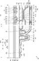
도 5는 일 실시예에 따른 표시 장치(3)를 개략적으로 나타낸 단면도이다. 이하 전술한 도 2의 실시예와 차이점을 중심으로 도 5의 실시예를 설명한다.5 is a cross-sectional view schematically illustrating a
도 5를 참조하면, 도 2 의 실시예와 달리, 본 실시예에서 제1 무기 봉지층(410)의 끝단(E1)이 제2 무기 봉지층(430)의 끝단(E2)보다 터치 컨택배선(730)에 가깝게 위치한다. 또는, 제2 댐부(120)의 끝단(E0)에서 제2 무기 봉지층(430)의 끝단(E2)까지의 길이(L430-3)는, 제2 댐부(120)의 끝단(E0)에서 제1 무기 봉지층(410)의 끝단(E1)까지의 길이(L410-3) 보다 짧다.Referring to FIG. 5 , unlike the embodiment of FIG. 2 , in this embodiment, the end E1 of the first
도 5에는 상세히 도시되어 있지 않으나, 도 2 의 실시예와 달리, 본 실시예에서는 제2 무기 봉지층(430)의 두께가 제1 무기 봉지층(410)의 두께보다 두껍다. 두께가 두꺼운 제2 무기 봉지층(430)의 길이를 짧게 형성함으로써 제2 무기 봉지층(430)에 의한 섀도우 영역을 표시 영역(DA) 측으로 시프트 할 수 있다.Although not illustrated in detail in FIG. 5 , unlike the embodiment of FIG. 2 , in this embodiment, the thickness of the second
따라서, 박막 봉지층(400)의 최외각 끝단인 제1 무기 봉지층(410)의 끝단(E1)과 터치 컨택배선(730)의 표시 영역(DA)에 가까운 끝단(E3) 사이의 제3 거리(D3)가 도출된다. 본 실시예의 제3 거리(D3)는 비교예의 제2 거리(D2)보다 짧게 형성됨으로서 본 실시예는 비교예보다 비표시 영역(NDA)에서의 데드 스페이스를 줄일 수 있다.Accordingly, the third distance between the end E1 of the first
또한, 제2 무기 봉지층(430)의 길이는 줄어들었지만, 제1 무기 봉지층(410)과 제2 무기 봉지층(430)의 끝단을 표시 영역(DA)에서 연장된 제1 터치 절연층(712)과 제2 터치 연결배선(720)이 커버하기 때문에, 외부의 불순물 침투를 방지할 수 있다.In addition, although the length of the second
한편, 본 실시예의 제2 무기 봉지층(430)의 길이(L430-3)가 도 2의 제1 무기 봉지층(410)의 길이(L410-1)와 같고, 본 실시예의 제1 무기 봉지층(410)의 길이(L410-3)가 도 2의 제2 무기 봉지층(430)의 길이(L430-1)와 같고, 본 실시예의 제2 무기 봉지층(430)의 두께가 도 2의 제1 무기 봉지층(410)의 두께와 같고, 본 실시예의 제1 무기 봉지층(410)의 두께가 도 2의 제2 무기 봉지층(410)의 두게와 같을 경우, 본 실시예의 제3 거리(D3)는 도 2의 제1 거리(D1)와 실질적으로 동일할 수 있다.Meanwhile, the length L430-3 of the second
도 6은 일 실시예에 따른 표시 장치(4)를 개략적으로 나타낸 단면도이다. 이하 전술한 도 2의 실시예와 차이점을 중심으로 도 6의 실시예를 설명한다.6 is a cross-sectional view schematically illustrating a display device 4 according to an exemplary embodiment. Hereinafter, the embodiment of FIG. 6 will be described with a focus on differences from the above-described embodiment of FIG. 2 .
도 6을 참조하면, 도 2 의 실시예와 달리, 본 실시예에서 제2 터치 연결배선(720)과 터치 컨택배선(730) 사이에 형성된 절연층은 제1 터치 절연층(712)외에 유기 절연층(130)을 더 포함한다.Referring to FIG. 6 , unlike the embodiment of FIG. 2 , in this embodiment, the insulating layer formed between the second
유기 절연층(130)은 일 실시예로 제2 평탄화막(111)과 동일한 재료로 형성된 제1 층(111c), 화소 정의막(113)과 동일한 재료로 형성된 제2 층(113c), 및 스페이서(115)와 동일한 재료로 형성된 제3 층(115c)를 포함할 수 있다. 제1 층(111c), 제2 층(113c), 및 제3 층(115c)은 유기 절연물을 포함할 수 있다. 다른 실시예로, 유기 절연층(130)은 제1 층(111c), 제2 층(113c), 및 제3 층(115c) 중 적어도 하나 이상의 층을 포함할 수 있다.The organic insulating layer 130 may include a
제2 터치 연결배선(720)은 제1 터치 절연층(712)에 형성된 제1 터치 컨택홀(CNT1)과 유기 절연층(130)에 형성된 제2 터치 컨택홀(CNT2)을 통해 터치 컨택배선(730)과 컨택할 수 있다.The second
본 실시예의 제1 무기 봉지층(410)의 길이(L410-4)와 제2 무기 봉지층(430)의 길이(L430-4)가 도 2의 실시예의 제1 무기 봉지층(410)의 길이(L410-1)와 제2 무기 봉지층(430)의 길이(L430-1)와 동일하고, 본 실시예의 제1 무기 봉지층(410)의 두께와 제2 무기 봉지층(430)의 두께가 도 2의 실시예의 제1 무기 봉지층(410)의 두께와 제2 무기 봉지층(430)의 두께와 동일하게 형성될 수 있다. 따라서, 본 실시예의 제4 거리(D4)는 도 2의 제1 거리(D1)와 실질적으로 동일할 수 있으며, 본 실시예의 제4 거리(D4)는 비교예의 제2 거리(D2)보다 짧게 형성됨으로써, 본 실시예는 비교예보다 비표시 영역(NDA)에서의 데드 스페이스를 줄일 수 있다.The length L410-4 of the first
그러나, 본 발명은 제1 무기 봉지층(410)과 제2 무기 봉지층(430)의 길이 및 두께가 도 2의 실시예의 제1 무기 봉지층(410)과 제2 무기 봉지층(430)의 길이 및 두께와 상이한 경우에도 적용될 수 있음은 물론이다.However, in the present invention, the length and thickness of the first
도 7은 일 실시예에 따른 표시 장치(5)를 개략적으로 나타낸 단면도이다. 이하 전술한 도 2의 실시예와 차이점을 중심으로 도 7의 실시예를 설명한다.7 is a cross-sectional view schematically illustrating a
도 7을 참조하면, 도 2 의 실시예와 달리, 본 실시예에서 제1 무기 봉지층(410)의 끝단(E1)이 제2 댐부(120)의 끝단(E0) 내측에 위치한다. 제2 무기 봉지층(430)의 끝단(E2)은 제2 댐부(120)의 끝단(E0)과 대략 일치할 수 있다.Referring to FIG. 7 , unlike the embodiment of FIG. 2 , in this embodiment, the end E1 of the first
본 실시예는 도 2의 실시예보다 1 무기 봉지층(410)의 끝단(E1) 및 제2 무기 봉지층(430)의 끝단(E2)이 표시 영역(DA) 방향으로 시프트되어, 제1 무기 봉지층(410) 및 제2 무기 봉지층(430)에 의한 섀도우 영역을 표시 영역(DA) 측으로 시프트 할 수 있다.In this embodiment, the end E1 of the first
따라서, 박막 봉지층(400)의 최외각 끝단인 제2 무기 봉지층(430)의 끝단(E2)과 터치 컨택배선(730)의 표시 영역(DA)에 가까운 끝단(E3) 사이의 제5 거리(D5)가 도출된다. 본 실시예의 제5 거리(D5)는 비교예의 제2 거리(D2)보다 짧게 형성됨으로서 본 실시예는 비교예보다 비표시 영역(NDA)에서의 데드 스페이스를 줄일 수 있다.Accordingly, the fifth distance between the end E2 of the second
그리고, 제1 무기 봉지층(410)이 제2 무기 봉지층(430)보다 짧게 형성되어 있기 때문에, 제1 무기 봉지층(410)을 형성한 후 진행하는 이산화질소(N2O) 등을 이용한 애싱(ashing) 공정에서, 제2 평탄화막(111), 화소 정의막(113) 및 스페이서(115)를 패터닝한 후 제1 무기 봉지층(410) 외곽에 잔존하는 유기물을 용이하게 제거할 수 있다. 따라서, 잔존하는 유기물의 박막 봉지층(400)으로의 침투를 방지할 수 있다.And, since the first
도 8은 일 실시예에 따른 표시 장치(6)를 개략적으로 나타낸 단면도이다. 이하 전술한 도 2의 실시예와 차이점을 중심으로 도 8의 실시예를 설명한다.8 is a cross-sectional view schematically illustrating a
도 8을 참조하면, 도 2 의 실시예와 달리, 본 실시예에서는 제1 터치 전극(711)에서 연장된 제1 터치 연결배선(720')이 터치 컨택배선(730)과 컨택한다.Referring to FIG. 8 , unlike the embodiment of FIG. 2 , in this embodiment, the first
제1 터치 연결배선(720')이 제1 터치 전극(711)에서 연장되기 때문에, 제1 터치 절연층(712)에 터치 컨택홀이 형성되지 않는다, 대신에 제1 터치 연결배선(720')과 터치 컨택배선(730) 사이에 유기 절연층(130)이 위치하고, 유기 절연층(130)에 형성된 제2 터치 컨택홀(CNT2)을 통해 제1 터치 연결배선(720')과 터치 컨택배선(730)이 컨택할 수 있다.Since the first
유기 절연층(130)은 전술한 도 6의 실시예와 마찬가지로 제2 평탄화막(111)과 동일한 재료로 형성된 제1 층(111c), 화소 정의막(113)과 동일한 재료로 형성된 제2 층(113c), 및 스페이서(115)와 동일한 재료로 형성된 제3 층(115c)를 포함할 수 있다. 다른 실시예로, 유기 절연층(130)은 제1 층(111c), 제2 층(113c), 및 제3 층(115c) 중 적어도 하나 이상의 층을 포함할 수 있다.The organic insulating layer 130 includes the
본 실시예의 제1 무기 봉지층(410)의 길이(L410-6)와 제2 무기 봉지층(430)의 길이(L430-6)가 도 2의 실시예의 제1 무기 봉지층(410)의 길이(L410-1)와 제2 무기 봉지층(430)의 길이(L430-1)와 동일하고, 본 실시예의 제1 무기 봉지층(410)의 두께와 제2 무기 봉지층(430)의 두께가 도 2의 실시예의 제1 무기 봉지층(410)의 두께와 제2 무기 봉지층(430)의 두께와 동일하게 형성될 수 있다. 따라서, 본 실시예의 제6 거리(D6)는 도 2의 제1 거리(D1)와 실질적으로 동일할 수 있으며, 본 실시예의 제6 거리(D6)는 비교예의 제2 거리(D2)보다 짧게 형성됨으로써, 본 실시예는 비교예보다 비표시 영역(NDA)에서의 데드 스페이스를 줄일 수 있다.The length L410-6 of the first
그러나, 본 발명은 제1 무기 봉지층(410)과 제2 무기 봉지층(430)의 길이 및 두께가 도 2의 실시예의 제1 무기 봉지층(410)과 제2 무기 봉지층(430)의 길이 및 두께와 상이한 경우에도 적용될 수 있음은 물론이다.However, in the present invention, the length and thickness of the first
도 9는 일 실시예에 따른 표시 장치(7)를 개략적으로 나타낸 단면도이다. 이하 전술한 도 2의 실시예와 차이점을 중심으로 도 9의 실시예를 설명한다.9 is a cross-sectional view schematically illustrating a
도 9를 참조하면, 도 2 의 실시예와 달리, 본 실시예에서는 제2 터치 전극(713)에서 연장된 제2 터치 연결배선(720)뿐만 아니라, 제1 터치 전극(711)에서 연장된 제1 터치 연결배선(720')도 터치 컨택배선(730)과 컨택한다.Referring to FIG. 9 , unlike the embodiment of FIG. 2 , in this embodiment, not only the second
본 실시예에서 제1 터치 연결배선(720')과 제2 터치 연결배선(720) 사이에 제2 터치 절연층(712)이 위치하고, 터치 컨택배선(730)과 제1 터치 연결배선(720') 사이에 유기 절연층(130)이 더 위치한다.In this embodiment, the second
제2 터치 절연층(712)에 형성된 제1 터치 컨택홀(CNT1)을 통해 제1 터치 연결배선(720')과 제2 터치 연결배선(720)이 컨택하고, 유기 절연층(130)에 형성된 제2 터치 컨택홀(CNT2)을 통해 제1 터치 연결배선(720')과 컨택배선(730)과 컨택한다. 제1 터치 연결배선(720')과 제2 터치 연결배선(720)의 적층 구조는 터치 스크린층(700)의 저항을 줄여 터치 감도를 향상 시킬 수 있다.The first
본 실시예에서 유기 절연층(130)은 전술한 도 6의 실시예와 마찬가지로 제2 평탄화막(111)과 동일한 재료로 형성된 제1 층(111c), 화소 정의막(113)과 동일한 재료로 형성된 제2 층(113c), 및 스페이서(115)와 동일한 재료로 형성된 제3 층(115c)를 포함할 수 있다. 다른 실시예로, 유기 절연층(130)은 제1 층(111c), 제2 층(113c), 및 제3 층(115c) 중 적어도 하나 이상의 층을 포함할 수 있다.In this embodiment, the organic insulating layer 130 is formed of the same material as the
본 실시예의 제1 무기 봉지층(410)의 길이(L410-7)와 제2 무기 봉지층(430)의 길이(L430-7)가 도 2의 실시예의 제1 무기 봉지층(410)의 길이(L410-1)와 제2 무기 봉지층(430)의 길이(L430-1)와 동일하고, 본 실시예의 제1 무기 봉지층(410)의 두께와 제2 무기 봉지층(430)의 두께가 도 2의 실시예의 제1 무기 봉지층(410)의 두께와 제2 무기 봉지층(430)의 두께와 동일하게 형성될 수 있다. 따라서, 본 실시예의 제7 거리(D7)는 도 2의 제1 거리(D1)와 실질적으로 동일할 수 있으며, 본 실시예의 제7 거리(D7)는 비교예의 제2 거리(D2)보다 짧게 형성됨으로써, 본 실시예는 비교예보다 비표시 영역(NDA)에서의 데드 스페이스를 줄일 수 있다.The length L410-7 of the first
그러나, 본 발명은 제1 무기 봉지층(410)과 제2 무기 봉지층(430)의 길이 및 두께가 도 2의 실시예의 제1 무기 봉지층(410)과 제2 무기 봉지층(430)의 길이 및 두께와 상이한 경우에도 적용될 수 있음은 물론이다.However, in the present invention, the length and thickness of the first
이와 같이 본 발명은 도면에 도시된 일 실시예를 참고로 하여 설명하였으나 이는 예시적인 것에 불과하며 당해 분야에서 통상의 지식을 가진 자라면 이로부터 다양한 변형 및 실시예의 변형이 가능하다는 점을 이해할 것이다. 따라서, 본 발명의 진정한 기술적 보호 범위는 첨부된 특허청구범위의 기술적 사상에 의하여 정해져야 할 것이다.As described above, the present invention has been described with reference to one embodiment shown in the drawings, but it will be understood by those skilled in the art that various modifications and variations of the embodiments are possible therefrom. Accordingly, the true technical protection scope of the present invention should be determined by the technical spirit of the appended claims.
1: 표시 장치
30: 구동전압 공급라인
100: 기판
101: 버퍼층
109: 제1 평탄화막
111: 제2 평탄화막
113: 화소정의막
115: 스페이서
110: 제1 댐부
120: 제2 댐부
400: 박막 봉지층
410: 제1 무기 봉지층
420: 유기 봉지층
430: 제2 무기 봉지층
700: 터치 스크린층
710: 터치 전극
711: 제1 터치 도전층
712: 제1 터치 절연층
713: 제2 터치 도전층
714: 제2 터치 절연층
720: 제2 터치 연결배선
720': 제1 터치 연결배선
730: 터치 컨택배선
DA: 표시 영역
NDA: 비표시 영역
CNT1: 제1 터치 컨택홀
CNT2: 제2 터치 컨택홀1: display device
30: drive voltage supply line
100: substrate
101: buffer layer
109: first planarization film
111: second planarization film
113: pixel defining layer
115: spacer
110: first dam unit
120: second dam unit
400: thin film encapsulation layer
410: first inorganic encapsulation layer
420: organic encapsulation layer
430: second inorganic encapsulation layer
700: touch screen layer
710: touch electrode
711: first touch conductive layer
712: first touch insulating layer
713: second touch conductive layer
714: second touch insulating layer
720: second touch connection wiring
720': first touch connection wiring
730: touch contact wiring
DA: display area
NDA: non-display area
CNT1: first touch contact hole
CNT2: second touch contact hole
Claims (20)
Translated fromKorean상기 표시 영역에 위치하고, 제1 무기 봉지층, 유기 봉지층, 제2 무기 봉지층을 포함하고, 상기 제1 무기 봉지층과 상기 제2 무기 봉지층의 길이가 다른, 박막 봉지층;
상기 박막 봉지층 상에 위치한 터치 전극을 포함하는 터치 스크린층;
상기 박막 봉지층과 이격되어 상기 박막 봉지층 외곽에 위치하는 터치 컨택배선;
상기 터치 컨택배선 상에 위치하는 절연층;
상기 절연층에 형성되고, 상기 박막 봉지층과 이격되어 형성된 터치 컨택홀; 및
상기 터치 전극에서 연장되어, 상기 터치 컨택홀을 통해 상기 터치 컨택배선과 연결된 터치 연결배선;을 포함하는 표시 장치.A display device comprising: a display area including a plurality of pixels and a non-display area around the display area;
a thin film encapsulation layer positioned in the display area, the thin film encapsulation layer including a first inorganic encapsulation layer, an organic encapsulation layer, and a second inorganic encapsulation layer, wherein the length of the first inorganic encapsulation layer and the second inorganic encapsulation layer are different;
a touch screen layer including a touch electrode positioned on the thin film encapsulation layer;
a touch contact wiring spaced apart from the thin film encapsulation layer and positioned outside the thin film encapsulation layer;
an insulating layer positioned on the touch contact wiring;
a touch contact hole formed in the insulating layer and spaced apart from the thin film encapsulation layer; and
and a touch connection wiring extending from the touch electrode and connected to the touch contact wiring through the touch contact hole.
상기 제2 무기 봉지층의 끝단은 상기 제1 무기봉지층의 끝단보다 상기 터치 컨택배선에 가깝게 위치하는, 표시 장치.According to claim 1,
and an end of the second inorganic encapsulation layer is located closer to the touch contact wiring than an end of the first inorganic encapsulation layer.
상기 제1 무기 봉지층은 상기 제2 무기 봉지층보다 두꺼운, 표시 장치.3. The method of claim 2,
and the first inorganic encapsulation layer is thicker than the second inorganic encapsulation layer.
상기 제1 무기 봉지층의 끝단은 상기 제2 무기봉지층의 끝단보다 상기 터치 컨택배선에 가깝게 위치하는, 표시 장치.According to claim 1,
and an end of the first inorganic encapsulation layer is located closer to the touch contact wiring than an end of the second inorganic encapsulation layer.
상기 제2 무기 봉지층은 상기 제1 무기 봉지층보다 두꺼운, 표시 장치.5. The method of claim 4,
and the second inorganic encapsulation layer is thicker than the first inorganic encapsulation layer.
상기 터치 전극은 제1 터치 도전층 및 제2 터치 도전층을 포함하고,
상기 터치 스크린층은, 상기 제1 터치 도전층 및 상기 제2 터치 도전층 사이에 위치하는 제1 터치 절연층 및 상기 제2 터치 도전층 상에 위치하는 제2 터치 절연층을 더 포함하는, 표시 장치.According to claim 1,
The touch electrode includes a first touch conductive layer and a second touch conductive layer,
The touch screen layer further includes a first touch insulating layer positioned between the first touch conductive layer and the second touch conductive layer and a second touch insulating layer positioned on the second touch conductive layer. Device.
상기 절연층은 상기 제1 터치 절연층에서 연장된, 표시 장치.7. The method of claim 6,
The insulating layer extends from the first touch insulating layer.
상기 제1 터치 절연층은 무기 절연물을 포함하는, 표시 장치.8. The method of claim 7,
The first touch insulating layer includes an inorganic insulating material.
상기 터치 연결배선은 상기 제2 터치 도전층에서 연장된, 표시 장치.7. The method of claim 6,
The touch connection wiring extends from the second touch conductive layer.
상기 터치 연결배선은 상기 제1 터치 도전층에서 연장된, 표시 장치.7. The method of claim 6,
The touch connection wiring extends from the first touch conductive layer.
상기 터치 연결배선은, 상기 제1 터치 도전층에서 연장된 제1 터치 연결배선 및 상기 제2 터치 도전층에서 연장된 제2 터치 연결배선을 포함하는, 표시 장치.7. The method of claim 6,
The touch connection wiring includes a first touch connection wiring extending from the first touch conductive layer and a second touch connection wiring extending from the second touch conductive layer.
상기 표시 영역 및 상기 비표시 영역에 위치하고 유기 절연물을 포함하는 평탄화막; 및
상기 평탄화막 상에 위치하고 유기 절연물을 화소 정의막;을 더 포함하고,
상기 절연층은 상기 평탄화막 및 상기 화소 정의막과 동일한 재료를 포함하는, 표시 장치.According to claim 1,
a planarization layer disposed in the display area and the non-display area and including an organic insulating material; and
and a pixel defining layer positioned on the planarization layer and using an organic insulator.
and the insulating layer includes the same material as the planarization layer and the pixel defining layer.
상기 제1 무기봉지층 및 상기 제2 무기 봉지층의 상면 및 끝단을 상기 터치 연결배선이 커버하는, 표시 장치.According to claim 1,
The touch connection wiring covers upper surfaces and ends of the first inorganic encapsulation layer and the second inorganic encapsulation layer.
상기 비표시 영역과 상기 터치 컨택배선 사이에 위치하고, 상기 화소에 전원 전압을 제공하는 전원 전압선;
상기 전원 전압선과 중첩하도록 위치하는 제1 댐부; 및
상기 제1 댐부 외곽에 위치하는 제2 댐부;를 더 포함하는, 표시 장치.According to claim 1,
a power voltage line positioned between the non-display area and the touch contact line and providing a power voltage to the pixel;
a first dam portion positioned to overlap the power supply voltage line; and
The display device of claim 1, further comprising: a second dam located outside the first dam.
상기 제1 무기 봉지층 및 상기 제2 무기 봉지층의 끝단은 상기 표시 영역과 상기 제2 댐부 사이에 위치하는, 표시 장치.15. The method of claim 14,
and ends of the first inorganic encapsulation layer and the second inorganic encapsulation layer are positioned between the display area and the second dam portion.
상기 제1 무기 봉지층 및 상기 제2 무기 봉지층의 끝단은 상기 제2 댐부와 상기 터치 컨택배선 사이에 위치하는, 표시 장치.15. The method of claim 14,
and ends of the first inorganic encapsulation layer and the second inorganic encapsulation layer are positioned between the second dam portion and the touch contact wiring.
상기 표시 영역에 위치하고, 제1 무기 봉지층, 유기 봉지층, 제2 무기 봉지층을 포함하는 박막 봉지층;
상기 박막 봉지층 상에 위치하고, 터치 전극을 포함하는 터치 스크린층;
상기 박막 봉지층과 이격되어 상기 박막 봉지층 외곽에 위치하고, 상기 터치 전극에서 연장된 터치 연결배선과 전기적으로 접속하는 터치 컨택배선;을 포함하고,
상기 제1 무기 봉지층은 상기 제2 무기 봉지층보다 두껍고,
상기 제2 무기 봉지층의 끝단은 상기 제1 무기 봉지층의 끝단보다 상기 터치 컨택배선에 가깝게 위치하는, 표시 장치.A display device comprising: a display area including a plurality of pixels and a non-display area around the display area;
a thin film encapsulation layer positioned in the display area and including a first inorganic encapsulation layer, an organic encapsulation layer, and a second inorganic encapsulation layer;
a touch screen layer positioned on the thin film encapsulation layer and including a touch electrode;
and a touch contact wiring spaced apart from the thin film encapsulation layer and located outside the thin film encapsulation layer and electrically connected to a touch connection wiring extending from the touch electrode
the first inorganic encapsulation layer is thicker than the second inorganic encapsulation layer,
and an end of the second inorganic encapsulation layer is located closer to the touch contact wiring than an end of the first inorganic encapsulation layer.
상기 비표시 영역과 상기 터치 컨택배선 사이에 위치하는 제1 댐부; 및
상기 제1 댐부 외곽에 위치하는 제2 댐부;를 더 포함하는, 표시 장치.18. The method of claim 17,
a first dam portion positioned between the non-display area and the touch contact wiring; and
The display device of claim 1, further comprising: a second dam located outside the first dam.
상기 제1 무기 봉지층 및 상기 제2 무기 봉지층의 끝단은 상기 표시 영역과 상기 제2 댐부 사이에 위치하는, 표시 장치.19. The method of claim 18,
and ends of the first inorganic encapsulation layer and the second inorganic encapsulation layer are positioned between the display area and the second dam portion.
상기 제1 무기 봉지층 및 상기 제2 무기 봉지층의 끝단은 상기 제2 댐부와 상기 터치 컨택배선 사이에 위치하는, 표시 장치.19. The method of claim 18,
and ends of the first inorganic encapsulation layer and the second inorganic encapsulation layer are positioned between the second dam portion and the touch contact wiring.
Priority Applications (2)
| Application Number | Priority Date | Filing Date | Title |
|---|---|---|---|
| KR1020190161667AKR20210072198A (en) | 2019-12-06 | 2019-12-06 | Display apparatus |
| US17/033,735US11424300B2 (en) | 2019-12-06 | 2020-09-26 | Display apparatus |
Applications Claiming Priority (1)
| Application Number | Priority Date | Filing Date | Title |
|---|---|---|---|
| KR1020190161667AKR20210072198A (en) | 2019-12-06 | 2019-12-06 | Display apparatus |
Publications (1)
| Publication Number | Publication Date |
|---|---|
| KR20210072198Atrue KR20210072198A (en) | 2021-06-17 |
Family
ID=76210283
Family Applications (1)
| Application Number | Title | Priority Date | Filing Date |
|---|---|---|---|
| KR1020190161667APendingKR20210072198A (en) | 2019-12-06 | 2019-12-06 | Display apparatus |
Country Status (2)
| Country | Link |
|---|---|
| US (1) | US11424300B2 (en) |
| KR (1) | KR20210072198A (en) |
Cited By (1)
| Publication number | Priority date | Publication date | Assignee | Title |
|---|---|---|---|---|
| US12382784B2 (en) | 2021-08-18 | 2025-08-05 | Samsung Display Co., Ltd. | Display device including a dam and having an outer via facing the display area |
Families Citing this family (9)
| Publication number | Priority date | Publication date | Assignee | Title |
|---|---|---|---|---|
| US12310191B2 (en)* | 2019-09-19 | 2025-05-20 | Sharp Kabushiki Kaisha | Display device and manufacturing method for display device |
| KR102724697B1 (en) | 2020-02-21 | 2024-11-01 | 삼성디스플레이 주식회사 | Display apparatus and flexible display apparatus |
| CN112799550B (en)* | 2021-03-04 | 2024-04-09 | 武汉天马微电子有限公司 | Touch display panel and touch display device |
| US12056301B2 (en)* | 2021-10-18 | 2024-08-06 | Lg Display Co., Ltd. | Touch display device |
| KR20230093112A (en)* | 2021-12-17 | 2023-06-27 | 삼성디스플레이 주식회사 | Display device |
| CN114284456B (en)* | 2021-12-29 | 2023-11-10 | 湖北长江新型显示产业创新中心有限公司 | Display panel and display device |
| US20230380245A1 (en)* | 2022-05-17 | 2023-11-23 | Samsung Display Co., Ltd. | Display apparatus |
| KR20240125725A (en)* | 2023-02-09 | 2024-08-20 | 삼성디스플레이 주식회사 | Display apparatus and manufacturing the same |
| KR20250129335A (en)* | 2024-02-22 | 2025-08-29 | 엘지디스플레이 주식회사 | Display device |
Family Cites Families (11)
| Publication number | Priority date | Publication date | Assignee | Title |
|---|---|---|---|---|
| US7903540B2 (en) | 2007-08-02 | 2011-03-08 | Alvarion Ltd. | Method and device for synchronization in wireless networks |
| KR101998831B1 (en) | 2016-07-29 | 2019-07-11 | 삼성디스플레이 주식회사 | Display apparatus |
| KR101834792B1 (en) | 2016-08-31 | 2018-03-06 | 엘지디스플레이 주식회사 | Organic light emitting display with touch sensor and fabricating method thereof |
| KR101926527B1 (en) | 2016-09-30 | 2018-12-10 | 엘지디스플레이 주식회사 | Organic light emitting display with touch sensor and fabricating method thereof |
| KR102665541B1 (en) | 2016-12-23 | 2024-05-13 | 엘지디스플레이 주식회사 | Display device and method for manufacturing thereof |
| KR102354925B1 (en) | 2017-06-14 | 2022-01-21 | 엘지디스플레이 주식회사 | Display device and method for manufacturing thereof |
| KR20190023866A (en) | 2017-08-30 | 2019-03-08 | 엘지디스플레이 주식회사 | Organic emissive display device |
| KR101866395B1 (en) | 2018-02-19 | 2018-06-11 | 엘지디스플레이 주식회사 | Organic light emitting display with touch sensor |
| CN112820766B (en)* | 2018-03-28 | 2024-07-09 | 上海天马微电子有限公司 | Flexible display panel and display device |
| US11244994B2 (en)* | 2019-10-23 | 2022-02-08 | Wuhan China Star Optoelectronics Semiconductor Display Technology Co., Ltd. | Thin film transistor array substrate and organic light emitting diode panel |
| KR102866118B1 (en)* | 2019-11-28 | 2025-09-30 | 엘지디스플레이 주식회사 | Touch display device |
- 2019
- 2019-12-06KRKR1020190161667Apatent/KR20210072198A/enactivePending
- 2020
- 2020-09-26USUS17/033,735patent/US11424300B2/enactiveActive
Cited By (1)
| Publication number | Priority date | Publication date | Assignee | Title |
|---|---|---|---|---|
| US12382784B2 (en) | 2021-08-18 | 2025-08-05 | Samsung Display Co., Ltd. | Display device including a dam and having an outer via facing the display area |
Also Published As
| Publication number | Publication date |
|---|---|
| US20210175292A1 (en) | 2021-06-10 |
| US11424300B2 (en) | 2022-08-23 |
Similar Documents
| Publication | Publication Date | Title |
|---|---|---|
| US11424300B2 (en) | Display apparatus | |
| US10748984B2 (en) | Display device and method of manufacturing the same | |
| EP3745460B1 (en) | Display apparatus | |
| US10680205B2 (en) | Display apparatus with substrate hole and touch electrode | |
| CN106252379B (en) | Display device | |
| US11424422B2 (en) | Display device with opening pattern | |
| US11462605B2 (en) | Display apparatus | |
| US12193262B2 (en) | Display apparatus | |
| CN106249936B (en) | Flat panel display device | |
| US11411054B2 (en) | Pad area with multiple conductive layers and display apparatus including the same | |
| KR102724697B1 (en) | Display apparatus and flexible display apparatus | |
| US11495650B2 (en) | Display apparatus | |
| US11302767B2 (en) | Display panel with shielded signal lines routed around an opening area in the display panel | |
| CN112117307A (en) | Display device | |
| KR20210062780A (en) | Display apparatus and manufacturing the same | |
| KR20210087612A (en) | Display apparatus and manufacturing the same | |
| KR20210102526A (en) | Display apparatus and manufacturing the same | |
| US20240090273A1 (en) | Display apparatus and method of manufacturing the same | |
| KR20230160672A (en) | Display apparatus | |
| KR20230166019A (en) | Display apparatus and manufacturing method thereof |
Legal Events
| Date | Code | Title | Description |
|---|---|---|---|
| PA0109 | Patent application | Patent event code:PA01091R01D Comment text:Patent Application Patent event date:20191206 | |
| PG1501 | Laying open of application | ||
| A201 | Request for examination | ||
| PA0201 | Request for examination | Patent event code:PA02012R01D Patent event date:20221110 Comment text:Request for Examination of Application Patent event code:PA02011R01I Patent event date:20191206 Comment text:Patent Application | |
| E902 | Notification of reason for refusal | ||
| PE0902 | Notice of grounds for rejection | Comment text:Notification of reason for refusal Patent event date:20250428 Patent event code:PE09021S01D |