KR20210070454A - Electronic device - Google Patents
Electronic deviceDownload PDFInfo
- Publication number
- KR20210070454A KR20210070454AKR1020190159952AKR20190159952AKR20210070454AKR 20210070454 AKR20210070454 AKR 20210070454AKR 1020190159952 AKR1020190159952 AKR 1020190159952AKR 20190159952 AKR20190159952 AKR 20190159952AKR 20210070454 AKR20210070454 AKR 20210070454A
- Authority
- KR
- South Korea
- Prior art keywords
- sensing
- pattern
- patterns
- sensing unit
- boundary
- Prior art date
- Legal status (The legal status is an assumption and is not a legal conclusion. Google has not performed a legal analysis and makes no representation as to the accuracy of the status listed.)
- Pending
Links
Images


Classifications
- G—PHYSICS
- G06—COMPUTING OR CALCULATING; COUNTING
- G06F—ELECTRIC DIGITAL DATA PROCESSING
- G06F3/00—Input arrangements for transferring data to be processed into a form capable of being handled by the computer; Output arrangements for transferring data from processing unit to output unit, e.g. interface arrangements
- G06F3/01—Input arrangements or combined input and output arrangements for interaction between user and computer
- G06F3/03—Arrangements for converting the position or the displacement of a member into a coded form
- G06F3/041—Digitisers, e.g. for touch screens or touch pads, characterised by the transducing means
- G06F3/0414—Digitisers, e.g. for touch screens or touch pads, characterised by the transducing means using force sensing means to determine a position
- G06F3/04144—Digitisers, e.g. for touch screens or touch pads, characterised by the transducing means using force sensing means to determine a position using an array of force sensing means
- G—PHYSICS
- G06—COMPUTING OR CALCULATING; COUNTING
- G06F—ELECTRIC DIGITAL DATA PROCESSING
- G06F3/00—Input arrangements for transferring data to be processed into a form capable of being handled by the computer; Output arrangements for transferring data from processing unit to output unit, e.g. interface arrangements
- G06F3/01—Input arrangements or combined input and output arrangements for interaction between user and computer
- G06F3/03—Arrangements for converting the position or the displacement of a member into a coded form
- G06F3/041—Digitisers, e.g. for touch screens or touch pads, characterised by the transducing means
- G06F3/044—Digitisers, e.g. for touch screens or touch pads, characterised by the transducing means by capacitive means
- G06F3/0445—Digitisers, e.g. for touch screens or touch pads, characterised by the transducing means by capacitive means using two or more layers of sensing electrodes, e.g. using two layers of electrodes separated by a dielectric layer
- G—PHYSICS
- G06—COMPUTING OR CALCULATING; COUNTING
- G06F—ELECTRIC DIGITAL DATA PROCESSING
- G06F3/00—Input arrangements for transferring data to be processed into a form capable of being handled by the computer; Output arrangements for transferring data from processing unit to output unit, e.g. interface arrangements
- G06F3/01—Input arrangements or combined input and output arrangements for interaction between user and computer
- G06F3/03—Arrangements for converting the position or the displacement of a member into a coded form
- G06F3/041—Digitisers, e.g. for touch screens or touch pads, characterised by the transducing means
- G06F3/044—Digitisers, e.g. for touch screens or touch pads, characterised by the transducing means by capacitive means
- G06F3/0448—Details of the electrode shape, e.g. for enhancing the detection of touches, for generating specific electric field shapes, for enhancing display quality
- G—PHYSICS
- G06—COMPUTING OR CALCULATING; COUNTING
- G06F—ELECTRIC DIGITAL DATA PROCESSING
- G06F3/00—Input arrangements for transferring data to be processed into a form capable of being handled by the computer; Output arrangements for transferring data from processing unit to output unit, e.g. interface arrangements
- G06F3/01—Input arrangements or combined input and output arrangements for interaction between user and computer
- G06F3/03—Arrangements for converting the position or the displacement of a member into a coded form
- G06F3/041—Digitisers, e.g. for touch screens or touch pads, characterised by the transducing means
- G06F3/044—Digitisers, e.g. for touch screens or touch pads, characterised by the transducing means by capacitive means
- G06F3/0443—Digitisers, e.g. for touch screens or touch pads, characterised by the transducing means by capacitive means using a single layer of sensing electrodes
- G—PHYSICS
- G06—COMPUTING OR CALCULATING; COUNTING
- G06F—ELECTRIC DIGITAL DATA PROCESSING
- G06F3/00—Input arrangements for transferring data to be processed into a form capable of being handled by the computer; Output arrangements for transferring data from processing unit to output unit, e.g. interface arrangements
- G06F3/01—Input arrangements or combined input and output arrangements for interaction between user and computer
- G06F3/03—Arrangements for converting the position or the displacement of a member into a coded form
- G06F3/041—Digitisers, e.g. for touch screens or touch pads, characterised by the transducing means
- G06F3/044—Digitisers, e.g. for touch screens or touch pads, characterised by the transducing means by capacitive means
- G06F3/0446—Digitisers, e.g. for touch screens or touch pads, characterised by the transducing means by capacitive means using a grid-like structure of electrodes in at least two directions, e.g. using row and column electrodes
- G—PHYSICS
- G06—COMPUTING OR CALCULATING; COUNTING
- G06F—ELECTRIC DIGITAL DATA PROCESSING
- G06F2203/00—Indexing scheme relating to G06F3/00 - G06F3/048
- G06F2203/041—Indexing scheme relating to G06F3/041 - G06F3/045
- G06F2203/04111—Cross over in capacitive digitiser, i.e. details of structures for connecting electrodes of the sensing pattern where the connections cross each other, e.g. bridge structures comprising an insulating layer, or vias through substrate
- G—PHYSICS
- G06—COMPUTING OR CALCULATING; COUNTING
- G06F—ELECTRIC DIGITAL DATA PROCESSING
- G06F2203/00—Indexing scheme relating to G06F3/00 - G06F3/048
- G06F2203/041—Indexing scheme relating to G06F3/041 - G06F3/045
- G06F2203/04112—Electrode mesh in capacitive digitiser: electrode for touch sensing is formed of a mesh of very fine, normally metallic, interconnected lines that are almost invisible to see. This provides a quite large but transparent electrode surface, without need for ITO or similar transparent conductive material
Landscapes
- Engineering & Computer Science (AREA)
- General Engineering & Computer Science (AREA)
- Theoretical Computer Science (AREA)
- Human Computer Interaction (AREA)
- Physics & Mathematics (AREA)
- General Physics & Mathematics (AREA)
- Quality & Reliability (AREA)
- Devices For Indicating Variable Information By Combining Individual Elements (AREA)
- Electroluminescent Light Sources (AREA)
Abstract
Description
Translated fromKorean본 발명은 감도가 향상된 센서를 포함하는 전자 장치에 관한 것이다.The present invention relates to an electronic device including a sensor with improved sensitivity.
전자 장치는 전기적 신호에 따라 활성화되는 액티브 영역을 포함한다. 전자 장치는 액티브 영역을 통해 외부에서 인가되는 입력를 감지하고, 이와 동시에 다양한 이미지를 표시하여 사용자에게 정보를 제공할 수 있다. 최근 다양한 형상의 전자 장치들이 개발되면서, 다양한 형상을 가진 액티브 영역이 구현되고 있다.The electronic device includes an active region activated according to an electrical signal. The electronic device may detect an input applied from the outside through the active area, and simultaneously display various images to provide information to the user. Recently, as electronic devices having various shapes have been developed, active regions having various shapes are being implemented.
본 발명은 감도가 향상된 센서를 포함하는 전자 장치를 제공하는 것을 일 목적으로 한다.An object of the present invention is to provide an electronic device including a sensor with improved sensitivity.
본 발명의 일 실시예에 따른 전자 장치는 표시 패널, 및 상기 표시 패널 위에 배치되며, 액티브 영역 및 주변 영역이 정의되고, 상기 액티브 영역 위에 배치된 복수의 센싱 단위들을 포함하는 센서를 포함할 수 있다. 상기 복수의 센싱 단위들 각각은 복수의 가지 부분들을 갖는 제1 감지 패턴, 상기 제1 감지 패턴과 이격된 복수의 제2 감지 패턴들, 상기 복수의 제2 감지 패턴들은 서로 연결하는 브릿지 패턴, 상기 제1 감지 패턴 및 상기 복수의 제2 감지 패턴들 중 적어도 하나와 이격된 복수의 패턴들을 포함하고, 상기 복수의 센싱 단위들 중 상기 액티브 영역 및 상기 주변 영역의 경계 중 곡률을 갖는 제1 경계 부분에 접한 센싱 단위의 상기 복수의 패턴들은 복수의 외곽 패턴들을 포함하고, 상기 복수의 외곽 패턴들 중 적어도 하나는 상기 센싱 단위의 상기 제1 감지 패턴 또는 상기 센싱 단위의 상기 복수의 제2 감지 패턴들에 전기적으로 연결될 수 있다.An electronic device according to an embodiment of the present invention may include a display panel and a sensor disposed on the display panel, in which an active area and a peripheral area are defined, and including a plurality of sensing units disposed on the active area. . Each of the plurality of sensing units includes a first sensing pattern having a plurality of branch portions, a plurality of second sensing patterns spaced apart from the first sensing pattern, a bridge pattern connecting the plurality of second sensing patterns to each other, and the A first boundary portion including a plurality of patterns spaced apart from at least one of a first detection pattern and a plurality of second detection patterns, the first boundary portion having a curvature among boundaries of the active area and the peripheral area among the plurality of sensing units The plurality of patterns of a sensing unit that is in contact with a includes a plurality of outer patterns, and at least one of the plurality of outer patterns is the first sensing pattern of the sensing unit or the plurality of second sensing patterns of the sensing unit can be electrically connected to.
상기 복수의 외곽 패턴들은 상기 제1 감지 패턴과 상기 복수의 제2 감지 패턴들 사이에 배치된 제1 외곽 패턴, 및 상기 복수의 제2 감지 패턴들 중 하나의 제2 감지 패턴을 사이에 두고 상기 제1 감지 패턴과 이격된 제2 외곽 패턴을 포함할 수 있다.The plurality of outer patterns may include a first outer pattern disposed between the first sensing pattern and the plurality of second sensing patterns, and a second sensing pattern among the plurality of second sensing patterns interposed therebetween. It may include a second outer pattern spaced apart from the first sensing pattern.
상기 제1 외곽 패턴은 상기 복수의 가지 부분들 중 하나의 가지 부분에 연결되고, 상기 제2 외곽 패턴은 상기 하나의 제2 감지 패턴과 이격될 수 있다.The first outer pattern may be connected to one of the plurality of branch portions, and the second outer pattern may be spaced apart from the one second sensing pattern.
상기 제1 외곽 패턴은 상기 복수의 가지 부분들 중 하나의 가지 부분에 연결되고, 상기 제2 외곽 패턴은 상기 하나의 제2 감지 패턴과 연결될 수 있다.The first outer pattern may be connected to one branch portion among the plurality of branch portions, and the second outer pattern may be connected to the one second sensing pattern.
상기 제1 외곽 패턴은 상기 제1 감지 패턴과 상기 복수의 제2 감지 패턴들과 이격되고, 상기 제2 외곽 패턴은 상기 하나의 제2 감지 패턴에 연결될 수 있다.The first outer pattern may be spaced apart from the first sensing pattern and the plurality of second sensing patterns, and the second outer pattern may be connected to the one second sensing pattern.
상기 복수의 가지 부분들 중 상기 제1 경계 부분에 접한 외곽 가지 부분의 폭은 다른 가지 부분의 폭보다 클 수 있다.A width of an outer branch portion in contact with the first boundary portion among the plurality of branch portions may be greater than a width of other branch portions.
상기 경계는 상기 제1 경계 부분으로부터 연장된 제2 경계 부분을 더 포함하고, 상기 복수의 센싱 단위들은 상기 경계로부터 이격된 제1 센싱 단위, 상기 제1 경계 부분에 접하는 제2 센싱 단위, 및 상기 제2 경계 부분에 접하는 제3 센싱 단위를 포함하고, 상기 제3 센싱 단위의 면적은 상기 제1 센싱 단위의 면적 및 상기 제2 센싱 단위의 면적 각각보다 크고, 상기 제1 센싱 단위의 면적은 상기 제2 센싱 단위의 면적보다 클 수 있다.The boundary further includes a second boundary portion extending from the first boundary portion, wherein the plurality of sensing units include a first sensing unit spaced apart from the boundary, a second sensing unit in contact with the first boundary portion, and the a third sensing unit in contact with a second boundary portion, wherein an area of the third sensing unit is larger than an area of the first sensing unit and an area of the second sensing unit, and an area of the first sensing unit is the It may be larger than the area of the second sensing unit.
상기 센서는 상기 제1 감지 패턴에 전기적으로 연결된 제1 감지 라인 및 상기 복수의 제2 감지 패턴들에 전기적으로 연결된 제2 감지 라인을 포함하는 라인부를 더 포함하고, 상기 제3 센싱 단위의 상기 제1 감지 패턴은 상기 제1 감지 라인과 연결 될 수 있다.The sensor further includes a line part including a first sensing line electrically connected to the first sensing pattern and a second sensing line electrically connected to the plurality of second sensing patterns, wherein the second sensing unit of the third sensing unit One sensing pattern may be connected to the first sensing line.
상기 제3 센싱 단위는 상기 라인부와 상기 복수의 제2 감지 패턴들 사이에 배치된 경계 패턴을 더 포함할 수 있다.The third sensing unit may further include a boundary pattern disposed between the line portion and the plurality of second sensing patterns.
상기 경계 패턴과 상기 복수의 제2 감지 패턴들 사이의 경계는 지그재그 형상 또는 직선 형상을 가질 수 있다.A boundary between the boundary pattern and the plurality of second sensing patterns may have a zigzag shape or a linear shape.
상기 복수의 센싱 단위들은 제1 방향 및 상기 제1 방향과 교차하는 제2 방향을 따라 배열되고, 상기 복수의 가지 부분들 중 일부 가지 부분들은 상기 제1 방향 및 상기 제2 방향과 교차하는 제3 방향을 따라 연장되고, 상기 복수의 가지 부분들 중 다른 가지 부분들은 상기 제3 방향과 교차하는 제4 방향을 따라 연장될 수 있다.The plurality of sensing units are arranged in a first direction and a second direction crossing the first direction, and some branch parts of the plurality of branch parts may include a third direction crossing the first direction and the second direction. direction, and other branch portions of the plurality of branch portions may extend in a fourth direction intersecting the third direction.
상기 복수의 가지 부분들 각각은 상기 브릿지 패턴으로부터 멀어지는 방향으로 연장될 수 있다.Each of the plurality of branch portions may extend in a direction away from the bridge pattern.
복수의 제2 감지 패턴들 각각은 상기 복수의 가지 부분들 중 적어도 2 개의 가지 부분들을 에워쌀 수 있다.Each of the plurality of second sensing patterns may surround at least two branch portions among the plurality of branch portions.
상기 복수의 센싱 단위들은 제1 방향 및 상기 제1 방향과 교차하는 제2 방향을 따라 배열되고, 상기 복수의 센싱 단위들 중 상기 제1 방향으로 인접한 2 개의 센싱 단위들 각각의 상기 복수의 제2 감지 패턴들은 서로 전기적으로 연결되고, 상기 복수의 센싱 단위들 중 상기 상기 제2 방향으로 인접한 2 개의 센싱 단위들 각각의 상기 복수의 제2 감지 패턴들은 복수의 패턴들 중 일부를 사이에 두고 이격될 수 있다.The plurality of sensing units are arranged in a first direction and a second direction intersecting the first direction, and each of the plurality of second sensing units of two sensing units adjacent in the first direction among the plurality of sensing units The sensing patterns are electrically connected to each other, and the plurality of second sensing patterns of each of the two sensing units adjacent in the second direction among the plurality of sensing units are spaced apart from each other with a portion of the plurality of patterns interposed therebetween. can
본 발명의 일 실시예에 따른 전자 장치는 표시 패널, 및 상기 표시 패널 위에 배치되며, 액티브 영역 및 주변 영역이 정의되고, 상기 액티브 영역 위에 배치된 복수의 센싱 단위들 및 상기 주변 영역 위에 배치되며 상기 복수의 센싱 단위들에 전기적으로 연결된 라인들을 포함하는 라인부를 포함하는 센서를 포함할 수 있다. 상기 복수의 센싱 단위들 각각은 복수의 가지 부분들을 갖는 제1 감지 패턴, 상기 제1 감지 패턴을 사이에 두고 이격된 복수의 제2 감지 패턴들, 및 상기 복수의 제2 감지 패턴들은 서로 연결하는 브릿지 패턴을 포함하고, 상기 복수의 센싱 단위들은 상기 액티브 영역 및 상기 주변 영역의 경계로부터 이격된 제1 센싱 단위, 상기 경계 중 곡률을 갖는 제1 경계 부분에 접하는 제2 센싱 단위, 및 상기 경계 중 상기 라인부와 인접한 제2 경계 부분에 접하는 제3 센싱 단위를 포함하고, 상기 제3 센싱 단위는 상기 라인부와 상기 복수의 제2 감지 패턴들 사이에 배치된 경계 패턴을 더 포함할 수 있다.An electronic device according to an embodiment of the present invention is disposed on a display panel and the display panel, an active area and a peripheral area are defined, and a plurality of sensing units disposed on the active area and the peripheral area are disposed on the The sensor may include a sensor including a line unit including lines electrically connected to the plurality of sensing units. Each of the plurality of sensing units includes a first sensing pattern having a plurality of branch portions, a plurality of second sensing patterns spaced apart from each other with the first sensing pattern interposed therebetween, and the plurality of second sensing patterns are connected to each other. a bridge pattern, wherein the plurality of sensing units include a first sensing unit spaced apart from a boundary between the active area and the peripheral area, a second sensing unit contacting a first boundary portion having a curvature among the boundaries, and the boundary. A third sensing unit may include a third sensing unit in contact with a second boundary portion adjacent to the line portion, and the third sensing unit may further include a boundary pattern disposed between the line portion and the plurality of second sensing patterns.
상기 경계 패턴과 상기 복수의 제2 감지 패턴들 사이의 경계는 지그재그 형상 또는 직선 형상을 가질 수 있다.A boundary between the boundary pattern and the plurality of second sensing patterns may have a zigzag shape or a linear shape.
상기 복수의 센싱 단위들 각각은 상기 제1 감지 패턴 및 상기 복수의 제2 감지 패턴들과 이격된 복수의 패턴들을 더 포함하고, 상기 복수의 패턴들은 상기 제1 경계 부분에 접하는 복수의 외곽 패턴들을 포함하고, 상기 복수의 외곽 패턴들 중 적어도 하나는 상기 제1 감지 패턴 또는 상기 복수의 제2 감지 패턴들에 전기적으로 연결될 수 있다.Each of the plurality of sensing units further includes a plurality of patterns spaced apart from the first detection pattern and the plurality of second detection patterns, wherein the plurality of patterns form a plurality of outer patterns in contact with the first boundary portion. and at least one of the plurality of outer patterns may be electrically connected to the first sensing pattern or the plurality of second sensing patterns.
상기 복수의 외곽 패턴들은 상기 제1 감지 패턴과 상기 복수의 제2 감지 패턴들 사이에 배치된 제1 외곽 패턴, 및 상기 복수의 제2 감지 패턴들 중 하나의 제2 감지 패턴을 사이에 두고 상기 제1 감지 패턴과 이격된 제2 외곽 패턴을 포함하고, 상기 제1 외곽 패턴 및 상기 제2 외곽 패턴 중 적어도 하나는 상기 복수의 가지 부분들 중 하나의 가지 부분 또는 상기 하나의 제2 감지 패턴에 연결될 수 있다.The plurality of outer patterns may include a first outer pattern disposed between the first sensing pattern and the plurality of second sensing patterns, and a second sensing pattern among the plurality of second sensing patterns interposed therebetween. a second outer pattern spaced apart from the first sensing pattern, wherein at least one of the first outer pattern and the second outer pattern is disposed on one of the plurality of branch portions or on the one second sensing pattern can be connected
본 발명의 일 실시예에 따른 전자 장치는 표시 패널, 및 상기 표시 패널 위에 배치되며, 액티브 영역 및 주변 영역이 정의되고, 복수의 가지 부분들을 포함하는 제1 감지 전극 및 상기 제1 감지 전극과 교차하는 제2 감지 전극을 포함하는 센서를 포함할 수 있다. 상기 복수의 가지 부분들 중 상기 액티브 영역 및 상기 주변 영역의 경계 중 곡률을 갖는 경계 부분에 접하는 가지 부분의 폭은 상기 복수의 가지 부분들 중 상기 경계 부분에 이격된 가지 부분의 폭보다 클 수 있다.An electronic device according to an embodiment of the present invention includes a display panel and a first sensing electrode disposed on the display panel, an active region and a peripheral region defined, including a plurality of branch portions, and crossing the first sensing electrode It may include a sensor including a second sensing electrode. Among the plurality of branch portions, a width of a branch portion contacting a boundary portion having a curvature among boundaries of the active region and the peripheral region may be greater than a width of a branch portion spaced apart from the boundary portion among the plurality of branch portions. .
본 발명의 일 실시예에 따른 전자 장치는 표시 패널, 및 상기 표시 패널 위에 배치되며, 액티브 영역 및 주변 영역이 정의되고, 상기 액티브 영역 위에 배치된 기준 센싱 단위 및 외곽 센싱 단위를 포함하는 센서를 포함할 수 있다. 상기 기준 센싱 단위 및 상기 외곽 센싱 단위 각각은 복수의 가지 부분들을 갖는 제1 감지 패턴, 상기 제1 감지 패턴과 이격된 복수의 제2 감지 패턴들, 상기 복수의 제2 감지 패턴들은 서로 연결하는 브릿지 패턴, 상기 제1 감지 패턴 및 상기 복수의 제2 감지 패턴들 중 적어도 하나와 이격된 복수의 패턴들을 포함하고, 상기 외곽 센싱 단위는 상기 액티브 영역 및 상기 주변 영역의 경계 중 곡률을 갖는 경계 부분에 인접하고, 상기 외곽 센싱 단위의 상기 복수의 패턴들 중 적어도 하나는 상기 제1 감지 패턴 또는 상기 복수의 제2 감지 패턴들에 전기적으로 연결될 수 있다.An electronic device according to an embodiment of the present invention includes a display panel and a sensor disposed on the display panel, an active area and a peripheral area defined, and a reference sensing unit and an outer sensing unit disposed on the active area can do. Each of the reference sensing unit and the outer sensing unit includes a first sensing pattern having a plurality of branch portions, a plurality of second sensing patterns spaced apart from the first sensing pattern, and a bridge connecting the plurality of second sensing patterns to each other a pattern, the first sensing pattern, and a plurality of patterns spaced apart from at least one of the plurality of second sensing patterns, wherein the outer sensing unit is positioned at a boundary portion having a curvature among the boundaries of the active area and the peripheral area. At least one of the plurality of patterns of the adjacent outer sensing unit may be electrically connected to the first sensing pattern or the plurality of second sensing patterns.
센서의 제1 내지 제3 센싱 단위들의 면적들은 서로 상이할 수 있다. 본 발명에 따르면, 제2 센싱 단위 및 제3 센싱 단위 내의 패턴들을 조절하여 제2 센싱 단위 및 제3 센싱 단위의 상호정전용량들을 조절할 수 있다. 따라서, 액티브 영역 내에서 균일한 감도를 제공하는 센서를 구현할 수 있다.Areas of the first to third sensing units of the sensor may be different from each other. According to the present invention, the mutual capacitances of the second sensing unit and the third sensing unit may be adjusted by adjusting patterns in the second sensing unit and the third sensing unit. Accordingly, it is possible to implement a sensor providing uniform sensitivity in the active region.
면적이 상대적으로 작은 제2 센싱 단위의 외곽 패턴들 중 적어도 일부를 제1 감지 패턴 또는 제2 감지 패턴에 전기적으로 연결시킴에 따라, 제1 센싱 단위와의 면적의 차이에 의해 감소된 제2 센싱 단위의 상호정전용량이 보상될 수 있다.As at least some of the outer patterns of the second sensing unit having a relatively small area are electrically connected to the first sensing pattern or the second sensing pattern, the second sensing reduced by the difference in area from the first sensing unit The mutual capacitance of the unit may be compensated.
면적이 상대적으로 큰 제3 센싱 단위는 경계 패턴을 더 포함하여. 제1 센싱 단위와의 면적의 차이에 의해 증가된 제3 센싱 단위의 상호정전용량을 감소시킬 수 있다. 또한, 경계 패턴에 의해 제3 센싱 단위의 제2 감지 패턴과 주변 영역에 배치된 감지 라인들 사이에 발생하는 기생정전용량이 감소될 수 있다.The third sensing unit having a relatively large area further includes a boundary pattern. The mutual capacitance of the third sensing unit increased by the difference in area from the first sensing unit may be reduced. Also, parasitic capacitance generated between the second sensing pattern of the third sensing unit and sensing lines disposed in the peripheral area may be reduced by the boundary pattern.
도 1은 본 발명의 일 실시예에 따른 전자 장치의 사시도이다.
도 2는 본 발명의 일 실시예에 따른 전자 장치의 일부 구성을 도시한 단면도이다.
도 3은 본 발명의 일 실시예에 따른 표시 패널의 평면도이다.
도 4는 본 발명의 일 실시예에 따른 표시 패널의 단면도이다.
도 5는 본 발명의 일 실시예에 따른 센서의 평면도이다.
도 6은 본 발명의 일 실시예에 따른 센서의 단면도이다.
도 7a는 도 4의 AA' 영역을 확대하여 도시한 평면도다.
도 7b는 도 7a의 XX' 영역을 확대하여 도시한 평면도이다.
도 8은 도 4의 BB' 영역을 확대하여 도시한 평면도다.
도 9는 본 발명의 일 실시예에 따른 도 4의 BB' 영역과 대응하는 영역을 확대하여 도시한 평면도다.
도 10은 본 발명의 일 실시예에 따른 도 4의 BB' 영역과 대응하는 영역을 확대하여 도시한 평면도다.
도 11은 본 발명의 일 실시예에 따른 도 4의 BB' 영역과 대응하는 영역을 확대하여 도시한 평면도다.
도 12는 본 발명의 일 실시예에 따른 도 4의 BB' 영역과 대응하는 영역을 확대하여 도시한 평면도다.
도 13은 본 발명의 일 실시예에 따른 센서의 일부 영역을 확대하여 도시한 평면도다.
도 14는 본 발명의 일 실시예에 따른 센서의 일부를 확대하여 도시한 평면도다.1 is a perspective view of an electronic device according to an embodiment of the present invention.
2 is a cross-sectional view illustrating a partial configuration of an electronic device according to an embodiment of the present invention.
3 is a plan view of a display panel according to an exemplary embodiment.
4 is a cross-sectional view of a display panel according to an exemplary embodiment.
5 is a plan view of a sensor according to an embodiment of the present invention.
6 is a cross-sectional view of a sensor according to an embodiment of the present invention.
FIG. 7A is a plan view illustrating an enlarged area AA′ of FIG. 4 .
FIG. 7B is a plan view illustrating an enlarged area XX′ of FIG. 7A .
FIG. 8 is a plan view illustrating an enlarged area BB′ of FIG. 4 .
9 is an enlarged plan view of a region corresponding to region BB′ of FIG. 4 according to an embodiment of the present invention.
10 is an enlarged plan view of a region corresponding to region BB′ of FIG. 4 according to an embodiment of the present invention.
11 is an enlarged plan view of a region corresponding to region BB′ of FIG. 4 according to an embodiment of the present invention.
12 is an enlarged plan view of a region corresponding to region BB′ of FIG. 4 according to an embodiment of the present invention.
13 is an enlarged plan view of a partial region of a sensor according to an embodiment of the present invention.
14 is an enlarged plan view of a part of a sensor according to an embodiment of the present invention.
본 명세서에서, 어떤 구성요소(또는 영역, 층, 부분 등)가 다른 구성요소 "상에 있다", "연결 된다", 또는 "결합된다"고 언급되는 경우에 그것은 다른 구성요소 상에 직접 배치/연결/결합될 수 있거나 또는 그들 사이에 제3의 구성요소가 배치될 수도 있다는 것을 의미한다.In this specification, when a component (or region, layer, part, etc.) is referred to as being “on,” “connected to,” or “coupled to” another component, it is directly disposed/on the other component. It means that it can be connected/coupled or a third component can be placed between them.
동일한 도면부호는 동일한 구성요소를 지칭한다. 또한, 도면들에 있어서, 구성요소들의 두께, 비율, 및 치수는 기술적 내용의 효과적인 설명을 위해 과장된 것이다.Like reference numerals refer to like elements. In addition, in the drawings, thicknesses, ratios, and dimensions of components are exaggerated for effective description of technical content.
"및/또는"은 연관된 구성들이 정의할 수 있는 하나 이상의 조합을 모두 포함한다. “and/or” includes any combination of one or more that the associated configurations may define.
제1, 제2 등의 용어는 다양한 구성요소들을 설명하는데 사용될 수 있지만, 상기 구성요소들은 상기 용어들에 의해 한정되어서는 안 된다. 상기 용어들은 하나의 구성요소를 다른 구성요소로부터 구별하는 목적으로만 사용된다. 예를 들어, 본 발명의 권리 범위를 벗어나지 않으면서 제1 구성요소는 제2 구성요소로 명명될 수 있고, 유사하게 제2 구성요소도 제1 구성요소로 명명될 수 있다. 단수의 표현은 문맥상 명백하게 다르게 뜻하지 않는 한, 복수의 표현을 포함한다.Terms such as first, second, etc. may be used to describe various elements, but the elements should not be limited by the terms. The above terms are used only for the purpose of distinguishing one component from another. For example, without departing from the scope of the present invention, a first component may be referred to as a second component, and similarly, a second component may also be referred to as a first component. The singular expression includes the plural expression unless the context clearly dictates otherwise.
또한, "아래에", "하측에", "위에", "상측에" 등의 용어는 도면에 도시된 구성들의 연관관계를 설명하기 위해 사용된다. 상기 용어들은 상대적인 개념으로, 도면에 표시된 방향을 기준으로 설명된다.In addition, terms such as "below", "below", "above", "upper" and the like are used to describe the relationship between the components shown in the drawings. The above terms are relative concepts, and are described based on directions indicated in the drawings.
다르게 정의되지 않는 한, 본 명세서에서 사용된 모든 용어 (기술 용어 및 과학 용어 포함)는 본 발명이 속하는 기술 분야의 당업자에 의해 일반적으로 이해되는 것과 동일한 의미를 갖는다. 또한, 일반적으로 사용되는 사전에서 정의된 용어와 같은 용어는 관련 기술의 맥락에서 의미와 일치하는 의미를 갖는 것으로 해석되어야 하고, 이상적인 또는 지나치게 형식적인 의미로 해석되지 않는 한, 명시적으로 여기에서 정의될 수 있다.Unless defined otherwise, all terms (including technical and scientific terms) used herein have the same meaning as commonly understood by one of ordinary skill in the art to which this invention belongs. Also, terms such as terms defined in commonly used dictionaries should be construed as having a meaning consistent with their meaning in the context of the relevant art, and unless they are interpreted in an ideal or overly formal sense, they are explicitly defined herein can be
"포함하다" 또는 "가지다" 등의 용어는 명세서 상에 기재된 특징, 숫자, 단계, 동작, 구성요소, 부품 또는 이들을 조합한 것이 존재함을 지정하려는 것이지, 하나 또는 그 이상의 다른 특징들이나 숫자, 단계, 동작, 구성요소, 부분품 또는 이들을 조합한 것들의 존재 또는 부가 가능성을 미리 배제하지 않는 것으로 이해되어야 한다.Terms such as “comprise” or “have” are intended to designate that a feature, number, step, action, component, part, or combination thereof described in the specification is present, and includes one or more other features, numbers, or steps. , it should be understood that it does not preclude the possibility of the existence or addition of , operation, components, parts, or combinations thereof.
이하, 도면을 참조하여 본 발명의 실시예들을 설명한다.Hereinafter, embodiments of the present invention will be described with reference to the drawings.
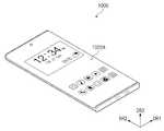
도 1은 본 발명의 일 실시예에 따른 전자 장치의 사시도이다.1 is a perspective view of an electronic device according to an embodiment of the present invention.
도 1을 참조하면, 전자 장치(1000)는 전기적 신호에 따라 활성화되는 장치일 수 있다. 예를 들어, 전자 장치(1000)는 휴대폰, 태블릿, 자동차 내비게이션, 게임기, 또는 웨어러블 장치일 수 있으나, 이에 제한되는 것은 아니다. 도 1에서는 전자 장치(1000)가 휴대폰인 것을 예시적으로 도시하였다.Referring to FIG. 1 , an
전자 장치(1000)는 액티브 영역(1000A)을 통해 영상을 표시할 수 있다. 액티브 영역(1000A)은 제1 방향(DR1) 및 제2 방향(DR2)에 의해 정의된 평면을 포함할 수 있다. 액티브 영역(1000A)은 상기 평면의 적어도 2 개의 측으로부터 각각 벤딩된 곡면들을 더 포함할 수 있다. 하지만, 액티브 영역(1000A)의 형상이 이에 제한되는 것은 아니다. 예를 들어, 액티브 영역(1000A)은 상기 평면만을 포함할 수도 있고, 액티브 영역(1000A)은 상기 평면의 적어도 2개 이상, 예를 들어 4 개의 측으로부터 각각 벤딩된 4개의 곡면들을 더 포함할 수도 있다.The
전자 장치(1000)의 두께 방향은 제1 방향(DR1) 및 제2 방향(DR2)과 교차하는 제3 방향(DR3)과 나란할 수 있다. 따라서, 전자 장치(1000)를 구성하는 부재들의 전면(또는 상면)과 배면(또는 하면)은 제3 방향(DR3)을 기준으로 정의될 수 있다.The thickness direction of the
도 2는 본 발명의 일 실시예에 따른 전자 장치의 일부 구성을 도시한 단면도이다.2 is a cross-sectional view illustrating a partial configuration of an electronic device according to an embodiment of the present invention.
도 2를 참조하면, 전자 장치(1000)는 표시 패널(100) 및 센서(200)를 포함할 수 있다.Referring to FIG. 2 , the
표시 패널(100)은 영상을 실질적으로 생성하는 구성일 수 있다. 표시 패널(100)은 발광형 표시 패널일 수 있다. 예를 들어, 표시 패널(100)은 유기발광 표시 패널 또는 퀀텀닷 발광 표시 패널일 수 있다. 또는 표시 패널(100)은 수광형 표시 패널일 수 있다. 예를 들어, 표시 패널(100)은 액정 표시 패널일 수 있다.The
센서(200)는 표시 패널(100) 위에 배치될 수 있다. 센서(200)는 외부에서 인가되는 외부 입력을 감지할 수 있다. 외부 입력은 사용자의 입력일 수 있다. 사용자의 입력은 사용자 신체의 일부, 광, 열, 펜, 또는 압력 등 다양한 형태의 외부 입력들을 포함할 수 있다.The
센서(200)는 연속된 공정을 통해 표시 패널(100) 위에 형성될 수 있다. 또는 센서(200)는 표시 패널(100)과 접착 부재를 통해 서로 결합될 수 있다. 접착 부재는 통상의 접착제 또는 점착제를 포함할 수 있다. 예를 들어, 접착부재는 감압접착필름(PSA, Pressure Sensitive Adhesive film), 광학투명접착필름(OCA, Optically Clear Adhesive film) 또는 광학투명접착수지(OCR, Optically Clear Resin)와 같은 투명한 접착부재일 수 있다.The
도시되지 않았으나, 전자 장치(1000)는 센서(200) 위에 배치된 윈도우를 더 포함할 수 있다. 윈도우는 광학적으로 투명한 절연 물질을 포함할 수 있으며, 윈도우는 유리 또는 플라스틱을 포함할 수 있다. 윈도우는 다층구조 또는 단층 구조를 가질 수 있다.Although not shown, the
도 3은 본 발명의 일 실시예에 따른 표시 패널의 평면도이다.3 is a plan view of a display panel according to an exemplary embodiment.
도 3을 참조하면, 표시 패널(100)에는 액티브 영역(100A) 및 주변 영역(100N)이 정의될 수 있다. 액티브 영역(100A)은 전기적 신호에 따라 활성화되는 영역일 수 있다. 예를 들어, 액티브 영역(100A)은 영상을 표시하는 영역일 수 있다. 주변 영역(100N)은 액티브 영역(100A)을 에워쌀 수 있다. 주변 영역(100N)에는 액티브 영역(100A)을 구동하기 위한 구동 회로나 구동 라인 등이 배치될 수 있다.Referring to FIG. 3 , an
표시 패널(100)의 액티브 영역(100A) 내에는 투과 영역(100T)이 정의될 수 있다. 투과 영역(100T)은 액티브 영역(100A)에 의해 에워싸일 수 있다. 다만, 이에 제한되는 것은 아니다. 예를 들어, 투과 영역(100T)의 일부분은 액티브 영역(100A)에 접하고, 다른 일부분은 주변 영역(100N)에 접할 수도 있다.A
투과 영역(100T)은 액티브 영역(100A)에 비해 상대적으로 높은 투과율을 가진 영역일 수 있다. 투과 영역(100T)은 전자 모듈로 입력되는 외부 신호나 전자 모듈로부터 출력되는 신호가 전달되는 공간일 수 있다. 예를 들어, 상기 전자 모듈은 카메라 모듈일 수 있다.The
투과 영역(100T)은 표시 패널(100)을 구성하는 구성들 모두 또는 적어도 일부가 제거되어 정의될 수 있다. 투과 영역(100T)은 평면상에서 원, 타원, 다각형, 또는 적어도 일측에 곡선 변을 포함하는 다각형 중 어느 하나의 형상을 가질 수 있으며, 어느 하나의 실시예로 한정되지 않는다.The
표시 패널(100)은 베이스층(100-1), 복수의 화소들(110), 복수의 신호 라인들(120, 130, 140), 복수의 표시 패드들(150), 및 복수의 감지 패드들(160)을 포함할 수 있다.The
베이스층(100-1)은 합성수지 필름을 포함할 수 있다. 합성수지 필름은 열 경화성 수지를 포함할 수 있다. 베이스층(100-1)은 다층구조를 가질 수 있다. 예컨대 베이스층(100-1)은 합성수지층, 접착층, 및 합성수지층의 3층 구조를 가질 수도 있다. 특히, 합성수지층은 폴리이미드계 수지층일 수 있고, 그 재료는 특별히 제한되지 않는다. 합성수지층은 아크릴계 수지, 메타크릴계 수지, 폴리이소프렌, 비닐계 수지, 에폭시계 수지, 우레탄계 수지, 셀룰로오스계 수지, 실록산계 수지, 폴리아미드계 수지 및 페릴렌계 수지 중 적어도 어느 하나를 포함할 수 있다. 그밖에 베이스층(100-1)은 유리 기판, 또는 유/무기 복합재료 기판 등을 포함할 수 있다.The base layer 100 - 1 may include a synthetic resin film. The synthetic resin film may include a thermosetting resin. The base layer 100 - 1 may have a multi-layered structure. For example, the base layer 100-1 may have a three-layer structure of a synthetic resin layer, an adhesive layer, and a synthetic resin layer. In particular, the synthetic resin layer may be a polyimide-based resin layer, and the material thereof is not particularly limited. The synthetic resin layer may include at least one of acrylic resins, methacrylic resins, polyisoprene, vinyl resins, epoxy resins, urethane resins, cellulose resins, siloxane resins, polyamide resins, and perylene resins. . In addition, the base layer 100 - 1 may include a glass substrate or an organic/inorganic composite material substrate.
신호 라인들(120, 130, 140)은 화소들(110)에 연결되어 화소들(110)에 전기적 신호들을 전달한다. 도 3에서는 신호 라인들(120, 130, 140)이 데이터 라인(120), 스캔 라인(130), 및 전원 라인(140)을 포함하는 것을 예시적으로 도시하였다. 다만, 이는 예시적으로 도시한 것이고, 신호 라인들(120, 130, 140)은 초기화 전압 라인, 발광 제어 라인 중 적어도 어느 하나를 더 포함할 수도 있으며, 어느 하나의 실시예로 한정되지 않는다.The signal lines 120 , 130 , and 140 are connected to the
화소들(110)은 액티브 영역(100A)에 배치될 수 있다. 본 실시예에서는 복수의 화소들 중 하나의 화소(110)의 등가 회로도를 확대하여 예시적으로 도시하였다.The
화소(110)는 제1 트랜지스터(111), 제2 트랜지스터(112), 커패시터(113), 및 발광 소자(114)를 포함할 수 있다. 제1 트랜지스터(111)는 화소(110)의 온-오프를 제어하는 스위칭 소자일 수 있다. 제1 트랜지스터(111)는 스캔 라인(130)을 통해 전달된 스캔 신호에 응답하여 데이터 라인(120)을 통해 전달된 데이터 신호를 전달 또는 차단할 수 있다.The
커패시터(113)는 제1 트랜지스터(111)와 전원 라인(140)에 연결될 수 있다. 커패시터(113)는 제1 트랜지스터(111)로부터 전달된 데이터 신호와 전원 라인(140)에 인가된 제1 전원 신호 사이의 차이에 대응하는 전하량을 충전할 수 있다.The
제2 트랜지스터(112)는 제1 트랜지스터(111), 커패시터(113), 및 발광 소자(114)에 연결될 수 있다. 제2 트랜지스터(112)는 커패시터(113)에 저장된 전하량에 대응하여 발광 소자(114)에 흐르는 구동전류를 제어할 수 있다. 커패시터(113)에 충전된 전하량에 따라 제2 트랜지스터(112)의 턴-온 시간이 결정될 수 있다. 제2 트랜지스터(112)는 턴-온 시간 동안 전원 라인(140)을 통해 전달된 제1 전원 신호를 발광 소자(114)에 제공할 수 있다.The
발광 소자(114)는 전기적 신호에 따라 광을 발생시키거나 광량을 제어할 수 있다. 예를 들어, 발광 소자(114)는 유기 발광 소자, 양자점 발광 소자, 마이크로 엘이디 발광 소자, 또는 나노 엘이디 발광 소자를 포함할 수 있다.The
발광 소자(114)는 전원 단자(115)와 연결되어 전원 라인(140)이 제공하는 제1 전원 신호와 상이한 전원 신호(이하, 제2 전원 신호 또는 그라운드 전압)를 제공받을 수 있다. 발광 소자(114)에는 제2 트랜지스터(112)로부터 제공되는 전기적 신호와 제2 전원 신호 사이의 차이에 대응하는 구동 전류가 흐르게 되고, 발광 소자(114)는 구동 전류에 대응하는 광을 생성할 수 있다.The
한편, 이는 예시적으로 도시한 것이고, 화소(110)는 다양한 구성과 배열을 가진 전자 소자들을 포함할 수 있으며, 어느 하나의 실시예로 한정되지 않는다. 예를 들어, 화소(110)는 7개의 트랜지스터들 및 하나의 커패시터를 포함하는 등가회로를 가질 수도 있으며, 화소(110)의 등가회로도는 다양한 형태로 변형될 수 있다.Meanwhile, this is illustrated by way of example, and the
표시 패드들(150)은 제1 패드(151) 및 제2 패드(152)를 포함할 수 있다. 제1 패드(151)는 복수로 구비되어 데이터 라인들(120)에 각각 연결될 수 있다. 제2 패드(152)는 전원 라인(140)과 전기적으로 연결될 수 있다. 도시되지 않았으나, 제2 패드(152)는 전원 패턴을 통해 전원 라인(140)과 전기적으로 연결될 수도 있다.The
표시 패널(100)은 표시 패드들(150)을 통해 외부로부터 제공된 전기적 신호들을 화소들(110)에 제공할 수 있다. 한편, 표시 패드들(150)은 제1 패드(151) 및 제2 패드(152) 외에 다른 전기적 신호들을 수신하기 위한 패드들을 더 포함할 수 있으며, 어느 하나의 실시예로 한정되지 않는다.The
구동칩(300)은 표시 패널(100)의 주변 영역(100N) 위에 실장될 수 있다. 구동칩(300)은 칩 형태의 타이밍 제어회로일 수 있다. 이 경우, 데이터 라인들(120)은 구동칩(300)을 거쳐 제1 패드들(151)에 전기적으로 연결될 수 있다. 다만, 이는 예시적인 것으로 구동칩(300)은 표시 패널(100)과는 별개의 필름 상에 실장될 수 있다. 이 경우, 구동칩(300)은 상기 필름을 통해 표시 패드들(150)과 전기적으로 연결될 수도 있다.The
복수의 감지 패드들(160)은 후술될 센서의 감지 전극들과 전기적으로 연결될 수 있다. 복수의 감지 패드들(160) 중 일부 감지 패드들과 다른 일부 감지 패드들은 표시 패드들(150)을 사이에 두고 이격되어 배치될 수 있다. 다만, 이에 제한되는 것은 아니며, 감지 패드들(160)과 표시 패드들(150)의 배치 관계는 다양하게 변형될 수 있다.The plurality of
도 4는 본 발명의 일 실시예에 따른 표시 패널의 단면도이다.4 is a cross-sectional view of a display panel according to an exemplary embodiment.
도 4를 참조하면, 표시 패널(100)은 복수 개의 절연층들 및 반도체 패턴, 도전 패턴, 신호 라인 등을 포함할 수 있다. 코팅, 증착 등의 방식으로 의해 절연층, 반도체층 및 도전층이 형성된다. 이후, 포토리소그래피의 방식으로 절연층, 반도체층 및 도전층이 선택적으로 패터닝될 수 있다. 이러한 방식으로 회로층(100-2) 및 표시소자층(100-3)에 포함된 반도체 패턴, 도전 패턴, 신호 라인 등이 형성된다. 이 후, 표시소자층(100-3)을 커버하는 봉지층(100-4)이 형성될 수 있다.Referring to FIG. 4 , the
베이스층(100-1)의 상면에 적어도 하나의 무기층이 형성된다. 무기층은 알루미늄옥사이드, 티타늄옥사이드, 실리콘옥사이드 실리콘옥시나이트라이드, 지르코늄옥사이드, 및 하프늄옥사이드 중 적어도 하나를 포함할 수 있다. 무기층은 다층으로 형성될 수 있다. 다층의 무기층들은 배리어층 및/또는 버퍼층을 구성할 수 있다. 본 실시예에서 표시 패널(100)은 버퍼층(BFL)을 포함하는 것으로 도시되었다.At least one inorganic layer is formed on the upper surface of the base layer 100 - 1 . The inorganic layer may include at least one of aluminum oxide, titanium oxide, silicon oxide silicon oxynitride, zirconium oxide, and hafnium oxide. The inorganic layer may be formed in multiple layers. The multi-layered inorganic layers may constitute a barrier layer and/or a buffer layer. In the present exemplary embodiment, the
버퍼층(BFL)은 베이스층(100-1)과 반도체 패턴 사이의 결합력을 향상시킬 수 있다. 버퍼층(BFL)은 실리콘옥사이드층 및 실리콘나이트라이드층을 포함할 수 있으며, 실리콘 옥사이드층과 실리콘나이트라이드층은 교대로 적층될 수 있다.The buffer layer BFL may improve a bonding force between the base layer 100 - 1 and the semiconductor pattern. The buffer layer BFL may include a silicon oxide layer and a silicon nitride layer, and the silicon oxide layer and the silicon nitride layer may be alternately stacked.
버퍼층(BFL) 상에 반도체 패턴이 배치된다. 반도체 패턴은 폴리실리콘을 포함할 수 있다. 그러나 이에 제한되지 않고, 반도체 패턴은 비정질실리콘 또는 금속 산화물을 포함할 수도 있다.A semiconductor pattern is disposed on the buffer layer BFL. The semiconductor pattern may include polysilicon. However, the present invention is not limited thereto, and the semiconductor pattern may include amorphous silicon or metal oxide.
도 4는 일부의 반도체 패턴을 도시한 것일 뿐이고, 다른 영역에 반도체 패턴이 더 배치될 수 있다. 반도체 패턴은 화소들(110, 도 3 참조)에 걸쳐 특정한 규칙으로 배열될 수 있다. 반도체 패턴은 도핑 여부에 따라 전기적 성질이 다를 수 있다. 반도체 패턴은 도핑영역과 비-도핑영역을 포함할 수 있다. 도핑영역은 N형 도판트 또는 P형 도판트로 도핑될 수 있다. P타입의 트랜지스터는 P형 도판트로 도핑된 도핑영역을 포함하고, N타입의 트랜지스터는 N형 도판트로 도핑된 도핑영역을 포함할 수 있다.FIG. 4 only shows some semiconductor patterns, and semiconductor patterns may be further disposed in other regions. The semiconductor pattern may be arranged in a specific rule across the pixels 110 (refer to FIG. 3 ). The semiconductor pattern may have different electrical properties depending on whether it is doped or not. The semiconductor pattern may include a doped region and a non-doped region. The doped region may be doped with an N-type dopant or a P-type dopant. The P-type transistor may include a doped region doped with a P-type dopant, and the N-type transistor may include a doped region doped with an N-type dopant.
도핑영역은 비-도핑영역보다 전도성이 크고, 실질적으로 전극 또는 신호 라인의 역할을 할 수 있다. 비-도핑영역은 실질적으로 트랜지스터의 액티브(또는 채널)에 해당할 수 있다. 다시 말해, 반도체 패턴의 일부분은 트랜지스터의 액티브일수 있고, 다른 일부분은 트랜지스터의 소스 또는 드레인일 수 있고, 또 다른 일부분은 연결 전극 또는 연결 신호라인일 수 있다.The doped region has higher conductivity than the non-doped region, and may substantially function as an electrode or a signal line. The non-doped region may substantially correspond to the active (or channel) of the transistor. In other words, a portion of the semiconductor pattern may be an active transistor, another portion may be a source or drain of the transistor, and another portion may be a connection electrode or a connection signal line.
도 4에 도시된 것과 같이, 제1 트랜지스터(111)의 소스(S1), 액티브(A1), 및 드레인(D1)이 반도체 패턴으로부터 형성되고, 제2 트랜지스터(112)의 소스(S2), 액티브(A2), 및 드레인(D2)이 반도체 패턴으로부터 형성될 수 있다. 소스(S1, S2) 및 드레인(D1, D2)은 단면 상에서 액티브(A1, A2)로부터 서로 반대 방향으로 연장될 수 있다. 도 4에는 반도체 패턴으로부터 형성된 연결 신호 라인(SCL)의 일부분을 도시하였다. 별도로 도시하지 않았으나, 연결 신호 라인(SCL)은 평면 상에서 제2 트랜지스터(112)의 드레인(D2)에 연결될 수 있다.As shown in FIG. 4 , the source S1 , the active A1 , and the drain D1 of the
제1 절연층(10)은 버퍼층(BFL) 위에 배치될 수 있다. 제1 절연층(10)은 복수 개의 화소들(110, 도 3 참조)에 공통으로 중첩하며, 반도체 패턴을 커버할 수 있다. 제1 절연층(10)은 무기층 및/또는 유기층일 수 있으며, 단층 또는 다층 구조를 가질 수 있다. 제1 절연층(10)은 알루미늄옥사이드, 티타늄옥사이드, 실리콘옥사이드, 실리콘옥시나이트라이드, 지르코늄옥사이드, 및 하프늄옥사이드 중 적어도 하나를 포함할 수 있다. 본 실시예에서 제1 절연층(10)은 단층의 실리콘옥사이드층일 수 있다. 제1 절연층(10)뿐만 아니라 후술하는 회로층(100-2)의 절연층은 무기층 및/또는 유기층일 있으며, 단층 또는 다층 구조를 가질 수 있다. 무기층은 상술한 물질 중 적어도 하나를 포함할 수 있으나, 이에 제한되는 것은 아니다.The first insulating
게이트(G1, G2)는 제1 절연층(10) 위에 배치된다. 게이트(G1)는 금속패턴의 일부분일 수 있다. 게이트(G1, G2)는 액티브(A1, A2)에 중첩한다. 반도체 패턴을 도핑하는 공정에서 게이트(G1, G2)는 마스크로 기능할 수 있다.The gates G1 and G2 are disposed on the first insulating
제2 절연층(20)은 제1 절연층(10) 위에 배치되며, 게이트(G1, G2)를 커버할 수 있다. 제2 절연층(20)은 화소들(110, 도 3 참조)에 공통으로 중첩할 수 있다. 제2 절연층(20)은 무기층 및/또는 유기층일 수 있으며, 단층 또는 다층 구조를 가질 수 있다. 본 실시예에서 제2 절연층(20)은 단층의 실리콘옥사이드층일 수 있다.The second insulating
상부 전극(UE)은 제2 절연층(20) 위에 배치될 수 있다. 상부 전극(UE)은 제2 트랜지스터(112)의 게이트(G2)와 중첩할 수 있다. 상부 전극(UE)은 금속 패턴의 일부분일 수 있다. 게이트(G2)의 일부분과 그에 중첩하는 상부 전극(UE)은 커패시터(113, 도 3 참조)를 정의할 수 있다. 본 발명의 일 실시예에서 상부 전극(UE)은 생략될 수도 있다.The upper electrode UE may be disposed on the second insulating
제3 절연층(30)은 제2 절연층(20) 위에 배치되며, 상부 전극(UE)을 커버할 수 있다. 본 실시예에서 제3 절연층(30)은 단층의 실리콘옥사이드층일 수 있다.The third insulating
제1 연결 전극(CNE1)은 제3 절연층(30) 위에 배치될 수 있다. 제1 연결 전극(CNE1)은 제1 내지 제3 절연층(10, 20, 30)을 관통하는 컨택홀(CNT-1)을 통해 연결 신호 라인(SCL)에 접속될 수 있다.The first connection electrode CNE1 may be disposed on the third insulating
제4 절연층(40)은 제3 절연층(30) 위에 배치될 수 있다. 제4 절연층(40)은 단층의 실리콘 옥사이드층일 수 있다. 제5 절연층(50)은 제4 절연층(40) 위에 배치될 수 있다. 제5 절연층(50)은 유기층일 수 있다.The fourth insulating
제2 연결 전극(CNE2)은 제5 절연층(50) 위에 배치될 수 있다. 제2 연결 전극(CNE2)은 제4 절연층(40) 및 제5 절연층(50)을 관통하는 컨택홀(CNT-2)을 통해 제1 연결 전극(CNE1)에 접속될 수 있다.The second connection electrode CNE2 may be disposed on the fifth insulating
제6 절연층(60)은 제5 절연층(50) 위에 배치되며, 제2 연결 전극(CNE2)을 커버할 수 있다. 제6 절연층(60)은 유기층일 수 있다.The sixth insulating
발광 소자(114)를 포함하는 표시소자층(100-3)은 회로층(100-2) 위에 배치될 수 있다. 발광 소자(114)는 제1 전극(AE), 정공 제어층(HCL), 발광층(EML), 전자 제어층(ECL), 및 제2 전극(CE)을 포함할 수 있다.The display device layer 100 - 3 including the
제1 전극(AE)은 제6 절연층(60) 위에 배치될 수 있다. 제1 전극(AE)은 제6 절연층(60)을 관통하는 컨택홀(CNT-3)을 통해 제2 연결 전극(CNE2)에 연결될 수 있다.The first electrode AE may be disposed on the sixth insulating
화소 정의막(70)은 제6 절연층(60) 위에 배치되며, 제1 전극(AE)의 일부분을 커버할 수 있다. 화소 정의막(70)에는 개구부(70-OP)가 정의된다. 화소 정의막(70)의 개구부(70-OP)는 제1 전극(AE)의 적어도 일부분을 노출시킨다.The
도 4에 도시된 것과 같이, 액티브 영역(100A, 도 3 참조)은 화소 영역(PXA)과 화소 영역(PXA)에 인접한 비화소 영역(NPXA)을 포함할 수 있다. 비화소 영역(NPXA)은 화소 영역(PXA)을 에워쌀 수 있다. 본 실시예에서 화소 영역(PXA)은 개구부(70-OP)에 의해 노출된 제1 전극(AE)의 일부 영역에 대응하게 정의되었다.As illustrated in FIG. 4 , the
정공 제어층(HCL)은 제1 전극(AE) 위에 배치될 수 있다. 정공 제어층(HCL)은 화소 영역(PXA)과 비화소 영역(NPXA)에 공통으로 배치될 수 있다. 정공 제어층(HCL)은 정공 수송층을 포함하고, 정공 주입층을 더 포함할 수 있다.The hole control layer HCL may be disposed on the first electrode AE. The hole control layer HCL may be commonly disposed in the pixel area PXA and the non-pixel area NPXA. The hole control layer HCL may include a hole transport layer and may further include a hole injection layer.
발광층(EML)은 정공 제어층(HCL) 위에 배치될 수 있다. 발광층(EML)은 개구부(70-OP)에 대응하는 영역에 배치될 수 있다. 즉, 발광층(EML)은 화소들(110, 도 3 참조) 각각에 분리되어 형성될 수 있다. 다만, 이에 제한되는 것은 아니며, 발광층(EML)은 정공 제어층(HCL)과 같이 화소 영역(PXA)과 비화소 영역(NPXA)에 공통으로 배치될 수도 있다. 발광층(EML)이 화소들 각각에 분리되어 형성된 경우, 발광층들(EML)은 청색, 적색, 및 녹색 중 적어도 하나의 색의 광을 발광할 수 있다. 발광층(EML)이 화소들(110, 도 3 참조)에 공통으로 배치된 경우, 발광층(EML)은 청색 광을 제공하거나, 백색 광을 제공할 수 있다.The emission layer EML may be disposed on the hole control layer HCL. The emission layer EML may be disposed in a region corresponding to the opening 70 -OP. That is, the emission layer EML may be formed separately in each of the pixels 110 (refer to FIG. 3 ). However, the present invention is not limited thereto, and the emission layer EML may be commonly disposed in the pixel area PXA and the non-pixel area NPXA like the hole control layer HCL. When the emission layer EML is separately formed in each of the pixels, the emission layers EML may emit light of at least one color among blue, red, and green. When the emission layer EML is commonly disposed on the pixels 110 (refer to FIG. 3 ), the emission layer EML may provide blue light or white light.
전자 제어층(ECL)은 발광층(EML) 위에 배치될 수 있다. 전자 제어층(ECL)은 전자 수송층을 포함하고, 전자 주입층을 더 포함할 수 있다. 정공 제어층(HCL)과 전자 제어층(ECL)은 오픈 마스크를 이용하여 복수 개의 화소들에 공통으로 형성될 수 있다.The electronic control layer ECL may be disposed on the emission layer EML. The electron control layer ECL may include an electron transport layer and may further include an electron injection layer. The hole control layer HCL and the electron control layer ECL may be commonly formed in the plurality of pixels using an open mask.
제2 전극(CE)은 전자 제어층(ECL) 위에 배치될 수 있다. 제2 전극(CE)은 일체의 형상을 갖고, 복수 개의 화소들(110, 도 3 참조)에 공통적으로 배치될 수 있다.The second electrode CE may be disposed on the electronic control layer ECL. The second electrode CE has an integral shape and may be commonly disposed in the plurality of pixels 110 (refer to FIG. 3 ).
캡핑층(80)은 제2 전극(CE) 위에 배치되며 제2 전극(CE)에 접촉할 수 있다. 캡핑층(80)은 유기물질을 포함할 수 있다. 캡핑층(80)은 후속의 공정 예컨대 스퍼터링 공정으로부터 제2 전극(CE)을 보호하고, 발광 소자(114)의 출광 효율을 향상시킬 수 있다. 캡핑층(80)은 후술 될 제1 무기층(91)보다 큰 굴절률을 가질 수 있으나, 이에 제한되는 것은 아니다. 본 발명의 일 실시예에서, 캡핑층(80)은 생략될 수도 있다. The
봉지층(100-4)은 표시소자층(100-3) 위에 배치될 수 있다. 봉지층(100-4)은 제1 무기층(91), 유기층(92), 및 제2 무기층(93)을 포함할 수 있다. 제1 무기층(91) 및 제2 무기층(93)은 수분/산소로부터 표시소자층(100-3)을 보호하고, 유기층(92)은 먼지 입자와 같은 이물질로부터 표시소자층(100-3)을 보호한다. 제1 무기층(91) 및 제2 무기층(93)은 실리콘나이트라이드층, 실리콘옥시 나이트라이드층, 실리콘옥사이드층, 티타늄옥사이드층, 또는 알루미늄옥사이드층 등을 포함할 수 있다. 유기층(92)은 아크릴 계열 유기층을 포함할 수 있고, 이에 제한되지 않는다.The encapsulation layer 100 - 4 may be disposed on the display device layer 100 - 3 . The encapsulation layer 100 - 4 may include a first
본 발명의 일 실시예에서 캡핑층(80)과 제1 무기층(91) 사이에 무기층, 예컨대 LiF층이 더 배치될 수 있다. LiF층은 발광 소자(114)의 출광 효율을 향상시킬 수 있다.In an embodiment of the present invention, an inorganic layer, for example, a LiF layer, may be further disposed between the capping
도 5는 본 발명의 일 실시예에 따른 센서의 평면도이다.5 is a plan view of a sensor according to an embodiment of the present invention.
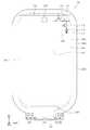
도 5를 참조하면, 센서(200)에는 액티브 영역(200A) 및 주변 영역(200N)이 정의될 수 있다. 액티브 영역(200A)은 전기적 신호에 따라 활성화되는 영역일 수 있다. 예를 들어, 액티브 영역(200A)은 입력을 감지하는 영역일 수 있다. 주변 영역(200N)은 액티브 영역(200A)을 에워쌀 수 있다.Referring to FIG. 5 , an
액티브 영역(200A)과 주변 영역(200N) 사이에 경계(200B)가 정의되고, 경계(200B)는 제1 경계 부분(200B1) 및 제2 경계 부분(200B2)을 포함할 수 있다. 제1 경계 부분(200B1)은 곡률을 갖는 경계(200B)의 일부분일 수 있고, 제2 경계 부분(200B2)은 제1 방향(DR1)을 따라 연장된 경계(200B)의 일부분일 수 있다.A
센서(200)의 액티브 영역(200A) 내에는 투과 영역(200T)이 정의될 수 있다. 투과 영역(200T)은 앞서 설명된 표시 패널(100, 도 3 참조)의 투과 영역(100T, 도 3 참조)과 평면 상에서 중첩할 수 있다. 투과 영역(200T)은 센서(200)를 구성하는 구성들 모두 또는 적어도 일부가 제거되어 정의될 수 있다.A
센서(200)는 베이스 절연층(200-1), 제1 감지 전극들(210), 제2 감지 전극들(220), 패턴들(230), 및 라인부(240)를 포함할 수 있다. 제1 감지 전극들(210), 제2 감지 전극들(220), 및 패턴들(230)은 액티브 영역(200A)에 배치되고, 라인부(240)는 주변 영역(200N)에 배치될 수 있다. 라인부(240)는 컨택홀을 통해 복수의 감지 패드들(160, 도 3 참조)에 전기적으로 연결될 수 있다.The
센서(200)는 제1 감지 전극들(210)과 제2 감지 전극들(220) 사이의 상호정전용량의 변화를 통해 외부 입력에 대한 정보를 획득할 수 있다. 제1 감지 전극들(210)은 제1 방향(DR1)을 따라 배열되고, 제1 감지 전극들(210) 각각은 제2 방향(DR2)을 따라 연장될 수 있다. 제1 감지 전극들(210)은 제1 감지 패턴들(211) 및 제1 연결 패턴들(212)을 포함할 수 있다. 제1 연결 패턴들(212)은 서로 인접한 2 개의 제1 감지 패턴들(211)을 전기적으로 연결할 수 있다.The
제2 감지 전극들(220) 각각은 제1 방향(DR1)을 따라 연장되고, 제2 감지 전극들(220)은 제2 방향(DR2)을 따라 배열될 수 있다. 제2 감지 전극들(220)은 제2 감지 패턴들(221) 및 제2 연결 패턴들(222)을 포함할 수 있다. 제2 연결 패턴들(222)은 서로 인접한 2 개의 제2 감지 패턴들(221)을 전기적으로 연결할 수 있다. 서로 인접한 2 개의 제2 감지 패턴들(221)은 2 개의 제2 연결 패턴들(222)에 의해 서로 연결될 수 있으나, 이에 제한되는 것은 아니다.Each of the
제1 감지 패턴들(211) 각각은 서로 연결된 제1 부분(211a), 제2 부분(211b), 및 제3 부분(211c)을 포함할 수 있다.Each of the
제1 부분(211a)은 제2 방향(DR2)을 따라 연장할 수 있다. 제1 부분(211a)의 일 단은 하나의 제1 연결 패턴(212)에 연결되고, 제1 부분(211a)의 타 단은 다른 하나의 제1 연결 패턴(212)에 연결될 수 있다. 제1 부분(211a)은 줄기 부분으로 지칭될 수 있다. 제1 연결 패턴들(212)과 제1 감지 패턴들(211)은 하나의 연결된 구조를 갖기 때문에, 제1 연결 패턴들(212)은 제1 부분(211a)의 일부분으로 정의될 수도 있다.The
제2 부분(211b)은 제1 부분(211a)으로부터 제1 방향(DR1)을 향해 돌출될 수 있다. 예를 들어, 제2 부분(211b)은 제1 부분(211a)의 중앙 영역으로부터 멀어지는 방향으로 돌출될 수 있다. 제2 부분(211b)은 돌기 부분으로 지칭될 수 있다.The
제3 부분(211c)은 복수로 제공될 수 있다. 제3 부분들(211c)은 제1 부분(211a)으로부터 제3 방향(DR3a) 또는 제4 방향(DR4a)을 따라 연장될 수 있다. 제3 부분들(211c) 중 일부는 제3 방향(DR3a)을 따라 연장되고, 제3 부분들(211c) 중 다른 일부는 제4 방향(DR4a)을 따라 연장될 수 있다. 제3 부분들(211c)은 가지 부분들로 지칭될 수 있다.A plurality of
제3 방향(DR3a)은 제1 방향(DR1) 및 제2 방향(DR2)과 교차하는 방향일 수 있다. 예를 들어, 제3 방향(DR3a)은 제1 방향(DR1)과 제2 방향(DR2) 사이의 방향일 수 있다. 제4 방향(DR4a)은 제3 방향(DR3a)과 교차하는 방향일 수 있다. 예를 들어, 제3 방향(DR3a)과 제4 방향(DR4a)은 서로 직교할 수 있다.The third direction DR3a may be a direction crossing the first direction DR1 and the second direction DR2 . For example, the third direction DR3a may be a direction between the first direction DR1 and the second direction DR2 . The fourth direction DR4a may be a direction crossing the third direction DR3a. For example, the third direction DR3a and the fourth direction DR4a may be orthogonal to each other.
제2 감지 패턴들(221) 각각은 인접한 제1 감지 패턴들(211)의 형상에 대응하는 형상을 가질 수 있다. 제2 감지 패턴들(221) 각각은 인접한 제1 감지 패턴들(211) 각각의 적어도 2 개의 제3 부분들(211c)을 에워쌀 수 있다.Each of the
감지 라인들(241, 242)은 제1 감지 라인들(241) 및 제2 감지 라인들(242)을 포함할 수 있다. 제1 감지 라인들(241)은 제1 감지 전극들(210)에 각각 전기적으로 연결될 수 있다. 제2 감지 라인들(242)은 제2 감지 전극들(220)에 각각 전기적으로 연결될 수 있다. 제2 감지 라인들(242) 중 일부는 제2 감지 전극들(220) 중 일부의 좌측에 각각 연결되고, 제2 감지 라인들(242) 중 다른 일부는 제2 감지 전극들(220) 중 다른 일부의 우측에 각각 연결될 수 있다. 다만, 제1 감지 라인들(241)과 제1 감지 전극들(210)의 연결 관계 및 제2 감지 라인들(242)과 제2 감지 전극들(220)의 연결 관계가 도 5에 도시된 예에 제한되는 것은 아니다.The sensing lines 241 and 242 may include
패턴들(230)은 제1 감지 패턴들(211) 및 제2 감지 패턴들(221)과 이격될 수 있다. 패턴들(230)은 제1 감지 패턴들(211) 및 제2 감지 패턴들(221)과 동일한 공정을 통해 형성될 수 있다. 따라서, 패턴들(230)은 제1 감지 패턴들(211) 및 제2 감지 패턴들(221)과 동일한 재료를 포함하며, 동일한 적층 구조를 가질 수 있다. 패턴들(230)은 더미 패턴들, 보조 패턴들, 추가 패턴들, 서브 패턴들, 또는 경계 패턴들로 지칭될 수 있다.The
패턴들(230)은 제1 패턴(230a) 및 제2 패턴(230b)을 포함할 수 있다. 제1 패턴(230a)은 제1 감지 패턴(211)과 제2 감지 패턴(221) 사이에 배치될 수 있다. 제2 패턴(230b)은 제2 감지 패턴들(221) 사이에 배치될 수 있다. 예를 들어, 제2 패턴(230b)은 제2 방향(DR2)으로 인접한 2 개의 제2 감지 패턴들(221) 사이에 배치되어, 상기 2 개의 제2 감지 패턴들(221)을 서로 이격시킬 수 있다.The
제2 패턴(230b)은 제1 경계 패턴(230b1) 및 제2 경계 패턴들(230b2)을 포함할 수 있다. 제1 경계 패턴(230b1)은 평면 상에서 마름모꼴 형상을 가질 수 있다. 제2 경계 패턴들(230b2)은 제1 경계 패턴(230b1)을 사이에 두고 서로 이격되어 배치될 수 있다. 제2 경계 패턴들(230b2) 각각은 제1 방향(DR1)을 따라 연장될 수 있다. 제2 경계 패턴들(230b2) 각각은 제1 경계 패턴(230b1)과 제1 패턴(230a)에 연결될 수 있다.The
제1 패턴(230a)이 제1 감지 패턴들(211)과 제2 감지 패턴들(221) 사이에 배치되고, 제2 패턴(230b)이 제2 감지 패턴들(221) 사이에 배치됨에 따라 제1 감지 패턴들(211)과 제2 감지 패턴들(221) 사이의 경계 영역 및 제2 감지 패턴들(221) 사이의 경계 영역의 시인성이 감소될 수 있다.As the
패턴들(230) 중 일부는 플로팅 전극으로 제1 감지 패턴들(211) 및 제2 감지 패턴들(221)과 전기적으로 연결되지 않을 수 있다. 또는 패턴들(230) 중 일부는 그라운드될 수 있다. 패턴들(230) 중 다른 일부는 제1 감지 패턴들(211) 또는 제2 감지 패턴들(221)과 연결되어, 센서(200)의 감도를 개선할 수 있다. 이에 대한 구체적인 설명은 후술된다.Some of the
도 6은 본 발명의 일 실시예에 따른 센서의 단면도이다.6 is a cross-sectional view of a sensor according to an embodiment of the present invention.
도 5 및 도 6을 참조하면, 단면 상에서 센서(200)는 베이스 절연층(200-1), 제1 도전층(200-2), 감지 절연층(200-3), 제2 도전층(200-4), 및 커버 절연층(200-5)을 포함할 수 있다. 제1 도전층(200-2)은 베이스 절연층(200-1) 위에 배치될 수 있다. 감지 절연층(200-3)은 제1 도전층(200-2) 위에 배치될 수 있다. 제2 도전층(200-4)은 감지 절연층(200-3) 위에 배치될 수 있다. 커버 절연층(200-5)은 제2 도전층(200-4) 위에 배치될 수 있다.5 and 6 , on a cross-section, the
베이스 절연층(200-1)은 실리콘나이트라이드, 실리콘옥시나이트라이드, 및 실리콘옥사이드 중 어느 하나를 포함하는 무기층일 수 있다. 또는 베이스 절연층(200-1)은 에폭시 수지, 아크릴 수지, 또는 이미드 계열 수지를 포함하는 유기층일 수도 있다. 베이스 절연층(200-1)은 단층 구조를 갖거나, 제3 방향(DR3)을 따라 적층된 적층 구조를 가질 수 있다.The base insulating layer 200 - 1 may be an inorganic layer including any one of silicon nitride, silicon oxynitride, and silicon oxide. Alternatively, the base insulating layer 200 - 1 may be an organic layer including an epoxy resin, an acrylic resin, or an imide-based resin. The base insulating layer 200 - 1 may have a single-layer structure or a stacked structure stacked along the third direction DR3 .
베이스 절연층(200-1)은 표시 패널(100, 도 2 참조) 위에 직접 형성될 수 있다. 또는 베이스 절연층(200-1)은 표시 패널(100, 도 2 참조)의 일 구성일 수 있다. 또는 베이스 절연층(200-1)은 별도의 베이스층 위에 형성되고, 상기 베이스층은 표시 패널(100, 도 2 참조)과 접착부재를 통해 서로 결합될 수도 있다.The base insulating layer 200 - 1 may be directly formed on the display panel 100 (refer to FIG. 2 ). Alternatively, the base insulating layer 200 - 1 may be a component of the display panel 100 (refer to FIG. 2 ). Alternatively, the base insulating layer 200 - 1 may be formed on a separate base layer, and the base layer may be coupled to the display panel 100 (refer to FIG. 2 ) through an adhesive member.
제1 도전층(200-2) 및 제2 도전층(200-4) 각각은 단층구조를 갖거나, 제3 방향(DR3)을 따라 적층된 다층 구조를 가질 수 있다. 단층구조의 도전층은 금속층 또는 투명 도전층을 포함할 수 있다. 금속층은 몰리브덴, 은, 티타늄, 구리, 알루미늄, 또는 이들의 합금을 포함할 수 있다. 투명 도전층은 인듐주석산화물(indium tin oxide, ITO), 인듐아연산화물(indium zinc oxide, IZO), 산화아연(zinc oxide, ZnO), 인듐주석아연산화물(indium zinc tin oxide, IZTO) 등과 같은 투명한 전도성산화물을 포함할 수 있다. 그밖에 투명 도전층은 PEDOT과 같은 전도성 고분자, 금속 나노 와이어, 그라핀 등을 포함할 수 있다.Each of the first conductive layer 200 - 2 and the second conductive layer 200 - 4 may have a single-layer structure or a multi-layer structure stacked along the third direction DR3 . The single-layered conductive layer may include a metal layer or a transparent conductive layer. The metal layer may include molybdenum, silver, titanium, copper, aluminum, or an alloy thereof. The transparent conductive layer is transparent, such as indium tin oxide (ITO), indium zinc oxide (IZO), zinc oxide (ZnO), indium zinc tin oxide (IZTO), etc. It may include a conductive oxide. In addition, the transparent conductive layer may include a conductive polymer such as PEDOT, metal nanowires, graphene, and the like.
다층구조의 도전층은 금속층들을 포함할 수 있다. 금속층들은 예컨대 티타늄/알루미늄/티타늄의 3층 구조를 가질 수 있다. 다층구조의 도전층은 적어도 하나의 금속층 및 적어도 하나의 투명 도전층을 포함할 수 있다.The multi-layered conductive layer may include metal layers. The metal layers may have, for example, a three-layer structure of titanium/aluminum/titanium. The multi-layered conductive layer may include at least one metal layer and at least one transparent conductive layer.
제1 도전층(200-2) 및 제2 도전층(200-4) 각각은 제1 감지 패턴들(211), 제1 연결 패턴들(212), 제2 감지 패턴들(221), 제2 연결 패턴들(222), 및 제1 및 제2 감지 라인들(241, 242) 중 일부를 포함할 수 있다.Each of the first conductive layer 200 - 2 and the second conductive layer 200 - 4 includes
예를 들어, 제1 도전층(200-2)은 제2 연결 패턴들(222), 제1 및 제2 감지 라인들(241, 242)을 포함할 수 있다. 제2 도전층(200-4)은 제1 감지 패턴들(211), 제2 감지 패턴들(221), 제1 연결 패턴들(212), 제1 및 제2 감지 라인들(241, 242), 및 패턴들(230)을 포함할 수 있다.For example, the first conductive layer 200 - 2 may include
제1 도전층(200-2)의 제1 및 제2 감지 라인들(241, 242)과 제2 도전층(200-4)의 제1 및 제2 감지 라인들(241, 242)은 감지 절연층(200-3)을 관통하는 컨택홀을 통해 서로 전기적으로 연결될 수 있다. 따라서, 제1 및 제2 감지 라인들(241, 242)의 저항이 감소될 수 있다.The first and
제1 연결 패턴들(212)은 제1 감지 패턴들(211)과 동일한 공정을 통해 형성될 수 있다. 따라서, 제1 연결 패턴들(212)과 제1 감지 패턴들(211)은 동일한 재료를 포함하며, 동일한 적층 구조를 가질 수 있다. 또한, 제1 연결 패턴들(212)과 제1 감지 패턴들(211)은 하나의 연결된 구조를 가질 수 있다. 제2 연결 패턴들(222)은 제2 감지 패턴들(221)과 서로 다른 층 상에 배치될 수 있다. 따라서, 제2 감지 패턴들(221)은 브릿지 패턴들이라 지칭될 수 있다.The
감지 절연층(200-3) 및 커버 절연층(200-5) 중 적어도 어느 하나는 무기막을 포함할 수 있다. 무기막은 알루미늄옥사이드, 티타늄옥사이드, 실리콘옥사이드, 실리콘옥시나이트라이드, 지르코늄옥사이드, 및 하프늄옥사이드 중 적어도 하나를 포함할 수 있다.At least one of the sensing insulating layer 200 - 3 and the cover insulating layer 200 - 5 may include an inorganic layer. The inorganic layer may include at least one of aluminum oxide, titanium oxide, silicon oxide, silicon oxynitride, zirconium oxide, and hafnium oxide.
감지 절연층(200-3) 및 커버 절연층(200-5) 중 적어도 어느 하나는 유기막을 포함할 수 있다. 유기막은 아크릴계 수지, 메타크릴계 수지, 폴리이소프렌, 비닐계 수지, 에폭시계 수지, 우레탄계 수지, 셀룰로오스계 수지, 실록산계 수지, 폴리이미드계 수지, 폴리아미드계 수지 및 페릴렌계 수지 중 적어도 어느 하나를 포함할 수 있다.At least one of the sensing insulating layer 200 - 3 and the cover insulating layer 200 - 5 may include an organic layer. The organic film is made of at least one of acrylic resin, methacrylic resin, polyisoprene, vinyl-based resin, epoxy-based resin, urethane-based resin, cellulose-based resin, siloxane-based resin, polyimide-based resin, polyamide-based resin, and perylene-based resin. may include
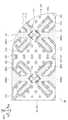
도 7a는 도 4의 AA' 영역을 확대하여 도시한 평면도다. 도 7b는 도 7a의 XX' 영역을 확대하여 도시한 평면도다.FIG. 7A is a plan view illustrating an enlarged area AA′ of FIG. 4 . FIG. 7B is a plan view illustrating an enlarged area XX′ of FIG. 7A .
도 7a 및 도 7b를 참조하면, 제1 감지 패턴들(211), 제2 감지 패턴들(221), 및 패턴들(230) 각각은 메쉬 구조(또는 격자 구조)를 가질 수 있다. 제1 감지 패턴들(211), 제2 감지 패턴들(221), 및 패턴들(230) 사이의 경계(BD)는 메쉬 구조의 일부분이 제거되어 정의될 수 있다. 도 7a에서는 경계(BD)를 명확히 도시하기 위해 경계를 실선으로 도시하였다. 도 7b에 도시된 메쉬 구조들의 일부분이 제거된 부분은 경계(BD)에 대응될 수 있다. 또한, 경계가 시인되는 것을 방지하기 위해 메쉬 구조들 내의 일부분이 제거된 단선부들(CTP)이 추가로 제공될 수 있다.7A and 7B , each of the
도 5, 도 7a, 및 도 7b를 참조하면, 센서(200)는 복수의 센싱 단위들(200U)을 포함할 수 있다. 복수의 센싱 단위들(200U)은 액티브 영역(200A)에 배치될 수 있다. 복수의 센싱 단위들(200U) 각각은 2 개의 제1 감지 패턴들(211) 각각의 일부분, 2 개의 제2 감지 패턴들(221) 각각의 일부분, 하나의 제1 연결 패턴(212), 하나의 제1 연결 패턴(212)과 교차하는 제2 연결 패턴들(222), 및 패턴들(230)을 포함할 수 있다.5, 7A, and 7B , the
복수의 센싱 단위들(200U)은 제1 센싱 단위(200U1), 제2 센싱 단위(200U2, 도 8 참조), 및 제3 센싱 단위(200U3, 도 8 참조)를 포함할 수 있다.The plurality of
제1 센싱 단위(200U1)는 경계(200B)로부터 이격된 센싱 단위들(200U) 중 하나일 수 있다. 제1 센싱 단위(200U1)는 기준 센싱 단위로 지칭될 수 있다. 제1 센싱 단위(200U1)에서 제3 부분들(211c, 또는 가지 부분들)은 제2 연결 패턴들(222, 또는 브릿지 패턴들)로부터 멀어지는 방향으로 연장될 수 있다. 제1 센싱 단위(200U1)에는 4 개의 제3 부분들(211c)이 배치될 수 있다. 2 개의 제3 부분들(211c)은 제3 방향(DR3a)을 따라 연장되고, 나머지 2 개의 제3 부분들(211c)은 제4 방향(DR4a)을 따라 연장될 수 있다.The first sensing unit 200U1 may be one of the
도 8은 도 4의 BB' 영역을 확대하여 도시한 평면도다.FIG. 8 is a plan view illustrating an enlarged area BB′ of FIG. 4 .
도 5, 도 7a, 및 도 8을 참조하면, 제2 센싱 단위(200U2)는 제1 경계 부분(200B1)에 접하는 센싱 단위들(200U) 중 하나일 수 있고, 제3 센싱 단위(200U3)는 제2 경계 부분(200B2)에 접하는 센싱 단위들(200U) 중 하나일 수 있다. 제2 센싱 단위(200U2)는 외곽 센싱 단위로 지칭될 수 있다.5, 7A, and 8 , the second sensing unit 200U2 may be one of the
제1 센싱 단위(200U1)의 면적, 제2 센싱 단위(200U2)의 면적, 및 제3 센싱 단위(200U3)의 면적은 서로 상이할 수 있다. 예를 들어, 제2 센싱 단위(200U2)의 면적은 제1 센싱 단위(200U1, 또는 기준 센싱 단위)의 면적보다 작고, 제3 센싱 단위(200U3)의 면적은 제1 센싱 단위(200U1)의 면적보다 클 수 있다. 이 경우, 제1 내지 제3 센싱 단위들(200U1, 200U2, 200U3) 각각의 상호정전용량은 서로 상이할 수 있다. 상호정전용량은 입력 수단, 예를 들어, 손가락의 입력에 따라 변화하는 정전용량일 수 있다. 본 발명의 실시예에 따르면, 제2 센싱 단위(200U2) 및 제3 센싱 단위(200U3) 내의 패턴들의 연결관계를 조절하여 상호정전용량들을 조절할 수 있다. 따라서, 센서(200)의 감도가 균일해질 수 있다.The area of the first sensing unit 200U1 , the area of the second sensing unit 200U2 , and the area of the third sensing unit 200U3 may be different from each other. For example, the area of the second sensing unit 200U2 is smaller than the area of the first sensing unit 200U1 or the reference sensing unit, and the area of the third sensing unit 200U3 is the area of the first sensing unit 200U1. can be larger In this case, the mutual capacitance of each of the first to third sensing units 200U1 , 200U2 , and 200U3 may be different from each other. The mutual capacitance may be a capacitance that changes according to an input of an input means, for example, a finger. According to an embodiment of the present invention, the mutual capacitances may be adjusted by adjusting the connection relationship between the patterns in the second sensing unit 200U2 and the third sensing unit 200U3. Accordingly, the sensitivity of the
제2 센싱 단위(200U2)는 제1 경계 부분(200B1)에 접하는 제1 감지 패턴(211-U2), 제2 감지 패턴(221-U2), 및 패턴들(231a, 231b-1, 231b-2, 232)을 포함할 수 있다.The second sensing unit 200U2 includes a first sensing pattern 211 - U2 , a second sensing pattern 221 - U2 , and
제2 센싱 단위(200U2)의 면적은 제1 센싱 단위(200U1)의 면적보다 작다. 따라서, 제2 센싱 단위(200U2)의 상호정전용량을 증가시키기 위해 제2 센싱 단위(200U2) 내의 패턴들(231a, 231b-1, 231b-2, 232) 중 적어도 일부를 제1 감지 패턴(211) 또는 제2 감지 패턴(221)에 전기적으로 연결시킬 수 있다. 즉, 제1 센싱 단위(200U1)와 비교하였을 때, 플로팅된 패턴이 있어야 할 자리에 감지 패턴에 연결된 패턴이 배치될 수 있다.The area of the second sensing unit 200U2 is smaller than the area of the first sensing unit 200U1. Accordingly, in order to increase the mutual capacitance of the second sensing unit 200U2, at least some of the
제1 경계 부분(200B1)에 접하는 제2 센싱 단위(200U2)의 패턴들(231a, 231b-1, 231b-2, 232)은 외곽 패턴들(231a, 231b-1, 231b-2, 232)로 지칭될 수 있다. 외곽 패턴들(231a, 231b-1, 231b-2, 232) 중 적어도 하나는 제1 감지 패턴(211-U2)에 전기적으로 연결될 수 있다.The
외곽 패턴들(231a, 231b-1, 231b-2, 232)은 제1 감지 패턴(211-U2)과 제2 감지 패턴(221-U2) 사이 및 제1 감지 패턴(211-U2)과 제2 감지 패턴(221-U23) 사이에 배치된 제1 외곽 패턴들(231a, 231b-1, 231b-2) 및 제2 감지 패턴들(221-U2, 221-U23) 중 어느 하나를 사이에 두고 제1 감지 패턴(211-U2)과 이격된 제2 외곽 패턴(232)을 포함할 수 있다.The
제1 외곽 패턴들(231a, 231b-1, 231b-2) 중 적어도 일부는 제1 감지 패턴(211-U2)에 전기적으로 연결될 수 있다. 따라서, 제2 센싱 단위(200U2)의 상호정전용량은 제1 외곽 패턴들(231a, 231b-1, 231b-2) 중 일부가 제1 감지 패턴(211-U2)에 연결되기 전보다 증가할 수 있다.At least some of the first
제2 센싱 단위(200U2)는 제2 연결 패턴들(222, 또는 브릿지 패턴들)로부터 연장된 4 개의 제3 연결 부분들(211-U2c1, 211-U2c2, 211-U2c3, 211-U2c4)을 포함할 수 있다. 제3 연결 부분들(211-U2c1, 211-U2c2, 211-U2c3, 211-U2c4)은 가지 부분들로 지칭될 수 있다. 가지 부분들(211-U2c1, 211-U2c2, 211-U2c3, 211-U2c4)은 제1 가지 부분(211-U2c1), 제2 가지 부분(211-U2c2), 제3 가지 부분(211-U2c3), 및 제4 가지 부분(211-U2c4)을 포함할 수 있다.The second sensing unit 200U2 includes four third connection parts 211-U2c1 , 211-U2c2 , 211-U2c3 , and 211-U2c4 extending from the
제1 가지 부분(211-U2c1) 및 제3 가지 부분(211-U2c3) 각각은 제3 방향(DR3a)을 따라 연장될 수 있고, 제2 가지 부분(211-U2c2) 및 제4 가지 부분(211-U2c4) 각각은 제4 방향(DR4a)을 따라 연장될 수 있다. 제1 가지 부분(211-U2c1)은 제1 경계 부분(200B1)에 접할 수 있다. 제2 가지 부분(211-U2c2), 제3 가지 부분(211-U2c3), 및 제4 가지 부분(211-U2c4) 각각은 제1 경계 부분(200B1)에 이격될 수 있다.Each of the first branch portion 211 - U2c1 and the third branch portion 211 - U2c3 may extend in the third direction DR3a, and the second branch portion 211 - U2c2 and the
제1 가지 부분(211-U2c1)은 전기적으로 서로 연결된 제3 부분(211-U2c) 및 제1 외곽 패턴(231b-1)을 포함할 수 있다. 제3 부분(211-U2c)은 제1 센싱 단위(200U1)의 제3 부분(211c)과 대응되는 부분일 수 있고, 제1 외곽 패턴(231b-1)은 플로팅 패턴에 대응되는 부분일 수 있다.The first branch portion 211 - U2c1 may include a third portion 211 - U2c electrically connected to each other and a first
제1 가지 부분(211-U2c1)은 제1 외곽 패턴(231b-1)을 더 포함하기 때문에, 제1 가지 부분(211-U2c1)의 최대 폭(WTa)은 제2 가지 부분(211-U2c2), 제3 가지 부분(211-U2c3), 및 제4 가지 부분(211-U2c4) 각각의 최대 폭(WTb)보다 클 수 있다. 또한, 제1 외곽 가지 부분(231b-2)은 제2 부분(211-U2b)에 전기적으로 연결될 수 있다. 그 결과, 제2 센싱 단위(200U2)의 면적이 제1 센싱 단위(200U1)의 면적보다 작더라도, 제1 가지 부분(211-U2c1)의 최대 폭(WTa)을 증가시키고, 제1 외곽 가지 부분(231b-2)을 제2 부분(211-U2b)에 전기적으로 연결시킴에 따라 제2 센싱 단위(200U2)의 감소된 상호정전용량이 보상될 수 있다.Since the first branch portion 211 - U2c1 further includes the first
제2 센싱 단위(200U2)에서 제1 외곽 패턴들(231b-1, 231b-2)이 제1 감지 패턴(211-U2)에 전기적으로 연결되기 때문에, 제1 외곽 패턴들(231b-1, 231b-2)은 보조 감지 패턴으로 지칭될 수 있다. 제1 외곽 패턴들(231b-1, 231b-2)은 실질적으로 제1 감지 패턴(211-U2)으로 기능할 수 있다. 따라서, 제1 센싱 단위(200U1)와의 면적의 차이에 의해 감소된 제2 센싱 단위(200U2)의 상호정전용량이 제1 외곽 패턴들(231b-1, 231b-2)에 의해 보상될 수 있다.Since the first
제3 센싱 단위(200U3)는 경계 패턴(233)을 더 포함할 수 있다. 경계 패턴(233)은 제2 경계 부분(200B2)에 인접하게 배치될 수 있다. 경계 패턴(233)은 제2 감지 패턴(221-U23)과 라인부(240) 사이에 배치될 수 있다. 경계 패턴(233)에 의해 제2 감지 패턴(221-U23)과 제1 감지 라인들(241) 사이에 발생하는 기생정전용량 및 제2 감지 패턴(221-U3)과 제1 감지 라인들(241) 사이에 발생하는 기생정전용량이 감소될 수 있다.The third sensing unit 200U3 may further include a
경계 패턴(233)과 제2 감지 패턴(221-U23) 사이의 경계(233B)는 제1 경계 패턴(230b1)과 제2 감지 패턴(221-U23) 사이의 경계의 형상에 대응될 수 있다. 예를 들어, 경계(233B)는 지그재그 형상을 가질 수 있다.The
제3 센싱 단위(200U3)의 면적은 제1 센싱 단위(200U1)의 면적보다 클 수 있다. 따라서, 제3 센싱 단위(200U3)의 상호정전용량은 제1 센싱 단위(200U1)의 상호정전용량보다 클 수 있다. 본 발명의 실시예에 따르면, 경계 패턴(233)이 제공됨에 따라 제3 센싱 단위(200U3)의 상호정전용량은 감소될 수 있다. 따라서, 제3 센싱 단위(200U3)의 상호정전용량과 제1 센싱 단위(200U1)의 상호정전용량의 차이가 감소될 수 있다.An area of the third sensing unit 200U3 may be larger than an area of the first sensing unit 200U1. Accordingly, the mutual capacitance of the third sensing unit 200U3 may be greater than the mutual capacitance of the first sensing unit 200U1 . According to an embodiment of the present invention, as the
본 발명의 실시예에 따르면, 센싱 단위의 형상의 변형에 의해 감소된 상호정전용량은 증가되고, 증가된 상호정전용량은 감소될 수 있다. 따라서, 액티브 영역(200A) 내에서 균일한 감도가 제공될 수 있다.According to an embodiment of the present invention, the mutual capacitance reduced by the deformation of the shape of the sensing unit may be increased, and the increased mutual capacitance may be decreased. Accordingly, a uniform sensitivity may be provided in the
도 9는 본 발명의 일 실시예에 따른 도 4의 BB' 영역과 대응하는 영역을 확대하여 도시한 평면도다. 도 9를 설명함에 있어서, 도 8과 차이가 있는 부분에 대해 중점적으로 설명하고, 도 8과 동일한 부분에 대한 설명은 생략된다.9 is an enlarged plan view of a region corresponding to region BB′ of FIG. 4 according to an embodiment of the present invention. In the description of FIG. 9 , parts different from those of FIG. 8 will be mainly described, and descriptions of parts identical to those of FIG. 8 will be omitted.
도 5, 도 7a, 및 도 9를 참조하면, 제2 센싱 단위(200U2)의 면적은 제1 센싱 단위(200U1)의 면적보다 작다. 따라서, 제2 센싱 단위(200U2)의 상호정전용량을 증가시키기 위해 제2 센싱 단위(200U2) 내의 패턴들(231a, 232-1) 중 적어도 일부를 제1 감지 패턴(211) 또는 제2 감지 패턴(221)에 전기적으로 연결시킬 수 있다. 따라서, 제1 센싱 단위(200U1)와 비교하였을 때, 플로팅된 패턴이 있어야 할 자리에 감지 패턴에 연결된 패턴이 배치될 수 있다.5, 7A, and 9 , the area of the second sensing unit 200U2 is smaller than that of the first sensing unit 200U1. Accordingly, in order to increase the mutual capacitance of the second sensing unit 200U2, at least a portion of the
제1 경계 부분(200B1)에 접하는 제2 센싱 단위(200U2)의 패턴들(231a, 232-1)은 외곽 패턴들(231a, 232-1)로 지칭될 수 있다. 외곽 패턴들(231a, 232-1) 중 적어도 하나는 제2 감지 패턴들(221-U21, 221-U231)에 전기적으로 연결될 수 있다.The
외곽 패턴들(231a, 232-1)은 제1 감지 패턴(211-U2)과 제2 감지 패턴(221-U21) 사이 및 제1 감지 패턴(211-U2)과 제2 감지 패턴(221-U231) 사이에 배치된 제1 외곽 패턴들(231a) 및 제2 감지 패턴들(221-U21, 221-U231) 중 어느 하나를 사이에 두고 제1 감지 패턴(211-U2)과 이격된 제2 외곽 패턴들(232-1)을 포함할 수 있다.The
본 실시예에서, 제2 외곽 패턴들(232-1)은 제2 감지 패턴들(221-U21, 221-U231)에 전기적으로 연결될 수 있다. 따라서, 제2 센싱 단위(200U2)의 상호정전용량은 제2 외곽 패턴들(232-1)이 제2 감지 패턴들(221-U21, 221-U231)에 연결되기 전보다 증가할 수 있다.In this embodiment, the second outer patterns 232-1 may be electrically connected to the second sensing patterns 221-U21 and 221-U231. Accordingly, the mutual capacitance of the second sensing unit 200U2 may increase compared to before the second outer patterns 232-1 are connected to the second sensing patterns 221-U21 and 221-U231.
제2 외곽 패턴들(232-1)이 제2 감지 패턴들(221-U21, 221-U231)에 전기적으로 연결되기 때문에, 제2 외곽 패턴들(232-1)은 보조 감지 패턴으로 지칭될 수 있다.Since the second outer patterns 232-1 are electrically connected to the second sensing patterns 221-U21 and 221-U231, the second outer patterns 232-1 may be referred to as auxiliary sensing patterns. have.
도 10은 본 발명의 일 실시예에 따른 도 4의 BB' 영역과 대응하는 영역을 확대하여 도시한 평면도다. 도 10을 설명함에 있어서, 도 8과 차이가 있는 부분에 대해 중점적으로 설명하고, 도 8과 동일한 부분에 대한 설명은 생략된다.10 is an enlarged plan view of a region corresponding to region BB′ of FIG. 4 according to an embodiment of the present invention. In the description of FIG. 10 , a part different from FIG. 8 will be mainly described, and a description of the same part as FIG. 8 will be omitted.
도 5 및 도 10을 참조하면, 제2 센싱 단위(200U2)의 제1 외곽 패턴들(231b-1, 231b-2)은 제1 감지 패턴(211-U2)에 연결되고, 제2 외곽 패턴들(232-1)은 제2 감지 패턴들(221-U21, 221-U231)에 전기적으로 연결될 수 있다.5 and 10 , the first
제1 외곽 패턴들(231b-1, 231b-2)은 제1 감지 패턴(211-U2)에 전기적으로 연결되기 때문에, 제1 외곽 패턴들(231b-1, 231b-2)은 제1 보조 감지 패턴으로 지칭될 수 있다. 제2 외곽 패턴들(232-1)이 제2 감지 패턴들(221-U21, 221-U231)에 전기적으로 연결되기 때문에, 제2 외곽 패턴들(232-1)은 제2 보조 감지 패턴으로 지칭될 수 있다.Since the first
제2 센싱 단위(200U2)의 상호정전용량은 제1 외곽 패턴들(231b-1, 231b-2)이 제1 감지 패턴(211-U2)에 연결되기 전 및 제2 외곽 패턴들(232-1)이 제2 감지 패턴들(221-U21, 221-U231)에 전기적으로 연결되기 전보다 증가할 수 있다.The mutual capacitance of the second sensing unit 200U2 is determined before the first
도 11은 본 발명의 일 실시예에 따른 도 4의 BB' 영역과 대응하는 영역을 확대하여 도시한 평면도다. 도 10을 설명함에 있어서, 도 8과 차이가 있는 부분에 대해 중점적으로 설명하고, 도 8과 동일한 부분에 대한 설명은 생략된다.11 is an enlarged plan view of a region corresponding to region BB′ of FIG. 4 according to an embodiment of the present invention. In the description of FIG. 10 , parts different from those of FIG. 8 will be mainly described, and descriptions of the same parts as those of FIG. 8 will be omitted.
도 5 및 도 11을 참조하면, 제3 센싱 단위(200U3)는 경계 패턴(233-1)을 더 포함할 수 있다. 경계 패턴(233-1)은 제2 경계 부분(200B2)에 인접하게 배치될 수 있다. 경계 패턴(233-1)은 제2 감지 패턴(221-U23)과 라인부(240) 사이에 배치될 수 있다.5 and 11 , the third sensing unit 200U3 may further include a boundary pattern 233 - 1 . The boundary pattern 233 - 1 may be disposed adjacent to the second boundary portion 200B2 . The boundary pattern 233 - 1 may be disposed between the second sensing pattern 221 - U23 and the
경계 패턴(233-1)과 제2 감지 패턴(221-U23) 사이의 경계(233B-1)는 소정 방향, 예를 들어, 제1 방향(DR1)을 따라 연장된 직선 형상을 가질 수 있다. 또는, 경계(233B-1)는 경계(200B)에 나란하게 연장될 수 있다. 따라서, 제2 감지 패턴(221-U23)과 라인부(240) 사이의 거리는 소정 간격 이상으로 확보될 수 있다. 따라서, 도 8과 비교하였을 때, 제2 감지 패턴(221-U23)과 제1 감지 라인들(241) 사이 및 제2 감지 패턴(221-U3)과 제1 감지 라인들(241) 사이에 발생하는 기생정전용량들이 더 감소될 수 있다.The
도 12는 본 발명의 일 실시예에 따른 도 4의 BB' 영역과 대응하는 영역을 확대하여 도시한 평면도다. 도 12를 설명함에 있어서, 도 8과 차이가 있는 부분에 대해 중점적으로 설명하고, 도 8과 동일한 부분에 대한 설명은 생략된다.12 is an enlarged plan view of a region corresponding to region BB′ of FIG. 4 according to an embodiment of the present invention. In the description of FIG. 12 , parts different from those of FIG. 8 will be mainly described, and descriptions of parts identical to those of FIG. 8 will be omitted.
도 5 및 도 12를 참조하면, 제2 센싱 단위(200U2) 및 제3 센싱 단위(200U3) 각각에 경계 패턴(233, 도 8 참조)이 제공되지 않을 수 있다. 따라서, 제2 감지 패턴들(221-U232, 221-U32)은 제1 경계 부분(200B1) 및 제2 경계 부분(200B2)에 접할 수 있다.5 and 12 , the boundary pattern 233 (refer to FIG. 8 ) may not be provided in each of the second sensing unit 200U2 and the third sensing unit 200U3 . Accordingly, the second sensing patterns 221 - U232 and 221 - U32 may contact the first boundary portion 200B1 and the second boundary portion 200B2 .
도 13은 본 발명의 일 실시예에 따른 센서의 일부 영역을 확대하여 도시한 평면도다. 도 13을 설명함에 있어서, 도 8과 차이가 있는 부분에 대해 중점적으로 설명하고, 도 8과 동일한 부분에 대한 설명은 생략된다.13 is an enlarged plan view of a partial region of a sensor according to an embodiment of the present invention. In the description of FIG. 13 , a part different from FIG. 8 will be mainly described, and a description of the same part as FIG. 8 will be omitted.
도 5 및 도 13을 참조하면, 제2 센싱 단위(200U2)의 제1 감지 패턴(211)의 형상은 제1 센싱 단위(200U1, 도 7a 참조)의 제1 감지 패턴(211)의 형상에 대응될 수 있다. 따라서, 제2 센싱 단위(200U2)의 가지 부분들(211c)의 폭들은 서로 동일할 수 있다.5 and 13 , the shape of the
제3 센싱 단위(200U3)는 경계 패턴(233)을 더 포함할 수 있다. 경계 패턴(233)은 제2 경계 부분(200B2)에 인접하게 배치될 수 있다. 경계 패턴(233)은 제2 감지 패턴(221-U23)과 라인부(240, 도 5 참조) 사이에 배치될 수 있다.The third sensing unit 200U3 may further include a
도 14는 본 발명의 일 실시예에 따른 센서의 일부를 확대하여 도시한 평면도다.14 is an enlarged plan view of a part of a sensor according to an embodiment of the present invention.
도 14를 참조하면, 센서(200-A)는 도 7a와 비교하였을 때, 패턴들(234a, 234b)을 더 포함할 수 있다. 패턴들(234a, 234b)은 제1 감지 패턴(211) 내에 정의된 제1 추가 패턴(234a) 및 제2 감지 패턴(221-1) 내에 정의된 제2 추가 패턴(234b)을 더 포함할 수 있다.Referring to FIG. 14 , the sensor 200 -A may further include
제1 추가 패턴(234a)은 제1 감지 패턴(211)에 의해 에워싸이고, 제2 추가 패턴(234b)은 제2 감지 패턴(221-1)에 의해 에워싸일 수 있다. 제1 추가 패턴(234a) 및 제2 추가 패턴(234b)은 플로팅 전극으로 제1 감지 패턴(211) 및 제2 감지 패턴(221-1)과 전기적으로 연결되지 않을 수 있다. 또는 제1 추가 패턴(234a) 및 제2 추가 패턴(234b)은 그라운드될 수도 있다. 또는 제1 추가 패턴(234a) 및 제2 추가 패턴(234b) 중 어느 하나는 제1 감지 패턴(211) 또는 제2 감지 패턴(221-1)에 전기적으로 연결될 수 도 있다.The first
이상에서는 본 발명의 바람직한 실시예를 참조하여 설명하였지만, 해당 기술 분야의 숙련된 당업자 또는 해당 기술 분야에 통상의 지식을 갖는 자라면, 후술될 특허청구범위에 기재된 본 발명의 사상 및 기술 영역으로부터 벗어나지 않는 범위 내에서 본 발명을 다양하게 수정 및 변경시킬 수 있음을 이해할 수 있을 것이다. 따라서, 본 발명의 기술적 범위는 명세서의 상세한 설명에 기재된 내용으로 한정되는 것이 아니라 특허청구범위에 의해 정하여져야만 할 것이다.Although the above has been described with reference to the preferred embodiment of the present invention, those skilled in the art or those having ordinary knowledge in the technical field will not depart from the spirit and technical scope of the present invention described in the claims to be described later. It will be understood that various modifications and variations of the present invention can be made without departing from the scope of the present invention. Accordingly, the technical scope of the present invention should not be limited to the contents described in the detailed description of the specification, but should be defined by the claims.
1000: 전자 장치100: 표시 패널
200: 센서200U: 센싱 단위들
200U1: 제1 센싱 단위200U2: 제2 센싱 단위
200U3: 제3 센싱 단위1000: electronic device 100: display panel
200:
200U1: first sensing unit 200U2: second sensing unit
200U3: third sensing unit
Claims (20)
Translated fromKorean상기 표시 패널 위에 배치되며, 액티브 영역 및 주변 영역이 정의되고, 상기 액티브 영역 위에 배치된 복수의 센싱 단위들을 포함하는 센서를 포함하고,
상기 복수의 센싱 단위들 각각은 복수의 가지 부분들을 갖는 제1 감지 패턴, 상기 제1 감지 패턴과 이격된 복수의 제2 감지 패턴들, 상기 복수의 제2 감지 패턴들은 서로 연결하는 브릿지 패턴, 상기 제1 감지 패턴 및 상기 복수의 제2 감지 패턴들 중 적어도 하나와 이격된 복수의 패턴들을 포함하고,
상기 복수의 센싱 단위들 중 상기 액티브 영역 및 상기 주변 영역의 경계 중 곡률을 갖는 제1 경계 부분에 접한 센싱 단위의 상기 복수의 패턴들은 복수의 외곽 패턴들을 포함하고, 상기 복수의 외곽 패턴들 중 적어도 하나는 상기 센싱 단위의 상기 제1 감지 패턴 또는 상기 센싱 단위의 상기 복수의 제2 감지 패턴들에 전기적으로 연결된 전자 장치.display panel; and
a sensor disposed on the display panel, an active area and a peripheral area defined, and a sensor including a plurality of sensing units disposed on the active area;
Each of the plurality of sensing units includes a first sensing pattern having a plurality of branch portions, a plurality of second sensing patterns spaced apart from the first sensing pattern, a bridge pattern connecting the plurality of second sensing patterns to each other, and the It includes a plurality of patterns spaced apart from at least one of the first detection pattern and the plurality of second detection patterns,
Among the plurality of sensing units, the plurality of patterns of a sensing unit in contact with a first boundary portion having a curvature among boundaries of the active region and the peripheral region includes a plurality of outer patterns, and at least one of the plurality of outer patterns One is an electronic device electrically connected to the first sensing pattern of the sensing unit or the plurality of second sensing patterns of the sensing unit.
상기 복수의 외곽 패턴들은,
상기 제1 감지 패턴과 상기 복수의 제2 감지 패턴들 사이에 배치된 제1 외곽 패턴; 및
상기 복수의 제2 감지 패턴들 중 하나의 제2 감지 패턴을 사이에 두고 상기 제1 감지 패턴과 이격된 제2 외곽 패턴을 포함하는 전자 장치.According to claim 1,
The plurality of outer patterns are,
a first outer pattern disposed between the first sensing pattern and the plurality of second sensing patterns; and
and a second outer pattern spaced apart from the first sensing pattern with one second sensing pattern interposed therebetween.
상기 제1 외곽 패턴은 상기 복수의 가지 부분들 중 하나의 가지 부분에 연결되고, 상기 제2 외곽 패턴은 상기 하나의 제2 감지 패턴과 이격된 전자 장치.3. The method of claim 2,
The first outer pattern is connected to one branch of the plurality of branch portions, and the second outer pattern is spaced apart from the one second sensing pattern.
상기 제1 외곽 패턴은 상기 복수의 가지 부분들 중 하나의 가지 부분에 연결되고, 상기 제2 외곽 패턴은 상기 하나의 제2 감지 패턴과 연결된 전자 장치.3. The method of claim 2,
The first outer pattern is connected to one branch portion among the plurality of branch portions, and the second outer pattern is connected to the one second sensing pattern.
상기 제1 외곽 패턴은 상기 제1 감지 패턴과 상기 복수의 제2 감지 패턴들과 이격되고, 상기 제2 외곽 패턴은 상기 하나의 제2 감지 패턴에 연결된 전자 장치.3. The method of claim 2,
The first outer pattern is spaced apart from the first sensing pattern and the plurality of second sensing patterns, and the second outer pattern is connected to the one second sensing pattern.
상기 복수의 가지 부분들 중 상기 제1 경계 부분에 접한 외곽 가지 부분의 폭은 다른 가지 부분의 폭보다 큰 전자 장치.According to claim 1,
A width of an outer branch portion in contact with the first boundary portion among the plurality of branch portions is greater than a width of other branch portions.
상기 경계는 상기 제1 경계 부분으로부터 연장된 제2 경계 부분을 더 포함하고, 상기 복수의 센싱 단위들은 상기 경계로부터 이격된 제1 센싱 단위, 상기 제1 경계 부분에 접하는 제2 센싱 단위, 및 상기 제2 경계 부분에 접하는 제3 센싱 단위를 포함하고, 상기 제3 센싱 단위의 면적은 상기 제1 센싱 단위의 면적 및 상기 제2 센싱 단위의 면적 각각보다 크고, 상기 제1 센싱 단위의 면적은 상기 제2 센싱 단위의 면적보다 큰 전자 장치.According to claim 1,
The boundary further includes a second boundary portion extending from the first boundary portion, wherein the plurality of sensing units include a first sensing unit spaced apart from the boundary, a second sensing unit in contact with the first boundary portion, and the a third sensing unit in contact with a second boundary portion, wherein an area of the third sensing unit is larger than an area of the first sensing unit and an area of the second sensing unit, and an area of the first sensing unit is the An electronic device larger than an area of the second sensing unit.
상기 센서는 상기 제1 감지 패턴에 전기적으로 연결된 제1 감지 라인 및 상기 복수의 제2 감지 패턴들에 전기적으로 연결된 제2 감지 라인을 포함하는 라인부를 더 포함하고, 상기 제3 센싱 단위의 상기 제1 감지 패턴은 상기 제1 감지 라인과 연결된 전자 장치.8. The method of claim 7,
The sensor further includes a line part including a first sensing line electrically connected to the first sensing pattern and a second sensing line electrically connected to the plurality of second sensing patterns, wherein the second sensing unit of the third sensing unit A first sensing pattern is an electronic device connected to the first sensing line.
상기 제3 센싱 단위는 상기 라인부와 상기 복수의 제2 감지 패턴들 사이에 배치된 경계 패턴을 더 포함하는 전자 장치.9. The method of claim 8,
The third sensing unit further includes a boundary pattern disposed between the line portion and the plurality of second sensing patterns.
상기 경계 패턴과 상기 복수의 제2 감지 패턴들 사이의 경계는 지그재그 형상 또는 직선 형상을 갖는 전자 장치.10. The method of claim 9,
The boundary between the boundary pattern and the plurality of second sensing patterns has a zigzag shape or a straight line shape.
상기 복수의 센싱 단위들은 제1 방향 및 상기 제1 방향과 교차하는 제2 방향을 따라 배열되고, 상기 복수의 가지 부분들 중 일부 가지 부분들은 상기 제1 방향 및 상기 제2 방향과 교차하는 제3 방향을 따라 연장되고, 상기 복수의 가지 부분들 중 다른 가지 부분들은 상기 제3 방향과 교차하는 제4 방향을 따라 연장되는 전자 장치.According to claim 1,
The plurality of sensing units are arranged in a first direction and a second direction crossing the first direction, and some branch parts of the plurality of branch parts may include a third direction crossing the first direction and the second direction. The electronic device extends along a direction, and other branch portions of the plurality of branch portions extend in a fourth direction intersecting the third direction.
상기 복수의 가지 부분들 각각은 상기 브릿지 패턴으로부터 멀어지는 방향으로 연장되는 전자 장치.According to claim 1,
Each of the plurality of branch portions extends in a direction away from the bridge pattern.
복수의 제2 감지 패턴들 각각은 상기 복수의 가지 부분들 중 적어도 2 개의 가지 부분들을 에워싸는 전자 장치.According to claim 1,
Each of the plurality of second sensing patterns surrounds at least two branch portions of the plurality of branch portions.
상기 복수의 센싱 단위들은 제1 방향 및 상기 제1 방향과 교차하는 제2 방향을 따라 배열되고,
상기 복수의 센싱 단위들 중 상기 제1 방향으로 인접한 2 개의 센싱 단위들 각각의 상기 복수의 제2 감지 패턴들은 서로 전기적으로 연결되고,
상기 복수의 센싱 단위들 중 상기 상기 제2 방향으로 인접한 2 개의 센싱 단위들 각각의 상기 복수의 제2 감지 패턴들은 복수의 패턴들 중 일부를 사이에 두고 이격된 전자 장치.According to claim 1,
The plurality of sensing units are arranged along a first direction and a second direction intersecting the first direction,
the plurality of second sensing patterns of each of the two sensing units adjacent in the first direction among the plurality of sensing units are electrically connected to each other;
The plurality of second sensing patterns of each of the two sensing units adjacent in the second direction among the plurality of sensing units are spaced apart from each other with a portion of the plurality of patterns interposed therebetween.
상기 표시 패널 위에 배치되며, 액티브 영역 및 주변 영역이 정의되고, 상기 액티브 영역 위에 배치된 복수의 센싱 단위들 및 상기 주변 영역 위에 배치되며 상기 복수의 센싱 단위들에 전기적으로 연결된 라인들을 포함하는 라인부를 포함하는 센서를 포함하고,
상기 복수의 센싱 단위들 각각은 복수의 가지 부분들을 갖는 제1 감지 패턴, 상기 제1 감지 패턴을 사이에 두고 이격된 복수의 제2 감지 패턴들, 및 상기 복수의 제2 감지 패턴들은 서로 연결하는 브릿지 패턴을 포함하고,
상기 복수의 센싱 단위들은 상기 액티브 영역 및 상기 주변 영역의 경계로부터 이격된 제1 센싱 단위, 상기 경계 중 곡률을 갖는 제1 경계 부분에 접하는 제2 센싱 단위, 및 상기 경계 중 상기 라인부와 인접한 제2 경계 부분에 접하는 제3 센싱 단위를 포함하고,
상기 제3 센싱 단위는 상기 라인부와 상기 복수의 제2 감지 패턴들 사이에 배치된 경계 패턴을 더 포함하는 전자 장치.display panel; and
a line portion disposed on the display panel, having an active area and a peripheral area defined, and including a plurality of sensing units disposed on the active area and lines disposed on the peripheral area and electrically connected to the plurality of sensing units A sensor comprising:
Each of the plurality of sensing units includes a first sensing pattern having a plurality of branch portions, a plurality of second sensing patterns spaced apart from each other with the first sensing pattern interposed therebetween, and the plurality of second sensing patterns are connected to each other. including a bridge pattern;
The plurality of sensing units may include a first sensing unit spaced apart from a boundary between the active region and the peripheral region, a second sensing unit in contact with a first boundary portion having a curvature among the boundaries, and a second sensing unit adjacent to the line portion among the boundaries. 2 comprising a third sensing unit tangent to the boundary portion;
The third sensing unit further includes a boundary pattern disposed between the line portion and the plurality of second sensing patterns.
상기 경계 패턴과 상기 복수의 제2 감지 패턴들 사이의 경계는 지그재그 형상 또는 직선 형상을 갖는 전자 장치.16. The method of claim 15,
The boundary between the boundary pattern and the plurality of second sensing patterns has a zigzag shape or a straight line shape.
상기 복수의 센싱 단위들 각각은 상기 제1 감지 패턴 및 상기 복수의 제2 감지 패턴들과 이격된 복수의 패턴들을 더 포함하고, 상기 복수의 패턴들은 상기 제1 경계 부분에 접하는 복수의 외곽 패턴들을 포함하고, 상기 복수의 외곽 패턴들 중 적어도 하나는 상기 제1 감지 패턴 또는 상기 복수의 제2 감지 패턴들에 전기적으로 연결된 전자 장치.16. The method of claim 15,
Each of the plurality of sensing units further includes a plurality of patterns spaced apart from the first detection pattern and the plurality of second detection patterns, wherein the plurality of patterns form a plurality of outer patterns in contact with the first boundary portion. and at least one of the plurality of outer patterns is electrically connected to the first sensing pattern or the plurality of second sensing patterns.
상기 복수의 외곽 패턴들은,
상기 제1 감지 패턴과 상기 복수의 제2 감지 패턴들 사이에 배치된 제1 외곽 패턴; 및
상기 복수의 제2 감지 패턴들 중 하나의 제2 감지 패턴을 사이에 두고 상기 제1 감지 패턴과 이격된 제2 외곽 패턴을 포함하고, 상기 제1 외곽 패턴 및 상기 제2 외곽 패턴 중 적어도 하나는 상기 복수의 가지 부분들 중 하나의 가지 부분 또는 상기 하나의 제2 감지 패턴에 연결된 전자 장치.18. The method of claim 17,
The plurality of outer patterns are,
a first outer pattern disposed between the first sensing pattern and the plurality of second sensing patterns; and
a second outer pattern spaced apart from the first sensing pattern with one second sensing pattern interposed therebetween, wherein at least one of the first outer pattern and the second outer pattern comprises: An electronic device connected to one branch portion of the plurality of branch portions or the one second sensing pattern.
상기 표시 패널 위에 배치되며, 액티브 영역 및 주변 영역이 정의되고, 복수의 가지 부분들을 포함하는 제1 감지 전극 및 상기 제1 감지 전극과 교차하는 제2 감지 전극을 포함하는 센서를 포함하고,
상기 복수의 가지 부분들 중 상기 액티브 영역 및 상기 주변 영역의 경계 중 곡률을 갖는 경계 부분에 접하는 가지 부분의 폭은 상기 복수의 가지 부분들 중 상기 경계 부분에 이격된 가지 부분의 폭보다 큰 전자 장치.display panel; and
a sensor disposed on the display panel, an active region and a peripheral region defined, a sensor including a first sensing electrode including a plurality of branch portions and a second sensing electrode crossing the first sensing electrode;
Among the plurality of branch portions, a width of a branch portion contacting a boundary portion having a curvature among boundaries of the active region and the peripheral region is greater than a width of a branch portion spaced apart from the boundary portion among the plurality of branch portions. .
상기 표시 패널 위에 배치되며, 액티브 영역 및 주변 영역이 정의되고, 상기 액티브 영역 위에 배치된 기준 센싱 단위 및 외곽 센싱 단위를 포함하는 센서를 포함하고,
상기 기준 센싱 단위 및 상기 외곽 센싱 단위 각각은 복수의 가지 부분들을 갖는 제1 감지 패턴, 상기 제1 감지 패턴과 이격된 복수의 제2 감지 패턴들, 상기 복수의 제2 감지 패턴들은 서로 연결하는 브릿지 패턴, 상기 제1 감지 패턴 및 상기 복수의 제2 감지 패턴들 중 적어도 하나와 이격된 복수의 패턴들을 포함하고,
상기 외곽 센싱 단위는 상기 액티브 영역 및 상기 주변 영역의 경계 중 곡률을 갖는 경계 부분에 인접하고, 상기 외곽 센싱 단위의 상기 복수의 패턴들 중 적어도 하나는 상기 제1 감지 패턴 또는 상기 복수의 제2 감지 패턴들에 전기적으로 연결된 전자 장치.display panel; and
a sensor disposed on the display panel, an active area and a peripheral area defined, and a sensor including a reference sensing unit and an outer sensing unit disposed on the active area;
Each of the reference sensing unit and the outer sensing unit includes a first sensing pattern having a plurality of branch portions, a plurality of second sensing patterns spaced apart from the first sensing pattern, and a bridge connecting the plurality of second sensing patterns to each other pattern, comprising a plurality of patterns spaced apart from at least one of the first detection pattern and the plurality of second detection patterns,
The outer sensing unit is adjacent to a boundary portion having a curvature among the boundaries of the active region and the peripheral region, and at least one of the plurality of patterns of the outer sensing unit is the first sensing pattern or the plurality of second sensing units. An electronic device electrically connected to the patterns.
Priority Applications (6)
| Application Number | Priority Date | Filing Date | Title |
|---|---|---|---|
| KR1020190159952AKR20210070454A (en) | 2019-12-04 | 2019-12-04 | Electronic device |
| US17/105,436US11360629B2 (en) | 2019-12-04 | 2020-11-25 | Electronic apparatus |
| CN202011387236.7ACN112905066A (en) | 2019-12-04 | 2020-12-01 | Electronic device |
| US17/838,245US11755165B2 (en) | 2019-12-04 | 2022-06-12 | Electronic apparatus |
| US18/230,681US12153770B2 (en) | 2019-12-04 | 2023-08-07 | Electronic apparatus |
| US18/957,325US20250085823A1 (en) | 2019-12-04 | 2024-11-22 | Electronic apparatus |
Applications Claiming Priority (1)
| Application Number | Priority Date | Filing Date | Title |
|---|---|---|---|
| KR1020190159952AKR20210070454A (en) | 2019-12-04 | 2019-12-04 | Electronic device |
Publications (1)
| Publication Number | Publication Date |
|---|---|
| KR20210070454Atrue KR20210070454A (en) | 2021-06-15 |
Family
ID=76111336
Family Applications (1)
| Application Number | Title | Priority Date | Filing Date |
|---|---|---|---|
| KR1020190159952APendingKR20210070454A (en) | 2019-12-04 | 2019-12-04 | Electronic device |
Country Status (3)
| Country | Link |
|---|---|
| US (4) | US11360629B2 (en) |
| KR (1) | KR20210070454A (en) |
| CN (1) | CN112905066A (en) |
Cited By (1)
| Publication number | Priority date | Publication date | Assignee | Title |
|---|---|---|---|---|
| US11537232B2 (en) | 2020-04-13 | 2022-12-27 | Samsung Display Co., Ltd. | Electronic device |
Families Citing this family (4)
| Publication number | Priority date | Publication date | Assignee | Title |
|---|---|---|---|---|
| KR20210070454A (en)* | 2019-12-04 | 2021-06-15 | 삼성디스플레이 주식회사 | Electronic device |
| KR20210145027A (en) | 2020-05-22 | 2021-12-01 | 삼성디스플레이 주식회사 | Electronic device |
| CN113741728B (en)* | 2021-08-19 | 2023-11-28 | 武汉华星光电半导体显示技术有限公司 | Touch panel and mobile terminal |
| TWI817695B (en)* | 2022-09-01 | 2023-10-01 | 大陸商宸美(廈門)光電有限公司 | Electrode structure with hollow micro-patterns and device including the same |
Family Cites Families (23)
| Publication number | Priority date | Publication date | Assignee | Title |
|---|---|---|---|---|
| US20110291982A1 (en)* | 2010-05-28 | 2011-12-01 | Au Optronics Corp. | Touch display apparatus and touch sensing device thereof |
| TWI424219B (en) | 2010-05-31 | 2014-01-21 | Chunghwa Picture Tubes Ltd | Touch display device |
| KR20120103787A (en) | 2011-03-11 | 2012-09-20 | (주)네오위즈게임즈 | Terminal, system and the method for assigning sequence numbers using online chat |
| KR102056110B1 (en)* | 2012-10-04 | 2019-12-16 | 삼성전자주식회사 | Touch panel |
| KR101533971B1 (en)* | 2012-12-13 | 2015-07-06 | 주식회사 지니틱스 | Touch electrode pattern, touch panel, and touch input device having the same |
| US9298323B2 (en)* | 2012-12-20 | 2016-03-29 | Tpk Touch Solutions Inc. | Sensing electrode structure and touch panel employing the same |
| US9829523B1 (en)* | 2012-12-27 | 2017-11-28 | Cypress Semiconductor Corporation | Offset sensor pattern |
| TWI483160B (en) | 2013-09-12 | 2015-05-01 | Au Optronics Corp | Touch panel |
| CN204390220U (en) | 2014-02-25 | 2015-06-10 | 宸鸿科技(厦门)有限公司 | Capacitance type touch-control panel |
| KR102500994B1 (en)* | 2014-10-17 | 2023-02-16 | 가부시키가이샤 한도오따이 에네루기 켄큐쇼 | Touch panel |
| CN104699348A (en)* | 2015-04-01 | 2015-06-10 | 上海天马微电子有限公司 | Array substrate and display device |
| KR102341352B1 (en)* | 2015-04-08 | 2021-12-20 | 삼성디스플레이 주식회사 | Display device with touch sensor |
| JP6745703B2 (en)* | 2016-10-31 | 2020-08-26 | 三菱電機株式会社 | Touch screens, touch panels, display devices and electronic devices |
| KR102668136B1 (en)* | 2016-12-12 | 2024-05-24 | 삼성디스플레이 주식회사 | Display module |
| GB2559573B (en)* | 2017-02-09 | 2020-03-25 | Solomon Systech Ltd | Touch Sensor |
| KR102491224B1 (en) | 2017-06-01 | 2023-01-20 | 엘지디스플레이 주식회사 | Touch display device and touch panel |
| KR102374168B1 (en)* | 2017-08-08 | 2022-03-17 | 삼성디스플레이 주식회사 | Input sensing unit and display device having the same |
| CN107301003B (en)* | 2017-08-08 | 2021-03-23 | 京东方科技集团股份有限公司 | A touch panel, its manufacturing method, touch screen and display device |
| CN108710447A (en)* | 2018-05-14 | 2018-10-26 | 京东方科技集团股份有限公司 | A kind of touch-control structure and display screen |
| KR102414056B1 (en) | 2018-09-19 | 2022-06-28 | 삼성디스플레이 주식회사 | Touch sensing unit and display apparatus including the same |
| US11340743B2 (en)* | 2019-03-29 | 2022-05-24 | Apple Inc. | Touch sensor with refined corner, edge, and other structures |
| KR20210070454A (en)* | 2019-12-04 | 2021-06-15 | 삼성디스플레이 주식회사 | Electronic device |
| CN112083830B (en)* | 2020-09-18 | 2024-06-25 | 武汉天马微电子有限公司 | Display panel and display device |
- 2019
- 2019-12-04KRKR1020190159952Apatent/KR20210070454A/enactivePending
- 2020
- 2020-11-25USUS17/105,436patent/US11360629B2/enactiveActive
- 2020-12-01CNCN202011387236.7Apatent/CN112905066A/enactivePending
- 2022
- 2022-06-12USUS17/838,245patent/US11755165B2/enactiveActive
- 2023
- 2023-08-07USUS18/230,681patent/US12153770B2/enactiveActive
- 2024
- 2024-11-22USUS18/957,325patent/US20250085823A1/enactivePending
Cited By (2)
| Publication number | Priority date | Publication date | Assignee | Title |
|---|---|---|---|---|
| US11537232B2 (en) | 2020-04-13 | 2022-12-27 | Samsung Display Co., Ltd. | Electronic device |
| US12164718B2 (en) | 2020-04-13 | 2024-12-10 | Samsung Display Co., Ltd. | Electronic device |
Also Published As
| Publication number | Publication date |
|---|---|
| US11360629B2 (en) | 2022-06-14 |
| US20220326812A1 (en) | 2022-10-13 |
| CN112905066A (en) | 2021-06-04 |
| US11755165B2 (en) | 2023-09-12 |
| US20230376156A1 (en) | 2023-11-23 |
| US12153770B2 (en) | 2024-11-26 |
| US20210173525A1 (en) | 2021-06-10 |
| US20250085823A1 (en) | 2025-03-13 |
Similar Documents
| Publication | Publication Date | Title |
|---|---|---|
| KR20210070454A (en) | Electronic device | |
| US11653523B2 (en) | Display device | |
| US11625119B2 (en) | Display device including an input sensor having a corner area | |
| US12250859B2 (en) | Display device | |
| KR102748276B1 (en) | Display device and method for manufacturing display device | |
| KR20210147150A (en) | Electronic device | |
| US12333119B2 (en) | Electronic device | |
| KR20220001036A (en) | Electronic device | |
| KR20210070457A (en) | Input sensing unit and display device including the same | |
| KR20210118301A (en) | Display device | |
| CN113900537A (en) | electronic device | |
| KR20210127296A (en) | Electronic device | |
| KR102787589B1 (en) | Display device | |
| US11301106B2 (en) | Display device including built-in components to sense input through electromagnetic pen | |
| CN114077345A (en) | Electronic device | |
| KR20210155844A (en) | Display device | |
| US11449164B1 (en) | Display device | |
| KR20220091649A (en) | Display device |
Legal Events
| Date | Code | Title | Description |
|---|---|---|---|
| PA0109 | Patent application | St.27 status event code:A-0-1-A10-A12-nap-PA0109 | |
| PG1501 | Laying open of application | St.27 status event code:A-1-1-Q10-Q12-nap-PG1501 | |
| A201 | Request for examination | ||
| PA0201 | Request for examination | St.27 status event code:A-1-2-D10-D11-exm-PA0201 | |
| D13-X000 | Search requested | St.27 status event code:A-1-2-D10-D13-srh-X000 | |
| D14-X000 | Search report completed | St.27 status event code:A-1-2-D10-D14-srh-X000 | |
| E902 | Notification of reason for refusal | ||
| PE0902 | Notice of grounds for rejection | St.27 status event code:A-1-2-D10-D21-exm-PE0902 | |
| E13-X000 | Pre-grant limitation requested | St.27 status event code:A-2-3-E10-E13-lim-X000 | |
| P11-X000 | Amendment of application requested | St.27 status event code:A-2-2-P10-P11-nap-X000 | |
| P13-X000 | Application amended | St.27 status event code:A-2-2-P10-P13-nap-X000 | |
| PE0701 | Decision of registration | St.27 status event code:A-1-2-D10-D22-exm-PE0701 |