KR20210066770A - Hybrid bonded structure - Google Patents
Hybrid bonded structureDownload PDFInfo
- Publication number
- KR20210066770A KR20210066770AKR1020210068151AKR20210068151AKR20210066770AKR 20210066770 AKR20210066770 AKR 20210066770AKR 1020210068151 AKR1020210068151 AKR 1020210068151AKR 20210068151 AKR20210068151 AKR 20210068151AKR 20210066770 AKR20210066770 AKR 20210066770A
- Authority
- KR
- South Korea
- Prior art keywords
- conductors
- dielectric layer
- integrated circuit
- conductor
- interconnect structure
- Prior art date
- Legal status (The legal status is an assumption and is not a legal conclusion. Google has not performed a legal analysis and makes no representation as to the accuracy of the status listed.)
- Granted
Links
Images


Classifications
- H—ELECTRICITY
- H01—ELECTRIC ELEMENTS
- H01L—SEMICONDUCTOR DEVICES NOT COVERED BY CLASS H10
- H01L24/00—Arrangements for connecting or disconnecting semiconductor or solid-state bodies; Methods or apparatus related thereto
- H01L24/01—Means for bonding being attached to, or being formed on, the surface to be connected, e.g. chip-to-package, die-attach, "first-level" interconnects; Manufacturing methods related thereto
- H01L24/02—Bonding areas ; Manufacturing methods related thereto
- H01L24/03—Manufacturing methods
- H—ELECTRICITY
- H10—SEMICONDUCTOR DEVICES; ELECTRIC SOLID-STATE DEVICES NOT OTHERWISE PROVIDED FOR
- H10F—INORGANIC SEMICONDUCTOR DEVICES SENSITIVE TO INFRARED RADIATION, LIGHT, ELECTROMAGNETIC RADIATION OF SHORTER WAVELENGTH OR CORPUSCULAR RADIATION
- H10F39/00—Integrated devices, or assemblies of multiple devices, comprising at least one element covered by group H10F30/00, e.g. radiation detectors comprising photodiode arrays
- H10F39/80—Constructional details of image sensors
- H10F39/809—Constructional details of image sensors of hybrid image sensors
- H—ELECTRICITY
- H01—ELECTRIC ELEMENTS
- H01L—SEMICONDUCTOR DEVICES NOT COVERED BY CLASS H10
- H01L21/00—Processes or apparatus adapted for the manufacture or treatment of semiconductor or solid state devices or of parts thereof
- H01L21/02—Manufacture or treatment of semiconductor devices or of parts thereof
- H01L21/04—Manufacture or treatment of semiconductor devices or of parts thereof the devices having potential barriers, e.g. a PN junction, depletion layer or carrier concentration layer
- H01L21/50—Assembly of semiconductor devices using processes or apparatus not provided for in a single one of the groups H01L21/18 - H01L21/326 or H10D48/04 - H10D48/07 e.g. sealing of a cap to a base of a container
- H01L21/52—Mounting semiconductor bodies in containers
- H—ELECTRICITY
- H01—ELECTRIC ELEMENTS
- H01L—SEMICONDUCTOR DEVICES NOT COVERED BY CLASS H10
- H01L21/00—Processes or apparatus adapted for the manufacture or treatment of semiconductor or solid state devices or of parts thereof
- H01L21/67—Apparatus specially adapted for handling semiconductor or electric solid state devices during manufacture or treatment thereof; Apparatus specially adapted for handling wafers during manufacture or treatment of semiconductor or electric solid state devices or components ; Apparatus not specifically provided for elsewhere
- H01L21/67005—Apparatus not specifically provided for elsewhere
- H01L21/67011—Apparatus for manufacture or treatment
- H01L21/67092—Apparatus for mechanical treatment
- H—ELECTRICITY
- H01—ELECTRIC ELEMENTS
- H01L—SEMICONDUCTOR DEVICES NOT COVERED BY CLASS H10
- H01L21/00—Processes or apparatus adapted for the manufacture or treatment of semiconductor or solid state devices or of parts thereof
- H01L21/70—Manufacture or treatment of devices consisting of a plurality of solid state components formed in or on a common substrate or of parts thereof; Manufacture of integrated circuit devices or of parts thereof
- H01L21/77—Manufacture or treatment of devices consisting of a plurality of solid state components or integrated circuits formed in, or on, a common substrate
- H01L21/78—Manufacture or treatment of devices consisting of a plurality of solid state components or integrated circuits formed in, or on, a common substrate with subsequent division of the substrate into plural individual devices
- H—ELECTRICITY
- H01—ELECTRIC ELEMENTS
- H01L—SEMICONDUCTOR DEVICES NOT COVERED BY CLASS H10
- H01L23/00—Details of semiconductor or other solid state devices
- H01L23/52—Arrangements for conducting electric current within the device in operation from one component to another, i.e. interconnections, e.g. wires, lead frames
- H01L23/522—Arrangements for conducting electric current within the device in operation from one component to another, i.e. interconnections, e.g. wires, lead frames including external interconnections consisting of a multilayer structure of conductive and insulating layers inseparably formed on the semiconductor body
- H01L23/5226—Via connections in a multilevel interconnection structure
- H—ELECTRICITY
- H01—ELECTRIC ELEMENTS
- H01L—SEMICONDUCTOR DEVICES NOT COVERED BY CLASS H10
- H01L23/00—Details of semiconductor or other solid state devices
- H01L23/52—Arrangements for conducting electric current within the device in operation from one component to another, i.e. interconnections, e.g. wires, lead frames
- H01L23/522—Arrangements for conducting electric current within the device in operation from one component to another, i.e. interconnections, e.g. wires, lead frames including external interconnections consisting of a multilayer structure of conductive and insulating layers inseparably formed on the semiconductor body
- H01L23/528—Layout of the interconnection structure
- H—ELECTRICITY
- H01—ELECTRIC ELEMENTS
- H01L—SEMICONDUCTOR DEVICES NOT COVERED BY CLASS H10
- H01L24/00—Arrangements for connecting or disconnecting semiconductor or solid-state bodies; Methods or apparatus related thereto
- H01L24/01—Means for bonding being attached to, or being formed on, the surface to be connected, e.g. chip-to-package, die-attach, "first-level" interconnects; Manufacturing methods related thereto
- H01L24/02—Bonding areas ; Manufacturing methods related thereto
- H01L24/04—Structure, shape, material or disposition of the bonding areas prior to the connecting process
- H01L24/06—Structure, shape, material or disposition of the bonding areas prior to the connecting process of a plurality of bonding areas
- H—ELECTRICITY
- H01—ELECTRIC ELEMENTS
- H01L—SEMICONDUCTOR DEVICES NOT COVERED BY CLASS H10
- H01L24/00—Arrangements for connecting or disconnecting semiconductor or solid-state bodies; Methods or apparatus related thereto
- H01L24/01—Means for bonding being attached to, or being formed on, the surface to be connected, e.g. chip-to-package, die-attach, "first-level" interconnects; Manufacturing methods related thereto
- H01L24/02—Bonding areas ; Manufacturing methods related thereto
- H01L24/07—Structure, shape, material or disposition of the bonding areas after the connecting process
- H01L24/08—Structure, shape, material or disposition of the bonding areas after the connecting process of an individual bonding area
- H—ELECTRICITY
- H01—ELECTRIC ELEMENTS
- H01L—SEMICONDUCTOR DEVICES NOT COVERED BY CLASS H10
- H01L24/00—Arrangements for connecting or disconnecting semiconductor or solid-state bodies; Methods or apparatus related thereto
- H01L24/01—Means for bonding being attached to, or being formed on, the surface to be connected, e.g. chip-to-package, die-attach, "first-level" interconnects; Manufacturing methods related thereto
- H01L24/26—Layer connectors, e.g. plate connectors, solder or adhesive layers; Manufacturing methods related thereto
- H01L24/27—Manufacturing methods
- H—ELECTRICITY
- H01—ELECTRIC ELEMENTS
- H01L—SEMICONDUCTOR DEVICES NOT COVERED BY CLASS H10
- H01L24/00—Arrangements for connecting or disconnecting semiconductor or solid-state bodies; Methods or apparatus related thereto
- H01L24/01—Means for bonding being attached to, or being formed on, the surface to be connected, e.g. chip-to-package, die-attach, "first-level" interconnects; Manufacturing methods related thereto
- H01L24/26—Layer connectors, e.g. plate connectors, solder or adhesive layers; Manufacturing methods related thereto
- H01L24/28—Structure, shape, material or disposition of the layer connectors prior to the connecting process
- H—ELECTRICITY
- H01—ELECTRIC ELEMENTS
- H01L—SEMICONDUCTOR DEVICES NOT COVERED BY CLASS H10
- H01L24/00—Arrangements for connecting or disconnecting semiconductor or solid-state bodies; Methods or apparatus related thereto
- H01L24/80—Methods for connecting semiconductor or other solid state bodies using means for bonding being attached to, or being formed on, the surface to be connected
- H01L24/89—Methods for connecting semiconductor or other solid state bodies using means for bonding being attached to, or being formed on, the surface to be connected using at least one connector not provided for in any of the groups H01L24/81 - H01L24/86
- H—ELECTRICITY
- H01—ELECTRIC ELEMENTS
- H01L—SEMICONDUCTOR DEVICES NOT COVERED BY CLASS H10
- H01L24/00—Arrangements for connecting or disconnecting semiconductor or solid-state bodies; Methods or apparatus related thereto
- H01L24/93—Batch processes
- H01L24/94—Batch processes at wafer-level, i.e. with connecting carried out on a wafer comprising a plurality of undiced individual devices
- H—ELECTRICITY
- H01—ELECTRIC ELEMENTS
- H01L—SEMICONDUCTOR DEVICES NOT COVERED BY CLASS H10
- H01L25/00—Assemblies consisting of a plurality of semiconductor or other solid state devices
- H01L25/50—Multistep manufacturing processes of assemblies consisting of devices, the devices being individual devices of subclass H10D or integrated devices of class H10
- H01L27/092—
- H01L27/146—
- H—ELECTRICITY
- H10—SEMICONDUCTOR DEVICES; ELECTRIC SOLID-STATE DEVICES NOT OTHERWISE PROVIDED FOR
- H10D—INORGANIC ELECTRIC SEMICONDUCTOR DEVICES
- H10D84/00—Integrated devices formed in or on semiconductor substrates that comprise only semiconducting layers, e.g. on Si wafers or on GaAs-on-Si wafers
- H10D84/80—Integrated devices formed in or on semiconductor substrates that comprise only semiconducting layers, e.g. on Si wafers or on GaAs-on-Si wafers characterised by the integration of at least one component covered by groups H10D12/00 or H10D30/00, e.g. integration of IGFETs
- H10D84/82—Integrated devices formed in or on semiconductor substrates that comprise only semiconducting layers, e.g. on Si wafers or on GaAs-on-Si wafers characterised by the integration of at least one component covered by groups H10D12/00 or H10D30/00, e.g. integration of IGFETs of only field-effect components
- H10D84/83—Integrated devices formed in or on semiconductor substrates that comprise only semiconducting layers, e.g. on Si wafers or on GaAs-on-Si wafers characterised by the integration of at least one component covered by groups H10D12/00 or H10D30/00, e.g. integration of IGFETs of only field-effect components of only insulated-gate FETs [IGFET]
- H10D84/85—Complementary IGFETs, e.g. CMOS
- H—ELECTRICITY
- H10—SEMICONDUCTOR DEVICES; ELECTRIC SOLID-STATE DEVICES NOT OTHERWISE PROVIDED FOR
- H10F—INORGANIC SEMICONDUCTOR DEVICES SENSITIVE TO INFRARED RADIATION, LIGHT, ELECTROMAGNETIC RADIATION OF SHORTER WAVELENGTH OR CORPUSCULAR RADIATION
- H10F39/00—Integrated devices, or assemblies of multiple devices, comprising at least one element covered by group H10F30/00, e.g. radiation detectors comprising photodiode arrays
- H10F39/011—Manufacture or treatment of image sensors covered by group H10F39/12
- H10F39/018—Manufacture or treatment of image sensors covered by group H10F39/12 of hybrid image sensors
- H—ELECTRICITY
- H10—SEMICONDUCTOR DEVICES; ELECTRIC SOLID-STATE DEVICES NOT OTHERWISE PROVIDED FOR
- H10F—INORGANIC SEMICONDUCTOR DEVICES SENSITIVE TO INFRARED RADIATION, LIGHT, ELECTROMAGNETIC RADIATION OF SHORTER WAVELENGTH OR CORPUSCULAR RADIATION
- H10F39/00—Integrated devices, or assemblies of multiple devices, comprising at least one element covered by group H10F30/00, e.g. radiation detectors comprising photodiode arrays
- H10F39/011—Manufacture or treatment of image sensors covered by group H10F39/12
- H10F39/026—Wafer-level processing
- H—ELECTRICITY
- H10—SEMICONDUCTOR DEVICES; ELECTRIC SOLID-STATE DEVICES NOT OTHERWISE PROVIDED FOR
- H10F—INORGANIC SEMICONDUCTOR DEVICES SENSITIVE TO INFRARED RADIATION, LIGHT, ELECTROMAGNETIC RADIATION OF SHORTER WAVELENGTH OR CORPUSCULAR RADIATION
- H10F39/00—Integrated devices, or assemblies of multiple devices, comprising at least one element covered by group H10F30/00, e.g. radiation detectors comprising photodiode arrays
- H10F39/10—Integrated devices
- H10F39/12—Image sensors
- H10F39/199—Back-illuminated image sensors
- H—ELECTRICITY
- H10—SEMICONDUCTOR DEVICES; ELECTRIC SOLID-STATE DEVICES NOT OTHERWISE PROVIDED FOR
- H10F—INORGANIC SEMICONDUCTOR DEVICES SENSITIVE TO INFRARED RADIATION, LIGHT, ELECTROMAGNETIC RADIATION OF SHORTER WAVELENGTH OR CORPUSCULAR RADIATION
- H10F39/00—Integrated devices, or assemblies of multiple devices, comprising at least one element covered by group H10F30/00, e.g. radiation detectors comprising photodiode arrays
- H10F39/80—Constructional details of image sensors
- H10F39/802—Geometry or disposition of elements in pixels, e.g. address-lines or gate electrodes
- H—ELECTRICITY
- H10—SEMICONDUCTOR DEVICES; ELECTRIC SOLID-STATE DEVICES NOT OTHERWISE PROVIDED FOR
- H10F—INORGANIC SEMICONDUCTOR DEVICES SENSITIVE TO INFRARED RADIATION, LIGHT, ELECTROMAGNETIC RADIATION OF SHORTER WAVELENGTH OR CORPUSCULAR RADIATION
- H10F39/00—Integrated devices, or assemblies of multiple devices, comprising at least one element covered by group H10F30/00, e.g. radiation detectors comprising photodiode arrays
- H10F39/80—Constructional details of image sensors
- H10F39/811—Interconnections
- H—ELECTRICITY
- H01—ELECTRIC ELEMENTS
- H01L—SEMICONDUCTOR DEVICES NOT COVERED BY CLASS H10
- H01L2224/00—Indexing scheme for arrangements for connecting or disconnecting semiconductor or solid-state bodies and methods related thereto as covered by H01L24/00
- H01L2224/01—Means for bonding being attached to, or being formed on, the surface to be connected, e.g. chip-to-package, die-attach, "first-level" interconnects; Manufacturing methods related thereto
- H01L2224/02—Bonding areas; Manufacturing methods related thereto
- H01L2224/0212—Auxiliary members for bonding areas, e.g. spacers
- H01L2224/02122—Auxiliary members for bonding areas, e.g. spacers being formed on the semiconductor or solid-state body
- H01L2224/02233—Auxiliary members for bonding areas, e.g. spacers being formed on the semiconductor or solid-state body not in direct contact with the bonding area
- H01L2224/02235—Reinforcing structures
- H—ELECTRICITY
- H01—ELECTRIC ELEMENTS
- H01L—SEMICONDUCTOR DEVICES NOT COVERED BY CLASS H10
- H01L2224/00—Indexing scheme for arrangements for connecting or disconnecting semiconductor or solid-state bodies and methods related thereto as covered by H01L24/00
- H01L2224/01—Means for bonding being attached to, or being formed on, the surface to be connected, e.g. chip-to-package, die-attach, "first-level" interconnects; Manufacturing methods related thereto
- H01L2224/02—Bonding areas; Manufacturing methods related thereto
- H01L2224/0212—Auxiliary members for bonding areas, e.g. spacers
- H01L2224/02122—Auxiliary members for bonding areas, e.g. spacers being formed on the semiconductor or solid-state body
- H01L2224/02233—Auxiliary members for bonding areas, e.g. spacers being formed on the semiconductor or solid-state body not in direct contact with the bonding area
- H01L2224/02255—Shape of the auxiliary member
- H—ELECTRICITY
- H01—ELECTRIC ELEMENTS
- H01L—SEMICONDUCTOR DEVICES NOT COVERED BY CLASS H10
- H01L2224/00—Indexing scheme for arrangements for connecting or disconnecting semiconductor or solid-state bodies and methods related thereto as covered by H01L24/00
- H01L2224/01—Means for bonding being attached to, or being formed on, the surface to be connected, e.g. chip-to-package, die-attach, "first-level" interconnects; Manufacturing methods related thereto
- H01L2224/02—Bonding areas; Manufacturing methods related thereto
- H01L2224/0212—Auxiliary members for bonding areas, e.g. spacers
- H01L2224/02122—Auxiliary members for bonding areas, e.g. spacers being formed on the semiconductor or solid-state body
- H01L2224/02233—Auxiliary members for bonding areas, e.g. spacers being formed on the semiconductor or solid-state body not in direct contact with the bonding area
- H01L2224/0226—Material of the auxiliary member
- H—ELECTRICITY
- H01—ELECTRIC ELEMENTS
- H01L—SEMICONDUCTOR DEVICES NOT COVERED BY CLASS H10
- H01L2224/00—Indexing scheme for arrangements for connecting or disconnecting semiconductor or solid-state bodies and methods related thereto as covered by H01L24/00
- H01L2224/01—Means for bonding being attached to, or being formed on, the surface to be connected, e.g. chip-to-package, die-attach, "first-level" interconnects; Manufacturing methods related thereto
- H01L2224/02—Bonding areas; Manufacturing methods related thereto
- H01L2224/04—Structure, shape, material or disposition of the bonding areas prior to the connecting process
- H01L2224/05—Structure, shape, material or disposition of the bonding areas prior to the connecting process of an individual bonding area
- H01L2224/05001—Internal layers
- H01L2224/05005—Structure
- H01L2224/05008—Bonding area integrally formed with a redistribution layer on the semiconductor or solid-state body, e.g.
- H—ELECTRICITY
- H01—ELECTRIC ELEMENTS
- H01L—SEMICONDUCTOR DEVICES NOT COVERED BY CLASS H10
- H01L2224/00—Indexing scheme for arrangements for connecting or disconnecting semiconductor or solid-state bodies and methods related thereto as covered by H01L24/00
- H01L2224/01—Means for bonding being attached to, or being formed on, the surface to be connected, e.g. chip-to-package, die-attach, "first-level" interconnects; Manufacturing methods related thereto
- H01L2224/02—Bonding areas; Manufacturing methods related thereto
- H01L2224/04—Structure, shape, material or disposition of the bonding areas prior to the connecting process
- H01L2224/05—Structure, shape, material or disposition of the bonding areas prior to the connecting process of an individual bonding area
- H01L2224/0554—External layer
- H01L2224/0555—Shape
- H01L2224/05551—Shape comprising apertures or cavities
- H—ELECTRICITY
- H01—ELECTRIC ELEMENTS
- H01L—SEMICONDUCTOR DEVICES NOT COVERED BY CLASS H10
- H01L2224/00—Indexing scheme for arrangements for connecting or disconnecting semiconductor or solid-state bodies and methods related thereto as covered by H01L24/00
- H01L2224/01—Means for bonding being attached to, or being formed on, the surface to be connected, e.g. chip-to-package, die-attach, "first-level" interconnects; Manufacturing methods related thereto
- H01L2224/02—Bonding areas; Manufacturing methods related thereto
- H01L2224/04—Structure, shape, material or disposition of the bonding areas prior to the connecting process
- H01L2224/05—Structure, shape, material or disposition of the bonding areas prior to the connecting process of an individual bonding area
- H01L2224/0554—External layer
- H01L2224/0555—Shape
- H01L2224/05552—Shape in top view
- H01L2224/05553—Shape in top view being rectangular
- H—ELECTRICITY
- H01—ELECTRIC ELEMENTS
- H01L—SEMICONDUCTOR DEVICES NOT COVERED BY CLASS H10
- H01L2224/00—Indexing scheme for arrangements for connecting or disconnecting semiconductor or solid-state bodies and methods related thereto as covered by H01L24/00
- H01L2224/01—Means for bonding being attached to, or being formed on, the surface to be connected, e.g. chip-to-package, die-attach, "first-level" interconnects; Manufacturing methods related thereto
- H01L2224/02—Bonding areas; Manufacturing methods related thereto
- H01L2224/04—Structure, shape, material or disposition of the bonding areas prior to the connecting process
- H01L2224/05—Structure, shape, material or disposition of the bonding areas prior to the connecting process of an individual bonding area
- H01L2224/0554—External layer
- H01L2224/0555—Shape
- H01L2224/05552—Shape in top view
- H01L2224/05554—Shape in top view being square
- H—ELECTRICITY
- H01—ELECTRIC ELEMENTS
- H01L—SEMICONDUCTOR DEVICES NOT COVERED BY CLASS H10
- H01L2224/00—Indexing scheme for arrangements for connecting or disconnecting semiconductor or solid-state bodies and methods related thereto as covered by H01L24/00
- H01L2224/01—Means for bonding being attached to, or being formed on, the surface to be connected, e.g. chip-to-package, die-attach, "first-level" interconnects; Manufacturing methods related thereto
- H01L2224/02—Bonding areas; Manufacturing methods related thereto
- H01L2224/04—Structure, shape, material or disposition of the bonding areas prior to the connecting process
- H01L2224/05—Structure, shape, material or disposition of the bonding areas prior to the connecting process of an individual bonding area
- H01L2224/0554—External layer
- H01L2224/0555—Shape
- H01L2224/05552—Shape in top view
- H01L2224/05555—Shape in top view being circular or elliptic
- H—ELECTRICITY
- H01—ELECTRIC ELEMENTS
- H01L—SEMICONDUCTOR DEVICES NOT COVERED BY CLASS H10
- H01L2224/00—Indexing scheme for arrangements for connecting or disconnecting semiconductor or solid-state bodies and methods related thereto as covered by H01L24/00
- H01L2224/01—Means for bonding being attached to, or being formed on, the surface to be connected, e.g. chip-to-package, die-attach, "first-level" interconnects; Manufacturing methods related thereto
- H01L2224/02—Bonding areas; Manufacturing methods related thereto
- H01L2224/04—Structure, shape, material or disposition of the bonding areas prior to the connecting process
- H01L2224/05—Structure, shape, material or disposition of the bonding areas prior to the connecting process of an individual bonding area
- H01L2224/0554—External layer
- H01L2224/0556—Disposition
- H01L2224/05563—Only on parts of the surface of the internal layer
- H—ELECTRICITY
- H01—ELECTRIC ELEMENTS
- H01L—SEMICONDUCTOR DEVICES NOT COVERED BY CLASS H10
- H01L2224/00—Indexing scheme for arrangements for connecting or disconnecting semiconductor or solid-state bodies and methods related thereto as covered by H01L24/00
- H01L2224/01—Means for bonding being attached to, or being formed on, the surface to be connected, e.g. chip-to-package, die-attach, "first-level" interconnects; Manufacturing methods related thereto
- H01L2224/02—Bonding areas; Manufacturing methods related thereto
- H01L2224/04—Structure, shape, material or disposition of the bonding areas prior to the connecting process
- H01L2224/05—Structure, shape, material or disposition of the bonding areas prior to the connecting process of an individual bonding area
- H01L2224/0554—External layer
- H01L2224/05599—Material
- H01L2224/056—Material with a principal constituent of the material being a metal or a metalloid, e.g. boron [B], silicon [Si], germanium [Ge], arsenic [As], antimony [Sb], tellurium [Te] and polonium [Po], and alloys thereof
- H01L2224/05638—Material with a principal constituent of the material being a metal or a metalloid, e.g. boron [B], silicon [Si], germanium [Ge], arsenic [As], antimony [Sb], tellurium [Te] and polonium [Po], and alloys thereof the principal constituent melting at a temperature of greater than or equal to 950°C and less than 1550°C
- H01L2224/05647—Copper [Cu] as principal constituent
- H—ELECTRICITY
- H01—ELECTRIC ELEMENTS
- H01L—SEMICONDUCTOR DEVICES NOT COVERED BY CLASS H10
- H01L2224/00—Indexing scheme for arrangements for connecting or disconnecting semiconductor or solid-state bodies and methods related thereto as covered by H01L24/00
- H01L2224/01—Means for bonding being attached to, or being formed on, the surface to be connected, e.g. chip-to-package, die-attach, "first-level" interconnects; Manufacturing methods related thereto
- H01L2224/02—Bonding areas; Manufacturing methods related thereto
- H01L2224/04—Structure, shape, material or disposition of the bonding areas prior to the connecting process
- H01L2224/06—Structure, shape, material or disposition of the bonding areas prior to the connecting process of a plurality of bonding areas
- H01L2224/0601—Structure
- H01L2224/0603—Bonding areas having different sizes, e.g. different heights or widths
- H—ELECTRICITY
- H01—ELECTRIC ELEMENTS
- H01L—SEMICONDUCTOR DEVICES NOT COVERED BY CLASS H10
- H01L2224/00—Indexing scheme for arrangements for connecting or disconnecting semiconductor or solid-state bodies and methods related thereto as covered by H01L24/00
- H01L2224/01—Means for bonding being attached to, or being formed on, the surface to be connected, e.g. chip-to-package, die-attach, "first-level" interconnects; Manufacturing methods related thereto
- H01L2224/02—Bonding areas; Manufacturing methods related thereto
- H01L2224/04—Structure, shape, material or disposition of the bonding areas prior to the connecting process
- H01L2224/06—Structure, shape, material or disposition of the bonding areas prior to the connecting process of a plurality of bonding areas
- H01L2224/0605—Shape
- H01L2224/06051—Bonding areas having different shapes
- H—ELECTRICITY
- H01—ELECTRIC ELEMENTS
- H01L—SEMICONDUCTOR DEVICES NOT COVERED BY CLASS H10
- H01L2224/00—Indexing scheme for arrangements for connecting or disconnecting semiconductor or solid-state bodies and methods related thereto as covered by H01L24/00
- H01L2224/01—Means for bonding being attached to, or being formed on, the surface to be connected, e.g. chip-to-package, die-attach, "first-level" interconnects; Manufacturing methods related thereto
- H01L2224/02—Bonding areas; Manufacturing methods related thereto
- H01L2224/04—Structure, shape, material or disposition of the bonding areas prior to the connecting process
- H01L2224/06—Structure, shape, material or disposition of the bonding areas prior to the connecting process of a plurality of bonding areas
- H01L2224/061—Disposition
- H01L2224/0612—Layout
- H01L2224/0613—Square or rectangular array
- H01L2224/06133—Square or rectangular array with a staggered arrangement, e.g. depopulated array
- H—ELECTRICITY
- H01—ELECTRIC ELEMENTS
- H01L—SEMICONDUCTOR DEVICES NOT COVERED BY CLASS H10
- H01L2224/00—Indexing scheme for arrangements for connecting or disconnecting semiconductor or solid-state bodies and methods related thereto as covered by H01L24/00
- H01L2224/01—Means for bonding being attached to, or being formed on, the surface to be connected, e.g. chip-to-package, die-attach, "first-level" interconnects; Manufacturing methods related thereto
- H01L2224/02—Bonding areas; Manufacturing methods related thereto
- H01L2224/04—Structure, shape, material or disposition of the bonding areas prior to the connecting process
- H01L2224/06—Structure, shape, material or disposition of the bonding areas prior to the connecting process of a plurality of bonding areas
- H01L2224/0651—Function
- H01L2224/06515—Bonding areas having different functions
- H01L2224/06517—Bonding areas having different functions including bonding areas providing primarily mechanical bonding
- H—ELECTRICITY
- H01—ELECTRIC ELEMENTS
- H01L—SEMICONDUCTOR DEVICES NOT COVERED BY CLASS H10
- H01L2224/00—Indexing scheme for arrangements for connecting or disconnecting semiconductor or solid-state bodies and methods related thereto as covered by H01L24/00
- H01L2224/01—Means for bonding being attached to, or being formed on, the surface to be connected, e.g. chip-to-package, die-attach, "first-level" interconnects; Manufacturing methods related thereto
- H01L2224/02—Bonding areas; Manufacturing methods related thereto
- H01L2224/07—Structure, shape, material or disposition of the bonding areas after the connecting process
- H01L2224/08—Structure, shape, material or disposition of the bonding areas after the connecting process of an individual bonding area
- H01L2224/081—Disposition
- H01L2224/0812—Disposition the bonding area connecting directly to another bonding area, i.e. connectorless bonding, e.g. bumpless bonding
- H01L2224/08135—Disposition the bonding area connecting directly to another bonding area, i.e. connectorless bonding, e.g. bumpless bonding the bonding area connecting between different semiconductor or solid-state bodies, i.e. chip-to-chip
- H01L2224/08145—Disposition the bonding area connecting directly to another bonding area, i.e. connectorless bonding, e.g. bumpless bonding the bonding area connecting between different semiconductor or solid-state bodies, i.e. chip-to-chip the bodies being stacked
- H01L2224/08146—Disposition the bonding area connecting directly to another bonding area, i.e. connectorless bonding, e.g. bumpless bonding the bonding area connecting between different semiconductor or solid-state bodies, i.e. chip-to-chip the bodies being stacked the bonding area connecting to a via connection in the body
- H—ELECTRICITY
- H01—ELECTRIC ELEMENTS
- H01L—SEMICONDUCTOR DEVICES NOT COVERED BY CLASS H10
- H01L2224/00—Indexing scheme for arrangements for connecting or disconnecting semiconductor or solid-state bodies and methods related thereto as covered by H01L24/00
- H01L2224/01—Means for bonding being attached to, or being formed on, the surface to be connected, e.g. chip-to-package, die-attach, "first-level" interconnects; Manufacturing methods related thereto
- H01L2224/02—Bonding areas; Manufacturing methods related thereto
- H01L2224/07—Structure, shape, material or disposition of the bonding areas after the connecting process
- H01L2224/09—Structure, shape, material or disposition of the bonding areas after the connecting process of a plurality of bonding areas
- H01L2224/0951—Function
- H01L2224/09515—Bonding areas having different functions
- H01L2224/09517—Bonding areas having different functions including bonding areas providing primarily mechanical support
- H—ELECTRICITY
- H01—ELECTRIC ELEMENTS
- H01L—SEMICONDUCTOR DEVICES NOT COVERED BY CLASS H10
- H01L2224/00—Indexing scheme for arrangements for connecting or disconnecting semiconductor or solid-state bodies and methods related thereto as covered by H01L24/00
- H01L2224/01—Means for bonding being attached to, or being formed on, the surface to be connected, e.g. chip-to-package, die-attach, "first-level" interconnects; Manufacturing methods related thereto
- H01L2224/10—Bump connectors; Manufacturing methods related thereto
- H01L2224/11—Manufacturing methods
- H01L2224/113—Manufacturing methods by local deposition of the material of the bump connector
- H01L2224/1133—Manufacturing methods by local deposition of the material of the bump connector in solid form
- H01L2224/11334—Manufacturing methods by local deposition of the material of the bump connector in solid form using preformed bumps
- H—ELECTRICITY
- H01—ELECTRIC ELEMENTS
- H01L—SEMICONDUCTOR DEVICES NOT COVERED BY CLASS H10
- H01L2224/00—Indexing scheme for arrangements for connecting or disconnecting semiconductor or solid-state bodies and methods related thereto as covered by H01L24/00
- H01L2224/01—Means for bonding being attached to, or being formed on, the surface to be connected, e.g. chip-to-package, die-attach, "first-level" interconnects; Manufacturing methods related thereto
- H01L2224/10—Bump connectors; Manufacturing methods related thereto
- H01L2224/11—Manufacturing methods
- H01L2224/118—Post-treatment of the bump connector
- H01L2224/11848—Thermal treatments, e.g. annealing, controlled cooling
- H01L2224/11849—Reflowing
- H—ELECTRICITY
- H01—ELECTRIC ELEMENTS
- H01L—SEMICONDUCTOR DEVICES NOT COVERED BY CLASS H10
- H01L2224/00—Indexing scheme for arrangements for connecting or disconnecting semiconductor or solid-state bodies and methods related thereto as covered by H01L24/00
- H01L2224/01—Means for bonding being attached to, or being formed on, the surface to be connected, e.g. chip-to-package, die-attach, "first-level" interconnects; Manufacturing methods related thereto
- H01L2224/10—Bump connectors; Manufacturing methods related thereto
- H01L2224/12—Structure, shape, material or disposition of the bump connectors prior to the connecting process
- H01L2224/13—Structure, shape, material or disposition of the bump connectors prior to the connecting process of an individual bump connector
- H01L2224/13001—Core members of the bump connector
- H01L2224/13099—Material
- H01L2224/131—Material with a principal constituent of the material being a metal or a metalloid, e.g. boron [B], silicon [Si], germanium [Ge], arsenic [As], antimony [Sb], tellurium [Te] and polonium [Po], and alloys thereof
- H—ELECTRICITY
- H01—ELECTRIC ELEMENTS
- H01L—SEMICONDUCTOR DEVICES NOT COVERED BY CLASS H10
- H01L2224/00—Indexing scheme for arrangements for connecting or disconnecting semiconductor or solid-state bodies and methods related thereto as covered by H01L24/00
- H01L2224/01—Means for bonding being attached to, or being formed on, the surface to be connected, e.g. chip-to-package, die-attach, "first-level" interconnects; Manufacturing methods related thereto
- H01L2224/26—Layer connectors, e.g. plate connectors, solder or adhesive layers; Manufacturing methods related thereto
- H01L2224/28—Structure, shape, material or disposition of the layer connectors prior to the connecting process
- H01L2224/29—Structure, shape, material or disposition of the layer connectors prior to the connecting process of an individual layer connector
- H01L2224/29001—Core members of the layer connector
- H01L2224/29099—Material
- H01L2224/2919—Material with a principal constituent of the material being a polymer, e.g. polyester, phenolic based polymer, epoxy
- H—ELECTRICITY
- H01—ELECTRIC ELEMENTS
- H01L—SEMICONDUCTOR DEVICES NOT COVERED BY CLASS H10
- H01L2224/00—Indexing scheme for arrangements for connecting or disconnecting semiconductor or solid-state bodies and methods related thereto as covered by H01L24/00
- H01L2224/80—Methods for connecting semiconductor or other solid state bodies using means for bonding being attached to, or being formed on, the surface to be connected
- H01L2224/80001—Methods for connecting semiconductor or other solid state bodies using means for bonding being attached to, or being formed on, the surface to be connected by connecting a bonding area directly to another bonding area, i.e. connectorless bonding, e.g. bumpless bonding
- H01L2224/80009—Pre-treatment of the bonding area
- H01L2224/8001—Cleaning the bonding area, e.g. oxide removal step, desmearing
- H01L2224/80011—Chemical cleaning, e.g. etching, flux
- H—ELECTRICITY
- H01—ELECTRIC ELEMENTS
- H01L—SEMICONDUCTOR DEVICES NOT COVERED BY CLASS H10
- H01L2224/00—Indexing scheme for arrangements for connecting or disconnecting semiconductor or solid-state bodies and methods related thereto as covered by H01L24/00
- H01L2224/80—Methods for connecting semiconductor or other solid state bodies using means for bonding being attached to, or being formed on, the surface to be connected
- H01L2224/80001—Methods for connecting semiconductor or other solid state bodies using means for bonding being attached to, or being formed on, the surface to be connected by connecting a bonding area directly to another bonding area, i.e. connectorless bonding, e.g. bumpless bonding
- H01L2224/8012—Aligning
- H—ELECTRICITY
- H01—ELECTRIC ELEMENTS
- H01L—SEMICONDUCTOR DEVICES NOT COVERED BY CLASS H10
- H01L2224/00—Indexing scheme for arrangements for connecting or disconnecting semiconductor or solid-state bodies and methods related thereto as covered by H01L24/00
- H01L2224/80—Methods for connecting semiconductor or other solid state bodies using means for bonding being attached to, or being formed on, the surface to be connected
- H01L2224/80001—Methods for connecting semiconductor or other solid state bodies using means for bonding being attached to, or being formed on, the surface to be connected by connecting a bonding area directly to another bonding area, i.e. connectorless bonding, e.g. bumpless bonding
- H01L2224/8034—Bonding interfaces of the bonding area
- H01L2224/80357—Bonding interfaces of the bonding area being flush with the surface
- H—ELECTRICITY
- H01—ELECTRIC ELEMENTS
- H01L—SEMICONDUCTOR DEVICES NOT COVERED BY CLASS H10
- H01L2224/00—Indexing scheme for arrangements for connecting or disconnecting semiconductor or solid-state bodies and methods related thereto as covered by H01L24/00
- H01L2224/80—Methods for connecting semiconductor or other solid state bodies using means for bonding being attached to, or being formed on, the surface to be connected
- H01L2224/80001—Methods for connecting semiconductor or other solid state bodies using means for bonding being attached to, or being formed on, the surface to be connected by connecting a bonding area directly to another bonding area, i.e. connectorless bonding, e.g. bumpless bonding
- H01L2224/808—Bonding techniques
- H01L2224/80894—Direct bonding, i.e. joining surfaces by means of intermolecular attracting interactions at their interfaces, e.g. covalent bonds, van der Waals forces
- H01L2224/80895—Direct bonding, i.e. joining surfaces by means of intermolecular attracting interactions at their interfaces, e.g. covalent bonds, van der Waals forces between electrically conductive surfaces, e.g. copper-copper direct bonding, surface activated bonding
- H—ELECTRICITY
- H01—ELECTRIC ELEMENTS
- H01L—SEMICONDUCTOR DEVICES NOT COVERED BY CLASS H10
- H01L2224/00—Indexing scheme for arrangements for connecting or disconnecting semiconductor or solid-state bodies and methods related thereto as covered by H01L24/00
- H01L2224/80—Methods for connecting semiconductor or other solid state bodies using means for bonding being attached to, or being formed on, the surface to be connected
- H01L2224/80001—Methods for connecting semiconductor or other solid state bodies using means for bonding being attached to, or being formed on, the surface to be connected by connecting a bonding area directly to another bonding area, i.e. connectorless bonding, e.g. bumpless bonding
- H01L2224/808—Bonding techniques
- H01L2224/80894—Direct bonding, i.e. joining surfaces by means of intermolecular attracting interactions at their interfaces, e.g. covalent bonds, van der Waals forces
- H01L2224/80896—Direct bonding, i.e. joining surfaces by means of intermolecular attracting interactions at their interfaces, e.g. covalent bonds, van der Waals forces between electrically insulating surfaces, e.g. oxide or nitride layers
- H—ELECTRICITY
- H01—ELECTRIC ELEMENTS
- H01L—SEMICONDUCTOR DEVICES NOT COVERED BY CLASS H10
- H01L2224/00—Indexing scheme for arrangements for connecting or disconnecting semiconductor or solid-state bodies and methods related thereto as covered by H01L24/00
- H01L2224/80—Methods for connecting semiconductor or other solid state bodies using means for bonding being attached to, or being formed on, the surface to be connected
- H01L2224/80001—Methods for connecting semiconductor or other solid state bodies using means for bonding being attached to, or being formed on, the surface to be connected by connecting a bonding area directly to another bonding area, i.e. connectorless bonding, e.g. bumpless bonding
- H01L2224/80909—Post-treatment of the bonding area
- H01L2224/80948—Thermal treatments, e.g. annealing, controlled cooling
- H—ELECTRICITY
- H01—ELECTRIC ELEMENTS
- H01L—SEMICONDUCTOR DEVICES NOT COVERED BY CLASS H10
- H01L2224/00—Indexing scheme for arrangements for connecting or disconnecting semiconductor or solid-state bodies and methods related thereto as covered by H01L24/00
- H01L2224/80—Methods for connecting semiconductor or other solid state bodies using means for bonding being attached to, or being formed on, the surface to be connected
- H01L2224/80001—Methods for connecting semiconductor or other solid state bodies using means for bonding being attached to, or being formed on, the surface to be connected by connecting a bonding area directly to another bonding area, i.e. connectorless bonding, e.g. bumpless bonding
- H01L2224/80986—Specific sequence of steps, e.g. repetition of manufacturing steps, time sequence
- H—ELECTRICITY
- H01—ELECTRIC ELEMENTS
- H01L—SEMICONDUCTOR DEVICES NOT COVERED BY CLASS H10
- H01L2224/00—Indexing scheme for arrangements for connecting or disconnecting semiconductor or solid-state bodies and methods related thereto as covered by H01L24/00
- H01L2224/80—Methods for connecting semiconductor or other solid state bodies using means for bonding being attached to, or being formed on, the surface to be connected
- H01L2224/83—Methods for connecting semiconductor or other solid state bodies using means for bonding being attached to, or being formed on, the surface to be connected using a layer connector
- H01L2224/838—Bonding techniques
- H01L2224/8385—Bonding techniques using a polymer adhesive, e.g. an adhesive based on silicone, epoxy, polyimide, polyester
- H—ELECTRICITY
- H01—ELECTRIC ELEMENTS
- H01L—SEMICONDUCTOR DEVICES NOT COVERED BY CLASS H10
- H01L2224/00—Indexing scheme for arrangements for connecting or disconnecting semiconductor or solid-state bodies and methods related thereto as covered by H01L24/00
- H01L2224/91—Methods for connecting semiconductor or solid state bodies including different methods provided for in two or more of groups H01L2224/80 - H01L2224/90
- H01L2224/92—Specific sequence of method steps
- H01L2224/9202—Forming additional connectors after the connecting process
- H—ELECTRICITY
- H01—ELECTRIC ELEMENTS
- H01L—SEMICONDUCTOR DEVICES NOT COVERED BY CLASS H10
- H01L2224/00—Indexing scheme for arrangements for connecting or disconnecting semiconductor or solid-state bodies and methods related thereto as covered by H01L24/00
- H01L2224/91—Methods for connecting semiconductor or solid state bodies including different methods provided for in two or more of groups H01L2224/80 - H01L2224/90
- H01L2224/92—Specific sequence of method steps
- H01L2224/922—Connecting different surfaces of the semiconductor or solid-state body with connectors of different types
- H01L2224/9222—Sequential connecting processes
- H—ELECTRICITY
- H01—ELECTRIC ELEMENTS
- H01L—SEMICONDUCTOR DEVICES NOT COVERED BY CLASS H10
- H01L2224/00—Indexing scheme for arrangements for connecting or disconnecting semiconductor or solid-state bodies and methods related thereto as covered by H01L24/00
- H01L2224/93—Batch processes
- H01L2224/94—Batch processes at wafer-level, i.e. with connecting carried out on a wafer comprising a plurality of undiced individual devices
- H—ELECTRICITY
- H01—ELECTRIC ELEMENTS
- H01L—SEMICONDUCTOR DEVICES NOT COVERED BY CLASS H10
- H01L23/00—Details of semiconductor or other solid state devices
- H01L23/52—Arrangements for conducting electric current within the device in operation from one component to another, i.e. interconnections, e.g. wires, lead frames
- H01L23/522—Arrangements for conducting electric current within the device in operation from one component to another, i.e. interconnections, e.g. wires, lead frames including external interconnections consisting of a multilayer structure of conductive and insulating layers inseparably formed on the semiconductor body
- H01L23/532—Arrangements for conducting electric current within the device in operation from one component to another, i.e. interconnections, e.g. wires, lead frames including external interconnections consisting of a multilayer structure of conductive and insulating layers inseparably formed on the semiconductor body characterised by the materials
- H01L23/53204—Conductive materials
- H01L23/53209—Conductive materials based on metals, e.g. alloys, metal silicides
- H01L23/53228—Conductive materials based on metals, e.g. alloys, metal silicides the principal metal being copper
- H—ELECTRICITY
- H01—ELECTRIC ELEMENTS
- H01L—SEMICONDUCTOR DEVICES NOT COVERED BY CLASS H10
- H01L24/00—Arrangements for connecting or disconnecting semiconductor or solid-state bodies; Methods or apparatus related thereto
- H01L24/01—Means for bonding being attached to, or being formed on, the surface to be connected, e.g. chip-to-package, die-attach, "first-level" interconnects; Manufacturing methods related thereto
- H01L24/02—Bonding areas ; Manufacturing methods related thereto
- H01L24/04—Structure, shape, material or disposition of the bonding areas prior to the connecting process
- H01L24/05—Structure, shape, material or disposition of the bonding areas prior to the connecting process of an individual bonding area
- H—ELECTRICITY
- H01—ELECTRIC ELEMENTS
- H01L—SEMICONDUCTOR DEVICES NOT COVERED BY CLASS H10
- H01L2924/00—Indexing scheme for arrangements or methods for connecting or disconnecting semiconductor or solid-state bodies as covered by H01L24/00
- H01L2924/10—Details of semiconductor or other solid state devices to be connected
- H01L2924/11—Device type
- H01L2924/14—Integrated circuits
- H01L2924/143—Digital devices
- H01L2924/1431—Logic devices
- H—ELECTRICITY
- H01—ELECTRIC ELEMENTS
- H01L—SEMICONDUCTOR DEVICES NOT COVERED BY CLASS H10
- H01L2924/00—Indexing scheme for arrangements or methods for connecting or disconnecting semiconductor or solid-state bodies as covered by H01L24/00
- H01L2924/20—Parameters
- H01L2924/201—Temperature ranges
- H01L2924/20104—Temperature range 100 C=<T<150 C, 373.15 K =< T < 423.15K
- H—ELECTRICITY
- H01—ELECTRIC ELEMENTS
- H01L—SEMICONDUCTOR DEVICES NOT COVERED BY CLASS H10
- H01L2924/00—Indexing scheme for arrangements or methods for connecting or disconnecting semiconductor or solid-state bodies as covered by H01L24/00
- H01L2924/20—Parameters
- H01L2924/201—Temperature ranges
- H01L2924/20105—Temperature range 150 C=<T<200 C, 423.15 K =< T < 473.15K
- H—ELECTRICITY
- H01—ELECTRIC ELEMENTS
- H01L—SEMICONDUCTOR DEVICES NOT COVERED BY CLASS H10
- H01L2924/00—Indexing scheme for arrangements or methods for connecting or disconnecting semiconductor or solid-state bodies as covered by H01L24/00
- H01L2924/20—Parameters
- H01L2924/201—Temperature ranges
- H01L2924/20108—Temperature range 300 C=<T<350 C, 573.15K =<T< 623.15K
- H—ELECTRICITY
- H01—ELECTRIC ELEMENTS
- H01L—SEMICONDUCTOR DEVICES NOT COVERED BY CLASS H10
- H01L2924/00—Indexing scheme for arrangements or methods for connecting or disconnecting semiconductor or solid-state bodies as covered by H01L24/00
- H01L2924/20—Parameters
- H01L2924/201—Temperature ranges
- H01L2924/20109—Temperature range 350 C=<T<400 C, 623.15K =<T< 673.15K
- H—ELECTRICITY
- H01—ELECTRIC ELEMENTS
- H01L—SEMICONDUCTOR DEVICES NOT COVERED BY CLASS H10
- H01L2924/00—Indexing scheme for arrangements or methods for connecting or disconnecting semiconductor or solid-state bodies as covered by H01L24/00
- H01L2924/20—Parameters
- H01L2924/201—Temperature ranges
- H01L2924/2011—Temperature range 400 C=<T<450 C, 673.15K =<T< 723.15K
- H—ELECTRICITY
- H10—SEMICONDUCTOR DEVICES; ELECTRIC SOLID-STATE DEVICES NOT OTHERWISE PROVIDED FOR
- H10F—INORGANIC SEMICONDUCTOR DEVICES SENSITIVE TO INFRARED RADIATION, LIGHT, ELECTROMAGNETIC RADIATION OF SHORTER WAVELENGTH OR CORPUSCULAR RADIATION
- H10F39/00—Integrated devices, or assemblies of multiple devices, comprising at least one element covered by group H10F30/00, e.g. radiation detectors comprising photodiode arrays
- H10F39/80—Constructional details of image sensors
- H10F39/805—Coatings
- H10F39/8053—Colour filters
- H—ELECTRICITY
- H10—SEMICONDUCTOR DEVICES; ELECTRIC SOLID-STATE DEVICES NOT OTHERWISE PROVIDED FOR
- H10F—INORGANIC SEMICONDUCTOR DEVICES SENSITIVE TO INFRARED RADIATION, LIGHT, ELECTROMAGNETIC RADIATION OF SHORTER WAVELENGTH OR CORPUSCULAR RADIATION
- H10F39/00—Integrated devices, or assemblies of multiple devices, comprising at least one element covered by group H10F30/00, e.g. radiation detectors comprising photodiode arrays
- H10F39/80—Constructional details of image sensors
- H10F39/805—Coatings
- H10F39/8057—Optical shielding
- H—ELECTRICITY
- H10—SEMICONDUCTOR DEVICES; ELECTRIC SOLID-STATE DEVICES NOT OTHERWISE PROVIDED FOR
- H10F—INORGANIC SEMICONDUCTOR DEVICES SENSITIVE TO INFRARED RADIATION, LIGHT, ELECTROMAGNETIC RADIATION OF SHORTER WAVELENGTH OR CORPUSCULAR RADIATION
- H10F39/00—Integrated devices, or assemblies of multiple devices, comprising at least one element covered by group H10F30/00, e.g. radiation detectors comprising photodiode arrays
- H10F39/80—Constructional details of image sensors
- H10F39/806—Optical elements or arrangements associated with the image sensors
- H10F39/8063—Microlenses
Landscapes
- Engineering & Computer Science (AREA)
- Microelectronics & Electronic Packaging (AREA)
- Computer Hardware Design (AREA)
- Power Engineering (AREA)
- Physics & Mathematics (AREA)
- Condensed Matter Physics & Semiconductors (AREA)
- General Physics & Mathematics (AREA)
- Manufacturing & Machinery (AREA)
- Geometry (AREA)
- Internal Circuitry In Semiconductor Integrated Circuit Devices (AREA)
- Semiconductor Integrated Circuits (AREA)
- Solid State Image Pick-Up Elements (AREA)
Abstract
Translated fromKorean
Description
Translated fromKorean관련 출원에 대한 상호참조CROSS-REFERENCE TO RELATED APPLICATIONS
본 출원은 2017년 11월 23일 출원된 미국 가출원 번호 제62/590,345호의 우선권을 주장한다. 상기 언급한 특허 출원의 전부가 참조에 의해 여기에 포함되며 본 명세서의 일부를 이룬다.This application claims priority to U.S. Provisional Application No. 62/590,345, filed on November 23, 2017. All of the aforementioned patent applications are hereby incorporated by reference and form a part of this specification.
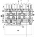
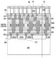
웨이퍼-웨이퍼 본딩을 위한 웨이퍼 레벨 하이브리드 본딩(hybrid bonding) 기술이 배면 조명(BSI; back-side illuminated) 상보형 금속 산화물 반도체(CMOS; complementary metal-oxide semiconductor) 이미지 센서(CIS; CMOS image sensors)와 같은 3차원 집적 회로(3D-IC; three-dimensional integrated circuit) 컴포넌트의 제조에 이용되고 있다. BSI-CIS를 제조할 때, 어레이로 배열되는 BSI 감지 집적 회로들을 포함한 센서 웨이퍼 및 어레이로 배열되는 로직 회로 칩들을 포함한 로직 회로 웨이퍼가 제공된다. 센서 웨이퍼와 로직 회로 웨이퍼는, 로직 회로 웨이퍼가 센서 웨이퍼 위에 적층되도록 웨이퍼 레벨 하이브리드 본딩 기술을 통해 서로 본딩된다. 그 후에, 하이브리드 본딩된 센서 및 로직 회로 웨이퍼는 패키징되고 개별화되어(singulated) BSI-CIS 디바이스를 형성한다. 센서 웨이퍼와 로직 회로 웨이퍼의 하이브리드 본딩 프로세스 동안, 웨이퍼의 본딩 계면에서 구리 압출(extrusion) 및/또는 구리 확산(migration)이 발생할 수 있다. 따라서, 상기 언급한 구리 압출 및/또는 구리 확산으로 인해 하이브리드 본딩된 웨이퍼의 신뢰성이 악화된다.Wafer-level hybrid bonding technology for wafer-wafer bonding has been developed with back-side illuminated (BSI) complementary metal-oxide semiconductor (CMOS) image sensors (CIS) and CMOS image sensors. The same three-dimensional integrated circuit (3D-IC) is used in the manufacture of components. In manufacturing a BSI-CIS, a sensor wafer including BSI sensing integrated circuits arranged in an array and a logic circuit wafer including logic circuit chips arranged in an array are provided. The sensor wafer and the logic circuit wafer are bonded to each other through a wafer level hybrid bonding technique such that the logic circuit wafer is laminated on the sensor wafer. Thereafter, the hybrid bonded sensor and logic circuit wafers are packaged and singulated to form a BSI-CIS device. During the hybrid bonding process of the sensor wafer and the logic circuit wafer, copper extrusion and/or copper migration may occur at the bonding interface of the wafer. Accordingly, the reliability of the hybrid bonded wafer is deteriorated due to the aforementioned copper extrusion and/or copper diffusion.
제1 집적 회로 컴포넌트 및 제2 집적 회로 컴포넌트를 포함하는 하이브리드 본딩된 구조물이 제공된다. 제1 집적 회로 컴포넌트는 제1 유전체 층, 제1 전도체 및 아이솔레이션 구조물을 포함한다. 제1 전도체 및 아이솔레이션 구조물은 제1 유전체 층에 매립된다. 아이솔레이션 구조물은 제1 전도체로부터 전기적으로 절연되며 제1 전도체를 둘러싼다. 제2 집적 회로 컴포넌트는 제2 유전체 층 및 제2 전도체를 포함한다. 제2 전도체는 제2 유전체 층에 매립된다. 제1 유전체 층은 제2 유전체 층에 본딩되고 제1 전도체는 제2 전도체에 본딩된다.A hybrid bonded structure is provided that includes a first integrated circuit component and a second integrated circuit component. The first integrated circuit component includes a first dielectric layer, a first conductor, and an isolation structure. The first conductor and isolation structures are embedded in the first dielectric layer. The isolation structure is electrically insulated from and surrounds the first conductor. The second integrated circuit component includes a second dielectric layer and a second conductor. A second conductor is embedded in the second dielectric layer. The first dielectric layer is bonded to the second dielectric layer and the first conductor is bonded to the second conductor.
본 개시의 양상은 다음의 상세한 설명으로부터 첨부 도면과 함께 볼 때 가장 잘 이해된다. 산업계에서의 표준 실시에 따라 다양한 특징부들이 실축척대로 도시되지 않은 것을 유의하여야 한다. 사실상, 다양한 특징부들의 치수는 설명을 명확하게 하기 위해 임의로 증가되거나 감소되었을 수 있다.
도 1 내지 도 7은 본 개시의 일부 실시예에 따라 BSI-CIS 디바이스를 제조하기 위한 프로세스 흐름을 예시한다.
도 8 및 도 9는 본 개시의 일부 실시예에 따른 웨이퍼의 하이브리드 본딩 프로세스를 예시한 단면도들이다.
도 10은 본 개시의 일부 실시예에 따른 하이브리드 본딩된 구조물의 단면도이다.
도 11 및 도 12는 본 개시의 일부 대안의 실시예에 따른 웨이퍼의 하이브리드 본딩 프로세스를 예시한 단면도들이다.
도 13 내지 도 18은 본 개시의 다양한 실시예에 따른 하이브리드 본딩된 구조물을 예시한 단면도들이다.
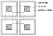
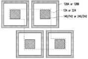
도 19 내지 도 28은 본 개시의 다양한 실시예에 따른 제1 집적 회로 컴포넌트 및/또는 제2 집적 회로 컴포넌트의 하나의 전도체 그룹을 각각 예시한 평면도들이다.Aspects of the present disclosure are best understood from the following detailed description when taken in conjunction with the accompanying drawings. It should be noted that, in accordance with standard practice in the industry, various features are not drawn to scale. In fact, the dimensions of various features may have been arbitrarily increased or decreased for clarity of description.
1-7 illustrate a process flow for manufacturing a BSI-CIS device in accordance with some embodiments of the present disclosure.
8 and 9 are cross-sectional views illustrating a hybrid bonding process of a wafer in accordance with some embodiments of the present disclosure.
10 is a cross-sectional view of a hybrid bonded structure in accordance with some embodiments of the present disclosure.
11 and 12 are cross-sectional views illustrating a hybrid bonding process of a wafer in accordance with some alternative embodiments of the present disclosure.
13 to 18 are cross-sectional views illustrating hybrid bonded structures according to various embodiments of the present disclosure.
19 to 28 are plan views each illustrating one conductor group of a first integrated circuit component and/or a second integrated circuit component according to various embodiments of the present disclosure;
다음의 개시는 제공되는 주제의 상이한 특징들을 구현하기 위한 많은 다양한 실시예 또는 예를 제공한다. 컴포넌트 및 구성의 구체적 예가 본 개시를 단순화하도록 아래에 기재된다. 이들은 물론 단지 예일 뿐이며 한정하고자 하는 것이 아니다. 예를 들어, 이어지는 다음 기재에 있어서 제2 특징부 상에 또는 위에 제1 특징부를 형성하는 것은, 제1 및 제2 특징부가 직접 접촉하여 형성되는 실시예를 포함할 수 있고, 제1 및 제2 특징부가 직접 접촉하지 않도록 제1 특징부와 제2 특징부 사이에 추가의 특징부가 형성될 수 있는 실시예도 또한 포함할 수 있다. 또한, 본 개시는 다양한 예에서 참조 번호 및/또는 문자를 반복할 수 있다. 이 반복은 단순하고 명확하게 하기 위한 목적인 것이며, 그 자체가 설명되는 다양한 실시예 및/또는 구성 간의 관계를 지시하는 것은 아니다.The following disclosure provides many different embodiments or examples for implementing different features of the presented subject matter. Specific examples of components and configurations are described below to simplify the present disclosure. These are, of course, merely examples and are not intended to be limiting. For example, in the following description, forming a first feature on or over a second feature may include embodiments in which the first and second features are formed in direct contact, and the first and second features Embodiments in which additional features may be formed between the first and second features such that the features do not directly contact may also be included. In addition, this disclosure may repeat reference numbers and/or letters in the various examples. This repetition is for the purpose of simplicity and clarity, and does not in itself indicate a relationship between the various embodiments and/or configurations being described.
또한, “밑에”, “아래에”, “하부”, “위에”, “상부” 등과 같은 공간적으로 상대적인 용어는 도면에 예시된 바와 같이 하나의 구성요소 또는 특징부의 또다른 구성요소(들) 또는 특징부(들)에 대한 관계를 기재하고자 설명을 쉽게 하기 위해 여기에서 사용될 수 있다. 공간적으로 상대적인 용어는 도면에 도시된 배향에 더하여 사용중이거나 동작중인 디바이스의 상이한 배향들을 망라하도록 의도된다. 장치는 달리 배향될 수 있고(90도 회전되거나 또는 다른 배향으로), 여기에서 사용된 공간적으로 상대적인 기술자는 마찬가지로 그에 따라 해석될 수 있다.Also, spatially relative terms such as “below”, “below”, “lower”, “above”, “above”, etc. are used to refer to one component or another component(s) of a feature as illustrated in the drawings. May be used herein for ease of description to describe the relationship to feature(s). The spatially relative terms are intended to encompass different orientations of the device in use or operation in addition to the orientation shown in the figures. The device may be otherwise oriented (rotated 90 degrees or at other orientations), and spatially relative descriptors used herein may likewise be interpreted accordingly.
도 1 내지 도 7은 본 개시의 일부 실시예에 따라 BSI-CIS 디바이스를 제조하기 위한 프로세스 흐름을 예시한다.1-7 illustrate a process flow for manufacturing a BSI-CIS device in accordance with some embodiments of the present disclosure.
도 1을 참조하면, 제1 집적 회로 컴포넌트(100) 및 제2 집적 회로 컴포넌트(200)가 제공된다. 제1 집적 회로 컴포넌트(100)는 안에 형성된 복수의 제1 반도체 디바이스를 갖는 제1 반도체 기판(110), 제1 반도체 기판(110) 상에 배치된 제1 상호접속 구조물(120), 제1 상호접속 구조물(120)을 덮는 제1 유전체 층(130) 및 적어도 하나의 제1 전도체 그룹(140)을 포함할 수 있다. 적어도 하나의 제1 전도체 그룹(140)은 제1 상호접속 구조물(120)을 통해 서로 전기적으로 접속되는 복수의 제1 전도체(142)를 포함할 수 있다. 적어도 하나의 제1 전도체 그룹(140)은 제1 유전체 층(130)에 매립된다. 제2 집적 회로 컴포넌트(200)는 안에 형성된 복수의 제2 반도체 디바이스를 갖는 제2 반도체 기판(210), 제2 반도체 기판(210) 상에 배치된 제2 상호접속 구조물(220), 제2 상호접속 구조물(220)을 덮는 제2 유전체 층(230) 및 적어도 하나의 제2 전도체 그룹(240)을 포함할 수 있다. 적어도 하나의 제2 전도체 그룹(240)은 제2 상호접속 구조물(220)을 통해 서로 전기적으로 접속되는 복수의 제2 전도체(242)를 포함할 수 있다. 적어도 하나의 제2 전도체 그룹(240)은 제2 유전체 층(230)에 매립된다.Referring to FIG. 1 , a first
도 1에 도시된 바와 같이, 일부 실시예에서, 제1 집적 회로 컴포넌트(100)는 어레이로 배열된 복수의 감광 칩들(102)을 포함하는 제1 반도체 웨이퍼(즉, 센서 웨이퍼)일 수 있고, 제2 집적 회로 컴포넌트(200)는 어레이로 배열된 복수의 로직 집적 회로 칩들(202)을 포함하는 제2 반도체 웨이퍼(즉, 로직 회로 웨이퍼)일 수 있다. 다르게 말하자면, 상기 언급한 제1 반도체 기판(110), 제1 상호접속 구조물(120), 제1 유전체 층(130) 및 적어도 하나의 제1 전도체 그룹(140)이 제1 반도체 웨이퍼에서 복수의 감광 칩(102)을 형성할 수 있고, 상기 언급한 제2 반도체 기판(210), 제2 상호접속 구조물(220), 제2 유전체 층(230) 및 적어도 하나의 제2 전도체 그룹(240)이 제2 반도체 웨이퍼에서 복수의 로직 집적 회로 칩(202)을 형성할 수 있다.1 , in some embodiments, the first
일부 실시예에서, 제1 전도체(142) 및 제2 전도체(242)의 재료는 구리(Cu) 또는 다른 적합한 금속성 재료일 수 있는 반면에, 제1 유전체 층(130) 및 제2 유전체 층(230)의 재료는 실리콘 산화물(SiOx, x>0), 실리콘 질화물(SiNx, x>0), 실리콘 산질화물(SiOxNy, x>0 및 y >0) 또는 다른 적합한 유전체 재료일 수 있다. 제1 전도체(142)는 퇴적 다음에 화학 기계적 연마(CMP; chemical mechanical polishing)에 의해 형성될 수 있다. 마찬가지로, 제2 전도체(242)는 또다른 퇴적 다음에 화학 기계적 연마(CMP)에 의해 형성될 수 있다. 제1 전도체(142) 및 제2 전도체(242)는 부식 및/또는 디싱(dishing) 문제가 최소화될 수 있도록 전도체 밀도를 조정하는 데에 도움이 된다.In some embodiments, the material of the
일부 실시예에서, 웨이퍼-웨이퍼 하이브리드 본딩을 용이하게 하기 위해, 제1 집적 회로 컴포넌트(100) 및 제2 집적 회로 컴포넌트(200)의 본딩 표면에 대한 표면 준비가 수행된다. 표면 준비는 예를 들어 표면 세척 및 활성화를 포함할 수 있다. 표면 세척은, 제1 전도체(142), 제1 유전체 층(130), 제2 전도체(242) 및 제2 유전체 층(230)의 상부 표면 상의 입자를 제거하도록 제1 집적 회로 컴포넌트(100) 및 제2 집적 회로 컴포넌트(200)의 본딩 표면에 대해 수행될 수 있다. 제1 집적 회로 컴포넌트(100) 및 제2 집적 회로 컴포넌트(200)의 본딩 표면은 예를 들어 습식 세척에 의해 세척될 수 있다. 입자가 제거될 뿐만 아니라, 제1 전도체(142) 및 제2 전도체(242)의 상부 표면 상에 형성된 자연 산화물도 또한 제거될 수 있다. 제1 전도체(142) 및 제2 전도체(242)의 상부 표면 상에 형성된 자연 산화물은 예를 들어 습식 세척에 사용된 화학물질에 의해 제거될 수 있다.In some embodiments, surface preparation for the bonding surfaces of the first
제1 집적 회로 컴포넌트(100) 및 제2 집적 회로 컴포넌트(200)의 본딩 표면을 세척한 후에, 높은 본딩 강도의 발전을 위해 제1 유전체 층(130) 및 제2 유전체 층(230)의 상부 표면의 활성화가 수행될 수 있다. 일부 실시예에서, 제1 유전체 층(130) 및 제2 유전체 층(230)의 상부 표면을 처리하도록 플라즈마 활성화가 수행될 수 있다.After cleaning the bonding surfaces of the first
도 1 및 도 2를 참조하면, 제1 집적 회로 컴포넌트(100)는 제2 집적 회로 컴포넌트(200)와 정렬되고 마이크론이하(sub-micron) 정렬 정밀도가 달성될 수 있다. 제1 집적 회로 컴포넌트(100) 및 제2 집적 회로 컴포넌트(200)가 정밀하게 정렬되면, 제1 집적 회로 컴포넌트(100)는 제2 집적 회로 컴포넌트(200) 상에 배치되며 이와 접촉한다. 제1 유전체 층(130)의 활성화된 상부 표면이 제2 유전체 층(230)의 활성화된 상부 표면과 접촉할 때, 제1 집적 회로 컴포넌트(100)의 제1 유전체 층(130)과 제2 집적 회로 컴포넌트(200)의 제2 유전체 층(230)이 프리본딩(pre-bond)된다. 다르게 말하자면, 제1 집적 회로 컴포넌트(100) 및 제2 집적 회로 컴포넌트(200)는 제1 유전체 층(130)과 제2 유전체 층(230)의 프리본딩을 통해 프리본딩된다. 제1 유전체 층(130)과 제2 유전체 층(230)의 프리본딩 후에, 제1 전도체(142)는 제2 전도체(242)와 접촉한다.1 and 2 , a first
제1 집적 회로 컴포넌트(100)를 제2 집적 회로 컴포넌트(200)에 프리 본딩한 후에, 제1 집적 회로 컴포넌트(100)와 제2 집적 회로 컴포넌트(200)의 하이브리드 본딩이 수행된다. 제1 집적 회로 컴포넌트(100)와 제2 집적 회로 컴포넌트(200)의 하이브리드 본딩은 유전체 본딩을 위한 트리트먼트(treatment) 및 전도체 본딩을 위한 열 어닐링을 포함할 수 있다. 일부 실시예에서, 유전체 본딩을 위한 트리트먼트는 제1 유전체 층(130)과 제2 유전체 층(230) 간의 본딩을 강화하도록 수행된다. 예를 들어, 유전체 본딩을 위한 트리트먼트는 약 100 ℃ 내지 약 150 ℃ 범위의 온도에서 수행될 수 있다. 유전체 본딩을 위한 트리트먼트를 수행한 후에, 제1 전도체(142)와 제2 전도체(242) 간의 본딩을 용이하게 하도록 전도체 본딩을 위한 열 어닐링이 수행된다. 예를 들어, 전도체 본딩을 위한 열 어닐링은 약 300 ℃ 내지 약 400 ℃ 범위의 온도에서 수행될 수 있다. 전도체 본딩을 위한 열 어닐링의 프로세스 온도는 유전체 본딩을 위한 트리트먼트의 프로세스 온도보다 더 높다. 전도체 본딩을 위한 열 어닐링이 상대적으로 더 높은 온도에서 수행되므로, 제1 전도체(142)와 제2 전도체(242) 간의 본딩 계면에서 금속 확산 및 입계 성장이 일어날 수 있다. 반면에, 전도체 본딩을 위한 열 어닐링이 수행될 때, 제1 전도체(142) 및 제2 전도체(242)는 전도체(142, 242)와 유전체 층(130, 230) 간의 열 팽창 계수(CTE; coefficient of thermal expansion) 불일치로부터 초래되는 압력을 받을 수 있다. 전도체 본딩을 위한 열 어닐링을 수행할 때, 제1 유전체 층(130)이 제2 유전체 층(230)에 본딩되고 제1 전도체(140)가 제2 전도체(240)에 본딩된다. 일부 실시예에서, 제1 전도체(140)는 전도성 비아(예컨대, 구리 비아), 전도성 패드(예컨대, 구리 패드), 또는 이들의 조합일 수 있으며, 제2 전도체(240)는 전도성 비아(예컨대, 구리 비아), 전도성 패드(예컨대, 구리 패드) 또는 이들의 조합일 수 있다. 예를 들어, 제1 전도체(140)와 제2 전도체(240) 간의 전도체 본딩은 비아-비아 본딩, 패드-패드 본딩 또는 비아-패드 본딩일 수 있다.After pre-bonding the first
제1 집적 회로 컴포넌트(100)와 제2 집적 회로 컴포넌트(200)의 하이브리드 본딩이 수행된 후에, 제1 상호접속 구조물(120) 및 제2 상호접속 구조물(220)은 제1 전도체(142) 및 제2 전도체(242)를 통해 서로 전기적으로 접속된다.After the hybrid bonding of the first
제1 집적 회로 컴포넌트(100)와 제2 집적 회로 컴포넌트(200)가 하이브리드 본딩된 후에, 도 2에 도시된 바와 같이, 적층 및 하이브리드 본딩된 웨이퍼를 포함하는 하이브리드 본딩된 구조물(HB1)이 달성된다. 일부 실시예에서, 하이브리드 본딩된 구조물(HB1)은 필요한 경우 복수의 개별화된 하이브리드 본딩된 구조물(HB2)로 개별화될 수 있고, 개별화된 하이브리드 본딩된 구조물(HB2)의 각각은 적층 및 하이브리드 본딩된 칩을 포함한다. 다르게 말하자면, 개별화된 하이브리드 본딩된 구조물(HB2)의 각각은 로직 집적 회로 칩 및 감광 칩을 포함할 수 있으며, 감광 칩은 로직 집적 회로 칩 위에 적층되어 이와 하이브리드 본딩된다. 상기 언급한 실시예에서, 하이브리드 본딩된 구조물(HB1)은 하이브리드 본딩된 웨이퍼를 포함하고, 하이브리드 본딩된 구조물(HB2)은 하이브리드 본딩된 칩을 포함한다. 그러나, 본 개시는 이에 한정되지 않는다. 일부 대안의 실시예에서, 하이브리드 본딩된 구조물(도시되지 않음)은 웨이퍼 및 웨이퍼 상에 적층되어 하이브리드 본딩되어 있는 적어도 하나의 칩을 포함할 수 있다.After the first
도 3 및 도 4를 참조하면, 제1 반도체 기판(110)의 배면 표면 상에 접착제(300)가 형성된다. 접착제(300)는 예를 들어 감광 칩(102)의 감지 영역을 둘러싸도록 감광 칩(102)의 주변 영역을 덮도록 형성된다. 커버 리드(400)의 하부 표면 상에 배치된 스페이서(500)를 갖는 커버 리드(400)가 제공된다. 커버 리드(400)는 하이브리드 본딩된 구조물(HB1)을 덮도록 이용될 수 있고, 스페이서(500)의 위치는 접착제(300)의 분포에 대응한다. 하이브리드 본딩된 구조물(HB1) 상에 형성된 접착제(300)를 통해, 스페이서(500)는 하이브리드 본딩된 구조물(HB1)과 접착되고, 커버 리드(400)와 하이브리드 본딩된 구조물(HB1) 사이에 갭이 형성된다. 커버 리드(400)가 스페이서(500) 및 갭에 의해 하이브리드 본딩된 구조물(HB1)로부터 떨어져 있으므로, 하이브리드 본딩된 구조물(HB1) 상에 형성된 컴포넌트는 커버 리드(400)와 접촉하지 않고 잘 보호될 수 있다. 예를 들어, 접착제(300)의 재료는 적합한 절연 특성을 갖는 유기 재료일 수 있고, 커버 리드(400)는 광학 코팅(예컨대, 반사 방지 코팅)이 있거나 없는 커버 글래스일 수 있고, 스페이서(500)는 에폭시 수지 또는 다른 적합한 재료일 수 있다.3 and 4 , an adhesive 300 is formed on the rear surface of the
일부 실시예에서, 커버 리드(400) 및 스페이서(500)가 하이브리드 본딩된 구조물(HB1)에 접착된 후에, 하이브리드 본딩된 구조물(HB1)의 두께를 더 감소시키도록 제2 반도체 기판(210)의 배면 표면에 대해 그라인딩 프로세스가 수행될 수 있다.In some embodiments, after the
도 5를 참조하면, 커버 리드(400) 및 스페이서(500)가 접착제(300)를 통해 하이브리드 본딩된 구조물(HB1)과 접착된 후에, 제2 집적 회로 컴포넌트(200)의 제2 상호접속 구조물(220)이 드러날 때까지, 예를 들어 쓰루 실리콘 비아(TSV; through silicon via) 프로세스에 의해 복수의 쓰루 홀(TH)이 제2 반도체 기판(210)에 형성된다. 그 후에, 쓰루 홀(TH)을 통해 제2 상호접속 구조물(220)에 전기적으로 접속된 재배선 층(250)이 제2 반도체 기판(210)의 배면 표면(즉, 하부 표면) 상에 형성된다. 재배선 층(250)을 형성하기 전에, 재배선 층(250)을 제2 반도체 기판(210)으로부터 전기적으로 절연하도록, 절연 층(도시되지 않음)이 제2 반도체 기판(210)의 배면 표면 및 쓰루 홀(TH)의 측벽 상에 형성될 수 있다. 도 5에 도시된 바와 같이, 재배선 층(250)은 제1 상호접속 구조물(120) 및 제2 상호접속 구조물(220)을 제2 반도체 기판(210)의 배면 표면에 재분배한다. 일부 실시예에서, 도면에는 도시되지 않았지만, 제2 상호접속 구조물(220)은 랜딩(landing) 패드를 포함할 수 있고, 랜딩 패드는 쓰루 홀(TH)에 의해 드러날 수 있으며, 재배선 층(250)은 쓰루 홀(TH)을 통해 랜딩 패드에 전기적으로 접속될 수 있다.Referring to FIG. 5 , after the
도 6을 참조하면, 패시베이션 층(260)이 재배선 층(250)을 부분적으로 덮도록 제2 반도체 기판(210)의 배면 표면 상에 형성된다. 패시베이션 층(260)은 재배선 층(250)(예컨대, 재배선 층(250)의 볼 패드)을 부분적으로 노출시키기 위한 복수의 개구를 포함할 수 있다. 패시베이션 층(260)이 형성된 후에, 어레이로 배열된 복수의 전도성 단자(270)(예컨대, 전도성 볼)가 패시베이션 층(260)의 개구에 의해 노출된 재배선 층(250)의 일부 상에 형성된다. 전도성 단자(270)는 볼 배치 및 리플로우 프로세스에 의해 형성된 솔더 볼일 수 있다.Referring to FIG. 6 , a
도 6 및 도 7을 참조하면, 전도성 단자(270)를 형성한 후에, 도 6에 도시된 결과적인 구조물을 복수의 BSI-CIS 디바이스들로 개별화하도록 스크라이브 라인(SL)을 따라 다이싱 프로세스가 수행된다. 도 7에 도시된 바와 같이, 개별화된 BSI-CIS 디바이스는 볼 그리드 어레이(BGA; ball grid array) 디바이스일 수 있다.6 and 7 , after forming the
BSI-CIS 디바이스의 신뢰성은 하이브리드 본딩된 구조물(HB1)에 의해 영향받을 수 있다. 제1 집적 회로 컴포넌트(100)와 제2 집적 회로 컴포넌트(200) 간의 전기적 접속은 하이브리드 본딩 계면에서 발생할 수 있는 압출(예컨대, 구리 압출) 및/또는 확산(예컨대, 전기적 확산, 열 확산 및/또는 응력 확산) 때문에 실패할 수 있다(즉, 전기적 개방 및 단락 문제). 압출 및 확산 문제를 해결하기 위해 제1 상호접속 구조물(120) 및 제2 상호접속 구조물(220)의 신규의 설계가 필요하다. 제1 상호접속 구조물(120) 및 제2 상호접속 구조물(220)의 세부사항이 도 8 내지 도 18과 함께 다음과 같이 기재된다.The reliability of the BSI-CIS device may be affected by the hybrid bonded structure HB1. The electrical connection between the first
도 8 및 도 9는 본 개시의 일부 실시예에 따른 웨이퍼의 하이브리드 본딩 프로세스를 예시한 단면도들이다.8 and 9 are cross-sectional views illustrating a hybrid bonding process of a wafer in accordance with some embodiments of the present disclosure.
도 8 및 도 9를 참조하면, 일부 실시예에서, 제1 집적 회로 컴포넌트(100)는 제1 반도체 기판(110)에 또는 제1 반도체 기판(110) 상에 형성된 복수의 제1 반도체 디바이스(112)(예컨대, 포토 다이오드, 트랜지스터, 커패시터 등) 및 제1 반도체 기판(110)의 배면 표면(즉, 상부 표면) 상에 형성된 마이크로렌즈 어레이(ML)를 포함할 수 있다. 제1 반도체 기판(110)에 형성된 제1 반도체 디바이스(112)는 어레이로 배열될 수 있고 제1 반도체 기판(110)의 배면 표면 상에 형성된 마이크로렌즈 어레이(ML)에 의해 덮어질 수 있다. 일부 대안의 실시예에서, 제1 집적 회로 컴포넌트(100)는 마이크로렌즈 어레이(ML)와 제1 반도체 디바이스(112) 사이에 형성된 복수의 컬러 필터(CF)를 더 포함할 수 있다. 다르게 말하자면, 컬러 필터(CF)는 제1 반도체 기판(110)의 배면 표면 상에 형성되고 마이크로렌즈 어레이(ML)는 컬러 필터(CF) 상에 형성된다. 실제 설계 요건에 기초하여, 제1 집적 회로 컴포넌트(100)에서 제1 반도체 디바이스(112)의 광학 특성을 강화하기 위한 다른 광학 컴포넌트(예컨대, 블랙 매트릭스)가 형성될 수 있다.8 and 9 , in some embodiments, the first
또한, 일부 실시예에서, 제2 집적 회로 컴포넌트(200)는 제2 반도체 기판(210)에 또는 제2 반도체 기판(210) 상에 형성된 복수의 제2 반도체 디바이스(212)(예컨대, 트랜지스터, 커패시터 등)를 포함할 수 있다. 일부 실시예에서, 제2 반도체 디바이스(212) 및 제1 상호접속 구조물(120)은 로직 회로부를 구성할 수 있다.Further, in some embodiments, the second
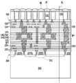
도 8 및 도 9에 도시된 바와 같이, 제1 전도체(142)의 두 그룹과 제2 전도체(242)의 두 그룹이 도시되어 있지만, 본 개시는 제1 집적 회로 컴포넌트(100) 상에 형성된 제1 전도체(142)의 그룹의 수 및 제2 집적 회로 컴포넌트(200) 상에 형성된 제2 전도체(242)의 그룹의 수를 한정하지 않는다. 또한, 본 개시는 각각의 전도체 그룹(140 또는 240)에 포함된 전도체(142 또는 242)의 수를 한정하지 않는다. 이 실시예에서는, 예를 들어, 2개의 전도체(142)가 하나의 전도체 그룹(140)에 포함되고, 2개의 전도체(242)가 하나의 전도체 그룹(240)에 포함된다.As shown in FIGS. 8 and 9 , two groups of
제1 전도체 그룹(140)은 제1 상호접속 구조물(120)에서 제1 션트 트렌이스(shunt trace)(T1)를 통해 제1 반도체 디바이스(112)에 전기적으로 접속될 수 있다. 다르게 말하자면, 제1 전도체 그룹(140) 중의 적어도 하나는 제1 상호접속 구조물(120)에서 하나의 대응하는 제1 션트 트렌이스(ST1)를 통해 제1 반도체 디바이스(112) 중의 하나에 전기적으로 접속될 수 있다. 제1 션트 트렌이스(ST1)의 수는 제1 전도체 그룹(140)의 수와 동일할 수 있다. 일부 실시예에서, 제1 상호접속 구조물(120)은 유전체간 층(122) 및 상호접속 금속 층(124)을 포함할 수 있다. 상호접속 금속 층(124)은 제1 전도체 그룹(140)과 제1 반도체 디바이스(112) 간에 전기적으로 접속된다. 제1 상호접속 구조물(120)에서의 제1 션트 트레이스(ST1)는 상호접속 금속 층(124)의 일부에 의해 형성될 수 있다. 마찬가지로, 제2 전도체 그룹(240)은 제2 상호접속 구조물(220)에서 제2 션트 트렌이스(ST2)를 통해 제2 반도체 디바이스(212)에 전기적으로 접속될 수 있다. 다르게 말하자면, 제2 전도체 그룹(240) 중의 적어도 하나는 제2 상호접속 구조물(220)에서 하나의 대응하는 제2 션트 트렌이스(ST2)를 통해 제2 반도체 디바이스(212) 중의 하나에 전기적으로 접속될 수 있다. 제2 션트 트렌이스(ST2)의 수는 제2 전도체 그룹(240)의 수와 동일할 수 있다. 일부 실시예에서, 제2 상호접속 구조물(220)은 유전체간 층(222) 및 상호접속 금속 층(224)을 포함할 수 있다. 상호접속 금속 층(224)은 제2 전도체 그룹(240)과 제2 반도체 디바이스(212) 간에 전기적으로 접속된다. 제2 상호접속 구조물(220)에서의 제2 션트 트레이스(ST2)는 상호접속 금속 층(224)의 일부에 의해 형성될 수 있다.The first group of
제1 전도체 그룹(140) 중의 하나에 포함된 제1 전도체(142)는 상호접속 금속 층(124)의 최상부 금속 패턴(즉, 최하부 금속 층)과 직접 접촉하고 이에 접속된다. 마찬가지로, 제2 전도체 그룹(240) 중의 하나에 포함된 제2 전도체(242)는 상호접속 금속 층(224)의 최상부 금속 패턴(즉, 최상부 금속 층)과 직접 접촉하고 이에 접속된다. 다르게 말하자면, 제1 전도체(142) 및 제2 전도체(242)는 상호접속 금속 층(124)의 최상부 금속 패턴과 상호접속 금속 층(224)의 최상부 금속 패턴 사이에 위치된다.A
도 8에 도시된 바와 같이, 제1 집적 회로 컴포넌트(100)와 제2 집적 회로 컴포넌트(200)의 하이브리드 본딩 전에, 제1 집적 회로 컴포넌트(100) 및 제2 집적 회로 컴포넌트(200)는 프리본딩을 위해 세척되고 서로 정렬된다. 다르게 말하자면, 제1 집적 회로 컴포넌트(100) 상의 제1 전도체 그룹(140) 및 제2 집적 회로 컴포넌트(200) 상의 제2 전도체 그룹(240)은 하이브리드 본딩 전에 미리 정렬된다.As shown in FIG. 8 , before the hybrid bonding of the first
도 9에 도시된 바와 같이, 제1 집적 회로 컴포넌트(100)와 제2 집적 회로 컴포넌트(200)를 하이브리드 본딩한 후에, 제1 션트 트레이스(ST1), 제2 션트 트레이스(ST2), 제1 전도체(142)(즉, 제1 전도체 그룹(140)), 및 제2 전도체(242)(즉, 제1 전도체 그룹(140))는 제1 집적 회로 컴포넌트(100) 및 제2 집적 회로 컴포넌트(200)에서의 복수의 션트 경로(SP1)를 제공한다. 제1 전도체 디바이스(112)는 션트 경로(SP1)를 통해 제2 반도체 디바이스(212)에 전기적으로 접속할 수 있다. 이 실시예에서, 션트 경로(SP1)의 각각의 하나는 제1 반도체 디바이스(112)와 제2 반도체 디바이스(212) 사이에 전류를 전송하기 위한 2개의 접속 경로를 포함한다. 그러나, 션트 경로(SP1)의 각각의 하나에서의 접속 경로의 수는 본 개시에서 한정되지 않는다. 일부 대안의 실시예에서, 상이한 션트 경로(SP1)에 포함된 접속 경로의 수는 동일하거나 상이할 수 있다.As shown in FIG. 9 , after hybrid bonding the first
제1 션트 트레이스(ST1) 및 제2 션트 트레이스(ST2)는, 제1 션트 트레이스(ST1)와 제2 션트 트레이스(ST2)에서의 전류 밀도를 감소시키도록 제1 반도체 디바이스(112)와 제2 반도체 디바이스(212) 사이에 흐르는 전류를 확산시킬 수 있다. 제1 션트 트레이스(ST1) 및 제2 션트 트레이스(ST2)에서의 전류 밀도의 감소는 제1 집적 회로 컴포넌트(100)와 제2 집적 회로 컴포넌트(200) 간의 하이브리드 본딩된 계면에서 발생하는 전기적 확산(예컨대, 구리 확산)을 최소화할 수 있다. 제1 션트 트레이스(ST1) 및 제2 션트 트레이스(ST2)와 하이브리드 본딩된 전도체(142/242)는 더 낮은 저항을 제공할 수 있다. 또한, 제1 션트 트레이스(ST1) 및 제2 션트 트레이스(ST2)는 하이브리드 본딩 동안 제1 전도체(142) 및 제2 전도체(242)에 의해 받는 스트레스를 확산시킬 수 있다. 제1 전도체(142) 및 제2 전도체(242)에 의해 받는 스트레스의 확산은 제1 집적 회로 컴포넌트(100)와 제2 집적 회로 컴포넌트(200) 간의 하이브리드 본딩된 계면에서 발생하는 스트레스 확산을 최소화할 수 있다. 따라서, 하이브리드 본딩의 수율이 제1 션트 트레이스(ST1) 및 제2 션트 트레이스(ST2)로 인해 증가할 수 있다.The first shunt trace ST1 and the second shunt trace ST2 connect the
상기 언급한 유전체 본딩을 위한 트리트먼트 동안, 열 확산으로부터 초래되는 개방 및/또는 단락 회로 문제는 제1 상호접속 구조물(120) 및 제2 상호접속 구조물(220)의 설계에 의해 최소화될 수 있다. 상기 언급한 전도체 본딩을 위한 열 어닐링 동안, 열 확산 및 스트레스 확산으로부터 초래되는 개방 및/또는 단락 회로 문제 뿐만 아니라 CTE 불일치로부터 초래되는 압출 문제도 또한, 제1 상호접속 구조물(120) 및 제2 상호접속 구조물(220)의 설계에 의해 최소화될 수 있다. 하이브리드 본딩된 구조물(HB1)(도 4에 도시됨)의 두께를 감소시키기 위한 상기 언급한 그라인딩 프로세스 동안, 스트레스로부터의 결과로서 발생할 수 있는 압출 문제 및 스트레스 확산은 제1 상호접속 구조물(120) 및 제2 상호접속 구조물(220)의 설계에 의해 최소화될 수 있다. BSI-CIS 디바이스의 동작 동안, 전기적 확산으로부터 초래되는 개방/단락 회로 문제는 제1 상호접속 구조물(120) 및 제2 상호접속 구조물(220)의 설계에 의해 최소화될 수 있다. 요약하자면, 전술한 압출 및 확산은 제1 상호접속 구조물(120) 및 제2 상호접속 구조물(220)의 설계에 의해 최소화될 수 있다.During the aforementioned treatment for dielectric bonding, open and/or short circuit problems resulting from thermal diffusion can be minimized by the design of the
도 10은 본 개시의 일부 실시예에 따른 하이브리드 본딩된 구조물의 단면도이다.10 is a cross-sectional view of a hybrid bonded structure in accordance with some embodiments of the present disclosure.
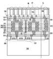
도 9 및 도 10을 참조하면, 도 10에 도시된 하이브리드 본딩된 구조물은, 3개의 제1 전도체(142)가 제1 전도체 그룹(140)의 각각에 포함되고 3개의 제2 전도체(242)가 제2 전도체 그룹(240)의 각각에 포함된다는 것을 제외하고는, 도 9에 도시된 바와 유사하다. 또한, 이 실시예에서, 션트 경로(SP2)의 각각의 하나는 예를 들어 제1 반도체 디바이스(112)와 제2 반도체 디바이스(212) 사이에 전류를 전송하기 위한 3개의 접속 경로를 포함한다. 그러나, 션트 경로(SP2)의 각각의 하나에서의 접속 경로의 수는 본 개시에서 한정되지 않는다. 일부 대안의 실시예에서, 상이한 션트 경로(SP2)에 포함된 접속 경로의 수는 동일하거나 상이할 수 있다.9 and 10 , in the hybrid bonded structure shown in FIG. 10 , three
도 11 및 도 12는 본 개시의 일부 대안의 실시예에 따른 웨이퍼의 하이브리드 본딩 프로세스를 예시한 단면도들이다.11 and 12 are cross-sectional views illustrating a hybrid bonding process of a wafer in accordance with some alternative embodiments of the present disclosure.
도 8, 도 9, 도 11 및 도 12를 참조하면, 도 11 및 도 12에 예시된 제1 상호접속 구조물(120) 및 제2 상호접속 구조물(220)은, 제1 전도체 그룹(140) 중의 하나에 포함된 제1 전도체(142)가 상호접속 금속 층(124)의 복수의 최상부 금속 패턴(즉, 최하부 금속 층)과 접촉하고 제1 전도체 그룹(140) 중의 하나에 포함된 제1 전도체(142)가 최상부 금속 패턴 위에 위치된 하나의 금속 패턴에 의해 서로 전기적으로 접속된다는 것을 제외하고는, 도 8 및 도 9에 예시된 바와 유사하다. 마찬가지로, 제2 전도체 그룹(240) 중의 하나에 포함된 제2 전도체(242)는 상호접속 금속 층(224)의 복수의 최상부 금속 패턴(즉, 최하부 금속 층)과 접촉하고, 제2 전도체 그룹(240) 중의 하나에 포함된 제2 전도체(242)는 최상부 금속 패턴 아래에 위치된 하나의 금속 패턴에 의해 서로 전기적으로 접속된다.8 , 9 , 11 and 12 , the
제1 전도체 그룹(140)은 제1 상호접속 구조물(120)에서 제1 션트 트렌이스(ST1)를 통해 제1 반도체 디바이스(112)에 전기적으로 접속될 수 있다. 다르게 말하자면, 제1 전도체 그룹(140) 중의 적어도 하나는 제1 상호접속 구조물(120)에서 하나의 대응하는 제1 션트 트렌이스(ST1)를 통해 제1 반도체 디바이스(112) 중의 하나에 전기적으로 접속될 수 있다. 제1 션트 트렌이스(ST1)의 수는 제1 전도체 그룹(140)의 수와 동일할 수 있다. 일부 실시예에서, 제1 상호접속 구조물(120)은 유전체간 층(122) 및 상호접속 금속 층(124)을 포함할 수 있다. 상호접속 금속 층(124)은 제1 전도체 그룹(140)과 제1 반도체 디바이스(112) 사이에 전기적으로 접속된다. 제1 상호접속 구조물(120)에서의 제1 션트 트레이스(ST1)는 상호접속 금속 층(124)의 일부에 의해 형성될 수 있다. 마찬가지로, 제2 전도체 그룹(240)은 제2 상호접속 구조물(220)에서 제2 션트 트렌이스(ST2)를 통해 제2 반도체 디바이스(212)에 전기적으로 접속될 수 있다. 다르게 말하자면, 제2 전도체 그룹(240) 중의 적어도 하나는 제2 상호접속 구조물(220)에서 하나의 대응하는 제2 션트 트렌이스(ST2)를 통해 제2 반도체 디바이스(212) 중의 하나에 전기적으로 접속될 수 있다. 제2 션트 트렌이스(ST2)의 수는 제2 전도체 그룹(240)의 수와 동일할 수 있다. 일부 실시예에서, 제2 상호접속 구조물(220)은 유전체간 층(222) 및 상호접속 금속 층(224)을 포함할 수 있다. 상호접속 금속 층(224)은 제2 전도체 그룹(240)과 제2 반도체 디바이스(212) 사이에 전기적으로 접속된다. 제2 상호접속 구조물(220)에서의 제2 션트 트레이스(ST2)는 상호접속 금속 층(224)의 일부에 의해 형성될 수 있다. 다르게 말하자면, 제1 전도체(142) 및 제2 전도체(242)가 상호접속 금속 층(124)의 최상부 금속 패턴과 상호접속 금속 층(224)의 최상부 금속 패턴 사이에 위치되며, 그 뿐만 아니라, 상호접속 금속 층(124 및 224)의 일부가 상호접속 금속 층(124)의 최상부 금속 패턴과 상호접속 금속 층(224)의 최상부 금속 패턴 사이에 개재된다.The first group of
도 13 내지 도 18은 본 개시의 다양한 실시예에 따른 하이브리드 본딩된 구조물을 예시한 단면도들이다.13 to 18 are cross-sectional views illustrating hybrid bonded structures according to various embodiments of the present disclosure.
도 13을 참조하면, 도 13에 예시된 제1 상호접속 구조물(120) 및 제2 상호접속 구조물(220)은, 아이솔레이션(isolation) 부분(128A) 및 아이솔레이션 부분(128B)을 각각 포함하는 복수의 아이솔레이션 구조물이 제1 상호접속 구조물(120)에 더 포함된다는 것을 제외하고는, 도 11 및 도 12에 예시된 바와 유사하다. 아이솔레이션 구조물의 아이솔레이션 부분(128A)은 제1 전도체(142)로부터 전기적으로 절연되고, 제1 전도체(142)의 각각은 아이솔레이션 부분(128A)의 하나에 의해 둘러싸인다. 또한, 아이솔레이션 구조물의 복수의 아이솔레이션 부분(128B)은 제2 전도체(242)로부터 전기적으로 절연되고, 제2 전도체(242)의 각각은 아이솔레이션 부분(128B)의 하나에 의해 둘러싸인다. 아이솔레이션 부분(128A)은 제1 유전체 층(130)에 매립되고 아이솔레이션 부분(128B)은 제2 유전체 층(230)에 매립된다. 아이솔레이션 부분(128A)은 전기적으로 플로팅되고 서로 분리되며, 아이솔레이션 부분(128B)은 전기적으로 플로팅되고 서로 분리된다. 도 13에 도시된 바와 같이, 아이솔레이션 부분(128A)의 각각은 각각 아이솔레이션 부분(128B)의 하나와 하이브리드 본딩된다. 일부 실시예에서, 아이솔레이션 부분(128A) 및 제1 전도체(142)는 동일 프로세스에 의해 형성될 수 있고 동일 재료로 제조될 수 있으며, 아이솔레이션 부분(128B) 및 제2 전도체(242)는 동일 프로세스에 의해 형성될 수 있고 동일 재료로 제조될 수 있다. 예를 들어, 아이솔레이션 부분(128A), 제1 전도체(142), 아이솔레이션 부분(128B) 및 제2 전도체(242)는 구리 또는 다른 적합한 금속성 재료와 같은 동일 재료에 의해 형성될 수 있다.Referring to FIG. 13 , the
제1 전도체(142) 및 아이솔레이션 부분(128A)은 퇴적 다음에 화학 기계적 연마(CMP)에 의해 형성될 수 있다. 마찬가지로, 제2 전도체(242) 및 아이솔레이션 부분(128B)은 또다른 퇴적 다음에 화학 기계적 연마(CMP)에 의해 형성될 수 있다. 제1 전도체(142), 아이솔레이션 부분(128B), 제2 전도체(242) 및 아이솔레이션 부분(128B)은 부식 및/또는 디싱 문제가 최소화될 수 있도록 전도체 밀도를 조정하는 데에 도움이 된다. 또한, 전기적 플로팅된 아이솔레이션 부분(128A 및 128B)은 제1 전도체(142) 및 제2 전도체(242)의 확산 문제로부터 초래되는 개방/단락 회로 문제를 저지할 수 있다.
도 14를 참조하면, 도 14에 예시된 제1 상호접속 구조물(120) 및 제2 상호접속 구조물(220)은, (도 13에 도시된 바와 같은)제1 상호접속 구조물(120)에서의 아이솔레이션 부분(128A)이 생략된다는 것을 제외하고는, 도 13에 예시된 바와 유사하다. 일부 실시예에서, 아이솔레이션 부분(128B) 및 제2 전도체(242)는 동일 프로세스에 의해 형성될 수 있고 동일 재료로 제조될 수 있다. 예를 들어, 아이솔레이션 부분(128B), 제1 전도체(142), 및 제2 전도체(242)는 구리 또는 다른 적합한 금속성 재료와 같은 동일 재료에 의해 형성될 수 있다.Referring to FIG. 14 , the
도 15를 참조하면, 도 15에 예시된 제1 상호접속 구조물(120) 및 제2 상호접속 구조물(220)은, (도 13에 도시된 바와 같은)제2 상호접속 구조물(220)에서의 아이솔레이션 부분(128B)이 생략된다는 것을 제외하고는, 도 13에 예시된 바와 유사하다. 일부 실시예에서, 아이솔레이션 부분(128A) 및 제1 전도체(142)는 동일 프로세스에 의해 형성될 수 있고 동일 재료로 제조될 수 있다. 예를 들어, 아이솔레이션 부분(128A), 제1 전도체(142), 및 제2 전도체(242)는 구리 또는 다른 적합한 금속성 재료와 같은 동일 재료에 의해 형성될 수 있다.Referring to FIG. 15 , the
도 16 내지 도 18을 참조하면, 도 16, 도 17 및 도 18에 예시된 제1 상호접속 구조물(120) 및 제2 상호접속 구조물(220)은, 제1 션트 트레이스(ST1) 및 제2 션트 트레이스(ST2)가 제1 상호접속 구조물(120) 및 제2 상호접속 구조물(220)에 없다는 것을 제외하고는, 도 13, 도 14 및 도 15에 예시된 바와 유사하다. 다르게 말하자면, 션트 트레이스 설계는 아이솔레이션 구조물과 결합되는 것이 필수인 것은 아니다.16 to 18 , the
도 19 내지 도 28은 본 개시의 다양한 실시예에 따라 제1 집적 회로 컴포넌트 및/또는 제2 집적 회로 컴포넌트의 하나의 전도체 그룹을 각각 예시한 평면도들이다.19-28 are plan views each illustrating one conductor group of a first integrated circuit component and/or a second integrated circuit component in accordance with various embodiments of the present disclosure;
도 19 내지 도 22를 참조하면, 하나의 전도체 그룸(140/240)에서, 하나의 상호접속 금속 층(124/224)에 의해 서로 전기적으로 접속된 복수의(예컨대, 2, 3 또는 4개의 제1) 전도체(142/242)가 포함될 수 있다. 제1 전도체(142/242)의 각각의 하나는 하나의 아이솔레이션 부분(128A 및/또는 128B)에 의해 둘러싸일 수 있다. 이 실시예에서, 아이솔레이션 부분(128A 또는 128B)은 직사각형 링일 수 있다. 하나의 전도체 그룹(140/240)에 속하는 전도체(142/242)는 행 방향, 열 방향을 따라 배열되거나 어레이로 배열될 수 있다.19 to 22 , in one
일부 대안의 실시예에서, 도 23 및 도 24에 도시된 바와 같이, 하나의 상호접속 금속 층(124/224)에 의해 서로 전기적으로 접속된 전도체(142/242)는 원형 형상으로 이루어질 수 있고, 아이솔레이션 부분(128A 또는 128B)은 예를 들어 원형 링일 수 있다. 일부 대안의 실시예에서, 도 25 및 도 26에 도시된 바와 같이, 하나의 상호접속 금속 층(124/224)에 의해 서로 전기적으로 접속된 전도체(142/242)는 직사각형 형상으로 이루어질 수 있고, 아이솔레이션 부분(128A 또는 128B)은 예를 들어 전도체(142/242)를 둘러싸도록 배열된 복수의 분리된 아이솔레이션 스트라이프를 포함할 수 있다. 일부 다른 실시예에서, 도 27 및 도 28에 도시된 바와 같이, 하나의 상호접속 금속 층(124/224)에 의해 서로 전기적으로 접속된 전도체(142/242)는 직사각형 형상으로 이루어질 수 있고, 아이솔레이션 부분(128A 또는 128B)은 예를 들어 육각형 형상으로 이루어질 수 있다.In some alternative embodiments, as shown in FIGS. 23 and 24 , the
본 개시의 일부 실시예에 따르면, 다음 단계들을 포함하는 하이브리드 본딩된 구조물을 제조하는 방법이 제공된다. 제1 집적 회로 컴포넌트 및 제2 집적 회로 컴포넌트가 제공된다. 제1 집적 회로 컴포넌트는 복수의 제1 반도체 디바이스를 그 안에 갖는 제1 반도체 기판, 제1 반도체 기판 상에 배치된 제1 상호접속 구조물, 제1 상호접속 구조물을 덮는 제1 유전체 층 및 적어도 하나의 제1 전도체 그룹을 포함한다. 적어도 하나의 제1 전도체 그룹은 제1 상호접속 구조물을 통해 서로 전기적으로 접속된 복수의 제1 전도체를 포함한다. 제2 집적 회로 컴포넌트는 복수의 제2 반도체 디바이스를 그 안에 갖는 제2 반도체 기판, 제2 반도체 기판 상에 배치된 제2 상호접속 구조물, 제2 상호접속 구조물을 덮는 제2 유전체 층 및 적어도 하나의 제2 전도체 그룹을 포함한다. 적어도 하나의 제2 전도체 그룹은 제2 상호접속 구조물을 통해 서로 전기적으로 접속된 복수의 제2 전도체를 포함한다. 제1 유전체 층이 제2 유전체 층에 본딩되고 복수의 제1 전도체가 복수의 제2 전도체에 본딩되도록, 제1 집적 회로 컴포넌트와 제2 집적 회로 컴포넌트를 본딩하기 위한 하이브리드 본딩 프로세스가 수행된다.According to some embodiments of the present disclosure, there is provided a method of manufacturing a hybrid bonded structure comprising the following steps. A first integrated circuit component and a second integrated circuit component are provided. The first integrated circuit component includes a first semiconductor substrate having a plurality of first semiconductor devices therein, a first interconnect structure disposed on the first semiconductor substrate, a first dielectric layer covering the first interconnect structure, and at least one and a first group of conductors. The at least one first group of conductors includes a plurality of first conductors electrically connected to each other via a first interconnect structure. The second integrated circuit component includes a second semiconductor substrate having a plurality of second semiconductor devices therein, a second interconnect structure disposed on the second semiconductor substrate, a second dielectric layer covering the second interconnect structure, and at least one and a second group of conductors. The at least one second group of conductors includes a plurality of second conductors electrically connected to each other via a second interconnect structure. A hybrid bonding process for bonding the first integrated circuit component and the second integrated circuit component is performed such that the first dielectric layer is bonded to the second dielectric layer and the plurality of first conductors are bonded to the plurality of second conductors.
본 개시의 일부 실시예에 따르면, 다음 단계들을 포함하는 하이브리드 본딩된 구조물을 제조하는 방법이 제공된다. 제1 집적 회로 컴포넌트 및 제2 집적 회로 컴포넌트가 제공된다. 제1 집적 회로 컴포넌트는 제1 반도체 기판, 제1 상호접속 구조물, 제1 유전체 층 및 복수의 제1 전도체 그룹을 포함한다. 제1 반도체 기판은 그 안에 복수의 제1 반도체 디바이스를 포함한다. 제1 상호접속 구조물은 제1 기판 상에 배치되고 제1 반도체 디바이스에 전기적으로 접속된다. 제1 유전체 층은 제1 상호접속 구조물을 덮는다. 복수의 제1 전도체 그룹은 제1 유전체 층에 매립되며, 제1 상호접속 구조물을 통해 제1 반도체 디바이스에 전기적으로 접속된다. 복수의 제1 전도체 그룹 중의 적어도 하나의 제1 전도체 그룹은 서로 전기적으로 접속된 복수의 제1 전도체를 포함한다. 제2 집적 회로 컴포넌트는 제2 반도체 기판, 제2 상호접속 구조물, 제2 유전체 층 및 복수의 제2 전도체 그룹을 포함한다. 제2 반도체 기판은 그 안에 복수의 제2 반도체 디바이스를 포함한다. 제2 상호접속 구조물은 제2 기판 상에 배치되고 제2 반도체 디바이스에 전기적으로 접속된다. 제2 유전체 층은 제2 상호접속 구조물을 덮는다. 복수의 제2 전도체 그룹은 제2 유전체 층에 매립되며, 제2 상호접속 구조물을 통해 제2 반도체 디바이스에 전기적으로 접속된다. 복수의 제2 전도체 그룹 중의 적어도 하나의 제2 전도체 그룹은 서로 전기적으로 접속된 복수의 제2 전도체를 포함한다. 제1 유전체 층이 제2 유전체 층에 본딩되고 적어도 하나의 제1 전도체 그룹이 적어도 하나의 제2 전도체 그룹에 전기적으로 접속되되도록, 제1 집적 회로 컴포넌트와 제2 집적 회로 컴포넌트를 본딩하기 위한 하이브리드 본딩 프로세스가 수행되며, 적어도 하나의 제1 전도체 그룹, 적어도 하나의 제2 전도체 그룹, 제1 상호접속 구조물 및 제2 상호접속 구조물에 의해 션트 경로가 제공된다.According to some embodiments of the present disclosure, there is provided a method of manufacturing a hybrid bonded structure comprising the following steps. A first integrated circuit component and a second integrated circuit component are provided. The first integrated circuit component includes a first semiconductor substrate, a first interconnect structure, a first dielectric layer, and a plurality of first conductor groups. The first semiconductor substrate includes a plurality of first semiconductor devices therein. A first interconnect structure is disposed on the first substrate and is electrically connected to the first semiconductor device. A first dielectric layer covers the first interconnect structure. A plurality of first groups of conductors are embedded in the first dielectric layer and are electrically connected to the first semiconductor device through the first interconnect structure. At least one first conductor group of the plurality of first conductor groups includes a plurality of first conductors electrically connected to each other. The second integrated circuit component includes a second semiconductor substrate, a second interconnect structure, a second dielectric layer, and a plurality of second groups of conductors. The second semiconductor substrate includes a plurality of second semiconductor devices therein. A second interconnect structure is disposed on the second substrate and is electrically connected to the second semiconductor device. A second dielectric layer covers the second interconnect structure. A plurality of second groups of conductors are embedded in the second dielectric layer and are electrically connected to the second semiconductor device through a second interconnect structure. At least one second conductor group of the plurality of second conductor groups includes a plurality of second conductors electrically connected to each other. Hybrid for bonding a first integrated circuit component and a second integrated circuit component such that the first dielectric layer is bonded to the second dielectric layer and the at least one first group of conductors is electrically connected to the at least one second group of conductors A bonding process is performed, wherein a shunt path is provided by at least one first group of conductors, at least one second group of conductors, a first interconnect structure and a second interconnect structure.
본 개시의 일부 실시예에 따르면, 제1 집적 회로 칩 및 제2 집적 회로 칩을 포함하는 하이브리드 본딩된 구조물이 제공된다. 제1 집적 회로 칩은 제1 유전체 층, 복수의 제1 전도체 및 복수의 아이솔레이션 구조물을 포함한다. 복수의 제1 전도체 및 복수의 아이솔레이션 구조물은 제1 유전체 층에 매립된다. 복수의 아이솔레이션 구조물은 복수의 제1 전도체로부터 전기적으로 절연되며 복수의 제1 전도체를 둘러싼다. 제2 집적 회로 칩은 제2 유전체 층 및 복수의 제2 전도체를 포함한다. 복수의 제2 전도체는 제2 유전체 층에 매립된다. 제1 유전체 층은 제2 유전체 층에 본딩되고 복수의 제1 전도체는 복수의 제2 전도체에 본딩된다.According to some embodiments of the present disclosure, there is provided a hybrid bonded structure including a first integrated circuit chip and a second integrated circuit chip. The first integrated circuit chip includes a first dielectric layer, a plurality of first conductors, and a plurality of isolation structures. A plurality of first conductors and a plurality of isolation structures are embedded in the first dielectric layer. The plurality of isolation structures are electrically insulated from and surround the plurality of first conductors. The second integrated circuit chip includes a second dielectric layer and a plurality of second conductors. A plurality of second conductors are embedded in the second dielectric layer. The first dielectric layer is bonded to the second dielectric layer and the plurality of first conductors is bonded to the plurality of second conductors.
전술한 바는 당해 기술 분야에서의 숙련자들이 본 개시의 양상을 보다 잘 이해할 수 있도록 여러 실시예들의 특징을 나타낸 것이다. 당해 기술 분야에서의 숙련자라면, 여기에서 소개된 실시예와 동일한 목적을 수행하고/하거나 동일한 이점을 달성하기 위해 다른 프로세스 및 구조를 설계 또는 수정하기 위한 기반으로서 본 개시를 용이하게 사용할 수 있다는 것을 알아야 한다. 당해 기술 분야에서의 숙련자는 또한, 이러한 등가의 구성이 본 개시의 진정한 의미 및 범위로부터 벗어나지 않으며, 본 개시의 진정한 의미 및 범위에서 벗어나지 않고서 다양한 변경, 치환 및 대안을 행할 수 있다는 것을 알아야 한다.The foregoing has set forth features of several embodiments so that those skilled in the art may better understand aspects of the present disclosure. Those skilled in the art should appreciate that they can readily use the present disclosure as a basis for designing or modifying other processes and structures for carrying out the same purposes and/or achieving the same advantages as the embodiments introduced herein. do. Those skilled in the art should also appreciate that such equivalent constructions do not depart from the true meaning and scope of the present disclosure, and that various changes, substitutions and alterations may be made without departing from the true meaning and scope of the present disclosure.
실시예Example
실시예 1. 하이브리드 본딩된 구조물을 제조하는 방법에 있어서,Example 1. A method of manufacturing a hybrid bonded structure, comprising:
복수의 제1 반도체 디바이스를 그 안에 갖는 제1 반도체 기판, 상기 제1 반도체 기판 상에 배치된 제1 상호접속 구조물, 상기 제1 상호접속 구조물을 덮는 제1 유전체 층 및 적어도 하나의 제1 전도체 그룹을 포함하는 제1 집적 회로 컴포넌트를 제공하는 단계로서, 상기 적어도 하나의 제1 전도체 그룹은 상기 제1 상호접속 구조물을 통해 서로 전기적으로 접속된 복수의 제1 전도체를 포함하는 것인, 상기 제1 집적 회로 컴포넌트를 제공하는 단계;a first semiconductor substrate having a plurality of first semiconductor devices therein, a first interconnect structure disposed on the first semiconductor substrate, a first dielectric layer covering the first interconnect structure, and at least one first conductor group providing a first integrated circuit component comprising: the at least one first group of conductors comprising a plurality of first conductors electrically connected to each other via the first interconnect structure. providing an integrated circuit component;
복수의 제2 반도체 디바이스를 그 안에 갖는 제2 반도체 기판, 상기 제2 반도체 기판 상에 배치된 제2 상호접속 구조물, 상기 제2 상호접속 구조물을 덮는 제2 유전체 층 및 적어도 하나의 제2 전도체 그룹을 포함하는 제2 집적 회로 컴포넌트를 제공하는 단계로서, 상기 적어도 하나의 제2 전도체 그룹은 상기 제2 상호접속 구조물을 통해 서로 전기적으로 접속된 복수의 제2 전도체를 포함하는 것인, 상기 제2 집적 회로 컴포넌트를 제공하는 단계; 및a second semiconductor substrate having a second plurality of semiconductor devices therein, a second interconnect structure disposed on the second semiconductor substrate, a second dielectric layer covering the second interconnect structure, and at least one second group of conductors providing a second integrated circuit component comprising: the at least one second group of conductors comprising a plurality of second conductors electrically connected to each other via the second interconnect structure providing an integrated circuit component; and
상기 제1 유전체 층이 상기 제2 유전체 층에 본딩되고 상기 복수의 제1 전도체가 상기 복수의 제2 전도체에 본딩되도록, 상기 제1 집적 회로 컴포넌트와 상기 제2 집적 회로 컴포넌트를 본딩하기 위한 하이브리드 본딩 프로세스를 수행하는 단계hybrid bonding for bonding the first integrated circuit component and the second integrated circuit component such that the first dielectric layer is bonded to the second dielectric layer and the plurality of first conductors are bonded to the plurality of second conductors Steps to do the process
를 포함하는, 하이브리드 본딩된 구조물을 제조하는 방법.A method of manufacturing a hybrid bonded structure comprising:
실시예 2. 실시예 1에 있어서, 상기 하이브리드 본딩 프로세스는,Example 2. The method of Example 1, wherein the hybrid bonding process comprises:
상기 제1 유전체 층과 상기 제2 유전체 층 간의 유전체 본딩을 위한 트리트먼트를 수행하는 단계; 및performing a treatment for dielectric bonding between the first dielectric layer and the second dielectric layer; and
상기 복수의 제1 전도체와 상기 복수의 제2 전도체 간의 전도체 본딩을 위한 열 어닐링을 수행하는 단계performing thermal annealing for conductor bonding between the plurality of first conductors and the plurality of second conductors;
를 포함하는 것인, 하이브리드 본딩된 구조물을 제조하는 방법.A method for producing a hybrid bonded structure comprising a.
실시예 3. 실시예 1에 있어서, 상기 전도체 본딩을 위한 열 어닐링의 프로세스 온도는 상기 유전체 본딩을 위한 트리트먼트의 프로세스 온도보다 더 높은 것인, 하이브리드 본딩된 구조물을 제조하는 방법.Example 3. The method of Example 1, wherein the process temperature of the thermal annealing for bonding the conductor is higher than the process temperature of the treatment for bonding the dielectric.
실시예 4. 실시예 1에 있어서, 상기 제1 유전체 층과 상기 제2 유전체 층의 유전체 본딩을 위한 트리트먼트는 약 100 ℃ 내지 약 150 ℃ 범위의 온도에서 수행되는 것인, 하이브리드 본딩된 구조물을 제조하는 방법.Example 4. The hybrid bonded structure of Example 1, wherein the treatment for dielectric bonding of the first dielectric layer and the second dielectric layer is performed at a temperature ranging from about 100 °C to about 150 °C. How to manufacture.
실시예 5. 실시예 1에 있어서, 상기 전도체 본딩을 위한 열 어닐링은 약 300 ℃ 내지 약 400 ℃ 범위의 온도에서 수행되는 것인, 하이브리드 본딩된 구조물을 제조하는 방법.Example 5 The method of making the hybrid bonded structure of Example 1, wherein the thermal annealing for bonding the conductors is performed at a temperature ranging from about 300°C to about 400°C.
실시예 6. 실시예 1에 있어서, 상기 복수의 제1 전도체와 상기 복수의 제2 전도체 간의 전도체 본딩은 비아-비아 본딩, 패드-패드 본딩 또는 비아-패드 본딩을 포함하는 것인, 하이브리드 본딩된 구조물을 제조하는 방법.Embodiment 6. The hybrid bonded of
실시예 7. 실시예 1에 있어서,Example 7. The method of Example 1,
복수의 개별화된(singulated) 하이브리드 본딩된 구조물을 형성하도록 서로 하이브리드 본딩된 상기 제1 집적 회로 컴포넌트와 상기 제2 집적 회로 컴포넌트를 개별화하는 단계singulating the first integrated circuit component and the second integrated circuit component that are hybrid bonded to each other to form a plurality of singulated hybrid bonded structures;
를 더 포함하는, 하이브리드 본딩된 구조물을 제조하는 방법.A method of manufacturing a hybrid bonded structure, further comprising a.
실시예 8. 하이브리드 본딩된 구조물을 제조하는 방법에 있어서,Example 8. A method of making a hybrid bonded structure, comprising:
제1 반도체 기판, 제1 상호접속 구조물, 제1 유전체 층 및 복수의 제1 전도체 그룹을 포함하는 제1 집적 회로 컴포넌트를 제공하는 단계로서, 상기 제1 반도체 기판은 그 안에 복수의 제1 반도체 디바이스를 포함하고, 상기 제1 상호접속 구조물은 상기 제1 기판 상에 배치되며 상기 제1 반도체 디바이스에 전기적으로 접속되고, 상기 제1 유전체 층은 상기 제1 상호접속 구조물을 덮고, 상기 복수의 제1 전도체 그룹은 상기 제1 유전체 층에 매립되며 상기 제1 상호접속 구조물을 통해 상기 제1 반도체 디바이스에 전기적으로 접속되고, 상기 복수의 제1 전도체 그룹 중의 적어도 하나의 제1 전도체 그룹은 서로 전기적으로 접속된 복수의 제1 전도체를 포함하는 것인, 상기 제1 집적 회로 컴포넌트를 제공하는 단계;providing a first integrated circuit component comprising a first semiconductor substrate, a first interconnect structure, a first dielectric layer, and a plurality of first conductor groups, the first semiconductor substrate comprising therein a plurality of first semiconductor devices wherein the first interconnect structure is disposed on the first substrate and is electrically connected to the first semiconductor device, the first dielectric layer covers the first interconnect structure, and the plurality of first a group of conductors embedded in the first dielectric layer and electrically connected to the first semiconductor device through the first interconnect structure, wherein at least one first group of conductors of the plurality of first conductor groups are electrically connected to each other providing the first integrated circuit component comprising a plurality of first conductors;
제2 반도체 기판, 제2 상호접속 구조물, 제2 유전체 층 및 복수의 제2 전도체 그룹을 포함하는 제2 집적 회로 컴포넌트를 제공하는 단계로서, 상기 제2 반도체 기판은 그 안에 복수의 제2 반도체 디바이스를 포함하고, 상기 제2 상호접속 구조물은 상기 제2 기판 상에 배치되며 상기 제2 반도체 디바이스에 전기적으로 접속되고, 상기 제2 유전체 층은 상기 제2 상호접속 구조물을 덮고, 상기 복수의 제2 전도체 그룹은 상기 제2 유전체 층에 매립되며 상기 제2 상호접속 구조물을 통해 상기 제2 반도체 디바이스에 전기적으로 접속되고, 상기 복수의 제2 전도체 그룹 중의 적어도 하나의 제2 전도체 그룹은 서로 전기적으로 접속된 복수의 제2 전도체를 포함하는 것인, 상기 제2 집적 회로 컴포넌트를 제공하는 단계; 및providing a second integrated circuit component comprising a second semiconductor substrate, a second interconnect structure, a second dielectric layer, and a plurality of second groups of conductors, the second semiconductor substrate comprising therein a plurality of second semiconductor devices wherein the second interconnect structure is disposed on the second substrate and is electrically connected to the second semiconductor device, the second dielectric layer covers the second interconnect structure, and the plurality of second a group of conductors is embedded in the second dielectric layer and electrically connected to the second semiconductor device through the second interconnect structure, wherein at least one second group of conductors of the plurality of second conductor groups are electrically connected to each other providing the second integrated circuit component comprising a plurality of second conductors; and
상기 제1 유전체 층이 상기 제2 유전체 층에 본딩되고 상기 적어도 하나의 제1 전도체 그룹이 상기 적어도 하나의 제2 전도체 그룹에 전기적으로 접속되도록, 상기 제1 집적 회로 컴포넌트와 상기 제2 집적 회로 컴포넌트를 본딩하기 위한 하이브리드 본딩 프로세스를 수행하는 단계를 포함하고,the first integrated circuit component and the second integrated circuit component such that the first dielectric layer is bonded to the second dielectric layer and the at least one first conductor group is electrically connected to the at least one second conductor group performing a hybrid bonding process for bonding
상기 적어도 하나의 제1 전도체 그룹, 상기 적어도 하나의 제2 전도체 그룹, 상기 제1 상호접속 구조물 및 상기 제2 상호접속 구조물에 의해 션트 경로가 제공되는 것인, 하이브리드 본딩된 구조물을 제조하는 방법.and a shunt path is provided by the at least one first group of conductors, the at least one second group of conductors, the first interconnect structure and the second interconnect structure.
실시예 9. 실시예 8에 있어서, 상기 하이브리드 본딩 프로세스는,Embodiment 9. The method of embodiment 8, wherein the hybrid bonding process comprises:
상기 제1 유전체 층과 상기 제2 유전체 층 간의 유전체 본딩을 위한 트리트먼트를 수행하는 단계; 및performing a treatment for dielectric bonding between the first dielectric layer and the second dielectric layer; and
상기 복수의 제1 전도체와 상기 복수의 제2 전도체 간의 전도체 본딩을 위한 열 어닐링을 수행하는 단계performing thermal annealing for conductor bonding between the plurality of first conductors and the plurality of second conductors;
를 포함하는 것인, 하이브리드 본딩된 구조물을 제조하는 방법.A method for producing a hybrid bonded structure comprising a.
실시예 10. 실시예 8에 있어서, 상기 전도체 본딩을 위한 열 어닐링의 프로세스 온도는 상기 유전체 본딩을 위한 트리트먼트의 프로세스 온도보다 더 높은 것인, 하이브리드 본딩된 구조물을 제조하는 방법.Example 10. The method of Example 8, wherein the process temperature of the thermal annealing for bonding the conductor is higher than the process temperature of the treatment for bonding the dielectric.
실시예 11. 실시예 8에 있어서, 상기 제1 유전체 층과 상기 제2 유전체 층의 유전체 본딩을 위한 트리트먼트는 약 100 ℃ 내지 약 150 ℃ 범위의 온도에서 수행되는 것인, 하이브리드 본딩된 구조물을 제조하는 방법.Example 11. The hybrid bonded structure of Example 8, wherein the treatment for dielectric bonding of the first dielectric layer and the second dielectric layer is performed at a temperature ranging from about 100° C. to about 150° C. How to manufacture.
실시예 12. 실시예 8에 있어서, 상기 전도체 본딩을 위한 열 어닐링은 약 300 ℃ 내지 약 400 ℃ 범위의 온도에서 수행되는 것인, 하이브리드 본딩된 구조물을 제조하는 방법.Example 12 The method of making a hybrid bonded structure of Example 8, wherein the thermal annealing for bonding the conductors is performed at a temperature ranging from about 300°C to about 400°C.
실시예 13. 실시예 8에 있어서, 상기 복수의 제1 전도체와 상기 복수의 제2 전도체 간의 전도체 본딩은 비아-비아 본딩, 패드-패드 본딩 또는 비아-패드 본딩을 포함하는 것인, 하이브리드 본딩된 구조물을 제조하는 방법.Embodiment 13. The hybrid bonded of embodiment 8, wherein conductor bonding between the plurality of first conductors and the plurality of second conductors comprises via-via bonding, pad-pad bonding, or via-pad bonding. How to manufacture the structure.
실시예 14. 실시예 8에 있어서,Example 14. The method of Example 8,
복수의 개별화된 하이브리드 본딩된 구조물을 형성하도록 서로 하이브리드 본딩된 상기 제1 집적 회로 컴포넌트와 상기 제2 집적 회로 컴포넌트를 개별화하는 단계singulating the first integrated circuit component and the second integrated circuit component that are hybrid bonded to each other to form a plurality of singulated hybrid bonded structures;
를 더 포함하는, 하이브리드 본딩된 구조물을 제조하는 방법.A method of manufacturing a hybrid bonded structure, further comprising a.
실시예 15. 하이브리드 본딩된 구조물에 있어서,Example 15. A hybrid bonded structure comprising:
복수의 제1 반도체 디바이스를 그 안에 갖는 제1 반도체 기판, 상기 제1 반도체 기판 상에 배치된 제1 상호접속 구조물, 상기 제1 상호접속 구조물을 덮는 제1 유전체 층 및 적어도 하나의 제1 전도체 그룹을 포함하는 제1 집적 회로 칩으로서, 상기 적어도 하나의 제1 전도체 그룹은 상기 제1 상호접속 구조물을 통해 서로 전기적으로 접속된 복수의 제1 전도체를 포함하는 것인, 상기 제1 집적 회로 칩; 및a first semiconductor substrate having a plurality of first semiconductor devices therein, a first interconnect structure disposed on the first semiconductor substrate, a first dielectric layer covering the first interconnect structure, and at least one first conductor group a first integrated circuit chip comprising: the at least one first group of conductors comprising a plurality of first conductors electrically connected to each other via the first interconnect structure; and
복수의 제2 반도체 디바이스를 그 안에 갖는 제2 반도체 기판, 상기 제2 반도체 기판 상에 배치된 제2 상호접속 구조물, 상기 제2 상호접속 구조물을 덮는 제2 유전체 층 및 적어도 하나의 제2 전도체 그룹을 포함하는 제2 집적 회로 칩으로서, 상기 적어도 하나의 제2 전도체 그룹은 상기 제2 상호접속 구조물을 통해 서로 전기적으로 접속된 복수의 제2 전도체를 포함하는 것인, 상기 제2 집적 회로 칩을 포함하고,a second semiconductor substrate having a second plurality of semiconductor devices therein, a second interconnect structure disposed on the second semiconductor substrate, a second dielectric layer covering the second interconnect structure, and at least one second group of conductors A second integrated circuit chip comprising: the at least one second group of conductors comprising a plurality of second conductors electrically connected to each other via the second interconnect structure; including,
상기 제1 유전체 층은 상기 제2 유전체 층에 본딩되고 상기 복수의 제1 전도체는 상기 복수의 제2 전도체에 본딩되는 것인, 하이브리드 본딩된 구조물.wherein the first dielectric layer is bonded to the second dielectric layer and the plurality of first conductors are bonded to the plurality of second conductors.
실시예 16. 실시예 15에 있어서, 상기 제1 전도체는 전도성 비아 및/또는 전도성 패드를 포함하는 것인, 하이브리드 본딩된 구조물.Embodiment 16 The hybrid bonded structure of embodiment 15, wherein the first conductor comprises conductive vias and/or conductive pads.
실시예 17. 실시예 15에 있어서, 상기 적어도 하나의 제1 전도체 그룹은 상기 제1 상호접속 구조물에서의 제1 션트 트레이스(shunt traces)를 통해 상기 복수의 제1 반도체 디바이스 중의 하나에 전기적으로 접속되고, 상기 적어도 하나의 제2 전도체 그룹은 상기 제2 상호접속 구조물에서의 제2 션트 트레이스를 통해 상기 복수의 제2 반도체 디바이스 중의 하나에 전기적으로 접속되며, 그리하여 상기 제1 션트 트레이스, 상기 제2 션트 트레이스, 상기 복수의 제1 전도체 및 상기 복수의 제2 전도체는 상기 제1 집적 회로 칩 및 상기 제2 집적 회로 칩에서 션트 경로를 제공하는 것인, 하이브리드 본딩된 구조물.Embodiment 17. The method of embodiment 15, wherein the at least one first group of conductors electrically connect to one of the plurality of first semiconductor devices via first shunt traces in the first interconnect structure. wherein the at least one second group of conductors is electrically connected to one of the plurality of second semiconductor devices through a second shunt trace in the second interconnect structure, such that the first shunt trace, the second wherein the shunt traces, the plurality of first conductors and the plurality of second conductors provide a shunt path in the first integrated circuit chip and the second integrated circuit chip.
실시예 18. 실시예 15에 있어서, 상기 복수의 제1 전도체로부터 전기적으로 절연되며 상기 복수의 제1 전도체를 둘러싸는 복수의 아이솔레이션 구조물을 더 포함하는, 하이브리드 본딩된 구조물.Embodiment 18. The hybrid bonded structure of embodiment 15, further comprising a plurality of isolation structures electrically insulated from and surrounding the plurality of first conductors.
실시예 19. 실시예 18에 있어서, 상기 복수의 아이솔레이션 구조물은 전기적으로 플로팅되며 서로 분리되어 있는 것인, 하이브리드 본딩된 구조물.Embodiment 19 The hybrid bonded structure of embodiment 18, wherein the plurality of isolation structures are electrically floating and isolated from each other.
실시예 20. 실시예 15에 있어서, 상기 제1 집적 회로 칩은 감광 칩이고, 상기 제2 집적 회로 칩은 로직 집적 회로 칩인 것인, 하이브리드 본딩된 구조물.Embodiment 20 The hybrid bonded structure of embodiment 15, wherein the first integrated circuit chip is a photosensitive chip and the second integrated circuit chip is a logic integrated circuit chip.
Claims (9)
Translated fromKorean복수의 제1 반도체 디바이스를 그 안에 갖는 제1 반도체 기판, 상기 제1 반도체 기판 상에 배치된 제1 상호접속 구조물, 상기 제1 상호접속 구조물을 덮는 제1 유전체 층, 및 적어도 하나의 제1 전도체 그룹을 포함하는 제1 집적 회로 컴포넌트를 제공하는 단계 - 상기 적어도 하나의 제1 전도체 그룹은 상기 제1 유전체 층으로부터 노출된 복수의 제1 전도체를 포함하고, 상기 적어도 하나의 제1 전도체 그룹의 상기 복수의 제1 전도체는 상기 제1 상호접속 구조물을 통해 서로 전기적으로 접속되며, 상기 복수의 제1 전도체의 상부 표면은 상기 제1 유전체 층의 상부 표면과 수평을 이룸 - ;
복수의 제2 반도체 디바이스를 그 안에 갖는 제2 반도체 기판, 상기 제2 반도체 기판 상에 배치된 제2 상호접속 구조물, 상기 제2 상호접속 구조물을 덮는 제2 유전체 층, 및 적어도 하나의 제2 전도체 그룹을 포함하는 제2 집적 회로 컴포넌트를 제공하는 단계 - 상기 적어도 하나의 제2 전도체 그룹은 상기 제2 유전체 층으로부터 노출된 복수의 제2 전도체를 포함하고, 상기 적어도 하나의 제2 전도체 그룹의 상기 복수의 제2 전도체는 상기 제2 상호접속 구조물을 통해 서로 전기적으로 접속되며, 상기 복수의 제2 전도체의 상부 표면은 상기 제2 유전체 층의 상부 표면과 수평을 이룸 - ; 및
상기 제1 유전체 층이 상기 제2 유전체 층에 본딩되고 상기 복수의 제1 전도체가 상기 복수의 제2 전도체에 본딩되도록, 상기 제1 집적 회로 컴포넌트와 상기 제2 집적 회로 컴포넌트를 본딩하기 위한 하이브리드 본딩 프로세스를 수행하는 단계
를 포함하고,
상기 제1 집적 회로 컴포넌트는 상기 복수의 제1 전도체로부터 전기적으로 절연되는 복수의 제1 아이솔레이션 구조물을 포함하고, 상기 제2 집적 회로 컴포넌트는 상기 복수의 제2 전도체로부터 전기적으로 절연되는 복수의 제2 아이솔레이션 구조물을 포함하고,
상기 복수의 제1 전도체 각각은 상기 복수의 제1 아이솔레이션 구조물 중 하나의 구조물에 의해 둘러싸이며, 상기 복수의 제2 전도체 각각은 상기 복수의 제2 아이솔레이션 구조물 중 하나의 구조물에 의해 둘러싸이며, 상기 복수의 제1 아이솔레이션 구조물 각각은 상기 복수의 제2 아이솔레이션 구조물 중 하나의 구조물에 본딩되는 것인, 하이브리드 본딩된 구조물을 제조하는 방법.A method of manufacturing a hybrid bonded structure comprising:
A first semiconductor substrate having a plurality of first semiconductor devices therein, a first interconnect structure disposed on the first semiconductor substrate, a first dielectric layer covering the first interconnect structure, and at least one first conductor providing a first integrated circuit component comprising a group, wherein the at least one first group of conductors comprises a plurality of first conductors exposed from the first dielectric layer, and wherein the at least one group of first conductors comprises a plurality of first conductors exposed from the first dielectric layer. a plurality of first conductors are electrically connected to each other through the first interconnect structure, wherein an upper surface of the plurality of first conductors is parallel to an upper surface of the first dielectric layer;
a second semiconductor substrate having a plurality of second semiconductor devices therein, a second interconnect structure disposed on the second semiconductor substrate, a second dielectric layer covering the second interconnect structure, and at least one second conductor providing a second integrated circuit component comprising a group, wherein the at least one second group of conductors comprises a plurality of second conductors exposed from the second dielectric layer, wherein the at least one group of second conductors comprises a plurality of second conductors exposed from the second dielectric layer. a plurality of second conductors are electrically connected to each other through the second interconnect structure, wherein an upper surface of the plurality of second conductors is parallel to an upper surface of the second dielectric layer; and
hybrid bonding for bonding the first integrated circuit component and the second integrated circuit component such that the first dielectric layer is bonded to the second dielectric layer and the plurality of first conductors are bonded to the plurality of second conductors Steps to do the process
including,
The first integrated circuit component includes a plurality of first isolation structures electrically insulated from the plurality of first conductors, and the second integrated circuit component includes a second plurality of isolation structures electrically insulated from the plurality of second conductors. an isolation structure;
each of the plurality of first conductors is surrounded by one of the plurality of first isolation structures, and each of the plurality of second conductors is surrounded by one of the plurality of second isolation structures; wherein each of the first isolation structures of is bonded to one of the plurality of second isolation structures.
상기 제1 유전체 층과 상기 제2 유전체 층 간의 유전체 본딩을 위한 트리트먼트를 수행하는 단계; 및
상기 복수의 제1 전도체와 상기 복수의 제2 전도체 간의 전도체 본딩을 위한 열 어닐링을 수행하는 단계
를 포함하는 것인, 하이브리드 본딩된 구조물을 제조하는 방법.The method according to claim 1, The hybrid bonding process,
performing a treatment for dielectric bonding between the first dielectric layer and the second dielectric layer; and
performing thermal annealing for conductor bonding between the plurality of first conductors and the plurality of second conductors;
A method for producing a hybrid bonded structure comprising a.
복수의 개별화된(singulated) 하이브리드 본딩된 구조물을 형성하도록 서로 하이브리드 본딩된 상기 제1 집적 회로 컴포넌트와 상기 제2 집적 회로 컴포넌트를 개별화하는 단계
를 더 포함하는, 하이브리드 본딩된 구조물을 제조하는 방법.The method according to claim 1,
singulating the first integrated circuit component and the second integrated circuit component that are hybrid bonded to each other to form a plurality of singulated hybrid bonded structures;
A method of manufacturing a hybrid bonded structure, further comprising a.
제1 반도체 기판, 제1 상호접속 구조물, 제1 유전체 층, 및 복수의 제1 전도체 그룹을 포함하는 제1 집적 회로 컴포넌트를 제공하는 단계 - 상기 제1 반도체 기판은 그 안에 복수의 제1 반도체 디바이스를 포함하고, 상기 제1 상호접속 구조물은 상기 제1 반도체 기판 상에 배치되며 상기 제1 반도체 디바이스에 전기적으로 접속되고, 상기 제1 유전체 층은 상기 제1 상호접속 구조물을 덮고, 상기 복수의 제1 전도체 그룹은 상기 제1 유전체 층에 매립되며 상기 제1 상호접속 구조물을 통해 상기 제1 반도체 디바이스에 전기적으로 접속되고, 상기 복수의 제1 전도체 그룹 중의 적어도 하나의 제1 전도체 그룹은 상기 제1 유전체 층으로부터 노출된 복수의 제1 전도체를 포함하고, 상기 적어도 하나의 제1 전도체 그룹의 상기 복수의 제1 전도체는 서로 전기적으로 접속되며, 상기 복수의 제1 전도체의 상부 표면은 상기 제1 유전체 층의 상부 표면과 수평을 이룸 - ;
제2 반도체 기판, 제2 상호접속 구조물, 제2 유전체 층, 및 복수의 제2 전도체 그룹을 포함하는 제2 집적 회로 컴포넌트를 제공하는 단계 - 상기 제2 반도체 기판은 그 안에 복수의 제2 반도체 디바이스를 포함하고, 상기 제2 상호접속 구조물은 상기 제2 반도체 기판 상에 배치되며 상기 제2 반도체 디바이스에 전기적으로 접속되고, 상기 제2 유전체 층은 상기 제2 상호접속 구조물을 덮고, 상기 복수의 제2 전도체 그룹은 상기 제2 유전체 층에 매립되며 상기 제2 상호접속 구조물을 통해 상기 제2 반도체 디바이스에 전기적으로 접속되고, 상기 복수의 제2 전도체 그룹 중의 적어도 하나의 제2 전도체 그룹은 상기 제2 유전체 층으로부터 노출된 복수의 제2 전도체를 포함하고, 상기 적어도 하나의 제2 전도체 그룹의 상기 복수의 제2 전도체는 서로 전기적으로 접속되며, 상기 복수의 제2 전도체의 상부 표면은 상기 제2 유전체 층의 상부 표면과 수평을 이룸 - ; 및
상기 제1 유전체 층이 상기 제2 유전체 층에 본딩되고 상기 적어도 하나의 제1 전도체 그룹이 상기 적어도 하나의 제2 전도체 그룹에 전기적으로 접속되도록, 상기 제1 집적 회로 컴포넌트와 상기 제2 집적 회로 컴포넌트를 본딩하기 위한 하이브리드 본딩 프로세스를 수행하는 단계 - 상기 적어도 하나의 제1 전도체 그룹, 상기 적어도 하나의 제2 전도체 그룹, 상기 제1 상호접속 구조물, 및 상기 제2 상호접속 구조물에 의해 션트 경로가 제공됨 -
를 포함하고,
상기 제1 집적 회로 컴포넌트는 상기 복수의 제1 전도체로부터 전기적으로 절연되는 복수의 제1 아이솔레이션 구조물을 포함하고, 상기 제2 집적 회로 컴포넌트는 상기 복수의 제2 전도체로부터 전기적으로 절연되는 복수의 제2 아이솔레이션 구조물을 포함하고,
상기 복수의 제1 전도체 각각은 상기 복수의 제1 아이솔레이션 구조물 중 하나의 구조물에 의해 둘러싸이며, 상기 복수의 제2 전도체 각각은 상기 복수의 제2 아이솔레이션 구조물 중 하나의 구조물에 의해 둘러싸이며, 상기 복수의 제1 아이솔레이션 구조물 각각은 상기 복수의 제2 아이솔레이션 구조물 중 하나의 구조물에 본딩되는 것인, 하이브리드 본딩된 구조물을 제조하는 방법.A method of manufacturing a hybrid bonded structure comprising:
providing a first integrated circuit component comprising a first semiconductor substrate, a first interconnect structure, a first dielectric layer, and a plurality of first groups of conductors, the first semiconductor substrate having therein a plurality of first semiconductor devices wherein the first interconnect structure is disposed on the first semiconductor substrate and is electrically connected to the first semiconductor device, the first dielectric layer covers the first interconnect structure, and a first group of conductors is embedded in the first dielectric layer and electrically connected to the first semiconductor device through the first interconnect structure, wherein at least one first group of conductors of the plurality of groups of first conductors comprises the first group of conductors a plurality of first conductors exposed from the dielectric layer, wherein the plurality of first conductors of the at least one first conductor group are electrically connected to each other, and an upper surface of the plurality of first conductors comprises the first dielectric level with the upper surface of the floor - ;
providing a second integrated circuit component comprising a second semiconductor substrate, a second interconnect structure, a second dielectric layer, and a plurality of second groups of conductors, the second semiconductor substrate comprising therein a plurality of second semiconductor devices wherein the second interconnect structure is disposed on the second semiconductor substrate and is electrically connected to the second semiconductor device, the second dielectric layer covers the second interconnect structure, and two groups of conductors are embedded in the second dielectric layer and electrically connected to the second semiconductor device through the second interconnect structure, and wherein at least one second group of conductors of the plurality of groups of second conductors comprises the second group of conductors. a plurality of second conductors exposed from the dielectric layer, wherein the plurality of second conductors of the at least one second conductor group are electrically connected to each other, and an upper surface of the plurality of second conductors comprises the second dielectric level with the upper surface of the floor - ; and
the first integrated circuit component and the second integrated circuit component such that the first dielectric layer is bonded to the second dielectric layer and the at least one first conductor group is electrically connected to the at least one second conductor group performing a hybrid bonding process to bond a shunt path provided by the at least one first conductor group, the at least one second conductor group, the first interconnect structure, and the second interconnect structure -
including,
The first integrated circuit component includes a plurality of first isolation structures electrically insulated from the plurality of first conductors, and the second integrated circuit component includes a second plurality of isolation structures electrically insulated from the plurality of second conductors. an isolation structure;
each of the plurality of first conductors is surrounded by one of the plurality of first isolation structures, and each of the plurality of second conductors is surrounded by one of the plurality of second isolation structures; wherein each of the first isolation structures of is bonded to one of the plurality of second isolation structures.
복수의 제1 반도체 디바이스를 그 안에 갖는 제1 반도체 기판, 상기 제1 반도체 기판 상에 배치된 제1 상호접속 구조물, 상기 제1 상호접속 구조물을 덮는 제1 유전체 층, 및 적어도 하나의 제1 전도체 그룹을 포함하는 제1 집적 회로 칩 - 상기 적어도 하나의 제1 전도체 그룹은 상기 제1 유전체 층으로부터 노출된 복수의 제1 전도체를 포함하고, 상기 적어도 하나의 제1 전도체 그룹의 상기 복수의 제1 전도체는 상기 제1 상호접속 구조물을 통해 서로 전기적으로 접속되며, 상기 복수의 제1 전도체의 상부 표면은 상기 제1 유전체 층의 상부 표면과 수평을 이룸 - ;
복수의 제2 반도체 디바이스를 그 안에 갖는 제2 반도체 기판, 상기 제2 반도체 기판 상에 배치된 제2 상호접속 구조물, 상기 제2 상호접속 구조물을 덮는 제2 유전체 층, 및 적어도 하나의 제2 전도체 그룹을 포함하는 제2 집적 회로 칩 - 상기 적어도 하나의 제2 전도체 그룹은 상기 제2 유전체 층으로부터 노출된 복수의 제2 전도체를 포함하고, 상기 적어도 하나의 제2 전도체 그룹의 상기 복수의 제2 전도체는 상기 제2 상호접속 구조물을 통해 서로 전기적으로 접속되며, 상기 복수의 제2 전도체의 상부 표면은 상기 제2 유전체 층의 상부 표면과 수평을 이루고, 상기 제1 유전체 층은 상기 제2 유전체 층에 본딩되고 상기 복수의 제1 전도체는 상기 복수의 제2 전도체에 본딩됨 - ;
상기 복수의 제1 전도체로부터 전기적으로 절연되는 복수의 제1 아이솔레이션 구조물; 및
상기 복수의 제2 전도체로부터 전기적으로 절연되는 복수의 제2 아이솔레이션 구조물
을 포함하고,
상기 복수의 제1 전도체 각각은 상기 복수의 제1 아이솔레이션 구조물 중 하나의 구조물에 의해 둘러싸이며, 상기 복수의 제2 전도체 각각은 상기 복수의 제2 아이솔레이션 구조물 중 하나의 구조물에 의해 둘러싸이며, 상기 복수의 제1 아이솔레이션 구조물 각각은 상기 복수의 제2 아이솔레이션 구조물 중 하나의 구조물에 본딩되는 것인, 하이브리드 본딩된 구조물.In the hybrid bonded structure,
A first semiconductor substrate having a plurality of first semiconductor devices therein, a first interconnect structure disposed on the first semiconductor substrate, a first dielectric layer covering the first interconnect structure, and at least one first conductor a first integrated circuit chip comprising a group, wherein said at least one first group of conductors comprises a first plurality of conductors exposed from said first dielectric layer, said first plurality of conductors of said at least one first group of conductors being exposed from said first dielectric layer. conductors are electrically connected to each other through the first interconnect structure, wherein upper surfaces of the plurality of first conductors are level with an upper surface of the first dielectric layer;
a second semiconductor substrate having a plurality of second semiconductor devices therein, a second interconnect structure disposed on the second semiconductor substrate, a second dielectric layer covering the second interconnect structure, and at least one second conductor a second integrated circuit chip comprising a group, wherein the at least one second group of conductors comprises a plurality of second conductors exposed from the second dielectric layer, and wherein the second plurality of groups of the at least one second conductor group are exposed. conductors are electrically connected to each other through the second interconnect structure, wherein upper surfaces of the plurality of second conductors are level with upper surfaces of the second dielectric layer, and wherein the first dielectric layer comprises the second dielectric layer. bonded to and wherein the plurality of first conductors are bonded to the plurality of second conductors;
a plurality of first isolation structures electrically insulated from the plurality of first conductors; and
a plurality of second isolation structures electrically insulated from the plurality of second conductors
including,
each of the plurality of first conductors is surrounded by one of the plurality of first isolation structures, and each of the plurality of second conductors is surrounded by one of the plurality of second isolation structures; wherein each of the first isolation structures of is bonded to one of the plurality of second isolation structures.
Applications Claiming Priority (5)
| Application Number | Priority Date | Filing Date | Title |
|---|---|---|---|
| US201762590345P | 2017-11-23 | 2017-11-23 | |
| US62/590,345 | 2017-11-23 | ||
| US15/983,104US10672820B2 (en) | 2017-11-23 | 2018-05-18 | Hybrid bonded structure |
| US15/983,104 | 2018-05-18 | ||
| KR1020180145101AKR20190059857A (en) | 2017-11-23 | 2018-11-22 | Hybrid bonded structure |
Related Parent Applications (1)
| Application Number | Title | Priority Date | Filing Date |
|---|---|---|---|
| KR1020180145101ADivisionKR20190059857A (en) | 2017-11-23 | 2018-11-22 | Hybrid bonded structure |
Publications (2)
| Publication Number | Publication Date |
|---|---|
| KR20210066770Atrue KR20210066770A (en) | 2021-06-07 |
| KR102418161B1 KR102418161B1 (en) | 2022-07-08 |
Family
ID=66533317
Family Applications (2)
| Application Number | Title | Priority Date | Filing Date |
|---|---|---|---|
| KR1020180145101ACeasedKR20190059857A (en) | 2017-11-23 | 2018-11-22 | Hybrid bonded structure |
| KR1020210068151AActiveKR102418161B1 (en) | 2017-11-23 | 2021-05-27 | Hybrid bonded structure |
Family Applications Before (1)
| Application Number | Title | Priority Date | Filing Date |
|---|---|---|---|
| KR1020180145101ACeasedKR20190059857A (en) | 2017-11-23 | 2018-11-22 | Hybrid bonded structure |
Country Status (4)
| Country | Link |
|---|---|
| US (2) | US10672820B2 (en) |
| KR (2) | KR20190059857A (en) |
| CN (1) | CN109830490B (en) |
| TW (1) | TWI739025B (en) |
Cited By (1)
| Publication number | Priority date | Publication date | Assignee | Title |
|---|---|---|---|---|
| KR20230042965A (en)* | 2021-09-23 | 2023-03-30 | 한화정밀기계 주식회사 | Hybrid bonding apparatus and hybrid bonding method using the same |
Families Citing this family (37)
| Publication number | Priority date | Publication date | Assignee | Title |
|---|---|---|---|---|
| US8735219B2 (en) | 2012-08-30 | 2014-05-27 | Ziptronix, Inc. | Heterogeneous annealing method and device |
| US10204893B2 (en) | 2016-05-19 | 2019-02-12 | Invensas Bonding Technologies, Inc. | Stacked dies and methods for forming bonded structures |
| US10269756B2 (en) | 2017-04-21 | 2019-04-23 | Invensas Bonding Technologies, Inc. | Die processing |
| JP2018190766A (en)* | 2017-04-28 | 2018-11-29 | ソニーセミコンダクタソリューションズ株式会社 | Semiconductor device, manufacturing method, imaging element, and electronic equipment |
| US10879212B2 (en) | 2017-05-11 | 2020-12-29 | Invensas Bonding Technologies, Inc. | Processed stacked dies |
| US10811401B1 (en)* | 2017-12-08 | 2020-10-20 | Facebook Technologies, Llc | Maintaining alignment between a LED device and a backplane during bonding |
| US10727219B2 (en) | 2018-02-15 | 2020-07-28 | Invensas Bonding Technologies, Inc. | Techniques for processing devices |
| US11276676B2 (en) | 2018-05-15 | 2022-03-15 | Invensas Bonding Technologies, Inc. | Stacked devices and methods of fabrication |
| US10937755B2 (en) | 2018-06-29 | 2021-03-02 | Advanced Micro Devices, Inc. | Bond pads for low temperature hybrid bonding |
| WO2020010056A1 (en) | 2018-07-03 | 2020-01-09 | Invensas Bonding Technologies, Inc. | Techniques for joining dissimilar materials in microelectronics |
| US11462419B2 (en) | 2018-07-06 | 2022-10-04 | Invensas Bonding Technologies, Inc. | Microelectronic assemblies |
| US11158606B2 (en) | 2018-07-06 | 2021-10-26 | Invensas Bonding Technologies, Inc. | Molded direct bonded and interconnected stack |
| EP3667721A1 (en)* | 2018-12-10 | 2020-06-17 | IMEC vzw | Method for fabricating an optical device |
| CN113330557A (en) | 2019-01-14 | 2021-08-31 | 伊文萨思粘合技术公司 | Bonding structure |
| JP7321724B2 (en)* | 2019-03-05 | 2023-08-07 | キヤノン株式会社 | Semiconductor equipment and equipment |
| US11296053B2 (en) | 2019-06-26 | 2022-04-05 | Invensas Bonding Technologies, Inc. | Direct bonded stack structures for increased reliability and improved yield in microelectronics |
| US11195810B2 (en) | 2019-08-23 | 2021-12-07 | Taiwan Semiconductor Manufacturing Company, Ltd. | Bonding structure and method of forming same |
| KR102733567B1 (en) | 2019-08-28 | 2024-11-26 | 삼성전자주식회사 | Semiconductor package |
| US12080672B2 (en)* | 2019-09-26 | 2024-09-03 | Adeia Semiconductor Bonding Technologies Inc. | Direct gang bonding methods including directly bonding first element to second element to form bonded structure without adhesive |
| KR102740759B1 (en) | 2019-10-23 | 2024-12-12 | 삼성전자주식회사 | Semiconductor package |
| US11380645B2 (en)* | 2019-11-26 | 2022-07-05 | Taiwan Semiconductor Manufacturing Company, Ltd. | Semiconductor structure comprising at least one system-on-integrated-circuit component |
| US11721653B2 (en) | 2019-12-23 | 2023-08-08 | Adeia Semiconductor Bonding Technologies Inc. | Circuitry for electrical redundancy in bonded structures |
| US11387204B2 (en)* | 2020-01-16 | 2022-07-12 | Taiwan Semiconductor Manufacturing Company, Ltd. | Semiconductor structure and method of fabricating the same |
| CN111244057B (en)* | 2020-02-12 | 2021-01-22 | 武汉新芯集成电路制造有限公司 | Bonding structure and manufacturing method thereof |
| DE102020116340B4 (en)* | 2020-02-27 | 2025-01-16 | Taiwan Semiconductor Manufacturing Co., Ltd. | STACKED IMAGE SENSOR DEVICE AND ITS MANUFACTURING METHOD |
| US11594571B2 (en) | 2020-02-27 | 2023-02-28 | Taiwan Semiconductor Manufacturing Co., Ltd. | Stacked image sensor device and method of forming same |
| WO2021188846A1 (en) | 2020-03-19 | 2021-09-23 | Invensas Bonding Technologies, Inc. | Dimension compensation control for directly bonded structures |
| US11742314B2 (en)* | 2020-03-31 | 2023-08-29 | Adeia Semiconductor Bonding Technologies Inc. | Reliable hybrid bonded apparatus |
| US11107775B1 (en)* | 2020-03-31 | 2021-08-31 | Nanya Technology Corporation | Semiconductor device with electrically floating contacts between signal-transmitting contacts |
| US11631647B2 (en) | 2020-06-30 | 2023-04-18 | Adeia Semiconductor Bonding Technologies Inc. | Integrated device packages with integrated device die and dummy element |
| US11587894B2 (en)* | 2020-07-09 | 2023-02-21 | Taiwan Semiconductor Manufacturing Company, Ltd. | Package and method of fabricating the same |
| JP2022018705A (en)* | 2020-07-16 | 2022-01-27 | キヤノン株式会社 | Semiconductor device |
| JP7621894B2 (en)* | 2021-06-16 | 2025-01-27 | キオクシア株式会社 | Semiconductor device and its manufacturing method |
| US12021057B2 (en)* | 2021-08-31 | 2024-06-25 | Taiwan Semiconductor Manufacturing Company, Ltd. | Semiconductor structure and semiconductor die |
| US12272647B2 (en) | 2022-02-10 | 2025-04-08 | Samsung Electronics Co., Ltd. | 3D stacked chip that shares power rails |
| US12300644B2 (en)* | 2022-03-28 | 2025-05-13 | Taiwan Semiconductor Manufacturing Co., Ltd. | Die bonding pads and methods of forming the same |
| US20240103218A1 (en)* | 2022-09-26 | 2024-03-28 | Taiwan Semiconductor Manufacturing Co., Ltd. | Optical Device and Method of Manufacture |
Citations (4)
| Publication number | Priority date | Publication date | Assignee | Title |
|---|---|---|---|---|
| JP2012178496A (en)* | 2011-02-28 | 2012-09-13 | Sony Corp | Solid state image pickup device, electronic apparatus, semiconductor device, manufacturing method of solid state image pickup device |
| KR20130136900A (en)* | 2012-06-05 | 2013-12-13 | 타이완 세미콘덕터 매뉴팩쳐링 컴퍼니 리미티드 | Three dimensional integrated circuit structures and hybrid bonding methods for semiconductor wafers |
| KR20140008983A (en)* | 2012-07-12 | 2014-01-22 | 타이완 세미콘덕터 매뉴팩쳐링 컴퍼니 리미티드 | Method and apparatus for image sensor packaging |
| WO2016185883A1 (en)* | 2015-05-18 | 2016-11-24 | ソニー株式会社 | Semiconductor device and imaging device |
Family Cites Families (11)
| Publication number | Priority date | Publication date | Assignee | Title |
|---|---|---|---|---|
| US8629524B2 (en) | 2012-04-27 | 2014-01-14 | Taiwan Semiconductor Manufacturing Company, Ltd. | Apparatus for vertically integrated backside illuminated image sensors |
| US9443796B2 (en)* | 2013-03-15 | 2016-09-13 | Taiwan Semiconductor Manufacturing Company, Ltd. | Air trench in packages incorporating hybrid bonding |
| US9087821B2 (en)* | 2013-07-16 | 2015-07-21 | Taiwan Semiconductor Manufacturing Co., Ltd. | Hybrid bonding with through substrate via (TSV) |
| US9711555B2 (en)* | 2013-09-27 | 2017-07-18 | Taiwan Semiconductor Manufacturing Company, Ltd. | Dual facing BSI image sensors with wafer level stacking |
| US9257399B2 (en)* | 2013-10-17 | 2016-02-09 | Taiwan Semiconductor Manufacturing Company, Ltd. | 3D integrated circuit and methods of forming the same |
| US9299736B2 (en)* | 2014-03-28 | 2016-03-29 | Taiwan Semiconductor Manufacturing Company, Ltd. | Hybrid bonding with uniform pattern density |
| US10043769B2 (en)* | 2015-06-03 | 2018-08-07 | Micron Technology, Inc. | Semiconductor devices including dummy chips |
| US10014340B2 (en)* | 2015-12-28 | 2018-07-03 | Taiwan Semiconductor Manufacturing Co., Ltd. | Stacked SPAD image sensor |
| US9666566B1 (en)* | 2016-04-26 | 2017-05-30 | Taiwan Semiconductor Manufacturing Company, Ltd. | 3DIC structure and method for hybrid bonding semiconductor wafers |
| US9666573B1 (en)* | 2016-10-26 | 2017-05-30 | Micron Technology, Inc. | Methods of forming integrated circuitry |
| US10515908B2 (en)* | 2017-10-31 | 2019-12-24 | Taiwan Semiconductor Manufacturing Co., Ltd. | Seal ring for bonded dies |
- 2018
- 2018-05-18USUS15/983,104patent/US10672820B2/enactiveActive
- 2018-08-16TWTW107128598Apatent/TWI739025B/enactive
- 2018-08-22CNCN201810959903.0Apatent/CN109830490B/enactiveActive
- 2018-11-22KRKR1020180145101Apatent/KR20190059857A/ennot_activeCeased
- 2020
- 2020-06-01USUS16/888,862patent/US11437422B2/enactiveActive
- 2021
- 2021-05-27KRKR1020210068151Apatent/KR102418161B1/enactiveActive
Patent Citations (4)
| Publication number | Priority date | Publication date | Assignee | Title |
|---|---|---|---|---|
| JP2012178496A (en)* | 2011-02-28 | 2012-09-13 | Sony Corp | Solid state image pickup device, electronic apparatus, semiconductor device, manufacturing method of solid state image pickup device |
| KR20130136900A (en)* | 2012-06-05 | 2013-12-13 | 타이완 세미콘덕터 매뉴팩쳐링 컴퍼니 리미티드 | Three dimensional integrated circuit structures and hybrid bonding methods for semiconductor wafers |
| KR20140008983A (en)* | 2012-07-12 | 2014-01-22 | 타이완 세미콘덕터 매뉴팩쳐링 컴퍼니 리미티드 | Method and apparatus for image sensor packaging |
| WO2016185883A1 (en)* | 2015-05-18 | 2016-11-24 | ソニー株式会社 | Semiconductor device and imaging device |
Cited By (1)
| Publication number | Priority date | Publication date | Assignee | Title |
|---|---|---|---|---|
| KR20230042965A (en)* | 2021-09-23 | 2023-03-30 | 한화정밀기계 주식회사 | Hybrid bonding apparatus and hybrid bonding method using the same |
Also Published As
| Publication number | Publication date |
|---|---|
| TWI739025B (en) | 2021-09-11 |
| CN109830490A (en) | 2019-05-31 |
| KR102418161B1 (en) | 2022-07-08 |
| US11437422B2 (en) | 2022-09-06 |
| US10672820B2 (en) | 2020-06-02 |
| CN109830490B (en) | 2021-03-30 |
| KR20190059857A (en) | 2019-05-31 |
| TW201926483A (en) | 2019-07-01 |
| US20190157333A1 (en) | 2019-05-23 |
| US20200295070A1 (en) | 2020-09-17 |
Similar Documents
| Publication | Publication Date | Title |
|---|---|---|
| KR102418161B1 (en) | Hybrid bonded structure | |
| US11443995B2 (en) | Integrated circuit package and method | |
| US10056419B2 (en) | Chip package having chip connected to sensing device with redistribution layer in insulator layer | |
| US11854921B2 (en) | Integrated circuit package and method | |
| US10535696B2 (en) | Pad structure exposed in an opening through multiple dielectric layers in BSI image sensor chips | |
| CN107644847B (en) | Semiconductor package and method of manufacturing the same | |
| US9748304B2 (en) | Image sensor devices, methods of manufacture thereof, and semiconductor device manufacturing methods | |
| KR101887262B1 (en) | Structure and formation method for chip package | |
| US11973095B2 (en) | Method for forming chip package with second opening surrounding first opening having conductive structure therein | |
| US9997473B2 (en) | Chip package and method for forming the same | |
| US20240313026A1 (en) | Method for fabricating hybrid bonded structure | |
| CN103426892A (en) | Vertically integrated image sensor chips and methods for forming the same | |
| TW201349390A (en) | Semiconductor device and method of manufacturing same | |
| US20190326257A1 (en) | High density fan-out packaging | |
| CN106898589B (en) | Integrated circuit with a plurality of transistors | |
| CN103117261A (en) | Package structures and methods for forming the same | |
| CN106611715A (en) | Chip package and method for manufacturing the same | |
| US20230343737A1 (en) | Semiconductor packages and methods of forming the same | |
| CN106409813B (en) | Multi-element package and method of making the same |
Legal Events
| Date | Code | Title | Description |
|---|---|---|---|
| A107 | Divisional application of patent | ||
| PA0107 | Divisional application | Comment text:Divisional Application of Patent Patent event date:20210527 Patent event code:PA01071R01D Filing date:20181122 Application number text:1020180145101 | |
| PA0201 | Request for examination | ||
| PG1501 | Laying open of application | ||
| E902 | Notification of reason for refusal | ||
| PE0902 | Notice of grounds for rejection | Comment text:Notification of reason for refusal Patent event date:20210611 Patent event code:PE09021S01D | |
| E601 | Decision to refuse application | ||
| PE0601 | Decision on rejection of patent | Patent event date:20211213 Comment text:Decision to Refuse Application Patent event code:PE06012S01D Patent event date:20210611 Comment text:Notification of reason for refusal Patent event code:PE06011S01I | |
| X091 | Application refused [patent] | ||
| AMND | Amendment | ||
| PX0901 | Re-examination | Patent event code:PX09011S01I Patent event date:20211213 Comment text:Decision to Refuse Application | |
| PX0701 | Decision of registration after re-examination | Patent event date:20220411 Comment text:Decision to Grant Registration Patent event code:PX07013S01D Patent event date:20220307 Comment text:Amendment to Specification, etc. Patent event code:PX07012R01I Patent event date:20211213 Comment text:Decision to Refuse Application Patent event code:PX07011S01I | |
| X701 | Decision to grant (after re-examination) | ||
| GRNT | Written decision to grant | ||
| PR0701 | Registration of establishment | Comment text:Registration of Establishment Patent event date:20220704 Patent event code:PR07011E01D | |
| PR1002 | Payment of registration fee | Payment date:20220705 End annual number:3 Start annual number:1 | |
| PG1601 | Publication of registration | ||
| PR1001 | Payment of annual fee | Payment date:20250619 Start annual number:4 End annual number:4 |