KR20210063299A - Imaging device and electronic device - Google Patents
Imaging device and electronic deviceDownload PDFInfo
- Publication number
- KR20210063299A KR20210063299AKR1020210066007AKR20210066007AKR20210063299AKR 20210063299 AKR20210063299 AKR 20210063299AKR 1020210066007 AKR1020210066007 AKR 1020210066007AKR 20210066007 AKR20210066007 AKR 20210066007AKR 20210063299 AKR20210063299 AKR 20210063299A
- Authority
- KR
- South Korea
- Prior art keywords
- layer
- transistor
- oxide semiconductor
- region
- conductive layer
- Prior art date
- Legal status (The legal status is an assumption and is not a legal conclusion. Google has not performed a legal analysis and makes no representation as to the accuracy of the status listed.)
- Granted
Links
Images


Classifications
- H—ELECTRICITY
- H10—SEMICONDUCTOR DEVICES; ELECTRIC SOLID-STATE DEVICES NOT OTHERWISE PROVIDED FOR
- H10F—INORGANIC SEMICONDUCTOR DEVICES SENSITIVE TO INFRARED RADIATION, LIGHT, ELECTROMAGNETIC RADIATION OF SHORTER WAVELENGTH OR CORPUSCULAR RADIATION
- H10F39/00—Integrated devices, or assemblies of multiple devices, comprising at least one element covered by group H10F30/00, e.g. radiation detectors comprising photodiode arrays
- H10F39/80—Constructional details of image sensors
- H10F39/809—Constructional details of image sensors of hybrid image sensors
- H01L27/14634—
- H01L27/14612—
- H01L27/14625—
- H01L27/14636—
- H01L27/1469—
- H—ELECTRICITY
- H10—SEMICONDUCTOR DEVICES; ELECTRIC SOLID-STATE DEVICES NOT OTHERWISE PROVIDED FOR
- H10D—INORGANIC ELECTRIC SEMICONDUCTOR DEVICES
- H10D86/00—Integrated devices formed in or on insulating or conducting substrates, e.g. formed in silicon-on-insulator [SOI] substrates or on stainless steel or glass substrates
- H10D86/40—Integrated devices formed in or on insulating or conducting substrates, e.g. formed in silicon-on-insulator [SOI] substrates or on stainless steel or glass substrates characterised by multiple TFTs
- H10D86/421—Integrated devices formed in or on insulating or conducting substrates, e.g. formed in silicon-on-insulator [SOI] substrates or on stainless steel or glass substrates characterised by multiple TFTs having a particular composition, shape or crystalline structure of the active layer
- H10D86/423—Integrated devices formed in or on insulating or conducting substrates, e.g. formed in silicon-on-insulator [SOI] substrates or on stainless steel or glass substrates characterised by multiple TFTs having a particular composition, shape or crystalline structure of the active layer comprising semiconductor materials not belonging to the Group IV, e.g. InGaZnO
- H—ELECTRICITY
- H10—SEMICONDUCTOR DEVICES; ELECTRIC SOLID-STATE DEVICES NOT OTHERWISE PROVIDED FOR
- H10D—INORGANIC ELECTRIC SEMICONDUCTOR DEVICES
- H10D86/00—Integrated devices formed in or on insulating or conducting substrates, e.g. formed in silicon-on-insulator [SOI] substrates or on stainless steel or glass substrates
- H10D86/40—Integrated devices formed in or on insulating or conducting substrates, e.g. formed in silicon-on-insulator [SOI] substrates or on stainless steel or glass substrates characterised by multiple TFTs
- H10D86/421—Integrated devices formed in or on insulating or conducting substrates, e.g. formed in silicon-on-insulator [SOI] substrates or on stainless steel or glass substrates characterised by multiple TFTs having a particular composition, shape or crystalline structure of the active layer
- H10D86/425—Integrated devices formed in or on insulating or conducting substrates, e.g. formed in silicon-on-insulator [SOI] substrates or on stainless steel or glass substrates characterised by multiple TFTs having a particular composition, shape or crystalline structure of the active layer having different crystal properties in different TFTs or within an individual TFT
- H—ELECTRICITY
- H10—SEMICONDUCTOR DEVICES; ELECTRIC SOLID-STATE DEVICES NOT OTHERWISE PROVIDED FOR
- H10D—INORGANIC ELECTRIC SEMICONDUCTOR DEVICES
- H10D86/00—Integrated devices formed in or on insulating or conducting substrates, e.g. formed in silicon-on-insulator [SOI] substrates or on stainless steel or glass substrates
- H10D86/40—Integrated devices formed in or on insulating or conducting substrates, e.g. formed in silicon-on-insulator [SOI] substrates or on stainless steel or glass substrates characterised by multiple TFTs
- H10D86/60—Integrated devices formed in or on insulating or conducting substrates, e.g. formed in silicon-on-insulator [SOI] substrates or on stainless steel or glass substrates characterised by multiple TFTs wherein the TFTs are in active matrices
- H—ELECTRICITY
- H10—SEMICONDUCTOR DEVICES; ELECTRIC SOLID-STATE DEVICES NOT OTHERWISE PROVIDED FOR
- H10D—INORGANIC ELECTRIC SEMICONDUCTOR DEVICES
- H10D87/00—Integrated devices comprising both bulk components and either SOI or SOS components on the same substrate
- H—ELECTRICITY
- H10—SEMICONDUCTOR DEVICES; ELECTRIC SOLID-STATE DEVICES NOT OTHERWISE PROVIDED FOR
- H10F—INORGANIC SEMICONDUCTOR DEVICES SENSITIVE TO INFRARED RADIATION, LIGHT, ELECTROMAGNETIC RADIATION OF SHORTER WAVELENGTH OR CORPUSCULAR RADIATION
- H10F39/00—Integrated devices, or assemblies of multiple devices, comprising at least one element covered by group H10F30/00, e.g. radiation detectors comprising photodiode arrays
- H10F39/011—Manufacture or treatment of image sensors covered by group H10F39/12
- H10F39/014—Manufacture or treatment of image sensors covered by group H10F39/12 of CMOS image sensors
- H—ELECTRICITY
- H10—SEMICONDUCTOR DEVICES; ELECTRIC SOLID-STATE DEVICES NOT OTHERWISE PROVIDED FOR
- H10F—INORGANIC SEMICONDUCTOR DEVICES SENSITIVE TO INFRARED RADIATION, LIGHT, ELECTROMAGNETIC RADIATION OF SHORTER WAVELENGTH OR CORPUSCULAR RADIATION
- H10F39/00—Integrated devices, or assemblies of multiple devices, comprising at least one element covered by group H10F30/00, e.g. radiation detectors comprising photodiode arrays
- H10F39/011—Manufacture or treatment of image sensors covered by group H10F39/12
- H10F39/016—Manufacture or treatment of image sensors covered by group H10F39/12 of thin-film-based image sensors
- H—ELECTRICITY
- H10—SEMICONDUCTOR DEVICES; ELECTRIC SOLID-STATE DEVICES NOT OTHERWISE PROVIDED FOR
- H10F—INORGANIC SEMICONDUCTOR DEVICES SENSITIVE TO INFRARED RADIATION, LIGHT, ELECTROMAGNETIC RADIATION OF SHORTER WAVELENGTH OR CORPUSCULAR RADIATION
- H10F39/00—Integrated devices, or assemblies of multiple devices, comprising at least one element covered by group H10F30/00, e.g. radiation detectors comprising photodiode arrays
- H10F39/011—Manufacture or treatment of image sensors covered by group H10F39/12
- H10F39/018—Manufacture or treatment of image sensors covered by group H10F39/12 of hybrid image sensors
- H—ELECTRICITY
- H10—SEMICONDUCTOR DEVICES; ELECTRIC SOLID-STATE DEVICES NOT OTHERWISE PROVIDED FOR
- H10F—INORGANIC SEMICONDUCTOR DEVICES SENSITIVE TO INFRARED RADIATION, LIGHT, ELECTROMAGNETIC RADIATION OF SHORTER WAVELENGTH OR CORPUSCULAR RADIATION
- H10F39/00—Integrated devices, or assemblies of multiple devices, comprising at least one element covered by group H10F30/00, e.g. radiation detectors comprising photodiode arrays
- H10F39/10—Integrated devices
- H10F39/12—Image sensors
- H10F39/18—Complementary metal-oxide-semiconductor [CMOS] image sensors; Photodiode array image sensors
- H—ELECTRICITY
- H10—SEMICONDUCTOR DEVICES; ELECTRIC SOLID-STATE DEVICES NOT OTHERWISE PROVIDED FOR
- H10F—INORGANIC SEMICONDUCTOR DEVICES SENSITIVE TO INFRARED RADIATION, LIGHT, ELECTROMAGNETIC RADIATION OF SHORTER WAVELENGTH OR CORPUSCULAR RADIATION
- H10F39/00—Integrated devices, or assemblies of multiple devices, comprising at least one element covered by group H10F30/00, e.g. radiation detectors comprising photodiode arrays
- H10F39/80—Constructional details of image sensors
- H10F39/803—Pixels having integrated switching, control, storage or amplification elements
- H10F39/8037—Pixels having integrated switching, control, storage or amplification elements the integrated elements comprising a transistor
- H10F39/80377—Pixels having integrated switching, control, storage or amplification elements the integrated elements comprising a transistor characterised by the channel of the transistor, e.g. channel having a doping gradient
- H—ELECTRICITY
- H10—SEMICONDUCTOR DEVICES; ELECTRIC SOLID-STATE DEVICES NOT OTHERWISE PROVIDED FOR
- H10F—INORGANIC SEMICONDUCTOR DEVICES SENSITIVE TO INFRARED RADIATION, LIGHT, ELECTROMAGNETIC RADIATION OF SHORTER WAVELENGTH OR CORPUSCULAR RADIATION
- H10F39/00—Integrated devices, or assemblies of multiple devices, comprising at least one element covered by group H10F30/00, e.g. radiation detectors comprising photodiode arrays
- H10F39/80—Constructional details of image sensors
- H10F39/805—Coatings
- H10F39/8053—Colour filters
- H—ELECTRICITY
- H10—SEMICONDUCTOR DEVICES; ELECTRIC SOLID-STATE DEVICES NOT OTHERWISE PROVIDED FOR
- H10F—INORGANIC SEMICONDUCTOR DEVICES SENSITIVE TO INFRARED RADIATION, LIGHT, ELECTROMAGNETIC RADIATION OF SHORTER WAVELENGTH OR CORPUSCULAR RADIATION
- H10F39/00—Integrated devices, or assemblies of multiple devices, comprising at least one element covered by group H10F30/00, e.g. radiation detectors comprising photodiode arrays
- H10F39/80—Constructional details of image sensors
- H10F39/805—Coatings
- H10F39/8057—Optical shielding
- H—ELECTRICITY
- H10—SEMICONDUCTOR DEVICES; ELECTRIC SOLID-STATE DEVICES NOT OTHERWISE PROVIDED FOR
- H10F—INORGANIC SEMICONDUCTOR DEVICES SENSITIVE TO INFRARED RADIATION, LIGHT, ELECTROMAGNETIC RADIATION OF SHORTER WAVELENGTH OR CORPUSCULAR RADIATION
- H10F39/00—Integrated devices, or assemblies of multiple devices, comprising at least one element covered by group H10F30/00, e.g. radiation detectors comprising photodiode arrays
- H10F39/80—Constructional details of image sensors
- H10F39/806—Optical elements or arrangements associated with the image sensors
- H—ELECTRICITY
- H10—SEMICONDUCTOR DEVICES; ELECTRIC SOLID-STATE DEVICES NOT OTHERWISE PROVIDED FOR
- H10F—INORGANIC SEMICONDUCTOR DEVICES SENSITIVE TO INFRARED RADIATION, LIGHT, ELECTROMAGNETIC RADIATION OF SHORTER WAVELENGTH OR CORPUSCULAR RADIATION
- H10F39/00—Integrated devices, or assemblies of multiple devices, comprising at least one element covered by group H10F30/00, e.g. radiation detectors comprising photodiode arrays
- H10F39/80—Constructional details of image sensors
- H10F39/811—Interconnections
- H—ELECTRICITY
- H01—ELECTRIC ELEMENTS
- H01L—SEMICONDUCTOR DEVICES NOT COVERED BY CLASS H10
- H01L2224/00—Indexing scheme for arrangements for connecting or disconnecting semiconductor or solid-state bodies and methods related thereto as covered by H01L24/00
- H01L2224/01—Means for bonding being attached to, or being formed on, the surface to be connected, e.g. chip-to-package, die-attach, "first-level" interconnects; Manufacturing methods related thereto
- H01L2224/02—Bonding areas; Manufacturing methods related thereto
- H01L2224/07—Structure, shape, material or disposition of the bonding areas after the connecting process
- H01L2224/08—Structure, shape, material or disposition of the bonding areas after the connecting process of an individual bonding area
- H01L2224/081—Disposition
- H01L2224/0812—Disposition the bonding area connecting directly to another bonding area, i.e. connectorless bonding, e.g. bumpless bonding
- H01L2224/08135—Disposition the bonding area connecting directly to another bonding area, i.e. connectorless bonding, e.g. bumpless bonding the bonding area connecting between different semiconductor or solid-state bodies, i.e. chip-to-chip
- H01L2224/08145—Disposition the bonding area connecting directly to another bonding area, i.e. connectorless bonding, e.g. bumpless bonding the bonding area connecting between different semiconductor or solid-state bodies, i.e. chip-to-chip the bodies being stacked
- H—ELECTRICITY
- H01—ELECTRIC ELEMENTS
- H01L—SEMICONDUCTOR DEVICES NOT COVERED BY CLASS H10
- H01L2224/00—Indexing scheme for arrangements for connecting or disconnecting semiconductor or solid-state bodies and methods related thereto as covered by H01L24/00
- H01L2224/80—Methods for connecting semiconductor or other solid state bodies using means for bonding being attached to, or being formed on, the surface to be connected
- H01L2224/80001—Methods for connecting semiconductor or other solid state bodies using means for bonding being attached to, or being formed on, the surface to be connected by connecting a bonding area directly to another bonding area, i.e. connectorless bonding, e.g. bumpless bonding
- H01L2224/8034—Bonding interfaces of the bonding area
- H01L2224/80357—Bonding interfaces of the bonding area being flush with the surface
- H—ELECTRICITY
- H01—ELECTRIC ELEMENTS
- H01L—SEMICONDUCTOR DEVICES NOT COVERED BY CLASS H10
- H01L2224/00—Indexing scheme for arrangements for connecting or disconnecting semiconductor or solid-state bodies and methods related thereto as covered by H01L24/00
- H01L2224/80—Methods for connecting semiconductor or other solid state bodies using means for bonding being attached to, or being formed on, the surface to be connected
- H01L2224/80001—Methods for connecting semiconductor or other solid state bodies using means for bonding being attached to, or being formed on, the surface to be connected by connecting a bonding area directly to another bonding area, i.e. connectorless bonding, e.g. bumpless bonding
- H01L2224/808—Bonding techniques
- H01L2224/80894—Direct bonding, i.e. joining surfaces by means of intermolecular attracting interactions at their interfaces, e.g. covalent bonds, van der Waals forces
- H01L2224/80895—Direct bonding, i.e. joining surfaces by means of intermolecular attracting interactions at their interfaces, e.g. covalent bonds, van der Waals forces between electrically conductive surfaces, e.g. copper-copper direct bonding, surface activated bonding
- H—ELECTRICITY
- H01—ELECTRIC ELEMENTS
- H01L—SEMICONDUCTOR DEVICES NOT COVERED BY CLASS H10
- H01L2224/00—Indexing scheme for arrangements for connecting or disconnecting semiconductor or solid-state bodies and methods related thereto as covered by H01L24/00
- H01L2224/80—Methods for connecting semiconductor or other solid state bodies using means for bonding being attached to, or being formed on, the surface to be connected
- H01L2224/80001—Methods for connecting semiconductor or other solid state bodies using means for bonding being attached to, or being formed on, the surface to be connected by connecting a bonding area directly to another bonding area, i.e. connectorless bonding, e.g. bumpless bonding
- H01L2224/808—Bonding techniques
- H01L2224/80894—Direct bonding, i.e. joining surfaces by means of intermolecular attracting interactions at their interfaces, e.g. covalent bonds, van der Waals forces
- H01L2224/80896—Direct bonding, i.e. joining surfaces by means of intermolecular attracting interactions at their interfaces, e.g. covalent bonds, van der Waals forces between electrically insulating surfaces, e.g. oxide or nitride layers
- H—ELECTRICITY
- H10—SEMICONDUCTOR DEVICES; ELECTRIC SOLID-STATE DEVICES NOT OTHERWISE PROVIDED FOR
- H10D—INORGANIC ELECTRIC SEMICONDUCTOR DEVICES
- H10D30/00—Field-effect transistors [FET]
- H10D30/60—Insulated-gate field-effect transistors [IGFET]
- H—ELECTRICITY
- H10—SEMICONDUCTOR DEVICES; ELECTRIC SOLID-STATE DEVICES NOT OTHERWISE PROVIDED FOR
- H10D—INORGANIC ELECTRIC SEMICONDUCTOR DEVICES
- H10D30/00—Field-effect transistors [FET]
- H10D30/60—Insulated-gate field-effect transistors [IGFET]
- H10D30/67—Thin-film transistors [TFT]
- H10D30/674—Thin-film transistors [TFT] characterised by the active materials
- H10D30/6755—Oxide semiconductors, e.g. zinc oxide, copper aluminium oxide or cadmium stannate
- Y—GENERAL TAGGING OF NEW TECHNOLOGICAL DEVELOPMENTS; GENERAL TAGGING OF CROSS-SECTIONAL TECHNOLOGIES SPANNING OVER SEVERAL SECTIONS OF THE IPC; TECHNICAL SUBJECTS COVERED BY FORMER USPC CROSS-REFERENCE ART COLLECTIONS [XRACs] AND DIGESTS
- Y02—TECHNOLOGIES OR APPLICATIONS FOR MITIGATION OR ADAPTATION AGAINST CLIMATE CHANGE
- Y02E—REDUCTION OF GREENHOUSE GAS [GHG] EMISSIONS, RELATED TO ENERGY GENERATION, TRANSMISSION OR DISTRIBUTION
- Y02E10/00—Energy generation through renewable energy sources
- Y02E10/50—Photovoltaic [PV] energy
- Y02E10/549—Organic PV cells
Landscapes
- Thin Film Transistor (AREA)
- Chemical & Material Sciences (AREA)
- Solid State Image Pick-Up Elements (AREA)
- Engineering & Computer Science (AREA)
- Materials Engineering (AREA)
- Nanotechnology (AREA)
- Transforming Light Signals Into Electric Signals (AREA)
- Internal Circuitry In Semiconductor Integrated Circuit Devices (AREA)
- Electroluminescent Light Sources (AREA)
- Crystallography & Structural Chemistry (AREA)
- Metal-Oxide And Bipolar Metal-Oxide Semiconductor Integrated Circuits (AREA)
Abstract
Description
Translated fromKorean본 발명의 일 형태는 촬상 장치에 관한 것이다.One aspect of the present invention relates to an imaging device.
또한, 본 발명의 일 형태는 상술한 기술분야에 한정되지 않는다. 본 명세서 등에서 개시(開示)하는 발명의 일 형태가 속하는 기술분야는, 물건, 방법, 또는 제조 방법에 관한 것이다. 또는, 본 발명의 일 형태는 공정(process), 기계(machine), 제품(manufacture), 또는 조성물(composition of matter)에 관한 것이다. 따라서, 본 명세서에서 개시하는 본 발명의 일 형태가 속하는 기술분야의 더 구체적인 예로서는, 반도체 장치, 표시 장치, 액정 표시 장치, 발광 장치, 조명 장치, 축전 장치, 기억 장치, 촬상 장치, 이들의 동작 방법, 또는 이들의 제조 방법을 들 수 있다.In addition, one aspect of this invention is not limited to the above-mentioned technical field. The technical field to which one embodiment of the invention disclosed in this specification and the like belongs relates to an article, a method, or a manufacturing method. Alternatively, one aspect of the present invention relates to a process, a machine, a product, or a composition of matter. Accordingly, as more specific examples of the technical field to which one embodiment of the present invention disclosed in this specification belongs, a semiconductor device, a display device, a liquid crystal display device, a light emitting device, a lighting device, a power storage device, a memory device, an imaging device, and an operation method thereof , or their manufacturing method.
또한, 본 명세서 등에서 반도체 장치란, 반도체 특성을 이용함으로써 기능할 수 있는 장치 전반을 가리킨다. 트랜지스터, 반도체 회로는 반도체 장치의 일 형태이다. 또한, 기억 장치, 표시 장치, 촬상 장치, 전자 기기는 반도체 장치를 갖는 경우가 있다.In addition, in this specification, etc., a semiconductor device refers to the whole apparatus which can function by using semiconductor characteristics. A transistor and a semiconductor circuit are one form of a semiconductor device. In addition, a memory device, a display device, an imaging device, and an electronic device may have a semiconductor device.
트랜지스터에 적용할 수 있는 반도체 재료로서 산화물 반도체가 주목을 받고 있다. 예를 들어, 산화물 반도체로서 산화 아연 또는 In-Ga-Zn계 산화물 반도체를 사용하여 트랜지스터를 제작하는 기술이 개시되어 있다(특허문헌 1 및 특허문헌 2 참조).Oxide semiconductors are attracting attention as semiconductor materials applicable to transistors. For example, a technique for fabricating a transistor using zinc oxide or an In-Ga-Zn-based oxide semiconductor as an oxide semiconductor is disclosed (see
또한, 산화물 반도체를 갖는 트랜지스터를 화소 회로의 일부에 사용하는 구성의 촬상 장치가 특허문헌 3에 개시되어 있다.Further,
또한, 실리콘을 갖는 트랜지스터, 산화물 반도체를 갖는 트랜지스터, 및 결정성 실리콘층을 갖는 포토다이오드를 적층시키는 구성의 촬상 장치가 특허문헌 4에 개시되어 있다.Further,
반도체 집적 회로는 고밀도화, 고용량화가 진행되는 한편, 소형화가 요구되고 있어, 2차원적인 집적화로부터 3차원적인 집적화로 바뀌고 있다.BACKGROUND ART Semiconductor integrated circuits are being required to be miniaturized while increasing density and high capacity, and are changing from two-dimensional integration to three-dimensional integration.
3차원적인 집적화를 하는 데 있어서 제작 공정이 복잡해지는 경우가 있지만, 각 층의 재료 및 설계 규칙 등의 자유도가 높아지기 때문에, 2차원적인 집적화를 할 때에는 제작하기 어려운, 고기능을 갖춘 반도체 집적 회로를 제작할 수 있다.In the case of three-dimensional integration, the manufacturing process may be complicated, but since the degree of freedom in materials and design rules of each layer increases, it is difficult to fabricate a semiconductor integrated circuit with high functionality when performing two-dimensional integration. can
따라서, 본 발명의 일 형태에서는, 3차원적으로 집적화한 촬상 장치를 제공하는 것을 목적 중 하나로 한다. 화소를 따로따로 구동시킬 수 있는 촬상 장치를 제공하는 것을 목적 중 하나로 한다. 소형화할 수 있는 촬상 장치를 제공하는 것을 목적 중 하나로 한다. 또는, 노이즈가 적은 화상을 촬상할 수 있는 촬상 장치를 제공하는 것을 목적 중 하나로 한다. 또는, 고속 동작에 적합한 촬상 장치를 제공하는 것을 목적 중 하나로 한다. 또는, 해상도가 높은 촬상 장치를 제공하는 것을 목적 중 하나로 한다. 또는, 저조도하에서 촬상할 수 있는 촬상 장치를 제공하는 것을 목적 중 하나로 한다. 또는, 넓은 온도 범위에서 사용할 수 있는 촬상 장치를 제공하는 것을 목적 중 하나로 한다. 또는, 개구율이 높은 촬상 장치를 제공하는 것을 목적 중 하나로 한다. 또는, 신뢰성이 높은 촬상 장치를 제공하는 것을 목적 중 하나로 한다. 또는, 신규 촬상 장치 등을 제공하는 것을 목적 중 하나로 한다.Accordingly, in one embodiment of the present invention, one of the objects is to provide a three-dimensionally integrated imaging device. One of the objects is to provide an image pickup device capable of driving pixels separately. One of the objects is to provide an imaging device that can be miniaturized. Another object is to provide an imaging device capable of imaging an image with less noise. Another object is to provide an imaging device suitable for high-speed operation. Another object is to provide an imaging device with high resolution. Another object is to provide an imaging device capable of imaging under low illumination. Another object is to provide an imaging device that can be used in a wide temperature range. Another object is to provide an imaging device having a high aperture ratio. Another object is to provide an imaging device with high reliability. Another object is to provide a novel imaging device or the like.
또한, 이들 과제의 기재는 다른 과제의 존재를 방해하는 것은 아니다. 또한, 본 발명의 일 형태는 이들 과제 모두를 해결할 필요는 없다. 또한, 이들 외의 과제는 명세서, 도면, 청구항 등의 기재로부터 저절로 명백해지는 것이며, 명세서, 도면, 청구항 등의 기재로부터 이들 외의 과제를 추출할 수 있다.In addition, the description of these subjects does not prevent the existence of other subjects. In addition, one aspect of this invention does not need to solve all these subjects. In addition, these other subjects will become apparent by itself from the description of the specification, drawings, claims, and the like, and other subjects can be extracted from the descriptions of the specification, drawings, and claims.
본 발명의 일 형태는 적층 구조를 갖는 촬상 장치에 관한 것이다.One embodiment of the present invention relates to an imaging device having a laminated structure.
본 발명의 일 형태는 제 1 층, 제 2 층, 제 3 층을 갖는 촬상 장치이고, 제 2 층은 제 1 층과 제 3 층 사이에 제공되고, 제 1 층은 광전 변환 소자를 갖고, 제 2 층은 산화물 반도체를 활성층으로 하는 제 1 트랜지스터, 제 1 절연층, 및 제 1 금속층을 갖고, 제 3 층은 실리콘을 활성층 또는 활성 영역으로 하는 제 2 트랜지스터, 제 2 절연층, 및 제 2 금속층을 갖고, 제 1 금속층 및 제 2 금속층은 주성분이 동일한 금속 원소이고, 제 1 금속층은 제 1 절연층에 매설된 영역을 갖고, 제 2 금속층은 제 2 절연층에 매설된 영역을 갖고, 제 1 금속층은 제 2 금속층과 접합된 영역을 갖고, 제 1 절연층은 제 2 절연층과 접합된 영역을 갖고, 제 1 트랜지스터 및 제 2 트랜지스터는 게이트 전극의 상면이 서로 대향하도록 배치되고, 광전 변환 소자는 제 1 트랜지스터와 전기적으로 접속되고, 제 1 트랜지스터는 제 1 금속층과 전기적으로 접속되고, 제 2 트랜지스터는 제 2 금속층과 전기적으로 접속되어 있는 것을 특징으로 하는 촬상 장치이다.One aspect of the present invention is an imaging device having a first layer, a second layer, and a third layer, the second layer being provided between the first layer and the third layer, the first layer having a photoelectric conversion element, The second layer has a first transistor using an oxide semiconductor as an active layer, a first insulating layer, and a first metal layer, and the third layer has a second transistor using silicon as an active layer or active region, a second insulating layer, and a second metal layer. wherein the first metal layer and the second metal layer have the same main component as a metal element, the first metal layer has a region embedded in the first insulating layer, the second metal layer has a region embedded in the second insulating layer, and a first The metal layer has a region bonded to the second metal layer, the first insulating layer has a region bonded to the second insulating layer, the first transistor and the second transistor are disposed so that top surfaces of the gate electrode face each other, the photoelectric conversion element is electrically connected to the first transistor, the first transistor is electrically connected to the first metal layer, and the second transistor is electrically connected to the second metal layer.
또한, 제 2 층은 산화물 반도체를 활성층으로 하는 n채널형의 제 3 트랜지스터, 및 제 3 금속층을 갖고, 제 3 층은 실리콘을 활성층 또는 활성 영역으로 하는 p채널형의 제 4 트랜지스터, 및 제 4 금속층을 갖고, 제 3 금속층 및 제 4 금속층은 주성분이 동일한 금속 원소이고, 제 3 금속층은 제 1 절연층에 매설된 영역을 갖고, 제 4 금속층은 제 2 절연층에 매설된 영역을 갖고, 제 3 금속층은 제 4 금속층과 접합된 영역을 갖고, 제 3 트랜지스터 및 제 4 트랜지스터는 게이트 전극의 상면이 서로 대향하도록 배치되고, 제 3 트랜지스터는 제 3 금속층과 전기적으로 접속되고, 제 4 트랜지스터는 제 4 금속층과 전기적으로 접속되어 있는 구성으로 할 수도 있다.Further, the second layer has a third n-channel type transistor using an oxide semiconductor as an active layer, and a third metal layer, and the third layer has a p-channel type fourth transistor using silicon as an active layer or an active region, and a fourth a metal layer, wherein the third metal layer and the fourth metal layer have the same main component metal element, the third metal layer has a region embedded in the first insulating layer, the fourth metal layer has a region embedded in the second insulating layer, The third metal layer has a region bonded to the fourth metal layer, the third transistor and the fourth transistor are disposed so that top surfaces of the gate electrode face each other, the third transistor is electrically connected to the third metal layer, and the fourth transistor is It can also be set as the structure electrically connected with the 4 metal layer.
또한, 본 발명의 다른 일 형태는 제 1 층, 제 2 층, 제 3 층을 갖는 촬상 장치이고, 제 2 층은 제 1 층과 제 3 층 사이에 제공되고, 제 1 층은 광전 변환 소자, 제 3 절연층, 및 제 5 금속층을 갖고, 제 2 층은 산화물 반도체를 활성층으로 하는 제 1 트랜지스터, 제 4 절연층, 및 제 6 금속층을 갖고, 제 3 층은 실리콘을 활성층 또는 활성 영역으로 하는 제 2 트랜지스터를 갖고, 제 5 금속층 및 제 6 금속층은 주성분이 동일한 금속 원소이고, 제 5 금속층은 제 3 절연층에 매설된 영역을 갖고, 제 6 금속층은 제 4 절연층에 매설된 영역을 갖고, 제 5 금속층은 제 6 금속층과 접합된 영역을 갖고, 제 3 절연층은 제 4 절연층과 접합된 영역을 갖고, 광전 변환 소자는 제 5 금속층과 전기적으로 접속되고, 제 1 트랜지스터는 제 5 금속층과 전기적으로 접속되고, 제 2 트랜지스터는 제 1 트랜지스터와 전기적으로 접속되어 있는 것을 특징으로 하는 촬상 장치이다.Further, another aspect of the present invention is an imaging device having a first layer, a second layer, and a third layer, the second layer is provided between the first layer and the third layer, the first layer is a photoelectric conversion element; A third insulating layer and a fifth metal layer, the second layer having a first transistor using an oxide semiconductor as an active layer, a fourth insulating layer, and a sixth metal layer, the third layer having silicon as an active layer or active region a second transistor, wherein the fifth metal layer and the sixth metal layer have the same main component metal element, the fifth metal layer has a region embedded in the third insulating layer, the sixth metal layer has a region embedded in the fourth insulating layer, , the fifth metal layer has a region bonded to the sixth metal layer, the third insulating layer has a region bonded to the fourth insulating layer, the photoelectric conversion element is electrically connected to the fifth metal layer, and the first transistor is connected to the fifth It is electrically connected to the metal layer, and the 2nd transistor is electrically connected to the 1st transistor, An imaging device characterized by the above-mentioned.
상기 금속 원소는 Cu, Al, W, 또는 Au인 것이 바람직하다.The metal element is preferably Cu, Al, W, or Au.
산화물 반도체는 In, Zn, M(M은 Al, Ga, Y, 또는 Sn)을 갖는 것이 바람직하다.The oxide semiconductor preferably has In, Zn, M (M is Al, Ga, Y, or Sn).
본 발명의 일 형태를 사용함으로써, 3차원적으로 집적화한 촬상 장치를 제공할 수 있다. 화소를 따로따로 구동시킬 수 있는 촬상 장치를 제공할 수 있다. 소형화할 수 있는 촬상 장치를 제공할 수 있다. 또는, 노이즈가 적은 화상을 촬상할 수 있는 촬상 장치를 제공할 수 있다. 또는, 고속 동작에 적합한 촬상 장치를 제공할 수 있다. 또는, 해상도가 높은 촬상 장치를 제공할 수 있다. 또는, 저조도하에서 촬상할 수 있는 촬상 장치를 제공할 수 있다. 또는, 넓은 온도 범위에서 사용할 수 있는 촬상 장치를 제공할 수 있다. 또는, 개구율이 높은 촬상 장치를 제공할 수 있다. 또는, 신뢰성이 높은 촬상 장치를 제공할 수 있다. 또는, 신규 촬상 장치 등을 제공할 수 있다.By using one aspect of the present invention, it is possible to provide a three-dimensionally integrated imaging device. An imaging device capable of driving pixels separately can be provided. An imaging device capable of being miniaturized can be provided. Alternatively, an imaging device capable of imaging an image with little noise can be provided. Alternatively, an imaging device suitable for high-speed operation can be provided. Alternatively, an imaging device with high resolution can be provided. Alternatively, an imaging device capable of imaging under low illumination can be provided. Alternatively, an imaging device that can be used in a wide temperature range can be provided. Alternatively, an imaging device having a high aperture ratio can be provided. Alternatively, a highly reliable imaging device can be provided. Alternatively, a novel imaging device or the like can be provided.
또한, 본 발명의 일 형태는 이들 효과에 한정되는 것은 아니다. 예를 들어, 본 발명의 일 형태는 경우 또는 상황에 따라, 이들 효과 외의 효과를 갖는 경우도 있다. 또는, 예를 들어, 본 발명의 일 형태는, 경우 또는 상황에 따라, 이들 효과를 갖지 않는 경우도 있다.In addition, one aspect of this invention is not limited to these effects. For example, one embodiment of the present invention may have effects other than these effects depending on the case or circumstances. Alternatively, for example, one embodiment of the present invention may not have these effects depending on the case or circumstances.
도 1은 촬상 장치의 화소를 설명하기 위한 도면 및 회로도.
도 2는 촬상 장치의 화소를 설명하기 위한 도면.
도 3은 촬상 장치의 구성을 설명하기 위한 단면도.
도 4는 촬상 장치의 구성을 설명하기 위한 단면도.
도 5는 촬상 장치의 구성을 설명하기 위한 단면도.
도 6은 광전 변환 소자의 접속 형태를 설명하기 위한 단면도.
도 7은 광전 변환 소자의 접속 형태를 설명하기 위한 단면도.
도 8은 촬상 장치의 구성을 설명하기 위한 단면도 및 광전 변환 소자의 접속 형태를 설명하기 위한 단면도.
도 9는 촬상 장치의 구성을 설명하기 위한 단면도.
도 10은 촬상 장치의 구성을 설명하기 위한 단면도.
도 11은 촬상 장치의 제작 공정을 설명하기 위한 도면.
도 12는 촬상 장치의 제작 공정을 설명하기 위한 도면.
도 13은 촬상 장치의 구성을 설명하기 위한 단면도.
도 14는 촬상 장치의 구성을 설명하기 위한 단면도.
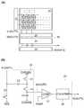
도 15는 촬상 장치를 설명하기 위한 블록 다이어그램, CDS 회로의 회로도, 및 A/D 변환 회로의 블록 다이어그램.
도 16은 촬상 장치의 구성을 설명하기 위한 상면도 및 사시도.
도 17은 촬상 장치의 구성을 설명하기 위한 단면도.
도 18은 촬상 장치의 구성을 설명하기 위한 단면도.
도 19는 촬상 장치의 구성을 설명하기 위한 단면도.
도 20은 화소를 설명하기 위한 회로도.
도 21은 화소를 설명하기 위한 회로도.
도 22는 촬상 장치의 동작을 설명하기 위한 타이밍 차트.
도 23은 화소를 설명하기 위한 회로도.
도 24는 휘어진 촬상 장치를 설명하기 위한 도면.
도 25는 트랜지스터를 설명하기 위한 상면도 및 단면도.
도 26은 트랜지스터를 설명하기 위한 상면도 및 단면도.
도 27은 트랜지스터의 채널 폭 방향의 단면을 설명하기 위한 도면.
도 28은 트랜지스터의 채널 길이 방향의 단면을 설명하기 위한 도면.
도 29는 반도체층을 설명하기 위한 상면도 및 단면도.
도 30은 트랜지스터를 설명하기 위한 상면도 및 단면도.
도 31은 트랜지스터를 설명하기 위한 상면도 및 단면도.
도 32는 트랜지스터의 채널 폭 방향의 단면을 설명하기 위한 도면.
도 33은 트랜지스터의 채널 길이 방향의 단면을 설명하기 위한 도면.
도 34는 트랜지스터를 설명하기 위한 상면도 및 단면도.
도 35는 트랜지스터를 설명하기 위한 상면도.
도 36은 산화물 반도체의 원자수비의 범위를 설명하기 위한 도면.
도 37은 InMZnO4의 결정을 설명하기 위한 도면.
도 38은 산화물 반도체의 적층 구조에서의 밴드도.
도 39는 CAAC-OS 및 단결정 산화물 반도체의 XRD에 의한 구조 해석을 설명하기 위한 도면, 및 CAAC-OS의 제한 시야 전자 회절 패턴을 나타낸 도면.
도 40은 CAAC-OS의 단면 TEM 이미지, 및 평면 TEM 이미지 및 그 화상 해석 이미지.
도 41은 nc-OS의 전자 회절 패턴을 나타낸 도면 및 nc-OS의 단면 TEM 이미지.
도 42는 a-like OS의 단면 TEM 이미지.
도 43은 In-Ga-Zn 산화물의 전자 조사에 의한 결정부의 변화를 나타낸 도면.
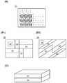
도 44는 촬상 장치가 제공된 패키지의 사시도 및 단면도.
도 45는 촬상 장치가 제공된 패키지의 사시도 및 단면도.
도 46은 전자 기기를 설명하기 위한 도면.
도 47은 X선 촬상 패널의 외관 사진 및 X선 촬상 사진.BRIEF DESCRIPTION OF THE DRAWINGS It is a figure and circuit diagram for demonstrating the pixel of an imaging device.
Fig. 2 is a diagram for explaining a pixel of an imaging device;
Fig. 3 is a cross-sectional view for explaining the configuration of an imaging device;
Fig. 4 is a cross-sectional view for explaining the configuration of an imaging device;
Fig. 5 is a cross-sectional view for explaining the configuration of an imaging device;
Fig. 6 is a cross-sectional view for explaining a connection form of a photoelectric conversion element;
Fig. 7 is a cross-sectional view for explaining a connection form of a photoelectric conversion element;
Fig. 8 is a cross-sectional view for explaining a configuration of an imaging device and a cross-sectional view for explaining a connection form of a photoelectric conversion element;
Fig. 9 is a cross-sectional view for explaining the configuration of an imaging device;
Fig. 10 is a cross-sectional view for explaining the configuration of an imaging device;
It is a figure for demonstrating the manufacturing process of an imaging device.
It is a figure for demonstrating the manufacturing process of an imaging device.
Fig. 13 is a cross-sectional view for explaining the configuration of an imaging device;
Fig. 14 is a cross-sectional view for explaining the configuration of an imaging device;
Fig. 15 is a block diagram for explaining an imaging device, a circuit diagram of a CDS circuit, and a block diagram of an A/D conversion circuit;
16 is a top view and a perspective view for explaining the configuration of an imaging device;
Fig. 17 is a cross-sectional view for explaining the configuration of an imaging device;
Fig. 18 is a cross-sectional view for explaining the configuration of an imaging device;
Fig. 19 is a cross-sectional view for explaining the configuration of an imaging device;
Fig. 20 is a circuit diagram for explaining a pixel;
Fig. 21 is a circuit diagram for explaining a pixel;
Fig. 22 is a timing chart for explaining the operation of the imaging device;
Fig. 23 is a circuit diagram for explaining a pixel;
Fig. 24 is a diagram for explaining a curved imaging device;
25 is a top view and a cross-sectional view for explaining a transistor;
26 is a top view and a cross-sectional view for explaining a transistor;
Fig. 27 is a diagram for explaining a cross section of a transistor in the channel width direction;
Fig. 28 is a view for explaining a cross section of a transistor in the channel length direction;
29 is a top view and a cross-sectional view for explaining a semiconductor layer;
30 is a top view and a cross-sectional view for explaining a transistor;
31 is a top view and a cross-sectional view for explaining a transistor;
Fig. 32 is a diagram for explaining a cross section of a transistor in the channel width direction;
Fig. 33 is a view for explaining a cross section of a transistor in the channel length direction;
34 is a top view and a cross-sectional view for explaining a transistor;
Fig. 35 is a top view for explaining a transistor;
Fig. 36 is a diagram for explaining the range of the atomic ratio of the oxide semiconductor;
37 is a diagram for explaining a crystalof InMZnO 4 .
Fig. 38 is a band diagram of an oxide semiconductor stacked structure;
Fig. 39 is a diagram for explaining structural analysis by XRD of CAAC-OS and single crystal oxide semiconductors, and a diagram showing a limited-field electron diffraction pattern of CAAC-OS;
Fig. 40 is a cross-sectional TEM image of a CAAC-OS, a planar TEM image, and an image analysis image thereof;
41 is a diagram showing an electron diffraction pattern of nc-OS and a cross-sectional TEM image of nc-OS.
42 is a cross-sectional TEM image of an a-like OS.
Fig. 43 is a view showing the change of the crystal part by electron irradiation of In-Ga-Zn oxide.
44 is a perspective view and a cross-sectional view of a package provided with an imaging device;
45 is a perspective view and a cross-sectional view of a package provided with an imaging device;
46 is a diagram for explaining an electronic device;
47 is an external photograph and an X-ray imaging photograph of the X-ray imaging panel.
실시형태에 대하여 도면을 참조하여 자세히 설명한다. 다만, 본 발명은 이하의 설명에 한정되지 않고, 본 발명의 취지 및 그 범위에서 벗어나지 않고 그 형태 및 자세한 사항을 다양하게 변경할 수 있다는 것은 당업자라면 용이하게 이해할 수 있다. 따라서, 본 발명은 이하에 기재하는 실시형태의 내용에 한정하여 해석되는 것은 아니다. 또한, 이하에 설명하는 발명의 구성에서, 동일한 부분 또는 같은 기능을 갖는 부분에는 동일한 부호를 상이한 도면들 사이에서 공통적으로 사용하고, 그 반복되는 설명은 생략하는 경우가 있다. 또한, 도면을 구성하는 같은 요소의 해칭을 상이한 도면들 사이에서 적절히 생략 또는 변경하는 경우도 있다.EMBODIMENT OF THE INVENTION Embodiment is demonstrated in detail with reference to drawings. However, the present invention is not limited to the following description, and it can be easily understood by those skilled in the art that various changes can be made in the form and details without departing from the spirit and scope of the present invention. Therefore, this invention is limited to the content of embodiment described below and is not interpreted. In addition, in the configuration of the invention described below, the same reference numerals are commonly used between different drawings for the same parts or parts having the same functions, and repeated descriptions thereof are sometimes omitted. In addition, hatching of the same elements constituting the drawings may be appropriately omitted or changed between different drawings.
또한, 제 1, 제 2로서 붙여지는 서수사는 편의상 사용되는 것이고, 공정 순서 또는 적층 순서를 나타내는 것이 아니다. 따라서, 예를 들어, "제 1"를 "제 2" 또는 "제 3" 등으로 적절히 바꿔서 설명할 수 있다. 또한, 본 명세서 등에 기재되어 있는 서수사와, 본 발명의 일 형태를 특정하기 위하여 사용되는 서수사는 일치하지 않는 경우가 있다.In addition, the ordinal numbers attached as 1st and 2nd are used for convenience, and do not represent a process order or a lamination|stacking order. Therefore, for example, "first" can be appropriately replaced with "second" or "third" and the like. In addition, the ordinal number described in this specification etc. and the ordinal number used in order to specify one aspect of this invention may not correspond.
예를 들어, 본 명세서 등에서, "X와 Y가 접속되어 있다"라고 명시적으로 기재되어 있는 경우에는, X와 Y가 전기적으로 접속되어 있는 경우와, X와 Y가 기능적으로 접속되어 있는 경우와, X와 Y가 직접 접속되어 있는 경우가 본 명세서 등에 개시되어 있는 것으로 한다. 따라서, 소정의 접속 관계, 예를 들어 도면 또는 문장에 나타낸 접속 관계에 한정되지 않고, 도면 또는 문장에 나타낸 접속 관계 외의 것도, 도면 또는 문장에 나타낸 것으로 한다.For example, in this specification or the like, when it is explicitly described as "X and Y are connected", the case where X and Y are electrically connected, the case where X and Y are functionally connected, and the A case in which , X and Y are directly connected is assumed to be disclosed in this specification and the like. Therefore, it is not limited to a predetermined connection relationship, for example, a connection relationship shown in a drawing or text, and anything other than a connection relationship shown in the drawing or text is also shown in the drawing or text.
여기서, X와 Y는, 대상물(예를 들어, 장치, 소자, 회로, 배선, 전극, 단자, 도전막, 층 등)이다.Here, X and Y are objects (eg, devices, elements, circuits, wirings, electrodes, terminals, conductive films, layers, etc.).
X와 Y가 직접 접속되어 있는 경우의 일례로서는, X와 Y의 전기적인 접속을 가능하게 하는 소자(예를 들어, 스위치, 트랜지스터, 용량 소자, 인덕터, 저항 소자, 다이오드, 표시 소자, 발광 소자, 부하 등)가 X와 Y 사이에 접속되지 않으며, X와 Y의 전기적인 접속을 가능하게 하는 소자(예를 들어, 스위치, 트랜지스터, 용량 소자, 인덕터, 저항 소자, 다이오드, 표시 소자, 발광 소자, 부하 등)를 통하지 않고 X와 Y가 접속되어 있는 경우를 들 수 있다.As an example of the case where X and Y are directly connected, an element (eg, a switch, a transistor, a capacitor, an inductor, a resistance element, a diode, a display element, a light emitting element, A load, etc.) is not connected between X and Y, and an element (for example, a switch, a transistor, a capacitor, an inductor, a resistance element, a diode, a display element, a light emitting element, There is a case where X and Y are connected without passing through a load, etc.).
X와 Y가 전기적으로 접속되어 있는 경우의 일례로서는, X와 Y의 전기적인 접속을 가능하게 하는 소자(예를 들어, 스위치, 트랜지스터, 용량 소자, 인덕터, 저항 소자, 다이오드, 표시 소자, 발광 소자, 부하 등)가 X와 Y 사이에 하나 이상 접속되는 경우를 들 수 있다. 또한, 스위치는 온/오프가 제어되는 기능을 갖는다. 즉, 스위치는 도통 상태(온 상태) 또는 비도통 상태(오프 상태)가 되어, 전류를 흘릴지 여부를 제어하는 기능을 갖는다. 또는, 스위치는 전류를 흘리는 경로를 선택하여 전환하는 기능을 갖는다. 또한, X와 Y가 전기적으로 접속되어 있는 경우에는, X와 Y가 직접 접속되어 있는 경우를 포함하는 것으로 한다.As an example of a case where X and Y are electrically connected, an element (eg, a switch, a transistor, a capacitor, an inductor, a resistance element, a diode, a display element, a light emitting element) which enables the electric connection of X and Y is possible. , load, etc.) is connected between X and Y. In addition, the switch has a function that on/off is controlled. That is, the switch has a function of controlling whether or not a current flows by being in a conduction state (on state) or in a non-conduction state (off state). Alternatively, the switch has a function of selecting and switching the path through which the current flows. In addition, the case where X and Y are electrically connected shall include the case where X and Y are directly connected.
X와 Y가 기능적으로 접속되어 있는 경우의 일례로서는, X와 Y의 기능적인 접속을 가능하게 하는 회로(예를 들어, 논리 회로(인버터, NAND 회로, NOR 회로 등), 신호 변환 회로(D/A 변환 회로, A/D 변환 회로, 감마 보정 회로 등), 전위 레벨 변환 회로(전원 회로(승압 회로, 강압 회로 등), 신호의 전위 레벨을 바꾸는 레벨 시프터 회로 등), 전압원, 전류원, 전환 회로, 증폭 회로(신호 진폭 또는 전류량 등을 크게 할 수 있는 회로, 연산 증폭기, 차동 증폭 회로, 소스 폴로어 회로, 버퍼 회로 등), 신호 생성 회로, 기억 회로, 제어 회로 등)가 X와 Y 사이에 하나 이상 접속되는 경우를 들 수 있다. 또한, 일례로서, X와 Y 사이에 다른 회로가 개재(介在)되어 있어도, X로부터 출력된 신호가 Y에 전달되는 경우에는, X와 Y는 기능적으로 접속되어 있는 것으로 한다. 또한, X와 Y가 기능적으로 접속되어 있는 경우에는, X와 Y가 직접 접속되어 있는 경우와, X와 Y가 전기적으로 접속되어 있는 경우를 포함하는 것으로 한다.As an example of the case where X and Y are functionally connected, a circuit (for example, a logic circuit (inverter, NAND circuit, NOR circuit, etc.) that enables functional connection of X and Y), a signal conversion circuit (D/ A conversion circuit, A/D conversion circuit, gamma correction circuit, etc.), potential level conversion circuit (power supply circuit (step-up circuit, step-down circuit, etc.), level shifter circuit that changes the potential level of a signal, etc.), voltage source, current source, switching circuit , amplification circuits (circuits that can increase signal amplitude or amount of current, etc., operational amplifiers, differential amplifier circuits, source follower circuits, buffer circuits, etc.), signal generation circuits, memory circuits, control circuits, etc.) are located between X and Y. A case in which more than one is connected is mentioned. In addition, as an example, even if another circuit is interposed between X and Y, when the signal output from X is transmitted to Y, X and Y shall be functionally connected. In addition, the case where X and Y are functionally connected shall include the case where X and Y are directly connected, and the case where X and Y are electrically connected.
또한, "X와 Y가 전기적으로 접속되어 있다"라고 명시적으로 기재되어 있는 경우에는, X와 Y가 전기적으로 접속되어 있는 경우(즉, X와 Y가 다른 소자 또는 다른 회로를 개재하여 접속되어 있는 경우)와, X와 Y가 기능적으로 접속되어 있는 경우(즉, X와 Y가 다른 회로를 개재하여 기능적으로 접속되어 있는 경우)와, X와 Y가 직접 접속되어 있는 경우(즉, X와 Y가 다른 소자 또는 다른 회로를 개재하지 않고 접속되어 있는 경우)가, 본 명세서 등에 기재되어 있는 것으로 한다. 즉, "전기적으로 접속되어 있다"라고 명시적으로 기재되어 있는 경우에는 단순히 "접속되어 있다"라고만 명시적으로 기재되어 있는 경우와 같은 내용이 본 명세서 등에 기재되어 있는 것으로 한다.In addition, when it is explicitly described that "X and Y are electrically connected", when X and Y are electrically connected (that is, X and Y are connected via another element or another circuit, case), when X and Y are functionally connected (that is, when X and Y are functionally connected through another circuit), and when X and Y are directly connected (that is, when X and Y are connected to each other) The case where Y is connected without interposing another element or another circuit) shall be described in this specification and the like. That is, in the case where "electrically connected" is explicitly described, the same content as the case where only "connected" is explicitly described is assumed to be described in this specification and the like.
또한, 예를 들어, 트랜지스터의 소스(또는 제 1 단자 등)가 Z1을 통하여(또는 통하지 않고) X와 전기적으로 접속되고, 트랜지스터의 드레인(또는 제 2 단자 등)이 Z2를 통하여(또는 통하지 않고) Y와 전기적으로 접속되어 있는 경우나, 트랜지스터의 소스(또는 제 1 단자 등)가 Z1의 일부와 직접 접속되고 Z1의 다른 일부가 X와 직접 접속되고, 트랜지스터의 드레인(또는 제 2 단자 등)이 Z2의 일부와 직접 접속되고 Z2의 다른 일부가 Y와 직접 접속되어 있는 경우에는, 이하와 같이 표현할 수 있다.Also, for example, the source (or first terminal, etc.) of the transistor is electrically connected to X through (or not through) Z1, and the drain (or second terminal, etc.) of the transistor is electrically connected through (or not through) Z2. ) is electrically connected to Y, or the source (or first terminal, etc.) of the transistor is directly connected to a part of Z1 and another part of Z1 is directly connected to X, and the drain (or second terminal, etc.) of the transistor When a part of Z2 is directly connected and another part of Z2 is directly connected to Y, it can be expressed as follows.
예를 들어, "X와 Y와 트랜지스터의 소스(또는 제 1 단자 등)와 드레인(또는 제 2 단자 등)은 서로 전기적으로 접속되어 있고, X, 트랜지스터의 소스(또는 제 1 단자 등), 트랜지스터의 드레인(또는 제 2 단자 등), Y의 순서로 전기적으로 접속되어 있다"라고 표현할 수 있다. 또는, "트랜지스터의 소스(또는 제 1 단자 등)는 X와 전기적으로 접속되고, 트랜지스터의 드레인(또는 제 2 단자 등)은 Y와 전기적으로 접속되고, X, 트랜지스터의 소스(또는 제 1 단자 등), 트랜지스터의 드레인(또는 제 2 단자 등), Y의 순서로 전기적으로 접속되어 있다"라고 표현할 수 있다. 또는, "X는 트랜지스터의 소스(또는 제 1 단자 등)와 드레인(또는 제 2 단자 등)을 통하여 Y와 전기적으로 접속되고, X, 트랜지스터의 소스(또는 제 1 단자 등), 트랜지스터의 드레인(또는 제 2 단자 등), Y의 순서로 접속되어 있다"라고 표현할 수 있다. 이들의 예와 같은 표현 방법을 사용하여, 회로 구성에서의 접속의 순서에 대하여 규정함으로써, 트랜지스터의 소스(또는 제 1 단자 등)와 드레인(또는 제 2 단자 등)을 구별하여, 기술적 범위를 결정할 수 있다.For example, "X and Y and the source (or first terminal, etc.) and drain (or second terminal, etc.) of the transistor are electrically connected to each other, and X, the source (or the first terminal, etc.) of the transistor, the transistor is electrically connected in the order of the drain (or the second terminal, etc.) of Or, "the source (or first terminal, etc.) of the transistor is electrically connected to X, the drain (or second terminal, etc.) of the transistor is electrically connected to Y, and X, the source (or first terminal, etc.) of the transistor ), the drain (or the second terminal, etc.) of the transistor, and are electrically connected in the order of Y". Or, "X is electrically connected to Y through the source (or first terminal, etc.) and drain (or second terminal, etc.) of the transistor, and X, the source (or first terminal, etc.) of the transistor, the drain ( or the second terminal, etc.) and connected in the order of Y". Using the same method of expression as in these examples, by specifying the sequence of connections in the circuit configuration, the source (or first terminal, etc.) and drain (or second terminal, etc.) of the transistor are distinguished and the technical scope is determined can
또는, 다른 표현 방법으로서, 예를 들어, "트랜지스터의 소스(또는 제 1 단자 등)는 적어도 제 1 접속 경로를 통하여 X와 전기적으로 접속되고, 상기 제 1 접속 경로는 제 2 접속 경로를 갖지 않고, 상기 제 2 접속 경로는 트랜지스터를 통한 트랜지스터의 소스(또는 제 1 단자 등)와 트랜지스터의 드레인(또는 제 2 단자 등) 사이의 경로이고, 상기 제 1 접속 경로는 Z1을 통한 경로이고, 트랜지스터의 드레인(또는 제 2 단자 등)은 적어도 제 3 접속 경로를 통하여 Y와 전기적으로 접속되고, 상기 제 3 접속 경로는 상기 제 2 접속 경로를 갖지 않고, 상기 제 3 접속 경로는 Z2를 통한 경로이다"라고 표현할 수 있다. 또는, "트랜지스터의 소스(또는 제 1 단자 등)는 적어도 제 1 접속 경로에 의하여 Z1을 통하여 X와 전기적으로 접속되고, 상기 제 1 접속 경로는 제 2 접속 경로를 갖지 않고, 상기 제 2 접속 경로는 트랜지스터를 통한 접속 경로를 갖고, 트랜지스터의 드레인(또는 제 2 단자 등)은 적어도 제 3 접속 경로에 의하여 Z2를 통하여 Y와 전기적으로 접속되고, 상기 제 3 접속 경로는 상기 제 2 접속 경로를 갖지 않는다"라고 표현할 수 있다. 또는, "트랜지스터의 소스(또는 제 1 단자 등)는 적어도 제 1 전기적 경로에 의하여 Z1을 통하여 X와 전기적으로 접속되고, 상기 제 1 전기적 경로는 제 2 전기적 경로를 갖지 않고, 상기 제 2 전기적 경로는 트랜지스터의 소스(또는 제 1 단자 등)로부터 트랜지스터의 드레인(또는 제 2 단자 등)으로의 전기적 경로이고, 트랜지스터의 드레인(또는 제 2 단자 등)은 적어도 제 3 전기적 경로에 의하여 Z2를 통하여 Y와 전기적으로 접속되고, 상기 제 3 전기적 경로는 제 4 전기적 경로를 갖지 않고, 상기 제 4 전기적 경로는 트랜지스터의 드레인(또는 제 2 단자 등)으로부터 트랜지스터의 소스(또는 제 1 단자 등)로의 전기적 경로이다"라고 표현할 수 있다. 이들의 예와 같은 표현 방법을 사용하여, 회로 구성에서의 접속 경로에 대하여 규정함으로써, 트랜지스터의 소스(또는 제 1 단자 등)와 드레인(또는 제 2 단자 등)을 구별하여, 기술적 범위를 결정할 수 있다.Or, as another way of expression, for example, "a source (or a first terminal, etc.) of a transistor is electrically connected to X through at least a first connection path, wherein the first connection path does not have a second connection path, and , the second connection path is a path between the source (or first terminal, etc.) of the transistor and the drain (or second terminal, etc.) of the transistor through the transistor, the first connection path is a path through Z1, the drain (or the second terminal, etc.) is electrically connected to Y through at least a third connection path, the third connection path does not have the second connection path, and the third connection path is a path through Z2" can be expressed as or "the source (or first terminal, etc.) of the transistor is electrically connected to X through Z1 by at least a first connection path, the first connection path does not have a second connection path, and the second connection path has a connection path through the transistor, the drain (or second terminal, etc.) of the transistor is electrically connected to Y through Z2 by at least a third connection path, wherein the third connection path does not have the second connection path It can be expressed as "not or "the source (or first terminal, etc.) of the transistor is electrically connected to X through Z1 by at least a first electrical path, wherein the first electrical path does not have a second electrical path, and the second electrical path is the electrical path from the source (or first terminal, etc.) of the transistor to the drain (or second terminal, etc.) of the transistor, and the drain (or second terminal, etc.) of the transistor is Y through Z2 by at least a third electrical path wherein the third electrical path does not have a fourth electrical path and the fourth electrical path is an electrical path from the drain (or second terminal, etc.) of the transistor to the source (or first terminal, etc.) of the transistor is" can be expressed. By specifying the connection path in the circuit configuration using the same expression method as in these examples, the source (or first terminal, etc.) and drain (or second terminal, etc.) of the transistor can be distinguished and the technical scope can be determined. have.
또한, 이들의 표현 방법은 일례이며, 이들의 표현 방법에 한정되지 않는다. 여기서, X, Y, Z1, 및 Z2는 대상물(예를 들어, 장치, 소자, 회로, 배선, 전극, 단자, 도전막, 또는 층 등)인 것으로 한다.In addition, these expression methods are an example, and are not limited to these expression methods. Here, it is assumed that X, Y, Z1, and Z2 are objects (eg, devices, elements, circuits, wirings, electrodes, terminals, conductive films, or layers).
또한, 회로도에서는 독립되어 있는 구성 요소들이 전기적으로 접속되어 있는 것처럼 도시되어 있어도, 하나의 구성 요소가 복수의 구성 요소의 기능도 갖는 경우가 있다. 예를 들어, 배선의 일부가 전극으로서도 기능하는 경우에는, 하나의 도전막이 배선 및 전극 양쪽의 구성 요소의 기능을 갖고 있다. 따라서, 본 명세서에서 "전기적으로 접속"이란, 이와 같이, 하나의 도전막이 복수의 구성 요소의 기능을 갖는 경우도 그 범주에 포함된다.In addition, although independent components are shown as being electrically connected in a circuit diagram, one component may also have the function of several components. For example, when a part of wiring also functions as an electrode, one conductive film has the function of both the wiring and the electrode. Accordingly, in the present specification, "electrically connected" also includes a case in which one conductive film has the function of a plurality of components as described above.
또한, "막"이라는 용어와 "층"이라는 용어는 경우 또는 상황에 따라 서로 바꿀 수 있다. 예를 들어, "도전층"이라는 용어를 "도전막"이라는 용어로 바꿀 수 있는 경우가 있다. 또는, 예를 들어, "절연막"이라는 용어를 "절연층"이라는 용어로 바꿀 수 있는 경우가 있다.In addition, the terms "film" and "layer" may be used interchangeably depending on the case or situation. For example, the term "conductive layer" may be replaced with the term "conductive film" in some cases. Alternatively, for example, the term “insulating film” may be replaced with the term “insulating layer” in some cases.
또한, 일반적으로 전위(전압)는 상대적인 것이며, 기준의 전위에 대한 상대적인 크기에 따라 크기가 결정된다. 따라서, "접지", "GND", "그라운드" 등이라고 기재되어 있는 경우에도, 전위는 반드시 0V로 한정되는 것은 아니다. 예를 들어, 회로에서 가장 낮은 전위를 기준으로 하여, "접지"나 "GND"를 정의하는 경우도 있다. 또는, 회로에서 중간 정도의 전위를 기준으로 하여, "접지"나 "GND"를 정의하는 경우도 있다. 그 경우에는, 그 전위를 기준으로 하여, 양의 전위와 음의 전위가 규정된다.In addition, in general, the potential (voltage) is relative, and the magnitude is determined according to the magnitude relative to the potential of the reference. Therefore, even when "ground", "GND", "ground" and the like are described, the potential is not necessarily limited to 0V. For example, "ground" or "GND" is sometimes defined with reference to the lowest potential in a circuit. Alternatively, "ground" or "GND" may be defined based on an intermediate potential in the circuit. In that case, a positive potential and a negative potential are defined with the potential as a reference.
(실시형태 1)(Embodiment 1)
본 실시형태에서는, 본 발명의 일 형태에 따른 촬상 장치에 대하여 도면을 참조하여 설명한다.In the present embodiment, an imaging device according to one embodiment of the present invention will be described with reference to the drawings.
본 발명의 일 형태는 제 1 구조물, 제 2 구조물을 각각 제작한 후에, 제 1 구조물과 제 2 구조물을 접합함으로써, 각각이 갖는 금속층을 접합하여 3차원적으로 집적화한 촬상 장치의 구성 및 제작 방법이다.According to one aspect of the present invention, a first structure and a second structure are respectively fabricated, and then the first structure and the second structure are joined, whereby the metal layers of each are bonded to each other to form a three-dimensionally integrated imaging device configuration and manufacturing method. to be.
제 1 구조물은 실리콘을 활성층 또는 활성 영역으로 하는 트랜지스터와, 상기 트랜지스터와 전기적으로 접속되는 제 1 금속층과, 제 1 절연층을 포함하는 구성으로 할 수 있다.The first structure may include a transistor including silicon as an active layer or an active region, a first metal layer electrically connected to the transistor, and a first insulating layer.
제 2 구조물은 광전 변환 소자와, 산화물 반도체를 활성층으로 하는 트랜지스터와, 상기 트랜지스터와 전기적으로 접속되는 제 2 금속층과, 제 2 절연층을 포함하는 구성으로 할 수 있다.The second structure may include a photoelectric conversion element, a transistor including an oxide semiconductor as an active layer, a second metal layer electrically connected to the transistor, and a second insulating layer.
또는, 제 1 구조물은 실리콘을 활성층 또는 활성 영역으로 하는 제 1 트랜지스터와, 산화물 반도체를 활성층으로 하는 제 2 트랜지스터와, 제 2 트랜지스터와 전기적으로 접속되는 제 3 금속층과, 제 3 절연층을 포함하는 구성으로 하고, 제 2 구조물은 광전 변환 소자와, 상기 광전 변환 소자와 전기적으로 접속되는 제 4 금속층과, 제 4 절연층을 포함하는 구성으로 하여도 좋다.Alternatively, the first structure may include a first transistor using silicon as an active layer or an active region, a second transistor using an oxide semiconductor as an active layer, a third metal layer electrically connected to the second transistor, and a third insulating layer The second structure may be configured to include a photoelectric conversion element, a fourth metal layer electrically connected to the photoelectric conversion element, and a fourth insulating layer.
또한, 제 1 구조물, 제 2 구조물, 및 제 3 구조물을 접합시킨 구성으로 할 수도 있다.Moreover, it can also be set as the structure which joined the 1st structure, the 2nd structure, and the 3rd structure.
이 경우, 제 1 구조물은 실리콘을 활성층 또는 활성 영역으로 하는 트랜지스터와, 상기 트랜지스터와 전기적으로 접속되는 제 1 금속층과, 제 1 절연층을 포함하는 구성으로 할 수 있다. 제 2 구조물은 산화물 반도체를 활성층으로 하는 트랜지스터와, 상기 트랜지스터와 전기적으로 접속되는 제 2 금속층과, 제 3 금속층과, 제 2 절연층과, 제 3 절연층을 포함하는 구성으로 할 수 있다. 제 3 구조물은 광전 변환 소자와, 상기 광전 변환 소자와 전기적으로 접속되는 제 4 금속층과, 제 4 절연층을 포함하는 구성으로 할 수 있다.In this case, the first structure may include a transistor including silicon as an active layer or an active region, a first metal layer electrically connected to the transistor, and a first insulating layer. The second structure may include a transistor including an oxide semiconductor as an active layer, a second metal layer electrically connected to the transistor, a third metal layer, a second insulating layer, and a third insulating layer. The third structure may include a photoelectric conversion element, a fourth metal layer electrically connected to the photoelectric conversion element, and a fourth insulating layer.
상기 산화물 반도체를 활성층으로 하는 트랜지스터는 오프 전류가 작고, 촬상 장치의 화소 내에 데이터를 유지하는 메모리를 쉽게 구성할 수 있다.The transistor using the oxide semiconductor as an active layer has a small off-state current, and a memory for holding data in a pixel of an imaging device can be easily constructed.
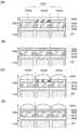
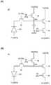
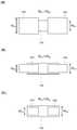
도 1의 (A)는 본 발명의 일 형태에 따른 촬상 장치가 갖는 화소(20)의 단면의 모식도이고, 도 1의 (B)는 화소(20)의 회로도이다. 또한, 도 1의 (A), (B) 등에는 트랜지스터가 n채널형인 경우의 예를 도시하였지만, 본 발명의 일 형태는 이에 한정되지 않고, 일부의 트랜지스터를 p채널형 트랜지스터로 치환하여도 좋다.FIG. 1A is a schematic diagram of a cross section of a
화소(20)에서, 광전 변환 소자(PD)의 한쪽 전극은 트랜지스터(41)의 소스 및 드레인 중 한쪽과 전기적으로 접속된다. 트랜지스터(41)의 소스 및 드레인 중 다른 쪽은 트랜지스터(42)의 소스 및 드레인 중 한쪽과 전기적으로 접속된다. 트랜지스터(41)의 소스 및 드레인 중 다른 쪽은 트랜지스터(43)의 게이트에 전기적으로 접속된다. 트랜지스터(43)의 소스 및 드레인 중 한쪽은 트랜지스터(44)의 소스 및 드레인 중 한쪽과 전기적으로 접속된다.In the
여기서, 트랜지스터(41)의 소스 및 드레인 중 다른 쪽, 트랜지스터(42)의 소스 및 드레인 중 한쪽, 트랜지스터(43)의 게이트가 접속되는 노드(FD)를 전하 검출부로 한다. 또한, 도 20의 (A)에 도시된 바와 같이, 노드(FD)에 용량 소자가 접속되는 구성이어도 좋다.Here, the other of the source and the drain of the
도 1의 (A), (B)에서, 광전 변환 소자(PD)의 다른 쪽 전극은 배선(71)(VPD)과 전기적으로 접속된다. 트랜지스터(42)의 소스 및 드레인 중 다른 쪽은 배선(72)(VRS)과 전기적으로 접속된다. 트랜지스터(43)의 소스 및 드레인 중 다른 쪽은 배선(73)(VPI)과 전기적으로 접속된다. 트랜지스터(44)의 소스 및 드레인 중 다른 쪽은 배선(91)(OUT1)과 전기적으로 접속된다.In FIGS. 1A and 1B , the other electrode of the photoelectric conversion element PD is electrically connected to the wiring 71 (VPD). The other of the source and drain of the
또한, 도 1의 (A), (B)에 도시된 요소(트랜지스터, 광전 변환 소자 등)와 배선의 접속 형태는 일례이며, 각각의 요소가 상이한 배선과 전기적으로 접속되는 경우나, 복수의 요소가 동일한 배선과 전기적으로 접속되는 경우도 있다.In addition, the connection form of the element (transistor, photoelectric conversion element, etc.) and wiring shown in FIG. 1(A), (B) is an example, When each element is electrically connected with different wiring, or a plurality of elements may be electrically connected to the same wiring.
배선(71)(VPD), 배선(72)(VRS), 및 배선(73)(VPI)은 전원선으로서의 기능을 가질 수 있다. 예를 들어, 배선(71)(VPD)은 저전위 전원선으로서 기능시킬 수 있다. 배선(72)(VRS) 및 배선(73)(VPI)은 고전위 전원선으로서 기능시킬 수 있다.The wiring 71 (VPD), the wiring 72 (VRS), and the wiring 73 (VPI) may have a function as a power supply line. For example, the wiring 71 (VPD) can function as a low potential power supply line. The wiring 72 (VRS) and the wiring 73 (VPI) can function as high potential power lines.
트랜지스터(41)의 게이트는 배선(61)(TX)과 전기적으로 접속된다. 트랜지스터(42)의 게이트는 배선(62)(RS)과 전기적으로 접속된다. 트랜지스터(44)의 게이트는 배선(63)(SE)과 전기적으로 접속된다.The gate of the
배선(61)(TX), 배선(62)(RS), 및 배선(63)(SE)은 각각이 접속되는 트랜지스터의 도통을 제어하는 신호선으로서 기능시킬 수 있다.The wiring 61 (TX), the wiring 62 (RS), and the wiring 63 (SE) can each function as a signal line for controlling the conduction of the connected transistor.
트랜지스터(41)는 광전 변환 소자(PD)의 음극의 전위를 노드(FD)에 전송하기 위한 트랜지스터로서 기능시킬 수 있다. 트랜지스터(42)는 노드(FD)의 전위를 리셋하기 위한 트랜지스터로서 기능시킬 수 있다. 트랜지스터(43)는 노드(FD)의 전위에 대응한 출력을 수행하기 위한 트랜지스터로서 기능시킬 수 있다. 트랜지스터(44)는 화소(20)를 선택하기 위한 트랜지스터로서 기능시킬 수 있다.The
또한, 상술한 화소(20)의 구성은 일례이며, 일부의 회로, 일부의 트랜지스터, 일부의 용량 소자, 또는 일부의 배선 등이 포함되지 않는 경우도 있다. 또는, 상술한 구성에 포함되지 않는 회로, 트랜지스터, 용량 소자, 배선 등이 포함되는 경우도 있다. 또한, 일부의 배선의 접속 형태가 상술한 구성과 상이한 경우도 있다.In addition, the configuration of the
본 발명의 일 형태에 따른 촬상 장치는 도 1의 (A)에 도시된 바와 같이, 층(1100), 층(1200), 및 층(1300)을 갖는다.An imaging device according to one embodiment of the present invention has a
층(1100)은 광전 변환 소자(PD)를 갖는 구성으로 할 수 있다. 광전 변환 소자(PD)에는, 예를 들어, 2개의 단자를 갖는 포토다이오드를 사용할 수 있다. 상기 포토다이오드로서는, 단결정 실리콘 기판을 사용한 pn형 포토다이오드, 비정질 실리콘 박막, 미결정 실리콘 박막, 또는 다결정 실리콘 박막을 사용한 pin형 포토다이오드, 셀레늄 또는 셀레늄의 화합물, 또는 유기 화합물을 사용한 포토다이오드 등을 사용할 수 있다.The
층(1200)은 트랜지스터(41) 및 트랜지스터(42)를 갖는 구성으로 할 수 있다. 트랜지스터(41) 및 트랜지스터(42)로서는, 산화물 반도체를 활성층으로 하는 트랜지스터(이하, OS 트랜지스터)를 사용하는 것이 바람직하다. 또한, 층(1200)은 트랜지스터(41)의 소스 및 드레인 중 한쪽 및 트랜지스터(42)의 소스 및 드레인 중 한쪽과 전기적으로 접속되는 금속층(401b)을 갖는다.The
OS 트랜지스터는 매우 낮은 오프 전류 특성을 갖는다. 따라서, 트랜지스터(41) 및 트랜지스터(42)의 낮은 오프 전류 특성에 의하여, 노드(FD)에서 전하를 유지할 수 있는 기간을 매우 길게 할 수 있다. 따라서, 회로 구성이나 동작 방법을 복잡하게 하지 않고, 모든 화소에서 동시에 전하의 축적 동작을 수행하는 글로벌 셔터 방식을 적용할 수 있다. 또한, 본 발명의 일 형태에 따른 촬상 장치는 롤링 셔터 방식으로 동작시킬 수도 있다.OS transistors have very low off-current characteristics. Accordingly, due to the low off-current characteristics of the
OS 트랜지스터는 실리콘을 활성 영역 또는 활성층에 사용한 트랜지스터(이하, Si 트랜지스터)보다 전기 특성 변동의 온도 의존성이 작기 때문에, 매우 넓은 온도 범위에서 사용할 수 있다. 따라서, OS 트랜지스터를 갖는 촬상 장치 및 반도체 장치는 자동차, 항공기, 우주선 등에도 탑재하기 적합하다.Since the OS transistor has a smaller temperature dependence of electrical characteristic variation than a transistor using silicon for the active region or active layer (hereinafter referred to as a Si transistor), it can be used over a very wide temperature range. Accordingly, the imaging device and semiconductor device having the OS transistor are suitable for mounting in automobiles, aircraft, spacecraft, and the like.
또한, OS 트랜지스터는 Si 트랜지스터보다 드레인 내압이 높은 특성을 갖는다. 셀레늄계 재료를 광전 변환층에 사용한 광전 변환 소자에서는, 애벌란시 증배를 이용하기 위하여 비교적 높은 전압(예를 들어, 10V 이상)을 인가하여 동작시키는 것이 바람직하다. 따라서, 셀레늄계 재료를 광전 변환층에 사용한 광전 변환 소자를 OS 트랜지스터와 조합함으로써, 신뢰성이 높은 촬상 장치로 할 수 있다.In addition, the OS transistor has a higher drain withstand voltage than the Si transistor. In the photoelectric conversion element using a selenium-based material for the photoelectric conversion layer, it is preferable to apply and operate a relatively high voltage (eg, 10 V or more) in order to utilize avalanche multiplication. Therefore, by combining the photoelectric conversion element which used the selenium type material for the photoelectric conversion layer with the OS transistor, it can be set as an imaging device with high reliability.
층(1300)은 트랜지스터(43) 및 트랜지스터(44)를 갖는 구성으로 할 수 있다. 트랜지스터(43), 트랜지스터(44)에는, 실리콘을 활성층 또는 활성 영역으로 하는 트랜지스터를 사용하는 것이 바람직하다. 실리콘을 활성층 또는 활성 영역으로 하는 트랜지스터는 온 전류가 크고, 노드(FD)의 전위를 효율적으로 증폭할 수 있다. 또한, 층(1200)은 트랜지스터(44)의 게이트와 전기적으로 접속되는 금속층(401a)을 갖는다.The
도 1의 (A)에 도시된 바와 같이, 금속층(401a) 및 금속층(401b)은 각각이 직접 접촉하는 위치에 제공되고, 금속층(401a) 및 금속층(401b)은 도통하는 접속부(401)를 갖는 구성으로 한다.As shown in Fig. 1A, the
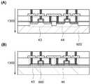
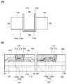
또한, 본 발명의 일 형태에 따른 촬상 장치는 도 2의 (A)에 도시된 구성을 가져도 좋다.Further, the imaging device according to one embodiment of the present invention may have the configuration shown in FIG. 2A .
도 2의 (A)에 도시된 구성에서는, 층(1100)은 광전 변환 소자(PD)와, 광전 변환 소자(PD)의 한쪽 전극과 전기적으로 접속되는 금속층(402b)과, 광전 변환 소자(PD)의 다른 쪽 전극과 전기적으로 접속되는 금속층(403b)을 갖는다. 또한, 금속층(403b)은 층(1100)에 제공되지 않아도 된다.In the configuration shown in FIG. 2A , the
층(1200)은 트랜지스터(41)와, 트랜지스터(42)와, 트랜지스터(41)의 소스 및 드레인 중 한쪽과 전기적으로 접속되는 금속층(402a)과, 배선(71)과 전기적으로 접속되는 금속층(403a)을 갖는다. 또한, 배선(71) 및 금속층(403a)은 층(1200)에 제공되지 않아도 된다.The
층(1300)은 트랜지스터(43) 및 트랜지스터(44)를 갖는다.
도 2의 (A)에 도시된 바와 같이, 금속층(402a) 및 금속층(402b)은 각각이 직접 접촉하는 위치에 제공되고, 금속층(402a) 및 금속층(402b)은 도통하는 접속부(402)를 갖는 구성으로 한다. 또한, 금속층(403a) 및 금속층(403b)은 각각이 직접 접촉하는 위치에 제공되고, 금속층(403a) 및 금속층(403b)은 도통하는 접속부(403)를 갖는 구성으로 한다.As shown in FIG. 2A, the
또한, 본 발명의 일 형태에 따른 촬상 장치는 도 2의 (B)에 도시된 구성을 가져도 좋다.In addition, the imaging device which concerns on one aspect of this invention may have the structure shown in FIG.2(B).
도 2의 (B)에 도시된 구성에서는, 층(1100)은 광전 변환 소자(PD)와, 광전 변환 소자(PD)의 한쪽 전극과 전기적으로 접속되는 금속층(402b)과, 광전 변환 소자(PD)의 다른 쪽 전극과 전기적으로 접속되는 금속층(403b)을 갖는다. 또한, 금속층(403b)은 층(1100)에 제공되지 않아도 된다.In the configuration shown in FIG. 2B , the
층(1200)은 트랜지스터(41)와, 트랜지스터(42)와, 트랜지스터(41)의 소스 및 드레인 중 한쪽과 전기적으로 접속되는 금속층(402a)과, 배선(71)과 전기적으로 접속되는 금속층(403a)과, 트랜지스터(41)의 소스 및 드레인 중 한쪽 및 트랜지스터(42)의 소스 및 드레인 중 한쪽과 전기적으로 접속되는 금속층(401b)을 갖는다. 또한, 배선(71) 및 금속층(403a)은 층(1200)에 제공되지 않아도 된다.The
층(1300)은 트랜지스터(43)와, 트랜지스터(44)와, 트랜지스터(43)의 게이트와 전기적으로 접속되는 금속층(401a)을 갖는다.The
도 2의 (B)에 도시된 바와 같이, 금속층(402a) 및 금속층(402b)은 각각이 직접 접촉하는 위치에 제공되고, 금속층(402a) 및 금속층(402b)은 도통하는 접속부(402)를 갖는 구성으로 한다. 또한, 금속층(403a) 및 금속층(403b)은 각각이 직접 접촉하는 위치에 제공되고, 금속층(403a) 및 금속층(403b)은 도통하는 접속부(403)를 갖는 구성으로 한다. 또한, 금속층(401a) 및 금속층(401b)은 각각이 직접 접촉하는 위치에 제공되고, 금속층(401a) 및 금속층(401b)은 도통하는 접속부(401)를 갖는 구성으로 한다.As shown in FIG. 2B, the
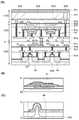
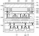
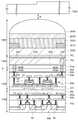
도 3의 (A), (B), (C)는 도 1의 (A)에 대응하는 화소(20)의 구체적인 구성을 설명하기 위한 도면이다. 도 3의 (A)는 트랜지스터(41), 트랜지스터(42), 트랜지스터(43), 트랜지스터(44)의 채널 길이 방향을 나타내는 단면도이다. 도 3의 (B)는 도 3의 (A)에서의 일점쇄선 X1-X2를 따라 자른 단면도이고, 트랜지스터(41)의 채널 폭 방향의 단면을 도시한 것이다. 도 3의 (C)는 도 3의 (A)에서의 일점쇄선 Y1-Y2를 따라 자른 단면도이고, 트랜지스터(42)의 채널 폭 방향의 단면을 도시한 것이다.3A, 3B, and 3C are diagrams for explaining a specific configuration of the
본 실시형태에서 설명하는 단면도에서는, 배선, 전극, 금속층, 및 콘택트 플러그(도전체(82))를 별개의 요소로서 도시하였지만, 이들이 전기적으로 접속되어 있는 경우에는, 하나의 요소로서 제공되는 경우도 있다. 또한, 배선, 전극, 및 금속층 등의 요소가 도전체(82)를 통하여 접속되는 형태는 일례이며, 각 요소가 도전체(82)를 통하지 않고 직접 접속되는 경우도 있다.In the cross-sectional view described in this embodiment, the wiring, the electrode, the metal layer, and the contact plug (conductor 82) are shown as separate elements, but when they are electrically connected, they are provided as one element. have. In addition, the form in which elements, such as wiring, an electrode, and a metal layer, are connected via the
트랜지스터 등의 각 요소 위에는 보호막, 층간 절연막, 또는 평탄화막으로서의 기능을 갖는 절연층(81a) 내지 절연층(81j) 등이 제공된다. 예를 들어, 절연층(81a) 내지 절연층(81j)에는 산화 실리콘막, 산화 질화 실리콘막 등의 무기 절연막을 사용할 수 있다. 또는, 아크릴 수지, 폴리이미드 수지 등의 유기 절연막 등을 사용하여도 좋다. 절연층(81a) 내지 절연층(81j) 등의 상면은 필요에 따라 CMP(Chemical Mechanical Polishing)법 등으로 평탄화 처리가 수행되는 것이 바람직하다.On each element such as a transistor, an insulating
또한, 도면에 도시된 배선 등의 일부가 제공되지 않는 경우나, 도면에 도시되지 않은 배선이나 트랜지스터 등이 각 층에 포함되는 경우도 있다. 또한, 도면에 도시되지 않은 층이 포함되는 경우도 있다. 또한, 도면에 도시된 층의 일부가 포함되지 않는 경우도 있다.In addition, there are cases in which a part of wirings shown in the drawings are not provided, or wirings, transistors, etc. not shown in the drawings are sometimes included in each layer. In addition, there are cases where a layer not shown in the drawings is included. In addition, there are cases where some of the layers shown in the drawings are not included.
OS 트랜지스터가 형성되는 영역과 Si 디바이스(Si 트랜지스터 또는 Si 포토다이오드)가 형성되는 영역 사이에는 절연층(80a), 절연층(80b)이 제공된다.An insulating
트랜지스터(43), 트랜지스터(44)의 활성 영역 근방에 제공되는 절연층 내의 수소는 실리콘의 댕글링 본드를 종단한다. 따라서, 상기 수소는 트랜지스터(43), 트랜지스터(44)의 신뢰성을 향상시키는 효과가 있다. 한편, 트랜지스터(41), 트랜지스터(42)의 활성층인 산화물 반도체층의 근방에 제공되는 절연층 내의 수소는 산화물 반도체층 내에 캐리어를 생성하는 요인 중 하나가 된다. 그러므로, 상기 수소는 트랜지스터(41), 트랜지스터(42)의 신뢰성을 저하시키는 요인이 되는 경우가 있다. 따라서, Si 트랜지스터를 갖는 한쪽 층과 OS 트랜지스터를 갖는 다른 쪽 층을 적층하는 경우, 이들 사이에 수소의 확산을 방지하는 기능을 갖는 절연층(80b)을 제공하는 것이 바람직하다. 절연층(80b)에 의하여 수소를 한쪽 층에 가둠으로써 트랜지스터(43), 트랜지스터(44)의 신뢰성을 향상시킬 수 있다. 또한, 한쪽 층으로부터 다른 쪽 층으로의 수소의 확산이 억제됨으로써 트랜지스터(41), 트랜지스터(42)의 신뢰성도 향상시킬 수 있다. 또한, 상기와 같은 이유로, Si 포토다이오드를 갖는 한쪽 층과 OS 트랜지스터를 갖는 다른 쪽 층 사이에 수소의 확산을 방지하는 기능을 갖는 절연층(80a)을 제공하는 것이 바람직하다.
절연층(80a), 절연층(80b)으로서는, 예를 들어, 산화 알루미늄, 산화 질화 알루미늄, 산화 갈륨, 산화 질화 갈륨, 산화 이트륨, 산화 질화 이트륨, 산화 하프늄, 산화 질화 하프늄, 이트리아 안정화 지르코니아(YSZ) 등을 사용할 수 있다.As the insulating
도 3의 (A)에서, 층(1100)이 갖는 광전 변환 소자(PD)는 단결정 실리콘 기판을 사용한 pn형 포토다이오드를 나타낸다. 상기 광전 변환 소자(PD)는 p+영역(620), p-영역(630), n형 영역(640), p+영역(650)을 갖는 구성으로 할 수 있다.In FIG. 3A , the photoelectric conversion element PD included in the
n형 영역(640)은 금속층(405)과 전기적으로 접속된다. 또한, p+영역(650)은 금속층(406)과 전기적으로 접속된다. 금속층(405) 및 금속층(406)은 절연층(81g)을 관통하여 제공된다.The n-
층(1200)에는 OS 트랜지스터인 트랜지스터(41) 및 트랜지스터(42)가 제공된다. 트랜지스터(41), 트랜지스터(42)가 모두 백 게이트를 갖는 구성을 도시하였지만, 일부의 트랜지스터, 예를 들어, 트랜지스터(41)만이 백 게이트를 갖는 형태이어도 좋다. 상기 백 게이트는 도 3의 (B)에 도시된 바와 같이 대향하도록 제공되는 트랜지스터의 프런트 게이트와 전기적으로 접속되는 경우가 있다. 또는, 프런트 게이트와 상이한 고정 전위를 상기 백 게이트에 공급할 수 있는 구성으로 하여도 좋다.
금속층(401b)은 절연층(81d)에 매설된 영역을 갖도록 제공되고, 도전층 및 도전체(82) 등을 통하여 트랜지스터(41)의 소스 및 드레인 중 다른 쪽 및 트랜지스터(42)의 소스 및 드레인 중 한쪽과 전기적으로 접속된다. 또한, 트랜지스터(41)의 소스 및 드레인 중 한쪽은 도전체(82) 및 도전층 등을 통하여 금속층(405)과 전기적으로 접속된다. 또한, 배선(71)은 도전체(82)를 통하여 금속층(406)과 전기적으로 접속된다.The
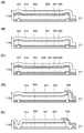
층(1300)에는, Si 트랜지스터인 트랜지스터(43) 및 트랜지스터(44)가 제공된다. 도 3의 (A)에는, 트랜지스터(43), 트랜지스터(44)가 FIN형의 구성을 갖는 예를 도시하였지만, 도 4의 (A)에 도시된 바와 같이 플레이너형이어도 좋다. 또는, 도 4의 (B)에 도시된 바와 같이, 실리콘 박막의 활성층(660)을 갖는 트랜지스터이어도 좋다. 활성층(660)은 다결정 실리콘이나 SOI(Silicon on Insulator)의 단결정 실리콘을 사용하여 형성될 수 있다.In the
금속층(401a)은 절연층(81c)에 매설된 영역을 갖도록 제공되고, 도전층 및 도전체(82) 등을 통하여 트랜지스터(43)의 게이트와 전기적으로 접속된다.The
여기서, 금속층(401a) 및 금속층(401b)에는 주성분이 동일한 금속 원소가 사용되는 것이 바람직하다. 또한, 절연층(81c) 및 절연층(81d)은 동일한 성분으로 구성되어 있는 것이 바람직하다.Here, it is preferable that a metal element having the same main component is used for the
예를 들어, 금속층(401a) 및 금속층(401b)에는, Cu, Al, Sn, Zn, W, Ag, Pt, 또는 Au 등을 사용할 수 있다. 접합하기 쉽다는 이유로, 바람직하게는 Cu, Al, W, 또는 Au를 사용한다. 또한, 절연층(81c) 및 절연층(81d)에는, 산화 실리콘, 산화 질화 실리콘, 질화 산화 실리콘, 질화 실리콘, 질화 타이타늄 등을 사용할 수 있다.For example, Cu, Al, Sn, Zn, W, Ag, Pt, Au, or the like can be used for the
금속층(401a) 및 금속층(401b) 각각에 상술한 바와 같은 금속 재료를 사용하고, 절연층(81c) 및 절연층(81d) 각각에 상술한 바와 같은 금속 재료를 사용함으로써, 도 3에 도시된 접합 위치 a에서 접합 공정을 수행할 수 있다. 상기 접합 공정에 의하여, 금속층(401a)과 금속층(401b)의 전기적인 접속을 얻을 수 있다. 또한, 절연층(81c)과 절연층(81d)의 기계적인 강도를 갖는 접속을 얻을 수 있다.By using a metal material as described above for each of the
금속층끼리를 접합하기 위해서는, 표면의 산화막 및 불순물의 흡착층 등을 스퍼터링 처리 등에 의하여 제거하고, 세정화 및 활성화한 표면끼리를 접촉시켜 접합하는 표면 활성화 접합법을 사용할 수 있다. 또는, 온도와 압력을 병용하여 표면끼리를 접합하는 확산 접합법 등을 사용할 수 있다. 표면 활성화 접합법 및 확산 접합법은 모두 원자 레벨로 결합되기 때문에, 전기적으로 또한 기계적으로도 우수한 접합을 얻을 수 있다.In order to bond metal layers together, a surface activation bonding method in which an oxide film on the surface, an adsorption layer of impurities, etc. are removed by sputtering or the like, and the cleaned and activated surfaces are brought into contact with each other and joined can be used. Alternatively, a diffusion bonding method or the like in which the surfaces are joined together using temperature and pressure can be used. Since both the surface-activated bonding method and the diffusion bonding method are bonded at the atomic level, it is possible to obtain an excellent bonding electrically and mechanically.
또한, 절연층끼리를 접합하기 위해서는, 연마 등에 의하여 높은 평탄성을 얻은 후에, 산소 플라스마 등으로 친수성 처리를 수행한 표면끼리를 접합시켜 일시적으로 접합하고, 가열 처리에 의한 탈수로 제대로 접합하는 친수성 접합법 등을 사용할 수 있다. 친수성 접합법의 사용에 의해서도 원자 레벨로 결합되기 때문에, 기계적으로 우수한 접합을 얻을 수 있다.In addition, in order to bond the insulating layers to each other, after obtaining high flatness by polishing or the like, the surfaces subjected to hydrophilic treatment with oxygen plasma or the like are joined to temporarily bond, and the hydrophilic bonding method, etc. can be used Since bonding is performed at the atomic level even by the use of a hydrophilic bonding method, a mechanically excellent bonding can be obtained.
층(1300)과 층(1200)을 접합시키는 경우, 각각의 접합면에는 절연층과 금속층이 혼재되기 때문에, 예를 들어, 표면 활성화 접합법 및 친수성 접합법을 조합하여 수행하면 좋다.In the case of bonding the
예를 들어, 연마 후에 표면을 세정화하고, 금속층의 표면에 산화 방지 처리를 수행하고 나서, 친수성 처리를 수행하여 접합하는 방법 등을 사용할 수 있다. 또한, 금속층의 표면을 Au 등의 난(難)산화성 금속으로 하여 친수성 처리를 수행하여도 좋다. 또한, 상술한 방법 외의 접합 방법을 사용하여도 좋다.For example, a method in which the surface is cleaned after polishing, an antioxidation treatment is performed on the surface of the metal layer, and then hydrophilic treatment is performed for bonding, or the like can be used. Further, the surface of the metal layer may be subjected to hydrophilic treatment by making the surface of the metal layer difficult to oxidize such as Au. Moreover, you may use the joining method other than the method mentioned above.
접합법은 각 디바이스가 완성된 후에 수행되기 때문에, OS 트랜지스터 및 Si 트랜지스터를 각각에 최적인 공정을 사용하여 제작할 수 있다. 따라서, 각 트랜지스터의 전기 특성 및 신뢰성을 높일 수 있다. 또한, 접합은 각 톱 게이트형 트랜지스터를 완성시킨 후에 수행되기 때문에, OS 트랜지스터의 프런트 게이트 전극 및 Si 트랜지스터의 게이트 전극은 상면이 서로 대향하도록 배치된다.Since the bonding method is performed after each device is completed, the OS transistor and the Si transistor can be manufactured using a process optimal for each. Accordingly, the electrical characteristics and reliability of each transistor can be improved. In addition, since bonding is performed after completing each top-gate transistor, the front gate electrode of the OS transistor and the gate electrode of the Si transistor are arranged so that their top surfaces face each other.
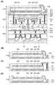
또한, 화소(20)는 도 5에 도시된 적층 구성으로 할 수도 있다. 도 5에 도시된 화소(20)는 도 3의 (A)에 도시된 화소(20)와 층(1100)만이 상이하고, 그 외의 구성은 같다.Also, the
도 5에서, 층(1100)이 갖는 광전 변환 소자(PD)는 광전 변환층에 셀레늄을 사용한 포토다이오드를 나타낸다. 상기 광전 변환 소자(PD)는 광전 변환층(561), 투광성 도전층(562), 전극(566), 격벽(567), 배선(571)을 갖는 구성으로 할 수 있다.In FIG. 5 , the photoelectric conversion element PD included in the
전극(566)은 금속층(405)과 전기적으로 접속된다. 또한, 투광성 도전층(562)은 배선(571)을 통하여 금속층(406)과 전기적으로 접속된다. 금속층(405) 및 금속층(406)은 절연층(81g)을 관통하여 제공된다.The
도 5에는 셀레늄계 재료를 광전 변환층(561)에 사용한 형태를 도시하였다. 셀레늄계 재료를 사용한 광전 변환 소자(PD)는 가시광에 대한 외부 양자 효율이 높은 특성을 갖는다. 또한, 셀레늄계 재료는 광 흡수 계수가 높기 때문에, 광전 변환층(561)을 얇게 하기 쉽다는 이점이 있다. 셀레늄계 재료를 사용한 광전 변환 소자(PD)는 애벌란시 증배에 의하여 증폭이 큰 고감도 센서로 할 수 있다. 즉, 셀레늄계 재료를 광전 변환층(561)에 사용함으로써, 화소 면적이 축소하더라도 충분한 광 전류를 얻을 수 있다. 따라서, 셀레늄계 재료를 사용한 광전 변환 소자(PD)는 저조도 환경에서의 촬상에도 적합하다고 할 수 있다.5 illustrates a form in which a selenium-based material is used for the
셀레늄계 재료로서는, 비정질 셀레늄 또는 결정 셀레늄을 사용할 수 있다. 결정 셀레늄은 예를 들어, 비정질 셀레늄을 성막한 후에 가열 처리를 수행함으로써 얻을 수 있다. 결정 셀레늄의 결정 입경을 화소 피치보다 작게 함으로써 화소마다의 특성의 편차를 저감시킬 수 있다. 또한, 결정 셀레늄은 비정질 셀레늄보다 가시광에 대한 분광 감도나 광 흡수 계수가 높은 특성을 갖는다.As the selenium-based material, amorphous selenium or crystalline selenium can be used. Crystalline selenium can be obtained, for example, by performing heat treatment after forming amorphous selenium into a film. By making the crystal grain size of crystalline selenium smaller than the pixel pitch, it is possible to reduce variations in characteristics for each pixel. In addition, crystalline selenium has a higher spectral sensitivity to visible light or a higher light absorption coefficient than amorphous selenium.
도 5에는, 광전 변환층(561)을 단층으로서 도시하였지만, 도 6의 (A)에 도시된 바와 같이 수광면 측에 정공 주입 저지층(568)으로서 산화 갈륨, 산화 세륨, 또는 In-Ga-Zn 산화물 등을 제공하여도 좋다. 또는, 도 6의 (B)에 도시된 바와 같이, 전극(566) 측에 전자 주입 저지층(569)으로서 산화 니켈 또는 황화 안티모니 등을 제공하여도 좋다. 또는, 도 6의 (C)에 도시된 바와 같이 정공 주입 저지층(568) 및 전자 주입 저지층(569)을 제공하는 구성으로 하여도 좋다.Although the
광전 변환층(561)은 구리, 인듐, 및 셀레늄의 화합물(CIS)을 포함하는 층이어도 좋다. 또는 구리, 인듐, 갈륨, 및 셀레늄의 화합물(CIGS)을 포함하는 층이어도 좋다. CIS 및 CIGS에서는 셀레늄의 단층과 마찬가지로 애벌란시 증배를 이용하는 광전 변환 소자를 형성할 수 있다.The
셀레늄계 재료를 사용한 광전 변환 소자(PD)는 예를 들어, 금속 재료 등으로 형성된 전극(566)과 투광성 도전층(562) 사이에 광전 변환층(561)을 갖는 구성으로 할 수 있다. 또한, CIS 및 CIGS는 p형 반도체이고, 접합을 형성하기 위하여 n형 반도체인 황화 카드뮴이나 황화 아연 등을 이와 접촉하도록 제공하여도 좋다.The photoelectric conversion element PD using the selenium-based material can have a configuration in which, for example, a
도 5에서는 투광성 도전층(562)과 배선(571)이 직접 접촉하는 구성으로 하였지만, 도 6의 (D)에 도시된 바와 같이 배선(588)을 개재하여 양쪽이 접촉하는 구성으로 하여도 좋다. 또한, 도 5에서는 광전 변환층(561) 및 투광성 도전층(562)을 화소 회로 사이에서 분리하지 않는 구성으로 하였지만, 도 6의 (E)에 도시된 바와 같이 회로 사이에서 이들을 분리하는 구성으로 하여도 좋다. 또한, 화소 사이에서 전극(566)을 갖지 않는 영역에는 절연체로 이루어진 격벽(567)을 형성함으로써 광전 변환층(561) 및 투광성 도전층(562)에 균열이 생기지 않도록 하는 것이 바람직하지만, 도 7의 (A) 및 (B)에 도시된 바와 같이 격벽(567)을 제공하지 않는 구성으로 하여도 좋다.In Fig. 5, the light-transmitting
또한, 전극(566) 및 배선(571) 등은 다층으로 하여도 좋다. 예를 들어, 도 7의 (C)에 도시된 바와 같이, 전극(566)을 도전층(566a)과 도전층(566b)의 2층으로 하고, 배선(571)을 도전층(571a)과 도전층(571b)의 2층으로 할 수 있다. 도 7의 (C)에 도시된 구성에서는 예를 들어, 도전층(566a) 및 도전층(571a)을 저저항의 금속 등을 선택하여 형성하고, 도전층(566b) 및 도전층(571b)을 광전 변환층(561)과의 콘택트 특성이 좋은 금속 등을 선택하여 형성하면 좋다. 이와 같은 구성으로 함으로써, 광전 변환 소자(PD)의 전기 특성을 향상시킬 수 있다. 또한, 일부 금속은 투광성 도전층(562)과 접촉함으로써 전식(電蝕)을 일으킬 수 있다. 이와 같은 금속을 도전층(571a)에 사용한 경우에도 도전층(571b)을 개재함으로써 전식을 방지할 수 있다.In addition, the
도전층(566b) 및 도전층(571b)에는 예를 들어, 몰리브데넘이나 텅스텐 등을 사용할 수 있다. 또한, 도전층(566a) 및 도전층(571a)에는 예를 들어, 알루미늄, 타이타늄, 또는 타이타늄 사이에 알루미늄을 끼우는 적층을 사용할 수 있다.For the conductive layer 566b and the
또한, 도 7의 (D)에 도시된 바와 같이, 투광성 도전층(562)과 배선(571)은 도전체(82) 및 배선(588)을 통하여 접속되어도 좋다.Further, as shown in FIG. 7D , the light-transmitting
격벽(567)은 무기 절연체나 절연 유기 수지 등을 사용하여 형성할 수 있다. 또한, 격벽(567)은 트랜지스터 등에 대한 차광 및/또는 화소 하나당 수광부의 면적을 확정하기 위하여 흑색 등으로 착색되어 있어도 좋다.The
또한, 화소(20)는 도 8의 (A)에 도시된 적층 구성으로 할 수도 있다. 도 8의 (A)에 도시된 화소(20)는, 도 3의 (A)에 도시된 화소(20)와 층(1100)만이 상이하고, 그 외의 구성은 같다.In addition, the
도 8의 (A)에서 층(1100)이 갖는 광전 변환 소자(PD)는 광전 변환층에 비정질 실리콘막이나 미결정 실리콘막 등을 사용한 pin형 포토다이오드를 나타낸다. 상기 광전 변환 소자(PD)는 n형 반도체층(565), i형 반도체층(564), p형 반도체층(563), 전극(566), 배선(571), 배선(588)을 갖는 구성으로 할 수 있다.In FIG. 8A , the photoelectric conversion element PD included in the
전극(566)은 금속층(405)과 전기적으로 접속된다. 또한, p형 반도체층(563)은 배선(588) 및 배선(571)을 통하여 금속층(406)과 전기적으로 접속된다. 금속층(405) 및 금속층(406)은 절연층(81g)을 관통하여 제공된다.The
i형 반도체층(564)에는 비정질 실리콘을 사용하는 것이 바람직하다. 또한, p형 반도체층(563) 및 n형 반도체층(565)에는 각각의 도전형을 부여하는 도펀트를 포함하는 비정질 실리콘 또는 미결정 실리콘 등을 사용할 수 있다. 비정질 실리콘을 광전 변환층으로 하는 포토다이오드는 가시광의 파장 영역에서의 감도가 높고, 미약한 가시광을 검지하기 쉽다.It is preferable to use amorphous silicon for the i-
또한, pin형의 박막 포토다이오드의 형태를 갖는 광전 변환 소자(PD)의 구성, 및 광전 변환 소자(PD) 및 배선의 접속 형태는, 도 8의 (B), (C), (D)에 예시된 것이라도 좋다. 또한, 광전 변환 소자(PD)의 구성, 광전 변환 소자(PD)와 배선의 접속 형태는 이에 한정되지 않고, 다른 형태라도 좋다.In addition, the structure of the photoelectric conversion element PD which has the form of a pin-type thin film photodiode, and the connection form of the photoelectric conversion element PD and wiring are shown to (B), (C), (D) of FIG. It may be exemplified. In addition, the structure of the photoelectric conversion element PD and the connection form of the photoelectric conversion element PD and wiring are not limited to this, Other forms may be sufficient.
도 8의 (B)는 광전 변환 소자(PD)의 p형 반도체층(563)과 접촉하는 투광성 도전층(562)을 제공한 구성이다. 투광성 도전층(562)은 전극으로서 작용하며, 광전 변환 소자(PD)의 출력 전류를 높일 수 있다.Fig. 8B is a configuration in which a light-transmitting
투광성 도전층(562)에는, 예를 들어, 인듐 주석 산화물, 실리콘을 포함하는 인듐 주석 산화물, 아연을 포함하는 산화 인듐, 산화 아연, 갈륨을 포함하는 산화 아연, 알루미늄을 포함하는 산화 아연, 산화 주석, 플루오린을 포함하는 산화 주석, 안티모니를 포함하는 산화 주석, 그래핀 또는 산화 그래핀 등을 사용할 수 있다. 또한, 투광성 도전층(562)은 단층에 한정되지 않고, 상이한 막의 적층이어도 좋다.The light-transmitting
도 8의 (C)는 투광성 도전층(562)과 배선(571)이 도전체(82) 및 배선(588)을 통하여 접속된 구성이다. 또한, 광전 변환 소자(PD)의 p형 반도체층(563)과 배선(571)이 도전체(82) 및 배선(588)을 통하여 접속된 구성으로 할 수도 있다. 또한, 도 8의 (C)에서는 투광성 도전층(562)을 제공하지 않는 구성으로 할 수도 있다.FIG. 8C shows a configuration in which a light-transmitting
도 8의 (D)는 광전 변환 소자(PD)를 덮는 절연층(81k)에 p형 반도체층(563)이 노출되는 개구부가 제공되고, 이 개구부를 덮는 투광성 도전층(562)과 배선(571)이 전기적인 접속을 갖는 구성이다.8D shows that the insulating
상술한 셀레늄계 재료나 비정질 실리콘 등을 사용하여 형성한 광전 변환 소자(PD)는 성막 공정, 리소그래피 공정, 에칭 공정 등의 일반적인 반도체 제작 공정을 사용하여 제작할 수 있다. 또한, 셀레늄계 재료는 고저항이고, 도 5에 도시된 바와 같이 광전 변환층(561)을 회로 사이에서 분리하지 않는 구성으로 할 수도 있다. 따라서, 수율이 높고, 저렴하게 제작할 수 있다.The photoelectric conversion device PD formed using the above-described selenium-based material, amorphous silicon, or the like may be manufactured using general semiconductor manufacturing processes such as a film formation process, a lithography process, and an etching process. In addition, the selenium-based material has a high resistance, and as shown in FIG. 5 , the
또한, 도 5 및 도 8의 (A)에 도시된 화소(20)가 갖는 광전 변환 소자(PD)는 박막의 적층체이기 때문에, 접합 공정 후에 형성되는 것이 바람직하다.Further, since the photoelectric conversion element PD included in the
또한, 화소(20)는 도 9에 도시된 적층 구성으로 할 수도 있다. 도 9에 도시된 화소(20)는 층(1300) 위에 층(1200)을 형성하고, 층(1200)과 별도로 형성한 층(1100)을 접합 위치 b에서 접합시킨 구성을 갖는다. 즉, 금속층의 접합부는 도 3의 (A)의 적층 구성에서는 층(1300)과 층(1200) 사이에 제공되지만, 도 9에 도시된 적층 구성에서는 층(1200)과 층(1100) 사이에 제공된다.Also, the
도 9에서 층(1100)이 갖는 광전 변환 소자(PD)는 단결정 실리콘을 사용한 pn형 포토다이오드를 나타낸다. 상기 광전 변환 소자(PD)는 p+영역(620), p-영역(630), n형 영역(640), p+영역(650)을 갖는 구성으로 할 수 있다.In FIG. 9 , the photoelectric conversion element PD included in the
n형 영역(640)은 금속층(402b)과 전기적으로 접속된다. 또한, p+영역(650)은 금속층(403b)과 전기적으로 접속된다. 금속층(405) 및 금속층(406)은 절연층(81g)을 관통하여 제공된다.The n-
층(1200)에는 금속층(402a), 금속층(403a)이 제공된다. 금속층(402a)은 절연층(81h)에 매설된 영역을 갖도록 제공되고, 도전층 및 도전체(82) 등을 통하여 트랜지스터(41)의 소스 및 드레인 중 한쪽과 전기적으로 접속된다. 또한, 금속층(403a)은 절연층(81h)에 매설된 영역을 갖도록 제공되고, 도전체(82)를 통하여 배선(71)과 전기적으로 접속된다.The
층(1300)에는 Si 트랜지스터인 트랜지스터(43) 및 트랜지스터(44)가 제공된다. 트랜지스터(43)의 게이트는 도전층 및 도전체(82) 등을 통하여 트랜지스터(41)의 소스 및 드레인 중 다른 쪽, 및 트랜지스터(42)의 소스 및 드레인 중 한쪽과 전기적으로 접속된다.
또한, 화소(20)는 도 10에 도시된 적층 구성으로 할 수도 있다. 도 10에 도시된 화소(20)는 층(1300), 층(1200), 및 층(1100)을 개별적으로 형성하고, 층(1300)과 층(1200)을 접합 위치 a에서 접합시키고, 층(1200)과 층(1100)을 접합 위치 b에서 접합시키는 구성이다. 즉, 금속층의 접합부가 층(1300)과 층(1200) 사이 및 층(1200)과 층(1100) 사이에 제공된다.Also, the
도 10에서, 층(1100)이 갖는 광전 변환 소자(PD)는 단결정 실리콘 기판을 사용한 pn형 포토다이오드를 나타낸다. 상기 광전 변환 소자(PD)는 p+영역(620), p-영역(630), n형 영역(640), p+영역(650)을 갖는 구성으로 할 수 있다.In FIG. 10 , the photoelectric conversion element PD included in the
n형 영역(640)은 금속층(402b)과 전기적으로 접속된다. 또한, p+영역(650)은 금속층(403b)과 전기적으로 접속된다. 금속층(402a) 및 금속층(403b)은 절연층(81g)을 관통하여 제공된다.The n-
층(1200)에는 금속층(401b), 금속층(402a), 금속층(403a)이 제공된다. 금속층(401b)은 절연층(81d)에 매설된 영역을 갖도록 제공되고, 도전층 및 도전체(82) 등을 통하여 트랜지스터(41)의 소스 및 드레인 중 다른 쪽, 및 트랜지스터(42)의 소스 및 드레인 중 한쪽과 전기적으로 접속된다. 금속층(402a)은 절연층(81g)에 매설된 영역을 갖도록 제공되고, 도전층 및 도전체(82) 등을 통하여 트랜지스터(41)의 소스 및 드레인 중 한쪽과 전기적으로 접속된다. 또한, 금속층(403a)은 절연층(81g)에 매설된 영역을 갖도록 제공되고, 도전체(82)를 통하여 배선(71)과 전기적으로 접속된다.The
층(1300)에는 금속층(401a)이 제공된다. 금속층(401a)은 절연층(81c)에 매설된 영역을 갖도록 제공되고, 도전층 및 도전체(82) 등을 통하여 트랜지스터(41)의 소스 및 드레인 중 한쪽과 전기적으로 접속된다.The
도 3의 (A)에 도시된 적층 구성의 제작 방법의 일례를 도 11의 (A1) 내지 (A3)을 참조하여 설명한다.An example of the manufacturing method of the laminated structure shown in FIG.3(A) is demonstrated with reference to FIGS. 11(A1) - (A3).
먼저, 최상층에 절연층(81c) 및 금속층(401a)을 갖는 층(1300)을 제작한다(도 11의 (A1) 참조). 금속층(401a)은 예를 들어, 절연층(81c)에 트랜지스터(43)의 게이트 전극과 전기적으로 접속하는 배선층에 도달하는 관통구멍을 형성하고, CVD법, 도금법 등을 사용하여 상기 관통구멍을 충전하도록 금속층을 제공하고, 표면을 연마하여 불필요한 금속층을 제거함으로써 제작되면 좋다. 또는, CVD법이나 스퍼터링법 등의 성막법을 사용하여 금속층(401a)을 먼저 형성하고, 금속층(401a)을 덮도록 절연층(81c)을 형성하고, 표면을 연마함으로써 금속층(401a)의 상면을 노출시켜도 좋다. 어느 방법에서도 연마에는 CMP(Chemical Mechanical Polishing)법 등을 사용하여 표면 전체를 평탄화시킴으로써 금속층(401a)과 절연층(81c)의 높이 차이가 가능한 한 나지 않는 형상으로 하는 것이 바람직하다.First, a
또한, 광전 변환 소자(PD)를 제작하고, 최상층에 절연층(81d) 및 금속층(401b)을 갖는 층(1200)을 광전 변환 소자(PD) 위에 제작한다.Moreover, the photoelectric conversion element PD is produced, and the
광전 변환 소자(PD)는, 예를 들어, 단결정 실리콘 기판(670)에 확산법이나 도핑법 등을 사용하여 불순물 영역을 형성함으로써 제작한다. 그리고, 상기 광전 변환 소자(PD) 위에 OS 트랜지스터 등의 각 요소를 전기적으로 접속시켜 형성하고, 최상층에 절연층(81d) 및 금속층(401b)을 형성한다. 금속층(401b)은 금속층(401a)과 마찬가지로 형성할 수 있고, CMP법 등을 사용하여 절연층(81d) 및 금속층(401b)의 표면을 평탄화시킨다.The photoelectric conversion element PD is manufactured by, for example, forming an impurity region in the single
다음에, 층(1300)의 상기 평탄화시킨 표면 및 층(1200)의 상기 평탄화시킨 표면에, 상술한 접합을 수행하기 전의 처리를 수행한다. 그 후, 금속층(401a)과 금속층(401b)이 접촉하도록 위치를 맞춰서 접합하고, 적절한 처리를 수행하여 이들 양쪽 및 절연층(81c)과 절연층(81d)을 접합시킨다(도 11의 (A2) 참조).Next, the planarized surface of the
접합이 완료되면, 단결정 실리콘 기판(670)의 불필요한 영역을 연마하고, 광전 변환 소자(PD)의 수광면을 노출시키고, 필요에 따라 절연층 등의 보호막을 형성한다(도 11의 (A3) 참조). 이와 같이 하여, 도 3의 (A)에 도시된 적층 구조가 완성된다.When bonding is completed, an unnecessary region of the single
또한, 단결정 실리콘 기판(670)의 연마는 접합 공정 전 또는 OS 트랜지스터를 형성하기 전에 수행하여도 좋다. 이 경우에는, 박리 가능한 접착제 등을 사용하여 지지 기판을 적절히 제공함으로써 공정을 수행하는 것이 바람직하다.Further, the single
도 5 및 도 8의 (A)에 도시된 적층 구성의 제작 방법의 일례를 도 11의 (B1) 내지 (B4)를 참조하여 설명한다. 또한, 층(1300)의 제작 방법 및 층(1300)과 층(1200)의 접합 공정은, 상술한 도 3의 (A)에 도시된 화소(20)의 제작 방법을 참조할 수 있다.An example of the manufacturing method of the laminated structure shown in FIG.5 and FIG.8(A) is demonstrated with reference to FIGS. 11(B1) - (B4). In addition, the manufacturing method of the
먼저, 최상층에 절연층(81c) 및 금속층(401a)을 갖는 층(1300)을 제작한다(도 11의 (B1) 참조).First, a
또한, 유리 기판 또는 반도체 기판 등의 평탄한 지지 기판(1700) 위에 박리층(1800)을 제공하고, 최상층에 절연층(81d) 및 금속층(401b)을 갖는 층(1200)을 박리층(1800) 위에 제작한다.In addition, a
박리층(1800)은 예를 들어, 텅스텐막과 실리콘 산화막의 적층 등으로 형성할 수 있다. 상기 적층은 열적으로 안정적이고, 트랜지스터의 제작 공정이 종료된 후에 물리적인 힘을 가함으로써, 텅스텐막과 실리콘 산화막의 계면 근방에서 박리를 수행할 수 있다. 또는, 박리층(1800)으로서 폴리이미드막을 사용하여도 좋다. 폴리이미드막을 사용한 경우에는, 투광성 기판을 사용하는 것이 바람직하고, 트랜지스터의 제작 공정이 종료된 후에 투광성 기판 측으로부터 레이저광 등의 광을 조사하여 폴리이미드막을 취약화시켜 박리를 수행할 수 있다. 또는, 열적으로 안정적이고 박리 가능한 접착제 등을 박리층(1800)으로서 사용하여도 좋다.The
다음에, 층(1300)과 층(1200)을 접합한다(도 11의 (B2) 참조).Next, the
접합이 완료되면, 지지 기판(1700)으로부터 층(1300)과 층(1200)의 적층체를 박리한다. 이때, 층(1200)의 표면에 박리층의 일부가 잔존하는 경우에는, 세정이나 에칭 등에 의하여 그것을 제거하여, 금속층(405) 및 금속층(406)의 표면을 노출시킨다(도 11의 (B3), 도 3의 (A) 참조).When bonding is completed, the laminate of the
그리고, 층(1200) 위에 광전 변환 소자(PD)를 갖는 층(1100)을 형성한다(도 11의 (B4) 참조). 이와 같이 하여, 도 5 또는 도 8의 (A)에 도시된 적층 구조가 완성된다.Then, the
도 9에 도시된 적층 구성의 제작 방법의 일례를 도 12의 (A1) 내지 (A4)를 참조하여 설명한다. 또한, 접합부의 금속층의 제작 방법 및 접합의 방법은 도 3의 (A)의 적층 구조의 제작 방법을 참조할 수 있다.An example of the manufacturing method of the laminated structure shown in FIG. 9 is demonstrated with reference to FIGS. 12 (A1) - (A4). In addition, the manufacturing method of the laminated structure of FIG. 3(A) can be referred for the manufacturing method of the metal layer of a junction part, and the bonding method.
먼저, 층(1300)을 제작하고(도 12의 (A1) 참조), 최상층에 절연층(81h), 금속층(402a), 및 금속층(403a)을 갖는 층(1200)을 층(1300) 위에 제작한다(도 12의 (A2) 참조). 이때, 층(1300)이 갖는 요소와 층(1200)이 갖는 요소는 필요에 따라 전기적으로 접속된다.First, a
다음에, 층(1200)과 광전 변환 소자(PD)를 제공한 단결정 실리콘 기판(670)을 접합하고, 금속층(402a)과 금속층(402b), 금속층(403a)과 금속층(403b), 및 절연층(81h)과 절연층(81g)을 접합한다(도 12의 (A3) 참조).Next, the
접합이 완료되면, 단결정 실리콘 기판(670)의 불필요한 영역을 연마하고, 광전 변환 소자(PD)의 수광면을 노출시키고, 필요에 따라 절연층 등의 보호막을 형성한다(도 12의 (A4) 참조). 이와 같이 함으로써 층(1100)을 형성할 수 있고, 도 9에 도시된 적층 구조가 완성된다.When bonding is completed, an unnecessary region of the single
또한, 단결정 실리콘 기판(670)의 연마는, 접합 공정 전에 수행하여도 좋다. 이 경우에는, 박리 가능한 접착제 등을 사용하여 지지 기판을 적절히 제공함으로써 공정을 수행하는 것이 바람직하다.In addition, the polishing of the single
도 10에 도시된 적층 구성의 제작 방법의 일례를 도 12의 (B1) 내지 (B5)를 참조하여 설명한다. 또한, 접합부의 금속층의 제작 방법 및 접합의 방법은 도 3의 (A)의 적층 구조의 제작 방법을 참조할 수 있다.An example of the manufacturing method of the laminated structure shown in FIG. 10 is demonstrated with reference to FIGS. 12 (B1) - (B5). In addition, the manufacturing method of the laminated structure of FIG. 3(A) can be referred for the manufacturing method of the metal layer of a junction part, and the bonding method.
먼저, 최상층에 절연층(81c) 및 금속층(401a)을 갖는 층(1300)을 제작한다(도 12의 (B1) 참조).First, a
또한, 유리 기판 또는 반도체 기판 등의 평탄한 지지 기판(1700) 위에 박리층(1800)을 제공하고, 최하층에 절연층(81g), 금속층(402a), 및 금속층(403a)을 갖고 최상층에 절연층(81d) 및 금속층(401b)을 갖는 층(1200)을 박리층(1800) 위에 제작한다.In addition, a
다음에, 층(1300)과 층(1200)을 접합한다(도 12의 (B2) 참조).Next, the
접합이 완료되면, 지지 기판(1700)으로부터 층(1300)과 층(1200)의 적층체를 박리한다. 이때, 층(1200)의 표면에 박리층의 일부가 잔존하는 경우에는, 세정이나 에칭 등에 의하여 그것을 제거하여, 금속층(402a) 및 금속층(403a)의 표면을 노출시킨다(도 12의 (B3) 참조).When bonding is completed, the laminate of the
다음에, 층(1200)과 광전 변환 소자(PD)를 제공한 단결정 실리콘 기판(670)을 접합하고, 금속층(402a)과 금속층(402b), 금속층(403a)과 금속층(403b), 및 절연층(81h)과 절연층(81g)을 접합한다(도 12의 (B4) 참조).Next, the
접합이 완료되면, 단결정 실리콘 기판(670)의 불필요한 영역을 연마하고, 광전 변환 소자(PD)의 수광면을 노출시키고, 필요에 따라 절연층 등의 보호막을 형성한다(도 12의 (B5) 참조). 이와 같이 함으로써 층(1100)을 형성할 수 있고, 도 10에 도시된 적층 구조가 완성된다.When bonding is completed, an unnecessary region of the single
또한, 단결정 실리콘 기판(670)의 연마는, 접합 공정 전에 수행하여도 좋다. 이 경우에는, 박리 가능한 접착제 등을 사용하여 지지 기판을 적절히 제공함으로써 공정을 수행하는 것이 바람직하다.In addition, the polishing of the single
또한, 본 발명의 일 형태에 따른 촬상 장치에서는, 층(1300)에 형성한 Si 트랜지스터에 화소 회로와 상이한 회로를 제공할 수 있다. 상기 회로로서는, 예를 들어, 칼럼 드라이버(column driver) 및 로 드라이버(row driver) 등의 구동 회로, A/D 컨버터 등의 데이터 변환 회로, CDS(Correlated Double Sampling) 회로 등의 노이즈 저감 회로, 및 촬상 장치 전체의 제어 회로 등이 있다.Further, in the imaging device according to one embodiment of the present invention, the Si transistor formed in the
상술한 어느 회로에 포함되는 트랜지스터(46) 및 트랜지스터(47)를 도 13에 도시하였다. 트랜지스터(46), 트랜지스터(47)는 광전 변환 소자(PD)와 중첩하는 영역에 형성될 수 있다. 또한, 트랜지스터(46) 및 트랜지스터(47) 중 한쪽 또는 양쪽은, 트랜지스터(41) 및 트랜지스터(42)의 한쪽 또는 양쪽과 중첩하는 영역에 형성되어도 좋다. 즉, 상기 회로는 화소(20)와 중첩하는 영역에 형성된다. 또한, 도 13에는 트랜지스터(46)를 p채널형으로 하고, 트랜지스터(47)를 n채널형으로 한 CMOS 인버터의 구성의 예를 도시하였지만, 기타 회로 구성이 채용되어도 좋다.The
또한, 도 14에 도시된 바와 같이, 트랜지스터(47)는 층(1200)에 제공된 OS 트랜지스터이어도 좋다. 도 14에 도시된 구성에서는, 접합 공정에서 트랜지스터(46)와 트랜지스터(47)를, 이들이 서로 중첩하는 영역에 제공할 수 있고, 회로 면적을 작게 할 수 있다. 또한, 화소(20)가 갖는 트랜지스터(44), 트랜지스터(45)를 p채널형으로 형성하는 경우에는 단결정 실리콘 기판(600)에 제공하는 트랜지스터를 모두 p채널형으로 할 수도 있어, n채널형의 Si 트랜지스터를 형성하는 공정을 생략할 수 있다.Also, as shown in FIG. 14 , the
또한, 도 13 및 도 14는 도 3의 (A)에 도시된 화소(20)에 트랜지스터(46), 트랜지스터(47)를 부가한 적층 구성을 도시한 것이지만, 도 5, 도 9, 또는 도 10의 화소(20)에 트랜지스터(46) 및 트랜지스터(47)를 부가할 수도 있다.13 and 14 show a stacked structure in which a
도 15의 (A)는 본 발명의 일 형태에 따른 촬상 장치의 회로 구성을 설명하기 위한 블록 다이어그램이다. 상기 촬상 장치는 매트릭스로 배열된 화소(20)를 갖는 화소 어레이(21)와, 화소 어레이(21)의 행을 선택하는 기능을 갖는 회로(22)(로 드라이버)와, 화소(20)의 출력 신호에 대하여 CDS 동작을 수행하기 위한 회로(23)(CDS 회로)와, 회로(23)로부터 출력된 아날로그 데이터를 디지털 데이터로 변환하는 기능을 갖는 회로(24)(A/D 변환 회로 등)와, 회로(24)에서 변환된 데이터를 선택하여 판독하는 기능을 갖는 회로(25)(칼럼 드라이버)를 갖는다. 또한, 회로(23)를 제공하지 않는 구성으로 할 수도 있다. 또한, 회로(23) 내지 회로(25)를 합쳐서 회로(30)로 한다.Fig. 15A is a block diagram for explaining the circuit configuration of the imaging device according to one embodiment of the present invention. The imaging device includes a
도 15의 (B)는 화소 어레이(21)의 하나의 열에 접속되는 회로(23)의 회로도 및 회로(24)의 블록 다이어그램이다. 회로(23)는 트랜지스터(51), 트랜지스터(52), 용량 소자(C3), 및 용량 소자(C4)를 갖는 구성으로 할 수 있다. 또한, 회로(24)는 콤퍼레이터 회로(27) 및 카운터 회로(29)를 갖는 구성으로 할 수 있다.15B is a circuit diagram of a
트랜지스터(53)는 전류원 회로로서의 기능을 갖는다. 트랜지스터(53)의 소스 및 드레인 중 한쪽에 배선(91)(OUT1)이 전기적으로 접속되고, 소스 및 드레인 중 다른 쪽에 전원선이 접속된다. 상기 전원선은 예를 들어, 저전위 전원선(VSS)으로 할 수 있다. 또한, 트랜지스터(53)는 게이트에 바이어스 전압이 항상 인가되어 있는 상태로 한다.The
회로(23)에서, 트랜지스터(51)의 소스 및 드레인 중 한쪽은 트랜지스터(52)의 소스 및 드레인 중 한쪽과 전기적으로 접속된다. 트랜지스터(51)의 소스 및 드레인 중 한쪽은 용량 소자(C3)의 한쪽 전극과 전기적으로 접속된다. 트랜지스터(52)의 소스 및 드레인 중 다른 쪽은 용량 소자(C4)의 한쪽 전극과 전기적으로 접속된다. 트랜지스터(52)의 소스 및 드레인 중 다른 쪽은 배선(92)(OUT2)과 전기적으로 접속된다. 트랜지스터(51)의 소스 및 드레인 중 다른 쪽은, 예를 들어, 기준 전위가 공급되는 고전위 전원선(CDSVDD)과 전기적으로 접속된다. 용량 소자(C4)의 다른 쪽 전극은, 예를 들어, 저전위 전원선(CDSVSS)과 전기적으로 접속된다.In the
도 1의 (B)에 도시된 화소(20)와 접속된 경우의 회로(23)의 동작의 일례를 설명한다. 우선, 트랜지스터(51) 및 트랜지스터(52)를 도통시킨다. 다음에, 화소(20)로부터 배선(91)(OUT1)에 촬상 데이터의 전위를 출력하고, 배선(92)(OUT2)에서 기준 전위(CDSVDD)를 유지한다. 그 후, 트랜지스터(51)를 비도통으로 하고 화소(20)로부터 배선(91)(OUT1)에 리셋 전위(여기서는 촬상 데이터의 전위보다 높은 전위, 예를 들어 VDD 전위로 함)를 출력한다. 이때, 배선(92)(OUT2)은 촬상 데이터의 전위와 리셋 전위의 차이의 절대값을 기준 전위(CDSVDD)에 가산한 전위가 된다. 따라서, 기준 전위(CDSVDD)에 실질적인 촬상 데이터의 전위를 가산한, 노이즈가 적은 전위 신호를 회로(24)에 공급할 수 있다.An example of the operation of the
또한, 리셋 전위가 촬상 데이터의 전위보다 낮은 전위(예를 들어, GND 전위 등)인 경우, 배선(92)(OUT2)은 촬상 데이터의 전위와 리셋 전위의 차이의 절대값을 기준 전위(CDSVDD)로부터 감산한 전위가 된다.In addition, when the reset potential is a potential lower than the potential of the imaging data (eg, GND potential, etc.), the wiring 92 (OUT2) uses the absolute value of the difference between the potential of the imaging data and the reset potential as the reference potential (CDSVDD). is the potential subtracted from .
회로(24)에서는, 회로(23)로부터 콤퍼레이터 회로(27)에 입력되는 신호 전위와 상승 또는 하강하도록 소인되는 기준 전위(RAMP)가 비교된다. 그리고, 콤퍼레이터 회로(27)의 출력에 따라 카운터 회로(29)가 동작하고, 배선(93)(OUT3)에 디지털 신호가 출력된다.In the
또한, 본 발명의 일 형태에 따른 촬상 장치는 화소 어레이(21)와 회로(30)를 갖는 회로부(35)의 적층 구조로 할 수 있다. 예를 들어, 도 16의 (A)를 화소 어레이(21)의 상면도, 도 16의 (B1), (B2)를 회로부(35)의 상면도로 한 경우에는, 도 16의 (C)의 사시도에 도시된 바와 같은 화소 어레이(21)와 회로부(35)의 적층 구성으로 할 수 있다. 상술한 구성으로 함으로써, 각 요소에 적합한 트랜지스터를 사용할 수 있으며, 촬상 장치의 면적을 작게 할 수 있다. 또한, 도 16의 (B1), (B2)에서의 회로의 레이아웃은 일례이고, 다른 레이아웃이어도 좋다. 또한, 회로부(35)에 제어 회로(26)를 제공하는 구성을 예시하였지만, 제어 회로(26)는 회로부(35) 외부에 제공되어도 좋다.In addition, the imaging device according to one embodiment of the present invention can have a laminated structure of a
도 16의 (B1)에는 회로(22) 및 회로(30)가 2개로 분할되고, 단부가 아니라 중앙 부근에 배치되는 구성을 도시하였다. 회로(22) 및 회로(30)가 갖는 시프트 레지스터 회로는 2개로 분할된 영역에서 독립적으로 동작하여도 좋고, 일련의 시프트 레지스터 회로로서 동작하여도 좋다.Fig. 16 (B1) shows a configuration in which the
도 16의 (B2)에 도시된 회로(22) 및 회로(30)는, 도 16의 (B1)과 마찬가지로 2개로 분할되어 있지만, 회로를 비스듬하게 배치한 구성이다.The
도 16의 (B1), (B2)에 도시된 구성으로 함으로써, 회로(22) 및 회로(30)를 단부에 제공하는 경우에 비하여 화소(20)와 접속되는 각 배선의 부하를 작게 할 수 있다. 또한, 상기 각 배선의 부하는 균일하지 않지만, 배선 용량 및 배선 저항이 작으면 그 불균일을 문제로서 삼지 않는다.With the configuration shown in Figs. 16 (B1) and (B2), the load on each wiring connected to the
회로(22) 및 회로(30)는, 고속 동작과 CMOS 회로의 구성 모두를 달성하기 위하여, 실리콘을 사용한 트랜지스터(이하, Si 트랜지스터)를 사용하여 제작되는 것이 바람직하다. 예를 들어, 실리콘 기판에 회로부(35)를 형성할 수 있다. 또한, 화소 어레이(21)는 산화물 반도체를 사용한 트랜지스터(이하, OS 트랜지스터)를 사용하여 제작되는 것이 바람직하다. 또한, 회로(22) 및 회로(30)를 구성하는 일부의 트랜지스터를 OS 트랜지스터로 형성하여도 좋다.The
도 17의 (A)는 촬상 장치에 컬러 필터 등을 부가한 형태의 일례의 단면도이다. 이 단면도는, 화소 3개분의 화소 회로를 갖는 영역의 일부를 도시한 것이다. 광전 변환 소자(PD)가 형성되는 층(1100) 위에는 절연층(2500)이 형성된다. 절연층(2500)에는 가시광에 대한 투광성이 높은 산화 실리콘막 등을 사용할 수 있다. 또한, 패시베이션막으로서, 질화 실리콘막을 적층하는 구성으로 하여도 좋다. 또한, 반사 방지막으로서 산화 하프늄 등의 유전체막을 적층하는 구성으로 하여도 좋다.Fig. 17A is a cross-sectional view of an example of a form in which a color filter or the like is added to the imaging device. This cross-sectional view shows a part of a region having a pixel circuit for three pixels. An insulating
절연층(2500) 위에는 차광층(2510)이 형성되어도 좋다. 차광층(2510)은 상부의 컬러 필터를 통과하는 광의 혼색을 방지하는 기능을 갖는다. 차광층(2510)에는 알루미늄, 텅스텐 등의 금속층을 사용하거나, 이 금속층과 반사 방지막으로서의 기능을 갖는 유전체막의 적층을 사용할 수 있다.A
절연층(2500) 및 차광층(2510) 위에는 평탄화막으로서 유기 수지층(2520)을 제공하는 구성으로 할 수 있다. 또한, 화소마다 컬러 필터(2530)(컬러 필터(2530a), 컬러 필터(2530b), 및 컬러 필터(2530c))가 형성된다. 예를 들어, 컬러 필터(2530a), 컬러 필터(2530b), 및 컬러 필터(2530c)에 각각 R(적색), G(녹색), B(청색), Y(황색), C(시안), M(마젠타) 등의 색을 할당함으로써 컬러 화상을 얻을 수 있다.An
컬러 필터(2530) 위에는 투광성을 갖는 절연층(2560) 등을 제공할 수 있다.A light-transmitting
또한, 도 17의 (B)에 도시된 바와 같이, 컬러 필터(2530) 대신에 광학 변환층(2550)을 사용하여도 좋다. 이와 같은 구성으로 함으로써 다양한 파장 영역에서의 화상이 얻어지는 촬상 장치로 할 수 있다.Also, as shown in FIG. 17B , an
예를 들어, 광학 변환층(2550)에 가시광선의 파장 이하의 광을 차단하는 필터를 사용하면, 적외선 촬상 장치로 할 수 있다. 또한, 광학 변환층(2550)에 근적외선의 파장 이하의 광을 차단하는 필터를 사용하면, 원적외선 촬상 장치로 할 수 있다. 또한, 광학 변환층(2550)에 가시광선의 파장 이상의 광을 차단하는 필터를 사용하면, 자외선 촬상 장치로 할 수 있다.For example, if a filter that blocks light having a wavelength of visible light or less is used for the
또한, 광학 변환층(2550)에 신틸레이터를 사용하면, X선 촬상 장치 등에 사용되는, 방사선의 강약을 가시화한 화상을 얻는 촬상 장치로 할 수 있다. 피사체를 투과한 X선 등의 방사선은 신틸레이터에 입사되면 포토루미네선스 현상에 의하여 가시광선이나 자외광선 등의 광(형광)으로 변환된다. 그리고, 상기 광을 광전 변환 소자(PD)에 의하여 검지함으로써 화상 데이터를 취득한다. 또한, 방사선 검출기 등에 상기 구성을 갖는 촬상 장치를 사용하여도 좋다.Moreover, if a scintillator is used for the
신틸레이터는, X선이나 감마선 등의 방사선이 조사되면 그 에너지를 흡수하여 가시광이나 자외광을 발하는 물질을 포함한다. 예를 들어, Gd2O2S:Tb, Gd2O2S:Pr, Gd2O2S:Eu, BaFCl:Eu, NaI, CsI, CaF2, BaF2, CeF3, LiF, LiI, ZnO를 수지나 세라믹에 분산시킨 것을 사용할 수 있다.The scintillator includes a material that absorbs energy when irradiated with radiation, such as X-rays or gamma rays, and emits visible light or ultraviolet light. Forexample, Gd 2 O 2 S: Tb , Gd 2 O 2 S: Pr, Gd 2 O 2 S: Eu, BaFCl: Eu, NaI, CsI,
도 47의 (A)는 OS 트랜지스터를 사용하여 시험적으로 만든 X선 촬상 패널의 사진이다. 패널의 크기는 100.5mm×139mm, 화소수는 384×512, 화소 크기는 120μm×120μm, 해상도는 106ppi이고, 포토다이오드에는 비정질 실리콘을 사용하였다. 또한, 상기 패널에는 화소를 선택하는 로 드라이버 및 출력 신호를 제어하는 멀티플렉서가 내장되어 있다.Fig. 47A is a photograph of an X-ray imaging panel experimentally made using an OS transistor. The size of the panel is 100.5mm×139mm, the number of pixels is 384×512, the pixel size is 120μm×120μm, and the resolution is 106ppi, and amorphous silicon is used for the photodiode. In addition, a row driver for selecting a pixel and a multiplexer for controlling an output signal are built in the panel.
도 47의 (B)는 신틸레이터(Gd2O2S:Tb)를 부가한 상기 X선 촬상 패널로 촬상한 X선 촬상 사진이다. 상기 패널 위에 납판, 구리로 만든 동전, 및 외장이 수지인 시계를 배치하고, 이들 상방으로부터 X선을 조사하여 촬상하였다. X선을 차폐하는 납판 아래에서는, 신틸레이터가 발광하지 않아 촬상 사진은 흑색이 된다. 납보다 X선이 투과되기 쉬운 구리로 만든 동전 아래에서의 촬상 사진은 회색이 된다. 또한, 외장이 수지인 시계는 X선이 투과되기 때문에, 내부의 금속 부품 등이 촬상된다.Fig. 47B is an X-ray imaging photograph captured by the X-ray imaging panel to which a scintillator (Gd2 O2 S:Tb) is added. A lead plate, a copper coin, and a watch having a resin exterior were placed on the panel, and X-rays were irradiated from above to capture an image. Under the lead plate that shields the X-rays, the scintillator does not emit light, and the captured picture becomes black. The image taken under a coin made of copper, which is more permeable to X-rays than lead, becomes gray. In addition, since X-rays are transmitted through a watch whose exterior is made of resin, internal metal parts and the like are imaged.
또한, 셀레늄계 재료를 사용한 광전 변환 소자(PD)에서는, X선 등의 방사선을 전하로 직접 변환할 수 있어 신틸레이터가 필요 없는 구성으로 할 수도 있다.Moreover, in the photoelectric conversion element PD using a selenium material, radiation, such as X-rays, can be directly converted into electric charge, and it can also be set as the structure which does not require a scintillator.
또한, 도 17의 (C)에 도시된 바와 같이, 컬러 필터(2530a), 컬러 필터(2530b), 및 컬러 필터(2530c) 위에 마이크로렌즈 어레이(2540)를 제공하여도 좋다. 마이크로렌즈 어레이(2540)가 갖는 각 렌즈를 통과하는 광이 바로 아래의 컬러 필터를 통과하여, 광전 변환 소자(PD)에 조사된다. 또한, 도 17의 (D)에 도시된 바와 같이, 광학 변환층(2550) 위에 마이크로렌즈 어레이(2540)를 제공하여도 좋다. 또한, 도 17의 (A), (B), (C), (D)에 도시된 층(1100) 외의 영역을 층(1600)으로 한다.Further, as shown in FIG. 17C , the
도 18은 본 발명의 일 형태에 따른 화소(20)와 도 17의 (C)에 도시된 마이크로렌즈 어레이(2540) 등의 적층 구성을 구체적으로 예시한 도면이다. 도 18은 도 3의 (A)에 도시된 화소(20)의 구성을 사용한 예이다. 또한, 도 19는 도 9에 도시된 화소의 구성을 사용한 예이다.18 is a diagram specifically illustrating a stacked configuration of the
이와 같이, 광전 변환 소자(PD)와 화소(20)가 갖는 회로가 서로 중첩되는 영역을 갖도록 구성할 수 있기 때문에, 촬상 장치를 소형화할 수 있다.As described above, since the circuits of the photoelectric conversion element PD and the
또한, 도 18 및 도 19에 도시된 바와 같이 마이크로 렌즈 어레이(2540) 상방에 회절 격자(1500)를 제공한 구성으로 하여도 좋다. 회절 격자(1500)를 통한 피사체의 상(회절 화상)을 화소에 취득하고, 연산 처리에 의하여 화소에서의 촬상 화상으로부터 입력 화상(피사체의 상)을 구성할 수 있다. 또한, 렌즈 대신에 회절 격자(1500)를 사용함으로써 촬상 장치를 갖는 전자 기기 등의 비용을 삭감할 수 있다.Further, as shown in FIGS. 18 and 19 , a configuration in which a
회절 격자(1500)는 투광성을 갖는 재료로 형성될 수 있다. 예를 들어, 산화 실리콘막, 산화 질화 실리콘막 등의 무기 절연막을 사용할 수 있다. 또는, 아크릴 수지, 폴리이미드 수지 등의 유기 절연막 등을 사용하여도 좋다. 또는, 상기 무기 절연막과 유기 절연막의 적층이어도 좋다.The
또한, 회절 격자(1500)는 감광성 수지 등을 사용한 리소그래피 공정으로 형성될 수 있다. 또한, 리소그래피 공정과 에칭 공정을 사용하여 형성될 수도 있다. 또한, 나노 임프린트 리소그래피나 레이저 스크라이빙 등을 사용하여 형성될 수도 있다.Also, the
회절 격자(1500)와 마이크로렌즈 어레이(2540) 사이에 간격 X를 제공하여도 좋다. 간격 X는 1mm 이하, 바람직하게는 100μm 이하로 할 수 있다. 또한, 이 간격은 공간이어도 좋고, 투광성을 갖는 재료를 밀봉층 또는 접착층으로서 제공하여도 좋다. 예를 들어, 질소나 희가스 등의 불활성 가스를 상기 간격에 가둘 수 있다. 또는, 아크릴 수지, 에폭시 수지, 또는 폴리이미드 수지 등을 상기 간격에 제공하여도 좋다. 또는, 실리콘(silicone) 오일 등의 액체를 제공하여도 좋다. 또한, 마이크로렌즈 어레이(2540)를 제공하지 않는 경우에도 컬러 필터(2530)와 회절 격자(1500) 사이에 간격 X를 제공하여도 좋다.A spacing X may be provided between the
화소(20)는 도 20의 (B)에 도시된 회로 구성이어도 좋다. 도 20의 (B)에 도시된 화소(20)는 광전 변환 소자(PD)가 접속되는 방향이 도 1의 (A)에 도시된 화소(20)와 상이하다. 이 경우, 배선(71)(VPD) 및 배선(72)(VRS)의 전위를 도 1의 (B)의 회로의 설명과 반대의 전위로 함으로써 동작시킬 수 있다.The
또한, 화소(20)에 사용하는 트랜지스터는, 도 21의 (A)에 도시된 바와 같이 트랜지스터(41) 내지 트랜지스터(44)에 백 게이트를 제공한 구성이어도 좋다. 도 21의 (A)는 백 게이트에 정전위를 인가하는 구성을 도시한 것이고, 문턱 전압을 제어할 수 있다.In addition, the transistor used for the
각 백 게이트에 접속되는 배선(75) 내지 배선(78)에는, 상이한 전위를 개별적으로 공급할 수 있다. 또는, 도 21의 (B)에 도시된 바와 같이, 트랜지스터(41) 및 트랜지스터(42)가 갖는 백 게이트에 접속되는 배선은 전기적으로 접속되어 있어도 좋다. 또한, 트랜지스터(43) 및 트랜지스터(44)가 갖는 백 게이트에 접속되는 배선은 전기적으로 접속되어 있어도 좋다.Different potentials can be individually supplied to the
n채널형 트랜지스터에서는, 백 게이트에 소스 전위보다 낮은 전위를 인가하면, 문턱 전압이 양 방향으로 변동된다. 반대로, 백 게이트에 소스 전위보다 높은 전위를 인가하면, 문턱 전압이 음 방향으로 변동된다. 따라서, 미리 정해진 게이트 전압으로 각 트랜지스터의 온/오프를 제어하는 경우에는, 백 게이트에 소스 전위보다 낮은 전위를 인가함으로써 오프 전류를 작게 할 수 있다. 또한, 백 게이트에 소스 전위보다 높은 전위를 인가함으로써 온 전류를 작게 할 수 있다.In the n-channel transistor, when a potential lower than the source potential is applied to the back gate, the threshold voltage fluctuates in both directions. Conversely, when a potential higher than the source potential is applied to the back gate, the threshold voltage fluctuates in the negative direction. Accordingly, when the on/off of each transistor is controlled by a predetermined gate voltage, the off current can be reduced by applying a potential lower than the source potential to the back gate. In addition, by applying a potential higher than the source potential to the back gate, the on current can be reduced.
도 1, 도 20의 (A), (B), 도 21의 (A), (B)에 도시된 회로에서는, 노드(FD)의 전위 유지 능력이 높은 것이 요구되기 때문에, 상술한 바와 같이 트랜지스터(41), 트랜지스터(42)에는 오프 전류가 낮은 OS 트랜지스터를 사용하는 것이 바람직하다. 트랜지스터(41), 트랜지스터(42)의 백 게이트에 소스 전위보다 낮은 전위를 인가함으로써, 오프 전류를 더 작게 할 수 있다. 따라서, 노드(FD)의 전위 유지 능력을 높일 수 있다.In the circuits shown in Figs. 1, 20 (A), (B), and 21 (A) and (B), a high potential holding capability of the node FD is required, and therefore, as described above, the transistor (41), it is preferable to use an OS transistor having a low off-state current for the
또한, 상술한 바와 같이, 트랜지스터(43), 트랜지스터(44)에는 온 전류가 높은 Si 트랜지스터를 사용하는 것이 바람직하다. 트랜지스터(43), 트랜지스터(44)의 백 게이트에 소스 전위보다 높은 전위를 인가함으로써, 온 전류를 더 크게 할 수 있다. 따라서, 배선(91)(OUT1)에 출력되는 판독 전위를 신속히 확정할 수 있다. 즉, 높은 주파수로 동작시킬 수 있다.In addition, as described above, it is preferable to use a Si transistor having a high on-state current for the
또한, 트랜지스터(44)는 도 21의 (C)에 도시된 바와 같이 프런트 게이트와 같은 전위가 백 게이트에 인가되는 구성이어도 좋다. 또한, 트랜지스터(43), 트랜지스터(44)는 Si 트랜지스터가 아니라 OS 트랜지스터이어도 좋다. OS 트랜지스터는 온 전류가 비교적 작지만, 백 게이트를 제공함으로써 온 전류를 크게 할 수 있고, 높은 주파수로 동작할 수 있다.Further, the
또한, 촬상 장치 내부에는, 각 전원 전위 외에, 신호 전위 및 상기 백 게이트에 인가하는 전위 등, 복수의 전위를 사용한다. 촬상 장치의 외부로부터 복수의 전위가 공급되면, 단자의 개수 등이 증가되기 때문에, 촬상 장치는 내부에 복수의 전위를 생성하는 전원 회로를 갖는 것이 바람직하다.In addition, a plurality of potentials, such as a signal potential and a potential applied to the back gate, are used inside the imaging device, in addition to the respective power source potentials. When a plurality of potentials are supplied from the outside of the imaging device, since the number of terminals and the like increase, it is preferable that the imaging device has a power supply circuit for generating a plurality of potentials therein.
도 22에 도시된 타이밍 차트를 참조하여 도 21의 (A)에 도시된 화소 회로의 동작을 설명한다. 타이밍 차트에서 "V1"은 기준 전위보다 높은 전위이고, 예를 들어, 고전원 전위(VDD)로 할 수 있다. "V0"은 기준 전위, 즉 소스 전위이고, 예를 들어, 0V, GND 전위, 또는 저전원 전위(VSS)로 할 수 있다.The operation of the pixel circuit shown in FIG. 21A will be described with reference to the timing chart shown in FIG. 22 . In the timing chart, "V1" is a potential higher than the reference potential, and may be, for example, a high power supply potential (VDD). "V0" is a reference potential, that is, a source potential, and may be, for example, 0V, a GND potential, or a low power supply potential (VSS).
우선, 시각(T1)에 배선(75)(RS) 및 배선(61)(TX)의 전위를 "V1"로 하면, 트랜지스터(41)와 트랜지스터(42)가 도통되어, 노드(FD)는 리셋 전위(예를 들어, VDD)로 리셋된다(리셋 동작). 이때, 배선(75) 및 배선(76)을 "V0"보다 높은 전위(>"V0")로 하면, 트랜지스터(41), 트랜지스터(42)의 온 전류가 증가되어 리셋 동작을 신속히 수행할 수 있다.First, when the potentials of the wiring 75 (RS) and the wiring 61 (TX) are set to "V1" at time T1, the
시각(T2)에 배선(75)(RS)의 전위를 "V0"로 하면, 트랜지스터(42)가 비도통이 되고, 리셋 동작이 종료하여 축적 동작이 시작된다. 이때, 배선(76)을 "V0"보다 낮은 전위로 하면, 트랜지스터(42)의 오프 전류를 낮게 할 수 있고, 누설 전류에 의한 노드(FD)로의 전하의 공급을 방지할 수 있다. 또한, 시각(T2)에 배선(75)의 전위를 "V0"로 하여도 좋다.When the potential of the wiring 75 (RS) is set to "V0" at time T2, the
시각(T3)에 배선(61)(TX)의 전위를 "V0"로 하면, 트랜지스터(41)가 비도통이 되고, 노드(FD)의 전위가 확정되어 유지된다(유지 동작). 이때, 배선(75)을 "V0"보다 낮은 전위(<"V0")로 하면, 트랜지스터(41)의 오프 전류를 낮게 할 수 있고, 누설 전류에 의한 노드(FD)로부터의 전하의 유출을 방지할 수 있다.When the potential of the wiring 61 (TX) is set to "V0" at time T3, the
시각(T4)에 배선(63)(SE)의 전위를 "V1"로 하면, 트랜지스터(44)가 도통되어, 트랜지스터(43)에 흐르는 전류에 따라 배선(91)(OUT1)의 전위가 변화된다(판독 동작). 이때, 배선(77) 및 배선(78)을 "V0"보다 높은 전위(>"V0")로 하면, 트랜지스터(43), 트랜지스터(44)의 온 전류가 증가되어, 배선(91)(OUT1)의 전위를 신속히 확정할 수 있다.When the potential of the wiring 63 (SE) is set to "V1" at time T4, the
시각(T5)에 배선(63)(SE)의 전위를 "V0"로 하면, 트랜지스터(44)가 비도통이 되어, 판독 동작이 완료된다. 또한, 판독 동작이 종료될 때까지 노드(FD)의 전위가 변화하지 않도록 배선(75), 배선(76)의 전위를 "V0"보다 낮은 전위(<"V0")로 유지하는 것이 바람직하다. 또한, 상술한 설명에서, 배선(76)은 배선(75)과 같은 타이밍에서 전위를 변화시켜도 좋다.When the potential of the wiring 63 (SE) is "V0" at time T5, the
이와 같이 함으로써, 노드(FD)의 전위에 따른 신호를 판독할 수 있다. 또한, 도 1의 (A)에 도시된 화소(20)는 도 22에 도시된 타이밍 차트의 배선(75) 내지 배선(78)의 제어를 제외하여 동작시키면 좋다. 도 21의 (B)에 도시된 화소(20)는 도 22에 도시된 타이밍 차트의 배선(76), 배선(78)을 제어하지 않고 동작시키면 좋다.By doing in this way, a signal corresponding to the potential of the node FD can be read. Note that the
또한, 본 발명의 일 형태에 따른 화소 회로는 도 23의 (A), (B)에 도시된 바와 같이 복수의 화소에서 트랜지스터를 공유하는 구성으로 하여도 좋다.Further, the pixel circuit according to one embodiment of the present invention may have a configuration in which a plurality of pixels share a transistor as shown in FIGS. 23A and 23B .
도 23의 (A)에 도시된 트랜지스터 공유형의 화소에서는, 화소(20a) 내지 화소(20d)는 광전 변환 소자(PD) 및 트랜지스터(41)를 각각 갖고, 트랜지스터(42), 트랜지스터(43), 트랜지스터(44), 및 용량 소자(C1)를 공유하는 구성이다. 화소(20a) 내지 화소(20d)가 갖는 트랜지스터(41) 각각은, 배선(61a) 내지 배선(61d)에 의하여 동작이 제어된다. 상기 구성에서는, 화소마다 리셋 동작, 축적 동작, 유지 동작, 판독 동작을 순차적으로 수행할 수 있고, 주로 롤링 셔터 방식을 사용한 촬상에 적합하다.In the transistor sharing type pixel shown in FIG. 23A , the
도 23의 (B)에 도시된 트랜지스터 공유형의 화소에서는, 화소(20a) 내지 화소(20d)는 변환 소자(PD) 및 트랜지스터(41), 트랜지스터(45)를 각각 갖고, 트랜지스터(42), 트랜지스터(43), 트랜지스터(44), 및 용량 소자(C1)를 공유하는 구성이다. 배선(65)(GPD)의 전위에 의하여 동작이 제어되는 트랜지스터(45)를 광전 변환 소자(PD)와 배선(71)(VPD) 사이에 제공함으로써, 광전 변환 소자(PD)의 음극에 전위를 유지할 수 있다. 따라서, 모든 화소에서 동시에 리셋 동작, 축적 동작, 유지 동작을 순차적으로 수행하고, 화소마다 판독 동작을 수행하는 글로벌 셔터 방식을 사용한 촬상에 적합하다.In the transistor sharing type pixel shown in FIG. 23B, the
도 23의 (A), (B)에 도시된 화소 회로는 배선(91)(OUT1)이 연장되는 방향(이하, 수직 방향)으로 배열된 복수의 화소(화소(20a), 화소(20b), 화소(20c), 화소(20d))에서 트랜지스터를 공유하는 구성을 나타낸 것이지만, 배선(63)(SE)이 연장되는 방향(이하, 수평 방향)으로 배열된 복수의 화소에서 트랜지스터를 공유하는 구성이어도 좋다. 또는, 수평 수직 방향으로 배열된 복수의 화소에서 트랜지스터를 공유하는 구성이어도 좋다.The pixel circuit shown in FIGS. 23A and 23B includes a plurality of pixels (a
또한, 트랜지스터를 공유하는 화소수는 4개에 한정되지 않고, 2개, 3개, 또는 5개 이상이어도 좋다.Note that the number of pixels sharing the transistor is not limited to four, and may be two, three, or five or more.
도 23의 (A), (B)에는, 도 1에 도시된 배선(72)(VRS)과 배선(73)(VPI)을 통합하여 배선(72)(VRS)을 생략하는 구성을 도시하였지만, 배선(72)(VRS)을 갖는 구성이어도 좋다. 또한, 용량 소자(C1)의 다른 쪽 전극이 배선(73)(VPI)과 접속되는 예를 도시하였지만, 배선(71)(VPD)과 접속되어도 좋다.23A and 23B show a configuration in which the wiring 72 (VRS) and the wiring 73 (VPI) shown in FIG. 1 are integrated and the wiring 72 (VRS) is omitted. A configuration having wiring 72 (VRS) may be used. In addition, although the example in which the other electrode of the capacitor C1 is connected to the wiring 73 (VPI) is shown, it may be connected to the wiring 71 (VPD).
또한, 도 24의 (A1) 및 도 24의 (B1)에 도시된 바와 같이 촬상 장치를 만곡시켜도 좋다. 도 24의 (A1)은 촬상 장치를 이 도면에 나타낸 이점쇄선 Y1-Y2를 따라 만곡시킨 상태를 도시한 것이다. 도 24의 (A2)는 도 24의 (A1)에 나타낸 이점쇄선 X1-X2를 따라 자른 부분의 단면도이다. 도 24의 (A3)은 도 24의 (A1)에 나타낸 이점쇄선 Y1-Y2를 따라 자른 부분의 단면도이다.Alternatively, the imaging device may be curved as shown in FIGS. 24A1 and 24B1 . Fig. 24 (A1) shows a state in which the imaging device is curved along the dashed-dotted line Y1-Y2 shown in this figure. Fig. 24 (A2) is a cross-sectional view taken along the double-dotted line X1-X2 shown in Fig. 24 (A1). Fig. 24 (A3) is a cross-sectional view taken along the double-dotted chain line Y1-Y2 shown in Fig. 24 (A1).
도 24의 (B1)은 촬상 장치를 이 도면에 나타낸 이점쇄선 X3-X4를 따라 만곡시키고, 또한 이 도면 중에 나타낸 이점쇄선 Y3-Y4를 따라 만곡시킨 상태를 도시한 것이다. 도 24의 (B2)는 도 24의 (B1)에 나타낸 이점쇄선 X3-X4를 따라 자른 부분의 단면도이다. 도 24의 (B3)은 도 24의 (B1)에 나타낸 이점쇄선 Y3-Y4를 따라 자른 부분의 단면도이다.Fig. 24 (B1) shows a state in which the imaging device is curved along the dashed-dotted line X3-X4 shown in this figure, and also curved along the double-dotted line Y3-Y4 shown in this figure. Fig. 24 (B2) is a cross-sectional view taken along the double-dotted line X3-X4 shown in Fig. 24 (B1). Fig. 24(B3) is a cross-sectional view taken along the double-dotted chain line Y3-Y4 shown in Fig. 24(B1).
촬상 장치를 만곡시킴으로써, 상면(像面) 만곡이나 비점수차를 저감할 수 있다. 따라서, 촬상 장치와 조합하여 사용하는 렌즈 등의 광학 설계를 용이하게 할 수 있다. 예를 들어, 수차 보정을 위한 렌즈의 개수를 저감할 수 있기 때문에, 촬상 장치를 사용한 반도체 장치 등의 소형화나 경량화를 용이하게 할 수 있다. 또한, 촬상된 화상의 품질을 향상시킬 수 있다.By curving the imaging device, curvature of an image plane and astigmatism can be reduced. Accordingly, it is possible to facilitate the optical design of a lens or the like used in combination with the imaging device. For example, since the number of lenses for correcting aberration can be reduced, it is possible to easily reduce the size and weight of a semiconductor device or the like using the imaging device. In addition, the quality of a captured image can be improved.
또한, 본 실시형태에서 본 발명의 일 형태에 대하여 설명하였다. 또는, 다른 실시형태에서 본 발명의 일 형태에 대하여 설명한다. 다만, 본 발명의 일 형태는 이들에 한정되지 않는다. 즉, 본 실시형태 및 다른 실시형태에는 다양한 발명의 형태가 기재되어 있기 때문에, 본 발명의 일 형태는 특정의 형태에 한정되지 않는다. 예를 들어, 본 발명의 일 형태로서 이를 촬상 장치에 적용한 경우의 예를 설명하였지만 본 발명의 일 형태는 이에 한정되지 않는다. 경우 또는 상황에 따라 본 발명의 일 형태를 촬상 장치에 적용하지 않아도 된다. 예를 들어, 본 발명의 일 형태는 다른 기능을 갖는 반도체 장치에 적용되어도 좋다. 예를 들어, 본 발명의 일 형태로서 트랜지스터의 채널 형성 영역, 소스 드레인 영역 등이 산화물 반도체를 갖는 경우의 예를 설명하였지만, 본 발명의 일 형태는 이에 한정되지 않는다. 경우 또는 상황에 따라 본 발명의 일 형태에서의 다양한 트랜지스터, 트랜지스터의 채널 형성 영역, 또는 트랜지스터의 소스 드레인 영역 등은 다양한 반도체를 가져도 좋다. 경우 또는 상황에 따라 본 발명의 일 형태에서의 다양한 트랜지스터, 트랜지스터의 채널 형성 영역, 또는 트랜지스터의 소스 드레인 영역 등은 예를 들어, 실리콘, 저마늄, 실리콘 저마늄, 탄소화 실리콘, 갈륨 비소, 알루미늄 갈륨 비소, 인듐 인, 질화 갈륨, 또는 유기 반도체 등 중 적어도 하나를 가져도 좋다. 또는, 예를 들어, 경우 또는 상황에 따라 본 발명의 일 형태에서의 다양한 트랜지스터, 트랜지스터의 채널 형성 영역, 또는 트랜지스터의 소스 드레인 영역 등은 산화물 반도체를 갖지 않아도 된다. 예를 들어, 본 발명의 일 형태로서 글로벌 셔터 방식의 경우의 예를 나타내었지만, 본 발명의 일 형태는 이에 한정되지 않는다. 경우 또는 상황에 따라 본 발명의 일 형태는 다른 방식, 예를 들어, 롤링 셔터 방식을 사용하여도 좋다. 또는, 경우에 따라 또는 상황에 따라 클로벌 셔터 방식을 사용하지 않아도 된다.In addition, in this embodiment, one aspect of this invention was demonstrated. Alternatively, one embodiment of the present invention will be described in another embodiment. However, one embodiment of the present invention is not limited thereto. That is, since the form of various invention is described in this embodiment and other embodiment, one form of this invention is not limited to a specific form. For example, as one embodiment of the present invention, an example of applying it to an imaging device has been described, but one embodiment of the present invention is not limited thereto. It is not necessary to apply one aspect of the present invention to an imaging device depending on the case or situation. For example, one embodiment of the present invention may be applied to a semiconductor device having other functions. For example, as one embodiment of the present invention, an example has been described in which the channel formation region, the source drain region, and the like of a transistor have an oxide semiconductor, but one embodiment of the present invention is not limited thereto. Depending on the case or situation, the various transistors in one embodiment of the present invention, the channel formation region of the transistor, or the source drain region of the transistor may have various semiconductors. Depending on the case or situation, various transistors in one embodiment of the present invention, a channel formation region of a transistor, or a source drain region of a transistor, etc. are, for example, silicon, germanium, silicon germanium, silicon carbide, gallium arsenide, aluminum. You may have at least one of gallium arsenide, indium phosphorus, gallium nitride, an organic semiconductor, etc. Alternatively, for example, depending on the case or situation, the various transistors in one embodiment of the present invention, the channel formation region of the transistor, the source drain region of the transistor, etc. may not have an oxide semiconductor. For example, although the example in the case of a global shutter system was shown as one aspect of this invention, one aspect of this invention is not limited to this. Depending on the case or situation, one embodiment of the present invention may use another method, for example, a rolling shutter method. Alternatively, depending on the case or situation, it is not necessary to use the global shutter method.
본 실시형태는 다른 실시형태에 기재되는 구성과 적절히 조합하여 실시할 수 있다.This embodiment can be implemented in appropriate combination with the structures described in other embodiments.
(실시형태 2)(Embodiment 2)
본 실시형태에서는, 본 발명의 일 형태에 사용할 수 있는 OS 트랜지스터에 대하여 도면을 참조하여 설명한다. 또한, 본 실시형태에서의 도면에서는 명료화를 위하여 일부의 요소를 확대, 축소, 또는 생략하여 도시하였다.In the present embodiment, an OS transistor that can be used in one embodiment of the present invention will be described with reference to the drawings. In addition, in the drawings in the present embodiment, some elements are enlarged, reduced, or omitted for clarity.
도 25의 (A) 및 (B)는 본 발명의 일 형태에 따른 트랜지스터(101)의 상면도 및 단면도이다. 도 25의 (A)는 상면도이고, 도 25의 (A)에 도시된 일점쇄선 B1-B2 방향의 단면이 도 25의 (B)에 상당한다. 또한, 도 25의 (A)에 도시된 일점쇄선 B3-B4 방향의 단면이 도 27의 (A)에 상당한다. 또한, 일점쇄선 B1-B2 방향을 채널 길이 방향, 일점쇄선 B3-B4 방향을 채널 폭 방향이라고 부른다.25A and 25B are a top view and a cross-sectional view of a
트랜지스터(101)는 기판(115)과 접촉하는 절연층(120)과, 절연층(120)과 접촉하는 산화물 반도체층(130)과, 산화물 반도체층(130)과 전기적으로 접속되는 도전층(140) 및 도전층(150)과, 산화물 반도체층(130), 도전층(140) 및 도전층(150)과 접촉하는 절연층(160)과, 절연층(160)과 접촉하는 도전층(170)과, 도전층(140), 도전층(150), 절연층(160) 및 도전층(170)과 접촉하는 절연층(175)과, 절연층(175)과 접촉하는 절연층(180)을 갖는다. 또한, 필요에 따라 절연층(180)에 평탄화막으로서의 기능을 부가하여도 좋다.The
도전층(140)은 소스 전극층, 도전층(150)은 드레인 전극층, 절연층(160)은 게이트 절연막, 도전층(170)은 게이트 전극층으로서 각각 기능할 수 있다.The
도 25의 (B)에 도시된 영역(231)은 소스 영역, 영역(232)은 드레인 영역, 영역(233)은 채널 형성 영역으로서 각각 기능할 수 있다. 영역(231) 및 영역(232)은 도전층(140) 및 도전층(150)과 각각 접촉하고, 도전층(140) 및 도전층(150)으로서 산소와 결합하기 쉬운 도전 재료를 사용하면 영역(231) 및 영역(232)을 저저항화할 수 있다.A
구체적으로는, 산화물 반도체층(130)과 도전층(140) 및 도전층(150)이 접촉함으로써 산화물 반도체층(130) 내에 산소 결손이 생기고, 이 산소 결손과 산화물 반도체층(130) 내에 잔류하거나 또는 외부로부터 확산되는 수소와의 상호 작용에 의하여 영역(231) 및 영역(232)은 저저항의 n형이 된다.Specifically, when the
또한, 트랜지스터의 '소스'나 '드레인'의 기능은 다른 극성의 트랜지스터를 채용하는 경우나, 회로 동작에서 전류의 방향이 변화하는 경우 등에는 서로 바꿔는 경우가 있다. 따라서, 본 명세서에서, '소스' 및 '드레인'이라는 용어는 서로 바꿔 사용할 수 있다. 또한, '전극층'은 '배선'으로 바꿔 말할 수도 있다.In addition, the functions of a 'source' and a 'drain' of a transistor are sometimes interchanged when transistors of different polarities are employed or when the direction of current changes in circuit operation. Accordingly, in this specification, the terms 'source' and 'drain' may be used interchangeably. In addition, the 'electrode layer' can also be referred to as 'wiring'.
도전층(170)은 도전층(171)과 도전층(172)의 2층으로 형성되는 예가 도시되어 있지만, 1층 또는 3층 이상의 적층이어도 좋다. 이 구성은 본 실시형태에서 설명하는 다른 트랜지스터에도 적용할 수 있다.Although an example in which the
도전층(140) 및 도전층(150)은 단층으로 형성되는 예가 도시되어 있지만, 2층 이상의 적층이어도 좋다. 이 구성은 본 실시형태에서 설명하는 다른 트랜지스터에도 적용할 수 있다.Although the example in which the
본 발명의 일 형태에 따른 트랜지스터는 도 25의 (C) 및 (D)에 도시된 구성을 가져도 좋다. 도 25의 (C)는 트랜지스터(102)의 상면도이고, 도 25의 (C)에 도시된 일점쇄선 C1-C2 방향의 단면이 도 25의 (D)에 상당한다. 또한, 도 25의 (C)에 도시된 일점쇄선 C3-C4 방향의 단면은 도 27의 (B)에 상당한다. 또한, 일점쇄선 C1-C2 방향을 채널 길이 방향, 일점쇄선 C3-C4 방향을 채널 폭 방향이라고 부른다.The transistor according to one embodiment of the present invention may have the configuration shown in FIGS. 25C and 25D. Fig. 25C is a top view of the
트랜지스터(102)는 게이트 절연막으로서 작용하는 절연층(160)의 단부와 게이트 전극층으로서 작용하는 도전층(170)의 단부를 일치시키지 않는 점을 제외하면 트랜지스터(101)와 같은 구성을 갖는다. 트랜지스터(102)의 구조에서는 도전층(140) 및 도전층(150)이 절연층(160)으로 넓게 덮여 있기 때문에 도전층(140) 및 도전층(150)과 도전층(170) 사이의 저항이 높고 게이트 누설 전류가 적다는 특징을 갖는다.The
트랜지스터(101) 및 트랜지스터(102)는 도전층(170)과 도전층(140) 및 도전층(150)이 중첩되는 영역을 갖는 톱 게이트 구조이다. 이 영역의 채널 길이 방향의 폭은 기생 용량을 작게 하기 위하여 3nm 이상 300nm 미만으로 하는 것이 바람직하다. 이 구성에서는, 산화물 반도체층(130)에 오프셋 영역이 형성되지 않기 때문에, 온 전류가 높은 트랜지스터를 형성하기 쉽다.The
본 발명의 일 형태에 따른 트랜지스터는 도 25의 (E) 및 (F)에 도시된 구성을 가져도 좋다. 도 25의 (E)는 트랜지스터(103)의 상면도이고, 도 25의 (E)에 도시된 일점쇄선 D1-D2 방향의 단면이 도 25의 (F)에 상당한다. 또한, 도 25의 (E)에 도시된 일점쇄선 D3-D4 방향의 단면은 도 27의 (A)에 상당한다. 또한, 일점쇄선 D1-D2 방향을 채널 길이 방향, 일점쇄선 D3-D4 방향을 채널 폭 방향이라고 부른다.The transistor according to one embodiment of the present invention may have the configuration shown in FIGS. 25E and 25F . Fig. 25E is a top view of the
트랜지스터(103)는 기판(115)과 접촉하는 절연층(120)과, 절연층(120)과 접촉하는 산화물 반도체층(130)과, 산화물 반도체층(130)과 접촉하는 절연층(160)과, 절연층(160)과 접촉하는 도전층(170)과, 산화물 반도체층(130), 절연층(160), 및 도전층(170)을 덮는 절연층(175)과, 절연층(175)과 접촉하는 절연층(180)과, 절연층(175) 및 절연층(180)에 제공된 개구부를 통하여 산화물 반도체층(130)과 전기적으로 접촉하는 도전층(140) 및 도전층(150)을 갖는다. 또한, 필요에 따라 절연층(180), 도전층(140), 및 도전층(150)에 접촉하는 절연층(평탄화막) 등을 가져도 좋다.The
도전층(140)은 소스 전극층, 도전층(150)은 드레인 전극층, 절연층(160)은 게이트 절연막, 도전층(170)은 게이트 전극층으로서 각각 기능할 수 있다.The
도 25의 (F)에 도시된 영역(231)은 소스 영역, 영역(232)은 드레인 영역, 영역(233)은 채널 형성 영역으로서 각각 기능할 수 있다. 영역(231) 및 영역(232)은 절연층(175)과 접촉하고, 예를 들어 수소가 포함되는 절연 재료를 절연층(175)으로서 사용하면 영역(231) 및 영역(232)을 저저항화할 수 있다.A
구체적으로는, 절연층(175)을 형성할 때까지의 공정에 의하여 영역(231) 및 영역(232)에 생기는 산소 결손과, 절연층(175)으로부터 영역(231) 및 영역(232)으로 확산되는 수소의 상호 작용에 의하여, 영역(231) 및 영역(232)은 저저항의 n형이 된다. 또한, 수소가 포함되는 절연 재료로서는, 예를 들어 질화 실리콘이나 질화 알루미늄 등을 사용할 수 있다.Specifically, oxygen vacancies generated in the
본 발명의 일 형태에 따른 트랜지스터는 도 26의 (A) 및 (B)에 도시된 구성을 가져도 좋다. 도 26의 (A)는 트랜지스터(104)의 상면도이고, 도 26의 (A)에 도시된 일점쇄선 E1-E2 방향의 단면이 도 26의 (B)에 상당한다. 또한, 도 26의 (A)에 도시된 일점쇄선 E3-E4 방향의 단면은 도 27의 (A)에 상당한다. 또한, 일점쇄선 E1-E2 방향을 채널 길이 방향, 일점쇄선 E3-E4 방향을 채널 폭 방향이라고 부른다.The transistor according to one embodiment of the present invention may have the configuration shown in FIGS. 26A and 26B. Fig. 26A is a top view of the
트랜지스터(104)는 도전층(140) 및 도전층(150)이 산화물 반도체층(130)의 단부를 덮도록 접촉하는 점을 제외하면 트랜지스터(103)와 같은 구성을 갖는다.The
도 26의 (B)에 도시된 영역(331) 및 영역(334)은 소스 영역, 영역(332) 및 영역(335)은 드레인 영역, 영역(333)은 채널 형성 영역으로서 각각 기능할 수 있다.The
영역(331) 및 영역(332)은 트랜지스터(101)에서의 영역(231) 및 영역(232)과 마찬가지로 저저항화할 수 있다.The
영역(334) 및 영역(335)은 트랜지스터(103)에서의 영역(231) 및 영역(232)과 마찬가지로 저저항화할 수 있다. 또한, 채널 길이 방향에서의 영역(334) 및 영역(335)의 길이가 100nm 이하, 바람직하게는 50nm 이하인 경우에는 게이트 전계의 기여에 의하여 온 전류가 크게 저하되지 않는다. 따라서, 영역(334) 및 영역(335)의 저저항화를 수행하지 않는 경우도 있다.The
트랜지스터(103) 및 트랜지스터(104)는 도전층(170)과 도전층(140) 및 도전층(150)이 중첩하는 영역을 갖지 않는 자기 정렬 구조(self-aligned structure)를 갖는다. 자기 정렬 구조의 트랜지스터는 게이트 전극층과 소스 전극층 및 드레인 전극층 사이의 기생 용량이 매우 작기 때문에, 고속 동작이 요구되는 용도에 적합하다.The
본 발명의 일 형태에 따른 트랜지스터는 도 26의 (C) 및 (D)에 도시된 구성을 가져도 좋다. 도 26의 (C)는 트랜지스터(105)의 상면도이고, 도 26의 (C)에 도시된 일점쇄선 F1-F2 방향의 단면이 도 26의 (D)에 상당한다. 또한, 도 26의 (C)에 도시된 일점쇄선 F3-F4 방향의 단면은 도 27의 (A)에 상당한다. 또한, 일점쇄선 F1-F2 방향을 채널 길이 방향, 일점쇄선 F3-F4 방향을 채널 폭 방향이라고 부른다.The transistor according to one embodiment of the present invention may have the configuration shown in FIGS. 26C and 26D. Fig. 26C is a top view of the
트랜지스터(105)는 기판(115)과 접촉하는 절연층(120)과, 절연층(120)과 접촉하는 산화물 반도체층(130)과, 산화물 반도체층(130)과 전기적으로 접속되는 도전층(141) 및 도전층(151)과, 산화물 반도체층(130), 도전층(141), 및 도전층(151)과 접촉하는 절연층(160)과, 절연층(160)과 접촉하는 도전층(170)과, 산화물 반도체층(130), 도전층(141), 도전층(151), 절연층(160), 및 도전층(170)과 접촉하는 절연층(175)과, 절연층(175)과 접촉하는 절연층(180)과, 절연층(175) 및 절연층(180)에 제공된 개구부를 통하여 도전층(141) 및 도전층(151)과 각각 전기적으로 접속되는 도전층(142) 및 도전층(152)을 갖는다. 또한, 필요에 따라 절연층(180), 도전층(142), 및 도전층(152)에 접촉하는 절연층 등을 가져도 좋다.The
도전층(141) 및 도전층(151)은 산화물 반도체층(130)의 상면과 접촉하고, 측면에는 접촉하지 않는 구성을 갖는다.The
트랜지스터(105)는 도전층(141) 및 도전층(151)을 갖는 점, 절연층(175) 및 절연층(180)에 제공된 개구부를 갖는 점, 그리고 이 개구부를 통하여 도전층(141) 및 도전층(151)과 각각 전기적으로 접속되는 도전층(142) 및 도전층(152)을 갖는 점을 제외하면, 트랜지스터(101)와 같은 구성을 갖는다. 도전층(140)(도전층(141) 및 도전층(142))은 소스 전극층으로서 작용시킬 수 있고, 도전층(150)(도전층(151) 및 도전층(152))은 드레인 전극층으로서 작용시킬 수 있다.The
또한, 본 발명의 일 형태에 따른 트랜지스터는 도 26의 (E) 및 (F)에 도시된 구성을 가져도 좋다. 도 26의 (E)는 트랜지스터(106)의 상면도이고, 도 26의 (E)에 도시된 일점쇄선 G1-G2 방향의 단면이 도 26의 (F)에 상당한다. 또한, 도 26의 (E)에 도시된 일점쇄선 G3-G4 방향의 단면은 도 27의 (A)에 상당한다. 또한, 일점쇄선 G1-G2 방향을 채널 길이 방향, 일점쇄선 G3-G4 방향을 채널 폭 방향이라고 부른다.Further, the transistor according to one embodiment of the present invention may have the configuration shown in FIGS. 26E and 26F . Fig. 26E is a top view of the
트랜지스터(106)는, 기판(115)과 접촉하는 절연층(120)과, 절연층(120)과 접촉하는 산화물 반도체층(130)과, 산화물 반도체층(130)과 전기적으로 접속되는 도전층(141) 및 도전층(151)과, 산화물 반도체층(130)과 접촉하는 절연층(160)과, 절연층(160)과 접촉하는 도전층(170)과, 절연층(120), 산화물 반도체층(130), 도전층(141), 도전층(151), 절연층(160), 및 도전층(170)과 접촉하는 절연층(175)과; 절연층(175)과 접촉하는 절연층(180)과; 절연층(175) 및 절연층(180)에 제공된 개구부를 통하여 도전층(141) 및 도전층(151)과 각각 전기적으로 접속되는 도전층(142) 및 도전층(152)을 갖는다. 또한, 필요에 따라 절연층(180), 도전층(142), 및 도전층(152)에 접촉하는 절연층(평탄화막) 등을 가져도 좋다.The
도전층(141) 및 도전층(151)은 산화물 반도체층(130)의 상면과 접촉하고, 측면에는 접촉하지 않는 구성을 갖는다.The
트랜지스터(106)는 도전층(141) 및 도전층(151)을 갖는 점을 제외하면 트랜지스터(103)와 같은 구성을 갖는다. 도전층(140)(도전층(141) 및 도전층(142))은 소스 전극층으로서 작용시킬 수 있고, 도전층(150)(도전층(151) 및 도전층(152))은 드레인 전극층으로서 작용시킬 수 있다.The
트랜지스터(105) 및 트랜지스터(106)의 구성은 도전층(140) 및 도전층(150)이 절연층(120)과 접촉하지 않는 구성이기 때문에, 절연층(120) 내의 산소가 도전층(140) 및 도전층(150)에 의하여 추출되기 어려워지고, 절연층(120)으로부터 산화물 반도체층(130) 내로 산소를 쉽게 공급할 수 있다.Since the configuration of the
트랜지스터(103)에서의 영역(231) 및 영역(232), 트랜지스터(104) 및 트랜지스터(106)에서의 영역(334) 및 영역(335)에는 산소 결손을 형성하고 도전율을 높이기 위한 불순물을 첨가하여도 좋다. 산화물 반도체층에 산소 결손을 형성하는 불순물로서는 예를 들어, 인, 비소, 안티모니, 붕소, 알루미늄, 실리콘, 질소, 헬륨, 네온, 아르곤, 크립톤, 제논, 인듐, 플루오린, 염소, 타이타늄, 아연, 및 탄소 중 어느 것으로부터 선택되는 하나 이상을 사용할 수 있다. 상기 불순물의 첨가 방법으로서는 플라스마 처리법, 이온 주입법, 이온 도핑법, 플라스마 잠입 이온 주입법 등을 사용할 수 있다.Oxygen vacancies are formed in the
불순물 원소로서 상기 원소가 산화물 반도체층에 첨가되면, 산화물 반도체층 내의 금속 원소와 산소의 결합이 절단되어 산소 결손이 형성된다. 산화물 반도체층에 포함되는 산소 결손과, 산화물 반도체층 내에 잔존하거나 또는 나중에 첨가되는 수소와의 상호 작용에 의하여, 산화물 반도체층의 도전율을 높게 할 수 있다.When the above element as an impurity element is added to the oxide semiconductor layer, the bond between the metal element and oxygen in the oxide semiconductor layer is cleaved to form oxygen vacancies. The electrical conductivity of the oxide semiconductor layer can be increased by interaction between oxygen vacancies contained in the oxide semiconductor layer and hydrogen remaining in the oxide semiconductor layer or added later.
불순물 원소의 첨가에 의하여 산소 결손이 형성된 산화물 반도체에 수소를 첨가하면, 산소 결손 사이트에 수소가 들어가 전도대 근방에 도너 준위가 형성된다. 결과적으로, 산화물 도전체를 형성할 수 있다. 여기서는 도전체화된 산화물 반도체를 산화물 도전체라고 한다. 또한, 산화물 도전체는 산화물 반도체와 마찬가지로 투광성을 갖는다.When hydrogen is added to an oxide semiconductor in which oxygen vacancies are formed by addition of an impurity element, hydrogen enters the oxygen vacancies site and a donor level is formed in the vicinity of the conduction band. As a result, an oxide conductor can be formed. Here, an oxide semiconductor that has become a conductor is referred to as an oxide conductor. In addition, the oxide conductor has light-transmitting properties like the oxide semiconductor.
산화물 도전체는 축퇴형 반도체(degenerated semiconductor)이고, 전도대단(conduction band edge)과 페르미 준위가 일치 또는 실질적으로 일치한다고 추정된다. 그러므로, 산화물 도전체층과, 소스 전극층 및 드레인 전극층으로서 기능하는 도전층과의 접촉은 옴 접촉(ohmic contact)이 되어 산화물 도전체층과, 소스 전극층 및 드레인 전극층으로서 기능하는 도전층 사이의 접촉 저항을 저감할 수 있다.The oxide conductor is a degenerated semiconductor, and it is assumed that the conduction band edge and the Fermi level coincide or substantially coincide. Therefore, the contact between the oxide conductor layer and the conductive layer serving as the source electrode layer and the drain electrode layer becomes an ohmic contact, thereby reducing the contact resistance between the oxide conductor layer and the conductive layer serving as the source electrode layer and the drain electrode layer. can do.
본 발명의 일 형태에 따른 트랜지스터는 도 28의 (A), (B), (C), (D), (E), (F)에 도시된 채널 길이 방향의 단면도 및 도 27 (C) 및 (D)에 도시된 채널 폭 방향의 단면도와 같이, 산화물 반도체층(130)과 기판(115) 사이에 도전층(173)을 가져도 좋다. 상기 도전층(173)을 제 2 게이트 전극층(백 게이트)으로서 사용함으로써 온 전류를 증가시키거나 문턱 전압을 제어할 수 있다. 또한, 도 28의 (A) (B), (C), (D), (E), (F)에 도시된 단면도에서 도전층(173)의 폭을 산화물 반도체층(130)보다 짧게 하여도 좋다. 또한, 도전층(173)의 폭을 도전층(170)의 폭보다 짧게 하여도 좋다.A transistor according to one embodiment of the present invention is a cross-sectional view in the channel length direction shown in (A), (B), (C), (D), (E), and (F) of FIGS. 28 and 27 (C) and A
온 전류를 증가시키기 위해서는, 예를 들어 도전층(170)과 도전층(173)을 같은 전위로 하고 더블 게이트 트랜지스터로서 구동시키면 좋다. 또한, 문턱 전압을 제어하기 위해서는 도전층(170)과는 상이한 정전위를 도전층(173)에 공급하면 좋다. 도전층(170)과 도전층(173)을 같은 전위로 하기 위해서는 예를 들어, 도 27의 (D)에 도시된 바와 같이, 도전층(170)과 도전층(173)을 콘택트 홀을 통하여 전기적으로 접속하면 좋다.In order to increase the on current, for example, the
도 25 및 도 26에서의 트랜지스터(101) 내지 트랜지스터(106)는 산화물 반도체층(130)이 단층인 예를 도시한 것이지만, 산화물 반도체층(130)은 적층이어도 좋다. 트랜지스터(101) 내지 트랜지스터(106)의 산화물 반도체층(130)은 도 29의 (B) 및 (C) 또는 도 29의 (D) 및 (E)에 도시된 산화물 반도체층(130)과 서로 바꿀 수 있다.Although the
도 29의 (A)는 산화물 반도체층(130)의 상면도이고, 도 29의 (B) 및 (C)는 2층 구조의 산화물 반도체층(130)의 단면도이다. 또한, 도 29의 (D) 및 (E)는 3층 구조의 산화물 반도체층(130)의 단면도이다.29A is a top view of the
산화물 반도체층(130a), 산화물 반도체층(130b), 및 산화물 반도체층(130c)에는 각각 조성이 상이한 산화물 반도체층 등을 사용할 수 있다.For the
본 발명의 일 형태에 따른 트랜지스터는 도 30의 (A) 및 (B)에 도시된 구성을 가져도 좋다. 도 30의 (A)는 트랜지스터(107)의 상면도이고, 도 30의 (A)에 도시된 일점쇄선 H1-H2 방향의 단면이 도 30의 (B)에 상당한다. 또한, 도 30의 (A)에 도시된 일점쇄선 H3-H4 방향의 단면이 도 32의 (A)에 상당한다. 또한, 일점쇄선 H1-H2 방향을 채널 길이 방향, 일점쇄선 H3-H4 방향을 채널 폭 방향이라고 부른다.The transistor according to one embodiment of the present invention may have the configuration shown in FIGS. 30A and 30B . FIG. 30A is a top view of the
트랜지스터(107)는 기판(115)과 접촉하는 절연층(120)과, 절연층(120)과 접촉하는 산화물 반도체층(130a) 및 산화물 반도체층(130b)으로 이루어진 적층과, 이 적층과 전기적으로 접속되는 도전층(140) 및 도전층(150)과, 상기 적층, 도전층(140), 및 도전층(150)과 접촉하는 산화물 반도체층(130c)과, 이 산화물 반도체층(130c)과 접촉하는 절연층(160)과, 절연층(160)과 접촉하는 도전층(170)과, 도전층(140), 도전층(150), 산화물 반도체층(130c), 절연층(160), 및 도전층(170)과 접촉하는 절연층(175)과, 절연층(175)과 접촉하는 절연층(180)을 갖는다. 또한, 필요에 따라 절연층(180)에 평탄화막으로서의 기능을 부가하여도 좋다.The
트랜지스터(107)는 영역(231) 및 영역(232)에서 산화물 반도체층(130)이 2층(산화물 반도체층(130a) 및 산화물 반도체층(130b))인 점, 영역(233)에서 산화물 반도체층(130)이 3층(산화물 반도체층(130a), 산화물 반도체층(130b), 및 산화물 반도체층(130c))인 점, 및 도전층(140) 및 도전층(150)과 절연층(160) 사이에 산화물 반도체층의 일부(산화물 반도체층(130c))가 개재되는 점을 제외하면, 트랜지스터(101)와 같은 구성을 갖는다.
본 발명의 일 형태에 따른 트랜지스터는 도 30의 (C) 및 (D)에 도시된 구성을 가져도 좋다. 도 30의 (C)는 트랜지스터(108)의 상면도이고, 도 30의 (C)에 도시된 일점쇄선 I1-I2 방향의 단면이 도 30의 (D)에 상당한다. 또한, 도 30의 (C)에 도시된 일점쇄선 I3-I4 방향의 단면이 도 32의 (B)에 상당한다. 또한, 일점쇄선 I1-I2 방향을 채널 길이 방향, 일점쇄선 I3-I4 방향을 채널 폭 방향이라고 부른다.The transistor according to one embodiment of the present invention may have the configuration shown in FIGS. 30C and 30D. FIG. 30C is a top view of the
트랜지스터(108)는 절연층(160) 및 산화물 반도체층(130c)의 단부가 도전층(170)의 단부와 일치하지 않는 점에서 트랜지스터(107)와 상이하다.The
본 발명의 일 형태에 따른 트랜지스터는 도 30의 (E) 및 (F)에 도시된 구성을 가져도 좋다. 도 30의 (E)는 트랜지스터(109)의 상면도이고, 도 30의 (E)에 도시된 일점쇄선 J1-J2 방향의 단면이 도 30의 (F)에 상당한다. 또한, 도 30의 (E)에 도시된 일점쇄선 J3-J4 방향의 단면이 도 32의 (A)에 상당한다. 또한, 일점쇄선 J1-J2 방향을 채널 길이 방향, 일점쇄선 J3-J4 방향을 채널 폭 방향이라고 부른다.The transistor according to one embodiment of the present invention may have the configuration shown in FIGS. 30E and 30F . Fig. 30E is a top view of the
트랜지스터(109)는 기판(115)과 접촉하는 절연층(120)과, 절연층(120)과 접촉하는 산화물 반도체층(130a) 및 산화물 반도체층(130b)으로 이루어진 적층과, 이 적층과 접촉하는 산화물 반도체층(130c)과, 산화물 반도체층(130c)과 접촉하는 절연층(160)과, 절연층(160)과 접촉하는 도전층(170)과, 상기 적층, 산화물 반도체층(130c), 절연층(160), 및 도전층(170)을 덮는 절연층(175)과, 절연층(175)과 접촉하는 절연층(180)과, 절연층(175) 및 절연층(180)에 제공된 개구부를 통하여 상기 적층과 전기적으로 접속되는 도전층(140) 및 도전층(150)을 갖는다. 또한, 필요에 따라 절연층(180), 도전층(140), 및 도전층(150)에 접촉하는 절연층(평탄화막) 등을 가져도 좋다.The
트랜지스터(109)는 영역(231) 및 영역(232)에서 산화물 반도체층(130)이 2층(산화물 반도체층(130a) 및 산화물 반도체층(130b))인 점, 영역(233)에서 산화물 반도체층(130)이 3층(산화물 반도체층(130a), 산화물 반도체층(130b), 및 산화물 반도체층(130c))인 점을 제외하면 트랜지스터(103)와 같은 구성을 갖는다.
본 발명의 일 형태에 따른 트랜지스터는 도 31의 (A) 및 (B)에 도시된 구성을 가져도 좋다. 도 31의 (A)는 트랜지스터(110)의 상면도이고, 도 31의 (A)에 도시된 일점쇄선 K1-K2 방향의 단면이 도 31의 (B)에 상당한다. 또한, 도 31의 (A)에 도시된 일점쇄선 K3-K4 방향의 단면이 도 32의 (A)에 상당한다. 또한, 일점쇄선 K1-K2 방향을 채널 길이 방향, 일점쇄선 K3-K4 방향을 채널 폭 방향이라고 부른다.The transistor according to one embodiment of the present invention may have the configuration shown in FIGS. 31A and 31B. Fig. 31A is a top view of the
트랜지스터(110)는 영역(331) 및 영역(332)에서 산화물 반도체층(130)이 2층(산화물 반도체층(130a) 및 산화물 반도체층(130b))인 점, 영역(333)에서 산화물 반도체층(130)이 3층(산화물 반도체층(130a), 산화물 반도체층(130b), 및 산화물 반도체층(130c))인 점을 제외하면 트랜지스터(104)와 같은 구성을 갖는다.In the
본 발명의 일 형태에 따른 트랜지스터는 도 31의 (C) 및 (D)에 도시된 구성을 가져도 좋다. 도 31의 (C)는 트랜지스터(111)의 상면도이고, 도 31의 (C)에 도시된 일점쇄선 L1-L2 방향의 단면이 도 31의 (D)에 상당한다. 또한, 도 31의 (C)에 도시된 일점쇄선 L3-L4 방향의 단면이 도 32의 (A)에 상당한다. 또한, 일점쇄선 L1-L2 방향을 채널 길이 방향, 일점쇄선 L3-L4 방향을 채널 폭 방향이라고 부른다.The transistor according to one embodiment of the present invention may have the configuration shown in FIGS. 31C and 31D. Fig. 31C is a top view of the
트랜지스터(111)는 기판(115)과 접촉하는 절연층(120)과, 절연층(120)과 접촉하는 산화물 반도체층(130a) 및 산화물 반도체층(130b)으로 이루어진 적층과, 이 적층과 전기적으로 접속되는 도전층(141) 및 도전층(151)과, 상기 적층, 도전층(141), 및 도전층(151)과 접촉하는 산화물 반도체층(130c)과, 산화물 반도체층(130c)과 접촉하는 절연층(160)과, 절연층(160)과 접촉하는 도전층(170)과, 상기 적층, 도전층(141), 도전층(151), 산화물 반도체층(130c), 절연층(160), 및 도전층(170)과 접촉하는 절연층(175)과, 절연층(175)과 접촉하는 절연층(180)과, 절연층(175) 및 절연층(180)에 제공된 개구부를 통하여 도전층(141) 및 도전층(151)과 각각 전기적으로 접속되는 도전층(142) 및 도전층(152)을 갖는다. 또한, 필요에 따라 절연층(180), 도전층(142), 및 도전층(152)에 접촉하는 절연층(평탄화막) 등을 가져도 좋다.The
트랜지스터(111)는 영역(231) 및 영역(232)에서 산화물 반도체층(130)이 2층(산화물 반도체층(130a) 및 산화물 반도체층(130b))인 점, 영역(233)에서 산화물 반도체층(130)이 3층(산화물 반도체층(130a), 산화물 반도체층(130b), 및 산화물 반도체층(130c))인 점, 및 도전층(141) 및 도전층(151)과 절연층(160) 사이에 산화물 반도체층의 일부(산화물 반도체층(130c))가 개재되는 점을 제외하면, 트랜지스터(105)와 같은 구성을 갖는다.The
본 발명의 일 형태에 따른 트랜지스터는 도 31의 (E) 및 (F)에 도시된 구성을 가져도 좋다. 도 31의 (E)는 트랜지스터(112)의 상면도이고, 도 31의 (E)에 도시된 일점쇄선 M1-M2 방향의 단면이 도 31의 (F)에 상당한다. 또한, 도 31의 (E)에 도시된 일점쇄선 M3-M4 방향의 단면이 도 32의 (A)에 상당한다. 또한, 일점쇄선 M1-M2 방향을 채널 길이 방향, 일점쇄선 M3-M4 방향을 채널 폭 방향이라고 부른다.The transistor according to one embodiment of the present invention may have the configuration shown in FIGS. 31E and 31F. Fig. 31E is a top view of the
트랜지스터(112)는 영역(331), 영역(332), 영역(334), 및 영역(335)에서 산화물 반도체층(130)이 2층(산화물 반도체층(130a) 및 산화물 반도체층(130b))인 점, 영역(333)에서 산화물 반도체층(130)이 3층(산화물 반도체층(130a), 산화물 반도체층(130b), 및 산화물 반도체층(130c))인 점을 제외하면, 트랜지스터(106)와 같은 구성을 갖는다.The
본 발명의 일 형태에 따른 트랜지스터는 도 33의 (A), (B), (C), (D), (E), (F)에 도시된 채널 길이 방향의 단면도, 및 도 32의 (C) 및 (D)에 도시된 채널 폭 방향의 단면도와 같이, 산화물 반도체층(130)과 기판(115) 사이에 도전층(173)을 가져도 좋다. 이 도전층을 제 2 게이트 전극층(백 게이트)으로서 사용함으로써 온 전류를 더 증가시키거나 문턱 전압을 제어할 수 있다. 또한, 도 33의 (A), (B), (C), (D), (E), (F)에 도시된 단면도에서 도전층(173)의 폭을 산화물 반도체층(130)보다 짧게 하여도 좋다. 또한, 도전층(173)의 폭을 도전층(170)의 폭보다 짧게 하여도 좋다.A transistor according to one embodiment of the present invention is a cross-sectional view in the channel length direction shown in (A), (B), (C), (D), (E), and (F) of FIGS. 33 and 32 (C). ) and (D), the
또한, 본 발명의 일 형태에 따른 트랜지스터는 도 34의 (A) 및 (B)에 도시된 구성으로 할 수도 있다. 도 34의 (A)는 상면도이고, 도 34의 (B)는 도 34의 (A)에 도시된 일점쇄선 N1-N2, 및 일점쇄선 N3-N4에 대응하는 단면도이다. 또한, 도 34의 (A)의 상면도에서는, 도면의 명료화를 위하여 일부의 요소를 생략하였다.Further, the transistor according to one embodiment of the present invention may have the configuration shown in Figs. 34A and 34B. 34A is a top view, and FIG. 34B is a cross-sectional view corresponding to the dash-dotted line N1-N2 and the dash-dotted line N3-N4 shown in FIG. 34A. In addition, in the top view of FIG. 34(A), some elements are abbreviate|omitted for clarity of drawing.
도 34의 (A) 및 (B)에 도시된 트랜지스터(113)는 기판(115)과, 기판(115) 위의 절연층(120)과, 절연층(120) 위의 산화물 반도체층(130)(산화물 반도체층(130a), 산화물 반도체층(130b), 및 산화물 반도체층(130c))과, 산화물 반도체층(130)에 접촉하고 간격을 두고 배치된 도전층(140) 및 도전층(150)과, 산화물 반도체층(130c)에 접촉하는 절연층(160)과, 절연층(160)에 접촉하는 도전층(170)을 갖는다. 또한, 산화물 반도체층(130), 절연층(160), 및 도전층(170)은 트랜지스터(113) 위의 절연층(190)에 제공된 산화물 반도체층(130a), 산화물 반도체층(130b), 및 절연층(120)에 도달하는 개구부에 제공되어 있다.The
트랜지스터(113)의 구성은, 상술한 다른 트랜지스터의 구성과 비교하여, 소스 전극 또는 드레인 전극이 되는 도전체와 게이트 전극이 되는 도전체가 중첩되는 영역이 적기 때문에, 기생 용량을 작게 할 수 있다. 따라서, 트랜지스터(113)는 고속 동작이 필요한 회로의 요소로서 적합하다. 트랜지스터(113)의 상면은, 도 34의 (B)에 도시된 바와 같이 CMP(Chemical Mechanical Polishing)법 등을 사용하여 평탄화하는 것이 바람직하지만, 평탄화하지 않는 구성으로 할 수도 있다.In the configuration of the
본 발명의 일 형태에 따른 트랜지스터에서의 도전층(140)(소스 전극층) 및 도전층(150)(드레인 전극층)은 도 35의 (A) 및 (B)에 도시된 상면도(산화물 반도체층(130), 도전층(140), 및 도전층(150)만 도시되었음)와 같이, 산화물 반도체층(130)의 폭(WOS)보다 도전층(140) 및 도전층(150)의 폭(WSD)이 길게 형성되어도 좋고, 짧게 형성되어도 좋다. WOS≥WSD(WSD는 WOS 이하)로 함으로써 게이트 전계가 산화물 반도체층(130) 전체에 가해지기 쉬워져 트랜지스터의 전기 특성을 향상시킬 수 있다. 또한, 도 35의 (C)에 도시된 바와 같이, 도전층(140) 및 도전층(150)이 산화물 반도체층(130)과 중첩되는 영역에만 형성되어도 좋다.The conductive layer 140 (source electrode layer) and the conductive layer 150 (drain electrode layer) in the transistor according to one embodiment of the present invention are top views (oxide semiconductor layer ( 130), the
본 발명의 일 형태에 따른 트랜지스터(트랜지스터(101) 내지 트랜지스터(113))는 어느 구성에서도, 게이트 전극층인 도전층(170)이 게이트 절연막인 절연층(160)을 개재하여 산화물 반도체층(130)의 채널 폭 방향을 전기적으로 둘러싸기 때문에, 온 전류를 높일 수 있다. 이와 같은 트랜지스터의 구조를 surrounded channel(s-channel) 구조라고 부른다.In any configuration of the transistors (
산화물 반도체층(130a) 및 산화물 반도체층(130b)을 갖는 트랜지스터, 및 산화물 반도체층(130a), 산화물 반도체층(130b), 및 산화물 반도체층(130c)을 갖는 트랜지스터에서는 산화물 반도체층(130)을 구성하는 2층 또는 3층의 재료를 적절히 선택함으로써 산화물 반도체층(130b)에 전류를 흘릴 수 있다. 산화물 반도체층(130b)에 전류가 흐름으로써 계면 산란의 영향을 받기 어렵고 높은 온 전류를 얻을 수 있다. 따라서, 산화물 반도체층(130b)을 두껍게 함으로써 온 전류가 향상될 수 있다.In a transistor having an
상술한 구성으로 함으로써, 트랜지스터의 전기 특성을 향상시킬 수 있다.By setting it as the above-mentioned structure, the electrical characteristic of a transistor can be improved.
본 실시형태에 나타내는 구성은, 다른 실시형태에 나타내는 구성과 적절히 조합하여 사용할 수 있다.The structure shown in this embodiment can be used, combining suitably with the structure shown in another embodiment.
(실시형태 3)(Embodiment 3)
본 실시형태에서는 실시형태 2에 기재된 트랜지스터의 구성 요소에 대하여 자세히 설명한다.In this embodiment, the constituent elements of the transistor described in
기판(115)에는 유리 기판, 석영 기판, 반도체 기판, 세라믹 기판, 표면이 절연 처리된 금속 기판 등을 사용할 수 있다. 또는, 트랜지스터나 포토다이오드가 형성된 실리콘 기판, 및 이 실리콘 기판 위에 절연층, 배선, 콘택트 플러그로서의 기능을 갖는 도전체 등이 형성된 것을 사용할 수 있다. 또한, 실리콘 기판에 p채널형 트랜지스터를 형성하는 경우에는, n-형 도전형을 갖는 실리콘 기판을 사용하는 것이 바람직하다. 또는, n-형 또는 i형 실리콘층을 갖는 SOI 기판이어도 좋다. 또한, 실리콘 기판에 제공되는 트랜지스터가 p채널형인 경우에는, 트랜지스터를 형성하는 면의 면 방위는 (110)면인 실리콘 기판을 사용하는 것이 바람직하다. (110)면에 p채널형 트랜지스터를 형성함으로써 이동도를 높게 할 수 있다.For the
절연층(120)은 기판(115)에 포함되는 요소로부터 불순물이 확산되는 것을 방지하는 기능에 더하여 산화물 반도체층(130)에 산소를 공급하는 기능도 가질 수 있다. 따라서, 절연층(120)은 산소가 포함되는 절연막인 것이 바람직하며, 화학량론적 조성보다 많은 산소가 포함되는 절연막인 것이 더 바람직하다. 절연층(120)은 TDS법으로 측정한 산소 원자로 환산된 산소의 방출량이 1.0×10¹⁹atoms/cm3 이상인 것이 바람직하다. 또한, 상기 TDS 분석 시에서의 막의 표면 온도를 100℃ 이상 700℃ 이하, 또는 100℃ 이상 500℃ 이하의 범위로 한다. 또한, 기판(115)이 다른 디바이스가 형성된 기판인 경우, 절연층(120)은 층간 절연막으로서의 기능도 갖는다. 이 경우에는 표면이 평평해지도록 CMP법 등으로 평탄화 처리를 수행하는 것이 바람직하다.The insulating
예를 들어, 절연층(120)에는 산화 알루미늄, 산화 마그네슘, 산화 실리콘, 산화 질화 실리콘, 산화 갈륨, 산화 저마늄, 산화 이트륨, 산화 지르코늄, 산화 란타넘, 산화 네오디뮴, 산화 하프늄, 및 산화 탄탈럼 등의 산화물 절연막, 질화 실리콘, 질화 산화 실리콘, 질화 알루미늄, 질화 산화 알루미늄 등의 질화물 절연막, 또는 이들의 혼합 재료를 사용할 수 있다. 또한, 상기 재료의 적층이어도 좋다.For example, the insulating
산화물 반도체층(130)은 절연층(120) 측으로부터 산화물 반도체층(130a), 산화물 반도체층(130b), 및 산화물 반도체층(130c)이 순차적으로 적층된 3층 구조로 할 수 있다.The
또한, 산화물 반도체층(130)이 단층인 경우에는, 본 실시형태에 기재된 산화물 반도체층(130b)에 상당하는 층을 사용하면 좋다.In the case where the
산화물 반도체층(130)이 2층인 경우에는, 절연층(120) 측으로부터 산화물 반도체층(130a)에 상당하는 층 및 산화물 반도체층(130b)에 상당하는 층이 순차적으로 적층된 것을 사용하면 좋다. 이 구성의 경우, 산화물 반도체층(130a)과 산화물 반도체층(130b)을 서로 바꿀 수도 있다.When the
일례로서는, 산화물 반도체층(130b)에는 산화물 반도체층(130a) 및 산화물 반도체층(130c)보다 전자 친화력(진공 준위로부터 전도대 하단까지의 에너지)이 큰 산화물 반도체를 사용한다.As an example, an oxide semiconductor having a higher electron affinity (energy from the vacuum level to the lower end of the conduction band) than the
이와 같은 구조에서, 도전층(170)에 전계가 인가되면, 산화물 반도체층(130) 중 전도대 하단의 에너지가 가장 작은 산화물 반도체층(130b)에 채널이 형성된다. 따라서, 산화물 반도체층(130b)은 반도체로서 기능하는 영역을 갖는다고 할 수 있지만, 산화물 반도체층(130a) 및 산화물 반도체층(130c)은 절연체 또는 반절연체로서 기능하는 영역을 갖는다고도 할 수 있다.In this structure, when an electric field is applied to the
산화물 반도체층(130a), 산화물 반도체층(130b), 및 산화물 반도체층(130c)으로서 사용할 수 있는 산화물 반도체는 적어도 In 또는 Zn을 포함하는 것이 바람직하다. 또는, In과 Zn 양쪽을 포함하는 것이 바람직하다. 또한, 이 산화물 반도체를 사용한 트랜지스터의 전기 특성의 편차를 줄이기 위하여, 상술한 것에 더하여 Al, Ga, Y, 또는 Sn 등의 스태빌라이저(stabilizer)를 포함하는 것이 바람직하다.The oxide semiconductor that can be used as the
산화물 반도체층(130a), 산화물 반도체층(130b), 및 산화물 반도체층(130c)에는 결정부가 포함되는 것이 바람직하다. 특히, c축으로 배향된 결정을 사용함으로써 트랜지스터에 안정된 전기 특성을 부여할 수 있다. 또한, c축으로 배향된 결정은 변형에 강하고, 가요성 기판이 사용된 반도체 장치의 신뢰성을 향상시킬 수 있다.The
소스 전극층으로서 작용하는 도전층(140) 및 드레인 전극층으로서 작용하는 도전층(150)에는, 예를 들어, Al, Cr, Cu, Ta, Ti, Mo, W, Ni, Mn, Nd, Sc, 및 상기 금속 재료의 합금 또는 도전성 질화물로부터 선택된 재료의 단층 또는 적층을 사용할 수 있다. 또한, 저저항의 Cu나 Cu-Mn 등의 합금과 상기 재료의 적층을 사용하여도 좋다. 트랜지스터(105), 트랜지스터(106), 트랜지스터(111), 및 트랜지스터(112)에는, 예를 들어, 도전층(141) 및 도전층(151)에 W을 사용하고, 도전층(142) 및 도전층(152)에 Ti과 Al의 적층막 등을 사용할 수 있다.The
상기 재료는 산화물 반도체막으로부터 산소를 추출하는 성질을 갖는다. 그러므로, 상기 재료와 접하는 산화물 반도체막의 일부의 영역에서는 산화물 반도체막 내의 산소가 이탈되어 산소 결손이 형성된다. 막 내에 약간 포함되는 수소와 상기 산소 결손이 결합됨으로써, 그 영역은 현저하게 n형화된다. 따라서, n형화된 상기 영역은 트랜지스터의 소스 또는 드레인으로서 작용시킬 수 있다.The material has a property of extracting oxygen from the oxide semiconductor film. Therefore, in a region of a part of the oxide semiconductor film in contact with the material, oxygen in the oxide semiconductor film is released and oxygen vacancies are formed. Hydrogen, which is slightly contained in the film, and the oxygen vacancies are combined, so that the region is remarkably n-typed. Thus, the n-typed region can act as the source or drain of the transistor.
도전층(140) 및 도전층(150)에 W을 사용하는 경우에는, 질소를 도핑하여도 좋다. 질소를 도핑함으로써 산소를 추출하는 성질을 적절히 약하게 할 수 있고, n형화된 영역이 채널 영역까지 확대되는 것을 방지할 수 있다. 또한, 도전층(140) 및 도전층(150)을 n형 반도체층과의 적층으로 하고, n형 반도체층과 산화물 반도체층을 접촉시키는 것에 의해서도 n형화된 영역이 채널 영역까지 확대되는 것을 방지할 수 있다. n형 반도체층으로서는, 질소가 첨가된 In-Ga-Zn 산화물, 산화 아연, 산화 인듐, 산화 주석, 산화 인듐 주석 등을 사용할 수 있다.When W is used for the
게이트 절연막으로서 작용하는 절연층(160)에는 산화 알루미늄, 산화 마그네슘, 산화 실리콘, 산화 질화 실리콘, 질화 산화 실리콘, 질화 실리콘, 산화 갈륨, 산화 저마늄, 산화 이트륨, 산화 지르코늄, 산화 란타넘, 산화 네오디뮴, 산화 하프늄, 및 산화 탄탈럼 중 1종 이상을 포함하는 절연막을 사용할 수 있다. 또한, 절연층(160)은 상술한 재료의 적층이어도 좋다. 또한, 절연층(160)은 불순물로서 La, N, Zr 등을 포함하여도 좋다.The insulating
또한, 절연층(160)의 적층 구조의 일례에 대하여 설명한다. 절연층(160)은 예를 들어, 산소, 질소, 실리콘, 하프늄 등을 갖는다. 구체적으로는, 산화 하프늄 및 산화 실리콘 또는 산화 질화 실리콘을 포함하면 바람직하다.In addition, an example of the stacked structure of the insulating
산화 하프늄 및 산화 알루미늄은 산화 실리콘이나 산화질화 실리콘과 비교하여 비유전율이 높다. 따라서, 산화 실리콘을 사용한 경우에 비하여 절연층(160)의 막 두께를 두껍게 할 수 있기 때문에, 터널 전류에 의한 누설 전류를 작게 할 수 있다. 즉, 오프 전류가 작은 트랜지스터를 구현할 수 있다. 또한, 결정 구조를 갖는 산화 하프늄은 비정질 구조를 갖는 산화 하프늄에 비하여 비유전율이 높다. 따라서, 오프 전류가 작은 트랜지스터로 하기 위해서는 결정 구조를 갖는 산화 하프늄을 사용하는 것이 바람직하다. 결정 구조의 예로서는 단사정계나 입방정계 등을 들 수 있다. 다만, 본 발명의 일 형태는 이에 한정되지 않는다.Hafnium oxide and aluminum oxide have high relative dielectric constants compared to silicon oxide or silicon oxynitride. Therefore, since the film thickness of the insulating
또한, 산화물 반도체층(130)과 접촉하는 절연층(120) 및 절연층(160)으로서는, 질소 산화물의 방출량이 적은 막을 사용하는 것이 바람직하다. 질소 산화물의 방출량이 많은 절연층과 산화물 반도체가 접촉하는 경우, 질소 산화물에 기인하는 준위 밀도가 높아지는 경우가 있다. 절연층(120) 및 절연층(160)에는 예를 들어, 질소 산화물의 방출량이 적은 산화 질화 실리콘막 또는 산화 질화 알루미늄막 등의 산화물 절연층을 사용할 수 있다.In addition, as the insulating
질소 산화물의 방출량이 적은 산화질화 실리콘막은 TDS법에서 질소 산화물의 방출량보다 암모니아의 방출량이 많은 막이고, 대표적으로는 암모니아의 방출량이 1×1018cm-3 이상 5×1019cm-3 이하이다. 또한, 암모니아의 방출량은 막의 표면 온도가 50℃ 이상 650℃ 이하, 바람직하게는 50℃ 이상 550℃ 이하의 가열 처리에 의한 방출량이다.A silicon oxynitride film with a small amount of nitrogen oxide is a film that emits more ammonia than that of nitrogen oxide in the TDS method. Typically, the amount of ammonia emitted is 1×1018 cm-3 or more and 5×1019 cm-3 or less. . Incidentally, the amount of ammonia released is the amount released by heat treatment at a film surface temperature of 50°C or higher and 650°C or lower, preferably 50°C or higher and 550°C or lower.
절연층(120) 및 절연층(160)으로서 상기 산화물 절연층을 사용함으로써 트랜지스터의 문턱 전압이 변동되는 것을 저감할 수 있어, 트랜지스터의 전기 특성의 변동을 저감할 수 있다.By using the oxide insulating layer as the insulating
게이트 전극층으로서 작용하는 도전층(170)에는, 예를 들어 Al, Ti, Cr, Co, Ni, Cu, Y, Zr, Mo, Ru, Ag, Mn, Nd, Sc, Ta, 및 W 등의 도전막을 사용할 수 있다. 또한, 상기 재료의 합금이나 상기 재료의 도전성 질화물을 사용하여도 좋다. 또한, 상기 재료, 상기 재료의 합금, 및 상기 재료의 도전성 질화물로부터 선택된 복수의 재료의 적층이어도 좋다. 대표적으로는, 텅스텐, 텅스텐과 질화 타이타늄의 적층, 텅스텐과 질화 탄탈럼의 적층 등을 사용할 수 있다. 또한, 저저항의 Cu 또는 Cu-Mn 등의 합금이나, 상기 재료와 Cu 또는 Cu-Mn 등의 합금의 적층을 사용하여도 좋다. 본 실시형태에서는 도전층(171)에 질화 탄탈럼을 사용하고, 도전층(172)에 텅스텐을 사용하여 도전층(170)을 형성한다.The
또한, 도전층(170)에는 In-Ga-Zn 산화물, 산화 아연, 산화 인듐, 산화 주석, 산화 인듐 주석 등의 산화물 도전층을 사용하여도 좋다.In addition, an oxide conductive layer such as In-Ga-Zn oxide, zinc oxide, indium oxide, tin oxide, or indium tin oxide may be used for the
절연층(175)에는 수소가 포함되는 질화 실리콘막 또는 질화 알루미늄막 등을 사용할 수 있다. 실시형태 2에 기재된 트랜지스터(103), 트랜지스터(104), 트랜지스터(106), 트랜지스터(109), 트랜지스터(110), 및 트랜지스터(112)에서는, 절연층(175)으로서 수소가 포함되는 절연막을 사용함으로써 산화물 반도체층의 일부를 n형화할 수 있다. 또한, 질화 절연막은 수분 등의 차단막으로서의 작용도 갖고 있기 때문에, 트랜지스터의 신뢰성을 향상시킬 수 있다.For the insulating
또한, 절연층(175)으로서는 산화 알루미늄막을 사용할 수도 있다. 특히, 실시형태 2에 기재된 트랜지스터(101), 트랜지스터(102), 트랜지스터(105), 트랜지스터(107), 트랜지스터(108), 및 트랜지스터(111)에서는 절연층(175)에 산화 알루미늄막을 사용하는 것이 바람직하다. 산화 알루미늄막은 수소나 수분 등의 불순물과 산소 양쪽이 막을 투과하는 것을 차단하는 효과가 높다. 따라서, 산화 알루미늄막은 트랜지스터의 제작 공정 중 및 제작 후에, 수소나 수분 등의 불순물이 산화물 반도체층(130)에 혼입되거나, 산소가 산화물 반도체층으로부터 방출되거나, 절연층(120)으로부터 산소가 불필요하게 방출되는 것을 방지하는 효과를 갖는 보호막으로서 사용되기 적합하다.In addition, an aluminum oxide film may be used as the insulating
절연층(175) 위에는 절연층(180)이 형성되어 있는 것이 바람직하다. 상기 절연층에는 산화 마그네슘, 산화 실리콘, 산화질화 실리콘, 질화산화 실리콘, 질화 실리콘, 산화 갈륨, 산화 저마늄, 산화 이트륨, 산화 지르코늄, 산화 란타넘, 산화 네오디뮴, 산화 하프늄, 및 산화 탄탈럼 중 1종 이상을 포함하는 절연막을 사용할 수 있다. 또한, 상기 절연층은 상기 재료의 적층이어도 좋다.The insulating
여기서, 절연층(180)은 절연층(120)과 마찬가지로 화학량론적 조성보다 많은 산소를 갖는 것이 바람직하다. 절연층(180)으로부터 방출되는 산소를 절연층(160)을 거쳐 산화물 반도체층(130)의 채널 형성 영역으로 확산시킬 수 있기 때문에, 채널 형성 영역에 형성된 산소 결손에 산소를 보전(補塡)할 수 있다. 따라서, 안정적인 트랜지스터의 전기 특성을 얻을 수 있다.Here, the insulating
반도체 장치의 고집적화를 위해서는 트랜지스터를 미세화할 필요가 있다. 한편, 트랜지스터의 미세화로 인하여 트랜지스터의 전기 특성은 악화되는 경향이 있고, 예를 들어, 채널 폭을 축소하면 온 전류가 저하된다.In order to achieve high integration of semiconductor devices, it is necessary to miniaturize transistors. On the other hand, due to the miniaturization of the transistor, the electrical characteristics of the transistor tend to deteriorate, for example, when the channel width is reduced, the on-current decreases.
본 발명의 일 형태에 따른 트랜지스터(107) 내지 트랜지스터(112)에서는 채널이 형성되는 산화물 반도체층(130b)을 덮도록 산화물 반도체층(130c)이 형성되어 있고, 채널 형성층과 게이트 절연막이 접촉하지 않는 구성을 갖는다. 그러므로, 채널 형성층과 게이트 절연막의 계면에서 캐리어가 산란하는 것을 억제할 수 있고, 트랜지스터의 온 전류를 크게 할 수 있다.In the
본 발명의 일 형태에 따른 트랜지스터에서는, 상술한 바와 같이, 산화물 반도체층(130)의 채널 폭 방향을 전기적으로 둘러싸도록 게이트 전극층(도전층(170))이 형성되어 있기 때문에, 상면에 대하여 수직 방향으로부터의 게이트 전계에 더하여 측면에 대하여 수직 방향으로부터의 게이트 전계가 산화물 반도체층(130)에 인가된다. 즉, 채널 형성층에 대하여 전체적으로 게이트 전계가 인가되고, 실효 채널 폭이 확대되기 때문에, 온 전류를 더 높일 수 있다.In the transistor according to one embodiment of the present invention, since the gate electrode layer (conductive layer 170 ) is formed so as to electrically surround the channel width direction of the
본 실시형태에서 설명한 금속막, 반도체막, 무기 절연막 등 다양한 막은, 대표적으로 스퍼터링법이나 플라스마 CVD법에 의하여 형성될 수 있지만, 다른 방법, 예를 들어, 열 CVD법에 의하여 형성되어도 좋다. 열 CVD법의 예로서는, MOCVD(Metal Organic Chemical Vapor Deposition)법이나 ALD(Atomic Layer Deposition)법 등이 있다.Various films, such as a metal film, a semiconductor film, and an inorganic insulating film, described in this embodiment can be typically formed by a sputtering method or a plasma CVD method, but may be formed by another method, for example, a thermal CVD method. Examples of the thermal CVD method include a MOCVD (Metal Organic Chemical Vapor Deposition) method, an ALD (Atomic Layer Deposition) method, and the like.
열 CVD법은 플라스마를 사용하지 않는 성막 방법이기 때문에, 플라스마 대미지에 의하여 결함이 생성되는 일이 없다는 이점을 갖는다.Since the thermal CVD method is a film-forming method that does not use plasma, it has an advantage that defects are not generated by plasma damage.
또한, 열 CVD법에 의한 성막은, 원료 가스와 산화제를 체임버 내에 동시에 공급하고, 체임버 내를 대기압하 또는 감압하로 하고 기판 근방 또는 기판 위에서 반응시켜 기판 위에 퇴적시킴으로써 수행하여도 좋다.Further, the film formation by the thermal CVD method may be performed by simultaneously supplying a source gas and an oxidizing agent into the chamber, under atmospheric pressure or under reduced pressure, reacting in the vicinity of the substrate or on the substrate, and depositing it on the substrate.
ALD법에 의한 성막은, 체임버 내를 대기압하 또는 감압하로 하고, 반응을 위한 원료 가스를 체임버에 도입하여 반응시키고, 이를 반복함으로써 수행한다. 원료 가스와 함께 불활성 가스(아르곤 또는 질소 등)를 캐리어 가스로서 도입하여도 좋다. 예를 들어, 2종류 이상의 원료 가스를 순차적으로 체임버에 공급하여도 좋다. 이때, 여러 종류의 원료 가스가 혼합되지 않도록 제 1 원료 가스가 반응한 후에 불활성 가스를 도입하고, 제 2 원료 가스를 도입한다. 또는, 불활성 가스를 도입하는 대신에 진공 배기에 의하여 제 1 원료 가스를 배출한 후, 제 2 원료 가스를 도입하여도 좋다. 제 1 원료 가스가 기판 표면에 흡착되어 반응함으로써 제 1 층이 형성되고, 나중에 도입되는 제 2 원료 가스가 흡착되어 반응함으로써 제 1 층 위에 제 2 층이 적층되어, 박막이 형성된다. 이 가스 도입 순서를 제어하면서 원하는 두께가 될 때까지 복수회 반복함으로써, 단차 피복성이 우수한 박막을 형성할 수 있다. 박막의 두께는 가스 도입을 반복하는 횟수에 따라 조절할 수 있기 때문에, 막 두께를 정밀하게 조절할 수 있어 ALD법은 미세한 FET를 제작하는 경우에 적합하다.Film formation by the ALD method is performed by making the inside of the chamber under atmospheric pressure or under reduced pressure, introducing a raw material gas for reaction into the chamber to react, and repeating this. An inert gas (such as argon or nitrogen) may be introduced as a carrier gas together with the source gas. For example, two or more types of source gases may be sequentially supplied to the chamber. At this time, the inert gas is introduced after the first raw material gas reacts so as not to mix various kinds of the raw material gas, and the second raw material gas is introduced. Alternatively, instead of introducing the inert gas, the second source gas may be introduced after the first source gas is discharged by vacuum evacuation. A first layer is formed by adsorbing and reacting the first source gas on the substrate surface, and by adsorbing and reacting the second source gas introduced later, the second layer is laminated on the first layer to form a thin film. By repeating this gas introduction sequence a plurality of times until a desired thickness is obtained, a thin film excellent in step coverage can be formed. Since the thickness of the thin film can be adjusted according to the number of repetitions of gas introduction, the film thickness can be precisely controlled, so the ALD method is suitable for manufacturing a fine FET.
MOCVD법이나 ALD법 등의 열 CVD법은, 상술한 실시형태에 개시된 금속막, 반도체막, 무기 절연막 등 다양한 막을 형성할 수 있고, 예를 들어 In-Ga-Zn-O막을 형성하는 경우에는, 트라이메틸인듐(In(CH3)3), 트라이메틸갈륨(Ga(CH3)3), 및 다이메틸아연(Zn(CH3)2)을 사용할 수 있다. 이들의 조합에 한정되지 않고, 트라이메틸갈륨 대신 트라이에틸갈륨(Ga(C2H5)3)을 사용할 수도 있고, 다이메틸아연 대신 다이에틸아연(Zn(C2H5)2)을 사용할 수도 있다.Thermal CVD methods such as MOCVD and ALD methods can form various films such as metal films, semiconductor films, and inorganic insulating films disclosed in the above-described embodiments. For example, when forming an In-Ga-Zn-O film, Trimethylindium (In(CH3 )3 ), trimethylgallium (Ga(CH3 )3 ), and dimethylzinc (Zn(CH3 )2 ) can be used. The combination is not limited thereto, and triethylgallium (Ga(C2 H5 )3 ) may be used instead of trimethylgallium, and diethylzinc (Zn(C2 H5 )2 ) may be used instead of dimethylzinc. have.
예를 들어, ALD법을 이용하는 성막 장치에 의하여 산화 하프늄막이 형성되는 경우에는, 용매와 하프늄 전구체가 포함되는 액체(하프늄알콕사이드나, 테트라키스다이메틸아마이드하프늄(TDMAH, Hf[N(CH3)2]4) 및 테트라키스(에틸메틸아마이드)하프늄 등의 하프늄아마이드)를 기화시킨 원료 가스와, 산화제로서 오존(O3)의 2종류의 가스를 사용한다.For example, when a hafnium oxide film is formed by a film forming apparatus using an ALD method, a liquid containing a solvent and a hafnium precursor (hafnium alkoxide or tetrakisdimethylamidehafnium (TDMAH, Hf[N(CH3 )2 ) ]4 ) and hafnium amide such as tetrakis (ethylmethylamide) hafnium) are vaporized, and ozone (O3 ) is used as an oxidizing agent.
예를 들어, ALD법을 이용하는 성막 장치에 의하여 산화 알루미늄막이 형성되는 경우에는, 용매와 알루미늄 전구체가 포함되는 액체(트라이메틸알루미늄(TMA, Al(CH3)3) 등)를 기화시킨 원료 가스와, 산화제로서 H2O의 2종류의 가스를 사용한다. 다른 재료로서는 트리스(다이메틸아마이드)알루미늄, 트라이아이소뷰틸알루미늄, 알루미늄트리스(2,2,6,6-테트라메틸-3,5-헵테인다이오네이트) 등이 있다.For example, when an aluminum oxide film is formed by a film forming apparatus using an ALD method, a raw material gas obtained by vaporizing aliquid containing a solvent and an aluminum precursor (trimethylaluminum (TMA, Al(CH 3 )3 ), etc.) , two types of gas,H 2 O, are used as the oxidizing agent. Other materials include tris(dimethylamide)aluminum, triisobutylaluminum, and aluminumtris(2,2,6,6-tetramethyl-3,5-heptanediionate).
예를 들어, ALD를 이용하는 성막 장치에 의하여 산화 실리콘막이 형성되는 경우에는, 헥사클로로다이실레인을 피성막면에 흡착시키고 산화성 가스(O2, 일산화이질소)의 라디칼을 공급하여 흡착물과 반응시킨다.For example, when a silicon oxide film is formed by a film forming apparatus using ALD, hexachlorodisilane is adsorbed on the film-forming surface, andradicals of an oxidizing gas (O 2 , dinitrogen monoxide) are supplied to react with the adsorbed material. .
예를 들어, ALD법을 이용하는 성막 장치에 의하여 텅스텐막이 형성되는 경우에는, WF6 가스와 B2H6 가스를 순차적으로 도입하여 초기 텅스텐막을 형성한 후에, WF6 가스와 H2 가스를 순차적으로 도입하여 텅스텐막을 형성한다. 또한, B2H6 가스 대신에 SiH4 가스를 사용하여도 좋다.For example, when the tungsten film is formed by the film forming apparatus using the ALD method, the WF6 gas and the B2 H6 gas are sequentially introduced to form the initial tungsten film, and then the WF6 gas and the H2 gas are sequentially introduced. introduced to form a tungsten film. In addition,SiH 4 gas may be used instead ofB 2 H6 gas.
예를 들어, ALD법을 이용하는 성막 장치에 의하여 산화물 반도체막, 예를 들어 In-Ga-Zn-O막이 형성되는 경우에는, In(CH3)3 가스와 O3 가스를 순차적으로 도입하여 In-O층을 형성한 후, Ga(CH3)3 가스와 O3 가스를 순차적으로 도입하여 GaO층을 형성하고 나서, Zn(CH3)2 가스와 O3 가스를 순차적으로 도입하여 ZnO층을 형성한다. 또한, 이들 층의 순서는 이 예에 한정되지 않는다. 이들의 가스를 사용하여 In-Ga-O층이나 In-Zn-O층, Ga-Zn-O층 등의 혼합 화합물층을 형성하여도 좋다. 또한, O3 가스 대신에 Ar 등의 불활성 가스로 버블링하여 얻어진 H2O 가스를 사용하여도 좋지만, H를 포함하지 않는 O3 가스를 사용하는 것이 바람직하다.For example, when an oxide semiconductor film, for example, an In-Ga-Zn-O film is formed by a film forming apparatus using an ALD method, an In(CH3 )3 gas and an O3 gas are sequentially introduced and the In- After the O layer is formed, a Ga(CH3 )3 gas and an O3 gas are sequentially introduced to form a GaO layer, and then a Zn(CH3 )2 gas and an O3 gas are sequentially introduced to form a ZnO layer. do. In addition, the order of these layers is not limited to this example. A mixed compound layer such as an In-Ga-O layer, an In-Zn-O layer, or a Ga-Zn-O layer may be formed using these gases. In addition,H 2 O gas obtained by bubbling with an inert gas such as Ar may be used instead ofO 3 gas, but it is preferable to useO 3 gas that does not contain H.
산화물 반도체층의 성막에는 대향 타깃식 스퍼터링 장치를 사용할 수도 있다. 이 대향 타깃식 스퍼터링 장치를 사용한 성막법을 VDSP(vapor deposition SP)라고 부를 수도 있다.An opposing target sputtering apparatus can also be used for film-forming of an oxide semiconductor layer. The film forming method using this opposing target sputtering apparatus can also be called VDSP (vapor deposition SP).
대향 타깃식 스퍼터링 장치를 사용하여 산화물 반도체층을 성막함으로써 산화물 반도체층을 성막할 때의 플라스마 손상을 저감할 수 있다. 그러므로, 막 내의 산소 결손을 저감할 수 있다. 또한, 대향 타깃식 스퍼터링 장치를 사용함으로써 저압에서의 성막이 가능하기 때문에 성막된 산화물 반도체층 내의 불순물 농도(예를 들어, 수소, 희가스(아르곤 등), 물 등)를 저감할 수 있다.Plasma damage at the time of forming an oxide semiconductor layer into a film can be reduced by forming an oxide semiconductor layer into a film using a counter-target type sputtering apparatus. Therefore, oxygen vacancies in the film can be reduced. In addition, since film formation at a low pressure is possible by using the opposing target sputtering apparatus, the concentration of impurities in the formed oxide semiconductor layer (for example, hydrogen, rare gas (argon, etc.), water, etc.) can be reduced.
본 실시형태에 나타내는 구성은, 다른 실시형태에 나타내는 구성과 적절히 조합하여 사용할 수 있다.The structure shown in this embodiment can be used, combining suitably with the structure shown in another embodiment.
(실시형태 4)(Embodiment 4)
본 실시형태에서는, 본 발명의 일 형태에 사용할 수 있는 산화물 반도체의 재료에 대하여 설명한다.In this embodiment, the material of the oxide semiconductor which can be used for one embodiment of this invention is demonstrated.
산화물 반도체는 적어도 인듐 또는 아연을 포함하는 것이 바람직하다. 특히 인듐 및 아연을 포함하는 것이 바람직하다. 또한, 이들에 더하여, 원소 M으로서 알루미늄, 갈륨, 이트륨, 또는 주석 등이 포함되는 것이 바람직하다. 또한, 원소 M으로서는 붕소, 실리콘, 타이타늄, 철, 니켈, 저마늄, 지르코늄, 몰리브데넘, 란타넘, 세륨, 네오디뮴, 하프늄, 탄탈럼, 텅스텐, 또는 마그네슘 등으로부터 선택된 하나 또는 여러 종류가 포함되어도 좋다.The oxide semiconductor preferably contains at least indium or zinc. It is particularly preferred to include indium and zinc. Moreover, in addition to these, it is preferable that aluminum, gallium, yttrium, tin, etc. are contained as element M. In addition, as element M, one or several types selected from boron, silicon, titanium, iron, nickel, germanium, zirconium, molybdenum, lanthanum, cerium, neodymium, hafnium, tantalum, tungsten, or magnesium may be included. good.
여기서, 산화물 반도체막이 인듐, 원소 M, 및 아연을 갖는 경우를 생각한다.Here, the case where the oxide semiconductor film has indium, element M, and zinc is considered.
우선, 도 36의 (A), (B), 및 (C)를 참조하여, 본 발명에 따른 산화물 반도체가 갖는 인듐, 원소M, 및 아연의 원자수비의 바람직한 범위에 대하여 설명한다. 또한, 산소의 원자수비에 대해서는 기재하지 않는다. 또한, 산화물 반도체가 갖는 인듐, 원소M, 및 아연의 원자수비의 각 항을 [In], [M], 및 [Zn]으로 한다.First, with reference to (A), (B), and (C) of FIG. 36, the preferable range of the atomic ratio of indium, element M, and zinc which the oxide semiconductor which concerns on this invention has is demonstrated. In addition, the atomic ratio of oxygen is not described. In addition, each term of the atomic ratio of indium, element M, and zinc which an oxide semiconductor has is [In], [M], and [Zn].
도 36의 (A), (B), 및 (C)에서, 파선은 [In]:[M]:[Zn]=(1+α):(1-α):1의 원자수비(-1≤α≤1)가 되는 라인, [In]:[M]:[Zn]=(1+α):(1-α):2의 원자수비가 되는 라인, [In]:[M]:[Zn]=(1+α):(1-α):3의 원자수비가 되는 라인, [In]:[M]:[Zn]=(1+α):(1-α):4의 원자수비가 되는 라인, 및 [In]:[M]:[Zn]=(1+α):(1-α):5의 원자수비가 되는 라인을 나타낸다.In (A), (B), and (C) of FIG. 36 , the broken line indicates an atomic ratio (-1) of [In]:[M]:[Zn]=(1+α):(1-α):1 ≤α≤1), [In]:[M]:[Zn]=(1+α):(1-α):2 atomic ratio line, [In]:[M]:[ Zn]=(1+α):(1-α):3 atomic ratio, [In]:[M]:[Zn]=(1+α):(1-α):4 atoms A line serving as a defense and a line serving as an atomic ratio of [In]:[M]:[Zn]=(1+α):(1-α):5 are shown.
또한, 일점쇄선은 [In]:[M]:[Zn]=1:1:β의 원자수비(β≥0)가 되는 라인, [In]:[M]:[Zn]=1:2:β의 원자수비가 되는 라인, [In]:[M]:[Zn]=1:3:β의 원자수비가 되는 라인, [In]:[M]:[Zn]=1:4:β의 원자수비가 되는 라인, [In]:[M]:[Zn]=2:1:β의 원자수비가 되는 라인, 및 [In]:[M]:[Zn]=5:1:β의 원자수비가 되는 라인을 나타낸다.In addition, the dashed-dotted line is a line with an atomic ratio (β≥0) of [In]:[M]:[Zn]=1:1:β, [In]:[M]:[Zn]=1:2: A line with an atomic ratio of β, a line with an atomic ratio of [In]:[M]:[Zn]=1:3:β, a line with an atomic ratio of [In]:[M]:[Zn]=1:4:β A line with an atomic ratio, a line with an atomic ratio of [In]:[M]:[Zn]=2:1:β, and an atom of [In]:[M]:[Zn]=5:1:β It represents the defensive line.
또한, 도 36에 도시된 [In]:[M]:[Zn]=0:2:1의 원자수비 또는 그 근방의 값을 갖는 산화물 반도체는 스피넬형의 결정 구조를 갖기 쉽다.Further, an oxide semiconductor having an atomic ratio of [In]:[M]:[Zn]=0:2:1 shown in Fig. 36 or a value in the vicinity thereof tends to have a spinel-type crystal structure.
도 36의 (A) 및 (B)는, 본 발명의 일 형태에 따른 산화물 반도체가 갖는, 인듐, 원소M, 및 아연의 원자수비의 바람직한 범위의 일례에 대하여 도시한 것이다.36A and 36B show examples of preferred ranges of the atomic ratios of indium, element M, and zinc in the oxide semiconductor according to one embodiment of the present invention.
일례로서, [In]:[M]:[Zn]=1:1:1인 InMZnO4의 결정 구조를 도 37에 도시하였다. 또한, 도 37은 b축에 대한 평행 방향으로부터 관찰한 경우의 InMZnO4의 결정 구조이다. 또한, 도 37에 도시된 M, Zn, 산소를 갖는 층(이하, (M,Zn)층)에서의 금속 원소는 원소M 또는 아연을 나타낸다. 이 경우, 원소M과 아연의 비율이 같은 것으로 한다. 원소M과 아연은 서로 바꿀 수 있고, 배열은 불규칙하다.As an example, the crystal structure of InMZnO 4 in which [In]:[M]:[Zn]=1:1:1 is shown in FIG. 37 . Moreover, FIG. 37 is a crystal structure ofInMZnO 4 when it observes from the parallel direction with respect to b-axis. In addition, the metal element in the layer having M, Zn, and oxygen (hereinafter, (M,Zn) layer) shown in FIG. 37 represents element M or zinc. In this case, it is assumed that the ratio of element M and zinc is the same. Elements M and zinc are interchangeable, and the arrangement is irregular.
InMZnO4는 층상의 결정 구조(층상 구조라고도 함)를 갖고, 도 37에 도시된 바와 같이, 인듐 및 산소를 갖는 층(이하, In층) 1개마다, 원소M, 아연, 및 산소를 갖는 (M,Zn)층을 2개 갖는다.InMZnO4 has a layered crystal structure (also referred to as a layered structure), and as shown in FIG. 37 , each layer having indium and oxygen (hereinafter, In layer) has elements M, zinc, and oxygen ( M, Zn) has two layers.
또한, 인듐과 원소M은, 서로 바꿀 수 있다. 그러므로, (M,Zn)층의 원소M이 인듐과 치환되면, (In,M,Zn)층이라고 나타낼 수도 있다. 이 경우, In층 1개마다, (In,M,Zn)층을 2개 갖는 층상 구조가 된다.In addition, indium and element M are interchangeable with each other. Therefore, when the element M of the (M, Zn) layer is substituted with indium, it may be expressed as a (In, M, Zn) layer. In this case, each In layer has a layered structure having two (In, M, Zn) layers.
[In]:[M]:[Zn]=1:1:2가 되는 원자수비의 산화물 반도체는, In층 1개마다, (M,Zn)층을 3개 갖는 층상 구조가 된다. 즉, [In] 및 [M]에 대하여 [Zn]이 크게 되면, 산화물 반도체가 결정화한 경우에 In층에 대한 (M,Zn)층의 비율이 증가된다.An oxide semiconductor having an atomic ratio of [In]:[M]:[Zn] = 1:1:2 has a layered structure having three (M, Zn) layers for each In layer. That is, when [Zn] becomes large with respect to [In] and [M], the ratio of the (M, Zn) layer to the In layer increases when the oxide semiconductor is crystallized.
다만, 산화물 반도체 내에서, In층 1개에 대한 (M,Zn)층의 개수가 정수가 아닌 경우, In층이 1개에 대한 (M,Zn)층의 개수가 정수인 층상 구조를 여러 종류 갖는 경우가 있다. 예를 들어, [In]:[M]:[Zn]=1:1:1.5인 경우, In층이 1개마다 (M,Zn)층을 2개 갖는 층상 구조와, (M,Zn)층을 3개 갖는 층상 구조가 혼재하는 층상 구조가 되는 경우가 있다.However, in the oxide semiconductor, when the number of (M, Zn) layers for one In layer is not an integer, the number of (M, Zn) layers for one In layer has several types of layered structures. There are cases. For example, when [In]:[M]:[Zn]=1:1:1.5, a layered structure having two (M,Zn) layers for each In layer and a (M,Zn) layer It may become a layered structure in which the layered structure which has three is mixed.
예를 들어, 산화물 반도체를 스퍼터링 장치에 의하여 성막하는 경우, 타깃의 원자수비에서 어긋난 원자수비를 갖는 막이 형성된다. 특히, 성막 시의 기판 온도에 따라서는, 타깃의 [Zn]보다 막의 [Zn]이 작아지는 경우가 있다.For example, when an oxide semiconductor is formed into a film by a sputtering apparatus, the film|membrane which has the atomic ratio shift|deviated from the atomic ratio of a target is formed. In particular, depending on the substrate temperature at the time of film formation, [Zn] of the film may be smaller than [Zn] of the target.
또한, 산화물 반도체 내에 복수의 상이 공존하는 경우가 있다(2상 공존, 3상 공존 등). 예를 들어, 원자수비가 [In]:[M]:[Zn]=0:2:1인 원자수비의 근방의 값이면, 스피넬형의 결정 구조와 층상의 결정 구조의 2상이 공존하기 쉽다. 또한, 원자수비가 [In]:[M]:[Zn]=1:0:0인 원자수비의 근방의 값이면, 빅스비아이트(bixbyite)형의 결정 구조와 층상 결정 구조의 2상이 공존하기 쉽다. 산화물 반도체 내에 복수의 상이 공존하는 경우, 상이한 결정 구조 사이에서, 입계(그레인 바운더리라고도 함)가 형성되는 경우가 있다.Moreover, a plurality of phases may coexist in an oxide semiconductor (two-phase coexistence, three-phase coexistence, etc.). For example, when the atomic ratio is a value near the atomic ratio of [In]:[M]:[Zn] = 0:2:1, two phases of a spinel crystal structure and a layered crystal structure coexist easily. In addition, if the atomic ratio is a value near the atomic ratio of [In]:[M]:[Zn] = 1:0:0, two phases of a bixbyite-type crystal structure and a layered crystal structure coexist easy to do. When a plurality of phases coexist in an oxide semiconductor, a grain boundary (also referred to as a grain boundary) may be formed between different crystal structures.
또한, 인듐의 함유율을 높임으로써, 산화물 반도체의 캐리어 이동도(전자 이동도)를 높게 할 수 있다. 이것은 인듐, 원소M, 및 아연을 갖는 산화물 반도체에서는, 중금속의 s궤도가 캐리어 전도에 주로 기여하고 있어, 인듐의 함유율을 높이면 s궤도가 중첩되는 영역이 더 커지기 때문에, 인듐의 함유율이 높은 산화물 반도체는 인듐의 함유율이 낮은 산화물 반도체와 비교하여 캐리어 이동도가 높아지기 때문이다.Moreover, the carrier mobility (electron mobility) of an oxide semiconductor can be made high by raising the content rate of indium. This is because in an oxide semiconductor having indium, element M, and zinc, the s orbital of a heavy metal mainly contributes to carrier conduction, and if the content of indium is increased, the area where the s orbital overlaps becomes larger. Therefore, an oxide semiconductor with a high content of indium This is because carrier mobility is higher than that of an oxide semiconductor having a low indium content.
한편, 산화물 반도체 내의 인듐 및 아연의 함유율이 낮아지면, 캐리어 이동도가 낮아진다. 따라서, [In]:[M]:[Zn]=0:1:0을 나타내는 원자수비 및 그 근방의 값인 원자수비(예를 들어, 도 36의 (C)에 도시된 영역C)에서는, 절연성이 높아진다.On the other hand, when the content of indium and zinc in the oxide semiconductor is lowered, the carrier mobility is lowered. Therefore, in the atomic ratio of [In]:[M]:[Zn] = 0:1:0 and the atomic ratio of a value in the vicinity thereof (for example, region C shown in FIG. 36C), the insulating property this rises
따라서, 본 발명의 일 형태에 따른 산화물 반도체는, 캐리어 이동도가 높고 입계가 적은 층상 구조가 되기 쉬고, 도 36의 (A)에 영역 A로서 나타내어진 원자수비를 갖는 것이 바람직하다.Accordingly, the oxide semiconductor according to one embodiment of the present invention tends to have a layered structure with high carrier mobility and few grain boundaries, and preferably has an atomic ratio shown as region A in FIG. 36A .
또한, 도 36의 (B)에 도시된 영역 B는, [In]:[M]:[Zn]=4:2:3 내지 4.1, 및 그 근방의 값을 나타낸다. 근방의 값에는, 예를 들어, 원자수비가 [In]:[M]:[Zn]=5:3:4가 포함된다. 영역 B로서 나타내어진 원자수비를 갖는 산화물 반도체는, 특히, 결정성이 높고, 캐리어 이동도도 높은 우수한 산화물 반도체이다.In addition, the region B shown in FIG. 36(B) shows [In]:[M]:[Zn]=4:2:3 to 4.1, and values in the vicinity thereof. The values in the vicinity include, for example, an atomic ratio of [In]:[M]:[Zn]=5:3:4. The oxide semiconductor having the atomic ratio represented by the region B is an excellent oxide semiconductor with particularly high crystallinity and high carrier mobility.
또한, 산화물 반도체가 층상 구조를 형성하는 조건은, 원자수비에 의하여 일의적으로 정해지지 않는다. 층상 구조를 형성하기 위한 난이도는 원자수비에 따라 달라진다. 한편, 원자수비가 같아도 형성 조건에 따라 층상 구조가 되는 경우도 있고 층상 구조가 되지 않는 경우도 있다. 따라서, 도시된 영역은 산화물 반도체가 층상 구조를 갖는 원자수비를 나타내는 영역이고, 영역 A 내지 영역C의 경계는 엄밀하지 않다.In addition, the conditions under which an oxide semiconductor forms a layered structure are not uniquely determined by the atomic ratio. The difficulty for forming the layered structure varies depending on the number of atoms. On the other hand, even if the atomic ratio is the same, depending on the formation conditions, a layered structure may be formed or a layered structure may not be formed. Accordingly, the illustrated region is a region in which the oxide semiconductor exhibits an atomic ratio having a layered structure, and the boundary between regions A to C is not strict.
여기서, 상기 산화물 반도체를 트랜지스터에 사용하는 경우에 대하여 설명한다.Here, a case where the oxide semiconductor is used for a transistor will be described.
또한, 상기 산화물 반도체를 트랜지스터에 사용하면, 입계에서의 캐리어 산란 등을 감소시킬 수 있기 때문에, 전계 효과 이동도가 높은 트랜지스터를 구현할 수 있다. 또한, 신뢰성이 높은 트랜지스터를 구현할 수 있다.In addition, when the oxide semiconductor is used in a transistor, carrier scattering at grain boundaries can be reduced, and thus a transistor having high field effect mobility can be implemented. In addition, it is possible to implement a transistor with high reliability.
또한, 트랜지스터에는 캐리어 밀도가 낮은 산화물 반도체를 사용하는 것이 바람직하다. 예를 들어, 산화물 반도체의 캐리어 밀도를 8×10¹¹/cm3 미만, 바람직하게는 1×10¹¹/cm3 미만, 더 바람직하게는 1×10¹⁰/cm3 미만이며, 1×10⁻⁹/cm3 이상으로 하면 좋다.In addition, it is preferable to use an oxide semiconductor with a low carrier density for the transistor. For example, the carrier density of the oxide semiconductor isless than 8×10 11 /cm3 , preferably less than 1×10¹¹ /cm3 , more preferably less than 1×10¹⁰ /cm3 , and 1×10⁻⁹ /cm3 or more is good.
또한, 고순도 진성 또는 실질적으로 고순도 진성인 산화물 반도체는 캐리어 발생원이 적기 때문에, 캐리어 밀도를 낮게 할 수 있다. 또한, 고순도 진성 또는 실질적으로 고순도 진성인 산화물 반도체는 결함 준위 밀도가 낮기 때문에 트랩 준위 밀도도 낮아지는 경우가 있다.In addition, since the high-purity intrinsic or substantially high-purity intrinsic oxide semiconductor has few carrier generation sources, the carrier density can be made low. In addition, since the high-purity intrinsic or substantially high-purity intrinsic oxide semiconductor has a low density of defect states, the density of trap states may also decrease in some cases.
또한, 산화물 반도체의 트랩 준위에 포획된 전하는 소실될 때까지 걸리는 시간이 길어 마치 고정 전하처럼 작용하는 경우가 있다. 따라서, 트랩 준위 밀도가 높은 산화물 반도체에 채널 영역이 형성되는 트랜지스터는 전기 특성이 불안정해지는 경우가 있다.In addition, the charge trapped in the trap level of the oxide semiconductor takes a long time to dissipate, so it may act as if it were a fixed charge. Accordingly, in a transistor in which a channel region is formed in an oxide semiconductor having a high density of trap states, electrical characteristics may become unstable.
따라서, 트랜지스터의 특성을 안정시키기 위해서는, 산화물 반도체 내의 불순물 농도를 저감하는 것이 유효하다. 또한, 산화물 반도체 내의 불순물 농도를 저감하기 위해서는, 근접한 막의 불순물 농도도 저감하는 것이 바람직하다. 불순물로서는, 수소, 질소, 알칼리 금속, 알칼리 토금속, 철, 니켈, 실리콘 등이 있다.Therefore, in order to stabilize the characteristics of the transistor, it is effective to reduce the impurity concentration in the oxide semiconductor. In addition, in order to reduce the impurity concentration in the oxide semiconductor, it is preferable to also reduce the impurity concentration of the adjacent film. Examples of impurities include hydrogen, nitrogen, alkali metals, alkaline earth metals, iron, nickel, silicon and the like.
여기서, 산화물 반도체에서 불순물이 미치는 영향에 대하여 설명한다.Here, the effect of impurities in the oxide semiconductor will be described.
산화물 반도체에 제 14족 원소 중 하나인 실리콘이나 탄소가 포함되면, 산화물 반도체에서 결함 준위가 형성된다. 그래서, 산화물 반도체 또는 산화물 반도체와 접촉하는 층과의 계면 근방에서는, 실리콘이나 탄소의 농도(이차 이온 질량 분석법(SIMS: Secondary Ion Mass Spectrometry)에 의하여 얻어지는 농도)를 2×10¹⁸atoms/cm3 이하, 바람직하게는 2×10¹⁷atoms/cm3 이하가 되는 영역을 갖도록 제어한다.When silicon or carbon, which is one of
또한, 산화물 반도체에 알칼리 금속 또는 알칼리 토금속이 포함되면, 결함 준위를 형성하고, 캐리어를 생성하는 경우가 있다. 따라서, 알칼리 금속 또는 알칼리 토금속이 포함되는 산화물 반도체를 사용한 트랜지스터는 노멀리 온(normally-on) 특성이 되기 쉽다. 따라서, 산화물 반도체 내의 알칼리 금속 또는 알칼리 토금속의 농도를 저감하는 것이 바람직하다. 구체적으로는, 산화물 반도체 내의 알칼리 금속 또는 알칼리 토금속의 농도(SIMS 분석에 의하여 얻어지는 농도)가 1×10¹⁸atoms/cm3 이하, 바람직하게는 2×10¹⁶atoms/cm3 이하가 되는 영역을 갖도록 제어한다.Moreover, when an alkali metal or alkaline-earth metal is contained in an oxide semiconductor, a defect level may be formed and a carrier may be produced|generated. Accordingly, a transistor using an oxide semiconductor containing an alkali metal or alkaline earth metal tends to have normally-on characteristics. Therefore, it is preferable to reduce the concentration of the alkali metal or alkaline earth metal in the oxide semiconductor. Specifically, to have a region in which the concentration of alkali metal or alkaline earth metal (concentration obtained by SIMS analysis) in the oxide semiconductor is 1×10¹⁸ atoms/cm3 or less, preferably 2×10¹⁶ atoms/cm3 or less. Control.
또한, 산화물 반도체에 질소가 포함되면, 캐리어인 전자가 발생되고 캐리어 밀도가 증가되어, n형화되기 쉽다. 결과적으로, 질소가 포함되는 산화물 반도체를 반도체에 사용한 트랜지스터는 노멀리 온 특성을 갖기 쉽다. 따라서, 상기 산화물 반도체에서 질소는 가능한 한 저감되어 있는 것이 바람직하다. 구체적으로는, 산화물 반도체 내의 질소 농도(SIMS 분석에 의하여 얻어지는 농도)가 5×10¹⁹atoms/cm3 미만, 바람직하게는 5×10¹⁸atoms/cm3 이하, 더 바람직하게는 1×10¹⁸atoms/cm3 이하, 더욱 바람직하게는 5×10¹⁷atoms/cm3 이하가 되는 영역을 갖도록 제어한다.In addition, when nitrogen is contained in the oxide semiconductor, electrons that are carriers are generated and the carrier density is increased, so that the oxide semiconductor tends to be n-type. As a result, a transistor in which an oxide semiconductor containing nitrogen is used as a semiconductor tends to have normally-on characteristics. Therefore, it is preferable that nitrogen is reduced as much as possible in the oxide semiconductor. Specifically, the nitrogen concentration (concentration obtained by SIMS analysis) in the oxide semiconductor isless than 5×10 19 atoms/cm3 , preferably 5×10¹⁸ atoms/cm3 or less, more preferably 1×10¹⁸ atoms /cm3 or less, more preferably 5×10¹⁷ atoms/cm3 or less, is controlled to have a region.
또한, 산화물 반도체에 포함되는 수소는, 금속 원자와 결합하는 산소와 반응하여 물이 되기 때문에, 산소 결손을 형성하는 경우가 있다. 상기 산소 결손에 수소가 들어감으로써 캐리어인 전자가 생성되는 경우가 있다. 또한, 수소의 일부가 금속 원자와 결합하는 산소와 결합하여, 캐리어인 전자를 생성하는 경우가 있다. 따라서, 수소가 포함되는 산화물 반도체를 사용한 트랜지스터는 노멀리 온 특성을 갖기 쉽다. 그러므로, 산화물 반도체 내의 수소는 가능한 한 저감되는 것이 바람직하다. 구체적으로는, 산화물 반도체 내의 수소 농도(SIMS 분석에 의하여 얻어지는 농도)가 1×10²⁰atoms/cm3 미만, 바람직하게는 1×10¹⁹atoms/cm3 미만, 더 바람직하게는 5×10¹⁸atoms/cm3 미만, 더욱 바람직하게는 1×10¹⁸atoms/cm3 미만이 되는 영역을 갖도록 제어한다.Moreover, since hydrogen contained in an oxide semiconductor reacts with oxygen couple|bonded with a metal atom to become water, oxygen vacancies may be formed. When hydrogen enters the oxygen vacancies, electrons serving as carriers are sometimes generated. In addition, a part of hydrogen may combine with oxygen bonded to a metal atom to generate electrons as carriers. Accordingly, a transistor using an oxide semiconductor containing hydrogen tends to have normally-on characteristics. Therefore, it is desirable that the hydrogen in the oxide semiconductor be reduced as much as possible. Specifically, the hydrogen concentration (concentration obtained by SIMS analysis) in the oxide semiconductor isless than 1×10 20 atoms/cm3 , preferably less than 1×10¹⁹ atoms/cm3 , more preferably 5×10¹⁸ atoms Control to have a region that is less than /cm3 , more preferably less than 1×10¹⁸ atoms/cm3 .
불순물이 충분히 저감된 산화물 반도체를 트랜지스터의 채널 형성 영역에 사용함으로써, 안정된 전기 특성을 부여할 수 있다. 또한, 상술한 바와 같이 고순도화된 산화물 반도체를 채널 형성 영역에 사용한 트랜지스터의 오프 전류는 매우 작다. 예를 들어, 소스와 드레인 사이의 전압을 0.1V, 5V, 또는 10V 정도로 한 경우에, 트랜지스터의 채널 폭당 오프 전류를 수yA/μm 내지 수zA/μm까지 저감할 수 있다.By using an oxide semiconductor in which impurities have been sufficiently reduced in the channel formation region of the transistor, stable electrical characteristics can be imparted. In addition, the off-state current of the transistor using the highly purified oxide semiconductor for the channel formation region as described above is very small. For example, when the voltage between the source and drain is set to about 0.1 V, 5 V, or 10 V, the off-state current per channel width of the transistor can be reduced to several yA/μm to several zA/μm.
이어서, 상기 산화물 반도체를 2층 구조 또는 3층 구조로 한 경우에 대하여 설명한다. 산화물 반도체(S1), 산화물 반도체(S2), 및 산화물 반도체(S3)의 적층 구조와 접촉하는 절연체의 밴드도와, 산화물 반도체(S2)와 산화물 반도체(S3)의 적층 구조와 접촉하는 절연체의 밴드도에 대하여, 도 38을 참조하여 설명한다. 또한, 산화물 반도체(S1)는 산화물 반도체층(130a), 산화물 반도체(S2)는 산화물 반도체층(130b), 산화물 반도체(S3)는 산화물 반도체층(130c)에 상당한다.Next, the case where the oxide semiconductor has a two-layer structure or a three-layer structure will be described. A band diagram of an insulator in contact with the stacked structure of the oxide semiconductor (S1), the oxide semiconductor (S2), and the oxide semiconductor (S3), and a band diagram of the insulator in contact with the stacked structure of the oxide semiconductor (S2) and the oxide semiconductor (S3) will be described with reference to FIG. 38 . In addition, the oxide semiconductor S1 corresponds to the
도 38의 (A)는 절연체(I1), 산화물 반도체(S1), 산화물 반도체(S2), 산화물 반도체(S3), 및 절연체(I2)를 갖는 적층 구조의 막 두께 방향의 밴드도의 일례이다. 또한, 도 38의 (B)는 절연체(I1), 산화물 반도체(S2), 산화물 반도체(S3), 및 절연체(I2)를 갖는 적층 구조의 막 두께 방향의 밴드도의 일례이다. 또한, 쉽게 이해하기 위하여 밴드도는 절연체(I1), 산화물 반도체(S1), 산화물 반도체(S2), 산화물 반도체(S3), 및 절연체(I2)의 전도대 하단의 에너지 준위(Ec)를 나타낸다.38A is an example of a band diagram in the film thickness direction of a laminate structure including an insulator I1, an oxide semiconductor S1, an oxide semiconductor S2, an oxide semiconductor S3, and an insulator I2. Fig. 38B is an example of a band diagram in the film thickness direction of a stacked structure including an insulator I1, an oxide semiconductor S2, an oxide semiconductor S3, and an insulator I2. In addition, for easy understanding, the band diagram shows the energy level (Ec) at the lower end of the conduction band of the insulator (I1), the oxide semiconductor (S1), the oxide semiconductor (S2), the oxide semiconductor (S3), and the insulator (I2).
산화물 반도체(S1), 산화물 반도체(S3)는, 산화물 반도체(S2)보다 전도대 하단의 에너지 준위가 진공 준위에 가깝고, 대표적으로는, 산화물 반도체(S2)의 전도대 하단의 에너지 준위와, 산화물 반도체(S1) 및 산화물 반도체(S3)의 전도대 하단의 에너지 준위의 차이가 0.15eV 이상, 또는 0.5eV 이상 또한 2eV 이하, 또는 1eV 이하인 것이 바람직하다. 즉, 산화물 반도체(S1) 및 산화물 반도체(S3)의 전자 친화력보다 산화물 반도체(S2)의 전자 친화력이 크고, 산화물 반도체(S1) 및 산화물 반도체(S3)의 전자 친화력과 산화물 반도체(S2)의 전자 친화력의 차이가 0.15eV 이상, 또는 0.5eV 이상 또한 2eV 이하, 또는 1eV 이하인 것이 바람직하다.In the oxide semiconductor (S1) and the oxide semiconductor (S3), the energy level at the lower end of the conduction band is closer to the vacuum level than the oxide semiconductor (S2), and typically, the energy level at the lower end of the conduction band of the oxide semiconductor (S2) and the oxide semiconductor ( It is preferable that the difference between the energy levels of the conduction band lower end of S1) and the oxide semiconductor S3 is 0.15 eV or more, or 0.5 eV or more, and 2 eV or less, or 1 eV or less. That is, the electron affinity of the oxide semiconductor S2 is greater than that of the oxide semiconductor S1 and the oxide semiconductor S3, and the electron affinity of the oxide semiconductor S1 and the oxide semiconductor S3 and the electron affinity of the oxide semiconductor S2. It is preferable that the difference in affinity is 0.15 eV or more, or 0.5 eV or more, and 2 eV or less, or 1 eV or less.
도 38의 (A) 및 (B)에 도시된 바와 같이, 산화물 반도체(S1), 산화물 반도체(S2), 산화물 반도체(S3)에서 전도대 하단의 에너지 준위는 완만하게 변화한다. 이것을 연속적으로 변화 또는 연속 접합한다고도 바꿔 말할 수 있다. 이와 같은 밴드도를 갖기 위해서는, 산화물 반도체(S1)와 산화물 반도체(S2)의 계면 또는 산화물 반도체(S2)와 산화물 반도체(S3)의 계면에서 형성되는 혼합층의 결함 준위 밀도를 낮게 하면 좋다.As shown in (A) and (B) of FIG. 38 , the energy level at the lower end of the conduction band in the oxide semiconductor S1 , the oxide semiconductor S2 , and the oxide semiconductor S3 changes gently. This can also be said to be continuously changed or continuously joined. In order to have such a band diagram, the density of defect states in the mixed layer formed at the interface between the oxide semiconductor S1 and the oxide semiconductor S2 or the interface between the oxide semiconductor S2 and the oxide semiconductor S3 may be reduced.
구체적으로는, 산화물 반도체(S1)와 산화물 반도체(S2), 산화물 반도체(S2)와 산화물 반도체(S3)가 산소 외에 같은 원소를 가짐(주성분으로 함)으로써 결함 준위 밀도가 낮은 혼합층을 형성할 수 있다. 예를 들어, 산화물 반도체(S2)가 In-Ga-Zn 산화물 반도체의 경우, 산화물 반도체(S1), 산화물 반도체(S3)로서, In-Ga-Zn 산화물 반도체, Ga-Zn 산화물 반도체, 산화 갈륨 등을 사용하면 좋다.Specifically, since the oxide semiconductor (S1) and the oxide semiconductor (S2), the oxide semiconductor (S2) and the oxide semiconductor (S3) contain the same element other than oxygen (as a main component), a mixed layer having a low density of defect states can be formed. have. For example, when the oxide semiconductor S2 is an In-Ga-Zn oxide semiconductor, as the oxide semiconductor S1 and the oxide semiconductor S3, an In-Ga-Zn oxide semiconductor, a Ga-Zn oxide semiconductor, gallium oxide, etc. good to use
이때, 캐리어의 경로는 주로 산화물 반도체(S2)가 된다. 산화물 반도체(S1)와 산화물 반도체(S2)의 계면 및 산화물 반도체(S2)와 산화물 반도체(S3)의 계면에서의 결함 준위 밀도를 낮게 할 수 있어, 캐리어 전도에 미치는 계면 산란의 영향이 작고, 높은 온 전류가 얻어진다.At this time, the path of the carrier is mainly the oxide semiconductor (S2). The density of defect states at the interface between the oxide semiconductor (S1) and the oxide semiconductor (S2) and the interface between the oxide semiconductor (S2) and the oxide semiconductor (S3) can be reduced, and the influence of interfacial scattering on carrier conduction is small and high. On current is obtained.
트랩 준위에 전자가 포획됨으로써, 포획된 전자는 고정 전하와 같이 작용하기 때문에, 트랜지스터의 문턱 전압은 양 방향으로 변동된다. 산화물 반도체(S1) 및 산화물 반도체(S3)를 제공함으로써, 트랩 준위를 산화물 반도체(S2)로부터 멀리할 수 있다. 상기 구성으로 함으로써, 트랜지스터의 문턱 전압이 양 방향으로 변동되는 것을 방지할 수 있다.By trapping electrons at the trap level, the trapped electrons act like a fixed charge, so the threshold voltage of the transistor fluctuates in both directions. By providing the oxide semiconductor S1 and the oxide semiconductor S3, the trap level can be kept away from the oxide semiconductor S2. With the above configuration, it is possible to prevent the threshold voltage of the transistor from fluctuating in both directions.
산화물 반도체(S1) 및 산화물 반도체(S3)는, 산화물 반도체(S2)와 비교하여 도전율이 충분히 낮은 재료를 사용한다. 이때, 주로 산화물 반도체(S2), 산화물 반도체(S2)와 산화물 반도체(S1)의 계면, 및 산화물 반도체(S2)와 산화물 반도체(S3)의 계면이 채널 영역으로서 기능한다. 예를 들어, 산화물 반도체(S1), 산화물 반도체(S3)로서 절연성이 높은 도 36의 (C)의 영역C에 나타내어진 원자수비를 갖는 산화물 반도체를 사용하면 좋다.For the oxide semiconductor S1 and the oxide semiconductor S3, a material having a sufficiently low electrical conductivity as compared with the oxide semiconductor S2 is used. At this time, mainly the oxide semiconductor S2, the interface between the oxide semiconductor S2 and the oxide semiconductor S1, and the interface between the oxide semiconductor S2 and the oxide semiconductor S3 function as a channel region. For example, as the oxide semiconductor S1 and the oxide semiconductor S3, an oxide semiconductor having a high insulating property and the atomic ratio shown in the region C of FIG. 36C may be used.
특히, 산화물 반도체(S2)로서 영역 A에 나타내어진 원자수비를 갖는 산화물 반도체를 사용하는 경우, 산화물 반도체(S1) 및 산화물 반도체(S3)로서 [M]/[In]이1 이상인 산화물 반도체를 사용하는 것이 바람직하고, 더 바람직하게는 2 이상인 산화물 반도체이다. 또한, 산화물 반도체(S3)로서 충분히 높은 절연성을 얻을 수 있는 [M]/([Zn]+[In])이 1 이상인 원자수비를 갖는 산화물 반도체를 사용하는 것이 적합하다.In particular, when an oxide semiconductor having the atomic ratio shown in the region A is used as the oxide semiconductor S2, an oxide semiconductor having [M]/[In] of 1 or more is used as the oxide semiconductor S1 and the oxide semiconductor S3. It is preferable to do it, More preferably, it is an oxide semiconductor of 2 or more. In addition, as the oxide semiconductor S3, it is preferable to use an oxide semiconductor having an atomic ratio in which [M]/([Zn]+[In]) capable of obtaining sufficiently high insulation is 1 or more.
본 실시형태에 기재된 구성은, 다른 실시형태에 기재된 구성과 적절히 조합하여 사용할 수 있다.The configuration described in the present embodiment can be used in appropriate combination with the configuration described in other embodiments.
(실시형태 5)(Embodiment 5)
이하에서는 본 발명의 일 형태에 사용할 수 있는 산화물 반도체의 구조에 대하여 설명한다.Hereinafter, the structure of the oxide semiconductor which can be used for one embodiment of the present invention will be described.
또한, 본 명세서에서 "평행"이란, 2개의 직선이 -10° 이상 10° 이하의 각도로 배치된 상태를 말한다. 따라서, -5° 이상 5° 이하의 경우도 그 범주에 포함된다. 또한, "수직"이란, 2개의 직선이 80° 이상 100° 이하의 각도로 배치된 상태를 말한다. 따라서, 85° 이상 95° 이하의 경우도 그 범주에 포함된다.In addition, in this specification, "parallel" refers to a state in which two straight lines are arranged at an angle of -10° or more and 10° or less. Therefore, the case of -5° or more and 5° or less is also included in the category. In addition, "vertical" means a state in which two straight lines are arranged at an angle of 80° or more and 100° or less. Accordingly, the case of 85° or more and 95° or less is also included in the category.
또한, 본 명세서에서 삼방정계 및 능면체정계(rhombohedral crystal system)는 육방정계에 포함된다.Also, in the present specification, a trigonal system and a rhombohedral crystal system are included in the hexagonal system.
<산화물 반도체의 구조><Structure of oxide semiconductor>
이하에서는, 산화물 반도체의 구조에 대하여 설명한다.Hereinafter, the structure of the oxide semiconductor will be described.
산화물 반도체는 단결정 산화물 반도체와 그 외의 비단결정 산화물 반도체로 나누어진다. 비단결정 산화물 반도체로서는 CAAC-OS(c-axis-aligned crystalline oxide semiconductor), 다결정 산화물 반도체, nc-OS(nanocrystalline oxide semiconductor), a-like OS(amorphous-like oxide semiconductor), 및 비정질 산화물 반도체 등이 있다.Oxide semiconductors are divided into single-crystal oxide semiconductors and other non-single-crystal oxide semiconductors. Examples of the non-single crystal oxide semiconductor include a c-axis-aligned crystalline oxide semiconductor (CAAC-OS), a polycrystalline oxide semiconductor, a nanocrystalline oxide semiconductor (nc-OS), an amorphous-like oxide semiconductor (a-like OS), and an amorphous oxide semiconductor. have.
또한, 다른 관점에서 보면, 산화물 반도체는 비정질 산화물 반도체와 이 외의 결정성 산화물 반도체로 나누어진다. 결정성 산화물 반도체로서는, 단결정 산화물 반도체, CAAC-OS, 다결정 산화물 반도체, 및 nc-OS 등이 있다.Further, from another point of view, oxide semiconductors are divided into amorphous oxide semiconductors and other crystalline oxide semiconductors. Examples of the crystalline oxide semiconductor include single crystal oxide semiconductor, CAAC-OS, polycrystalline oxide semiconductor, and nc-OS.
비정질 구조에 대해서는, 일반적으로, 등방적이며 불균질 구조를 갖지 않는다, 준안정 상태에 있고 원자의 배치가 고정화되지 않는다, 결합 각도에 유연성이 있다, 단거리 질서를 갖지만 장거리 질서는 갖지 않는다 등의 견해가 있다.Regarding the amorphous structure, it is generally isotropic and does not have a heterogeneous structure, it is in a metastable state and the arrangement of atoms is not fixed, there is a flexibility in bonding angles, and there is a short-range order but no long-range order there is
반대의 관점에서 보면, 안정된 산화물 반도체를 완전한 비정질(completely amorphous) 산화물 반도체라고 부를 수는 없다. 또한, 등방적이지 않은(예를 들어, 미소한 영역에서 주기 구조를 갖는) 산화물 반도체를 완전한 비정질 산화물 반도체라고 부를 수는 없다. 한편, a-like OS는 등방적이지 않지만 공동(보이드라고도 함)을 갖는 불안정한 구조이다. 불안정하다는 점에서는 a-like OS는 물성적으로 비정질 산화물 반도체에 가깝다.From the opposite point of view, a stable oxide semiconductor cannot be called a completely amorphous oxide semiconductor. Also, an oxide semiconductor that is not isotropic (eg, having a periodic structure in a microscopic region) cannot be called a completely amorphous oxide semiconductor. On the other hand, an a-like OS is not isotropic but has an unstable structure with cavities (also called voids). In terms of instability, a-like OS is close to an amorphous oxide semiconductor in physical properties.
<CAAC-OS><CAAC-OS>
우선, CAAC-OS에 대하여 설명한다.First, the CAAC-OS will be described.
CAAC-OS는 c축 배향된 복수의 결정부(펠릿이라고도 함)를 갖는 산화물 반도체의 일종이다.CAAC-OS is a type of oxide semiconductor having a plurality of c-axis oriented crystal portions (also referred to as pellets).
CAAC-OS를 X선 회절(XRD: X-Ray Diffraction)에 의하여 해석한 경우에 대하여 설명한다. 예를 들어, 공간군 R-3m으로 분류되는 InGaZnO4의 결정을 갖는 CAAC-OS의 구조를 out-of-plane법에 의하여 해석하면, 도 39의 (A)에 도시된 바와 같이 회절각(2θ)이 31° 근방일 때 피크가 나타난다. 이 피크는 InGaZnO4의 결정의 (009)면에서 유래되기 때문에, CAAC-OS에서는 결정이 c축 배향성을 갖고, CAAC-OS의 막이 형성되는 면(피형성면이라고도 함) 또는 상면에 실질적으로 수직인 방향으로 c축이 배향되는 것을 확인할 수 있다. 또한, 2θ가 31° 근방일 때의 피크 외에도 2θ가 36° 근방일 때도 피크가 나타나는 경우가 있다. 2θ가 36° 근방일 때의 피크는 공간군 Fd-3m으로 분류되는 결정 구조에 기인한다. 그러므로, CAAC-OS는 상기 피크를 나타내지 않는 것이 바람직하다.A case where CAAC-OS is analyzed by X-ray diffraction (XRD) will be described.For example, when the structure of a CAAC-OS having an InGaZnO 4 crystal classified in the space group R-3m is analyzed by the out-of-plane method, as shown in FIG. 39(A), the diffraction angle (2θ) ) is around 31°, a peak appears. Since this peak isderived from the (009) plane of the crystal of InGaZnO 4 , the crystal has c-axis orientation in CAAC-OS and is substantially perpendicular to the plane (also referred to as formation plane) or top plane on which the film of CAAC-OS is formed. It can be seen that the c-axis is oriented in the phosphorous direction. In addition to the peak when 2θ is around 31°, a peak may also appear when 2θ is around 36°. The peak when 2θ is around 36° is due to the crystal structure classified into the space group Fd-3m. Therefore, it is preferable that CAAC-OS does not exhibit the above peak.
한편, 피형성면에 평행한 방향으로부터 X선을 입사시키는 in-plane법에 의하여 CAAC-OS의 구조를 해석하면, 2θ가 56° 근방일 때 피크가 나타난다. 이 피크는 InGaZnO4의 결정의 (110)면에서 유래된다. 그리고, 2θ를 56° 근방에 고정하고, 시료면의 법선 벡터를 축(φ축)으로 하여 시료를 회전시키면서 분석(φ스캔)을 수행하여도, 도 39의 (B)에 도시된 바와 같이 명료한 피크는 나타나지 않는다. 한편, 단결정 InGaZnO4에 대하여 2θ를 56° 근방에 고정하고 φ스캔을 수행한 경우, 도 39의 (C)에 도시된 바와 같이, (110)면과 등가인 결정면에서 유래되는 피크가 6개 관찰된다. 따라서, XRD를 사용한 구조 해석에 의거하여, CAAC-OS는 a축 및 b축의 배향이 불규칙한 것을 확인할 수 있다.On the other hand, when the structure of the CAAC-OS is analyzed by the in-plane method in which X-rays are incident from a direction parallel to the surface to be formed, a peak appears when 2θ is around 56°. This peak originates from the (110) plane of the crystal ofInGaZnO 4 . And, even if 2θ is fixed around 56° and analysis (φ scan) is performed while rotating the sample using the normal vector of the sample surface as the axis (φ axis), it is clear as shown in FIG. One peak does not appear. On the other hand,when φ scan was performed with 2θ fixed at around 56° for single crystal InGaZnO 4 , as shown in (C) of FIG. 39 , six peaks derived from the crystal plane equivalent to the (110) plane were observed. do. Therefore, based on the structural analysis using XRD, it can be confirmed that the orientation of the a-axis and the b-axis of CAAC-OS is irregular.
다음에, 전자 회절에 의하여 해석한 CAAC-OS에 대하여 설명한다. 예를 들어, InGaZnO4의 결정을 갖는 CAAC-OS에 대하여, 프로브 직경이 300nm인 전자선을 CAAC-OS의 피형성면에 평행하게 입사시키면, 도 39의 (D)에 도시된 바와 같은 회절 패턴(제한 시야 전자 회절 패턴이라고도 함)이 나타나는 경우가 있다. 이 회절 패턴에는 InGaZnO4의 결정의 (009)면에서 유래되는 스폿이 포함된다. 따라서, 전자 회절에 의해서도 CAAC-OS에 포함되는 펠릿이 c축 배향성을 갖고, c축이 피형성면 또는 상면에 실질적으로 수직인 방향을 향하고 있는 것을 알 수 있다. 한편, 동일한 시료에 대하여, 시료면에 수직인 방향으로부터 프로브 직경이 300nm인 전자선을 입사시켰을 때의 회절 패턴을 도 39의 (E)에 도시하였다. 도 39의 (E)를 보면, 링 형상의 회절 패턴이 확인된다. 따라서, 프로브 직경이 300nm인 전자선을 사용한 전자 회절에 의해서도 CAAC-OS에 포함되는 펠릿의 a축 및 b축은 배향성을 갖지 않는 것을 알 수 있다. 또한, 도 39의 (E)에서의 제 1 링은, InGaZnO4의 결정의 (010)면 및 (100)면 등에서 유래된다고 생각된다. 또한, 도 39의 (E)에서의 제 2 링은 (110)면 등에서 유래한다고 생각된다.Next, the CAAC-OS analyzed by electron diffraction will be described. For example,for a CAAC-OS having an InGaZnO 4 crystal, when an electron beam having a probe diameter of 300 nm is incident parallel to the surface to be formed of the CAAC-OS, a diffraction pattern as shown in Fig. 39(D) ( limited field electron diffraction pattern). This diffraction pattern includes spots derived from the (009) plane ofthe InGaZnO 4 crystal. Therefore, it can be seen from electron diffraction that the pellets included in the CAAC-OS have c-axis orientation, and the c-axis is oriented in a direction substantially perpendicular to the surface to be formed or the upper surface. On the other hand, a diffraction pattern when an electron beam with a probe diameter of 300 nm was incident on the same sample from a direction perpendicular to the sample plane is shown in Fig. 39(E). Referring to FIG. 39E , a ring-shaped diffraction pattern is confirmed. Therefore, even by electron diffraction using an electron beam having a probe diameter of 300 nm, it can be seen that the a-axis and the b-axis of the pellets included in the CAAC-OS do not have orientation. Further, it is considered that even the first ring in (E) of 39, etc. derived from (010) plane and the surface 100 of the crystal of InGaZnO4. In addition, it is thought that the 2nd ring in FIG. 39(E) originates in the (110) plane etc.
또한, 투과 전자 현미경(TEM: Transmission Electron Microscope)에 의하여 CAAC-OS의 명시야상과 회절 패턴의 복합 해석 이미지(고분해능 TEM 이미지라고도 함)를 관찰하면, 복수의 펠릿을 확인할 수 있다. 한편, 고분해능 TEM 이미지에서도 펠릿들 사이의 경계, 즉 결정립계(그레인 바운더리라고도 함)를 명확하게 확인할 수 없는 경우가 있다. 그러므로, CAAC-OS는 결정립계에 기인하는 전자 이동도의 저하가 일어나기 어렵다고 할 수 있다.In addition, when a complex analysis image (also referred to as a high-resolution TEM image) of the bright field image and the diffraction pattern of the CAAC-OS is observed by a transmission electron microscope (TEM), a plurality of pellets can be identified. On the other hand, even in a high-resolution TEM image, the boundary between the pellets, that is, a grain boundary (also called a grain boundary) may not be clearly identified in some cases. Therefore, it can be said that, in CAAC-OS, a decrease in electron mobility due to grain boundaries hardly occurs.
도 40의 (A)는 시료면에 실질적으로 평행한 방향으로부터 관찰한 CAAC-OS의 단면의 고분해능 TEM 이미지이다. 고분해능 TEM 이미지의 관찰에는, 구면 수차 보정(Spherical Aberration Corrector) 기능을 사용하였다. 구면 수차 보정 기능을 사용한 고분해능 TEM 이미지를 특히 Cs 보정 고분해능 TEM 이미지라고 부른다. Cs 보정 고분해능 TEM 이미지는 예를 들어, 원자 분해능 분석 전자 현미경(JEOL Ltd. 제조, JEM-ARM200F) 등에 의하여 관찰될 수 있다.Fig. 40(A) is a high-resolution TEM image of a cross section of the CAAC-OS observed from a direction substantially parallel to the sample plane. A spherical aberration corrector function was used for observation of the high-resolution TEM image. A high-resolution TEM image using the spherical aberration correction function is specifically called a Cs-corrected high-resolution TEM image. The Cs-corrected high-resolution TEM image can be observed by, for example, an atomic resolution analysis electron microscope (manufactured by JEOL Ltd., JEM-ARM200F).
도 40의 (A)를 보면, 금속 원자가 층상으로 배열되어 있는 영역인 펠릿을 확인할 수 있다. 펠릿 하나의 크기는 1nm 이상인 것이나, 3nm 이상인 것이 있는 것을 알 수 있다. 따라서, 펠릿을 나노 결정(nc: nanocrystal)이라고 부를 수도 있다. 또한, CAAC-OS를 CANC(C-Axis Aligned nanocrystals)를 갖는 산화물 반도체라고 부를 수도 있다. 펠릿은 CAAC-OS의 피형성면 또는 상면의 요철을 반영하고 있으며, CAAC-OS의 피형성면 또는 상면과 평행하게 된다.Referring to FIG. 40A , it can be seen that the pellet is a region in which metal atoms are arranged in a layered manner. It can be seen that the size of one pellet is 1 nm or more, or 3 nm or more. Therefore, the pellet can also be called nanocrystal (nc: nanocrystal). Also, CAAC-OS may be referred to as an oxide semiconductor having C-Axis Aligned nanocrystals (CANC). The pellet reflects the unevenness of the formed surface or upper surface of the CAAC-OS, and is parallel to the formed surface or upper surface of the CAAC-OS.
또한, 도 40의 (B) 및 (C)는 시료면에 실질적으로 수직인 방향으로부터 관찰한 CAAC-OS의 평면의 Cs 보정 고분해능 TEM 이미지이다. 도 40의 (D) 및 (E)는 각각 도 40의 (B) 및 (C)를 화상 처리한 이미지이다. 이하에서는, 화상 처리의 방법에 대하여 설명한다. 우선, 도 40의 (B)를 고속 푸리에 변환(FFT: Fast Fourier Transform) 처리함으로써 FFT 이미지를 취득한다. 다음에, 취득한 FFT 이미지에서 원점을 기준으로 하여 2.8nm-1에서 5.0nm-1 사이의 범위가 남도록 마스크 처리를 한다. 이어서, 마스크 처리한 FFT 이미지를 역고속 푸리에 변환(IFFT: Inverse Fast Fourier Transform) 처리함으로써 화상 처리한 이미지를 취득한다. 이와 같이 취득한 이미지를 FFT 필터링 이미지라고 부른다. FFT 필터링 이미지는 Cs 보정 고분해능 TEM 이미지에서 주기 성분을 추출한 이미지이고 격자 배열을 나타낸 것이다.40B and 40C are Cs-corrected high-resolution TEM images of the plane of the CAAC-OS observed from a direction substantially perpendicular to the sample plane. 40 (D) and (E) are images obtained by image processing of FIGS. 40 (B) and (C), respectively. Below, the method of image processing is demonstrated. First, an FFT image is obtained by performing Fast Fourier Transform (FFT) processing in FIG. 40B. Next, with reference to the reference point in the acquired image and the FFT process is to leave the mask range from 5.0nm 2.8nm from-1-1. Next, the image-processed image is acquired by performing an inverse fast Fourier transform (IFFT) process on the mask-processed FFT image. The image thus acquired is called an FFT filtered image. The FFT-filtered image is an image obtained by extracting the periodic component from the Cs-corrected high-resolution TEM image and shows the lattice arrangement.
도 40의 (D)에서는 격자 배열이 흐트러진 부분을 파선으로 나타내었다. 파선으로 둘러싸인 영역이 하나의 펠릿이다. 그리고, 파선으로 나타낸 부분이 펠릿과 펠릿의 연결부이다. 파선은 육각형상이기 때문에 펠릿이 육각형상인 것을 알 수 있다. 또한, 펠릿의 형상은 정육각형상에 한정되지 않고, 비정육각형상인 경우가 많다.In FIG. 40(D), a portion in which the grid arrangement is disturbed is indicated by a broken line. The area enclosed by the dashed line is one pellet. And the part indicated by the broken line is the connection part of a pellet and a pellet. Since the broken line is hexagonal, it can be seen that the pellets are hexagonal. In addition, the shape of a pellet is not limited to a regular hexagonal shape, Non-regular hexagonal shape is common in many cases.
도 40의 (E)에서는 격자 배열이 정렬된 영역과 다른 격자 배열이 정렬된 영역 사이를 점선으로 나타내었다. 점선 근방에서도 명확한 결정립계를 확인할 수 없다. 점선 근방의 격자점을 중심으로 하여 주위의 격자점을 연결하면, 변형된(distorted) 육각형이나 오각형 또는/및 칠각형 등이 형성된다. 즉, 격자 배열을 변형시킴으로써 결정립계의 형성이 억제되는 것을 알 수 있다. 이것은 CAAC-OS가 a-b면 방향에서 원자간의 결함 거리가 조밀하지 않거나, 금속 원소가 치환되어 원자간의 결합 거리가 변화되는 것 등에 의하여 변형을 허용할 수 있기 때문이라고 생각된다.In (E) of FIG. 40, a dotted line indicates an area in which a grid arrangement is arranged and an area in which another grid arrangement is arranged. A clear grain boundary cannot be confirmed even near the dotted line. When the lattice points in the vicinity of the dotted line are connected to the lattice points around the dotted line as the center, a distorted hexagon, pentagon, and/or heptagon is formed. That is, it can be seen that the formation of grain boundaries is suppressed by modifying the lattice arrangement. This is considered to be because the CAAC-OS can allow deformation due to the fact that the defect distance between atoms in the a-b plane direction is not dense, or the bonding distance between atoms is changed due to the substitution of metal elements.
상술한 바와 같이, CAAC-OS는 c축 배향성을 갖고, 또한 a-b면 방향에서 복수의 펠릿(나노 결정)이 연결되고 변형을 갖는 결정 구조를 갖는다. 따라서, CAAC-OS를 CAA crystal(c-axis-aligned a-b-plane-anchored crystal)을 갖는 산화물 반도체라고 부를 수도 있다.As described above, CAAC-OS has a c-axis orientation, and has a crystal structure in which a plurality of pellets (nanocrystals) are connected in the a-b plane direction and have strain. Accordingly, the CAAC-OS may be referred to as an oxide semiconductor having a CAA crystal (c-axis-aligned a-b-plane-anchored crystal).
CAAC-OS는 결정성이 높은 산화물 반도체이다. 산화물 반도체의 결정성은 불순물의 혼입이나 결함의 생성 등에 의하여 저하되는 경우가 있기 때문에, 반대로 보면 CAAC-OS는 불순물이나 결함(산소 결손 등)이 적은 산화물 반도체라고 할 수도 있다.CAAC-OS is an oxide semiconductor with high crystallinity. Since the crystallinity of an oxide semiconductor may be deteriorated due to mixing of impurities or generation of defects, the CAAC-OS can be said to be an oxide semiconductor with few impurities or defects (oxygen vacancies, etc.).
또한, 불순물은 산화물 반도체의 주성분 외의 원소이며, 수소, 탄소, 실리콘, 전이 금속 원소 등이 있다. 예를 들어, 산화물 반도체를 구성하는 금속 원소보다 산소와의 결합력이 강한 원소(실리콘 등)는, 산화물 반도체로부터 산소를 빼앗음으로써 산화물 반도체의 원자 배열을 흐트러지게 하여, 결정성을 저하시키는 요인이 된다. 또한, 철이나 니켈 등의 중금속, 아르곤, 이산화탄소 등은, 원자 반경(또는 분자 반경)이 크기 때문에, 산화물 반도체의 원자 배열을 흐트러지게 하여, 결정성을 저하시키는 요인이 된다.In addition, an impurity is an element other than the main component of an oxide semiconductor, and there exist hydrogen, carbon, silicon, a transition metal element, etc. For example, an element (such as silicon) that has a stronger bonding force with oxygen than a metal element constituting the oxide semiconductor deprives the oxide semiconductor of oxygen, thereby disturbing the atomic arrangement of the oxide semiconductor, thereby reducing crystallinity. . In addition, heavy metals such as iron and nickel, argon, carbon dioxide, and the like have large atomic radii (or molecular radii), thereby disturbing the atomic arrangement of the oxide semiconductor and reducing crystallinity.
<nc-OS><nc-OS>
다음에, nc-OS에 대하여 설명한다.Next, the nc-OS will be described.
nc-OS를 XRD에 의하여 해석한 경우에 대하여 설명한다. 예를 들어, out-of-plane법에 의하여 nc-OS의 구조를 해석하면 배향성을 나타내는 피크가 나타나지 않는다. 즉, nc-OS의 결정은 배향성을 갖지 않는다.A case in which the nc-OS is analyzed by XRD will be described. For example, when the structure of the nc-OS is analyzed by the out-of-plane method, a peak indicating orientation does not appear. That is, the crystals of nc-OS do not have orientation.
또한, 예를 들어, InGaZnO4의 결정을 갖는 nc-OS를 박편화하고, 두께가 34nm인 영역에 대하여 프로브 직경이 50nm인 전자선을 피형성면에 평행하게 입사시키면, 도 41의 (A)에 나타낸 바와 같은 링 형상의 회절 패턴(나노빔 전자 회절 패턴)이 관측된다. 또한, 같은 시료에 프로브 직경이 1nm인 전자선을 입사시켰을 때의 회절 패턴(나노빔 전자 회절 패턴)을 도 41의 (B)에 나타내었다. 도 41의 (B)를 보면, 링 형상의 영역 내에 복수의 스폿이 관측된다. 따라서, nc-OS는 프로브 직경이 50nm인 전자선을 입사시켜도 질서성이 확인되지 않지만, 프로브 직경이 1nm인 전자선을 입사시키면 질서성이 확인된다.Further, for example, whenan nc-OS having an InGaZnO 4 crystal is thinned and an electron beam having a probe diameter of 50 nm is incident parallel to the surface to be formed with respect to a region having a thickness of 34 nm, in Fig. 41 (A) A ring-shaped diffraction pattern (nanobeam electron diffraction pattern) as shown is observed. Fig. 41B shows a diffraction pattern (nanobeam electron diffraction pattern) when an electron beam having a probe diameter of 1 nm was incident on the same sample. Referring to Fig. 41B, a plurality of spots are observed in the ring-shaped region. Therefore, in the nc-OS, order is not confirmed even when an electron beam having a probe diameter of 50 nm is incident, but order is confirmed when an electron beam having a probe diameter of 1 nm is incident.
또한, 두께가 10nm 미만인 영역에 대하여 프로브 직경이 1nm인 전자선을 입사시키면, 도 41의 (C)에 도시된 바와 같이, 스폿이 실질적으로 정육각형으로 배치된 전자 회절 패턴이 관측되는 경우가 있다. 따라서, 두께가 10nm 미만인 범위에서, nc-OS가 질서성이 높은 영역, 즉 결정을 갖는 것을 알 수 있다. 또한, 결정이 다양한 방향을 향하고 있기 때문에 규칙적인 전자 회절 패턴이 관측되지 않는 영역도 있다.Further, when an electron beam having a probe diameter of 1 nm is incident on a region having a thickness of less than 10 nm, an electron diffraction pattern in which spots are arranged in a substantially regular hexagonal shape may be observed as shown in FIG. 41C. Therefore, it can be seen that in the range where the thickness is less than 10 nm, the nc-OS has a region with high order, that is, crystals. Also, there are regions where a regular electron diffraction pattern is not observed because the crystals are oriented in various directions.
도 41의 (D)는 피형성면에 실질적으로 평행한 방향으로부터 관찰한 nc-OS의 단면의 Cs 보정 고분해능 TEM 이미지이다. nc-OS는 고분해능 TEM 이미지에서 보조선으로 나타낸 부분 등과 같이, 결정부를 확인할 수 있는 영역과, 명확한 결정부를 확인할 수 없는 영역을 갖는다. nc-OS에 포함되는 결정부의 크기는 1nm 이상 10nm 이하이며, 특히 1nm 이상 3nm 이하인 경우가 많다. 또한, 결정부의 크기가 10nm보다 크고 100nm 이하인 산화물 반도체를 미결정 산화물 반도체(micro crystalline oxide semiconductor)라고 부르는 경우가 있다. nc-OS는 예를 들어 고분해능 TEM 이미지에서는, 결정립계를 명확하게 확인할 수 없는 경우가 있다. 또한, 나노 결정은 CAAC-OS에서의 펠릿과 기원이 같을 가능성이 있다. 그러므로, 이하에서는 nc-OS의 결정부를 펠릿이라고 부르는 경우가 있다.Fig. 41D is a Cs-corrected high-resolution TEM image of a cross section of the nc-OS observed from a direction substantially parallel to the surface to be formed. The nc-OS has a region in which a crystal part can be confirmed and a region in which a clear crystal part cannot be confirmed, such as a portion indicated by an auxiliary line in a high-resolution TEM image. The size of the crystal part included in the nc-OS is 1 nm or more and 10 nm or less, and in particular, it is often 1 nm or more and 3 nm or less. Also, an oxide semiconductor having a size of a crystal part greater than 10 nm and less than or equal to 100 nm is sometimes referred to as a micro crystalline oxide semiconductor. In nc-OS, for example, in a high-resolution TEM image, grain boundaries may not be clearly confirmed in some cases. In addition, the nanocrystals are likely to have the same origin as the pellets in CAAC-OS. Therefore, in the following, the crystal part of the nc-OS is sometimes called a pellet.
이와 같이, nc-OS는 미소한 영역(예를 들어, 1nm 이상 10nm 이하의 영역, 특히 1nm 이상 3nm 이하의 영역)에서 원자 배열에 주기성을 갖는다. 또한, nc-OS는 상이한 펠릿들 사이에서 결정 방위에 규칙성이 보이지 않는다. 따라서, 막 전체에서 배향성이 보이지 않는다. 따라서, 분석 방법에 따라서는 nc-OS를 a-like OS나 비정질 산화물 반도체와 구별되지 않는 경우가 있다.As such, the nc-OS has periodicity in the arrangement of atoms in a microscopic region (eg, a region of 1 nm or more and 10 nm or less, particularly a region of 1 nm or more and 3 nm or less). In addition, nc-OS shows no regularity in crystal orientation between different pellets. Therefore, no orientation is seen throughout the film. Therefore, depending on the analysis method, nc-OS may not be distinguished from an a-like OS or an amorphous oxide semiconductor.
또한, 펠릿(나노 결정) 사이에서는 결정 방위가 규칙성을 갖지 않기 때문에, nc-OS를 RANC(Random Aligned nanocrystals)를 갖는 산화물 반도체, 또는 NANC(Non-Aligned nanocrystals)를 갖는 산화물 반도체라고 부를 수도 있다.In addition, since the crystal orientation does not have regularity between pellets (nanocrystals), nc-OS can also be called an oxide semiconductor having RANC (Random Aligned nanocrystals) or an oxide semiconductor having NANC (Non-Aligned nanocrystals). .
nc-OS는 비정질 산화물 반도체보다 규칙성이 높은 산화물 반도체이다. 그러므로, nc-OS는 a-like OS나 비정질 산화물 반도체보다 결함 준위 밀도가 낮다. 다만, nc-OS는 상이한 펠릿들 사이에서 결정 방위에 규칙성이 보이지 않는다. 그러므로, nc-OS는 CAAC-OS와 비교하여 결함 준위 밀도가 높다.nc-OS is an oxide semiconductor with higher regularity than an amorphous oxide semiconductor. Therefore, the nc-OS has a lower density of defect states than an a-like OS or an amorphous oxide semiconductor. However, nc-OS does not show regularity in crystal orientation between different pellets. Therefore, nc-OS has a higher density of defect states compared to CAAC-OS.
<a-like OS><a-like OS>
a-like OS는 nc-OS와 비정질 산화물 반도체의 중간의 구조를 갖는 산화물 반도체이다.The a-like OS is an oxide semiconductor having an intermediate structure between an nc-OS and an amorphous oxide semiconductor.
도 42는 a-like OS의 고분해능 단면 TEM 이미지이다. 여기서, 도 42의 (A)는 전자 조사를 시작하였을 때의 a-like OS의 고분해능 단면 TEM 이미지이다. 도 42의 (B)는 4.3×10⁸e-/nm2의 전자(e-)를 조사한 후의 a-like OS의 고분해능 단면 TEM 이미지이다. 도 42의 (A) 및 (B)를 보면, a-like OS는 전자 조사를 시작하였을 때부터 세로 방향으로 연신(延伸)하는 줄무늬 형상의 명(明) 영역이 관찰되는 것을 알 수 있다. 또한, 명 영역은 전자 조사 후에 형상이 변화되는 것을 알 수 있다. 또한, 명 영역은 공동 또는 저밀도 영역이라고 추측된다.42 is a high-resolution cross-sectional TEM image of an a-like OS. Here, FIG. 42A is a high-resolution cross-sectional TEM image of a-like OS when electron irradiation is started. 42B is a high-resolution cross-sectional TEM image of the a-like OS after irradiating electrons (e− ) of 4.3×10⁸ e− /nm2 . 42 (A) and (B), it can be seen that in the a-like OS, stripe-shaped bright regions extending in the longitudinal direction from the start of electron irradiation are observed. In addition, it can be seen that the shape of the bright region changes after irradiation with electrons. It is also assumed that the bright region is a cavity or low-density region.
공동을 갖기 때문에, a-like OS는 불안정한 구조이다. 이하에서는 a-like OS가 CAAC-OS 및 nc-OS와 비교하여 불안정한 구조임을 나타내기 위하여, 전자 조사에 의한 구조의 변화를 나타낸다.Because it has a cavity, the a-like OS has an unstable structure. Hereinafter, in order to show that the a-like OS has an unstable structure compared to CAAC-OS and nc-OS, changes in the structure due to electron irradiation are shown.
시료로서 a-like OS, nc-OS, 및 CAAC-OS를 준비한다. 이들 시료는 모두 In-Ga-Zn 산화물이다.Prepare a-like OS, nc-OS, and CAAC-OS as samples. All of these samples are In-Ga-Zn oxide.
먼저, 각 시료의 고분해능 단면 TEM 이미지를 취득한다. 고분해능 단면 TEM 이미지에 의거하면, 각 시료는 모두 결정부를 갖는다.First, a high-resolution cross-sectional TEM image of each sample is acquired. According to the high-resolution cross-sectional TEM image, each sample has a crystal part.
또한, InGaZnO4의 결정의 단위 격자는 In-O층 3층과 Ga-Zn-O층 6층의 총 9층이 c축 방향으로 층상으로 중첩된 구조를 갖는 것이 알려져 있다. 이들 근접한 층끼리의 간격은, (009)면의 격자면 간격(d값이라고도 함)과 같은 정도이며, 결정 구조 해석으로부터 그 값은 0.29nm로 산출된다. 그러므로, 이하에서는 격자 줄무늬(lattice fringe)의 간격이 0.28nm 이상 0.30nm 이하인 부분을 InGaZnO4의 결정부로 간주하였다. 또한, 격자 줄무늬는 InGaZnO4의 결정의 a-b면에 대응한다.In addition, itis known that the unit lattice of the InGaZnO 4 crystal has a structure in which a total of 9 layers of 3 In-O layers and 6 Ga-Zn-O layers are layered in the c-axis direction. The spacing between these adjacent layers is about the same as the lattice spacing (also called d value) of the (009) plane, and the value is calculated as 0.29 nm from crystal structure analysis. Therefore, in the following description, a portion in which the spacing of lattice fringes is 0.28 nm or more and 0.30 nm or less is regarded as a crystalpart of InGaZnO 4 . In addition, the lattice fringes correspond to the ab side of the crystal ofInGaZnO 4 .
도 43은 각 시료의 결정부(22군데 내지 30군데)의 평균 크기를 조사한 예이다. 또한, 상술한 격자 줄무늬의 길이를 결정부의 크기로 하였다. 도 42를 보면, a-like OS는 TEM 이미지의 취득 등에 따른 누적 전자 조사량에 따라 결정부가 커지는 것을 알 수 있다. 도 42를 보면, TEM에 의한 관찰 초기에는 1.2nm 정도의 크기였던 결정부(초기핵이라고도 함)가, 전자(e-)의 누적 조사량이 4.2×10⁸e-/nm2가 될 때 1.9nm 정도의 크기까지 성장한 것을 알 수 있다. 한편, nc-OS 및 CAAC-OS는 전자 조사가 시작될 때부터 누적 전자 조사량이 4.2×10⁸e-/nm2가 될 때까지의 범위에서, 결정부의 크기는 변화되지 않은 것을 알 수 있다. 도 42를 보면, 누적 전자 조사량과 상관없이 nc-OS 및 CAAC-OS의 결정부의 크기는 각각 1.3nm 정도 및 1.8nm 정도인 것을 알 수 있다. 또한, 전자선 조사 및 TEM에 의한 관찰에는 히타치 투과 전자 현미경 H-9000NAR을 사용하였다. 전자선 조사 조건은 가속 전압을 300kV, 전류 밀도를 6.7×10⁵e-/(nm2ㆍs), 조사 영역의 직경을 230nm로 하였다.43 is an example of examining the average size of crystal parts (22 to 30 places) of each sample. In addition, the length of the lattice stripe mentioned above was made into the size of a crystal part. Referring to FIG. 42 , it can be seen that in the a-like OS, the crystal part increases according to the accumulated electron irradiation amount according to the acquisition of a TEM image. Referring to FIG. 42 , the crystal part (also called the initial nucleus), which was initially observed by TEM with a size of about 1.2 nm, is 1.9 nm when the cumulative irradiation amount ofelectrons (e −) becomes 4.2×10 8 e−/nm 2 . It can be seen that they have grown to a certain size On the other hand, in the nc-OS and CAAC-OS, it can be seen that the size of the crystal part does not change in the range from thestart of electron irradiation until the cumulative electron irradiation amount becomes 4.2×10 8 e− /nm2 . Referring to FIG. 42 , it can be seen that the size of the crystal part of the nc-OS and CAAC-OS is about 1.3 nm and about 1.8 nm, respectively, regardless of the cumulative electron irradiation amount. In addition, Hitachi transmission electron microscope H-9000NAR was used for electron beam irradiation and observation by TEM. Electron beam irradiation conditions were an acceleration voltage of 300 kV, a current density of 6.7×10⁵ e− /(nm2 ·s), and a diameter of the irradiation area of 230 nm.
이와 같이, a-like OS에서는, 전자 조사에 의한 결정부의 성장이 관찰되는 경우가 있다. 한편, nc-OS 및 CAAC-OS에서는 전자 조사에 의한 결정부의 성장이 거의 관찰되지 않는다. 즉, a-like OS는 nc-OS 및 CAAC-OS에 비하여, 불안정한 구조임을 알 수 있다.As described above, in the a-like OS, the growth of the crystal part by electron irradiation is sometimes observed. On the other hand, in the nc-OS and CAAC-OS, the growth of the crystal part by electron irradiation is hardly observed. That is, it can be seen that the a-like OS has an unstable structure compared to the nc-OS and CAAC-OS.
또한, 공동을 갖기 때문에, a-like OS는 nc-OS 및 CAAC-OS와 비교하여 밀도가 낮은 구조이다. 구체적으로는, a-like OS의 밀도는 같은 조성을 갖는 단결정 산화물 반도체의 밀도의 78.6% 이상 92.3% 미만이다. 또한, nc-OS의 밀도 및 CAAC-OS의 밀도는 같은 조성을 갖는 단결정 산화물 반도체의 밀도의 92.3% 이상 100% 미만이다. 단결정 산화물 반도체의 밀도의 78% 미만인 산화물 반도체는, 성막하는 것 자체가 어렵다.In addition, because of the cavity, the a-like OS has a low density structure compared to nc-OS and CAAC-OS. Specifically, the density of the a-like OS is 78.6% or more and less than 92.3% of the density of the single crystal oxide semiconductor having the same composition. In addition, the density of the nc-OS and the density of the CAAC-OS are 92.3% or more and less than 100% of the density of the single crystal oxide semiconductor having the same composition. It is difficult to form an oxide semiconductor having a density of less than 78% of the single crystal oxide semiconductor.
예를 들어, In:Ga:Zn=1:1:1[원자수비]을 만족시키는 산화물 반도체에서, 능면체정 구조를 갖는 단결정 InGaZnO4의 밀도는 6.357g/cm3이다. 따라서, 예를 들어 In:Ga:Zn=1:1:1[원자수비]을 만족시키는 산화물 반도체에서, a-like OS의 밀도는 5.0g/cm3 이상 5.9g/cm3 미만이다. 또한, 예를 들어 In:Ga:Zn=1:1:1[원자수비]을 만족시키는 산화물 반도체에서, nc-OS의 밀도 및 CAAC-OS의 밀도는 5.9g/cm3 이상 6.3g/cm3 미만이다.For example, in an oxide semiconductor satisfying In:Ga:Zn=1:1:1 [atomic ratio],the density of single crystal InGaZnO 4 having a rhombohedral structure is 6.357 g/cm3 . Therefore, for example, in an oxide semiconductor satisfying In:Ga:Zn=1:1:1 [atomic ratio], the density of the a-like OS is 5.0 g/cm3 or more and less than 5.9 g/cm3 . Also, for example, in an oxide semiconductor satisfying In:Ga:Zn=1:1:1 [atomic ratio], the density of nc-OS and density of CAAC-OS are 5.9 g/cm3 or more and 6.3 g/cm3 is less than
또한, 같은 조성을 갖는 단결정이 존재하지 않는 경우, 임의의 비율로 조성이 상이한 단결정 산화물 반도체를 조합함으로써, 원하는 조성을 갖는 단결정 산화물 반도체의 밀도에 상당하는 밀도를 어림잡을 수 있다. 원하는 조성을 갖는 단결정 산화물 반도체에 상당하는 밀도는, 조성이 상이한 단결정 산화물 반도체를 조합하는 비율에 대하여 가중 평균을 사용하여 어림잡으면 좋다. 다만, 밀도는 가능한 한 적은 종류의 단결정을 조합하여 어림잡는 것이 바람직하다.In addition, when single crystals having the same composition do not exist, the density corresponding to the density of the single crystal oxide semiconductors having a desired composition can be estimated by combining single crystal oxide semiconductors having different compositions in arbitrary ratios. What is necessary is just to estimate the density corresponding to the single crystal oxide semiconductor which has a desired composition using a weighted average with respect to the ratio of combining single crystal oxide semiconductors with different compositions. However, it is preferable to estimate the density by combining as few types of single crystals as possible.
상술한 바와 같이, 산화물 반도체는 다양한 구조를 갖고, 각각이 다양한 특성을 갖는다. 또한, 산화물 반도체는 예를 들어, 비정질 산화물 반도체, a-like OS, nc-OS, CAAC-OS 중, 2종 이상을 갖는 적층막이어도 된다.As described above, oxide semiconductors have various structures, each having various characteristics. The oxide semiconductor may be, for example, a laminated film including two or more of an amorphous oxide semiconductor, a-like OS, nc-OS, and CAAC-OS.
<산화물 반도체의 캐리어 밀도><Carrier density of oxide semiconductor>
다음에, 산화물 반도체의 캐리어 밀도에 대하여 이하에 설명한다.Next, the carrier density of an oxide semiconductor is demonstrated below.
산화물 반도체의 캐리어 밀도에 영향을 미치는 인자로서는, 산화물 반도체 내의 산소 결손(Vo) 또는 산화물 반도체 내의 불순물 등을 들 수 있다.Examples of factors affecting the carrier density of the oxide semiconductor include oxygen vacancies (Vo) in the oxide semiconductor or impurities in the oxide semiconductor.
산화물 반도체 내의 산소 결손이 많아지면, 상기 산소 결손과 수소가 결합(이 상태를 VoH라고도 함)한 경우에 결함 준위 밀도가 높아진다. 또는, 산화물 반도체 내의 불순물이 많아지면, 상기 불순물에 기인하여 결함 준위 밀도가 높아진다. 따라서, 산화물 반도체 내의 결함 준위 밀도를 제어함으로써, 산화물 반도체의 캐리어 밀도를 제어할 수 있다.When the oxygen vacancies in the oxide semiconductor increase, the density of defect states increases when the oxygen vacancies and hydrogen are bonded (this state is also called VoH). Alternatively, when impurities in the oxide semiconductor increase, the density of defect states increases due to the impurities. Therefore, by controlling the density of defect states in the oxide semiconductor, the carrier density of the oxide semiconductor can be controlled.
여기서, 산화물 반도체를 채널 영역에 사용하는 트랜지스터에 대하여 생각한다.Here, a transistor using an oxide semiconductor for the channel region will be considered.
트랜지스터의 문턱 전압이 음으로 변동되는 것을 억제하거나 또는 트랜지스터의 오프 전류를 저감하는 것을 목적으로 하는 경우에는, 산화물 반도체의 캐리어 밀도를 낮게 하는 것이 바람직하다. 산화물 반도체의 캐리어 밀도를 낮게 하는 경우에는, 산화물 반도체 내의 불순물 농도를 낮춰 결함 준위 밀도를 낮추면 좋다. 본 명세서 등에서, 불순물 농도가 낮고, 결함 준위 밀도가 낮은 것을 고순도 진성 또는 실질적으로 고순도 진성이라고 한다. 고순도 진성의 산화물 반도체의 캐리어 밀도는 8×1015cm-3 미만, 바람직하게는 1×1011cm-3 미만, 더 바람직하게는 1×1010cm-3 미만이고, 1×10⁻⁹cm-3 이상으로 하면 좋다.When the purpose of suppressing negative fluctuations in the threshold voltage of the transistor or reducing the off-state current of the transistor is to reduce the carrier density of the oxide semiconductor, it is preferable. When making the carrier density of an oxide semiconductor low, what is necessary is just to lower the impurity concentration in an oxide semiconductor, and to lower|hang the defect state density. In this specification and the like, a thing having a low impurity concentration and a low density of defect states is called high-purity intrinsic or substantially high-purity intrinsic. The high purity intrinsic oxide semiconductor has a carrier density ofless than 8×10 15 cm-3 , preferably less than 1×1011 cm-3 , more preferably less than 1×1010 cm-3 , and 1×10⁻⁹ cm-3 or higher is good.
한편, 트랜지스터의 온 전류를 향상시키거나 또는 트랜지스터의 전계 효과 이동도를 향상시키는 것을 목적으로 하는 경우에는, 산화물 반도체의 캐리어 밀도를 높게 하는 것이 바람직하다. 산화물 반도체의 캐리어 밀도를 높게 하는 경우에는, 산화물 반도체의 불순물 농도를 약간 높이거나, 또는 산화물 반도체의 결함 준위 밀도를 약간 높이면 좋다. 또는, 산화물 반도체의 밴드 갭을 더 작게 하면 좋다. 예를 들어, 트랜지스터의 Id-Vg 특성의 온/오프비가 얻어지는 범위에서, 불순물 농도가 약간 높거나, 또는 결함 준위 밀도가 약간 높은 산화물 반도체는 실질적으로 진성이라고 간주할 수 있다. 또한, 전자 친화력이 크고, 이에 따라 밴드 갭이 작아지고, 결과적으로 열여기된 전자(캐리어)의 밀도가 증가한 산화물 반도체는 실질적으로 진성이라고 간주할 수 있다. 또한, 전자 친화력이 더 큰 산화물 반도체를 사용한 경우에는, 트랜지스터의 문턱 전압이 더 낮아진다.On the other hand, when it is aimed at improving the on-state current of a transistor or improving the field effect mobility of a transistor, it is preferable to make the carrier density of an oxide semiconductor high. In the case of increasing the carrier density of the oxide semiconductor, the impurity concentration of the oxide semiconductor may be slightly increased, or the density of defect states of the oxide semiconductor may be slightly increased. Alternatively, the band gap of the oxide semiconductor may be made smaller. For example, in a range where the on/off ratio of the Id-Vg characteristic of the transistor is obtained, an oxide semiconductor having a slightly higher impurity concentration or a slightly higher density of defect states can be considered substantially intrinsic. In addition, an oxide semiconductor having a large electron affinity and thus a small band gap and consequently an increased density of thermally excited electrons (carriers) can be regarded as substantially intrinsic. In addition, when an oxide semiconductor having a higher electron affinity is used, the threshold voltage of the transistor becomes lower.
상술한 캐리어 밀도를 높인 산화물 반도체는 약간 n형화되어 있다. 따라서, 캐리어 밀도를 높인 산화물 반도체를 'Slightly-n'이라고 불러도 좋다.The oxide semiconductor in which the above-mentioned carrier density was raised is slightly n-typed. Accordingly, an oxide semiconductor having an increased carrier density may be referred to as 'Slightly-n'.
실질적으로 진성인 산화물 반도체의 캐리어 밀도는 1×105cm-3 이상 1×1018cm-3 미만이 바람직하고, 1×107cm-3 이상 1×1017cm-3 이하가 더 바람직하고, 1×109cm-3 이상 5×1016cm-3 이하가 더욱 바람직하고, 1×1010cm-3 이상 1×1016cm-3 이하가 더욱더 바람직하고, 1×1011cm-3 이상 1×1015cm-3 이하가 보다 바람직하다.Substantially intrinsic carrier density of an oxide semiconductor and is 1 × 105 cm-3 or more is less than 1 × 1018 cm-3 is preferable, 1 × 107 cm-3 × 1017 cm-3 or more or less 1 more preferably , more preferably 1×109 cm-3 or more and 5×1016 cm-3 or less, more preferably 1×1010 cm-3 or more and 1×1016 cm-3 or less, even more preferably 1×1011 cm-3 or less More preferably 1×1015 cm-3 or less.
본 실시형태에 나타내는 구성은, 다른 실시형태에 나타내는 구성과 적절히 조합하여 사용할 수 있다.The structure shown in this embodiment can be used, combining suitably with the structure shown in another embodiment.
(실시형태 6)(Embodiment 6)
본 실시형태에서는, 이미지 센서 칩을 내장한 패키지 및 카메라 모듈의 일례에 대하여 설명한다. 상기 이미지 센서 칩에는, 본 발명의 일 형태에 따른 촬상 장치의 구성을 사용할 수 있다.In the present embodiment, an example of a package and a camera module incorporating an image sensor chip will be described. The configuration of the imaging device according to one embodiment of the present invention can be used for the image sensor chip.
도 44의 (A)는 이미지 센서 칩을 내장한 패키지의 상면 측의 외관 사시도이다. 상기 패키지는, 이미지 센서 칩(850)을 고정하는 패키지 기판(810), 커버 유리(820), 및 이들을 접착시키는 접착제(830) 등을 갖는다.44A is an external perspective view of a top surface side of a package in which an image sensor chip is embedded. The package includes a
도 44의 (B)는 상기 패키지의 하면 측의 외관 사시도이다. 패키지의 하면에는 땜납 볼을 범프(840)로 한 BGA(Ball Grid Array)의 구성을 갖는다. 또한, BGA에 한정되지 않고, LGA(Land Grid Array)나 PGA(Pin Grid Array) 등이어도 좋다.Fig. 44B is an external perspective view of the lower surface side of the package. The lower surface of the package has a BGA (Ball Grid Array) configuration in which solder balls are
도 44의 (C)는 커버 유리(820) 및 접착제(830)의 일부를 생략하여 도시한 패키지의 사시도이고, 도 44의 (D)는 상기 패키지의 단면도이다. 패키지 기판(810) 위에는 전극 패드(860)가 형성되고, 전극 패드(860) 및 범프(840)는 스루 홀(through hole)(880) 및 랜드(land)(885)를 통하여 전기적으로 접속되어 있다. 전극 패드(860)는 와이어(870)를 통하여 이미지 센서 칩(850)이 갖는 전극과 전기적으로 접속된다.FIG. 44(C) is a perspective view of a package in which parts of the
또한, 도 45의 (A)는 이미지 센서 칩을 렌즈 일체형의 패키지에 내장한 카메라 모듈의 상면 측의 외관 사시도이다. 상기 카메라 모듈은 이미지 센서 칩(851)을 고정하는 패키지 기판(811), 렌즈 커버(821), 및 렌즈(835) 등을 갖는다. 또한, 패키지 기판(811)과 이미지 센서 칩(851) 사이에는 촬상 장치의 구동 회로 및 신호 변환 회로 등의 기능을 갖는 IC 칩(890)도 제공되어 있고, SiP(System in Package)로서의 구성을 갖는다.45A is an external perspective view of an upper surface of a camera module in which an image sensor chip is incorporated in a lens-integrated package. The camera module includes a
도 45의 (B)는 상기 카메라 모듈의 하면 측의 외관 사시도이다. 패키지 기판(811)의 하면 및 4측면에는, 실장용 랜드(841)가 제공되는 QFN(Quad Flat No- lead package)의 구성을 갖는다. 또한, 상기 구성은 일례에 불과하고 QFP(Quad Flat Package)나 상술한 BGA 등이어도 좋다.Fig. 45B is an external perspective view of the lower surface side of the camera module. On the lower surface and four sides of the
도 45의 (C)는 렌즈 커버(821) 및 렌즈(835)의 일부를 생략하여 도시한 모듈의 사시도이고, 도 45의 (D)는 상기 카메라 모듈의 단면도이다. 랜드(841)의 일부는 전극 패드(861)로서 이용되고, 전극 패드(861)는 와이어(871)를 통하여 이미지 센서 칩(851) 및 IC 칩(890)이 갖는 전극과 전기적으로 접속된다.FIG. 45C is a perspective view of a module in which parts of the
이미지 센서 칩이 상술한 바와 같은 형태의 패키지에 내장됨으로써, 실장이 용이해져, 다양한 반도체 장치, 전자 기기에 실장할 수 있다.Since the image sensor chip is embedded in the package having the above-described type, mounting is facilitated, and thus the image sensor chip can be mounted in various semiconductor devices and electronic devices.
본 실시형태에 나타내는 구성은 다른 실시형태에 나타내는 구성과 적절히 조합하여 사용할 수 있다.The structure shown in this embodiment can be used combining suitably with the structure shown in another embodiment.
(실시형태 7)(Embodiment 7)
본 발명의 일 형태에 따른 촬상 장치, 표시 장치, 및 이들 양쪽을 포함하는 반도체 장치를 사용할 수 있는 전자 기기로서, 표시 기기, 퍼스널 컴퓨터, 기록 매체를 갖는 화상 기억 장치 또는 화상 재생 장치, 휴대 전화, 휴대형을 포함한 게임기, 휴대 데이터 단말, 전자 서적 단말, 비디오 카메라, 디지털 스틸 카메라 등의 카메라, 고글형 디스플레이(헤드마운트 디스플레이), 내비게이션 시스템, 음향 재생 장치(카 오디오, 디지털 오디오 플레이어 등), 복사기, 팩시밀리, 프린터, 프린터 복합기, 현금 자동 입출금기(ATM), 자동 판매기 등을 들 수 있다. 이들 전자 기기의 구체적인 예를 도 46에 도시하였다.An electronic device that can use an imaging device, a display device, and a semiconductor device including both of the imaging device according to one embodiment of the present invention, the display device, a personal computer, an image storage or image reproducing device having a recording medium, a mobile phone, Cameras including portable game consoles, portable data terminals, electronic book terminals, video cameras, digital still cameras, goggles displays (head-mounted displays), navigation systems, sound reproduction devices (car audio, digital audio players, etc.), copiers, facsimiles, printers, printers, automatic teller machines (ATMs), vending machines, and the like. A specific example of these electronic devices is shown in FIG. 46 .
도 46의 (A)에 도시된 감시 카메라는 하우징(951), 렌즈(952), 지지부(953) 등을 갖는다. 상기 감시 카메라의 화상을 취득하기 위한 부품의 하나로서 본 발명의 일 형태에 따른 촬상 장치를 가질 수 있다. 또한, 감시 카메라란 관용적인 명칭이고, 용도를 한정하는 것은 아니다. 예를 들어, 감시 카메라로서의 기능을 갖는 기기는 카메라 또는 비디오 카메라라고도 불린다.The surveillance camera shown in FIG. 46A has a
도 46의 (B)에 도시된 비디오 카메라는 제 1 하우징(971), 제 2 하우징(972), 표시부(973), 조작 키(974), 렌즈(975), 접속부(976) 등을 갖는다. 조작 키(974) 및 렌즈(975)는 제 1 하우징(971)에 제공되어 있고, 표시부(973)는 제 2 하우징(972)에 제공되어 있다. 상기 비디오 카메라의 화상을 취득하기 위한 부품의 하나로서 본 발명의 일 형태에 따른 촬상 장치를 가질 수 있다.The video camera shown in FIG. 46B has a
도 46의 (C)에 도시된 디지털 카메라는 하우징(961), 셔터 버튼(962), 마이크로폰(963), 발광부(967), 렌즈(965) 등을 갖는다. 상기 디지털 카메라의 화상을 취득하기 위한 부품의 하나로서 본 발명의 일 형태에 따른 촬상 장치를 가질 수 있다.The digital camera shown in FIG. 46C has a
도 46의 (D)에 도시된 손목 시계형 정보 단말은 하우징(931), 표시부(932), 리스트 밴드(933), 조작용 버튼(935), 용두(936), 카메라(939) 등을 갖는다. 표시부(932)는 터치 패널이어도 좋다. 상기 정보 단말에서의 화상을 취득하기 위한 부품의 하나로서 본 발명의 일 형태에 따른 촬상 장치를 가질 수 있다.The wrist watch type information terminal shown in FIG. 46D has a
도 46의 (E)에 도시된 휴대형 게임기는 하우징(901), 하우징(902), 표시부(903), 표시부(904), 마이크로폰(905), 스피커(906), 조작 키(907), 스타일러스(908), 카메라(909) 등을 갖는다. 또한, 도 46의 (E)에 도시된 휴대형 게임기는 2개의 표시부(903) 및 표시부(904)를 갖지만, 휴대형 게임기가 갖는 표시부의 수는 이에 한정되지 않는다. 상기 휴대형 게임기의 화상을 취득하기 위한 부품의 하나로서 본 발명의 일 형태에 따른 촬상 장치를 가질 수 있다.The portable game machine shown in FIG. 46E includes a
도 46의 (F)에 도시된 휴대 데이터 단말은 하우징(911), 표시부(912), 카메라(919) 등을 갖는다. 표시부(912)가 갖는 터치 패널 기능에 의하여 정보의 입출력을 수행할 수 있다. 상기 휴대 데이터 단말의 화상을 취득하기 위한 부품의 하나로서 본 발명의 일 형태에 따른 촬상 장치를 가질 수 있다.The portable data terminal shown in FIG. 46F has a
또한, 본 실시형태는 본 명세서에서 나타낸 다른 실시형태와 적절히 조합할 수 있다.In addition, this embodiment can be suitably combined with the other embodiment shown in this specification.
20: 화소
20a: 화소
20b: 화소
20c: 화소
20d: 화소
21: 화소 어레이
22: 회로
23: 회로
24: 회로
25: 회로
26: 제어 회로
27: 콤퍼레이터 회로
29: 카운터 회로
30: 회로
35: 회로부
41: 트랜지스터
42: 트랜지스터
43: 트랜지스터
44: 트랜지스터
45: 트랜지스터
46: 트랜지스터
47: 트랜지스터
51: 트랜지스터
52: 트랜지스터
53: 트랜지스터
61: 배선
61a: 배선
61d: 배선
62: 배선
63: 배선
64: 배선
65: 배선
71: 배선
72: 배선
73: 배선
75: 배선
76: 배선
77: 배선
78: 배선
80a: 절연층
80b: 절연층
81a: 절연층
81c: 절연층
81d: 절연층
81g: 절연층
81h: 절연층
81j: 절연층
81k: 절연층
82: 도전체
88: 배선
91: 배선
92: 배선
93: 배선
101: 트랜지스터
102: 트랜지스터
103: 트랜지스터
104: 트랜지스터
105: 트랜지스터
106: 트랜지스터
107: 트랜지스터
108: 트랜지스터
109: 트랜지스터
110: 트랜지스터
111: 트랜지스터
112: 트랜지스터
113: 트랜지스터
115: 기판
120: 절연층
130: 산화물 반도체층
130a: 산화물 반도체층
130b: 산화물 반도체층
130c: 산화물 반도체층
140: 도전층
141: 도전층
142: 도전층
150: 도전층
151: 도전층
152: 도전층
160: 절연층
170: 도전층
171: 도전층
172: 도전층
173: 도전층
175: 절연층
180: 절연층
190: 절연층
231: 영역
232: 영역
233: 영역
331: 영역
332: 영역
333: 영역
334: 영역
335: 영역
401: 접속부
401a: 금속층
401b: 금속층
402: 접속부
402a: 금속층
402b: 금속층
403: 접속부
403a: 금속층
403b: 금속층
405: 금속층
406: 금속층
561: 광전 변환층
562: 투광성 도전층
563: 반도체층
564: 반도체층
565: 반도체층
566: 전극
566a: 도전층
566b: 도전층
567: 격벽
568: 정공 주입 저지층
569: 전자 주입 저지층
571: 배선
571a: 도전층
571b: 도전층
588: 배선
600: 단결정 실리콘 기판
620: p+영역
630: p-영역
640: n형 영역
650: p+영역
660: 활성층
670: 단결정 실리콘 기판
810: 패키지 기판
811: 패키지 기판
820: 커버 유리
821: 렌즈 커버
830: 접착제
835: 렌즈
840: 범프
841: 랜드
850: 이미지 센서 칩
851: 이미지 센서 칩
860: 전극 패드
861: 전극 패드
870: 와이어
871: 와이어
880: 스루 홀(through hole)
885: 랜드(land)
890: IC칩
901: 하우징
902: 하우징
903: 표시부
904: 표시부
905: 마이크로폰
906: 스피커
907: 조작 키
908: 스타일러스
909: 카메라
911: 하우징
912: 표시부
919: 카메라
931: 하우징
932: 표시부
933: 리스트 밴드
935: 버튼
936: 용두
939: 카메라
951: 하우징
952: 렌즈
953: 지지부
961: 하우징
962: 셔터 버튼
963: 마이크로폰
965: 렌즈
967: 발광부
971: 하우징
972: 하우징
973: 표시부
974: 조작 키
975: 렌즈
976: 접속부
1100: 층
1200: 층
1300: 층
1500: 회절 격자
1600: 층
1700: 지지 기판
1800: 박리층
2500: 절연층
2510: 차광층
2520: 유기 수지층
2530: 컬러 필터
2530a: 컬러 필터
2530b: 컬러 필터
2530c: 컬러 필터
2540: 마이크로폰 렌즈 어레이
2550: 광학 변환층
2560: 절연층20: pixel
20a: pixel
20b: pixel
20c: pixel
20d: pixel
21: pixel array
22: circuit
23: circuit
24: circuit
25: circuit
26: control circuit
27: comparator circuit
29: counter circuit
30: circuit
35: circuit part
41: transistor
42: transistor
43: transistor
44: transistor
45: transistor
46: transistor
47: transistor
51: transistor
52: transistor
53: transistor
61: wiring
61a: wiring
61d: wiring
62: wiring
63: wiring
64: wiring
65: wiring
71: wiring
72: wiring
73: wiring
75: wiring
76: wiring
77: wiring
78: wiring
80a: insulating layer
80b: insulating layer
81a: insulating layer
81c: insulating layer
81d: insulating layer
81g: insulating layer
81h: insulating layer
81j: insulating layer
81k: insulating layer
82: conductor
88: wiring
91: wiring
92: wiring
93: wiring
101: transistor
102: transistor
103: transistor
104: transistor
105: transistor
106: transistor
107: transistor
108: transistor
109: transistor
110: transistor
111: transistor
112: transistor
113: transistor
115: substrate
120: insulating layer
130: oxide semiconductor layer
130a: oxide semiconductor layer
130b: oxide semiconductor layer
130c: oxide semiconductor layer
140: conductive layer
141: conductive layer
142: conductive layer
150: conductive layer
151: conductive layer
152: conductive layer
160: insulating layer
170: conductive layer
171: conductive layer
172: conductive layer
173: conductive layer
175: insulating layer
180: insulating layer
190: insulating layer
231: realm
232: realm
233: realm
331: realm
332: area
333: realm
334: area
335: realm
401: connection
401a: metal layer
401b: metal layer
402: connection
402a: metal layer
402b: metal layer
403: connection
403a: metal layer
403b: metal layer
405: metal layer
406: metal layer
561: photoelectric conversion layer
562: light-transmitting conductive layer
563: semiconductor layer
564: semiconductor layer
565: semiconductor layer
566: electrode
566a: conductive layer
566b: conductive layer
567: bulkhead
568: hole injection blocking layer
569: electron injection blocking layer
571: wiring
571a: conductive layer
571b: conductive layer
588: wiring
600: single crystal silicon substrate
620: p+ region
630: p- region
640: n-type region
650: p+ region
660: active layer
670: single crystal silicon substrate
810: package substrate
811: package substrate
820: cover glass
821: lens cover
830: adhesive
835: lens
840: bump
841: Land
850: image sensor chip
851: image sensor chip
860: electrode pad
861: electrode pad
870: wire
871: wire
880: through hole (through hole)
885: land
890: IC chip
901: housing
902: housing
903: display unit
904: display unit
905: microphone
906: speaker
907: operation key
908: stylus
909: camera
911: housing
912: display unit
919: camera
931: housing
932: display unit
933: wrist band
935: button
936: Crown
939: camera
951: housing
952: lens
953: support
961: housing
962: shutter button
963: microphone
965: lens
967: light emitting unit
971: housing
972: housing
973: display unit
974: operation key
975: lens
976: connection
1100: floor
1200: layer
1300: floor
1500: diffraction grating
1600: layer
1700: support substrate
1800: release layer
2500: insulating layer
2510: light blocking layer
2520: organic resin layer
2530: color filter
2530a: color filter
2530b: color filter
2530c: color filter
2540: microphone lens array
2550: optical conversion layer
2560: insulating layer
Claims (3)
Translated fromKorean제 1 금속부는, 상기 제 1 금속부의 아래에 배치된 제 2 금속부와 접합되어 있고,
상기 제 1 금속부의 상층에 제 1 트랜지스터가 복수 배치되고,
상기 제 1 트랜지스터의 상층에 상기 광전 변환 소자가 배치되고,
상기 제 2 금속부의 하층에 제 2 트랜지스터가 배치되고,
상기 제 2 트랜지스터의 전류 특성은, 상기 제 1 트랜지스터의 전류 특성과 상이하고,
상기 광전 변환 소자는, 반도체 기판에 형성되고,
상기 광전 변환 소자의 p형 영역은, 상기 반도체 기판의 아래의 도전층과 전기적으로 접속되고,
상기 반도체 기판의 위에 배치된 차광층은, 상기 p형 영역과 상기 도전층이 접촉하는 영역과 중첩하는 영역을 포함하고,
복수의 상기 제 1 트랜지스터 중 하나와 복수의 상기 제 1 트랜지스터 중 다른 하나는, 소스 영역 또는 드레인 영역이 공유되어 있고, 상기 소스 영역 또는 상기 드레인 영역이, 상기 제 1 금속부와 상기 제 2 금속부의 접합 영역과 중첩을 갖도록 배치되어 있는, 촬상 장치.An imaging device including a photoelectric conversion element, comprising:
The first metal part is joined to a second metal part disposed under the first metal part,
A plurality of first transistors are disposed on the upper layer of the first metal part,
The photoelectric conversion element is disposed on an upper layer of the first transistor,
a second transistor is disposed under the second metal part;
a current characteristic of the second transistor is different from a current characteristic of the first transistor;
The photoelectric conversion element is formed on a semiconductor substrate,
The p-type region of the photoelectric conversion element is electrically connected to the conductive layer under the semiconductor substrate,
The light blocking layer disposed on the semiconductor substrate includes a region overlapping a region in which the p-type region and the conductive layer are in contact,
One of the plurality of first transistors and the other of the plurality of first transistors share a source region or a drain region, and the source region or the drain region includes the first metal portion and the second metal portion. An imaging device, arranged so as to overlap with the bonding region.
제 1 금속부는, 상기 제 1 금속부의 아래에 배치된 제 2 금속부와 접합되어 있고,
상기 제 1 금속부의 상층에 제 1 트랜지스터가 복수 배치되고,
상기 제 1 트랜지스터의 상층에 상기 광전 변환 소자가 배치되고,
상기 제 2 금속부의 하층에 제 2 트랜지스터가 배치되고,
상기 광전 변환 소자는, 반도체 기판에 형성되고,
상기 광전 변환 소자의 p형 영역은, 상기 반도체 기판의 아래의 도전층과 전기적으로 접속되고,
상기 반도체 기판의 위에 배치된 차광층은, 상기 p형 영역과 상기 도전층이 접촉하는 영역과 중첩하는 영역을 포함하고,
복수의 상기 제 1 트랜지스터 중 하나와 복수의 상기 제 1 트랜지스터 중 다른 하나는, 소스 영역 또는 드레인 영역이 공유되어 있고, 상기 소스 영역 또는 상기 드레인 영역이, 상기 제 1 금속부와 상기 제 2 금속부의 접합 영역과 중첩을 갖도록 배치되어 있는, 촬상 장치.An imaging device including a photoelectric conversion element, comprising:
The first metal part is joined to a second metal part disposed under the first metal part,
A plurality of first transistors are disposed on the upper layer of the first metal part,
The photoelectric conversion element is disposed on an upper layer of the first transistor,
a second transistor is disposed under the second metal part;
The photoelectric conversion element is formed on a semiconductor substrate,
The p-type region of the photoelectric conversion element is electrically connected to the conductive layer under the semiconductor substrate,
The light blocking layer disposed on the semiconductor substrate includes a region overlapping a region in which the p-type region and the conductive layer are in contact,
One of the plurality of first transistors and the other of the plurality of first transistors share a source region or a drain region, and the source region or the drain region includes the first metal portion and the second metal portion. An imaging device, arranged so as to overlap with the bonding region.
제 1 금속부는, 상기 제 1 금속부의 아래에 배치된 제 2 금속부와 접합되어 있고,
상기 제 1 금속부의 상층에 제 1 트랜지스터가 복수 배치되고,
상기 제 1 금속부의 상층에 상기 광전 변환 소자가 배치되고,
상기 제 2 금속부의 하층에 제 2 트랜지스터가 배치되고,
상기 광전 변환 소자는, 반도체 기판에 형성되고,
상기 광전 변환 소자의 p형 영역은, 상기 반도체 기판의 아래의 도전층과 전기적으로 접속되고,
상기 반도체 기판의 위에 배치된 차광층은, 상기 p형 영역과 상기 도전층이 접촉하는 영역과 중첩하는 영역을 포함하고,
복수의 상기 제 1 트랜지스터 중 하나와 복수의 상기 제 1 트랜지스터 중 다른 하나는, 소스 영역 또는 드레인 영역이 공유되어 있고, 상기 소스 영역 또는 상기 드레인 영역이, 상기 제 1 금속부와 상기 제 2 금속부의 접합 영역과 중첩을 갖도록 배치되어 있는, 촬상 장치.An imaging device including a photoelectric conversion element, comprising:
The first metal part is joined to a second metal part disposed under the first metal part,
A plurality of first transistors are disposed on the upper layer of the first metal part,
The photoelectric conversion element is disposed on an upper layer of the first metal part,
a second transistor is disposed under the second metal part;
The photoelectric conversion element is formed on a semiconductor substrate,
The p-type region of the photoelectric conversion element is electrically connected to the conductive layer under the semiconductor substrate,
The light blocking layer disposed on the semiconductor substrate includes a region overlapping a region in which the p-type region and the conductive layer are in contact,
One of the plurality of first transistors and the other of the plurality of first transistors share a source region or a drain region, and the source region or the drain region includes the first metal portion and the second metal portion. An imaging device, arranged so as to overlap with the bonding region.
Applications Claiming Priority (5)
| Application Number | Priority Date | Filing Date | Title |
|---|---|---|---|
| JPJP-P-2015-256138 | 2015-12-28 | ||
| JP2015256138 | 2015-12-28 | ||
| JPJP-P-2016-171454 | 2016-09-02 | ||
| JP2016171454 | 2016-09-02 | ||
| KR1020160174419AKR20170077800A (en) | 2015-12-28 | 2016-12-20 | Imaging device and electronic device |
Related Parent Applications (1)
| Application Number | Title | Priority Date | Filing Date |
|---|---|---|---|
| KR1020160174419ADivisionKR20170077800A (en) | 2015-12-28 | 2016-12-20 | Imaging device and electronic device |
Publications (2)
| Publication Number | Publication Date |
|---|---|
| KR20210063299Atrue KR20210063299A (en) | 2021-06-01 |
| KR102364879B1 KR102364879B1 (en) | 2022-02-17 |
Family
ID=59086584
Family Applications (4)
| Application Number | Title | Priority Date | Filing Date |
|---|---|---|---|
| KR1020160174419ACeasedKR20170077800A (en) | 2015-12-28 | 2016-12-20 | Imaging device and electronic device |
| KR1020190098024AActiveKR102194755B1 (en) | 2015-12-28 | 2019-08-12 | Imaging device and electronic device |
| KR1020210066007AActiveKR102364879B1 (en) | 2015-12-28 | 2021-05-24 | Imaging device and electronic device |
| KR1020230087521AActiveKR102736018B1 (en) | 2015-12-28 | 2023-07-06 | Camera module and electronic device |
Family Applications Before (2)
| Application Number | Title | Priority Date | Filing Date |
|---|---|---|---|
| KR1020160174419ACeasedKR20170077800A (en) | 2015-12-28 | 2016-12-20 | Imaging device and electronic device |
| KR1020190098024AActiveKR102194755B1 (en) | 2015-12-28 | 2019-08-12 | Imaging device and electronic device |
Family Applications After (1)
| Application Number | Title | Priority Date | Filing Date |
|---|---|---|---|
| KR1020230087521AActiveKR102736018B1 (en) | 2015-12-28 | 2023-07-06 | Camera module and electronic device |
Country Status (3)
| Country | Link |
|---|---|
| US (6) | US10020336B2 (en) |
| JP (8) | JP2018041943A (en) |
| KR (4) | KR20170077800A (en) |
Families Citing this family (31)
| Publication number | Priority date | Publication date | Assignee | Title |
|---|---|---|---|---|
| JP6165127B2 (en)* | 2014-12-22 | 2017-07-19 | 三菱重工工作機械株式会社 | Semiconductor device and manufacturing method of semiconductor device |
| JP6904730B2 (en)* | 2016-03-08 | 2021-07-21 | 株式会社半導体エネルギー研究所 | Imaging device |
| EP3435658B1 (en)* | 2016-03-24 | 2024-01-03 | Nikon Corporation | Imaging element and imaging device |
| JP2018129412A (en)* | 2017-02-09 | 2018-08-16 | ソニーセミコンダクタソリューションズ株式会社 | Semiconductor device and manufacturing method of semiconductor device |
| JP2018186211A (en)* | 2017-04-27 | 2018-11-22 | ルネサスエレクトロニクス株式会社 | Semiconductor device and manufacturing method thereof |
| US10727217B2 (en)* | 2017-09-29 | 2020-07-28 | Taiwan Semiconductor Manufacturing Company, Ltd. | Method of manufacturing semiconductor device that uses bonding layer to join semiconductor substrates together |
| JP7248674B2 (en)* | 2018-06-08 | 2023-03-29 | ソニーセミコンダクタソリューションズ株式会社 | Imaging device, stacked imaging device and solid-state imaging device |
| WO2020044183A1 (en)* | 2018-08-31 | 2020-03-05 | 株式会社半導体エネルギー研究所 | Semiconductor device |
| WO2020054282A1 (en)* | 2018-09-11 | 2020-03-19 | ソニーセミコンダクタソリューションズ株式会社 | Solid-state imaging element |
| CN112703598A (en)* | 2018-09-21 | 2021-04-23 | 株式会社半导体能源研究所 | Imaging device, method for manufacturing the same, and electronic apparatus |
| JP7278046B2 (en)* | 2018-09-26 | 2023-05-19 | 株式会社半導体エネルギー研究所 | Manufacturing method of semiconductor device |
| TWI677741B (en)* | 2018-11-12 | 2019-11-21 | 友達光電股份有限公司 | Display apparatus |
| JP7597581B2 (en) | 2018-12-27 | 2024-12-10 | 株式会社半導体エネルギー研究所 | Semiconductor Device |
| CN113330555A (en) | 2019-01-29 | 2021-08-31 | 株式会社半导体能源研究所 | Imaging device and electronic apparatus |
| US10950545B2 (en) | 2019-03-08 | 2021-03-16 | International Business Machines Corporation | Circuit wiring techniques for stacked transistor structures |
| WO2021001719A1 (en) | 2019-07-04 | 2021-01-07 | 株式会社半導体エネルギー研究所 | Imaging device and electronic equipment |
| JP7679169B2 (en)* | 2019-08-08 | 2025-05-19 | キヤノン株式会社 | Photoelectric conversion device, photoelectric conversion system |
| JP2021082775A (en)* | 2019-11-22 | 2021-05-27 | 株式会社半導体エネルギー研究所 | Imaging device and manufacturing method for the same |
| JP2021100025A (en)* | 2019-12-20 | 2021-07-01 | 株式会社半導体エネルギー研究所 | Imaging device and driving method for imaging device |
| KR20220119606A (en)* | 2019-12-27 | 2022-08-30 | 가부시키가이샤 한도오따이 에네루기 켄큐쇼 | Semiconductor device and method of manufacturing semiconductor device |
| WO2022018561A1 (en)* | 2020-07-24 | 2022-01-27 | 株式会社半導体エネルギー研究所 | Imaging device and electronic apparatus |
| KR20220032923A (en) | 2020-09-08 | 2022-03-15 | 삼성전자주식회사 | Image sensors |
| TW202215654A (en)* | 2020-09-22 | 2022-04-16 | 日商半導體能源研究所股份有限公司 | Imaging device and electronic apparatus |
| KR102847327B1 (en) | 2020-10-23 | 2025-08-14 | 삼성전자주식회사 | stack chip package |
| JP7222493B2 (en)* | 2021-04-28 | 2023-02-15 | 日本電産マシンツール株式会社 | Semiconductor device manufacturing method and room temperature bonding apparatus |
| KR20220151053A (en) | 2021-05-04 | 2022-11-14 | 삼성전자주식회사 | Image sensor |
| KR20220152737A (en)* | 2021-05-10 | 2022-11-17 | 삼성전자주식회사 | Image sensor and semiconductor device comprising a metal oxide semiconductor layer doped with nitrogen, and method of fabricating the same |
| JP2023016007A (en) | 2021-07-20 | 2023-02-01 | 株式会社半導体エネルギー研究所 | Displays and electronic devices |
| US12101966B2 (en)* | 2022-04-28 | 2024-09-24 | Semiconductor Energy Laboratory Co., Ltd. | Display device and electronic device |
| JP2024126521A (en) | 2023-03-07 | 2024-09-20 | キヤノン株式会社 | Radiation detector, radiation CT device, and method of manufacturing a radiation detector |
| WO2024243905A1 (en)* | 2023-05-31 | 2024-12-05 | 长江存储科技有限责任公司 | Semiconductor device and preparation method therefor, and storage system |
Citations (6)
| Publication number | Priority date | Publication date | Assignee | Title |
|---|---|---|---|---|
| JP2007096055A (en) | 2005-09-29 | 2007-04-12 | Semiconductor Energy Lab Co Ltd | Semiconductor device and manufacturing method of semiconductor device |
| JP2007123861A (en) | 2005-09-29 | 2007-05-17 | Semiconductor Energy Lab Co Ltd | Semiconductor device and manufacturing method thereof |
| JP2011119711A (en) | 2009-11-06 | 2011-06-16 | Semiconductor Energy Lab Co Ltd | Semiconductor device |
| JP2013243355A (en) | 2012-04-25 | 2013-12-05 | Semiconductor Energy Lab Co Ltd | Semiconductor device and manufacture method |
| KR101514119B1 (en)* | 2012-08-09 | 2015-04-21 | 타이완 세미콘덕터 매뉴팩쳐링 컴퍼니 리미티드 | Cmos image sensor chips with stacked scheme and methods for forming the same |
| JP2015195378A (en)* | 2014-03-28 | 2015-11-05 | 株式会社半導体エネルギー研究所 | Imaging apparatus |
Family Cites Families (43)
| Publication number | Priority date | Publication date | Assignee | Title |
|---|---|---|---|---|
| JP3173747B2 (en)* | 1992-10-09 | 2001-06-04 | 株式会社半導体エネルギー研究所 | Method for manufacturing semiconductor device |
| US5501989A (en) | 1993-03-22 | 1996-03-26 | Semiconductor Energy Laboratory Co., Ltd. | Method of making semiconductor device/circuit having at least partially crystallized semiconductor layer |
| JP3405955B2 (en)* | 1993-03-22 | 2003-05-12 | 株式会社半導体エネルギー研究所 | Semiconductor circuit |
| JP3886747B2 (en)* | 2001-07-19 | 2007-02-28 | 株式会社半導体エネルギー研究所 | Semiconductor device and manufacturing method thereof |
| JP4123415B2 (en) | 2002-05-20 | 2008-07-23 | ソニー株式会社 | Solid-state imaging device |
| KR100673950B1 (en) | 2004-02-20 | 2007-01-24 | 삼성테크윈 주식회사 | Image sensor module and camera module package with same |
| KR100610481B1 (en) | 2004-12-30 | 2006-08-08 | 매그나칩 반도체 유한회사 | Image sensor with wider light receiving area and manufacturing method |
| EP1770788A3 (en) | 2005-09-29 | 2011-09-21 | Semiconductor Energy Laboratory Co., Ltd. | Semiconductor device having oxide semiconductor layer and manufacturing method thereof |
| JP4752447B2 (en) | 2005-10-21 | 2011-08-17 | ソニー株式会社 | Solid-state imaging device and camera |
| JP2008235478A (en)* | 2007-03-19 | 2008-10-02 | Nikon Corp | Image sensor |
| JP5781720B2 (en) | 2008-12-15 | 2015-09-24 | ルネサスエレクトロニクス株式会社 | Semiconductor device and manufacturing method of semiconductor device |
| JP5029624B2 (en) | 2009-01-15 | 2012-09-19 | ソニー株式会社 | Solid-state imaging device and electronic apparatus |
| IN2012DN03080A (en) | 2009-10-30 | 2015-07-31 | Semiconductor Energy Lab | |
| JP2011129633A (en)* | 2009-12-16 | 2011-06-30 | Sony Corp | Solid-state imaging device and method of manufacturing the same, and electronic apparatus |
| EP2518768B1 (en) | 2009-12-26 | 2019-03-20 | Canon Kabushiki Kaisha | Solid-state imaging device and imaging system |
| JP2011176715A (en) | 2010-02-25 | 2011-09-08 | Nikon Corp | Back-illuminated image sensor and imaging apparatus |
| US9473714B2 (en) | 2010-07-01 | 2016-10-18 | Semiconductor Energy Laboratory Co., Ltd. | Solid-state imaging device and semiconductor display device |
| JP5917036B2 (en) | 2010-08-05 | 2016-05-11 | 株式会社半導体エネルギー研究所 | Method for manufacturing SOI substrate |
| JP5682174B2 (en) | 2010-08-09 | 2015-03-11 | ソニー株式会社 | Solid-state imaging device, manufacturing method thereof, and electronic apparatus |
| JP2012094719A (en) | 2010-10-27 | 2012-05-17 | Sony Corp | Solid-state imaging device, method of manufacturing the same and electronic device |
| US8735263B2 (en) | 2011-01-21 | 2014-05-27 | Semiconductor Energy Laboratory Co., Ltd. | Method for manufacturing SOI substrate |
| JP5696513B2 (en) | 2011-02-08 | 2015-04-08 | ソニー株式会社 | SOLID-STATE IMAGING DEVICE, ITS MANUFACTURING METHOD, AND ELECTRONIC DEVICE |
| JP6299058B2 (en) | 2011-03-02 | 2018-03-28 | ソニー株式会社 | Solid-state imaging device, method for manufacturing solid-state imaging device, and electronic apparatus |
| US9123529B2 (en) | 2011-06-21 | 2015-09-01 | Semiconductor Energy Laboratory Co., Ltd. | Method for reprocessing semiconductor substrate, method for manufacturing reprocessed semiconductor substrate, and method for manufacturing SOI substrate |
| US8772130B2 (en) | 2011-08-23 | 2014-07-08 | Semiconductor Energy Laboratory Co., Ltd. | Manufacturing method of SOI substrate |
| US9153565B2 (en) | 2012-06-01 | 2015-10-06 | Taiwan Semiconductor Manufacturing Company, Ltd. | Image sensors with a high fill-factor |
| US8957358B2 (en) | 2012-04-27 | 2015-02-17 | Taiwan Semiconductor Manufacturing Company, Ltd. | CMOS image sensor chips with stacked scheme and methods for forming the same |
| US8629524B2 (en) | 2012-04-27 | 2014-01-14 | Taiwan Semiconductor Manufacturing Company, Ltd. | Apparatus for vertically integrated backside illuminated image sensors |
| TWI540710B (en) | 2012-06-22 | 2016-07-01 | Sony Corp | A semiconductor device, a method for manufacturing a semiconductor device, and an electronic device |
| JP6074985B2 (en) | 2012-09-28 | 2017-02-08 | ソニー株式会社 | Semiconductor device, solid-state imaging device, and manufacturing method of semiconductor device |
| JP6291822B2 (en)* | 2012-12-25 | 2018-03-14 | 株式会社ニコン | Substrate and substrate bonding method |
| JP6307791B2 (en)* | 2013-02-27 | 2018-04-11 | 株式会社ニコン | Semiconductor device |
| JP2015041677A (en) | 2013-08-21 | 2015-03-02 | ルネサスエレクトロニクス株式会社 | Semiconductor device and manufacturing method of the same |
| KR101395235B1 (en)* | 2013-10-31 | 2014-05-16 | (주)실리콘화일 | A image sensor using back illumination photodiode and method of manufacturing the same |
| JP2015170620A (en)* | 2014-03-04 | 2015-09-28 | 株式会社東芝 | Solid-state imaging device |
| KR102450562B1 (en)* | 2014-03-13 | 2022-10-07 | 가부시키가이샤 한도오따이 에네루기 켄큐쇼 | Imaging device |
| CN106134182B (en) | 2014-03-31 | 2019-05-17 | 株式会社尼康 | The manufacturing method of detecting element, lock detection device, substrate and detecting element |
| KR102380829B1 (en)* | 2014-04-23 | 2022-03-31 | 가부시키가이샤 한도오따이 에네루기 켄큐쇼 | Imaging device |
| KR102418666B1 (en)* | 2014-05-29 | 2022-07-11 | 가부시키가이샤 한도오따이 에네루기 켄큐쇼 | Imaging element, electronic appliance, method for driving imaging device, and method for driving electronic appliance |
| WO2016046685A1 (en) | 2014-09-26 | 2016-03-31 | Semiconductor Energy Laboratory Co., Ltd. | Imaging device |
| JP6570417B2 (en)* | 2014-10-24 | 2019-09-04 | 株式会社半導体エネルギー研究所 | Imaging apparatus and electronic apparatus |
| US9548327B2 (en)* | 2014-11-10 | 2017-01-17 | Semiconductor Energy Laboratory Co., Ltd. | Imaging device having a selenium containing photoelectric conversion layer |
| TWI792065B (en) | 2015-01-30 | 2023-02-11 | 日商半導體能源研究所股份有限公司 | Imaging device and electronic device |
- 2016
- 2016-12-19USUS15/383,327patent/US10020336B2/ennot_activeExpired - Fee Related
- 2016-12-20KRKR1020160174419Apatent/KR20170077800A/ennot_activeCeased
- 2016-12-28JPJP2016254671Apatent/JP2018041943A/ennot_activeWithdrawn
- 2018
- 2018-04-09USUS15/947,911patent/US10388687B2/enactiveActive
- 2019
- 2019-07-26JPJP2019137971Apatent/JP2019192941A/ennot_activeWithdrawn
- 2019-07-26JPJP2019137968Apatent/JP2019192940A/ennot_activeWithdrawn
- 2019-07-26JPJP2019137969Apatent/JP6843195B2/enactiveActive
- 2019-08-12KRKR1020190098024Apatent/KR102194755B1/enactiveActive
- 2019-08-15USUS16/541,292patent/US10910427B2/enactiveActive
- 2021
- 2021-01-25USUS17/157,152patent/US11239273B2/enactiveActive
- 2021-04-23JPJP2021073001Apatent/JP6959468B2/enactiveActive
- 2021-05-24KRKR1020210066007Apatent/KR102364879B1/enactiveActive
- 2021-08-20JPJP2021134655Apatent/JP2021192438A/ennot_activeWithdrawn
- 2022
- 2022-01-24USUS17/582,279patent/US11626439B2/enactiveActive
- 2023
- 2023-03-27USUS18/126,533patent/US11942497B2/enactiveActive
- 2023-06-26JPJP2023103937Apatent/JP2023121790A/ennot_activeWithdrawn
- 2023-07-06KRKR1020230087521Apatent/KR102736018B1/enactiveActive
- 2024
- 2024-11-14JPJP2024198920Apatent/JP2025015650A/enactivePending
Patent Citations (6)
| Publication number | Priority date | Publication date | Assignee | Title |
|---|---|---|---|---|
| JP2007096055A (en) | 2005-09-29 | 2007-04-12 | Semiconductor Energy Lab Co Ltd | Semiconductor device and manufacturing method of semiconductor device |
| JP2007123861A (en) | 2005-09-29 | 2007-05-17 | Semiconductor Energy Lab Co Ltd | Semiconductor device and manufacturing method thereof |
| JP2011119711A (en) | 2009-11-06 | 2011-06-16 | Semiconductor Energy Lab Co Ltd | Semiconductor device |
| JP2013243355A (en) | 2012-04-25 | 2013-12-05 | Semiconductor Energy Lab Co Ltd | Semiconductor device and manufacture method |
| KR101514119B1 (en)* | 2012-08-09 | 2015-04-21 | 타이완 세미콘덕터 매뉴팩쳐링 컴퍼니 리미티드 | Cmos image sensor chips with stacked scheme and methods for forming the same |
| JP2015195378A (en)* | 2014-03-28 | 2015-11-05 | 株式会社半導体エネルギー研究所 | Imaging apparatus |
Also Published As
| Publication number | Publication date |
|---|---|
| KR102364879B1 (en) | 2022-02-17 |
| JP2018041943A (en) | 2018-03-15 |
| JP2019208052A (en) | 2019-12-05 |
| US10020336B2 (en) | 2018-07-10 |
| KR20230107524A (en) | 2023-07-17 |
| US20180233525A1 (en) | 2018-08-16 |
| US20170186800A1 (en) | 2017-06-29 |
| JP2025015650A (en) | 2025-01-30 |
| JP2021121028A (en) | 2021-08-19 |
| US20230238412A1 (en) | 2023-07-27 |
| US10910427B2 (en) | 2021-02-02 |
| KR102194755B1 (en) | 2020-12-23 |
| US20210143203A1 (en) | 2021-05-13 |
| US20190371848A1 (en) | 2019-12-05 |
| JP2021192438A (en) | 2021-12-16 |
| KR20170077800A (en) | 2017-07-06 |
| JP2023121790A (en) | 2023-08-31 |
| US20220149100A1 (en) | 2022-05-12 |
| JP2019192940A (en) | 2019-10-31 |
| KR102736018B1 (en) | 2024-12-02 |
| KR20190096904A (en) | 2019-08-20 |
| JP6843195B2 (en) | 2021-03-17 |
| JP2019192941A (en) | 2019-10-31 |
| US11942497B2 (en) | 2024-03-26 |
| US11239273B2 (en) | 2022-02-01 |
| JP6959468B2 (en) | 2021-11-02 |
| US10388687B2 (en) | 2019-08-20 |
| US11626439B2 (en) | 2023-04-11 |
Similar Documents
| Publication | Publication Date | Title |
|---|---|---|
| KR102364879B1 (en) | Imaging device and electronic device | |
| KR102687305B1 (en) | Imaging device, module, electronic device, and method of operating the imaging device | |
| JP7625632B2 (en) | Imaging device | |
| JP6960025B2 (en) | Imaging device | |
| JP7291270B2 (en) | Imaging device | |
| KR102544169B1 (en) | Imaging device, module, electronic device, and method of operating the imaging device | |
| JP6737633B2 (en) | Imaging device and electronic device | |
| JP6903413B2 (en) | Imaging equipment, modules, and electronics | |
| JP2017153074A (en) | Imaging apparatus and electronic apparatus |
Legal Events
| Date | Code | Title | Description |
|---|---|---|---|
| A107 | Divisional application of patent | ||
| A302 | Request for accelerated examination | ||
| PA0107 | Divisional application | Comment text:Divisional Application of Patent Patent event date:20210524 Patent event code:PA01071R01D Filing date:20161220 Application number text:1020160174419 | |
| PA0201 | Request for examination | ||
| PA0302 | Request for accelerated examination | Patent event date:20210524 Patent event code:PA03022R01D Comment text:Request for Accelerated Examination | |
| PG1501 | Laying open of application | ||
| E902 | Notification of reason for refusal | ||
| PE0902 | Notice of grounds for rejection | Comment text:Notification of reason for refusal Patent event date:20210726 Patent event code:PE09021S01D | |
| E701 | Decision to grant or registration of patent right | ||
| PE0701 | Decision of registration | Patent event code:PE07011S01D Comment text:Decision to Grant Registration Patent event date:20211118 | |
| GRNT | Written decision to grant | ||
| PR0701 | Registration of establishment | Comment text:Registration of Establishment Patent event date:20220215 Patent event code:PR07011E01D | |
| PR1002 | Payment of registration fee | Payment date:20220215 End annual number:3 Start annual number:1 | |
| PG1601 | Publication of registration | ||
| PR1001 | Payment of annual fee | Payment date:20241230 Start annual number:4 End annual number:4 |