KR20210062723A - Display device - Google Patents
Display deviceDownload PDFInfo
- Publication number
- KR20210062723A KR20210062723AKR1020217015184AKR20217015184AKR20210062723AKR 20210062723 AKR20210062723 AKR 20210062723AKR 1020217015184 AKR1020217015184 AKR 1020217015184AKR 20217015184 AKR20217015184 AKR 20217015184AKR 20210062723 AKR20210062723 AKR 20210062723A
- Authority
- KR
- South Korea
- Prior art keywords
- layer
- oxide semiconductor
- thin film
- film transistor
- semiconductor layer
- Prior art date
- Legal status (The legal status is an assumption and is not a legal conclusion. Google has not performed a legal analysis and makes no representation as to the accuracy of the status listed.)
- Granted
Links
- 239000004065semiconductorSubstances0.000claimsabstractdescription456
- 238000000034methodMethods0.000claimsdescription65
- 239000000463materialSubstances0.000claimsdescription61
- 239000013078crystalSubstances0.000claimsdescription35
- VYPSYNLAJGMNEJ-UHFFFAOYSA-NSilicium dioxideChemical compoundO=[Si]=OVYPSYNLAJGMNEJ-UHFFFAOYSA-N0.000claimsdescription26
- 229910052814silicon oxideInorganic materials0.000claimsdescription26
- 229910052782aluminiumInorganic materials0.000claimsdescription21
- XAGFODPZIPBFFR-UHFFFAOYSA-NaluminiumChemical compound[Al]XAGFODPZIPBFFR-UHFFFAOYSA-N0.000claimsdescription16
- 229910052581Si3N4Inorganic materials0.000claimsdescription13
- 229910052733galliumInorganic materials0.000claimsdescription13
- 229910052750molybdenumInorganic materials0.000claimsdescription13
- HQVNEWCFYHHQES-UHFFFAOYSA-Nsilicon nitrideChemical compoundN12[Si]34N5[Si]62N3[Si]51N64HQVNEWCFYHHQES-UHFFFAOYSA-N0.000claimsdescription13
- 229910052719titaniumInorganic materials0.000claimsdescription13
- 229910052738indiumInorganic materials0.000claimsdescription10
- ZOKXTWBITQBERF-UHFFFAOYSA-NMolybdenumChemical compound[Mo]ZOKXTWBITQBERF-UHFFFAOYSA-N0.000claimsdescription9
- 239000011733molybdenumSubstances0.000claimsdescription9
- 229910052804chromiumInorganic materials0.000claimsdescription8
- 229910052715tantalumInorganic materials0.000claimsdescription8
- 229910052725zincInorganic materials0.000claimsdescription8
- 239000010409thin filmSubstances0.000abstractdescription248
- 238000010438heat treatmentMethods0.000abstractdescription93
- 229910052760oxygenInorganic materials0.000abstractdescription75
- 239000001301oxygenSubstances0.000abstractdescription69
- QVGXLLKOCUKJST-UHFFFAOYSA-Natomic oxygenChemical compound[O]QVGXLLKOCUKJST-UHFFFAOYSA-N0.000abstractdescription68
- 239000012298atmosphereSubstances0.000abstractdescription65
- 230000002829reductive effectEffects0.000abstractdescription49
- 230000015572biosynthetic processEffects0.000abstractdescription43
- 238000004519manufacturing processMethods0.000abstractdescription36
- 239000012535impuritySubstances0.000abstractdescription29
- 238000006356dehydrogenation reactionMethods0.000abstractdescription13
- 230000018044dehydrationEffects0.000abstractdescription12
- 238000006297dehydration reactionMethods0.000abstractdescription12
- 239000010410layerSubstances0.000description525
- 239000010408filmSubstances0.000description332
- 239000000758substrateSubstances0.000description124
- 239000007789gasSubstances0.000description54
- 229910007541Zn OInorganic materials0.000description50
- 239000004973liquid crystal related substanceSubstances0.000description50
- XKRFYHLGVUSROY-UHFFFAOYSA-NArgonChemical compound[Ar]XKRFYHLGVUSROY-UHFFFAOYSA-N0.000description42
- 238000004544sputter depositionMethods0.000description37
- IJGRMHOSHXDMSA-UHFFFAOYSA-NAtomic nitrogenChemical compoundN#NIJGRMHOSHXDMSA-UHFFFAOYSA-N0.000description32
- XLOMVQKBTHCTTD-UHFFFAOYSA-NZinc monoxideChemical compound[Zn]=OXLOMVQKBTHCTTD-UHFFFAOYSA-N0.000description31
- 230000006870functionEffects0.000description28
- 230000001681protective effectEffects0.000description24
- 239000012299nitrogen atmosphereSubstances0.000description22
- 229910052786argonInorganic materials0.000description21
- 238000005530etchingMethods0.000description21
- 239000003990capacitorSubstances0.000description19
- 239000000956alloySubstances0.000description17
- 238000005401electroluminescenceMethods0.000description17
- 239000011159matrix materialSubstances0.000description17
- 229910052757nitrogenInorganic materials0.000description17
- 239000002245particleSubstances0.000description17
- 239000011787zinc oxideSubstances0.000description17
- 229910045601alloyInorganic materials0.000description16
- 229910052739hydrogenInorganic materials0.000description15
- 238000005259measurementMethods0.000description15
- 238000012545processingMethods0.000description15
- 239000004020conductorSubstances0.000description14
- 239000011261inert gasSubstances0.000description14
- 229910052751metalInorganic materials0.000description14
- 239000000123paperSubstances0.000description14
- 229920005989resinPolymers0.000description14
- 239000011347resinSubstances0.000description14
- 239000010936titaniumSubstances0.000description14
- 235000014692zinc oxideNutrition0.000description14
- PXHVJJICTQNCMI-UHFFFAOYSA-NnickelSubstances[Ni]PXHVJJICTQNCMI-UHFFFAOYSA-N0.000description13
- 239000002184metalSubstances0.000description12
- 239000003566sealing materialSubstances0.000description12
- 208000005156DehydrationDiseases0.000description11
- 238000000206photolithographyMethods0.000description11
- 238000010583slow coolingMethods0.000description11
- 229910052734heliumInorganic materials0.000description10
- 239000001307heliumSubstances0.000description10
- SWQJXJOGLNCZEY-UHFFFAOYSA-Nhelium atomChemical compound[He]SWQJXJOGLNCZEY-UHFFFAOYSA-N0.000description10
- 239000001257hydrogenSubstances0.000description10
- 239000003094microcapsuleSubstances0.000description10
- QTBSBXVTEAMEQO-UHFFFAOYSA-NAcetic acidChemical compoundCC(O)=OQTBSBXVTEAMEQO-UHFFFAOYSA-N0.000description9
- XUIMIQQOPSSXEZ-UHFFFAOYSA-NSiliconChemical compound[Si]XUIMIQQOPSSXEZ-UHFFFAOYSA-N0.000description9
- RTAQQCXQSZGOHL-UHFFFAOYSA-NTitaniumChemical compound[Ti]RTAQQCXQSZGOHL-UHFFFAOYSA-N0.000description9
- 239000011651chromiumSubstances0.000description9
- 229910052759nickelInorganic materials0.000description9
- 230000008569processEffects0.000description9
- 229910052710siliconInorganic materials0.000description9
- 239000010703siliconSubstances0.000description9
- XLYOFNOQVPJJNP-UHFFFAOYSA-NwaterSubstancesOXLYOFNOQVPJJNP-UHFFFAOYSA-N0.000description9
- 238000004891communicationMethods0.000description8
- 239000010949copperSubstances0.000description8
- 239000011521glassSubstances0.000description8
- -1hydrogen ionsChemical class0.000description8
- XEEYBQQBJWHFJM-UHFFFAOYSA-NironSubstances[Fe]XEEYBQQBJWHFJM-UHFFFAOYSA-N0.000description8
- 238000004088simulationMethods0.000description8
- 239000002356single layerSubstances0.000description8
- 229910052721tungstenInorganic materials0.000description8
- 238000001039wet etchingMethods0.000description8
- UFHFLCQGNIYNRP-UHFFFAOYSA-NHydrogenChemical compound[H][H]UFHFLCQGNIYNRP-UHFFFAOYSA-N0.000description7
- 125000004429atomChemical group0.000description7
- 229910003437indium oxideInorganic materials0.000description7
- PJXISJQVUVHSOJ-UHFFFAOYSA-Nindium(iii) oxideChemical compound[O-2].[O-2].[O-2].[In+3].[In+3]PJXISJQVUVHSOJ-UHFFFAOYSA-N0.000description7
- AMGQUBHHOARCQH-UHFFFAOYSA-Nindium;oxotinChemical compound[In].[Sn]=OAMGQUBHHOARCQH-UHFFFAOYSA-N0.000description7
- 238000003780insertionMethods0.000description7
- 230000037431insertionEffects0.000description7
- 229910052742ironInorganic materials0.000description7
- 238000012360testing methodMethods0.000description7
- NBIIXXVUZAFLBC-UHFFFAOYSA-NPhosphoric acidChemical compoundOP(O)(O)=ONBIIXXVUZAFLBC-UHFFFAOYSA-N0.000description6
- 230000001276controlling effectEffects0.000description6
- 238000001816coolingMethods0.000description6
- 230000005684electric fieldEffects0.000description6
- 239000000945fillerSubstances0.000description6
- 238000003475laminationMethods0.000description6
- 239000010937tungstenSubstances0.000description6
- RYGMFSIKBFXOCR-UHFFFAOYSA-NCopperChemical compound[Cu]RYGMFSIKBFXOCR-UHFFFAOYSA-N0.000description5
- 239000000460chlorineSubstances0.000description5
- 229920001940conductive polymerPolymers0.000description5
- 229910052802copperInorganic materials0.000description5
- 238000001312dry etchingMethods0.000description5
- 229910044991metal oxideInorganic materials0.000description5
- 150000004706metal oxidesChemical class0.000description5
- 239000000203mixtureSubstances0.000description5
- 229910052754neonInorganic materials0.000description5
- GKAOGPIIYCISHV-UHFFFAOYSA-Nneon atomChemical compound[Ne]GKAOGPIIYCISHV-UHFFFAOYSA-N0.000description5
- 229910052756noble gasInorganic materials0.000description5
- QGLKJKCYBOYXKC-UHFFFAOYSA-NnonaoxidotritungstenChemical compoundO=[W]1(=O)O[W](=O)(=O)O[W](=O)(=O)O1QGLKJKCYBOYXKC-UHFFFAOYSA-N0.000description5
- 238000005192partitionMethods0.000description5
- 239000000243solutionSubstances0.000description5
- 238000003860storageMethods0.000description5
- WFKWXMTUELFFGS-UHFFFAOYSA-NtungstenChemical compound[W]WFKWXMTUELFFGS-UHFFFAOYSA-N0.000description5
- 229910001930tungsten oxideInorganic materials0.000description5
- 210000000707wristAnatomy0.000description5
- 239000011701zincSubstances0.000description5
- VYZAMTAEIAYCRO-UHFFFAOYSA-NChromiumChemical compound[Cr]VYZAMTAEIAYCRO-UHFFFAOYSA-N0.000description4
- 229910005191Ga 2 O 3Inorganic materials0.000description4
- 229910020923Sn-OInorganic materials0.000description4
- GWEVSGVZZGPLCZ-UHFFFAOYSA-NTitan oxideChemical compoundO=[Ti]=OGWEVSGVZZGPLCZ-UHFFFAOYSA-N0.000description4
- 239000012300argon atmosphereSubstances0.000description4
- 230000008859changeEffects0.000description4
- 150000001875compoundsChemical class0.000description4
- 238000010586diagramMethods0.000description4
- KPUWHANPEXNPJT-UHFFFAOYSA-NdisiloxaneChemical class[SiH3]O[SiH3]KPUWHANPEXNPJT-UHFFFAOYSA-N0.000description4
- 238000007667floatingMethods0.000description4
- 239000007788liquidSubstances0.000description4
- 238000000329molecular dynamics simulationMethods0.000description4
- 150000002894organic compoundsChemical class0.000description4
- 229920003023plasticPolymers0.000description4
- 239000004033plasticSubstances0.000description4
- 239000012798spherical particleSubstances0.000description4
- GUVRBAGPIYLISA-UHFFFAOYSA-Ntantalum atomChemical compound[Ta]GUVRBAGPIYLISA-UHFFFAOYSA-N0.000description4
- OGIDPMRJRNCKJF-UHFFFAOYSA-Ntitanium oxideInorganic materials[Ti]=OOGIDPMRJRNCKJF-UHFFFAOYSA-N0.000description4
- 229910052723transition metalInorganic materials0.000description4
- YVTHLONGBIQYBO-UHFFFAOYSA-Nzinc indium(3+) oxygen(2-)Chemical compound[O--].[Zn++].[In+3]YVTHLONGBIQYBO-UHFFFAOYSA-N0.000description4
- ZAMOUSCENKQFHK-UHFFFAOYSA-NChlorine atomChemical compound[Cl]ZAMOUSCENKQFHK-UHFFFAOYSA-N0.000description3
- MYMOFIZGZYHOMD-UHFFFAOYSA-NDioxygenChemical compoundO=OMYMOFIZGZYHOMD-UHFFFAOYSA-N0.000description3
- 229910052779NeodymiumInorganic materials0.000description3
- GRYLNZFGIOXLOG-UHFFFAOYSA-NNitric acidChemical compoundO[N+]([O-])=OGRYLNZFGIOXLOG-UHFFFAOYSA-N0.000description3
- NRTOMJZYCJJWKI-UHFFFAOYSA-NTitanium nitrideChemical compound[Ti]#NNRTOMJZYCJJWKI-UHFFFAOYSA-N0.000description3
- NIXOWILDQLNWCW-UHFFFAOYSA-Nacrylic acid groupChemical groupC(C=C)(=O)ONIXOWILDQLNWCW-UHFFFAOYSA-N0.000description3
- 229910000147aluminium phosphateInorganic materials0.000description3
- QGZKDVFQNNGYKY-UHFFFAOYSA-NammoniaNatural productsNQGZKDVFQNNGYKY-UHFFFAOYSA-N0.000description3
- 229910052801chlorineInorganic materials0.000description3
- 239000003086colorantSubstances0.000description3
- 229910001873dinitrogenInorganic materials0.000description3
- 229910001882dioxygenInorganic materials0.000description3
- 238000009826distributionMethods0.000description3
- 239000000428dustSubstances0.000description3
- 230000000694effectsEffects0.000description3
- 239000000284extractSubstances0.000description3
- 238000009616inductively coupled plasmaMethods0.000description3
- 239000011572manganeseSubstances0.000description3
- 230000007246mechanismEffects0.000description3
- QEFYFXOXNSNQGX-UHFFFAOYSA-Nneodymium atomChemical compound[Nd]QEFYFXOXNSNQGX-UHFFFAOYSA-N0.000description3
- 229910017604nitric acidInorganic materials0.000description3
- 150000004767nitridesChemical class0.000description3
- 230000003287optical effectEffects0.000description3
- BASFCYQUMIYNBI-UHFFFAOYSA-NplatinumChemical compound[Pt]BASFCYQUMIYNBI-UHFFFAOYSA-N0.000description3
- 229920006267polyester filmPolymers0.000description3
- 229920002620polyvinyl fluoridePolymers0.000description3
- 230000003252repetitive effectEffects0.000description3
- 230000004044responseEffects0.000description3
- 230000002441reversible effectEffects0.000description3
- 229910052706scandiumInorganic materials0.000description3
- SIXSYDAISGFNSX-UHFFFAOYSA-Nscandium atomChemical compound[Sc]SIXSYDAISGFNSX-UHFFFAOYSA-N0.000description3
- 239000007787solidSubstances0.000description3
- UWCWUCKPEYNDNV-LBPRGKRZSA-N2,6-dimethyl-n-[[(2s)-pyrrolidin-2-yl]methyl]anilineChemical compoundCC1=CC=CC(C)=C1NC[C@H]1NCCC1UWCWUCKPEYNDNV-LBPRGKRZSA-N0.000description2
- 239000004215Carbon black (E152)Substances0.000description2
- CURLTUGMZLYLDI-UHFFFAOYSA-NCarbon dioxideChemical compoundO=C=OCURLTUGMZLYLDI-UHFFFAOYSA-N0.000description2
- YCKRFDGAMUMZLT-UHFFFAOYSA-NFluorine atomChemical compound[F]YCKRFDGAMUMZLT-UHFFFAOYSA-N0.000description2
- 206010052128GlareDiseases0.000description2
- VEXZGXHMUGYJMC-UHFFFAOYSA-NHydrochloric acidChemical compoundClVEXZGXHMUGYJMC-UHFFFAOYSA-N0.000description2
- MHAJPDPJQMAIIY-UHFFFAOYSA-NHydrogen peroxideChemical compoundOOMHAJPDPJQMAIIY-UHFFFAOYSA-N0.000description2
- 239000004642PolyimideSubstances0.000description2
- AZWHFTKIBIQKCA-UHFFFAOYSA-N[Sn+2]=O.[O-2].[In+3]Chemical compound[Sn+2]=O.[O-2].[In+3]AZWHFTKIBIQKCA-UHFFFAOYSA-N0.000description2
- 229910021529ammoniaInorganic materials0.000description2
- 239000005380borophosphosilicate glassSubstances0.000description2
- DQXBYHZEEUGOBF-UHFFFAOYSA-Nbut-3-enoic acid;etheneChemical compoundC=C.OC(=O)CC=CDQXBYHZEEUGOBF-UHFFFAOYSA-N0.000description2
- 230000001413cellular effectEffects0.000description2
- 238000004140cleaningMethods0.000description2
- 229910017052cobaltInorganic materials0.000description2
- 239000010941cobaltSubstances0.000description2
- GUTLYIVDDKVIGB-UHFFFAOYSA-Ncobalt atomChemical compound[Co]GUTLYIVDDKVIGB-UHFFFAOYSA-N0.000description2
- 238000005260corrosionMethods0.000description2
- 230000007797corrosionEffects0.000description2
- 238000002425crystallisationMethods0.000description2
- 230000008025crystallizationEffects0.000description2
- 238000009792diffusion processMethods0.000description2
- 230000005611electricityEffects0.000description2
- 238000005516engineering processMethods0.000description2
- 239000005038ethylene vinyl acetateSubstances0.000description2
- 230000001747exhibiting effectEffects0.000description2
- 239000005262ferroelectric liquid crystals (FLCs)Substances0.000description2
- 239000011152fibreglassSubstances0.000description2
- 239000010419fine particleSubstances0.000description2
- 239000011737fluorineSubstances0.000description2
- 229910052731fluorineInorganic materials0.000description2
- 125000001153fluoro groupChemical groupF*0.000description2
- 229930195733hydrocarbonNatural products0.000description2
- 150000002430hydrocarbonsChemical class0.000description2
- 238000002347injectionMethods0.000description2
- 239000007924injectionSubstances0.000description2
- 238000009413insulationMethods0.000description2
- 229910052748manganeseInorganic materials0.000description2
- 239000007769metal materialSubstances0.000description2
- 239000002159nanocrystalSubstances0.000description2
- 239000010955niobiumSubstances0.000description2
- 125000000962organic groupChemical group0.000description2
- 239000011368organic materialSubstances0.000description2
- 125000004430oxygen atomChemical groupO*0.000description2
- 239000005360phosphosilicate glassSubstances0.000description2
- 239000000049pigmentSubstances0.000description2
- 238000005268plasma chemical vapour depositionMethods0.000description2
- 238000001020plasma etchingMethods0.000description2
- 229920001200poly(ethylene-vinyl acetate)Polymers0.000description2
- 229920002037poly(vinyl butyral) polymerPolymers0.000description2
- 229920001721polyimidePolymers0.000description2
- 229920000915polyvinyl chloridePolymers0.000description2
- 239000004800polyvinyl chlorideSubstances0.000description2
- 239000011241protective layerSubstances0.000description2
- 238000001552radio frequency sputter depositionMethods0.000description2
- 238000005546reactive sputteringMethods0.000description2
- 230000001105regulatory effectEffects0.000description2
- 238000000926separation methodMethods0.000description2
- 239000002904solventSubstances0.000description2
- 125000006850spacer groupChemical group0.000description2
- 230000003068static effectEffects0.000description2
- 238000003786synthesis reactionMethods0.000description2
- VZGDMQKNWNREIO-UHFFFAOYSA-NtetrachloromethaneChemical compoundClC(Cl)(Cl)ClVZGDMQKNWNREIO-UHFFFAOYSA-N0.000description2
- 238000012546transferMethods0.000description2
- 230000007704transitionEffects0.000description2
- 229910000314transition metal oxideInorganic materials0.000description2
- 150000003624transition metalsChemical class0.000description2
- 238000001771vacuum depositionMethods0.000description2
- 239000002351wastewaterSubstances0.000description2
- ZSLUVFAKFWKJRC-IGMARMGPSA-N232ThChemical compound[232Th]ZSLUVFAKFWKJRC-IGMARMGPSA-N0.000description1
- 239000004925Acrylic resinSubstances0.000description1
- 229920000178Acrylic resinPolymers0.000description1
- 229910000838Al alloyInorganic materials0.000description1
- 229910017073AlLiInorganic materials0.000description1
- 239000004986Cholesteric liquid crystals (ChLC)Substances0.000description1
- 239000004593EpoxySubstances0.000description1
- GYHNNYVSQQEPJS-UHFFFAOYSA-NGalliumChemical compound[Ga]GYHNNYVSQQEPJS-UHFFFAOYSA-N0.000description1
- FYYHWMGAXLPEAU-UHFFFAOYSA-NMagnesiumChemical compound[Mg]FYYHWMGAXLPEAU-UHFFFAOYSA-N0.000description1
- PWHULOQIROXLJO-UHFFFAOYSA-NManganeseChemical compound[Mn]PWHULOQIROXLJO-UHFFFAOYSA-N0.000description1
- 239000004952PolyamideSubstances0.000description1
- 229910018503SF6Inorganic materials0.000description1
- BQCADISMDOOEFD-UHFFFAOYSA-NSilverChemical compound[Ag]BQCADISMDOOEFD-UHFFFAOYSA-N0.000description1
- 229910002808Si–O–SiInorganic materials0.000description1
- 229910006404SnO 2Inorganic materials0.000description1
- 229910052776ThoriumInorganic materials0.000description1
- 206010047571Visual impairmentDiseases0.000description1
- QCWXUUIWCKQGHC-UHFFFAOYSA-NZirconiumChemical compound[Zr]QCWXUUIWCKQGHC-UHFFFAOYSA-N0.000description1
- YHMKWOWVAIPFMP-UHFFFAOYSA-N[O-2].[Fe+2].[In+3].[Zn+2]Chemical class[O-2].[Fe+2].[In+3].[Zn+2]YHMKWOWVAIPFMP-UHFFFAOYSA-N0.000description1
- 230000001133accelerationEffects0.000description1
- 125000000217alkyl groupChemical group0.000description1
- 239000005407aluminoborosilicate glassSubstances0.000description1
- 238000004458analytical methodMethods0.000description1
- 238000000137annealingMethods0.000description1
- 125000003118aryl groupChemical group0.000description1
- 229910052788bariumInorganic materials0.000description1
- DSAJWYNOEDNPEQ-UHFFFAOYSA-Nbarium atomChemical compound[Ba]DSAJWYNOEDNPEQ-UHFFFAOYSA-N0.000description1
- 230000009286beneficial effectEffects0.000description1
- UMIVXZPTRXBADB-UHFFFAOYSA-NbenzocyclobuteneChemical compoundC1=CC=C2CCC2=C1UMIVXZPTRXBADB-UHFFFAOYSA-N0.000description1
- 229910052790berylliumInorganic materials0.000description1
- ATBAMAFKBVZNFJ-UHFFFAOYSA-Nberyllium atomChemical compound[Be]ATBAMAFKBVZNFJ-UHFFFAOYSA-N0.000description1
- 239000011230binding agentSubstances0.000description1
- 230000005540biological transmissionEffects0.000description1
- 230000000903blocking effectEffects0.000description1
- 239000005388borosilicate glassSubstances0.000description1
- 229910052791calciumInorganic materials0.000description1
- 239000001569carbon dioxideSubstances0.000description1
- 229910002092carbon dioxideInorganic materials0.000description1
- 239000000969carrierSubstances0.000description1
- 239000000919ceramicSubstances0.000description1
- 239000003795chemical substances by applicationSubstances0.000description1
- 230000003098cholesteric effectEffects0.000description1
- 230000000052comparative effectEffects0.000description1
- 239000002131composite materialSubstances0.000description1
- 229920001577copolymerPolymers0.000description1
- 238000000354decomposition reactionMethods0.000description1
- 230000003247decreasing effectEffects0.000description1
- 230000002950deficientEffects0.000description1
- 238000007872degassingMethods0.000description1
- 230000000994depressogenic effectEffects0.000description1
- 238000013461designMethods0.000description1
- 238000003795desorptionMethods0.000description1
- 238000011161developmentMethods0.000description1
- 239000003989dielectric materialSubstances0.000description1
- 238000006073displacement reactionMethods0.000description1
- 239000007772electrode materialSubstances0.000description1
- 239000003822epoxy resinSubstances0.000description1
- 230000005281excited stateEffects0.000description1
- 239000004744fabricSubstances0.000description1
- 239000011888foilSubstances0.000description1
- 238000013467fragmentationMethods0.000description1
- 238000006062fragmentation reactionMethods0.000description1
- 230000004313glareEffects0.000description1
- 230000005283ground stateEffects0.000description1
- 229910052735hafniumInorganic materials0.000description1
- VBJZVLUMGGDVMO-UHFFFAOYSA-Nhafnium atomChemical compound[Hf]VBJZVLUMGGDVMO-UHFFFAOYSA-N0.000description1
- 230000005525hole transportEffects0.000description1
- 150000002431hydrogenChemical class0.000description1
- 238000003384imaging methodMethods0.000description1
- 230000006872improvementEffects0.000description1
- 238000011065in-situ storageMethods0.000description1
- APFVFJFRJDLVQX-UHFFFAOYSA-Nindium atomChemical compound[In]APFVFJFRJDLVQX-UHFFFAOYSA-N0.000description1
- NJWNEWQMQCGRDO-UHFFFAOYSA-Nindium zincChemical compound[Zn].[In]NJWNEWQMQCGRDO-UHFFFAOYSA-N0.000description1
- 150000002484inorganic compoundsChemical class0.000description1
- 229910010272inorganic materialInorganic materials0.000description1
- 239000012212insulatorSubstances0.000description1
- 230000009545invasionEffects0.000description1
- 150000002500ionsChemical class0.000description1
- 239000005001laminate filmSubstances0.000description1
- 238000010030laminatingMethods0.000description1
- 230000033001locomotionEffects0.000description1
- 229910052749magnesiumInorganic materials0.000description1
- 239000011777magnesiumSubstances0.000description1
- 239000000696magnetic materialSubstances0.000description1
- 230000005389magnetismEffects0.000description1
- 238000001755magnetron sputter depositionMethods0.000description1
- WPBNNNQJVZRUHP-UHFFFAOYSA-Lmanganese(2+);methyl n-[[2-(methoxycarbonylcarbamothioylamino)phenyl]carbamothioyl]carbamate;n-[2-(sulfidocarbothioylamino)ethyl]carbamodithioateChemical compound[Mn+2].[S-]C(=S)NCCNC([S-])=S.COC(=O)NC(=S)NC1=CC=CC=C1NC(=S)NC(=O)OCWPBNNNQJVZRUHP-UHFFFAOYSA-L0.000description1
- 229910021645metal ionInorganic materials0.000description1
- 150000002739metalsChemical class0.000description1
- UNRFQJSWBQGLDR-UHFFFAOYSA-Nmethane trihydrofluorideChemical compoundC.F.F.FUNRFQJSWBQGLDR-UHFFFAOYSA-N0.000description1
- 230000004048modificationEffects0.000description1
- 238000012986modificationMethods0.000description1
- QKCGXXHCELUCKW-UHFFFAOYSA-Nn-[4-[4-(dinaphthalen-2-ylamino)phenyl]phenyl]-n-naphthalen-2-ylnaphthalen-2-amineChemical compoundC1=CC=CC2=CC(N(C=3C=CC(=CC=3)C=3C=CC(=CC=3)N(C=3C=C4C=CC=CC4=CC=3)C=3C=C4C=CC=CC4=CC=3)C3=CC4=CC=CC=C4C=C3)=CC=C21QKCGXXHCELUCKW-UHFFFAOYSA-N0.000description1
- 229910052758niobiumInorganic materials0.000description1
- GUCVJGMIXFAOAE-UHFFFAOYSA-Nniobium atomChemical compound[Nb]GUCVJGMIXFAOAE-UHFFFAOYSA-N0.000description1
- 238000007645offset printingMethods0.000description1
- 239000012788optical filmSubstances0.000description1
- AHLBNYSZXLDEJQ-FWEHEUNISA-NorlistatChemical compoundCCCCCCCCCCC[C@H](OC(=O)[C@H](CC(C)C)NC=O)C[C@@H]1OC(=O)[C@H]1CCCCCCAHLBNYSZXLDEJQ-FWEHEUNISA-N0.000description1
- TWNQGVIAIRXVLR-UHFFFAOYSA-Noxo(oxoalumanyloxy)alumaneChemical compoundO=[Al]O[Al]=OTWNQGVIAIRXVLR-UHFFFAOYSA-N0.000description1
- BPUBBGLMJRNUCC-UHFFFAOYSA-Noxygen(2-);tantalum(5+)Chemical compound[O-2].[O-2].[O-2].[O-2].[O-2].[Ta+5].[Ta+5]BPUBBGLMJRNUCC-UHFFFAOYSA-N0.000description1
- 230000003071parasitic effectEffects0.000description1
- 238000009832plasma treatmentMethods0.000description1
- 229910052697platinumInorganic materials0.000description1
- 229920002647polyamidePolymers0.000description1
- 229920000767polyanilinePolymers0.000description1
- 229920000647polyepoxidePolymers0.000description1
- 229920000128polypyrrolePolymers0.000description1
- 229920001296polysiloxanePolymers0.000description1
- 229920000123polythiophenePolymers0.000description1
- 238000005086pumpingMethods0.000description1
- 230000005855radiationEffects0.000description1
- 238000005215recombinationMethods0.000description1
- 238000007650screen-printingMethods0.000description1
- VSZWPYCFIRKVQL-UHFFFAOYSA-Nselanylidenegallium;seleniumChemical compound[Se].[Se]=[Ga].[Se]=[Ga]VSZWPYCFIRKVQL-UHFFFAOYSA-N0.000description1
- LIVNPJMFVYWSIS-UHFFFAOYSA-Nsilicon monoxideChemical compound[Si-]#[O+]LIVNPJMFVYWSIS-UHFFFAOYSA-N0.000description1
- FDNAPBUWERUEDA-UHFFFAOYSA-Nsilicon tetrachlorideChemical compoundCl[Si](Cl)(Cl)ClFDNAPBUWERUEDA-UHFFFAOYSA-N0.000description1
- 229920002050silicone resinPolymers0.000description1
- 229910052709silverInorganic materials0.000description1
- 239000004332silverSubstances0.000description1
- 238000009751slip formingMethods0.000description1
- 229910001415sodium ionInorganic materials0.000description1
- 238000005507sprayingMethods0.000description1
- 239000010935stainless steelSubstances0.000description1
- 229910001220stainless steelInorganic materials0.000description1
- 239000007858starting materialSubstances0.000description1
- 239000000126substanceSubstances0.000description1
- 125000001424substituent groupChemical group0.000description1
- SFZCNBIFKDRMGX-UHFFFAOYSA-Nsulfur hexafluorideChemical compoundFS(F)(F)(F)(F)FSFZCNBIFKDRMGX-UHFFFAOYSA-N0.000description1
- 229960000909sulfur hexafluorideDrugs0.000description1
- 230000001360synchronised effectEffects0.000description1
- MZLGASXMSKOWSE-UHFFFAOYSA-Ntantalum nitrideChemical compound[Ta]#NMZLGASXMSKOWSE-UHFFFAOYSA-N0.000description1
- 229910001936tantalum oxideInorganic materials0.000description1
- 239000013076target substanceSubstances0.000description1
- TXEYQDLBPFQVAA-UHFFFAOYSA-NtetrafluoromethaneChemical compoundFC(F)(F)FTXEYQDLBPFQVAA-UHFFFAOYSA-N0.000description1
- 238000007669thermal treatmentMethods0.000description1
- 229920001187thermosetting polymerPolymers0.000description1
- XOLBLPGZBRYERU-UHFFFAOYSA-Ntin dioxideChemical compoundO=[Sn]=OXOLBLPGZBRYERU-UHFFFAOYSA-N0.000description1
- 229910001887tin oxideInorganic materials0.000description1
- 238000013519translationMethods0.000description1
- 238000002834transmittanceMethods0.000description1
- FAQYAMRNWDIXMY-UHFFFAOYSA-NtrichloroboraneChemical compoundClB(Cl)ClFAQYAMRNWDIXMY-UHFFFAOYSA-N0.000description1
- LEONUFNNVUYDNQ-UHFFFAOYSA-Nvanadium atomChemical compound[V]LEONUFNNVUYDNQ-UHFFFAOYSA-N0.000description1
- 229910052726zirconiumInorganic materials0.000description1
Images


Classifications
- H—ELECTRICITY
- H10—SEMICONDUCTOR DEVICES; ELECTRIC SOLID-STATE DEVICES NOT OTHERWISE PROVIDED FOR
- H10D—INORGANIC ELECTRIC SEMICONDUCTOR DEVICES
- H10D99/00—Subject matter not provided for in other groups of this subclass
- H—ELECTRICITY
- H10—SEMICONDUCTOR DEVICES; ELECTRIC SOLID-STATE DEVICES NOT OTHERWISE PROVIDED FOR
- H10D—INORGANIC ELECTRIC SEMICONDUCTOR DEVICES
- H10D86/00—Integrated devices formed in or on insulating or conducting substrates, e.g. formed in silicon-on-insulator [SOI] substrates or on stainless steel or glass substrates
- H10D86/40—Integrated devices formed in or on insulating or conducting substrates, e.g. formed in silicon-on-insulator [SOI] substrates or on stainless steel or glass substrates characterised by multiple TFTs
- H10D86/60—Integrated devices formed in or on insulating or conducting substrates, e.g. formed in silicon-on-insulator [SOI] substrates or on stainless steel or glass substrates characterised by multiple TFTs wherein the TFTs are in active matrices
- H01L29/66742—
- H01L27/1225—
- H01L29/66969—
- H01L29/78606—
- H01L29/7869—
- H—ELECTRICITY
- H10—SEMICONDUCTOR DEVICES; ELECTRIC SOLID-STATE DEVICES NOT OTHERWISE PROVIDED FOR
- H10D—INORGANIC ELECTRIC SEMICONDUCTOR DEVICES
- H10D30/00—Field-effect transistors [FET]
- H10D30/01—Manufacture or treatment
- H10D30/021—Manufacture or treatment of FETs having insulated gates [IGFET]
- H10D30/031—Manufacture or treatment of FETs having insulated gates [IGFET] of thin-film transistors [TFT]
- H—ELECTRICITY
- H10—SEMICONDUCTOR DEVICES; ELECTRIC SOLID-STATE DEVICES NOT OTHERWISE PROVIDED FOR
- H10D—INORGANIC ELECTRIC SEMICONDUCTOR DEVICES
- H10D30/00—Field-effect transistors [FET]
- H10D30/60—Insulated-gate field-effect transistors [IGFET]
- H10D30/67—Thin-film transistors [TFT]
- H10D30/6704—Thin-film transistors [TFT] having supplementary regions or layers in the thin films or in the insulated bulk substrates for controlling properties of the device
- H10D30/6713—Thin-film transistors [TFT] having supplementary regions or layers in the thin films or in the insulated bulk substrates for controlling properties of the device characterised by the properties of the source or drain regions, e.g. compositions or sectional shapes
- H—ELECTRICITY
- H10—SEMICONDUCTOR DEVICES; ELECTRIC SOLID-STATE DEVICES NOT OTHERWISE PROVIDED FOR
- H10D—INORGANIC ELECTRIC SEMICONDUCTOR DEVICES
- H10D30/00—Field-effect transistors [FET]
- H10D30/60—Insulated-gate field-effect transistors [IGFET]
- H10D30/67—Thin-film transistors [TFT]
- H10D30/6729—Thin-film transistors [TFT] characterised by the electrodes
- H10D30/673—Thin-film transistors [TFT] characterised by the electrodes characterised by the shapes, relative sizes or dispositions of the gate electrodes
- H—ELECTRICITY
- H10—SEMICONDUCTOR DEVICES; ELECTRIC SOLID-STATE DEVICES NOT OTHERWISE PROVIDED FOR
- H10D—INORGANIC ELECTRIC SEMICONDUCTOR DEVICES
- H10D30/00—Field-effect transistors [FET]
- H10D30/60—Insulated-gate field-effect transistors [IGFET]
- H10D30/67—Thin-film transistors [TFT]
- H10D30/674—Thin-film transistors [TFT] characterised by the active materials
- H10D30/6755—Oxide semiconductors, e.g. zinc oxide, copper aluminium oxide or cadmium stannate
- H—ELECTRICITY
- H10—SEMICONDUCTOR DEVICES; ELECTRIC SOLID-STATE DEVICES NOT OTHERWISE PROVIDED FOR
- H10D—INORGANIC ELECTRIC SEMICONDUCTOR DEVICES
- H10D30/00—Field-effect transistors [FET]
- H10D30/60—Insulated-gate field-effect transistors [IGFET]
- H10D30/67—Thin-film transistors [TFT]
- H10D30/6757—Thin-film transistors [TFT] characterised by the structure of the channel, e.g. transverse or longitudinal shape or doping profile
- H—ELECTRICITY
- H10—SEMICONDUCTOR DEVICES; ELECTRIC SOLID-STATE DEVICES NOT OTHERWISE PROVIDED FOR
- H10D—INORGANIC ELECTRIC SEMICONDUCTOR DEVICES
- H10D62/00—Semiconductor bodies, or regions thereof, of devices having potential barriers
- H10D62/80—Semiconductor bodies, or regions thereof, of devices having potential barriers characterised by the materials
- H—ELECTRICITY
- H10—SEMICONDUCTOR DEVICES; ELECTRIC SOLID-STATE DEVICES NOT OTHERWISE PROVIDED FOR
- H10D—INORGANIC ELECTRIC SEMICONDUCTOR DEVICES
- H10D64/00—Electrodes of devices having potential barriers
- H10D64/20—Electrodes characterised by their shapes, relative sizes or dispositions
- H10D64/27—Electrodes not carrying the current to be rectified, amplified, oscillated or switched, e.g. gates
- H10D64/311—Gate electrodes for field-effect devices
- H10D64/411—Gate electrodes for field-effect devices for FETs
- H10D64/511—Gate electrodes for field-effect devices for FETs for IGFETs
- H10D64/512—Disposition of the gate electrodes, e.g. buried gates
- H—ELECTRICITY
- H10—SEMICONDUCTOR DEVICES; ELECTRIC SOLID-STATE DEVICES NOT OTHERWISE PROVIDED FOR
- H10D—INORGANIC ELECTRIC SEMICONDUCTOR DEVICES
- H10D86/00—Integrated devices formed in or on insulating or conducting substrates, e.g. formed in silicon-on-insulator [SOI] substrates or on stainless steel or glass substrates
- H10D86/40—Integrated devices formed in or on insulating or conducting substrates, e.g. formed in silicon-on-insulator [SOI] substrates or on stainless steel or glass substrates characterised by multiple TFTs
- H10D86/421—Integrated devices formed in or on insulating or conducting substrates, e.g. formed in silicon-on-insulator [SOI] substrates or on stainless steel or glass substrates characterised by multiple TFTs having a particular composition, shape or crystalline structure of the active layer
- H10D86/423—Integrated devices formed in or on insulating or conducting substrates, e.g. formed in silicon-on-insulator [SOI] substrates or on stainless steel or glass substrates characterised by multiple TFTs having a particular composition, shape or crystalline structure of the active layer comprising semiconductor materials not belonging to the Group IV, e.g. InGaZnO
- H—ELECTRICITY
- H10—SEMICONDUCTOR DEVICES; ELECTRIC SOLID-STATE DEVICES NOT OTHERWISE PROVIDED FOR
- H10D—INORGANIC ELECTRIC SEMICONDUCTOR DEVICES
- H10D86/00—Integrated devices formed in or on insulating or conducting substrates, e.g. formed in silicon-on-insulator [SOI] substrates or on stainless steel or glass substrates
- H10D86/40—Integrated devices formed in or on insulating or conducting substrates, e.g. formed in silicon-on-insulator [SOI] substrates or on stainless steel or glass substrates characterised by multiple TFTs
- H10D86/441—Interconnections, e.g. scanning lines
- H—ELECTRICITY
- H10—SEMICONDUCTOR DEVICES; ELECTRIC SOLID-STATE DEVICES NOT OTHERWISE PROVIDED FOR
- H10D—INORGANIC ELECTRIC SEMICONDUCTOR DEVICES
- H10D86/00—Integrated devices formed in or on insulating or conducting substrates, e.g. formed in silicon-on-insulator [SOI] substrates or on stainless steel or glass substrates
- H10D86/40—Integrated devices formed in or on insulating or conducting substrates, e.g. formed in silicon-on-insulator [SOI] substrates or on stainless steel or glass substrates characterised by multiple TFTs
- H10D86/451—Integrated devices formed in or on insulating or conducting substrates, e.g. formed in silicon-on-insulator [SOI] substrates or on stainless steel or glass substrates characterised by multiple TFTs characterised by the compositions or shapes of the interlayer dielectrics
- H—ELECTRICITY
- H10—SEMICONDUCTOR DEVICES; ELECTRIC SOLID-STATE DEVICES NOT OTHERWISE PROVIDED FOR
- H10K—ORGANIC ELECTRIC SOLID-STATE DEVICES
- H10K59/00—Integrated devices, or assemblies of multiple devices, comprising at least one organic light-emitting element covered by group H10K50/00
- H10K59/10—OLED displays
- H10K59/12—Active-matrix OLED [AMOLED] displays
- H10K59/121—Active-matrix OLED [AMOLED] displays characterised by the geometry or disposition of pixel elements
- H10K59/1213—Active-matrix OLED [AMOLED] displays characterised by the geometry or disposition of pixel elements the pixel elements being TFTs
- H—ELECTRICITY
- H10—SEMICONDUCTOR DEVICES; ELECTRIC SOLID-STATE DEVICES NOT OTHERWISE PROVIDED FOR
- H10K—ORGANIC ELECTRIC SOLID-STATE DEVICES
- H10K59/00—Integrated devices, or assemblies of multiple devices, comprising at least one organic light-emitting element covered by group H10K50/00
- H10K59/10—OLED displays
- H10K59/12—Active-matrix OLED [AMOLED] displays
- H10K59/123—Connection of the pixel electrodes to the thin film transistors [TFT]
- H—ELECTRICITY
- H10—SEMICONDUCTOR DEVICES; ELECTRIC SOLID-STATE DEVICES NOT OTHERWISE PROVIDED FOR
- H10K—ORGANIC ELECTRIC SOLID-STATE DEVICES
- H10K59/00—Integrated devices, or assemblies of multiple devices, comprising at least one organic light-emitting element covered by group H10K50/00
- H10K59/10—OLED displays
- H10K59/12—Active-matrix OLED [AMOLED] displays
- H10K59/131—Interconnections, e.g. wiring lines or terminals
Landscapes
- Engineering & Computer Science (AREA)
- Microelectronics & Electronic Packaging (AREA)
- Physics & Mathematics (AREA)
- Geometry (AREA)
- Thin Film Transistor (AREA)
- Devices For Indicating Variable Information By Combining Individual Elements (AREA)
- Liquid Crystal (AREA)
- Electroluminescent Light Sources (AREA)
- Electrodes Of Semiconductors (AREA)
- Condensed Matter Physics & Semiconductors (AREA)
- Electrochromic Elements, Electrophoresis, Or Variable Reflection Or Absorption Elements (AREA)
- General Physics & Mathematics (AREA)
- Manufacturing & Machinery (AREA)
- Computer Hardware Design (AREA)
- Power Engineering (AREA)
- Dram (AREA)
- Shift Register Type Memory (AREA)
- Vehicle Body Suspensions (AREA)
- Diaphragms For Electromechanical Transducers (AREA)
- Measuring Pulse, Heart Rate, Blood Pressure Or Blood Flow (AREA)
Abstract
Translated fromKorean
Description
Translated fromKorean본 발명은 산화물 반도체를 포함하는 반도체 장치의 제조 방법에 관한 것이다.The present invention relates to a method of manufacturing a semiconductor device containing an oxide semiconductor.
최근, 절연 표면을 갖는 기판 위에 형성된 (수 나노미터 내지 수백 나노미터의 두께를 갖는) 반도체 박막을 이용해 박막 트랜지스터(TFT)를 형성하는 기술이 주목받고 있다. 박막 트랜지스터는, IC나 전기 광학 장치와 같은 전자 디바이스에 넓게 응용되며, 특히, 화상 표시 장치의 스위칭 소자로서 개발이 급해지고 있다.Recently, a technology for forming a thin film transistor (TFT) using a semiconductor thin film (having a thickness of several nanometers to hundreds of nanometers) formed on a substrate having an insulating surface has been attracting attention. Thin film transistors are widely applied to electronic devices such as ICs and electro-optical devices, and in particular, development is rapidly increasing as a switching element for image display devices.
다양한 응용을 위해 다양한 금속 산화물이 이용되고 있다. 산화 인듐은 잘 알려진 재료이며, 액정 디스플레이등에 필요한 투명 전극 재료로서 이용되고 있다.Various metal oxides are used for various applications. Indium oxide is a well-known material and is used as a transparent electrode material required for liquid crystal displays and the like.
일부 금속 산화물은 반도체 특성을 가진다. 예를 들어, 반도체 특성을 갖는 금속 산화물로서는, 예를 들어, 산화 텅스텐, 산화 주석, 산화 인듐, 산화 아연등이 포함되며, 이러한 반도체 특성을 갖는 금속 산화물을 이용하여 채널 형성 영역이 형성되는 박막 트랜지스터가 이미 알려져 있다(특허 문헌 1 내지 4, 비특허 문헌 1).Some metal oxides have semiconductor properties. For example, as a metal oxide having semiconductor characteristics, for example, tungsten oxide, tin oxide, indium oxide, zinc oxide, etc. are included, and a thin film transistor in which a channel formation region is formed using a metal oxide having such semiconductor characteristics Is already known (
또한, 금속 산화물로서 일원계 산화물 뿐만 아니라 다원계 산화물도 알려져 있다. 예를 들어, 동족계(homologous series)를 갖는 InGaO3(ZnO)m(m:자연수)는, In, Ga 및 Zn을 포함하는 다원계 산화물 반도체로서 알려진 물질이다(비특허 문헌 2 내지 4).Further, as a metal oxide, not only one-element oxides but also multi-element oxides are known. For example, InGaO3 (ZnO)m (m: natural number) having a homologous series is a material known as a multi-element oxide semiconductor containing In, Ga, and Zn (
또한, 이와 같은 In-Ga-Zn계 산화물을 포함하는 산화물 반도체는 박막 트랜지스터의 채널층에 적용될 수 있다는 것이 확인되었다(특허 문헌 5, 비특허 문헌 5 및 6).In addition, it was confirmed that the oxide semiconductor containing such an In-Ga-Zn-based oxide can be applied to a channel layer of a thin film transistor (
[참조 문헌][References]
[특허 문헌][Patent Literature]
[특허 문헌 1] 일본 공개 특허 출원 제S60-198861[Patent Document 1] Japanese Published Patent Application No. S60-198861
[특허 문헌 2] 일본 공개 특허 출원 제H8-264794[Patent Document 2] Japanese Laid-Open Patent Application No. H8-264794
[특허 문헌 3] PCT 국제 출원 번호 제H11-505377호의 일본어 번역판[Patent Document 3] Japanese translation of PCT International Application No. H11-505377
[특허 문헌 4] 일본 공개 특허 출원 제2000-150900[Patent Document 4] Japanese Published Patent Application No. 2000-150900
[특허 문헌 5] 일본 공개 특허 출원 제2004-103957[Patent Document 5] Japanese Published Patent Application No. 2004-103957
[비특허 문헌][Non-patent literature]
[비특허 문헌 1] M. W. Prins, K. O. Grosse-Holz, G. Muller, J.F.M. Cillessen, J. B. Giesbers, R. P. Weening, and R. M. Wolf, "A ferroelectric transparent thin-film transistor", Appl. Phys. Lett, 17 June 1996, Vol.68 pp.3650-3652[Non-Patent Document 1] M. W. Prins, K. O. Grosse-Holz, G. Muller, J.F.M. Cillessen, J. B. Giesbers, R. P. Weening, and R. M. Wolf, "A ferroelectric transparent thin-film transistor", Appl. Phys. Lett, 17 June 1996, Vol. 68 pp. 3650-3652
[비특허 문헌 2] M. Nakamura, N. Kimizuka, and T. Mohri, "The Phase Relations in the In2O3-Ga2ZnO4-ZnO System at 1350 ℃", J. Solid State Chem., 1991, Vol.93, pp.298-315[Non-Patent Document 2] M. Nakamura, N. Kimizuka, and T. Mohri, "The Phase Relations in the In2 O3 -Ga2 ZnO4 -ZnO System at 1350 °C", J. Solid State Chem., 1991 , Vol.93, pp.298-315
[비특허 문헌 3] N. Kimizuka, M. Isobe, and M. Nakamura, "Syntheses and Single-Crystal Data of Homologous Compounds, In2O3(ZnO)m (m=3, 4, and 5), InGaO3(ZnO)3, and Ga2O3(ZnO)m (m=7, 8, 9, and 16) in the In2O3-ZnGa2O4-ZnO System", J. Solid State Chem., 1995, Vol.116, pp.170-178[Non-Patent Document 3] N. Kimizuka, M. Isobe, and M. Nakamura, "Syntheses and Single-Crystal Data of Homologous Compounds, In2 O3 (ZnO)m (m=3, 4, and 5), InGaO3 (ZnO)3 , and Ga2 O3 (ZnO)m (m=7, 8, 9, and 16) in the In2 O3 -ZnGa2 O4 -ZnO System", J. Solid State Chem., 1995, Vol. 116, pp. 170-178
[비특허 문헌 4] M. Nakamura, N. Kimizuka, T. Mohri, and M. Isobe, "Syntheses and crystal structures of new homologous compounds, indium iron zinc oxides (InFeO3(ZnO)m) (m: natural number) and related compounds", KOTAI BUTSURI (SOLID STATE PHYSICS), 1993, Vol. 28, No. 5, pp. 317-327[Non-Patent Document 4] M. Nakamura, N. Kimizuka, T. Mohri, and M. Isobe, "Syntheses and crystal structures of new homologous compounds, indium iron zinc oxides (InFeO3(ZnO)m ) (m: natural number) and related compounds", KOTAI BUTSURI (SOLID STATE PHYSICS), 1993, Vol. 28, No. 5, pp. 317-327
[비특허 문헌 5] K. Nomura, H. Ohta, K. Ueda, T. Kamiya, M. Hirano, and H. Hosono, "Thin-film transistor fabricated in single-crystalline transparent oxide semiconductor", SCIENCE, 2003, Vol. 300, pp. 1269-1272[Non-Patent Document 5] K. Nomura, H. Ohta, K. Ueda, T. Kamiya, M. Hirano, and H. Hosono, "Thin-film transistor fabricated in single-crystalline transparent oxide semiconductor", SCIENCE, 2003, Vol. 300, pp. 1269-1272
[비특허 문헌 6] K. Nomura, H. Ohta, A. Takagi, T. Kamiya, M. Hirano, and H. Hosono, "Room-temperature fabrication of transparent flexible thin-film transistors using amorphous oxide semiconductors", NATURE, 2004, Vol.432 pp.488-492[Non-Patent Document 6] K. Nomura, H. Ohta, A. Takagi, T. Kamiya, M. Hirano, and H. Hosono, "Room-temperature fabrication of transparent flexible thin-film transistors using amorphous oxide semiconductors", NATURE , 2004, Vol.432 pp.488-492
안정된 전기 특성을 갖는 박막 트랜지스터를 포함하는 신뢰성이 높은 반도체 장치를 제조하여 제공하는 것이 목적이다.It is an object to manufacture and provide a highly reliable semiconductor device including a thin film transistor having stable electrical characteristics.
채널 형성 영역과 소스 영역 및 드레인 영역을 포함한 반도체층이 산화물 반도체층을 이용하여 형성되는 박막 트랜지스터를 포함하는 반도체 장치의 제조 방법에 있어서, 산화물 반도체층의 순도를 개선하고 수분과 같은 불순물을 저감하도록 열 처리(탈수화 또는 탈수소화를 위한 열 처리)가 수행된다. 또한, 산화물 반도체층내 뿐만 아니라 게이트 절연층내에 존재하는 수분과 같은 불순물이 저감되고, 산화물 반도체층의 상하에 접하여 제공되는 막과 산화물 반도체층 사이의 계면에 존재하는 수분과 같은 불순물이 저감된다.In a method of manufacturing a semiconductor device including a thin film transistor in which a semiconductor layer including a channel formation region, a source region, and a drain region is formed using an oxide semiconductor layer, the purity of the oxide semiconductor layer is improved and impurities such as moisture are reduced. Heat treatment (heat treatment for dehydration or dehydrogenation) is performed. In addition, impurities such as moisture present not only in the oxide semiconductor layer but also in the gate insulating layer are reduced, and impurities such as moisture present at the interface between the oxide semiconductor layer and the film provided in contact with the upper and lower portions of the oxide semiconductor layer are reduced.
본 명세서에서, 채널 형성 영역을 포함하는 반도체층에 이용되는 산화물 반도체막을 제1 산화물 반도체막(제1 산화물 반도체층)이라 말하고, 소스 영역 및 드레인 영역에 이용되는 산화물 반도체막을 제2 산화물 반도체막(제2 산화물 반도체층)이라 말한다.In this specification, the oxide semiconductor film used for the semiconductor layer including the channel formation region is referred to as a first oxide semiconductor film (first oxide semiconductor layer), and the oxide semiconductor film used for the source region and the drain region is referred to as a second oxide semiconductor film ( The second oxide semiconductor layer).
수분과 같은 불순물을 저감하기 위하여, 제1 산화물 반도체막 및 제2 산화물 반도체막이 형성된 다음, 제1 산화물 반도체막 및 제2 산화물 반도체막이 노출된 상태에서, 질소 또는 (아르곤, 헬륨과 같은) 희가스의 불활성 가스 분위기하 또는 감압 하에서, 200℃이상, 바람직하게는 400℃이상 600℃이하의 열 처리가 가해진다. 따라서, 제1 산화물 반도체막 및 제2 산화물 반도체막에 포함된 수분이 저감된다. 가열 후, 산화물 반도체 막이, 산소 분위기하, 실온이상, 100℃미만의 범위에서 서랭된다.In order to reduce impurities such as moisture, after the first oxide semiconductor film and the second oxide semiconductor film are formed, nitrogen or a noble gas (such as argon or helium) is used in a state in which the first oxide semiconductor film and the second oxide semiconductor film are exposed. In an inert gas atmosphere or under reduced pressure, a heat treatment of 200°C or higher, preferably 400°C or higher and 600°C or lower is applied. Accordingly, moisture contained in the first oxide semiconductor film and the second oxide semiconductor film is reduced. After heating, the oxide semiconductor film is slowly cooled in an oxygen atmosphere at room temperature or more and less than 100°C.
질소 또는 아르곤과 같은 불활성 가스 분위기하, 또는 감압하의 열 처리에 의해 수분이 저감된 제1 산화물 반도체막 및 제2 산화물 반도체막을 이용하여, 박막 트랜지스터의 전기 특성이 향상되고, 높은 양산성과 고성능 양쪽 모두를 구비한 박막 트랜지스터가 실현된다.By using the first oxide semiconductor film and the second oxide semiconductor film in which moisture is reduced by heat treatment under an inert gas atmosphere such as nitrogen or argon, or under reduced pressure, the electrical properties of the thin film transistor are improved, and both high mass production and high performance A thin film transistor provided with is realized.
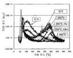
도 29는, 상이한 가열 온도 조건하의 질소 분위기에서 열 처리가 수행된 복수의 샘플에 관해 온도상승 이탈 분석 장치(TDS; Thermal Desorption Spectroscopy)를 이용한 측정 결과를 나타낸다.FIG. 29 shows measurement results using a temperature rise desorption analyzer (TDS) for a plurality of samples subjected to heat treatment in a nitrogen atmosphere under different heating temperature conditions.
온도상승 이탈 분석 장치는, 샘플을 고진공에서 가열하여 그 온도가 상승할 때 샘플로부터 이탈하거나 발생하는 가스 성분을 4중극자 질량 분석기(quadrupole mass spectrometer)를 이용하여 검출하고 식별하기 위한 장치이다. 온도상승 이탈 분석 장치를 이용하여, 샘플 표면 또는 내부로부터 이탈하는 가스 및 분자를 관찰할 수 있다. ESCO, Ltd의 온도상승 이탈 분석 장치(제품명: EMD-WA1000S)를 이용하였다. 측정 조건으로서는, 온도 상승률은 약 10℃/분으로 설정되었고, SEM 전압은 1500 V, 드웰 타임(Dwell Time)은 0.2(초), 사용 채널수는 23개로 하였다. 또한, 측정 동안, 압력은 약 1×10⁻⁷(Pa)의 진공도였다. H2O의 이온화 계수를 1.0, H2O의 단편화 계수를 0.805, H2O의 스루패스 계수를 1.56, H2O의 펌핑 레이트를 1.0으로 하였다는 점에 유의한다.The temperature rise deviation analyzer is a device for detecting and identifying a gas component that is separated from a sample or generated when the temperature rises by heating a sample in a high vacuum using a quadrupole mass spectrometer. By using the temperature rise deviation analysis device, it is possible to observe gases and molecules deviating from the surface or the inside of the sample. A temperature rise deviation analyzer (product name: EMD-WA1000S) of ESCO, Ltd was used. As the measurement conditions, the temperature rise rate was set to about 10°C/min, the SEM voltage was set to 1500 V, the dwell time was set to 0.2 (second), and the number of channels used was set to 23. In addition, during the measurement, the pressure was a degree of vacuum ofabout 1×10 -7 (Pa). The ionization coefficients of H2 O 1.0, and significant fragmentation factor of H2 O to 0.805, that is a through-pass coefficients of H2 O was a pumping rate of 1.56, H2 O to 1.0.
도 29는, H2O에 관한 TDS 측정 결과를 나타내는 그래프이며, 여기서 다음과 같은 샘플들이 비교되었다: 유리 기판 위에 두께 50 nm의 In-Ga-Zn-O계 비-단결정막을 형성한 샘플(샘플1)과; 질소 분위기하 가열 온도 250℃에서 1시간 동안 열 처리를 행한 샘플(샘플4)과; 질소 분위기하 가열 온도 350℃에서 1시간 동안 열 처리를 행한 샘플(샘플3)과; 질소 분위기하 가열 온도 450℃에서 1시간 동안 열 처리를 행한 샘플(샘플5)과; 질소 분위기하 가열 온도 350℃에서 10시간 동안 열 처리를 행한 샘플(샘플6). 도 29의 결과로부터, 질소 분위기에서의 가열 온도가 높을수록, In-Ga-Zn-O계 비-단결정 막으로부터 이탈하는 수분(H2O)과 같은 불순물의 양이 더 많이 줄어든다는 것을 알 수 있다.29 isa graph showing the TDS measurement result for H 2 O, where the following samples were compared: A sample in which an In-Ga-Zn-O-based non-single crystal film having a thickness of 50 nm was formed on a glass substrate (sample 1) and; A sample (Sample 4) subjected to heat treatment for 1 hour at a heating temperature of 250°C in a nitrogen atmosphere; A sample (Sample 3) subjected to heat treatment for 1 hour at a heating temperature of 350° C. in a nitrogen atmosphere; A sample (Sample 5) subjected to heat treatment for 1 hour at a heating temperature of 450°C in a nitrogen atmosphere; A sample subjected to heat treatment for 10 hours at a heating temperature of 350°C in a nitrogen atmosphere (Sample 6). From the results of Fig. 29, it can be seen that the higher the heating temperature in a nitrogen atmosphere, the more the amount of impurities such asmoisture (H 2 O) that escapes from the In-Ga-Zn-O non-single crystal film is reduced. have.
또, 도 29의 그래프에서, 200℃ 내지 250℃ 부근에서 수분(H2O)와 같은 불순물의 이탈을 나타내는 제1 피크를 관찰할 수 있고, 300℃ 이상에서 수분(H2O)과 같은 불순물의 이탈을 나타내는 제2 피크를 관찰할 수 있다.In addition, in the graph of FIG. 29, a first peak indicating the separation of impurities such asmoisture (H 2O) can be observed around 200°C to 250°C, and impurities such as moisture (H 2 O) at 300°C or higher. A second peak indicating the deviation of can be observed.
질소 분위기하 450℃에서 열 처리를 수행한 샘플은, 실온에서 대기중에 약 1주간 방치해도 200℃ 이상에서 수분의 이탈이 관찰되지 않았다는 점에 유의한다. 따라서, 열 처리에 의해 In-Ga-Zn-O계 비-단결정 막이 안정화된다는 것을 알 수 있다.It should be noted that, even if the sample subjected to heat treatment at 450°C in a nitrogen atmosphere was left in the air at room temperature for about one week, no moisture escape was observed at 200°C or higher. Therefore, it can be seen that the In-Ga-Zn-O-based non-single crystal film is stabilized by the heat treatment.
또한, H2O 외에도 H, O, OH, H2, O2, N, N2, 및 Ar의 각각에 관하여 TDS 측정을 수행하였다. H2O, H, O, 및 OH에 관해서는 분명히 피크를 관찰할 수 있었지만, H2, O2, N, N2, 및 Ar에 관해서는 피크를 관찰할 수 없었다. 각 샘플은, 유리 기판 위에 두께 50 nm로 In-Ga-Zn-O계 비-단결정 막을 형성한 구조를 가졌고, 가열 조건은 다음과 같이 설정되었다: 질소 분위기하 250℃ 1시간; 질소 분위기하 350℃ 1시간; 질소 분위기하 350℃ 10시간; 및 질소 분위기하 450℃ 1시간. 비교예로서, 열 처리가 수행되지 않은 In-Ga-Zn-O계 비-단결정 막과 유리 기판 단독을 각각 측정했다. 도 30은 H의 TDS 측정 결과를, 도 31은 O의 TDS 측정 결과를, 도 32는 OH의 TDS 측정 결과를, 도 33은 H2의 TDS 측정 결과를 나타낸다. 상기 가열 조건에서의 질소 분위기의 산소 밀도는, 20 ppm 이하임에 유의한다.In addition, inaddition to H 2 O, TDS measurement was performed for each of H, O, OH, H2 , O2 , N, N2, and Ar. Peaks were clearly observed for H2 O, H, O, and OH, but no peaks were observed for H2 , O2 , N, N2 , and Ar. Each sample had a structure in which an In-Ga-Zn-O-based non-single crystal film was formed on a glass substrate with a thickness of 50 nm, and heating conditions were set as follows: 250° C. for 1 hour under nitrogen atmosphere; 350°C for 1 hour under nitrogen atmosphere; 350 DEG C for 10 hours in a nitrogen atmosphere; And 450° C. for 1 hour under a nitrogen atmosphere. As a comparative example, an In-Ga-Zn-O-based non-single crystal film and a glass substrate alone to which heat treatment was not performed were measured, respectively. 30 shows the TDS measurement result of H, FIG. 31 shows the TDS measurement result of O, FIG. 32 shows the TDS measurement result of OH, and FIG. 33 shows the TDS measurement resultof H 2. Note that the oxygen density in the nitrogen atmosphere under the above heating conditions is 20 ppm or less.
이상의 결과에 따르면, In-Ga-Zn-O계 비-단결정 막의 열 처리의 수행에 의해, 주로 수분(H2O)이 방출되는 것을 알 수 있다. 즉, 열 처리에 의해 In-Ga-Zn-O계 비-단결정 막으로부터 수분(H2O)의 이탈이 주로 일어나고, 물 분자의 분해에 의해 생성된 물질이, 도 30, 31, 및 32에 각각 도시된 H, O, 및 OH에 관한 TDS의 측정치에 영향을 주고 있다. In-Ga-Zn-O계 비-단결정 막은 수소와 OH를 포함한다고 생각된다; 따라서, 이것들도 열처리에 의해 방출된다.According to the above results, it can be seen thatmoisture (H 2 O) is mainly released by the heat treatment of the In-Ga-Zn-O-based non-single crystal film.That is, the separation of moisture (H 2 O) from the In-Ga-Zn-O-based non-single crystal film mainly occurs by heat treatment, and the material produced by the decomposition of water molecules is shown in FIGS. 30, 31, and 32. Influence the measurements of TDS for H, O, and OH shown, respectively. It is thought that the In-Ga-Zn-O-based non-single crystal film contains hydrogen and OH; Therefore, these are also released by heat treatment.
본 명세서에서, 질소 또는 (아르곤 또는 헬륨과 같은) 희가스의 불활성 가스 분위기하 또는 감압하의 열 처리를 탈수화 또는 탈수소화를 위한 열 처리라고 부른다. 본 명세서에서, "탈수소화"란, 열 처리에 의한 H2의 제거만을 말하는 것은 아니고, 편의상, H, OH등의 제거도 포함하여, "탈수화 또는 탈수소화"라고 말한다.In this specification, heat treatment of nitrogen or a noble gas (such as argon or helium) under an inert gas atmosphere or under reduced pressure is referred to as heat treatment for dehydration or dehydrogenation. In this specification, "dehydrogenation"does not mean only the removal of H 2 by heat treatment, but for convenience, it also includes removal of H, OH and the like, and refers to "dehydration or dehydrogenation".
불활성 가스 분위기하의 열 처리에 의해 산화물 반도체층에 포함된 (H2O, H, OH와 같은) 불순물을 저감시켜 캐리어 농도를 증가시킨 후, 산소 분위기하에서 서랭을 수행한다. 서랭 후, 예를 들어, 산화물 반도체층에 접하여 산화물 절연막이 형성된다; 따라서, 산화물 반도체층의 캐리어 농도가 저감되어 신뢰성이 향상된다.After increasing the carrier concentration by reducing impurities (such asH 2 O, H, OH) contained in the oxide semiconductor layer by heat treatment in an inert gas atmosphere, slow cooling is performed in an oxygen atmosphere. After slow cooling, for example, an oxide insulating film is formed in contact with the oxide semiconductor layer; Accordingly, the carrier concentration in the oxide semiconductor layer is reduced, and reliability is improved.
제1 산화물 반도체막 및 제2 산화물 반도체막의 저항은, 질소 분위기하의 열 처리에 의해 감소된다(캐리어 농도가, 바람직하게는 1×10¹⁸/cm3 이상으로 증가됨). 따라서, 저항이 감소된 제1 산화물 반도체막 및 제2 산화물 반도체막이 형성될 수 있다. 저항이 감소된 제1 산화물 반도체막 및 제2 산화물 반도체막을 에칭 공정을 통해 가공하여 제1 산화물 반도체층 및 제2 산화물 반도체층을 형성하고, 한층 더, 에칭 공정에 의해 가공하여 반도체층과, 소스 영역 및 드레인 영역을 형성한다.The resistance of the first oxide semiconductor film and the second oxide semiconductor film is reduced by heat treatment in a nitrogen atmosphere (carrier concentration is preferably increased to 1×10¹⁸ /cm3 or more). Accordingly, a first oxide semiconductor film and a second oxide semiconductor film with reduced resistance may be formed. The first oxide semiconductor film and the second oxide semiconductor film with reduced resistance are processed through an etching process to form a first oxide semiconductor layer and a second oxide semiconductor layer, and further processed by an etching process to form a semiconductor layer and a source. A region and a drain region are formed.
그 후, 저항이 감소된 제1 산화물 반도체층에 접하여 산화물 절연막이 형성되면, 저항이 감소된 제1 산화물 반도체층에 있어서, 적어도 산화물 절연막과 접하는 영역의 저항이 증가된다(캐리어 농도가, 바람직하게는 1×10¹⁸/cm3 미만으로 감소됨); 따라서, 저항이 증가된 산화물 반도체 영역이 형성될 수 있다. 반도체 장치의 제조 공정 동안에, 불활성 가스 분위기하(또는 감압하)의 가열, 산소 분위기하의 서랭, 및 산화물 절연막의 형성등에 의해 제1 산화물 반도체막 및 제2 산화물 반도체막의 캐리어 농도를 증가 및 감소시키는 것이 중요하다. 즉, I형 제1 산화물 반도체막 및 i형 제2 산화물 반도체막이 탈수화 또는 탈수소화를 위한 열 처리에 놓여 산소 결핍형이 되고, 즉, (n- 또는 n+와 같은) n형 산화물 반도체막이 되고, 그 다음, 산화물 절연막이 형성되어 제1 산화물 반도체층이 산소 과잉형이 된다, 즉, i형 산화물 반도체층이 된다. 따라서, 양호한 전기 특성을 갖는 신뢰성이 높은 박막 트랜지스터를 포함하는 반도체 장치를 제조하여 제공하는 것이 가능하다.Thereafter, when the oxide insulating film is formed in contact with the first oxide semiconductor layer with reduced resistance, in the first oxide semiconductor layer with reduced resistance, at least the resistance of the region in contact with the oxide insulating film is increased (carrier concentration is preferably Is reduced to less than 1×10¹⁸ /cm3 ); Accordingly, an oxide semiconductor region with increased resistance can be formed. During the manufacturing process of the semiconductor device, increasing and decreasing the carrier concentration of the first oxide semiconductor film and the second oxide semiconductor film by heating under an inert gas atmosphere (or under reduced pressure), slow cooling under an oxygen atmosphere, and the formation of an oxide insulating film, etc. It is important. That is, the I-type first oxide semiconductor film and the i-type second oxide semiconductor film are subjected to heat treatment for dehydration or dehydrogenation to become oxygen-deficient, i.e., an n- type oxide semiconductor film (such as n-or n+) Then, an oxide insulating film is formed so that the first oxide semiconductor layer becomes an oxygen-excessive type, that is, becomes an i-type oxide semiconductor layer. Accordingly, it is possible to manufacture and provide a semiconductor device including a highly reliable thin film transistor having good electrical properties.
저항이 감소된 제1 산화물 반도체층에 접하여 형성되는 산화물 절연막으로서, 수분, 수소 이온, 및 OH-와 같은 불순물을 차단하는 무기 절연막이 사용된다는 점에 유의한다. 구체적으로는, 산화 규소막(silicon oxide film), 또는 질화 산화 규소막(silicon nitride oxide film)이 이용된다.Note that as the oxide insulating film formed in contact with the first oxide semiconductor layer having reduced resistance, an inorganic insulating film that blocks impurities suchas moisture, hydrogen ions, and OH − is used. Specifically, a silicon oxide film or a silicon nitride oxide film is used.
또한, 산화물 반도체층과 소스 영역 및 드레인 영역 위에 보호막 역할을 하는 산화물 절연막이 형성한 후에, 2번째의 열 처리를 수행할 수도 있다. 산화물 반도체층과 소스 영역 및 드레인 영역 위에 보호막 역할을 하는 산화물 절연막을 형성한 후 2번째의 열 처리를 수행하는 경우, 박막 트랜지스터의 전기적 특성의 격차를 저감할 수 있다.Further, after the oxide semiconductor layer and the oxide insulating film serving as a protective film are formed on the source region and the drain region, a second heat treatment may be performed. When the second heat treatment is performed after forming the oxide semiconductor layer and the oxide insulating layer serving as a protective layer on the source region and the drain region, a difference in electrical characteristics of the thin film transistor can be reduced.
본 명세서에서 개시되는 본 발명의 구조의 한 실시예에서, 게이트 전극층이 형성되고; 게이트 전극층 위에 게이트 절연층이 형성되고; 게이트 절연층 위에 제1 산화물 반도체막이 형성되고; 제1 산화물 반도체막 위에 제2 산화물 반도체막이 형성되고; 제1 산화물 반도체막 및 제2 산화물 반도체막이 가열되어 탈수화, 또는 탈수소된 후, 산소 분위기하에서 서랭되고; 산소 분위기하에서 서랭된 제1 산화물 반도체막 및 제2 산화물 반도체막이 선택적으로 에칭되어 제1 산화물 반도체층 및 제2 산화물 반도체층을 형성하고; 제1 산화물 반도체층 및 제2 산화물 반도체층 위에 도전막이 형성되고; 제1 산화물 반도체층, 제2 산화물 반도체층, 및 도전막이 선택적으로 에칭되어 반도체층, 소스 영역, 드레인 영역, 소스 전극층 및 드레인 전극층을 형성하고; 게이트 절연층, 반도체층, 소스 영역, 드레인 영역, 소스 전극층, 및 드레인 전극층 위에 반도체층의 일부와 접하는 산화물 절연막이 형성되어 캐리어 농도가 저감된다.In one embodiment of the structure of the invention disclosed herein, a gate electrode layer is formed; A gate insulating layer is formed over the gate electrode layer; A first oxide semiconductor film is formed over the gate insulating layer; A second oxide semiconductor film is formed over the first oxide semiconductor film; The first oxide semiconductor film and the second oxide semiconductor film are heated to be dehydrated or dehydrogenated, and then slowly cooled in an oxygen atmosphere; The first oxide semiconductor film and the second oxide semiconductor film slowly cooled in an oxygen atmosphere are selectively etched to form a first oxide semiconductor layer and a second oxide semiconductor layer; A conductive film is formed over the first oxide semiconductor layer and the second oxide semiconductor layer; The first oxide semiconductor layer, the second oxide semiconductor layer, and the conductive film are selectively etched to form a semiconductor layer, a source region, a drain region, a source electrode layer, and a drain electrode layer; An oxide insulating film in contact with a part of the semiconductor layer is formed on the gate insulating layer, the semiconductor layer, the source region, the drain region, the source electrode layer, and the drain electrode layer to reduce the carrier concentration.
본 명세서에서 개시되는 본 발명의 구조의 또 다른 실시예에서, 게이트 전극층이 형성되고; 게이트 전극층 위에 게이트 절연층이 형성되고; 게이트 절연층 위에 제1 산화물 반도체막이 형성되고; 제1 산화물 반도체막 위에 제2 산화물 반도체막이 형성되고; 제1 산화물 반도체막 및 제2 산화물 반도체막이 불활성 가스 분위기하에서 가열되어 캐리어 농도가 증가된 다음, 산소 분위기하에서 서랭되고; 산소 분위기하에서 서랭된 제1 산화물 반도체막 및 제2 산화물 반도체막이 선택적으로 에칭되어 제1 산화물 반도체층 및 제2 산화물 반도체층을 형성하고; 제1 산화물 반도체층 및 제2 산화물 반도체층 위에 도전막이 형성되고; 제1 산화물 반도체층, 제2 산화물 반도체층, 및 도전막이 선택적으로 에칭되어 반도체층, 소스 영역, 드레인 영역, 소스 전극층 및 드레인 전극층을 형성하고; 게이트 절연층, 반도체층, 소스 영역, 드레인 영역, 소스 전극층, 및 드레인 전극층 위에 반도체층의 일부와 접하는 산화물 절연막이 형성되어 캐리어 농도가 저감된다.In another embodiment of the structure of the present invention disclosed herein, a gate electrode layer is formed; A gate insulating layer is formed over the gate electrode layer; A first oxide semiconductor film is formed over the gate insulating layer; A second oxide semiconductor film is formed over the first oxide semiconductor film; The first oxide semiconductor film and the second oxide semiconductor film are heated under an inert gas atmosphere to increase the carrier concentration, and then slowly cooled under an oxygen atmosphere; The first oxide semiconductor film and the second oxide semiconductor film slowly cooled in an oxygen atmosphere are selectively etched to form a first oxide semiconductor layer and a second oxide semiconductor layer; A conductive film is formed over the first oxide semiconductor layer and the second oxide semiconductor layer; The first oxide semiconductor layer, the second oxide semiconductor layer, and the conductive film are selectively etched to form a semiconductor layer, a source region, a drain region, a source electrode layer, and a drain electrode layer; An oxide insulating film in contact with a part of the semiconductor layer is formed on the gate insulating layer, the semiconductor layer, the source region, the drain region, the source electrode layer, and the drain electrode layer to reduce the carrier concentration.
본 명세서에서 개시되는 본 발명의 구조의 한 실시예에서, 게이트 전극층이 형성되고; 게이트 전극층 위에 게이트 절연층이 형성되고; 게이트 절연층 위에 제1 산화물 반도체막이 형성되고; 제1 산화물 반도체막 위에 제2 산화물 반도체막이 형성되고; 제1 산화물 반도체막 및 제2 산화물 반도체막이 감압하에서 가열되어 캐리어 농도가 증가된 다음, 산소 분위기하에서 서랭되고; 산소 분위기하에서 서랭된 제1 산화물 반도체막 및 제2 산화물 반도체막이 선택적으로 에칭되어 제1 산화물 반도체층 및 제2 산화물 반도체층을 형성하고; 제1 산화물 반도체층 및 제2 산화물 반도체층 위에 도전막이 형성되고; 제1 산화물 반도체층, 제2 산화물 반도체층, 및 도전막이 선택적으로 에칭되어 반도체층, 소스 영역, 드레인 영역, 소스 전극층 및 드레인 전극층을 형성하고; 게이트 절연층, 반도체층, 소스 영역, 드레인 영역, 소스 전극층, 및 드레인 전극층 위에 반도체층의 일부와 접하는 산화물 절연막이 형성되어 캐리어 농도가 저감된다.In one embodiment of the structure of the invention disclosed herein, a gate electrode layer is formed; A gate insulating layer is formed over the gate electrode layer; A first oxide semiconductor film is formed over the gate insulating layer; A second oxide semiconductor film is formed over the first oxide semiconductor film; The first oxide semiconductor film and the second oxide semiconductor film are heated under reduced pressure to increase the carrier concentration, and then slowly cooled in an oxygen atmosphere; The first oxide semiconductor film and the second oxide semiconductor film slowly cooled in an oxygen atmosphere are selectively etched to form a first oxide semiconductor layer and a second oxide semiconductor layer; A conductive film is formed over the first oxide semiconductor layer and the second oxide semiconductor layer; The first oxide semiconductor layer, the second oxide semiconductor layer, and the conductive film are selectively etched to form a semiconductor layer, a source region, a drain region, a source electrode layer, and a drain electrode layer; An oxide insulating film in contact with a part of the semiconductor layer is formed on the gate insulating layer, the semiconductor layer, the source region, the drain region, the source electrode layer, and the drain electrode layer to reduce the carrier concentration.
반도체층과 소스 영역 및 드레인 영역으로서 이용될 수 있는 산화물 반도체층으로서는, 반도체 특성을 갖는 산화물 재료가 이용될 수 있다. 예를 들어, InMO3(ZnO)m (m>0)으로 표현되는 박막을 형성하고, 반도체층과 소스 영역 및 드레인 영역으로서 그 박막을 이용한 박막 트랜지스터가 제조된다. M은, Ga, Fe, Ni, Mn 및 Co로부터 선택된 하나의 금속 원소 또는 복수의 금속 원소를 나타낸다는 점에 유의해야 한다. 예를 들어, M이 Ga를 나타내는 경우도 있는 반면, M이, Ga(Ga 및 Ni 또는 Ga 및 Fe) 외에도, Ni 또는 Fe와 같은 상기 금속 원소를 나타내는 경우도 있다. 또한, 상기 산화물 반도체는, M으로서 포함되는 금속 원소 외에도, 불순물 원소로서 Fe 또는 Ni, 그 외의 천이 금속 원소, 또는 천이 금속의 산화물을 포함할 수도 있다. 본 명세서에 있어서, InMO3(ZnO)m (m>0)로 표현되는 구조의 산화물 반도체 중에서, M으로서 Ga를 포함하는 산화물 반도체를 In-Ga-Zn-O계 산화물 반도체라고 부르며, In-Ga-Zn-O계 산화물 반도체의 박막을 In-Ga-Zn-O계 비-단결정 막이라고 부른다.As the semiconductor layer and the oxide semiconductor layer that can be used as the source region and the drain region, an oxide material having semiconductor properties can be used. For example,a thin film represented by InMO 3 (ZnO)m (m> 0) is formed, and a thin film transistor is manufactured using the thin film as a semiconductor layer, a source region, and a drain region. It should be noted that M represents one metal element or a plurality of metal elements selected from Ga, Fe, Ni, Mn and Co. For example, while M represents Ga in some cases, M represents a metal element such as Ni or Fe in addition to Ga (Ga and Ni or Ga and Fe). In addition, the oxide semiconductor may contain Fe or Ni, other transition metal elements, or oxides of transition metals as impurity elements in addition to the metal element included as M. In the present specification,among oxide semiconductors having a structure represented by InMO 3 (ZnO)m (m> 0), an oxide semiconductor containing Ga as M is called an In-Ga-Zn-O-based oxide semiconductor, and In-Ga A thin film of -Zn-O-based oxide semiconductor is called an In-Ga-Zn-O-based non-single crystal film.
산화물 반도체층에 적용되는 산화물 반도체로서 상기 외에도, In-Sn-Zn-O-계의 산화물 반도체; In-Al-Zn-O-계의 산화물 반도체; Sn-Ga-Zn-O-계의 산화물 반도체; Al-Ga-Zn-O-계의 산화물 반도체; Sn-Al-Zn-O-계의 산화물 반도체; In-Zn-O-계의 산화물 반도체; Sn-Zn-O-계의 산화물 반도체; Al-Zn-O-계의 산화물 반도체; In-O-계의 산화물 반도체; Sn-O-계의 산화물 반도체; Zn-O-계의 산화물 반도체를 적용할 수 있다. 또한, 상기 산화물 반도체층은 산화 규소(silicon oxide)를 포함할 수도 있다. 산화물 반도체층에 포함되는, 결정화를 저해하는 산화 규소(SiOx(X>0))는, 제조 공정에서 산화물 반도체층의 형성 후에 열 처리를 수행한 경우 산화물 반도체층의 결정화가 억제될 수 있다. 산화물 반도체층은 아몰퍼스인 것이 바람직하지만, 부분적으로 결정화되어도 좋다.As an oxide semiconductor applied to the oxide semiconductor layer, in addition to the above, an In-Sn-Zn-O-based oxide semiconductor; In-Al-Zn-O-based oxide semiconductor; Sn-Ga-Zn-O-based oxide semiconductors; Al-Ga-Zn-O-based oxide semiconductors; Sn-Al-Zn-O-based oxide semiconductors; In-Zn-O-based oxide semiconductors; Sn-Zn-O-based oxide semiconductors; Al-Zn-O-based oxide semiconductors; In-O-based oxide semiconductors; Sn-O-based oxide semiconductors; Zn-O-based oxide semiconductors can be applied. In addition, the oxide semiconductor layer may include silicon oxide. Silicon oxide (SiOx (X>0)) contained in the oxide semiconductor layer, which inhibits crystallization, may be inhibited from crystallization of the oxide semiconductor layer when heat treatment is performed after the formation of the oxide semiconductor layer in the manufacturing process. The oxide semiconductor layer is preferably amorphous, but may be partially crystallized.
산화물 반도체는, 바람직하게는 In을 포함하는 산화물 반도체이고, 더 바람직하게는, In 및 Ga을 포함하는 산화물 반도체이다. I형(진성) 산화물 반도체를 얻기 위해, 탈수화 또는 탈수소화가 효과적이다.The oxide semiconductor is preferably an oxide semiconductor containing In, and more preferably an oxide semiconductor containing In and Ga. In order to obtain an I-type (intrinsic) oxide semiconductor, dehydration or dehydrogenation is effective.
또한, 박막 트랜지스터의 소스 영역 및 드레인 영역(n+층, 버퍼층이라고도 한다)으로서 이용되는 산화물 반도체층은, 채널 형성 영역으로서 이용되는 산화물 반도체층보다 높은 도전율(전기 전도율)을 갖는 것이 바람직하다.Further, it is preferable that the oxide semiconductor layer used as the source region and the drain region (also referred to as n + layer, buffer layer) of the thin film transistor has a higher conductivity (electrical conductivity) than the oxide semiconductor layer used as the channel formation region.
박막 트랜지스터는 정전기등으로 인해 파괴되기 쉽기 때문에, 구동 회로를 보호하기 위한 보호 회로를 게이트선 또는 소스선과 동일한 기판 위에 제공하는 것이 바람직하다. 보호 회로는, 산화물 반도체를 포함하는 비선형 소자를 이용하여 형성하는 것이 바람직하다.Since the thin film transistor is apt to be destroyed by static electricity or the like, it is preferable to provide a protection circuit for protecting the driving circuit on the same substrate as the gate line or the source line. It is preferable to form the protection circuit using a nonlinear element containing an oxide semiconductor.
게이트 절연층, 제1 산화물 반도체막, 및 제2 산화물 반도체막은, 대기에 노출되지 않고 연속적으로 처리(연속 처리, 인 시츄(insitu) 공정, 연속 성막이라고도 부름)될 수도 있다. 대기에 노출시키지 않고 연속 처리함으로써, 적층된 층들 사이의 각 계면, 즉, 게이트 절연층, 제1 산화물 반도체막 및 제2 산화물 반도체막의 계면들이, 물이나 하이드로 카본과 같은, 대기 성분이나 대기중에 부유하는 불순물 원소에 오염되지 않고 형성될 수 있다. 따라서, 박막 트랜지스터의 특성 격차를 저감할 수 있다.The gate insulating layer, the first oxide semiconductor film, and the second oxide semiconductor film may be continuously processed (also referred to as continuous processing, in-situ processing, and continuous film formation) without being exposed to the atmosphere. By continuous treatment without exposure to the atmosphere, each interface between the laminated layers, i.e., the interfaces of the gate insulating layer, the first oxide semiconductor film and the second oxide semiconductor film, floats in the atmosphere or an atmospheric component such as water or hydrocarbon. It can be formed without being contaminated by impurity elements. Accordingly, it is possible to reduce the difference in characteristics of the thin film transistor.
본 명세서에서 "연속 처리"란, PCVD법 또는 스퍼터링법을 이용한 제1 처리 단계로부터 PCVD법 또는 스퍼터링법을 이용한 제2 처리 단계까지의 공정 동안에, 피처리 기판이 놓여 있는 분위기가 대기와 같은 오염 분위기에 오염되지 않고, 진공 또는 불활성 가스 분위기(질소 분위기 또는 희가스 분위기)가 되도록 항상 제어된다는 것을 의미한다는 점에 유의한다. 연속 처리에 의해, 세정된 피처리 기판에 수분등이 재부착되는 것을 피하면서 막 형성과 같은 처리가 수행될 수 있다.In the present specification, "continuous treatment" means that during the process from the first treatment step using the PCVD method or the sputtering method to the second treatment step using the PCVD method or the sputtering method, the atmosphere in which the target substrate is placed is a contaminated atmosphere such as the atmosphere. Note that it means that it is always controlled to be in a vacuum or inert gas atmosphere (nitrogen atmosphere or rare gas atmosphere) without being contaminated on. By the continuous treatment, a treatment such as film formation can be performed while avoiding reattachment of moisture or the like to the cleaned substrate to be processed.
동일한 챔버에서 제1 처리 단계로부터 제2 처리 단계까지의 공정을 수행하는 것은, 본 명세서에서의 연속 처리의 범위 내에 있다.It is within the scope of the continuous processing herein to perform the process from the first processing step to the second processing step in the same chamber.
또한, 상이한 챔버에서 제1 처리 단계로부터 제2 처리 단계까지의 공정을 수행하는 경우, 제1 처리 단계후, 대기에 노출되지 않고 또 다른 챔버로 기판을 반송하여 제2 처리를 수행하는 것도 본 명세서에서의 연속 처리의 범위 내에 있다.In addition, when performing a process from the first processing step to the second processing step in a different chamber, after the first processing step, the second processing is performed by transferring the substrate to another chamber without being exposed to the atmosphere. It is within the range of continuous processing in
제1 처리 단계와 제2 처리 단계 사이에, 기판 반송 단계, 정렬 단계, 서랭 단계, 또는 제2 단계에 필요한 온도로 기판을 가열 또는 냉각하는 단계 등이 제공될 수 있다는 점에 유의한다. 이와 같은 공정도 역시 본 명세서에서의 연속 처리의 범위 내에 있다.It is noted that between the first processing step and the second processing step, a substrate transfer step, an alignment step, a slow cooling step, or a step of heating or cooling the substrate to a temperature required for the second step, and the like may be provided. Such a process is also within the scope of the continuous treatment herein.
세정 단계, 습식 에칭, 레지스트 형성과 같은 액체를 이용하는 단계가 제1 처리 단계와 제2 처리 단계 사이에 제공될 수 있다. 이와 같은 경우는, 본 명세서에서의 연속 처리의 범위 내에 있지 않다.A step of using a liquid such as a cleaning step, wet etching, resist formation may be provided between the first processing step and the second processing step. In such a case, it is not within the range of continuous processing in the present specification.
본 명세서에서 "제1", "제2"와 같은 서수는 편의상 이용되는 것이지, 단계들의 순서 또는 적층 순서를 나타내는 것은 아니다. 또한, 본 명세서에서의 서수는, 본 발명을 특정하는 특정한 명칭을 나타내는 것이 아니다.In the present specification, ordinal numbers such as "first" and "second" are used for convenience and do not indicate the order of steps or stacking. In addition, an ordinal number in this specification does not represent a specific name specifying the present invention.
게다가, 구동 회로를 포함하는 표시 장치로서, 액정 표시 장치 외에도, 발광 소자를 포함하는 발광 표시 장치나, 전기영동 표시 소자를 포함하는 전자 페이퍼라고도 칭해지는 표시 장치를 들 수 있다.Further, as a display device including a driving circuit, in addition to a liquid crystal display device, a light emitting display device including a light emitting element and a display device also referred to as an electronic paper including an electrophoretic display device are exemplified.
발광 소자를 포함하는 발광 표시 장치에서, 복수의 박막 트랜지스터가 화소부에 포함되고, 그 화소부에는, 박막 트랜지스터의 게이트 전극이 다른 박막 트랜지스터의 소스 배선 또는 드레인 배선에 전기적으로 접속되는 영역이 있다. 또한, 발광 소자를 포함하는 발광 표시 장치의 구동 회로에서, 박막 트랜지스터의 게이트 전극이 그 박막 트랜지스터의 소스 배선 또는 드레인 배선에 접속되는 영역이 있다.In a light emitting display device including a light emitting element, a plurality of thin film transistors are included in a pixel portion, and in the pixel portion, there is a region in which a gate electrode of the thin film transistor is electrically connected to a source wiring or a drain wiring of another thin film transistor. Further, in a driving circuit of a light emitting display device including a light emitting element, there is a region in which a gate electrode of a thin film transistor is connected to a source wiring or a drain wiring of the thin film transistor.
본 명세서에서, 반도체 장치란, 일반적으로 반도체 특성을 이용하여 기능할 수 있는 장치를 의미하며, 전기 광학 장치, 반도체 회로, 및 전자 기기는 모두 반도체 장치이다.In the present specification, a semiconductor device generally refers to a device capable of functioning using semiconductor properties, and electro-optical devices, semiconductor circuits, and electronic devices are all semiconductor devices.
안정된 전기 특성을 갖는 박막 트랜지스터를 제조 및 제공할 수 있다. 따라서, 양호한 전기 특성을 갖는 신뢰성이 높은 박막 트랜지스터를 포함하는 반도체 장치를 제공할 수 있다.It is possible to manufacture and provide a thin film transistor having stable electrical properties. Accordingly, it is possible to provide a semiconductor device including a highly reliable thin film transistor having good electrical characteristics.
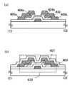
도 1의 (a) 내지 (c)는 반도체 장치의 제조 방법을 나타낸다;
도 2의 (a) 및 (b)는 반도체 장치의 제조 방법을 나타낸다;
도 3의 (a) 및 (b)는 반도체 장치를 나타낸다;
도 4의 (a) 내지 (c)는 반도체 장치의 제조 방법을 나타낸다;
도 5의 (a) 내지 (c)는 반도체 장치의 제조 방법을 나타낸다;
도 6의 (a) 및 (b)는 반도체 장치의 제조 방법을 나타낸다;
도 7은 반도체 장치를 나타낸다;
도 8의 (a1), (a2), (b1) 및 (b2)는 반도체 장치를 나타낸다;
도 9는 반도체 장치를 나타낸다;
도 10의 (a1), (a2), 및 (b)는 반도체 장치를 나타낸다;
도 11의 (a) 및 (b)는 반도체 장치를 나타낸다;
도 12는 반도체 장치의 화소 등가 회로를 나타낸다;
도 13의 (a) 내지 (c)는 반도체 장치를 나타낸다;
도 14의 (a) 및 (b)는 반도체 장치의 블록도이다;
도 15는 신호선 구동 회로의 구성을 나타낸다;
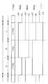
도 16은 신호선 구동 회로의 동작을 나타내는 타이밍 차트이다;
도 17은 신호선 구동 회로의 동작을 나타내는 타이밍 차트이다;
도 18은 시프트 레지스터의 구성을 나타낸다;
도 19는 도 18에 나타낸 플립-플롭의 접속 구조를 나타낸다;
도 20은 반도체 장치를 나타낸다;
도 21은 산화물 반도체층의 산소 농도의 시뮬레이션 결과를 나타낸다;
도 22는 전자 서적 리더(reader)의 예를 나타내는 외관도이다;
도 23의 (a) 및 (b)는 각각 텔레비젼 세트 및 디지털 포토 프레임의 예를 나타내는 외관도이다;
도 24의 (a) 및 (b)는 게임 기기의 예를 나타내는 외관도이다;
도 25의 (a) 및 (b)는 각각 휴대형 컴퓨터 및 휴대 전화기의 예를 나타내는 외관도이다;
도 26은 반도체 장치를 나타낸다;
도 27은 반도체 장치를 나타낸다;
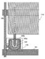
도 28은 전기로(electric furnace)의 단면도이다;
도 29는 TDS 측정 결과를 나타내는 그래프이다;
도 30은 H에 관한 TDS 측정 결과를 나타내는 그래프이다;
도 31은 O에 관한 TDS 측정 결과를 나타내는 그래프이다;
도 32는 OH에 관한 TDS 측정 결과를 나타내는 그래프이다;
도 33은 H2에 관한 TDS 측정 결과를 나타내는 그래프이다;
도 34는 시뮬레이션에 이용된 산화물 반도체층의 구조를 나타낸다.1A to 1C show a method of manufacturing a semiconductor device;
2A and 2B show a method of manufacturing a semiconductor device;
3A and 3B show a semiconductor device;
4A to 4C show a method of manufacturing a semiconductor device;
5A to 5C show a method of manufacturing a semiconductor device;
6A and 6B show a method of manufacturing a semiconductor device;
7 shows a semiconductor device;
8(a1), (a2), (b1) and (b2) show semiconductor devices;
9 shows a semiconductor device;
10(a1), (a2), and (b) show semiconductor devices;
11A and 11B show a semiconductor device;
12 shows a pixel equivalent circuit of a semiconductor device;
13A to 13C show semiconductor devices;
14A and 14B are block diagrams of a semiconductor device;
15 shows the configuration of a signal line driving circuit;
16 is a timing chart showing the operation of the signal line driving circuit;
17 is a timing chart showing the operation of the signal line driving circuit;
18 shows the configuration of a shift register;
Fig. 19 shows the connection structure of the flip-flop shown in Fig. 18;
20 shows a semiconductor device;
21 shows a simulation result of the oxygen concentration of the oxide semiconductor layer;
22 is an external view showing an example of an electronic book reader;
23A and 23B are external views showing examples of a television set and a digital photo frame, respectively;
24A and 24B are external views showing an example of a game device;
25A and 25B are external views showing examples of a portable computer and a portable telephone, respectively;
26 shows a semiconductor device;
27 shows a semiconductor device;
28 is a cross-sectional view of an electric furnace;
29 is a graph showing TDS measurement results;
30 is a graph showing TDS measurement results for H;
31 is a graph showing TDS measurement results for O;
32 is a graph showing the result of TDS measurement for OH;
33 is a graph showing TDS measurement results forH 2;
34 shows the structure of an oxide semiconductor layer used in the simulation.
본 발명의 실시를 위한 최상의 모드Best Mode for the Practice of the Invention
실시예 및 예가 도면들을 참조하여 상세히 설명될 것이다. 그러나, 본 발명은 이하의 설명만으로 제한되는 것은 아니며, 본 발명의 사상과 범위로부터 벗어나지 않고 형태와 세부사항에 있어서 다양한 변경과 수정이 이루어질 수 있다는 것을 당업자라면 용이하게 이해할 것이다. 따라서, 본 발명은, 이하의 실시예와 예들의 설명으로만 제한되는 것으로 해석되어서는 안된다. 이하에서 설명되는 구조들에서, 동일한 부분 또는 유사한 기능을 갖는 부분은, 상이한 도면들에서 동일한 참조 번호들로 표기되며, 반복적 설명은 생략한다.Embodiments and examples will be described in detail with reference to the drawings. However, the present invention is not limited only to the following description, and it will be readily understood by those skilled in the art that various changes and modifications can be made in form and detail without departing from the spirit and scope of the present invention. Accordingly, the present invention should not be construed as being limited only to the description of the following examples and examples. In the structures described below, the same part or parts having a similar function are denoted by the same reference numerals in different drawings, and a repetitive description is omitted.
[실시예 1][Example 1]
반도체 장치 및 반도체 장치의 제조 방법이, 도 1의 (a) 내지 (c), 도 2의 (a) 및 (b), 및 도 3의 (a) 및 (b)를 참조하여 설명될 것이다.The semiconductor device and the manufacturing method of the semiconductor device will be described with reference to FIGS. 1A to 1C, 2A and 2B, and 3A and 3B.
도 3의 (a)는 반도체 장치에 포함된 박막 트랜지스터(470)의 평면도이고, 도 3의 (b)는 도 3의 (a)의 라인 C1-C2를 따라 취해진 단면도이다. 박막 트랜지스터(470)는 역스태거형 박막 트랜지스터(inverted staggered thin film transistor)이며, 절연 표면을 갖는 기판인 기판(400) 위에, 게이트 전극층(401), 게이트 절연층(402), 반도체층(403), 소스 영역 및 드레인 영역(404a 및 404b), 및 소스 전극층 및 드레인 전극층(405a 및 405b)을 포함한다. 또한, 박막 트랜지스터(470)를 피복하고 반도체층(403)과 접하도록 산화물 절연막(407)이 제공된다.3A is a plan view of the
반도체층(403)과 소스 영역 및 드레인 영역(404a 및 404b)이 되는 적어도 제1 산화물 반도체막 및 제2 산화물 반도체막의 형성 후에 수분과 같은 불순물을 저감하는 열 처리(탈수화 또는 탈수소화를 위한 열 처리)를 수행하여, 제1 산화물 반도체막 및 제2 산화물 반도체막의 저항이 감소된다(캐리어 농도가, 바람직하게는 1×10¹⁸/cm3 이상으로 증가됨). 그 다음, 제1 산화물 반도체층에 접하여 산화물 절연막(407)을 형성함으로써, 그 저항이 증가된다(캐리어 농도가, 바람직하게는 1×10¹⁸/cm3 미만, 한층 더 바람직하게는 1×10¹⁴/cm3 이하로 감소됨). 따라서, 저항이 증가된 제1 산화물 반도체층은 채널 형성 영역으로서 이용될 수 있다.Thermal treatment to reduce impurities such as moisture after formation of the
또한, 탈수화 또는 탈수소화를 위한 열 처리에 의해 수분(H2O)과 같은 불순물이 제거된 후, 산소 분위기하에서 서랭을 수행하는 것이 바람직하다. 탈수화 또는 탈수소화를 위한 열 처리 및 산소 분위기하의 서랭 후, 제1 산화물 반도체층에 접해 산화물 절연막의 형성을 수행해 제1 산화물 반도체층의 캐리어 농도가 저감되어, 박막 트랜지스터(470)의 신뢰성을 향상시킨다.Further, it is preferable to perform slow cooling in an oxygen atmosphere after impurities such asmoisture (H 2 O) are removed by heat treatment for dehydration or dehydrogenation. After heat treatment for dehydration or dehydrogenation and slow cooling in an oxygen atmosphere, the oxide insulating film is formed in contact with the first oxide semiconductor layer to reduce the carrier concentration of the first oxide semiconductor layer, thereby improving the reliability of the
반도체층(403)과 소스 영역 및 드레인 영역(404a 및 404b)내 뿐만이 아니라, 게이트 절연층(402)내, 및 반도체층(403)의 상하에 접하여 제공되는 막과 산화물 반도체층인 반도체층(403) 사이의 계면들, 구체적으로는, 게이트 절연층(402)과 반도체층(403) 사이의 계면, 및 산화물 절연막(407)과 반도체층(403) 사이의 계면에 존재하는 수분과 같은 불순물이 저감된다.A
산화물 반도체층인 반도체층(403)과 소스 영역 및 드레인 영역(404a 및 404b)에 접하는 소스 전극층 및 드레인 전극층(405a 및 405b)은, 티타늄, 알루미늄, 망간, 마그네슘, 지르코늄, 베릴륨, 및 토륨으로부터 선택된 하나 이상의 재료를 이용하여 형성된다. 또한, 상술한 원소들의 임의 조합을 포함하는 합금막의 적층이 사용될 수도 있다.The
채널 형성 영역을 포함한 반도체층(403)과 소스 영역 및 드레인 영역(404a 및 404b)으로서, 반도체 특성을 갖는 산화물 재료를 이용할 수도 있다. 예를 들어, InMO3(ZnO)m (m>0)으로 표현되는 구조의 산화물 반도체를 이용할 수 있고, 특히, In-Ga-Zn-O계 산화물 반도체를 이용하는 것이 바람직하다. M은, 갈륨(Ga), 철(Fe), 니켈(Ni), 망간(Mn) 및 코발트(Co)로부터 선택된 하나의 금속 원소 또는 복수의 금속 원소를 나타낸다는 점에 유의해야 한다. 예를 들어, M이 Ga를 나타내는 경우도 있는 반면, M이, Ga(Ga 및 Ni 또는 Ga 및 Fe) 외에도, Ni 또는 Fe와 같은 상기 금속 원소를 나타내는 경우도 있다. 또한, 상기 산화물 반도체는, M으로서 포함되는 금속 원소 외에도, 불순물 원소로서 Fe 또는 Ni, 그 외의 천이 금속 원소, 또는 천이 금속의 산화물을 포함할 수도 있다. 본 명세서에 있어서, InMO3(ZnO)m (m>0)로 표현되는 구조의 산화물 반도체 중에서, M으로서 적어도 Ga를 포함하는 산화물 반도체를 In-Ga-Zn-O계 산화물 반도체라고 부르며, In-Ga-Zn-O계 산화물 반도체의 박막을 In-Ga-Zn-O계 비-단결정 막이라고 부른다.As the
산화물 반도체층에 적용되는 산화물 반도체로서 상기 외에도, In-Sn-Zn-O-계의 산화물 반도체; In-Al-Zn-O-계의 산화물 반도체; Sn-Ga-Zn-O-계의 산화물 반도체; Al-Ga-Zn-O-계의 산화물 반도체; Sn-Al-Zn-O-계의 산화물 반도체; In-Zn-O-계의 산화물 반도체; Sn-Zn-O-계의 산화물 반도체; Al-Zn-O-계의 산화물 반도체; In-O-계의 산화물 반도체; Sn-O-계의 산화물 반도체; Zn-O-계의 산화물 반도체를 적용할 수 있다. 또한, 상기 산화물 반도체는 산화 규소를 포함할 수도 있다.As an oxide semiconductor applied to the oxide semiconductor layer, in addition to the above, an In-Sn-Zn-O-based oxide semiconductor; In-Al-Zn-O-based oxide semiconductor; Sn-Ga-Zn-O-based oxide semiconductors; Al-Ga-Zn-O-based oxide semiconductors; Sn-Al-Zn-O-based oxide semiconductors; In-Zn-O-based oxide semiconductors; Sn-Zn-O-based oxide semiconductors; Al-Zn-O-based oxide semiconductors; In-O-based oxide semiconductors; Sn-O-based oxide semiconductors; Zn-O-based oxide semiconductors can be applied. In addition, the oxide semiconductor may include silicon oxide.
반도체층(제1 산화물 반도체층이라고도 함)과 소스 전극층 사이에 소스 영역이 제공되고, 반도체층과 드레인 전극층 사이에 드레인 영역이 제공된다. 소스 영역 및 드레인 영역으로서, n형의 도전형을 갖는 산화물 반도체층(제2 산화물 반도체층이라고도 함)을 이용할 수 있다.A source region is provided between the semiconductor layer (also referred to as the first oxide semiconductor layer) and the source electrode layer, and a drain region is provided between the semiconductor layer and the drain electrode layer. As the source region and the drain region, an oxide semiconductor layer (also referred to as a second oxide semiconductor layer) having an n-type conductivity type can be used.
또한, 박막 트랜지스터의 소스 영역 및 드레인 영역(404a 및 404b)으로서 이용되는 제2 산화물 반도체층은, 채널 형성 영역으로서 이용되는 제1 산화물 반도체층보다 더 얇고 더 높은 도전율(전기 전도율)을 갖는 것이 바람직하다.In addition, it is preferable that the second oxide semiconductor layer used as the source region and the
또한, 채널 형성 영역으로서 이용되는 제1 산화물 반도체층은 아몰퍼스 구조를 가지며, 소스 영역 및 드레인 영역으로서 이용되는 제2 산화물 반도체층은 아몰퍼스 구조안에 결정립(나노 크리스탈)을 포함하는 경우가 있다. 소스 영역 및 드레인 영역으로서 이용되는 제2 산화물 반도체층 내의 결정립(나노 크리스탈)은, 1 nm 내지 10 nm, 전형적으로는 약 2 nm 내지 4 nm의 직경을 가진다.Further, the first oxide semiconductor layer used as the channel formation region has an amorphous structure, and the second oxide semiconductor layer used as the source region and the drain region includes crystal grains (nano crystals) in the amorphous structure in some cases. The crystal grains (nano crystals) in the second oxide semiconductor layer used as the source region and the drain region have a diameter of 1 nm to 10 nm, typically about 2 nm to 4 nm.
본 실시예에서는, 채널 형성 영역을 포함한 반도체층(403)과 소스 영역 및 드레인 영역(n+층, 버퍼층이라고도 함)(404a 및 404b)으로서 In-Ga-Zn-O계 비-단결정 막을 이용한다.In this embodiment, an In-Ga-Zn-O non-single crystal film is used as the
도 1의 (a) 내지 (c)와 도 2의 (a) 및 (b)는, 박막 트랜지스터(470)의 제조 공정을 나타내는 단면도이다.1A to 1C and FIGS. 2A and 2B are cross-sectional views illustrating a manufacturing process of the
절연 표면을 갖는 기판인 기판(400) 위에 게이트 전극층(401)이 제공된다. 기초막의 역할을 하는 절연막을, 기판(400)과 게이트 전극층(401) 사이에 제공할 수도 있다. 기초막은, 기판(400)으로부터의 불순물 원소의 확산을 방지하는 기능을 갖고 있고, 질화 규소막, 산화 규소막, 질화 산화 규소막, 또는 산화 질화 규소막 중 하나 이상을 단층으로 또는 적층하여 형성될 수 있다. 게이트 전극층(401)은, 몰리브덴, 티타늄, 크롬, 탄탈룸, 텅스텐, 알루미늄, 구리, 네오디뮴, 스칸듐과 같은 금속 재료 또는 이들 재료들 중 임의의 재료를 주성분으로 포함하는 합금 재료를 이용해, 단층으로 또는 적층해 형성될 수 있다.A
예를 들어, 게이트 전극층(401)의 2층의 적층 구조로서, 알루미늄층 위에 몰리브덴층이 적층된 2층의 적층 구조; 구리층 위에 몰리브덴층을 적층한 2층 구조; 구리층 위에 질화 티타늄층 또는 질화 탄탈룸을 적층한 2층 구조; 질화 티타늄층과 몰리브덴층을 적층한 2층 구조가 바람직하다. 3층의 적층 구조로서는, 텅스텐층 또는 질화 텅스텐층의 적층, 알루미늄과 규소의 합금 또는 알루미늄과 티타늄의 합금의 적층, 및 질화 티타늄층 또는 티타늄층의 적층이 바람직하다.For example, as a two-layer laminate structure of the
게이트 전극층(401) 위에 게이트 절연층(402)이 형성된다.A
게이트 절연층(402)은, 플라스마 CVD법 또는 스퍼터링법등에 의해, 산화 규소층, 질화 규소층, 산화 질화 규소층 또는 질화 산화 규소층을 단층으로 또는 적층해 형성될 수 있다. 예를 들어, 성막 가스로서 SiH4, 산소, 및 질소를 이용해, 플라스마 CVD법에 의해 산화 질화 규소층을 형성할 수 있다.The
게이트 절연층(402) 위에, 제1 산화물 반도체막(430) 및 제2 산화물 반도체막(433)이 형성되어 적층된다(도 1의 (a) 참조). 제1 산화물 반도체막(430)은 채널 형성 영역으로서 기능하는 반도체층으로서 역할하며, 제2 산화물 반도체막(433)은 소스 영역 및 드레인 영역으로서 역할한다.On the
산화물 반도체막을 스퍼터링법에 의해 형성하기 이전에, 아르곤 가스를 도입해 플라스마를 발생시키는 역스퍼터링을 수행하여 게이트 절연층(402)의 표면에 부착된 먼지를 제거하는 것이 바람직하다는 점에 유의한다. 역스퍼터링이란, 타겟 측에 전압을 인가하지 않고, RF 전원을 이용해 아르곤 분위기에서 기판측에 전압을 인가해 기판 근방에 플라스마를 생성해 표면을 바꾸는 방법이다. 아르곤 분위기 대신에, 질소 분위기, 헬륨 분위기 등을 이용할 수도 있다는 점에 유의한다. 대안으로서, 아르곤 분위기에 산소, N2O등을 추가한 분위기를 이용할 수도 있다. 추가의 대안으로서, 아르곤 분위기에 Cl2, CF4등을 추가한 분위기를 이용할 수도 있다.Note that before forming the oxide semiconductor film by the sputtering method, it is preferable to perform reverse sputtering to generate plasma by introducing argon gas to remove dust adhering to the surface of the
산화물 반도체막으로서, In-Ga-Zn-O계 비-단결정 막을 이용한다. 산화물 반도체막은, In-Ga-Zn-O-계 산화물 반도체 타겟을 이용한 스퍼터링법에 의해 형성된다. 산화물 반도체막은, 희가스(대표적으로는, 아르곤) 분위기하, 산소 분위기하, 또는 희가스(대표적으로는 아르곤) 및 산소 분위기하에서, 스퍼터링법에 의해 형성될 수 있다.As the oxide semiconductor film, an In-Ga-Zn-O non-single crystal film is used. The oxide semiconductor film is formed by a sputtering method using an In-Ga-Zn-O-based oxide semiconductor target. The oxide semiconductor film may be formed by a sputtering method in a rare gas (typically argon) atmosphere, an oxygen atmosphere, or a rare gas (typically argon) and oxygen atmosphere.
게이트 절연층(402), 제1 산화물 반도체막(430) 및 제2 산화물 반도체막(433)을 대기에 노출시키지 않고 연속적으로 형성할 수도 있다. 대기에 노출시키지 않고 연속으로 막을 형성함으로써, 적층들의 각 계면이, 물이나 하이드로 카본과 같은 대기 성분이나 대기중에 부유하는 불순물 원소에 오염되지 않고 형성될 수 있다. 따라서, 박막 트랜지스터의 특성 격차를 저감할 수 있다.The
제1 산화물 반도체막(430) 및 제2 산화물 반도체막(433)에 (질소, 헬륨, 네온, 또는 아르곤과 같은) 불활성 가스 분위기하 또는 감압하에서 열 처리를 실시한 후, 산소 분위기하에서 서랭을 수행한다(도 1의 (b) 참조). 제1 산화물 반도체막(430) 및 제2 산화물 반도체막(433)을 상기 분위기하에서 열 처리할 때, 제1 산화물 반도체막(430) 및 제2 산화물 반도체막(433)에 포함된 물 또는 수소와 같은 불순물을 제거할 수 있다.After heat treatment is performed on the first
열 처리에 있어서, 질소 또는 헬륨, 네온, 아르곤과 같은 희가스에, 물 또는 수소와 같은 불순물이 포함되지 않는 것이 바람직하다는 점에 유의한다. 또한, 열 처리 장치에 도입하는 질소 또는 헬륨, 네온, 아르곤과 같은 희가스의 순도를, 6N(99.9999%) 이상, 바람직하게는 7N(99.99999%) 이상, (즉, 불순물 농도를 1 ppm 이하, 바람직하게는 0.1 ppm 이하)로 하는 것이 바람직하다.Note that in the heat treatment, it is preferable that impurities such as water or hydrogen are not contained in nitrogen or a rare gas such as helium, neon, or argon. In addition, the purity of nitrogen or rare gases such as helium, neon, and argon introduced into the heat treatment apparatus is 6N (99.9999%) or more, preferably 7N (99.99999%) or more, (i.e., the impurity concentration is 1 ppm or less, preferably Preferably, it is 0.1 ppm or less).
또한, 열 처리에서, 전기로를 이용한 가열 방법 또는 가열된 가스를 이용하는 GRTA(Gas Rapid Thermal Anneal) 법 또는 램프광을 이용하는 LRTA(Lamp Rapid Thermal Anneal)법과 같은 순간 가열 방법을 이용할 수 있다.In addition, in the heat treatment, an instantaneous heating method such as a heating method using an electric furnace or a Gas Rapid Thermal Anneal (GRTA) method using a heated gas or a Lamp Rapid Thermal Anneal (LRTA) method using a lamp light may be used.
여기서, 제1 산화물 반도체막(430) 및 제2 산화물 반도체막(433)에 대한 열 처리의 한 형태로서 전기로(601)를 이용한 가열 방법이, 도 28을 참조하여 설명된다.Here, a heating method using the
도 28은 전기로(601)의 개략도이다. 챔버(602)의 외측에는 챔버(602)를 가열하는데 이용되는 히터(603)가 제공된다. 챔버(602) 내에는 기판(604)을 탑재하는 서셉터(605)가 제공되고 기판은(604)은 챔버(602) 내로 또는 내로부터 이송된다. 또한, 챔버(602)에는 가스 공급 수단(606) 및 배기 수단(607)이 제공되고 있다. 가스 공급 수단(606)에 의해, 챔버(602) 내에 가스가 도입된다. 배기 수단(607)은 챔버(602) 내부를 배기하거나 챔버(602) 내의 압력을 줄인다. 전기로(601)의 온도 상승 특성을 0. 1℃/min 이상, 20℃/min 이하로 하는 것이 바람직하다는 점에 유의한다. 전기로(601)의 강온 특성을 0.1℃/min 이상, 15℃/min 이하로 하는 것이 바람직하다는 점에 유의한다.28 is a schematic diagram of an
가스 공급 수단(606)은, 가스 공급원(611a), 가스 공급원(611b), 압력 조정 밸브(612a), 압력 조정 밸브(612b), 정제기(613a), 정제기(613b), 매스 플로우 콘트롤러 (614a), 매스 플로우 콘트롤러(614b), 스톱 밸브(615a), 스톱 밸브(615b)를 포함한다. 본 실시예에서는, 가스 공급원(611a) 및 가스 공급원(611b)과 챔버(602) 사이에 정제기(613a) 및 정제기(613b)를 제공하는 것이 바람직하다. 정제기(613a) 및 정제기(613b)의 제공에 의해, 가스 공급원(611a) 및 가스 공급원(611b)으로부터 챔버(602) 내에 도입되는 가스 내의, 물 또는 수소와 같은 불순물을, 정제기(613a) 및 정제기(613b)에 의해 제거할 수 있고, 챔버(602) 내로의 물 또는 수소와 같은 불순물의 침입을 억제할 수 있다.The gas supply means 606 includes a
본 실시예에서는, 가스 공급원(611a) 및 가스 공급원(611b)으로부터, 질소 또는 희가스를 챔버(602) 내에 도입하여, 챔버 내부를 질소 또는 희가스 분위기에 있게 하고, 200℃이상 600℃이하, 바람직하게는 400℃이상 450℃이하로 가열된 챔버(602)에서, 기판(604) 위에 형성된 제1 산화물 반도체막(430) 및 제2 산화물 반도체막(433)을 가열한다. 이런 식으로, 제1 산화물 반도체막(430) 및 제2 산화물 반도체막(433)을 탈수화 또는 탈수소화할 수 있다.In this embodiment, nitrogen or noble gas is introduced into the
대안으로서, 배기 수단에 의한 감압하에서, 200℃이상 600℃이하, 바람직하게는 400℃이상 450℃이하에서 가열된 챔버(602)에서, 기판(604) 위에 형성된 제1 산화물 반도체막(430) 및 제2 산화물 반도체막(433)을 가열하여, 제1 산화물 반도체막(430) 및 제2 산화물 반도체막(433)을 탈수화 또는 탈수소화할 수 있다.As an alternative, the first
그 다음, 가스 공급원(611a)으로부터 챔버(602)로의 질소 또는 희가스의 도입을 멈추고, 히터를 오프 상태로 한다. 그 다음, 가스 공급원(611b)으로부터 챔버(602) 내에 산소를 도입하고, 가열 장치의 챔버(602)를 서랭한다. 즉, 챔버(602) 내의 분위기를 산소 분위기로 변경하여, 기판(604)을 서랭한다. 여기서는, 가스 공급원(611b)으로부터 챔버(602) 내에 도입되는 산소에, 물 또는 수소와 같은 불순물이 포함되지 않는 것이 바람직하다. 또한, 가스 공급원(611b)으로부터 챔버(602) 내에 도입하는 산소의 순도를, 6N(99.9999%) 이상, 바람직하게는 7N(99.99999%) 이상, (즉, 산소내 불순물 농도를 1 ppm 이하, 바람직하게는 0.1 ppm 이하)로 하는 것이 바람직하다. 불활성 가스 분위기하 또는 감압하의 열 처리에 의해, 산화물 반도체막의 저항은 감소된다(캐리어 농도가, 바람직하게는 1×10¹⁸/cm3 이상으로 증가됨). 따라서, 저항이 감소된 제1 산화물 반도체막(434) 및 제2 산화물 반도체막(435)을 형성할 수 있다.Then, the introduction of nitrogen or noble gas from the
그 결과, 이후에 완성되는 박막 트랜지스터의 신뢰성을 높일 수 있다.As a result, it is possible to increase the reliability of a thin film transistor to be completed later.
감압하에서 열 처리를 수행하는 경우, 열 처리 후에 챔버(602) 내에 산소를 도입하고 압력을 대기압으로 되돌림으로써 냉각을 수행할 수 있다는 점에 유의한다.Note that when the heat treatment is performed under reduced pressure, cooling can be performed by introducing oxygen into the
또, 가스 공급원(611b)으로부터 챔버(602) 내에 산소를 도입함과 동시에, 헬륨, 네온, 또는 아르곤과 같은 희가스와 질소 중 한편 또는 양쪽 모두를 챔버(602) 내에 도입할 수도 있다.Further, while oxygen is introduced into the
대안으로서, 가열 장치의 챔버(602) 내의 기판(604)을 300℃로 냉각한 후, 기판(604)을 실온의 분위기로 이송할 수도 있다. 그 결과, 기판(604)의 냉각 시간을 단축할 수가 있다.As an alternative, after cooling the
만일 가열 장치가 멀티-챔버를 가지는 경우, 열 처리와 냉각 처리를 서로 상이한 챔버에서 수행할 수 있다. 전형적으로는, 질소 또는 희가스로 충전되고 200℃ 이상, 600℃ 이하, 바람직하게는 400℃ 이상, 450℃ 이하로 가열된 제1 챔버에서, 기판 위의 산화물 반도체막을 가열한다. 그 다음, 질소 또는 희가스가 도입된 반송 챔버를 거쳐, 산소 또는 희가스로 충전되어 100℃이하, 바람직하게는 실온인 제2 챔버 내로 상기 열 처리된 기판을 도입하여, 냉각 처리를 수행한다. 전술된 단계들을 통해, 처리율을 향상시킬 수 있다.If the heating device has a multi-chamber, the heat treatment and the cooling treatment can be performed in different chambers. Typically, in a first chamber filled with nitrogen or a rare gas and heated to 200° C. or higher, 600° C. or lower, preferably 400° C. or higher and 450° C. or lower, the oxide semiconductor film on the substrate is heated. Then, the heat-treated substrate is introduced into a second chamber filled with oxygen or a rare gas through a transfer chamber into which nitrogen or a rare gas is introduced into a second chamber having a temperature of 100°C or less, preferably room temperature, and a cooling treatment is performed. Through the above-described steps, it is possible to improve the throughput.
불활성 가스 분위기하 또는 감압하의 열 처리 후에, 산소 분위기하에서 실온 이상 100℃ 미만까지 서랭을 실시해, 제1 산화물 반도체막(434) 및 제2 산화물 반도체막(435)이 제공된 기판을 가열 장치로부터 꺼내, 포토리소그래피 단계를 수행한다.After heat treatment in an inert gas atmosphere or under reduced pressure, slow cooling is performed in an oxygen atmosphere from room temperature to less than 100°C, and the substrate provided with the first
불활성 가스 분위기하 또는 감압하의 열 처리 후의 제1 산화물 반도체막(434) 및 제2 산화물 반도체막(435)은, 아몰퍼스 상태인 것이 바람직하지만, 부분적으로 결정화된 것이어도 좋다.The first
제1 산화물 반도체막(434) 및 제2 산화물 반도체막(435)을 포토리소그래피 단계에 의해 섬-형상의 산화물 반도체층인 제1 산화물 반도체층(431) 및 제2 산화물 반도체층(436)으로 가공한다(도 1의 (c) 참조).The first
게이트 절연층(402), 제1 산화물 반도체층(431) 및 제2 산화물 반도체층(436) 위에, 도전막을 형성한다.A conductive film is formed on the
도전막의 재료로서, Al, Cr, Ta, Ti, Mo, W로부터 선택된 원소; 상기 원소들 중 임의의 원소를 그 성분으로서 포함하는 합금; 상기 원소들 중 임의의 원소의 조합을 포함하는 합금막등을 들 수 있다.As the material of the conductive film, an element selected from Al, Cr, Ta, Ti, Mo, and W; An alloy containing any of the above elements as its component; And an alloy film including a combination of any of the above elements.
도전막의 형성 후에 열 처리를 수행하는 경우, 도전막이 열 처리를 견딜 수 있는 내열성을 갖는 것이 바람직하다. Al 단독은 내열성이 낮고 부식하기 쉬운 등의 문제점이 있으므로, 내열성 도전 재료와 조합하여 알루미늄을 사용한다. Al과 조합하여 사용되는 내열성 도전 재료로서, 티타늄(Ti), 탄탈룸(Ta), 텅스텐(W), 몰리브덴(Mo), 크롬(Cr), Nd(네오디뮴), Sc(스칸듐)으로부터 선택된 원소; 상기 원소들 중 임의의 원소를 성분으로서 포함하는 합금; 상기 원소들 중 임의의 원소를 조합하여 포함하는 합금막; 상기 원소들 중 임의의 원소를 성분으로서 포함하는 질화물을 사용할 수 있다.When performing heat treatment after formation of the conductive film, it is preferable that the conductive film has heat resistance capable of withstanding the heat treatment. Since Al alone has problems such as low heat resistance and easy corrosion, aluminum is used in combination with a heat-resistant conductive material. As a heat-resistant conductive material used in combination with Al, an element selected from titanium (Ti), tantalum (Ta), tungsten (W), molybdenum (Mo), chromium (Cr), Nd (neodymium), and Sc (scandium); An alloy containing any of the above elements as a component; An alloy film comprising any of the above elements in combination; A nitride containing any of the above elements as a component may be used.
제1 산화물 반도체층(431), 제2 산화물 반도체층(436), 및 도전막을 에칭 단계를 통해 에칭하여 제1 산화물 반도체층(432), 소스 영역 및 드레인 영역(404a 및 404b), 소스 전극층 및 드레인 전극층(405a 및 405b)을 형성한다(도 2의 (a) 참조). 제1 산화물 반도체층(431)의 일부만이 에칭되어 제1 산화물 반도체층(432)이 침강부(함몰부)를 가진다는 점에 유의한다.The first
산화물 절연막(407)으로서의 산화 규소막을 스퍼터링법에 의해 제1 산화물 반도체층(432)에 접하여 형성한다. 저항이 감소된 산화물 반도체층에 접하여 형성되는 산화물 절연막(407)은, 수분, 수소 이온, 및 OH-와 같은 불순물을 포함하지 않으며, 이 불순물들이 외부로부터 침입하는 것을 차단하는 무기 절연막을 이용하여 형성된다. 구체적으로는, 산화 규소막, 또는 질화 산화 규소막이 이용된다.A silicon oxide film as the
본 실시예에서는, 산화물 절연막(407)으로서 두께 300 nm의 산화 규소막을 형성한다. 막 형성시의 기판 온도는, 실온 이상, 300℃ 이하일 수 있으며; 이 실시예에서는, 기판 온도는 100℃로 설정된다. 산화 규소막의 스퍼터링법에 의한 형성은, 희가스(대표적으로는, 아르곤) 분위기하, 산소 분위기하, 또는 희가스(대표적으로는, 아르곤) 및 산소 분위기하에서 수행할 수 있다. 또한, 타겟으로서 산화 규소 타겟이나 규소 타겟을 이용할 수도 있다. 예를 들어, 규소 타겟을 이용해, 산소 및 질소 분위기하에서 스퍼터링법에 의해 산화 규소막을 형성할 수 있다.In this embodiment, a silicon oxide film having a thickness of 300 nm is formed as the
저항이 감소된 제1 산화물 반도체층(432)에 접하여 스퍼터링법 또는 PCVD법등에 의해 산화물 절연막(407)을 형성하면, 저항이 감소된 제1 산화물 반도체층(432)에 있어서, 적어도 산화물 절연막(407)과 접하는 영역의 저항이 증가된다(캐리어 농도가, 바람직하게는 1×10¹⁸/cm3 미만, 한층 더 바람직하게는 1×10¹⁴/cm3 이하로 감소됨); 따라서, 저항이 증가된 산화물 반도체 영역을 형성할 수 있다. 반도체 장치의 제조 공정 동안에, 불활성 가스 분위기하(또는 감압하)의 가열, 산소 분위기하의 서랭, 및 산화물 절연막의 형성등에 의해 산화물 반도체층의 캐리어 농도를 증가 및 감소시키는 것이 중요하다. 제1 산화물 반도체층(432)은, 저항이 증가된 산화물 반도체 영역을 포함하는 반도체층(403)의 역할을 한다. 따라서, 박막 트랜지스터(470)가 제조될 수 있다(도 2의 (b) 참조).When the
상기 탈수 처리 또는 탈수소처리를 위한 열 처리에 의해 제1 산화물 반도체막 및 제2 산화물 반도체막에 포함된 (H2O, H, 또는 OH와 같은) 불순물을 저감시켜 캐리어 농도를 증가시킨 후, 산소 분위기하에서 서랭한다. 서랭 후, 제1 산화물 반도체막을 섬-형상의 제1 산화물 반도체층으로 가공하고, 제1 산화물 반도체층에 접해 산화물 절연막을 형성하여, 제1 산화물 반도체층의 캐리어 농도를 저감한다. 캐리어 농도가 감소된 제1 산화물 반도체층이 반도체층으로서 이용될 때, 박막 트랜지스터(470)의 신뢰성을 향상시킬 수 있다.After reducing the impurities (such as H 2 O, H, or OH) contained in the first oxide semiconductor film and the second oxide semiconductor film by the dehydration treatment or heat treatment for dehydrogenation treatment to increase the carrier concentration, oxygen Slowly cool under the atmosphere. After slow cooling, the first oxide semiconductor film is processed into an island-shaped first oxide semiconductor layer, and an oxide insulating film is formed in contact with the first oxide semiconductor layer to reduce the carrier concentration of the first oxide semiconductor layer. When the first oxide semiconductor layer having a reduced carrier concentration is used as the semiconductor layer, the reliability of the
또한, 산화물 절연막(407)의 형성 후, 질소 분위기하 또는 대기 분위기하(대기중)에서 박막 트랜지스터(470)에 열 처리(바람직하게는 150℃이상 350℃미만)를 수행할 수도 있다. 예를 들어, 질소 분위기하에서 250℃, 1시간의 열 처리를 수행한다. 열 처리에 의해, 산화물 반도체층(403)이 산화물 절연막(407)에 접한 상태로 가열된다. 따라서, 박막 트랜지스터(470)의 전기 특성의 격차를 저감할 수 있다. 이 열 처리(바람직하게는 150℃ 이상 350℃ 미만)는, 산화물 절연막(407)의 형성 이후에 수행되는 한, 특별한 제한이 없다. 이 열처리가, 또 다른 공정, 예를 들어 수지막 형성시의 열 처리나, 투명 도전막을 저저항화하기 위한 열 처리를 겸한다면, 공정수를 늘리는 일 없이 이 열처리를 수행할 수가 있다.In addition, after the
[실시예 2][Example 2]
반도체 장치 및 반도체 장치의 제조 방법이, 도 26을 참조하여 설명될 것이다. 실시예 1과 동일한 부분 또는 유사한 기능을 갖는 부분은, 실시예 1에서 설명된 것과 유사한 방식으로 형성될 수 있다; 따라서, 반복적 설명은 생략한다.A semiconductor device and a method of manufacturing the semiconductor device will be described with reference to FIG. 26. The same parts as in Example 1 or parts having similar functions may be formed in a manner similar to that described in Example 1; Therefore, repetitive description is omitted.
도 26에 나타낸 박막 트랜지스터(471)는, 게이트 전극층(401) 및 반도체층(403)의 채널 영역과 중첩하도록 도전층(408)을 제공하면서 도전층(408)과 반도체층(403) 사이에 절연막을 개재시킨 예이다.The
도 26는 반도체 장치에 포함된 박막 트랜지스터(471)의 단면도이다. 박막 트랜지스터(471)는 바텀-게이트 박막 트랜지스터이며, 절연 표면을 갖는 기판인 기판(400) 위에, 게이트 전극층(401), 게이트 절연층(402), 반도체층(403), 소스 및 드레인 영역(404a 및 404b), 소스 전극층 및 드레인 전극층(405a 및 405b), 도전층(408)을 포함한다. 도전층(408)은, 게이트 전극층(401)과 중첩하도록 산화물 절연막(407) 위에 제공되고 있다.26 is a cross-sectional view of a
도전층(408)은, 게이트 전극층(401), 소스 전극층 및 드레인 전극층(405a 및 405b)과 유사한 재료 및 방법을 이용해 형성될 수 있다. 화소 전극층을 제공하는 경우, 도전층(408)은 화소 전극층과 유사한 재료 및 방법을 이용하여 형성될 수 있다. 본 실시예에서, 도전층(408)으로서 티타늄막, 알루미늄막, 및 티타늄막의 적층을 이용한다.The
도전층(408)은, 게이트 전극층(401)과 동일하거나 상이한 전위를 가질 수도 있으며, 제2 게이트 전극층으로서 기능할 수 있다. 또한, 도전층(408)은 플로팅 상태일 수도 있다.The
산화물 반도체층(403)과 중첩하는 위치에 도전층(408)을 제공할 때, 박막 트랜지스터의 신뢰성을 검사하기 위한 바이어스-온도 스트레스 시험(이하, BT 시험이라고 언급)에 있어서, BT시험 전과 후의 박막 트랜지스터(471)의 임계 전압의 변화량을 저감할 수가 있다. 특히, 기판 온도를 150℃까지 상승시킨 후에 게이트에 -20V의 전압을 인가하는 -BT 시험에 있어서, 임계 전압의 변동을 억제할 수 있다.When providing the
이 실시예는 실시예 1과 적절히 조합하여 구현될 수 있다.This embodiment can be implemented in appropriate combination with the first embodiment.
[실시예 3][Example 3]
반도체 장치 및 반도체 장치의 제조 방법이, 도 27을 참조하여 설명될 것이다. 실시예 1과 동일한 부분 또는 유사한 기능을 갖는 부분은, 실시예 1에서 설명된 것과 유사한 방식으로 형성될 수 있다; 따라서, 반복적 설명은 생략한다.A semiconductor device and a method of manufacturing the semiconductor device will be described with reference to FIG. 27. The same parts as in Example 1 or parts having similar functions may be formed in a manner similar to that described in Example 1; Therefore, repetitive description is omitted.
도 27에 나타낸 박막 트랜지스터(472)는, 게이트 전극층(401) 및 반도체층(403)의 채널 영역과 중첩하도록 도전층(409)과 반도체층(403) 사이에 절연층(410) 및 산화물 절연막(407)을 개재하여 도전층(409)을 제공한 예이다.The
도 27은 반도체 장치에 포함된 박막 트랜지스터(472)의 단면도이다. 박막 트랜지스터(472)는 바텀-게이트 박막 트랜지스터이며, 절연 표면을 갖는 기판인 기판(400) 위에, 게이트 전극층(401), 게이트 절연층(402), 반도체층(403), 소스 및 드레인 영역(404a 및 404b), 소스 전극층 및 드레인 전극층(405a 및 405b), 도전층(409)을 포함한다. 도전층(409)은, 게이트 전극층(401)과 중첩하도록 산화물 절연막(407) 및 절연층(410) 위에 제공되고 있다.27 is a cross-sectional view of a
본 실시예에서는, 산화물 절연막(407) 위에 평탄화막 역할을 하는 절연층(410)을 적층하고, 소스 전극층 또는 드레인 전극층(405b)에 이르는 통로를 산화물 절연막(407) 및 절연층(410)에 형성한다. 산화물 절연막(407) 및 절연층(410)에 형성된 통로에 도전막을 형성하고 원하는 형상으로 에칭하여, 도전층(409) 및 화소 전극층(411)을 형성한다. 이런 식으로, 화소 전극층(411)을 형성하는 단계에서, 동일 재료 및 방법을 이용해 도전층(409)을 형성할 수가 있다. 본 실시예에서, 화소 전극층(411) 및 도전층(409)으로서 산화 규소를 포함한 산화 인듐 - 산화 주석 합금(산화 규소를 포함한 In-Sn-O계 산화물)을 이용한다.In this embodiment, an insulating
대안으로서, 도전층(409)은, 게이트 전극층(401), 소스 전극층 및 드레인 전극층(405 a 및 405b)과 유사한 재료 및 방법을 이용해 형성될 수 있다.As an alternative, the
도전층(409)은, 게이트 전극층(401)과 동일하거나 상이한 전위를 가질 수도 있으며, 제2 게이트 전극층으로서 기능할 수 있다. 또한, 도전층(409)은 플로팅 상태일 수도 있다.The
또한, 산화물 반도체층(403)과 중첩하는 위치에 도전층(409)을 제공할 때, 박막 트랜지스터의 신뢰성을 검사하기 위한 바이어스-온도 스트레스 시험(이하, BT 시험이라고 언급)에 있어서, BT시험 전과 후 사이의 박막 트랜지스터(472)의 임계 전압의 변화량을 저감할 수가 있다.In addition, in the bias-temperature stress test (hereinafter referred to as BT test) for checking the reliability of the thin film transistor when providing the
본 실시예는, 다른 실시예에서 설명한 구조와 적절하게 조합하여 구현될 수 있다.This embodiment can be implemented in appropriate combination with the structures described in other embodiments.
[실시예 4][Example 4]
박막 트랜지스터를 포함한 반도체 장치의 제조 공정을, 도 4의 (a) 내지 (c), 도 5의 (a) 내지 (c), 도 6의 (a) 및 (b), 도 7, 및 도 8의 (a1), (a2), (b1) 및 (b2)를 참조하여 설명한다.The manufacturing process of a semiconductor device including a thin film transistor is described in FIGS. 4A to 4C, 5A to 5C, 6A and 6B, 7 and 8. It will be described with reference to (a1), (a2), (b1) and (b2) of.
도 4의 (a)에서, 투광성을 갖는 기판(100)으로서, 바륨 보로실리케이트 유리(barium borosilicate glass), 알루미노보로실리케이트 유리(aluminoborosilicate glass) 등의 유리 기판을 이용할 수 있다.In FIG. 4A, as the
그 다음, 기판(100) 전체 표면 위에 도전층을 형성한 후, 제1 포토리소그래피 공정을 수행한다. 레지스트 마스크를 형성한 다음, 에칭에 의해 불필요한 부분을 제거하여, 배선 및 전극(게이트 전극층(101)을 포함한 게이트 배선, 커패시터 배선(108), 및 제1 단자(121))을 형성한다. 이 때, 적어도 게이트 전극층(101)의 단부가 점점 가늘어지는 형상(tapered shape)을 갖도록 에칭을 수행한다.Then, after forming a conductive layer on the entire surface of the
게이트 전극층(101)을 포함한 게이트 배선, 커패시터 배선(108), 및 단자부의 제1 단자(121) 각각은, 티타늄(Ti), 탄탈룸(Ta), 텅스텐(W), 몰리브덴(Mo), 크롬(Cr), Nd(네오디뮴), 스칸듐(Sc)으로부터 선택된 원소; 또는 상기 원소들 중 임의의 원소를 성분으로서 포함하는 합금; 상기 원소들 주 임의의 원소를 조합한 합금막; 또는 상기 원소들 중 임의의 원소를 성분으로서 포함하는 질화물과 같은, 내열성 도전 재료를 이용하여 형성되는 것이 바람직하다. 알루미늄(Al)이나 구리(Cu)와 같은 저저항 도전성 재료를 이용하는 경우, Al 단체 또는 Cu 단체에서는 내열성이 작고 부식하기 쉬운 등의 문제점이 있으므로 상기 내열성 도전성 재료와 조합하여 이용한다.Each of the gate wiring including the
그 다음, 게이트 전극층(101)의 전체 표면 위에, 게이트 절연층(102)을 형성한다(도 4의 (a) 참조). 게이트 절연층(102)은, 스퍼터링법, PCVD법등에 의해 50 nm 내지 250 nm의 두께로 형성된다.Then, a
예를 들어, 게이트 절연층(102)으로서, 스퍼터링법에 의해 100 nm 두께로 산화 규소막을 형성한다. 물론, 게이트 절연층(102)은, 이와 같은 산화 규소막으로 한정되지 않고, 산화 질화 규소막, 질화 규소막, 산화 알루미늄, 산화 탄탈룸막과 같은 다른 절연막을 이용하여, 단층 또는 적층 구조를 갖도록 형성될 수도 있다.For example, as the
그 다음, 게이트 절연층(102) 위에, 제1 산화물 반도체막(131)(제1 In-Ga-Zn-O계 비-단결정 막)을 형성한다. 플라스마 처리 후 대기에 노출되지 않고 제1 산화물 반도체막(131)이 형성되고, 이것은, 게이트 절연층과 반도체막 사이의 계면에 먼지나 수분이 부착되지 않는다는 점에서 유익하다. 여기서는, 직경 8 인치의 In, Ga, 및 Zn을 포함한 산화물 반도체 타겟(In2O3:Ga2O3:ZnO=1:1:1)을 이용해, 기판과 타겟의 사이의 거리를 170 mm, 압력 0. 4 Pa, 직류(DC) 전원 0. 5 kW, 아르곤 또는 산소 분위기하에서 제1 산화물 반도체막(131)을 형성한다. 펄스 직류(DC) 전원을 이용하면, 먼지를 경감할 수 있고 막두께를 균일하게 할 수 있기 때문에 바람직하다는 점에 유의한다. 제1 산화물 반도체막(131)의 두께는, 5 nm 내지 200 nm로 설정된다. 제1 산화물 반도체막(131)으로서, In-Ga-Zn-O계 산화물 반도체 타겟을 이용해 스퍼터링법에 의해 두께 50 nm의 In-Ga-Zn-O계 비-단결정 막을 형성한다.Then, on the
그 다음, 대기에 노출되지 않고 스퍼터링법으로 제2 산화물 반도체막(136)(제2 In-Ga-Zn-O계 비-단결정 막)을 형성한다(도 4의 (b) 참조). 여기서, 스퍼터링은, In2O3:Ga2O3:ZnO=1:1:1인 타겟을 이용하여, 막 형성 조건으로서 압력 0. 4 Pa, 전력 500 W, 막 형성 온도 실온, 아르곤 가스 유량 40 sccm를 도입해, 수행된다. In2O3:Ga2O3:ZnO=1:1:1인 타겟을 이용하지만, 막 형성 직후에 크기 1 nm 내지 10 nm의 결정립을 포함한 In-Ga-Zn-O계 비-단결정 막이 형성되는 경우가 있다. 타겟의 성분비, 형성 압력(0.1Pa 내지 2.0 Pa), 전력(250 W 내지 3000 W: 8 인치 φ), 및 온도(실온 내지 100℃)와 같은 반응성 스퍼터링의 막 형성 조건을 적절히 조절함으로써, 결정립의 유무나 결정립의 밀도가 조절될 수 있고, 직경 사이즈가 1 nm-10 nm의 범위에서 조절될 수 있다고 말할 수 있다는 점에 유의한다. 제2 In-Ga-Zn-O계 비-단결정 막은, 5 nm 내지 20 nm의 두께를 가진다. 물론, 막에 포함되는 결정립의 크기는 막 두께를 초과하지 않는다. 여기서, 제2 In-Ga-Zn-O계 비-단결정 막의 두께는, 5 nm이다.Then, a second oxide semiconductor film 136 (a second In-Ga-Zn-O non-single crystal film) is formed by sputtering without being exposed to the atmosphere (see Fig. 4B). Here, sputtering is performedusing a target of In 2 O3 :Ga2 O3 :ZnO=1:1:1, as film formation conditions, pressure 0.4 Pa, power 500 W, film formation temperature room temperature, and argon gas flow rate. It is carried out by introducing 40 sccm. A target of In2 O3 :Ga2 O3 :ZnO=1:1:1 is used, but an In-Ga-Zn-O non-single crystal film containing crystal grains of 1 nm to 10 nm in size is formed immediately after film formation. There are cases. By appropriately adjusting the film formation conditions of reactive sputtering such as the component ratio of the target, formation pressure (0.1 Pa to 2.0 Pa), power (250 W to 3000 W: 8 inch φ), and temperature (room temperature to 100° C.), Note that it can be said that the presence or absence of the grain density can be controlled, and the diameter size can be adjusted in the range of 1 nm-10 nm. The second In-Ga-Zn-O-based non-single crystal film has a thickness of 5 nm to 20 nm. Of course, the size of the crystal grains included in the film does not exceed the film thickness. Here, the thickness of the second In-Ga-Zn-O-based non-single crystal film is 5 nm.
제1 In-Ga-Zn-O계 비-단결정 막은, 제2 In-Ga-Zn-O계 비-단결정 막과는 상이한 막 형성 조건하에서 형성된다. 예를 들어, 제1 In-Ga-Zn-O계 비-단결정 막은, 제2 In-Ga-Zn-O계 비-단결정 막의 막 형성 조건에서의 산소 가스 유량 대 아르곤 가스 유량의 비율보다 높은 산소 가스 유량 대 아르곤 가스 유량의 비율을 갖는 조건에서 형성된다. 구체적으로는, 제2 In-Ga-Zn-O계 비-단결정 막은, (아르곤 또는 헬륨과 같은) 희가스 분위기하(또는 산소 가스 10%이하와 아르곤 가스 90%이상을 포함하는 분위기)에서 형성되고, 제1 In-Ga-Zn-O계 비-단결정 막은, 산소 혼합 분위기하(산소 가스 유량은 희가스 유량보다 높다)에서 형성된다.The first In-Ga-Zn-O-based non-single crystal film is formed under different film formation conditions than the second In-Ga-Zn-O-based non-single crystal film. For example, the first In-Ga-Zn-O-based non-single crystal film has oxygen higher than the ratio of the oxygen gas flow rate to the argon gas flow rate under the film formation conditions of the second In-Ga-Zn-O-based non-single crystal film. It is formed under conditions having a ratio of gas flow rate to argon gas flow rate. Specifically, the second In-Ga-Zn-O-based non-single crystal film is formed in a rare gas atmosphere (or an atmosphere containing 10% or less of oxygen gas and 90% or more of argon gas) (such as argon or helium), and , The first In-Ga-Zn-O-based non-single crystal film is formed in an oxygen-mixed atmosphere (oxygen gas flow rate is higher than rare gas flow rate).
제2 In-Ga-Zn-O계 비-단결정 막의 형성에 이용되는 챔버는, 앞서 역스퍼터링을 실시한 챔버와 동일한 챔버이거나 상이한 챔버일 수 있다.The chamber used for the formation of the second In-Ga-Zn-O-based non-single crystal film may be the same chamber or a different chamber as the chamber previously subjected to reverse sputtering.
스퍼터링법의 예로서, 스퍼터링용 전원으로서 고주파 전원을 이용하는 RF 스퍼터링법과, DC 스퍼터링법, 바이어스가 펄스화된 방식으로 인가되는 펄스 DC 스퍼터링법이 포함된다. RF 스퍼터링법은 주로 절연막을 형성하는 경우에 이용되고, DC 스퍼터링법은 주로 금속막을 형성하는 경우에 이용된다.Examples of the sputtering method include an RF sputtering method using a high-frequency power source as a sputtering power source, a DC sputtering method, and a pulsed DC sputtering method in which a bias is applied in a pulsed manner. The RF sputtering method is mainly used when forming an insulating film, and the DC sputtering method is mainly used when forming a metal film.
또한, 상이한 재료의 복수개 타겟이 셋팅될 수 있는 멀티-소스 스퍼터링 장치도 있다. 멀티-소스 스퍼터링 장치를 이용하여, 동일한 챔버에서 상이한 재료의 막을 적층하여 형성하거나, 동일한 챔버에서 전기 방전에 의해 동시에 복수 종류의 재료의 막을 형성할 수도 있다.There are also multi-source sputtering devices in which a plurality of targets of different materials can be set. By using a multi-source sputtering apparatus, films of different materials may be stacked and formed in the same chamber, or films of a plurality of types of materials may be simultaneously formed by electric discharge in the same chamber.
또한, 챔버 내부에 자석 시스템을 갖추고 마그네트론 스퍼터링법에 이용되는 스퍼터링 장치와, 글로우 방전을 사용하지 않고 마이크로파를 이용해 발생시킨 플라스마를 이용하는 ECR 스퍼터링법에 이용되는 스퍼터링 장치가 있다.In addition, there is a sputtering device used in a magnetron sputtering method with a magnetic system inside the chamber, and a sputtering device used in the ECR sputtering method using plasma generated using microwaves without using glow discharge.
또한, 스퍼터링법에 의한 막 형성 방법으로서, 막 형성 동안에 타겟 물질과 스퍼터링 가스 성분을 서로 화학반응시켜 그 화합물 박막을 형성하는 리액티브 스퍼터링법과, 막 형성 동안에 기판에도 전압을 인가하는 바이어스 스퍼터링법이 있다.In addition, as a film formation method by sputtering, there are reactive sputtering method in which a target substance and a sputtering gas component are chemically reacted with each other during film formation to form a thin film of the compound, and a bias sputtering method in which a voltage is applied to a substrate during film formation. .
그 다음, 제1 산화물 반도체막(131) 및 제2 산화물 반도체막(136)에 탈수화 또는 탈수소화를 위한 열 처리를 수행한다. 제1 산화물 반도체막(131) 및 제2 산화물 반도체막(136)에 (질소, 헬륨, 네온, 또는 아르곤과 같은) 불활성 가스 분위기하 또는 감압하에서 열 처리를 실시한 후, 산소 분위기하에서 서랭을 수행한다.Then, heat treatment for dehydration or dehydrogenation is performed on the first
열 처리는, 200℃ 이상에서 수행하는 것이 바람직하다. 예를 들어, 질소 분위기하에서 450℃, 1시간의 열 처리를 수행한다. 질소 분위기하의 이 열 처리에 의해, 제1 산화물 반도체막(131) 및 제2 산화물 반도체막(136)의 저항은 감소되고(캐리어 농도가, 바람직하게는 1×10¹⁸/cm3 이상으로 증가됨), 그 전도율이 증가된다. 따라서, 저항이 감소된 제1 산화물 반도체막(133) 및 제2 산화물 반도체막(137)이 형성된다(도 4의 (c) 참조). 제1 산화물 반도체막(133) 및 제2 산화물 반도체막(137)의 전기 전도율은 1×10⁻¹ S/cm이상, 1×10² S/cm이하가 바람직하다.It is preferable to perform heat treatment at 200 degreeC or more. For example, heat treatment is performed at 450° C. for 1 hour in a nitrogen atmosphere. By this heat treatment under a nitrogen atmosphere, the resistance of the first
그 다음, 제2 포토리소그래피 단계가 수행된다. 레지스트 마스크가 형성되고, 제1 산화물 반도체막(133) 및 제2 산화물 반도체막(137)이 에칭된다. 예를 들어, 인산과 초산과 질산을 혼합한 용액을 이용한 습식 에칭에 의해 불필요한 부분들을 제거하여, 제1 산화물 반도체층(134) 및 제2 산화물 반도체층(138)을 형성한다. 여기서의 에칭은 습식 에칭으로 한정되지 않고 건식 에칭을 이용해도 좋다는 점에 유의한다.Then, a second photolithography step is performed. A resist mask is formed, and the first
건식 에칭을 위한 에칭 가스로서, 염소를 포함하는 가스(염소(Cl2), 염화 붕소(BCl3), 염화 규소(SiCl4), 사염화탄소(CCl4)와 같은 염소계 가스)가 바람직하게 사용된다.As the etching gas for dry etching, a gas containing chlorine (chlorine-based gas such as chlorine (Cl2 ), boron chloride (BCl3 ), silicon chloride (SiCl4 ), and carbon tetrachloride (CCl4 )) is preferably used.
대안으로서, 불소를 포함하는 가스(4 불화 탄소(CF4), 6 불화 유황(SF6), 3 불화 질소(NF3), 3 불화 메탄(CHF3)과 같은 불소계 가스); 취화 수소(HBr); 산소(O2); 이러한 가스에 헬륨(He)이나 아르곤(Ar)등의 희가스를 첨가한 가스 등을 이용할 수가 있다.As an alternative, a fluorine-containing gas (a fluorine-based gas such as carbon tetrafluoride (CF4 ), sulfur hexafluoride (SF6 ), nitrogentrifluoride (NF 3 ), methane trifluoride (CHF3 )); Hydrogen embrittlement (HBr); Oxygen (O2 ); A gas obtained by adding a rare gas such as helium (He) or argon (Ar) to such a gas can be used.
건식 에칭법으로서, 평행 평판형 RIE(Reactive Ion Etching) 법이나, ICP(Inductively Coupled Plasma:유도 결합형 플라스마) 에칭법을 이용할 수가 있다. 희망하는 형상으로 막을 에칭하기 위하여, 에칭 조건(코일형의 전극에 인가되는 전력량, 기판측의 전극에 인가되는 전력량, 기판측의 전극 온도등)을 적절하게 조절한다.As a dry etching method, a parallel plate type RIE (Reactive Ion Etching) method or an ICP (Inductively Coupled Plasma: Inductively Coupled Plasma) etching method can be used. In order to etch the film into a desired shape, the etching conditions (the amount of power applied to the coil-type electrode, the amount of power applied to the electrode on the substrate side, the temperature of the electrode on the substrate side, etc.) are appropriately adjusted.
습식 에칭을 위해 이용하는 에칭제로서는, 인산과 초산과 질산을 혼합한 용액등을 이용할 수가 있다. 대안으로서, (KANTO CHEMICAL CO., INC에 의해 생산되는) ITO-07N을 이용할 수도 있다.As an etchant used for wet etching, a solution of phosphoric acid, acetic acid, and nitric acid may be used. As an alternative, it is also possible to use ITO-07N (produced by KANTO CHEMICAL CO., INC).
또한, 습식 에칭 후의 에칭제는 에칭된 재료와 함께 세정에 의해 제거된다. 제거된 재료를 포함하는 액칭제의 폐수를 정제하여, 그 재료를 재이용할 수도 있다. 에칭후의 폐수로부터 산화물 반도체층에 포함된 인듐과 같은 재료를 회수해 재이용하면, 자원을 효율적으로 사용하여 비용을 절감할 수 있다.Further, the etchant after wet etching is removed by cleaning together with the etched material. The wastewater of the liquefaction agent containing the removed material may be purified and the material may be reused. When a material such as indium contained in the oxide semiconductor layer is recovered from the wastewater after etching and reused, resources can be efficiently used and cost can be reduced.
에칭에 의해 희망하는 형상을 얻기 위하여, 재료에 따라 (에칭액, 에칭 시간, 및 온도와 같은) 에칭 조건을 적절히 조절한다.In order to obtain a desired shape by etching, etching conditions (such as etchant, etching time, and temperature) are appropriately adjusted according to the material.
그 다음, 스퍼터링법이나 진공 증착법으로 제1 산화물 반도체층(134) 및 제2 산화물 반도체층(138) 위에 금속 재료를 이용하여 도전막(132)을 형성한다(도 5의 (b) 참조).Then, a
도전막(132)의 재료로서, Al, Cr, Ta, Ti, Mo, W로부터 선택된 원소, 또는 상기 원소들 중 임의의 원소를 그 성분으로서 포함하는 합금, 상기 원소들 중 임의의 원소의 조합을 포함하는 합금등을 들 수 있다.As the material of the
도전막(132)의 형성 후에 열 처리를 수행하는 경우, 도전막은 이 열 처리를 견딜 수 있는 내열성을 갖는 것이 바람직하다.When performing heat treatment after formation of the
그 다음, 제3 포토리소그래피 단계가 수행된다. 레지스트 마스크를 형성하고, 에칭에 의해 불필요한 부분을 제거해 소스 전극층 및 드레인 전극층(105a 및 105b), 제1 산화물 반도체층(135), 소스 영역 및 드레인 영역(104a 및 104b), 및 제2 단자(122)를 형성한다(도 5의 (c) 참조). 이 때의 에칭 방법으로서 습식 에칭 또는 건식 에칭을 이용한다. 예를 들어, 도전막(132)으로서 알루미늄막 또는 알루미늄 합금막을 이용하는 경우, 인산과 초산과 질산을 혼합한 용액을 이용한 습식 에칭을 수행할 수가 있다. 대안으로서, 암모니아과수(과산화수소:암모니아:물 = 5:2:2)를 이용한 습식 에칭에 의해, 도전막(132)을 에칭하여 소스 전극층 및 드레인 전극층(105a 및 105b)을 형성한다. 이 에칭 단계에서, 제1 산화물 반도체층(134)의 노출 영역의 일부가 에칭되어, 제1 산화물 반도체층(135)이 형성된다. 따라서, 제1 산화물 반도체층(135)은, 소스 전극층 및 드레인 전극층(105a 및 105b)들 사이에서 두께가 얇은 영역을 가진다. 도 5의 (c)에서, 소스 전극층 및 드레인 전극층(105a 및 105b), 제1 산화물 반도체층(135), 소스 영역 및 드레인 영역(104a 및 104b)는 건식 에칭에 의해 한 번에 에칭된다; 따라서, 소스 전극층 및 드레인 전극층(105a 및 105b), 제1 산화물 반도체층(135), 및 소스 영역 및 드레인 영역(104a 및 104b)의 단부는 서로 정렬되어, 연속적 구조가 형성된다.Then, a third photolithography step is performed. A resist mask is formed, and unnecessary portions are removed by etching to form the source and drain
제3 포토리소그래피 단계에 있어서, 소스 전극층 및 드레인 전극층(105a 및 105b)과 동일한 재료를 이용하여 형성된 제2 단자(122)를 단자부에 남긴다. 제2 단자(122)는 소스 배선(소스 전극층 및 드레인 전극층(105a 및 105b)을 포함한 소스 배선)에 전기적으로 접속된다는 점에 유의한다.In the third photolithography step, a
또한, 다계조 마스크를 이용하여 형성된 복수의 두께(전형적으로는 2개의 상이한 두께)의 영역을 갖는 레지스트 마스크를 이용하면, 레지스트 마스크의 수를 줄일 수가 있어, 공정이 간략화되고, 비용이 저감된다.In addition, when a resist mask having regions of a plurality of thicknesses (typically two different thicknesses) formed using a multi-gradation mask is used, the number of resist masks can be reduced, simplifying the process and reducing the cost.
그 다음, 레지스트 마스크를 제거하고, 게이트 절연층(102), 제1 산화물 반도체층(135), 소스 영역 및 드레인 영역(104a 및 104b), 및 소스 전극층 및 드레인 전극층(105a 및 105b)을 덮도록 보호 절연층(107)을 형성한다. 보호 절연층(107)으로서, PCVD법에 의해 형성되는 산화 질화 규소막을 이용한다. 보호 절연층(107)의 역할을 하는 산화 질화 규소막이 소스 전극층 및 드레인 전극층(105a 및 105b) 사이의 제1 산화물 반도체층(135)의 노출 영역에 접하여 제공됨으로써, 보호 절연층(107)과 접하는 제1 산화물 반도체층(135)의 영역의 저항이 증가된다(캐리어 농도가, 바람직하게는 1×10¹⁸/cm3 미만, 한층 더 바람직하게는 1×10¹⁴/cm3 이하로 감소됨). 따라서, 저항이 증가된 채널 형성 영역을 포함하는 반도체층(103)이 형성될 수 있다.Then, the resist mask is removed, and the
이상의 단계들을 통해, 박막 트랜지스터(170)를 제조할 수 있다. 도 7은 이 단계에서의 평면도에 대응한다는 점에 유의한다.Through the above steps, the
그 다음, 제4 포토리소그래피 단계가 수행된다. 레지스트 마스크를 형성하고, 보호 절연층(107) 및 게이트 절연층(102)이 에칭되어, 소스 또는 드레인 전극층(105b)에 이르는 콘택 홀(125)이 형성된다. 또한, 동일한 에칭 단계에서, 제2 단자(122)에 이르는 콘택 홀(127)과 제1 단자(121)에 이르는 콘택 홀(126)도 형성한다. 도 6의 (a)는 이 단계에서의 단면도이다.Then, a fourth photolithography step is performed. A resist mask is formed, and the protective insulating
그 다음, 레지스트 마스크가 제거된 다음, 투명 도전막이 형성된다. 투명 도전막은, 스퍼터링법이나 진공 증착법등에 의해 산화 인듐(In2O3)이나 산화 인듐 산화 주석 합금(In2O3-SnO2, ITO로 약기함) 등을 이용하여 형성된다. 이와 같은 재료는 염산계의 용액에 의해 에칭된다. 그러나, 특히 ITO의 에칭시에는 찌꺼기가 발생하기 쉽기 때문에, 에칭 가공성을 개선하기 위해서 산화 인듐 산화 아연 합금(In2O3-ZnO)을 이용할 수도 있다. 대안으로서, 산화 규소를 포함하는 산화 인듐 - 산화 주석 합금(산화 규소를 포함하는 In-Sn-O계 산화물)을 이용할 수도 있다.Then, the resist mask is removed, and then a transparent conductive film is formed. The transparent conductive film is formed using indium oxide (In2 O3 ) or an indium tin oxide alloy (In2 O3 -SnO2 , abbreviated as ITO) or the like by a sputtering method or a vacuum evaporation method. Such a material is etched with a hydrochloric acid-based solution. However, especially when ITO is etched, debris is easily generated, and thus an indium zinc oxide alloy (In2 O3 -ZnO) may be used to improve etching processability. As an alternative, it is also possible to use an indium oxide-tin oxide alloy containing silicon oxide (In-Sn-O-based oxide containing silicon oxide).
또한, 화소 전극층으로서 반사성 전극층을 이용하는 경우, 텅스텐(W), 몰리브덴(Mo), 지르코늄(Zr), 하프늄(Hf), 바나듐(V), 니오브(Nb), 탄탈룸(Ta), 크롬(Cr), 코발트(Co), 니켈(Ni), 티타늄(Ti), 백금(Pt), 알루미늄(Al), 구리(Cu), 은(Ag)과 같은 금속; 그 합금; 및 그 금속 질화물로부터 선택된 한 종 이상의 재료를 이용하여 반사성 전극층을 형성할 수가 있다.In addition, when a reflective electrode layer is used as the pixel electrode layer, tungsten (W), molybdenum (Mo), zirconium (Zr), hafnium (Hf), vanadium (V), niobium (Nb), tantalum (Ta), chromium (Cr) , Metals such as cobalt (Co), nickel (Ni), titanium (Ti), platinum (Pt), aluminum (Al), copper (Cu), and silver (Ag); Its alloy; And it is possible to form a reflective electrode layer using one or more materials selected from the metal nitride.
그 다음, 제5 포토리소그래피 단계가 수행된다. 레지스터 마스크를 형성하고, 에칭에 의해 불필요한 부분을 제거해 화소 전극층(110)을 형성한다.Then, a fifth photolithography step is performed. A resist mask is formed and unnecessary portions are removed by etching to form the
이 제5 포토리소그래피 단계에 있어서, 스토리지 커패시터는, 커패시터부에서 게이트 절연층(102) 및 보호 절연층(107)이 유전체로서 사용되는 커패시터 배선(108)과 화소 전극층(110)으로 형성된다.In this fifth photolithography step, the storage capacitor is formed of a
또한, 제5 포토리소그래피 단계에서, 제1 단자(121) 및 제2 단자(122)를 레지스트 마스크로 피복하고, 투명 도전막(128 및 129)을 단자부에 남긴다. 투명 도전막(128 및 129)은 FPC와의 접속에 이용되는 전극 또는 배선으로서 기능한다. 제1 단자(121) 위에 형성된 투명 도전막(128)은, 게이트 배선의 입력 단자로서 기능하는 접속용의 단자 전극이다. 제2 단자(122) 위에 형성된 투명 도전막(129)은, 소스 배선의 입력 단자로서 기능하는 접속용의 단자 전극이다.Further, in the fifth photolithography step, the
그 다음, 레지스트 마스크가 제거된다. 도 6의 (b)는 이 단계에서의 단면도이다.Then, the resist mask is removed. 6B is a cross-sectional view in this step.
열 처리는, 보호 절연층(107)의 형성 또는 화소 전극층(110)의 형성 이후에 수행될 수 있다. 열 처리는, 대기 분위기하 또는 질소 분위기하에서, 150℃ 이상 350℃ 미만에서 수행될 수 있다. 열 처리에서, 반도체층(103)이 보호 절연층(107)과 접한 상태로 가열된다; 따라서, 반도체층(103)의 저항이 더욱 증가되어, 트랜지스터의 전기 특성의 향상 및, 전기 특성의 격차를 경감할 수 있다. 이 열 처리(바람직하게는 150℃ 이상 350℃ 미만)에 관하여, 보호 절연층(107)의 형성 이후에 수행되는 한, 특별한 제한이 없다. 이 열처리가, 또 다른 공정, 예를 들어 수지막 형성시의 열 처리나, 투명 도전막을 저저항화하기 위한 열 처리를 겸한다면, 공정수를 늘리는 일 없이 이 열처리를 수행할 수가 있다.The heat treatment may be performed after the formation of the protective insulating
또한, 도 8의 (a1) 및 (a2)는, 각각, 이 단계에서의 게이트 배선 단자부의 단면도 및 평면도이다. 도 8의 (a1)은, 도 8의 (a2)의 라인 E1- E2를 따라 취해진 단면도이다. 도 8의 (a1)에서, 보호 절연막(154) 위에 형성된 투명 도전막(155)은, 입력 단자로서 기능하는 접속용의 단자 전극이다. 또한, 도 8의 (a1)의 단자부에서, 게이트 배선과 동일한 재료로 형성되는 제1 단자(151)와, 소스 배선과 동일한 재료로 형성되는 접속 전극층(153)은, 그들 사이에 게이트 절연층(152)이 개재된 채 서로 중첩하며, 투명 도전막(155)을 통해 서로 전기적으로 접속된다. 도 6의 (b)에서 투명 도전막(128)과 제1 단자(121)가 서로 접촉하고 있는 부분이, 도 8의 (a1)에서 투명 도전막(155)과 제1 단자(151)이 서로 접촉하고 있는 부분에 대응하고 있다는 점에 유의한다.In addition, (a1) and (a2) of FIG. 8 are a cross-sectional view and a plan view of a gate wiring terminal portion at this stage, respectively. Fig. 8(a1) is a cross-sectional view taken along the line E1-E2 in Fig. 8(a2). In Fig. 8A1, the transparent
도 8의 (b1) 및 (b2)는 각각, 도 6의 (b)에 도시된 것과는 상이한 소스 배선 단자부의 단면도 및 평면도이다. 도 8의 (b1)은, 도 8의 (b2)의 라인 F1-F2를 따라 취해진 단면도이다. 도 8의 (b1)에서, 보호 절연막(154) 위에 형성된 투명 도전막(155)은, 입력 단자로서 기능하는 접속용의 단자 전극이다. 게다가, 도 8의 (b1)의 단자부에서, 게이트 배선과 동일한 재료를 이용하여 형성되는 전극층(156)이, 소스 배선에 전기적으로 접속된 제2 단자(150)의 하부에 위치하여 중첩되며, 이들 사이에는 게이트 절연층(152)이 개재된다. 전극층(156)은 제2 단자(150)에 전기적으로 접속되지 않고, 전극층(156)의 전위를 제2 단자(150)와는 상이한 전위, 예를 들어, 플로팅, GND, 0 V 등으로 설정하면, 노이즈 또는 정전기 방지를 위한 커패시터를 형성할 수가 있다. 제2 단자(150)는 투명 도전막(155)에 전기적으로 접속되며, 이들 사이에는 보호 절연막(154)이 개재되어 있다.8(b1) and (b2) are sectional views and plan views of source wiring terminal portions different from those shown in FIG. 6(b), respectively. Fig. 8(b1) is a cross-sectional view taken along the line F1-F2 in Fig. 8(b2). In Fig. 8B1, the transparent
화소 밀도에 따라, 복수의 게이트 배선, 소스 배선, 및 커패시터 배선이 제공된다. 또한, 단자부에서, 게이트 배선과 동일한 전위의 제1 단자, 소스 배선과 동일한 전위의 제2 단자, 커패시터 배선과 동일한 전위의 제3의 단자등이 각각 복수 배치된다. 단자들 각각의 수는, 임의의 갯수일 수 있으며, 단자들의 수는 실시자에 의해 적절하게 결정될 수 있다.Depending on the pixel density, a plurality of gate wirings, source wirings, and capacitor wirings are provided. Further, in the terminal portion, a plurality of first terminals having the same potential as the gate wiring, a second terminal having the same potential as the source wiring, and a third terminal having the same potential as the capacitor wiring are disposed. The number of each of the terminals may be any number, and the number of terminals may be appropriately determined by an operator.
이들 5회의 포토리소그래피 단계를 통해, 5개의 포토마스크를 사용해, 스태거형 구조를 갖는 바텀-게이트 박막 트랜지스터인 박막 트랜지스터(170)을 포함하는 화소 박막 트랜지스터부 및 스토리지 커패시터를 완성할 수 있다. 화소들이 매트릭스 형태로 배열되어 있는 화소부의 각 화소에 박막 트랜지스터 및 스토리지 커패시터를 배치함으로써, 액티브 매트릭스 표시 장치를 제조하기 위한 기판들 중 하나를 얻을 수 있다. 본 명세서에서는, 편의상, 이와 같은 기판을 액티브 매트릭스 기판이라고 부른다.Through these five photolithography steps, a pixel thin film transistor unit including a
액티브 매트릭스 액정 표시 장치를 제조하는 경우, 액티브 매트릭스 기판과 대향 전극이 제공된 대향 기판은 서로 접합되며, 그 사이에 액정층이 개재된다. 대향 기판 상의 대향 전극과 전기적으로 접속된 공통 전극은, 액티브 매트릭스 기판 위에 제공되며, 공통 전극에 전기적으로 접속된 제4 단자가 단자부에 제공된다는 점에 유의한다. 이 제4 단자는, 공통 전극을, GND 또는 0V와 같은 고정 전위로 설정하기 위한 단자이다.In the case of manufacturing an active matrix liquid crystal display device, the active matrix substrate and the counter substrate provided with the counter electrode are bonded to each other, and a liquid crystal layer is interposed therebetween. Note that the common electrode electrically connected to the counter electrode on the counter substrate is provided on the active matrix substrate, and a fourth terminal electrically connected to the common electrode is provided in the terminal portion. This fourth terminal is a terminal for setting the common electrode to a fixed potential such as GND or 0V.
대안으로서, 커패시터 배선을 제공하지 않고, 화소 전극이 인접 화소의 게이트 배선과 중첩하고, 보호 절연막 및 게이트 절연층이 이들 사이에 개재되어 있는, 스토리지 커패시터를 형성할 수도 있다.As an alternative, it is also possible to form a storage capacitor without providing a capacitor wiring, in which the pixel electrode overlaps with the gate wiring of the adjacent pixel, and the protective insulating film and the gate insulating layer are interposed therebetween.
액티브 매트릭스 액정 표시 장치에서, 매트릭스 형태로 배치된 화소 전극은, 화면에 표시 패턴을 형성하도록 구동된다. 구체적으로는, 선택된 화소 전극과 그 화소 전극에 대응하는 대향 전극 사이에 전압이 인가되어, 화소 전극과 대향 전극 사이에 제공된 액정층이 광학적으로 변조되고, 이 광학적 변조가 관찰자에게는 표시 패턴으로서 인식된다.In an active matrix liquid crystal display device, pixel electrodes arranged in a matrix form are driven to form a display pattern on a screen. Specifically, a voltage is applied between the selected pixel electrode and the counter electrode corresponding to the pixel electrode, so that the liquid crystal layer provided between the pixel electrode and the counter electrode is optically modulated, and this optical modulation is recognized by the observer as a display pattern. .
동영상 표시에 있어서, 액정 표시 장치는, 액정 분자 자체의 긴 응답 시간 때문에, 동영상의 흐려짐과 잔상의 문제가 있다. 액정 표시 장치의 동영상 특성을 개선하기 위하여, 매 한 프레임 걸러 한 프레임마다 전체 화면에 검정색 화상이 표시되는 소위, 검정색 삽입이라 불리는 구동 기술이 사용된다.In video display, a liquid crystal display device has problems of blurring and afterimages of the video due to the long response time of the liquid crystal molecules themselves. In order to improve the moving picture characteristics of the liquid crystal display, a driving technique called black insertion is used in which a black image is displayed on the entire screen every other frame.
대안으로서, 동영상 특성을 개선하기 위해 수직 동기 주파수가 통상의 수직 동기 주파수보다 1.5배 이상, 바람직하게는 2배 이상 높은, 배속 구동이라 불리는 구동 기술이 이용될 수 있다.As an alternative, a driving technique called double-speed driving, in which the vertical synchronization frequency is 1.5 times or more, preferably 2 times or more higher than the normal vertical synchronization frequency, can be used to improve the moving picture characteristics.
또한, 액정 표시 장치의 동영상 특성을 개선하기 위하여, 복수의 LED(발광 다이오드) 광원 또는 복수의 EL 광원을 포함하는 면광원을 백 라이트로서 이용하고, 면광원에 포함된 각 광원을 1 프레임 기간 내에서 펄스화된 방식으로 독립적으로 구동하는 또 다른 구동 기술이 이용될 수도 있다. 면광원으로서, 3 종류 이상의 LED가 이용될 수도 있고, 백색 발광의 LED가 이용될 수도 있다. 복수의 LED가 독립적으로 제어될 수 있기 때문에, LED의 발광 타이밍은, 액정층이 광학적으로 변조되는 타이밍과 동기화될 수 있다. 이 구동 기술에 따르면, LED들은 부분적으로 소등될 수 있기 때문에, 특히, 검정색 표시 영역의 비율이 많은 영상을 표시하는 경우, 소비 전력의 저감 효과를 얻을 수 있다.In addition, in order to improve the moving picture characteristics of the liquid crystal display, a surface light source including a plurality of LED (light emitting diode) light sources or a plurality of EL light sources is used as a backlight, and each light source included in the surface light source is used within one frame period. Another driving technique may be used that independently drives in a pulsed manner at. As the surface light source, three or more types of LEDs may be used, or white light emitting LEDs may be used. Since a plurality of LEDs can be controlled independently, the timing of light emission of the LEDs can be synchronized with the timing at which the liquid crystal layer is optically modulated. According to this driving technique, since the LEDs can be partially turned off, in particular, when displaying an image with a large percentage of the black display area, an effect of reducing power consumption can be obtained.
이러한 구동 기술들을 조합함으로써, 동영상 특성과 같은, 액정 표시 장치의 표시 특성이 종래의 액정 표시 장치에 비해 개선될 수 있다.By combining these driving techniques, display characteristics of a liquid crystal display device, such as a moving picture characteristic, can be improved compared to a conventional liquid crystal display device.
본 명세서에 개시된 n채널형의 트랜지스터는, 채널 형성 영역을 위해 이용되는 산화물 반도체막을 포함하며, 양호한 동적 특성을 가지기 때문에, 이러한 구동 기술들과 조합될 수 있다.The n-channel transistor disclosed in this specification includes an oxide semiconductor film used for a channel formation region, and has good dynamic characteristics, and thus can be combined with these driving techniques.
발광 표시 장치의 제조시, 유기 발광 소자의 한 전극(캐소드라고도 부름)은, GND 또는 0 V와 같은 저전원 전위로 설정된다; 따라서, 캐소드를, GND 또는 0 V와 같은 저전원 전위로 설정하기 위한 제4 단자가 단자부에 제공된다. 또한, 발광 표시 장치의 제조시, 소스 배선 및 게이트 배선 외에도 전원 공급선이 제공된다. 따라서, 전원 공급선에 전기적으로 접속된 제5 단자가 단자부에 제공된다.When manufacturing a light emitting display device, one electrode (also referred to as a cathode) of the organic light emitting element is set to a low power supply potential such as GND or 0 V; Accordingly, a fourth terminal for setting the cathode to a low power supply potential such as GND or 0 V is provided in the terminal portion. In addition, in manufacturing a light emitting display device, power supply lines are provided in addition to source wiring and gate wiring. Accordingly, a fifth terminal electrically connected to the power supply line is provided in the terminal portion.
발광 표시 장치의 제조시, 일부 경우에는 유기 수지층을 포함하는 격벽이 유기 발광 소자들 사이에 제공된다. 그 경우, 유기 수지층에 수행되는 열 처리는, 반도체층(103)의 저항을 증가시켜 트랜지스터의 전기 특성의 향상 및 전기 특성의 격차를 경감하는 열처리를 겸할 수 있다.When manufacturing a light emitting display device, in some cases, a partition wall including an organic resin layer is provided between the organic light emitting elements. In that case, the heat treatment performed on the organic resin layer may increase the resistance of the
박막 트랜지스터에 대해 산화물 반도체를 이용함으로써, 제조 비용이 저감된다. 특히, 탈수화 또는 탈수소화를 위한 열 처리에 의해, 수분과 같은 불순물들이 저감되고 산화물 반도체막의 순도가 높아진다. 따라서, 막-형성 챔버내의 이슬점을 낮춘 특수한 스퍼터링 장치나 초고순도의 산화물 반도체 타겟을 이용하지 않아도, 양호한 전기 특성을 갖는 신뢰성이 높은 박막 트랜지스터를 포함하는 반도체 장치를 제조할 수 있다.By using an oxide semiconductor for a thin film transistor, manufacturing cost is reduced. In particular, by heat treatment for dehydration or dehydrogenation, impurities such as moisture are reduced and the purity of the oxide semiconductor film is increased. Therefore, it is possible to manufacture a semiconductor device including a highly reliable thin film transistor having good electrical characteristics without using a special sputtering device with a lower dew point in the film-forming chamber or an ultra-high purity oxide semiconductor target.
채널 형성 영역의 반도체층은 저항이 증가된 영역이므로, 박막 트랜지스터의 전기적 특성이 안정화되고, 오프 전류의 증가등을 방지할 수 있다. 따라서, 양호한 전기 특성을 갖는 신뢰성이 높은 박막 트랜지스터를 포함하는 반도체 장치를 제공할 수 있다.Since the semiconductor layer of the channel formation region is a region with increased resistance, electrical characteristics of the thin film transistor can be stabilized, and an increase in off current can be prevented. Accordingly, it is possible to provide a semiconductor device including a highly reliable thin film transistor having good electrical characteristics.
본 실시예는, 다른 실시예에서 설명한 구조와 적절하게 조합하여 구현될 수 있다.This embodiment can be implemented in appropriate combination with the structures described in other embodiments.
[실시예 5][Example 5]
반도체 장치의 일례인 표시 장치에서 적어도 구동 회로의 일부와 화소부에 배치되는 박막 트랜지스터를 동일 기판 위에 형성하는 예를 이하에서 설명한다.In the display device as an example of a semiconductor device, an example in which at least a part of a driving circuit and a thin film transistor disposed in the pixel portion are formed on the same substrate will be described below.
화소부에 배치되는 박막 트랜지스터는 실시예 1 내지 4에 따라 형성된다. 또한, 실시예 1 내지 4에서 설명된 박막 트랜지스터는 n채널형 TFT이기 때문에, 구동 회로들 중에서 n채널형 TFT를 포함할 수 있는 구동 회로의 일부는, 화소부의 박막 트랜지스터와 동일한 기판 위에 형성된다.The thin film transistors disposed in the pixel portion are formed according to the first to fourth embodiments. Further, since the thin film transistors described in
도 14의 (a)는, 반도체 장치의 일례인 액티브 매트릭스 액정 표시 장치의 블록도의 일례를 나타낸다. 도 14의 (a)에 나타낸 표시 장치는, 기판(5300) 위에, 표시 소자를 갖춘 화소를 복수개 포함하는 화소부(5301)와, 각 화소를 선택하는 주사선 구동 회로(5302)와, 선택된 화소로의 비디오 신호의 입력을 제어하는 신호선 구동 회로(5303)를 포함한다.14A shows an example of a block diagram of an active matrix liquid crystal display device as an example of a semiconductor device. The display device shown in FIG. 14A includes, on a
화소부(5301)는, 신호선 구동 회로(5303)로부터 열방향으로 연장된 복수의 신호선(S1-Sm)(미도시)에 의해 신호선 구동 회로(5303)에 접속되고, 주사선 구동 회로(5302)로부터 행방향으로 연장된 복수의 주사선(G1-Gn)(미도시)에 의해 주사선 구동 회로(5302)에 접속된다. 화소부(5301)는, 신호선(S1-Sm) 및 주사선(G1-Gn)에 대응하도록 매트릭스 형태로 배열된 복수의 화소(미도시)를 포함한다. 각각의 화소는, 신호선 Sj(신호선 S1 내지 Sm 중 하나) 및 주사선 Gi(주사선 G1 내지 Gn 중 하나)에 접속된다.The
또한, 실시예 1 내지 4에서 설명된 박막 트랜지스터는 n채널형 TFT이며, n채널형 TFT를 포함하는 신호선 구동 회로를 도 15를 참조하여 설명한다.Further, the thin film transistors described in Examples 1 to 4 are n-channel TFTs, and a signal line driving circuit including an n-channel TFT will be described with reference to FIG. 15. FIG.
도 15에 나타낸 신호선 구동 회로는, 구동 IC(5601), 스위치군(5602_1 내지 5602_M), 제1 배선(5611), 제2 배선(5612), 제3 배선(5613), 및 배선(5621_1 내지 5621_M)을 포함한다. 스위치군(5602_1 내지 5602_M) 각각은, 제1 박막 트랜지스터(5603a), 제2 박막 트랜지스터(5603b), 및 제3 박막 트랜지스터(5603c)를 포함한다.The signal line driving circuit shown in Fig. 15 includes a driving
구동 IC(5601)는, 제1 배선(5611), 제2 배선(5612), 제3 배선(5613), 및 배선(5621_1 내지 5621_M)에 접속된다. 스위치군(5602_1 내지 5602_M) 각각은, 제1 배선(5611), 제2 배선(5612), 및 제3 배선(5613)에 접속되고, 배선(5621_1 내지 5621_M)은 스위치군(5602_1 내지 5602_M)에 각각 접속된다. 배선(5621_1 내지 5621_M) 각각은, 제1 박막 트랜지스터(5603a), 제2 박막 트랜지스터(5603b), 및 제3 박막 트랜지스터(5603c)를 통해 3개의 신호선에 접속된다. 예를 들어, J열의 배선(5621_J)(배선 5621_1 내지 5621_M 중 하나)은, 스위치군(5602_J)에 포함된 제1 박막 트랜지스터(5603a), 제2 박막 트랜지스터(5603b) 및 제3 박막 트랜지스터(5603c)를 통해, 신호선(Sj-1), 신호선(Sj), 신호선(Sj+1)에 접속된다.The
제1 배선(5611), 제2 배선(5612), 제3 배선(5613) 각각에는, 신호가 입력된다.Signals are input to each of the first wiring 5611, the
구동 IC(5601)는 단결정 기판 위에 형성되는 것이 바람직하다는 점에 유의한다. 또한, 스위치군(5602_1 내지 5602_M)은, 화소부와 동일한 기판 위에 형성되는 것이 바람직하다. 따라서, 구동 IC(5601)와 스위치군(5602_1 내지 5602_M)은 FPC등을 통해 접속된다.Note that the
그 다음, 도 15에 나타낸 신호선 구동 회로의 동작을, 도 16의 타이밍 차트를 참조하여 설명한다. 도 16의 타이밍 차트는, i행의 주사선 Gi가 선택된 경우를 나타낸다. i행의 주사선 Gi의 선택 기간은, 제1 서브-선택 기간 T1, 제2 서브-선택 기간 T2, 및 제3 서브-선택 기간 T3으로 분할된다. 또한, 도 15의 신호선 구동 회로는, 다른 행의 주사선이 선택되고 있는 경우에도 도 16와 유사하게 동작한다.Next, the operation of the signal line driving circuit shown in FIG. 15 will be described with reference to the timing chart in FIG. 16. The timing chart of Fig. 16 shows a case where the i-row scanning line Gi is selected. The selection period of the i-row scanning line Gi is divided into a first sub-selection period T1, a second sub-selection period T2, and a third sub-selection period T3. Further, the signal line driving circuit of Fig. 15 operates similarly to Fig. 16 even when the scanning lines of another row are selected.
도 16의 타이밍 차트는, J열의 배선(5621_J)가 제1 박막 트랜지스터(5603a), 제2 박막 트랜지스터(5603b) 및 제3 박막 트랜지스터(5603c)를 통해, 신호선(Sj-1), 신호선(Sj), 신호선(Sj+1)에 접속되는 경우를 나타낸다는 점에 유의한다.In the timing chart of Fig. 16, the wiring 5621_J in column J is through the first
도 16의 타이밍 차트는, i행의 주사선 Gi가 선택되는 타이밍, 제1 박막 트랜지스터(5603a)의 온/오프의 타이밍 (5703a), 제2 박막 트랜지스터(5603b)의 온/오프의 타이밍(5703b), 제3 박막 트랜지스터(5603c)의 온/오프의 타이밍(5703c), 및 J열의 배선(5621_J)에 입력되는 신호(5721_J)를 나타낸다.The timing chart of FIG. 16 shows the timing at which the i-row scanning line Gi is selected, the on/off timing of the first
제1 서브-선택 기간 T1, 제2 서브-선택 기간 T2, 및 제3 서브-선택 기간 T3에서, 배선(5621_1 내지 5621_M)에는 상이한 비디오 신호들이 입력된다. 예를 들어, 제1 서브-선택 기간 T1에서 배선(5621_J)에 입력되는 비디오 신호는 신호선(Sj-1)에 입력되고, 제2 서브-선택 기간 T2에서 배선(5621_J)에 입력되는 비디오 신호는 신호선(Sj)에 입력되며, 제3 서브-선택 기간 T3에서 배선(5621_J)에 입력되는 비디오 신호는 신호선(Sj1)에 입력된다. 또한, 제1 서브-선택 기간 T1, 제2 서브-선택 기간 T2, 및 제3 서브-선택 기간 T3에서 배선(5621_J)에 입력되는 비디오 신호를 각각 Data_j-1, Data_j, Data_j+1로 표기한다.In the first sub-selection period T1, the second sub-selection period T2, and the third sub-selection period T3, different video signals are input to the wirings 5621_1 to 5621_M. For example, a video signal input to the wiring 5621_J in the first sub-selection period T1 is input to the signal line Sj-1, and the video signal input to the wiring 5621_J in the second sub-selection period T2 is A video signal input to the signal line Sj and input to the wiring 5621_J in the third sub-select period T3 is input to the signal line Sj1. In addition, video signals input to the wiring 5621_J in the first sub-selection period T1, the second sub-selection period T2, and the third sub-selection period T3 are denoted as Data_j-1, Data_j, and Data_j+1, respectively.
도 16에 도시된 바와 같이, 제1 서브-선택 기간 T1에서, 제1 박막 트랜지스터(5603a)는 온으로 되고, 제2 박막 트랜지스터(5603b) 및 제3 박막 트랜지스터(5603c)는 오프로 된다. 이 때, 배선(5621_J)에 입력되는 Data_j-1이, 제1 박막 트랜지스터(5603a)를 통해 신호선(Sj-1)에 입력된다. 제2 서브-선택 기간 T2에서, 제2 박막 트랜지스터(5603b)는 온으로 되고, 제1 박막 트랜지스터(5603a) 및 제3 박막 트랜지스터(5603c)는 오프로 된다. 이 때, 배선(5621_J)에 입력되는 Data_j가, 제2 박막 트랜지스터(5603b)를 통해 신호선(Sj)에 입력된다. 제3 서브-선택 기간 T3에서, 제3 박막 트랜지스터(5603c)는 온으로 되고, 제1 박막 트랜지스터(5603a) 및 제2 박막 트랜지스터(5603b)는 오프로 된다. 이 때, 배선(5621_J)에 입력되는 Data_j+1이, 제3 박막 트랜지스터(5603c)를 통해 신호선(Sj+1)에 입력된다.As shown in FIG. 16, in the first sub-selection period T1, the first
전술된 바와 같이, 도 15의 신호선 구동 회로에서, 1개의 게이트 선택 기간을 3개로 분할함으로써, 1개의 게이트 선택 기간에 하나의 배선(5621)으로부터 3개의 신호선에 비디오 신호를 입력할 수 있다. 따라서, 도 15의 신호선 구동 회로에서, 구동 IC(5601)가 제공된 기판과 화소부가 제공된 기판 사이의 접속수가 신호선 수의 약 1/3로 될 수 있다. 접속수가 신호선 수의 약 1/3로 줄어들어, 도 15의 신호선 구동 회로의 신뢰성, 수율등이 향상될 수 있다.As described above, in the signal line driving circuit of Fig. 15, by dividing one gate selection period into three, video signals can be input from one
도 15에 도시된 바와 같이, 1개의 게이트 선택 기간을 복수의 서브-선택 기간으로 분할하고 각각의 서브-선택 기간에서 하나의 배선으로부터 복수의 신호선에 비디오 신호를 입력할 수가 있다면, 박막 트랜지스터의 배치, 갯수, 구동 방법 등에는 특별한 제한이 없다는 점에 유의한다.As shown in Fig. 15, if one gate selection period is divided into a plurality of sub-selection periods and video signals can be input from one wiring to a plurality of signal lines in each sub-selection period, the arrangement of the thin film transistors Note that there are no special restrictions on the number, number, and driving method.
예를 들어, 3개 이상의 서브-선택 기간 각각에서 하나의 배선으로부터 3개 이상의 신호선에 비디오 신호를 입력할 때, 박막 트랜지스터 및 박막 트랜지스터를 제어하기 위한 배선만 추가하면 된다. 1개의 게이트 선택 기간을 4개 이상의 서브-선택 기간으로 분할하면, 1개의 서브-선택 기간이 더 짧아진다는 점에 유의한다. 따라서, 1개의 게이트 선택 기간을 2개 또는 3개의 서브-선택 기간으로 분할하는 것이 바람직하다.For example, when inputting video signals from one wiring to three or more signal lines in each of three or more sub-selection periods, it is only necessary to add a thin film transistor and a wiring for controlling the thin film transistor. Note that if one gate selection period is divided into four or more sub-selection periods, one sub-selection period becomes shorter. Therefore, it is preferable to divide one gate selection period into two or three sub-selection periods.
또 다른 예로서, 도 17의 타이밍 차트에 도시된 바와 같이, 1개의 게이트 선택 기간을, 프리차지 기간 Tp, 제1 서브-선택 기간 T1, 제2 서브-선택 기간 T2, 및 제3 서브-선택 기간 T3으로 분할할 수도 있다. 또한, 도 17의 타이밍 차트는, i행의 주사선 Gi가 선택되는 타이밍, 제1 박막 트랜지스터(5603a)의 온/오프의 타이밍 (5803a), 제2 박막 트랜지스터(5603b)의 온/오프의 타이밍(5803b), 제3 박막 트랜지스터(5603c)의 온/오프의 타이밍(5803c), 및 J열의 배선(5621_J)에 입력되는 신호(5821_J)를 나타낸다. 도 17에 도시된 바와 같이, 프리차지 기간 Tp에서, 제1 박막 트랜지스터(5603a), 제2 박막 트랜지스터(5603b) 및 제3 박막 트랜지스터(5603c)가 온으로 된다. 이 때, 배선(5621_J)에 입력되는 프리차지 전압(Vp)이 제1 박막 트랜지스터(5603a), 제2 박막 트랜지스터(5603b), 및 제3 박막 트랜지스터(5603c)를 통해 각각 신호선(Sj-1), 신호선(Sj), 신호선(Sj+1)에 입력된다. 제1 서브-선택 기간 T1에서, 제1 박막 트랜지스터(5603a)는 온으로 되고, 제2 박막 트랜지스터(5603b) 및 제3 박막 트랜지스터(5603c)는 오프로 된다. 이 때, 배선(5621_J)에 입력되는 Data_j-1이, 제1 박막 트랜지스터(5603a)를 통해 신호선(Sj-1)에 입력된다. 제2 서브-선택 기간 T2에서, 제2 박막 트랜지스터(5603b)는 온으로 되고, 제1 박막 트랜지스터(5603a) 및 제3 박막 트랜지스터(5603c)는 오프로 된다. 이 때, 배선(5621_J)에 입력되는 Data_j가, 제2 박막 트랜지스터(5603b)를 통해 신호선(Sj)에 입력된다. 제3 서브-선택 기간 T3에서, 제3 박막 트랜지스터(5603c)는 온으로 되고, 제1 박막 트랜지스터(5603a) 및 제2 박막 트랜지스터(5603b)는 오프로 된다. 이 때, 배선(5621_J)에 입력되는 Data_j+1이, 제3 박막 트랜지스터(5603c)를 통해 신호선(Sj+1)에 입력된다.As another example, as shown in the timing chart of FIG. 17, one gate selection period is defined as a precharge period Tp, a first sub-selection period T1, a second sub-selection period T2, and a third sub-selection. It can also be divided into period T3. In addition, the timing chart of FIG. 17 shows the timing at which the i-row scanning line Gi is selected, the timing of on/off of the first
전술된 바와 같이, 도 17의 타이밍 차트가 적용된 도 15의 신호선 구동 회로에서, 서브-선택 기간 이전에 프리차지 기간을 제공함으로써 신호선을 프리차지 할 수 있기 때문에, 비디오 신호를 화소에 고속으로 기입할 수 있다. 도 16과 유사한 도 17의 부분은 공통의 참조 번호로 표기하며, 동일 부분 및 유사한 기능을 갖는 부분의 상세한 설명은 생략한다는 점에 유의한다.As described above, in the signal line driving circuit of FIG. 15 to which the timing chart of FIG. 17 is applied, since the signal line can be precharged by providing a precharge period before the sub-selection period, the video signal can be written to the pixel at high speed. I can. It should be noted that parts of FIG. 17 that are similar to those of FIG. 16 are denoted by common reference numerals, and detailed descriptions of the same parts and parts having similar functions are omitted.
또한, 주사선 구동 회로의 구성을 설명한다. 주사선 구동 회로는, 시프트 레지스터를 포함한다. 추가적으로, 일부 경우에는, 주사선 구동 회로는 시프트 레지스터 또는 버퍼를 포함할 수 있다. 주사선 구동 회로에서, 시프트 레지스터에 클록 신호(CLK) 및 스타트 펄스 신호(SP)가 입력될 때, 선택 신호가 생성된다. 생성된 선택 신호는 버퍼에 의해 버퍼링 및 증폭되고, 그 결과의 신호는 대응하는 주사선에 공급된다. 1개 라인의 화소들의 트랜지스터들의 게이트 전극들이, 주사선에 접속된다. 1개 라인의 화소들의 트랜지스터들은 한번에 모두 ON으로 되어야 하기 때문에, 큰 전류를 공급할 수 있는 버퍼가 사용된다.Further, the configuration of the scanning line driving circuit will be described. The scanning line driving circuit includes a shift register. Additionally, in some cases, the scan line driving circuit may include a shift register or buffer. In the scanning line driving circuit, when the clock signal CLK and the start pulse signal SP are input to the shift register, a selection signal is generated. The generated selection signal is buffered and amplified by the buffer, and the resulting signal is supplied to the corresponding scan line. Gate electrodes of transistors of one line of pixels are connected to the scanning line. Since the transistors of the pixels of one line must be turned ON at one time, a buffer capable of supplying a large current is used.
주사선 구동 회로의 일부에 이용하는 시프트 레지스터의 한 형태를 도 18 및 도 19를 참조하여 설명한다.An embodiment of a shift register used for a part of the scanning line driver circuit will be described with reference to Figs.
도 18은 시프트 레지스터의 회로 구성을 나타낸다. 도 18에 도시된 시프트 레지스터는, 복수의 플립 플롭, 즉 플립 플롭(5701_1 내지 5701_n)을 포함한다. 시프트 레지스터는, 제1 클록 신호, 제2 클록 신호, 스타트 펄스 신호, 및 리셋 신호의 입력과 더불어 동작한다.18 shows the circuit configuration of the shift register. The shift register shown in FIG. 18 includes a plurality of flip-flops, that is, flip-flops 5701_1 to 5701_n. The shift register operates together with inputs of a first clock signal, a second clock signal, a start pulse signal, and a reset signal.
도 18의 시프트 레지스터의 접속 관계를 설명한다. 도 18의 시프트 레지스터의 i단의 플립 플롭(5701_i)(플립 플롭들 5701_1 내지 5701_n 중 하나)에서, 도 19에 도시된 제1 배선(5501)은 제7 배선(5717_i-1)에 접속되고; 도 19에 도시된 제2 배선(5502)은 제7 배선(5717_i+1)에 접속되며; 도 19에 도시된 제3 배선(5503)은 제7 배선(5717_i)에 접속되고; 도 19에 도시된 제6 배선(5506)은 제5 배선(5715)에 접속된다.The connection relationship of the shift register in Fig. 18 will be described. In the flip-flop 5701_i (one of the flip-flops 5701_1 to 5701_n) of the i-stage of the shift register in FIG. 18, the
또한, 도 19에 도시된 제4 배선(5504)은 홀수단의 플립 플롭들 내의 제2 배선(5712)에 접속되고, 짝수단의 플립 플롭들 내의 제3 배선(5713)에 접속된다. 도 19에 도시된 제5 배선(5505)은 제4 배선(5714)에 접속된다.Further, the
도 19에 도시된 제1단의 플립 플롭(5701_1)의 제1 배선(5501)은 제1 배선(5711)에 접속된다는 점에 유의한다. 게다가, 도 19에 도시된 n단의 플립 플롭(5701_n)의 제2 배선(5502)은 제6 배선(5716)에 접속된다.Note that the
제1 배선(5711), 제2 배선(5712), 제3 배선(5713), 및 제6 배선(5716)은, 각각 제1 신호선, 제2 신호선, 제3 신호선, 및 제4 신호선이라고 불릴 수 있다는 점에 유의한다. 제4 배선(5714) 및 제5 배선(5715)은, 각각 제1 전원선 및 제2 전원선이라고 불릴 수 있다.The
그 다음, 도 19는, 도 18에 도시된 플립 플롭의 상세사항을 나타낸다. 도 19에 도시된 플립 플롭은, 제1 박막 트랜지스터(5571), 제2 박막 트랜지스터(5572), 제3 박막 트랜지스터(5573), 제4 박막 트랜지스터(5574), 제5 박막 트랜지스터(5575), 제6 박막 트랜지스터(5576), 제7 박막 트랜지스터(5577) 및 제8 박막 트랜지스터(5578)를 포함한다. 제1 박막 트랜지스터(5571), 제2 박막 트랜지스터(5572), 제3 박막 트랜지스터(5573), 제4 박막 트랜지스터(5574), 제5 박막 트랜지스터(5575), 제6 박막 트랜지스터(5576), 제7 박막 트랜지스터(5577), 및 제8 박막 트랜지스터(5578)는, 각각 n채널형 트랜지스터이며, 게이트-소스간 전압(Vgs)이 임계 전압(Vth)을 초과할 때 온으로 된다.Next, FIG. 19 shows details of the flip-flop shown in FIG. 18. The flip-flops illustrated in FIG. 19 include a first
이제, 도 19에 도시된 플립 플롭의 접속 구성을 이하에서 설명한다.Now, the connection configuration of the flip-flop shown in Fig. 19 will be described below.
제1 박막 트랜지스터(5571)의 제1 전극(소스 전극 및 드레인 전극 중 하나)은 제4 배선(5504)에 접속된다. 제1 박막 트랜지스터(5571)의 제2 전극(소스 전극 및 드레인 전극 중 다른 하나)은 제3 배선(5503)에 접속된다.A first electrode (one of a source electrode and a drain electrode) of the first
제2 박막 트랜지스터(5572)의 제1 전극은 제6 배선(5506)에 접속된다. 제2 박막 트랜지스터(5572)의 제2 전극은 제3 배선(5503)에 접속된다.The first electrode of the second
제3 박막 트랜지스터(5573)의 제1 전극은 제5 배선(5505)에 접속되고, 제3 박막 트랜지스터(5573)의 제2 전극은 제2 박막 트랜지스터(5572)의 게이트 전극에 접속된다. 제3 박막 트랜지스터(5573)의 게이트 전극은 제5 배선(5505)에 접속된다.The first electrode of the third
제4 박막 트랜지스터(5574)의 제1 전극은 제6 배선(5506)에 접속되고, 제4 박막 트랜지스터(5574)의 제2 전극은 제2 박막 트랜지스터(5572)의 게이트 전극에 접속된다. 제4 박막 트랜지스터(5574)의 게이트 전극은 제1 박막 트랜지스터(5571)의 게이트 전극에 접속된다.The first electrode of the fourth
제5 박막 트랜지스터(5575)의 제1 전극은 제5 배선(5505)에 접속되고, 제5 박막 트랜지스터(5575)의 제2 전극은 제1 박막 트랜지스터(5571)의 게이트 전극에 접속된다. 제5 박막 트랜지스터(5575)의 게이트 전극은 제1 배선(5501)에 접속된다.The first electrode of the fifth
제6 박막 트랜지스터(5576)의 제1 전극은 제6 배선(5506)에 접속되고, 제6 박막 트랜지스터(5576)의 제2 전극은 제1 박막 트랜지스터(5571)의 게이트 전극에 접속된다. 제6 박막 트랜지스터(5576)의 게이트 전극은 제2 박막 트랜지스터(5572)의 게이트 전극에 접속된다.The first electrode of the sixth
제7 박막 트랜지스터(5577)의 제1 전극은 제6 배선(5506)에 접속되고, 제7 박막 트랜지스터(5577)의 제2 전극은 제1 박막 트랜지스터(5571)의 게이트 전극에 접속된다. 제7 박막 트랜지스터(5577)의 게이트 전극은 제2 배선(5502)에 접속된다. 제8 박막 트랜지스터(5578)의 제1 전극은 제6 배선(5506)에 접속되고, 제8 박막 트랜지스터(5578)의 제2 전극은 제2 박막 트랜지스터(5572)의 게이트 전극에 접속된다. 제8 박막 트랜지스터(5578)의 게이트 전극은 제1 배선(5501)에 접속된다.The first electrode of the seventh
제1 박막 트랜지스터(5571)의 게이트 전극, 제4 박막 트랜지스터(5574)의 게이트 전극, 제5 박막 트랜지스터(5575)의 제2 전극, 제6 박막 트랜지스터(5576)의 제2 전극, 및 제7 박막 트랜지스터(5577)의 제2 전극이 서로 접속되는 지점을 노드(5543)라고 부른다는 점에 유의한다. 또한, 제2 박막 트랜지스터(5572)의 게이트 전극, 제3 박막 트랜지스터(5573)의 제2 전극, 제4 박막 트랜지스터(5574)의 제2 전극, 제6 박막 트랜지스터(5576)의 게이트 전극, 및 제8 박막 트랜지스터(5578)의 제2 전극이 서로 접속되는 지점을 노드(5544)라고 부른다.The gate electrode of the first
제1 배선(5501), 제2 배선(5502), 제3 배선(5503), 및 제4 배선(5504)은, 각각 제1 신호선, 제2 신호선, 제3 신호선, 및 제4 신호선이라고 불릴 수 있다는 점에 유의한다. 제5 배선(5505) 및 제6 배선(5506)은, 각각 제1 전원선 및 제2 전원선이라고 불릴 수 있다.The
또한, 신호선 구동 회로 및 주사선 구동 회로는, 실시예 1 내지 4에서 설명한 n채널형 TFT만을 이용하여 형성될 수 있다. 실시예 1 내지 4에서 설명된 n채널형 TFT는 높은 이동도를 가지기 때문에, 구동 회로의 구동 주파수를 증가시킬 수 있다. 또한, 실시예 1 내지 4에서 설명된 n채널형 TFT에서는 기생 커패시턴스가 저감되기 때문에, 높은 주파수 특성(f 특성이라 불림)이 얻어진다. 예를 들어, 실시예 1 내지 4에서 설명된 n채널형 TFT를 이용한 주사선 구동 회로는, 고속으로 동작할 수 있기 때문에, 프레임 주파수가 증가될 수 있고, 예를 들어 흑화면 삽입등을 실현할 수 있다.Further, the signal line driving circuit and the scanning line driving circuit can be formed using only the n-channel type TFTs described in the first to fourth embodiments. Since the n-channel TFTs described in
또한, 주사선 구동 회로의 트랜지스터의 채널폭이 증가되거나 복수의 주사선 구동 회로가 제공될 때, 더욱 높은 프레임 주파수를 실현할 수 있다. 복수의 주사선 구동 회로가 제공될 때, 짝수행의 주사선을 구동하기 위한 주사선 구동 회로를 한 측에 배치하고, 홀수행의 주사선을 구동하기 위한 주사선 구동 회로를 그 반대측에 배치하여, 프레임 주파수의 증가를 실현할 수 있다. 또한, 동일한 주사선에 신호를 출력하기 위해 복수의 주사선 구동 회로를 이용하면, 표시 장치의 대형화에 있어서 유리하다.Further, when the channel width of the transistors of the scanning line driving circuit is increased or when a plurality of scanning line driving circuits are provided, a higher frame frequency can be realized. When a plurality of scanning line driving circuits are provided, a scanning line driving circuit for driving even-numbered scanning lines is arranged on one side, and a scanning line driving circuit for driving odd-numbered scanning lines is arranged on the opposite side, thereby increasing the frame frequency. Can be realized. Further, if a plurality of scan line driving circuits are used to output signals to the same scan line, it is advantageous in increasing the size of the display device.
또한, 반도체 장치의 일례인 액티브 매트릭스 발광 표시 장치를 제조할 때, 적어도 하나의 화소에 복수의 박막 트랜지스터를 배치하기 때문에, 복수의 주사선 구동 회로를 배치하는 것이 바람직하다. 도 14의 (b)는, 액티브 매트릭스 발광 표시 장치의 블록도의 일례를 나타낸다.In addition, when manufacturing an active matrix light emitting display device as an example of a semiconductor device, since a plurality of thin film transistors are disposed in at least one pixel, it is preferable to arrange a plurality of scanning line driving circuits. 14B shows an example of a block diagram of an active matrix light emitting display device.
도 14의 (b)에 나타낸 표시 장치는, 기판(5400) 위에, 표시 소자를 갖춘 화소를 복수개 포함하는 화소부(5401)와, 각 화소를 선택하는 제1 주사선 구동 회로(5402) 및 제2 주사선 구동 회로(5404)와, 선택된 화소로의 비디오 신호의 입력을 제어하는 신호선 구동 회로(5403)를 포함한다.The display device shown in FIG. 14B includes a
도 14의 (b)에 나타낸 발광 표시 장치의 화소에 입력되는 비디오 신호가 디지털 신호일 때, 트랜지스터의 온/오프 전환에 의해, 화소가 발광하거나 발광하지 않는다. 따라서, 면적 계조법(area grayscale method) 또는 시간 계조법(time grayscale method)을 이용해 계조를 표시할 수 있다. 면적 계조법이란, 한개 화소를 복수의 부화소로 분할하고 각 부화소를 비디오 신호에 기초하여 독립적으로 구동시켜 계조를 표시하는 구동법을 말한다. 또한, 시간 계조법이란, 화소가 발광하는 기간을 제어하여 계조를 표시하는 구동법을 말한다.When the video signal input to the pixel of the light-emitting display device shown in Fig. 14B is a digital signal, the pixel emits or does not emit light due to on/off switching of the transistor. Therefore, grayscale can be displayed using an area grayscale method or a time grayscale method. The area gradation method refers to a driving method in which one pixel is divided into a plurality of subpixels and each subpixel is independently driven based on a video signal to display a gradation. In addition, the time gradation method refers to a driving method in which gradations are displayed by controlling a period in which pixels emit light.
발광 소자는 액정 소자 등에 비해 응답 속도가 높기 때문에, 액정 소자보다 시간 계조법에 더 적합하다. 구체적으로, 시간 계조법으로 표시하는 경우, 1 프레임 기간을 복수의 서브프레임 기간으로 분할한다. 그 다음, 비디오 신호에 따라, 화소의 발광 소자는 각 서브프레임 기간에서 발광 또는 비발광 상태가 된다. 1 프레임 기간을 복수의 서브 프레임 기간으로 분할함으로써, 1 프레임 기간중에 화소가 실제로 발광하는 시간의 총 길이를 비디오 신호에 의해 제어할 수가 있어서, 계조를 표시할 수 있다.Since the light-emitting element has a higher response speed than a liquid crystal element or the like, it is more suitable for a time gray scale method than a liquid crystal element. Specifically, in the case of displaying by the time gradation method, one frame period is divided into a plurality of subframe periods. Then, in accordance with the video signal, the light-emitting elements of the pixel are in a light-emitting or non-emission state in each sub-frame period. By dividing one frame period into a plurality of sub-frame periods, the total length of time the pixels actually emit light during one frame period can be controlled by the video signal, and gray scale can be displayed.
도 14의 (b)에 나타낸 발광 표시 장치의 예에서, 하나의 화소에 2개의 스위칭용 TFT가 배치된 경우, 제1 주사선 구동 회로(5402)는 2개의 스위칭용 TFT들 중 하나의 게이트 배선 역할을 하는 제1 주사선에 입력되는 신호를 생성하고, 제2 주사선 구동 회로(5404)는 2개의 스위칭용 TFT들 중 다른 하나의 게이트 배선 역할을 하는 제2 주사선에 입력되는 신호를 생성한다는 점에 유의한다. 그러나, 하나의 주사선 구동 회로가, 제1 주사선에 입력되는 신호와 제2 주사선에 입력되는 신호 양자 모두를 생성할 수도 있다. 또한, 예를 들어, 1개의 화소에 포함된 스위칭용 TFT의 갯수에 따라, 스위칭 소자의 동작을 제어하는데 이용되는 복수의 주사선이 각 화소에 제공될 가능성도 있다. 이 경우, 1개의 주사선 구동 회로가 복수의 주사선에 입력되는 신호 모두를 생성할 수도 있고, 복수의 주사선 구동 회로가 복수의 주사선에 입력되는 신호들을 생성할 수도 있다.In the example of the light-emitting display device shown in FIG. 14B, when two switching TFTs are disposed in one pixel, the first scanning
또한, 발광 표시 장치에서, 구동 회로들 중에서 n채널형 TFT를 포함할 수 있는 구동 회로의 일부가 화소부의 박막 트랜지스터와 동일한 기판 위에 형성될 수 있다. 대안으로서, 신호선 구동 회로 및 주사선 구동 회로는, 실시예 1 내지 4에서 설명한 n채널형 TFT만을 이용하여 형성될 수 있다.Further, in the light emitting display device, a part of the driving circuit, which may include an n-channel TFT among the driving circuits, may be formed on the same substrate as the thin film transistor of the pixel portion. As an alternative, the signal line driving circuit and the scanning line driving circuit can be formed using only the n-channel type TFTs described in the first to fourth embodiments.
이상의 공정에 의해, 반도체 장치로서 신뢰성이 높은 표시 장치를 제조할 수 있다.Through the above steps, a highly reliable display device as a semiconductor device can be manufactured.
본 실시예는, 다른 실시예에서 설명한 구조와 적절하게 조합하여 구현될 수 있다.This embodiment can be implemented in appropriate combination with the structures described in other embodiments.
[실시예 6][Example 6]
화소부에 대해 및 나아가서는 구동 회로에 대해 박막 트랜지스터를 제조하여 이용할 때, 표시 기능을 갖는 반도체 장치(표시 장치라고도 함)를 제조할 수가 있다. 또한, 박막 트랜지스터를 이용하여 구동 회로의 일부 또는 전체를 화소부와 동일한 기판 위에 형성하면, 시스템-온-패널을 얻을 수 있다.When a thin film transistor is manufactured and used for the pixel portion and further for the driving circuit, it is possible to manufacture a semiconductor device (also referred to as a display device) having a display function. In addition, when a part or all of the driving circuit is formed on the same substrate as the pixel portion using a thin film transistor, a system-on-panel can be obtained.
표시 장치는 표시 소자를 포함한다. 표시 소자로서, 액정 소자(액정 표시 소자라고도 함), 발광 소자(발광 표시 소자라고도 함)를 사용할 수 있다. 발광 소자는, 그 범주에, 전류 또는 전압에 의해 휘도가 제어되는 소자를 포함하며, 구체적으로는, 무기 EL(Electro Luminescence), 유기 EL등을 포함한다. 또한, 전자 잉크와 같은, 전기적 효과에 의해 콘트라스트가 변화하는 표시 매체도 사용할 수 있다.The display device includes a display element. As the display element, a liquid crystal element (also referred to as a liquid crystal display element) and a light emitting element (also referred to as a light-emitting display element) can be used. The light-emitting element includes, in its category, an element whose luminance is controlled by a current or voltage, and specifically includes an inorganic EL (Electro Luminescence), an organic EL, and the like. Further, a display medium such as electronic ink, whose contrast changes due to an electrical effect, can also be used.
또한, 표시 장치는, 표시 소자가 밀봉되어 있는 패널과, 콘트롤러를 포함한 IC등을 그 패널 위에 탑재한 모듈을 포함한다. 본 발명의 한 실시예는 또한, 표시 장치의 제조 과정에서 표시 소자가 완성되기 이전의 한 형태에 대응하는 소자 기판에 관한 것이며, 이 소자 기판에는, 복수의 화소들 각각의 표시 소자에 전류를 공급하기 위한 수단이 제공된다. 구체적으로는, 소자 기판은, 표시 소자의 화소 전극만이 형성된 상태일 수도 있고, 화소 전극이 되는 도전막을 형성한 이후로서, 도전막을 에칭하여 화소 전극을 형성하기 이전의 상태일 수도 있고, 기타의 상태일 수도 있다.Further, the display device includes a panel in which a display element is sealed, and a module in which an IC including a controller is mounted on the panel. An embodiment of the present invention also relates to an element substrate corresponding to a form before the display element is completed in the manufacturing process of the display device, and to the element substrate, current is supplied to each display element of a plurality of pixels. Means are provided for doing so. Specifically, the element substrate may be in a state in which only the pixel electrode of the display element is formed, after forming the conductive film serving as the pixel electrode, and before forming the pixel electrode by etching the conductive film, or other It may be a state.
본 명세서에서 표시 장치란, 화상 표시 장치, 표시 장치, 또는 광원(조명 장치 포함)을 의미한다는 점에 유의한다. 또한, 표시 장치는 그 범주 내에 다음과 같은 모듈들을 포함한다: FPC(Flexible Printed Circuit) 또는 TAB(Tape Automated Bonding) 테이프 또는 TCP(Tape Carrier Package)와 같은 커넥터가 부착된 모듈; TAB 테이프나 TCP의 끝에 인쇄 배선판이 제공된 모듈; 또는 COG(Chip On Glass) 방식에 의해 집적 회로(IC)가 표시 소자에 직접 탑재된 모듈.Note that a display device in this specification means an image display device, a display device, or a light source (including a lighting device). In addition, the display device includes the following modules within its category: a module to which a connector such as a flexible printed circuit (FPC) or a tape automated bonding (TAB) tape or a tape carrier package (TCP) is attached; A module provided with a printed wiring board at the end of a TAB tape or TCP; Or, a module in which an integrated circuit (IC) is directly mounted on a display device by a COG (Chip On Glass) method.
반도체 장치의 한 구현예인 액정 표시 패널의 외관 및 단면을, 도 10의 (a1), (a2) 및 (b)를 참조하여 설명한다. 도 10의 (a1) 및 (a2)는, 제1 기판(4001) 위에 형성된 실시예 4에서 설명된 박막 트랜지스터와 같은 산화물 반도체층을 각각 포함하는 신뢰성이 높은 박막 트랜지스터(4010 및 4011)와 액정 소자(4013)가 밀폐재(4005)를 이용하여 제1 기판(4001)과 제2 기판(4006) 사이에 밀봉되어 있는 패널의 평면도이다. 도 10의 (b)는, 도 10의 (a1) 및 (a2)의 라인 M-N을 따라 취해진 단면도이다.The appearance and cross-section of a liquid crystal display panel, which is an exemplary embodiment of a semiconductor device, will be described with reference to FIGS. 10A1, 10A2, and 10B. 10A1 and 10A2 illustrate highly reliable
제1 기판(4001) 위에 제공된 화소부(4002)와 주사선 구동 회로(4004)를 둘러싸도록, 밀폐재(4005)가 제공되고 있다. 화소부(4002)와 주사선 구동 회로(4004) 위에, 제2 기판(4006)이 제공되고 있다. 따라서, 화소부(4002)와 주사선 구동 회로(4004)는, 제1 기판(4001)과 밀폐재(4005)와 제2 기판(4006)에 의해, 액정층(4008)과 함께 밀폐되고 있다. 단결정 반도체막 또는 다결정 반도체막을 이용하여 별도 준비된 기판 위에 형성된 신호선 구동 회로(4003)가, 제1 기판(4001) 위의 밀폐재(4005)에 의해 둘러싸여 있는 영역과는 상이한 영역에 탑재되고 있다.A sealing
별도 형성된 구동 회로의 접속 방법에는, 특별한 제한이 있는 것은 아니고, COG 방법, 와이어 본딩 방법, TAB 방법등을 이용할 수 있다는 점에 유의한다. 도 10의 (a1)은, COG 방법에 의해 신호선 구동 회로(4003)를 탑재하는 예를 나타내며, 도 10의 (a2)는, TAB 방법에 의해 신호선 구동 회로(4003)를 탑재하는 예를 나타낸다.Note that there is no particular limitation on the connection method of the separately formed driving circuit, and a COG method, a wire bonding method, a TAB method, or the like can be used. FIG. 10A1 shows an example in which the signal
제1 기판(4001) 위에 제공된 화소부(4002)와 주사선 구동 회로(4004) 각각은, 복수의 박막 트랜지스터를 포함하며, 10의 (b)는, 화소부(4002)에 포함된 박막 트랜지스터(4010)와 주사선 구동 회로(4004)에 포함된 박막 트랜지스터(4011)를 예시하고 있다. 박막 트랜지스터(4010 및 4011) 위에는 절연층(4020 및 4021)이 제공된다.Each of the
박막 트랜지스터(4010 및 4011)로서, 실시예 4에서 설명된 박막 트랜지스터와 같은 산화물 반도체층을 포함한 신뢰성이 높은 박막 트랜지스터가 이용될 수 있다. 대안으로서, 실시예 1 내지 실시예 3에서 설명된 박막 트랜지스터를 이용할 수도 있다. 본 실시예에서, 박막 트랜지스터(4010 및 4011)는 n채널형 박막 트랜지스터이다.As the
액정 소자(4013)에 포함된 화소 전극층(4030)은, 박막 트랜지스터(4010)에 전기적으로 접속되고 있다. 액정 소자(4013)의 대향 전극층(4031)은 제2 기판(4006) 위에 형성된다. 화소 전극층(4030)과 대향 전극층(4031)과 액정층(4008)이 서로 중첩하고 있는 부분이, 액정 소자(4013)에 대응한다. 화소 전극층(4030) 및 대향 전극층(4031)에는, 각각 배향막으로서 기능하는 절연층(4032) 및 절연층(4033)이 제공된다는 점에 유의한다. 액정층(4008)은 화소 전극층(4030)과 대향 전극층(4031) 사이에 끼어 있고, 이들 사이에는 절연층(4032 및 4033)이 개재되어 있다.The
제1 기판(4001) 및 제2 기판(4006)은, 유리, 금속(대표적으로는, 스텐레스강), 세라믹, 또는 플라스틱으로 형성될 수 있다는 점에 유의한다. 플라스틱으로서, FRP(Fiberglass-Reinforced Plastics) 판, 폴리비닐 플루라이드(PVF; PolyVinyl Fluoride) 필름, 폴리에스테르 필름 또는 아크릴 수지 필름을 이용할 수 있다. 대안으로서, PVF 필름들이나 폴리에스테르 필름들 사이에 알루미늄 호일을 끼워 둔 구조의 시트(sheet)를 이용할 수 있다.Note that the
참조 번호(4035)는 절연막을 선택적으로 에칭하여 얻어지는 기둥 모양의 스페이서를 가리키며, 화소 전극층(4030)과 대향 전극층(4031) 사이의 거리(셀 갭)를 제어하기 위해 제공되고 있다. 구형 스페이서(spherical spacer)를 이용할 수도 있다는 점에 유의한다. 대향 전극층(4031)은, 박막 트랜지스터(4010)와 동일한 기판 위에 제공된 공통 전위선에 전기적으로 접속된다. 공통 접속부를 이용하여, 대향 전극층(4031)은 한쌍의 기판 사이에 배치된 도전성 입자를 통해 공통 전위선에 전기적으로 접속될 수 있다. 도전성 입자는 밀폐재(4005)에 포함된다는 점에 유의한다.
대안으로서, 배향막이 필요하지 않은 블루상(blue phase)을 나타내는 액정을 이용할 수도 있다. 블루상은 액정상들 중 하나로서, 콜레스테릭 액정의 온도를 상승시키는 동안 콜레스테릭상이 등방상으로 전이되기 직전에 나타나는 상이다. 블루상은 좁은 온도 범위에서만 나타나기 때문에, 온도 범위를 개선하기 위해서 액정층(4008)에 대해 5 중량% 이상의 카이럴제(chiral agent)를 포함하는 액정 조성물이 이용된다. 블루상을 나타내는 액정과 카이럴제를 포함하는 액정 조성물은, 1 msec 이하의 짧은 응답 시간을 가지며, 광학적 등방성을 갖기 때문에, 배향 처리가 불필요하고, 시야각 의존성이 작다.As an alternative, a liquid crystal exhibiting a blue phase in which an alignment layer is not required may be used. The blue phase is one of the liquid crystal phases, which appears immediately before the cholesteric phase transitions to the isotropic phase while raising the temperature of the cholesteric liquid crystal. Since the blue phase appears only in a narrow temperature range, a liquid crystal composition containing 5% by weight or more of a chiral agent with respect to the
본 발명의 실시예는, 투과형 액정 표시 장치 외에도, 반사형 액정 표시 장치 또는 반투과형 액정 표시 장치에도 적용될 수 있다.In addition to the transmissive liquid crystal display, the embodiments of the present invention can be applied to a reflective liquid crystal display or a transflective liquid crystal display.
또, 기판의 외측(관찰자 측)에 편광판을 제공하고 기판의 내측 표면에 착색층 및 표시 소자에 이용하는 전극층을 이 순서로 제공한 액정 표시 장치의 예가 설명된다; 그러나, 편광판은 기판의 내측 표면에 제공될 수도 있다. 편광판과 착색층의 적층 구조는 본 실시예에서 설명된 것만으로 한정되지 않고, 편광판 및 착색층의 재료와 제조 공정 조건에 따라 적절하게 설정될 수 있다. 또한, 블랙 매트릭스(black matrix)로서 역할하는 차광막을 제공할 수도 있다.Further, an example of a liquid crystal display device in which a polarizing plate is provided outside the substrate (observer side) and a colored layer and an electrode layer used for a display element are provided on the inner surface of the substrate in this order will be described; However, the polarizing plate may be provided on the inner surface of the substrate. The laminated structure of the polarizing plate and the colored layer is not limited to only those described in the present embodiment, and may be appropriately set according to the materials of the polarizing plate and the colored layer and manufacturing process conditions. In addition, a light shielding film serving as a black matrix may be provided.
박막 트랜지스터(4010 및 4011)에서, 보호 절연막으로서의 절연층(4020)이 채널 형성 영역을 포함한 반도체층에 접하여 형성되고 있다. 절연층(4020)은, 실시예 1에서 설명된 산화물 절연막(407)과 유사한 재료 및 방법을 이용하여 형성될 수 있다. 또한, 박막 트랜지스터의 표면 요철을 저감하기 위하여, 박막 트랜지스터는, 평탄화 절연막으로서 역할하는 절연층(4021)으로 피복된다.In the
본 실시예에서는, 적층 구조를 갖는 절연층(4020)이 보호막으로서 형성된다. 절연층(4020)의 첫번째 층으로서, 스퍼터링법을 이용해 산화 규소막이 형성된다. 보호막으로서 산화 규소막을 이용하면, 소스 전극층 및 드레인 전극층에 이용되는 알루미늄막의 힐록(hillock) 방지에 효과가 있다.In this embodiment, the insulating
보호막의 두번째 층으로서 절연층이 형성된다. 절연층(4020)의 두번째 층으로서, 스퍼터링법에 의해 질화 규소막이 형성된다. 보호막으로서 질화 규소막을 이용하면, 나트륨 이온과 같은 이동성 이온이 반도체 영역에 침입하는 것을 방지하여, TFT의 전기 특성의 격차를 억제할 수 있다.An insulating layer is formed as the second layer of the protective film. As the second layer of the insulating
또한, 보호막을 형성한 후에, 질소 분위기하 또는 대기 분위기하에서 열 처리(300℃이하)를 수행할 수도 있다.In addition, after forming the protective layer, heat treatment (300°C or less) may be performed under a nitrogen atmosphere or an atmospheric atmosphere.
평탄화 절연막으로서 절연층(4021)이 형성된다. 절연층(4021)으로서, 폴리이미드, 아크릴, 벤조시크로부텐, 폴리아미드, 에폭시와 같은, 내열성을 갖는 유기 재료를 이용할 수 있다. 이와 같은 유기 재료 외에도, 저유전율 재료(low-k 재료), 실록산계 수지, PSG(PhosphoSilicate Glass), BPSG(BoroPhosphoSilicate Glass) 등을 이용하는 것도 가능하다. 이러한 재료를 이용하여 형성된 복수의 절연막을 적층함으로써 절연층(4021)을 형성할 수도 있다는 점에 유의한다.An insulating
실록산계 수지는, 출발 재료로서 실록산계 재료를 이용하여 형성되며 Si-O-Si 결합을 포함하는 수지라는 점에 유의한다. 실록산계 수지는, 치환기로서 유기기(예를 들어, 알킬기나 아릴기)나 플루오르기를 포함할 수 있다. 또한, 유기기는 플루오르기를 포함할 수도 있다.Note that the siloxane-based resin is a resin formed using a siloxane-based material as a starting material and containing a Si-O-Si bond. The siloxane-based resin may contain an organic group (for example, an alkyl group or an aryl group) or a fluorine group as a substituent. In addition, the organic group may contain a fluorine group.
절연층(4021)의 형성 방법에는 특별한 제한이 없으며, 그 재료에 따라, 스퍼터링법, SOG법, 스핀 코트, 딥 방법, 스프레이 도포법, 액적 사출법(예를 들어, 잉크젯법, 스크린 인쇄, 오프셋 인쇄(offset printing)등) 등과 같은 방법; 닥터 나이프(doctor knife), 롤 코터(roll coater), 커텐 코터, 나이프 코터등과 같은 툴을 이용할 수 있다. 절연층(4021)의 베이킹 단계가 반도체층의 어닐링 단계를 겸함으로써, 반도체 장치를 효율적으로 제조할 수 있다.There is no particular limitation on the method of forming the insulating
화소 전극층(4030) 및 대향 전극층(4031)은, 산화 텅스텐을 포함한 인듐 산화물, 산화 텅스텐을 포함한 인듐 아연 산화물, 산화 티타늄을 포함한 인듐 산화물, 산화 티타늄을 포함한 인듐 주석 산화물, 인듐 주석 산화물(이하, ITO라 언급함), 인듐 아연 산화물, 산화 규소를 첨가한 인듐 주석 산화물등과 같은 투광성 도전 재료를 이용하여 형성될 수 있다.The
화소 전극층(4030) 및 대향 전극층(4031)에 대해, 도전성 고분자(도전성 폴리머라고도 함)를 포함한 도전성 조성물을 이용할 수 있다. 도전성 조성물을 이용해 형성된 화소 전극은, 10000Ω/square 이하의 시트 저항과, 파장 550 nm에서 70% 이상의 투광율을 갖는 것이 바람직하다. 또한, 도전성 조성물에 포함된 도전성 고분자의 저항율이 0. 1Ω-cm이하인 것이 바람직하다.For the
도전성 고분자로서, 이른바 π-전자 켤레(π-electron conjugated) 도전성 고분자를 이용할 수 있다. 예를 들어, 폴리아닐린(polyaniline) 또는 그 유도체, 폴리피롤(polypyrrole) 또는 그 유도체, 폴리치오펜(polythiophene) 또는 그 유도체, 또는 이들의 2종 이상의 공중합체를 이용하는 것이 가능하다.As the conductive polymer, a so-called π-electron conjugated conductive polymer can be used. For example, it is possible to use polyaniline or a derivative thereof, polypyrrole or a derivative thereof, polythiophene or a derivative thereof, or a copolymer of two or more thereof.
또한, 각종 신호 및 전위가, FPC(4018)로부터, 별도 형성된 신호선 구동 회로(4003), 주사선 구동 회로(4004), 또는 화소부(4002)에 공급된다.Further, various signals and potentials are supplied from the
접속 단자 전극(4015)은, 액정 소자(4013)에 포함된 화소 전극층(4030)과 동일한 도전막으로부터 형성되고, 단자 전극(4016)은, 박막 트랜지스터(4010 및 4011)에 포함된 소스 전극층 및 드레인 전극층과 동일한 도전막으로부터 형성된다.The
접속 단자 전극(4015)은, 이방성 도전막(4019)을 통해 FPC(4018)에 포함된 단자에 전기적으로 접속된다.The
도 10의 (a1), (a2), 및 (b)는, 신호선 구동 회로(4003)가 별도로 형성되어 제1 기판(4001) 위에 탑재된 예를 나타내지만, 본 발명은 이 구조만으로 한정되지 않는다는 점에 유의한다. 주사선 구동 회로가 별도로 형성되어 탑재되거나, 신호선 구동 회로의 일부 또는 주사선 구동 회로의 일부만이 별도로 형성되어 탑재될 수도 있다.10(a1), (a2), and (b) show an example in which the signal
도 20은, 본 명세서에서 개시된 제조 방법에 따라 제조된 TFT 기판(2600)을 이용해 반도체 장치로서 액정 표시 모듈을 형성하는 일례를 나타내고 있다.20 shows an example of forming a liquid crystal display module as a semiconductor device using the
도 20은, TFT 기판(2600)과 대향 기판(2601)이 밀폐재(2602)에 의해 서로 접합되고, 이들 기판들 사이에 TFT등을 포함한 화소부(2603), 액정층을 포함한 표시 소자(2604), 착색층(2605)이 제공되어 표시 영역을 형성하고 있는 액정 표시 모듈의 일례를 나타낸다. 착색층(2605)은 컬러 표시를 수행하는데 필요하다. RGB 시스템의 경우, 적, 록, 청의 색상에 대응하는 각 착색층이 각 화소에 제공되고 있다. TFT 기판(2600)과 대향 기판(2601)의 외측에는, 편광판(2606 및 2607) 및 확산판(2613)이 제공되고 있다. 광원은 냉음극관(2610)과 반사판(2611)을 포함한다. 회로 기판(2612)은, 가요성 배선 기판(2609)을 통해 TFT 기판 (2600)의 배선 회로부(2608)에 접속되며, 제어 회로나 전원 회로와 같은 외부 회로를 포함한다. 편광판과 액정층이, 그들 사이에 위상차판(retardation plate)을 가진 상태로 적층될 수도 있다.20, a
액정 표시 모듈을 위해, TN(Twisted Nematic) 모드, IPS(In-Plane-Switching) 모드, FFS(Fringe Field Switching) 모드, MVA(Multi-domain Vertical Alignment) 모드, PVA(Patterned Vertical Alignment) 모드, ASM(Axially Symmetric Aligned Micro-cell) 모드, OCB(Optical Compensated Birefringence) 모드, FLC(Ferroelectric Liquid crystal) 모드, AFLC(AntiFerroelectric Liquid Crystal) 모드등을 이용할 수 있다.For liquid crystal display modules, TN (Twisted Nematic) mode, IPS (In-Plane-Switching) mode, FFS (Fringe Field Switching) mode, MVA (Multi-domain Vertical Alignment) mode, PVA (Patterned Vertical Alignment) mode, ASM (Axially Symmetric Aligned Micro-cell) mode, OCB (Optical Compensated Birefringence) mode, FLC (Ferroelectric Liquid crystal) mode, AFLC (AntiFerroelectric Liquid Crystal) mode, etc. can be used.
이상의 공정에 의해, 반도체 장치로서 신뢰성이 높은 표시 패널을 제조할 수 있다.Through the above steps, it is possible to manufacture a highly reliable display panel as a semiconductor device.
본 실시예는, 다른 실시예에서 설명한 구조와 적절하게 조합하여 구현될 수 있다.This embodiment can be implemented in appropriate combination with the structures described in other embodiments.
[실시예 7][Example 7]
반도체 장치로서 전자 페이퍼의 예를 설명할 것이다.An example of electronic paper as a semiconductor device will be described.
반도체 장치는, 스위칭 소자에 전기적으로 접속된 소자를 이용하여 전자 잉크를 구동시키는 전자 페이퍼에 이용될 수 있다. 전자 페이퍼는, 전기영동 표시 장치(전기영동 디스플레이)라고도 불리며, 종이와 같은 수준의 가독성과, 다른 표시 장치들에 비해 낮은 소비 전력을 가지며, 얇고 가볍게 만들 수 있다는 점에서 유리하다.The semiconductor device can be used for electronic paper that drives electronic ink using an element electrically connected to a switching element. Electronic paper, also referred to as an electrophoretic display device (electrophoretic display), is advantageous in that it has the same level of readability as paper, lower power consumption than other display devices, and can be made thin and light.
전기영동 디스플레이는, 다양한 형태를 가질 수 있다. 전기영동 디스플레이는, 용매 또는 용질에 분산된 복수의 마이크로캡슐을 포함하고, 각각의 마이크로캡슐은, 양으로 대전된 제1 입자와 음으로 대전된 제2 입자를 포함한다. 마이크로캡슐에 전계를 인가함으로써, 마이크로캡슐 내의 입자들이 서로 반대 방향으로 이동하고, 한측에 집합한 입자들의 색상만이 표시된다. 제1 입자 또는 제2 입자 각각이 색소를 포함하고, 전계가 없다면 이동하지 않는다는 점에 유의한다. 게다가, 제1 입자와 제2 입자는 상이한 색상(무색을 포함)을 가진다.The electrophoretic display may have various forms. The electrophoretic display includes a plurality of microcapsules dispersed in a solvent or solute, and each microcapsule includes a positively charged first particle and a negatively charged second particle. By applying an electric field to the microcapsules, the particles in the microcapsules move in opposite directions, and only the colors of the particles collected on one side are displayed. Note that each of the first particles or the second particles contains a pigment and does not move without an electric field. In addition, the first particle and the second particle have different colors (including colorless).
따라서, 전기영동 디스플레이는, 높은 유전 상수를 갖는 물질이 높은 전계 영역쪽으로 이동하는 소위 유전체전기영동 효과(dielectrophoretic effect)를 이용하는 디스플레이이다. 전기영동 디스플레이는, 액정 표시 장치에서 요구되는 편광판을 사용할 필요가 없다.Thus, an electrophoretic display is a display that uses a so-called dielectrophoretic effect in which a material having a high dielectric constant moves toward a high electric field region. The electrophoretic display does not need to use a polarizing plate required in a liquid crystal display device.
상기 마이크로캡슐을 용매에 분산시킨 용액을 전자 잉크라 부른다. 이 전자 잉크는, 유리, 플라스틱, 옷감, 종이등의 표면에 인쇄될 수 있다. 또한, 컬라 필터, 또는 색소를 갖는 입자를 이용함으로써, 컬러 표시도 가능하다.A solution obtained by dispersing the microcapsules in a solvent is called electronic ink. This electronic ink can be printed on the surface of glass, plastic, cloth, paper, and the like. In addition, color display is also possible by using a color filter or a particle having a dye.
또한, 액티브 매트릭스 기판 위에서 2개의 전극의 사이에 끼워지도록 복수의 마이크로캡슐을 적절하게 배치하면, 액티브 매트릭스 표시 장치가 완성되고, 마이크로캡슐에 전계를 인가하여 표시를 수행할 수가 있다. 예를 들어, 실시예 1 내지 4에서 설명된 박막 트랜지스터를 이용하여 얻어진 액티브 매트릭스 기판을 이용할 수가 있다.In addition, if a plurality of microcapsules are properly disposed on the active matrix substrate so as to be sandwiched between two electrodes, an active matrix display device is completed, and display can be performed by applying an electric field to the microcapsules. For example, an active matrix substrate obtained by using the thin film transistors described in Examples 1 to 4 can be used.
마이크로캡슐 내의 제1 입자 및 제2 입자는 각각, 도전체 재료, 절연체 재료, 반도체 재료, 자성 재료, 액정 재료, 강유전성 재료, 전자발광 재료, 전기변색 재료, 자기영동 재료로부터 선택된 하나의 재료, 또는 이들 중 임의의 재료들로 된 복합 재료를 이용하여 형성될 수 있다는 점에 유의한다.Each of the first particles and the second particles in the microcapsule is one material selected from a conductor material, an insulator material, a semiconductor material, a magnetic material, a liquid crystal material, a ferroelectric material, an electroluminescent material, an electrochromic material, a magnetophoretic material, or Note that it can be formed using a composite material of any of these materials.
도 9는, 반도체 장치의 예로서 액티브 매트릭스 전자 페이퍼를 나타낸다. 반도체 장치에 이용되는 박막 트랜지스터(581)는, 실시예1에서 설명된 박막 트랜지스터와 유사한 방식으로 제조될 수 있고, 산화물 반도체층을 포함한 신뢰성이 높은 박막 트랜지스터이다. 실시예 2 내지 실시예 4에서 설명된 박막 트랜지스터가 본 실시예의 박막 트랜지스터(581)로서 사용될 수 있다.9 shows an active matrix electronic paper as an example of a semiconductor device. The
도 9의 전자 페이퍼는, 트위스트 볼 표시 방식(twisting ball display system)을 이용한 표시 장치의 예이다. 트위스트 볼 표시 시스템이란, 표시 소자에 이용되는 전극층들인 제1 전극층과 제2 전극층 사이에 흰색과 흑색으로 착색된 구형 입자들을 배치하고, 제1 전극층과 제2 전극층 사이에 전위차를 생성해 구형 입자의 방향을 제어하여 표시를 수행하는 방법을 말한다.The electronic paper of FIG. 9 is an example of a display device using a twisting ball display system. With the twist ball display system, spherical particles colored in white and black are disposed between the first electrode layer and the second electrode layer, which are electrode layers used in the display element, and a potential difference is generated between the first electrode layer and the second electrode layer, It refers to a method of performing indication by controlling the direction.
기판(580)과 기판(596) 사이에 밀봉된 박막 트랜지스터(581)는 바텀-게이트 구조를 갖는 박막 트랜지스터이며, 반도체층과 접하는 절연막(583)으로 덮여 있다. 박막 트랜지스터(581)의 소스 전극층 또는 드레인 전극층은, 절연막(583) 및 절연층(585)에 형성된 통로를 통해 제1 전극층(587)과 접해 있어, 박막 트랜지스터(581)는 제1 전극층(587)에 전기적으로 접속하고 있다. 제1 전극층(587)과 제2 전극층(588) 사이에서, 구형 입자(589) 각각은 흑색 영역(590a), 백색 영역(590b), 및 이들 영역 주위의, 액체로 채워진 공동(594)을 포함한다. 구형 입자(589)의 주변 공간은 수지와 같은 충전재(595)로 채워지고 있다(도 9 참조). 제1 전극층(587)은 화소 전극에 대응하고, 제2 전극층(588)은 공통 전극에 대응한다. 제2 전극층(588)은, 박막 트랜지스터(581)와 동일한 기판(580) 위에 제공된 공통 전위선에 전기적으로 접속된다. 공통 접속부를 이용해, 제2 전극층(588)은, 기판(580)과 기판(596) 사이에 제공된 도전성 입자를 통해 공통 전위선에 전기적으로 접속될 수 있다.The
트위스트 볼 대신에, 전기영동 소자를 이용할 수도 있다. 투명한 액체와, 양으로 대전된 흰색 미립자와, 음으로 대전된 검은색 미립자를 봉입한 직경이 약 10μm 내지 200μm인 마이크로캡슐이 이용된다. 제1 전극층과 제2 전극층 사이에 제공되는 마이크로캡슐에서, 제1 전극층과 제2 전극층에 의해 전계가 인가될 때, 흰색 미립자와 검은색 미립자가 서로 반대 방향으로 이동해, 흰색 또는 검은색을 표시할 수가 있다. 이 원리를 이용한 표시 소자가 전기영동 표시 소자이며, 일반적으로 전자 페이퍼라고 불리고 있다. 전기영동 표시 소자는, 액정 표시 소자보다 높은 반사율을 갖기 때문에, 보조광이 불필요하고, 소비 전력이 작으며, 어슴푸레한 장소에서도 표시부를 인식할 수 있다. 또한, 표시부에 전원이 공급되지 않는 때에도, 한 번 표시된 상이 유지될 수 있다. 따라서, 표시 기능을 갖는 반도체 장치(간단히, 표시 장치, 또는 표시 장치를 구비한 반도체 장치라고도 함)가 전파 발신원으로부터 멀리 있더라도, 표시된 상이 보존될 수 있다.Instead of a twist ball, it is also possible to use an electrophoretic element. A transparent liquid, positively charged white fine particles, and negatively charged black fine particles are enclosed in a microcapsule having a diameter of about 10 μm to 200 μm. In the microcapsules provided between the first electrode layer and the second electrode layer, when an electric field is applied by the first electrode layer and the second electrode layer, the white particles and the black particles move in opposite directions to display white or black. There can be. A display element using this principle is an electrophoretic display element, and is generally referred to as electronic paper. Since the electrophoretic display element has a higher reflectance than that of the liquid crystal display element, auxiliary light is unnecessary, power consumption is small, and the display portion can be recognized even in a dark place. Further, even when no power is supplied to the display unit, the image once displayed can be maintained. Thus, even if a semiconductor device having a display function (simply referred to as a display device or a semiconductor device with a display device) is far from the radio wave source, the displayed image can be preserved.
이상의 공정에 의해, 반도체 장치로서 신뢰성이 높은 전자 페이퍼가 제조될 수 있다.By the above process, electronic paper with high reliability can be manufactured as a semiconductor device.
본 실시예는, 다른 실시예에서 설명한 구조와 적절하게 조합하여 구현될 수 있다.This embodiment can be implemented in appropriate combination with the structures described in other embodiments.
[실시예 8][Example 8]
반도체 장치로서 발광 표시 장치의 예를 설명할 것이다. 표시 장치에 포함되는 표시 소자로서, 본 실시예에서는 전계발광(electroluminescence)을 이용하는 발광 소자를 설명한다. 전계발광을 이용하는 발광 소자는, 발광 재료가 유기 화합물인지 또는 무기 화합물인지에 따라 분류된다. 일반적으로, 전자는 유기 EL 소자라 불리고, 후자는 무기 EL 소자라 불린다.An example of a light emitting display device as a semiconductor device will be described. As a display element included in a display device, in the present embodiment, a light-emitting element using electroluminescence will be described. Light-emitting elements using electroluminescence are classified according to whether the light-emitting material is an organic compound or an inorganic compound. In general, the former is called an organic EL device, and the latter is called an inorganic EL device.
유기 EL 소자에서, 발광 소자에 전압을 인가함으로써, 한 쌍의 전극으로부터 발광 유기 화합물을 포함하는 층 내로 전자 및 정공이 주입되어, 전류가 흐른다. 그 다음, 캐리어(전자 및 정공)가 재결합함으로써, 발광 유기 화합물이 여기된다. 발광 유기 화합물이 여기 상태로부터 기저 상태로 돌아옴으로써, 발광한다. 이와 같은 메카니즘 덕택에, 이러한 발광 소자는, 전류 여기형 발광 소자라 불린다.In the organic EL device, by applying a voltage to the light emitting device, electrons and holes are injected from a pair of electrodes into a layer containing a light emitting organic compound, and a current flows. Then, carriers (electrons and holes) recombine to excite the light-emitting organic compound. When the light-emitting organic compound returns from the excited state to the ground state, it emits light. Thanks to such a mechanism, such a light-emitting element is called a current-excited light-emitting element.
무기 EL 소자는, 그 소자 구조에 따라 분산형 무기 EL 소자와 박막형 무기 EL소자로 분류된다. 분산형 무기 EL 소자는, 발광 재료의 입자를 바인더(binder) 내에 분산시킨 발광층을 가지며, 그 발광 메카니즘은 도너 준위와 억셉터-준위를 이용하는 도너-억셉터-재결합형 발광이다. 박막형 무기 EL 소자는, 유전체층들 사이에 발광층을 끼우고, 이것을 전극들 사이에 더 끼운 구조를 가지며, 그 발광 메카니즘은 금속 이온들의 내측-쉘 전자 천이를 이용하는 국부형 발광이다. 본 실시예에서는 발광 소자로서 유기 EL 소자를 이용해 설명한다는 점에 유의한다.Inorganic EL devices are classified into distributed inorganic EL devices and thin-film inorganic EL devices according to their device structure. The dispersed inorganic EL element has a light emitting layer in which particles of a light emitting material are dispersed in a binder, and its light emitting mechanism is a donor-acceptor-recombination type light emission using a donor level and an acceptor-level. The thin-film inorganic EL device has a structure in which a light-emitting layer is sandwiched between dielectric layers and further sandwiched between electrodes, and its light-emitting mechanism is localized light emission using inner-shell electron transition of metal ions. Note that in this embodiment, an organic EL element is used as the light emitting element.
도 12는, 반도체 장치의 예로서, 디지털 시간 계조 구동을 적용할 수 있는 화소 구성의 예를 나타낸다.12 shows an example of a pixel configuration to which digital time gray scale driving can be applied as an example of a semiconductor device.
디지털 시간 계조 구동이 적용될 수 있는 화소의 구성 및 동작을 설명한다. 본 실시예에서는, 하나의 화소가, 채널 형성 영역에서 산화물 반도체층을 이용하는 n채널형의 트랜지스터 2개를 포함하는 예를 설명한다.A configuration and operation of a pixel to which digital time grayscale driving can be applied will be described. In this embodiment, an example in which one pixel includes two n-channel transistors using an oxide semiconductor layer in the channel formation region will be described.
화소(6400)는, 스위칭용 트랜지스터(6401), 구동용 트랜지스터(6402), 발광 소자(6404), 및 커패시터(6403)를 포함한다. 스위칭용 트랜지스터(6401)에서, 그 게이트는 주사선(6406)에 접속되고, 그 제1 전극(소스 전극 및 드레인 전극 중 하나)은 신호선(6405)에 접속되며, 그 제2 전극(소스 전극 및 드레인 전극 중 다른 하나)은 구동용 트랜지스터(6402)의 게이트에 접속되고 있다. 구동용 트랜지스터(6402)에서, 그 게이트는 커패시터(6403)를 통해 전원선(6407)에 접속되고, 그 제1 전극은 전원선(6407)에 접속되며, 그 제2 전극은 발광 소자(6404)의 제1 전극(화소 전극)에 접속되어 있다. 발광 소자(6404)의 제2 전극은 공통 전극(6408)에 대응한다. 공통 전극(6408)은, 동일한 기판 위에 제공된 공통 전위선에 전기적으로 접속된다.The
발광 소자(6404)의 제2 전극(공통 전극 6408)은 저전원 전위에 설정되어 있다는 점에 유의한다. 저전원 전위란, 전원선(6407)에 설정된 고전원 전위를 기준으로 하여, 저전원 전위가 상기 고전원 전위보다 낮은 전위임에 유의한다. 저전원 전위로서는, 예를 들어 GND, 0 V등이 이용될 수 있다. 고전원 전위와 저전원 전위 사이의 전위차를 발광 소자(6404)에 인가해, 발광 소자(6404)에 전류를 흘림으로써 발광 소자(6404)를 발광시킨다. 따라서, 고전원 전위와 저전원 전위 사이의 전위차가 발광 소자(6404)의 순방향 임계 전압 이상이 되도록 각각의 전위를 설정한다.Note that the second electrode (common electrode 6408) of the
커패시터(6403) 대신에 구동용 트랜지스터(6402)의 게이트 커패시턴스를 이용하면, 커패시터(6403)를 생략할 수 있다. 채널 형성 영역과 게이트 전극 사이에 구동용 트랜지스터(6402)의 게이트 커패시턴스를 형성할 수도 있다.If the gate capacitance of the driving
여기서, 전압-입력 전압 구동 방법을 이용하는 경우, 구동용 트랜지스터(6402)의 게이트에는 비디오 신호가 입력되어, 구동용 트랜지스터(6402)가 충분히 온으로 되든지 또는 오프로 되든지의 2개 상태중 어느 하나가 된다. 즉, 구동용 트랜지스터(6402)는 선형 영역에서 동작하기 때문에, 전원선(6407)의 전압보다 높은 전압이 구동용 트랜지스터(6402)의 게이트에 인가된다. 신호선(6405)에는, (전원선 전압 + 구동용 트랜지스터(6402)의 Vth) 이상의 전압이 인가된다는 점에 유의한다.Here, in the case of using the voltage-input voltage driving method, a video signal is input to the gate of the driving
디지털 시간 계조 구동 대신에, 아날로그 계조 구동을 수행하는 경우, 상이한 방식으로 신호를 입력함으로써, 도 12에서와 동일한 화소 구성을 이용할 수 있다.In the case of performing analog grayscale driving instead of digital time grayscale driving, the same pixel configuration as in FIG. 12 can be used by inputting signals in a different manner.
아날로그 계조 구동을 수행하는 경우, 구동용 트랜지스터(6402)의 게이트에는, (발광 소자(6404)의 순방향 전압+구동용 트랜지스터(6402)의 Vth) 이상의 전압이 인가된다. 발광 소자(6404)의 순방향 전압이란, 소망 휘도를 달성하기 위한 전압을 말하며, 적어도 순방향 임계 전압을 포함한다. 구동용 트랜지스터(6402)가 포화 영역에서 동작하는 것을 가능케하는 비디오 신호를 입력함으로써, 발광 소자(6404)에 전류를 공급할 수 있다. 구동용 트랜지스터(6402)가 포화 영역에서 동작할 수 있도록 하기 위해, 전원선(6407)의 전위는, 구동용 트랜지스터(6402)의 게이트 전위보다 높게 설정된다. 아날로그 비디오 신호를 이용할 때, 비디오 신호에 따라 발광 소자(6404)에 전류를 공급하여 아날로그 계조 구동을 수행하는 것이 가능하다.When performing analog grayscale driving, a voltage equal to or higher than (forward voltage of the
화소 구성은, 도 12에 도시된 구성만으로 제한되지 않는다는 점에 유의한다. 예를 들어, 도 12에 나타낸 화소는, 스위치, 저항, 커패시터, 트랜지스터, 논리 회로등을 더 포함할 수 있다.Note that the pixel configuration is not limited only to the configuration shown in FIG. 12. For example, the pixel shown in FIG. 12 may further include a switch, a resistor, a capacitor, a transistor, and a logic circuit.
그 다음, 발광 소자의 구조가 도 13의 (a) 내지 (c)를 참조하여 설명된다. n채널 구동용 TFT를 예로서 들어, 화소의 단면 구조를 설명한다. 도 13의 (a) 내지 (c)에 나타낸 반도체 장치에 이용되는 구동용 TFT(7001, 7011, 및 7021)는, 실시예 1에 설명된 박막 트랜지스터와 유사한 방식으로 제조될 수 있으며, 산화물 반도체층을 포함한 신뢰성이 높은 박막 트랜지스터이다. 대안으로서, 구동용 TFT(7001, 7011, 및 7021)로서, 실시예 2 내지는 실시예 4에 설명된 박막 트랜지스터를 이용할 수도 있다.Then, the structure of the light emitting device is described with reference to FIGS. 13A to 13C. A cross-sectional structure of a pixel will be described taking the n-channel driving TFT as an example. The driving
발광 소자로부터 방출된 광을 추출하기 위하여, 애노드(anode)와 캐소드(cathode) 중 적어도 하나가 광을 투과시킬 것이 요구된다. 기판 위에 박막 트랜지스터 및 발광 소자를 형성한다. 발광 소자는, 기판의 반대 면을 통해 광을 추출하는 상부면 방출 구조나, 기판측의 면을 통해 광을 추출하는 하부면 방출 구조나, 기판측 및 기판과는 반대측의 면을 통해 광을 추출하는 양면 방출 구조를 가질 수 있다. 화소 구성은, 이들 방출 구조들 중 임의의 구조를 갖는 발광 소자에 적용될 수 있다.In order to extract the light emitted from the light emitting device, it is required that at least one of the anode and the cathode transmit light. A thin film transistor and a light emitting device are formed on the substrate. The light-emitting device extracts light through an upper surface emission structure that extracts light through an opposite surface of a substrate, a lower surface emission structure that extracts light through a surface on the substrate side, or a surface opposite to the substrate side and the substrate. It may have a double-sided emission structure. The pixel configuration can be applied to a light emitting device having any of these emission structures.
도 13의 (a)를 참조하여 상부면 방출 구조를 갖는 발광 소자를 설명한다.A light emitting device having a top emission structure will be described with reference to FIG. 13A.
도 13의 (a)는, 구동용 TFT(7001)가 n채널형 TFT이고 발광 소자(7002)로부터 애노드(7005) 측으로 광이 방출되는 화소의 단면도이다. 도 13의 (a)에서, 발광 소자(7002)의 캐소드(7003)는 구동용 TFT(7001)에 전기적으로 접속되고, 발광층(7004) 및 애노드(7005)가 이 순서로 캐소드(7003) 위에 적층되어 있다. 캐소드(7003)는, 일 함수가 작고 광을 반사하는 다양한 도전 재료를 이용하여 형성될 수 있다. 예를 들어, 바람직하게는 Ca, Al, MgAg, AlLi 등이 사용된다. 발광층(7004)은, 단일 층 또는 적층된 복수의 층으로서 형성될 수 있다. 발광층(7004)이 복수의 층으로서 형성되는 경우, 전자 주입층, 전자 수송층, 발광층, 홀 수송층, 홀 주입층을 이 순서대로 캐소드(7003) 위에 적층함으로써 발광층(7004)을 형성한다. 이들 층들 모두가 반드시 제공될 필요는 없다는 점에 유의한다. 애노드(7005)는, 산화 텅스텐을 포함한 인듐 산화물, 산화 텅스텐을 포함한 인듐 아연 산화물, 산화 티타늄을 포함한 인듐 산화물, 산화 티타늄을 포함한 인듐 주석 산화물, 인듐 주석 산화물(이하, ITO라 언급됨), 인듐 아연 산화물, 산화 규소를 첨가한 인듐 주석 산화물과 같은 투광성 도전 재료를 이용하여 형성된다.13A is a cross-sectional view of a pixel in which the driving
발광 소자(7002)는, 캐소드(7003)와 애노드(7005) 사이에 발광층(7004)이 끼워져 있는 영역에 대응한다. 도 13의 (a)에 나타낸 화소의 경우, 화살표로 표시된 바와 같이 발광 소자(7002)로부터 애노드(7005) 측으로 광이 방출된다.The light-emitting
그 다음, 하부면 방출 구조를 갖는 발광 소자를 도 13의 (b)를 참조하여 설명한다. 도 13의 (b)는, 구동용 TFT(7011)가 n채널형 TFT이고 발광 소자(7012)로부터 캐소드(7013) 측으로 광이 방출되는 경우의 화소의 단면도이다. 도 13의 (b)에서, 구동용 TFT(7011)에 전기적으로 접속된 투광성 도전막(7017) 위에, 발광 소자(7012)의 캐소드(7013)가 형성되고, 발광층(7014) 및 애노드(7015)는 이 순서대로 캐소드(7013) 위에 적층되고 있다. 애노드(7015)가 투광성을 가질 때 애노드(7015)를 덮도록 광을 반사 또는 차단하기 위한 차광막(7016)이 형성될 수도 있다는 점에 유의한다. 도 13의 (a)의 경우에서와 같이, 일 함수가 작은 도전성 재료를 이용하여 캐소드(7013)를 형성하기만 한다면, 캐소드(7023)는 다양한 도전 재료를 이용하여 형성될 수 있다. 캐소드(7013)는, 광을 투과시킬 수 있는 두께(바람직하게는, 약 5 nm 내지 30 nm정도)를 갖도록 형성된다는 점에 유의한다. 예를 들어, 20 nm의 두께를 갖는 알루미늄막을 캐소드(7013)로서 이용할 수 있다. 도 13의 (a)의 경우와 유사하게, 발광층(7014)은 단일층을 이용하여 형성하거나 또는 복수의 층을 적층하여 형성할 수도 있다. 애노드(7015)는 광을 투과시킬 필요는 없지만, 도 13의 (a)의 경우에서와 같이, 투광성 도전 재료를 이용해 형성될 수 있다. 차광막(7016)으로서, 예를 들어 광을 반사하는 금속을 이용할 수가 있지만, 차광막(7016)은 금속막으로 한정되지 않는다. 예를 들어, 검정색의 색소를 첨가한 수지를 이용할 수도 있다.Next, a light emitting device having a bottom emission structure will be described with reference to FIG. 13B. 13B is a cross-sectional view of a pixel when the driving
발광 소자(7012)는, 캐소드(7013)와 애노드(7015) 사이에 발광층(7014)이 끼어 있는 영역에 대응한다. 도 13의 (b)에 나타낸 화소의 경우, 화살표로 표시된 바와 같이 발광 소자(7012)로부터 캐소드(7013) 측으로 광이 방출된다.The light-emitting
그 다음, 양면 방출 구조를 갖는 발광 소자를, 도 13의 (c)를 참조하여 설명한다. 도 13의 (c)에서, 구동용 TFT(7021)에 전기적으로 접속된 투광성 도전막(7027) 위에, 발광 소자(7022)의 캐소드(7023)가 형성되고, 발광층(7024) 및 애노드(7025)는 이 순서대로 캐소드(7023) 위에 적층되고 있다. 도 13의 (a)의 경우에서와 같이, 일 함수가 작은 도전성 재료를 이용하여 캐소드(7023)를 형성하기만 한다면, 캐소드(7023)는 다양한 도전 재료를 이용하여 형성될 수 있다. 캐소드(7023)는, 광을 투과시킬 수 있는 두께를 갖도록 형성된다는 점에 유의한다. 예를 들어, 20 nm의 두께를 갖는 알루미늄막을 캐소드(7023)로서 이용할 수 있다. 도 13의 (a)에서와 같이, 발광층(7024)은 단일층을 이용하여 형성되거나 또는 복수의 층을 적층하여 형성될 수 있다. 애노드(7025)는, 도 13의 (a)의 경우에서와 같이, 투광성 도전 재료를 이용해 형성될 수 있다.Next, a light emitting device having a double-sided emission structure will be described with reference to FIG. 13C. In Fig. 13C, a
발광 소자(7022)는, 캐소드(7023), 발광층(7024), 및 애노드(7025)가 서로 중첩하고 있는 영역에 대응한다. 도 13의 (c)에 도시된 화소의 경우, 화살표로 표시된 바와 같이 발광 소자(7022)로부터 애노드(7025) 및 캐소드(7023) 측으로 광이 방출된다.The light-emitting
비록 본 실시예에서는 발광 소자로서 유기 EL 소자를 설명하고 있지만, 발광 소자로서 무기 EL 소자를 제공할 수도 있다.Although the organic EL element is described as a light emitting element in this embodiment, an inorganic EL element can also be provided as the light emitting element.
발광 소자의 구동을 제어하는 박막 트랜지스터(구동용 TFT)가 발광 소자에 전기적으로 접속되어 있는 예를 설명하고 있지만, 구동용 TFT와 발광 소자 사이에 전류 제어용 TFT가 접속되어 있는 구조를 이용할 수도 있다는 점에 유의한다.An example in which a thin film transistor (driver TFT) that controls driving of the light emitting element is electrically connected to the light emitting element is described, but a structure in which a current control TFT is connected between the driving TFT and the light emitting element can also be used. Please note.
본 실시예에서 설명된 반도체 장치의 구조는 도 13의 (a) 내지 (c)에 도시된 구조만으로 제한되는 것은 아니고, 본 명세서에 개시된 기술의 사상에 기초하여 다양한 방식으로 수정될 수 있다는 점에 유의한다.The structure of the semiconductor device described in this embodiment is not limited only to the structures shown in FIGS. 13A to 13C, and may be modified in various ways based on the spirit of the technology disclosed herein. Be careful.
그 다음, 반도체 장치의 한 실시예인 발광 표시 패널(발광 패널이라고도 함)의 외관 및 단면을, 도 11의 (a) 및 (b)를 참조하여 설명한다. 도 11의 (a)는, 제1 기판 위에 형성된 박막 트랜지스터 및 발광 소자가, 밀폐재에 의해 제1 기판과 제2 기판 사이에서 밀봉되어 있는, 패널의 평면도이다. 도 11의 (b)는, 도 11의 (a)의 라인 H-I를 따라 취해진 단면도이다.Next, an external appearance and a cross section of a light emitting display panel (also referred to as a light emitting panel), which is an embodiment of a semiconductor device, will be described with reference to FIGS. 11A and 11B. 11A is a plan view of a panel in which a thin film transistor and a light emitting element formed on a first substrate are sealed between a first substrate and a second substrate by a sealing material. FIG. 11B is a cross-sectional view taken along the line H-I of FIG. 11A.
제1 기판(4501) 위에 제공된 화소부(4502), 신호선 구동 회로(4503a 및 4503b), 및 주사선 구동 회로(4504a 및 4504b)를 둘러싸도록, 밀폐재(4505)가 제공되고 있다. 또한, 화소부(4502), 신호선 구동 회로(4503a 및 4503b), 및 주사선 구동 회로(4504a 및 4504b) 위에, 제2 기판(4506)이 제공되고 있다. 따라서, 화소부(4502), 신호선 구동 회로(4503a 및 4503b), 및 주사선 구동 회로(4504a 및 4504b)는, 제1 기판(4501), 밀폐재(4505), 및 제2 기판(4506)에 의해, 충전재(4507)와 함께 밀봉되고 있다. 이런 식으로, 표시 장치가 외부 대기에 노출되지 않도록 기밀성이 높고 탈가스가 적은 (라미네이트 필름 또는 자외선 경화 수지 필름과 같은) 보호 필름이나 커버재로 패키징(봉입)하는 것이 바람직하다.A sealing
제1 기판(4501) 위에 제공된 화소부(4502), 신호선 구동 회로(4503a 및 4503b), 및 주사선 구동 회로(4504a 및 4504b)는 각각, 복수의 박막 트랜지스터를 포함하며, 화소부(4502)에 포함된 박막 트랜지스터(4510)와 신호선 구동 회로(4503a)에 포함된 박막 트랜지스터(4509)가 도 11의 (b)에 예로서 도시되어 있다.The
박막 트랜지스터(4509 및 4510)로서, 실시예 3에서 설명된 산화물 반도체층을 포함한 신뢰성이 높은 박막 트랜지스터가 이용될 수 있다. 대안으로서, 실시예 1 내지 실시예 4에서 설명된 박막 트랜지스터를 이용할 수 있다. 본 실시예에서, 박막 트랜지스터(4509 및 4510)는 n채널형 박막 트랜지스터이다.As the
게다가, 참조 번호(4511)는 발광 소자를 가리킨다. 발광 소자(4511)에 포함된 화소 전극인 제1 전극층(4517)은, 박막 트랜지스터(4510)의 소스 전극층 또는 드레인 전극층에 전기적으로 접속된다. 발광 소자(4511)의 구조는, 제1 전극층(4517), 전계발광층(4512), 제2 전극층(4513)을 포함하는, 본 실시예에서 설명된 적층 구조만으로 한정되지 않는다는 점에 유의한다. 예를 들어, 발광 소자(4511)로부터 광이 추출되는 방향에 의존하는 적절한 방식으로, 발광 소자(4511)의 구조가 적절하게 변경될 수 있다.In addition,
격벽(4520)은, 유기 수지막, 무기 절연막 또는 유기 폴리실록산을 이용해 형성된다. 감광성 재료를 이용해 격벽(4520)을 형성하여 제1 전극층(4517) 위에 개구부를 가짐으로써, 그 개구부의 측벽이 연속한 곡률을 갖는 경사면으로서 형성되도록 하는 것이 특히 바람직하다.The
전계발광층(4512)은, 단일 층 또는 적층된 복수의 층으로서 형성될 수 있다.The
산소, 수소, 수분, 이산화탄소등이 발광 소자(4511) 내에 침입하지 않도록 하기 위해, 제2 전극층(4513) 및 격벽(4520) 위에 보호막을 형성할 수도 있다. 보호막으로서는, 질화 규소막, 질화 산화 규소막, DLC막등을 형성할 수 있다.In order to prevent oxygen, hydrogen, moisture, carbon dioxide, etc. from entering the light-emitting
또한, 각종 신호 및 전위가, FPC(4518a 및 4518b)로부터, 신호선 구동 회로(4503a 및 4503b), 주사선 구동 회로(4504a 및 4504b), 또는 화소부(4502)에 공급되고 있다.Further, various signals and potentials are supplied from the
접속 단자 전극(4515)은, 발광 소자(4511)에 포함된 제1 전극층(4517)과 동일한 도전막으로부터 형성되고, 단자 전극(4516)은, 박막 트랜지스터(4509 및 4510)에 포함된 소스 전극층 및 드레인 전극층과 동일한 도전막으로부터 형성된다.The
접속 단자 전극(4515)은, 이방성 도전막(4519)을 통해 FPC(4518a)의 단자에 전기적으로 접속된다.The
발광 소자(4511)로부터 광이 추출되는 방향에 위치하는 제2 기판(4506)은 투광성을 가질 필요가 있다. 그 경우, 유리판, 플라스틱판, 폴리에스테르 필름 또는 아크릴 필름과 같은 투광성 재료가 사용된다.The
또, 충전재(4507)로서, 질소나 아르곤과 같은 불활성 가스 외에도, 자외선 경화 수지 또는 열경화 수지를 이용할 수 있다. 예를 들어, PVC(폴리비닐 클로라이드), 아크릴, 폴리이미드, 에폭시 수지, 실리콘 수지, PVB(폴리비닐 부티랄) 또는 EVA(에틸렌 비닐 아세테이트)를 이용할 수 있다. 예를 들어, 충전재로서 질소가 이용될 수 있다.Further, as the
만일 필요하다면, 편광판, 또는 원 편광판(타원 편광판을 포함), 위상차판(1/4 파장판 또는 1/2 파장판), 또는 칼라 필터와 같은 광학 필름이 발광 소자의 발광면 위에 적절하게 제공될 수도 있다. 또한, 편광판 또는 원 편광판에 반사 방지막을 제공할 수도 있다. 예를 들어, 표면 상의 요철에 의해 반사광이 확산되어 눈부심을 저감할 수 있는 안티-글래어 처리(anti-glare treatment)를 수행할 수 있다.If necessary, a polarizing plate, or an optical film such as a circular polarizing plate (including an elliptically polarizing plate), a retardation plate (a 1/4 wave plate or a 1/2 wave plate), or a color filter may be suitably provided on the light emitting surface of the light-emitting element. May be. In addition, an antireflection film may be provided on a polarizing plate or a circular polarizing plate. For example, an anti-glare treatment capable of reducing glare by diffusing reflected light due to irregularities on the surface may be performed.
신호선 구동 회로(4503a 및 4503b) 및 주사선 구동 회로(4504a 및 4504b)는, 별도 준비된 기판 위에 단결정 반도체막 또는 다결정 반도체막을 이용하여 형성된 구동 회로로서 탑재될 수 있다. 대안으로서, 신호선 구동 회로 단독 또는 그 일부, 또는 주사선 구동 회로 단독 또는 그 일부만이 별도로 형성되어 탑재될 수 있다. 본 실시예는 도 11의 (a) 및 (b)에 나타낸 구조만으로 한정되지 않는다.The signal
이상의 공정에 의해, 반도체 장치로서 신뢰성이 높은 발광 표시 패널(발광 패널)을 제조할 수 있다.Through the above steps, a highly reliable light-emitting display panel (light-emitting panel) as a semiconductor device can be manufactured.
본 실시예는, 다른 실시예에서 설명한 구조와 적절하게 조합하여 구현될 수 있다.This embodiment can be implemented in appropriate combination with the structures described in other embodiments.
[실시예 9][Example 9]
본 명세서에서 개시하는 반도체 장치는 전자 페이퍼에 적용될 수 있다. 전자 페이퍼는, 데이터를 표시할 수 있는 것이라면 다양한 분야의 전자 기기에 이용될 수 있다. 예를 들어, 전자 페이퍼는, 전자 서적(전자 북) 리더, 포스터, 전철등의 탈 것의 차내 광고, 신용 카드와 같은 각종 카드의 표시에 적용될 수 있다. 이와 같은 전자 기기의 예를 도 22에 나타낸다.The semiconductor device disclosed in this specification can be applied to electronic paper. Electronic paper can be used in electronic devices in various fields as long as it can display data. For example, electronic paper can be applied to electronic book (electronic book) readers, posters, in-vehicle advertisements for vehicles such as trains, and display of various cards such as credit cards. 22 shows an example of such an electronic device.
도 22는, 전자 서적 리더(2700)의 일례를 나타낸다. 예를 들어, 전자 서적 리더(2700)는, 2개의 하우징, 하우징(2701) 및 하우징(2703)을 포함한다. 하우징(2701) 및 하우징(2703)은 경첩(2711)에 의해 결합되어, 전자 서적 리더(2700)가 경첩(2711)을 축으로 하여 개폐될 수 있게 한다. 이와 같은 구조에 의해, 전자 서적 리더(2700)가 종이 서적처럼 동작할 수 있다.22 shows an example of the
표시부(2705) 및 표시부(2707)는, 각각 하우징(2701) 및 하우징(2703)에 내장된다. 표시부(2705) 및 표시부(2707)는 하나의 화상 또는 상이한 화상을 표시할 수 있다. 표시부(2705) 및 표시부(2707)가 상이한 화상을 표시하는 경우, 예를 들어, 우측의 표시부(도 22에서는 표시부(2705))는 텍스트를 표시하고, 좌측의 표시부(도 22에서는 표시부(2707))는 그래픽을 표시할 수 있다.The
도 22는, 하우징(2701)에 조작부등이 제공되어 있는 예를 나타내고 있다. 예를 들어, 하우징(2701)에는 전원 스위치(2721), 조작 키(2723), 스피커(2725) 등이 제공되고 있다. 조작 키(2723)에 의해, 페이지를 넘길 수 있다. 하우징의 표시부와 동일한 면에는, 키보드, 포인팅 장치 등도 역시 제공될 수 있다는 점에 유의한다. 또한, 하우징의 이면이나 측면에, 외부 접속용 단자(이어폰 단자, USB 단자, 또는 AC 어댑터 및 USB 케이블과 같은 각종 케이블에 접속가능한 단자 등), 기록 매체 삽입부등이 제공될 수도 있다. 게다가, 전자 서적 리더(2700)는, 전자 사전의 기능을 가질 수도 있다.22 shows an example in which the
또한, 전자 서적 리더(2700)는 정보를 무선으로 송수신할 수 있다. 무선 통신을 통해, 전자 서적 서버로부터 원하는 서적 데이터등을 구입해, 다운로드할 수 있다.In addition, the
[실시예 10][Example 10]
본 명세서에서 개시하는 반도체 장치는 (게임기를 포함한) 다양한 전자 기기에 적용될 수 있다. 전자 기기의 예로서는, 텔레비젼 세트(텔레비젼, 또는 텔레비젼 수상기라고도 함), 컴퓨터용등의 모니터, 디지털 카메라나 디지털 비디오 카메라와 같은 카메라, 디지털 포토 프레임, 휴대 전화기(휴대 전화, 휴대 전화 세트라고도 함), 휴대형 게임기, 휴대 정보 단말기, 오디오 재생 장치, 파칭코기 등과 같은 대형 게임기등이 포함된다.The semiconductor device disclosed in the present specification can be applied to various electronic devices (including game machines). Examples of electronic devices include television sets (also referred to as television sets or television sets), monitors for computers, cameras such as digital cameras and digital video cameras, digital photo frames, mobile phones (also referred to as mobile phones and mobile phone sets), Large game machines such as portable game machines, portable information terminals, audio playback devices, pachinko machines, etc. are included.
도 23의 (a)는, 텔레비젼 세트(9600)의 일례를 나타내고 있다. 텔레비젼 세트(9600)에서, 표시부(9603)는 하우징(9601) 내에 내장된다. 표시부(9603)에는 영상을 표시할 수 있다. 여기서, 하우징(9601)은 스탠드(9605)에 의해 지지된다.23A shows an example of a
텔레비젼 세트(9600)는, 하우징(9601)의 조작 스위치 또는 별개의 리모콘(9610)에 의해 작동될 수 있다. 리모콘(9610)의 조작 키(9609)에 의해 채널이나 음량을 제어하여 표시부(9603)에 표시되는 영상을 제어할 수 있다. 또한, 리모콘(9610)에는, 리모콘(9610)으로부터 출력되는 데이터를 표시하기 위한 표시부(9607)가 제공될 수 있다.The
텔레비젼 세트(9600)에는, 수신기, 모뎀등이 제공될 수 있다는 점에 유의한다. 수신기에 의해, 일반적인 텔레비젼 방송을 수신할 수 있다. 또한, 텔레비젼 세트(9600)가 모뎀을 통해 유선 또는 무선에 의해 통신 네트워크에 접속될 때, 단방향(송신자로부터 수신자) 또는 쌍방향(송신자와 수신자간, 또한 수신자들간 등)의 데이터 통신이 수행될 수 있다.Note that the
도 23의 (b)는, 디지털 포토 프레임(9700)의 일례를 나타내고 있다. 예를 들어, 디지털 포토 프레임(9700)에서, 표시부(9703)는 하우징(9701) 내에 내장된다. 표시부(9703)에는, 다양한 화상이 표시될 수 있다. 예를 들어, 표시부(9703)는 통상의 포토 프레임으로서 기능하기 위해 디지털 카메라등으로 촬영한 화상 데이터를 표시할 수 있다.23B shows an example of the
디지털 포토 프레임(9700)에는, 조작부, 외부 접속부(USB 단자, USB 케이블과 같은 다양한 케이블에 접속 가능한 단자 등), 기록 매체 삽입부 등이 제공된다는 점에 유의한다. 비록 이들은 표시부(9703)와 동일한 면에 제공될 수 있지만, 그 설계 향상 때문에 측면이나 배면에 제공하는 것이 바람직하다. 예를 들어, 디지털 카메라로 촬영한 화상 데이터가 저장되는 메모리를 디지털 포토 프레임(9700)의 기록 매체 삽입부 내에 삽입함으로써, 그 화상 데이타를 표시부(9703)에 표시할 수 있다.Note that the
디지털 포토 프레임(9700)은, 무선으로 정보를 송수신할 수도 있다. 무선 통신에 의해, 원하는 화상 데이타를 다운로드하여 표시시킬 수 있다.The
도 24의 (a)는, 2개의 하우징, 하우징(9881) 및 하우징(9891)을 포함하는 휴대형 오락 기기를 도시한다. 하우징(9881) 및 하우징(9891)은 개폐될 수 있도록 접속부(9893)에 접속된다. 표시부(9882) 및 표시부(9883)는 각각 하우징(9881) 및 하우징(9891)에 내장된다. 또한, 도 24의 (a)에 도시된 휴대형 오락 기기는, 스피커부(9884), 기록 매체 삽입부(9886), LED 램프(9890), 입력 수단(조작 키(9885), 접속 단자(9887), 센서(9888)(힘, 변위, 위치, 속도, 가속도, 각속도, 회전수, 거리, 광,액, 자기, 온도, 화학물질, 음성, 시간, 경도, 전기장, 전류, 전압, 전력, 방사선, 유량, 습도, 경도, 진동, 향기나 또는 적외선을 측정하는 기능을 포함하는 센서), 및 마이크로폰(9889) 등을 포함한다. 물론, 휴대형 오락 기기의 구조는 전술된 것만으로 한정되지 않으며, 적어도 본 명세서에 개시된 반도체 장치를 갖춘 다른 구조도 이용할 수 있다. 휴대형 오락 기기는 적절하다면 다른 부속 장비를 포함할 수도 있다. 도 24의 (a)에 도시된 휴대형 오락 기기는, 기록 매체에 저장된 프로그램 또는 데이터를 판독하여 표시부에 표시하는 기능이나, 무선 통신에 의해 다른 휴대형 오락 기기와 정보를 공유하는 기능을 가진다. 도 24의 (a)에 도시된 휴대형 오락 기기는, 전술된 것으로만 제한되지 않고 다양한 기능을 가질 수 있다.Fig. 24A shows a portable entertainment device including two housings, a
도 24의 (b)는, 대형 오락 기기인 슬롯 머신(9900)의 일례를 나타내고 있다. 슬롯 머신(9900)에서, 표시부(9903)는 하우징(9901) 내에 내장된다. 또한, 슬롯 머신(9900)은, 스타트 레바나 스톱 스위치와 같은 조작 수단, 코인 투입구, 스피커등을 포함한다. 물론, 슬롯 머신(9900)의 구조는 전술된 것만으로 한정되지 않으며, 적어도 본 명세서에 개시된 반도체 장치를 갖춘 다른 구조도 이용할 수 있다. 슬롯 머신(9900)은, 적절하다면 다른 부속 장비를 포함할 수도 있다.Fig. 24B shows an example of a
도 25의 (a)는, 휴대형 컴퓨터의 일례를 나타내는 사시도이다.25A is a perspective view showing an example of a portable computer.
도 25의 (a)의 휴대형 컴퓨터에서, 표시부(9303)를 갖는 상부 하우징(9301)과 키보드(9304)를 갖는 하부 하우징(9302)은, 상부 하우징(9301)과 하부 하우징(9302)을 접속하는 경첩 유니트를 닫음으로써 서로 중첩할 수 있다. 도 25의 (a)의 휴대형 컴퓨터는 운반하기 편리할 수 있으며, 입력을 위해 키보드를 사용하는 경우에는, 경첩 유닛이 개방되어, 사용자가 표시부(9303)를 보면서 입력할 수 있다.In the portable computer of FIG. 25A, an
하부 하우징(9302)은, 키보드(9304) 외에도, 입력을 수행할 수 있는 포인팅 장치(9306)를 포함한다. 또한, 표시부(9303)가 터치 입력 패널일 때, 표시부의 일부를 터치함으로써 입력을 수행할 수 있다. 하부 하우징(9302)은 CPU와 같은 연산 기능부 또는 하드 디스크를 포함한다. 또한, 하부 하우징(9302)은, 또 다른 장치, 예를 들어, USB의 통신 규격에 따른 통신 케이블이 삽입되는 외부 접속 포트(9305)를 포함한다.In addition to the
상부 하우징(9301)은, 상부 하우징(9301) 내부에 슬라이드시켜 수납할 수 있는 표시부(9307)를 더 포함한다. 따라서, 넓은 표시 화면을 실현할 수가 있다. 또한, 사용자는 수납가능한 표시부(9307)의 화면의 방향을 조절할 수 있다. 수납가능한 표시부(9307)가 터치 입력 패널일 때, 수납가능한 표시부의 일부를 터치함으로써 입력을 수행할 수 있다.The
표시부(9303) 또는 수납가능한 표시부(9307)는, 액정 표시 패널, 유기 발광 소자 또는 무기 발광 소자와 같은 발광 표시 패널등의 영상 표시 장치를 이용하여 형성된다.The
또한, 도 25의 (a)의 휴대형 컴퓨터는, 수신기등을 갖추고, 텔레비젼 방송을 수신해 영상을 표시부에 표시할 수 있다. 상부 하우징(9301)과 하부 하우징(9302)을 접속하는 경첩 유니트를 닫은 상태로, 표시부(9307)를 슬라이드시켜 표시부(9307)의 화면 전체를 노출시키고 화면 각도를 조절함으로써, 사용자는 텔레비젼 방송을 볼 수도 있다. 이 경우, 경첩 유니트는 개방되지 않고 표시부(9303)에서 표시는 수행되지 않는다. 또한, 텔레비젼 방송을 표시하기 위한 회로만의 기동이 수행된다. 따라서, 전력 소비가 최소화될 수 있어, 배터리 용량이 제한되어 있는 휴대형의 컴퓨터에 유익하다.In addition, the portable computer of Fig. 25A is equipped with a receiver or the like, and can receive TV broadcasts and display an image on the display unit. With the hinge unit connecting the
도 25의 (b)는, 손목 시계와 같이 사용자가 손목에 착용할 수 있는 휴대 전화의 일례를 나타내는 사시도이다.25B is a perspective view showing an example of a mobile phone that a user can wear on a wrist, such as a wrist watch.
이 휴대 전화는, 적어도 전화 기능을 갖는 통신 장치 및 배터리를 포함하는 본체; 본체를 손목에 장착할 수 있게 하는 밴드부(9204); 손목에 꼭 맞게 밴드부(9204)를 조절하는 조절부(9205); 표시부(9201); 스피커(9207); 및 마이크로폰(9208)을 포함한다.This cellular phone includes: a main body including a battery and a communication device having at least a phone function; A
또한, 본체는, 조작 스위치(9203)를 포함한다. 조작 스위치(9203)는, 전원을 켜기 위한 스위치나, 표시 전환 스위치나, 촬상 개시 지시용 스위치 등으로 역할하는 것 외에도, 예를 들어, 누르면 인터넷용의 프로그램을 기동시키는 스위치로서 역할하며, 각각의 기능에 대응하도록 사용될 수 있다.In addition, the main body includes an
이 휴대 전화로의 입력은, 손가락이나 입력 펜등으로 표시부(9201)를 터치하거나, 조작 스위치(9203)를 작동하거나, 또는 마이크로폰(9208) 내에 음성을 입력함으로써 이루어진다. 도 25의 (b)에는 표시부(9201)에 표시된 표시 버턴(9202)이 도시되어 있다는 점에 유의한다. 입력은, 손가락등으로 표시 버턴(9202)을 터치함으로써 수행될 수 있다.The input to the mobile phone is performed by touching the
또한, 본체는, 카메라 렌즈를 통해 형성되는 피사체의 상을 전자 화상 신호로 변환하는 기능을 갖는 촬상 수단을 포함하는 카메라부(9206)를 포함한다. 카메라부는 반드시 제공될 필요는 없다는 점에 유의한다.Further, the main body includes a
도 25의 (b)에 나타낸 휴대 전화는, 텔레비젼 방송 수신기등을 갖추고, 텔레비젼 방송을 수신해 영상을 표시부(9201)에 표시할 수가 있다. 또한, 도 25의 (b)에 나타낸 휴대 전화는, 메모리와 같은 기억 장치등을 갖추고, 텔레비젼 방송을 메모리에 녹화할 수 있다. 도 25의 (b)에 나타낸 휴대 전화는, GPS와 같은, 위치 정보를 수집하는 기능을 가질 수도 있다.The mobile phone shown in Fig. 25B is equipped with a television broadcast receiver or the like, and can receive a television broadcast and display an image on the
표시부(9201)는, 액정 표시 패널, 유기 발광 소자 또는 무기 발광 소자와 같은 발광 표시 패널등의 영상 표시 장치를 이용하여 형성된다. 도 25의 (b)에 나타낸 휴대 전화는 작고 경량이어서, 제한된 배터리 용량을 가진다. 표시부(9201)를 위한 표시 장치로서, 낮은 소비 전력으로 구동할 수 있는 패널을 이용하는 것이 바람직하다.The
도 25의 (b)는 손목에 착용하는 전자 기기를 나타낸다; 그러나, 본 실시예는, 휴대할 수 있는 형상을 이용하는 한, 이것만으로 제한되지 않는다는 점에 유의한다.25B shows an electronic device worn on a wrist; However, it should be noted that this embodiment is not limited to this as long as a portable shape is used.
[예 1][Example 1]
높은 산소 밀도를 갖는 영역 및 낮은 산소 밀도를 갖는 영역을 포함하는 산화물 반도체층에 있어서, 열 처리 전후의 산소 밀도의 변화에 대한 시뮬레이션 결과를, 도 34 및 도 21을 참조하여 설명한다. 시뮬레이션을 위한 소프트웨어로서, Fujitsu Limited의 Materials Explorer 5.0을 이용했다.In the oxide semiconductor layer including a region having a high oxygen density and a region having a low oxygen density, a simulation result of a change in oxygen density before and after heat treatment will be described with reference to FIGS. 34 and 21. As software for the simulation, Fujitsu Limited's Materials Explorer 5.0 was used.
도 34는, 시뮬레이션에 이용된 산화물 반도체층의 모델을 나타낸다. 여기서는, 산화물 반도체층(701)을 위해, 낮은 산소 밀도를 갖는 층(703) 및 높은 산소 밀도를 갖는 층(705)을 적층한 구조를 이용하였다.34 shows a model of an oxide semiconductor layer used in the simulation. Here, for the
낮은 산소 밀도를 갖는 층(703)의 경우, 15개의 In원자, 15개의 Ga원자, 15개의 Zn원자, 및 54개의 O원자를 포함하는 아몰퍼스 구조가 이용되었다.In the case of the
또한, 높은 산소 밀도를 갖는 층(705)의 경우, 15개의 In원자, 15개의 Ga원자, 15개의 Zn원자, 및 66개의 O원자를 포함하는 아몰퍼스 구조가 이용되었다.Further, in the case of the
게다가, 산화물 반도체층(701)의 밀도는 5.9g/cm3로 설정되었다.In addition, the density of the
그 다음, 산화물 반도체층(701)에 대해, NVT 앙상블, 온도 250℃의 조건하에, 고전 MD(분자 동역학) 시뮬레이션을 수행했다. 시간 단계는 0.2 fs로 설정되었고, 총 시뮬레이션 시간을 200 ps로 설정했다. 또한, 금속-산소 결합 및 산소-산소 결합의 퍼텐셜에 대해 Born-Mayer-Huggins 퍼텐셜을 적용했다. 게다가, 산화물 반도체층(701)의 상단부 및 하단부에서의 원자의 움직임이 고정되었다.Then, for the
그 다음, 시뮬레이션 결과를 도 21에 나타낸다. z-축 좌표에서 0 nm 내지 1.15 nm의 범위는 낮은 산소 밀도를 갖는 층(703)을 나타내며, z-축 좌표의 1.15 nm 내지 2.3 nm의 범위는 높은 산소 밀도를 갖는 층(705)을 나타낸다. MD 시뮬레이션 이전의 산소의 밀도 분포는 실선(707)으로 표시되고, MD 시뮬레이션 이후의 산소 밀도의 분포는 점선(709)으로 표시된다.Then, the simulation results are shown in Fig. 21. The range of 0 nm to 1.15 nm in the z-axis coordinate represents the
실선(707)은, 낮은 산소 밀도를 갖는 층(703)과 높은 산소 밀도를 갖는 층(705) 사이의 계면으로부터, 높은 산소 농도를 갖는 층(705)에 이르는 범위의 영역에서, 산화물 반도체층(701)이 더 높은 산소 밀도를 갖는다는 것을 보여준다. 반면, 점선(709)은, 낮은 산소 밀도를 갖는 층(703)과 높은 산소 밀도를 갖는 층(705)에서 산소 밀도가 균일하다는 것을 보여준다.The
이상으로부터, 낮은 산소 밀도를 갖는 층(703)과 높은 산소 밀도를 갖는 층(705)의 적층에서와 같이 산소 밀도 분포의 불균일성이 존재하는 경우, 열 처리에 의해 산소 밀도가 높은 편으로부터 낮은 편으로 산소가 확산되어, 산소 밀도가 균일하게 된다.From the above, when there is a non-uniformity in the oxygen density distribution as in the lamination of the
즉, 실시예 1에서 설명된 바와 같이, 제1 산화물 반도체층(432) 위에 산화물 절연막(407)을 형성함으로써, 제1 산화물 반도체층(432)과 산화물 절연막(407) 사이의 계면에서의 산소 밀도가 높아지기 때문에, 산소 밀도가 낮은 산화물 반도체층(432)으로 산소가 확산하여, 제1 반도체층(432)이 더 높은 저항을 가지게 된다. 이상으로부터, 박막 트랜지스터의 신뢰성을 향상시킬 수 있다.That is, as described in Example 1, by forming the
본 출원은, 본 명세서에서 참조용으로 그 전체를 인용하는 2009년 6월 30일 일본 특허청에 출원된 출원번호 제2009-156414호에 기초하고 있다.This application is based on Application No. 2009-156414 filed with the Japan Intellectual Property Office on June 30, 2009, which is incorporated in its entirety for reference in this specification.
34: 산화물 반도체층, 100: 기판, 101: 게이트 전극층, 102: 게이트 절연층, 103: 반도체층, 107: 보호 절연층, 108: 커패시터 배선, 110: 화소 전극층, 121: 단자, 122: 단자, 125: 콘택 홀, 126: 콘택 홀, 127: 콘택 홀, 128: 투명 도전막, 129: 투명 도전막, 131: 산화물 반도체막, 132: 도전막, 133: 산화물 반도체막, 134: 산화물 반도체층, 135: 산화물 반도체층, 136: 산화물 반도체막, 137: 산화물 반도체막, 138: 산화물 반도체층, 150: 단자, 151: 단자, 152: 게이트 절연층, 153: 접속 전극층, 154: 보호 절연막, 155: 투명 도전막, 156: 전극층, 170: 박막 트랜지스터, 400: 기판, 401: 게이트 전극층, 402: 게이트 절연층, 403: 반도체층, 407: 산화물 절연막, 408: 도전층, 409: 도전층, 410: 절연층, 411: 화소 전극층, 430: 산화물 반도체막, 431: 산화물 반도체층, 432: 산화물 반도체층, 433: 산화물 반도체막, 434: 산화물 반도체막, 435: 산화물 반도체막, 436: 산화물 반도체층, 470: 박막 트랜지스터, 471: 박막 트랜지스터, 472: 박막 트랜지스터, 580: 기판, 581: 박막 트랜지스터, 583: 절연막, 585: 절연층, 587: 전극층, 588: 전극층, 589: 구형 입자, 594: 공동, 595: 충전재, 596: 기판, 601: 전기로, 602: 챔버, 603: 히터, 604: 기판, 605: 서셉터, 606: 가스 공급 수단, 607: 배기 수단, 703: 낮은 산소 밀도를 갖는 층, 705: 높은 산소 밀도를 갖는 층, 707: 실선, 709: 점선, 104a: 소스 또는 드레인 영역, 104b: 소스 또는 드레인 영역, 105a: 소스 또는 드레인 전극층, 105b:소스 또는 드레인 전극층, 2600: TFT 기판, 2601: 대향 기판, 2602: 밀폐재, 2603: 화소부, 2604: 표시 소자, 605: 착색층, 2606: 편광판, 2607: 편광판, 2608: 배선 회로부, 2609: 가요성 배선 기판, 2610: 냉음극관, 2611: 반사판, 2612: 회로 기판, 2613: 확산판, 2700: 전자 서적 리더, 2701: 하우징, 2703: 하우징, 2705: 표시부, 2707: 표시부, 2711: 경첩, 2721: 전원 스위치, 2723: 조작 키, 2725: 스피커, 4001: 기판, 4002: 화소부, 4003: 신호선 구동 회로, 4004: 주사선 구동 회로, 4005: 밀폐재, 4006: 기판 4008: 액정층, 4010: 박막 트랜지스터, 4011: 박막 트랜지스터, 4013: 액정 소자, 4015: 접속 단자 전극, 4016: 단자 전극, 4018: FPC, 4019: 이방성 도전막, 4020: 절연층, 4021: 절연층, 4030: 화소 전극층, 4031: 대향 전극층, 4032: 절연층, 404a: 소스 또는 드레인 영역, 404b: 소스 또는 드레인 영역, 405a: 소스 또는 드레인 전극층, 405b: 소스 또는 드레인 전극층, 4501: 기판, 4502: 화소부, 4505: 밀폐재, 4506: 기판, 4507: 충전재, 4509: 박막 트랜지스터, 4510: 박막 트랜지스터, 4511 : 발광 소자, 4512: 전계발광층, 4513: 제2 전극층, 4515: 접속 단자 전극, 4516: 단자 전극, 4517: 제1 전극층, 4519: 이방성 도전막, 4520: 격벽, 5300: 기판, 5301: 화소부, 5302: 주사선 구동 회로, 5303: 신호선 구동 회로, 5400: 기판, 5401: 화소부, 5402: 주사선 구동 회로, 5403: 신호선 구동 회로, 5404: 주사선 구동 회로, 5501: 배선, 5502: 배선, 5503: 배선, 5504: 배선, 5505: 배선, 5506: 배선, 5543: 노드, 5544: 노드, 5571: 박막 트랜지스터, 5572: 박막 트랜지스터, 5573: 박막 트랜지스터, 5574: 박막 트랜지스터, 5575: 박막 트랜지스터, 5576:박막 트랜지스터, 5577: 박막 트랜지스터, 5578: 박막 트랜지스터, 5601: 구동 IC, 5602: 스위치군, 5611: 배선, 5612: 배선, 5613: 배선, 5621: 배선, 5701: 플립-플롭, 5711: 배선, 5712: 배선, 5713: 배선, 5714: 배선, 5715: 배선, 5716: 배선, 5717: 배선, 5721: 신호, 5821: 신호, 590a: 흑색 영역, 590b: 백색 영역, 611a: 가스 공급원, 611b: 가스 공급원, 612a: 압력 조정 밸브, 612b: 압력 조정 밸브, 613a: 정제기, 613b: 정제기, 614a: 매스 플로우 콘트롤러, 614b: 매스 플로우 콘트롤러, 615a: 스톱 밸브, 615b: 스톱 밸브, 6400: 화소, 6401: 스위칭용 트랜지스터, 6402: 구동용 트랜지스터, 6403: 커패시터 소자, 6404: 발광 소자, 6405: 신호선, 6406: 주사선, 6407: 전원선, 6408: 공통 전극, 7001: TFT, 7002: 발광 소자, 7003: 캐소드, 7004: 발광층, 7005: 애노드, 7011: 구동용 TFT, 7012: 발광 소자, 7013: 캐소드, 7014: 발광층, 7015: 애노드, 7016: 차광막, 7017: 도전막, 7021: 구동용 TFT, 7022: 발광 소자, 7023: 캐소드, 7024: 발광층, 7025: 애노드, 7027: 도전막, 9201: 표시부, 9202: 표시 버턴, 9203: 조작 스위치, 9204: 밴드부, 9205: 조절부, 9206: 카메라부, 9207: 스피커, 9208: 마이크로폰, 9301: 상부 하우징, 9302: 하부 하우징, 9303: 표시부, 9304: 키보드, 9305: 외부 접속 포트, 9306: 포인팅 장치, 9307: 표시부, 9600: 텔레비전 세트, 9601: 하우징, 9603: 표시부, 9605: 스탠드, 9607: 표시부, 9609: 조작 키, 9610: 리모콘, 9700: 디지털 포토 프레임, 9701: 하우징, 9703: 표시부, 9881: 하우징, 9882: 표시부, 9883: 표시부, 9884: 스피커부, 9885: 조작 키, 9886: 기록 매체 삽입부, 9887: 접속 단자, 9888: 센서, 9889: 마이크로폰, 9890: LED 램프, 9891: 하우징, 9893: 접속부, 9900: 슬롯 머신, 9901: 하우징, 9903: 표시부, 4503a: 신호선 구동 회로, 4503b: 신호선 구동 회로, 4504a: 주사선 구동 회로, 4504b: 주사선 구동 회로, 4518a: FPC, 4518b: FPC, 5603a: 박막 트랜지스터, 5603b: 박막 트랜지스터, 5603c: 박막 트랜지스터, 5703a: 타이밍, 5703b: 타이밍, 5703c: 타이밍, 5803a: 타이밍, 5803b: 타이밍, 5803c: 타이밍.Reference numeral 34: oxide semiconductor layer, 100: substrate, 101: gate electrode layer, 102: gate insulating layer, 103: semiconductor layer, 107: protective insulating layer, 108: capacitor wiring, 110: pixel electrode layer, 121: terminal, 122: terminal, 125: contact hole, 126: contact hole, 127: contact hole, 128: transparent conductive film, 129: transparent conductive film, 131: oxide semiconductor film, 132: conductive film, 133: oxide semiconductor film, 134: oxide semiconductor layer, Reference numeral 135: oxide semiconductor layer, 136: oxide semiconductor film, 137: oxide semiconductor film, 138: oxide semiconductor layer, 150: terminal, 151: terminal, 152: gate insulating layer, 153: connection electrode layer, 154: protective insulating film, 155: Reference Numerals: Transparent conductive film, 156: electrode layer, 170: thin film transistor, 400: substrate, 401: gate electrode layer, 402: gate insulating layer, 403: semiconductor layer, 407: oxide insulating film, 408: conductive layer, 409: conductive layer, 410: Insulation layer, 411: pixel electrode layer, 430: oxide semiconductor film, 431: oxide semiconductor layer, 432: oxide semiconductor layer, 433: oxide semiconductor film, 434: oxide semiconductor film, 435: oxide semiconductor film, 436: oxide semiconductor layer, 470: thin film transistor, 471: thin film transistor, 472: thin film transistor, 580: substrate, 581: thin film transistor, 583: insulating film, 585: insulating layer, 587: electrode layer, 588: electrode layer, 589: spherical particle, 594: cavity, 595: filler, 596: substrate, 601: electric furnace, 602: chamber, 603: heater, 604: substrate, 605: susceptor, 606: gas supply means, 607: exhaust means, 703: layer having a low oxygen density, 705: a layer having a high oxygen density, 707: a solid line, 709: a dotted line, 104a: a source or drain region, 104b: a source or drain region, 105a: a source or drain electrode layer, 105b: a source or drain electrode layer, 2600: a TFT substrate, 2601: opposite substrate, 2602: sealing material , 2603: pixel portion, 2604: display element, 605: colored layer, 2606: polarizing plate, 2607: polarizing plate, 2608: wiring circuit portion, 2609: flexible wiring board, 2610: cold cathode tube, 2611: reflector, 2612: circuit board, 2613: diffuser plate, 2700: e-book reader, 2701: housing, 2703: housing, 2705: display, 2707: display, 2711: hinge, 2721: power switch, 2723: operation key, 2725: speaker, 4001: board, 4002 : Pixel portion, 4003: signal line driving circuit, 4004: scanning line driving circuit, 4005: sealing material, 4006: substrate 4008: liquid crystal layer, 4010: thin film transistor, 4011: thin film transistor, 4013: liquid crystal element, 4015: connection terminal electrode, 4016: terminal electrode, 4018: FPC, 4019: anisotropic conductive film, 4020: insulating layer, 4021: insulating layer, 4030: pixel electrode layer, 4031: counter electrode layer, 4032: insulating layer, 404a: source or drain region, 404b: source Or drain region, 405a: source or drain electrode layer, 405b: source or drain electrode layer, 4501: substrate, 4502: pixel portion, 4505: sealing material, 4506: substrate, 4507: filler, 4509: thin film transistor, 4510: thin film transistor, 4511: light-emitting element, 4512: electroluminescent layer, 4513: second electrode layer, 4515: connection terminal electrode, 4516: terminal electrode, 4517: first electrode layer, 4519: anisotropic conductive film, 4520: partition wall, 5300: substrate, 5301: pixel Reference numeral 5302: scanning line driving circuit, 5303: signal line driving circuit, 5400: substrate, 5401: pixel portion, 5402: scanning line driving circuit, 5403: signal line driving circuit, 5404: scanning line driving circuit, 5501: wiring, 5502: wiring, 5503 : Wiring, 5504: wiring, 5505: wiring, 5506: wiring, 5543: node, 5544: node, 5571: thin film transistor, 5572: thin film transistor Gister, 5573: thin film transistor, 5574: thin film transistor, 5575: thin film transistor, 5576: thin film transistor, 5577: thin film transistor, 5578: thin film transistor, 5601: driver IC, 5602: switch group, 5611: wiring, 5612: wiring, 5613: wiring, 5621: wiring, 5701: flip-flop, 5711: wiring, 5712: wiring, 5713: wiring, 5714: wiring, 5715: wiring, 5716: wiring, 5717: wiring, 5721: signal, 5821: signal, 590a: black area, 590b: white area, 611a: gas source, 611b: gas source, 612a: pressure regulating valve, 612b: pressure regulating valve, 613a: purifier, 613b: purifier, 614a: mass flow controller, 614b: mass flow Controller, 615a: stop valve, 615b: stop valve, 6400: pixel, 6401: switching transistor, 6402: driving transistor, 6403: capacitor element, 6404: light emitting element, 6405: signal line, 6406: scanning line, 6407: power line , 6408: common electrode, 7001: TFT, 7002: light emitting element, 7003: cathode, 7004: light emitting layer, 7005: anode, 7011: driving TFT, 7012: light emitting element, 7013: cathode, 7014: light emitting layer, 7015: anode, 7016: light shielding film, 7017: conductive film, 7021: driving TFT, 7022: light emitting element, 7023: cathode, 7024: light emitting layer, 7025: anode, 7027: conductive film, 9201: display portion, 9202: display button, 9203: operation switch , 9204: band part, 9205: control part, 9206: camera part, 9207: speaker, 9208: microphone, 9301: upper housing, 9302: lower housing, 9303: display, 9304: keyboard, 9305: external connection port, 9306: pointing Device, 9307: display, 9600: television set, 9601: housing, 9603: display, 9605: Stand, 9607: display, 9609: operation keys, 9610: remote control, 9700: digital photo frame, 9701: housing, 9703: display, 9881: housing, 9882: display, 9883: display, 9884: speaker, 9885: operation keys , 9886: recording medium insert, 9887: connection terminal, 9888: sensor, 9889: microphone, 9890: LED lamp, 9891: housing, 9893: connection, 9900: slot machine, 9901: housing, 9903: display, 4503a: signal line Driving circuit, 4503b: signal line driving circuit, 4504a: scanning line driving circuit, 4504b: scanning line driving circuit, 4518a: FPC, 4518b: FPC, 5603a: thin film transistor, 5603b: thin film transistor, 5603c: thin film transistor, 5703a: timing, 5703b: Timing, 5703c: Timing, 5803a: Timing, 5803b: Timing, 5803c: Timing.
Claims (5)
Translated fromKorean상기 트랜지스터는,
제1 도전층;
상기 제1 도전층 위의 제1 절연층;
상기 제1 절연층 위의 제1 산화물 반도체층;
상기 제1 산화물 반도체층 위의 제2 산화물 반도체층; 및
상기 제2 산화물 반도체층과 접하는 영역을 포함하는 제2 도전층 및 제3 도전층을 포함하고,
상기 제2 도전층 위 및 상기 제3 도전층 위의 제2 절연층을 포함하고,
상기 제2 절연층 위의 평탄화 절연층을 포함하고,
상기 화소 전극층은, 상기 제2 절연층의 제1 개구부 및 상기 평탄화 절연층의 제2 개구부를 통해, 상기 제2 도전층 또는 상기 제3 도전층과 접하는 영역을 포함하고,
상기 평탄화 절연층 위의, 상기 제1 도전층과 중첩하는 영역, 및 상기 제1 산화물 반도체층 및 상기 제2 산화물 반도체층과 중첩하는 영역을 포함하고, 상기 화소 전극층과 동일한 재료를 포함하는 제4 도전층을 포함하는, 표시 장치.A display device including a transistor and a pixel electrode layer,
The transistor,
A first conductive layer;
A first insulating layer over the first conductive layer;
A first oxide semiconductor layer over the first insulating layer;
A second oxide semiconductor layer over the first oxide semiconductor layer; And
Including a second conductive layer and a third conductive layer including a region in contact with the second oxide semiconductor layer,
Including a second insulating layer on the second conductive layer and on the third conductive layer,
Including a planarization insulating layer over the second insulating layer,
The pixel electrode layer includes a region in contact with the second conductive layer or the third conductive layer through the first opening of the second insulating layer and the second opening of the planarization insulating layer,
A fourth including a region on the planarization insulating layer overlapping the first conductive layer, and a region overlapping the first oxide semiconductor layer and the second oxide semiconductor layer, and including the same material as the pixel electrode layer A display device including a conductive layer.
상기 트랜지스터는,
알루미늄을 포함하는 층 위에 몰리브덴을 포함하는 층을 포함하는 제1 도전층;
상기 제1 도전층 위의, 산화 규소를 포함하는 층 및 질화 규소를 포함하는 층을 적층한 제1 절연층;
상기 제1 절연층 위의, In, Ga 및 Zn을 포함하는 제1 산화물 반도체층;
상기 제1 산화물 반도체층 위의, In, Ga 및 Zn을 포함하는 제2 산화물 반도체층; 및
상기 제2 산화물 반도체층과 접하는 영역을 포함하고, Al, Cr, Ta, Ti, Mo 또는 W를 포함하는 제2 도전층 및 제3 도전층을 포함하고,
상기 제2 도전층 위 및 상기 제3 도전층 위의, 산화 규소를 포함하는 제2 절연층을 포함하고,
상기 제2 절연층 위의 평탄화 절연층을 포함하고,
상기 화소 전극층은, In 및 Zn을 포함하고, 상기 제2 절연층의 제1 개구부 및 상기 평탄화 절연층의 제2 개구부를 통해, 상기 제2 도전층 또는 상기 제3 도전층과 접하는 영역을 포함하고,
상기 평탄화 절연층 위의, 상기 제1 도전층과 중첩하는 영역, 및 상기 제1 산화물 반도체층 및 상기 제2 산화물 반도체층과 중첩하는 영역을 포함하고, 상기 화소 전극층과 동일한 재료를 포함하는 제4 도전층을 포함하는, 표시 장치.A display device including a transistor and a pixel electrode layer,
The transistor,
A first conductive layer including a layer including molybdenum on the layer including aluminum;
A first insulating layer in which a layer including silicon oxide and a layer including silicon nitride are stacked on the first conductive layer;
A first oxide semiconductor layer including In, Ga, and Zn on the first insulating layer;
A second oxide semiconductor layer including In, Ga, and Zn over the first oxide semiconductor layer; And
Includes a region in contact with the second oxide semiconductor layer, and includes a second conductive layer and a third conductive layer including Al, Cr, Ta, Ti, Mo, or W,
And a second insulating layer including silicon oxide on the second conductive layer and on the third conductive layer,
Including a planarization insulating layer over the second insulating layer,
The pixel electrode layer includes In and Zn, and includes a region in contact with the second conductive layer or the third conductive layer through the first opening of the second insulating layer and the second opening of the planarization insulating layer, ,
A fourth including a region on the planarization insulating layer overlapping the first conductive layer, and a region overlapping the first oxide semiconductor layer and the second oxide semiconductor layer, and including the same material as the pixel electrode layer A display device including a conductive layer.
상기 트랜지스터는,
제1 도전층;
상기 제1 도전층 위의 제1 절연층;
상기 제1 절연층 위의 제1 산화물 반도체층;
상기 제1 산화물 반도체층 위의 제2 산화물 반도체층; 및
상기 제2 산화물 반도체층과 접하는 영역을 포함하는 제2 도전층 및 제3 도전층을 포함하고,
상기 제2 도전층 위 및 상기 제3 도전층 위의 제2 절연층을 포함하고,
상기 제2 절연층 위의 평탄화 절연층을 포함하고,
상기 화소 전극층은, 상기 제2 절연층의 제1 개구부 및 상기 평탄화 절연층의 제2 개구부를 통해, 상기 제2 도전층 또는 상기 제3 도전층과 접하는 영역을 포함하고,
상기 평탄화 절연층 위의, 상기 제1 도전층과 중첩하는 영역, 및 상기 제1 산화물 반도체층 및 상기 제2 산화물 반도체층과 중첩하는 영역을 포함하고, 상기 화소 전극층과 동일한 재료를 포함하는 제4 도전층을 포함하고,
상기 단자부는,
상기 제1 도전층과 동일한 재료를 포함하는 제5 도전층;
상기 제5 도전층 위의 상기 제1 절연층;
상기 제1 절연층 위의, 상기 제2 도전층 및 상기 제3 도전층과 동일한 재료를 포함하는 제6 도전층;
상기 제6 도전층 위의, 제3 개구부를 포함하는 상기 제2 절연층; 및
상기 제2 절연층 위의, 상기 제3 개구부에서 상기 제6 도전층과 접하는 영역을 포함하고, 상기 화소 전극층과 동일한 재료를 포함하는 제7 도전층을 포함하는, 표시 장치.A display device comprising a transistor, a pixel electrode layer, and a terminal portion,
The transistor,
A first conductive layer;
A first insulating layer over the first conductive layer;
A first oxide semiconductor layer over the first insulating layer;
A second oxide semiconductor layer over the first oxide semiconductor layer; And
Including a second conductive layer and a third conductive layer including a region in contact with the second oxide semiconductor layer,
Including a second insulating layer on the second conductive layer and on the third conductive layer,
Including a planarization insulating layer over the second insulating layer,
The pixel electrode layer includes a region in contact with the second conductive layer or the third conductive layer through the first opening of the second insulating layer and the second opening of the planarization insulating layer,
A fourth including a region on the planarization insulating layer overlapping the first conductive layer, and a region overlapping the first oxide semiconductor layer and the second oxide semiconductor layer, and including the same material as the pixel electrode layer Including a conductive layer,
The terminal portion,
A fifth conductive layer comprising the same material as the first conductive layer;
The first insulating layer over the fifth conductive layer;
A sixth conductive layer over the first insulating layer and comprising the same material as the second conductive layer and the third conductive layer;
The second insulating layer over the sixth conductive layer and including a third opening; And
A display device comprising: a seventh conductive layer on the second insulating layer, including a region in contact with the sixth conductive layer through the third opening and including the same material as the pixel electrode layer.
상기 트랜지스터는,
알루미늄을 포함하는 층 위에 몰리브덴을 포함하는 층을 포함하는 제1 도전층;
상기 제1 도전층 위의, 산화 규소를 포함하는 층 및 질화 규소를 포함하는 층을 적층한 제1 절연층;
상기 제1 절연층 위의, In, Ga 및 Zn을 포함하는 제1 산화물 반도체층;
상기 제1 산화물 반도체층 위의, In, Ga 및 Zn을 포함하는 제2 산화물 반도체층; 및
상기 제2 산화물 반도체층과 접하는 영역을 포함하고, Al, Cr, Ta, Ti, Mo 또는 W를 포함하는 제2 도전층 및 제3 도전층을 포함하고,
상기 제2 도전층 위 및 상기 제3 도전층 위의, 산화 규소를 포함하는 제2 절연층을 포함하고,
상기 제2 절연층 위의 평탄화 절연층을 포함하고,
상기 화소 전극층은, In 및 Zn을 포함하고, 상기 제2 절연층의 제1 개구부 및 상기 평탄화 절연층의 제2 개구부를 통해, 상기 제2 도전층 또는 상기 제3 도전층과 접하는 영역을 포함하고,
상기 평탄화 절연층 위의, 상기 제1 도전층과 중첩하는 영역, 및 상기 제1 산화물 반도체층 및 상기 제2 산화물 반도체층과 중첩하는 영역을 포함하고, 상기 화소 전극층과 동일한 재료를 포함하는 제4 도전층을 포함하고,
상기 단자부는,
상기 제1 도전층과 동일한 재료를 포함하는 제5 도전층;
상기 제5 도전층 위의 상기 제1 절연층;
상기 제1 절연층 위의, 상기 제2 도전층 및 상기 제3 도전층과 동일한 재료를 포함하는 제6 도전층;
상기 제6 도전층 위의, 제3 개구부를 포함하는 상기 제2 절연층; 및
상기 제2 절연층 위의, 상기 제3 개구부에서 상기 제6 도전층과 접하는 영역을 포함하고, 상기 화소 전극층과 동일한 재료를 포함하는 제7 도전층을 포함하는, 표시 장치.A display device comprising a transistor, a pixel electrode layer, and a terminal portion,
The transistor,
A first conductive layer including a layer including molybdenum on the layer including aluminum;
A first insulating layer in which a layer including silicon oxide and a layer including silicon nitride are stacked on the first conductive layer;
A first oxide semiconductor layer including In, Ga, and Zn on the first insulating layer;
A second oxide semiconductor layer including In, Ga, and Zn over the first oxide semiconductor layer; And
Includes a region in contact with the second oxide semiconductor layer, and includes a second conductive layer and a third conductive layer including Al, Cr, Ta, Ti, Mo, or W,
And a second insulating layer including silicon oxide on the second conductive layer and on the third conductive layer,
Including a planarization insulating layer over the second insulating layer,
The pixel electrode layer includes In and Zn, and includes a region in contact with the second conductive layer or the third conductive layer through the first opening of the second insulating layer and the second opening of the planarization insulating layer, ,
A fourth including a region on the planarization insulating layer overlapping the first conductive layer, and a region overlapping the first oxide semiconductor layer and the second oxide semiconductor layer, and including the same material as the pixel electrode layer Including a conductive layer,
The terminal portion,
A fifth conductive layer comprising the same material as the first conductive layer;
The first insulating layer over the fifth conductive layer;
A sixth conductive layer over the first insulating layer and comprising the same material as the second conductive layer and the third conductive layer;
The second insulating layer over the sixth conductive layer and including a third opening; And
A display device comprising: a seventh conductive layer on the second insulating layer, including a region in contact with the sixth conductive layer through the third opening and including the same material as the pixel electrode layer.
상기 제2 산화물 반도체층은, 직경 1 nm 내지 10 nm의 결정립을 포함하는, 표시 장치.The method according to any one of claims 1 to 4,
The second oxide semiconductor layer includes crystal grains having a diameter of 1 nm to 10 nm.
Priority Applications (1)
| Application Number | Priority Date | Filing Date | Title |
|---|---|---|---|
| KR1020227028578AKR102501183B1 (en) | 2009-06-30 | 2010-06-17 | Display device |
Applications Claiming Priority (4)
| Application Number | Priority Date | Filing Date | Title |
|---|---|---|---|
| JPJP-P-2009-156414 | 2009-06-30 | ||
| JP2009156414 | 2009-06-30 | ||
| PCT/JP2010/060699WO2011001880A1 (en) | 2009-06-30 | 2010-06-17 | Method for manufacturing semiconductor device |
| KR1020207035424AKR102256492B1 (en) | 2009-06-30 | 2010-06-17 | Method for manufacturing semiconductor device |
Related Parent Applications (1)
| Application Number | Title | Priority Date | Filing Date |
|---|---|---|---|
| KR1020207035424ADivisionKR102256492B1 (en) | 2009-06-30 | 2010-06-17 | Method for manufacturing semiconductor device |
Related Child Applications (1)
| Application Number | Title | Priority Date | Filing Date |
|---|---|---|---|
| KR1020227028578ADivisionKR102501183B1 (en) | 2009-06-30 | 2010-06-17 | Display device |
Publications (2)
| Publication Number | Publication Date |
|---|---|
| KR20210062723Atrue KR20210062723A (en) | 2021-05-31 |
| KR102435377B1 KR102435377B1 (en) | 2022-08-23 |
Family
ID=43410955
Family Applications (9)
| Application Number | Title | Priority Date | Filing Date |
|---|---|---|---|
| KR1020187027511AActiveKR102011616B1 (en) | 2009-06-30 | 2010-06-17 | Method for manufacturing semiconductor device |
| KR1020207035424AActiveKR102256492B1 (en) | 2009-06-30 | 2010-06-17 | Method for manufacturing semiconductor device |
| KR1020227028578AActiveKR102501183B1 (en) | 2009-06-30 | 2010-06-17 | Display device |
| KR1020177034363AActiveKR101903930B1 (en) | 2009-06-30 | 2010-06-17 | Method for manufacturing semiconductor device |
| KR1020197023366AActiveKR102191282B1 (en) | 2009-06-30 | 2010-06-17 | Method for manufacturing semiconductor device |
| KR1020127002437AActiveKR101645061B1 (en) | 2009-06-30 | 2010-06-17 | Method for manufacturing semiconductor device |
| KR1020157016017AActiveKR101604577B1 (en) | 2009-06-30 | 2010-06-17 | Method for manufacturing semiconductor device |
| KR1020167020272AActiveKR101805335B1 (en) | 2009-06-30 | 2010-06-17 | Semiconductor device, display device, and electronic equipment |
| KR1020217015184AActiveKR102435377B1 (en) | 2009-06-30 | 2010-06-17 | Display device |
Family Applications Before (8)
| Application Number | Title | Priority Date | Filing Date |
|---|---|---|---|
| KR1020187027511AActiveKR102011616B1 (en) | 2009-06-30 | 2010-06-17 | Method for manufacturing semiconductor device |
| KR1020207035424AActiveKR102256492B1 (en) | 2009-06-30 | 2010-06-17 | Method for manufacturing semiconductor device |
| KR1020227028578AActiveKR102501183B1 (en) | 2009-06-30 | 2010-06-17 | Display device |
| KR1020177034363AActiveKR101903930B1 (en) | 2009-06-30 | 2010-06-17 | Method for manufacturing semiconductor device |
| KR1020197023366AActiveKR102191282B1 (en) | 2009-06-30 | 2010-06-17 | Method for manufacturing semiconductor device |
| KR1020127002437AActiveKR101645061B1 (en) | 2009-06-30 | 2010-06-17 | Method for manufacturing semiconductor device |
| KR1020157016017AActiveKR101604577B1 (en) | 2009-06-30 | 2010-06-17 | Method for manufacturing semiconductor device |
| KR1020167020272AActiveKR101805335B1 (en) | 2009-06-30 | 2010-06-17 | Semiconductor device, display device, and electronic equipment |
Country Status (7)
| Country | Link |
|---|---|
| US (14) | US8216878B2 (en) |
| EP (2) | EP3236504A1 (en) |
| JP (9) | JP5389750B2 (en) |
| KR (9) | KR102011616B1 (en) |
| CN (2) | CN104576748B (en) |
| TW (10) | TWI790855B (en) |
| WO (1) | WO2011001880A1 (en) |
Families Citing this family (51)
| Publication number | Priority date | Publication date | Assignee | Title |
|---|---|---|---|---|
| JP5111867B2 (en)* | 2007-01-16 | 2013-01-09 | 株式会社ジャパンディスプレイイースト | Display device |
| US8461582B2 (en) | 2009-03-05 | 2013-06-11 | Semiconductor Energy Laboratory Co., Ltd. | Semiconductor device and method for manufacturing the same |
| KR101810699B1 (en) | 2009-06-30 | 2018-01-25 | 가부시키가이샤 한도오따이 에네루기 켄큐쇼 | Method for manufacturing semiconductor device |
| KR102011616B1 (en)* | 2009-06-30 | 2019-08-16 | 가부시키가이샤 한도오따이 에네루기 켄큐쇼 | Method for manufacturing semiconductor device |
| WO2011001881A1 (en) | 2009-06-30 | 2011-01-06 | Semiconductor Energy Laboratory Co., Ltd. | Method for manufacturing semiconductor device |
| KR102798889B1 (en) | 2009-07-10 | 2025-04-23 | 가부시키가이샤 한도오따이 에네루기 켄큐쇼 | Method for manufacturing liquid crystal display device |
| KR101320229B1 (en)* | 2009-07-27 | 2013-10-21 | 가부시키가이샤 고베 세이코쇼 | Wiring structure and display apparatus having wiring structure |
| WO2011027656A1 (en) | 2009-09-04 | 2011-03-10 | Semiconductor Energy Laboratory Co., Ltd. | Transistor and display device |
| KR101843558B1 (en)* | 2009-10-09 | 2018-03-30 | 가부시키가이샤 한도오따이 에네루기 켄큐쇼 | Shift register and display device and driving method thereof |
| KR102462043B1 (en) | 2009-10-16 | 2022-11-03 | 가부시키가이샤 한도오따이 에네루기 켄큐쇼 | Semiconductor device |
| KR101370301B1 (en) | 2009-11-20 | 2014-03-05 | 가부시키가이샤 한도오따이 에네루기 켄큐쇼 | Method for manufacturing semiconductor device |
| KR101511076B1 (en) | 2009-12-08 | 2015-04-10 | 가부시키가이샤 한도오따이 에네루기 켄큐쇼 | Semiconductor device and manufacturing method thereof |
| WO2011102233A1 (en)* | 2010-02-19 | 2011-08-25 | Semiconductor Energy Laboratory Co., Ltd. | Semiconductor device |
| WO2011118741A1 (en) | 2010-03-26 | 2011-09-29 | Semiconductor Energy Laboratory Co., Ltd. | Method for manufacturing semiconductor device |
| CN102834921B (en) | 2010-03-26 | 2016-04-27 | 株式会社半导体能源研究所 | Manufacturing method of semiconductor device |
| KR101808198B1 (en) | 2010-05-21 | 2017-12-12 | 가부시키가이샤 한도오따이 에네루기 켄큐쇼 | Method for manufacturing semiconductor device |
| CN105957802A (en) | 2010-05-21 | 2016-09-21 | 株式会社半导体能源研究所 | Semiconductor device and manufacturing method thereof |
| WO2012029596A1 (en)* | 2010-09-03 | 2012-03-08 | Semiconductor Energy Laboratory Co., Ltd. | Method for manufacturing semiconductor device |
| JP5647860B2 (en)* | 2010-10-28 | 2015-01-07 | 富士フイルム株式会社 | Thin film transistor and manufacturing method thereof |
| JP6030298B2 (en)* | 2010-12-28 | 2016-11-24 | 株式会社半導体エネルギー研究所 | Buffer storage device and signal processing circuit |
| US8476622B2 (en)* | 2011-01-05 | 2013-07-02 | Electronics And Telecommunications Research Institute | Active matrix organic light emitting diode |
| TWI624878B (en) | 2011-03-11 | 2018-05-21 | 半導體能源研究所股份有限公司 | Semiconductor device manufacturing method |
| JP2012256406A (en)* | 2011-04-08 | 2012-12-27 | Semiconductor Energy Lab Co Ltd | Memory device and semiconductor device using the same |
| TWI743509B (en) | 2011-05-05 | 2021-10-21 | 日商半導體能源研究所股份有限公司 | Semiconductor device and method for manufacturing the same |
| WO2012157463A1 (en)* | 2011-05-13 | 2012-11-22 | Semiconductor Energy Laboratory Co., Ltd. | Semiconductor device |
| KR102504604B1 (en) | 2011-09-29 | 2023-02-27 | 가부시키가이샤 한도오따이 에네루기 켄큐쇼 | Semiconductor device |
| KR101424799B1 (en) | 2011-09-29 | 2014-08-01 | 가부시키가이샤 한도오따이 에네루기 켄큐쇼 | Semiconductor device |
| JP2013093561A (en)* | 2011-10-07 | 2013-05-16 | Semiconductor Energy Lab Co Ltd | Oxide semiconductor film and semiconductor device |
| JP2013087962A (en)* | 2011-10-13 | 2013-05-13 | Panasonic Corp | Heating cooker |
| US8829528B2 (en)* | 2011-11-25 | 2014-09-09 | Semiconductor Energy Laboratory Co., Ltd. | Semiconductor device including groove portion extending beyond pixel electrode |
| US9048265B2 (en) | 2012-05-31 | 2015-06-02 | Semiconductor Energy Laboratory Co., Ltd. | Method for manufacturing semiconductor device comprising oxide semiconductor layer |
| CN104620390A (en) | 2012-09-13 | 2015-05-13 | 株式会社半导体能源研究所 | Semiconductor device |
| US9406810B2 (en)* | 2012-12-03 | 2016-08-02 | Semiconductor Energy Laboratory Co., Ltd. | Semiconductor device and manufacturing method thereof |
| US9312392B2 (en)* | 2013-05-16 | 2016-04-12 | Semiconductor Energy Laboratory Co., Ltd. | Semiconductor device |
| KR102112283B1 (en) | 2013-08-20 | 2020-05-19 | 삼성디스플레이 주식회사 | Display substrate having a thin film transistor and method of manufacturing the same |
| JP6494184B2 (en)* | 2014-06-12 | 2019-04-03 | 三菱電機株式会社 | Thin film transistor, active matrix substrate, method for manufacturing thin film transistor, and method for manufacturing active matrix substrate |
| KR102241846B1 (en)* | 2014-07-16 | 2021-04-20 | 삼성디스플레이 주식회사 | Organic light-emitting display apparatus and manufacturing method of the same |
| JP2016111368A (en)* | 2014-12-08 | 2016-06-20 | 株式会社半導体エネルギー研究所 | Transistor |
| CN107112367B (en) | 2015-01-08 | 2020-06-16 | 三菱电机株式会社 | Thin film transistor substrate, method for manufacturing thin film transistor substrate, and liquid crystal display device |
| KR102423679B1 (en)* | 2015-09-21 | 2022-07-21 | 삼성디스플레이 주식회사 | Method of manufacturing display device |
| CN107273973B (en) | 2015-10-23 | 2022-07-05 | 株式会社半导体能源研究所 | Semiconductor device and electronic apparatus |
| US9721835B2 (en)* | 2015-12-11 | 2017-08-01 | International Business Machines Corporation | Modulating microstructure in interconnects |
| CN109661696B (en)* | 2016-09-05 | 2021-04-13 | 夏普株式会社 | Active matrix substrate and manufacturing method thereof |
| US10514854B2 (en)* | 2016-11-04 | 2019-12-24 | Microsoft Technology Licensing, Llc | Conditional authorization for isolated collections |
| KR102343573B1 (en)* | 2017-05-26 | 2021-12-28 | 삼성디스플레이 주식회사 | Flexible display device |
| CN106972034B (en)* | 2017-05-27 | 2018-12-14 | 福州京东方光电科技有限公司 | A kind of thin film transistor and its manufacturing method, array substrate |
| US10784172B2 (en)* | 2017-12-29 | 2020-09-22 | Texas Instruments Incorporated | Testing solid state devices before completing manufacture |
| CN108550528B (en)* | 2018-03-19 | 2021-03-05 | 长江存储科技有限责任公司 | Semiconductor device manufacturing method |
| KR20230033058A (en)* | 2021-08-26 | 2023-03-08 | 삼성디스플레이 주식회사 | Display device and method of fabricating the same |
| TWI813217B (en)* | 2021-12-09 | 2023-08-21 | 友達光電股份有限公司 | Semiconductor device and manufacturing method thereof |
| TWI841366B (en)* | 2023-04-28 | 2024-05-01 | 國立中興大學 | Dual-band thin film transistor photodetector |
Citations (5)
| Publication number | Priority date | Publication date | Assignee | Title |
|---|---|---|---|---|
| KR20060001753A (en)* | 2004-06-30 | 2006-01-06 | 삼성에스디아이 주식회사 | Organic electroluminescent device and manufacturing method thereof |
| KR20060102085A (en)* | 2005-03-22 | 2006-09-27 | 삼성에스디아이 주식회사 | Organic thin film transistor and flat panel display device having same |
| KR20080093709A (en)* | 2007-04-18 | 2008-10-22 | 삼성전자주식회사 | Thin film transistor substrate and manufacturing method thereof |
| JP2009021612A (en)* | 2005-09-29 | 2009-01-29 | Semiconductor Energy Lab Co Ltd | Semiconductor device and manufacturing method thereof |
| KR20090021741A (en)* | 2007-08-28 | 2009-03-04 | 삼성모바일디스플레이주식회사 | Thin film transistor and light emitting display device using same |
Family Cites Families (217)
| Publication number | Priority date | Publication date | Assignee | Title |
|---|---|---|---|---|
| JPS60198861A (en) | 1984-03-23 | 1985-10-08 | Fujitsu Ltd | Thin film transistor |
| FR2605442B1 (en) | 1986-10-17 | 1988-12-09 | Thomson Csf | ELECTROOPTIC VISUALIZATION SCREEN WITH CONTROL TRANSISTORS AND METHOD FOR PRODUCING THE SAME |
| JPH0244256B2 (en) | 1987-01-28 | 1990-10-03 | Kagaku Gijutsucho Mukizaishitsu Kenkyushocho | INGAZN2O5DESHIMESARERUROTSUHOSHOKEINOSOJOKOZOOJUSURUKAGOBUTSUOYOBISONOSEIZOHO |
| JPH0244260B2 (en) | 1987-02-24 | 1990-10-03 | Kagaku Gijutsucho Mukizaishitsu Kenkyushocho | INGAZN5O8DESHIMESARERUROTSUHOSHOKEINOSOJOKOZOOJUSURUKAGOBUTSUOYOBISONOSEIZOHO |
| JPH0244258B2 (en) | 1987-02-24 | 1990-10-03 | Kagaku Gijutsucho Mukizaishitsu Kenkyushocho | INGAZN3O6DESHIMESARERUROTSUHOSHOKEINOSOJOKOZOOJUSURUKAGOBUTSUOYOBISONOSEIZOHO |
| JPS63210023A (en) | 1987-02-24 | 1988-08-31 | Natl Inst For Res In Inorg Mater | Compound having a hexagonal layered structure represented by InGaZn↓4O↓7 and its manufacturing method |
| JPH07101268B2 (en) | 1987-02-25 | 1995-11-01 | 日本電信電話株式会社 | Thin film transistor array |
| JPH0244262B2 (en) | 1987-02-27 | 1990-10-03 | Kagaku Gijutsucho Mukizaishitsu Kenkyushocho | INGAZN6O9DESHIMESARERUROTSUHOSHOKEINOSOJOKOZOOJUSURUKAGOBUTSUOYOBISONOSEIZOHO |
| JPH0244263B2 (en) | 1987-04-22 | 1990-10-03 | Kagaku Gijutsucho Mukizaishitsu Kenkyushocho | INGAZN7O10DESHIMESARERUROTSUHOSHOKEINOSOJOKOZOOJUSURUKAGOBUTSUOYOBISONOSEIZOHO |
| JPH02156676A (en) | 1988-12-09 | 1990-06-15 | Fuji Xerox Co Ltd | Thin film semiconductor device |
| JPH0669919B2 (en) | 1989-03-28 | 1994-09-07 | 住友セメント株式会社 | Manufacturing method of superconducting ceramic thin film |
| JP2776083B2 (en) | 1991-08-23 | 1998-07-16 | 日本電気株式会社 | Liquid crystal display device and manufacturing method thereof |
| JPH05251705A (en) | 1992-03-04 | 1993-09-28 | Fuji Xerox Co Ltd | Thin-film transistor |
| KR100333153B1 (en) | 1993-09-07 | 2002-12-05 | 가부시키가이샤 한도오따이 에네루기 켄큐쇼 | Process for fabricating semiconductor device |
| JP3949639B2 (en) | 1993-09-07 | 2007-07-25 | 株式会社半導体エネルギー研究所 | Method for manufacturing semiconductor device |
| JP2777545B2 (en)* | 1994-12-05 | 1998-07-16 | 株式会社フロンテック | Active matrix liquid crystal display |
| JP3479375B2 (en) | 1995-03-27 | 2003-12-15 | 科学技術振興事業団 | Metal oxide semiconductor device in which a pn junction is formed with a thin film transistor made of a metal oxide semiconductor such as cuprous oxide, and methods for manufacturing the same |
| JP3605932B2 (en) | 1995-03-31 | 2004-12-22 | セイコーエプソン株式会社 | Method for manufacturing MIM type nonlinear element |
| KR100394896B1 (en) | 1995-08-03 | 2003-11-28 | 코닌클리케 필립스 일렉트로닉스 엔.브이. | A semiconductor device including a transparent switching element |
| JP3625598B2 (en) | 1995-12-30 | 2005-03-02 | 三星電子株式会社 | Manufacturing method of liquid crystal display device |
| JPH09266179A (en) | 1996-03-29 | 1997-10-07 | Nec Corp | Tungsten alloy electrodes and wiring |
| JP3380953B2 (en)* | 1996-09-19 | 2003-02-24 | ソニー株式会社 | Heating laser processing equipment |
| JPH10102257A (en) | 1996-09-27 | 1998-04-21 | Nippon Process Eng Kk | Coating forming device by chemical vapor deposition |
| US5976796A (en) | 1996-10-04 | 1999-11-02 | Loma Linda University | Construction and expression of renilla luciferase and green fluorescent protein fusion genes |
| JP4170454B2 (en) | 1998-07-24 | 2008-10-22 | Hoya株式会社 | Article having transparent conductive oxide thin film and method for producing the same |
| US6246070B1 (en)* | 1998-08-21 | 2001-06-12 | Semiconductor Energy Laboratory Co., Ltd. | Semiconductor device provided with semiconductor circuit made of semiconductor element and method of fabricating the same |
| JP2000114479A (en) | 1998-10-01 | 2000-04-21 | Toshiba Corp | Method of forming conductive film and method of forming capacitor using the same |
| JP2000150861A (en) | 1998-11-16 | 2000-05-30 | Tdk Corp | Oxide thin film |
| JP3276930B2 (en) | 1998-11-17 | 2002-04-22 | 科学技術振興事業団 | Transistor and semiconductor device |
| JP2000173945A (en) | 1998-12-02 | 2000-06-23 | Sharp Corp | Vertical heat treatment equipment for semiconductor substrates |
| US6254687B1 (en) | 1999-03-26 | 2001-07-03 | Japan Process Engineering, Ltd. | Chemical vapor deposition system with reduced material deposition on chamber wall surfaces |
| US6228174B1 (en) | 1999-03-26 | 2001-05-08 | Ichiro Takahashi | Heat treatment system using ring-shaped radiation heater elements |
| JP3383784B2 (en)* | 1999-11-24 | 2003-03-04 | 一郎 高橋 | Heat treatment equipment for semiconductor wafers |
| JP2000357586A (en) | 1999-06-15 | 2000-12-26 | Sharp Corp | Method of manufacturing thin film EL element and thin film EL element |
| TW460731B (en) | 1999-09-03 | 2001-10-21 | Ind Tech Res Inst | Electrode structure and production method of wide viewing angle LCD |
| KR100366372B1 (en)* | 2000-05-08 | 2002-12-31 | 한국과학기술연구원 | METHOD FOR MANUFACTURING A METAL THIN FILM OF OHMIC CONTACT FOR LIGHT EMITTING DIODE AND LASER DIODE BASED ON ZnO OXIDE SEMICONDUCTOR |
| JP4089858B2 (en) | 2000-09-01 | 2008-05-28 | 国立大学法人東北大学 | Semiconductor device |
| JP4540201B2 (en) | 2000-09-13 | 2010-09-08 | 独立行政法人産業技術総合研究所 | Method for manufacturing semiconductor device having ZnO-based oxide semiconductor layer |
| KR20020038482A (en) | 2000-11-15 | 2002-05-23 | 모리시타 요이찌 | Thin film transistor array, method for producing the same, and display panel using the same |
| JP2002319321A (en)* | 2000-12-11 | 2002-10-31 | Sony Corp | Method of forming for ito film |
| JP3997731B2 (en) | 2001-03-19 | 2007-10-24 | 富士ゼロックス株式会社 | Method for forming a crystalline semiconductor thin film on a substrate |
| JP2002289859A (en) | 2001-03-23 | 2002-10-04 | Minolta Co Ltd | Thin film transistor |
| JP3925839B2 (en) | 2001-09-10 | 2007-06-06 | シャープ株式会社 | Semiconductor memory device and test method thereof |
| JP4090716B2 (en) | 2001-09-10 | 2008-05-28 | 雅司 川崎 | Thin film transistor and matrix display device |
| JP4164562B2 (en) | 2002-09-11 | 2008-10-15 | 独立行政法人科学技術振興機構 | Transparent thin film field effect transistor using homologous thin film as active layer |
| WO2003040441A1 (en) | 2001-11-05 | 2003-05-15 | Japan Science And Technology Agency | Natural superlattice homologous single crystal thin film, method for preparation thereof, and device using said single crystal thin film |
| US7255899B2 (en) | 2001-11-12 | 2007-08-14 | Dainippon Screen Mfg. Co., Ltd. | Heat treatment apparatus and heat treatment method of substrate |
| JP2003209054A (en)* | 2001-11-12 | 2003-07-25 | Dainippon Screen Mfg Co Ltd | Heat treatment method and apparatus for substrate |
| JP3986342B2 (en)* | 2002-03-25 | 2007-10-03 | 大日本スクリーン製造株式会社 | Substrate heat treatment equipment |
| JP4083486B2 (en) | 2002-02-21 | 2008-04-30 | 独立行政法人科学技術振興機構 | Method for producing LnCuO (S, Se, Te) single crystal thin film |
| CN1445821A (en) | 2002-03-15 | 2003-10-01 | 三洋电机株式会社 | Forming method of ZnO film and ZnO semiconductor layer, semiconductor element and manufacturing method thereof |
| JP3933591B2 (en) | 2002-03-26 | 2007-06-20 | 淳二 城戸 | Organic electroluminescent device |
| JP2004006615A (en) | 2002-04-26 | 2004-01-08 | Sumitomo Mitsubishi Silicon Corp | High resistance silicon wafer and its manufacturing method |
| JP2007235153A (en) | 2002-04-26 | 2007-09-13 | Sumco Corp | High-resistance silicon wafer, and manufacturing method thereof |
| US7339187B2 (en) | 2002-05-21 | 2008-03-04 | State Of Oregon Acting By And Through The Oregon State Board Of Higher Education On Behalf Of Oregon State University | Transistor structures |
| JP2004022625A (en) | 2002-06-13 | 2004-01-22 | Murata Mfg Co Ltd | Semiconductor device and method of manufacturing the semiconductor device |
| US7105868B2 (en) | 2002-06-24 | 2006-09-12 | Cermet, Inc. | High-electron mobility transistor with zinc oxide |
| US7067843B2 (en) | 2002-10-11 | 2006-06-27 | E. I. Du Pont De Nemours And Company | Transparent oxide semiconductor thin film transistors |
| JP4166105B2 (en) | 2003-03-06 | 2008-10-15 | シャープ株式会社 | Semiconductor device and manufacturing method thereof |
| JP2004273732A (en) | 2003-03-07 | 2004-09-30 | Sharp Corp | Active matrix substrate and manufacturing method thereof |
| US7541614B2 (en) | 2003-03-11 | 2009-06-02 | Semiconductor Energy Laboratory Co., Ltd. | Integrated circuit, semiconductor device comprising the same, electronic device having the same, and driving method of the same |
| JP2004297048A (en) | 2003-03-11 | 2004-10-21 | Semiconductor Energy Lab Co Ltd | Integrated circuit, semiconductor display unit having integrated circuit, and integrated circuit driving method |
| JP4526776B2 (en) | 2003-04-02 | 2010-08-18 | 株式会社半導体エネルギー研究所 | LIGHT EMITTING DEVICE AND ELECTRONIC DEVICE |
| JP4108633B2 (en) | 2003-06-20 | 2008-06-25 | シャープ株式会社 | THIN FILM TRANSISTOR, MANUFACTURING METHOD THEREOF, AND ELECTRONIC DEVICE |
| US7262463B2 (en) | 2003-07-25 | 2007-08-28 | Hewlett-Packard Development Company, L.P. | Transistor including a deposited channel region having a doped portion |
| US7659138B2 (en) | 2003-12-26 | 2010-02-09 | Semiconductor Energy Laboratory Co., Ltd. | Method for manufacturing an organic semiconductor element |
| US7297977B2 (en) | 2004-03-12 | 2007-11-20 | Hewlett-Packard Development Company, L.P. | Semiconductor device |
| US7145174B2 (en) | 2004-03-12 | 2006-12-05 | Hewlett-Packard Development Company, Lp. | Semiconductor device |
| US7282782B2 (en) | 2004-03-12 | 2007-10-16 | Hewlett-Packard Development Company, L.P. | Combined binary oxide semiconductor device |
| CN1998087B (en) | 2004-03-12 | 2014-12-31 | 独立行政法人科学技术振兴机构 | Amorphous oxide and thin film transistor |
| JP4461873B2 (en) | 2004-03-29 | 2010-05-12 | カシオ計算機株式会社 | Zinc oxide processing method and thin film transistor manufacturing method |
| TW200541079A (en) | 2004-06-04 | 2005-12-16 | Adv Lcd Tech Dev Ct Co Ltd | Crystallizing method, thin-film transistor manufacturing method, thin-film transistor, and display device |
| US7211825B2 (en) | 2004-06-14 | 2007-05-01 | Yi-Chi Shih | Indium oxide-based thin film transistors and circuits |
| EP1624333B1 (en)* | 2004-08-03 | 2017-05-03 | Semiconductor Energy Laboratory Co., Ltd. | Display device, manufacturing method thereof, and television set |
| JP4877873B2 (en)* | 2004-08-03 | 2012-02-15 | 株式会社半導体エネルギー研究所 | Display device and manufacturing method thereof |
| JP2006100760A (en) | 2004-09-02 | 2006-04-13 | Casio Comput Co Ltd | Thin film transistor and manufacturing method thereof |
| US7285501B2 (en) | 2004-09-17 | 2007-10-23 | Hewlett-Packard Development Company, L.P. | Method of forming a solution processed device |
| JP4754918B2 (en)* | 2004-09-30 | 2011-08-24 | 株式会社半導体エネルギー研究所 | Method for manufacturing semiconductor device |
| US7382421B2 (en) | 2004-10-12 | 2008-06-03 | Hewlett-Packard Development Company, L.P. | Thin film transistor with a passivation layer |
| US7298084B2 (en) | 2004-11-02 | 2007-11-20 | 3M Innovative Properties Company | Methods and displays utilizing integrated zinc oxide row and column drivers in conjunction with organic light emitting diodes |
| US7791072B2 (en) | 2004-11-10 | 2010-09-07 | Canon Kabushiki Kaisha | Display |
| EP2453481B1 (en) | 2004-11-10 | 2017-01-11 | Canon Kabushiki Kaisha | Field effect transistor with amorphous oxide |
| US7863611B2 (en) | 2004-11-10 | 2011-01-04 | Canon Kabushiki Kaisha | Integrated circuits utilizing amorphous oxides |
| US7453065B2 (en) | 2004-11-10 | 2008-11-18 | Canon Kabushiki Kaisha | Sensor and image pickup device |
| AU2005302964B2 (en) | 2004-11-10 | 2010-11-04 | Canon Kabushiki Kaisha | Field effect transistor employing an amorphous oxide |
| US7829444B2 (en) | 2004-11-10 | 2010-11-09 | Canon Kabushiki Kaisha | Field effect transistor manufacturing method |
| JP5126730B2 (en)* | 2004-11-10 | 2013-01-23 | キヤノン株式会社 | Method for manufacturing field effect transistor |
| JP5118810B2 (en) | 2004-11-10 | 2013-01-16 | キヤノン株式会社 | Field effect transistor |
| KR100953596B1 (en) | 2004-11-10 | 2010-04-21 | 캐논 가부시끼가이샤 | Light emitting device |
| JP5094019B2 (en) | 2005-01-21 | 2012-12-12 | 株式会社半導体エネルギー研究所 | Method for manufacturing semiconductor device |
| US7579224B2 (en) | 2005-01-21 | 2009-08-25 | Semiconductor Energy Laboratory Co., Ltd. | Method for manufacturing a thin film semiconductor device |
| TWI445178B (en) | 2005-01-28 | 2014-07-11 | Semiconductor Energy Lab | Semiconductor device, electronic device, and method of manufacturing semiconductor device |
| TWI505473B (en) | 2005-01-28 | 2015-10-21 | Semiconductor Energy Lab | Semiconductor device, electronic device, and method of manufacturing semiconductor device |
| US7858451B2 (en) | 2005-02-03 | 2010-12-28 | Semiconductor Energy Laboratory Co., Ltd. | Electronic device, semiconductor device and manufacturing method thereof |
| US7948171B2 (en) | 2005-02-18 | 2011-05-24 | Semiconductor Energy Laboratory Co., Ltd. | Light emitting device |
| US20060197092A1 (en) | 2005-03-03 | 2006-09-07 | Randy Hoffman | System and method for forming conductive material on a substrate |
| US8681077B2 (en) | 2005-03-18 | 2014-03-25 | Semiconductor Energy Laboratory Co., Ltd. | Semiconductor device, and display device, driving method and electronic apparatus thereof |
| JP4602920B2 (en) | 2005-03-19 | 2010-12-22 | 三星モバイルディスプレイ株式會社 | ORGANIC THIN FILM TRANSISTOR, FLAT DISPLAY DEVICE PROVIDED WITH SAME, AND METHOD FOR MANUFACTURING ORGANIC THIN FILM TRANSISTOR |
| US7544967B2 (en) | 2005-03-28 | 2009-06-09 | Massachusetts Institute Of Technology | Low voltage flexible organic/transparent transistor for selective gas sensing, photodetecting and CMOS device applications |
| US7645478B2 (en) | 2005-03-31 | 2010-01-12 | 3M Innovative Properties Company | Methods of making displays |
| US8300031B2 (en) | 2005-04-20 | 2012-10-30 | Semiconductor Energy Laboratory Co., Ltd. | Semiconductor device comprising transistor having gate and drain connected through a current-voltage conversion element |
| JP2006344849A (en) | 2005-06-10 | 2006-12-21 | Casio Comput Co Ltd | Thin film transistor |
| US7691666B2 (en) | 2005-06-16 | 2010-04-06 | Eastman Kodak Company | Methods of making thin film transistors comprising zinc-oxide-based semiconductor materials and transistors made thereby |
| US7402506B2 (en) | 2005-06-16 | 2008-07-22 | Eastman Kodak Company | Methods of making thin film transistors comprising zinc-oxide-based semiconductor materials and transistors made thereby |
| US7507618B2 (en) | 2005-06-27 | 2009-03-24 | 3M Innovative Properties Company | Method for making electronic devices using metal oxide nanoparticles |
| KR100711890B1 (en) | 2005-07-28 | 2007-04-25 | 삼성에스디아이 주식회사 | OLED display and manufacturing method thereof |
| JP2007041260A (en)* | 2005-08-03 | 2007-02-15 | Fujifilm Holdings Corp | Liquid crystal display element |
| JP2007059128A (en) | 2005-08-23 | 2007-03-08 | Canon Inc | Organic EL display device and manufacturing method thereof |
| JP2007073558A (en)* | 2005-09-02 | 2007-03-22 | Kochi Prefecture Sangyo Shinko Center | Thin film transistor manufacturing method |
| JP4560502B2 (en) | 2005-09-06 | 2010-10-13 | キヤノン株式会社 | Field effect transistor |
| JP5116225B2 (en) | 2005-09-06 | 2013-01-09 | キヤノン株式会社 | Manufacturing method of oxide semiconductor device |
| JP4280736B2 (en) | 2005-09-06 | 2009-06-17 | キヤノン株式会社 | Semiconductor element |
| JP4850457B2 (en) | 2005-09-06 | 2012-01-11 | キヤノン株式会社 | Thin film transistor and thin film diode |
| JP2007073705A (en) | 2005-09-06 | 2007-03-22 | Canon Inc | Oxide semiconductor channel thin film transistor and method for manufacturing the same |
| JP5064747B2 (en)* | 2005-09-29 | 2012-10-31 | 株式会社半導体エネルギー研究所 | Semiconductor device, electrophoretic display device, display module, electronic device, and method for manufacturing semiconductor device |
| JP5078246B2 (en)* | 2005-09-29 | 2012-11-21 | 株式会社半導体エネルギー研究所 | Semiconductor device and manufacturing method of semiconductor device |
| JP5037808B2 (en) | 2005-10-20 | 2012-10-03 | キヤノン株式会社 | Field effect transistor using amorphous oxide, and display device using the transistor |
| KR20070049270A (en)* | 2005-11-08 | 2007-05-11 | 엘지.필립스 엘시디 주식회사 | Organic electroluminescent display and manufacturing method thereof |
| CN101577231B (en) | 2005-11-15 | 2013-01-02 | 株式会社半导体能源研究所 | Semiconductor device and method of manufacturing the same |
| JP5250929B2 (en)* | 2005-11-30 | 2013-07-31 | 凸版印刷株式会社 | Transistor and manufacturing method thereof |
| TWI292281B (en) | 2005-12-29 | 2008-01-01 | Ind Tech Res Inst | Pixel structure of active organic light emitting diode and method of fabricating the same |
| US7867636B2 (en) | 2006-01-11 | 2011-01-11 | Murata Manufacturing Co., Ltd. | Transparent conductive film and method for manufacturing the same |
| JP4977478B2 (en) | 2006-01-21 | 2012-07-18 | 三星電子株式会社 | ZnO film and method of manufacturing TFT using the same |
| US7576394B2 (en) | 2006-02-02 | 2009-08-18 | Kochi Industrial Promotion Center | Thin film transistor including low resistance conductive thin films and manufacturing method thereof |
| US7977169B2 (en) | 2006-02-15 | 2011-07-12 | Kochi Industrial Promotion Center | Semiconductor device including active layer made of zinc oxide with controlled orientations and manufacturing method thereof |
| TWI295855B (en) | 2006-03-03 | 2008-04-11 | Ind Tech Res Inst | Double gate thin-film transistor and method for forming the same |
| KR20070101595A (en) | 2006-04-11 | 2007-10-17 | 삼성전자주식회사 | ZnO TFT |
| KR100785038B1 (en) | 2006-04-17 | 2007-12-12 | 삼성전자주식회사 | Amorphous ZnO based Thin Film Transistor |
| KR101206033B1 (en)* | 2006-04-18 | 2012-11-28 | 삼성전자주식회사 | Fabrication method of ZnO Thin Film and ZnO Transistor, and Thin Film Transistor adopting the same |
| US20070252928A1 (en) | 2006-04-28 | 2007-11-01 | Toppan Printing Co., Ltd. | Structure, transmission type liquid crystal display, reflection type display and manufacturing method thereof |
| US8330492B2 (en)* | 2006-06-02 | 2012-12-11 | Semiconductor Energy Laboratory Co., Ltd. | Liquid crystal display device and electronic device |
| JP5028033B2 (en) | 2006-06-13 | 2012-09-19 | キヤノン株式会社 | Oxide semiconductor film dry etching method |
| US7906415B2 (en)* | 2006-07-28 | 2011-03-15 | Xerox Corporation | Device having zinc oxide semiconductor and indium/zinc electrode |
| JP5028900B2 (en) | 2006-08-01 | 2012-09-19 | カシオ計算機株式会社 | Display panel manufacturing method using light emitting element |
| JP4999400B2 (en) | 2006-08-09 | 2012-08-15 | キヤノン株式会社 | Oxide semiconductor film dry etching method |
| JP4609797B2 (en) | 2006-08-09 | 2011-01-12 | Nec液晶テクノロジー株式会社 | Thin film device and manufacturing method thereof |
| JP5127183B2 (en) | 2006-08-23 | 2013-01-23 | キヤノン株式会社 | Thin film transistor manufacturing method using amorphous oxide semiconductor film |
| JP4332545B2 (en) | 2006-09-15 | 2009-09-16 | キヤノン株式会社 | Field effect transistor and manufacturing method thereof |
| JP4274219B2 (en) | 2006-09-27 | 2009-06-03 | セイコーエプソン株式会社 | Electronic devices, organic electroluminescence devices, organic thin film semiconductor devices |
| JP5164357B2 (en) | 2006-09-27 | 2013-03-21 | キヤノン株式会社 | Semiconductor device and manufacturing method of semiconductor device |
| US7622371B2 (en)* | 2006-10-10 | 2009-11-24 | Hewlett-Packard Development Company, L.P. | Fused nanocrystal thin film semiconductor and method |
| US20080101903A1 (en) | 2006-10-30 | 2008-05-01 | International Retail Services Group, Llc | Transport system and method |
| JP2008124408A (en) | 2006-11-16 | 2008-05-29 | Sony Corp | Method for manufacturing thin film semiconductor device |
| JP4380689B2 (en) | 2006-11-21 | 2009-12-09 | 信越半導体株式会社 | Vertical heat treatment boat and semiconductor wafer heat treatment method using the same |
| US7772021B2 (en) | 2006-11-29 | 2010-08-10 | Samsung Electronics Co., Ltd. | Flat panel displays comprising a thin-film transistor having a semiconductive oxide in its channel and methods of fabricating the same for use in flat panel displays |
| JP2008140684A (en) | 2006-12-04 | 2008-06-19 | Toppan Printing Co Ltd | Color EL display and manufacturing method thereof |
| KR101303578B1 (en) | 2007-01-05 | 2013-09-09 | 삼성전자주식회사 | Etching method of thin film |
| KR100877153B1 (en) | 2007-01-09 | 2009-01-09 | 한국전자통신연구원 | A method of forming a nano semiconductor film for an electronic device and a thin film transistor including the semiconductor film |
| JP4616359B2 (en)* | 2007-01-09 | 2011-01-19 | 韓國電子通信研究院 | Method for forming ZnO semiconductor film for electronic device and thin film transistor including the semiconductor film |
| US8207063B2 (en) | 2007-01-26 | 2012-06-26 | Eastman Kodak Company | Process for atomic layer deposition |
| KR101312259B1 (en) | 2007-02-09 | 2013-09-25 | 삼성전자주식회사 | Thin film transistor and method for forming the same |
| US8436349B2 (en) | 2007-02-20 | 2013-05-07 | Canon Kabushiki Kaisha | Thin-film transistor fabrication process and display device |
| KR100851215B1 (en) | 2007-03-14 | 2008-08-07 | 삼성에스디아이 주식회사 | Thin film transistor and organic light emitting display device using same |
| JP5244331B2 (en) | 2007-03-26 | 2013-07-24 | 出光興産株式会社 | Amorphous oxide semiconductor thin film, manufacturing method thereof, thin film transistor manufacturing method, field effect transistor, light emitting device, display device, and sputtering target |
| JP4727684B2 (en) | 2007-03-27 | 2011-07-20 | 富士フイルム株式会社 | Thin film field effect transistor and display device using the same |
| JP5197058B2 (en)* | 2007-04-09 | 2013-05-15 | キヤノン株式会社 | Light emitting device and manufacturing method thereof |
| WO2008126879A1 (en) | 2007-04-09 | 2008-10-23 | Canon Kabushiki Kaisha | Light-emitting apparatus and production method thereof |
| US7795613B2 (en) | 2007-04-17 | 2010-09-14 | Toppan Printing Co., Ltd. | Structure with transistor |
| KR20080094300A (en) | 2007-04-19 | 2008-10-23 | 삼성전자주식회사 | Thin film transistors and methods of manufacturing the same and flat panel displays comprising thin film transistors |
| KR101334181B1 (en) | 2007-04-20 | 2013-11-28 | 삼성전자주식회사 | Thin Film Transistor having selectively crystallized channel layer and method of manufacturing the same |
| KR100982395B1 (en) | 2007-04-25 | 2010-09-14 | 주식회사 엘지화학 | Thin film transistor and method for manufacturing same |
| CN101663762B (en) | 2007-04-25 | 2011-09-21 | 佳能株式会社 | Oxynitride semiconductor |
| JP2008282913A (en)* | 2007-05-09 | 2008-11-20 | Nippon Shokubai Co Ltd | Method for manufacturing copper-oxide-based semiconductor thin film, and copper-oxide-based semiconductor thin film |
| JP5215589B2 (en) | 2007-05-11 | 2013-06-19 | キヤノン株式会社 | Insulated gate transistor and display device |
| JP5294651B2 (en) | 2007-05-18 | 2013-09-18 | キヤノン株式会社 | Inverter manufacturing method and inverter |
| KR101334182B1 (en)* | 2007-05-28 | 2013-11-28 | 삼성전자주식회사 | Fabrication method of ZnO family Thin film transistor |
| KR101345376B1 (en) | 2007-05-29 | 2013-12-24 | 삼성전자주식회사 | Fabrication method of ZnO family Thin film transistor |
| EP2153468B1 (en) | 2007-05-31 | 2010-12-01 | Canon Kabushiki Kaisha | Manufacturing method of thin film transistor using oxide semiconductor |
| JP5364293B2 (en) | 2007-06-01 | 2013-12-11 | 株式会社半導体エネルギー研究所 | Display device manufacturing method and plasma CVD apparatus |
| JP5339772B2 (en)* | 2007-06-11 | 2013-11-13 | 富士フイルム株式会社 | Electronic display |
| US7682882B2 (en)* | 2007-06-20 | 2010-03-23 | Samsung Electronics Co., Ltd. | Method of manufacturing ZnO-based thin film transistor |
| US20090001881A1 (en) | 2007-06-28 | 2009-01-01 | Masaya Nakayama | Organic el display and manufacturing method thereof |
| JP2009031750A (en)* | 2007-06-28 | 2009-02-12 | Fujifilm Corp | Organic EL display device and manufacturing method thereof |
| US8354674B2 (en) | 2007-06-29 | 2013-01-15 | Semiconductor Energy Laboratory Co., Ltd. | Semiconductor device wherein a property of a first semiconductor layer is different from a property of a second semiconductor layer |
| JPWO2009034953A1 (en)* | 2007-09-10 | 2010-12-24 | 出光興産株式会社 | Thin film transistor |
| JP5354999B2 (en) | 2007-09-26 | 2013-11-27 | キヤノン株式会社 | Method for manufacturing field effect transistor |
| JP4759598B2 (en)* | 2007-09-28 | 2011-08-31 | キヤノン株式会社 | THIN FILM TRANSISTOR, MANUFACTURING METHOD THEREOF, AND DISPLAY DEVICE USING THE SAME |
| JP2009099847A (en)* | 2007-10-18 | 2009-05-07 | Canon Inc | THIN FILM TRANSISTOR, ITS MANUFACTURING METHOD, AND DISPLAY DEVICE |
| JP2009128761A (en) | 2007-11-27 | 2009-06-11 | Sharp Corp | Substrate device, manufacturing method thereof, and display device |
| US20110052490A1 (en) | 2007-11-29 | 2011-03-03 | Plur0Med, Inc | Endoscopic mucosal resectioning using purified inverse thermosensitive polymers |
| JP5068149B2 (en) | 2007-11-29 | 2012-11-07 | 株式会社ジャパンディスプレイウェスト | Optical sensor element, optical sensor element driving method, display apparatus, and display apparatus driving method |
| CN101897031B (en) | 2007-12-13 | 2013-04-17 | 出光兴产株式会社 | Field-effect transistor using oxide semiconductor and manufacturing method thereof |
| US8202365B2 (en) | 2007-12-17 | 2012-06-19 | Fujifilm Corporation | Process for producing oriented inorganic crystalline film, and semiconductor device using the oriented inorganic crystalline film |
| WO2009093625A1 (en) | 2008-01-23 | 2009-07-30 | Idemitsu Kosan Co., Ltd. | Field-effect transistor, method for manufacturing field-effect transistor, display device using field-effect transistor, and semiconductor device |
| KR100963104B1 (en) | 2008-07-08 | 2010-06-14 | 삼성모바일디스플레이주식회사 | Thin film transistor, its manufacturing method, and flat panel display device comprising thin film transistor |
| US7812346B2 (en) | 2008-07-16 | 2010-10-12 | Cbrite, Inc. | Metal oxide TFT with improved carrier mobility |
| TWI469354B (en) | 2008-07-31 | 2015-01-11 | Semiconductor Energy Lab | Semiconductor device and method of manufacturing same |
| JP5608347B2 (en) | 2008-08-08 | 2014-10-15 | 株式会社半導体エネルギー研究所 | Semiconductor device and manufacturing method of semiconductor device |
| US8129718B2 (en) | 2008-08-28 | 2012-03-06 | Canon Kabushiki Kaisha | Amorphous oxide semiconductor and thin film transistor using the same |
| US9082857B2 (en) | 2008-09-01 | 2015-07-14 | Semiconductor Energy Laboratory Co., Ltd. | Semiconductor device comprising an oxide semiconductor layer |
| JP5537787B2 (en)* | 2008-09-01 | 2014-07-02 | 株式会社半導体エネルギー研究所 | Method for manufacturing semiconductor device |
| JP4623179B2 (en) | 2008-09-18 | 2011-02-02 | ソニー株式会社 | Thin film transistor and manufacturing method thereof |
| JP5451280B2 (en) | 2008-10-09 | 2014-03-26 | キヤノン株式会社 | Wurtzite crystal growth substrate, manufacturing method thereof, and semiconductor device |
| EP2184783B1 (en)* | 2008-11-07 | 2012-10-03 | Semiconductor Energy Laboratory Co, Ltd. | Semiconductor device and method for manufacturing the same |
| KR101609727B1 (en) | 2008-12-17 | 2016-04-07 | 삼성디스플레이 주식회사 | Thin film transistor substrate and method of fabricating thereof |
| TWI431130B (en) | 2008-12-19 | 2014-03-21 | Applied Materials Inc | Copper black copper iron ore transparent P-type semiconductor manufacturing and application method |
| TWI604430B (en)* | 2009-01-16 | 2017-11-01 | 半導體能源研究所股份有限公司 | Liquid crystal display device and electronic device thereof |
| TWI489628B (en) | 2009-04-02 | 2015-06-21 | Semiconductor Energy Lab | Semiconductor device and method of manufacturing same |
| TWI535023B (en)* | 2009-04-16 | 2016-05-21 | 半導體能源研究所股份有限公司 | Semiconductor device and method of manufacturing same |
| JP5240059B2 (en) | 2009-05-14 | 2013-07-17 | トヨタ自動車株式会社 | Abnormality detector for exhaust gas recirculation system |
| KR101810699B1 (en) | 2009-06-30 | 2018-01-25 | 가부시키가이샤 한도오따이 에네루기 켄큐쇼 | Method for manufacturing semiconductor device |
| WO2011001881A1 (en) | 2009-06-30 | 2011-01-06 | Semiconductor Energy Laboratory Co., Ltd. | Method for manufacturing semiconductor device |
| KR102011616B1 (en)* | 2009-06-30 | 2019-08-16 | 가부시키가이샤 한도오따이 에네루기 켄큐쇼 | Method for manufacturing semiconductor device |
| KR101732859B1 (en) | 2009-06-30 | 2017-05-04 | 가부시키가이샤 한도오따이 에네루기 켄큐쇼 | Method for manufacturing semiconductor device |
| KR102503687B1 (en) | 2009-07-03 | 2023-02-27 | 가부시키가이샤 한도오따이 에네루기 켄큐쇼 | Method for manufacturing semiconductor device |
| JP5663214B2 (en) | 2009-07-03 | 2015-02-04 | 株式会社半導体エネルギー研究所 | Method for manufacturing semiconductor device |
| KR101476817B1 (en) | 2009-07-03 | 2014-12-26 | 가부시키가이샤 한도오따이 에네루기 켄큐쇼 | Display device including transistor and manufacturing method thereof |
| KR101857405B1 (en) | 2009-07-10 | 2018-05-11 | 가부시키가이샤 한도오따이 에네루기 켄큐쇼 | Semiconductor device and method for manufacturing the same |
| KR20120093952A (en)* | 2009-11-06 | 2012-08-23 | 가부시키가이샤 한도오따이 에네루기 켄큐쇼 | Method for manufacturing semiconductor element and semiconductor device, and deposition apparatus |
| KR101370301B1 (en) | 2009-11-20 | 2014-03-05 | 가부시키가이샤 한도오따이 에네루기 켄큐쇼 | Method for manufacturing semiconductor device |
| JP6108103B2 (en) | 2013-06-06 | 2017-04-05 | トヨタ自動車株式会社 | Winding device and winding method |
| JP6975683B2 (en) | 2018-06-05 | 2021-12-01 | 任天堂株式会社 | Information processing programs, information processing devices, information processing systems, and information processing methods |
| JP7101049B2 (en) | 2018-06-06 | 2022-07-14 | 朋和産業株式会社 | Food packaging bag |
| JP7114059B2 (en) | 2018-06-07 | 2022-08-08 | 三甲株式会社 | tray |
| JP6991930B2 (en) | 2018-06-07 | 2022-01-13 | 相互印刷株式会社 | Press-through pack packaging |
| JP6594576B1 (en) | 2018-06-07 | 2019-10-23 | キヤノン株式会社 | Optical system, imaging apparatus and imaging system including the same |
| JP6788174B1 (en) | 2019-06-11 | 2020-11-25 | 馨 林谷 | A cutting blade with a weed adhesive liquid removal hole on the mother plate. |
- 2010
- 2010-06-17KRKR1020187027511Apatent/KR102011616B1/enactiveActive
- 2010-06-17KRKR1020207035424Apatent/KR102256492B1/enactiveActive
- 2010-06-17WOPCT/JP2010/060699patent/WO2011001880A1/enactiveApplication Filing
- 2010-06-17KRKR1020227028578Apatent/KR102501183B1/enactiveActive
- 2010-06-17EPEP17174541.7Apatent/EP3236504A1/ennot_activeWithdrawn
- 2010-06-17KRKR1020177034363Apatent/KR101903930B1/enactiveActive
- 2010-06-17KRKR1020197023366Apatent/KR102191282B1/enactiveActive
- 2010-06-17KRKR1020127002437Apatent/KR101645061B1/enactiveActive
- 2010-06-17EPEP10794049.6Apatent/EP2449595B1/enactiveActive
- 2010-06-17KRKR1020157016017Apatent/KR101604577B1/enactiveActive
- 2010-06-17CNCN201410555144.3Apatent/CN104576748B/enactiveActive
- 2010-06-17KRKR1020167020272Apatent/KR101805335B1/enactiveActive
- 2010-06-17KRKR1020217015184Apatent/KR102435377B1/enactiveActive
- 2010-06-17CNCN201080029505.0Apatent/CN102473728B/enactiveActive
- 2010-06-29TWTW110146412Apatent/TWI790855B/enactive
- 2010-06-29TWTW102123176Apatent/TWI503898B/enactive
- 2010-06-29USUS12/826,015patent/US8216878B2/enactiveActive
- 2010-06-29TWTW107116161Apatent/TWI680513B/enactive
- 2010-06-29TWTW105137665Apatent/TWI590340B/enactive
- 2010-06-29JPJP2010148064Apatent/JP5389750B2/enactiveActive
- 2010-06-29TWTW106112601Apatent/TWI631629B/enactive
- 2010-06-29TWTW110122175Apatent/TWI753837B/enactive
- 2010-06-29TWTW099121254Apatent/TWI501320B/enactive
- 2010-06-29TWTW104123549Apatent/TWI541908B/enactive
- 2010-06-29TWTW105113102Apatent/TWI571940B/enactive
- 2010-06-29TWTW108144153Apatent/TWI733262B/enactive
- 2012
- 2012-06-13USUS13/495,481patent/US8394671B2/enactiveActive
- 2013
- 2013-02-14USUS13/767,335patent/US8513054B2/enactiveActive
- 2013-08-15USUS13/967,605patent/US8697488B2/enactiveActive
- 2013-10-09JPJP2013212080Apatent/JP5677544B2/enactiveActive
- 2014
- 2014-04-08USUS14/247,665patent/US9293566B2/enactiveActive
- 2014-12-26JPJP2014263776Apatent/JP6013444B2/enactiveActive
- 2015
- 2015-09-28USUS14/867,636patent/US9299807B2/enactiveActive
- 2016
- 2016-03-01USUS15/057,445patent/US9412768B2/enactiveActive
- 2016-06-27USUS15/193,827patent/US9985118B2/enactiveActive
- 2016-09-21JPJP2016183642Apatent/JP2017005271A/ennot_activeWithdrawn
- 2018
- 2018-04-16USUS15/953,795patent/US10418467B2/enactiveActive
- 2018-06-05JPJP2018107982Apatent/JP2018148233A/ennot_activeWithdrawn
- 2019
- 2019-04-16USUS16/385,396patent/US10790383B2/enactiveActive
- 2019-12-10JPJP2019222786Apatent/JP6836644B2/enactiveActive
- 2020
- 2020-09-21USUS17/026,486patent/US11417754B2/enactiveActive
- 2021
- 2021-02-05JPJP2021017021Apatent/JP7030223B2/enactiveActive
- 2022
- 2022-02-21JPJP2022024430Apatent/JP7475382B2/enactiveActive
- 2022-08-09USUS17/883,882patent/US20220384622A1/ennot_activeAbandoned
- 2023
- 2023-06-27USUS18/214,623patent/US12302645B2/enactiveActive
- 2024
- 2024-04-16JPJP2024066064Apatent/JP7721729B2/enactiveActive
- 2025
- 2025-01-14USUS19/019,827patent/US20250160003A1/enactivePending
Patent Citations (5)
| Publication number | Priority date | Publication date | Assignee | Title |
|---|---|---|---|---|
| KR20060001753A (en)* | 2004-06-30 | 2006-01-06 | 삼성에스디아이 주식회사 | Organic electroluminescent device and manufacturing method thereof |
| KR20060102085A (en)* | 2005-03-22 | 2006-09-27 | 삼성에스디아이 주식회사 | Organic thin film transistor and flat panel display device having same |
| JP2009021612A (en)* | 2005-09-29 | 2009-01-29 | Semiconductor Energy Lab Co Ltd | Semiconductor device and manufacturing method thereof |
| KR20080093709A (en)* | 2007-04-18 | 2008-10-22 | 삼성전자주식회사 | Thin film transistor substrate and manufacturing method thereof |
| KR20090021741A (en)* | 2007-08-28 | 2009-03-04 | 삼성모바일디스플레이주식회사 | Thin film transistor and light emitting display device using same |
Also Published As
Similar Documents
| Publication | Publication Date | Title |
|---|---|---|
| KR102256492B1 (en) | Method for manufacturing semiconductor device | |
| KR102458127B1 (en) | Method for manufacturing semiconductor device | |
| KR101291395B1 (en) | Method for manufacturing semiconductor device |
Legal Events
| Date | Code | Title | Description |
|---|---|---|---|
| A107 | Divisional application of patent | ||
| PA0104 | Divisional application for international application | Comment text:Divisional Application for International Patent Patent event code:PA01041R01D Patent event date:20210520 Application number text:1020207035424 Filing date:20201209 | |
| PA0201 | Request for examination | ||
| PG1501 | Laying open of application | ||
| E902 | Notification of reason for refusal | ||
| PE0902 | Notice of grounds for rejection | Comment text:Notification of reason for refusal Patent event date:20210722 Patent event code:PE09021S01D | |
| E902 | Notification of reason for refusal | ||
| PE0902 | Notice of grounds for rejection | Comment text:Notification of reason for refusal Patent event date:20211220 Patent event code:PE09021S01D | |
| E701 | Decision to grant or registration of patent right | ||
| PE0701 | Decision of registration | Patent event code:PE07011S01D Comment text:Decision to Grant Registration Patent event date:20220525 | |
| GRNT | Written decision to grant | ||
| PR0701 | Registration of establishment | Comment text:Registration of Establishment Patent event date:20220818 Patent event code:PR07011E01D | |
| PR1002 | Payment of registration fee | Payment date:20220819 End annual number:3 Start annual number:1 | |
| PG1601 | Publication of registration |