KR20210061391A - Measurement method, patterning device, apparatus and computer program - Google Patents
Measurement method, patterning device, apparatus and computer programDownload PDFInfo
- Publication number
- KR20210061391A KR20210061391AKR1020217011371AKR20217011371AKR20210061391AKR 20210061391 AKR20210061391 AKR 20210061391AKR 1020217011371 AKR1020217011371 AKR 1020217011371AKR 20217011371 AKR20217011371 AKR 20217011371AKR 20210061391 AKR20210061391 AKR 20210061391A
- Authority
- KR
- South Korea
- Prior art keywords
- target
- bias
- asymmetry
- measurements
- overlay
- Prior art date
- Legal status (The legal status is an assumption and is not a legal conclusion. Google has not performed a legal analysis and makes no representation as to the accuracy of the status listed.)
- Granted
Links
Images


Classifications
- G—PHYSICS
- G03—PHOTOGRAPHY; CINEMATOGRAPHY; ANALOGOUS TECHNIQUES USING WAVES OTHER THAN OPTICAL WAVES; ELECTROGRAPHY; HOLOGRAPHY
- G03F—PHOTOMECHANICAL PRODUCTION OF TEXTURED OR PATTERNED SURFACES, e.g. FOR PRINTING, FOR PROCESSING OF SEMICONDUCTOR DEVICES; MATERIALS THEREFOR; ORIGINALS THEREFOR; APPARATUS SPECIALLY ADAPTED THEREFOR
- G03F7/00—Photomechanical, e.g. photolithographic, production of textured or patterned surfaces, e.g. printing surfaces; Materials therefor, e.g. comprising photoresists; Apparatus specially adapted therefor
- G03F7/70—Microphotolithographic exposure; Apparatus therefor
- G03F7/70483—Information management; Active and passive control; Testing; Wafer monitoring, e.g. pattern monitoring
- G03F7/70605—Workpiece metrology
- G03F7/70616—Monitoring the printed patterns
- G03F7/70633—Overlay, i.e. relative alignment between patterns printed by separate exposures in different layers, or in the same layer in multiple exposures or stitching
- G—PHYSICS
- G01—MEASURING; TESTING
- G01N—INVESTIGATING OR ANALYSING MATERIALS BY DETERMINING THEIR CHEMICAL OR PHYSICAL PROPERTIES
- G01N21/00—Investigating or analysing materials by the use of optical means, i.e. using sub-millimetre waves, infrared, visible or ultraviolet light
- G01N21/17—Systems in which incident light is modified in accordance with the properties of the material investigated
- G01N21/47—Scattering, i.e. diffuse reflection
- G01N21/4788—Diffraction
- G—PHYSICS
- G01—MEASURING; TESTING
- G01N—INVESTIGATING OR ANALYSING MATERIALS BY DETERMINING THEIR CHEMICAL OR PHYSICAL PROPERTIES
- G01N21/00—Investigating or analysing materials by the use of optical means, i.e. using sub-millimetre waves, infrared, visible or ultraviolet light
- G01N21/84—Systems specially adapted for particular applications
- G01N21/88—Investigating the presence of flaws or contamination
- G01N21/95—Investigating the presence of flaws or contamination characterised by the material or shape of the object to be examined
- G01N21/9501—Semiconductor wafers
- G—PHYSICS
- G01—MEASURING; TESTING
- G01N—INVESTIGATING OR ANALYSING MATERIALS BY DETERMINING THEIR CHEMICAL OR PHYSICAL PROPERTIES
- G01N21/00—Investigating or analysing materials by the use of optical means, i.e. using sub-millimetre waves, infrared, visible or ultraviolet light
- G01N21/84—Systems specially adapted for particular applications
- G01N21/88—Investigating the presence of flaws or contamination
- G01N21/95—Investigating the presence of flaws or contamination characterised by the material or shape of the object to be examined
- G01N21/956—Inspecting patterns on the surface of objects
- G—PHYSICS
- G03—PHOTOGRAPHY; CINEMATOGRAPHY; ANALOGOUS TECHNIQUES USING WAVES OTHER THAN OPTICAL WAVES; ELECTROGRAPHY; HOLOGRAPHY
- G03F—PHOTOMECHANICAL PRODUCTION OF TEXTURED OR PATTERNED SURFACES, e.g. FOR PRINTING, FOR PROCESSING OF SEMICONDUCTOR DEVICES; MATERIALS THEREFOR; ORIGINALS THEREFOR; APPARATUS SPECIALLY ADAPTED THEREFOR
- G03F7/00—Photomechanical, e.g. photolithographic, production of textured or patterned surfaces, e.g. printing surfaces; Materials therefor, e.g. comprising photoresists; Apparatus specially adapted therefor
- G03F7/70—Microphotolithographic exposure; Apparatus therefor
- G03F7/70058—Mask illumination systems
- G03F7/70191—Optical correction elements, filters or phase plates for controlling intensity, wavelength, polarisation, phase or the like
- G—PHYSICS
- G03—PHOTOGRAPHY; CINEMATOGRAPHY; ANALOGOUS TECHNIQUES USING WAVES OTHER THAN OPTICAL WAVES; ELECTROGRAPHY; HOLOGRAPHY
- G03F—PHOTOMECHANICAL PRODUCTION OF TEXTURED OR PATTERNED SURFACES, e.g. FOR PRINTING, FOR PROCESSING OF SEMICONDUCTOR DEVICES; MATERIALS THEREFOR; ORIGINALS THEREFOR; APPARATUS SPECIALLY ADAPTED THEREFOR
- G03F7/00—Photomechanical, e.g. photolithographic, production of textured or patterned surfaces, e.g. printing surfaces; Materials therefor, e.g. comprising photoresists; Apparatus specially adapted therefor
- G03F7/70—Microphotolithographic exposure; Apparatus therefor
- G03F7/70483—Information management; Active and passive control; Testing; Wafer monitoring, e.g. pattern monitoring
- G03F7/70605—Workpiece metrology
- G03F7/70681—Metrology strategies
- G03F7/70683—Mark designs
- G—PHYSICS
- G03—PHOTOGRAPHY; CINEMATOGRAPHY; ANALOGOUS TECHNIQUES USING WAVES OTHER THAN OPTICAL WAVES; ELECTROGRAPHY; HOLOGRAPHY
- G03F—PHOTOMECHANICAL PRODUCTION OF TEXTURED OR PATTERNED SURFACES, e.g. FOR PRINTING, FOR PROCESSING OF SEMICONDUCTOR DEVICES; MATERIALS THEREFOR; ORIGINALS THEREFOR; APPARATUS SPECIALLY ADAPTED THEREFOR
- G03F7/00—Photomechanical, e.g. photolithographic, production of textured or patterned surfaces, e.g. printing surfaces; Materials therefor, e.g. comprising photoresists; Apparatus specially adapted therefor
- G03F7/70—Microphotolithographic exposure; Apparatus therefor
- G03F7/70483—Information management; Active and passive control; Testing; Wafer monitoring, e.g. pattern monitoring
- G03F7/70605—Workpiece metrology
- G03F7/706835—Metrology information management or control
- G—PHYSICS
- G03—PHOTOGRAPHY; CINEMATOGRAPHY; ANALOGOUS TECHNIQUES USING WAVES OTHER THAN OPTICAL WAVES; ELECTROGRAPHY; HOLOGRAPHY
- G03F—PHOTOMECHANICAL PRODUCTION OF TEXTURED OR PATTERNED SURFACES, e.g. FOR PRINTING, FOR PROCESSING OF SEMICONDUCTOR DEVICES; MATERIALS THEREFOR; ORIGINALS THEREFOR; APPARATUS SPECIALLY ADAPTED THEREFOR
- G03F7/00—Photomechanical, e.g. photolithographic, production of textured or patterned surfaces, e.g. printing surfaces; Materials therefor, e.g. comprising photoresists; Apparatus specially adapted therefor
- G03F7/70—Microphotolithographic exposure; Apparatus therefor
- G03F7/708—Construction of apparatus, e.g. environment aspects, hygiene aspects or materials
- G03F7/7085—Detection arrangement, e.g. detectors of apparatus alignment possibly mounted on wafers, exposure dose, photo-cleaning flux, stray light, thermal load
- G—PHYSICS
- G03—PHOTOGRAPHY; CINEMATOGRAPHY; ANALOGOUS TECHNIQUES USING WAVES OTHER THAN OPTICAL WAVES; ELECTROGRAPHY; HOLOGRAPHY
- G03F—PHOTOMECHANICAL PRODUCTION OF TEXTURED OR PATTERNED SURFACES, e.g. FOR PRINTING, FOR PROCESSING OF SEMICONDUCTOR DEVICES; MATERIALS THEREFOR; ORIGINALS THEREFOR; APPARATUS SPECIALLY ADAPTED THEREFOR
- G03F9/00—Registration or positioning of originals, masks, frames, photographic sheets or textured or patterned surfaces, e.g. automatically
- G03F9/70—Registration or positioning of originals, masks, frames, photographic sheets or textured or patterned surfaces, e.g. automatically for microlithography
- G03F9/7003—Alignment type or strategy, e.g. leveling, global alignment
- G03F9/7007—Alignment other than original with workpiece
- G—PHYSICS
- G03—PHOTOGRAPHY; CINEMATOGRAPHY; ANALOGOUS TECHNIQUES USING WAVES OTHER THAN OPTICAL WAVES; ELECTROGRAPHY; HOLOGRAPHY
- G03F—PHOTOMECHANICAL PRODUCTION OF TEXTURED OR PATTERNED SURFACES, e.g. FOR PRINTING, FOR PROCESSING OF SEMICONDUCTOR DEVICES; MATERIALS THEREFOR; ORIGINALS THEREFOR; APPARATUS SPECIALLY ADAPTED THEREFOR
- G03F9/00—Registration or positioning of originals, masks, frames, photographic sheets or textured or patterned surfaces, e.g. automatically
- G03F9/70—Registration or positioning of originals, masks, frames, photographic sheets or textured or patterned surfaces, e.g. automatically for microlithography
- G03F9/7073—Alignment marks and their environment
- G03F9/7076—Mark details, e.g. phase grating mark, temporary mark
- G—PHYSICS
- G03—PHOTOGRAPHY; CINEMATOGRAPHY; ANALOGOUS TECHNIQUES USING WAVES OTHER THAN OPTICAL WAVES; ELECTROGRAPHY; HOLOGRAPHY
- G03F—PHOTOMECHANICAL PRODUCTION OF TEXTURED OR PATTERNED SURFACES, e.g. FOR PRINTING, FOR PROCESSING OF SEMICONDUCTOR DEVICES; MATERIALS THEREFOR; ORIGINALS THEREFOR; APPARATUS SPECIALLY ADAPTED THEREFOR
- G03F9/00—Registration or positioning of originals, masks, frames, photographic sheets or textured or patterned surfaces, e.g. automatically
- G03F9/70—Registration or positioning of originals, masks, frames, photographic sheets or textured or patterned surfaces, e.g. automatically for microlithography
- G03F9/7088—Alignment mark detection, e.g. TTR, TTL, off-axis detection, array detector, video detection
Landscapes
- Physics & Mathematics (AREA)
- General Physics & Mathematics (AREA)
- Health & Medical Sciences (AREA)
- Life Sciences & Earth Sciences (AREA)
- Chemical & Material Sciences (AREA)
- Analytical Chemistry (AREA)
- Biochemistry (AREA)
- General Health & Medical Sciences (AREA)
- Immunology (AREA)
- Pathology (AREA)
- Engineering & Computer Science (AREA)
- Environmental & Geological Engineering (AREA)
- Epidemiology (AREA)
- Public Health (AREA)
- Multimedia (AREA)
- Exposure And Positioning Against Photoresist Photosensitive Materials (AREA)
- Length Measuring Devices By Optical Means (AREA)
Abstract
Translated fromKoreanDescription
Translated fromKorean본 출원은 2018년 10월 8일자로 출원된 EP 출원 제18199182.9호에 대해 우선권을 주장하며, 이러한 문헌의 내용은 원용에 의해 전체적으로 본 명세서에 포함된다.This application claims priority to EP Application No. 18 199 182.9 filed on Oct. 8, 2018, the contents of which are incorporated herein by reference in their entirety.
본 발명은, 예를 들어 리소그래피 기법에 의한 디바이스의 제조에 이용 가능한 계측을 위한 방법 및 장치, 그리고 리소그래피 기법을 사용하는 디바이스의 제조 방법에 관한 것이다. 본 발명은 또한 그러한 방법에서 이용가능한 패터닝 디바이스 및 컴퓨터 프로그램 제품에 관한 것이다.FIELD OF THE INVENTION The present invention relates to a method and apparatus for metrology usable for the manufacture of devices, for example by lithographic techniques, and to methods of making devices using lithographic techniques. The invention also relates to a patterning device and a computer program product usable in such a method.
리소그래피 장치는 기판 상에, 일반적으로 기판의 타겟부 상에 원하는 패턴을 적용하는 기기이다. 리소그래피 장치는, 예를 들어 집적 회로(IC)의 제조에 사용될 수 있다. 그러한 경우, 마스크 또는 레티클이라고도 칭하는 패터닝 디바이스가 IC의 개별 층상에 형성될 회로 패턴을 생성하는 데 사용될 수 있다. 이러한 패턴은 기판(예컨대, 실리콘 웨이퍼) 상의 타겟부(예를 들어, 다이의 일부, 하나의 다이 또는 수 개의 다이를 포함) 상으로 전사될 수 있다. 패턴의 전사는 전형적으로 기판 상에 제공된 방사선-감응 재료(레지스트)의 층 상으로의 이미징을 통해 이루어진다. 일반적으로, 단일 기판은 연속적으로 패터닝되는 인접한 타겟부들의 네트워크를 포함할 것이다. 리소그래피 프로세스에서는, 예를 들어 프로세스 제어 및 검증을 위해 생성된 구조체를 자주 측정하는 것이 바람직하다. 임계 치수(CD)를 측정하는 데 종종 사용되는 스캐닝 전자 현미경, 및 오버레이(디바이스 내의 2개의 층들 사이의 정렬 정확도에 대한 척도)를 측정하기 위한 전문화된 툴을 포함하여 이러한 측정을 수행하기 위한 다양한 툴이 알려져 있다. 오버레이는 2개의 층 사이의 오정렬의 정도로 기술될 수 있는데, 예를 들어 1nm의 측정된 오버레이에 대한 언급은 2개의 층이 1nm만큼 오정렬된 상황을 나타낼 수 있다.A lithographic apparatus is an apparatus that applies a desired pattern onto a substrate, usually onto a target portion of the substrate. Lithographic apparatus can be used, for example, in the manufacture of integrated circuits (ICs). In such cases, patterning devices, also referred to as masks or reticles, can be used to create circuit patterns to be formed on individual layers of the IC. Such a pattern may be transferred onto a target portion (eg, including part of a die, one die or several dies) on a substrate (eg, a silicon wafer). Transfer of the pattern is typically through imaging onto a layer of radiation-sensitive material (resist) provided on the substrate. In general, a single substrate will contain a network of adjacent target portions that are successively patterned. In a lithographic process, it is desirable to frequently measure the resulting structure, for example for process control and verification. Various tools for performing these measurements, including scanning electron microscopy often used to measure critical dimensions (CD), and specialized tools for measuring overlays (a measure of the accuracy of alignment between two layers within a device). This is known. The overlay can be described with the degree of misalignment between the two layers, for example a reference to a measured overlay of 1 nm may indicate a situation where the two layers are misaligned by 1 nm.
최근, 리소그래피 분야에서 사용하기 위한 다양한 형태의 스캐터로미터가 개발되어 왔다. 이들 디바이스는 방사선 빔을 타겟 상으로 지향시키고, 산란된 방사선의 하나 이상의 특성 - 예를 들어, 파장의 함수로서의 단일 반사각에서의 세기; 반사된 각도의 함수로서 하나 이상의 파장에서의 세기; 또는 반사된 각도의 함수로서 편광 - 을 측정하여 "스펙트럼"을 얻고, 그로부터 타겟의 관심 특성을 결정할 수 있다. 관심 특성의 결정은 다양한 기법, 예를 들어 엄격 결합파 해석 또는 유한 요소 방법 등의 반복적인 접근법에 의한 타겟의 재구성; 라이브러리 탐색; 및 주성분 분석 등에 의해 수행될 수 있다.Recently, various types of scatterometers have been developed for use in the field of lithography. These devices direct a beam of radiation onto a target, and one or more properties of the scattered radiation—eg, the intensity at a single angle of reflection as a function of wavelength; Intensity at one or more wavelengths as a function of reflected angle; Alternatively, a "spectrum" can be obtained by measuring the polarization-as a function of the reflected angle, from which the characteristics of interest of the target can be determined. Determination of the characteristic of interest may include reconstruction of the target by various techniques, for example, iterative approaches such as tightly coupled wave analysis or finite element method; Library search; And principal component analysis or the like.
기존의 스캐터로미터에 의해 사용되는 타겟은, 예컨대 40μm × 40μm 격자와 같은 비교적 큰 격자이며, 측정 빔은 격자보다 작은 스폿을 생성한다(즉, 격자가 언더필됨). 이로써 타겟의 수학적 재구성이 단순화되는데, 이는 타겟이 실질적으로 무한하다고 간주될 수 있기 때문이다. 그러나, 예를 들어, 타겟이 스크라이브 레인보다는 제품 피처들 사이에 위치될 수 있도록, 타겟의 크기를 예컨대 10 ㎛ × 10 ㎛ 이하로 줄이기 위해서, 격자가 측정 스폿보다 작게 만들어진 계측법이 제안되어 왔다(즉, 격자가 오버필됨). 통상적으로 이러한 타겟은 0차 회절 차수(정반사에 대응)가 차단되고 더 높은 차수만이 처리되는 암시야 계측법을 이용하여 측정된다. 암시야 계측법의 예는 국제 특허 출원 WO 2009/078708 및 WO 2009/106279 에서 찾을 수 있으며, 이들 문헌은 원용에 의해 그 전체가 본원에 포함된다. 이러한 기법의 추가 발전사항은 특허 공보 US20110027704A, US20110043791A 및 US20120242970A에 기재되어 있다. 처리량을 개선하기 위한 장치의 수정예는 US2010201963A1 및 US2011102753A1에 기재되어 있다. 이러한 문헌 모두의 내용 또한 원용에 의해 본원에 포함된다.회절 차수의 암시야 검출을 이용하는 회절 기반 오버레이는 보다 작은 타겟에 대한 오버레이 측정을 가능하게 한다. 이러한 타겟은 조명 스폿보다 작을 수 있고 웨이퍼 상의 제품 구조체에 의해 둘러싸일 수 있다. 타겟은 하나의 이미지 내에서 측정될 수 있는 다수의 격자를 포함할 수 있다.The target used by conventional scatterometers is a relatively large grating, such as a 40 μm × 40 μm grating, for example, and the measuring beam produces a smaller spot than the grating (ie, the grating is underfilled). This simplifies the mathematical reconstruction of the target, since the target can be considered substantially infinite. However, for example, in order to reduce the size of the target to, for example, 10 μm × 10 μm or less, so that the target can be positioned between product features rather than the scribe lane, a metrology method in which the grating is made smaller than the measurement spot has been proposed (ie , The grid is overfilled). Typically, these targets are measured using dark field metrology in which the zero-order diffraction orders (corresponding to specular reflection) are blocked and only higher orders are processed. Examples of dark field metrology can be found in international patent applications WO 2009/078708 and WO 2009/106279, which documents are incorporated herein by reference in their entirety. Further developments of this technique are described in patent publications US20110027704A, US20110043791A and US20120242970A. Modifications of devices to improve throughput are described in US2010201963A1 and US2011102753A1. The contents of all of these documents are also incorporated herein by reference.Diffraction based overlays using dark field detection of diffraction orders allow overlay measurements on smaller targets. These targets may be smaller than the illumination spot and may be surrounded by product structures on the wafer. The target can include multiple gratings that can be measured within one image.
공지된 계측 기법에서는, -1 및 +1 회절 차수 세기를 별도로 얻기 위해 오버레이 타겟을 회전시키거나 조명 모드 또는 이미징 모드를 변경하면서, 특정 조건 하에서 오버레이 타겟을 두 번 측정함으로써 오버레이 측정 결과를 얻는다. 주어진 오버레이 타겟에 대한 세기 비대칭, 즉 이들 회절 차수 세기의 비교는 타겟에 있어서의 비대칭의 측정치를 제공한다. 오버레이 타겟에서의 이러한 비대칭은 오버레이(2개의 층의 원치 않는 오정렬)의 지표로서 사용될 수 있다.In a known metrology technique, the overlay measurement result is obtained by measuring the overlay target twice under certain conditions while rotating the overlay target to separately obtain -1 and +1 diffraction order intensities or changing the illumination mode or imaging mode. Intensity asymmetry for a given overlay target, ie comparison of these diffraction order intensities, provides a measure of asymmetry in the target. This asymmetry in the overlay target can be used as an indicator of the overlay (an undesired misalignment of the two layers).
4개의 별개의 서브타겟을 사용하는 공지된 방법에서는, 패터닝된 영역의 특정 부분이 엣지 효과로 인해 사용될 수 없다. 반도체 제품 설계에서 공간의 효율적인 이용은 매우 중요하다. 2개의 특정 오프셋만 사용하게 되면 위에서 언급한 선형성에 대한 가정이 강요되므로, 실제 관계가 비선형일 때 부정확해질 수 있다. 사용되는 공지된 설계에서 오프셋의 수를 늘리면 사용되는 공간이 늘어날 것이다.In the known method of using four separate subtargets, certain portions of the patterned area cannot be used due to the edge effect. Efficient use of space is very important in semiconductor product design. If only two specific offsets are used, the above-mentioned linearity assumption is enforced, so it may become inaccurate when the actual relationship is nonlinear. Increasing the number of offsets in known designs used will increase the space used.
정확도를 높이고 및/또는 타겟을 위해 사용되는 공간을 줄이면서, 오버레이 또는 기타 성능 파라미터의 계측을 수행할 수 있는 것이 바람직하다.It is desirable to be able to perform measurements of overlays or other performance parameters while increasing accuracy and/or reducing the space used for the target.
제1 양태에서 본 발명은 첨부된 청구항 1에 규정된 바와 같이 리소그래피 프로세스의 성능 파라미터를 측정하는 방법을 제공한다.In a first aspect the invention provides a method of measuring a performance parameter of a lithographic process as defined in the appended
제2 양태에서 본 발명은, 리소그래피 장치에서 사용되는 패터닝 디바이스를 추가로 제공하며, 상기 패터닝 디바이스는 하나 이상의 디바이스 패턴을 규정하는 부분 및 하나 이상의 계측 패턴을 규정하는 부분을 포함하고, 상기 계측 패턴은 전술한 바와 같은 본 발명의 제1 양태의 방법에서 사용되는 적어도 하나의 타겟을 포함하고, 상기 타겟은 타겟 상의 위치들 간에 바이어스 변동을 가지며, 상기 바이어스 변동은 비대칭-관련 속성에 있는 것이다.In a second aspect, the present invention further provides a patterning device used in a lithographic apparatus, the patterning device comprising a portion defining at least one device pattern and a portion defining at least one metrology pattern, the metrology pattern It comprises at least one target used in the method of the first aspect of the present invention as described above, the target having a bias variation between positions on the target, the bias variation being in an asymmetric-related property.
본 발명은 또한 계측 장치를 제공하는데, 타겟을 방사선으로 조명하도록 구성된 조명 시스템 및 타겟의 조명으로부터 발생하는 산란 방사선을 검출하도록 구성된 검출 시스템을 포함하고, 계측 장치는 전술한 바와 같은 본 발명의 제1 양태의 방법을 수행하도록 동작할 수 있다.The present invention also provides a measuring device comprising an illumination system configured to illuminate a target with radiation and a detection system configured to detect scattered radiation arising from illumination of the target, wherein the measuring device comprises a first of the present invention as described above. Operable to perform the method of the aspect.
본 발명은 추가적으로, 적절한 프로세서 제어 장치 상에서 실행될 때 프로세서 제어 장치로 하여금 제1 양태의 방법을 수행하게 하는 프로세서 판독가능 명령을 포함하는 컴퓨터 프로그램, 및 그러한 컴퓨터 프로그램을 포함하는 컴퓨터 프로그램 캐리어를 제공한다.The invention further provides a computer program comprising processor readable instructions that when executed on a suitable processor control device cause the processor control device to perform the method of the first aspect, and a computer program carrier comprising such a computer program.
본 발명의 다양한 실시예들의 구조 및 동작뿐만 아니라 본 발명의 추가적인 특징들 및 장점들에 대하여 첨부된 도면들을 참조하여 이하에서 상세히 설명할 것이다. 본 발명은 본 명세서에서 설명되는 특정 실시예에 제한되지 않는다는 점에 유의해야 한다. 이러한 실시예는 단지 예시의 목적으로 여기에 제시된다. 추가적인 실시예는 본 명세서에 포함된 교시에 기초하여 통상의 기술자에게 명백할 것이다.The structure and operation of various embodiments of the present invention, as well as additional features and advantages of the present invention will be described in detail below with reference to the accompanying drawings. It should be noted that the invention is not limited to the specific embodiments described herein. These embodiments are presented here for illustrative purposes only. Additional embodiments will be apparent to those skilled in the art based on the teachings contained herein.
이제 본 발명의 실시예에 관해, 첨부된 도면을 참조로 하여 단지 예시의 목적으로 설명할 것이다.
도 1은 본 발명의 일 실시예에 따른 리소그래피 장치를 나타낸다.
도 2은 본 발명의 일 실시예에 따른 리소그래피 셀 또는 클러스터를 나타낸다.
도 3은 (a) 제1 쌍의 조명 개구를 이용하여 타겟을 측정하는 데 사용하기 위한 암시야 스케터로미터의 개략도; (b) 주어진 조명 방향에 대한 타겟 격자의 회절 스펙트럼의 세부 사항; (c) 회절 기반 오버레이 측정을 위해 스캐터로미터를 이용함에 있어서 추가적인 조명 모드를 제공하는 제2 쌍의 조명 개구; 및 (d) 제1 쌍 및 제2 쌍의 개구를 조합한 제3 쌍의 조명 개구를 나타낸다.
도 4은 다중 격자 타겟의 공지된 형태 및 기판 상의 측정 스폿의 개요를 나타낸 것이다.
도 5는 도 3의 스캐터로미터에서 획득한 도 4의 타겟의 이미지를 나타낸다.
도 6은 본 명세서의 일 양태에 따른 연속적인 바이어스 피처를 포함하는 다중 격자 타겟의 제1 예를 나타낸다.
도 7는 도 3의 스캐터로미터에서 획득한 도 6의 타겟의 이미지를 나타낸다.
도 8은 본 명세서의 일 실시예에 따라 (a) 제로 오버레이 및 (b) 비제로 오버레이의 조건 하에서 도 6의 타겟의 하나의 격자 내에서 연속적인 바이어스의 구현을 개략적으로 상세히 나타낸 것이다.
도 9는 본 명세서의 일 실시예에 따라 도 6의 다중 격자 타겟 내에서 연속 바이어스 격자의 배열을 개략적으로 상세히 나타낸 것이다.
도 10은 본 명세서의 일 양태에 따른 연속적인 바이어스 피처를 포함하는 수정된 다중 격자 타겟의 제2 예를 나타낸다.
도 11는 도 3의 스캐터로미터에서 획득한 도 10의 타겟의 이미지를 나타낸다.
도 12(a)는 도 10의 타겟의 하나의 격자 내에서 연속적인 바이어스의 구현을 개략적으로 상세히 나타낸 것이며, (b)는 그러한 격자 내에서 위치에 따른 바이어스의 변동을 나타낸 것이다.
도 13은 본 명세서의 일 실시예에 따라 (a) 제로 오버레이 및 (b) 비제로 오버레이의 조건 하에서 도 10의 다중 격자 타겟의 2개의 격자 내에서 연속적인 바이어스의 구현을 개략적으로 상세히 나타낸 것이다.
도 14은 도 3의 스캐터로미터를 이용하는 오버레이 측정 방법의 단계를 보여주는 흐름도이다.
도 15는 본 명세서의 일 실시예에 따라 오버레이 오차의 계산 원리의 도표식 설명을 포함하여 (a)는 도 13에 도시된 격자 중 첫 번째 격자와 관련한 신호 처리를 나타내고, (b)는 도 13에 도시된 격자 중 다른 격자와 관련한 신호 처리를 나타낸 것이다.
도 16은 본 명세서의 다른 실시예에 따라 앵커 포인트의 제공을 포함하는 수정된 다중 격자 타겟의 2개의 격자 내에서 연속 바이어스의 구현을 개략적으로 상세히 나타낸 것이다.
도 17(a)는 도 16의 다중 격자 타겟에서 앵커 포인트의 일례로서 바이어스 기울기 변화를 포함하는 것을 나타내고, (b)는 비제로 오버레이 조건 하에서 도 16에 도시된 격자로부터 획득한 비대칭 신호를 나타내며, (c)는 앵커 포인트에 대한 지식을 사용하여 비대칭 신호를 수정하는 것을 나타낸다.
도 18은 본 명세서의 다른 예에 따라 연속적인 바이어스에 대한 대안으로서 다단(multi-step) 바이어스를 갖는 격자의 예를 도시한다.
도 19는 본 명세서의 다른 예에 따라 이중 바이어스 격자를 갖는 다중 격자 타겟을 예시한다.
도 20은 L자형 피처에 기초하여 두 방향으로 오버레이 바이어스를 갖는 대안적인 격자 타겟을 예시한 것이다.
도 21은 바이어스 영역의 다단(multi-step) 배열을 포함하도록 수정된, 도 20의 격자의 수정된 버전을 예시한다.
도 22는 본 명세서의 또 다른 실시예에 따라 L자형 피처의 회전에 의해 연속적인 바이어스를 포함하도록 수정된, 도 20의 격자의 또 다른 수정된 버전을 예시한다.
도 23 및 24는 도 21의 배열에 기초하여 4개의 사분면에서 바이어스 영역의 다단(multi-step) 배열을 갖는 타겟을 예시한다.Embodiments of the present invention will now be described for purposes of illustration only, with reference to the accompanying drawings.
1 shows a lithographic apparatus according to an embodiment of the present invention.
2 shows a lithographic cell or cluster according to an embodiment of the present invention.
3 is a schematic diagram of a dark field scatterometer for use in measuring a target using (a) a first pair of illumination apertures; (b) details of the diffraction spectrum of the target grating for a given illumination direction; (c) a second pair of illumination apertures that provide additional illumination modes in using the scatterometer for diffraction based overlay measurements; And (d) a third pair of illumination openings in which the first pair and the second pair of openings are combined.
4 shows an overview of a known type of multi-grating target and a measurement spot on a substrate.
5 shows an image of the target of FIG. 4 obtained by the scatterometer of FIG. 3.
6 shows a first example of a multiple grating target including a continuous bias feature in accordance with an aspect of the present specification.
7 shows an image of the target of FIG. 6 obtained by the scatterometer of FIG. 3.
FIG. 8 schematically shows in detail the implementation of a continuous bias within one grating of the target of FIG. 6 under conditions of (a) zero overlay and (b) non-zero overlay according to an embodiment of the present specification.
9 schematically illustrates in detail an arrangement of a continuous bias grating in the multi-grating target of FIG. 6 according to an embodiment of the present specification.
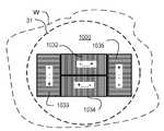
10 shows a second example of a modified multiple grating target including a continuous bias feature in accordance with an aspect of the present disclosure.
11 shows an image of the target of FIG. 10 obtained by the scatterometer of FIG. 3.
Fig. 12(a) schematically shows in detail the implementation of a continuous bias within one grating of the target of Fig. 10, and Fig. 12(b) shows the variation of the bias with position within such a grating.
FIG. 13 schematically shows in detail the implementation of a continuous bias within two gratings of the multi-grid target of FIG. 10 under conditions of (a) zero overlay and (b) non-zero overlay according to an embodiment of the present specification.
14 is a flowchart showing steps of an overlay measurement method using the scatterometer of FIG. 3.
FIG. 15 is a diagrammatic description of a calculation principle of an overlay error according to an embodiment of the present specification, (a) shows signal processing related to the first grid among the grids shown in FIG. 13, and (b) is It shows signal processing related to other gratings among the gratings shown in FIG.
16 schematically shows in detail the implementation of continuous bias within two gratings of a modified multi-grating target including the provision of anchor points according to another embodiment of the present disclosure.
FIG. 17(a) shows that a bias slope change is included as an example of an anchor point in the multi-grid target of FIG. 16, and (b) shows an asymmetric signal obtained from the grating shown in FIG. 16 under a non-zero overlay condition, (c) shows correcting the asymmetric signal using the knowledge of the anchor point.
18 shows an example of a grating with multi-step bias as an alternative to continuous bias according to another example herein.
19 illustrates a multiple grating target having a double bias grating according to another example herein.
20 illustrates an alternative grating target with overlay bias in two directions based on an L-shaped feature.
FIG. 21 illustrates a modified version of the grating of FIG. 20, modified to include a multi-step arrangement of bias regions.
FIG. 22 illustrates another modified version of the grating of FIG. 20, modified to include a continuous bias by rotation of an L-shaped feature according to another embodiment of the present specification.
23 and 24 illustrate a target having a multi-step arrangement of bias regions in four quadrants based on the arrangement of FIG. 21.
본 발명의 실시예를 상세하게 설명하기 전에, 본 발명의 실시예가 구현될 수 있는 예시적인 환경을 제시하는 것이 유익하다.Before describing the embodiments of the present invention in detail, it is beneficial to present an exemplary environment in which the embodiments of the present invention may be implemented.
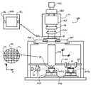
도 1은 리소그래피 장치(LA)를 개략적으로 나타낸다. 리소그래피 장치는 방사선 빔(B)(예를 들어, UV 방사선 또는 DUV 방사선)을 조절하도록 구성된 조명 광학 시스템(조명기)(IL), 패터닝 디바이스(예를 들어, 마스크)(MA)를 지지하도록 구성되고 또한 특정 파라미터에 따라 패터닝 디바이스를 정확히 위치시키도록 구성된 제1 위치설정기(PM)에 연결된 패터닝 디바이스 지지체 또는 지지 구조체(예를 들어, 마스크 테이블)(MT); 기판(예를 들어, 레지스트로 코팅된 웨이퍼)(W)을 유지하도록 구성되고 또한 특정의 파라미터에 따라 기판을 정확하게 위치시키도록 구성된 제2 위치설정기(PW)에 연결된 기판 테이블(예를 들어, 웨이퍼 테이블)(WT); 및 패터닝 디바이스(MA)에 의해 방사선 빔(B)에 부여된 패턴을 기판(W)의 타겟부(C)(예를 들어, 하나 이상의 다이를 포함) 상에 투영하도록 구성된 투영 광학 시스템(예를 들어, 굴절형 투영 렌즈 시스템)(PS)을 포함한다.1 schematically shows a lithographic apparatus LA. The lithographic apparatus is configured to support an illumination optical system (illuminator) IL configured to modulate a radiation beam B (e.g., UV radiation or DUV radiation), a patterning device (e.g., a mask) MA, and In addition, a patterning device support or support structure (eg, a mask table) MT connected to a first positioner PM configured to accurately position the patterning device according to a specific parameter; A substrate table (e.g., a substrate table (e.g., a resist coated wafer) W) connected to a second positioner (PW) configured to hold the substrate (W) and also configured to accurately position the substrate according to certain parameters. Wafer table) (WT); And a projection optical system configured to project the pattern imparted to the radiation beam B by the patterning device MA onto the target portion C of the substrate W (e.g., including one or more dies). For example, a refractive projection lens system) (PS).
조명 광학 시스템은 방사선을 지향, 성형(shaping) 또는 제어하기 위한, 굴절형, 반사형, 자기형, 전자기형, 정전기형 또는 그 외 다른 유형의 광학 컴포넌트, 또는 이들의 임의의 조합 등의 다양한 유형의 광학 또는 비광학 컴포넌트를 포함할 수 있다.Illumination optical systems are of various types, such as refractive, reflective, magnetic, electromagnetic, electrostatic or any other type of optical component, or any combination thereof, for directing, shaping or controlling radiation. Optical or non-optical components.
패터닝 디바이스 지지체는 패터닝 디바이스의 배향, 리소그래피 장치의 설계, 및 예를 들어 패터닝 디바이스가 진공 환경에 유지되고 있는지 여부 등의 기타 조건에 의존하는 방식으로 패터닝 디바이스를 유지한다. 패터닝 디바이스 지지체는 기계식, 진공식, 정전식 또는 다른 클램핑 기술을 사용하여 패터닝 디바이스를 유지할 수 있다. 패터닝 디바이스 지지체는 예를 들어, 필요에 따라 고정되거나 이동가능한 프레임 또는 테이블이 될 수 있다. 패터닝 디바이스 지지체는 패터닝 디바이스가 예를 들어 투영 시스템에 대해 원하는 위치에 있도록 보장할 수 있다. 본 명세서에서 "레티클" 또는 "마스크"라는 용어의 어떠한 사용도 "패터닝 디바이스"라는 좀 더 일반적인 용어와 동의어로 간주될 수 있다.The patterning device support holds the patterning device in a manner that depends on the orientation of the patterning device, the design of the lithographic apparatus, and other conditions such as, for example, whether the patterning device is being held in a vacuum environment. The patterning device support can hold the patterning device using mechanical, vacuum, electrostatic or other clamping techniques. The patterning device support can be, for example, a frame or table that is fixed or movable as required. The patterning device support can ensure that the patterning device is in a desired position, for example relative to the projection system. Any use of the terms "reticle" or "mask" herein may be considered synonymous with the more general term "patterning device".
본 명세서에서 사용되는 "패터닝 디바이스"라는 용어는 기판의 타겟부에 패턴을 생성하기 위해 방사선 빔의 단면에 패턴을 부여하는 데 사용될 수 있는 임의의 디바이스를 지칭하는 것으로 폭넓게 해석되어야 한다. 방사선 빔에 부여된 패턴은, 예를 들어 패턴이 위상-시프팅 피처 또는 소위 어시스트 피처를 포함하는 경우, 기판의 타겟부에서의 원하는 패턴과 정확히 일치하지 않을 수도 있다는 점에 주목해야 한다. 일반적으로, 방사선 빔에 부여된 패턴은 집적 회로와 같이 타겟부에 생성되는 디바이스의 특정 기능 층에 해당할 것이다.The term "patterning device" as used herein should be broadly interpreted as referring to any device that can be used to impart a pattern in a cross-section of a radiation beam to create a pattern in a target portion of a substrate. It should be noted that the pattern imparted to the radiation beam may not exactly match the desired pattern at the target portion of the substrate, for example if the pattern comprises a phase-shifting feature or a so-called assist feature. In general, the pattern imparted to the radiation beam will correspond to a specific functional layer of a device being created in the target portion, such as an integrated circuit.
패터닝 디바이스는 투과형 또는 반사형일 수 있다. 패터닝 디바이스의 예는 마스크, 프로그램 가능한 미러 어레이 및 프로그램 가능한 LCD 패널을 포함한다. 마스크는 리소그래피에서 잘 알려져 있으며 바이너리, 교번 위상 시프트 및 감쇠 위상 시프트와 같은 마스크 타입은 물론 다양한 하이브리드 마스크 타입을 포함한다. 프로그램 가능한 미러 어레이의 예는 입사하는 방사선 빔을 다양한 방향으로 반사시키도록 각각 개별적으로 기울어질 수 있는 작은 미러의 매트릭스 배열을 채용한다. 기울어진 미러는 미러 매트릭스에 의해 반사되는 방사선 빔에 패턴을 부여한다.The patterning device may be transmissive or reflective. Examples of patterning devices include masks, programmable mirror arrays, and programmable LCD panels. Masks are well known in lithography and include a variety of hybrid mask types as well as mask types such as binary, alternating phase shift and attenuated phase shift. An example of a programmable mirror array employs a matrix array of small mirrors, each of which can be individually tilted to reflect an incident radiation beam in various directions. The tilted mirror imparts a pattern to the radiation beam reflected by the mirror matrix.
도시된 바와 같이, 상기 장치는 투과형(예를 들어, 투과형 마스크를 채택)이다. 대안적으로, 장치는 반사형(예를 들어, 위에서 언급된 바와 같은 유형의 프로그램 가능한 미러 어레이를 채택하거나, 반사형 마스크를 채택함)일 수 있다.As shown, the device is of a transmissive type (eg, employing a transmissive mask). Alternatively, the device may be reflective (eg employing a programmable mirror array of the type as mentioned above, or employing a reflective mask).
또한, 리소그래피 장치는 투영 시스템과 기판 사이의 공간을 채우도록, 비교적 높은 굴절률을 갖는 액체, 예를 들어 물로 기판의 적어도 일부가 덮일 수 있는 유형일 수도 있다. 액침액은 또한 리소그래피 장치의 다른 공간, 예를 들어, 마스크와 투영 시스템 사이에 적용될 수 있다. 액침 기술은 투영 시스템의 개구수를 증가시키기 위해 당해 기술 분야에서 잘 알려져 있다. 본 명세서에서 사용되는 "액침"이라는 용어는 기판과 같은 구조체가 액체에 잠겨야 함을 의미하는 것이 아니라 오히려 액체가 노광 중에 투영 시스템과 기판 사이에 위치한다는 것을 의미한다.Further, the lithographic apparatus may be of a type in which at least a portion of the substrate can be covered with a liquid having a relatively high refractive index, for example water, to fill the space between the projection system and the substrate. The immersion liquid can also be applied to other spaces of the lithographic apparatus, for example between the mask and the projection system. Liquid immersion techniques are well known in the art for increasing the numerical aperture of projection systems. The term “liquid immersion” as used herein does not mean that a structure such as a substrate must be immersed in a liquid, but rather that the liquid is positioned between the projection system and the substrate during exposure.
도 1을 참조하면, 조명기(IL)는 방사선 소스(SO)로부터 방사선 빔을 수광한다. 예를 들어, 방사선 소스가 엑시머 레이저인 경우, 방사선 소스 및 리소그래피 장치는 별개의 개체일 수 있다. 그러한 경우에, 방사선 소스는 리소그래피 장치의 일부를 형성하는 것으로 여겨지지 않으며, 방사선 빔은 예를 들어 적절한 지향 미러 및/또는 빔 확장기를 포함하는 빔 전달 시스템(BD)의 도움으로 방사선 소스(SO)로부터 조명기(IL)로 전달된다. 이와 다른 경우, 예를 들어 방사선 소스가 수은 램프인 경우, 소스는 리소그래피 장치에 통합된 부분일 수 있다. 방사선 소스(SO) 및 조명기(IL)는 필요에 따라 빔 전달 시스템(BD)과 함께 방사선 시스템으로 지칭될 수 있다.Referring to FIG. 1, the illuminator IL receives a radiation beam from a radiation source SO. For example, if the radiation source is an excimer laser, the radiation source and the lithographic apparatus may be separate entities. In such a case, the radiation source is not considered to form part of the lithographic apparatus, and the radiation beam is a radiation source SO with the help of a beam delivery system BD comprising a suitable directing mirror and/or a beam expander, for example. It is transmitted from to the fixture (IL). In other cases, for example if the radiation source is a mercury lamp, the source may be an integral part of the lithographic apparatus. The radiation source SO and the illuminator IL may be referred to as a radiation system together with a beam delivery system BD as needed.
조명기(IL)는 방사선 빔의 각도 세기 분포를 조정하기 위한 조정기(AD)를 포함할 수 있다. 일반적으로, 조명기의 퓨필 평면 내의 세기 분포의 적어도 외측 및/또는 내측 반경방향 치수(일반적으로 각각 외측-σ 및 내측-σ로 지칭됨)가 조정될 수 있다. 또한, 조명기(IL)는 집속기(IN) 및 집광기(CO)와 같은 다양한 다른 컴포넌트들을 포함할 수 있다. 조명기는 단면에 원하는 균일성과 세기 분포를 갖도록 방사선 빔을 컨디셔닝하는 데 사용될 수 있다.The illuminator IL may include an adjuster AD for adjusting the angular intensity distribution of the radiation beam. In general, at least the outer and/or inner radial dimensions of the intensity distribution in the pupil plane of the illuminator (commonly referred to as σ-outer and σ-inner, respectively) can be adjusted. Further, the illuminator IL may include various other components such as a concentrator IN and a concentrator CO. The illuminator can be used to condition the radiation beam to have the desired uniformity and intensity distribution in the cross section.
방사선 빔(B)은 패터닝 디바이스 지지체(예를 들어, 마스크 테이블)(MT) 상에 유지되는 패터닝 디바이스(예를 들어, 마스크)(MA) 상에 입사되고, 패터닝 디바이스에 의해 패터닝된다. 방사선 빔(B)은 패터닝 디바이스(예를 들어, 마스크)(MA)를 지난 후, 투영 광학 시스템(PS)을 통과하여, 기판(W)의 타겟부(C) 상에 빔이 포커싱되고, 타겟부(C) 상에 패턴의 이미지를 투영하게 된다. 제2 위치설정기(PW)와 위치 센서(IF)(예를 들어, 간섭계 디바이스, 선형 엔코더, 2-D 인코더 또는 용량성 센서)를 이용하여, 기판 테이블(WT)을 정확하게 이동시켜, 예를 들어 여러 타겟부(C)를 방사선 빔(B)의 경로 내에 위치시킬 수 있다. 마찬가지로, 제1 위치설정기(PM) 및 다른 위치 센서(도 1에 명시적으로 도시되어 있지 않음)를 이용하여, 예를 들어, 마스크 라이브러리로부터의 기계적 인출 이후 또는 스캔 중에, 패터닝 디바이스(예를 들어, 마스크)(MA)를 방사선 빔(B)의 경로에 대하여 정확하게 위치시킬 수 있다.The radiation beam B is incident on a patterning device (eg, a mask) MA, which is held on a patterning device support (eg, a mask table) MT, and is patterned by the patterning device. The radiation beam B passes through the patterning device (e.g., mask) MA, and then passes through the projection optical system PS, so that the beam is focused on the target portion C of the substrate W, and the target The image of the pattern is projected onto the part (C). Using a second positioner (PW) and a position sensor (IF) (e.g., an interferometric device, a linear encoder, a 2-D encoder or a capacitive sensor), the substrate table WT is accurately moved, e.g. For example, it is possible to position several target portions C in the path of the radiation beam B. Similarly, using a first positioner PM and another position sensor (not explicitly shown in Fig. 1), for example, after a mechanical withdrawal from the mask library or during a scan, a patterning device (e.g. For example, it is possible to accurately position the mask MA with respect to the path of the radiation beam B.
패터닝 디바이스(예컨대, 마스크)(MA) 및 기판(W)은 마스크 정렬 마크(M1, M2) 및 기판 정렬 마크(P1, P2)를 사용하여 정렬될 수 있다. 도시된 바와 같은 기판 정렬 마크는 전용화된 타겟부를 점유하지만, 이들은 타겟부 사이의 공간에 위치할 수도 있다(이들은 스크라이브-레인 정렬 마크(scribe-lane alignment mark)로 알려져 있다). 유사하게, 둘 이상의 다이가 패터닝 디바이스(예컨대, 마스크)(MA) 상에 제공되는 상황에서 마스크 정렬 마크는 다이들 사이에 위치될 수 있다. 디바이스 피처 사이에서 다이 내에 작은 정렬 마커가 포함될 수도 있는데, 이러한 경우 마커는 가능한 작고 인접한 피처와는 다른 이미징 또는 프로세스 조건을 필요로 하지 않는 것이 바람직하다. 정렬 마커를 검출하는 정렬 시스템에 관해 이하에서 더 설명할 것이다.The patterning device (eg, mask) MA and the substrate W may be aligned using mask alignment marks M1 and M2 and substrate alignment marks P1 and P2. The substrate alignment marks as shown occupy dedicated target portions, but they may also be located in the space between the target portions (they are known as scribe-lane alignment marks). Similarly, in situations in which more than one die is provided on the patterning device (eg, mask) MA, the mask alignment mark may be located between the dies. Small alignment markers may also be included within the die between device features, in which case it is desirable that the markers are as small as possible and do not require different imaging or process conditions than adjacent features. An alignment system that detects an alignment marker will be described further below.
이러한 예에서 리소그래피 장치(LA)는 2개의 기판 테이블(WTa, WTb) 및 기판 테이블이 그 사이에서 교환될 수 있는 2개의 스테이션 - 노광 스테이션 및 측정 스테이션 - 을 갖는 이른바 듀얼 스테이지 타입이다. 하나의 기판 테이블 상의 하나의 기판이 노광 스테이션에서 노광되는 동안, 다른 기판이 측정 스테이션에서 나머지 기판 테이블 상에 로딩될 수 있고 다양한 준비 단계가 수행될 수 있다. 이러한 준비 단계는 레벨 센서(LS)를 사용하여 기판의 표면 제어를 매핑하고 정렬 센서(AS)를 사용하여 기판 상의 정렬 마커의 위치를 측정하는 단계를 포함할 수 있다. 이는 장치의 처리량을 실질적으로 증가시킬 수 있다.The lithographic apparatus LA in this example is of a so-called dual stage type having two substrate tables WTa, WTb and two stations-an exposure station and a measurement station-in which the substrate tables can be exchanged. While one substrate on one substrate table is being exposed at the exposure station, another substrate can be loaded on the other substrate table at the measurement station and various preparatory steps can be performed. This preparation step may include mapping the surface control of the substrate using the level sensor LS and measuring the position of the alignment marker on the substrate using the alignment sensor AS. This can substantially increase the throughput of the device.
도시된 리소그래피 장치는 예를 들어 스텝 모드 또는 스캔 모드를 포함하는 다양한 모드로 이용될 수 있다. 리소그래피 장치의 구성 및 동작은 통상의 기술자에게 잘 알려져 있으므로, 본 발명을 이해하기 위해 추가적인 설명은 불필요하다.The illustrated lithographic apparatus can be used in a variety of modes including, for example, a step mode or a scan mode. Since the configuration and operation of the lithographic apparatus are well known to those skilled in the art, no further explanation is necessary to understand the present invention.
도 2에 도시된 바와 같이, 리소그래피 장치(LA)는 리소그래피 셀(LC) 또는 리소셀 또는 클러스터로 지칭되는 리소그래피 시스템의 일부를 형성한다. 리소그래피 셀(LC)은 또한 기판에 노광-전 및 노광-후 프로세스를 수행하기 위한 장치를 포함할 수 있다. 통상적으로, 이러한 장치는 레지스트층을 증착하는 스핀 코터(spin coater)(SC), 노광된 레지스트를 현상하는 현상기(DE), 냉각 플레이트(chill plate, CH), 및 베이크 플레이트(bake plate, BK)를 포함한다. 기판 핸들러 또는 로봇(RO)이 입력/출력 포트(I/O1, I/O2)로부터 기판을 픽업하여, 이를 상이한 프로세스 장치 간에 이동시키며, 그 후 리소그래피 장치의 로딩 베이(loading bay, LB)에 전달한다. 통칭하여 트랙으로도 지칭되는 이들 장치는 감독 제어 시스템(SCS)에 의해 제어되는 트랙 제어 유닛(TCU)의 제어 하에 있게 되며, 감독 제어 시스템은 또한 리소그래피 제어 유닛(LACU)을 통해 리소그래피 장치를 제어한다. 그러므로, 처리량 및 처리 효율을 최대화하기 위해 상이한 장치가 작동될 수 있다.As shown in Fig. 2, the lithographic apparatus LA forms part of a lithographic system referred to as a lithographic cell LC or a lithographic cell or cluster. The lithographic cell LC may also include an apparatus for performing pre-exposure and post-exposure processes on the substrate. Typically, such devices include a spin coater (SC) for depositing a resist layer, a developer (DE) for developing the exposed resist, a chill plate (CH), and a bake plate (BK). Includes. The substrate handler or robot (RO) picks up the substrate from the input/output ports (I/O1, I/O2), moves it between different process units, and then transfers it to the loading bay (LB) of the lithographic apparatus. do. These devices, collectively also referred to as tracks, are under the control of the Track Control Unit (TCU), which is controlled by the Supervisory Control System (SCS), which also controls the lithographic apparatus through the Lithography Control Unit (LACU). . Therefore, different devices can be operated to maximize throughput and processing efficiency.
리소그래피 장치에 의해 노광되는 기판이 정확하고 일관되게 노광되도록, 노광된 기판을 검사하여 후속하는 층들 간의 오버레이 오차, 라인 두께, 임계 치수(CD) 등의 특성을 측정하는 것이 바람직하다. 따라서, 리소셀(LC)이 그 안에 위치되는 제조 설비는, 리소셀 내에서 처리된 기판(W)의 일부 또는 전부를 받아들이는 계측 시스템(MET)을 더 포함한다. 계측 결과는 감독 제어 시스템(SCS)에 직접적으로 또는 간접적으로 제공된다. 오차가 검출되는 경우, 특히 동일한 배치(batch)의 다른 기판들이 여전히 노광될 수 있을 정도로 검사가 충분히 신속하고 빠르게 수행될 수 있다면, 후속 기판의 노광에 대한 조정이 이루어질 수 있다. 또한, 이미 노광된 기판이 수율 개선을 위해 스트리핑 및 재작업될 수 있고, 또는 폐기될 수 있으며, 이로써 결함 있는 것으로 알려진 기판 상에서 추가 처리를 수행하는 것을 피하게 된다. 기판의 단지 특정 타겟 부분만이 결함 있는 경우, 양호한 타겟 부분에 대해서만 추가적인 노광이 행해질 수도 있다.It is desirable to inspect the exposed substrate to measure properties such as overlay error, line thickness, critical dimension (CD), etc. between subsequent layers, so that the substrate exposed by the lithographic apparatus is accurately and consistently exposed. Accordingly, the manufacturing facility in which the lysocell LC is located therein further includes a measurement system MET that accepts some or all of the substrate W processed in the lysocell. The measurement results are provided directly or indirectly to a supervisory control system (SCS). If an error is detected, adjustments to the exposure of subsequent substrates can be made, especially if the inspection can be performed quickly and quickly enough so that other substrates of the same batch can still be exposed. In addition, substrates that have already been exposed may be stripped and reworked to improve yield, or may be discarded, thereby avoiding further processing on substrates known to be defective. If only a specific target portion of the substrate is defective, an additional exposure may be done only for the good target portion.
계측 시스템(MET) 내에서 검사 장치는 기판의 특성을 결정하는 데 사용되며, 특히 동일한 기판의 상이한 층들 또는 상이한 기판들의 특성이 층마다 어떻게 달라지는지를 결정하는 데 사용된다. 이러한 검사 장치는 리소그래피 장치(LA) 또는 리소셀(LC)에 통합될 수 있거나 독립형 디바이스일 수 있다. 가장 신속한 측정을 가능하게 하기 위해, 검사 장치가 노광 직후 노광된 레지스트 층에서 특성을 측정하는 것이 바람직하다. 그러나, 레지스트 내의 잠상은 매우 낮은 콘트라스트를 가지며 - 방사선에 노광된 레지스트의 부분과 방사선에 노광되지 않은 부분 간의 굴절율에 단지 아주 작은 차이가 있음 - 모든 검사 장치가 잠상의 유용한 측정을 행할 수 있을 정도로 충분한 감도를 갖는 것은 아니다. 따라서, 통상적으로 노광된 기판에 대해 수행되는 첫 번째 단계이고 레지스트의 노광된 부분과 노광되지 않은 부분 간의 콘트라스트를 증가시키는 단계인, 노광후 베이크 단계(post-exposure bake step, PEB) 후에 측정이 이루어질 수 있다. 이러한 스테이지에서, 레지스트 내의 이미지는 반잠상(semi-latent)으로 지칭될 수 있다. 또한, 레지스트의 노광된 부분 또는 노광되지 않은 부분 중의 하나를 제거한 시점에서 현상된 레지스트 이미지의 측정을 행하거나, 또는 에칭과 같은 패턴 전사 단계 후에 측정을 행하는 것도 가능하다. 후자의 가능성은 결함이 있는 기판의 재작업에 대한 가능성을 제한하지만, 유용한 정보를 여전히 제공할 수 있다.Within the metrology system (MET) an inspection device is used to determine the properties of a substrate, in particular different layers of the same substrate or how the properties of different substrates vary from layer to layer. Such an inspection apparatus may be integrated into the lithographic apparatus LA or the lithographic apparatus LC or may be a standalone device. In order to enable the fastest measurement, it is desirable for the inspection apparatus to measure the properties in the exposed resist layer immediately after exposure. However, the latent image in the resist has a very low contrast-there is only a very small difference in the refractive index between the portion of the resist exposed to radiation and the portion not exposed to the radiation-enough to allow all inspection devices to make useful measurements of the latent image. It does not have sensitivity. Therefore, measurements are made after the post-exposure bake step (PEB), which is the first step that is typically performed on the exposed substrate and increases the contrast between the exposed and unexposed portions of the resist. I can. At this stage, the image in the resist may be referred to as a semi-latent image. In addition, it is also possible to measure the developed resist image at the time when one of the exposed or unexposed portions of the resist is removed, or after a pattern transfer step such as etching. The latter possibility limits the possibility of reworking a defective substrate, but can still provide useful information.
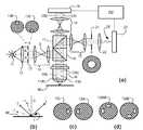
계측 장치가 도 3(a)에 도시되어 있다. 타겟(T)과 이러한 타겟을 조명하는 데 사용되는 측정 방사선의 회절된 광선이 도 3(b)에 보다 상세히 예시되어 있다. 도시된 계측 장치는 암시야 계측 장치로서 알려진 유형이다. 여기에 도시된 계측 장치는 순전히 암시야 계측에 대한 설명을 제공하기 위한 일례이다. 이러한 계측 장치는 독립형 디바이스이어도 되고, 또는 예컨대 측정 스테이션에서 리소그래피 장치(LA)에 또는 리소그래피 셀(LC)에 통합될 수도 있다. 장치 도처에서 여러 개의 브랜치를 갖는 광축은 점선 O로 표시되어 있다. 이러한 장치에서, 광원(11)(예를 들어, 크세논 램프)에 의해 방출된 광은 빔 스플리터(15)를 통해 렌즈(12, 14) 및 대물 렌즈(16)를 포함하는 광학 시스템에 의해 기판(W) 상으로 지향된다. 이들 렌즈는 4F 배열의 이중 시퀀스로 배치된다. 기판 이미지를 여전히 검출기 상에 제공하고 동시에 공간 주파수 필터링을 위해 중간 퓨필 평면에 대한 액세스를 허용한다면, 상이한 렌즈 배열이 사용될 수 있다. 따라서, 방사선이 기판 상에 입사하는 각도 범위는, 여기에서(공액) 퓨필 평면으로 지칭되는, 기판 평면의 공간 스펙트럼을 제공하는 평면에서의 공간 세기 분포를 규정함으로써 선택될 수 있다. 특히, 이것은 대물 렌즈 퓨필 평면의 역-투영 이미지(back-projected image)인 평면에서, 렌즈(12)와 렌즈(14) 사이에 적합한 형태의 개구 플레이트(13)를 삽입함으로써 행해질 수 있다. 예시된 실시예에서, 개구 플레이트(13)는 상이한 조명 모드가 선택될 수 있도록 13N 및 13S로 표시된 상이한 형태를 갖는다. 본 예에서의 조명 시스템은 축외 조명 모드를 형성한다. 제1 조명 모드에서, 개구 플레이트(13N)는, 단지 설명을 목적으로 "북쪽"으로 지정된 방향으로부터 축외 조명을 제공한다. 제2 조명 모드에서, 개구 플레이트(13S)는 유사한 조명을 제공하지만 "남쪽"으로 표시된 반대 방향으로부터 조명을 제공하기 위해 이용된다. 상이한 개구를 사용함으로써 다른 조명 모드도 가능하다. 요구되는 조명 모드 밖의 임의의 불필요한 광은 요구되는 측정 신호와 간섭할 것이기 때문에 퓨필 평면의 나머지는 어두운 것이 바람직하다.The measuring device is shown in Fig. 3(a). The target T and the diffracted rays of measurement radiation used to illuminate this target are illustrated in more detail in Fig. 3(b). The illustrated metrology device is of the type known as a dark field metrology device. The measurement device shown here is purely an example to provide an explanation for dark field measurement. This metrology apparatus may be a standalone device or may be integrated into the lithographic apparatus LA or in the lithographic cell LC, for example at a measurement station. The optical axis with multiple branches throughout the device is indicated by the dotted line O. In such a device, the light emitted by the light source 11 (e.g., a xenon lamp) is transmitted through a
도 3(b)에 도시된 바와 같이, 타겟(T)은 기판(W)이 대물 렌즈(16)의 광축(O)에 수직인 상태로 배치된다. 기판(W)은 지지체(미도시)에 의해 지지될 수 있다. 축(O)에서 벗어난 각도로 타겟(T) 상에 충돌하는 측정 방사선 광선(I)은 하나의 0차 광선(실선 0) 및 2개의 1차 광선(일점쇄선 +1과 이점쇄선 -1)을 발생시킨다. 오버필된 소형 타겟을 이용하는 경우, 이들 광선은 계측 타겟(T) 및 기타 피처를 포함한 기판의 영역을 커버하는 다수의 평행 광선 중의 단지 하나가 된다는 점을 기억해야 한다. 플레이트(13)의 개구가 (유용한 광량을 허용하는데 필요한) 한정된 폭을 가지므로, 입사 광선(I)은 실제로는 일정 범위의 각도를 점유할 것이고, 회절 광선 0차와 +1/-1차가 다소 확산될(spread out) 것이다. 소형 타겟의 포인트 확산 함수에 따라, 각각의 차수 +1과 -1은 도시된 바와 같이 단일의 이상적인 광선이 아니라 일정 범위의 각도에 걸쳐 추가로 확산될 것이다. 타겟의 격자 피치 및 조명 각도는 대물 렌즈에 진입하는 1차 광선이 중앙의 광축과 근접하게 정렬되도록 설계되거나 조정될 수 있다는 것에 주목해야 한다. 도 3(a) 및 도 3(b)에 예시된 광선은 순전히 이들이 도면에서 보다 용이하게 구별될 수 있도록 하기 위해 다소 축을 벗어난 것으로 도시되어 있다.As shown in FIG. 3B, the target T is disposed in a state in which the substrate W is perpendicular to the optical axis O of the
기판(W) 상의 타겟(T)에 의해 회절된 적어도 0차와 +1차 회절 광선은 대물 렌즈(16)에 의해 집광되고, 빔 스플리터(15)를 통해 역으로 지향된다. 도 3(a)로 돌아가서, 제1 조명 모드와 제2 조명 모드 둘 모두가 북쪽(N)과 남쪽(S)으로 표시된 정반대 측의 개구를 지정하는 것으로 예시되어 있다. 측정 방사선의 입사 광선(I)이 광축의 북쪽 측으로부터 기인한 것인 경우, 즉 제1 조명 모드가 개구 플레이트(13N)를 이용하여 적용된 경우에는, +1차 회절 광선(+1(N)으로 표시됨)이 대물 렌즈(16)에 진입한다. 반대로, 제2 조명 모드가 개구 플레이트(13S)를 이용하여 적용된 경우에는, -1차 회절 광선(-1(S)로 표시됨)이 렌즈(16)에 진입하는 광선이 된다.At least the 0th and +1st order diffracted rays diffracted by the target T on the substrate W are condensed by the
제2의 빔 스플리터(17)는 회절 빔을 2개의 측정 브랜치로 분할한다. 제1 측정 브랜치에서, 광학 시스템(18)은 0차 및 1차 회절 빔을 이용하여 제1 센서(19)(예컨대, CCD 또는 CMOS 센서) 상에 타겟의 회절 스펙트럼(퓨필 평면 이미지)을 형성한다. 각각의 회절 차수는 센서 상의 상이한 포인트에 충돌하며, 이로써 이미지 처리가 차수를 비교하고 대비(contrast)할 수 있게 된다. 센서(19)에 의해 캡쳐된 퓨필 평면 이미지는 계측 장치를 포커싱하거나 및/또는 1차 빔의 세기 측정치를 정규화하기 위해 이용될 수 있다. 퓨필 평면 이미지는 또한 재구성과 같은 수많은 측정 목적을 위해 사용될 수 있다.The
제2 측정 브랜치에서, 광학 시스템(20, 22)은 센서(23)(예컨대, CCD 또는 CMOS 센서) 상에 타겟(T)의 이미지를 형성한다. 제2 측정 브랜치에서, 퓨필 평면에 공액 관계를 이루는 평면에 구경 조리개(21)가 제공된다. 구경 조리개(21)는 센서(23) 상에 형성된 타겟의 이미지가 -1차 또는 +1차 빔으로만 형성되도록 0차 회절 빔을 차단하도록 기능한다. 센서(19, 23)에 의해 캡쳐된 이미지는 이러한 이미지를 처리하는 프로세서(PU)에 출력되며, 프로세서의 기능은 수행되는 측정의 특정한 타입에 좌우될 것이다. "이미지"라는 용어는 본 명세서에서는 넓은 의미로 사용된다는 것을 유의하기 바란다. 이와 같은 격라 라인의 이미지는 -1 및 +1 차수 중의 하나만이 제공되는 경우에는 형성되지 않을 것이다.In the second measurement branch, the
도 3에 도시된 개구 플레이트(13) 및 시야 조리개(21)의 구체적인 형태는 단지 예에 불과하다. 본 발명의 또 다른 실시예에서는, 타겟의 축상 조명이 사용되고, 실질적으로 단지 하나의 1차 회절 광만을 센서에 전달하기 위하여 축외 개구를 갖는 구경 조리개가 사용된다. 다른 예로서 2-사분면 개구가 사용될 수도 있다. 이렇게 하면 위에서 언급한 US2010201963A1에 기술된 바와 같이 플러스 및 마이너스 차수를 동시에 검출할 수 있게 된다. 검출 브랜치 내에 광학 웨지(세그먼트화된 프리즘 또는 다른 적절한 요소)를 갖는 실시예는, 위에서 언급한 US2011102753A1에 기술된 바와 같이, 단일 이미지에서 공간적으로 이미징을 위한 차수를 분리하기 위해 사용될 수 있다. 또 다른 실시예에서, 측정에 있어서 1차 빔 대신 또는 1차 빔에 추가하여 2차, 3차 및 더 높은 차수의 빔(도 3에 도시되지 않음)이 사용될 수 있다 또 다른 실시예로서, 세그먼트화된 프리즘이 구경 조리개(21) 대신에 사용될 수 있으며, 이 경우 +1 및 -1 차수가 이미지 센서(23) 상의 공간적으로 분리된 위치에서 동시에 캡처될 수 있다.The specific shapes of the
측정 방사선을 이들 상이한 타입의 측정에 적합화시키기 위해, 개구 플레이트(13)는 원하는 패턴을 제 위치에 놓이게 하도록 회전하는 디스크 둘레에 형성된 다수의 개구 패턴을 포함할 수 있다. 개구 플레이트(13N 또는 13S)는 하나의 방향(설정에 따라 X 또는 Y)으로 배향된 격자를 측정하는 데에만 사용될 수 있다는 것을 유의해야 한다. 직교 격자의 측정을 위해, 90 ° 및 270 °만큼 타겟의 회전이 구현될 수 있다. 상이한 개구 플레이트가 도 3(c) 및 3(d)에 도시되어 있다. 이를 이용하는 것과 장치의 수많은 기타 변형예 및 응용예가 위에서 언급한 종래의 특허 문헌에 기술되어 있다.In order to adapt the measurement radiation to these different types of measurements, the
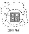
도 4는 공지된 방법에 따라 기판 상에 형성된 오버레이 타겟 또는 복합 오버레이 타겟을 도시한다. 이러한 예에서의 오버레이 타겟은 조밀하게 함께 위치된 4개의 서브타겟(32 내지 35)을 포함하여, 이들이 계측 장치의 계측 방사선 조명 빔에 의해 형성된 측정 스폿(31) 내에 모두 있게 된다. 따라서 4개의 서브 오버레이 타겟은 모두 동시에 조명되고 센서(23) 상에 동시에 이미징된다. 오버레이의 측정에 전용화된 예에서, 서브타겟(32 내지 35)은 그 자체로, 기판(W) 상에 형성된 반도체 디바이스의 상이한 층들에 패터닝되는 중첩되는 격자들에 의해 형성된 복합 구조체이다. 서브타겟(32 내지 35)은 복합 서브타겟의 상이한 부분들이 형성되는 층들 사이의 오버레이의 측정을 용이하게 하기 위해 상이하게 바이어스된 오버레이 오프셋들을 가질 수도 있다. 오버레이 바이어스의 의미는 이하에서 도 7과 관련하여 설명할 것이다. 서브타겟(32 내지 35)은 또한, X 및 Y 방향으로 입사하는 방사선을 회절시키도록, 도시된 바와 같이 그 배향이 다를 수 있다. 일례에서, 서브타겟(32 및 34)은 각각 +d, -d의 바이어스를 갖는 X-방향 서브타겟이다. 서브타겟(33 및 35)은 각각 오프셋 +d 및 -d를 갖는 Y-방향 서브타겟이다. 이들 서브타겟에 대한 별개의 이미지가 센서(23)에 의해 캡쳐된 이미지에서 식별될 수 있다. 이는 오버레이 타겟의 한 가지 예시일 뿐이다. 오버레이 타겟은 4개보다 많거나 적은 서브타겟을 포함할 수도 있다.4 shows an overlay target or a composite overlay target formed on a substrate according to a known method. The overlay target in this example comprises four
도 5는 도 3(d)로부터의 개구 플레이트(13NW 또는 13SE)를 이용하여, 도 3의 장치에서 도 4의 오버레이 타겟을 사용하여, 센서(23) 상에 형성되어 센서에 의해 검출될 수 있는 이미지의 예를 도시한다. 퓨필 평면 이미지 센서(19)는 상이한 개별 서브타겟들(25a 내지 25d)을 분해할 수는 없지만, 이미지 센서(23)는 그렇게 할 수 있다. 빗금친 영역(40)은, 기판 상의 조명된 스폿(31)이 대응하는 원형 영역(41)으로 이미징되는, 센서 상의 이미지의 필드를 나타낸다. 이러한 이미지 내에서, 직사각형 영역(42-45)은 작은 오버레이 서브타겟(32 내지 35)의 이미지를 나타낸다. 오버레이 타겟이 제품 영역에 있는 경우 이러한 이미지 필드의 주변부에 제품 피처가 보일 수도 있다. 이미지 프로세서 및 컨트롤러(PU)는 패턴 인식을 사용해 이들 이미지를 처리하여 서브타겟(32 내지 35)의 별개 이미지(42 내지 45)를 식별한다. 이런 식으로, 이미지는 센서 프레임 내의 특정 위치에 매우 정밀하게 정렬될 필요가 없으며, 이는 전체적으로 측정 장치의 처리량을 크게 개선한다.5 is formed on the
일단 서브타겟의 별개 이미지가 식별되면, 이러한 개별 이미지의 세기가, 예를 들어 식별된 영역 내에서 선택된 픽셀 세기 값을 평균화하거나 합산함으로써 측정될 수 있다. 이미지들의 세기 및/또는 다른 특성을 서로 비교할 수 있다. 리소그래피 프로세스의 상이한 파라미터를 측정하기 위해 이러한 결과는 조합될 수 있다. 오버레이 성능은 이러한 파라미터의 중요한 예이다.Once separate images of the subtarget are identified, the intensity of these individual images can be measured, for example, by averaging or summing selected pixel intensity values within the identified area. The intensity and/or other characteristics of the images can be compared with each other. These results can be combined to measure different parameters of the lithographic process. Overlay performance is an important example of this parameter.
예를 들어 위에서 언급한 US20110027704A 등의 출원에 기술된 방법을 이용하면, 서브타겟(32 내지 35) 내에서 2개의 층 사이의 오버레이 오차(즉, 원치 않는 그리고 의도하지 않은 오버레이 오정렬)가 측정된다. 이러한 방법은 마이크로 회절 기반 오버레이(μDBO)라고 할 수도 있다. 이러한 측정은, 세기 비대칭의 척도를 얻기 위해 +1차 및 -1차 암시야 이미지의 세기를 비교함으로써 드러나는 바와 같이 (다른 대응하는 더 높은 차수의 세기, 예컨대 +2 및 -2차를 비교할 수도 있음) 오버레이 타겟 비대칭을 통해 수행된다. Using the method described in, for example, an application such as US20110027704A mentioned above, an overlay error between two layers (i.e., undesired and unintended overlay misalignment) within the subtargets 32-35 is measured. This method can also be referred to as a micro diffraction based overlay (μDBO). These measurements can also be compared to other corresponding higher-order intensities, such as +2 and -2, as revealed by comparing the intensities of the +1st and -1st order darkfield images to obtain a measure of intensity asymmetry. ) Performed through overlay target asymmetry.
도 4에 예시된 것과 같은 다중 격자 타겟을 사용하는 알려진 방법에서는, 오버레이(OV)가 다음 방정식을 통해 결정될 수 있다.In a known method of using a multi-grid target as illustrated in FIG. 4, the overlay (OV) can be determined through the following equation.


여기서:here:


식 1은 감도 계수 K에 관해 다시 표현될 수 있는데, 이러한 계수는 (완벽한 타겟이라 가정할 때) 오버레이와는 독립적이라는 특별한 특성을 갖는 스택 의존 파라미터이다.

여기서:here:

식 2는, 서브타겟을 형성하는 격자의 피치와 비교하여, 작은 바이어스 값과 오버레이 오차를 가정한 것에 기초하는 단순한 선형적인 방정식이지만, 보다 넓은 범위에 걸친 바이어스와 오버레이 오차에 대한 비대칭의 의존관계는 실질적으로 정현파 형태를 갖는다. 식 2의 선형 모델 대신에 정현파 모델을 사용할 수도 있다.
4개의 별개의 서브타겟을 사용하는 공지된 방법에서는, 이미지(40) 내에서 서브타겟들이 구별되도록 각 서브타겟 주변에 경계를 필요로 한다(도 4 및 도 5에는 도시되어 있지 않음). 이는, 패터닝된 영역의 특정 부분이 엣지 효과로 인해 사용될 수 없음을 의미한다. 부가적으로, 2개의 특정 오프셋만 사용하게 되면 위에서 언급한 선형성에 대한 가정이 강요되므로, 실제 관계가 비선형일 때 부정확해질 수 있다.In the known method of using four separate sub-targets, a boundary is required around each sub-target so that the sub-targets are distinguished within the image 40 (not shown in Figs. 4 and 5). This means that a specific part of the patterned area cannot be used due to the edge effect. Additionally, if only two specific offsets are used, the above-mentioned assumption about linearity is enforced, so it may become inaccurate when the actual relationship is nonlinear.
다음 내용에서는 연속적인 바이어스 변동 및/또는 다수의 바이어스 값을 갖는 오버레이 타겟을 포함하는 솔루션을 제안한다. 방금 설명한 이미지 평면 오버레이 측정 기법에 적용될 때, 이러한 다수의 바이어스 값이 타겟 영역에 걸친 세기 이미지에 나타날 수 있다. 양호한 정보가 사용되고 있음을 보장하기 위해 선형성 및/또는 정현파 피팅에 대한 검증이 수행될 수 있다. 또한, 오버레이에 대한 타겟 및 측정 장치의 감도 및 기타 요인에 대한 추가의 정보가 획득될 수 있다. 실시예는, 오버레이 격자를 형성하는 하나 또는 두 격자의 회전 또는 엇갈림(staggering)에 기초하여 예시될 것이다. 실시예는 상부 및 하부 격자의 상이한 피치에 기초하여 예시될 것이다. 적절한 설계를 통해 현재의 영역보다 많은 영역이 신호 결정에 사용될 수 있다. 현재 기술에 비해 타겟 크기가 줄어들고 및/또는 측정 정확도가 향상될 수 있다.In the following, a solution including an overlay target having a continuous bias fluctuation and/or a plurality of bias values is proposed. When applied to the image plane overlay measurement technique just described, these multiple bias values can appear in the intensity image over the target area. Verification of linearity and/or sinusoidal fit can be performed to ensure that good information is being used. In addition, additional information about the sensitivity of the target and the measurement device to the overlay and other factors may be obtained. An embodiment will be illustrated based on the rotation or staggering of one or two gratings forming an overlay grating. Embodiments will be illustrated based on different pitches of the upper and lower gratings. With proper design, more areas than the current area can be used for signal determination. Compared to the current technology, the target size may be reduced and/or measurement accuracy may be improved.
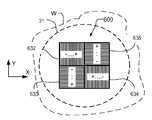
도 6은 개별적인 서브타겟(632 내지 635)을 포함하는 다중 격자 타겟(600)을 도시한다. 도 4의 타겟에서와 같이 4개의 서브타겟은 X 방향 측정을 위한 2개의 오버레이 격자와 Y 방향 측정을 위한 2개의 오버레이 격자를 포함한다. 그러나 각각의 격자 내에 고정된 오버레이 바이어스를 제공하는 대신, 음의 값, 양의 값 및 중간 값을 포함하는 다단(multi-step) 또는 연속적인 바이어스 변동이 제공된다. 격자(632 및 635)는 각각 X 및 Y에 따라 증가하는 바이어스 값을 갖는다. 반대로, 격자(633 및 634)는 각각 X 및 Y에 따라 감소하는 바이어스 값을 갖는다. 타겟(600) 및 개별적인 서브타겟이 알려진 타겟과 동일한 치수를 갖는지 또는 더 크거나 더 작게 만들어지는지는 설계 선택의 문제이다.6 shows a
도 7은 도 3의 장치에서 센서(23) 상에 캡처된 대응하는 이미지(740)를 개략적으로 나타낸다. 도면부호 742 내지 745는 개별적인 서브 겟에 대응하는 세기 이미지 영역을 나타낸다. 각각의 서브타겟에 걸친 바이어스의 변동으로 인해, 세기 값은 각 영역 내에서 일정하지 않고 변화한다. 관심 영역(ROI) 대신에, 도시된 바와 같이 바이어스 변동의 방향과 정렬된 "관심 라인"(LOI)를 상상할 수도 있다. 오버레이 측정을 얻기 위해 세기 정보를 처리하는 방식은 후술될 것이다. 먼저, 연속적인 바이어스 타겟의 다양한 가능한 구현이 예시될 것이다.7 schematically shows a
도 6의 서브타겟(632)을 일례로 이용하는 도 8(a)에서, 서브타겟은 하부의 피처(804) 위에 인쇄된 피처(802)를 갖는 오버레이 격자를 포함한다. 본 명세서의 모든 예에서, 피처는 단지 예시를 위해 확대되어 도시된 것임을 이해할 것이다. 실제 격자는 수백 개의 라인으로 구성되는 경향이 있을 수 있다. 피처(804 및 802)는 평행하지 않게 놓이고 그 사이에 작은 편차 각도, 예를 들어 0.1 내지 0.5 °, 예를 들어 0.35 °의 편차 각도를 갖도록 형성된다. 이러한 예에서, 하부의 피처(804)는 y-축에 대해 각도를 이루도록 인쇄된 바 있다. 실제 구현에서, 하나 또는 두 층 모두 이러한 축에 대해 회전가능할 수 있다. 그 결과, 도시된 바와 같은 라인의 배향 내에서, 바이어스 값 d는 타겟의 중앙에 걸친 0의 값으로부터, 중앙 위쪽의 양수 값과 중앙 아래쪽의 음수 값으로 변동된다. 바이어스 값은 X 방향으로의 값이고, 타겟에 걸쳐 Y 방향으로 연속적으로 변동된다. 대안적인 구현으로, 경사진 라인보다는, 하나 또는 두 개의 라인이 일련의 미세한 바이어스 단차를 두고 엇갈려 구현될 수 있다.In FIG. 8(a) using the
도 8(a)에 도시된 상황에서 오버레이 오차(OV)는 0이므로 비대칭(A)은 바이어스가 0인 동일한 선을 따라 0이 된다. 한편, 도 8(b)를 참조하면, X 방향으로의 오버레이가 0이 아닌 경우, 비대칭이 0인 라인은 Y 방향으로 시프트된다.In the situation shown in FIG. 8(a), the overlay error OV is 0, so the asymmetry A becomes 0 along the same line where the bias is 0. On the other hand, referring to FIG. 8B, when the overlay in the X direction is not 0, a line with asymmetry of 0 is shifted in the Y direction.
도 9는, 도 8에 도시된 형태를 가지며 바이어스 변동의 적절한 배향 및 극성을 갖는 4개의 서브타겟(632 내지 635)을 나타낸다.9 shows four
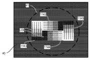
도 10은 1032부터 1035까지 번호가 매겨진 4개의 서브타겟 내에서 연속적인 또는 다단(multi-step) 바이어스를 갖는 또 다른 예시 타겟 설계를 나타낸다. 이 경우 각각의 서브타겟은 정사각형이 아닌 직사각형의 형태를 갖는다. 그렇지 않으면, 격자의 배향 및 바이어스 변동의 극성은 도 6 내지 도 9의 예의 타겟(632 내지 635)에서와 동일하다. 도 11은 서브타겟(1032 내지 1035)에 대응하는 영역(1142 내지 1145)을 갖는 대응하는 이미지를 나타낸다. 다시 말하지만, 바이어스의 변동은 균일한 세기를 갖는 단일한 관심 영역이 아니라 각각의 서브타겟의 이미지에 걸쳐 세기 변동을 유발한다.10 shows another exemplary target design with continuous or multi-step bias within four subtargets numbered from 1032 to 1035. In this case, each sub-target has a shape of a rectangle rather than a square. Otherwise, the orientation of the grating and the polarity of bias fluctuations are the same as in the targets 632-635 of the example of FIGS. 6-9. 11 shows corresponding
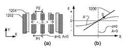
도 12(a)는 도 10의 직사각형의 연속적인 바이어스 서브타겟의 한 가지 가능한 구현예를 보여준다. 설명의 목적으로 과장된 바이어스 변동을 갖는 단지 몇 개의 라인으로만 구성된 격자가 도시된다. 서브타겟의 상부 층에 있는 라인 피처(1202)는 하부 층의 피처(1204) 위에 인쇄된다. 바이어스 변동을 얻기 위해 하나 또는 두 세트의 라인 피처를 회전하는 대신, 이러한 예에서는 상부 및 하부 라인의 격자 피치(주기)가 상이하다. 상부 층의 피처(1202)는 피치 P1로 배열되고, 하부 층의 피처(1204)는 약간 더 작은 피치 P2로 배열된다. 이것은 도 12(b)의 그래프 및 라인(1206)으로 나타낸 바와 같이 바이어스 d의 선형적인 변동을 유발한다. 이러한 라인은 기울기 S를 갖는다. 도 6 내지 도 7의 회전 예와 달리, 바이어스의 변동, 따라서 관심 라인(LOI)은 격자의 주기성 방향과 평행하다.Fig. 12(a) shows one possible implementation of the rectangular continuous bias sub-target of Fig. 10; For illustrative purposes, a grating consisting of only a few lines with exaggerated bias fluctuations is shown. The
그래프에는 또한 격자에 걸친 비대칭(A)의 변동을 표현하는 정현파 곡선이 도시되어 있다. 오버레이 오차가 0이라고 가정하면 바이어스(d)와 비대칭(A)은 표시된 바와 같이 동일한 선을 따라 0이다. 오버레이 오차가 있는 경우 이러한 관계가 깨진다. 오버레이 오차를 결정할 수 있도록, 알려진 제로 바이어스 라인에 대한 제로 비대칭 포인트의 시프트가 측정될 수 있다. 그러나 단일 타겟으로부터 이를 수행하려면, 제로 바이어스 라인의 위치를 알기 위해 타겟의 위치를 매우 정밀하게 측정해야 할 것이다. 도 13에 도시된 바와 같이, 서로 반대의 바이어스 변동을 가진 서브타겟의 보완적인 쌍을 제공하면 오버레이를 보다 정확하게 측정할 수 있으며, 또한 측정 장치에 있어서 프로세스 효과 및 비대칭에 기인한 변동에 대해 측정이 강건해지게 된다.The graph also shows a sinusoidal curve representing the variation of asymmetry (A) across the grating. Assuming that the overlay error is zero, the bias (d) and asymmetry (A) are zero along the same line as indicated. If there is an overlay error, this relationship is broken. To be able to determine the overlay error, the shift of the zero asymmetry point with respect to the known zero bias line can be measured. However, to do this from a single target, you will have to measure the position of the target very precisely to know the position of the zero bias line. As shown in Fig. 13, providing a complementary pair of sub-targets having opposite bias fluctuations allows the overlay to be more accurately measured, and also for the fluctuations due to process effects and asymmetry in the measuring device. You become strong.
도 13은 X 방향으로 (a) 제로 오버레이 오차 및 (b) 비제로 오버레이 오차의 조건 하에서 서브타겟(1032 및 1034)을 나타낸다. 동일한 설명이 Y-방향 서브타겟(1033 및 1035)에 적용될 것임을 이해할 것이다. 표기된 바와 같이, 서브타겟(1032)은 작은 피치(P2) 위에 더 큰 피치(P1)를 갖는다. 바이어스 d는 X가 증가함에 따라 점진적으로 증가한다. 반면, 서브타겟(134)은 더 큰 피치(P1) 위에 더 작은 피치(P2)를 갖는다. 결과적으로 바이어스 d는 X가 증가함에 따라 점진적으로 감소한다.13 shows sub-targets 1032 and 1034 in the X direction under conditions of (a) zero overlay error and (b) non-zero overlay error. It will be appreciated that the same description will apply to the Y-
따라서 오버레이 오차가 도입되면, 도 13(b)에 도시된 바와 같이 2개의 서브타겟에서 제로 비대칭의 라인이 제로 바이어스의 라인에 대해 동일한 크기이지만 반대 방향으로 이동한다. 한 쌍의 서브타겟의 세기 이미지(1142 및 1144)로부터 측정된 비대칭을 비교함으로써 오버레이 오차를 측정할 수 있다.Therefore, when an overlay error is introduced, as shown in FIG. 13(b), a line of zero asymmetry in the two sub-targets is the same size with respect to the line of zero bias, but moves in the opposite direction. The overlay error may be measured by comparing the asymmetry measured from the
완전한 오버레이 측정 방법에 관해 이제 도 10 내지 13의 타겟(1000)의 예를 이용하여 도 14를 참조로 설명할 것이다. 이러한 방법은 도 6 내지 도 9의 연속적인 바이어스 타겟 및 아래에서 추가로 예시되고 설명되는 타겟들을 포함하는 대안적인 예에 적용될 수 있다. 예를 들어, 도 15는 (a) 타겟(1000)의 서브타겟(1032)의 길이에 걸친 비대칭 변동의 측정 및 (b) 서브타겟(1034)의 길이에 걸친 비대칭 변동의 측정에 있어서 방법의 세부 사항을 예시한다.The complete overlay measurement method will now be described with reference to FIG. 14 using an example of the
도 14의 단계 S1에서, 기판, 예를 들어 반도체 웨이퍼는 서브타겟(1032-1035)을 포함하는 오버레이 타겟을 생성하기 위해 리소그래피 장치, 예컨대 도 2의 리소그래피 셀을 통해 1 회 이상 처리된다. S2에서는, 도 3의 계측 장치를 사용하여, 서브타겟(1032 내지 1035)의 이미지가 1차 회절 빔 중 하나(예컨대, -1)만을 사용하여 획득된다. 단계 S3에서, 나머지 1차 회절 빔(+1)을 사용하여 오버레이 타겟의 제2 이미지가 제2 이미지로 캡처된다. 단순함을 위해 단일 이미지를 언급하지만, 이용가능한 정보를 늘리고 요구되는 수준의 측정 성능을 달성하기 위해, 동일한 조명 조건 하에서 또는 서로 다른 조건 하에서 여러 이미지를 취할 수 있다. 조명 조건은 예를 들어 파장 및/또는 편광에 있어서 달라질 수 있다.In step S1 of FIG. 14, a substrate, e.g., a semiconductor wafer, is processed one or more times through a lithographic apparatus, e.g., the lithographic cell of FIG. 2 to create an overlay target comprising sub-targets 1032-1035. In S2, using the metrology device of FIG. 3, images of the sub-targets 1032 to 1035 are acquired using only one of the first order diffracted beams (eg -1). In step S3, a second image of the overlay target is captured as a second image using the remaining first order diffracted beam (+1). While referring to a single image for simplicity, it is possible to take multiple images under the same lighting conditions or under different conditions to increase the available information and achieve the required level of measurement performance. The lighting conditions can vary in wavelength and/or polarization, for example.
각각의 이미지에 1차 회절 방사선의 절반만 포함시킴으로써, 여기에서 언급된 '이미지'는 기존의 암시야 현미경 이미지가 아니라는 점에 유의해야 한다. 오버레이 타겟의 개별 오버레이 타겟 라인들은 분해되지 않을 것이다. 각 오버레이 타겟은 특정 세기 레벨의 영역으로 간단히 표현될 것이다.It should be noted that by including only half of the first-order diffracted radiation in each image, the'image' referred to herein is not a conventional dark field microscopy image. Individual overlay target lines of the overlay target will not be resolved. Each overlay target will simply be represented by an area of a specific intensity level.
단계 S4에서 세기 값은, 각각의 성분 오버레이 타겟의 이미지 내에서 바이어스 변동의 방향과 정렬되는, 도 15(a) 및 도 15(b)에 예시된 하나 이상의 관심 라인(LOI)을 따라 샘플링된다.In step S4 the intensity values are sampled along one or more lines of interest (LOI) illustrated in FIGS. 15(a) and 15(b), which are aligned with the direction of the bias variation within the image of each component overlay target.
단계 S5에서, 각각의 서브타겟에 걸친 비대칭의 변동은, 각각의 서브타겟(1032-1035)에 대한 +1 및 -1차에 대해 획득된 세기 값을 비교함으로써 프로세서(PU)에서 결정된다. 이는, 공지된 바와 같이, 단순한 차감 또는 비율 형식으로 이루어진다. 공지된 방법에서 사용되는 것과 유사한 기술이, 관심 영역을 식별하고 픽셀 정확도로 +1 및 -1 이미지를 정렬하기 위해 적용될 수 있다.In step S5, the variation of the asymmetry across each sub-target is determined in the processor PU by comparing the intensity values obtained for the +1 and -1 orders for each sub-target 1032-1035. This, as is known, is made in the form of a simple subtraction or ratio. Techniques similar to those used in known methods can be applied to identify regions of interest and align +1 and -1 images with pixel accuracy.
모든 관심 라인(LOI)에 대한 세기 값이 비대칭 도출을 위해 비교되기 전에 결합되는지 또는 비대칭 값이 관심 라인을 따라 도출된 후 평균 비대칭을 얻기 위해 결합되는지 여부는 구현의 문제이다. 도 15(a) 및 도(b)에 도시된 바와 같이, 타겟에 알려진 기울기의 바이어스 변동이 존재하면 추가적인 정보를 허용하게 되고 단계 S5에서 예비 단계로서 데이터 검증이 수행될 수 있다. 예를 들어, 비대칭 샘플 값(1500)이 예측된 선형 또는 정현파 관계(곡선 1502, 1504)에 피팅될 수 있다. 타겟의 엣지 영역은 1506에서 볼 수 있는 것처럼 피팅된 곡선에서 이탈하여 명확하게 식별될 수 있다. 비정상적인 값(1508, 1510)이 마찬가지로 식별될 수 있다. 원으로 표시된 샘플 값은 계산에서 배제될 수 있다. 바이어스 및/또는 오버레이 오차가 신호를 비대칭 곡선의 비선형 영역으로 유도하는 경우, 응답의 선형 섹션을 식별할 수 있으며, 필요한 경우 이러한 섹션의 값만 이용할 수 있다. 그러한 필터링은 도시된 바와 같이 비대칭 값에서 및/또는 비대칭을 계산하기 전에 세기 값에서 수행될 수 있다.It is a matter of implementation whether the intensity values for all lines of interest (LOI) are combined before being compared for derivation of asymmetry, or whether the asymmetry values are derived along the line of interest and then combined to obtain an average asymmetry. As shown in FIGS. 15A and 15B, if there is a known slope bias variation in the target, additional information is allowed, and data verification may be performed as a preliminary step in step S5. For example, an
이하 추가로 설명하는 바와 같이, 적합한 설계의 타겟은 "앵커 포인트"를 포함할 수 있으므로, 이러한 전처리는 또한 서브타겟 이미지 사이의 피처의 정렬을 개선할 수 있다.As will be described further below, since targets of suitable design may include “anchor points”, this pre-processing may also improve the alignment of features between subtarget images.
단계 S6에서, 다수의 오버레이 타겟에 대해 측정된 세기 비대칭은, 오버레이 타겟(T) 근방에서 리소그래피 프로세스의 하나 이상의 성능 파라미터를 계산하기 위해, 해당 오버레이 타겟의 오버레이 바이어스의 알려진 변동에 대한 지식과 함께 사용된다. 큰 관심이 있는 성능 파라미터는 오버레이이다.In step S6, the measured intensity asymmetry for multiple overlay targets is used with knowledge of known variations in the overlay bias of that overlay target to calculate one or more performance parameters of the lithography process in the vicinity of the overlay target T. do. A performance parameter of great interest is the overlay.
현재의 오버레이 계산 방법은 식 1, 2 및 3을 참조로 하여 전술한 바 있다. 본 명세서의 연속적인 바이어스/다중 바이어스 타겟을 이용하여 상이한 방법이 적용될 수 있다.The current overlay calculation method has been described above with reference to
도 15는 예상되는 거동에 곡선을 피팅하는 것에 기초한 한 가지 방법을 보여준다. 예시된 선형적인 예에서:15 shows one method based on fitting a curve to the expected behavior. In the illustrated linear example:
AAPBPB = a = aPBPB* X + b* X + bPBPB; A; ANBNB = a = aNBNB* X + b* X + bNBNB; 또는; or
AAPBPB = K *(OV + S * X) + b = K *(OV + S * X) + bPBPB; A; ANBNB = K *(OV-S * X) + b = K *(OV-S * X) + bNBNB
여기서 APB 및 ANB 는 양의 바이어스 변동을 갖는 서브타겟(1032)을 따른 그리고 음의 바이어스 변동을 갖는 서브타겟(1034)을 따른 각각의 포인트 X에서의 비대칭 값이다. aPB, bPB, aNB, bNB 의 인자는 경우에 따라 달라진다. 이상적인 경우에는 aPB = aNB 로 예상된다. 두 번째 식은 이러한 인자를, 이미 위에서 언급한 프로세스 종속 인자 K, 미지의 오버레이 오차(OV), 및 바이어스 변동의 알려진 기울기(S)의 항으로 변환한다. 기울기(S)는 2개의 서브타겟 간에 동일하며 부호만 다르다고 가정한다.Where APB and ANB are the asymmetry values at each point X along the sub-target 1032 with a positive bias variation and along the sub-target 1034 with a negative bias variation. The factors of aPB, bPB, aNB, and bNB vary from case to case. In the ideal case, aPB = aNB is expected. The second equation transforms these factors into terms of the process dependent factor K, the unknown overlay error (OV), and the known slope of the bias fluctuation (S), already mentioned above. It is assumed that the slope (S) is the same between the two sub-targets and only the sign is different.
정현파 모델이 적용될 경우 식은 다음과 같다:When the sinusoidal model is applied, the equation is:
APB = bPB + K * sin(OV + S * X); APB = bNB + K * sin(OV-S * X);APB= bPB+ K * sin(OV + S * X); APB= bNB+ K * sin(OV-S * X) ;
도 15(b)에서, 양의 바이어스 변동을 갖는 서브타겟(1032)에 대한 비대칭 변동에 해당하는 곡선(1502)은 음의 바이어스 변동을 갖는 서브타겟(1034)에 대한 비대칭 변동과 동일한 그래프 상에 중첩되어 있다. 양의 오버레이 오차(OV)로 인해, 제로 비대칭의 라인은 서브타겟(1032)에 대한 제로 바이어스의 라인의 좌측으로 이동하였고, 서브타겟(1034)에 대한 제로 비대칭의 라인은 우측으로 이동하였다. 오버레이를 결정하기 위해 프로세서는 비대칭 APB 및 ANB의 제로 포인트 사이의 시프트(xs)를 계산한다. 그 다음에 시프트(xs)와 타겟의 알려진 기울기로부터 오버레이를 계산하는 것은 간단한 문제이다. 선형 모델의 경우, 이는 다음과 같다:In FIG. 15(b), a
OV = xs / SOV = xs / S
원하는 경우 정현파 모델을 적용할 수 있다.If desired, a sinusoidal model can be applied.
대안적인 구현으로서 오버레이는 관심 라인을 따라 각각의 공간적 위치에 대해 계산되며, 예를 들면 다음과 같다:As an alternative implementation, the overlay is computed for each spatial location along the line of interest, for example:
K =(AK =(APBPB - A -ANBNB) / S * X) / S * X
OV =(AOV =(APBPB + A + ANBNB) / [S * X *(A) / [S * X *(APBPB - A -APBPB)])]
모든 위치로부터의 결과를 단일 오버레이 측정으로 결합할 수 있다. 다시 말하지만 원하는 경우 정현파 모델을 적용할 수 있다. 위에서 언급했듯이, 이러한 계산이 다양한 관심 라인(LOI)에 대해 개별적으로 수행된 후에 결합되는지 또는 계산에 사용되기 전에 픽셀 값이 관심 라인을 가로지르는 방향으로 평균화되는지 여부는 구현의 문제이다. 도 15의 비대칭 곡선에 대해 설명한 원리에 기초하여, 결과들이 결합되기 전에, 비선형 영역(비정현파 영역)과 이상치를 제거하는 필터링 단계를 오버레이 곡선에 적용할 수 있다.Results from all locations can be combined into a single overlay measurement. Again, you can apply a sinusoidal model if you want. As mentioned above, whether these calculations are performed individually for the various lines of interest (LOI) and then combined, or whether pixel values are averaged across the line of interest before being used in a calculation is a matter of implementation. Based on the principle described for the asymmetric curve of FIG. 15, before the results are combined, a filtering step of removing non-linear regions (non-sinusoidal regions) and outliers may be applied to the overlay curve.
바이어스가 동일한 영역은 두 곡선에서 동일한 비대칭 응답을 가져야하지만, 오정렬과 광학적 효과 및/또는 처리 효과로 인해 편차가 유발될 수 있다. 이로 인해 지금까지 위에서 설명한 방법이 부정확해질 것이다. 따라서, 일부 실시예에서, 오버레이를 계산하기 위해 결합되기 전에, 비대칭 곡선의 정렬을 용이하게 하기 위해 "앵커 포인트"로서 사용될 수 있는 피처가 포함된다.Regions with the same bias should have the same asymmetric response in both curves, but deviation may be caused by misalignment and optical and/or processing effects. This will make the method described above so far inaccurate. Thus, in some embodiments, features are included that can be used as “anchor points” to facilitate alignment of the asymmetric curves before being combined to calculate the overlay.
도 16과 도 17의 예에서 앵커 포인트는 타겟에 걸친 바이어스의 변동 내에 포함되어 있다. 도 10 내지 도 13에 도시된 것의 수정된 버전에 해당하는 수정된 다중 격자 타겟(1600)의 일부가 도시된다. 2개의 서브타겟(1632 및 1634)이 도시되어 있다. 각 타겟의 중앙 부분에서, 상부 및 하부 격자 피치(P1 및 P2)는 타겟(1000)에서와 동일하다. 그러나 다른 영역에서는 피치 P1 및 P2가 반전되어 바이어스 변동의 기울기가 구조체 내의 알려진 포인트에서 변화한다(본 예에서는 반전됨). 이러한 예에서 기울기는 표기된 바와 같이 위치 X1 및 X2에서 반전된다. 도 16에 도시되지 않은 예에서, 타겟(1632)의 하부 격자는 피치(P2)를 갖고, 타겟(1632)의 상부 격자는 피치(P2)를 갖는 하부 격자와 모두 중첩되는 2개의 영역을 포함하는데, 타겟(1632)의 상부 격자의 제1 영역은 타겟(1632)의 하부 격자의 피치(P2)보다 작은 피치(P1)를 가지며, 타겟(1632)의 상부 격자의 제2 영역은 타겟(1632)의 하부 격자의 피치(P2)보다 큰 피치(P3)를 갖는다.In the example of FIGS. 16 and 17 the anchor point is contained within the variation of the bias across the target. A portion of a modified
도 17(a)는, 서브타겟(1634)(곡선 1704, 파선)에 대하여 그리고 서브타겟(1632)(곡선 1702, 실선)에 대하여 위치 X에 대해 바이어스 d가 플롯될 때 기울기 반전을 보여준다. 바이어스의 변동은, 단차(1706)에 의해 표시된 바와 같이, 비대칭 측정의 목적을 위해 순환적이다.Figure 17(a) shows the slope inversion when the bias d is plotted for position X for sub-target 1634 (
도 17(b)에는, 서브타겟(1632)(곡선 1712, 실선)의 이미지(1142) 및 서브타겟(1634)(곡선 1714, 파선)의 이미지(1144)로부터 측정되는 비대칭의 정현파 변동이 도시되어 있다. 이러한 곡선 사이의 제로 크로싱의 위치 차이는, 오버레이 오차에 대응하는 시프트(xs)에 의해 유발되지만, 이미지 오정렬 또는 장치 내의 처리 효과 또는 광학적 효과에 의해 유발될 수도 있다. 타겟(1600)에 통합된 기울기 변화는 정현파 형태의 곡선(1712 및 1714)에서 벗어나는 인식가능한 앵커 포인트를 제공하기 때문에, 이러한 오차 소스는 예컨대, 도 17(b)의 1716에 나타난 바와 같이 앵커 포인트 사이의 오정렬에 의해 식별될 수 있다.In Fig. 17(b), asymmetric sinusoidal fluctuations measured from the
도 17(c)에서 곡선 1712 및 1714는 곡선 1722 및 1724로 다시 플로팅되었으며, 알려진 동일한 바이어스 및 동일한 X 위치를 갖는 이러한 포인트들이 정렬되도록 앵커 포인트들을 정렬하기 위해 시프트되었다. 이러한 곡선으로부터 곡선의 제로 크로싱 사이의 시프트(xs)가 계산되고 오버레이가 전술한 바와 같이 계산된다.In Fig. 17(c) curves 1712 and 1714 were plotted back to
다수의 앵커 포인트가 제공되는 경우, 이들의 상대적인 시프트의 평균을 이용하여 곡선의 최상의 피팅을 얻을 수 있다. 앵커 포인트의 수는 2개보다 작을 수 있고 또는 2개보다 클 수도 있다. 원칙적으로, 비교를 위한 제2의 격자를 필요로 하지 않고도, 3개 이상의 기울기 변화를 갖는 것으로 도시된 유형의 격자를 단독으로 사용할 수 있다. 이는, 양의 바이어스 변동과 음의 바이어스 변동의 요구되는 순서를 갖는 서브타겟들이 동일한 확장된 구조 내에서 발견될 수 있기 때문이다. 따라서, "서브타겟"은 단일 격자 구조체 내에 중첩 영역들을 포함하는 것으로 해석되어야 한다. 상기 예는 앵커 포인트로서 기울기의 반전을 포함하고 있지만, 일정한 바이어스의 작은 영역을 포함하여, 이와 다른 유형의 앵커 포인트가 포함될 수도 있다. 일정한 바이어스의 영역과 기울기의 반전이, 동일한 타겟 내에, 동일하거나 상이한 위치에 포함될 수 있다. 일정한 바이어스의 영역은 기울기 변화의 예시이며 기울기 변화는 기울기의 반전으로 한정되는 것은 아니다. 기울기 변화는, 도시된 예에서와 같이 비대칭이 바이어스 변화에 민감한 영역에서 발생하도록 설계될 수 있다. 감도는 프로세스 효과와 광학적 효과에 따라 달라지므로 이는 완벽하게 제어될 수는 없다.If multiple anchor points are provided, the average of their relative shifts can be used to obtain the best fit of the curve. The number of anchor points may be less than two or may be greater than two. In principle, it is possible to use a grating of the type shown as having three or more gradient changes alone, without the need for a second grating for comparison. This is because sub-targets having the required order of positive bias fluctuation and negative bias fluctuation can be found within the same extended structure. Thus, "subtarget" should be interpreted as including overlapping regions within a single grid structure. The above example includes the inversion of the slope as the anchor point, but other types of anchor points may be included, including small areas of constant bias. Regions of constant bias and inversion of the slope may be included in the same target, at the same or different positions. The constant bias region is an example of a slope change, and the slope change is not limited to the inversion of the slope. The gradient change can be designed such that asymmetry occurs in a region sensitive to bias change, as in the illustrated example. Sensitivity depends on the process effect and the optical effect, so it cannot be completely controlled.
도 18은 연속적인 바이어스 변동이 아닌 단계적 바이어스 변동을 갖는 서브구조체의 예를 보여준다. 바이어스의 변동을 알고 있다면 관측된 세기와 비대칭에 적절한 곡선이 피팅될 수 있다.18 shows an example of a substructure having a stepwise bias variation rather than a continuous bias variation. If the bias fluctuation is known, a curve suitable for the observed intensity and asymmetry can be fitted.
도 19는 다중 격자 타겟의 각 서브타겟이 서로 다른 바이어스의 영역을 갖는 추가적인 변형예를 나타낸다. 이러한 예에서 X 방향 바이어스는 Y 방향으로 -10nm에서 +10nm 까지 변화한다.19 shows an additional modified example in which each sub-target of the multi-grid target has different bias regions. In this example, the X direction bias varies from -10 nm to +10 nm in the Y direction.
도 20은 격자에 X 및 Y 회절 모두를 제공하기 위해 L자형 라인 피처가 사용되는 타겟 또는 서브타겟(2000)을 예시한다. 도 21에서 이러한 설계는, 타겟의 상이한 세그먼트들에서 관심 라인을 따라 바이어스의 단계적 변동이 제공되는 타겟(2100)을 제공하도록 적응된다. Y 방향으로 -10 nm 내지 +10 nm 의 바이어스가 표시되어 있다. 도 22는 하부 격자의 L자형 라인 피처가 도 6의 방식으로 약간 회전됨으로써 타겟에 걸쳐 바이어스의 연속적인 변동을 제공하는 타겟(2200)을 보여준다. 타겟(2120 및 2200)에는 각각 정렬 피처(2102 및 2202)가 제공되어, 세기 측정을 추출하기 위한 이미지의 정렬을 돕는다.20 illustrates a target or
도 23은 타겟(2200)의 피처를 통합하되 정사각형 주위로 반복되는 보다 큰 타겟(2300)을 예시한다. 도 24는 타겟(2200)의 형태를 가지되 회전된 4개의 서브타겟이 제공되는 타겟(2400)을 예시한다.23 illustrates a
위의 내용은 본원에서 개시된 개념을 적용하여 구현될 수 있는 타겟 설계의 일부 예에 불과하다. 기술된 방법은 오버레이 측정을 개선하고 및/또는 기판 상의 공간 활용을 개선하기 위해 이러한 타겟으로부터의 신호가 어떻게 처리될 수 있는지에 관한 예시적인 방법에 불과하다.The above are only some examples of target design that can be implemented by applying the concepts disclosed herein. The described method is merely an exemplary method of how signals from such targets can be processed to improve overlay measurements and/or improve space utilization on the substrate.
앞서 기술한 타겟은 측정의 목적을 위해 특별히 설계되고 형성된 계측 타겟이지만, 이와 다른 실시예에서는 기판 상에 형성된 디바이스의 기능적 부분에 해당하는 타겟 상에서 특성이 측정될 수 있다. 많은 디바이스가 규칙적이고 격자 모양인 구조를 가지고 있다. 본 명세서에서 사용되는 "타겟 격자" 및 "타겟"이라는 용어는 수행되는 측정을 위해 특별히 구조체가 제공될 것을 요하지 않는다. 또한, 계측 타겟의 피치(P)는 스캐터로미터의 광학 시스템의 분해능 한계에 가깝지만, 타겟부(C)에서 리소그래피 프로세스에 의해 만들어진 전형적인 제품 피처의 치수보다 훨씬 클 수 있다. 실제로, 타겟 내의 오버레이 격자의 라인 및/또는 공간은, 제품 피처와 치수가 유사한 더 작은 구조체를 포함하도록 만들어질 수 있다.The above-described target is a measurement target specially designed and formed for the purpose of measurement, but in other embodiments, properties may be measured on a target corresponding to a functional part of a device formed on a substrate. Many devices have a regular, lattice-like structure. The terms “target grating” and “target” as used herein do not require that a special structure be provided for the measurements to be performed. Also, the pitch P of the metrology target is close to the resolution limit of the scatterometer's optical system, but can be much larger than the dimensions of a typical product feature made by a lithographic process in the target portion C. In practice, the lines and/or spaces of the overlay grating within the target can be made to include smaller structures that are similar in dimension to product features.
기판 및 패터닝 디바이스 상에서 실현되는 것과 같은 타겟의 물리적 격자 구조체와 관련하여, 일 실시예는, 리소그래피 프로세스에 관한 정보를 얻기 위해 기판 상의 타겟을 측정하고 및/또는 측정치를 분석하는 방법을 기술하는 기계 판독 가능 명령의 하나 이상의 시퀀스를 포함하는 컴퓨터 프로그램을 포함할 수 있다. 이러한 컴퓨터 프로그램은 예를 들어 도 3의 장치의 유닛(PU) 및/또는 도 2의 제어 유닛(LACU) 내에서 실행될 수 있다. 또한, 그러한 컴퓨터 프로그램이 저장되어 있는 데이터 저장 매체(예를 들어, 반도체 메모리, 자기 또는 광학 디스크)가 제공될 수 있다. 기존의 계측 장치(예를 들어 도 3에 도시된 타입)가 이미 생산 및/또는 사용 중인 경우, 본 발명은 프로세서로 하여금 단계 S1-S6를 수행하게 하여 오버레이 오차를 계산하게 하도록 업데이트된 컴퓨터 프로그램 제품을 제공함으로써 구현될 수 있다.With respect to the physical grating structure of the target as realized on the substrate and patterning device, one embodiment is a machine-readable description describing how to measure and/or analyze the measurement target on the substrate to obtain information about the lithographic process. It may comprise a computer program comprising one or more sequences of possible instructions. Such a computer program can be executed, for example, in the unit PU of the apparatus of FIG. 3 and/or the control unit LACU of FIG. 2. Further, a data storage medium (eg, a semiconductor memory, a magnetic or optical disk) in which such a computer program is stored may be provided. If an existing measuring device (for example, the type shown in Fig. 3) is already being produced and/or in use, the present invention is an updated computer program product to cause the processor to perform steps S1-S6 to calculate the overlay error. It can be implemented by providing
프로그램은 선택적으로 광학 시스템, 기판 지지체 등을 제어하도록 배열되어 적절한 복수의 타겟 상에서 비대칭 측정을 위해 단계 S1-S6를 수행할 수도 있다.The program may optionally be arranged to control the optical system, substrate support, etc. to perform steps S1-S6 for asymmetry measurements on a suitable plurality of targets.
본 발명에 따른 추가 실시예는 아래의 번호가 매겨진 조항에서 추가로 기술된다.Further embodiments according to the invention are further described in the numbered clauses below.
1. 리소그래피 프로세스의 성능 파라미터를 측정하는 방법으로서,1. As a method of measuring performance parameters of a lithography process,
기판 상에 형성된 타겟 상의 위치들로부터 복수의 비대칭 측정을 획득하는 단계;Obtaining a plurality of asymmetry measurements from positions on a target formed on the substrate;
상기 타겟 상의 위치들 간의 바이어스 변동에 기초하여, 상기 복수의 비대칭 측정을 비대칭과 상기 성능 파라미터 사이의 적어도 하나의 예상된 관계에 피팅(fitting)하는 단계; 및Fitting the plurality of asymmetry measurements to at least one expected relationship between asymmetry and the performance parameter based on bias variations between locations on the target; And
피팅된 관계로부터 상기 성능 파라미터에 대한 척도를 도출하는 단계를 포함하는, 성능 파라미터 측정 방법.Deriving a measure for the performance parameter from a fitted relationship.
2. 제1조항에 있어서, 상기 복수의 비대칭 측정을 비대칭과 상기 성능 파라미터 사이의 적어도 하나의 예상된 관계에 피팅하는 단계는, 상기 예상된 관계로부터 벗어나고 및/또는 상기 피팅된 관계의 특정 세그먼트의 범위 밖에 있는 측정을 전적으로 또는 부분적으로 감가(discount)하는 단계를 포함하는, 성능 파라미터 측정 방법.2. The method of
3. 제1조항 또는 제2조항에 있어서, 상기 예상된 관계는 소정 바이어스 값에서의 제로 비대칭의 예상을 포함하고, 상기 복수의 측정은 적어도 하나의 음의 바이어스 값과 연관된 위치들 및 적어도 하나의 양의 바이어스 값과 연관된 위치들을 포함하는 위치들로부터의 측정을 포함하는, 성능 파라미터 측정 방법.3. The method of
4. 제3조항에 있어서, 상기 복수의 측정은 둘 이상의 음의 바이어스 값 및 둘 이상의 양의 바이어스 값과 연관된 위치들로부터의 측정을 포함하는, 성능 파라미터 측정 방법.4. The method of clause 3, wherein the plurality of measurements comprises measurements from locations associated with at least two negative bias values and at least two positive bias values.
5. 제4조항에 있어서, 상기 복수의 측정은 상기 타겟의 영역에 걸친 바이어스 값의 연속적인 변동과 연관된 위치들로부터의 측정을 포함하는, 성능 파라미터 측정 방법.5. The method of
6. 제1조항 내지 제5조항 중 어느 한 조항에 있어서, 적어도 2개의 서브타겟 상의 위치들로부터 비대칭 측정이 획득되고, 각 서브타겟에 대한 비대칭 측정은 상이한 서브타겟들과 연관된 상이한 바이어스 변동들에 따라 해당 서브타겟에 대한 예상된 관계에 피팅되고, 성능 파라미터의 측정을 결정하기 위해 상기 2개의 서브타겟에 대한 피팅된 관계가 함께 사용되는, 성능 파라미터 측정 방법.6. According to any one of
7. 제6조항에 있어서, 상기 비대칭 측정은 2개의 서브타겟으로부터 획득되고, 상기 2개의 서브타겟은 동일한 크기이지만 서로 반대인 바이어스 변동을 갖는 것으로 가정되는, 성능 파라미터 측정 방법.7. The method of clause 6, wherein the asymmetry measurement is obtained from two sub-targets, and the two sub-targets are assumed to have the same magnitude but opposite bias fluctuations.
8. 제6조항 또는 제7조항에 있어서, 상기 피팅된 관계 중 2개 이상은, 성능 파라미터의 측정을 결정하기 위해 함께 사용되기 전에, 상기 타겟의 피처에 의해 규정되는 하나 이상의 앵커 포인트를 참조하여 정렬되는, 성능 파라미터 측정 방법.8. The method of clause 6 or 7, wherein two or more of the fitted relationships refer to one or more anchor points defined by the features of the target before being used together to determine a measure of the performance parameter. Aligned, method of measuring performance parameters.
9. 제8조항에 있어서, 상기 앵커 포인트는 측정된 비대칭의 변동에 있는 피처를 사용하여 식별되는, 성능 파라미터 측정 방법.9. The method of clause 8, wherein the anchor points are identified using features in measured asymmetry fluctuations.
10. 제9조항에 있어서, 상기 앵커 포인트는 상기 서브타겟 내의 알려진 위치에서의 상기 바이어스 변동의 기울기의 변화와 연관된 것인, 성능 파라미터 측정 방법.10. The method of clause 9, wherein the anchor point is associated with a change in the slope of the bias variation at a known location within the sub-target.
11. 제1조항 내지 제10조항 중 어느 한 조항에 있어서, 상기 성능 파라미터는 오버레이이고 상기 바이어스 변동은 2개의 상이한 리소그래피 단계에서 기판 상에 인쇄된 피처들 사이의 프로그래밍된 위치 오프셋의 변동인, 성능 파라미터 측정 방법.11. Performance according to any one of clauses 1-10, wherein the performance parameter is an overlay and the bias variation is a variation of a programmed position offset between features printed on a substrate in two different lithography steps. How to measure parameters.
12. 리소그래피 장치에서 사용되는 패터닝 디바이스로서, 상기 패터닝 디바이스는 하나 이상의 디바이스 패턴을 규정하는 부분 및 하나 이상의 계측 패턴을 규정하는 부분을 포함하고, 상기 계측 패턴은 제1조항 내지 제11조항 중 어느 한 조항에 따른 방법에서 사용되는 적어도 하나의 타겟을 포함하고, 상기 타겟은 타겟 상의 위치들 간에 바이어스 변동을 가지며, 상기 바이어스 변동은 비대칭-관련 속성에 있는 것인, 패터닝 디바이스.12. A patterning device used in a lithographic apparatus, wherein the patterning device includes a portion defining at least one device pattern and a portion defining at least one measurement pattern, wherein the measurement pattern is any one of
13. 제12조항에 있어서, 상기 타겟 내의 상기 위치들은 적어도 하나의 음의 바이어스 값을 갖는 위치들 및 적어도 하나의 양의 바이어스 값과 연관된 위치들을 포함하는, 패터닝 디바이스.13. The patterning device of
14. 제13조항에 있어서, 상기 타겟 내의 상기 위치들은 둘 이상의 음의 바이어스 값 및 둘 이상의 양의 바이어스 값을 갖는 위치들을 포함하는, 패터닝 디바이스.14. The patterning device of
15. 제14조항에 있어서, 상기 타겟 내의 상기 위치들은 상기 타겟의 영역에 걸친 바이어스 값의 연속적인 변동을 갖는 위치들을 포함하는, 패터닝 디바이스.15. The patterning device of
6. 제12조항 내지 제15조항 중 어느 한 조항에 있어서, 상기 타겟은 적어도 2개의 서브타겟을 포함하고, 각각의 서브타겟은 상이한 바이어스 변동을 갖는, 패터닝 디바이스.6. The patterning device according to any one of
17. 제16조항에 있어서, 2개의 서브타겟은 동일한 크기이지만 서로 반대의 바이어스 변동을 갖는, 패터닝 디바이스.17. The patterning device of
18. 제16조항 또는 제17조항에 있어서, 하나 이상의 앵커 포인트가 각 서브타겟의 피처에 의해 규정되는, 패터닝 디바이스.18. The patterning device of
19. 제18조항에 있어서, 상기 앵커 포인트는 상기 바이어스 변동에 있는 피처에 의해 규정되는, 패터닝 디바이스.19. The patterning device of
20. 제19조항에 있어서, 상기 앵커 포인트는 상기 서브타겟 내의 위치에서의 상기 바이어스 변동의 기울기의 변화에 의해 규정되는, 패터닝 디바이스.20. The patterning device of
21. 제12조항 내지 제20조항 중 어느 한 조항에 있어서, 상기 성능 파라미터는 오버레이이고, 패터닝 디바이스는 디바이스 구조체의 상이한 층들을 규정하는 데 사용하기 위한 패터닝 디바이스들의 세트 중 하나이고, 상기 바이어스 변동은 이러한 세트의 다른 패터닝 디바이스에 규정된 피처들 간의 프로그래밍된 위치 오프셋인, 패터닝 디바이스.21.The method of any one of clauses 12-20, wherein the performance parameter is an overlay, the patterning device is one of a set of patterning devices for use to define different layers of the device structure, and the bias variation is The patterning device, which is a programmed position offset between features defined in this set of other patterning devices.
22. 제21조항에 있어서, 상기 바이어스 변동은 상기 패터닝 디바이스에 의해 규정된 격자 피처와 세트의 다른 패터닝 디바이스에 의해 규정된 격자 피처 간의 각도에 의해 적어도 부분적으로 규정되는, 패터닝 디바이스.22. The patterning device of
23. 제21조항 또는 제22조항에 있어서, 상기 바이어스 변동은 상기 패터닝 디바이스에 의해 규정된 격자 피처와 세트의 다른 패터닝 디바이스에 의해 규정된 격자 피처 사이의 피치 차이에 의해 적어도 부분적으로 규정되는, 패터닝 디바이스.23. Patterning according to
24. 제23조항에 있어서, 상기 바이어스 변동에 있어서 적어도 하나의 기울기의 변화는 패터닝 디바이스에 의해 규정된 격자 피처 내의 위치에서의 피치 변화에 의해 규정되는, 패터닝 디바이스.24. The patterning device of
25. 계측 장치로서,25. As a measuring device,
타겟을 방사선으로 조명하도록 구성된 조명 시스템; 및An illumination system configured to illuminate the target with radiation; And
타겟의 조명으로부터 발생하는 산란 방사선을 검출하도록 구성된 검출 시스템을 포함하고, 상기 계측 장치는 제1조항 내지 제11조항 중 어느 한 조항에 따른 방법을 수행하도록 동작할 수 있는, 계측 장치.A measurement device comprising a detection system configured to detect scattered radiation arising from illumination of a target, wherein the measurement device is operable to perform a method according to any one of
26. 적절한 프로세서 제어 장치 상에서 실행될 때 프로세서 제어 장치로 하여금 제1조항 내지 제11조항 중 어느 한 조항의 방법을 수행하게 하는 프로세서 판독가능 명령을 포함하는 컴퓨터 프로그램.26. A computer program comprising processor-readable instructions that, when executed on an appropriate processor control device, cause the processor control device to perform the method of any one of clauses 1-11.
27. 제26조항의 컴퓨터 프로그램을 포함하는 컴퓨터 프로그램 캐리어.27. A computer program carrier containing the computer program of clause 26.
광학 리소그래피의 맥락에서 본 발명의 실시예를 이용하는 것에 대해 특별히 언급하였지만, 본 발명은 다른 응용예, 예를 들어 임프린트 리소그래피에서도 이용될 수 있고, 문맥이 허용하는 한 광학 리소그래피로 제한되지 않음이 인식될 것이다. 임프린트 리소그래피에서 패터닝 디바이스의 토포그래피는 기판 상에 생성되는 패턴을 규정한다. 패터닝 디바이스의 토포그래피는 기판에 공급된 레지스트 층으로 가압될 수 있고, 레지스트는 전자기 방사선, 열, 압력 또는 이들의 조합을 가함으로써 경화된다. 패터닝 디바이스는 레지스트가 경화된 후 레지스트로부터 분리되어 레지스트에 패턴을 남겨둔다.Although special mention has been made of the use of embodiments of the invention in the context of optical lithography, it will be appreciated that the invention may also be used in other applications, such as imprint lithography, and is not limited to optical lithography as the context permits. will be. In imprint lithography, the topography of the patterning device defines the pattern created on the substrate. The topography of the patterning device can be pressed with a layer of resist supplied to the substrate, and the resist is cured by applying electromagnetic radiation, heat, pressure, or a combination thereof. The patterning device is separated from the resist after the resist is cured, leaving a pattern in the resist.
본원에서 사용된 "방사선" 및 "빔"이라는 용어는, 자외(UV)선(예컨대, 약 365, 355, 248, 193, 157, 또는 126 nm의 파장을 가짐) 및 극자외(EUV)선(예컨대, 5-20 nm 범위의 파장을 가짐)을 포함하는 모든 타입의 전자기 방사선 뿐만 아니라 이온 빔 또는 전자 빔 등의 입자 빔을 포괄한다.As used herein, the terms "radiation" and "beam" refer to ultraviolet (UV) radiation (e.g., having a wavelength of about 365, 355, 248, 193, 157, or 126 nm) and extreme ultraviolet (EUV) radiation ( For example, all types of electromagnetic radiation, including, for example, having a wavelength in the range of 5-20 nm), as well as particle beams such as ion beams or electron beams.
문맥이 허용하는 경우, "렌즈"라는 용어는 굴절형, 반사형, 자기형, 전자기형 및 정전형 컴포넌트를 포함하는 다양한 타입의 컴포넌트 중 어느 하나 또는 그 조합을 지칭할 수도 있다.Where the context permits, the term “lens” may refer to any one or combination of various types of components, including refractive, reflective, magnetic, electromagnetic, and electrostatic components.
특정 실시예에 대한 전술한 설명은 본 발명의 일반적인 본질을 충분히 드러낼 것이므로, 당업계 내의 지식을 적용함으로써, 과도한 실험없이, 본 발명의 일반적인 개념을 벗어나지 않고도, 이러한 특정 실시예를 용이하게 수정하고 및/또는 다양한 응용을 위해 적응시킬 수 있을 것이다. 그러므로, 그러한 적응예 및 수정예는 여기에 제시된 교시 및 지침에 기초하여 개시된 실시예의 등가물의 의미 및 범위 내에 있는 것으로 의도된다. 본 명세서의 어구 또는 용어는 이러한 교시 및 지침에 비추어 당업자에 의해 해석될 수 있도록 예시적인 설명을 하기 위한 것이지 한정하기 위한 것이 아님을 이해해야 한다.Since the above description of a specific embodiment will sufficiently reveal the general essence of the present invention, by applying knowledge in the art, without undue experimentation, without departing from the general concept of the present invention, these specific embodiments can be easily modified and And/or may be adapted for a variety of applications. Therefore, such adaptations and modifications are intended to be within the meaning and scope of equivalents of the disclosed embodiments based on the teachings and guidelines presented herein. It is to be understood that the phraseology or terminology herein is for illustrative purposes only, and not limitation, so that they can be interpreted by those skilled in the art in light of these teachings and guidelines.
본 발명의 범위 및 폭은 전술한 예시적인 실시예들 중 어느 것에 의해서도 제한되어서는 안 되며, 다음의 청구범위 및 그 균등범위에 따라서만 규정되어야 한다.The scope and breadth of the present invention should not be limited by any of the above-described exemplary embodiments, but should be defined only in accordance with the following claims and their equivalents.
Claims (15)
Translated fromKorean기판 상에 형성된 타겟 상의 위치들로부터 복수의 비대칭 측정을 획득하는 단계;
상기 타겟 상의 위치들 간의 바이어스 변동에 기초하여, 상기 복수의 비대칭 측정을 비대칭과 상기 성능 파라미터 사이의 적어도 하나의 예상된 관계에 피팅(fitting)하는 단계; 및
피팅된 관계로부터 상기 성능 파라미터에 대한 척도를 도출하는 단계를 포함하는, 성능 파라미터 측정 방법.A method of measuring performance parameters of a lithography process, comprising:
Obtaining a plurality of asymmetry measurements from positions on a target formed on the substrate;
Fitting the plurality of asymmetry measurements to at least one expected relationship between asymmetry and the performance parameter based on bias variations between locations on the target; And
Deriving a measure for the performance parameter from a fitted relationship.
상기 복수의 비대칭 측정을 비대칭과 상기 성능 파라미터 사이의 적어도 하나의 예상된 관계에 피팅하는 단계는, 상기 예상된 관계로부터 벗어나고 및/또는 상기 피팅된 관계의 특정 세그먼트의 범위 밖에 있는 측정을 전적으로 또는 부분적으로 감가(discount)하는 단계를 포함하는, 성능 파라미터 측정 방법.The method of claim 1,
Fitting the plurality of asymmetry measurements to at least one expected relationship between asymmetry and the performance parameter may, in whole or in part, of measurements deviating from the expected relationship and/or outside the bounds of a particular segment of the fitted relationship. A method for measuring a performance parameter, comprising the step of discounting.
상기 예상된 관계는 소정 바이어스 값에서의 제로 비대칭의 예상을 포함하고, 상기 복수의 측정은 적어도 하나의 음의 바이어스 값과 연관된 위치들 및 적어도 하나의 양의 바이어스 값과 연관된 위치들을 포함하는 위치들로부터의 측정을 포함하는, 성능 파라미터 측정 방법.The method according to claim 1 or 2,
The expected relationship includes an estimate of zero asymmetry at a predetermined bias value, and the plurality of measurements includes positions associated with at least one negative bias value and positions associated with at least one positive bias value. A method of measuring a performance parameter comprising measurement from.
상기 복수의 측정은 둘 이상의 음의 바이어스 값 및 둘 이상의 양의 바이어스 값과 연관된 위치들로부터의 측정을 포함하는, 성능 파라미터 측정 방법.The method of claim 3,
Wherein the plurality of measurements includes measurements from locations associated with at least two negative bias values and at least two positive bias values.
상기 복수의 측정은 상기 타겟의 영역에 걸친 바이어스 값의 연속적인 변동과 연관된 위치들로부터의 측정을 포함하는, 성능 파라미터 측정 방법.The method of claim 4,
Wherein the plurality of measurements include measurements from locations associated with a continuous variation of a bias value across an area of the target.
적어도 2개의 서브타겟 상의 위치들로부터 비대칭 측정이 획득되고, 각 서브타겟에 대한 비대칭 측정은 상이한 서브타겟들과 연관된 상이한 바이어스 변동들에 따라 해당 서브타겟에 대한 예상된 관계에 피팅되고, 성능 파라미터의 측정을 결정하기 위해 상기 2개의 서브타겟에 대한 피팅된 관계가 함께 사용되는, 성능 파라미터 측정 방법.The method according to any one of claims 1 to 5,
Asymmetry measurements are obtained from positions on at least two subtargets, and the asymmetry measurements for each subtarget are fitted to the expected relationship for that subtarget according to different bias fluctuations associated with the different subtargets, and A method of measuring a performance parameter, wherein the fitted relationship for the two subtargets is used together to determine a measurement.
상기 비대칭 측정은 2개의 서브타겟으로부터 획득되고, 상기 2개의 서브타겟은 동일한 크기이지만 서로 반대인 바이어스 변동을 갖는 것으로 가정되는, 성능 파라미터 측정 방법.The method of claim 6,
The asymmetry measurement is obtained from two sub-targets, and it is assumed that the two sub-targets have the same size but opposite bias fluctuations.
상기 피팅된 관계 중 2개 이상은, 성능 파라미터의 측정을 결정하기 위해 함께 사용되기 전에, 상기 타겟의 피처에 의해 규정되는 하나 이상의 앵커 포인트를 참조하여 정렬되는, 성능 파라미터 측정 방법.The method according to claim 6 or 7,
Wherein two or more of the fitted relationships are aligned with reference to one or more anchor points defined by features of the target before being used together to determine a measure of the performance parameter.
상기 앵커 포인트는 측정된 비대칭의 변동에 있는 피처를 사용하여 식별되는, 성능 파라미터 측정 방법.The method of claim 8,
Wherein the anchor point is identified using a feature in the measured asymmetry variation.
상기 앵커 포인트는 상기 서브타겟 내의 알려진 위치에서의 상기 바이어스 변동의 기울기의 변화와 연관된 것인, 성능 파라미터 측정 방법.The method of claim 9,
Wherein the anchor point is associated with a change in the slope of the bias variation at a known location within the subtarget.
상기 성능 파라미터는 오버레이이고 상기 바이어스 변동은 2개의 상이한 리소그래피 단계에서 기판 상에 인쇄된 피처들 사이의 프로그래밍된 위치 오프셋의 변동인, 성능 파라미터 측정 방법.The method according to any one of claims 1 to 10,
Wherein the performance parameter is an overlay and the bias variation is a variation in a programmed position offset between features printed on a substrate in two different lithography steps.
상기 타겟 내의 상기 위치들은 적어도 하나의 음의 바이어스 값을 갖는 위치들 및 적어도 하나의 양의 바이어스 값과 연관된 위치들을 포함하는, 패터닝 디바이스.The method of claim 12,
Wherein the positions within the target include positions having at least one negative bias value and positions associated with at least one positive bias value.
상기 타겟 내의 상기 위치들은 둘 이상의 음의 바이어스 값 및 둘 이상의 양의 바이어스 값을 갖는 위치들을 포함하는, 패터닝 디바이스.The method of claim 13,
Wherein the locations within the target include locations having at least two negative bias values and at least two positive bias values.
상기 타겟 내의 상기 위치들은 상기 타겟의 영역에 걸친 바이어스 값의 연속적인 변동을 갖는 위치들을 포함하는, 패터닝 디바이스.The method of claim 14,
The patterning device, wherein the locations within the target include locations having a continuous variation in a bias value across an area of the target.
Applications Claiming Priority (3)
| Application Number | Priority Date | Filing Date | Title |
|---|---|---|---|
| EP18199182 | 2018-10-08 | ||
| EP18199182.9 | 2018-10-08 | ||
| PCT/EP2019/077016WO2020074412A1 (en) | 2018-10-08 | 2019-10-07 | Metrology method, patterning device, apparatus and computer program |
Publications (2)
| Publication Number | Publication Date |
|---|---|
| KR20210061391Atrue KR20210061391A (en) | 2021-05-27 |
| KR102616712B1 KR102616712B1 (en) | 2023-12-20 |
Family
ID=63794411
Family Applications (1)
| Application Number | Title | Priority Date | Filing Date |
|---|---|---|---|
| KR1020217011371AActiveKR102616712B1 (en) | 2018-10-08 | 2019-10-07 | Metrology methods, patterning devices, apparatus and computer programs |
Country Status (7)
| Country | Link |
|---|---|
| US (2) | US10996570B2 (en) |
| JP (1) | JP7179979B2 (en) |
| KR (1) | KR102616712B1 (en) |
| CN (1) | CN113196172B (en) |
| IL (1) | IL282017B1 (en) |
| TW (1) | TWI711894B (en) |
| WO (1) | WO2020074412A1 (en) |
Families Citing this family (8)
| Publication number | Priority date | Publication date | Assignee | Title |
|---|---|---|---|---|
| JP7179979B2 (en) | 2018-10-08 | 2022-11-29 | エーエスエムエル ネザーランズ ビー.ブイ. | Metrology method, patterning device, apparatus and computer program |
| US12019377B2 (en)* | 2018-12-04 | 2024-06-25 | Asml Netherlands B.V. | Target for measuring a parameter of a lithographic process |
| WO2021168724A1 (en) | 2020-02-27 | 2021-09-02 | Shenzhen Xpectvision Technology Co., Ltd. | Method of phase contrast imaging |
| WO2021224009A1 (en)* | 2020-05-07 | 2021-11-11 | Asml Netherlands B.V. | A substrate comprising a target arrangement, and associated at least one patterning device, lithographic method and metrology method |
| US11521874B2 (en)* | 2020-09-30 | 2022-12-06 | Kla Corporation | Systems and methods for determining measurement location in semiconductor wafer metrology |
| CN113655695B (en)* | 2021-09-02 | 2023-11-07 | 西华大学 | Composite photoetching alignment system and method based on medium microsphere super-resolution imaging |
| CN120112855A (en) | 2022-11-14 | 2025-06-06 | Asml荷兰有限公司 | Simulating the electromagnetic response of semiconductor structures for diffraction-based optical metrology |
| US20250297955A1 (en)* | 2024-03-25 | 2025-09-25 | Kla Corporation | Scanning diffraction based overlay scatterometry |
Citations (6)
| Publication number | Priority date | Publication date | Assignee | Title |
|---|---|---|---|---|
| US5789124A (en)* | 1996-10-10 | 1998-08-04 | International Business Machines Corporation | Method of monitoring lithographic resist poisoning |
| US6982793B1 (en)* | 2002-04-04 | 2006-01-03 | Nanometrics Incorporated | Method and apparatus for using an alignment target with designed in offset |
| KR20140139080A (en)* | 2012-03-27 | 2014-12-04 | 에이에스엠엘 네델란즈 비.브이. | Metrology method and apparatus, lithographic system and device manufacturing method |
| KR20160088408A (en)* | 2013-11-26 | 2016-07-25 | 에이에스엠엘 네델란즈 비.브이. | Method, apparatus and substrates for lithographic metrology |
| WO2018015179A1 (en)* | 2016-07-21 | 2018-01-25 | Asml Netherlands B.V. | Method of measuring a target, substrate, metrology apparatus, and lithographic apparatus |
| US20180129139A1 (en)* | 2016-11-10 | 2018-05-10 | Asml Netherlands B.V. | Correction using stack difference |
Family Cites Families (21)
| Publication number | Priority date | Publication date | Assignee | Title |
|---|---|---|---|---|
| US7046361B1 (en)* | 2002-04-04 | 2006-05-16 | Nanometrics Incorporated | Positioning two elements using an alignment target with a designed offset |
| US7440105B2 (en)* | 2002-12-05 | 2008-10-21 | Kla-Tencor Technologies Corporation | Continuously varying offset mark and methods of determining overlay |
| US7528941B2 (en)* | 2006-06-01 | 2009-05-05 | Kla-Tencor Technolgies Corporation | Order selected overlay metrology |
| NL1036245A1 (en) | 2007-12-17 | 2009-06-18 | Asml Netherlands Bv | Diffraction based overlay metrology tool and method or diffraction based overlay metrology. |
| NL1036597A1 (en) | 2008-02-29 | 2009-09-01 | Asml Netherlands Bv | Metrology method and apparatus, lithographic apparatus, and device manufacturing method. |
| NL1036857A1 (en) | 2008-04-21 | 2009-10-22 | Asml Netherlands Bv | Inspection method and apparatus, lithographic apparatus, lithographic processing cell and device manufacturing method. |
| NL2003292A (en)* | 2008-09-08 | 2010-03-15 | Asml Netherlands Bv | A substrate, a method of measuring a property, an inspection apparatus and a lithographic apparatus. |
| NL2004094A (en) | 2009-02-11 | 2010-08-12 | Asml Netherlands Bv | Inspection apparatus, lithographic apparatus, lithographic processing cell and inspection method. |
| KR101461457B1 (en) | 2009-07-31 | 2014-11-13 | 에이에스엠엘 네델란즈 비.브이. | Metrology method and apparatus, lithographic system, and lithographic processing cell |
| CN102483582B (en) | 2009-08-24 | 2016-01-20 | Asml荷兰有限公司 | Metrology method and apparatus, lithography apparatus, lithography processing unit, and substrate including a metrology target |
| WO2012062501A1 (en) | 2010-11-12 | 2012-05-18 | Asml Netherlands B.V. | Metrology method and apparatus, and device manufacturing method |
| WO2015062854A1 (en)* | 2013-10-30 | 2015-05-07 | Asml Netherlands B.V. | Inspection apparatus and methods, substrates having metrology targets, lithographic system and device manufacturing method |
| NL2013837A (en)* | 2013-12-19 | 2015-06-22 | Asml Netherlands Bv | Inspection methods, substrates having metrology targets, lithographic system and device manufacturing method. |
| EP3149544B1 (en) | 2014-06-02 | 2018-10-10 | ASML Netherlands B.V. | Method of designing metrology targets, substrates having metrology targets, method of measuring overlay, and device manufacturing method |
| KR101986258B1 (en) | 2014-08-29 | 2019-06-07 | 에이에스엠엘 네델란즈 비.브이. | Metrology method, target and substrate |
| NL2017466A (en)* | 2015-09-30 | 2017-04-05 | Asml Netherlands Bv | Metrology method, target and substrate |
| KR102353216B1 (en)* | 2016-05-12 | 2022-01-18 | 에이에스엠엘 네델란즈 비.브이. | Method of obtaining measurements, apparatus for performing a process step and metrology apparatus |
| KR102640173B1 (en)* | 2016-06-14 | 2024-02-26 | 삼성전자주식회사 | Diffraction based overlay mark and metrology method |
| KR20200004381A (en) | 2017-05-08 | 2020-01-13 | 에이에스엠엘 네델란즈 비.브이. | Methods of measuring structures, inspection apparatus, lithography systems, and device manufacturing methods |
| US10473460B2 (en)* | 2017-12-11 | 2019-11-12 | Kla-Tencor Corporation | Overlay measurements of overlapping target structures based on symmetry of scanning electron beam signals |
| JP7179979B2 (en) | 2018-10-08 | 2022-11-29 | エーエスエムエル ネザーランズ ビー.ブイ. | Metrology method, patterning device, apparatus and computer program |
- 2019
- 2019-10-07JPJP2021519171Apatent/JP7179979B2/enactiveActive
- 2019-10-07USUS16/594,613patent/US10996570B2/enactiveActive
- 2019-10-07CNCN201980077503.XApatent/CN113196172B/enactiveActive
- 2019-10-07KRKR1020217011371Apatent/KR102616712B1/enactiveActive
- 2019-10-07WOPCT/EP2019/077016patent/WO2020074412A1/ennot_activeCeased
- 2019-10-07ILIL282017Apatent/IL282017B1/enunknown
- 2019-10-08TWTW108136383Apatent/TWI711894B/enactive
- 2021
- 2021-05-03USUS17/306,670patent/US11385553B2/enactiveActive
Patent Citations (6)
| Publication number | Priority date | Publication date | Assignee | Title |
|---|---|---|---|---|
| US5789124A (en)* | 1996-10-10 | 1998-08-04 | International Business Machines Corporation | Method of monitoring lithographic resist poisoning |
| US6982793B1 (en)* | 2002-04-04 | 2006-01-03 | Nanometrics Incorporated | Method and apparatus for using an alignment target with designed in offset |
| KR20140139080A (en)* | 2012-03-27 | 2014-12-04 | 에이에스엠엘 네델란즈 비.브이. | Metrology method and apparatus, lithographic system and device manufacturing method |
| KR20160088408A (en)* | 2013-11-26 | 2016-07-25 | 에이에스엠엘 네델란즈 비.브이. | Method, apparatus and substrates for lithographic metrology |
| WO2018015179A1 (en)* | 2016-07-21 | 2018-01-25 | Asml Netherlands B.V. | Method of measuring a target, substrate, metrology apparatus, and lithographic apparatus |
| US20180129139A1 (en)* | 2016-11-10 | 2018-05-10 | Asml Netherlands B.V. | Correction using stack difference |
Also Published As
| Publication number | Publication date |
|---|---|
| CN113196172B (en) | 2024-08-09 |
| US20210255553A1 (en) | 2021-08-19 |
| CN113196172A (en) | 2021-07-30 |
| KR102616712B1 (en) | 2023-12-20 |
| IL282017B1 (en) | 2025-07-01 |
| IL282017A (en) | 2021-05-31 |
| JP2022504488A (en) | 2022-01-13 |
| TW202024805A (en) | 2020-07-01 |
| US20200110342A1 (en) | 2020-04-09 |
| US10996570B2 (en) | 2021-05-04 |
| JP7179979B2 (en) | 2022-11-29 |
| WO2020074412A1 (en) | 2020-04-16 |
| US11385553B2 (en) | 2022-07-12 |
| TWI711894B (en) | 2020-12-01 |
Similar Documents
| Publication | Publication Date | Title |
|---|---|---|
| KR102104843B1 (en) | Measurement methods and devices, computer programs and lithography systems | |
| KR102438502B1 (en) | Measurement method, patterning device and device manufacturing method | |
| KR102616712B1 (en) | Metrology methods, patterning devices, apparatus and computer programs | |
| JP6510658B2 (en) | Metrology method and apparatus, computer program, and lithography system | |
| KR102170137B1 (en) | Metrology targets, methods and apparatus, computer programs and lithographic systems | |
| CN110998448B (en) | Metrology method and apparatus and computer program | |
| KR102233398B1 (en) | Metrology methods, devices and computer programs | |
| US10268124B2 (en) | Asymmetry monitoring of a structure | |
| TWI890022B (en) | A substrate comprising a target arrangement, and associated at least one patterning device, lithographic method and metrology method | |
| KR102669792B1 (en) | Targets for measuring parameters of lithographic processes | |
| KR102525482B1 (en) | Instrumentation methods, devices and computer programs | |
| CN115552221B (en) | Substrate comprising a target arrangement and associated at least one patterning device, lithographic method and metrology method | |
| US20230236515A1 (en) | A target for measuring a parameter of a lithographic process | |
| TW202414110A (en) | Metrology target and associated metrology method |
Legal Events
| Date | Code | Title | Description |
|---|---|---|---|
| AMND | Amendment | ||
| P11-X000 | Amendment of application requested | St.27 status event code:A-2-2-P10-P11-nap-X000 | |
| P13-X000 | Application amended | St.27 status event code:A-2-2-P10-P13-nap-X000 | |
| PA0105 | International application | St.27 status event code:A-0-1-A10-A15-nap-PA0105 | |
| PA0201 | Request for examination | St.27 status event code:A-1-2-D10-D11-exm-PA0201 | |
| PG1501 | Laying open of application | St.27 status event code:A-1-1-Q10-Q12-nap-PG1501 | |
| D13-X000 | Search requested | St.27 status event code:A-1-2-D10-D13-srh-X000 | |
| D14-X000 | Search report completed | St.27 status event code:A-1-2-D10-D14-srh-X000 | |
| PE0902 | Notice of grounds for rejection | St.27 status event code:A-1-2-D10-D21-exm-PE0902 | |
| AMND | Amendment | ||
| P11-X000 | Amendment of application requested | St.27 status event code:A-2-2-P10-P11-nap-X000 | |
| P13-X000 | Application amended | St.27 status event code:A-2-2-P10-P13-nap-X000 | |
| E601 | Decision to refuse application | ||
| PE0601 | Decision on rejection of patent | St.27 status event code:N-2-6-B10-B15-exm-PE0601 | |
| AMND | Amendment | ||
| E13-X000 | Pre-grant limitation requested | St.27 status event code:A-2-3-E10-E13-lim-X000 | |
| P11-X000 | Amendment of application requested | St.27 status event code:A-2-2-P10-P11-nap-X000 | |
| P13-X000 | Application amended | St.27 status event code:A-2-2-P10-P13-nap-X000 | |
| PX0901 | Re-examination | St.27 status event code:A-2-3-E10-E12-rex-PX0901 | |
| PX0701 | Decision of registration after re-examination | St.27 status event code:A-3-4-F10-F13-rex-PX0701 | |
| X701 | Decision to grant (after re-examination) | ||
| GRNT | Written decision to grant | ||
| PR0701 | Registration of establishment | St.27 status event code:A-2-4-F10-F11-exm-PR0701 | |
| PR1002 | Payment of registration fee | St.27 status event code:A-2-2-U10-U12-oth-PR1002 Fee payment year number:1 | |
| PG1601 | Publication of registration | St.27 status event code:A-4-4-Q10-Q13-nap-PG1601 | |
| P22-X000 | Classification modified | St.27 status event code:A-4-4-P10-P22-nap-X000 |