KR20210058808A - Light-emitting element - Google Patents
Light-emitting elementDownload PDFInfo
- Publication number
- KR20210058808A KR20210058808AKR1020217002553AKR20217002553AKR20210058808AKR 20210058808 AKR20210058808 AKR 20210058808AKR 1020217002553 AKR1020217002553 AKR 1020217002553AKR 20217002553 AKR20217002553 AKR 20217002553AKR 20210058808 AKR20210058808 AKR 20210058808A
- Authority
- KR
- South Korea
- Prior art keywords
- light
- lec
- substrate
- light emitting
- concave portion
- Prior art date
- Legal status (The legal status is an assumption and is not a legal conclusion. Google has not performed a legal analysis and makes no representation as to the accuracy of the status listed.)
- Granted
Links
Images


Classifications
- H—ELECTRICITY
- H10—SEMICONDUCTOR DEVICES; ELECTRIC SOLID-STATE DEVICES NOT OTHERWISE PROVIDED FOR
- H10H—INORGANIC LIGHT-EMITTING SEMICONDUCTOR DEVICES HAVING POTENTIAL BARRIERS
- H10H20/00—Individual inorganic light-emitting semiconductor devices having potential barriers, e.g. light-emitting diodes [LED]
- H10H20/80—Constructional details
- H10H20/84—Coatings, e.g. passivation layers or antireflective coatings
- H01L33/20—
- H—ELECTRICITY
- H10—SEMICONDUCTOR DEVICES; ELECTRIC SOLID-STATE DEVICES NOT OTHERWISE PROVIDED FOR
- H10H—INORGANIC LIGHT-EMITTING SEMICONDUCTOR DEVICES HAVING POTENTIAL BARRIERS
- H10H29/00—Integrated devices, or assemblies of multiple devices, comprising at least one light-emitting semiconductor element covered by group H10H20/00
- H10H29/20—Assemblies of multiple devices comprising at least one light-emitting semiconductor device covered by group H10H20/00
- H10H29/24—Assemblies of multiple devices comprising at least one light-emitting semiconductor device covered by group H10H20/00 comprising multiple light-emitting semiconductor devices
- H—ELECTRICITY
- H10—SEMICONDUCTOR DEVICES; ELECTRIC SOLID-STATE DEVICES NOT OTHERWISE PROVIDED FOR
- H10H—INORGANIC LIGHT-EMITTING SEMICONDUCTOR DEVICES HAVING POTENTIAL BARRIERS
- H10H20/00—Individual inorganic light-emitting semiconductor devices having potential barriers, e.g. light-emitting diodes [LED]
- H10H20/80—Constructional details
- H10H20/81—Bodies
- H10H20/819—Bodies characterised by their shape, e.g. curved or truncated substrates
- H01L27/156—
- H01L33/24—
- H01L33/38—
- H01L33/62—
- H—ELECTRICITY
- H10—SEMICONDUCTOR DEVICES; ELECTRIC SOLID-STATE DEVICES NOT OTHERWISE PROVIDED FOR
- H10H—INORGANIC LIGHT-EMITTING SEMICONDUCTOR DEVICES HAVING POTENTIAL BARRIERS
- H10H20/00—Individual inorganic light-emitting semiconductor devices having potential barriers, e.g. light-emitting diodes [LED]
- H10H20/80—Constructional details
- H10H20/81—Bodies
- H10H20/813—Bodies having a plurality of light-emitting regions, e.g. multi-junction LEDs or light-emitting devices having photoluminescent regions within the bodies
- H—ELECTRICITY
- H10—SEMICONDUCTOR DEVICES; ELECTRIC SOLID-STATE DEVICES NOT OTHERWISE PROVIDED FOR
- H10H—INORGANIC LIGHT-EMITTING SEMICONDUCTOR DEVICES HAVING POTENTIAL BARRIERS
- H10H20/00—Individual inorganic light-emitting semiconductor devices having potential barriers, e.g. light-emitting diodes [LED]
- H10H20/80—Constructional details
- H10H20/81—Bodies
- H10H20/819—Bodies characterised by their shape, e.g. curved or truncated substrates
- H10H20/821—Bodies characterised by their shape, e.g. curved or truncated substrates of the light-emitting regions, e.g. non-planar junctions
- H—ELECTRICITY
- H10—SEMICONDUCTOR DEVICES; ELECTRIC SOLID-STATE DEVICES NOT OTHERWISE PROVIDED FOR
- H10H—INORGANIC LIGHT-EMITTING SEMICONDUCTOR DEVICES HAVING POTENTIAL BARRIERS
- H10H20/00—Individual inorganic light-emitting semiconductor devices having potential barriers, e.g. light-emitting diodes [LED]
- H10H20/80—Constructional details
- H10H20/83—Electrodes
- H10H20/831—Electrodes characterised by their shape
- H10H20/8312—Electrodes characterised by their shape extending at least partially through the bodies
- H—ELECTRICITY
- H10—SEMICONDUCTOR DEVICES; ELECTRIC SOLID-STATE DEVICES NOT OTHERWISE PROVIDED FOR
- H10H—INORGANIC LIGHT-EMITTING SEMICONDUCTOR DEVICES HAVING POTENTIAL BARRIERS
- H10H20/00—Individual inorganic light-emitting semiconductor devices having potential barriers, e.g. light-emitting diodes [LED]
- H10H20/80—Constructional details
- H10H20/85—Packages
- H10H20/857—Interconnections, e.g. lead-frames, bond wires or solder balls
- H—ELECTRICITY
- H10—SEMICONDUCTOR DEVICES; ELECTRIC SOLID-STATE DEVICES NOT OTHERWISE PROVIDED FOR
- H10H—INORGANIC LIGHT-EMITTING SEMICONDUCTOR DEVICES HAVING POTENTIAL BARRIERS
- H10H29/00—Integrated devices, or assemblies of multiple devices, comprising at least one light-emitting semiconductor element covered by group H10H20/00
- H10H29/10—Integrated devices comprising at least one light-emitting semiconductor component covered by group H10H20/00
- H10H29/14—Integrated devices comprising at least one light-emitting semiconductor component covered by group H10H20/00 comprising multiple light-emitting semiconductor components
- H10H29/142—Two-dimensional arrangements, e.g. asymmetric LED layout
- H—ELECTRICITY
- H10—SEMICONDUCTOR DEVICES; ELECTRIC SOLID-STATE DEVICES NOT OTHERWISE PROVIDED FOR
- H10H—INORGANIC LIGHT-EMITTING SEMICONDUCTOR DEVICES HAVING POTENTIAL BARRIERS
- H10H29/00—Integrated devices, or assemblies of multiple devices, comprising at least one light-emitting semiconductor element covered by group H10H20/00
- H10H29/80—Constructional details
- H10H29/85—Packages
- H10H29/855—Optical field-shaping means, e.g. lenses
- H10H29/8552—Light absorbing arrangements, e.g. black matrix
- H—ELECTRICITY
- H10—SEMICONDUCTOR DEVICES; ELECTRIC SOLID-STATE DEVICES NOT OTHERWISE PROVIDED FOR
- H10H—INORGANIC LIGHT-EMITTING SEMICONDUCTOR DEVICES HAVING POTENTIAL BARRIERS
- H10H29/00—Integrated devices, or assemblies of multiple devices, comprising at least one light-emitting semiconductor element covered by group H10H20/00
- H10H29/80—Constructional details
- H10H29/85—Packages
- H10H29/857—Interconnections
Landscapes
- Led Devices (AREA)
- Led Device Packages (AREA)
Abstract
Translated fromKoreanDescription
Translated fromKorean본 발명은 발광 소자에 관한 것으로, 보다 상세하게는 복수의 발광 셀들을 포함하는 발광 소자에 관한 것이다.The present invention relates to a light-emitting device, and more particularly, to a light-emitting device including a plurality of light-emitting cells.
발광 다이오드는 무기 광원으로서, 디스플레이 장치, 차량용 램프, 일반 조명과 같은 여러 분야에 다양하게 이용되고 있다. 발광 다이오드는 수명이 길고, 소비 전력이 낮으며, 응답속도가 빠른 장점이 있어 기존 광원을 빠르게 대체하고 있다.Light-emitting diodes are inorganic light sources and are used in various fields such as display devices, vehicle lamps, and general lighting. Light-emitting diodes have the advantages of long lifespan, low power consumption, and fast response speed, so they are rapidly replacing existing light sources.
최근, 발광 다이오드가 휴대폰을 비롯한 각종 표시장치의 배면 광원으로 이용되도록 경박단소화되어 있어, 이웃한 발광 셀들 사이 색이 혼합되는 등 문제가 대두되고 있다.In recent years, since light-emitting diodes are light and thin to be used as a back light source of various display devices including mobile phones, problems such as mixing of colors between neighboring light-emitting cells have arisen.
본원 발명이 해결하고자 하는 과제는 색혼합을 방지하여 색재현성이 우수한 발광 소자를 제공하는데 있다.The problem to be solved by the present invention is to provide a light emitting device having excellent color reproducibility by preventing color mixing.
본 발명이 해결하고자 하는 과제는 이상에서 언급한 과제에 제한되지 않으며, 언급되지 않은 또 다른 과제들은 아래의 기재로부터 당업자에게 명확하게 이해될 수 있을 것이다.The problem to be solved by the present invention is not limited to the problems mentioned above, and other problems that are not mentioned will be clearly understood by those skilled in the art from the following description.
해결하고자 하는 과제를 달성하기 위하여 본 발명의 실시예들에 따른 발광 소자는, 제1 면 및 상기 제1 면에 대향하는 제2 면을 갖는 기판, 상기 기판의 제1 면 상에 배치되는 복수의 발광 셀들, 및 상기 복수의 발광 셀들 사이에서, 상기 제1 면 및 제2 면 중 적어도 하나로부터 상기 기판 내부로 연장되는 오목부의 적어도 일부를 채우는 차광막을 포함한다.In order to achieve the problem to be solved, the light emitting device according to the embodiments of the present invention includes a substrate having a first surface and a second surface facing the first surface, and a plurality of light emitting devices disposed on the first surface of the substrate. And a light-shielding film filling at least a portion of a concave portion extending into the substrate from at least one of the first surface and the second surface, between the light-emitting cells and the plurality of light-emitting cells.
실시예들에 따르면, 상기 발광 셀들 중 적어도 하나는 수직으로 적층된 제1, 제2 및 제3 발광부들을 가질 수 있다.According to embodiments, at least one of the light emitting cells may have first, second, and third light emitting units vertically stacked.
나아가, 상기 발광 소자는 상기 적어도 하나의 발광 셀 상에 배치된 공통 패드, 제1 내지 제3 패드들을 더 포함할 수 있으며, 상기 공통 패드는 상기 제1, 제2 및 제3 발광부에 공통으로 전기적으로 연결되고, 상기 제1, 제2 및 제3 패드들은 각각 상기 제1, 제2 및 제3 발광부에 전기적으로 연결될 수 있다.Further, the light emitting device may further include a common pad and first to third pads disposed on the at least one light emitting cell, and the common pad is common to the first, second, and third light emitting units. It is electrically connected, and the first, second, and third pads may be electrically connected to the first, second, and third light emitting units, respectively.
실시예들에 따르면, 상기 차광막은 Ti, Ni, Al, Ag, Cr, 포토레지스트, 에폭시, PDMS 또는 블랙매트릭스를 포함할 수 있다.According to embodiments, the light shielding layer may include Ti, Ni, Al, Ag, Cr, photoresist, epoxy, PDMS, or black matrix.
실시예들에 따르면, 상기 차광막은 상기 기판의 제1 면에 배치되되, 상기 기판의 제1 면 상에서 상기 발광 셀들 사이를 채워 상기 발광 셀들 각각의 상부면과 동일한 상부면을 가질 수 있다.According to embodiments, the light blocking layer may be disposed on the first surface of the substrate, and fill between the light emitting cells on the first surface of the substrate and have the same top surface as the top surface of each of the light emitting cells.
실시예들에 따르면, 상기 발광 소자는, 상기 차광막 상에 배치되고, 상기 발광 셀들 각각과 전기적으로 연결되는 패드들을 더 포함할 수 있다.According to embodiments, the light emitting device may further include pads disposed on the light blocking layer and electrically connected to each of the light emitting cells.
실시예들에 따르면, 상기 발광 소자는, 상기 차광막 상에 배치되는 절연막, 상기 절연막 및 상기 차광막을 관통하여 상기 발광 셀들 각각과 전기적으로 연결되는 관통 전극들, 및 상기 절연막 상에 배치되며 상기 관통 전극들과 전기적으로 연결되는 패드들을 더 포함할 수 있다.According to embodiments, the light-emitting device includes an insulating layer disposed on the light-shielding layer, through electrodes penetrating the insulating layer and the light-shielding layer and electrically connected to each of the light emitting cells, and the through-electrode disposed on the insulating layer It may further include pads electrically connected to the field.
실시예들에 따르면, 상기 오목부는, 상기 기판의 제1 면으로부터 상기 기판 내부로 연장하는 제1 오목부와, 상기 기판의 제2 면으로부터 상기 기판 내부로 연장하는 제2 오목부를 포함하고, 상기 차광막은 상기 제1 오목부의 적어도 일부를 채우는 제1 차광막과, 상기 제2 오목부의 적어도 일부를 채우는 제2 차광막을 포함할 수 있다.According to embodiments, the concave portion includes a first concave portion extending from the first surface of the substrate to the inside of the substrate, and a second concave portion extending from the second surface of the substrate to the inside of the substrate, the The light blocking layer may include a first light blocking layer filling at least a portion of the first concave portion and a second light blocking layer filling at least a portion of the second concave portion.
실시예들에 따르면, 상기 제1 차광막의 기판 내 단부와 상기 제2 차광막의 기판 내 단부는 서로 오버랩될 수 있다.According to embodiments, the inner end of the first light blocking layer and the inner end of the second light blocking layer may overlap each other.
실시예들에 따르면, 상기 제1 차광막은 제1 방향으로 연장하는 수직부 및 상기 제1 방향에 수직인 제2 방향으로 연장하는 수평부를 포함하되, 상기 제1 차광막은 상기 수직부 및 상기 수평부는 서로 교차하고, 상기 제2 차광막은 상기 제1 방향으로 연장하며 서로 평행한 수직부들 및 상기 제2 방향으로 연장하는 수평부들을 포함하되, 상기 제2 차광막은 상기 수직부들 각각과 상기 수평부들 각각은 서로 교차할 수 있다.According to embodiments, the first shading layer includes a vertical portion extending in a first direction and a horizontal portion extending in a second direction perpendicular to the first direction, wherein the first shading layer includes the vertical portion and the horizontal portion. Crossing each other, the second light blocking layer includes vertical portions extending in the first direction and parallel to each other and horizontal portions extending in the second direction, wherein the second light blocking layer comprises each of the vertical portions and the horizontal portions They can cross each other.
실시예들에 따르면, 상기 제2 차광막의 수직부들 사이에 상기 제1 차광막의 수직부가 배치되고, 상기 제2 차광막의 수평부들 사이에 상기 제1 차광막의 수평부가 배치될 수 있다.According to embodiments, a vertical portion of the first light-shielding layer may be disposed between vertical portions of the second light-shielding layer, and a horizontal portion of the first light-shielding layer may be disposed between horizontal portions of the second light-shielding layer.
실시예들에 따르면, 상기 기판은 상기 복수의 발광 셀들이 배치되는 셀 영역들 및 상기 셀 영역들을 제외하는 주변 영역을 포함하고, 상기 셀 영역들 각각은 상기 제1 차광막 및 상기 제2 차광막에 의해 정의되는 출광 영역들을 포함하되, 상기 출광 영역들 각각은 상기 셀 영역들 각각보다 작을 수 있다.According to embodiments, the substrate includes cell regions in which the plurality of light emitting cells are disposed and a peripheral region excluding the cell regions, and each of the cell regions is formed by the first light blocking layer and the second light blocking layer. It includes defined light emission areas, and each of the light emission areas may be smaller than each of the cell areas.
실시예들에 따르면, 상기 출광 영역들 각각에는 요철 구조를 가질 수 있다.According to embodiments, each of the light exit regions may have an uneven structure.
실시예들에 따르면, 상기 차광막은 상기 기판의 제2 면에 배치되며, 상기 발광 소자는, 상기 기판을 관통하며 상기 차광막과 상기 발광 셀들을 전기적으로 연결하는 관통 전극들을 더 포함할 수 있다.According to embodiments, the light blocking layer is disposed on the second surface of the substrate, and the light emitting device may further include through electrodes penetrating the substrate and electrically connecting the light blocking layer to the light emitting cells.
실시예들에 따르면, 상기 차광막은 Ti, Ni, Al, Ag 또는 Cr을 포함할 수 있다.According to embodiments, the light shielding layer may include Ti, Ni, Al, Ag, or Cr.
실시예들에 따르면, 상기 발광 소자는, 상기 기판의 제1 면과 상기 발광 셀들 사이에 배치되며, 상기 발광 셀들과 전기적으로 연결되는 패드를 더 포함할 수 있다.According to embodiments, the light emitting device may further include a pad disposed between the first surface of the substrate and the light emitting cells, and electrically connected to the light emitting cells.
실시예들에 따르면, 상기 기판은 상기 복수의 발광 셀들이 배치되는 셀 영역들 및 상기 셀 영역들을 제외하는 주변 영역을 포함하고, 상기 셀 영역들 각각은 상기 차광막에 의해 정의되는 출광 영역들을 포함하되, 상기 출광 영역들 각각은 상기 셀 영역들 각각보다 작을 수 있다.According to embodiments, the substrate includes cell regions in which the plurality of light emitting cells are disposed and a peripheral region excluding the cell regions, and each of the cell regions includes light exit regions defined by the light blocking layer. , Each of the light exit areas may be smaller than each of the cell areas.
실시예들에 따르면, 상기 출광 영역들 각각에는 요철 구조를 가질 수 있다.According to embodiments, each of the light exit regions may have an uneven structure.
실시예들에 따르면, 상기 오목부는 단면적 관점에서, 'V'자형 구조, 상기 기판의 제1 면 또는 제2 면이 열린 다각형 구조, 및 'U'자형 구조 중 하나를 포함할 수 있다.According to embodiments, the concave portion may include one of a'V'-shaped structure, a polygonal structure with an open first or second surface of the substrate, and a'U'-shaped structure in terms of a cross-sectional area.
실시예들에 따르면, 상기 차광막은 상기 오목부의 적어도 일부를 채우고 상기 기판의 제1 면 또는 제2 면으로 연장할 수 있다.According to embodiments, the light blocking layer may fill at least a portion of the concave portion and extend to the first surface or the second surface of the substrate.
기타 실시예들의 구체적인 사항들은 상세한 설명 및 도면들에 포함되어 있다.Details of other embodiments are included in the detailed description and drawings.
본 발명의 실시예들에 따른 발광 소자에 따르면, 복수의 발광 셀들을 포함하는 기판에 오목부를 형성하고 오목부의 적어도 일부를 채우는 차광막을 배치함으로써, 이웃하는 발광 셀들로부터 발생된 광 각각이 차광막에 의해 차단, 흡수, 또는 반사되어 서로 영향을 미치지 않아, 색혼합과 같은 문제를 방지하여 발광 소자의 색재현성을 향상시킬 수 있다.According to the light emitting device according to the embodiments of the present invention, by forming a concave portion in a substrate including a plurality of light emitting cells and disposing a light-shielding film that fills at least a portion of the concave portion, each light generated from neighboring light-emitting cells is transmitted by the light-shielding layer. Since they are blocked, absorbed, or reflected and do not affect each other, problems such as color mixing can be prevented, thereby improving color reproducibility of the light emitting device.
또한, 차광막을 기판의 양면에 배치하여 얇은 기판을 포함하는 발광 소자가 외부 충격에 의해 손상되는 것을 방지할 수 있다.In addition, by disposing the light-shielding film on both sides of the substrate, it is possible to prevent the light emitting device including the thin substrate from being damaged by an external impact.
발광 셀들 각각이 배치되는 셀 영역의 일부를 차광하여 셀 영역보다 작게 출광 영역을 형성하고, 발광 셀로부터 출광 영역을 통한 광은 보다 집중되어 출광함으로써 발광 소자의 명암비(contrast)를 향상시킬 수 있다.A portion of the cell area in which each of the light-emitting cells is disposed is shielded to form a light-emitting area smaller than the cell area, and light through the light-emitting area from the light-emitting cell is more concentrated to emit light, thereby improving the contrast of the light-emitting element.
도 1a는 본 발명의 일 실시예에 따른 발광 소자를 설명하기 위한 평면도이다.
도 1b는 도 1a의 발광 소자를 A-A'으로 절단한 단면도이다.
도 1c는 도 1a의 발광 소자의 오목부를 확대한 도면이다.
도 1d 내지 도 1f는 도 1c의 오목부의 변형예들이다.
도 2a 내지 도 2d는 본 발명의 실시예들에 따른 차광막의 구조를 설명하기 위한 단면도들이다.
도 3a는 본 발명의 다른 실시예에 따른 발광 소자를 설명하기 위한 평면도이다.
도 3b는 도 3a의 발광 소자를 A-A'으로 절단한 단면도이다.
도 4a는 본 발명의 또 다른 실시예에 따른 발광 소자를 설명하기 위한 평면도이다.
도 4b는 도 4a의 발광 소자를 A-A'으로 절단한 단면도이다.
도 5a는 본 발명의 또 다른 실시예에 따른 발광 소자를 설명하기 위한 평면도이다.
도 5b는 도 5a의 발광 소자를 A-A'으로 절단한 단면도이다.
도 6a는 본 발명의 또 다른 실시예에 따른 발광 소자를 설명하기 위한 평면도이다.
도 6b는 도 6a의 발광 소자를 A-A'으로 절단한 단면도이다.
도 7a 및 도 7b는 본 발명의 또 다른 실시예에 따른 발광 소자를 설명하기 위한 평면도들이다.
도 7c는 도 7a의 발광 소자를 A-A'으로 절단한 단면도들이다.
도 8a 및 도 8b는 본 발명의 또 다른 실시예에 따른 발광 소자를 설명하기 위한 평면도들이다.
도 8c는 도 8a의 발광 소자를 A-A'으로 절단한 단면도들이다.
도 9a 및 도 9b는 본 발명의 또 다른 실시예에 따른 발광 소자를 설명하기 위한 평면도들이다.
도 9c는 도 9a의 발광 소자를 A-A'으로 절단한 단면도들이다.
도 10a 및 도 10b는 본 발명의 또 다른 실시예에 따른 발광 소자를 설명하기 위한 평면도들이다.
도 10c는 도 10a의 발광 소자를 A-A'으로 절단한 단면도들이다.
도 11a는 본 발명의 또 다른 실시예에 따른 발광 소자를 설명하기 위한 평면도이다.
도 11b는 도 11a의 발광 소자를 A-A'으로 절단한 단면도이다.
도 12a, 도 13a, 도 14a, 도 15a 및 도 16a는 본 발명의 일 실시예에 따른 발광 소자를 제조하는 방법을 설명하기 위한 평면도들이다.
도 12b, 도 13b, 도 14b, 도 15b 및 도 16b는 각각 도 12a, 도 13a, 도 14a, 도 15a 및 도 16a의 발광 소자를 A-A'으로 절단한 단면도들이다.
도 17a, 도 18a 및 도 19a는 본 발명의 다른 실시예에 따른 발광 소자의 제조 방법을 설명하기 위한 평면도들이다.
도 17b, 도 18b 및 도 19b는 각각 도 17a, 도 18a 및 도 19a의 발광 소자를 A-A'으로 절단한 단면도들이다.1A is a plan view illustrating a light emitting device according to an exemplary embodiment of the present invention.
1B is a cross-sectional view taken along line A-A' of the light emitting device of FIG. 1A.
1C is an enlarged view of a concave portion of the light emitting device of FIG. 1A.
1D to 1F are modified examples of the concave portion of FIG. 1C.
2A to 2D are cross-sectional views illustrating a structure of a light shielding film according to exemplary embodiments.
3A is a plan view illustrating a light emitting device according to another exemplary embodiment of the present invention.
3B is a cross-sectional view taken along line A-A' of the light emitting device of FIG. 3A.
4A is a plan view illustrating a light emitting device according to another exemplary embodiment of the present invention.
4B is a cross-sectional view taken along line A-A' of the light emitting device of FIG. 4A.
5A is a plan view illustrating a light emitting device according to another exemplary embodiment of the present invention.
5B is a cross-sectional view taken along line A-A' of the light emitting device of FIG. 5A.
6A is a plan view illustrating a light emitting device according to another exemplary embodiment of the present invention.
6B is a cross-sectional view taken along line A-A' of the light emitting device of FIG. 6A.
7A and 7B are plan views illustrating a light emitting device according to another exemplary embodiment of the present invention.
7C is a cross-sectional view of the light emitting device of FIG. 7A taken along line A-A'.
8A and 8B are plan views illustrating a light emitting device according to another exemplary embodiment of the present invention.
8C is a cross-sectional view taken along line A-A' of the light emitting device of FIG. 8A.
9A and 9B are plan views illustrating a light emitting device according to another exemplary embodiment of the present invention.
9C is a cross-sectional view of the light emitting device of FIG. 9A taken along line A-A'.
10A and 10B are plan views illustrating a light emitting device according to another exemplary embodiment of the present invention.
10C is a cross-sectional view of the light emitting device of FIG. 10A taken along line A-A'.
11A is a plan view illustrating a light emitting device according to another exemplary embodiment of the present invention.
11B is a cross-sectional view taken along line A-A' of the light emitting device of FIG. 11A.
12A, 13A, 14A, 15A, and 16A are plan views illustrating a method of manufacturing a light emitting device according to an exemplary embodiment of the present invention.
12B, 13B, 14B, 15B, and 16B are cross-sectional views taken along line A-A' of the light emitting device of FIGS. 12A, 13A, 14A, 15A, and 16A, respectively.
17A, 18A, and 19A are plan views illustrating a method of manufacturing a light emitting device according to another exemplary embodiment of the present invention.
17B, 18B, and 19B are cross-sectional views taken along line A-A' of the light emitting device of FIGS. 17A, 18A, and 19A, respectively.
본 발명의 구성 및 효과를 충분히 이해하기 위하여, 첨부한 도면을 참조하여 본 발명의 바람직한 실시 예들을 설명한다. 그러나 본 발명은, 이하에서 개시되는 실시예들에 한정되는 것이 아니라, 여러 가지 형태로 구현될 수 있고 다양한 변경을 가할 수 있다.In order to fully understand the configuration and effects of the present invention, preferred embodiments of the present invention will be described with reference to the accompanying drawings. However, the present invention is not limited to the embodiments disclosed below, but may be implemented in various forms and various modifications may be made.
또한, 본 발명의 실시예들에서 사용되는 용어들은 다르게 정의되지 않는 한, 해당 기술 분야에서 통상의 지식을 가진 자에게 통상적으로 알려진 의미로 해석될 수 있다.In addition, terms used in the embodiments of the present invention may be interpreted as meanings commonly known to those of ordinary skill in the art, unless otherwise defined.
이하, 도면들을 참조하여 본 발명의 실시예들에 따른 발광 소자에 대해 상세히 설명한다.Hereinafter, light-emitting devices according to embodiments of the present invention will be described in detail with reference to the drawings.
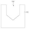
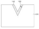
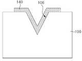
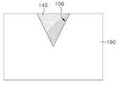
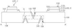
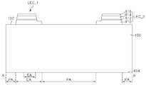
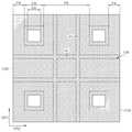
도 1a는 본 발명의 일 실시예에 따른 발광 소자를 설명하기 위한 평면도이고, 도 1b는 도 1a의 발광 소자를 A-A'으로 절단한 단면도이다. 도 1c는 도 1b의 발광 소자의 오목부(106)를 확대한 도면이고, 도 1d 내지 도 1f는 도 1c의 오목부(106)의 변형예들이다.1A is a plan view illustrating a light emitting device according to an exemplary embodiment of the present invention, and FIG. 1B is a cross-sectional view taken along line A-A' of the light emitting device of FIG. 1A. 1C is an enlarged view of the
도 1a 내지 도 1c를 참조하면, 발광 소자는 기판(100) 및 기판(100) 상에 배치되는 복수의 발광 셀들(LEC_1, LEC_2)을 포함할 수 있다.1A to 1C, the light emitting device may include a
기판(100)은 질화갈륨계 반도체층을 성장시킬 수 있는 기판(100)으로, 사파이어(Al2O3), 탄화실리콘(SiC), 질화갈륨(GaN), 질화인듐갈륨(InGaN), 질화알루미늄갈륨(AlGaN), 질화알루미늄(AlN), 산화갈륨(Ga2O3), 갈륨비소(GaAs), 또는 실리콘(Si)를 포함할 수 있다. 또한, 기판(100)은 유연성(flexible) 기판이거나, 회로가 형성된 기판일 수 있다.The
기판(100)은 발광 셀들(LEC_1, LEC_2)이 배치되는 제1 면(102)과, 제1 면(102)에 대향하는 제2 면(104)을 포함할 수 있다. 기판(100)의 제2 면(104)이 발광 셀들(LEC_1, LEC_2)로부터 발생된 광의 출광면일 수 있다.The
일 실시예에 따르면, 기판(100)은 가능한 얇은 두께를 가질 수 있다. 기판(100)은 발광 셀들(LEC_1, LEC_2)로부터 발생된 광이 이동 가능한 도광판으로 기능할 수 있어, 이러한 도광판으로서의 기능을 상실시키기 위하여 최대한 얇은 두께를 가질 수 있다. 예컨대, 기판(100)은 약 80 내지 200um의 두께를 가질 수 있다.According to an embodiment, the
기판(100)의 제1 면(102)에는, 기판(100)을 식각하여 제1 면(102)으로부터 내부로 연장되는 오목부(106)를 형성할 수 있다. 오목부(106)는 제1 방향(DR1)으로 연장하는 수직부(VL)와, 제1 방향(DR1)과 수직인 제2 방향(DR2)으로 연장하는 수평부(HL)를 포함할 수 있다. 수직부(VL) 및 수평부(HL)는 서로 교차할 수 있다.In the
도 1c를 참조하면, 오목부(106)는 기판(100)의 제1 면(102)으로부터 기판(100) 내부 일 지점으로 수렴하는 두 개의 변들을 갖는 'V'자형 구조를 가질 수 있다. 오목부(106)의 깊이(DT)는 기판(100)의 두께(DT_S)의 1/3 내지 2/3일 수 있다. 일 예로, 기판(100)이 80 내지 100um의 두께(DT_S)를 가질 때, 오목부(106)는 25 내지 70um의 깊이(DT)를 가질 수 있다. 또한, 오목부(106)의 두 변들 사이 최장폭(WT)은 20 내지 30um일 수 있다. 오목부(106)의 두 변들 사이의 각도(β)는 40 내지 80도일 수 있다.Referring to FIG. 1C, the
오목부(106)는 'V'자형 구조뿐만 아니라 다양한 구조를 가질 수 있다. 도 1d를 참조하면, 오목부(106)는 기판(100)의 제1 면(102)으로부터 내부로 연장되며 서로 평행한 두 수직면과, 수직면 사이를 연결하는 수평면을 포함할 수 있다. 단면적 관점에서, 오목부(106)는 기판(100)의 제1 면(102)에 대응되는 면이 '열린 사각형(open square)' 구조를 가질 수 있다. 도 1e를 참조하면, 오목부(106)는 기판(100)의 제1 면(102)으로부터 내부로 연장되며 서로 평행한 두 수직면들과, 두 수직면들 사이 접점으로 수렴하는 두 면들을 포함할 수 있다. 단면적 관점에서, 오목부(106)는 기판(100)의 제1 면(102)에 대응하는 면이 '열린 오각형(open pentagon)'구조를 가질 수 있다. 도 1f를 참조하면, 오목부(106)는 기판(100)의 제1 면(102)으로부터 내부로 연장되며 곡면을 가지며, 단면적 관점에서 'U'자 구조를 가질 수 있다. 실시예들에서 설명된 오목부(106)의 구조는 예시적인 것으로 오목부(106)는 다양할 수 있으며, 본 발명에서 오목부(106)의 구조를 이로 한정하는 것은 아니다.The
오목부(106) 내부에는, 오목부(106)의 적어도 일부에 형성된 차광막(140)이 배치될 수 있다. 차광막(140)은 이웃하는 두 개의 발광 셀들(LEC_1, LEC_2), 예컨대, 제1 발광 셀(LEC_1) 및 제2 발광 셀(LEC_2) 사이에서, 제1 발광 셀(LEC_1)에서 발생된 광이 제2 발광 셀(LEC_2)에 영향을 미치지 않도록 제1 발광 셀(LEC_1)에서 발생된 광을 제1 발광 셀(LEC_1) 방향으로 반사시키거나 차단 또는 흡수시킬 수 있다. 마찬가지로, 제2 발광 셀(LEC_2)에서 발생된 광이 제1 발광 셀(LEC_1)에 영향을 미치지 않도록 제2 발광 셀(LEC_2)에서 발생된 광을 제2 발광 셀(LEC_2) 방향으로 반사시키거나 차단 또는 흡수시킬 수 있다. 예컨대, 차광막(140)은 Ti, Ni, Al, Ag, Cr과 같은 금속을 포함하거나, 포토레지스트(photoresist), 에폭시(epoxy), PDMS(polydimethylsiloxane) 및 블랙매트릭스(black matrix)과 같은 물질을 포함할 수 있다.Inside the
이하, 차광막(140)의 구조를 상세하게 설명하되, 도 1c에 도시된 오목부(106)에 형성된 차광막(140)을 예시적으로 설명하기로 한다.Hereinafter, the structure of the
도 2a 내지 도 2d는 본 발명의 실시예들에 따른 차광막의 구조를 설명하기 위한 단면도들이다.2A to 2D are cross-sectional views illustrating a structure of a light shielding film according to exemplary embodiments.
도 2a를 참조하면, 차광막(140)은 오목부(106)를 완전하게 매립하지 않으며, 오목부(106)의 내측벽을 따라 연속적으로 컨포멀하게(comformally) 형성될 수 있다. 도 2b를 참조하면, 차광막(140)은 오목부(106)를 완전하게 채우지 않으며, 오목부(106)의 내측벽 상에 컨포멀하게 형성되고, 기판(100)의 제1 면(102) 상으로 연장되어, 기판(100)의 제1 면(102)의 적어도 일부를 덮을 수 있다. 도 2c를 참조하면, 차광막(140)은 오목부(106)를 매립하며 기판(100)의 제1 면(102)과 동일한 평면에 상부면을 가질 수 있다. 도 2d를 참조하면, 차광막(140)은 오목부(106)를 매립하며, 기판(100)의 제1 면(102) 상으로 연장되어 기판(100)의 제1 면(102)의 적어도 일부를 덮을 수 있다.Referring to FIG. 2A, the
본 실시예들에서는 오목부(106)가 도 1c에 도시된 오목부(106) 구조인 것을 예시적으로 설명하나, 도 1d 내지 도 1f에 도시된 오목부(106) 구조에도 동일하게 적용될 수 있어 상세한 설명을 생략하기로 한다.In the present embodiments, it is illustratively described that the
도 1a 및 도 1b를 참조하면, 기판(100) 상에 발광 셀들(LEC_1, LEC_2)은 일 거리로 이격되어 배치될 수 있다. 발광 셀들(LEC_1, LEC_2)의 이격 거리는 발광 소자가 실장되는 장치에 따라 변경될 수 있다.1A and 1B, the light emitting cells LEC_1 and LEC_2 may be disposed on the
일 실시예에 따른 발광 셀들(LEC_1, LEC_2) 각각은 105 내지 150도의 지향각(α)을 가질 수 있다. 전술한 바와 같이, 발광 셀들(LEC_1, LEC_2) 사이의 이격 거리는 발광 셀들(LEC_1, LEC_2)이 실장되는 장치에 따라 변화될 수 있다. 따라서, 105 내지 150도의 지향각(α)을 갖는 제1 발광 셀(LEC_1) 및 제2 발광 셀(LEC_2) 사이에서, 기판(100)에 차광막(140)이 형성된 오목부(106)가 배치되되, 제1 발광 셀(LEC_1)(또는 제2 발광 셀(LEC_2))에서 발생되는 광이 차광막(140)에 의해 반사, 차단, 또는 흡수되어 제2 발광 셀(LEC_2)(또는 제1 발광 셀(LEC_1))에 영향을 미치지 않을 수 있는 위치에 오목부(106)가 배치될 수 있다.Each of the light emitting cells LEC_1 and LEC_2 according to an exemplary embodiment may have a directivity angle α of 105 to 150 degrees. As described above, the separation distance between the light emitting cells LEC_1 and LEC_2 may be changed according to a device in which the light emitting cells LEC_1 and LEC_2 are mounted. Therefore, between the first light-emitting cell LEC_1 and the second light-emitting cell LEC_2 having a directivity angle α of 105 to 150 degrees, the
한편, 기판(100) 상에 배치된 복수의 발광 셀들(LEC_1, LEC_2)은 목적하는 장치에 한번에 실장되는 단위일 수 있다. 일 예로, 기판(100) 상에 4개의 발광 셀들(LEC_1, LEC_2)이 형성된 발광 소자는 한번의 공정으로 4개의 발광 셀들(LEC_1, LEC_2)을 목적하는 장치에 실장할 수 있다. 본 실시예에서는 4개의 발광 셀들(LEC_1, LEC_2)을 예시적으로 설명하나, 본 발명에서 발광 소자 내 발광 셀들(LEC_1, LEC_2)의 수량을 이로 한정하지 않는다.Meanwhile, the plurality of light emitting cells LEC_1 and LEC_2 disposed on the
발광 셀들(LEC_1, LEC_2) 각각은 제1 도전형 반도체층(110), 활성층(112), 제2 도전형 반도체층(114), 및 오믹층(116)을 포함할 수 있다. 제1 도전형 반도체층(110)은 Si이 도핑된 질화갈륨계 반도체층을 포함하는 n형 반도체층일 수 있다. 제2 도전형 반도체층(114)은 Mg이 도핑된 질화갈륨계 반도체층을 포함하는 p형 반도체층일 수 있다. 이와는 다르게, 제1 도전형 반도체층(110)은 p형 반도체층일 수 있으며, 제2 도전형 반도체층(114)은 n형 반도체층일 수 있다. 활성층(112)은 다중양자우물구조(Multi Quantum Well: MQW)을 포함할 수 있고, 원하는 피크 파장의 광을 방출하도록 그 조성비가 결정될 수 있다. 오믹층(116)은 ZnO(Zinc Oxide), ITO(Indium Tin Oxide), ZITO(Zinc-doped Indium Tin Oxide), ZIO(Zinc Indium Oxide), GIO(Gallium Indium Oxide), ZTO(Zinc Tin Oxide), FTO(Fluorine-doped Tin Oxide), GZO(Gallium-doped Zinc Oxide), AZO(Aluminum-doped Zinc Oxide) 등과 같은 투명 산화물층(Transparent Conductive Oxide: TCO)이 사용될 수 있다.Each of the light emitting cells LEC_1 and LEC_2 may include a first conductivity
또한, 발광 셀들(LEC_1, LEC_2) 각각은 제1 도전형 반도체층(110)과 전기적으로 연결되는 제1 패드(120) 및 오믹층(116)과 전기적으로 연결되는 제2 패드(130)를 더 포함할 수 있다. 제1 패드(120) 및 제2 패드(130) 각각은 Au, Ti, Ni, Cr, 및 Al으로 이루어진 군으로부터 선택된 적어도 하나를 포함할 수 있다.In addition, each of the light emitting cells LEC_1 and LEC_2 further includes a
도 3a는 본 발명의 다른 실시예에 따른 발광 소자를 설명하기 위한 개략적인 평면도이고, 도 3b는 도 3a의 A-A'으로 절단한 단면도이다.3A is a schematic plan view illustrating a light emitting device according to another exemplary embodiment of the present invention, and FIG. 3B is a cross-sectional view taken along line AA′ of FIG. 3A.
도 3a 및 도 3b를 참조하면, 본 실시예에 따른 발광 소자는 도 1a 및 도 1b를 참조하여 설명한 발광 소자와 대체로 유사하나, 발광 셀들(LEC_1, LEC_2) 각각이 수직 적층된(vertically stacked) 제1 발광부(LEC_1_1, LEC_2_1), 제2 발광부(LEC_1_2, LEC_2_2), 및 제3 발광부(LEC_1_3, LEC_2_3)를 포함하는 것에 차이가 있다. 이하에서는 중복을 피하기 위해 차이점에 대해 설명한다. 기판(100)의 제2 면(104)이 출광면일 경우, 제1 발광부(LEC_1_1, LEC_2_1)는 가장 짧은 파장의 광을 발생시키고, 제2 발광부(LEC_1_2, LEC_2_2)는 제1 발광부(LEC_1_1, LEC_2_1)에서 발생되는 광보다 길고 제3 발광부(LEC_1_3, LEC_2_3)에서 발생된 광보다는 짧은 파장의 광을 발생시키고, 제3 발광부(LEC_1_3, LEC_2_3)는 가장 긴 파장의 광을 발생시킬 수 있다. 예컨대, 제1 발광부(LEC_1_1, LEC_2_1)는 청색광을 발생시키고, 제2 발광부(LEC_1_2, LEC_2_2)는 녹색광을 발생시키며, 제3 발광부(LEC_1_3, LEC_2_3)는 적색광을 발광시킬 수 있다. 그러나 본 개시가 이에 한정되는 것은 아니다. 예를 들어, 제2 발광부(LEC_1_2, 2-2)가 제1 발광부(LEC_1_1, LEC_2_1)보다 단파장의 광을 방출할 수 있다. 제1 발광부(LEC_1_1, LEC_2_1)는 제1 n형 반도체층, 제1 활성층, 제1 p형 반도체층, 및 제1 오믹층을 포함할 수 있다. 제2 발광부(LEC_1_2, LEC_2_2)는 제2 n형 반도체층, 제2 활성층, 제2 p형 반도체층, 및 제2 오믹층을 포함할 수 있다. 제3 발광부(LEC_1_3, LEC_2_3)는 제3 n형 반도체층, 제3 활성층, 제3 p형 반도체층, 및 제3 오믹층을 포함할 수 있다. 제1 n형 반도체층, 제2 n형 반도체층, 및 제3 n형 반도체층 각각은 Si이 도핑된 질화갈륨계 반도체층일 수 있다. 제1 p형 반도체층, 제2 p형 반도체층, 및 제3 p형 반도체층 각각은 Mg이 도핑된 질화갈륨계 반도체층일 수 있다. 제1 활성층, 제2 활성층, 및 제3 활성층 각각은 다중양자우물구조을 포함할 수 있고, 원하는 피크 파장의 광을 방출하도록 그 조성비가 결정될 수 있다. 제1 오믹층, 제2 오믹층, 및 제3 오믹층 각각은 ZnO(Zinc Oxide), ITO(Indium Tin Oxide), ZITO(Zinc-doped Indium Tin Oxide), ZIO(Zinc Indium Oxide), GIO(Gallium Indium Oxide), ZTO(Zinc Tin Oxide), FTO(Fluorine-doped Tin Oxide), GZO(Gallium-doped Zinc Oxide), AZO(Aluminum-doped Zinc Oxide) 등과 같은 투명 산화물층(Transparent Conductive Oxide: TCO)이 사용될 수 있다.3A and 3B, the light emitting device according to the present embodiment is substantially similar to the light emitting device described with reference to FIGS. 1A and 1B, but each of the light emitting cells LEC_1 and LEC_2 is vertically stacked. There is a difference in including the first light emitting parts LEC_1_1 and LEC_2_1, the second light emitting parts LEC_1_2 and LEC_2_2, and the third light emitting parts LEC_1_3 and LEC_2_3. Hereinafter, differences will be described in order to avoid duplication. When the
발광 셀들(LEC_1, LEC_2) 각각은 제1 오믹층, 제2 오믹층, 및 제3 오믹층(도시하지 않음)을 한번에 전기적으로 연결하는 공통 패드(120a), 제1 n형 반도체층과 전기적으로 연결되는 제1 패드(120b), 제2 n형 반도체층과 전기적으로 연결되는 제2 패드(120c), 및 제3 n형 반도체층과 전기적으로 연결되는 제3 패드(120d)를 더 포함할 수 있다. 이와는 다르게, 발광 셀들(LEC_1, LEC_2) 각각은 제1 n형 반도체층, 제2 n형 반도체층, 및 제3 n형 반도체층을 한번에 전기적으로 연결하는 공통 패드(120a), 제1 오믹층과 전기적으로 연결되는 제1 패드(120b), 제2 오믹층과 전기적으로 연결되는 제2 패드(120c), 및 제3 오믹층과 전기적으로 연결되는 제3 패드(120d)를 더 포함할 수 있다.Each of the light emitting cells LEC_1 and LEC_2 electrically connects the first ohmic layer, the second ohmic layer, and the third ohmic layer (not shown) to the
일 예로, 발광 셀들 각각이 수직 적층된 제1 발광부(LEC_1_1, LEC_2_1), 제2 발광부(LEC_1_2, LEC_2_2), 및 제3 발광부(LEC_1_3, LEC_2_3)를 포함하는 경우, 제3 발광부(LEC_1_3, LEC_2_3)는 제2 발광부(LEC_1_2, LEC_2_2)의 적어도 일부를 노출시키고, 제2 발광부(LEC_1_2, LEC_2_2)는 제1 발광부(LEC_1_1, LEC_2_1)의 적어도 일부를 노출시켜, 공통 패드(120a), 제1 패드(120b), 제2 패드(120c), 및 제3 패드(120d) 각각을 제1 발광부(LEC_1_1, LEC_2_1), 제2 발광부(LEC_1_2, LEC_2_2), 및 제3 발광부(LEC_1_3, LEC_2_3)와 전기적으로 연결시킬 수 있다. 이 경우, 제3 발광부(LEC_1_3, LEC_2_3)는 제2 발광부(LEC_1_2, LEC_2_2)보다 작고, 제2 발광부(LEC_1_2, LEC_2_2)는 제1 발광부(LEC_1_1, LEC_2_1)보다 작을 수 있다.As an example, when each of the light emitting cells includes the first light emitting parts LEC_1_1 and LEC_2_1 vertically stacked, the second light emitting parts LEC_1_2 and LEC_2_2, and the third light emitting parts LEC_1_3 and LEC_2_3, the third light emitting part ( LEC_1_3 and LEC_2_3 expose at least a part of the second light emitting parts LEC_1_2 and LEC_2_2, and the second light emitting parts LEC_1_2 and LEC_2_2 expose at least a part of the first light emitting parts LEC_1_1 and LEC_2_1 to expose a common pad ( 120a), the
다른 예로, 제1 발광부(LEC_1_1, LEC_2_1), 제2 발광부(LEC_1_2, LEC_2_2), 및 제3 발광부(LEC_1_3, LEC_2_3) 각각은 동일한 크기를 가지며, 발광 셀들(LEC_1, LEC_2) 각각은 공통 패드(120a), 제1 패드(120b), 제2 패드(120c), 및 제3 패드(120d) 각각과 제1 발광부(LEC_1_1, LEC_2_1), 제2 발광부(LEC_1_2, LEC_2_2), 및 제3 발광부(LEC_1_3, LEC_2_3)와 전기적으로 연결시키는 복수의 비아 구조물들(도시하지 않음)을 더 포함할 수 있다.As another example, each of the first light emitting parts LEC_1_1 and LEC_2_1, the second light emitting parts LEC_1_2 and LEC_2_2, and the third light emitting parts LEC_1_3 and LEC_2_3 have the same size, and each of the light emitting cells LEC_1 and LEC_2 is common. Each of the
또 다른 예로, 제1 발광부(LEC_1_1, LEC_2_1) 및 제2 발광부(LEC_1_2, LEC_2_2) 각각은 동일한 크기를 가지되, 제3 발광부(LEC_1_3, LEC_2_3)는 제2 발광부(LEC_1_2, LEC_2_2)의 적어도 일부를 노출시켜, 공통 패드(120a), 제1 패드(120b), 제2 패드(120c), 및 제3 패드(120d) 각각은 제1 발광부(LEC_1_1, LEC_2_1), 제2 발광부(LEC_1_2, LEC_2_2), 및 제3 발광부(LEC_1_3, LEC_2_3)와 전기적으로 연결시킬 수 있다. 이때, 제1 발광부(LEC_1_1, LEC_2_1) 및 제2 발광부(LEC_1_2, LEC_2_2)와 공통 패드(120a), 제1 패드(120b) 및 제2 패드(120c)는 복수의 비아 구조물(도시하지 않음)에 의해 전기적으로 연결될 수 있다.As another example, each of the first light emitting parts LEC_1_1 and LEC_2_1 and the second light emitting parts LEC_1_2 and LEC_2_2 have the same size, but the third light emitting parts LEC_1_3 and LEC_2_3 are the second light emitting parts LEC_1_2 and LEC_2_2 By exposing at least a portion of the
본 실시예에 있어서, 오목부(106) 및 차광막(140)은 도 1a 내지 도 1f를 참조하여 설명한 것 뿐만 아니라, 도 2a 내지 도 2d를 참조하여 설명한 것들도 유사하게 채택될 수 있다.In the present embodiment, the
본 실시예에서, 3개의 발광부들이 수직으로 적층된 것에 대해 설명하지만, 이에 한정되는 것은 아니며, 2개의 발광부들 또는 4개 이상의 발광부들이 수직으로 적층될 수도 있다.In the present embodiment, a description will be made of vertically stacking three light-emitting units, but the present invention is not limited thereto, and two light-emitting units or four or more light-emitting units may be vertically stacked.
나아가, 기판(100) 상에 배치된 발광셀들이 모두 수직으로 적층된 발광부들을 가질 수 있지만, 본 실시예가 이에 한정되는 것은 아니며, 일부 발광셀은 단일의 발광부를 가질 수도 있다.Further, the light emitting cells disposed on the
또한, 본 실시예에서 설명된 수직으로 적층된 발광부들은 뒤에서 설명되는 다양한 실시예들의 발광셀에도 적용될 수 있다.In addition, the vertically stacked light emitting units described in this embodiment may be applied to light emitting cells of various embodiments described later.
도 4a는 본 발명의 또 다른 실시예에 따른 발광 소자를 설명하기 위한 평면도이고, 도 4b는 도 4a의 발광 소자를 A-A'으로 절단한 단면도이다. 도 5a는 본 발명의 또 다른 실시예에 따른 발광 소자를 설명하기 위한 평면도이고, 도 5b는 도 5a의 발광 소자를 A-A'으로 절단한 단면도이다.4A is a plan view illustrating a light emitting device according to another exemplary embodiment of the present invention, and FIG. 4B is a cross-sectional view taken along line A-A' of the light emitting device of FIG. 4A. 5A is a plan view illustrating a light emitting device according to another exemplary embodiment of the present invention, and FIG. 5B is a cross-sectional view taken along line A-A' of the light emitting device of FIG. 5A.
도 4a, 도 4b, 도 5a, 및 도 5b를 참조하면, 발광 소자는 기판(100) 및 기판(100) 상에 배치되는 복수의 발광 셀들(LEC_1, LEC_2)을 포함할 수 있다.4A, 4B, 5A, and 5B, the light emitting device may include a
기판(100)은 발광 셀들(LEC_1, LEC_2)이 배치되는 제1 면(102)과, 제1 면(102)에 대향하는 제2 면(104)을 포함할 수 있다. 기판(100)의 제1 면(102)에는 제1 면(102)으로부터 내부로 연장되는 오목부(106)를 형성할 수 있다. 기판(100) 및 오목부(106)는 도 1a 및 도 1b에서 설명된 것과 실질적으로 동일하여 그 상세한 설명을 생략하기로 한다.The
상세하게 도시되지 않았으나,오목부(106)의 구조는 도 1c 내지 도 1f에 설명된 오목부(106)의 구조를 가질 수 있다. 그러나, 본 발명이 이상의 구조로 오목부(106)의 구조를 한정하는 것은 아니다.Although not shown in detail, the structure of the
기판(100)의 제1 면(102) 상에 발광 셀들(LEC_1, LEC_2)이 일 거리로 이격되어 배치될 수 있다. 본 실시예에서 발광 셀들(LEC_1, LEC_2) 각각은 수직 적층된 제1 도전형 반도체층(110), 활성층(112), 제2 도전형 반도체층(114), 및 오믹층(116)과, 제1 도전형 반도체층(110)과 전기적으로 연결되는 제1 패드(120)와, 오믹층(116)과 전기적으로 연결되는 제2 패드(130)를 포함할 수 있다.The light emitting cells LEC_1 and LEC_2 may be disposed on the
차광막(140)은 오목부(106)를 채우며 제1 면(102) 상에서 발광 셀들(LEC_1, LEC_2)을 덮으며 배치될 수 있다. 이 경우, 차광막(140)은 포토레지스트, 에폭시, PDMS 및 블랙 매트릭스와 같은 절연 물질을 포함할 수 있다.The
일 실시예에 따르면, 발광 셀들(LEC_1, LEC_2)의 활성층들(112) 각각에서 발생된 광은 활성층(112) 상하 좌우 사방으로 발광하는데, 차광막(140)이 발광 셀들(LEC_1, LEC_2) 사이에 배치되어, 광이 혼합되는 것을 방지할 수 있다. 더욱 구체적으로 설명하면, 기판(100)의 제1 면(102) 상부에서는 차광막(140)이 이웃하는 발광 셀들(LEC_1, LEC_2), 예컨대 제1 발광 셀(LEC_1) 및 제2 발광 셀(LEC_2) 사이에 배치되어 제1 발광 셀(LEC_1)의 활성층(112)에서 발생된 광은 제2 발광 셀(LEC_2)에 영향을 미치지 않고 기판(100)의 제1 면(102) 방향으로 조사되고, 제2 발광 셀(LEC_2)의 활성층(112)에서 발생된 광은 제1 발광 셀(LEC_1)에 영향을 미치지 않고 기판(100)의 제1 면(102) 방향으로 조사될 수 있다. 기판(100)으로 조사된 제1 발광 셀(LEC_1)의 광과 제2 발광 셀(LEC_2)의 광 각각은 기판(100) 내에서 사방으로 조사될 수 있으나, 제1 발광 셀(LEC_1)의 광과 제2 발광 셀(LEC_2)의 광 각각은 오목부(106)를 채우는 차광막(140)에서 반사, 차단, 또는 흡수되어 서로에게 영향을 미치지 않을 수 있다.According to an embodiment, light generated from each of the
또한, 차광막(140)이 오목부(106)를 채우고, 발광 셀들(LEC_1, LEC_2)을 덮으며 형성됨으로써, 얇은 기판(100)이 외부 충격으로 쪼개지거나 손상되는 것을 방지할 수 있다.In addition, since the
도 4a 및 도 4b를 참조하면, 차광막(140)의 상부면은 오믹층(116)의 상부면과 실질적으로 동일 평면일 수 있다. 또한, 차광막(140)은 오믹층(116)를 노출시킬 수 있다. 일 예로, 제1 패드(120)는 차광막(140)에 의해 매립되어, 차광막(140)을 관통하는 관통 전극(122)을 통해 차광막(140) 상에 배치되는 제3 패드(124)와 전기적으로 연결될 수 있다. 제2 패드(130)는 차광막(140) 상에 노출된 오믹층(116) 상에 배치될 수 있다.4A and 4B, the upper surface of the
도 5a 및 도 5b를 참조하면, 차광막(140) 상에 절연막(150)이 더 배치될 수 있다. 절연막(150)은 차광막(140)과 실질적으로 동일한 물질을 포함할 수 있다. 이와는 다르게, 절연막(150)은 실리콘 산화물 또는 실리콘 질화물을 포함할 수도 있다. 발광 소자는, 절연막(150)을 관통하며 제1 패드(120)와 전기적으로 연결되는 제1 관통 전극(122)과, 제2 패드(130)와 전기적으로 연결되는 제2 관통 전극(132)과, 절연막(150) 상에 배치되며 제1 관통 전극(122)과 전기적으로 접촉하는 제3 패드(124)와, 제2 관통 전극(132)과 전기적으로 접촉하는 제4 패드(134)를 더 포함할 수 있다. 이 경우, 제1 패드(120) 및 제2 패드(130) 사이 이격 거리가 실장되는 장치에서 요구되는 이격 거리와 상이한 경우, 제1 패드(120)와 전기적으로 연결된 제3 패드(124) 및 제2 패드(130)와 전기적으로 연결된 제4 패드(134)의 위치를 변경하여 실장되는 장치의 목적하는 거리로 조정할 수 있다.5A and 5B, an insulating
도 4a, 도 4b, 도 5a 및 도 5b에 도시된 기판(100), 오목부(106), 차광막(140), 및 복수의 발광 셀들(LEC_1, LEC_2) 각각의 생략된 상세한 설명은 도 1a 내지 도 1f, 도 2a 내지 도 2d에서 설명된 기판(100), 오목부(106), 차광막(140), 및 복수의 발광 셀들(LEC_1, LEC_2)과 실질적으로 동일하여 상세한 설명을 생략하기로 한다.The omitted detailed description of each of the
도 6a는 본 발명의 또 다른 실시예에 따른 발광 소자를 설명하기 위한 평면도고, 도 6b는 도 6a의 발광 소자를 A-A'으로 절단한 단면도이다.6A is a plan view illustrating a light emitting device according to another exemplary embodiment of the present invention, and FIG. 6B is a cross-sectional view taken along line A-A' of the light emitting device of FIG. 6A.
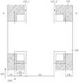
도 6a 및 도 6b를 참조하면, 발광 소자는 기판(100) 및 기판(100) 상에 배치되는 복수의 발광 셀들(LEC_1, LEC_2)을 포함할 수 있다.6A and 6B, the light emitting device may include a
기판(100)은 발광 셀들(LEC_1, LEC_2)이 배치되는 제1 면(102)과, 제1 면(102)에 대향하는 제2 면(104)을 포함할 수 있다. 기판(100)의 제1 면(102)에는 제1 면(102)으로부터 내부로 연장되는 제1 오목부(106)를 형성할 수 있다. 제1 오목부(106)는 제1 방향(DR1)으로 연장하는 수직부(VL)와 제1 방향(DR1)과 수직인 제2 방향(DR2)으로 연장하는 수평부(HL)를 포함할 수 있다. 제1 오목부(106)의 수직부(VL) 및 수평부(HL)는 서로 교차할 수 있다. 기판(100)의 제2 면(104)에는 제2 면(104)으로부터 내부로 연장되는 제2 오목부(108)를 형성할 수 있다. 제2 오목부(108)는 제1 방향(DR1)으로 연장하며 서로 평행한 수직부들(VL)과 제2 방향(DR2)으로 연장하며 서로 평행한 수평부들(HL)을 포함할 수 있다. 제2 오목부(108)의 수직부들(VL) 및 수평부들(HL)을 서로 교차할 수 있다.The
평면적 관점에서, 제1 오목부(106)의 수직부(VL)는 제2 오목부(108)의 수직부들(VL)과 오버랩되지 않으며, 제1 오목부(106)의 수평부(HL)는 제2 오목부(108)의 수평부들(HL)과 오버랩되지 않을 수 있다. 일 예로, 제1 오목부(106)의 수직부(VL)는 제2 오목부(108)의 이웃하는 두 개의 수직부들(VL) 사이에 배치될 수 있다. 제1 오목부(106)의 수평부(HL)는 제2 오목부(108)의 이웃하는 두 개의 수평부들(HL) 사이에 배치될 수 있다. 또한, 제2 오목부(108)가 제1 오목부(106)보다 발광 셀들(LEC_1, LEC_2)에 더 인접하게 배치될 수 있다.From a plan view, the vertical portion VL of the first
단면적 관점에서, 제1 오목부(106)의 수직부(VL)는 제2 오목부(108)의 이웃하는 두 개의 수직부들(VL) 사이에 배치될 수 있다. 도 6b의 A부분을 참조하면, 제1 오목부(106)의 수직부(VL)의 단부와 제2 오목부(108)의 수직부들(VL) 각각의 단부는 서로 오버랩될 수 있다.In terms of cross-sectional area, the vertical portion VL of the first
본 실시예에서는 제1 오목부(106) 및 제2 오목부(108) 각각의 구조가 도 1c에서 설명된 구조를 사용하는 것으로 도시되었으나, 제1 오목부(106) 및 제2 오목부(108) 각각의 구조는 도 1d 내지 도 1f에 설명된 오목부(106)의 구조를 가질 수 있다. 한편, 본 발명이 이상의 구조로 제1 오목부(106) 및 제2 오목부(108) 각각의 구조를 이것으로 한정하는 것은 아니다.In the present embodiment, the structure of each of the first
제1 오목부(106) 내부에는, 제1 오목부(106)의 적어도 일부를 채우는 제1 차광막(140)이 배치될 수 있다. 제2 오목부(108) 내부에는, 제2 오목부(108)의 적어도 일부를 채우는 제2 차광막(145)이 배치될 수 있다. 제1 차광막(140) 및 제2 차광막(145) 각각은 Ti, Ni, Al, Ag, Cr과 같은 금속을 포함하거나, 포토레지스트, 에폭시, PDMS, 및 블랙매트릭스와 같은 물질을 포함할 수 있다. 제1 차광막(140) 및 제2 차광막(145) 각각은 도 2a의 구조를 사용한 것으로 도시되었으나, 제1 차광막(140) 및 제2 차광막(145) 각각의 구조는 2a 내지 2d에서 설명된 차광막(140) 구조를 가질 수 있다. 한편, 본 발명이 이상의 구조로 제1 차광막(140) 및 제2 차광막(145) 각각의 구조를 이로 한정하는 것은 아니다.Inside the first
복수의 발광 셀들(LEC_1, LEC_2), 예컨대 제1 발광 셀(LEC_1) 및 제2 발광 셀(LEC_2) 각각으로부터 발생된 광은 발광 셀들(LEC_1, LEC_2)에 인접한 배치된 제2 차광막(145)에 의해 반사, 차단 및 흡수되는데, 제2 차광막(145)을 제외한 공간으로 통과한 광은 제1 차광막(140)에 의해 반사, 차단 및 흡수될 수 있다. 제1 발광 셀(LEC_1) 및 제2 발광 셀(LEC_2) 사이에 제2 차광막(145) 및 제1 차광막(140)이 배치됨으로써, 제1 발광 셀(LEC_1)에서 발생된 광이 제2 발광 셀(LEC_2)에 영향을 미치기 어렵고 제2 발광 셀(LEC_2)에서 발생된 광이 제1 발광 셀(LEC_1)에 영향을 미치기 어려울 수 있다. 따라서, 복수의 발광 셀로부터 발생된 광이 혼합되어 발생되는 문제를 방지할 수 있다.The light generated from each of the plurality of light emitting cells LEC_1 and LEC_2, for example, the first light emitting cell LEC_1 and the second light emitting cell LEC_2, is applied to the second
도 6a 및 도 6b에 도시된 기판(100), 제1 오목부(106), 제2 오목부(108), 제1 차광막(140), 제2 차광막(145), 및 복수의 발광 셀들(LEC_1, LEC_2) 각각의 생략된 상세한 설명은 도 1a 내지 도 1f, 도 2a 내지 도 2d에서 설명된 기판(100), 오목부(106), 차광막(140), 및 복수의 발광 셀들(LEC_1, LEC_2)과 실질적으로 동일하여 상세한 설명을 생략하기로 한다.The
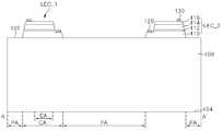
도 7a 및 도 7b는 본 발명의 또 다른 실시예에 따른 발광 소자를 설명하기 위한 평면도들이고, 도 7c는 도 7a의 발광 소자를 A-A'으로 절단한 단면도들이다. 도 7a는 발광 소자를 일 측, 예컨대 패드들이 배치되는 위치에서 바라본 평면도이고, 도 7b는 발광 소자를 일 측에 대향하는 타 측, 예컨대 출광면에서 바라본 평면도이다.7A and 7B are plan views illustrating a light emitting device according to another embodiment of the present invention, and FIG. 7C is a cross-sectional view taken along line A-A' of the light emitting device of FIG. 7A. FIG. 7A is a plan view of the light emitting device from one side, eg, a position where pads are disposed, and FIG. 7B is a plan view of the light emitting device from the other side opposite to one side, eg, a light exit surface.
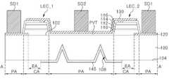
도 7a 내지 도 7c를 참조하면, 발광 소자는 기판(100) 및 기판(100) 상에 배치되는 복수의 발광 셀들(LEC_1, LEC_2)을 포함할 수 있다.7A to 7C, the light emitting device may include a
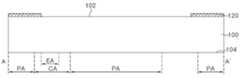
기판(100)은 발광 셀들(LEC_1, LEC_2)이 배치되는 제1 면(102)과, 제1 면(102)에 대향하는 제2 면(104)을 포함할 수 있다. 기판(100)의 제1 면(102)에는 제1 오목부(106)가 형성되고, 기판(100)의 제2 면(104)에는 제2 오목부(108)가 형성될 수 있다. 제1 오목부(106)는 수직부(VL) 및 수평부(HL)를 포함하며, 제2 오목부(108)는 수직부들(VL) 및 수평부들(HL)을 포함할 수 있다. 발광 셀들(LEC_1, LEC_2)은 기판(100)의 제1 면(102) 상에 배치되되, 발광 셀들(LEC_1, LEC_2) 각각은 제1 도전형 반도체층(110), 활성층(112), 제2 도전형 반도체층(114), 및 오믹층(116)을 포함할 수 있다. 또한, 발광 소자는 발광 셀들(LEC_1, LEC_2)의 제1 도전형 반도체층들(110) 각각과 전기적으로 연결되는 제1 패드들(120)과, 오믹층들(116) 각각과 전기적으로 연결되는 제2 패드들(130)을 더 포함할 수 있다. 기판(100), 제1 오목부(106), 제2 오목부(108), 발광 셀들(LEC_1, LEC_2), 제1 패드들(120), 및 제2 패드들(130)은 도 6a 및 도 6b에서 설명된 기판(100), 제1 오목부(106), 제2 오목부(108), 발광 셀들(LEC_1, LEC_2), 제1 패드들(120), 및 제2 패드들(130)과 실질적으로 동일하여 상세한 설명을 생략하기로 한다.The
기판(100)은 발광 셀들(LEC_1, LEC_2)이 위치하는 셀 영역들(CA)과, 셀 영역들(CA)을 제외한 주변 영역(PA)을 포함할 수 있다. 셀 영역들(CA) 각각은 광이 출광되는 출광 영역(EA)을 포함할 수 있다. 출광 영역(EA)은 셀 영역(CA)보다 작을 가질 수 있다.The
도 7a 및 도 7c를 참조하면, 기판(100)의 제1 면(102) 상에 제1 오목부(106)의 적어도 일부를 채우는 제1 차광막(140)이 제공될 수 있다. 제1 차광막(140)은 셀 영역들(CA)을 노출시키도록 주변 영역(PA)의 일부를 덮으며 배치될 수 있다.7A and 7C, a first
도 7b 및 도 7c를 참조하면, 기판(100)의 제2 면(104) 상에 제2 오목부(108)의 적어도 일부를 채우는 제2 차광막(145)이 제공될 수 있다. 제2 차광막(145)은 주변 영역(PA)을 덮고 셀 영역들(CA)의 일부를 덮어, 출광 영역들(EA)을 노출시킬 수 있다. 일 예로, 평면적 관점에서 셀 영역(CA)이 사각형 구조를 갖는 경우, 출광 영역(EA)은 셀 영역(CA)과 동심을 가지는 사각형 구조를 가지되, 셀 영역(CA)보다 작을 가질 수 있다.7B and 7C, a second
본 실시예에서는 제1 차광막(140) 및 제2 차광막(145) 각각을 도 2b에서 설명된 구조로 예시적으로 설명하고 있으나, 도 2a, 도 2c 내지 도 2d에 도시된 차광막(140)의 구조 중 적어도 하나를 취할 수 있으며, 본 발명이 제1 차광막(140) 및 제2 차광막(145)의 구조를 이로 한정하는 것은 아니다.In this embodiment, each of the first
이 경우, 발광 셀로부터 발광되는 광이 발광 셀보다 작은 크기의 출광 영역(EA)을 통해 조사되되, 출광 영역(EA)을 제외한 부분은 제2 차광막(145)에 의해 차광됨으로써, 발광 셀로부터 발광된 광이 출광 영역(EA)에 집중되어 출광될 수 있다. 이로써, 발광 소자는 우수한 명암비(contrast)를 가질 수 있다.In this case, light emitted from the light-emitting cell is irradiated through the light-emitting area EA having a size smaller than that of the light-emitting cell, but the portion excluding the light-emitting area EA is shielded by the second light-shielding
게다가, 기판(100)의 두께가 얇은데 기판(100)의 제1 면(102) 및 제2 면(104) 각각에 제1 차광막(140) 및 제2 차광막(145)이 형성되어, 기판(100)이 외부 충격에 의해 파손되어 발광 소자가 손상되는 것을 방지할 수 있다. 또한, 기판(100)이 글래스(glass) 재질을 포함하고, 기판(100)의 제2 면(104)이 출사면일 때, 출사면의 제2 면(104)으로 외부의 광이 반사되어 목적하지 않은 외부 물체가 시인되는 현상을 기판의 제2 면(104)의 제2 차광막(145)에 의해 방지할 수 있다.In addition, although the thickness of the
일 실시예에 따르면, 출광 영역들(EA)에 대응되는 기판(100)의 제2 면(104)에 러프닝(roughing) 공정을 이용하여 요철 구조(PT)를 형성할 수 있다. 출광 영역들(EA) 각각이 요철 구조(PT)를 가짐으로써, 발광 셀들(LEC_1, LEC_2) 각각보다 작은 출광 영역(EA)을 통해 출광하는 광이 요철 구조(PT)에 의해 산란되어, 발광 소자의 광추출 효과를 증대시킬 수 있다. 한편, 출광 영역들(EA)에 대응되는 기판(100)의 제2 면(104)에 요철 구조(PT)는 생략될 수도 있다.According to an embodiment, the uneven structure PT may be formed on the
도 7a 내지 도 7c에 도시된 기판(100), 제1 오목부(106), 제2 오목부(108), 제1 차광막(140), 제2 차광막(145), 및 복수의 발광 셀들(LEC_1, LEC_2) 각각의 생략된 상세한 설명은 도 1a 내지 도 1f, 도 2a 내지 도 2d에서 설명된 기판(100), 오목부(106), 차광막(140), 및 복수의 발광 셀들(LEC_1, LEC_2)과 실질적으로 동일하여 상세한 설명을 생략하기로 한다.The
도 8a 및 도 8b는 본 발명의 또 다른 실시예에 따른 발광 소자를 설명하기 위한 평면도들이고, 도 8c는 도 8a의 발광 소자를 A-A'으로 절단한 단면도들이다. 도 8a는 발광 소자를 일 측, 예컨대 패드들이 배치되는 위치에서 바라본 평면도이고, 도 8b는 발광 소자를 일 측에 대향하는 타 측, 예컨대 출광면에서 바라본 평면도이다.8A and 8B are plan views illustrating a light emitting device according to another exemplary embodiment of the present invention, and FIG. 8C is a cross-sectional view taken along line A-A' of the light emitting device of FIG. 8A. FIG. 8A is a plan view of the light-emitting device from one side, eg, a position where pads are disposed, and FIG. 8B is a plan view of the light-emitting device, viewed from the other side opposite to one side, eg, a light exit surface.
도 8a 내지 도 8c를 참조하면, 발광 소자는 기판(100) 및 기판(100) 상에 배치되는 복수의 발광 셀들(LEC_1, LEC_2)을 포함할 수 있다.8A to 8C, the light emitting device may include a
기판(100)은 발광 셀들(LEC_1, LEC_2)이 배치되는 제1 면(102)과, 제1 면(102)에 대향하는 제2 면(104)을 포함할 수 있다. 기판(100)은 발광 셀들(LEC_1, LEC_2)이 위치하는 셀 영역들(CA)과, 셀 영역들(CA)을 제외한 주변 영역(PA)을 포함할 수 있다. 셀 영역들(CA) 각각은 출광 영역(EA)을 포함할 수 있다. 출광 영역(EA)은 셀 영역(CA)보다 작을 수 있다. 기판(100)의 제1 면(102)에는 제1 오목부(106)가 형성되고, 기판(100)의 제2 면(104)에는 제2 오목부(108)가 형성될 수 있다. 제1 오목부(106)는 수직부(VL) 및 수평부(HL)를 포함하며, 제2 오목부(108)는 수직부들(VL) 및 수평부들(HL)을 포함할 수 있다.The
기판(100), 제1 오목부(106), 및 제2 오목부(108)는 도 7a 내지 도 7c에서 설명된 기판(100), 제1 오목부(106), 및 제2 오목부(108)와 실질적으로 동일하여 상세한 설명을 생략하기로 한다.The
발광 소자는 제1 오목부(106)에 형성된 제1 차광막(140) 및 제2 오목부(108)에 형성된 제2 차광막(145)을 더 포함할 수 있다. 제1 차광막(140)은 제1 오목부(106)의 적어도 일부를 채우며 배치되며, 도 2b에 도시된 구조를 가질 수 있다. 제2 차광막(145)은 제2 오목부(108)의 적어도 일부를 채우며 배치되며, 도 2b에 도시된 구조를 가질 수 있다.The light emitting device may further include a first
제1 차광막(140) 및 제2 차광막(145)이 도 2b에 도시된 구조로 예시적으로 도시하였으나, 도 2a, 도 2c 내지 도 2d에 도시된 차광막(140)의 구조 중 적어도 하나를 취할 수 있으며, 본 발명이 제1 차광막(140) 및 제2 차광막(145)의 구조를 이로 한정하는 것은 아니다.Although the first light-
일 실시예에 따르면, 제1 차광막(140)은 Ti, Ni, Al, Ag, Cr과 같은 금속을 포함하거나, 포토레지스트, 에폭시, PDMS, 및 블랙매트릭스와 같은 물질을 포함할 수 있다. 제2 차광막(145)은 Ti, Ni, Al, Ag, Cr과 같은 금속을 포함할 수 있다.According to an embodiment, the first
발광 셀들(LEC_1, LEC_2) 각각은 제1 도전형 반도체층(110), 활성층(112), 제2 도전형 반도체층(114), 및 오믹층(116)을 포함할 수 있다. 제1 도전형 반도체층(110)은 n형 반도체층이고, 제2 도전형 반도체층(114)은 p형 반도체층일 수 있다. 이와는 다르게, 제1 도전형 반도체층(110)은 p형 반도체층이고, 제2 도전형 반도체층(114)은 n형 반도체층일 수 있다.Each of the light emitting cells LEC_1 and LEC_2 may include a first conductivity
일 실시예에 따르면, 발광 셀들(LEC_1, LEC_2) 각각의 제1 도전형 반도체층(110)이 관통 전극(VE)을 통해 제2 차광막(145)과 전기적으로 연결될 수 있다. 전술한 바와 같이, 제2 차광막(145)은 Ti, Ni, Al, Ag, Cr과 같은 금속을 포함하여, 전극으로 기능할 수 있다. 즉, 제2 차광막(145)을 통해 제1 도전형 반도체층들(110) 각각으로 전류를 공급할 수 있으며, 제2 차광막(145)은 제1 도전형 반도체층들(110)로 전류는 공급하는 공통 패드로 기능할 수 있다.According to an embodiment, the first conductivity
일 실시예에 따르면, 제1 차광막(140) 및 제2 차광막(145)에 의해 이웃하는 두 개의 발광 셀들(LEC_1, LEC_2), 예컨대, 제1 발광 셀(LEC_1) 및 제2 발광 셀(LEC_2) 각각으로부터 발생된 광은 서로 혼합되지 않아, 발광 소자는 우수한 색재현성을 가질 수 있다. 또한, 제1 차광막(140)이 기판(100)의 제1 면(102)에 배치되고 제2 차광막(145)이 기판(100)의 제2 면(104)에 배치되어, 얇은 두께의 기판(100)이 외부의 충격에 의해 손상되는 것을 방지할 수 있다. 그리고, 제2 차광막(145)은 금속을 포함하여 제1 도전형 반도체층들(110)로 전류를 제공하는 공통 패드로 기능할 수 있다.According to an embodiment, two light emitting cells LEC_1 and LEC_2 adjacent to each other by the first
일 실시예에 따르면, 제2 차광막(145)이 도 8b에 도시된 바와 같이 출광 영역들(EA)을 선택적으로 노출시키고 다른 부분을 차광함으로써, 발광 셀들(LEC_1, LEC_2)로부터 발생된 광이, 셀 영역(CA)보다 작은 출광 영역(EA)을 통과하여 출광할 수 있다. 따라서, 발광 셀로부터 발광된 광이 출광 영역(EA)에 집중되어 출광될 수 있다. 이로써, 발광 소자는 우수한 명암비(contrast)를 가질 수 있다.According to an embodiment, the second light-
발광 소자는 오믹층들(116) 각각에 배치되는 패드(120)들을 더 포함할 수 있다. 패드(120)들 각각은 Ti, Ni, Al, Ag, Cr과 같은 금속을 포함할 수 있다. 패드(120)들은 오믹층들(116)을 통해 제2 도전형 반도체층들(114) 각각으로 전류를 제공할 수 있다.The light emitting device may further include
한편 도시되지 않았으나, 제2 차광막(145)에 의해 노출된 기판(100)의 제2 면(104)의 출광 영역들(EA)에 요철 구조(PT)가 형성될 수 있다. 출광 영역들(EA) 각각이 요철 구조(PT)를 가짐으로써, 발광 셀들(LEC_1, LEC_2) 각각보다 작은 출광 영역(EA)을 통해 출광하는 광이 요철 구조(PT)에 의해 산란되어 발광 소자의 광추출 효과를 증대시킬 수 있다.Meanwhile, although not shown, the uneven structure PT may be formed in the light exit regions EA of the
도 8a 내지 도 8c에 도시된 기판(100), 제1 오목부(106), 제2 오목부(108), 제1 차광막(140), 제2 차광막(145), 및 복수의 발광 셀들(LEC_1, LEC_2) 각각의 생략된 상세한 설명은 도 7a 내지 도 7c에서 설명된 기판(100), 제1 오목부(106), 제2 오목부(108), 제1 차광막(140), 제2 차광막(145) 및 복수의 발광 셀들(LEC_1, LEC_2)과 실질적으로 동일하여 상세한 설명을 생략하기로 한다.The
도 9a 및 도 9b는 본 발명의 또 다른 실시예에 따른 발광 소자를 설명하기 위한 평면도들이고, 도 9c는 도 9a의 발광 소자를 A-A'으로 절단한 단면도들이다. 도 9a는 발광 소자를 일 측, 예컨대 패드들이 배치되는 위치에서 바라본 평면도이고, 도 9b는 발광 소자를 일 측에 대향하는 타 측, 예컨대 출광면에서 바라본 평면도이다.9A and 9B are plan views illustrating a light emitting device according to another exemplary embodiment of the present invention, and FIG. 9C is a cross-sectional view taken along line A-A' of the light emitting device of FIG. 9A. FIG. 9A is a plan view of the light emitting device from one side, eg, a position where pads are disposed, and FIG. 9B is a plan view of the light emitting device viewed from the other side opposite to one side, eg, a light exit surface.
도 9a 내지 도 9c를 참조하면, 발광 소자는 기판(100), 기판(100)의 제1 면(102) 상에 배치되는 복수의 발광 셀들(LEC_1, LEC_2), 기판(100)의 제1 면(102) 상에 배치되어 복수의 발광 셀들(LEC_1, LEC_2)과 전기적으로 연결되는 제1 패드(120) 및 제2 패드들(130), 및 기판(100)의 제1 면(102)에 대향하는 제2 면(104)에 배치되는 차광막(145)을 포함할 수 있다.9A to 9C, the light emitting device includes a
기판(100)은 발광 셀들(LEC_1, LEC_2)이 배치되는 셀 영역들(CA)과, 셀 영역들(CA)을 제외한 주변 영역(PA)을 포함하고, 셀 영역들(CA) 각각은 셀 영역(CA)보다 작을 갖는 출광 영역(EA)을 포함할 수 있다.The
발광 셀들(LEC_1, LEC_2) 각각은 수직 적층된 제1 도전형 반도체층(110), 활성층(112), 제2 도전형 반도체층(114), 및 오믹층(116)을 포함할 수 있다. 제1 패드(120)는 제1 도전형 반도체층들(110)을 전기적으로 공통으로 연결할 수 있다. 제1 패드(120)는 제1 도전형 반도체층들(110)로 전류를 공급할 수 있다. 예컨대, 제1 패드(120)는 Ti, Ni, Al, Ag, Cr, Au, Cu와 같은 금속을 포함할 수 있다.Each of the light emitting cells LEC_1 and LEC_2 may include a vertically stacked first conductivity
일 실시예에 따르면, 제1 패드(120)는 제1 도전형 반도체층들(110) 및 기판(100)의 제1 면(102) 사이에 배치될 수 있다. 또한, 제1 패드(120)는 기판(100)의 중앙 부위에 배치되며 셀 영역들(CA)의 일부를 덮되, 출광 영역들(EA) 각각을 노출시킬 수 있다. 발광 셀들(LEC_1, LEC_2) 각각으로부터 발생된 광은 제1 패드(120)에 의해 덮인 부분에서 차단, 반사, 또는 흡수되고, 출광 영역들(EA)을 통해 기판(100)으로 조사될 수 있다. 따라서, 제1 패드(120)는 차광막으로 기능할 수 있다.According to an embodiment, the
평면적 관점에서, 기판(100)은 사각형 구조이고, 기판(100)의 각 모서리에 기판(100)의 가장자리로부터 이격되어 발광 셀들(LEC_1, LEC_2)이 배치될 수 있다. 일 예로, 제1 패드(120)는 기판(100)의 각 모서리를 노출시키는 십자 구조를 가질 수 있다. 이 경우, 제1 패드(120)는 출광 영역들(EA)뿐만 아니라, 출광 영역들(EA) 각각으로부터 기판(100)의 각 모서리까지 노출시킬 수 있다. 다른 예로, 제1 패드(120)는 출광 영역들(EA)을 노출시키는 개구들을 포함하는 사각형 구조를 가질 수 있다. 이 경우, 제1 패드(120)는 출광 영역들(EA)만 선택적으로 노출시킬 수 있다.From a plan view, the
제2 패드들(130) 각각은 오믹층들(116) 각각과 전기적으로 접촉하며 배치될 수 있다. 제2 패드들(130)은 오믹층들(116)을 통해 제2 도전형 반도체층들(114) 각각으로 전류를 공급할 수 있다.Each of the
기판(100)의 제2 면(104)에는 제2 면(104)으로부터 기판(100) 내부로 들어간 오목부(108)를 포함할 수 있다. 오목부(108)는 제1 방향(DR1)으로 연장하고 서로 평행한 수직부들(VL)과 제2 방향(DR2)으로 연장하고 서로 평행한 수평부들(HL)을 포함할 수 있다. 오목부(108)의 수직부들(VL) 및 수평부들(HL)은 서로 교차할 수 있다.The
본 실시예에서는 오목부(108)의 구조가 도 1c에서 설명된 구조를 사용하는 것으로 도시되었으나, 오목부(108)의 구조는 도 1d 내지 도 1f에 설명된 오목부(106)의 구조를 가질 수 있다. 한편, 본 발명이 이상의 구조로 오목부(108)의 구조를 한정하는 것은 아니다.In this embodiment, the structure of the
차광막(145)은 기판(100)의 제2 면(104)에 배치될 수 있다. 일 실시예에 따르면, 차광막(145)은 오목부(108)의 적어도 일부를 채우는 제1 부분(145_1)과, 기판(100)의 제2 면(104)에서 모서리들에 각각 배치되되 출광 영역들(EA)을 노출시키도록 배치되는 제2 부분들(145_2)을 포함할 수 있다.The
차광막(145)의 제1 부분(145_1)은 도 2a의 구조를 사용한 것으로 도시되었으나, 차광막(145)의 구조는 도 2b 내지 도 2d에서 설명된 차광막(140) 구조를 가질 수 있다. 한편, 본 발명이 이상의 구조로 차광막(145)의 구조를 한정하는 것은 아니다.The first portion 145_1 of the
차광막(145)의 제2 부분들(145_2)은 제1 패드(120)가 형성되지 않은 부분들에 대응되어 배치되되, 출광 영역들(EA)을 노출시킬 수 있다. 제2 부분들(145_2) 각각은 'L'자 구조를 가질 수 있다. 다른 실시예에 따르면, 차광막(145)은 도 7b에 도시된 바와 같이, 출광 영역들(EA)을 선택적으로 노출시키며 다른 부분들을 모두 덮는 구조를 가질 수도 있다.The second portions 145_2 of the
발광 셀들(LEC_1, LEC_2) 각각으로부터 발생된 광은 차광막(145)의 제1 부분(145_1)에 의해 반사, 차단, 또는 흡수되어 발광 셀들(LEC_1, LEC_2) 각각의 광이 혼합되는 것을 방지하여 발광 소자의 색재현성을 향상시킬 수 있다.The light generated from each of the light-emitting cells LEC_1 and LEC_2 is reflected, blocked, or absorbed by the first portion 145_1 of the light-
또한, 차광막(145)의 제2 부분들(145_2) 각각은 제1 패드(120)가 덮지 않은 주변 영역(PA) 및 셀 영역들(CA)의 일부를 덮어, 출광 영역들(EA)을 정의할 수 있다. 정의된 출광 영역들(EA)은 셀 영역들(CA) 내에서, 셀 영역들(CA) 각각보다 작을 수 있다. 따라서, 발광 셀들(LEC_1, LEC_2)로부터 발생된 광은, 출광 영역들(EA)을 통해 선택적으로 집중되어 출광될 수 있다. 따라서, 발광 소자는 우수한 명암비를 나타낼 수 있다.In addition, each of the second portions 145_2 of the light-
도 9a 내지 도 9c에 도시된 기판(100), 오목부(108), 차광막(145), 및 복수의 발광 셀들(LEC_1, LEC_2) 각각의 생략된 상세한 설명은 도 8a 내지 도 8c에서 설명된 기판(100), 제2 오목부(108), 제2 차광막(145) 및 복수의 발광 셀들(LEC_1, LEC_2)과 실질적으로 동일하여 상세한 설명을 생략하기로 한다.The omitted detailed description of each of the
도 10a 및 도 10b는 본 발명의 또 다른 실시예에 따른 발광 소자를 설명하기 위한 평면도들이고, 도 10c는 도 10a의 발광 소자를 A-A'으로 절단한 단면도들이다. 도 10a는 발광 소자를 일 측에서 바라본 평면도이고, 도 10b는 발광 소자를 일 측에 대향하는 타 측에서 바라본 평면도이다.10A and 10B are plan views illustrating a light emitting device according to another exemplary embodiment of the present invention, and FIG. 10C is a cross-sectional view taken along line A-A' of the light emitting device of FIG. 10A. 10A is a plan view of the light-emitting device as viewed from one side, and FIG. 10B is a plan view of the light-emitting device as viewed from the other side opposite to one side.
도 10a 내지 도 10c를 참조하면, 발광 소자는 기판(100), 기판(100)의 제1 면(102) 상에 배치되는 복수의 발광 셀들(LEC_1, LEC_2), 기판(100)의 제1 면(102)에 배치되며 발광 셀들(LEC_1, LEC_2)과 전기적으로 연결되는 제1 패드들(120) 및 제2 패드(130), 및 기판(100)의 제1 면(102)에 대향하는 제2 면(104)에 배치되는 차광막(145)을 포함할 수 있다.10A to 10C, the light emitting device includes a
기판(100)은 발광 셀들(LEC_1, LEC_2)이 배치되는 셀 영역들(CA)과, 셀 영역들(CA)을 제외한 주변 영역(PA)을 포함하고, 셀 영역들(CA) 각각은 셀 영역(CA)보다 작은 출광 영역(EA)을 포함할 수 있다.The
평면적 관점에서, 기판(100)은 사각형 구조이고, 기판(100)의 각 모서리에 기판(100)의 가장자리로부터 이격되어 발광 셀들(LEC_1, LEC_2)이 배치될 수 있다.From a plan view, the
발광 셀들(LEC_1, LEC_2) 각각은 수직 적층된 제1 도전형 반도체층(110), 활성층(112), 제2 도전형 반도체층(114), 및 오믹층(116)을 포함할 수 있다. 제1 패드들(120) 각각은 제1 도전형 반도체층들(110) 각각과 전기적으로 연결할 수 있다. 제1 패드들(120) 각각은 제1 도전형 반도체층들(110) 각각으로 전류를 공급할 수 있다. 예컨대, 제1 패드(120)는 Ti, Ni, Al, Ag, Cr, Au, Cu와 같은 금속을 포함할 수 있다.Each of the light emitting cells LEC_1 and LEC_2 may include a vertically stacked first conductivity
일 실시예에 따르면, 제1 패드들(120) 각각은 제1 도전형 반도체층들(110) 및 기판(100)의 제1 면(102) 사이에 배치될 수 있다. 또한, 제1 패드들(120) 각각은 기판(100)의 모서리들에 각각 배치되되, 출광 영역들(EA)을 노출시키도록 배치될 수 있다. 일 예로, 제1 패드들(120)은 'L'자 구조를 가질 수 있다.According to an embodiment, each of the
제1 패드들(120) 각각은 셀 영역들(CA) 각각의 일부를 덮되, 출광 영역들(EA) 각각을 노출시킬 수 있다. 발광 셀들(LEC_1, LEC_2) 각각으로부터 발생된 광은 제1 패드들(120)에 의해 덮인 부분에서 차단, 반사, 또는 흡수되고, 출광 영역들(EA)을 통해 기판(100)으로 조사될 수 있다. 따라서, 제1 패드들(120) 각각은 차광막으로 기능할 수 있다.Each of the
제2 패드(130)는 기판(100)의 중앙 부위에 배치되고, 오믹층들(116)과 전기적으로 공통으로 연결되어 기판(100)의 제1 면(102)으로 연장될 수 있다. 일 실시예에 따르면, 발광 소자는 제1 도전형 반도체층(110), 활성층(112), 제2 도전형 반도체층(114), 오믹층(116), 및 기판(100)과 제2 패드(130) 사이에 배치된 패시베이션막(PVT)을 더 포함할 수 있다. 제2 패드(130)는 Ti, Ni, Al, Ag, Cr, Au, Cu과 같은 금속을 포함하고, 패시베이션막(PVT)은 SiO2 또는 SiN과 같은 절연물을 포함할 수 있다. 패시베이션막(PVT)은 오믹층들(116) 각각의 적어도 일부를 노출시키는 개구들을 포함할 수 있다. 개구들을 통해 제2 패드(130)는 오믹층들(116)과 전기적으로 연결될 수 있다.The
일 실시예에 따르면, 제2 패드(130)가 오믹층들(116) 각각의 상부를 덮을 수 있다. 이 경우, 활성층들(112) 각각으로부터 사방으로 발광하는 광 중 일부가 제2 패드(130)에 의해 기판(100) 방향으로 반사될 수 있다.According to an embodiment, the
일 실시예에 따르면, 제1 패드들(120) 각각은 제2 패드(130)의 일부와 오버랩될 수 있다. 제1 패드들(120) 각각은 셀 영역들(CA)의 일부를 덮어 출광 영역들(EA)을 노출시키며, 제2 패드(130)는 출광 영역들(EA) 각각을 포함하는 셀 영역들(CA) 각각을 덮을 수 있다.According to an embodiment, each of the
차광막(145)은 기판(100)의 제2 면(104)에 형성된 오목부(108)의 적어도 일부를 채우며 배치될 수 있다. 본 실시예에서는 오목부(108)의 구조가 도 1c에서 설명된 구조를 사용하는 것으로 도시되었으나, 오목부(108)의 구조는 도 1d, 도 1e, 및 도 1f에 설명된 오목부(106)의 구조를 가질 수 있다. 한편, 본 발명이 이상의 구조로 오목부(108)의 구조를 한정하는 것은 아니다. 또한, 본 실시예에서는 차광막(145)은 도 2b의 구조를 사용하는 것으로 도시하였으나, 차광막(145)의 구조는 도 2a, 도 2c, 및 도 2d에서 설명된 차광막(140) 구조를 가질 수 있다. 한편, 본 발명이 이상의 구조로 차광막(145)의 구조를 한정하는 것은 아니다.The
일 실시예에 따르면, 차광막(145)은 오목부(108)를 채우고 서로 연결되어 기판(100)의 제2 면(104)의 일부를 덮으며 배치될 수 있다. 차광막(145)은 기판(100)의 제2 면(104)의 중심 영역에 배치될 수 있다. 또한, 차광막(145)은 출광 영역들(EA)을 노출시키면서 제1 패드들(120)이 배치되지 않은 영역에 대응되도록 배치될 수 있다. 일 예로, 차광막(145)은 출광 영역들(EA)을 노출시키도록 '십자' 구조를 가질 수 있다. 예컨대, 차광막(145)은 Ti, Ni, Al, Ag, Cr과 같은 금속을 포함하거나, 포토레지스트, 에폭시, PDMS, 및 블랙매트릭스와 같은 물질을 포함할 수 있다.According to an exemplary embodiment, the
발광 셀들(LEC_1, LEC_2) 각각으로부터 발생된 광은 차광막(145)에 의해 반사, 차단, 또는 흡수되어 발광 셀들(LEC_1, LEC_2) 각각의 광이 혼합되는 것을 방지하여 발광 소자의 색재현성을 향상시킬 수 있다. 또한, 차광막(145)은 제1 패드들(120)이 덮지 않은 주변 영역(PA) 및 셀 영역들(CA)의 일부를 덮어 출광 영역(EA)을 정의할 수 있다. 정의된 출광 영역들(EA)은 셀 영역들(CA) 내에서, 셀 영역들(CA) 각각보다 작을 가질 수 있다. 따라서, 발광 셀들(LEC_1, LEC_2)로부터 발생된광은 출광 영역들(EA)을 통해 선택적으로 집중되어 출광될 수 있다. 따라서, 발광 소자는 우수한 명암비를 나타낼 수 있다.The light generated from each of the light-emitting cells LEC_1 and LEC_2 is reflected, blocked, or absorbed by the light-shielding
발광 소자는, 제1 패드들(120) 상부에서 제1 패드들(120) 각각과 전기적으로 연결되는 제1 솔더들(SD1), 및 제2 패드(130) 상부에서 제2 패드(130)와 전기적으로 연결되는 제2 솔더(SD2)를 더 포함할 수 있다.The light emitting device includes first solders SD1 electrically connected to each of the
도 10a 내지 도 10c에 도시된 기판(100), 오목부(108), 차광막(145), 및 복수의 발광 셀들(LEC_1, LEC_2) 각각의 생략된 상세한 설명은 도 9a 내지 도 9c에서 설명된 기판(100), 오목부(108), 차광막(145) 및 복수의 발광 셀들(LEC_1, LEC_2)과 실질적으로 동일하여 상세한 설명을 생략하기로 한다.The omitted detailed description of each of the
도 11a는 본 발명의 또 다른 실시예에 따른 발광 소자를 설명하기 위한 평면도이고, 도 11b는 도 11a의 발광 소자를 A-A'으로 절단한 단면도이다. 도 11a는 발광 소자를 일 측, 예컨대 패드들이 배치되는 위치에서 바라본 평면도이고, 발광 소자를 일 측에 대향하는 타 측, 예컨대 출광면에서 바라본 평면도는 도 10b와 실질적으로 동일하여, 도 10b를 참조한다.11A is a plan view illustrating a light emitting device according to another exemplary embodiment of the present invention, and FIG. 11B is a cross-sectional view taken along line A-A' of the light emitting device of FIG. 11A. FIG. 11A is a plan view of the light-emitting device viewed from one side, eg, a position where the pads are disposed, and a plan view of the light-emitting device viewed from the other side opposite to one side, eg, a light exit surface, is substantially the same as FIG. 10B, see FIG. do.
도 10b, 도 11a 및 도 11b를 참조하면, 발광 소자는 기판(100), 기판(100)의 제1 면(102) 상에 배치되는 복수의 발광 셀들(LEC_1, LEC_2), 기판(100)의 제1 면(102)에 배치되며 발광 셀들(LEC_1, LEC_2)과 전기적으로 연결되는 제1 패드들(120) 및 제2 패드들(130), 기판(100)의 제1 면(102)에 배치되며 발광 셀들(LEC_1, LEC_2) 사이에 배치되는 제1 차광막(140), 및 기판(100)의 제1 면(102)에 대향하는 제2 면(104)에 배치되는 제2 차광막(145)을 포함할 수 있다.10B, 11A, and 11B, the light emitting device includes a
기판(100)은 발광 셀들(LEC_1, LEC_2)이 배치되는 셀 영역들(CA)과, 셀 영역들(CA)을 제외한 주변 영역(PA)을 포함하고, 셀 영역들(CA) 각각은 셀 영역(CA)보다 작은 출광 영역(EA)을 포함할 수 있다.The
발광 셀들(LEC_1, LEC_2) 각각은 수직 적층된 제1 도전형 반도체층(110), 활성층(112), 제2 도전형 반도체층(114), 및 오믹층(116)을 포함할 수 있다. 제1 패드들(120) 각각은 제1 도전형 반도체층들(110) 각각과 기판(100) 사이에 배치되며, 제1 패드들(120) 각각은 제1 도전형 반도체층들(110) 각각과 전기적으로 접할 수 있다. 일 실시예에 따르면, 기판(100)은 사각형 구조를 가지며, 발광 셀들(LEC_1, LEC_2) 각각은 기판(100)의 각 모서리에 배치될 때, 제1 패드들(120)은 각 모서리에 배치되되 출광 영역들(EA) 각각을 노출시킬 수 있다. 제1 패드들(120) 각각은 Ti, Ni, Al, Ag, Cr, Au, Cu과 같은 금속을 포함할 수 있다.Each of the light emitting cells LEC_1 and LEC_2 may include a vertically stacked first conductivity
제2 패드들(130) 각각은 오믹층들(116) 각각과 전기적으로 연결될 수 있다. 일 실시예에 따르면, 제1 도전형 반도체층(110), 활성층(112), 제2 도전형 반도체층(114), 오믹층(116), 및 기판(100)과, 제2 패드들(130) 사이에 배치된 패시베이션막(PVT)을 더 포함할 수 있다. 제2 패드들(130) 각각은 Ti, Ni, Al, Ag, Cr, Au, Cu과 같은 금속을 포함하고, 패시베이션막(PVT)은 SiO2 또는 SiN과 같은 절연물을 포함할 수 있다. 패시베이션막(PVT)은 오믹층들(116) 각각의 적어도 일부를 노출시키는 개구들을 포함할 수 있다. 개구들을 통해 제2 패드들(130) 각각은 오믹층들(116) 각각과 전기적으로 연결될 수 있다.Each of the
일 실시예에 따르면, 제2 패드들(130) 각각은 오믹층들(116) 각각의 상부를 덮을 수 있다. 이 경우, 활성층들(112) 각각으로부터 사방으로 발광하는 광 중 일부가 제2 패드(130)에 의해 기판(100) 방향으로 반사될 수 있다.According to an embodiment, each of the
일 실시예에 따르면, 제1 패드들(120) 각각은 제2 패드들(130) 각각과 오버랩될 수 있다. 제1 패드들(120) 각각은 셀 영역들(CA)의 일부를 덮어 출광 영역들(EA)을 노출시키며, 제2 패드들(130) 각각은 출광 영역들(EA) 각각을 포함하는 셀 영역들(CA) 각각을 덮을 수 있다.According to an embodiment, each of the
제1 차광막(140)은 기판(100)의 제1 면(102)에 형성된 제1 오목부(106)의 적어도 일부를 채우며 배치될 수 있다. 예컨대, 제1 차광막(140)은 Ti, Ni, Al, Ag, Cr과 같은 금속을 포함하거나, 포토레지스트, 에폭시, PDMS, 및 블랙매트릭스와 같은 물질을 포함할 수 있다.The first
본 실시예에서는 제1 오목부(106)의 구조가 도 1c에서 설명된 구조를 사용하는 것으로 도시되었으나, 제1 오목부(106)의 구조는 도 1d 내지 도 1f에 설명된 오목부(106)의 구조를 가질 수 있다. 한편, 본 발명이 이상의 구조로 제1 오목부(106)의 구조를 한정하는 것은 아니다. 또한, 본 실시예에서는 제1 차광막(140)은 도 2b의 구조를 사용하는 것으로 도시하였으나, 제1 차광막(140)의 구조는 도 2a, 도 2c, 및 도 2d에서 설명된 차광막 구조를 가질 수 있다. 한편, 본 발명이 이상의 구조로 제1 차광막(140)의 구조를 한정하는 것은 아니다.In the present embodiment, the structure of the first
제2 차광막(145)은 도 10a 내지 도 10c에서 설명된 제2 차광막(145)과 실질적으로 동일하여 그 상세한 설명을 생략하기로 한다.The second light-shielding
발광 셀들(LEC_1, LEC_2) 각각으로부터 발생된 광은 제1 차광막(140) 및 제2 차광막(145)에 의해 반사, 차단, 또는 흡수되어 발광 셀들(LEC_1, LEC_2) 각각의 광이 혼합되는 것을 방지하여 발광 소자의 색재현성을 향상시킬 수 있다. 또한, 제2 차광막(145)은 제1 패드들(120)이 덮지 않은 주변 영역(PA) 및 셀 영역들(CA)의 일부를 덮어 출광 영역들(EA) 각각을 정의할 수 있다. 정의된 출광 영역들(EA)은 셀 영역들(CA) 내에서, 셀 영역들(CA) 각각보다 작을 가질 수 있다. 따라서, 발광 셀들(LEC_1, LEC_2)로부터 발생된광은 출광 영역들(EA)을 통해 선택적으로 집중되어 출광될 수 있다. 따라서, 발광 소자는 우수한 명암비를 나타낼 수 있다.Light generated from each of the light emitting cells LEC_1 and LEC_2 is reflected, blocked, or absorbed by the first
도 11a 내지 도 11b에 도시된 기판(100), 제1 오목부(106), 제2 오목부(108), 제1 차광막(140), 제2 차광막(145), 복수의 발광 셀들(LEC_1, LEC_2), 제1 패드들(120), 및 제2 패드들(130) 각각의 생략된 상세한 설명은 도 6a 내지 도 6b에서 설명된 기판(100), 제1 오목부(106), 제2 오목부(108), 제1 차광막(140), 제2 차광막(145), 복수의 발광 셀들(LEC_1, LEC_2), 제1 패드들(120), 및 제2 패드들(130),과 실질적으로 동일하여 상세한 설명을 생략하기로 한다.The
이하, 본 발명의 일 실시예에 따른 발광 소자의 제조 방법을 상세하게 설명하기로 한다. 도 7a 내지 도 7c에 도시된 발광 소자의 제조 방법을 예시적으로 설명하기로 한다.Hereinafter, a method of manufacturing a light emitting device according to an embodiment of the present invention will be described in detail. A method of manufacturing the light emitting device shown in FIGS. 7A to 7C will be described as an example.
도 12a, 도 13a, 도 14a, 도 15a 및 도 16a는 본 발명의 일 실시예에 따른 발광 소자를 제조하는 방법을 설명하기 위한 평면도들이고, 도 12b, 도 13b, 도 14b, 도 15b 및 도 16b는 각각 도 12a, 도 13a, 도 14a, 도 15a 및 도 16a의 발광 소자를 A-A'으로 절단한 단면도들이다.12A, 13A, 14A, 15A, and 16A are plan views illustrating a method of manufacturing a light emitting device according to an embodiment of the present invention, and FIGS. 12B, 13B, 14B, 15B, and 16B 12A, 13A, 14A, 15A, and 16A are cross-sectional views taken along line A-A', respectively.
도 12a 및 도 12b를 참조하면, 기판(100)의 제1 면(102) 상에 셀들을 형성할 수 있다.12A and 12B, cells may be formed on the
기판(100) 제1 면(102) 상에 제1 도전형 반도체층(110), 활성층(112), 및 제2 도전형 반도체층(114)을 MOCVD(Metal-Organic Chemical Vapor Deposition), MBE(Molecular Beam Epitaxy), HVPE(Hydride Vapor Phase Epitaxy), MOC(Metal-Organic Chloride) 등의 성장법을 이용하여 형성할 수 있다.The first conductivity-
이어서, 제2 도전형 반도체층(114) 상에 오믹층(116)을 증착 공정을 이용하여 형성할 수 있다.Subsequently, the
오믹층(116), 제2 도전형 반도체층(114), 및 활성층(112)을 식각하여 제1 도전형 반도체층(110)의 일부를 노출시키는 메사 구조물들을 형성할 수 있다. 메사 구조물들을 형성한 후, 리플로우(reflow) 공정을 통해 메사 구조물들 각각은 경사진 측벽들을 가질 수 있다.Mesa structures exposing a portion of the first conductivity
제1 도전형 반도체층(110)을 패터닝하여, 복수의 발광 셀들(LEC_1, LEC_2)을 형성할 수 있다.The first conductivity
다른 실시예에 있어서, 도 3a 및 도 3b의 발광셀들(LEC_1, LEC_2)을 형성하기 위해, 기판(100)의 제1 면(102) 상에 오믹층(116)이 형성된 후, 다른 기판 상에 형성된 반도체층들이 순차적으로 오믹층(116) 상에 본딩될 수 있으며, 이들 층들이 패터닝되어 제1 발광부(LEC1_1, LEC2_1), 제2 발광부(LEC_1_2, LEC_2_2) 및 제3 발광부(LEC_1_3, LEC_2_3)를 포함하는 발광셀들(LEC_1, LEC_2)이 형성될 수 있다.In another embodiment, after the
도 13a 및 도 13b를 참조하면, 메사 구조물들에 의해 노출된 제1 도전형 반도체층들(110) 각각과 전기적으로 연결되는 제1 패드들(120)과, 오믹층들(116) 각각과 전기적으로 연결되는 제2 패드들(130)을 형성할 수 있다.13A and 13B, the
복수의 발광 셀들(LEC_1, LEC_2)이 형성된 기판(100) 상에 패드막을 통상적인 증착 공정을 통해 컨포멀하게 형성할 수 있다. 패드막은 Ti, Ni, Al, Ag, Cr, Au, 및 Cu으로 이루어진 군으로부터 선택된 적어도 하나를 포함할 수 있다. 패드막을 패터닝하여, 제1 도전형 반도체층들(110) 상에 제1 패드들(120)과 오믹층들(116) 상에 제2 패드들(130)을 각각 형성할 수 있다.A pad film may be conformally formed on the
도 14a 및 도 14b를 참조하면, 기판(100)의 제1 면(102)에 대향하는 제2 면(104)을 화학적 기계적 연마(Chemical Mechanical Polishing)등과 같은 공정으로 연마하여, 기판(100)을 얇게 형성할 수 있다.14A and 14B, the
도 15a 및 도 15b를 참조하면, 기판(100)의 제1 면(102)에 제1 오목부(106)를 형성할 수 있다. 일 예로, 기판(100)의 제1 면(102)에 제1 오목부(106)는 레이저 공정 또는 식각 공정 등으로 형성될 수 있다.15A and 15B, a first
기판(100)의 제1 면(102)에, 제1 오목부(106)의 적어도 일부를 채우는 제1 차광막(140)을 도금, 부식, 증착, 테이프, 페인팅, 스크린 프린팅 등의 공정으로 형성할 수 있다. 제1 차광막(140)은 Ti, Ni, Al, Ag, Cr과 같은 금속을 포함하거나, 포토레지스트, 에폭시, PDMS, 및 블랙매트릭스와 같은 물질을 포함할 수 있다.On the
일 실시예에 따르면, 도 12a 내지 도 15a 및 도 12b 내지 도 15b의 공정으로 도 1a 및 도 1b에 도시된 발광 소자를 완성할 수 있다.According to an embodiment, the light emitting device shown in FIGS. 1A and 1B may be completed through the processes of FIGS. 12A to 15A and 12B to 15B.
도 16a 및 도 16b를 참조하면, 기판(100)의 제2 면(104)에 제2 오목부(108)를 형성할 수 있다. 일 예로, 기판(100)의 제2 면(104)에 제2 오목부(108)는 레이저 공정 또는 식각 공정 등으로 형성될 수 있다.16A and 16B, a second
기판(100)의 제2 면(104)에, 제2 오목부(108)의 적어도 일부를 채우며 기판(100)의 출광 영역들(EA)을 노출시키는 개구들을 포함하는 제2 차광막(145)을 형성할 수 있다. 제2 차광막(145)은 도금, 부식, 증착, 테이프, 페인팅, 스크린 프린팅 등의 공정으로 형성할 수 있다. 제2 차광막(145)은 Ti, Ni, Al, Ag, Cr과 같은 금속을 포함하거나, 포토레지스트, 에폭시, PDMS, 및 블랙매트릭스와 같은 물질을 포함할 수 있다.On the
본 실시예에서는 제1 오목부(106) 및 제1 차광막(140)을 형성한 후, 제2 오목부(108) 및 제2 차광막(145)을 형성하는 것으로 설명하였으나, 제1 오목부(106) 및 제2 오목부(108)를 형성한 후, 제1 차광막(140) 및 제2 차광막(145)을 형성할 수도 있다.In the present embodiment, after forming the first
이 공정에서, 제2 차광막(145)을 제2 오목부(108) 내에만 잔류하도록 형성한다면, 도 12a 내지 도 16a 및 도 12b 내지 도 16b의 공정으로 도 6a 및 도 6b에 도시된 발광 소자를 완성할 수 있다.In this process, if the second light-shielding
도 7a 및 도 7b를 참조하면, 출광 영역들(EA)에 대응되는 기판(100)의 제2 면(104)에 요철 구조(PT)를 형성할 수 있다. 일 예로, 요철 구조(PT)는 기판(100)의 제2 면(104)을 샌드블라스트(sandblast), 식각(etching), 글라인딩(grinding)과 같은 공정을 이용하여 형성될 수 있다.7A and 7B, an uneven structure PT may be formed on the
이하, 본 발명의 다른 실시예에 따른 발광 소자의 제조 방법을 상세하게 설명하기로 한다. 도 10a 내지 도 10c에 도시된 발광 소자의 제조 방법을 예시적으로 설명하기로 한다.Hereinafter, a method of manufacturing a light emitting device according to another embodiment of the present invention will be described in detail. A method of manufacturing the light emitting device shown in FIGS. 10A to 10C will be described as an example.
도 17a, 도 18a 및 도 19a는 본 발명의 다른 실시예에 따른 발광 소자의 제조 방법을 설명하기 위한 평면도들이고, 도 17b, 도18b 및 도 19b는 각각 도 17a, 도 18a 및 도 19a의 발광 소자를 A-A'으로 절단한 단면도들이다.17A, 18A, and 19A are plan views illustrating a method of manufacturing a light emitting device according to another embodiment of the present invention, and FIGS. 17B, 18B, and 19B are the light emitting devices of FIGS. 17A, 18A, and 19A, respectively. These are cross-sectional views cut by A-A'.
도 17a 및 도 17b를 참조하면, 기판(100)의 제1 면(102) 상에 제1 패드들(120)을 포함하는 회로 패턴들을 형성할 수 있다.Referring to FIGS. 17A and 17B, circuit patterns including
기판(100)은 복수의 셀 영역들(CA)과 셀 영역들(CA)을 제외한 주변 영역(PA)을 포함할 수 있다. 셀 영역들(CA) 각각은 셀 영역(CA)보다 작은 출광 영역들(EA)을 각각 포함할 수 있다.The
제1 패드들(120) 각각은 출광 영역들(EA)을 노출시키며 배치될 수 있다. 일 예로, 기판(100)이 사각형 구조를 가질 경우, 제1 패드들(120) 각각은 기판(100)의 각 모서리에 배치될 수 있다. 출광 영역들(EA)을 노출시키기 위하여 제1 패드들(120) 각각은 'L'자 구조를 가질 수 있다.Each of the
도 18a 및 도 18b를 참조하면, 제1 패드들(120)을 포함하는 회로 패턴들이 형성된 기판(100)의 제1 면(102) 상에 제1 도전형 반도체층(110), 활성층(112), 제2 도전형 반도체층(114) 및 오믹층(116)을 형성한 후, 식각하여 셀 영역들(CA) 각각에 복수의 발광 셀들(LEC_1, LEC_2)을 형성할 수 있다. 이에 대한 설명은 도 12a 및 도 12b를 참조하기로 한다.18A and 18B, a first conductivity
일 실시예에 따르면, 발광 셀들(LEC_1, LEC_2) 각각의 제1 도전형 반도체층들(110)은 제1 패드들(120)과 전기적으로 접촉하며 배치될 수 있다. 제1 패드들(120) 각각은 Ti, Ni, Al, Ag, Cr, Au, 및 Cu으로 이루어진 군으로부터 선택된 적어도 하나를 포함할 수 있다.According to an embodiment, the first conductivity type semiconductor layers 110 of each of the light emitting cells LEC_1 and LEC_2 may be disposed in electrical contact with the
일 실시예에 따르면, 제1 패드들(120) 각각은 출광 영역들(EA)을 선택적으로 노출시키고 다른 부분을 덮어, 차광막으로 기능할 수 있다.According to an embodiment, each of the
도 19a 및 도 19b를 참조하면, 발광 셀들(LEC_1, LEC_2) 상에 패시베이션막(PVT)을 컨포멀하게 형성하고, 패시베이션막(PVT)을 식각하여 오믹층들(116) 각각의 일부를 노출시키는 개구들을 형성할 수 있다. 패시베이션막(PVT) 상에 개구들을 매립하며 기판(100)의 제1 면(102) 상으로 연장하는 제2 패드(130)를 형성할 수 있다. 제2 패드(130)는 오믹층들(116)과 전기적으로 공통으로 연결될 수 있다.19A and 19B, a passivation layer PVT is conformally formed on the light emitting cells LEC_1 and LEC_2, and a part of each of the
일 실시예에 따르면, 제2 패드(130)는 오믹층들(116) 각각의 상부면을 덮으며 형성될 수 있다. 이처럼 제2 패드(130)가 오믹층들(116) 각각의 상부면을 덮음으로써 활성층(112)으로부터 발생된 광이 기판(100) 방향으로 반사될 수 있다. 또한, 제2 패드(130)는 오믹층들(116) 상부에서는 출광 영역들(EA)을 덮을 수 있으나, 기판(100)의 제1 면(102)에서 출광 영역들(EA)을 각각 노출시킬 수 있다.According to an embodiment, the
도 10a 내지 도 10c를 참조하면, 기판(100)의 제1 면(102)에 대향하는 제2 면(104)에 레이저 또는 식각 공정을 이용하여 오목부(108)를 형성할 수 있다. 기판(100)의 제2 면(104) 상에 오목부(108)의 적어도 일부를 채우며, 출광 영역들(EA) 각각을 노출시키는 차광막(145)을 형성할 수 있다. 차광막(145)은 Ti, Ni, Al, Ag, Cr과 같은 금속을 포함하거나, 포토레지스트, 에폭시, PDMS, 및 블랙매트릭스와 같은 물질을 포함할 수 있다.Referring to FIGS. 10A to 10C, the
기판(100)의 제1 면(102)에 형성된 제1 패드들(120)과 기판(100)의 제2 면(104)에 형성된 차광막(145)에 의해 출광 영역들(EA)이 정의될 수 있다.The light exit regions EA may be defined by the
이상, 첨부된 도면을 참조하여 본 발명의 실시예를 설명하였지만, 본 발명이 속하는 기술분야에서 통상의 지식을 가진 자는 본 발명이 그 기술적 사상이나 필수적인 특징을 변경하지 않고서 다른 구체적인 형태로 실시될 수 있다는 것을 이해할 수 있을 것이다. 그러므로 이상에서 기술한 실시예에는 모든 면에서 예시적인 것이며 한정적이 아닌 것으로 이해해야만 한다.In the above, embodiments of the present invention have been described with reference to the accompanying drawings, but those of ordinary skill in the art to which the present invention pertains can be implemented in other specific forms without changing the technical spirit or essential features. You can understand that there is. Therefore, it should be understood that the embodiments described above are illustrative in all respects and not limiting.
Claims (20)
Translated fromKorean상기 기판의 제1 면 상에 배치되는 복수의 발광 셀들; 및
상기 복수의 발광 셀들 사이에서, 상기 제1 면 및 제2 면 중 적어도 하나로부터 상기 기판 내부로 연장되는 오목부의 적어도 일부를 채우는 차광막을 포함하는 발광 소자.A substrate having a first surface and a second surface opposite to the first surface;
A plurality of light emitting cells disposed on the first surface of the substrate; And
A light-emitting device comprising a light-shielding film between the plurality of light-emitting cells and filling at least a portion of a concave portion extending into the substrate from at least one of the first surface and the second surface.
상기 발광 셀들 중 적어도 하나는 수직으로 적층된 제1, 제2 및 제3 발광부들을 가지는 발광 소자.The method of claim 1,
At least one of the light-emitting cells is a light-emitting device having first, second, and third light-emitting portions vertically stacked.
상기 적어도 하나의 발광 셀 상에 배치된 공통 패드, 제1 내지 제3 패드들을 더 포함하되,
상기 공통 패드는 상기 제1, 제2 및 제3 발광부에 공통으로 전기적으로 연결되고, 상기 제1, 제2 및 제3 패드들은 각각 상기 제1, 제2 및 제3 발광부에 전기적으로 연결된 발광 소자.The method of claim 2,
Further comprising a common pad and first to third pads disposed on the at least one light emitting cell,
The common pad is electrically connected to the first, second, and third light emitting units in common, and the first, second, and third pads are electrically connected to the first, second, and third light emitting units, respectively. Light-emitting element.
상기 차광막은 Ti, Ni, Al, Ag, Cr, 포토레지스트, 에폭시, PDMS 또는 블랙매트릭스를 포함하는 발광 소자.The method of claim 1,
The light-emitting device includes Ti, Ni, Al, Ag, Cr, photoresist, epoxy, PDMS, or black matrix.
상기 차광막은 상기 기판의 제1 면에 배치되되,
상기 기판의 제1 면 상에서 상기 발광 셀들 사이를 채워 상기 발광 셀들 각각의 상부면과 동일한 상부면을 갖는 발광 소자.The method of claim 1,
The light shielding film is disposed on the first surface of the substrate,
A light-emitting device having the same upper surface as the upper surface of each of the light-emitting cells by filling between the light-emitting cells on the first surface of the substrate.
상기 차광막 상에 배치되고, 상기 발광 셀들 각각과 전기적으로 연결되는 패드들을 더 포함하는 발광 소자.The method of claim 5,
A light-emitting device disposed on the light-shielding layer and further comprising pads electrically connected to each of the light-emitting cells.
상기 차광막 상에 배치되는 절연막;
상기 절연막 및 상기 차광막을 관통하여 상기 발광 셀들 각각과 전기적으로 연결되는 관통 전극들; 및
상기 절연막 상에 배치되며 상기 관통 전극들과 전기적으로 연결되는 패드들을 더 포함하는 발광 소자.The method of claim 5,
An insulating film disposed on the light blocking film;
Through electrodes penetrating the insulating layer and the light blocking layer and electrically connected to each of the light emitting cells; And
The light emitting device further comprises pads disposed on the insulating layer and electrically connected to the through electrodes.
상기 오목부는, 상기 기판의 제1 면으로부터 상기 기판 내부로 연장하는 제1 오목부와, 상기 기판의 제2 면으로부터 상기 기판 내부로 연장하는 제2 오목부를 포함하고,
상기 차광막은 상기 제1 오목부의 적어도 일부를 채우는 제1 차광막과, 상기 제2 오목부의 적어도 일부를 채우는 제2 차광막을 포함하는 발광 소자.The method of claim 1,
The concave portion includes a first concave portion extending from the first surface of the substrate to the inside of the substrate, and a second concave portion extending into the substrate from the second surface of the substrate,
The light-emitting device includes a first light-shielding film that fills at least a portion of the first concave portion and a second light-shielding film that fills at least a portion of the second concave portion.
상기 제1 차광막의 기판 내 단부와 상기 제2 차광막의 기판 내 단부는 서로 오버랩되는 발광 소자.The method of claim 8,
A light emitting device in which an end portion of the first light shielding layer in the substrate and an end portion of the second light shielding layer in the substrate overlap each other.
상기 제1 차광막은 제1 방향으로 연장하는 수직부 및 상기 제1 방향에 수직인 제2 방향으로 연장하는 수평부를 포함하되, 상기 제1 차광막은 상기 수직부 및 상기 수평부는 서로 교차하고,
상기 제2 차광막은 상기 제1 방향으로 연장하며 서로 평행한 수직부들 및 상기 제2 방향으로 연장하는 수평부들을 포함하되, 상기 제2 차광막은 상기 수직부들 각각과 상기 수평부들 각각은 서로 교차하는 발광 소자.The method of claim 8,
The first shading layer includes a vertical portion extending in a first direction and a horizontal portion extending in a second direction perpendicular to the first direction, wherein the first shading layer crosses the vertical portion and the horizontal portion,
The second shading layer includes vertical portions extending in the first direction and parallel to each other, and horizontal portions extending in the second direction, wherein the second shading layer includes light emission in which each of the vertical portions and each of the horizontal portions cross each other. device.
상기 제2 차광막의 수직부들 사이에 상기 제1 차광막의 수직부가 배치되고,
상기 제2 차광막의 수평부들 사이에 상기 제1 차광막의 수평부가 배치되는 발광 소자.The method of claim 10,
A vertical portion of the first light-shielding layer is disposed between vertical portions of the second light-shielding layer,
A light-emitting device in which a horizontal portion of the first light-shielding layer is disposed between horizontal portions of the second light-shielding layer.
상기 기판은 상기 복수의 발광 셀들이 배치되는 셀 영역들 및 상기 셀 영역들을 제외하는 주변 영역을 포함하고,
상기 셀 영역들 각각은 상기 제1 차광막 및 상기 제2 차광막에 의해 정의되는 출광 영역들을 포함하되,
상기 출광 영역들 각각은 상기 셀 영역들 각각보다 작은 발광 소자.The method of claim 8,
The substrate includes cell regions in which the plurality of light emitting cells are disposed and a peripheral region excluding the cell regions,
Each of the cell regions includes light exit regions defined by the first light blocking layer and the second light blocking layer,
Each of the light emitting regions is smaller than each of the cell regions.
상기 출광 영역들 각각에는 요철 구조를 갖는 발광 소자.The method of claim 12,
A light-emitting device having an uneven structure in each of the light exit regions.
상기 차광막은 상기 기판의 제2 면에 배치되며,
상기 기판을 관통하며 상기 차광막과 상기 발광 셀들을 전기적으로 연결하는 관통 전극들을 더 포함하는 발광 소자.The method of claim 1,
The light shielding film is disposed on the second surface of the substrate,
The light-emitting device further comprises through electrodes penetrating the substrate and electrically connecting the light-shielding layer and the light-emitting cells.
상기 차광막은 Ti, Ni, Al, Ag 또는 Cr을 포함하는 발광 소자.The method of claim 14,
The light-shielding layer is a light-emitting device containing Ti, Ni, Al, Ag, or Cr.
상기 기판의 제1 면과 상기 발광 셀들 사이에 배치되며, 상기 발광 셀들과 전기적으로 연결되는 패드를 더 포함하는 발광 소자.The method of claim 1,
The light emitting device further comprises a pad disposed between the first surface of the substrate and the light emitting cells and electrically connected to the light emitting cells.
상기 기판은 상기 복수의 발광 셀들이 배치되는 셀 영역들 및 상기 셀 영역들을 제외하는 주변 영역을 포함하고,
상기 셀 영역들 각각은 상기 차광막에 의해 정의되는 출광 영역들을 포함하되,
상기 출광 영역들 각각은 상기 셀 영역들 각각보다 작은 발광 소자.The method of claim 1,
The substrate includes cell regions in which the plurality of light emitting cells are disposed and a peripheral region excluding the cell regions,
Each of the cell regions includes light exit regions defined by the light blocking layer,
Each of the light emitting regions is smaller than each of the cell regions.
상기 출광 영역들 각각에는 요철 구조를 갖는 발광 소자.The method of claim 17,
A light-emitting device having an uneven structure in each of the light exit regions.
상기 오목부는 단면적 관점에서, 'V'자형 구조, 상기 기판의 제1 면 또는 제2 면이 열린 다각형 구조, 및 'U'자형 구조 중 하나를 포함하는 발광 소자.The method of claim 1,
The concave portion, in terms of cross-sectional area, includes one of a'V'-shaped structure, a polygonal structure in which the first or second surface of the substrate is opened, and a'U'-shaped structure.
상기 차광막은 상기 오목부의 적어도 일부를 채우고 상기 기판의 제1 면 또는 제2 면으로 연장하는 발광 소자.The method of claim 1,
The light blocking layer fills at least a portion of the concave portion and extends to a first surface or a second surface of the substrate.
Applications Claiming Priority (5)
| Application Number | Priority Date | Filing Date | Title |
|---|---|---|---|
| US201862741924P | 2018-10-05 | 2018-10-05 | |
| US62/741,924 | 2018-10-05 | ||
| US16/589,593US11282984B2 (en) | 2018-10-05 | 2019-10-01 | Light emitting device |
| US16/589,593 | 2019-10-01 | ||
| PCT/KR2019/012952WO2020071810A1 (en) | 2018-10-05 | 2019-10-02 | Light-emitting device |
Publications (2)
| Publication Number | Publication Date |
|---|---|
| KR20210058808Atrue KR20210058808A (en) | 2021-05-24 |
| KR102849644B1 KR102849644B1 (en) | 2025-08-25 |
Family
ID=70050875
Family Applications (1)
| Application Number | Title | Priority Date | Filing Date |
|---|---|---|---|
| KR1020217002553AActiveKR102849644B1 (en) | 2018-10-05 | 2019-10-02 | light-emitting element |
Country Status (8)
| Country | Link |
|---|---|
| US (3) | US11282984B2 (en) |
| EP (1) | EP3863069B1 (en) |
| JP (1) | JP7536754B2 (en) |
| KR (1) | KR102849644B1 (en) |
| CN (2) | CN113261117B (en) |
| BR (1) | BR112021006417A2 (en) |
| MY (1) | MY207358A (en) |
| WO (1) | WO2020071810A1 (en) |
Families Citing this family (3)
| Publication number | Priority date | Publication date | Assignee | Title |
|---|---|---|---|---|
| JP7348520B2 (en)* | 2018-12-25 | 2023-09-21 | 日亜化学工業株式会社 | Light emitting device and display device |
| WO2023044215A1 (en) | 2021-09-14 | 2023-03-23 | Exxonmobil Chemical Patents Inc. | Catalyst feeder and processes thereof |
| WO2024129842A1 (en)* | 2022-12-15 | 2024-06-20 | Lumileds Llc | Segmented sapphire led with improved luminance confinement |
Citations (11)
| Publication number | Priority date | Publication date | Assignee | Title |
|---|---|---|---|---|
| JPH07263752A (en)* | 1994-03-18 | 1995-10-13 | Sony Corp | Semiconductor color light emitting device |
| US20090078955A1 (en)* | 2007-09-26 | 2009-03-26 | Iii-N Technlogy, Inc | Micro-Emitter Array Based Full-Color Micro-Display |
| KR20110095772A (en)* | 2010-02-19 | 2011-08-25 | 삼성엘이디 주식회사 | Semiconductor light emitting device, light emitting module and lighting device having a multi-cell array |
| KR20120056269A (en)* | 2009-08-07 | 2012-06-01 | 오스람 옵토 세미컨덕터스 게엠베하 | Method for producing an optoelectronic semiconductor component and optoelectronic semiconductor component |
| US20130285092A1 (en)* | 2012-04-25 | 2013-10-31 | Hon Hai Precision Industry Co., Ltd. | Light emitting diode |
| JP2015156431A (en)* | 2014-02-20 | 2015-08-27 | スタンレー電気株式会社 | Semiconductor light emitting element and semiconductor light emitting device |
| KR20170082889A (en)* | 2016-01-07 | 2017-07-17 | 엘지이노텍 주식회사 | Light emitting device |
| US20170294417A1 (en)* | 2016-04-12 | 2017-10-12 | Cree, Inc. | High density pixelated led and devices and methods thereof |
| WO2017212797A1 (en)* | 2016-06-07 | 2017-12-14 | ソニー株式会社 | Light emitting element and display device provided with light emitting element |
| US20180088261A1 (en)* | 2016-09-28 | 2018-03-29 | Samsung Display Co., Ltd. | Color filter and display device including the same |
| JP2018523310A (en)* | 2015-07-28 | 2018-08-16 | オスラム オプト セミコンダクターズ ゲゼルシャフト ミット ベシュレンクテル ハフツングOsram Opto Semiconductors GmbH | Component manufacturing method and component |
Family Cites Families (84)
| Publication number | Priority date | Publication date | Assignee | Title |
|---|---|---|---|---|
| WO1997006458A1 (en)* | 1995-08-03 | 1997-02-20 | Matsushita Electric Industrial Co., Ltd. | Optical device and method of manufacturing it |
| JP3176856B2 (en)* | 1995-12-14 | 2001-06-18 | 沖電気工業株式会社 | Edge-emitting LED, edge-emitting LED array, light source device, and methods of manufacturing the same |
| US6633120B2 (en)* | 1998-11-19 | 2003-10-14 | Unisplay S.A. | LED lamps |
| TW408497B (en)* | 1997-11-25 | 2000-10-11 | Matsushita Electric Works Ltd | LED illuminating apparatus |
| JP3002180B1 (en)* | 1998-07-13 | 2000-01-24 | 松下電子工業株式会社 | Optical semiconductor device |
| JP2002139630A (en)* | 2000-10-31 | 2002-05-17 | Alps Electric Co Ltd | Light transmission plate, method for manufacturing the same, surface light-emitting device and liquid crystal display |
| WO2002073256A1 (en)* | 2001-02-28 | 2002-09-19 | Nec Corporation | Optical circuit element and production method therefor, array-form optical circuit element, optical circuit device using it |
| JP2002280602A (en)* | 2001-03-21 | 2002-09-27 | Toshiba Corp | Vertical cavity type light emitting diode and optical transmission module using the light emitting diode |
| US6547249B2 (en)* | 2001-03-29 | 2003-04-15 | Lumileds Lighting U.S., Llc | Monolithic series/parallel led arrays formed on highly resistive substrates |
| EP1658642B1 (en)* | 2003-08-28 | 2014-02-26 | Panasonic Corporation | Semiconductor light emitting device, light emitting module, lighting apparatus, display element and manufacturing method of semiconductor light emitting device |
| US7339198B2 (en)* | 2004-01-16 | 2008-03-04 | Yu-Nung Shen | Light-emitting diode chip package body and packaging method thereof |
| US7064356B2 (en)* | 2004-04-16 | 2006-06-20 | Gelcore, Llc | Flip chip light emitting diode with micromesas and a conductive mesh |
| JP2005327979A (en)* | 2004-05-17 | 2005-11-24 | Toshiba Corp | Semiconductor light emitting element and semiconductor light emitting device |
| EP1780464A4 (en)* | 2004-08-06 | 2009-08-19 | Kuraray Co | LIGHT GUIDE PLATE, MANUFACTURING METHOD THEREFOR, AND SUPERFICIAL LIGHT SOURCE DEVICE WITH SAID PLATE |
| JP4667803B2 (en)* | 2004-09-14 | 2011-04-13 | 日亜化学工業株式会社 | Light emitting device |
| JP2006134975A (en)* | 2004-11-04 | 2006-05-25 | Hitachi Displays Ltd | LIGHTING DEVICE AND DISPLAY DEVICE USING THE LIGHTING DEVICE |
| US7221044B2 (en)* | 2005-01-21 | 2007-05-22 | Ac Led Lighting, L.L.C. | Heterogeneous integrated high voltage DC/AC light emitter |
| US8476648B2 (en)* | 2005-06-22 | 2013-07-02 | Seoul Opto Device Co., Ltd. | Light emitting device and method of manufacturing the same |
| AU2006337843B2 (en)* | 2006-02-06 | 2011-06-23 | Sphelar Power Corporation | Light receiving or emitting semiconductor module |
| JP2007305708A (en)* | 2006-05-10 | 2007-11-22 | Rohm Co Ltd | Semiconductor light emitting element array and lighting apparatus using the same |
| US7626210B2 (en)* | 2006-06-09 | 2009-12-01 | Philips Lumileds Lighting Company, Llc | Low profile side emitting LED |
| JP4698660B2 (en)* | 2006-12-12 | 2011-06-08 | サムスンコーニング精密素材株式会社 | External light shielding film for display device, manufacturing method thereof, and filter for display device including the same |
| JP5295783B2 (en)* | 2007-02-02 | 2013-09-18 | セミコンダクター・コンポーネンツ・インダストリーズ・リミテッド・ライアビリティ・カンパニー | Semiconductor device |
| US8716723B2 (en)* | 2008-08-18 | 2014-05-06 | Tsmc Solid State Lighting Ltd. | Reflective layer between light-emitting diodes |
| JP5047243B2 (en)* | 2008-09-26 | 2012-10-10 | シャープ株式会社 | Optical element wafer module, optical element module, optical element module manufacturing method, electronic element wafer module, electronic element module manufacturing method, electronic element module, and electronic information device |
| KR101533817B1 (en) | 2008-12-31 | 2015-07-09 | 서울바이오시스 주식회사 | A light emitting device having a plurality of non-polar light emitting cells and a method of manufacturing the same |
| JP2010219377A (en)* | 2009-03-18 | 2010-09-30 | Toshiba Corp | Semiconductor light-emitting device and method of manufacturing the same |
| US8716049B2 (en)* | 2010-02-23 | 2014-05-06 | Applied Materials, Inc. | Growth of group III-V material layers by spatially confined epitaxy |
| KR101637581B1 (en)* | 2010-03-09 | 2016-07-07 | 엘지이노텍 주식회사 | Light emitting device package and fabricating method thereof |
| KR101650518B1 (en)* | 2010-09-13 | 2016-08-23 | 에피스타 코포레이션 | Light-emitting structure |
| JP2012142410A (en)* | 2010-12-28 | 2012-07-26 | Rohm Co Ltd | Light emitting element unit and method for manufacturing the same, light emitting element package, and lighting system |
| JP5765000B2 (en)* | 2011-03-25 | 2015-08-19 | セイコーエプソン株式会社 | Liquid crystal device and projector |
| KR20130109319A (en)* | 2012-03-27 | 2013-10-08 | 삼성전자주식회사 | Semiconductor light emitting device, light emitting module and lighting device |
| US9318530B2 (en)* | 2012-08-07 | 2016-04-19 | Seoul Viosys Co., Ltd. | Wafer level light-emitting diode array and method for manufacturing same |
| JP5900284B2 (en)* | 2012-10-25 | 2016-04-06 | 豊田合成株式会社 | Semiconductor light emitting element and light emitting device |
| JP5368620B1 (en)* | 2012-11-22 | 2013-12-18 | 株式会社東芝 | Semiconductor light emitting device and manufacturing method thereof |
| US9269745B2 (en)* | 2012-11-23 | 2016-02-23 | Seoul Viosys Co., Ltd. | Light emitting diode having a plurality of light emitting units |
| KR20140066397A (en)* | 2012-11-23 | 2014-06-02 | 서울바이오시스 주식회사 | Light emitting diode having a plurality of light emitting units |
| KR20140073351A (en)* | 2012-12-06 | 2014-06-16 | 엘지이노텍 주식회사 | Light Emitting Device |
| US9356212B2 (en)* | 2012-12-21 | 2016-05-31 | Seoul Viosys Co., Ltd. | Light emitting diode and method of fabricating the same |
| US9093627B2 (en)* | 2012-12-21 | 2015-07-28 | Seoul Viosys Co., Ltd. | Light emitting diode and method of fabricating the same |
| JP6176032B2 (en)* | 2013-01-30 | 2017-08-09 | 日亜化学工業株式会社 | Semiconductor light emitting device |
| US9431590B2 (en)* | 2013-03-15 | 2016-08-30 | Cree, Inc. | Ceramic based light emitting diode (LED) devices and methods |
| EP2830094B1 (en)* | 2013-07-22 | 2020-02-26 | LG Innotek Co., Ltd. | Light emitting device |
| US20160161326A1 (en)* | 2013-12-01 | 2016-06-09 | Mao-Jen Wu | Flexible Optical Sensor Module |
| US10278243B2 (en)* | 2014-03-06 | 2019-04-30 | Seoul Semiconductor Co., Ltd. | Backlight module with MJT LED and backlight unit including the same |
| US20150323379A1 (en)* | 2014-05-07 | 2015-11-12 | Mao-Jen Wu | Optical Inertial Sensing Module |
| KR102197082B1 (en)* | 2014-06-16 | 2020-12-31 | 엘지이노텍 주식회사 | Light emitting device and light emitting device package including the same |
| JP6413460B2 (en)* | 2014-08-08 | 2018-10-31 | 日亜化学工業株式会社 | LIGHT EMITTING DEVICE AND LIGHT EMITTING DEVICE MANUFACTURING METHOD |
| US20160056351A1 (en)* | 2014-08-22 | 2016-02-25 | Epistar Corporation | Light-emitting device |
| CN107210342B (en)* | 2015-02-13 | 2019-01-18 | 西铁城电子株式会社 | Light emitting device and its manufacturing method |
| CN104752586A (en)* | 2015-03-27 | 2015-07-01 | 华南理工大学 | LED graphic optimized packaging substrate, LED packaging member and manufacture method thereof |
| EP3244459B1 (en)* | 2015-04-02 | 2020-10-14 | Nichia Corporation | Light emitting device |
| US10069037B2 (en)* | 2015-04-20 | 2018-09-04 | Epistar Corporation | Light-emitting device and manufacturing method thereof |
| US10236413B2 (en)* | 2015-04-20 | 2019-03-19 | Epistar Corporation | Light-emitting device and manufacturing method thereof |
| CN110504342A (en)* | 2015-04-22 | 2019-11-26 | 新世纪光电股份有限公司 | Light-emitting element and method of manufacturing the same |
| JP6569291B2 (en)* | 2015-05-13 | 2019-09-04 | 日亜化学工業株式会社 | Light emitting element |
| JP2018528598A (en)* | 2015-06-26 | 2018-09-27 | ソウル セミコンダクター カンパニー リミテッド | Backlight unit using multi-cell light emitting diode |
| KR102357188B1 (en)* | 2015-07-21 | 2022-01-28 | 쑤저우 레킨 세미컨덕터 컴퍼니 리미티드 | Light emitting device |
| JP2017032798A (en)* | 2015-07-31 | 2017-02-09 | ソニーセミコンダクタソリューションズ株式会社 | SUBSTRATE WITH LENS, LAMINATED LENS STRUCTURE, CAMERA MODULE, AND MANUFACTURING APPARATUS AND METHOD |
| CN108475712B (en)* | 2015-12-01 | 2021-11-09 | 夏普株式会社 | image forming element |
| EP3185293B1 (en)* | 2015-12-25 | 2020-03-25 | Nichia Corporation | Light emitting element |
| WO2017119730A1 (en)* | 2016-01-05 | 2017-07-13 | 엘지이노텍(주) | Light emitting element |
| TWI588984B (en)* | 2016-03-14 | 2017-06-21 | 群創光電股份有限公司 | Display device |
| CN107195653A (en)* | 2016-03-14 | 2017-09-22 | 群创光电股份有限公司 | Display device |
| JP6384508B2 (en)* | 2016-04-06 | 2018-09-05 | 日亜化学工業株式会社 | Light emitting device |
| KR102291493B1 (en)* | 2016-08-11 | 2021-08-20 | 삼성디스플레이 주식회사 | Color filter and display device including the same |
| CN106299143B (en)* | 2016-09-05 | 2019-03-08 | 京东方科技集团股份有限公司 | A collimated light source, its manufacturing method and display device |
| DE102016123013A1 (en)* | 2016-11-29 | 2018-05-30 | Osram Opto Semiconductors Gmbh | Display device with a plurality of separately operable pixels |
| KR102707425B1 (en)* | 2017-01-06 | 2024-09-20 | 서울바이오시스 주식회사 | Light emitting device having currnt blocking layer |
| CN107170773B (en)* | 2017-05-23 | 2019-09-17 | 深圳市华星光电技术有限公司 | Micro- LED display panel and preparation method thereof |
| TWI630729B (en)* | 2017-08-28 | 2018-07-21 | 友達光電股份有限公司 | Illuminating device |
| KR20240045357A (en)* | 2018-01-11 | 2024-04-05 | 소니 세미컨덕터 솔루션즈 가부시키가이샤 | Solid-state imaging device and electronic device |
| WO2019147738A1 (en)* | 2018-01-23 | 2019-08-01 | Light Share, LLC | Full-color monolithic micro-led pixels |
| JP6822429B2 (en)* | 2018-02-19 | 2021-01-27 | 日亜化学工業株式会社 | Light emitting element |
| TWI770225B (en)* | 2018-07-12 | 2022-07-11 | 晶元光電股份有限公司 | Light-emitting device |
| TWI837140B (en)* | 2018-07-18 | 2024-04-01 | 日商索尼半導體解決方案公司 | Light-receiving element and ranging module |
| KR102575580B1 (en)* | 2018-08-21 | 2023-09-06 | 쑤저우 레킨 세미컨덕터 컴퍼니 리미티드 | Smeiconductor device |
| CN109326614B (en)* | 2018-10-15 | 2022-07-05 | 京东方科技集团股份有限公司 | Display substrate, manufacturing method thereof and display device |
| KR102704438B1 (en)* | 2018-10-26 | 2024-09-09 | 삼성디스플레이 주식회사 | Optical filter substrate and display device including the same |
| US11271136B2 (en)* | 2018-11-07 | 2022-03-08 | Seoul Viosys Co., Ltd | Light emitting device |
| US11482650B2 (en)* | 2018-11-07 | 2022-10-25 | Seoul Viosys Co., Ltd. | Light emitting device including light shielding layer |
| CN111477647A (en)* | 2019-01-24 | 2020-07-31 | 晶元光电股份有限公司 | Light emitting element and method for manufacturing the same |
| CN113906309A (en)* | 2019-05-30 | 2022-01-07 | Oppo广东移动通信有限公司 | Camera module, control method, computer storage medium and electronic device |
- 2019
- 2019-10-01USUS16/589,593patent/US11282984B2/enactiveActive
- 2019-10-02WOPCT/KR2019/012952patent/WO2020071810A1/ennot_activeCeased
- 2019-10-02KRKR1020217002553Apatent/KR102849644B1/enactiveActive
- 2019-10-02MYMYPI2021001803Apatent/MY207358A/enunknown
- 2019-10-02CNCN201980065526.9Apatent/CN113261117B/enactiveActive
- 2019-10-02BRBR112021006417Apatent/BR112021006417A2/enactiveSearch and Examination
- 2019-10-02EPEP19869507.4Apatent/EP3863069B1/enactiveActive
- 2019-10-02JPJP2021518710Apatent/JP7536754B2/enactiveActive
- 2019-10-08CNCN201921681432.8Upatent/CN210516746U/enactiveActive
- 2022
- 2022-03-21USUS17/700,395patent/US11824141B2/enactiveActive
- 2023
- 2023-11-17USUS18/513,083patent/US20240088330A1/enactivePending
Patent Citations (12)
| Publication number | Priority date | Publication date | Assignee | Title |
|---|---|---|---|---|
| JPH07263752A (en)* | 1994-03-18 | 1995-10-13 | Sony Corp | Semiconductor color light emitting device |
| US20090078955A1 (en)* | 2007-09-26 | 2009-03-26 | Iii-N Technlogy, Inc | Micro-Emitter Array Based Full-Color Micro-Display |
| KR20120056269A (en)* | 2009-08-07 | 2012-06-01 | 오스람 옵토 세미컨덕터스 게엠베하 | Method for producing an optoelectronic semiconductor component and optoelectronic semiconductor component |
| JP2013501368A (en)* | 2009-08-07 | 2013-01-10 | オスラム オプト セミコンダクターズ ゲゼルシャフト ミット ベシュレンクテル ハフツング | Optoelectronic semiconductor component manufacturing method and optoelectronic semiconductor component |
| KR20110095772A (en)* | 2010-02-19 | 2011-08-25 | 삼성엘이디 주식회사 | Semiconductor light emitting device, light emitting module and lighting device having a multi-cell array |
| US20130285092A1 (en)* | 2012-04-25 | 2013-10-31 | Hon Hai Precision Industry Co., Ltd. | Light emitting diode |
| JP2015156431A (en)* | 2014-02-20 | 2015-08-27 | スタンレー電気株式会社 | Semiconductor light emitting element and semiconductor light emitting device |
| JP2018523310A (en)* | 2015-07-28 | 2018-08-16 | オスラム オプト セミコンダクターズ ゲゼルシャフト ミット ベシュレンクテル ハフツングOsram Opto Semiconductors GmbH | Component manufacturing method and component |
| KR20170082889A (en)* | 2016-01-07 | 2017-07-17 | 엘지이노텍 주식회사 | Light emitting device |
| US20170294417A1 (en)* | 2016-04-12 | 2017-10-12 | Cree, Inc. | High density pixelated led and devices and methods thereof |
| WO2017212797A1 (en)* | 2016-06-07 | 2017-12-14 | ソニー株式会社 | Light emitting element and display device provided with light emitting element |
| US20180088261A1 (en)* | 2016-09-28 | 2018-03-29 | Samsung Display Co., Ltd. | Color filter and display device including the same |
Also Published As
| Publication number | Publication date |
|---|---|
| BR112021006417A2 (en) | 2021-07-06 |
| EP3863069B1 (en) | 2025-06-25 |
| US20240088330A1 (en) | 2024-03-14 |
| MY207358A (en) | 2025-02-22 |
| US11282984B2 (en) | 2022-03-22 |
| JP7536754B2 (en) | 2024-08-20 |
| US20220285587A1 (en) | 2022-09-08 |
| WO2020071810A1 (en) | 2020-04-09 |
| EP3863069C0 (en) | 2025-06-25 |
| CN210516746U (en) | 2020-05-12 |
| JP2022504319A (en) | 2022-01-13 |
| EP3863069A4 (en) | 2022-07-06 |
| CN113261117A (en) | 2021-08-13 |
| US20200111936A1 (en) | 2020-04-09 |
| US11824141B2 (en) | 2023-11-21 |
| EP3863069A1 (en) | 2021-08-11 |
| CN113261117B (en) | 2024-11-29 |
| KR102849644B1 (en) | 2025-08-25 |
Similar Documents
| Publication | Publication Date | Title |
|---|---|---|
| US10903397B2 (en) | Light emitting device package | |
| KR102665335B1 (en) | LED unit for display and display device having same | |
| US10559717B2 (en) | Light-emitting device and manufacturing method thereof | |
| KR102450150B1 (en) | Semiconductor light emitting device | |
| CN108110117B (en) | Light Emitting Diode with Light Blocking Layer | |
| RU2664755C1 (en) | Ultraviolet light emitting nitride semiconductor element and ultraviolet light emitting nitride semiconductor device | |
| KR102617962B1 (en) | Semiconductor light emitting device | |
| US11810943B2 (en) | Light-emitting device and manufacturing method thereof | |
| KR20190091124A (en) | Semiconductor light emitting device | |
| US11545595B2 (en) | Contact structures for light emitting diode chips | |
| JP7550146B2 (en) | Light emitting element | |
| US20240088330A1 (en) | Light emitting device | |
| KR20210074301A (en) | light emitting element | |
| JP7651578B2 (en) | Light emitting device and LED display device having the same | |
| US20240297207A1 (en) | Light emitting device | |
| KR102610627B1 (en) | Light emitting diode having plurality of wavelength converter | |
| KR102217128B1 (en) | Light emitting diode and method of fabricating the same | |
| KR100635920B1 (en) | Light emitting element | |
| KR20230024121A (en) | Semiconductor light emitting device | |
| KR20150037215A (en) | Light emitting device having wide beam angle and method of fabricating the same |
Legal Events
| Date | Code | Title | Description |
|---|---|---|---|
| PA0105 | International application | St.27 status event code:A-0-1-A10-A15-nap-PA0105 | |
| P11-X000 | Amendment of application requested | St.27 status event code:A-2-2-P10-P11-nap-X000 | |
| P13-X000 | Application amended | St.27 status event code:A-2-2-P10-P13-nap-X000 | |
| PG1501 | Laying open of application | St.27 status event code:A-1-1-Q10-Q12-nap-PG1501 | |
| PA0201 | Request for examination | St.27 status event code:A-1-2-D10-D11-exm-PA0201 | |
| P11-X000 | Amendment of application requested | St.27 status event code:A-2-2-P10-P11-nap-X000 | |
| P13-X000 | Application amended | St.27 status event code:A-2-2-P10-P13-nap-X000 | |
| D13-X000 | Search requested | St.27 status event code:A-1-2-D10-D13-srh-X000 | |
| D14-X000 | Search report completed | St.27 status event code:A-1-2-D10-D14-srh-X000 | |
| E902 | Notification of reason for refusal | ||
| PE0902 | Notice of grounds for rejection | St.27 status event code:A-1-2-D10-D21-exm-PE0902 | |
| E13-X000 | Pre-grant limitation requested | St.27 status event code:A-2-3-E10-E13-lim-X000 | |
| P11-X000 | Amendment of application requested | St.27 status event code:A-2-2-P10-P11-nap-X000 | |
| P22-X000 | Classification modified | St.27 status event code:A-2-2-P10-P22-nap-X000 | |
| E701 | Decision to grant or registration of patent right | ||
| PE0701 | Decision of registration | St.27 status event code:A-1-2-D10-D22-exm-PE0701 | |
| PR0701 | Registration of establishment | St.27 status event code:A-2-4-F10-F11-exm-PR0701 | |
| PR1002 | Payment of registration fee | St.27 status event code:A-2-2-U10-U12-oth-PR1002 Fee payment year number:1 | |
| PG1601 | Publication of registration | St.27 status event code:A-4-4-Q10-Q13-nap-PG1601 |