KR20210056468A - Sensing unit and display device including the same - Google Patents
Sensing unit and display device including the sameDownload PDFInfo
- Publication number
- KR20210056468A KR20210056468AKR1020190142424AKR20190142424AKR20210056468AKR 20210056468 AKR20210056468 AKR 20210056468AKR 1020190142424 AKR1020190142424 AKR 1020190142424AKR 20190142424 AKR20190142424 AKR 20190142424AKR 20210056468 AKR20210056468 AKR 20210056468A
- Authority
- KR
- South Korea
- Prior art keywords
- sensing
- layer
- electrode
- disposed
- line
- Prior art date
- Legal status (The legal status is an assumption and is not a legal conclusion. Google has not performed a legal analysis and makes no representation as to the accuracy of the status listed.)
- Pending
Links
Images


Classifications
- G—PHYSICS
- G06—COMPUTING OR CALCULATING; COUNTING
- G06F—ELECTRIC DIGITAL DATA PROCESSING
- G06F3/00—Input arrangements for transferring data to be processed into a form capable of being handled by the computer; Output arrangements for transferring data from processing unit to output unit, e.g. interface arrangements
- G06F3/01—Input arrangements or combined input and output arrangements for interaction between user and computer
- G06F3/03—Arrangements for converting the position or the displacement of a member into a coded form
- G06F3/041—Digitisers, e.g. for touch screens or touch pads, characterised by the transducing means
- G06F3/044—Digitisers, e.g. for touch screens or touch pads, characterised by the transducing means by capacitive means
- G06F3/0446—Digitisers, e.g. for touch screens or touch pads, characterised by the transducing means by capacitive means using a grid-like structure of electrodes in at least two directions, e.g. using row and column electrodes
- G—PHYSICS
- G06—COMPUTING OR CALCULATING; COUNTING
- G06F—ELECTRIC DIGITAL DATA PROCESSING
- G06F3/00—Input arrangements for transferring data to be processed into a form capable of being handled by the computer; Output arrangements for transferring data from processing unit to output unit, e.g. interface arrangements
- G06F3/01—Input arrangements or combined input and output arrangements for interaction between user and computer
- G06F3/03—Arrangements for converting the position or the displacement of a member into a coded form
- G06F3/041—Digitisers, e.g. for touch screens or touch pads, characterised by the transducing means
- G06F3/044—Digitisers, e.g. for touch screens or touch pads, characterised by the transducing means by capacitive means
- G06F3/0448—Details of the electrode shape, e.g. for enhancing the detection of touches, for generating specific electric field shapes, for enhancing display quality
- H01L27/323—
- H—ELECTRICITY
- H10—SEMICONDUCTOR DEVICES; ELECTRIC SOLID-STATE DEVICES NOT OTHERWISE PROVIDED FOR
- H10K—ORGANIC ELECTRIC SOLID-STATE DEVICES
- H10K59/00—Integrated devices, or assemblies of multiple devices, comprising at least one organic light-emitting element covered by group H10K50/00
- H10K59/40—OLEDs integrated with touch screens
- G—PHYSICS
- G06—COMPUTING OR CALCULATING; COUNTING
- G06F—ELECTRIC DIGITAL DATA PROCESSING
- G06F3/00—Input arrangements for transferring data to be processed into a form capable of being handled by the computer; Output arrangements for transferring data from processing unit to output unit, e.g. interface arrangements
- G06F3/01—Input arrangements or combined input and output arrangements for interaction between user and computer
- G06F3/03—Arrangements for converting the position or the displacement of a member into a coded form
- G06F3/041—Digitisers, e.g. for touch screens or touch pads, characterised by the transducing means
- G06F3/0416—Control or interface arrangements specially adapted for digitisers
- G—PHYSICS
- G02—OPTICS
- G02F—OPTICAL DEVICES OR ARRANGEMENTS FOR THE CONTROL OF LIGHT BY MODIFICATION OF THE OPTICAL PROPERTIES OF THE MEDIA OF THE ELEMENTS INVOLVED THEREIN; NON-LINEAR OPTICS; FREQUENCY-CHANGING OF LIGHT; OPTICAL LOGIC ELEMENTS; OPTICAL ANALOGUE/DIGITAL CONVERTERS
- G02F1/00—Devices or arrangements for the control of the intensity, colour, phase, polarisation or direction of light arriving from an independent light source, e.g. switching, gating or modulating; Non-linear optics
- G02F1/01—Devices or arrangements for the control of the intensity, colour, phase, polarisation or direction of light arriving from an independent light source, e.g. switching, gating or modulating; Non-linear optics for the control of the intensity, phase, polarisation or colour
- G02F1/13—Devices or arrangements for the control of the intensity, colour, phase, polarisation or direction of light arriving from an independent light source, e.g. switching, gating or modulating; Non-linear optics for the control of the intensity, phase, polarisation or colour based on liquid crystals, e.g. single liquid crystal display cells
- G02F1/133—Constructional arrangements; Operation of liquid crystal cells; Circuit arrangements
- G02F1/1333—Constructional arrangements; Manufacturing methods
- G02F1/133305—Flexible substrates, e.g. plastics, organic film
- G—PHYSICS
- G02—OPTICS
- G02F—OPTICAL DEVICES OR ARRANGEMENTS FOR THE CONTROL OF LIGHT BY MODIFICATION OF THE OPTICAL PROPERTIES OF THE MEDIA OF THE ELEMENTS INVOLVED THEREIN; NON-LINEAR OPTICS; FREQUENCY-CHANGING OF LIGHT; OPTICAL LOGIC ELEMENTS; OPTICAL ANALOGUE/DIGITAL CONVERTERS
- G02F1/00—Devices or arrangements for the control of the intensity, colour, phase, polarisation or direction of light arriving from an independent light source, e.g. switching, gating or modulating; Non-linear optics
- G02F1/01—Devices or arrangements for the control of the intensity, colour, phase, polarisation or direction of light arriving from an independent light source, e.g. switching, gating or modulating; Non-linear optics for the control of the intensity, phase, polarisation or colour
- G02F1/13—Devices or arrangements for the control of the intensity, colour, phase, polarisation or direction of light arriving from an independent light source, e.g. switching, gating or modulating; Non-linear optics for the control of the intensity, phase, polarisation or colour based on liquid crystals, e.g. single liquid crystal display cells
- G02F1/133—Constructional arrangements; Operation of liquid crystal cells; Circuit arrangements
- G02F1/1333—Constructional arrangements; Manufacturing methods
- G02F1/1334—Constructional arrangements; Manufacturing methods based on polymer dispersed liquid crystals, e.g. microencapsulated liquid crystals
- G—PHYSICS
- G02—OPTICS
- G02F—OPTICAL DEVICES OR ARRANGEMENTS FOR THE CONTROL OF LIGHT BY MODIFICATION OF THE OPTICAL PROPERTIES OF THE MEDIA OF THE ELEMENTS INVOLVED THEREIN; NON-LINEAR OPTICS; FREQUENCY-CHANGING OF LIGHT; OPTICAL LOGIC ELEMENTS; OPTICAL ANALOGUE/DIGITAL CONVERTERS
- G02F1/00—Devices or arrangements for the control of the intensity, colour, phase, polarisation or direction of light arriving from an independent light source, e.g. switching, gating or modulating; Non-linear optics
- G02F1/01—Devices or arrangements for the control of the intensity, colour, phase, polarisation or direction of light arriving from an independent light source, e.g. switching, gating or modulating; Non-linear optics for the control of the intensity, phase, polarisation or colour
- G02F1/13—Devices or arrangements for the control of the intensity, colour, phase, polarisation or direction of light arriving from an independent light source, e.g. switching, gating or modulating; Non-linear optics for the control of the intensity, phase, polarisation or colour based on liquid crystals, e.g. single liquid crystal display cells
- G02F1/133—Constructional arrangements; Operation of liquid crystal cells; Circuit arrangements
- G02F1/1333—Constructional arrangements; Manufacturing methods
- G02F1/1335—Structural association of cells with optical devices, e.g. polarisers or reflectors
- G02F1/13363—Birefringent elements, e.g. for optical compensation
- G—PHYSICS
- G06—COMPUTING OR CALCULATING; COUNTING
- G06F—ELECTRIC DIGITAL DATA PROCESSING
- G06F1/00—Details not covered by groups G06F3/00 - G06F13/00 and G06F21/00
- G06F1/16—Constructional details or arrangements
- G06F1/1613—Constructional details or arrangements for portable computers
- G06F1/1615—Constructional details or arrangements for portable computers with several enclosures having relative motions, each enclosure supporting at least one I/O or computing function
- G06F1/1616—Constructional details or arrangements for portable computers with several enclosures having relative motions, each enclosure supporting at least one I/O or computing function with folding flat displays, e.g. laptop computers or notebooks having a clamshell configuration, with body parts pivoting to an open position around an axis parallel to the plane they define in closed position
- G—PHYSICS
- G06—COMPUTING OR CALCULATING; COUNTING
- G06F—ELECTRIC DIGITAL DATA PROCESSING
- G06F1/00—Details not covered by groups G06F3/00 - G06F13/00 and G06F21/00
- G06F1/16—Constructional details or arrangements
- G06F1/1613—Constructional details or arrangements for portable computers
- G06F1/1626—Constructional details or arrangements for portable computers with a single-body enclosure integrating a flat display, e.g. Personal Digital Assistants [PDAs]
- G—PHYSICS
- G06—COMPUTING OR CALCULATING; COUNTING
- G06F—ELECTRIC DIGITAL DATA PROCESSING
- G06F3/00—Input arrangements for transferring data to be processed into a form capable of being handled by the computer; Output arrangements for transferring data from processing unit to output unit, e.g. interface arrangements
- G06F3/01—Input arrangements or combined input and output arrangements for interaction between user and computer
- G06F3/03—Arrangements for converting the position or the displacement of a member into a coded form
- G06F3/041—Digitisers, e.g. for touch screens or touch pads, characterised by the transducing means
- G06F3/0412—Digitisers structurally integrated in a display
- G—PHYSICS
- G06—COMPUTING OR CALCULATING; COUNTING
- G06F—ELECTRIC DIGITAL DATA PROCESSING
- G06F3/00—Input arrangements for transferring data to be processed into a form capable of being handled by the computer; Output arrangements for transferring data from processing unit to output unit, e.g. interface arrangements
- G06F3/01—Input arrangements or combined input and output arrangements for interaction between user and computer
- G06F3/03—Arrangements for converting the position or the displacement of a member into a coded form
- G06F3/041—Digitisers, e.g. for touch screens or touch pads, characterised by the transducing means
- G06F3/0416—Control or interface arrangements specially adapted for digitisers
- G06F3/04164—Connections between sensors and controllers, e.g. routing lines between electrodes and connection pads
- G—PHYSICS
- G06—COMPUTING OR CALCULATING; COUNTING
- G06F—ELECTRIC DIGITAL DATA PROCESSING
- G06F3/00—Input arrangements for transferring data to be processed into a form capable of being handled by the computer; Output arrangements for transferring data from processing unit to output unit, e.g. interface arrangements
- G06F3/01—Input arrangements or combined input and output arrangements for interaction between user and computer
- G06F3/03—Arrangements for converting the position or the displacement of a member into a coded form
- G06F3/041—Digitisers, e.g. for touch screens or touch pads, characterised by the transducing means
- G06F3/044—Digitisers, e.g. for touch screens or touch pads, characterised by the transducing means by capacitive means
- G06F3/0443—Digitisers, e.g. for touch screens or touch pads, characterised by the transducing means by capacitive means using a single layer of sensing electrodes
- H—ELECTRICITY
- H01—ELECTRIC ELEMENTS
- H01L—SEMICONDUCTOR DEVICES NOT COVERED BY CLASS H10
- H01L21/00—Processes or apparatus adapted for the manufacture or treatment of semiconductor or solid state devices or of parts thereof
- H01L21/02—Manufacture or treatment of semiconductor devices or of parts thereof
- H01L21/04—Manufacture or treatment of semiconductor devices or of parts thereof the devices having potential barriers, e.g. a PN junction, depletion layer or carrier concentration layer
- H01L21/18—Manufacture or treatment of semiconductor devices or of parts thereof the devices having potential barriers, e.g. a PN junction, depletion layer or carrier concentration layer the devices having semiconductor bodies comprising elements of Group IV of the Periodic Table or AIIIBV compounds with or without impurities, e.g. doping materials
- H01L21/28—Manufacture of electrodes on semiconductor bodies using processes or apparatus not provided for in groups H01L21/20 - H01L21/268
- H01L27/3276—
- H01L51/52—
- H—ELECTRICITY
- H10—SEMICONDUCTOR DEVICES; ELECTRIC SOLID-STATE DEVICES NOT OTHERWISE PROVIDED FOR
- H10K—ORGANIC ELECTRIC SOLID-STATE DEVICES
- H10K50/00—Organic light-emitting devices
- H10K50/80—Constructional details
- H—ELECTRICITY
- H10—SEMICONDUCTOR DEVICES; ELECTRIC SOLID-STATE DEVICES NOT OTHERWISE PROVIDED FOR
- H10K—ORGANIC ELECTRIC SOLID-STATE DEVICES
- H10K59/00—Integrated devices, or assemblies of multiple devices, comprising at least one organic light-emitting element covered by group H10K50/00
- H10K59/10—OLED displays
- H10K59/12—Active-matrix OLED [AMOLED] displays
- H10K59/131—Interconnections, e.g. wiring lines or terminals
- G—PHYSICS
- G02—OPTICS
- G02F—OPTICAL DEVICES OR ARRANGEMENTS FOR THE CONTROL OF LIGHT BY MODIFICATION OF THE OPTICAL PROPERTIES OF THE MEDIA OF THE ELEMENTS INVOLVED THEREIN; NON-LINEAR OPTICS; FREQUENCY-CHANGING OF LIGHT; OPTICAL LOGIC ELEMENTS; OPTICAL ANALOGUE/DIGITAL CONVERTERS
- G02F1/00—Devices or arrangements for the control of the intensity, colour, phase, polarisation or direction of light arriving from an independent light source, e.g. switching, gating or modulating; Non-linear optics
- G02F1/01—Devices or arrangements for the control of the intensity, colour, phase, polarisation or direction of light arriving from an independent light source, e.g. switching, gating or modulating; Non-linear optics for the control of the intensity, phase, polarisation or colour
- G02F1/13—Devices or arrangements for the control of the intensity, colour, phase, polarisation or direction of light arriving from an independent light source, e.g. switching, gating or modulating; Non-linear optics for the control of the intensity, phase, polarisation or colour based on liquid crystals, e.g. single liquid crystal display cells
- G02F1/133—Constructional arrangements; Operation of liquid crystal cells; Circuit arrangements
- G02F1/1333—Constructional arrangements; Manufacturing methods
- G02F1/133342—Constructional arrangements; Manufacturing methods for double-sided displays
- G—PHYSICS
- G06—COMPUTING OR CALCULATING; COUNTING
- G06F—ELECTRIC DIGITAL DATA PROCESSING
- G06F2203/00—Indexing scheme relating to G06F3/00 - G06F3/048
- G06F2203/041—Indexing scheme relating to G06F3/041 - G06F3/045
- G06F2203/04103—Manufacturing, i.e. details related to manufacturing processes specially suited for touch sensitive devices
- G—PHYSICS
- G06—COMPUTING OR CALCULATING; COUNTING
- G06F—ELECTRIC DIGITAL DATA PROCESSING
- G06F2203/00—Indexing scheme relating to G06F3/00 - G06F3/048
- G06F2203/041—Indexing scheme relating to G06F3/041 - G06F3/045
- G06F2203/04107—Shielding in digitiser, i.e. guard or shielding arrangements, mostly for capacitive touchscreens, e.g. driven shields, driven grounds
Landscapes
- Engineering & Computer Science (AREA)
- Physics & Mathematics (AREA)
- Theoretical Computer Science (AREA)
- General Engineering & Computer Science (AREA)
- General Physics & Mathematics (AREA)
- Human Computer Interaction (AREA)
- Nonlinear Science (AREA)
- Chemical & Material Sciences (AREA)
- Mathematical Physics (AREA)
- Computer Hardware Design (AREA)
- Optics & Photonics (AREA)
- Crystallography & Structural Chemistry (AREA)
- Microelectronics & Electronic Packaging (AREA)
- Dispersion Chemistry (AREA)
- Manufacturing & Machinery (AREA)
- Condensed Matter Physics & Semiconductors (AREA)
- Power Engineering (AREA)
- Devices For Indicating Variable Information By Combining Individual Elements (AREA)
- Computer Networks & Wireless Communication (AREA)
- Quality & Reliability (AREA)
- Electroluminescent Light Sources (AREA)
Abstract
Description
Translated fromKorean본 발명은 센싱 유닛과 그를 포함하는 표시 장치에 관한 것이다.The present invention relates to a sensing unit and a display device including the same.
사용자에게 영상을 제공하는 스마트 폰, 태블릿 PC, 디지털 카메라, 노트북 컴퓨터, 네비게이션, 및 텔레비전(TV) 등의 전자 기기는 영상을 표시하기 위한 표시 장치를 포함한다. 표시 장치는 영상을 생성하여 표시하는 표시 패널 및 다양한 입력 장치를 포함한다.Electronic devices such as a smart phone, a tablet PC, a digital camera, a notebook computer, a navigation system, and a television (TV) that provide an image to a user include a display device for displaying an image. The display device includes a display panel that generates and displays an image and various input devices.
센싱 유닛은 정보 입력 장치의 일종으로서, 표시 장치에 구비되어 사용될 수 있다. 터치 센서는 표시 장치의 표시 패널의 일면에 부착되거나, 표시 패널과 일체로 제작되어 사용될 수 있다. 사용자는 표시 장치의 화면에 표시되는 이미지를 보면서 센싱 유닛을 누르거나 터치하여 정보를 입력할 수 있다.The sensing unit is a type of information input device, and may be provided and used in a display device. The touch sensor may be attached to one surface of a display panel of a display device, or may be manufactured and used integrally with the display panel. The user can input information by pressing or touching the sensing unit while viewing the image displayed on the screen of the display device.
센싱 유닛은 일 방향으로 전기적으로 연결된 제1 센싱 전극, 일 방향과 교차하는 타 방향으로 전기적으로 연결된 제2 센싱 전극을 포함하며, 각 센싱 전극에 연결되는 센싱 라인을 포함할 수 있다.The sensing unit includes a first sensing electrode electrically connected in one direction, a second sensing electrode electrically connected in another direction crossing one direction, and may include a sensing line connected to each sensing electrode.
본 발명이 해결하고자 하는 과제는 비표시 영역을 최소화할 수 있는 센싱 유닛을 제공하고자 하는 것이다.The problem to be solved by the present invention is to provide a sensing unit capable of minimizing a non-display area.
또한, 본 발명이 해결하고자 하는 과제는 비표시 영역을 최소화할 수 있는 표시 장치를 제공하고자 하는 것이다.In addition, an object to be solved by the present invention is to provide a display device capable of minimizing a non-display area.
본 발명의 과제들은 이상에서 언급한 과제로 제한되지 않으며, 언급되지 않은 또 다른 기술적 과제들은 아래의 기재로부터 당업자에게 명확하게 이해될 수 있을 것이다.The problems of the present invention are not limited to the problems mentioned above, and other technical problems that are not mentioned will be clearly understood by those skilled in the art from the following description.
상기 과제를 해결하기 위한 일 실시예에 따른 센싱 유닛은 센싱 영역에 제1 방향으로 배치되는 제1 그룹의 제1 센싱 전극들, 및 상기 제1 그룹의 상기 제1 센싱 전극들 중 어느 하나와 전기적으로 연결되는 제1 센싱 라인을 포함하고, 상기 제1 센싱 라인은 상기 센싱 영역에 배치되고, 상기 제1 방향과 교차하는 제2 방향으로 연장한다.The sensing unit according to an exemplary embodiment for solving the above problem is electrically connected to any one of first sensing electrodes of a first group and the first sensing electrodes of the first group arranged in a first direction in a sensing area. And a first sensing line connected to each other, wherein the first sensing line is disposed in the sensing area and extends in a second direction crossing the first direction.
상기 제1 그룹의 상기 제1 센싱 전극들은 제1 층 전극 및 상기 제1 층 전극 상에 배치되는 제2 층 전극을 포함하고, 상기 제1 층 전극은 상기 제1 센싱 라인의 일단과 연결될 수 있다.The first sensing electrodes of the first group include a first layer electrode and a second layer electrode disposed on the first layer electrode, and the first layer electrode may be connected to one end of the first sensing line. .
상기 제1 층 전극과 상기 제1 센싱 라인은 동일한 층에 배치될 수 있다.The first layer electrode and the first sensing line may be disposed on the same layer.
상기 제1 층 전극과 상기 제2 층 전극 사이에 배치되는 제1 센싱 절연층을 더 포함하고, 상기 제2 층 전극은 상기 제1 센싱 절연층을 관통하는 컨택홀을 통해 상기 제1 층 전극과 접할 수 있다.Further comprising a first sensing insulating layer disposed between the first layer electrode and the second layer electrode, the second layer electrode and the first layer electrode through a contact hole penetrating the first sensing insulating layer I can touch it.
상기 제1 센싱 전극과 전기적으로 분리된 도전 패턴들을 더 포함할 수 있다.It may further include conductive patterns electrically separated from the first sensing electrode.
상기 도전 패턴은 상기 제1 센싱 전극에 의해 둘러싸일 수 있다.The conductive pattern may be surrounded by the first sensing electrode.
상기 도전 패턴은 상기 제1 센싱 라인과 두께 방향으로 중첩할 수 있다.The conductive pattern may overlap the first sensing line in a thickness direction.
상기 제2 방향으로 배치되고, 상기 제1 센싱 전극과 전기적으로 분리된 제2 센싱 전극들을 더 포함할 수 있다.Second sensing electrodes disposed in the second direction and electrically separated from the first sensing electrode may be further included.
상기 제2 방향으로 인접한 상기 제2 센싱 전극들을 연결하는 연결부를 더 포함하고, 상기 제1 센싱 라인과 상기 연결부는 동일한 층에 배치될 수 있다.A connection part for connecting the second sensing electrodes adjacent in the second direction may be further included, and the first sensing line and the connection part may be disposed on the same layer.
상기 제2 센싱 전극과 상기 연결부 사이에 배치되는 제1 센싱 절연층을 더 포함하고, 상기 제2 센싱 전극은 상기 제1 센싱 절연층을 관통하는 컨택홀을 통해 상기 연결부와 접할 수 있다.A first sensing insulating layer disposed between the second sensing electrode and the connection part may be further included, and the second sensing electrode may contact the connection part through a contact hole penetrating the first sensing insulating layer.
상기 제2 센싱 전극들 중 어느 하나와 전기적으로 연결되는 제2 센싱 라인을 더 포함하고, 상기 제1 센싱 라인과 상기 제2 센싱 라인은 상기 제1 방향을 따라 교대로 배열될 수 있다.A second sensing line electrically connected to any one of the second sensing electrodes may be further included, and the first sensing line and the second sensing line may be alternately arranged along the first direction.
상기 제1 센싱 라인과 상기 제2 센싱 라인은 서로 이격되고 두께 방향으로 중첩하지 않을 수 있다.The first sensing line and the second sensing line may be spaced apart from each other and may not overlap in a thickness direction.
상기 센싱 영역 외측에 위치하는 제1 센싱 패드 영역 및 상기 제1 센싱 패드 영역과 이격된 제2 센싱 패드 영역을 포함하고, 상기 제1 센싱 패드 영역은 상기 제1 센싱 라인과 연결되는 제1 센싱 패드를 포함하고, 1상기 제2 센싱 패드 영역은 상기 제2 센싱 라인과 연결되는 제2 센싱 패드를 포함할 수 있다.A first sensing pad region including a first sensing pad region positioned outside the sensing region and a second sensing pad region spaced apart from the first sensing pad region, wherein the first sensing pad region is connected to the first sensing line And the first second sensing pad area may include a second sensing pad connected to the second sensing line.
상기 제1 센싱 라인은 상기 제2 센싱 라인과 두께 방향으로 중첩할 수 있다.The first sensing line may overlap the second sensing line in a thickness direction.
상기 과제를 해결하기 위한 일 실시예에 따른 센싱 유닛은 센싱 영역에 제1 방향으로 배치되는 제1 그룹의 제1 센싱 전극들, 상기 제1 방향으로 배치되고, 상기 제1 그룹과 이격된 제2 그룹의 제1 센싱 전극들, 및 상기 제1 그룹의 상기 제1 센싱 전극들 중 어느 하나와 전기적으로 연결되는 제1 센싱 라인을 포함하고, 상기 제1 센싱 라인은 상기 센싱 영역에 배치되고, 상기 제2 그룹의 상기 제1 센싱 전극들과 두께 방향으로 중첩한다.The sensing unit according to an embodiment for solving the above problem includes first sensing electrodes of a first group disposed in a first direction in a sensing area, and a second sensing electrode disposed in the first direction and spaced apart from the first group. And a first sensing line electrically connected to any one of first sensing electrodes of the group and the first sensing electrodes of the first group, wherein the first sensing line is disposed in the sensing area, and the It overlaps the first sensing electrodes of the second group in the thickness direction.
상기 제1 센싱 라인은 상기 센싱 영역에서 상기 제1 방향과 교차하는 제2 방향으로 연장할 수 있다.The first sensing line may extend in a second direction crossing the first direction in the sensing area.
상기 제1 그룹의 상기 제1 센싱 전극들 및 상기 제2 그룹의 상기 제1 센싱 전극들은 각각 제1 층 전극 및 상기 제1 층 전극 상에 배치되는 제2 층 전극을 포함하고, 상기 제1 층 전극은 상기 제1 센싱 라인과 동일한 층에 배치될 수 있다.The first sensing electrodes of the first group and the first sensing electrodes of the second group each include a first layer electrode and a second layer electrode disposed on the first layer electrode, and the first layer The electrode may be disposed on the same layer as the first sensing line.
상기 제1 센싱 라인의 일단은 상기 제1 그룹의 상기 제1 센싱 전극의 상기 제1 층 전극과 연결될 수 있다.One end of the first sensing line may be connected to the first layer electrode of the first sensing electrode of the first group.
상기 제1 센싱 라인은 상기 제2 그룹의 상기 제1 센싱 전극의 상기 제2 층 전극과 두께 방향으로 중첩할 수 있다.The first sensing line may overlap the second layer electrode of the first sensing electrode of the second group in a thickness direction.
상기 제1 층 전극과 상기 제2 층 전극 사이에 배치되는 제1 센싱 절연층을 더 포함하고, 상기 제1 그룹의 상기 제1 센싱 전극의 상기 제2 층 전극은 상기 제1 센싱 절연층을 관통하는 컨택홀을 통해 상기 제1 층 전극과 접할 수 있다.Further comprising a first sensing insulating layer disposed between the first layer electrode and the second layer electrode, wherein the second layer electrode of the first sensing electrode of the first group penetrates the first sensing insulating layer The first layer electrode may be contacted through the contact hole.
상기 과제를 해결하기 위한 일 실시예에 따른 표시 장치는 표시 영역을 포함하는 기판, 상기 기판 상에 배치된 발광층, 및 상기 발광층 상에 배치된 센싱 유닛으로서, 상기 표시 영역과 중첩하는 센싱 영역에 제1 방향으로 배치되는 제1 그룹의 제1 센싱 전극들, 및 상기 제1 그룹의 상기 제1 센싱 전극들 중 어느 하나와 전기적으로 연결되는 제1 센싱 라인을 포함하는 센싱 유닛을 포함하고, 상기 제1 센싱 라인은 상기 센싱 영역에 배치되고, 상기 제1 방향과 교차하는 제2 방향으로 연장할 수 있다.A display device according to an exemplary embodiment for solving the above problem is a substrate including a display area, a light emitting layer disposed on the substrate, and a sensing unit disposed on the light emitting layer, and are provided in a sensing area overlapping the display area. A sensing unit including first sensing electrodes of a first group arranged in one direction, and a first sensing line electrically connected to any one of the first sensing electrodes of the first group, and the first sensing electrode One sensing line may be disposed in the sensing area and may extend in a second direction crossing the first direction.
상기 표시 영역에 배치된 화소, 및 상기 기판과 상기 발광층 사이에 배치되고, 상기 화소의 발광 영역을 정의하는 화소 정의막을 더 포함하고, 상기 제1 센싱 전극들은 상기 화소 정의막과 두께 방향으로 중첩할 수 있다.A pixel disposed in the display area, and a pixel defining layer disposed between the substrate and the emission layer and defining a light emitting area of the pixel, wherein the first sensing electrodes overlap the pixel defining layer in a thickness direction. I can.
상기 제2 방향으로 배치되고, 상기 제1 센싱 전극들과 전기적으로 분리된 제2 센싱 전극들을 더 포함할 수 있다.Second sensing electrodes disposed in the second direction and electrically separated from the first sensing electrodes may be further included.
상기 제2 방향으로 인접한 상기 제2 센싱 전극을 연결하는 연결부를 포함하고, 상기 제1 센싱 라인과 상기 연결부는 동일한 층에 배치될 수 있다.A connection part for connecting the second sensing electrode adjacent in the second direction may be included, and the first sensing line and the connection part may be disposed on the same layer.
기타 실시예의 구체적인 사항들은 상세한 설명 및 도면들에 포함되어 있다.Details of other embodiments are included in the detailed description and drawings.
실시예들에 따른 센싱 유닛과 표시 장치에 의하면, 표시 영역과 중첩하는 센싱 영역 내에 센싱 라인을 배치하여 표시 장치의 비표시 영역을 최소화할 수 있다.According to the sensing unit and the display device according to exemplary embodiments, a non-display area of the display device may be minimized by arranging the sensing line in the sensing area overlapping the display area.
실시예들에 따른 효과는 이상에서 예시된 내용에 의해 제한되지 않으며, 더욱 다양한 효과들이 본 명세서 내에 포함되어 있다.Effects according to the embodiments are not limited by the contents exemplified above, and more various effects are included in the present specification.
도 1은 일 실시예에 따른 표시 장치의 사시도이다.
도 2는 도 1의 표시 장치의 평면도이다.
도 3 및 도 4는 도 1의 표시 장치의 측면도들이다.
도 5는 도 2의 Ⅴ-Ⅴ' 선을 기준으로 자른 단면도이다.
도 6은 도 5의 표시 유닛과 관련된 구성들을 보여주는 평면도이다.
도 7은 도 5의 센싱 유닛과 관련된 구성들을 보여주는 평면도이다.
도 8은 도 7의 A 영역의 확대도이다.
도 9는 도 8의 B 영역의 확대도이다.
도 10은 도 8의 C 영역의 확대도이다.
도 11은 도 9의 ⅩⅠ-ⅩⅠ' 선을 기준으로 자른 단면도이다.
도 12는 도 10의 ⅩⅡ-ⅩⅡ' 선을 기준으로 자른 단면도이다.
도 13 및 도 14는 다른 실시예에 따른 센싱층의 확대도이다.
도 15는 도 13의 ⅩⅤ-ⅩⅤ' 선을 기준으로 자른 단면도이다.
도 16은 도 14의 ⅩⅥ-ⅩⅥ' 선을 기준으로 자른 단면도이다.
도 17은 또 다른 실시예에 따른 센싱 유닛과 관련된 구성들을 보여주는 평면도이다.
도 18은 도 17의 D 영역의 확대도이다.
도 19는 도 18의 E 영역의 확대도이다.
도 20은 도 18의 F 영역의 확대도이다.
도 21은 도 19의 ⅩⅩⅠ-ⅩⅩⅠ' 선을 기준으로 자른 단면도이다.
도 22는 도 20의 ⅩⅩⅡ-ⅩⅩⅡ' 선을 기준으로 자른 단면도이다.
도 23은 또 다른 실시예에 따른 센싱 유닛과 관련된 구성들을 보여주는 평면도이다.1 is a perspective view of a display device according to an exemplary embodiment.
2 is a plan view of the display device of FIG. 1.
3 and 4 are side views of the display device of FIG. 1.
5 is a cross-sectional view taken along the line V-V' of FIG. 2.
6 is a plan view illustrating configurations related to the display unit of FIG. 5.
7 is a plan view showing configurations related to the sensing unit of FIG. 5.
8 is an enlarged view of area A of FIG. 7.
9 is an enlarged view of area B of FIG. 8.
10 is an enlarged view of area C of FIG. 8.
FIG. 11 is a cross-sectional view taken along the line XI-XI' of FIG. 9.
12 is a cross-sectional view taken along the line XII-XII' of FIG. 10.
13 and 14 are enlarged views of a sensing layer according to another embodiment.
FIG. 15 is a cross-sectional view taken along the line XV-XV' of FIG. 13.
FIG. 16 is a cross-sectional view taken along the line XVI-XVI' of FIG. 14.
17 is a plan view showing configurations related to a sensing unit according to another embodiment.
18 is an enlarged view of area D of FIG. 17.
19 is an enlarged view of area E of FIG. 18.
20 is an enlarged view of area F of FIG. 18.
FIG. 21 is a cross-sectional view taken on the basis of the line XXI-XXI' of FIG. 19.
22 is a cross-sectional view taken along the line XXII-XXII' of FIG. 20.
23 is a plan view showing configurations related to a sensing unit according to another embodiment.
본 발명의 이점 및 특징, 그리고 그것들을 달성하는 방법은 첨부되는 도면과 함께 상세하게 후술되어 있는 실시예들을 참조하면 명확해질 것이다. 그러나 본 발명은 이하에서 개시되는 실시예들에 한정되는 것이 아니라 서로 다른 다양한 형태로 구현될 것이며, 단지 본 실시예들은 본 발명의 개시가 완전하도록 하며, 본 발명이 속하는 기술분야에서 통상의 지식을 가진 자에게 발명의 범주를 완전하게 알려주기 위해 제공되는 것이며, 본 발명은 청구항의 범주에 의해 정의될 뿐이다.Advantages and features of the present invention, and a method of achieving them will become apparent with reference to the embodiments described below in detail together with the accompanying drawings. However, the present invention is not limited to the embodiments disclosed below, but will be implemented in various different forms. It is provided to completely inform the scope of the invention to the possessor, and the invention is only defined by the scope of the claims.
소자(elements) 또는 층이 다른 소자 또는 층의 "상(on)"으로 지칭되는 것은 다른 소자 바로 위에 또는 중간에 다른 층 또는 다른 소자를 개재한 경우를 모두 포함한다. 명세서 전체에 걸쳐 동일 참조 부호는 동일 구성 요소를 지칭한다. 실시예들을 설명하기 위한 도면에 개시된 형상, 크기, 비율, 각도, 개수 등은 예시적인 것이므로 본 발명이 도시된 사항에 한정되는 것은 아니다.When elements or layers are referred to as “on” of another element or layer includes all cases of interposing another layer or another element directly on or in the middle of another element. The same reference numerals refer to the same elements throughout the specification. The shapes, sizes, ratios, angles, numbers, etc. disclosed in the drawings for explaining the embodiments are exemplary, and the present invention is not limited to the illustrated matters.
비록 제1, 제2 등이 다양한 구성요소들을 서술하기 위해서 사용되나, 이들 구성요소들은 이들 용어에 의해 제한되지 않음은 물론이다. 이들 용어들은 단지 하나의 구성요소를 다른 구성요소와 구별하기 위하여 사용하는 것이다. 따라서, 이하에서 언급되는 제1 구성요소는 본 발명의 기술적 사상 내에서 제2 구성요소일 수도 있음은 물론이다.Although the first, second, and the like are used to describe various components, it goes without saying that these components are not limited by these terms. These terms are only used to distinguish one component from another component. Therefore, it goes without saying that the first component mentioned below may be the second component within the technical idea of the present invention.
본 발명의 여러 실시예들의 각각 특징들이 부분적으로 또는 전체적으로 서로 결합 또는 조합 가능하고, 기술적으로 다양한 연동 및 구동이 가능하며, 각 실시예들이 서로에 대하여 독립적으로 실시 가능할 수도 있고 연관 관계로 함께 실시할 수도 있다.Each of the features of the various embodiments of the present invention can be partially or entirely combined or combined with each other, technically various interlocking and driving are possible, and each of the embodiments may be independently implemented with respect to each other or can be implemented together in an association relationship. May be.
이하 첨부된 도면을 참조하여 구체적인 실시예들에 대해 설명한다.Hereinafter, specific embodiments will be described with reference to the accompanying drawings.
도 1은 일 실시예에 따른 표시 장치의 사시도이다. 도 2는 도 1의 표시 장치의 평면도이다. 도 3 및 도 4는 도 1의 표시 장치의 측면도들이다.1 is a perspective view of a display device according to an exemplary embodiment. 2 is a plan view of the display device of FIG. 1. 3 and 4 are side views of the display device of FIG. 1.
본 명세서에서, “상부”, “탑”, “상면”은 표시 패널(100)을 기준으로 상부 방향, 즉 Z축 방향을 가리키고, “하부”, “바텀”, “하면”은 표시 패널(100)을 기준으로 하부 방향, 즉 Z축 방향의 반대 방향을 가리킨다. 또한, “좌”, “우”, “상”, “하”는 표시 패널(100)을 평면에서 바라보았을 때의 방향을 가리킨다. 예를 들어, “좌”는 X축 방향의 반대 방향, “우”는 X축 방향, “상”은 Y축 방향, “하”는 Y축 방향의 반대 방향을 가리킨다.In the present specification, “upper”, “top”, and “top” indicate the upper direction, that is, the Z-axis direction with respect to the
도 1 내지 도 4를 참조하면, 표시 장치(10)는 동영상이나 정지영상을 표시하는 장치로서, 모바일 폰(mobile phone), 스마트 폰(smart phone), 태블릿 PC(tablet personal computer), 및 스마트 워치(smart watch), 워치 폰(watch phone), 이동 통신 단말기, 전자 수첩, 전자 책, PMP(portable multimedia player), 네비게이션, UMPC(Ultra Mobile PC) 등과 같은 휴대용 전자 기기뿐만 아니라, 텔레비전, 노트북, 모니터, 광고판, 사물 인터넷(internet of things, IOT) 등의 다양한 제품의 표시 화면으로 사용될 수 있다. 표시 장치(10)는 유기 발광 표시 장치, 액정 표시 장치, 플라즈마 표시 장치, 전계방출 표시 장치, 전기 영동 표시 장치, 전기 습윤 표시 장치, 양자점 발광 표시 장치, 및 마이크로 LED 표시 장치 중 어느 하나일 수 있다. 이하에서는, 표시 장치(10)가 유기 발광 표시 장치인 것을 중심으로 설명하였으나, 본 발명은 이에 제한되지 않는다.1 to 4, the
일 실시예에 따른 표시 장치(10)는 표시 패널(100), 표시 구동 회로(200), 회로 보드(300), 및 터치 구동 회로(400)를 포함한다.The
표시 패널(100)은 메인 영역(MA)과 메인 영역(MA)의 일 측으로부터 돌출된 돌출 영역(PA)을 포함할 수 있다.The
메인 영역(MA)은 제1 방향(X축 방향)의 단변과 제1 방향(X축 방향)과 교차하는 제2 방향(Y축 방향)의 장변을 갖는 직사각형 형태의 평면으로 형성될 수 있다. 제1 방향(X축 방향)의 단변과 제2 방향(Y축 방향)의 장변이 만나는 코너(corner)는 소정의 곡률을 갖도록 둥글게 형성되거나 직각으로 형성될 수 있다. 표시 장치(10)의 평면 형태는 사각형에 한정되지 않고, 다른 다각형, 원형 또는 타원형으로 형성될 수 있다. 메인 영역(MA)은 평탄하게 형성될 수 있으나, 이에 한정되지 않으며, 좌우측 끝단에 형성된 곡면부를 포함할 수 있다. 이 경우, 곡면부는 일정한 곡률을 갖거나 변화하는 곡률을 가질 수 있다.The main area MA may be formed in a rectangular plane having a short side in a first direction (X-axis direction) and a long side in a second direction (Y-axis direction) crossing the first direction (X-axis direction). A corner where the short side in the first direction (X-axis direction) and the long side in the second direction (Y-axis direction) meet may be rounded to have a predetermined curvature or may be formed at a right angle. The planar shape of the
메인 영역(MA)은 화소들이 형성되어 영상을 표시하는 표시 영역(DA)과 표시 영역(DA)의 주변 영역인 비표시 영역(NDA)을 포함할 수 있다.The main area MA may include a display area DA in which pixels are formed to display an image, and a non-display area NDA that is a peripheral area of the display area DA.
표시 영역(DA)에는 화소들뿐만 아니라, 화소들에 접속되는 스캔 라인들, 데이터 라인들, 및 전원 라인이 배치될 수 있다. 메인 영역(MA)이 곡면부를 포함하는 경우, 표시 영역(DA)은 곡면부에 배치될 수 있다. 이 경우, 곡면부에서도 표시 패널(100)의 영상이 보일 수 있다.In addition to pixels, scan lines, data lines, and power lines connected to the pixels may be disposed in the display area DA. When the main area MA includes a curved portion, the display area DA may be disposed on the curved portion. In this case, an image of the
비표시 영역(NDA)은 표시 영역(DA)의 바깥쪽에서부터 표시 패널(100)의 가장자리까지의 영역으로 정의될 수 있다. 비표시 영역(NDA)에는 스캔 라인들에 스캔 신호들을 인가하기 위한 스캔 구동부, 및 데이터 라인들과 표시 구동 회로(200)를 연결하는 링크 라인들이 배치될 수 있다.The non-display area NDA may be defined as an area from the outside of the display area DA to the edge of the
돌출 영역(PA)은 메인 영역(MA)의 일 측으로부터 돌출될 수 있다. 예를 들어, 돌출 영역(PA)은 도 2와 같이 메인 영역(MA)의 하 측으로부터 돌출될 수 있다. 돌출 영역(PA)의 제1 방향(X축 방향)의 길이는 메인 영역(MA)의 제1 방향(X축 방향)의 길이보다 작을 수 있다.The protruding area PA may protrude from one side of the main area MA. For example, the protrusion area PA may protrude from the lower side of the main area MA as shown in FIG. 2. The length of the protrusion area PA in the first direction (X-axis direction) may be smaller than the length of the main area MA in the first direction (X-axis direction).
돌출 영역(PA)은 벤딩 영역(BA)과 패드 영역(PDA)을 포함할 수 있다. 이 경우, 패드 영역(PDA)은 벤딩 영역(BA)의 일 측에 배치되고, 메인 영역(MA)은 벤딩 영역(BA)의 타 측에 배치될 수 있다. 예를 들어, 패드 영역(PDA)은 벤딩 영역(BA)의 하 측에 배치되고, 메인 영역(MA)은 벤딩 영역(BA)의 상 측에 배치될 수 있다.The protrusion area PA may include a bending area BA and a pad area PDA. In this case, the pad area PDA may be disposed on one side of the bending area BA, and the main area MA may be disposed on the other side of the bending area BA. For example, the pad area PDA may be disposed below the bending area BA, and the main area MA may be disposed above the bending area BA.
표시 패널(100)은 구부러지거나, 휘어지거나, 벤딩되거나, 접히거나, 말릴 수 있도록 유연하게 형성될 수 있다. 그러므로, 표시 패널(100)은 벤딩 영역(BA)에서 두께 방향(Z축 방향)으로 벤딩될 수 있다. 도 3과 같이 표시 패널(100)이 벤딩되기 전에 표시 패널(100)의 패드 영역(PDA)의 일면은 상부를 향하고 있다. 도 4와 같이 표시 패널(100)이 벤딩된 후에는 표시 패널(100)의 패드 영역(PDA)의 일면은 하부로 향하게 된다. 이로 인해, 패드 영역(PDA)은 메인 영역(MA)의 하부에 배치되므로, 메인 영역(MA)과 중첩될 수 있다.The
표시 패널(100)의 패드 영역(PDA)에는 표시 구동 회로(200)와 회로 보드(300)와 전기적으로 연결되는 패드들이 배치될 수 있다.Pads electrically connected to the
표시 패널(100)의 하부에는 패널 하부 커버(101)가 배치될 수 있다. 패널 하부 커버(101)는 접착 부재를 통해 표시 패널(100)의 하면에 부착될 수 있다. 접착 부재는 압력 민감 점착제(pressure sensitive adhesive, PSA)일 수 있다.A
패널 하부 커버(101)는 외부로부터 입사되는 광을 흡수하기 위한 광 흡수 부재, 외부로부터의 충격을 흡수하기 위한 완충 부재, 표시 패널(100)의 열을 효율적으로 방출하기 위한 방열 부재를 포함할 수 있다.The panel
광 흡수 부재는 표시 패널(100)의 하부에 배치될 수 있다. 광 흡수 부재는 광의 투과를 저지하여 광 흡수 부재의 하부에 배치된 구성들, 예를 들어 회로 보드(300) 등이 표시 패널(100)의 상부에서 시인되는 것을 방지한다. 광 흡수 부재는 블랙 안료나 블랙 염료 등과 같은 광 흡수 물질을 포함할 수 있다.The light absorbing member may be disposed under the
완충 부재는 광 흡수 부재의 하부에 배치될 수 있다. 완충 부재는 외부 충격을 흡수하여 표시 패널(100)이 파손되는 것을 방지한다. 완충 부재는 단일층 또는 복수층으로 이루어질 수 있다. 예를 들어, 완충 부재는 폴리우레탄(polyurethane), 폴리카보네이트(polycarbonate), 폴리프로필렌(polypropylene), 폴리에틸렌(polyethylene)등과 같은 고분자 수지로 형성되거나, 고무, 우레탄 계열 물질, 또는 아크릴 계열 물질을 발포 성형한 스폰지 등 탄성을 갖는 물질을 포함하여 이루어질 수 있다. 완충 부재는 쿠션층일 수 있다.The buffer member may be disposed under the light absorbing member. The buffer member absorbs an external shock and prevents the
방열 부재는 완충 부재의 하부에 배치될 수 있다. 방열 부재는 그라파이트나 탄소 나노 튜브 등을 포함하는 제1 방열층과 전자기파를 차폐할 수 있고 열전도성이 우수한 구리, 니켈, 페라이트, 은과 같은 금속 박막으로 형성된 제2 방열층을 포함할 수 있다.The heat dissipation member may be disposed under the buffer member. The heat dissipation member may include a first heat dissipation layer including graphite or carbon nanotubes, and a second heat dissipation layer formed of a metal thin film such as copper, nickel, ferrite, or silver, which can shield electromagnetic waves and has excellent thermal conductivity.
표시 패널(100)이 쉽게 구부러질 수 있도록 하기 위해, 도 3과 같이 패널 하부 커버(101)는 표시 패널(100)의 벤딩 영역(BA)에 배치되지 않을 수 있다. 표시 패널(100)이 벤딩 영역(BA)에서 구부러져 패드 영역(PDA)은 메인 영역(MA)의 하부에 배치되므로, 메인 영역(MA)과 중첩될 수 있다. 이로 인해, 표시 패널(100)의 메인 영역(MA)에 배치된 패널 하부 커버(101)와 표시 패널(100)의 패드 영역(PDA)에 배치된 패널 하부 커버(101)는 접착 부재(102)에 의해 부착될 수 있다. 접착 부재(102)는 압력 민감 점착제일 수 있다.In order to allow the
표시 구동 회로(200)는 표시 패널(100)을 구동하기 위한 신호들과 전압들을 출력한다. 예를 들어, 표시 구동 회로(200)는 데이터 라인들에 데이터 전압들을 공급할 수 있다. 또한, 표시 구동 회로(200)는 전원 라인에 전원 전압을 공급하며, 스캔 구동부에 스캔 제어 신호들을 공급할 수 있다. 표시 구동 회로(200)는 집적회로(integrated circuit, IC)로 형성되어 COG(chip on glass) 방식, COP(chip on plastic) 방식, 또는 초음파 접합 방식으로 패드 영역(PDA)에서 표시 패널(100) 상에 장착될 수 있으나, 이에 한정되지 않는다. 예를 들어, 표시 구동 회로(200)는 회로 보드(300) 상에 장착될 수 있다.The
패드들은 표시 구동 회로(200)에 전기적으로 연결되는 표시 패드들과 센싱 라인들에 전기적으로 연결되는 센싱 패드들을 포함할 수 있다.The pads may include display pads electrically connected to the
회로 보드(300)는 이방성 도전 필름(anisotropic conductive film)을 이용하여 패드들 상에 부착될 수 있다. 이로 인해, 회로 보드(300)의 리드 라인들은 패드들에 전기적으로 연결될 수 있다. 회로 보드(300)는 연성 인쇄 회로 보드(flexible prinited circuit board), 인쇄 회로 보드(printed circuit board) 또는 칩온 필름(chip on film)과 같은 연성 필름(flexible film)일 수 있다.The
터치 구동 회로(400)는 표시 패널(100)의 센싱층(TSL)의 센싱 전극들에 연결될 수 있다. 터치 구동 회로(400)는 센싱층(TSL)의 센싱 전극들에 구동 신호들을 인가하고 센싱 전극들의 상호 용량 값들을 측정한다. 구동 신호는 복수의 구동 펄스들을 갖는 신호일 수 있다. 터치 구동 회로(400)는 상호 용량 값들에 따라 사용자의 터치 여부와 근접 여부 등을 판단할 수 있다. 사용자의 터치는 사용자의 손가락 또는 펜 등과 같은 물체가 센싱층(TSL) 상에 배치되는 표시 장치(10)의 일 면에 직접 접촉하는 것을 가리킨다. 사용자의 근접은 사용자의 손가락 또는 펜 등과 같은 물체가 표시 장치(10)의 일면 상에서 떨어져 위치하는(hovering) 것을 가리킨다.The
터치 구동 회로(400)는 회로 보드(300) 상에 배치될 수 있다. 터치 구동 회로(400)는 집적회로(IC)로 형성되어 회로 보드(300) 상에 장착될 수 있다.The
도 5는 도 2의 Ⅴ-Ⅴ' 선을 기준으로 자른 단면도이다.5 is a cross-sectional view taken along the line V-V' of FIG. 2.
도 5를 참조하면, 표시 패널(100)은 기판(SUB), 기판(SUB) 상에 배치된 박막 트랜지스터층(TFTL), 발광 소자층(EML), 및 박막 봉지층(TFEL)을 갖는 표시 유닛(DU)과, 센싱층(TSL)을 갖는 센싱 유닛(TDU)을 포함할 수 있다.Referring to FIG. 5, the
기판(SUB)은 유리, 석영, 고분자 수지 등의 절연 물질로 이루어질 수 있다. 고분자 물질의 예로는 폴리에테르술폰(polyethersulphone: PES), 폴리아크릴레이트(polyacrylate: PA), 폴리아릴레이트(polyarylate: PAR), 폴리에테르이미드(polyetherimide: PEI), 폴리에틸렌 나프탈레이트(polyethylene napthalate: PEN), 폴리에틸렌 테레프탈레이드(polyethylene terepthalate: PET), 폴리페닐렌 설파이드(polyphenylene sulfide: PPS), 폴리알릴레이트(polyallylate), 폴리이미드(polyimide: PI), 폴리카보네이트(polycarbonate: PC), 셀룰로오스 트리 아세테이트(cellulose triacetate: CAT), 셀룰로오스 아세테이트 프로피오네이트(cellulose acetate propionate: CAP) 또는 이들의 조합을 들 수 있다. 또는, 기판(SUB)은 금속 재질의 물질을 포함할 수도 있다.The substrate SUB may be made of an insulating material such as glass, quartz, or polymer resin. Examples of polymeric materials include polyethersulphone (PES), polyacrylate (PA), polyarylate (PAR), polyetherimide (PEI), polyethylene napthalate (PEN). , Polyethylene terepthalate (PET), polyphenylene sulfide (PPS), polyallylate, polyimide (PI), polycarbonate (PC), cellulose triacetate (cellulose triacetate: CAT), cellulose acetate propionate (CAP), or a combination thereof. Alternatively, the substrate SUB may include a metal material.
기판(SUB)은 리지드(rigid) 기판이거나 벤딩(bending), 폴딩(folding), 롤링(rolling) 등이 가능한 플렉서블(flexible) 기판일 수 있다. 기판(SUB)이 플렉서블 기판인 경우, 폴리이미드(PI)로 형성될 수 있지만, 이에 한정되는 것은 아니다.The substrate SUB may be a rigid substrate or a flexible substrate capable of bending, folding, rolling, or the like. When the substrate SUB is a flexible substrate, it may be formed of polyimide PI, but is not limited thereto.
박막 트랜지스터층(TFTL)은 기판(SUB) 상에 배치될 수 있다. 박막 트랜지스터층(TFTL)에는 화소들 각각의 박막 트랜지스터들뿐만 아니라, 스캔 라인들, 데이터 라인들, 전원 라인들, 스캔 제어 라인들, 및 패드들과 데이터 라인들을 연결하는 라우팅 라인들 등이 형성될 수 있다. 박막 트랜지스터들 각각은 게이트 전극, 반도체층, 소스 전극, 및 드레인 전극을 포함할 수 있다. 스캔 구동부(SD)가 도 6과 같이 표시 패널(100)의 비표시 영역(NDA)에 형성되는 경우, 스캔 구동부(SD)는 박막 트랜지스터들을 포함할 수 있다.The thin film transistor layer TFTL may be disposed on the substrate SUB. In the thin film transistor layer TFTL, not only the thin film transistors of each of the pixels, but also scan lines, data lines, power lines, scan control lines, and routing lines connecting pads and data lines are formed. I can. Each of the thin film transistors may include a gate electrode, a semiconductor layer, a source electrode, and a drain electrode. When the scan driver SD is formed in the non-display area NDA of the
박막 트랜지스터층(TFTL)은 표시 영역(DA)과 비표시 영역(NDA)에 배치될 수 있다. 구체적으로, 박막 트랜지스터층(TFTL)의 화소들 각각의 박막 트랜지스터들, 스캔 라인들, 데이터 라인들, 및 전원 라인들은 표시 영역(DA)에 배치될 수 있다. 박막 트랜지스터층(TFTL)의 스캔 제어 라인들과 링크 라인들은 비표시 영역(NDA)에 배치될 수 있다. 박막 트랜지스터층(TFTL)에 대한 상세한 설명은 도 15 및 도 16을 참조하여 후술하기로 한다.The thin film transistor layer TFTL may be disposed in the display area DA and the non-display area NDA. Specifically, thin film transistors, scan lines, data lines, and power lines of each of the pixels of the thin film transistor layer TFTL may be disposed in the display area DA. Scan control lines and link lines of the thin film transistor layer TFTL may be disposed in the non-display area NDA. A detailed description of the thin film transistor layer TFTL will be described later with reference to FIGS. 15 and 16.
박막 트랜지스터층(TFTL) 상에는 발광 소자층(EML)이 배치될 수 있다. 발광 소자층(EML)은 제1 전극, 발광층, 및 제2 전극을 포함하는 화소들과 화소들을 정의하는 화소 정의막을 포함할 수 있다. 발광층은 유기 물질을 포함하는 유기 발광층일 수 있다. 이 경우, 발광층은 정공 수송층(hole transporting layer), 유기 발광층(organic light emitting layer), 및 전자 수송층(electron transporting layer)을 포함할 수 있다. 박막 트랜지스터층(TFTL)의 박막 트랜지스터를 통해 제1 전극에 소정의 전압이 인가되고, 제2 전극에 캐소드 전압이 인가되면 정공과 전자가 각각 정공 수송층과 전자 수송층을 통해 유기 발광층으로 이동되며, 유기 발광층에서 서로 결합하여 발광하게 된다. 발광 소자층(EML)의 화소들은 표시 영역(DA)에 배치될 수 있다. 발광 소자층(EML)에 대한 상세한 설명은 도 15 및 도 16을 참조하여 후술하기로 한다.The light emitting device layer EML may be disposed on the thin film transistor layer TFTL. The light emitting device layer EML may include pixels including a first electrode, a light emitting layer, and a second electrode, and a pixel defining layer defining the pixels. The emission layer may be an organic emission layer including an organic material. In this case, the emission layer may include a hole transporting layer, an organic light emitting layer, and an electron transporting layer. When a predetermined voltage is applied to the first electrode through the thin film transistor of the thin film transistor layer (TFTL) and a cathode voltage is applied to the second electrode, holes and electrons are transferred to the organic emission layer through the hole transport layer and the electron transport layer, respectively. They are combined with each other in the emission layer to emit light. Pixels of the light emitting device layer EML may be disposed in the display area DA. A detailed description of the light emitting element layer EML will be described later with reference to FIGS. 15 and 16.
발광 소자층(EML) 상에는 박막 봉지층(TFEL)이 배치될 수 있다. 박막 봉지층(TFEL)은 발광 소자층(EML)에 산소 또는 수분이 침투되는 것을 방지하는 역할을 한다. 이를 위해, 박막 봉지층(TFEL)은 적어도 하나의 무기막을 포함할 수 있다. 무기막은 실리콘 나이트라이드층, 실리콘 옥시 나이트라이드층, 실리콘 옥사이드층, 티타늄옥사이드층, 또는 알루미늄옥사이드층일 수 있으나, 이에 한정되지 않는다. 또한, 박막 봉지층(TFEL)은 먼지와 같은 이물질로부터 발광 소자층(EML)을 보호하는 역할을 한다. 이를 위해, 박막 봉지층(TFEL)은 적어도 하나의 유기막을 포함할 수 있다. 유기막은 아크릴 수지(acryl resin), 에폭시 수지(epoxy resin), 페놀 수지(phenolic resin), 폴리아미드 수지(polyamide resin), 또는 폴리이미드 수지(polyimide resin)일 수 있으나, 이에 한정되지 않는다.A thin film encapsulation layer TFEL may be disposed on the light emitting device layer EML. The thin film encapsulation layer TFEL serves to prevent penetration of oxygen or moisture into the light emitting device layer EML. To this end, the thin film encapsulation layer TFEL may include at least one inorganic layer. The inorganic layer may be a silicon nitride layer, a silicon oxy nitride layer, a silicon oxide layer, a titanium oxide layer, or an aluminum oxide layer, but is not limited thereto. In addition, the thin film encapsulation layer TFEL serves to protect the light emitting element layer EML from foreign substances such as dust. To this end, the thin film encapsulation layer TFEL may include at least one organic layer. The organic film may be an acrylic resin, an epoxy resin, a phenolic resin, a polyamide resin, or a polyimide resin, but is not limited thereto.
박막 봉지층(TFEL)은 표시 영역(DA)과 비표시 영역(NDA) 모두에 배치될 수 있다. 구체적으로, 박막 봉지층(TFEL)은 표시 영역(DA)과 비표시 영역(NDA)의 발광 소자층(EML)을 덮으며, 비표시 영역(NDA)의 박막 트랜지스터층(TFTL)을 덮도록 배치될 수 있다. 박막 봉지층(TFEL)에 대한 상세한 설명은 도 15 및 도 16을 참조하여 후술하기로 한다.The thin film encapsulation layer TFEL may be disposed in both the display area DA and the non-display area NDA. Specifically, the thin film encapsulation layer TFEL is disposed to cover the light emitting element layer EML in the display area DA and the non-display area NDA, and to cover the thin film transistor layer TFTL in the non-display area NDA. Can be. A detailed description of the thin film encapsulation layer TFEL will be described later with reference to FIGS. 15 and 16.
박막 봉지층(TFEL) 상에는 센싱층(TSL)이 배치될 수 있다. 센싱층(TSL)이 박막 봉지층(TFEL) 상에 바로 배치됨으로써, 센싱층(TSL)을 포함하는 별도의 터치 패널이 박막 봉지층(TFEL) 상에 부착되는 경우보다 표시 장치(10)의 두께를 줄일 수 있는 장점이 있다.A sensing layer TSL may be disposed on the thin film encapsulation layer TFEL. Since the sensing layer TSL is directly disposed on the thin film encapsulation layer TFEL, the thickness of the
센싱층(TSL)은 상호 정전 용량 방식으로 사용자의 터치를 감지하기 위한 센싱 전극들과 패드들과 센싱 전극들을 연결하는 센싱 라인들을 포함할 수 있다. 센싱층(TSL)의 센싱 전극들은 도 7과 같이 표시 영역(DA)에 중첩하는 센싱 영역(TSA)에 배치될 수 있다. 센싱층(TSL)의 센싱 라인들은 도 7과 같이 센싱 영역(TSA)과 부분적으로 중첩하도록 배치될 수 있다. 이에 따라, 표시 장치(10)의 비표시 영역(NDA)을 최소화할 수 있으며, 이에 대한 상세한 설명은 후술하기로 한다.The sensing layer TSL may include sensing electrodes for sensing a user's touch in a mutual capacitance method, and sensing lines connecting the pads and the sensing electrodes. The sensing electrodes of the sensing layer TSL may be disposed in the sensing area TSA overlapping the display area DA as shown in FIG. 7. The sensing lines of the sensing layer TSL may be disposed to partially overlap the sensing area TSA as shown in FIG. 7. Accordingly, the non-display area NDA of the
센싱층(TSL) 상에는 편광 필름이 배치될 수 있다. 편광 필름은 선편광판과 λ/4 판(quarter-wave plate)과 같은 위상지연필름을 포함할 수 있다. 이 경우, 위상지연필름이 센싱층(TSL) 상에 배치되고, 선편광판이 위상지연필름 상에 배치될 수 있다. 또한, 편광 필름 상에는 커버 윈도우가 배치될 수 있다. 커버 윈도우는 OCA(optically clear adhesive) 필름과 같은 투명 접착 부재에 의해 편광 필름 상에 부착될 수 있다.A polarizing film may be disposed on the sensing layer TSL. The polarizing film may include a linear polarizing plate and a phase delay film such as a λ/4 plate. In this case, a phase delay film may be disposed on the sensing layer TSL, and a linear polarizing plate may be disposed on the phase delay film. In addition, a cover window may be disposed on the polarizing film. The cover window may be attached on the polarizing film by a transparent adhesive member such as an optically clear adhesive (OCA) film.
도 6은 도 5의 표시 유닛과 관련된 구성들을 보여주는 평면도이다.6 is a plan view illustrating configurations related to the display unit of FIG. 5.
도 6에서는 설명의 편의를 위해 표시 유닛(DU)의 화소(P)들, 스캔 라인(SL)들, 데이터 라인(DL)들, 스캔 제어 라인들(SCL), 팬 아웃 라인(DLL)들, 스캔 구동부(SD), 표시 구동 회로(200), 및 표시 패드(DP)들 만을 도시하였다.In FIG. 6, for convenience of description, pixels P, scan lines SL, data lines DL, scan control lines SCL, fan-out lines DLLs of the display unit DU, Only the scan driver SD, the
도 6을 참조하면, 스캔 라인(SL)들, 데이터 라인(DL)들, 및 화소(P)들은 표시 영역(DA)에 배치된다. 스캔 라인(SL)들은 제1 방향(X축 방향)으로 나란하게 형성되고, 데이터 라인(DL)들은 제1 방향(X축 방향)과 교차하는 제2 방향(Y축 방향)으로 나란하게 형성될 수 있다.Referring to FIG. 6, scan lines SL, data lines DL, and pixels P are disposed in the display area DA. The scan lines SL are formed in parallel in a first direction (X-axis direction), and the data lines DL are formed in parallel in a second direction (Y-axis direction) crossing the first direction (X-axis direction). I can.
화소(P)들 각각은 스캔 라인(SL)들 중 적어도 어느 하나와 데이터 라인(DL)들 중 어느 하나에 접속될 수 있다. 화소(P)들 각각은 구동 트랜지스터와 적어도 하나의 스위칭 트랜지스터를 포함하는 박막 트랜지스터들, 발광 소자, 및 커패시터를 포함할 수 있다. 화소(P)들 각각은 스캔 라인(SL)으로부터 스캔 신호가 인가되는 경우 데이터 라인(DL)의 데이터 전압을 공급받으며, 게이트 전극에 인가된 데이터 전압에 따라 발광 소자에 구동 전류를 공급함으로써 발광할 수 있다. 발광 소자는 애노드 전극, 유기 발광층, 및 캐소드 전극을 포함하는 유기 발광 소자인 것을 중심으로 설명하였으나, 이에 한정되지 않는다. 발광 소자는 애노드 전극, 양자점 발광층, 및 캐소드 전극을 포함하는 양자점 발광 소자, 애노드 전극, 무기 반도체를 갖는 무기 발광층, 및 캐소드 전극을 포함하는 무기 발광 소자, 또는 초소형 발광 다이오드를 포함하는 초소형 발광 소자로 구현될 수 있다.Each of the pixels P may be connected to at least one of the scan lines SL and one of the data lines DL. Each of the pixels P may include thin film transistors including a driving transistor and at least one switching transistor, a light emitting device, and a capacitor. Each of the pixels P receives a data voltage of the data line DL when a scan signal is applied from the scan line SL, and emits light by supplying a driving current to the light emitting device according to the data voltage applied to the gate electrode. I can. The light emitting device has been described mainly as an organic light emitting device including an anode electrode, an organic light emitting layer, and a cathode electrode, but is not limited thereto. The light emitting device is a quantum dot light emitting device including an anode electrode, a quantum dot light emitting layer, and a cathode electrode, an inorganic light emitting device including an anode electrode, an inorganic light emitting layer having an inorganic semiconductor, and a cathode electrode, or a micro light emitting device including a micro light emitting diode. Can be implemented.
스캔 구동부(SD)는 복수의 스캔 제어 라인들(SCL)을 통해 표시 구동 회로(200)에 연결된다. 그러므로, 스캔 구동부(SD)는 표시 구동 회로(200)의 스캔 제어 신호를 입력 받을 수 있다. 스캔 구동부(SD)는 스캔 제어 신호에 따라 스캔 신호들을 생성하여 스캔 라인(SL)들에 공급한다.The scan driver SD is connected to the
도 6에서는 스캔 구동부(SD)가 표시 영역(DA)의 좌측 바깥쪽의 비표시 영역(NDA)에 형성된 것을 예시하였으나, 이에 한정되지 않는다. 예를 들어, 스캔 구동부(SD)는 표시 영역(DA)의 좌측 바깥쪽과 우측 바깥쪽의 비표시 영역(NDA)에 형성될 수 있다.6 illustrates that the scan driver SD is formed in the non-display area NDA outside the left side of the display area DA, but is not limited thereto. For example, the scan driver SD may be formed in the non-display area NDA on the left outer side and the right outer side of the display area DA.
표시 구동 회로(200)는 표시 패드(DP)들에 접속되어 디지털 비디오 데이터와 타이밍 신호들을 입력 받는다. 표시 구동 회로(200)는 디지털 비디오 데이터를 아날로그 정극성/부극성 데이터 전압들로 변환하여 팬 아웃 라인(DLL)들을 통해 데이터 라인(DL)들에 공급한다. 또한, 표시 구동 회로(200)는 복수의 스캔 제어 라인들(SCL)을 통해 스캔 구동부(SD)를 제어하기 위한 스캔 제어 신호를 생성하여 공급한다. 스캔 구동부(SD)의 스캔 신호들에 의해 데이터 전압들이 공급될 화소(P)들이 선택되며, 선택된 화소(P)들에 데이터 전압들이 공급된다. 표시 구동 회로(200)는 집적회로(IC)로 형성되어 COG(chip on glass) 방식, COP(chip on plastic) 방식, 또는 초음파 접합 방식으로 기판(SUB) 상에 부착될 수 있으나, 이에 한정되지 않는다. 예를 들어, 표시 구동 회로(200)는 회로 보드(300) 상에 장착될 수 있다.The
표시 패널(100)은 도 6과 같이 표시 구동 회로(200)에 전기적으로 연결되는 표시 패드(DP)들과 센싱 라인들에 전기적으로 연결되는 센싱 패드들(TP1, TP2)을 포함할 수 있다. 표시 패드(DP)들이 배치되는 표시 패드 영역(DPA)은 제1 센싱 패드(TP1)들이 배치되는 제1 센싱 패드 영역(TPA1)과 제2 센싱 패드(TP2)들이 배치되는 제2 센싱 패드 영역(TPA2) 사이에 배치될 수 있다. 도 6과 같이, 표시 패드 영역(DPA)은 돌출 영역(PA)의 일 단의 중앙에 배치되고, 제1 센싱 패드 영역(TPA1)은 돌출 영역(PA)의 일 단의 좌측에 배치되며, 제2 센싱 패드 영역(TPA2)은 돌출 영역(PA)의 일 단의 우측에 배치될 수 있다.As shown in FIG. 6, the
회로 보드(300)는 이방성 도전 필름(anisotropic conductive film)을 이용하여 표시 패드(DP)들과 센싱 패드들(TP1, TP2) 상에 부착될 수 있다. 이로 인해, 회로 보드(300)의 리드 라인들은 표시 패드(DP)들과 센싱 패드들(TP1, TP2)에 전기적으로 연결될 수 있다. 회로 보드(300)는 연성 인쇄 회로 보드(flexible prinited circuit board), 인쇄 회로 보드(printed circuit board) 또는 칩온 필름(chip on film)과 같은 연성 필름(flexible film)일 수 있다.The
터치 구동 회로(400)는 표시 패널(100)의 센싱 유닛의 센싱 전극들에 연결될 수 있다. 터치 구동 회로(400)는 센싱 전극들에 구동 신호들을 인가하고 센싱 전극들의 상호 정전 용량(mutual capacitance, 이하 "상호 용량"으로 칭함)들을 측정한다. 구동 신호는 복수의 구동 펄스들을 갖는 신호일 수 있다. 터치 구동 회로(400)는 상호 용량들에 따라 터치가 입력된 터치 좌표들을 산출할 수 있다.The
터치 구동 회로(400)는 회로 보드(300) 상에 배치될 수 있다. 터치 구동 회로(400)는 집적회로(IC)로 형성되어 회로 보드(300) 상에 장착될 수 있다.The
도 7은 도 5의 센싱 유닛과 관련된 구성들을 보여주는 평면도이다.7 is a plan view showing configurations related to the sensing unit of FIG. 5.
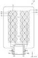
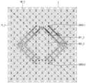
도 7에서는 설명의 편의를 위해 센싱 전극들(RE, TE), 도전 패턴(DE), 센싱 라인들(RL, TL), 센싱 패드들(TP1, TP2)만을 도시하였다.In FIG. 7, only the sensing electrodes RE and TE, the conductive pattern DE, the sensing lines RL and TL, and the sensing pads TP1 and TP2 are illustrated for convenience of description.
도 7을 참조하면, 센싱 유닛(TDU)은 사용자의 터치를 감지하기 위한 센싱 영역(TSA)과 센싱 영역(TSA)의 주변에 배치되는 센싱 주변 영역(TPA)을 포함한다. 센싱 영역(TSA)은 표시 유닛(DU)의 표시 영역(DA)에 중첩하고, 센싱 주변 영역(TPA)은 표시 유닛(DU)의 비표시 영역(NDA)에 중첩할 수 있다.Referring to FIG. 7, the sensing unit TDU includes a sensing area TSA for sensing a user's touch and a sensing peripheral area TPA disposed around the sensing area TSA. The sensing area TSA may overlap the display area DA of the display unit DU, and the sensing peripheral area TPA may overlap the non-display area NDA of the display unit DU.
센싱 전극들(RE, TE)은 센싱 영역(TSA)에 배치될 수 있다. 센싱 전극들(RE, TE)은 제1 센싱 전극(RE)들 및 제2 센싱 전극(TE)들을 포함할 수 있다. 도 7에 도시된 실시예에서, 제1 센싱 전극(RE)은 감지 전극이고, 제2 센싱 전극(TE)은 구동 전극인 것을 중심으로 설명한다.The sensing electrodes RE and TE may be disposed in the sensing area TSA. The sensing electrodes RE and TE may include first sensing electrodes RE and second sensing electrodes TE. In the embodiment illustrated in FIG. 7, the first sensing electrode RE is a sensing electrode, and the second sensing electrode TE is a driving electrode.
제1 센싱 전극(RE)들은 복수의 행에 제1 방향(X축 방향)으로 배치되고, 전기적으로 연결될 수 있다. 제2 센싱 전극(TE)들은 복수의 열에 제1 방향(X축 방향)과 교차하는 제2 방향(Y축 방향)으로 배치되며, 전기적으로 연결될 수 있다. 도 7에서는 제1 센싱 전극(RE)들 및 제2 센싱 전극(TE)들 각각이 마름모의 평면 형태를 갖는 것을 예시하였으나, 제1 센싱 전극(RE)들 및 제2 센싱 전극(TE)들 각각의 평면 형태는 이에 한정되지 않는다.The first sensing electrodes RE are disposed in a first direction (X-axis direction) in a plurality of rows, and may be electrically connected. The second sensing electrodes TE are disposed in a plurality of columns in a second direction (Y-axis direction) crossing the first direction (X-axis direction), and may be electrically connected. 7 illustrates that each of the first sensing electrodes RE and the second sensing electrodes TE has a diamond-shaped planar shape, but each of the first sensing electrodes RE and the second sensing electrodes TE The planar shape of is not limited thereto.
제1 센싱 전극(RE)들 및 제2 센싱 전극(TE)들은 서로 전기적으로 분리될 수 있다. 제1 센싱 전극(RE)들 및 제2 센싱 전극(TE)들은 서로 이격되어 배치될 수 있다.The first sensing electrodes RE and the second sensing electrodes TE may be electrically separated from each other. The first sensing electrodes RE and the second sensing electrodes TE may be disposed to be spaced apart from each other.
제1 센싱 전극(RE)들 각각의 크기와 제2 센싱 전극(TE)들 각각의 크기는 실질적으로 동일할 수 있다.The size of each of the first sensing electrodes RE and the size of each of the second sensing electrodes TE may be substantially the same.
도전 패턴(DE)들은 제1 센싱 전극(RE)들 및 제2 센싱 전극(TE)들과 전기적으로 분리될 수 있다. 즉, 도전 패턴(DE)들은 제1 센싱 전극(RE)들 및 제2 센싱 전극(TE)들과 이격되어 배치될 수 있다. 도전 패턴(DE)들은 제1 센싱 전극(RE)들 및 제2 센싱 전극(TE)들 각각에 의해 둘러싸이도록 배치될 수 있다.The conductive patterns DE may be electrically separated from the first sensing electrodes RE and the second sensing electrodes TE. That is, the conductive patterns DE may be disposed to be spaced apart from the first sensing electrodes RE and the second sensing electrodes TE. The conductive patterns DE may be disposed to be surrounded by each of the first sensing electrodes RE and the second sensing electrodes TE.
도전 패턴(DE)들로 인해 발광 소자층(EML)의 제2 전극과 제1 센싱 전극(RE) 또는 제2 센싱 전극(TE) 사이의 기생 정전 용량이 작아질 수 있다. 기생 정전 용량이 작아지는 경우 제1 센싱 전극(RE)과 제2 센싱 전극(TE) 사이의 상호 용량이 충전되는 충전 속도를 높일 수 있다.Due to the conductive patterns DE, the parasitic capacitance between the second electrode of the light emitting element layer EML and the first sensing electrode RE or the second sensing electrode TE may decrease. When the parasitic capacitance decreases, the charging speed at which the mutual capacitance between the first sensing electrode RE and the second sensing electrode TE is charged may be increased.
센싱 라인들(RL, TL)은 센싱 주변 영역(TPA)으로부터 연장하여 센싱 영역(TSA)에 배치될 수 있다. 센싱 라인들(RL, TL)은 제1 센싱 전극(RE)들에 연결되는 제1 센싱 라인(RL), 제2 센싱 전극(TE)들에 연결되는 제2 센싱 라인(TL)을 포함할 수 있다. 도 7에 도시된 실시예에서, 제1 센싱 라인(RL)은 감지 라인이고, 제2 센싱 라인(TL)은 구동 라인인 것을 중심으로 설명한다.The sensing lines RL and TL may extend from the sensing peripheral area TPA and may be disposed in the sensing area TSA. The sensing lines RL and TL may include a first sensing line RL connected to the first sensing electrodes RE and a second sensing line TL connected to the second sensing electrodes TE. have. In the embodiment illustrated in FIG. 7, the first sensing line RL is a sensing line, and the second sensing line TL is a driving line.
제1 센싱 라인(RL)의 일단은 제1 센싱 전극(RE)과 전기적으로 연결되고, 제1 센싱 라인(RL)의 타단은 제1 센싱 패드(TP1)들과 연결될 수 있다.One end of the first sensing line RL may be electrically connected to the first sensing electrode RE, and the other end of the first sensing line RL may be connected to the first sensing pads TP1.
제1 센싱 라인(RL)은 제1 센싱 패드(TP1)들이 배치된 센싱 주변 영역(TPA)으로부터 연장하여 센싱 영역(TSA)에 배치될 수 있다. 제1 센싱 라인(RL)은 센싱 영역(TSA)에서 제1 센싱 전극(RE)과 전기적으로 연결될 수 있다. 제1 센싱 라인(RL)은 센싱 영역(TSA)에서 제2 방향(Y축 방향)으로 연장할 수 있다.The first sensing line RL may be disposed in the sensing area TSA by extending from the sensing peripheral area TPA in which the first sensing pads TP1 are disposed. The first sensing line RL may be electrically connected to the first sensing electrode RE in the sensing area TSA. The first sensing line RL may extend in a second direction (Y-axis direction) in the sensing area TSA.
제1 센싱 라인(RL)들은 각 행에 배치된 제1 센싱 전극(RE)들 중 어느 하나와 전기적으로 연결될 수 있다. 예를 들어, 도 7에 도시된 바와 같이, 제1 센싱 라인(RL)들은 제1 행의 제1 열에 배치된 제1 센싱 전극(RE), 제2 행의 제2 열에 배치된 제1 센싱 전극(RE), 제n 행의 제n 열에 배치된 제1 센싱 전극(RE) 각각에 전기적으로 연결될 수 있다.The first sensing lines RL may be electrically connected to any one of the first sensing electrodes RE arranged in each row. For example, as shown in FIG. 7, the first sensing lines RL are a first sensing electrode RE disposed in a first column of a first row, and a first sensing electrode disposed in a second column of a second row. It may be electrically connected to (RE) and each of the first sensing electrodes RE disposed in the n-th column of the n-th row.
제2 센싱 라인(TL)의 일단은 제2 센싱 전극(TE)과 전기적으로 연결되고, 제2 센싱 라인(TL)의 타단은 제2 센싱 패드(TP2)들과 연결될 수 있다.One end of the second sensing line TL may be electrically connected to the second sensing electrode TE, and the other end of the second sensing line TL may be connected to the second sensing pads TP2.
제2 센싱 라인(TL)은 제2 센싱 패드(TP2)들이 배치된 센싱 주변 영역(TPA)으로부터 센싱 영역(TSA)의 가장자리까지 연장할 수 있다. 제2 센싱 라인(TL)은 센싱 영역(TSA)의 가장자리에서 제2 센싱 전극(TE)과 전기적으로 연결될 수 있다.The second sensing line TL may extend from the sensing peripheral area TPA in which the second sensing pads TP2 are disposed to the edge of the sensing area TSA. The second sensing line TL may be electrically connected to the second sensing electrode TE at the edge of the sensing area TSA.
제2 센싱 라인(TL)들은 각 열에 배치된 제2 센싱 전극(TE)들 중 어느 하나와 전기적으로 연결될 수 있다. 예를 들어, 도 7에 도시된 바와 같이, 제2 센싱 라인(TL)들은 제2 방향(Y축 방향)으로 전기적으로 연결된 제2 센싱 전극(TE)들 중 하측 끝에 배치된 제2 센싱 전극(TE)과 전기적으로 연결될 수 있다.The second sensing lines TL may be electrically connected to any one of the second sensing electrodes TE arranged in each column. For example, as shown in FIG. 7, the second sensing lines TL are disposed at the lower end of the second sensing electrodes TE that are electrically connected in the second direction (Y-axis direction). TE) can be electrically connected.
제1 센싱 라인(TL)은 제2 센싱 라인(RL)과 교차하여 두께 방향으로 중첩할 수 있다.The first sensing line TL may cross and overlap the second sensing line RL in the thickness direction.
도 7에 도시된 실시예에 의하면, 제1 센싱 라인(RL)은 표시 영역(DA)과 중첩하는 센싱 영역(TSA) 내에 배치될 수 있다. 이에 따라, 센싱 주변 영역(TPA)에 제1 센싱 라인(RL)을 배치하기 위한 공간이 불필요하므로, 표시 장치(10)의 비표시 영역(NDA)을 최소화할 수 있다.According to the embodiment illustrated in FIG. 7, the first sensing line RL may be disposed in the sensing area TSA overlapping the display area DA. Accordingly, since a space for arranging the first sensing line RL in the sensing peripheral area TPA is unnecessary, the non-display area NDA of the
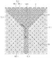
도 8은 도 7의 A 영역의 확대도이다.8 is an enlarged view of area A of FIG. 7.
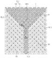
도 8을 참조하면, 제1 센싱 전극(RE)들과 제2 센싱 전극(TE)들이 그들의 교차 영역들에서 전기적으로 분리되기 위해, 제1 방향(X축 방향)으로 서로 인접한 제1 센싱 전극(RE)들은 제1 연결부(BE1)를 통해 연결되고, 제2 방향(Y축 방향)으로 서로 인접한 제2 센싱 전극(TE)들은 제2 연결부(BE2)를 통해 연결될 수 있다.Referring to FIG. 8, in order to electrically separate the first sensing electrodes RE and the second sensing electrodes TE in their crossing regions, the first sensing electrodes adjacent to each other in a first direction (X-axis direction) ( The REs are connected through the first connection part BE1, and the second sensing electrodes TE adjacent to each other in the second direction (Y-axis direction) may be connected through the second connection part BE2.
제1 연결부(BE1)는 제1 센싱 전극(RE)들로부터 연장된 형태를 가질 수 있다. 제1 연결부(BE1)는 제1 센싱 전극(RE)들과 동일한 층에 배치될 수 있다.The first connection part BE1 may have a shape extending from the first sensing electrodes RE. The first connection part BE1 may be disposed on the same layer as the first sensing electrodes RE.
제2 연결부(BE2)는 제1 컨택홀(CNT1)들을 통해 제2 센싱 전극(TE)들과 접속될 수 있다. 제2 연결부(BE2)들은 적어도 한 번 절곡된 형상을 가질 수 있다. 도 8에서는 제2 연결부(BE2)들이 "<" 또는 ">"와 같이 절곡된 것을 예시하였으나, 제2 연결부(BE2)들의 형상은 이에 한정되지 않는다. 또한, 제2 방향(Y축 방향)으로 서로 인접한 제2 센싱 전극(TE)들이 복수 개의 제2 연결부(BE2)들에 의해 연결되므로, 제2 연결부(BE2)들 중 어느 하나가 단선되더라도, 제2 방향(Y축 방향)으로 서로 인접한 제2 센싱 전극(TE)들은 안정적으로 연결될 수 있다. 도 8에서는 서로 인접한 제2 센싱 전극(TE)들이 두 개의 제2 연결부(BE2)들에 의해 연결되는 것을 예시하였으나, 제2 연결부(BE2)들의 개수는 이에 한정되지 않는다.The second connection part BE2 may be connected to the second sensing electrodes TE through the first contact holes CNT1. The second connection parts BE2 may have a shape that is bent at least once. 8 illustrates that the second connection parts BE2 are bent such as "<" or ">", but the shape of the second connection parts BE2 is not limited thereto. In addition, since the second sensing electrodes TE adjacent to each other in the second direction (Y-axis direction) are connected by the plurality of second connection parts BE2, even if any one of the second connection parts BE2 is disconnected, the Second sensing electrodes TE adjacent to each other in two directions (Y-axis direction) may be stably connected. In FIG. 8, it is illustrated that the second sensing electrodes TE adjacent to each other are connected by the two second connection parts BE2, but the number of the second connection parts BE2 is not limited thereto.
도전 패턴(DE)들은 제1 센싱 전극(RE)들 및 제2 센싱 전극(TE)들과 전기적으로 분리될 수 있다. 도전 패턴(DE)들은 제1 센싱 전극(RE)들 및 제2 센싱 전극(TE)들 각각에 의해 둘러싸이도록 배치될 수 있다. 도전 패턴(DE)들과 제1 센싱 전극(RE)들 및 제2 센싱 전극(TE) 사이에는 개구부(OP)가 위치할 수 있다. 이 경우, 도전 패턴(DE)들 각각은 개구부(OP)에 의해 둘러싸이고, 제1 센싱 전극(RE)들 및 제2 센싱 전극(TE)들은 개구부(OP)를 둘러싸도록 배치될 수 있다.The conductive patterns DE may be electrically separated from the first sensing electrodes RE and the second sensing electrodes TE. The conductive patterns DE may be disposed to be surrounded by each of the first sensing electrodes RE and the second sensing electrodes TE. An opening OP may be positioned between the conductive patterns DE and the first sensing electrodes RE and the second sensing electrode TE. In this case, each of the conductive patterns DE may be surrounded by the opening OP, and the first sensing electrodes RE and the second sensing electrodes TE may be disposed to surround the opening OP.
도전 패턴(DE)들 각각의 크기는 제1 센싱 전극(RE)들 및 제2 센싱 전극(TE)들 각각의 크기보다 작을 수 있다. 도 8에서는 제1 센싱 전극(RE)들, 제2 센싱 전극(TE)들, 및 도전 패턴(DE)들 각각이 마름모의 평면 형태를 갖는 것을 예시하였으나, 제1 센싱 전극(RE)들, 제2 센싱 전극(TE)들, 및 도전 패턴(DE)들 각각의 평면 형태는 이에 한정되지 않는다.The size of each of the conductive patterns DE may be smaller than the size of each of the first sensing electrodes RE and the second sensing electrodes TE. In FIG. 8, it is illustrated that each of the first sensing electrodes RE, the second sensing electrodes TE, and the conductive patterns DE have a diamond-shaped planar shape. 2 The planar shape of each of the sensing electrodes TE and the conductive patterns DE is not limited thereto.
도 8에 도시된 실시예에 의하면, 제1 방향(X축 방향)으로 서로 인접한 제1 센싱 전극(RE)들은 제1 연결부(BE1)를 통해 연결되고, 제2 방향(Y축 방향)으로 서로 인접한 제2 센싱 전극(TE)들은 제2 연결부(BE2)를 통해 연결될 수 있다. 이에 따라, 제1 센싱 전극(RE)들 및 제2 센싱 전극(TE)들은 그들의 교차 영역들에서 전기적으로 분리되며, 제1 센싱 전극(RE)들은 제1 방향(X축 방향)으로 전기적으로 연결되고, 제2 센싱 전극(TE)들은 제2 방향(Y축 방향)으로 전기적으로 연결될 수 있다.According to the embodiment shown in FIG. 8, the first sensing electrodes RE adjacent to each other in the first direction (X-axis direction) are connected through the first connection part BE1 and are connected to each other in the second direction (Y-axis direction) The adjacent second sensing electrodes TE may be connected through the second connection part BE2. Accordingly, the first sensing electrodes RE and the second sensing electrodes TE are electrically separated in their crossing regions, and the first sensing electrodes RE are electrically connected in the first direction (X-axis direction). Then, the second sensing electrodes TE may be electrically connected in a second direction (Y-axis direction).
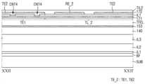
도 9는 도 8의 B 영역의 확대도이다.9 is an enlarged view of area B of FIG. 8.
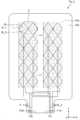
도 9를 참조하면, 제1 센싱 전극(RE)들, 제2 센싱 전극(TE)들, 제1 연결부(BE1), 제2 연결부(BE2)들은 메쉬 형상 또는 그물망 형상을 가질 수 있다. 도전 패턴(DE)들 역시 메쉬 형상 또는 그물망 형상을 가질 수 있다.Referring to FIG. 9, the first sensing electrodes RE, the second sensing electrodes TE, the first connection part BE1, and the second connection part BE2 may have a mesh shape or a mesh shape. The conductive patterns DE may also have a mesh shape or a mesh shape.
제1 센싱 전극(RE)들 및 제2 센싱 전극(TE)들을 포함하는 센싱층(TSL)이 도 5와 같이 박막 봉지막(TFEL) 상에 바로 배치되는 경우, 발광 소자층(EML)의 제2 전극과 센싱층(TSL)의 제1 센싱 전극(RE)들 및 제2 센싱 전극(TE)들 각각의 사이의 거리가 가깝기 때문에, 발광 소자층(EML)의 제2 전극과 센싱층(TSL)의 제1 센싱 전극(RE)들 및 제2 센싱 전극(TE)들 각각의 사이에 기생 정전 용량(parasitic capacitance)이 크게 형성될 수 있다. 기생 정전 용량은 발광 소자층(EML)의 제2 전극과 센싱층(TSL)의 제1 센싱 전극(RE)들 및 제2 센싱 전극(TE)들 각각의 사이의 중첩 면적에 비례하므로, 기생 정전 용량을 줄이기 위해 제1 센싱 전극(RE)들 및 제2 센싱 전극(TE)들 각각은 메쉬 형상 또는 그물망 형상을 가지는 것이 바람직하다.When the sensing layer TSL including the first sensing electrodes RE and the second sensing electrodes TE is directly disposed on the thin film encapsulation layer TFEL as shown in FIG. Since the distance between the second electrode and the first sensing electrodes RE and the second sensing electrodes TE of the sensing layer TSL is close, the second electrode and the sensing layer TSL of the light emitting element layer EML are A parasitic capacitance may be largely formed between each of the first sensing electrodes RE and the second sensing electrodes TE of ). Since the parasitic capacitance is proportional to the overlapping area between the second electrode of the light emitting element layer EML and the first sensing electrodes RE and the second sensing electrodes TE of the sensing layer TSL, the parasitic capacitance In order to reduce capacity, it is preferable that each of the first sensing electrodes RE and the second sensing electrodes TE has a mesh shape or a mesh shape.
제1 센싱 전극(RE), 제2 센싱 전극(TE)들, 도전 패턴(DE)들은 서로 이격되어 배치될 수 있다. 제1 센싱 전극(RE)과 제2 센싱 전극(TE) 사이, 제1 센싱 전극(RE)과 도전 패턴(DE) 사이, 제2 센싱 전극(TE)과 도전 패턴(DE) 사이, 제2 센싱 전극(TE)과 제1 연결부(BE1) 사이에는 갭이 존재할 수 있다. 도 9에서는 설명의 편의를 위해 제1 센싱 전극(RE)과 제2 센싱 전극(TE) 사이의 경계, 제2 센싱 전극(TE)과 제1 연결부(BE1) 사이의 경계, 및 제1 센싱 전극(RE)과 제1 연결부(BE1) 사이의 경계를 점선으로 도시하였다.The first sensing electrodes RE, the second sensing electrodes TE, and the conductive patterns DE may be disposed to be spaced apart from each other. Between the first sensing electrode RE and the second sensing electrode TE, between the first sensing electrode RE and the conductive pattern DE, between the second sensing electrode TE and the conductive pattern DE, and the second sensing A gap may exist between the electrode TE and the first connection part BE1. In FIG. 9, for convenience of description, a boundary between a first sensing electrode RE and a second sensing electrode TE, a boundary between a second sensing electrode TE and a first connector BE1, and a first sensing electrode The boundary between (RE) and the first connection part BE1 is shown by a dotted line.
제1 연결부(BE1)는 제1 센싱 전극(RE)들 사이에 배치될 수 있다. 제1 연결부(BE1)는 제1 센싱 전극(RE)들 각각에서 연장될 수 있다. 그러므로, 제1 연결부(BE1)는 별도의 컨택홀 없이 제1 센싱 전극(RE)들에 연결될 수 있다.The first connection part BE1 may be disposed between the first sensing electrodes RE. The first connection part BE1 may extend from each of the first sensing electrodes RE. Therefore, the first connection part BE1 may be connected to the first sensing electrodes RE without a separate contact hole.
제2 연결부(BE2)는 제1 컨택홀들(CNT1)을 통해 제2 센싱 전극(TE)들에 각각 접속될 수 있다. 제2 연결부(BE2)의 일 단은 제1-1 컨택홀(CNT1-1)을 통해 제2 방향(Y축 방향)으로 서로 인접한 제2 센싱 전극(TE)들 중 어느 한 제2 센싱 전극(TE)에 접속될 수 있다. 제2 연결부(BE2)의 타 단은 제1-2 컨택홀(CNT1-2)을 통해 제2 방향(Y축 방향)으로 서로 인접한 제2 센싱 전극(TE)들 중 다른 제2 센싱 전극(TE)에 접속될 수 있다.The second connection part BE2 may be connected to the second sensing electrodes TE through the first contact holes CNT1, respectively. One end of the second connection part BE2 is one of the second sensing electrodes TE adjacent to each other in the second direction (Y-axis direction) through the 1-1 contact hole CNT1-1 ( TE) can be connected. The other end of the second connection part BE2 is the second sensing electrode TE among the second sensing electrodes TE adjacent to each other in the second direction (Y-axis direction) through the 1-2 contact hole CNT1-2. ) Can be accessed.
제2 연결부(BE2)는 제1 센싱 전극(RE) 또는 제2 센싱 전극(TE)과 중첩할 수 있다. 또는, 제2 연결부(BE2)는 제1 센싱 전극(RE) 대신에 제1 연결부(BE1)와 중첩할 수도 있다. 또는, 제2 연결부(BE2)는 제1 센싱 전극(RE)과 제1 연결부(BE1) 모두에 중첩할 수도 있다. 제2 연결부(BE2)는 제1 연결부(BE1)와 상이한 층에 배치될 수 있다. 따라서, 제2 연결부(BE2)는 제1 연결부(BE1)와 중첩하더라도, 제1 연결부(BE1)에 단락(short-circuited)되지 않을 수 있다.The second connection part BE2 may overlap the first sensing electrode RE or the second sensing electrode TE. Alternatively, the second connection part BE2 may overlap the first connection part BE1 instead of the first sensing electrode RE. Alternatively, the second connection part BE2 may overlap both the first sensing electrode RE and the first connection part BE1. The second connection part BE2 may be disposed on a different layer from the first connection part BE1. Therefore, even if the second connection part BE2 overlaps the first connection part BE1, it may not be short-circuited to the first connection part BE1.
제1 센싱 전극(RE)들, 제2 센싱 전극(TE)들, 제1 연결부(BE1), 및 제2 연결부(BE2)는 각 서브 화소(R, G, B)와 비중첩하도록 배치될 수 있다. 즉, 제1 센싱 전극(RE)들, 제2 센싱 전극(TE)들, 제1 연결부(BE1), 및 제2 연결부(BE2)는 각 서브 화소(R, G, B)의 가장자리를 따라 배치될 수 있다. 즉, 제1 센싱 전극(RE)들, 제2 센싱 전극(TE)들, 제1 연결부(BE1), 및 제2 연결부(BE2)는 각 서브 화소(R, G, B)를 정의하는 화소 정의막과 중첩하도록 배치될 수 있다.The first sensing electrodes RE, the second sensing electrodes TE, the first connection part BE1, and the second connection part BE2 may be disposed so as to be non-overlapping with each of the sub-pixels R, G, and B. have. That is, the first sensing electrodes RE, the second sensing electrodes TE, the first connection part BE1, and the second connection part BE2 are disposed along the edges of each of the sub-pixels R, G, and B. Can be. That is, the first sensing electrodes RE, the second sensing electrodes TE, the first connection part BE1, and the second connection part BE2 are pixel definitions that define each of the sub-pixels R, G, and B. It can be arranged to overlap with the membrane.
서브 화소(R, G, B)들은 제1 색을 발광하는 제1 서브 화소(R), 제2 색을 발광하는 제2 서브 화소(G), 및 제3 색을 발광하는 제3 서브 화소(B)를 포함할 수 있다. 도 9에서는 제1 서브 화소(R)가 적색 서브 화소, 제2 서브 화소(G)가 녹색 서브 화소, 제3 서브 화소(B)가 청색 서브 화소인 것을 예시하였으나, 이에 한정되지 않는다. 도 9에서는 제1 서브 화소(R), 제2 서브 화소(G), 및 제3 서브 화소(B)가 육각형의 평면 형태를 갖는 것을 예시하였으나, 이에 한정되지 않는다. 제1 서브 화소(R), 제2 서브 화소(G), 및 제3 서브 화소(B)는 육각형 이외에 다른 다각형, 원형 또는 타원형의 평면 형태를 가질 수 있다. 또한, 도 9에서는 제1 서브 화소(R)의 크기, 제2 서브 화소(G)의 크기, 및 제3 서브 화소(B)의 크기가 실질적으로 동일한 것을 예시하였으나, 서브 화소(R, G, B)들의 크기는 이에 한정되지 않는다. 예를 들어, 제3 서브 화소(B)의 크기가 가장 크고, 제2 서브 화소(G)의 크기가 가장 작을 수 있다. 또는, 제1 서브 화소(R)의 크기와 제3 서브 화소(B)의 크기는 실질적으로 동일하고, 제2 서브 화소(G)의 크기는 제1 서브 화소(R)의 크기와 제3 서브 화소(B)의 크기 각각보다 작을 수 있다.The sub-pixels R, G, and B include a first sub-pixel R emitting a first color, a second sub-pixel G emitting a second color, and a third sub-pixel emitting a third color ( B) may be included. 9 illustrates that the first sub-pixel R is a red sub-pixel, the second sub-pixel G is a green sub-pixel, and the third sub-pixel B is a blue sub-pixel, but the present invention is not limited thereto. 9 illustrates that the first sub-pixel R, the second sub-pixel G, and the third sub-pixel B have a hexagonal planar shape, but are not limited thereto. The first sub-pixel R, the second sub-pixel G, and the third sub-pixel B may have a polygonal, circular, or elliptical planar shape other than a hexagonal shape. In addition, although FIG. 9 illustrates that the size of the first sub-pixel R, the size of the second sub-pixel G, and the size of the third sub-pixel B are substantially the same, the sub-pixels R, G, and The size of B) is not limited thereto. For example, the size of the third sub-pixel B may be the largest, and the size of the second sub-pixel G may be the smallest. Alternatively, the size of the first sub-pixel R and the size of the third sub-pixel B are substantially the same, and the size of the second sub-pixel G is the size of the first sub-pixel R and the third sub-pixel. It may be smaller than the size of each of the pixels B.
화소(P)는 계조를 표현할 수 있는 한 그룹의 서브 화소들을 가리킨다. 도 9에서는 화소(P)가 하나의 제1 서브 화소(R), 두 개의 제2 서브 화소(G)들, 및 하나의 제3 서브 화소(B)를 포함하는 것을 예시하였으나, 이에 한정되지 않는다. 예를 들어, 화소(P)는 하나의 제1 서브 화소(R), 하나의 제2 서브 화소(G), 및 하나의 제3 서브 화소(B)를 포함할 수 있다.The pixel P refers to a group of sub-pixels capable of expressing gray scale. 9 illustrates that the pixel P includes one first sub-pixel R, two second sub-pixels G, and one third sub-pixel B, but is not limited thereto. . For example, the pixel P may include one first sub-pixel R, one second sub-pixel G, and one third sub-pixel B.
도 9에 도시된 실시예에 의하면, 제1 센싱 전극(RE)들, 제2 센싱 전극(TE)들, 제1 연결부(BE1), 제2 연결부(BE2)들이 메쉬 형상 또는 그물망 형상을 가지므로, 서브 화소(R, G, B)들은 제1 센싱 전극(RE)들, 제2 센싱 전극(TE)들, 제1 연결부(BE1), 및 제2 연결부(BE2)들과 중첩하지 않을 수 있다. 따라서, 서브 화소(R, G, B)들로부터 출력된 광이 제1 센싱 전극(RE)들, 제2 센싱 전극(TE)들, 제1 연결부(BE1), 및 제2 연결부(BE2)들에 의해 가려짐으로써, 광의 휘도가 감소되는 것을 방지할 수 있다.According to the embodiment shown in FIG. 9, since the first sensing electrodes RE, the second sensing electrodes TE, the first connection part BE1, and the second connection part BE2 have a mesh shape or a mesh shape, , The sub-pixels R, G, and B may not overlap with the first sensing electrodes RE, the second sensing electrodes TE, the first connection part BE1, and the second connection part BE2. . Accordingly, the light output from the sub-pixels R, G, B is the first sensing electrodes RE, the second sensing electrodes TE, the first connection part BE1, and the second connection part BE2. By being covered by, it is possible to prevent the luminance of light from decreasing.
도 10은 도 8의 C 영역의 확대도이다.10 is an enlarged view of area C of FIG. 8.
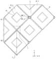
도 10을 참조하면, 제1 센싱 전극(RE)들은 제1 층 전극(RE1) 및 제2 층 전극(RE2)을 포함할 수 있다.Referring to FIG. 10, the first sensing electrodes RE may include a first layer electrode RE1 and a second layer electrode RE2.
제1 센싱 전극(RE)들의 제1 층 전극(RE1)은 복수의 행에 부분적으로 배치되고, 제2 층 전극(RE2)은 복수의 행 전체에 배치될 수 있다.The first layer electrode RE1 of the first sensing electrodes RE may be partially disposed in a plurality of rows, and the second layer electrode RE2 may be disposed in all of the plurality of rows.
예를 들어, 도 8 내지 도 10에 도시된 바와 같이, 제1 행에 배치된 제1 센싱 전극(RE)들은 제1 그룹(G1)으로 정의되고, 제2 행에 배치된 제1 센싱 전극(RE)들은 제2 그룹(G2)으로 정의될 수 있다. 제1 그룹(G1)과 제2 그룹(G2)은 서로 이격되어 배치될 수 있다. 제1 그룹(G1)의 제1 층 전극(RE1)은 제1 열에 부분적으로 배치될 수 있다. 즉, 제1 그룹(G1)의 제1 층 전극(RE1)은 제1 열에 배치된 제2 층 전극(RE2)과 두께 방향으로 중첩하도록 배치될 수 있다. 또한, 제1 그룹(G1)의 제1 층 전극(RE1)은 제1 그룹(G1)의 제1 열을 제외한 나머지 열에 배치된 제2 층 전극(RE2)들과 비중첩하도록 배치될 수 있다. 또한, 제1 그룹(G1)의 제1 층 전극(RE1)은 제2 그룹(G2)의 제2 층 전극(RE2)들과 비중첩하도록 배치될 수 있다.For example, as shown in FIGS. 8 to 10, the first sensing electrodes RE disposed in the first row are defined as a first group G1, and the first sensing electrodes RE disposed in the second row ( RE) may be defined as a second group (G2). The first group G1 and the second group G2 may be disposed to be spaced apart from each other. The first layer electrode RE1 of the first group G1 may be partially disposed in the first column. That is, the first layer electrode RE1 of the first group G1 may be disposed to overlap the second layer electrode RE2 disposed in the first column in the thickness direction. Also, the first layer electrode RE1 of the first group G1 may be disposed so as to be non-overlapping with the second layer electrodes RE2 disposed in the remaining rows except for the first row of the first group G1. In addition, the first layer electrode RE1 of the first group G1 may be disposed so as to be non-overlapping with the second layer electrodes RE2 of the second group G2.
한편, 도 10에서는 제1 그룹(G1)의 제1 층 전극(RE1)이 제1 열에 배치된 제2 층 전극(RE2)과 전면적으로 중첩하는 경우를 예시하였으나, 이에 제한되는 것은 아니다. 즉, 제1 그룹(G1)의 제1 층 전극(RE1)은 제2 열 등 다른 열의 제2 층 전극(RE2) 중 어느 하나와 중첩하도록 배치될 수 있다.Meanwhile, in FIG. 10, a case in which the first layer electrode RE1 of the first group G1 completely overlaps the second layer electrode RE2 disposed in the first column is illustrated, but is not limited thereto. That is, the first layer electrode RE1 of the first group G1 may be disposed to overlap with any one of the second layer electrodes RE2 of another column such as the second row.
제1 층 전극(RE1)은 상술한 제1 센싱 라인(RL)과 연결될 수 있다. 제1 센싱 라인(RL)은 제1 층 전극(RE1)의 일단으로부터 연장된 형상을 가질 수 있다. 제1 센싱 라인(RL)은 제1 층 전극(RE1)으로부터 센싱 주변 영역(TPA)에 배치된 제1 센싱 패드(TP1)까지 연장할 수 있다. 이 경우, 제1 센싱 라인(RL)은 센싱 영역(TSA)에 배치된 제1 센싱 전극(RE) 또는 제2 센싱 전극(TE)과 부분적으로 중첩할 수 있다. 예를 들어, 도 10에 도시된 바와 같이, 제1 그룹(G1)의 제1 층 전극(RE1)에 연결된 제1 센싱 라인(RL)은 제2 그룹(G2)의 제1 센싱 전극(RE)과 두께 방향으로 중첩할 수 있다. 즉, 제1 그룹(G1)의 제1 층 전극(RE1)에 연결된 제1 센싱 라인(RL)은 제2 그룹(G2)의 제2 층 전극(RE2)과 중첩될 수 있다.The first layer electrode RE1 may be connected to the above-described first sensing line RL. The first sensing line RL may have a shape extending from one end of the first layer electrode RE1. The first sensing line RL may extend from the first layer electrode RE1 to the first sensing pad TP1 disposed in the sensing peripheral area TPA. In this case, the first sensing line RL may partially overlap the first sensing electrode RE or the second sensing electrode TE disposed in the sensing area TSA. For example, as shown in FIG. 10, the first sensing line RL connected to the first layer electrode RE1 of the first group G1 is the first sensing electrode RE of the second group G2. And can be overlapped in the thickness direction. That is, the first sensing line RL connected to the first layer electrode RE1 of the first group G1 may overlap the second layer electrode RE2 of the second group G2.
각 그룹의 제1 층 전극(RE1)은 제2 컨택홀(CNT2)들을 통해 각 그룹의 제2 층 전극(RE2)과 전기적으로 연결될 수 있다. 즉, 제1 층 전극(RE1)은 제1 센싱 라인(RL)과 각 그룹의 제1 센싱 전극(RE)을 연결하는 역할을 할 수 있다. 예를 들어, 제1 그룹(G1)의 제1 층 전극(RE1)은 제1 센싱 라인(RL)과 제1 그룹(G1)의 제1 센싱 전극(RE)들을 연결할 수 있다. 또한, 제2 그룹(G2)의 제1 층 전극(RE2)은 제1 센싱 라인(RL)과 제2 그룹(G2)의 제1 센싱 전극(RE)들을 연결할 수 있다. 한편, 도 10에서는 제2 컨택홀(CNT2)들이 제1 층 전극(RE1)의 일측 즉, 하측에 부분적으로 형성된 경우를 예시하였으나, 이에 제한되는 것은 아니다. 즉, 제2 컨택홀(CNT2)들은 제1 층 전극(RE1)과 제2 층 전극(RE2)이 중첩하는 영역 전체에 걸쳐 형성될 수도 있다.The first layer electrode RE1 of each group may be electrically connected to the second layer electrode RE2 of each group through the second contact holes CNT2. That is, the first layer electrode RE1 may serve to connect the first sensing line RL and the first sensing electrode RE of each group. For example, the first layer electrode RE1 of the first group G1 may connect the first sensing line RL and the first sensing electrodes RE of the first group G1. In addition, the first layer electrode RE2 of the second group G2 may connect the first sensing line RL and the first sensing electrodes RE of the second group G2. Meanwhile, in FIG. 10, a case in which the second contact holes CNT2 are partially formed on one side, that is, a lower side of the first layer electrode RE1, is illustrated, but is not limited thereto. That is, the second contact holes CNT2 may be formed over the entire area where the first layer electrode RE1 and the second layer electrode RE2 overlap.
제1 층 전극(RE1)은 제1 센싱 라인(RL)과 동일한 층에 배치될 수 있다. 제1 층 전극(RE1)과 제1 센싱 라인(RL)은 동일한 물질로 이루어질 수 있다. 예를 들어, 제1 층 전극(RE1)은 도 12에 도시된 제1 센싱 도전층(171)으로 이루어질 수 있다. 한편, 도 10에서는 제1 센싱 라인(RL)이 제1 층 전극(RE1)에 의해 제2 층 전극(RE2)과 연결되는 경우를 예시하였으나, 이에 제한되는 것은 아니다. 즉, 제1 센싱 전극(RE)의 제1 층 전극(RE1)이 생략되고, 제1 센싱 라인(RL)은 제2 층 전극(RE2)에 직접 연결될 수 있다. 이 경우, 제2 층 전극(RE2)은 하부에 배치된 절연층을 관통하는 컨택홀을 통해 제1 센싱 라인(RL)과 직접 연결될 수 있다. The first layer electrode RE1 may be disposed on the same layer as the first sensing line RL. The first layer electrode RE1 and the first sensing line RL may be made of the same material. For example, the first layer electrode RE1 may be formed of the first sensing
제1 층 전극(RE1)은 메쉬 형상 또는 그물망 형상을 가질 수 있다. 제1 층 전극(RE1)이 메쉬 형상 또는 그물망 형상을 가지므로, 서브 화소(R, G, B)들은 제1 층 전극(RE1)과 중첩하지 않을 수 있다. 따라서, 서브 화소(R, G, B)들로부터 출력된 광이 제1 층 전극(RE1)에 의해 가려짐으로써, 광의 휘도가 감소되는 것을 방지할 수 있음은 앞서 설명한 바와 같다.The first layer electrode RE1 may have a mesh shape or a mesh shape. Since the first layer electrode RE1 has a mesh shape or a mesh shape, the sub-pixels R, G, and B may not overlap the first layer electrode RE1. Accordingly, as described above, since the light output from the sub-pixels R, G, and B is covered by the first layer electrode RE1, it is possible to prevent the luminance of the light from decreasing.
도 11은 도 9의 ⅩⅠ-ⅩⅠ' 선을 기준으로 자른 단면도이다. 도 12는 도 10의 ⅩⅡ-ⅩⅡ' 선을 기준으로 자른 단면도이다.FIG. 11 is a cross-sectional view taken along the line XI-XI' of FIG. 9. 12 is a cross-sectional view taken along the line XII-XII' of FIG. 10.
도 9의 ⅩⅠ-ⅩⅠ' 선에는 제2 센싱 전극(TE)과 제2 연결부(BE2) 간의 접속 구조가 나타나 있다. 도 10의 ⅩⅡ-ⅩⅡ' 선에는 제1 센싱 전극(RE)의 제1 층 전극(RE1), 제2 층 전극(RE2), 및/또는 제1 센싱 라인(RL) 간의 접속 구조가 나타나 있다.A connection structure between the second sensing electrode TE and the second connection part BE2 is shown on the line XI-XI' of FIG. 9. A connection structure between the first layer electrode RE1, the second layer electrode RE2, and/or the first sensing line RL of the first sensing electrode RE is shown on lines XII-XII' of FIG. 10.
도 11 및 도 12를 참조하면, 기판(SUB) 상에는 박막 트랜지스터층(TFTL)이 배치된다. 박막 트랜지스터층(TFTL)은 버퍼층(BF), 반도체층(ACT), 제1 절연층(IL1), 제1 도전층(110), 제2 절연층(IL2), 제2 도전층(120), 및 제3 절연층(IL3)을 포함한다. 상술한 각 층들은 단일막으로 이루어질 수 있지만, 복수의 막을 포함하는 적층막으로 이루어질 수도 있다. 각 층들 사이에는 다른 층이 더 배치될 수도 있다.11 and 12, a thin film transistor layer TFTL is disposed on a substrate SUB. The thin film transistor layer TFTL includes a buffer layer BF, a semiconductor layer ACT, a first insulating layer IL1, a first
기판(SUB)의 일면 상에는 버퍼층(BF)이 형성될 수 있다. 버퍼층(BF)은 투습에 취약한 기판(SUB)을 통해 침투하는 수분으로부터 박막 트랜지스터들과 발광 소자층(EML)의 발광층(152)을 보호하기 위해 기판(SUB)의 일면 상에 형성될 수 있다. 버퍼층(BF)은 교번하여 적층된 복수의 무기막들로 이루어질 수 있다. 예를 들어, 버퍼층(BF)은 실리콘 나이트라이드층, 실리콘 옥시 나이트라이드층, 실리콘 옥사이드층, 티타늄옥사이드층, 및 알루미늄옥사이드층 중 하나 이상의 무기막이 교번하여 적층된 다중막으로 형성될 수 있다. 버퍼층(BF)은 생략될 수 있다.A buffer layer BF may be formed on one surface of the substrate SUB. The buffer layer BF may be formed on one surface of the substrate SUB to protect the thin film transistors and the
버퍼층(BF) 상에는 반도체층(ACT)이 배치된다. 반도체층(ACT)은 화소들의 복수의 트랜지스터의 채널을 이룬다. 반도체층(ACT)은 다결정 실리콘을 포함할 수 있다. 다결정 실리콘은 비정질 실리콘을 결정화하여 형성될 수 있다.The semiconductor layer ACT is disposed on the buffer layer BF. The semiconductor layer ACT forms a channel of a plurality of transistors of pixels. The semiconductor layer ACT may include polycrystalline silicon. Polycrystalline silicon can be formed by crystallizing amorphous silicon.
반도체층(ACT)이 다결정 실리콘으로 이루어지는 경우, 반도체층(ACT)에 이온을 도핑하는 경우, 이온 도핑된 반도체층(ACT)은 도전성을 가질 수 있다. 이로 인해, 반도체층(ACT)은 복수의 트랜지스터의 채널 영역뿐만 아니라 소스 영역과 드레인 영역을 포함할 수 있다. 상기 소스 영역 및 상기 드레인 영역은 각 채널 영역의 양 옆에 연결되어 있을 수 있다.When the semiconductor layer ACT is made of polycrystalline silicon, when the semiconductor layer ACT is doped with ions, the ion-doped semiconductor layer ACT may have conductivity. For this reason, the semiconductor layer ACT may include a source region and a drain region as well as a channel region of a plurality of transistors. The source region and the drain region may be connected to both sides of each channel region.
다른 실시예에서, 반도체층(ACT)은 단결정 실리콘, 저온 다결정 실리콘, 비정질 실리콘이나, 산화물 반도체를 포함할 수 있다. 상기 산화물 반도체는 예를 들어, 인듐, 아연, 갈륨, 주석, 티타늄, 알루미늄, 하프늄(Hf), 지르코늄(Zr), 마그네슘(Mg) 등을 함유하는 이성분계 화합물(ABx), 삼성분계 화합물(ABxCy), 사성분계 화합물(ABxCyDz)을 포함할 수 있다. 일 실시예에서, 반도체층(ACT)은 ITZO(인듐, 주석, 티타늄을 포함하는 산화물)나 IGZO(인듐, 갈륨, 주석을 포함하는 산화물)를 포함할 수 있다.In another embodiment, the semiconductor layer ACT may include single crystal silicon, low temperature polycrystalline silicon, amorphous silicon, or an oxide semiconductor. The oxide semiconductor is, for example, indium, zinc, gallium, tin, titanium, aluminum, hafnium (Hf), zirconium (Zr), magnesium (Mg) containing binary compounds (ABx), ternary compounds (ABxCy ), a four-component compound (ABxCyDz) may be included. In one embodiment, the semiconductor layer ACT may include ITZO (oxide including indium, tin, and titanium) or IGZO (oxide including indium, gallium, and tin).
반도체층(ACT) 상에는 제1 절연층(IL1)이 배치된다. 제1 절연층(IL1)은 대체로 기판(SUB)의 전체 면에 걸쳐 배치될 수 있다. 제1 절연층(IL1)은 게이트 절연 기능을 갖는 게이트 절연막일 수 있다. 제1 절연층(IL1)은 실리콘 화합물, 금속 산화물 등을 포함할 수 있다. 예를 들면, 제1 절연층(IL1)은 실리콘 산화물, 실리콘 질화물, 실리콘 산질화물, 알루미늄 산화물, 탄탈륨 산화물, 하프늄 산화물, 지르코늄 산화물, 티타늄 산화물 등을 포함할 수 있다. 제1 절연층(IL1)은 단일막 또는 서로 다른 물질의 적층막으로 이루어진 다층막일 수 있다.The first insulating layer IL1 is disposed on the semiconductor layer ACT. The first insulating layer IL1 may be disposed over the entire surface of the substrate SUB. The first insulating layer IL1 may be a gate insulating layer having a gate insulating function. The first insulating layer IL1 may include a silicon compound, a metal oxide, or the like. For example, the first insulating layer IL1 may include silicon oxide, silicon nitride, silicon oxynitride, aluminum oxide, tantalum oxide, hafnium oxide, zirconium oxide, titanium oxide, and the like. The first insulating layer IL1 may be a single layer or a multilayer layer formed of a stacked layer of different materials.
제1 절연층(IL1) 상에는 제1 도전층(110)이 배치된다. 제1 도전층(110)은 몰리브덴(Mo), 알루미늄(Al), 백금(Pt), 팔라듐(Pd), 은(Ag), 마그네슘 (Mg), 금(Au), 니켈(Ni), 네오디뮴(Nd), 이리듐(Ir), 크롬(Cr), 칼슘(Ca), 티타늄(Ti), 탄탈륨(Ta), 텅스텐(W), 구리(Cu) 가운데 선택된 하나 이상의 금속을 포함할 수 있다. 제1 도전층(110)은 단일막 또는 다층막일 수 있다. 제1 도전층(110)은 트랜지스터의 게이트 전극 및 유지 커패시터의 제1 전극을 포함할 수 있다.The first
제1 도전층(110) 상에는 제2 절연층(IL2)이 배치된다. 제2 절연층(IL2)은 대체로 기판(SUB)의 전체 면에 걸쳐 배치될 수 있다. 제2 절연층(IL2)은 제1 도전층(110)과 제2 도전층(120)을 절연시키는 역할을 한다.A second insulating layer IL2 is disposed on the first
제2 절연층(IL2)은 층간 절연막일 수 있다. 제2 절연층(IL2)은 상술한 제1 절연층(IL1)과 동일한 물질을 포함하거나, 제1 절연층(IL1)의 구성 물질로 예시된 물질에서 선택된 하나 이상의 물질을 포함할 수 있다.The second insulating layer IL2 may be an interlayer insulating layer. The second insulating layer IL2 may include the same material as the first insulating layer IL1 described above, or may include one or more materials selected from materials exemplified as constituent materials of the first insulating layer IL1.
제2 절연층(IL2) 상에는 제2 도전층(120)이 배치된다. 제2 도전층(120)은 알루미늄(Al), 몰리브덴(Mo), 백금(Pt), 팔라듐(Pd), 은(Ag), 마그네슘 (Mg), 금(Au), 니켈(Ni), 네오디뮴(Nd), 이리듐(Ir), 크롬(Cr), 칼슘(Ca), 티타늄(Ti), 탄탈륨(Ta), 텅스텐(W), 구리(Cu) 가운데 선택된 하나 이상의 금속을 포함할 수 있다. 제2 도전층(120)은 단일막 또는 다층막일 수 있다. 예를 들어, 제2 도전층(120)은 Ti/Al/Ti, Mo/Al/Mo, Mo/AlGe/Mo, Ti/Cu 등의 적층구조로 형성될 수 있다. 제2 도전층(120)은 상술한 데이터 라인들, 소스 전극(121) 및 드레인 전극(122)을 포함할 수 있다. 소스 전극(121) 및 드레인 전극(122)은 제2 절연층(IL2) 및 제1 절연층(IL1)을 관통하는 컨택홀을 통해 각각 반도체층(ACT)의 소스 영역 및 드레인 영역과 접속될 수 있다.A second
제3 절연층(IL3)은 제2 도전층(120)을 덮는다. 제3 절연층(IL3)은 비아층일 수 있다. 제3 절연층(IL3)은 아크릴계 수지(polyacrylates resin), 에폭시 수지(epoxy resin), 페놀 수지(phenolic resin), 폴리아미드계 수지(polyamides resin), 폴리이미드계 수지(polyimides rein), 불포화 폴리에스테르계 수지(unsaturated polyesters resin), 폴리페닐렌계 수지(poly phenylenethers resin), 폴리페닐렌설파이드계 수지(polyphenylenesulfides resin) 또는 벤조사이클로부텐(benzocyclobutene, BCB) 등의 유기 절연 물질을 포함할 수 있다.The third insulating layer IL3 covers the second
박막 트랜지스터층(TFTL) 상에는 발광 소자층(EML)이 배치된다. 발광 소자층(EML)은 제1 전극층(151), 발광층(152), 제2 전극층(153) 및 화소 정의막(140)을 포함할 수 있다.The light emitting element layer EML is disposed on the thin film transistor layer TFTL. The light emitting device layer EML may include a
서브 화소(R, G, B)들 각각은 제1 전극층(151), 발광층(152), 및 제2 전극층(153)이 순차적으로 적층되어 제1 전극층(151)으로부터의 정공과 제2 전극층(153)으로부터의 전자가 발광층(152)에서 서로 결합되어 발광하는 영역을 나타낸다. 제2 서브 화소(G)와 제3 서브 화소(B)는 도 11에 도시된 제1 서브 화소(R)와 실질적으로 동일한 구성을 포함할 수 있다.In each of the sub-pixels R, G, and B, a
제1 전극층(151)은 제3 절연층(IL3) 상에 배치될 수 있다. 제1 전극층(151)은 이에 제한되는 것은 아니지만 인듐-주석-산화물(Indium-Tin-Oxide: ITO), 인듐-아연-산화물(Indium-Zinc-Oxide: IZO), 산화아연(Zinc Oxide: ZnO), 산화인듐(Induim Oxide: In2O3)의 일함수가 높은 물질층과 은(Ag), 마그네슘(Mg), 알루미늄(Al), 백금(Pt), 납(Pb), 금(Au), 니켈(Ni), 네오듐(Nd), 이리듐(Ir), 크롬(Cr), 리튬(Li), 칼슘(Ca) 또는 이들의 혼합물 등과 같은 반사성 물질층이 적층된 적층막 구조를 가질 수 있다. 일함수가 높은층이 반사성 물질층보다 위층에 배치되어 발광층(152)에 가깝게 배치될 수 있다. 제1 전극층(151)은 ITO/Mg, ITO/MgF, ITO/Ag, ITO/Ag/ITO의 복수층 구조를 가질 수 있으나, 이에 제한되는 것은 아니다. 서브 화소(R, G, B)들의 애노드 전극은 제1 전극층(151)으로 이루어질 수 있다. 도 11에서는 애노드 전극이 제4 절연층(IL4)을 관통하는 컨택홀을 통해 드레인 전극(122)과 연결되는 경우를 예시하였으나, 이에 제한되는 것은 아니다. 즉, 애노드 전극은 제4 절연층(IL4)을 관통하는 컨택홀을 통해 소스 전극(121)과도 연결될 수 있다.The
제1 전극층(151) 상에는 화소 정의막(140)이 배치될 수 있다. 화소 정의막(140)은 서브 화소(R, G, B)들을 정의하는 역할을 하기 위해 평탄화막(250) 상에서 제1 전극층(151)을 구획하도록 형성될 수 있다. 화소 정의막(140)은 제1 전극층(151)을 노출하는 개구부를 포함할 수 있다. 즉, 화소 정의막(180)은 제1 전극층(151)의 가장자리를 덮도록 형성될 수 있다. 상기 개구부는 각 서브 화소(R, G, B)의 발광 영역을 정의할 수 있다.The
화소 정의막(140)은 실리콘 산화물, 실리콘 질화물, 실리콘 산질화물, 하프늄 산화물, 알루미늄 산화물, 티타늄 산화물, 탄탈륨 산화물, 아연 산화물 등의 무기 절연 물질이나 아크릴계 수지(polyacrylates resin), 에폭시 수지(epoxy resin), 페놀 수지(phenolic resin), 폴리아미드계 수지(polyamides resin), 폴리이미드계 수지(polyimides rein), 불포화 폴리에스테르계 수지(unsaturated polyesters resin), 폴리페닐렌계 수지(poly phenylenethers resin), 폴리페닐렌설파이드계 수지(polyphenylenesulfides resin) 또는 벤조사이클로부텐(baenzocyclobutene, BCB) 등의 유기 절연 물질을 포함할 수 있다. 화소 정의막(140)은 단일막 또는 서로 다른 물질의 적층막으로 이루어진 다층막일 수 있다.The
화소 정의막(140)의 개구부 내에는 발광층(152)이 배치된다. 발광층(152)은 유기 물질을 포함하여 소정의 색을 발광할 수 있다. 예를 들어, 발광층(152)은 정공 수송층(hole transporting layer), 유기 물질층, 및 전자 수송층(electron transporting layer)을 포함할 수 있다. 이 경우, 적색 서브 화소(R)의 발광층(152)은 적색 광을 발광하고, 녹색 서브 화소(G)의 발광층(152)은 녹색 광을 발광하며, 청색 서브 화소(B)의 발광층(152)은 청색 광을 발광할 수 있다.The
또는, 서브 화소(R, G, B)들의 발광층(152)들은 하나의 층으로 이루어져 백색 광, 자외선 광, 또는 청색 광을 발광할 수 있다. 이 경우 적색 서브 화소(R)는 적색 광을 투과시키는 적색 컬러필터층과 중첩하고, 녹색 서브 화소(G)는 녹색 광을 투과시키는 녹색 컬러필터층과 중첩하며, 청색 서브 화소(B)는 청색 광을 투과시키는 청색 컬러필터층과 중첩할 수 있다. 적색 컬러필터층, 녹색 컬러필터층, 및 청색 컬러필터층은 박막 봉지층(TFEL) 상에 배치될 수 있다. 또한, 적색 서브 화소(R)는 자외선 광 또는 청색 광을 적색 광으로 변환하는 적색 파장 변환층과 중첩하고, 녹색 서브 화소(G)는 자외선 광 또는 청색 광을 녹색 광으로 변환하는 적색 파장 변환층과 중첩하며, 청색 서브 화소(B)는 자외선 광 또는 청색 광을 청색 광으로 변환하는 청색 파장 변환층과 중첩할 수 있다. 적색 파장 변환층, 녹색 파장 변환층, 및 청색 파장 변환층은 박막 봉지층(TFEL) 상에 배치될 수 있다. 예를 들어, 적색 파장 변환층은 박막 봉지층(TFEL)과 적색 컬러필터층 사이에 배치되고, 녹색 파장 변환층은 박막 봉지층(TFEL)과 녹색 컬러필터층 사이에 배치되며, 청색 파장 변환층은 박막 봉지층(TFEL)과 청색 컬러필터층 사이에 배치될 수 있다.Alternatively, the emission layers 152 of the sub-pixels R, G, and B may be formed of a single layer to emit white light, ultraviolet light, or blue light. In this case, the red sub-pixel R overlaps the red color filter layer that transmits red light, the green sub-pixel G overlaps the green color filter layer that transmits green light, and the blue sub-pixel B emits blue light. It may overlap with the blue color filter layer that transmits. The red color filter layer, the green color filter layer, and the blue color filter layer may be disposed on the thin film encapsulation layer TFEL. In addition, the red sub-pixel R overlaps a red wavelength conversion layer that converts ultraviolet or blue light into red light, and the green sub-pixel G is a red wavelength conversion layer that converts ultraviolet or blue light into green light. And the blue sub-pixel B may overlap with a blue wavelength conversion layer that converts ultraviolet light or blue light into blue light. The red wavelength conversion layer, the green wavelength conversion layer, and the blue wavelength conversion layer may be disposed on the thin film encapsulation layer TFEL. For example, the red wavelength conversion layer is disposed between the thin film encapsulation layer (TFEL) and the red color filter layer, the green wavelength conversion layer is disposed between the thin film encapsulation layer (TFEL) and the green color filter layer, and the blue wavelength conversion layer is a thin film It may be disposed between the encapsulation layer TFEL and the blue color filter layer.
발광층(152)과 화소 정의막(140) 상에는 제2 전극층(153)이 배치된다. 캐소드 전극은 제2 전극층(153)으로 이루어질 수 있다. 캐소드 전극은 표시 영역(DA) 전체에 걸쳐 배치될 수 있다. 제2 전극층(153)은 Li, Ca, LiF/Ca, LiF/Al, Al, Mg, Ag, Pt, Pd, Ni, Au Nd, Ir, Cr, BaF, Ba 또는 이들의 화합물이나 혼합물(예를 들어, Ag와 Mg의 혼합물 등)과 같은 일함수가 작은 물질층을 포함할 수 있다. 제2 전극층(153)은 상기 일함수가 작은 물질층 상에 배치된 투명 금속 산화물층을 더 포함할 수 있다. 제2 전극층(153) 상에는 캡핑층(capping layer)이 형성될 수 있다.A
발광 소자층(EML) 상에는 박막 봉지층(TFEL)이 배치될 수 있다. 박막 봉지층(TFEL)은 제2 전극층(153) 상에 배치된다. 박막 봉지층(TFEL)은 발광층(152)과 제2 전극층(153)에 산소 또는 수분이 침투되는 것을 방지하기 위해 적어도 하나의 무기막을 포함할 수 있다. 또한, 박막 봉지층(TFEL)은 먼지와 같은 이물질로부터 발광 소자층(EML)을 보호하기 위해 적어도 하나의 유기막을 포함할 수 있다. 예를 들어, 박막 봉지층(TFEL)은 제2 전극층(153) 상에 배치된 제1 무기막, 제1 무기막 상에 배치된 유기막, 유기막 상에 배치된 제2 무기막을 포함할 수 있다. 제1 무기막과 제2 무기막은 실리콘 나이트라이드층, 실리콘 옥시 나이트라이드층, 실리콘 옥사이드층, 티타늄옥사이드층, 또는 알루미늄옥사이드층으로 형성될 수 있으나, 이에 한정되지 않는다. 유기막은 아크릴 수지(acryl resin), 에폭시 수지(epoxy resin), 페놀 수지(phenolic resin), 폴리아미드 수지(polyamide resin), 폴리이미드 수지(polyimide resin) 등으로 이루어질 수 있으나, 이에 한정되지 않는다.A thin film encapsulation layer TFEL may be disposed on the light emitting device layer EML. The thin film encapsulation layer TFEL is disposed on the
박막 봉지층(TFEL) 상에는 센싱층(TSL)이 배치될 수 있다. 박막 봉지층(TFEL)과 센싱층(TSL) 사이에는 버퍼막이 추가로 형성될 수 있다.A sensing layer TSL may be disposed on the thin film encapsulation layer TFEL. A buffer layer may be additionally formed between the thin film encapsulation layer TFEL and the sensing layer TSL.
센싱층(TSL)은 제1 센싱 도전층(171), 제1 센싱 절연층(TIL1), 제2 센싱 도전층(172), 및 제2 센싱 절연층(TIL2)을 포함할 수 있다.The sensing layer TSL may include a first sensing
상술한 각 층들은 단일막으로 이루어질 수 있지만, 복수의 막을 포함하는 적층막으로 이루어질 수도 있다. 각 층들 사이에는 다른 층이 더 배치될 수도 있다.Each of the above-described layers may be formed of a single layer, but may be formed of a laminated layer including a plurality of layers. Another layer may be further disposed between each layer.
제1 센싱 도전층(171)은 몰리브덴, 티타늄, 구리, 알루미늄, 및 이들의 합금을 포함할 수 있다. 제1 센싱 도전층(171)은 상술한 제1 센싱 전극(RE)의 제1 층 전극(RE1), 제1 센싱 라인(RL), 및 제2 연결부(BE2)를 포함할 수 있다.The first sensing
제1 센싱 도전층(171) 상에는 제1 센싱 절연층(TIL1)이 배치될 수 있다.A first sensing insulating layer TIL1 may be disposed on the first sensing
제1 센싱 절연층(TIL1)은 제1 센싱 도전층(171)과 제2 센싱 도전층(172)을 절연시킨다. 제1 센싱 절연층(TIL1)은 유기막 및/또는 무기막을 포함할 수 있다. 상기 유기막은 예를 들어, 아크릴계 수지, 메타크릴계 수지, 폴리이소프렌, 비닐계 수지, 에폭시계 수지, 우레탄계 수지, 셀룰로오스계 수지, 실록산계 수지, 폴리이미드계 수지, 폴리아미드계 수지 및 페릴렌계 수지 중 적어도 어느 하나를 포함할 수 있다. 상기 무기막은 예를 들어, 알루미늄 옥사이드, 티타늄 옥사이드, 실리콘 옥사이드 실리콘옥시나이트라이드, 지르코늄옥사이드, 및 하프늄 옥사이드 중 적어도 하나를 포함할 수 있다.The first sensing insulating layer TIL1 insulates the first sensing
제1 센싱 절연층(TIL1) 상에는 제2 센싱 도전층(172)이 배치될 수 있다. 제2 센싱 도전층(172)은 상술한 제1 센싱 도전층(171)과 동일한 물질을 포함하거나, 제1 센싱 도전층(171)의 구성 물질로 예시된 물질에서 선택된 하나 이상의 물질을 포함할 수 있다. 제2 센싱 도전층(172)은 상술한 제1 센싱 전극(RE)의 제2 층 전극(RE2), 제2 센싱 전극(TE), 및 제1 연결부(BE1)를 포함할 수 있다.A second sensing
제1 센싱 전극(RE)의 제2 층 전극(RE2)은 제1 센싱 절연층(TIL1)을 관통하는 제2 컨택홀(CNT2)을 통해 제1 센싱 전극(RE)의 제1 층 전극(RE1)과 연결될 수 있다. 이에 따라, 제1 센싱 전극(RE)의 제2 층 전극(RE2)은 제1 층 전극(RE1)을 통해 제1 센싱 라인(RL)과 연결될 수 있다.The second layer electrode RE2 of the first sensing electrode RE is the first layer electrode RE1 of the first sensing electrode RE through the second contact hole CNT2 penetrating the first sensing insulating layer TIL1. ) Can be connected. Accordingly, the second layer electrode RE2 of the first sensing electrode RE may be connected to the first sensing line RL through the first layer electrode RE1.
제2 센싱 전극(TE)은 제1 센싱 절연층(TIL1)을 관통하는 제1-1 컨택홀(CNT1-1)을 통해 제2 연결부(BE2)와 연결될 수 있다. 이에 따라, 제2 방향(Y축 방향)으로 서로 인접한 제2 센싱 전극(TE)들이 제2 연결부(BE2)를 통해 연결될 수 있다.The second sensing electrode TE may be connected to the second connection part BE2 through the 1-1 contact hole CNT1-1 penetrating the first sensing insulating layer TIL1. Accordingly, the second sensing electrodes TE adjacent to each other in the second direction (Y-axis direction) may be connected through the second connection part BE2.
제2 센싱 도전층(172) 상에는 제2 센싱 절연층(TIL2)이 배치될 수 있다. 제2 센싱 절연층(TIL2)은 제1 센싱 도전층(171)과 제2 센싱 도전층(172)로 인해 형성된 단차를 평탄화하는 역할을 할 수 있다. 제2 센싱 절연층(TIL2)은 상술한 제1 센싱 절연층(TIL1)과 동일한 물질을 포함하거나, 제1 센싱 절연층(TIL1)의 구성 물질로 예시된 물질에서 선택된 하나 이상의 물질을 포함할 수 있다.A second sensing insulating layer TIL2 may be disposed on the second sensing
도 1 내지 도 12에 도시된 실시예에 의하면, 제1 센싱 라인(RL)은 제1 층 전극(RE1)에 의해 각 그룹에 배치된 제1 센싱 전극(RE)들과 연결될 수 있다. 이 경우, 제1 센싱 라인(RL)은 제1 층 전극(RE1)의 일단으로부터 연장하여 센싱 영역(TSA) 내에 배치될 수 있다. 이에 따라, 센싱 주변 영역(TPA)에 제1 센싱 라인(RL)을 배치하기 위한 공간이 불필요하므로, 표시 장치(10)의 비표시 영역(NDA)을 최소화할 수 있다.1 to 12, the first sensing line RL may be connected to the first sensing electrodes RE disposed in each group by the first layer electrode RE1. In this case, the first sensing line RL may extend from one end of the first layer electrode RE1 and may be disposed in the sensing area TSA. Accordingly, since a space for arranging the first sensing line RL in the sensing peripheral area TPA is unnecessary, the non-display area NDA of the
이하, 다른 실시예에 대해 설명한다. 이하의 실시예에서 이미 설명한 구성과 동일한 구성에 대해서는 동일한 참조 번호로서 지칭하며, 중복 설명은 생략하거나 간략화하기로 한다.Hereinafter, another embodiment will be described. In the following embodiments, the same components as those previously described are referred to by the same reference numerals, and redundant descriptions will be omitted or simplified.
도 13 및 도 14는 다른 실시예에 따른 센싱층의 확대도이다. 도 15는 도 13의 ⅩⅤ-ⅩⅤ' 선을 기준으로 자른 단면도이다. 도 16은 도 14의 ⅩⅥ-ⅩⅥ' 선을 기준으로 자른 단면도이다.13 and 14 are enlarged views of a sensing layer according to another embodiment. FIG. 15 is a cross-sectional view taken along the line XV-XV' of FIG. 13. FIG. 16 is a cross-sectional view taken along the line XVI-XVI' of FIG. 14.
도 13은 도 8의 B 영역과 실질적으로 동일한 영역의 확대도이고, 도 14는 도 8의 C 영역과 실질적으로 동일한 영역의 확대도이다.13 is an enlarged view of an area substantially the same as area B of FIG. 8, and FIG. 14 is an enlarged view of an area substantially the same as area C of FIG.
도 13 내지 도 16를 참조하면, 본 실시예는 센싱층을 이루는 층간 구성이 도 1 내지 도 12의 실시예와 상이하다.13 to 16, the present exemplary embodiment differs from the exemplary embodiment of FIGS. 1 to 12 in an interlayer configuration constituting a sensing layer.
구체적으로, 제1 센싱 전극(RE_1)의 제2 층 전극(RE2_1) 및 제2 센싱 전극(TE_1)은 제1 센싱 도전층(171)으로 이루어질 수 있다.Specifically, the second layer electrode RE2_1 and the second sensing electrode TE_1 of the first sensing electrode RE_1 may be formed of the first sensing
제1 센싱 전극(RE_1)들은 복수의 행에 제1 방향(X축 방향)으로 배치되고, 제1 연결부(BE1_1)에 의해 전기적으로 연결될 수 있다. 제1 연결부(BE1_1)는 제1 센싱 전극(RE_1)의 제2 층 전극(RE2_1)과 동일한 층에 배치될 수 있다. 즉, 제1 연결부(BE1_1)는 제1 센싱 도전층(171)으로 이루어질 수 있다. 제1 연결부(BE1_1)는 제1 센싱 전극(RE1_1)의 제2 층 전극(RE2_1)들로부터 연장된 형태를 가질 수 있다.The first sensing electrodes RE_1 are disposed in a first direction (X-axis direction) in a plurality of rows, and may be electrically connected by the first connector BE1_1. The first connection part BE1_1 may be disposed on the same layer as the second layer electrode RE2_1 of the first sensing electrode RE_1. That is, the first connection part BE1_1 may be formed of the first sensing
제2 센싱 전극(TE_1)들은 복수의 열에 제2 방향(Y축 방향)으로 배치되고, 제2 연결부(BE2_1)에 의해 전기적으로 연결될 수 있다. 제2 연결부(BE2_1)는 제2 센싱 전극(TE_1)들과 상이한 층에 배치될 수 있다. 제2 연결부(BE2_1)는 제1 컨택홀(CNT1)들을 통해 제2 센싱 전극(TE_1)들과 접속될 수 있다. 예를 들어, 제2 연결부(BE2_1)는 제2 센싱 도전층(172)으로 이루어지고, 제1 센싱 절연층(TIL1)을 관통하는 제1 컨택홀(CNT1)을 통해 제1 센싱 도전층(171)으로 이루어진 제2 센싱 전극(TE_1)과 연결될 수 있다.The second sensing electrodes TE_1 are disposed in a second direction (Y-axis direction) in a plurality of columns, and may be electrically connected by the second connector BE2_1. The second connection part BE2_1 may be disposed on a different layer from the second sensing electrodes TE_1. The second connection part BE2_1 may be connected to the second sensing electrodes TE_1 through the first contact holes CNT1. For example, the second connection part BE2_1 is made of the second sensing
제2 연결부(BE2_1)의 일 단은 제1-1 컨택홀(CNT1-1)을 통해 제2 방향(Y축 방향)으로 서로 인접한 제2 센싱 전극(TE_1)들 중 어느 하나의 제2 센싱 전극(TE_1)에 접속될 수 있다. 제2 연결부(BE2_1)의 타 단은 제1-2 컨택홀(CNT1-2)을 통해 제2 방향(Y축 방향)으로 서로 인접한 제2 센싱 전극(TE_1)들 중 다른 제2 센싱 전극(TE_1)에 접속될 수 있다.One end of the second connection part BE2_1 is one of the second sensing electrodes TE_1 adjacent to each other in the second direction (Y-axis direction) through the 1-1 contact hole CNT1-1 Can be connected to (TE_1). The other end of the second connection part BE2_1 is the second sensing electrode TE_1 among the second sensing electrodes TE_1 adjacent to each other in the second direction (Y-axis direction) through the 1-2 contact hole CNT1-2. ) Can be accessed.
제1 센싱 라인(RL_1)은 제2 센싱 도전층(172)으로 이루어질 수 있다. 제1 센싱 라인(RL_1)은 제1 센싱 전극(RE_1)의 제1 층 전극(RE1_1)과 연결될 수 있다. 제1 센싱 라인(RL_1)은 제1 층 전극(RE1_1)의 일단으로부터 연장된 형상을 가질 수 있다. 제1 센싱 라인(RL_1)은 제1 층 전극(RE1_1)으로부터 센싱 주변 영역(TPA)에 배치된 제1 센싱 패드(TP1)까지 연장할 수 있다.The first sensing line RL_1 may be formed of a second sensing
제1 층 전극(RE1_1)은 제1 센싱 라인(RL_1)과 동일한 층에 배치될 수 있다. 제1 층 전극(RE1_1)은 제2 컨택홀(CNT2)들을 통해 제2 층 전극(RE2_1)과 전기적으로 연결될 수 있다. 예를 들어, 제1 층 전극(RE1_1)은 제2 센싱 도전층(172)으로 이루어지고 제1 센싱 절연층(TIL1)을 관통하는 제2 컨택홀(CNT2)을 통해 제1 센싱 도전층(171)으로 이루어진 제2 층 전극(RE2_1)과 연결될 수 있다. 이에 따라, 제1 층 전극(RE1_1)은 제1 센싱 라인(RL_1)과 각 행에 배치된 제1 센싱 전극(RE_1)을 연결하는 역할을 할 수 있다.The first layer electrode RE1_1 may be disposed on the same layer as the first sensing line RL_1. The first layer electrode RE1_1 may be electrically connected to the second layer electrode RE2_1 through the second contact holes CNT2. For example, the first layer electrode RE1_1 is formed of the second sensing
이외 제1 센싱 전극(RE_1), 제2 센싱 전극(TE_1), 제1 연결부(BE1_1), 제2 연결부(BE2_1), 및 제1 센싱 라인(RL_1)에 대한 상세한 설명은 도 1 내지 도 12를 참조하여 설명한 바 있으므로, 중복되는 내용은 생략한다.In addition, for detailed descriptions of the first sensing electrode RE_1, the second sensing electrode TE_1, the first connection part BE1_1, the second connection part BE2_1, and the first sensing line RL_1, refer to FIGS. 1 to 12. Since it has been described with reference to, overlapping content will be omitted.
도 13 내지 도 16에 도시된 실시예에 의하면, 제1 센싱 라인(RL_1)은 제1 층 전극(RE1_1)에 의해 각 행에 배치된 제1 센싱 전극(RE_1)들과 연결될 수 있다. 제1 센싱 라인(RL_1)은 제1 층 전극(RE1_1)의 일단으로부터 연장하여 센싱 영역(TSA) 내에 배치될 수 있다. 이에 따라, 센싱 주변 영역(TPA)에 제1 센싱 라인(RL_1)을 배치하기 위한 공간이 불필요하므로, 표시 장치(10)의 비표시 영역(NDA)을 최소화할 수 있음은 앞서 설명한 바와 같다.13 to 16, the first sensing line RL_1 may be connected to the first sensing electrodes RE_1 disposed in each row by the first layer electrode RE1_1. The first sensing line RL_1 may extend from one end of the first layer electrode RE1_1 and may be disposed in the sensing area TSA. Accordingly, since a space for arranging the first sensing line RL_1 in the sensing peripheral area TPA is unnecessary, it is possible to minimize the non-display area NDA of the
도 17은 또 다른 실시예에 따른 센싱 유닛과 관련된 구성들을 보여주는 평면도이다.17 is a plan view showing configurations related to a sensing unit according to another embodiment.
도 17을 참조하면, 본 실시예에 따른 센싱 유닛(TDU_2)은 제1 센싱 전극(RE_2)이 제2 방향(Y축 방향)으로 배치되고, 제2 센싱 전극(TE_2)이 제1 방향(X축 방향)으로 배치된다는 점에서 도 1 내지 도 12의 실시예와 상이하다.Referring to FIG. 17, in the sensing unit TDU_2 according to the present embodiment, a first sensing electrode RE_2 is disposed in a second direction (Y-axis direction), and a second sensing electrode TE_2 is disposed in a first direction (X direction). It is different from the embodiment of FIGS. 1 to 12 in that it is arranged in the axial direction).
도 17에서는 설명의 편의를 위해 센싱 전극들(RE_1, TE_1), 도전 패턴(DE), 센싱 라인들(RL_2, TL_2), 센싱 패드들(TP1, TP2)만을 도시하였다.In FIG. 17, only the sensing electrodes RE_1 and TE_1, the conductive pattern DE, the sensing lines RL_2 and TL_2, and the sensing pads TP1 and TP2 are illustrated for convenience of description.
도 17을 참조하면, 제1 센싱 전극(RE_2)들은 복수의 열에 제1 방향(X축 방향)과 교차하는 제2 방향(Y축 방향)으로 배치되며, 전기적으로 연결될 수 있다. 제2 센싱 전극(TE_2)들은 복수의 행에 제1 방향(X축 방향)으로 배치되고, 전기적으로 연결될 수 있다.Referring to FIG. 17, first sensing electrodes RE_2 are disposed in a plurality of columns in a second direction (Y-axis direction) crossing a first direction (X-axis direction), and may be electrically connected. The second sensing electrodes TE_2 are disposed in a first direction (X-axis direction) in a plurality of rows, and may be electrically connected.
제1 센싱 전극(RE_2)들 및 제2 센싱 전극(TE_2)들은 서로 전기적으로 분리될 수 있다. 제1 센싱 전극(RE_2)들 및 제2 센싱 전극(TE_2)들은 서로 이격되어 배치될 수 있다.The first sensing electrodes RE_2 and the second sensing electrodes TE_2 may be electrically separated from each other. The first sensing electrodes RE_2 and the second sensing electrodes TE_2 may be disposed to be spaced apart from each other.
제1 센싱 전극(RE_2)들 및 제2 센싱 전극(TE_2)들이 그들의 교차 영역들에서 전기적으로 분리되기 위해, 제1 방향(X축 방향)으로 서로 인접한 제2 센싱 전극(TE_2)들은 제2 연결부(BE2_2)를 통해 연결되고, 제2 방향(Y축 방향)으로 서로 인접한 제1 센싱 전극(RE_2)들은 제1 연결부(BE1_2)를 통해 연결될 수 있다.In order for the first sensing electrodes RE_2 and the second sensing electrodes TE_2 to be electrically separated in their crossing regions, the second sensing electrodes TE_2 adjacent to each other in the first direction (X-axis direction) are a second connection part. The first sensing electrodes RE_2 connected through BE2_2 and adjacent to each other in the second direction (Y-axis direction) may be connected through the first connector BE1_2.
도전 패턴(DE)들은 제1 센싱 전극(RE_2) 및 제2 센싱 전극(TE_2)들과 전기적으로 분리될 수 있다. 도전 패턴(DE)들과 제1 센싱 전극(RE_2) 및 제2 센싱 전극(TE_2)들 사이에는 개구부(OP)가 위치할 수 있다. 즉, 제1 센싱 전극(RE_2)들, 제2 센싱 전극(TE_2)들, 및 도전 패턴(DE)들은 서로 이격되어 배치될 수 있다. 도전 패턴(DE)들 각각은 개구부(OP)에 의해 둘러싸이고, 제1 센싱 전극(RE_2) 및 제2 센싱 전극(TE_2)들은 개구부(OP)를 둘러싸도록 배치될 수 있다.The conductive patterns DE may be electrically separated from the first sensing electrodes RE_2 and the second sensing electrodes TE_2. An opening OP may be positioned between the conductive patterns DE and the first sensing electrodes RE_2 and the second sensing electrodes TE_2. That is, the first sensing electrodes RE_2, the second sensing electrodes TE_2, and the conductive patterns DE may be disposed to be spaced apart from each other. Each of the conductive patterns DE may be surrounded by the opening OP, and the first sensing electrode RE_2 and the second sensing electrode TE_2 may be disposed to surround the opening OP.
도전 패턴(DE)들로 인해 발광 소자층(EML)의 제2 전극과 제1 센싱 전극(RE_2) 또는 제2 센싱 전극(TE_2) 사이의 기생 정전 용량이 작아질 수 있다. 기생 정전 용량이 작아지는 경우 제1 센싱 전극(RE_2)과 제2 센싱 전극(TE_2) 사이의 상호 용량이 충전되는 충전 속도를 높일 수 있음은 앞서 설명한 바와 같다.Due to the conductive patterns DE, the parasitic capacitance between the second electrode of the light emitting element layer EML and the first sensing electrode RE_2 or the second sensing electrode TE_2 may decrease. As described above, when the parasitic capacitance decreases, the charging speed at which the mutual capacitance between the first sensing electrode RE_2 and the second sensing electrode TE_2 is charged can be increased.
센싱 라인들(RL_2, TL_2)은 센싱 주변 영역(TPA)으로부터 연장하여 센싱 영역(TSA)에 배치될 수 있다. 센싱 라인들(RL_2, TL_2)은 제1 센싱 전극(RE_2)들에 연결되는 제1 센싱 라인(RL_2), 제2 센싱 전극(TE_2)들에 연결되는 제2 센싱 라인(TL_2)을 포함할 수 있다. 도 17에 도시된 실시예에서, 제1 센싱 라인(RL_2)은 감지 라인이고, 제2 센싱 라인(TL_2)은 구동 라인인 것을 중심으로 설명한다.The sensing lines RL_2 and TL_2 may extend from the sensing peripheral area TPA and be disposed in the sensing area TSA. The sensing lines RL_2 and TL_2 may include a first sensing line RL_2 connected to the first sensing electrodes RE_2 and a second sensing line TL_2 connected to the second sensing electrodes TE_2. have. In the embodiment illustrated in FIG. 17, the first sensing line RL_2 is a sensing line, and the second sensing line TL_2 is a driving line.
제1 센싱 라인(RL_2)의 일단은 제1 센싱 전극(RE_2)과 전기적으로 연결되고, 제1 센싱 라인(RL_2)의 타단은 제1 센싱 패드(TP1)들과 연결될 수 있다.One end of the first sensing line RL_2 may be electrically connected to the first sensing electrode RE_2, and the other end of the first sensing line RL_2 may be connected to the first sensing pads TP1.
제1 센싱 라인(RL_2)은 제1 센싱 패드(TP1)들이 배치된 센싱 주변 영역(TPA)으로부터 센싱 영역(TSA)의 가장자리까지 연장할 수 있다. 제1 센싱 라인(RL_2)은 센싱 영역(TSA)의 가장자리에서 제1 센싱 전극(RE_2)과 전기적으로 연결될 수 있다.The first sensing line RL_2 may extend from the sensing peripheral region TPA in which the first sensing pads TP1 are disposed to an edge of the sensing region TSA. The first sensing line RL_2 may be electrically connected to the first sensing electrode RE_2 at an edge of the sensing area TSA.
제1 센싱 라인(RL_2)들은 각 열에 배치된 제1 센싱 전극(RE_2)들 중 어느 하나와 전기적으로 연결될 수 있다. 예를 들어, 도 17에 도시된 바와 같이, 제1 센싱 라인(RL_2)들은 제2 방향(Y축 방향)으로 전기적으로 연결된 제1 센싱 전극(RE_2)들 중 하측 끝에 배치된 제1 센싱 전극(RE_2)과 전기적으로 연결될 수 있다.The first sensing lines RL_2 may be electrically connected to any one of the first sensing electrodes RE_2 arranged in each column. For example, as shown in FIG. 17, the first sensing lines RL_2 are disposed at the lower end of the first sensing electrodes RE_2 electrically connected in the second direction (Y-axis direction). RE_2) can be electrically connected.
제2 센싱 라인(TL_2)의 일단은 제2 센싱 전극(TE_2)과 전기적으로 연결되고, 제2 센싱 라인(TL_2)의 타단은 제2 센싱 패드(TP2)들과 연결될 수 있다.One end of the second sensing line TL_2 may be electrically connected to the second sensing electrode TE_2, and the other end of the second sensing line TL_2 may be connected to the second sensing pads TP2.
제2 센싱 라인(TL_2)은 제2 센싱 패드(TP2)들이 배치된 센싱 주변 영역(TPA)으로부터 연장하여 센싱 영역(TSA)에 배치될 수 있다. 제2 센싱 라인(TL_2)은 센싱 영역(TSA)에서 제2 센싱 전극(TE_2)과 전기적으로 연결될 수 있다. 제2 센싱 라인(TL_2)은 센싱 영역(TSA)에서 제2 방향(Y축 방향)으로 연장할 수 있다.The second sensing line TL_2 may be disposed in the sensing area TSA by extending from the sensing peripheral area TPA in which the second sensing pads TP2 are disposed. The second sensing line TL_2 may be electrically connected to the second sensing electrode TE_2 in the sensing area TSA. The second sensing line TL_2 may extend in a second direction (Y-axis direction) in the sensing area TSA.
제2 센싱 라인(TL_2)들은 각 행에 배치된 제2 센싱 전극(TE_2)들 중 어느 하나와 전기적으로 연결될 수 있다. 예를 들어, 도 17에 도시된 바와 같이, 제2 센싱 라인(TL_2)들은 제1 행의 제1 열에 배치된 제2 센싱 전극(TE_2), 제2 행의 제2 열에 배치된 제2 센싱 전극(TE_2), 제n 행의 제n 열에 배치된 제2 센싱 전극(TE_2) 각각에 전기적으로 연결될 수 있다.The second sensing lines TL_2 may be electrically connected to any one of the second sensing electrodes TE_2 disposed in each row. For example, as shown in FIG. 17, the second sensing lines TL_2 are a second sensing electrode TE_2 disposed in a first column of a first row, and a second sensing electrode disposed in a second column of a second row. It may be electrically connected to each of the second sensing electrodes TE_2 disposed in the n-th column of the n-th row and TE_2.
도 17에 도시된 실시예에 의하면, 제2 센싱 라인(TL_2)은 표시 영역(DA)과 중첩하는 센싱 영역(TSA) 내에 배치될 수 있다. 이에 따라, 센싱 주변 영역(TPA)에 제2 센싱 라인(TL_2)을 배치하기 위한 공간이 불필요하므로, 표시 장치(10)의 비표시 영역(NDA)을 최소화할 수 있다.According to the embodiment illustrated in FIG. 17, the second sensing line TL_2 may be disposed in the sensing area TSA overlapping the display area DA. Accordingly, since a space for arranging the second sensing line TL_2 in the sensing peripheral area TPA is unnecessary, the non-display area NDA of the
도 18은 도 17의 D 영역의 확대도이다.18 is an enlarged view of area D of FIG. 17.
도 18을 참조하면, 제1 센싱 전극(RE_2)들은 제2 방향(Y축 방향)으로 배치되며, 제1 연결부(BE1_2)에 의해 전기적으로 연결될 수 있다.Referring to FIG. 18, first sensing electrodes RE_2 are disposed in a second direction (Y-axis direction) and may be electrically connected by a first connection part BE1_2.
제2 센싱 전극(TE_2)들은 제1 방향(X축 방향)으로 배치되며, 제2 연결부(BE2_2)에 의해 전기적으로 연결될 수 있다.The second sensing electrodes TE_2 are disposed in a first direction (X-axis direction) and may be electrically connected by a second connection part BE2_2.
제1 연결부(BE1_2)는 제3 컨택홀(CNT3)들을 통해 제1 센싱 전극(RE_2)들과 접속될 수 있다. 제1 연결부(BE1_2)들은 적어도 한 번 절곡된 형상을 가질 수 있다. 도 8에서는 제1 연결부(BE1_2)들이 "<" 또는 ">"와 같이 절곡된 것을 예시하였으나, 제1 연결부(BE1_2)들의 형상은 이에 한정되지 않는다. 또한, 제2 방향(Y축 방향)으로 서로 인접한 제1 센싱 전극(RE_2)들이 복수 개의 제1 연결부(BE1_2)들에 의해 연결되므로, 제1 연결부(BE1_2)들 중 어느 하나가 단선되더라도, 제2 방향(Y축 방향)으로 서로 인접한 제1 센싱 전극(RE_2)들은 안정적으로 연결될 수 있다. 도 18에서는 서로 인접한 제1 센싱 전극(RE_2)들이 두 개의 제1 연결부(BE1_2)들에 의해 연결되는 것을 예시하였으나, 제1 연결부(BE1_2)들의 개수는 이에 한정되지 않는다.The first connection part BE1_2 may be connected to the first sensing electrodes RE_2 through the third contact holes CNT3. The first connection parts BE1_2 may have a shape that is bent at least once. 8 illustrates that the first connection parts BE1_2 are bent such as "<" or ">", but the shape of the first connection parts BE1_2 is not limited thereto. In addition, since the first sensing electrodes RE_2 adjacent to each other in the second direction (Y-axis direction) are connected by the plurality of first connection parts BE1_2, even if any one of the first connection parts BE1_2 is disconnected, the The first sensing electrodes RE_2 adjacent to each other in two directions (Y-axis direction) may be stably connected. 18 illustrates that the first sensing electrodes RE_2 adjacent to each other are connected by the two first connection parts BE1_2, but the number of the first connection parts BE1_2 is not limited thereto.
제2 연결부(BE2_2)는 제2 센싱 전극(TE_2)들로부터 연장된 형태를 가질 수 있다.The second connector BE2_2 may have a shape extending from the second sensing electrodes TE_2.
도 18에 도시된 실시예에 의하면, 제2 방향(Y축 방향)으로 서로 인접한 제1 센싱 전극(RE_2)들은 제1 연결부(BE1_2)를 통해 연결되고, 제1 방향(X축 방향)으로 서로 인접한 제2 센싱 전극(TE_2)들은 제2 연결부(BE2_2)를 통해 연결될 수 있다. 이에 따라, 제1 센싱 전극(RE_2) 및 제2 센싱 전극(TE_2)들은 그들의 교차 영역들에서 전기적으로 분리되며, 제1 센싱 전극(RE_2)들은 제2 방향(Y축 방향)으로 전기적으로 연결되고, 제2 센싱 전극(TE_2)들은 제1 방향(X축 방향)으로 전기적으로 연결될 수 있다.According to the embodiment shown in FIG. 18, the first sensing electrodes RE_2 adjacent to each other in the second direction (Y-axis direction) are connected through the first connection part BE1_2, and are connected to each other in the first direction (X-axis direction). The adjacent second sensing electrodes TE_2 may be connected through the second connector BE2_2. Accordingly, the first sensing electrode RE_2 and the second sensing electrode TE_2 are electrically separated in their crossing regions, and the first sensing electrodes RE_2 are electrically connected in the second direction (Y-axis direction). , The second sensing electrodes TE_2 may be electrically connected in a first direction (X-axis direction).
도 19는 도 18의 E 영역의 확대도이다.19 is an enlarged view of area E of FIG. 18.
도 19를 참조하면, 제1 센싱 전극(RE_2)들, 제2 센싱 전극(TE_2)들, 제1 연결부(BE1_2), 및 제2 연결부(BE2_2)는 메쉬 형상 또는 그물망 형상을 가질 수 있다. 도전 패턴(DE)들 역시 메쉬 형상 또는 그물망 형상을 가질 수 있다.Referring to FIG. 19, the first sensing electrodes RE_2, the second sensing electrodes TE_2, the first connection part BE1_2, and the second connection part BE2_2 may have a mesh shape or a mesh shape. The conductive patterns DE may also have a mesh shape or a mesh shape.
제1 센싱 전극(RE_2) 및 제2 센싱 전극(TE_2)들을 포함하는 센싱층(TSL)이 박막 봉지막(TFEL) 상에 바로 배치되는 경우, 발광 소자층(EML)의 제2 전극과 센싱층(TSL)의 제1 센싱 전극(RE_2) 및 제2 센싱 전극(TE_2)들 각각의 사이의 거리가 가깝기 때문에, 발광 소자층(EML)의 제2 전극과 센싱층(TSL)의 제1 센싱 전극(RE_2) 및 제2 센싱 전극(TE_2)들 각각의 사이에 기생 정전 용량(parasitic capacitance)이 크게 형성될 수 있다. 기생 정전 용량은 발광 소자층(EML)의 제2 전극과 센싱층(TSL)의 제1 센싱 전극(RE_2) 및 제2 센싱 전극(TE_2)들 각각의 사이의 중첩 면적에 비례하므로, 기생 정전 용량을 줄이기 위해 제1 센싱 전극(RE_2) 및 제2 센싱 전극(TE_2)들 각각은 메쉬 형상 또는 그물망 형상을 가지는 것이 바람직하다.When the sensing layer TSL including the first sensing electrode RE_2 and the second sensing electrodes TE_2 is directly disposed on the thin film encapsulation layer TFEL, the second electrode and the sensing layer of the light emitting element layer EML Since the distance between each of the first sensing electrode RE_2 and the second sensing electrode TE_2 of the (TSL) is close, the second electrode of the light emitting element layer EML and the first sensing electrode of the sensing layer TSL A parasitic capacitance may be largely formed between each of the RE_2 and the second sensing electrodes TE_2. Since the parasitic capacitance is proportional to the overlapping area between the second electrode of the light emitting element layer EML and the first sensing electrode RE_2 and the second sensing electrode TE_2 of the sensing layer TSL, the parasitic capacitance It is preferable that each of the first sensing electrode RE_2 and the second sensing electrode TE_2 have a mesh shape or a mesh shape in order to reduce the reduction.
제1 센싱 전극(RE_2)들, 제2 센싱 전극(TE_2)들, 도전 패턴(DE)들은 서로 이격되어 배치될 수 있다. 제1 센싱 전극(RE_2)과 제2 센싱 전극(TE_2) 사이, 제1 센싱 전극(RE_2)과 도전 패턴(DE) 사이, 제2 센싱 전극(TE_2)과 도전 패턴(DE) 사이, 제1 센싱 전극(RE_2)과 제2 연결부(BE2_2) 사이에는 갭이 존재할 수 있다. 도 19에서는 설명의 편의를 위해 제1 센싱 전극(RE_2)과 제2 센싱 전극(TE_2) 사이의 경계, 제1 센싱 전극(RE_2)과 제2 연결부(BE2_2) 사이의 경계, 및 제2 센싱 전극(TE_2)과 제2 연결부(BE2_2) 사이의 경계를 점선으로 도시하였다.The first sensing electrodes RE_2, the second sensing electrodes TE_2, and the conductive patterns DE may be disposed to be spaced apart from each other. Between the first sensing electrode RE_2 and the second sensing electrode TE_2, between the first sensing electrode RE_2 and the conductive pattern DE, between the second sensing electrode TE_2 and the conductive pattern DE, the first sensing A gap may exist between the electrode RE_2 and the second connection part BE2_2. In FIG. 19, for convenience of description, a boundary between a first sensing electrode RE_2 and a second sensing electrode TE_2, a boundary between a first sensing electrode RE_2 and a second connection part BE2_2, and a second sensing electrode The boundary between (TE_2) and the second connection part BE2_2 is shown by a dotted line.
제1 연결부(BE1_2)는 제3 컨택홀들(CNT3)을 통해 제1 센싱 전극(RE_2)들에 각각 접속될 수 있다. 제1 연결부(BE1_2)의 일 단은 제3-1 컨택홀(CNT3-1)을 통해 제2 방향(Y축 방향)으로 서로 인접한 제1 센싱 전극(RE_2)들 중 어느 한 제1 센싱 전극(RE_2)에 접속될 수 있다. 제1 연결부(BE1_2)의 타 단은 제3-2 컨택홀(CNT3-2)을 통해 제2 방향(Y축 방향)으로 서로 인접한 제1 센싱 전극(RE_2)들 중 다른 제1 센싱 전극(RE_2)에 접속될 수 있다.The first connector BE1_2 may be connected to the first sensing electrodes RE_2 through third contact holes CNT3, respectively. One end of the first connection part BE1_2 is one of the first sensing electrodes RE_2 adjacent to each other in the second direction (Y-axis direction) through the 3-1 contact hole CNT3-1 ( RE_2). The other end of the first connection part BE1_2 is the other first sensing electrode RE_2 among the first sensing electrodes RE_2 adjacent to each other in the second direction (Y-axis direction) through the 3-2 contact hole CNT3-2. ) Can be accessed.
제1 연결부(BE1_2)는 제1 센싱 전극(RE_2) 또는 제2 센싱 전극(TE_2)과 중첩할 수 있다. 또는, 제1 연결부(BE1_2)는 제2 센싱 전극(TE_2) 대신에 제2 연결부(BE2_2)와 중첩할 수도 있다. 또는, 제1 연결부(BE1_2)는 제2 센싱 전극(TE_2)과 제2 연결부(BE2_2) 모두에 중첩할 수도 있다. 제1 연결부(BE1_2)는 제2 센싱 전극(TE_2)들 및 제2 연결부(BE2_2)와 상이한 층에 배치될 수 있다. 따라서, 제2 센싱 전극(TE_2) 또는 제2 연결부(BE2_2)와 중첩하더라도, 제2 센싱 전극(TE_2) 또는 제2 연결부(BE2_2)에 단락(short-circuited)되지 않을 수 있다.The first connection part BE1_2 may overlap the first sensing electrode RE_2 or the second sensing electrode TE_2. Alternatively, the first connection part BE1_2 may overlap the second connection part BE2_2 instead of the second sensing electrode TE_2. Alternatively, the first connection part BE1_2 may overlap both the second sensing electrode TE_2 and the second connection part BE2_2. The first connection part BE1_2 may be disposed on a different layer from the second sensing electrodes TE_2 and the second connection part BE2_2. Accordingly, even if overlapped with the second sensing electrode TE_2 or the second connection part BE2_2, the second sensing electrode TE_2 or the second connection part BE2_2 may not be short-circuited.
제1 센싱 전극(RE_2)들, 제2 센싱 전극(TE_2)들, 제1 연결부(BE1_2), 및 제2 연결부(BE2_2)는 각 서브 화소(R, G, B)와 비중첩하도록 배치될 수 있다. 즉, 제1 센싱 전극(RE_2)들, 제2 센싱 전극(TE_2)들, 제1 연결부(BE1_2), 및 제2 연결부(BE2_2)는 각 서브 화소(R, G, B)의 가장자리를 따라 배치될 수 있다. 즉, 제1 센싱 전극(RE_2)들, 제2 센싱 전극(TE_2)들, 제1 연결부(BE1_2), 및 제2 연결부(BE2_2)는 각 서브 화소(R, G, B)를 정의하는 화소 정의막과 중첩하도록 배치될 수 있다. 서브 화소(R, G, B)는 도 9를 참조하여 설명한 바 있으므로, 중복되는 내용은 생략한다.The first sensing electrodes RE_2, the second sensing electrodes TE_2, the first connection part BE1_2, and the second connection part BE2_2 may be disposed so as to be non-overlapping with each of the sub-pixels R, G, and B. have. That is, the first sensing electrodes RE_2, the second sensing electrodes TE_2, the first connection part BE1_2, and the second connection part BE2_2 are disposed along the edges of each of the sub-pixels R, G, and B. Can be. That is, the first sensing electrodes RE_2, the second sensing electrodes TE_2, the first connection part BE1_2, and the second connection part BE2_2 are pixel definitions that define each of the sub-pixels R, G, and B. It can be arranged to overlap with the membrane. Since the sub-pixels R, G, and B have been described with reference to FIG. 9, overlapping contents are omitted.
제1 센싱 전극(RE_2)들, 제2 센싱 전극(TE_2)들, 제1 연결부(BE1_2) 및 제2 연결부(BE2_2)가 메쉬 형상 또는 그물망 형상을 가지므로, 서브 화소(R, G, B)들은 제1 센싱 전극(RE_2)들, 제2 센싱 전극(TE_2)들, 제1 연결부(BE1_2) 및 제2 연결부(BE2_2)와 중첩하지 않을 수 있다. 따라서, 서브 화소(R, G, B)들로부터 출력된 광이 제1 센싱 전극(RE_2)들, 제2 센싱 전극(TE_2)들, 제1 연결부(BE1_2) 및 제2 연결부(BE2_2)에 의해 가려짐으로써, 광의 휘도가 감소되는 것을 방지할 수 있음은 앞서 설명한 바와 같다.Since the first sensing electrodes RE_2, the second sensing electrodes TE_2, the first connection part BE1_2, and the second connection part BE2_2 have a mesh shape or a mesh shape, the sub-pixels R, G, B They may not overlap with the first sensing electrodes RE_2, the second sensing electrodes TE_2, the first connection part BE1_2, and the second connection part BE2_2. Accordingly, light output from the sub-pixels R, G, and B is transmitted by the first sensing electrodes RE_2, the second sensing electrodes TE_2, the first connection part BE1_2, and the second connection part BE2_2. As described above, it is possible to prevent the luminance of light from decreasing by being covered.
도 20은 도 18의 F 영역의 확대도이다.20 is an enlarged view of area F of FIG. 18.
도 20을 참조하면, 제2 센싱 전극(TE_2)들은 제1 층 전극(TE1) 및 제2 층 전극(TE2)을 포함할 수 있다.Referring to FIG. 20, the second sensing electrodes TE_2 may include a first layer electrode TE1 and a second layer electrode TE2.
제2 센싱 전극(TE_2)들의 제1 층 전극(TE1)은 복수의 행에 부분적으로 배치되고, 제2 층 전극(TE2)은 복수의 행 전체에 배치될 수 있다.The first layer electrode TE1 of the second sensing electrodes TE_2 may be partially disposed in a plurality of rows, and the second layer electrode TE2 may be disposed in the entire plurality of rows.
예를 들어, 도 18 내지 도 20에 도시된 바와 같이, 제1 행에 배치된 제2 센싱 전극(TE_2)들은 제1 그룹(G1')으로 정의되고, 제2 행에 배치된 제2 센싱 전극(TE_2)들은 제2 그룹(G2')으로 정의될 수 있다. 제1 그룹(G1')과 제2 그룹(G2')은 서로 이격되어 배치될 수 있다. 제1 그룹(G1')의 제1 층 전극(TE1)은 제1 열에 부분적으로 배치될 수 있다. 즉, 제1 그룹(G1')의 제1 층 전극(TE1)은 제1 열에 배치된 제2 층 전극(TE2)과 두께 방향으로 중첩하도록 배치될 수 있다. 또한, 제1 그룹(G1')의 제1 층 전극(TE1)은 제1 그룹(G1')의 제1 열을 제외한 나머지 열에 배치된 제2 층 전극(TE2)들과 비중첩하도록 배치될 수 있다. 또한, 제1 그룹(G1')의 제1 층 전극(TE1)은 제2 그룹(G2')의 제2 층 전극(TE2)들과 비중첩하도록 배치될 수 있다.For example, as shown in FIGS. 18 to 20, the second sensing electrodes TE_2 disposed in the first row are defined as a first group G1 ′, and the second sensing electrodes disposed in the second row (TE_2) may be defined as a second group G2'. The first group G1 ′ and the second group G2 ′ may be disposed to be spaced apart from each other. The first layer electrode TE1 of the first group G1 ′ may be partially disposed in the first column. That is, the first layer electrode TE1 of the first group G1 ′ may be disposed to overlap the second layer electrode TE2 disposed in the first column in the thickness direction. In addition, the first layer electrode TE1 of the first group G1 ′ may be disposed so as to be non-overlapping with the second layer electrodes TE2 disposed in the remaining columns except for the first column of the first group G1 ′. have. In addition, the first layer electrode TE1 of the first group G1 ′ may be disposed so as to be non-overlapping with the second layer electrodes TE2 of the second group G2 ′.
한편, 도 20에서는 제1 그룹(G1')의 제1 층 전극(TE1)이 제1 열에 배치된 제2 층 전극(TE2)과 전면적으로 중첩하는 경우를 예시하였으나, 이에 제한되는 것은 아니다. 즉, 제1 그룹(G1')의 제1 층 전극(TE1)은 제2 열 등 다른 열의 제2 층 전극(TE2) 중 어느 하나와 중첩하도록 배치될 수 있다.Meanwhile, in FIG. 20, a case where the first layer electrode TE1 of the first group G1 ′ completely overlaps the second layer electrode TE2 disposed in the first column is illustrated, but is not limited thereto. That is, the first layer electrode TE1 of the first group G1 ′ may be disposed to overlap with any one of the second layer electrodes TE2 of another column such as the second row.
제1 층 전극(TE1)은 상술한 제2 센싱 라인(TL_2)과 연결될 수 있다. 제2 센싱 라인(TL_2)은 제1 층 전극(TE1)의 일단으로부터 연장된 형상을 가질 수 있다. 제2 센싱 라인(TL_2)은 제1 층 전극(TE1)으로부터 센싱 주변 영역(TPA)에 배치된 제2 센싱 패드(TP2)까지 연장할 수 있다. 이 경우, 제2 센싱 라인(TL_2)은 센싱 영역(TSA)에 배치된 제1 센싱 전극(RE_2) 또는 제2 센싱 전극(TE_2)과 부분적으로 중첩할 수 있다. 예를 들어, 도 20에 도시된 바와 같이, 제1 그룹(G1')의 제1 층 전극(TE1)에 연결된 제2 센싱 라인(TL_2)은 제2 그룹(G2')의 제2 센싱 전극(TE_2)과 두께 방향으로 중첩할 수 있다. 즉, 제1 그룹(G1')의 제1 층 전극(TE1)에 연결된 제2 센싱 라인(TL_2)은 제2 그룹(G2')의 제2 층 전극(TE2)과 중첩될 수 있다.The first layer electrode TE1 may be connected to the second sensing line TL_2 described above. The second sensing line TL_2 may have a shape extending from one end of the first layer electrode TE1. The second sensing line TL_2 may extend from the first layer electrode TE1 to the second sensing pad TP2 disposed in the sensing peripheral area TPA. In this case, the second sensing line TL_2 may partially overlap the first sensing electrode RE_2 or the second sensing electrode TE_2 disposed in the sensing area TSA. For example, as shown in FIG. 20, the second sensing line TL_2 connected to the first layer electrode TE1 of the first group G1 ′ is the second sensing electrode ( TE_2) and can be overlapped in the thickness direction. That is, the second sensing line TL_2 connected to the first layer electrode TE1 of the first group G1 ′ may overlap the second layer electrode TE2 of the second group G2 ′.
각 그룹의 제1 층 전극(TE1)은 제4 컨택홀(CNT4)들을 통해 각 그룹의 제2 층 전극(TE2)과 전기적으로 연결될 수 있다. 즉, 제1 층 전극(TE1)은 제2 센싱 라인(TL_2)과 각 행에 배치된 제2 센싱 전극(TE_2)을 연결하는 역할을 할 수 있다. 예를 들어, 제1 그룹(G1')의 제1 층 전극(TE1)은 제2 센싱 라인(TL_2)과 제1 그룹(G1')의 제2 센싱 전극(TE_2)들을 연결할 수 있다. 또한, 제2 그룹(G2')의 제1 층 전극(RE2)은 제2 센싱 라인(TL_2)과 제2 그룹(G2')의 제2 센싱 전극(TE_2)들을 연결할 수 있다. 한편, 도 20에서는 제4 컨택홀(CNT4)들이 제1 층 전극(TE1)의 일측 즉, 하측에 부분적으로 형성된 경우를 예시하였으나, 이에 제한되는 것은 아니다. 즉, 제4 컨택홀(CNT4)들은 제1 층 전극(TE1)과 제2 층 전극(TE2)이 중첩하는 영역 전체에 걸쳐 형성될 수도 있다.The first layer electrode TE1 of each group may be electrically connected to the second layer electrode TE2 of each group through the fourth contact hole CNT4. That is, the first layer electrode TE1 may serve to connect the second sensing line TL_2 and the second sensing electrode TE_2 disposed in each row. For example, the first layer electrode TE1 of the first group G1 ′ may connect the second sensing line TL_2 and the second sensing electrodes TE_2 of the first group G1 ′. Also, the first layer electrode RE2 of the second group G2 ′ may connect the second sensing line TL_2 and the second sensing electrodes TE_2 of the second group G2 ′. Meanwhile, in FIG. 20, a case in which the fourth contact holes CNT4 are partially formed on one side, that is, a lower side of the first layer electrode TE1, is illustrated, but is not limited thereto. That is, the fourth contact holes CNT4 may be formed over the entire region where the first layer electrode TE1 and the second layer electrode TE2 overlap.
제1 층 전극(TE1)은 제2 센싱 라인(TL_2)과 동일한 층에 배치될 수 있다. 제1 층 전극(TE1)과 제2 센싱 라인(TL_2)은 동일한 물질로 이루어질 수 있다. 예를 들어, 제1 층 전극(TE1)은 도 22에 도시된 제1 센싱 도전층(171)으로 이루어질 수 있다. 한편, 도 20에서는 제2 센싱 라인(TL_2)이 제1 층 전극(TE1)에 의해 제2 층 전극(TE2)과 연결되는 경우를 예시하였으나, 이에 제한되는 것은 아니다. 즉, 제2 센싱 전극(TE_2)의 제1 층 전극(TE1)이 생략되고, 제2 센싱 라인(TL_2)은 제2 층 전극(TE2)에 직접 연결될 수 있다. 이 경우, 제2 층 전극(TE2)은 하부에 배치된 절연층을 관통하는 컨택홀을 통해 제2 센싱 라인(TL_2)과 직접 연결될 수 있다. The first layer electrode TE1 may be disposed on the same layer as the second sensing line TL_2. The first layer electrode TE1 and the second sensing line TL_2 may be made of the same material. For example, the first layer electrode TE1 may be formed of the first sensing
제1 층 전극(TE1)은 메쉬 형상 또는 그물망 형상을 가질 수 있다. 제1 층 전극(TE1)이 메쉬 형상 또는 그물망 형상을 가지므로, 서브 화소(R, G, B)들은 제1 층 전극(TE1)과 중첩하지 않을 수 있다. 따라서, 서브 화소(R, G, B)들로부터 출력된 광이 제1 층 전극(TE1)에 의해 가려짐으로써, 광의 휘도가 감소되는 것을 방지할 수 있음은 앞서 설명한 바와 같다.The first layer electrode TE1 may have a mesh shape or a mesh shape. Since the first layer electrode TE1 has a mesh shape or a mesh shape, the sub-pixels R, G, and B may not overlap the first layer electrode TE1. Accordingly, as described above, since the light output from the sub-pixels R, G, and B is covered by the first layer electrode TE1, it is possible to prevent the luminance of the light from decreasing.
도 21은 도 19의 ⅩⅩⅠ-ⅩⅩⅠ' 선을 기준으로 자른 단면도이다. 도 22는 도 20의 ⅩⅩⅡ-ⅩⅩⅡ' 선을 기준으로 자른 단면도이다.FIG. 21 is a cross-sectional view taken on the basis of the line XXI-XXI' of FIG. 19. 22 is a cross-sectional view taken on the basis of the line XXII-XXII' of FIG. 20.
도 19의 ⅩⅩⅠ-ⅩⅩⅠ' 선에는 제1 센싱 전극(RE_2)과 제1 연결부(BE1_2) 간의 접속 구조가 나타나 있다. 도 20의 ⅩⅩⅡ-ⅩⅩⅡ' 선에는 제2 센싱 전극(TE_2)의 제1 층 전극(TE1), 제2 층 전극(TE2), 및/또는 제2 센싱 라인(TL_2) 간의 접속 구조가 나타나 있다.In FIG. 19, a connection structure between the first sensing electrode RE_2 and the first connection part BE1_2 is shown on the line XXI-XXI'. A connection structure between the first layer electrode TE1, the second layer electrode TE2, and/or the second sensing line TL_2 of the second sensing electrode TE_2 is shown in line XXII-XXII' of FIG. 20.
도 21 및 도 22를 참조하면, 기판(SUB) 상에는 박막 트랜지스터층(TFTL)이 배치된다. 박막 트랜지스터층(TFTL)은 버퍼층(BF), 반도체층(ACT), 제1 절연층(IL1), 제1 도전층(110), 제2 절연층(IL2), 제2 도전층(120), 및 제3 절연층(IL3)을 포함한다. 박막 트랜지스터층(TFTL)은 도 11 및 도 12를 참조하여 설명한 바 있으므로, 중복되는 내용은 생략한다.21 and 22, a thin film transistor layer TFTL is disposed on a substrate SUB. The thin film transistor layer TFTL includes a buffer layer BF, a semiconductor layer ACT, a first insulating layer IL1, a first
박막 봉지층(TFEL) 상에는 센싱층(TSL)이 배치될 수 있다. 박막 봉지층(TFEL)과 센싱층(TSL) 사이에는 버퍼막이 추가로 형성될 수 있다.A sensing layer TSL may be disposed on the thin film encapsulation layer TFEL. A buffer layer may be additionally formed between the thin film encapsulation layer TFEL and the sensing layer TSL.
센싱층(TSL)은 제1 센싱 도전층(171), 제1 센싱 절연층(TIL1), 제2 센싱 도전층(172), 및 제2 센싱 절연층(TIL2)을 포함할 수 있다.The sensing layer TSL may include a first sensing
상술한 각 층들은 단일막으로 이루어질 수 있지만, 복수의 막을 포함하는 적층막으로 이루어질 수도 있다. 각 층들 사이에는 다른 층이 더 배치될 수도 있다.Each of the above-described layers may be formed of a single layer, but may be formed of a laminated layer including a plurality of layers. Another layer may be further disposed between each layer.
제1 센싱 도전층(171)은 몰리브덴, 티타늄, 구리, 알루미늄, 및 이들의 합금을 포함할 수 있다. 제1 센싱 도전층(171)은 상술한 제2 센싱 전극(TE_2)의 제1 층 전극(TE1), 제2 센싱 라인(TL_2), 및 제1 연결부(BE1_2)를 포함할 수 있다.The first sensing
제1 센싱 도전층(171) 상에는 제1 센싱 절연층(TIL1)이 배치될 수 있다.A first sensing insulating layer TIL1 may be disposed on the first sensing
제1 센싱 절연층(TIL1)은 제1 센싱 도전층(171)과 제2 센싱 도전층(172)을 절연시킨다. 제1 센싱 절연층(TIL1)은 유기막 및/또는 무기막을 포함할 수 있다. 상기 유기막은 예를 들어, 아크릴계 수지, 메타크릴계 수지, 폴리이소프렌, 비닐계 수지, 에폭시계 수지, 우레탄계 수지, 셀룰로오스계 수지, 실록산계 수지, 폴리이미드계 수지, 폴리아미드계 수지 및 페릴렌계 수지 중 적어도 어느 하나를 포함할 수 있다. 상기 무기막은 예를 들어, 알루미늄 옥사이드, 티타늄 옥사이드, 실리콘 옥사이드 실리콘옥시나이트라이드, 지르코늄옥사이드, 및 하프늄 옥사이드 중 적어도 하나를 포함할 수 있다.The first sensing insulating layer TIL1 insulates the first sensing
제1 센싱 절연층(TIL1) 상에는 제2 센싱 도전층(172)이 배치될 수 있다. 제2 센싱 도전층(172)은 상술한 제1 센싱 도전층(171)과 동일한 물질을 포함하거나, 제1 센싱 도전층(171)의 구성 물질로 예시된 물질에서 선택된 하나 이상의 물질을 포함할 수 있다. 제2 센싱 도전층(172)은 상술한 제1 센싱 전극(RE_2), 제2 센싱 전극(TE_2)의 제2 층 전극(TE2), 및 제2 연결부(BE2_2)를 포함할 수 있다.A second sensing
제1 센싱 전극(RE_2)은 제1 센싱 절연층(TIL1)을 관통하는 제3-1 컨택홀(CNT3-1)을 통해 제1 연결부(BE1_2)와 연결될 수 있다. 이에 따라, 제2 방향(Y축 방향)으로 서로 인접한 제1 센싱 전극(RE_2)들이 제1 연결부(BE1_2)를 통해 연결될 수 있다.The first sensing electrode RE_2 may be connected to the first connection part BE1_2 through the 3-1 contact hole CNT3-1 penetrating the first sensing insulating layer TIL1. Accordingly, the first sensing electrodes RE_2 adjacent to each other in the second direction (Y-axis direction) may be connected through the first connection part BE1_2.
제2 센싱 전극(TE_2)의 제2 층 전극(TE2)은 제1 센싱 절연층(TIL1)을 관통하는 제4 컨택홀(CNT4)을 통해 제2 센싱 전극(TE_2)의 제1 층 전극(TE1)과 연결될 수 있다. 이에 따라, 제2 센싱 전극(TE_2)의 제2 층 전극(TE2)은 제1 층 전극(TE1)을 통해 제2 센싱 라인(TL_2)과 연결될 수 있다.The second layer electrode TE2 of the second sensing electrode TE_2 is the first layer electrode TE1 of the second sensing electrode TE_2 through the fourth contact hole CNT4 penetrating the first sensing insulating layer TIL1. ) Can be connected. Accordingly, the second layer electrode TE2 of the second sensing electrode TE_2 may be connected to the second sensing line TL_2 through the first layer electrode TE1.
제2 센싱 도전층(172) 상에는 제2 센싱 절연층(TIL2)이 배치될 수 있다. 제2 센싱 절연층(TIL2)은 제1 센싱 도전층(171)과 제2 센싱 도전층(172)로 인해 형성된 단차를 평탄화하는 역할을 할 수 있다. 제2 센싱 절연층(TIL2)은 상술한 제1 센싱 절연층(TIL1)과 동일한 물질을 포함하거나, 제1 센싱 절연층(TIL1)의 구성 물질로 예시된 물질에서 선택된 하나 이상의 물질을 포함할 수 있다.A second sensing insulating layer TIL2 may be disposed on the second sensing
도 17 내지 도 22에 도시된 실시예에 의하면, 제2 센싱 라인(TL_2)은 제1 층 전극(TE1)에 의해 각 그룹에 배치된 제2 센싱 전극(TE_2)들과 연결될 수 있다. 이 경우, 제2 센싱 라인(TL_2)은 제1 층 전극(TE1)의 일단으로부터 연장하여 센싱 영역(TSA) 내에 배치될 수 있다. 이에 따라, 센싱 주변 영역(TPA)에 제2 센싱 라인(TL_2)을 배치하기 위한 공간이 불필요하므로, 표시 장치(10)의 비표시 영역(NDA)을 최소화할 수 있음은 앞서 설명한 바와 같다.17 to 22, the second sensing line TL_2 may be connected to the second sensing electrodes TE_2 disposed in each group by the first layer electrode TE1. In this case, the second sensing line TL_2 may extend from one end of the first layer electrode TE1 and may be disposed in the sensing area TSA. Accordingly, since a space for arranging the second sensing line TL_2 in the sensing peripheral area TPA is unnecessary, it is possible to minimize the non-display area NDA of the
도 23은 또 다른 실시예에 따른 센싱 유닛과 관련된 구성들을 보여주는 평면도이다.23 is a plan view showing configurations related to a sensing unit according to another embodiment.
도 23을 참조하면, 본 실시예에 따른 센싱 유닛(TDU_3)은 제1 센싱 패드(TP1')들과 제2 센싱 패드(TP2')들이 교대로 배열된다는 점에서 도 1 내지 도 12의 실시예와 상이하다.Referring to FIG. 23, in the sensing unit TDU_3 according to the present embodiment, the first sensing pads TP1 ′ and the second sensing pads TP2 ′ are alternately arranged. Is different from
구체적으로, 제1 센싱 패드(TP1')들과 제2 센싱 패드(TP2')들은 센싱 주변 영역(TPA)의 일측에 배치될 수 있다. 예를 들어, 도 23에 도시된 바와 같이, 제1 센싱 패드(TP1')들과 제2 센싱 패드(TP2')들은 센싱 영역(TSA)을 기준으로 하측에 위치하는 센싱 주변 영역(TPA)에 배치될 수 있다.Specifically, the first sensing pads TP1 ′ and the second sensing pads TP2 ′ may be disposed on one side of the sensing peripheral area TPA. For example, as shown in FIG. 23, the first sensing pads TP1 ′ and the second sensing pads TP2 ′ are located in the sensing peripheral area TPA located below the sensing area TSA. Can be placed.
제1 센싱 패드(TP1')들과 제2 센싱 패드(TP2')들은 제1 방향(X축 방향)을 따라 교대로 배열될 수 있다. The first sensing pads TP1 ′ and the second sensing pads TP2 ′ may be alternately arranged along the first direction (X-axis direction).
제1 센싱 패드(TP1')는 제1 센싱 라인(RL_3)의 일단과 연결될 수 있다. 제1 센싱 라인(RL_3)의 타단은 제1 센싱 전극(RE)과 연결될 수 있다. 즉, 제1 센싱 패드(TP1')는 제1 센싱 라인(RL_3)을 통해 제1 센싱 전극(RE)과 연결될 수 있다.The first sensing pad TP1 ′ may be connected to one end of the first sensing line RL_3. The other end of the first sensing line RL_3 may be connected to the first sensing electrode RE. That is, the first sensing pad TP1 ′ may be connected to the first sensing electrode RE through the first sensing line RL_3.
제2 센싱 패드(TP2')는 제2 센싱 라인(TL_3)의 일단과 연결될 수 있다. 제2 센싱 라인(TL_3)의 타단은 제2 센싱 전극(TE)과 연결될 수 있다. 즉, 제2 센싱 패드(TP2')는 제2 센싱 라인(TL_3)을 통해 제2 센싱 전극(TE)과 연결될 수 있다.The second sensing pad TP2 ′ may be connected to one end of the second sensing line TL_3. The other end of the second sensing line TL_3 may be connected to the second sensing electrode TE. That is, the second sensing pad TP2 ′ may be connected to the second sensing electrode TE through the second sensing line TL_3.
제1 센싱 라인(RL_3)과 제2 센싱 라인(TL_3)은 제1 방향(X축 방향)을 따라 교대로 배열될 수 있다. 제1 센싱 라인(RL_3)과 제2 센싱 라인(TL_3)은 서로 이격되도록 배치될 수 있다. 즉, 제1 센싱 라인(RL_3)은 제2 센싱 라인(TL_3)과 두께 방향으로 비중첩할 수 있다.The first sensing line RL_3 and the second sensing line TL_3 may be alternately arranged along the first direction (X-axis direction). The first sensing line RL_3 and the second sensing line TL_3 may be disposed to be spaced apart from each other. That is, the first sensing line RL_3 may be non-overlapping with the second sensing line TL_3 in the thickness direction.
제1 센싱 라인(RL_3)은 제1 센싱 패드(TP1')로부터 연장하여 센싱 영역(TSA)에 배치될 수 있다. 이에 따라, 센싱 주변 영역(TPA)에 제1 센싱 라인(RL_3)을 배치하기 위한 공간이 불필요하므로, 표시 장치(10)의 비표시 영역(NDA)을 최소화할 수 있음은 앞서 설명한 바와 같다.The first sensing line RL_3 may extend from the first sensing pad TP1 ′ and may be disposed in the sensing area TSA. Accordingly, since a space for arranging the first sensing line RL_3 in the sensing peripheral area TPA is unnecessary, it is possible to minimize the non-display area NDA of the
이상 첨부된 도면을 참조하여 본 발명의 실시예들을 설명하였지만, 본 발명이 속하는 기술분야에서 통상의 지식을 가진 자는 본 발명의 그 기술적 사상이나 필수적인 특징을 변경하지 않고서 다른 구체적인 형태로 실시될 수 있다는 것을 이해할 수 있을 것이다. 그러므로 이상에서 기술한 실시예들은 모든 면에서 예시적인 것이며 한정적이 아닌 것으로 이해해야만 한다.Although the embodiments of the present invention have been described with reference to the accompanying drawings, those of ordinary skill in the art to which the present invention pertains can be implemented in other specific forms without changing the technical spirit or essential features of the present invention. You will be able to understand. Therefore, it should be understood that the embodiments described above are illustrative and non-limiting in all respects.
10: 표시 장치
100: 표시 패널
200: 표시 구동 회로
300: 회로 보드
400: 터치 회로 보드10: display device
100: display panel
200: display drive circuit
300: circuit board
400: touch circuit board
Claims (24)
Translated fromKorean상기 제1 그룹의 상기 제1 센싱 전극들 중 어느 하나와 전기적으로 연결되는 제1 센싱 라인을 포함하고,
상기 제1 센싱 라인은 상기 센싱 영역에 배치되고, 상기 제1 방향과 교차하는 제2 방향으로 연장하는 센싱 유닛.First sensing electrodes of a first group disposed in a first direction in the sensing area; And
And a first sensing line electrically connected to any one of the first sensing electrodes of the first group,
The first sensing line is disposed in the sensing area and extends in a second direction crossing the first direction.
상기 제1 그룹의 상기 제1 센싱 전극들은 제1 층 전극 및 상기 제1 층 전극 상에 배치되는 제2 층 전극을 포함하고,
상기 제1 층 전극은 상기 제1 센싱 라인의 일단과 연결되는 센싱 유닛.The method of claim 1,
The first sensing electrodes of the first group include a first layer electrode and a second layer electrode disposed on the first layer electrode,
The first layer electrode is a sensing unit connected to one end of the first sensing line.
상기 제1 층 전극과 상기 제1 센싱 라인은 동일한 층에 배치되는 센싱 유닛.The method of claim 2,
A sensing unit in which the first layer electrode and the first sensing line are disposed on the same layer.
상기 제1 층 전극과 상기 제2 층 전극 사이에 배치되는 제1 센싱 절연층을 더 포함하고,
상기 제2 층 전극은 상기 제1 센싱 절연층을 관통하는 컨택홀을 통해 상기 제1 층 전극과 접하는 센싱 유닛.The method of claim 3,
Further comprising a first sensing insulating layer disposed between the first layer electrode and the second layer electrode,
The second layer electrode is a sensing unit in contact with the first layer electrode through a contact hole penetrating the first sensing insulating layer.
상기 제1 센싱 전극과 전기적으로 분리된 도전 패턴들을 더 포함하는 센싱 유닛.The method of claim 1,
A sensing unit further comprising conductive patterns electrically separated from the first sensing electrode.
상기 도전 패턴은 상기 제1 센싱 전극에 의해 둘러싸이는 센싱 유닛.The method of claim 5,
The conductive pattern is a sensing unit surrounded by the first sensing electrode.
상기 도전 패턴은 상기 제1 센싱 라인과 두께 방향으로 중첩하는 센싱 유닛.The method of claim 5,
The conductive pattern is a sensing unit overlapping the first sensing line in a thickness direction.
상기 제2 방향으로 배치되고, 상기 제1 센싱 전극과 전기적으로 분리된 제2 센싱 전극들을 더 포함하는 센싱 유닛.The method of claim 7,
A sensing unit disposed in the second direction and further comprising second sensing electrodes electrically separated from the first sensing electrode.
상기 제2 방향으로 인접한 상기 제2 센싱 전극들을 연결하는 연결부를 더 포함하고,
상기 제1 센싱 라인과 상기 연결부는 동일한 층에 배치되는 센싱 유닛.The method of claim 8,
Further comprising a connection portion for connecting the second sensing electrodes adjacent in the second direction,
A sensing unit disposed on the same layer as the first sensing line and the connection part.
상기 제2 센싱 전극과 상기 연결부 사이에 배치되는 제1 센싱 절연층을 더 포함하고,
상기 제2 센싱 전극은 상기 제1 센싱 절연층을 관통하는 컨택홀을 통해 상기 연결부와 접하는 센싱 유닛.The method of claim 9,
Further comprising a first sensing insulating layer disposed between the second sensing electrode and the connection part,
The second sensing electrode is a sensing unit in contact with the connection part through a contact hole penetrating the first sensing insulating layer.
상기 제2 센싱 전극들 중 어느 하나와 전기적으로 연결되는 제2 센싱 라인을 더 포함하고,
상기 제1 센싱 라인과 상기 제2 센싱 라인은 상기 제1 방향을 따라 교대로 배열되는 센싱 유닛.The method of claim 8,
Further comprising a second sensing line electrically connected to any one of the second sensing electrodes,
The first sensing line and the second sensing line are alternately arranged along the first direction.
상기 제1 센싱 라인과 상기 제2 센싱 라인은 서로 이격되고 두께 방향으로 중첩하지 않는 센싱 유닛.The method of claim 11,
The first sensing line and the second sensing line are spaced apart from each other and do not overlap in a thickness direction.
상기 센싱 영역 외측에 위치하는 제1 센싱 패드 영역 및 상기 제1 센싱 패드 영역과 이격된 제2 센싱 패드 영역을 포함하고,
상기 제1 센싱 패드 영역은 상기 제1 센싱 라인과 연결되는 제1 센싱 패드를 포함하고,
상기 제2 센싱 패드 영역은 상기 제2 센싱 라인과 연결되는 제2 센싱 패드를 포함하는 센싱 유닛.The method of claim 11,
A first sensing pad region positioned outside the sensing region and a second sensing pad region spaced apart from the first sensing pad region,
The first sensing pad area includes a first sensing pad connected to the first sensing line,
The second sensing pad area includes a second sensing pad connected to the second sensing line.
상기 제1 센싱 라인은 상기 제2 센싱 라인과 두께 방향으로 중첩하는 센싱 유닛.The method of claim 13,
The first sensing line overlaps the second sensing line in a thickness direction.
상기 제1 방향으로 배치되고, 상기 제1 그룹과 이격된 제2 그룹의 제1 센싱 전극들; 및
상기 제1 그룹의 상기 제1 센싱 전극들 중 어느 하나와 전기적으로 연결되는 제1 센싱 라인을 포함하고,
상기 제1 센싱 라인은 상기 센싱 영역에 배치되고, 상기 제2 그룹의 상기 제1 센싱 전극들과 두께 방향으로 중첩하는 센싱 유닛.First sensing electrodes of a first group disposed in a first direction in the sensing area;
First sensing electrodes of a second group disposed in the first direction and spaced apart from the first group; And
A first sensing line electrically connected to any one of the first sensing electrodes of the first group,
The first sensing line is disposed in the sensing area and overlaps the first sensing electrodes of the second group in a thickness direction.
상기 제1 센싱 라인은 상기 센싱 영역에서 상기 제1 방향과 교차하는 제2 방향으로 연장하는 센싱 유닛.The method of claim 15,
The first sensing line is a sensing unit extending in a second direction crossing the first direction in the sensing area.
상기 제1 그룹의 상기 제1 센싱 전극들 및 상기 제2 그룹의 상기 제1 센싱 전극들은 각각 제1 층 전극 및 상기 제1 층 전극 상에 배치되는 제2 층 전극을 포함하고,
상기 제1 층 전극은 상기 제1 센싱 라인과 동일한 층에 배치되는 센싱 유닛.The method of claim 15,
The first sensing electrodes of the first group and the first sensing electrodes of the second group each include a first layer electrode and a second layer electrode disposed on the first layer electrode,
The first layer electrode is a sensing unit disposed on the same layer as the first sensing line.
상기 제1 센싱 라인의 일단은 상기 제1 그룹의 상기 제1 센싱 전극의 상기 제1 층 전극과 연결되는 센싱 유닛.The method of claim 17,
One end of the first sensing line is connected to the first layer electrode of the first sensing electrode of the first group.
상기 제1 센싱 라인은 상기 제2 그룹의 상기 제1 센싱 전극의 상기 제2 층 전극과 두께 방향으로 중첩하는 센싱 유닛.The method of claim 17,
The first sensing line overlaps the second layer electrode of the first sensing electrode of the second group in a thickness direction.
상기 제1 층 전극과 상기 제2 층 전극 사이에 배치되는 제1 센싱 절연층을 더 포함하고,
상기 제1 그룹의 상기 제1 센싱 전극의 상기 제2 층 전극은 상기 제1 센싱 절연층을 관통하는 컨택홀을 통해 상기 제1 층 전극과 접하는 센싱 유닛.The method of claim 17,
Further comprising a first sensing insulating layer disposed between the first layer electrode and the second layer electrode,
A sensing unit in which the second layer electrode of the first sensing electrode of the first group contacts the first layer electrode through a contact hole penetrating the first sensing insulating layer.
상기 기판 상에 배치된 발광층; 및
상기 발광층 상에 배치된 센싱 유닛으로서,
상기 표시 영역과 중첩하는 센싱 영역에 제1 방향으로 배치되는 제1 그룹의 제1 센싱 전극들, 및
상기 제1 그룹의 상기 제1 센싱 전극들 중 어느 하나와 전기적으로 연결되는 제1 센싱 라인을 포함하는 센싱 유닛을 포함하고,
상기 제1 센싱 라인은 상기 센싱 영역에 배치되고, 상기 제1 방향과 교차하는 제2 방향으로 연장하는 표시 장치.A substrate including a display area;
A light emitting layer disposed on the substrate; And
As a sensing unit disposed on the light emitting layer,
First sensing electrodes of a first group disposed in a first direction in a sensing region overlapping the display region, and
And a sensing unit including a first sensing line electrically connected to any one of the first sensing electrodes of the first group,
The first sensing line is disposed in the sensing area and extends in a second direction crossing the first direction.
상기 표시 영역에 배치된 화소; 및
상기 기판과 상기 발광층 사이에 배치되고, 상기 화소의 발광 영역을 정의하는 화소 정의막을 더 포함하고,
상기 제1 센싱 전극들은 상기 화소 정의막과 두께 방향으로 중첩하는 표시 장치.The method of claim 21,
A pixel disposed in the display area; And
Further comprising a pixel defining layer disposed between the substrate and the emission layer and defining an emission region of the pixel,
The first sensing electrodes overlap the pixel defining layer in a thickness direction.
상기 제2 방향으로 배치되고, 상기 제1 센싱 전극들과 전기적으로 분리된 제2 센싱 전극들을 더 포함하는 표시 장치.The method of claim 22,
The display device further includes second sensing electrodes disposed in the second direction and electrically separated from the first sensing electrodes.
상기 제2 방향으로 인접한 상기 제2 센싱 전극을 연결하는 연결부를 포함하고,
상기 제1 센싱 라인과 상기 연결부는 동일한 층에 배치되는 표시 장치.
The method of claim 23,
A connection part connecting the second sensing electrode adjacent in the second direction,
The first sensing line and the connection part are disposed on the same layer.
Priority Applications (4)
| Application Number | Priority Date | Filing Date | Title |
|---|---|---|---|
| KR1020190142424AKR20210056468A (en) | 2019-11-08 | 2019-11-08 | Sensing unit and display device including the same |
| US16/878,666US11385751B2 (en) | 2019-11-08 | 2020-05-20 | Sensing unit and display device including the same |
| US16/940,984US11662864B2 (en) | 2019-11-08 | 2020-07-28 | Display device |
| CN202010835671.5ACN112783357A (en) | 2019-11-08 | 2020-08-19 | Sensing unit and display apparatus including the same |
Applications Claiming Priority (1)
| Application Number | Priority Date | Filing Date | Title |
|---|---|---|---|
| KR1020190142424AKR20210056468A (en) | 2019-11-08 | 2019-11-08 | Sensing unit and display device including the same |
Publications (1)
| Publication Number | Publication Date |
|---|---|
| KR20210056468Atrue KR20210056468A (en) | 2021-05-20 |
Family
ID=75750285
Family Applications (1)
| Application Number | Title | Priority Date | Filing Date |
|---|---|---|---|
| KR1020190142424APendingKR20210056468A (en) | 2019-11-08 | 2019-11-08 | Sensing unit and display device including the same |
Country Status (3)
| Country | Link |
|---|---|
| US (2) | US11385751B2 (en) |
| KR (1) | KR20210056468A (en) |
| CN (1) | CN112783357A (en) |
Cited By (4)
| Publication number | Priority date | Publication date | Assignee | Title |
|---|---|---|---|---|
| US11669183B2 (en) | 2021-08-02 | 2023-06-06 | Samsung Display Co., Ltd. | Touch detection device, display device including the same, and method for manufacturing the same |
| US12299230B2 (en) | 2023-01-17 | 2025-05-13 | Samsung Display Co., Ltd. | Display device |
| US12399584B2 (en) | 2022-10-07 | 2025-08-26 | Samsung Display Co., Ltd. | Input sensor and electronic device including the same |
| US12417002B2 (en) | 2022-12-20 | 2025-09-16 | Samsung Display Co., Ltd. | Electronic device |
Families Citing this family (9)
| Publication number | Priority date | Publication date | Assignee | Title |
|---|---|---|---|---|
| KR20210056468A (en)* | 2019-11-08 | 2021-05-20 | 삼성디스플레이 주식회사 | Sensing unit and display device including the same |
| KR20230016737A (en)* | 2021-07-26 | 2023-02-03 | 삼성디스플레이 주식회사 | Display device and touch input system including the same |
| KR20230017968A (en)* | 2021-07-28 | 2023-02-07 | 삼성디스플레이 주식회사 | Display Apparatus |
| KR20230025562A (en) | 2021-08-12 | 2023-02-22 | 삼성디스플레이 주식회사 | Display device and sensing system including the same |
| KR102499519B1 (en)* | 2021-09-17 | 2023-02-16 | 주식회사 하이딥 | Touch sensor and touch input device thereof |
| US12141000B2 (en)* | 2022-11-21 | 2024-11-12 | Synaptics Incorporated | Capacitive detection of fold angle for foldable devices |
| US11976922B1 (en)* | 2022-11-21 | 2024-05-07 | Synaptics Incorporated | Capacitive detection of fold angle for foldable devices |
| KR20240109309A (en) | 2023-01-03 | 2024-07-11 | 삼성디스플레이 주식회사 | Electronic device |
| KR20250004487A (en) | 2023-06-30 | 2025-01-08 | 삼성디스플레이 주식회사 | Input sensing unit and display device including the same |
Family Cites Families (49)
| Publication number | Priority date | Publication date | Assignee | Title |
|---|---|---|---|---|
| GB0116788D0 (en)* | 2001-07-10 | 2001-08-29 | Koninkl Philips Electronics Nv | Colour liquid crystal display devices |
| US7310124B2 (en)* | 2003-05-09 | 2007-12-18 | Sharp Kabushiki Kaisha | Color filter substrate, method of manufacturing the color filter and display device |
| TWI282005B (en)* | 2005-08-26 | 2007-06-01 | Innolux Display Corp | Liquid crystal display device |
| KR20070093261A (en)* | 2006-03-13 | 2007-09-18 | 삼성전자주식회사 | Color filter substrate and display device having same |
| KR101056385B1 (en)* | 2008-10-07 | 2011-08-12 | 한국전자통신연구원 | Detection element |
| WO2010105507A1 (en)* | 2009-03-20 | 2010-09-23 | 宸鸿科技(厦门)有限公司 | Capacitive touch circuit pattern and manufacturing method thereof |
| KR101871667B1 (en)* | 2012-03-16 | 2018-06-27 | 엘지디스플레이 주식회사 | Flexible printed circuit for connecting touch screen and liquid crystal display using the same |
| US10078404B2 (en)* | 2012-07-23 | 2018-09-18 | Samsung Display Co., Ltd. | Touch screen panel and touch sensing apparatus having the same |
| US9977272B2 (en)* | 2012-09-14 | 2018-05-22 | Superc-Touch Corporation | In-cell touch display panel structure using conductive wires to connect with sensing electrodes |
| KR101664121B1 (en)* | 2012-12-13 | 2016-10-10 | 제일모직 주식회사 | Photosensitive resin composition for color filter and color filter using the same |
| EP3020787B1 (en)* | 2013-07-12 | 2017-12-20 | LG Chem, Ltd. | Liquid crystal cell |
| WO2015056484A1 (en)* | 2013-10-15 | 2015-04-23 | シャープ株式会社 | Touch panel |
| KR102122402B1 (en)* | 2013-12-31 | 2020-06-15 | 엘지디스플레이 주식회사 | COT Structure Liquid Crystal Display Device and method of fabricating the same |
| KR102161620B1 (en)* | 2014-09-30 | 2020-10-06 | 엘지디스플레이 주식회사 | Polariztion control unit |
| KR20160080467A (en) | 2014-12-29 | 2016-07-08 | 엘지전자 주식회사 | Mobile terminal and method of controlling the same |
| DE102015103124B4 (en)* | 2015-03-04 | 2017-05-11 | Osram Oled Gmbh | Bi-directional organic display devices and methods for producing double-sided organic display devices |
| TWM508718U (en)* | 2015-03-12 | 2015-09-11 | Ind Tech Res Inst | Touch device |
| KR102568864B1 (en)* | 2015-06-26 | 2023-08-23 | 삼성디스플레이 주식회사 | Flexible display device |
| KR101932802B1 (en) | 2015-06-26 | 2019-03-20 | 주식회사 엘지화학 | Liquid crystal cell |
| KR102510915B1 (en)* | 2015-09-16 | 2023-03-17 | 삼성디스플레이 주식회사 | Display device and fabrication method of the same |
| KR102403205B1 (en)* | 2015-10-21 | 2022-05-30 | 엘지디스플레이 주식회사 | Display panel and display device |
| KR102543487B1 (en)* | 2015-12-28 | 2023-06-16 | 삼성디스플레이 주식회사 | Self capacitance touch screen and display device having the same |
| KR102548931B1 (en)* | 2016-03-22 | 2023-06-30 | 삼성디스플레이 주식회사 | Display device |
| CN105739790B (en)* | 2016-04-25 | 2018-10-19 | 上海天马微电子有限公司 | Touch display panel |
| CN107340934B (en)* | 2016-04-29 | 2020-10-20 | 瀚宇彩晶股份有限公司 | Capacitive touch display panel |
| KR102557140B1 (en)* | 2016-06-16 | 2023-07-20 | 삼성디스플레이 주식회사 | Display apparatus |
| KR101998831B1 (en) | 2016-07-29 | 2019-07-11 | 삼성디스플레이 주식회사 | Display apparatus |
| KR102701032B1 (en)* | 2016-10-06 | 2024-09-03 | 삼성디스플레이 주식회사 | Touch screen and display device having the same |
| CN106843621A (en)* | 2017-02-27 | 2017-06-13 | 武汉华星光电技术有限公司 | Flexible touching display screen and preparation method thereof |
| CN107203298B (en)* | 2017-05-26 | 2019-05-07 | 京东方科技集团股份有限公司 | Display device, touch display panel and driving method thereof |
| KR102421678B1 (en)* | 2017-07-20 | 2022-07-19 | 삼성디스플레이 주식회사 | Touch sensor and display device having the same |
| KR102399607B1 (en)* | 2017-08-17 | 2022-05-19 | 삼성디스플레이 주식회사 | Touch sensor and display device having the same |
| KR102428270B1 (en) | 2017-10-23 | 2022-08-03 | 삼성전자주식회사 | Display apparatus |
| WO2019105051A1 (en)* | 2017-11-30 | 2019-06-06 | 云谷(固安)科技有限公司 | Touch display panel and preparation method therefor, and touch display device |
| CN108153445B (en)* | 2017-11-30 | 2020-07-31 | 云谷(固安)科技有限公司 | Touch display panel and touch display device |
| US10757808B2 (en)* | 2018-01-16 | 2020-08-25 | Samsung Display Co., Ltd. | Display device and method of fabricating the same |
| CN108255347B (en)* | 2018-01-26 | 2020-06-30 | 云谷(固安)科技有限公司 | Touch display panel and preparation method and driving method thereof |
| KR102393796B1 (en)* | 2018-02-12 | 2022-05-04 | 삼성디스플레이 주식회사 | Sensing unit and display device having the same |
| KR102648676B1 (en)* | 2018-04-27 | 2024-03-18 | 삼성디스플레이 주식회사 | Touch sensing device and display device including the same |
| CN108803937B (en)* | 2018-07-06 | 2021-08-17 | 京东方科技集团股份有限公司 | A touch control structure and preparation method thereof, a touch control device, and a touch display device |
| US11073955B2 (en)* | 2018-09-12 | 2021-07-27 | Samsung Display Co., Ltd. | Display device |
| US11550437B2 (en)* | 2018-10-24 | 2023-01-10 | Samsung Display Co., Ltd. | Display device |
| KR102707496B1 (en)* | 2018-11-16 | 2024-09-19 | 삼성디스플레이 주식회사 | Touch sensing unit and display device including the same |
| KR102661702B1 (en) | 2018-12-28 | 2024-05-02 | 삼성디스플레이 주식회사 | Foldable display device and manufacturing method thereof |
| KR20200110574A (en)* | 2019-03-15 | 2020-09-24 | 삼성디스플레이 주식회사 | Touch sensing unit and display device comprising the same and method of aging the same |
| US20200341590A1 (en)* | 2019-04-23 | 2020-10-29 | Wenqi Li | Display panel and display device |
| KR102770943B1 (en)* | 2019-05-07 | 2025-02-24 | 삼성디스플레이 주식회사 | Display device |
| WO2020241313A1 (en)* | 2019-05-30 | 2020-12-03 | 東洋紡株式会社 | Foldable display |
| KR20210056468A (en)* | 2019-11-08 | 2021-05-20 | 삼성디스플레이 주식회사 | Sensing unit and display device including the same |
- 2019
- 2019-11-08KRKR1020190142424Apatent/KR20210056468A/enactivePending
- 2020
- 2020-05-20USUS16/878,666patent/US11385751B2/enactiveActive
- 2020-07-28USUS16/940,984patent/US11662864B2/enactiveActive
- 2020-08-19CNCN202010835671.5Apatent/CN112783357A/enactivePending
Cited By (6)
| Publication number | Priority date | Publication date | Assignee | Title |
|---|---|---|---|---|
| US11669183B2 (en) | 2021-08-02 | 2023-06-06 | Samsung Display Co., Ltd. | Touch detection device, display device including the same, and method for manufacturing the same |
| US11966529B2 (en) | 2021-08-02 | 2024-04-23 | Samsung Display Co., Ltd. | Touch detection device, display device including the same, and method for manufacturing the same |
| US12314502B2 (en) | 2021-08-02 | 2025-05-27 | Samsung Display Co., Ltd. | Touch detection device, display device including the same, and method for manufacturing the same |
| US12399584B2 (en) | 2022-10-07 | 2025-08-26 | Samsung Display Co., Ltd. | Input sensor and electronic device including the same |
| US12417002B2 (en) | 2022-12-20 | 2025-09-16 | Samsung Display Co., Ltd. | Electronic device |
| US12299230B2 (en) | 2023-01-17 | 2025-05-13 | Samsung Display Co., Ltd. | Display device |
Also Published As
| Publication number | Publication date |
|---|---|
| US20210141417A1 (en) | 2021-05-13 |
| US11662864B2 (en) | 2023-05-30 |
| US20210141490A1 (en) | 2021-05-13 |
| US11385751B2 (en) | 2022-07-12 |
| CN112783357A (en) | 2021-05-11 |
Similar Documents
| Publication | Publication Date | Title |
|---|---|---|
| US11385751B2 (en) | Sensing unit and display device including the same | |
| CN110928437B (en) | Touch sensing unit and display device including the same | |
| KR102763486B1 (en) | Touch sensing unit and display device comprising the same | |
| KR102826985B1 (en) | Touch sensing unit having force sensor and display device including the same | |
| US20220077256A1 (en) | Display device | |
| CN112445369B (en) | Sensing circuit and display device | |
| US11334185B2 (en) | Touch unit and a display device including the same | |
| US20240118765A1 (en) | Display device | |
| KR102698410B1 (en) | Touch sensing unit and display device including the same | |
| KR102792346B1 (en) | Display device | |
| US11150753B2 (en) | Display device including a touch detecting unit having an insulating pattern | |
| KR20210012086A (en) | Display device | |
| US11387294B2 (en) | Display device | |
| US12219858B2 (en) | Display device |
Legal Events
| Date | Code | Title | Description |
|---|---|---|---|
| PA0109 | Patent application | St.27 status event code:A-0-1-A10-A12-nap-PA0109 | |
| PG1501 | Laying open of application | St.27 status event code:A-1-1-Q10-Q12-nap-PG1501 | |
| A201 | Request for examination | ||
| PA0201 | Request for examination | St.27 status event code:A-1-2-D10-D11-exm-PA0201 | |
| P22-X000 | Classification modified | St.27 status event code:A-2-2-P10-P22-nap-X000 | |
| P22-X000 | Classification modified | St.27 status event code:A-2-2-P10-P22-nap-X000 | |
| E902 | Notification of reason for refusal | ||
| PE0902 | Notice of grounds for rejection | St.27 status event code:A-1-2-D10-D21-exm-PE0902 | |
| P11-X000 | Amendment of application requested | St.27 status event code:A-2-2-P10-P11-nap-X000 | |
| PE0701 | Decision of registration | St.27 status event code:A-1-2-D10-D22-exm-PE0701 |