KR20210056240A - Etching method and plasma processing apparatus - Google Patents
Etching method and plasma processing apparatusDownload PDFInfo
- Publication number
- KR20210056240A KR20210056240AKR1020200145268AKR20200145268AKR20210056240AKR 20210056240 AKR20210056240 AKR 20210056240AKR 1020200145268 AKR1020200145268 AKR 1020200145268AKR 20200145268 AKR20200145268 AKR 20200145268AKR 20210056240 AKR20210056240 AKR 20210056240A
- Authority
- KR
- South Korea
- Prior art keywords
- silicon
- gas
- film
- substrate
- mask
- Prior art date
- Legal status (The legal status is an assumption and is not a legal conclusion. Google has not performed a legal analysis and makes no representation as to the accuracy of the status listed.)
- Pending
Links
Images


Classifications
- H—ELECTRICITY
- H01—ELECTRIC ELEMENTS
- H01J—ELECTRIC DISCHARGE TUBES OR DISCHARGE LAMPS
- H01J37/00—Discharge tubes with provision for introducing objects or material to be exposed to the discharge, e.g. for the purpose of examination or processing thereof
- H01J37/32—Gas-filled discharge tubes
- H01J37/32009—Arrangements for generation of plasma specially adapted for examination or treatment of objects, e.g. plasma sources
- H01J37/32082—Radio frequency generated discharge
- H—ELECTRICITY
- H01—ELECTRIC ELEMENTS
- H01J—ELECTRIC DISCHARGE TUBES OR DISCHARGE LAMPS
- H01J37/00—Discharge tubes with provision for introducing objects or material to be exposed to the discharge, e.g. for the purpose of examination or processing thereof
- H01J37/02—Details
- H01J37/20—Means for supporting or positioning the object or the material; Means for adjusting diaphragms or lenses associated with the support
- H—ELECTRICITY
- H01—ELECTRIC ELEMENTS
- H01J—ELECTRIC DISCHARGE TUBES OR DISCHARGE LAMPS
- H01J37/00—Discharge tubes with provision for introducing objects or material to be exposed to the discharge, e.g. for the purpose of examination or processing thereof
- H01J37/32—Gas-filled discharge tubes
- H—ELECTRICITY
- H01—ELECTRIC ELEMENTS
- H01J—ELECTRIC DISCHARGE TUBES OR DISCHARGE LAMPS
- H01J37/00—Discharge tubes with provision for introducing objects or material to be exposed to the discharge, e.g. for the purpose of examination or processing thereof
- H01J37/32—Gas-filled discharge tubes
- H01J37/32009—Arrangements for generation of plasma specially adapted for examination or treatment of objects, e.g. plasma sources
- H01J37/32082—Radio frequency generated discharge
- H01J37/32174—Circuits specially adapted for controlling the RF discharge
- H—ELECTRICITY
- H01—ELECTRIC ELEMENTS
- H01J—ELECTRIC DISCHARGE TUBES OR DISCHARGE LAMPS
- H01J37/00—Discharge tubes with provision for introducing objects or material to be exposed to the discharge, e.g. for the purpose of examination or processing thereof
- H01J37/32—Gas-filled discharge tubes
- H01J37/32431—Constructional details of the reactor
- H01J37/3244—Gas supply means
- H01J37/32449—Gas control, e.g. control of the gas flow
- H—ELECTRICITY
- H01—ELECTRIC ELEMENTS
- H01L—SEMICONDUCTOR DEVICES NOT COVERED BY CLASS H10
- H01L21/00—Processes or apparatus adapted for the manufacture or treatment of semiconductor or solid state devices or of parts thereof
- H01L21/02—Manufacture or treatment of semiconductor devices or of parts thereof
- H01L21/02104—Forming layers
- H01L21/02107—Forming insulating materials on a substrate
- H01L21/02109—Forming insulating materials on a substrate characterised by the type of layer, e.g. type of material, porous/non-porous, pre-cursors, mixtures or laminates
- H01L21/02112—Forming insulating materials on a substrate characterised by the type of layer, e.g. type of material, porous/non-porous, pre-cursors, mixtures or laminates characterised by the material of the layer
- H01L21/02123—Forming insulating materials on a substrate characterised by the type of layer, e.g. type of material, porous/non-porous, pre-cursors, mixtures or laminates characterised by the material of the layer the material containing silicon
- H01L21/02164—Forming insulating materials on a substrate characterised by the type of layer, e.g. type of material, porous/non-porous, pre-cursors, mixtures or laminates characterised by the material of the layer the material containing silicon the material being a silicon oxide, e.g. SiO2
- H—ELECTRICITY
- H01—ELECTRIC ELEMENTS
- H01L—SEMICONDUCTOR DEVICES NOT COVERED BY CLASS H10
- H01L21/00—Processes or apparatus adapted for the manufacture or treatment of semiconductor or solid state devices or of parts thereof
- H01L21/02—Manufacture or treatment of semiconductor devices or of parts thereof
- H01L21/02104—Forming layers
- H01L21/02107—Forming insulating materials on a substrate
- H01L21/02109—Forming insulating materials on a substrate characterised by the type of layer, e.g. type of material, porous/non-porous, pre-cursors, mixtures or laminates
- H01L21/02112—Forming insulating materials on a substrate characterised by the type of layer, e.g. type of material, porous/non-porous, pre-cursors, mixtures or laminates characterised by the material of the layer
- H01L21/02123—Forming insulating materials on a substrate characterised by the type of layer, e.g. type of material, porous/non-porous, pre-cursors, mixtures or laminates characterised by the material of the layer the material containing silicon
- H01L21/0217—Forming insulating materials on a substrate characterised by the type of layer, e.g. type of material, porous/non-porous, pre-cursors, mixtures or laminates characterised by the material of the layer the material containing silicon the material being a silicon nitride not containing oxygen, e.g. SixNy or SixByNz
- H—ELECTRICITY
- H01—ELECTRIC ELEMENTS
- H01L—SEMICONDUCTOR DEVICES NOT COVERED BY CLASS H10
- H01L21/00—Processes or apparatus adapted for the manufacture or treatment of semiconductor or solid state devices or of parts thereof
- H01L21/02—Manufacture or treatment of semiconductor devices or of parts thereof
- H01L21/04—Manufacture or treatment of semiconductor devices or of parts thereof the devices having potential barriers, e.g. a PN junction, depletion layer or carrier concentration layer
- H01L21/18—Manufacture or treatment of semiconductor devices or of parts thereof the devices having potential barriers, e.g. a PN junction, depletion layer or carrier concentration layer the devices having semiconductor bodies comprising elements of Group IV of the Periodic Table or AIIIBV compounds with or without impurities, e.g. doping materials
- H01L21/30—Treatment of semiconductor bodies using processes or apparatus not provided for in groups H01L21/20 - H01L21/26
- H01L21/302—Treatment of semiconductor bodies using processes or apparatus not provided for in groups H01L21/20 - H01L21/26 to change their surface-physical characteristics or shape, e.g. etching, polishing, cutting
- H01L21/306—Chemical or electrical treatment, e.g. electrolytic etching
- H01L21/3065—Plasma etching; Reactive-ion etching
- H—ELECTRICITY
- H01—ELECTRIC ELEMENTS
- H01L—SEMICONDUCTOR DEVICES NOT COVERED BY CLASS H10
- H01L21/00—Processes or apparatus adapted for the manufacture or treatment of semiconductor or solid state devices or of parts thereof
- H01L21/02—Manufacture or treatment of semiconductor devices or of parts thereof
- H01L21/04—Manufacture or treatment of semiconductor devices or of parts thereof the devices having potential barriers, e.g. a PN junction, depletion layer or carrier concentration layer
- H01L21/18—Manufacture or treatment of semiconductor devices or of parts thereof the devices having potential barriers, e.g. a PN junction, depletion layer or carrier concentration layer the devices having semiconductor bodies comprising elements of Group IV of the Periodic Table or AIIIBV compounds with or without impurities, e.g. doping materials
- H01L21/30—Treatment of semiconductor bodies using processes or apparatus not provided for in groups H01L21/20 - H01L21/26
- H01L21/31—Treatment of semiconductor bodies using processes or apparatus not provided for in groups H01L21/20 - H01L21/26 to form insulating layers thereon, e.g. for masking or by using photolithographic techniques; After treatment of these layers; Selection of materials for these layers
- H01L21/3105—After-treatment
- H01L21/311—Etching the insulating layers by chemical or physical means
- H01L21/31105—Etching inorganic layers
- H01L21/31111—Etching inorganic layers by chemical means
- H01L21/31116—Etching inorganic layers by chemical means by dry-etching
- H—ELECTRICITY
- H01—ELECTRIC ELEMENTS
- H01L—SEMICONDUCTOR DEVICES NOT COVERED BY CLASS H10
- H01L21/00—Processes or apparatus adapted for the manufacture or treatment of semiconductor or solid state devices or of parts thereof
- H01L21/02—Manufacture or treatment of semiconductor devices or of parts thereof
- H01L21/04—Manufacture or treatment of semiconductor devices or of parts thereof the devices having potential barriers, e.g. a PN junction, depletion layer or carrier concentration layer
- H01L21/18—Manufacture or treatment of semiconductor devices or of parts thereof the devices having potential barriers, e.g. a PN junction, depletion layer or carrier concentration layer the devices having semiconductor bodies comprising elements of Group IV of the Periodic Table or AIIIBV compounds with or without impurities, e.g. doping materials
- H01L21/30—Treatment of semiconductor bodies using processes or apparatus not provided for in groups H01L21/20 - H01L21/26
- H01L21/31—Treatment of semiconductor bodies using processes or apparatus not provided for in groups H01L21/20 - H01L21/26 to form insulating layers thereon, e.g. for masking or by using photolithographic techniques; After treatment of these layers; Selection of materials for these layers
- H01L21/3105—After-treatment
- H01L21/311—Etching the insulating layers by chemical or physical means
- H01L21/31144—Etching the insulating layers by chemical or physical means using masks
- H—ELECTRICITY
- H01—ELECTRIC ELEMENTS
- H01L—SEMICONDUCTOR DEVICES NOT COVERED BY CLASS H10
- H01L21/00—Processes or apparatus adapted for the manufacture or treatment of semiconductor or solid state devices or of parts thereof
- H01L21/02—Manufacture or treatment of semiconductor devices or of parts thereof
- H01L21/04—Manufacture or treatment of semiconductor devices or of parts thereof the devices having potential barriers, e.g. a PN junction, depletion layer or carrier concentration layer
- H01L21/18—Manufacture or treatment of semiconductor devices or of parts thereof the devices having potential barriers, e.g. a PN junction, depletion layer or carrier concentration layer the devices having semiconductor bodies comprising elements of Group IV of the Periodic Table or AIIIBV compounds with or without impurities, e.g. doping materials
- H01L21/30—Treatment of semiconductor bodies using processes or apparatus not provided for in groups H01L21/20 - H01L21/26
- H01L21/31—Treatment of semiconductor bodies using processes or apparatus not provided for in groups H01L21/20 - H01L21/26 to form insulating layers thereon, e.g. for masking or by using photolithographic techniques; After treatment of these layers; Selection of materials for these layers
- H01L21/3205—Deposition of non-insulating-, e.g. conductive- or resistive-, layers on insulating layers; After-treatment of these layers
- H01L21/32055—Deposition of semiconductive layers, e.g. poly - or amorphous silicon layers
- H—ELECTRICITY
- H01—ELECTRIC ELEMENTS
- H01L—SEMICONDUCTOR DEVICES NOT COVERED BY CLASS H10
- H01L21/00—Processes or apparatus adapted for the manufacture or treatment of semiconductor or solid state devices or of parts thereof
- H01L21/02—Manufacture or treatment of semiconductor devices or of parts thereof
- H01L21/04—Manufacture or treatment of semiconductor devices or of parts thereof the devices having potential barriers, e.g. a PN junction, depletion layer or carrier concentration layer
- H01L21/18—Manufacture or treatment of semiconductor devices or of parts thereof the devices having potential barriers, e.g. a PN junction, depletion layer or carrier concentration layer the devices having semiconductor bodies comprising elements of Group IV of the Periodic Table or AIIIBV compounds with or without impurities, e.g. doping materials
- H01L21/30—Treatment of semiconductor bodies using processes or apparatus not provided for in groups H01L21/20 - H01L21/26
- H01L21/31—Treatment of semiconductor bodies using processes or apparatus not provided for in groups H01L21/20 - H01L21/26 to form insulating layers thereon, e.g. for masking or by using photolithographic techniques; After treatment of these layers; Selection of materials for these layers
- H01L21/3205—Deposition of non-insulating-, e.g. conductive- or resistive-, layers on insulating layers; After-treatment of these layers
- H01L21/321—After treatment
- H01L21/3213—Physical or chemical etching of the layers, e.g. to produce a patterned layer from a pre-deposited extensive layer
- H01L21/32133—Physical or chemical etching of the layers, e.g. to produce a patterned layer from a pre-deposited extensive layer by chemical means only
- H01L21/32135—Physical or chemical etching of the layers, e.g. to produce a patterned layer from a pre-deposited extensive layer by chemical means only by vapour etching only
- H01L21/32136—Physical or chemical etching of the layers, e.g. to produce a patterned layer from a pre-deposited extensive layer by chemical means only by vapour etching only using plasmas
- H01L21/32137—Physical or chemical etching of the layers, e.g. to produce a patterned layer from a pre-deposited extensive layer by chemical means only by vapour etching only using plasmas of silicon-containing layers
- H—ELECTRICITY
- H01—ELECTRIC ELEMENTS
- H01L—SEMICONDUCTOR DEVICES NOT COVERED BY CLASS H10
- H01L21/00—Processes or apparatus adapted for the manufacture or treatment of semiconductor or solid state devices or of parts thereof
- H01L21/02—Manufacture or treatment of semiconductor devices or of parts thereof
- H01L21/04—Manufacture or treatment of semiconductor devices or of parts thereof the devices having potential barriers, e.g. a PN junction, depletion layer or carrier concentration layer
- H01L21/18—Manufacture or treatment of semiconductor devices or of parts thereof the devices having potential barriers, e.g. a PN junction, depletion layer or carrier concentration layer the devices having semiconductor bodies comprising elements of Group IV of the Periodic Table or AIIIBV compounds with or without impurities, e.g. doping materials
- H01L21/30—Treatment of semiconductor bodies using processes or apparatus not provided for in groups H01L21/20 - H01L21/26
- H01L21/31—Treatment of semiconductor bodies using processes or apparatus not provided for in groups H01L21/20 - H01L21/26 to form insulating layers thereon, e.g. for masking or by using photolithographic techniques; After treatment of these layers; Selection of materials for these layers
- H01L21/3205—Deposition of non-insulating-, e.g. conductive- or resistive-, layers on insulating layers; After-treatment of these layers
- H01L21/321—After treatment
- H01L21/3213—Physical or chemical etching of the layers, e.g. to produce a patterned layer from a pre-deposited extensive layer
- H01L21/32139—Physical or chemical etching of the layers, e.g. to produce a patterned layer from a pre-deposited extensive layer using masks
- H—ELECTRICITY
- H01—ELECTRIC ELEMENTS
- H01L—SEMICONDUCTOR DEVICES NOT COVERED BY CLASS H10
- H01L21/00—Processes or apparatus adapted for the manufacture or treatment of semiconductor or solid state devices or of parts thereof
- H01L21/67—Apparatus specially adapted for handling semiconductor or electric solid state devices during manufacture or treatment thereof; Apparatus specially adapted for handling wafers during manufacture or treatment of semiconductor or electric solid state devices or components ; Apparatus not specifically provided for elsewhere
- H01L21/67005—Apparatus not specifically provided for elsewhere
- H01L21/67011—Apparatus for manufacture or treatment
- H01L21/67017—Apparatus for fluid treatment
- H01L21/67063—Apparatus for fluid treatment for etching
- H01L21/67069—Apparatus for fluid treatment for etching for drying etching
- H—ELECTRICITY
- H05—ELECTRIC TECHNIQUES NOT OTHERWISE PROVIDED FOR
- H05H—PLASMA TECHNIQUE; PRODUCTION OF ACCELERATED ELECTRICALLY-CHARGED PARTICLES OR OF NEUTRONS; PRODUCTION OR ACCELERATION OF NEUTRAL MOLECULAR OR ATOMIC BEAMS
- H05H1/00—Generating plasma; Handling plasma
- H05H1/24—Generating plasma
- H05H1/46—Generating plasma using applied electromagnetic fields, e.g. high frequency or microwave energy
- H—ELECTRICITY
- H01—ELECTRIC ELEMENTS
- H01J—ELECTRIC DISCHARGE TUBES OR DISCHARGE LAMPS
- H01J2237/00—Discharge tubes exposing object to beam, e.g. for analysis treatment, etching, imaging
- H01J2237/32—Processing objects by plasma generation
- H01J2237/33—Processing objects by plasma generation characterised by the type of processing
- H01J2237/334—Etching
Landscapes
- Engineering & Computer Science (AREA)
- Physics & Mathematics (AREA)
- Condensed Matter Physics & Semiconductors (AREA)
- General Physics & Mathematics (AREA)
- Manufacturing & Machinery (AREA)
- Computer Hardware Design (AREA)
- Microelectronics & Electronic Packaging (AREA)
- Power Engineering (AREA)
- Chemical & Material Sciences (AREA)
- Plasma & Fusion (AREA)
- Analytical Chemistry (AREA)
- Chemical Kinetics & Catalysis (AREA)
- General Chemical & Material Sciences (AREA)
- Inorganic Chemistry (AREA)
- Electromagnetism (AREA)
- Spectroscopy & Molecular Physics (AREA)
- Drying Of Semiconductors (AREA)
- Plasma Technology (AREA)
Abstract
Translated fromKoreanDescription
Translated fromKorean본 개시의 예시적 실시형태는, 에칭 방법 및 플라즈마 처리 장치에 관한 것이다.An exemplary embodiment of the present disclosure relates to an etching method and a plasma processing apparatus.
전자 디바이스의 제조에 있어서는, 기판의 실리콘 함유막의 플라즈마 에칭이 행해지고 있다. 실리콘 함유막의 플라즈마 에칭에 있어서는, 플루오로카본 가스를 포함하는 처리 가스가 이용되고 있다. 이와 같은 플라즈마 에칭에 대해서는, 미국 특허출원 공개공보 제2016/0343580호에 기재되어 있다.In the manufacture of electronic devices, plasma etching of a silicon-containing film on a substrate is performed. In plasma etching of a silicon-containing film, a processing gas containing a fluorocarbon gas is used. Such plasma etching is disclosed in U.S. Patent Application Publication No. 2016/0343580.
본 개시는, 실리콘 함유막의 플라즈마 에칭에 있어서 기판을 보호하는 기술을 제공한다.The present disclosure provides a technique for protecting a substrate in plasma etching of a silicon-containing film.
하나의 예시적 실시형태에 있어서, 에칭 방법이 제공된다. 에칭 방법은, 플라즈마 처리 장치의 챔버 내에 기판을 준비하는 공정 (a)를 포함한다. 기판은, 실리콘 함유막 및 마스크를 포함한다. 마스크는, 탄소를 함유한다. 에칭 방법은, 챔버 내에서 처리 가스로부터 생성된 플라즈마로부터의 화학종(化學種)에 의하여 실리콘 함유막을 에칭하는 공정 (b)를 더 포함한다. 처리 가스는, 할로젠 원소 및 인을 포함한다. 공정 (b)에 있어서, 마스크의 표면에 탄소와 인의 결합이 형성된다.In one exemplary embodiment, an etching method is provided. The etching method includes a step (a) of preparing a substrate in a chamber of a plasma processing apparatus. The substrate includes a silicon-containing film and a mask. The mask contains carbon. The etching method further includes a step (b) of etching the silicon-containing film by chemical species from plasma generated from the processing gas in the chamber. The processing gas contains a halogen element and phosphorus. In step (b), a bond of carbon and phosphorus is formed on the surface of the mask.
하나의 예시적 실시형태에 의하면, 실리콘 함유막의 플라즈마 에칭에 있어서 기판을 보호하는 것이 가능해진다.According to one exemplary embodiment, it becomes possible to protect the substrate in plasma etching of a silicon-containing film.
도 1은, 하나의 예시적 실시형태에 관한 에칭 방법의 흐름도이다.
도 2는, 도 1에 나타내는 에칭 방법이 적용될 수 있는 일례의 기판의 부분 확대 단면도이다.
도 3은, 하나의 예시적 실시형태에 관한 플라즈마 처리 장치를 개략적으로 나타내는 도이다.
도 4의 (a)는, 도 1에 나타내는 에칭 방법이 적용된 일례의 기판의 부분 확대 단면도이며, 도 4의 (b)는, 인을 포함하지 않는 처리 가스로부터 생성된 플라즈마에 의하여 에칭된 일례의 기판의 부분 확대 단면도이다.
도 5는, 하나의 예시적 실시형태에 관한 에칭 방법에 관한 일례의 타이밍 차트이다.
도 6의 (a) 및 도 6의 (b)는 각각, 공정 STP에 있어서 실리콘 산화막, 실리콘 질화막을 에칭한 실험예에 있어서 형성된 보호막(PF)에 대한 XPS 분석의 결과를 나타내는 도이다.
도 7은, 하나의 예시적 실시형태에 관한 에칭 방법에 관한 다른 예의 타이밍 차트이다.
도 8은, 다른 예의 기판의 평면도이다.
도 9의 (a)는, 도 8의 IXA-IXA선을 따라 취한 단면도이며, 도 9의 (b)는, 도 8의 IXB-IXB선을 따라 취한 단면도이다.
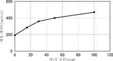
도 10은, 제1 실험으로 구한, 처리 가스 중의 PF3 가스의 유량과 실리콘 산화막의 에칭 레이트와의 관계를 나타내는 그래프이다.
도 11은, 제1 실험으로 구한, 처리 가스 중의 PF3 가스의 유량과 실리콘 산화막에 형성된 개구의 최대폭과의 관계를 나타내는 그래프이다.
도 12는, 제1 실험으로 구한, 처리 가스 중의 PF3 가스의 유량과 선택비의 관계를 나타내는 그래프이다.
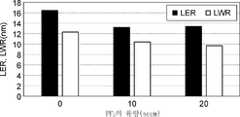
도 13은, 제2 실험으로 구한, 처리 가스 중의 PF3 가스의 유량과 LER 및 LWR의 각각과의 관계를 나타내는 그래프이다.
도 14는, 다른 예시적 실시형태에 관한 에칭 방법(방법 MT2)의 흐름도이다.
도 15의 (a), 도 15의 (b), 도 15의 (c)는, 방법 MT2의 공정 ST22가 적용되어 있을 때의 상태, 방법 MT2의 공정 ST23이 적용되어 있을 때의 상태, 방법 MT2가 적용된 후의 상태 각각의 일례의 기판의 부분 확대 단면도이다.
도 16은, 또 다른 예시적 실시형태에 관한 에칭 방법(방법 MT3)의 흐름도이다.
도 17의 (a), 도 17의 (b)는, 방법 MT3의 공정 STP3이 적용되어 있을 때의 상태, 방법 MT3이 적용된 후의 상태 각각의 일례의 기판의 부분 확대 단면도이다.1 is a flow chart of an etching method according to one exemplary embodiment.
2 is a partially enlarged cross-sectional view of a substrate as an example to which the etching method shown in FIG. 1 can be applied.
3 is a diagram schematically showing a plasma processing apparatus according to an exemplary embodiment.
4A is a partially enlarged cross-sectional view of an example substrate to which the etching method shown in FIG. 1 is applied, and FIG. 4B is an example etched by plasma generated from a processing gas that does not contain phosphorus. It is a partial enlarged cross-sectional view of the substrate.
5 is a timing chart of an example of an etching method according to an exemplary embodiment.
6A and 6B are diagrams showing the results of XPS analysis on the protective film PF formed in the experimental example in which the silicon oxide film and the silicon nitride film were etched in step STP, respectively.
Fig. 7 is a timing chart of another example of an etching method according to an exemplary embodiment.
8 is a plan view of a substrate of another example.
FIG. 9A is a cross-sectional view taken along line IXA-IXA in FIG. 8, and FIG. 9B is a cross-sectional view taken along line IXB-IXB in FIG.
10 is a graph showing the relationship between the flow rate of the PF3 gas in the processing gas and the etching rate of the silicon oxide film determined in the first experiment.
11 is a graph showing the relationship between the flow rate of the PF 3 gas in the processing gas and the maximum width of the opening formed in the silicon oxide film obtained in the first experiment.
12 is a graph showing the relationship between the flow rate of the PF3 gas in the processing gas and the selectivity ratio determined in the first experiment.
13 is a graph showing the relationship between the flow rateof the PF 3 gas in the processing gas and the LER and LWR, determined by the second experiment.
14 is a flowchart of an etching method (method MT2) according to another exemplary embodiment.
15A, 15B, and 15C show a state when step ST22 of method MT2 is applied, a state when step ST23 of method MT2 is applied, and method MT2. It is a partially enlarged cross-sectional view of the substrate in each example of the state after is applied.
Fig. 16 is a flow chart of an etching method (method MT3) according to another exemplary embodiment.
17A and 17B are partially enlarged cross-sectional views of the substrate in each example of a state when the step STP3 of the method MT3 is applied and a state after the method MT3 is applied.
이하, 다양한 예시적 실시형태에 대하여 설명한다.Hereinafter, various exemplary embodiments will be described.
하나의 예시적 실시형태에 있어서, 에칭 방법이 제공된다. 에칭 방법은, 플라즈마 처리 장치의 챔버 내에 기판을 준비하는 공정 (a)를 포함한다. 기판은, 실리콘 함유막 및 마스크를 포함한다. 마스크는, 탄소를 함유한다. 에칭 방법은, 챔버 내에서 처리 가스로부터 생성된 플라즈마로부터의 화학종에 의하여 실리콘 함유막을 에칭하는 공정 (b)를 더 포함한다. 처리 가스는, 할로젠 원소 및 인을 포함한다. 공정 (b)에 있어서, 마스크의 표면에 탄소와 인의 결합이 형성된다. 할로젠 원소는, 불소여도 된다.In one exemplary embodiment, an etching method is provided. The etching method includes a step (a) of preparing a substrate in a chamber of a plasma processing apparatus. The substrate includes a silicon-containing film and a mask. The mask contains carbon. The etching method further includes a step (b) of etching the silicon-containing film by chemical species from plasma generated from the processing gas in the chamber. The processing gas contains a halogen element and phosphorus. In step (b), a bond of carbon and phosphorus is formed on the surface of the mask. The halogen element may be fluorine.
상기 실시형태의 에칭 방법에 있어서, 마스크의 표면에 형성되는 탄소와 인의 결합은, 마스크에 있어서의 탄소 간 결합보다 높은 결합 에너지를 갖는다. 따라서, 상기 실시형태의 에칭 방법에 의하면, 실리콘 함유막의 플라즈마 에칭에 있어서, 마스크가 보호된다. 따라서, 상기 실시형태에 의하면, 실리콘 함유막의 플라즈마 에칭에 있어서 기판을 보호하는 것이 가능해진다. 또, 상기 실시형태의 에칭 방법에 의하면, 실리콘 함유막의 플라즈마 에칭에 있어서의 마스크의 형상의 열화가 억제된다.In the etching method of the above embodiment, the bond between carbon and phosphorus formed on the surface of the mask has a higher bonding energy than the bond between carbon in the mask. Therefore, according to the etching method of the above embodiment, the mask is protected in plasma etching of the silicon-containing film. Therefore, according to the above embodiment, it becomes possible to protect the substrate in the plasma etching of the silicon-containing film. Further, according to the etching method of the above embodiment, deterioration of the shape of the mask in the plasma etching of the silicon-containing film is suppressed.
하나의 예시적 실시형태에 있어서, 실리콘 함유막은, 실리콘 산화막을 포함하고 있어도 된다. 실리콘 함유막은, 실리콘 질화막, 다결정 실리콘막, 탄소 함유 실리콘막, 및 저유전율막 중 적어도 하나를 더 포함하고 있어도 된다.In one exemplary embodiment, the silicon-containing film may contain a silicon oxide film. The silicon-containing film may further include at least one of a silicon nitride film, a polycrystalline silicon film, a carbon-containing silicon film, and a low dielectric constant film.
하나의 예시적 실시형태에 있어서, 마스크는, 실리콘 함유막 상에서 상기 마스크가 구획 형성하는 개구에 대하여 상기 마스크가 차지하는 비율이 높은 부분과 상기 비율이 낮은 부분을 포함하고 있어도 된다. 개구에 대하여 마스크가 차지하는 비율이 높은 부분은, 마스크가 조밀하게 형성된 부분(이하, "조밀 영역"이라고 함)이다. 개구에 대하여 마스크가 차지하는 비율이 낮은 부분은, 마스크가 성기게 형성된 부분(이하, "성김 영역"이라고 함)이다. 일반적으로는, 성김 영역에 있어서의 마스크는, 실리콘 함유막의 플라즈마 에칭에 의하여, 조밀 영역에 있어서의 마스크보다 많이 에칭된다. 그러나, 이 실시형태에 있어서는, 마스크는, 그 표면에 형성된 탄소와 인의 결합에 의하여 보호된다. 따라서, 성김 영역에 있어서의 마스크의 에칭량이 저감된다. 그 결과, 성김 영역에 있어서의 마스크의 에칭량과 조밀 영역에 있어서의 마스크의 에칭량의 차가 저감된다. 나아가서는, 성김 영역 및 조밀 영역의 쌍방을 갖는 마스크의 형상의 열화가 억제된다.In one exemplary embodiment, the mask may include a portion with a high ratio and a portion with a low ratio occupied by the mask with respect to the opening defined by the mask on the silicon-containing film. The portion where the ratio occupied by the mask to the opening is high is a portion in which the mask is formed densely (hereinafter referred to as "dense area"). The portion where the ratio occupied by the mask to the opening is low is the portion where the mask is sparsely formed (hereinafter, referred to as “sparse region”). In general, the mask in the sparse region is etched more than the mask in the dense region by plasma etching of the silicon-containing film. However, in this embodiment, the mask is protected by the bonding of carbon and phosphorus formed on its surface. Therefore, the etching amount of the mask in the sparse region is reduced. As a result, the difference between the etching amount of the mask in the sparse region and the etching amount of the mask in the dense region is reduced. Furthermore, deterioration of the shape of the mask having both the sparse region and the dense region is suppressed.
하나의 예시적 실시형태에 있어서, 에칭 방법은, 공정 (b)에 있어서 에칭에 의하여 형성된 개구를 구획 형성하는 측벽면 상에 보호막을 형성하는 공정 (c)를 더 포함하고 있어도 된다. 보호막은 처리 가스에 포함되는 인을 포함한다. 공정 (b)와 공정 (c)는 동시에 행해져도 된다. 보호막은, 인과 산소의 결합 및/또는 인과 실리콘의 결합을 포함하고 있어도 된다.In one exemplary embodiment, the etching method may further include a step (c) of forming a protective film on a sidewall surface defining an opening formed by etching in the step (b). The protective film contains phosphorus contained in the processing gas. Step (b) and step (c) may be performed at the same time. The protective film may contain a bond of phosphorus and oxygen and/or a bond of phosphorus and silicon.
하나의 예시적 실시형태에 있어서, 처리 가스는, 불소 함유 가스 및 인 함유 가스를 포함하고 있어도 된다.In one exemplary embodiment, the processing gas may contain a fluorine-containing gas and a phosphorus-containing gas.
하나의 예시적 실시형태에 있어서, 처리 가스는, 인을 포함하는 분자로서, PF3, PCl3, PF5, PCl5, POCl3, PH3, PBr3, 및 PBr5 중 적어도 하나를 포함하고 있어도 된다.In one exemplary embodiment, the treatment gas is a molecule comprising of, PF3, PCl3, PF5, PCl5, POCl3, PH3, PBr3, and PBr includes at least one of thefive You may have it.
하나의 예시적 실시형태에 있어서, 처리 가스는, 탄화 수소, 하이드로플루오로카본, 또는 플루오로카본을 더 포함하고 있어도 된다.In one exemplary embodiment, the processing gas may further contain hydrocarbons, hydrofluorocarbons, or fluorocarbons.
하나의 예시적 실시형태에서는, 전기 바이어스의 펄스를 포함하는 펄스파가, 공정 (b)에 있어서 기판을 지지하는 기판 지지기 내의 하부 전극에 주기적으로 부여되어도 된다. 펄스파의 주기를 규정하는 주파수는, 1Hz 이상, 100kHz 이하여도 된다. 펄스파의 주기의 시간 길이에 있어서 전기 바이어스의 펄스가 하부 전극에 부여되는 시간 길이가 차지하는 비율은, 50% 이상, 99% 이하여도 된다. 전기 바이어스는 고주파 전력이어도 되고, 전기 바이어스의 펄스에 있어서의 고주파 전력의 레벨은, 2kW 이상이어도 된다.In one exemplary embodiment, a pulse wave including a pulse of electric bias may be periodically applied to the lower electrode in the substrate supporter supporting the substrate in step (b). The frequency defining the period of the pulse wave may be 1 Hz or more and 100 kHz or less. In the time length of the period of the pulse wave, the proportion of the time length during which the pulse of the electric bias is applied to the lower electrode may be 50% or more and 99% or less. The electric bias may be a high frequency power, and the level of the high frequency power in the pulse of the electric bias may be 2 kW or more.
하나의 예시적 실시형태에서는, 기판의 온도가, 공정 (b)의 개시 시에 있어서, 0℃ 이하의 온도로 설정되어도 된다.In one exemplary embodiment, the temperature of the substrate may be set to a temperature of 0° C. or less at the start of the step (b).
다른 예시적 실시형태에서는, 플라즈마 처리 장치가 제공된다. 플라즈마 처리 장치는, 챔버, 기판 지지기, 가스 공급부, 및 플라즈마 생성부를 구비한다. 기판 지지기는, 챔버 내에서 기판을 지지하도록 구성되어 있다. 기판은, 실리콘 함유막 및 마스크를 포함한다. 마스크는, 탄소를 함유한다. 가스 공급부는, 실리콘 함유막을 에칭하기 위한 처리 가스를 챔버 내에 공급하도록 구성되어 있다. 처리 가스는, 할로젠 원소 및 인을 포함한다. 플라즈마 생성부는, 실리콘 함유막을 에칭하고, 마스크의 표면에 탄소와 인의 결합을 형성하기 위하여, 챔버 내에서 처리 가스로부터 플라즈마를 생성하도록 구성되어 있다. 할로젠 원소는, 불소여도 된다.In another exemplary embodiment, a plasma processing apparatus is provided. The plasma processing apparatus includes a chamber, a substrate support, a gas supply unit, and a plasma generation unit. The substrate supporter is configured to support a substrate within the chamber. The substrate includes a silicon-containing film and a mask. The mask contains carbon. The gas supply unit is configured to supply a processing gas for etching the silicon-containing film into the chamber. The processing gas contains a halogen element and phosphorus. The plasma generating unit is configured to generate plasma from the processing gas in the chamber in order to etch the silicon-containing film and to form a bond of carbon and phosphorus on the surface of the mask. The halogen element may be fluorine.
또 다른 예시적 실시형태에 있어서, 에칭 방법이 제공된다. 에칭 방법은, 기판을 준비하는 공정 (a1)을 포함한다. 기판은, 실리콘 함유막 및 상기 실리콘 함유막 상에 마련된 마스크를 포함한다. 에칭 방법은, 기판에 인 화학종을 공급함으로써, 실리콘 함유막에 있어서 개구를 구획 형성하는 측벽면을 불활성화하는 공정 (b1)을 더 포함한다. 에칭 방법은, 기판에 할로젠 화학종을 공급함으로써, 실리콘 함유막을 에칭하는 공정 (c1)을 더 포함한다.In yet another exemplary embodiment, an etching method is provided. The etching method includes a step (a1) of preparing a substrate. The substrate includes a silicon-containing film and a mask provided on the silicon-containing film. The etching method further includes a step (b1) of inactivating a sidewall surface defining an opening in the silicon-containing film by supplying a phosphorus chemical species to the substrate. The etching method further includes a step (c1) of etching the silicon-containing film by supplying a halogen species to the substrate.
상기 실시형태의 에칭 방법에서는, 실리콘 함유막의 측벽면이 인에 의하여 불활성화(또는 부동태(不動態)화)된다. 즉, 측벽면의 패시베이션이 행해진다. 따라서, 상기 실시형태의 에칭 방법에 의하면, 실리콘 함유막의 플라즈마 에칭 시에 실리콘 함유막의 가로 방향으로의 에칭을 억제하도록 측벽면이 보호된다. 따라서, 상기 실시형태의 에칭 방법에 의하면, 실리콘 함유막의 플라즈마 에칭에 있어서 기판을 보호하는 것이 가능해진다.In the etching method of the above embodiment, the sidewall surface of the silicon-containing film is deactivated (or passivated) by phosphorus. That is, passivation of the side wall surface is performed. Therefore, according to the etching method of the above embodiment, the sidewall surface is protected so as to suppress the etching of the silicon-containing film in the transverse direction during plasma etching of the silicon-containing film. Therefore, according to the etching method of the above embodiment, it becomes possible to protect the substrate in plasma etching of the silicon-containing film.
하나의 예시적 실시형태에 있어서, 마스크는 탄소를 함유하고 있어도 된다. 공정 (b1)은, 마스크의 표면에 탄소와 인의 결합을 형성해도 된다.In one exemplary embodiment, the mask may contain carbon. In step (b1), a bond of carbon and phosphorus may be formed on the surface of the mask.
하나의 예시적 실시형태에 있어서, 실리콘 함유막은, 실리콘 산화막을 포함하고 있어도 되고, 공정 (b1)은, 측벽면에 인과 산소의 결합을 형성해도 된다.In one exemplary embodiment, the silicon-containing film may contain a silicon oxide film, and in step (b1), a bond of phosphorus and oxygen may be formed on the side wall surface.
하나의 예시적 실시형태에 있어서, 공정 (b1)과 공정 (c1)이 동시에 행해져도 된다.In one exemplary embodiment, the step (b1) and the step (c1) may be performed at the same time.
하나의 예시적 실시형태에 있어서, 공정 (b1)과 공정 (c1)이 반복되어도 된다.In one exemplary embodiment, step (b1) and step (c1) may be repeated.
하나의 예시적 실시형태에 있어서, 공정 (b1) 및 (c1)은, 플라즈마 처리 장치의 챔버 내에 기판이 수용된 상태에서 실행되어도 된다.In one exemplary embodiment, steps (b1) and (c1) may be performed in a state in which the substrate is accommodated in the chamber of the plasma processing apparatus.
하나의 예시적 실시형태에 있어서, 인 화학종은, 인 함유 가스의 플라즈마를 생성함으로써 생성되어도 되고, 할로젠 화학종은, 할로젠 함유 가스의 플라즈마를 생성함으로써 생성되어도 된다.In one exemplary embodiment, the phosphorus species may be generated by generating the plasma of the phosphorus-containing gas, and the halogen species may be generated by generating the plasma of the halogen-containing gas.
하나의 예시적 실시형태에 있어서, 할로젠 함유 가스는, 불소 함유 가스를 포함하고 있어도 된다. 하나의 예시적 실시형태에 있어서, 불소 함유 가스는, 불화 수소, 불화 아이오딘, 및 플루오로카본 중 적어도 하나를 포함하고 있어도 된다.In one exemplary embodiment, the halogen-containing gas may contain a fluorine-containing gas. In one exemplary embodiment, the fluorine-containing gas may contain at least one of hydrogen fluoride, iodine fluoride, and fluorocarbon.
하나의 예시적 실시형태에 있어서, 인 함유 가스는 불소를 포함하고 있지 않아도 된다. 하나의 예시적 실시형태에 있어서, 인 함유 가스는, PCl3 또는 POCl3을 포함하고 있어도 된다.In one exemplary embodiment, the phosphorus-containing gas need not contain fluorine. In one exemplary embodiment, the phosphorus-containing gas may contain PCl3 or POCl3 .
또 다른 예시적 실시형태에 있어서, 플라즈마 처리 장치가 제공된다. 플라즈마 처리 장치는, 챔버, 기판 지지기, 가스 공급부, 플라즈마 생성부, 및 제어부를 구비한다. 기판 지지기는, 챔버 내에서 기판을 지지하도록 구성되어 있다. 기판은, 실리콘 함유막 및 상기 실리콘 함유막 상에 마련된 마스크를 포함한다. 가스 공급부는, 인 함유 가스 및 할로젠 함유 가스를 챔버 내에 공급하도록 구성되어 있다. 플라즈마 생성부는, 챔버 내에서 가스로부터 플라즈마를 생성하도록 구성되어 있다. 제어부는, 가스 공급부 및 플라즈마 생성부를 제어하도록 구성되어 있다. 제어부는, 실리콘 함유막에 있어서 개구를 구획 형성하는 측벽면을 불활성화시키는 인 화학종을 생성하기 위하여, 챔버 내에 인 함유 가스를 공급하여 인 함유 가스로부터 플라즈마를 생성하도록 가스 공급부 및 플라즈마 생성부를 제어한다. 제어부는, 실리콘 함유막을 에칭하는 할로젠 화학종을 생성하기 위하여, 챔버 내에 할로젠 함유 가스를 공급하여 할로젠 함유 가스로부터 플라즈마를 생성하도록 가스 공급부 및 플라즈마 생성부를 제어한다.In yet another exemplary embodiment, a plasma processing apparatus is provided. The plasma processing apparatus includes a chamber, a substrate support, a gas supply unit, a plasma generation unit, and a control unit. The substrate supporter is configured to support a substrate within the chamber. The substrate includes a silicon-containing film and a mask provided on the silicon-containing film. The gas supply unit is configured to supply a phosphorus-containing gas and a halogen-containing gas into the chamber. The plasma generating unit is configured to generate plasma from gas in the chamber. The control unit is configured to control the gas supply unit and the plasma generation unit. The control unit controls the gas supply unit and the plasma generation unit to generate plasma from the phosphorus-containing gas by supplying a phosphorus-containing gas into the chamber in order to generate a phosphorus species that inactivates the sidewall surface defining an opening in the silicon-containing film. . The control unit controls the gas supply unit and the plasma generation unit to generate plasma from the halogen-containing gas by supplying a halogen-containing gas into the chamber in order to generate a halogen species for etching the silicon-containing film.
또 다른 예시적 실시형태에 있어서, 에칭 방법이 제공된다. 에칭 방법은, 플라즈마 처리 장치의 챔버 내에 기판을 준비하는 공정 (a2)를 포함한다. 기판은, 실리콘 함유막을 포함한다. 에칭 방법은, 챔버 내에서 처리 가스로부터 생성된 플라즈마로부터의 화학종에 의하여 실리콘 함유막을 에칭하는 공정 (b2)를 더 포함한다. 처리 가스는, 할로젠 원소 및 인을 포함한다.In yet another exemplary embodiment, an etching method is provided. The etching method includes a step (a2) of preparing a substrate in a chamber of a plasma processing apparatus. The substrate includes a silicon-containing film. The etching method further includes a step (b2) of etching the silicon-containing film by chemical species from plasma generated from the processing gas in the chamber. The processing gas contains a halogen element and phosphorus.
상기 실시형태에 의하면, 실리콘과 처리 가스에 포함되는 인을 포함하는 보호막이, 에칭에 의하여 실리콘 함유막에 형성된 개구를 구획 형성하는 측벽면 상에 형성된다. 이 보호막에 의하여 측벽면이 보호되면서, 실리콘 함유막이 에칭된다. 따라서, 실리콘 함유막의 플라즈마 에칭에 있어서, 가로 방향의 에칭을 억제하는 것이 가능해진다.According to the above embodiment, a protective film containing silicon and phosphorus contained in the processing gas is formed on the sidewall surface defining an opening formed in the silicon-containing film by etching. While the sidewall surface is protected by this protective film, the silicon-containing film is etched. Therefore, in the plasma etching of the silicon-containing film, it becomes possible to suppress the etching in the transverse direction.
하나의 예시적 실시형태에 있어서, 에칭 방법은, 공정 (b2)에 있어서의 에칭에 의하여 형성된 개구를 구획 형성하는 측벽면 상에 보호막을 형성하는 공정 (c2)를 더 포함하고 있어도 된다. 이 보호막은 처리 가스에 포함되는 인을 포함한다. 공정 (b2)와 공정 (c2)는, 동시에 발생해도 된다.In one exemplary embodiment, the etching method may further include a step (c2) of forming a protective film on a sidewall surface defining an opening formed by etching in the step (b2). This protective film contains phosphorus contained in the processing gas. Step (b2) and step (c2) may occur simultaneously.
하나의 예시적 실시형태에 있어서, 처리 가스는, 인을 포함하는 분자로서, PF3, PCl3, PF5, PCl5, POCl3, PH3, PBr3, 및 PBr5 중 적어도 하나를 포함하고 있어도 된다.In one exemplary embodiment, the treatment gas is a molecule comprising of, PF3, PCl3, PF5, PCl5, POCl3, PH3, PBr3, and PBr includes at least one of thefive You may have it.
하나의 예시적 실시형태에 있어서, 처리 가스는 탄소 및 수소를 더 포함하고 있어도 된다.In one exemplary embodiment, the process gas may further contain carbon and hydrogen.
하나의 예시적 실시형태에 있어서, 처리 가스는, 수소를 포함하는 분자로서, H2, HF, CxHy, CsHtFu, 및 NH3 중 적어도 하나를 포함하고 있어도 된다. 여기에서, x, y, s, t, u의 각각은 자연수이다.In one exemplary embodiment, the processing gas is a molecule containing hydrogen, and may contain at least one ofH 2 , HF, Cx Hy , Cs Ht Fu , and NH3. Here, each of x, y, s, t, and u is a natural number.
하나의 예시적 실시형태에 있어서, 할로젠 원소는 불소여도 된다.In one exemplary embodiment, the halogen element may be fluorine.
하나의 예시적 실시형태에 있어서, 처리 가스는 산소를 더 포함하고 있어도 된다.In one exemplary embodiment, the processing gas may further contain oxygen.
하나의 예시적 실시형태에 있어서, 실리콘 함유막은 실리콘 함유 유전체막이어도 된다.In one exemplary embodiment, the silicon-containing film may be a silicon-containing dielectric film.
하나의 예시적 실시형태에 있어서, 실리콘 함유막은, 실리콘 산화막, 실리콘 질화막, 및 실리콘막 중 적어도 하나의 막을 포함하고 있어도 된다.In one exemplary embodiment, the silicon-containing film may include at least one of a silicon oxide film, a silicon nitride film, and a silicon film.
하나의 예시적 실시형태에 있어서, 실리콘 함유막은, 서로 다른 막종(膜種)을 갖는 2개 이상의 실리콘 함유막을 포함하고 있어도 된다.In one exemplary embodiment, the silicon-containing film may include two or more silicon-containing films having different film types.
하나의 예시적 실시형태에 있어서, 2개 이상의 실리콘 함유막은, 실리콘 산화막 및 실리콘 질화막을 포함하고 있어도 된다. 혹은, 2개 이상의 실리콘 함유막은, 실리콘 산화막 및 실리콘막을 포함하고 있어도 된다. 혹은, 2개 이상의 실리콘 함유막은, 실리콘 산화막, 실리콘 질화막, 및 실리콘막을 포함하고 있어도 된다.In one exemplary embodiment, the two or more silicon-containing films may include a silicon oxide film and a silicon nitride film. Alternatively, two or more silicon-containing films may contain a silicon oxide film and a silicon film. Alternatively, two or more silicon-containing films may contain a silicon oxide film, a silicon nitride film, and a silicon film.
하나의 예시적 실시형태에 있어서, 기판은, 실리콘 함유막 상에 마련된 마스크를 더 갖고 있어도 된다.In one exemplary embodiment, the substrate may further have a mask provided on the silicon-containing film.
하나의 예시적 실시형태에서는, 공정 (b2)의 개시 시에 있어서 기판의 온도가 0℃ 이하의 온도로 설정되어도 된다.In one exemplary embodiment, at the start of the step (b2), the temperature of the substrate may be set to a temperature of 0°C or less.
또 다른 예시적 실시형태에 있어서는, 플라즈마 처리 장치가 제공된다. 플라즈마 처리 장치는, 챔버, 기판 지지기, 가스 공급부, 및 고주파 전원을 구비한다. 기판 지지기는, 챔버 내에서 기판을 지지하도록 구성되어 있다. 가스 공급부는, 실리콘 함유막을 에칭하기 위한 처리 가스를 챔버 내에 공급하도록 구성되어 있다. 처리 가스는, 할로젠 원소 및 인을 포함한다. 고주파 전원은, 챔버 내에서 처리 가스로부터 플라즈마를 생성하기 위하여 고주파 전력을 발생시키도록 구성되어 있다.In yet another exemplary embodiment, a plasma processing apparatus is provided. The plasma processing apparatus includes a chamber, a substrate support, a gas supply unit, and a high frequency power supply. The substrate supporter is configured to support a substrate within the chamber. The gas supply unit is configured to supply a processing gas for etching the silicon-containing film into the chamber. The processing gas contains a halogen element and phosphorus. The high-frequency power source is configured to generate high-frequency power in order to generate plasma from the processing gas in the chamber.
이하, 도면을 참조하여 다양한 예시적 실시형태에 대하여 상세하게 설명한다. 또한, 각 도면에 있어서 동일 또는 상당한 부분에 대해서는 동일한 부호를 붙이는 것으로 한다.Hereinafter, various exemplary embodiments will be described in detail with reference to the drawings. In addition, in each drawing, the same reference numerals are assigned to the same or equivalent parts.
도 1은, 하나의 예시적 실시형태에 관한 에칭 방법의 흐름도이다. 도 1에 나타내는 에칭 방법(이하, "방법 MT"라고 함)은, 실리콘 함유막을 갖는 기판에 적용된다. 방법 MT에서는, 실리콘 함유막이 에칭된다.1 is a flow chart of an etching method according to one exemplary embodiment. The etching method shown in Fig. 1 (hereinafter referred to as "method MT") is applied to a substrate having a silicon-containing film. In method MT, the silicon-containing film is etched.
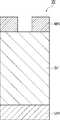
도 2는, 도 1에 나타내는 에칭 방법이 적용될 수 있는 일례의 기판의 부분 확대 단면도이다. 도 2에 나타내는 기판(W)은, DRAM, 3D-NAND와 같은 디바이스의 제조에 이용될 수 있다. 기판(W)은, 실리콘 함유막(SF)을 갖는다. 기판(W)은, 하지(下地) 영역(UR)을 더 갖고 있어도 된다. 실리콘 함유막(SF)은, 하지 영역(UR) 상에 마련될 수 있다. 실리콘 함유막(SF)은, 실리콘 함유 유전체막일 수 있다. 실리콘 함유 유전체막은, 실리콘 산화막 또는 실리콘 질화막을 포함할 수 있다. 실리콘 함유 유전체막은, 실리콘을 함유하는 막이면, 다른 막종을 갖는 막이어도 된다. 또, 실리콘 함유막(SF)은, 실리콘막(예를 들면 다결정 실리콘막)을 포함하고 있어도 된다. 또, 실리콘 함유막(SF)은, 실리콘 질화막, 다결정 실리콘막, 탄소 함유 실리콘막, 및 저유전율막 중 적어도 하나를 포함하고 있어도 된다. 탄소 함유 실리콘막은, SiC막 및/또는 SiOC막을 포함할 수 있다. 저유전율막은, 실리콘을 함유하고, 층간 절연막으로서 이용될 수 있다. 또, 실리콘 함유막(SF)은, 서로 다른 막종을 갖는 2개 이상의 실리콘 함유막을 포함하고 있어도 된다. 2개 이상의 실리콘 함유막은, 실리콘 산화막 및 실리콘 질화막을 포함하고 있어도 된다. 실리콘 함유막(SF)은, 예를 들면 교대로 적층된 1개 이상의 실리콘 산화막 및 1개 이상의 실리콘 질화막을 포함하는 다층막이어도 된다. 실리콘 함유막(SF)은, 교대로 적층된 복수의 실리콘 산화막 및 복수의 실리콘 질화막을 포함하는 다층막이어도 된다. 혹은, 2개 이상의 실리콘 함유막은, 실리콘 산화막 및 실리콘막을 포함하고 있어도 된다. 실리콘 함유막(SF)은, 예를 들면 교대로 적층된 1개 이상의 실리콘 산화막 및 1개 이상의 실리콘막을 포함하는 다층막이어도 된다. 실리콘 함유막(SF)은, 교대로 적층된 복수의 실리콘 산화막 및 복수의 다결정 실리콘막을 포함하는 다층막이어도 된다. 혹은, 2개 이상의 실리콘 함유막은, 실리콘 산화막, 실리콘 질화막, 및 실리콘막을 포함하고 있어도 된다.FIG. 2 is a partially enlarged cross-sectional view of a substrate as an example to which the etching method shown in FIG. 1 can be applied. The substrate W shown in FIG. 2 can be used for manufacturing devices such as DRAM and 3D-NAND. The substrate W has a silicon-containing film SF. The substrate W may further have a base region UR. The silicon-containing film SF may be provided on the underlying region UR. The silicon-containing film SF may be a silicon-containing dielectric film. The silicon-containing dielectric film may include a silicon oxide film or a silicon nitride film. The silicon-containing dielectric film may be a film having a different film type as long as it contains silicon. Moreover, the silicon-containing film SF may contain a silicon film (for example, a polycrystalline silicon film). Moreover, the silicon-containing film SF may contain at least one of a silicon nitride film, a polycrystalline silicon film, a carbon-containing silicon film, and a low dielectric constant film. The carbon-containing silicon film may include a SiC film and/or a SiOC film. The low dielectric constant film contains silicon and can be used as an interlayer insulating film. Further, the silicon-containing film SF may contain two or more silicon-containing films having different film types. Two or more silicon-containing films may contain a silicon oxide film and a silicon nitride film. The silicon-containing film SF may be, for example, a multilayer film including one or more silicon oxide films and one or more silicon nitride films stacked alternately. The silicon-containing film SF may be a multilayer film including a plurality of silicon oxide films and a plurality of silicon nitride films stacked alternately. Alternatively, two or more silicon-containing films may contain a silicon oxide film and a silicon film. The silicon-containing film SF may be, for example, a multilayer film including one or more silicon oxide films and one or more silicon films stacked alternately. The silicon-containing film SF may be a multilayer film including a plurality of silicon oxide films and a plurality of polycrystalline silicon films stacked alternately. Alternatively, two or more silicon-containing films may contain a silicon oxide film, a silicon nitride film, and a silicon film.
기판(W)은, 마스크(MK)를 더 갖고 있어도 된다. 마스크(MK)는, 실리콘 함유막(SF) 상에 마련되어 있다. 마스크(MK)는, 공정 ST2에 있어서 실리콘 함유막(SF)의 에칭 레이트보다 낮은 에칭 레이트를 갖는 재료로 형성된다. 마스크(MK)는, 유기 재료로 형성될 수 있다. 즉, 마스크(MK)는, 탄소를 함유해도 된다. 마스크(MK)는, 예를 들면 어모퍼스 카본막, 포토레지스트막, 또는 스핀 온 카본막(SOC막)으로 형성될 수 있다. 혹은, 마스크(MK)는, 실리콘 함유 반사 방지막과 같은 실리콘 함유막으로 형성되어도 된다. 혹은, 마스크(MK)는, 질화 타이타늄, 텅스텐, 탄화 텅스텐과 같은 금속 함유 재료로 형성된 금속 함유 마스크여도 된다. 마스크(MK)는, 3μm 이상의 두께를 가질 수 있다.The substrate W may further have a mask MK. The mask MK is provided on the silicon-containing film SF. The mask MK is formed of a material having an etching rate lower than that of the silicon-containing film SF in step ST2. The mask MK may be formed of an organic material. That is, the mask MK may contain carbon. The mask MK may be formed of, for example, an amorphous carbon film, a photoresist film, or a spin-on carbon film (SOC film). Alternatively, the mask MK may be formed of a silicon-containing film such as a silicon-containing antireflection film. Alternatively, the mask MK may be a metal-containing mask formed of a metal-containing material such as titanium nitride, tungsten or tungsten carbide. The mask MK may have a thickness of 3 μm or more.
마스크(MK)는, 패터닝되어 있다. 즉, 마스크(MK)는, 공정 ST2에 있어서 실리콘 함유막(SF)에 전사되는 패턴을 갖고 있다. 마스크(MK)의 패턴이 실리콘 함유막(SF)에 전사되면, 실리콘 함유막(SF)에는 홀 또는 트렌치와 같은 개구(오목부)가 형성된다. 공정 ST2에 있어서 실리콘 함유막(SF)에 형성되는 개구의 어스펙트비는 20 이상이면 되고, 30 이상, 40 이상, 또는 50 이상이어도 된다. 또한, 마스크(MK)는, 라인 앤드 스페이스 패턴을 갖고 있어도 된다.The mask MK is patterned. That is, the mask MK has a pattern transferred to the silicon-containing film SF in step ST2. When the pattern of the mask MK is transferred to the silicon-containing film SF, an opening (recess) such as a hole or a trench is formed in the silicon-containing film SF. The aspect ratio of the opening formed in the silicon-containing film SF in step ST2 may be 20 or more, 30 or more, 40 or more, or 50 or more. Moreover, the mask MK may have a line and space pattern.
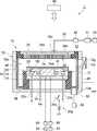
방법 MT에서는, 실리콘 함유막(SF)의 에칭을 위하여 플라즈마 처리 장치가 이용된다. 도 3은, 하나의 예시적 실시형태에 관한 플라즈마 처리 장치를 개략적으로 나타내는 도이다. 도 3에 나타내는 플라즈마 처리 장치(1)는, 챔버(10)를 구비한다. 챔버(10)는, 그 안에 내부 공간(10s)을 제공한다. 챔버(10)는 챔버 본체(12)를 포함한다. 챔버 본체(12)는, 대략 원통 형상을 갖는다. 챔버 본체(12)는, 예를 들면 알루미늄으로 형성된다. 챔버 본체(12)의 내벽면 상에는, 내부식성을 갖는 막이 마련되어 있다. 내부식성을 갖는 막은, 산화 알루미늄, 산화 이트륨 등의 세라믹으로 형성될 수 있다.In the method MT, a plasma processing apparatus is used for etching the silicon-containing film SF. 3 is a diagram schematically showing a plasma processing apparatus according to an exemplary embodiment. The
챔버 본체(12)의 측벽에는, 통로(12p)가 형성되어 있다. 기판(W)은, 통로(12p)를 통하여 내부 공간(10s)과 챔버(10)의 외부와의 사이에서 반송(搬送)된다. 통로(12p)는, 게이트 밸브(12g)에 의하여 개폐된다. 게이트 밸브(12g)는, 챔버 본체(12)의 측벽을 따라 마련된다.A
챔버 본체(12)의 바닥부 상에는, 지지부(13)가 마련되어 있다. 지지부(13)는, 절연 재료로 형성된다. 지지부(13)는, 대략 원통 형상을 갖는다. 지지부(13)는, 내부 공간(10s) 내에서, 챔버 본체(12)의 바닥부로부터 상방으로 뻗어 있다. 지지부(13)는, 기판 지지기(14)를 지지하고 있다. 기판 지지기(14)는, 내부 공간(10s) 내에서 기판(W)을 지지하도록 구성되어 있다.On the bottom part of the chamber
기판 지지기(14)는, 하부 전극(18) 및 정전 척(20)을 갖는다. 기판 지지기(14)는, 전극 플레이트(16)를 더 가질 수 있다. 전극 플레이트(16)는, 알루미늄 등의 도체로 형성되어 있고, 대략 원반 형상을 갖는다. 하부 전극(18)은, 전극 플레이트(16) 상에 마련되어 있다. 하부 전극(18)은, 알루미늄 등의 도체로 형성되어 있고, 대략 원반 형상을 갖는다. 하부 전극(18)은, 전극 플레이트(16)에 전기적으로 접속되어 있다.The
정전 척(20)은, 하부 전극(18) 상에 마련되어 있다. 기판(W)은, 정전 척(20)의 상면 상에 재치된다. 정전 척(20)은, 본체 및 전극을 갖는다. 정전 척(20)의 본체는, 대략 원반 형상을 갖고, 유전체로 형성된다. 정전 척(20)의 전극은, 막 형상의 전극이며, 정전 척(20)의 본체 내에 마련되어 있다. 정전 척(20)의 전극은, 스위치(20s)를 통하여 직류 전원(20p)에 접속되어 있다. 정전 척(20)의 전극에 직류 전원(20p)으로부터의 전압이 인가되면, 정전 척(20)과 기판(W)의 사이에 정전 인력이 발생한다. 기판(W)은, 그 정전 인력에 의하여 정전 척(20)에 끌어당겨지고, 정전 척(20)에 의하여 지지된다.The
기판 지지기(14) 상에는, 에지 링(25)이 배치된다. 에지 링(25)은, 링 형상의 부재이다. 에지 링(25)은, 실리콘, 탄화 실리콘, 또는 석영 등으로 형성될 수 있다. 기판(W)은, 정전 척(20) 상이며, 또한 에지 링(25)에 의하여 둘러싸인 영역 내에 배치된다.On the
하부 전극(18)의 내부에는, 유로(18f)가 마련되어 있다. 유로(18f)에는, 챔버(10)의 외부에 마련되어 있는 칠러 유닛으로부터 배관(22a)을 통하여 열교환 매체(예를 들면 냉매)가 공급된다. 유로(18f)에 공급된 열교환 매체는, 배관(22b)을 통하여 칠러 유닛으로 되돌려진다. 플라즈마 처리 장치(1)에서는, 정전 척(20) 상에 재치된 기판(W)의 온도가, 열교환 매체와 하부 전극(18)과의 열교환에 의하여, 조정된다.A
플라즈마 처리 장치(1)에는, 가스 공급 라인(24)이 마련되어 있다. 가스 공급 라인(24)은, 전열 가스 공급 기구로부터의 전열 가스(예를 들면 He 가스)를, 정전 척(20)의 상면과 기판(W)의 이면과의 사이의 간극에 공급한다.The
플라즈마 처리 장치(1)는, 상부 전극(30)을 더 구비한다. 상부 전극(30)은, 기판 지지기(14)의 상방에 마련되어 있다. 상부 전극(30)은, 부재(32)를 통하여, 챔버 본체(12)의 상부에 지지되어 있다. 부재(32)는, 절연성을 갖는 재료로 형성된다. 상부 전극(30)과 부재(32)는, 챔버 본체(12)의 상부 개구를 닫고 있다.The
상부 전극(30)은, 천판(天板)(34) 및 지지체(36)를 포함할 수 있다. 천판(34)의 하면은, 내부 공간(10s)의 측의 하면이며, 내부 공간(10s)을 구획 형성한다. 천판(34)은, 발생하는 줄(Joule)열이 적은 저저항의 도전체 또는 반도체로 형성될 수 있다. 천판(34)은, 천판(34)을 그 판두께 방향으로 관통하는 복수의 가스 토출 구멍(34a)을 갖는다.The
지지체(36)는, 천판(34)을 착탈 가능하게 지지한다. 지지체(36)는, 알루미늄 등의 도전성 재료로 형성된다. 지지체(36)의 내부에는, 가스 확산실(36a)이 마련되어 있다. 지지체(36)는, 가스 확산실(36a)로부터 하방으로 뻗는 복수의 가스 구멍(36b)을 갖는다. 복수의 가스 구멍(36b)은, 복수의 가스 토출 구멍(34a)에 각각 연통되어 있다. 지지체(36)에는, 가스 도입구(36c)가 형성되어 있다. 가스 도입구(36c)는, 가스 확산실(36a)에 접속되어 있다. 가스 도입구(36c)에는, 가스 공급관(38)이 접속되어 있다.The
가스 공급관(38)에는, 유량 제어기군(41) 및 밸브군(42)을 통하여, 가스 소스군(40)이 접속되어 있다. 유량 제어기군(41) 및 밸브군(42)은, 가스 공급부를 구성하고 있다. 가스 공급부는, 가스 소스군(40)을 더 포함하고 있어도 된다. 가스 소스군(40)은, 복수의 가스 소스를 포함한다. 복수의 가스 소스는, 방법 MT에서 이용되는 처리 가스의 소스를 포함한다. 유량 제어기군(41)은, 복수의 유량 제어기를 포함한다. 유량 제어기군(41)의 복수의 유량 제어기의 각각은, 매스 플로 컨트롤러 또는 압력 제어식의 유량 제어기이다. 밸브군(42)은, 복수의 개폐 밸브를 포함한다. 가스 소스군(40)의 복수의 가스 소스의 각각은, 유량 제어기군(41)의 대응의 유량 제어기 및 밸브군(42)의 대응의 개폐 밸브를 통하여, 가스 공급관(38)에 접속되어 있다.A
플라즈마 처리 장치(1)에서는, 챔버 본체(12)의 내벽면 및 지지부(13)의 외주(外周)를 따라, 실드(46)가 착탈 가능하게 마련되어 있다. 실드(46)는, 챔버 본체(12)에 반응 부생물이 부착되는 것을 방지한다. 실드(46)는, 예를 들면 알루미늄으로 형성된 모재(母材)의 표면에 내부식성을 갖는 막을 형성함으로써 구성된다. 내부식성을 갖는 막은, 산화 이트륨 등의 세라믹으로 형성될 수 있다.In the
지지부(13)와 챔버 본체(12)의 측벽과의 사이에는, 배플 플레이트(48)가 마련되어 있다. 배플 플레이트(48)는, 예를 들면 알루미늄으로 형성된 부재의 표면에 내부식성을 갖는 막(산화 이트륨 등의 막)을 형성함으로써 구성된다. 배플 플레이트(48)에는, 복수의 관통 구멍이 형성되어 있다. 배플 플레이트(48)의 하방이며, 또한 챔버 본체(12)의 바닥부에는, 배기구(12e)가 마련되어 있다. 배기구(12e)에는, 배기관(52)을 통하여 배기 장치(50)가 접속되어 있다. 배기 장치(50)는, 압력 조정 밸브 및 터보 분자 펌프 등의 진공 펌프를 포함한다.A
플라즈마 처리 장치(1)는, 고주파 전원(62) 및 바이어스 전원(64)을 구비하고 있다. 고주파 전원(62)은, 고주파 전력 HF를 발생시키는 전원이다. 고주파 전력 HF는, 플라즈마의 생성에 적합한 제1 주파수를 갖는다. 제1 주파수는, 예를 들면 27MHz~100MHz의 범위 내의 주파수이다. 고주파 전원(62)은, 정합기(66) 및 전극 플레이트(16)를 통하여 하부 전극(18)에 접속되어 있다. 정합기(66)는, 고주파 전원(62)의 부하 측(하부 전극(18) 측)의 임피던스를 고주파 전원(62)의 출력 임피던스에 정합시키기 위한 회로를 갖는다. 또한, 고주파 전원(62)은, 정합기(66)를 통하여, 상부 전극(30)에 접속되어 있어도 된다. 고주파 전원(62)은, 일례의 플라즈마 생성부를 구성하고 있다.The
바이어스 전원(64)은, 전기 바이어스를 발생시키는 전원이다. 바이어스 전원(64)은, 하부 전극(18)에 전기적으로 접속되어 있다. 전기 바이어스는, 제2 주파수를 갖는다. 제2 주파수는, 제1 주파수보다 낮다. 제2 주파수는, 예를 들면 400kHz~13.56MHz의 범위 내의 주파수이다. 전기 바이어스는, 고주파 전력 HF와 함께 이용되는 경우에는, 기판(W)에 이온을 끌어들이기 위하여 하부 전극(18)에 부여된다. 전기 바이어스가 하부 전극(18)에 부여되면, 기판 지지기(14) 상에 재치된 기판(W)의 전위는, 제2 주파수로 규정되는 주기 내에서 변동한다.The
일 실시형태에 있어서, 전기 바이어스는, 제2 주파수를 갖는 고주파 전력 LF여도 된다. 고주파 전력 LF는, 고주파 전력 HF와 함께 이용되는 경우에는, 기판(W)에 이온을 끌어들이기 위한 고주파 바이어스 전력으로서 이용된다. 고주파 전력 LF를 발생시키도록 구성된 바이어스 전원(64)은, 정합기(68) 및 전극 플레이트(16)를 통하여 하부 전극(18)에 접속된다. 정합기(68)는, 바이어스 전원(64)의 부하 측(하부 전극(18) 측)의 임피던스를 바이어스 전원(64)의 출력 임피던스에 정합시키기 위한 회로를 갖는다.In one embodiment, the electric bias may be a high frequency power LF having a second frequency. When the high frequency power LF is used together with the high frequency power HF, it is used as a high frequency bias power for attracting ions to the substrate W. The
또한, 고주파 전력 HF를 이용하지 않고, 고주파 전력 LF를 이용하여, 즉, 단일의 고주파 전력만을 이용하여 플라즈마를 생성해도 된다. 이 경우에는, 고주파 전력 LF의 주파수는, 13.56MHz보다 큰 주파수, 예를 들면 40MHz여도 된다. 또, 이 경우에는, 플라즈마 처리 장치(1)는, 고주파 전원(62) 및 정합기(66)를 구비하지 않아도 된다. 이 경우에는, 바이어스 전원(64)은 일례의 플라즈마 생성부를 구성한다.In addition, plasma may be generated not using the high frequency power HF, but using the high frequency power LF, that is, using only a single high frequency power. In this case, the frequency of the high frequency power LF may be greater than 13.56 MHz, for example, 40 MHz. Further, in this case, the
다른 실시형태에 있어서, 전기 바이어스는, 직류 전압의 펄스파여도 된다. 직류 전압의 펄스파는, 주기적으로 발생되어, 하부 전극(18)에 부여된다. 직류 전압의 펄스파의 주기는, 제2 주파수로 규정된다. 직류 전압의 펄스파의 주기는, 2개의 기간을 포함한다. 2개의 기간 중 일방의 기간에 있어서의 직류 전압은, 음극성 직류 전압이다. 2개의 기간 중 일방의 기간에 있어서의 직류 전압의 레벨(즉, 절댓값)은, 2개의 기간 중 타방의 기간에 있어서의 직류 전압의 레벨(즉, 절댓값)보다 높다. 타방의 기간에 있어서의 직류 전압은, 부극성, 양극성 중 어느 쪽이어도 된다. 타방의 기간에 있어서의 직류 전압의 레벨은 제로여도 된다. 이 실시형태에 있어서, 바이어스 전원(64)은, 로 패스 필터 및 전극 플레이트(16)를 통하여 하부 전극(18)에 접속된다.In another embodiment, the electric bias may be a pulse wave of a DC voltage. The DC voltage pulse wave is periodically generated and applied to the
일 실시형태에 있어서, 바이어스 전원(64)은, 전기 바이어스의 연속파를 하부 전극(18)에 부여해도 된다. 즉, 바이어스 전원(64)은, 전기 바이어스를 연속적으로 하부 전극(18)에 부여해도 된다. 전기 바이어스의 연속파는, 방법 MT의 공정 STP 또는 공정 ST2 및 공정 ST3이 실행되고 있는 기간에 있어서, 하부 전극(18)에 부여될 수 있다.In one embodiment, the
다른 실시형태에 있어서, 바이어스 전원(64)은, 전기 바이어스의 펄스파를 하부 전극(18)에 부여해도 된다. 전기 바이어스의 펄스파는, 주기적으로 하부 전극(18)에 부여될 수 있다. 전기 바이어스의 펄스파의 주기는, 제3 주파수로 규정된다. 제3 주파수는, 제2 주파수보다 낮다. 제3 주파수는, 예를 들면 1Hz 이상, 200kHz 이하이다. 다른 예에서는, 제3 주파수는, 5Hz 이상, 100kHz 이하여도 된다.In another embodiment, the
전기 바이어스의 펄스파의 주기는, 2개의 기간, 즉 H 기간 및 L 기간을 포함한다. H 기간에 있어서의 전기 바이어스의 레벨(즉, 전기 바이어스의 펄스의 레벨)은, L 기간에 있어서의 전기 바이어스의 레벨보다 높다. 즉, 전기 바이어스의 레벨이 증감됨으로써, 전기 바이어스의 펄스파가 하부 전극(18)에 부여되어도 된다. L 기간에 있어서의 전기 바이어스의 레벨은, 제로보다 커도 된다. 혹은, L 기간에 있어서의 전기 바이어스의 레벨은, 제로여도 된다. 즉, 전기 바이어스의 펄스파는, 전기 바이어스의 하부 전극(18)으로의 공급과 공급 정지를 교대로 전환함으로써, 하부 전극(18)에 부여되어도 된다. 여기에서, 전기 바이어스가 고주파 전력 LF인 경우에는, 전기 바이어스의 레벨은, 고주파 전력 LF의 전력 레벨이다. 전기 바이어스가 고주파 전력 LF인 경우에는, 전기 바이어스의 펄스에 있어서의 고주파 전력 LF의 레벨은, 2kW 이상이어도 된다. 전기 바이어스가 음극성 직류 전압의 펄스파인 경우에는, 전기 바이어스의 레벨은, 음극성 직류 전압의 절댓값의 실효값이다. 전기 바이어스의 펄스파의 듀티비, 즉, 전기 바이어스의 펄스파의 주기에 있어서 H 기간이 차지하는 비율은, 예를 들면 1% 이상, 80% 이하이다. 다른 예에서는, 전기 바이어스의 펄스파의 듀티비는 5% 이상 50% 이하여도 된다. 혹은, 전기 바이어스의 펄스파의 듀티비는, 50% 이상, 99% 이하여도 된다. 전기 바이어스의 펄스파는, 방법 MT의 공정 ST2 및 공정 ST3을 실행하기 위하여, 하부 전극(18)에 부여될 수 있다.The period of the pulse wave of the electric bias includes two periods, that is, an H period and an L period. The electric bias level in the H period (that is, the electric bias pulse level) is higher than the electric bias level in the L period. That is, by increasing or decreasing the level of the electric bias, a pulse wave of the electric bias may be applied to the
일 실시형태에 있어서, 고주파 전원(62)은, 고주파 전력 HF의 연속파를 공급해도 된다. 즉, 고주파 전원(62)은, 고주파 전력 HF를 연속적으로 공급해도 된다. 고주파 전력 HF의 연속파는, 방법 MT의 공정 STP 또는 공정 ST2 및 공정 ST3이 실행되고 있는 기간에 있어서, 공급될 수 있다.In one embodiment, the high
다른 실시형태에 있어서, 고주파 전원(62)은, 고주파 전력 HF의 펄스파를 공급해도 된다. 고주파 전력 HF의 펄스파는, 주기적으로 공급될 수 있다. 고주파 전력 HF의 펄스파의 주기는, 제4 주파수로 규정된다. 제4 주파수는, 제2 주파수보다 낮다. 일 실시형태에 있어서, 제4 주파수는, 제3 주파수와 동일하다. 고주파 전력 HF의 펄스파의 주기는, 2개의 기간, 즉 H 기간 및 L 기간을 포함한다. H 기간에 있어서의 고주파 전력 HF의 전력 레벨은, 2개의 기간 중 L 기간에 있어서의 고주파 전력 HF의 전력 레벨보다 높다. L 기간에 있어서의 고주파 전력 HF의 전력 레벨은, 제로보다 커도 되고, 제로여도 된다.In another embodiment, the high
또한, 고주파 전력 HF의 펄스파의 주기는, 전기 바이어스의 펄스파의 주기와 동기하고 있어도 된다. 고주파 전력 HF의 펄스파의 주기에 있어서의 H 기간은, 전기 바이어스의 펄스파의 주기에 있어서의 H 기간과 동기하고 있어도 된다. 혹은, 고주파 전력 HF의 펄스파의 주기에 있어서의 H 기간은, 전기 바이어스의 펄스파의 주기에 있어서의 H 기간과 동기하고 있지 않아도 된다. 고주파 전력 HF의 펄스파의 주기에 있어서의 H 기간의 시간 길이는, 전기 바이어스의 펄스파의 주기에 있어서의 H 기간의 시간 길이와 동일해도 되고, 달라도 된다.Further, the period of the pulse wave of the high frequency power HF may be synchronized with the period of the pulse wave of the electric bias. The H period in the period of the pulse wave of the high frequency power HF may be synchronized with the H period in the period of the pulse wave of the electric bias. Alternatively, the H period in the period of the pulse wave of the high frequency power HF does not need to be synchronized with the H period in the period of the pulse wave of the electric bias. The time length of the H period in the period of the pulse wave of the high frequency power HF may be the same as or different from the time length of the H period in the period of the pulse wave of the electric bias.
플라즈마 처리 장치(1)에 있어서 플라즈마 처리가 행해지는 경우에는, 가스가 가스 공급부로부터 내부 공간(10s)으로 공급된다. 또, 고주파 전력 HF 및/또는 전기 바이어스가 공급됨으로써, 상부 전극(30)과 하부 전극(18)의 사이에서 고주파 전계가 생성된다. 생성된 고주파 전계가 내부 공간(10s) 내의 가스로부터 플라즈마를 생성한다.When plasma processing is performed in the
플라즈마 처리 장치(1)는, 제어부(80)를 더 구비할 수 있다. 제어부(80)는, 프로세서, 메모리 등의 기억부, 입력 장치, 표시 장치, 신호의 입출력 인터페이스 등을 구비하는 컴퓨터일 수 있다. 제어부(80)는, 플라즈마 처리 장치(1)의 각부(各部)를 제어한다. 제어부(80)에서는, 입력 장치를 이용하여, 오퍼레이터가 플라즈마 처리 장치(1)를 관리하기 위하여 커맨드의 입력 조작 등을 행할 수 있다. 또, 제어부(80)에서는, 표시 장치에 의하여, 플라즈마 처리 장치(1)의 가동 상황을 가시화하여 표시할 수 있다. 또한, 기억부에는, 제어 프로그램 및 레시피 데이터가 저장되어 있다. 제어 프로그램은, 플라즈마 처리 장치(1)에서 각종 처리를 실행하기 위하여, 프로세서에 의하여 실행된다. 프로세서는, 제어 프로그램을 실행하고, 레시피 데이터에 따라 플라즈마 처리 장치(1)의 각부를 제어한다.The
다시 도 1을 참조한다. 이하, 방법 MT에 대하여, 그것이 플라즈마 처리 장치(1)를 이용하여 도 2에 나타내는 기판(W)에 적용되는 경우를 예로 들어 설명한다. 플라즈마 처리 장치(1)가 이용되는 경우에는, 제어부(80)에 의한 플라즈마 처리 장치(1)의 각부의 제어에 의하여, 플라즈마 처리 장치(1)에 있어서 방법 MT가 실행될 수 있다. 이하의 설명에 있어서는, 방법 MT의 실행을 위한 제어부(80)에 의한 플라즈마 처리 장치(1)의 각부의 제어에 대해서도 설명한다.See FIG. 1 again. Hereinafter, with respect to the method MT, a case where it is applied to the substrate W shown in Fig. 2 using the
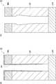
이하의 설명에서는, 도 1에 더하여, 도 4의 (a), 도 4의 (b), 및 도 5를 참조한다. 도 4의 (a)는, 도 1에 나타내는 에칭 방법이 적용된 일례의 기판의 부분 확대 단면도이며, 도 4의 (b)는, 인을 포함하지 않는 처리 가스로부터 생성된 플라즈마에 의하여 에칭된 일례의 기판의 부분 확대 단면도이다. 도 5는, 하나의 예시적 실시형태에 관한 에칭 방법에 관한 일례의 타이밍 차트이다. 도 5에 있어서, 가로축은 시간을 나타내고 있다. 도 5에 있어서, 세로축은, 고주파 전력 HF의 전력 레벨, 전기 바이어스의 레벨, 및 처리 가스의 공급 상태를 나타내고 있다. 고주파 전력 HF의 "L" 레벨은, 고주파 전력 HF가 공급되고 있지 않거나, 또는 고주파 전력 HF의 전력 레벨이, "H"로 나타내는 전력 레벨보다 낮은 것을 나타내고 있다. 전기 바이어스의 "L" 레벨은, 전기 바이어스가 하부 전극(18)에 부여되고 있지 않거나, 또는 전기 바이어스의 레벨이, "H"로 나타내는 레벨보다 낮은 것을 나타내고 있다. 또, 처리 가스의 공급 상태의 "ON"은, 처리 가스가 챔버(10) 내에 공급되고 있는 것을 나타내고 있으며, 처리 가스의 공급 상태의 "OFF"는, 챔버(10) 내로의 처리 가스의 공급이 정지되어 있는 것을 나타내고 있다.In the following description, in addition to FIG. 1, FIG. 4(a), FIG. 4(b), and FIG. 5 are referred. 4A is a partially enlarged cross-sectional view of an example substrate to which the etching method shown in FIG. 1 is applied, and FIG. 4B is an example etched by plasma generated from a processing gas that does not contain phosphorus. It is a partial enlarged cross-sectional view of the substrate. 5 is a timing chart of an example of an etching method according to an exemplary embodiment. In Fig. 5, the horizontal axis represents time. In Fig. 5, the vertical axis represents the power level of the high frequency power HF, the level of the electric bias, and the supply state of the processing gas. The "L" level of the high frequency power HF indicates that the high frequency power HF is not supplied or that the power level of the high frequency power HF is lower than the power level indicated by "H". The "L" level of the electric bias indicates that the electric bias is not applied to the
도 1에 나타내는 바와 같이, 방법 MT는, 공정 ST1에서 개시한다. 공정 ST1에서는, 기판(W)이 챔버(10) 내에 준비된다. 기판(W)은, 챔버(10) 내에서 정전 척(20) 상에 재치되고, 정전 척(20)에 의하여 지지된다. 또한, 기판(W)은 300mm의 직경을 가질 수 있다.As shown in Fig. 1, the method MT starts in step ST1. In step ST1, the substrate W is prepared in the
방법 MT에서는, 이어서 공정 STP가 실행된다. 공정 STP에서는, 기판(W)에 대한 플라즈마 처리가 실행된다. 공정 STP에서는, 챔버(10) 내에서 처리 가스로부터 플라즈마가 생성된다. 방법 MT는, 공정 ST2를 포함한다. 공정 ST2는, 공정 STP의 실행 중에 행해진다. 방법 MT는, 공정 ST3을 더 포함할 수 있다. 공정 ST3은, 공정 STP의 실행 중에 행해진다. 공정 ST2와 공정 ST3은, 동시에 행해져도 되고, 혹은 상호 간에 독립적으로 행해져도 된다.In method MT, step STP is then executed. In step STP, plasma processing is performed on the substrate W. In step STP, plasma is generated from the processing gas in the
공정 ST2에서는, 실리콘 함유막(SF)이, 공정 STP에 있어서 챔버(10) 내에서 처리 가스로부터 생성된 플라즈마로부터의 화학종에 의하여 에칭된다. 공정 ST3에서는, 보호막(PF)이, 공정 STP에 있어서 챔버(10) 내에서 처리 가스로부터 생성된 플라즈마로부터의 화학종에 의하여, 기판(W) 상에 형성된다. 보호막(PF)은, 실리콘 함유막(SF)에 형성된 개구를 구획 형성하는 측벽면 상에 형성된다.In step ST2, the silicon-containing film SF is etched by chemical species from the plasma generated from the processing gas in the
공정 STP에서 이용되는 처리 가스는, 할로젠 원소 및 인을 포함한다. 처리 가스에 포함되는 할로젠 원소는, 불소일 수 있다. 즉, 처리 가스는, 불소 함유 가스를 포함할 수 있다. 처리 가스는, 적어도 하나의 할로젠 함유 분자를 포함할 수 있다. 처리 가스는, 적어도 하나의 할로젠 함유 분자로서, 플루오로카본 및 하이드로플루오로카본 중 적어도 하나를 포함할 수 있다. 플루오로카본은, 예를 들면 CF4, C2F6, C3F6, C3F8, C4F6, C4F8, C5F8 등 중 적어도 하나이다. 하이드로플루오로카본은, 예를 들면 CH2F2, CHF3, CH3F 등 중 적어도 하나이다.The processing gas used in the step STP contains a halogen element and phosphorus. The halogen element included in the processing gas may be fluorine. That is, the processing gas may contain a fluorine-containing gas. The processing gas may contain at least one halogen-containing molecule. The processing gas, as at least one halogen-containing molecule, may include at least one of fluorocarbon and hydrofluorocarbon. The fluorocarbon is, for example, at least one ofCF 4 , C2 F6 , C3 F6 , C3 F8 , C4 F6 , C4 F8 , C5 F8 and the like. Hydrofluorocarbon is, for example, at least one of CH 2 F2 , CHF3 , CH3 F, and the like.
처리 가스는, 적어도 하나의 인 함유 분자를 포함할 수 있다. 즉, 처리 가스는, 적어도 하나의 인 함유 가스를 포함할 수 있다. 인 함유 가스는, 인과 할로젠의 쌍방을 포함하는 가스여도 된다. 인 함유 분자는, 십산화 사인(P4O10), 팔산화 사인(P4O8), 육산화 사인(P4O6)과 같은 산화물이어도 된다. 십산화 사인은, 오산화 이인(P2O5)이라고 불리는 경우가 있다. 인 함유 분자는, 인과 할로젠의 쌍방을 포함하는 분자여도 된다. 인 함유 분자는, 삼불화 인(PF3), 오불화 인(PF5), 삼염화 인(PCl3), 오염화 인(PCl5), 삼브로민화 인(PBr3), 오브로민화 인(PBr5), 아이오딘화 인(PI3)과 같은 할로젠화물이어도 된다. 인 함유 분자는, 불화 포스포릴(POF3), 염화 포스포릴(POCl3), 브로민화 포스포릴(POBr3)과 같은 할로젠화 포스포릴이어도 된다. 인 함유 분자는, 포스핀(PH3), 인화 칼슘(Ca3P2), 인산(H3PO4), 인산 나트륨(Na3PO4), 헥사플루오로 인산(HPF6) 등이어도 된다. 인 함유 분자는, 플루오로포스핀류(HxPFy)여도 된다. 여기에서, x와 y의 합은, 3 또는 5이다. 플루오로포스핀류로서는, HPF2, H2PF3이 예시된다. 처리 가스는, 적어도 하나의 인 함유 분자로서, 상기의 인 함유 분자 중 하나 이상의 인 함유 분자를 포함할 수 있다. 예를 들면, 처리 가스는, 적어도 하나의 인 함유 분자로서, PF3, PCl3, PF5, PCl5, POCl3, PH3, PBr3, 및 PBr5 중 적어도 하나를 포함할 수 있다. 또한, 처리 가스에 포함되는 각 인 함유 분자는, 액체 또는 고체인 경우에는, 가열 등에 의하여 기화되어 챔버(10) 내에 공급될 수 있다.The processing gas may contain at least one phosphorus-containing molecule. That is, the processing gas may contain at least one phosphorus-containing gas. The phosphorus-containing gas may be a gas containing both phosphorus and halogen. The phosphorus-containing molecule may be an oxide such as sine decoxide (P4 O10 ), sine octaoxide (P4 O8 ), or hexaoxide (P4 O6 ). Sign of decoxidation is sometimes called diphosphorus pentoxide (P2 O5 ). The phosphorus-containing molecule may be a molecule containing both phosphorus and halogen. Phosphorus-containing molecules include phosphorus trifluoride (PF3 ), phosphorus pentafluoride (PF5 ), phosphorus trichloride (PCl3 ),phosphorus pentachloride (PCl 5 ), phosphorus tribromide (PBr3 ), phosphorus obromide ( PBr5 ), and ahalogenide such as phosphorus iodide (PI 3 ) may be used. Phosphorus-containing molecule may be a halide, such as fluoride, phosphine to phosphine poril (POF3), phosphine poril chloride (POCl3), phosphonium bromide poril (POBr3) poril. The phosphorus-containing molecule may be phosphine (PH3 ), calcium phosphide (Ca3 P2 ), phosphoric acid (H3 PO4 ), sodium phosphate (Na3 PO4 ), hexafluoro phosphoric acid (HPF6 ), or the like. The phosphorus-containing molecule may be fluorophosphine (Hx PFy ). Here, the sum of x and y is 3 or 5. Examples of fluorophosphines include HPF2 and H2 PF3 . The processing gas may contain at least one phosphorus-containing molecule as at least one phosphorus-containing molecule. For example, a process gas, comprising: at least one phosphorus-containing molecule may include aPF 3, PCl 3, PF 5 , PCl 5, POCl 3, PH 3, PBr 3, PBr5, and at least one of. Further, each phosphorus-containing molecule contained in the processing gas can be vaporized by heating or the like and supplied into the
공정 ST2에서 이용되는 처리 가스는, 탄소 및 수소를 더 포함하고 있어도 된다. 처리 가스는, 수소를 포함하는 분자로서, H2, 불화 수소(HF), 탄화 수소(CxHy), 하이드로플루오로카본(CsHtFu), 및 NH3 중 적어도 하나를 포함하고 있어도 된다. 탄화 수소는, 예를 들면 CH4 또는 C3H6이다. 처리 가스는, 탄소를 포함하는 분자로서, 상기의 탄화 수소, 상기의 하이드로플루오로카본, 및 플루오로카본(CvFw) 중 적어도 하나를 포함하고 있어도 된다. 여기에서, x, y, s, t, u, v, w의 각각은 자연수이다. 처리 가스는, 산소를 더 포함하고 있어도 된다. 처리 가스는, 산소 함유 가스, 예를 들면 O2를 포함하고 있어도 된다. 혹은, 처리 가스는, 산소를 포함하고 있지 않아도 된다.The processing gas used in step ST2 may further contain carbon and hydrogen. The processing gas is a molecule containing hydrogen, and contains at least one of H2 , hydrogen fluoride (HF), hydrocarbon (Cx Hy ), hydrofluorocarbon (Cs Ht Fu ), and NH3 You can do it. Hydrocarbons are, for example, CH4 or C3 H6 . As a molecule containing carbon, the processing gas may contain at least one of theabove hydrocarbons, the above hydrofluorocarbons, and fluorocarbons (C v Fw ). Here, each of x, y, s, t, u, v, and w is a natural number. The processing gas may further contain oxygen. The processing gas may contain an oxygen-containing gas such as O2 . Alternatively, the processing gas does not have to contain oxygen.
일 실시형태에 있어서, 처리 가스는, 제1 가스 및 제2 가스를 포함할 수 있다. 제1 가스는, 인을 함유하지 않는 가스이다. 제1 가스는, 할로젠 원소를 포함할 수 있다. 제1 가스는, 상술한 적어도 하나의 할로젠 함유 분자의 가스를 포함할 수 있다. 제1 가스는, 탄소 및 수소를 더 포함하고 있어도 된다. 제1 가스는, 상술한 수소를 포함하는 분자의 가스 및/또는 탄소를 포함하는 분자의 가스를 더 포함하고 있어도 된다. 제1 가스는, 산소를 더 포함하고 있어도 된다. 제1 가스는, O2 가스를 포함하고 있어도 된다. 혹은, 제1 가스는, 산소를 포함하고 있지 않아도 된다. 제2 가스는, 인을 함유하는 가스이다. 제2 가스는, 상술한 적어도 하나의 인 함유 분자의 가스를 포함하고 있어도 된다.In one embodiment, the processing gas may contain a first gas and a second gas. The first gas is a gas that does not contain phosphorus. The first gas may contain a halogen element. The first gas may include the gas of at least one halogen-containing molecule described above. The first gas may further contain carbon and hydrogen. The first gas may further contain a molecular gas containing hydrogen and/or a molecular gas containing carbon. The first gas may further contain oxygen. The 1st gas may containO 2 gas. Alternatively, the first gas does not have to contain oxygen. The second gas is a gas containing phosphorus. The second gas may contain the gas of at least one phosphorus-containing molecule described above.
공정 STP에서 이용되는 처리 가스에 있어서, 제1 가스의 유량에 대한 제2 가스의 유량의 비인 유량비는, 0보다 크고, 0.5 이하로 설정되어도 된다. 유량비는, 0.075 이상, 0.3 이하로 설정되어도 된다. 유량비는, 0.1 이상, 0.25 이하로 설정되어도 된다.In the process gas used in the step STP, the flow rate ratio, which is the ratio of the flow rate of the second gas to the flow rate of the first gas, may be set to be greater than 0 and 0.5 or less. The flow rate ratio may be set to 0.075 or more and 0.3 or less. The flow rate ratio may be set to 0.1 or more and 0.25 or less.
공정 STP에서는, 챔버(10) 내의 가스의 압력이 지정된 압력으로 설정된다. 공정 STP에서는, 챔버(10) 내의 가스의 압력은, 10mTorr(1.3Pa) 이상, 100mTorr(13.3Pa) 이하의 압력으로 설정될 수 있다. 또, 공정 STP에서는, 챔버(10) 내에서 처리 가스로부터 플라즈마를 생성하기 위하여, 고주파 전력 HF가 공급된다. 도 5에 있어서 실선으로 나타내는 바와 같이, 공정 STP에서는, 고주파 전력 HF의 연속파가 공급되어도 된다. 공정 STP에서는, 고주파 전력 HF 대신에 고주파 전력 LF가 이용되어도 된다. 공정 STP에서는, 고주파 전력 HF 및 전기 바이어스의 쌍방이 공급되어도 된다. 도 5에 있어서 실선으로 나타내는 바와 같이, 공정 STP에서는, 전기 바이어스의 연속파가 하부 전극(18)에 부여되어도 된다. 고주파 전력 HF의 전력의 레벨은, 2kW 이상, 10kW 이하의 레벨로 설정될 수 있다. 고주파 전력 LF의 레벨은, 2kW(기판(W)의 단위면적당 전력의 레벨에서는 2.83W/cm2) 이상의 레벨로 설정될 수 있다. 고주파 전력 LF의 레벨은, 10kW(기판(W)의 단위면적당 전력의 레벨에서는 14.2W/cm2) 이상의 레벨로 설정되어도 된다.In step STP, the pressure of the gas in the
공정 STP의 실행을 위하여, 제어부(80)는, 처리 가스를 챔버(10) 내에 공급하도록 가스 공급부를 제어한다. 또, 제어부(80)는, 챔버(10) 내에서의 가스의 압력이 지정된 압력으로 설정되도록 배기 장치(50)를 제어한다. 또, 제어부(80)는, 처리 가스로부터 플라즈마를 생성하도록 플라즈마 생성부를 제어한다. 플라즈마 처리 장치(1)에서는, 제어부(80)는, 고주파 전력 HF, 고주파 전력 LF, 또는 고주파 전력 HF 및 전기 바이어스를 공급하도록 고주파 전원(62) 및 바이어스 전원(64)을 제어한다.In order to execute the step STP, the
일 실시형태의 방법 MT에 있어서, 공정 ST2(또는 공정 STP)의 개시 시의 기판(W)의 온도는, 0℃ 이하의 온도로 설정되어도 된다. 이와 같은 온도로 기판(W)의 온도가 설정되면, 공정 ST2에 있어서의 실리콘 함유막(SF)의 에칭 레이트가 높아진다. 공정 ST2의 개시 시의 기판(W)의 온도를 설정하기 위하여, 제어부(80)는 칠러 유닛을 제어할 수 있다. 또한, 공정 ST2(또는 공정 STP)의 실행 중의 기판(W)의 온도는, 200℃ 이하의 온도여도 된다.In the method MT of one embodiment, the temperature of the substrate W at the start of step ST2 (or step STP) may be set to a temperature of 0°C or less. When the temperature of the substrate W is set at such a temperature, the etching rate of the silicon-containing film SF in step ST2 increases. In order to set the temperature of the substrate W at the start of step ST2, the
일 실시형태에 있어서, 방법 MT는, 공정 STT를 더 포함하고 있어도 된다. 공정 STT는, 공정 ST2(또는 공정 STP) 전에 실행된다. 기판(W)의 온도는, 공정 STT에 있어서, 0℃ 이하의 온도로 설정된다. 공정 ST2의 개시 시의 기판(W)의 온도는, 공정 STT에 있어서 설정된다. 공정 STT에 있어서 기판(W)의 온도를 설정하기 위하여, 제어부(80)는, 칠러 유닛을 제어할 수 있다.In one embodiment, the method MT may further include a step STT. Step STT is executed before step ST2 (or step STP). The temperature of the substrate W is set to a temperature of 0°C or less in step STT. The temperature of the substrate W at the start of step ST2 is set in step STT. In order to set the temperature of the substrate W in the process STT, the
공정 ST2에서는, 실리콘 함유막(SF)이, 처리 가스로부터 생성된 플라즈마로부터의 할로젠 화학종에 의하여 에칭된다. 일 실시형태에서는, 실리콘 함유막(SF)의 전체 영역 중 마스크(MK)로부터 노출되어 있는 부분이 에칭된다(도 4의 (a)를 참조).In step ST2, the silicon-containing film SF is etched by halogen species from plasma generated from the processing gas. In one embodiment, a portion of the entire area of the silicon-containing film SF that is exposed from the mask MK is etched (see Fig. 4A).
처리 가스가, 인 함유 분자로서 PF3과 같이 인과 할로젠 원소를 함유하는 분자를 포함하고 있는 경우에는, 이러한 분자에서 유래하는 할로젠 화학종은, 실리콘 함유막(SF)의 에칭에 기여한다. 따라서, PF3과 같이 인과 할로젠 원소를 함유하는 인 함유 분자는, 공정 ST2에 있어서는, 실리콘 함유막(SF)의 에칭 레이트를 높인다.When the processing gas contains molecules containingphosphorus and halogen elements, such as PF 3 as phosphorus-containing molecules, halogen species derived from these molecules contribute to the etching of the silicon-containing film SF. Accordingly,phosphorus-containing molecules containing phosphorus and halogen elements like PF 3 increase the etching rate of the silicon-containing film SF in step ST2.
또, 마스크(MK)가 탄소를 함유하는 경우에는, 공정 ST2에 있어서, 마스크의 표면에 있어서 탄소와 인의 결합이 형성된다. 마스크(MK)의 표면에 형성되는 탄소와 인의 결합은, 마스크(MK)에 있어서의 탄소 간 결합보다 높은 결합 에너지를 갖는다. 따라서, 방법 MT에 의하면, 실리콘 함유막(SF)의 플라즈마 에칭에 있어서, 마스크(MK)가 보호된다. 또, 실리콘 함유막(SF)의 플라즈마 에칭에 있어서, 마스크(MK)의 형상의 열화가 억제된다. 따라서, 방법 MT에 의하면, 막의 플라즈마 에칭에 있어서 기판을 보호하는 것이 가능해진다.In addition, when the mask MK contains carbon, in step ST2, a bond of carbon and phosphorus is formed on the surface of the mask. The bond between carbon and phosphorus formed on the surface of the mask MK has a higher bonding energy than the bond between carbon in the mask MK. Therefore, according to the method MT, in the plasma etching of the silicon-containing film SF, the mask MK is protected. In addition, in the plasma etching of the silicon-containing film SF, deterioration of the shape of the mask MK is suppressed. Therefore, according to the method MT, it becomes possible to protect the substrate in plasma etching of the film.
일 실시형태에 있어서는, 방법 MT는, 도 1에 나타내는 바와 같이, 공정 ST3을 더 포함하고 있어도 된다. 공정 ST3에서는, 보호막(PF)이, 공정 ST2의 에칭에 의하여 실리콘 함유막(SF)에 형성된 개구를 구획 형성하는 측벽면 상에 형성된다(도 4의 (a)를 참조). 보호막(PF)은, 공정 STP에 있어서 챔버(10) 내에서 처리 가스로부터 생성된 플라즈마로부터의 화학종에 의하여 형성된다. 일 실시형태에서는, 공정 ST3은, 공정 ST2와 동시에 진행할 수 있다. 도 4의 (a)에 나타내는 바와 같이, 일 실시형태에 있어서, 보호막(PF)은, 그 두께가 실리콘 함유막(SF)에 형성된 개구의 깊이 방향을 따라 감소되도록 형성되어도 된다.In one embodiment, the method MT may further include step ST3 as shown in FIG. 1. In step ST3, the protective film PF is formed on the sidewall surface defining an opening formed in the silicon-containing film SF by etching in step ST2 (see Fig. 4A). The protective film PF is formed by chemical species from plasma generated from the processing gas in the
보호막(PF)은, 실리콘 및 공정 STP에서 이용되는 처리 가스에 포함되는 인을 포함한다. 일 실시형태에서는, 보호막(PF)은, 처리 가스에 포함되는 탄소 및/또는 수소를 더 포함하고 있어도 된다. 일 실시형태에서는, 보호막(PF)은, 처리 가스에 포함되거나 또는 실리콘 함유막(SF)에 포함되는 산소를 더 포함하고 있어도 된다. 일 실시형태에서는, 보호막(PF)은, 인과 산소의 결합을 포함하고 있어도 된다.The protective film PF contains silicon and phosphorus contained in the processing gas used in the eutectic STP. In one embodiment, the protective film PF may further contain carbon and/or hydrogen contained in the processing gas. In one embodiment, the protective film PF may further contain oxygen contained in the processing gas or the silicon-containing film SF. In one embodiment, the protective film PF may contain a bond of phosphorus and oxygen.
도 6의 (a) 및 도 6의 (b)는 각각, 공정 STP에 있어서 실리콘 산화막, 실리콘 질화막을 에칭한 실험예에 있어서 형성된 보호막(PF)에 대한 XPS 분석의 결과를 나타내는 도이다. 도 6의 (a) 및 도 6의 (b)의 각각은, P2p 스펙트럼을 나타내고 있다. 실험예의 공정 STP의 조건을 이하에 나타낸다.6A and 6B are diagrams showing the results of XPS analysis on the protective film PF formed in the experimental example in which the silicon oxide film and the silicon nitride film were etched in step STP, respectively. Each of FIGS. 6A and 6B shows a P2p spectrum. The conditions of the step STP of the experimental example are shown below.
<공정 STP의 조건><Conditions of process STP>
챔버(10) 내의 가스의 압력: 100mTorr(13.33Pa)Pressure of gas in chamber 10: 100mTorr (13.33Pa)
처리 가스: 50sccm의 PF3 가스 및 150sccm의 Ar 가스Process gas: 50 sccm of PF3 gas and 150 sccm of Ar gas
고주파 전력 HF(연속파): 40MHz, 4500WHigh frequency power HF (continuous wave): 40 MHz, 4500 W
고주파 전력 LF(연속파): 400kHz, 7000WHigh frequency power LF (continuous wave): 400 kHz, 7000 W
기판의 온도(에칭 개시 전의 기판 지지기의 온도): -70℃The temperature of the substrate (the temperature of the substrate supporter before the start of etching): -70°C
공정 STP의 실행 기간의 시간 길이: 30초Time length of the execution period of the process STP: 30 seconds
공정 STP에 있어서 실리콘 산화막을 에칭한 실험예에 따르면, 보호막(PF)의 XPS 분석의 결과, 도 6의 (a)에 나타내는 바와 같이, Si-O의 결합 피크와 P-O의 결합 피크가 관찰되었다. 또, 공정 STP에 있어서 실리콘 질화막을 에칭한 실험예에 따르면, 보호막(PF)의 XPS 분석의 결과, 도 6의 (b)에 나타내는 바와 같이, Si-P의 결합 피크와 P-N의 결합 피크가 관찰되었다.According to the experimental example in which the silicon oxide film was etched in the step STP, as a result of XPS analysis of the protective film PF, as shown in Fig. 6A, the bonding peak of Si-O and the bonding peak of P-O were observed. Further, according to the experimental example in which the silicon nitride film was etched in the step STP, as a result of XPS analysis of the protective film (PF), as shown in Fig. 6(b), the bonding peak of Si-P and the bonding peak of PN were observed. Became.
처리 가스에 인이 포함되지 않으면, 도 4의 (b)에 나타내는 바와 같이, 실리콘 함유막(SF)은, 가로 방향으로도 에칭된다. 그 결과, 실리콘 함유막(SF)에 형성되는 개구의 폭이 일부에서 넓어진다. 예를 들면, 실리콘 함유막(SF)에 형성되는 개구의 폭은 마스크(MK)의 근방에서 부분적으로 넓어진다.When phosphorus is not contained in the processing gas, as shown in Fig. 4B, the silicon-containing film SF is etched in the horizontal direction as well. As a result, the width of the opening formed in the silicon-containing film SF is partially widened. For example, the width of the opening formed in the silicon-containing film SF is partially widened in the vicinity of the mask MK.
한편, 방법 MT에서는, 보호막(PF)이, 에칭에 의하여 실리콘 함유막(SF)에 형성된 개구를 구획 형성하는 측벽면 상에 형성된다. 이 보호막(PF)에 의하여 측벽면이 보호되면서, 실리콘 함유막(SF)이 에칭된다. 따라서, 방법 MT에 의하면, 실리콘 함유막(SF)의 플라즈마 에칭에 있어서, 가로 방향의 에칭을 억제하는 것이 가능해진다.On the other hand, in the method MT, the protective film PF is formed on the sidewall surface defining an opening formed in the silicon-containing film SF by etching. While the sidewall surface is protected by this protective film PF, the silicon-containing film SF is etched. Therefore, according to the method MT, in the plasma etching of the silicon-containing film SF, it becomes possible to suppress the etching in the horizontal direction.
일 실시형태에 있어서는, 공정 STP가 계속되고 있는 기간, 즉 공정 STP에 있어서 처리 가스로부터 플라즈마가 생성되고 있는 기간 중에, 공정 ST2와 공정 ST3을 각각이 포함하는 1개 이상의 사이클이 순서대로 실행되어도 된다. 공정 STP에 있어서는, 2개 이상의 사이클이 순서대로 실행되어도 된다.In one embodiment, one or more cycles each including steps ST2 and ST3 may be sequentially executed during a period in which the process STP continues, that is, a period in which plasma is generated from the processing gas in the process STP. . In step STP, two or more cycles may be sequentially executed.
일 실시형태에서는, 도 5에 있어서 파선으로 나타내는 바와 같이, 상술한 전기 바이어스의 펄스파가, 공정 STP에 있어서 바이어스 전원(64)으로부터 하부 전극(18)에 부여되어도 된다. 즉, 처리 가스로부터 생성된 플라즈마가 챔버(10) 내에 존재할 때에, 전기 바이어스의 펄스파가, 바이어스 전원(64)으로부터 하부 전극(18)에 부여되어도 된다. 이 실시형태에 있어서는, 공정 ST2의 실리콘 함유막(SF)의 에칭은, 주로 전기 바이어스의 펄스파의 주기 내의 H 기간에 있어서 발생한다. 또, 공정 ST3의 보호막(PF)의 형성은, 주로 전기 바이어스의 펄스파의 주기 내의 L 기간에 있어서 발생한다.In one embodiment, as indicated by the broken line in FIG. 5, the pulse wave of the electric bias described above may be applied from the
또한, 전기 바이어스가 고주파 전력 LF인 경우에는, 전기 바이어스의 펄스파의 주기 내의 H 기간에 있어서, 고주파 전력 LF의 전력 레벨은, 2kW 이상의 레벨로 설정될 수 있다. 전기 바이어스의 펄스파의 주기 내의 H 기간에 있어서, 고주파 전력 LF의 전력 레벨은, 10kW 이상의 레벨로 설정되어도 된다.Further, when the electric bias is the high-frequency power LF, the power level of the high-frequency power LF can be set to a level of 2 kW or more in the H period within the period of the pulse wave of the electric bias. In the H period within the period of the pulse wave of the electric bias, the power level of the high frequency power LF may be set to a level of 10 kW or more.
일 실시형태에서는, 도 5에 있어서 파선으로 나타내는 바와 같이, 상술한 고주파 전력 HF의 펄스파가, 공정 STP에 있어서 공급되어도 된다. 고주파 전력 HF의 펄스파의 주기 내의 H 기간에 있어서, 고주파 전력 HF의 전력 레벨은, 1kW 이상, 10kW 이하의 레벨로 설정될 수 있다. 도 5에 나타내는 바와 같이, 고주파 전력 HF의 펄스파의 주기는, 전기 바이어스의 펄스파의 주기와 동기하고 있어도 된다. 도 5에 나타내는 바와 같이, 고주파 전력 HF의 펄스파의 주기에 있어서의 H 기간은, 전기 바이어스의 펄스파의 주기에 있어서의 H 기간과 동기하고 있어도 된다. 혹은, 고주파 전력 HF의 펄스파의 주기에 있어서의 H 기간은, 전기 바이어스의 펄스파의 주기에 있어서의 H 기간과 동기하고 있지 않아도 된다. 고주파 전력 HF의 펄스파의 주기에 있어서의 H 기간의 시간 길이는, 전기 바이어스의 펄스파의 주기에 있어서의 H 기간의 시간 길이와 동일해도 되고, 달라도 된다.In one embodiment, as indicated by the broken line in FIG. 5, the pulse wave of the high-frequency power HF described above may be supplied in the step STP. In the H period within the period of the pulse wave of the high frequency power HF, the power level of the high frequency power HF can be set to a level of 1 kW or more and 10 kW or less. As shown in Fig. 5, the period of the pulse wave of the high frequency power HF may be synchronized with the period of the pulse wave of the electric bias. As shown in Fig. 5, the H period in the period of the pulse wave of the high frequency power HF may be synchronized with the H period in the period of the pulse wave of the electric bias. Alternatively, the H period in the period of the pulse wave of the high frequency power HF does not need to be synchronized with the H period in the period of the pulse wave of the electric bias. The time length of the H period in the period of the pulse wave of the high frequency power HF may be the same as or different from the time length of the H period in the period of the pulse wave of the electric bias.
도 7은, 하나의 예시적 실시형태에 관한 에칭 방법에 관한 다른 예의 타이밍 차트이다. 도 7에 있어서, 가로축은 시간을 나타내고 있다. 도 7에 있어서, 세로축은, 고주파 전력 HF의 전력 레벨, 전기 바이어스의 레벨, 제1 가스의 공급 상태, 및 제2 가스의 공급 상태를 나타내고 있다. 고주파 전력 HF의 "L" 레벨은, 고주파 전력 HF가 공급되고 있지 않거나, 또는 고주파 전력 HF의 전력 레벨이, "H"로 나타내는 전력 레벨보다 낮은 것을 나타내고 있다. 전기 바이어스의 "L" 레벨은, 전기 바이어스가 하부 전극(18)에 부여되지 않거나, 또는 전기 바이어스의 레벨이, "H"로 나타내는 레벨보다 낮은 것을 나타내고 있다. 또, 제1 가스의 공급 상태의 "ON"은, 제1 가스가 챔버(10) 내에 공급되고 있는 것을 나타내고 있으며, 제1 가스의 공급 상태의 "OFF"는, 챔버(10) 내로의 제1 가스의 공급이 정지되어 있는 것을 나타내고 있다. 또, 제2 가스의 공급 상태의 "ON"은, 제2 가스가 챔버(10) 내에 공급되고 있는 것을 나타내고 있으며, 제2 가스의 공급 상태의 "OFF"는, 챔버(10) 내로의 제2 가스의 공급이 정지되어 있는 것을 나타내고 있다.Fig. 7 is a timing chart of another example of an etching method according to an exemplary embodiment. In Fig. 7, the horizontal axis represents time. In Fig. 7, the vertical axis represents the power level of the high frequency power HF, the level of the electric bias, the state of supplying the first gas, and the state of supplying the second gas. The "L" level of the high frequency power HF indicates that the high frequency power HF is not supplied or that the power level of the high frequency power HF is lower than the power level indicated by "H". The "L" level of the electric bias indicates that the electric bias is not applied to the
도 7에 나타내는 바와 같이, 공정 STP에 있어서는, 제1 가스와 제2 가스는, 서로 교대로 챔버(10) 내에 공급되어도 된다. 공정 ST2의 실리콘 함유막(SF)의 에칭은, 주로 제1 가스가 챔버(10) 내에 공급되는 기간에 있어서 발생한다. 또, 공정 ST3의 보호막(PF)의 형성은, 주로 제2 가스가 챔버(10) 내에 공급되는 기간에 있어서 발생한다.As shown in FIG. 7, in the step STP, the first gas and the second gas may be supplied into the
도 7에 있어서 실선으로 나타내는 바와 같이, 공정 STP에 있어서, 고주파 전력 HF의 연속파가 공급되어도 된다. 혹은, 도 5에 나타낸 고주파 전력 HF의 펄스파와 동일하게, 공정 STP에 있어서, 고주파 전력 HF의 펄스파가 공급되어도 된다. 고주파 전력 HF의 펄스파는, 도 7에 있어서 파선으로 나타나 있다. 고주파 전력 HF의 펄스파의 주기 내의 H 기간은, 제1 가스가 챔버(10) 내에 공급되는 기간과 동기하거나 또는 부분적으로 중복된다. 또, 고주파 전력 HF의 펄스파의 주기 내의 L 기간은, 제2 가스가 챔버(10) 내에 공급되는 기간과 동기하거나 또는 부분적으로 중복된다.As indicated by the solid line in FIG. 7, in the step STP, a continuous wave of high frequency power HF may be supplied. Alternatively, similarly to the pulse wave of the high frequency power HF shown in Fig. 5, in the step STP, the pulse wave of the high frequency power HF may be supplied. The pulse wave of the high frequency power HF is indicated by a broken line in FIG. 7. The H period within the period of the pulse wave of the high frequency power HF is synchronized with or partially overlaps the period in which the first gas is supplied into the
또, 도 7에 있어서 실선으로 나타내는 바와 같이, 공정 STP에 있어서, 전기 바이어스의 연속파가 하부 전극(18)에 부여되어도 된다. 혹은, 도 5에 나타낸 전기 바이어스의 펄스파와 동일하게, 공정 STP에 있어서, 전기 바이어스의 펄스파가 하부 전극(18)에 부여되어도 된다. 전기 바이어스의 펄스파는, 도 7에 있어서 파선으로 나타나 있다. 전기 바이어스의 펄스파의 주기 내의 H 기간은, 제1 가스가 챔버(10) 내에 공급되는 기간과 동기하거나, 부분적으로 중복된다. 또, 전기 바이어스의 펄스파의 주기 내의 L 기간은, 제2 가스가 챔버(10) 내에 공급되는 기간과 동기하거나, 부분적으로 중복된다.In addition, as indicated by the solid line in FIG. 7, in the step STP, a continuous wave of electric bias may be applied to the
이하, 도 8, 도 9의 (a), 및 도 9의 (b)를 참조한다. 도 8은, 다른 예의 기판의 평면도이다. 도 9의 (a)는, 도 8의 IXA-IXA선을 따라 취한 단면도이며, 도 9의 (b)는, 도 8의 IXB-IXB선을 따라 취한 단면도이다. 방법 MT가 적용되는 기판은, 도 8, 도 9의 (a), 및 도 9의 (b)에 나타내는 기판(W)과 같은 마스크(MK)를 갖고 있어도 된다. 즉, 방법 MT가 적용되는 기판의 마스크는, 실리콘 함유막(SF) 상에서 해당 마스크가 구획 형성하는 개구에 대하여 해당 마스크가 차지하는 비율이 높은 부분과 그 비율이 낮은 부분을 포함하고 있어도 된다.Hereinafter, reference will be made to FIGS. 8, 9(a), and 9(b). 8 is a plan view of a substrate of another example. FIG. 9A is a cross-sectional view taken along line IXA-IXA in FIG. 8, and FIG. 9B is a cross-sectional view taken along line IXB-IXB in FIG. The substrate to which the method MT is applied may have the same mask MK as the substrate W shown in Figs. 8, 9A, and 9B. That is, the mask of the substrate to which the method MT is applied may include a portion of the silicon-containing film SF in which the mask occupies a high ratio and a portion with a low ratio of the opening formed by the mask.
도 8, 도 9의 (a) 및 도 9의 (b)에 나타내는 기판(W)의 마스크(MK)는, 탄소를 함유하고 있다. 마스크(MK)는, 예를 들면 어모퍼스 카본막, 포토레지스트막, 또는 스핀 온 카본막(SOC막)으로 형성되어 있다.The mask MK of the substrate W shown in FIGS. 8, 9A and 9B contains carbon. The mask MK is formed of, for example, an amorphous carbon film, a photoresist film, or a spin-on carbon film (SOC film).
도 8, 도 9의 (a) 및 도 9의 (b)에 나타내는 기판(W)에 있어서, 마스크(MK)는, 복수의 개구(OP)를 구획 형성하고 있다. 마스크(MK)는, 실리콘 함유막(SF) 상에서 마스크(MK)가 구획 형성하는 개구(OP)에 대하여 마스크(MK)가 차지하는 비율이 높은 부분(MKA)과 그 비율이 낮은 부분(MKB)을 포함하고 있다. 개구(OP)에 대하여 마스크(MK)가 차지하는 비율이 높은 부분(MKA)은, 마스크(MK)가 조밀하게 형성된 부분, 즉 조밀 영역이다. 개구(OP)에 대하여 마스크(MK)가 차지하는 비율이 낮은 부분(MKB)은, 마스크(MK)가 성기게 형성된 부분, 즉 성김 영역이다. 또한, 이 "비율"은, 실리콘 함유막(SF) 상의 면내에 있어서의 단위면적당 마스크(MK)의 면적의 비율, 혹은 실리콘 함유막(SF) 상의 면내에 있어서의 단위길이당 마스크(MK)의 길이의 비율이다.In the substrate W shown in FIGS. 8, 9A and 9B, the mask MK defines a plurality of openings OP. The mask MK includes a portion MKA with a high ratio of the mask MK and a portion MKB with a low ratio of the mask MK with respect to the opening OP defined by the mask MK on the silicon-containing film SF. Includes. The portion MKA in which the ratio occupied by the mask MK with respect to the opening OP is high is a portion in which the mask MK is formed densely, that is, a dense region. The portion MKB in which the ratio of the mask MK to the opening OP is low is a portion in which the mask MK is sparsely formed, that is, a sparse area. In addition, this "ratio" is the ratio of the area of the mask MK per unit area in the plane on the silicon-containing film SF, or the mask MK per unit length in the plane on the silicon-containing film SF. It is a ratio of length.
복수의 개구(OP)의 각각은, 도 8에 나타내는 바와 같이, 직사각형의 평면 형상을 갖고 있어도 된다. 혹은, 복수의 개구(OP)의 각각은, 원형 또는 타원형과 같은 다른 평면 형상을 갖고 있어도 된다. 복수의 개구(OP)의 각각은, 도 8에 나타내는 바와 같이, 그들의 복수의 행과 복수의 열을 제공하도록 이차원적으로 배열되어 있어도 된다. 도 8, 도 9의 (a) 및 도 9의 (b)에 나타내는 기판(W)에 있어서, 부분(MKA)은, 상술한 배열의 행방향 및 열방향 중 일방의 방향의 마스크(MK)의 패턴을 포함하고 있으며, 부분(MKB)은, 타방의 방향의 마스크(MK)의 패턴을 포함하고 있다.Each of the plurality of openings OP may have a rectangular planar shape as shown in FIG. 8. Alternatively, each of the plurality of openings OP may have another planar shape such as a circle or an ellipse. Each of the plurality of openings OP may be arranged two-dimensionally so as to provide a plurality of rows and a plurality of columns, as shown in FIG. 8. In the substrate W shown in FIGS. 8, 9A and 9B, the portion MKA is the mask MK in one of the row and column directions of the above-described arrangement. The pattern is included, and the part MKB includes the pattern of the mask MK in the other direction.
일반적으로는, 성김 영역에 있어서의 마스크(MK)는, 실리콘 함유막(SF)의 플라즈마 에칭에 의하여, 조밀 영역에 있어서의 마스크(MK)보다 많이 에칭된다. 도 8, 도 9의 (a) 및 도 9의 (b)에 나타내는 기판(W)에 있어서, 성김 영역에 있어서의 마스크(MK)가 조밀 영역에 있어서의 마스크(MK)보다 많이 에칭되면, 마스크(MK)의 내부 응력에 의하여, 라인(LN)의 형상에 왜곡이 발생한다. 라인(LN)의 형상의 왜곡이 발생하면, 라인(LN)의 LER(Line Edge Roughness) 및 LWR(Line Width Roughness)이 커진다. 그러나, 방법 MT에서는, 마스크(MK)의 탄소와 공정 STP에 있어서 생성되는 플라즈마로부터의 인의 결합이 마스크(MK)의 표면에 형성된다. 마스크(MK)의 표면에 형성되는 탄소와 인의 결합은, 마스크(MK)에 있어서의 탄소 간 결합보다 높은 결합 에너지를 갖는다. 따라서, 방법 MT에서는, 마스크(MK)의 표면에 형성된 탄소와 인의 결합이, 공정 ST2에 있어서의 실리콘 함유막(SF)의 에칭 시에, 마스크(MK)를 보호한다. 따라서, 방법 MT에 의하면, 실리콘 함유막(SF)의 플라즈마 에칭에 있어서 기판(W)을 보호하는 것이 가능해진다. 또, 마스크(MK)의 표면에 형성된 탄소와 인의 결합은, 성김 영역에 있어서의 마스크(MK)의 에칭량을 저감시킨다. 그 결과, 성김 영역에 있어서의 마스크(MK)의 에칭량과 조밀 영역에 있어서의 마스크(MK)의 에칭량의 차가 저감된다. 나아가서는, 성김 영역 및 조밀 영역의 쌍방을 갖는 마스크(MK)의 형상의 열화가 억제된다.In general, the mask MK in the sparse region is etched more than the mask MK in the dense region by plasma etching of the silicon-containing film SF. In the substrate W shown in FIGS. 8, 9A and 9B, when the mask MK in the sparse region is etched more than the mask MK in the dense region, the mask Due to the internal stress of (MK), distortion occurs in the shape of the line LN. When the distortion of the shape of the line LN occurs, the line edge roughness (LER) and the line width roughness (LWR) of the line LN increase. However, in the method MT, a bond of carbon of the mask MK and phosphorus from the plasma generated in the step STP is formed on the surface of the mask MK. The bond between carbon and phosphorus formed on the surface of the mask MK has a higher bonding energy than the bond between carbon in the mask MK. Therefore, in the method MT, the bonding of carbon and phosphorus formed on the surface of the mask MK protects the mask MK when etching the silicon-containing film SF in step ST2. Therefore, according to the method MT, it becomes possible to protect the substrate W in the plasma etching of the silicon-containing film SF. Further, the bonding of carbon and phosphorus formed on the surface of the mask MK reduces the amount of etching of the mask MK in the sparse region. As a result, the difference between the etching amount of the mask MK in the sparse region and the etching amount of the mask MK in the dense region is reduced. Furthermore, deterioration of the shape of the mask MK having both a sparse region and a dense region is suppressed.
이하, 방법 MT의 평가를 위하여 행한 제1 실험에 대하여 설명한다. 제1 실험에서는, 도 2에 나타낸 기판(W)과 동일한 구조를 갖는 복수의 샘플 기판을 준비했다. 복수의 샘플 기판의 각각은, 실리콘 산화막 및 해당 실리콘 산화막 상에 마련된 마스크를 갖고 있었다. 마스크는, 어모퍼스 카본막으로 형성된 마스크였다. 제1 실험에서는, 복수의 샘플 기판에 방법 MT의 공정 STP를 적용했다. 복수의 샘플 기판 각각에 대하여 이용한 처리 가스는, 서로 다른 유량의 PF3 가스를 포함하고 있었다. 공정 STP에 있어서의 다른 조건을 이하에 나타낸다. 또한, PF3 가스의 유량은 각각, 0sccm, 15sccm, 30sccm, 50sccm, 및 100sccm이었다. 즉, 제1 실험에 있어서, 제1 가스의 유량에 대한 제2 가스의 유량의 비인 유량비는 각각, 0, 0.075, 0.15, 0.25, 0.5였다.Hereinafter, the first experiment performed for the evaluation of the method MT will be described. In the first experiment, a plurality of sample substrates having the same structure as the substrate W shown in FIG. 2 were prepared. Each of the plurality of sample substrates had a silicon oxide film and a mask provided on the silicon oxide film. The mask was a mask formed of an amorphous carbon film. In the first experiment, the step STP of the method MT was applied to a plurality of sample substrates. The processing gas used for each of the plurality of sample substratescontained PF 3 gas having different flow rates. Other conditions in step STP are shown below. In addition,the flow rates of the PF 3 gas were 0 sccm, 15 sccm, 30 sccm, 50 sccm, and 100 sccm, respectively. That is, in the first experiment, the flow rate ratio, which is the ratio of the flow rate of the second gas to the flow rate of the first gas, was 0, 0.075, 0.15, 0.25, and 0.5, respectively.
<공정 STP의 조건><Conditions of process STP>
챔버(10) 내의 가스의 압력: 25mTorr(3.3Pa)Pressure of gas in chamber 10: 25mTorr (3.3Pa)
처리 가스: 50sccm의 CH4 가스, 100sccm의 CF4 가스, 50sccm의 O2 가스Process gas: 50 sccm CH4 gas, 100 sccm CF4 gas, 50 sccm O2 gas
고주파 전력 HF(연속파): 40MHz, 4500WHigh frequency power HF (continuous wave): 40 MHz, 4500 W
고주파 전력 LF(연속파): 400kHz, 7000WHigh frequency power LF (continuous wave): 400 kHz, 7000 W
샘플 기판의 온도(에칭 개시 전의 기판 지지기의 온도): -30℃Temperature of the sample substrate (temperature of the substrate supporter before the start of etching): -30°C
공정 STP의 실행 기간의 시간 길이: 600초Time length of the execution period of the process STP: 600 seconds
제1 실험에서는, 복수의 샘플 기판의 각각에 대하여, 실리콘 산화막의 에칭 레이트, 실리콘 산화막에 형성된 개구의 최대폭, 및 선택비를 구했다. 선택비는, 실리콘 산화막의 에칭 레이트를 마스크의 에칭 레이트로 나눈 값이다. 제1 실험에서는, 공정 STP에서 이용한 처리 가스 중의 PF3 가스의 유량과 실리콘 산화막의 에칭 레이트와의 관계를 구했다. 또, 공정 STP에서 이용한 처리 가스 중의 PF3 가스의 유량과 실리콘 산화막에 형성된 개구의 최대폭과의 관계를 구했다. 또, 공정 STP에서 이용한 처리 가스 중의 PF3 가스의 유량과 선택비의 관계를 구했다. 처리 가스 중의 PF3 가스의 유량과 실리콘 산화막의 에칭 레이트와의 관계를 도 10에 나타낸다. 또, 처리 가스 중의 PF3 가스의 유량과 실리콘 산화막에 형성된 개구의 최대폭의 관계를 도 11에 나타낸다. 또, 처리 가스 중의 PF3 가스의 유량과 선택비의 관계를 도 12에 나타낸다.In the first experiment, for each of the plurality of sample substrates, the etching rate of the silicon oxide film, the maximum width of the opening formed in the silicon oxide film, and the selectivity were determined. The selectivity is a value obtained by dividing the etching rate of the silicon oxide film by the etching rate of the mask.In the first experiment, the relationship between the flow rate of the PF 3 gas in the processing gas used in the step STP and the etching rate of the silicon oxide film was determined.Further, the relationship between the flow rate of the PF 3 gas in the processing gas used in the step STP and the maximum width of the opening formed in the silicon oxide film was determined.In addition, the relationship between the flow rate of the PF 3 gas in the process gas used in the step STP and the selectivity ratio was determined. Fig. 10 shows the relationship between the flow rate of the PF3 gas in the processing gas and the etching rate of the silicon oxide film. In addition,Fig. 11 shows the relationship between the flow rate of the PF 3 gas in the processing gas and the maximum width of the opening formed in the silicon oxide film. 12 shows the relationship between the flow rate of the PF3 gas in the processing gas and the selectivity ratio.
도 10 및 도 12에 나타내는 바와 같이, 처리 가스가 인을 포함하는 경우, 즉, 제1 가스의 유량에 대한 제2 가스의 유량의 비인 유량비가 0보다 큰 경우에, 실리콘 산화막의 에칭 레이트 및 선택비가 높아지는 것이 확인되었다. 또, 도 12에 나타내는 바와 같이, 처리 가스 중의 PF3 가스의 유량이 15sccm 이상, 60sccm 또는 50sccm 이하인 경우, 상당히 높은 선택비가 얻어지는 것이 확인되었다. 즉, 유량비가 0.075 이상, 0.3 또는 0.25 이하인 경우에, 상당히 높은 선택비가 얻어지는 것이 확인되었다. 또, 도 10에 나타내는 바와 같이, 처리 가스 중의 PF3 가스의 유량이 20sccm 이상인 경우, 즉, 유량비가 0.1 이상인 경우에, PF3을 첨가하지 않는 경우에 비하여, 에칭 레이트가 1.5배 정도가 되는 것이 확인되었다.10 and 12, when the processing gas contains phosphorus, that is, when the flow rate ratio, which is the ratio of the flow rate of the second gas to the flow rate of the first gas, is greater than 0, the etching rate and selection of the silicon oxide film It was confirmed that the rain was rising. Further, as shown in Fig. 12, whenthe flow rate of the PF 3 gas in the processing gas was 15 sccm or more, 60 sccm, or 50 sccm or less, it was confirmed that a considerably high selectivity was obtained. That is, when the flow rate ratio is 0.075 or more, 0.3 or 0.25 or less, it has been confirmed that a considerably high selectivity is obtained. In addition, as shown in Fig. 10,when the flow rate of the PF 3 gas in the processing gas is 20 sccm or more, that is, when the flow rate ratio is 0.1 or more, the etching rate is about 1.5 times as compared to thecase where PF 3 is not added. Confirmed.
또, 도 11에 나타내는 바와 같이, 처리 가스가 인을 포함하는 경우에, 실리콘 산화막의 개구의 최대폭이 작아지는 것, 즉, 실리콘 산화막의 개구의 폭이 일부에서 넓어지는 것을 억제하는 것이 가능한 것이 확인되었다. 특히, 처리 가스 중의 PF3 가스의 유량이 50sccm 이상인 경우에, 실리콘 산화막의 개구의 폭이 일부에서 넓어지는 것이 보다 현저히 억제될 수 있는 것이 확인되었다.In addition, as shown in Fig. 11, when the processing gas contains phosphorus, it is confirmed that the maximum width of the opening of the silicon oxide film decreases, that is, it is possible to suppress the width of the opening of the silicon oxide film from being partially widened. Became. Particularly, when the flow rate of the PF3 gas in the processing gas is 50 sccm or more, it has been confirmed that the widening of the opening width of the silicon oxide film can be suppressed more significantly.
이하, 방법 MT의 평가를 위하여 행한 제2 실험에 대하여 설명한다. 제2 실험에서는, 도 8, 도 9의 (a), 및 도 9의 (b)에 나타낸 기판(W)과 동일한 구조를 갖는 복수의 샘플 기판을 준비했다. 복수의 샘플 기판의 각각은, 실리콘 산화막 및 해당 실리콘 산화막 상에 마련된 마스크를 갖고 있었다. 마스크는, 어모퍼스 카본막으로 형성된 마스크였다. 제2 실험에서는, 복수의 샘플 기판에 방법 MT의 공정 STP를 적용했다. 복수의 샘플 기판 각각에 대하여 이용한 처리 가스는, 서로 다른 유량의 PF3 가스를 포함하고 있었다. 제2 실험에 있어서의 공정 STP의 다른 조건은, 제1 실험에 있어서의 공정 STP의 다른 조건과 동일했다.Hereinafter, a second experiment performed for evaluation of the method MT will be described. In the second experiment, a plurality of sample substrates having the same structure as the substrate W shown in FIGS. 8, 9A, and 9B were prepared. Each of the plurality of sample substrates had a silicon oxide film and a mask provided on the silicon oxide film. The mask was a mask formed of an amorphous carbon film. In the second experiment, the step STP of the method MT was applied to a plurality of sample substrates. The processing gas used for each of the plurality of sample substratescontained PF 3 gas having different flow rates. Other conditions of the step STP in the second experiment were the same as the other conditions of the step STP in the first experiment.
제2 실험에서는, 공정 STP의 적용 후의 기판(W)의 마스크(MK)의 라인(LN)의 LER 및 LWR을 구했다. 제2 실험으로 구한 처리 가스 중의 PF3 가스의 유량과 LER 및 LWR의 각각과의 관계를 도 13에 나타낸다. 도 13에 나타내는 바와 같이, 처리 가스 중의 PF3 가스의 유량의 증가에 따라, LER 및 LWR이 작아지는 것이 확인되었다. 즉, 처리 가스 중의 PF3 가스의 유량의 증가에 따라, 마스크(MK)의 형상의 열화가 저감되는 것이 확인되었다.In the second experiment, the LER and LWR of the line LN of the mask MK of the substrate W after application of the step STP were determined. Fig. 13 shows the relationship between the flow rateof the PF 3 gas in the process gas determined in the second experiment and the respective LER and LWR. As shown in FIG. 13, it was confirmed that LER and LWR decreased with an increase in the flow rateof the PF 3 gas in the processing gas. That is, it was confirmed that the deterioration of the shape of the mask MK was reduced with an increase in the flow rateof the PF 3 gas in the processing gas.
이하, 다른 예시적 실시형태에 관한 에칭 방법에 대하여 설명한다. 이하의 설명에서는, 도 14, 도 15의 (a), 도 15의 (b), 및 도 15의 (c)를 참조한다. 도 14는, 다른 예시적 실시형태에 관한 에칭 방법(이하, "방법 MT2"라고 함)의 흐름도이다. 도 15의 (a), 도 15의 (b), 도 15의 (c)는, 방법 MT2의 공정 ST22가 적용되어 있을 때의 상태, 방법 MT2의 공정 ST23이 적용되어 있을 때의 상태, 방법 MT2가 적용된 후의 상태 각각의 일례의 기판의 부분 확대 단면도이다. 이하에서는, 방법 MT2를, 그것이 플라즈마 처리 장치(1)를 이용하여 행해지는 경우를 예로 들어 설명한다.Hereinafter, an etching method according to another exemplary embodiment will be described. In the following description, reference will be made to FIGS. 14, 15(a), 15(b), and 15(c). 14 is a flowchart of an etching method (hereinafter referred to as "method MT2") according to another exemplary embodiment. 15A, 15B, and 15C show a state when step ST22 of method MT2 is applied, a state when step ST23 of method MT2 is applied, and method MT2. It is a partially enlarged cross-sectional view of the substrate in each example of the state after is applied. Hereinafter, the method MT2 will be described taking a case where it is performed using the
도 14에 나타내는 방법 MT2는, 도 2에 나타낸 바와 같은 기판과 같이, 실리콘 함유막(SF) 및 마스크(MK)를 갖는 기판(W)에 적용될 수 있다. 방법 MT2는, 공정 ST21에서 개시한다. 공정 ST21은, 방법 MT1의 공정 ST1과 동일한 공정이다. 공정 ST21에서는, 기판(W)이 챔버(10) 내에 준비된다. 기판(W)은, 챔버(10) 내에서 정전 척(20) 상에 재치되고, 정전 척(20)에 의하여 지지된다. 방법 MT2의 공정 ST22, 공정 ST23, 및 공정 ST24는, 기판(W)이 챔버(10) 내에 수용된 상태에서 실행될 수 있다.The method MT2 shown in FIG. 14 can be applied to the substrate W having the silicon-containing film SF and the mask MK, like the substrate shown in FIG. 2. Method MT2 starts at step ST21. Step ST21 is the same step as step ST1 of method MT1. In step ST21, the substrate W is prepared in the
방법 MT2에서는, 공정 ST22가 공정 ST21 후에 실행된다. 공정 ST22에서는, 실리콘 함유막(SF)이 에칭된다. 공정 ST22에서는, 도 15의 (a)에 나타내는 바와 같이, 할로젠 화학종이 기판(W)에 공급되어, 실리콘 함유막(SF)이 부분적으로 에칭된다. 할로젠 화학종은, 예를 들면 이온이며, 도 15의 (a)에 있어서 "+"를 둘러싸는 원으로 나타나 있다.In method MT2, step ST22 is executed after step ST21. In step ST22, the silicon-containing film SF is etched. In step ST22, as shown in Fig. 15A, halogen species are supplied to the substrate W, and the silicon-containing film SF is partially etched. The halogen species is, for example, an ion, and is represented by a circle surrounding "+" in Fig. 15A.
공정 ST22에서 이용되는 할로젠 화학종은, 에칭 가스로부터 생성된 플라즈마로부터 공급된다. 에칭 가스는, 할로젠 함유 가스를 포함한다. 할로젠 함유 가스는, 불소 함유 가스를 포함하고 있어도 된다. 불소 함유 가스는, 불화 수소, 삼불화 질소(NF3), 육불화 황(SF6), 상술한 플루오로카본, 및 상술한 하이드로플루오로카본 중 적어도 하나를 포함하고 있어도 된다. 플루오로카본을 포함하는 에칭 가스는, 실리콘 함유막(SF)이 실리콘 산화막을 포함하는 경우에 이용될 수 있다. 하이드로플루오로카본을 포함하는 에칭 가스는, 실리콘 함유막(SF)이 실리콘 질화막을 포함하는 경우에 이용될 수 있다. 실리콘 함유막(SF)이 다결정 실리콘을 포함하는 경우에는, 할로젠 함유 가스는, Cl2 가스와 같은 할로젠 가스를 포함하고 있어도 된다. 에칭 가스는, 상술한 제1 가스와 같이, 탄소 및 수소를 더 포함하고 있어도 된다. 에칭 가스는, 상술한 수소를 포함하는 분자의 가스 및/또는 탄소를 포함하는 분자의 가스를 더 포함하고 있어도 된다. 에칭 가스는, 산소를 더 포함하고 있어도 된다. 에칭 가스는, O2 가스를 포함하고 있어도 된다.The halogen species used in step ST22 is supplied from plasma generated from the etching gas. The etching gas contains a halogen-containing gas. The halogen-containing gas may contain a fluorine-containing gas. The fluorine-containing gas may containat least one of hydrogen fluoride, nitrogen trifluoride (NF 3 ), sulfur hexafluoride (SF6 ), the fluorocarbon described above, and the hydrofluorocarbon described above. The etching gas containing fluorocarbon can be used when the silicon-containing film SF contains a silicon oxide film. The etching gas containing hydrofluorocarbon can be used when the silicon-containing film SF contains a silicon nitride film. When the silicon-containing film SF contains polycrystalline silicon, the halogen-containing gas may contain a halogen gas such asCl 2 gas. Like the first gas described above, the etching gas may further contain carbon and hydrogen. The etching gas may further contain a molecular gas containing hydrogen and/or a molecular gas containing carbon. The etching gas may further contain oxygen. The etching gas may containO 2 gas.
공정 ST22의 실행을 위하여, 제어부(80)는, 에칭 가스를 챔버(10) 내에 공급하도록 가스 공급부를 제어한다. 또, 제어부(80)는, 챔버(10) 내에서의 가스의 압력이 지정된 압력으로 설정되도록 배기 장치(50)를 제어한다. 또, 제어부(80)는, 챔버(10) 내에서 에칭 가스로부터 플라즈마를 생성하도록 플라즈마 생성부를 제어한다. 플라즈마 처리 장치(1)에서는, 제어부(80)는, 고주파 전력 HF, 고주파 전력 LF, 또는 고주파 전력 HF 및 전기 바이어스를 공급하도록 고주파 전원(62) 및 바이어스 전원(64)을 제어한다.In order to execute step ST22, the
방법 MT2에서는, 공정 ST23 및 공정 ST24가, 공정 ST22 후에 순서대로 실행된다. 공정 ST23에서는, 도 15의 (b)에 나타내는 바와 같이, 기판(W)에 인 화학종이 공급된다. 인 화학종은, 예를 들면 이온 및/또는 라디칼과 같은 인 활성종이며, 도 15의 (b)에 있어서 "P"를 둘러싸는 원으로 나타나 있다. 공정 ST23에서는, 도 15의 (b)에 나타내는 바와 같이, 실리콘 함유막(SF)에 있어서 개구를 구획 형성하는 측벽면에 있어서 실리콘 함유막(SF)에 포함되는 원소와 인의 결합이 형성된다. 실리콘 함유막(SF)이 실리콘 산화막을 포함하는 경우에는, 인과 산소의 결합이 실리콘 함유막(SF)의 측벽면에 있어서 형성된다. 공정 ST23에서는, 실리콘 함유막(SF)의 측벽면이 인 화학종에 의하여 불활성화(또는 부동태화)된다. 즉, 실리콘 함유막(SF)의 측벽면의 패시베이션이 행해진다. 또한, 마스크(MK)가 탄소를 함유하는 경우에는, 공정 ST23에 있어서, 마스크(MK)의 표면에 탄소와 인의 결합이 형성되어도 된다.In method MT2, steps ST23 and ST24 are sequentially executed after step ST22. In step ST23, a phosphorus chemical species is supplied to the substrate W as shown in Fig. 15B. The phosphorus species is, for example, a phosphorus active species such as an ion and/or a radical, and is represented by a circle surrounding "P" in FIG. 15B. In step ST23, as shown in Fig. 15B, a bond between an element contained in the silicon-containing film SF and phosphorus is formed on the sidewall surface defining an opening in the silicon-containing film SF. When the silicon-containing film SF contains a silicon oxide film, a bond of phosphorus and oxygen is formed on the side wall surface of the silicon-containing film SF. In step ST23, the sidewall surface of the silicon-containing film SF is deactivated (or passivated) by phosphorus species. That is, passivation of the side wall surface of the silicon-containing film SF is performed. In addition, when the mask MK contains carbon, in step ST23, a bond of carbon and phosphorus may be formed on the surface of the mask MK.
공정 ST23에서 이용되는 인 화학종은, 패시베이션 가스로부터 생성된 플라즈마로부터 공급된다. 공정 ST23에서 이용되는 패시베이션 가스는, 인 함유 가스를 포함한다. 인 함유 가스는, 상술한 적어도 하나의 인 함유 분자를 포함한다. 일 실시형태에서는, 인 함유 가스는 불소를 포함하고 있지 않아도 된다. 그와 같은 인 함유 가스는, PCl3 또는 POCl3을 포함하고 있어도 된다.The phosphorus species used in step ST23 is supplied from the plasma generated from the passivation gas. The passivation gas used in step ST23 contains a phosphorus-containing gas. The phosphorus-containing gas contains at least one phosphorus-containing molecule described above. In one embodiment, the phosphorus-containing gas does not have to contain fluorine. Such a phosphorus-containing gas may contain PCl3 or POCl3 .
공정 ST23의 실행을 위하여, 제어부(80)는, 패시베이션 가스를 챔버(10) 내에 공급하도록 가스 공급부를 제어한다. 또, 제어부(80)는, 챔버(10) 내에서의 가스의 압력이 지정된 압력으로 설정되도록 배기 장치(50)를 제어한다. 또, 제어부(80)는, 챔버(10) 내에서 패시베이션 가스로부터 플라즈마를 생성하도록 플라즈마 생성부를 제어한다. 플라즈마 처리 장치(1)에서는, 제어부(80)는, 고주파 전력 HF, 고주파 전력 LF, 또는 고주파 전력 HF 및 전기 바이어스를 공급하도록 고주파 전원(62) 및 바이어스 전원(64)을 제어한다.In order to execute step ST23, the
공정 ST24에서는, 실리콘 함유막(SF)이 추가로 에칭된다. 공정 ST24는, 공정 ST22와 동일한 공정이다. 즉, 공정 ST24에서는, 에칭 가스로부터 생성된 플라즈마로부터 공급되는 할로젠 화학종에 의하여, 실리콘 함유막(SF)이 에칭된다.In step ST24, the silicon-containing film SF is further etched. Step ST24 is the same step as step ST22. That is, in step ST24, the silicon-containing film SF is etched by the halogen species supplied from the plasma generated from the etching gas.
일 실시형태에 있어서는, 공정 ST23과 공정 ST24는 교대로 반복되어도 된다. 이 경우에, 방법 MT2는, 공정 ST25를 더 포함할 수 있다. 공정 ST25에서는, 정지 조건이 충족되는지 여부가 판정된다. 공정 ST25에 있어서, 정지 조건은, 예를 들면 공정 ST23과 공정 ST24를 포함하는 사이클의 반복의 횟수가 소정 횟수에 도달하고 있는 경우에 충족된다고 판정된다. 공정 ST25에 있어서 정지 조건이 충족되어 있지 않다고 판정되면, 다시 사이클이 실행된다. 한편, 공정 ST25에 있어서 정지 조건이 충족되어 있다고 판정되면, 방법 MT2가 종료된다. 방법 MT2가 종료되면, 도 15의 (c)에 나타내는 바와 같이, 하지 영역(UR)이 노출될 수 있다.In one embodiment, step ST23 and step ST24 may be alternately repeated. In this case, the method MT2 may further include a step ST25. In step ST25, it is determined whether or not the stop condition is satisfied. In step ST25, it is determined that the stop condition is satisfied, for example, when the number of repetitions of the cycle including steps ST23 and ST24 reaches a predetermined number of times. If it is determined in step ST25 that the stop condition is not satisfied, the cycle is executed again. On the other hand, when it is determined in step ST25 that the stop condition is satisfied, the method MT2 is ended. When the method MT2 is finished, as shown in (c) of FIG. 15, the lower region UR may be exposed.
또한, 공정 ST23에 있어서 이용되는 인 화학종은, 기판(W)이 그 안에 수용되어 있는 챔버로부터 떨어진 장소에서 생성된 플라즈마로부터 공급되어도 된다. 또, 공정 ST23에서 이용되는 플라즈마 처리 장치와 공정 ST24에서 이용되는 플라즈마 처리 장치는, 서로 달라도 된다. 이 경우에는, 기판(W)은, 공정 ST23에서 이용되는 플라즈마 처리 장치와 공정 ST24에서 이용되는 플라즈마 처리 장치의 사이에서는, 감압된 공간만을 통하여(즉, 진공을 해제하지 않고) 반송될 수 있다.Further, the phosphorus chemical species used in step ST23 may be supplied from plasma generated at a location away from the chamber in which the substrate W is accommodated. In addition, the plasma processing device used in step ST23 and the plasma processing device used in step ST24 may be different from each other. In this case, the substrate W can be conveyed between the plasma processing device used in step ST23 and the plasma processing device used in step ST24 only through the reduced pressure space (that is, without releasing the vacuum).
이하, 또 다른 예시적 실시형태에 관한 에칭 방법에 대하여 설명한다. 이하의 설명에서는, 도 16, 도 17의 (a), 및 도 17의 (b)를 참조한다. 도 16은, 또 다른 예시적 실시형태에 관한 에칭 방법(이하, "방법 MT3"이라고 함)의 흐름도이다. 도 17의 (a), 도 17의 (b)는, 방법 MT3의 공정 STP3이 적용되어 있을 때의 상태, 방법 MT3이 적용된 후의 상태 각각의 일례의 기판의 부분 확대 단면도이다. 이하에서는, 방법 MT3을, 그것이 플라즈마 처리 장치(1)를 이용하여 행해지는 경우를 예로 들어 설명한다.Hereinafter, an etching method according to another exemplary embodiment will be described. In the following description, reference will be made to FIGS. 16, 17(a), and 17(b). Fig. 16 is a flow chart of an etching method (hereinafter referred to as "method MT3") according to another exemplary embodiment. 17A and 17B are partially enlarged cross-sectional views of the substrate in each example of a state when the step STP3 of the method MT3 is applied and a state after the method MT3 is applied. Hereinafter, the method MT3 will be described taking a case where it is performed using the
도 16에 나타내는 방법 MT3은, 도 2에 나타낸 바와 같은 기판과 같이, 실리콘 함유막(SF) 및 마스크(MK)를 갖는 기판(W)에 적용될 수 있다. 방법 MT3은, 공정 ST31에서 개시한다. 공정 ST31은, 방법 MT1의 공정 ST1과 동일한 공정이다. 공정 ST31에서는, 기판(W)이 챔버(10) 내에 준비된다. 기판(W)은, 챔버(10) 내에서 정전 척(20) 상에 재치되고, 정전 척(20)에 의하여 지지된다. 방법 MT3의 공정 STP3은, 기판(W)이 챔버(10) 내에 수용된 상태에서 실행된다.The method MT3 shown in FIG. 16 can be applied to the substrate W having the silicon-containing film SF and the mask MK, like the substrate shown in FIG. 2. Method MT3 starts at step ST31. Step ST31 is the same step as step ST1 of method MT1. In step ST31, the substrate W is prepared in the
공정 STP3은, 동시에 행해지는 공정 ST33과 공정 ST34를 포함한다. 공정 ST33은, 방법 MT2의 공정 ST23과 동일한 공정이다. 공정 ST33에 있어서는, 도 17의 (a)에 나타내는 바와 같이, 인 화학종이 기판(W)에 공급되고, 실리콘 함유막(SF)의 측벽면에 대한 패시베이션 처리가 행해진다. 도 17의 (a)에 있어서, 인 화학종은, "P"를 둘러싸는 원으로 나타나 있다. 공정 ST34는, 방법 MT2의 공정 ST24와 동일한 공정이다. 공정 ST34에 있어서는, 도 17의 (a)에 나타내는 바와 같이, 할로젠 화학종이 기판(W)에 공급되어, 실리콘 함유막(SF)이 에칭된다. 도 17의 (a)에 있어서, 할로젠 화학종은, "+"를 둘러싸는 원으로 나타나 있다.Step STP3 includes step ST33 and step ST34 performed at the same time. Step ST33 is the same step as step ST23 of method MT2. In step ST33, as shown in Fig. 17A, phosphorus species is supplied to the substrate W, and a passivation treatment is performed on the side wall surface of the silicon-containing film SF. In Fig. 17A, the phosphorus species is represented by a circle surrounding "P". Step ST34 is the same step as step ST24 of method MT2. In step ST34, as shown in Fig. 17A, halogen species are supplied to the substrate W, and the silicon-containing film SF is etched. In Fig. 17A, the halogen species is indicated by a circle surrounding "+".
공정 STP3에서는, 공정 ST33과 공정 ST34를 동시에 행하기 때문에, 챔버(10) 내에서 처리 가스의 플라즈마가 생성된다. 처리 가스는, 공정 ST23에 관련하여 상술한 패시베이션 가스와 공정 ST22에 관련하여 상술한 에칭 가스를 포함한다.In step STP3, since step ST33 and step ST34 are simultaneously performed, plasma of the processing gas is generated in the
공정 STP3의 실행을 위하여, 제어부(80)는, 처리 가스를 챔버(10) 내에 공급하도록 가스 공급부를 제어한다. 또, 제어부(80)는, 챔버(10) 내에서의 가스의 압력이 지정된 압력으로 설정되도록 배기 장치(50)를 제어한다. 또, 제어부(80)는, 챔버(10) 내에서 처리 가스로부터 플라즈마를 생성하도록 플라즈마 생성부를 제어한다. 플라즈마 처리 장치(1)에서는, 제어부(80)는, 고주파 전력 HF, 고주파 전력 LF, 또는 고주파 전력 HF 및 전기 바이어스를 공급하도록 고주파 전원(62) 및 바이어스 전원(64)을 제어한다.In order to execute step STP3, the
방법 MT2 및 방법 MT3에 있어서는, 실리콘 함유막(SF)의 측벽면이 인에 의하여 불활성화(또는 부동태화)된다. 즉, 측벽면의 패시베이션이 행해진다. 따라서, 방법 MT2 및 방법 MT3에 의하면, 실리콘 함유막(SF)의 플라즈마 에칭 시에 실리콘 함유막(SF)의 가로 방향으로의 에칭을 억제하도록 측벽면이 보호된다. 따라서, 방법 MT2 및 방법 MT3에 의하면, 실리콘 함유막(SF)의 플라즈마 에칭에 있어서 기판(W)을 보호하는 것이 가능해진다.In the method MT2 and the method MT3, the sidewall surface of the silicon-containing film SF is inactivated (or passivated) by phosphorus. That is, passivation of the side wall surface is performed. Accordingly, according to the method MT2 and the method MT3, the sidewall surface is protected so as to suppress the etching of the silicon-containing film SF in the transverse direction during plasma etching of the silicon-containing film SF. Therefore, according to the method MT2 and the method MT3, it becomes possible to protect the substrate W in the plasma etching of the silicon-containing film SF.
이상, 다양한 예시적 실시형태에 대하여 설명해 왔지만, 상술한 예시적 실시형태에 한정되지 않고, 다양한 추가, 생략, 치환, 및 변경이 이루어져도 된다. 또, 다른 실시형태에 있어서의 요소를 조합하여 다른 실시형태를 형성하는 것이 가능하다.As described above, various exemplary embodiments have been described, but the present invention is not limited to the above exemplary embodiments, and various additions, omissions, substitutions, and changes may be made. Moreover, it is possible to form another embodiment by combining elements in another embodiment.
예를 들면, 방법 MT, 방법 MT2, 및 방법 MT3의 각각에 있어서 이용되는 플라즈마 처리 장치는, 플라즈마 처리 장치(1) 이외의 용량 결합형 플라즈마 처리 장치여도 된다. 혹은, 방법 MT, 방법 MT2, 및 방법 MT3의 각각에 있어서 이용되는 플라즈마 처리 장치는, 용량 결합형 이외의 타입의 플라즈마 처리 장치여도 된다. 그와 같은 플라즈마 처리 장치는, 유도 결합형 플라즈마 처리 장치, ECR(전자 사이클로트론 공명) 플라즈마 처리 장치, 또는 마이크로파와 같은 표면파를 이용하여 플라즈마를 생성하는 플라즈마 처리 장치 등이어도 된다.For example, the plasma processing apparatus used in each of the method MT, the method MT2, and the method MT3 may be a capacitively coupled plasma processing apparatus other than the
또, 플라즈마 처리 장치는, 고주파 전력 LF를 하부 전극(18)에 공급하는 바이어스 전원(64)에 더하여, 음극성 직류 전압의 펄스를 단속적으로 또는 주기적으로 하부 전극(18)에 인가하도록 구성된 별개의 바이어스 전원을 구비하고 있어도 된다.In addition, the plasma processing apparatus is a separate device configured to intermittently or periodically apply a pulse of a negative DC voltage to the
이상의 설명으로부터, 본 개시의 다양한 실시형태는, 설명의 목적으로 본 명세서에서 설명되어 있으며, 본 개시의 범위 및 주지로부터 벗어나지 않고 다양한 변경을 할 수 있는 것이 이해될 것이다. 따라서, 본 명세서에 개시한 다양한 실시형태는 한정되는 것을 의도하고 있지 않고, 진정한 범위와 주지는, 첨부한 특허청구의 범위에 의하여 나타난다.From the above description, it will be understood that various embodiments of the present disclosure have been described in this specification for purposes of explanation, and that various changes can be made without departing from the scope and knowledge of the present disclosure. Accordingly, the various embodiments disclosed in the present specification are not intended to be limited, and are indicated by the true scope and known scope of the appended claims.
Claims (18)
Translated fromKorean(b) 상기 챔버 내에서 처리 가스로부터 생성된 플라즈마로부터의 화학종에 의하여 상기 실리콘 함유막을 에칭하는 공정이며, 상기 처리 가스는, 할로젠 원소 및 인을 포함하는, 상기 공정을 포함하고,
상기 (b)에 있어서, 상기 마스크의 표면에 탄소와 인의 결합이 형성되는, 에칭 방법.(a) a step of preparing a substrate in a chamber of a plasma processing apparatus, wherein the substrate includes a silicon-containing film and a mask provided on the silicon-containing film, the mask containing carbon, and
(b) a process of etching the silicon-containing film by chemical species from plasma generated from a process gas in the chamber, the process gas comprising the process of containing a halogen element and phosphorus,
The etching method according to (b) above, wherein a bond of carbon and phosphorus is formed on the surface of the mask.
상기 실리콘 함유막은, 실리콘 산화막을 포함하는, 에칭 방법.The method according to claim 1,
The etching method, wherein the silicon-containing film includes a silicon oxide film.
상기 실리콘 함유막은, 실리콘 질화막, 다결정 실리콘막, 탄소 함유 실리콘막, 및 저유전율막 중 적어도 하나를 더 포함하는, 에칭 방법.The method according to claim 1 or 2,
The silicon-containing film further comprises at least one of a silicon nitride film, a polycrystalline silicon film, a carbon-containing silicon film, and a low dielectric constant film.
상기 마스크는, 상기 실리콘 함유막 상에서 상기 마스크가 구획 형성하는 개구에 대하여 상기 마스크가 차지하는 비율이 높은 부분과 상기 비율이 낮은 부분을 포함하는, 에칭 방법.The method according to any one of claims 1 to 3,
The etching method, wherein the mask includes a portion with a high ratio of the mask to an opening defined by the mask on the silicon-containing film and a portion with a low ratio of the mask.
상기 마스크는, 라인 앤드 스페이스 패턴을 갖는, 에칭 방법.The method according to any one of claims 1 to 4,
The etching method, wherein the mask has a line and space pattern.
(c) 상기 (b)에 있어서 에칭에 의하여 형성된 개구를 구획 형성하는 측벽면 상에 보호막을 형성하는 공정을 더 포함하고,
상기 보호막은 상기 처리 가스에 포함되는 인을 포함하는, 에칭 방법.The method according to any one of claims 1 to 5,
(c) further comprising a step of forming a protective film on the sidewall surface defining the opening formed by etching in the above (b),
The etching method, wherein the protective film contains phosphorus contained in the processing gas.
상기 (b)와 상기 (c)가 동시에 행해지는, 에칭 방법.The method of claim 6,
The etching method, wherein (b) and (c) are performed at the same time.
상기 보호막은, 인과 산소의 결합 및/또는 인과 실리콘의 결합을 포함하는, 에칭 방법.The method according to claim 6 or 7,
The protective film includes a bond of phosphorus and oxygen and/or a bond of phosphorus and silicon.
상기 처리 가스는, 불소 함유 가스 및 인 함유 가스를 포함하는, 에칭 방법.The method according to any one of claims 1 to 8,
The etching method, wherein the processing gas contains a fluorine-containing gas and a phosphorus-containing gas.
상기 처리 가스는, 상기 인을 포함하는 분자로서, PF3, PCl3, PF5, PCl5, POCl3, PH3, PBr3, 및 PBr5 중 적어도 하나를 포함하는, 에칭 방법.The method according to any one of claims 1 to 9,
The process gas is, as a molecule containing the above a, PF3, PCl3, PF5, PCl5, POCl3, PH3, PBr3, PBr and including at least one of5, an etching method.
상기 처리 가스는, 탄화 수소, 하이드로플루오로카본, 또는 플루오로카본을 더 포함하는, 에칭 방법.The method according to any one of claims 1 to 10,
The processing gas further contains hydrocarbon, hydrofluorocarbon, or fluorocarbon.
상기 (b)에 있어서, 전기 바이어스의 펄스를 포함하는 펄스파가, 상기 기판을 지지하는 기판 지지기 내의 하부 전극에 주기적으로 부여되는, 에칭 방법.The method according to any one of claims 1 to 11,
The etching method according to (b) above, wherein a pulse wave including a pulse of electric bias is periodically applied to a lower electrode in a substrate supporter supporting the substrate.
상기 펄스파의 주기를 규정하는 주파수는, 1Hz 이상, 100kHz 이하인, 에칭 방법.The method of claim 12,
A frequency defining the period of the pulse wave is 1 Hz or more and 100 kHz or less.
상기 펄스파의 주기의 시간 길이에 있어서 상기 전기 바이어스의 상기 펄스가 상기 하부 전극에 부여되는 시간 길이가 차지하는 비율은, 50% 이상, 99% 이하인, 에칭 방법.The method according to claim 12 or 13,
The etching method, wherein a ratio of the length of time that the pulse of the electric bias is applied to the lower electrode in the time length of the period of the pulse wave is 50% or more and 99% or less.
상기 전기 바이어스는 고주파 전력이며, 상기 전기 바이어스의 상기 펄스에 있어서의 상기 고주파 전력의 레벨은, 2kW 이상인, 에칭 방법.The method according to any one of claims 12 to 14,
The electric bias is a high frequency power, and the level of the high frequency power in the pulse of the electric bias is 2 kW or more.
상기 (b)의 개시 시에 있어서, 상기 기판의 온도가 0℃ 이하의 온도로 설정되는, 에칭 방법.The method according to any one of claims 1 to 15,
At the start of the above (b), the temperature of the substrate is set to a temperature of 0°C or less.
상기 챔버 내에서 기판을 지지하도록 구성된 기판 지지기이며, 상기 기판은 실리콘 함유막 및 상기 실리콘 함유막 상에 마련된 마스크를 포함하고, 상기 마스크는 탄소를 함유하는, 상기 기판 지지기와,
상기 실리콘 함유막을 에칭하기 위한 처리 가스를 상기 챔버 내에 공급하도록 구성된 가스 공급부이며, 상기 처리 가스는 할로젠 원소 및 인을 포함하는, 상기 가스 공급부와,
상기 실리콘 함유막을 에칭하고, 상기 마스크의 표면에 탄소와 인의 결합을 형성하기 위하여, 상기 챔버 내에서 상기 처리 가스로부터 플라즈마를 생성하도록 구성된 플라즈마 생성부를 구비하는 플라즈마 처리 장치.Chamber,
A substrate supporter configured to support a substrate in the chamber, the substrate comprising a silicon-containing film and a mask provided on the silicon-containing film, the mask containing carbon,
A gas supply unit configured to supply a processing gas for etching the silicon-containing film into the chamber, wherein the processing gas contains a halogen element and phosphorus;
A plasma processing apparatus comprising a plasma generating unit configured to generate a plasma from the processing gas in the chamber to etch the silicon-containing film and to form a bond of carbon and phosphorus on the surface of the mask.
(b) 상기 기판에 인 화학종을 공급함으로써, 상기 실리콘 함유막에 있어서 개구를 구획 형성하는 측벽면을 불활성화하는 공정과,
(c) 상기 기판에 할로젠 화학종을 공급함으로써, 상기 실리콘 함유막을 에칭하는 공정을 포함하는 에칭 방법.(a) a step of preparing a substrate, wherein the substrate includes a silicon-containing film and a mask provided on the silicon-containing film, and
(b) a step of inactivating a sidewall surface defining an opening in the silicon-containing film by supplying a phosphorus chemical species to the substrate; and
(c) an etching method comprising a step of etching the silicon-containing film by supplying a halogen species to the substrate.
Applications Claiming Priority (4)
| Application Number | Priority Date | Filing Date | Title |
|---|---|---|---|
| JPJP-P-2019-203326 | 2019-11-08 | ||
| JP2019203326 | 2019-11-08 | ||
| JPJP-P-2020-148214 | 2020-09-03 | ||
| JP2020148214AJP7599872B2 (en) | 2019-11-08 | 2020-09-03 | Etching method and plasma processing apparatus |
Publications (1)
| Publication Number | Publication Date |
|---|---|
| KR20210056240Atrue KR20210056240A (en) | 2021-05-18 |
Family
ID=75849834
Family Applications (1)
| Application Number | Title | Priority Date | Filing Date |
|---|---|---|---|
| KR1020200145268APendingKR20210056240A (en) | 2019-11-08 | 2020-11-03 | Etching method and plasma processing apparatus |
Country Status (5)
| Country | Link |
|---|---|
| US (1) | US12387941B2 (en) |
| JP (2) | JP7599872B2 (en) |
| KR (1) | KR20210056240A (en) |
| TW (1) | TWI887291B (en) |
| WO (1) | WO2021090516A1 (en) |
Cited By (1)
| Publication number | Priority date | Publication date | Assignee | Title |
|---|---|---|---|---|
| WO2024049699A1 (en)* | 2022-08-31 | 2024-03-07 | Lam Research Corporation | Nitride thermal atomic layer etch |
Families Citing this family (13)
| Publication number | Priority date | Publication date | Assignee | Title |
|---|---|---|---|---|
| JP7412257B2 (en)* | 2019-12-20 | 2024-01-12 | 東京エレクトロン株式会社 | Etching method, substrate processing equipment, and substrate processing system |
| KR20240033271A (en)* | 2021-07-27 | 2024-03-12 | 도쿄엘렉트론가부시키가이샤 | Etching method, semiconductor device manufacturing method, etching program, and plasma processing device |
| JP7667060B2 (en)* | 2021-10-22 | 2025-04-22 | 東京エレクトロン株式会社 | Plasma processing method and plasma processing system |
| JP7674223B2 (en)* | 2021-11-01 | 2025-05-09 | 東京エレクトロン株式会社 | Plasma processing method and plasma processing system |
| JP2023082809A (en)* | 2021-12-03 | 2023-06-15 | 東京エレクトロン株式会社 | Plasma processing method and plasma processing apparatus |
| US11694876B2 (en)* | 2021-12-08 | 2023-07-04 | Applied Materials, Inc. | Apparatus and method for delivering a plurality of waveform signals during plasma processing |
| JPWO2023233673A1 (en)* | 2022-06-01 | 2023-12-07 | ||
| TW202425121A (en)* | 2022-08-25 | 2024-06-16 | 日商東京威力科創股份有限公司 | Etching method and plasma processing apparatus |
| WO2024064526A1 (en)* | 2022-09-13 | 2024-03-28 | Lam Research Corporation | Method for etching features in a stack |
| JP2024093205A (en)* | 2022-12-27 | 2024-07-09 | 東京エレクトロン株式会社 | Etching method and plasma processing apparatus |
| JPWO2024171669A1 (en)* | 2023-02-13 | 2024-08-22 | ||
| KR20240128194A (en)* | 2023-02-17 | 2024-08-26 | 피에스케이 주식회사 | Substrate processing method and apparatus |
| WO2025150427A1 (en)* | 2024-01-09 | 2025-07-17 | 東京エレクトロン株式会社 | Etching method and plasma processing system |
Family Cites Families (36)
| Publication number | Priority date | Publication date | Assignee | Title |
|---|---|---|---|---|
| JPS55107780A (en)* | 1979-02-07 | 1980-08-19 | Hitachi Ltd | Etching method |
| US4450042A (en)* | 1982-07-06 | 1984-05-22 | Texas Instruments Incorporated | Plasma etch chemistry for anisotropic etching of silicon |
| JP2650970B2 (en)* | 1987-07-31 | 1997-09-10 | 株式会社日立製作所 | Dry etching method |
| JPH0262039A (en)* | 1988-08-29 | 1990-03-01 | Hitachi Ltd | Microfabrication method and device for multilayer elements |
| JPH07147273A (en) | 1993-11-24 | 1995-06-06 | Tokyo Electron Ltd | Etching treatment |
| JPH08181116A (en)* | 1994-12-26 | 1996-07-12 | Mitsubishi Electric Corp | Dry etching method and dry etching apparatus |
| TW473857B (en) | 1996-04-26 | 2002-01-21 | Hitachi Ltd | Method of manufacturing semiconductor device |
| US6635185B2 (en) | 1997-12-31 | 2003-10-21 | Alliedsignal Inc. | Method of etching and cleaning using fluorinated carbonyl compounds |
| JP4153606B2 (en)* | 1998-10-22 | 2008-09-24 | 東京エレクトロン株式会社 | Plasma etching method and plasma etching apparatus |
| JP2001035832A (en)* | 1999-07-16 | 2001-02-09 | Canon Inc | Dry etching method |
| US7338907B2 (en) | 2004-10-04 | 2008-03-04 | Sharp Laboratories Of America, Inc. | Selective etching processes of silicon nitride and indium oxide thin films for FeRAM device applications |
| US7951683B1 (en) | 2007-04-06 | 2011-05-31 | Novellus Systems, Inc | In-situ process layer using silicon-rich-oxide for etch selectivity in high AR gapfill |
| JP5235596B2 (en) | 2008-10-15 | 2013-07-10 | 東京エレクトロン株式会社 | Si etching method |
| US7993937B2 (en) | 2009-09-23 | 2011-08-09 | Tokyo Electron Limited | DC and RF hybrid processing system |
| US8193094B2 (en) | 2010-06-21 | 2012-06-05 | Taiwan Semiconductor Manufacturing Company, Ltd. | Post CMP planarization by cluster ION beam etch |
| US8608973B1 (en) | 2012-06-01 | 2013-12-17 | Lam Research Corporation | Layer-layer etch of non volatile materials using plasma |
| JP2014049466A (en) | 2012-08-29 | 2014-03-17 | Tokyo Electron Ltd | Etching processing method and substrate processing apparatus |
| KR102149718B1 (en)* | 2012-11-01 | 2020-08-31 | 도쿄엘렉트론가부시키가이샤 | Plasma treatment method and plasma treatment device |
| US20140248718A1 (en) | 2013-03-04 | 2014-09-04 | Jisoo Kim | Patterning of magnetic tunnel junction (mtj) film stacks |
| JP6230930B2 (en) | 2014-02-17 | 2017-11-15 | 東京エレクトロン株式会社 | Manufacturing method of semiconductor device |
| TWI658509B (en)* | 2014-06-18 | 2019-05-01 | L'air Liquide, Societe Anonyme Pour L'etude Et L'exploitation Des Procedes Georges Claude | Chemistries for tsv/mems/power device etching |
| JP6199250B2 (en) | 2014-07-25 | 2017-09-20 | 東京エレクトロン株式会社 | Method for processing an object |
| JP6400425B2 (en) | 2014-10-15 | 2018-10-03 | 東京エレクトロン株式会社 | Method for etching a multilayer film |
| JP6334369B2 (en)* | 2014-11-11 | 2018-05-30 | 株式会社日立ハイテクノロジーズ | Plasma processing apparatus and plasma processing method |
| US9997373B2 (en) | 2014-12-04 | 2018-06-12 | Lam Research Corporation | Technique to deposit sidewall passivation for high aspect ratio cylinder etch |
| US10246772B2 (en) | 2015-04-01 | 2019-04-02 | Applied Materials, Inc. | Plasma enhanced chemical vapor deposition of films for improved vertical etch performance in 3D NAND memory devices |
| JP6498022B2 (en) | 2015-04-22 | 2019-04-10 | 東京エレクトロン株式会社 | Etching method |
| JP6327295B2 (en) | 2015-08-12 | 2018-05-23 | セントラル硝子株式会社 | Dry etching method |
| US9543148B1 (en)* | 2015-09-01 | 2017-01-10 | Lam Research Corporation | Mask shrink layer for high aspect ratio dielectric etch |
| TWI692799B (en) | 2015-12-18 | 2020-05-01 | 美商應用材料股份有限公司 | Cleaning method |
| WO2017176027A1 (en) | 2016-04-05 | 2017-10-12 | 주식회사 테스 | Method for selectively etching silicon oxide film |
| JP6568822B2 (en) | 2016-05-16 | 2019-08-28 | 東京エレクトロン株式会社 | Etching method |
| US9960049B2 (en) | 2016-05-23 | 2018-05-01 | Applied Materials, Inc. | Two-step fluorine radical etch of hafnium oxide |
| US10790140B2 (en) | 2017-02-14 | 2020-09-29 | Applied Materials, Inc. | High deposition rate and high quality nitride |
| US10410878B2 (en) | 2017-10-31 | 2019-09-10 | American Air Liquide, Inc. | Hydrofluorocarbons containing —NH2 functional group for 3D NAND and DRAM applications |
| US10453684B1 (en)* | 2018-05-09 | 2019-10-22 | Applied Materials, Inc. | Method for patterning a material layer with desired dimensions |
- 2020
- 2020-02-14WOPCT/JP2020/005847patent/WO2021090516A1/ennot_activeCeased
- 2020-09-03JPJP2020148214Apatent/JP7599872B2/enactiveActive
- 2020-11-03KRKR1020200145268Apatent/KR20210056240A/enactivePending
- 2020-11-04TWTW109138386Apatent/TWI887291B/enactive
- 2022
- 2022-06-29USUS17/852,395patent/US12387941B2/enactiveActive
- 2024
- 2024-12-04JPJP2024211136Apatent/JP2025029128A/enactivePending
Cited By (1)
| Publication number | Priority date | Publication date | Assignee | Title |
|---|---|---|---|---|
| WO2024049699A1 (en)* | 2022-08-31 | 2024-03-07 | Lam Research Corporation | Nitride thermal atomic layer etch |
Also Published As
| Publication number | Publication date |
|---|---|
| JP2021077865A (en) | 2021-05-20 |
| WO2021090516A1 (en) | 2021-05-14 |
| JP7599872B2 (en) | 2024-12-16 |
| TW202125583A (en) | 2021-07-01 |
| TWI887291B (en) | 2025-06-21 |
| JP2025029128A (en) | 2025-03-05 |
| US20220328323A1 (en) | 2022-10-13 |
| US12387941B2 (en) | 2025-08-12 |
Similar Documents
| Publication | Publication Date | Title |
|---|---|---|
| KR20210056240A (en) | Etching method and plasma processing apparatus | |
| KR102737018B1 (en) | Etching method and plasma processing apparatus | |
| KR20220082068A (en) | Etching method | |
| JP7336623B2 (en) | Etching method | |
| CN116013778A (en) | Plasma processing method and plasma processing system | |
| CN112786441A (en) | Etching method and plasma processing apparatus | |
| TW202249119A (en) | Substrate processing method and substrate processing apparatus | |
| US20230215691A1 (en) | Etching method and etching apparatus | |
| TWI887292B (en) | Etching method and plasma processing apparatus | |
| JP2023127546A (en) | Plasma processing method and plasma processing device | |
| KR20230081663A (en) | Etching method and plasma processing apparatus | |
| KR20230129310A (en) | Plasma processing method and plasma processing apparatus | |
| JP7565194B2 (en) | Etching method and plasma processing apparatus | |
| KR20240006488A (en) | Substrate processing method and substrate processing device | |
| JP7649847B2 (en) | Etching Method | |
| TWI899223B (en) | Etching method | |
| US20250323055A1 (en) | Etching method | |
| TWI893237B (en) | Etching method | |
| TW202244984A (en) | Etching method capable of simultaneously etching a multi-layer film and a single-layer film having a silicon-containing film | |
| TW202245050A (en) | Etching method and etching apparatus etching a film to be etched in a plasma processing apparatus | |
| JP2023020916A (en) | Plasma processing method and plasma processing apparatus | |
| TW202245051A (en) | Substrate treating method and substrate treating apparatus introducing a process gas including at least one gas from a group consisting of a C4H2F6 gas, a C4H2F8 gas, a C3H2F4 gas and a C3H2F6 gas, a HF gas and a phosphorus halide gas into the chamber | |
| CN116705601A (en) | Plasma treatment method and plasma treatment apparatus |
Legal Events
| Date | Code | Title | Description |
|---|---|---|---|
| PA0109 | Patent application | St.27 status event code:A-0-1-A10-A12-nap-PA0109 | |
| PG1501 | Laying open of application | St.27 status event code:A-1-1-Q10-Q12-nap-PG1501 | |
| PA0201 | Request for examination | St.27 status event code:A-1-2-D10-D11-exm-PA0201 | |
| E902 | Notification of reason for refusal | ||
| PE0902 | Notice of grounds for rejection | St.27 status event code:A-1-2-D10-D21-exm-PE0902 | |
| P11-X000 | Amendment of application requested | St.27 status event code:A-2-2-P10-P11-nap-X000 | |
| P13-X000 | Application amended | St.27 status event code:A-2-2-P10-P13-nap-X000 | |
| PE0701 | Decision of registration | St.27 status event code:A-1-2-D10-D22-exm-PE0701 |