KR20210048568A - Method for conditioning a plasma processing chamber - Google Patents
Method for conditioning a plasma processing chamberDownload PDFInfo
- Publication number
- KR20210048568A KR20210048568AKR1020217011451AKR20217011451AKR20210048568AKR 20210048568 AKR20210048568 AKR 20210048568AKR 1020217011451 AKR1020217011451 AKR 1020217011451AKR 20217011451 AKR20217011451 AKR 20217011451AKR 20210048568 AKR20210048568 AKR 20210048568A
- Authority
- KR
- South Korea
- Prior art keywords
- pressure
- plasma processing
- silicon oxide
- processing chamber
- layer
- Prior art date
- Legal status (The legal status is an assumption and is not a legal conclusion. Google has not performed a legal analysis and makes no representation as to the accuracy of the status listed.)
- Granted
Links
Images


Classifications
- C—CHEMISTRY; METALLURGY
- C23—COATING METALLIC MATERIAL; COATING MATERIAL WITH METALLIC MATERIAL; CHEMICAL SURFACE TREATMENT; DIFFUSION TREATMENT OF METALLIC MATERIAL; COATING BY VACUUM EVAPORATION, BY SPUTTERING, BY ION IMPLANTATION OR BY CHEMICAL VAPOUR DEPOSITION, IN GENERAL; INHIBITING CORROSION OF METALLIC MATERIAL OR INCRUSTATION IN GENERAL
- C23C—COATING METALLIC MATERIAL; COATING MATERIAL WITH METALLIC MATERIAL; SURFACE TREATMENT OF METALLIC MATERIAL BY DIFFUSION INTO THE SURFACE, BY CHEMICAL CONVERSION OR SUBSTITUTION; COATING BY VACUUM EVAPORATION, BY SPUTTERING, BY ION IMPLANTATION OR BY CHEMICAL VAPOUR DEPOSITION, IN GENERAL
- C23C16/00—Chemical coating by decomposition of gaseous compounds, without leaving reaction products of surface material in the coating, i.e. chemical vapour deposition [CVD] processes
- C23C16/22—Chemical coating by decomposition of gaseous compounds, without leaving reaction products of surface material in the coating, i.e. chemical vapour deposition [CVD] processes characterised by the deposition of inorganic material, other than metallic material
- C23C16/30—Deposition of compounds, mixtures or solid solutions, e.g. borides, carbides, nitrides
- C23C16/40—Oxides
- C23C16/401—Oxides containing silicon
- C—CHEMISTRY; METALLURGY
- C23—COATING METALLIC MATERIAL; COATING MATERIAL WITH METALLIC MATERIAL; CHEMICAL SURFACE TREATMENT; DIFFUSION TREATMENT OF METALLIC MATERIAL; COATING BY VACUUM EVAPORATION, BY SPUTTERING, BY ION IMPLANTATION OR BY CHEMICAL VAPOUR DEPOSITION, IN GENERAL; INHIBITING CORROSION OF METALLIC MATERIAL OR INCRUSTATION IN GENERAL
- C23C—COATING METALLIC MATERIAL; COATING MATERIAL WITH METALLIC MATERIAL; SURFACE TREATMENT OF METALLIC MATERIAL BY DIFFUSION INTO THE SURFACE, BY CHEMICAL CONVERSION OR SUBSTITUTION; COATING BY VACUUM EVAPORATION, BY SPUTTERING, BY ION IMPLANTATION OR BY CHEMICAL VAPOUR DEPOSITION, IN GENERAL
- C23C16/00—Chemical coating by decomposition of gaseous compounds, without leaving reaction products of surface material in the coating, i.e. chemical vapour deposition [CVD] processes
- C23C16/02—Pretreatment of the material to be coated
- C23C16/0227—Pretreatment of the material to be coated by cleaning or etching
- C23C16/0245—Pretreatment of the material to be coated by cleaning or etching by etching with a plasma
- C—CHEMISTRY; METALLURGY
- C23—COATING METALLIC MATERIAL; COATING MATERIAL WITH METALLIC MATERIAL; CHEMICAL SURFACE TREATMENT; DIFFUSION TREATMENT OF METALLIC MATERIAL; COATING BY VACUUM EVAPORATION, BY SPUTTERING, BY ION IMPLANTATION OR BY CHEMICAL VAPOUR DEPOSITION, IN GENERAL; INHIBITING CORROSION OF METALLIC MATERIAL OR INCRUSTATION IN GENERAL
- C23C—COATING METALLIC MATERIAL; COATING MATERIAL WITH METALLIC MATERIAL; SURFACE TREATMENT OF METALLIC MATERIAL BY DIFFUSION INTO THE SURFACE, BY CHEMICAL CONVERSION OR SUBSTITUTION; COATING BY VACUUM EVAPORATION, BY SPUTTERING, BY ION IMPLANTATION OR BY CHEMICAL VAPOUR DEPOSITION, IN GENERAL
- C23C16/00—Chemical coating by decomposition of gaseous compounds, without leaving reaction products of surface material in the coating, i.e. chemical vapour deposition [CVD] processes
- C23C16/44—Chemical coating by decomposition of gaseous compounds, without leaving reaction products of surface material in the coating, i.e. chemical vapour deposition [CVD] processes characterised by the method of coating
- C23C16/4401—Means for minimising impurities, e.g. dust, moisture or residual gas, in the reaction chamber
- C23C16/4404—Coatings or surface treatment on the inside of the reaction chamber or on parts thereof
- C—CHEMISTRY; METALLURGY
- C23—COATING METALLIC MATERIAL; COATING MATERIAL WITH METALLIC MATERIAL; CHEMICAL SURFACE TREATMENT; DIFFUSION TREATMENT OF METALLIC MATERIAL; COATING BY VACUUM EVAPORATION, BY SPUTTERING, BY ION IMPLANTATION OR BY CHEMICAL VAPOUR DEPOSITION, IN GENERAL; INHIBITING CORROSION OF METALLIC MATERIAL OR INCRUSTATION IN GENERAL
- C23C—COATING METALLIC MATERIAL; COATING MATERIAL WITH METALLIC MATERIAL; SURFACE TREATMENT OF METALLIC MATERIAL BY DIFFUSION INTO THE SURFACE, BY CHEMICAL CONVERSION OR SUBSTITUTION; COATING BY VACUUM EVAPORATION, BY SPUTTERING, BY ION IMPLANTATION OR BY CHEMICAL VAPOUR DEPOSITION, IN GENERAL
- C23C16/00—Chemical coating by decomposition of gaseous compounds, without leaving reaction products of surface material in the coating, i.e. chemical vapour deposition [CVD] processes
- C23C16/44—Chemical coating by decomposition of gaseous compounds, without leaving reaction products of surface material in the coating, i.e. chemical vapour deposition [CVD] processes characterised by the method of coating
- C23C16/455—Chemical coating by decomposition of gaseous compounds, without leaving reaction products of surface material in the coating, i.e. chemical vapour deposition [CVD] processes characterised by the method of coating characterised by the method used for introducing gases into reaction chamber or for modifying gas flows in reaction chamber
- C23C16/45523—Pulsed gas flow or change of composition over time
- C23C16/45525—Atomic layer deposition [ALD]
- C23C16/45527—Atomic layer deposition [ALD] characterized by the ALD cycle, e.g. different flows or temperatures during half-reactions, unusual pulsing sequence, use of precursor mixtures or auxiliary reactants or activations
- C23C16/45536—Use of plasma, radiation or electromagnetic fields
- C—CHEMISTRY; METALLURGY
- C23—COATING METALLIC MATERIAL; COATING MATERIAL WITH METALLIC MATERIAL; CHEMICAL SURFACE TREATMENT; DIFFUSION TREATMENT OF METALLIC MATERIAL; COATING BY VACUUM EVAPORATION, BY SPUTTERING, BY ION IMPLANTATION OR BY CHEMICAL VAPOUR DEPOSITION, IN GENERAL; INHIBITING CORROSION OF METALLIC MATERIAL OR INCRUSTATION IN GENERAL
- C23C—COATING METALLIC MATERIAL; COATING MATERIAL WITH METALLIC MATERIAL; SURFACE TREATMENT OF METALLIC MATERIAL BY DIFFUSION INTO THE SURFACE, BY CHEMICAL CONVERSION OR SUBSTITUTION; COATING BY VACUUM EVAPORATION, BY SPUTTERING, BY ION IMPLANTATION OR BY CHEMICAL VAPOUR DEPOSITION, IN GENERAL
- C23C16/00—Chemical coating by decomposition of gaseous compounds, without leaving reaction products of surface material in the coating, i.e. chemical vapour deposition [CVD] processes
- C23C16/44—Chemical coating by decomposition of gaseous compounds, without leaving reaction products of surface material in the coating, i.e. chemical vapour deposition [CVD] processes characterised by the method of coating
- C23C16/455—Chemical coating by decomposition of gaseous compounds, without leaving reaction products of surface material in the coating, i.e. chemical vapour deposition [CVD] processes characterised by the method of coating characterised by the method used for introducing gases into reaction chamber or for modifying gas flows in reaction chamber
- C23C16/45557—Pulsed pressure or control pressure
- H—ELECTRICITY
- H01—ELECTRIC ELEMENTS
- H01L—SEMICONDUCTOR DEVICES NOT COVERED BY CLASS H10
- H01L21/00—Processes or apparatus adapted for the manufacture or treatment of semiconductor or solid state devices or of parts thereof
- H01L21/02—Manufacture or treatment of semiconductor devices or of parts thereof
- H01L21/02041—Cleaning
- H01L21/02043—Cleaning before device manufacture, i.e. Begin-Of-Line process
- H01L21/02046—Dry cleaning only
- H—ELECTRICITY
- H01—ELECTRIC ELEMENTS
- H01L—SEMICONDUCTOR DEVICES NOT COVERED BY CLASS H10
- H01L21/00—Processes or apparatus adapted for the manufacture or treatment of semiconductor or solid state devices or of parts thereof
- H01L21/02—Manufacture or treatment of semiconductor devices or of parts thereof
- H01L21/02104—Forming layers
- H01L21/02107—Forming insulating materials on a substrate
- H01L21/02225—Forming insulating materials on a substrate characterised by the process for the formation of the insulating layer
- H01L21/0226—Forming insulating materials on a substrate characterised by the process for the formation of the insulating layer formation by a deposition process
- H01L21/02263—Forming insulating materials on a substrate characterised by the process for the formation of the insulating layer formation by a deposition process deposition from the gas or vapour phase
- H01L21/02271—Forming insulating materials on a substrate characterised by the process for the formation of the insulating layer formation by a deposition process deposition from the gas or vapour phase deposition by decomposition or reaction of gaseous or vapour phase compounds, i.e. chemical vapour deposition
- H01L21/02274—Forming insulating materials on a substrate characterised by the process for the formation of the insulating layer formation by a deposition process deposition from the gas or vapour phase deposition by decomposition or reaction of gaseous or vapour phase compounds, i.e. chemical vapour deposition in the presence of a plasma [PECVD]
- H—ELECTRICITY
- H01—ELECTRIC ELEMENTS
- H01L—SEMICONDUCTOR DEVICES NOT COVERED BY CLASS H10
- H01L21/00—Processes or apparatus adapted for the manufacture or treatment of semiconductor or solid state devices or of parts thereof
- H01L21/02—Manufacture or treatment of semiconductor devices or of parts thereof
- H01L21/02104—Forming layers
- H01L21/02107—Forming insulating materials on a substrate
- H01L21/02296—Forming insulating materials on a substrate characterised by the treatment performed before or after the formation of the layer
- H01L21/02299—Forming insulating materials on a substrate characterised by the treatment performed before or after the formation of the layer pre-treatment
- H01L21/02312—Forming insulating materials on a substrate characterised by the treatment performed before or after the formation of the layer pre-treatment treatment by exposure to a gas or vapour
- H01L21/02315—Forming insulating materials on a substrate characterised by the treatment performed before or after the formation of the layer pre-treatment treatment by exposure to a gas or vapour treatment by exposure to a plasma
- H—ELECTRICITY
- H01—ELECTRIC ELEMENTS
- H01L—SEMICONDUCTOR DEVICES NOT COVERED BY CLASS H10
- H01L21/00—Processes or apparatus adapted for the manufacture or treatment of semiconductor or solid state devices or of parts thereof
- H01L21/02—Manufacture or treatment of semiconductor devices or of parts thereof
- H01L21/04—Manufacture or treatment of semiconductor devices or of parts thereof the devices having potential barriers, e.g. a PN junction, depletion layer or carrier concentration layer
- H01L21/18—Manufacture or treatment of semiconductor devices or of parts thereof the devices having potential barriers, e.g. a PN junction, depletion layer or carrier concentration layer the devices having semiconductor bodies comprising elements of Group IV of the Periodic Table or AIIIBV compounds with or without impurities, e.g. doping materials
- H01L21/30—Treatment of semiconductor bodies using processes or apparatus not provided for in groups H01L21/20 - H01L21/26
- H01L21/302—Treatment of semiconductor bodies using processes or apparatus not provided for in groups H01L21/20 - H01L21/26 to change their surface-physical characteristics or shape, e.g. etching, polishing, cutting
- H01L21/306—Chemical or electrical treatment, e.g. electrolytic etching
- H01L21/3065—Plasma etching; Reactive-ion etching
- H—ELECTRICITY
- H01—ELECTRIC ELEMENTS
- H01L—SEMICONDUCTOR DEVICES NOT COVERED BY CLASS H10
- H01L21/00—Processes or apparatus adapted for the manufacture or treatment of semiconductor or solid state devices or of parts thereof
- H01L21/67—Apparatus specially adapted for handling semiconductor or electric solid state devices during manufacture or treatment thereof; Apparatus specially adapted for handling wafers during manufacture or treatment of semiconductor or electric solid state devices or components ; Apparatus not specifically provided for elsewhere
- H01L21/67005—Apparatus not specifically provided for elsewhere
- H01L21/67011—Apparatus for manufacture or treatment
- H01L21/67017—Apparatus for fluid treatment
- H—ELECTRICITY
- H01—ELECTRIC ELEMENTS
- H01L—SEMICONDUCTOR DEVICES NOT COVERED BY CLASS H10
- H01L21/00—Processes or apparatus adapted for the manufacture or treatment of semiconductor or solid state devices or of parts thereof
- H01L21/67—Apparatus specially adapted for handling semiconductor or electric solid state devices during manufacture or treatment thereof; Apparatus specially adapted for handling wafers during manufacture or treatment of semiconductor or electric solid state devices or components ; Apparatus not specifically provided for elsewhere
- H01L21/683—Apparatus specially adapted for handling semiconductor or electric solid state devices during manufacture or treatment thereof; Apparatus specially adapted for handling wafers during manufacture or treatment of semiconductor or electric solid state devices or components ; Apparatus not specifically provided for elsewhere for supporting or gripping
- H01L21/6831—Apparatus specially adapted for handling semiconductor or electric solid state devices during manufacture or treatment thereof; Apparatus specially adapted for handling wafers during manufacture or treatment of semiconductor or electric solid state devices or components ; Apparatus not specifically provided for elsewhere for supporting or gripping using electrostatic chucks
- H01L21/6833—Details of electrostatic chucks
Landscapes
- Chemical & Material Sciences (AREA)
- Engineering & Computer Science (AREA)
- Physics & Mathematics (AREA)
- Chemical Kinetics & Catalysis (AREA)
- Organic Chemistry (AREA)
- General Chemical & Material Sciences (AREA)
- Metallurgy (AREA)
- Mechanical Engineering (AREA)
- Materials Engineering (AREA)
- Power Engineering (AREA)
- General Physics & Mathematics (AREA)
- Condensed Matter Physics & Semiconductors (AREA)
- Manufacturing & Machinery (AREA)
- Microelectronics & Electronic Packaging (AREA)
- Computer Hardware Design (AREA)
- Plasma & Fusion (AREA)
- Inorganic Chemistry (AREA)
- Electromagnetism (AREA)
- Drying Of Semiconductors (AREA)
- Formation Of Insulating Films (AREA)
Abstract
Translated fromKoreanDescription
Translated fromKorean관련 출원에 대한 교차 참조Cross reference to related application
본 출원은 2018년 9월 21일에 출원된 미국 특허 출원 번호 제 62/734,844 호의 우선권의 이익을 주장하고, 이는 모든 목적들을 위해 참조로서 본 명세서에 인용된다.This application claims the benefit of the priority of U.S. Patent Application No. 62/734,844, filed September 21, 2018, which is incorporated herein by reference for all purposes.
본 개시는 반도체 웨이퍼 상에 반도체 디바이스들을 형성하는 방법들에 관한 것이다. 보다 구체적으로, 본 개시는 기판들의 프로세싱을 위해 챔버를 컨디셔닝하는 것에 관한 것이다.The present disclosure relates to methods of forming semiconductor devices on a semiconductor wafer. More specifically, the present disclosure relates to conditioning a chamber for processing of substrates.
반도체 디바이스들을 형성할 때, 플라즈마 프로세싱 챔버들이 기판들을 프로세싱하도록 사용될 수도 있다. 잔여물들은 플라즈마 프로세싱 챔버들 내에 증착된다. 잔여물들은 기판 각각의 프로세싱 사이에서 제거될 수도 있다.When forming semiconductor devices, plasma processing chambers may be used to process substrates. Residues are deposited within the plasma processing chambers. Residues may be removed between processing of each of the substrates.
전술한 바를 달성하기 위해 그리고 본 개시의 목적에 따라, 척을 포함하는 플라즈마 프로세싱 챔버를 컨디셔닝하기 위한 방법이 제공된다. 방법은 복수의 사이클들을 포함하고, 사이클 각각은 플라즈마 프로세싱 챔버의 내부 및 척을 세정하는 단계 및 플라즈마 프로세싱 챔버의 내부 상 및 척 상에 실리콘 옥사이드 기반 코팅을 형성하는 단계를 포함한다. 실리콘 옥사이드 기반 코팅은 제 1 층 및 제 2 층을 갖는다.In order to achieve the foregoing and in accordance with the purposes of the present disclosure, a method for conditioning a plasma processing chamber including a chuck is provided. The method includes a plurality of cycles, each of which includes cleaning an interior of the plasma processing chamber and a chuck and forming a silicon oxide based coating on the interior of the plasma processing chamber and on the chuck. The silicon oxide based coating has a first layer and a second layer.
본 개시의 이들 및 다른 특징들은 본 개시의 상세한 기술 (description) 및 이하의 도면들과 함께 아래에 보다 상세하게 기술될 것이다.These and other features of the present disclosure will be described in more detail below in conjunction with a detailed description of the present disclosure and the following drawings.
본 개시는 유사한 참조 번호들이 유사한 엘리먼트들을 참조하는 첨부된 도면들의 도면들에, 제한이 아니라 예로서 예시된다.
도 1은 일 실시 예의 고 레벨 플로우차트이다.
도 2는 일 실시 예에서 사용된 다층 실리콘 옥사이드 기반 코팅을 형성하는 단계의 보다 상세한 플로우차트이다.
도 3은 또 다른 실시 예에서 사용된 다층 실리콘 옥사이드 기반 코팅을 형성하는 단계의 보다 상세한 플로우차트이다.
도 4는 또 다른 실시 예의 고 레벨 플로우차트이다.
도 5는 일 실시 예에서 사용될 수도 있는 에칭 챔버의 개략도이다.
도 6은 일 실시 예의 실시에 사용될 수도 있는 컴퓨터 시스템의 개략도이다.
도 7은 도 4에 도시된 실시 예에 따라 형성된 실리콘 옥사이드 기반 코팅을 갖는 정전 척 (electrostatic chuck; ESC) 의 일부의 개략적인 단면도이다.The present disclosure is illustrated by way of example, not limitation, in the drawings of the accompanying drawings in which like reference numbers refer to like elements.
1 is a high-level flowchart of an embodiment.
2 is a more detailed flowchart of the steps of forming a multilayer silicon oxide based coating used in one embodiment.
3 is a more detailed flowchart of the steps of forming a multilayer silicon oxide based coating used in another embodiment.
4 is a high-level flowchart of another embodiment.
5 is a schematic diagram of an etching chamber that may be used in one embodiment.
6 is a schematic diagram of a computer system that may be used in the practice of an embodiment.
7 is a schematic cross-sectional view of a portion of an electrostatic chuck (ESC) having a silicon oxide based coating formed according to the embodiment shown in FIG. 4.
본 개시는 첨부한 도면들에 예시된 바와 같이 개시의 몇몇 실시 예들을 참조하여 이제 상세히 기술될 것이다. 이하의 기술에서, 본 개시의 완전한 이해를 제공하기 위해 수많은 구체적 상세들이 제시된다. 그러나, 본 개시가 이들 구체적인 상세들의 일부 또는 전부 없이 실시될 수도 있다는 것이 당업자들에게 명백할 것이다. 다른 예들에서, 공지된 프로세스 단계들 및/또는 구조체들은 본 개시를 불필요하게 모호하게 하지 않기 위해 상세히 기술되지 않았다.The present disclosure will now be described in detail with reference to some embodiments of the disclosure as illustrated in the accompanying drawings. In the following description, numerous specific details are set forth to provide a thorough understanding of the present disclosure. However, it will be apparent to those skilled in the art that the present disclosure may be practiced without some or all of these specific details. In other instances, well-known process steps and/or structures have not been described in detail in order not to unnecessarily obscure the present disclosure.
도 1은 기판들을 프로세싱하기 위한 실시 예의 고 레벨 플로우차트이다. 예시적인 실시 예에서, 기판이 플라즈마 프로세싱 챔버 내에 배치된다 (단계 104). 기판은 실리콘 웨이퍼일 수도 있다. 기판이 플라즈마 프로세싱 챔버 내에 배치된 후, 기판은 프로세싱된다 (단계 108). 프로세스는 에칭 프로세스일 수도 있다. 에칭 프로세스는 유전체 층 또는 전도성 층을 에칭할 수도 있다. 이러한 프로세스는 에칭 가스를 제공할 수도 있다. 에칭 가스는 플라즈마로 형성될 것이다. 플라즈마는 기판 상의 층을 에칭할 것이고, 또는 기판을 에칭할 수도 있다. 에칭 프로세스는 에칭 생성물들을 생성할 수도 있다. 에칭 생성물들은 플라즈마 프로세싱 챔버의 내부 상에 에칭 잔여물들로서 증착될 수도 있다. 다른 실시 예들에서, 프로세스는 증착 프로세스일 수도 있다. 증착 프로세스는 플라즈마 프로세싱 챔버의 내부 상에 증착될 수도 있는 증착 반응 물질들을 사용할 수도 있다. 이어서 기판은 플라즈마 프로세싱 챔버로부터 제거된다 (단계 112).1 is a high level flowchart of an embodiment for processing substrates. In an exemplary embodiment, a substrate is placed within a plasma processing chamber (step 104). The substrate may be a silicon wafer. After the substrate is placed in the plasma processing chamber, the substrate is processed (step 108). The process may be an etching process. The etching process may etch the dielectric layer or the conductive layer. This process may provide an etching gas. The etching gas will be formed into a plasma. The plasma will etch the layer on the substrate, or may etch the substrate. The etching process may produce etch products. Etch products may be deposited as etch residues on the interior of the plasma processing chamber. In other embodiments, the process may be a deposition process. The deposition process may use deposition reactants that may be deposited on the interior of the plasma processing chamber. The substrate is then removed from the plasma processing chamber (step 112).
플라즈마 프로세싱 챔버의 내부가 세정된다 (단계 116). 이 실시 예에서, 기판이 제거되고 (단계 112) 새로운 기판이 플라즈마 프로세싱 챔버 내에 배치되지 않기 때문에, 세정 프로세스는 웨이퍼리스 (waferless) 세정이다. 일부 실시 예들에서, 플라즈마 프로세싱은 플라즈마 프로세싱 챔버의 내부 표면들 상에 질소 함유 잔여물들 또는 탄소 기반 폴리머 잔여물들과 같은 다른 잔여물들을 증착할 수도 있다. 잔여물들이 플라즈마 프로세싱 챔버의 내측 표면들로부터 세정되지 않는다면, 잔여물들은 프로세싱될 다음 기판을 오염시킬 수도 있다. 따라서, 프로세싱을 위해 다음 기판이 플라즈마 프로세싱 챔버 내에 배치되기 전에, 플라즈마 프로세싱 챔버가 세정된다. 이 실시 예에서, 세정 가스가 플라즈마 프로세싱 챔버 내로 흐른다 (단계 404). 이 실시 예에서, SiOx를 세정하기 위해, 세정 가스는 30 sccm 내지 500 sccm의 질소 트리플루오라이드 (NF3), 및 0 sccm 내지 200 sccm의 아르곤 (Ar) 을 포함한다. 플라즈마가 세정 가스로부터 생성된다. 이 실시 예에서, 이는 2000 W의 13.6 ㎒의 주파수를 갖는 여기 (excitation) 무선 주파수 (Radio Frequency; RF) 를 제공함으로써 달성될 수도 있다. 일 실시 예에서, 탄소를 세정하기 위해, 세정 가스는 40 내지 200 sccm 산소 (O2) 를 포함한다. 1000 W의 13.6 ㎒의 주파수로 여기 RF를 제공함으로써 세정 가스로부터 플라즈마가 생성된다. 이 실시 예에서, 0 V 내지 400 V의 크기를 갖는 바이어스가 0 kW 내지 1 kW의 400 ㎑ 내지 13.6 ㎒의 주파수를 갖는 RF를 제공함으로써 제공된다. 이어서 세정 프로세스가 중단된다.The interior of the plasma processing chamber is cleaned (step 116). In this embodiment, since the substrate is removed (step 112) and no new substrate is placed in the plasma processing chamber, the cleaning process is waferless cleaning. In some embodiments, plasma processing may deposit other residues such as nitrogen containing residues or carbon based polymer residues on the inner surfaces of the plasma processing chamber. If the residues are not cleaned from the inner surfaces of the plasma processing chamber, the residues may contaminate the next substrate to be processed. Thus, the plasma processing chamber is cleaned before the next substrate is placed in the plasma processing chamber for processing. In this embodiment, a cleaning gas flows into the plasma processing chamber (step 404). In this embodiment,to clean SiO x , the cleaning gas comprises 30 sccm to 500 sccm of nitrogen trifluoride (NF3 ), and 0 sccm to 200 sccm of argon (Ar). Plasma is generated from the cleaning gas. In this embodiment, this may be achieved by providing an excitation Radio Frequency (RF) having a frequency of 13.6 MHz of 2000 W. In one embodiment, to clean the carbon, the cleaning gas contains 40 to 200 sccm oxygen (O2 ). Plasma is created from the cleaning gas by providing the excitation RF at a frequency of 13.6 MHz of 1000 W. In this embodiment, a bias having a magnitude of 0 V to 400 V is provided by providing an RF having a frequency of 400 kHz to 13.6 MHz of 0 kW to 1 kW. The cleaning process is then stopped.
다층 실리콘 옥사이드 (SiO2) 기반 코팅이 플라즈마 프로세싱 챔버의 내부 상에 형성된다 (단계 120). 도 2는 일 실시 예에서 사용된 다층 실리콘 옥사이드 기반 코팅을 형성하는 단계의 보다 상세한 플로우차트이다. 다층 실리콘 옥사이드 기반 코팅은 제 1 실리콘 옥사이드 기반 층 및 제 2 실리콘 옥사이드 기반 층을 포함한다. 제 1 실리콘 옥사이드 기반 증착 프로세스가 제 1 압력에서 제 1 실리콘 옥사이드 기반 층을 형성하도록 제공된다 (단계 204). 이 예에서, 제 1 실리콘 옥사이드 기반 증착 프로세스는 100 sccm의 실리콘 테트라클로라이드 (SiCl4), 200 sccm의 O2, 및 300 sccm의 Ar 증착 가스를 흘린다. 증착 가스는 13.6 ㎒로 1000 W의 TCP (Transformer Coupled Plasma) 전력을 제공함으로써 플라즈마로 변환된다. 1의 TCCT (Transformer Coupled Capacitive Tuning) 매칭이 제공된다. 50 mTorr의 챔버 압력이 제공된다.A multilayer silicon oxide (SiO2 ) based coating is formed on the interior of the plasma processing chamber (step 120). 2 is a more detailed flowchart of the steps of forming a multilayer silicon oxide based coating used in one embodiment. The multilayer silicon oxide based coating includes a first silicon oxide based layer and a second silicon oxide based layer. A first silicon oxide based deposition process is provided to form a first silicon oxide based layer at a first pressure (step 204). In this example, the first silicon oxide based deposition processflows 100 sccm of silicon tetrachloride (SiCl 4 ), 200 sccm of O2 , and 300 sccm of Ar deposition gas. The deposition gas is converted into plasma by providing 1000 W of TCP (Transformer Coupled Plasma) power at 13.6 MHz. 1 TCCT (Transformer Coupled Capacitive Tuning) matching is provided. A chamber pressure of 50 mTorr is provided.
이어서 제 2 실리콘 옥사이드 기반 증착 프로세스가 제 2 압력에서 제 2 실리콘 옥사이드 기반 층을 형성하도록 제공된다 (단계 208). 이 예에서, 제 2 실리콘 옥사이드 기반 증착 프로세스는 100 sccm의 SiCl4, 200 sccm의 O2, 및 300 sccm의 Ar의 증착 가스를 흘린다. 증착 가스는 13.6 ㎒로 1000 W의 TCP 전력을 제공함으로써 플라즈마로 변환된다. 1의 TCCT 매칭이 제공된다. 10 mTorr의 챔버 압력이 제공된다. 다양한 실시 예들에서, 제 1 압력은 20 mTorr의 제 1 문턱값 압력보다 높고, 제 2 압력은 20 mTorr의 제 2 문턱값 압력보다 낮다. 다른 실시 예들에서, 제 1 압력은 40 mTorr의 제 1 문턱값 압력보다 높고, 제 2 압력은 20 mTorr의 제 2 문턱값 압력보다 낮다.A second silicon oxide based deposition process is then provided to form a second silicon oxide based layer at a second pressure (step 208). In this example, the second silicon oxide based deposition processflows a deposition gas of 100 sccm of SiCl 4 , 200 sccm of O2 , and 300 sccm of Ar. The deposition gas is converted to plasma by providing 1000 W of TCP power at 13.6 MHz. A TCCT match of 1 is provided. A chamber pressure of 10 mTorr is provided. In various embodiments, the first pressure is higher than a first threshold pressure of 20 mTorr and the second pressure is lower than a second threshold pressure of 20 mTorr. In other embodiments, the first pressure is higher than a first threshold pressure of 40 mTorr, and the second pressure is lower than a second threshold pressure of 20 mTorr.
플라즈마 프로세싱 챔버의 세정 (단계 116) 은 기판 프로세싱 (단계 108) 동안 증착된 오염 물질들을 제거한다. 다층 실리콘 옥사이드 기반 코팅의 형성 (단계 120) 은 플라즈마 프로세싱 챔버 내의 모든 오염 물질들을 더 중화시키도록 플라즈마 프로세싱 챔버의 내부 및 척을 코팅한다. 다층 실리콘 옥사이드 기반 코팅이 형성된 후 (단계 120), 프로세스는 플라즈마 프로세싱 챔버 내에 또 다른 기판을 배치하는 단계 (단계 104) 로 돌아가고, 사이클은 반복된다. 전술한 사이클은 필요에 따라 또는 목표된 대로 복수 회 반복된다.Cleaning of the plasma processing chamber (step 116) removes contaminants deposited during substrate processing (step 108). Formation of a multilayer silicon oxide based coating (step 120) coats the interior and chuck of the plasma processing chamber to further neutralize all contaminants within the plasma processing chamber. After the multilayer silicon oxide based coating is formed (step 120), the process returns to placing another substrate in the plasma processing chamber (step 104), and the cycle repeats. The above-described cycle is repeated a plurality of times as necessary or as desired.
제 1 실리콘 옥사이드 기반 층은 제 2 실리콘 옥사이드 기반 층의 밀도보다 높은 밀도를 갖는다. 2 개의 실리콘 옥사이드 기반 층들의 밀도들은 오염을 최소화하고 기판의 개선된 디척킹 (dechucking) 을 제공하도록 튜닝될 수도 있다. 오염 물질들을 감소시키도록 최적화된 종래 기술의 코팅들은 디척킹 문제들을 갖는 것으로 밝혀졌다. 이러한 디척킹 문제들은 척에 부착되는 기판들에 의해 유발된다. 부착은 기판의 제거를 보다 어렵게 한다. 제 1 압력을 사용하여 제 1 실리콘 옥사이드 기반 층을 형성하고 (단계 204), 제 2 압력을 사용하여 제 2 실리콘 옥사이드 기반 층을 형성함으로써 (단계 208), 제 1 압력 및 제 2 압력은 오염의 감소 및 디척킹의 용이성 모두를 최적화하도록 설정될 수도 있다. 보다 낮은 압력에서의 실리콘 옥사이드 기반 증착은 단위 시간 당 보다 두꺼운 증착을 제공한다. 보다 낮은 압력에서의 실리콘 옥사이드 기반 증착 프로세스는 입자 문제들을 생성하는, 보다 박편화되기 (flake) 쉬운 증착을 제공한다. 보다 높은 압력에서의 실리콘 옥사이드 기반 증착 프로세스는 종단되지 않은 결합 또는 댕글링 (dangling) 결합을 갖는 보다 박형 증착을 제공한다. 종단되지 않은 결합들은 기판에 부착될 수 있다.The first silicon oxide based layer has a density higher than that of the second silicon oxide based layer. Densities of the two silicon oxide based layers may be tuned to minimize contamination and provide improved dechucking of the substrate. Prior art coatings optimized to reduce contaminants have been found to have dechucking problems. These dechucking problems are caused by substrates attached to the chuck. Attachment makes removal of the substrate more difficult. By using a first pressure to form a first silicon oxide based layer (step 204), and using a second pressure to form a second silicon oxide based layer (step 208), the first pressure and the second pressure are It may be set to optimize both reduction and ease of dechucking. Silicon oxide based deposition at lower pressures provides thicker depositions per unit time. The silicon oxide based deposition process at lower pressure provides a more flake prone deposition that creates particle problems. Silicon oxide based deposition processes at higher pressures provide thinner deposition with unterminated or dangling bonds. Unterminated bonds can be attached to the substrate.
도 3은 또 다른 실시 예의 다층 실리콘 옥사이드 기반 코팅을 형성하는 단계 (단계 120) 의 보다 상세한 플로우차트이다. 초기 실리콘 옥사이드 기반 증착 프로세스가 초기 압력에서 초기 실리콘 옥사이드 기반 층을 형성하도록 제공된다 (단계 304). 이 예에서, 초기 실리콘 옥사이드 기반 증착 프로세스는 100 sccm의 SiCl4, 200 sccm의 O2, 및 300 sccm의 Ar의 증착 가스를 흘린다. 증착 가스는 13.6 ㎒로 1000 W의 TCP 전력을 제공함으로써 플라즈마로 변환된다. 1의 TCCT 매칭이 제공된다. 10 mTorr의 챔버 압력이 제공된다. 이 실시 예에서, 보다 낮은 압력에서의 초기 실리콘 옥사이드 기반 증착 프로세스는 개선된 접착 및 보다 두꺼운 증착을 제공한다.3 is a more detailed flowchart of the steps of forming a multilayer silicon oxide based coating (step 120) of another embodiment. An initial silicon oxide based deposition process is provided to form an initial silicon oxide based layer at an initial pressure (step 304). In this example, the initial silicon oxide based deposition processflows a deposition gas of 100 sccm of SiCl 4 , 200 sccm of O2 , and 300 sccm of Ar. The deposition gas is converted to plasma by providing 1000 W of TCP power at 13.6 MHz. A TCCT match of 1 is provided. A chamber pressure of 10 mTorr is provided. In this embodiment, the initial silicon oxide based deposition process at lower pressure provides improved adhesion and thicker deposition.
이어서 제 1 실리콘 옥사이드 기반 증착 프로세스가 제 1 압력에서 제 1 실리콘 옥사이드 기반 층을 형성하도록 제공된다 (단계 308). 이 예에서, 제 1 실리콘 옥사이드 기반 증착 프로세스는 100 sccm의 SiCl4, 200 sccm의 O2, 및 300 sccm의 Ar의 증착 가스를 흘린다. 증착 가스는 13.6 ㎒로 1000 W의 TCP 전력을 제공함으로써 플라즈마로 변환된다. 1의 TCCT 매칭이 제공된다. 50 mTorr의 챔버 압력이 제공된다. 보다 높은 압력에서의 제 1 실리콘 옥사이드 기반 층은 박편화될 가능성이 보다 적은 보다 박형 층을 제공한다. 제 1 실리콘 옥사이드 기반 층은 기판에 부착되는 경향이 있다.A first silicon oxide based deposition process is then provided to form the first silicon oxide based layer at a first pressure (step 308). In this example, the first silicon oxide based deposition processflows a deposition gas of 100 sccm of SiCl 4 , 200 sccm of O2 , and 300 sccm of Ar. The deposition gas is converted to plasma by providing 1000 W of TCP power at 13.6 MHz. A TCCT match of 1 is provided. A chamber pressure of 50 mTorr is provided. The first silicon oxide based layer at higher pressure provides a thinner layer that is less likely to be flaky. The first silicon oxide based layer tends to adhere to the substrate.
이어서 제 2 실리콘 옥사이드 기반 증착 프로세스가 제 2 압력에서 제 2 실리콘 옥사이드 기반 층을 형성하도록 제공된다 (단계 312). 이 예에서, 제 2 실리콘 옥사이드 기반 증착 프로세스는 100 sccm의 SiCl4, 200 sccm의 O2, 및 300 sccm의 Ar의 증착 가스를 흘린다. 증착 가스는 13.6 ㎒로 1000 W의 TCP 전력을 제공함으로써 플라즈마로 변환된다. 1의 TCCT 매칭이 제공된다. 10 mTorr의 챔버 압력이 제공된다. 다양한 실시 예들에서, 초기 압력은 20 mTorr보다 낮고, 제 1 압력은 20 mTorr보다 높고, 그리고 제 2 압력은 20 mTorr보다 낮다. 다른 실시 예들에서, 제 1 압력은 40 mTorr보다 높고, 초기 압력 및 제 2 압력은 20 mTorr보다 낮다. 보다 낮은 압력에서의 제 2 실리콘 옥사이드 기반 층은 기판에 대한 증착된 층의 부착을 감소시키도록 증착된다.A second silicon oxide based deposition process is then provided to form a second silicon oxide based layer at a second pressure (step 312). In this example, the second silicon oxide based deposition processflows a deposition gas of 100 sccm of SiCl 4 , 200 sccm of O2 , and 300 sccm of Ar. The deposition gas is converted to plasma by providing 1000 W of TCP power at 13.6 MHz. A TCCT match of 1 is provided. A chamber pressure of 10 mTorr is provided. In various embodiments, the initial pressure is less than 20 mTorr, the first pressure is greater than 20 mTorr, and the second pressure is less than 20 mTorr. In other embodiments, the first pressure is greater than 40 mTorr, and the initial pressure and second pressure are less than 20 mTorr. A second silicon oxide based layer at lower pressure is deposited to reduce adhesion of the deposited layer to the substrate.
도 4는 또 다른 실시 예의 고 레벨 플로우차트이다. 예시적인 실시 예에서, 기판이 플라즈마 프로세싱 챔버 내에 배치된다 (단계 404). 기판은 실리콘 웨이퍼일 수도 있다. 기판이 플라즈마 프로세싱 챔버 내에 배치된 후, 기판은 프로세싱된다 (단계 408). 프로세스는 에칭 프로세스 또는 증착 프로세스일 수도 있다. 기판이 프로세싱된 후, 기판은 이어서 플라즈마 프로세싱 챔버로부터 제거된다 (단계 412).4 is a high-level flowchart of another embodiment. In an exemplary embodiment, a substrate is placed within a plasma processing chamber (step 404). The substrate may be a silicon wafer. After the substrate is placed in the plasma processing chamber, the substrate is processed (step 408). The process may be an etching process or a deposition process. After the substrate has been processed, the substrate is then removed from the plasma processing chamber (step 412).
다음에, 플라즈마 프로세싱 챔버가 세정된다 (단계 416). 일부 실시 예들에서, 플라즈마 프로세싱은 플라즈마 프로세싱 챔버의 표면들 상에 잔여물들을 증착할 수도 있다. 이 실시 예에서, 세정 가스가 플라즈마 프로세싱 챔버 내로 흐른다. 이 실시 예에서, SiOx를 세정하기 위해, 세정 가스는 30 sccm 내지 700 sccm의 NF3, 및 0 sccm 내지 300 sccm의 Ar을 포함한다. 플라즈마가 세정 가스로부터 생성된다. 이 실시 예에서, 2000 W의 13.6 ㎒의 주파수를 갖는 여기 RF가 제공된다. 또 다른 실시 예에서, 탄소를 세정하기 위해, 세정 가스는 40 내지 200 sccm의 O2를 포함한다. 1000 W의 13.6 ㎒의 주파수로 여기 RF를 제공함으로써 세정 가스로부터 플라즈마가 생성된다. 이 실시 예에서, 0 V 내지 400 V의 크기를 갖는 바이어스가 0 kW 내지 1 kW의 400 ㎑ 내지 13.6 ㎒의 주파수를 갖는 RF를 제공함으로써 제공된다. 이어서 세정 프로세스가 중단된다. 플라즈마 프로세싱 챔버의 세정 (단계 416) 은 기판의 프로세싱 (단계 408) 에 의해 증착된 오염 물질들을 제거한다. 세정 (단계 416) 동안 산소 연소 (oxygen burn) 가 기판 프로세싱 (단계 408) 으로부터 임의의 증착물 또는 오염 물질을 제거한다. 세정 (단계 416) 동안 NF3 연소가 기판 프로세싱 (단계 408) 을 견뎌낸 남아있는 증착된 실리콘 옥사이드를 제거한다.Next, the plasma processing chamber is cleaned (step 416). In some embodiments, plasma processing may deposit residues on the surfaces of the plasma processing chamber. In this embodiment, a cleaning gas flows into the plasma processing chamber. In this embodiment,to clean SiO x , the cleaning gas contains 30 sccm to 700 sccm of NF3 , and 0 sccm to 300 sccm of Ar. Plasma is generated from the cleaning gas. In this embodiment, an excitation RF with a frequency of 13.6 MHz of 2000 W is provided. In another embodiment, to clean the carbon, the cleaning gas comprises 40 to 200 sccm of O2 . Plasma is created from the cleaning gas by providing the excitation RF at a frequency of 13.6 MHz of 1000 W. In this embodiment, a bias having a magnitude of 0 V to 400 V is provided by providing an RF having a frequency of 400 kHz to 13.6 MHz of 0 kW to 1 kW. The cleaning process is then stopped. Cleaning of the plasma processing chamber (step 416) removes contaminants deposited by processing of the substrate (step 408). Oxygen burn during cleaning (step 416) removes any deposits or contaminants from the substrate processing (step 408).The NF 3 combustion during cleaning (step 416) removes the remaining deposited silicon oxide that has withstood the substrate processing (step 408).
SiO2 기반 코팅이 플라즈마 프로세싱 챔버의 내부 상에 증착된다 (단계 420). 이 예에서, 실리콘 옥사이드 기반 증착 프로세스는 100 sccm의 SiCl4, 200 sccm의 O2, 및 300 sccm의 Ar의 증착 가스를 흘린다. 증착 가스는 13.6 ㎒로 1000 W의 TCP 전력을 제공함으로써 플라즈마로 변환된다. 1의 TCCT 매칭이 제공된다. 50 mTorr의 챔버 압력이 제공된다. 다양한 실시 예들에서, 챔버 압력은 적어도 40 mTorr이다. 실리콘 옥사이드 기반 코팅은 인입 웨이퍼 각각에 대해 일관된 챔버 조건을 제공한다. 실리콘 옥사이드 기반 코팅을 제공하는 것은 (단계 420) 제 1 웨이퍼 효과들 및 챔버 시즈닝 (seasoning) 문제들을 제거하거나 최소화한다. 실리콘 옥사이드 기반 코팅을 제공하는 것은 (단계 420) 또한 챔버 컴포넌트들을 보호하여 이들의 수명을 연장한다. 그렇지 않으면, 챔버 컴포넌트들은 플라즈마에 의해 에칭될 수도 있고, 대응하여 보다 짧은 수명을 가질 수도 있다. 실리콘 옥사이드 기반 코팅을 제공하는 것은 (단계 420) 에칭될 수도 있는 챔버 컴포넌트들로부터 오염을 더 감소시키거나 방지한다. 플라즈마 프로세스 챔버 세정 (단계 416) 후, 실리콘 옥사이드 기반 코팅 (단계 420) 은 신뢰할 수 있는 두께 및 일관성으로 세정 챔버 표면 상에 증착된다.A SiO2 based coating is deposited on the interior of the plasma processing chamber (step 420). In this example, the silicon oxide based deposition processflows a deposition gas of 100 sccm of SiCl 4 , 200 sccm of O2 , and 300 sccm of Ar. The deposition gas is converted to plasma by providing 1000 W of TCP power at 13.6 MHz. A TCCT match of 1 is provided. A chamber pressure of 50 mTorr is provided. In various embodiments, the chamber pressure is at least 40 mTorr. Silicon oxide based coatings provide consistent chamber conditions for each incoming wafer. Providing a silicon oxide based coating (step 420) eliminates or minimizes first wafer effects and chamber seasoning problems. Providing a silicon oxide based coating (step 420) also protects the chamber components to extend their lifetime. Otherwise, the chamber components may be etched by the plasma and correspondingly have a shorter lifetime. Providing a silicon oxide based coating (step 420) further reduces or prevents contamination from chamber components that may be etched. After plasma process chamber cleaning (step 416), a silicon oxide based coating (step 420) is deposited on the cleaning chamber surface with a reliable thickness and consistency.
실리콘 옥사이드 기반 코팅의 산소 기반 연소가 제공된다 (단계 424). 이 예에서, 산소 기반 연소는 200 sccm의 O2 및 300 sccm의 Ar의 연소 가스를 흘린다. 연소 가스는 13.6 ㎒로 1000 W의 TCP 전력을 제공함으로써 플라즈마로 변환된다. 50 mTorr의 챔버 압력이 제공된다. 실리콘 옥사이드 기반 코팅 (단계 420) 의 증착은 기판 프로세싱의 다음 사이클 동안 플라즈마 프로세싱 챔버 내의 모든 오염 물질들을 더 중화시키도록 플라즈마 프로세싱 챔버의 내부 및 척을 코팅한다. 실리콘 옥사이드 기반 코팅 (단계 420) 및 산소 기반 연소 (단계 424) 는 오염을 최소화하고 기판의 개선된 디척킹을 제공한다.Oxygen-based combustion of a silicon oxide-based coating is provided (step 424). In this example, oxygen-based combustionflows 200 sccm of O 2 and 300 sccm of Ar of combustion gas. The flue gas is converted to plasma by providing 1000 W of TCP power at 13.6 MHz. A chamber pressure of 50 mTorr is provided. Deposition of a silicon oxide based coating (step 420) coats the interior and chuck of the plasma processing chamber to further neutralize all contaminants within the plasma processing chamber during the next cycle of substrate processing. Silicon oxide based coating (step 420) and oxygen based combustion (step 424) minimize contamination and provide improved dechucking of the substrate.
산소 기반 연소 (단계 424) 는 증착된 실리콘 옥사이드 기반 코팅 상의 임의의 댕글링 결합 또는 비종단된 결합으로 하여금 연결부들을 형성하도록 종단된 결합들을 형성하게 하여, 임의의 댕글링 결합들이 기판의 후면에 부착되는 것을 방지한다. 다양한 실시 예들에서, 산소 기반 연소 (단계 424) 동안 바이어스는 400 V 미만이다. 예를 들어, 바이어스는 0 V와 같다. 프로세스는 플라즈마 프로세싱 챔버 내에 또 다른 기판을 배치하는 단계 (단계 404) 로 돌아가고, 사이클은 필요에 따라 또는 목표된 대로 복수 회 반복된다. 산소 기반 연소 (단계 424) 는 보다 큰 균일성 및 개선된 성능을 위해 코팅 표면을 개질한다. 산소 기반 연소 (단계 424) 는 또한 실리콘 옥사이드의 느슨하게 결합된 덩어리들 (clumps) 을 제거할 수도 있다. 그 결과, 실리콘 옥사이드 기반 코팅은 산소 연소에 의해 변화되지 않은 실리콘 옥사이드 기반 코팅의 제 1 층 및 산소 연소에 의해 변화된 실리콘 옥사이드 기반 코팅의 제 2 층을 갖는다. 이에 더하여, 산소 연소는 제 2 층을 보다 견고하거나 (robust) 보다 단단한 (tough) 층으로 만든다.Oxygen-based combustion (step 424) causes any dangling or unterminated bonds on the deposited silicon oxide-based coating to form terminated bonds to form connections, so that any dangling bonds adhere to the back side of the substrate. Prevent it from becoming. In various embodiments, the bias is less than 400 V during oxygen based combustion (step 424). For example, the bias is equal to 0 V. The process returns to placing another substrate in the plasma processing chamber (step 404), and the cycle is repeated multiple times as needed or desired. Oxygen based combustion (step 424) modifies the coating surface for greater uniformity and improved performance. Oxygen based combustion (step 424) may also remove loosely bound clumps of silicon oxide. As a result, the silicon oxide-based coating has a first layer of silicon oxide-based coating that is not changed by oxygen combustion and a second layer of silicon oxide-based coating that has been changed by oxygen combustion. In addition, oxygen combustion makes the second layer a more robust or tougher layer.
도 5는 플라즈마 프로세싱 시스템 (500) 의 일 예를 개략적으로 예시한다. 플라즈마 프로세싱 시스템 (500) 은 일 실시 예에 따른 기판 (501) 을 프로세싱하도록 사용될 수도 있다. 플라즈마 프로세싱 시스템 (500) 은 챔버 벽 (562) 에 의해 인클로징된 (enclose) 플라즈마 프로세싱 챔버 (504) 를 갖는 플라즈마 반응기 (502) 를 포함한다. 매칭 네트워크 (508) 에 의해 튜닝된 플라즈마 전력 공급부 (506) 가, 유도적으로 커플링된 전력을 제공함으로써 플라즈마 프로세싱 챔버 (504) 에서 플라즈마 (514) 를 생성하도록 전력 윈도우 (512) 근방에 위치된 TCP 코일 (510) 에 전력을 공급한다. TCP 코일 (상부 전력 소스) (510) 은 플라즈마 프로세싱 챔버 (504) 내에 균일한 확산 프로파일을 생성하도록 구성될 수도 있다. 예를 들어, TCP 코일 (510) 은 플라즈마 (514) 내에 토로이달 (toroidal) 전력 분포를 생성하도록 구성될 수도 있다. 전력 윈도우 (512) 는 에너지로 하여금 TCP 코일 (510) 로부터 플라즈마 프로세싱 챔버 (504) 로 통과하게 하는 동안 TCP 코일 (510) 을 플라즈마 프로세싱 챔버 (504) 로부터 분리하도록 제공된다. 매칭 네트워크 (518) 에 의해 튜닝된 웨이퍼 바이어스 전압 전력 공급부 (516) 가 기판 (501) 상에 바이어스 전압을 설정하도록 전극 (520) 에 전력을 제공한다. 전극 (520) 은 기판 (501) 에 대한 척을 제공하고, 전극 (520) 은 정전 척으로서 역할한다. 기판 온도 제어기 (566) 가 Peltier 가열기/냉각기 (568) 에 제어 가능하게 연결된다. 제어기 (524) 가 플라즈마 전력 공급부 (506), 기판 온도 제어기 (566), 및 웨이퍼 바이어스 전압 전력 공급부 (516) 에 대한 지점들을 설정한다.5 schematically illustrates an example of a
플라즈마 전력 공급부 (506) 및 웨이퍼 바이어스 전압 전력 공급부 (516) 는 13.56 ㎒, 27 ㎒, 2 ㎒, 1 ㎒, 400 ㎑, 또는 이들의 조합들과 같은 특정한 무선 주파수들에서 동작하도록 구성될 수도 있다. 플라즈마 전력 공급부 (506) 및 웨이퍼 바이어스 전압 전력 공급부 (516) 는 목표된 프로세스 성능을 달성하기 위해 다양한 전력들을 공급하도록 적절하게 사이즈가 정해질 수도 있다. 예를 들어, 일 실시예에서, 플라즈마 전력 공급부 (506) 는 50 내지 5000 W 범위의 전력을 공급할 수도 있고, 웨이퍼 바이어스 전압 전력 공급부 (516) 는 20 내지 2000 V 범위의 바이어스 전압을 공급할 수도 있다. 또한, TCP 코일 (510) 및/또는 전극 (520) 은 2 개 이상의 서브-코일들 또는 서브-전극들로 구성될 수도 있다. 2 개 이상의 서브-코일들 또는 서브-전극들은 단일 전력 공급부에 의해 전력 공급되거나 복수의 전력 공급부들에 의해 전력 공급될 수도 있다.
도 5에 도시된 바와 같이, 플라즈마 프로세싱 시스템 (500) 은 가스 소스 (530) 를 더 포함한다. 가스 소스 (530) 는 노즐의 형태로 피드 (536) 에 가스 또는 리모트 (remote) 플라즈마를 제공한다. 프로세스 가스들 및 부산물들은 압력 제어 밸브 (542) 및 펌프 (544) 를 통해 플라즈마 프로세싱 챔버 (504) 로부터 제거된다. 압력 제어 밸브 (542) 및 펌프 (544) 는 또한 플라즈마 프로세싱 챔버 (504) 내에 특정한 압력을 유지하기 위한 역할을 한다. 가스 소스 (530) 는 제어기 (524) 에 의해 제어된다. CA, Fremont 소재의 Lam Research Corp. 의 Kiyo®가 일 실시예를 실시하기 위해 사용될 수도 있다.As shown in FIG. 5, the
도 6은 컴퓨터 시스템 (600) 을 도시하는 고 레벨 블록도이다. 컴퓨터 시스템 (600) 은 실시 예들에서 사용된 제어기 (524) 를 구현하기에 적합하다. 컴퓨터 시스템은 집적 회로, 인쇄 회로 보드, 및 소형 휴대용 디바이스로부터 대형 슈퍼 컴퓨터까지 범위의 많은 물리적 형태들을 가질 수도 있다. 컴퓨터 시스템 (600) 은 하나 이상의 프로세서들 (602) 을 포함하고, (그래픽, 텍스트, 및 다른 데이터를 디스플레이하기 위한) 전자 디스플레이 디바이스 (604), 메인 메모리 (606) (예를 들어, RAM (Random Access Memory)), 저장 디바이스 (608) (예를 들어, 하드 디스크 드라이브), 이동식 저장 디바이스 (610) (예를 들어, 광학 디스크 드라이브), 사용자 인터페이스 디바이스들 (612) (예를 들어, 키보드들, 터치 스크린들, 키패드들, 마우스들 또는 다른 포인팅 디바이스들, 등), 및 통신 인터페이스 (614) (예를 들어, 무선 네트워크 인터페이스) 를 더 포함할 수 있다. 통신 인터페이스 (614) 는 소프트웨어 및 데이터로 하여금 링크를 통해 컴퓨터 시스템 (600) 과 외부 디바이스들 사이에서 이송되게 한다. 시스템은 또한 전술한 디바이스들/모듈들에 연결된 통신 인프라스트럭처 (616) (예를 들어, 통신 버스, 크로스-오버 바, 또는 네트워크) 를 포함할 수도 있다.6 is a high level block diagram illustrating a
통신 인터페이스 (614) 를 통해 전달된 정보는 신호들을 반송하고, 전선 또는 케이블, 광섬유, 전화선, 휴대전화 링크, 무선 주파수 링크, 및/또는 다른 통신 채널들을 사용하여 구현될 수도 있는 통신 링크를 통해, 통신 인터페이스 (614) 에 의해 수신될 수 있는 전자, 전자기, 광학, 또는 다른 신호들과 같은 신호들의 형태일 수도 있다. 이러한 통신 인터페이스를 사용하여, 하나 이상의 프로세서들 (602) 이 상기 기술된 방법 단계들을 수행하는 동안 네트워크로부터 정보를 수신할 수도 있고, 또는 네트워크에 정보를 출력할 수도 있다는 것이 고려된다. 또한, 방법 실시예들은 프로세서들 상에서만 실행될 수도 있거나, 프로세싱의 일부를 공유하는 원격 프로세서들과 함께 인터넷과 같은 네트워크를 통해 실행될 수도 있다.The information conveyed through the
용어 "비일시적 컴퓨터 판독가능 매체"는 일반적으로 메인 메모리, 보조 메모리, 이동식 저장장치, 및 하드 디스크들, 플래시 메모리, 디스크 드라이브 메모리, CD-ROM 및 다른 형태들의 영구 메모리와 같은 저장 디바이스들과 같은 매체를 지칭하도록 사용되고, 반송파들 또는 신호들과 같은 일시적 주제를 커버하는 것으로 해석되지 않는다. 컴퓨터 코드의 예들은 컴파일러에 의해 생성된 것과 같은 머신 코드, 및 인터프리터 (interpreter) 를 사용하여 컴퓨터에 의해 실행되는 보다 고 레벨 코드를 포함하는 파일들을 포함한다. 컴퓨터 판독가능 매체는 또한 반송파에 구현된 컴퓨터 데이터 신호에 의해 송신되고, 프로세서에 의해 실행 가능한 인스트럭션들의 시퀀스를 나타내는 컴퓨터 코드일 수도 있다.The term "non-transitory computer-readable medium" generally refers to storage devices such as main memory, auxiliary memory, removable storage, and hard disks, flash memory, disk drive memory, CD-ROM, and other forms of permanent memory. It is used to refer to a medium and is not to be construed as covering a transitory subject such as carriers or signals. Examples of computer code include machine code, such as generated by a compiler, and files containing higher level code executed by a computer using an interpreter. The computer-readable medium may also be computer code transmitted by a computer data signal embodied on a carrier wave and representing a sequence of instructions executable by a processor.
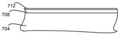
도 7은 도 4에 도시된 실시 예에 따라 형성된 실리콘 옥사이드 기반 코팅을 갖는 ESC (704) 의 일부의 개략적인 단면도이다. 실리콘 옥사이드 기반 코팅은 제 1 층 (708) 및 제 2 층 (712) 을 포함한다. 제 1 층 (708) 은 산소 연소에 의해 변화되지 않은 실리콘 옥사이드 기반 코팅의 일부이다. 제 2 층 (712) 은 산소 연소에 의해 변화된 실리콘 옥사이드 기반 코팅의 일부이다. 상기 언급된 바와 같이, 제 2 층 (712) 이 제 1 층 (708) 보다 견고하다는 것을 알게 되었다. 이에 더하여, 단단해진 제 2 층 (712) 을 제공하기 위해 산소 연소를 사용하는 것은 웨이퍼와 ESC (704) 사이의 부착을 감소시킨다는 것을 알게 되었다. ESC (704) 에 부착되는 웨이퍼는 고온 프로세스들에서 문제이다. 웨이퍼 부착은 높은 동적 정렬 오프셋 에러들을 발생시킬 수도 있다. 따라서, 산소 연소의 사용은 입자/결함 레벨들 및 동적 정렬 오프셋 에러들을 감소시킨다.7 is a schematic cross-sectional view of a portion of an
본 개시가 몇몇의 실시예들의 측면에서 기술되었지만, 본 개시의 범위 내에 속하는 변경들, 수정들, 치환들, 및 다양한 대체 등가물들이 있다. 또한 본 개시의 방법들 및 장치들을 구현하는 많은 대안적인 방식들이 있다는 것에 유의해야 한다. 따라서 이하의 첨부된 청구항들은 본 개시의 진정한 정신 및 범위 내에 속하는 이러한 변경들, 수정들, 치환들, 및 다양한 대체 등가물들을 모두 포함하는 것으로 해석되는 것이 의도된다.While the present disclosure has been described in terms of several embodiments, there are variations, modifications, permutations, and various alternative equivalents that fall within the scope of the present disclosure. It should also be noted that there are many alternative ways of implementing the methods and apparatuses of the present disclosure. Accordingly, it is intended that the following appended claims be interpreted as including all such changes, modifications, substitutions, and various alternative equivalents falling within the true spirit and scope of this disclosure.
Claims (17)
Translated fromKorean상기 방법은 복수의 사이클들을 포함하고, 상기 사이클 각각은,
플라즈마 프로세싱 챔버의 내부 및 척을 세정하는 단계; 및
상기 플라즈마 프로세싱 챔버의 상기 내부 상 및 상기 척 상에 실리콘 옥사이드 기반 코팅을 형성하는 단계로서, 상기 실리콘 옥사이드 기반 코팅은 제 1 층 및 제 2 층을 갖는, 상기 실리콘 옥사이드 기반 코팅을 형성하는 단계를 포함하는, 플라즈마 프로세싱 챔버를 컨디셔닝하기 위한 방법.A method for conditioning a plasma processing chamber comprising a chuck, comprising:
The method includes a plurality of cycles, each of the cycles,
Cleaning the chuck and the interior of the plasma processing chamber; And
Forming a silicon oxide-based coating on the inside of the plasma processing chamber and on the chuck, the silicon oxide-based coating comprising forming the silicon oxide-based coating having a first layer and a second layer A method for conditioning a plasma processing chamber.
상기 실리콘 옥사이드 기반 코팅을 형성하는 단계는,
상기 플라즈마 프로세싱 챔버의 상기 내부 상 및 상기 척 상에 실리콘 옥사이드 기반 코팅을 증착하는 단계; 및
산소 기반 연소 (oxygen based burn) 에 의해 변화되지 않은 상기 실리콘 옥사이드 기반 코팅의 상기 제 1 층 및 상기 산소 기반 연소에 의해 변화된 상기 실리콘 옥사이드 기반 코팅의 상기 제 2 층 내에 상기 실리콘 옥사이드 기반 코팅을 형성하도록 상기 실리콘 옥사이드 기반 코팅의 산소 기반 연소를 제공하는 단계를 포함하는, 플라즈마 프로세싱 챔버를 컨디셔닝하기 위한 방법.The method of claim 1,
The step of forming the silicon oxide-based coating,
Depositing a silicon oxide-based coating on the inside of the plasma processing chamber and on the chuck; And
To form the silicon oxide based coating in the first layer of the silicon oxide based coating not changed by oxygen based burn and the second layer of the silicon oxide based coating changed by the oxygen based combustion Providing oxygen-based combustion of the silicon oxide-based coating.
상기 산소 기반 연소를 제공하는 단계는,
산소를 포함하는 연소 가스를 제공하는 단계; 및
상기 연소 가스를 플라즈마로 변환하는 단계를 포함하는, 플라즈마 프로세싱 챔버를 컨디셔닝하기 위한 방법.The method of claim 2,
Providing the oxygen-based combustion,
Providing a combustion gas comprising oxygen; And
Converting the combustion gas to plasma.
상기 산소 기반 연소는 균일성을 개선하도록 상기 실리콘 옥사이드 기반 코팅의 상기 제 2 층을 개질하는, 플라즈마 프로세싱 챔버를 컨디셔닝하기 위한 방법.The method of claim 3,
Wherein the oxygen-based combustion modifies the second layer of the silicon oxide-based coating to improve uniformity.
상기 산소 기반 연소를 제공하는 단계는 400 V 미만의 바이어스를 제공하는 단계를 더 포함하는, 플라즈마 프로세싱 챔버를 컨디셔닝하기 위한 방법.The method of claim 3,
The step of providing the oxygen-based combustion further comprises providing a bias of less than 400 V.
상기 실리콘 옥사이드 기반 코팅을 형성한 후 상기 플라즈마 프로세싱 챔버 내에 기판을 배치하는 단계;
상기 플라즈마 프로세싱 챔버 내에서 상기 기판을 플라즈마 프로세싱하는 단계로서, 상기 실리콘 옥사이드 기반 코팅은 상기 기판의 상기 플라즈마 프로세싱 동안 상기 플라즈마 프로세싱 챔버의 상기 내부 및 상기 척을 보호하는, 상기 기판을 플라즈마 프로세싱하는 단계; 및
상기 플라즈마 프로세싱 챔버로부터 상기 기판을 제거하는 단계를 더 포함하는, 플라즈마 프로세싱 챔버를 컨디셔닝하기 위한 방법.The method of claim 2,
Placing a substrate in the plasma processing chamber after forming the silicon oxide-based coating;
Plasma processing the substrate in the plasma processing chamber, wherein the silicon oxide based coating protects the interior of the plasma processing chamber and the chuck during the plasma processing of the substrate; And
And removing the substrate from the plasma processing chamber.
상기 플라즈마 프로세싱 챔버의 상기 내부 및 상기 척의 세정은 웨이퍼리스 (waferless) 세정이고, 상기 웨이퍼리스 세정은,
세정 가스를 제공하는 단계; 및
상기 세정 가스를 플라즈마로 변환하는 단계로서, 상기 플라즈마는 상기 플라즈마 프로세싱 챔버의 상기 내부 상 및 상기 척 상의 잔여물을 제거하는, 상기 세정 가스를 플라즈마로 변환하는 단계를 포함하는, 플라즈마 프로세싱 챔버를 컨디셔닝하기 위한 방법.The method of claim 2,
The cleaning of the inside of the plasma processing chamber and the chuck is waferless cleaning, and the waferless cleaning,
Providing a cleaning gas; And
Converting the cleaning gas to plasma, wherein the plasma comprises converting the cleaning gas to plasma to remove residues on the inside of the plasma processing chamber and on the chuck. Way to do it.
상기 실리콘 옥사이드 기반 코팅을 형성하는 단계는,
제 1 압력에서 상기 플라즈마 프로세싱 챔버의 상기 내부 상 및 상기 척 상에 상기 제 1 층을 증착하는 단계; 및
상기 제 1 압력보다 낮은 제 2 압력에서 상기 제 1 층 위에 상기 플라즈마 프로세싱 챔버의 상기 내부 상 및 상기 척 상에 상기 제 2 층을 증착하는 단계를 포함하는, 플라즈마 프로세싱 챔버를 컨디셔닝하기 위한 방법.The method of claim 1,
The step of forming the silicon oxide-based coating,
Depositing the first layer on the chuck and on the interior of the plasma processing chamber at a first pressure; And
Depositing the second layer on the chuck and on the interior of the plasma processing chamber over the first layer at a second pressure less than the first pressure.
상기 제 1 층을 증착하는 단계는,
실리콘 함유 성분 (component) 및 산소 함유 성분을 포함하는 증착 가스를 제공하는 단계; 및
제 1 문턱값 압력보다 높은 압력 하에서 상기 증착 가스를 플라즈마로 변환하는 단계로서, 상기 플라즈마는 상기 제 1 층으로 하여금 상기 플라즈마 프로세싱 챔버의 상기 내부 상 및 상기 척 상에 증착되게 하는, 플라즈마 프로세싱 챔버를 컨디셔닝하기 위한 방법.The method of claim 8,
The step of depositing the first layer,
Providing a deposition gas comprising a silicon-containing component and an oxygen-containing component; And
Converting the deposition gas to plasma under a pressure higher than a first threshold pressure, wherein the plasma causes the first layer to be deposited on the interior and on the chuck of the plasma processing chamber. Method for conditioning.
상기 제 2 층을 증착하는 단계는,
상기 실리콘 함유 성분 및 산소 함유 성분을 포함하는 상기 증착 가스를 제공하는 단계; 및
제 2 문턱값 압력보다 낮은 압력 하에서 상기 증착 가스를 상기 플라즈마로 변환하는 단계로서, 상기 제 2 문턱값 압력은 상기 제 1 문턱값 압력보다 낮고, 상기 플라즈마는 상기 제 2 층으로 하여금 상기 플라즈마 프로세싱 챔버의 상기 내부 상 및 상기 척 상에 증착되게 하는, 상기 증착 가스를 상기 플라즈마로 변환하는 단계를 포함하는, 플라즈마 프로세싱 챔버를 컨디셔닝하기 위한 방법.The method of claim 9,
The step of depositing the second layer,
Providing the deposition gas containing the silicon-containing component and the oxygen-containing component; And
Converting the deposition gas into the plasma under a pressure lower than a second threshold pressure, wherein the second threshold pressure is lower than the first threshold pressure, and the plasma causes the second layer to cause the plasma processing chamber Converting the deposition gas to the plasma, causing it to be deposited on the inside of the chuck and on the chuck.
상기 제 1 문턱값 압력은 40 mTorr이고, 상기 제 2 문턱값 압력은 20 mTorr인, 플라즈마 프로세싱 챔버를 컨디셔닝하기 위한 방법.The method of claim 10,
Wherein the first threshold pressure is 40 mTorr and the second threshold pressure is 20 mTorr.
상기 제 1 문턱값 압력은 40 mTorr 인, 플라즈마 프로세싱 챔버를 컨디셔닝하기 위한 방법.The method of claim 9,
Wherein the first threshold pressure is 40 mTorr.
상기 실리콘 옥사이드 기반 코팅을 형성하는 단계는 상기 제 1 층을 증착하기 전에 초기 압력에서 상기 플라즈마 프로세싱 챔버의 상기 내부 상 및 상기 척 상에 초기 층을 증착하는 단계를 더 포함하고, 상기 초기 압력은 상기 제 1 압력보다 낮고, 상기 제 1 층은 상기 초기 층 위에 증착되는, 플라즈마 프로세싱 챔버를 컨디셔닝하기 위한 방법.The method of claim 8,
The step of forming the silicon oxide-based coating further comprises depositing an initial layer on the inside of the plasma processing chamber and on the chuck at an initial pressure before depositing the first layer, wherein the initial pressure is the Lower than a first pressure, wherein the first layer is deposited over the initial layer.
상기 제 1 압력은 20 mTorr보다 높고 상기 제 2 압력 및 상기 초기 압력은 20 mTorr보다 낮은, 플라즈마 프로세싱 챔버를 컨디셔닝하기 위한 방법.The method of claim 13,
Wherein the first pressure is greater than 20 mTorr and the second pressure and the initial pressure are less than 20 mTorr.
상기 제 1 압력은 40 mTorr보다 높고 상기 초기 압력 및 상기 제 2 압력은 20 mTorr보다 낮은, 플라즈마 프로세싱 챔버를 컨디셔닝하기 위한 방법.The method of claim 13,
Wherein the first pressure is greater than 40 mTorr and the initial pressure and the second pressure are less than 20 mTorr.
상기 제 1 압력은 20 mTorr보다 높고 상기 제 2 압력은 20 mTorr보다 낮은, 플라즈마 프로세싱 챔버를 컨디셔닝하기 위한 방법.The method of claim 8,
The first pressure is greater than 20 mTorr and the second pressure is less than 20 mTorr.
상기 제 1 압력은 40 mTorr보다 높고 상기 제 2 압력은 20 mTorr보다 낮은, 플라즈마 프로세싱 챔버를 컨디셔닝하기 위한 방법.The method of claim 8,
The first pressure is greater than 40 mTorr and the second pressure is less than 20 mTorr.
Applications Claiming Priority (3)
| Application Number | Priority Date | Filing Date | Title |
|---|---|---|---|
| US201862734844P | 2018-09-21 | 2018-09-21 | |
| US62/734,844 | 2018-09-21 | ||
| PCT/US2019/051318WO2020060929A1 (en) | 2018-09-21 | 2019-09-16 | Method for conditioning a plasma processing chamber |
Publications (2)
| Publication Number | Publication Date |
|---|---|
| KR20210048568Atrue KR20210048568A (en) | 2021-05-03 |
| KR102836261B1 KR102836261B1 (en) | 2025-07-18 |
Family
ID=69887953
Family Applications (1)
| Application Number | Title | Priority Date | Filing Date |
|---|---|---|---|
| KR1020217011451AActiveKR102836261B1 (en) | 2018-09-21 | 2019-09-16 | Method for conditioning a plasma processing chamber |
Country Status (4)
| Country | Link |
|---|---|
| US (1) | US12060636B2 (en) |
| KR (1) | KR102836261B1 (en) |
| TW (1) | TWI839386B (en) |
| WO (1) | WO2020060929A1 (en) |
Families Citing this family (7)
| Publication number | Priority date | Publication date | Assignee | Title |
|---|---|---|---|---|
| US11289355B2 (en) | 2017-06-02 | 2022-03-29 | Lam Research Corporation | Electrostatic chuck for use in semiconductor processing |
| US11469084B2 (en) | 2017-09-05 | 2022-10-11 | Lam Research Corporation | High temperature RF connection with integral thermal choke |
| US11990360B2 (en) | 2018-01-31 | 2024-05-21 | Lam Research Corporation | Electrostatic chuck (ESC) pedestal voltage isolation |
| US11086233B2 (en)* | 2018-03-20 | 2021-08-10 | Lam Research Corporation | Protective coating for electrostatic chucks |
| US11183368B2 (en) | 2018-08-02 | 2021-11-23 | Lam Research Corporation | RF tuning systems including tuning circuits having impedances for setting and adjusting parameters of electrodes in electrostatic chucks |
| US11626271B2 (en)* | 2020-06-18 | 2023-04-11 | Tokyo Electron Limited | Surface fluorination remediation for aluminium oxide electrostatic chucks |
| WO2025019595A1 (en)* | 2023-07-18 | 2025-01-23 | Applied Materials, Inc. | Method for controlling particle growth in a plasma chamber |
Citations (6)
| Publication number | Priority date | Publication date | Assignee | Title |
|---|---|---|---|---|
| US20050221001A1 (en)* | 2004-03-31 | 2005-10-06 | Tokyo Electron Limited Of Tbs Broadcast Center | Method for extending time between chamber cleaning processes |
| US20070155137A1 (en)* | 2003-01-31 | 2007-07-05 | Sharp Laboratories Of America, Inc. | High density plasma non-stoichiometric SiOxNy films |
| US20070238199A1 (en)* | 2006-03-31 | 2007-10-11 | Tokyo Electron Limited | Method for conditioning a process chamber |
| KR20160115761A (en)* | 2015-03-26 | 2016-10-06 | 램 리써치 코포레이션 | Minimizing radical recombination using ald silicon oxide surface coating with intermittent restoration plasma |
| KR20160121429A (en)* | 2015-04-09 | 2016-10-19 | 램 리써치 코포레이션 | Eliminating first wafer metal contamination effect in high density plasma chemical vapor deposition systems |
| KR20180044214A (en)* | 2016-10-21 | 2018-05-02 | 어플라이드 머티어리얼스, 인코포레이티드 | Technique to prevent aluminum fluoride build up on the heater |
Family Cites Families (11)
| Publication number | Priority date | Publication date | Assignee | Title |
|---|---|---|---|---|
| ID22140A (en)* | 1997-06-30 | 1999-09-09 | Matsushita Electric Industrial Co Ltd | METHODS FOR PRODUCING THIN SEMICONDUCTOR FILM AND ITS EQUIPMENT |
| TW416100B (en)* | 1997-07-02 | 2000-12-21 | Applied Materials Inc | Control of oxygen to silane ratio in a seasoning process to improve particle performance in an HDP-CVD system |
| US20050079731A1 (en)* | 2000-08-31 | 2005-04-14 | Micron Technology, Inc. | Plasma enhanced chemical vapor deposition methods and semiconductor processing methods of forming layers and shallow trench isolation regions |
| KR100375102B1 (en)* | 2000-10-18 | 2003-03-08 | 삼성전자주식회사 | Method for CVD and apparatus for performing the same in semiconductor device processing |
| US6720259B2 (en)* | 2001-10-02 | 2004-04-13 | Genus, Inc. | Passivation method for improved uniformity and repeatability for atomic layer deposition and chemical vapor deposition |
| US20040261815A1 (en)* | 2003-06-27 | 2004-12-30 | Texas Instruments, Incorporated | Three-step chamber cleaning process for deposition tools |
| US20050066994A1 (en)* | 2003-09-30 | 2005-03-31 | Biles Peter John | Methods for cleaning processing chambers |
| US7989365B2 (en) | 2009-08-18 | 2011-08-02 | Applied Materials, Inc. | Remote plasma source seasoning |
| US8524612B2 (en)* | 2010-09-23 | 2013-09-03 | Novellus Systems, Inc. | Plasma-activated deposition of conformal films |
| US9406534B2 (en)* | 2014-09-17 | 2016-08-02 | Lam Research Corporation | Wet clean process for cleaning plasma processing chamber components |
| KR102058106B1 (en)* | 2015-11-20 | 2019-12-20 | 주식회사 원익아이피에스 | Method of fabricating semiconductor device |
- 2019
- 2019-09-16WOPCT/US2019/051318patent/WO2020060929A1/ennot_activeCeased
- 2019-09-16KRKR1020217011451Apatent/KR102836261B1/enactiveActive
- 2019-09-16USUS17/273,649patent/US12060636B2/enactiveActive
- 2019-09-20TWTW108133953Apatent/TWI839386B/enactive
Patent Citations (6)
| Publication number | Priority date | Publication date | Assignee | Title |
|---|---|---|---|---|
| US20070155137A1 (en)* | 2003-01-31 | 2007-07-05 | Sharp Laboratories Of America, Inc. | High density plasma non-stoichiometric SiOxNy films |
| US20050221001A1 (en)* | 2004-03-31 | 2005-10-06 | Tokyo Electron Limited Of Tbs Broadcast Center | Method for extending time between chamber cleaning processes |
| US20070238199A1 (en)* | 2006-03-31 | 2007-10-11 | Tokyo Electron Limited | Method for conditioning a process chamber |
| KR20160115761A (en)* | 2015-03-26 | 2016-10-06 | 램 리써치 코포레이션 | Minimizing radical recombination using ald silicon oxide surface coating with intermittent restoration plasma |
| KR20160121429A (en)* | 2015-04-09 | 2016-10-19 | 램 리써치 코포레이션 | Eliminating first wafer metal contamination effect in high density plasma chemical vapor deposition systems |
| KR20180044214A (en)* | 2016-10-21 | 2018-05-02 | 어플라이드 머티어리얼스, 인코포레이티드 | Technique to prevent aluminum fluoride build up on the heater |
Also Published As
| Publication number | Publication date |
|---|---|
| WO2020060929A1 (en) | 2020-03-26 |
| US20210340668A1 (en) | 2021-11-04 |
| TW202031922A (en) | 2020-09-01 |
| US12060636B2 (en) | 2024-08-13 |
| TWI839386B (en) | 2024-04-21 |
| KR102836261B1 (en) | 2025-07-18 |
Similar Documents
| Publication | Publication Date | Title |
|---|---|---|
| KR102836261B1 (en) | Method for conditioning a plasma processing chamber | |
| KR102540183B1 (en) | Hydrogen Activated Atomic Layer Etching | |
| KR102403856B1 (en) | Method for etching etching layer | |
| US9673058B1 (en) | Method for etching features in dielectric layers | |
| TW201843701A (en) | Atomic layer etching of silicon nitride | |
| US20230122167A1 (en) | Method for conditioning a plasma processing chamber | |
| TWI878250B (en) | Apparatus for atomic layer deposition or chemical vapor deposition | |
| US20140179106A1 (en) | In-situ metal residue clean | |
| TWI806871B (en) | Porous low-k dielectric etch | |
| CN109952636B (en) | Plasma ignition suppression | |
| KR102059312B1 (en) | Mitigation of silicide formation on wafer bevel | |
| KR20150016178A (en) | Conformal sidewall passivation | |
| CN112335028B (en) | Method and apparatus for processing wafers | |
| JP6821292B2 (en) | How to etch the tungsten-containing layer | |
| KR102700803B1 (en) | A method for improving deposition-induced CD imbalance using spatially selective ashing of carbon-based films | |
| CN110520964B (en) | Silicon-based deposition for semiconductor processing | |
| TW201903897A (en) | Sulfide deposition for semiconductor processing | |
| US12444588B2 (en) | Method and apparatus for processing wafers |
Legal Events
| Date | Code | Title | Description |
|---|---|---|---|
| PA0105 | International application | St.27 status event code:A-0-1-A10-A15-nap-PA0105 | |
| PG1501 | Laying open of application | St.27 status event code:A-1-1-Q10-Q12-nap-PG1501 | |
| A201 | Request for examination | ||
| PA0201 | Request for examination | St.27 status event code:A-1-2-D10-D11-exm-PA0201 | |
| D13-X000 | Search requested | St.27 status event code:A-1-2-D10-D13-srh-X000 | |
| D14-X000 | Search report completed | St.27 status event code:A-1-2-D10-D14-srh-X000 | |
| E902 | Notification of reason for refusal | ||
| PE0902 | Notice of grounds for rejection | St.27 status event code:A-1-2-D10-D21-exm-PE0902 | |
| E13-X000 | Pre-grant limitation requested | St.27 status event code:A-2-3-E10-E13-lim-X000 | |
| P11-X000 | Amendment of application requested | St.27 status event code:A-2-2-P10-P11-nap-X000 | |
| P13-X000 | Application amended | St.27 status event code:A-2-2-P10-P13-nap-X000 | |
| E701 | Decision to grant or registration of patent right | ||
| PE0701 | Decision of registration | St.27 status event code:A-1-2-D10-D22-exm-PE0701 | |
| PR0701 | Registration of establishment | St.27 status event code:A-2-4-F10-F11-exm-PR0701 | |
| PR1002 | Payment of registration fee | St.27 status event code:A-2-2-U10-U12-oth-PR1002 Fee payment year number:1 | |
| PG1601 | Publication of registration | St.27 status event code:A-4-4-Q10-Q13-nap-PG1601 |