KR20210040134A - Measuring device - Google Patents
Measuring deviceDownload PDFInfo
- Publication number
- KR20210040134A KR20210040134AKR1020217006840AKR20217006840AKR20210040134AKR 20210040134 AKR20210040134 AKR 20210040134AKR 1020217006840 AKR1020217006840 AKR 1020217006840AKR 20217006840 AKR20217006840 AKR 20217006840AKR 20210040134 AKR20210040134 AKR 20210040134A
- Authority
- KR
- South Korea
- Prior art keywords
- radiation
- illumination
- branches
- polarization
- branch
- Prior art date
- Legal status (The legal status is an assumption and is not a legal conclusion. Google has not performed a legal analysis and makes no representation as to the accuracy of the status listed.)
- Abandoned
Links
Images


Classifications
- G—PHYSICS
- G01—MEASURING; TESTING
- G01N—INVESTIGATING OR ANALYSING MATERIALS BY DETERMINING THEIR CHEMICAL OR PHYSICAL PROPERTIES
- G01N21/00—Investigating or analysing materials by the use of optical means, i.e. using sub-millimetre waves, infrared, visible or ultraviolet light
- G01N21/84—Systems specially adapted for particular applications
- G01N21/88—Investigating the presence of flaws or contamination
- G01N21/95—Investigating the presence of flaws or contamination characterised by the material or shape of the object to be examined
- G01N21/956—Inspecting patterns on the surface of objects
- G—PHYSICS
- G01—MEASURING; TESTING
- G01B—MEASURING LENGTH, THICKNESS OR SIMILAR LINEAR DIMENSIONS; MEASURING ANGLES; MEASURING AREAS; MEASURING IRREGULARITIES OF SURFACES OR CONTOURS
- G01B11/00—Measuring arrangements characterised by the use of optical techniques
- G01B11/24—Measuring arrangements characterised by the use of optical techniques for measuring contours or curvatures
- G01B11/25—Measuring arrangements characterised by the use of optical techniques for measuring contours or curvatures by projecting a pattern, e.g. one or more lines, moiré fringes on the object
- G01B11/2513—Measuring arrangements characterised by the use of optical techniques for measuring contours or curvatures by projecting a pattern, e.g. one or more lines, moiré fringes on the object with several lines being projected in more than one direction, e.g. grids, patterns
- G—PHYSICS
- G01—MEASURING; TESTING
- G01N—INVESTIGATING OR ANALYSING MATERIALS BY DETERMINING THEIR CHEMICAL OR PHYSICAL PROPERTIES
- G01N21/00—Investigating or analysing materials by the use of optical means, i.e. using sub-millimetre waves, infrared, visible or ultraviolet light
- G01N21/17—Systems in which incident light is modified in accordance with the properties of the material investigated
- G01N21/47—Scattering, i.e. diffuse reflection
- G—PHYSICS
- G01—MEASURING; TESTING
- G01N—INVESTIGATING OR ANALYSING MATERIALS BY DETERMINING THEIR CHEMICAL OR PHYSICAL PROPERTIES
- G01N21/00—Investigating or analysing materials by the use of optical means, i.e. using sub-millimetre waves, infrared, visible or ultraviolet light
- G01N21/84—Systems specially adapted for particular applications
- G01N21/88—Investigating the presence of flaws or contamination
- G01N21/8806—Specially adapted optical and illumination features
- G—PHYSICS
- G02—OPTICS
- G02F—OPTICAL DEVICES OR ARRANGEMENTS FOR THE CONTROL OF LIGHT BY MODIFICATION OF THE OPTICAL PROPERTIES OF THE MEDIA OF THE ELEMENTS INVOLVED THEREIN; NON-LINEAR OPTICS; FREQUENCY-CHANGING OF LIGHT; OPTICAL LOGIC ELEMENTS; OPTICAL ANALOGUE/DIGITAL CONVERTERS
- G02F1/00—Devices or arrangements for the control of the intensity, colour, phase, polarisation or direction of light arriving from an independent light source, e.g. switching, gating or modulating; Non-linear optics
- G02F1/01—Devices or arrangements for the control of the intensity, colour, phase, polarisation or direction of light arriving from an independent light source, e.g. switching, gating or modulating; Non-linear optics for the control of the intensity, phase, polarisation or colour
- G02F1/0136—Devices or arrangements for the control of the intensity, colour, phase, polarisation or direction of light arriving from an independent light source, e.g. switching, gating or modulating; Non-linear optics for the control of the intensity, phase, polarisation or colour for the control of polarisation, e.g. state of polarisation [SOP] control, polarisation scrambling, TE-TM mode conversion or separation
- G—PHYSICS
- G02—OPTICS
- G02F—OPTICAL DEVICES OR ARRANGEMENTS FOR THE CONTROL OF LIGHT BY MODIFICATION OF THE OPTICAL PROPERTIES OF THE MEDIA OF THE ELEMENTS INVOLVED THEREIN; NON-LINEAR OPTICS; FREQUENCY-CHANGING OF LIGHT; OPTICAL LOGIC ELEMENTS; OPTICAL ANALOGUE/DIGITAL CONVERTERS
- G02F1/00—Devices or arrangements for the control of the intensity, colour, phase, polarisation or direction of light arriving from an independent light source, e.g. switching, gating or modulating; Non-linear optics
- G02F1/29—Devices or arrangements for the control of the intensity, colour, phase, polarisation or direction of light arriving from an independent light source, e.g. switching, gating or modulating; Non-linear optics for the control of the position or the direction of light beams, i.e. deflection
- G02F1/33—Acousto-optical deflection devices
- G—PHYSICS
- G03—PHOTOGRAPHY; CINEMATOGRAPHY; ANALOGOUS TECHNIQUES USING WAVES OTHER THAN OPTICAL WAVES; ELECTROGRAPHY; HOLOGRAPHY
- G03F—PHOTOMECHANICAL PRODUCTION OF TEXTURED OR PATTERNED SURFACES, e.g. FOR PRINTING, FOR PROCESSING OF SEMICONDUCTOR DEVICES; MATERIALS THEREFOR; ORIGINALS THEREFOR; APPARATUS SPECIALLY ADAPTED THEREFOR
- G03F7/00—Photomechanical, e.g. photolithographic, production of textured or patterned surfaces, e.g. printing surfaces; Materials therefor, e.g. comprising photoresists; Apparatus specially adapted therefor
- G03F7/70—Microphotolithographic exposure; Apparatus therefor
- G03F7/70483—Information management; Active and passive control; Testing; Wafer monitoring, e.g. pattern monitoring
- G03F7/70605—Workpiece metrology
- G03F7/70616—Monitoring the printed patterns
- G—PHYSICS
- G03—PHOTOGRAPHY; CINEMATOGRAPHY; ANALOGOUS TECHNIQUES USING WAVES OTHER THAN OPTICAL WAVES; ELECTROGRAPHY; HOLOGRAPHY
- G03F—PHOTOMECHANICAL PRODUCTION OF TEXTURED OR PATTERNED SURFACES, e.g. FOR PRINTING, FOR PROCESSING OF SEMICONDUCTOR DEVICES; MATERIALS THEREFOR; ORIGINALS THEREFOR; APPARATUS SPECIALLY ADAPTED THEREFOR
- G03F7/00—Photomechanical, e.g. photolithographic, production of textured or patterned surfaces, e.g. printing surfaces; Materials therefor, e.g. comprising photoresists; Apparatus specially adapted therefor
- G03F7/70—Microphotolithographic exposure; Apparatus therefor
- G03F7/70483—Information management; Active and passive control; Testing; Wafer monitoring, e.g. pattern monitoring
- G03F7/70605—Workpiece metrology
- G03F7/706843—Metrology apparatus
- G03F7/706847—Production of measurement radiation, e.g. synchrotron, free-electron laser, plasma source or higher harmonic generation [HHG]
- G—PHYSICS
- G01—MEASURING; TESTING
- G01B—MEASURING LENGTH, THICKNESS OR SIMILAR LINEAR DIMENSIONS; MEASURING ANGLES; MEASURING AREAS; MEASURING IRREGULARITIES OF SURFACES OR CONTOURS
- G01B2210/00—Aspects not specifically covered by any group under G01B, e.g. of wheel alignment, caliper-like sensors
- G01B2210/56—Measuring geometric parameters of semiconductor structures, e.g. profile, critical dimensions or trench depth
- G—PHYSICS
- G01—MEASURING; TESTING
- G01N—INVESTIGATING OR ANALYSING MATERIALS BY DETERMINING THEIR CHEMICAL OR PHYSICAL PROPERTIES
- G01N21/00—Investigating or analysing materials by the use of optical means, i.e. using sub-millimetre waves, infrared, visible or ultraviolet light
- G01N21/84—Systems specially adapted for particular applications
- G01N21/88—Investigating the presence of flaws or contamination
- G01N21/8806—Specially adapted optical and illumination features
- G01N2021/8812—Diffuse illumination, e.g. "sky"
- G01N2021/8816—Diffuse illumination, e.g. "sky" by using multiple sources, e.g. LEDs
- G—PHYSICS
- G01—MEASURING; TESTING
- G01N—INVESTIGATING OR ANALYSING MATERIALS BY DETERMINING THEIR CHEMICAL OR PHYSICAL PROPERTIES
- G01N21/00—Investigating or analysing materials by the use of optical means, i.e. using sub-millimetre waves, infrared, visible or ultraviolet light
- G01N21/84—Systems specially adapted for particular applications
- G01N21/88—Investigating the presence of flaws or contamination
- G01N21/8806—Specially adapted optical and illumination features
- G01N2021/8848—Polarisation of light
Landscapes
- Physics & Mathematics (AREA)
- General Physics & Mathematics (AREA)
- Nonlinear Science (AREA)
- Optics & Photonics (AREA)
- Life Sciences & Earth Sciences (AREA)
- Health & Medical Sciences (AREA)
- Chemical & Material Sciences (AREA)
- Analytical Chemistry (AREA)
- Biochemistry (AREA)
- General Health & Medical Sciences (AREA)
- Immunology (AREA)
- Pathology (AREA)
- Engineering & Computer Science (AREA)
- Computer Vision & Pattern Recognition (AREA)
- Plasma & Fusion (AREA)
- Exposure And Positioning Against Photoresist Photosensitive Materials (AREA)
- Length Measuring Devices By Optical Means (AREA)
Abstract
Translated fromKorean
Description
Translated fromKorean본 출원은 2018년 9월 4일자로 출원된 EP 출원 제18192442.4호 및 2019년 1월 15일자로 출원된 EP 출원 제19151907.3호에 대해 우선권을 주장하며, 이러한 문헌의 내용은 원용에 의해 전체적으로 본 명세서에 포함된다.This application claims priority to EP Application No. 18192442.4 filed on September 4, 2018 and EP Application No. 19151907.3 filed on January 15, 2019, the contents of which are incorporated herein by reference in their entirety. Included in
본 발명은 기판 상의 구조체의 관심 파라미터를 결정하기 위한 계측 장치 및 이러한 관심 파라미터를 결정하는 방법에 관한 것이다.The present invention relates to a metrology apparatus for determining a parameter of interest of a structure on a substrate and a method of determining such a parameter of interest.
리소그래피 장치는 기판 상에 원하는 패턴을 적용하도록 구성된 기기이다. 리소그래피 장치는, 예를 들어 집적 회로(IC)의 제조에 사용될 수 있다. 리소그래피 장치는, 예를 들어, 패터닝 디바이스(예를 들어, 마스크)에 있는 패턴(또는 "설계 레이아웃" 또는 "설계"로도 지칭됨)을 기판(예를 들어, 웨이퍼) 상에 제공된 방사선-감응 재료(레지스트)의 층 상에 투영할 수 있다.A lithographic apparatus is an apparatus configured to apply a desired pattern onto a substrate. Lithographic apparatus can be used, for example, in the manufacture of integrated circuits (ICs). A lithographic apparatus, for example, transfers a pattern (or also referred to as “design layout” or “design”) in a patterning device (eg, a mask) to a radiation-sensitive material provided on a substrate (eg, a wafer). It can be projected on the layer of (resist).
기판 상에 패턴을 투영하기 위해 리소그래피 장치는 전자기 방사선을 사용할 수 있다. 이러한 방사선의 파장은 기판 상에 형성될 수 있는 피처의 최소 크기를 결정한다. 현재 사용되는 전형적인 파장은 365nm(i-line), 248nm, 193nm 및 13.5nm 이다. 4-20 nm 범위, 예를 들어 6.7 nm 또는 13.5 nm 의 파장을 갖는 극자외(EUV) 방사선을 사용하는 리소그래피 장치는, 예컨대 파장 193 nm의 방사선을 사용하는 리소그래피 장치보다 기판 상에 더 작은 피처를 형성하기 위해 사용될 수 있다.A lithographic apparatus may use electromagnetic radiation to project a pattern onto a substrate. The wavelength of this radiation determines the minimum size of a feature that can be formed on the substrate. Typical wavelengths currently in use are 365nm (i-line), 248nm, 193nm and 13.5nm. A lithographic apparatus using extreme ultraviolet (EUV) radiation with a wavelength in the range of 4-20 nm, e.g. 6.7 nm or 13.5 nm, has smaller features on a substrate than a lithographic apparatus using radiation with a wavelength of 193 nm, e.g. Can be used to form.
리소그래피 장치의 전통적인 분해능 한계보다 작은 치수를 갖는 피처를 처리하기 위해 로우-k1 리소그래피가 사용될 수 있다. 이러한 프로세스에서, 분해능 식은 CD = k1 × λ/NA로 표현될 수 있으며, 여기서 λ는 채용된 방사선의 파장이고, NA는 리소그래피 장치에서의 투영 광학계의 개구수이고, CD는 "임계 치수"(일반적으로 인쇄되는 최소 피처 크기이지만, 이 경우 1/2 피치)이고, k1은 실험상 분해능 인자이다. 일반적으로, k1이 작을수록, 특별한 전기적 기능 및 성능을 달성하기 위해 회로 설계자가 계획한 형상 및 치수와 유사한 기판 상의 패턴을 재현하는 것이 더 어려워진다. 이러한 어려움을 극복하기 위해, 정교한 미세 조정 단계가 리소그래피 투영 장치 및/또는 설계 레이아웃에 적용될 수 있다. 예를 들어 NA의 최적화, 커스터마이즈 조명 스킴, 위상 시프팅 패터닝 디바이스의 사용, 설계 레이아웃에서의 광학 근접 보정(OPC, 종종 "광학 및 프로세스 보정"이라고도 함)과 같은 설계 레이아웃의 다양한 최적화, 또는 "분해능 향상 기법"(RET)으로 일반적으로 규정되는 기타 다른 방법이 여기에 포함되지만 이에 제한되는 것은 아니다. 대안적으로, 리소그래피 장치의 안정성을 제어하기 위한 엄격한 제어 루프가 낮은 k1에서 패턴의 재현을 개선하기 위해 사용될 수 있다.Low-k 1 lithography can be used to process features with dimensions that are smaller than the traditional resolution limit of a lithographic apparatus. In this process, the resolution equationcan be expressed as CD = k 1 × λ/NA, where λ is the wavelength of the employed radiation, NA is the numerical aperture of the projection optical system in the lithographic apparatus, and CD is the “critical dimension” ( It is usually the smallest feature size to be printed, but in this
계측 장치는 기판 상의 구조체의 관심 파라미터를 측정하는 데 사용될 수 있다. 예를 들어, 계측 장치는 임계 치수, 기판 상의 층들 사이의 오버레이 및 기판 상의 패턴의 비대칭과 같은 파라미터를 측정하는 데 사용될 수 있다. 측정 방사선의 광선이 기판을 조명하는 데 사용된다. 이러한 방사선은 기판 상의 구조체에 의해 회절된다. 회절된 방사선은 대물 렌즈에 의해 집광되고 센서에 의해 캡쳐된다.The metrology device can be used to measure a parameter of interest of the structure on the substrate. For example, metrology devices can be used to measure parameters such as critical dimensions, overlays between layers on a substrate, and asymmetry of patterns on a substrate. A ray of measurement radiation is used to illuminate the substrate. This radiation is diffracted by the structure on the substrate. The diffracted radiation is focused by the objective lens and captured by the sensor.
조명의 세기는 방사선 소스의 파워 및 계측 장치의 광학 시스템의 손실에 의해 제한될 수 있다. 대물 렌즈는 높은 개구수, 예컨대 약 0.95의 개구수를 가질 수도 있다. 계측 장치는 예를 들어 집광된 회절 방사선의 수차를 줄이기 위해 대물 렌즈의 하류에 복잡한 광학기를 필요로 할 수도 있다.The intensity of illumination may be limited by the power of the radiation source and the loss of the optical system of the metrology device. The objective lens may have a high numerical aperture, such as about 0.95. The metrology device may require complex optics downstream of the objective lens, for example to reduce the aberration of the concentrated diffracted radiation.
본 발명은 더 높은 세기의 조명을 가질 수 있고/있거나 더 신속한 측정을 수행할 수 있는 계측 장치를 제공하고자 한다.It is an object of the present invention to provide a metrology device capable of having higher intensity illumination and/or capable of performing faster measurements.
본 발명의 일 양태에 따르면, 기판 상의 구조체의 관심 특성을 결정하기 위한 계측 장치가 제공된다. 다른 양태에 따르면, 기판 상의 구조체의 관심 파라미터를 결정하기 위한 방법이 제공된다. 계측 장치는: 조명 방사선을 생성하기 위한 방사선 소스; 기판 상의 구조체를 조명하기 위한 적어도 2개의 조명 브랜치 - 조명 브랜치는 서로 상이한 각도로부터 구조체를 조명하도록 구성됨 -; 및 조명 방사선을 수광하고 방사선의 적어도 일부를 상기 적어도 2개의 조명 브랜치 중 선택가능한 하나에 전달하도록 구성된 방사선 스위치를 포함한다. 상기 방사선 스위치는: 조명 방사선의 편광 방향을 제어하고 편광 제어된 조명 방사선을 출력하도록 구성된 포켈스 셀, 및 상기 포켈스 셀의 광학적으로 하류에 있는 편광 빔 스플리터를 포함하되, 편광 빔 스플리터는, 편광 제어된 조명 방사선의 편광 방향에 따라, 편광 제어된 조명 방사선을 상기 적어도 2개의 조명 브랜치 중 제1 조명 브랜치로 투과시키거나 편광 제어된 조명 방사선을 조명 브랜치 중 제2 조명 브랜치로 반사시키도록 구성된다.According to one aspect of the present invention, a metrology device is provided for determining a property of interest of a structure on a substrate. According to another aspect, a method for determining a parameter of interest of a structure on a substrate is provided. The metrology device comprises: a radiation source for generating illumination radiation; At least two lighting branches for illuminating the structure on the substrate, the lighting branches configured to illuminate the structure from different angles from each other; And a radiation switch configured to receive illumination radiation and deliver at least a portion of the radiation to the selectable one of the at least two illumination branches. The radiation switch comprises: a Pockels cell configured to control a polarization direction of illumination radiation and output polarization-controlled illumination radiation, and a polarization beam splitter optically downstream of the Pockels cell, wherein the polarization beam splitter comprises: According to the polarization direction of the controlled illumination radiation, the polarization-controlled illumination radiation is transmitted to the first illumination branch of the at least two illumination branches, or the polarization-controlled illumination radiation is reflected to the second illumination branch of the illumination branch. .
이제 본 발명의 실시예에 관해, 첨부된 도면을 참조로 하여 단지 예시의 목적으로 설명할 것이다.
도 1은 리소그래피 장치의 개략도이다.
도 2는 리소그래피 셀의 개략도이다.
도 3은 반도체 제조를 최적화하기 위한 세 가지 핵심 기술 간의 협력을 나타내는 홀리스틱 리소그래피의 개략적인 도면을 나타낸다.
도 4는 본 발명의 일 실시예에 따라 기판 상의 구조체의 관심 파라미터가 어떻게 결정될 수 있는지를 개략적으로 나타낸다.
도 5은 (a) 제1 쌍의 조명 개구를 이용하여 타겟을 측정하는 데 사용하기 위한 비교 예에 따른 암시야 스케터로미터의 개략도; (b) 주어진 조명 방향에 대한 타겟 격자의 회절 스펙트럼의 세부 사항; (c) 회절 기반 오버레이 측정을 위해 스캐터로미터를 이용함에 있어서 추가적인 조명 모드를 제공하는 제2 쌍의 조명 개구; 및 (d) 제1 쌍 및 제2 쌍의 개구를 조합한 제3 쌍의 조명 개구를 나타낸다.
도 6은 본 발명의 일 실시예에 따른 계측 장치를 나타낸다.
도 7은 조명 스폿 크기가 어떻게 추정되는지를 보여준다.
도 8는 본 발명의 일 실시예에 따른 리소그래피 장치의 컴포넌트들 사이의 광학적 연결을 개략적으로 나타낸다.
도 9은 본 발명의 일 실시예에 따른 구조체를 조명하는 조명 브랜치의 평면도이다.
도 10은 본 발명의 일 실시예에 따른 계측 장치의 일부를 개략적으로 나타낸 것이다.
도 11은 본 발명의 일 실시예에 따른 계측 장치의 일부를 개략적으로 나타낸 것이다.Embodiments of the present invention will now be described for purposes of illustration only, with reference to the accompanying drawings.
1 is a schematic diagram of a lithographic apparatus.
2 is a schematic diagram of a lithographic cell.
3 shows a schematic diagram of holistic lithography showing the collaboration between three key technologies for optimizing semiconductor manufacturing.
4 schematically shows how a parameter of interest of a structure on a substrate can be determined according to an embodiment of the present invention.
5 is a schematic diagram of a dark field scatterometer according to a comparative example for use in measuring a target using (a) a first pair of illumination apertures; (b) details of the diffraction spectrum of the target grating for a given illumination direction; (c) a second pair of illumination apertures that provide additional illumination modes in using the scatterometer for diffraction based overlay measurements; And (d) a third pair of illumination openings in which the first pair and the second pair of openings are combined.
6 shows a measuring device according to an embodiment of the present invention.
7 shows how the illumination spot size is estimated.
8 schematically shows an optical connection between components of a lithographic apparatus according to an embodiment of the present invention.
9 is a plan view of a lighting branch that illuminates a structure according to an embodiment of the present invention.
10 schematically shows a part of a measuring device according to an embodiment of the present invention.
11 schematically shows a part of a measuring device according to an embodiment of the present invention.
본 개시내용에서, 용어 "방사선" 및 "빔"은 자외선(예를 들어, 365, 248, 193, 157 또는 126 nm의 파장을 갖는 방사선) 및 EUV(예를 들어 약 5-100 nm 범위의 파장을 갖는 극 자외선)를 포함하는 모든 타입의 전자기 방사선을 포괄하기 위해 사용된다.In the present disclosure, the terms “radiation” and “beam” refer to ultraviolet (e.g., radiation having a wavelength of 365, 248, 193, 157 or 126 nm) and EUV (e.g., wavelengths in the range of about 5-100 nm). It is used to cover all types of electromagnetic radiation, including ultra-ultraviolet rays).
본 명세서에 사용되는 용어 "레티클", "마스크" 또는 "패터닝 디바이스"는, 기판의 타겟부에 생성될 패턴에 대응하여, 입사 방사선 빔에 패터닝된 단면을 부여하는 데 사용될 수 있는 일반적인 패터닝 디바이스를 지칭하는 것으로 넓게 해석될 수 있다. "광 밸브"라는 용어 또한 이와 관련하여 사용될 수 있다. 전통적인 마스크(투과형 또는 반사형, 바이너리, 위상 시프팅, 하이브리드 등) 이외에 다른 패터닝 디바이스의 예는, 프로그래밍 가능한 미러 어레이 및 프로그래밍 가능한 LCD 어레이를 포함한다.As used herein, the term “reticle”, “mask” or “patterning device” refers to a general patterning device that can be used to impart a patterned cross section to an incident radiation beam, corresponding to a pattern to be created in a target portion of a substrate. It can be broadly interpreted as referring to. The term "light valve" may also be used in this connection. Examples of patterning devices other than traditional masks (transmissive or reflective, binary, phase shifting, hybrid, etc.) include programmable mirror arrays and programmable LCD arrays.
도 1은 리소그래피 장치(LA)를 개략적으로 나타낸다. 리소그래피 장치(LA)는 방사선 빔(B)(예를 들어, UV 방사선, DUV 방사선 또는 EUV 방사선)을 컨디셔닝하도록 구성된 조명 시스템(조명기로도 지칭됨)(IL), 패터닝 디바이스(예를 들어, 마스크)(MA)를 지지하도록 구성되고 소정 파라미터들에 따라 패터닝 디바이스(MA)를 정확히 위치설정하도록 구성된 제1 위치 설정기(PM)에 연결되는 마스크 지지체(예를 들어, 마스크 테이블)(T), 기판(예를 들어, 레지스트 코팅된 웨이퍼)(W)을 유지하도록 구성되고 소정 파라미터들에 따라 기판 지지체를 정확히 위치설정하도록 구성된 제2 위치 설정기(PW)에 연결되는 기판 지지체(예를 들어, 웨이퍼 테이블)(WT); 및 기판(W)의 타겟부(C)(예를 들어, 하나 이상의 다이를 포함함) 상에 패터닝 디바이스(MA)에 의해 방사선 빔(B)에 부여된 패턴을 투영하도록 구성된 투영 시스템(예를 들어, 굴절형 투영 렌즈 시스템)(PS)을 포함한다.1 schematically shows a lithographic apparatus LA. The lithographic apparatus LA comprises an illumination system (also referred to as an illuminator) IL configured to condition a radiation beam B (e.g. UV radiation, DUV radiation or EUV radiation), a patterning device (e.g., a mask A mask support (e.g., a mask table) T configured to support (MA) and connected to a first positioner PM configured to accurately position the patterning device MA according to predetermined parameters, A substrate support (e.g., a substrate support (e.g., a resist coated wafer) connected to a second positioner PW configured to hold a substrate (e.g., a resist coated wafer) W and configured to accurately position the substrate support according to predetermined parameters. Wafer table) (WT); And a projection system configured to project a pattern imparted to the radiation beam B by the patterning device MA onto a target portion C (e.g., comprising one or more dies) of the substrate W (e.g. For example, a refractive projection lens system) (PS).
동작 시에 조명 시스템(IL)은, 예컨대 빔 전달 시스템(BD)을 통해 방사선 소스(SO)로부터 방사선 빔을 수광한다. 조명 시스템(IL)은 방사선을 지향, 성형 및/또는 제어하기 위해 굴절형, 반사형, 자기형, 전자기형, 정전형 및/또는 기타 다른 유형의 광학 컴포넌트 또는 이들의 임의의 조합과 같은 다양한 유형의 광학 컴포넌트를 포함할 수 있다. 조명기(IL)는 패터닝 디바이스(MA)의 평면에서 방사선 빔(B)의 단면에 원하는 공간 및 각도 세기 분포를 갖도록 방사선 빔(B)을 컨디셔닝하는 데 사용될 수 있다.In operation the illumination system IL receives a beam of radiation from the radiation source SO, for example via a beam delivery system BD. Lighting systems (IL) are of various types, such as refractive, reflective, magnetic, electromagnetic, electrostatic and/or other types of optical components, or any combination thereof, to direct, shape and/or control radiation. It may include an optical component of. The illuminator IL can be used to condition the radiation beam B to have a desired spatial and angular intensity distribution in the cross section of the radiation beam B in the plane of the patterning device MA.
본 명세서에서 사용된 "투영 시스템"(PS)이라는 용어는, 사용되는 노광 방사선에 적합하고 및/또는 액침액의 사용 또는 진공의 사용과 같은 다른 요인들에 대해 적합한 것으로서, 굴절형, 반사형, 반사굴절형, 애너모픽, 자기형, 전자기형 및/또는 정전형 광학 시스템 또는 이들의 임의의 조합을 포함하는 다양한 유형의 투영 시스템을 포괄하는 것으로 폭넓게 해석되어야 한다. 본 명세서에서 "투영 렌즈"라는 용어의 어떠한 사용도 "투영 시스템"(PS)이라는 좀 더 일반적인 용어와 동의어로 간주될 수 있다.The term "projection system" (PS), as used herein, is suitable for the exposure radiation used and/or for other factors such as the use of an immersion liquid or the use of a vacuum, such as refractive type, reflective type, It should be broadly interpreted as encompassing various types of projection systems, including refractory, anamorphic, magnetic, electromagnetic and/or electrostatic optical systems, or any combination thereof. Any use of the term "projection lens" herein may be considered synonymous with the more general term "projection system" (PS).
리소그래피 장치(LA)는 투영 시스템(PS)과 기판(W) 사이의 공간을 채우도록, 비교적 높은 굴절률을 갖는 액체, 예를 들어 물로 기판의 적어도 일부가 덮일 수 있는 유형일 수도 있고, 이는 또한 액침 리소그래피라 불린다. 액침 기술에 대한 추가 정보는 US6952253에 제공되어 있으며, 이는 본 명세서에 원용에 의해 통합된다.The lithographic apparatus LA may be of a type in which at least a portion of the substrate can be covered with a liquid having a relatively high refractive index, for example water, so as to fill the space between the projection system PS and the substrate W, which is also a type of immersion lithography. Is called. Additional information on immersion technology is provided in US6952253, which is incorporated herein by reference.
리소그래피 장치(LA)는 또한 2개 이상의 기판 지지체(WT)(또한 "이중 스테이지"라고도 함)를 갖는 유형일 수도 있다. 이러한 "다중 스테이지" 기기에서는, 기판 지지체(WT)가 병렬적으로 사용될 수 있고, 및/또는 기판(W)의 후속 노광을 준비하는 단계가 기판 지지체(WT) 중 하나에 위치된 기판(W) 상에서 수행되면서, 나머지 기판 지지대(WT) 상의 또 다른 기판(W)은 이러한 다른 기판(W) 상에 패턴을 노광하기 위해 이용될 수 있다.The lithographic apparatus LA may also be of a type having two or more substrate supports WT (also referred to as "dual stage"). In such a "multi-stage" machine, the substrate supports WT may be used in parallel and/or the step of preparing the subsequent exposure of the substrate W is a substrate W placed on one of the substrate supports WT. While performed on, another substrate W on the remaining substrate support WT can be used to expose the pattern on this other substrate W.
기판 지지체(WT) 이외에, 리소그래피 장치(LA)는 측정 스테이지를 포함할 수 있다. 측정 스테이지는 센서 및/또는 세정 디바이스를 유지하도록 배열된다. 센서는 투영 시스템(PS)의 특성 또는 방사선 빔(B)의 특성을 측정하도록 배열될 수 있다. 측정 스테이지는 다수의 센서를 보유할 수 있다. 세정 디바이스는 리소그래피 장치의 일부, 예를 들어 투영 시스템(PS)의 일부 또는 액침액을 제공하는 시스템의 일부를 세정하도록 배열될 수 있다. 기판 지지체(WT)가 투영 시스템(PS)으로부터 떨어져 있을 때 측정 스테이지는 투영 시스템(PS) 아래로 이동할 수 있다.In addition to the substrate support WT, the lithographic apparatus LA may comprise a measurement stage. The measuring stage is arranged to hold the sensor and/or the cleaning device. The sensor may be arranged to measure a property of the projection system PS or a property of the radiation beam B. The measuring stage can hold multiple sensors. The cleaning device may be arranged to clean a part of the lithographic apparatus, for example a part of the projection system PS or a part of the system that provides an immersion liquid. The measurement stage can move below the projection system PS when the substrate support WT is away from the projection system PS.
동작 시에, 방사선 빔(B)은 마스크 지지체(T) 상에 유지되는 패터닝 디바이스, 예컨대 마스크(MA) 상에 입사되고, 패터닝 디바이스(MA) 상에 존재하는 패턴(설계 레이아웃)에 의해 패터닝된다. 마스크(MA)를 거친 후에, 방사선 빔(B)은 투영 시스템(PS)을 통과하게 되며, 투영 시스템(PS)은 기판(W)의 타겟부(C) 상으로 빔을 포커싱한다. 제2 위치설정기(PW) 및 위치 측정 시스템(IF)의 도움으로, 기판 지지체(WT)는 예를 들어, 방사선 빔(B)의 경로 내에서 포커싱되고 및 정렬된 위치에 다양한 타겟부(C)를 위치설정하기 위해 정확하게 이동될 수 있다. 마찬가지로, 제1 위치 설정기(PM) 및 가능하게는 또 다른 위치 센서(도 1에는 명확히 도시되지는 않음)가 방사선 빔(B)의 경로에 대해 패터닝 디바이스(MA)를 정확히 위치설정하기 위해 사용될 수 있다. 패터닝 디바이스(MA)와 기판(W)은 마스크 정렬 마크(M1, M2)와 기판 정렬 마크(P1, P2)를 이용하여 정렬될 수 있다. 도시된 바와 같이 기판 정렬 마크(P1, P2)는 전용화된 타겟부를 점유하지만, 이들은 타겟부 사이의 공간에 위치할 수도 있다. 기판 정렬 마크(P1, P2)는 이들이 타겟부(C) 사이에 위치될 때 스크라이브-레인 정렬 마크로 알려져 있다.In operation, the radiation beam B is incident on a patterning device, e.g., the mask MA, which is held on the mask support T, and is patterned by a pattern (design layout) present on the patterning device MA. . After passing through the mask MA, the radiation beam B passes through the projection system PS, and the projection system PS focuses the beam onto the target portion C of the substrate W. With the aid of the second positioner PW and the positioning system IF, the substrate support WT is, for example, focused and aligned in the path of the radiation beam B at various target portions C ) Can be moved precisely to position. Likewise, a first positioner PM and possibly another position sensor (not clearly shown in Fig. 1) will be used to accurately position the patterning device MA with respect to the path of the radiation beam B. I can. The patterning device MA and the substrate W may be aligned using the mask alignment marks M1 and M2 and the substrate alignment marks P1 and P2. As shown, the substrate alignment marks P1 and P2 occupy the dedicated target portions, but they may be located in the space between the target portions. The substrate alignment marks P1 and P2 are known as scribe-lane alignment marks when they are positioned between the target portions C.
도 2에 도시된 바와 같이, 리소그래피 장치(LA)는 리소그래피 셀(LC)의 일부를 형성할 수 있는데, 이는 때때로 리소셀 또는 (리소) 클러스터라고도 하며, 종종 기판(W)에 노광 전 및 노광 후 프로세스를 수행하는 장치를 포함한다. 통상적으로 이들은 레지스트 층을 증착하기 위한 스핀 코터(SC), 노광된 레지스트를 현상하기 위한 현상기(DE), 냉각 플레이트(CH) 및 베이크 플레이트(BK)를 포함하며, 이들은 예를 들어 기판(W)의 온도를 컨디셔닝하기 위한 것이며, 예컨대 레지스트 층에서 용매를 컨디셔닝하기 위한 것이다. 기판 핸들러 또는 로봇(RO)이 입력/출력 포트(I/O1, I/O2)로부터 기판(W)을 픽업하여, 이를 상이한 프로세스 장치 간에 이동시키며, 리소그래피 장치(LA)의 로딩 베이(LB)에 기판(W)을 전달한다. 통칭하여 트랙으로도 지칭되는 리소셀 내의 이들 디바이스는 통상적으로 감독 제어 시스템(SCS)에 의해 제어될 수 있는 트랙 제어 유닛(TCU)의 제어 하에 있게 되며, 감독 제어 시스템은 또한 예컨대 리소그래피 제어 유닛(LACU)을 통해 리소그래피 장치를 제어할 수 있다.As shown in Fig. 2, the lithographic apparatus LA may form part of the lithographic cell LC, which is sometimes referred to as a lithographic cell or (litho) cluster, and is often before and after exposure to the substrate W. It includes a device that performs the process. Typically these include a spin coater (SC) for depositing a resist layer, a developer (DE) for developing the exposed resist, a cooling plate (CH) and a bake plate (BK), which, for example, include a substrate (W). It is for conditioning the temperature of, for example, for conditioning the solvent in the resist layer. The substrate handler or robot (RO) picks up the substrate (W) from the input/output ports (I/O1, I/O2), moves it between different process units, and enters the loading bay (LB) of the lithographic apparatus (LA). Transfer the substrate W. These devices in the lysocell, collectively also referred to as the track, are usually under the control of a track control unit (TCU), which can be controlled by a supervisory control system (SCS), which is also for example a lithographic control unit (LACU). ) To control the lithographic apparatus.
리소그래피 장치(LA)에 의해 노광되는 기판(W)이 정확하고 일관되게 노광되도록, 기판을 검사하여 후속하는 층들 간의 오버레이 오차, 라인 두께, 임계 치수(CD) 등의 패터닝된 구조체의 속성을 측정하는 것이 바람직하다. 이를 위해, 검사 툴(미도시)이 리소 셀에 포함될 수 있다. 오차가 검출되는 경우, 특히 동일한 배치(batch) 또는 로트의 다른 기판(W)이 노광되거나 처리되기 전에 검사가 수행된다면, 예를 들어 후속 기판의 노광에 대해 또는 기판(W) 상에서 수행될 다른 처리 단계에 대해 조정이 이루어질 수 있다.In order to ensure that the substrate W exposed by the lithographic apparatus LA is accurately and consistently exposed, the substrate is inspected to measure the properties of the patterned structure such as overlay error, line thickness, critical dimension (CD), etc. between subsequent layers. It is desirable. To this end, an inspection tool (not shown) may be included in the litho cell. If an error is detected, especially if the inspection is performed before another substrate (W) of the same batch or lot is exposed or processed, for example for exposure of a subsequent substrate or other processing to be performed on the substrate (W). Adjustments can be made to the steps.
검사 장치(계측 장치라고도 칭할 수도 있음)가 기판(W)의 속성을 결정하는 데 사용되며, 특히 동일한 기판(W)의 상이한 층들과 연관되는 속성이 층마다 어떻게 달라지는지 또는 상이한 기판들(W)의 속성이 어떻게 달라지는지를 결정하는 데 사용된다. 검사 장치는 대안적으로 기판(W) 상의 결함을 식별하도록 구성될 수 있고, 예를 들어 리소 셀의 일부일 수 있거나, 리소그래피 장치(LA)에 통합될 수 있거나, 심지어 독립형 디바이스일 수도 있다. 검사 장치는 잠상(노광 후 레지스트 층의 이미지) 또는 반잠상 이미지(노광후 베이크 단계(PEB) 이후 레지스트 층의 이미지), 또는 현상된 레지스트 이미지(레지스트의 노광된 부분 또는 노광되지 않은 부분이 제거됨), 또는 심지어 에칭된 이미지(에칭 등의 패턴 전사 단계 이후)에 대해 속성을 측정할 수 있다.An inspection device (which may also be referred to as a measuring device) is used to determine the properties of the substrate W, in particular how the properties associated with different layers of the same substrate W vary from layer to layer or different substrates (W). It is used to determine how the properties of are different. The inspection apparatus may alternatively be configured to identify defects on the substrate W and may be, for example, part of a lithographic apparatus, integrated into the lithographic apparatus LA, or even a standalone device. The inspection apparatus can be used as a latent image (image of the resist layer after exposure) or a semi-latent image (image of the resist layer after the post-exposure bake step (PEB)), or a developed resist image (exposed or unexposed part of the resist is removed) , Or even an etched image (after a pattern transfer step such as etching).
일반적으로 리소그래피 장치(LA)에서의 패터닝 프로세스는 기판(W) 상의 구조체의 치수설정 및 배치의 높은 정확도를 요하는 처리에 있어서 가장 중요한 단계 중 하나이다. 이러한 높은 정확도를 보장하기 위해 도 3에 개략적으로 도시된 바와 같이 3개의 시스템이 소위 "홀리스틱" 제어 환경으로 조합될 수 있다. 이들 시스템 중 하나는 본 발명의 계측 장치(MT)(제2 시스템) 및 컴퓨터 시스템(CL)(제3 시스템)에 (가상으로) 연결된 리소그래피 장치(LA)이다. 이러한 "홀리스틱" 환경의 핵심은 이들 3개의 시스템 사이의 협력을 최적화하여 전체적인 프로세스 윈도우를 향상시키고 리소그래피 장치(LA)에 의해 수행된 패터닝이 프로세스 윈도우 내에 유지되도록 엄격한 제어 루프를 제공하는 것이다. 프로세스 윈도우는 특정 제조 프로세스가 규정된 결과(예를 들어, 기능 반도체 디바이스)를 생성하게 되는 프로세스 파라미터(예를 들어, 선량, 포커스, 오버레이)의 범위를 규정한다 - 일반적으로 이러한 윈도우 내에서 리소그래피 프로세스 또는 패터닝 프로세스의 프로세스 파라미터가 변화하도록 허용된다.In general, the patterning process in the lithographic apparatus LA is one of the most important steps in a process that requires high accuracy of dimensionalization and placement of structures on the substrate W. To ensure this high accuracy, three systems can be combined into a so-called "holistic" control environment as schematically shown in FIG. 3. One of these systems is a lithographic apparatus LA connected (virtually) to the metrology apparatus MT (second system) and computer system CL (third system) of the present invention. The key to this "holistic" environment is to optimize the cooperation between these three systems to improve the overall process window and to provide a tight control loop so that the patterning performed by the lithographic apparatus (LA) remains within the process window. A process window defines a range of process parameters (e.g., dose, focus, overlay) that a particular manufacturing process will produce a specified result (e.g. a functional semiconductor device)-typically a lithographic process within such a window. Or it is allowed to change the process parameters of the patterning process.
컴퓨터 시스템(CL)은, 어떤 분해능 향상 기법을 사용할지를 예측하고 어느 마스크 레이아웃 및 리소그래피 장치 설정이 패터닝 프로세스의 가장 큰 전체 프로세스 윈도우를 달성하는지를 결정하도록 컴퓨테이션 리소그래피 시뮬레이션 및 계산을 수행하기 위해 패터닝될 설계 레이아웃(의 일부)을 사용할 수 있다(도 3에서 첫 번째 스케일 SC1에 양방향 화살표로 표시됨). 전형적으로, 분해능 향상 기법은 리소그래피 장치(LA)의 패터닝 가능성과 매칭되도록 구성된다. 컴퓨터 시스템(CL)은 또한, 예컨대 최적이 아닌 처리로 인해 결함이 존재할 수 있는지를 예측하기 위해, (예를 들어, 계측 장치(MT)로부터의 입력을 사용하여) 프로세스 윈도우 내의 어느 곳에서 리소그래피 장치(LA)가 현재 작동하는 중인지를 검출하기 위해 사용될 수도 있다(예를 들어, 도 3에서 두 번째 스케일 SC2에 "0"을 가리키는 화살표로 도시됨).The computer system (CL) is designed to be patterned to perform computational lithography simulations and calculations to predict which resolution enhancement technique to use and determine which mask layout and lithographic apparatus settings achieve the largest overall process window of the patterning process. Layout (part of) can be used (in Fig. 3, indicated by a double arrow on the first scale SC1). Typically, the resolution enhancement technique is configured to match the patternability of the lithographic apparatus LA. The computer system CL can also use the lithographic apparatus anywhere in the process window (e.g., using input from metrology device MT) to predict whether defects may be present due to processing that is not optimal. It may also be used to detect whether (LA) is currently running (eg, shown by an arrow pointing to “0” on the second scale SC2 in FIG. 3).
계측 장치(MT)는 정확한 시뮬레이션 및 예측을 가능하게 하도록 컴퓨터 시스템(CL)에 입력을 제공할 수 있고, 예를 들면 리소그래피 장치(LA)의 교정 상태에 있어서, 가능한 드리프트를 식별하기 위해 리소그래피 장치(LA)에 피드백을 제공할 수 있다(도 3에서 세 번째 스케일 SC3에 다수의 화살표로 도시됨).The metrology device MT can provide inputs to the computer system CL to enable accurate simulation and prediction, for example in the calibration state of the lithographic apparatus LA, to identify possible drifts. LA) (shown by multiple arrows on the third scale SC3 in FIG. 3).
리소그래피 프로세스에서는, 예를 들어 프로세스 제어 및 검증을 위해 생성된 구조체를 자주 측정하는 것이 바람직하다. 주사 전자 현미경 또는 다양한 형태의 스케터로미터 계측 장치(MT)를 포함하여, 이러한 측정을 수행하기 위한 다양한 유형의 계측 장치(MT)가 알려져 있다. 스캐터로미터는, 이러한 스캐터로미터의 대물계의 퓨필 평면 또는 퓨필 평면과 공액인 평면에 센서를 구비함으로써(이 경우 측정은 일반적으로 퓨필 기반 측정이라 함) 또는 이미지 평면 또는 이러한 이미지 평면에 공액인 평면에 센서를 구비함으로써(이 경우 측정은 이미지 또는 필드 기반 측정이라 함) 리소그래피 프로세스의 파라미터의 측정을 가능하게 하는 다목적 기구이다. 이러한 스캐터로미터 및 관련 측정 기법은 특허 출원 US20100328655, US2011102753A1, US20120044470A, US2010049470A, US20110249244, US20110026032 또는 EP1,628,164A에 추가로 설명되어 있으며, 이러한 문헌의 내용은 원용에 의해 본 명세서에 포함된다. 전술한 스캐터로미터는 연질 x-선 및 가시광선에서부터 근적외선 파장 범위의 광을 사용하여 격자를 측정할 수 있다. 본 발명의 계측 장치(MT)는 회절 기반 스캐터로미터일 수 있다.In a lithographic process, it is desirable to frequently measure the resulting structure, for example for process control and verification. Various types of metrology devices MT are known for carrying out such measurements, including scanning electron microscopy or various types of scatterometer metrology devices MT. The scatterometer is either by having a sensor in the pupil plane of such a scatterometer's objective system or in a plane that is conjugated with the pupil plane (in this case, the measurement is generally referred to as a pupil-based measurement) or in the image plane or in such an image plane. It is a versatile instrument that allows the measurement of parameters of a lithographic process by having a sensor in a plane that is conjugated (in this case the measurement is referred to as an image or field-based measurement). Such scatterometers and related measurement techniques are further described in patent applications US20100328655, US2011102753A1, US20120044470A, US2010049470A, US20110249244, US20110026032 or EP1,628,164A, the contents of which are incorporated herein by reference. The above-described scatterometer can measure a grating using soft x-rays and light in a wavelength range from visible to near-infrared rays. The measuring device MT of the present invention may be a diffraction-based scatterometer.
제1 실시예에서, 계측 장치(MT)는 각도 분해 스캐터로미터이다. 이러한 스캐터로미터에서 격자의 특성을 재구성하거나 계산하기 위해 측정된 신호에 재구성 방법이 적용될 수 있다. 이러한 재구성은, 예를 들어 산란된 방사선과 타겟 구조체의 수학적 모델과의 상호 작용을 시뮬레이션하고 그 시뮬레이션 결과와 측정의 결과를 비교한 결과일 수 있다. 수학적 모델의 파라미터는 시뮬레이션된 상호 작용이 실제 타겟으로부터 관측된 것과 유사한 회절 패턴을 생성할 때까지 조정된다.In the first embodiment, the measuring device MT is an angular resolved scatterometer. In such a scatterometer, a reconstruction method can be applied to the measured signal to reconstruct or calculate the characteristics of the grating. This reconstruction may be, for example, the result of simulating the interaction of the scattered radiation with a mathematical model of the target structure and comparing the simulation result with the result of the measurement. The parameters of the mathematical model are adjusted until the simulated interaction produces a diffraction pattern similar to that observed from the real target.
제2 실시예에서, 계측 장치(MT)는 분광 스캐터로미터이다. 이러한 분광 스캐터로미터에서, 방사선 소스에 의해 방출된 방사선은 타겟으로 지향되고 타겟으로부터 반사 또는 산란된 방사선은 분광계 검출기로 지향되어, 정반사된 방사선의 스펙트럼(즉, 파장의 함수로서의 세기 측정)을 측정하게 된다. 이러한 데이터로부터, 검출된 스펙트럼을 발생시키는 타겟의 구조 또는 프로파일이 예를 들어 엄격 결합파 분석 및 비선형 회귀에 의해 또는 시뮬레이션된 스펙트럼의 라이브러리와의 비교에 의해 재구성될 수 있다.In the second embodiment, the metrology device MT is a spectroscopic scatterometer. In such a spectroscopic scatterometer, the radiation emitted by the radiation source is directed to the target and the radiation reflected or scattered from the target is directed to the spectrometer detector to obtain a spectrum of specularly reflected radiation (i.e., measuring the intensity as a function of wavelength). Will be measured. From these data, the structure or profile of the target generating the detected spectrum can be reconstructed, for example, by tight coupling wave analysis and nonlinear regression or by comparison with a library of simulated spectra.
제3 실시예에서, 계측 장치(MT)는 타원계측 스캐터로미터이다. 타원계측 스캐터로미터는 각각의 편광 상태에 대해 산란된 방사선을 측정함으로써 리소그래피 프로세스의 파라미터를 결정할 수 있게 한다. 이러한 계측 장치는 예를 들어 계측 장치의 조명 섹션에서 적절한 편광 필터를 사용함으로써 편광된 광(예를 들어, 선형, 원형 또는 타원형 편광된 광)을 방출한다. 계측 장치에 적합한 소스는 또한 편광된 방사선을 제공할 수 있다. 기존의 타원계측 스캐터로미터의 다양한 실시예가 미국 특허 출원 11/451,599, 11/708,678, 12/256,780, 12/486,449, 12/920,968, 12/922,587, 13/000,229, 13/033,135, 13/533,110 및 13/891,410 등에 개시되어 있으며, 이들 문헌은 원용에 의해 전체로서 본원에 포함된다.In the third embodiment, the measuring device MT is an ellipsometric scatterometer. An ellipsometric scatterometer makes it possible to determine the parameters of the lithography process by measuring the scattered radiation for each polarization state. Such metrology devices emit polarized light (eg linear, circular or elliptical polarized light), for example by using a suitable polarizing filter in the illumination section of the metrology device. Sources suitable for metrology devices can also provide polarized radiation. Various examples of conventional ellipsometric scatterometers are disclosed in
계측 장치(MT)의 일 실시예에서, 계측 장치(MT)는 반사 스펙트럼 및/또는 검출 구성에서 비대칭을 측정함으로써 2개의 오정렬된 격자 또는 주기적 구조체의 오버레이를 측정하도록 적응되며, 비대칭은 오버레이의 정도와 관련된다. 2개의 (전형적으로 중첩되는) 격자 구조체가 2개의 상이한 층(반드시 연속된 층일 필요는 없음)에 적용될 수 있고, 웨이퍼 상의 실질적으로 동일한 위치에 형성될 수 있다. 스캐터로미터는 예를 들어 공동 특허 출원 EP1,628,164A에 기술된 바와 같은 대칭적인 검출 구성을 가질 수 있고, 따라서 임의의 비대칭이 명확하게 구별될 수 있다. 이는 격자의 오정렬을 측정하는 간단한 방법을 제공하게 된다. 주기적 구조체의 비대칭을 통해 타겟이 측정될 때 주기적 구조체를 함유하는 2개의 층 사이의 오버레이 오차를 측정하기 위한 추가의 예는 PCT 특허 출원 공보 WO 2011/012624 또는 미국 특허 출원 US 20160161863에서 찾을 수 있고, 이러한 문헌은 원용에 의해 전체 내용이 본원에 통합된다.In one embodiment of the metrology device MT, the metrology device MT is adapted to measure the overlay of two misaligned gratings or periodic structures by measuring the asymmetry in the reflection spectrum and/or detection configuration, where the asymmetry is the degree of overlay. It is related to. Two (typically overlapping) grating structures can be applied to two different layers (not necessarily contiguous layers) and can be formed at substantially the same location on the wafer. The scatterometer may have a symmetrical detection configuration, for example as described in joint patent application EP1,628,164A, so any asymmetry can be clearly distinguished. This provides a simple way to measure grid misalignment. Further examples for measuring the overlay error between two layers containing the periodic structure when the target is measured through the asymmetry of the periodic structure can be found in PCT patent application publication WO 2011/012624 or US patent application US 20160161863, These documents are incorporated herein by reference in their entirety.
관심 있는 다른 파라미터는 초점과 선량일 수 있다. 초점 및 선량은 미국 특허 출원 US2011-0249244에 기재된 바와 같이 산란계측에 의해(또는 대안적으로 주사 전자 현미경에 의해) 동시에 결정될 수도 있으며, 이러한 문헌의 내용은 원용에 의해 전체로서 본원에 통합된다. 초점 에너지 매트릭스(FEM - 초점 노출 매트릭스라고도 함)에서 각각의 포인트에 대한 임계 치수 및 측벽 각도 측정치의 고유한 조합을 갖는 단일 구조체가 사용될 수도 있다. 임계 치수와 측벽 각도의 이러한 고유한 조합을 사용할 수 있는 경우 초점 및 선량 값은 이러한 측정치로부터 고유하게 결정될 수 있다.Other parameters of interest may be focus and dose. Focus and dose may be determined simultaneously by scatterometry (or alternatively by scanning electron microscopy) as described in US patent application US2011-0249244, the contents of which are incorporated herein by reference in their entirety. A single structure with a unique combination of critical dimension and sidewall angle measurements for each point in the focal energy matrix (also referred to as the FEM-focal exposure matrix) may be used. If this unique combination of critical dimensions and sidewall angles is available, the focal and dose values can be uniquely determined from these measurements.
계측 타겟인 기판 상의 구조체는, 주로 레지스트에, 하지만 예컨대 에칭 프로세스 이후에도, 리소그래피 프로세스에 의해 형성된 복합 격자의 앙상블일 수 있다. 전형적으로 격자 내의 구조체의 피치 및 라인폭은 계측 타겟으로부터 기인한 회절 차수를 캡처할 수 있도록 하는 측정 광학계(특히 광학계의 NA)에 크게 의존한다. 앞서 언급한 바와 같이, 회절된 신호는 두 개의 층들 사이의 시프트('오버레이'라고도 함)를 결정하는 데 사용되거나 리소그래피 프로세스에 의해 생성된 원래 격자의 적어도 일부를 재구성하는 데 사용될 수 있다. 이러한 재구성은 리소그래피 프로세스의 품질에 대한 안내를 제공하는 데 사용될 수 있으며 리소그래피 프로세스의 적어도 일부를 제어하는 데 사용될 수 있다. 타겟은 더 작은 하위 세그먼트들을 가질 수 있고, 이들은 타겟에서 설계 레이아웃의 기능적 부분의 치수를 모방하도록 구성된다. 이러한 하위 세그먼트화로 인해, 전체 프로세스 파라미터 측정이 설계 레이아웃의 기능적 부분에 더 유사하게 되도록 타겟은 설계 레이아웃의 기능적 부분과 더 유사하게 거동할 것이다. 타겟은 언더필 모드 또는 오버필 모드로 측정될 수 있다. 언더필 모드에서는 측정 빔이 전체 타겟보다 작은 스폿을 생성한다. 오버필 모드에서는 측정 빔이 전체 타겟보다 큰 스폿을 생성한다. 이러한 오버필 모드에서는, 상이한 타겟을 동시에 측정하여 상이한 프로세싱 파라미터를 동시에 결정할 수도 있다.The structure on the substrate, which is the metrology target, may be an ensemble of composite gratings formed mainly in a resist, but even after an etching process, for example by a lithographic process. Typically the pitch and line width of the structure within the grating is highly dependent on the measurement optics (especially the NA of the optics), which makes it possible to capture diffraction orders resulting from the metrology target. As previously mentioned, the diffracted signal may be used to determine a shift (also referred to as an'overlay') between the two layers or may be used to reconstruct at least a portion of the original grating produced by the lithographic process. This reconstruction can be used to provide guidance on the quality of the lithographic process and can be used to control at least a portion of the lithographic process. The target may have smaller sub-segments, which are configured to mimic the dimensions of the functional part of the design layout in the target. Due to this sub-segmentation, the target will behave more like the functional part of the design layout so that the overall process parameter measurements are more similar to the functional part of the design layout. The target may be measured in an underfill mode or an overfill mode. In the underfill mode, the measuring beam produces a spot smaller than the entire target. In the overfill mode, the measuring beam creates a larger spot than the entire target. In this overfill mode, different targets may be measured simultaneously to determine different processing parameters at the same time.
특정 타겟을 사용하는 리소그래피 파라미터의 전체적인 측정 품질은 이러한 리소그래피 파라미터를 측정하는 데에 사용되는 측정 레시피에 의해 적어도 부분적으로 결정된다. "기판 측정 레시피"라는 용어는 측정 자체의 하나 이상의 파라미터, 측정된 하나 이상의 패턴의 하나 이상의 파라미터, 또는 둘 모두를 포함할 수 있다. 예를 들어, 기판 측정 레시피에 사용된 측정이 회절 기반 광학 측정인 경우, 측정의 하나 이상의 파라미터는 방사선의 파장, 방사선의 편광, 기판에 대한 방사선의 입사각, 기판 상의 패턴에 대한 방사선의 배향 등을 포함할 수 있다. 측정 레시피를 선택하는 기준 중 하나는 예를 들어, 프로세싱 변동에 대한 측정 파라미터 중 하나의 감도일 수 있다. 추가적인 예가 미국 특허 출원 US2016-0161863 및 공개된 미국 출원 US 2016/0370717A1에 기술되어 있으며, 이들은 원용에 의해 전체로서 본원에 포함된다.The overall quality of measurement of lithographic parameters using a particular target is determined, at least in part, by the measurement recipe used to measure these lithographic parameters. The term “substrate measurement recipe” may include one or more parameters of the measurement itself, one or more parameters of one or more patterns measured, or both. For example, if the measurement used in the substrate measurement recipe is a diffraction-based optical measurement, one or more parameters of the measurement are the wavelength of the radiation, the polarization of the radiation, the angle of incidence of the radiation against the substrate, the orientation of the radiation with respect to the pattern on the substrate, etc. Can include. One of the criteria for selecting a measurement recipe may be, for example, the sensitivity of one of the measurement parameters to processing variations. Additional examples are described in US patent application US2016-0161863 and published US application US 2016/0370717A1, which are incorporated herein by reference in their entirety.
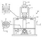
본 발명의 일 실시예에 따라 스캐터로미터 등의 계측 장치(MT)가 도 4에 도시되어 있다. 이는 기판(6) 상에 방사선을 투영하는 광대역(백색광) 방사선 투영기(2)를 포함한다. 반사 또는 산란 방사선은 정반사된 방사선의 스펙트럼(10)(즉, 파장의 함수로서의 세기의 측정)을 측정하는 분광계 검출기(4)로 전달된다. 이 데이터로부터, 검출된 스펙트럼을 발생시키는 구조체 또는 프로파일이 프로세서(PU)에 의해 재구성될 수 있으며, 이는 예를 들어, 정밀 결합파 분석 및 비선형 회귀 분석에 의해 또는 도 4의 하단에 표시된 바와 같은 시뮬레이션된 스펙트럼 라이브러리와의 비교를 통해 이루어진다. 일반적으로, 이러한 재구성을 위해, 구조체의 일반적인 형태가 알려져 있으며, 일부 파라미터는 구조체가 만들어진 프로세스에 대한 지식으로부터 추정되고, 산란계측 데이터로부터 결정되어야 하는 구조체의 몇 가지 파라미터만이 남게 된다. 이러한 스캐터로미터는 수직 입사 스캐터로미터 또는 경사 입사 스캐터로미터로 구성될 수 있다.A measuring device MT such as a scatterometer according to an embodiment of the present invention is illustrated in FIG. 4. It comprises a broadband (white light)
본 발명의 더 나은 이해를 위해, 비교 예에 따른 계측 장치가 도 5를 참조로 하여 이하에서 설명된다.For a better understanding of the present invention, a measuring device according to a comparative example is described below with reference to FIG. 5.
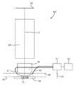
도 5(a)는 비교 예에 따른 계측 장치, 보다 구체적으로 암시야 스캐터로미터를 나타낸다. 타겟(TT)과 이러한 타겟을 조명하는 데 사용되는 측정 방사선의 회절된 광선이 도 5(b)에 보다 상세히 예시되어 있다. 도시된 계측 장치는 암시야 계측 장치로서 알려진 유형이다. 이러한 계측 장치는 독립형 디바이스이어도 되고, 또는 예컨대 측정 스테이션에서 리소그래피 장치(LA)에 또는 리소그래피 셀(LC)에 통합될 수도 있다. 장치 도처에서 여러 개의 브랜치를 갖는 광축은 점선 O로 표시되어 있다. 이러한 장치에서, 광원(11)(예를 들어, 크세논 램프)에 의해 방출된 광은 빔 스플리터(15)를 통해 렌즈(12, 14) 및 대물 렌즈(16)를 포함하는 광학 시스템에 의해 기판(W) 상으로 지향된다. 이들 렌즈는 4F 배열의 이중 시퀀스로 배치된다. 기판 이미지를 여전히 검출기 상에 제공하고 동시에 공간 주파수 필터링을 위해 중간 퓨필 평면에 대한 액세스를 허용한다면, 상이한 렌즈 배열이 사용될 수 있다. 따라서, 방사선이 기판 상에 입사하는 각도 범위는, 여기에서 (공액) 퓨필 평면으로 지칭되는, 기판 평면의 공간 스펙트럼을 제공하는 평면에서의 공간 세기 분포를 규정함으로써 선택될 수 있다. 특히, 이것은 대물 렌즈 퓨필 평면의 역-투영 이미지(back-projected image)인 평면에서, 렌즈(12)와 렌즈(14) 사이에 적합한 형태의 개구 플레이트(13)를 삽입함으로써 행해질 수 있다. 예시된 실시예에서, 개구 플레이트(13)는 상이한 조명 모드가 선택될 수 있도록 13N 및 13S로 표시된 상이한 형태를 갖는다. 본 예에서의 조명 시스템은 축외 조명 모드를 형성한다. 제1 조명 모드에서, 개구 플레이트(13N)는, 단지 설명을 목적으로 "북쪽"으로 지정된 방향으로부터 축외 조명을 제공한다. 제2 조명 모드에서, 개구 플레이트(13S)는 유사한 조명을 제공하지만 "남쪽"으로 표시된 반대 방향으로부터 조명을 제공하기 위해 이용된다. 상이한 개구를 사용함으로써 다른 조명 모드도 가능하다. 요구되는 조명 모드 밖의 임의의 불필요한 광은 요구되는 측정 신호와 간섭할 것이기 때문에 퓨필 평면의 나머지는 어두운 것이 바람직하다.5(a) shows a measuring device according to a comparative example, more specifically a dark field scatterometer. The target TT and the diffracted rays of measurement radiation used to illuminate this target are illustrated in more detail in Fig. 5(b). The illustrated metrology device is of the type known as a dark field metrology device. This metrology apparatus may be a standalone device or may be integrated into the lithographic apparatus LA or in the lithographic cell LC, for example at a measurement station. The optical axis with multiple branches throughout the device is indicated by the dotted line O. In such a device, the light emitted by the light source 11 (e.g., a xenon lamp) is transmitted through a
도 5(b)에 도시된 바와 같이, 타겟(TT)은 기판(W)이 대물 렌즈(16)의 광축(O)에 수직인 상태로 배치된다. 기판(W)은 지지체(미도시)에 의해 지지될 수 있다. 축(O)에서 벗어난 각도로 타겟(TT) 상에 충돌하는 측정 방사선 광선(I)은 하나의 0차 광선(실선 0) 및 2개의 1차 광선(일점쇄선 +1과 이점쇄선 -1)을 발생시킨다. 오버필된 소형 타겟을 이용하는 경우, 이들 광선은 계측 타겟(TT) 및 기타 피처를 포함한 기판의 영역을 커버하는 다수의 평행 광선 중의 단지 하나가 된다는 점을 기억해야 한다. 플레이트(13)의 개구가 (유용한 광량을 허용하는데 필요한) 한정된 폭을 가지므로, 입사 광선(I)은 실제로는 일정 범위의 각도를 점유할 것이고, 회절 광선 0차와 +1/-1차가 다소 확산될(spread out) 것이다. 소형 타겟의 포인트 확산 함수에 따라, 각각의 차수 +1과 -1은 도시된 바와 같이 단일의 이상적인 광선이 아니라 일정 범위의 각도에 걸쳐 추가로 확산될 것이다. 타겟의 격자 피치 및 조명 각도는 대물 렌즈에 진입하는 1차 광선이 중앙의 광축과 근접하게 정렬되도록 설계되거나 조정될 수 있다는 것에 주목해야 한다. 도 5(a) 및 5(b)에 예시된 광선은 순전히 이들이 도면에서 보다 용이하게 구별될 수 있도록 하기 위해 다소 축에서 벗어난 것으로 도시되어 있다.As shown in FIG. 5B, the target TT is disposed in a state in which the substrate W is perpendicular to the optical axis O of the
기판(W) 상의 타겟(TT)에 의해 회절된 적어도 0차와 +1차 회절 광선은 대물 렌즈(16)에 의해 집광되고, 빔 스플리터(15)를 통해 역으로 지향된다. 도 5(a)로 돌아가서, 제1 조명 모드와 제2 조명 모드 둘 모두가 북쪽(N)과 남쪽(S)으로 표시된 정반대 측의 개구를 지정하는 것으로 예시되어 있다. 측정 방사선의 입사 광선(I)이 광축의 북쪽 측으로부터 기인한 것인 경우, 즉 제1 조명 모드가 개구 플레이트(13N)를 이용하여 적용된 경우에는, +1차 회절 광선(+1(N)으로 표시됨)이 대물 렌즈(16)에 진입한다. 반대로, 제2 조명 모드가 개구 플레이트(13S)를 이용하여 적용된 경우에는, -1차 회절 광선(1(S)로 표시됨)이 렌즈(16)에 진입하는 광선이 된다.At least the 0th and +1st order diffracted rays diffracted by the target TT on the substrate W are condensed by the
제2의 빔 스플리터(17)는 회절 빔을 2개의 측정 브랜치로 분할한다. 제1 측정 브랜치에서, 광학 시스템(18)은 0차 및 1차 회절 빔을 이용하여 제1 센서(19)(예컨대, CCD 또는 CMOS 센서) 상에 타겟의 회절 스펙트럼(퓨필 평면 이미지)을 형성한다. 각각의 회절 차수는 센서 상의 상이한 포인트에 충돌하며, 이로써 이미지 처리가 차수를 비교하고 대비(contrast)할 수 있게 된다. 센서(19)에 의해 캡쳐된 퓨필 평면 이미지는 계측 장치를 포커싱하거나 및/또는 1차 빔의 세기 측정치를 정규화하기 위해 이용될 수 있다. 퓨필 평면 이미지는 또한 재구성과 같은 수많은 측정 목적을 위해 사용될 수 있다.The
제2 측정 브랜치에서, 광학 시스템(20, 22)은 센서(23)(예컨대, CCD 또는 CMOS 센서) 상에 타겟(TT)의 이미지를 형성한다. 제2 측정 브랜치에서, 퓨필 평면에 공액 관계를 이루는 평면에 구경 조리개(21)가 제공된다. 구경 조리개(21)는 센서(23) 상에 형성된 타겟의 이미지가 -1차 또는 +1차 빔으로만 형성되도록 0차 회절 빔을 차단하도록 기능한다. 센서(19, 23)에 의해 캡쳐된 이미지는 이러한 이미지를 처리하는 프로세서(PU)에 출력되며, 프로세서의 기능은 수행되는 측정의 특정한 타입에 좌우될 것이다. "이미지"라는 용어는 본 명세서에서는 넓은 의미로 사용된다는 것을 유의하기 바란다. 이와 같은 격라 라인의 이미지는 -1 및 +1 차수 중의 하나만이 제공되는 경우에는 형성되지 않을 것이다.In the second measurement branch, the
도 5에 도시된 개구 플레이트(13) 및 시야 조리개(21)의 구체적인 형태는 단지 예에 불과하다. 본 발명의 또 다른 실시예에서는, 타겟의 축상 조명이 사용되고, 실질적으로 단지 하나의 1차 회절 광만을 센서에 전달하기 위하여 축외 개구를 갖는 구경 조리개가 사용된다. 또 다른 실시예에서, 1차 빔 대신 또는 1차 빔에 추가하여 2차, 3차 및 더 높은 차수의 빔(도 3에 도시되지 않음)이 측정에 사용될 수 있다.The specific shapes of the
측정 방사선을 이들 상이한 타입의 측정에 적합화시키기 위해, 개구 플레이트(13)는 원하는 패턴을 제 위치에 놓이게 하도록 회전하는 디스크 둘레에 형성된 다수의 개구 패턴을 포함할 수 있다. 개구 플레이트(13N 또는 13S)는 하나의 방향(설정에 따라 X 또는 Y)으로 배향된 격자를 측정하는 데에만 사용될 수 있다는 것을 유의해야 한다. 직교 격자의 측정을 위해, 90 ° 및 270 °만큼 타겟의 회전이 구현될 수 있다. 상이한 개구 플레이트가 도 4(c) 및 4(d)에 도시되어 있다. 이를 이용하는 것과 장치의 수많은 기타 변형예 및 응용예가 위에서 언급한 종래의 특허 문헌에 기술되어 있다.In order to adapt the measurement radiation to these different types of measurements, the
측정 방사선의 광선은 광원(11)에 의해 방출되는 빛에 의해 제공된다. 이러한 광은 빔 스플리터(15) 및 기판(W)으로부터 회절된 방사선을 집광하는 대물 렌즈(16)를 통해 기판(W) 상으로 지향된다.The beam of measurement radiation is provided by light emitted by the
타겟(TT)은 제1 방향(예를 들어, X 방향)으로의 라인들의 2개의 격자 및 제1 방향에 직교하는 제2 방향(예를 들어, Y 방향)으로의 라인들의 2개의 격자를 포함할 수 있다. 대물 렌즈(16)는 격자로부터 회절된 방사선을 집광하기 위해 높은 개구 수(NA), 예를 들어 약 0.95의 개구수를 가질 필요가 있다. 도 5에 도시된 바와 같이, 대물 렌즈(16)와 센서(19, 23) 사이에는 많은 광학 요소가 필요하다.The target TT includes two gratings of lines in a first direction (eg, X direction) and two gratings of lines in a second direction (eg, Y direction) orthogonal to the first direction. can do. The
더 높은 세기의 조명을 가질 수 있고/있거나 더 신속한 측정을 수행할 수 있는 계측 장치를 갖는 것이 바람직할 것이다. 검출 렌즈(예를 들어, 도 5의 계측 장치에서 대물 렌즈(16))의 개구수에 대한 요구 사항이 더 낮은 계측 장치를 갖는 것이 바람직할 것이다. 검출 광학기가 단순화된 계측 장치를 갖는 것이 바람직할 것이다.It would be desirable to have a metrology device capable of having higher intensity illumination and/or performing faster measurements. It would be desirable to have a metrology device with a lower requirement on the numerical aperture of the detection lens (eg,
도 6은 본 발명의 일 실시예에 따른 계측 장치(MT)를 개략적으로 나타낸다. 계측 장치(MT)는 기판(W) 상의 구조체의 관심 파라미터를 결정하기 위한 것이다. 구조체는 계측 타겟(TT)이다.6 schematically shows a measuring device MT according to an embodiment of the present invention. The measuring device MT is for determining a parameter of interest of the structure on the substrate W. The structure is a metrology target (TT).
일 실시예에서, 계측 장치(MT)는 방사선 소스(32)를 포함한다. 방사선 소스(32)는 조명 방사선을 생성하기 위한 것이다. 예를 들면, 일 실시예에서 방사선 소스(32)는 백색 광 레이저와 같은 레이저이다. 방사선 소스(32)는 조명 방사선을 전달하기 위한 적어도 하나의 광결정 섬유를 포함할 수 있다. 그러나, 방사선 소스(32)가 백색광 레이저일 필요는 없다. 다른 유형의 레이저 또는 비-레이저 소스가 방사선 소스(32)로서 사용될 수 있다.In one embodiment, the metrology device MT comprises a
도 6에 도시된 바와 같이, 일 실시예에서 계측 장치(MT)는 적어도 2개의 조명 브랜치(51, 52)를 포함한다. 적어도 2개의 조명 브랜치(51, 52)는 기판(W) 상의 타겟(TT)을 조명하기 위한 것이다. 조명 브랜치(51, 52)는 예를 들어 도 6에 도시된 바와 같이 서로 상이한 각도로부터 타겟(TT)을 조명하도록 구성된다. 조명 브랜치의 수는 2개로 제한되지 않는다. 예를 들어, 3개, 4개 또는 그 이상의 조명 브랜치가 있을 수 있다.As shown in FIG. 6, in one embodiment, the measurement device MT includes at least two
조명 브랜치(51, 52)는 조명 방사선이 타겟(TT)에 도달하기 위한 상이한 광학 경로를 나타낸다. 조명 브랜치(51, 52)를 통해 전달되는 조명 방사선은 방사선 소스(32)에 의해 제공된다. 조명 브랜치(51, 52)는 방사선 소스(32)로부터의 조명 방사선이 타겟(TT)으로 지향되도록 하기 위한 대안적인 방법이다.The
도 6에 도시된 바와 같이, 일 실시예에서 계측 장치(MT)는 방사선 스위치(27)를 포함한다. 방사선 스위치(27)는 스위칭 요소이다. 방사선 스위치(27)는 방사선 소스(32)로부터 조명 방사선을 수광하도록 구성된다. 방사선 스위치(27)는 방사선의 적어도 일부를 적어도 2개의 조명 브랜치(51, 52) 중 선택가능한 하나에 전달하도록 구성된다.As shown in FIG. 6, the measuring device MT includes a
예를 들어, 방사선 스위치(27)는 서로 다른 작동 모드 사이에서 스위칭될 수 있다. 제1 모드에서, 방사선 스위치(27)는 조명 방사선을 수광하고 방사선의 적어도 일부를 제1 조명 브랜치(51)로 전달하도록 구성된다. 제2 모드에서, 방사선 스위치(27)는 조명 방사선을 수광하고 방사선의 적어도 일부를 제2 조명 브랜치(52)로 전달하도록 구성된다. 제1 모드는 제1 조명 브랜치(51)가 선택되는 경우에 대응한다. 제2 모드는 제2 조명 브랜치(52)가 선택되는 경우에 대응한다. 도 6에 도시된 바와 같이, 일 실시예에서 방사선 스위치는 모드를 선택하는 데 사용될 수 있는 제어 신호(57)를 수신하도록 구성된다.For example, the
일 실시예에서, 타겟(TT)은 적어도 2개의 조명 브랜치(51, 52)에 의해 서로 상이한 각도로부터 순차적으로 조명된다. 제1 기간에서, 타겟(TT)은 제1 조명 브랜치(51)로부터의 조명 방사선에 의해 조명된다. (제1 기간에 이어지는) 제2 기간에서 타겟(TT)은 제2 조명 브랜치(52)로부터의 조명 방사선에 의해 조명된다. 일 실시예에서, 제1 기간은 제2 기간과 중첩되지 않는다. 일 실시예에서, 제2 기간은 실질적으로 어떠한 갭도 없이 실질적으로 제1 기간 직후에 뒤따른다.In one embodiment, the target TT is sequentially illuminated from different angles from each other by at least two
일 실시예에서, 2개의 조명 브랜치(51, 52)는 상보적인 각도들에 대응한다. 예를 들어, 제1 조명 브랜치(51)가 제1 각도로부터 타겟(TT)을 조명하는 경우, 제2 조명 브랜치(52)는 타겟(TT)에 대한 법선 방향으로 볼 때(즉, 도 9에 도시된 평면도) 제1 각도로부터 180 °의 상보적인 각도로부터 타겟(TT)을 조명한다. 특히, 일 실시예에서, 제1 조명 브랜치(51)는 (단일 배향, 예를 들어 X 배향으로) 타겟(TT)으로부터 암시야 측정을 수행하기 위한 것이며, 검출 렌즈(16)에 의해 제1 회절 차수가 집광된다. 제2 조명 브랜치(52)는 동일한 배향으로 동일한 타겟(TT)로부터 암시야 측정을 수행하기 위한 것이지만, 상보적 회절 차수가 검출 렌즈(16)에 의해 집광된다.In one embodiment, the two
도 9를 참조하면, 일 실시예에서 상이한 조명 브랜치(51, 53)는 타겟(TT)의 상이한 격자의 관심 특성을 결정하기 위한 것이다. 예를 들어, 제1 조명 브랜치(51)는 X 방향으로의 격자로부터 회절된 방사선을 측정하기 위한 것일 수 있다. 또 다른 조명 브랜치(53)는 Y 방향으로의 격자로부터 회절된 방사선을 측정하기 위한 것일 수 있다.Referring to FIG. 9, in one embodiment
본 발명에 따르면, 정규 및 상보적인 각도들로부터의 측정이 순차적으로 이루어질 수 있다. 추가적으로 또는 대안적으로, 서로 상이한 방향으로의 격자에 대한 측정이 순차적으로 이루어질 수 있다. 다시 말해서, 이들 상이한 측정을 위한 회절 방사선이 검출 렌즈(16)에 의해 동시에 집광될 필요가 없다. 대신, 검출 렌즈(16)는 한 번에 이들 측정 중 단지 하나만을 위해 방사선을 집광할 수 있다.According to the invention, measurements from normal and complementary angles can be made sequentially. Additionally or alternatively, measurements of the gratings in different directions can be made sequentially. In other words, the diffracted radiation for these different measurements need not be condensed simultaneously by the
본 발명의 실시예는 검출 렌즈(16)에 대해 더 낮은 NA를 갖는 계측 장치(MT)를 달성할 것으로 예상된다. 일 실시예에서, 검출 렌즈(16)는 NA가 0.9 이하, 선택적으로 0.8 이하, 선택적으로 0.7 이하, 선택적으로 0.6 이하, 선택적으로 0.5 이하 및 선택적으로 0.4 이하이다. 검출 렌즈(16)는 계측 장치(MT)의 검출 브랜치의 일부이다. 검출 렌즈(16)는 산란/반사된 방사선의 일부를 집광하고 이를 센서(19)를 향하는 방향으로 전달하도록 구성된다. 본 발명의 실시예는 계측 장치(MT)의 검출 렌즈(16)에 대해 더 높은 레벨의 설계상 자유를 제공할 것으로 예상된다. 예를 들어, 제조하기에 더 간단하거나 저렴한 렌즈가 사용될 수 있다.Embodiments of the present invention are expected to achieve a metrology device MT with a lower NA for the
전술한 바와 같이, 방사선 스위치(27)가 제공되어 방사선을 조명 브랜치(51, 52)로 차례로 전달한다. 일 실시예에서 방사 스위치(27)는 1ms 미만으로 조명 브랜치 사이를 스위칭하도록 구성된다. 방사선 스위치(27)에 의해 제공되는 신속한 스위칭으로 인해 제한된 기간 내에 측정이 순차적으로 이루어질 수 있다. 본 발명의 일 실시예는 타겟(TT)의 X 방향 및 Y 방향의 격자에 대한 정규 및 상보적인 모드의 고속 순차 측정을 가능하게 할 것으로 예상된다.As described above, a
일 실시예에서, 방사 스위치(27)는 공간 광 변조기를 포함한다. 공간 광 변조기는 방사선 소스(32)로부터 조명 방사선을 수광하도록 구성된다. 공간 광 변조기는 조명 방사선에 공간적으로 변화하는 변조를 적용하도록 구성된다. 일 실시예로서, 공간 광 변조기는 마이크로미러 디바이스를 포함한다. 마이크로미러 디바이스는 복수의 미시적으로 작은 거울을 포함한다. 이러한 거울은 미세 전자 기계 시스템이다. 미러의 배향은 미러 어레이 주변의 두 전극 사이에 전압을 인가함으로써 제어된다. 미러의 배향은, 조명 방사선을 적어도 2개의 조명 브랜치(51, 52) 중 선택가능한 하나에 전달하도록 제어될 수 있다. 일 실시예에서, 공간 광 변조기는 공간 광 변조기 상의 이미지가 전자적으로 생성되고 변화되도록 전기적으로 어드레싱된다. 대안적인 실시예에서, 공간 광 변조기 전면 또는 후면 상에 이미지로 인코딩된 광을 비춤으로써 공간 광 변조기 상의 이미지가 생성 및 변화되도록 공간 광 변조기는 광학적으로 어드레싱된다.In one embodiment, the
공간 광 변조기는 낮은 손실로 조명 방사선을 조명 브랜치(51, 52)로 전달한다. 본 발명의 일 실시예는 타겟(TT)의 고휘도 조명을 달성할 것으로 예상된다. 다양한 파장의 방사선을 이용하여 타겟(TT)의 측정을 수행하는 것이 바람직할 수 있다. 공간 광 변조기는 광범위한 파장에 걸쳐 조명 방사선을 전달할 수 있다.The spatial light modulator delivers the illumination radiation to the
전술한 바와 같이, 타겟(TT)은 (상이한 조명 브랜치(51, 52)를 이용함으로써) 상이한 각도들로부터의 조명 방사선에 의해 순차적으로 조명될 수 있다. 상이한 각도들의 전체 세트로부터의 조명 방사선을 이용하여 측정이 수행된 후, 조명 방사선의 파장이 변화될 수 있다. 파장의 변화에 이어 상이한 각도에서의 측정이 반복될 수 있다. 상이한 각도를 이용하여 또 다른 전체 측정 세트가 변화된 파장에서 수행될 수 있다. 이들 동작은, 상이한 각도로 조명되는 상이한 파장의 방사선에 대응하는 측정 세트를 얻도록 완료될 수 있다. 공간 광 변조기는 조명 방사선의 전체 범위의 파장을 다루도록 구성될 수 있다. 일 실시예에서, 조명 방사선의 파장은 측정 절차 동안 약 10 회 변화될 수 있다.As described above, the target TT can be sequentially illuminated by illumination radiation from different angles (by using
그러나, 방사선 스위치(27)가 공간 광 변조기를 포함할 필요는 없다. 다른 형태의 방사선 스위치(27)가 사용될 수 있다. 예를 들어, 일 실시예에서 방사선 스위치(27)는 음향 광학 편향기를 포함한다. 음향 광학 편향기는 브래그 셀이라고도 불릴 수 있다. 음향 광학 편향기는 음향 파를 이용하여 조명 방사선의 주파수를 시프트시키고 회절시키기 위해 음향 광학 효과를 이용한다. 예를 들어, 일 실시예에서 음향 광학 편향기는 비선형 결정을 포함한다. 음향 광학 편향기는 전자기 신호 또는 음향 신호를 제공함으로써 재료(예컨대, 비선형 결정)의 광학적 특성을 변화시키도록 구성된다. 음향 광학 편향기가 재료의 광학적 특성을 변화시키는 방식을 제어함으로써, 조명 방사선은 적어도 2개의 조명 브랜치(51, 52) 중 선택가능한 하나로 지향될 수 있다.However, the
음향 광학 편향기에는 기계적으로 움직이는 부품의 수가 더 적다(기계적으로 움직이는 부품이 없을 수도 있음). 본 발명의 일 실시예는 긴 수명으로 조명 브랜치 선택의 높은 신뢰성을 달성할 것으로 예상된다.There are fewer mechanically moving parts in an acousto-optic deflector (there may be no mechanically moving parts). One embodiment of the present invention is expected to achieve high reliability of lighting branch selection with a long lifetime.
공간 광 변조기나 음향 광학 편향기 모두 본 발명에 필수적인 것은 아니다. 부가적으로 또는 대안적으로, 방사선 스위치(27)는 적어도 하나의 빔 스플리터 및 적어도 2개의 조명 브랜치(51, 52) 중 선택가능한 하나에 방사선의 전달을 제어하도록 구성된 복수의 셔터를 포함한다.Neither a spatial light modulator nor an acousto-optic deflector is essential to the present invention. Additionally or alternatively, the
공간 광 변조기와 음향 광학 편향기는 낮은 손실로 조명 방사선을 조명 브랜치(51, 52)로 전달할 수 있다. 특히, 조명 방사선을 서로 상이한 경로로 분할한 다음 일부 경로를 의도적으로 잘라낼(그럼으로써 해당 방사선을 잃게 됨) 필요가 없다. 대신, 실질적으로 모든 방사선이 원하는 광학 경로를 따라 지향될 수 있다.The spatial light modulator and acousto-optic deflector can deliver the illumination radiation to the
도 11은 본 발명의 일 실시예에 따른 계측 장치(MT)의 일부를 개략적으로 나타낸 것이다. 도 11에 도시된 실시예에서, 방사선 스위치(27)는 음향 광학 편향기(75)를 포함한다. 음향 광학 편향기(75)는 광을 다양한 각도로 방향 전환(즉, 편향)시키도록 구성된다. 음향 광학 편향기(75)는 광을 서로 상이한 방향으로 편향시키도록 구성된다. 반사각은 재료에서 음향 파가 여기되는 구동 주파수 및/또는 파워에 따라 달라진다. 일 실시예에서, 음향 광학 편향기(75)는 400 nm 내지 1600 nm 범위의 방사선을 편향시키도록 구성된다.11 schematically shows a part of a measurement device MT according to an embodiment of the present invention. In the embodiment shown in FIG. 11, the
일 실시예에서, 제어기는 음향 광학 편향기(75)의 재료에서 음향 파를 여기시키기 위해 구동 주파수 및/또는 파워를 제어하도록 구성된다. 음향 광학 편향기(75)가 광을 방향 전환할 수 있는 각도의 범위는 특별히 제한되지 않는다. 일 실시예에서, 음향 광학 편향기(75)는 0.5 내지 1.5˚의 각도 범위에 걸쳐 광을 편향시키도록 구성된다.In one embodiment, the controller is configured to control the drive frequency and/or power to excite acoustic waves in the material of the acousto-
도 11에 도시된 바와 같이, 일 실시예에서 방사선 스위치(27)는 초점 렌즈(76)를 포함한다. 초점 렌즈(76)는 음향 광학 편향기(75)에 의해 편향된 광을 수광하고 광을 조명 브랜치(51-54)로 지향시키도록 구성된다. 음향 광학 편향기(75)에 의해 제공되는 편향 각도 및 초점 렌즈(76)의 초점 거리는 광 빔의 충분히 큰 공간적 편향을 제공하도록 선택될 수 있다. 예를 들어, 일 실시예에서 초점 렌즈(76)는 약 60 mm의 초점 거리를 가질 수 있다. 음향 광학 편향기(75)가 1˚ 이상의 각도 범위에 걸쳐 광을 편향시키고 초점 렌즈(76)가 60mm의 초점 거리를 갖는 경우, 광 빔의 공간적 변위는 약 1mm 일 수 있다.As shown in FIG. 11, in one embodiment the
도 11에 도시된 바와 같이, 일 실시예에서 방사선 스위치(27)는 렌즈 어레이(77)를 포함한다. 렌즈 어레이는 음향 광학 편향기(75)로부터의 방사선 빔을 조명 브랜치(51-54)에 대응하는 광섬유(30)에 결합하도록 구성된다. 일 실시예에서, 렌즈 어레이(77)는 복수의 렌즈를 포함한다. 일 실시예에서, 렌즈 어레이(77)는 각 조명 브랜치(51-54)의 광섬유(30)에 대응하는 렌즈를 포함한다. 일 실시예에서, 렌즈 어레이(77)의 각 렌즈는 적어도 1mm, 선택적으로 최대 2mm의 직경을 갖는다.As shown in FIG. 11, in one embodiment the
음향 광학 편향기(75)에 의해 적용되는 편향 각도는 음향 광학 편향기(75)에서 여기되는 음향 파의 주파수 및/또는 파워를 변화시켜 제어될 수 있다. 따라서, 음향 광학 편향기(75)에 입력되는 주파수 및 파워를 변화시킴으로써, 특정 조명 브랜치(51-54)의 선택된 개별 광섬유(30)로 광을 재지향시키도록 편향 각도가 신속하게 스위칭될 수 있다. 이는 1ms 미만으로 조명 브랜치(51-54)를 스위칭하는 것을 가능하게 한다.The deflection angle applied by the acousto-
일 실시예에서, 방사선 스위치(27)는 조명 브랜치(51-54)에 적용되는 방사선의 세기를 변화시키도록 구성된다. 예를 들어, 방사선 스위치(27)는 조명 세기를 예컨대 중간 세기와 높은 세기 사이에서 변화시키도록 구성될 수 있다. 이에 대해 아래에서 보다 자세히 설명할 것이다.In one embodiment,
일 실시예에서, 음향 광학 편향기는 방사선 빔 중 얼마나 많은 부분이 대응하는 조명 브랜치(51-54)의 광섬유(30)에 결합되는지를 제어하기 위해 방사선 빔의 방향을 변화시키도록 구성된다. 조명 브랜치(51-54)에 적용된 개별 세기는 음향 광학 편향기(75)에 의해 제공되는 편향 각도를 디튜닝(detuning)함으로써 조절될 수 있다. 높은 세기의 방사선이 필요한 경우, 음향 광학 편향기(75)는 방사선 빔이 특정 조명 브랜치(51)의 광섬유(30)의 중심에 적용되도록 하는 편향 각도를 제공하도록 구성된다. 방사선 빔을 광섬유(30)의 중심으로 지향시킴으로써, 조명 세기가 최대화될 수 있다(또는 거의 최대화될 수 있다).In one embodiment, the acoustooptic deflector is configured to change the direction of the radiation beam to control how much of the radiation beam is coupled to the
더 낮은 세기의 방사선이 필요한 경우, 음향 광학 편향기(75)는 방사선 빔이 광섬유(30)의 (단면 영역에서) 중심을 벗어난 위치로 지향되도록 하는 약간 다른 편향 각도를 적용하도록 제어될 수 있다. 이는 광섬유(30)에 결합되는 방사선의 양을 감소시킨다. 이는 조명 브랜치(51)의 광섬유(30)를 통해 전달되는 방사선의 세기를 감소시킨다. 이러한 방식으로, 광섬유(30)의 팁에 형성된 스폿이 중심을 벗어나고 더 적은 광이 광섬유(30)에 결합되도록 각도를 약간 디튜닝함으로써 개별 세기를 조절할 수 있다.If a lower intensity of radiation is desired, the
이러한 방식으로, 서로 다른 조명 브랜치(51-54)를 따라 전달되는 빔의 작은 세기 불균형이 조절되고 보정될 수 있다. 예를 들어, 에너지 센서(55)가 조명 브랜치(51-54) 사이의 세기 불균형을 표시하는 경우, 음향 광학 편향기(75)는 편향을 변화시키도록 제어될 수 있다. 이는 세기 불균형을 보상하고 조명 브랜치(51-54)에 걸친 세기의 일관성을 높일 수 있다.In this way, small intensity imbalances of beams transmitted along different illumination branches 51-54 can be adjusted and corrected. For example, if the
조명 세기를 변화시키기 위해 음향 광학 편향기(75)를 이용하는 것은 도 8에 도시된 전술한 실시예의 특징들과 조합될 수 있다는 점에 유의해야 한다. 조명 세기를 변화시키기 위해 음향 광학 편향기(75)를 이용하는 것은 또한 도 8에 도시된 다른 특징들과 독립적으로 사용될 수 있다.It should be noted that using the
도 10은 본 발명의 일 실시예에 따른 계측 장치(MT)의 일부를 개략적으로 나타낸 것이다. 도 10에 도시된 실시예에서, 방사선 스위치(27)는 적어도 하나의 포켈스 셀(70)을 포함한다. 포켈스 셀(70)은 방사선 빔의 편광 방향을 제어하도록 구성된 전기 광학 컴포넌트이다. 포켈스 셀은 전기장에 의해 유도되는 광학 매질 내의 복굴절을 생성하도록 구성된다. 복굴절은 전기장에 따라 달라진다. 전압이 포켈스 셀(70)의 결정에 인가되면 복굴절의 양이 변화한다. 특히 복굴절의 양은 인가된 전압에 따라 선형적으로 변화할 수 있다. 포켈스 셀(70)은 가변 지연기로 기능한다.10 schematically shows a part of a measurement device MT according to an embodiment of the present invention. In the embodiment shown in FIG. 10, the
포켈스 셀(70)에 인가되는 전압은 포켈스 셀(70)이 가변 지연을 적용하도록 제어된다. 가변 지연기는 포켈스 셀(70)에 입력되는 방사선의 편광 방향에 영향을 미친다. 방사선의 편광 방향을 제어함으로써, 방사선은 아래에서 더 상세히 설명되는 바와 같이 상이한 조명 브랜치(51-54)로 지향될 수 있다.The voltage applied to the
도 10에 도시된 바와 같이, 일 실시예에서 계측 장치(MT)는 방사선 소스(32)로부터 방사선을 수광하도록 구성된 빔 스플리터(61)를 포함한다. 빔 스플리터(61)는 2개의 상이한 브랜치를 따라 방사선을 지향시키도록 구성된다. 이러한 빔 스플리터(61)의 제공은 필수적인 것은 아니다. 대안적인 실시예에서, 방사선은 도 10에 도시된 2개의 브랜치 중 하나를 따라(즉, 단지 하나의 포켈스 셀(70)을 이용) 방사선 소스(32)로부터 지향된다. 나머지 브랜치(나머지 포켈스 셀(70)을 이용)는 선택 사항이다. As shown in FIG. 10, in one embodiment the metrology device MT includes a
일 실시예로서, 파장 선택기(33)는 음향 광학 튜닝가능 필터(36)에서 여기된 음향 파의 주파수 및/또는 파워에 기초하여 선택된 파장 범위의 조명 방사선을 투과시키도록 구성된 음향 광학 튜닝가능 필터(36)를 포함한다. 특히 도 10에 도시된 바와 같이, 일 실시예에서 계측 장치(MT)는 적어도 2개의 음향 광학 튜닝가능 필터(36)를 포함한다. 음향 광학 튜닝가능 필터(36)는 파장 선택기(33)의 일부를 형성할 수 있다. 음향 광학 튜닝가능 필터(36)는 음향 광학 튜닝가능 필터(36)에 의해 투과되는 방사선의 파장을 선택하도록 구성된다. 일 실시예에서, 음향 광학 튜닝가능 필터(36)는 약 3nm의 대역폭을 갖는다.In one embodiment, the
음향 광학 튜닝가능 필터(36)는 방사선을 선형으로 편광시키도록 구성된다. 음향 광학 튜닝가능 필터(36)에 의해 출력되는 방사선은 선형 편광된다. 선형 편광된 방사선은 음향 광학 튜닝가능 필터(36)의 하류에 있는 포켈스 셀(70)로 입력된다.The acousto-optic tunable filter 36 is configured to linearly polarize the radiation. The radiation output by the acoustooptic tunable filter 36 is linearly polarized. Linearly polarized radiation enters the
위에서 언급한 바와 같이 포켈스 셀은 가변 지연기로 기능한다. 포켈스 셀(70)은, 지연기의 "빠른" 축 및 "느린" 축이 포켈스 셀(70)에 의해 수광된 선형 편광 방사선의 편광 평면에 대해 45°로 배열되도록 구성된다. 포켈스 셀(70)에 인가된 전압이 지연기가 0 °에 있게 되도록 구성될 때, 방사선의 편광은 포켈스 셀(70)에 의해 변하지 않는다. 그러나, 포켈스 셀(70)에 인가된 전압이 지연기가 180 °에 있게 되도록 제어될 때, 방사선의 편광 방향은 90 °만큼 회전된다. 포켈스 셀(70)에 인가된 전압은 1ms 미만으로 변화될 수 있어, 편광 방향의 스위칭은 1ms 미만으로 이루어질 수 있다.As mentioned above, the Pockels cell functions as a variable delay. The
180°의 지연을 제공하기 위해 포켈스 셀(70)에 인가되어야 하는 전압은 방사선의 파장에 따라 달라진다. 따라서 방사선의 파장은, 포켈스 셀(70)에 의해 출력되는 방사선의 편광 방향을 제어하기 위해 포켈스 셀(70)에 인가되는 전압을 제어하는 제어기의 입력이다.The voltage that must be applied to the
도 10에 도시된 바와 같이, 일 실시예에서 방사선 스위치(27)는 포켈스 셀(70)의 광학적으로 하류에 편광 빔 스플리터(71)를 포함한다. 편광 빔 스플리터(71)는 포켈스 셀(70)에 의해 제어되는 편광 방향에 따라 방사선 빔을 투과 또는 반사시키도록 구성된다. 포켈스 셀(70)에 의해 출력되는 방사선은 편광 빔 스플리터(71)로 진입한다. 방사선의 선택된 편광 방향에 따라, 방사선은 편광 빔 스플리터(71)에 의해 투과되거나 반사된다. 도 10에 도시된 바와 같이, 일 실시예에서 방사선 스위치(27)는 반파장 지연기(72)를 포함한다. 반파장 지연기(72)는 방사선의 편광 방향을 역으로 회전시키도록 구성된다.As shown in FIG. 10, in one embodiment the
편광 빔 스플리터(71)에 의해 투과된 방사선 빔과 편광 빔 스플리터(71)에 의해 반사된 다음 반파장 지연기(72)에 의해 투과된 방사선 빔은 모두 동일한 편광 방향을 갖게 된다. 이러한 2개의 빔은 2개의 상이한 조명 브랜치(51, 52)에 대응한다. 따라서, 방사선 스위치(27)는 포켈스 셀(70)에 인가된 전압을 제어함으로써 어떤 조명 브랜치(51, 52)가 사용되는지를 제어하도록 구성된다.The radiation beam transmitted by the
일 실시예로서, 계측 장치(MT)는 적어도 2개의 음향 광학 튜닝가능 필터(36-37)를 포함하되, 적어도 하나는 방사선 스위치(27)의 상류에 배열되고 적어도 하나는 방사선 스위치(27)의 하류에 배열된다. 특히 도 10에 도시된 바와 같이, 일 실시예에서 각각의 조명 브랜치(51-54)에는 추가적인 음향 광학 튜닝가능 필터(37)가 구비된다. 이러한 추가 음향 광학 튜닝가능 필터(37)는 대응하는 조명 브랜치(51-54)에 대해 빔을 스위치 온 및 스위치 오프하도록 구성된다.In one embodiment, the metrology device MT comprises at least two acoustooptic tunable filters 36-37, at least one arranged upstream of the
일 실시예에서, 이러한 추가 음향 광학 튜닝가능 필터(37)는 음향 광학 튜닝가능 필터(36)에 비해 더 큰 대역폭을 갖는다. 방사선이 2개의 음향 광학 튜닝가능 필터(36, 37)를 통과하도록 요구함으로써, 원치 않는 파장의 방사선을 보다 확실하게 배척할 수 있다. 이러한 음향 광학 튜닝가능 필터(37)에 의해 제공되는 스위치는 본 발명의 다른 실시예에 적용될 수 있다.In one embodiment, this additional acousto-optic
도 10에 도시된 바와 같이, 각각 포켈스 셀(70)을 갖는 2개의 브랜치가 있어 전체적으로 조명 브랜치(51-54)를 제공할 수 있다. 대안적으로, 단지 2개의 조명 브랜치(51, 52)가 요구된다면 단지 하나의 브랜치가 필요할 수도 있다.As shown in FIG. 10, since there are two branches each having a
일 실시예에서, 방사선 소스(32)의 바로 하류에 있는 빔 스플리터(61)는 편광 빔 스플리터이다. 이에 의해, 대응하는 음향 광학 튜닝가능 필터(36)를 통한 투과를 위해 최적의 편광을 갖는 2개의 빔을 생성하는 것이 가능해진다. 이것은 음향 광학 튜닝가능 필터(36)에서 손실될 에너지의 양을 감소시킨다.In one embodiment, the
일 실시예에서, 광원(32)은 초연속체 광원이다.In one embodiment,
포켈스 셀(70)과 음향 광학 튜닝가능 필터(36-37)는 도 8에 도시된 전술한 실시예의 특징들과 조합될 수 있다는 점에 유의해야 한다. 포켈스 셀(70)과 음향 광학 튜닝가능 필터(36-37)는 또한 도 8에 도시된 다른 특징들과 독립적으로 사용될 수 있다.It should be noted that the
일 실시예에서, 계측 장치(MT)는 검출 렌즈(16)를 포함한다. 이러한 렌즈는 구조체(즉, 타겟(TT))로부터 회절된 방사선의 적어도 일부를 집광하기 위한 것이다. 일 실시예에서, 렌즈는 도 5의 계측 장치와 관련하여 전술한 대물 렌즈(16)와 유사하다. 이하의 설명에서 렌즈는 대물 렌즈로 설명된다. 그러나 렌즈가 대물 렌즈일 필요는 없다. 대안으로, 렌즈는 단일 렌즈일 수 있다. 렌즈는 싱글릿(singlet), 예를 들어 평면-비구면(plano-asphere) 또는 이중-비구면(bi-asphere)일 수 있다. 렌즈는 자유 형태 곡률을 갖는 임의의 표면 또는 프레넬 렌즈일 수 있다. 렌즈는 굴절률에 구배를 갖는 재료를 포함할 수 있다.In one embodiment, the metrology device MT includes a
일 실시예에서, 계측 장치(MT)는 이미지 센서(19)를 포함한다. 센서(19)는 집광된 회절 방사선의 기록을 획득하기 위한 것이다. 센서(19)는 도 6에 도시된 계측 장치와 관련하여 전술한 센서(19)와 유사할 수 있다.In one embodiment, the measurement device MT includes an
일 실시예에서, 계측 장치(MT)는 광학기(24)를 포함한다. 광학기(24)는 집광된 회절 방사선을 센서(19)로 전송하기 위한 것이다. 광학기(24)는 렌즈, 빔 스플리터 및 광학 마스크와 같은 하나 이상의 광학 요소를 포함할 수 있다.In one embodiment, the metrology device MT includes
일 실시예에서, 조명 브랜치(51, 52)는 타겟(TT)을 조명하기 위한 적어도 하나의 광섬유를 포함한다. 도 6에 도시된 바와 같이, 일 실시예에서 적어도 하나의 광섬유는 타겟(TT)을 직접 조명하기 위한 것이다. 다시 말해서, 광섬유의 단부와 타겟(TT) 사이에 어떠한 광학기도 필요하지 않다. 이는 타겟(TT)으로 지향되는 조명 방사선의 코히어런스를 유지하는 데 도움이 된다.In one embodiment, the
도 5에 도시된 계측 장치의 비교 예에서, 타겟(TT)은 광원(11)에 의해 방출되고 대물 렌즈(16)를 포함하는 다양한 광학 요소를 통해 전송되는 방사선에 의해 조명된다. 본 발명의 계측 장치(MT)의 일 실시예는 타겟(TT)이 광섬유에 의해 직접 조명될 수 있다는 점에서 상이하다. 다시 말해서, 조명 방사선이 광섬유로부터 방출될 때 렌즈나 빔 스플리터와 같은 추가 광학기를 통해 전송되지 않는다. 특히, 광섬유로부터 방출되는 조명 방사선은 타겟(TT)에 입사되기 전에 검출 렌즈(16)를 통과하지 않는다.In the comparative example of the metrology device shown in FIG. 5, the target TT is illuminated by radiation emitted by the
그러나 광섬유가 타겟(TT)을 직접 조명하는 것이 필수적인 것은 아니다. 일 실시예로서, 적어도 하나의 광섬유는 적어도 하나의 다른 광학 요소를 통해 간접적으로 구조체를 조명하기 위한 것이다. 예를 들어, 광섬유의 단부와 타겟(TT) 사이에 렌즈, 빔 스플리터 등과 같은 광학 요소가 제공될 수 있다.However, it is not essential that the optical fiber directly illuminates the target TT. In one embodiment, at least one optical fiber is for illuminating the structure indirectly through at least one other optical element. For example, an optical element such as a lens, a beam splitter, or the like may be provided between the end of the optical fiber and the target TT.
도 7은 타겟(TT)을 조명하는 방사선 스폿(31)의 크기를 개략적으로 도시한다. 스폿(31)의 크기는 도 6에 도시된 치수를 사용하여 추정될 수 있다. 스폿(31)의 크기(S)는 광섬유 직경(φ)이 증가함에 따라 증가한다. 스폿(31)은 폭과 길이를 갖는 타원형일 수 있다. 스폿(31)의 크기(S)는 광섬유(30)의 팁(40)과 타겟(TT) 사이의 거리(d)가 증가함에 따라 증가한다. 스폿(31)의 크기(S)는 광섬유(30)로부터 방출된 방사선 광선들의 확산을 나타내는 각도(NA)가 증가함에 따라 증가한다. 스폿(31)의 크기(S)는 타겟(TT)에 대한 법선과 광섬유로부터의 방사선의 중심 광선 사이에 규정된 방위각(θ)이 증가함에 따라 증가한다. 일 실시예에서, 모든 조명 브랜치(51, 52)는 타겟(TT)의 동일한 영역을 조명한다. 상이한 조명 브랜치(51, 52)의 스폿(31)은 서로 중첩된다. 일 실시예에서, 조명 브랜치(51, 52)는 동일한 방위각(θ)으로 타겟(TT)을 조명한다. 일 실시예에서, 조명 브랜치(51, 52)의 광섬유(30)는 동일한 직경을 갖는다.7 schematically shows the size of the
일 실시예에서, 적어도 하나의 광섬유의 팁(40)은 광축(O)에 평행한 방향으로 대물 렌즈(16)와 타겟(TT) 사이에 위치된다. 광축(O)은 검출 렌즈(16)에 의해 규정된다. 특히, 도 6에 도시된 바와 같이 팁(40)은, 기판(W)의 표면에 의해 형성된 제1 가상 평면(25)에 의해 일측에서 제한되고 제1 가상 평면에 평행하면서 기판(W)을 향하는 대물 렌즈(16)의 단부와 접하는 제2 가상 평면(26)에 의해 다른 측에서 제한되는 공간 내에 위치될 수 있다.In one embodiment, the tip 40 of the at least one optical fiber is positioned between the
이것의 일례가 도 6에 도시되어 있으며, 조명 브랜치(51, 52)의 광섬유는 검출 렌즈(16)의 단부면 밑의 위치까지 아래로 연장된다. 이것은 광섬유의 팁(40)을 타겟(TT)에 가깝게 위치시키는 데 도움이 될 수 있다. 그러나 팁(40)이 광축에 평행한 방향으로 검출 렌즈(16)와 타겟(TT) 사이에 있을 필요는 없다. 예를 들어, 팁(40)은 검출 렌즈(16)의 단부면 바로 위에 위치할 수 있지만, 그 일측에 위치할 수 있다. 이것은, 검출 렌즈(16)에 의해 집광될 수 있는 타겟(TT)으로부터의 어떠한 회절 방사선과도 팁(40)이 간섭하지 않도록 보장하면서 행해질 수 있다.An example of this is shown in Fig. 6, and the optical fibers of the
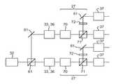
도 8은 계측 장치(MT)의 선택적인 컴포넌트들 사이의 광학적 연결을 개략적으로 도시한다. 도 8에 도시되고 위에서 기술한 바와 같이, 계측 장치(MT)는 방사선 소스(32) 및 방사선 스위치(27)를 포함한다. 도 8에 도시된 바와 같이, 일 실시예에서 계측 장치(MT)는 4개의 조명 브랜치(51-54)를 포함한다. 조명 브랜치 중 2개는 타겟(TT)의 제1 격자 세트의 관심 특성을 결정하기 위한 것이다. 조명 브랜치 중 2개는 타겟(TT)의 제2 격자 세트의 관심 특성을 결정하기 위한 것이다.8 schematically shows the optical connection between optional components of the metrology device MT. As shown in FIG. 8 and described above, the metrology device MT comprises a
도 8에 도시된 바와 같이, 일 실시예에서 계측 장치(MT)는 파장 선택기(33)를 포함한다. 파장 선택기(33)는 조명 방사선을 수광하도록 구성된다. 파장 선택기(33)는 선택된 파장 범위의 조명 방사선을 투과시키도록 구성된다. 파장 선택기(33)는 선택된 파장 범위를 벗어난 조명 방사선을 필터링하도록 구성된다. 일 실시예에서, 선택된 파장 범위는 약 5 내지 15 nm의 대역폭을 갖는다.As shown in FIG. 8, in one embodiment, the measurement device MT includes a
도 8에 도시된 바와 같이, 일 실시예에서 파장 선택기(33)는 복수의 선택기 유닛(34, 35)을 포함한다. 일 실시예에서, 파장 선택기(33)는 가시 방사선 선택기 유닛(34) 및 적외 방사선 선택기 유닛(35)을 포함한다. 가시 방사선 선택기 유닛(34)은 가시광 스펙트럼 내에서 선택된 파장 범위를 투과시키고 다른 방사선을 필터링하도록 구성된다. 적외 방사선 선택기 유닛(35)은 적외선 스펙트럼 내에서 선택된 파장 범위를 투과시키고 다른 방사선을 필터링하도록 구성된다. 방사선 스펙트럼의 다른 섹션에 대해 추가 선택기 유닛이 제공될 수 있다.As shown in FIG. 8, in one embodiment the
도 8에 도시된 바와 같이, 일 실시예에서 파장 선택기(33)는 조명 방사선을 선택기 유닛(34, 35) 사이에서 분할하기 위한 빔 스플리터(61)를 포함한다. 일 실시예에서, 파장 선택기(33)는 방사선 스위치(27)로의 입력을 위해 분할된 광 경로를 단일 광 경로로 재결합하기 위한 반사기(62)(예를 들어, 거울)를 포함한다.As shown in FIG. 8, in one embodiment the
도 8에 도시된 바와 같이, 일 실시예에서 파장 선택기(33)는 방사선 소스(32)의 광학적으로 하류에 그리고 방사선 스위치(27)의 광학적으로 상류에 위치한다. 파장 선택기(33)는 방사선 소스(32)로부터 조명 방사선을 수광한다. 파장 선택기(33)는 선택된 파장 범위의 조명 방사선을 방사선 스위치(27)로 출력한다. 대안적인 실시예에서, 파장 선택기(33)는 방사선 스위치(27)의 하류에 위치된다.As shown in FIG. 8, in one embodiment the
계측 장치(MT)가 파장 선택기(33)를 포함하는 것은 필수적인 것은 아니다. 일 실시예에서 방사선 소스(32)는 단일 파장 소스(예를 들어, 단일 파장 레이저)를 포함한다. 예를 들어, 방사선 소스(32)가 단일 파장 소스를 포함할 때 파장 선택기는 필요하지 않다. 일 실시예에서, 방사선 소스(32)는 출력이 비교적 작은 대역폭(예를 들어, 단일 파장) 내에 있고 그 작은 대역폭의 중심 파장이 선택가능한 것인 튜닝가능 단일 파장 소스이다.It is not essential that the measurement device MT includes the
도 8에 도시된 바와 같이, 일 실시예에서 계측 장치(MT)는 분광계(28)를 포함한다. 방사선 스위치(27)는 방사선의 적어도 일부를 분광계(28)로 선택가능하게 전달하도록 구성된다. 분광계(28)는 조명 방사선의 스펙트럼 성분을 측정하도록 구성된다. 예를 들어, 분광계(28)는 조명 방사선의 파장 범위 및 프로파일을 측정하도록 구성된다. 일 실시예에서, 분광계는 조명 방사선의 파장을 제어하기 위한 피드백을 제공하기 위해 방사선 소스(32) 및/또는 파장 선택기(33)에 의해 수신되는 정보를 출력한다.As shown in FIG. 8, the measurement device MT includes a
일 실시예로서, 방사선 스위치(27)는 조명 방사선의 일부를 분광계(28)로 지속적으로 전달하도록 구성된다. 이를 통해 측정에 사용되는 조명 방사선의 파장에 대한 지속적인 피드백 제어가 가능해진다. 대안적인 실시예로서, 방사선 스위치(27)는 조명 방사선의 적어도 일부를 분광계(28)에 간헐적으로 전달하도록 제어된다. 이것은 조명 방사선의 파장의 간헐적인 피드백 제어를 가능하게 한다. 조명 방사선이 분광계(28)에 전달되고 있지 않을 때, 조명 방사선의 휘도는 높게 유지된다. 피드백은 또한 연속적인 방식으로 파장 선택기(33)의 출력 중 작은 부분(예를 들어, 0.1 - 1%)을 분리해냄(split off)으로써 간헐적인 대신 연속적으로 수행될 수도 있다.In one embodiment, the
도 8에 도시된 바와 같이, 일 실시예에서 계측 장치(MT)는 빔 덤프(29)를 포함한다. 방사선 스위치(27)는 방사선의 적어도 일부를 빔 덤프(29)로 선택가능하게 전달하도록 구성된다. 빔 덤프(29)는 방사선을 흡수하도록 구성된다. 빔 덤프(29)는 방사선 소스(32)를 스위치 오프 하지 않고도 조명 브랜치(51-54)에 의해 조명 방사선이 방출되는 것을 방지하기 위해 사용될 수 있다. 빔 덤프(29)는 조명 방사선을 위한 셔터로서 작용하도록 사용될 수 있다. 하지만 계측 장치(MT)가 빔 덤프를 포함하는 것은 필수적인 것은 아니다. 단지 일례로서, 계측 장치(MT)는 빔 덤프(29)를 포함하지 않을 수 있고, 빠르게 스위치 온 및 스위치 오프될 수 있는 방사선 소스(32)를 가질 수 있다.As shown in FIG. 8, the metrology device MT includes a
도 8에 도시된 바와 같이, 일 실시예에서 계측 장치(MT)는 적어도 2개의 에너지 센서(55)를 포함한다. 특히, 일 실시예에서 각각의 조명 브랜치는 에너지 센서(55)를 포함한다. 에너지 센서(55)는 대응하는 조명 브랜치(51-54)의 광섬유(30)를 통해 전달된 방사선의 세기를 측정하도록 구성된다.As shown in FIG. 8, in one embodiment, the measurement device MT includes at least two
각각의 조명 브랜치(51-54)에는 대응하는 에너지 센서(55)가 제공된다. 에너지 센서(55)는 조명 브랜치(51-54)를 통해 전달되는 조명 방사선의 세기를 제어하는 것을 돕는다. 일 실시예에서, 에너지 센서(55)는 방사선 세기의 피드백 제어에 사용되는 정보를 출력한다. 예를 들어, 방사선 소스(32)의 파워는 에너지 센서(55)로부터 수신된 정보에 기초하여 제어될 수 있다.Each illumination branch 51-54 is provided with a
전술한 바와 같이, 일 실시예에서 2개의 조명 브랜치(51, 52)가 제1 격자(X 방향의 라인을 가짐)를 측정하기 위해 사용된다. 또 다른 2개의 조명 브랜치(53, 54)는 제2 격자(Y 방향의 라인을 가짐)를 측정하기 위해 사용된다. 에너지 센서(55)는, 동일한 격자를 측정하기 위해 두 개의 조명 브랜치(51, 52)에 의해 전달된 방사선의 세기가 두 브랜치에 대해 동일하게 되도록 하기 위해 사용될 수 있다. 제2 격자에 대해서도 2개의 브랜치에 대해 유사한 제어가 수행된다. 다른 실시예로서, 에너지 센서(55)에 의해 측정된 값이 센서(19) 상에서 측정된 세기를 정규화하는 데 사용되어 측정이 서로 더 정확하게 비교될 수 있다. 본 발명의 일 실시예는 오버레이 측정의 더 높은 정확도를 달성할 것으로 예상된다. 이는 오버레이 신호가 동일한 격자를 측정하는 2개의 브랜치 사이의 세기 차이에 매우 민감하기 때문이다.As described above, in one embodiment, two
도 8에 도시된 바와 같이, 일 실시예에서 각 조명 브랜치(51-54)는 방사선을 에너지 센서(55)를 향해 재지향시키기 위해 빔 스플리터(61)를 포함한다. 일 실시예에서, 빔 스플리터(61)는 방사선의 대부분(예를 들어, 약 99 %)을 투과시키고 에너지 센서(55)를 향해 방사선의 소수 부분(예를 들어, 약 1 %) 만을 반사시키도록 구성된다. 도 8에 도시된 바와 같이, 에너지 센서(55)는 조명 브랜치(51-54)의 광섬유(30)의 광학적으로 하류에 있다. 이것은 에너지 센서(55)가 조명 브랜치(51-54)에 의해 출력되는 방사선의 세기를 측정할 수 있게 한다. 그러나, 에너지 센서(55)는 광섬유(30)의 상류에 위치할 수 있다(다만 에너지 센서에 의해 이루어지는 측정이 광섬유(30) 내에서의 손실을 고려하지 않을 수도 있음).As shown in FIG. 8, in one embodiment each illumination branch 51-54 includes a
계측 장치(MT)가 에너지 센서(55)를 포함하는 것은 필수적인 것은 아니다. 예를 들어, 방사선 선량 센서가 타겟(TT)에서 수신되는 방사선을 측정하는 데 사용될 수 있다.It is not essential that the measurement device MT includes the
도 8에 도시된 바와 같이, 일 실시예에서 계측 장치(MT)는 적어도 2개의 편광기(56)를 포함한다. 특히, 일 실시예에서 각각의 조명 브랜치는 편광기(56)를 포함한다. 편광기(56)는 대응하는 조명 브랜치(51-54)를 통해 전달된 방사선을 편광시키도록 구성된다. 도 8에 도시된 바와 같이, 일 실시예로서 편광기(56)는 조명 브랜치(51-54)의 광섬유(30)의 광학적으로 하류에 있다. 일 실시예에서, 편광기(56)는 방사선이 타겟(TT)에 도달하기 직전에 적절한 모드로 조명 방사선을 편광시키도록 구성된다.As shown in FIG. 8, in one embodiment, the measurement device MT includes at least two
일 실시예로서, 편광기(56)는 선택가능한 편광의 투과를 허용하도록 제어가능하다. 예를 들어, 편광기의 모드는 적절한 방사선 편광을 제공하도록 스위칭될 수 있다. 대안적인 실시예에서, 편광기(56)는 이러한 방식으로 제어가능하지 않고 고정된 방사선 편광을 제공한다.In one embodiment,
도 8에 도시된 바와 같이, 일 실시예에서 계측 장치(MT)는 검출 브랜치를 포함한다. 검출 브랜치는 기판(W) 상의 구조체(TT)로부터 회절 및/또는 산란된 방사선을 집광하도록 구성된다. 도 6에 도시된 바와 같이, 일 실시예에서 검출 브랜치는 검출 렌즈(16) 및 추가 광학기(24)를 포함한다. 일 실시예에서 검출 브랜치는 센서(19)를 포함한다. 일 실시예에서 검출 브랜치는 빔 스플리터를 포함한다.As shown in FIG. 8, in one embodiment, the measurement device MT includes a detection branch. The detection branch is configured to collect the diffracted and/or scattered radiation from the structure TT on the substrate W. As shown in FIG. 6, in one embodiment the detection branch includes a
일 실시예에서, 검출 브랜치는 센서(19)에 의해 획득된 데이터를 처리하도록 구성된 프로세서를 포함한다. 일 실시예에서, 프로세서는 회절 방사선의 수차를 보정하기 위한 컴퓨테이션 이미징 알고리즘을 구현하도록 구성된다. 일 실시예에서, 검출 브랜치의 광학기(24)는 도 5에 도시된 비교 예에 비해 단순화되어 있다. 단순화된 광학기의 결과로 회절 방사선의 수차가 증가할 수도 있다. 컴퓨테이션 이미징 알고리즘은 단순화된 광학기로 인한 이러한 수차를 보정하는 데 사용된다.In one embodiment, the detection branch includes a processor configured to process data obtained by
일 실시예로서 검출 브랜치는 0차가 아닌 회절 차수 방사선을 집광하도록 구성된다. 예를 들어, 일 실시예에서 검출 브랜치(16, 24)는 +1 및 -1 회절 차수를 집광하도록 구성된다. 일 실시예에서, 검출 브랜치(16, 24)는 정반사된 방사선을 집광하도록 구성되지 않는다.In one embodiment, the detection branch is configured to condense non-zero order diffracted radiation. For example, in one embodiment the
일 실시예에서, 조명 브랜치(51-54)는 검출 브랜치(16, 24)로부터 분리된다. 조명 브랜치(51-54)는 검출 브랜치(16, 24)와 공통된 컴포넌트를 공유하지 않는다.In one embodiment, illumination branches 51-54 are separate from
도 8에 도시된 바와 같이, 일 실시예에서 계측 장치(MT)는 적어도 하나의 이미지 센서(19)를 포함한다. 이미지 센서(19)는 기판(W) 상의 구조체(TT)로부터 회절된 방사선을 검출하도록 구성된다. 도 8에 도시된 바와 같이, 일 실시예에서 계측 장치(MT)는 복수의 (예컨대, 2개의) 이미지 센서(19)를 포함한다. 이미지 센서(19)는 전체 스펙트럼 중 상이한 섹션들의 방사선을 검출하기 위한 것일 수 있다. 예를 들어, 하나의 이미지 센서가 가시 방사선을 검출하기 위한 것이고 다른 이미지 센서(19)는 적외 방사선을 검출하기 위한 것일 수 있다. 도 8에 도시된 바와 같이, 일 실시예로서, 상이한 이미지 센서(19) 사이에서 집광된 방사선을 분할하기 위해 빔 스플리터(61)가 제공된다. 그러나, 복수의 이미지 센서가 반드시 제공될 필요는 없다. 대안적인 실시예에서 단지 하나의 이미지 센서(19)가 제공된다.As shown in FIG. 8, in one embodiment, the measurement device MT includes at least one
전술한 바와 같이, 계측 장치(MT)의 다양한 컴포넌트가 제어가능하다. 예를 들어, 방사선 소스(32), 파장 선택기(33), 방사선 스위치(27) 및 편광기(56)는 서로 다른 모드 사이에서 제어될 수 있다. 일 실시예에서, 계측 장치(MT)는 이들 컴포넌트 중 하나 이상을 제어하도록 구성된 제어기(58)를 포함한다.As described above, various components of the metrology device MT are controllable. For example, the
전술한 바와 같이, 일 실시예에서 계측 장치(MT)는 방사선의 양상을 측정하기 위한 하나 이상의 컴포넌트를 포함한다. 예를 들어, 분광계(28) 및 에너지 센서(55)는 측정에 사용되고 있는 조명 방사선의 파장 프로파일 및 세기를 측정할 수 있다. 일 실시예에서, 제어기(58)는 이러한 측정 컴포넌트(예를 들어, 분광계(28) 및 에너지 센서(55))로부터 정보를 수신한다. 일 실시예에서, 제어기(58)는 수신된 정보에 기초하여 제어 신호를 생성한다. 이를 통해 측정에 사용되는 조명 방사선에 대한 피드백 제어가 가능해진다.As described above, in one embodiment metrology device MT includes one or more components for measuring aspects of radiation. For example, the
도 9는 본 발명의 일 실시예에 따라 기판(W) 상의 타겟(TT)을 조명하는 4개의 별개의 조명 브랜치(51-54)의 광섬유(30)의 평면도이다. 도 9는 타겟(TT)에 대한 법선 방향으로 본 도면이다. 법선은 검출 브랜치(16, 24)(도 6에 도시된 바와 같음)의 광축(O)에 평행할 수 있다.9 is a plan view of an
도 9에 도시된 바와 같이, 조명 브랜치(51-54)의 광섬유(30)는 타겟(TT)에 대한 법선 방향으로 볼 때 서로 반대 방향으로부터 타겟(TT)을 조명하도록 구성된다. 도 9에 도시된 예에서, 조명 브랜치(51 및 52)는 타겟(TT)의 제1 격자 세트(X 방향의 라인을 가짐)를 측정하기 위한 것이다. 조명 브랜치(53 및 54)는 제2 격자(Y 방향으로의 라인을 가짐)를 측정하기 위한 것이다. 조명 브랜치(51 및 52)는 서로 상보적인 각도로부터 타겟(TT)을 조명한다. 이것은 조명 브랜치(51, 52) 사이의 각도 β가 180 °임을 의미한다. 마찬가지로, 조명 브랜치(53, 54)는 서로 상보적인 각도(즉, 서로 반대측)로부터 타겟(TT)을 조명한다.9, the
일 실시예로서, 조명 브랜치(51-54)는 서로 균등하게 이격되어 있는 서로 상이한 각도로부터 타겟(TT)을 조명하도록 구성된다. 예를 들면 도 9에 도시된 바와 같이 인접한 조명 브랜치(예컨대, 조명 브랜치 51 및 54) 사이의 각도 α는 90 °이다. 이것은 4개의 조명 브랜치(51-54) 모두가 서로 균등하게 이격된 각도에 있음을 의미한다. 각각의 쌍의 인접한 조명 브랜치들 사이에는 90 ° 각도가 존재한다. 조명 브랜치(51, 52)는 타겟(TT)에 대한 법선 방향으로 볼 때 서로 반대 방향으로부터 타겟(TT)을 조명하도록 배열된다. 조명 브랜치(53, 54)는 타겟(TT)에 대한 법선 방향으로 볼 때 서로 반대 방향으로부터 타겟(TT)을 조명하도록 배열된다.In one embodiment, the lighting branches 51-54 are configured to illuminate the target TT from different angles that are evenly spaced from each other. For example, as shown in FIG. 9, the angle α between adjacent lighting branches (eg,
일 실시예에서, 계측 장치(MT)는 회절 기반 스캐터로미터이다.In one embodiment, the metrology device MT is a diffraction based scatterometer.
추가의 실시예는 다음의 번호가 매겨진 조항으로 제공된다:Additional embodiments are provided with the following numbered articles:
1. 기판 상의 구조체의 관심 특성을 결정하기 위한 계측 장치로서,1. As a measurement device for determining a characteristic of interest of a structure on a substrate,
조명 방사선을 생성하기 위한 방사선 소스;A radiation source for generating illumination radiation;
기판 상의 구조체를 조명하기 위한 적어도 2개의 조명 브랜치 - 조명 브랜치는 서로 상이한 각도로부터 구조체를 조명하도록 구성됨; 및At least two lighting branches for illuminating the structure on the substrate, the lighting branches configured to illuminate the structure from different angles from each other; And
조명 방사선을 수광하고 방사선의 적어도 일부를 상기 적어도 2개의 조명 브랜치 중 선택가능한 하나에 전달하도록 구성된 방사선 스위치를 포함하는, 계측 장치.And a radiation switch configured to receive illumination radiation and deliver at least a portion of the radiation to a selectable one of the at least two illumination branches.
2. 제1조항에 있어서, 상기 방사선 스위치는 공간 광 변조기를 포함하는, 계측 장치.2. The metrology device of
3. 제2조항에 있어서, 공간 광 변조기는 마이크로미러 디바이스를 포함하는, 계측 장치.3. The metrology apparatus of
4. 제1조항에 있어서, 상기 방사선 스위치는 음향 광학 편향기를 포함하는, 계측 장치.4. The metrology device of
5. 제4조항에 있어서, 상기 방사선 스위치는 상기 음향 광학 편향기로부터의 방사선 빔을 조명 브랜치에 대응하는 광섬유에 결합하도록 구성된 렌즈 어레이를 포함하는 계측 장치.5. The metrology device of
6. 제4조항에 있어서, 상기 음향 광학 편향기는 방사선 빔 중 얼마나 많은 부분이 대응하는 조명 브랜치의 광섬유에 결합되는지를 제어하기 위해 방사선 빔의 방향을 변화시키도록 구성되는 계측 장치.6. The metrology device of
7. 제4조항에 있어서, 상기 방사선 스위치는 방사선 빔의 편광 방향을 제어하도록 구성된 포켈스 셀을 포함하는 계측 장치.7. The metrology device of
8. 제7조항에 있어서, 포켈스 셀에 의해 제어되는 편광 방향에 따라 방사선 빔을 투과 또는 반사시키도록 구성된 편광 빔 스플리터를 포함하는 계측 장치.8. The metrology device of clause 7 comprising a polarizing beam splitter configured to transmit or reflect a radiation beam according to a polarization direction controlled by a Pockels cell.
9. 제1조항에 있어서, 상기 방사선 스위치는, 적어도 하나의 빔 스플리터, 및 상기 적어도 2개의 조명 브랜치 중 선택가능한 하나에 방사선의 적어도 일부의 전달을 제어하도록 구성된 복수의 셔터를 포함하는, 계측 장치.9. The metrology device of
10. 제1조항 내지 제9조항 중 어느 한 조항에 있어서, 조명 브랜치는 상기 구조체에 대한 법선 방향으로 볼 때 서로 상이한 각도로부터 상기 구조체를 조명하도록 구성되는, 계측 장치.10. The metrology device according to any one of
11. 제1조항 내지 제10조항 중 어느 한 조항에 있어서, 조명 브랜치는 서로 균등하게 이격되어 있는 서로 상이한 각도로부터 상기 구조체를 조명하도록 구성되는, 계측 장치.11. The metrology device according to any one of
12. 제1조항 내지 제11조항 중 어느 한 조항에 있어서, 조명 브랜치는 상기 구조체를 조명하기 위한 적어도 하나의 광섬유를 포함하는, 계측 장치.12. The metrology device according to any of the preceding clauses, wherein the illumination branch comprises at least one optical fiber for illuminating the structure.
13. 제12조항에 있어서, 상기 적어도 하나의 광섬유는 상기 구조체를 직접 조명하기 위한 것인 계측 장치.13. The metrology device of
14. 제12조항에 있어서, 상기 적어도 하나의 광섬유는 적어도 하나의 다른 광학 요소를 통해 간접적으로 구조체를 조명하기 위한 것인 계측 장치.14. The metrology device of
15. 제1조항 내지 제14조항 중 어느 한 조항에 있어서, 조명 방사선을 수광하고 선택된 파장 범위의 조명 방사선을 투과시키며 상기 선택된 파장 범위 밖의 조명 방사선은 필터링하도록 구성된 파장 선택기를 포함하는, 계측 장치.15. The metrology device according to any one of
16. 제15조항에 있어서, 상기 파장 선택기는 음향 광학 튜닝가능 필터에서 여기된 음향 파의 주파수 및/또는 파워에 기초하여 선택된 파장 범위의 조명 방사선을 투과시키도록 구성된 음향 광학 튜닝가능 필터를 포함하는 계측 장치.16. The method of
17. 제16조항에 있어서, 적어도 2개의 음향 광학 튜닝가능 필터를 포함하되, 적어도 하나는 상기 방사선 스위치의 상류에 배열되고 적어도 하나는 상기 방사선 스위치의 하류에 배열되는 계측 장치.17. The metrology device of
18. 제1조항 내지 제17조항 중 어느 한 조항에 있어서, 분광계를 포함하되, 상기 방사선 스위치가 방사선의 적어도 일부를 상기 분광계로 선택가능하게 전달하도록 구성되는, 계측 장치.18. The metrology device of any of clauses 1-17, comprising a spectrometer, wherein the radiation switch is configured to selectively deliver at least a portion of the radiation to the spectrometer.
19. 제1조항 내지 제18조항 중 어느 한 조항에 있어서, 빔 덤프를 포함하되, 상기 방사선 스위치가 방사선의 적어도 일부를 빔 덤프로 선택가능하게 전달하도록 구성되는, 계측 장치.19. The metrology device of any of clauses 1-18, comprising a beam dump, wherein the radiation switch is configured to selectively deliver at least a portion of the radiation to the beam dump.
20. 제1조항 내지 제21조항 중 어느 한 조항에 있어서, 적어도 4개의 조명 브랜치를 포함하는 계측 장치.20. The measuring device according to any one of
21. 제1조항 내지 제20조항 중 어느 한 조항에 있어서, 상기 구조체는 제1 방향으로의 라인들의 제1 격자 및 제1 방향에 직교하는 제2 방향으로의 라인들의 제2 격자를 포함하고,21. The structure according to any one of
상기 조명 브랜치 중 적어도 2개는 서로 상이한 각도로부터 제1 격자의 관심 특성을 결정하기 위한 것이고, 조명 브랜치 중 적어도 2개는 서로 상이한 각도로부터 제2 격자의 관심 특성을 결정하기 위한 것인, 계측 장치.At least two of the lighting branches are for determining the characteristics of interest of the first grating from different angles, and at least two of the lighting branches are for determining the characteristics of interest of the second grating from different angles. .
22. 제21조항에 있어서, 제1 격자의 관심 특성을 결정하기 위한 조명 브랜치 중 적어도 2개는 구조체에 대한 법선 방향으로 볼 때 서로 반대 방향으로부터 구조체를 조명하도록 배열되는 계측 장치.22. The metrology device of
23. 제21조항 또는 제22조항에 있어서, 제2 격자의 관심 특성을 결정하기 위한 조명 브랜치 중 적어도 2개는 구조체에 대한 법선 방향으로 볼 때 서로 반대 방향으로부터 구조체를 조명하도록 배열되는 계측 장치.23. The metrology device of
24. 제1조항 내지 제23조항 중 어느 한 조항에 있어서, 적어도 2개의 조명 브랜치에 대응하는 적어도 2개의 에너지 센서를 포함하고, 에너지 센서는 대응하는 조명 브랜치를 통해 전달되는 방사선의 세기를 측정하도록 구성된, 계측 장치.24. A clause according to any one of
25. 제1조항 내지 제24조항 중 어느 한 조항에 있어서, 상기 적어도 2개의 조명 브랜치에 대응하는 적어도 2개의 편광기를 포함하되, 편광기는 대응하는 조명 브랜치를 통해 전달되는 방사선을 편광시키도록 구성되는, 계측 장치.25. The clause of any of paragraphs 1-24, comprising at least two polarizers corresponding to the at least two illumination branches, wherein the polarizers are configured to polarize radiation transmitted through the corresponding illumination branches. , Measuring device.
26. 제25조항에 있어서, 편광기는 선택가능한 편광의 투과를 허용하도록 제어가능한 것인 계측 장치.26. The metrology device of
27. 제1조항 내지 제26조항 중 어느 한 조항에 있어서, 기판 상의 구조체로부터 회절 및/또는 산란된 방사선을 집광하도록 구성된 검출 브랜치를 포함하는 계측 장치.27. The metrology device according to any one of
28. 제27조항에 있어서, 검출 브랜치는 0차가 아닌 회절 차수 방사선을 집광하도록 구성되는 계측 장치.28. The metrology device of
29. 제27조항 또는 제28조항에 있어서, 상기 적어도 2개의 조명 브랜치는 상기 검출 브랜치와는 별개인 계측 장치.29. The metrology device of
30. 제1조항 내지 제29조항 중 어느 한 조항에 있어서, 기판 상의 구조체로부터 회절된 방사선을 검출하도록 구성된 적어도 하나의 이미지 센서를 포함하는 계측 장치.30. The metrology device of any of clauses 1-29, comprising at least one image sensor configured to detect diffracted radiation from a structure on a substrate.
31. 제1조항 내지 제30조항 중 어느 한 조항에 있어서, 방사선 스위치 및/또는 방사선 소스를 제어하도록 구성된 제어기를 포함하는, 계측 장치.31. The metrology device according to any of the preceding clauses, comprising a radiation switch and/or a controller configured to control a radiation source.
32. 제31조항에 있어서, 계측 장치가 파장 선택기를 포함할 때, 제어기는 파장 선택기를 제어하도록 구성되는, 계측 장치.32. The metrology device of
33. 제31조항 또는 제32조항에 있어서, 계측 장치가 편광기를 포함할 때, 제어기는 편광기를 제어하도록 구성되는, 계측 장치.33. The metrology device of
34. 제31조항 내지 제33조항 중 어느 한 조항에 있어서, 계측 장치가 에너지 센서를 포함할 때, 제어기는 에너지 센서로부터 정보를 수신하도록 구성되고, 제어기는 수신된 정보에 기초하여 제어 신호를 생성하는, 계측 장치.34. The clause according to any one of
35. 제31조항 내지 제34조항 중 어느 한 조항에 있어서, 계측 장치가 분광계를 포함할 때, 제어기는 분광계로부터 정보를 수신하도록 구성되고, 제어기는 수신된 정보에 기초하여 제어 신호를 생성하는, 계측 장치.35. The method of any one of clauses 31-34, wherein when the metrology device comprises a spectrometer, the controller is configured to receive information from the spectrometer, and the controller generates a control signal based on the received information. Instrumentation device.
36. 기판 상의 구조체의 관심 파라미터를 결정하기 위한 방법으로서,36. A method for determining a parameter of interest of a structure on a substrate, comprising:
조명 방사선을 생성하는 단계;Generating illumination radiation;
방사선 스위치에서 조명 방사선을 수광하고 방사선의 적어도 일부를 적어도 2개의 조명 브랜치 중 선택 가능한 하나에 전달하는 단계;Receiving illumination radiation at a radiation switch and delivering at least a portion of the radiation to a selectable one of at least two illumination branches;
상기 적어도 2개의 조명 브랜치에 의해 서로 상이한 각도로부터 상기 구조체를 순차적으로 조명하는 단계;Sequentially illuminating the structure from different angles by the at least two lighting branches;
구조체로부터 회절된 방사선의 적어도 일부를 집광하는 단계; 및Condensing at least a portion of the radiation diffracted from the structure; And
이미지 센서에서 집광된 회절 방사선의 기록을 수신하고 획득하는 단계를 포함하는 방법.And receiving and obtaining a record of the concentrated diffracted radiation at an image sensor.
37. 제36조항에 있어서,37. According to Article 36,
방사선 스위치에서 수신되는 조명 방사선의 파장을 변화시키는 단계; 및Changing a wavelength of illumination radiation received at the radiation switch; And
변화된 파장의 조명 방사선을 이용하여 적어도 두 개의 조명 브랜치에 의해 서로 상이한 각도로부터 구조체를 다시 순차적으로 조명하는 단계를 포함하는 방법.A method comprising the step of sequentially illuminating the structure again from different angles from each other by at least two illumination branches using the varying wavelength of illumination radiation.
38. 제1조항 내지 제35조항 중 어느 한 조항에 따른 계측 장치를 포함하는 리소그래피 셀.38. A lithographic cell comprising a metrology device according to any of paragraphs 1-35.
추가 실시예는 다음 목록의 조항으로 제공된다:Additional examples are provided with the following list of clauses:
a.) 기판 상의 구조체의 관심 특성을 결정하기 위한 계측 장치로서,a.) A measuring device for determining a property of interest of a structure on a substrate,
조명 방사선을 생성하기 위한 방사선 소스;A radiation source for generating illumination radiation;
기판 상의 구조체를 조명하기 위한 적어도 2개의 조명 브랜치 - 조명 브랜치는 서로 상이한 각도로부터 구조체를 조명하도록 구성됨; 및At least two lighting branches for illuminating the structure on the substrate, the lighting branches configured to illuminate the structure from different angles from each other; And
조명 방사선을 수광하고 방사선의 적어도 일부를 상기 적어도 2개의 조명 브랜치 중 선택가능한 하나에 전달하도록 구성된 방사선 스위치를 포함하고,A radiation switch configured to receive illumination radiation and deliver at least a portion of the radiation to a selectable one of said at least two illumination branches,
상기 방사선 스위치는:The radiation switch is:
조명 방사선의 편광 방향을 제어하고 편광 제어된 조명 방사선을 출력하도록 구성된 포켈스 셀, 및A Pockels cell configured to control the polarization direction of the illumination radiation and output polarization-controlled illumination radiation, and
상기 포켈스 셀의 광학적으로 하류에 있는 편광 빔 스플리터를 포함하되, 편광 빔 스플리터는, 편광 제어된 조명 방사선의 편광 방향에 따라, 편광 제어된 조명 방사선을 상기 적어도 2개의 조명 브랜치 중 제1 조명 브랜치로 투과시키거나 편광 제어된 조명 방사선을 조명 브랜치 중 제2 조명 브랜치로 반사시키도록 구성되는, 계측 장치.A polarization beam splitter optically downstream of the Pockels cell, wherein the polarization beam splitter transmits the polarization-controlled illumination radiation according to the polarization direction of the polarization-controlled illumination radiation to a first illumination branch among the at least two illumination branches. And reflecting the polarization controlled illumination radiation to a second illumination branch of the illumination branch.
b.) 제a조항에 있어서, 상기 포켈스 셀의 광학적으로 상류에 배열되고 조명 방사선을 선형으로 편광시키도록 구성된 상류 음향 광학 튜닝가능 필터를 더 포함하는, 계측 장치.b.) The metrology device of clause a, further comprising an upstream acousto-optic tunable filter arranged optically upstream of the Pockels cell and configured to linearly polarize illumination radiation.
c.) 제a조항 또는 제b조항에 있어서, 상기 제1 및 제2 조명 브랜치 중 하나의 브랜치에 배열되고 상기 제1 및 제2 조명 브랜치 중 하나의 브랜치에서 상기 편광 빔 스플리터에 의해 각각 투과 또는 반사된 상기 편광 제어된 조명 방사선의 편광 방향을 회전시키도록 구성된 반파장 지연기를 더 포함하는, 계측 장치.c.) according to clause a or b, arranged in one of the first and second lighting branches and transmitted by the polarizing beam splitter in one of the first and second lighting branches, respectively, or And a half-wave retarder configured to rotate the polarization direction of the reflected polarization controlled illumination radiation.
d.) 제a조항 내지 제c조항 중 어느 한 조항에 있어서, 조명 브랜치는 각각, 상기 방사선 스위치의 하류에 배열되고 개개의 조명 브랜치를 스위치 온 및 스위치 오프하도록 구성되는 개개의 하류 음향 광학 튜닝가능 필터를 포함하는, 계측 장치.d.) according to any one of clauses a to c, wherein each lighting branch is arranged downstream of the radiation switch and is configured to switch on and off the individual lighting branches. Measurement device comprising a filter.
e.) 제a조항 내지 제d조항 중 어느 한 조항에 있어서, 조명 방사선의 파장을 나타내는 데이터를 수신하고 조명 방사선의 파장에 따라 포켈스 셀(70)에 인가되는 전압을 제어하도록 구성된 제어기를 더 포함하는, 계측 장치.e.) A controller according to any one of clauses a to d, further comprising a controller configured to receive data indicative of the wavelength of the illumination radiation and to control the voltage applied to the Pockels cell (70) according to the wavelength of the illumination radiation. Containing, measurement device.
f.) 제a조항 내지 제e조항 중 어느 한 조항에 있어서, 상기 방사선 스위치는 공간 광 변조기를 포함하고, 선택적으로 공간 광 변조기는 마이크로미러 디바이스를 포함하는, 계측 장치.f.) The metrology apparatus according to any one of clauses a to e, wherein the radiation switch comprises a spatial light modulator and optionally the spatial light modulator comprises a micromirror device.
g.) 제a조항 내지 제f조항 중 어느 한 조항에 있어서, 상기 방사선 스위치는 음향 광학 편향기를 포함하는, 계측 장치.g.) The metrology device according to any one of clauses a to f, wherein the radiation switch comprises an acousto-optic deflector.
h.) 제a조항 내지 제g조항 중 어느 한 조항에 있어서, 상기 방사선 스위치는, 적어도 하나의 빔 스플리터, 및 상기 적어도 2개의 조명 브랜치 중 선택가능한 하나에 방사선의 적어도 일부의 전달을 제어하도록 구성된 복수의 셔터를 포함하는, 계측 장치.h.) The method of any one of clauses a to g, wherein the radiation switch is configured to control the delivery of at least a portion of the radiation to at least one beam splitter and to a selectable one of the at least two illumination branches. A measuring device comprising a plurality of shutters.
i.) 제a조항 내지 제h조항 중 어느 한 조항에 있어서, 조명 브랜치는 상기 구조체에 대한 법선 방향으로 볼 때 서로 상이한 각도로부터 상기 구조체를 조명하도록 구성되는, 계측 장치.i.) The metrology device according to any one of clauses a to h, wherein the lighting branch is configured to illuminate the structure from different angles when viewed in a direction normal to the structure.
j.) 제a조항 내지 제i조항 중 어느 한 조항에 있어서, 조명 브랜치는 서로 균등하게 이격되어 있는 서로 상이한 각도로부터 상기 구조체를 조명하도록 구성되는, 계측 장치.j.) The metrology device according to any one of clauses a to i, wherein the lighting branches are configured to illuminate the structure from different angles equally spaced from each other.
k.) 제a조항 내지 제j조항 중 어느 한 조항에 있어서, 조명 브랜치는 상기 구조체를 조명하기 위한 적어도 하나의 광섬유를 포함하고, 선택적으로, 상기 적어도 하나의 광섬유는 구조체를 직접 조명하기 위한 것이거나, 또는 상기 적어도 하나의 광섬유는 적어도 하나의 다른 광학 요소를 통해 간접적으로 구조체를 조명하기 위한 것인, 계측 장치.k.) according to any one of clauses a to j, wherein the illumination branch comprises at least one optical fiber for illuminating the structure, and optionally, the at least one optical fiber is for directly illuminating the structure. Alternatively, or the at least one optical fiber for illuminating the structure indirectly through at least one other optical element.
l.) 제a조항 내지 제k조항 중 어느 한 조항에 있어서,l.) In any one of Articles a to k,
조명 방사선을 수광하고 선택된 파장 범위의 조명 방사선을 투과시키며 상기 선택된 파장 범위 밖의 조명 방사선은 필터링하도록 구성된 파장 선택기를 포함하는, 계측 장치. And a wavelength selector configured to receive illumination radiation, transmit illumination radiation in a selected wavelength range, and filter illumination radiation outside the selected wavelength range.
m.) 제a조항 내지 제l조항 중 어느 한 조항에 있어서,m.) in any one of paragraphs a to 1,
- 분광계로서, 상기 방사선 스위치가 방사선의 적어도 일부를 상기 분광계로 선택가능하게 전달하도록 구성되는, 분광계;-A spectrometer, wherein the radiation switch is configured to selectively deliver at least a portion of radiation to the spectrometer;
- 빔 덤프로서, 상기 방사선 스위치가 방사선의 적어도 일부를 빔 덤프로 선택가능하게 전달하도록 구성되는, 빔 덤프 중 적어도 하나를 포함하는, 계측 장치.-A beam dump, comprising at least one of the beam dumps, wherein the radiation switch is configured to selectively deliver at least a portion of the radiation to the beam dump.
n.) 제a조항 내지 제m조항 중 어느 한 조항에 있어서, 적어도 2개의 조명 브랜치에 대응하는 적어도 2개의 에너지 센서를 포함하고, 에너지 센서는 대응하는 조명 브랜치를 통해 전달되는 방사선의 세기를 측정하도록 구성된, 계측 장치.n.) According to any one of clauses a to m, comprising at least two energy sensors corresponding to at least two lighting branches, the energy sensor measuring the intensity of radiation transmitted through the corresponding lighting branches. Configured to, instrumentation.
o.) 제a조항 내지 제n조항 중 어느 한 조항에 있어서, 상기 적어도 2개의 조명 브랜치에 대응하는 적어도 2개의 편광기를 포함하되, 편광기는 대응하는 조명 브랜치를 통해 전달되는 방사선을 편광시키도록 구성되고, 선택적으로, 편광기는 선택가능한 편광의 투과를 허용하도록 제어가능한 것인 계측 장치.o.) according to any one of clauses a to n, comprising at least two polarizers corresponding to the at least two lighting branches, wherein the polarizers are configured to polarize radiation transmitted through the corresponding lighting branches. And, optionally, the polarizer is controllable to allow transmission of selectable polarization.
p.) 제a조항 내지 제o조항 중 어느 한 조항에 있어서, 기판 상의 구조체로부터 회절 및/또는 산란된 방사선을 집광하도록 구성된 검출 브랜치를 포함하는 계측 장치.p.) The metrology device according to any one of clauses a to o, comprising a detection branch configured to collect the diffracted and/or scattered radiation from the structure on the substrate.
q.) 제p조항에 있어서,q.) In Article p,
검출 브랜치가 0차가 아닌 회절 차수 방사선을 집광하도록 구성되는 것과,Wherein the detection branch is configured to condense non-zero-order diffracted-order radiation,
적어도 2개의 조명 브랜치가 상기 검출 브랜치와는 별개인 것 중 적어도 하나인 계측 장치.At least one of the at least two illumination branches separate from the detection branch.
r.) 기판 상의 구조체의 관심 파라미터를 결정하기 위한 방법으로서,r.) a method for determining a parameter of interest of a structure on a substrate,
조명 방사선을 생성하는 단계;Generating illumination radiation;
스위치에서 조명 방사선을 수광하고 방사선의 적어도 일부를 적어도 2개의 조명 브랜치 중 선택 가능한 하나에 전달하는 단계;Receiving illumination radiation at the switch and delivering at least a portion of the radiation to a selectable one of at least two illumination branches;
상기 적어도 2개의 조명 브랜치에 의해 서로 상이한 각도로부터 상기 구조체를 순차적으로 조명하는 단계;Sequentially illuminating the structure from different angles by the at least two lighting branches;
구조체로부터 회절된 방사선의 적어도 일부를 집광하는 단계; 및Condensing at least a portion of the radiation diffracted from the structure; And
이미지 센서에서 집광된 회절 방사선의 기록을 수신하고 획득하는 단계를 포함하고,Receiving and obtaining a record of the concentrated diffracted radiation at the image sensor,
상기 방사선 스위치는:The radiation switch is:
조명 방사선의 편광 방향을 제어하고 편광 제어된 조명 방사선을 출력하도록 구성된 포켈스 셀, 및A Pockels cell configured to control the polarization direction of the illumination radiation and output polarization-controlled illumination radiation, and
상기 포켈스 셀의 광학적으로 하류에 있는 편광 빔 스플리터를 포함하되, 편광 빔 스플리터는, 편광 제어된 조명 방사선의 편광 방향에 따라, 편광 제어된 조명 방사선을 상기 적어도 2개의 조명 브랜치 중 제1 조명 브랜치로 투과시키거나 편광 제어된 조명 방사선을 조명 브랜치 중 제2 조명 브랜치로 반사시키도록 구성되는, 방법.A polarization beam splitter optically downstream of the Pockels cell, wherein the polarization beam splitter transmits the polarization-controlled illumination radiation according to the polarization direction of the polarization-controlled illumination radiation to a first illumination branch among the at least two illumination branches. And reflecting polarization controlled illumination radiation to a second illumination branch of the illumination branch.
s.) 제a조항 내지 제q조항 중 어느 한 조항에 따른 계측 장치를 포함하는 리소그래피 셀.s.) A lithographic cell comprising a metrology device according to any of paragraphs a to q.
본 명세서에서 "계측 장치" 또는 "검사 장치"를 구체적으로 언급하였지만, 두 용어는 또한 검사 장치 또는 검사 시스템을 지칭할 수도 있다. 예를 들어, 본 발명의 일 실시예를 포함하는 검사 또는 계측 장치는 기판 또는 웨이퍼 상의 구조체의 특성을 결정하는 데에 사용될 수 있다. 예를 들어, 본 발명의 일 실시예를 포함하는 검사 장치 또는 계측 장치는 기판의 결함 또는 기판 또는 웨이퍼 상의 구조체의 결함을 검출하는 데에 사용될 수 있다. 이러한 실시예에서, 기판 상의 구조체의 관심 특성은 구조체 내의 결함, 구조체의 특정 부분의 부재, 또는 기판 또는 웨이퍼 상의 원치 않는 구조체의 존재에 관한 것일 수 있다.Although specifically mentioned herein a “measurement device” or a “test device”, both terms may also refer to a test device or test system. For example, an inspection or metrology apparatus comprising an embodiment of the present invention may be used to determine the properties of a structure on a substrate or wafer. For example, the inspection apparatus or measurement apparatus including an embodiment of the present invention may be used to detect defects of a substrate or a defect of a structure on a substrate or a wafer. In such embodiments, the property of interest of the structure on the substrate may relate to a defect within the structure, the absence of a specific portion of the structure, or the presence of an undesired structure on the substrate or wafer.
본 명세서에서는 IC의 제조에 리소그래피 장치를 사용하는 것에 대해 특별히 언급할 수 있지만, 여기에 설명된 리소그래피 장치는 다른 응용예를 가질 수 있음을 이해해야 할 것이다. 가능한 다른 응용 분야로는, 통합된 광학 시스템, 자기 도메인 메모리를 위한 안내 및 검출 패턴, 평판 디스플레이, 액정 디스플레이(LCD) 및 박막 자기 헤드 등의 제조가 있다.While this specification may specifically mention the use of a lithographic apparatus in the manufacture of ICs, it will be appreciated that the lithographic apparatus described herein may have other applications. Other possible applications include the manufacture of integrated optical systems, guidance and detection patterns for magnetic domain memories, flat panel displays, liquid crystal displays (LCDs) and thin film magnetic heads.
본 명세서에서는 리소그래피 장치와 관련하여 본 발명의 실시예를 구체적으로 언급할 수 있지만, 본 발명의 실시예는 다른 장치에서도 사용될 수 있다. 본 발명의 실시예는 마스크 검사 장치, 계측 장치, 또는 웨이퍼(또는 기타 다른 기판) 또는 마스크(또는 기타 다른 패터닝 디바이스)와 같은 대상물을 측정 또는 처리하는 임의의 장치의 일부를 형성할 수 있다. 이들 장치는 일반적으로 리소그래피 툴이라 지칭될 수 있다. 이러한 리소그래피 툴은 진공 조건 또는 주변(비-진공) 조건을 이용할 수 있다.In this specification, embodiments of the present invention may be specifically referred to in connection with a lithographic apparatus, but embodiments of the present invention may also be used in other apparatuses. Embodiments of the present invention may form part of a mask inspection apparatus, a metrology apparatus, or any apparatus that measures or processes an object such as a wafer (or other substrate) or a mask (or other patterning device). These devices may generally be referred to as lithography tools. These lithography tools can use vacuum conditions or ambient (non-vacuum) conditions.
광학 리소그래피의 맥락에서 본 발명의 실시예를 이용하는 것에 대해 특정하게 언급하였지만, 본 발명은 문맥이 허용하는 한 광학 리소그래피로 제한되지 않으며 예를 들어 임프린트 리소그래피 등의 다른 응용예에서도 이용될 수 있음을 이해할 것이다.While specific mention has been made of the use of embodiments of the present invention in the context of optical lithography, it is to be understood that the present invention is not limited to optical lithography as the context permits and may also be used in other applications, e. will be.
이상에서 발명의 특정 실시예들이 설명되었지만, 본 발명은 설명된 것과 다르게 실시될 수도 있다는 것을 이해할 수 있을 것이다. 앞선 설명은 예시적인 것으로 의도되며, 제한적인 것으로 의도되지 않는다. 따라서, 이하 제시되는 청구 범위로부터 벗어남이 없이, 기술된 본 발명에 대해 수정이 이루어질 수 있음은 당업자에게 명백할 것이다.While specific embodiments of the invention have been described above, it will be understood that the invention may be practiced differently from what has been described. The preceding description is intended to be illustrative and not limiting. Accordingly, it will be apparent to those skilled in the art that modifications may be made to the described invention without departing from the scope of the claims set forth below.
Claims (15)
Translated fromKorean- 조명 방사선을 생성하기 위한 방사선 소스;
- 기판 상의 구조체를 조명하기 위한 적어도 2개의 조명 브랜치 - 조명 브랜치는 서로 상이한 각도로부터 구조체를 조명하도록 구성됨 -; 및
- 조명 방사선을 수광하고 방사선의 적어도 일부를 상기 적어도 2개의 조명 브랜치 중 선택가능한 하나에 전달하도록 구성된 방사선 스위치를 포함하고,
상기 방사선 스위치는:
조명 방사선의 편광 방향을 제어하고 편광 제어된 조명 방사선을 출력하도록 구성된 포켈스 셀, 및
상기 포켈스 셀의 광학적으로 하류에 있는 편광 빔 스플리터를 포함하되, 편광 빔 스플리터는, 편광 제어된 조명 방사선의 편광 방향에 따라, 편광 제어된 조명 방사선을 상기 적어도 2개의 조명 브랜치 중 제1 조명 브랜치로 투과시키거나 편광 제어된 조명 방사선을 조명 브랜치 중 제2 조명 브랜치로 반사시키도록 구성되는, 계측 장치.As a measurement device for determining a characteristic of interest of a structure on a substrate,
-A radiation source for generating illumination radiation;
-At least two lighting branches for illuminating the structure on the substrate-the lighting branches are configured to illuminate the structure from different angles from each other -; And
-A radiation switch configured to receive illumination radiation and deliver at least a portion of the radiation to a selectable one of said at least two illumination branches,
The radiation switch is:
A Pockels cell configured to control the polarization direction of the illumination radiation and output polarization-controlled illumination radiation, and
And a polarization beam splitter optically downstream of the Pockels cell, wherein the polarization beam splitter transmits the polarization-controlled illumination radiation according to the polarization direction of the polarization-controlled illumination radiation to a first illumination branch among the at least two illumination branches. And reflecting the polarization controlled illumination radiation to a second illumination branch of the illumination branch.
상기 포켈스 셀의 광학적으로 상류에 배열되고 조명 방사선을 선형으로 편광시키도록 구성된 상류 음향 광학 튜닝가능 필터를 더 포함하는, 계측 장치.The method of claim 1,
And an upstream acousto-optic tunable filter arranged optically upstream of the Pockels cell and configured to linearly polarize illumination radiation.
상기 제1 및 제2 조명 브랜치 중 하나의 브랜치에 배열되고 상기 제1 및 제2 조명 브랜치 중 하나의 브랜치에서 상기 편광 빔 스플리터에 의해 각각 투과 또는 반사된 상기 편광 제어된 조명 방사선의 편광 방향을 회전시키도록 구성된 반파장 지연기를 더 포함하는, 계측 장치.The method according to claim 1 or 2,
Rotate the polarization direction of the polarization-controlled illumination radiation arranged in one of the first and second illumination branches and transmitted or reflected by the polarization beam splitter in one of the first and second illumination branches, respectively The measuring device further comprising a half-wave retarder configured to cause the delay.
조명 브랜치는 각각, 상기 방사선 스위치의 하류에 배열되고 개개의 조명 브랜치를 스위치 온 및 스위치 오프하도록 구성되는 개개의 하류 음향 광학 튜닝가능 필터를 포함하는, 계측 장치.The method according to any one of claims 1 to 3,
Wherein each illumination branch comprises a respective downstream acousto-optic tunable filter arranged downstream of the radiation switch and configured to switch on and off the respective illumination branch.
조명 방사선의 파장을 나타내는 데이터를 수신하고 조명 방사선의 파장에 따라 포켈스 셀(70)에 인가되는 전압을 제어하도록 구성된 제어기를 더 포함하는, 계측 장치.The method according to any one of claims 1 to 4,
And a controller configured to receive data indicative of the wavelength of the illumination radiation and to control the voltage applied to the Pockels cell (70) according to the wavelength of the illumination radiation.
상기 방사선 스위치는 공간 광 변조기를 포함하고, 선택적으로 공간 광 변조기는 마이크로미러 디바이스를 포함하는, 계측 장치.The method according to any one of claims 1 to 5,
Wherein the radiation switch comprises a spatial light modulator and optionally the spatial light modulator comprises a micromirror device.
상기 방사선 스위치는 음향 광학 편향기를 포함하는, 계측 장치.The method according to any one of claims 1 to 6,
Wherein the radiation switch comprises an acousto-optic deflector.
상기 방사선 스위치는, 적어도 하나의 빔 스플리터, 및 상기 적어도 2개의 조명 브랜치 중 선택가능한 하나에 방사선의 적어도 일부의 전달을 제어하도록 구성된 복수의 셔터를 포함하는, 계측 장치.The method according to any one of claims 1 to 7,
The radiation switch comprises at least one beam splitter and a plurality of shutters configured to control delivery of at least a portion of radiation to a selectable one of the at least two illumination branches.
조명 브랜치는 상기 구조체에 대한 법선 방향으로 볼 때 서로 상이한 각도로부터 상기 구조체를 조명하도록 구성되는, 계측 장치.The method according to any one of claims 1 to 8,
The illumination branch is configured to illuminate the structure from different angles when viewed in a direction normal to the structure.
조명 브랜치는 서로 균등하게 이격되어 있는 서로 상이한 각도로부터 상기 구조체를 조명하도록 구성되는, 계측 장치.The method according to any one of claims 1 to 9,
The metrology device, wherein the lighting branches are configured to illuminate the structure from different angles that are evenly spaced from each other.
조명 브랜치는 상기 구조체를 조명하기 위한 적어도 하나의 광섬유를 포함하고, 선택적으로, 상기 적어도 하나의 광섬유는 구조체를 직접 조명하기 위한 것이거나, 또는 상기 적어도 하나의 광섬유는 적어도 하나의 다른 광학 요소를 통해 간접적으로 구조체를 조명하기 위한 것인, 계측 장치.The method according to any one of claims 1 to 10,
The illumination branch comprises at least one optical fiber for illuminating the structure, and optionally, the at least one optical fiber is for directly illuminating the structure, or the at least one optical fiber is through at least one other optical element. A metrology device for indirectly illuminating the structure.
조명 방사선을 수광하고 선택된 파장 범위의 조명 방사선을 투과시키며 상기 선택된 파장 범위 밖의 조명 방사선은 필터링하도록 구성된 파장 선택기를 포함하는, 계측 장치.The method according to any one of claims 1 to 11,
And a wavelength selector configured to receive illumination radiation, transmit illumination radiation in a selected wavelength range, and filter illumination radiation outside the selected wavelength range.
- 분광계로서, 상기 방사선 스위치가 방사선의 적어도 일부를 상기 분광계로 선택가능하게 전달하도록 구성되는, 분광계;
- 빔 덤프로서, 상기 방사선 스위치가 방사선의 적어도 일부를 빔 덤프로 선택가능하게 전달하도록 구성되는, 빔 덤프
중 적어도 하나를 포함하는, 계측 장치.The method according to any one of claims 1 to 12,
-A spectrometer, wherein the radiation switch is configured to selectively deliver at least a portion of radiation to the spectrometer;
-A beam dump, wherein the radiation switch is configured to selectively deliver at least a portion of the radiation to the beam dump.
A measurement device comprising at least one of.
- 조명 방사선을 생성하는 단계;
- 방사선 스위치에서 조명 방사선을 수광하고 방사선의 적어도 일부를 적어도 2개의 조명 브랜치 중 선택 가능한 하나에 전달하는 단계;
- 상기 적어도 2개의 조명 브랜치에 의해 서로 상이한 각도로부터 상기 구조체를 순차적으로 조명하는 단계;
- 구조체로부터 회절된 방사선의 적어도 일부를 집광하는 단계; 및
- 이미지 센서에서 집광된 회절 방사선의 기록을 수신하고 획득하는 단계를 포함하고,
상기 방사선 스위치는:
조명 방사선의 편광 방향을 제어하고 편광 제어된 조명 방사선을 출력하도록 구성된 포켈스 셀, 및
상기 포켈스 셀의 광학적으로 하류에 있는 편광 빔 스플리터를 포함하되, 편광 빔 스플리터는, 편광 제어된 조명 방사선의 편광 방향에 따라, 편광 제어된 조명 방사선을 상기 적어도 2개의 조명 브랜치 중 제1 조명 브랜치로 투과시키거나 편광 제어된 조명 방사선을 조명 브랜치 중 제2 조명 브랜치로 반사시키도록 구성되는, 기판 상의 구조체의 관심 파라미터를 결정하기 위한 방법.A method for determining a parameter of interest of a structure on a substrate, comprising:
-Generating illumination radiation;
-Receiving illumination radiation at a radiation switch and delivering at least a portion of the radiation to a selectable one of at least two illumination branches;
-Sequentially illuminating the structure from different angles by the at least two lighting branches;
-Condensing at least a portion of the radiation diffracted from the structure; And
-Receiving and obtaining a record of the concentrated diffracted radiation at the image sensor,
The radiation switch is:
A Pockels cell configured to control the polarization direction of the illumination radiation and output polarization-controlled illumination radiation, and
And a polarization beam splitter optically downstream of the Pockels cell, wherein the polarization beam splitter transmits the polarization-controlled illumination radiation according to the polarization direction of the polarization-controlled illumination radiation to a first illumination branch among the at least two illumination branches. A method for determining a parameter of interest of a structure on a substrate, configured to reflect a polarization controlled illumination radiation to a second illumination branch of the illumination branch.
Applications Claiming Priority (5)
| Application Number | Priority Date | Filing Date | Title |
|---|---|---|---|
| EP18192442.4 | 2018-09-04 | ||
| EP18192442.4AEP3620857A1 (en) | 2018-09-04 | 2018-09-04 | Metrology apparatus |
| EP19151907.3 | 2019-01-15 | ||
| EP19151907 | 2019-01-15 | ||
| PCT/EP2019/070599WO2020048692A1 (en) | 2018-09-04 | 2019-07-31 | Metrology apparatus |
Publications (1)
| Publication Number | Publication Date |
|---|---|
| KR20210040134Atrue KR20210040134A (en) | 2021-04-12 |
Family
ID=67482946
Family Applications (1)
| Application Number | Title | Priority Date | Filing Date |
|---|---|---|---|
| KR1020217006840AAbandonedKR20210040134A (en) | 2018-09-04 | 2019-07-31 | Measuring device |
Country Status (6)
| Country | Link |
|---|---|
| US (2) | US10895452B2 (en) |
| KR (1) | KR20210040134A (en) |
| CN (1) | CN112639622B (en) |
| IL (1) | IL281207A (en) |
| TW (1) | TWI722540B (en) |
| WO (1) | WO2020048692A1 (en) |
Cited By (1)
| Publication number | Priority date | Publication date | Assignee | Title |
|---|---|---|---|---|
| KR102530552B1 (en)* | 2022-11-08 | 2023-05-10 | 주식회사 큐빅셀 | Scanning holography system for recording different colors |
Families Citing this family (9)
| Publication number | Priority date | Publication date | Assignee | Title |
|---|---|---|---|---|
| EP3611569A1 (en)* | 2018-08-16 | 2020-02-19 | ASML Netherlands B.V. | Metrology apparatus and photonic crystal fiber |
| KR20210040134A (en)* | 2018-09-04 | 2021-04-12 | 에이에스엠엘 네델란즈 비.브이. | Measuring device |
| EP3629086A1 (en)* | 2018-09-25 | 2020-04-01 | ASML Netherlands B.V. | Method and apparatus for determining a radiation beam intensity profile |
| US12066762B2 (en) | 2019-08-29 | 2024-08-20 | ASML Holding N.V. & ASML Netherlands B.V. | On chip sensor for wafer overlay measurement |
| TWI735953B (en)* | 2019-09-18 | 2021-08-11 | 財團法人工業技術研究院 | Three-dimension measurement device and operation method thereof |
| KR20220032922A (en) | 2020-09-08 | 2022-03-15 | 삼성전자주식회사 | Apparatus and method for pupil ellipsometry, and method for fabricating semiconductor device using the method |
| JP7667213B2 (en) | 2022-08-23 | 2025-04-22 | 環球晶圓股▲ふん▼有限公司 | Amorphous phase modification device and method for processing single crystal material |
| WO2025172038A1 (en)* | 2024-02-12 | 2025-08-21 | Asml Netherlands B.V. | Apparatus for use in a metrology tool |
| EP4600747A1 (en)* | 2024-02-12 | 2025-08-13 | ASML Netherlands B.V. | Apparatus with a plurality of beam-modifying modules for use in a metrology tool |
Family Cites Families (39)
| Publication number | Priority date | Publication date | Assignee | Title |
|---|---|---|---|---|
| US4988202A (en)* | 1989-06-28 | 1991-01-29 | Westinghouse Electric Corp. | Solder joint inspection system and method |
| US5703692A (en)* | 1995-08-03 | 1997-12-30 | Bio-Rad Laboratories, Inc. | Lens scatterometer system employing source light beam scanning means |
| JPH09138198A (en)* | 1995-11-15 | 1997-05-27 | Nikon Corp | Defect inspection equipment |
| US6201601B1 (en)* | 1997-09-19 | 2001-03-13 | Kla-Tencor Corporation | Sample inspection system |
| US6034978A (en)* | 1999-05-12 | 2000-03-07 | Cymer, Inc. | Gas discharge laser with gas temperature control |
| WO2002079760A2 (en)* | 2001-03-30 | 2002-10-10 | Therma-Wave, Inc. | Polarimetric scatterometer for critical dimension measurements of periodic structures |
| KR100585476B1 (en) | 2002-11-12 | 2006-06-07 | 에이에스엠엘 네델란즈 비.브이. | Lithographic Apparatus and Device Manufacturing Method |
| US7068363B2 (en)* | 2003-06-06 | 2006-06-27 | Kla-Tencor Technologies Corp. | Systems for inspection of patterned or unpatterned wafers and other specimen |
| US7791727B2 (en) | 2004-08-16 | 2010-09-07 | Asml Netherlands B.V. | Method and apparatus for angular-resolved spectroscopic lithography characterization |
| US7656529B1 (en)* | 2006-05-30 | 2010-02-02 | Mehrdad Nikoonahad | Overlay error measurement using fourier optics |
| US7791724B2 (en) | 2006-06-13 | 2010-09-07 | Asml Netherlands B.V. | Characterization of transmission losses in an optical system |
| US7701577B2 (en) | 2007-02-21 | 2010-04-20 | Asml Netherlands B.V. | Inspection method and apparatus, lithographic apparatus, lithographic processing cell and device manufacturing method |
| IL194839A0 (en) | 2007-10-25 | 2009-08-03 | Asml Netherlands Bv | Inspection method and apparatus, lithographic apparatus, lithographic processing cell and device manufacturing method |
| NL1036123A1 (en) | 2007-11-13 | 2009-05-14 | Asml Netherlands Bv | Inspection method and apparatus, lithographic apparatus, lithographic processing cell and device manufacturing method. |
| NL1036245A1 (en) | 2007-12-17 | 2009-06-18 | Asml Netherlands Bv | Diffraction based overlay metrology tool and method or diffraction based overlay metrology. |
| NL1036684A1 (en) | 2008-03-20 | 2009-09-22 | Asml Netherlands Bv | Inspection method and apparatus, lithographic apparatus, lithographic processing cell and device manufacturing method. |
| NL1036685A1 (en) | 2008-03-24 | 2009-09-25 | Asml Netherlands Bv | Inspection method and apparatus, lithographic apparatus, lithographic processing cell and device manufacturing method. |
| NL1036734A1 (en) | 2008-04-09 | 2009-10-12 | Asml Netherlands Bv | A method of assessing a model, an inspection apparatus and a lithographic apparatus. |
| NL1036857A1 (en) | 2008-04-21 | 2009-10-22 | Asml Netherlands Bv | Inspection method and apparatus, lithographic apparatus, lithographic processing cell and device manufacturing method. |
| EP2128701A1 (en)* | 2008-05-30 | 2009-12-02 | ASML Netherlands BV | Method of determining defects in a substrate and apparatus for exposing a substrate in a lithographic process |
| JP2011525713A (en) | 2008-06-26 | 2011-09-22 | エーエスエムエル ネザーランズ ビー.ブイ. | Overlay measuring apparatus, lithographic apparatus, and device manufacturing method using such an overlay measuring apparatus |
| KR101295203B1 (en) | 2008-10-06 | 2013-08-09 | 에이에스엠엘 네델란즈 비.브이. | Lithographic focus and dose measurement using a 2-d target |
| KR101461457B1 (en) | 2009-07-31 | 2014-11-13 | 에이에스엠엘 네델란즈 비.브이. | Metrology method and apparatus, lithographic system, and lithographic processing cell |
| NL2006229A (en) | 2010-03-18 | 2011-09-20 | Asml Netherlands Bv | Inspection method and apparatus, and associated computer readable product. |
| US8896832B2 (en) | 2010-06-17 | 2014-11-25 | Kla-Tencor Corp. | Discrete polarization scatterometry |
| WO2012022584A1 (en) | 2010-08-18 | 2012-02-23 | Asml Netherlands B.V. | Substrate for use in metrology, metrology method and device manufacturing method |
| KR101245148B1 (en)* | 2011-03-10 | 2013-03-19 | 주식회사 미르기술 | Vision inspect apparatus of improved picture visibility |
| JP5430612B2 (en)* | 2011-05-31 | 2014-03-05 | Ckd株式会社 | 3D measuring device |
| NL2009004A (en) | 2011-07-20 | 2013-01-22 | Asml Netherlands Bv | Inspection method and apparatus, and lithographic apparatus. |
| NL2008936A (en)* | 2011-07-28 | 2013-01-29 | Asml Netherlands Bv | Illumination source for use in inspection methods and/or lithography inspection and lithographic apparatus and inspection method. |
| WO2013094733A1 (en)* | 2011-12-22 | 2013-06-27 | 株式会社ニコン | Measurement method and device, and maintenance method and device |
| DE102012201410B4 (en)* | 2012-02-01 | 2013-08-14 | Carl Zeiss Smt Gmbh | Projection exposure apparatus with a measuring device for measuring an optical element |
| NL2010717A (en) | 2012-05-21 | 2013-11-25 | Asml Netherlands Bv | Determining a structural parameter and correcting an asymmetry property. |
| US9835954B2 (en)* | 2013-05-21 | 2017-12-05 | Asml Netherlands B.V. | Inspection method and apparatus, substrates for use therein and device manufacturing method |
| CN107111250B (en) | 2014-11-26 | 2019-10-11 | Asml荷兰有限公司 | Measurement methods, computer products and systems |
| NL2016937A (en) | 2015-06-17 | 2016-12-22 | Asml Netherlands Bv | Recipe selection based on inter-recipe consistency |
| WO2017001124A1 (en)* | 2015-06-30 | 2017-01-05 | Asml Netherlands B.V. | Position measurement system and lithographic apparatus |
| NL2017943A (en)* | 2015-12-23 | 2017-06-28 | Asml Netherlands Bv | Metrology methods, metrology apparatus and device manufacturing method |
| KR20210040134A (en)* | 2018-09-04 | 2021-04-12 | 에이에스엠엘 네델란즈 비.브이. | Measuring device |
- 2019
- 2019-07-31KRKR1020217006840Apatent/KR20210040134A/ennot_activeAbandoned
- 2019-07-31CNCN201980057917.6Apatent/CN112639622B/enactiveActive
- 2019-07-31WOPCT/EP2019/070599patent/WO2020048692A1/ennot_activeCeased
- 2019-08-21TWTW108129741Apatent/TWI722540B/ennot_activeIP Right Cessation
- 2019-09-03USUS16/558,457patent/US10895452B2/enactiveActive
- 2021
- 2021-01-05USUS17/141,698patent/US11549806B2/enactiveActive
- 2021-03-02ILIL281207Apatent/IL281207A/enunknown
Cited By (2)
| Publication number | Priority date | Publication date | Assignee | Title |
|---|---|---|---|---|
| KR102530552B1 (en)* | 2022-11-08 | 2023-05-10 | 주식회사 큐빅셀 | Scanning holography system for recording different colors |
| WO2024101604A1 (en)* | 2022-11-08 | 2024-05-16 | 주식회사 큐빅셀 | System for acquiring holograms of different colors |
Also Published As
| Publication number | Publication date |
|---|---|
| CN112639622A (en) | 2021-04-09 |
| WO2020048692A1 (en) | 2020-03-12 |
| IL281207A (en) | 2021-04-29 |
| US20210123724A1 (en) | 2021-04-29 |
| TWI722540B (en) | 2021-03-21 |
| US11549806B2 (en) | 2023-01-10 |
| CN112639622B (en) | 2024-03-19 |
| US20200072599A1 (en) | 2020-03-05 |
| US10895452B2 (en) | 2021-01-19 |
| TW202033940A (en) | 2020-09-16 |
Similar Documents
| Publication | Publication Date | Title |
|---|---|---|
| US11549806B2 (en) | Metrology apparatus | |
| KR102523532B1 (en) | Methods and instrumentation for determining the properties of structures | |
| TWI585546B (en) | Illumination system, inspection apparatus including such an illumination system, inspection method and manufacturing method | |
| KR102648880B1 (en) | Metrology apparatus and a method of determining a characteristic of interest | |
| US11940739B2 (en) | Metrology apparatus | |
| KR20240036031A (en) | Measurement methods and measurement devices | |
| TWI662375B (en) | A flexible illuminator | |
| KR20240016967A (en) | Metrology methods and associated metrology tools | |
| EP3614207A1 (en) | Metrology apparatus | |
| US20250207978A1 (en) | Illumination arrangement for a metrology device and associated method | |
| EP3620857A1 (en) | Metrology apparatus | |
| EP4279993A1 (en) | Source selection module and associated metrology apparatus | |
| EP4575636A1 (en) | A color selection module for filtering a selectable wavelength band | |
| KR20250005146A (en) | Source selection module and associated instrumentation | |
| KR20250093502A (en) | Lighting modules for metrology devices | |
| TW202509661A (en) | An illumination module for a metrology device | |
| NL2021774A (en) | Metrology apparatus | |
| NL2023181A (en) | Detection apparatus for simultaneous acquisition of multiple diverse images of an object |
Legal Events
| Date | Code | Title | Description |
|---|---|---|---|
| P11-X000 | Amendment of application requested | St.27 status event code:A-2-2-P10-P11-nap-X000 | |
| P13-X000 | Application amended | St.27 status event code:A-2-2-P10-P13-nap-X000 | |
| PA0105 | International application | St.27 status event code:A-0-1-A10-A15-nap-PA0105 | |
| PA0201 | Request for examination | St.27 status event code:A-1-2-D10-D11-exm-PA0201 | |
| PG1501 | Laying open of application | St.27 status event code:A-1-1-Q10-Q12-nap-PG1501 | |
| D13-X000 | Search requested | St.27 status event code:A-1-2-D10-D13-srh-X000 | |
| D14-X000 | Search report completed | St.27 status event code:A-1-2-D10-D14-srh-X000 | |
| E902 | Notification of reason for refusal | ||
| PE0902 | Notice of grounds for rejection | St.27 status event code:A-1-2-D10-D21-exm-PE0902 | |
| E701 | Decision to grant or registration of patent right | ||
| PE0701 | Decision of registration | St.27 status event code:A-1-2-D10-D22-exm-PE0701 | |
| PC1904 | Unpaid initial registration fee | St.27 status event code:A-2-2-U10-U14-oth-PC1904 St.27 status event code:N-2-6-B10-B12-nap-PC1904 | |
| P22-X000 | Classification modified | St.27 status event code:A-2-2-P10-P22-nap-X000 |