KR20210039825A - An apparatus for depositing a substrate and a deposition system having the same - Google Patents
An apparatus for depositing a substrate and a deposition system having the sameDownload PDFInfo
- Publication number
- KR20210039825A KR20210039825AKR1020190122511AKR20190122511AKR20210039825AKR 20210039825 AKR20210039825 AKR 20210039825AKR 1020190122511 AKR1020190122511 AKR 1020190122511AKR 20190122511 AKR20190122511 AKR 20190122511AKR 20210039825 AKR20210039825 AKR 20210039825A
- Authority
- KR
- South Korea
- Prior art keywords
- substrate
- ion beam
- deposition
- target
- ion
- Prior art date
- Legal status (The legal status is an assumption and is not a legal conclusion. Google has not performed a legal analysis and makes no representation as to the accuracy of the status listed.)
- Ceased
Links
Images


Classifications
- C—CHEMISTRY; METALLURGY
- C23—COATING METALLIC MATERIAL; COATING MATERIAL WITH METALLIC MATERIAL; CHEMICAL SURFACE TREATMENT; DIFFUSION TREATMENT OF METALLIC MATERIAL; COATING BY VACUUM EVAPORATION, BY SPUTTERING, BY ION IMPLANTATION OR BY CHEMICAL VAPOUR DEPOSITION, IN GENERAL; INHIBITING CORROSION OF METALLIC MATERIAL OR INCRUSTATION IN GENERAL
- C23C—COATING METALLIC MATERIAL; COATING MATERIAL WITH METALLIC MATERIAL; SURFACE TREATMENT OF METALLIC MATERIAL BY DIFFUSION INTO THE SURFACE, BY CHEMICAL CONVERSION OR SUBSTITUTION; COATING BY VACUUM EVAPORATION, BY SPUTTERING, BY ION IMPLANTATION OR BY CHEMICAL VAPOUR DEPOSITION, IN GENERAL
- C23C14/00—Coating by vacuum evaporation, by sputtering or by ion implantation of the coating forming material
- C23C14/22—Coating by vacuum evaporation, by sputtering or by ion implantation of the coating forming material characterised by the process of coating
- C23C14/221—Ion beam deposition
- H—ELECTRICITY
- H01—ELECTRIC ELEMENTS
- H01L—SEMICONDUCTOR DEVICES NOT COVERED BY CLASS H10
- H01L21/00—Processes or apparatus adapted for the manufacture or treatment of semiconductor or solid state devices or of parts thereof
- H01L21/67—Apparatus specially adapted for handling semiconductor or electric solid state devices during manufacture or treatment thereof; Apparatus specially adapted for handling wafers during manufacture or treatment of semiconductor or electric solid state devices or components ; Apparatus not specifically provided for elsewhere
- H01L21/683—Apparatus specially adapted for handling semiconductor or electric solid state devices during manufacture or treatment thereof; Apparatus specially adapted for handling wafers during manufacture or treatment of semiconductor or electric solid state devices or components ; Apparatus not specifically provided for elsewhere for supporting or gripping
- H01L21/687—Apparatus specially adapted for handling semiconductor or electric solid state devices during manufacture or treatment thereof; Apparatus specially adapted for handling wafers during manufacture or treatment of semiconductor or electric solid state devices or components ; Apparatus not specifically provided for elsewhere for supporting or gripping using mechanical means, e.g. chucks, clamps or pinches
- H01L21/68714—Apparatus specially adapted for handling semiconductor or electric solid state devices during manufacture or treatment thereof; Apparatus specially adapted for handling wafers during manufacture or treatment of semiconductor or electric solid state devices or components ; Apparatus not specifically provided for elsewhere for supporting or gripping using mechanical means, e.g. chucks, clamps or pinches the wafers being placed on a susceptor, stage or support
- H01L21/68764—Apparatus specially adapted for handling semiconductor or electric solid state devices during manufacture or treatment thereof; Apparatus specially adapted for handling wafers during manufacture or treatment of semiconductor or electric solid state devices or components ; Apparatus not specifically provided for elsewhere for supporting or gripping using mechanical means, e.g. chucks, clamps or pinches the wafers being placed on a susceptor, stage or support characterised by a movable susceptor, stage or support, others than those only rotating on their own vertical axis, e.g. susceptors on a rotating caroussel
- C—CHEMISTRY; METALLURGY
- C23—COATING METALLIC MATERIAL; COATING MATERIAL WITH METALLIC MATERIAL; CHEMICAL SURFACE TREATMENT; DIFFUSION TREATMENT OF METALLIC MATERIAL; COATING BY VACUUM EVAPORATION, BY SPUTTERING, BY ION IMPLANTATION OR BY CHEMICAL VAPOUR DEPOSITION, IN GENERAL; INHIBITING CORROSION OF METALLIC MATERIAL OR INCRUSTATION IN GENERAL
- C23C—COATING METALLIC MATERIAL; COATING MATERIAL WITH METALLIC MATERIAL; SURFACE TREATMENT OF METALLIC MATERIAL BY DIFFUSION INTO THE SURFACE, BY CHEMICAL CONVERSION OR SUBSTITUTION; COATING BY VACUUM EVAPORATION, BY SPUTTERING, BY ION IMPLANTATION OR BY CHEMICAL VAPOUR DEPOSITION, IN GENERAL
- C23C14/00—Coating by vacuum evaporation, by sputtering or by ion implantation of the coating forming material
- C23C14/06—Coating by vacuum evaporation, by sputtering or by ion implantation of the coating forming material characterised by the coating material
- C23C14/14—Metallic material, boron or silicon
- C—CHEMISTRY; METALLURGY
- C23—COATING METALLIC MATERIAL; COATING MATERIAL WITH METALLIC MATERIAL; CHEMICAL SURFACE TREATMENT; DIFFUSION TREATMENT OF METALLIC MATERIAL; COATING BY VACUUM EVAPORATION, BY SPUTTERING, BY ION IMPLANTATION OR BY CHEMICAL VAPOUR DEPOSITION, IN GENERAL; INHIBITING CORROSION OF METALLIC MATERIAL OR INCRUSTATION IN GENERAL
- C23C—COATING METALLIC MATERIAL; COATING MATERIAL WITH METALLIC MATERIAL; SURFACE TREATMENT OF METALLIC MATERIAL BY DIFFUSION INTO THE SURFACE, BY CHEMICAL CONVERSION OR SUBSTITUTION; COATING BY VACUUM EVAPORATION, BY SPUTTERING, BY ION IMPLANTATION OR BY CHEMICAL VAPOUR DEPOSITION, IN GENERAL
- C23C14/00—Coating by vacuum evaporation, by sputtering or by ion implantation of the coating forming material
- C23C14/22—Coating by vacuum evaporation, by sputtering or by ion implantation of the coating forming material characterised by the process of coating
- C23C14/34—Sputtering
- C23C14/46—Sputtering by ion beam produced by an external ion source
- C—CHEMISTRY; METALLURGY
- C23—COATING METALLIC MATERIAL; COATING MATERIAL WITH METALLIC MATERIAL; CHEMICAL SURFACE TREATMENT; DIFFUSION TREATMENT OF METALLIC MATERIAL; COATING BY VACUUM EVAPORATION, BY SPUTTERING, BY ION IMPLANTATION OR BY CHEMICAL VAPOUR DEPOSITION, IN GENERAL; INHIBITING CORROSION OF METALLIC MATERIAL OR INCRUSTATION IN GENERAL
- C23C—COATING METALLIC MATERIAL; COATING MATERIAL WITH METALLIC MATERIAL; SURFACE TREATMENT OF METALLIC MATERIAL BY DIFFUSION INTO THE SURFACE, BY CHEMICAL CONVERSION OR SUBSTITUTION; COATING BY VACUUM EVAPORATION, BY SPUTTERING, BY ION IMPLANTATION OR BY CHEMICAL VAPOUR DEPOSITION, IN GENERAL
- C23C14/00—Coating by vacuum evaporation, by sputtering or by ion implantation of the coating forming material
- C23C14/22—Coating by vacuum evaporation, by sputtering or by ion implantation of the coating forming material characterised by the process of coating
- C23C14/50—Substrate holders
- C23C14/505—Substrate holders for rotation of the substrates
- C—CHEMISTRY; METALLURGY
- C23—COATING METALLIC MATERIAL; COATING MATERIAL WITH METALLIC MATERIAL; CHEMICAL SURFACE TREATMENT; DIFFUSION TREATMENT OF METALLIC MATERIAL; COATING BY VACUUM EVAPORATION, BY SPUTTERING, BY ION IMPLANTATION OR BY CHEMICAL VAPOUR DEPOSITION, IN GENERAL; INHIBITING CORROSION OF METALLIC MATERIAL OR INCRUSTATION IN GENERAL
- C23C—COATING METALLIC MATERIAL; COATING MATERIAL WITH METALLIC MATERIAL; SURFACE TREATMENT OF METALLIC MATERIAL BY DIFFUSION INTO THE SURFACE, BY CHEMICAL CONVERSION OR SUBSTITUTION; COATING BY VACUUM EVAPORATION, BY SPUTTERING, BY ION IMPLANTATION OR BY CHEMICAL VAPOUR DEPOSITION, IN GENERAL
- C23C14/00—Coating by vacuum evaporation, by sputtering or by ion implantation of the coating forming material
- C23C14/22—Coating by vacuum evaporation, by sputtering or by ion implantation of the coating forming material characterised by the process of coating
- C23C14/54—Controlling or regulating the coating process
- C23C14/541—Heating or cooling of the substrates
- C—CHEMISTRY; METALLURGY
- C23—COATING METALLIC MATERIAL; COATING MATERIAL WITH METALLIC MATERIAL; CHEMICAL SURFACE TREATMENT; DIFFUSION TREATMENT OF METALLIC MATERIAL; COATING BY VACUUM EVAPORATION, BY SPUTTERING, BY ION IMPLANTATION OR BY CHEMICAL VAPOUR DEPOSITION, IN GENERAL; INHIBITING CORROSION OF METALLIC MATERIAL OR INCRUSTATION IN GENERAL
- C23C—COATING METALLIC MATERIAL; COATING MATERIAL WITH METALLIC MATERIAL; SURFACE TREATMENT OF METALLIC MATERIAL BY DIFFUSION INTO THE SURFACE, BY CHEMICAL CONVERSION OR SUBSTITUTION; COATING BY VACUUM EVAPORATION, BY SPUTTERING, BY ION IMPLANTATION OR BY CHEMICAL VAPOUR DEPOSITION, IN GENERAL
- C23C14/00—Coating by vacuum evaporation, by sputtering or by ion implantation of the coating forming material
- C23C14/58—After-treatment
- C23C14/5806—Thermal treatment
- H—ELECTRICITY
- H01—ELECTRIC ELEMENTS
- H01J—ELECTRIC DISCHARGE TUBES OR DISCHARGE LAMPS
- H01J37/00—Discharge tubes with provision for introducing objects or material to be exposed to the discharge, e.g. for the purpose of examination or processing thereof
- H01J37/30—Electron-beam or ion-beam tubes for localised treatment of objects
- H01J37/317—Electron-beam or ion-beam tubes for localised treatment of objects for changing properties of the objects or for applying thin layers thereon, e.g. for ion implantation
- H01J37/3178—Electron-beam or ion-beam tubes for localised treatment of objects for changing properties of the objects or for applying thin layers thereon, e.g. for ion implantation for applying thin layers on objects
- H—ELECTRICITY
- H01—ELECTRIC ELEMENTS
- H01L—SEMICONDUCTOR DEVICES NOT COVERED BY CLASS H10
- H01L21/00—Processes or apparatus adapted for the manufacture or treatment of semiconductor or solid state devices or of parts thereof
- H01L21/67—Apparatus specially adapted for handling semiconductor or electric solid state devices during manufacture or treatment thereof; Apparatus specially adapted for handling wafers during manufacture or treatment of semiconductor or electric solid state devices or components ; Apparatus not specifically provided for elsewhere
- H01L21/67005—Apparatus not specifically provided for elsewhere
- H01L21/67011—Apparatus for manufacture or treatment
- H01L21/67098—Apparatus for thermal treatment
- H01L21/67103—Apparatus for thermal treatment mainly by conduction
- H—ELECTRICITY
- H01—ELECTRIC ELEMENTS
- H01J—ELECTRIC DISCHARGE TUBES OR DISCHARGE LAMPS
- H01J2237/00—Discharge tubes exposing object to beam, e.g. for analysis treatment, etching, imaging
- H01J2237/20—Positioning, supporting, modifying or maintaining the physical state of objects being observed or treated
- H01J2237/2001—Maintaining constant desired temperature
- H—ELECTRICITY
- H01—ELECTRIC ELEMENTS
- H01J—ELECTRIC DISCHARGE TUBES OR DISCHARGE LAMPS
- H01J2237/00—Discharge tubes exposing object to beam, e.g. for analysis treatment, etching, imaging
- H01J2237/30—Electron or ion beam tubes for processing objects
- H01J2237/31—Processing objects on a macro-scale
- H01J2237/3142—Ion plating
- H01J2237/3146—Ion beam bombardment sputtering
- H—ELECTRICITY
- H01—ELECTRIC ELEMENTS
- H01L—SEMICONDUCTOR DEVICES NOT COVERED BY CLASS H10
- H01L21/00—Processes or apparatus adapted for the manufacture or treatment of semiconductor or solid state devices or of parts thereof
- H01L21/67—Apparatus specially adapted for handling semiconductor or electric solid state devices during manufacture or treatment thereof; Apparatus specially adapted for handling wafers during manufacture or treatment of semiconductor or electric solid state devices or components ; Apparatus not specifically provided for elsewhere
- H01L21/67005—Apparatus not specifically provided for elsewhere
- H01L21/67011—Apparatus for manufacture or treatment
- H01L21/67017—Apparatus for fluid treatment
- H—ELECTRICITY
- H01—ELECTRIC ELEMENTS
- H01L—SEMICONDUCTOR DEVICES NOT COVERED BY CLASS H10
- H01L21/00—Processes or apparatus adapted for the manufacture or treatment of semiconductor or solid state devices or of parts thereof
- H01L21/67—Apparatus specially adapted for handling semiconductor or electric solid state devices during manufacture or treatment thereof; Apparatus specially adapted for handling wafers during manufacture or treatment of semiconductor or electric solid state devices or components ; Apparatus not specifically provided for elsewhere
- H01L21/67005—Apparatus not specifically provided for elsewhere
- H01L21/67011—Apparatus for manufacture or treatment
- H01L21/67098—Apparatus for thermal treatment
- H—ELECTRICITY
- H01—ELECTRIC ELEMENTS
- H01L—SEMICONDUCTOR DEVICES NOT COVERED BY CLASS H10
- H01L21/00—Processes or apparatus adapted for the manufacture or treatment of semiconductor or solid state devices or of parts thereof
- H01L21/67—Apparatus specially adapted for handling semiconductor or electric solid state devices during manufacture or treatment thereof; Apparatus specially adapted for handling wafers during manufacture or treatment of semiconductor or electric solid state devices or components ; Apparatus not specifically provided for elsewhere
- H01L21/67005—Apparatus not specifically provided for elsewhere
- H01L21/67011—Apparatus for manufacture or treatment
- H01L21/67155—Apparatus for manufacturing or treating in a plurality of work-stations
- H01L21/67161—Apparatus for manufacturing or treating in a plurality of work-stations characterized by the layout of the process chambers
- H01L21/67167—Apparatus for manufacturing or treating in a plurality of work-stations characterized by the layout of the process chambers surrounding a central transfer chamber
- H—ELECTRICITY
- H01—ELECTRIC ELEMENTS
- H01L—SEMICONDUCTOR DEVICES NOT COVERED BY CLASS H10
- H01L21/00—Processes or apparatus adapted for the manufacture or treatment of semiconductor or solid state devices or of parts thereof
- H01L21/67—Apparatus specially adapted for handling semiconductor or electric solid state devices during manufacture or treatment thereof; Apparatus specially adapted for handling wafers during manufacture or treatment of semiconductor or electric solid state devices or components ; Apparatus not specifically provided for elsewhere
- H01L21/67005—Apparatus not specifically provided for elsewhere
- H01L21/67011—Apparatus for manufacture or treatment
- H01L21/67155—Apparatus for manufacturing or treating in a plurality of work-stations
- H01L21/67207—Apparatus for manufacturing or treating in a plurality of work-stations comprising a chamber adapted to a particular process
- H01L21/67213—Apparatus for manufacturing or treating in a plurality of work-stations comprising a chamber adapted to a particular process comprising at least one ion or electron beam chamber
- H—ELECTRICITY
- H01—ELECTRIC ELEMENTS
- H01L—SEMICONDUCTOR DEVICES NOT COVERED BY CLASS H10
- H01L21/00—Processes or apparatus adapted for the manufacture or treatment of semiconductor or solid state devices or of parts thereof
- H01L21/67—Apparatus specially adapted for handling semiconductor or electric solid state devices during manufacture or treatment thereof; Apparatus specially adapted for handling wafers during manufacture or treatment of semiconductor or electric solid state devices or components ; Apparatus not specifically provided for elsewhere
- H01L21/67005—Apparatus not specifically provided for elsewhere
- H01L21/67242—Apparatus for monitoring, sorting or marking
- H01L21/67248—Temperature monitoring
- H—ELECTRICITY
- H01—ELECTRIC ELEMENTS
- H01L—SEMICONDUCTOR DEVICES NOT COVERED BY CLASS H10
- H01L21/00—Processes or apparatus adapted for the manufacture or treatment of semiconductor or solid state devices or of parts thereof
- H01L21/67—Apparatus specially adapted for handling semiconductor or electric solid state devices during manufacture or treatment thereof; Apparatus specially adapted for handling wafers during manufacture or treatment of semiconductor or electric solid state devices or components ; Apparatus not specifically provided for elsewhere
- H01L21/677—Apparatus specially adapted for handling semiconductor or electric solid state devices during manufacture or treatment thereof; Apparatus specially adapted for handling wafers during manufacture or treatment of semiconductor or electric solid state devices or components ; Apparatus not specifically provided for elsewhere for conveying, e.g. between different workstations
- H01L21/67703—Apparatus specially adapted for handling semiconductor or electric solid state devices during manufacture or treatment thereof; Apparatus specially adapted for handling wafers during manufacture or treatment of semiconductor or electric solid state devices or components ; Apparatus not specifically provided for elsewhere for conveying, e.g. between different workstations between different workstations
- H01L21/6773—Conveying cassettes, containers or carriers
- H—ELECTRICITY
- H01—ELECTRIC ELEMENTS
- H01L—SEMICONDUCTOR DEVICES NOT COVERED BY CLASS H10
- H01L21/00—Processes or apparatus adapted for the manufacture or treatment of semiconductor or solid state devices or of parts thereof
- H01L21/67—Apparatus specially adapted for handling semiconductor or electric solid state devices during manufacture or treatment thereof; Apparatus specially adapted for handling wafers during manufacture or treatment of semiconductor or electric solid state devices or components ; Apparatus not specifically provided for elsewhere
- H01L21/677—Apparatus specially adapted for handling semiconductor or electric solid state devices during manufacture or treatment thereof; Apparatus specially adapted for handling wafers during manufacture or treatment of semiconductor or electric solid state devices or components ; Apparatus not specifically provided for elsewhere for conveying, e.g. between different workstations
- H01L21/67739—Apparatus specially adapted for handling semiconductor or electric solid state devices during manufacture or treatment thereof; Apparatus specially adapted for handling wafers during manufacture or treatment of semiconductor or electric solid state devices or components ; Apparatus not specifically provided for elsewhere for conveying, e.g. between different workstations into and out of processing chamber
Landscapes
- Chemical & Material Sciences (AREA)
- Engineering & Computer Science (AREA)
- Organic Chemistry (AREA)
- Chemical Kinetics & Catalysis (AREA)
- Materials Engineering (AREA)
- Mechanical Engineering (AREA)
- Metallurgy (AREA)
- Physics & Mathematics (AREA)
- Condensed Matter Physics & Semiconductors (AREA)
- General Physics & Mathematics (AREA)
- Manufacturing & Machinery (AREA)
- Computer Hardware Design (AREA)
- Microelectronics & Electronic Packaging (AREA)
- Power Engineering (AREA)
- Thermal Sciences (AREA)
- Analytical Chemistry (AREA)
- Physical Vapour Deposition (AREA)
Abstract
Description
Translated fromKorean본 발명은 기판 증착장치 및 이를 구비하는 기판 증착 시스템에 관한 것으로서, 보다 상세하게는, 이온 빔 증착장치 및 이를 구비하는 이온 빔 증착 시스템에 관한 것이다.The present invention relates to a substrate deposition apparatus and a substrate deposition system including the same, and more particularly, to an ion beam deposition apparatus and an ion beam deposition system including the same.
종래 반도체 소자의 금속배선은 주로 화학기상 증착(CVD))공정 및 물리기상 증착(PVD)공정에 의해 수행되고 있는데, 반도체 소자의 고용량 고집적화 경향에 따라 저저항 금속배선에 대한 필요성이 증가하고 있다.Metal wiring of a conventional semiconductor device is mainly performed by a chemical vapor deposition (CVD) process and a physical vapor deposition (PVD) process, and the need for low-resistance metal wiring is increasing according to the tendency of high-capacity and high integration of semiconductor devices.
그러나, 화학기상 증착공정은 공급된 약액의 플라즈마 흡착에 의해 배선용 금속막을 형성하므로 불순물에 의한 저항상승을 내재적으로 포함하여 저저항 금속배선을 형성하는데 한계가 있다. 또한, 물리기상 증착공정은 스퍼터되는 반응성 이온에 의해 박막을 형성하므로 반응성 이온에 의한 산화와 낮은 결정화도에 의해 배선저항을 낮추는데 근본적인 한계를 갖고 있다.However, since the chemical vapor deposition process forms a metal film for wiring by plasma adsorption of the supplied chemical liquid, there is a limitation in forming a low-resistance metal wiring by implicitly including an increase in resistance due to impurities. In addition, the physical vapor deposition process has a fundamental limitation in reducing wiring resistance due to oxidation by reactive ions and low crystallinity because a thin film is formed by sputtered reactive ions.
물리기상 증착공정의 결정성 훼손과 반응성 이온에 의한 산화를 방지하기 위한 공정으로서 막질의 결정화도와 불순물 함량을 줄이고 상온에서 증착공정을 수행할 수 있는 이온 빔 증착(ion beam deposition, IBD)공정이 반도체 제조공정에 널리 이용되고 있다. 그러나, 종래의 이온 빔 증착공정에 의해 생성된 박막은 높은 비저항을 구비하여 반도체 소자의 배선으로 활용되고 있지 못하는 실정이다.As a process to prevent deterioration of crystallinity in the physical vapor deposition process and oxidation by reactive ions, the ion beam deposition (IBD) process, which can reduce the crystallinity and impurity content of the film quality, and perform the deposition process at room temperature, is a semiconductor. It is widely used in manufacturing processes. However, the thin film produced by the conventional ion beam deposition process has a high specific resistance and is not used as a wiring of a semiconductor device.
본 발명의 실시예들은 상술한 바와 같은 문제점을 개선하기 위해 제안된 것으로서, 본 발명의 목적은 이온 빔에 의해 증착공정을 수행하는 동안 기판을 가열하여 충분한 결정화도와 그레인 사이즈를 갖고 저저항 박막을 형성할 수 있는 이온 빔 증착장치를 제공하는 것이다.Embodiments of the present invention have been proposed to improve the above-described problems, and an object of the present invention is to form a low-resistance thin film having sufficient crystallinity and grain size by heating a substrate during a deposition process using an ion beam. It is to provide an ion beam deposition apparatus capable of.
본 발명의 또 다른 목적은 상기한 바와 같은 이온빔 증착장치를 구비하는 증착 시스템을 제공하는 것이다.Another object of the present invention is to provide a deposition system including the ion beam deposition apparatus as described above.
상기한 목적을 달성하기 위한 본 발명의 일실시예에 따른 이온 빔 증착장치는 증착대상 기판을 고정하는 기판 어셈블리, 상기 기판에 대하여 기울어지게 위치하고 증착물질로 구성되는 타겟(target)을 고정하는 타겟 어셈블리(target assembly), 상기 타겟으로 이온 빔을 주사하여 상기 증착물질의 이온인 증착입자를 상기 기판으로 방출시키는 이온 건(ion gun) 및 상기 기판을 가열하여 상기 증착입자가 상기 기판에 증착되어 형성되는 박막의 결정화도를 높이는 기판 가열기를 포함한다.An ion beam deposition apparatus according to an embodiment of the present invention for achieving the above object includes a substrate assembly for fixing a substrate to be deposited, and a target assembly for fixing a target made of a deposition material positioned at an angle with respect to the substrate. (target assembly), an ion gun that emits deposited particles, which are ions of the deposition material, to the substrate by scanning an ion beam to the target, and the deposition particles are formed by depositing the deposition particles on the substrate by heating the substrate. It includes a substrate heater to increase the crystallinity of the thin film.
상기한 목적을 달성하기 위한 본 발명의 다른 실시예에 의한 이온빔 증착 장치는 이온 빔 증착공정이 수행되도록 밀폐공간을 제공하는 공정챔버, 상기 공정챔버의 일측부에 고정되어 증착대상 기판을 고정하는 기판 어셈블리, 상기 공정챔버의 내부에서 상기 기판에 대하여 기울어지게 배치되고 증착물질로 구성되는 타겟(target)을 고정하는 타겟 어셈블리(target assembly), 상기 공정챔버의 다른 측부에 고정되고 상기 타겟으로 이온 빔을 주사하여 상기 증착물질의 이온인 증착입자를 상기 기판으로 방출시키는 이온 건(ion gun), 상기 기판을 가열하여 상기 증착입자가 상기 기판에 증착되어 형성되는 박막의 결정화도를 높이는 기판 가열기, 상기 기판 어셈블리와 연결되어 상기 기판을 수용하는 기판 스택, 및 상기 공정챔버와 연결되어 상기 공정챔버 내부를 일정한 진공압으로 유지하는 진공 생성기를 포함한다.An ion beam deposition apparatus according to another embodiment of the present invention for achieving the above object includes a process chamber providing an enclosed space so that an ion beam deposition process is performed, and a substrate fixed to one side of the process chamber to fix a substrate to be deposited. An assembly, a target assembly disposed inclined with respect to the substrate in the process chamber and fixing a target composed of a deposition material, fixed to the other side of the process chamber and transmitting an ion beam to the target An ion gun that scans to release deposition particles, which are ions of the deposition material, onto the substrate, a substrate heater that heats the substrate to increase the crystallinity of a thin film formed by depositing the deposition particles on the substrate, and the substrate assembly And a substrate stack connected to and accommodating the substrate, and a vacuum generator connected to the process chamber to maintain the inside of the process chamber at a constant vacuum pressure.
상기한 목적을 달성하기 위한 본 발명의 다른 실시예에 의한 이온빔 증착 시스템은 기판 핸들러(handler)를 구비하는 이송장치;, 상기 이송장치의 일 측부에 배치되어 다수의 기판을 수납하는 적어도 하나의 기판 대기장치, 및 상기 이송장치의 다른 측부에 배치되어 상기 기판 핸들러에 의해 상기 기판 대기장치로부터 로딩된 증착대상 기판에 대해 이온 밤 증착공정을 수행하여 상기 기판 상에 박막을 형성하는 적어도 하나의 이온 빔 증착장치를 포함한다.An ion beam deposition system according to another embodiment of the present invention for achieving the above object includes a transfer device having a substrate handler; at least one substrate disposed on one side of the transfer device to receive a plurality of substrates. At least one ion beam disposed on the other side of the standby device and the transfer device to form a thin film on the substrate by performing an ion bomb deposition process on the substrate to be deposited from the substrate waiting device by the substrate handler. It includes a vapor deposition apparatus.
이때, 상기 이온 빔 증착장치는 상기 이온 빔 증착공정이 수행되도록 밀폐공간을 제공하는 공정챔버, 상기 공정챔버의 일측부에 고정되어 기판을 고정하는 기판 어셈블리, 상기 공정챔버의 내부에서 상기 기판에 대하여 기울어지게 배치되고 증착물질로 구성되는 타겟(target)을 고정하는 타겟 어셈블리(target assembly), 상기 공정챔버의 다른 측부에 고정되고 상기 타겟으로 이온 빔을 주사하여 상기 증착물질의 이온인 증착입자를 상기 기판으로 방출시키는 이온 건(ion gun), 상기 기판을 가열하여 상기 증착입자가 상기 기판에 증착되어 형성되는 박막의 결정화도를 높이는 기판 가열기, 및 상기 공정챔버와 연결되어 상기 밀폐공간을 일정한 진공압으로 유지하는 진공 생성기를 구비한다.In this case, the ion beam deposition apparatus includes a process chamber providing an enclosed space so that the ion beam deposition process is performed, a substrate assembly fixed to one side of the process chamber to fix the substrate, and with respect to the substrate inside the process chamber. A target assembly that is disposed in an inclined manner and fixes a target composed of a deposition material, is fixed to the other side of the process chamber and scans an ion beam to the target to obtain deposition particles that are ions of the deposition material. An ion gun emitting to the substrate, a substrate heater that heats the substrate to increase the crystallinity of a thin film formed by depositing the deposited particles on the substrate, and a substrate heater connected to the process chamber to reduce the sealed space to a constant vacuum pressure. It is equipped with a vacuum generator to hold.
본 발명에 의한 이온빔 증착장치 및 이를 구비하는 증착 시스템에 의하면, 기판을 가열하여 상온이 아니라 고온에서 이온 빔 증착공정을 수행함으로써 박막의 그레인 사이즈를 적정하게 조절할 수 있다. 이에 따라, 스퍼터링 공정이나 상온 IBD 공정과 비교하여 박막의 결정화도를 높이고 비저항을 충분히 낮출 수 있다. 이에 따라, 고집적 고용량 반도체 소자의 금속 배선막을 본 발명에 의한 고온 IBD 공정에 의해 안정적으로 형성할 수 있다.According to the ion beam deposition apparatus and the deposition system including the same according to the present invention, the grain size of the thin film can be appropriately adjusted by heating the substrate and performing the ion beam deposition process at a high temperature instead of room temperature. Accordingly, compared to the sputtering process or the room temperature IBD process, the crystallinity of the thin film can be increased and the specific resistance can be sufficiently reduced. Accordingly, a metal wiring film of a highly integrated high-capacity semiconductor device can be stably formed by the high-temperature IBD process according to the present invention.
또한, 단일한 이송 챔버에 다수의 이온 빔 증착장치를 배치하여 동시에 다수의 이온 빔 증착공정을 수행함으로써 증착공정의 효율을 현저하게 높일 수 있다.In addition, by disposing a plurality of ion beam deposition apparatuses in a single transfer chamber and simultaneously performing a plurality of ion beam deposition processes, the efficiency of the deposition process can be remarkably improved.
도 1은 본 발명의 일실시예에 의한 이온 빔 증착장치를 나타내는 개략적인 구성도이다.
도 2는 도 1에 도시된 기판 가열기의 다른 실시예를 나타내는 도면이다.
도 3은 도 1에 도시된 기판 가열기의 또 다른 실시예를 나타내는 도면이다.
도 4는 본 발명의 다른 실시예에 의한 이온 빔 증착장치를 개략적으로 나타내는 구성도이다.
도 5는 본 발명의 다른 실시예에 의한 이온 빔 증착장치를 개략적으로 나타내는 구성도이다.
도 6은 본 발명의 일실시예에 따라 도 5에 도시된 이온 빔 증착장치를 구비하는 이온 빔 증착 시스템을 개략적으로 나타내는 구성도이다.
도 7은 본 발명의 일실시예에 따라 도 5에 도시된 이온 빔 증착장치를 이용하여 이온 빔 증착공정을 수행하는 방법을 나타내는 흐름도이다.1 is a schematic configuration diagram showing an ion beam deposition apparatus according to an embodiment of the present invention.
FIG. 2 is a diagram illustrating another embodiment of the substrate heater shown in FIG. 1.
3 is a view showing another embodiment of the substrate heater shown in FIG.
4 is a block diagram schematically showing an ion beam deposition apparatus according to another embodiment of the present invention.
5 is a schematic diagram of an ion beam deposition apparatus according to another embodiment of the present invention.
6 is a block diagram schematically showing an ion beam deposition system including the ion beam deposition apparatus shown in FIG. 5 according to an embodiment of the present invention.
7 is a flowchart illustrating a method of performing an ion beam deposition process using the ion beam deposition apparatus shown in FIG. 5 according to an embodiment of the present invention.
이하, 첨부된 도면들을 참조하여 본 발명의 바람직한 실시예들에 따른 수직형 메모리 장치에 대하여 상세하게 설명하지만, 본 발명이 하기의 실시예들에 제한되는 것은 아니며, 해당 분야에서 통상의 지식을 가진 자라면 본 발명의 기술적 사상을 벗어나지 않는 범위 내에서 본 발명을 다양한 다른 형태로 구현할 수 있을 것이다.Hereinafter, a vertical memory device according to exemplary embodiments of the present invention will be described in detail with reference to the accompanying drawings, but the present invention is not limited to the following embodiments, and those skilled in the art If grown, the present invention may be implemented in various other forms within the scope of the technical spirit of the present invention.
첨부된 도면에 있어서, 기판, 층(막), 영역, 패턴들 또는 구조물들의 치수는 본 발명의 명확성을 기하기 위하여 실제보다 확대하여 도시한 것이다. 본 발명에 있어서, 각 층(막), 영역, 전극, 패턴들 또는 구조물들이 기판, 각 층(막), 영역, 전극, 구조물들 또는 패턴들 "상에", "상부에" 또는 "하부"에 형성되는 것으로 언급되는 경우에는 각 층(막), 영역, 전극, 패턴들 또는 구조물들이 직접 기판, 각 층(막), 영역, 구조물 또는 패턴들 위에 형성되거나 아래에 위치하는 것을 의미하거나, 다른 층(막), 다른 영역, 다른 전극, 다른 패턴들 또는 다른 구조물이 기판 상에 추가적으로 형성될 수 있다. 또한, 물질, 층(막), 영역, 전극, 패턴들 또는 구조물들이 "제1", "제2", "제3" 및/또는 "예비"로 언급되는 경우, 이러한 부재들을 한정하기 위한 것이 아니라 단지 각 물질, 층(막), 영역, 전극, 패턴들 또는 구조물들을 구분하기 위한 것이다. 따라서 "제1", "제2", "제3" 및/또는 "예비"는 각 층(막), 영역, 전극, 패턴들 또는 구조물들에 대하여 각기 선택적으로 또는 교환적으로 사용될 수 있다.In the accompanying drawings, dimensions of substrates, layers (films), regions, patterns, or structures are shown to be enlarged compared to actual dimensions for clarity of the present invention. In the present invention, each layer (film), region, electrode, patterns or structures are “on”, “upper” or “lower” of the substrate, each layer (film), region, electrode, structures or patterns. When referred to as being formed in, it means that each layer (film), region, electrode, pattern, or structure is directly formed on or under the substrate, each layer (film), region, structure, or patterns, or A layer (film), another region, another electrode, another pattern, or another structure may be additionally formed on the substrate. In addition, when a material, layer (film), region, electrode, patterns or structures are referred to as “first”, “second”, “third” and/or “preliminary”, it is intended to limit these members. Rather, it is only intended to distinguish each material, layer (film), region, electrode, pattern, or structure. Accordingly, “first”, “second”, “third” and/or “preliminary” may be used selectively or interchangeably for each layer (film), region, electrode, patterns or structures, respectively.
도 1은 본 발명의 일실시예에 의한 이온 빔 증착장치를 나타내는 개략적인 구성도이다.1 is a schematic configuration diagram showing an ion beam deposition apparatus according to an embodiment of the present invention.
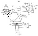
도 1을 참조하면, 본 발명의 일실시예에 의한 이온 빔 증착장치(500)는 증착대상 기판(W)을 고정하는 기판 어셈블리(100), 상기 기판(W)에 대하여 기울어지게 위치하고 증착물질로 구성되는 타겟(target, 220)을 고정하는 타겟 어셈블리(target assembly, 200), 상기 타겟(210)으로 이온 빔을 주사하여 상기 증착물질의 원자인 증착입자(P)를 상기 기판(W)으로 방출시키는 이온 건(ion gun, 300) 및 상기 기판(W)을 가열하여 상기 증착입자(DP)가 상기 기판(W)에 증착되어 형성되는 박막(L)의 결정화도를 높이는 기판 가열기(400)를 포함한다.Referring to FIG. 1, an ion
일실시예로서, 상기 기판 어셈블리(100)는 상기 기판(W)을 고정하고 일정한 각도로 틸팅하는 기판 고정부(110) 및 상기 기판 고정부(110)를 지지하고 회전축을 중심으로 회전하여 상기 기판 고정부(110)를 회전하는 지지부(120)로 구성될 수 있다.In one embodiment, the
기판 고정부(110)는 알루미늄(Al)과 같은 전기 전도성이 우수한 도전성 물질로 이루어지는 고정부 몸체(112)와 상기 고정부 몸체(112)의 상면에 배치되어 기판(W)을 고정하는 고정 척(114)으로 구성될 수 있다.The
상기 고정부 몸체(112)는 고정 척(114)을 수용할 수 있는 사이즈와 형상으로 제공되며, 내부에 상기 증착입자(DP)를 상기 기판(W)으로 유도할 수 있는 가이드 전극(미도시)이 선택적으로 배치될 수 있다. 특히, 후술하는 바와 같이 히터와 같은 발열수단을 선택적으로 배치하여 상기 기판(W)에 대한 이온 빔 증착공정이 수행되는 동안 기판(W)을 증착온도로 유지할 수 있다.The
상기 고정부 몸체(112)는 고정부 몸체(112)의 상면과 평행하게 연장하는 틸팅 축(TA1)을 중심으로 회전하여 일정함 범위의 기판 경사각으로 기울어지게 배치될 수 있다. 예를 들면, 상기 고정부 몸체(112)는 지지부(120)와 수직한 수평면을 기준으로 상기 틸팅축(TA)에 대하여 시계방향 및 반시계방향을 따라 회전하여 기판 경사각만큼 기울어지게 위치할 수 있다.The
고정부 몸체(112)의 회전에 의해 고정척(114)에 고정된 기판(W)도 함께 회전하여 상기 기판(W)도 기판 경사각만큼 기울어지게 위치하게 된다. 이때, 상기 기판 기울기는 타겟(220)으로부터 방출되는 증착입자(DP)가 기판(W)의 표면에 증착되는 효율을 극대화 할 수 있도록 결정된다.The substrate W fixed to the
상기 기판 기울기는 증착입자(DP)의 이동방향에 따라 적절하게 조절될 수 있다. 본 실시예의 경우, 상기 기판(W)은 수평하게 배치되어 기판 기울기가 0°인 경우를 예시적으로 개시하고 있지만, 상기 타겟(220)의 위치에 따라 증착입자(DP)의 증착효율을 극대화 하도록 다양하니 기판 기울기를 갖도록 설정될 수 있음은 자명하다.The substrate slope may be appropriately adjusted according to the moving direction of the deposition particles DP. In the case of this embodiment, the substrate W is disposed horizontally and the substrate inclination is 0°. However, in order to maximize the deposition efficiency of the deposition particles DP according to the position of the
상기 고정 척(114)은 세라믹과 같은 절연물질로 구성되는 디스크 형상으로 제공되며 다양한 기판 고정수단을 구비하여 상면에 증착대상 기판(W)을 고정한다. 본 실시예의 경우, 상기 고정 척(114)은 한 쌍의 폴리이미드계 필름과 상기 폴리이미드계 필름(미도시) 사이에 배치되고 고압의 직류 전원과 연결된 도전성 박막(미도시)을 구비하는 정전 척(electro static chuck, ESC)으로 구성될 수 있다. 그러나, 고정 척(114)은 상기한 바와 같은 정전 척(ESC)뿐만 아니라 기계적으로 기판을 고정하는 클램프와 같이 다양한 고정수단이 이용될 수 있음은 자명하다.The
상기 지지부(120)는 공정챔버(미도시)의 일측으로부터 연장하여 기판 지지부(110)를 지지하고 회전축(RA)을 중심으로 회전하여 상기 기판 고정부(110)를 회전할 수 있다.The
예를 들면, 상기 지지부(120)는 공정챔버의 측부로부터 공정챔버의 내부공간을 향하여 연장하여 상기 고정부 몸체(112)의 중심부와 접속하는 서포트 바(support bar)로 구성될 수 있다.For example, the
상기 지지부(120)는 공정챔버의 내부공간을 향하여 연장하는 연장높이를 선택적으로 조절하여 기판(W)의 고정위치를 조절할 수 있다. 또한, 상기 지지부(120)는 그 중심과 상기 고정부 몸체(112)의 중심을 관통하는 회전축(RA)을 중심으로 회전하도록 구성되어 이온 빔 증착공정이 진행되는 동안 상기 기판(W)을 회전할 수 있다.The
특히, 상기 고정부 몸체(112)의 틸팅에 의해 기판(W)이 적절한 기판 기울기로 고정된 상태에서 고정부 몸체(112)를 회전함으로써 기판(W) 상에 형성되는 박막(L)의 균일도를 극대화 할 수 있다.In particular, the uniformity of the thin film (L) formed on the substrate (W) by rotating the fixing body (112) while the substrate (W) is fixed at an appropriate substrate tilt by tilting the fixing body (112). Can be maximized.
일실시예로서, 상기 타겟 어셈블리(200)는 기판(W)에 대하여 일정한 각도로 기울어지게 위치하고 증착물질로 구성되는 적어도 하나의 타겟(220)을 구비한다.In one embodiment, the
예를 들면, 상기 타겟 어셈블리(200)는 타겟 축(TA2)에 대하여 회전하고 다각형상을 갖는 타겟 몸체(210) 및 상기 타겟 몸체(210)에 개별적으로 고정되고 증착물질로 구성되는 적어도 하나의 타겟(220)을 구비한다.For example, the
타겟 몸체(210)는 다수의 측면을 구비하는 각기둥 형상으로 제공되며 상기 각기둥의 중심을 관통하는 타겟 축(TA2)을 중심으로 회전하도록 구성된다. 따라서, 타겟 몸체(210)의 측면은 상기 기판(W)과 이온 건(300) 사이에 증착 기하구조(deposition geometry)를 형성하여 이온 빔에 의해 생성된 증착입자(DP)가 상기 기판(W)으로 이동하는 타겟면(a)과 다수의 대기면(b)으로 구성된다. 증착 기하구조에 의해 타겟(220)에 대한 마모와 기판(W) 상에 형성되는 박막(L)의 균일성을 최적화 할 수 있다.The
따라서, 상기 타겟 몸체(210)의 회전에 의해 타겟면(a)과 대기면(b)이 서로 교환될 수 있다. 본 실시에의 경우, 상기 타겟 몸체(210)는 1개의 타겟면(a)과 2개의 대기면(b)을 구비하는 삼각기둥 형상으로 제공되고, 상기 타겟(2200은 최대 3개까지 장착될 수 있다. 그러나, 상기 대기면(b)의 개수는 필요한 타겟(220)의 개수에 따라 달라질 수 있음은 자명하다. 예를 들면, 타겟 몸체(210)가 8각기둥 형상으로 제공되는 경우, 상기 타겟(220)은 최대 8개까지 장착될 수 있다.Accordingly, the target surface (a) and the atmosphere surface (b) may be exchanged with each other by the rotation of the
상기 타겟(220)은 타겟 몸체(210)의 타겟면(a)과 대기면(b)의 적어도 하나에 장착된다. 이때, 상기 타겟(220)은 증착물질로 구성되고 상기 타겟면(a)이나 대기면(b)을 덮는 판상으로 제공되며, 이온 건(300)으로부터 주입되는 고에너지 이온 빔과의 충돌에 의해 증착물질 이온인 증착입자(DP)를 생성하게 된다.The
따라서, 상기 타겟(220)은 기판(W)에 증착되는 박막의 종류에 따라 다양한 물질로 구성될 수 있다. 다수의 타겟(220)들은 모두 동일한 물질로 구성되어 상기 박막(L)은 단일한 박막으로 형성될 수 있다. 이와 달리, 다수의 타겟(220)들이 서로 다른 물질로 구성되어 상기 박막(L)은 서로 다른 조성을 갖는 다층막으로 형성될 수도 있다.Accordingly, the
선택적으로, 상기 타겟(220)은 별도의 회전부재(미도시)에 의해 타겟면(a)과 평행하게 회전함으로써 타겟(220)의 마모 불균일성을 방지할 수 있다.Optionally, the
본 실시예의 경우, 상기 타겟(220)은 저저항 금속물질로 구성되어 상기 기판(W) 상에 저저항 금속막을 형성할 수 있다. 예를 들면, 상기 저저항 금속물질은 텅스텐(W), 루테늄(Ru), 탄탈륨(Ta), 티타늄(Ti), 알루미늄(Al), 구리(Cu), 몰리브덴(Mo), 코발트(Co), 아스뮴(Ag), 백금(Pt), 니켈(Ni), 크롬(Cr), 은(Au), 게르마늄(Ge), 마그네슘(Mg), 팔라듐(Pd), 하프늄(Hf), 아연(Zn), 바나듐(V), 지르코늄(Zr) 및 이들의 금속 합금과 이들의 금속 질화물 중의 어느 하나로 구성될 수 있다. 따라서, 본 실시예의 경우, 상기 증착입자(DP)도 금속원자나 이온으로 구성될 수 있다.In this embodiment, the
일실시예로서, 상기 이온 건(300)은 상기 타겟으로 이온 빔을 주사하여 증착입자(DP)를 기판(W)으로 방출한다. 이온 건(300)은 외부의 빔 소스로부터 공급된 빔 소스기체를 고에너지를 갖고 상기 타겟(220)에 대하여 일정한 경사각으로 입사하는 이온 빔(IB)으로 형성한다.In one embodiment, the
예를 들면, 상기 이온 건(300)은 상기 빔 소스기체를 이온화하는 제1 방전챔버(310), 상기 제1 방전챔버(310)와 연결되어 상기 빔 소스기체의 이온들을 가속하여 상기 타겟 어셈블리(200)로 향하는 직진성 고에너지 이온들인 이온 빔(IB)을 생성하는 제1 이온 그리드(ion grid, IG1) 및 상기 이온 빔(IB)으로 전자를 주사(emission)하여 상기 타겟 어셈블리(200)와의 사이에 중성 아크(neutralization arc)를 방지하는 뉴트럴라이저(neutralizer, 350)로 구성될 수 있다.For example, the
상기 제1 방전챔버(310)는 상기 빔 소스로부터 공급된 빔 소스기체를 방전하여 이온화시킬 수 있다. 예를 들면, 방전 캐소드와 가스 공급단 사이에 강한 전기장을 인가하여 상기 빔 소스기체를 방전하거나 상기 빔 소스 기체를 플라즈마 상태로 형성함으로써 이온화할 수 있다. 예를 들면, 상기 제1 방전챔버는 고주파 유도결합 플라즈마(radio frequency inductively coupled plasma, RFICP) 생성기를 포함할 수 있다. 빔 소스기체의 이온들은 제1 방전챔버에 인가되는 전자기력에 의해 가속되어 고에너지의 이온 빔으로 형성된다.The
이때, 상기 빔 소스기체는 아르곤(Ar), 크립톤(Kr), 네온(Ne) 및 크세논(Xe) 중의 어느 하나로 구성하여 이온 빔의 운동에너지를 극대화하고 불순물에 의한 오염을 최소화 할 수 있다.At this time, the beam source gas may be composed of any one of argon (Ar), krypton (Kr), neon (Ne), and xenon (Xe) to maximize kinetic energy of the ion beam and minimize contamination by impurities.
상기 제1 이온 그리드(IG1)는 상기 제1 방전챔버(310)와 연결되어 상기 빔 소스기체의 이온들을 가속하여 타겟(220)으로 향하는 직진성 고에너지 이온들인 이온 빔(IB)을 생성한다.The first ion grid IG1 is connected to the
예를 들면, 상기 제1 이온 그리드(IG1)는 제1 방전챔버(310)를 한정하고 제1 방전챔버(310)의 상기 고에너지 이온들이 통과하는 주사 홀을 구비하는 스크린 그리드(320), 가속 그리드(330) 및 선택적으로 제공되는 감속 그리드(340)로 구성될 수 있다.For example, the first ion grid IG1 defines a
상기 스크린 그리드(320)는 제1 방전챔버(310)에 형성된 플라즈마 쉐스(PS)와 접촉하여 플라즈마로부터 빔 소스기체의 이온들을 추출하여 상기 가속 그리드(330)로 전송한다. 가속 그리드(330)는 추출된 빔 소스기체의 이온들을 상기 타겟(220)을 향하는 방향으로 가속하여 직진성과 운동에너지를 높인다. 이에 따라, 상기 가속 그리드(330)를 통하여 타겟(220)을 향하는 직진성 고에너지 이온들인 이온 빔(IB)을 형성하게 된다. 상기 감속 그리드(340)는 선택적으로 배치되어 이온 빔(IB)의 속도를 제어하게 된다.The
상기 스크린 그리드(320), 가속 그리드(330) 및 감속 그리드(340) 각각의 주사 홀 사이즈와 각 그리드 간의 이격거리를 조절하여 타겟(220)으로 주사되는 이온 빔(IB)의 에너지와 타겟(220)의 주사영역을 조절할 수 있다. 이때, 상기 이온 빔(IB)의 주사영역은 타겟(220)의 사이즈보다 작게 형성하여 이온 빔(IB)에 의해 타겟 몸체(210)가 손상되는 것을 방지할 수 있다.The energy and target 220 of the ion beam IB scanned to the
상기 뉴트럴라이저(neutralizer, 350)는 제1 이온 그리드(IB1)의 단부에서 이온 빔(IB)이 통과하는 주사 홀을 둘러싸는 원통형상으로 배치된다. 상기 뉴트럴라이저(350)는 타겟(220)과 이온 건(300) 사이의 공간으로 전자를 공급하여 이온 빔(IB)과 타겟(220) 사이의 전압차이(voltage potential)에 의한 중성아크(Neutralization arc)를 방지한다. 따라서, 뉴트럴라이저(350)에 의해 공급되는 전자의 양은 타겟(220)의 물성과 주위환경의 절연성 및 접지성에 따라 달라진다.The
고에너지 이온 빔(IB)이 타겟(220)과 충돌하면 타겟(220)의 표면으로부터 증착입자(DP)가 분출되어 기판(W)으로 이동하게 된다. 증착 기하구조에 의해 이온 빔(IB)과 타겟(220)의 충돌에 의해 분출된 증착입자(DP)는 기판(W)을 향하여 이동하여 이온 빔 증착(ion beam deposition, IBD)공정에 의해 기판(W) 상에 박막(L)을 형성하게 된다.When the high-energy ion beam IB collides with the
기판(W) 상에 형성되는 박막(L)은 기판 가열기(400)에 의해 박막의 특성을 개량할 수 있다. 상기 기판 가열기(400)는 이온 빔 증착공정이 진행되는 동안 상기 기판(W)을 가열하여 박막(L)의 결정화도(crystality)를 높일 수 있다.The thin film L formed on the substrate W may improve the characteristics of the thin film by the
종래의 이온 빔 증착공정은 상온에서 수행되어 박막의 그레인 사이즈가 작게 형성되어 결정화도가 떨어지는 경향이 있다. 그레인 사이즈가 작은 경우 충분한 결정성을 확보하기 어려워 박막의 저항을 낮추는데 한계가 있다. 이에 따라, 고용량 고집적 반도체 소자의 금속배선은 종래의 이온 빔 증착공정으로는 형성하기 어려운 점이 있다.The conventional ion beam deposition process is performed at room temperature so that the grain size of the thin film is formed to be small, and thus the crystallinity tends to decrease. When the grain size is small, it is difficult to secure sufficient crystallinity, so there is a limit to lowering the resistance of the thin film. Accordingly, metal wiring of a high-capacity, high-integration semiconductor device is difficult to form by a conventional ion beam deposition process.
그러나, 본 실시예에 의하면 이온 빔 증착공정이 수행되는 동안 기판(W)을 상온보다 높은 증착온도로 유지하여 그레인 사이즈를 증가시켜 박막의 결정화도를 높이고 전기저항을 충분히 줄일 수 있다.However, according to the present embodiment, while the ion beam deposition process is performed, the substrate W is maintained at a deposition temperature higher than room temperature to increase the grain size, thereby increasing the crystallinity of the thin film and sufficiently reducing the electrical resistance.
예를 들면, 상기 기판 가열기(400)는 상기 기판 어셈블리(100)의 외부에서 상기 기판(W)을 조사하는 램프 구조물(410)을 포함할 수 있다.For example, the
상기 램프 구조물(410)은 기판(W)의 상부에 배치되어 기판(W)의 전면으로 복사열을 제공하면 다양한 구조를 가질 수 있다. 상기 램프 구조물(410)은 진공으로 밀봉된 석영 튜브의 내부에 열방사체를 배치하고 석영튜브의 양단을 전기적으로 연결하여 가시광선이나 적외선 광을 기판(W)으로 조사할 수 있다. 예를 들면, 상기 램프 구저물(410)은 상기 열방사체의 구성에 따라 카본 열방사 램프, 크세논 램프 또는 할로겐 램프로 구성할 수 있다.The
이와 달리, 상기 기판 가열기(400)는 기판 고정부(110)의 내부에 배치되어 주울 열을 생성하는 전열기(420)로 구성될 수도 잇다.Alternatively, the
도 2는 도 1에 도시된 기판 가열기의 다른 실시예를 나타내는 도면이다.FIG. 2 is a diagram illustrating another embodiment of the substrate heater shown in FIG. 1.
도 2를 참조하면, 상기 기판 가열기(400)는 고정 척(112)의 내부에 배치된 전열라인(422)과 상기 전열라인으로 전력을 공급하는 파워(424)를 포함하는 라인 전열기(420)로 구성될 수 있다.Referring to FIG. 2, the
상기 전열라인(422)은 고정 척(114)의 내부에서 디스크 형상을 갖는 고정 척(114)의 반경방향을 따라 일정한 간격으로 배치되는 와선 구조물로 제공될 수 있다. 상기 와선형상을 갖는 전열라인(422)의 양단은 상기 전열파워(424)로 연결된다. 이에 따라, 발열이 필요한 경우 상기 전열파워(424)로부터 전류가 인가되면 전열라인(422)을 따라 주울열이 발생하여 고정 척(114)을 균일하게 가열하고 상면에 고정된 기판(W)도 균일하게 가열된다.The heat transfer line 422 may be provided as a vortex structure disposed at regular intervals along the radial direction of the fixed
이때, 상기 라인 전열기(420)에 의한 기판(W)의 온도를 증착온도로 유지하기 위해 고정 척(114)의 내부에 냉각라인(CL)이 선택적으로 제공될 수 있다. 상기 냉각라인(CL)도 전열라인(422)과 마찬가지로 와선 구조물로 제공될 수 있으며 고정부 몸체(122)의 반경방향을 따라 인접한 전열라인(422) 사이에 배치될 수 있다.In this case, in order to maintain the temperature of the substrate W by the
예시적으로, 외부에 배치된 냉각 탱크(CT)로부터 상기 냉각라인(CL)으로 냉매가 공급되어 냉각라인(CL)을 따라 고정 척(112)의 내부에서 유동하게 된다. 이에 따라, 냉매의 온도를 조절함으로써 상기 고정 척(114)의 온도를 일정하게 유지할 수 있다.Exemplarily, the refrigerant is supplied from the externally disposed cooling tank CT to the cooling line CL and flows inside the fixed
도 3은 도 1에 도시된 기판 가열기의 또 다른 실시예를 나타내는 도면이다.3 is a view showing another embodiment of the substrate heater shown in FIG.
도 3을 참조하면, 상기 기판 가열기(400)는 상기 고정 척(114)의 내부에 배치되고 상기 고정 척(114)의 상면(US)에 대응하도록 상단부를 덮는 면상 발열체(432)와 상기 면상 발열체(432)로 전력을 공급하는 구동파워(434)를 포함하는 면상 전열기(430)로 구성될 수 있다.Referring to FIG. 3, the
상기 면상 발열체(432)는 고정 척(114)의 상단부에 고정 척(114)의 내부를 매립하여 상면(US)을 덮고 일정한 두께를 갖도록 측면과 접촉하도록 배치된다. 이에 따라, 상기 고정 척(114)의 상단부는 상기 면상 발열체로 매립되어 상기 기판(W)은 면상 발열체(432)의 상부에 배치될 수 있다.The
상기 면상 발열체(432)는 벌크 형상의 카본 발열체를 구비하여 상기 구동파워(434)로부터 파워가 공급되면 상면(US) 전체로 균일한 열량을 방출하게 된다. 따라서, 상기 기판(W)은 고정 척(US)의 상면으로부터 전달되는 열에 의해 하면 전체가 균일하게 가열된다.The
이때, 상기 기판(W)의 온도는 면상 발열체(432)로 인가되는 파워를 조절함으로써 제어할 수 있다. 그러나, 온도 조절시간과 정밀도를 높이기 위해 면상 발열체(432)의 하부에 냉각판(CP)을 더 배치할 수 있다.In this case, the temperature of the substrate W can be controlled by adjusting the power applied to the
상기 냉각판(CP)은 면상 발열체와 동일한 형상을 갖고 면상 발열체(432)의 하면의 전면과 직접 접촉하는 열전 냉각소자로 구성될 수 있다. 냉각 파워(P)에 의해 상기 열전 냉각소자로 전류가 인가되면, 페르티에 효과에 의해 상기 면상 발열체(432)로부터 열을 흡수하여 면상 발열체(432)의 온도를 조절할 수 있다.The cooling plate CP may be configured as a thermoelectric cooling element having the same shape as the planar heating element and directly contacting the front surface of the lower surface of the
본 실시예에서는 상기 면상 발열체(432)의 온도를 조절하기 위한 수단으로서 열전 냉각소자로 구성된 냉각판(CP)을 개시하지만, 온도제어의 정밀도만 높다면 상기 면상 발열체(432)로부터 열을 흡수할 수 있는 다양한 냉각수단이 상기 냉각판(CP)으로 이용될 수 있음은 자명하다.In this embodiment, a cooling plate CP composed of a thermoelectric cooling element is disclosed as a means for controlling the temperature of the
상기 기판 가열기(400)에 의해 이온 빔 증착공정이 진행되는 동안 상기 기판(W)은 약 150°C 내지 300°C의 증착온도로 유지될 수 있다. 증착온도가 약 150°C 이하인 경우, 상온에서 수행되는 종래의 이온빔 증착공정에 의해 형성된 박막과 비교하여 그레인 사이즈의 증가가 미미하여 박막 결정화도의 개선효과를 달성하기 어렵다. 또한, 상기 증착온도가 약 300°C를 넘는 경우, 박막(L)의 그레인 사이즈가 스퍼터링 공정에 의한 그레인 사이즈보다 더 크게 된다. 박막(L)의 그레인 사이즈가 과도하게 크게 되면 결정화도가 오히려 감소하여 박막(L)의 비저항이 증가하게 된다.While the ion beam deposition process is performed by the
이에 따라, 상기 기판 가열기(400)는 이온 빔 증착공정이 진행되는 동안 기판(W)의 온도를 약 150°C 내지 300°C, 더 바람직하게는, 약 200°C 내지 250°C의 증착온도로 유지한다.Accordingly, the
아래의 표 1은 반도체 소자의 배선으로 널리 이용되는 텅스텐 막을 본 발명에 의한 고온 이온 빔 증착공정과 종래의 상온 이온 증착 빔 공정 및 플라즈마 스퍼터링 공정에 의해 형성하는 경우의 박막 특성을 나타낸다.Table 1 below shows the characteristics of a thin film when a tungsten film, which is widely used as a wiring of a semiconductor device, is formed by a high temperature ion beam deposition process according to the present invention, a conventional room temperature ion deposition beam process, and a plasma sputtering process.
표 1에 도시된 바와 같이 본 발명에 의한 고온 IBD 공정은 박막(L)의 그레인 사이즈를 적정하게 조절함으로써 스퍼터링 공정이나 상온 IBD 공정과 비교하여 박막의 결정화도를 높이고 비저항을 충분히 낮출 수 있다. 이에 따라, 고집적 고용량 반도체 소자의 금속 배선막을 본 발명에 의한 고온 IBD 공정에 의해 안정적으로 형성할 수 있다.As shown in Table 1, the high-temperature IBD process according to the present invention can increase the crystallinity of the thin film and sufficiently lower the specific resistance as compared to the sputtering process or the room temperature IBD process by appropriately adjusting the grain size of the thin film L. Accordingly, a metal wiring film of a highly integrated high-capacity semiconductor device can be stably formed by the high-temperature IBD process according to the present invention.
도 4는 본 발명의 다른 실시예에 의한 이온 빔 증착장치를 개략적으로 나타내는 구성도이다.4 is a schematic diagram of an ion beam deposition apparatus according to another embodiment of the present invention.
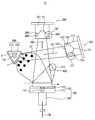
도 4에 도시된 이온 빔 증착장치는 기판 어셈블리로 보조 이온 빔을 주사하는 보조 이온 건이 더 배치된 것을 제외하고는 도 1에 도시된 이온 빔 증착장치와 실질적으로 동일한 구성을 갖는다. 이에 따라, 도 4에서 도 1과 동일한 구성요소에 대해서는 동일한 참조부호를 사용하고 동일한 구성요소에 대한 더 이상의 상세한 설명은 생략한다. 이하에서, 상기 이온 건(300)으로부터 주사되는 이온 빔을 참조부호 IB1으로 표시하고 보조 이온 건으로부터 주사된 보조 이온 빔을 참조부호 IB2로 구분하여 표시한다.The ion beam deposition apparatus shown in FIG. 4 has substantially the same configuration as the ion beam deposition apparatus shown in FIG. 1 except that an auxiliary ion gun for scanning an auxiliary ion beam to the substrate assembly is further disposed. Accordingly, in FIG. 4, the same reference numerals are used for the same components as in FIG. 1, and further detailed descriptions of the same components are omitted. Hereinafter, the ion beam scanned from the
도 4를 참조하면, 상기 기판 어셈블리(100)의 상부에 보조 이온 빔(IB2)을 주사하는 보조 이온 건(390)이 더 배치된다. 본 실시예의 경우, 상기 보조 이온 건(390)은 도 1에 도시된 이온 건(300)과 실질적으로 동일한 구성을 갖는다.Referring to FIG. 4, an
따라서, 상기 보조 이온 건(390)은 보조 빔 소스기체를 이온화하는 제2 방전챔버(391)와 상기 제2 방전챔버(392)와 연결되어 상기 보조 빔 소스기체의 이온들을 가속하여 상기 기판(W)으로 향하는 직진성 고에너지 이온들인 보조 이온 빔(IB2)을 생성하는 제2 이온 그리드(ion grid, IG2)로 구성될 수 있다. 제2 이온 그리드(IG2)는 제2 방전챔버(391)를 한정하고 제2 방전챔버(391)의 상기 고에너지 이온들이 통과하는 주사 홀을 구비하는 스크린 그리드(392), 가속 그리드(393) 및 선택적으로 제공되는 감속 그리드(394)로 구성될 수 있다.Accordingly, the
이때, 상기 보조 빔 소스기체는 빔 소스 기체와 마찬가지로 아르곤(Ar), 크립톤(Kr), 네온(Ne) 및 크세논(Xe) 중의 어느 하나로 구성하여 보조 이온 빔(IB2)의 운동에너지를 극대화하고 불순물에 의한 오염을 최소화 할 수 있다.At this time, the auxiliary beam source gas is composed of any one of argon (Ar), krypton (Kr), neon (Ne), and xenon (Xe) like the beam source gas to maximize the kinetic energy of the auxiliary ion beam (IB2) and impurities. It can minimize the pollution caused by.
제2 방전챔버(391), 스크린 그리드(392), 가속 그리드(393) 및 선택적으로 제공되는 감속 그리드(394)는 도 1을 참조하여 설명한 제1 방전챔버(310), 스크린 그리드(320), 가속 그리드(330) 및 감속 그리드(340)와 실질적으로 동일한 구성을 갖는다. 따라서, 상기 제2 방전챔버(391), 스크린 그리드(392), 가속 그리드(393) 및 감속 그리드(394)에 관한 더 이상의 상세한 설명은 생략한다.The
상기 보조 이온 빔(IB2)은 기판(W)의 상면으로 조사되어 기판으로부터 불순물을 제거하거나 증착입자(DP)가 기판 상에 증착되는 것을 보조할 수 있다. 보조 이온 빔(IB2)이 기판(W)에 도달하면, 보조 이온 빔의 운동에너지가 열에너지로 전환되어 기판의 표면에 대한 표면처리를 수행할 수 있다.The auxiliary ion beam IB2 may be irradiated to the upper surface of the substrate W to remove impurities from the substrate or assist the deposition of the deposition particles DP on the substrate. When the auxiliary ion beam IB2 reaches the substrate W, the kinetic energy of the auxiliary ion beam is converted into thermal energy to perform surface treatment on the surface of the substrate.
이때, 기판(W)의 온도를 보조적으로 상승시켜 상기 기판 가열기(400)의 구동로드를 경감시키거나 기판 가열기(400)를 대체할 수도 있다. 즉, 상기 보조 이온 빔(IB2)에 의해 기판(W)의 온도를 상기 증착온도까지 상승시킬 수 있다면 보조 이온 건(390)으로 기판 가열기(400)를 대체할 수도 있다.In this case, the temperature of the substrate W may be increased to reduce the driving load of the
이에 따라, 기판(W)에 형성되는 박막(L)의 오염도를 줄이고 그레인 사이즈를 적절하게 조절함으로서 박막(L)의 결정화도를 개선할 수 있다.Accordingly, the degree of contamination of the thin film L formed on the substrate W may be reduced, and the crystallinity of the thin film L may be improved by appropriately adjusting the grain size.
특히, 상기 보조 이온 건(390)과 기판(W) 사이에는 전압차(voltage potential)가 생성되지 않으므로, 중성아크를 방지하기 위한 뉴트럴라이저는 상기 보조 이온 건(390)에 배치되지 않을 수 있다.In particular, since a voltage potential is not generated between the
그러나, 고정 척(114)에 전압이 인가되어 보조 이온 건(390)과 기판(W) 사이에 전압차가 형성되면, 중성 아크(neutralization arc)를 방지하기 위한 뉴트럴라이저가 배치될 수도 있음은 자명하다.However, when a voltage is applied to the fixed
상술한 바와 같은 보조 이온 건에 의해 기판(W) 상의 불순물을 제거하여 박막의 순도를 높이고 기판의 온도를 높임으로써 결정화도 및 순도가 높은 박막(L)을 형성할 수 있다. 이에 따라, 상기 박막의 비저항을 현저하게 낮출 수 있다.The purity of the thin film is increased by removing impurities on the substrate W by the auxiliary ion gun as described above, and the thin film L having high crystallinity and purity may be formed by increasing the temperature of the substrate. Accordingly, it is possible to significantly lower the specific resistance of the thin film.
도 5는 본 발명의 다른 실시예에 의한 이온 빔 증착장치를 개략적으로 나타내는 구성도이다. 예시적으로 도 5에 도시된 이온 빔 증착장치는 도 4에 도시된 이온 빔 증착장치를 포함한다. 이에 따라, 도 5에서 도 4와 동일한 구성요소에 대해서는 동일한 참조부호를 사용한다. 본 실시예에서는 도 4에 도시된 이온 빔 증착장치를 구비하는 장치를 개시하고 있지만, 도 1에 도시된 이온 빔 증착장치를 구비하는 장치도 본 실시예의 증착장치에 포함될 수 있음은 자명하다.5 is a schematic diagram of an ion beam deposition apparatus according to another embodiment of the present invention. Exemplarily, the ion beam deposition apparatus shown in FIG. 5 includes the ion beam deposition apparatus shown in FIG. 4. Accordingly, in FIG. 5, the same reference numerals are used for the same components as in FIG. 4. Although this embodiment discloses an apparatus including the ion beam deposition apparatus shown in FIG. 4, it is obvious that the apparatus including the ion beam deposition apparatus shown in FIG. 1 may also be included in the deposition apparatus of this embodiment.
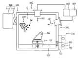
도 5를 참조하면, 본 발명의 다른 실시예에 의한 이온 증착장치(1000)는 이온 빔 증착공정이 수행되도록 밀폐공간을 제공하는 공정챔버(600), 상기 공정챔버(600)의 측부에 고정되어 증착대상 기판(W)을 고정하는 기판 어셈블리(100), 상기 공정챔버(600)의 내부에서 상기 기판(W)에 대하여 기울어지게 배치되고 증착물질로 구성되는 타겟(target, 220)을 고정하는 타겟 어셈블리(200), 상기 공정챔버(600)의 제2 측부(602)에 고정되고 상기 타겟(200)으로 이온 빔(IB1)을 주사하여 상기 증착물질의 이온인 증착입자(DP)를 상기 기판(W)으로 방출시키는 이온 건(300), 상기 기판(W)을 가열하여 상기 증착입자(DP)가 상기 기판(W)에 증착되어 형성되는 박막(L)의 결정화도를 높이는 기판 가열기(400), 상기 기판 어셈블리(100)와 연결되어 상기 기판(W)을 수용하는 기판 스택(700), 및 상기 공정챔버(600)의 제3 측부(603)에 배치되어 상기 공정챔버(600) 내부를 일정한 진공압으로 유지하는 진공 생성기(800)를 포함한다.5, the ion deposition apparatus 1000 according to another embodiment of the present invention is a
선택적으로, 상기 이온 빔 증착장치(1000)는 보조 빔 소스기체를 이온화하는 제2 방전챔버(391), 상기 제2 방전챔버(391)와 연결되어 상기 보조 빔 소스기체의 이온들을 가속하여 상기 기판으로 향하는 직진성 고에너지 이온들인 이온 빔을 생성하는 제2 이온 그리드(ion grid, IG2)를 구비하고 상기 기판(W)으로 상기 보조 이온 빔(IB2)을 주사하는 보조 이온 건(390)을 더 포함할 수 있다.Optionally, the ion beam deposition apparatus 1000 is connected to a
일실시예로서, 상기 공정챔버(600)는 외부로부터 밀폐되고 이온 빔 증착공정이 수행되는 내부공간(S)을 갖는 입체형상으로 제공된다. 상기 공정챔버(600)는 단일한 하우징으로 구성될 수도 있고 서로 분리되는 상부 하우징 및 하부 하우징의 결합으로 구성될 수도 있다.As an embodiment, the
특히, 이온 빔 증착공정이 진행되는 동안 상기 내부공간에는 진공압이 인가되므로 상기 공정챔버(600)는 공정에 요구되는 진공압에 충분히 대응할 수 있는 강도와 강성을 갖는 구조물로 제공된다.In particular, since a vacuum pressure is applied to the inner space while the ion beam deposition process is in progress, the
공정챔버(600)의 하부에는 기판 스택(700)으로부터 증착대상 기판(W)을 공정챔버(600)로 로딩하고 증착이 완료된 기판을 공정챔버(600)로부터 언로딩하기 위한 게이트(610)가 제공된다.A
상기 기판 스택(700)은 게이트(610)를 통하여 기판 어셈블리(100)와 연결된다. 예를 들면, 기판 스택(700)은 다수의 기판(W)을 적재하여 반도체 소자용 제조장비 사이를 이동하는 기판 홀더(C)가 위치하는 로더 포트(710) 및 로봇 암과 같은 기판 전송수단(미도시)을 이용하여 증착대상 기판을 기판 홀더(C)로부터 추출하여 공정챔버(600)로 전송하거나 증착완료 기판을 공정챔버(600)로부터 기판 홀더(C)로 적재하는 기판 전송부(720)를 포함한다. 기판 전송수단은 상기 공정챔버(600)와 상기 기판 홀더(C) 사이에서 기판(W)을 전송한다. 상기 기판 홀더(C)는 웨이퍼 카세트나 풉(FOUP)을 포함할 수 있다.The
기판 가이드(620)가 게이트(610)를 관통하여 상기 기판 추출부(720)까지 이동할 수 있다. 기판 추출부(720)로부터 증착대상 기판이 추출되면 상기 기판 가이드(620)에 탑재되고 상기 기판 가이드(620)는 기판 어셈블리(100)의 기판 고정부(110)까지 이동하여 고정 척(114)에 기판을 로딩한다.The
상기 공정챔버(600)의 다른 측부에는 상기 공정챔버(600)의 내부공간(S)을 일정한 진공압으로 유지하는 진공 생성기(800)가 배치된다.A
예를 들면, 상기 진공 생성기(800)는 공정챔버(600)와 연결되는 게이트 밸브(810) 및 게이트 밸브(810)에 의해 내부공간(S)으로 진공압을 인가하는 진공펌프(820)룰 포함한다.For example, the
본 실시예의 경우, 이온 빔 증착공정이 진행되는 동안 상기 공정챔버(600)의 내부공간(S)은 진공 생성기(800)에 의해 약 10-5Torr 내지 10-9Torr의 진공압이 유지된다. 이에 따라, 상기 증착입자(DP)는 실질적으로 운동에너지의 손실없이 기판(W)으로 이동할 수 있다.In the present embodiment, during the ion beam deposition process, a vacuumpressure of about 10 -5 Torr to 10-9 Torr is maintained in the internal space S of the
상기 게이트(610)와 인접한 공정챔버(600)의 측부에 상기 기판 어셈블리(100)가 배치된다. 기판 어셈블리(100)의 지지부(120)는 상기 측부와 인접한 로딩/언로딩 위치와 내부공간(S)을 향하여 돌출한 증착위치 사이를 왕복할 수 있다.The
로딩/언로딩 위치에서 상기 고정 척(114)의 상면과 기판 가이드(620)의 상면은 동일한 평면을 형성한다. 이에 따라, 증착대상 기판은 기판 가이드(620)로부터 용이하게 고정 척(114)으로 로딩되며 증착완료 기판은 고정 척(114)으로부터 기판 가이드(620)로 용이하게 언로딩 될 수 있다.In the loading/unloading position, the upper surface of the fixed
기판(W)이 고정 척(114)에 로딩되면 정전기력에 의해 기판은 고정 척(114)에 고정되고, 상기 지지부(120)는 내부공간(S)을 향하여 돌출하여 기판(W)을 가공위치에 위치시킨다.When the substrate W is loaded on the fixed
가공위치에서 상기 고정부 몸체(112)는 틸팅 축(TA1)을 중심으로 회전하여 기판(W)이 타겟면(a)에 대하여 증착 기하구조에 적합하도록 위치시킨다. 본 실시예의 경우, 상기 기판(W)은 기판 경사각을 0°로 설정되는 것을 예시적으로 개시하고 있지만, 타겟 어셈블리(200)와 이온 건(300)의 위치에 따라 상기 기판(W)은 틸팅 축(TA1)을 중심으로 한 회전에 의해 다양한 기판 경사각을 갖도록 위치시킬 수 있다.In the processing position, the fixing
상기 기판 어셈블리(100)는 도 5에 도시된 기판 어셈블리(100)와 실질적으로 동일한 구성을 가지므로, 기판 어셈블리(100)에 대한 더 이상의 상세한 설명은 생략한다.Since the
증착물질로 구성된 타겟(220)이 고정된 타겟 어셈블리(200)가 기판 어셈블리(100)의 상부 일측에 배치되고 상기 타겟(220)으로 이온 빔(IB1)을 주사하는 이온 건(300)이 타겟(220)에 대하여 경사지게 기판 어셈블리(100)의 상부 타측에 배치된다.A
외부의 빔 소스(BS1)로부터 빔 소스기체가 이온 건(300)의 제1 방전챔버(310)로 공급되면 빔 소스기체의 이온들로 방전된다. 상기 빔 소스기체의 이온들은 상기 제1 이온 그리드(IG1)에 의해 직진성을 갖는 고에너지 이온 빔(IB1)이 되어 상기 타겟(220)으로 주사된다.When the beam source gas is supplied from the external beam source BS1 to the
이온 빔(IB1)과 타겟(220)의 충돌에 의해 증착물질의 이온들인 증착임자(DP)가 분출되고 상기 증착입자(DP)들은 증착 기하구조를 갖도록 배치된 기판(W)으로 이동하여 기판(W)의 상면에 증착된다. 이에 따라, 상기 기판(W)의 상면에 박막(L)이 형성된다.Due to the collision between the ion beam IB1 and the
이때, 상기 기판 어셈블리(100)의 상부에는 기판(W)의 전면을 가열하는 기판 가열기(400)가 배치된다. 이에 따라, 상기 증착입자(DP)가 기판(W)에 증착될 때, 기판(W)을 약 150°C 내지 300°C의 증착온도로 유지할 수 있다.In this case, a
예를 들면, 금속물질로 구성되는 타겟(220)으로 이온 빔(IB1)을 조사하면, 금속물질의 증착입자(DP)가 타겟(220)으로부터 분출되어 상기 기판(W)의 상면에 증착된다.For example, when the ion beam IB1 is irradiated with the
예를 들면, 상기 타겟은 텅스텐(W), 루테늄(Ru), 탄탈륨(Ta), 티타늄(Ti), 알루미늄(Al), 구리(Cu), 몰리브덴(Mo), 코발트(Co), 아스뮴(Ag), 백금(Pt), 니켈(Ni), 크롬(Cr), 은(Au), 게르마늄(Ge), 마그네슘(Mg), 팔라듐(Pd), 하프늄(Hf), 아연(Zn), 바나듐(V), 지르코늄(Zr) 및 이들의 금속 합금과 이들의 금속 질화물 중의 어느 하나를 포함할 수 있다.For example, the target is tungsten (W), ruthenium (Ru), tantalum (Ta), titanium (Ti), aluminum (Al), copper (Cu), molybdenum (Mo), cobalt (Co), asmium ( Ag), platinum (Pt), nickel (Ni), chromium (Cr), silver (Au), germanium (Ge), magnesium (Mg), palladium (Pd), hafnium (Hf), zinc (Zn), vanadium ( V), zirconium (Zr), and metal alloys thereof, and metal nitrides thereof.
이때, 상기 기판 가열기(400)에 의해 기판(W)의 온도가 고온으로 유지되므로, 상기 박막(L)은 상온 이온 빔 증착공정과 비교하여 상대적으로 큰 그레인 사이즈를 갖고 우수한 결정화도를 갖게 된다. 이에 따라, 기판(W) 상에 형성되는 금속성 박막(L)의 비저항을 현저하게 줄일 수 있다.At this time, since the temperature of the substrate W is maintained at a high temperature by the
본 실시예의 경우, 상기 박막(L)은 약 80nm 내지 약 100nm의 그레인 사이즈를 갖고 약 5Ωm 내지 약 9Ωm의 비저항을 갖는다. 이에 따라, 상기 금속성 박막(L)은 고집적 고용량 반도체 소자의 배선 구조물로 활용될 수 잇다.In this embodiment, the thin film L has a grain size of about 80 nm to about 100 nm and a specific resistance of about 5 Ωm to about 9 Ωm. Accordingly, the metallic thin film L may be used as a wiring structure of a highly integrated high-capacity semiconductor device.
상기 기판(W)의 상부에는 상기 기판(W)으로 보조 이온 빔(IB2)을 주사하여 기판의 불순물을 제거하고 증착입자(DP)의 증착을 활성화 할 수 있는 보조 이온 건(390)이 위치한다.An
외부의 보조 빔 소스(BS2)로부터 보조 빔 소스기체가 보조 이온 건(390)의 제2 방전챔버(391)로 공급되면 보조 빔 소스기체의 이온들로 방전된다. 상기 보조 빔 소스기체의 이온들은 상기 제2 이온 그리드(IG2)에 의해 직진성을 갖는 고에너지 보조 이온 빔(IB2)이 되어 상기 기판(W)으로 주사된다.When the auxiliary beam source gas is supplied from the external auxiliary beam source BS2 to the
보조 이온 빔(IB2)은 기판(W)에 충돌하여 기판의 불순물들을 제거하고 기판의 온도를 상승시킬 수 있다. 이에 따라, 박막(L)의 순도와 결정화도를 높일 수 있다.The auxiliary ion beam IB2 may collide with the substrate W to remove impurities from the substrate and increase the temperature of the substrate. Accordingly, the purity and crystallinity of the thin film L can be increased.
상기 타겟 어셈블리(200), 이온 건(300), 기판 가열기(400) 및 보조 이온 건(390)은 도 4를 참조하여 설명한 이온 건(300), 기판 가열기(400) 및 보조 이온 건(390)과 실질적으로 동일한 구성을 갖는다. 따라서, 상기 이온 건(300), 기판 가열기(400) 및 보조 이온 건(390)에 대한 더 이상의 상세한 설명은 생략한다.The
상술한 바와 같은 이온 빔 증착장치(1000)에 의하면, 박막(L)의 그레인 사이즈를 적정하게 조절함으로써 스퍼터링 공정이나 상온 IBD 공정과 비교하여 박막의 결정화도를 높이고 비저항을 충분히 낮출 수 있다. 이에 따라, 고집적 고용량 반도체 소자의 금속 배선막을 본 발명에 의한 고온 IBD 공정에 의해 안정적으로 형성할 수 있다.According to the ion beam deposition apparatus 1000 as described above, by appropriately adjusting the grain size of the thin film L, it is possible to increase the crystallinity of the thin film and sufficiently lower the specific resistance compared to the sputtering process or the room temperature IBD process. Accordingly, a metal wiring film of a highly integrated high-capacity semiconductor device can be stably formed by the high-temperature IBD process according to the present invention.
도 6은 본 발명의 일실시예에 따라 도 5에 도시된 이온 빔 증착장치를 구비하는 이온 빔 증착 시스템을 개략적으로 나타내는 구성도이다.6 is a block diagram schematically showing an ion beam deposition system including the ion beam deposition apparatus shown in FIG. 5 according to an embodiment of the present invention.
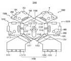
도 6을 참조하면, 본 발명의 일실시예에 의한 이온 빔 증착 시스템(2000)은 기판 핸들러(handler, 1120)를 구비하는 이송장치(1100), 상기 이송장치(1100)의 일 측부에 배치되어 다수의 기판(W)을 수납하는 적어도 하나의 기판수납 장치(1200) 및 상기 이송장치(1100)의 다른 측부에 배치되어 상기 기판 핸들러(1110)에 의해 상기 기판 대기장치(1200)로부터 로딩된 증착대상 기판에 대해 이온 밤 증착공정을 수행하여 상기 기판(W) 상에 박막(L)을 형성하는 적어도 하나의 이온 빔 증착장치(1300)를 포함한다.6, the ion
상기 이송장치(1100)는 다각형 실린더 형상을 갖는 이송챔버(1110)와 상기 이송챔버(1110)의 중심부에 고정되어 360° 회전 가능한 기판 핸들러(1120)를 구비한다.The
본 실시예의 경우, 상기 이송챔버(1110)는 육각기둥 형상으로 제공되어 제1 내지 제6 측면(1111 내지 1116)을 갖고 4개의 이온 빔 증착장치와 2개의 기판 대기장치가 단일한 이송챔버(1110)에 연결된다. 이에 따라, 동시에 4개의 이온 빔 증착공정을 독립적으로 수행할 수 있다.In this embodiment, the
상기 기판 핸들러(1120)는 이송챔버(1110)의 중심에 고정된 고정 축(1121)과 상기 고정 축(1121)을 따라 회전하는 이송 암(1122)으로 구성된다.이송 암(1121)은 이온 빔 공정의 처리 알고리즘에 따라 기판 대기장치(1200)와 이온 빔 증착장치(1300) 사이를 이동하면서 기판(W)을 이송하게 된다.The
상기 기판 대기장치(1200)는 상기 이송장치(1100)의 제1 측면(1111)에 연결되도록 위치하고 다수의 증착대상 기판을 수납하는 제1 기판 스택(1210) 및 상기 이송장치(1100)의 제6 측면(1116)에 연결되도록 위치하고 박막이 형성된 증착완료 기판을 수납하는 제2 기판 스택(1250)을 포함한다.The
상기 제1 기판 스택(1210)은 입구 게이트(1211)를 통하여 상기 이송장치(1100)와 선택적으로 연결되고 상기 제2 기판 스택(1250)은 출구 게이트(1251)를 통하여 이송장치(1100)와 선택적으로 연결된다.The
다수의 기판 홀더(C)가 로드 포트(1215, 1255)에 위치하면, 각 기판 홀더(C)는 입력된 투입순서에 따라 기판 전송부(1213, 1253)를 향하여 정렬한다. 입구 게이트(1211)와 인접한 기판 전송부(1213)에 의해 기판 홀더(C)로부터 증착대상 기판(W)을 추출하여 이온 빔 증착장치(1300)로 전송하고, 증착완료 기판은 출구 게이트(1251)와 인접한 기판 전송부(1253)를 통하여 기판 홀더(C)에 수납된다. When a plurality of substrate holders C are positioned at the
상기 기판 전송부(1213, 1253) 및 로드 포트(1215, 1255)는 도 4에 도시된 기판 스택(700)의 기판 전송부(720) 및 로드 포트(710)와 실질적으로 동일한 구성을 갖는다. 따라서, 상기 상기 기판 대기장치(1200)에 대한 더 이상의 상세한 설명은 생략한다.The
제1 내지 제4 이온 빔 증착장치(1310, 1330, 1350,1370)가 상기 이송챔버(1110)의 제2 내지 제5 측면(1112, 1113, 1114, 1115)에 각각 배치된다. 각 증착장치와 이송챔버(1110) 사이에는 제1 내지 제4 로드락 챔버(1311, 1331, 1351, 1371)가 배치되어 진공압이 인가되는 공정챔버(600)와 대기압이 작용하는 이송챔버(1110) 사이의 기판 교환에 따른 압력손상을 방지할 수 있다.First to fourth ion
제1 내지 제4 이온 빔 증착장치(1310, 1330, 1350,1370)는 도 4에 도시된 이온 빔 증착장치와 실질적으로 동일한 구성을 갖는다. 따라서, 각 이온 빔 증작장치(1310, 1330, 1350,1370)는 이온 빔 증착공정이 수행되도록 밀폐공간을 제공하는 공정챔버(600), 상기 공정챔버(600)의 일측부에 고정되어 기판(W)을 고정하는 기판 어셈블리(100), 공정챔버(600)의 내부에서 상기 기판(W)에 대하여 기울어지게 배치되고 증착물질로 구성되는 타겟(target, 220)을 고정하는 타겟 어셈블리(200), 상기 공정챔버(600)의 다른 측부에 고정되고 상기 타겟(220)으로 이온 빔(IB1)을 주사하여 상기 증착물질의 이온인 증착입자(DP)를 상기 기판(W)으로 방출시키는 이온 건(300), 상기 기판(W)을 가열하여 상기 증착입자(DP)가 상기 기판(W)에 증착되어 형성되는 박막(L)의 결정화도를 높이는 기판 가열기(400) 및 상기 공정챔버(600)와 연결되어 상기 밀폐공간을 일정한 진공압으로 유지하는 진공 생성기(800)로 구성된다.The first to fourth ion
상기 기판 어셈블리(100), 타겟 어셈블리(200), 이온 건(300), 기판 가열기(400), 공정챔버(600) 및 진공 생성기(800)는 도 4를 참조하여 설명한 것과 실질적으로 동일하므로 더 이상의 상세한 설명은 생략한다.The
상술한 바와 같은 이온 빔 증착 시스템(2000)은 동시에 다수의 이온 빔 증착공정을 수행함으로써 증착공정의 효율을 현저하게 높일 수 있다. 중앙 제어장치(미도시)에 입력된 증착 알고리즘에 따라 4개의 이온 빔 증착장치에 대한 증착공정과 제1 및 제2 기판 스택(1210, 1250)의 동작을 제어함으로써 동시에 4개의 이온 빔 증착공정을 수행할 수 있다.The ion
본 실시예에서는 단층으로 된 6각 이송챔버(1110)를 이용하여 동시에 4개의 이온 빔 증착공정을 수행하는 것을 개시하고 았지만, 이는 예시적인 것이며 이송챔버의 형상이나 복층 이송챔버를 통하여 동시에 수행할 수 있는 이온 빔 증착공정의 수를 증가시킬 수 있음은 자명하다.In this embodiment, it has been disclosed to simultaneously perform four ion beam deposition processes using a single-layered
도 7은 본 발명의 일실시예에 따라 도 5에 도시된 이온 빔 증착장치를 이용하여 이온 빔 증착공정을 수행하는 방법을 나타내는 흐름도이다.7 is a flowchart illustrating a method of performing an ion beam deposition process using the ion beam deposition apparatus shown in FIG. 5 according to an embodiment of the present invention.
도 5 및 도 7을 참조하면, 먼저 진공압이 인가된 공정챔버(600)에 구비된 기판 어셈블리(100)에 기판(W)을 고정한다(단계 S100).Referring to FIGS. 5 and 7, first, a substrate W is fixed to a
진공 생성기(800)를 구동하여 공정챔버(600) 내부의 밀폐공간(S)을 진공상태로 형성한다. 예를 들면, 상기 공정챔버(600)의 내부공간(S)은 10-5Torr 내지 10-9Torr의 압력으로 설정될 수 있다.By driving the
이어서, 기판 홀더(C)로부터 추출된 증착대상 기판(W)은 기판 가이드(620)에 의해 공정챔버(600)의 내부로 공급된 후 고정 척(114)의 상면에 위치한다. 이어서, 고정 척(114)에 정전기력을 생성하여 기판(W)을 고정 척(114)에 고정한다.Subsequently, the deposition target substrate W extracted from the substrate holder C is supplied to the inside of the
이와 달리, 고정 척(114)에 기판(W)을 고정한 후 공정챔버(600)의 내부공간을 진공으로 형성할 수도 있음은 자명하다.In contrast, it is obvious that after fixing the substrate W to the fixing
이어서, 상기 기판(W)을 가열하여 증착온도로 설정한다(단계 S100).Subsequently, the substrate W is heated to set the deposition temperature (step S100).
예를 들면, 상기 기판 어셈블리(100)의 외부에 배치된 램프 구조물(410)이나 기판 어셈블리(100)의 내부에 배치된 라인 전열기(420) 또는 면상 전열기(430)에 의해 기판(W)을 가열할 수 있다.For example, the substrate W is heated by a
본 실시예의 경우, 상기 증착온도는 약 150°C 내지 300°C의 범위로 설정될 수 있다.In this embodiment, the deposition temperature may be set in the range of about 150 °C to 300 °C.
이어서, 증착물질로 구성되는 타겟(220)을 향하여 일정한 경사각으로 이온 빔(IB1)을 주사하여 상기 증착물질의 이온인 증착입자(DP)를 상기 기판(W)을 향하여 방출시킨다(단계 S300). 동시에 상기 기판(W)으로 보조 이온 빔(IB2)을 주사하여 상기 기판(W)으로부터 불순물을 제거하고 상기 기판(W)을 보조적으로 가열한다(단계 S400).Subsequently, the ion beam IB1 is scanned toward the
이온 빔 소스기체를 제1 방전챔버(310)에서 이온화 한 후, 상기 이온 입자들을 제1 이온 그리드(IG1)를 이용하여 타겟(220)으로 직진하는 고에너지 이온 빔(IB1)으로 형성한다. 이온 빔(IB1)은 타겟(220)의 표면에 충돌하여 증착물질의 이온인 증착입자(DP)를 생성한다. 이때, 이온 건(300)과 타겟(220) 사이의 중성 아크를 방지하기 위해 뉴트럴라이즈(350)를 통하여 이온 건(300)과 타겟(220) 사이의 공간으로 전자를 입사할 수 있다.After ionizing the ion beam source gas in the
이때, 상기 이온 건(300)과 타겟(220)은 일정한 경사각으로 기울어지게 배치되어 생성되는 증착입자(DP)들이 기판(W)으로 유동할 수 있도록 설정한다. 즉, 기판(W), 타겟(220) 및 이온 건(300)은 증착 기하구조에 따라 배치되어 이온 빔(IB1)은 가장 큰 에너지로 타겟(220)에 충돌하며 증착입자(DP)는 기판(W)으로 향하도록 타겟(220)으로부터 분출된다.At this time, the
이온 빔(IB1)과 동시에 보조 이온 빔(IB2)이 기판(W)으로 주사된다.Simultaneously with the ion beam IB1, the auxiliary ion beam IB2 is scanned onto the substrate W.
보조 이온 빔 소스기체를 제2 방전챔버(391)에서 이온화 한 후, 상기 이온입자들을 제2 이온 그리드(IG2)를 이용하여 기판(W)으로 직진하는 고에너지 보조 이온 빔(IB2)으로 형성한다. 보조 이온 빔(IB2)은 기판(W)의 표면에 충돌하여 불순물을 제거하고 기판(W)의 온도를 보조적으로 올릴 수 있다.After ionizing the auxiliary ion beam source gas in the
이어서, 타겟(220)으로부터 분출된 상기 증착입자(DP)들은 기판(W)을 향하여 이동한 후 기판 표면에 증착하여 박막(L)을 형성한다(단계 S500).Subsequently, the deposition particles DP ejected from the
타겟(220)과 기판(W)은 증착입자의 평균 자유행정 거리 이내에 위치하도록 설정된다. 평균 자유행정 거리는 진공상태에서 증착입자(DP)가 충돌하지 않고 이동할 수 있는 거리이다. 따라서, 타겟(220)과 기판(W)이 평균 자유행정 거리 이내에 위치하도록 설정한다면 타겟(220)으로부터 분출된 증착입자(DP)는 기판(W)에 증착될 수 있다.The
평균 자유행정 거리보다 크게 타겟(220)과 기판(W)이 설정된 경우 기고정 척(114)에 바이어스를 인가하여 증착입자(DP)를 기판(W)쪽으로 유도할 수 있다. 이 경우, 필요에 따라 보조 이온 건(390)과 기판(W) 사이에 뉴트럴라이저를 더 배치하여 보조 이온 건(390)과 기판(W) 사이의 중성 아크를 방지할 수 있다.When the
상술한 바와 같은 이온 빔 증착공정에 의해 약 80nm 내지 100nm의 그레인 사이즈를 갖고 약 5Ωm ~ 9Ωm의 비저항을 갖는 저저항 금속박막을 형성할 수 있다. 이에 따라, 고집적 고용량 반도체 소자의 배선을 용이하게 형성할 수 있다.By the ion beam deposition process as described above, a low-resistance metal thin film having a grain size of about 80 nm to 100 nm and a specific resistance of about 5 Ωm to 9 Ωm can be formed. Accordingly, it is possible to easily form the wiring of the highly integrated high-capacity semiconductor device.
상술한 바와 같은 본 발명의 일실시예에 의한 이온빔 증착장치 및 이를 구비하는 이온빔 증착 시스템과 이를 이용한 반도체 소자용 금속 배선막의 형성방법에 의하면, 기판을 가열하여 상온이 아니라 고온에서 이온 빔 증착공정을 수행함으로써 박막의 그레인 사이즈를 적정하게 조절할 수 있다. 이에 따라, 스퍼터링 공정이나 상온 IBD 공정과 비교하여 박막의 결정화도를 높이고 비저항을 충분히 낮출 수 있다. 이에 따라, 고집적 고용량 반도체 소자의 금속 배선막을 본 발명에 의한 고온 IBD 공정에 의해 안정적으로 형성할 수 있다.According to the ion beam deposition apparatus according to an embodiment of the present invention as described above, the ion beam deposition system including the same, and a method of forming a metal wiring film for a semiconductor device using the same, an ion beam deposition process is performed at a high temperature instead of room temperature by heating a substrate. By performing, it is possible to appropriately adjust the grain size of the thin film. Accordingly, compared to the sputtering process or the room temperature IBD process, the crystallinity of the thin film can be increased and the specific resistance can be sufficiently reduced. Accordingly, a metal wiring film of a highly integrated high-capacity semiconductor device can be stably formed by the high-temperature IBD process according to the present invention.
또한, 단일한 이송 챔버에 다수의 이온 빔 증착장치를 배치하여 동시에 다수의 이온 빔 증착공정을 수행함으로써 증착공정의 효율을 현저하게 높일 수 있다.In addition, by disposing a plurality of ion beam deposition apparatuses in a single transfer chamber and simultaneously performing a plurality of ion beam deposition processes, the efficiency of the deposition process can be remarkably improved.
상기에서는 본 발명의 바람직한 실시예를 참조하여 설명하였지만, 해당 기술 분야의 숙련된 당업자는 하기의 특허 청구 범위에 기재된 본 발명의 사상 및 영역으로부터 벗어나지 않는 범위 내에서 본 발명을 다양하게 수정 및 변경시킬 수 있음을 이해할 수 있을 것이다.Although the above has been described with reference to preferred embodiments of the present invention, those skilled in the art will be able to variously modify and change the present invention without departing from the spirit and scope of the present invention described in the following claims. You will understand that you can.
Claims (20)
Translated fromKorean상기 기판에 대하여 기울어지게 위치하고 증착물질로 구성되는 타겟(target)을 고정하는 타겟 어셈블리(target assembly);
상기 타겟으로 이온 빔을 주사하여 상기 증착물질의 이온인 증착입자를 상기 기판으로 방출시키는 이온 건(ion gun); 및
상기 기판을 가열하여 상기 증착입자가 상기 기판에 증착되어 형성되는 박막의 결정화도를 높이는 기판 가열기를 포함하는 이온 빔 증착장치.A substrate assembly for fixing a substrate to be deposited;
A target assembly positioned inclined with respect to the substrate and fixing a target composed of a deposition material;
An ion gun for releasing deposited particles, which are ions of the deposition material, to the substrate by scanning an ion beam to the target; And
An ion beam deposition apparatus comprising a substrate heater that heats the substrate to increase the crystallinity of a thin film formed by depositing the deposition particles on the substrate.
상기 공정챔버의 일측부에 고정되어 증착대상 기판을 고정하는 기판 어셈블리;
상기 공정챔버의 내부에서 상기 기판에 대하여 기울어지게 배치되고 증착물질로 구성되는 타겟(target)을 고정하는 타겟 어셈블리(target assembly);
상기 공정챔버의 다른 측부에 고정되고 상기 타겟으로 이온 빔을 주사하여 상기 증착물질의 이온인 증착입자를 상기 기판으로 방출시키는 이온 건(ion gun);
상기 기판을 가열하여 상기 증착입자가 상기 기판에 증착되어 형성되는 박막의 결정화도를 높이는 기판 가열기;
상기 기판 어셈블리와 연결되어 상기 기판을 수용하는 기판 스택; 및
상기 공정챔버와 연결되어 상기 공정챔버 내부를 일정한 진공압으로 유지하는 진공 생성기를 포함하는 이온 빔 증착장치.A process chamber providing an enclosed space so that an ion beam deposition process is performed;
A substrate assembly fixed to one side of the process chamber to fix a substrate to be deposited;
A target assembly disposed to be inclined with respect to the substrate in the process chamber and fixing a target composed of a deposition material;
An ion gun fixed to the other side of the process chamber and scanning an ion beam toward the target to emit deposition particles, which are ions of the deposition material, to the substrate;
A substrate heater for heating the substrate to increase the crystallinity of a thin film formed by depositing the deposition particles on the substrate;
A substrate stack connected to the substrate assembly to receive the substrate; And
An ion beam deposition apparatus comprising a vacuum generator connected to the process chamber to maintain the inside of the process chamber at a constant vacuum pressure.
상기 이송장치의 일 측부에 배치되어 다수의 기판을 수납하는 적어도 하나의 기판 대기장치; 및
상기 이송장치의 다른 측부에 배치되어 상기 기판 핸들러에 의해 상기 기판 대기장치로부터 로딩된 증착대상 기판에 대해 이온 밤 증착공정을 수행하여 상기 기판 상에 박막을 형성하는 적어도 하나의 이온 빔 증착장치를 포함하고,
상기 이온 빔 증착장치는,
상기 이온 빔 증착공정이 수행되도록 밀폐공간을 제공하는 공정챔버;
상기 공정챔버의 일측부에 고정되어 기판을 고정하는 기판 어셈블리;
상기 공정챔버의 내부에서 상기 기판에 대하여 기울어지게 배치되고 증착물질로 구성되는 타겟(target)을 고정하는 타겟 어셈블리(target assembly);
상기 공정챔버의 다른 측부에 고정되고 상기 타겟으로 이온 빔을 주사하여 상기 증착물질의 이온인 증착입자를 상기 기판으로 방출시키는 이온 건(ion gun);
상기 기판을 가열하여 상기 증착입자가 상기 기판에 증착되어 형성되는 박막의 결정화도를 높이는 기판 가열기; 및
상기 공정챔버와 연결되어 상기 밀폐공간을 일정한 진공압으로 유지하는 진공 생성기를 구비하는 증착 시스템.
A transfer device having a substrate handler;
At least one substrate waiting device disposed on one side of the transfer device to receive a plurality of substrates; And
At least one ion beam deposition device disposed on the other side of the transfer device and performing an ion bomb deposition process on the deposition target substrate loaded from the substrate waiting device by the substrate handler to form a thin film on the substrate. and,
The ion beam deposition apparatus,
A process chamber providing a closed space to perform the ion beam deposition process;
A substrate assembly fixed to one side of the process chamber to fix a substrate;
A target assembly disposed to be inclined with respect to the substrate in the process chamber and fixing a target composed of a deposition material;
An ion gun fixed to the other side of the process chamber and scanning an ion beam toward the target to emit deposition particles, which are ions of the deposition material, to the substrate;
A substrate heater for heating the substrate to increase the crystallinity of a thin film formed by depositing the deposition particles on the substrate; And
A deposition system comprising a vacuum generator connected to the process chamber to maintain the sealed space at a constant vacuum pressure.
Priority Applications (3)
| Application Number | Priority Date | Filing Date | Title |
|---|---|---|---|
| KR1020190122511AKR20210039825A (en) | 2019-10-02 | 2019-10-02 | An apparatus for depositing a substrate and a deposition system having the same |
| US16/898,609US11535929B2 (en) | 2019-10-02 | 2020-06-11 | Apparatus for depositing a substrate and deposition system having the same |
| CN202011020907.6ACN112593189A (en) | 2019-10-02 | 2020-09-25 | Ion beam deposition apparatus and deposition system having the same |
Applications Claiming Priority (1)
| Application Number | Priority Date | Filing Date | Title |
|---|---|---|---|
| KR1020190122511AKR20210039825A (en) | 2019-10-02 | 2019-10-02 | An apparatus for depositing a substrate and a deposition system having the same |
Publications (1)
| Publication Number | Publication Date |
|---|---|
| KR20210039825Atrue KR20210039825A (en) | 2021-04-12 |
Family
ID=75180723
Family Applications (1)
| Application Number | Title | Priority Date | Filing Date |
|---|---|---|---|
| KR1020190122511ACeasedKR20210039825A (en) | 2019-10-02 | 2019-10-02 | An apparatus for depositing a substrate and a deposition system having the same |
Country Status (3)
| Country | Link |
|---|---|
| US (1) | US11535929B2 (en) |
| KR (1) | KR20210039825A (en) |
| CN (1) | CN112593189A (en) |
Families Citing this family (2)
| Publication number | Priority date | Publication date | Assignee | Title |
|---|---|---|---|---|
| US20230130162A1 (en)* | 2021-10-25 | 2023-04-27 | Taiwan Semiconductor Manufacturing Co., Ltd. | System and method for plasma enhanced atomic layer deposition with protective grid |
| US11901167B2 (en)* | 2022-04-18 | 2024-02-13 | Plasma-Therm Nes Llc | Ion beam deposition target life enhancement |
Family Cites Families (19)
| Publication number | Priority date | Publication date | Assignee | Title |
|---|---|---|---|---|
| US4793908A (en)* | 1986-12-29 | 1988-12-27 | Rockwell International Corporation | Multiple ion source method and apparatus for fabricating multilayer optical films |
| JPH0310066A (en)* | 1989-06-06 | 1991-01-17 | Nippon Sheet Glass Co Ltd | Coating method for transparent conductive film |
| JPH0978237A (en)* | 1995-09-14 | 1997-03-25 | Nippon Dennetsu Co Ltd | Production of thin film and device therefor |
| KR100258056B1 (en)* | 1997-12-11 | 2000-06-01 | 김희용 | Fabrication Method of SnO2 Thin Films for Gas Sensors from Sn Targets Using Dual Ion Beam Sputtering |
| US6063244A (en)* | 1998-05-21 | 2000-05-16 | International Business Machines Corporation | Dual chamber ion beam sputter deposition system |
| JP2000124195A (en)* | 1998-10-14 | 2000-04-28 | Tokyo Electron Ltd | Surface treatment method and device |
| US6113703A (en)* | 1998-11-25 | 2000-09-05 | Applied Materials, Inc. | Method and apparatus for processing the upper and lower faces of a wafer |
| JP4549022B2 (en)* | 2001-04-30 | 2010-09-22 | ラム リサーチ コーポレイション | Method and apparatus for controlling spatial temperature distribution across the surface of a workpiece support |
| KR100514347B1 (en)* | 2003-06-13 | 2005-09-13 | 한국과학기술연구원 | Carbon nanocomposite thin film and fabrication method thereof by nanosized metal dots |
| KR100669828B1 (en) | 2005-03-22 | 2007-01-16 | 성균관대학교산학협력단 | Atomic Layer Deposition Apparatus Using Neutral Beam and Atomic Layer Deposition Method Using Apparatus |
| KR100834114B1 (en) | 2007-03-15 | 2008-06-02 | 재단법인서울대학교산학협력재단 | IBID system for manufacturing metal wire with biaxial orientation |
| KR100838045B1 (en) | 2007-11-28 | 2008-06-12 | 심문식 | Oxide thin film deposition apparatus using sputtering and ion beam deposition |
| KR101019213B1 (en)* | 2008-11-18 | 2011-03-04 | 세메스 주식회사 | Substrate processing apparatus and substrate processing method using the same |
| JP5897275B2 (en)* | 2011-07-25 | 2016-03-30 | 東京エレクトロン株式会社 | Temperature control unit, substrate mounting table, substrate processing apparatus, temperature control system, and substrate processing method |
| EP2776602A4 (en)* | 2011-11-11 | 2015-06-24 | Veeco Instr Inc | Ion beam deposition of fluorine-based optical films |
| CN102534472B (en)* | 2012-01-10 | 2013-09-11 | 烟台睿创微纳技术有限公司 | Double ion beam reaction sputtering deposition equipment and method for preparing vanadium oxide film |
| US10109498B2 (en) | 2016-08-09 | 2018-10-23 | Varian Semiconductor Equipment Associates, Inc. | Composite patterning mask using angled ion beam deposition |
| US11152251B2 (en) | 2017-07-31 | 2021-10-19 | Taiwan Semiconductor Manufacturing Co., Ltd. | Method for manufacturing semiconductor device having via formed by ion beam |
| JP6541161B2 (en) | 2017-11-17 | 2019-07-10 | 株式会社日立ハイテクサイエンス | Charged particle beam device |
- 2019
- 2019-10-02KRKR1020190122511Apatent/KR20210039825A/ennot_activeCeased
- 2020
- 2020-06-11USUS16/898,609patent/US11535929B2/enactiveActive
- 2020-09-25CNCN202011020907.6Apatent/CN112593189A/enactivePending
Also Published As
| Publication number | Publication date |
|---|---|
| CN112593189A (en) | 2021-04-02 |
| US11535929B2 (en) | 2022-12-27 |
| US20210102285A1 (en) | 2021-04-08 |
Similar Documents
| Publication | Publication Date | Title |
|---|---|---|
| JP4892227B2 (en) | Improved magnetron sputtering system for large area substrates. | |
| US5624536A (en) | Processing apparatus with collimator exchange device | |
| KR20210102499A (en) | Plasma chamber target for reducing defects in workpiece during dielectric sputtering | |
| EP0859070B1 (en) | Coating of inside of vacuum chambers | |
| US8986522B2 (en) | Angled sputtering physical vapor deposition apparatus with wafer holder and wafer holder for an angled sputtering physical vapor deposition apparatus | |
| US20100247804A1 (en) | Biasable cooling pedestal | |
| US12249537B2 (en) | Substrate flipping in vacuum for dual sided PVD sputtering | |
| US11948784B2 (en) | Tilted PVD source with rotating pedestal | |
| KR20210039825A (en) | An apparatus for depositing a substrate and a deposition system having the same | |
| EP3316277A1 (en) | Repeller for ion implanter, cathode, chamber wall, slit member, and ion generating device comprising same | |
| KR20010051386A (en) | A method for depositing one or more layers on a substrate | |
| JP4345036B2 (en) | Ion beam shield for ion implanters | |
| US9406558B2 (en) | Cu wiring fabrication method and storage medium | |
| CN120677265A (en) | Physical Vapor Deposition Sources and Chamber Components | |
| KR20200051947A (en) | Sputtering apparatus | |
| US20240105425A1 (en) | Substrate processing apparatus and method of processing substrate by using the same | |
| US20220270866A1 (en) | Apparatus for performing sputtering process and method thereof | |
| US12195843B2 (en) | Multicathode PVD system for high aspect ratio barrier seed deposition | |
| KR102849886B1 (en) | Substrate processing method and substrate processing device | |
| WO2025212507A1 (en) | Delivery of pulsed voltage waveforms to improve step coverage and damage control |
Legal Events
| Date | Code | Title | Description |
|---|---|---|---|
| PA0109 | Patent application | Patent event code:PA01091R01D Comment text:Patent Application Patent event date:20191002 | |
| PG1501 | Laying open of application | ||
| PA0201 | Request for examination | Patent event code:PA02012R01D Patent event date:20220812 Comment text:Request for Examination of Application Patent event code:PA02011R01I Patent event date:20191002 Comment text:Patent Application | |
| E902 | Notification of reason for refusal | ||
| PE0902 | Notice of grounds for rejection | Comment text:Notification of reason for refusal Patent event date:20240709 Patent event code:PE09021S01D | |
| E601 | Decision to refuse application | ||
| PE0601 | Decision on rejection of patent | Patent event date:20250326 Comment text:Decision to Refuse Application Patent event code:PE06012S01D |