KR20210038984A - Drive sense circuit with drive sense line - Google Patents
Drive sense circuit with drive sense lineDownload PDFInfo
- Publication number
- KR20210038984A KR20210038984AKR1020217008818AKR20217008818AKR20210038984AKR 20210038984 AKR20210038984 AKR 20210038984AKR 1020217008818 AKR1020217008818 AKR 1020217008818AKR 20217008818 AKR20217008818 AKR 20217008818AKR 20210038984 AKR20210038984 AKR 20210038984A
- Authority
- KR
- South Korea
- Prior art keywords
- signal
- circuit
- sensor
- power
- power signal
- Prior art date
- Legal status (The legal status is an assumption and is not a legal conclusion. Google has not performed a legal analysis and makes no representation as to the accuracy of the status listed.)
- Ceased
Links
Images


Classifications
- H—ELECTRICITY
- H02—GENERATION; CONVERSION OR DISTRIBUTION OF ELECTRIC POWER
- H02M—APPARATUS FOR CONVERSION BETWEEN AC AND AC, BETWEEN AC AND DC, OR BETWEEN DC AND DC, AND FOR USE WITH MAINS OR SIMILAR POWER SUPPLY SYSTEMS; CONVERSION OF DC OR AC INPUT POWER INTO SURGE OUTPUT POWER; CONTROL OR REGULATION THEREOF
- H02M3/00—Conversion of DC power input into DC power output
- H02M3/02—Conversion of DC power input into DC power output without intermediate conversion into AC
- H02M3/04—Conversion of DC power input into DC power output without intermediate conversion into AC by static converters
- H02M3/10—Conversion of DC power input into DC power output without intermediate conversion into AC by static converters using discharge tubes with control electrode or semiconductor devices with control electrode
- H02M3/145—Conversion of DC power input into DC power output without intermediate conversion into AC by static converters using discharge tubes with control electrode or semiconductor devices with control electrode using devices of a triode or transistor type requiring continuous application of a control signal
- H02M3/155—Conversion of DC power input into DC power output without intermediate conversion into AC by static converters using discharge tubes with control electrode or semiconductor devices with control electrode using devices of a triode or transistor type requiring continuous application of a control signal using semiconductor devices only
- H02M3/156—Conversion of DC power input into DC power output without intermediate conversion into AC by static converters using discharge tubes with control electrode or semiconductor devices with control electrode using devices of a triode or transistor type requiring continuous application of a control signal using semiconductor devices only with automatic control of output voltage or current, e.g. switching regulators
- H02M3/157—Conversion of DC power input into DC power output without intermediate conversion into AC by static converters using discharge tubes with control electrode or semiconductor devices with control electrode using devices of a triode or transistor type requiring continuous application of a control signal using semiconductor devices only with automatic control of output voltage or current, e.g. switching regulators with digital control
- G—PHYSICS
- G01—MEASURING; TESTING
- G01D—MEASURING NOT SPECIALLY ADAPTED FOR A SPECIFIC VARIABLE; ARRANGEMENTS FOR MEASURING TWO OR MORE VARIABLES NOT COVERED IN A SINGLE OTHER SUBCLASS; TARIFF METERING APPARATUS; MEASURING OR TESTING NOT OTHERWISE PROVIDED FOR
- G01D21/00—Measuring or testing not otherwise provided for
- G—PHYSICS
- G01—MEASURING; TESTING
- G01D—MEASURING NOT SPECIALLY ADAPTED FOR A SPECIFIC VARIABLE; ARRANGEMENTS FOR MEASURING TWO OR MORE VARIABLES NOT COVERED IN A SINGLE OTHER SUBCLASS; TARIFF METERING APPARATUS; MEASURING OR TESTING NOT OTHERWISE PROVIDED FOR
- G01D5/00—Mechanical means for transferring the output of a sensing member; Means for converting the output of a sensing member to another variable where the form or nature of the sensing member does not constrain the means for converting; Transducers not specially adapted for a specific variable
- G01D5/12—Mechanical means for transferring the output of a sensing member; Means for converting the output of a sensing member to another variable where the form or nature of the sensing member does not constrain the means for converting; Transducers not specially adapted for a specific variable using electric or magnetic means
- H—ELECTRICITY
- H02—GENERATION; CONVERSION OR DISTRIBUTION OF ELECTRIC POWER
- H02M—APPARATUS FOR CONVERSION BETWEEN AC AND AC, BETWEEN AC AND DC, OR BETWEEN DC AND DC, AND FOR USE WITH MAINS OR SIMILAR POWER SUPPLY SYSTEMS; CONVERSION OF DC OR AC INPUT POWER INTO SURGE OUTPUT POWER; CONTROL OR REGULATION THEREOF
- H02M1/00—Details of apparatus for conversion
- H02M1/0003—Details of control, feedback or regulation circuits
- H02M1/0009—Devices or circuits for detecting current in a converter
- H—ELECTRICITY
- H02—GENERATION; CONVERSION OR DISTRIBUTION OF ELECTRIC POWER
- H02M—APPARATUS FOR CONVERSION BETWEEN AC AND AC, BETWEEN AC AND DC, OR BETWEEN DC AND DC, AND FOR USE WITH MAINS OR SIMILAR POWER SUPPLY SYSTEMS; CONVERSION OF DC OR AC INPUT POWER INTO SURGE OUTPUT POWER; CONTROL OR REGULATION THEREOF
- H02M1/00—Details of apparatus for conversion
- H02M1/08—Circuits specially adapted for the generation of control voltages for semiconductor devices incorporated in static converters
- H—ELECTRICITY
- H02—GENERATION; CONVERSION OR DISTRIBUTION OF ELECTRIC POWER
- H02M—APPARATUS FOR CONVERSION BETWEEN AC AND AC, BETWEEN AC AND DC, OR BETWEEN DC AND DC, AND FOR USE WITH MAINS OR SIMILAR POWER SUPPLY SYSTEMS; CONVERSION OF DC OR AC INPUT POWER INTO SURGE OUTPUT POWER; CONTROL OR REGULATION THEREOF
- H02M3/00—Conversion of DC power input into DC power output
- H02M3/22—Conversion of DC power input into DC power output with intermediate conversion into AC
- H02M3/24—Conversion of DC power input into DC power output with intermediate conversion into AC by static converters
- H02M3/28—Conversion of DC power input into DC power output with intermediate conversion into AC by static converters using discharge tubes with control electrode or semiconductor devices with control electrode to produce the intermediate AC
- H02M3/325—Conversion of DC power input into DC power output with intermediate conversion into AC by static converters using discharge tubes with control electrode or semiconductor devices with control electrode to produce the intermediate AC using devices of a triode or a transistor type requiring continuous application of a control signal
- H02M3/335—Conversion of DC power input into DC power output with intermediate conversion into AC by static converters using discharge tubes with control electrode or semiconductor devices with control electrode to produce the intermediate AC using devices of a triode or a transistor type requiring continuous application of a control signal using semiconductor devices only
- H02M3/33507—Conversion of DC power input into DC power output with intermediate conversion into AC by static converters using discharge tubes with control electrode or semiconductor devices with control electrode to produce the intermediate AC using devices of a triode or a transistor type requiring continuous application of a control signal using semiconductor devices only with automatic control of the output voltage or current, e.g. flyback converters
- H02M3/33515—Conversion of DC power input into DC power output with intermediate conversion into AC by static converters using discharge tubes with control electrode or semiconductor devices with control electrode to produce the intermediate AC using devices of a triode or a transistor type requiring continuous application of a control signal using semiconductor devices only with automatic control of the output voltage or current, e.g. flyback converters with digital control
- G—PHYSICS
- G06—COMPUTING OR CALCULATING; COUNTING
- G06F—ELECTRIC DIGITAL DATA PROCESSING
- G06F3/00—Input arrangements for transferring data to be processed into a form capable of being handled by the computer; Output arrangements for transferring data from processing unit to output unit, e.g. interface arrangements
- G06F3/01—Input arrangements or combined input and output arrangements for interaction between user and computer
- G06F3/03—Arrangements for converting the position or the displacement of a member into a coded form
- G06F3/041—Digitisers, e.g. for touch screens or touch pads, characterised by the transducing means
- G06F3/0416—Control or interface arrangements specially adapted for digitisers
- G06F3/04166—Details of scanning methods, e.g. sampling time, grouping of sub areas or time sharing with display driving
- H02M2001/0009—
Landscapes
- Engineering & Computer Science (AREA)
- Physics & Mathematics (AREA)
- General Physics & Mathematics (AREA)
- Power Engineering (AREA)
- General Engineering & Computer Science (AREA)
- Theoretical Computer Science (AREA)
- Human Computer Interaction (AREA)
- Arrangements For Transmission Of Measured Signals (AREA)
- Transmission And Conversion Of Sensor Element Output (AREA)
Abstract
Translated fromKorean
Description
Translated fromKorean연방 지원 연구 또는 개발에 관한 진술Statement regarding federally funded research or development
적용 없음.No application.
콤팩트 디스크에 제출된 자료의 참조 통합Reference consolidation of submitted material on compact discs
적용 없음.No application.
기술 분야Technical field
본 발명은 전반적으로 데이터 통신 시스템, 보다 구체적으로 감지된 데이터 수집 및/또는 통신에 관한 것이다.The present invention relates generally to data communication systems, and more particularly to sensed data collection and/or communication.
센서는 가정 자동화에서 산업 시스템, 헬스 케어, 교통 등에 이르기까지 다양한 응용 분야에서 사용된다. 예를 들어, 센서는 물리적, 자동차, 비행기, 보트, 선박, 트럭, 오토바이, 휴대폰, 텔레비전, 터치 스크린, 산업 플랜트, 가전 기기, 모터, 계산대 등에 다양한 응용 분야에 배치된다.Sensors are used in a variety of applications ranging from home automation to industrial systems, healthcare, and transportation. For example, sensors are deployed in a variety of applications in physical, automobiles, airplanes, boats, ships, trucks, motorcycles, cell phones, televisions, touch screens, industrial plants, home appliances, motors, checkout counters, etc.
일반적으로 센서는 물리량을 전기 또는 광 신호로 변환한다. 예를 들어, 센서는 생물학적 상태, 화학적 상태, 전기적 상태, 전자기 상태, 온도, 자기 상태, 기계적 운동 (위치, 속도, 가속도, 힘, 압력), 광학 상태 및/또는 방사능 상태와 같은 물리적 현상을 전기 신호로 변환한다.In general, sensors convert physical quantities into electrical or optical signals. For example, sensors can be used to detect physical phenomena such as biological states, chemical states, electrical states, electromagnetic states, temperature, magnetic states, mechanical motion (position, velocity, acceleration, force, pressure), optical states, and/or radioactive states. Convert it to a signal.
센서는 한 형태의 에너지 (예를 들어, 힘)를 다른 형태의 에너지 (예를 들어, 전기 신호)로 변환하는 기능을 하는 트랜스듀서(transducer)를 포함한다. 센서의 다양한 응용을 지원하는 다양한 트랜스듀서가 있다. 예를 들어, 트랜스듀서는 커패시터, 압전 트랜스듀서, 압전 저항 트랜스듀서, 열 트랜스듀서, 열전대, 포토 레지스터, 포토 다이오드 및/또는 포토 트랜지스터와 같은 광전도 트랜스듀서이다.The sensor includes a transducer that functions to convert one form of energy (eg, force) into another form of energy (eg, an electrical signal). There are a variety of transducers that support a variety of sensor applications. For example, the transducer is a photoconductive transducer such as a capacitor, piezoelectric transducer, piezoresistive transducer, thermal transducer, thermocouple, photoresistor, photodiode and/or phototransistor.
센서 회로는 센서에 결합되어 센서에 파워를 제공하고 센서로부터 물리적 현상을 나타내는 신호를 수신한다. 센서 회로는 센서에 대한 적어도 세 개의 전기적 연결을 포함한다 : 하나는 파워 서플라이(power supply)용; 다른 하나는 공통 전압 기준 (예를 들어, 접지)용; 및 세번째는 물리적 현상을 나타내는 신호를 수신용. 물리적 현상을 나타내는 신호는 물리적 현상이 한 극단(extreme)에서 다른 극단으로 변화할 때 파워 서플라이 전압에서 접지까지 다양하다 (물리적 현상을 감지하는 범위에 대해).The sensor circuit is coupled to the sensor to provide power to the sensor and receive signals from the sensor representing physical phenomena. The sensor circuit includes at least three electrical connections to the sensor: one for a power supply; The other for a common voltage reference (eg ground); And the third is for receiving a signal representing a physical phenomenon. Signals representing physical phenomena vary from power supply voltage to ground as the physical phenomena change from one extreme to another (for the range of sensing the physical phenomena).
센서 회로는 처리를 위해 수신된 센서 신호를 하나 이상의 컴퓨팅 디바이스에 제공한다. 컴퓨팅 디바이스는 데이터를 통신하고, 데이터를 처리하고 및/또는 데이터를 저장하는 것으로 알려져 있다. 컴퓨팅 디바이스는 휴대폰, 랩톱, 태블릿, 개인용 컴퓨터 (PC), 워크스테이션, 비디오 게임 디바이스, 수백만 개의 웹 검색, 주식 거래, 또는 매시간 온라인 구매를 지원하는 서버 및/또는 데이터 센터일 수 있다.The sensor circuit provides the received sensor signal to one or more computing devices for processing. Computing devices are known to communicate data, process data, and/or store data. The computing device may be a mobile phone, laptop, tablet, personal computer (PC), workstation, video game device, server and/or data center supporting millions of web searches, stock trading, or hourly online purchases.
컴퓨팅 디바이스는 다양한 애플리케이션을 위해 센서 신호를 처리한다. 예를 들어, 컴퓨팅 디바이스는 센서 신호를 처리하여 운송 중에 냉장 트럭에 있는 다양한 품목의 온도를 결정한다. 다른 예로서, 컴퓨팅 디바이스는 터치 스크린 상의 터치를 결정하기 위해 센서 신호를 처리한다. 또 다른 예로서, 컴퓨팅 디바이스는 제품의 생산 라인에서 다양한 데이터 포인트를 결정하기 위해 센서 신호를 처리한다.Computing devices process sensor signals for a variety of applications. For example, the computing device processes sensor signals to determine the temperature of various items in a refrigerated truck during transportation. As another example, the computing device processes sensor signals to determine a touch on a touch screen. As another example, a computing device processes sensor signals to determine various data points on a product's production line.
도 1은 본 발명에 따른 통신 시스템의 실시예의 개략적인 블록도이다.
도 2는 본 발명에 따른 컴퓨팅 디바이스의 실시예의 개략적인 블록도이다.
도 3은 본 발명에 따른 컴퓨팅 디바이스의 다른 실시예의 개략적인 블록도이다.
도 4는 본 발명에 따른 컴퓨팅 디바이스의 다른 실시예의 개략적인 블록도이다.
도 5a는 본 발명에 따른 컴퓨팅 서브 시스템의 개략적인 플롯 다이어그램이다.
도 5b는 본 발명에 따른 컴퓨팅 서브 시스템의 다른 실시예의 개략적인 블록도이다.
도 5c는 본 발명에 따른 컴퓨팅 서브 시스템의 다른 실시예의 개략적인 블록도이다.
도 5d는 본 발명에 따른 컴퓨팅 서브 시스템의 다른 실시예의 개략적인 블록도이다.
도 5e는 본 발명에 따른 컴퓨팅 서브 시스템의 다른 실시예의 개략적인 블록도이다.
도 6은 본 발명에 따른 드라이브 감지 회로의 실시예의 개략적인 블록도이다.
도 6a는 본 발명에 따른 드라이브 감지 회로의 다른 실시예의 개략적인 블록도이다.
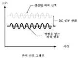
도 7은 본 발명에 따른 파워 신호 그래프의 예이다.
도 8은 본 발명에 따른 센서 그래프의 예이다.
도 9는 본 발명에 따른 파워 신호 그래프의 다른 예의 개략적인 블록도이다.
도 10은 본 발명에 따른 파워 신호 그래프의 다른 예의 개략적인 블록도이다.
도 11은 본 발명에 따른 파워 신호 그래프의 다른 예의 개략적인 블록도이다.
도 11a는 본 발명에 따른 파워 신호 그래프의 다른 예의 개략적인 블록도이다.
도 12는 본 발명에 따른 파워 신호 변화 검출 회로의 실시예의 개략적인 블록도이다.
도 13은 본 발명에 따른 드라이브 감지 회로의 다른 실시예의 개략적인 블록도이다.
도 14는 본 발명에 따른 드라이브 감지 회로의 다른 실시예의 개략적인 블록도이다.
도 15는 본 발명에 따른 드라이브 감지 회로의 다른 실시예의 개략적인 블록도이다.
도 16은 본 발명에 따른 드라이브 감지 회로의 다른 실시예의 개략적인 블록도이다.
도 17은 본 발명에 따른 드라이브 감지 회로의 다른 실시예의 개략적인 블록도이다.
도 18은 본 발명에 따른 드라이브 감지 회로의 다른 실시예의 개략적인 블록도이다.
도 19는 본 발명에 따른 드라이브 감지 회로의 다른 실시예의 개략적인 블록도이다.
도 20은 본 발명에 따른 드라이브 감지 회로의 다른 실시예의 개략적인 블록도이다.
도 21은 본 발명에 따른 드라이브 감지 회로의 다른 실시예의 개략적인 블록도이다.
도 22는 본 발명에 따른 드라이브 감지 회로의 다른 실시예의 개략적인 블록도이다.
도 23은 본 발명에 따른 드라이브 감지 회로의 다른 실시예의 개략적인 블록도이다.
도 24는 본 발명에 따른 드라이브 감지 회로의 다른 실시예의 개략적인 블록도이다.
도 25는 본 발명에 따른 드라이브 감지 회로의 다른 실시예의 개략적인 블록도이다.
도 26은 본 발명에 따른 드라이브 감지 회로의 다른 실시예의 개략적인 블록도이다.
도 27은 본 발명에 따른 드라이브 감지 회로의 다른 실시예의 개략적인 블록도이다.
도 28은 본 발명에 따른 드라이브 감지 회로의 다른 실시예의 개략적인 블록도이다.
도 29는 본 발명에 따른 드라이브 감지 회로의 다른 실시예의 개략적인 블록도이다.
도 30은 본 발명에 따른 드라이브 감지 회로의 다른 실시예의 개략적인 블록도이다.
도 31은 본 발명에 따른 드라이브 감지 회로의 다른 실시예의 개략적인 블록도이다.
도 32는 본 발명에 따른 드라이브 감지 회로의 다른 실시예의 개략적인 블록도이다.
도 33은 본 발명에 따른 드라이브 감지 회로의 다른 실시예의 개략적인 블록도이다.
도 34는 본 발명에 따른 드라이브 감지 회로의 다른 실시예의 개략적인 블록도이다.
도 35는 본 발명에 따른 드라이브 감지 회로의 다른 실시예의 개략적인 블록도이다.
도 36은 본 발명에 따른 드라이브 감지 회로의 다른 실시예의 개략적인 블록도이다.
도 37은 본 발명에 따른 드라이브 감지 회로의 다른 실시예의 개략적인 블록도이다.
도 38은 본 발명에 따른 드라이브 감지 회로의 다른 실시예의 개략적인 블록도이다.1 is a schematic block diagram of an embodiment of a communication system according to the present invention.
2 is a schematic block diagram of an embodiment of a computing device in accordance with the present invention.
3 is a schematic block diagram of another embodiment of a computing device in accordance with the present invention.
4 is a schematic block diagram of another embodiment of a computing device in accordance with the present invention.
5A is a schematic plot diagram of a computing subsystem in accordance with the present invention.
5B is a schematic block diagram of another embodiment of a computing subsystem according to the present invention.
5C is a schematic block diagram of another embodiment of a computing subsystem according to the present invention.
5D is a schematic block diagram of another embodiment of a computing subsystem according to the present invention.
5E is a schematic block diagram of another embodiment of a computing subsystem according to the present invention.
6 is a schematic block diagram of an embodiment of a drive sensing circuit according to the present invention.
6A is a schematic block diagram of another embodiment of a drive sensing circuit according to the present invention.
7 is an example of a power signal graph according to the present invention.
8 is an example of a sensor graph according to the present invention.
9 is a schematic block diagram of another example of a power signal graph according to the present invention.
10 is a schematic block diagram of another example of a power signal graph according to the present invention.
11 is a schematic block diagram of another example of a power signal graph according to the present invention.
11A is a schematic block diagram of another example of a power signal graph according to the present invention.
12 is a schematic block diagram of an embodiment of a power signal change detection circuit according to the present invention.
13 is a schematic block diagram of another embodiment of a drive sensing circuit according to the present invention.
14 is a schematic block diagram of another embodiment of a drive sensing circuit according to the present invention.
15 is a schematic block diagram of another embodiment of a drive sensing circuit according to the present invention.
16 is a schematic block diagram of another embodiment of a drive sensing circuit according to the present invention.
17 is a schematic block diagram of another embodiment of a drive sensing circuit according to the present invention.
18 is a schematic block diagram of another embodiment of a drive sensing circuit according to the present invention.
19 is a schematic block diagram of another embodiment of a drive sensing circuit according to the present invention.
20 is a schematic block diagram of another embodiment of a drive sensing circuit according to the present invention.
21 is a schematic block diagram of another embodiment of a drive sensing circuit according to the present invention.
22 is a schematic block diagram of another embodiment of a drive sensing circuit according to the present invention.
23 is a schematic block diagram of another embodiment of a drive sensing circuit according to the present invention.
24 is a schematic block diagram of another embodiment of a drive sensing circuit according to the present invention.
25 is a schematic block diagram of another embodiment of a drive sensing circuit according to the present invention.
26 is a schematic block diagram of another embodiment of a drive sensing circuit according to the present invention.
27 is a schematic block diagram of another embodiment of a drive sensing circuit according to the present invention.
28 is a schematic block diagram of another embodiment of a drive sensing circuit according to the present invention.
29 is a schematic block diagram of another embodiment of a drive sensing circuit according to the present invention.
30 is a schematic block diagram of another embodiment of a drive sensing circuit according to the present invention.
31 is a schematic block diagram of another embodiment of a drive sensing circuit according to the present invention.
32 is a schematic block diagram of another embodiment of a drive sensing circuit according to the present invention.
33 is a schematic block diagram of another embodiment of a drive sensing circuit according to the present invention.
34 is a schematic block diagram of another embodiment of a drive sensing circuit according to the present invention.
35 is a schematic block diagram of another embodiment of a drive sensing circuit according to the present invention.
36 is a schematic block diagram of another embodiment of a drive sensing circuit according to the present invention.
37 is a schematic block diagram of another embodiment of a drive sensing circuit according to the present invention.
38 is a schematic block diagram of another embodiment of a drive sensing circuit according to the present invention.
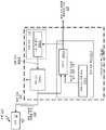
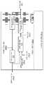
도 1은 복수의 컴퓨팅을 포함하는 통신 시스템 (10)의 실시예의 개략적인 블록도이다. 디바이스 (12-10), 하나 이상의 서버 (22), 하나 이상의 데이터베이스 (24), 하나 이상의 네트워크 (26), 복수의 드라이브 감지 회로 (28), 복수의 센서 (30) 및 복수의 액추에이터 (32). 컴퓨팅 디바이스 (14)는 센서 및 드라이브 센서 회로를 갖는 터치 스크린 (16)을 포함하고, 컴퓨팅 디바이스 (18)는 센서, 액추에이터 및 드라이브 감지 회로를 포함하는 터치 및 촉각(tactic) 스크린 (20)을 포함한다.1 is a schematic block diagram of an embodiment of a communication system 10 including a plurality of computing. Devices 12-10, one or more servers 22, one or
센서 (30)는 물리적 입력을 전기 출력 및/또는 광 출력으로 변환하는 기능을 한다. 센서의 물리적 입력은 다양한 물리적 입력 상태 중 하나일 수 있다. 예를 들어, 물리적 상태는 음향파(acoustic wave) (예를 들어, 진폭, 위상, 편광, 스펙트럼 및/또는 파동 속도); 생물학적 및/또는 화학적 상태 (예를 들어, 유체 농도, 레벨, 조성 등); 전기적 상태 (예를 들어, 전하, 전압, 전류, 전도도, 유전율, 진폭, 위상 및/또는 분극화를 포함하는 절충계(eclectic field)); 자기적 상태 (예를 들어, 자속, 투과성, 자기장, 진폭, 위상 및/또는 분극화를 포함하는 자계); 광학 상태 (예를 들어, 굴절률, 반사도, 흡수률 등); 열적 상태 (예를 들어, 온도, 유속, 비열, 열전도율 등); 및 기계적 상태 (예를 들어, 위치, 속도, 가속도, 힘, 스트레인(strain), 응력(stress), 압력, 토크 등) 중 하나 이상을 포함하지만 이에 한정되지는 않는다. 예를 들어, 압전 센서는 힘이나 압력을 절충 신호(eclectic signal)로 변환한다. 또 다른 예로, 마이크는 가청 음향파를 전기 신호로 변환한다.The
다양한 유형의 물리적 상태를 감지하기 위한 다양한 유형의 센서가 있다. 센서 유형은 커패시터 센서, 유도성 센서, 가속도계, 압전 센서, 광 센서, 자기장 센서, 초음향파 센서, 온도 센서, 적외선 (IR) 센서, 터치 센서, 근접 센서, 압력 센서, 레벨 센서, 연기 센서 및 가스 센서를 포함하지만 이에 한정되지는 않는다. 여러 면에서, 센서는 실제 상태를 디지털 신호로 변환하고 그런 다음 의료 애플리케이션, 생산 자동화 애플리케이션, 가정 환경 제어, 공공 안전 등을 포함하되 이에 한정되지 않는 방대한 애플리케이션을 위해 컴퓨팅 디바이스에 의해 처리되는 물리적 세계와 디지털 세계 간의 인터페이스 역할을 한다.There are different types of sensors to detect different types of physical states. Sensor types include capacitor sensor, inductive sensor, accelerometer, piezoelectric sensor, light sensor, magnetic field sensor, ultrasonic sensor, temperature sensor, infrared (IR) sensor, touch sensor, proximity sensor, pressure sensor, level sensor, smoke sensor and Including, but not limited to, gas sensors. In many ways, sensors convert real state into digital signals, and then the physical world and the physical world processed by computing devices for a wide variety of applications, including, but not limited to, medical applications, production automation applications, home environmental control, public safety, etc. It serves as an interface between the digital worlds.
다양한 유형의 센서는 센서에 파워를 제공하고, 센서로부터 신호를 수신하고, 및/또는 센서로부터의 신호를 해석하는 인자(factor)인 다양한 센서 특성을 갖는다. 센서 특성은 저항, 리액턴스, 파워 요구 사항, 감도, 범위, 안정성, 반복성, 선형성, 에러, 응답 시간 및/또는 주파수 응답을 포함한다. 예를 들어, 저항, 리액턴스 및/또는 파워 요구 사항은 드라이브 회로 요구 사항을 결정하는 인자이다. 다른 예로서, 감도, 안정성 및/또는 선형성은 수신된 전기 및/또는 광 신호 (예를 들어, 온도, 압력 등의 측정)에 기초하여 물리적 상태의 측정을 해석하기 위한 인자이다.Various types of sensors have various sensor characteristics, which are factors that provide power to the sensor, receive signals from the sensor, and/or interpret signals from the sensor. Sensor characteristics include resistance, reactance, power requirements, sensitivity, range, stability, repeatability, linearity, error, response time and/or frequency response. For example, resistance, reactance, and/or power requirements are factors that determine drive circuit requirements. As another example, sensitivity, stability and/or linearity are factors for interpreting measurements of physical states based on received electrical and/or optical signals (eg, measurements of temperature, pressure, etc.).
액추에이터 (32)는 전기 입력을 물리적 출력으로 변환한다. 액추에이터의 물리적 출력은 다양한 물리적 출력 상태 중 하나일 수 있다. 예를 들어, 물리적 출력 상태는 음향파 (예를 들어, 진폭, 위상, 편광, 스펙트럼 및/또는 파동 속도), 자기 상태 (예를 들어, 자속, 투과성, 자기장, 진폭, 위상 및/또는 분극화); 열적 상태 (예를 들어, 온도, 유속(flux), 비열, 열전도율 등); 및 기계적 상태 (예를 들어, 위치, 속도, 가속도, 힘, 스트레인, 응력, 압력, 토크 등) 중 하나 이상을 포함하지만 이에 한정되지는 않는다. 예를 들어, 압전 액추에이터는 전압을 힘 또는 압력으로 변환합니다. 다른 예로, 스피커는 전기 신호를 가청 음향파로 변환한다.Actuator 32 converts an electrical input into a physical output. The physical output of the actuator can be one of a variety of physical output states. For example, the physical output states are acoustic waves (e.g., amplitude, phase, polarization, spectral and/or wave velocity), magnetic states (e.g., magnetic flux, permeability, magnetic field, amplitude, phase and/or polarization). ; Thermal state (eg, temperature, flux, specific heat, thermal conductivity, etc.); And one or more of a mechanical state (eg, position, velocity, acceleration, force, strain, stress, pressure, torque, etc.). Piezo actuators, for example, convert voltage into force or pressure. As another example, the speaker converts the electrical signal into an audible acoustic wave.
액추에이터 (32)는 다양한 액추에이터 중 하나일 수 있다. 예를 들어, 액추에이터 (32)는 콤 드라이브(comb drive), 디지털 마이크로 미러 디바이스, 전기 모터, 전기 활성 폴리머, 유압 실린더, 압전 액추에이터, 공압 액추에이터, 스크류 잭, 서보 메커니즘, 솔레노이드, 스테퍼 모터, 형상 메모리 얼라우(shape-memory allow), 열 바이모프(thermal bimorph) 및 유압 액추에이터 중 하나이다.Actuator 32 can be one of a variety of actuators. For example, actuator 32 may be a comb drive, digital micromirror device, electric motor, electroactive polymer, hydraulic cylinder, piezoelectric actuator, pneumatic actuator, screw jack, servo mechanism, solenoid, stepper motor, shape memory. It is one of the shape-memory allow, thermal bimorph and hydraulic actuators.
다양한 유형의 액추에이터는 액추에이터에 파워를 제공하고 원하는 성능을 위해 액추에이터에 신호를 발송하는 인자인 다양한 액추에이터 특성을 갖는다. 액추에이터 특성은 저항, 리액턴스, 파워 요구 사항, 감도, 범위, 안정성, 반복성, 선형성, 에러, 응답 시간 및/또는 주파수 응답을 포함한다. 예를 들어, 저항, 리액턴스 및 파워 요구 사항은 드라이브 회로 요구 사항을 결정하는 인자이다. 또 다른 예로서, 감도, 안정성 및/또는 선형성은 원하는 물리적 출력 상태를 얻기 위해 액추에이터에 발송할 신호를 생성하는 인자이다.Various types of actuators have different actuator characteristics, which are factors that provide power to the actuator and signal the actuator for the desired performance. Actuator characteristics include resistance, reactance, power requirements, sensitivity, range, stability, repeatability, linearity, error, response time and/or frequency response. For example, resistance, reactance, and power requirements are factors that determine drive circuit requirements. As another example, sensitivity, stability, and/or linearity are factors that generate a signal to be sent to the actuator to obtain the desired physical output state.
컴퓨팅 디바이스 (12, 14, 18)는 각각 휴대용 컴퓨팅 디바이스 및/또는 고정 컴퓨팅 디바이스일 수 있다. 휴대용 컴퓨팅 디바이스는 소셜 네트워킹 디바이스, 게임 디바이스, 휴대폰, 스마트 폰, 디지털 어시스턴트, 디지털 음악 플레이어, 디지털 비디오 플레이어, 랩톱 컴퓨터, 핸드 헬드 컴퓨터, 태블릿, 비디오 게임 컨트롤러 및/또는 컴퓨팅 코어를 포함하는 다른 휴대용 디바이스일 수 있다. 고정 컴퓨팅 디바이스는 컴퓨터 (PC), 컴퓨터 서버, 케이블 셋톱 박스, 위성 수신기, 텔레비전 세트, 프린터, 팩스, 홈 엔터테인먼트 장비, 비디오 게임 콘솔 및/또는 임의 유형의 가정 또는 사무실 컴퓨팅 장비일 수 있다. 컴퓨팅 디바이스 (12, 14, 18)는 도 2-4 중 하나 이상을 참조하여 더 상세히 논의될 것이다.Computing devices 12, 14, 18 can each be a portable computing device and/or a fixed computing device. Portable computing devices include social networking devices, gaming devices, mobile phones, smart phones, digital assistants, digital music players, digital video players, laptop computers, handheld computers, tablets, video game controllers, and/or other portable devices including computing cores. Can be The fixed computing device may be a computer (PC), computer server, cable set top box, satellite receiver, television set, printer, fax machine, home entertainment equipment, video game console, and/or any type of home or office computing equipment. Computing devices 12, 14, 18 will be discussed in more detail with reference to one or more of FIGS. 2-4.
서버 (22)는 대량의 데이터 요청을 병렬로 처리하도록 최적화된 특수한 유형의 컴퓨팅 디바이스다. 서버 (22)는 더 강력한 처리 모듈, 더 많은 메인 메모리 및/또는 더 많은 하드 드라이브 메모리 (예를 들어, 솔리드 스테이트, 하드 드라이브 등)를 갖는 컴퓨팅 디바이스 (12, 14 및/또는 18)의 컴포넌트와 유사한 컴포넌트를 포함한다. 또한, 서버 (22)는 일반적으로 원격 액세스된다; 따라서 일반적으로 사용자 입력 디바이스 및/또는 사용자 출력 디바이스를 포함하지 않는다. 또한, 서버는 독립형 개별 컴퓨팅 디바이스 및/또는 클라우드 컴퓨팅 디바이스일 수 있다.Server 22 is a special type of computing device optimized to process large data requests in parallel. Server 22 includes components of computing devices 12, 14 and/or 18 with more powerful processing modules, more main memory and/or more hard drive memory (e.g., solid state, hard drives, etc.). It contains similar components. Also, the server 22 is generally remotely accessed; Therefore, it generally does not include a user input device and/or a user output device. Further, the server may be a standalone individual computing device and/or a cloud computing device.
데이터베이스 (24)는 대규모 데이터 저장 및 검색에 최적화된 특별한 유형의 컴퓨팅 디바이스다. 데이터베이스 (24)는 더 많은 하드 드라이브 메모리 (예를 들어, 솔리드 스테이트, 하드 드라이브 등) 및 잠재적으로 더 많은 처리 모듈 및/또는 메인 메모리를 갖는 컴퓨팅 디바이스 (12, 14 및/또는 18)의 컴포넌트와 유사한 컴포넌트를 포함한다. 또한, 데이터베이스 (24)는 일반적으로 원격 액세스된다; 따라서 일반적으로 사용자 입력 디바이스 및/또는 사용자 출력 디바이스를 포함하지 않는다. 또한, 데이터베이스 (24)는 독립형 개별 컴퓨팅 디바이스일 수 있고 및/또는 클라우드 컴퓨팅 디바이스일 수 있다.
네트워크 (26)는 하나 이상의 근거리 네트워크 (LAN) 및/또는 하나 이상의 광역 네트워크 (WAN)를 포함하며, 이는 공용 네트워크 및/또는 사설 네트워크일 수 있다. LAN은 무선 LAN (예를 들어, Wi-Fi 액세스 포인트, 블루투스(Bluetooth), 지그비(ZigBee) 등) 및/또는 유선 네트워크 (예를 들어, 파이어와이어(Firewire), 이더넷 등)일 수 있다. WAN은 유선 및/또는 무선 WAN일 수 있다. 예를 들어, LAN은 개인 가정 또는 기업의 무선 네트워크일 수 있고 WAN은 인터넷, 휴대 전화 인프라 및/또는 위성 통신 인프라이다.Network 26 includes one or more local area networks (LANs) and/or one or more wide area networks (WANs), which may be public and/or private networks. The LAN may be a wireless LAN (eg, a Wi-Fi access point, Bluetooth, ZigBee, etc.) and/or a wired network (eg, Firewire, Ethernet, etc.). The WAN may be a wired and/or wireless WAN. For example, a LAN may be a private home or business wireless network and a WAN is the Internet, a cellular phone infrastructure, and/or a satellite communications infrastructure.
동작의 예에서, 컴퓨팅 디바이스 (12-1)는 복수의 드라이브 감지 회로 (28)와 통신하고, 이는 결국 복수의 센서 (30)와 통신한다. 센서 (30) 및/또는 드라이브 감지 회로 (28)는 컴퓨팅 디바이스 (12-1) 내부 및/또는 그 외부에 있다. 예를 들어, 센서 (30)는 컴퓨팅 디바이스 (12-1)의 외부에 있을 수 있고 드라이브 감지 회로는 컴퓨팅 디바이스 (12-1) 내에 있다. 다른 예로서, 센서 (30)와 드라이브 감지 회로 (28)는 둘 모두 컴퓨팅 디바이스 (12-1)의 외부에 있다. 드라이브 감지 회로 (28)가 컴퓨팅 디바이스의 외부에 있을 때, 도 5a 내지 5c 중 하나 이상을 참조하여 더 상세히 논의되는 바와 같이 유선 및/또는 무선 통신 링크를 통해 컴퓨팅 디바이스 (12-1)에 결합된다.In an example of operation, computing device 12-1 communicates with a plurality of
컴퓨팅 디바이스 (12-1)는 드라이브 감지 회로 (28)와 통신하여; (a) 전원을 켜고, (b) 센서로부터 데이터를 획득하고 (개별적으로 및/또는 집합적으로), (c) 감지된 데이터를 컴퓨팅 디바이스 (12-1)에 전달하는 방법에 대해 드라이브 감지 회로에 지시하고, (d) 제공 센서와 함께 사용할 시그널링 속성 (예를 들어, DC 레벨, AC 레벨, 주파수, 파워 레벨, 정류된(regulated) 전류 신호, 정류된 전압 신호, 임피던스 정류, 다양한 센서의 주파수 패턴, 다른 감지 애플리케이션에 대한 상이한 주파수 등), 및/또는 (e) 다른 명령 및/또는 지침을 제공한다.The computing device 12-1 communicates with the
특정 예로서, 센서 (30)는 파이프 라인의 섹션 내의 유량(flow rate) 및/또는 압력을 측정하기 위해 파이프 라인을 따라 분포된다. 드라이브 감지 회로 (28)는 자신의 전원(power source) (예를 들어, 배터리, 전원 등)을 가지며 각각의 센서 (30)에 근접하게 위치된다. 원하는 시간 간격 (밀리 초, 초, 분, 시간 등)에서, 드라이브 감지 회로 (28)는 정류된 소스 신호 또는 파워 신호를 센서 (30)에 제공한다. 센서 (30)의 전기적 특성은 정류된 소스 신호 또는 파워 신호에 영향을 미치며, 이는 센서가 감지하는 상태 (예를 들어, 유량 및/또는 압력)를 반영한다.As a specific example, the
드라이브 감지 회로 (28)는 센서의 전기적 특성의 결과로서 정류된 소스 신호 또는 파워 신호에 대한 영향을 검출한다. 그런 다음, 드라이브 감지 회로 (28)는 파워 신호에 대한 검출된 영향에 기초하여 정류된 소스 신호 또는 파워 신호에 대한 변화를 나타내는 신호를 생성한다. 정류된 소스 신호 또는 파워 신호에 대한 변화는 센서 (30)에 의해 감지되는 상태를 나타낸다.The
드라이브 감지 회로 (28)는 상태의 대표 신호를 컴퓨팅 디바이스 (12-1)에 제공한다. 대표 신호는 아날로그 신호 또는 디지털 신호일 수 있다. 어느 경우이든, 컴퓨팅 디바이스 (12-1)는 파이프 라인을 따라 각각의 센서 위치에서 압력 및/또는 유량을 결정하기 위해 대표 신호를 해석한다. 컴퓨팅 디바이스는 그런 다음 이 정보를 서버 (22), 데이터베이스 (24) 및/또는 저장 및/또는 추가 처리를 위해 다른 컴퓨팅 디바이스에 제공할 수 있다.The
동작의 다른 예로서, 컴퓨팅 디바이스 (12-2)는 드라이브 감지 회로 (28)에 결합되고, 이는 결국 센서 (30)에 결합된다. 센서 (30) 및/또는 드라이브 감지 회로 (28)는 컴퓨팅 디바이스 (12-2)의 내부 및/또는 외부에 있을 수 있다. 이 예에서, 센서 (30)는 컴퓨팅 디바이스 (12-2)에 특정한 상태를 감지하고 있다. 예를 들어, 센서 (30)는 온도 센서, 주변 광 센서, 주변 소음 센서 등일 수 있다. 전술한 바와 같이, 컴퓨팅 디바이스 (12-2)에 의해 지시될 때 (일정한 간격 또는 연속 감지를 위한 디폴트 설정일 수 있음), 드라이브 감지 회로 (28)는 정류된 소스 신호 또는 파워 신호를 센서 (30)에 제공하고 센서의 전기적 특성에 따라 정류된 소스 신호 또는 파워 신호에 영향을 검출한다. 드라이브 감지 회로는 해당 영향의 대표 신호를 생성하여 그것을 컴퓨팅 디바이스 (12-2)로 발송한다.As another example of operation, the computing device 12-2 is coupled to the
동작의 다른 예에서, 컴퓨팅 디바이스 (12-3)는 복수의 센서 (30)에 결합된 복수의 드라이브 감지 회로 (28)에 결합되고, 복수의 액추에이터 (32)에 결합된 복수의 드라이브 감지 회로 (28)에 결합된다. 상기 설명에 따라 센서 (30)에 결합된 드라이브 감지 회로 (28)의 일반적 기능.In another example of operation, the computing device 12-3 is coupled to a plurality of
액추에이터 (32)는 본질적으로 액추에이터가 전기 신호를 물리적 상태로 변환한다는 점에서 센서의 역이기 때문에, 센서가 물리적 상태를 전기 신호로 변환하는 동안, 드라이브 감지 회로 (28)는 액추에이터 (32)에 파워를 공급하는 데 사용될 수 있다. 따라서, 이 예에서, 컴퓨팅 디바이스 (12-3)는 드라이브 감지 회로 (28)에 액추에이터 (32)를 위한 액추에이션 신호를 제공한다. 드라이브 감지 회로는 액추에이션 신호를 액추에이터 (32)에 제공되는 파워 신호 또는 정류된 제어 신호로 변조한다. 액추에이터 (32)는 파워 신호 또는 정류된 제어 신호로부터 파워를 공급 받고 변조된 액추에이션 신호로부터 원하는 물리적 상태를 생성한다.Since actuator 32 is essentially the inverse of the sensor in that the actuator converts the electrical signal into a physical state, while the sensor converts the physical state into an electrical signal, the
동작의 다른 예로서, 컴퓨팅 디바이스 (12-x)는 센서 (30)에 결합된 드라이브 감지 회로 (28)에 결합되고, 액추에이터 (32)에 결합된 드라이브 감지 회로 (28)에 결합된다. 이 예에서, 센서 (30) 및 액추에이터 (32)는 컴퓨팅 디바이스 (12-x)에 의해 사용된다. 예를 들어, 센서 (30)는 압전 마이크로폰이고, 액추에이터 (32)는 압전 스피커일 수 있다.As another example of operation, the computing device 12-x is coupled to the
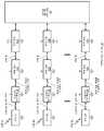
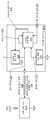
도 2는 컴퓨팅 디바이스 (12) (예를 들어, 12-1 내지 12-x 중 어느 하나)의 실시예의 개략적인 블록도이다. 컴퓨팅 디바이스 (12)는 코어 제어 모듈 (40), 하나 이상의 처리 모듈 (42), 하나 이상의 메인 메모리 (44), 캐시 메모리 (46), 비디오 그래픽 처리 모듈 (48), 디스플레이 (50), 입력-출력 (I/O) 주변 제어 모듈 (52), 하나 이상의 입력 인터페이스 모듈 (56), 하나 이상의 출력 인터페이스 모듈 (58), 하나 이상의 네트워크 인터페이스 모듈 (60), 및 하나 이상의 메모리 인터페이스 모듈 (62)을 포함한다. 처리 모듈 (42)은 본 발명 섹션의 상세한 설명의 끝에서 더 상세히 설명되고, 대안적인 실시예에서 메인 메모리 (44)에 대한 방향성 연결을 갖는다. 대안적인 실시예에서, 코어 제어 모듈 (40) 및 I/O 및/또는 주변 제어 모듈 (52)은 칩셋, QPI (Quick Path Interconnect) 및/또는 UPI (Ultra-Path Interconnect)와 같은 하나의 모듈이다.2 is a schematic block diagram of an embodiment of computing device 12 (eg, any one of 12-1 to 12-x). Computing device 12 includes
각각의 메인 메모리 (44)는 하나 이상의 RAM (Random Access Memory) 집적 회로 또는 칩을 포함한다. 예를 들어, 메인 메모리 (44)는 각각 2,400MHz의 속도로 실행되는 4 개의 DDR4 (4 세대 더블 데이터 속도) RAM 칩을 포함한다. 일반적으로, 메인 메모리 (44)는 처리 모듈 (42)에 가장 관련된 데이터 및 동작 지침을 저장한다. 예를 들어, 코어 제어 모듈 (40)은 메인 메모리 (44) 및 메모리 (64-66)로부터의 데이터 및/또는 동작 지침의 전송을 정류한다. 메모리 (64-66)로부터 검색된 데이터 및/또는 동작 지침은 처리 모듈에 의해 요청된 데이터 및/또는 동작 지침이거나 처리 모듈에 의해 가장 필요할 것이다. 처리 모듈이 메인 메모리의 데이터 및/또는 동작 지침으로 완료될 때, 코어 제어 모듈 (40)은 저장을 위해 업데이트된 데이터를 메모리 (64-66)로 발송하는 것을 정류한다.Each main memory 44 includes one or more random access memory (RAM) integrated circuits or chips. For example, main memory 44 contains four DDR4 (4th generation double data rate) RAM chips each running at a speed of 2,400MHz. In general, main memory 44 stores data and operating instructions most relevant to
메모리 (64-66)는 캐시 메모리 및 메인 메모리 디바이스와 비교하여 상대적으로 저장된 데이터 양당 비용이 저렴한 하나 이상의 하드 드라이브, 하나 이상의 솔리드 스테이트 메모리 칩, 및/또는 하나 이상의 다른 대용량 저장 디바이스를 포함한다. 메모리 (64-66)는 I/O 및/또는 주변 제어 모듈 (52)을 통해 그리고 하나 이상의 메모리 인터페이스 모듈 (62)을 통해 코어 제어 모듈 (40)에 결합된다. 일 실시예에서, I/O 및/또는 주변 제어 모듈 (52)은 주변 컴포넌트가 코어 제어 모듈 (40)에 연결되는 하나 이상의 주변 컴포넌트 인터페이스 (PCI) 버스를 포함한다. 메모리 인터페이스 모듈 (62)은 메모리 디바이스를 I/O 및/또는 주변 제어 모듈 (52)에 결합하기 위한 소프트웨어 드라이버 및 하드웨어 커넥터를 포함한다. 예를 들어, 메모리 인터페이스 (62)는 SATA (Serial Advanced Technology Attachment) 포트를 따른다.The memories 64-66 include one or more hard drives, one or more solid state memory chips, and/or one or more other mass storage devices that are relatively low in cost per amount of stored data compared to cache memory and main memory devices. The memories 64-66 are coupled to the
코어 제어 모듈 (40)은 I/O 및/또는 주변 제어 모듈 (52), 네트워크 인터페이스 모듈(들) (60), 및 네트워크 인터페이스 모듈(들) (60), 네트워크 카드 (68 또는 70)를 통해 처리 모듈(들) (42)과 네트워크(들) (26) 사이의 데이터 통신을 정류한다. 네트워크 카드 (68 또는 70)는 무선 통신 유닛 또는 유선 통신 유닛을 포함한다. 무선 통신 유닛은 무선 근거리 통신망 (WLAN) 통신 디바이스, 셀룰러 통신 디바이스, 블루투스 디바이스 및/또는 지그비 통신 디바이스를 포함한다. 유선 통신 디바이스는 기가비트 LAN 연결, 파이어와이어(Firewire) 연결 및/또는 독점 컴퓨터 유선 연결을 포함한다. 네트워크 인터페이스 모듈 (60)은 네트워크 카드를 I/O 및/또는 주변 제어 모듈 (52)에 결합하기 위한 소프트웨어 드라이버 및 하드웨어 커넥터를 포함한다. 예를 들어, 네트워크 인터페이스 모듈 (60)은 IEEE 802.11, 셀룰러 전화 프로토콜, 10/100/1000 기가비트 LAN 프로토콜 등의 하나 이상의 버전을 따른다.The
코어 제어 모듈 (40)은 입력 인터페이스 모듈(들) (56)과 I/O 및/또는 주변 제어 모듈 (52)을 통해 처리 모듈(들) (42)과 입력 디바이스(들) (72) 사이에서 데이터 통신을 정류한다. 입력 디바이스 (72)는 키패드, 키보드, 제어 스위치, 터치 패드, 마이크로폰, 카메라 등을 포함한다. 입력 인터페이스 모듈 (56)은 입력 디바이스를 I/O 및/또는 주변 제어 모듈 (52)에 결합하기 위한 소프트웨어 드라이버 및 하드웨어 커넥터를 포함한다. 일 실시예에서, 입력 인터페이스 모듈 (56)은 하나 이상의 범용 직렬 버스 (USB) 프로토콜에 따른다.The
코어 제어 모듈 (40)은 출력 인터페이스 모듈(들) (58)과 I/O 및/또는 주변 제어 모듈 (52)을 통해 처리 모듈(들) (42)과 출력 디바이스(들) (74) 사이에서 데이터 통신을 정류한다. 출력 디바이스 (74)는 스피커 등을 포함한다. 출력 인터페이스 모듈 (58)은 출력 디바이스를 I/O 및/또는 주변 제어 모듈 (52)에 결합하기 위한 소프트웨어 드라이버 및 하드웨어 커넥터를 포함한다. 일 실시예에서, 출력 인터페이스 모듈 (56)은 하나 이상의 오디오 코덱 프로토콜에 따른다.The
처리 모듈 (42)은 디스플레이 (50) 상에 데이터를 디스플레이하기 위해 비디오 그래픽 처리 모듈 (48)과 직접 통신한다. 디스플레이 (50)는 LED (발광 다이오드) 디스플레이, LCD (액정 디스플레이) 및/또는 다른 유형의 디스플레이 기술을 포함한다. 디스플레이는 디스플레이 품질에 영향을 미치는 해상도, 종횡비 및 다른 기능을 가진다. 비디오 그래픽 처리 모듈 (48)은 처리 모듈 (42)로부터 데이터를 수신하고, 데이터를 처리하여 디스플레이의 특성에 따라 렌더링된 데이터를 생성하고, 렌더링된 데이터를 디스플레이 (50)에 제공한다.The
도 2는 입력 인터페이스 모듈 (56) (예를 들어, USB 포트)에 연결된 드라이브 감지 회로 (28)에 연결된 센서 (30) 및 액추에이터 (32)를 추가로 도시한다. 대안적으로, 하나 이상의 드라이브 감지 회로 (28)는 무선 네트워크 카드 (예를 들어, WLAN) 또는 유선 네트워크 카드 (예를 들어, 기가비트 LAN)를 통해 컴퓨팅 디바이스에 결합된다. 도시되지 않았지만, 컴퓨팅 디바이스 (12)는 코어 제어 모듈 (40)에 연결된 BIOS (Basic Input Output System) 메모리를 더 포함한다.2 further shows the
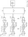
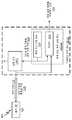
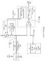
도 3은 코어 제어 모듈 (40), 하나 이상의 처리 모듈 (42), 하나 이상의 메인 메모리 (44), 캐시 메모리 (46), 비디오 그래픽 처리 모듈 (48), 터치 스크린 (16), 입력-출력 (I/O) 주변 제어 모듈 (52), 하나 이상의 입력 인터페이스 모듈 (56), 하나 이상의 출력 인터페이스 모듈 (58), 하나 이상의 네트워크 인터페이스 모듈 (60) 및 하나 이상의 메모리 인터페이스 모듈 (62)을 포함하는 컴퓨팅 디바이스 (14)의 다른 실시예의 개략적인 블록도이다. 터치 스크린 (16)은 터치 스크린 디스플레이 (80), 복수의 센서 (30), 복수의 드라이브 감지 회로 (DSC : drive-sense circuit) 및 터치 스크린 처리 모듈 (82)을 포함한다.3 shows a
컴퓨팅 디바이스 (14)는 입력 디바이스로서 터치 스크린을 추가하여 도 2의 컴퓨팅 디바이스 (12)와 유사하게 동작한다. 터치 스크린은 스크린의 근위 터치를 검출하기 위해 복수의 센서 (예를 들어, 전극, 커패시터 감지 셀, 커패시터 센서, 유도성 센서 등)를 포함한다. 예를 들어, 하나 이상의 손가락이 화면을 터치하면 터치에 근접한 센서의 커패시턴스가 영향을 받는다 (예를 들어, 임피던스 변화). 영향을 받는 센서에 결합된 드라이브 감지 회로 (DSC)는 변경을 검출하고 별도의 처리 모듈이거나 처리 모듈 (42)에 통합될 수 있는 터치 스크린 처리 모듈 (82)에 대한 변경의 표현을 제공한다.Computing device 14 operates similarly to computing device 12 of FIG. 2 by adding a touch screen as an input device. The touch screen includes a plurality of sensors (eg, electrodes, capacitor sensing cells, capacitor sensors, inductive sensors, etc.) to detect a proximal touch of the screen. For example, if more than one finger touches the screen, the capacitance of the sensor close to the touch is affected (eg, impedance change). A drive detection circuit (DSC) coupled to the affected sensor detects the change and provides a representation of the change to the touch screen processing module 82, which may be a separate processing module or incorporated into the
터치 스크린 처리 모듈 (82)은 터치(들)의 위치를 결정하기 위해 드라이브 감지 회로 (DSC)로부터의 대표 신호를 처리한다. 이 정보는 입력으로서 처리하기 위해 처리 모듈 (42)에 입력된다. 예를 들어, 터치는 화면의 버튼, 스크롤 기능, 확대/축소 기능 등의 선택을 나타낸다.The touch screen processing module 82 processes representative signals from the drive sensing circuit (DSC) to determine the location of the touch(s). This information is input to the
도 4는 코어 제어 모듈 (40), 하나 이상의 처리 모듈 (42), 하나 이상의 메인 메모리 (44), 캐시 메모리 (46), 비디오 그래픽 처리 모듈 (48), 터치 및 촉각 스크린 (20), 입력-출력 (I/O) 주변 제어 모듈 (52), 하나 이상의 입력 인터페이스 모듈 (56), 하나 이상의 출력 인터페이스 모듈 (58), 하나 이상의 네트워크 인터페이스 모듈 (60) 및 하나 이상의 메모리 인터페이스 모듈 (62)을 포함하는 컴퓨팅 디바이스 (18)의 다른 실시예의 개략적인 블록도이다. 터치 및 촉각 스크린 (20)은 터치 및 촉각 스크린 디스플레이 (90), 복수의 센서 (30), 복수의 액추에이터 (32), 복수의 드라이브 감지 회로 (DSC), 터치 스크린 처리 모듈 (82) 및 촉각 스크린 처리 모듈 (92)을 포함한다.4 shows a
컴퓨팅 디바이스 (18)는 출력 디바이스로서 스크린 (20)에 촉각 측면을 추가하여 도 3의 컴퓨팅 디바이스 (14)와 유사하게 동작한다. 스크린 (20)의 촉각 부분은 스크린 (20)에 촉감을 제공하기 위해 복수의 액추에이터 (예를 들어, 발진을 생성하는 압전 트랜스듀서, 움직임을 생성하는 솔레노이드 등)를 포함한다. 그렇게 하기 위해, 처리 모듈은 촉각 데이터를 생성하는데, 이는 촉각 스크린 처리 모듈 (92)을 통해 적절한 드라이브 감지 회로 (DSC)에 제공되며, 이는 독립형 처리 모듈이거나 처리 모듈 (42)에 통합될 수 있다. 드라이브 감지 회로 (DSC)는 촉각 데이터를 드라이브 동작 신호(drive-actuate signal)로 변환하고 이를 적절한 액추에이터에 제공하여 스크린 (20)에 원하는 촉감을 생성한다.Computing device 18 operates similarly to computing device 14 of FIG. 3 by adding a tactile aspect to screen 20 as an output device. The tactile portion of the screen 20 includes a plurality of actuators (eg, a piezoelectric transducer generating oscillation, a solenoid generating motion, etc.) to provide a tactile sensation to the screen 20. To do so, the processing module generates tactile data, which is provided to the appropriate drive sensing circuit (DSC) via the tactile screen processing module 92, which may be a standalone processing module or integrated into the
도 5a는 감지된 데이터 처리 모듈 (65), 복수의 통신 모듈 (61A-x), 복수의 처리 모듈 (42A-x), 복수의 드라이브 감지 회로 (28), 및 도 1의 센서 (30)일 수 있는 복수의 센서 (1-x)를 포함하는 컴퓨팅 서브 시스템 (25)의 개략도이다. 감지된 데이터 처리 모듈 (65)은 하나 이상의 서버 (22) 내의 하나 이상의 처리 모듈 및/또는 처리 모듈 (42A-x)이 상주하는 컴퓨팅 디바이스와 상이한 하나 이상의 컴퓨팅 디바이스 내의 하나 이상의 처리 모듈이다.5A is a sensed
드라이브 감지 회로 (28) (또는 다수의 드라이브 감지 회로), 처리 모듈 (예를 들어, 41A) 및 통신 모듈 (예를 들어, 61A)은 공통 컴퓨팅 디바이스 내에 있다. 드라이브 감지 회로(들), 처리 모듈 및 통신 모듈의 각각의 그룹은 별도의 컴퓨팅 디바이스에 있다. 통신 모듈 (61A-x)는 하나 이상의 OSI (Open System Interconnection) 모델, 전송 제어 프로토콜/인터넷 프로토콜 (TCP/IP) 모델 및 다른 통신 프로토콜 모듈에 따른 하나 이상의 유선 통신 프로토콜 및/또는 하나 이상의 무선 통신 프로토콜에 따라 구성된다.Drive sense circuit 28 (or multiple drive sense circuits), processing module (e.g., 41A) and communication module (e.g., 61A) are within a common computing device. Each group of drive sensing circuit(s), processing module and communication module is on a separate computing device. The
동작의 예에서, 처리 모듈 (예를 들어, 42A)은 제어 신호를 대응하는 드라이브 감지 회로 (28)에 제공한다. 처리 모듈 (42A)은 제어 신호를 생성하거나, 감지된 데이터 처리 모듈 (65)로부터 수신하거나, 감지된 데이터 처리 모듈 (65)로부터 표시를 수신하여 제어 신호를 생성할 수 있다. 제어 신호는 드라이브 감지 회로 (28)가 대응하는 센서에 드라이브 신호를 제공할 수 있게 한다. 제어 신호는 드라이브 신호의 생성 및/또는 센서로부터 수신된 감지 신호의 해석을 가능하게 하기 위해 하나 이상의 주파수 성분을 갖는 기준 신호를 더 포함할 수 있다.In an example of operation, a processing module (e.g., 42A) provides a control signal to a corresponding
제어 신호에 기초하여, 드라이브 감지 회로 (28)는 드라이브 & 감지 라인상의 대응 센서 (예를 들어, 1)에 드라이브 신호를 제공한다. 드라이브 신호 (예를 들어, 파워 신호, 정류된 소스 신호 등)를 수신하는 동안 센서는 물리적 상태 (1-x) (예를 들어, 음향파, 생물학적 상태, 화학적 상태, 전기적 상태, 자기 상태, 광학 상태, 열적 상태 및/또는 기계적 상태)를 감지한다. 물리적 상태의 결과로 센서의 전기적 특성 (예를 들어, 임피던스, 전압, 전류, 커패시턴스, 인덕턴스, 저항, 리액턴스 등)이 변경되어 드라이브 신호에 영향을 미친다. 센서가 광학 센서인 경우 감지된 광학 상태를 전기적 특성으로 변환한다.Based on the control signal, the
드라이브 감지 회로 (28)는 드라이브 & 감지 라인을 통해 드라이브 신호에 대한 영향을 검출하고 그 영향을 처리하여 아날로그 또는 디지털 신호일 수 있는 파워 변화를 나타내는 신호를 생성한다. 처리 모듈 (42A)은 파워 변화를 나타내는 신호를 수신하고, 그것을 해석하고, 감지된 물리적 상태를 나타내는 값을 생성한다. 예를 들어, 센서가 압력을 감지하는 경우 감지된 물리적 상태를 나타내는 값은 압력 측정치이다 (예를 들어, x PSI (평방 인치당 파운드)).The
감지된 데이터 처리 기능 (예를 들어, 알고리즘, 애플리케이션 등)에 따라, 감지된 데이터 처리 모듈 (65)은 처리 모듈로부터 감지된 물리적 상태를 나타내는 값을 수집한다. 센서 (1-x)는 동일한 유형의 센서 (예를 들어, 압력 센서)일 수 있고, 각각 다른 센서이거나 이들의 조합일 수 있다; 감지된 물리적 상태는 동일할 수도 있고, 각각 다를 수도 있고, 이들의 조합일 수도 있다. 감지된 데이터 처리 모듈 (65)은 하나 이상의 원하는 결과를 생성하기 위해 수집된 값을 처리한다. 예를 들어, 컴퓨팅 서브 시스템 (25)이 파이프 라인을 따라 압력을 모니터링하는 경우, 수집된 값의 처리는 압력이 모두 정상 한계치 내에 있거나 감지된 압력 중 하나 이상이 정상 한계치 내에 있지 않음을 나타낸다.According to the sensed data processing function (eg, algorithm, application, etc.), the sensed
또 다른 예로서, 컴퓨팅 서브 시스템 (25)이 제조 시설에서 사용되는 경우, 센서는 다양한 물리적 상태, 음향파 (예를 들어, 방음, 사운드 생성, 초음향파 모니터링 등), 생물학적 상태 (예를 들어, 박테리아 오염 등), 화학적 상태 (예를 들어, 조성, 가스 농도 등), 전기적 상태 (예를 들어, 전류 레벨, 전압 레벨, 전자기 간섭 등), 자기 상태 (예를 들어, 유도 전류, 자기장 강도, 자기장 방향 등), 광학 상태 (예를 들어, 주변 광, 적외선 등), 열적 상태 (예를 들어, 온도 등) 및/또는 기계적 상태 (예를 들어, 물리적 위치, 힘, 압력, 가속도 등)를 감지한다.As another example, if the computing subsystem 25 is used in a manufacturing facility, the sensor may be used in various physical states, acoustic waves (e.g., sound insulation, sound generation, ultrasonic monitoring, etc.), biological states (e.g. , Bacterial contamination, etc.), chemical state (e.g. composition, gas concentration, etc.), electrical state (e.g., current level, voltage level, electromagnetic interference, etc.), magnetic state (e.g. induced current, magnetic field strength, etc.) , Magnetic field direction, etc.), optical state (e.g., ambient light, infrared, etc.), thermal state (e.g., temperature, etc.) and/or mechanical state (e.g., physical position, force, pressure, acceleration, etc.) To detect.
컴퓨팅 서브 시스템 (25)은 하나 이상의 센서 대신 및/또는 센서에 추가하여 하나 이상의 액추에이터를 더 포함할 수 있다. 컴퓨팅 서브 시스템 (25)이 액추에이터를 포함할 때, 대응하는 처리 모듈은 대응하는 드라이브 감지 회로 (28)에 동작 제어 신호를 제공한다. 동작 제어 신호는 드라이브 감지 회로 (28)가 드라이브 & 동작 라인 (예를 들어, 드라이브 & 감지 라인과 유사하지만 액추에이터 용)을 통해 액추에이터에 드라이브 신호를 제공할 수 있게 한다. 드라이브 신호는 액추에이터의 원하는 동작을 가능하게 하기 위해 하나 이상의 주파수 성분 및/또는 진폭 성분을 포함한다.The computing subsystem 25 may further include one or more actuators in place of and/or in addition to the one or more sensors. When the computing subsystem 25 includes an actuator, the corresponding processing module provides motion control signals to the corresponding
또한, 컴퓨팅 서브 시스템 (25)은 함께 동작하는 액추에이터 및 센서를 포함할 수 있다. 예를 들어, 센서는 액추에이터의 물리적 상태를 감지한다. 이 예에서, 드라이브 감지 회로는 액추에이터에 드라이브 신호를 제공하고 다른 드라이브 감지 신호는 센서에 동일한 드라이브 신호 또는 확장된 버전을 제공한다. 이를 통해 추가로 센서는 액추에이터의 물리적 상태를 거의 즉각적이고 지속적으로 감지할 수 있다. 이것은 센서가 제 1 주파수에서 동작하게 하고 액추에이터가 제 2 주파수에서 동작하는 것을 허용한다.Additionally, the computing subsystem 25 may include actuators and sensors that work together. For example, a sensor detects the physical state of an actuator. In this example, the drive sense circuit provides the drive signal to the actuator and the other drive sense signal provides the same drive signal or extended version to the sensor. This allows additional sensors to detect the physical state of the actuator almost instantaneously and continuously. This allows the sensor to operate at a first frequency and allows the actuator to operate at a second frequency.
일 실시예에서, 컴퓨팅 서브 시스템은 다양한 애플리케이션 (예를 들어, 제조, 파이프 라인, 테스트, 모니터링, 보안 등)을 위한 독립형 시스템이다. 다른 실시예에서, 컴퓨팅 서브 시스템 (25)은 더 큰 시스템을 형성하는 복수의 서브 시스템 중 하나의 서브 시스템이다. 예를 들어, 지리적 위치에 따라 서로 다른 서브 시스템이 사용된다. 특정 예로서, 컴퓨팅 서브 시스템 (25)은 공장의 한 부분에 배치되고 다른 컴퓨팅 서브 시스템은 공장의 다른 부분에 배치된다. 다른 예로서, 서브 시스템의 기능을 기반으로 다른 서브 시스템이 사용된다. 구체적인 예로, 한 서브 시스템은 도시의 신호등 동작을 모니터링하고 다른 하위 시스템은 도시의 하수 처리장을 모니터링 한다.In one embodiment, the computing subsystem is a standalone system for various applications (eg, manufacturing, pipeline, testing, monitoring, security, etc.). In another embodiment, computing subsystem 25 is one of a plurality of subsystems forming a larger system. For example, different subsystems are used depending on the geographic location. As a specific example, the computing subsystem 25 is located in one part of the factory and the other computing subsystem is located in another part of the factory. As another example, different subsystems are used based on the capabilities of the subsystems. As a specific example, one subsystem monitors the behavior of traffic lights in the city and the other subsystem monitors the urban sewage treatment plant.
컴퓨팅 시스템의 사용 및/또는 배치, 감지하는 물리적 상태 및/또는 동작중인 물리적 상태에 관계없이, 각각의 센서 및 각각의 액추에이터 (포함된 경우)는 별도의 드라이브 및 감지 라인과 반대인 단일 라인에 의해 드라이빙되고 감지된다. 이는 낮은 파워 요구 사항, 높은 임피던스 센서를 드라이빙하는 더 나은 기능, 낮은 라인 간 간섭 및/또는 동시 감지 기능을 포함하되 이에 한정되지 않는 많은 장점을 제공한다.Regardless of the use and/or placement of the computing system, the physical state it senses, and/or the physical state in operation, each sensor and each actuator (if included) is by a single line as opposed to a separate drive and sense line. Driven and detected. This provides a number of advantages including, but not limited to, low power requirements, better ability to drive high impedance sensors, low line-to-line interference and/or simultaneous sensing.
도 5b는 감지된 데이터 처리 모듈 (65), 통신 모듈 (61), 복수의 처리 모듈 (42A-x), 복수의 드라이브 감지 회로 (28) 및 도 1의 센서 (30)일 수 있는 복수의 센서 (1-x)를 포함하는 컴퓨팅 서브 시스템 (25)의 다른 실시예의 개략적인 블록도이다. 감지된 데이터 처리 모듈 (65)은 하나 이상의 서버 (22) 내의 하나 이상의 처리 모듈 및/또는 처리 모듈 (42A-x)이 상주하는 컴퓨팅 디바이스, 디바이스와 다른 하나 이상의 컴퓨팅 디바이스 내의 하나 이상의 처리 모듈이다.5B shows a plurality of sensors, which may be a sensed
일 실시예에서, 드라이브 감지 회로 (28), 처리 모듈 및 통신 모듈은 공통 컴퓨팅 디바이스 내에 있다. 예를 들어, 컴퓨팅 디바이스는 복수의 처리 모듈을 포함하는 중앙 처리 유닛을 포함한다. 감지된 데이터 처리 모듈 (65), 통신 모듈 (61), 처리 모듈 (42A-x), 드라이브 감지 회로 (28) 및 센서 (1-x)의 기능 및 동작은 도 5a를 참조하여 논의된 바와 같다.In one embodiment, the
도 5c는 감지된 데이터 처리 모듈 (65), 통신 모듈 (61), 처리 모듈 (42), 복수의 드라이브 감지 회로 (28) 및 도 1의 센서 (30)일 수 있는 복수의 센서(1-x)를 포함하는 컴퓨팅 서브 시스템 (25)의 다른 실시예의 개략적인 블록도이다. 감지된 데이터 처리 모듈 (65)은 하나 이상의 서버 (22) 내의 하나 이상의 처리 모듈 및/또는 처리 모듈 (42)이 상주하는 컴퓨팅 디바이스와 상이한 하나 이상의 컴퓨팅 디바이스 내의 하나 이상의 처리 모듈이다.5C shows a plurality of sensors (1-x), which may be the sensed
일 실시예에서, 드라이브 감지 회로 (28), 처리 모듈 및 통신 모듈은 공통 컴퓨팅 디바이스 내에 있다. 감지된 데이터 처리 모듈 (65), 통신 모듈 (61), 처리 모듈 (42), 드라이브 감지 회로 (28) 및 센서 (1-x)의 기능 및 동작은 도 5a를 참조하여 논의된 바와 같다.In one embodiment, the
도 5d는 처리 모듈 (42), 기준 신호 회로 (100), 복수의 드라이브 감지 회로 (28) 및 복수의 센서 (30)를 포함하는 컴퓨팅 서브 시스템 (25)의 다른 실시예의 개략적인 블록도이다. 처리 모듈 (42)은 드라이브 감지 처리 블록 (104), 드라이브 감지 제어 블록 (102) 및 기준 제어 블록 (106)을 포함한다. 처리 모듈 (42)의 각각의 블록 (102-106)은 처리 모듈의 개별 모듈을 통해 구현될 수 있고, 처리 모듈 내의 소프트웨어 및 하드웨어의 조합일 수 있고 및/또는 처리 모듈 (42) 내의 필드 프로그래밍 가능 모듈일 수 있다.5D is a schematic block diagram of another embodiment of a computing subsystem 25 including a
동작의 예에서, 드라이브 감지 제어 블록 (104)은 하나 이상의 드라이브 감지 회로 (28)를 인에이블하기 위해 하나 이상의 제어 신호를 생성한다. 예를 들어, 드라이브 감지 제어 블록 (102)은 주어진 시간 기간 (예를 들어, 1 초, 1 분 등) 동안 드라이브 감지 회로 (28)를 인에이블(enable)하는 제어 신호를 생성한다. 다른 예로서, 드라이브 감지 제어 블록 (102)은 드라이브 감지 회로 (28)를 순차적으로 인에이블하기 위한 제어 신호를 생성한다. 또 다른 예로서, 드라이브 감지 제어 블록 (102)은 드라이브 감지 회로 (28)를 주기적으로 (예를 들어, 매초, 매분, 매시간 한번 인에이블됨) 인에이블하기 위해 일련의 제어 신호를 생성한다.In an example of operation, the drive
동작의 예를 계속하여, 기준 제어 블록 (106)은 기준 신호 회로 (100)에 제공하는 기준 제어 신호를 생성한다. 기준 신호 회로 (100)는 제어 신호에 따라 드라이브 감지 회로 (28)에 대한 하나 이상의 기준 신호를 생성한다. 예를 들어, 제어 신호는 인에이블 신호이고, 이에 응답하여 기준 신호 회로 (100)는 드라이브 감지 회로 (28)에 제공하는 사전 프로그래밍된 기준 신호를 생성한다. 다른 예에서, 기준 신호 회로 (100)는 각각의 드라이브 감지 회로 (28)에 대한 고유한 기준 신호를 생성한다. 또 다른 예에서, 기준 신호 회로 (100)는 제 1 그룹의 드라이브 감지 회로 (28) 각각에 대한 제 1 고유 기준 신호를 생성하고 제 2 그룹의 드라이브 감지 회로 (28) 각각에 대한 제 2 고유 기준 신호를 생성한다.Continuing the example of the operation, the
기준 신호 회로 (100)는 다양한 방식으로 구현될 수 있다. 예를 들어, 기준 신호 회로 (100)는 DC (직류) 전압 생성기(generator), AC 전압 생성기 및 전압 조합 회로를 포함한다. DC 전압 생성기는 제 1 레벨에서 DC 전압을 생성하고 AC 전압 생성기는 제 1 레벨보다 작거나 같은 제 2 레벨에서 AC 전압을 생성한다. 전압 조합 회로는 DC 및 AC 전압을 조합하여 기준 신호를 생성한다. 예로서, 기준 신호 회로 (100)는 추후 논의될 도 7에 도시된 신호와 유사한 기준 신호를 생성한다.The reference signal circuit 100 can be implemented in various ways. For example, the reference signal circuit 100 includes a DC (direct current) voltage generator, an AC voltage generator, and a voltage combination circuit. The DC voltage generator generates a DC voltage at a first level and the AC voltage generator generates an AC voltage at a second level less than or equal to the first level. The voltage combination circuit combines DC and AC voltages to generate a reference signal. As an example, the reference signal circuit 100 generates a reference signal similar to the signal shown in FIG. 7 to be discussed later.
다른 예로서, 기준 신호 회로 (100)는 DC 전류 생성기, AC 전류 생성기 및 전류 조합 회로를 포함한다. DC 전류 생성기는 DC 전류를 제 1 전류 레벨로 생성하고 AC 전류 생성기는 제 1 전류 레벨보다 작거나 같은 제 2 전류 레벨에서 AC 전류를 생성한다. 전류 조합 회로는 DC 및 AC 전류를 조합하여 기준 신호를 생성한다.As another example, the reference signal circuit 100 includes a DC current generator, an AC current generator, and a current combination circuit. The DC current generator generates a DC current at a first current level and the AC current generator generates an AC current at a second current level less than or equal to the first current level. The current combination circuit combines DC and AC currents to generate a reference signal.
동작의 예로 돌아가서, 기준 신호 회로 (100)는 기준 신호 또는 신호를 드라이브 감지 회로 (28)에 제공한다. 드라이브 감지 회로 (28)가 드라이브 감지 제어 블록 (102)으로부터의 제어 신호를 통해 인에이블될 때, 그것은 대응하는 센서 (30)에 드라이브 신호를 제공한다. 물리적 상태의 결과로 센서의 전기적 특성이 변경되고, 이는 드라이브 신호에 영향을 준다. 드라이브 신호 및 기준 신호에 대한 검출 영향에 기초하여, 드라이브 감지 회로 (28)는 드라이브 신호에 대한 영향을 나타내는 신호를 생성한다.Returning to the example of operation, the reference signal circuit 100 provides a reference signal or signal to the
드라이브 감지 회로는 드라이브 신호에 대한 영향을 나타내는 신호를 드라이브 감지 처리 블록 (104)에 제공한다. 드라이브 감지 처리 블록 (104)은 물리적 상태의 감지된 값 (97) (예를 들어, 특정 온도, 특정 압력 레벨 등을 나타내는 디지털 값)을 생성하기 위해 대표 신호를 처리한다. 처리 모듈 (42)은 감지된 값 (97)을 컴퓨팅 디바이스에서 실행중인 다른 애플리케이션, 다른 컴퓨팅 디바이스 및/또는 서버 (22)에 제공한다.The drive detection circuit provides a signal to the drive
도 5e는 처리 모듈 (42), 복수의 드라이브 감지 회로 (28) 및 복수의 센서 (30)를 포함하는 컴퓨팅 서브 시스템 (25)의 다른 실시예의 개략적인 블록도이다. 이 실시예는 드라이브 감지 처리 블록 (104), 드라이브 감지 제어 블록 (102), 및 기준 제어 블록 (106)의 기능이 더 상세히 도시된 도 5d의 실시예와 유사하다. 예를 들어, 드라이브 감지 제어 블록 (102)은 개별 인에이블/디스에이블 블록 (102-1 내지 102-y)을 포함한다. 인에이블/디스에이블 블록 기능은 도 5d를 참조하여 상기에서 설명한 방식으로 해당 드라이브 감지 회로를 인에이블 또는 디스에이블한다.5E is a schematic block diagram of another embodiment of a computing subsystem 25 including a
드라이브 감지 처리 블록 (104)은 편차(variance) 결정 모듈 (104-1a 내지 y) 및 편차 해석 모듈 (104-2a 내지 y)을 포함한다. 예를 들어, 편차 결정 모듈 (104-1a)은 대응하는 드라이브 감지 회로 (28)로부터 센서에 의해 감지된 물리적 상태를 나타내는 신호를 수신한다. 편차 결정 모듈 (104-1a)은 감지된 물리적 상태를 나타내는 신호와 알려진 또는 기준 물리적 상태를 나타내는 신호와의 차이를 결정하는 기능을 한다. 편차 해석 모듈 (104-1b)은 감지된 물리적 상태에 대한 특정 값을 결정하기 위해 차이를 해석한다.The drive
구체적인 예로서, 편차 결정 모듈 (104-1a)은 대응하는 드라이브 감지 회로(28)로부터 센서에 의해 감지된 물리적 상태 (예를 들어, 온도)를 나타내는 1001 0110 (십진수 150)의 디지털 신호를 수신한다. 8 비트의 경우 감지된 물리적 상태를 나타내는 28 (256) 개의 신호가 있다. 온도 단위가 섭씨이고 디지털 값 0100 0000 (십진수 64)이 섭씨 25도에 대해 알려진 값을 나타낸다고 가정한다. 편차 결정 모듈 (104-b1)은 감지된 값 (예를 들어, 1001 0110, 십진수 150)을 나타내는 디지털 신호와 알려진 신호 값 (예를 들어, 0100 0000, 십진수 64) 사이의 차이를 결정하고, 이는 0011 0000 (십진수 86)이다. 편차 결정 모듈 (104-b1)은 그런 다음 차이 및 알려진 값에 기초하여 감지된 값을 결정한다. 이 예에서, 감지된 값은 섭씨 25 + 86 * (100/256) = 25 + 33.6 = 58.6 도이다.As a specific example, the deviation determination module 104-1a receives a digital signal of 1001 0110 (150 decimal) representing a physical state (e.g., temperature) detected by the sensor from the corresponding
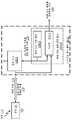
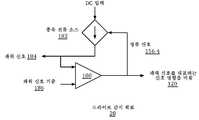
도 6은 센서 (30)에 결합된 드라이브 센터 회로 (28-a)의 개략적인 블록도이다. 드라이브 감지 감지 회로 (28)는 전원 회로 (110) 및 파워 신호 변화 검출 회로 (112)를 포함한다. 센서 (30)는 다양한 물리적 상태 (114) (예를 들어, 압력, 온도, 생물학적, 화학적 등)에 기초하여 다양한 전기적 특성 (예를 들어, 커패시턴스, 인덕턴스, 임피던스, 전류, 전압 등)을 갖는 하나 이상의 트랜스듀서를 포함하고, 또는 그 반대 (예를 들어, 액추에이터)를 포함한다.6 is a schematic block diagram of a drive center circuit 28-a coupled to the
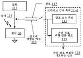
전원 회로 (110)는 센서 (30)에 동작 가능하게 결합되고, 인에이블될 때 (예를 들어, 처리 모듈 (42)로부터의 제어 신호로부터 파워가 인가되고, 스위치가 폐쇄되고, 기준 신호가 수신되는 등) 센서 (30)에 파워 신호 (116)를 제공한다. 전원 회로 (110)는 전압 기반 파워 신호를 생성하기 위한 전압 공급 회로 (예를 들어, 배터리, 선형 레귤레이터, 비 정류된 DC-DC 컨버터 등), 전류 기반 파워 신호를 생성하기 위한 전류 공급 회로 (예를 들어, 전류 소스 회로, 전류 미러 회로 등) 센서에 원하는 파워 레벨을 제공하고 센서의 임피던스와 실질적으로 정합(match)하는 회로일 수 있다. 전원 회로 (110)는 DC (직류) 성분 및/또는 발진 성분을 포함하는 파워 신호 (116)를 생성한다.The
파워 신호 (116)를 수신하고 상태 (114)에 노출될 때, 센서의 전기적 특성은 파워 신호에 영향을 미친다 (118). 파워 신호 변화 검출 회로 (112)가 인에이블되면, 센서의 전기적 특성의 결과로서 파워 신호에 대한 영향 (118)을 검출한다. 예를 들어, 파워 신호는 1.5 전압 신호이고 제 1 상태하에서 센서는 1.5K Ohms의 임피던스에 해당하는 1 밀리 암페어의 전류를 소비한다. 제 2 상태하에서 파워 신호는 1.5V로 유지되고 전류는 1.5mA로 증가한다. 따라서, 상태 1에서 상태 2로 센서의 임피던스가 1.5K Ohms에서 1K Ohms로 변경되었다. 파워 신호 변화 검출 회로 (112)는 이러한 변화를 결정하고 파워 신호에 대한 변화의 대표 신호 (120)를 생성한다.When receiving the power signal 116 and exposed to the state 114, the electrical properties of the sensor affect the power signal (118). When the power signal
다른 예로서, 파워 신호는 1.5 전압 신호이고, 제 1 상태에서 센서는 1.5K Ohms의 임피던스에 대응하는 1 밀리 암페어의 전류를 소비한다. 제 2 상태에서 파워 신호는 1.3V로 떨어지고 전류는 1.3 밀리 암페어로 증가한다. 따라서, 상태 1에서 상태 2로 센서의 임피던스가 1.5K Ohms에서 1K Ohms로 변경되었다. 파워 신호 변화 검출 회로 (112)는 이러한 변화를 결정하고 파워 신호에 대한 변화의 대표 신호 (120)를 생성한다.As another example, the power signal is a 1.5 voltage signal, and in the first state the sensor consumes 1 milliampere of current corresponding to an impedance of 1.5K Ohms. In the second state, the power signal drops to 1.3V and the current increases to 1.3 milliamps. Therefore, from state 1 to state 2, the impedance of the sensor was changed from 1.5K Ohms to 1K Ohms. The power signal
파워 신호 (116)는 도 7에 도시된 바와 같이 DC 성분 (122) 및/또는 발진 성분 (124)을 포함한다. 발진 성분 (124)은 정현파 신호, 구형파 신호, 삼각파 신호, 다수의 레벨 신호 (예를 들어, DC 성분에 대해 시간이 지남에 따라 다양한 크기를 가짐) 및/또는 다각형 신호(polygonal signal) (예를 들어, DC 성분에 대해 대칭 또는 비대칭 다각형 모양을 가짐)을 포함한다. 파워 신호는 상태 변화 또는 상태의 결과로 센서로부터의 영향없이 표시된다는 것에 유의한다.The power signal 116 includes a DC component 122 and/or an oscillation component 124 as shown in FIG. 7. The oscillation component 124 is a sine wave signal, a square wave signal, a triangular wave signal, a plurality of level signals (e.g., having various sizes over time for a DC component) and/or a polygonal signal (e.g. For example, it has a symmetrical or asymmetrical polygonal shape with respect to the DC component). Note that the power signal is displayed without influence from the sensor as a result of a state change or state.
일 실시예에서, 파워 발생 회로 (110)는 파워 신호 (116)의 발진 성분 (124)의 주파수를 변화시켜 센서의 임피던스에 동조될 수 있고/있거나 시스템에 른 파워 신호로부터 주파수에서 오프셋될 수 있다. 예를 들어, 커패시턴스 센서의 임피던스는 주파수에 따라 감소한다. 따라서, 발진 성분의 주파수가 커패시턴스에 비해 너무 높으면 커패시터가 짧아 보이고 커패시턴스의 변화를 놓칠 수 있다. 마찬가지로 발진 성분의 주파수가 커패시턴스에 비해 너무 낮으면 커패시터가 개방된 것처럼 보이고 커패시턴스의 변화가 누락된다.In one embodiment, the
일 실시예에서, 파워 생성 회로 (110)는 감지의 해상도를 개선하고 및/또는 감지의 파워 소비를 조절하기 위해 DC 성분 (122) 및/또는 발진 성분 (124)의 크기를 변경한다. 또한, 파워 생성 회로 (110)는 발진 성분 (124)의 크기가 DC 성분 (122)의 크기보다 작도록 드라이브 신호 (110)를 생성한다.In one embodiment, the
도 6a는 센서 (30)에 결합된 드라이브 센터 회로 (28-a1)의 개략적인 블록도이다. 드라이브 감지 감지 회로 (28-a1)는 신호 소스 회로 (111), 신호 변화 검출 회로 (113) 및 전원(115)를 포함한다. 전원 (115) (예를 들어, 배터리, 파워 서플라이, 전류 소스 등)은 신호 소스 회로 (111)에 의해 생성되는 신호 (117)와 조합된 전압 및/또는 전류를 생성한다. 조합된 신호는 센서 (30)에 공급된다.6A is a schematic block diagram of a drive center circuit 28-a1 coupled to the
신호 소스 회로 (111)는 전압 기반 신호 (117)를 생성하기 위한 전압 공급 회로 (예를 들어, 배터리, 선형 레귤레이터, 비정류된 DC-DC 컨버터 등), 전류 기반 신호 (117)를 생성하기 위한 전류 공급 회로(예를 들어, 전류 소스 회로, 전류 미러 회로 등), 또는 센서에 원하는 파워 레벨을 제공하고 센서의 임피던스를 실질적으로 정합시키는 회로일 수 있다. 신호 소스 회로 (111)는 DC (직류) 성분 및/또는 발진 성분을 포함하는 신호 (117)를 생성한다.The
조합된 신호 (예를 들어, 전원으로부터 파워 및 신호 (117))를 수신할 때 및 상태 (114)에 노출될 때, 센서의 전기적 특성은 신호에 영향을 미친다 (119). 신호 변화 검출 회로 (113)가 인에이블되면, 센서의 전기적 특성의 결과로 신호에 대한 영향 (119)을 검출한다.When receiving a combined signal (e.g., power and signal 117 from a power source) and when exposed to state 114, the electrical properties of the sensor affect the signal (119). When the signal
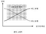
도 8은 전기적 특성 대 상태를 나타내는 센서 그래프의 예이다. 센서는 상태의 증분 변화가 전기적 특성에 상응하는 증분 변화를 생성하는 실질적으로 선형 영역을 가지고 있다. 그래프는 두 가지 유형의 전기적 특성을 보여준다 : 하나는 상태가 증가함에 따라 증가하고 다른 하나는 감소하고 상태가 증가한다. 제 1 유형의 예로서, 온도 센서의 임피던스가 증가하고 온도가 증가한다. 제 2 유형의 예로서, 커패시턴스 터치 센서는 터치가 감지될 때 커패시턴스가 감소한다.8 is an example of a sensor graph showing electrical characteristics versus state. The sensor has a substantially linear region in which incremental changes in state produce incremental changes corresponding to electrical properties. The graph shows two types of electrical properties: one increases as the state increases, the other decreases, and the state increases. As an example of the first type, the impedance of the temperature sensor increases and the temperature increases. As an example of the second type, the capacitance touch sensor reduces its capacitance when a touch is sensed.
도 9는 센서의 전기적 특성 또는 전기적 특성의 변화가 파워 신호에 영향을 미치는 파워 신호 그래프의 다른 예의 개략적인 블록도이다. 이 예에서, 센서의 전기적 특성의 영향 또는 전기적 특성의 변화는 DC 성분을 줄였지만 발진 성분에는 거의 영향을 주지 않았다. 예를 들어, 전기적 특성은 저항이다. 이 예에서, 센서의 저항 또는 저항 변화는 파워 신호를 감소시켜 상대적으로 일정한 전류에 대한 저항 증가를 추정한다.9 is a schematic block diagram of another example of a power signal graph in which an electrical characteristic of a sensor or a change in an electrical characteristic affects a power signal. In this example, the influence of the electrical characteristics of the sensor or the change of the electrical characteristics reduced the DC component, but had little effect on the oscillation component. For example, the electrical property is resistance. In this example, the resistance or change in resistance of the sensor reduces the power signal to estimate the increase in resistance to a relatively constant current.
도 10은 센서의 전기적 특성 또는 전기적 특성의 변화가 파워 신호에 영향을 미치는 파워 신호 그래프의 또 다른 예의 개략적인 블록도이다. 이 예에서, 센서의 전기적 특성의 영향 또는 전기적 특성의 변화는 발진 성분의 크기를 줄 였지만 DC 성분에는 거의 영향을 미치지 않았다. 예를 들어, 전기적 특성은 커패시터 및/또는 인덕터의 임피던스이다. 이 예에서, 센서의 임피던스 또는 임피던스 변화는 발진 신호 성분의 크기를 감소시켜 상대적으로 일정한 전류에 대한 임피던스 증가를 추론한다.10 is a schematic block diagram of another example of a power signal graph in which an electrical characteristic of a sensor or a change in an electrical characteristic affects a power signal. In this example, the influence of the electrical characteristics of the sensor or the change of the electrical characteristics reduced the size of the oscillation component, but had little effect on the DC component. For example, the electrical characteristic is the impedance of the capacitor and/or inductor. In this example, the impedance or change in impedance of the sensor reduces the magnitude of the oscillating signal component, inferring an increase in impedance for a relatively constant current.
도 11은 센서의 전기적 특성 또는 전기적 특성의 변화가 파워 신호에 영향을 미치는 파워 신호 그래프의 다른 예의 개략적인 블록도이다. 이 예에서, 센서의 전기적 특성 또는 전기적 특성의 변화의 영향은 발진 성분의 주파수를 시프트 시켰지만 DC 성분에는 거의 영향을 미치지 않았다. 예를 들어, 전기적 특성은 커패시터 및/또는 인덕터의 리액턴스이다. 이 예에서, 센서의 리액턴스 또는 리액턴스 변화는 발진 신호 성분의 주파수를 시프트시켜 리액턴스 증가를 추론한다 (예를 들어, 센서가 적분기 또는 위상 시프트 회로로 동작함).11 is a schematic block diagram of another example of a power signal graph in which an electrical characteristic of a sensor or a change in an electrical characteristic affects a power signal. In this example, the effect of the change in the electrical characteristics or electrical characteristics of the sensor shifted the frequency of the oscillation component, but had little effect on the DC component. For example, the electrical property is the reactance of the capacitor and/or inductor. In this example, the reactance or reactance change of the sensor shifts the frequency of the oscillating signal component to infer the increase in reactance (eg, the sensor operates as an integrator or phase shift circuit).
도 11a는 센서의 전기적 특성 또는 전기적 특성의 변화가 파워 신호에 영향을 미치는 파워 신호 그래프의 또 다른 예의 개략적인 블록도이다. 이 예에서, 센서의 전기적 특성의 영향 또는 센서의 전기적 특성의 변화는 발진 성분의 주파수를 변경하지만 DC 성분에는 거의 영향을 주지 않다. 예를 들어, 센서는 서로 다른 주파수에서 발진하는 두 개의 트랜스듀서를 포함한다. 제 1 트랜스듀서는 f1의 주파수에서 파워 신호를 수신하고 이를 제 1 물리적 상태로 변환한다. 제 2 트랜스듀서는 제 1 물리적 상태에 의해 자극되어 다른 주파수 f2에서 전기 신호를 생성한다. 이 예에서, 센서의 제 1 및 제 2 트랜스듀서는 발진 신호 성분의 주파수를 변경하여 더 세분화된 감지 및/또는 더 넓은 감지 범위를 허용한다.11A is a schematic block diagram of another example of a power signal graph in which an electrical characteristic of a sensor or a change in an electrical characteristic affects a power signal. In this example, the influence of the electrical characteristics of the sensor or the change of the electrical characteristics of the sensor changes the frequency of the oscillation component, but has little effect on the DC component. For example, the sensor contains two transducers that oscillate at different frequencies. The first transducer receives the power signal at a frequency of f1 and converts it to a first physical state. The second transducer is stimulated by the first physical state to generate an electrical signal at a different frequency f2. In this example, the first and second transducers of the sensor change the frequency of the oscillating signal component to allow for a more granular sensing and/or a wider sensing range.
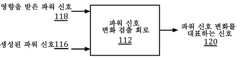
도 12는 파워 신호 변화의 대표 신호 (120)를 생성하기 위해 생성된 영향을 받는 파워 신호 (118) 및 파워 신호 (116)를 수신하는 파워 신호 변화 검출 회로 (112)의 실시예의 개략적인 블록도이다. 파워 신호에 대한 영향 (118)은 센서의 전기적 특성 및/또는 전기적 특성의 변화의 결과이며; 영향의 몇 가지 예가 도면들 8-11a에 도시된다.12 is a schematic block diagram of an embodiment of a power signal
일 실시예에서, 파워 신호 변화 검출 회로 (112)는 파워 신호 (116)의 DC 성분 (122) 및/또는 발진 성분 (124)의 변화를 검출한다. 그런 다음, 파워 신호 변화 검출 회로 (112)는 파워 신호의 변화에 따라 파워 신호에 변화의 대표 신호 (120)를 생성한다. 예를 들어, 파워 신호의 변화는 센서의 임피던스 및/또는 센서의 임피던스의 변화로 인해 발생한다. 대표 신호 (120)는 파워 신호의 변화 및/또는 센서의 임피던스의 변화를 반영한다.In one embodiment, the power signal
일 실시예에서, 파워 신호 변화 검출 회로 (112)는 주파수에서 발진 성분에 대한 변화를 검출하도록 동작할 수 있으며, 이는 발진 성분의 위상 편이, 주파수 변화 및/또는 크기의 변화일 수 있다. 파워 신호 변화 검출 회로 (112)는 또한 주파수에서 발진 성분에 대한 변화에 기초하여 파워 신호의 변화를 나타내는 신호를 생성하도록 동작 가능하다. 파워 신호 변화 검출 회로 (112)는 또한 발진 성분에 관한 피드백을 전원 회로 (110)에 제공하도록 동작 가능하다. 피드백은 전원 회로 (110)가 원하는 주파수, 위상 및/또는 크기에서 발진 성분을 정류할 수 있게 한다.In one embodiment, the power signal
도 13은 전류 소스 (110-1) 및 파워 신호 변화 검출 회로 (112-a1)를 포함하는 드라이브 감지 회로 (28-a2)의 다른 실시예의 개략적인 블록도이다. 파워 신호 변화 검출 회로 (112-a1)는 전원 기준 회로 (130) 및 비교기 (132)를 포함한다. 전류 소스 (110-1)는 독립 전류 소스, 종속 전류 소스, 전류 미러 회로 등일 수 있다.13 is a schematic block diagram of another embodiment of a drive detection circuit 28-a2 including a current source 110-1 and a power signal change detection circuit 112-a1. The power signal change detection circuit 112-a1 includes a power supply reference circuit 130 and a comparator 132. The current source 110-1 may be an independent current source, a dependent current source, a current mirror circuit, or the like.
동작의 예에서, 전원 기준 회로 (130)는 DC 및 발진 성분을 갖는 전류 기준 (134)을 전류 소스 (110-1)에 제공한다. 전류 소스는 전류 기준 (134)에 기초하여 파워 신호 (116)로서 전류를 생성한다. 센서 (30)의 전기적 특성은 전류 파워 신호 (116)에 영향을 미친다. 예를 들어, 센서의 임피던스가 감소하고 전류 파워 신호(116)가 실질적으로 변하지 않으면, 센서 양단의 전압이 감소한다.In an example of operation, the power reference circuit 130 provides a current reference 134 having DC and oscillation components to the current source 110-1. The current source generates a current as the power signal 116 based on the current reference 134. The electrical properties of the
비교기 (132)는 파워 신호에 대한 변화를 대표하는 신호 (120)를 생성하기 위해 전류 기준 (134)을 영향을 받는 파워 신호 (118)와 비교한다. 예를 들어, 전류 기준 신호 (134)는 주어진 전류 (I)에 주어진 임피던스 (Z)를 곱한 것에 대응한다. 전류 기준은 주어진 전류 (I)를 생성하기 위해 파워 신호를 생성한다. 센서 (30)의 임피던스가 주어진 임피던스 (Z)와 실질적으로 정합한다면, 비교기의 출력은 실질적으로 정합하는 임피던스를 반영한다. 센서 (30)의 임피던스가 주어진 임피던스 (Z)보다 크면, 비교기의 출력은 센서 (30)의 임피던스가 주어진 임피던스 (Z)의 임피던스보다 얼마나 큰지를 나타낸다. 센서 (30)의 임피던스가 주어진 임피던스 (Z)보다 작다면, 비교기의 출력은 센서 (30)의 임피던스가 주어진 임피던스 (Z)의 임피던스보다 얼마나 적은지를 나타낸다.The comparator 132 compares the current reference 134 to the affected
도 14는 전압 소스 (110-2) 및 파워 신호 변화 검출 회로 (112-a2)를 포함하는 드라이브 감지 회로 (28-a3)의 다른 실시예의 개략적인 블록도이다. 파워 신호 변화 검출 회로 (112-a2)는 전원 기준 회로 (130-2) 및 비교기 (132-2)를 포함한다. 전압 소스 (110-2)은 배터리, 선형 레귤레이터, DC-DC 컨버터 등일 수 있다.14 is a schematic block diagram of another embodiment of a drive detection circuit 28-a3 including a voltage source 110-2 and a power signal change detection circuit 112-a2. The power signal change detection circuit 112-a2 includes a power supply reference circuit 130-2 and a comparator 132-2. The voltage source 110-2 may be a battery, a linear regulator, a DC-DC converter, or the like.
동작의 예에서, 전원 기준 회로 (130-2)는 DC 및 발진 성분을 갖는 전압 기준 (136)을 전압 소스 (110-2)에 제공한다. 전압 소스는 전압 기준 (136)에 기초하여 파워 신호 (116)로서 전압을 생성한다. 센서 (30)의 전기적 특성은 전압 파워 신호 (116)에 영향을 미친다. 예를 들어, 센서의 임피던스가 감소하고 전압 파워 신호(116)가 실질적으로 변하지 않으면, 센서를 통과하는 전류가 증가한다.In an example of operation, the power reference circuit 130-2 provides a voltage reference 136 having DC and oscillation components to the voltage source 110-2. The voltage source generates a voltage as the power signal 116 based on the voltage reference 136. The electrical properties of the
비교기 (132)는 전압 기준 (136)을 영향을 받는 파워 신호 (118)와 비교하여 파워 신호에 대한 변화를 대표하는 신호 (120)를 생성한다. 예를 들어, 전압 기준 신호 (134)는 주어진 임피던스 (Z)로 나눈 주어진 전압 (V)에 대응한다. 전압 기준은 주어진 전압 (V)을 생성하는 파워 신호를 생성한다. 센서 (30)의 임피던스가 주어진 임피던스 (Z)와 실질적으로 정합한다면, 비교기의 출력은 실질적으로 정합하는 임피던스를 반영한다. 센서 (30)의 임피던스가 주어진 임피던스 (Z)보다 크면, 비교기의 출력은 센서 (30)의 임피던스가 주어진 임피던스 (Z)의 임피던스보다 얼마나 큰지를 나타낸다. 센서 (30)의 임피던스가 주어진 임피던스 (Z)보다 작다면, 비교기의 출력은 센서 (30)의 임피던스가 주어진 임피던스 (Z)의 임피던스보다 얼마나 적은지를 나타낸다.The comparator 132 compares the voltage reference 136 to the affected
도 15는 전원 회로 (110), 파워 신호 변화 검출 회로 (112), 아날로그-디지털 컨버터 (140) 및 드라이버 (142)를 포함하는 드라이브 감지 회로 (28-a4)의 다른 실시예의 개략적인 블록도이다. 전원 회로 (110) 및 파워 신호 변화 검출 회로 (112)는 파워 신호 변화를 대표하는 신호 (120)를 생성하기 위해 도 13을 참조하여 앞서 논의된 바와 같이 기능한다.15 is a schematic block diagram of another embodiment of a drive detection circuit 28-a4 including a
이 실시예에서, 전원 회로 (110)는 전원 회로 (110)에 의해 생성된 파워 신호의 파워를 증가시키는 (예를 들어, 전압 및/또는 전류를 증가시키는) 기능을하는 드라이버 (142)에 출력을 제공한다. 드라이버(142)는 파워 신호 (116)를 센서 (30)에 제공한다. 파워 증폭기일 수 있는 드라이버와 함께, 저 임피던스 센서 (30)는 감지 애플리케이션을 위한 특정 유형으로 사용될 수 있다.In this embodiment, the
아날로그-디지털 컨버터 (140)는 파워 신호 변화를 대표하는 신호 (120)를 디지털 신호 (144)로 변환한다. 디지털 신호 (144)는 드라이브 감지 회로와 처리 모듈 사이의 연결을 통해 처리 모듈 (42)에 제공된다. 처리 모듈은 디지털 신호를 센서가 노출되는 상태의 상대 값으로 변환한다. 드라이브 감지 회로 (28-a4)와 처리 모듈 (42) 사이의 연결은 드라이브 감지 회로가 처리 모듈의 컴퓨팅 디바이스의 내부인지 외부인지에 따라 달라진다. 내부에 있는 경우, 드라이브 감지 회로는 PCI 버스 등을 통해 처리 모듈에 연결된다. 드라이브 감지 회로가 처리 모듈의 외부에 있는 경우, 연결은 USB 연결, 블루투스(Bluetooth) 연결, WLAN 연결, 인터넷 연결 및/또는 WAN 연결이다.The analog-to-digital converter 140 converts a
도 16은 변화 검출 회로(150), 정류 회로 regulation circuit) (152) 및 전원 회로 (154)를 포함하는 드라이브 감지 회로 (28-b)의 다른 실시예의 개략적인 블록도이다. 드라이브 감지 회로 (28-b)는 다양한 물리적 상태 (예를 들어, 압력, 온도, 생물학적, 화학적 등)에 기초하여 다양한 전기적 특성 (예를 들어, 커패시턴스, 인덕턴스, 임피던스, 전류, 전압 등)을 갖는 트랜스듀서를 포함하는 센서 (30)에 결합된다.16 is a schematic block diagram of another embodiment of a drive sensing circuit 28-b comprising a
전원 회로 (154)는 센서 (30)에 동작 가능하게 결합되고, 인에이블될 때 (예를 들어, 처리 모듈 (42)로부터의 제어 신호로부터 파워가 인가되고, 스위치가 폐쇄되고, 기준 신호가 수신되는 등) 파워 신호 (158)를 센서 (30)에 제공한다. 전원 회로 (154)는 전압 기반 파워를 생성하기 위한 전압 공급 회로 (예를 들어, 배터리, 선형 레귤레이터, 비 정류된 DC-DC 컨버터 등) 또는 전류 기반 파워 신호를 생성하기 위한 전류 공급 회로 (예를 들어, 전류 소스 회로, 전류 미러 회로 등)일 수 있다. 전원 회로 (154)는 DC (직류) 성분 및 발진 성분을 포함하는 파워 신호 (158)를 생성한다.The
파워 신호 (158)를 수신하고 상태 (114)에 노출될 때, 센서의 전기적 특성은 파워 신호에 영향을 미친다 (160). 변화 검출 회로 (150)가 인에이블되면, 센서 (30)의 전기적 특성의 결과로서 파워 신호에 대한 영향 (160)을 검출한다. 변화 검출 회로 (150)는 또한 파워 신호에 대한 검출된 영향을 기반으로 파워 신호 변화를 대표하는 신호 (120)를 생성하도록 동작 가능하다.When receiving the
정류 회로 (152)가 인에이블 되었을 때, 정류 신호 (156)를 생성하여 DC 성분을 원하는 DC 레벨로 정류하고 및/또는 파워 신호에 대한 변화를 대표하는 신호 (120)에 기초하여 발진 성분을 원하는 발진 레벨 (예를 들어, 크기, 위상 및/또는 주파수)로 정류한다. 전원 회로 (154)는 센서의 전기적 특성에 관계없이 원하는 설정 (158)에서 파워 신호를 유지하기 위해 정류 신호 (156)를 이용한다. 이러한 방식으로, 정류의 양은 전기적 특성이 파워 신호에 미치는 영향을 나타낸다.When the
일 예에서, 전원 회로 (158)는 DC 및 AC 성분을 갖는 정류된 파워 신호를 제공하도록 동작할 수 있는 DC-DC 컨버터이다. 변화 검출 회로 (150)는 비교기이고 정류 회로 (152)는 정류 신호 (156)를 생성하는 펄스 폭 변조기이다. 비교기는 센서의 영향을 받는 파워 신호 (158)를 DC 및 AC 성분을 포함하는 기준 신호와 비교한다. 전기적 특성이 제 1 레벨 (예를 들어, 제 1 임피던스)에 있을 때, 파워 신호가 기준 신호와 실질적으로 유사하도록 전압 및 전류를 제공하도록 파워 신호가 정류된다.In one example,
전기적 특성이 제 2 레벨 (예를 들어, 제 2 임피던스)로 변경되면, 변화 검출 회로(150)는 파워 신호 (158)의 DC 및/또는 AC 성분의 변화를 감지하고 변화를 나타내는 대표 신호 (120)를 생성한다. 정류 회로 (152)는 대표 신호 (120)의 변화를 검출하고 정류 신호를 생성하여 파워 신호에 대한 영향을 실질적으로 제거한다. 파워 신호 (158)의 정류는 DC 및/또는 AC 성분의 크기 정류, AC 성분의 주파수 조절 및/또는 AC 성분의 위상 조절에 의해 수행될 수 있다.When the electrical characteristic is changed to the second level (e.g., the second impedance), the
도 17은 전류 소스 (154-1) 및 변화 검출 회로 (150-1)를 포함하는 드라이브 감지 회로 (28-b1)의 다른 실시예의 개략적인 블록도이다. 변화 검출 회로 (150-1)는 전원 기준 회로 (162) 및 비교기 (164)를 포함한다. 전류 소스 (154-1)는 독립 전류 소스, 종속 전류 소스, 전류 미러 회로 등일 수 있다.17 is a schematic block diagram of another embodiment of a drive sensing circuit 28-b1 including a current source 154-1 and a change detection circuit 150-1. The change detection circuit 150-1 includes a power
동작의 예에서, 전원 기준 회로 (162)는 DC 및/또는 발진 성분이 있는 전류 기준을 비교기 (164)에 제공한다. 비교기 (164)는 기준 전류를 전류 소스 (154-1)에 의해 생성된 전류 파워 신호 (158)와 비교하고, 비교에 기초하여 대표 신호 (120)를 생성한다.In an example of operation,
피드백 회로 (166) (예를 들어, 종속 전류 소스 바이어싱 회로, 와이어 등)를 포함하는 정류 회로 (152)는 대표 신호 (120)에 기초하여 정류 신호 (156-1)를 생성하고 정류 신호를 전류 소스 (154-1)에 제공한다. 전류 소스는 정류 신호 (156-1)에 기초하여 파워 신호 (116)로서 정류된 전류를 생성한다.A
예로서, 전류 기준 신호는 주어진 전류 (I)에 주어진 임피던스 (Z)를 곱한 것에 대응한다. 전류 소스 (154-1)는 주어진 전류 (I)를 생성하기 위해 파워 신호를 생성한다. 센서 (30)의 임피던스가 주어진 임피던스 (Z)와 실질적으로 정합한다면, 비교기의 출력은 실질적으로 정합하는 임피던스를 반영한다. 센서 (30)의 임피던스가 주어진 임피던스 (Z)보다 크면, 비교기의 출력은 센서 (30)의 임피던스가 주어진 임피던스 (Z)의 임피던스보다 얼마나 큰지를 나타낸다. 센서 (30)의 임피던스가 주어진 임피던스 (Z)보다 작다면, 비교기의 출력은 센서 (30)의 임피던스가 주어진 임피던스 (Z)의 임피던스보다 얼마나 적은지를 나타낸다. 정류 회로는 센서 임피던스의 변화를 설명하고 전류 소스가 정류된 전류 소스를 생성하도록 보장하는 기능을 한다 (예를 들어, 주어진 전류 (I)에 실질적으로 유지됨).As an example, the current reference signal corresponds to a given current (I) multiplied by a given impedance (Z). Current source 154-1 generates a power signal to generate a given current I. If the impedance of the
도 18은 전압 소스 (154-2) 및 변화 검출 회로 (150-2)를 포함하는 드라이브 감지 회로 (28-b2)의 다른 실시예의 개략적인 블록도이다. 변화 검출 회로 (150-2)는 전원 기준 회로 (162-2) 및 비교기 (164-2)를 포함한다. 전압 소스 (154-2)은 선형 레귤레이터, DC-DC 컨버터 등일 수 있다.18 is a schematic block diagram of another embodiment of a drive sensing circuit 28-b2 including a voltage source 154-2 and a change detection circuit 150-2. The change detection circuit 150-2 includes a power supply reference circuit 162-2 and a comparator 164-2. The voltage source 154-2 may be a linear regulator, a DC-DC converter, or the like.
동작의 예에서, 전원 기준 회로 (162-2)는 DC 및 발진 성분을 갖는 전압 기준을 비교기 (164-2)에 제공한다. 비교기 (164-2)는 기준 전압을 전압 소스 (154-2)에 의해 생성된 전압 파워 신호 (158)와 비교하고 그 비교에 기초하여 대표 신호 (120)를 생성한다.In an example of operation, the power reference circuit 162-2 provides a voltage reference having DC and oscillation components to the comparator 164-2. The comparator 164-2 compares the reference voltage with the
피드백 회로 (166-2) (예를 들어, 파워 서플라이 정류 회로, 바이어스 회로, 와이어 등)를 포함하는 정류 회로 (152)는 대표 신호 (120)에 기초하여 정류 신호 (156-2)를 생성하고, 전압 소스 (154-2)에 정류 신호를 제공한다. 전압 소스는 정류 신호 (156-1)에 기초하여 파워 신호 (116)로서 정류된 전압을 생성한다.A
예를 들어, 전압 기준 신호는 주어진 임피던스 (Z)로 나눈 주어진 전압 (V)에 대응한다. 전압 소스 (154-2)은 주어진 전압 (V)을 생성하기 위해 파워 신호를 생성한다. 센서 (30)의 임피던스가 주어진 임피던스 (Z)와 실질적으로 정합한다면, 비교기의 출력은 실질적으로 정합하는 임피던스를 반영한다. 센서 (30)의 임피던스가 주어진 임피던스 (Z)보다 크면, 비교기의 출력은 센서 (30)의 임피던스가 주어진 임피던스 (Z)의 임피던스보다 얼마나 큰지를 나타낸다. 센서 (30)의 임피던스가 주어진 임피던스 (Z)보다 작다면, 비교기의 출력은 센서 (30)의 임피던스가 주어진 임피던스 (Z)의 임피던스보다 얼마나 적은지를 나타낸다. 정류 회로는 센서 임피던스의 변화를 설명하고 전압 소스가 정류된 전압 소스를 생성하도록 보장하는 기능을 한다 (예를 들어, 주어진 전압 (V)에서 실질적으로 유지됨).For example, a voltage reference signal corresponds to a given voltage (V) divided by a given impedance (Z). Voltage source 154-2 generates a power signal to generate a given voltage (V). If the impedance of the
도 19는 전원 회로 (154), 변화 검출 회로 (150), 정류 회로 (152), 아날로그-디지털 컨버터 (140) 및 드라이버(142)를 포함하는 드라이브 감지 회로 (28-b3)의 다른 실시예의 개략적인 블록도이다. 전원 회로 (154), 정류 회로 (152) 및 변화 검출 회로 (150)는 파워 신호 변화를 대표하는 신호 (120) 및 정류 신호 (156)를 생성하기 위해 도 16을 참조하여 앞서 논의된 바와 같이 기능한다.19 is a schematic of another embodiment of a drive detection circuit 28-b3 including a
이 실시예에서, 전원 회로 (154)는 파워 신호의 파워 (예를 들어, 전압 및/또는 전류 증가)을 증가시키는 기능을 하는 드라이버 (142)에 출력을 제공한다. 드라이브기 (142)는 파워 신호 (116)를 센서 (30)에 제공한다. 파워 증폭기일 수 있는 드라이버로, 저 임피던스 센서 (30)는 특정 유형의 감지 애플리케이션에 사용될 수 있다.In this embodiment,
아날로그-디지털 컨버터 (140)는 파워 신호 변화를 대표하는 신호 (120)를 디지털 신호 (144)로 변환한다. 디지털 신호 (144)는 드라이브 감지 회로와 처리 모듈 사이의 연결을 통해 처리 모듈 (42)에 제공된다.The analog-to-digital converter 140 converts a
도 20은 파워 서플라이 회로 (155) 및 연산 증폭기 (op amp) 또는 비교기 (172)를 포함하는 드라이브 감지 회로 (28)의 다른 실시예의 개략적인 블록도이다. 파워 서플라이 회로 (155)는 다양한 방식으로 구현될 수 있다. 예를 들어, 파워 서플라이 회로 (155)는 정류 신호 (156-3)에 기초하여 파워 신호 (174)를 생성하기 위해 DC 입력 전압 (DC in)을 감압(step down)하는 선형 레귤레이터이다. 다른 예로서, 파워 서플라이 회로 (155)는 파워 신호 (174)를 생성하기 위해 정류 신호에 기초하여 DC 입력 전압을 승압(step up) 또는 감압하는 DC-DC 컨버터다.20 is a schematic block diagram of another embodiment of a
연산 증폭기 (172)는 파워 신호 (174)를 파워 신호 기준과 비교하여 파워 신호 변화를 대표하는 신호 (120)인 정류 신호 (156-3)를 생성한다. 특정 실시예에서, 파워 서플라이 회로 (155)는 P-채널 FET (전계 효과 트랜지스터) 및 바이어스 회로를 포함한다. P-채널 FET의 소스는 DC 입력에 결합되고 게이트는 바이어스 회로에 결합되고 드레인은 파워 신호 (174)를 제공하도록 결합된다. 바이어스 회로는 정류 신호 (156-3)를 수신하고 파워 신호 (174)의 전압이 파워 신호 기준 (170)의 전압과 실질적으로 정합하도록 게이트 소스 전압을 조절한다. 예를 들어, 파워 신호 기준이 도 7에 도시된 바와 같이 DC 성분 및/또는 발진 성분을 갖는 경우, 파워 신호 (174)는 실질적으로 유사한 DC 성분 및/또는 발진 성분을 가질 것이다.The
파워 신호 (174)가 센서에 제공되고 센서가 상태에 노출될 때, 센서의 전기적 특성이 파워 신호에 영향을 미칠 것이다. 파워 기준 신호 (170)의 전압과 실질적으로 정합하도록 파워 신호 (174)의 전압을 정류하는 제어 루프는 정류 신호를 조절하여 센서가 파워 신호 (174)에 미치는 영향을 보상할 것이다. 보상은 센서의 전기적 특성이 파워 신호에 미치는 영향에 해당하고, 센서에 의해 감지되고 있는 상태를 대표한다. 따라서, 정류 신호 (156-3)는 파워 서플라이 회로 (155)의 정류 및 파워 신호에 대한 영향을 대표하는 신호 (120) 둘 모두를 제공한다.When a power signal 174 is provided to the sensor and the sensor is exposed to a state, the electrical properties of the sensor will affect the power signal. A control loop that rectifies the voltage of the power signal 174 to substantially match the voltage of the power reference signal 170 will adjust the rectified signal to compensate for the sensor's effect on the power signal 174. The compensation corresponds to the effect of the sensor's electrical characteristics on the power signal and represents the state being sensed by the sensor. Thus, the commutation signal 156-3 provides both a
도 21은 이 실시예에서 전류 비교기로서 기능하는 종속 전류 소스 (182) 및 트랜스 임피던스 증폭기 (180)를 포함하는 드라이브 감지 회로 (28)의 다른 실시예의 개략적인 블록도이다. 종속 전류 소스 (182)는 다양한 방식으로 구현될 수 있다. 예를 들어, 종속 전류 소스 (182)는 정류 신호 (156-3)에 기초하여 파워 신호 (184)를 생성하기 위해 DC 입력 전압 (DC 입력)을 통해 공급되는 전류 미러 회로이다. 다른 예로서, 종속 전류 소스 (182)는 전압 제어 전류 소스이다. 또 다른 예로서, 종속 전류 소스 (182)는 전류 제어 전류 소스이다.Fig. 21 is a schematic block diagram of another embodiment of a
트랜스 임피던스 증폭기 (180)는 파워 신호 (174)의 전류를 파워 신호 기준 (186)의 전류와 비교하여 파워 신호 변화를 대표하는 신호 (120)인 정류 신호 (156-4)를 생성한다. 특정 실시예에서, 파워 서플라이 회로 (155)는 P-채널 FET (전계 효과 트랜지스터) 및 바이어스 회로를 포함한다. P-채널 FET의 소스는 DC 입력에 결합되고 게이트는 바이어스 회로에 결합되고 드레인은 파워 신호 (184)를 제공하도록 결합된다. 바이어스 회로는 정류 신호 (156-4)를 수신하고 파워 신호 (184)의 전류가 파워 신호 기준 (186)의 전류와 실질적으로 정합하도록 게이트 소스 전압을 조절한다.The trans-
파워 신호 (184)의 전류가 센서에 제공되고 센서가 상태에 노출될 때, 센서의 전기적 특성이 파워 신호에 영향을 미칠 것이다. 파워 기준 신호 (186)의 전류와 실질적으로 정합하도록 파워 신호 (184)의 전류를 정류하는 제어 루프는 정류 신호를 조절하여 센서가 파워 신호 (184)에 미치는 영향을 보상할 것이다. 보상은 센서의 전기적 특성이 파워 신호에 미치는 영향에 해당하며 센서에 의해 감지되는 상태를 대표한다. 따라서, 정류 신호 (156-4)는 파워 신호에 대한 영향을 대표하는 신호 (120) 및 종속 전류 소스 (182)의 정류 둘 모두를 제공한다.When the current of the power signal 184 is provided to the sensor and the sensor is exposed to the state, the electrical properties of the sensor will affect the power signal. A control loop that rectifies the current in the power signal 184 to substantially match the current in the
도 22는 센서 (30)에 결합된 드라이브 감지 회로 (28-c)의 다른 실시예의 개략적인 블록도이다. 드라이브 감지 회로 (28-c)는 아날로그 회로부 (190) 및 디지털 회로부 (192)를 포함한다. 아날로그 회로부(190)가 인에이블되면, 아날로그 정류 신호 (204)에 기초하여 정류된 소스 신호 (196)를 생성하도록 동작할 수 있다. 아날로그 회로는 다양한 방식으로 인에이블된다. 예를 들어, 아날로그 회로부 (190)는 파워가 드라이브 감지 회로 (28-c)에 인가될 때 인에이블된다. 다른 예로서, 아날로그 회로부 (190)는 드라이브 감지 회로가 처리 모듈로부터 제어 신호를 수신할 때 인에이블된다.22 is a schematic block diagram of another embodiment of a drive sensing circuit 28-c coupled to the
아날로그 회로부 (190)는 정류된 소스 신호 (196)를 센서 (30)에 제공한다. 정류된 소스 신호 (196)는 정류된 전류 신호, 정류된 전압 신호 또는 정류된 임피던스 신호일 수 있다. 센서 (30)가 상태 (114)에 노출될 때, 센서의 전기적 특성은 정류된 소스 신호에 영향을 미친다 (198).The
정류된 소스 신호 (196)를 생성하는 것에 추가하여, 아날로그 회로부 (190)는 또한 원하는 소스 레벨에서 기준 소스 신호 (194)를 생성한다. 예를 들어, 기준 소스 신호 (194)는 크기를 갖는 DC 성분 및/또는 파형 (예를 들어, 정현파, 정사각형, 삼각형, 다각형, 다수의 계단 등), 주파수, 위상 및 크기를 갖는 발진 성분을 포함하도록 생성된다. 아날로그 회로부 (190)는 또한 정류된 소스 신호 (196)를 기준 소스 신호 (194)와 비교하여 비교 신호 (200)를 생성하도록 동작할 수 있다. 비교 신호 (200)는 센서의 전기적 특성이 정류된 소스 신호에 미치는 영향에 대응하고 센서 (30)에 의해 감지되는 상태 (114)를 대표한다.In addition to generating the rectified
디지털 회로가 인에이블되면, 비교 신호 (200)를 디지털 신호 (202)로 변환하도록 동작할 수 있다. 디지털 신호는 비교 신호의 디지털 표현이며, 따라서, 센서의 전기적 특성이 정류된 소스 신호에 미치는 영향에 대응하고 센서 (30)에 의해 감지되는 상태 (114)를 대표한다. 디지털 회로부 (192)는 또한 디지털 신호 (202)를 아날로그 정류 신호 (204)로 변환하도록 동작 가능하다.When the digital circuit is enabled, it can operate to convert the
도 23은 아날로그 회로부 (190) 및 디지털 회로부 (192)를 포함하는 드라이브 감지 회로 (28-c1)의 다른 실시예의 개략적인 블록도이다. 아날로그 회로부 (190)는 종속 전류 소스 (216), 비교기 (210), 아날로그-디지털 컨버터 (212)의 아날로그 부분, 및 디지털-아날로그 컨버터 (214)의 아날로그 부분을 포함한다. 디지털 회로부 (192)는 아날로그-디지털 컨버터 (212)의 디지털 부분 및 디지털-아날로그 컨버터 (214)의 디지털 부분을 포함한다. 아날로그-디지털 컨버터 (ADC) (212)는 플래시 ADC, 연속 근사 ADC, 램프 비교 ADC, Wilkinson ADC, 통합 ADC, 델타 인코딩 ADC 및/또는 시그마-델타 ADC일 수 있다. 디지털-아날로그 컨버터 (DAC) (214)는 시그마-델타 DAC, 펄스 폭 변조기 DAC, 이진 가중 DAC, 연속 근사 DAC, 및/또는 온도계 코딩 DAC일 수 있다.FIG. 23 is a schematic block diagram of another embodiment of a drive sensing circuit 28-c1 including an
종속 전류 소스 (216)는 아날로그 정류 신호 (220)에 기초하여 정류된 전류 신호로서 정류된 소스 신호 (196-1)를 생성한다. 비교기 (210)는 정류된 소스 신호 (196-1)를 기준 소스 신호 (194-1)와 비교하고, 이는 DC 성분 및/또는 발진 성분을 갖는 전류 기준 신호이다. 비교 신호 (218)는 정류된 소스 신호 (196-1)에 대한 영향에 대응하고, 센서 (30)에 의해 감지되는 상태 (114)를 대표한다. 비교기 (210)는 비교 신호 (218)를 아날로그-디지털 컨버터 (212)에 제공하여 디지털 신호(202)를 생성한다. 디지털-아날로그 컨버터 (214)는 디지털 신호를 아날로그 정류 신호 (220)로 변환한다.The dependent
도 24는 아날로그 회로부 (190) 및 디지털 회로부 (192)를 포함하는 드라이브 감지 회로 (28-c2)의 다른 실시예의 개략적인 블록도이다. 아날로그 회로부 (190)는 전압 소스 회로 (216), 변화 검출 회로 (224), 아날로그-디지털 컨버터 (212-2)의 아날로그 부분 및 디지털-아날로그 컨버터 (214-2)의 아날로그 부분을 포함한다. 디지털 회로부 (192)는 아날로그-디지털 컨버터 (212-2)의 디지털 부분 및 디지털-아날로그 컨버터 (214-2)의 디지털 부분을 포함한다. 아날로그-디지털 컨버터 (212-2) 및 디지털-아날로그 컨버터 (214-2)는 도 23을 참조하여 논의된 유형 중 하나 이상이다.24 is a schematic block diagram of another embodiment of a drive sensing circuit 28-c2 comprising an
전압 소스 회로 (226) (예를 들어, 전원, 선형 레귤레이터, 바이어스 트랜지스터 등)는 아날로그 정류 신호 (220-2)에 기초하여 정류된 전압 신호로서 정류된 소스 신호 (196-2)를 생성한다. 변화 검출 회로 (224) (예를 들어, 연산 증폭기, 비교기 등)는 정류된 소스 신호 (196-2)를 DC 성분 및/또는 발진 성분을 갖는 전압 기준 신호인 기준 소스 신호 (194-2)와 비교한다. 비교 신호 (218-2)는 정류된 소스 신호 (196-2)에 대한 영향에 대응하고 센서 (30)에 의해 감지되는 상태 (114)를 대표한다. 변화 검출 회로 (224)는 디지털 신호 (202)를 생성하는 아날로그-디지털 컨버터 (212-2)에 비교 신호 (218-2)를 제공한다. 디지털-아날로그 컨버터 (214-2)는 디지털 신호를 아날로그 정류 신호 (220-2)로 변환한다.The voltage source circuit 226 (e.g., power supply, linear regulator, bias transistor, etc.) generates a rectified source signal 196-2 as a rectified voltage signal based on the analog rectified signal 220-2. The change detection circuit 224 (e.g., an operational amplifier, a comparator, etc.) converts the rectified source signal 196-2 to a reference source signal 194-2, which is a voltage reference signal having a DC component and/or an oscillation component. Compare. The comparison signal 218-2 corresponds to the effect on the rectified source signal 196-2 and is representative of the state 114 sensed by the
도 25는 가변 임피던스 센서 (30-1)에 결합된 드라이브 감지 회로 (28-d)의 다른 실시예의 개략적인 블록도이다. 드라이브 감지 회로 (28-d)는 전압 (V) 기준 회로 (230), 전류 (I) 루프 교정 회로 (232) 및 정류된 전류 (I) 소스 회로 (234)를 포함한다. 일반적으로, 드라이브 감지 회로 (28-d)는 센서에 인가되는 전류를 정류하고, 센서 전압 (246) 및 전압 기준 (236)와 관련하여 센서 (30-1)의 임피던스 (Z)를 감지하기 위해 전압을 일정하게 유지한다.25 is a schematic block diagram of another embodiment of a drive sensing circuit 28-d coupled to a variable impedance sensor 30-1. The drive sense circuit 28-d includes a voltage (V)
드라이브 감지 회로 (28-d)가 인에이블되면, 정류된 전류 소스 회로 (234)는 아날로그 정류 신호 (242)에 기초하여 정류된 전류 신호 (238)를 생성하도록 동작할 수 있다. 정류된 전류 소스 회로 (234)는 센서 전압 (246)이 V 기준 회로 (230)에 의해 생성된 전압 기준 (236)과 실질적으로 정합하도록 정류된 전류 신호 (238)를 생성한다.When the drive sense circuit 28-d is enabled, the rectified
V 기준 회로 (230) (밴드 갭 기준, 레귤레이터, 분배기 네트워크, AC 발생기 및/또는 조합 회로일 수 있음)는 DC 성분 및/또는 적어도 하나의 발진 성분을 포함하는 전압 기준 (236)을 생성한다. 예를 들어, V 기준 회로는 크기가 1 내지 3 볼트인 DC 성분을 생성하고 주파수 1에서 제 1 정현파 발진 성분을 생성하고 주파수 2에서 제 2 정현파 발진 성분을 생성한다. 구체적인 예로서, 주파수 1에서 제 1 정현파 발진 성분은 터치 스크린 디스플레이의 셀프 터치를 감지하는데 사용되며 주파수 2에서 제 2 정현파 발진 성분은 터치 스크린 디스플레이의 상호 터치를 감지하는데 사용된다.V reference circuit 230 (which may be a band gap reference, regulator, divider network, AC generator, and/or combination circuit) generates a voltage reference 236 comprising a DC component and/or at least one oscillating component. For example, the V reference circuit generates a DC component of magnitude 1 to 3 volts, generates a first sinusoidal oscillation component at frequency 1 and a second sinusoidal oscillation component at frequency 2. As a specific example, the first sinusoidal oscillation component at frequency 1 is used to detect the self-touch of the touch screen display, and the second sinusoidal oscillation component at frequency 2 is used to detect mutual touches of the touch screen display.
정류된 전류 소스 회로 (234)는 정류된 전류 신호 (238)를 센서 (30-1)에 제공한다. 센서 (30-1)가 상태 (114-1)에 노출될 때, 그 임피던스는 V = I * Z에 기초하여 정류된 전류 신호 (238)에 영향을 미친다 (240). 이와 같이, 센서 전압 (246)은 정류된 전류 소스 회로 (234)에 의해 제공되는 전류 (I) 및 센서 (30-1)의 임피던스의 결과로서 생성된다. 변화하는 상태 (114-1)으로 인해 센서 (30-1)의 임피던스가 변화함에 따라, 정류된 전류 소스 회로 (234)에 의해 제공되는 전류가 변화하여 센서 전압 (246)이 DC 성분 및/또는 발진하는 성분(들)을 포함하는 전압 기준 (236)과 실질적으로 동일하게 유지된다.The rectified
전류 (I) 루프 교정 회로 (232)는 센서 전압 (246)과 전압 기준 (236)의 비교에 기초하여 비교 신호 (244)를 생성하도록 동작할 수 있다. 정류된 전류 신호 (238)에 대한 센서의 임피던스의 영향은 I 루프 교정 회로 (232)에 의해 검출되고 비교 신호 (244)에 의해 포착된다. I 루프 교정 회로 (232)는 또한 비교 신호 (244)를 디지털 신호 (202)로 변환하도록 동작 가능하며, 이는 센서의 임피던스가 정류된 전류 신호에 미치는 영향의 디지털 표현이며 감지된 상태 (114-1)에 대응한다. I 루프 교정 회로는 또한 디지털 신호 (202)를 아날로그 정류 신호 (242)로 변환하도록 동작 가능하며, 이에 따라 센서 전압 (246)을 전압 기준 (236)과 실질적으로 동일하게 유지하는 피드백 루프를 생성한다.The current (I)
도 26은 가변 임피던스 센서 (30-1)에 결합된 드라이브 감지 회로 (28-d1)의 다른 실시예의 개략적인 블록도이다. 드라이브 감지 회로 (28-d1)는 전압 (V) 기준 회로 (230), 전류 (I) 루프 교정 회로 (232-1) 및 정류된 전류 (I) 소스 회로 (234-1)를 포함한다. 정류된 전류 (I) 소스 회로 (234-1)는 종속 전류 소스를 포함하고, I 루프 교정 회로 (232-1)는 전압 비교기 또는 연산 증폭기 (250), 아날로그-디지털 컨버터 (212-3) 및 디지털-아날로그 컨버터 (214-3)를 포함한다. 아날로그-디지털 컨버터 (212-3) 및 디지털-아날로그 컨버터 (214-3)는 도 23을 참조하여 논의된 유형 중 하나 이상이다.26 is a schematic block diagram of another embodiment of a drive sensing circuit 28-d1 coupled to the variable impedance sensor 30-1. The drive sense circuit 28-d1 includes a voltage (V)
드라이브 감지 회로 (28-d1)가 인에이블되면, 정류된 전류 소스 회로 (234-1)는 아날로그 정류 신호 (242-1)에 기초하여 정류된 전류 신호 (238-1)를 생성하도록 동작 가능하다. 정류된 전류 소스 회로 (234-1)는 센서 전압 (246-1)이 V 기준 회로 (230)에 의해 생성된 전압 기준 (236)과 실질적으로 정합하도록 정류된 전류 신호 (238-1)를 생성한다.When the drive sense circuit 28-d1 is enabled, the rectified current source circuit 234-1 is operable to generate a rectified current signal 238-1 based on the analog rectified signal 242-1. . The rectified current source circuit 234-1 generates a rectified current signal 238-1 such that the sensor voltage 246-1 substantially matches the voltage reference 236 generated by the
정류된 전류 소스 회로 (234-1)는 정류된 전류 신호 (238-1)를 센서 (30-1)에 제공한다. 센서 (30-1)가 상태 (114-1)에 노출될 때, 그 임피던스는 V = I * Z에 기초하여 정류된 전류 신호 (238-1)에 영향을 미친다(240-1). 이와 같이, 센서 전압 (246-1)은 정류된 전류 소스 회로 (234-1)에 의해 제공되는 전류 (I) 및 센서 (30-1)의 임피던스의 결과로서 생성된다. 변화하는 상태 (114-1)으로 인해 센서 (30-1)의 임피던스가 변화함에 따라, 정류된 전류 소스 회로 (234-1)에 의해 제공되는 전류가 변화하여 센서 전압 (246-1)이 DC 성분 및/또는 발진 성분(들)을 포함하는 전압 기준 (236-1)과 실질적으로 동일하게 유지된다.The rectified current source circuit 234-1 provides a rectified current signal 238-1 to the sensor 30-1. When the sensor 30-1 is exposed to the state 114-1, its impedance affects the rectified current signal 238-1 based on V = I * Z (240-1). As such, the sensor voltage 246-1 is generated as a result of the current I provided by the rectified current source circuit 234-1 and the impedance of the sensor 30-1. As the impedance of the sensor 30-1 changes due to the changing state 114-1, the current provided by the rectified current source circuit 234-1 changes so that the sensor voltage 246-1 becomes DC It remains substantially the same as the voltage reference 236-1 comprising the component and/or oscillating component(s).
비교기 (250)는 비교 신호 (244-1)를 생성하기 위해 센서 전압 (246-1)을 전압 기준 (236)와 비교한다. 정류된 전류 신호 (238-1)에 대한 센서의 임피던스 영향은 비교 신호 (244-1)에 의해 포착된다. 아날로그-디지털 컨버터 (212-3)는 비교 신호 (244-1)를 디지털 신호 (202)로 변환하는데, 이는 센서의 임피던스가 정류된 전류 신호에 미치는 영향의 디지털 표현이며 감지된 상태 (114-1)에 대응한다. 디지털-아날로그 컨버터 (214-3)는 디지털 신호 (202)를 아날로그 정류 신호 (242-1)로 변환함으로써, 센서 전압 (246-1)을 전압 기준 (236)과 실질적으로 동일하게 유지하는 피드백 루프를 생성한다.
도 27은 가변 임피던스 센서 (30-1)에 결합된 드라이브 감지 회로 (28-e)의 다른 실시예의 개략적인 블록도이다. 드라이브 감지 회로 (28-e)는 전류 (I) 기준 회로 (260), 전압 (V) 루프 교정 회로 (262) 및 정류된 전압 (V) 소스 회로 (264)를 포함한다. 일반적으로, 드라이브 감지 회로 (28-e)는 센서에 인가되는 전압을 정류하고, 센서 전류 (272) 및 전류 기준 (270)과 관련하여 센서 (30-1)의 임피던스 (Z)를 감지하기 위해 전류를 일정하게 유지한다.Fig. 27 is a schematic block diagram of another embodiment of a drive sensing circuit 28-e coupled to a variable impedance sensor 30-1. The drive sense circuit 28-e includes a current (I)
드라이브 감지 회로 (28-e)가 인에이블되면, 정류된 전압 소스 회로 (264)는 아날로그 정류 신호 (274)에 기초하여 정류된 전압 신호 (266)를 생성하도록 동작할 수 있다. 정류된 전압 소스 회로 (264)는 정류된 전압 신호 (266)를 생성하여 센서 전류 (272)는 I 기준 회로 (260)에 의해 생성된 전류 기준 (270)과 실질적으로 정합한다.When the drive sense circuit 28-e is enabled, the rectified
I 기준 회로 (260) (바이어스된 종속 전류 소스, 독립 전류 소스, 전류 미러, AC 전류 생성기 및/또는 조합 회로일 수 있음)는 DC 성분 및/또는 적어도 하나의 발진 성분을 포함하는 전류 기준 (270)을 생성한다. 예를 들어, I 기준 회로는 100 마이크로 암페어에서 300 마이크로 암페어 (또는 다른 범위) 사이의 크기를 갖는 DC 성분을 생성하고, 주파수 1에서 제 1 정현파 발진 전류 성분을 생성하고, 주파수 2에서 제 2 정현파 발진 전류 성분을 생성한다. 특정 예로서, 주파수 1에서 제 1 정현파 발진 전류 성분은 터치 스크린 디스플레이의 셀프 터치를 감지하는데 사용되고 주파수 2의 제 2 정현파 발진 전류 성분은 터치 스크린 디스플레이의 상호 터치를 감지하는데 사용된다.I reference circuit 260 (which may be a biased dependent current source, independent current source, current mirror, AC current generator and/or combination circuit) is a current reference 270 comprising a DC component and/or at least one oscillating component. ). For example, the I reference circuit generates a DC component with a magnitude between 100 microamperes and 300 microamperes (or other range), generates a first sinusoidal oscillating current component at frequency 1, and a second sinusoidal wave at frequency 2 It generates an oscillating current component. As a specific example, a first sinusoidal oscillation current component at frequency 1 is used to sense a self-touch of a touch screen display, and a second sinusoidal oscillation current component at frequency 2 is used to sense mutual touches of a touch screen display.
정류된 전압 소스 회로 (264)는 정류된 전압 신호 (266)를 센서 (30-1)에 제공한다. 센서 (30-1)가 상태 (114-1)에 노출될 때, 그것의 임피던스는 Z = V/I에 기초하여 정류된 전압 신호 (266)에 영향을 미친다 (240). 이와 같이, 센서 전류 (272)는 정류된 전압 소스 회로 (264)에 의해 제공되는 전압 (V) 및 센서 (30-1)의 임피던스의 결과로서 생성된다. 변화하는 상태 (114-1)으로 인해 센서 (30-1)의 임피던스가 변화함에 따라, 정류된 전압 소스 회로 (264)에 의해 제공되는 전압이 변화하여 센서 전류 (272)가 DC 성분 및/또는 발진하는 성분(들)을 포함하는 전류 기준 (270)과 실질적으로 동일하게 유지된다.The rectified
전압 (V) 루프 교정 회로 (262)는 센서 전류 (272)와 전류 기준 (270)의 비교에 기초하여 비교 신호 (276)를 생성하도록 동작할 수 있다. 정류된 전압 신호 (266)에 대한 센서의 임피던스의 영향은 V 루프 교정 회로 (262)에 의해 검출되고 비교 신호 (276)에 의해 포착된다. V 루프 교정 회로 (262)는 또한 비교 신호 (276)를 디지털 신호 (202)로 변환하도록 동작할 수 있고, 이는 센서의 임피던스가 정류된 전압 신호에 미치는 영향을 디지털로 표현하고 감지된 상태 (114-1)에 대응한다. V 루프 교정 회로는 또한 디지털 신호 (202)를 아날로그 정류 신호 (274)로 변환하도록 동작 가능하여, 센서 전류 (272)를 전류 기준 (270)과 실질적으로 동일하게 유지하기 위한 피드백 루프를 생성한다.The voltage (V)
도 28은 가변 임피던스 센서 (30-1)에 결합된 드라이브 감지 회로 (28-e1)의 다른 실시예의 개략적인 블록도이다. 드라이브 감지 회로 (28-e1)는 전류 (I) 기준 회로 (260-1), 전압 (V) 루프 교정 회로 (262-1) 및 정류된 전압 (V) 소스 회로 (264-1)를 포함한다. I 기준 회로 (260-1)는 기준 전류 (Iref)를 생성하기 위한 독립 전류 소스를 포함한다. V 루프 교정 회로 (262-1)는 전류 비교기 (예를 들어, 트랜스 임피던스 증폭기), 아날로그-디지털 컨버터 (212-4) 및 디지털-아날로그 컨버터 (214-4)를 포함한다. 정류된 전압 소스 (264-1)는 P-채널 FET 및 전류 미러 (273)를 포함한다. 정류된 전압 소스 (264-1)는 P-채널 FET의 게이트와 소스 사이에 결합된 바이어스 회로 (미도시)를 더 포함할 수 있다. 아날로그-디지털 컨버터 (212-4) 및 디지털-아날로그 컨버터 (214-4)는 도 23을 참조하여 논의된 유형 중 하나 이상이다.28 is a schematic block diagram of another embodiment of a drive sensing circuit 28-e1 coupled to a variable impedance sensor 30-1. The drive detection circuit 28-e1 includes a current (I) reference circuit 260-1, a voltage (V) loop calibration circuit 262-1, and a rectified voltage (V) source circuit 264-1. . I reference circuit 260-1 includes an independent current source for generating areference current I ref. The V loop calibration circuit 262-1 includes a current comparator (eg, a transimpedance amplifier), an analog-to-digital converter 212-4, and a digital-to-analog converter 214-4. The rectified voltage source 264-1 includes a P-channel FET and a
드라이브 감지 회로 (28-e1)가 인에이블되면, 정류된 전압 소스 회로 (264-1)는 아날로그 정류 신호 (274-1)에 기초하여 정류된 전압 신호 (266)를 생성하도록 동작 가능하다. 정류된 전압 소스 회로 (264)는 정류된 전압 신호 (266)를 생성하여 센서 전류 (272)는 I 기준 회로 (260)에 의해 생성된 전류 기준 (270), 그 배수 또는 그 일부와 실질적으로 정합한다. 전류 미러 (273)는 센서 전류(272)를 미러링하고 미러링된 전류는 전류 기준 (270)과 실질적으로 정합한다. 전류 미러 (273)에 의해 생성된 미러링된 전류는 애플리케이션 및/또는 센서 감도에 따라 센서 전류 (272)와 같고, 센서 전류 (272)보다 크거나, 센서 전류 (272)보다 작다.When the drive sense circuit 28-e1 is enabled, the rectified voltage source circuit 264-1 is operable to generate a rectified
I 기준 회로 (260) (DC 전류 소스 및/또는 AC 전류 소스일 수 있음)는 DC 성분 및/또는 적어도 하나의 발진 성분을 포함하는 전류 기준 (270-1)을 생성한다. 예를 들어, I 기준 회로는 100 마이크로 암페어에서 300 마이크로 암페어 (또는 다른 범위) 사이의 크기를 갖는 DC 성분을 생성하고, 주파수 1에서 제 1 정현파 발진 전류 성분을 생성하고, 주파수 2에서 제 2 정현파 발진 전류 성분을 생성한다.I reference circuit 260 (which may be a DC current source and/or an AC current source) generates a current reference 270-1 comprising a DC component and/or at least one oscillating component. For example, the I reference circuit generates a DC component with a magnitude between 100 microamperes and 300 microamperes (or other range), generates a first sinusoidal oscillating current component at frequency 1, and a second sinusoidal wave at frequency 2 It generates an oscillating current component.
정류된 전압 소스 회로 (264-1)는 정류된 전압 신호 (266)를 센서 (30-1)에 제공한다. 센서 (30-1)가 상태 (114-1)에 노출될 때, 그것의 임피던스는 Z = V/I에 기초하여 정류된 전압 신호 (266)에 영향을 미친다 (240). 이와 같이, 센서 전류 (272)는 정류된 전압 소스 회로 (264-1)에 의해 제공되는 전압 (V) 및 센서 (30-1)의 임피던스의 결과로서 생성된다. 변화하는 상태 (114-1)으로 인해 센서 (30-1)의 임피던스가 변화함에 따라, 정류된 전압 소스 회로 (264-1)에 의해 제공되는 전압이 변화하여 센서 전류 (272)의 미러링된 전류가 DC 성분 및/또는 발진 성분(들)를 포함하는 전류 기준 (270-1)과 실질적으로 동일하게 유지된다.The rectified voltage source circuit 264-1 provides a rectified
전류 비교기 (comp)는 비교 신호 (276)를 생성하기 위해 센서 전류 (272)의 미러링된 전류를 전류 기준 (270-1)과 비교한다. 정류된 전압 신호 (266)에 대한 센서의 임피던스의 영향은 비교 신호 (276)에 의해 포착된다. 아날로그-디지털 컨버터 (212-4)는 비교 신호 (276)를 디지털 신호 (202)로 변환하는데, 이는 센서의 임피던스가 정류된 전압 신호에 미치는 영향을 디지털로 표현하고 감지된 상태 (114-1)에 대응한다. 디지털-아날로그 컨버터 (214-4)는 디지털 신호 (202)를 아날로그 정류 신호 (274)로 변환함으로써, 센서 전류 (272)의 미러링된 전류를 전류 기준 (270-1)과 실질적으로 동일하게 유지하는 피드백 루프를 생성한다.Current comparator comp compares the mirrored current of sensor current 272 with current reference 270-1 to generate comparison signal 276. The influence of the sensor's impedance on the rectified
도 29는 가변 전류 센서 (30-2)에 결합된 드라이브 감지 회로 (28-f)의 다른 실시예의 개략적인 블록도이다. 드라이브 감지 회로 (28-f)는 임피던스 (Z) 기준 회로 (280), 전압 (V) 루프 교정 회로 (282) 및 정류된 전압 (V) 소스 회로 (284)를 포함한다. 일반적으로, 드라이브 감지 회로 (28-f)는 센서에 인가되는 전압을 정류하고, 센서 임피던스 (292) 및 임피던스 (Z) 기준 (290)과 관련하여 센서 (30-2)의 전류 (I)를 감지하기 위해 센서의 임피던스를 일정하게 유지한다. 센서 (30-2)의 다양한 전류는 감지되는 상태 (114-2) (예를 들어, 자기장, 전류 흐름 등)에 대한 변화를 나타내고, 이는 모터 모니터링 애플리케이션, 부하 감지 애플리케이션, 전자 회로 애플리케이션, 고장 분석 애플리케이션 등에 사용될 수 있다.29 is a schematic block diagram of another embodiment of a drive sensing circuit 28-f coupled to a variable current sensor 30-2. The drive sense circuit 28-f includes an impedance (Z)
드라이브 감지 회로 (28-f)가 인에이블되면, 정류된 전압 소스 회로 (284)는 아날로그 정류 신호 (294)에 기초하여 정류된 전압 신호 (286)를 생성하도록 동작할 수 있다. 정류된 전압 소스 회로 (284)는 정류된 전압 신호 (286)를 생성하여 센서 임피던스 (292) (예를 들어, 커패시턴스, 인덕턴스 등)는 Z 기준 회로 (280)에 의해 생성된 임피던스 기준 (290)과 실질적으로 정합한다.When the drive sense circuit 28-f is enabled, the rectified voltage source circuit 284 can operate to generate a rectified
Z 기준 회로 (280) (캐패시터, 인덕터, 커패시터의 회로 등가물, 인덕터의 회로 등가물, 동조 가능 커패시터 뱅크 등일 수 있음)는 DC 성분 및/또는 적어도 하나의 발진 (AC) 성분을 포함하는 임피던스 기준 (290)을 생성한다. 예를 들어, Z 기준 회로는 주파수 1에서 원하는 제 1 임피던스를 갖고 주파수 2에서 원하는 제 2 임피던스를 갖고 및/또는 DC에서 원하는 저항을 갖도록 DC 성분을 생성한다.The Z reference circuit 280 (which may be a capacitor, an inductor, a circuit equivalent of a capacitor, a circuit equivalent of an inductor, a tunable capacitor bank, etc.) is an
정류된 전압 소스 회로 (284)는 정류된 전압 신호 (286)를 센서 (30-2)에 제공한다. 센서 (30-2)가 상태 (114-2)에 노출될 때, 그 전류는 I = V/Z에 기초하여 정류된 전압 신호 (286)에 영향을 미친다 (288). 이와 같이, 센서 임피던스 (292)는 정류된 전압 소스 회로 (284)에 의해 제공되는 전압 (V) 및 센서 (30-2)를 통해 흐르는 전류에 대응한다. 변화하는 상태 (114-1)으로 인해 센서 (30-2)의 전류가 변화함에 따라, 정류된 전압 소스 회로 (284)에 의해 제공되는 전압이 변화하여 센서 임피던스 (292)가 DC 저항 및/또는 f1 및 f2에서 원하는 임피던스를 포함하는 임피던스 기준 (290)과 실질적으로 동일하게 유지되도록 한다.The rectified voltage source circuit 284 provides a rectified
전압 (V) 루프 교정 회로 (282)는 센서 임피던스 (292)와 임피던스 기준 (290)의 비교에 기초하여 비교 신호 (296)를 생성하도록 동작할 수 있다. 정류된 임피던스 신호 (286)에 대한 센서 전류의 영향은 V 루프 교정 회로 (282)에 의해 검출되고 비교 신호 (296)에 의해 포착된다. V 루프 교정 회로 (282)는 또한 비교 신호 (296)를 디지털 신호 (202)로 변환하도록 동작 가능하며, 이는 센서의 전류가 정류된 전압 신호에 미치는 영향을 디지털로 표현하고 감지된 상태 (114-2)에 대응한다. V 루프 교정 회로는 또한 디지털 신호 (202)를 아날로그 정류 신호 (294)로 변환하도록 동작 가능하며, 이에 의해 센서 임피던스 (292)를 임피던스 기준 (290)과 실질적으로 동일하게 유지하는 피드백 루프를 생성한다.The voltage (V)
도 30은 가변 전류 센서 (30-2)에 결합된 드라이브 감지 회로 (28-f1)의 다른 실시예의 개략적인 블록도이다. 드라이브 감지 회로 (28-f1)는 임피던스 (Z) 기준 회로 (280-1), 전압 (V) 루프 교정 회로 (282-1) 및 정류된 전압 (V) 소스 회로 (284-1)를 포함한다. Z 기준 회로는 전류 소스 회로와 임피던스 (Zref)를 포함한다. V 루프 교정 회로 (282-1)는 비교기 (comp), 아날로그-디지털 컨버터 (212-5) 및 디지털-아날로그 컨버터 (214-5)를 포함한다. 아날로그-디지털 컨버터 (212-5) 및 디지털-아날로그 컨버터 (214-5)는 도 23을 참조하여 논의된 유형 중 하나 이상이다.30 is a schematic block diagram of another embodiment of a drive sensing circuit 28-f1 coupled to a variable current sensor 30-2. The drive sense circuit 28-f1 includes an impedance (Z) reference circuit 280-1, a voltage (V) loop calibration circuit 282-1, and a rectified voltage (V) source circuit 284-1. . The Z reference circuit includes a current source circuit and an impedance (Zref ). The V loop calibration circuit 282-1 includes a comparator (comp), an analog-to-digital converter 212-5, and a digital-to-analog converter 214-5. Analog-to-digital converter 212-5 and digital-to-analog converter 214-5 are one or more of the types discussed with reference to FIG. 23.
드라이브 감지 회로 (28-f1)가 인에이블되면, P-채널 트랜지스터 및 전압 바이어스 회로를 포함하는 정류된 전압 소스 회로 (284-1)는 아날로그 정류 신호(294)에 기초하여 정류된 전압 신호 (286)를 생성하도록 동작할 수 있다. 정류된 전압 소스 회로 (284-1)는 센서 임피던스 (292) (예를 들어, 커패시턴스, 인덕턴스 등)가 Z 기준 회로 (280)에 의해 생성된 임피던스 기준 (290)과 실질적으로 정합하도록 정류된 전압 신호 (286)를 생성한다.When the drive sense circuit 28-f1 is enabled, the rectified voltage source circuit 284-1 including the P-channel transistor and the voltage bias circuit is rectified based on the analog rectified
(전류 소스 회로 및 임피던스를 포함하는) Z 기준 회로 (280)는 DC 성분 및/또는 적어도 하나의 발진 (AC) 성분을 포함하도록 (V/I)에 따라 임피던스 기준 (290)을 생성한다. 예를 들어, Z 기준 회로는 주파수 1에서 원하는 제 1 임피던스를 가지며, 주파수 2에서 원하는 제 2 임피던스를 갖고 및/또는 DC에서 원하는 저항을 갖도록 DC 성분을 생성한다.The Z reference circuit 280 (including the current source circuit and impedance) generates an
정류된 전압 소스 회로 (284-1)는 정류된 전압 신호 (286)를 센서 (30-2)에 제공한다. 센서 (30-2)가 상태 (114-2)에 노출될 때, 그 전류는 I = V/Z에 기초하여 정류된 임피던스 신호 (286)에 영향을 미친다 (288). 이와 같이, 센서 임피던스 (292)는 정류된 전압 소스 회로 (284)에 의해 제공되는 전압 (V) 및 센서 (30-2)를 통해 흐르는 전류에 대응한다. 변화하는 상태 (114-1)으로 인해 센서 (30-2)의 전류가 변화함에 따라, 정류된 전압 소스 회로 (284)에 의해 제공되는 전압이 변화하여 센서 임피던스 (292)가 DC 저항 및/또는 f1 및 f2에서 원하는 임피던스를 포함하는 임피던스 기준 (290)과 실질적으로 동일하게 유지되도록 한다.The rectified voltage source circuit 284-1 provides a rectified
비교기는 (전압 또는 전류로서) 임피던스 기준을 센서 임피던스 (292)와 비교하여 정류된 임피던스 신호 (286)에 대한 센서의 전류의 영향을 포착하는 비교 신호 (296)를 생성한다. 아날로그-디지털 컨버터(212-5)는 비교 신호 (296)를 디지털 신호 (202)로 변환하는데, 이는 센서의 전류가 정류된 전압 신호에 미치는 영향의 디지털 표현이고 감지된 상태 (114-2)에 대응한다. 디지털-아날로그 컨버터 (214-5)는 디지털 신호 (202)를 아날로그 정류 신호 (294)로 변환함으로써, 센서 임피던스 (292)를 임피던스 기준 (290)과 실질적으로 동일하게 유지하는 피드백 루프를 생성한다.The comparator compares the impedance reference (as voltage or current) to the
도 31은 가변 전류 센서 (30-2)에 결합된 드라이브 감지 회로 (28-g)의 다른 실시예의 개략적인 블록도이다. 드라이브 감지 회로 (28-g)는 전압 (V) 기준 회로 (300), 임피던스 (Z) 루프 교정 회로 (302) 및 정류된 임피던스 (Z) 소스 회로 (304)를 포함한다. 일반적으로, 드라이브 감지 회로 (28-g)는 센서의 임피던스를 정류하고 센서 전압 (306) 및 전압 (V) 기준 (312)과 관련하여 센서 (30-2)의 전류 (I)를 감지하도록 센서의 전압을 일정하게 유지한다. 센서 (30-2)의 전류 변화는 감지되는 상태 (114-2)의 변화 (예를 들어, 자기장, 전류 흐름 등)를 나타내며, 이는 모터 모니터링 애플리케이션, 부하 감지 애플리케이션, 전자 회로 애플리케이션, 고장 분석 애플리케이션 등에 사용될 수 있다.31 is a schematic block diagram of another embodiment of a drive sensing circuit 28-g coupled to a variable current sensor 30-2. The drive sense circuit 28-g includes a voltage (V)
드라이브 감지 회로 (28-g)가 인에이블되면, 정류된 임피던스 소스 회로 (304)는 아날로그 정류 신호 (314)에 기초하여 정류된 임피던스 신호 (308)를 생성하도록 동작할 수 있다. 정류된 임피던스 소스 회로 (304)는 센서 전압 (306)이 V 기준 회로 (300)에 의해 생성된 전압 기준 (312)과 실질적으로 정합하도록 정류된 Z 소스 회로 (304)에 의해 생성된 전압의 주파수를 변화시킴으로써 정류된 임피던스 신호 (308)를 생성한다.When the drive sense circuit 28-g is enabled, the rectified
V 기준 회로 (300) (밴드 갭 기준, 선형 레귤레이터, 파워 서플라이, 분배기 네트워크, AC 발생기, 조합 회로 등을 포함)는 DC 성분 및/또는 적어도 하나의 발진 (AC) 성분을 포함하는 전압 기준 (312)을 생성한다. 예를 들어, V 기준 회로는 원하는 DC 레벨을 갖는 DC 성분, 제 1 주파수 1에서 제 1 발진 성분 및 주파수 2에서 제 2 발진 성분을 생성한다. 대안적으로 발진 성분의 주파수는 주파수 범위를 스윕핑하여 센서의 임피던스를 최적화하는 주파수 또는 주파수들을 찾는다.V reference circuit 300 (including band gap reference, linear regulator, power supply, divider network, AC generator, combination circuit, etc.) is a
정류된 임피던스 소스 회로 (304)는 정류된 임피던스 신호 (308)를 센서 (30-2)에 제공한다. 센서 (30-2)가 상태 (114-2)에 노출될 때, 그 전류는 I = V/Z에 기초하여 정류된 임피던스 신호 (308)에 영향을 미친다 (288). 이와 같이, 센서 전압 (306)은 정류 Z 소스 회로에 의해 정류되는 센서의 임피던스 및 정류된 임피던스 소스 회로 (304)에 의해 센서 (30-2)에 제공되는 전류에 대응한다. 변화하는 상태 (114-2)으로 인해 센서 (30-2)의 전류가 변함에 따라, 임피던스는 정류된 임피던스 소스 회로 (304)에 의해 조절되어 센서 전압 (306)이 DC 저항 및 f1 및 f2에서 원하는 임피던스를 포함하는 전압 기준 (312)과 실질적으로 동일하게 유지되도록 한다.The rectified
임피던스 (Z) 루프 교정 회로 (302)는 센서 전압 (306)과 전압 기준 (312)의 비교에 기초하여 비교 신호 (316)를 생성하도록 동작할 수 있다. 정류된 전압 신호 (308)에 대한 센서 전류의 영향은 Z 루프 교정 회로 (302)에 의해 검출되고 비교 신호 (316)에 의해 포착된다. Z 루프 교정 회로 (302)는 또한 비교 신호 (316)를 디지털 신호 (202)로 변환하도록 동작할 수 있고, 이는 센서의 전류가 정류된 임피던스 신호에 미치는 영향을 디지털로 표현하고 감지된 상태 (114-2)에 대응한다. Z 루프 교정 회로는 또한 디지털 신호 (202)를 아날로그 정류 신호 (314)로 변환하도록 동작 가능하여, 센서 전압 (306)을 전압 기준 (312)과 실질적으로 동일하게 유지하기 위한 피드백 루프를 생성한다.The impedance (Z)
도 32는 가변 전류 센서 (30-2)에 결합된 드라이브 감지 회로 (28-g1)의 다른 실시예의 개략적인 블록도이다. 드라이브 감지 회로 (28-g1)는 전압 (V) 기준 회로 (300-1), 임피던스 (Z) 루프 교정 회로 (302-1) 및 정류된 임피던스 (Z) 소스 회로 (304)를 포함한다. 전압 기준 회로 (300-1)는 전류 소스 회로 (320) 및 가변 임피던스를 포함한다. Z 루프 교정 회로 (302-1)는 비교기 또는 연산 증폭기, 아날로그-디지털 컨버터 (212-6) 및 디지털-아날로그 컨버터 (214-6)를 포함한다. 아날로그-디지털 컨버터 (212-6) 및 디지털-아날로그 컨버터 (214-6)는 도 23을 참조하여 논의된 유형 중 하나 이상이다.Fig. 32 is a schematic block diagram of another embodiment of a drive sensing circuit 28-g1 coupled to a variable current sensor 30-2. The drive sense circuit 28-g1 includes a voltage (V) reference circuit 300-1, an impedance (Z) loop calibration circuit 302-1, and a rectified impedance (Z)
드라이브 감지 회로 (28-g1)가 인에이블되면, 정류된 임피던스 소스 회로 (304-1)는 아날로그 정류 신호 (314)에 기초하여 정류된 임피던스 신호 (308)를 생성하도록 동작할 수 있다. 주파수 가변 바이어스 회로 (324)는 가변 주파수 전압 성분을 포함하는 정류된 임피던스 신호 (308)를 생성하기 위해 주파수 가변 게이트 소스 전압을 P-채널 FET에 제공한다. 이러한 방식으로, 센서 전압 (306)은 V 기준 회로 (300-1)에 의해 생성된 기준 전압 (312)과 실질적으로 정합한다.When the drive sense circuit 28-g1 is enabled, the rectified impedance source circuit 304-1 may operate to generate a rectified impedance signal 308 based on the analog rectified
(전류 소스 및 가변 임피던스를 포함하는) V 기준 회로 (300)는 DC 성분 및/또는 적어도 하나의 발진 (AC) 성분을 포함하는 전압 기준 (312)을 생성한다. 예를 들어, 전류 소스 회로 (320) 및/또는 가변 임피던스는 원하는 DC 레벨을 갖는 DC 성분, 제 1 주파수 1의 제 1 발진 성분 및 주파수 2의 제 2 발진 성분을 생성한다. 대안적으로 전류 소스 회로 (320) 및/또는 가변 임피던스는 센서의 임피던스를 최적화하는 주파수, 주파수들을 찾기 위해 주파수 범위 내에서 주파수 스윕핑(frequency sweep)을 수행한다.The V reference circuit 300 (including a current source and variable impedance) generates a
정류된 임피던스 소스 회로 (304)는 정류된 임피던스 신호 (308)를 센서 (30-2)에 제공한다. 센서 (30-2)가 상태 (114-2)에 노출될 때, 그 전류는 I = V/Z에 기초하여 정류된 임피던스 신호 (308)에 영향을 미친다 (288). 이와 같이, 센서 전압 (306)은 정류 Z 소스 회로에 의해 정류된 센서의 임피던스 및 정류된 임피던스 소스 회로 (304)에 의해 센서 (30-2)에 제공되는 전류에 대응한다. 변화하는 상태 (114-2)으로 인해 센서 (30-2)의 전류가 변화할 때, 임피던스는 정류된 임피던스 소스 회로 (304)에 의해 조절되어 센서 전압 (306)이 DC 저항 및/또는 f1 및 f2에서 원하는 임피던스를 포함하는 전압 기준 (312)과 실질적으로 동일하게 유지된다.The rectified
비교기는 센서 전압 (306)과 전압 기준 (312)의 비교에 기초하여 비교 신호 (316)를 생성하도록 동작 가능하다. 정류된 전압 신호 (308)에 대한 센서 전류의 영향은 Z 루프 교정 회로 (302)에 의해 검출되고 비교 신호 (316)에 의해 포착된다. 아날로그-디지털 컨버터 (212-6)는 비교 신호 (316)를 디지털 신호 (202)로 변환하는데, 이는 센서의 전류가 정류된 임피던스 신호에 미치는 영향의 디지털 표현이며 감지된 상태 (114-2)에 대응한다. 디지털-아날로그 컨버터 (214-6)는 디지털 신호 (202)를 아날로그 정류 신호 (314)로 변환함으로써, 센서 전압 (306)을 전압 기준 (312)과 실질적으로 동일하게 유지하는 피드백 루프를 생성한다.The comparator is operable to generate a
도 33은 가변 전류 센서 (30-2)에 결합된 드라이브 감지 회로 (28-g2)의 다른 실시예의 개략적인 블록도이다. 드라이브 감지 회로 (28-g1)는 전압 (V) 기준 회로 (전류 소스 및 임피던스 (Zref) 포함), 임피던스 (Z) 루프 교정 회로 (비교기 포함, 아날로그-디지털 컨버터 (212-6)), 디지털-아날로그 컨버터 (214-6), 전류 미러 회로 (322) 및 제어된 가변 임피던스 (318) 및 정류된 임피던스 (Z) 소스 회로 (이는 전압 바이어스 회로 (324) 및 P-채널 FET를 포함함)를 포함한다.33 is a schematic block diagram of another embodiment of a drive sensing circuit 28-g2 coupled to a variable current sensor 30-2. The drive sense circuit (28-g1) consists of a voltage (V) reference circuit (including current source and impedance (Zref )), impedance (Z) loop calibration circuit (including comparator, analog-to-digital converter (212-6)), digital -An analog converter 214-6, a
드라이브 감지 회로 (28-g1)가 인에이블되면, 비교기는 전압 기준 신호 (312)를 센서 전압 (306)과 비교하여 비교 신호를 생성한다. 아날로그-디지털 컨버터는 비교 신호를 디지털 신호 (202)로 변환한다. 디지털-아날로그 컨버터는 디지털 신호 (202)를 아날로그 정류 신호 (314)로 변환한다.When the drive sense circuit 28-g1 is enabled, the comparator compares the
아날로그 정류 신호 (314)는 제어된 가변 임피던스 (318)의 임피던스를 변화시킨다. 회로 (318)의 가변 임피던스에 센서 전류 (Is)의 미러링된 전류 (Im)를 곱하여 센서 전압 (306)을 생성한다. 미러링된 전류는 P-채널 FET에 의해 제공된 전류를 가변 전류 센서 (30-2)에 미러링하는 전류 미러 회로 (322)에 의해 생성된다. P-채널 FET는 하나 이상의 저항 및/또는 하나 이상의 커패시터를 포함하는 전압 바이어스 회로 (324)를 통해 인에이블된다. 제어된 가변 임피던스 (318)의 임피던스의 변화는 기준 전압 (312)과 실질적으로 정합하도록 센서 전압 (306)을 정류한다.The analog rectified
도 34는 가변 전압 센서 (30-3)에 결합된 드라이브 감지 회로 (28-h)의 다른 실시예의 개략적인 블록도이다. 드라이브 감지 회로 (28-h)는 전류 (I) 기준 회로 (330), 임피던스 (Z) 루프 교정 회로 (332) 및 정류된 임피던스 (Z) 소스 회로 (334)를 포함한다. 일반적으로, 드라이브 감지 회로 (28-h)는 센서의 임피던스를 정류하고 센서 전류 (336) 및 전류 (I) 기준 (342)과 관련하여 센서 (30-3)의 전압 (V)을 감지하기 위해 센서 전류를 일정하게 유지한다. 센서 (30-3)의 변화하는 전압은 감지되는 상태 (114-3)의 변화를 나타낸다 (예를 들어, 전압 레벨, 커패시턴스, 인덕턴스, 열적 상태 등).Fig. 34 is a schematic block diagram of another embodiment of a drive sensing circuit 28-h coupled to a variable voltage sensor 30-3. The drive sense circuit 28-h includes a current (I)
드라이브 감지 회로 (28-h)가 인 에이블되면, 정류된 임피던스 소스 회로 (334)는 아날로그 정류 신호 (344)에 기초하여 정류된 임피던스 신호 (338)를 생성하도록 동작 가능하다. 정류된 임피던스 소스 회로 (334)는 센서 전류 (306)가 I 기준 회로 (330)에 의해 생성된 전압 기준 (342)과 실질적으로 정합하도록 정류된 Z 소스 회로 (334)에 의해 생성된 전류의 주파수를 변화시킴으로써 정류된 임피던스 신호 (338)를 생성한다.When the drive sense circuit 28-h is enabled, the rectified
(이전에 논의된 전류 기준 회로에 따라 구현될 수 있는) I 기준 회로 (330)는 DC 성분 및/또는 적어도 하나의 발진 (AC) 성분을 포함하는 전류 기준 (342)을 생성한다. 예를 들어, I 기준 회로는 원하는 DC 레벨을 갖는 DC 성분, 제 1 주파수 1에서 제 1 발진 성분 및 주파수 2에서 제 2 발진 성분을 생성한다. 대안적으로, 발진 성분의 주파수가 주파수 범위를 스윕핑하여 센서의 임피던스를 최적화하는 주파수를 찾는다.I reference circuit 330 (which may be implemented according to the current reference circuit discussed previously) generates a current reference 342 comprising a DC component and/or at least one oscillating (AC) component. For example, the I reference circuit generates a DC component having a desired DC level, a first oscillation component at a first frequency 1 and a second oscillation component at a frequency 2. Alternatively, the frequency of the oscillating component sweeps the frequency range to find a frequency that optimizes the sensor's impedance.
정류된 임피던스 소스 회로 (334)는 정류된 임피던스 신호 (338)를 센서 (30-3)에 제공한다. 센서 (30-3)가 상태 (114-3)에 노출될 때, 그 전압은 V = I * Z에 기초하여 정류된 임피던스 신호 (338)에 영향을 미친다 (288). 이와 같이, 센서 전류 (336)는 정류 Z 소스 회로에 의해 정류되는 센서의 임피던스 및 정류된 임피던스 소스 회로 (334)에 의해 센서 (30-3)에 제공되는 전압에 대응한다. 변화하는 상태 (114-3)으로 인해 센서 (30-3)의 전압이 변함에 따라, 임피던스는 정류된 임피던스 소스 회로 (334)에 의해 조절되어 센서 전류 (336)가 DC 저항 및/또는 f1 및 f2에서 원하는 임피던스를 포함하는 전류 기준 (342)과 실질적으로 동일하게 유지된다.A rectified
임피던스 (Z) 루프 교정 회로 (332)는 센서 전류 (336)와 전류 기준 (342)의 비교에 기초하여 비교 신호 (346)를 생성하도록 동작 가능하다. 정류된 임피던스 신호 (338)에 대한 센서의 전압 영향은 Z 루프 교정 회로 (332)에 의해 검출되고 비교 신호 (336)에 의해 포착된다. Z 루프 교정 회로 (332)는 또한 비교 신호 (336)를 디지털 신호 (202)로 변환하도록 동작 가능하며, 이는 센서의 전압이 정류된 임피던스 신호에 미치는 영향을 디지털로 표현하고 감지된 상태 (114-3)에 대응한다. Z 루프 교정 회로는 또한 디지털 신호 (202)를 아날로그 정류 신호 (344)로 변환하도록 동작 가능하며, 이에 의해 센서 전류 (336)를 전류 기준 (342)과 실질적으로 동일하게 유지하는 피드백 루프를 생성한다.The impedance (Z)
도 35는 가변 전압 센서 (30-3)에 결합된 드라이브 감지 회로 (28-h1)의 다른 실시예의 개략적인 블록도이다. 드라이브 감지 회로 (28-h1)는 전류 (I) 기준 회로 (330), 임피던스 (Z) 루프 교정 회로 (332) 및 정류된 임피던스 (Z) 소스 회로 (334)를 포함한다. I 기준 회로 (330)는 가변 전류 소스 회로 (350)를 포함한다. Z 루프 교정 회로 (332)는 비교기, 아날로그-디지털 컨버터 (212-8) 및 디지털-아날로그 컨버터 (214-8)를 포함한다. 정류된 Z 소스 회로 (334)는 가변 임피던스 (354), P-채널 FET 및 전압 바이어스 회로 (352)를 포함한다. 아날로그-디지털 컨버터 (212-8) 및 디지털-아날로그 컨버터 (214-8)는 도 23을 참조하여 논의된 유형 중 하나 이상이다.Fig. 35 is a schematic block diagram of another embodiment of a drive sensing circuit 28-h1 coupled to the variable voltage sensor 30-3. The drive sense circuit 28-h1 includes a current (I)
전압 바이어스 회로 (352)는 P-채널 FET에 대한 게이트-소스 전압을 생성하고 가변 임피던스의 임피던스는 아날로그 정류 신호 (344)에 기초하여 조절된다. 이 실시예에서, 가변 임피던스 및 P-채널 트랜지스터의 조합은 가변 전압 센서 (30-3)에 대해 원하는 전류 레벨에서 정류된 임피던스 신호 (338)를 생성한다. 정류된 임피던스 신호 (338)는 원하는 전류 레벨 (예를 들어, 몇 마이크로 암페어에서 암페어 이상)에서 센서의 전압 변화가 센서의 선형 범위내에 있도록 센서 (30-3)의 원하는 임피던스를 획득하도록 정류된다.The voltage bias circuit 352 generates a gate-source voltage for the P-channel FET and the impedance of the variable impedance is adjusted based on the analog rectified
(이전에 논의된 전류 기준 회로에 따라 구현될 수 있는) I 기준 회로 (330)는 DC 성분 및/또는 적어도 하나의 발진 (AC) 성분을 포함하도록 전류 기준 (342)을 생성한다. 예를 들어, 가변 전류 소스 회로 (350)는 원하는 DC 레벨을 갖는 DC 성분, 제 1 주파수 1의 제 1 발진 성분 및 주파수 2의 제 2 발진 성분을 생성한다.I reference circuit 330 (which may be implemented according to the current reference circuit discussed previously) generates a current reference 342 to include a DC component and/or at least one oscillating (AC) component. For example, the variable
비교기 (예를 들어, 트랜스 임피던스 증폭기)는 센서 전류 (336)를 전류 기준 (342)과 비교하여 비교 신호 (346)를 생성한다. 정류된 임피던스 신호 (338)에 대한 센서의 전압 영향은 비교 신호 (336)에 의해 포착된다. 아날로그-디지털 컨버터 (212-8)는 비교 신호 (346)를 디지털 신호 (202)로 변환하는데, 이는 센서의 전압이 정류된 임피던스 신호에 미치는 영향의 디지털 표현이며 감지된 상태 (114-3)에 대응한다. 디지털-아날로그 컨버터는 디지털 신호 (202)를 아날로그 정류 신호 (344)로 변환하여, 센서 전류 (336)를 전류 기준 (342)과 실질적으로 동일하게 유지하는 피드백 루프를 생성한다.A comparator (e.g., a transimpedance amplifier) compares the sensor current 336 to a current reference 342 to generate a comparison signal 346. The effect of the sensor's voltage on the rectified
도 36은 가변 전압 센서 (30-3)에 결합된 드라이브 감지 회로 (28-h2)의 다른 실시예의 개략적인 블록도이다. 드라이브 감지 회로 (28-h2)는 P-채널 트랜지스터 (335), 가변 임피던스 (333) (예를 들어, 저항기(들), 커패시터(들) 및/또는 트랜지스터(들)), 비교기 (331), 아날로그-디지털 컨버터(212-8) 및 디지털-아날로그 컨버터 (214-8)를 포함한다.Fig. 36 is a schematic block diagram of another embodiment of a drive sensing circuit 28-h2 coupled to a variable voltage sensor 30-3. The drive sense circuit 28-h2 includes a P-
동작시, 가변 전압 센서 (30-3)는 전류 레벨 (Is)에서 가변 임피던스 신호를 수신할 때 전압을 변화시키는 상태에 노출된다. 비교기 (331)는 센서 (30-1)의 미러링된 전류를 전류 기준 (342)과 비교하여 비교 신호 (336)를 생성한다. 아날로그-디지털 컨버터 (212-8)는 비교 신호 (336)를 디지털 신호 (202)로 변환한다. 디지털-아날로그 컨버터 (214-8)는 디지털 신호 (202)를 아날로그 정류 신호 (344)로 변환한다. 가변 임피던스 (333)는 아날로그 정류 신호 (334)에 기초하여 조절된다. 가변 임피던스 (333)를 조절하는 것은 정류된 임피던스 신호 (338)를 생성하기 위해 P-채널 트랜지스터의 게이트-소스 전압을 조절한다.In operation, the variable voltage sensor 30-3 is exposed to a state of changing the voltage when receiving a variable impedance signal at thecurrent level I s.
도 37은 가변 전압 센서 (30-3)에 결합된 드라이브 감지 회로 (28-i)의 다른 실시예의 개략적인 블록도이다. 드라이브 감지 회로 (28-i)는 임피던스 (Z) 기준 회로 (360), 전류 (I) 루프 교정 회로 (262) 및 정류된 전류 (I) 소스 회로 (264)를 포함한다. 일반적으로, 드라이브 감지 회로 (28-i)는 센서에 인가되는 전류를 정류하고 센서 임피던스 (366) 및 임피던스 기준 (372)과 관련하여 센서 (30-3)의 전압을 감지하기 위해 센서의 임피던스를 일정하게 유지한다.37 is a schematic block diagram of another embodiment of a drive sensing circuit 28-i coupled to a variable voltage sensor 30-3. The drive sense circuit 28-i includes an impedance (Z)
드라이브 감지 회로 (28-i)가 인 에이블되면, 정류된 전류 소스 회로 (364)는 아날로그 정류 신호 (374)에 기초하여 정류된 전류 신호 (368)를 생성하도록 동작 가능하다. 정류된 전류 소스 회로 (364)는 센서 임피던스 (Z) (366)가 Z 기준 회로 (260)에 의해 생성된 임피던스 기준 (372)과 실질적으로 정합하도록 정류된 전류 신호 (368)를 생성한다.When the drive sense circuit 28-i is enabled, the rectified current source circuit 364 is operable to generate a rectified
Z 기준 회로 (360) (캐패시터, 인덕터, 커패시터의 회로 등가물, 인덕터의 회로 등가물, 정류 가능 커패시터 뱅크 등일 수 있음)는 DC 성분 및/또는 적어도 하나의 발진 성분을 포함하는 임피던스 기준 (372)을 생성한다. 예를 들어, 임피던스 기준 (372)은 DC 성분 및/또는 적어도 하나의 발진 (AC) 성분을 포함한다. 예를 들어, Z 기준 회로 (360)는 DC에서 원하는 저항을 갖는 DC 성분, 주파수 1에서 제 1 원하는 임피던스, 주파수 2에서 제 2 원하는 임피던스를 생성한다.The Z reference circuit 360 (which may be a capacitor, an inductor, a circuit equivalent of a capacitor, a circuit equivalent of an inductor, a rectified capacitor bank, etc.) generates an
정류된 전류 소스 회로 (364)는 정류된 전류 신호 (368)를 센서 (30-3)에 제공한다. 센서 (30-3)가 상태 (114-3)에 노출될 때, 그 전압은 I = V/Z에 기초하여 정류된 전류 신호 (388)에 영향을 미친다 (370). 이와 같이, 센서 임피던스 (366)는 정류된 전류 소스 회로 (364)에 의해 제공되는 전류 (I) 및 센서 (30-3)의 전압의 결과로서 생성된다. 변화하는 상태 (114-3)으로 인해, 센서 (30-3)의 전압이 변화할 때, 정류된 전류 소스 회로 (234)에 의해 제공된 전류가 변화하여 센서 임피던스 (366)가 DC 성분 및/또는 발진 성분(들)을 포함하는 임피던스 기준 (372)과 실질적으로 동일하게 유지된다.The rectified current source circuit 364 provides a rectified
전류 (I) 루프 교정 회로 (362)는 센서 임피던스 (366)와 임피던스 기준 (372)의 비교에 기초하여 비교 신호 (376)를 생성하도록 동작 가능하다. 정류된 전류 신호 (368)에 대한 센서의 전압 영향은 I 루프 교정 회로 (362)에 의해 검출되고 비교 신호 (376)에 의해 포착된다. I 루프 교정 회로 (362)는 또한 비교 신호 (376)를 디지털 신호 (202)로 변환하도록 동작 가능하며, 이는 센서의 전압이 정류된 전류 신호에 미치는 영향을 디지털로 표현하고 감지된 상태 (114-3)에 대응한다. I 루프 교정 회로는 또한 디지털 신호 (202)를 아날로그 정류 신호 (374)로 변환하도록 동작 가능하며, 이에 의해 센서 임피던스 (366)를 임피던스 기준 (372)과 실질적으로 동일하게 유지하는 피드백 루프를 생성한다.The current (I)
도 38은 가변 전압 센서 (30-3)에 결합된 드라이브 감지 회로 (28-i1)의 다른 실시예의 개략적인 블록도이다. 드라이브 감지 회로 (28-i1)는 임피던스 (Z) 기준 회로 (360-1), 전류 (I) 루프 교정 회로 (262-1) 및 종속 전류 소스로 구현된 정류된 전류 (I) 소스 회로 (364-1)를 포함한다. Z 기준 회로 (360-1)는 전압으로 표현될 수 있는 임피던스 기준(임피던스 기준 V = 전류 소스의 전류 x 임피던스 회로의 임피던스)을 생성하기 위해 전류 소스 회로 및 임피던스 기준을 생성하기 위한 임피던스 회로 (예를 들어, 저항기(들), 커패시터(들), 인덕터(들), 트랜지스터(들) 등)를 포함한다.38 is a schematic block diagram of another embodiment of a drive sensing circuit 28-i1 coupled to the variable voltage sensor 30-3. The drive sense circuit (28-i1) consists of an impedance (Z) reference circuit (360-1), a current (I) loop calibration circuit (262-1), and a rectified current (I) source circuit (364) implemented as a dependent current source. -1). The Z reference circuit 360-1 is a current source circuit to generate an impedance reference (impedance reference V = current of the current source x impedance of the impedance circuit) that can be expressed as a voltage. For example, resistor(s), capacitor(s), inductor(s), transistor(s), etc.).
종속 전류 소스 (364-1)는 아날로그 정류 신호 (374)에 기초하여 정류된 전류 신호 (368)를 생성한다. 센서 (30)의 전압 및 정류된 전류 신호 (368)의 전류는 센서 임피던스 (366)를 제공한다.The dependent current source 364-1 generates a rectified
비교기는 센서 임피던스 (366)를 전압에서 수행될 수 있는 임피던스 기준과 비교하여 비교 신호 (376)를 생성한다. 아날로그-디지털 컨버터 (212-8)는 비교 신호 (376)를 디지털 신호 (202)로 변환하는데, 이는 센서의 전압이 정류된 전류 신호에 미치는 영향의 디지털 표현이며 감지된 상태 (114-3)에 대응한다. 디지털-아날로그 컨버터 (214-8)는 디지털 신호 (202)를 아날로그 정류 신호 (374)로 변환함으로써, 센서 임피던스 (366)를 임피던스 기준 (372)과 실질적으로 동일하게 유지하는 피드백 루프를 생성한다.The comparator generates a comparison signal 376 by comparing the sensor impedance 366 to an impedance reference that may be performed at voltage. Analog-to-digital converter 212-8 converts the comparison signal 376 to a
앞의 도면에서 사용된, 드라이브 감지 회로는 28의 일반 도면 번호를 갖는다. 특정 도면에서 드라이브 감지 회로의 도면 번호에 접미사 (예를 들어, -a, -b, -c 등)가 있는 경우 접미사가 있는 도면 번호는 드라이브 감지 회로의 특정 실시예를 나타낸다. 드라이브 감지 회로의 특정 실시예는 도면 번호에 대한 접미사가 없는 드라이브 감지 회로의 피처 및/또는 기능의 일부 또는 전부를 포함한다. 또한, 드라이브 감지 회로가 문자와 숫자를 갖는 접미사를 가질 때, 이것은 드라이브 감지 회로의 실시예의 다른 서브 실시예로 표현된다. 접미사가 있는 도면 번호가 있는 도면의 다른 컴포넌트에도 동일하게 적용된다.The drive sensing circuit, used in the previous figure, has a generic reference number of 28. In a specific drawing, if there is a suffix (eg, -a, -b, -c, etc.) in the drawing number of the drive sensing circuit, the drawing number with the suffix indicates a specific embodiment of the drive sensing circuit. Certain embodiments of the drive sense circuit include some or all of the features and/or functions of the drive sense circuit without a suffix to the reference number. Further, when the drive detection circuit has a suffix with letters and numbers, this is represented by another sub-embodiment of the embodiment of the drive detection circuit. The same applies to other components of a drawing with a reference number with a suffix.
비트 스트림, 스트림, 신호 시퀀스 등 (또는 그 등가물)과 같은 본 출원에서 사용될 수 있는 용어는 내용이 다수의 원하는 유형(예를 들어, 데이터, 비디오, 음성, 텍스트, 그래픽, 오디오 등, 이들의 임의의 것은 일반적으로 '데이터'라고도 함) 중 임의의 것에 대응하는 디지털 정보를 설명하기 위해 상호 교환적으로 사용되었다는 것에 유의한다.Terms that may be used in this application, such as bit streams, streams, signal sequences, etc. (or their equivalents), are of a number of desired types (e.g., data, video, voice, text, graphics, audio, etc.), any of these. It should be noted that in general,'data' has been used interchangeably to describe digital information corresponding to any one).
본 명세서에서 사용될 수 있는, 용어 "실질적으로(substantially)" 및 "대략적으로(approximately)"는 상대적으로 항목 간에 및/또는 해당 용어에 대해 업계에서 허용하는 허용 오차를 제공한다. 일부 산업의 경우 산업에서 허용하는 허용 오차는 1 % 미만이고 다른 산업의 경우 산업에서 허용되는 허용 오차는 10 % 이상이다. 업계에서 인정하는 허용 오차의 다른 예는 1 % 미만에서 50 %까지이다. 업계에서 허용하는 허용 오차는 컴포넌트 값, 집적 회로 프로세스 변동, 온도 변동, 상승 및 하강 시간, 열적 잡음, 치수, 신호 에러, 패킷 손실, 온도, 압력, 물질 구성 및/또는 성능 메트릭에 해당하지만, 이에 한정되지 않는다. 산업 내에서 허용된 허용 오차의 허용 오차 편차는 백분율 레벨보다 크거나 작을 수 있습니다 (예를 들어, 치수 허용 오차는 +/- 1 % 미만). 항목 간의 일부 상대성은 백분율 레벨 미만의 차이에서 몇 퍼센트까지 범위에 이를 수 있다. 항목 간의 다른 상대성은 몇 퍼센트의 차이에서 차이의 크기까지 다양할 수 있다.The terms “substantially” and “approximately”, as used herein, provide industry-accepted tolerances between items and/or for those terms relatively. For some industries, the tolerance allowed by the industry is less than 1%, and for other industries, the tolerance allowed by the industry is more than 10%. Another example of an industry-accepted tolerance is from less than 1% to 50%. Industry-accepted tolerances are component values, integrated circuit process variations, temperature variations, rise and fall times, thermal noise, dimensions, signal errors, packet loss, temperature, pressure, material composition and/or performance metrics, but do not apply. Not limited. The tolerance deviation of the tolerance allowed within the industry may be greater or less than the percentage level (eg dimensional tolerance less than +/- 1 %). Some relativity between items can range from differences below the percentage level to a few percent. Different relativity between items can range from a few percent difference to the magnitude of the difference.
본 출원에서 또한 사용될 수 있는, 용어 "구성된", "동작 가능하게 결합된", "결합된" 및/또는 "결합"는 항목 간의 직접 결합 및/또는 개재 항목을 통한 항목 간의 간접 결합을 포함하고 (예를 들어, 항목(item)은 컴포넌트, 엘리먼트, 회로 및/또는 모듈이 포함하지만 이에 한정되지 않음), 여기서 간접 결합의 예를 들어, 개재 항목은 신호의 정보를 수정하지 않지만, 현재 레벨, 전압 레벨 및/또는 파워 레벨을 조절할 수 있다. 본 명세서에서 추가로 사용될 수 있는, 추론된 결합 (즉, 하나의 엘리먼트가 추론에 의해 다른 엘리먼트에 결합되는 경우)은 "결합된"과 동일한 방식으로 두 항목 사이의 직접 및 간접 결합을 포함한다.The terms “consisting of”, “operably coupled”, “coupled” and/or “combination”, which may also be used in this application, include direct coupling between items and/or indirect coupling between items through intervening items, and (E.g., items include, but are not limited to, components, elements, circuits and/or modules), where, for example of indirect coupling, intervening items do not modify information in the signal, but at the current level, The voltage level and/or power level can be adjusted. Inferred associations (ie, when one element is coupled to another element by inference), which may be used further herein, includes direct and indirect associations between two items in the same manner as “coupled”.
본 출원에서 추가로 사용될 수 있는, 용어 "구성된", "동작 가능", "결합된" 또는 "동작 가능하게 결합된"는 항목이 활성화될 때 하나 이상의 그 대응 기능을 수행하고 하나 이상의 다른 항목에 대한 추론된 결합을 더 포함할 수 있는 하나 이상의 파워 연결, 입력(들), 출력(들) 등을 포함하는 것을 나타낸다. 본 명세서에서 추가로 사용될 수 있는, 용어 "관련된"은 별개의 항목의 직접 및/또는 간접 결합 및/또는 하나의 항목의 다른 항목 내에 내장되는 것을 포함한다.The terms “consisting of”, “operable”, “combined” or “operably coupled”, which may be used further in this application, perform one or more of their corresponding functions when an item is activated, and perform one or more other items. Indicate to include one or more power connections, input(s), output(s), etc., which may further include inferred combinations for. As further used herein, the term “related” includes direct and/or indirect combinations of separate items and/or embedded within other items of one item.
본 명세서에서 사용될 수 있는, 용어 "바람직하게 비교하다"는 둘 이상의 항목, 신호 등 간의 비교가 원하는 관계를 제공함을 나타낸다. 예를 들어, 원하는 관계가 신호 1의 크기가 신호 2보다 큰 경우, 바람직한 비교는 신호 1의 크기가 신호 2의 크기보다 크거나 신호 1의 크기가 신호 2의 크기보다 작을 때 달성될 수 있다. 본 명세서에서 사용될 수 있는, 용어 "바람직하지 않게 비교하다compares unfavorably)"는 둘 이상의 항목, 신호 등 간의 비교가 원하는 관계를 제공하지 못한다는 것을 나타낸다.As used herein, the term "preferably compare" indicates that a comparison between two or more items, signals, etc., provides the desired relationship. For example, if the desired relationship is that the magnitude of signal 1 is greater than the magnitude of signal 2, a desirable comparison can be achieved when the magnitude of signal 1 is greater than the magnitude of signal 2 or when the magnitude of signal 1 is less than the magnitude of signal 2. As used herein, the term "compares unfavorably" indicates that a comparison between two or more items, signals, etc. does not provide the desired relationship.
본 명세서에서 사용될 수 있는, 하나 이상의 청구 범위는 이 일반적인 형태의 특정 형태로 어구 "a, b 및 c 중 적어도 하나" 또는 이 일반적인 형태의 "a, b 또는 c 중 적어도 하나","a","b"및 "c"보다 더 많거나 적은 엘리먼트를 포함할 수 있다. 어느 어구에서든, 어구는 동일하게 해석되어야 한다. 특히, "a, b, c 중 적어도 하나"는 "a, b 또는 c 중 적어도 하나"와 동일하며 a, b 및/또는 c를 의미한다. 예를 들어, "a"만, "b"만, "c"만, "a" 및 "b", "a" 및 "c", "b" 및 "c" 및/또는 "a","b" 및"c"를 의미한다.One or more claims, which may be used herein, refer to the phrases "at least one of a, b and c" in a particular form of this general form or "at least one of a, b or c" in this general form, "a", It may include more or fewer elements than “b” and “c”. In any phrase, the phrase should be interpreted identically. In particular, "at least one of a, b, c" is the same as "at least one of a, b or c" and means a, b and/or c. For example, "a" only, "b" only, "c" only, "a" and "b", "a" and "c", "b" and "c" and/or "a"," b" and "c".
본 명세서에서 또한 사용될 수 있는, 용어 "처리 모듈", "처리 회로", "프로세서", "처리 회로" 및/또는 "처리 유닛"는 단일 처리 디바이스 또는 복수의 처리 디바이스일 수 있다. 이러한 처리 디바이스는 마이크로 프로세서, 마이크로 컨트롤러, 디지털 신호 프로세서, 마이크로 컴퓨터, 중앙 처리 유닛, 필드 프로그래밍 가능 게이트 어레이, 프로그래밍 가능 논리 디바이스, 상태 머신, 논리 회로부, 아날로그 회로부, 디지털 회로부 및/또는 회로부 및/또는 동작 지침의 하드 코딩을 기반으로 신호 (아날로그 및/또는 디지털)를 조작하는 임의의 디바이스일 수 있다. 처리 모듈, 모듈, 처리 회로, 처리 회로부 및/또는 처리 유닛은 단일 메모리 디바이스, 복수의 메모리 디바이스 및/또는 다른 처리 모듈, 모듈, 처리 회로, 처리 회로부 및/또는 처리 디바이스의 내장 회로부일 수 있는 메모리 및/또는 통합 메모리 소자일 수 있거나 이를 더 포함할 수 있다. 이러한 메모리 디바이스는 판독 전용 메모리, 랜덤 액세스 메모리, 휘발성 메모리, 비 휘발성 메모리, 정적 메모리, 동적 메모리, 플래시 메모리, 캐시 메모리 및/또는 디지털 정보를 저장하는 임의의 디바이스일 수 있다. 처리 모듈, 모듈, 처리 회로, 처리 회로부 및/또는 처리 디바이스가 하나 이상의 처리 디바이스를 포함하는 경우 처리 디바이스는 중앙에 위치할 수 있거나 (예를 들어, 유선 및/또는 무선 버스 구조를 통해 서로 직접 연결됨) 또는 분산되어 위치될 수 있다 (예를 들어, 근거리 통신망 및/또는 광역 통신망을 통한 간접 결합을 통한 클라우드 컴퓨팅)는 것에 유의한다. 또한 처리 모듈, 모듈, 처리 회로, 처리 회로부 및/또는 처리 디바이스가 상태 머신, 아날로그 회로부, 디지털 회로부 및/또는 논리 회로부를 통해 하나 이상의 기능을 구현하는 경우 메모리 및/또는 대응하는 동작 명령을 저장하는 메모리 소자는 상태 머신, 아날로그 회로부, 디지털 회로부 및/또는 논리 회로부를 포함하는 회로부 내부 또는 외부에 내장될 수 있다는 것에 유의한다. 또한, 메모리 소자는 저장될 수 있고, 처리 모듈, 모듈, 처리 회로, 처리 회로부 및/또는 처리 유닛은 하나 이상의 도면에서 도시된 단계 및/또는 기능 중 적어도 일부에 대응하는 하드 코딩 및/또는 동작 지침을 실행한다. 이러한 메모리 디바이스 또는 메모리 소자는 제조품에 포함될 수 있다.The terms “processing module”, “processing circuit”, “processor”, “processing circuit” and/or “processing unit”, which may also be used herein, may be a single processing device or a plurality of processing devices. Such processing devices include microprocessors, microcontrollers, digital signal processors, microcomputers, central processing units, field programmable gate arrays, programmable logic devices, state machines, logic circuitry, analog circuitry, digital circuitry and/or circuitry and/or It can be any device that manipulates signals (analog and/or digital) based on hard coding of operating instructions. The processing module, module, processing circuit, processing circuit portion and/or processing unit may be a single memory device, a plurality of memory devices and/or other processing modules, modules, processing circuits, processing circuit portions and/or a memory that may be an embedded circuit portion of a processing device. And/or may be an integrated memory device or may further include the same. Such memory devices may be read-only memory, random access memory, volatile memory, non-volatile memory, static memory, dynamic memory, flash memory, cache memory, and/or any device that stores digital information. If the processing module, module, processing circuit, processing circuit portion and/or processing device comprises one or more processing devices, the processing devices may be centrally located (e.g., directly connected to each other via wired and/or wireless bus structures. ) Or may be located distributed (e.g., cloud computing through indirect coupling over local area networks and/or wide area networks). Also, if the processing module, module, processing circuit, processing circuitry and/or processing device implements one or more functions through state machine, analog circuitry, digital circuitry and/or logic circuitry, it stores memory and/or corresponding operation instructions. It is noted that the memory element may be embedded inside or outside the circuitry including the state machine, analog circuitry, digital circuitry and/or logic circuitry. Further, the memory element may be stored, and the processing module, module, processing circuit, processing circuit portion and/or processing unit may be hard-coded and/or operating instructions corresponding to at least some of the steps and/or functions shown in one or more drawings. Run. Such a memory device or memory element may be included in an article of manufacture.
하나 이상의 실시예가 지정된 기능의 성능 및 그 관계를 예시하는 방법 단계의 도움으로 상기에서 설명되었다. 이러한 기능적 빌딩 블록 및 방법 단계의 경계 및 순서는 설명의 편의를 위해 본 출원에서 임의로 정의되었다. 지정된 기능과 관계가 적절하게 수행되는 한 대체 경계 및 시퀀스를 정의할 수 있다. 따라서 그러한 임의의 대안적인 경계 또는 시퀀스는 청구 범위의 범위 및 사상 내에 있다. 또한, 이러한 기능적 빌딩 블록의 경계는 설명의 편의를 위해 임의로 정의되었다. 특정 중요한 기능이 적절하게 수행되는 한 대체 경계를 정의할 수 있다. 유사하게, 흐름도 블록은 또한 특정 중요한 기능을 설명하기 위해 본 출원에서 임의로 정의되었을 수 있다.One or more embodiments have been described above with the aid of method steps illustrating the performance of a specified function and its relationship. The boundaries and order of these functional building blocks and method steps have been arbitrarily defined in this application for convenience of description. Alternate boundaries and sequences can be defined as long as the specified functions and relationships are performed properly. Thus, any such alternative boundary or sequence is within the scope and spirit of the claims. In addition, the boundaries of these functional building blocks have been arbitrarily defined for convenience of description. Alternative boundaries can be defined as long as certain critical functions are performed properly. Similarly, flowchart blocks may also have been arbitrarily defined in this application to describe certain important functions.
사용되는 범위까지, 흐름도 블록 경계 및 시퀀스는 다르게 정의될 수 있으며 여전히 특정 중요한 기능을 수행할 수 있다. 따라서 기능적 빌딩 블록과 흐름도 블록 및 시퀀스의 이러한 대안적인 정의는 청구 범위의 범위와 사상 내에 있다. 당업자는 또한 본 명세서의 기능적 빌딩 블록 및 다른 예시적인 블록, 모듈 및 컴포넌트는 예시된 대로 또는 개별 컴포넌트, 애플리케이션 특정 집적 회로, 적절한 소프트웨어 또는 이들의 조합 등을 실행하는 프로세서 등에 의해 구현될 수 있음을 인식할 것이다.To the extent used, flowchart block boundaries and sequences may be defined differently and still perform certain important functions. Accordingly, these alternative definitions of functional building blocks and flow diagram blocks and sequences are within the scope and spirit of the claims. Those of skill in the art will also appreciate that the functional building blocks and other exemplary blocks, modules, and components herein may be implemented as illustrated or by individual components, application specific integrated circuits, processors running appropriate software or combinations thereof, and the like. something to do.
추가적으로, 흐름도는 "시작" 및/또는 "계속"표시를 포함할 수 있다. "시작" 및 "계속"표시는 제시된 단계가 선택적으로 하나 이상의 다른 루틴에 통합되거나 다른 루틴과 함께 사용될 수 있음을 반영한다. 또한, 흐름도는 "종료" 및/또는 "계속"표시를 포함할 수 있다. "종료"및/또는 "계속"표시는 제시된 단계가 설명되고 도시된 바와 같이 종료될 수 있거나 선택적으로 하나 이상의 다른 루틴에 통합되거나 다른 방법과 함께 사용될 수 있음을 반영한다. 이 문맥에서 "시작"은 제시된 제 1 단계의 시작을 나타내며 구체적으로 표시되지 않은 다른 활동이 선행될 수 있다. 또한, "계속" 표시는 제시된 단계가 여러 번 수행될 수 있고/있거나 구체적으로 도시되지 않은 다른 활동에 의해 성공될 수 있음을 반영한다. 또한, 순서도는 특정 단계의 순서를 나타내지만 인과 관계의 원칙이 유지된다면 다른 순서도 마찬가지로 가능하다.Additionally, the flow chart may include “start” and/or “continue” indications. The "start" and "continue" indications reflect that the presented steps may optionally be incorporated into or used in conjunction with one or more other routines. In addition, the flow chart may include “end” and/or “continue” indications. The indications "terminate" and/or "continue" reflect that the presented step may be terminated as described and illustrated, or may optionally be incorporated into one or more other routines, or used in conjunction with other methods. In this context "beginning" denotes the beginning of the proposed first stage and may be preceded by other activities not specifically indicated. Further, the indication "continue" reflects that the presented step may be performed multiple times and/or may be successful by other activities not specifically shown. Also, although the flowchart shows the sequence of certain steps, other sequences are possible as well as long as the principle of causal relationship is maintained.
하나 이상의 실시예는 하나 이상의 양상, 하나 이상의 피처, 하나 이상의 개념 및/또는 하나 이상의 예를 예시하기 위해 본 출원에서 사용된다. 장치, 제조 물품, 머신 및/또는 프로세스의 물리적 실시예는 본 출원에서 논의된 하나 이상의 실시예를 참조하여 설명된 하나 이상의 양상, 피처, 개념, 예 등을 포함할 수 있다. 또한, 도면마다, 실시예는 동일하거나 상이한 도면 번호를 사용할 수 있는 동일하거나 유사하게 명명된 기능, 단계, 모듈 등을 통합할 수 있으며, 그에 따라 기능, 단계, 모듈 등은 동일하거나 유사한 기능, 단계, 모듈 등 또는 다른 기능일 수 있다.One or more embodiments are used in this application to illustrate one or more aspects, one or more features, one or more concepts, and/or one or more examples. Physical embodiments of an apparatus, article of manufacture, machine, and/or process may include one or more aspects, features, concepts, examples, and the like described with reference to one or more embodiments discussed in this application. In addition, for each drawing, the embodiments may incorporate identical or similarly named functions, steps, modules, etc., which may use the same or different drawing numbers, and accordingly, functions, steps, modules, etc. may be identical or similar functions, steps, etc. , Modules, etc., or other functions.
상기 설명된 도면(들)에서 트랜지스터는 전계 효과 트랜지스터 (FET)로서 도시되어 있지만, 당업자가 이해할 수 있는 바와 같이, 트랜지스터는 바이폴라, 금속 산화물 반도체 전계 효과 트랜지스터 (MOSFET), N-우물 트랜지스터, P-우물 트랜지스터, 증강 모드(enhancement mode), 공핍 모드 및 제로 전압 임계 값 (VT) 트랜지스터를 포함하지만 이에 한정되지 않는 임의의 유형의 트랜지스터 구조를 사용하여 구현될 수 있다.In the figure(s) described above, the transistor is shown as a field effect transistor (FET), but as will be appreciated by those skilled in the art, the transistor is a bipolar, metal oxide semiconductor field effect transistor (MOSFET), N-well transistor, P- It can be implemented using any type of transistor structure including, but not limited to, a well transistor, enhancement mode, depletion mode, and zero voltage threshold (VT) transistor.
달리 구체적으로 언급되지 않는 한, 본 명세서에 제시된 임의의 도면의 도면에서 엘리먼트들에 대한 신호 및/또는 엘리먼트들 사이의 신호는 아날로그 또는 디지털, 연속 시간 또는 이산 시간 및 단일 종단 또는 차동일 수 있다. 예를 들어, 신호 경로가 단일 종단 경로로 표시되는 경우, 그것은 또한 차동 신호 경로도 나타낸다. 마찬가지로 신호 경로가 차동 경로로 표시되는 경우, 그것은 또한 단일 종단 신호 경로도 나타낸다. 하나 이상의 특정 아키텍처가 본 출원에 설명되어 있지만, 당업자에 의해 인식되는 명시적으로 표시되지 않은 하나 이상의 데이터 버스, 엘리먼트 간 직접 연결 및/또는 다른 엘리먼트 간의 간접 결합을 사용하는 다른 아키텍처도 유사하게 구현될 수 있다.Unless specifically stated otherwise, signals for elements and/or signals between elements in the drawings of any figure presented herein may be analog or digital, continuous time or discrete time, and single-ended or differential. For example, if a signal path is represented as a single-ended path, it also represents a differential signal path. Likewise if a signal path is denoted as a differential path, it also denotes a single-ended signal path. While one or more specific architectures are described in this application, other architectures that use one or more data buses, direct connections between elements and/or indirect couplings between other elements, not explicitly indicated as recognized by those skilled in the art, may be similarly implemented. I can.
용어 "모듈"은 하나 이상의 실시예의 설명에서 사용된다. 모듈은 프로세서 또는 다른 처리 디바이스와 같은 디바이스 또는 동작 지침을 저장하는 메모리를 포함하거나 이와 관련하여 동작할 수 있는 다른 하드웨어를 통해 하나 이상의 기능을 구현한다. 모듈은 독립적으로 및/또는 소프트웨어 및/또는 펌웨어와 함께 동작할 수 있다. 본 명세서에서 또한 사용되는, 모듈은 하나 이상의 서브 모듈을 포함할 수 있으며, 이들의 각각은 하나 이상의 모듈일 수 있다.The term “module” is used in the description of one or more embodiments. A module implements one or more functions through a device, such as a processor or other processing device, or other hardware that may include or operate in connection with a memory that stores operating instructions. The modules can operate independently and/or with software and/or firmware. As also used herein, a module may include one or more sub-modules, each of which may be one or more modules.
본 명세서에서 더 사용될 수 있는, 컴퓨터 판독 가능 메모리는 하나 이상의 메모리 소자를 포함한다. 메모리 소자는 별도의 메모리 디바이스, 다수의 메모리 디바이스, 또는 메모리 디바이스 내의 메모리 위치 세트일 수 있다. 이러한 메모리 디바이스는 판독 전용 메모리, 랜덤 액세스 메모리, 휘발성 메모리, 비 휘발성 메모리, 정적 메모리, 동적 메모리, 플래시 메모리, 캐시 메모리 및/또는 디지털 정보를 저장하는 임의의 디바이스일 수 있다. 메모리 디바이스는 솔리드 스테이트 메모리, 하드 드라이브 메모리, 클라우드 메모리, 썸 드라이브(thumb drive), 서버 메모리, 컴퓨팅 디바이스 메모리 및/또는 디지털 정보를 저장하기 위한 다른 물리적 매체의 형태일 수 있다.Computer-readable memory, which may be further used herein, includes one or more memory elements. The memory elements may be separate memory devices, multiple memory devices, or a set of memory locations within a memory device. Such memory devices may be read-only memory, random access memory, volatile memory, non-volatile memory, static memory, dynamic memory, flash memory, cache memory, and/or any device that stores digital information. The memory device may be in the form of solid state memory, hard drive memory, cloud memory, thumb drive, server memory, computing device memory, and/or other physical media for storing digital information.
하나 이상의 실시예의 다양한 기능 및 특징의 특정 조합이 본 출원에서 명시적으로 설명되었지만, 이러한 피처 및 기능의 다른 조합도 마찬가지로 가능하다. 본 개시는 본 명세서에 개시된 특정 예에 의해 한정되지 않고 이러한 다른 조합을 명시적으로 포함한다.While specific combinations of various functions and features of one or more embodiments have been explicitly described in this application, other combinations of such features and functions are likewise possible. The present disclosure is not limited by the specific examples disclosed herein, and expressly includes such other combinations.
Claims (20)
Translated fromKorean상태를 감지하도록 구성된 센서에 동작 가능하게 결합된 전원 회로로서, 인에이블(enable)된 때 상기 전원 회로는,
파워 신호(power signal)를 생성하고,
상기 센서에 상기 파워 신호를 제공하고, 상기 센서의 전기적 특성electrical characteristic)은 상기 상태에 대한 노출에 기초하여 수정되고; 및
상기 상태에 대한 노출에 기초하여 수정되는 상기 센서의 전기적 특성에 대응하는 상기 파워 신호의 변화를 검출하는 것을 포함하는 상기 파워 신호에 기초하여 상기 센서와의 통신을 가능하게 하도록 구성된, 상기 전원 회로;
상기 전원 회로에 동작 가능하게 결합된 변화 검출 회로(change detection circuit)로서, 인에이블된 때, 상기 변화 검출 회로는,
상기 파워 신호의 변화를 결정하기 위해 상기 파워 신호를 처리하고;
상기 상태에 대한 노출에 기초하여 수정되는 상기 센서의 전기적 특성을 결정하기 위해 상기 파워 신호의 변화를 처리하고; 및
상기 상태에 대한 노출에 기초하여 수정되는 상기 센서의 전기적 특성에 대응하는 상기 파워 신호의 변화를 대표하는 신호를 생성하도록 구성된, 상기 변화 검출 회로; 및
상기 전원 회로 및 상기 변화 검출 회로 둘 모두에 동작 가능하게 결합된 정류 회로(regulation circuit)로서, 인에이블된 때, 상기 정류 회로는,
정류 신호를 생성하기 위해 상기 변화 검출 회로에 의해 생성된 상기 상태에 대한 노출에 기초하여 수정되는 상기 센서의 전기적 특성에 대응하는 상기 파워 신호의 변화를 대표하는 상기 신호를 처리하고; 및
상기 상태에 대한 노출을 기반으로 수정되는 상기 센서의 전기적 특성에 관계없이 상기 파워 신호를 원하는 레벨로 유지하기 위해 상기 전원 회로에 위해 사용될 상기 정류 신호를 상기 전원 회로에 제공하도록 구성된, 상기 정류 회로를 포함하는, 드라이브 감지 회로.In a drive-sense circuit (DSC),
A power circuit operably coupled to a sensor configured to sense a state, the power circuit when enabled, the power circuit comprising:
Generate a power signal,
Providing the power signal to the sensor, the electrical characteristic of the sensor being modified based on exposure to the condition; And
The power supply circuit configured to enable communication with the sensor based on the power signal comprising detecting a change in the power signal corresponding to an electrical characteristic of the sensor that is modified based on exposure to the state;
A change detection circuit operably coupled to the power supply circuit, wherein when enabled, the change detection circuit comprises:
Process the power signal to determine a change in the power signal;
Process a change in the power signal to determine an electrical characteristic of the sensor that is modified based on exposure to the condition; And
The change detection circuit configured to generate a signal representative of a change in the power signal corresponding to an electrical characteristic of the sensor that is modified based on exposure to the state; And
A rectification circuit operably coupled to both the power supply circuit and the change detection circuit, when enabled, the rectification circuit,
Process the signal representative of a change in the power signal corresponding to an electrical characteristic of the sensor that is modified based on exposure to the state generated by the change detection circuit to generate a rectified signal; And
The rectification circuit configured to provide the power supply circuit with the rectification signal to be used for the power supply circuit to maintain the power signal at a desired level irrespective of the electrical characteristics of the sensor being modified based on exposure to the state. Including, drive detection circuit.
상기 전원 회로는 상기 정류 신호에 기초하여 전압 기반 파워 신호 또는 전류 기반 파워 신호 중 적어도 하나를 생성하도록 구성된 전원 회로를 더 포함하고;
상기 변화 검출 회로는,
전압 기준 또는 전류 기준 중 적어도 하나를 생성하는 전원 기준 회로; 및
상기 상태에 대한 노출에 기초하여 수정되는 상기 센서의 전기적 특성에 대응하는 상기 파워 신호의 변화를 대표하는 상기 신호를 생성하기 위해 상기 전압 기반 파워 신호 또는 상기 전류 기반 파워 신호 중 적어도 하나를 비교하도록 구성된 비교기를 포함하고; 및
상기 정류 회로는 상기 비교기의 출력에 결합된 입력 및 상기 전원에 결합된 출력을 갖는 피드백 회로를 포함하는, 드라이브 감지 회로.The method of claim 1,
The power circuit further comprises a power circuit configured to generate at least one of a voltage-based power signal or a current-based power signal based on the rectified signal;
The change detection circuit,
A power reference circuit for generating at least one of a voltage reference or a current reference; And
Configured to compare at least one of the voltage-based power signal or the current-based power signal to generate the signal representative of a change in the power signal corresponding to an electrical characteristic of the sensor that is modified based on exposure to the state. Includes a comparator; And
The rectifying circuit comprising a feedback circuit having an input coupled to the output of the comparator and an output coupled to the power supply.
정현파 신호;
구형파 신호;
삼각파 신호;
다수의 레벨 신호; 및
다각형 신호 중 하나를 포함하는, 드라이브 감지 회로.The method of claim 6, wherein the oscillation component of the power signal is
Sinusoidal signal;
Square wave signal;
Triangle wave signal;
Multiple level signals; And
A drive detection circuit comprising one of the polygonal signals.
상기 변화 검출 회로에 동작 가능하게 결합된 아날로그-디지털 컨버터 (ADC)를 더 포함하되, 인에이블된 때, 상기 ADC는 상기 상태에 노출을 기반으로 수정되는 상기 센서의 전기적 특성에 대응하는 상기 파워 신호의 변화를 대표하는 상기 신호를 상기 디지털 신호로 처리하도록 구성된, 드라이브 감지 회로.The method of claim 1,
Further comprising an analog-to-digital converter (ADC) operably coupled to the change detection circuit, wherein when enabled, the ADC is the power signal corresponding to the electrical characteristic of the sensor modified based on exposure to the state The drive sensing circuit configured to process the signal representing a change in the digital signal.
동작 지침을 저장하는 메모리; 및
상기 DSC 및 상기 메모리에 동작 가능하게 결합된 하나 이상의 처리 모듈를 더 포함하되, 인에이블된 때, 상기 하나 이상의 처리 모듈은,
기준 신호를 생성하고;
상기 기준 신호에 기초한 상기 파워 신호의 생성에 따라 상기 DSC에 의해 사용될 상기 기준 신호를 상기 DSC에 제공하고; 및
상기 상태를 결정하기 위해 상기 센서의 전기적 특성을 결정하고 상기 센서의 전기적 특성을 해석하여 상기 상태에 대한 노출을 기반으로 수정되는 상기 센서의 전기적 특성에 대응하는 상기 파워 신호의 변화를 대표하는 상기 신호를 처리하도록 상기 동작 지침을 실행하도록 구성된, 드라이브 감지 회로.The method of claim 1,
A memory for storing operation instructions; And
Further comprising one or more processing modules operably coupled to the DSC and the memory, wherein when enabled, the one or more processing modules,
Generate a reference signal;
Providing the reference signal to the DSC to be used by the DSC in accordance with the generation of the power signal based on the reference signal; And
The signal representing a change in the power signal corresponding to the electrical characteristic of the sensor modified based on the exposure to the state by determining the electrical characteristic of the sensor and analyzing the electrical characteristic of the sensor to determine the state The drive detection circuit, configured to execute the operation instruction to process.
파워 신호를 생성하기 위해 전원 회로를 동작시키는 단계;
상태를 감지하도록 구성된 센서에 상기 파워 신호를 제공하도록 상기 전원 회로를 동작시키는 단계로서, 상기 센서의 전기적 특성은 상기 상태에 대한 노출에 기초하여 수정되는, 상기 전원 회로를 동작시키는 단계; 및
상기 상태에 대한 노출에 기초하여 수정되는 상기 센서의 전기적 특성에 대응하는 상기 파워 신호의 변화를 검출하는 것을 포함하는 상기 파워 신호에 기초하여 상기 센서와의 통신을 가능하게 하도록 상기 전원 회로를 동작시키는 단계;
상기 파워 신호의 변화를 결정하기 위해 상기 파워 신호를 처리하도록 상기 전원 회로에 동작 가능하게 결합된 변화 검출 회로를 동작시키는 단계;
상기 상태에 대한 노출에 기초하여 수정되는 상기 센서의 전기적 특성을 결정하기 위해 상기 파워 신호의 변화를 처리하도록 상기 변화 검출 회로를 동작시키는 단계; 및
상기 상태에 대한 노출에 기초하여 수정되는 상기 센서의 전기적 특성에 대응하는 상기 파워 신호의 변화를 대표하는 신호를 생성하기 위해 상기 변화 검출 회로를 동작시키는 단계;
정류 신호를 생성하기 위해 상기 변화 검출 회로에 의해 생성된 상기 상태에 대한 노출을 기반으로 수정되는 상기 센서의 전기적 특성에 대응하는 상기 파워 신호의 변화를 대표하는 상기 신호를 처리하도록 상기 전원 회로 및 상기 변화 검출 회로 둘 모두에 동작 가능하게 결합된 정류 회로를 동작시키는 단계; 및
상기 상태에 대한 노출을 기반으로 수정되는 상기 센서의 전기적 특성에 관계없이 상기 파워 신호를 원하는 레벨로 유지하기 위해 상기 전원 회로에 의해 사용될 상기 정류 신호를 상기 전원 회로에 제공하도록 상기 정류 회로를 동작시키는 단계를 포함하는, 방법.In a method for implementing within a drive detection circuit (DSC),
Operating a power supply circuit to generate a power signal;
Operating the power circuit to provide the power signal to a sensor configured to sense a condition, wherein electrical characteristics of the sensor are modified based on exposure to the condition; And
Operating the power circuit to enable communication with the sensor based on the power signal comprising detecting a change in the power signal corresponding to an electrical characteristic of the sensor that is modified based on exposure to the state. step;
Operating a change detection circuit operatively coupled to the power supply circuit to process the power signal to determine a change in the power signal;
Operating the change detection circuit to process a change in the power signal to determine an electrical characteristic of the sensor that is modified based on exposure to the condition; And
Operating the change detection circuit to generate a signal representative of a change in the power signal corresponding to an electrical characteristic of the sensor that is modified based on exposure to the state;
The power circuit and the power supply circuit to process the signal representative of the change in the power signal corresponding to the electrical characteristic of the sensor that is modified based on the exposure to the state generated by the change detection circuit to generate a rectified signal. Operating a rectifier circuit operatively coupled to both change detection circuits; And
Operating the rectification circuit to provide the rectification signal to the power supply circuit to be used by the power supply circuit to maintain the power signal at a desired level irrespective of the electrical characteristics of the sensor being modified based on exposure to the state. A method comprising the steps of.
상기 정류 신호에 기초하여 전압 기반 파워 신호 또는 전류 기반 파워 신호 중 적어도 하나를 생성하기 위해 상기 전원 회로의 상기 전원 회로를 동작시키는 단계;
전압 기준 또는 전류 기준 중 적어도 하나를 생성하기 위해 상기 변화 검출 회로의 전원 기준 회로를 동작시키는 단계; 및
상기 상태에 대한 노출에 기초하여 수정되는 상기 센서의 전기적 특성에 대응하는 상기 파워 신호의 변화를 대표하는 상기 신호를 생성하기 위해 상기 전압 기반 파워 신호 또는 상기 전류 기반 파워 신호 중 적어도 하나를 비교하도록 상기 변화 검출 회로의 비교기를 동작시키는 단계; 및
상기 정류 회로는 상기 비교기의 출력에 결합된 입력 및 상기 전원에 결합된 출력을 갖는 상기 정류 회로의 피드백 회로를 동작시키는 단계를 포함하는, 방법.The method of claim 11,
Operating the power circuit of the power circuit to generate at least one of a voltage-based power signal or a current-based power signal based on the rectified signal;
Operating a power supply reference circuit of the change detection circuit to generate at least one of a voltage reference or a current reference; And
To compare at least one of the voltage-based power signal or the current-based power signal to generate the signal representing a change in the power signal corresponding to the electrical characteristic of the sensor that is modified based on the exposure to the state. Operating a comparator of the change detection circuit; And
Wherein the rectifying circuit comprises operating a feedback circuit of the rectifying circuit having an input coupled to an output of the comparator and an output coupled to the power supply.
정현파 신호;
구형파 신호;
삼각파 신호;
다수의 레벨 신호; 및
다각형 신호 중 하나를 포함하는, 방법.The method of claim 16, wherein the oscillation component of the power signal is
Sinusoidal signal;
Square wave signal;
Triangle wave signal;
Multiple level signals; And
A method comprising one of the polygonal signals.
상기 상태에 노출을 기반으로 수정되는 상기 센서의 전기적 특성에 대응하는 상기 파워 신호의 변화를 대표하는 상기 신호를 디지털 신호로 처리하기 위해 상기 변화 검출 회로에 동작 가능하게 결합된 아날로그-디지털 컨버터 (ADC)를 동작시키는 단계를 더 포함하는, 방법.The method of claim 11,
An analog-to-digital converter (ADC) operably coupled to the change detection circuit to process the signal representing a change in the power signal corresponding to the electrical characteristic of the sensor, which is modified based on exposure to the state, as a digital signal. ).
기준 신호를 생성하는 단계;
상기 기준 신호에 기초한 상기 파워 신호의 생성에 따라 상기 DSC에 의해 사용될 상기 기준 신호를 상기 DSC에 제공하는 단계; 및
상기 상태를 결정하기 위해 상기 센서의 전기적 특성을 결정하고 상기 센서의 전기적 특성을 해석하여 상기 상태에 대한 노출을 기반으로 수정되는 상기 센서의 전기적 특성에 대응하는 상기 파워 신호의 변화를 대표하는 상기 신호를 처리하는 단계를 위해 하나 이상의 처리 모듈을 동작시키는 단계를 더 포함하는, 방법.The method of claim 11,
Generating a reference signal;
Providing the reference signal to the DSC to be used by the DSC in response to generation of the power signal based on the reference signal; And
The signal representing a change in the power signal corresponding to the electrical characteristic of the sensor modified based on the exposure to the state by determining the electrical characteristic of the sensor and analyzing the electrical characteristic of the sensor to determine the state And operating one or more processing modules for processing.
Applications Claiming Priority (3)
| Application Number | Priority Date | Filing Date | Title |
|---|---|---|---|
| US16/113,379 | 2018-08-27 | ||
| US16/113,379US11099032B2 (en) | 2018-08-27 | 2018-08-27 | Drive sense circuit with drive-sense line |
| PCT/US2019/048081WO2020046782A1 (en) | 2018-08-27 | 2019-08-26 | Drive sense circuit with drive-sense line |
Publications (1)
| Publication Number | Publication Date |
|---|---|
| KR20210038984Atrue KR20210038984A (en) | 2021-04-08 |
Family
ID=69584541
Family Applications (1)
| Application Number | Title | Priority Date | Filing Date |
|---|---|---|---|
| KR1020217008818ACeasedKR20210038984A (en) | 2018-08-27 | 2019-08-26 | Drive sense circuit with drive sense line |
Country Status (6)
| Country | Link |
|---|---|
| US (3) | US11099032B2 (en) |
| EP (1) | EP3830940A4 (en) |
| JP (1) | JP2021536625A (en) |
| KR (1) | KR20210038984A (en) |
| CN (1) | CN113287254B (en) |
| WO (1) | WO2020046782A1 (en) |
Families Citing this family (6)
| Publication number | Priority date | Publication date | Assignee | Title |
|---|---|---|---|---|
| US10996728B2 (en)* | 2019-01-04 | 2021-05-04 | Sigmasense, Llc. | Power supply signal conditioning system based on drive-sense circuit (DSC) processing |
| US10908641B1 (en)* | 2019-10-09 | 2021-02-02 | Sigmasense, Llc. | Display generated data transmission from user device to touchscreen via user |
| US11182038B2 (en)* | 2020-04-08 | 2021-11-23 | Sigmasense, Llc. | Encoded data pattern touchscreen sensing system |
| JP7429625B2 (en) | 2020-09-23 | 2024-02-08 | 株式会社日立製作所 | Train speed calculation system |
| US20230370053A1 (en)* | 2022-05-13 | 2023-11-16 | Artimus Robotics Inc. | High voltage waveform generator with analog switching array |
| US11855613B2 (en)* | 2022-05-31 | 2023-12-26 | Taiwan Semiconductor Manufacturing Company, Ltd. | Post-driver with low voltage operation and electrostatic discharge protection |
Family Cites Families (39)
| Publication number | Priority date | Publication date | Assignee | Title |
|---|---|---|---|---|
| JPS59135685A (en) | 1983-01-24 | 1984-08-03 | Hitachi Ltd | Sense circuit for pulse drive detection |
| US5437178A (en) | 1992-07-06 | 1995-08-01 | Kay-Ray/Sensall, Inc. | Controller for ultrasonic sensors |
| US6021172A (en) | 1994-01-28 | 2000-02-01 | California Institute Of Technology | Active pixel sensor having intra-pixel charge transfer with analog-to-digital converter |
| US6218972B1 (en) | 1997-09-11 | 2001-04-17 | Rockwell Science Center, Inc. | Tunable bandpass sigma-delta digital receiver |
| US7476233B1 (en)* | 2000-10-20 | 2009-01-13 | Ethicon Endo-Surgery, Inc. | Ultrasonic surgical system within digital control |
| DE10146204A1 (en)* | 2001-09-19 | 2003-04-10 | Grieshaber Vega Kg | Circuit arrangement for the voltage supply of a two-wire sensor |
| US7058521B2 (en)* | 2004-03-26 | 2006-06-06 | Panametrics, Inc. | Low power ultrasonic flow meter |
| US8279180B2 (en) | 2006-05-02 | 2012-10-02 | Apple Inc. | Multipoint touch surface controller |
| US8547114B2 (en) | 2006-11-14 | 2013-10-01 | Cypress Semiconductor Corporation | Capacitance to code converter with sigma-delta modulator |
| US8089289B1 (en) | 2007-07-03 | 2012-01-03 | Cypress Semiconductor Corporation | Capacitive field sensor with sigma-delta modulator |
| US7528755B2 (en) | 2007-09-06 | 2009-05-05 | Infineon Technologies Ag | Sigma-delta modulator for operating sensors |
| JP5222015B2 (en)* | 2008-04-28 | 2013-06-26 | アズビル株式会社 | Field equipment |
| US7825837B1 (en)* | 2008-09-05 | 2010-11-02 | National Semiconductor Corporation | Background calibration method for analog-to-digital converters |
| JP5396167B2 (en) | 2009-06-18 | 2014-01-22 | 株式会社ワコム | Indicator detection apparatus and indicator detection method |
| US8537110B2 (en) | 2009-07-24 | 2013-09-17 | Empire Technology Development Llc | Virtual device buttons |
| US8031094B2 (en) | 2009-09-11 | 2011-10-04 | Apple Inc. | Touch controller with improved analog front end |
| TWI447625B (en)* | 2009-09-14 | 2014-08-01 | Au Optronics Corp | Capacitive touch detection system and detection signal receiving and waveform shaping module |
| US9184701B2 (en)* | 2010-04-20 | 2015-11-10 | Rf Micro Devices, Inc. | Snubber for a direct current (DC)-DC converter |
| US8766930B2 (en) | 2010-06-02 | 2014-07-01 | Pixart Imaging Inc. | Capacitive touchscreen system with drive-sense circuits |
| US8966400B2 (en) | 2010-06-07 | 2015-02-24 | Empire Technology Development Llc | User movement interpretation in computer generated reality |
| JP5743198B2 (en) | 2011-04-28 | 2015-07-01 | 株式会社ワコム | Multi-touch multi-user detection device |
| US9046909B2 (en)* | 2011-09-02 | 2015-06-02 | Rambus Inc. | On-chip regulator with variable load compensation |
| US8625726B2 (en) | 2011-09-15 | 2014-01-07 | The Boeing Company | Low power radio frequency to digital receiver |
| KR101567591B1 (en) | 2011-12-02 | 2015-11-20 | 엠파이어 테크놀로지 디벨롭먼트 엘엘씨 | Safety scheme for gesture-based game system |
| US9201547B2 (en) | 2012-04-30 | 2015-12-01 | Apple Inc. | Wide dynamic range capacitive sensing |
| TWI499959B (en)* | 2013-02-07 | 2015-09-11 | Au Optronics Corp | Touch ic and touch apparatus using the same touch ic |
| CN103995626B (en) | 2013-02-19 | 2018-05-29 | 比亚迪股份有限公司 | A kind of touch independent positioning method and device for touch-screen |
| US9001066B2 (en) | 2013-05-06 | 2015-04-07 | Rajkumari Mohindra | PAPR optimized OFDM touch engine with tone spaced windowed demodulation |
| US9256330B2 (en) | 2013-05-22 | 2016-02-09 | Qualcomm Technologies, Inc. | Capacitive touch panel configured to sense both active and passive input with a single sensor |
| KR20150002202A (en) | 2013-06-28 | 2015-01-07 | 엘지디스플레이 주식회사 | Display Device With Integrated Touch Screen and Method for Driving The Same |
| TWI512566B (en) | 2013-10-02 | 2015-12-11 | Novatek Microelectronics Corp | Touch control detecting apparatus and method thereof |
| US8982097B1 (en) | 2013-12-02 | 2015-03-17 | Cypress Semiconductor Corporation | Water rejection and wet finger tracking algorithms for truetouch panels and self capacitance touch sensors |
| EP2958000B1 (en) | 2014-05-30 | 2018-04-11 | Marvell World Trade Ltd. | Touch panel and touch detection circuit |
| EP3213173A4 (en) | 2014-10-27 | 2018-06-06 | Apple Inc. | Pixelated self-capacitance water rejection |
| US9690352B2 (en)* | 2014-12-09 | 2017-06-27 | Htc Corporation | Portable electronic device and power control method therefor |
| CN104536627B (en) | 2014-12-29 | 2017-11-14 | 厦门天马微电子有限公司 | A kind of touch-control driving testing circuit, display panel and display device |
| US10234336B2 (en)* | 2015-08-06 | 2019-03-19 | Sandisk Technologies Llc | Ring oscillators for temperature detection in wideband supply noise environments |
| US10007335B2 (en) | 2015-12-14 | 2018-06-26 | Empire Technology Development Llc | User interface selection based on user context |
| US10372282B2 (en) | 2016-12-01 | 2019-08-06 | Apple Inc. | Capacitive coupling reduction in touch sensor panels |
- 2018
- 2018-08-27USUS16/113,379patent/US11099032B2/enactiveActive
- 2019
- 2019-08-26EPEP19853507.2Apatent/EP3830940A4/ennot_activeWithdrawn
- 2019-08-26WOPCT/US2019/048081patent/WO2020046782A1/ennot_activeCeased
- 2019-08-26JPJP2021511618Apatent/JP2021536625A/enactivePending
- 2019-08-26KRKR1020217008818Apatent/KR20210038984A/ennot_activeCeased
- 2019-08-26CNCN201980069609.5Apatent/CN113287254B/enactiveActive
- 2021
- 2021-03-31USUS17/219,306patent/US11907471B2/enactiveActive
- 2021-04-14USUS17/301,784patent/US11762499B2/enactiveActive
Also Published As
| Publication number | Publication date |
|---|---|
| US11907471B2 (en) | 2024-02-20 |
| CN113287254A (en) | 2021-08-20 |
| US11762499B2 (en) | 2023-09-19 |
| US20200064154A1 (en) | 2020-02-27 |
| JP2021536625A (en) | 2021-12-27 |
| CN113287254B (en) | 2024-04-05 |
| US20210231463A1 (en) | 2021-07-29 |
| EP3830940A1 (en) | 2021-06-09 |
| EP3830940A4 (en) | 2023-07-12 |
| US20210247207A1 (en) | 2021-08-12 |
| US11099032B2 (en) | 2021-08-24 |
| WO2020046782A1 (en) | 2020-03-05 |
Similar Documents
| Publication | Publication Date | Title |
|---|---|---|
| KR20210038984A (en) | Drive sense circuit with drive sense line | |
| US11906564B2 (en) | Analog and digital frequency domain data sensing circuit | |
| US20230076645A1 (en) | Single line high impedance drive and low impedance sense circuit | |
| US12298792B2 (en) | Determining the effects of different electrical characteristics of a drive-sense circuit on a load | |
| US12105912B2 (en) | Sensor monitoring system | |
| US12032780B2 (en) | Generating an analog drive sense signal | |
| US20250190070A1 (en) | Current reference operative drive-sense circuit (DSC) with voltage amplifier | |
| US12007421B2 (en) | Load sensing circuit employing sink and sense configuration | |
| KR102718952B1 (en) | Wireless Power Transfer and Communication | |
| HK40060112A (en) | Drive sense circuit with drive-sense line |
Legal Events
| Date | Code | Title | Description |
|---|---|---|---|
| PA0105 | International application | Patent event date:20210324 Patent event code:PA01051R01D Comment text:International Patent Application | |
| PG1501 | Laying open of application | ||
| A201 | Request for examination | ||
| PA0201 | Request for examination | Patent event code:PA02012R01D Patent event date:20220613 Comment text:Request for Examination of Application | |
| E902 | Notification of reason for refusal | ||
| PE0902 | Notice of grounds for rejection | Comment text:Notification of reason for refusal Patent event date:20240115 Patent event code:PE09021S01D | |
| E601 | Decision to refuse application | ||
| PE0601 | Decision on rejection of patent | Patent event date:20240402 Comment text:Decision to Refuse Application Patent event code:PE06012S01D Patent event date:20240115 Comment text:Notification of reason for refusal Patent event code:PE06011S01I |