KR20210036335A - Semiconductor device - Google Patents
Semiconductor deviceDownload PDFInfo
- Publication number
- KR20210036335A KR20210036335AKR1020210039859AKR20210039859AKR20210036335AKR 20210036335 AKR20210036335 AKR 20210036335AKR 1020210039859 AKR1020210039859 AKR 1020210039859AKR 20210039859 AKR20210039859 AKR 20210039859AKR 20210036335 AKR20210036335 AKR 20210036335A
- Authority
- KR
- South Korea
- Prior art keywords
- light
- wiring
- conductive layer
- electrode
- layer
- Prior art date
- Legal status (The legal status is an assumption and is not a legal conclusion. Google has not performed a legal analysis and makes no representation as to the accuracy of the status listed.)
- Granted
Links
Images


Classifications
- H—ELECTRICITY
- H10—SEMICONDUCTOR DEVICES; ELECTRIC SOLID-STATE DEVICES NOT OTHERWISE PROVIDED FOR
- H10D—INORGANIC ELECTRIC SEMICONDUCTOR DEVICES
- H10D86/00—Integrated devices formed in or on insulating or conducting substrates, e.g. formed in silicon-on-insulator [SOI] substrates or on stainless steel or glass substrates
- H10D86/40—Integrated devices formed in or on insulating or conducting substrates, e.g. formed in silicon-on-insulator [SOI] substrates or on stainless steel or glass substrates characterised by multiple TFTs
- H01L27/1214—
- H—ELECTRICITY
- H10—SEMICONDUCTOR DEVICES; ELECTRIC SOLID-STATE DEVICES NOT OTHERWISE PROVIDED FOR
- H10D—INORGANIC ELECTRIC SEMICONDUCTOR DEVICES
- H10D30/00—Field-effect transistors [FET]
- H10D30/01—Manufacture or treatment
- H10D30/021—Manufacture or treatment of FETs having insulated gates [IGFET]
- H—ELECTRICITY
- H01—ELECTRIC ELEMENTS
- H01L—SEMICONDUCTOR DEVICES NOT COVERED BY CLASS H10
- H01L21/00—Processes or apparatus adapted for the manufacture or treatment of semiconductor or solid state devices or of parts thereof
- H01L21/02—Manufacture or treatment of semiconductor devices or of parts thereof
- H01L21/02104—Forming layers
- H01L21/02365—Forming inorganic semiconducting materials on a substrate
- H01L21/02518—Deposited layers
- H01L21/02521—Materials
- H01L21/02551—Group 12/16 materials
- H01L21/02554—Oxides
- H—ELECTRICITY
- H01—ELECTRIC ELEMENTS
- H01L—SEMICONDUCTOR DEVICES NOT COVERED BY CLASS H10
- H01L21/00—Processes or apparatus adapted for the manufacture or treatment of semiconductor or solid state devices or of parts thereof
- H01L21/02—Manufacture or treatment of semiconductor devices or of parts thereof
- H01L21/02104—Forming layers
- H01L21/02365—Forming inorganic semiconducting materials on a substrate
- H01L21/02518—Deposited layers
- H01L21/02521—Materials
- H01L21/02565—Oxide semiconducting materials not being Group 12/16 materials, e.g. ternary compounds
- H—ELECTRICITY
- H01—ELECTRIC ELEMENTS
- H01L—SEMICONDUCTOR DEVICES NOT COVERED BY CLASS H10
- H01L21/00—Processes or apparatus adapted for the manufacture or treatment of semiconductor or solid state devices or of parts thereof
- H01L21/02—Manufacture or treatment of semiconductor devices or of parts thereof
- H01L21/04—Manufacture or treatment of semiconductor devices or of parts thereof the devices having potential barriers, e.g. a PN junction, depletion layer or carrier concentration layer
- H01L21/18—Manufacture or treatment of semiconductor devices or of parts thereof the devices having potential barriers, e.g. a PN junction, depletion layer or carrier concentration layer the devices having semiconductor bodies comprising elements of Group IV of the Periodic Table or AIIIBV compounds with or without impurities, e.g. doping materials
- H01L21/28—Manufacture of electrodes on semiconductor bodies using processes or apparatus not provided for in groups H01L21/20 - H01L21/268
- H—ELECTRICITY
- H01—ELECTRIC ELEMENTS
- H01L—SEMICONDUCTOR DEVICES NOT COVERED BY CLASS H10
- H01L21/00—Processes or apparatus adapted for the manufacture or treatment of semiconductor or solid state devices or of parts thereof
- H01L21/70—Manufacture or treatment of devices consisting of a plurality of solid state components formed in or on a common substrate or of parts thereof; Manufacture of integrated circuit devices or of parts thereof
- H01L21/71—Manufacture of specific parts of devices defined in group H01L21/70
- H01L21/768—Applying interconnections to be used for carrying current between separate components within a device comprising conductors and dielectrics
- H01L27/1225—
- H01L27/124—
- H01L27/1288—
- H01L29/45—
- H01L29/4908—
- H01L29/7869—
- H—ELECTRICITY
- H10—SEMICONDUCTOR DEVICES; ELECTRIC SOLID-STATE DEVICES NOT OTHERWISE PROVIDED FOR
- H10D—INORGANIC ELECTRIC SEMICONDUCTOR DEVICES
- H10D30/00—Field-effect transistors [FET]
- H10D30/60—Insulated-gate field-effect transistors [IGFET]
- H10D30/67—Thin-film transistors [TFT]
- H10D30/6729—Thin-film transistors [TFT] characterised by the electrodes
- H10D30/6737—Thin-film transistors [TFT] characterised by the electrodes characterised by the electrode materials
- H10D30/6739—Conductor-insulator-semiconductor electrodes
- H—ELECTRICITY
- H10—SEMICONDUCTOR DEVICES; ELECTRIC SOLID-STATE DEVICES NOT OTHERWISE PROVIDED FOR
- H10D—INORGANIC ELECTRIC SEMICONDUCTOR DEVICES
- H10D30/00—Field-effect transistors [FET]
- H10D30/60—Insulated-gate field-effect transistors [IGFET]
- H10D30/67—Thin-film transistors [TFT]
- H10D30/674—Thin-film transistors [TFT] characterised by the active materials
- H10D30/6741—Group IV materials, e.g. germanium or silicon carbide
- H10D30/6743—Silicon
- H—ELECTRICITY
- H10—SEMICONDUCTOR DEVICES; ELECTRIC SOLID-STATE DEVICES NOT OTHERWISE PROVIDED FOR
- H10D—INORGANIC ELECTRIC SEMICONDUCTOR DEVICES
- H10D30/00—Field-effect transistors [FET]
- H10D30/60—Insulated-gate field-effect transistors [IGFET]
- H10D30/67—Thin-film transistors [TFT]
- H10D30/674—Thin-film transistors [TFT] characterised by the active materials
- H10D30/6755—Oxide semiconductors, e.g. zinc oxide, copper aluminium oxide or cadmium stannate
- H10D30/6756—Amorphous oxide semiconductors
- H—ELECTRICITY
- H10—SEMICONDUCTOR DEVICES; ELECTRIC SOLID-STATE DEVICES NOT OTHERWISE PROVIDED FOR
- H10D—INORGANIC ELECTRIC SEMICONDUCTOR DEVICES
- H10D64/00—Electrodes of devices having potential barriers
- H10D64/60—Electrodes characterised by their materials
- H10D64/62—Electrodes ohmically coupled to a semiconductor
- H—ELECTRICITY
- H10—SEMICONDUCTOR DEVICES; ELECTRIC SOLID-STATE DEVICES NOT OTHERWISE PROVIDED FOR
- H10D—INORGANIC ELECTRIC SEMICONDUCTOR DEVICES
- H10D84/00—Integrated devices formed in or on semiconductor substrates that comprise only semiconducting layers, e.g. on Si wafers or on GaAs-on-Si wafers
- H10D84/01—Manufacture or treatment
- H—ELECTRICITY
- H10—SEMICONDUCTOR DEVICES; ELECTRIC SOLID-STATE DEVICES NOT OTHERWISE PROVIDED FOR
- H10D—INORGANIC ELECTRIC SEMICONDUCTOR DEVICES
- H10D86/00—Integrated devices formed in or on insulating or conducting substrates, e.g. formed in silicon-on-insulator [SOI] substrates or on stainless steel or glass substrates
- H10D86/01—Manufacture or treatment
- H10D86/021—Manufacture or treatment of multiple TFTs
- H10D86/0231—Manufacture or treatment of multiple TFTs using masks, e.g. half-tone masks
- H—ELECTRICITY
- H10—SEMICONDUCTOR DEVICES; ELECTRIC SOLID-STATE DEVICES NOT OTHERWISE PROVIDED FOR
- H10D—INORGANIC ELECTRIC SEMICONDUCTOR DEVICES
- H10D86/00—Integrated devices formed in or on insulating or conducting substrates, e.g. formed in silicon-on-insulator [SOI] substrates or on stainless steel or glass substrates
- H10D86/40—Integrated devices formed in or on insulating or conducting substrates, e.g. formed in silicon-on-insulator [SOI] substrates or on stainless steel or glass substrates characterised by multiple TFTs
- H10D86/421—Integrated devices formed in or on insulating or conducting substrates, e.g. formed in silicon-on-insulator [SOI] substrates or on stainless steel or glass substrates characterised by multiple TFTs having a particular composition, shape or crystalline structure of the active layer
- H10D86/423—Integrated devices formed in or on insulating or conducting substrates, e.g. formed in silicon-on-insulator [SOI] substrates or on stainless steel or glass substrates characterised by multiple TFTs having a particular composition, shape or crystalline structure of the active layer comprising semiconductor materials not belonging to the Group IV, e.g. InGaZnO
- H—ELECTRICITY
- H10—SEMICONDUCTOR DEVICES; ELECTRIC SOLID-STATE DEVICES NOT OTHERWISE PROVIDED FOR
- H10D—INORGANIC ELECTRIC SEMICONDUCTOR DEVICES
- H10D86/00—Integrated devices formed in or on insulating or conducting substrates, e.g. formed in silicon-on-insulator [SOI] substrates or on stainless steel or glass substrates
- H10D86/40—Integrated devices formed in or on insulating or conducting substrates, e.g. formed in silicon-on-insulator [SOI] substrates or on stainless steel or glass substrates characterised by multiple TFTs
- H10D86/441—Interconnections, e.g. scanning lines
- H—ELECTRICITY
- H10—SEMICONDUCTOR DEVICES; ELECTRIC SOLID-STATE DEVICES NOT OTHERWISE PROVIDED FOR
- H10D—INORGANIC ELECTRIC SEMICONDUCTOR DEVICES
- H10D86/00—Integrated devices formed in or on insulating or conducting substrates, e.g. formed in silicon-on-insulator [SOI] substrates or on stainless steel or glass substrates
- H10D86/40—Integrated devices formed in or on insulating or conducting substrates, e.g. formed in silicon-on-insulator [SOI] substrates or on stainless steel or glass substrates characterised by multiple TFTs
- H10D86/60—Integrated devices formed in or on insulating or conducting substrates, e.g. formed in silicon-on-insulator [SOI] substrates or on stainless steel or glass substrates characterised by multiple TFTs wherein the TFTs are in active matrices
- H—ELECTRICITY
- H10—SEMICONDUCTOR DEVICES; ELECTRIC SOLID-STATE DEVICES NOT OTHERWISE PROVIDED FOR
- H10D—INORGANIC ELECTRIC SEMICONDUCTOR DEVICES
- H10D89/00—Aspects of integrated devices not covered by groups H10D84/00 - H10D88/00
Landscapes
- Engineering & Computer Science (AREA)
- Physics & Mathematics (AREA)
- General Physics & Mathematics (AREA)
- Microelectronics & Electronic Packaging (AREA)
- Power Engineering (AREA)
- Condensed Matter Physics & Semiconductors (AREA)
- Manufacturing & Machinery (AREA)
- Computer Hardware Design (AREA)
- Thin Film Transistor (AREA)
- Nonlinear Science (AREA)
- Liquid Crystal (AREA)
- Electroluminescent Light Sources (AREA)
- Mathematical Physics (AREA)
- Chemical & Material Sciences (AREA)
- Crystallography & Structural Chemistry (AREA)
- Optics & Photonics (AREA)
- Devices For Indicating Variable Information By Combining Individual Elements (AREA)
- Metal-Oxide And Bipolar Metal-Oxide Semiconductor Integrated Circuits (AREA)
- Internal Circuitry In Semiconductor Integrated Circuit Devices (AREA)
- Electrodes Of Semiconductors (AREA)
Abstract
Description
Translated fromKorean본 발명은 반도체 장치, 표시 장치, 발광 장치 또는 이들의 제조 방법에 관한 것이다. 특히, 채널 형성 영역에 산화물 반도체막을 사용한 박막 트랜지스터(이하, TFT라고 한다)로 구성된 회로를 갖는 반도체 장치 및 그 제작 방법에 관한 것이다. 예를 들어, 액정 표시 패널로 대표되는 전기 광학 장치나 유기 발광 소자를 갖는 발광 표시 장치를 부품으로서 탑재한 전자 기기에 관한 것이다.The present invention relates to a semiconductor device, a display device, a light emitting device, or a manufacturing method thereof. In particular, it relates to a semiconductor device having a circuit composed of a thin film transistor (hereinafter referred to as TFT) using an oxide semiconductor film in a channel formation region, and a method of manufacturing the same. For example, it relates to an electronic device in which an electro-optical device typified by a liquid crystal display panel or a light-emitting display device having an organic light-emitting element is mounted as a component.
액정 표시 장치로 대표되는 표시 장치의 스위칭 소자로서, 아몰퍼스 실리콘 등의 실리콘층을 채널층으로서 사용한 박막 트랜지스터(TFT)가 널리 사용되고 있다. 아몰퍼스 실리콘을 사용한 박막 트랜지스터는, 전계 효과 이동도가 낮지만, 유리 기판의 대면적화에 대응할 수 있다는 이점을 가지고 있다.As a switching element of a display device typified by a liquid crystal display device, a thin film transistor (TFT) in which a silicon layer such as amorphous silicon is used as a channel layer is widely used. A thin film transistor using amorphous silicon has a low field effect mobility, but has an advantage of being able to cope with a large area of a glass substrate.
또, 최근 반도체 특성을 나타낸 금속 산화물을 사용하여 박막 트랜지스터를 제작하여, 전자 디바이스나 광 디바이스에 응용하는 기술이 주목받고 있다. 예를 들어, 금속 산화물 중에서 산화텅스텐, 산화주석, 산화인듐, 산화아연 등은 반도체 특성을 나타낸 것이 알려져 있다. 이와 같은 금속 산화물로 구성되는 투명 반도체층을 채널 형성 영역으로 하는 박막 트랜지스터가 개시되어 있다(특허문헌 1).In addition, in recent years, a technique of manufacturing a thin film transistor using a metal oxide exhibiting semiconductor properties and applying it to an electronic device or an optical device is attracting attention. For example, among metal oxides, tungsten oxide, tin oxide, indium oxide, and zinc oxide are known to exhibit semiconductor properties. A thin film transistor in which a transparent semiconductor layer made of such a metal oxide is used as a channel formation region is disclosed (Patent Document 1).
또, 트랜지스터의 채널층을 투광성을 갖는 산화물 반도체층으로 형성함과 함께, 게이트 전극, 소스 전극, 드레인 전극도 투광성을 갖는 투명 도전막으로 형성함으로써 개구율을 향상시키는 기술이 검토되고 있다(특허문헌 2).In addition, techniques for improving the aperture ratio by forming the channel layer of the transistor from an oxide semiconductor layer having light-transmitting properties and forming the gate electrode, the source electrode, and the drain electrode as a transparent conductive film having light-transmitting properties have been studied (Patent Document 2). ).
개구율이 향상됨으로써 광 이용 효율이 향상되고, 표시 장치의 전력 절약화 및 소형화를 달성할 수 있게 된다. 그 한편, 표시 장치의 대형화나 휴대 기기에 대한 응용의 관점에서는, 개구율의 향상과 함께 소비 전력의 추가적인 저감이 요구되고 있다.By improving the aperture ratio, light utilization efficiency is improved, and power saving and miniaturization of the display device can be achieved. On the other hand, from the viewpoint of an increase in the size of a display device or application to a portable device, an increase in the aperture ratio and further reduction in power consumption are required.
또한, 전기 광학 소자의 투명 전극에 대한 금속 보조 배선의 배선 방법으로서, 투명 전극의 상하 어느 것에 의해 투명 전극과 도통이 취해지도록 금속 보조 배선과 투명 전극이 중첩되도록 배선되는 것이 알려져 있다(예를 들어, 특허문헌 3 참조).In addition, as a wiring method of a metal auxiliary wiring to a transparent electrode of an electro-optical element, it is known that the metal auxiliary wiring and the transparent electrode are overlapped so that the transparent electrode and the transparent electrode are connected by any of the top and bottom of the transparent electrode (for example, , See Patent Document 3).
또한, 액티브 매트릭스 기판에 형성되는 부가 용량용 전극을 ITO, SnO2 등의 투명 도전막으로 이루어지는 것으로 하고, 부가 용량용 전극의 전기 저항을 작게 하기 위해, 금속막으로 이루어지는 보조 배선을 부가 용량용 전극에 접하여 형성하는 구성이 알려져 있다(예를 들어, 특허문헌 4 참조).In addition, the additional capacitor electrode formed on the active matrix substrate ismade of a transparent conductive film such as ITO or SnO 2, and in order to reduce the electrical resistance of the additional capacitor electrode, an auxiliary wiring made of a metal film is used as an additional capacitor electrode. A configuration formed by contacting with is known (see, for example, Patent Document 4).
또한, 비정질 산화물 반도체막을 사용한 전계 효과형 트랜지스터에 있어서, 게이트 전극, 소스 전극 및 드레인 전극의 각 전극을 형성하는 재료는, 인듐주석 산화물(ITO), 인듐아연 산화물, ZnO, SnO2 등의 투명 전극이나, Al, Ag, Cr, Ni, Mo, Au,Ti, Ta 등의 금속 전극, 또는 이들을 함유하는 합금의 금속 전극 등을 사용할 수 있으며, 이들 2층 이상을 적층하여 접촉 저항을 저감시키거나 또는 계면 강도를 향상시켜도 된다는 것은 알려져 있다(예를 들어, 특허문헌 5 참조).In addition, in a field-effect transistor using an amorphous oxide semiconductor film, the material forming each electrode of the gate electrode, the source electrode, and the drain electrode is a transparent electrode such asindium tin oxide (ITO), indium zinc oxide, ZnO, SnO 2 etc. However, metal electrodes such as Al, Ag, Cr, Ni, Mo, Au, Ti, Ta, or the like, or a metal electrode of an alloy containing them may be used, and two or more layers of these may be stacked to reduce contact resistance, or It is known that the interface strength may be improved (for example, see Patent Document 5).
또한, 아몰퍼스 산화물 반도체를 사용하는 트랜지스터의 소스 전극, 드레인 전극 및 게이트 전극, 보조 용량 전극의 재료로서, 인듐(In), 알루미늄(Al), 금(Au), 은(Ag) 등의 금속이나, 산화인듐(In2O3), 산화주석(SnO2), 산화아연(ZnO), 산화카드뮴(CdO), 산화인듐카드뮴(CdIn2O4), 산화카드뮴주석(Cd2SnO4), 산화아연주석(Zn2SnO4) 등의 산화물 재료를 사용할 수 있으며, 게이트 전극, 소스 전극 및 드레인 전극의 재료는 모두 동일하거나 상이해도 된다는 것이 알려져 있다(예를 들어, 특허문헌 6, 7 참조).In addition, as materials for the source electrode, drain electrode and gate electrode, and storage capacitor electrode of a transistor using an amorphous oxide semiconductor, metals such as indium (In), aluminum (Al), gold (Au), and silver (Ag), Indium oxide (In2 O3 ), tin oxide (SnO2 ), zinc oxide (ZnO), cadmium oxide (CdO), indium cadmium oxide (CdIn2 O4 ), cadmium tin oxide (Cd2 SnO4 ), zinc oxide It is known that oxide materials such as tin (Zn2 SnO4 ) can be used, and that the materials of the gate electrode, the source electrode, and the drain electrode may all be the same or different (for example, see Patent Documents 6 and 7).
본 발명의 일 양태는, 소비 전력이 낮은 반도체 장치를 제공하는 것을 과제로 한다. 또한, 본 발명의 일 양태는, 배선 저항이 낮은 반도체 장치를 제공하는 것을 과제로 한다. 또한, 본 발명의 일 양태는, 비용을 저감시키는 반도체 장치를 제공하는 것을 과제로 한다. 또한, 본 발명의 일 양태는, 투과율이 높은 반도체 장치를 제공하는 것을 과제로 한다. 또한, 본 발명의 일 양태는, 고정세 반도체 장치를 제공하는 것을 과제로 한다. 또한, 본 발명의 일 양태는, 개구율이 높은 반도체 장치를 제공하는 것을 과제로 한다. 또한, 본 발명의 일 양태는, 큰 유지 용량을 갖는 반도체 장치를 제공하는 것을 과제로 한다. 또한, 본 발명의 일 양태는, 광 누설이 저감된 반도체 장치를 제공하는 것을 과제로 한다. 또한, 본 발명의 일 양태는, 피드스루 전압이 저감된 반도체 장치를 제공하는 것을 과제로 한다. 또한, 본 발명의 일 양태는, 공핍층을 형성하기 쉬운 반도체 장치를 제공하는 것을 과제로 한다.An aspect of the present invention makes it a subject to provide a semiconductor device with low power consumption. In addition, an aspect of the present invention makes it a subject to provide a semiconductor device having a low wiring resistance. In addition, an aspect of the present invention makes it a subject to provide a semiconductor device that reduces cost. In addition, an aspect of the present invention makes it a subject to provide a semiconductor device having a high transmittance. In addition, an aspect of the present invention makes it a subject to provide a high-definition semiconductor device. In addition, an aspect of the present invention makes it a subject to provide a semiconductor device having a high aperture ratio. In addition, an aspect of the present invention makes it a subject to provide a semiconductor device having a large storage capacity. In addition, an aspect of the present invention makes it a subject to provide a semiconductor device in which light leakage is reduced. In addition, an aspect of the present invention makes it a subject to provide a semiconductor device in which the feed-through voltage is reduced. In addition, an aspect of the present invention makes it a subject to provide a semiconductor device in which a depletion layer is easily formed.
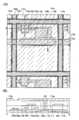
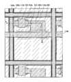
본 발명의 일 양태는, 절연면을 갖는 기판 상에 형성된 반도체층과, 반도체층과 전기적으로 접속된 제 1 전극을 포함하는 제 1 배선과, 반도체층과 제 1 전극을 덮도록 형성된 절연막과, 반도체층 상에 절연막을 개재하여 형성된 제 2 전극을 포함하는 제 2 배선을 갖고, 제 1 전극은 제 1 도전층을 갖고, 제 1 배선은 제 1 도전층과 제 2 도전층을 갖고, 제 2 전극은 제 3 도전층을 가지며, 제 2 배선은 제 3 도전층과 제 4 도전층을 갖는 것을 특징으로 하는 반도체 장치이다.One aspect of the present invention is a first wiring comprising a semiconductor layer formed on a substrate having an insulating surface, a first electrode electrically connected to the semiconductor layer, an insulating film formed to cover the semiconductor layer and the first electrode, It has a second wiring including a second electrode formed on the semiconductor layer via an insulating film, the first electrode has a first conductive layer, the first wiring has a first conductive layer and a second conductive layer, and a second The electrode has a third conductive layer, and the second wiring has a third conductive layer and a fourth conductive layer.
또, 본 발명의 일 양태는, 절연면을 갖는 기판 상에 형성된 반도체층과, 반도체층과 접속된 제 1 전극을 포함하는 제 1 배선과, 반도체층과 제 1 전극을 덮도록 형성된 절연막과, 반도체층 상에 절연막을 개재하여 형성된 제 2 전극을 포함하는 제 2 배선과, 제 3 배선을 갖고, 제 1 전극은 제 1 도전층을 갖고, 제 1 배선은 제 1 도전층과 제 2 도전층을 갖고, 제 2 전극은 제 3 도전층을 갖고, 제 2 배선은 제 3 도전층과 제 4 도전층을 가지며, 제 3 배선은 제 5 도전층과 제 6 도전층을 갖는 것을 특징으로 하는 반도체 장치이다.Another aspect of the present invention is a semiconductor layer formed on a substrate having an insulating surface, a first wiring including a first electrode connected to the semiconductor layer, an insulating film formed to cover the semiconductor layer and the first electrode, A second wiring including a second electrode formed on a semiconductor layer via an insulating film, and a third wiring, the first electrode having a first conductive layer, and the first wiring having a first conductive layer and a second conductive layer And the second electrode has a third conductive layer, the second wiring has a third conductive layer and a fourth conductive layer, and the third wiring has a fifth conductive layer and a sixth conductive layer. It is a device.
상기에서 제 1 도전층 및 제 3 도전층은, 투광성을 갖는 것이 바람직하다. 또, 제 2 도전층 및 제 4 도전층은, 제 1 도전층 또는 제 3 도전층 또는 투광성을 갖는 도전층의 도전율보다 높은 것이 바람직하다. 또, 제 2 도전층 및 제 4 도전층은 차광성을 갖는 것이 바람직하다.In the above, it is preferable that the first conductive layer and the third conductive layer have light transmission properties. Moreover, it is preferable that the 2nd conductive layer and 4th conductive layer are higher than the electric conductivity of a 1st conductive layer, a 3rd conductive layer, or a light-transmitting conductive layer. In addition, it is preferable that the second conductive layer and the fourth conductive layer have light-shielding properties.
또, 상기에서 반도체층은, 인듐, 갈륨 또는 아연을 함유하는 산화물 반도체층인 것이 바람직하다.Further, in the above, the semiconductor layer is preferably an oxide semiconductor layer containing indium, gallium, or zinc.
본 명세서 중에서 사용할 수 있는 산화물 반도체의 일례로는, InMO3(ZnO)m(m>0)으로 표기되는 것이 있다. 여기에서, M은 갈륨(Ga), 철(Fe), 니켈(Ni), 망간(Mn) 및 코발트(Co)에서 선택된 1개의 금속 원소 또는 복수의 금속 원소를 나타낸다. 예를 들어, M으로서 Ga가 선택되는 경우에는, Ga만인 경우 이외에, Ga와 Ni나 Ga와 Fe 등, Ga 이외의 상기 금속 원소가 선택되는 경우를 포함한다. 또, 상기 산화물 반도체에 있어서, M으로서 포함되는 금속 원소 이외에, 불순물 원소로서 Fe, Ni 그 밖의 천이 금속 원소, 또는 그 천이 금속의 산화물이 함유되어 있는 것이 있다. 본 명세서에서는, 상기 산화물 반도체 중, M으로서 적어도 갈륨을 함유하는 것을 In-Ga-Zn-O계 산화물 반도체라고 하고, 당해 재료를 사용한 박막을 In-Ga-Zn-O계 비(非)단결정막이라고 하는 경우가 있다.As an example of an oxide semiconductor that can be used in the present specification, there is one represented by InMO3 (ZnO)m (m>0). Here, M represents one metal element or a plurality of metal elements selected from gallium (Ga), iron (Fe), nickel (Ni), manganese (Mn), and cobalt (Co). For example, the case where Ga is selected as M includes the case where the metal element other than Ga is selected, such as Ga and Ni, Ga and Fe, in addition to the case of only Ga. Further, in the oxide semiconductor described above, in addition to the metal element contained as M, there are some containing Fe, Ni or other transition metal elements, or oxides of the transition metal as impurity elements. In the present specification, among the oxide semiconductors, those containing at least gallium as M are referred to as In-Ga-Zn-O-based oxide semiconductors, and a thin film using the material is an In-Ga-Zn-O-based non-single crystal film. There is a case called.
산화물 반도체로서, 상기 이외에도 In-Sn-Zn-O계, In-Al-Zn-O계, Sn-Ga-Zn-O계, Al-Ga-Zn-O계, Sn-Al-Zn-O계, In-Zn-O계, Sn-Zn-O계, Al-Zn-O계, In-O계, Sn-O계, Zn-O계 산화물 반도체를 적용할 수 있다. 이들 산화물 반도체에 결정화를 억제하고, 비정질 상태를 유지시키는 불순물을 첨가함으로써 박막 트랜지스터의 특성을 안정화시킬 수 있다.As an oxide semiconductor, in addition to the above, In-Sn-Zn-O-based, In-Al-Zn-O-based, Sn-Ga-Zn-O-based, Al-Ga-Zn-O-based, Sn-Al-Zn-O-based , In-Zn-O-based, Sn-Zn-O-based, Al-Zn-O-based, In-O-based, Sn-O-based, Zn-O-based oxide semiconductors can be applied. The characteristics of the thin film transistor can be stabilized by adding impurities that suppress crystallization and maintain an amorphous state to these oxide semiconductors.
또한, 본 발명의 일 양태에서 사용되는 반도체층은, 투광성을 가지고 있으면 된다. 투광성을 갖는 반도체층으로서, 예를 들어 산화물 반도체를 사용할 수 있다. 또, 산화물 반도체 이외에, 결정성 반도체(단결정 반도체 혹은 다결정 반도체), 비정질 반도체, 미결정 반도체, 마이크로크리스탈 반도체, 유기 반도체 등 중 어느 것을 사용해도 된다.In addition, the semiconductor layer used in one aspect of the present invention should have light-transmitting properties. As a light-transmitting semiconductor layer, for example, an oxide semiconductor can be used. In addition to the oxide semiconductor, any of a crystalline semiconductor (single crystal semiconductor or polycrystalline semiconductor), an amorphous semiconductor, a microcrystalline semiconductor, a microcrystalline semiconductor, an organic semiconductor, or the like may be used.
또한, 상기에서 제 1 도전층 및 제 2 도전층 등의 가공에 다계조 마스크를 사용함으로써, 1장의 마스크(레티클)로 투광성을 갖는 영역(광 투과율이 높은 영역)과 차광성을 갖는 영역(광 투과율이 낮은 영역)을 형성할 수 있다. 이로써, 마스크 수를 증가시키지 않고, 투광성을 갖는 영역(광 투과율이 높은 영역)과 차광성을 갖는 영역(광 투과율이 낮은 영역)을 형성할 수 있다.In addition, by using a multi-gradation mask for processing the first conductive layer and the second conductive layer above, a single mask (reticle) has a light-transmitting area (a high light transmittance area) and a light-blocking area (light-shielding area). A region having a low transmittance) can be formed. Accordingly, a light-transmitting region (a region having a high light transmittance) and a light-shielding region (a region having a low light transmittance) can be formed without increasing the number of masks.
또한, 본 명세서 중에서 반도체 장치란, 반도체 특성을 이용함으로써 기능할 수 있는 장치 전반을 가리키며, 반도체 회로, 표시 장치, 전기 광학 장치, 발광 표시 장치 및 전자 기기는 모두 반도체 장치에 포함된다.In addition, in this specification, a semiconductor device refers to all devices that can function by using semiconductor properties, and semiconductor circuits, display devices, electro-optical devices, light-emitting displays, and electronic devices are all included in semiconductor devices.
또한, 본 명세서 중에서 표시 장치란, 화상 표시 디바이스, 발광 디바이스 혹은 광원(조명 장치도 포함한다)을 가리킨다. 또, 커넥터, 예를 들어 FPC(Flexible Printed Circuit) 혹은 TAB(Tape Automated Bonding) 테이프 혹은 TCP(Tape Carrier Package)가 장착된 모듈, TAB 테이프나 TCP 의 끝에 프린트 배선판이 형성된 모듈, 및 표시 소자에 COG(Chip On Glass) 방식에 의해 IC(집적 회로)가 직접 실장된 모듈도 모두 표시 장치에 포함하는 것으로 한다.In addition, in this specification, a display device refers to an image display device, a light-emitting device, or a light source (including a lighting device). In addition, connectors, for example, modules with FPC (Flexible Printed Circuit) or TAB (Tape Automated Bonding) tape or TCP (Tape Carrier Package) attached, modules in which a printed wiring board is formed at the end of TAB tape or TCP, and COG on display elements All modules in which an IC (integrated circuit) is directly mounted by the (Chip On Glass) method are also included in the display device.
또한, 스위치는 여러 가지 형태의 것을 사용할 수 있다. 예로는, 전기적 스위치나 기계적인 스위치 등이 있다. 요컨대, 전류의 흐름을 제어할 수 있는 것이면 되어 특정한 것에 한정되지 않는다. 예를 들어, 스위치로서 트랜지스터(예를 들어, 바이폴러 트랜지스터, MOS 트랜지스터 등), 다이오드(예를 들어, PN 다이오드, PIN 다이오드, 쇼트키 다이오드, MIM(Metal Insulator Metal) 다이오드, MIS(Metal Insulator Semiconductor) 다이오드, 다이오드 접속의 트랜지스터 등) 등을 사용할 수 있다. 또는 이들을 조합한 논리 회로를 스위치로서 사용할 수 있다.In addition, various types of switches can be used. Examples include electrical switches or mechanical switches. In short, it is not limited to a specific one as long as it can control the flow of current. For example, as a switch, a transistor (e.g., bipolar transistor, MOS transistor, etc.), diode (e.g., PN diode, PIN diode, Schottky diode, MIM (Metal Insulator Metal) diode, MIS (Metal Insulator Semiconductor)) ) Diodes, diode-connected transistors, etc.) can be used. Alternatively, a logic circuit combining these can be used as a switch.
기계적인 스위치의 예로는, 디지털 마이크로미러 디바이스(DMD)와 같이, MEMS(마이크로 일렉트로 메카니컬 시스템) 기술을 이용한 스위치가 있다. 그 스위치는 기계적으로 움직일 수 있는 전극을 가지며, 그 전극이 움직임으로써 도통과 비도통을 제어하며 동작한다.An example of a mechanical switch is a switch using MEMS (Micro Electro Mechanical System) technology, such as a digital micromirror device (DMD). The switch has an electrode that can be mechanically movable, and it operates by controlling conduction and non-conduction by moving the electrode.
스위치로서 트랜지스터를 사용하는 경우, 그 트랜지스터는 단순한 스위치로서 동작하기 때문에, 트랜지스터의 극성(도전형)은 특별히 한정되지 않는다. 단, 오프 전류를 억제하고자 하는 경우, 오프 전류가 적은 쪽의 극성의 트랜지스터를 사용하는 것이 바람직하다. 오프 전류가 적은 트랜지스터로는, LDD 영역을 갖는 트랜지스터나 멀티게이트 구조를 갖는 트랜지스터 등이 있다. 또는 스위치로서 동작시키는 트랜지스터의 소스 단자의 전위가 저전위측 전원(Vss, GND, 0V 등)의 전위에 가까운 값으로 동작하는 경우에는, N채널형 트랜지스터를 사용하는 것이 바람직하다. 반대로, 소스 단자의 전위가 고전위측 전원(Vdd 등)의 전위에 가까운 값으로 동작하는 경우에는, P채널형 트랜지스터를 사용하는 것이 바람직하다. 왜냐하면, N채널형 트랜지스터에서는 소스 단자가 저전위측 전원의 전위에 가까운 값으로 동작할 때, P채널형 트랜지스터에서는 소스 단자가 고전위측 전원의 전위에 가까운 값으로 동작할 때, 게이트와 소스 사이의 전압의 절대값을 크게 할 수 있기 때문에, 스위치로서 보다 정확한 동작을 할 수 있기 때문이다. 또한, 트랜지스터가 소스 팔로워 동작을 하는 경우가 적기 때문에, 출력 전압의 크기가 작아지는 경우가 적기 때문이다.When a transistor is used as a switch, since the transistor operates as a simple switch, the polarity (conductive type) of the transistor is not particularly limited. However, when it is desired to suppress the off current, it is preferable to use a transistor having a lower polarity of the off current. Transistors having a small off-current include a transistor having an LDD region, a transistor having a multi-gate structure, and the like. Alternatively, when the potential of the source terminal of the transistor to be operated as a switch operates at a value close to that of the low potential side power supply (Vss, GND, 0V, etc.), it is preferable to use an N-channel transistor. Conversely, when the potential of the source terminal operates at a value close to that of the high-potential power supply (Vdd or the like), it is preferable to use a P-channel transistor. This is because in the N-channel transistor, when the source terminal operates at a value close to the potential of the low-potential power supply, in the P-channel transistor, when the source terminal operates at a value close to the potential of the high-potential power supply, This is because since the absolute value of the voltage can be increased, more accurate operation can be performed as a switch. In addition, since there are few cases in which the transistors perform the source follower operation, the size of the output voltage is less likely to be reduced.
또한, N채널형 트랜지스터와 P채널형 트랜지스터의 양방을 사용하여 CMOS형 스위치를 스위치로서 사용해도 된다. CMOS형 스위치로 하면, P채널형 트랜지스터 또는 N채널형 트랜지스터 중 어느 일방의 트랜지스터가 도통되면 전류가 흐르기 때문에, 스위치로서 기능하기 쉬워진다. 예를 들어, 스위치에 대한 입력 신호의 전압이 높거나 낮은 경우에도 적절히 전압을 출력시킬 수 있다. 또한, 스위치를 온 또는 오프시키기 위한 신호의 전압 진폭값을 작게 할 수 있기 때문에, 소비 전력을 작게 할 수도 있다.Further, a CMOS switch may be used as a switch by using both an N-channel transistor and a P-channel transistor. In the case of a CMOS switch, when either of the P-channel transistors and the N-channel transistors conducts, current flows, so that the switch can be easily functioned. For example, even when the voltage of the input signal to the switch is high or low, the voltage can be appropriately output. Further, since the voltage amplitude value of the signal for turning the switch on or off can be made small, the power consumption can also be reduced.
또한, 스위치로서 트랜지스터를 사용하는 경우, 스위치는 입력 단자(소스 단자 또는 드레인 단자의 일방)와, 출력 단자(소스 단자 또는 드레인 단자의 타방)와, 도통을 제어하는 단자(게이트 단자)를 가지고 있다. 한편, 스위치로서 다이오드를 사용하는 경우, 스위치는 도통을 제어하는 단자를 갖지 않는 경우가 있다. 이 때문에, 트랜지스터보다 다이오드를 스위치로서 사용한 편이 단자를 제어하기 위한 배선을 줄일 수 있다.In addition, when a transistor is used as a switch, the switch has an input terminal (one of the source terminal or drain terminal), an output terminal (the other side of the source terminal or drain terminal), and a terminal that controls conduction (gate terminal). . On the other hand, when a diode is used as a switch, the switch may not have a terminal for controlling conduction. For this reason, the use of a diode as a switch rather than a transistor can reduce wiring for controlling the terminal.
또한, A와 B가 접속되어 있다고 명시적으로 기재하는 경우에는, A와 B가 전기적으로 접속되어 있는 경우와, A와 B가 기능적으로 접속되어 있는 경우와, A와 B가 직접 접속되어 있는 경우를 포함하는 것으로 한다. 여기에서, A, B는 대상물(예를 들어, 장치, 소자, 회로, 배선, 전극, 단자, 도전막, 층 등)인 것으로 한다. 따라서, 소정의 접속 관계, 예를 들어 도면 또는 문장에 나타난 접속 관계에 한정되지 않고, 도면 또는 문장에 나타난 접속 관계 이외의 것도 포함하는 것으로 한다.In addition, when it is explicitly stated that A and B are connected, when A and B are electrically connected, when A and B are functionally connected, and when A and B are directly connected. It shall include. Here, A and B are assumed to be objects (for example, devices, elements, circuits, wirings, electrodes, terminals, conductive films, layers, etc.). Therefore, it is not limited to a predetermined connection relationship, for example, a connection relationship shown in a drawing or a sentence, and it is assumed that anything other than the connection relationship shown in a drawing or a sentence is included.
예를 들어, A와 B가 전기적으로 접속되어 있는 경우로서, A와 B의 전기적인 접속을 가능하게 하는 소자(예를 들어, 스위치, 트랜지스터, 용량 소자, 인덕터, 저항 소자, 다이오드 등)가 A와 B 사이에 1개 이상 접속되어 있어도 된다. 혹은 A와 B가 기능적으로 접속되어 있는 경우로서, A와 B의 기능적인 접속을 가능하게 하는 회로(예를 들어, 논리 회로(인버터, NAND 회로, NOR 회로 등), 신호 변환 회로(DA 변환 회로, AD 변환 회로, 감마 보정 회로 등), 전위 레벨 변환 회로(전원 회로(승압 회로, 강압 회로 등), 신호의 전위 레벨을 바꾸는 레벨 시프터 회로 등), 전압원, 전류원, 전환 회로, 증폭 회로(신호 진폭 또는 전류량 등을 크게 할 수 있는 회로, OP 앰프 (Operational Amplifier), 차동 증폭 회로, 소스 팔로워 회로, 버퍼 회로 등), 신호 생성 회로, 기억 회로, 제어 회로 등)가 A와 B 사이에 1개 이상 접속되어 있어도 된다. 예를 들어, A와 B 사이에 다른 회로를 사이에 두고 있어도, A로부터 출력된 신호가 B로 전달되는 경우에는, A와 B는 기능적으로 접속되어 있는 것으로 한다.For example, when A and B are electrically connected, an element that enables the electrical connection of A and B (e.g., a switch, a transistor, a capacitive element, an inductor, a resistance element, a diode, etc.) is A One or more may be connected between and B. Alternatively, when A and B are functionally connected, a circuit that enables a functional connection of A and B (e.g., a logic circuit (inverter, NAND circuit, NOR circuit, etc.), a signal conversion circuit (DA conversion circuit) , AD conversion circuit, gamma correction circuit, etc.), potential level conversion circuit (power supply circuit (boost circuit, step-down circuit, etc.), level shifter circuit that changes the potential level of a signal), voltage source, current source, switching circuit, amplifier circuit (signal A circuit that can increase the amplitude or amount of current, an operational amplifier (operational amplifier), a differential amplifier circuit, a source follower circuit, a buffer circuit, etc.), a signal generation circuit, a memory circuit, a control circuit, etc.) is between A and B. It may be connected above. For example, even if a different circuit is interposed between A and B, when a signal output from A is transmitted to B, it is assumed that A and B are functionally connected.
또한, A와 B가 전기적으로 접속되어 있다고 명시적으로 기재하는 경우에는, A와 B가 전기적으로 접속되어 있는 경우(요컨대, A와 B 사이에 다른 소자나 다른 회로를 사이에 두고 접속되어 있는 경우)와, A와 B가 기능적으로 접속되어 있는 경우(요컨대, A와 B 사이에 다른 회로를 사이에 두고 기능적으로 접속되어 있는 경우)와, A와 B가 직접 접속되어 있는 경우(요컨대, A와 B 사이에 다른 소자나 다른 회로를 사이에 두지 않고 접속되어 있는 경우)를 포함하는 것으로 한다. 요컨대, 전기적으로 접속되어 있다고 명시적으로 기재하는 경우에는, 단지 접속되어 있다라고만 명시적으로 기재되어 있는 경우와 동일한 것으로 한다.In addition, when it is explicitly stated that A and B are electrically connected, when A and B are electrically connected (i.e., when A and B are connected with another element or other circuit between them) ), when A and B are functionally connected (i.e., when they are functionally connected with another circuit between A and B), and when A and B are directly connected (i.e., A and B B is connected without interposing other elements or other circuits). In short, in the case where it is explicitly stated that it is electrically connected, it is assumed that it is the same as that in the case where only the connection is explicitly stated.
또한, 표시 소자, 표시 소자를 갖는 장치인 표시 장치, 발광 소자, 발광 소자를 갖는 장치인 발광 장치는, 여러 가지 형태를 사용하거나 여러 가지 소자를 가질 수 있다. 예를 들어, 표시 소자, 표시 장치, 발광 소자 또는 발광 장치로는, EL(일렉트로루미네선스) 소자(유기물 및 무기물을 포함하는 EL 소자, 유기 EL 소자, 무기 EL 소자), LED(백색 LED, 적색 LED, 녹색 LED, 청색 LED 등), 트랜지스터(전류에 따라 발광하는 트랜지스터), 전자 방출 소자, 액정 소자, 전자 잉크, 전기 영동 소자, 그레이팅 라이트 밸브(GLV), 플라스마 디스플레이 패널(PDP), 디지털 마이크로미러 디바이스(DMD), 압전 세라믹 디스플레이, 카본 나노 튜브 등 전기 자기적 작용에 의해 콘트라스트, 휘도, 반사율, 투과율 등이 변화되는 표시 매체를 가질 수 있다. 또한, EL 소자를 사용한 표시 장치로는 EL 디스플레이, 전자 방출 소자를 사용한 표시 장치로는 필드 에미션 디스플레이(FED)나 SED 방식 평면형 디스플레이(SED:Surface-conduction Electron-emitter Disply) 등, 액정 소자를 사용한 표시 장치로는 액정 디스플레이(투과형 액정 디스플레이, 반투과형 액정 디스플레이, 반사형 액정 디스플레이, 직시형 액정 디스플레이, 투사형 액정 디스플레이), 전자 잉크나 전기 영동 소자를 사용한 표시 장치로는 전자 페이퍼가 있다.In addition, a display element, a display device having a display element, a light-emitting element, and a light-emitting device having a light-emitting element may use various types or have various elements. For example, as a display element, a display device, a light-emitting element, or a light-emitting device, an EL (electroluminescence) element (an EL element containing an organic substance and an inorganic substance, an organic EL element, an inorganic EL element), an LED (white LED, Red LED, green LED, blue LED, etc.), transistors (transistors that emit light according to current), electron emission elements, liquid crystal elements, electronic ink, electrophoretic elements, grating light valves (GLV), plasma display panels (PDP), digital A display medium such as a micromirror device (DMD), a piezoelectric ceramic display, or a carbon nanotube may have a display medium whose contrast, luminance, reflectance, transmittance, and the like are changed by an electric magnetic action. In addition, as a display device using an EL element, an EL display, and a display device using an electron-emitting device include liquid crystal elements such as a field emission display (FED) or a SED type flat panel display (SED: Surface-conduction Electron-emitter Disply). A liquid crystal display (transmissive liquid crystal display, transflective liquid crystal display, reflective liquid crystal display, direct-view liquid crystal display, projection liquid crystal display) is used as a display device, and electronic paper is used as a display device using electronic ink or an electrophoretic element.
또한, EL 소자란 양극과, 음극과, 양극과 음극 사이에 두어진 EL층을 갖는 소자이다. 또한, EL층으로는 일중항 여기자로부터의 발광(형광)을 이용하는 것, 삼중항 여기자로부터의 발광(인광)을 이용하는 것, 일중항 여기자로부터의 발광(형광)을 이용하는 것과 삼중항 여기자로부터의 발광(인광)을 이용하는 것을 포함하는 것, 유기물에 의해 형성된 것, 무기물에 의해 형성된 것, 유기물에 의해 형성된 것과 무기물에 의해 형성된 것을 포함하는 것, 고분자 재료, 저분자 재료, 고분자 재료와 저분자 재료를 포함하는 것 등을 가질 수 있다. 단, 이것에 한정되지 않으며, EL 소자로서 여러 가지의 것을 가질 수 있다.Further, the EL element is an element having an anode, a cathode, and an EL layer interposed between the anode and the cathode. In addition, as the EL layer, light emission from singlet excitons (fluorescence) is used, light emission from triplet excitons (phosphorescence) is used, light emission from singlet excitons (fluorescence) is used, and light emission from triplet excitons Including those using (phosphorescence), those formed by organic substances, those formed by inorganic substances, those formed by organic substances and those formed by inorganic substances, high molecular materials, low molecular materials, including high molecular materials and low molecular materials Can have things, etc. However, it is not limited to this, and various types of EL elements can be provided.
또한, 전자 방출 소자란 음극에 고전계를 집중시켜 전자를 인출하는 소자이다. 예를 들어, 전자 방출 소자로서 스핀트형, 카본 나노 튜브(CNT)형, 금속-절연체-금속을 적층한 MIM(Metal-Insulator-Metal)형, 금속-절연체-반도체를 적층한 MIS(Metal-Insulator-Semiconductor)형, MOS형, 실리콘형, 박막 다이오드형, 다이아몬드형, 금속-절연체-반도체-금속형 등의 박막형, HEED형, EL형, 포러스 실리콘형, 표면 전도(SCE)형 등을 가질 수 있다. 단, 이것에 한정되지 않으며, 전자 방출 소자로서 여러 가지의 것을 가질 수 있다.In addition, the electron emitting device is a device that extracts electrons by concentrating a high field on the cathode. For example, as an electron emission device, a spint type, a carbon nanotube (CNT) type, a metal-insulator-metal stacked MIM (Metal-Insulator-Metal) type, and a metal-insulator-semiconductor stacked MIS (Metal-Insulator) type -Semiconductor) type, MOS type, silicon type, thin-film diode type, diamond type, metal-insulator-semiconductor-metal type, thin film type, HEED type, EL type, porous silicon type, surface conduction (SCE) type, etc. have. However, it is not limited to this, and various things can be provided as an electron-emitting device.
또한, 액정 소자란 액정의 광학적 변조 작용에 의해 광의 투과 또는 비투과를 제어하는 소자로서, 1쌍의 전극 및 액정에 의해 구성된다. 또한, 액정의 광학적 변조 작용은, 액정에 가해지는 전계(횡 방향의 전계, 종 방향의 전계 또는 경사 방향의 전계를 포함한다)에 의해 제어된다. 또한, 액정 소자로는 네마틱 액정, 콜레스테릭 액정, 스멕틱 액정, 디스코틱 액정, 서모트로픽 액정, 리오트로픽 액정, 저분자 액정, 고분자 액정, 고분자 분산형 액정(PDLC), 강유전 액정, 반(反)강유전 액정, 주사슬형 액정, 측사슬형 고분자 액정, 플라스마 어드레스 액정(PALC), 바나나형 액정 등을 들 수 있다. 또, 액정의 구동 방식으로는, TN(Twisted Nematic) 모드, STN(Super Twisted Nematic) 모드, IPS(In-Plane-Switching) 모드, FFS(Fringe Field Switching) 모드, MVA(Multi-domain Vertical Alignment) 모드, PVA(Patterned Vertical Alignment) 모드, ASV(Advanced Super View) 모드, ASM(Axially Symmetric aligned Micro-cell) 모드, OCB(Optically Compensated Birefringence) 모드, ECB(Electrically Controlled Birefringence) 모드, FLC(Ferroelectric Liquid Crystal) 모드, AFLC(AntiFerroelectric Liquid Crystal) 모드, PDLC(Polymer Dispersed Liquid Crystal) 모드, 게스트 호스트 모드, 블루상(Blue Phase) 모드 등을 사용할 수 있다. 단, 이것에 한정되지 않으며, 액정 소자 및 그 구동 방식으로서 여러 가지의 것을 사용할 수 있다.In addition, a liquid crystal element is an element that controls transmission or non-transmission of light by an optical modulating action of the liquid crystal, and is constituted by a pair of electrodes and a liquid crystal. Further, the optical modulating action of the liquid crystal is controlled by an electric field applied to the liquid crystal (including an electric field in a lateral direction, an electric field in a vertical direction, or an electric field in an oblique direction). In addition, as a liquid crystal element, nematic liquid crystal, cholesteric liquid crystal, smectic liquid crystal, discotic liquid crystal, thermotropic liquid crystal, lyotropic liquid crystal, low molecular liquid crystal, polymer liquid crystal, polymer dispersed liquid crystal (PDLC), ferroelectric liquid crystal, semi-( Anti-ferroelectric liquid crystal, main chain liquid crystal, side chain polymer liquid crystal, plasma address liquid crystal (PALC), banana liquid crystal, and the like. In addition, as a driving method of the liquid crystal, TN (Twisted Nematic) mode, STN (Super Twisted Nematic) mode, IPS (In-Plane-Switching) mode, FFS (Fringe Field Switching) mode, MVA (Multi-domain Vertical Alignment) Mode, Patterned Vertical Alignment (PVA) Mode, Advanced Super View (ASV) Mode, Axially Symmetric Aligned Micro-cell (ASM) Mode, Optically Compensated Birefringence (OCB) Mode, Electrically Controlled Birefringence (ECB) Mode, Ferroelectric Liquid Crystal (FLC) ) Mode, AFLC (AntiFerroelectric Liquid Crystal) mode, PDLC (Polymer Dispersed Liquid Crystal) mode, guest host mode, and blue phase mode. However, it is not limited to this, and various things can be used as a liquid crystal element and its driving system.
또한, 전자 페이퍼로는, 분자에 의해 표시되는 것(광학 이방성, 염료 분자 배향 등), 입자에 의해 표시되는 것(전기 영동, 입자 이동, 입자 회전, 상 변화 등), 필름의 일단이 이동함으로써 표시되는 것, 분자의 발색/상 변화에 의해 표시되는 것, 분자의 광 흡수에 의해 표시되는 것, 전자와 홀이 결합되어 자발광에 의해 표시되는 것 등의 것을 말한다. 예를 들어, 전자 페이퍼의 표시 방법으로서, 마이크로캡슐형 전기 영동, 수평 이동형 전기 영동, 수직 이동형 전기 영동, 구 형상 트위스트 볼, 자기 트위스트 볼, 원주 트위스트 볼 방식, 대전 토너, 전자 분말 유체, 자기 영동형, 자기 감열식, 일렉트로웨팅, 광 산란(투명/백탁 변화), 콜레스테릭 액정/광 도전층, 콜레스테릭 액정, 쌍안정성 네마틱 액정, 강유전성 액정, 2색성 색소ㆍ액정 분산형, 가동 필름, 류코 염료에 의한 발소색, 포토크로믹, 일렉트로크로믹, 일렉트로디포지션, 플렉시블 유기 EL 등을 사용할 수 있다. 단, 이것에 한정되지 않으며, 전자 페이퍼 및 그 표시 방법으로서 여러 가지의 것을 사용할 수 있다. 여기에서, 마이크로캡슐형 전기 영동을 사용함으로써, 전기 영동 방식의 결점인 영동 입자의 응집, 침전을 해결할 수 있다. 전자 분말 유체는, 고속 응답성, 고반사율, 광시야각, 저소비 전력, 메모리성 등의 장점을 갖는다.In addition, as electronic papers, those represented by molecules (optical anisotropy, dye molecule orientation, etc.), those represented by particles (electrophoresis, particle movement, particle rotation, phase change, etc.), and one end of the film are moved. It refers to things that are displayed, that are displayed by color/phase change of molecules, that are displayed by light absorption of molecules, that are displayed by self-luminescence by bonding of electrons and holes. For example, as a display method of electronic paper, microcapsule type electrophoresis, horizontal movement type electrophoresis, vertical movement type electrophoresis, spherical twist ball, magnetic twist ball, circumferential twist ball method, charged toner, electronic powder fluid, magnetophoresis Type, self-heating type, electrowetting, light scattering (transparency/cloudiness change), cholesteric liquid crystal/light conductive layer, cholesteric liquid crystal, bistable nematic liquid crystal, ferroelectric liquid crystal, dichroic dye/liquid crystal dispersion type, movable Films, coloring with leuco dyes, photochromic, electrochromic, electrodeposition, flexible organic EL, and the like can be used. However, it is not limited to this, and various things can be used as an electronic paper and its display method. Here, by using microcapsule type electrophoresis, it is possible to solve the agglomeration and precipitation of the electrophoretic particles, which is a drawback of the electrophoresis method. The electronic powder fluid has advantages such as high speed response, high reflectance, wide viewing angle, low power consumption, and memory.
또한, 플라스마 디스플레이 패널은, 전극을 표면에 형성한 기판과, 전극 및 미소한 홈을 표면에 형성하고 또한 홈 내에 형광체층을 형성한 기판을 좁은 간격으로 대향시키고, 희가스를 봉입한 구조를 갖는다. 혹은 플라스마 디스플레이 패널은, 플라스마 튜브를 상하로부터 필름 형상의 전극 사이에 둔 구조로 할 수도 있다. 플라스마 튜브란, 유리 튜브 내에 방전 가스, RGB 각각의 형광체 등을 봉지한 것이다. 또한, 전극 간에 전압을 가함으로써 자외선을 발생시켜 형광체를 발하게 함으로써 표시를 행할 수 있다. 또한, 플라스마 디스플레이 패널로는, DC형 PDP, AC형 PDP여도 된다. 여기에서, 플라스마 디스플레이 패널의 구동 방식으로는, AWS(Address While Sustain)구동, 서브 프레임을 리셋 기간, 어드레스 기간, 유지 기간으로 분할하는 ADS(Address Display Separated) 구동, CLEAR(HICONTRAST & LOW ENERGY ADDRESS & REDUCTION OF FALSE CONTOUR SEQUENCE) 구동, ALIS(Alternate Lighting of Surfaces)방식, TERES(Technology of Reciprocal Sustainer) 구동 등을 사용할 수 있다. 단, 이것에 한정되지 않으며, 플라스마 디스플레이 패널의 구동 방식으로서 여러 가지의 것을 사용할 수 있다.In addition, the plasma display panel has a structure in which a substrate having electrodes formed on the surface thereof, and a substrate having electrodes and minute grooves formed on the surface thereof and a phosphor layer formed in the grooves are opposed to each other at narrow intervals, and a rare gas is encapsulated. Alternatively, the plasma display panel may have a structure in which a plasma tube is sandwiched between film-shaped electrodes from the top and bottom. The plasma tube is a glass tube in which a discharge gas, a fluorescent substance of each RGB, etc. are sealed. In addition, by applying a voltage between the electrodes, ultraviolet rays are generated to emit a phosphor, so that display can be performed. Further, the plasma display panel may be a DC type PDP or an AC type PDP. Here, as the driving method of the plasma display panel, AWS (Address While Sustain) drive, ADS (Address Display Separated) drive that divides the subframe into a reset period, an address period, and a sustain period, and CLEAR (HICONTRAST & LOW ENERGY ADDRESS & REDUCTION OF FALSE CONTOUR SEQUENCE) drive, ALIS (Alternate Lighting of Surfaces) method, TERES (Technology of Reciprocal Sustainer) drive, etc. can be used. However, the present invention is not limited thereto, and various types of driving methods can be used for the plasma display panel.
또한, 광원을 필요로 하는 표시 장치, 예를 들어 액정 디스플레이(투과형 액정 디스플레이, 반투과형 액정 디스플레이, 반사형 액정 디스플레이, 직시형 액정 디스플레이, 투사형 액정 디스플레이), 그레이팅 라이트 밸브(GLV)를 사용한 표시 장치, 디지털 마이크로미러 디바이스(DMD)를 사용한 표시 장치 등의 광원으로는, 일렉트로루미네선스, 냉음극관, 열음극관, LED, 레이저 광원, 수은 램프 등을 사용할 수 있다. 단, 이것에 한정되지 않으며, 광원으로서 여러 가지의 것을 사용할 수 있다.In addition, display devices requiring a light source, for example, liquid crystal displays (transmissive liquid crystal displays, transflective liquid crystal displays, reflective liquid crystal displays, direct-view liquid crystal displays, projection liquid crystal displays), display devices using grating light valves (GLV) , As a light source for a display device using a digital micromirror device (DMD), an electroluminescence, a cold cathode tube, a hot cathode tube, an LED, a laser light source, a mercury lamp, or the like can be used. However, it is not limited to this, and various things can be used as a light source.
또한, 트랜지스터로서 여러 가지 형태의 트랜지스터를 사용할 수 있다. 따라서, 사용하는 트랜지스터의 종류에 한정은 없다. 예를 들어, 비정질 실리콘, 다결정 실리콘, 미결정(마이크로크리스탈, 나노크리스탈, 세미아몰퍼스라고도 한다) 실리콘 등으로 대표되는 비단결정 반도체막 및 단결정 반도체막을 갖는 박막 트랜지스터(TFT) 등을 사용할 수 있다. TFT를 사용하는 경우 여러 가지의 장점이 있다. 예를 들어, 단결정 실리콘의 경우보다 낮은 온도에서 제조할 수 있기 때문에, 제조 비용의 삭감 또는 제조 장치의 대형화를 도모할 수 있다. 제조 장치를 크게 할 수 있기 때문에, 대형 기판 상에 제조할 수 있다. 이 때문에, 동시에 많은 개수의 표시 장치를 제조할 수 있기 때문에, 저비용으로 제조할 수 있다. 또한, 제조 온도가 낮기 때문에, 내열성이 낮은 기판을 사용할 수 있다. 이 때문에, 투광성을 갖는 기판 상에 트랜지스터를 제조할 수 있다. 그리고, 투광성을 갖는 기판 상의 트랜지스터를 사용하여 표시 소자에서의 광의 투과를 제어할 수 있다. 혹은 트랜지스터의 막 두께가 얇기 때문에, 트랜지스터를 구성하는 막의 일부는 광을 투과시킬 수 있다. 이 때문에, 개구율을 향상시킬 수 있다.In addition, various types of transistors can be used as the transistor. Therefore, there is no limitation on the type of transistor to be used. For example, a non-single crystal semiconductor film represented by amorphous silicon, polycrystalline silicon, microcrystalline (also referred to as microcrystal, nanocrystal, semi-amorphous) silicon, etc., and a thin film transistor (TFT) having a single crystal semiconductor film may be used. There are several advantages when using a TFT. For example, since it can be manufactured at a lower temperature than in the case of single crystal silicon, it is possible to reduce the manufacturing cost or increase the size of the manufacturing apparatus. Since the manufacturing apparatus can be enlarged, it can be manufactured on a large-sized substrate. For this reason, since a large number of display devices can be manufactured at the same time, it can be manufactured at low cost. Further, since the manufacturing temperature is low, a substrate having low heat resistance can be used. For this reason, a transistor can be manufactured on a light-transmitting substrate. In addition, it is possible to control the transmission of light through the display element by using a transistor on the substrate having light-transmitting properties. Alternatively, since the film thickness of the transistor is thin, a part of the film constituting the transistor can transmit light. For this reason, the aperture ratio can be improved.
또한, 다결정 실리콘을 제조할 때, 촉매(니켈 등)를 사용함으로써 결정성을 더욱 향상시켜, 전기 특성이 양호한 트랜지스터를 제조할 수 있게 된다. 그 결과, 게이트 드라이버 회로(주사선 구동 회로)나 소스 드라이버 회로(신호선 구동 회로), 신호 처리 회로(신호 생성 회로, 감마 보정 회로, DA 변환 회로 등)를 기판 상에 일체로 형성할 수 있다.In addition, when producing polycrystalline silicon, by using a catalyst (such as nickel), crystallinity is further improved, and a transistor having good electrical characteristics can be manufactured. As a result, a gate driver circuit (scan line driving circuit), a source driver circuit (signal line driving circuit), and a signal processing circuit (signal generation circuit, gamma correction circuit, DA conversion circuit, etc.) can be integrally formed on the substrate.
또한, 미결정 실리콘을 제조할 때, 촉매(니켈 등)를 사용함으로써 결정성을 더욱 향상시켜, 전기 특성이 양호한 트랜지스터를 제조할 수 있게 된다. 이 때, 레이저 조사를 행하지 않고, 열처리를 가하는 것만으로 결정성을 향상시킬 수도 있다. 그 결과, 소스 드라이버 회로의 일부(아날로그 스위치 등) 및 게이트 드라이버 회로(주사선 구동 회로)를 기판 상에 일체로 형성할 수 있다. 또한, 결정화를 위해 레이저 조사를 행하지 않는 경우에는, 실리콘의 결정성의 불균일을 억제할 수 있다. 이 때문에, 화질이 향상된 화상을 표시할 수 있다.In addition, when producing microcrystalline silicon, by using a catalyst (such as nickel), crystallinity is further improved, and a transistor having good electrical characteristics can be manufactured. At this time, crystallinity can also be improved only by applying heat treatment without performing laser irradiation. As a result, a part of the source driver circuit (analog switch, etc.) and the gate driver circuit (scan line driving circuit) can be integrally formed on the substrate. In addition, when laser irradiation is not performed for crystallization, it is possible to suppress nonuniformity in crystallinity of silicon. For this reason, an image with improved image quality can be displayed.
단, 촉매(니켈 등)를 사용하지 않고, 다결정 실리콘이나 미결정 실리콘을 제조할 수는 있다.However, it is possible to manufacture polycrystalline silicon or microcrystalline silicon without using a catalyst (such as nickel).
또한, 실리콘의 결정성을 다결정 또는 미결정 등으로 향상시키는 것은 패널 전체적으로 실시하는 것이 바람직하지만, 그것에 한정되지 않는다. 패널의 일부 영역에서만 실리콘의 결정성을 향상시켜도 된다. 선택적으로 결정성을 향상시키는 것은, 레이저광을 선택적으로 조사하거나 하여 할 수 있다. 예를 들어, 화소 이외의 영역인 주변 회로 영역에만 레이저광을 조사해도 된다. 또는 게이트 드라이버 회로, 소스 드라이버 회로 등의 영역에만 레이저광을 조사해도 된다. 혹은 소스 드라이버 회로의 일부(예를 들어, 아날로그 스위치)의 영역에만 레이저광을 조사해도 된다. 그 결과, 회로를 고속으로 동작시킬 필요가 있는 영역에만 실리콘의 결정화를 향상시킬 수 있다. 화소 영역은 고속으로 동작시킬 필요성이 낮기 때문에, 결정성이 향상되지 않아도 문제없이 화소 회로를 동작시킬 수 있다. 결정성을 향상시키는 영역이 적어도 되기 때문에, 제조 공정도 짧게 할 수 있어 스루풋이 향상되고, 제조 비용을 저감시킬 수 있다. 필요로 되는 제조 장치의 수도 적은 수로 제조할 수 있기 때문에, 제조 비용을 저감시킬 수 있다.Incidentally, improving the crystallinity of silicon to polycrystalline or microcrystalline is preferably carried out as a whole of the panel, but is not limited thereto. The crystallinity of silicon may be improved only in some areas of the panel. Selectively improving the crystallinity can be achieved by selectively irradiating laser light. For example, you may irradiate the laser light only to the peripheral circuit area|region which is the area|region other than a pixel. Alternatively, laser light may be irradiated only to regions such as the gate driver circuit and the source driver circuit. Alternatively, laser light may be irradiated only in a region of a part of the source driver circuit (for example, an analog switch). As a result, crystallization of silicon can be improved only in regions where the circuit needs to be operated at high speed. Since the need to operate the pixel region at high speed is low, the pixel circuit can be operated without problems even if the crystallinity is not improved. Since the region for improving crystallinity is minimized, the manufacturing process can be shortened, the throughput is improved, and the manufacturing cost can be reduced. Since the number of required manufacturing apparatuses can be manufactured with a small number, manufacturing cost can be reduced.
또는 반도체 기판이나 SOI 기판 등을 사용하여 트랜지스터를 형성할 수 있다. 이들에 의해 특성이나 사이즈나 형상 등의 편차가 적고, 전류 공급 능력이 높으며, 사이즈가 작은 트랜지스터를 제조할 수 있다. 이들 트랜지스터를 사용하면, 회로의 저소비 전력화 또는 회로의 고집적화를 도모할 수 있다.Alternatively, a transistor can be formed using a semiconductor substrate or an SOI substrate. As a result, there are few variations in characteristics, size, shape, etc., a high current supply capability, and a transistor having a small size can be manufactured. When these transistors are used, it is possible to reduce the power consumption of the circuit or to increase the integration of the circuit.
또는 ZnO, a-InGaZnO, SiGe, GaAs, IZO, ITO, SnO, TiO, AlZnSnO(AZTO) 등의 화합물 반도체 또는 산화물 반도체를 갖는 트랜지스터나, 또한 이들 화합물 반도체 또는 산화물 반도체를 박막화한 박막 트랜지스터 등을 사용할 수 있다. 이들에 의해 제조 온도를 낮출 수 있어, 예를 들어 실온에서 트랜지스터를 제조할 수 있게 된다. 그 결과, 내열성이 낮은 기판, 예를 들어 플라스틱 기판이나 필름 기판에 직접 트랜지스터를 형성할 수 있다. 또한, 이들 화합물 반도체 또는 산화물 반도체를 트랜지스터의 채널 형성 영역에 사용할 뿐만 아니라, 그 이외의 용도에 사용할 수도 있다. 예를 들어, 이들 화합물 반도체 또는 산화물 반도체를 저항 소자, 화소 전극, 투광성을 갖는 전극으로서 사용할 수 있다. 또한, 이들을 트랜지스터와 동시에 성막 또는 형성할 수 있기 때문에, 비용을 저감시킬 수 있다.Alternatively, transistors having compound semiconductors or oxide semiconductors such as ZnO, a-InGaZnO, SiGe, GaAs, IZO, ITO, SnO, TiO, AlZnSnO (AZTO), or thin film transistors in which these compound semiconductors or oxide semiconductors are thinned can be used. I can. By these, the manufacturing temperature can be lowered, and for example, a transistor can be manufactured at room temperature. As a result, it is possible to form a transistor directly on a substrate having low heat resistance, for example, a plastic substrate or a film substrate. In addition, these compound semiconductors or oxide semiconductors can be used not only for the channel formation region of the transistor, but also for other uses. For example, these compound semiconductors or oxide semiconductors can be used as resistance elements, pixel electrodes, and electrodes having light-transmitting properties. Further, since these can be formed or formed simultaneously with the transistor, the cost can be reduced.
또는 잉크젯이나 인쇄법을 사용하여 형성한 트랜지스터 등을 사용할 수 있다. 이들에 의해 실온에서 제조, 저진공도로 제조, 또는 대형 기판 상에 제조할 수 있다. 마스크(레티클)를 사용하지 않아도 제조할 수 있게 되기 때문에, 트랜지스터의 레이아웃을 용이하게 변경할 수 있다. 또한, 레지스트를 사용할 필요가 없기 때문에 재료비가 저렴해지고, 공정 수를 삭감시킬 수 있다. 또한, 필요한 부분에만 막을 부착시키기 때문에, 전체면에 성막한 이후에 에칭하는 제법보다 재료가 낭비되지 않아 저비용으로 할 수 있다.Alternatively, a transistor formed by using an inkjet or printing method can be used. By these, it can be manufactured at room temperature, manufactured with low vacuum, or manufactured on a large-sized substrate. Since it can be manufactured without using a mask (reticle), the layout of the transistor can be easily changed. In addition, since there is no need to use a resist, the material cost becomes low and the number of steps can be reduced. In addition, since the film is attached only to a necessary portion, the material is not wasted compared to the method of etching after film formation on the entire surface, and thus the cost can be reduced.
또는 유기 반도체나 카본 나노 튜브를 갖는 트랜지스터 등을 사용할 수 있다. 이들에 의해 구부릴 수 있는 기판 상에 트랜지스터를 형성할 수 있다. 이와 같은 기판을 사용한 반도체 장치는 충격에 강하게 할 수 있다.Alternatively, an organic semiconductor or a transistor having a carbon nanotube can be used. By these, a transistor can be formed on a bendable substrate. A semiconductor device using such a substrate can be made resistant to impact.
또한, 여러 가지 구조의 트랜지스터를 사용할 수 있다. 예를 들어, MOS형 트랜지스터, 접합형 트랜지스터, 바이폴러 트랜지스터 등을 트랜지스터로서 사용할 수 있다. MOS형 트랜지스터를 사용함으로써, 트랜지스터의 사이즈를 작게 할 수 있다. 따라서, 복수의 트랜지스터를 탑재할 수 있다. 바이폴러 트랜지스터를 사용함으로써 큰 전류를 흘릴 수 있다. 따라서, 고속으로 회로를 동작시킬 수 있다.In addition, transistors of various structures can be used. For example, a MOS transistor, a junction transistor, a bipolar transistor, or the like can be used as the transistor. By using the MOS transistor, the size of the transistor can be reduced. Therefore, a plurality of transistors can be mounted. A large current can be passed by using a bipolar transistor. Therefore, it is possible to operate the circuit at high speed.
또한, MOS형 트랜지스터, 바이폴러 트랜지스터 등을 1개의 기판에 혼재시켜 형성해도 된다. 이로써, 저소비 전력, 소형화, 고속 동작 등을 실현시킬 수 있다.In addition, MOS transistors, bipolar transistors, and the like may be mixed on a single substrate. Thereby, it is possible to realize low power consumption, miniaturization, and high-speed operation.
이 밖에, 여러 가지 트랜지스터를 사용할 수 있다.In addition, various transistors can be used.
또한, 트랜지스터는 여러 가지 기판을 사용하여 형성할 수 있다. 기판의 종류는 특정한 것에 한정되지 않는다. 그 기판으로는, 예를 들어 단결정 기판(예를 들어, 실리콘 기판), SOI 기판, 유리 기판, 석영 기판, 플라스틱 기판, 금속 기판, 스테인리스 스틸 기판, 스테인리스 스틸 호일을 갖는 기판, 텅스텐 기판, 텅스텐 호일을 갖는 기판, 가요성 기판 등을 사용할 수 있다. 유리 기판의 일례로는, 바륨붕규산 유리, 알루미노붕규산 유리 등이 있다. 가요성 기판의 일례로는, 폴리에틸렌테레프탈레이트(PET), 폴리에틸렌나프탈레이트(PEN), 폴리에테르술폰(PES)으로 대표되는 플라스틱, 또는 아크릴 등의 가요성을 갖는 합성 수지 등이 있다. 이 밖에도, 부착 필름(폴리프로필렌, 폴리에스테르, 비닐, 폴리불화비닐, 염화비닐 등), 섬유 형상 재료를 포함하는 종이, 기재 필름(폴리에스테르, 폴리아미드, 폴리이미드, 무기 증착 필름, 종이류 등) 등이 있다. 또는 어느 기판을 사용하여 트랜지스터를 형성하고, 그 후에 다른 기판에 트랜지스터를 전치(轉置)하고, 다른 기판 상에 트랜지스터를 배치해도 된다. 트랜지스터가 전치되는 기판으로는, 단결정 기판, SOI 기판, 유리 기판, 석영 기판, 플라스틱 기판, 종이 기판, 셀로판 기판, 석재 기판, 목재 기판, 천 기판(cloth substate)(천연 섬유(견, 면, 마), 합성 섬유(나일론, 폴리우레탄, 폴리에스테르) 혹은 재생 섬유(아세테이트, 큐프라, 레이온, 재생 폴리에스테르) 등을 포함한다), 피혁 기판, 고무 기판, 스테인리스 스틸 기판, 스테인리스 스틸 호일을 갖는 기판 등을 사용할 수 있다. 혹은 사람 등과 같은 동물의 피부(표피, 진피) 또는 피하 조직을 기판으로서 사용해도 된다. 또는 어느 기판을 사용하여 트랜지스터를 형성하고, 그 기판을 연마하여 얇게 해도 된다. 연마되는 기판으로는, 단결정 기판, SOI 기판, 유리 기판, 석영 기판, 플라스틱 기판, 스테인리스 스틸 기판, 스테인리스 스틸 호일을 갖는 기판 등을 사용할 수 있다. 이들 기판을 사용함으로써 특성이 양호한 트랜지스터의 형성, 소비 전력이 작은 트랜지스터의 형성, 내구성이 높은 장치의 제조, 내열성의 부여, 경량화 또는 박형화를 도모할 수 있다.In addition, the transistor can be formed using various substrates. The type of the substrate is not limited to a specific one. Examples of the substrate include a single crystal substrate (e.g., a silicon substrate), an SOI substrate, a glass substrate, a quartz substrate, a plastic substrate, a metal substrate, a stainless steel substrate, a substrate having a stainless steel foil, a tungsten substrate, and a tungsten foil. A substrate having a, a flexible substrate, or the like can be used. Examples of the glass substrate include barium borosilicate glass, aluminoborosilicate glass, and the like. Examples of flexible substrates include plastics typified by polyethylene terephthalate (PET), polyethylene naphthalate (PEN), polyethersulfone (PES), or synthetic resins having flexibility such as acrylic. In addition, adhesive films (polypropylene, polyester, vinyl, polyvinyl fluoride, vinyl chloride, etc.), paper containing fibrous materials, and base films (polyester, polyamide, polyimide, inorganic vapor deposition film, paper, etc.) Etc. Alternatively, a transistor may be formed using any substrate, then the transistor may be transferred to another substrate, and the transistor may be disposed on the other substrate. Substrates on which transistors are transferred include single crystal substrates, SOI substrates, glass substrates, quartz substrates, plastic substrates, paper substrates, cellophane substrates, stone substrates, wood substrates, cloth substates (natural fibers (silk, cotton, hemp). ), synthetic fibers (nylon, polyurethane, polyester) or recycled fibers (including acetate, cupra, rayon, recycled polyester), leather substrates, rubber substrates, stainless steel substrates, substrates with stainless steel foil Etc. can be used. Alternatively, the skin (epidermis, dermis) or subcutaneous tissue of an animal such as human may be used as a substrate. Alternatively, a transistor may be formed using any substrate, and the substrate may be polished to make it thin. As the substrate to be polished, a single crystal substrate, an SOI substrate, a glass substrate, a quartz substrate, a plastic substrate, a stainless steel substrate, a substrate having a stainless steel foil, or the like can be used. By using these substrates, it is possible to form a transistor with good characteristics, form a transistor with low power consumption, manufacture a device with high durability, impart heat resistance, and reduce weight or thickness.
또한, 트랜지스터의 구성은 여러 가지 형태를 취할 수 있으며, 특정 구성에 한정되지 않는다. 예를 들어, 게이트 전극이 2개 이상의 멀티게이트 구조를 적용할 수 있다. 멀티게이트 구조로 하면, 채널 영역이 직렬로 접속되기 때문에, 복수의 트랜지스터가 직렬로 접속된 구성이 된다. 멀티게이트 구조에 의해 오프 전류의 저감, 트랜지스터의 내압 향상(신뢰성의 향상)을 도모할 수 있다. 혹은 멀티게이트 구조에 의해, 포화 영역에서 동작할 때에 드레인ㆍ소스 간 전압이 변화되어도 드레인ㆍ소스 간 전류가 그다지 변화되지 않아, 전압ㆍ전류 특성의 기울기를 플랫으로 할 수 있다. 전압ㆍ전류 특성의 기울기가 플랫인 특성을 이용하면, 이상적인 전류원 회로나 매우 높은 저항값을 갖는 능동 부하를 실현시킬 수 있다. 그 결과, 특성이 양호한 차동 회로나 커런트 미러 회로를 실현시킬 수 있다.In addition, the configuration of the transistor can take various forms, and is not limited to a specific configuration. For example, a multi-gate structure of two or more gate electrodes may be applied. In the case of a multi-gate structure, since the channel regions are connected in series, a configuration in which a plurality of transistors are connected in series is obtained. The multi-gate structure can reduce the off current and improve the breakdown voltage of the transistor (improvement of reliability). Alternatively, due to the multi-gate structure, even if the voltage between the drain and the source changes when operating in the saturation region, the current between the drain and the source does not change very much, so that the slope of the voltage and current characteristics can be made flat. If the slope of the voltage/current characteristics is flat, an ideal current source circuit or an active load having a very high resistance value can be realized. As a result, it is possible to realize a differential circuit or a current mirror circuit with good characteristics.
다른 예로서, 채널의 상하에 게이트 전극이 배치되어 있는 구조를 적용할 수 있다. 채널의 상하에 게이트 전극이 배치되어 있는 구조로 함으로써 채널 영역이 증가되기 때문에, 전류값의 증가를 도모할 수 있다. 또는 채널의 상하에 게이트 전극이 배치되어 있는 구조로 함으로써 공핍층이 생기기 쉬워지기 때문에, S값의 개선을 도모할 수 있다. 또한, 채널의 상하에 게이트 전극이 배치되는 구성으로 함으로써, 복수의 트랜지스터가 병렬로 접속되는 구성이 된다.As another example, a structure in which gate electrodes are disposed above and below the channel may be applied. By having a structure in which gate electrodes are arranged above and below the channel, since the channel region is increased, the current value can be increased. Alternatively, since the structure in which the gate electrodes are arranged above and below the channel makes it easy to generate a depletion layer, the S value can be improved. In addition, a structure in which gate electrodes are disposed above and below the channel provides a structure in which a plurality of transistors are connected in parallel.
채널 영역 상에 게이트 전극이 배치되어 있는 구조, 채널 영역 아래에 게이트 전극이 배치되어 있는 구조, 정(正)스태거 구조, 역(逆)스태거 구조, 채널 영역을 복수의 영역으로 나눈 구조, 채널 영역을 병렬로 접속시킨 구조, 또는 채널 영역이 직렬로 접속되는 구성도 적용할 수 있다. 또한, 채널 영역(혹은 그 일부)에 소스 전극이나 드레인 전극이 중첩되어 있는 구조도 적용할 수 있다. 채널 영역(혹은 그 일부)에 소스 전극이나 드레인 전극이 중첩되는 구조로 함으로써, 채널 영역의 일부에 전하가 쌓여 동작이 불안정해지는 것을 방지할 수 있다. 혹은 LDD 영역을 형성한 구조를 적용할 수 있다. LDD 영역을 형성함으로써, 오프 전류의 저감 또는 트랜지스터의 내압 향상(신뢰성의 향상)을 도모할 수 있다. 혹은 LDD 영역을 형성함으로써, 포화 영역에서 동작할 때에 드레인ㆍ소스 간 전압이 변화되어도 드레인ㆍ소스 간 전류가 그다지 변화되지 않아, 전압ㆍ전류 특성의 기울기를 플랫으로 할 수 있다.A structure in which a gate electrode is disposed on the channel region, a structure in which a gate electrode is disposed below the channel region, a positive stagger structure, an inverse stagger structure, a structure in which the channel region is divided into a plurality of regions, A structure in which the channel regions are connected in parallel, or a configuration in which the channel regions are connected in series can also be applied. In addition, a structure in which a source electrode or a drain electrode is superimposed on the channel region (or a portion thereof) may also be applied. By having a structure in which the source electrode or the drain electrode is superimposed on the channel region (or a part thereof), it is possible to prevent the operation from being unstable due to the accumulation of electric charges in a part of the channel region. Alternatively, a structure in which an LDD region is formed can be applied. By forming the LDD region, it is possible to reduce the off current or improve the breakdown voltage of the transistor (improvement of reliability). Alternatively, by forming the LDD region, even if the voltage between the drain and the source changes during operation in the saturation region, the current between the drain and the source does not change very much, so that the slope of the voltage and current characteristics can be made flat.
또한, 트랜지스터는 여러 가지 타입을 사용할 수 있으며, 여러 가지 기판을 사용하여 형성시킬 수 있다. 따라서, 소정의 기능을 실현시키기 위해 필요한 회로 전부를 동일한 기판에 형성할 수도 있다. 예를 들어, 소정의 기능을 실현시키기 위해 필요한 회로 전부를 유리 기판, 플라스틱 기판, 단결정 기판 또는 SOI 기판 등의 여러 가지 기판을 사용하여 형성할 수도 있다. 소정의 기능을 실현시키기 위해 필요한 회로 전부가 동일한 기판을 사용하여 형성되어 있음으로써, 부품 점수의 삭감에 따른 비용의 저감, 또는 회로 부품과의 접속 점수의 저감에 의한 신뢰성의 향상을 도모할 수 있다. 혹은 소정의 기능을 실현시키기 위해 필요한 회로의 일부가 어느 기판에 형성되고, 소정의 기능을 실현시키기 위해 필요한 회로의 다른 일부가 다른 기판에 형성되어 있을 수도 있다. 요컨대, 소정의 기능을 실현시키기 위해 필요한 회로 전부가 동일한 기판을 사용하여 형성되어 있지 않아도 된다. 예를 들어, 소정의 기능을 실현시키기 위해 필요한 회로의 일부는, 유리 기판 상에 트랜지스터에 의해 형성되고, 소정의 기능을 실현시키기 위해 필요한 회로의 다른 일부는 단결정 기판에 형성되고, 단결정 기판을 사용하여 형성된 트랜지스터에 의해 구성된 IC 칩을 COG(Chip On Glass)에 의해 유리 기판에 접속시켜 유리 기판 상에 그 IC 칩을 배치할 수도 있다. 혹은 그 IC 칩을 TAB(Tape Automated Bonding)나 프린트 기판을 사용하여 유리 기판과 접속시킬 수도 있다. 이와 같이, 회로의 일부가 동일한 기판에 형성되어 있음으로써, 부품 점수의 삭감에 따른 비용의 저감, 또는 회로 부품과의 접속 점수의 저감에 따른 신뢰성의 향상을 도모할 수 있다. 혹은 구동 전압이 높은 부분 및 구동 주파수가 높은 부분의 회로는 소비 전력이 커지기 때문에, 그러한 부분의 회로는 동일한 기판에 형성하지 않고, 그 대신에, 예를 들어 단결정 기판에 그 부분의 회로를 형성하고, 그 회로에 의해 구성된 IC 칩을 사용하게 하면 소비 전력의 증가를 방지할 수 있다.In addition, various types of transistors may be used, and may be formed using various substrates. Accordingly, it is also possible to form all of the circuits necessary to realize a predetermined function on the same substrate. For example, all of the circuits necessary to realize a predetermined function may be formed using various substrates such as a glass substrate, a plastic substrate, a single crystal substrate, or an SOI substrate. Since all the circuits necessary to realize a given function are formed using the same substrate, it is possible to improve reliability by reducing the number of components and reducing the number of connection points to the circuit components. . Alternatively, a part of a circuit required to realize a predetermined function may be formed on a certain substrate, and another part of a circuit required to realize a predetermined function may be formed on another substrate. In short, it is not necessary that all of the circuits necessary for realizing a predetermined function are formed using the same substrate. For example, part of the circuit required to realize a predetermined function is formed by transistors on a glass substrate, and another part of the circuit required to realize a predetermined function is formed on a single crystal substrate, and a single crystal substrate is used. The IC chip composed of the thus formed transistor may be connected to a glass substrate by COG (Chip On Glass), and the IC chip may be disposed on the glass substrate. Alternatively, the IC chip may be connected to a glass substrate using TAB (Tape Automated Bonding) or a printed circuit board. In this way, when a part of the circuit is formed on the same substrate, it is possible to reduce the cost by reducing the number of components or to improve the reliability by reducing the number of connection points to the circuit components. Alternatively, since the power consumption of the circuit of the portion with a high driving voltage and a portion with a high driving frequency increases, the circuit of that portion is not formed on the same substrate, but instead, a circuit of that portion is formed on a single crystal substrate, for example. If the IC chip constituted by the circuit is used, an increase in power consumption can be prevented.
또한, 1화소란 밝기를 제어할 수 있는 요소 1개분을 나타낸 것으로 한다. 따라서, 일례로는, 1화소란 1개의 색 요소를 나타낸 것으로 하고, 그 색 요소 1개로 밝기를 표현한다. 따라서, 그때에는, R(적), G(녹), B(청)의 색 요소로 이루어지는 컬러 표시 장치의 경우에는, 화상의 최소 단위는, R의 화소와 G의 화소와 B의 화소의 3화소로 구성되는 것으로 한다. 또한, 색 요소는 3색에 한정되지 않으며, 3색 이상을 사용해도 되고, RGB 이외의 색을 사용해도 된다. 예를 들어, 백색을 추가하여 RGBW(W는 백색)로 할 수도 있다. 혹은 RGB에, 예를 들어 옐로우, 시안, 마젠타, 에메랄드 그린, 주홍색 등을 1색 이상 추가할 수도 있다. 혹은 예를 들어, RGB 중 적어도 1색과 유사한 색을 RGB에 추가할 수도 있다. 예를 들어, R, G, B1, B2로 해도 된다. B1와 B2는 모두 청색이지만, 약간 파장이 상이하다. 마찬가지로 R1, R2, G, B로 할 수도 있다. 이와 같은 색 요소를 사용함으로써, 보다 실물에 가까운 표시를 할 수 있다. 이와 같은 색 요소를 사용함으로써, 소비 전력을 저감시킬 수 있다. 다른 예로는, 1개의 색 요소에 대하여 복수의 영역을 사용하여 밝기를 제어하는 경우에는, 그 영역 1개분을 1화소로 할 수도 있다. 따라서, 일례로서 면적 계조를 행하는 경우 또는 부화소(서브 화소)를 갖고 있는 경우, 1개의 색 요소에 대하여 밝기를 제어하는 영역이 복수 있어, 그 전체로 계조를 표현하는데, 밝기를 제어하는 영역의 1개분을 1화소로 할 수도 있다. 따라서, 그 경우에는, 1개의 색 요소는 복수의 화소로 구성되게 된다. 혹은 밝기를 제어하는 영역이 1개의 색 요소 중에 복수 있어도, 그것들을 합쳐서 1개의 색 요소를 1화소로 해도 된다. 따라서, 그 경우에는, 1개의 색 요소는 1개의 화소로 구성되게 된다. 혹은 1개의 색 요소에 대하여 복수의 영역을 사용하여 밝기를 제어하는 경우, 화소에 의해 표시에 기여하는 영역의 크기가 상이한 경우가 있다. 혹은 1개의 색 요소에 대하여 복수 있는, 밝기를 제어하는 영역에 있어서, 각각에 공급하는 신호를 약간 다르게 하도록 하여 시야각을 넓히도록 해도 된다. 요컨대, 1개의 색 요소에 대하여, 복수 개 있는 영역이 각각 갖는 화소 전극의 전위가 각각 상이한 경우도 가능하다. 그 결과, 액정 분자에 가해지는 전압이 각 화소 전극에 따라 각각 상이하다. 따라서, 시야각을 넓게 할 수 있다.In addition, it is assumed that one pixel represents one element capable of controlling the brightness. Therefore, as an example, it is assumed that one pixel represents one color element, and the brightness is expressed by one color element. Therefore, at that time, in the case of a color display device composed of color elements of R (red), G (green), and B (blue), the minimum unit of the image is 3 of the pixel of R, the pixel of G, and the pixel of B. It is assumed to be composed of pixels. In addition, the color element is not limited to three colors, three or more colors may be used, and colors other than RGB may be used. For example, white can be added to make RGBW (W is white). Alternatively, one or more colors, such as yellow, cyan, magenta, emerald green, and scarlet, may be added to RGB. Or, for example, a color similar to at least one of RGB may be added to RGB. For example, it is good also as R, G, B1, B2. Both B1 and B2 are blue, but have slightly different wavelengths. Similarly, R1, R2, G, and B can also be used. By using such a color element, it is possible to display more realistically. By using such a color element, power consumption can be reduced. As another example, when the brightness is controlled by using a plurality of regions for one color element, one pixel may be used for that region. Therefore, as an example, when performing area gradation or having subpixels (sub-pixels), there are a plurality of regions for controlling brightness for one color element, and gradations are expressed as a whole. One can also be used as one pixel. Therefore, in that case, one color element is composed of a plurality of pixels. Alternatively, even if there are a plurality of regions for controlling the brightness among one color element, one color element may be formed as one pixel by combining them. Therefore, in that case, one color element is constituted by one pixel. Alternatively, when the brightness is controlled by using a plurality of areas for one color element, the size of the area contributing to the display may be different depending on the pixels. Alternatively, in a plurality of regions for controlling brightness for one color element, the viewing angle may be widened by slightly differently supplying signals to each of them. In short, it is also possible for a single color element to have different potentials of the pixel electrodes of each of the plurality of regions. As a result, the voltage applied to the liquid crystal molecules is different for each pixel electrode. Therefore, the viewing angle can be widened.
또한, 1화소(3색분)라고 명시적으로 기재하는 경우에는, R와 G와 B의 3화소분을 1화소로 생각하는 경우인 것으로 한다. 1화소(1색분)라고 명시적으로 기재하는 경우에는, 1개의 색 요소에 대하여 복수의 영역이 있는 경우, 그것들을 합쳐서 1화소로 생각하는 경우인 것으로 한다.In addition, when expressly described as one pixel (three colors), it is assumed that three pixels of R, G, and B are considered as one pixel. In the case of explicitly describing one pixel (for one color), it is assumed that if there are a plurality of regions for one color element, they are combined to be considered as one pixel.
또한, 화소는 매트릭스 형상으로 배치(배열)되어 있는 경우가 있다. 여기에서, 화소가 매트릭스로 배치(배열)되어 있다는 것은, 종 방향 혹은 횡 방향에 있어서, 화소가 직선 상에 나란히 배치되어 있는 경우 또는 들쭉날쭉한 선 상에 배치되어 있는 경우를 포함한다. 따라서, 예를 들어 3색의 색 요소(예를 들어, RGB)로 풀 컬러 표시를 행하는 경우에 스트라이프 배치되어 있는 경우, 또는 3개의 색 요소의 도트가 델타 배치되어 있는 경우도 포함한다. 또한, 바이어 배치되어 있는 경우도 포함한다. 또한, 색 요소의 도트마다 그 표시 영역의 크기가 상이해도 된다. 이로써, 저소비 전력화 또는 표시 소자의 장기 수명화를 도모할 수 있다.In addition, the pixels may be arranged (arranged) in a matrix shape. Here, that the pixels are arranged (arranged) in a matrix includes a case where the pixels are arranged side by side on a straight line or a case where the pixels are arranged on a jagged line in the vertical direction or the horizontal direction. Therefore, for example, when performing full-color display with three color elements (eg, RGB), a case in which stripes are arranged, or a case in which dots of three color elements are arranged in a delta is also included. In addition, this includes cases where buyers are arranged. Further, the size of the display area may be different for each dot of the color element. Accordingly, it is possible to reduce power consumption or increase the life of the display element.
또한, 화소에 능동 소자를 갖는 액티브 매트릭스 방식 또는 화소에 능동 소자를 갖지 않는 패시브 매트릭스 방식을 사용할 수 있다.In addition, an active matrix method having an active element in a pixel or a passive matrix method having no active element in a pixel may be used.
액티브 매트릭스 방식에서는, 능동 소자(액티브 소자, 비선형 소자)로서 트랜지스터뿐만 아니라, 다양한 능동 소자(액티브 소자, 비선형 소자)를 사용할 수 있다. 예를 들어, MIM(Metal Insulator Metal)이나 TFD(Thin Film Diode) 등을 사용할 수도 있다. 이들 소자는 제조 공정이 적기 때문에, 제조 비용의 저감 또는 수율의 향상을 도모할 수 있다. 또한, 소자의 사이즈가 작기 때문에 개구율을 향상시킬 수 있어, 저소비 전력화나 고휘도화를 도모할 수 있다.In the active matrix system, not only transistors but also various active elements (active elements, nonlinear elements) can be used as active elements (active elements, nonlinear elements). For example, MIM (Metal Insulator Metal) or TFD (Thin Film Diode) may be used. Since these elements have few manufacturing steps, it is possible to reduce manufacturing cost or improve yield. In addition, since the size of the element is small, the aperture ratio can be improved, and low power consumption and high luminance can be achieved.
또한, 액티브 매트릭스 방식 이외의 것으로서, 능동 소자(액티브 소자, 비선형 소자)를 사용하지 않는 패시브 매트릭스형을 사용할 수도 있다. 능동 소자(액티브 소자, 비선형 소자)를 사용하지 않기 때문에 제조 공정이 적어, 제조 비용의 저감 또는 수율의 향상을 도모할 수 있다. 능동 소자(액티브 소자, 비선형 소자)를 사용하지 않기 때문에 개구율을 향상시킬 수 있어, 저소비 전력화나 고휘도화를 도모할 수 있다.In addition, it is also possible to use a passive matrix type that does not use active elements (active elements, nonlinear elements) other than the active matrix type. Since an active element (active element, nonlinear element) is not used, the manufacturing process is small, and the manufacturing cost can be reduced or the yield can be improved. Since an active element (active element, nonlinear element) is not used, the aperture ratio can be improved, and thus lower power consumption and higher luminance can be achieved.
또한, 트랜지스터란 게이트와 드레인과 소스를 포함하는 적어도 3개의 단자를 갖는 소자로서, 드레인 영역과 소스 영역 사이에 채널 영역을 갖고 있어, 드레인 영역과 채널 영역과 소스 영역을 통하여 전류를 흐르게 할 수 있다. 여기에서, 소스와 드레인은, 트랜지스터의 구조나 동작 조건 등에 따라 바뀌기 때문에, 어느 것이 소스 또는 드레인인지를 한정하기 곤란하다. 그래서, 소스 및 드레인으로서 기능하는 영역을 소스 혹은 드레인이라고 하지 않는 경우가 있다. 그 경우, 일례로는 각각을 제 1 단자, 제 2 단자라고 표기하는 경우가 있다. 혹은 각각을 제 1 전극, 제 2 전극이라고 표기하는 경우가 있다. 혹은 제 1 영역, 제 2 영역이라고 표기하는 경우가 있다.In addition, a transistor is a device having at least three terminals including a gate, a drain, and a source, and has a channel region between the drain region and the source region, so that current can flow through the drain region, the channel region, and the source region. . Here, since the source and the drain change depending on the structure of the transistor, operating conditions, etc., it is difficult to limit which source or drain is. Therefore, there are cases where the regions functioning as the source and the drain are not referred to as the source or the drain. In that case, as an example, each may be indicated as a first terminal and a second terminal. Alternatively, each may be referred to as a first electrode and a second electrode. Alternatively, it may be referred to as a first area or a second area.
또한, 트랜지스터는 베이스와 에미터와 컬렉터를 포함하는 적어도 3개의 단자를 갖는 소자여도 된다. 이 경우에도 마찬가지로 에미터와 컬렉터를 제 1 단자, 제 2 단자 등으로 표기하는 경우가 있다.Further, the transistor may be an element having at least three terminals including a base, an emitter, and a collector. In this case as well, the emitter and the collector are sometimes referred to as a first terminal, a second terminal, or the like.
또한, 게이트란 게이트 전극과 게이트 배선(게이트선, 게이트 신호선, 주사선, 주사 신호선 등이라고도 한다)을 포함한 전체 혹은 이들의 일부를 말한다. 게이트 전극이란 채널 영역을 형성하는 반도체와, 게이트 절연막을 개재하여 오버랩되어 있는 부분의 도전막을 말한다. 또한, 게이트 전극의 일부는 LDD(Lightly Doped Drain) 영역 또는 소스 영역(또는 드레인 영역)과, 게이트 절연막을 개재하여 오버랩되어 있는 경우도 있다. 게이트 배선이란 각 트랜지스터의 게이트 전극 사이를 접속시키기 위한 배선, 각 화소가 갖는 게이트 전극 사이를 접속시키기 위한 배선, 또는 게이트 전극과 다른 배선을 접속시키기 위한 배선을 말한다.In addition, a gate refers to all or a part of the gate electrode and the gate wiring (also referred to as a gate line, a gate signal line, a scanning line, a scanning signal line, etc.). The gate electrode refers to a semiconductor forming a channel region and a conductive film in a portion overlapping with the gate insulating film. In addition, some of the gate electrodes may overlap with a Lightly Doped Drain (LDD) region or a source region (or drain region) through a gate insulating film. The gate wiring refers to a wiring for connecting between the gate electrodes of each transistor, a wiring for connecting between the gate electrodes of each pixel, or a wiring for connecting the gate electrode and other wiring.
단, 게이트 전극으로서도 기능하고 게이트 배선으로서도 기능하는 부분(영역, 도전층, 배선 등)도 존재한다. 그러한 부분(영역, 도전층, 배선 등)은 게이트 전극이라고 해도 되고, 게이트 배선이라고 해도 된다. 요컨대, 게이트 전극과 게이트 배선을 명확하게 구별할 수 없는 영역도 존재한다. 예를 들어, 연신하여 배치되어 있는 게이트 배선의 일부와 채널 영역이 오버랩되어 있는 경우, 그 부분(영역, 도전층, 배선 등)은 게이트 배선으로서 기능하고 있지만, 게이트 전극으로서도 기능하게 된다. 따라서, 그러한 부분(영역, 도전층, 배선 등)은 게이트 전극이라고 해도 되고, 게이트 배선이라고 해도 된다.However, there is also a portion (region, conductive layer, wiring, etc.) that functions as a gate electrode and also as a gate wiring. Such portions (regions, conductive layers, wirings, etc.) may be referred to as gate electrodes or gate wirings. In short, there is also a region in which the gate electrode and the gate wiring cannot be clearly distinguished. For example, when a part of a gate wiring arranged by stretching and a channel region overlap, the portion (region, conductive layer, wiring, etc.) functions as a gate wiring, but also functions as a gate electrode. Therefore, such a portion (region, conductive layer, wiring, etc.) may be referred to as a gate electrode or a gate wiring.
또한, 게이트 전극과 동일한 재료로 형성되고, 게이트 전극과 동일한 섬(아일랜드)을 형성하여 연결되어 있는 부분(영역, 도전층, 배선 등)도 게이트 전극이라고 해도 된다. 마찬가지로, 게이트 배선과 동일한 재료로 형성되고, 게이트 배선과 동일한 섬(아일랜드)을 형성하여 연결되어 있는 부분(영역, 도전층, 배선 등)도 게이트 배선이라고 해도 된다. 이러한 부분(영역, 도전층, 배선 등)은 엄밀한 의미에서는 채널 영역과 오버랩되어 있지 않은 경우, 또는 다른 게이트 전극과 접속시키는 기능을 갖지 않는 경우가 있다. 그러나, 제조시의 사양 등의 관계에서, 게이트 전극 또는 게이트 배선과 동일한 재료로 형성되고, 게이트 전극 또는 게이트 배선과 동일한 섬(아일랜드)을 형성하여 연결되어 있는 부분(영역, 도전층, 배선 등)이 있다. 따라서, 그러한 부분(영역, 도전층, 배선 등)도 게이트 전극 또는 게이트 배선이라고 해도 된다.Further, a portion (region, conductive layer, wiring, etc.) formed of the same material as the gate electrode and connected by forming the same island (island) as the gate electrode may also be referred to as a gate electrode. Similarly, a portion (area, conductive layer, wiring, etc.) formed of the same material as the gate wiring and connected by forming the same island (island) as the gate wiring may also be referred to as a gate wiring. Such portions (regions, conductive layers, wirings, etc.) may not overlap with the channel region in a strict sense, or may not have a function of connecting with other gate electrodes. However, in relation to specifications at the time of manufacture, a portion (area, conductive layer, wiring, etc.) formed of the same material as the gate electrode or gate wiring and connected by forming the same island (island) as the gate electrode or gate wiring. There is this. Accordingly, such portions (regions, conductive layers, wirings, etc.) may also be referred to as gate electrodes or gate wirings.
또한, 예를 들어 멀티게이트의 트랜지스터에 있어서, 1개의 게이트 전극과, 다른 게이트 전극은, 게이트 전극과 동일한 재료로 형성된 도전층에 의해 접속되는 경우가 많다. 그러한 부분(영역, 도전층, 배선 등)은, 게이트 전극과 게이트 전극을 접속시키기 위한 부분(영역, 도전층, 배선 등)이기 때문에, 게이트 배선이라고 해도 되지만, 멀티게이트의 트랜지스터를 1개의 트랜지스터라고 간주할 수도 있기 때문에, 게이트 전극이라고 해도 된다. 요컨대, 게이트 전극 또는 게이트 배선과 동일한 재료로 형성되고, 게이트 전극 또는 게이트 배선과 동일한 섬(아일랜드)을 형성하여 연결되어 있는 부분(영역, 도전층, 배선 등)은, 게이트 전극이나 게이트 배선이라고 해도 된다. 또한, 예를 들어 게이트 전극과 게이트 배선을 접속시키고 있는 부분의 도전층으로서, 게이트 전극 또는 게이트 배선과는 상이한 재료로 형성된 도전층도 게이트 전극이라고 해도 되고, 게이트 배선이라고 해도 된다.In addition, in a multi-gate transistor, for example, one gate electrode and the other gate electrode are often connected by a conductive layer formed of the same material as the gate electrode. Since such a portion (region, conductive layer, wiring, etc.) is a portion (region, conductive layer, wiring, etc.) for connecting the gate electrode and the gate electrode, it may be referred to as a gate wiring, but a multi-gate transistor is referred to as one transistor. Since it can be considered, it may be referred to as a gate electrode. In short, a portion (area, conductive layer, wiring, etc.) formed of the same material as the gate electrode or gate wiring and connected by forming the same island (island) as the gate electrode or gate wiring may be referred to as a gate electrode or a gate wiring. do. Further, for example, as a conductive layer in a portion connecting the gate electrode and the gate wiring, a conductive layer formed of a material different from the gate electrode or the gate wiring may also be referred to as a gate electrode or a gate wiring.
또한, 게이트 단자란 게이트 전극의 부분(영역, 도전층, 배선 등) 또는 게이트 전극과 전기적으로 접속되어 있는 부분(영역, 도전층, 배선 등)에 대하여 그 일부분을 말한다.In addition, the gate terminal refers to a portion of a gate electrode (region, conductive layer, wiring, etc.) or a portion electrically connected to the gate electrode (region, conductive layer, wiring, etc.).
또한, 어느 배선을 게이트 배선, 게이트선, 게이트 신호선, 주사선, 주사 신호선 등이라고 하는 경우, 그 배선에 트랜지스터의 게이트가 접속되어 있지 않은 경우도 있다. 이 경우, 게이트 배선, 게이트선, 게이트 신호선, 주사선, 주사 신호선은, 트랜지스터의 게이트와 동일한 층으로 형성된 배선, 트랜지스터의 게이트와 동일한 재료로 형성된 배선 또는 트랜지스터의 게이트와 동시에 성막된 배선을 의미하는 경우가 있다. 예로는, 유지 용량용 배선, 전원선, 기준 전위 공급 배선 등이 있다.In addition, when any wiring is referred to as a gate wiring, a gate line, a gate signal line, a scanning line, a scanning signal line, or the like, the gate of the transistor may not be connected to the wiring. In this case, a gate wiring, a gate line, a gate signal line, a scanning line, and a scanning signal line mean a wiring formed of the same layer as the gate of the transistor, a wiring formed of the same material as the gate of the transistor, or a wiring formed simultaneously with the gate of the transistor. There is. Examples include storage capacitor wiring, power supply line, reference potential supply wiring, and the like.
또한, 소스란 소스 영역과 소스 전극과 소스 배선(소스선, 소스 신호선, 데이터선, 데이터 신호선 등이라고도 한다)을 포함한 전체 혹은 이들의 일부를 말한다. 소스 영역이란 P형 불순물(붕소나 갈륨 등)이나 N형 불순물(인이나 비소 등)이 많이 함유되는 반도체 영역을 말한다. 따라서, 약간만 P형 불순물이나 N형 불순물이 함유되는 영역, 이른바 LDD(Lightly Doped Drain) 영역은 소스 영역에는 포함되지 않는다. 소스 전극이란 소스 영역과는 다른 재료로 형성되고, 소스 영역과 전기적으로 접속되어 배치되어 있는 부분의 도전층을 말한다. 단, 소스 전극은 소스 영역도 포함하여 소스 전극이라고 하는 경우도 있다. 소스 배선이란 각 트랜지스터의 소스 전극 사이를 접속시키기 위한 배선, 각 화소가 갖는 소스 전극 사이를 접속시키기 위한 배선, 또는 소스 전극과 다른 배선을 접속시키기 위한 배선을 말한다.In addition, the source refers to all or part of the source region, source electrodes, and source wirings (also referred to as source lines, source signal lines, data lines, data signal lines, etc.). The source region refers to a semiconductor region containing a large amount of P-type impurities (such as boron or gallium) or N-type impurities (such as phosphorus or arsenic). Therefore, a region in which only a P-type impurity or an N-type impurity is contained, a so-called LDD (Lightly Doped Drain) region, is not included in the source region. The source electrode refers to a conductive layer formed of a material different from that of the source region, and disposed in electrical connection with the source region. However, the source electrode may also be referred to as a source electrode including a source region. The source wiring refers to a wiring for connecting the source electrodes of each transistor, a wiring for connecting the source electrodes of each pixel, or a wiring for connecting the source electrode and other wirings.
그러나, 소스 전극으로서도 기능하고 소스 배선으로서도 기능하는 부분(영역, 도전층, 배선 등)도 존재한다. 그러한 부분(영역, 도전층, 배선 등)은 소스 전극이라고 해도 되고, 소스 배선이라고 해도 된다. 요컨대, 소스 전극과 소스 배선을 명확하게 구별할 수 없는 영역도 존재한다. 예를 들어, 연신하여 배치되어 있는 소스 배선의 일부와 소스 영역이 오버랩되어 있는 경우, 그 부분(영역, 도전층, 배선 등)은 소스 배선으로서 기능하고 있지만, 소스 전극으로서도 기능하게 된다. 따라서, 그러한 부분(영역, 도전층, 배선 등)은 소스 전극이라고 해도 되고, 소스 배선이라고 해도 된다.However, there is also a portion (region, conductive layer, wiring, etc.) that functions as a source electrode and also as a source wiring. Such portions (regions, conductive layers, wirings, etc.) may be referred to as source electrodes or source wirings. In short, there is also a region in which the source electrode and the source wiring cannot be clearly distinguished. For example, when a part of the source wiring arranged by stretching and the source region overlap, the portion (region, conductive layer, wiring, etc.) functions as a source wiring, but also functions as a source electrode. Accordingly, such portions (regions, conductive layers, wirings, etc.) may be referred to as source electrodes or source wirings.
또한, 소스 전극과 동일한 재료로 형성되고, 소스 전극과 동일한 섬(아일랜드)을 형성하여 연결되어 있는 부분(영역, 도전층, 배선 등)이나, 소스 전극과 소스 전극을 접속시키는 부분(영역, 도전층, 배선 등)도 소스 전극이라고 해도 된다.In addition, a portion (area, conductive layer, wiring, etc.) formed of the same material as the source electrode and connected by forming the same island (island) as the source electrode, or a portion connecting the source electrode and the source electrode (area, conductive Layers, wirings, etc.) may also be referred to as source electrodes.
또한, 소스 영역과 오버랩되어 있는 부분도 소스 전극이라고 해도 된다. 마찬가지로, 소스 배선과 동일한 재료로 형성되고, 소스 배선과 동일한 섬(아일랜드)을 형성하여 연결되어 있는 영역도 소스 배선이라고 해도 된다. 이러한 부분(영역, 도전층, 배선 등)은, 엄밀한 의미에서는 다른 소스 전극과 접속시키는 기능을 갖고 있지 않은 경우가 있다. 그러나, 제조시의 사양 등의 관계에서, 소스 전극 또는 소스 배선과 동일한 재료로 형성되고, 소스 전극 또는 소스 배선과 연결되어 있는 부분(영역, 도전층, 배선 등)이 있다. 따라서, 그러한 부분(영역, 도전층, 배선 등)도 소스 전극 또는 소스 배선이라고 해도 된다.Further, a portion overlapping with the source region may also be referred to as a source electrode. Similarly, a region formed of the same material as the source wiring and connected by forming the same island (island) as the source wiring may also be referred to as a source wiring. Such portions (regions, conductive layers, wirings, etc.) may not have a function of connecting to other source electrodes in a strict sense. However, in relation to specifications at the time of manufacture, there is a portion (region, conductive layer, wiring, etc.) formed of the same material as the source electrode or the source wiring and connected to the source electrode or the source wiring. Accordingly, such portions (regions, conductive layers, wirings, etc.) may also be referred to as source electrodes or source wirings.
또한, 예를 들어, 소스 전극과 소스 배선을 접속시키고 있는 부분의 도전층으로서, 소스 전극 또는 소스 배선과는 상이한 재료로 형성된 도전층도 소스 전극이라고 해도 되고, 소스 배선이라고 해도 된다.Further, for example, as a conductive layer at a portion connecting the source electrode and the source wiring, a source electrode or a conductive layer formed of a material different from the source wiring may also be referred to as a source electrode or a source wiring.
또한, 소스 단자란 소스 영역이나, 소스 전극이나, 소스 전극과 전기적으로 접속되어 있는 부분(영역, 도전층, 배선 등)에 대하여 그 일부분을 말한다.In addition, the source terminal refers to a portion of a source region, a source electrode, or a portion (region, conductive layer, wiring, etc.) electrically connected to the source electrode.
또한, 어느 배선을 소스 배선, 소스선, 소스 신호선, 데이터선, 데이터 신호선 등이라고 하는 경우, 그 배선에 트랜지스터의 소스(드레인)가 접속되어 있지 않은 경우도 있다. 이 경우, 소스 배선, 소스선, 소스 신호선, 데이터선, 데이터 신호선은, 트랜지스터의 소스(드레인)와 동일한 층으로 형성된 배선, 트랜지스터의 소스(드레인)와 동일한 재료로 형성된 배선 또는 트랜지스터의 소스(드레인)와 동시에 성막된 배선을 의미하는 경우가 있다. 예로는, 유지 용량용 배선, 전원선, 기준 전위 공급 배선 등이 있다.In addition, when any wiring is referred to as a source wiring, a source line, a source signal line, a data line, a data signal line, or the like, the source (drain) of the transistor may not be connected to the wiring. In this case, the source wiring, source line, source signal line, data line, and data signal line are wiring formed of the same layer as the source (drain) of the transistor, a wiring formed of the same material as the source (drain) of the transistor, or the source (drain) of the transistor. In some cases, it means wiring formed at the same time as ). Examples include storage capacitor wiring, power supply line, reference potential supply wiring, and the like.
또한, 드레인에 대해서는 소스와 마찬가지이다.In addition, the drain is the same as that of the source.
또한, 반도체 장치란 반도체 소자(트랜지스터, 다이오드, 사이리스터 등)를 포함하는 회로를 갖는 장치를 말한다. 또한, 반도체 특성을 이용함으로써 기능할 수 있는 장치 전반을 반도체 장치라고 해도 된다. 또는 반도체 재료를 갖는 장치를 반도체 장치라고 한다.In addition, a semiconductor device refers to a device having a circuit including a semiconductor element (transistor, diode, thyristor, etc.). Further, the entire device capable of functioning by utilizing the semiconductor characteristics may be referred to as a semiconductor device. Alternatively, a device having a semiconductor material is referred to as a semiconductor device.
또한, 표시 장치란 표시 소자를 갖는 장치를 말한다. 또한, 표시 장치는 표시 소자를 포함하는 복수의 화소를 포함하고 있어도 된다. 또한, 표시 장치는 복수의 화소를 구동시키는 주변 구동 회로를 포함하고 있어도 된다. 또한, 복수의 화소를 구동시키는 주변 구동 회로는, 복수의 화소와 동일 기판 상에 형성되어도 된다. 또한, 표시 장치는 와이어 본딩이나 범프 등에 의해 기판 상에 배치된 주변 구동 회로, 이른바 칩 온 글래스(COG)에 의해 접속된 IC 칩, 또는 TAB 등에 의해 접속된 IC 칩을 포함하고 있어도 된다. 또한, 표시 장치는 IC 칩, 저항 소자, 용량 소자, 인덕터, 트랜지스터 등이 장착된 플렉시블 프린트 서킷(FPC)을 포함해도 된다. 또한, 표시 장치는 플렉시블 프린트 서킷(FPC) 등을 개재하여 접속되고, IC 칩, 저항 소자, 용량 소자, 인덕터, 트랜지스터 등이 장착된 프린트 배선 기판(PWB)을 포함하고 있어도 된다. 또한, 표시 장치는 편광판 또는 위상차판 등의 광학 시트를 포함하고 있어도 된다. 또한, 표시 장치는 조명 장치, 케이싱, 음성 입출력 장치, 광 센서 등을 포함하고 있어도 된다.In addition, a display device refers to a device having a display element. Further, the display device may include a plurality of pixels including a display element. Further, the display device may include a peripheral driving circuit for driving a plurality of pixels. Further, the peripheral driving circuit for driving the plurality of pixels may be formed on the same substrate as the plurality of pixels. Further, the display device may include a peripheral driving circuit arranged on a substrate by wire bonding or bumping, an IC chip connected by a so-called chip-on-glass (COG), or an IC chip connected by a TAB or the like. Further, the display device may include a flexible printed circuit (FPC) on which an IC chip, a resistance element, a capacitive element, an inductor, a transistor, and the like are mounted. Further, the display device may be connected via a flexible printed circuit (FPC) or the like, and may include a printed wiring board (PWB) on which an IC chip, a resistance element, a capacitor element, an inductor, a transistor, and the like are mounted. Further, the display device may include an optical sheet such as a polarizing plate or a retardation plate. Further, the display device may include a lighting device, a casing, an audio input/output device, an optical sensor, and the like.
또한, 조명 장치는 백라이트 유닛, 도광판, 프리즘 시트, 확산 시트, 반사 시트, 광원(LED, 냉음극관 등), 냉각 장치(수랭식, 공랭식) 등을 가지고 있어도 된다.Further, the lighting device may have a backlight unit, a light guide plate, a prism sheet, a diffusion sheet, a reflective sheet, a light source (LED, a cold cathode tube, etc.), a cooling device (water cooling type, air cooling type), or the like.
또한, 발광 장치란 발광 소자 등을 가지고 있는 장치를 말한다. 표시 소자로서 발광 소자를 가지고 있는 경우에는, 발광 장치는 표시 장치의 구체예의 하나이다.In addition, a light-emitting device refers to a device having a light-emitting element or the like. In the case of having a light-emitting element as a display element, the light-emitting device is one of specific examples of the display device.
또한, 반사 장치란 광반사 소자, 광회절 소자, 광반사 전극 등을 가지고 있는 장치를 말한다.In addition, the reflecting device refers to a device having a light reflection element, a light diffraction element, a light reflection electrode, and the like.
또한, 액정 표시 장치란 액정 소자를 가지고 있는 표시 장치를 말한다. 액정 표시 장치에는 직시형, 투사형, 투과형, 반사형, 반투과형 등이 있다.In addition, a liquid crystal display device refers to a display device having a liquid crystal element. Liquid crystal display devices include a direct view type, a projection type, a transmission type, a reflective type, and a transflective type.
또한, 구동 장치란 반도체 소자, 전기 회로, 전자 회로를 갖는 장치를 말한다. 예를 들어, 소스 신호선으로부터 화소 내로의 신호의 입력을 제어하는 트랜지스터(선택용 트랜지스터, 스위칭용 트랜지스터 등이라고 하는 경우가 있다), 화소 전극에 전압 또는 전류를 공급하는 트랜지스터, 발광 소자에 전압 또는 전류를 공급하는 트랜지스터 등은 구동 장치의 일례이다. 또한, 게이트 신호선에 신호를 공급하는 회로(게이트 드라이버, 게이트선 구동 회로 등이라고 하는 경우가 있다), 소스 신호선에 신호를 공급하는 회로(소스 드라이버, 소스선 구동 회로 등이라고 하는 경우가 있다) 등은 구동 장치의 일례이다.In addition, the driving device refers to a device having a semiconductor element, an electric circuit, and an electronic circuit. For example, a transistor that controls the input of a signal from a source signal line into a pixel (sometimes referred to as a selection transistor, a switching transistor, etc.), a transistor that supplies voltage or current to a pixel electrode, and a voltage or current to a light emitting element. A transistor or the like for supplying is an example of a driving device. In addition, a circuit that supplies signals to a gate signal line (sometimes called a gate driver, a gate line driving circuit, etc.), a circuit that supplies a signal to a source signal line (sometimes called a source driver, a source line drive circuit, etc.), etc. Is an example of a drive device.
또한, 표시 장치, 반도체 장치, 조명 장치, 냉각 장치, 발광 장치, 반사 장치, 구동 장치 등은 서로 중복하여 가지고 있는 경우가 있다. 예를 들어, 표시 장치가 반도체 장치 및 발광 장치를 가지고 있는 경우가 있다. 혹은 반도체 장치가 표시 장치 및 구동 장치를 가지고 있는 경우가 있다.In addition, a display device, a semiconductor device, a lighting device, a cooling device, a light emitting device, a reflecting device, a driving device, and the like may have overlapping with each other. For example, a display device may have a semiconductor device and a light emitting device. Alternatively, the semiconductor device may have a display device and a driving device.
또한, A 상에 B가 형성되어 있거나 혹은 A 상에 B가 형성되어 있다고 명시적으로 기재하는 경우에는, A 상에 B가 직접 접하여 형성되어 있는 것에 한정되지 않는다. 직접 접해 있지 않은 경우, 요컨대 A와 B 사이에 다른 대상물이 개재되는 경우도 포함하는 것으로 한다. 여기에서, A, B는 대상물(예를 들어, 장치, 소자, 회로, 배선, 전극, 단자, 도전막, 층 등)인 것으로 한다.In addition, when it explicitly states that B is formed on A or B is formed on A, it is not limited to what is formed by direct contact with B on A. In the case of not in direct contact, in other words, the case where another object is interposed between A and B is also included. Here, A and B are assumed to be objects (for example, devices, elements, circuits, wirings, electrodes, terminals, conductive films, layers, etc.).
따라서, 예를 들어 층 A 상에 (혹은 층 A 상에) 층 B가 형성되어 있다고 명시적으로 기재되어 있는 경우에는, 층 A 상에 직접 접하여 층 B가 형성되어 있는 경우와, 층 A 상에 직접 접하여 다른 층(예를 들어, 층 C나 층 D 등)이 형성되어 있고, 그 위에 직접 접하여 층 B가 형성되어 있는 경우를 포함하는 것으로 한다. 또한, 다른 층(예를 들어, 층 C나 층 D 등)은 단층이어도 되고, 복층이어도 된다.Thus, for example, when it is explicitly stated that layer B is formed on layer A (or on layer A), layer B is formed in direct contact with layer A, and layer A It is assumed that a case in which another layer (for example, layer C or layer D, etc.) is formed in direct contact, and layer B is formed in direct contact thereon. In addition, other layers (eg, layer C, layer D, etc.) may be a single layer or a multilayer.
또한, A의 상방에 B가 형성되어 있다고 명시적으로 기재되어 있는 경우에 대해서도 마찬가지이며, A 상에 B가 직접 접해 있는 것에 한정되지 않고, A와 B 사이에 다른 대상물이 개재되는 경우도 포함하는 것으로 한다. 따라서, 예를 들어 층 A의 상방에 층 B가 형성되어 있다고 하는 경우에는, 층 A 상에 직접 접하여 층 B가 형성되어 있는 경우와, 층 A 상에 직접 접하여 다른 층(예를 들어, 층 C나 층 D 등)이 형성되고 있고, 그 위에 직접 접하여 층 B가 형성되어 있는 경우를 포함하는 것으로 한다. 또한, 다른 층(예를 들어, 층 C나 층 D 등)은 단층이어도 되고, 복층이어도 된다.In addition, the same applies to the case where it is explicitly stated that B is formed above A, and is not limited to the direct contact of B on A, and includes cases where other objects are interposed between A and B. It should be. Therefore, for example, when it is said that layer B is formed above layer A, when layer B is formed in direct contact with layer A, and when layer B is formed in direct contact with layer A, another layer (e.g., layer C (B) Layer D, etc.) is formed, and the case where layer B is formed by direct contact with it is included. In addition, other layers (eg, layer C, layer D, etc.) may be a single layer or a multilayer.
또한, A 상에 B가 형성되어 있다, A 상에 B가 형성되어 있다, 또는 A의 상방에 B가 형성되어 있다고 명시적으로 기재하는 경우, 경사 상에 B가 형성되는 경우도 포함하는 것으로 한다.In addition, when it is explicitly stated that B is formed on A, B is formed on A, or B is formed above A, the case where B is formed on the slope is also included. .
또한, A 아래에 B가 혹은 A의 하방에 B가, 인 경우에 대해서도 마찬가지이다.In addition, the same applies to the case where B is under A or B is under A.
또한, 명시적으로 단수로서 기재되어 있는 것에 대해서는 단수인 것이 바람직하다. 단, 이것에 한정되지 않으며, 복수인 것도 가능하다. 마찬가지로, 명시적으로 복수로서 기재되어 있는 것에 대해서는 복수인 것이 바람직하다. 단, 이것에 한정되지 않으며, 단수인 것도 가능하다.Moreover, it is preferable that it is a singular number about what is explicitly described as a singular number. However, it is not limited to this, and it is also possible to have multiple. Similarly, it is preferable that it is plural about what is explicitly described as plural. However, it is not limited to this, and may be singular.
또한, 도면에서 크기, 층의 두께 또는 영역은 명료화하기 위해 과장되어 있는 경우가 있다. 따라서, 반드시 그 스케일에 한정되지 않는다.In addition, in the drawings, the size, layer thickness, or area may be exaggerated for clarity. Therefore, it is not necessarily limited to that scale.
또한, 도면은 이상적인 예를 모식적으로 나타낸 것으로, 도면에 나타낸 형상 또는 값 등에 한정되지 않는다. 예를 들어, 제조 기술에 의한 형상의 편차, 오차에 의한 형상의 편차, 노이즈에 의한 신호, 전압 혹은 전류의 편차, 또는 타이밍의 어긋남에 따른 신호, 전압 혹은 전류의 편차 등을 포함할 수 있다.In addition, the drawings schematically show an ideal example, and are not limited to the shapes or values shown in the drawings. For example, variations in shape due to manufacturing technology, variations in shape due to errors, variations in signals, voltages or currents due to noise, variations in signals, voltages, or currents due to variations in timing may be included.
또한, 전문 용어는 특정 실시형태 또는 실시예 등을 서술한 목적에서 사용되는 경우가 많아, 이것에 한정되지 않는다.In addition, the terminology is often used for the purpose of describing specific embodiments or examples, and the like is not limited thereto.
또한, 정의되어 있지 않은 문언(전문 용어 또는 학술 용어 등의 과학 기술 문언을 포함한다)은, 통상의 당업자가 이해하는 일반적인 의미와 동등한 의미로서 사용할 수 있다. 사전 등에 의해 정의되어 있는 문언은, 관련 기술의 배경과 모순이 없는 의미로 해석되는 것이 바람직하다.In addition, words that are not defined (including scientific and technical words such as technical terms or academic terms) can be used as a meaning equivalent to a general meaning understood by a person skilled in the art. It is preferable that the words defined by the dictionary or the like are interpreted in a sense that does not contradict the background of the related technology.
또한, 제 1, 제 2, 제 3 등의 어구는, 여러 가지 요소, 부재, 영역, 층, 구역을 다른 것과 구별하여 기술하기 위해 사용된다. 따라서, 제 1, 제 2, 제 3 등의 어구는, 요소, 부재, 영역, 층, 구역 등의 수를 한정하는 것은 아니다. 또한, 예를 들어, 「제 1」을 「제 2」또는 「제 3」 등으로 치환할 수 있다.In addition, phrases such as first, second, and third are used to describe various elements, members, regions, layers, and regions by distinguishing them from others. Therefore, phrases such as first, second, third, etc. do not limit the number of elements, members, regions, layers, regions, and the like. In addition, for example, "first" can be substituted with "second" or "third".
또한, 「상에」, 「상방에」, 「아래에」, 「하방에」, 「옆에」, 「오른쪽에」, 「왼쪽에」, 「비스듬하게」, 「안쪽에」 또는 「바로 앞에」 등의 공간적 배치를 나타낸 어구는, 어느 요소 또는 특징과 다른 요소 또는 특징과의 관련을 도면에 따라 간단하게 나타낸 위해 사용되는 경우가 많다. 단, 이것에 한정되지 않고, 이들의 공간적 배치를 나타낸 어구는 도면에 그리는 방향에 추가하여 다른 방향을 포함할 수 있다. 예를 들어, A 상에 B 라고 명시적으로 나타나는 경우에는, B가 A 상에 있는 것에 한정되지 않는다. 도면 중의 디바이스는 반전 또는 180°회전할 수 있기 때문에, B가 A 아래에 있는 것을 포함하는 것이 가능하다. 이와 같이, 「상에」와 같은 어구는, 「상에」의 방향에 추가하여 「아래에」의 방향을 포함할 수 있다. 단, 이것에 한정되지 않고, 도면 중의 디바이스는 여러 가지 방향으로 회전할 수 있기 때문에, 「상에」와 같은 어구는, 「상에」 및 「아래에」의 방향에 추가하여 「옆에」, 「오른쪽에」, 「왼쪽에」, 「비스듬하게」, 「안쪽에」 또는 「바로 앞에」 등의 다른 방향을 포함할 수 있다.In addition, "top", "top", "bottom", "bottom", "side", "right", "left", "obliquely", "inside" or "right in front" A phrase indicating a spatial arrangement such as "" is often used to simply indicate the relationship between a certain element or feature and another element or feature according to the drawings. However, the phrase is not limited thereto, and phrases indicating their spatial arrangement may include other directions in addition to the direction drawn in the drawing. For example, when B is explicitly indicated on A, B is not limited to what is on A. Since the device in the figure can be inverted or rotated 180°, it is possible to include those where B is below A. In this way, a phrase such as "above" may include a direction of "below" in addition to the direction of "above". However, it is not limited to this, and since the device in the drawing can rotate in various directions, phrases such as ``top'' are added to the directions ``top'' and ``bottom'', and ``side'', It can include other directions such as "on the right", "on the left", "obliquely", "inside", or "right in front of".
본 발명의 일 양태에 있어서, 투광성을 갖는 트랜지스터 또는 투광성을 갖는 용량 소자를 형성할 수 있다. 이 때문에, 화소 내에 트랜지스터나 용량 소자를 배치하는 경우에도, 트랜지스터나 용량 소자가 형성된 부분에서도 광을 투과시킬 수 있기 때문에, 개구율을 향상시킬 수 있다. 또한, 트랜지스터와 소자(예를 들어, 다른 트랜지스터)를 접속시키는 배선, 또는 용량 소자와 소자(예를 들어, 다른 용량 소자)를 접속시키는 배선은, 저항율이 낮고 도전율이 높은 재료를 사용하여 형성할 수 있기 때문에, 신호의 파형 일그러짐을 저감시키고, 배선 저항에 의한 전압 강하를 저감시킬 수 있다.In one aspect of the present invention, a light-transmitting transistor or a light-transmitting capacitive element can be formed. For this reason, even when a transistor or a capacitor is disposed in a pixel, light can be transmitted even at a portion in which the transistor or capacitor is formed, so that the aperture ratio can be improved. In addition, a wiring connecting a transistor and an element (e.g., another transistor) or a wiring connecting a capacitor and an element (e.g., another capacitor) may be formed using a material having a low resistivity and high conductivity. Therefore, it is possible to reduce the distortion of the waveform of the signal and reduce the voltage drop due to the wiring resistance.
도 1은 본 발명의 일 양태에 관련된 상면도 및 단면도이다.
도 2는 본 발명의 일 양태에 관련된 단면도이다.
도 3은 본 발명의 일 양태에 관련된 단면도이다.
도 4는 본 발명의 일 양태에 관련된 단면도이다.
도 5는 본 발명의 일 양태에 관련된 단면도이다.
도 6은 본 발명의 일 양태에 관련된 단면도이다.
도 7은 본 발명의 일 양태에 관련된 상면도 및 단면도이다.
도 8은 본 발명의 일 양태에 관련된 상면도 및 단면도이다.
도 9는 본 발명의 일 양태에 관련된 상면도이다.
도 10은 본 발명의 일 양태에 관련된 상면도 및 단면도이다.
도 11은 본 발명의 일 양태에 관련된 상면도 및 단면도이다.
도 12는 본 발명의 일 양태에 관련된 상면도이다.
도 13은 본 발명의 일 양태에 관련된 상면도 및 단면도이다.
도 14는 본 발명의 일 양태에 관련된 상면도 및 단면도이다.
도 15는 본 발명의 일 양태에 관련된 상면도이다.
도 16은 본 발명의 일 양태에 관련된 상면도 및 단면도이다.
도 17은 본 발명의 일 양태에 관련된 단면도이다.
도 18은 본 발명의 일 양태에 관련된 단면도이다.
도 19는 본 발명의 일 양태에 관련된 단면도이다.
도 20은 본 발명의 일 양태에 관련된 단면도이다.
도 21은 본 발명의 일 형태에 관련된 단면도이다.
도 22는 다계조 마스크를 설명하는 도면이다.
도 23은 본 발명의 일 양태에 관련된 단면도이다.
도 24는 본 발명의 일 양태에 관련된 블록도이다.
도 25는 본 발명의 일 양태에 관련된 단면도이다.
도 26은 본 발명의 일 양태에 관련된 반도체 장치를 설명하는 회로도이다.
도 27은 본 발명의 일 양태에 관련된 표시 장치를 설명하는 단면도이다.
도 28은 본 발명의 일 양태에 관련된 표시 장치를 설명하는 상면도 및 단면도이다.
도 29는 본 발명의 일 양태에 관련된 표시 장치를 설명하는 상면도 및 단면도이다.
도 30은 본 발명의 일 양태에 관련된 표시 장치를 설명하는 도면이다.
도 31은 본 발명의 일 양태에 관련된 전자 기기를 설명하는 도면이다.
도 32는 본 발명의 일 양태에 관련된 전자 기기를 설명하는 도면이다.
도 33은 본 발명의 일 양태에 관련된 전자 기기를 설명하는 도면이다.
도 34는 본 발명의 일 양태에 관련된 전자 기기를 설명하는 도면이다.
도 35는 본 발명의 일 양태에 관련된 단면도이다.
도 36은 본 발명의 일 양태에 관련된 평면도이다.
도 37은 본 발명의 일 양태에 관련된 회로를 설명하는 도면이다.
도 38은 본 발명의 일 양태에 관련된 회로를 설명하는 도면이다.
도 39는 본 발명의 일 양태에 관련된 회로를 설명하는 도면이다.
도 40은 본 발명의 일 양태에 관련된 표시 소자의 전위를 설명하는 도면이다.
도 41은 본 발명의 일 양태에 관련된 표시 화면을 설명하는 도면이다.1 is a top view and a cross-sectional view according to an aspect of the present invention.
2 is a cross-sectional view related to an aspect of the present invention.
3 is a cross-sectional view related to an aspect of the present invention.
4 is a cross-sectional view related to an aspect of the present invention.
5 is a cross-sectional view related to an aspect of the present invention.
6 is a cross-sectional view related to an aspect of the present invention.
7 is a top view and a cross-sectional view according to an aspect of the present invention.
8 is a top view and a cross-sectional view according to an aspect of the present invention.
9 is a top view according to an aspect of the present invention.
10 is a top view and a cross-sectional view according to an aspect of the present invention.
11 is a top view and a cross-sectional view according to an aspect of the present invention.
12 is a top view according to an aspect of the present invention.
13 is a top view and a cross-sectional view according to an aspect of the present invention.
14 is a top view and a cross-sectional view according to an aspect of the present invention.
15 is a top view according to an aspect of the present invention.
16 is a top view and a cross-sectional view according to an aspect of the present invention.
17 is a cross-sectional view according to an aspect of the present invention.
18 is a cross-sectional view according to an aspect of the present invention.
19 is a cross-sectional view related to an aspect of the present invention.
20 is a cross-sectional view related to an aspect of the present invention.
21 is a cross-sectional view according to one embodiment of the present invention.
22 is a diagram illustrating a multi-gradation mask.
23 is a cross-sectional view according to an aspect of the present invention.
24 is a block diagram related to an aspect of the present invention.
25 is a cross-sectional view according to an aspect of the present invention.
26 is a circuit diagram illustrating a semiconductor device according to an aspect of the present invention.
27 is a cross-sectional view illustrating a display device according to an aspect of the present invention.
28 is a top view and a cross-sectional view illustrating a display device according to an embodiment of the present invention.
29 is a top view and a cross-sectional view illustrating a display device according to an aspect of the present invention.
30 is a diagram illustrating a display device according to an aspect of the present invention.
31 is a diagram illustrating an electronic device according to an aspect of the present invention.
32 is a diagram for describing an electronic device according to an aspect of the present invention.
33 is a diagram for describing an electronic device according to an aspect of the present invention.
34 is a diagram illustrating an electronic device according to an aspect of the present invention.
35 is a cross-sectional view according to an aspect of the present invention.
36 is a plan view according to an aspect of the present invention.
37 is a diagram for explaining a circuit according to an aspect of the present invention.
38 is a diagram for explaining a circuit according to an aspect of the present invention.
39 is a diagram for explaining a circuit according to an aspect of the present invention.
40 is a diagram for explaining a potential of a display element according to an aspect of the present invention.
41 is a diagram for explaining a display screen according to an aspect of the present invention.
이하에서는, 본 발명의 실시형태에 대하여 도면을 사용하여 상세하게 설명한다. 단, 본 발명은 이하의 설명에 한정되지 않으며, 본 발명의 취지 및 그 범위로부터 일탈하지 않고 그 형태 및 상세를 여러 가지로 변경할 수 있다는 것은 당업자이면 용이하게 이해할 수 있다. 따라서, 본 발명은 이하에 나타낸 실시형태의 기재 내용에 한정하여 해석되지 않는다.Hereinafter, embodiments of the present invention will be described in detail with reference to the drawings. However, the present invention is not limited to the following description, and those skilled in the art can easily understand that the form and detail can be changed in various ways without departing from the spirit and scope of the present invention. Therefore, the present invention is not interpreted as being limited to the description of the embodiments shown below.
본 명세서에 있어서, 「막」이란 전체면에 형성되며, 패턴이 형성되어 있지 않은 것을 말한다. 그리고, 「층」이란 레지스트 마스크 등에 의해 원하는 형상으로 패턴이 형성된 것을 말한다. 또한, 전술한 바와 같은 「막」과 「층」의 구별은 편의적으로 하는 것으로서, 막과 층을 특별히 구별하지 않고 사용하는 경우가 있다. 또, 적층막의 각 층에 대해서도, 막과 층을 특별히 구별하지 않고 사용하는 경우가 있다.In this specification, the "film" is formed on the entire surface and means that no pattern is formed. In addition, the "layer" refers to a pattern formed in a desired shape with a resist mask or the like. In addition, the above-described distinction between the "film" and the "layer" is for convenience and may be used without specially distinguishing between the film and the layer. In addition, for each layer of the laminated film, there is a case where the film and the layer are not particularly distinguished.
또, 본 명세서에서 「제 1」, 「제 2」 또는 「제 3」 등의 수사가 붙는 용어는, 요소를 구별하기 위해 편의적으로 부여하는 것으로서, 수적으로 한정하는 것은 아니며, 또 배치 및 단계의 순서를 한정하는 것도 아니다.In the present specification, terms such as "first", "second", or "third" are given for convenience in order to distinguish elements, and are not limited in number, and Nor does it limit the order.
또한, 어느 1개의 실시형태 중에서 서술하는 내용(일부의 내용이어도 된다)은, 그 실시형태에서 서술하는 다른 내용(일부의 내용이어도 된다) 및/또는 1개 혹은 복수의 다른 실시형태에서 서술하는 내용(일부의 내용이어도 된다)에 대하여 적용, 조합 또는 치환 등을 실시할 수 있다.In addition, the content described in any one embodiment (some content may be) is other content described in the embodiment (some content may be) and/or the content described in one or a plurality of other embodiments. (Some contents may be) can be applied, combined, or substituted.
또한, 실시형태 중에서 서술하는 내용이란, 각각의 실시형태에서 여러 가지 도면을 사용하여 서술하는 내용 또는 명세서에 기재되는 문장을 사용하여 서술하는 내용을 말하는 것이다.In addition, the content described in the embodiment refers to the content described using various drawings or the content described using the sentences described in the specification in each embodiment.
또한, 어느 1개의 실시형태에서 서술하는 도면(일부여도 된다)은, 그 도면의 다른 부분, 그 실시형태에서 서술하는 다른 도면(일부여도 된다) 및/또는 1개 혹은 복수의 다른 실시형태에서 서술하는 도면(일부여도 된다)에 대하여 조합함으로써 더욱 많은 도면을 구성시킬 수 있다.In addition, a drawing (partly) described in any one embodiment is described in another part of the drawing, another drawing (may be partly) described in that embodiment, and/or one or more other embodiments. More drawings can be configured by combining them with respect to the following drawings (which may be part of them).
또한, 어느 1개의 실시형태에서 서술하는 도면 또는 문장에 있어서, 그 일부분을 꺼내어 발명의 일 양태를 구성하는 것은 가능하다. 따라서, 어느 부분을 서술하는 도면 또는 문장이 기재되어 있는 경우, 그 일부분의 도면 또는 문장을 꺼낸 내용도 발명의 일 양태로서 개시되어 있는 것이며, 발명의 일 양태를 구성할 수 있는 것으로 한다. 이를 위해, 예를 들어 능동 소자(트랜지스터, 다이오드 등), 배선, 수동 소자(용량 소자, 저항 소자 등), 도전층, 절연층, 반도체층, 유기 재료, 무기 재료, 부품, 기판, 모듈, 장치, 고체, 액체, 기체, 동작 방법, 제조 방법 등이 단수 또는 복수 기재된 도면(단면도, 평면도, 회로도, 블록도, 플로우차트, 공정도, 사시도, 입면도, 배치도, 타이밍 차트, 구조도, 모식도, 그래프, 표, 광로도, 벡터도, 상태도, 파형도, 사진, 화학식 등) 또는 문장에서 그 일부분을 꺼내어 발명의 일 양태를 구성하는 것이 가능한 것으로 한다.In addition, in a drawing or a sentence described in any one embodiment, it is possible to take out a part of it and constitute an aspect of the invention. Therefore, when a drawing or sentence describing a certain part is described, the content from which the drawing or sentence of the part is drawn is also disclosed as an aspect of the invention, and it is assumed that one aspect of the invention can be constituted. To this end, for example, active elements (transistors, diodes, etc.), wiring, passive elements (capacitive elements, resistance elements, etc.), conductive layers, insulating layers, semiconductor layers, organic materials, inorganic materials, components, substrates, modules, devices , Solid, liquid, gas, operation method, manufacturing method, etc. in one or more drawings (sectional view, plan view, circuit diagram, block diagram, flowchart, process diagram, perspective view, elevation view, layout diagram, timing chart, structure diagram, schematic diagram, graph , A table, an optical path, a vector diagram, a state diagram, a waveform diagram, a photograph, a chemical formula, etc.) or a part of it from a sentence to constitute an aspect of the invention.
(실시형태 1)(Embodiment 1)
본 실시형태에서는 반도체 장치 및 그 제작 공정에 대하여 도 1 내지 도 15를 사용하여 설명한다.In this embodiment, a semiconductor device and a manufacturing process thereof will be described with reference to FIGS. 1 to 15.
도 1에 본 실시형태의 반도체 장치를 나타낸다. 도 1(A)는 평면도이고, 도 1(B)는 도 1(A)에 있어서의 A-B로 절단한 단면도이다.1 shows the semiconductor device of this embodiment. Fig. 1(A) is a plan view, and Fig. 1(B) is a cross-sectional view taken along line A-B in Fig. 1(A).
도 1(A)에 나타낸 반도체 장치는, 1의 방향에 배치된 복수의 배선(예를 들어, 게이트 배선 및 용량 배선)과, 2의 방향에 배치된 복수의 배선(예를 들어, 소스 배선)과, 이들 배선의 교차부 부근의 복수의 트랜지스터를 갖는 화소부를 포함하고 있다. 또한, 1의 방향에 배치된 배선과 2의 방향에 배치된 배선은 직교하고 있는 것이 바람직하다. 또한, 본 명세서에 있어서, 화소부란 복수의 게이트 배선 및 복수의 소스 배선에 둘러싸인 영역을 가리킨다.The semiconductor device shown in Fig. 1A includes a plurality of wirings (e.g., gate wiring and capacitor wiring) arranged in the direction of 1, and a plurality of wirings (e.g., source wiring) arranged in the direction of 2 And a pixel portion having a plurality of transistors in the vicinity of the intersection of these wirings. In addition, it is preferable that the wiring arranged in the direction of 1 and the wiring arranged in the direction of 2 are orthogonal to each other. In addition, in this specification, a pixel portion refers to a region surrounded by a plurality of gate wirings and a plurality of source wirings.
도 1에 나타낸 트랜지스터(150)는, 절연면을 갖는 기판(100) 상에 반도체층(103a)과, 반도체층(103a) 상에 형성된 소스 전극 또는 드레인 전극으로서 기능하는 도전층(106a, 106b)과, 소스 전극 또는 드레인 전극으로서 기능하는 도전층(106a, 106b) 상에 형성된 게이트 절연막(110)과, 게이트 절연막(110) 상에 형성되고, 또한 도전층(106a, 106b) 사이에 형성된 게이트 전극으로서 기능하는 도전층(113a)으로 구성되어 있다. 따라서, 트랜지스터(150)는 이른바 탑게이트형 트랜지스터이다. 단, 채널(반도체층(103a))의 하측에 게이트 전극이 배치되어도 된다. 반도체층(103a)은 산화물을 갖는 것이 바람직하다. 단, 이것에 한정되지 않으며, 반도체층이 산화물을 갖고 있지 않아도 된다. 예를 들어, 반도체층(103a)으로서 실리콘, 갈륨비소, 화합물 반도체, 유기 반도체, 카본 나노 튜브 등을 사용하여 형성할 수 있다.The
또, 트랜지스터(150)를 구성하는 반도체층(103a)과, 게이트 전극으로서 기능하는 도전층(113a)과, 소스 전극 또는 드레인 전극으로서 기능하는 도전층(106a, 106b) 등 중 일부 또는 전부를 투광성을 갖는 재료를 사용하여 형성하고 있다. 이와 같이, 트랜지스터(150)를 구성하는 반도체층과 도전층 등 중 일부 또는 전부를 투광성을 갖는 재료를 사용하여 형성함으로써, 트랜지스터가 형성된 부분에서 광을 투과시킬 수 있기 때문에, 화소부의 개구율을 향상시킬 수 있다.In addition, some or all of the
통상적으로 소자와 소자, 예를 들어, 트랜지스터와 트랜지스터를 접속시키는 배선은, 게이트 전극, 소스 전극 또는 드레인 전극을 구성하는 도전층을 그대로 연장하여 동일한 섬(아일랜드)으로 형성되는 경우가 많다. 따라서, 트랜지스터의 게이트와 다른 트랜지스터의 게이트를 접속시키는 배선(게이트 배선이라고 한다)은, 트랜지스터의 게이트 전극과 동일한 층 구조나 동일한 재료로 형성되어 있는 경우가 많아, 트랜지스터의 소스와 다른 트랜지스터의 소스를 접속시키는 배선(소스 배선이라고 한다)은, 트랜지스터의 소스 전극과 동일한 층 구조나 동일한 재료로 형성되어 있는 경우가 많다. 따라서, 게이트 전극 및 소스 전극 혹은 드레인 전극으로서 투광성을 갖는 재료를 사용하여 형성한 경우, 게이트 배선 및 소스 배선은 게이트 전극 및 소스 전극 혹은 드레인 전극과 마찬가지로 투광성을 갖는 재료를 사용하여 형성되게 된다.In general, the wiring connecting the element and the element, for example, the transistor and the transistor, is often formed into the same island (island) by extending the conductive layer constituting the gate electrode, the source electrode, or the drain electrode as it is. Therefore, the wiring (referred to as the gate wiring) connecting the gate of the transistor to the gate of another transistor is often formed of the same layer structure or material as the gate electrode of the transistor. The wiring (referred to as a source wiring) to be connected is often formed of the same layer structure or material as the source electrode of the transistor. Accordingly, when the gate electrode and the source electrode or the drain electrode are formed using a light-transmitting material, the gate wiring and the source wiring are formed using a light-transmitting material similar to the gate electrode and the source electrode or the drain electrode.
투광성을 갖는 재료, 예를 들어 인듐주석 산화물, 인듐아연 산화물, 인듐주석아연 산화물 등은, 차광성 및 반사성을 갖는 재료, 예를 들어 알루미늄, 몰리브덴, 티탄, 텅스텐, 네오디뮴, 구리, 은, 크롬 등과 비교하여 도전율이 낮은 경향이 있다. 따라서, 투광성을 갖는 재료를 사용하여 배선을 형성하면, 배선 저항이 높아진다. 예를 들어, 대형 표시 장치를 제조하는 경우, 배선이 길어지기 때문에 배선 저항이 매우 높아진다. 배선 저항이 높아지면, 그 배선을 전파해 가는 신호의 파형 일그러짐이 발생되고, 배선 저항에 의한 전압 강하에 의해 공급되는 전압이 작아진다. 이 때문에, 정확한 전압이나 전류를 공급하기 곤란해져, 정상적인 표시나 동작을 행하기 곤란해질 우려가 있다.Light-transmitting materials such as indium tin oxide, indium zinc oxide, indium tin zinc oxide, etc. are materials having light-shielding and reflective properties, such as aluminum, molybdenum, titanium, tungsten, neodymium, copper, silver, chromium, etc. In comparison, the electrical conductivity tends to be low. Therefore, when wiring is formed using a light-transmitting material, wiring resistance is increased. For example, in the case of manufacturing a large display device, the wiring resistance becomes very high because the wiring becomes long. When the wiring resistance increases, the waveform of the signal propagating the wiring is distorted, and the voltage supplied by the voltage drop caused by the wiring resistance decreases. For this reason, it becomes difficult to supply an accurate voltage or current, and there is a fear that it becomes difficult to perform a normal display or operation.
그래서, 트랜지스터(150)의 게이트 전극과 전기적으로 접속되는 게이트 배선은, 투광성을 갖는 도전층(113a)과, 차광성을 갖는 도전층(116a)으로 적층한다. 그리고, 트랜지스터(150)의 소스 전극 또는 드레인 전극과 전기적으로 접속되는 소스 배선은, 투광성을 갖는 도전층(106a)과, 차광성을 갖는 도전층(109a)으로 적층한다. 요컨대, 트랜지스터(150)의 게이트 전극은, 투광성을 갖는 도전층(113a)의 일부로 형성되어 있다. 그리고, 트랜지스터(150)의 소스 전극 또는 드레인 전극은, 투광성을 갖는 도전층(106a)의 일부로 형성되어 있다.Thus, the gate wiring electrically connected to the gate electrode of the
도전층(113a)의 광 투과율은 충분히 높은 것이 바람직하다. 또, 도전층(113a)의 광 투과율은, 도전층(116a)의 광 투과율보다 높은 것이 바람직하다.It is preferable that the light transmittance of the
또, 도전층(116a)의 저항율은 충분히 낮고, 도전율은 충분히 높은 것이 바람직하다. 또, 도전층(116a)의 저항율은, 도전층(113a)의 저항율보다 낮은 것이 바람직하다. 단, 도전층(116a)은 도전층으로서 기능하기 때문에, 도전층(116a)의 저항율은, 절연층의 저항율보다 낮은 것이 바람직하다.Moreover, it is preferable that the resistivity of the
게이트 배선 또는 소스 배선을 투광성을 갖는 도전층과 차광성을 갖는 도전층으로 적층함으로써 배선 저항을 저감시킬 수 있다. 또, 배선 저항을 저감시킴으로써, 신호의 파형 일그러짐을 저감시키고, 배선 저항에 의한 전압 강하를 저감시킬 수 있다. 또, 배선 저항에 의한 전압 강하를 저감시킴으로써, 정확한 전압이나 전류를 공급할 수 있다. 이로써, 대형 표시 장치를 제조할 수 있게 된다. 또, 게이트 배선 또는 소스 배선은 차광성을 갖는 도전층을 사용하여 구성되어 있기 때문에 화소 간을 차광시킬 수 있다. 요컨대, 행 방향에 배치된 게이트 배선과, 열 방향에 배치된 소스 배선에 의해 블랙 매트릭스를 사용하지 않고 화소 간의 간극을 차광시킬 수 있다. 단, 블랙 매트릭스를 사용하는 것은 가능하다.By laminating the gate wiring or the source wiring with a light-transmitting conductive layer and a light-shielding conductive layer, wiring resistance can be reduced. Further, by reducing the wiring resistance, it is possible to reduce the distortion of the waveform of the signal and reduce the voltage drop due to the wiring resistance. Further, by reducing the voltage drop due to the wiring resistance, it is possible to supply an accurate voltage or current. This makes it possible to manufacture a large display device. Further, since the gate wiring or the source wiring is formed using a light-shielding conductive layer, it is possible to shield light between pixels. That is, the gaps between pixels can be shielded without using a black matrix by the gate wirings arranged in the row direction and the source wirings arranged in the column direction. However, it is possible to use a black matrix.
또, 표시 성능 면에서, 화소에는 큰 용량 소자를 갖게 함과 함께 고개구율화가 요구되고 있다. 각 화소가 높은 개구율을 가짐으로써 광 이용 효율이 향상되고, 표시 장치의 전력 절약화 및 소형화를 달성할 수 있다. 최근, 화소 사이즈의 미세화가 진행되어, 보다 고정세 화상이 요구되고 있다. 그러나, 화소 사이즈의 미세화로 인하여, 1개의 화소에서 차지하는 트랜지스터 및 배선의 형성 면적이 커져, 화소의 개구율을 저감시키고 있다. 그래서, 규정된 화소 사이즈 중에서 고개구율을 얻기 위해서는, 화소의 회로 구성에 필요한 요소를 효율적으로 레이아웃하는 것이 불가결하다.In addition, in terms of display performance, a pixel has a large capacitance element and a high aperture ratio is required. Since each pixel has a high aperture ratio, light utilization efficiency is improved, and power saving and miniaturization of the display device can be achieved. In recent years, miniaturization of the pixel size has progressed, and a higher-definition image is required. However, due to the miniaturization of the pixel size, the formation area of transistors and wirings occupied by one pixel is increased, and the aperture ratio of the pixel is reduced. Therefore, in order to obtain a high aperture ratio among the specified pixel sizes, it is indispensable to efficiently lay out elements necessary for the circuit configuration of the pixels.
본 발명의 일 양태에 관련된 용량 배선은, 게이트 배선과 동일한 1의 방향에 배치되어 있고, 화소 영역에서는, 투광성을 갖는 도전층(113b)으로 형성하는 것이 바람직하다. 그리고, 소스 배선과 중첩되는 영역에서는, 도전율을 높이기 위해 투광성을 갖는 도전층(113b)과, 차광성을 갖는 도전층(116b)을 적층시켜도 된다. 또, 용량 배선에는 유지 용량부(160)가 형성되어 있다. 유지 용량부(160)는, 트랜지스터(150)의 소스 전극 또는 드레인 전극 중 어느 일방(도전층(106b))에 접속되어 있다. 유지 용량부(160)는, 게이트 절연막(110)을 유전체로 하여, 전극으로서 기능하는 도전층(106b)과 도전층(113b)으로 구성되어 있다. 또한, 화소 전극과 도전층(113b) 사이에도 용량이 형성되기 때문에, 그 용량도 유지 용량으로 할 수 있다.The capacitor wiring according to an aspect of the present invention is disposed in the same direction as the gate wiring, and is preferably formed of a light-transmitting
본 실시형태에서는, 용량 배선의 폭과 게이트 배선의 폭이 동일해지도록 형성하는 예를 나타낸데, 용량 배선의 폭과 게이트 배선의 폭이 상이하도록 형성해도 된다. 용량 배선의 폭은, 게이트 배선의 폭보다 넓게 하는 것이 바람직하다. 용량 배선의 폭을 넓게 함으로써, 유지 용량부(160)의 면적을 크게 할 수 있다.In the present embodiment, an example is shown in which the width of the capacitor wiring and the width of the gate wiring are the same, but the width of the capacitor wiring and the width of the gate wiring may be different from each other. The width of the capacitor wiring is preferably made wider than the width of the gate wiring. By increasing the width of the capacitor wiring, the area of the
이와 같이 하여 유지 용량부(160)를 투광성을 갖는 도전층(106b), 도전층(113b)으로 구성함으로써, 유지 용량부(160)가 형성된 부분에서도 광을 투과시킬 수 있기 때문에, 개구율을 향상시킬 수 있다. 또, 유지 용량부(160)를 투광성을 갖는 도전층으로 구성함으로써, 개구율을 낮추지 않고 유지 용량부(160)를 크게 할 수 있기 때문에, 트랜지스터가 오프가 되었을 때에도 화소 전극의 전위 유지 특성이 향상되어, 표시 품질이 향상된다. 또, 피드스루 전위를 작게 할 수 있다. 또는 노이즈에 대한 내성이 향상되기 때문에, 크로스토크를 저감시킬 수 있게 된다. 또, 정확한 전압으로 할 수 있기 때문에, 깜박거림도 저감시킬 수 있게 된다. 화소의 회로 구성에 필요한 회로 요소를 효율적으로 레이아웃할 수 있다.In this way, by configuring the
또, 도 1에 나타낸 트랜지스터(150)는, 액정 표시 장치, 또는 EL 표시 장치로 대표되는 발광 표시 장치의 화소부에 형성되는 화소 트랜지스터에 적용할 수 있다. 이 때문에, 도 1에서는 게이트 절연막(110), 절연막(117)에 콘택트홀(130)이 형성되고, 절연막(117) 상에 화소 전극층(투광성을 갖는 도전층(119a, 119c))이 형성되고, 게이트 절연막(110), 절연막(117)에 형성된 콘택트홀(130)을 개재하여 화소 전극층(투광성을 갖는 투명 도전층(119a))과, 도전층(106b)이 접속되어 있다.Further, the
다음으로, 반도체 장치의 제작 공정의 일례에 대하여 도 2 내지 도 5를 사용하여 설명한다.Next, an example of a manufacturing process of a semiconductor device will be described with reference to FIGS. 2 to 5.
먼저, 절연면을 갖는 기판(100) 상에 산화물 반도체막(101)을 형성한다(도 2(A), (B) 참조).First, an
절연면을 갖는 기판(100)으로는, 예를 들어 액정 표시 장치 등에 사용되는 가시광 투과성을 갖는 유리 기판을 사용할 수 있다. 상기 유리 기판은 무알칼리 유리 기판인 것이 바람직하다. 무알칼리 유리 기판에는, 예를 들어 알루미노실리케이트 유리, 알루미노붕규산 유리, 바륨붕규산 유리 등의 유리 재료가 사용되고 있다. 이 밖에도, 절연면을 갖는 기판(100)으로서, 세라믹 기판, 석영 기판이나 사파이어 기판 등의 절연체로 이루어지는 절연성 기판, 규소 등의 반도체 재료로 이루어지는 반도체 기판의 표면을 절연 재료로 피복한 것, 금속이나 스테인리스 등의 도전체로 이루어지는 도전성 기판의 표면을 절연 재료로 피복한 것 등을 사용할 수 있다. 또한, PET(polyethylene terephthalate 폴리에틸렌테레프탈레이트) 등의 플라스틱 기판도 사용할 수 있다.As the
절연 표면을 갖는 기판(100) 상에 하지막이 되는 절연막을 형성해도 된다. 절연막은 기판(100)으로부터의 알칼리 금속(Li, Cs, Na 등)이나 알칼리 토금속(Ca, Mg 등)이나 다른 금속 원소 등의 불순물의 확산을 방지하는 기능을 갖는다. 또한, Na는 5×10¹⁹/㎤ 이하, 바람직하게는 1×10¹⁸/㎤ 이하로 한다. 절연막은 질화실리콘막, 산화실리콘막, 질화산화실리콘막, 산화질화실리콘막, 산화알루미늄막, 질화알루미늄막, 산화질화알루미늄막, 질화산화알루미늄막에서 선택된 단층 구조 또는 복수의 막에 의한 적층 구조에 의해 형성할 수 있다. 보다 바람직하게는, 질화실리콘막 상에 산화실리콘막을 형성하는 것이 바람직하다. 질화실리콘막을 사용함으로써 불순물의 확산을 충분히 방지할 수 있다. 또, 그 위에 산화실리콘막을 형성함으로써, 질화실리콘막이 반도체층과 접하는 것을 피할 수 있게 된다. 질화실리콘막과 반도체층이 접하면, 반도체층이 수소화될 가능성이 있기 때문이다. 단, 이것에 한정되지 않고, 질화실리콘막과 반도체층이 접하는 것은 가능하다.An insulating film serving as an underlying film may be formed on the
산화물 반도체막(101)을 형성하는 산화물 반도체로는, InMO3(ZnO)m(m>0)으로 표기되는 구조의 산화물 반도체를 사용하는 것이 바람직하고, 특히 In-Ga-Zn-O계 산화물 반도체를 사용하는 것이 바람직하다. 또한, M은 갈륨(Ga), 철(Fe), 니켈(Ni), 망간(Mn) 및 코발트(Co)에서 선택된 1개의 금속 원소 또는 복수의 금속 원소를 나타낸다. 예를 들어, M으로서 Ga인 경우가 있는 것 이외에, Ga와 Ni 또는 Ga와 Fe 등, Ga 이외의 상기 금속 원소가 포함되는 경우가 있다. 또, 상기 산화물 반도체에 있어서, M으로서 포함되는 금속 원소 이외에, 불순물 원소로서 Fe, Ni 그 밖의 천이 금속 원소, 또는 그 천이 금속의 산화물이 포함되어 있는 것이 있다. 본 명세서에서는, InMO3(ZnO)m(m>0)으로 표기되는 구조의 산화물 반도체 중, M으로서 적어도 Ga를 포함하는 구조의 산화물 반도체를 In-Ga-Zn-O계 산화물 반도체라고 하고, 그 박막을 In-Ga-Zn-O계 비단결정막이라고도 한다.As the oxide semiconductor forming the
In-Ga-Zn-O계 비단결정막의 결정 구조는, XRD(X 선 회절) 분석에 의해 아몰퍼스 구조가 관찰된다. 또한, 분석에 사용된 샘플의 In-Ga-Zn-O계 비단결정막은 스퍼터법에 의해 성막한 후, 열처리를 200℃∼500℃, 대표적으로는 300℃∼400℃에서 10분∼100분 동안 실시하고 있다.As for the crystal structure of the In-Ga-Zn-O-based non-single crystal film, an amorphous structure was observed by XRD (X-ray diffraction) analysis. In addition, the In-Ga-Zn-O non-single crystal film of the sample used for analysis was formed by sputtering, and then heat-treated at 200°C to 500°C, typically 300°C to 400°C for 10 to 100 minutes. I am doing it.
In-Ga-Zn-O계 비단결정막을 박막 트랜지스터의 활성층으로서 사용함으로써, 게이트 전압±20V에서 온오프비가 109이상, 이동도가 10㎠/Vㆍs 이상인 전기적 특성을 갖는 박막 트랜지스터를 제작할 수 있다.By using an In-Ga-Zn-O non-single crystal film as an active layer of a thin film transistor, a thin film transistor having electrical characteristics with anon-off ratio of 10 9 or more and a mobility of 10 cm2/V·s or more at a gate voltage of ±20 V can be manufactured. have.
단, 산화물 반도체막(101)은, InMO3(ZnO)m(m>0)으로 표기되는 구조의 산화물 반도체막에 한정되는 것은 아니다. 예를 들어, 산화인듐(InOx), 산화아연(ZnOx), 산화주석(SnO), 산화인듐아연(IZO), 산화인듐주석(Indium Tin Oxide:ITO), 산화실리콘을 포함하는 산화인듐주석(ITSO), 갈륨을 첨가한 산화아연(GZO) 등을 갖는 산화물 반도체막을 사용해도 된다.However, the
산화물 반도체막(101)의 막 두께는 50㎚ 이상으로 하고, 바람직하게는 60㎚∼150㎚로 한다. 또, 산화물 반도체막(101)은, 이후에 형성되는 소스 전극 또는 드레인 전극으로서 기능하는 도전층(106a, 106b) 사이에 도전층(106a, 106b)과 중첩되는 영역보다 막 두께가 얇은 영역을 갖는 경우가 있다. 이것은 도전층(106a, 106b)을 에칭할 때, 반도체층(103a)의 일부도 에칭됨으로써 발생되는 것이다. 따라서, 산화물 반도체막(101)의 막 두께를 50㎚ 이상으로 함으로써, 채널 형성 영역이 에칭에 의해 없어지는 것을 방지할 수 있다.The thickness of the
산화물 반도체막(101)의 캐리어 농도 범위는 1×10¹⁷/㎤ 미만(보다 바람직하게는 1×10¹¹/㎤ 이상)이 바람직하다. 산화물 반도체막(101)의 캐리어 농도 범위가 상기 범위를 초과하면, 박막 트랜지스터가 노멀리 온이 될 우려가 있다.The carrier concentration range of the
산화물 반도체막(101)에는 절연성 불순물을 함유시켜도 된다. 당해 불순물로서 산화실리콘, 산화게르마늄, 산화알루미늄 등으로 대표되는 절연성 산화물, 질화실리콘, 질화알루미늄 등으로 대표되는 절연성 질화물, 또는 산질화실리콘, 산질화알루미늄 등의 절연성 산질화물이 적용된다.The
이들 절연성 산화물, 절연성 질화물 또는 절연성 산질화물은, 산화물 반도체의 전기 전도성을 저해하지 않는 농도로 산화물 반도체에 첨가된다.These insulating oxides, insulating nitrides, or insulating oxynitrides are added to the oxide semiconductor at a concentration that does not impair the electrical conductivity of the oxide semiconductor.
산화물 반도체막(101)에 절연성 불순물을 함유시킴으로써, 그 산화물 반도체막(101)의 결정화를 억제할 수 있다. 산화물 반도체막(101)의 결정화를 억제함으로써, 박막 트랜지스터의 특성을 안정화시킬 수 있게 된다.By containing the insulating impurity in the
예를 들어, In-Ga-Zn-O계 산화물 반도체에 산화실리콘 등의 불순물을 함유시켜 둠으로써 300℃ 내지 600℃의 열처리를 실시해도, 그 산화물 반도체의 결정화 또는 미결정립의 생성을 방지할 수 있다.For example, even if an In-Ga-Zn-O-based oxide semiconductor contains impurities such as silicon oxide, even if heat treatment is performed at 300°C to 600°C, crystallization of the oxide semiconductor or generation of microcrystalline grains can be prevented. have.
In-Ga-Zn-O계 산화물 반도체를 채널 형성 영역으로 하는 박막 트랜지스터의 제조 과정에서는, 열처리를 실시함으로써 S값(subthreshold swing value)이나 전계 효과 이동도를 향상시킬 수 있는데, 그러한 경우에도 박막 트랜지스터가 노멀리 온이 되는 것을 방지할 수 있다. 또, 당해 박막 트랜지스터에 열 스트레스, 바이어스 스트레스가 가해진 경우에도 임계값 전압의 변동을 방지할 수 있다.In the process of manufacturing a thin film transistor using an In-Ga-Zn-O-based oxide semiconductor as a channel formation region, heat treatment can improve the S value (subthreshold swing value) and the electric field effect mobility. Even in such a case, the thin film transistor Can be prevented from turning on normally. Further, even when thermal stress or bias stress is applied to the thin film transistor, fluctuation of the threshold voltage can be prevented.
산화물 반도체막(101)에 적용하는 산화물 반도체로서, 상기 이외에도 In-Sn-Zn-O계, In-Al-Zn-O계, Sn-Ga-Zn-O계, Al-Ga-Zn-O계, Sn-Al-Zn-O계, In-Zn-O계, Sn-Zn-O계, Al-Zn-O계, In-O계, Sn-O계, Zn-O계 산화물 반도체를 적용할 수 있다. 또, 이들 산화물 반도체에 결정화를 억제하고, 비정질 상태를 유지시키는 불순물을 첨가함으로써, 박막 트랜지스터의 특성을 안정화시킬 수 있다.As an oxide semiconductor applied to the
본 발명의 일 양태에서 사용되는 반도체층은 투광성을 가지고 있으면 되고, 산화물 반도체 이외에 결정성 반도체(단결정 반도체 혹은 다결정 반도체), 비정질 반도체, 미결정 반도체, 마이크로크리스탈 반도체, 유기 반도체 등 중 어느 것을 사용해도 된다.The semiconductor layer used in one aspect of the present invention needs to have a light-transmitting property, and any of a crystalline semiconductor (single crystal semiconductor or polycrystalline semiconductor), an amorphous semiconductor, a microcrystalline semiconductor, a microcrystalline semiconductor, an organic semiconductor, etc. may be used in addition to the oxide semiconductor. .
또한, 기판(100) 상에 절연막을 형성한 경우, 산화물 반도체막(101)을 형성하기 전에 절연막 표면에 플라스마 처리를 실시해도 된다. 플라스마 처리를 실시함으로써, 절연막의 표면에 부착되어 있는 티끌(입자 등)을 제거할 수 있다.Further, when an insulating film is formed on the
플라스마 처리를 실시할 때, 펄스 직류(DC) 전원을 사용하면 티끌을 경감시킬 수 있고, 막 두께 분포도 균일해지기 바람직하다. 또, 상기 서술한 플라스마 처리를 실시한 후, 대기에 노출시키지 않고 산화물 반도체막(101)을 형성함으로써, 절연막과 산화물 반도체막(101)의 계면에 티끌이나 수분이 부착되는 것을 억제할 수 있다.When performing the plasma treatment, it is preferable to use a pulsed direct current (DC) power source to reduce dust and to have a uniform film thickness distribution. In addition, by forming the
또, 스퍼터 장치로서, 재료가 상이한 타겟을 복수 설치할 수 있는 다원 스퍼터 장치를 사용해도 된다. 다원 스퍼터 장치에서는, 동일 챔버에서 상이한 막을 적층하여 형성할 수도 있고, 동일 챔버에서 복수 종류의 재료를 동시에 스퍼터하여 1개의 막을 형성할 수도 있다. 또한, 챔버 내부에 자계 발생 기구를 구비한 마그네트론 스퍼터 장치를 사용하는 방법(마그네트론 스퍼터법)이나, 마이크로파를 사용하여 발생시킨 플라스마를 사용하는 ECR 스퍼터법 등을 사용해도 된다. 또, 성막 중에 타겟 물질과 스퍼터 가스 성분을 화학 반응시켜 이들의 화합물을 형성하는 리액티브 스퍼터법이나, 성막 중에 기판에도 전압을 가하는 바이어스 스퍼터법 등을 사용해도 된다.Further, as the sputtering device, a multi-won sputtering device capable of installing a plurality of targets having different materials may be used. In the multi-way sputtering apparatus, different films may be stacked and formed in the same chamber, or a single film may be formed by simultaneously sputtering a plurality of types of materials in the same chamber. In addition, a method of using a magnetron sputtering device having a magnetic field generating mechanism in the chamber (magnetron sputtering method), an ECR sputtering method using plasma generated using microwaves, or the like may be used. Further, a reactive sputtering method in which a target substance and a sputter gas component are chemically reacted during film formation to form these compounds, a bias sputtering method in which a voltage is applied to a substrate during film formation, or the like may be used.
다음으로, 산화물 반도체막(101) 상에 레지스트 마스크(102)를 형성하고, 당해 레지스트 마스크(102)를 사용하여 산화물 반도체막(101)을 선택적으로 에칭하여 섬 형상의 반도체층(103a)을 형성한다(도 2(C), (D) 참조). 레지스트 마스크의 형성에 스핀 코트법을 사용하는 경우, 레지스트막의 균일성의 향상을 위해 대량의 레지스트 재료나 대량의 현상액이 사용되어, 여분의 재료의 소비량이 많다. 특히 기판이 대형화되면, 스핀 코트법을 사용하는 성막 방법에서는, 대형 기판을 회전시키는 기구가 대규모가 되는 점, 재료액의 손실 및 폐수량이 많은 점에서 대량 생산상 불리하다. 또, 직사각형 기판을 스핀 코트시키면 회전축을 중심으로 하는 원형의 불균일이 도포막에 발생되기 쉽다. 그래서, 잉크젯법 등의 액적 토출법이나 스크린 인쇄법 등을 사용하여 선택적으로 레지스트 재료막을 형성하고, 노광을 실시하여 레지스트 마스크를 형성하는 것이 바람직하다. 선택적으로 레지스트 재료막을 형성함으로써, 레지스트 재료의 사용량의 삭감이 도모되기 때문에 대폭적인 비용 다운을 실현할 수 있으며, 1000㎜×1200㎜, 1100㎜×1250㎜, 1150㎜×1300㎜와 같은 대면적 기판에도 대응할 수 있다. 단, 이것에 한정되지 않는다.Next, a resist
이 때의 에칭 방법으로서 웨트 에칭 또는 드라이 에칭을 사용할 수 있다. 여기에서는, 아세트산과 질산과 인산의 혼합액을 사용한 웨트 에칭에 의해 산화물 반도체막(101)의 불필요한 부분을 제거하여 섬 형상의 반도체층(103a)을 형성한다. 또한, 상기 에칭 후에는 레지스트 마스크(102)는 제거한다. 또, 웨트 에칭에 사용하는 에천트는 산화물 반도체막(101)을 에칭할 수 있는 것이면 되어 상기 서술한 것에 한정되지 않는다. 드라이 에칭을 실시하는 경우에는, 염소를 함유하는 가스, 또는 염소를 함유하는 가스에 산소가 첨가된 가스를 사용하는 것이 바람직하다. 염소와 산소를 함유하는 가스를 사용함으로써, 하지막으로서 기능하는 절연막과 산화물 반도체막(101)의 에칭 선택비를 취하기 쉬워, 절연막에 대한 데미지를 충분히 저감시킬 수 있기 때문이다.As an etching method at this time, wet etching or dry etching can be used. Here, an island-shaped
또, 드라이 에칭에 사용하는 에칭 장치로는, 반응성 이온 에칭법(RIE법)을 사용한 에칭 장치나, ECR(Electron Cyclotron Resonance)이나 ICP(Inductively Coupled Plasma) 등의 고밀도 플라스마원을 사용한 드라이 에칭 장치를 사용할 수 있다. 또, ICP 에칭 장치와 비교하여 넓은 면적에 걸쳐 일정한 방전이 얻어지기 쉬운 드라이 에칭 장치로는, 상부 전극을 접지시키고, 하부 전극에 13.56㎒의 고주파 전원을 접속시키고, 추가로 하부 전극에 3.2㎒의 저주파 전원을 접지시킨 ECCP(Enhanced Capacitively Coupled Plasma) 모드의 에칭 장치가 있다. 이 ECCP 모드의 에칭 장치라면, 예를 들어 기판으로서 제 10 세대의 3m를 초과하는 사이즈의 기판을 사용하는 경우에도 대응할 수 있다.In addition, as an etching apparatus used for dry etching, an etching apparatus using a reactive ion etching method (RIE method) or a dry etching apparatus using a high-density plasma source such as ECR (Electron Cyclotron Resonance) or ICP (Inductively Coupled Plasma) is used. Can be used. In addition, as a dry etching apparatus in which a constant discharge is easily obtained over a large area compared to an ICP etching apparatus, the upper electrode is grounded, a 13.56 MHz high-frequency power source is connected to the lower electrode, and a 3.2 MHz power source is further connected to the lower electrode There is an etching apparatus in ECCP (Enhanced Capacitively Coupled Plasma) mode in which a low frequency power source is grounded. This ECCP mode etching apparatus can cope with the case of using, for example, a substrate having a size exceeding 3 m of the 10th generation as a substrate.
그 후, 200℃∼600℃, 대표적으로는 300℃∼500℃의 열처리를 실시하면 된다. 여기에서는, 질소 분위기 하에서 350℃, 1시간의 열처리를 실시한다. 이 열처리에 의해 반도체층(103a)을 구성하는 In-Ga-Zn-O계 산화물 반도체의 원자 레벨의 재배열이 이루어진다. 이 열처리(광 어닐 등도 포함한다)는, 반도체층(103a) 중에서의 캐리어의 이동을 저해하는 변형을 해방시킬 수 있다는 점에서 중요하다. 또한, 상기 열처리를 실시하는 타이밍은, 반도체층(103a)의 형성 후라면 특별히 한정되지 않는다.After that, heat treatment at 200°C to 600°C, typically 300°C to 500°C may be performed. Here, heat treatment is performed at 350° C. for 1 hour in a nitrogen atmosphere. By this heat treatment, the atomic level rearrangement of the In-Ga-Zn-O-based oxide semiconductor constituting the
다음으로, 섬 형상의 반도체층(103a) 상에 도전막(104)을 형성한다(도 2(E), (F) 참조).Next, a
도전막(104)은 인듐주석 산화물(ITO), 산화실리콘을 포함하는 인듐주석 산화물(ITSO), 유기인듐, 유기주석, 산화아연(ZnO), 질화티탄 등을 사용할 수 있다. 또, 산화아연을 함유하는 인듐아연 산화물(Indium Zinc Oxide:IZO), 갈륨(Ga)을 함유하는 산화아연, 산화주석(SnO2), 산화텅스텐을 함유하는 인듐 산화물, 산화텅스텐을 함유하는 인듐아연 산화물, 산화티탄을 함유하는 인듐 산화물, 산화티탄을 함유하는 인듐주석 산화물 등도 사용해도 된다. 도전막(104)은 상기 서술한 재료를 스퍼터링법에 의해 단층 구조 또는 2층 이상의 적층 구조로 형성할 수 있다. 단, 적층 구조로 하는 경우에는, 복수 막의 모든 광 투과율이 충분히 높은 것이 바람직하다.The
다음으로, 도전막(104) 상에 레지스트 마스크(105a, 105b)를 형성하고, 당해 레지스트 마스크(105a, 105b)를 사용하여 도전막(104)을 선택적으로 에칭하여 소스 전극 또는 드레인 전극으로서 기능하는 도전층(106a, 106b)을 형성한다(도 2(G), (H) 참조). 또한, 상기 에칭 후에는 레지스트 마스크(105a, 105b)는 제거한다. 이 때, 이후에 형성되는 게이트 절연막(110)의 피복성을 향상시키고, 단끊김을 방지하기 위해, 소스 전극 또는 드레인 전극으로서 기능하는 도전층(106a, 106b)의 단부(端部)가 테이퍼 형상이 되도록 에칭하는 것이 바람직하다. 또한, 소스 전극 또는 드레인 전극에는 소스 배선 등, 상기 도전막에 의해 형성되는 전극이나 배선이 포함된다.Next, resist
다음으로, 섬 형상의 반도체층(103a), 도전층(106a, 106b) 상에 도전막(107)을 형성한다(도 3(A), (B) 참조).Next, a
도전막(107)은 알루미늄(Al), 텅스텐(W), 티탄(Ti), 탄탈(Ta), 몰리브덴(Mo), 니켈(Ni), 백금(Pt), 구리(Cu), 금(Au), 은(Ag), 망간(Mn), 네오디뮴(Nd), 크롬(Cr), 안티몬(Sb), 니오브(Nb), 세륨(Ce) 등의 금속 재료, 또는 이들 금속 재료를 주성분으로 하는 합금 재료, 또는 이들 금속 재료를 성분으로 하는 질화물을 사용하여 단층 또는 적층으로 형성할 수 있다. 알루미늄 등의 저저항 도전성 재료로 형성하는 것이 바람직하다.The
도전층(106a, 106b)(또는 도전막(104)) 상에 도전막(107)을 형성한 경우, 양자의 막이 반응을 일으키는 경우가 있다. 예를 들어, 도전층(106a, 106b)에 ITO를 사용하고, 도전막(107)에 알루미늄을 사용한 경우, 화학 반응이 일어나는 경우가 있다. 따라서, 화학 반응이 일어나는 것을 피하기 위해, 도전층(106a, 106b)과 도전막(107) 사이에 고융점 재료를 사용하는 것이 바람직하다. 예를 들어, 고융점 재료의 예로는, 몰리브덴, 티탄, 텅스텐, 탄탈, 크롬 등을 들 수 있다. 그리고, 고융점 재료를 사용한 막 상에, 도전율이 높은 재료를 사용하여 도전층(106a, 106b)을 다층막으로 하는 것은 적합하다. 도전율이 높은 재료로는, 알루미늄, 구리, 은 등을 들 수 있다. 예를 들어, 도전층(106a, 106b)을 적층 구조로 형성하는 경우에는, 1층째를 몰리브덴, 2층째를 알루미늄, 3층째를 몰리브덴의 적층, 혹은 1층째를 몰리브덴, 2층째에 네오디뮴을 미량으로 함유하는 알루미늄, 3층째를 몰리브덴의 적층으로 형성할 수 있다. 이와 같은 구성으로 함으로써 히록의 발생을 방지할 수 있다. 또한, 차광성을 갖는 도전층보다 투광성을 갖는 도전층 쪽이 막 두께가 얇은 것이 바람직하다. 단 이것에 한정되지 않는다.When the
다음으로, 도전막(107) 상에 레지스트 마스크(108)를 형성하고, 당해 레지스트 마스크(108)를 사용하여 도전막(107)을 에칭하여 도전층(109a)을 형성한다(도 3(C), (D) 참조). 상기 에칭 후에는 레지스트 마스크(108)는 제거한다. 그 결과, 도전막(107)은, 레지스트 마스크(108)가 형성되어 있는 부분을 남기고 제거되어, 도전층(106a)이 노출된다. 이로써, 도전층(109a)과 도전층(106a)은, 각각의 층이 갖는 표면적이 상이하다. 요컨대, 도전층(106a)이 갖는 표면적은, 도전층(109a)이 갖는 표면적보다 크다. 또는 도전층(109a)과 도전층(106a)은, 도전층(109a)과 도전층(106a)이 중첩된 영역과, 도전층(109a)과 도전층(106a)이 중첩되어 있지 않은 영역을 갖는다.Next, a resist
도전층(106a)과 도전층(109a)이 중첩되는 영역에서는, 도전층(106a)과 도전층(109a)은 소스 배선으로서 기능하고, 도전층(106a)과 도전층(109a)이 중첩되지 않는 영역에서는, 도전층(106a)은 소스 전극 또는 드레인 전극으로서 기능한다. 소스 전극 또는 드레인 전극으로서 기능하는 도전층(106a)을 투광성을 갖는 재료로 형성함으로써, 소스 전극 또는 드레인 전극이 형성된 부분에서도 광을 투과시킬 수 있기 때문에, 화소의 개구율을 향상시킬 수 있다. 또, 도전층(109a)을 도전층(106a)보다 도전율이 높은 재료로 형성함으로써, 소스 배선의 배선 저항을 저감시키고, 소비 전력을 저감시킬 수 있다. 또, 소스 배선은 차광성을 갖는 도전층을 사용하여 구성되어 있기 때문에, 화소 간을 차광시킬 수 있다. 또, 콘트라스트를 향상시킬 수 있다.In the region where the
또한, 도전층(106a, 106b)을 형성한 후에 도전층(109a)을 형성하는 공정에 대하여 설명했는데, 형성하는 순서를 반대로 해도 된다. 요컨대, 소스 배선의 일부인 도전층(109a)을 형성한 후에, 소스 전극 또는 드레인 전극으로서 기능하는 도전층(106a, 106b)을 형성할 수도 있다(도 7 참조).In addition, although the process of forming the
또, 도전층(106b)은 유지 용량부(160)의 전극으로서도 기능한다.Further, the
다음으로, 도전층(106a, 106b)을 덮도록 게이트 절연막(110)을 형성한 후, 도전막(111)을 형성한다(도 3(E), (F) 참조).Next, after forming the
게이트 절연막(110)은 산화실리콘막, 산화질화실리콘막, 질화실리콘막, 질화산화실리콘막, 산화알루미늄막, 질화알루미늄막, 산화질화알루미늄막, 질화산화알루미늄막, 또는 산화탄탈막의 단층 또는 적층으로 형성할 수 있다. 게이트 절연막(110)은, 스퍼터법, CVD법 등을 사용하여 막 두께를 50㎚ 이상 250㎚ 이하로 형성할 수 있다. 예를 들어, 게이트 절연막(110)으로서 스퍼터법에 의해 산화실리콘막을 100㎚의 두께로 형성할 수 있다. 또는 스퍼터법에 의해 산화알루미늄막을 100㎚의 두께로 형성할 수 있다.The
게이트 절연막(110)을 치밀한 막으로 형성함으로써, 기판(100)측으로부터 반도체층(103a)으로 수분이나 산소가 침입하는 것을 방지할 수 있다. 또, 기판(100)에 함유되는 알칼리 금속(Li, Cs, Na 등)이나 알칼리 토금속(Ca, Mg 등)이나 다른 금속 원소 등의 불순물이 반도체층(103a)에 침입하는 것을 방지할 수 있다. 또한, Na는 5×10¹⁹/㎤ 이하, 바람직하게는 1×10¹⁸/㎤ 이하로 한다. 따라서, 산화물 반도체를 사용한 반도체 장치의 반도체 특성의 변동을 억제할 수 있다. 또, 반도체 장치의 신뢰성을 향상시킬 수 있다.By forming the
게이트 절연막(110)은 산화실리콘, 질화실리콘, 산화질화실리콘, 질화산화실리콘 등의 산소 또는 질소를 갖는 절연막, DLC(다이아몬드 라이크 카본) 등의 탄소를 함유하는 막이나, 에폭시, 폴리이미드, 폴리아미드, 폴리비닐페놀, 벤조시클로부텐, 아크릴 등의 유기 재료 또는 실록산 수지 등의 실록산 재료로 이루어지는 막을 단층 또는 적층 구조로 형성할 수 있다.The
또한, 게이트 절연막(110)은, 투광성을 가지고 있는 것이 바람직하다.In addition, it is preferable that the
도전막(111)은, 도전막(104)을 형성한 재료와 대체로 동일한 재료로 형성되는 것이 바람직하다. 단, 이것에 한정되지 않는다. 대체로 동일한 재료란, 주성분의 원소가 동일한 재료를 말하는 것으로서, 불순물 레벨에서는, 함유되는 원소의 종류나 농도 등이 상이한 경우가 있다. 이와 같이, 대체로 동일한 재료를 사용함으로써, 스퍼터나 증착 등으로 도전막(111)을 형성하는 경우, 도전막(104)와 재료를 공유할 수 있다는 장점이 있다. 도전막(111)과 도전막(104)의 재료를 공유함으로써 동일한 제조 장치를 사용할 수 있으며, 제조 공정을 순조롭게 흐르게 할 수 있어 스루풋을 향상시킬 수 있게 되고, 저비용화를 실현시킬 수 있게 된다.It is preferable that the
다음으로, 도전막(111) 상에 레지스트 마스크(112a, 112b)를 형성하고, 당해 레지스트 마스크(112a, 112b)를 사용하여 도전막(111)을 선택적으로 에칭하여 도전층(113a, 113b)을 형성한다(도 4(A), (B) 참조). 또한, 상기 에칭 후에는 레지스트 마스크(112a, 112b)는 제거한다.Next, resist
다음으로, 도전층(113a, 113b), 게이트 절연막(110) 상에 도전막(114)을 형성한다(도 4(C), (D) 참조).Next, a
도전막(114)은 알루미늄(Al), 텅스텐(W), 티탄(Ti), 탄탈(Ta), 몰리브덴(Mo), 니켈(Ni), 백금(Pt), 구리(Cu), 금(Au), 은(Ag), 망간(Mn), 네오디뮴(Nd), 크롬(Cr), 안티몬(Sb), 니오브(Nb), 세륨(Ce) 등의 금속 재료, 또는 이들 금속 재료를 주성분으로 하는 합금 재료, 또는 이들 금속 재료를 성분으로 하는 질화물을 사용하여 단층 또는 적층으로 형성할 수 있다. 알루미늄 등의 저저항 도전성 재료로 형성하는 것이 바람직하다.The
또, 도전막(114)은, 도전막(107)을 형성한 재료와는 상이한 재료로 형성하는 것이 바람직하다. 또는 도전막(114)은, 도전막(107)과는 상이한 적층 구조로 형성되는 것이 바람직하다. 왜냐하면, 반도체 장치의 제작 공정에 있어서, 가해지는 온도가 도전막(114)과 도전막(107)에서는 상이한 경우가 많기 때문이다. 통상적으로 도전막(107) 쪽이 고온 상태가 되는 경우가 많다. 따라서, 도전막(107) 쪽이 융점의 높은 재료 또는 적층 구조를 사용하는 것이 바람직하다. 또는 도전막(107) 쪽이 히록이 일어나기 어려운 재료 또는 적층 구조를 사용하는 것이 바람직하다. 또는 도전막(114)은, 영상 신호가 공급되는 신호선을 구성하는 경우가 있기 때문에, 도전막(107)보다 배선 저항이 작은 재료 또는 적층 구조를 사용하는 것이 바람직하다. 또한, 차광성을 갖는 도전층보다 투광성을 갖는 도전층 쪽이 막 두께가 얇은 것이 바람직하다.Further, the
도전층(106a, 106b)(또는 도전막(104)) 상에 도전막(107)을 형성하는 경우와 마찬가지로, 도전층(113a, 113b)(또는 도전막(111)) 상에 도전막(114)을 형성하는 경우, 양자의 막이 반응을 일으키는 경우가 있다. 따라서, 도전층(113a, 113b) 상에 도전막(114)을 형성하는 경우에 있어서도, 도전층(113a, 113b)과 도전막(114) 사이에 고융점 재료를 사용하는 것이 바람직하다. 예를 들어, 고융점 재료의 예로는, 몰리브덴, 티탄, 텅스텐, 탄탈, 크롬 등을 들 수 있다. 그리고, 고융점 재료를 사용한 막 상에, 도전율이 높은 재료를 사용하여 도전막(114)을 다층막으로 형성하는 것은 바람직하다. 도전율이 높은 재료로는, 알루미늄, 구리, 은 등을 들 수 있다.As in the case of forming the
다음으로, 도전막(114) 상에 레지스트 마스크(115)를 형성하고, 당해 레지스트 마스크(115)를 사용하여 도전막(114)을 에칭하여 도전층(116a)을 형성한다(도 4(E), (F) 참조). 상기 에칭 후에는 레지스트 마스크(115)는 제거한다. 그 결과, 도전막(114)은, 레지스트 마스크(115)가 형성되어 있는 부분을 남기고 제거되어, 도전층(113a)이 노출된다. 이로써, 도전층(116a)과 도전층(113a)은, 각각의 층이 갖는 표면적이 상이하다. 요컨대, 도전층(113a)이 갖는 표면적은, 도전층(116a)이 갖는 표면적보다 크다. 또는 도전층(116a과 113a)은, 도전층(113a)과 도전층(116a)이 중첩된 영역과, 도전층(116a)과 도전층(113a)이 중첩되어 있지 않은 영역을 갖는다.Next, a resist
도전층(113a)과 도전층(116a)이 중첩되는 영역에서는, 도전층(113a)과 도전층(116a)은 게이트 배선으로서 기능하고, 도전층(113a)과 도전층(116a)이 중첩되지 않는 영역에서는, 도전층(113a)은 게이트 전극으로서 기능한다. 게이트 전극으로서 기능하는 도전층(113a)을 투광성을 갖는 재료로 형성함으로써, 게이트 전극이 형성된 부분에서도 광을 투과시킬 수 있기 때문에, 화소의 개구율을 향상시킬 수 있다. 또, 게이트 배선으로서 기능하는 도전층(116a)을 도전층(113a)보다 도전율이 높은 재료로 형성함으로써, 배선 저항을 저감시키고, 소비 전력을 저감시킬 수 있다. 또, 소스 배선은, 차광성을 갖는 도전층(116a)을 사용하여 구성되어 있기 때문에, 화소 간을 차광시킬 수 있다. 요컨대, 행 방향에 배치된 게이트 배선과, 열 방향에 배치된 소스 배선에 의해 블랙 매트릭스를 사용하지 않고 화소 간의 간극을 차광시킬 수 있다.In the region where the
또한, 도전층(113a, 113b)을 형성한 후, 도전층(116a)을 형성하는 공정에 대하여 설명했는데, 형성하는 순서를 반대로 해도 된다. 요컨대, 게이트 배선으로서 기능하는 도전층(116a)을 형성한 후에, 게이트 전극으로서 기능하는 도전층(113a)을 형성할 수도 있다(도 7 참조).Further, after forming the
또, 게이트 배선과 동일한 방향에 용량 배선이 배치되어 있다. 용량 배선은, 화소 영역에서는 투광성을 갖는 도전층(113b)으로 형성하는 것이 바람직하지만, 소스 배선과 중첩되는 영역에서는, 도전층(113b)과 도전층(116b)으로 적층시켜도 된다. 도전층(113b)과, 도전층(113b)보다 도전율이 높은 도전층(116b)으로 적층시킴으로써 저항을 낮출 수 있다(도 1(A) 참조).Further, the capacitor wiring is arranged in the same direction as the gate wiring. The capacitor wiring is preferably formed of a light-transmitting
본 실시형태에서는, 용량 배선의 폭과 게이트 배선의 폭이 동일해지도록 형성하는 예를 나타내지만, 용량 배선의 폭과 게이트 배선의 폭이 상이하도록 형성해도 된다. 용량 배선의 폭은, 게이트 배선의 폭보다 넓게 하는 것이 바람직하다. 유지 용량부(160)의 표면적을 크게 할 수 있다.In the present embodiment, an example is shown in which the width of the capacitor wiring and the width of the gate wiring are the same, but the width of the capacitor wiring and the width of the gate wiring may be different from each other. The width of the capacitor wiring is preferably made wider than the width of the gate wiring. The surface area of the
이와 같이 하여, 유지 용량부(160)를 투광성을 갖는 도전층으로 구성함으로써, 유지 용량부(160)가 형성된 부분에서도 광을 투과시킬 수 있기 때문에, 개구율을 향상시킬 수 있다. 또, 유지 용량부(160)를 투광성을 갖는 재료로 구성함으로써 유지 용량부(160)를 크게 할 수도 있기 때문에, 트랜지스터가 오프가 되었을 때에도 화소 전극의 전위 유지 특성이 향상되어, 표시 품질이 향상된다. 또, 피드스루 전위를 작게 할 수 있다.In this way, by configuring the
이상에 의해, 트랜지스터(150), 유지 용량부(160)를 제작할 수 있다. 또, 트랜지스터(150), 유지 용량부(160)를 투광성을 갖는 소자로 할 수 있다.As described above, the
또한, 반도체층(103a)의 형성 후, 소스 전극, 소스 배선의 형성 후, 게이트 절연막의 형성 후, 또는 게이트 전극, 게이트 배선의 형성 후 중 어느 것에 있어서, 반도체층(103a)의 일부 영역 또는 전부 영역의 도전율을 높이는 처리를 실시해도 된다. 예를 들어, 도전율을 높이는 처리로서 수소화 처리 등을 들 수 있다. 수소를 함유한 질화실리콘을 반도체층(103a)의 상층에 배치하고, 열을 가함으로써 반도체층(103a)의 수소화 처리를 실시할 수 있다. 또는 수소 분위기 중에서 열을 가함으로써 수소화할 수도 있다. 또, 도 6(A)에 나타낸 바와 같이, 트랜지스터(151)의 반도체층(103a)의 채널 형성 영역과 중첩되는 영역에 채널 보호층(120a)을 형성함으로써, 반도체층(103a)에 선택적으로 도전율이 높아진 영역(121a, 121b)을 형성할 수 있다.In addition, in any one of after the formation of the
채널 보호층(120a)은 산화실리콘으로 형성되는 것이 바람직하다. 이로써, 반도체층(103a)의 채널 형성 영역에 수소가 들어가는 것을 저감시킬 수 있다. 또한, 채널 보호층(120a)은 도전율을 높이는 처리를 실시한 후에 제거해도 된다. 또는 채널 보호층(120b)은 레지스트로 형성할 수도 있다(도 6(B) 참조). 그 경우에는 수소화 처리 후, 레지스트를 제거하는 것이 바람직하다. 이와 같이, 산화물 반도체층에 대하여 도전율을 높이는 처리를 실시함으로써, 트랜지스터에 전류를 쉽게 흐르기 하여 용량 소자의 저항을 낮출 수 있다.It is preferable that the
도 6(A)에 있어서, 트랜지스터(151)의 채널 보호층(120a)은, 반도체층(103a)에 접하여 형성하는 예를 나타냈는데, 게이트 절연막(110) 상에 형성해도 된다. 또, 채널 보호층과, 게이트 전극으로서 기능하는 도전층의 형태를 조정하여 도전층보다 채널 보호층쪽을 크게 함으로써 오프셋 영역을 형성할 수 있다.In Fig. 6A, an example in which the channel
채널 보호층(120a)에 의해 도전층(106a, 106b)을 에칭할 때, 반도체층(103a)도 에칭되는 것을 방지할 수 있다. 이 때문에, 반도체층(103a)의 두께를 얇게 할 수 있다. 반도체층(103a)이 얇으면 공핍층이 생기기 쉽다. 이 때문에, S값을 작게 할 수 있다. 오프 전류도 작게 할 수 있다.When etching the
또는 도 6(C)에 나타낸 바와 같이, 반도체층(103a) 상에 반도체층(103a)보다 도전율이 높아진 영역(121a, 121b)을 형성한 트랜지스터(152)를 형성할 수도 있다.Alternatively, as shown in Fig. 6C, a
다음으로, 절연막(117)을 형성한 후, 절연막(117) 상에 레지스트 마스크(도시 생략)를 형성하고, 그 레지스트 마스크를 사용하여 절연막(117)을 에칭하고, 절연막(117)에 콘택트홀(130)을 형성한다(도 5(A), (B) 참조). 절연막(117)은, 트랜지스터(150), 유지 용량부(160), 또는 배선 등이 형성된 표면을 평탄하게 하는 절연막으로서 기능한다. 트랜지스터(150), 유지 용량부(160)를 투광성을 갖는 소자로서 형성할 수 있기 때문에, 이들이 배치되어 있는 영역도 개구 영역으로서 이용할 수 있다. 이 때문에, 트랜지스터(150), 유지 용량부(160), 또는 배선 등에 의한 요철을 완화시켜, 이들 소자가 형성된 상부를 평탄하게 하는 것은 유익하다.Next, after the insulating
또, 절연막(117)은, 불순물 등으로부터 트랜지스터(150)를 보호하는 절연막으로서 기능한다. 절연막(117)은, 예를 들어 질화실리콘을 갖는 막으로 형성할 수 있다. 질화실리콘을 갖는 막은, 불순물을 블로킹하는 효과가 높기 때문에 바람직하다. 또는 절연막(117)은 유기 재료를 갖는 막으로 형성할 수 있다. 유기 재료의 예로서 아크릴, 폴리이미드, 폴리아미드 등이 바람직하다. 이들 유기 재료는 요철을 평탄하게 하는 기능이 높기 때문에 바람직하다. 따라서, 절연막(117)을 질화실리콘을 갖는 막과 유기 재료를 갖는 막으로 적층 구조로 하는 경우에는, 하측에 질화실리콘을 갖는 막을 배치하고, 상측에 유기 재료를 갖는 막을 배치하는 것이 바람직하다. 또한, 절연막(117)을 적층 구조로 형성하는 경우에는, 각각의 막의 투광성이 충분히 높은 것이 바람직하다. 또, 감광성 재료도 사용할 수 있다. 그 경우에는, 절연막(117)에 에칭을 실시하여 콘택트홀을 형성하는 경우가 없어진다.Further, the insulating
또한, 절연막(117)은 컬러 필터로서의 기능을 가지고 있어도 된다. 기판(100)측에 컬러 필터를 형성함으로써, 대향 기판측에 컬러 필터를 형성할 필요가 없어져, 2개의 기판의 위치를 조정하기 위한 마진이 필요하지 않게 되기 때문에, 패널의 제조를 용이하게 할 수 있다. 또한, 절연막(117)은 형성하지 않아도 된다. 게이트 전극, 게이트 배선과 동일한 층 상에 화소 전극이 있어도 된다.Further, the insulating
다음으로, 절연막(117) 및 콘택트홀(130) 상에 도전막(118)을 형성한다(도 5(C), (D) 참조). 도전막(118)은 도전막(104), 도전막(111)을 형성한 재료와 대체로 동일한 재료를 가지고 구성되는 것이 바람직하다. 이와 같이, 대체로 동일한 재료를 사용함으로써, 스퍼터나 증착 등으로 도전막(118)을 형성하는 경우, 도전막(104), 도전막(111)과 재료를 공유할 수 있다는 장점이 있다. 재료를 공유할 수 있음으로써 동일한 제조 장치를 사용할 수 있어, 제조 공정을 순조롭게 흐르게 할 수 있어 스루풋을 향상시킬 수 있게 되며, 저비용화를 실현시킬 수 있게 된다. 단, 도전막(118)은, 도전막(104), 도전막(111)과 상이한 재료를 사용하여 형성해도 된다.Next, a
다음으로, 도전막(118) 상에 레지스트 마스크(도시 생략)를 형성하고, 그 레지스트 마스크를 사용하여 도전막(118)을 선택적으로 에칭하여 도전층(119a, 119b, 119c)을 형성한다(도 5(E), (F) 참조). 또한, 상기 에칭 후에는 레지스트 마스크는 제거한다.Next, a resist mask (not shown) is formed on the
도전층(119a, 119b, 119c)은, 화소 전극으로서 기능한다. 또, 도전층(119a, 119b, 119c)은, 콘택트홀(130)을 개재하여 소스 배선, 소스 전극, 게이트 배선, 게이트 전극, 화소 전극, 용량 배선, 유지 용량부의 전극 등을 서로 접속시킬 수 있다. 따라서, 도전층(119a∼119c)은, 도체와 도체를 접속시키기 위한 배선으로서 기능시킬 수 있다. 도전층(119a∼119c)의 막 두께는, 소스 전극을 포함하는 소스 배선에 사용하는 투광성을 갖는 도전층, 또는 게이트 전극을 포함하는 게이트 배선에 사용하는 투광성을 갖는 도전층보다 얇은 것이 바람직하지만, 본 발명의 일 양태는 이것에 한정되지 않으며, 도전층(119a∼119c)의 막 두께는, 소스 전극을 포함하는 소스 배선에 사용하는 투광성을 갖는 도전층, 또는 게이트 전극을 포함하는 게이트 배선에 사용하는 투광성을 갖는 도전층보다 두꺼워도 된다.The
이상에 의해, 도 1(A), (B)에 나타낸 반도체 장치를 제작할 수 있다. 본 실시형태에서 나타낸 제작 방법에 의해, 투광성을 갖는 트랜지스터(150) 및 투광성을 갖는 유지 용량부(160)를 형성할 수 있다. 이 때문에, 화소 내에 트랜지스터나 용량 소자를 배치하는 경우에도 트랜지스터나 용량 소자가 형성된 부분에서도 광을 투과시킬 수 있기 때문에, 개구율을 향상시킬 수 있다. 또한, 트랜지스터와 소자(예를 들어, 다른 트랜지스터)를 접속시키는 배선은, 저항율이 낮고 도전율이 높은 재료를 사용하여 형성할 수 있기 때문에, 신호의 파형 일그러짐을 저감시키고, 배선 저항에 의한 전압 강하를 저감시킬 수 있다.As described above, the semiconductor device shown in Figs. 1A and 1B can be manufactured. The light-transmitting
다음으로, 반도체 장치의 다른 일례에 대하여 도 7∼도 15를 사용하여 설명한다. 또한, 도 7∼도 15에 나타낸 반도체 장치는, 많은 부분에서 도 1과 공통된다. 따라서, 이하에서는, 중복되는 부분은 생략하고, 상이한 점에 대하여 설명한다.Next, another example of the semiconductor device will be described with reference to FIGS. 7 to 15. In addition, the semiconductor devices shown in Figs. 7 to 15 are common to Fig. 1 in many parts. Therefore, in the following, overlapping portions are omitted, and different points will be described.
도 7(A)는 평면도이고, 도 7(B)는 도 7(A)에 있어서의 A-B로 절단한 단면도, 도 7(C)는 도 7(A)에 있어서의 C-D로 절단한 단면도이다. 도 1에서는, 게이트 배선 및 소스 배선을 투광성을 갖는 도전층 상에 차광성을 갖는 도전층의 순서로 적층하는 예를 나타냈는데, 차광성을 갖는 도전층과 투광성을 갖는 도전층의 순서로 형성할 수도 있다(도 7 참조). 게이트 전극으로서 기능하는 투광성을 갖는 도전층(113a)이, 게이트 배선으로서 기능하는 차광성을 갖는 도전층(116a)과 접속되어 있으면 된다. 또, 소스 전극 또는 드레인 전극으로서 기능하는 투광성을 갖는 도전층(106a)이, 소스 배선으로서 기능하는 차광성을 갖는 도전층(109a)과 접속되어 있으면 된다.Fig. 7(A) is a plan view, Fig. 7(B) is a sectional view taken along line A-B in Fig. 7(A), and Fig. 7(C) is a sectional view taken along line C-D in Fig. 7(A). In Fig. 1, an example in which a gate wiring and a source wiring are stacked in order of a light-shielding conductive layer on a light-transmitting conductive layer is shown, and the conductive layer having a light-shielding property and a light-transmitting conductive layer are sequentially formed. It may be possible (see Fig. 7). The light-transmitting
도 8(A)는 평면도이고, 도 8(B)는 도 8(A)에 있어서의 A-B로 절단한 단면도, 도 8(C)는 도 8(A)에 있어서의 C-D로 절단한 단면도이다. 도 1에서는, 게이트 배선 및 소스 배선을 투광성을 갖는 도전층과 차광성을 갖는 도전층의 순서로 적층하는 예를 나타냈는데, 게이트 배선 및 소스 배선은 차광성을 갖는 도전층으로 형성할 수도 있다(도 8 참조). 게이트 전극으로서 기능하는 투광성을 갖는 도전층(113a)과, 게이트 배선으로서 기능하는 차광성을 갖는 도전층(116a)이 접속되어 있으면 된다. 또, 소스 전극 또는 드레인 전극으로서 기능하는 투광성을 갖는 도전층(106a)과, 소스 배선으로서 기능하는 차광성을 갖는 도전층(109a)이 접속되어 있으면 된다. 또한, 도 7은 차광성을 갖는 도전층과 투광성을 갖는 도전층의 순서로 형성하는 경우에 대하여, 도 8은 게이트 배선 및 소스 배선은 차광성을 갖는 도전층으로 형성하는 경우에 대하여 설명했는데, 투광성을 갖는 도전층과 차광성을 갖는 도전층의 순서로 형성할 수도 있다.Fig. 8(A) is a plan view, Fig. 8(B) is a sectional view taken along line A-B in Fig. 8(A), and Fig. 8(C) is a sectional view taken along line C-D in Fig. 8(A). In Fig. 1, an example in which the gate wiring and the source wiring are stacked in order of a light-transmitting conductive layer and a light-shielding conductive layer is shown, but the gate wiring and the source wiring may be formed of a light-shielding conductive layer ( See Fig. 8). A light-transmitting
또, 본 실시형태에서는 화소 내에 트랜지스터를 형성할 수 있기 때문에, 트랜지스터를 크게 형성할 수 있다. 예를 들어, 도 9에 나타낸 바와 같이, 게이트 배선폭보다 트랜지스터의 채널폭(W)이 길거나 또는 채널 길이(L)쪽이 긴 트랜지스터(153)를 제작할 수 있다. 트랜지스터를 크게 함으로써 그 전류 능력을 충분히 높일 수 있어, 화소에 대한 신호 기록 시간을 단축시킬 수 있다. 또는 오프 전류를 저감시킬 수 있고, 깜박거림 등을 저감시킬 수 있다. 따라서, 고정세 표시 장치를 제공할 수 있다.In addition, in this embodiment, since the transistor can be formed in the pixel, the transistor can be formed large. For example, as shown in FIG. 9, the
또한, 보호 회로나 게이트 드라이버나 소스 드라이버 등의 주변 구동 회로 부분에서는, 트랜지스터 부분에서 광이 투과할 필요가 없다. 따라서, 화소부는 트랜지스터나 용량 소자를 투광성을 갖는 재료로 형성하고, 주변 구동 회로 부분에서는 차광성을 갖는 재료로 형성해도 된다(도 25(A) 참조).In addition, in the protection circuit or the peripheral driving circuit portion such as a gate driver or a source driver, there is no need for light to pass through the transistor portion. Accordingly, the pixel portion may be formed of a light-transmitting material for the transistor or the capacitor, and the peripheral driving circuit portion may be formed of a light-shielding material (refer to Fig. 25(A)).
도 10(A)는 평면도이고, 도 10(B)는 도 10(A)에 있어서의 A-B로 절단한 단면도이다. 도 10의 도 1과 상이한 점은, 도전층(106c)과 도전층(113c)의 표면적을 도전층(106b)과 도전층(113b)보다 크게 하는 것에 있다. 유지 용량부(161)의 크기는, 화소 피치의 7할 이상 또는 8할 이상으로 하는 것이 바람직하다. 또, 화소 전극과의 콘택트는, 도전층(106c) 상의 도전층 (109b) 상에서 취하는 것으로 하고 있다. 이하, 도 1에서 나타낸 구성과 동일하기 때문에, 상세한 설명은 생략한다.Fig. 10(A) is a plan view, and Fig. 10(B) is a cross-sectional view taken along line A-B in Fig. 10(A). The difference from FIG. 1 in FIG. 10 is that the surface areas of the
이와 같은 구성으로 함으로써, 광 투과율이 높은 유지 용량부(161)를 크게 형성할 수 있다. 유지 용량부(161)를 크게 함으로써, 트랜지스터가 오프가 되었을 때에도, 화소 전극의 전위 유지 특성이 향상되어, 표시 품질이 향상된다. 또, 피드스루 전위를 작게 할 수 있다. 또, 유지 용량부(161)를 크게 형성하는 경우에도 유지 용량부(161)가 형성된 부분에서도 광을 투과시킬 수 있기 때문에 개구율을 높일 수 있고, 소비 전력을 저감시킬 수 있다. 또, 화소 전극의 콘택트홀에 의한 요철로 인하여 액정의 배향 흐트러짐이 있었다 하더라도, 차광성을 갖는 도전층 (109b)에 의해 광 누설을 방지할 수 있다.By setting it as such a structure, the
도 11(A)는 평면도이고, 도 11(B)는 도 11(A)에 있어서의 A-B로 절단한 단면도이다.Fig. 11(A) is a plan view, and Fig. 11(B) is a cross-sectional view taken along line A-B in Fig. 11(A).
도 11에 나타낸 반도체 장치는, 반도체층(103a)의 일부에 도전율이 높은 영역(n+영역이라고도 기재한다)을 형성함과 함께, 소스 전극 또는 드레인 전극으로서 기능하는 도전층(106a, 106b)을 게이트 전극과 중첩시키지 않도록 형성한 구성을 나타내고 있다. 도전율이 높은 영역은, 반도체층(103a)에서 도전층(106a, 106b)과 접속하는 영역에 형성할 수 있다. 또한, 도전율이 높은 영역은, 게이트 전극(도전층(113a))과 중첩시키도록 형성해도 되고, 중첩시키지 않도록 형성해도 된다.In the semiconductor device shown in Fig. 11, a region having a high conductivity (also referred to as n + region) is formed in a part of the
도전율이 높은 영역은, 도 6에서 설명한 바와 같이, 반도체층(103a)에 수소를 선택적으로 첨가함으로써 형성할 수 있다. 수소는 반도체층(103a)에서 도전율을 높게 하고자 하는 부분에 첨가하면 된다.A region having a high conductivity can be formed by selectively adding hydrogen to the
또, 소스 전극 및 드레인 전극과 게이트 전극이 중첩되지 않도록 형성함으로써, 소스 전극 및 드레인 전극과 게이트 전극 사이에 발생되는 기생 용량을 억제할 수 있다. 이 때문에, 피드스루를 저감시킬 수 있다.Further, by forming the source electrode, the drain electrode, and the gate electrode so that they do not overlap, it is possible to suppress the parasitic capacitance generated between the source electrode, the drain electrode, and the gate electrode. For this reason, the feed-through can be reduced.
도 11에서는 반도체층(103a)의 일부에 대하여 도전율을 높이고 있다. 이와 같은 구성으로 함으로써, 트랜지스터(154)에서는, 게이트 전극과 소스 전극 또는 드레인 전극을 오버랩시킬 필요가 없어진다.In FIG. 11, the conductivity of a part of the
또한, 소스 배선, 게이트 배선은 각각 차광성을 갖는 도전층과 투광성을 갖는 도전층의 적층이 되었는데, 이것에 한정되지 않는다. 소스 배선 및 게이트 배선이 차광성을 갖는 도전층만, 또는 소스 전극 및 드레인 전극이 투광성을 갖는 도전층만으로 되어 있어도 된다. 예를 들어, 게이트 배선이 차광성을 갖는 도전층만이고 소스 배선이 차광성을 갖는 도전층만이고, 드레인 전극이 투광성을 갖는 도전층만인 경우를 도 12에 나타낸다. 소스 배선은 차광성을 갖는 도전층만으로 형성되고, 게이트 배선도 차광성을 갖는 도전층만으로 형성되어 있다. 용량 배선은 차광성을 갖는 도전층으로 형성해도 되고, 투광성을 갖는 도전층으로 형성해도 된다. 또한, 소스 전극을 형성하는 투광성을 갖는 도전층과 게이트 배선과 오버랩되어 있는 영역은, 차광성을 갖는 도전층이 형성되어 있어도 된다.In addition, the source wiring and the gate wiring are laminated of a light-shielding conductive layer and a light-transmitting conductive layer, but are not limited thereto. The source wiring and the gate wiring may be formed of only a light-shielding conductive layer, or the source and drain electrodes may be formed of only a light-transmitting conductive layer. For example, FIG. 12 shows a case where the gate wiring is only a light-shielding conductive layer, the source wiring is only a light-shielding conductive layer, and the drain electrode is only a light-transmitting conductive layer. The source wiring is formed only with a light-shielding conductive layer, and the gate wiring is also formed with only a light-shielding conductive layer. The capacitor wiring may be formed of a light-shielding conductive layer or a light-transmitting conductive layer. In addition, a light-shielding conductive layer may be formed in a region overlapping with a light-transmitting conductive layer forming a source electrode and a gate wiring.
도 13(A), 도 14(A)에 화소의 구성의 일례로서 발광 표시 장치의 예를 나타낸다. 도 13(A)에 나타낸 화소는, 도전층(106a)과 도전층(109a)의 순서로 적층되는 게이트 배선과, 도전층(113a, 116a)의 순서로 적층되는 소스 배선과, 스위칭용 트랜지스터(150), 구동용 트랜지스터(155), 유지 용량부(162), 도전층(106d)과 도전층(109c)의 순서로 적층되는 전원선을 가지고 있다. 또, 도 14(A)에 나타낸 화소는, 도전층(106a)과 도전층(109a)의 순서로 적층되는 게이트 배선과, 도전층(113a, 116a)의 순서로 적층되는 소스 배선과, 스위칭용 트랜지스터(150), 구동용 트랜지스터(156), 유지 용량부(164), 도전층(106d)과 도전층(109c)의 순서로 적층되는 전원선을 가지고 있다.13(A) and 14(A) show an example of a light-emitting display device as an example of a configuration of a pixel. The pixels shown in Fig. 13A include gate wirings stacked in the order of a
도 13(A), 도 14(A)에 나타낸 트랜지스터(150)는, 절연 표면을 갖는 기판(100) 상에 반도체층(103a)과, 반도체층(103a) 상에 형성된 소스 전극 또는 드레인 전극으로서 기능하는 도전층(106a, 106c)과, 도전층(106a, 106c) 상에 형성된 게이트 절연막(110)과, 게이트 절연막(110) 상에 형성되고, 또한 도전층(106a, 106c) 사이에 형성된 게이트 전극으로서 기능하는 도전층(113a)으로 구성되어 있다. 또, 구동용 트랜지스터(155) 및 구동용 트랜지스터(156)는, 절연 표면을 갖는 기판(100) 상에 반도체층(103b)과, 반도체층(103b) 상에 형성된 소스 전극 또는 드레인 전극으로서 기능하는 도전층(106d, 106e)과, 도전층(106d, 106e) 상에 형성된 게이트 절연막(110)과, 게이트 절연막(110) 상에 형성되고, 또한 도전층(106d, 106e) 사이에 형성된 게이트 전극으로서 기능하는 도전층(113c 또는 113d)으로 구성되어 있다. 또, 도 13에서 유지 용량부(162)는 도전층(106e)과 도전층(113c)으로 구성되어 있고, 도 14에서 유지 용량부(164)는 도전층(106e)과 도전층(113d)으로 구성되어 있다.The
또한, 도 13(B)에 나타낸 바와 같이, 게이트와 드레인을 접속시키는 경우, 콘택트홀(132, 133)을 개재하여 가장 위의 ITO를 통하여 접속되어 있는데, 도 14(B)에 나타낸 바와 같이, 게이트와 드레인을 직접 콘택트홀(131)을 개재하여 접속시켜도 된다. 그 경우, 화소 전극의 면적을 크게 할 수 있기 때문에, 개구율이 향상된다. 또, 저항값을 작게 할 수 있다.In addition, as shown in Fig. 13(B), in the case of connecting the gate and the drain, the contact holes 132 and 133 are interposed and are connected through the uppermost ITO. As shown in Fig. 14B, The gate and drain may be directly connected through the
도 13, 도 14에 나타낸 반도체 장치는, 스위칭용 트랜지스터(150), 구동용 트랜지스터(155 또는 156)의 2개의 트랜지스터를 갖는 경우에 대하여 설명했는데, 1개의 화소에 3개 이상의 트랜지스터를 형성할 수도 있다.The semiconductor device shown in FIGS. 13 and 14 has been described with respect to the case of having two transistors, a switching
이와 같이, 본 실시의 일 양태는, 1화소 내에 2개 이상의 트랜지스터를 형성하는 경우에도 트랜지스터가 형성된 부분에서 광을 투과시킬 수 있기 때문에, 개구율을 높일 수 있다.As described above, in one aspect of the present embodiment, even when two or more transistors are formed in one pixel, since light can be transmitted through the portion in which the transistors are formed, the aperture ratio can be increased.
도 15는 트랜지스터의 형상이 도전층(106a)이 도전층(106b)을 둘러싸는 형상(예를 들어, U자형 또는 C자형)인 경우의 평면도이다.Fig. 15 is a plan view when the shape of the transistor is a shape in which the
도 15에 나타낸 트랜지스터(156)는, 절연면을 갖는 기판(100) 상에, 반도체층(103c)과, 반도체층(103c) 상에 형성된 소스 전극 또는 드레인 전극으로서 기능하는 도전층(106a, 106b)과, 도전층(106a, 106b) 상에 형성된 게이트 절연막(110)과, 게이트 절연막(110) 상에 형성된 게이트 전극으로서 기능하는 도전층(113a)으로 구성된다. 이와 같이, 소스 전극 및 드레인 전극의 일방은 소스 전극 및 드레인 전극의 타방을 둘러싸는 형상(예를 들어, U자형, C자형)임으로써, 소스 전극과 드레인 전극의 거리는 거의 일정하게 유지되어 있다.The
트랜지스터(156)를 상기한 형상으로 함으로써 그 트랜지스터의 채널의 폭을 크게 할 수 있고, 캐리어가 이동하는 영역의 면적을 증가시킬 수 있기 때문에 전류량을 늘릴 수 있고, 트랜지스터의 면적을 축소시킬 수 있다. 또, 전기적 특성의 편차를 저감시킬 수 있다.By forming the
또한, 본 실시형태에서는 용량 배선을 형성하는 구성에 대하여 설명했는데, 용량 배선을 형성하지 않고, 화소 전극을 인접하는 게이트 배선과 절연막을 개재하여 중첩시켜 유지 용량을 형성할 수도 있다(도 36 참조).In addition, although the configuration for forming the capacitor wiring has been described in this embodiment, it is also possible to form a storage capacitor by overlapping the pixel electrode via an adjacent gate wiring and an insulating film without forming the capacitor wiring (see Fig. 36). .
본 실시형태는 다른 실시형태와 적절히 조합하여 사용할 수 있다.This embodiment can be used in appropriate combination with other embodiments.
(실시형태 2)(Embodiment 2)
본 실시형태에서는, 반도체 장치의 제작 공정의 일례에 대하여 도 16 내지 도 23을 사용하여 설명한다. 또한, 본 실시형태에 있어서의 반도체 장치 및 그 제작 공정은, 많은 부분에서 실시형태 1과 공통된다. 따라서, 이하에서는, 중복되는 부분은 생략하고, 상이한 점에 대하여 상세하게 설명한다.In this embodiment, an example of a manufacturing process of a semiconductor device is described with reference to FIGS. 16 to 23. In addition, the semiconductor device in this embodiment and its manufacturing process are common to
도 16에 본 실시형태의 반도체 장치를 나타낸다. 도 16(A)는 평면도이고, 도 16(B)는 도 16(A)에 있어서의 A-B로 절단한 단면도이다.16 shows the semiconductor device of this embodiment. Fig. 16(A) is a plan view, and Fig. 16(B) is a cross-sectional view taken along line A-B in Fig. 16(A).
다음으로, 도 16에 나타낸 반도체 장치의 제작 공정의 일례에 대하여 도 17 내지 도 22를 사용하여 설명한다. 또, 본 실시형태에서는, 다계조 마스크를 사용하여 반도체 장치를 제작하는 경우에 대하여 설명한다.Next, an example of the manufacturing process of the semiconductor device shown in FIG. 16 will be described with reference to FIGS. 17 to 22. In addition, in this embodiment, the case of manufacturing a semiconductor device using a multi-gradation mask is demonstrated.
먼저, 절연 표면을 갖는 기판(200) 상에 반도체층(203)을 형성한다(도 17(A), (B) 참조).First, a
기판(200)의 재료, 반도체층(203)의 재료나 제작 방법에 대해서는, 실시형태 1에 나타낸 기판(100), 반도체층(103a)을 참조할 수 있다. 또, 절연 표면을 갖는 기판(200) 상에 하지막으로서 기능하는 절연막을 형성해도 된다.For the material of the
다음으로, 반도체층(203) 상에 도전막(204), 도전막(205)을 형성한다(도 17(C), (D) 참조). 도전막(204), 도전막(205)의 재료 및 제작 방법에 대해서는, 실시형태 1에 나타낸 도전막(104), 도전막(107)을 참조할 수 있다.Next, a
다음으로, 도전막(205) 상에 레지스트 마스크(206a, 206b)를 형성한다. 레지스트 마스크(206a, 206b)는, 다계조 마스크를 사용함으로써 두께가 상이한 영역을 갖는 레지스트 마스크를 형성할 수 있다. 다계조 마스크를 사용함으로써 사용하는 포토마스크의 장수가 저감되고, 제작 공정이 감소되기 때문에 바람직하다. 본 실시형태에 있어서, 도전막(204, 205)의 패턴을 형성하는 공정과, 도전막(212, 213)의 패턴을 형성하는 공정(도 19(C), (D) 참조)에서 다계조 마스크를 사용할 수 있다.Next, resist
다계조 마스크란 다단계의 광량으로 노광을 실시할 수 있는 마스크로서, 대표적으로는 노광 영역, 반노광 영역 및 미노광 영역의 3 단계의 광량으로 노광을 실시한다. 다계조 마스크를 사용함으로써, 1번의 노광 및 현상 공정에 의해 복수(대표적으로는 2종류)의 두께를 갖는 레지스트 마스크를 형성할 수 있다. 이 때문에, 다계조 마스크를 사용함으로써 포토마스크의 장수를 삭감시킬 수 있다.The multi-gradation mask is a mask capable of performing exposure with multiple levels of light, and typically, exposure is performed with three levels of light: an exposed area, a semi-exposed area, and an unexposed area. By using a multi-gradation mask, it is possible to form a resist mask having a plurality (typically two types) of thickness in one exposure and development process. For this reason, the number of photomasks can be reduced by using a multi-gradation mask.
도 22(A-1) 및 도 22(B-1)는 대표적인 다계조 마스크의 단면을 나타낸다. 도 22(A-1)에는 그레이톤 마스크(403)를 나타내고, 도 22(B-1)에는 하프톤 마스크(414)를 나타낸다.22(A-1) and 22(B-1) show cross-sections of a typical multi-gradation mask. A
도 22(A-1)에 나타낸 그레이톤 마스크(403)는, 투광성을 갖는 기판(400)에 차광층에 의해 형성된 차광부(401), 및 차광층의 패턴에 의해 형성된 회절 격자부(402)로 구성되어 있다.The
회절 격자부(402)는 노광에 사용하는 광의 해상도 한계 이하의 간격으로 형성된 슬릿, 도트 또는 메시 등을 가짐으로써 광의 투과율을 제어한다. 또한, 회절 격자부(402)에 형성되는 슬릿, 도트 또는 메시는 주기적인 것이어도 되고, 비주기적인 것이어도 된다.The
투광성을 갖는 기판(400)으로는 석영 등을 사용할 수 있다. 차광부(401) 및 회절 격자부(402)를 구성하는 차광층은 금속막을 사용하여 형성하면 되며, 바람직하게는 크롬 또는 산화크롬 등에 의해 형성된다.As the light-transmitting
그레이톤 마스크(403)에 노광하기 위한 광을 조사했을 경우, 도 22(A-2)에 나타낸 바와 같이, 차광부(401)에 중첩되는 영역에 있어서의 투광율은 0%가 되고, 차광부(401)도 회절 격자부(402)도 형성되어 있지 않은 영역에 있어서의 투광율은 100%가 된다. 또, 회절 격자부(402)에 있어서의 투광율은 대체로 10%∼70%의 범위이며, 회절 격자의 슬릿, 도트 또는 메시의 간격 등에 의해 조절할 수 있다.When the
도 22(B-1)에 나타낸 하프톤 마스크(414)는, 투광성을 갖는 기판(411) 상에 반투광층에 의해 형성된 반투광부(412) 및 차광층에 의해 형성된 차광부(413)로 구성되어 있다.The
반투광부(412)는 MoSiN, MoSi, MoSiO, MoSiON, CrSi 등의 층을 사용하여 형성할 수 있다. 차광부(413)는 그레이톤 마스크의 차광층과 동일한 금속막을 사용하여 형성하면 되고, 바람직하게는 크롬 또는 산화크롬 등에 의해 형성된다.The
하프톤 마스크(414)에 노광시키기 위한 광을 조사했을 경우, 도 22(B-2)에 나타낸 바와 같이, 차광부(413)에 중첩되는 영역에 있어서의 투광율은 0%가 되고, 차광부(413)도 반투광부(412)도 형성되어 있지 않은 영역에 있어서의 투광율은 100%가 된다. 또, 반투광부(412)에 있어서의 투광율은 대체로 10%∼70%의 범위이며, 형성하는 재료의 종류 또는 형성하는 막 두께 등에 의해 조정할 수 있다.When the
다계조 마스크를 사용함으로써 노광 부분, 중간 노광 부분 및 미노광 부분의 3개의 노광 레벨의 마스크를 형성할 수 있으며, 1번의 노광 및 현상 공정에 의해 복수(대표적으로는 2종류)의 두께 영역을 갖는 레지스트 마스크를 형성할 수 있다. 이 때문에, 다계조 마스크를 사용함으로써 포토마스크의 장수를 삭감시킬 수 있다.By using a multi-gradation mask, it is possible to form a mask with three exposure levels: an exposed portion, an intermediate exposed portion, and an unexposed portion, and having a plurality (typically two types) of thickness regions through one exposure and development process. A resist mask can be formed. For this reason, the number of photomasks can be reduced by using a multi-gradation mask.
도 17(E), (F)에 나타낸 하프톤 마스크는, 광을 투과하는 기판(300) 상에 반투과층(301a, 301b) 및 차광층(301c)으로 구성되어 있다. 따라서, 도전막(205) 상에 이후에 소스 배선이 되는 지점의 레지스트 마스크는 막 두께가 두껍고, 이후에 소스 전극 또는 드레인 전극이 되는 지점의 레지스트 마스크는 막 두께가 얇게 형성된다(17(E), (F) 참조).The halftone masks shown in FIGS. 17E and 17F are composed of
레지스트 마스크(206a, 206b)를 사용하여 도전막(204, 205)의 불필요한 부분을 선택적으로 에칭하여 제거하여 도전층(207a, 208a), 도전층(207b, 208b)을 형성한다(도 18(A), (B) 참조).The
다음으로, 레지스트 마스크(206a, 206b)에 대하여 산소 플라스마에 의한 애싱을 실시한다. 레지스트 마스크(206a, 206b)에 대하여 산소 플라스마에 의한 애싱을 실시함으로써 레지스트 마스크(206b)는 제거되어 도전층(207b)이 노출된다. 또, 레지스트 마스크(206a)는 축소되어, 레지스트 마스크(209)로서 잔존한다(도 18(C), (D) 참조). 이와 같이, 다계조 마스크로 형성한 레지스트 마스크를 사용함으로써, 추가 레지스트 마스크를 사용하지 않게 되기 때문에 공정을 간략화시킬 수 있다.Next, ashing with oxygen plasma is performed on the resist
다음으로, 레지스트 마스크(209)를 사용하여 도전층(207a, 207b)에 대하여 에칭하여 도전층(210a)을 형성한다(도 18(E), (F) 참조). 상기 에칭 후에는 레지스트 마스크(209)는 제거한다. 그 결과, 도전층(207b)은 제거되고, 도전층(208b)이 노출된다. 또, 도전층(207a)은, 레지스트 마스크(209)가 형성되어 있는 부분을 남기고 제거되어 도전층(208a)이 노출된다. 에칭함으로써 형성된 도전층(210a)과 도전층(208a)은, 각각의 층이 갖는 표면적이 크게 상이하다. 요컨대, 도전층(208a)이 갖는 표면적은, 도전층(210a)이 갖는 표면적보다 크다. 또는 도전층(210a)과 도전층(208a)은, 도전층(210a)과 도전층(208a)이 중첩된 영역과, 도전층(210a)과 도전층(208a)이 중첩되어 있지 않은 영역을 갖는다.Next, the
도전층(208a)과 도전층(210a)이 중첩되는 영역에서는, 도전층(208a)과 도전층(210a)은 소스 배선으로서 기능하고, 도전층(208a)과 도전층(210a)이 중첩되지 않는 영역에서는, 도전층(208a)은 소스 전극 또는 드레인 전극으로서 기능한다. 소스 전극 또는 드레인 전극으로서 기능하는 도전층(208a)을 투광성을 갖는 재료로 형성함으로써 화소의 개구율을 향상시킬 수 있다. 또, 소스 배선으로서 기능하는 도전층을 도전층(208a)과 도전층(208a)보다 도전율이 높은 도전층(210a)으로 적층 함으로써 배선 저항을 저감시키고, 소비 전력을 저감시킬 수 있다. 또, 소스 배선은, 차광성을 갖는 도전층(210a)을 사용하여 구성되어 있기 때문에, 화소 간을 차광시킬 수 있다.In the region where the
이와 같이, 다계조 마스크를 사용함으로써, 1장의 마스크로 투광성을 갖는 영역(광 투과율이 높은 영역)과 차광성을 갖는 영역(광 투과율이 낮은 영역)을 형성할 수 있다. 이로써, 마스크를 증가시키지 않고, 투광성을 갖는 영역(광 투과율이 높은 영역)과 차광성을 갖는 영역(광 투과율이 낮은 영역)을 형성할 수 있다.In this way, by using a multi-gradation mask, a light-transmitting region (a region having a high light transmittance) and a light-shielding region (a region having a low light transmittance) can be formed with one mask. Accordingly, a light-transmitting region (a region having a high light transmittance) and a light-shielding region (a region having a low light transmittance) can be formed without increasing the mask.
다음으로, 도전층(208a, 208b) 상에 게이트 절연막(211)을 형성한 후, 게이트 절연막(211) 상에 도전막(212), 도전막(213)을 형성한다(도 19(A), (B) 참조). 도전막(212), 도전막(213)의 재료 및 제작 방법에 대해서는, 실시형태 1에 나타낸 게이트 절연막(110), 도전막(111), 도전막(114)을 참조할 수 있다.Next, after forming the
다음으로, 하프톤 마스크를 사용하여 도전막(213) 상에 레지스트 마스크(214a, 214b)를 형성한다. 하프톤 마스크는, 광을 투과하는 기판(302) 상에 반투과층(303a, 303b) 및 차광층(303c, 303d)으로 구성되어 있다. 따라서, 도전막(213) 상에는, 이후에 게이트 배선이 되는 지점의 레지스트 마스크는 막 두께가 두껍고, 이후에 게이트 전극이 되는 지점의 레지스트 마스크는 막 두께가 얇게 형성된다(도 19(C), (D) 참조).Next, resist
레지스트 마스크(214a, 214b)를 사용하여 도전막(212, 213)의 불필요한 부분을 선택적으로 에칭하여 제거하여 도전층(215a, 216a), 도전층(215b, 216b)을 형성한다(도 20(A), (B) 참조).
다음으로, 레지스트 마스크(214a, 214b)에 대하여 산소 플라스마에 의한 애싱을 실시한다. 레지스트 마스크(214a, 214b)에 대하여 산소 플라스마에 의한 애싱을 실시함으로써 레지스트 마스크(214a, 214b)는 축소되어, 레지스트 마스크(217a, 217b)로서 잔존한다(도 20(C), (D) 참조). 이와 같이, 다계조 마스크로 형성한 레지스트 마스크를 사용함으로써, 추가 레지스트 마스크를 사용하지 않게 되기 때문에 공정을 간략화시킬 수 있다.Next, ashing with oxygen plasma is performed on the resist
다음으로, 레지스트 마스크(217a, 217b)를 사용하여 도전층(215a, 215b)에 대하여 에칭한다(도 20(E), (F) 참조). 그 결과, 도전층(215a, 215b)은, 레지스트 마스크(217a, 217b)가 형성되어 있는 부분을 남기고 제거되어 도전층(216a, 216b)가 노출된다. 이로써 형성된 도전층(218a, 218b)은, 도전층(216a, 216b)과 각각의 층이 갖는 표면적이 크게 상이하다. 요컨대, 도전층(216a, 216b)이 갖는 표면적은, 도전층(218a, 218b)이 갖는 표면적보다 크다. 또는 도전층(216a)과 도전층(218a)은, 도전층(216a)과 도전층(218a)이 중첩된 영역과, 도전층(216a)과 도전층(218a)이 중첩되어 있지 않은 영역을 갖는다. 또한, 상기 에칭 후에는, 레지스트 마스크(217a, 217b)는 제거한다.Next, the
적어도 도전층(218a)이 있는 영역에서는 게이트 배선으로서 기능하고, 도전층(216a)이 있는 영역에서는 게이트 전극으로서 기능한다. 게이트 전극으로서 기능하는 도전층(216a)을 투광성을 갖는 도전층으로 형성함으로써 화소의 개구율을 향상시킬 수 있다. 또, 게이트 배선으로서 기능하는 도전층(216a)과 도전층(218a)을 도전층(216a)과, 도전층(216a)보다 도전율이 높은 도전층(218a)으로 적층함으로써 배선 저항을 저감시키고, 소비 전력을 저감시킬 수 있다. 또, 게이트 배선은, 차광성을 갖는 도전층(218a)을 사용하여 구성되어 있기 때문에, 화소 간을 차광시킬 수 있다. 요컨대, 행 방향에 배치된 게이트 배선과 열 방향에 배치된 소스 배선에 의해 블랙 매트릭스를 사용하지 않고 화소 간의 간극을 차광시킬 수 있다.At least in the region where the
또, 게이트 배선과 동일한 방향에 용량 배선이 배치되어 있다. 용량 배선은, 도전층(216b)과, 도전층(216b)보다 도전율이 높은 도전층(218b)으로 형성되어 있다. 이와 같이 하여 형성함으로써 배선 저항을 저감시키고, 소비 전력을 저감시킬 수 있다. 또, 도전층(216b)은, 유지 용량부(260)의 전극으로서도 기능한다. 용량 배선에는 유지 용량부(260)가 게이트 절연막(211)을 유전체로 하여, 전극으로서 기능하는 도전층(208b)과 도전층(216b)으로 구성된다.Further, the capacitor wiring is arranged in the same direction as the gate wiring. The capacitor wiring is formed of a
이와 같이 하여 유지 용량부(260)를 투광성을 갖는 도전층으로 구성함으로써 유지 용량부(260)가 형성된 부분에서도 광을 투과시킬 수 있기 때문에, 개구율을 향상시킬 수 있다. 또, 유지 용량부(260)를 투광성을 갖는 재료로 구성함으로써 유지 용량부(260)를 크게 할 수도 있기 때문에, 트랜지스터가 오프가 되었을 때에도 화소 전극의 전위 유지 특성이 향상되어, 표시 품질이 향상된다. 또, 피드스루 전위를 작게 할 수 있다.In this way, since the
이상에 의해, 도 16에 나타낸 트랜지스터(250), 유지 용량부(260)를 제작할 수 있다.As described above, the
다음으로, 절연막(219)을 형성한 후, 절연막(219) 상에 레지스트 마스크(도시 생략)를 형성하고, 그 레지스트 마스크를 사용하여 절연막(219)을 에칭하여 절연막(219)에 콘택트홀을 형성한다(도 21(A), (B) 참조). 다음으로, 절연막(219) 및 콘택트홀 상에 도전막(220)을 형성한다. 절연막(219), 도전막(220)의 재료 및 제작 방법은, 실시형태 1의 절연막(117), 도전막(118)을 참조할 수 있다. 또한, 절연막(219)은 형성하지 않아도 되다. 게이트 전극, 게이트 배선과 동일한 층 상에 화소 전극이 있어도 된다.Next, after forming the insulating
다음으로, 도전막(220) 상에 레지스트 마스크(도시 생략)를 형성하고, 그 레지스트 마스크를 사용하여 도전막(220)을 선택적으로 에칭하여 도전층(221a, 221b, 221c)을 형성한다(도 21(C), (D) 참조). 도전층(221a, 221b, 221c)은 화소 전극으로서 기능한다. 또한, 상기 에칭 후에는 레지스트 마스크는 제거한다.Next, a resist mask (not shown) is formed on the
이상에 의해 반도체 장치를 제작할 수 있다. 다계조 마스크를 사용함으로써, 노광 부분, 중간 노광 부분 및 미노광 부분의 3개의 노광 레벨의 마스크를 형성할 수 있고, 1번의 노광 및 현상 공정에 의해 복수(대표적으로는 2종류)의 두께 영역을 갖는 레지스트 마스크를 형성할 수 있다. 이 때문에, 다계조 마스크를 사용함으로써 포토마스크의 장수를 삭감시킬 수 있다. 또, 본 실시형태에서 나타낸 제작 방법에 의해, 투광성을 갖는 트랜지스터(250) 및 투광성을 갖는 유지 용량부(260)를 형성할 수 있다. 이 때문에, 화소 내에 트랜지스터와 소자(예를 들어, 다른 트랜지스터)를 접속시키는 배선은, 저항율이 낮고 도전율이 높은 재료를 사용하여 형성할 수 있기 때문에 신호의 파형 일그러짐을 저감시키고, 배선 저항에 의한 전압 강하를 저감시킬 수 있다.A semiconductor device can be manufactured by the above. By using a multi-gradation mask, it is possible to form a mask of three exposure levels: an exposed portion, an intermediate exposed portion, and an unexposed portion, and a plurality (typically two types) of thickness regions can be formed by one exposure and development process. A resist mask can be formed. For this reason, the number of photomasks can be reduced by using a multi-gradation mask. Further, by the fabrication method shown in the present embodiment, a light-transmitting
또한, 보호 회로나 게이트 드라이버나 소스 드라이버 등의 주변 구동 회로 부분에서는, 트랜지스터 부분에서 광이 투과할 필요가 없다. 따라서, 화소부는 트랜지스터나 용량 소자를 투광성을 갖는 재료로 형성하고, 주변 구동 회로 부분에서는 차광성을 갖는 재료로 형성해도 된다(도 25(B) 참조).In addition, in the protection circuit or the peripheral driving circuit portion such as a gate driver or a source driver, there is no need for light to pass through the transistor portion. Accordingly, the pixel portion may be formed of a material having a light-transmitting property of the transistor or a capacitor, and the peripheral driving circuit portion may be formed of a material having a light-shielding property (see Fig. 25B).
본 실시형태에서는 소스 배선, 소스 전극, 게이트 배선 또는 게이트 전극의 형성에 있어서 다계조 마스크를 사용하는 경우에 대하여 설명했는데, 본 발명의 일 양태는 이것에 한정되지 않는다. 예를 들어, 반도체막, 소스 배선, 소스 전극의 형성에 있어서도 다계조 마스크를 사용할 수 있다. 본 실시형태에서는, 게이트 배선을 형성하는 공정과 소스 배선을 형성하는 공정의 양방의 공정에서 다계조 마스크를 사용하는 경우에 대하여 설명했는데, 게이트 배선을 형성하는 공정과 소스 배선을 형성하는 공정 중 어느 일방에서 사용해도 된다. 또, 반도체층과 소스 배선을 형성하는 공정에서도 다계조 마스크를 사용할 수 있다. 반도체층과 소스 배선 및 소스 전극을 다계조 마스크를 사용하여 형성한 경우를 도 23(A)에 나타낸다.In the present embodiment, a case where a multi-gradation mask is used in the formation of the source wiring, the source electrode, the gate wiring, or the gate electrode has been described, but one aspect of the present invention is not limited thereto. For example, a multi-gradation mask can also be used in the formation of a semiconductor film, a source wiring, and a source electrode. In this embodiment, the case of using the multi-gradation mask in both the steps of forming the gate wiring and the step of forming the source wiring has been described, but any of the steps of forming the gate wiring and the process of forming the source wiring You can use it in one room. In addition, a multi-gradation mask can also be used in the process of forming the semiconductor layer and the source wiring. Fig. 23(A) shows a case in which the semiconductor layer, the source wiring, and the source electrode are formed using a multi-gradation mask.
또, 반도체층, 소스 배선 및 소스 전극을 다계조 마스크를 사용하여 형성하고, 유지 용량부를 형성한 경우를 도 23(B)에 나타낸다. 또, 반도체막의 채널 형성 영역 상에 채널 보호막이 형성된 경우에 있어서도 다계조 마스크를 사용할 수 있다(도 23(C) 참조). 도 23(B), (C)에 있어서, 트랜지스터(250)의 반도체층과 유지 용량부(260)의 산화물 반도체층을 1개의 아일랜드로 했기 때문에, 산화물 반도체층을 형성하기 위한 레이아웃이 용이해진다. 또, 콘택트홀의 수를 저감시킬 수 있기 때문에 콘택트 저항을 저감시킬 수 있다. 또, 콘택트 불량을 저감시킬 수 있다.In addition, Fig. 23(B) shows a case where the semiconductor layer, the source wiring and the source electrode are formed using a multi-gradation mask and a storage capacitor is formed. In addition, a multi-gradation mask can be used even when a channel protective film is formed on the channel formation region of the semiconductor film (see Fig. 23C). In Figs. 23B and 23C, since the semiconductor layer of the
다음으로, 반도체층(203b) 및 소스 배선으로서 기능하는 도전층(210a)을 다계조 마스크로 형성한 경우를 도 35(A)에 나타낸다. 또, 반도체층(203b) 및 소스 전극 또는 드레인 전극으로서 기능하는 도전층(208c, 208d)을 다계조 마스크를 사용하여 형성한 경우를 도 35(B)에 나타낸다.Next, Fig. 35(A) shows a case in which the
본 실시형태는 다른 실시형태와 적절히 조합하여 사용할 수 있다.This embodiment can be used in appropriate combination with other embodiments.
(실시형태 3)(Embodiment 3)
본 실시형태에서는, 표시 장치에서 동일 기판 상에 적어도 구동 회로의 일부와 화소부에 배치하는 박막 트랜지스터를 제작하는 예에 대하여 이하에 설명한다.In the present embodiment, an example of fabricating a thin film transistor disposed on at least a part of a driving circuit and a pixel portion on the same substrate in a display device will be described below.
표시 장치의 일례인 액티브 매트릭스형 액정 표시 장치의 블록도의 일례를 도 24(A)에 나타낸다. 예 24(A)에 나타낸 표시 장치는, 기판(5300) 상에 표시 소자를 구비한 화소를 복수 갖는 화소부(5301)와, 각 화소를 선택하는 주사선 구동 회로(5302)와, 선택된 화소에 대한 비디오 신호의 입력을 제어하는 신호선 구동 회로(5303)를 갖는다.An example of a block diagram of an active matrix type liquid crystal display device as an example of a display device is shown in Fig. 24A. The display device shown in Example 24(A) includes a
도 24(B)에 나타낸 발광 표시 장치는, 기판(5400) 상에 표시 소자를 구비한 화소를 복수 갖는 화소부(5401)와, 각 화소를 선택하는 제 1 주사선 구동 회로(5402) 및 제 2 주사선 구동 회로(5404)와, 선택된 화소에 대한 비디오 신호의 입력을 제어하는 신호선 구동 회로(5403)를 갖는다.The light-emitting display device shown in FIG. 24B includes a
도 24(B)에 나타낸 발광 표시 장치의 화소에 입력되는 비디오 신호를 디지털 형식으로 하는 경우, 화소는 트랜지스터의 온과 오프의 전환에 의해 발광 혹은 비발광 상태가 된다. 따라서, 면적 계조법 또는 시간 계조법을 사용하여 계조를 표시할 수 있다. 면적 계조법은 1화소를 복수의 부화소로 분할하고, 각 부화소를 독립적으로 비디오 신호에 기초하여 구동시킴으로써 계조 표시를 행하는 구동법이다. 또, 시간 계조법은 화소가 발광하는 기간을 제어함으로써 계조 표시를 실시하는 구동법이다.When a video signal input to a pixel of the light-emitting display device shown in Fig. 24B is in a digital format, the pixel is in a light-emitting or non-emission state by switching on and off of the transistor. Therefore, the grayscale can be displayed using the area grayscale method or the time grayscale method. The area gradation method is a driving method in which gradation display is performed by dividing one pixel into a plurality of subpixels and driving each subpixel independently based on a video signal. In addition, the temporal gradation method is a driving method in which gradation display is performed by controlling the period during which pixels emit light.
발광 소자는 액정 소자 등에 비하여 응답 속도가 빠르기 때문에, 액정 소자보다 시간 계조법에 적합하다. 시간 계조법으로 표시를 행하는 경우, 1프레임 기간을 복수의 서브 프레임 기간으로 분할한다. 그리고, 비디오 신호에 따라, 각 서브 프레임 기간에서 화소의 발광 소자를 발광 또는 비발광 상태로 한다. 복수의 서브 프레임 기간으로 분할함으로써, 1프레임 기간 중에 화소가 발광하는 기간의 합계 길이를 비디오 신호에 의해 제어할 수 있으며, 계조를 표시할 수 있다.Since the light-emitting element has a faster response speed than a liquid crystal element or the like, it is more suitable for a time gradation method than a liquid crystal element. In the case of displaying by the temporal gradation method, one frame period is divided into a plurality of sub frame periods. Then, in accordance with the video signal, the light emitting element of the pixel is made to emit light or non-emit light in each sub-frame period. By dividing into a plurality of sub-frame periods, the total length of periods in which the pixels emit light during one frame period can be controlled by the video signal, and gray scales can be displayed.
또한, 도 24(B)에 나타낸 발광 표시 장치에서는, 1개의 화소에 2개의 스위칭용 TFT를 배치하는 경우로서, 일방의 스위칭용 TFT의 게이트 배선인 제 1 주사선에 입력되는 신호를 제 1 주사선 구동 회로(5402)에 의해 생성하고, 타방의 스위칭용 TFT의 게이트 배선인 제 2 주사선에 입력되는 신호를 제 2 주사선 구동 회로(5404)에 의해 생성시키는 예를 나타내고 있는데, 제 1 주사선에 입력되는 신호와 제 2 주사선에 입력되는 신호를 모두 1개의 주사선 구동 회로에 의해 생성하도록 해도 된다. 또, 예를 들어 1개의 화소가 갖는 스위칭용 TFT의 수에 따라, 스위칭 소자의 동작을 제어하기 위해 사용되는 주사선이 각 화소에 복수 형성되는 경우도 있을 수 있다. 이 경우, 복수의 주사선에 입력되는 신호를 모두 1개의 주사선 구동 회로로 생성해도 되고, 복수의 각 주사선 구동 회로로 생성해도 된다.In addition, in the light emitting display device shown in Fig. 24B, when two switching TFTs are arranged in one pixel, the signal input to the first scanning line, which is the gate wiring of one switching TFT, is driven by the first scanning line. An example in which a signal generated by the
액정 표시 장치의 화소부에 배치하는 박막 트랜지스터는, 실시형태 1 또는 실시형태 2에 따라 형성한다. 또, 실시형태 1 및 실시형태 2에 나타낸 박막 트랜지스터는 N채널형 TFT이기 때문에, 구동 회로 중 N채널형 TFT로 구성할 수 있는 구동 회로의 일부를 화소부의 박막 트랜지스터와 동일 기판 상에 형성한다.A thin film transistor disposed in a pixel portion of a liquid crystal display device is formed according to the first or second embodiment. In addition, since the thin film transistors shown in the first and second embodiments are N-channel TFTs, a part of the driving circuit that can be constituted by the N-channel TFT among the driving circuits is formed on the same substrate as the thin film transistor in the pixel portion.
또, 발광 표시 장치에서도 구동 회로 중 N채널형 TFT로 구성할 수 있는 구동 회로의 일부를 화소부의 박막 트랜지스터와 동일 기판 상에 형성할 수 있다. 또, 신호선 구동 회로 및 주사선 구동 회로를 실시형태 1, 2에 나타낸 N채널형 TFT만으로 제작할 수도 있다.Also in the light-emitting display device, a part of the driving circuit, which can be constituted by the N-channel TFT among the driving circuits, can be formed on the same substrate as the thin film transistor of the pixel portion. Further, the signal line driving circuit and the scanning line driving circuit can also be fabricated only with the N-channel TFTs shown in the first and second embodiments.
또한, 보호 회로나 게이트 드라이버나 소스 드라이버 등의 주변 구동 회로 부분에서는, 트랜지스터에서 광을 투과시킬 필요가 없다. 따라서, 화소부는 트랜지스터나 용량 소자에서 광을 투과시키고, 주변 구동 회로 부분에서는 트랜지스터에서 광을 투과시키지 않아도 된다.In addition, it is not necessary to transmit light through the transistor in the protection circuit or the peripheral driving circuit portion such as a gate driver or a source driver. Accordingly, the pixel portion does not have to transmit light from the transistor or the capacitor, and the peripheral driving circuit portion does not have to transmit the light from the transistor.
도 25(A)는 다계조 마스크를 사용하지 않고 박막 트랜지스터를 형성한 경우, 도 25(B)는 다계조 마스크를 사용하여 박막 트랜지스터를 형성한 경우이다. 다계조 마스크를 사용하지 않고 형성된 박막 트랜지스터는, 절연 표면을 갖는 기판(100) 상에 형성된 반도체층(171)과, 반도체층(171) 상에 형성된 소스 전극 또는 드레인 전극으로서 기능하는 도전층(172)과, 도전층(172) 상에 형성된 게이트 절연막(110)과, 게이트 절연막(110) 상에 형성된 게이트 전극으로서 기능하는 도전층(174)으로 구성되어 있다. 게이트 전극으로서 기능하는 도전층(174), 소스 전극 또는 드레인 전극으로서 기능하는 도전층(172)을 차광성을 갖는 도전층으로 형성할 수 있다(도 25(A) 참조). 또, 게이트 전극으로서 기능하는 도전층(174) 상에 절연막(175)이 형성되어 있다.FIG. 25(A) shows a case in which a thin film transistor is formed without using a multi-gradation mask, and FIG. 25(B) shows a case in which a thin film transistor is formed using a multi-gradation mask. The thin film transistor formed without using a multi-gradation mask includes a
다계조 마스크를 사용하여 형성된 박막 트랜지스터는, 절연 표면을 갖는 기판(200) 상에 형성된 반도체층(271)과, 반도체층(271) 상에 형성된 소스 전극 또는 드레인 전극으로서 기능하는 도전층(272, 273)과, 도전층(273) 상에 형성된 게이트 절연막, 게이트 절연막 상에 형성된 게이트 전극으로서 기능하는 도전층(275, 276)으로 구성되어 있다. 게이트 전극, 소스 전극 또는 드레인 전극은, 각각 투광성을 갖는 도전층과 차광성을 갖는 도전층을 적층하여 형성할 수 있다(도 25(B) 참조). 또, 게이트 전극으로서 기능하는 도전층(275, 276) 상에 절연막(277)이 형성되어 있다.A thin film transistor formed using a multi-gradation mask includes a
보호 회로나 게이트 드라이버나 소스 드라이버 등의 주변 구동 회로 부분에서는, 트랜지스터에서 광을 투과시킬 필요가 없다. 따라서, 본 발명의 일 양태에서 사용하는 반도체층은, 산화물 반도체 이외에 결정성 반도체(단결정 반도체 혹은 다결정 반도체), 비정질 반도체, 미결정 반도체, 마이크로크리스탈 반도체, 유기 반도체 등 중 어느 것을 사용해도 된다.It is not necessary to transmit light through the transistor in the protection circuit or the peripheral driving circuit portion such as a gate driver or a source driver. Therefore, as the semiconductor layer used in one aspect of the present invention, in addition to the oxide semiconductor, any of a crystalline semiconductor (single crystal semiconductor or polycrystalline semiconductor), an amorphous semiconductor, a microcrystalline semiconductor, a microcrystalline semiconductor, an organic semiconductor, or the like may be used.
또, 상기 서술한 구동 회로는, 액정 표시 장치나 발광 표시 장치에 한정하지 않고, 스위칭 소자와 전기적으로 접속하는 소자를 사용하여 전자 잉크를 구동시키는 전자 페이퍼에 사용해도 된다. 전자 페이퍼는, 전기 영동 표시 장치(전기 영동 디스플레이) 등이 있으며, 종이와 동일하게 읽기 쉽게 하고, 다른 표시 장치에 비하여 소비 전력을 억제하고 또한 박형, 경량으로 할 수 있다.In addition, the above-described driving circuit is not limited to a liquid crystal display device or a light-emitting display device, and may be used for electronic paper for driving electronic ink by using an element electrically connected to a switching element. Electronic paper includes an electrophoretic display device (electrophoretic display), and the like, and it is easy to read like paper, reduces power consumption compared to other display devices, and can be made thinner and lighter.
본 실시형태는, 다른 실시형태에 기재한 구성과 적절히 조합하여 실시할 수 있다.This embodiment can be implemented in appropriate combination with the structures described in the other embodiments.
(실시형태 4)(Embodiment 4)
다음으로, 반도체 장치의 일 형태인 표시 장치의 구성에 대하여 설명한다. 본 실시형태에서는, 표시 장치로서 일렉트로루미네선스를 이용하는 발광 소자를 갖는 발광 표시 장치에 대하여 설명한다. 일렉트로루미네선스를 이용하는 발광 소자는, 발광 재료가 유기 화합물인지 무기 화합물인지에 따라 구별되며, 일반적으로 전자는 유기 EL 소자, 후자는 무기 EL 소자라고 하고 있다.Next, a configuration of a display device, which is one embodiment of a semiconductor device, will be described. In this embodiment, a light-emitting display device having a light-emitting element using electroluminescence as the display device will be described. Light-emitting elements using electroluminescence are classified according to whether the light-emitting material is an organic compound or an inorganic compound. In general, the former is an organic EL element, and the latter is an inorganic EL element.
유기 EL 소자는 발광 소자에 전압을 인가함으로써, 1쌍의 전극으로부터 전자 및 정공이 각각 발광성 유기 화합물을 포함하는 층에 주입되어 전류가 흐른다. 그리고, 이들 캐리어(전자 및 정공)가 재결합함으로써, 발광성 유기 화합물이 여기 상태를 형성하고, 그 여기 상태가 기저 상태로 되돌아올 때에 발광한다. 이와 같은 메커니즘 때문에, 이와 같은 발광 소자는 전류 여기형 발광 소자라고 한다.In the organic EL device, by applying a voltage to the light-emitting device, electrons and holes are injected from a pair of electrodes into a layer each containing a light-emitting organic compound, so that a current flows. Then, when these carriers (electrons and holes) recombine, the light-emitting organic compound forms an excited state, and when the excited state returns to the ground state, it emits light. Because of this mechanism, such a light-emitting element is referred to as a current-excited light-emitting element.
무기 EL 소자는, 그 소자 구성에 따라 분산형 무기 EL 소자와 박막형 무기 EL 소자로 분류된다. 분산형 무기 EL 소자는, 발광 재료의 입자를 바인더 중에 분산시킨 발광층을 갖는 것으로서, 발광 메커니즘은 도너 준위와 어셉터 준위를 이용하는 도너 어셉터 재결합형 발광이다. 박막형 무기 EL 소자는, 발광층을 유전체층 사이에 끼우고, 추가로 그것을 전극 사이에 둔 구조로서, 발광 메커니즘은 금속 이온의 내각 전자 천이를 이용하는 국재형 발광이다. 또한, 여기에서는, 발광 소자로서 유기 EL 소자를 사용하여 설명한다.Inorganic EL devices are classified into distributed inorganic EL devices and thin-film inorganic EL devices according to the device configuration. A dispersed inorganic EL element has a light emitting layer in which particles of a light emitting material are dispersed in a binder, and the light emitting mechanism is a donor acceptor recombination type light emission using a donor level and an acceptor level. The thin-film inorganic EL device has a structure in which a light-emitting layer is sandwiched between dielectric layers and further between electrodes, and the light-emitting mechanism is localized light emission using internal electron transition of metal ions. In addition, here, an organic EL element is used as a light-emitting element, and it demonstrates.
다음으로, 디지털 시간 계조 구동을 적용할 수 있는 화소 구성 및 화소의 동작에 대하여 설명한다. 도 26은 디지털 시간 계조 구동을 적용할 수 있는 화소 구성의 일례를 나타낸 도면이다. 여기에서는 반도체층을 채널 형성 영역에 사용하는 N채널형 트랜지스터를 1개의 화소에 2개 사용하는 예를 나타낸다.Next, a pixel configuration to which digital time grayscale driving can be applied and an operation of the pixel will be described. 26 is a diagram showing an example of a pixel configuration to which digital time grayscale driving can be applied. Here, an example in which two N-channel transistors using a semiconductor layer for a channel formation region are used in one pixel is shown.
도 26(A)에 나타낸 화소(6400)는, 스위칭용 트랜지스터(6401), 구동용 트랜지스터(6402), 발광 소자(6404) 및 용량 소자(6403)를 가지고 있다. 스위칭용 트랜지스터(6401)는 게이트가 주사선(6406)에 접속되고, 제 1 전극(소스 전극 및 드레인 전극의 일방)이 신호선(6405)에 접속되고, 제 2 전극(소스 전극 및 드레인 전극의 타방)이 구동용 트랜지스터(6402)의 게이트에 접속되어 있다. 구동용 트랜지스터(6402)는, 게이트가 용량 소자(6403)를 통하여 전원선(6407)에 접속되고, 제 1 전극이 전원선(6407)에 접속되고, 제 2 전극이 발광 소자(6404)의 제 1 전극(화소 전극)에 접속되어 있다. 발광 소자(6404)의 제 2 전극은 공통 전극(6408)에 상당한다.The
또한, 발광 소자(6404)의 제 2 전극(공통 전극(6408))에는 저전원 전위가 설정되어 있다. 또한, 저전원 전위란, 전원선(6407)에 설정되는 고전원 전위를 기준으로 하여 저전원 전위<고전원 전위를 만족시키는 전위로서, 저전원 전위로는, 예를 들어 GND, 0V 등이 설정되어 있어도 된다. 이 고전원 전위와 저전원 전위의 전위차를 발광 소자(6404)에 인가하여, 발광 소자(6404)에 전류를 흐르게 하여 발광 소자(6404)를 발광시키기 때문에, 고전원 전위와 저전원 전위의 전위차가 발광 소자(6404)의 순방향 임계값 전압(Vth) 이상이 되도록 각각의 전위를 설정한다.In addition, a low power supply potential is set to the second electrode (common electrode 6408) of the light-emitting
또한, 용량 소자(6403)는 구동용 트랜지스터(6402)의 게이트 용량을 대용하여 생략할 수도 있다. 구동용 트랜지스터(6402)의 게이트 용량에 대해서는, 채널 영역과 게이트 전극 사이에서 용량이 형성되어 있어도 된다.In addition, the
여기에서, 전압 입력 전압 구동 방식의 경우에는, 구동용 트랜지스터(6402)의 게이트에는 구동용 트랜지스터(6402)가 충분히 온할지 오프할지의 2가지 상태가 되는 비디오 신호를 입력한다. 요컨대, 구동용 트랜지스터(6402)는 선형 영역에서 동작시킨다. 구동용 트랜지스터(6402)는 선형 영역에서 동작시키기 위해, 전원선(6407)의 전압보다 높은 전압을 구동용 트랜지스터(6402)의 게이트에 가한다. 또한, 신호선(6405)에는 (전원선 전압+구동용 트랜지스터(6402)의 Vth) 이상의 전압을 가한다.Here, in the case of the voltage input voltage driving method, a video signal in two states of whether the driving
또, 디지털 시간 계조 구동 대신에 아날로그 계조 구동을 실시하는 경우, 신호의 입력을 상이하게 함으로써 도 26(A)와 동일한 화소 구성을 사용할 수 있다.In the case of performing analog grayscale driving instead of digital time grayscale driving, the same pixel configuration as in Fig. 26A can be used by making the input of the signal different.
아날로그 계조 구동을 실시하는 경우, 구동용 트랜지스터(6402)의 게이트에 발광 소자(6404)의 순방향 전압+구동용 트랜지스터(6402)의 Vth 이상의 전압을 가한다. 발광 소자(6404)의 순방향 전압이란, 원하는 휘도로 하는 경우의 전압을 가리키고 있으며, 적어도 순방향 임계값 전압을 포함한다. 또한, 구동용 트랜지스터(6402)가 포화 영역에서 동작하는 비디오 신호를 입력함으로써, 발광 소자(6404)에 전류를 흐르게 할 수 있다. 구동용 트랜지스터(6402)를 포화 영역에서 동작시키기 위해, 전원선(6407)의 전위는, 구동용 트랜지스터(6402)의 게이트 전위보다 높게 한다. 비디오 신호를 아날로그로 함으로써, 발광 소자(6404)에 비디오 신호에 따른 전류를 흐르게 하여 아날로그 계조 구동을 실시할 수 있다.In the case of performing analog grayscale driving, a forward voltage of the
또한, 도 26(A)에 나타낸 화소 구성은 이것에 한정되지 않는다. 예를 들어, 도 26(A)에 나타낸 화소에 새로 스위치, 저항 소자, 용량 소자, 트랜지스터 또는 논리 회로 등을 추가해도 된다. 예를 들어, 도 26(B)에 나타낸 구성으로 해도 된다. 도 26(B)에 나타낸 화소(6410)는, 스위칭용 트랜지스터(6401), 구동용 트랜지스터(6402), 발광 소자(6404) 및 용량 소자(6403)를 가지고 있다. 스위칭용 트랜지스터(6401)는 게이트가 주사선(6406)에 접속되고, 제 1 전극(소스 전극 및 드레인 전극의 일방)이 신호선(6405)에 접속되며, 제 2 전극(소스 전극 및 드레인 전극의 타방)이 구동용 트랜지스터(6402)의 게이트에 접속되어 있다. 구동용 트랜지스터(6402)는, 게이트가 용량 소자(6403)를 개재하여 발광 소자(6404)의 제 1 전극(화소 전극)에 접속되고, 제 1 전극이 펄스 전압을 인가하는 배선(6426)에 접속되며, 제 2 전극이 발광 소자(6404)의 제 1 전극에 접속되어 있다. 발광 소자(6404)의 제 2 전극은 공통 전극(6408)에 상당한다. 물론 이 구성에 대하여 새로 스위치, 저항 소자, 용량 소자, 트랜지스터 또는 논리 회로 등을 추가해도 된다.In addition, the pixel configuration shown in Fig. 26A is not limited to this. For example, a switch, a resistance element, a capacitor element, a transistor, a logic circuit, or the like may be newly added to the pixel shown in Fig. 26A. For example, the configuration shown in Fig. 26(B) may be used. The
다음으로, 발광 소자의 구성에 대하여 도 27(A), 도 27(B), 도 27(C)를 사용하여 설명한다. 여기에서는, 구동용 TFT가 도 10에 나타낸 트랜지스터(150)인 경우를 예로 들어 화소의 단면 구조에 대하여 설명한다. 도 27(A), 도 27(B), 도 27(C)의 반도체 장치에 사용되는 구동용 TFT인 TFT(7001, 7011, 7021)는, 실시형태 1, 2에서 나타낸 트랜지스터와 동일하게 제작할 수 있으며, 산화물 반도체를 반도체층으로서 포함하는 높은 전기 특성을 갖는 박막 트랜지스터이다.Next, the configuration of the light emitting element will be described with reference to Figs. 27(A), 27(B), and 27(C). Here, a cross-sectional structure of a pixel will be described taking a case where the driving TFT is the
발광 소자는 발광을 취출하기 위해 적어도 양극 또는 음극의 일방이 투명하면 된다. 그리고, 기판 상에 박막 트랜지스터 및 발광 소자를 형성하고, 기판과는 반대측 면으로부터 발광을 취출하는 상면 사출이나, 기판측 면으로부터 발광을 취출하는 하면 사출이나, 기판측 및 기판과는 반대측 면으로부터 발광을 취출하는 양면 사출 구조의 발광 소자가 있으며, 도 26에 나타낸 화소 구성은 어느 사출 구조의 발광 소자에나 적용할 수 있다.The light-emitting element only needs to have at least one of the anode or the cathode transparent in order to emit light. In addition, a thin film transistor and a light-emitting device are formed on a substrate, and the top surface is ejected from the side opposite to the substrate, or the bottom surface is ejected from the side of the substrate, or the side is emitted from the substrate side and the side opposite to the substrate. There is a light-emitting element having a double-sided injection structure that extracts a light-emitting element, and the pixel configuration shown in Fig. 26 can be applied to a light-emitting element having any emission structure.
상면 사출 구조의 발광 소자에 대하여 도 27(A)를 사용하여 설명한다.A light emitting device having a top emission structure will be described with reference to Fig. 27A.
도 27(A)에 구동용 TFT인 TFT(7001)가 도 10에 나타낸 트랜지스터(150)이고, 발광 소자(7002)로부터 발해지는 광이 양극(7005)측으로 빠져나가는 경우의 화소의 단면도를 나타낸다. 도 27(A)에서는 발광 소자(7002)의 음극(7003)과 구동용 TFT인 TFT(7001)가 전기적으로 접속되어 있으며, 음극(7003) 상에 발광층(7004), 양극(7005)이 순서대로 적층되어 있다. 음극(7003)은 일함수가 작고, 게다가 또한 광을 반사시키는 도전막이라면 여러 가지 재료를 사용할 수 있다. 예를 들어, Ca, Al, MgAg, AlLi 등이 바람직하다. 그리고, 발광층(7004)은 단수의 층으로 구성되고 있어도 되고, 복수의 층이 적층되도록 구성되고 있어도 되어 어느 쪽이어도 된다. 복수의 층으로 구성되어 있는 경우, 음극(7003) 상에 전자 주입층, 전자 수송층, 발광층, 홀 수송층, 홀 주입층의 순서로 적층한다. 또한, 이들 층을 모두 형성할 필요는 없다. 양극(7005)은 광을 투과하는 투광성을 갖는 도전성 재료를 사용하여 형성하고, 예를 들어 산화텅스텐을 함유하는 인듐 산화물, 산화텅스텐을 함유하는 인듐아연 산화물, 산화티탄을 함유하는 인듐 산화물, 산화티탄을 함유하는 인듐주석 산화물, 인듐주석 산화물(이하, ITO로 나타낸다.), 인듐아연 산화물, 산화규소를 첨가한 인듐주석 산화물 등의 투광성을 갖는 도전성 도전막을 사용해도 된다.Fig. 27A shows a cross-sectional view of a pixel in the case where the
음극(7003) 및 양극(7005)으로 발광층(7004)을 사이에 두고 있는 영역이 발광 소자(7002)에 상당한다. 도 27(A)에 나타낸 화소의 경우, 발광 소자(7002)로부터 발해지는 광은, 화살표로 나타낸 바와 같이 양극(7005)측으로 사출된다.A region in which the
또한, 구동 회로에서 반도체층 상에 형성하는 게이트 전극은, 음극(7003)과 동일한 재료로 형성하면 공정을 간략화시킬 수 있기 때문에 바람직하다. 양극 상에 절연막을 형성해도 된다. 예를 들어, SiNx, SiOx에는 흡습성이 있기 때문에, EL 소자의 열화를 방지할 수 있다. 또, 음극을 반투과막(투과율 30∼80%, 반사율 30∼60%)으로 하여 마이크로캐비티-구조(미소 공진기)로 함으로써, 색 순도를 향상시킬 수 있다.Further, the gate electrode formed on the semiconductor layer in the driving circuit is preferably made of the same material as the
다음으로, 하면 사출 구조의 발광 소자에 대하여 도 27(B)를 사용하여 설명한다. 도 27(B)에 구동용 TFT(7011)가 도 10에 나타낸 트랜지스터(150)이고, 발광 소자(7012)로부터 발해지는 광이 음극(7013)측으로 사출되는 경우의 화소의 단면도를 나타낸다. 도 27(B)에서는, 구동용 TFT(7011)와 전기적으로 접속된 투광성을 갖는 도전층(7017) 상에, 발광 소자(7012)의 음극(7013)이 성막되어 있고, 음극(7013) 상에 발광층(7014), 양극(7015)이 순서대로 적층되어 있다. 또한, 양극(7015)이 투광성을 가질 경우, 양극 상을 덮도록 광을 반사 또는 차폐시키기 위한 차폐막(7016)이 성막되어 있어도 된다. 음극(7013)은, 도 27(A)의 경우와 마찬가지로, 일함수가 작은 도전성 재료라면 여러 가지 재료를 사용할 수 있다. 단, 그 막 두께는 광을 투과하는 정도(바람직하게는 5㎚∼30㎚ 정도)로 한다. 예를 들어, 20㎚의 막 두께를 갖는 알루미늄막을 음극(7013)으로서 사용할 수 있다. 그리고, 발광층(7014)은, 도 27(A)와 마찬가지로, 단수의 층으로 구성되고 있어도 되고, 복수의 층이 적층되도록 구성되어 있어도 되어 어느 쪽이어도 된다. 양극(7015)은 광을 투과할 필요는 없지만, 도 27(A)와 마찬가지로, 투광성을 갖는 도전성 재료를 사용하여 형성할 수 있다. 그리고, 차폐막(7016)은, 예를 들어 광을 반사시키는 금속 등을 사용할 수 있는데, 금속막에 한정되지 않는다. 예를 들어, 흑색 안료를 첨가한 수지 등을 사용할 수도 있다.Next, a light emitting element having a lower surface emitting structure will be described with reference to Fig. 27(B). Fig. 27B shows a cross-sectional view of a pixel in the case where the driving
음극(7013) 및 양극(7015)으로 발광층(7014)을 사이에 두고 있는 영역이 발광 소자(7012)에 상당한다. 도 27(B)에 나타낸 화소의 경우, 발광 소자(7012)로부터 발해지는 광은, 화살표로 나타낸 바와 같이 음극(7013)측으로 사출된다.A region in which the
또한, 구동 회로에서 반도체층 상에 형성하는 게이트 전극은, 음극(7013)과 동일한 재료로 형성하면 공정을 간략화시킬 수 있기 때문에 바람직하다.Further, the gate electrode formed on the semiconductor layer in the driving circuit is preferably made of the same material as the
다음으로, 양면 사출 구조의 발광 소자에 대하여 도 27(C)를 사용하여 설명한다. 도 27(C)에서는, 구동용 TFT(7021)와 전기적으로 접속된 투광성을 갖는 도전층(7027) 상에 발광 소자(7022)의 음극(7023)이 성막되어 있고, 음극(7023) 상에 발광층(7024), 양극(7025)이 순서대로 적층되어 있다. 음극(7023)은, 도 27(A)의 경우와 마찬가지로, 일함수가 작은 도전성 재료라면 여러 가지 재료를 사용할 수 있다. 단, 그 막 두께는 광을 투과하는 정도로 한다. 예를 들어, 20㎚의 막 두께를 갖는 Al을 음극(7023)으로서 사용할 수 있다. 그리고, 발광층(7024)은, 도 27(A)와 마찬가지로, 단수의 층으로 구성되고 있어도 되고, 복수의 층이 적층되도록 구성되어 있어도 되어 어느 쪽이어도 된다. 양극(7025)은, 도 27(A)와 마찬가지로, 투광성을 갖는 도전성 재료를 사용하여 형성할 수 있다.Next, a light emitting element having a double-sided injection structure will be described with reference to Fig. 27(C). In Fig. 27(C), the
음극(7023)과, 발광층(7024)과, 양극(7025)이 중첩되어 있는 부분이 발광 소자(7022)에 상당한다. 도 27(C)에 나타낸 화소의 경우, 발광 소자(7022)로부터 발해지는 광은, 화살표로 나타낸 바와 같이 양극(7025)측과 음극(7023)측의 양방으로 사출된다.A portion in which the
또한, 구동 회로에서 반도체층 상에 형성하는 게이트 전극은, 도전층(7027)과 동일한 재료로 형성하면 공정을 간략화시킬 수 있기 때문에 바람직하다. 또, 구동 회로에서 반도체층 상에 형성하는 게이트 전극은, 도전층(7027) 및 음극(7023)과 동일한 재료를 사용하여 적층시키면 공정을 간략화시킬 수 있는 것에 추가하여, 적층함으로써 배선 저항을 저하시킬 수 있어 바람직하다.Further, the gate electrode formed on the semiconductor layer in the driving circuit is preferably formed of the same material as the
또한, 여기에서는, 발광 소자로서 유기 EL 소자에 대하여 서술했는데, 발광 소자로서 무기 EL 소자를 형성할 수도 있다. 양극을 전체 화소 공통으로 하여 음극을 패터닝하여 화소 전극으로 해도 된다.In addition, although an organic EL element has been described as a light-emitting element here, an inorganic EL element can also be formed as a light-emitting element. The anode may be used in common for all pixels, and the cathode may be patterned to form a pixel electrode.
또한, 본 실시형태에서는, 발광 소자의 구동을 제어하는 박막 트랜지스터(구동용 TFT)와 발광 소자가 전기적으로 접속되어 있는 예를 나타냈는데, 구동용 TFT와 발광 소자 사이에 전류 제어용 TFT가 접속되어 있는 구성이어도 된다.In addition, in the present embodiment, an example in which a thin film transistor (driver TFT) that controls driving of a light emitting element and a light emitting element are electrically connected is shown. However, a current control TFT is connected between the driving TFT and the light emitting element. It may be a configuration.
또한, 본 실시형태에서 나타낸 반도체 장치는, 도 27(A), 도 27(B), 도 27(C)에 나타낸 구성에 한정되지 않으며, 개시한 기술적 사상에 기초하는 각종의 변형이 가능하다.In addition, the semiconductor device shown in this embodiment is not limited to the configuration shown in Figs. 27A, 27B, and 27C, and various modifications are possible based on the disclosed technical idea.
다음으로, 반도체 장치의 일 형태에 상당하는 발광 표시 패널(발광 패널이라고도 한다)의 상면 및 단면에 대하여 도 28(A), 도 28(B)를 사용하여 설명한다. 도 28(A)는 제 1 기판 상에 형성된 박막 트랜지스터 및 발광 소자를 제 2 기판과의 사이에 시일재에 의해 봉지한 패널의 상면도이고, 도 28(B)는 도 28(A)의 H-I에 있어서의 단면도에 상당한다.Next, a top surface and a cross section of a light emitting display panel (also referred to as a light emitting panel) corresponding to one embodiment of a semiconductor device will be described with reference to FIGS. 28A and 28B. FIG. 28(A) is a top view of a panel in which a thin film transistor formed on a first substrate and a light emitting element are sealed with a sealing material between a second substrate, and FIG. 28(B) is an HI of FIG. 28(A). It corresponds to the cross-sectional view in.
제 1 기판(4501) 상에 형성된 화소부(4502), 신호선 구동 회로(4503a, 4503b) 및 주사선 구동 회로(4504a, 4504b)를 둘러싸도록 하여 시일재(4505)가 형성되어 있다. 또, 화소부(4502), 신호선 구동 회로(4503a, 4503b) 및 주사선 구동 회로(4504a, 4504b) 상에 제 2 기판(4506)이 형성되어 있다. 따라서, 화소부(4502), 신호선 구동 회로(4503a, 4503b) 및 주사선 구동 회로(4504a, 4504b)는, 제 1 기판(4501)과 시일재(4505)와 제 2 기판(4506)에 의해 충전재(4507)와 함께 밀봉되어 있다. 이와 같이 외기(外氣)에 노출되지 않도록 기밀성이 높고, 탈가스가 적은 보호 필름(부착 필름, 자외선 경화 수지 필름 등)이나 커버재로 패키징(봉입)하는 것이 바람직하다.A sealing
또, 제 1 기판(4501) 상에 형성된 화소부(4502), 신호선 구동 회로(4503a, 4503b) 및 주사선 구동 회로(4504a, 4504b)는, 박막 트랜지스터를 복수 가지고 있으며, 도 28(B)에서는 화소부(4502)에 포함되는 박막 트랜지스터(4510)와, 신호선 구동 회로(4503a)에 포함되는 박막 트랜지스터(4509)를 예시하고 있다. 박막 트랜발광 소자(4511)는, 산화물 반도체를 반도체층으로서 포함하는 신뢰성이 높은 실시형태 1, 2에 나타낸 박막 트랜지스터를 적용할 수 있다.Further, the
또한, 보호 회로나 게이트 드라이버나 소스 드라이버 등의 주변 구동 회로 부분에서는, 트랜지스터 부분에서 광을 투과시킬 필요가 없다. 따라서, 화소부(4502)에서는 트랜지스터나 용량 소자를 투광성을 갖는 재료로 형성하고, 주변 구동 회로 부분에서는 차광성을 갖는 재료로 형성해도 된다.Further, it is not necessary to transmit light through the transistor portion in the protection circuit or the peripheral driving circuit portion such as a gate driver or a source driver. Accordingly, in the
또, 4511은 발광 소자에 상당하고, 발광 소자(4511)가 갖는 화소 전극인 제 1 전극층(4517)은, 박막 트랜지스터(4510)의 소스 전극층 또는 드레인 전극층과 전기적으로 접속되어 있다. 또한, 발광 소자(4511)의 구성은, 제 1 전극층(4517), 전계 발광층(4512), 제 2 전극층(4513)의 적층 구조인데, 본 실시형태에 나타낸 구성에 한정되지 않는다. 발광 소자(4511)로부터 취출하는 광의 방향 등에 맞추어 발광 소자(4511)의 구성은 적절히 바꿀 수 있다.Further, 4511 corresponds to a light-emitting element, and the
격벽(4520)은 유기 수지막, 무기 절연막 또는 유기 폴리실록산을 사용하여 형성한다. 특히 감광성 재료를 사용하여 제 1 전극층(4517) 상에 개구부를 형성하고, 그 개구부의 측벽이 연속된 곡률을 가지고 형성되는 경사면이 되도록 형성하는 것이 바람직하다.The
전계 발광층(4512)은 단수의 층으로 구성되고 있어도 되고, 복수의 층이 적층되도록 구성되어 있어도 되어 어느 쪽이어도 된다.The
발광 소자(4511)에 산소, 수소, 수분, 이산화탄소 등이 침입하지 않도록, 제 2 전극층(4513) 및 격벽(4520) 상에 보호막을 형성해도 된다. 보호막으로는 질화실리콘막, 질화산화실리콘막, DLC막 등을 형성할 수 있다.A protective film may be formed on the
또, 신호선 구동 회로(4503a, 4503b), 주사선 구동 회로(4504a, 4504b) 또는 화소부(4502)에 부여되는 각종 신호 및 전위는, FPC(4518a, 4518b)로부터 공급되고 있다.Further, various signals and potentials applied to the signal
접속 단자 전극(4515)이, 발광 소자(4511)가 갖는 제 1 전극층(4517)과 동일한 도전막으로 형성되고, 단자 전극(4516)은, 박막 트랜지스터(4509, 4510)가 갖는 소스 전극층 및 드레인 전극층과 동일한 도전막으로 형성되어 있어도 된다.The
접속 단자 전극(4515)은 FPC(4518a)가 갖는 단자와, 이방성 도전막(4519)을 개재하여 전기적으로 접속되어 있다.The
발광 소자(4511)로부터의 광의 취출 방향에 위치하는 제 2 기판은 투광성이어야 한다. 그 경우에는, 유리판, 플라스틱판, 폴리에스테르 필름 또는 아크릴 필름과 같은 투광성을 갖는 재료를 사용한다.The second substrate positioned in the direction of extraction of light from the light-emitting
또, 충전재(4507)로는 질소나 아르곤 등의 불활성 기체 이외에, 자외선 경화 수지 또는 열 경화 수지를 사용할 수 있으며, PVC(폴리비닐클로라이드), 아크릴, 폴리이미드, 에폭시 수지, 실리콘 수지, PVB(폴리비닐부티랄) 또는 EVA(에틸렌비닐아세테이트)를 사용할 수 있다.Further, as the
또, 필요하면 발광 소자의 사출면에 편광판 또는 원 편광판(타원 편광판을 포함한다), 위상차판(λ/4판, λ/2판), 컬러 필터 등의 광학 필름을 적절히 형성해도 된다. 또, 편광판 또는 원 편광판에 반사 방지막을 형성해도 된다. 예를 들어, 표면의 요철에 의해 반사광을 확산시켜 눈부심을 저감시킬 수 있는 안티글레어 처리를 실시할 수 있다.Further, if necessary, an optical film such as a polarizing plate or a circular polarizing plate (including an elliptically polarizing plate), a retardation plate (λ/4 plate, λ/2 plate), and a color filter may be appropriately formed on the emission surface of the light-emitting element. Moreover, you may form an antireflection film on a polarizing plate or a circular polarizing plate. For example, it is possible to perform an anti-glare treatment capable of reducing glare by diffusing the reflected light due to irregularities on the surface.
신호선 구동 회로(4503a, 4503b) 및 주사선 구동 회로(4504a, 4504b)는, 별도로 준비된 단결정 반도체 기판, 혹은 절연 기판 상에 단결정 반도체막 또는 다결정 반도체막에 의해 형성된 구동 회로에 의해 실장되어 있어도 된다. 또, 신호선 구동 회로만 혹은 일부 또는 주사선 구동 회로만, 혹은 일부만을 별도로 형성하여 실장해도 되어, 본 실시형태는 도 28(A) 및 도 28(B)의 구성에 한정되지 않는다.The signal
이상의 공정에 의해 제조 비용을 저감시킨 발광 표시 장치를 제작할 수 있다.Through the above process, a light-emitting display device with reduced manufacturing cost can be manufactured.
본 실시형태는 다른 실시형태에 기재한 구성과 적절히 조합하여 실시할 수 있다.This embodiment can be implemented in appropriate combination with the structures described in the other embodiments.
(실시형태 5)(Embodiment 5)
다음으로, 반도체 장치의 일 형태인 표시 장치의 다른 구성에 대하여 설명한다. 본 실시형태에서는, 표시 장치로서 액정 소자를 갖는 액정 표시 장치에 대하여 설명한다.Next, another configuration of a display device, which is one embodiment of a semiconductor device, will be described. In this embodiment, a liquid crystal display device having a liquid crystal element as a display device will be described.
먼저, 액정 표시 장치의 일 형태인 액정 표시 패널(액정 패널이라고도 한다)의 상면 및 단면에 대하여 도 29(A1), 도 29(A2), 도 29(B)를 사용하여 설명한다. 도 29(A1), 도 29(A2)는, 제 1 기판(4001) 상에 형성된 실시형태 1, 2에서 나타낸 산화물 반도체를 반도체층으로서 포함하는 박막 트랜지스터(4010, 4011), 및 액정 소자(4013)를, 제 2 기판(4006) 과의 사이에 시일재(4005)에 의해 봉지한 패널의 상면도이고, 도 29(B)는 도 29(A1), 도 29(A2)의 M-N에 있어서의 단면도에 상당한다.First, a top surface and a cross section of a liquid crystal display panel (also referred to as a liquid crystal panel), which is an embodiment of a liquid crystal display device, will be described with reference to FIGS. 29(A1), 29(A2), and 29(B). 29(A1) and 29(A2) show
제 1 기판(4001) 상에 형성된 화소부(4002)와, 주사선 구동 회로(4004)를 둘러싸도록 하여 시일재(4005)가 형성되어 있다. 또, 화소부(4002)와 주사선 구동 회로(4004) 상에 제 2 기판(4006)이 형성되어 있다. 따라서, 화소부(4002)와 주사선 구동 회로(4004)는, 제 1 기판(4001)과 시일재(4005)와 제 2 기판(4006)에 의해 액정층(4008)과 함께 봉지되어 있다. 또, 제 1 기판(4001) 상의 시일재(4005)에 의해 둘러싸여 있는 영역과는 상이한 영역에, 별도로 준비된 기판 상에 단결정 반도체막 또는 다결정 반도체막으로 형성된 신호선 구동 회로(4003)가 실장되어 있다.A sealing
또한, 별도로 형성된 구동 회로의 접속 방법은 특별히 한정되지 않으며, COG 방법, 와이어 본딩 방법 혹은 TAB 방법 등을 사용할 수 있다. 도 29(A1)은 COG 방법에 의해 신호선 구동 회로(4003)를 실장하는 예이고, 도 29(A2)는 TAB 방법에 의해 신호선 구동 회로(4003)를 실장하는 예이다.In addition, a method of connecting a separately formed driving circuit is not particularly limited, and a COG method, a wire bonding method, a TAB method, or the like may be used. Fig. 29(A1) is an example of mounting the signal
또, 제 1 기판(4001) 상에 형성된 화소부(4002)와, 주사선 구동 회로(4004)는, 박막 트랜지스터를 복수 가지고 있으며, 도 29(B)에서는 화소부(4002)에 포함되는 박막 트랜지스터(4010)와, 주사선 구동 회로(4004)에 포함되는 박막 트랜지스터(4011)를 예시하고 있다. 박막 트랜지스터(4010, 4011) 상에는 절연층(4021)이 형성되어 있다. 박막 트랜지스터(4010, 4011)는, 산화물 반도체를 반도체층으로서 포함하는 실시형태 1, 2에 나타낸 박막 트랜지스터를 적용할 수 있다.In addition, the
또한, 보호 회로나 게이트 드라이버나 소스 드라이버 등의 주변 구동 회로 부분에서는, 트랜지스터 부분에서 광을 투과시킬 필요가 없다. 따라서, 화소부(4002)에서는 트랜지스터나 용량 소자를 투광성을 갖는 재료로 형성하고, 주변 구동 회로 부분에서는 차광성을 갖는 재료로 형성해도 된다.Further, it is not necessary to transmit light through the transistor portion in the protection circuit or the peripheral driving circuit portion such as a gate driver or a source driver. Accordingly, in the
또, 액정 소자(4013)가 갖는 화소 전극(4030)은, 박막 트랜지스터(4010)와 전기적으로 접속되어 있다. 그리고, 액정 소자(4013)의 대향 전극층(4031)은, 제 2 기판(4006) 상에 형성되어 있다. 화소 전극(4030)과 대향 전극층(4031)과 액정층(4008)이 중첩되어 있는 부분이 액정 소자(4013)에 상당한다. 또한, 화소 전극(4030), 대향 전극층(4031)은, 각각 배향막으로서 기능하는 절연층(4032, 4033)이 형성되고, 절연층(4032, 4033)을 개재하여 액정층(4008)을 사이에 두고 있다.Further, the
화소부(4002)에서는 격자 형상의 배선 부분은 광을 통과하지 않지만, 그 이외는 광을 투과시킬 수 있기 때문에 개구율을 향상시킬 수 있다. 또한, 각 화소 전극 간에는 간극이 필요하고, 간극 부분에는 액정에 전계가 가해지지 않는다. 이 때문에, 그 간극 부분은 광을 투과시키지 않는 것이 바람직하다. 그래서, 격자 형상의 배선 부분을 블랙 매트릭스로서 이용할 수 있다.In the
또한, 제 1 기판(4001), 제 2 기판(4006)으로는 유리, 금속(대표적으로는 스테인리스), 세라믹스, 플라스틱을 사용할 수 있다. 플라스틱으로는, FRP(Fiberglass-Reinforced Plastics)판, PVF(폴리비닐플루오라이드) 필름, 폴리에스테르 필름 또는 아크릴 수지 필름을 사용할 수 있다. 또, 알루미늄 호일을 PVF 필름이나 폴리에스테르 필름으로 사이에 둔 구조의 시트를 사용할 수 있다.In addition, glass, metal (typically stainless steel), ceramics, and plastic may be used as the first and
또, 4035는 절연막을 선택적으로 에칭함으로써 얻어지는 기둥 형상의 스페이서로서, 화소 전극(4030)과 대향 전극층(4031) 사이의 거리(셀 갭)를 제어하기 위해 형성되어 있다. 또한, 구 형상의 스페이서를 사용하고 있어도 된다. 또, 대향 전극층(4031)은, 박막 트랜지스터(4010)와 동일 기판 상에 형성되는 공통 전위선과 전기적으로 접속된다. 공통 접속부를 사용하여 1쌍의 기판 간에 배치되는 도전성 입자를 개재하여 대향 전극층(4031)과 공통 전위선을 전기적으로 접속시킬 수 있다. 또한, 도전성 입자는 시일재(4005)에 함유시킨다.Further, 4035 is a columnar spacer obtained by selectively etching the insulating film, and is formed to control the distance (cell gap) between the
또, 배향막을 사용하지 않는 블루상을 나타낸 액정을 사용해도 된다. 블루상은 액정상의 하나로서, 콜레스테릭 액정을 승온시켜 가면, 콜레스테릭상으로부터 등방상으로 전이되기 직전에 발현되는 상이다. 블루상은 좁은 온도 범위에서밖에 발현되지 않기 때문에, 온도 범위를 개선시키기 위해 5중량% 이상의 카이랄제를 혼합시킨 액정 조성물을 사용하여 액정층(4008)에 사용한다. 블루상을 나타낸 액정과 카이랄제를 함유하는 액정 조성물은, 응답 속도가 10㎲∼100㎲로 짧고, 광학적 등방성이기 때문에 배향 처리가 불필요하고, 시야각 의존성이 작다.Moreover, you may use the liquid crystal which showed a blue phase which does not use an alignment film. The blue phase is one of the liquid crystal phases, and is a phase that is expressed just before the transition from the cholesteric phase to the isotropic phase when the cholesteric liquid crystal is heated. Since the blue phase is expressed only in a narrow temperature range, in order to improve the temperature range, a liquid crystal composition in which 5% by weight or more of a chiral agent is mixed is used for the
또한, 본 실시형태에서 나타낸 액정 표시 장치는 투과형 액정 표시 장치의 예인데, 반사형 액정 표시 장치에서도 반투과형 액정 표시 장치에서도 적용할 수 있다.In addition, the liquid crystal display device shown in this embodiment is an example of a transmissive liquid crystal display device, but it can be applied to a reflective liquid crystal display device or a transflective liquid crystal display device.
또, 본 실시형태에서 나타낸 액정 표시 장치는, 기판의 외측(시인측)에 편광판을 형성하고, 내측에 착색층, 표시 소자에 사용되는 전극층이라고 하는 순서로 형성하는 예를 나타낸데, 편광판은 기판 내측에 형성해도 된다. 또, 편광판과 착색층의 적층 구조도 본 실시형태에 한정되지 않으며, 편광판 및 착색층의 재료나 제작 공정 조건에 따라 적절히 설정하면 된다. 또, 블랙 매트릭스로서 기능하는 차광막을 형성해도 된다.In the liquid crystal display device shown in this embodiment, an example in which a polarizing plate is formed on the outside (viewing side) of the substrate, a colored layer on the inside, and an electrode layer used for the display element is formed in the order of the substrate. You may form it inside. In addition, the laminated structure of the polarizing plate and the colored layer is also not limited to the present embodiment, and may be appropriately set according to the materials of the polarizing plate and the colored layer, and the manufacturing process conditions. Moreover, you may form a light shielding film which functions as a black matrix.
또, 본 실시형태에서는, 박막 트랜지스터의 표면 요철을 저감시키기 위해, 그리고 박막 트랜지스터의 신뢰성을 향상시키기 위해, 실시형태 1, 2에서 얻어진 박막 트랜지스터를 보호막이나 평탄화 절연막으로서 기능하는 절연층(4021)으로 덮는 구성으로 되어 있다. 절연층(4021)은 1층 또는 2층 이상의 적층 구조로 형성할 수 있다. 또한, 보호막은, 대기 중에 부유하는 유기물이나 금속, 수증기 등의 오염 불순물의 침입을 방지하기 위한 것으로서 치밀한 막이 바람직하다. 보호막은 스퍼터법을 이용하여 산화실리콘막, 질화실리콘막, 산화질화실리콘막, 질화산화실리콘막, 산화알루미늄막, 질화알루미늄막, 산화질화알루미늄막 또는 질화산화알루미늄막의 단층 또는 적층으로 형성하면 된다. 본 실시형태에서는 보호막을 스퍼터법에 의해 형성하는 예를 나타낸데, 특별히 한정되지 않고 플라스마 CVD법 등의 여러 가지 방법으로 형성하면 된다.In addition, in this embodiment, in order to reduce surface irregularities of the thin film transistor and to improve the reliability of the thin film transistor, the thin film transistors obtained in the first and second embodiments are used as an insulating layer 4021 serving as a protective film or a planarization insulating film. It has a covering configuration. The insulating layer 4021 may be formed in a single layer or a stacked structure of two or more layers. In addition, the protective film is for preventing intrusion of contaminant impurities such as organic substances, metals, and water vapor floating in the air, and a dense film is preferable. The protective film may be formed as a single layer or a stack of a silicon oxide film, a silicon nitride film, a silicon oxynitride film, a silicon nitride oxide film, an aluminum oxide film, an aluminum nitride film, an aluminum oxynitride film or an aluminum nitride oxide film using a sputtering method. In this embodiment, an example in which the protective film is formed by a sputtering method is shown, but it is not particularly limited and may be formed by various methods such as plasma CVD method.
보호막으로서 적층 구조의 절연층으로 형성할 수 있다. 적층 구조의 절연층을 형성하는 경우에는, 보호막의 첫 번째 층으로서, 예를 들어 스퍼터법을 이용하여 산화실리콘막을 형성한다. 보호막으로서 산화실리콘막을 사용하면, 소스 전극층 및 드레인 전극층으로서 사용되는 알루미늄막의 히록 방지에 효과가 있다.As a protective film, it can be formed with an insulating layer of a laminated structure. In the case of forming the insulating layer of the laminated structure, as the first layer of the protective film, a silicon oxide film is formed by, for example, sputtering. If a silicon oxide film is used as the protective film, it is effective to prevent the aluminum film used as the source electrode layer and the drain electrode layer from slackening.
또, 보호막의 두 번째 층으로서, 예를 들어 스퍼터법을 이용하여 질화실리콘막을 형성한다. 보호막으로서 질화실리콘막을 사용하면, 나트륨 등의 가동 이온이 반도체 영역 중으로 침입하여 TFT의 전기 특성을 변화시키는 것을 억제할 수 있다.Further, as the second layer of the protective film, a silicon nitride film is formed by, for example, sputtering. If a silicon nitride film is used as the protective film, it is possible to suppress the invasion of movable ions such as sodium into the semiconductor region and changing the electrical characteristics of the TFT.
또, 보호막을 형성한 후에, 반도체층의 어닐(300℃∼400℃)을 실시해도 된다.Further, after forming the protective film, the semiconductor layer may be annealed (300°C to 400°C).
또, 평탄화 절연막으로서 절연층(4021)을 형성한다. 절연층(4021)으로는, 폴리이미드, 아크릴, 벤조시클로부텐, 폴리아미드, 에폭시 등의 내열성을 갖는 유기 재료를 사용할 수 있다. 또, 상기 유기 재료 이외에, 저유전율 재료(low-k 재료), 실록산계 수지, PSG(링거 가스), BPSG(인보론 유리) 등을 사용할 수 있다. 또한, 이들 재료로 형성되는 절연막을 복수 적층시킴으로써 절연층(4021)을 형성해도 된다.Further, an insulating layer 4021 is formed as a planarizing insulating film. As the insulating layer 4021, an organic material having heat resistance such as polyimide, acrylic, benzocyclobutene, polyamide, or epoxy can be used. In addition to the above organic materials, a low dielectric constant material (low-k material), a siloxane resin, PSG (Ringer gas), BPSG (inboron glass), or the like can be used. Further, the insulating layer 4021 may be formed by stacking a plurality of insulating films formed of these materials.
또한, 실록산계 수지란 실록산계 재료를 출발 재료로 하여 형성된 Si-O-Si 결합을 포함하는 수지에 상당한다. 실록산계 수지는, 치환기로는 유기기(예를 들어, 알킬기나 아릴기)나 플루오로기를 사용해도 된다. 또, 유기기는 플루오로기를 가지고 있어도 된다.In addition, the siloxane-based resin corresponds to a resin containing a Si-O-Si bond formed from a siloxane-based material as a starting material. As for the siloxane-based resin, an organic group (for example, an alkyl group or an aryl group) or a fluoro group may be used as the substituent. Moreover, the organic group may have a fluoro group.
절연층(4021)의 형성법은 특별히 한정되지 않으며, 그 재료에 따라 스퍼터법, SOG법, 스핀 코트, 딥, 스프레이 도포, 액적 토출법(잉크젯법, 스크린 인쇄, 오프셋 인쇄 등), 독터 나이프, 롤 코터, 커튼 코터, 나이프 코터 등을 사용할 수 있다. 절연층(4021)을 재료액을 사용하여 형성하는 경우, 베이크하는 공정에서 동시에 반도체층의 어닐(300℃∼400℃)을 실시해도 된다. 절연층(4021)의 소성 공정과 반도체층의 어닐을 겸함으로써 효율적으로 반도체 장치를 제작할 수 있게 된다.The method of forming the insulating layer 4021 is not particularly limited, and depending on the material, sputtering method, SOG method, spin coat, dip, spray coating, droplet discharge method (ink jet method, screen printing, offset printing, etc.), doctor knife, roll Coaters, curtain coaters, knife coaters, etc. can be used. When the insulating layer 4021 is formed using a material solution, the semiconductor layer may be annealed (300°C to 400°C) at the same time in the baking process. A semiconductor device can be efficiently manufactured by performing both the firing process of the insulating layer 4021 and the annealing of the semiconductor layer.
화소 전극(4030), 대향 전극층(4031)은, 산화텅스텐을 함유하는 인듐 산화물, 산화텅스텐을 함유하는 인듐아연 산화물, 산화티탄을 함유하는 인듐 산화물, 산화티탄을 함유하는 인듐주석 산화물, 인듐주석 산화물(이하, ITO로 나타낸다.), 인듐아연 산화물, 산화규소를 첨가한 인듐주석 산화물 등의 투광성을 갖는 도전성 재료를 사용할 수 있다.The
또, 화소 전극(4030), 대향 전극층(4031)으로서, 도전성 고분자(도전성 폴리머라고도 한다)를 함유하는 도전성 조성물을 사용하여 형성할 수 있다. 도전성 조성물을 사용하여 형성한 화소 전극은, 시트 저항이 10000Ω/□ 이하, 파장 550㎚에 있어서의 투광율이 70% 이상인 것이 바람직하다. 시트 저항은 보다 낮은 것이 바람직하다. 또, 도전성 조성물에 함유되는 도전성 고분자의 저항율이 0.1Ωㆍ㎝ 이하인 것이 바람직하다.Further, as the
도전성 고분자로는, 이른바 π 전자 공액계 도전성 고분자를 사용할 수 있다. 예를 들어, 폴리어닐린 또는 그 유도체, 폴리피롤 또는 그 유도체, 폴리티오펜 또는 그 유도체, 혹은 이들의 2종 이상의 공중합체 등을 들 수 있다.As the conductive polymer, a so-called π electron conjugated conductive polymer can be used. For example, polyaniline or a derivative thereof, polypyrrole or a derivative thereof, polythiophene or a derivative thereof, or a copolymer of two or more thereof may be mentioned.
또, 별도로 형성된 신호선 구동 회로(4003)와, 주사선 구동 회로(4004) 또는 화소부(4002)에 부여되는 각종 신호 및 전위는, FPC(4018)로부터 공급되고 있다.Further, a signal
접속 단자 전극(4015)이, 액정 소자(4013)가 갖는 화소 전극(4030)과 동일한 도전막으로 형성되고, 단자 전극(4016)은, 박막 트랜지스터(4010, 4011)의 소스 전극층 및 드레인 전극층과 동일한 도전막으로 형성되어 있어도 된다.The
접속 단자 전극(4015)은, FPC(4018)가 갖는 단자와, 이방성 도전막(4019)을 개재하여 전기적으로 접속되어 있다.The
또, 도 29(A1), 도 29(A2)에서는, 신호선 구동 회로(4003)를 별도로 형성하고, 제 1 기판(4001)에 실장하고 있는 예를 나타내고 있는데, 본 실시형태는 이 구성에 한정되지 않는다. 주사선 구동 회로를 별도로 형성하여 실장해도 되고, 신호선 구동 회로의 일부 또는 주사선 구동 회로의 일부만을 별도로 형성하여 실장해도 된다.In addition, in Fig. 29(A1) and Fig. 29(A2), an example in which the signal
도 30은 TFT 기판(2600)을 사용하여 반도체 장치로서 액정 표시 모듈을 구성하는 일례를 나타내고 있다.Fig. 30 shows an example of configuring a liquid crystal display module as a semiconductor device using the
도 30은 액정 표시 모듈의 일례로서, TFT 기판(2600)과 대향 기판(2601)이 시일재(2602)에 의해 고착되고, 그 사이에 TFT 등을 포함하는 화소부(2603), 액정층을 포함하는 표시 소자(2604), 착색층(2605), 편광판(2606)이 형성되어 표시 영역을 형성하고 있다. 착색층(2605)은 컬러 표시를 행하는 경우에 필요하고, RGB 방식의 경우에는, 적색, 녹색, 청색의 각 색에 대응한 착색층이 각 화소에 대응하여 형성되어 있다. TFT 기판(2600)과 대향 기판(2601)의 외측에는 편광판(2606), 편광판(2607), 확산판(2613)이 배치되어 있다. 광원은 냉음극관(2610)과 반사판(2611)에 의해 구성되고, 회로 기판(2612)은, 플렉시블 배선 기판(2609)에 의해 TFT 기판(2600)의 배선 회로부(2608)와 접속되어 컨트롤 회로나 전원 회로 등의 외부 회로가 삽입되어 있다. 또, 편광판과 액정층 사이에 위상차판을 가진 상태로 적층해도 된다.FIG. 30 is an example of a liquid crystal display module, in which a
액정 표시 모듈에는 TN(Twisted Nematic) 모드, IPS(In-Plane-Switching) 모드, FFS(Fringe Field Switching) 모드, MVA(Multi-domain Vertical Alignment) 모드, PVA(Patterned Vertical Alignment) 모드, ASM(Axially Symmetric aligned Micro-cell) 모드, OCB(Optically Compensated Birefringence) 모드, FLC(Ferroelectric Liquid Crystal) 모드, AFLC(AntiFerroelectric Liquid Crystal) 등을 사용할 수 있다.The liquid crystal display module includes TN (Twisted Nematic) mode, IPS (In-Plane-Switching) mode, FFS (Fringe Field Switching) mode, MVA (Multi-domain Vertical Alignment) mode, PVA (Patterned Vertical Alignment) mode, ASM (Axially Symmetric aligned micro-cell) mode, optically compensated birefringence (OCB) mode, ferroelectric liquid crystal (FLC) mode, antiferroelectric liquid crystal (AFLC), and the like can be used.
이상의 공정에 의해 제조 비용을 저감시킨 액정 표시 장치를 제작할 수 있다.The liquid crystal display device with reduced manufacturing cost can be manufactured by the above process.
본 실시형태는, 다른 실시형태에 기재한 구성과 적절히 조합하여 실시할 수 있다.This embodiment can be implemented in appropriate combination with the structures described in the other embodiments.
(실시형태 6)(Embodiment 6)
다음으로, 반도체 장치의 일 형태인 전자 페이퍼에 대하여 설명한다. 전자 페이퍼는 종이와 동일하게 읽기 쉽게 할 수 있고, 다른 표시 장치에 비하여 소비 전력을 억제하고 또한 박형, 경량으로 할 수 있다.Next, electronic paper, which is an embodiment of a semiconductor device, will be described. Electronic paper can be easily read like paper, and compared to other display devices, power consumption can be suppressed, and it can be made thinner and lighter.
도 31에 반도체 장치의 일 형태로서 액티브 매트릭스형 전자 페이퍼를 나타낸다. 반도체 장치의 화소부에 사용되는 박막 트랜지스터(581)로는, 상기 실시형태에서 나타낸 화소부의 박막 트랜지스터와 마찬가지로 제작할 수 있으며, 산화물 반도체를 반도체층으로서 포함하는 박막 트랜지스터이다.Fig. 31 shows an active matrix electronic paper as an embodiment of a semiconductor device. The
도 31에 나타낸 전자 페이퍼는, 트위스트 볼 표시 방식을 이용한 표시 장치의 예이다. 트위스트 볼 표시 방식이란, 백색과 흑색으로 나뉘어 도포된 구형 입자를 표시 소자에 사용하는 전극층인 제 1 전극층 및 제 2 전극층 사이에 배치하고, 제 1 전극층 및 제 2 전극층에 전위차를 발생시켜 구형 입자의 방향을 제어함으로써 표시를 행하는 방법이다.The electronic paper shown in Fig. 31 is an example of a display device using a twist ball display system. The twist ball display method means that spherical particles that are divided into white and black are disposed between the first electrode layer and the second electrode layer, which are electrode layers used in the display element, and a potential difference is generated between the first electrode layer and the second electrode layer, This is a method of displaying by controlling the direction.
기판(580) 상에 형성된 박막 트랜지스터(581)는 탑 게이트 구조의 박막 트랜지스터로서, 소스 전극층 또는 드레인 전극층은 제 1 전극층(587)과, 절연층(585)에 형성되는 개구에서 접해 있으며, 전기적으로 접속되어 있다. 제 1 전극층(587)과 기판(586)에 형성된 제 2 전극층(588) 사이에는 흑색 영역(590a) 및 백색 영역(590b)을 갖고, 주위에 액체로 채워져 있는 캐비티(594)를 포함하는 구형 입자(589)가 형성되어 있으며, 구형 입자(589) 주위는 수지 등의 충전재(595)로 충전되어 있다(도 31 참조).The
또, 트위스트 볼 대신에 전기 영동 표시 소자를 사용할 수도 있다. 투명한 액체와, 정(正) 또는 부(負)로 대전된 백색 미립자와 백색 미립자와 반대 극성으로 대전된 흑색 미립자를 봉입한 직경 10㎛∼200㎛ 정도의 마이크로캡슐을 사용한다. 제 1 전극층과 제 2 전극층 사이에 형성되는 마이크로캡슐은, 제 1 전극층과 제 2 전극층에 의해 전장(電場)이 부여되면, 백색 미립자와 흑색 미립자가 반대 방향으로 이동하여 백색 또는 흑색을 표시할 수 있다. 이 원리를 응용한 표시 소자가 전기 영동 표시 소자이다. 전기 영동 표시 소자는, 액정 소자에 비하여 반사율이 높기 때문에 보조 라이트는 불필요하고, 또 소비 전력이 작고, 약간 어두운 장소에서도 표시부를 인식할 수 있다. 또, 표시부에 전원이 공급되지 않는 경우라 하더라도, 한번 표시한 화상을 유지할 수 있기 때문에, 전원 공급원(예를 들어, 전파 발신원)으로부터 전자 페이퍼를 떼어놓은 경우라 하더라도 표시된 화상을 보존시켜 둘 수 있게 된다.Moreover, an electrophoretic display element can also be used instead of a twist ball. A microcapsule with a diameter of about 10 μm to 200 μm is used in which a transparent liquid, positively or negatively charged white fine particles, and white fine particles and black fine particles charged with the opposite polarity are enclosed. In the microcapsules formed between the first electrode layer and the second electrode layer, when an electric field is applied by the first electrode layer and the second electrode layer, white particles and black particles move in opposite directions to display white or black color. have. A display device to which this principle is applied is an electrophoretic display device. Since the electrophoretic display element has a higher reflectance than that of a liquid crystal element, an auxiliary light is unnecessary, power consumption is small, and the display portion can be recognized even in a slightly dark place. In addition, even when power is not supplied to the display unit, an image that has been displayed once can be retained, so that the displayed image can be saved even when the electronic paper is removed from the power supply source (e.g., radio wave source). do.
이상의 공정에 의해 제조 비용이 저감된 전자 페이퍼를 제작할 수 있다.The electronic paper with reduced manufacturing cost can be produced by the above process.
본 실시형태는, 다른 실시형태에 기재한 구성과 적절히 조합하여 실시할 수 있다.This embodiment can be implemented in appropriate combination with the structures described in the other embodiments.
(실시형태 7)(Embodiment 7)
본 실시형태에 관련된 반도체 장치는, 다양한 전자 기기(오락기도 포함한다)에 적용할 수 있다. 전자 기기로는, 예를 들어 텔레비전 장치(텔레비전 또는 텔레비전 수신기라고도 한다), 컴퓨터용 등의 모니터, 디지털 카메라, 디지털 비디오 카메라, 디지털 포토프레임, 휴대전화기(휴대전화, 휴대전화 장치라고도 한다), 휴대형 게임기, 휴대 정보 단말, 음향 재생 장치, 빠찡꼬기 등의 대형 게임기 등을 들 수 있다.The semiconductor device according to the present embodiment can be applied to various electronic devices (including entertainment). Examples of electronic devices include television devices (also referred to as television or television receivers), monitors for computers, digital cameras, digital video cameras, digital photo frames, mobile phones (also referred to as mobile phones and mobile phone devices), and portable devices. A game machine, a portable information terminal, a sound reproducing device, and a large-sized game machine such as a pajakko can be mentioned.
도 32(A)는 휴대정보 단말기기(9200)의 일례를 나타내고 있다. 휴대정보 단말기기(9200)는 컴퓨터를 내장하고 있어, 여러 가지 데이터를 처리할 수 있다. 이와 같은 휴대정보 단말기기(9200)로는 PDA(Personal Digital Assistance)를 들 수 있다.Fig. 32A shows an example of a portable
휴대정보 단말기기(9200)는, 케이싱(9201) 및 케이싱(9203)의 2개의 케이싱으로 구성되어 있다. 케이싱(9201)과 케이싱(9203)은, 연결부(9207)에 의해 접철할 수 있게 연결되어 있다. 케이싱(9201)에는 표시부(9202)가 삽입되어 있으며, 케이싱(9203)은 키보드(9205)를 구비하고 있다. 물론 휴대정보 단말기기(9200)의 구성은, 상기 서술한 것에 한정되지 않으며, 적어도 실시형태 1 또는 2에서 설명한 박막 트랜지스터를 구비한 구성이면 되고, 그 밖에 부속 설비가 적절히 형성된 구성으로 할 수 있다. 동일 기판 상에 구동 회로와 화소부를 형성함으로써 제조 비용이 저감되고, 전기 특성이 높은 박막 트랜지스터를 갖는 휴대정보 단말기기를 실현시킬 수 있다.The portable
도 32(B)는 디지털 비디오 카메라(9500)의 일례를 나타내고 있다. 디지털 비디오 카메라(9500)는, 케이싱(9501)에 표시부(9503)가 삽입되고, 그 밖에 각종 조작부가 형성되어 있다. 또한, 디지털 비디오 카메라(9500)의 구성은 특별히 한정되지 않으며, 적어도 실시형태 1 또는 2에서 설명한 박막 트랜지스터를 구비한 구성이면 되고, 그 밖에 부속 설비가 적절히 형성된 구성으로 할 수 있다. 동일 기판 상에 구동 회로와 화소부를 형성함으로써 제조 비용이 저감되고, 전기 특성이 높은 박막 트랜지스터를 갖는 디지털 비디오 카메라를 실현시킬 수 있다.Fig. 32(B) shows an example of a
도 32(C)는 휴대전화기(9100)의 일례를 나타내고 있다. 휴대전화기(9100)는, 케이싱(9104) 및 케이싱(9101)의 2개의 케이싱으로 구성되어 있으며, 연결부(9103)에 의해 접철할 수 있게 연결되어 있다. 케이싱(9104)에는 표시부(9102)가 삽입되어 있으며, 케이싱(9101)에는 조작키(9106)가 형성되어 있다. 또한, 휴대전화기(9100)의 구성은 특별히 한정되지 않으며, 적어도 실시형태 1 또는 2에서 설명한 박막 트랜지스터를 구비한 구성이면 되고, 그 밖에 부속 설비가 적절히 형성된 구성으로 할 수 있다. 동일 기판 상에 구동 회로와 화소부를 형성함으로써 제조 비용이 저감되고, 전기 특성이 높은 박막 트랜지스터를 갖는 휴대전화기를 실현시킬 수 있다.Fig. 32C shows an example of the
도 32(D)는 휴대할 수 있는 컴퓨터(9800)의 일례를 나타내고 있다. 컴퓨터(9800)는 개폐할 수 있게 연결된 케이싱(9801)과 케이싱(9804)을 구비하고 있다. 케이싱(9804)에는 표시부(9802)가 삽입되고, 케이싱(9801)은 키보드(9803) 등을 구비하고 있다. 또한, 컴퓨터(9800)의 구성은 특별히 한정되지 않으며, 적어도 실시형태 1 또는 2에서 설명한 박막 트랜지스터를 구비한 구성이면 되고, 그 밖에 부속 설비가 적절히 형성된 구성으로 할 수 있다. 동일 기판 상에 구동 회로와 화소부를 형성함으로써 제조 비용이 저감되고, 전기 특성이 높은 박막 트랜지스터를 갖는 컴퓨터를 실현시킬 수 있다.Fig. 32(D) shows an example of a portable computer 9900. The computer 9900 includes a
도 33(A)는 텔레비전 장치(9600)의 일례를 나타내고 있다. 텔레비전 장치(9600)는 케이싱(9601)에 표시부(9603)가 삽입되어 있다. 표시부(9603)에 의해 영상을 표시할 수 있다. 또, 여기에서는, 스탠드(9605)에 의해 케이싱(9601)을 지지한 구성을 나타내고 있다.33(A) shows an example of a
텔레비전 장치(9600)의 조작은, 케이싱(9601)이 구비하는 조작 스위치나 별체인 리모컨 조작기(9610)에 의해 실시할 수 있다. 리모컨 조작기(9610)가 구비하는 조작키(9609)에 의해 채널이나 음량을 조작할 수 있으며, 표시부(9603)에 표시되는 영상을 조작할 수 있다. 또, 리모컨 조작기(9610)에 당해 리모컨 조작기(9610)로부터 출력되는 정보를 표시하는 표시부(9607)를 형성하는 구성으로 해도 된다.The
또한, 텔레비전 장치(9600)는 수신기나 모뎀 등을 구비한 구성으로 한다. 수신기에 의해 일반 텔레비전 방송을 수신할 수 있으며, 추가로 모뎀을 통하여 유선 또는 무선에 의한 통신 네트워크에 접속시킴으로써 일방향(송신자로부터 수신자) 또는 쌍방향(송신자와 수신자 사이 혹은 수신자끼리 등)의 정보 통신을 할 수도 있다.Further, the
도 33(B)는 디지털 포토프레임(9700)의 일례를 나타내고 있다. 예를 들어, 디지털 포토프레임(9700)은, 케이싱(9701)에 표시부(9703)가 삽입되어 있다. 표시부(9703)는 각종 화상을 표시할 수 있으며, 예를 들어 디지털 카메라 등으로 촬영한 화상 데이터를 표시시킴으로써, 통상의 액자와 동일하게 기능시킬 수 있다.33(B) shows an example of a
또한, 디지털 포토프레임(9700)은 조작부, 외부 접속용 단자(USB 단자, USB 케이블 등의 각종 케이블과 접속시킬 수 있는 단자 등), 기록 매체 삽입부 등을 구비하는 구성으로 한다. 이들 구성은, 표시부와 동일 면에 삽입되어 있어도 되지만, 측면이나 이면에 구비하면 디자인성이 향상되기 때문에 바람직하다. 예를 들어, 디지털 포토프레임의 기록 매체 삽입부에 디지털 카메라로 촬영한 화상 데이터를 기억시킨 메모리를 삽입하여 화상 데이터를 입력하고, 입력된 화상 데이터를 표시부(9703)에 표시시킬 수 있다.Further, the
또, 디지털 포토프레임(9700)은 무선으로 정보를 송수신할 수 있는 구성으로 해도 된다. 무선에 의해 원하는 화상 데이터를 입력하고, 표시시키는 구성으로 할 수도 있다.Further, the
도 34(A)는 도 32(C)의 휴대전화와는 상이한 다른 휴대전화기(1000)의 일례를 나타내고 있다. 휴대전화기(1000)는, 케이싱(1001)에 삽입된 표시부(1002) 이외에, 조작 버튼(1003), 외부 접속 포트(1004), 스피커(1005), 마이크(1006) 등을 구비하고 있다.Fig. 34A shows an example of another
도 34(A)에 나타낸 휴대전화기(1000)는, 표시부(1002)를 손가락 등으로 터치하여 정보를 입력할 수 있다. 또, 전화를 걸거나 혹은 메일을 쓰는 조작은, 표시부(1002)를 손가락 등으로 터치함으로써 실시할 수 있다.In the
표시부(1002)의 화면은 주로 3개의 모드가 있다. 첫 번째는 화상의 표시를 주로 하는 표시 모드이고, 두 번재는 문자 등의 정보의 입력을 주로 하는 입력 모드이다. 세 번째는 표시 모드와 입력 모드의 2개의 모드가 혼합된 표시+입력 모드이다.The screen of the
예를 들어, 전화를 걸거나 혹은 메일을 작성하는 경우에는, 표시부(1002)를 문자의 입력을 주로 하는 문자 입력 모드로 하고, 화면에 표시시킨 문자의 입력 조작을 실시하면 된다. 이 경우, 표시부(1002) 화면 대부분에 키보드 또는 번호 버튼을 표시시키는 것이 바람직하다.For example, in the case of making a phone call or creating an e-mail, the
또, 휴대전화기(1000) 내부에 자이로, 가속도 센서 등의 기울기를 검출하는 센서를 갖는 검출 장치를 형성함으로써, 휴대전화기(1000)의 방향(세로인지 가로인지)을 판단하여, 표시부(1002)의 화면 표시를 자동적으로 전환하도록 할 수 있다.In addition, by forming a detection device having a sensor for detecting inclination such as a gyro and an acceleration sensor inside the
또, 화면 모드의 전환은, 표시부(1002)를 터치하는 것 또는 케이싱(1001)의 조작 버튼(1003)의 조작에 의해 행해진다. 또, 표시부(1002)에 표시되는 화상의 종류에 따라 전환하도록 할 수도 있다. 예를 들어, 표시부에 표시하는 화상 신호가 동영상 데이터라면 표시 모드, 텍스트 데이터라면 입력 모드로 전환한다.In addition, switching of the screen mode is performed by touching the
또, 입력 모드에 있어서, 표시부(1002)의 광 센서에 의해 검출되는 신호를 검지하여, 표시부(1002)의 터치 조작에 의한 입력이 일정 기간 없는 경우에는, 화면의 모드를 입력 모드로부터 표시 모드로 전환하도록 제어해도 된다.Further, in the input mode, a signal detected by the optical sensor of the
표시부(1002)는 이미지 센서로서 기능시킬 수도 있다. 예를 들어, 표시부(1002)에 손바닥이나 손가락을 닿게 함으로써 장문, 지문 등을 촬상함으로써 본인 인증을 할 수 있다. 또, 표시부에 근적외광을 발광하는 백라이트 또는 근적외광을 발광하는 센싱용 광원을 사용하면, 손가락 정맥, 손바닥 정맥 등을 촬상할 수도 있다.The
도 34(B)도 휴대전화기의 일례이다. 도 34(B)의 휴대전화기는, 케이싱(9411)에 표시부(9412) 및 조작 버튼(9413)을 포함하는 표시 장치(9410)와, 케이싱(9401)에 조작 버튼(9402), 외부 입력 단자(9403), 마이크(9404), 스피커(9405), 및 착신시에 발광하는 발광부(9406)를 포함하는 통신 장치(9400)를 가지고 있으며, 표시 기능을 갖는 표시 장치(9410)는, 전화 기능을 갖는 통신 장치(9400)와 화살표의 2 방향으로 탈착할 수 있다. 따라서, 표시 장치(9410)와 통신 장치(9400)의 단축끼리를 장착시킬 수도 있고, 표시 장치(9410)와 통신 장치(9400)의 장축끼리를 장착시킬 수도 있다. 또, 표시 기능만을 필요로 하는 경우, 통신 장치(9400)로부터 표시 장치(9410)을 떼어내어 표시 장치(9410)를 단독으로 사용할 수도 있다. 통신 장치(9400)와 표시 장치(9410)는, 무선 통신 또는 유선 통신에 의해 화상 또는 입력 정보를 주고 받을 수 있으며, 각각 충전할 수 있는 배터리를 갖는다.Fig. 34B is also an example of a mobile phone. The mobile phone shown in Fig. 34B includes a
(실시형태 8)(Embodiment 8)
본 실시형태에서는, 액정 표시 장치에 적용할 수 있는 화소의 구성 및 화소의 동작에 대하여 설명한다. 또한, 본 실시형태에 있어서의 액정 소자의 동작 모드로서 TN(Twisted Nematic) 모드, IPS(In-Plane-Switching) 모드, FFS(Fringe Field Switching) 모드, MVA(Multi-domain Vertical Alignment) 모드, PVA(Patterned Vertical Alignment) 모드, ASM(Axially Symmetric aligned Micro-cell) 모드, OCB(Optically Compensated Birefringence) 모드, FLC(Ferroelectric Liquid Crystal) 모드, AFLC(AntiFerroelectric Liquid Crystal) 등을 사용할 수 있다.In this embodiment, a configuration of a pixel applicable to a liquid crystal display and an operation of the pixel will be described. In addition, TN (Twisted Nematic) mode, IPS (In-Plane-Switching) mode, FFS (Fringe Field Switching) mode, MVA (Multi-domain Vertical Alignment) mode, PVA as the operation mode of the liquid crystal element in this embodiment. (Patterned Vertical Alignment) mode, ASM (Axially Symmetric Aligned Micro-cell) mode, OCB (Optically Compensated Birefringence) mode, FLC (Ferroelectric Liquid Crystal) mode, AFLC (AntiFerroelectric Liquid Crystal), etc. can be used.
도 37(A)는 액정 표시 장치에 적용할 수 있는 화소 구성의 일례를 나타낸 도면이다. 화소(5080)는 트랜지스터(5081), 액정 소자(5082) 및 용량 소자(5083)를 가지고 있다. 트랜지스터(5081)의 게이트는 배선(5085)과 전기적으로 접속된다. 트랜지스터(5081)의 제 1 단자는 배선(5084)과 전기적으로 접속된다. 트랜지스터(5081)의 제 2 단자는 액정 소자(5082)의 제 1 단자와 전기적으로 접속된다. 액정 소자(5082)의 제 2 단자는 배선(5087)과 전기적으로 접속된다. 용량 소자(5083)의 제 1 단자는 액정 소자(5082)의 제 1 단자와 전기적으로 접속된다. 용량 소자(5083)의 제 2 단자는 배선(5086)과 전기적으로 접속된다. 또한, 트랜지스터의 제 1 단자란 소스 또는 드레인 중 어느 일방이고, 트랜지스터의 제 2 단자란 소스 또는 드레인의 타방을 말하는 것이다. 요컨대, 트랜지스터의 제 1 단자가 소스인 경우에는, 트랜지스터의 제 2 단자는 드레인이 된다. 마찬가지로, 트랜지스터의 제 1 단자가 드레인인 경우에는, 트랜지스터의 제 2 단자는 소스가 된다.37A is a diagram showing an example of a pixel configuration applicable to a liquid crystal display device. The
배선(5084)은 신호선으로서 기능시킬 수 있다. 신호선은 화소의 외부로부터 입력된 신호 전압을 화소(5080)에 전달시키기 위한 배선이다. 배선(5085)은 주사선으로서 기능시킬 수 있다. 주사선은 트랜지스터(5081)의 온오프를 제어하기 위한 배선이다. 배선(5086)은 용량선으로서 기능시킬 수 있다. 용량선은 용량 소자(5083)의 제 2 단자에 소정의 전압을 가하기 위한 배선이다. 트랜지스터(5081)는 스위치로서 기능시킬 수 있다. 용량 소자(5083)는 유지 용량으로서 기능시킬 수 있다. 유지 용량은 스위치가 오프 상태에서도, 신호 전압이 액정 소자(5082)에 계속해서 가해지도록 하기 위한 용량 소자이다. 배선(5087)은 대향 전극으로서 기능시킬 수 있다. 대향 전극은 액정 소자(5082)의 제 2 단자에 소정의 전압을 가하기 위한 배선이다. 또한, 각각의 배선이 가질 수 있는 기능은 이것에 한정되지 않으며, 여러 가지 기능을 가질 수 있다. 예를 들어, 용량선에 가해지는 전압을 변화시킴으로써, 액정 소자에 가해지는 전압을 조정할 수도 있다. 또한, 트랜지스터(5081)는 스위치로서 기능하면 되기 때문에, 트랜지스터(5081)의 극성은 P채널형이어도 되고, N채널형이어도 된다.The
도 37(B)는 액정 표시 장치에 적용할 수 있는 화소 구성의 일례를 나타낸 도면이다. 도 37(B)에 나타낸 화소 구성예는, 도 37(A)에 나타낸 화소 구성예와 비교하여 배선(5087)이 생략되고, 또한 액정 소자(5082)의 제 2 단자와 용량 소자(5083)의 제 2 단자가 전기적으로 접속되어 있다는 점이 상이한 것 이외에는, 도 37(A)에 나타낸 화소 구성예와 동일한 구성인 것으로 되어 있다. 도 37(B)에 나타낸 화소 구성예는, 특히 액정 소자가 횡전계 모드(IPS 모드, FFS 모드를 포함한다)인 경우에 적용할 수 있다. 왜냐하면, 액정 소자가 횡전계 모드인 경우, 액정 소자(5082)의 제 2 단자 및 용량 소자(5083)의 제 2 단자를 동일 기판 상에 형성시킬 수 있기 때문에, 액정 소자(5082)의 제 2 단자와 용량 소자(5083)의 제 2 단자를 전기적으로 접속시키기 용이하기 때문이다. 도 37(B)에 나타낸 바와 같은 화소 구성으로 함으로써 배선(5087)을 생략할 수 있기 때문에, 제조 공정을 간략한 것으로 할 수 있어 제조 비용을 저감시킬 수 있다.37B is a diagram showing an example of a pixel configuration applicable to a liquid crystal display device. In the pixel configuration example shown in FIG. 37(B), the
도 37(A) 또는 도 37(B)에 나타낸 화소 구성은, 매트릭스 형상으로 복수 배치될 수 있다. 이렇게 함으로써, 액정 표시 장치의 표시부가 형성되어 여러 가지 화상을 표시할 수 있다. 도 37(C)는, 도 37(A)에 나타낸 화소 구성이 매트릭스 형상으로 복수 배치되어 있는 경우의 회로 구성을 나타낸 도면이다. 도 37(C)에 나타낸 회로 구성은, 표시부가 갖는 복수의 화소 중, 4개의 화소를 빼내어 나타낸 도면이다. 그리고, i열 j행(i, j는 자연수)에 위치하는 화소를 화소(5080_i, j)로 표기하고, 화소(5080_i, j)에는 배선(5084_i), 배선(5085_j), 배선(5086_j)이 각각 전기적으로 접속된다. 마찬가지로, 화소(5080_i+1,j)에 대해서는, 배선(5084_i+1), 배선(5085_j), 배선(5086_j)과 전기적으로 접속된다. 마찬가지로, 화소(5080_i, j+1)에 대해서는, 배선(5084_i), 배선(5085_j+1), 배선(5086_j+1)과 전기적으로 접속된다. 마찬가지로, 화소(5080_i+1, j+1)에 대해서는, 배선(5084_i+1), 배선(5085_j+1), 배선(5086_j+1)과 전기적으로 접속된다. 또한, 각 배선은, 동일 열 또는 행에 속하는 복수의 화소에 의해 공유될 수 있다. 또한, 도 37(C)에 나타낸 화소 구성에 있어서 배선(5087)은 대향 전극이고, 대향 전극은 모든 화소에서 공통이기 때문에, 배선(5087)에 대해서는 자연수 i 또는 j에 의한 표기는 행하지 않기로 한다. 또한, 도 37(B)에 나타낸 화소 구성을 사용할 수도 있기 때문에, 배선(5087)이 기재되어 있는 구성이라 하더라도 배선(5087)은 필수는 아니며, 다른 배선과 공유되거나 함으로써 생략될 수 있다.A plurality of pixel configurations shown in FIG. 37A or 37B may be arranged in a matrix shape. By doing so, the display portion of the liquid crystal display device is formed, and various images can be displayed. Fig. 37(C) is a diagram showing a circuit configuration when a plurality of pixel configurations shown in Fig. 37(A) are arranged in a matrix shape. The circuit configuration shown in Fig. 37C is a diagram showing four pixels out of a plurality of pixels included in the display unit. The pixels located in the i column and j rows (i and j are natural numbers) are represented by pixels 5080_i and j, and the pixels 5080_i and j include a wiring 5084_i, a wiring 5085_j, and a wiring 5086_j. Each is electrically connected. Similarly, the
도 37(C)에 나타낸 화소 구성은 여러 가지 방법에 의해 구동될 수 있다. 특히, 교류 구동이라고 하는 방법에 의해 구동됨으로써, 액정 소자의 열화(번인)를 억제할 수 있다. 도 37(D)는 교류 구동의 하나인 도트 반전 구동이 행해지는 경우의, 도 37(C)에 나타낸 화소 구성에 있어서의 각 배선에 가해지는 전압의 타이밍 차트를 나타낸 도면이다. 도트 반전 구동이 행해짐으로써, 교류 구동이 행해지는 경우에 시인되는 플리커(깜박거림)를 억제할 수 있다.The pixel configuration shown in Fig. 37C can be driven by various methods. In particular, by being driven by a method called AC drive, deterioration (burn-in) of the liquid crystal element can be suppressed. Fig. 37(D) is a diagram showing a timing chart of voltages applied to each wiring in the pixel configuration shown in Fig. 37(C) when dot inversion driving, which is one of the AC driving, is performed. By performing dot inversion driving, it is possible to suppress flicker (flicker) visually recognized when AC driving is performed.
도 37(C)에 나타낸 화소 구성에 있어서, 배선(5085_j)과 전기적으로 접속되어 있는 화소에 있어서의 스위치는, 1프레임 기간 중의 제 j 게이트 선택 기간에서 선택 상태(온 상태)가 되고, 그 이외의 기간에서는 비선택 상태(오프 상태)가 된다. 그리고, 제 j 게이트 선택 기간 후에, 제 j+1 게이트 선택 기간이 형성된다. 이와 같이 순차적으로 주사가 행해짐으로써, 1프레임 기간 내에 모든 화소가 차례대로 선택 상태가 된다. 도 37(D)에 나타낸 타이밍 차트에서는, 전압이 높은 상태(하이 레벨)가 됨으로써, 당해 화소에 있어서의 스위치가 선택 상태가 되고, 전압이 낮은 상태(로우 레벨)가 됨으로써 비선택 상태가 된다. 또한, 이것은 각 화소에 있어서의 트랜지스터가 N채널형인 경우로서, P채널형 트랜지스터가 사용되는 경우, 전압과 선택 상태의 관계는 N채널형의 경우와는 반대가 된다.In the pixel configuration shown in Fig. 37C, the switch in the pixel electrically connected to the wiring 5085_j is in a selected state (on state) in the j-th gate selection period in one frame period, and the other In the period of, it becomes a non-selection state (off state). Then, after the jth gate selection period, the j+1th gate selection period is formed. By sequentially scanning in this way, all pixels are sequentially selected within one frame period. In the timing chart shown in Fig. 37D, when the voltage becomes high (high level), the switch in the pixel is selected, and when the voltage is low (low level), the non-selection state is obtained. In addition, this is a case in which the transistor in each pixel is an N-channel type, and when a P-channel type transistor is used, the relationship between the voltage and the selection state is opposite to that of the N-channel type.
도 37(D)에 나타낸 타이밍 차트에서는, 제 k 프레임(k는 자연수)에 있어서의 제 j 게이트 선택 기간에 있어서, 신호선으로서 사용하는 배선(5084_i)에 정의 신호 전압이 가해지고, 배선(5084_i+1)에 부의 신호 전압이 가해진다. 그리고, 제 k 프레임에서의 제 j+1 게이트 선택 기간에 있어서, 배선(5084_i)에 부의 신호 전압이 가해지고, 배선(5084_i+1)에 정의 신호 전압이 가해진다. 그 후에도, 각각의 신호선은 게이트 선택 기간마다 극성이 반전된 신호가 교대로 가해진다. 그 결과, 제 k 프레임에서는, 화소(5080_i, j)에는 정의 신호 전압, 화소(5080_i+1, j)에는 부의 신호 전압, 화소(5080_i, j+1)에는 부의 신호 전압, 화소(5080_i+1, j+1)에는 정의 신호 전압이 각각 가해지게 된다. 그리고, 제 k+1 프레임에서는, 각각의 화소에서 제 k 프레임에서 기록된 신호 전압과는 반대 극성의 신호 전압이 기록된다. 그 결과, 제 k+1 프레임에서는, 화소(5080_i, j)에는 부의 신호 전압, 화소(5080_i+1, j)에는 정의 신호 전압, 화소(5080_i, j+1)에는 정의 신호 전압, 화소(5080_i+1, j+1)에는 부의 신호 전압이 각각 가해지게 된다. 이와 같이, 동일한 프레임에서는 인접하는 화소끼리 상이한 극성의 신호 전압이 가해지고, 또한 각각의 화소에서는 1프레임마다 신호 전압의 극성이 반전되는 구동 방법이 도트 반전 구동이다. 도트 반전 구동에 의해 액정 소자의 열화를 억제하면서, 표시되는 화상 전체 또는 일부가 균일한 경우에 시인되는 플리커를 저감시킬 수 있다. 또한, 배선(5086_j), 배선(5086_j+1)을 포함하는 모든 배선(5086)에 가해지는 전압은, 일정한 전압으로 할 수 있다. 또한, 배선(5084)의 타이밍 차트에 있어서의 신호 전압의 표기는 극성만으로 되어 있지만, 실제는 표시된 극성에서 여러 가지 신호 전압의 값을 취할 수 있다. 또한, 여기에서는 1도트(1화소)마다 극성을 반전시키는 경우에 대하여 서술했는데, 이것에 한정되지 않으며, 복수의 화소마다 극성을 반전시킬 수도 있다. 예를 들어, 2게이트 선택 기간마다 기록하는 신호 전압의 극성을 반전시킴으로써, 신호 전압의 기록에 가해지는 소비 전력을 저감시킬 수 있다. 이 밖에도, 1열마다 극성을 반전시키는 것(소스 라인 반전)도 가능하고, 1행마다 극성을 반전시키는 것(게이트 라인 반전)도 가능하다.In the timing chart shown in Fig. 37D, in the j-th gate selection period in the k-th frame (k is a natural number), a positive signal voltage is applied to the wiring 5084_i used as the signal line, and the wiring 5084_i+1 Is applied with a negative signal voltage. Then, in the j+1th gate selection period in the kth frame, a negative signal voltage is applied to the wiring 5084_i, and a positive signal voltage is applied to the
또한, 화소(5080)에 있어서의 용량 소자(5083)의 제 2 단자에는 1프레임 기간에서 일정한 전압이 가해지고 있으면 된다. 여기에서, 주사선으로서 사용하는 배선(5085)에 가해지는 전압은 1프레임 기간의 대부분에서 로우 레벨이고, 거의 일정한 전압이 가해지고 있기 때문에, 화소(5080)에서의 용량 소자(5083)의 제 2 단자의 접속처는 배선(5085)이어도 된다. 도 37(E)는 액정 표시 장치에 적용할 수 있는 화소 구성의 일례를 나타낸 도면이다. 도 37(E)에 나타낸 화소 구성은, 도 37(C)에 나타낸 화소 구성과 비교하면, 배선(5086)이 생략되고, 또한 화소(5080) 내의 용량 소자(5083)의 제 2 단자와, 1개 이전의 행에 있어서의 배선(5085)이 전기적으로 접속되어 있는 것을 특징으로 하고 있다. 구체적으로는, 도 37(E)에 표기되어 있는 범위에서는, 화소(5080_i, j+1) 및 화소(5080_i+1, j+1)에 있어서의 용량 소자(5083)의 제 2 단자는, 배선(5085_j)과 전기적으로 접속된다. 이와 같이, 화소(5080) 내의 용량 소자(5083)의 제 2 단자와, 1개 이전의 행에 있어서의 배선(5085)을 전기적으로 접속시킴으로써 배선(5086)을 생략할 수 있기 때문에, 화소의 개구율을 향상시킬 수 있다. 또한, 용량 소자(5083)의 제 2 단자의 접속처는, 1개 이전의 행에 있어서의 배선(5085)이 아니라, 다른 행에 있어서의 배선(5085)이어도 된다. 또한, 도 37(E)에 나타낸 화소 구성의 구동 방법은, 도 37(C)에 나타낸 화소 구성의 구동 방법과 동일한 것을 사용할 수 있다.In addition, it is sufficient that a constant voltage is applied to the second terminal of the
또한, 용량 소자(5083) 및 용량 소자(5083)의 제 2 단자에 전기적으로 접속되는 배선을 사용하여, 신호선으로서 사용하는 배선(5084)에 가해지는 전압을 작게 할 수 있다. 이 때의 화소 구성 및 구동 방법에 대하여 도 37(F) 및 도 37(G)를 사용하여 설명한다. 도 37(F)에 나타낸 화소 구성은, 도 37(A)에 나타낸 화소 구성과 비교하여, 배선(5086)을 1화소 열당 2개로 하고, 또한 화소(5080)에 있어서의 용량 소자(5083)의 제 2 단자와의 전기적인 접속을 인접하는 화소에서 교대로 실시하는 것을 특징으로 하고 있다. 또한, 2개로 한 배선(5086)은, 각각 배선(5086-1) 및 배선(5086-2)으로 하기로 한다. 구체적으로는, 도 37(F)에 표기되어 있는 범위에서는, 화소(5080_i, j)에 있어서의 용량 소자(5083)의 제 2 단자는, 배선(5086-1_j)과 전기적으로 접속되고, 화소(5080_i+1, j)에 있어서의 용량 소자(5083)의 제 2 단자는, 배선(5086-2_j)과 전기적으로 접속되고, 화소(5080_i, j+1)에 있어서의 용량 소자(5083)의 제 2 단자는, 배선(5086-2_j+1)과 전기적으로 접속되고, 화소(5080_i+1, j+1)에 있어서의 용량 소자(5083)의 제 2 단자는, 배선(5086-1_j+1)과 전기적으로 접속된다.Further, by using the wiring electrically connected to the
그리고, 예를 들어, 도 37(G)에 나타낸 바와 같이, 제 k 프레임에서 화소(5080_i, j)에 정의 극성의 신호 전압이 기록되는 경우, 배선(5086-1_j)은, 제 j 게이트 선택 기간에서는 로우 레벨로 하게 하고, 제 j 게이트 선택 기간의 종료 후, 하이 레벨로 변화시킨다. 그리고, 1프레임 기간 동안에는 그대로 하이 레벨을 유지하고, 제 k+1 프레임에서의 제 j 게이트 선택 기간에 부의 극성의 신호 전압이 기록된 후, 로우 레벨로 변화시킨다. 이와 같이, 정의 극성의 신호 전압이 화소에 기록된 후에, 용량 소자(5083)의 제 2 단자에 전기적으로 접속되는 배선의 전압을 정의 방향으로 변화시킴으로써, 액정 소자에 가해지는 전압을 정의 방향으로 소정의 양만큼 변화시킬 수 있다. 즉, 그만큼 화소에 기록하는 신호 전압을 작게 할 수 있기 때문에, 신호 기록에 가해지는 소비 전력을 저감시킬 수 있다. 또한, 제 j 게이트 선택 기간에 부의 극성의 신호 전압이 기록되는 경우에는, 부의 극성의 신호 전압이 화소에 기록된 후에, 용량 소자(5083)의 제 2 단자에 전기적으로 접속되는 배선의 전압을 부의 방향으로 변화시킴으로써, 액정 소자에 가해지는 전압을 부의 방향으로 소정의 양만큼 변화시킬 수 있기 때문에, 정의 극성의 경우와 마찬가지로 화소에 기록하는 신호 전압을 작게 할 수 있다. 요컨대, 용량 소자(5083)의 제 2 단자에 전기적으로 접속되는 배선은, 동일한 프레임의 동일한 행에서 정의 극성의 신호 전압이 가해지는 화소와 부의 극성의 신호 전압이 가해지는 화소에서 각각 상이한 배선인 것이 바람직하다. 도 37(F)는 제 k 프레임에서 정의 극성의 신호 전압이 기록되는 화소에는 배선(5086-1)이 전기적으로 접속되고, 제 k 프레임에서 부의 극성의 신호 전압이 기록되는 화소에는 배선(5086-2)이 전기적으로 접속되는 예이다. 단, 이것은 일례이며, 예를 들어 정의 극성의 신호 전압이 기록되는 화소와 부의 극성의 신호 전압이 기록되는 화소가 2화소마다 나타나는 구동 방법의 경우에는, 배선(5086-1) 및 배선(5086-2)의 전기적 접속도 그것에 맞추어 2화소마다 교대로 행해지는 것이 바람직하다. 더욱 말하면, 1행의 모든 화소에서 동일한 극성의 신호 전압이 기록되는 경우(게이트 라인 반전)도 생각해 볼 수 있지만, 그 경우에는, 배선(5086)은 1행당 1개이면 된다. 요컨대, 도 37(C)에 나타낸 화소 구성에 있어서도, 도 37(F) 및 도 37(G)를 사용하여 설명한 바와 같은, 화소에 기록하는 신호 전압을 작게 하는 구동 방법을 사용할 수 있다.And, for example, as shown in Fig. 37(G), when a signal voltage of positive polarity is written to the pixels 5080_i and j in the k-th frame, the wiring 5086-1_j is the j-th gate selection period. At, the level is set to a low level, and after the j-th gate selection period ends, the level is changed to a high level. The high level is maintained as it is during one frame period, and after a signal voltage of negative polarity is recorded in the j-th gate selection period in the k+1th frame, the signal voltage is changed to a low level. In this way, after the signal voltage of the positive polarity is written to the pixel, the voltage applied to the liquid crystal element is determined in the positive direction by changing the voltage of the wiring electrically connected to the second terminal of the
다음으로, 액정 소자가 MVA 모드 또는 PVA 모드 등으로 대표되는, 수직 배향(VA) 모드인 경우에 특히 바람직한 화소 구성 및 그 구동 방법에 대하여 서술한다. VA 모드는, 제조시에 러빙 공정이 불필요하고, 흑색 표시시의 광 누설이 적고, 구동 전압이 낮은 등의 우수한 특징을 갖는데, 화면을 경사 방향에서 보았을 때에 화질이 열화된다(시야각이 좁다)는 문제점도 갖는다. VA 모드의 시야각을 넓게 하려면, 도 38(A) 및 도 38(B)에 나타낸 바와 같이, 1화소에 복수의 부화소(서브 픽셀)를 갖는 화소 구성으로 하는 것이 유효하다. 도 38(A) 및 도 38(B)에 나타낸 화소 구성은, 화소(5080)가 2개의 부화소(부화소(5080-1), 부화소(5080-2))를 포함하는 경우의 일례를 나타낸 것이다. 또한, 1개의 화소에 있어서의 부화소의 수는 2개에 한정되지 않으며, 여러 수의 부화소를 사용할 수 있다. 부화소의 수가 클수록 보다 시야각을 넓게 할 수 있다. 복수의 부화소는 서로 동일한 회로 구성으로 할 수 있으며, 여기에서는 모든 부화소가 도 37(A)에 나타낸 회로 구성과 동일한 것으로 하여 설명한다. 또한, 제 1 부화소(5080-1)는, 트랜지스터(5081-1), 액정 소자(5082-1), 용량 소자(5083-1)를 갖는 것으로 하고, 각각의 접속 관계는 도 37(A)에 나타낸 회로 구성에 준하는 것으로 한다. 마찬가지로, 제 2 부화소(5080-2)는, 트랜지스터(5081-2), 액정 소자(5082-2), 용량 소자(5083-2)를 갖는 것으로 하고, 각각의 접속 관계는 도 37(A)에 나타낸 회로 구성에 준하는 것으로 한다.Next, when the liquid crystal element is a vertical alignment (VA) mode typified by an MVA mode or a PVA mode, a particularly preferable pixel configuration and a driving method thereof will be described. The VA mode has excellent features such as no rubbing process during manufacturing, less light leakage during black display, and low driving voltage, but the image quality deteriorates when the screen is viewed in an oblique direction (the viewing angle is narrow). It also has a problem. In order to widen the viewing angle of the VA mode, it is effective to have a pixel configuration having a plurality of subpixels (subpixels) in one pixel, as shown in Figs. 38A and 38B. The pixel configurations shown in Figs. 38A and 38B illustrate an example in which the
도 38(A)에 나타낸 화소 구성은, 1화소를 구성하는 2개의 부화소에 대하여, 주사선으로서 사용하는 배선(5085)을 2개(배선(5085-1), 배선(5085-2)) 갖고, 신호선으로서 사용하는 배선(5084)을 1개 갖고, 용량선으로서 사용하는 배선(5086)을 1개 갖는 구성을 나타낸 것이다. 이와 같이, 신호선 및 용량선을 2개의 부화소로 공용함으로써 개구율을 향상시킬 수 있고, 또한 신호선 구동 회로를 간단한 것으로 할 수 있기 때문에 제조 비용을 저감시킬 수 있으며, 또한 액정 패널과 구동 회로 IC의 접속 점수를 저감시킬 수 있기 때문에 수율을 향상시킬 수 있다. 도 38(B)에 나타낸 화소 구성은, 1화소를 구성하는 2개의 부화소에 대하여, 주사선으로서 사용하는 배선(5085)을 1개 갖고, 신호선으로서 사용하는 배선(5084)을 2개(배선(5084-1), 배선(5084-2)) 갖고, 용량선으로서 사용하는 배선(5086)을 1개 갖는 구성을 나타낸 것이다. 이와 같이, 주사선 및 용량선을 2개의 부화소로 공용함으로써 개구율을 향상시킬 수 있고, 또한 전체의 주사선 개수를 저감시킬 수 있기 때문에, 고정세 액정 패널에서도 1개당 게이트선 선택 기간을 충분히 길게 할 수 있으며, 각각의 화소에 적절한 신호 전압을 기록할 수 있다.The pixel configuration shown in Fig. 38A has two
도 38(C) 및 도 38(D)는, 도 38(B)에 나타낸 화소 구성에 있어서, 액정 소자를 화소 전극의 형상으로 치환하는 데다가, 각 소자의 전기적 접속 상태를 모식적으로 나타낸 예이다. 도 38(C) 및 도 38(D)에 있어서, 5088-1은 제 1 화소 전극을 나타내고, 5088-2는 제 2 화소 전극을 나타낸 것으로 한다. 도 38(C)에 있어서, 제 1 화소 전극(5088-1)은, 도 38(B)에 있어서의 액정 소자(5082-1)의 제 1 단자에 상당하고, 제 2 화소 전극(5088-2)은, 도 38(B)에 있어서의 액정 소자(5082-2)의 제 1 단자에 상당한다. 즉, 제 1 화소 전극(5088-1)은, 트랜지스터(5081-1)의 소스 또는 드레인의 일방과 전기적으로 접속되고, 제 2 화소 전극(5088-2)은 트랜지스터(5081-2)의 소스 또는 드레인의 일방과 전기적으로 접속된다. 한편, 도 38(D)에서는, 화소 전극과 트랜지스터의 접속 관계를 반대로 한다. 즉, 제 1 화소 전극(5088-1)은, 트랜지스터(5081-2)의 소스 또는 드레인의 일방과 전기적으로 접속되고, 제 2 화소 전극(5088-2)은, 트랜지스터(5081-1)의 소스 또는 드레인의 일방과 전기적으로 접속되는 것으로 한다.38(C) and 38(D) are examples in which a liquid crystal element is replaced with a shape of a pixel electrode in the pixel configuration shown in FIG. 38(B) and schematically shows the electrical connection state of each element. . In Figs. 38C and 38D, it is assumed that 5088-1 denotes a first pixel electrode, and 5088-2 denotes a second pixel electrode. In FIG. 38(C), the first pixel electrode 5088-1 corresponds to the first terminal of the liquid crystal element 5082-1 in FIG. 38(B), and the second pixel electrode 5088-2 ) Corresponds to the first terminal of the liquid crystal element 5082-2 in Fig. 38B. That is, the first pixel electrode 5088-1 is electrically connected to one of the source or drain of the transistor 5081-1, and the second pixel electrode 5088-2 is the source or the source of the transistor 5081-2. It is electrically connected to one of the drains. On the other hand, in Fig. 38D, the connection relationship between the pixel electrode and the transistor is reversed. That is, the first pixel electrode 5088-1 is electrically connected to one of the source or drain of the transistor 5081-2, and the second pixel electrode 5088-2 is the source of the transistor 5081-1. Alternatively, it is assumed that it is electrically connected to one of the drains.
도 38(C) 및 도 38(D)에서 나타낸 바와 같은 화소 구성을 매트릭스 형상으로 교대로 배치함으로써 특별한 효과를 얻을 수 있다. 이와 같은 화소 구성 및 그 구동 방법의 일례를 도 39(A) 및 도 39(B)에 나타낸다. 도 39(A)에 나타낸 화소 구성은, 화소(5080_i, j) 및 화소(5080_i+1, j+1)에 상당하는 부분을 도 38(C)에 나타낸 구성으로 하고, 화소(5080_i+1, j) 및 화소(5080_i, j+1)에 상당하는 부분을 도 38(D)에 나타낸 구성으로 한 것이다. 이 구성에 있어서, 도 39(B)에 나타낸 타이밍 차트와 같이 구동시키면, 제 k 프레임의 제 j 게이트 선택 기간에 있어서, 화소(5080_i, j)의 제 1 화소 전극 및 화소(5080_i+1, j)의 제 2 화소 전극에 정의 극성의 신호 전압이 기록되고, 화소(5080_i, j)의 제 2 화소 전극 및 화소(5080_i+1, j)의 제 1 화소 전극에 부의 극성의 신호 전압이 기록된다. 또한, 제 k 프레임의 제 j+1 게이트 선택 기간에 있어서, 화소(5080_i, j+1)의 제 2 화소 전극 및 화소(5080_i+1, j+1)의 제 1 화소 전극에 정의 극성의 신호 전압이 기록되고, 화소(5080_i, j+1)의 제 1 화소 전극 및 화소(5080_i+1, j+1)의 제 2 화소 전극에 부의 극성의 신호 전압이 기록된다. 제 k+1 프레임에서는, 각 화소에서 신호 전압의 극성이 반전된다. 이렇게 함으로써, 부화소를 포함하는 화소 구성에서 도트 반전 구동에 상당하는 구동을 실현시키면서, 신호선에 가해지는 전압의 극성을 1프레임 기간 내에서 동일한 것으로 할 수 있기 때문에, 화소의 신호 전압 기록에 가해지는 소비 전력을 대폭 저감시킬 수 있다. 또한, 배선(5086_j), 배선(5086_j+1)을 포함하는 모든 배선(5086)에 가해지는 전압은 일정한 전압으로 할 수 있다.A special effect can be obtained by alternately arranging the pixel configurations as shown in Figs. 38C and 38D in a matrix shape. An example of such a pixel configuration and a driving method thereof is shown in Figs. 39A and 39B. In the pixel configuration shown in Fig. 39(A), the parts corresponding to the pixels 5080_i and j and the pixels 5080_i+1, j+1 are the configuration shown in Fig. 38C, and the pixels 5080_i+1, j) and the pixels 5080_i , j+1) is the structure shown in Fig. 38(D). In this configuration, when driving as in the timing chart shown in Fig. 39(B), in the j-th gate selection period of the k-th frame, the first pixel electrode of the pixels 5080_i and j and the pixels 5080_i+1, j are The signal voltage of the positive polarity is written to the second pixel electrode, and the signal voltage of the negative polarity is written to the second pixel electrode of the pixels 5080_i and j and the first pixel electrode of the pixels 5080_i+1 and j. Further, in the j+1th gate selection period of the kth frame, a signal voltage of positive polarity is recorded in the second pixel electrode of the pixels 5080_i and j+1 and the first pixel electrode of the pixels 5080_i+1 and j+1, and the pixel 5080_i , j+1) and the second pixel electrode of the pixels 5080_i+1 and j+1 are recorded with a signal voltage of negative polarity. In the k+1th frame, the polarity of the signal voltage in each pixel is inverted. By doing so, while realizing driving equivalent to dot inversion driving in a pixel configuration including subpixels, the polarity of the voltage applied to the signal line can be made the same within one frame period. Power consumption can be drastically reduced. Further, the voltage applied to all the
또한, 도 39(C) 및 도 39(D)에 나타낸 화소 구성 및 그 구동 방법에 의해 화소에 기록되는 신호 전압의 크기를 작게 할 수 있다. 이것은 각각의 화소가 갖는 복수의 부화소에 전기적으로 접속되는 용량선을 부화소마다 상이하게 하는 것이다. 즉, 도 39(C) 및 도 39(D)에 나타낸 화소 구성 및 그 구동 방법에 의해 동일한 프레임 내에서 동일한 극성이 기록되는 부화소에 대해서는, 동일 행 내에서 용량선을 공통으로 하고, 동일한 프레임 내에서 상이한 극성이 기록되는 부화소에 대해서는 동일 행 내에서 용량선을 상이하게 한다. 그리고, 각 행의 기록이 종료된 시점에서, 각각의 용량선의 전압을 정의 극성의 신호 전압이 기록된 부화소에서는 정의 방향, 부의 극성의 신호 전압이 기록된 부화소에서는 부의 방향으로 변화시킴으로써, 화소에 기록되는 신호 전압의 크기를 작게 할 수 있다. 구체적으로는, 용량선으로서 사용하는 배선(5086)을 각 행에서 2개(배선(5086-1), 배선(5086-2))로 하고, 화소(5080_i, j)의 제 1 화소 전극과 배선(5086-1_j)이 용량 소자를 개재하여 전기적으로 접속되고, 화소(5080_i, j)의 제 2 화소 전극과 배선(5086-2_j)이 용량 소자를 개재하여 전기적으로 접속되고, 화소(5080_i+1, j)의 제 1 화소 전극과 배선(5086-2_j)이 용량 소자를 개재하여 전기적으로 접속되고, 화소(5080_i+1, j)의 제 2 화소 전극과 배선(5086-1_j)이 용량 소자를 개재하여 전기적으로 접속되고, 화소(5080_i, j+1)의 제 1 화소 전극과 배선(5086-2_j+1)이 용량 소자를 개재하여 전기적으로 접속되고, 화소(5080_i, j+1)의 제 2 화소 전극과 배선(5086-1_j+1)이 용량 소자를 개재하여 전기적으로 접속되고, 화소(5080_i+1, j+1)의 제 1 화소 전극과 배선(5086-1_j+1)이 용량 소자를 개재하여 전기적으로 접속되고, 화소(5080_i+1, j+1)의 제 2 화소 전극과 배선(5086-2_j+1)이 용량 소자를 개재하여 전기적으로 접속된다. 단, 이것은 일례이며, 예를 들어 정의 극성의 신호 전압이 기록되는 화소와 부의 극성의 신호 전압이 기록되는 화소가 2화소마다 나타나는 구동 방법의 경우에는, 배선(5086-1) 및 배선(5086-2)의 전기적 접속도 그것에 맞추어 2화소마다 교대로 행해지는 것이 바람직하다. 더욱 말하면, 1행 모든 화소에서 동일한 극성의 신호 전압이 기록되는 경우(게이트 라인 반전)도 생각해 볼 수 있지만, 그 경우에는 배선(5086)은 1행당 1개이면 된다. 요컨대, 도 39(A)에 나타낸 화소 구성에서도, 도 39(C) 및 도 39(D)를 사용하여 설명한 바와 같은, 화소에 기록하는 신호 전압을 작게 하는 구동 방법을 사용할 수 있다.In addition, it is possible to reduce the magnitude of the signal voltage written to the pixel by the pixel configuration and the driving method shown in Figs. 39(C) and 39(D). This makes the capacitance lines electrically connected to the plurality of subpixels of each pixel different for each subpixel. That is, with respect to the subpixels in which the same polarity is recorded in the same frame by the pixel configuration and the driving method shown in Figs. 39(C) and 39(D), the capacitor line is common in the same row, and the same frame For subpixels in which different polarities are recorded within, the capacitance lines are made different within the same row. Then, at the time when the recording of each row is finished, the voltage of each capacitance line is changed in the positive direction in the subpixel in which the signal voltage of the positive polarity is recorded, and in the negative direction in the subpixel in which the signal voltage of the negative polarity is recorded. It is possible to reduce the size of the signal voltage to be written to. Specifically, the
(실시형태 9)(Embodiment 9)
다음으로, 표시 장치의 다른 구성예 및 그 구동 방법에 대하여 설명한다. 본 실시형태에서는, 신호 기록에 대한 휘도의 응답이 느린(응답 시간이 긴) 표시 소자를 사용한 표시 장치의 경우에 대하여 말한다. 본 실시형태에서는, 응답 시간이 긴 표시 소자로서 액정 소자를 예로서 설명하는데, 본 실시형태에서의 표시 소자는 이것에 한정되지 않으며, 신호 기록에 대한 휘도의 응답이 느린 여러 가지 표시 소자를 사용할 수 있다.Next, another configuration example of the display device and a driving method thereof will be described. In this embodiment, the case of a display device using a display element having a slow response of luminance to signal recording (long response time) is described. In this embodiment, a liquid crystal element is described as an example as a display element having a long response time, but the display element in this embodiment is not limited to this, and various display elements having a slow response of luminance to signal recording can be used. have.
일반적인 액정 표시 장치의 경우, 신호 기록에 대한 휘도의 응답이 느려, 액정 소자에 신호 전압을 계속해서 가해진 경우에도 응답이 완료될 때까지 1프레임 기간 이상의 시간이 걸리는 경우가 있다. 이와 같은 표시 소자로 동영상을 표시해도 동영상을 충실히 재현할 수는 없다. 또한, 액티브 매트릭스 구동의 경우, 1개의 액정 소자에 대한 신호 기록의 시간은, 통상적으로 신호 기록 주기(1프레임 기간 또는 1서브 프레임 기간)를 주사선 수로 나눈 시간(1주사선 선택 기간)에 지나지 않아, 액정 소자는 이 얼마 안 되는 시간 내에 응답할 수 없는 경우가 많다. 따라서, 액정 소자의 응답의 대부분은, 신호 기록이 행해지지 않는 기간에 행해지게 된다. 여기에서, 액정 소자의 유전율은 당해 액정 소자의 투과율에 따라서 변화되지만, 신호 기록이 행해지지 않는 기간에서 액정 소자가 응답한다는 것은, 액정 소자의 외부와 전하의 교환이 행해지지 않는 상태(정전하 상태)에서 액정 소자의 유전율이 변화되는 것을 의미한다. 요컨대, (전하)=(용량)ㆍ(전압)의 식에 있어서, 전하가 일정한 상태에서 용량이 변화되게 되기 때문에, 액정 소자에 가해지는 전압은, 액정 소자의 응답에 따라서 신호 기록시의 전압으로부터 변화되게 된다. 따라서, 신호 기록에 대한 휘도의 응답이 느린 액정 소자를 액티브 매트릭스로 구동시키는 경우, 액정 소자에 가해지는 전압은, 신호 기록시의 전압에 원리적으로 도달할 수 없다.In the case of a general liquid crystal display device, the response of luminance to signal recording is slow, and even when a signal voltage is continuously applied to the liquid crystal element, it may take a period of time of one or more frames until the response is completed. Even if a moving picture is displayed with such a display device, the moving picture cannot be faithfully reproduced. In addition, in the case of active matrix driving, the time for signal writing to one liquid crystal element is usually only a time (one scan line selection period) divided by the number of scan lines by the signal writing period (1 frame period or 1 sub frame period), Liquid crystal elements are often unable to respond within this short time. Therefore, most of the response of the liquid crystal element is performed during a period in which signal recording is not performed. Here, the dielectric constant of the liquid crystal element varies depending on the transmittance of the liquid crystal element, but the response of the liquid crystal element in the period in which signal recording is not performed means that the exchange of electric charges with the outside of the liquid crystal element is not performed (static charge state ) Means that the dielectric constant of the liquid crystal element is changed. In short, in the equation of (charge) = (capacity) and (voltage), since the capacity changes while the charge is constant, the voltage applied to the liquid crystal element is from the voltage at the time of signal recording according to the response of the liquid crystal element. It will be changed. Accordingly, when a liquid crystal element having a slow response of luminance to signal recording is driven by an active matrix, the voltage applied to the liquid crystal element cannot in principle reach the voltage at the time of signal recording.
본 실시형태에 있어서의 표시 장치는, 표시 소자를 신호 기록 주기 내에 원하는 휘도까지 응답시키기 위해, 신호 기록시의 신호 레벨을 미리 보정된 것(보정 신호)로 함으로써 상기의 문제점을 해결할 수 있다. 또한, 액정 소자의 응답 시간은 신호 레벨이 클수록 짧아지기 때문에, 보정 신호를 기록함으로써 액정 소자의 응답 시간을 짧게 할 수도 있다. 이와 같은 보정 신호를 추가하는 구동 방법은, 오버드라이브라고도 한다. 본 실시형태에 있어서의 오버드라이브는, 신호 기록 주기가, 표시 장치에 입력되는 화상 신호의 주기(입력 화상 신호 주기(Tin))보다 짧은 경우라 하더라도, 신호 기록 주기에 맞추어 신호 레벨이 보정됨으로써 신호 기록 주기 내에 표시 소자를 원하는 휘도까지 응답시킬 수 있다. 신호 기록 주기가, 입력 화상 신호 주기(Tin)보다 짧은 경우란, 예를 들어 1개의 원(元)화상을 복수의 서브 화상으로 분할하고, 당해 복수의 서브 화상을 1프레임 기간 내에 순차적으로 표시시키는 경우를 들 수 있다.The display device according to the present embodiment can solve the above problem by setting the signal level at the time of signal recording to be corrected in advance (correction signal) in order to cause the display element to respond to the desired luminance within the signal recording period. Further, since the response time of the liquid crystal element becomes shorter as the signal level increases, the response time of the liquid crystal element can also be shortened by recording a correction signal. A driving method for adding such a correction signal is also referred to as overdrive. In the overdrive in this embodiment, even when the signal recording period is shorter than the period of the image signal input to the display device (input image signal period (Tin )), the signal level is corrected according to the signal recording period. The display element can respond to a desired luminance within the signal writing period. When the signal recording period isshorter than the input image signal period T in , for example, one original image is divided into a plurality of sub-images, and the plurality of sub-images are sequentially displayed within one frame period. The case of letting you do is mentioned.
다음으로, 액티브 매트릭스 구동의 표시 장치에 있어서 신호 기록시의 신호 레벨을 보정하는 방법의 예에 대하여 도 40(A) 및 (B)를 참조하여 설명한다. 도 40(A)는 횡축을 시간, 종축을 신호 기록시의 신호 레벨로 하고, 어느 1개의 표시 소자에 있어서의 신호 기록시의 신호 레벨의 휘도의 시간 변화를 모식적으로 나타낸 그래프이다. 도 40(B)는 횡축을 시간, 종축을 표시 레벨로 하고, 어느 1개의 표시 소자에 있어서의 표시 레벨의 시간 변화를 모식적으로 나타낸 그래프이다. 또한, 표시 소자가 액정 소자인 경우에는, 신호 기록시의 신호 레벨은 전압, 표시 레벨은 액정 소자의 투과율로 할 수 있다. 이 이후에는, 도 40(A)의 종축은 전압, 도 40(B)의 종축은 투과율인 것으로 하여 설명한다. 또한, 본 실시형태에 있어서의 오버드라이브는, 신호 레벨이 전압 이외(듀티비, 전류 등)인 경우도 포함한다. 또한, 본 실시형태에 있어서의 오버드라이브는, 표시 레벨이 투과율 이외(휘도, 전류 등)인 경우도 포함한다. 또한, 액정 소자에는 전압이 0일 때에 흑색 표시가 되는 노멀리 블랙형(예:VA 모드, IPS 모드 등)과, 전압이 0일 때에 백색 표시가 되는 노멀리 화이트형(예:TN 모드, OCB 모드 등)이 있는데, 도 40(B)에 나타낸 그래프는 어느 것에도 대응하고 있으며, 노멀리 블랙형의 경우에는 그래프의 상방으로 갈수록 투과율이 큰 것으로 하고, 노멀리 화이트형의 경우에는 그래프의 하방으로 갈수록 투과율이 큰 것으로 하면 된다. 즉, 본 실시형태에 있어서의 액정 모드는, 노멀리 블랙형이어도 되고 노멀리 화이트형이어도 된다. 또한, 시간축에는 신호 기록 타이밍이 점선으로 나타나 있으며, 신호 기록이 행해지고 나서 다음의 신호 기록이 행해질 때까지의 기간을 유지 기간(Fi)으로 하기로 한다. 본 실시형태에서는 i는 정수이고, 각각의 유지 기간을 나타낸 인덱스인 것으로 한다. 도 40(A) 및 (B)에서는, i는 0부터 2까지로 하여 나타내고 있는데, i는 이외의 정수도 취할 수 있다(0부터 2 이외에 대해서는 도시하지 않음). 또한, 유지 기간(Fi)에 있어서, 화상 신호에 대응하는 휘도를 실현시키는 투과율을 Ti로 하고, 정상 상태에서 투과율(Ti)을 부여하는 전압을 Vi로 한다. 또한, 도 40(A) 중의 파선(5101)은, 오버드라이브를 실시하지 않는 경우의 액정 소자에 가해지는 전압의 시간 변화를 나타내고, 실선(5102)은, 본 실시형태에 있어서의 오버드라이브를 실시하는 경우의 액정 소자에 가해지는 전압의 시간 변화를 나타내고 있다. 마찬가지로, 도 40(B) 중의 파선(5103)은, 오버드라이브가 행해지지 않는 경우의 액정 소자의 투과율의 시간 변화를 나타내고, 실선(5104)은 본 실시형태에 있어서의 오버드라이브를 실시하는 경우의 액정 소자의 투과율의 시간 변화를 나타내고 있다. 또한, 유지 기간(Fi)의 말미에 있어서의, 원하는 투과율(Ti)과 실제 투과율의 차를 오차(
도 40(A)에 나타낸 그래프에 있어서, 유지 기간(F0)에서는 파선(5101)과 실선(5102) 모두 원하는 전압(V0)이 가해져 있으며, 도 40(B)에 나타낸 그래프에서도 파선(5103)과 실선(5104) 모두 원하는 투과율(T0)이 얻어지고 있는 것으로 한다. 그리고, 오버드라이브가 행해지지 않는 경우, 파선(5101)에 나타낸 바와 같이, 유지 기간(F1)의 초두에서 원하는 전압(V1)이 액정 소자에 가해지지만, 이미 서술한 바와 같이 신호가 기록되는 기간은 유지 기간에 비하여 매우 짧아, 유지 기간 중 대부분의 기간은 정전하 상태가 되기 때문에, 유지 기간에서 액정 소자에 가해지는 전압은 투과율의 변화와 함께 변화되어 가, 유지 기간(F1)의 말미에서는 원하는 전압(V1)과 크게 상이한 전압이 된다. 이 때, 도 40(B)에 나타낸 그래프에 있어서의 파선(5103)도, 원하는 투과율(T1)와 크게 상이한 것이 된다. 이 때문에, 화상 신호에 충실한 표시를 행할 수 없어, 화질이 저하된다. 한편, 본 실시형태에 있어서의 오버드라이브가 행해지는 경우, 실선(5102)에 나타낸 바와 같이, 유지 기간(F1)의 초두에서 원하는 전압(V1)보다 큰 전압(V1')이 액정 소자에 가해지게 한다. 요컨대, 유지 기간(F1)에서 서서히 액정 소자에 가해지는 전압이 변화될 것을 예측하여, 유지 기간(F1)의 말미에서 액정 소자에 가해지는 전압이 원하는 전압(V1) 근방의 전압이 되도록, 유지 기간(F1)의 초두에서 원하는 전압(V1)으로부터 보정된 전압(V1')을 액정 소자에 가함으로써 정확하게 원하는 전압(V1)을 액정 소자에 가할 수 있게 된다. 이 때, 도 40(B)에 나타낸 그래프에 있어서의 실선(5104)에 나타낸 바와 같이, 유지 기간(F1)의 말미에서 원하는 투과율(T1)이 얻어진다. 즉, 유지 기간 중 대부분의 기간에서 정전하 상태가 됨에도 불구하고, 신호 기록 주기 내에서의 액정 소자의 응답을 실현시킬 수 있다. 다음으로, 유지 기간(F2)에서는, 원하는 전압(V2)이 V1보다 작은 경우를 나타내고 있는데, 이 경우에도 유지 기간(F1)과 마찬가지로, 유지 기간(F2)에서 서서히 액정 소자에 가해지는 전압이 변화될 것을 예측하여, 유지 기간(F2)의 말미에서 액정 소자에 가해지는 전압이 원하는 전압(V2) 근방의 전압이 되도록, 유지 기간(F2)의 초두에서 원하는 전압(V2)으로부터 보정된 전압(V2')을 액정 소자에 가하면 된다. 이렇게 함으로써, 도 40(B)에 나타낸 그래프에 있어서의 실선(5104)에 나타낸 바와 같이, 유지 기간(F2)의 말미에서 원하는 투과율(T2)이 얻어진다. 또한, 유지 기간(F1)과 같이, Vi가 Vi-1과 비교하여 커지는 경우에는, 보정된 전압(Vi')은 원하는 전압(Vi)보다 커지도록 보정되는 것이 바람직하다. 또한, 유지 기간(F2)과 같이, Vi가 Vi-1과 비교하여 작아지는 경우에는, 보정된 전압(Vi')은 원하는 전압(Vi)보다 작아지도록 보정되는 것이 바람직하다. 또한, 구체적인 보정값에 대해서는, 미리 액정 소자의 응답 특성을 측정함으로써 도출할 수 있다. 장치에 실장하는 방법으로는, 보정식을 정식화하여 논리 회로에 삽입하는 방법, 보정값을 룩업 테이블로서 메모리에 보존해 두고, 필요에 따라 보정값을 판독하는 방법 등을 사용할 수 있다.In the graph shown in Fig. 40(A), thedesired voltage V 0 is applied to both the
또한, 본 실시형태에 있어서의 오버드라이브를 실제로 장치로서 실현시키는 경우에는, 여러 가지 제약이 존재한다. 예를 들어, 전압의 보정은 소스 드라이버의 정격 전압의 범위 내에서 행해져야 한다. 즉, 원하는 전압이 원래 큰 값으로서, 이상적인 보정 전압이 소스 드라이버의 정격 전압을 초과하는 경우에는 보정할 수 없게 된다. 이와 같은 경우의 문제점에 대하여, 도 40(C) 및 (D)를 참조하여 설명한다. 도 40(C)는, 도 40(A)와 동일하게 횡축을 시간, 종축을 전압으로 하고, 어느 1개의 액정 소자에 있어서의 전압의 시간 변화를 실선(5105)으로서 모식적으로 나타낸 그래프이다. 도 40(D)는, 도 40(B)와 동일하게 횡축을 시간, 종축을 투과율로 하고, 어느 1개의 액정 소자에 있어서의 투과율의 시간 변화를 실선(5106)으로서 모식적으로 나타낸 그래프이다. 또한, 그 밖의 표기 방법에 대해서는, 도 40(A) 및 (B)과 동일하기 때문에 설명을 생략한다. 도 40(C) 및 (D)는, 유지 기간(F1)에 있어서의 원하는 투과율(T1)을 실현시키기 위한 보정 전압(V1')이 소스 드라이버의 정격 전압을 초과하기 때문에, V1'=V1로 하지 않을 수 없게 되어, 충분한 보정을 할 수 없는 상태를 나타내고 있다. 이 때, 유지 기간(F1)의 말미에서의 투과율은, 원하는 투과율(T1)과 오차(


또한, 이상적인 보정 전압이 소스 드라이버의 정격 전압을 초과함에 따른 오차(

또한, 소스 드라이버의 정격 전압은, 상기 서술한 상한 이외에 하한도 존재한다. 예를 들어, 전압 0보다 작은 전압이 가해지지 않는 경우를 들 수 있다. 이 때, 상기 서술한 상한의 경우와 마찬가지로, 이상적인 보정 전압이 가해지지 않게 되기 때문에 오차(


또한, 액정 소자의 열화를 억제하기 위해, 액정 소자에 가하는 전압의 극성을 정기적으로 반전시키는, 이른바 반전 구동을 오버드라이브와 조합하여 실시할 수 있다. 즉, 본 실시형태에 있어서의 오버드라이브는, 반전 구동과 동시에 행해지는 경우도 포함한다. 예를 들어, 신호 기록 주기가 입력 화상 신호 주기(Tin)의 1/2인 경우에, 극성을 반전시키는 주기와 입력 화상 신호 주기(Tin)가 동일한 정도이면, 정극성의 신호의 기록과 부극성의 신호의 기록이 2회마다 교대로 행해지게 된다. 이와 같이, 극성을 반전시키는 주기를 신호 기록 주기보다 길게 함으로써 화소의 충방전의 빈도를 저감시킬 수 있기 때문에, 소비 전력을 저감시킬 수 있다. 단, 극성을 반전시키는 주기를 지나치게 길게 하면, 극성의 차이에 따른 휘도차가 플리커로서 인식되는 문제가 발생되는 경우가 있기 때문에, 극성을 반전시키는 주기는 입력 화상 신호 주기(Tin)와 동일한 정도이거나 짧은 것이 바람직하다.Further, in order to suppress deterioration of the liquid crystal element, so-called inversion driving, which periodically reverses the polarity of the voltage applied to the liquid crystal element, can be performed in combination with overdrive. That is, the overdrive in this embodiment also includes a case where it is performed simultaneously with the reverse drive. For example, when the signal recording period is1/2 of the input image signal period (T in ), and the polarity reversal period and the input image signal period (Tin ) are about the same degree, the recording of the positive signal and the negative signal are The polarity signal is recorded alternately every two times. In this way, since the frequency of charging and discharging the pixels can be reduced by making the period for inverting the polarity longer than the signal writing period, power consumption can be reduced. However, if the period for inverting the polarity is too long, there may be a problem that the difference in luminance due to the difference in polarity is recognized as flicker, so the period in which the polarity is inverted is about the same as theinput image signal period (T in ). It is desirable to be short.
(실시형태 10)(Embodiment 10)
다음으로, 표시 장치의 다른 구성예 및 그 구동 방법에 대하여 설명한다. 본 실시형태에서는, 표시 장치의 외부로부터 입력되는 화상(입력 화상)의 움직임을 보간하는 화상을, 복수의 입력 화상을 기초로 하여 표시 장치의 내부에서 생성하고, 당해 생성된 화상(생성 화상)과 입력 화상을 순차적으로 표시시키는 방법에 대하여 설명한다. 또한, 생성 화상을 입력 화상의 움직임을 보간하는 화상으로 함으로써 동영상의 움직임을 매끄럽게 할 수 있고, 또한 홀드 구동에 의한 잔상 등에 의해 동영상의 품질이 저하되는 문제를 개선시킬 수 있다. 여기에서, 동영상의 보간에 대하여 이하에 설명한다. 동영상의 표시는, 이상적으로는 개개의 화소의 휘도를 리얼 타임으로 제어함으로써 실현되는 것인데, 화소의 리얼 타임 개별 제어는, 제어 회로의 수가 방대해지는 문제, 배선 스페이스의 문제, 및 입력 화상의 데이터량이 방대해지는 문제 등이 존재하여 실현하기 곤란하다. 따라서, 표시 장치에 의한 동영상의 표시는, 복수의 정지 화상을 일정한 주기로 순차적으로 표시함으로써, 표시가 동영상으로 보이도록 하여 행해지고 있다. 이 주기(본 실시형태에서는 입력 화상 신호 주기라고 하고, Tin으로 나타낸다)는 규격화되어 있으며, 예로서 NTSC 규격에서는 1/60초, PAL 규격에서는 1/50초이다. 이 정도의 주기에서도 임펄스형 표시 장치인 CRT에서는 동영상 표시에 문제는 일어나지 않았다. 그러나, 홀드형 표시 장치에서는, 이들 규격에 준한 동영상을 그대로 표시하면, 홀드형인 것에서 기인하는 잔상 등에 의해 표시가 선명해지지 않는 문제(홀드 블러:hold blur)가 발생된다. 홀드 블러는 인간의 눈의 추종에 의한 무의식적인 움직임의 보간과 홀드형 표시의 불일치(discrepancy)에 의해 인식되는 것이기 때문에, 종래 규격보다 입력 화상 신호 주기를 짧게 함(화소의 리얼 타임 개별 제어에 가깝게 함)으로써 저감시킬 수 있는데, 입력 화상 신호 주기를 짧게 하는 것은 규격의 변경을 수반하고, 게다가 데이터량도 증대되기 때문에 곤란하다. 그러나, 규격화된 입력 화상 신호를 기초로 하여, 입력 화상의 움직임을 보간하는 화상을 표시 장치 내부에서 생성하고, 당해 생성 화상에 의해 입력 화상을 보간하여 표시함으로써 규격의 변경 또는 데이터량의 증대 없이 홀드 블러를 저감시킬 수 있다. 이와 같이, 입력 화상 신호를 기초로 하여 표시 장치 내부에서 화상 신호를 생성하고, 입력 화상의 움직임을 보간하는 것을 동영상의 보간으로 하기로 한다.Next, another configuration example of the display device and a driving method thereof will be described. In the present embodiment, an image for interpolating motion of an image (input image) input from the outside of the display device is generated inside the display device based on a plurality of input images, and the generated image (generated image) is A method of sequentially displaying input images will be described. In addition, by using the generated image as an image for interpolating the motion of the input image, the motion of the moving picture can be smoothed, and the problem of deteriorating the quality of the moving picture due to an afterimage caused by hold driving can be improved. Here, the interpolation of the moving picture will be described below. Video display is ideally realized by controlling the luminance of individual pixels in real time, but real-time individual control of pixels is a problem of increasing the number of control circuits, a problem of wiring space, and the amount of data in the input image. It is difficult to realize due to the existence of enormous problems and the like. Accordingly, the display of a moving picture by the display device is performed by sequentially displaying a plurality of still images at a fixed period so that the display is viewed as a moving picture. This period (referred to as an input image signal period in the present embodimentand represented by T in ) is standardized, for example, 1/60 second in the NTSC standard and 1/50 second in the PAL standard. Even at such a period, there was no problem in displaying moving pictures in the CRT, which is an impulse type display device. However, in a hold type display device, if a moving picture conforming to these standards is displayed as it is, a problem in which the display is not clear (hold blur) occurs due to an afterimage caused by the hold type. Since hold blur is recognized by interpolation of unconscious movements caused by human eye tracking and discrepancy of the hold display, the input image signal period is shorter than the conventional standard (closer to real-time individual control of pixels. In addition, shortening the period of the input image signal is difficult because the standard changes and the amount of data increases. However, based on the standardized input image signal, an image that interpolates the motion of the input image is generated inside the display device, and the input image is interpolated and displayed by the generated image, thereby holding without changing the standard or increasing the amount of data. Blur can be reduced. In this way, an image signal is generated inside the display device based on the input image signal, and motion of the input image is interpolated as interpolation of the moving picture.
본 실시형태에 있어서의 동영상의 보간 방법에 의해 동영상 흐려짐을 저감시킬 수 있다. 본 실시형태에 있어서의 동영상의 보간 방법은, 화상 생성 방법과 화상 표시 방법으로 나눌 수 있다. 그리고, 특정 패턴의 움직임에 대해서는 다른 화상 생성 방법 및/또는 화상 표시 방법을 사용함으로써 효과적으로 동영상 흐려짐을 저감시킬 수 있다. 도 41(A) 및 (B)는, 본 실시형태에 있어서의 동영상의 보간 방법의 일례를 설명하기 위한 모식도이다. 도 41(A) 및 (B)에 있어서, 횡축은 시간이고, 횡 방향의 위치에 의해 각각의 화상이 다루어지는 타이밍을 나타내고 있다. 「입력」이라고 기재된 부분은, 입력 화상 신호가 입력되는 타이밍을 나타내고 있다. 여기에서는, 시간적으로 인접하는 2개의 화상으로서, 화상(5121) 및 화상(5122)에 주목하고 있다. 입력 화상은 주기(Tin)의 간격으로 입력된다. 또한, 주기(Tin) 1개분의 길이를 1프레임 혹은 1프레임 기간이라고 기재하는 경우가 있다. 「생성」이라고 기재된 부분은, 입력 화상 신호로부터 새롭게 화상이 생성되는 타이밍을 나타내고 있다. 여기에서는, 화상(5121) 및 화상(5122)을 기초로 하여 생성되는 생성 화상인 화상(5123)에 주목하고 있다. 「표시」라고 기재된 부분은, 표시 장치에 화상이 표시되는 타이밍을 나타내고 있다. 또한, 주목하고 있는 화상 이외의 화상에 대해서는 파선으로 기재하고 있을 뿐이지만, 주목하고 있는 화상과 동일하게 취급함으로써, 본 실시형태에 있어서의 동영상의 보간 방법의 일례를 실현시킬 수 있다.Video blurring can be reduced by the video interpolation method in the present embodiment. The video interpolation method in this embodiment can be divided into an image generation method and an image display method. Further, it is possible to effectively reduce blurring of a moving picture by using another image generating method and/or an image display method for the movement of a specific pattern. 41A and 41B are schematic diagrams for explaining an example of an interpolation method for moving pictures in the present embodiment. In Figs. 41A and 41B, the horizontal axis represents time, and represents the timing at which each image is handled by the position in the horizontal direction. The part described as "input" indicates the timing at which the input image signal is input. Here, attention is paid to the
본 실시형태에 있어서의 동영상의 보간 방법의 일례는, 도 41(A)에 나타나 있는 바와 같이, 시간적으로 인접한 2개의 입력 화상을 기초로 하여 생성된 생성 화상을 당해 2개의 입력 화상이 표시되는 타이밍의 간극에 표시시킴으로써 동영상의 보간을 실시할 수 있다. 이 때, 표시 화상의 표시 주기는 입력 화상의 입력 주기의 1/2로 하는 것이 바람직하다. 단, 이것에 한정되지 않으며, 여러 가지 표시 주기로 할 수 있다. 예를 들어, 표시 주기를 입력 주기의 1/2보다 짧게 함으로써 동영상을 보다 매끄럽게 표시할 수 있다. 또는 표시 주기를 입력 주기의 1/2보다 길게 함으로써 소비 전력을 저감시킬 수 있다. 또한, 여기에서는, 시간적으로 인접한 2개의 입력 화상을 기초로 하여 화상을 생성하고 있는데, 기초로 하는 입력 화상은 2개에 한정되지 않으며, 여러 가지 수를 사용할 수 있다. 예를 들어, 시간적으로 인접한 3개(3개 이상이어도 된다)의 입력 화상을 기초로 하여 화상을 생성하면, 2개의 입력 화상을 기초로 하는 경우보다 정밀도가 양호한 생성 화상을 얻을 수 있다. 또한, 화상(5121)의 표시 타이밍을 화상(5122)의 입력 타이밍과 동일한 시각, 즉 입력 타이밍에 대한 표시 타이밍을 1프레임 느린 것으로 하고 있는데, 본 실시형태에 있어서의 동영상의 보간 방법에 있어서의 표시 타이밍은 이것에 한정되지 않으며, 여러 가지 표시 타이밍을 사용할 수 있다. 예를 들어, 입력 타이밍에 대한 표시 타이밍을 1프레임 이상 늦출 수 있다. 이렇게 함으로써, 생성 화상인 화상(5123)의 표시 타이밍을 느리게 할 수 있기 때문에, 화상(5123)의 생성에 걸리는 시간에 여유를 갖게 할 수 있으며, 소비 전력 및 제조 비용의 저감으로 이어진다. 또한, 입력 타이밍에 대한 표시 타이밍을 지나치게 느리게 하면, 입력 화상을 유지시켜 두는 기간이 길어지고, 유지에 드는 메모리 용량이 증대되기 때문에, 입력 타이밍에 대한 표시 타이밍은, 1프레임 느린 정도 내지 2프레임 느린 정도가 바람직하다.An example of the video interpolation method in this embodiment is the timing at which the two input images are displayed based on the generated images generated based on two temporally adjacent input images, as shown in Fig. 41(A). Video can be interpolated by displaying in the gap of. At this time, it is preferable that the display period of the display image is 1/2 of the input period of the input image. However, it is not limited to this, and various display cycles can be used. For example, by making the display period shorter than 1/2 of the input period, the video can be displayed more smoothly. Alternatively, power consumption can be reduced by making the display period longer than 1/2 of the input period. In this case, an image is generated based on two temporally adjacent input images, but the number of based input images is not limited to two, and various numbers can be used. For example, when an image is generated based on three (three or more) input images adjacent in time, a generated image with higher precision can be obtained than the case based on two input images. In addition, although the display timing of the
여기에서, 화상(5121) 및 화상(5122)을 기초로 하여 생성되는 화상(5123)의 구체적인 생성 방법의 일례에 대하여 설명한다. 동영상을 보간하기 위해서는 입력 화상의 움직임을 검출할 필요가 있는데, 본 실시형태에서는, 입력 화상의 움직임의 검출을 위해 블록 매칭법이라고 하는 방법을 사용할 수 있다. 단, 이것에 한정되지 않으며, 여러 가지 방법(화상 데이터의 차분을 취하는 방법, 푸리에 변환을 이용하는 방법 등)을 사용할 수 있다. 블록 매칭법에서는, 먼저 입력 화상 1장분의 화상 데이터(여기에서는 화상(5121)의 화상 데이터)를 데이터 기억 수단(반도체 메모리, RAM 등의 기억 회로 등)에 기억시킨다. 그리고, 다음 프레임에서의 화상(여기에서는 화상(5122))을 복수의 영역으로 분할한다. 또한, 분할된 영역은, 도 41(A)와 같이 동일한 형상의 직사각형으로 할 수 있는데, 이것에 한정되지 않으며, 여러 가지의 것(화상에 의해 형상 또는 크기를 바꾸는 등)으로 할 수 있다. 그 후, 분할된 영역마다 데이터 기억 수단에 기억시키기 전의 프레임의 화상 데이터(여기에서는 화상(5121)의 화상 데이터)와 데이터를 비교하여 화상 데이터가 비슷한 영역을 탐색한다. 도 41(A)의 예에서는, 화상(5122)에 있어서의 영역(5124)과 데이터가 비슷한 영역을 화상(5121) 중에서 탐색하여, 영역(5126)이 탐색된 것으로 하고 있다. 또한, 화상(5121) 중을 탐색할 때, 탐색 범위는 한정되는 것이 바람직하다. 도 41(A)의 예에서는, 탐색 범위로서 영역(5124)의 면적의 4배 정도의 크기인 영역(5125)을 설정하고 있다. 또한, 탐색 범위를 이것보다 크게 함으로써 움직임이 빠른 동영상에서도 검출 정밀도를 높게 할 수 있다. 단, 지나치게 넓게 탐색하면 탐색 시간이 방대해져 움직임을 검출하기 곤란해지기 때문에, 영역(5125)은, 영역(5124) 면적의 2배 내지 6배 정도의 크기인 것이 바람직하다. 그 후, 탐색된 영역(5126)과, 화상(5122)에 있어서의 영역(5124)의 위치의 차이를 움직임 벡터(5127)로서 구한다. 움직임 벡터(5127)는 영역(5124)에 있어서의 화상 데이터의 1프레임 기간의 움직임을 나타낸 것이다. 그리고, 움직임의 중간 상태를 나타낸 화상을 생성하기 위해, 움직임 벡터의 방향은 그대로이고 크기를 바꾼 화상 생성용 벡터(5128)를 만들고, 화상(5121)에 있어서의 영역(5126)에 포함되는 화상 데이터를 화상 생성용 벡터(5128)에 따라서 이동시킴으로써, 화상(5123)에 있어서의 영역(5129) 내의 화상 데이터를 형성시킨다. 이들의 일련의 처리를 화상(5122)에 있어서의 모든 영역에 대하여 실시함으로써 화상(5123)을 생성할 수 있다. 그리고, 입력 화상(5121), 생성 화상(5123), 입력 화상(5122)을 순차적으로 표시함으로써 동영상을 보간할 수 있다. 또한, 화상 중의 물체(5130)는, 화상(5121) 및 화상(5122)에 있어서 위치가 상이한데(즉, 움직이고 있는데), 생성된 화상(5123)은, 화상(5121) 및 화상(5122)에 있어서의 물체의 중간점이 되고 있다. 이와 같은 화상을 표시함으로써 동영상의 움직임을 매끄럽게 할 수 있어, 잔상 등에 의한 동영상의 불선명함을 개선할 수 있다.Here, an example of a specific generation method of the
또한, 화상 생성용 벡터(5128)의 크기는, 화상(5123)의 표시 타이밍에 따라서 정할 수 있다. 도 41(A)의 예에서는, 화상(5123)의 표시 타이밍은 화상(5121) 및 화상(5122)의 표시 타이밍의 중간점(1/2)으로 하고 있기 때문에, 화상 생성용 벡터(5128)의 크기는 움직임 벡터(5127)의 1/2로 하고 있는데, 이 밖에도, 예를 들어 표시 타이밍이 1/3의 시점이면 크기를 1/3로 하고, 표시 타이밍이 2/3의 시점이면 크기를 2/3로 할 수 있다.In addition, the size of the
또한, 이와 같이 여러 가지 움직임 벡터를 가진 복수의 영역을 각각 움직여 새로운 화상을 만드는 경우에는, 이동처의 영역 내에 다른 영역이 이미 이동하고 있는 부분(오버랩)이나, 어디 영역으로부터도 이동되고 있지 않은 부분(공백)이 생기는 경우도 있다. 이들의 부분에 대해서는 데이터를 보정할 수 있다. 중복 부분의 보정 방법으로는, 예를 들어 오버랩 데이터의 평균을 취하는 방법, 움직임 벡터의 방향 등으로 우선도를 갖게 하고, 우선도가 높은 데이터를 생성 화상 내의 데이터로 하는 방법, 색(또는 밝기)은 어느 쪽인지가를 우선시키지만, 밝기(또는 색)는 평균을 취하는 방법 등을 사용할 수 있다. 공백 부분의 보정 방법으로는, 화상(5121) 또는 화상(5122)의 당해 위치에 있어서의 화상 데이터를 그대로 생성 화상 내의 데이터로 하는 방법, 화상(5121) 또는 화상(5122)의 당해 위치에 있어서의 화상 데이터의 평균을 취하는 방법 등을 사용할 수 있다. 그리고, 생성된 화상(5123)을 화상 생성용 벡터(5128)의 크기에 따른 타이밍으로 표시시킴으로써 동영상의 움직임을 매끄럽게 할 수 있고, 또한 홀드 구동에 의한 잔상 등에 의해 동영상의 품질이 저하되는 문제를 개선할 수 있다.In addition, in the case of creating a new image by moving a plurality of areas each having various motion vectors in this way, a portion in which another area is already moving (overlap) or a portion that is not moving from any area. (Blank) may occur. Data can be corrected for these parts. As a method of correcting the overlapping part, for example, a method of taking an average of overlap data, a method of giving priority to the direction of a motion vector, etc., and a method of making high priority data as data in the generated image, color (or brightness) Is prioritized, but brightness (or color) can be averaged. As a method of correcting the blank part, the image data at the position of the
본 실시형태에 있어서의 동영상의 보간 방법의 다른 예는, 도 41(B)에 나타나 있는 바와 같이, 시간적으로 인접한 2개의 입력 화상을 기초로 하여 생성된 생성 화상을 당해 2개의 입력 화상이 표시되는 타이밍의 간극에 표시시킬 때, 각각의 표시 화상을 추가로 복수의 서브 화상으로 분할하여 표시함으로써 동영상의 보간을 실시할 수 있다. 이 경우, 화상 표시 주기가 짧아짐에 따른 이점뿐만 아니라 어두운 화상이 정기적으로 표시됨(표시 방법이 임펄스형에 가까워짐)에 따른 이점도 얻을 수 있다. 요컨대, 화상 표시 주기가 화상 입력 주기에 비하여 1/2의 길이로 할 정도의 경우보다 잔상 등에 의한 동영상의 불선명함을 더욱 개선시킬 수 있다. 도 41(B)의 예에서는, 「입력」및 「생성」에 대해서는 도 41(A)의 예와 동일한 처리를 실시할 수 있기 때문에 설명을 생략한다. 도 41(B)의 예에 있어서의 「표시」는, 1개의 입력 화상 또는/및 생성 화상을 복수의 서브 화상으로 분할하여 표시할 수 있다. 구체적으로는, 도 41(B)에 나타낸 바와 같이, 화상(5121)을 서브 화상(5121a 및 5121b)으로 분할하여 순차적으로 표시함으로써 인간의 눈에는 화상(5121)이 표시된 것처럼 지각시키고, 화상(5123)을 서브 화상(5123a 및 5123b)으로 분할하여 순차적으로 표시함으로써 인간의 눈에는 화상(5123)이 표시된 것처럼 지각시키고, 화상(5122)을 서브 화상(5122a 및 5122b)으로 분할하여 순차적으로 표시함으로써 인간의 눈에는 화상(5122)이 표시된 것처럼 지각시킨다. 즉, 인간의 눈에 지각되는 화상으로는 도 41(A)의 예와 동일한 것으로 하면서, 표시 방법을 임펄스형에 가깝게 할 수 있기 때문에, 잔상 등에 의한 동영상의 불선명함을 더욱 개선시킬 수 있다. 또한, 서브 화상의 분할 수는, 도 41(B)에서는 2개로 하고 있지만, 이것에 한정되지 않고 여러 가지 분할 수를 사용할 수 있다. 또한, 서브 화상이 표시되는 타이밍은, 도 41(B)에서는 등간격(1/2)으로 하고 있는데, 이것에 한정되지 않고 여러 가지 표시 타이밍을 사용할 수 있다. 예를 들어, 어두운 서브 화상(5121b, 5122b, 5123b)의 표시 타이밍을 빠르게 함으로써(구체적으로는, 1/4 내지 1/2의 타이밍), 표시 방법을 보다 임펄스형에 가깝게 할 수 있기 때문에, 잔상 등에 의한 동영상의 불선명함을 더욱 개선시킬 수 있다. 또는 어두운 서브 화상의 표시 타이밍을 느리게 함으로써(구체적으로는, 1/2 내지 3/4의 타이밍) 밝은 화상의 표시 기간을 길게 할 수 있기 때문에, 표시 효율을 높일 수 있고, 소비 전력을 저감시킬 수 있다.Another example of the video interpolation method in this embodiment is a generated image generated based on two temporally adjacent input images, as shown in Fig. 41(B), in which the two input images are displayed. When displaying in the timing gap, it is possible to interpolate a moving picture by dividing each display image into a plurality of sub-images and displaying them. In this case, not only the advantage of shortening the image display period, but also the advantage of the periodic display of dark images (the display method approaches the impulse type) can be obtained. In short, it is possible to further improve the blurring of a moving picture due to an afterimage, rather than a case where the image display period is about 1/2 of the length of the image input period. In the example of FIG. 41(B), the description of "input" and "generate" is omitted because the same processing as in the example of FIG. 41(A) can be performed. "Display" in the example of Fig. 41B can be displayed by dividing one input image or/and a generated image into a plurality of sub-images. Specifically, as shown in Fig. 41(B), by dividing the
본 실시형태에 있어서의 동영상의 보간 방법의 다른 예는, 화상 내에서 움직이고 있는 물체의 형상을 검출하고, 움직이고 있는 물체의 형상에 따라 상이한 처리를 실시하는 예이다. 도 41(C)에 나타낸 예는, 도 41(B)의 예와 마찬가지로 표시의 타이밍을 나타내고 있는데, 표시되고 있는 내용이 움직이는 문자(스크롤 텍스트, 자막, 텔롭 등이라고도 한다)인 경우를 나타내고 있다. 또한, 「입력」및 「생성」에 대해서는, 도 41(B)와 동일하게 해도 되기 때문에 도시하지 않았다. 홀드 구동에 있어서의 동영상의 불선명함은, 움직이고 있는 것의 성질에 따라 정도가 상이한 경우가 있다. 특히, 문자가 움직이고 있는 경우에 현저히 인식되는 경우가 많다. 왜냐하면, 움직이는 문자를 읽을 때에는 아무래도 시선을 문자에 추종시키기 때문에 홀드 블러가 발생되기 쉬워지기 때문이다. 또한, 문자는 윤곽이 뚜렷한 경우가 많기 때문에, 홀드 블러에 의한 불선명함이 더욱 강조되는 경우도 있다. 즉, 화상 내를 움직이는 물체가 문자인지 여부를 판별하고, 문자인 경우에는 추가로 특별한 처리를 실시하는 것은, 홀드 블러의 저감을 위해서는 유효하다. 구체적으로는, 화상 내를 움직이고 있는 물체에 대하여 윤곽 검출 또는/및 패턴 검출 등을 하여 당해 물체가 문자인 것으로 판단된 경우에는, 동일한 화상으로부터 분할된 서브 화상끼리라 하더라도 움직임 보간을 실시하여 움직임의 중간 상태를 표시하도록 하여 움직임을 매끄럽게 할 수 있다. 당해 물체가 문자는 아닌 것으로 판단된 경우에는, 도 41(B)에 나타낸 바와 같이, 동일한 화상으로부터 분할된 서브 화상이라면 움직이고 있는 물체의 위치는 바꾸지 않고 표시할 수 있다. 도 41(C)의 예에서는, 문자인 것으로 판단된 영역(5131)이 상방향으로 움직이고 있는 경우를 나타내고 있는데, 서브 화상(5121a)과 서브 화상(5121b)에서 영역(5131)의 위치를 상이하게 하고 있다. 서브 화상(5123a)과 서브 화상(5123b), 서브 화상(5122a)과 서브 화상(5122b)에 대해서도 마찬가지이다. 이렇게 함으로써, 홀드 블러가 특히 인식되기 쉬운 움직이는 문자에 대해서는, 통상의 움직임 보상 배속 구동보다 더욱 움직임을 매끄럽게 할 수 있기 때문에, 잔상 등에 의한 동영상의 불선명함을 더욱 개선시킬 수 있다.Another example of the video interpolation method according to the present embodiment is an example in which the shape of an object moving in an image is detected, and different processing is performed according to the shape of the moving object. The example shown in Fig. 41(C) shows the timing of display as in the example of Fig. 41(B), but shows a case where the displayed content is a moving character (also referred to as scroll text, caption, telop, etc.). Note that "input" and "generation" may be the same as in Fig. 41(B), so they are not shown. The degree of blurring of a moving picture in hold driving may vary depending on the nature of the moving object. In particular, when a character is moving, it is often recognized remarkably. This is because, when reading moving characters, hold blur is likely to occur because the gaze is followed by the characters. In addition, since characters often have clear outlines, blurring due to hold blur may be further emphasized. That is, it is effective to reduce hold blur to determine whether or not an object moving in the image is a character, and to perform additional special processing in the case of a character. Specifically, when it is determined that the object is a character by performing contour detection or/and pattern detection on an object moving in the image, motion interpolation is performed even if sub-images divided from the same image You can make the movement smooth by making it display an intermediate state. When it is determined that the object is not a character, as shown in Fig. 41B, if it is a sub-image divided from the same image, the position of the moving object can be displayed without changing. In the example of Fig. 41(C), the case where the
100:기판
101:반도체막
102:레지스트 마스크
103a:반도체층
103b:반도체층
103c:반도체층
104:도전막
105a:레지스트 마스크
106a:도전층
106b:도전층
106c:도전층
106d:도전층
107:도전막
108:레지스트 마스크
109a:도전층
109b:도전층
109c:도전층
110:게이트 절연막
111:도전막
112a:레지스트 마스크
113a:도전층
113b:도전층
113c:도전층
113d:도전층
114:도전막
115:레지스트 마스크
116a:도전층
116b:도전층
117:절연막
118:도전막
119a:도전층
120a:채널 보호층
120b:채널 보호층
121a:영역
130:콘택트홀
150:트랜지스터
151:트랜지스터
152:트랜지스터
153:트랜지스터
154:트랜지스터
155:트랜지스터
156:트랜지스터
160:유지 용량부
161:유지 용량부
162:유지 용량부
170:기판
171:반도체층
172:도전층
173:게이트 절연막
174:도전층
175:절연막
200:기판
203:반도체층
203a:반도체층
204:도전막
205:도전막
206a:레지스트 마스크
206b:레지스트 마스크
207a:도전층
207b:도전층
208a:도전층
208b:도전층
208c:도전층
209:레지스트 마스크
210a:도전층
211:게이트 절연막
212:도전막
213:도전막
214a:레지스트 마스크
215a:도전층
215b:도전층
216a:도전층
216b:도전층
217a:레지스트 마스크
218a:도전층
218b:도전층
219:절연막
220:도전막
221a:도전층
250:트랜지스터
260:유지 용량부
270:기판
271:반도체층
272:도전층
273:도전층
274:게이트 절연막
275:도전층
276:도전층
277:절연막
300:기판
301a:반투과층
301c:차광층
302:기판
303a:반투과층
303c:차광층
400:기판
401:차광부
402:회절 격자부
403:그레이톤 마스크
411:기판
412:반투광부
413:차광부
414:하프톤 마스크
580:기판
581:박막 트랜지스터
585:절연층
586:기판
587:전극층
588:전극층
589:구형 입자
590a:흑색 영역
590b:백색 영역
594:캐비티
595:충전재
1000:휴대전화기
1001:케이싱
1002:표시부
1003:조작 버튼
1004:외부 접속 포트
1005:스피커
1006:마이크
2600:TFT 기판
2601:대향 기판
2602:시일재
2603:화소부
2604:표시 소자
2605:착색층
2606:편광판
2607:편광판
2608:배선 회로부
2609:플렉시블 배선 기판
2610:냉음극관
2611:반사판
2612:회로 기판
2613:확산판
4001:기판
4002:화소부
4003:신호선 구동 회로
4004:주사선 구동 회로
4005:시일재
4006:기판
4008:액정층
4010:박막 트랜지스터
4011:박막 트랜지스터
4013:액정 소자
4015:접속 단자 전극
4016:단자 전극
4018:FPC
4019:이방성 도전막
4020:절연층
4021:절연층
4030:화소 전극
4031:대향 전극층
4032:절연층
4033:절연층
4035:스페이서
4501:기판
4502:화소부
4503a:신호선 구동 회로
4504a:주사선 구동 회로
4505:시일재
4506:기판
4507:충전재
4509:박막 트랜지스터
4510:박막 트랜지스터
4511:발광 소자
4512:전계 발광층
4513:전극층
4515:접속 단자 전극
4516:단자 전극
4517:전극층
4518a:FPC
4519:이방성 도전막
4520:격벽
5080:화소
5081:트랜지스터
5082:액정 소자
5083:용량 소자
5088:화소 전극
5300:기판
5301:화소부
5302:주사선 구동 회로
5303:신호선 구동 회로
5400:기판
5401:화소부
5402:주사선 구동 회로
5403:신호선 구동 회로
5404:주사선 구동 회로
6400:화소
6401:스위칭용 트랜지스터
6402:구동용 트랜지스터
6403:용량 소자
6404:발광 소자
6405:신호선
6406:주사선
6407:전원선
6408:공통 전극
7001:TFT
7002:발광 소자
7003:음극
7004:발광층
7005:양극
7011:구동용 TFT
7012:발광 소자
7013:음극
7014:발광층
7015:양극
7016:차폐막
7017:도전층
7021:구동용 TFT
7022:발광 소자
7023:음극
7024:발광층
7025:양극
7027:도전층
9100:휴대전화기
9101:케이싱
9102:표시부
9103a:연결부
9104:케이싱
9106:조작키
9200:휴대정보 단말기기
9201:케이싱
9202:표시부
9203:케이싱
9205:키보드
9207:연결부
9400:통신 장치
9401:케이싱
9402:조작 버튼
9403:외부 입력 단자
9404:마이크
9405:스피커
9406:발광부
9410:표시 장치
9411:케이싱
9412:표시부
9413:조작 버튼
9500:디지털 비디오 카메라
9501:케이싱
9503:표시부
9600:텔레비전 장치
9601:케이싱
9603:표시부
9605:스탠드
9607:표시부
9609:조작키
9610:리모컨 조작기
9700:디지털 포토프레임
9701:케이싱
9703:표시부
9800:컴퓨터
9801:케이싱
9802:표시부
9803:키보드
9804:케이싱100: substrate
101: semiconductor film
102: resist mask
103a: semiconductor layer
103b: semiconductor layer
103c: semiconductor layer
104: conductive film
105a: resist mask
106a: conductive layer
106b: conductive layer
106c: conductive layer
106d: conductive layer
107: conductive film
108: resist mask
109a: conductive layer
109b: conductive layer
109c: conductive layer
110: gate insulating film
111: conductive film
112a: resist mask
113a: conductive layer
113b: conductive layer
113c: conductive layer
113d: conductive layer
114: conductive film
115: resist mask
116a: conductive layer
116b: conductive layer
117: insulating film
118: conductive film
119a: conductive layer
120a: channel protection layer
120b: channel protection layer
121a: area
130: contact hole
150: transistor
151: transistor
152: transistor
153: transistor
154: transistor
155: transistor
156: transistor
160: holding capacity part
161: holding capacity part
162: Holding capacity part
170: substrate
171: semiconductor layer
172: conductive layer
173: gate insulating film
174: conductive layer
175: insulating film
200: substrate
203: semiconductor layer
203a: semiconductor layer
204: conductive film
205: conductive film
206a: resist mask
206b: resist mask
207a: conductive layer
207b: conductive layer
208a: conductive layer
208b: conductive layer
208c: conductive layer
209: resist mask
210a: conductive layer
211: gate insulating film
212: conductive film
213: conductive film
214a: resist mask
215a: conductive layer
215b: conductive layer
216a: conductive layer
216b: conductive layer
217a: resist mask
218a: conductive layer
218b: conductive layer
219: insulating film
220: conductive film
221a: conductive layer
250: transistor
260: holding capacity part
270: substrate
271: semiconductor layer
272: conductive layer
273: conductive layer
274: gate insulating film
275: conductive layer
276: conductive layer
277: insulating film
300: substrate
301a: semi-transmissive layer
301c: light-shielding layer
302: substrate
303a: semi-transmissive layer
303c: light-shielding layer
400: substrate
401: light shielding part
402: diffraction grid portion
403: Gray tone mask
411: substrate
412: semi-transmissive part
413: light-shielding part
It is a
580: substrate
581: thin film transistor
585: Insulation layer
586: substrate
587: electrode layer
588: electrode layer
589: spherical particle
590a: black area
590b: white area
594: cavity
595: filler
1000: mobile phone
1001: casing
1002: display
1003: operation button
1004: External connection port
1005: speaker
1006: microphone
2600: TFT substrate
2601: Counter substrate
2602: Seal material
2603: pixel part
2604: display element
2605: colored layer
2606: polarizing plate
2607: polarizing plate
2608: wiring circuit part
2609: flexible wiring board
2610: cold cathode tube
2611: reflector
2612: circuit board
2613: diffusion plate
4001: substrate
4002: pixel part
4003: signal line drive circuit
4004: scan line drive circuit
4005: seal material
4006: substrate
4008: liquid crystal layer
4010: thin film transistor
4011: thin film transistor
4013: liquid crystal element
4015: connection terminal electrode
4016: terminal electrode
4018: FPC
4019: anisotropic conductive film
4020: insulating layer
4021: Insulation layer
4030: pixel electrode
4031: Counter electrode layer
4032: Insulation layer
4033: Insulation layer
4035: spacer
4501: substrate
4502: pixel part
4503a: signal line drive circuit
4504a: scan line drive circuit
It is
4506: substrate
4507: filler
4509: thin film transistor
4510: thin film transistor
4511: light-emitting element
4512: electroluminescent layer
4513: electrode layer
4515: connection terminal electrode
4516: terminal electrode
4517: electrode layer
4518a:FPC
4519: anisotropic conductive film
4520: bulkhead
5080: pixels
5081: transistor
5082: liquid crystal element
5083: Capacitive element
5088: pixel electrode
5300: substrate
5301: pixel part
5302: scan line drive circuit
5303: signal line drive circuit
5400: substrate
5401: pixel part
5402: scan line drive circuit
5403: signal line drive circuit
5404: scan line drive circuit
6400: pixels
6401: switching transistor
6402: driving transistor
6403: Capacitive element
6404: light-emitting element
6405: signal line
6406: scanning line
6407: power line
6408: common electrode
7001:TFT
7002: light-emitting element
7003: negative electrode
7004: light-emitting layer
7005: positive electrode
7011: driving TFT
7012: light-emitting element
7013: negative electrode
7014: light-emitting layer
7015: positive pole
7016: shielding film
7017: conductive layer
7021: Driving TFT
7022: light-emitting element
7023: negative pole
7024: light-emitting layer
7025: positive pole
7027: conductive layer
9100: mobile phone
9101: casing
9102: display
9103a: connection
9104: casing
9106: operation keys
9200: portable information terminal device
9201: casing
9202: display
9203: casing
9205: keyboard
9207: connection
9400: communication device
9401: casing
9402: operation button
9403: external input terminal
9404: microphone
9405: speaker
9406: light-emitting unit
9410: display device
9411: casing
9412: display
9413: operation button
9500: digital video camera
9501: casing
9503: display
9600: TV device
9601: casing
9603: display
9605: stand
9607: display
9609: operation keys
9610: remote control operation unit
9700: digital photo frame
9701: casing
9703: display
9800: computer
9801: casing
9802: display
9803: keyboard
9804: casing
Claims (1)
Translated fromKorean채널 형성 영역을 갖는 반도체층;
상기 반도체층과 전기적으로 접속된 제 1 전극;
상기 반도체층 위, 및 상기 제 1 전극 위의 제 1 절연막;
상기 제 1 절연막을 개재하여, 상기 채널 형성 영역과 중첩되는 영역을 갖는 제 2 전극;
상기 제 1 절연막을 개재하여, 상기 제 1 전극과 중첩되는 영역을 갖는 제 3 전극;
상기 제 2 전극 위의 제 2 절연막;
상기 제 2 절연막 위에 접하고, 상기 제 2 전극을 개재하여 상기 채널 형성 영역과 중첩되는 영역을 갖는 제 4 전극; 및
상기 제 2 절연막 위에 접하고, 또한 상기 제 4 전극과 같은 재료를 갖는 제 5 전극을 갖고,
상기 제 3 전극은 상기 제 5 전극을 개재하여 상기 제 1 전극과 전기적으로 접속하고,
상기 제 4 전극은 투광성을 갖고,
상기 제 5 전극은 투광성을 갖는, 반도체 장치.As a semiconductor device,
A semiconductor layer having a channel formation region;
A first electrode electrically connected to the semiconductor layer;
A first insulating layer on the semiconductor layer and on the first electrode;
A second electrode having a region overlapping the channel formation region through the first insulating layer;
A third electrode having a region overlapping the first electrode through the first insulating layer;
A second insulating layer over the second electrode;
A fourth electrode in contact with the second insulating layer and having a region overlapping the channel formation region through the second electrode; And
And a fifth electrode in contact with the second insulating film and having the same material as the fourth electrode,
The third electrode is electrically connected to the first electrode through the fifth electrode,
The fourth electrode has light-transmitting properties,
The semiconductor device, wherein the fifth electrode has light-transmitting properties.
Priority Applications (1)
| Application Number | Priority Date | Filing Date | Title |
|---|---|---|---|
| KR1020210091417AKR102401842B1 (en) | 2009-03-05 | 2021-07-13 | Semiconductor device |
Applications Claiming Priority (3)
| Application Number | Priority Date | Filing Date | Title |
|---|---|---|---|
| JPJP-P-2009-051899 | 2009-03-05 | ||
| JP2009051899 | 2009-03-05 | ||
| KR1020200004117AKR102235067B1 (en) | 2009-03-05 | 2020-01-13 | Semiconductor device |
Related Parent Applications (1)
| Application Number | Title | Priority Date | Filing Date |
|---|---|---|---|
| KR1020200004117ADivisionKR102235067B1 (en) | 2009-03-05 | 2020-01-13 | Semiconductor device |
Related Child Applications (1)
| Application Number | Title | Priority Date | Filing Date |
|---|---|---|---|
| KR1020210091417ADivisionKR102401842B1 (en) | 2009-03-05 | 2021-07-13 | Semiconductor device |
Publications (2)
| Publication Number | Publication Date |
|---|---|
| KR20210036335Atrue KR20210036335A (en) | 2021-04-02 |
| KR102279453B1 KR102279453B1 (en) | 2021-07-19 |
Family
ID=42677436
Family Applications (9)
| Application Number | Title | Priority Date | Filing Date |
|---|---|---|---|
| KR1020100019340AActiveKR101708467B1 (en) | 2009-03-05 | 2010-03-04 | Semiconductor device |
| KR1020170019458AExpired - Fee RelatedKR101835417B1 (en) | 2009-03-05 | 2017-02-13 | Semiconductor device |
| KR1020180024193AActiveKR101948708B1 (en) | 2009-03-05 | 2018-02-28 | Semiconductor device |
| KR1020190014928AActiveKR102008382B1 (en) | 2009-03-05 | 2019-02-08 | Semiconductor device |
| KR1020190092913AActiveKR102068152B1 (en) | 2009-03-05 | 2019-07-31 | Semiconductor device |
| KR1020200004117AActiveKR102235067B1 (en) | 2009-03-05 | 2020-01-13 | Semiconductor device |
| KR1020210039859AActiveKR102279453B1 (en) | 2009-03-05 | 2021-03-26 | Semiconductor device |
| KR1020210091417AActiveKR102401842B1 (en) | 2009-03-05 | 2021-07-13 | Semiconductor device |
| KR1020220061336AActiveKR102487564B1 (en) | 2009-03-05 | 2022-05-19 | Semiconductor device |
Family Applications Before (6)
| Application Number | Title | Priority Date | Filing Date |
|---|---|---|---|
| KR1020100019340AActiveKR101708467B1 (en) | 2009-03-05 | 2010-03-04 | Semiconductor device |
| KR1020170019458AExpired - Fee RelatedKR101835417B1 (en) | 2009-03-05 | 2017-02-13 | Semiconductor device |
| KR1020180024193AActiveKR101948708B1 (en) | 2009-03-05 | 2018-02-28 | Semiconductor device |
| KR1020190014928AActiveKR102008382B1 (en) | 2009-03-05 | 2019-02-08 | Semiconductor device |
| KR1020190092913AActiveKR102068152B1 (en) | 2009-03-05 | 2019-07-31 | Semiconductor device |
| KR1020200004117AActiveKR102235067B1 (en) | 2009-03-05 | 2020-01-13 | Semiconductor device |
Family Applications After (2)
| Application Number | Title | Priority Date | Filing Date |
|---|---|---|---|
| KR1020210091417AActiveKR102401842B1 (en) | 2009-03-05 | 2021-07-13 | Semiconductor device |
| KR1020220061336AActiveKR102487564B1 (en) | 2009-03-05 | 2022-05-19 | Semiconductor device |
Country Status (5)
| Country | Link |
|---|---|
| US (4) | US20100224878A1 (en) |
| JP (11) | JP2010232651A (en) |
| KR (9) | KR101708467B1 (en) |
| CN (2) | CN101826521B (en) |
| TW (1) | TWI613825B (en) |
Families Citing this family (88)
| Publication number | Priority date | Publication date | Assignee | Title |
|---|---|---|---|---|
| JPS6183684A (en)* | 1984-09-28 | 1986-04-28 | 株式会社日立製作所 | Ceramics joining method |
| KR20040023381A (en)* | 2002-09-11 | 2004-03-18 | 이문기 | Method for making a sausage including nut |
| US9041202B2 (en) | 2008-05-16 | 2015-05-26 | Semiconductor Energy Laboratory Co., Ltd. | Semiconductor device and manufacturing method of the same |
| US8461582B2 (en) | 2009-03-05 | 2013-06-11 | Semiconductor Energy Laboratory Co., Ltd. | Semiconductor device and method for manufacturing the same |
| WO2011045956A1 (en)* | 2009-10-16 | 2011-04-21 | シャープ株式会社 | Semiconductor device, display device provided with same, and method for manufacturing semiconductor device |
| KR101594855B1 (en)* | 2009-11-25 | 2016-02-18 | 삼성전자주식회사 | BLU and display device |
| KR101720072B1 (en)* | 2009-12-11 | 2017-03-27 | 가부시키가이샤 한도오따이 에네루기 켄큐쇼 | Nonvolatile latch circuit and logic circuit, and semiconductor device using the same |
| WO2011142371A1 (en) | 2010-05-14 | 2011-11-17 | Semiconductor Energy Laboratory Co., Ltd. | Semiconductor device |
| CN102446913A (en)* | 2010-09-30 | 2012-05-09 | 北京京东方光电科技有限公司 | Array baseplate and manufacturing method thereof and liquid crystal display |
| US8569754B2 (en)* | 2010-11-05 | 2013-10-29 | Semiconductor Energy Laboratory Co., Ltd. | Semiconductor device and manufacturing method thereof |
| TWI555205B (en)* | 2010-11-05 | 2016-10-21 | 半導體能源研究所股份有限公司 | Semiconductor device and method of manufacturing semiconductor device |
| TWI535014B (en) | 2010-11-11 | 2016-05-21 | 半導體能源研究所股份有限公司 | Semiconductor device and method of manufacturing same |
| TWI541981B (en)* | 2010-11-12 | 2016-07-11 | 半導體能源研究所股份有限公司 | Semiconductor device |
| KR101357480B1 (en) | 2010-11-17 | 2014-02-03 | 샤프 가부시키가이샤 | Thin-film transistor substrate, display device provided with same, and method for manufacturing thin-film transistor substrate |
| US8936965B2 (en)* | 2010-11-26 | 2015-01-20 | Semiconductor Energy Laboratory Co., Ltd. | Semiconductor device and manufacturing method thereof |
| US8735892B2 (en)* | 2010-12-28 | 2014-05-27 | Semiconductor Energy Laboratory Co., Ltd. | Semiconductor device using oxide semiconductor |
| TWI408479B (en)* | 2010-12-31 | 2013-09-11 | Wintek Corp | Display panel |
| TWI535032B (en)* | 2011-01-12 | 2016-05-21 | 半導體能源研究所股份有限公司 | Semiconductor device manufacturing method |
| KR101942701B1 (en) | 2011-01-20 | 2019-01-29 | 가부시키가이샤 한도오따이 에네루기 켄큐쇼 | Oxide semiconductor element and semiconductor device |
| TWI570920B (en)* | 2011-01-26 | 2017-02-11 | 半導體能源研究所股份有限公司 | Semiconductor device and method of manufacturing same |
| TWI521612B (en)* | 2011-03-11 | 2016-02-11 | 半導體能源研究所股份有限公司 | Semiconductor device manufacturing method |
| US8987728B2 (en)* | 2011-03-25 | 2015-03-24 | Semiconductor Energy Laboratory Co., Ltd. | Semiconductor device and method of manufacturing semiconductor device |
| KR101345047B1 (en)* | 2011-03-30 | 2013-12-26 | 샤프 가부시키가이샤 | Active matrix substrate, display device, and active matrix substrate manufacturing method |
| US9082860B2 (en)* | 2011-03-31 | 2015-07-14 | Semiconductor Energy Laboratory Co., Ltd. | Semiconductor device |
| US9960278B2 (en)* | 2011-04-06 | 2018-05-01 | Yuhei Sato | Manufacturing method of semiconductor device |
| US9466618B2 (en)* | 2011-05-13 | 2016-10-11 | Semiconductor Energy Laboratory Co., Ltd. | Semiconductor device including two thin film transistors and method of manufacturing the same |
| JP6110075B2 (en)* | 2011-05-13 | 2017-04-05 | 株式会社半導体エネルギー研究所 | Display device |
| US9093539B2 (en) | 2011-05-13 | 2015-07-28 | Semiconductor Energy Laboratory Co., Ltd. | Semiconductor device and method for manufacturing the same |
| US9105652B2 (en)* | 2011-05-24 | 2015-08-11 | Sharp Kabushiki Kaisha | Method of manufacturing semiconductor device |
| JP5717546B2 (en)* | 2011-06-01 | 2015-05-13 | 三菱電機株式会社 | Thin film transistor substrate and manufacturing method thereof |
| JP6005401B2 (en)* | 2011-06-10 | 2016-10-12 | 株式会社半導体エネルギー研究所 | Method for manufacturing semiconductor device |
| JP6013685B2 (en) | 2011-07-22 | 2016-10-25 | 株式会社半導体エネルギー研究所 | Semiconductor device |
| JP5814712B2 (en)* | 2011-09-15 | 2015-11-17 | 日本放送協会 | Thin film device manufacturing method |
| KR102089505B1 (en)* | 2011-09-23 | 2020-03-16 | 가부시키가이샤 한도오따이 에네루기 켄큐쇼 | Semiconductor device |
| US9287405B2 (en) | 2011-10-13 | 2016-03-15 | Semiconductor Energy Laboratory Co., Ltd. | Semiconductor device comprising oxide semiconductor |
| TWI575577B (en)* | 2011-11-15 | 2017-03-21 | 友達光電股份有限公司 | Method for manufacturing pixel structure and pixel structure |
| JP6050662B2 (en) | 2011-12-02 | 2016-12-21 | 株式会社半導体エネルギー研究所 | Semiconductor device and manufacturing method of semiconductor device |
| JP5960430B2 (en)* | 2011-12-23 | 2016-08-02 | 株式会社半導体エネルギー研究所 | Method for manufacturing semiconductor device |
| JP6059501B2 (en) | 2012-10-17 | 2017-01-11 | 株式会社半導体エネルギー研究所 | Method for manufacturing semiconductor device |
| JP6157100B2 (en) | 2012-12-13 | 2017-07-05 | ルネサスエレクトロニクス株式会社 | Semiconductor device |
| JP2014143410A (en)* | 2012-12-28 | 2014-08-07 | Semiconductor Energy Lab Co Ltd | Semiconductor device and manufacturing method of the same |
| US8902663B1 (en) | 2013-03-11 | 2014-12-02 | Monolithic 3D Inc. | Method of maintaining a memory state |
| CN105474397B (en)* | 2013-08-19 | 2019-06-18 | 出光兴产株式会社 | Oxide semiconductor substrate and Schottky barrier diode |
| JPWO2015025499A1 (en)* | 2013-08-19 | 2017-03-02 | 出光興産株式会社 | Oxide semiconductor substrate and Schottky barrier diode |
| CN105793989A (en)* | 2013-09-27 | 2016-07-20 | 科思创德国股份有限公司 | Fabrication of IGZO Oxide TFTs on High CTE, Low Retardation Polymer Films for LCD-TFT Applications |
| CN104733471A (en)* | 2013-12-23 | 2015-06-24 | 昆山国显光电有限公司 | Array substrate of organic light-emitting displaying device and preparing method thereof |
| KR102306200B1 (en)* | 2014-01-24 | 2021-09-30 | 가부시키가이샤 한도오따이 에네루기 켄큐쇼 | Semiconductor device |
| CN104241394A (en) | 2014-08-29 | 2014-12-24 | 京东方科技集团股份有限公司 | A kind of thin film transistor and corresponding preparation method, display substrate and display device |
| JP6587497B2 (en)* | 2014-10-31 | 2019-10-09 | 株式会社半導体エネルギー研究所 | Semiconductor device |
| US10186618B2 (en)* | 2015-03-18 | 2019-01-22 | Semiconductor Energy Laboratory Co., Ltd. | Semiconductor device and manufacturing method thereof |
| TWI534682B (en)* | 2015-03-24 | 2016-05-21 | 群創光電股份有限公司 | Display panel |
| CN104882450B (en)* | 2015-04-30 | 2018-05-25 | 京东方科技集团股份有限公司 | A kind of array substrate and preparation method thereof, display device |
| US10002970B2 (en)* | 2015-04-30 | 2018-06-19 | Semiconductor Energy Laboratory Co., Ltd. | Semiconductor device, manufacturing method of the same, or display device including the same |
| KR102367245B1 (en)* | 2015-07-21 | 2022-02-25 | 삼성디스플레이 주식회사 | Display device and manufacturing method thereof |
| CN106409919A (en) | 2015-07-30 | 2017-02-15 | 株式会社半导体能源研究所 | Semiconductor device and display device including the semiconductor device |
| CN105226016B (en)* | 2015-10-14 | 2018-11-23 | 京东方科技集团股份有限公司 | Array substrate and preparation method thereof |
| JP2017108132A (en)* | 2015-12-09 | 2017-06-15 | 株式会社リコー | Semiconductor device, display element, display device, and system |
| US10083991B2 (en)* | 2015-12-28 | 2018-09-25 | Semiconductor Energy Laboratory Co., Ltd. | Display device, display module, and electronic device |
| US9972271B2 (en) | 2016-05-12 | 2018-05-15 | Novatek Microelectronics Corp. | Display panel |
| EP3252800A1 (en)* | 2016-05-31 | 2017-12-06 | Laser Systems & Solutions of Europe | Deep junction electronic device and process for manufacturing thereof |
| KR102675912B1 (en) | 2016-06-30 | 2024-06-17 | 엘지디스플레이 주식회사 | Backplane Substrate, Manufacturing Method for the Same, and Organic Light Emitting Display Device Using the Same |
| TWI718330B (en)* | 2016-08-24 | 2021-02-11 | 日商半導體能源硏究所股份有限公司 | Semiconductor device and manufacturing method thereof |
| US20180145096A1 (en)* | 2016-11-23 | 2018-05-24 | Semiconductor Energy Laboratory Co., Ltd. | Display device and electronic device |
| CN106775063B (en)* | 2016-11-25 | 2020-04-21 | 京东方科技集团股份有限公司 | Touch panel, manufacturing method thereof, and display device |
| KR102447148B1 (en) | 2017-03-13 | 2022-09-23 | 가부시키가이샤 한도오따이 에네루기 켄큐쇼 | Semiconductor device and method of manufacturing semiconductor device |
| JP6844845B2 (en) | 2017-05-31 | 2021-03-17 | 三国電子有限会社 | Display device |
| JP7258754B2 (en) | 2017-07-31 | 2023-04-17 | 株式会社半導体エネルギー研究所 | SEMICONDUCTOR DEVICE AND METHOD FOR MANUFACTURING SEMICONDUCTOR DEVICE |
| US10818544B2 (en)* | 2017-09-27 | 2020-10-27 | Taiwan Semiconductor Manufacturing Co., Ltd. | Method to enhance electrode adhesion stability |
| JP2019066517A (en)* | 2017-09-28 | 2019-04-25 | 株式会社ジャパンディスプレイ | Display device |
| CN107977602A (en)* | 2017-10-10 | 2018-05-01 | 成都安瑞芯科技有限公司 | Ultrasonic fingerprint identification module, module, device and electronic equipment |
| GB2567897A (en)* | 2017-10-31 | 2019-05-01 | Flexenable Ltd | Source-drain conductors for organic TFTS |
| KR102856765B1 (en)* | 2018-03-30 | 2025-09-08 | 가부시키가이샤 한도오따이 에네루기 켄큐쇼 | display device |
| KR20200019308A (en)* | 2018-08-13 | 2020-02-24 | 삼성디스플레이 주식회사 | Organic light emitting diode display device |
| JP7190729B2 (en) | 2018-08-31 | 2022-12-16 | 三国電子有限会社 | ORGANIC ELECTROLUMINESCENT DEVICE HAVING CARRIER INJECTION CONTROL ELECTRODE |
| US11031506B2 (en) | 2018-08-31 | 2021-06-08 | Semiconductor Energy Laboratory Co., Ltd. | Semiconductor device including transistor using oxide semiconductor |
| KR102689232B1 (en)* | 2018-09-20 | 2024-07-29 | 삼성디스플레이 주식회사 | Transistor substrate, method of manufacturing the same, and display device including the same |
| KR102758968B1 (en)* | 2018-09-21 | 2025-01-24 | 삼성디스플레이 주식회사 | Display apparatus and method of manufacturing the same |
| JP7246681B2 (en) | 2018-09-26 | 2023-03-28 | 三国電子有限会社 | TRANSISTOR, TRANSISTOR MANUFACTURING METHOD, AND DISPLAY DEVICE INCLUDING TRANSISTOR |
| CN110233154B (en)* | 2018-11-26 | 2021-07-30 | 友达光电股份有限公司 | Component substrate |
| TWI850281B (en)* | 2018-12-27 | 2024-08-01 | 日商索尼半導體解決方案公司 | Semiconductor components |
| CN109686253B (en)* | 2019-01-08 | 2021-04-23 | 云谷(固安)科技有限公司 | Wiring structure and stretchable display device |
| CN110767739B (en)* | 2019-11-28 | 2025-09-09 | 京东方科技集团股份有限公司 | Display substrate and display device |
| JP7444436B2 (en)* | 2020-02-05 | 2024-03-06 | 三国電子有限会社 | liquid crystal display device |
| CN114360365A (en)* | 2020-10-13 | 2022-04-15 | 北京京东方显示技术有限公司 | Display panel, method for making the same, and display device |
| KR20220063448A (en) | 2020-11-10 | 2022-05-17 | 엘지디스플레이 주식회사 | Display device |
| JP7561671B2 (en) | 2021-03-29 | 2024-10-04 | 株式会社ジャパンディスプレイ | Display device |
| CN113451333A (en)* | 2021-06-25 | 2021-09-28 | Oppo广东移动通信有限公司 | Drive substrate, preparation method thereof, display panel assembly and electronic equipment |
| TW202332072A (en)* | 2022-01-19 | 2023-08-01 | 友達光電股份有限公司 | Sensing device |
Citations (9)
| Publication number | Priority date | Publication date | Assignee | Title |
|---|---|---|---|---|
| JPH0282221A (en) | 1988-09-20 | 1990-03-22 | Seiko Epson Corp | Wiring method for electro-optical elements |
| JPH02310536A (en) | 1989-05-26 | 1990-12-26 | Sharp Corp | Active matrix substrate |
| JP2004103957A (en) | 2002-09-11 | 2004-04-02 | Japan Science & Technology Corp | Transparent thin film field effect transistor using homologous thin film as active layer |
| US20060102907A1 (en)* | 2004-11-17 | 2006-05-18 | Samsung Electronics Co., Ltd. | Thin film transistor array panel and method for manufacturing the same |
| JP2007081362A (en) | 2005-09-14 | 2007-03-29 | Samsung Sdi Co Ltd | Transparent thin film transistor and manufacturing method thereof |
| JP2007109918A (en) | 2005-10-14 | 2007-04-26 | Toppan Printing Co Ltd | Transistor and manufacturing method thereof |
| JP2007115807A (en) | 2005-10-19 | 2007-05-10 | Toppan Printing Co Ltd | Transistor |
| JP2008176262A (en)* | 2006-03-20 | 2008-07-31 | Canon Inc | Light control device and image display device |
| JP2008243928A (en) | 2007-03-26 | 2008-10-09 | Idemitsu Kosan Co Ltd | Amorphous oxide semiconductor thin film, manufacturing method thereof, thin film transistor manufacturing method, field effect transistor, light emitting device, display device, and sputtering target |
Family Cites Families (202)
| Publication number | Priority date | Publication date | Assignee | Title |
|---|---|---|---|---|
| JPS60198861A (en) | 1984-03-23 | 1985-10-08 | Fujitsu Ltd | Thin film transistor |
| JPH0244256B2 (en) | 1987-01-28 | 1990-10-03 | Kagaku Gijutsucho Mukizaishitsu Kenkyushocho | INGAZN2O5DESHIMESARERUROTSUHOSHOKEINOSOJOKOZOOJUSURUKAGOBUTSUOYOBISONOSEIZOHO |
| JPS63210023A (en) | 1987-02-24 | 1988-08-31 | Natl Inst For Res In Inorg Mater | Compound having a hexagonal layered structure represented by InGaZn↓4O↓7 and its manufacturing method |
| JPH0244260B2 (en) | 1987-02-24 | 1990-10-03 | Kagaku Gijutsucho Mukizaishitsu Kenkyushocho | INGAZN5O8DESHIMESARERUROTSUHOSHOKEINOSOJOKOZOOJUSURUKAGOBUTSUOYOBISONOSEIZOHO |
| JPH0244258B2 (en) | 1987-02-24 | 1990-10-03 | Kagaku Gijutsucho Mukizaishitsu Kenkyushocho | INGAZN3O6DESHIMESARERUROTSUHOSHOKEINOSOJOKOZOOJUSURUKAGOBUTSUOYOBISONOSEIZOHO |
| JPH0244262B2 (en) | 1987-02-27 | 1990-10-03 | Kagaku Gijutsucho Mukizaishitsu Kenkyushocho | INGAZN6O9DESHIMESARERUROTSUHOSHOKEINOSOJOKOZOOJUSURUKAGOBUTSUOYOBISONOSEIZOHO |
| JPH0244263B2 (en) | 1987-04-22 | 1990-10-03 | Kagaku Gijutsucho Mukizaishitsu Kenkyushocho | INGAZN7O10DESHIMESARERUROTSUHOSHOKEINOSOJOKOZOOJUSURUKAGOBUTSUOYOBISONOSEIZOHO |
| US5162901A (en)* | 1989-05-26 | 1992-11-10 | Sharp Kabushiki Kaisha | Active-matrix display device with added capacitance electrode wire and secondary wire connected thereto |
| EP0445535B1 (en)* | 1990-02-06 | 1995-02-01 | Sel Semiconductor Energy Laboratory Co., Ltd. | Method of forming an oxide film |
| JP2585118B2 (en) | 1990-02-06 | 1997-02-26 | 株式会社半導体エネルギー研究所 | Method for manufacturing thin film transistor |
| JP3189310B2 (en)* | 1991-08-28 | 2001-07-16 | セイコーエプソン株式会社 | Liquid crystal device manufacturing method |
| JPH05251705A (en) | 1992-03-04 | 1993-09-28 | Fuji Xerox Co Ltd | Thin-film transistor |
| JPH0695142A (en) | 1992-09-10 | 1994-04-08 | Rohm Co Ltd | Liquid crystal display device |
| JP3786631B2 (en) | 1992-11-04 | 2006-06-14 | セイコーエプソン株式会社 | Active matrix substrate and liquid crystal display device |
| JP3615556B2 (en)* | 1992-11-04 | 2005-02-02 | セイコーエプソン株式会社 | Active matrix substrate and manufacturing method thereof |
| JPH0792491A (en) | 1993-09-21 | 1995-04-07 | Matsushita Electric Ind Co Ltd | Thin film transistor substrate for active matrix display device |
| JP3479375B2 (en) | 1995-03-27 | 2003-12-15 | 科学技術振興事業団 | Metal oxide semiconductor device in which a pn junction is formed with a thin film transistor made of a metal oxide semiconductor such as cuprous oxide, and methods for manufacturing the same |
| KR100394896B1 (en) | 1995-08-03 | 2003-11-28 | 코닌클리케 필립스 일렉트로닉스 엔.브이. | A semiconductor device including a transparent switching element |
| JP3999824B2 (en)* | 1995-08-21 | 2007-10-31 | 東芝電子エンジニアリング株式会社 | Liquid crystal display element |
| US5847410A (en)* | 1995-11-24 | 1998-12-08 | Semiconductor Energy Laboratory Co. | Semiconductor electro-optical device |
| JP3625598B2 (en) | 1995-12-30 | 2005-03-02 | 三星電子株式会社 | Manufacturing method of liquid crystal display device |
| JPH09236812A (en)* | 1996-02-28 | 1997-09-09 | Sharp Corp | Active matrix substrate and liquid crystal display device |
| JP3222762B2 (en)* | 1996-04-26 | 2001-10-29 | シャープ株式会社 | Active matrix substrate and manufacturing method thereof |
| JPH09318975A (en)* | 1996-05-30 | 1997-12-12 | Nec Corp | Thin film field effect transistor element array and method of manufacturing the same |
| JPH1020298A (en) | 1996-07-03 | 1998-01-23 | Sharp Corp | Liquid crystal display |
| JP3641342B2 (en) | 1997-03-07 | 2005-04-20 | Tdk株式会社 | Semiconductor device and organic EL display device |
| JP3754179B2 (en)* | 1997-05-30 | 2006-03-08 | 三洋電機株式会社 | Liquid crystal display |
| JPH1195256A (en)* | 1997-09-25 | 1999-04-09 | Sharp Corp | Active matrix substrate |
| JP3022443B2 (en)* | 1997-11-05 | 2000-03-21 | 日本電気株式会社 | Semiconductor device and method of manufacturing the same |
| JP3980156B2 (en)* | 1998-02-26 | 2007-09-26 | 株式会社半導体エネルギー研究所 | Active matrix display device |
| JP3980159B2 (en)* | 1998-03-05 | 2007-09-26 | 株式会社半導体エネルギー研究所 | Method for manufacturing semiconductor device |
| JP4170454B2 (en) | 1998-07-24 | 2008-10-22 | Hoya株式会社 | Article having transparent conductive oxide thin film and method for producing the same |
| CN1139837C (en)* | 1998-10-01 | 2004-02-25 | 三星电子株式会社 | Film transistor array substrate for liquid crystal display and manufacture thereof |
| JP2000150861A (en) | 1998-11-16 | 2000-05-30 | Tdk Corp | Oxide thin film |
| JP3276930B2 (en) | 1998-11-17 | 2002-04-22 | 科学技術振興事業団 | Transistor and semiconductor device |
| US6469317B1 (en)* | 1998-12-18 | 2002-10-22 | Semiconductor Energy Laboratory Co., Ltd. | Semiconductor device and method of fabricating the same |
| JP3916823B2 (en)* | 1999-04-07 | 2007-05-23 | シャープ株式会社 | Active matrix substrate, manufacturing method thereof, and flat panel image sensor |
| US6524876B1 (en)* | 1999-04-08 | 2003-02-25 | Samsung Electronics Co., Ltd. | Thin film transistor array panels for a liquid crystal display and a method for manufacturing the same |
| TW444257B (en)* | 1999-04-12 | 2001-07-01 | Semiconductor Energy Lab | Semiconductor device and method for fabricating the same |
| JP3796070B2 (en)* | 1999-07-21 | 2006-07-12 | シャープ株式会社 | Liquid crystal display |
| TW460731B (en) | 1999-09-03 | 2001-10-21 | Ind Tech Res Inst | Electrode structure and production method of wide viewing angle LCD |
| JP2001175198A (en)* | 1999-12-14 | 2001-06-29 | Semiconductor Energy Lab Co Ltd | Semiconductor device and manufacturing method thereof |
| US7023021B2 (en)* | 2000-02-22 | 2006-04-04 | Semiconductor Energy Laboratory Co., Ltd. | Semiconductor device and method of manufacturing the same |
| JP2001312222A (en)* | 2000-02-25 | 2001-11-09 | Sharp Corp | Active matrix substrate, manufacturing method thereof, display device and imaging device using the substrate |
| JP4776792B2 (en)* | 2000-02-28 | 2011-09-21 | 株式会社半導体エネルギー研究所 | Light emitting device and electric appliance |
| TW521303B (en) | 2000-02-28 | 2003-02-21 | Semiconductor Energy Lab | Electronic device |
| JP2001257350A (en)* | 2000-03-08 | 2001-09-21 | Semiconductor Energy Lab Co Ltd | Semiconductor device and manufacturing method thereof |
| JP4700160B2 (en)* | 2000-03-13 | 2011-06-15 | 株式会社半導体エネルギー研究所 | Semiconductor device |
| US6838696B2 (en)* | 2000-03-15 | 2005-01-04 | Advanced Display Inc. | Liquid crystal display |
| TW521226B (en) | 2000-03-27 | 2003-02-21 | Semiconductor Energy Lab | Electro-optical device |
| JP4954380B2 (en)* | 2000-03-27 | 2012-06-13 | 株式会社半導体エネルギー研究所 | Light emitting device, semiconductor device |
| JP2001324725A (en)* | 2000-05-12 | 2001-11-22 | Hitachi Ltd | Liquid crystal display device and manufacturing method thereof |
| TW501282B (en) | 2000-06-07 | 2002-09-01 | Semiconductor Energy Lab | Method of manufacturing semiconductor device |
| JP4801242B2 (en)* | 2000-07-31 | 2011-10-26 | 株式会社半導体エネルギー研究所 | Method for manufacturing semiconductor device |
| JP4089858B2 (en) | 2000-09-01 | 2008-05-28 | 国立大学法人東北大学 | Semiconductor device |
| JP4986351B2 (en)* | 2000-09-06 | 2012-07-25 | 株式会社半導体エネルギー研究所 | Semiconductor device |
| US6720577B2 (en) | 2000-09-06 | 2004-04-13 | Semiconductor Energy Laboratory Co., Ltd. | Semiconductor device and method of manufacturing the same |
| KR100720095B1 (en)* | 2000-11-07 | 2007-05-18 | 삼성전자주식회사 | Thin film transistor array substrate and manufacturing method thereof |
| KR20020038482A (en) | 2000-11-15 | 2002-05-23 | 모리시타 요이찌 | Thin film transistor array, method for producing the same, and display panel using the same |
| JP4954366B2 (en)* | 2000-11-28 | 2012-06-13 | 株式会社半導体エネルギー研究所 | Method for manufacturing semiconductor device |
| KR100766493B1 (en) | 2001-02-12 | 2007-10-15 | 삼성전자주식회사 | Thin Film Transistor Liquid Crystal Display |
| JP3997731B2 (en) | 2001-03-19 | 2007-10-24 | 富士ゼロックス株式会社 | Method for forming a crystalline semiconductor thin film on a substrate |
| JP2002289859A (en) | 2001-03-23 | 2002-10-04 | Minolta Co Ltd | Thin film transistor |
| US6525342B2 (en)* | 2001-05-23 | 2003-02-25 | International Business Machines Corporation | Low resistance wiring in the periphery region of displays |
| JP4090716B2 (en) | 2001-09-10 | 2008-05-28 | 雅司 川崎 | Thin film transistor and matrix display device |
| JP3925839B2 (en) | 2001-09-10 | 2007-06-06 | シャープ株式会社 | Semiconductor memory device and test method thereof |
| JP2003163223A (en)* | 2001-09-13 | 2003-06-06 | Seiko Epson Corp | Semiconductor device, electro-optical device, electronic device, method of manufacturing semiconductor device |
| US6816355B2 (en)* | 2001-09-13 | 2004-11-09 | Seiko Epson Corporation | Capacitor, semiconductor device, electro-optic device, method of manufacturing capacitor, method of manufacturing semiconductor device, and electronic apparatus |
| JP4798907B2 (en) | 2001-09-26 | 2011-10-19 | 株式会社半導体エネルギー研究所 | Semiconductor device |
| WO2003040441A1 (en)* | 2001-11-05 | 2003-05-15 | Japan Science And Technology Agency | Natural superlattice homologous single crystal thin film, method for preparation thereof, and device using said single crystal thin film |
| US6862052B2 (en)* | 2001-12-14 | 2005-03-01 | Samsung Electronics Co., Ltd. | Liquid crystal display, thin film transistor array panel for liquid crystal display and manufacturing method thereof |
| KR100980008B1 (en)* | 2002-01-02 | 2010-09-03 | 삼성전자주식회사 | Wiring structure, thin film transistor substrate using same and manufacturing method thereof |
| JP4083486B2 (en) | 2002-02-21 | 2008-04-30 | 独立行政法人科学技術振興機構 | Method for producing LnCuO (S, Se, Te) single crystal thin film |
| CN1445821A (en)* | 2002-03-15 | 2003-10-01 | 三洋电机株式会社 | Forming method of ZnO film and ZnO semiconductor layer, semiconductor element and manufacturing method thereof |
| US6853052B2 (en)* | 2002-03-26 | 2005-02-08 | Semiconductor Energy Laboratory Co., Ltd. | Semiconductor device having a buffer layer against stress |
| JP3933591B2 (en)* | 2002-03-26 | 2007-06-20 | 淳二 城戸 | Organic electroluminescent device |
| JP2003317971A (en)* | 2002-04-26 | 2003-11-07 | Semiconductor Energy Lab Co Ltd | Light emitting device and manufacturing method thereof |
| US7339187B2 (en) | 2002-05-21 | 2008-03-04 | State Of Oregon Acting By And Through The Oregon State Board Of Higher Education On Behalf Of Oregon State University | Transistor structures |
| JP2004022625A (en) | 2002-06-13 | 2004-01-22 | Murata Mfg Co Ltd | Semiconductor device and method of manufacturing the semiconductor device |
| US7105868B2 (en) | 2002-06-24 | 2006-09-12 | Cermet, Inc. | High-electron mobility transistor with zinc oxide |
| JP4360519B2 (en)* | 2002-07-18 | 2009-11-11 | シャープ株式会社 | Thin film transistor manufacturing method |
| US7067843B2 (en) | 2002-10-11 | 2006-06-27 | E. I. Du Pont De Nemours And Company | Transparent oxide semiconductor thin film transistors |
| JP4166105B2 (en) | 2003-03-06 | 2008-10-15 | シャープ株式会社 | Semiconductor device and manufacturing method thereof |
| JP2004273732A (en) | 2003-03-07 | 2004-09-30 | Sharp Corp | Active matrix substrate and manufacturing method thereof |
| JP4278034B2 (en)* | 2003-03-10 | 2009-06-10 | シャープ株式会社 | Display device substrate, manufacturing method thereof, and display device including the same |
| JP4108633B2 (en) | 2003-06-20 | 2008-06-25 | シャープ株式会社 | THIN FILM TRANSISTOR, MANUFACTURING METHOD THEREOF, AND ELECTRONIC DEVICE |
| US7262463B2 (en) | 2003-07-25 | 2007-08-28 | Hewlett-Packard Development Company, L.P. | Transistor including a deposited channel region having a doped portion |
| KR20050014060A (en)* | 2003-07-29 | 2005-02-07 | 삼성전자주식회사 | Thin film transistor array panel and method for manufacturing the same |
| US7297977B2 (en) | 2004-03-12 | 2007-11-20 | Hewlett-Packard Development Company, L.P. | Semiconductor device |
| US7145174B2 (en) | 2004-03-12 | 2006-12-05 | Hewlett-Packard Development Company, Lp. | Semiconductor device |
| CN1998087B (en) | 2004-03-12 | 2014-12-31 | 独立行政法人科学技术振兴机构 | Amorphous oxide and thin film transistor |
| US7282782B2 (en) | 2004-03-12 | 2007-10-16 | Hewlett-Packard Development Company, L.P. | Combined binary oxide semiconductor device |
| US7521368B2 (en)* | 2004-05-07 | 2009-04-21 | Semiconductor Energy Laboratory Co., Ltd. | Method for manufacturing semiconductor device |
| KR101086478B1 (en)* | 2004-05-27 | 2011-11-25 | 엘지디스플레이 주식회사 | Thin film transistor substrate for display element and manufacturing method thereof |
| US7211825B2 (en) | 2004-06-14 | 2007-05-01 | Yi-Chi Shih | Indium oxide-based thin film transistors and circuits |
| TWI382264B (en)* | 2004-07-27 | 2013-01-11 | Samsung Display Co Ltd | Thin film transistor array panel and display device including the same |
| EP1624333B1 (en)* | 2004-08-03 | 2017-05-03 | Semiconductor Energy Laboratory Co., Ltd. | Display device, manufacturing method thereof, and television set |
| JP4906029B2 (en)* | 2004-08-20 | 2012-03-28 | 株式会社半導体エネルギー研究所 | Method for manufacturing display device |
| KR20060018121A (en)* | 2004-08-23 | 2006-02-28 | 삼성전자주식회사 | Thin film transistor array panel and liquid crystal display including the same |
| US7247529B2 (en) | 2004-08-30 | 2007-07-24 | Semiconductor Energy Laboratory Co., Ltd. | Method for manufacturing display device |
| JP5030406B2 (en)* | 2004-08-30 | 2012-09-19 | 株式会社半導体エネルギー研究所 | Method for manufacturing display device |
| CN101006588B (en)* | 2004-08-31 | 2010-07-28 | 株式会社半导体能源研究所 | Method for producing semiconductor device |
| JP2006100760A (en) | 2004-09-02 | 2006-04-13 | Casio Comput Co Ltd | Thin film transistor and manufacturing method thereof |
| JP4016977B2 (en)* | 2004-09-03 | 2007-12-05 | セイコーエプソン株式会社 | Liquid crystal display device, electronic equipment |
| US7285501B2 (en) | 2004-09-17 | 2007-10-23 | Hewlett-Packard Development Company, L.P. | Method of forming a solution processed device |
| US7298084B2 (en) | 2004-11-02 | 2007-11-20 | 3M Innovative Properties Company | Methods and displays utilizing integrated zinc oxide row and column drivers in conjunction with organic light emitting diodes |
| US7453065B2 (en) | 2004-11-10 | 2008-11-18 | Canon Kabushiki Kaisha | Sensor and image pickup device |
| EP2453481B1 (en) | 2004-11-10 | 2017-01-11 | Canon Kabushiki Kaisha | Field effect transistor with amorphous oxide |
| US7829444B2 (en) | 2004-11-10 | 2010-11-09 | Canon Kabushiki Kaisha | Field effect transistor manufacturing method |
| US7791072B2 (en) | 2004-11-10 | 2010-09-07 | Canon Kabushiki Kaisha | Display |
| US7863611B2 (en)* | 2004-11-10 | 2011-01-04 | Canon Kabushiki Kaisha | Integrated circuits utilizing amorphous oxides |
| KR100953596B1 (en) | 2004-11-10 | 2010-04-21 | 캐논 가부시끼가이샤 | Light emitting device |
| AU2005302964B2 (en) | 2004-11-10 | 2010-11-04 | Canon Kabushiki Kaisha | Field effect transistor employing an amorphous oxide |
| US7579224B2 (en) | 2005-01-21 | 2009-08-25 | Semiconductor Energy Laboratory Co., Ltd. | Method for manufacturing a thin film semiconductor device |
| TWI445178B (en) | 2005-01-28 | 2014-07-11 | Semiconductor Energy Lab | Semiconductor device, electronic device, and method of manufacturing semiconductor device |
| TWI505473B (en) | 2005-01-28 | 2015-10-21 | Semiconductor Energy Lab | Semiconductor device, electronic device, and method of manufacturing semiconductor device |
| US7858451B2 (en) | 2005-02-03 | 2010-12-28 | Semiconductor Energy Laboratory Co., Ltd. | Electronic device, semiconductor device and manufacturing method thereof |
| US7948171B2 (en) | 2005-02-18 | 2011-05-24 | Semiconductor Energy Laboratory Co., Ltd. | Light emitting device |
| JP5117667B2 (en) | 2005-02-28 | 2013-01-16 | カシオ計算機株式会社 | Thin film transistor panel |
| JP2006245031A (en)* | 2005-02-28 | 2006-09-14 | Casio Comput Co Ltd | Thin film transistor panel |
| US20060197092A1 (en) | 2005-03-03 | 2006-09-07 | Randy Hoffman | System and method for forming conductive material on a substrate |
| KR101112534B1 (en)* | 2005-03-04 | 2012-03-13 | 삼성전자주식회사 | Organic light emitting display and method for manufacturing the same |
| KR20060097381A (en)* | 2005-03-09 | 2006-09-14 | 삼성전자주식회사 | Thin film transistor substrate and manufacturing method thereof |
| US8681077B2 (en) | 2005-03-18 | 2014-03-25 | Semiconductor Energy Laboratory Co., Ltd. | Semiconductor device, and display device, driving method and electronic apparatus thereof |
| US7544967B2 (en) | 2005-03-28 | 2009-06-09 | Massachusetts Institute Of Technology | Low voltage flexible organic/transparent transistor for selective gas sensing, photodetecting and CMOS device applications |
| US7645478B2 (en) | 2005-03-31 | 2010-01-12 | 3M Innovative Properties Company | Methods of making displays |
| US8300031B2 (en) | 2005-04-20 | 2012-10-30 | Semiconductor Energy Laboratory Co., Ltd. | Semiconductor device comprising transistor having gate and drain connected through a current-voltage conversion element |
| JP2006344849A (en) | 2005-06-10 | 2006-12-21 | Casio Comput Co Ltd | Thin film transistor |
| US7402506B2 (en) | 2005-06-16 | 2008-07-22 | Eastman Kodak Company | Methods of making thin film transistors comprising zinc-oxide-based semiconductor materials and transistors made thereby |
| US7691666B2 (en) | 2005-06-16 | 2010-04-06 | Eastman Kodak Company | Methods of making thin film transistors comprising zinc-oxide-based semiconductor materials and transistors made thereby |
| US7507618B2 (en) | 2005-06-27 | 2009-03-24 | 3M Innovative Properties Company | Method for making electronic devices using metal oxide nanoparticles |
| KR100711890B1 (en) | 2005-07-28 | 2007-04-25 | 삼성에스디아이 주식회사 | OLED display and manufacturing method thereof |
| KR20070019458A (en)* | 2005-08-12 | 2007-02-15 | 삼성전자주식회사 | Wiring, its formation method, thin film transistor substrate and its manufacturing method |
| JP2007059128A (en) | 2005-08-23 | 2007-03-08 | Canon Inc | Organic EL display device and manufacturing method thereof |
| JP5116225B2 (en) | 2005-09-06 | 2013-01-09 | キヤノン株式会社 | Manufacturing method of oxide semiconductor device |
| JP4280736B2 (en) | 2005-09-06 | 2009-06-17 | キヤノン株式会社 | Semiconductor element |
| JP4850457B2 (en) | 2005-09-06 | 2012-01-11 | キヤノン株式会社 | Thin film transistor and thin film diode |
| JP2007073705A (en) | 2005-09-06 | 2007-03-22 | Canon Inc | Oxide semiconductor channel thin film transistor and method for manufacturing the same |
| JP5064747B2 (en) | 2005-09-29 | 2012-10-31 | 株式会社半導体エネルギー研究所 | Semiconductor device, electrophoretic display device, display module, electronic device, and method for manufacturing semiconductor device |
| EP1770788A3 (en) | 2005-09-29 | 2011-09-21 | Semiconductor Energy Laboratory Co., Ltd. | Semiconductor device having oxide semiconductor layer and manufacturing method thereof |
| JP5078246B2 (en) | 2005-09-29 | 2012-11-21 | 株式会社半導体エネルギー研究所 | Semiconductor device and manufacturing method of semiconductor device |
| JP5105811B2 (en) | 2005-10-14 | 2012-12-26 | 株式会社半導体エネルギー研究所 | Display device |
| US7601566B2 (en)* | 2005-10-18 | 2009-10-13 | Semiconductor Energy Laboratory Co., Ltd. | Semiconductor device and manufacturing method thereof |
| JP5037808B2 (en) | 2005-10-20 | 2012-10-03 | キヤノン株式会社 | Field effect transistor using amorphous oxide, and display device using the transistor |
| JP2007123700A (en) | 2005-10-31 | 2007-05-17 | Toppan Printing Co Ltd | Oxide semiconductor patterning method and thin film transistor manufacturing method |
| CN101577231B (en)* | 2005-11-15 | 2013-01-02 | 株式会社半导体能源研究所 | Semiconductor device and method of manufacturing the same |
| US7615495B2 (en)* | 2005-11-17 | 2009-11-10 | Semiconductor Energy Laboratory Co., Ltd. | Display device and manufacturing method of the same |
| KR101219046B1 (en) | 2005-11-17 | 2013-01-08 | 삼성디스플레이 주식회사 | Display device and manufacturing method thereof |
| JP5395994B2 (en)* | 2005-11-18 | 2014-01-22 | 出光興産株式会社 | Semiconductor thin film, manufacturing method thereof, and thin film transistor |
| KR100732849B1 (en) | 2005-12-21 | 2007-06-27 | 삼성에스디아이 주식회사 | Organic light emitting display |
| US7821613B2 (en)* | 2005-12-28 | 2010-10-26 | Semiconductor Energy Laboratory Co., Ltd. | Display device and manufacturing method thereof |
| TWI292281B (en) | 2005-12-29 | 2008-01-01 | Ind Tech Res Inst | Pixel structure of active organic light emitting diode and method of fabricating the same |
| US7867636B2 (en) | 2006-01-11 | 2011-01-11 | Murata Manufacturing Co., Ltd. | Transparent conductive film and method for manufacturing the same |
| JP4977478B2 (en) | 2006-01-21 | 2012-07-18 | 三星電子株式会社 | ZnO film and method of manufacturing TFT using the same |
| JP5177954B2 (en) | 2006-01-30 | 2013-04-10 | キヤノン株式会社 | Field effect transistor |
| US7576394B2 (en)* | 2006-02-02 | 2009-08-18 | Kochi Industrial Promotion Center | Thin film transistor including low resistance conductive thin films and manufacturing method thereof |
| JP5015471B2 (en)* | 2006-02-15 | 2012-08-29 | 財団法人高知県産業振興センター | Thin film transistor and manufacturing method thereof |
| US7977169B2 (en) | 2006-02-15 | 2011-07-12 | Kochi Industrial Promotion Center | Semiconductor device including active layer made of zinc oxide with controlled orientations and manufacturing method thereof |
| JP5110803B2 (en) | 2006-03-17 | 2012-12-26 | キヤノン株式会社 | FIELD EFFECT TRANSISTOR USING OXIDE FILM FOR CHANNEL AND METHOD FOR MANUFACTURING THE SAME |
| KR20070101595A (en) | 2006-04-11 | 2007-10-17 | 삼성전자주식회사 | ZnO TFT |
| JP2007286150A (en)* | 2006-04-13 | 2007-11-01 | Idemitsu Kosan Co Ltd | Electro-optical device, current control TFT substrate, and manufacturing method thereof |
| JP4215068B2 (en) | 2006-04-26 | 2009-01-28 | エプソンイメージングデバイス株式会社 | Electro-optical device and electronic apparatus |
| US20070252928A1 (en) | 2006-04-28 | 2007-11-01 | Toppan Printing Co., Ltd. | Structure, transmission type liquid crystal display, reflection type display and manufacturing method thereof |
| JP5135709B2 (en) | 2006-04-28 | 2013-02-06 | 凸版印刷株式会社 | Thin film transistor and manufacturing method thereof |
| JP5028033B2 (en) | 2006-06-13 | 2012-09-19 | キヤノン株式会社 | Oxide semiconductor film dry etching method |
| JP2008010440A (en)* | 2006-06-27 | 2008-01-17 | Mitsubishi Electric Corp | Active matrix TFT array substrate and manufacturing method thereof |
| JP5128091B2 (en) | 2006-08-04 | 2013-01-23 | 三菱電機株式会社 | Display device and manufacturing method thereof |
| JP4609797B2 (en) | 2006-08-09 | 2011-01-12 | Nec液晶テクノロジー株式会社 | Thin film device and manufacturing method thereof |
| JP4999400B2 (en) | 2006-08-09 | 2012-08-15 | キヤノン株式会社 | Oxide semiconductor film dry etching method |
| JP4332545B2 (en) | 2006-09-15 | 2009-09-16 | キヤノン株式会社 | Field effect transistor and manufacturing method thereof |
| JP4274219B2 (en) | 2006-09-27 | 2009-06-03 | セイコーエプソン株式会社 | Electronic devices, organic electroluminescence devices, organic thin film semiconductor devices |
| JP5164357B2 (en) | 2006-09-27 | 2013-03-21 | キヤノン株式会社 | Semiconductor device and manufacturing method of semiconductor device |
| US7622371B2 (en) | 2006-10-10 | 2009-11-24 | Hewlett-Packard Development Company, L.P. | Fused nanocrystal thin film semiconductor and method |
| JP5090708B2 (en)* | 2006-10-20 | 2012-12-05 | 株式会社ジャパンディスプレイイースト | Image display device and manufacturing method thereof |
| US7772021B2 (en) | 2006-11-29 | 2010-08-10 | Samsung Electronics Co., Ltd. | Flat panel displays comprising a thin-film transistor having a semiconductive oxide in its channel and methods of fabricating the same for use in flat panel displays |
| JP2008140684A (en) | 2006-12-04 | 2008-06-19 | Toppan Printing Co Ltd | Color EL display and manufacturing method thereof |
| KR101303578B1 (en) | 2007-01-05 | 2013-09-09 | 삼성전자주식회사 | Etching method of thin film |
| US8207063B2 (en) | 2007-01-26 | 2012-06-26 | Eastman Kodak Company | Process for atomic layer deposition |
| US20080191207A1 (en) | 2007-02-08 | 2008-08-14 | Mitsubishi Electric Corporation | Thin film transistor device, method of manufacturing the same, and display apparatus |
| JP2008218960A (en)* | 2007-02-08 | 2008-09-18 | Mitsubishi Electric Corp | Thin film transistor device, manufacturing method thereof, and display device |
| TWI478347B (en)* | 2007-02-09 | 2015-03-21 | Idemitsu Kosan Co | A thin film transistor, a thin film transistor substrate, and an image display device, and an image display device, and a semiconductor device |
| KR100858088B1 (en)* | 2007-02-28 | 2008-09-10 | 삼성전자주식회사 | Thin film transistor and method of manufacturing the same |
| KR100851215B1 (en) | 2007-03-14 | 2008-08-07 | 삼성에스디아이 주식회사 | Thin film transistor and organic light emitting display device using same |
| US7795613B2 (en) | 2007-04-17 | 2010-09-14 | Toppan Printing Co., Ltd. | Structure with transistor |
| KR101325053B1 (en) | 2007-04-18 | 2013-11-05 | 삼성디스플레이 주식회사 | Thin film transistor substrate and manufacturing method thereof |
| KR20080094300A (en) | 2007-04-19 | 2008-10-23 | 삼성전자주식회사 | Thin film transistors and methods of manufacturing the same and flat panel displays comprising thin film transistors |
| KR101334181B1 (en) | 2007-04-20 | 2013-11-28 | 삼성전자주식회사 | Thin Film Transistor having selectively crystallized channel layer and method of manufacturing the same |
| CN101663762B (en) | 2007-04-25 | 2011-09-21 | 佳能株式会社 | Oxynitride semiconductor |
| GB0718656D0 (en)* | 2007-05-16 | 2007-11-07 | Seereal Technologies Sa | Holograms |
| KR101345376B1 (en)* | 2007-05-29 | 2013-12-24 | 삼성전자주식회사 | Fabrication method of ZnO family Thin film transistor |
| KR101415561B1 (en)* | 2007-06-14 | 2014-08-07 | 삼성디스플레이 주식회사 | Thin film transistor display panel and manufacturing method thereof |
| KR101392276B1 (en)* | 2007-10-31 | 2014-05-07 | 삼성디스플레이 주식회사 | Thin film transistor substrate and method of manufacturing the same |
| KR20090049659A (en)* | 2007-11-14 | 2009-05-19 | 삼성전자주식회사 | Display substrate and display panel having same |
| US8202365B2 (en) | 2007-12-17 | 2012-06-19 | Fujifilm Corporation | Process for producing oriented inorganic crystalline film, and semiconductor device using the oriented inorganic crystalline film |
| US9041202B2 (en)* | 2008-05-16 | 2015-05-26 | Semiconductor Energy Laboratory Co., Ltd. | Semiconductor device and manufacturing method of the same |
| TWI469354B (en) | 2008-07-31 | 2015-01-11 | Semiconductor Energy Lab | Semiconductor device and method of manufacturing same |
| JP4623179B2 (en) | 2008-09-18 | 2011-02-02 | ソニー株式会社 | Thin film transistor and manufacturing method thereof |
| JP5451280B2 (en) | 2008-10-09 | 2014-03-26 | キヤノン株式会社 | Wurtzite crystal growth substrate, manufacturing method thereof, and semiconductor device |
| JP5491833B2 (en)* | 2008-12-05 | 2014-05-14 | 株式会社半導体エネルギー研究所 | Semiconductor device |
| JP5589359B2 (en)* | 2009-01-05 | 2014-09-17 | セイコーエプソン株式会社 | Electro-optical device and electronic apparatus |
| US20100224880A1 (en)* | 2009-03-05 | 2010-09-09 | Semiconductor Energy Laboratory Co., Ltd. | Semiconductor device |
| US8461582B2 (en)* | 2009-03-05 | 2013-06-11 | Semiconductor Energy Laboratory Co., Ltd. | Semiconductor device and method for manufacturing the same |
- 2010
- 2010-02-24USUS12/711,667patent/US20100224878A1/ennot_activeAbandoned
- 2010-03-02TWTW099105969Apatent/TWI613825B/enactive
- 2010-03-04CNCN201010134385.2Apatent/CN101826521B/enactiveActive
- 2010-03-04CNCN201610403640.6Apatent/CN105957813B/ennot_activeExpired - Fee Related
- 2010-03-04KRKR1020100019340Apatent/KR101708467B1/enactiveActive
- 2010-03-05JPJP2010048612Apatent/JP2010232651A/ennot_activeWithdrawn
- 2014
- 2014-09-05JPJP2014180892Apatent/JP2015043088A/ennot_activeWithdrawn
- 2016
- 2016-08-29JPJP2016167015Apatent/JP6262305B2/enactiveActive
- 2017
- 2017-02-13KRKR1020170019458Apatent/KR101835417B1/ennot_activeExpired - Fee Related
- 2017-12-13JPJP2017238321Apatent/JP6311064B1/enactiveActive
- 2018
- 2018-02-28KRKR1020180024193Apatent/KR101948708B1/enactiveActive
- 2018-03-19JPJP2018050644Apatent/JP6345896B1/enactiveActive
- 2018-05-23JPJP2018098800Apatent/JP6594482B2/enactiveActive
- 2019
- 2019-02-08KRKR1020190014928Apatent/KR102008382B1/enactiveActive
- 2019-07-31KRKR1020190092913Apatent/KR102068152B1/enactiveActive
- 2019-09-24JPJP2019172805Apatent/JP6865256B2/enactiveActive
- 2020
- 2020-01-13KRKR1020200004117Apatent/KR102235067B1/enactiveActive
- 2020-03-18USUS16/822,350patent/US11233132B2/enactiveActive
- 2021
- 2021-03-26KRKR1020210039859Apatent/KR102279453B1/enactiveActive
- 2021-04-05JPJP2021064043Apatent/JP7144567B2/enactiveActive
- 2021-07-13KRKR1020210091417Apatent/KR102401842B1/enactiveActive
- 2021-12-23USUS17/560,321patent/US11961894B2/enactiveActive
- 2022
- 2022-05-19KRKR1020220061336Apatent/KR102487564B1/enactiveActive
- 2022-09-15JPJP2022147156Apatent/JP7432675B2/enactiveActive
- 2024
- 2024-02-05JPJP2024015436Apatent/JP7599595B2/enactiveActive
- 2024-03-14USUS18/604,713patent/US20240222464A1/ennot_activeAbandoned
- 2024-12-03JPJP2024210120Apatent/JP2025028097A/enactivePending
Patent Citations (9)
| Publication number | Priority date | Publication date | Assignee | Title |
|---|---|---|---|---|
| JPH0282221A (en) | 1988-09-20 | 1990-03-22 | Seiko Epson Corp | Wiring method for electro-optical elements |
| JPH02310536A (en) | 1989-05-26 | 1990-12-26 | Sharp Corp | Active matrix substrate |
| JP2004103957A (en) | 2002-09-11 | 2004-04-02 | Japan Science & Technology Corp | Transparent thin film field effect transistor using homologous thin film as active layer |
| US20060102907A1 (en)* | 2004-11-17 | 2006-05-18 | Samsung Electronics Co., Ltd. | Thin film transistor array panel and method for manufacturing the same |
| JP2007081362A (en) | 2005-09-14 | 2007-03-29 | Samsung Sdi Co Ltd | Transparent thin film transistor and manufacturing method thereof |
| JP2007109918A (en) | 2005-10-14 | 2007-04-26 | Toppan Printing Co Ltd | Transistor and manufacturing method thereof |
| JP2007115807A (en) | 2005-10-19 | 2007-05-10 | Toppan Printing Co Ltd | Transistor |
| JP2008176262A (en)* | 2006-03-20 | 2008-07-31 | Canon Inc | Light control device and image display device |
| JP2008243928A (en) | 2007-03-26 | 2008-10-09 | Idemitsu Kosan Co Ltd | Amorphous oxide semiconductor thin film, manufacturing method thereof, thin film transistor manufacturing method, field effect transistor, light emitting device, display device, and sputtering target |
Also Published As
Similar Documents
| Publication | Publication Date | Title |
|---|---|---|
| KR102235067B1 (en) | Semiconductor device | |
| US11955537B2 (en) | Semiconductor device and method for manufacturing the same | |
| KR102258875B1 (en) | Semiconductor device |
Legal Events
| Date | Code | Title | Description |
|---|---|---|---|
| A107 | Divisional application of patent | ||
| PA0107 | Divisional application | Comment text:Divisional Application of Patent Patent event date:20210326 Patent event code:PA01071R01D Filing date:20200113 Application number text:1020200004117 | |
| PG1501 | Laying open of application | ||
| A201 | Request for examination | ||
| PA0201 | Request for examination | Patent event code:PA02012R01D Patent event date:20210413 Comment text:Request for Examination of Application Patent event code:PA02011R04I Patent event date:20210326 Comment text:Divisional Application of Patent | |
| E701 | Decision to grant or registration of patent right | ||
| PE0701 | Decision of registration | Patent event code:PE07011S01D Comment text:Decision to Grant Registration Patent event date:20210421 | |
| A107 | Divisional application of patent | ||
| PA0107 | Divisional application | Comment text:Divisional Application of Patent Patent event date:20210713 Patent event code:PA01071R01D Filing date:20200113 Application number text:1020200004117 | |
| GRNT | Written decision to grant | ||
| PR0701 | Registration of establishment | Comment text:Registration of Establishment Patent event date:20210714 Patent event code:PR07011E01D | |
| PR1002 | Payment of registration fee | Payment date:20210714 End annual number:3 Start annual number:1 | |
| PG1601 | Publication of registration | ||
| PR1001 | Payment of annual fee | Payment date:20240617 Start annual number:4 End annual number:4 | |
| PR1001 | Payment of annual fee | Payment date:20250616 Start annual number:5 End annual number:5 |