KR20210032420A - Control system and method for plasma process - Google Patents
Control system and method for plasma processDownload PDFInfo
- Publication number
- KR20210032420A KR20210032420AKR1020217003893AKR20217003893AKR20210032420AKR 20210032420 AKR20210032420 AKR 20210032420AKR 1020217003893 AKR1020217003893 AKR 1020217003893AKR 20217003893 AKR20217003893 AKR 20217003893AKR 20210032420 AKR20210032420 AKR 20210032420A
- Authority
- KR
- South Korea
- Prior art keywords
- pulse
- plasma
- coupled
- coupling electrode
- plasma processing
- Prior art date
- Legal status (The legal status is an assumption and is not a legal conclusion. Google has not performed a legal analysis and makes no representation as to the accuracy of the status listed.)
- Pending
Links
Images


Classifications
- H—ELECTRICITY
- H01—ELECTRIC ELEMENTS
- H01J—ELECTRIC DISCHARGE TUBES OR DISCHARGE LAMPS
- H01J37/00—Discharge tubes with provision for introducing objects or material to be exposed to the discharge, e.g. for the purpose of examination or processing thereof
- H01J37/32—Gas-filled discharge tubes
- H01J37/32009—Arrangements for generation of plasma specially adapted for examination or treatment of objects, e.g. plasma sources
- H01J37/32082—Radio frequency generated discharge
- H01J37/321—Radio frequency generated discharge the radio frequency energy being inductively coupled to the plasma
- H01J37/3211—Antennas, e.g. particular shapes of coils
- C—CHEMISTRY; METALLURGY
- C23—COATING METALLIC MATERIAL; COATING MATERIAL WITH METALLIC MATERIAL; CHEMICAL SURFACE TREATMENT; DIFFUSION TREATMENT OF METALLIC MATERIAL; COATING BY VACUUM EVAPORATION, BY SPUTTERING, BY ION IMPLANTATION OR BY CHEMICAL VAPOUR DEPOSITION, IN GENERAL; INHIBITING CORROSION OF METALLIC MATERIAL OR INCRUSTATION IN GENERAL
- C23C—COATING METALLIC MATERIAL; COATING MATERIAL WITH METALLIC MATERIAL; SURFACE TREATMENT OF METALLIC MATERIAL BY DIFFUSION INTO THE SURFACE, BY CHEMICAL CONVERSION OR SUBSTITUTION; COATING BY VACUUM EVAPORATION, BY SPUTTERING, BY ION IMPLANTATION OR BY CHEMICAL VAPOUR DEPOSITION, IN GENERAL
- C23C16/00—Chemical coating by decomposition of gaseous compounds, without leaving reaction products of surface material in the coating, i.e. chemical vapour deposition [CVD] processes
- C23C16/44—Chemical coating by decomposition of gaseous compounds, without leaving reaction products of surface material in the coating, i.e. chemical vapour deposition [CVD] processes characterised by the method of coating
- C23C16/455—Chemical coating by decomposition of gaseous compounds, without leaving reaction products of surface material in the coating, i.e. chemical vapour deposition [CVD] processes characterised by the method of coating characterised by the method used for introducing gases into reaction chamber or for modifying gas flows in reaction chamber
- C23C16/45523—Pulsed gas flow or change of composition over time
- C23C16/45525—Atomic layer deposition [ALD]
- C23C16/45527—Atomic layer deposition [ALD] characterized by the ALD cycle, e.g. different flows or temperatures during half-reactions, unusual pulsing sequence, use of precursor mixtures or auxiliary reactants or activations
- C23C16/45536—Use of plasma, radiation or electromagnetic fields
- C—CHEMISTRY; METALLURGY
- C23—COATING METALLIC MATERIAL; COATING MATERIAL WITH METALLIC MATERIAL; CHEMICAL SURFACE TREATMENT; DIFFUSION TREATMENT OF METALLIC MATERIAL; COATING BY VACUUM EVAPORATION, BY SPUTTERING, BY ION IMPLANTATION OR BY CHEMICAL VAPOUR DEPOSITION, IN GENERAL; INHIBITING CORROSION OF METALLIC MATERIAL OR INCRUSTATION IN GENERAL
- C23C—COATING METALLIC MATERIAL; COATING MATERIAL WITH METALLIC MATERIAL; SURFACE TREATMENT OF METALLIC MATERIAL BY DIFFUSION INTO THE SURFACE, BY CHEMICAL CONVERSION OR SUBSTITUTION; COATING BY VACUUM EVAPORATION, BY SPUTTERING, BY ION IMPLANTATION OR BY CHEMICAL VAPOUR DEPOSITION, IN GENERAL
- C23C16/00—Chemical coating by decomposition of gaseous compounds, without leaving reaction products of surface material in the coating, i.e. chemical vapour deposition [CVD] processes
- C23C16/44—Chemical coating by decomposition of gaseous compounds, without leaving reaction products of surface material in the coating, i.e. chemical vapour deposition [CVD] processes characterised by the method of coating
- C23C16/50—Chemical coating by decomposition of gaseous compounds, without leaving reaction products of surface material in the coating, i.e. chemical vapour deposition [CVD] processes characterised by the method of coating using electric discharges
- C23C16/517—Chemical coating by decomposition of gaseous compounds, without leaving reaction products of surface material in the coating, i.e. chemical vapour deposition [CVD] processes characterised by the method of coating using electric discharges using a combination of discharges covered by two or more of groups C23C16/503 - C23C16/515
- H—ELECTRICITY
- H01—ELECTRIC ELEMENTS
- H01J—ELECTRIC DISCHARGE TUBES OR DISCHARGE LAMPS
- H01J37/00—Discharge tubes with provision for introducing objects or material to be exposed to the discharge, e.g. for the purpose of examination or processing thereof
- H01J37/32—Gas-filled discharge tubes
- H01J37/32009—Arrangements for generation of plasma specially adapted for examination or treatment of objects, e.g. plasma sources
- H01J37/32082—Radio frequency generated discharge
- H01J37/32137—Radio frequency generated discharge controlling of the discharge by modulation of energy
- H01J37/32146—Amplitude modulation, includes pulsing
- H—ELECTRICITY
- H01—ELECTRIC ELEMENTS
- H01J—ELECTRIC DISCHARGE TUBES OR DISCHARGE LAMPS
- H01J37/00—Discharge tubes with provision for introducing objects or material to be exposed to the discharge, e.g. for the purpose of examination or processing thereof
- H01J37/32—Gas-filled discharge tubes
- H01J37/32009—Arrangements for generation of plasma specially adapted for examination or treatment of objects, e.g. plasma sources
- H01J37/32082—Radio frequency generated discharge
- H01J37/32174—Circuits specially adapted for controlling the RF discharge
- H—ELECTRICITY
- H01—ELECTRIC ELEMENTS
- H01J—ELECTRIC DISCHARGE TUBES OR DISCHARGE LAMPS
- H01J37/00—Discharge tubes with provision for introducing objects or material to be exposed to the discharge, e.g. for the purpose of examination or processing thereof
- H01J37/32—Gas-filled discharge tubes
- H01J37/32431—Constructional details of the reactor
- H01J37/32532—Electrodes
- H—ELECTRICITY
- H01—ELECTRIC ELEMENTS
- H01L—SEMICONDUCTOR DEVICES NOT COVERED BY CLASS H10
- H01L21/00—Processes or apparatus adapted for the manufacture or treatment of semiconductor or solid state devices or of parts thereof
- H01L21/02—Manufacture or treatment of semiconductor devices or of parts thereof
- H01L21/04—Manufacture or treatment of semiconductor devices or of parts thereof the devices having potential barriers, e.g. a PN junction, depletion layer or carrier concentration layer
- H01L21/18—Manufacture or treatment of semiconductor devices or of parts thereof the devices having potential barriers, e.g. a PN junction, depletion layer or carrier concentration layer the devices having semiconductor bodies comprising elements of Group IV of the Periodic Table or AIIIBV compounds with or without impurities, e.g. doping materials
- H01L21/30—Treatment of semiconductor bodies using processes or apparatus not provided for in groups H01L21/20 - H01L21/26
- H01L21/302—Treatment of semiconductor bodies using processes or apparatus not provided for in groups H01L21/20 - H01L21/26 to change their surface-physical characteristics or shape, e.g. etching, polishing, cutting
- H01L21/306—Chemical or electrical treatment, e.g. electrolytic etching
- H01L21/3065—Plasma etching; Reactive-ion etching
- H—ELECTRICITY
- H01—ELECTRIC ELEMENTS
- H01L—SEMICONDUCTOR DEVICES NOT COVERED BY CLASS H10
- H01L21/00—Processes or apparatus adapted for the manufacture or treatment of semiconductor or solid state devices or of parts thereof
- H01L21/67—Apparatus specially adapted for handling semiconductor or electric solid state devices during manufacture or treatment thereof; Apparatus specially adapted for handling wafers during manufacture or treatment of semiconductor or electric solid state devices or components ; Apparatus not specifically provided for elsewhere
- H01L21/67005—Apparatus not specifically provided for elsewhere
- H01L21/67011—Apparatus for manufacture or treatment
- H01L21/67017—Apparatus for fluid treatment
- H01L21/67063—Apparatus for fluid treatment for etching
- H01L21/67069—Apparatus for fluid treatment for etching for drying etching
- H—ELECTRICITY
- H01—ELECTRIC ELEMENTS
- H01L—SEMICONDUCTOR DEVICES NOT COVERED BY CLASS H10
- H01L21/00—Processes or apparatus adapted for the manufacture or treatment of semiconductor or solid state devices or of parts thereof
- H01L21/67—Apparatus specially adapted for handling semiconductor or electric solid state devices during manufacture or treatment thereof; Apparatus specially adapted for handling wafers during manufacture or treatment of semiconductor or electric solid state devices or components ; Apparatus not specifically provided for elsewhere
- H01L21/683—Apparatus specially adapted for handling semiconductor or electric solid state devices during manufacture or treatment thereof; Apparatus specially adapted for handling wafers during manufacture or treatment of semiconductor or electric solid state devices or components ; Apparatus not specifically provided for elsewhere for supporting or gripping
- H01L21/6831—Apparatus specially adapted for handling semiconductor or electric solid state devices during manufacture or treatment thereof; Apparatus specially adapted for handling wafers during manufacture or treatment of semiconductor or electric solid state devices or components ; Apparatus not specifically provided for elsewhere for supporting or gripping using electrostatic chucks
- H—ELECTRICITY
- H01—ELECTRIC ELEMENTS
- H01J—ELECTRIC DISCHARGE TUBES OR DISCHARGE LAMPS
- H01J2237/00—Discharge tubes exposing object to beam, e.g. for analysis treatment, etching, imaging
- H01J2237/32—Processing objects by plasma generation
- H01J2237/33—Processing objects by plasma generation characterised by the type of processing
- H01J2237/332—Coating
- H—ELECTRICITY
- H01—ELECTRIC ELEMENTS
- H01J—ELECTRIC DISCHARGE TUBES OR DISCHARGE LAMPS
- H01J2237/00—Discharge tubes exposing object to beam, e.g. for analysis treatment, etching, imaging
- H01J2237/32—Processing objects by plasma generation
- H01J2237/33—Processing objects by plasma generation characterised by the type of processing
- H01J2237/334—Etching
Landscapes
- Engineering & Computer Science (AREA)
- Chemical & Material Sciences (AREA)
- Physics & Mathematics (AREA)
- Plasma & Fusion (AREA)
- Analytical Chemistry (AREA)
- Microelectronics & Electronic Packaging (AREA)
- Condensed Matter Physics & Semiconductors (AREA)
- Power Engineering (AREA)
- Computer Hardware Design (AREA)
- Manufacturing & Machinery (AREA)
- General Physics & Mathematics (AREA)
- Organic Chemistry (AREA)
- Chemical Kinetics & Catalysis (AREA)
- Materials Engineering (AREA)
- Metallurgy (AREA)
- General Chemical & Material Sciences (AREA)
- Mechanical Engineering (AREA)
- Electromagnetism (AREA)
- Plasma Technology (AREA)
- Drying Of Semiconductors (AREA)
- Chemical Vapour Deposition (AREA)
Abstract
Translated fromKorean
Description
Translated fromKorean관련 출원에 대한 상호 참조Cross-reference to related applications
본 출원은 2018년 8월 14일자로 출원된 미국 가출원 제62/718,454호, 2018년 8월 30일자로 출원된 미국 가출원 제62/724,879호, 및 2018년 12월 13일자로 출원된 미국 정규 출원 제16/219,535호에 대한 우선권을 주장하며, 이 출원들은 그 전체가 본원에 참조로 포함된다.This application is a U.S. Provisional Application No. 62/718,454 filed August 14, 2018, U.S. Provisional Application No. 62/724,879 filed August 30, 2018, and a U.S. Regular Application filed December 13, 2018 Claims priority to No. 16/219,535, which applications are incorporated herein by reference in their entirety.
본 발명은 일반적으로 플라즈마 공정(plasma processing)에 관한 것으로서, 구체적인 실시형태에서, 플라즈마 공정을 위한 제어 시스템 및 방법에 관한 것이다.The present invention relates generally to plasma processing, and in specific embodiments, to a control system and method for plasma processing.
반도체 소자의 제조는, 기판 상의 다수의 재료층의 형성, 패터닝(patterning), 및 제거를 포함하는 일련의 기술을 포함한다. 현재 및 차세대 반도체 소자의 물리적 및 전기적 사양을 달성하기 위해, 다양한 패터닝 공정에 대해, 구조적 무결성을 유지하면서 형상부(feature) 크기의 감소를 가능하게 하는 공정 흐름이 바람직하다. 역사적으로, 트랜지스터는 미세 가공을 통해, 배선/금속 배선이 위에 형성되면서 하나의 평면으로 생성되었기 때문에, 2차원(2D) 회로 또는 2D 제조를 특징으로 하였다. 비례 축소(scaling) 노력으로 2D 회로에서 단위 면적당 트랜지스터의 수가 크게 증가되었지만, 비례 축소가 나노미터 범위의 반도체 소자 제조 노드에 진입함에 따라, 비례 축소 노력은 더 많은 문제에 직면하고 있다. 따라서, 트랜지스터들이 서로 수직으로 적층되는 3차원(3D) 반도체 소자가 필요하다.Manufacture of semiconductor devices involves a series of techniques including the formation, patterning, and removal of multiple layers of material on a substrate. In order to achieve the physical and electrical specifications of current and next-generation semiconductor devices, for a variety of patterning processes, a process flow that enables reduction in feature size while maintaining structural integrity is desirable. Historically, transistors have been characterized by two-dimensional (2D) circuits or 2D fabrication, since they were created as a single plane with wires/metal wires formed thereon through microfabrication. Although the number of transistors per unit area in 2D circuits has been greatly increased due to the scaling effort, as the proportional scaling enters the semiconductor device manufacturing node in the nanometer range, the scaling effort is facing more problems. Accordingly, there is a need for a three-dimensional (3D) semiconductor device in which transistors are stacked vertically on each other.
소자 구조물이 조밀해지고 수직으로 전개됨에 따라, 정밀 재료 공정에 대한 요구가 더욱 불가피하게 되었다. 플라즈마 공정 시에 선택비, 프로파일 제어, 막 정합성, 및 균일성 간의 균형을 관리하기가 어려울 수 있다. 따라서, 재료를 정밀하게 조작하고 첨단 비례 축소 문제를 충족시키기 위해, 에칭 및 증착 방식에 최적인 공정 조건을 구분하여 제어하는 장비 및 기술이 바람직하다.As device structures become denser and expand vertically, the demand for precision material processing becomes more inevitable. It can be difficult to manage the balance between selectivity, profile control, film consistency, and uniformity in plasma processing. Therefore, in order to precisely manipulate the material and meet the cutting-edge proportional reduction problem, equipment and technology that distinguish and control process conditions that are optimal for etching and deposition methods are desirable.
통상적으로 반도체 소자의 제조에 플라즈마 공정이 사용된다. 예를 들어, 플라즈마 에칭 및 플라즈마 증착은 반도체 소자 제조 동안 통상적인 공정 단계이다. 플라즈마 공정 동안 플라즈마를 발생 및 지향시키기 위해, 소스 전력과 바이어스 전력의 조합이 사용될 수 있다. 도 16은 플라즈마 공정 동안 소스 전력 및 바이어스 전력의 인가를 위한 통상적인 타이밍 다이어그램(timing diagram)을 도시한다. 상단 다이어그램에서, 소스 전력 또는 바이어스 전력에 대한 별도의 펄스가 없다. 중간 다이어그램에서, 100 μs 소스 펄스가 인가되면서, 연속 바이어스 전력이 펄스 없이 인가된다. 하단 다이어그램에서, 80 μs 바이어스 펄스가 인가되면서, 연속 소스 전력이 펄스 없이 인가된다.Typically, a plasma process is used in the manufacture of semiconductor devices. For example, plasma etching and plasma deposition are common process steps during semiconductor device fabrication. To generate and direct the plasma during the plasma process, a combination of source power and bias power can be used. 16 shows a typical timing diagram for application of source power and bias power during a plasma process. In the top diagram, there are no separate pulses for source power or bias power. In the middle diagram, a 100 μs source pulse is applied, while a continuous bias power is applied without a pulse. In the bottom diagram, with an 80 μs bias pulse applied, continuous source power is applied without pulses.
일 실시형태에 따라, 플라즈마 공정 시스템은, 진공 챔버; 제1 결합 전극(coupling electrode); 진공 챔버에 배치된 기판 홀더; 제2 결합 전극; 및 제어기를 포함한다. 기판 홀더는 기판을 지지하도록 구성된다. 제1 결합 전극은, 진공 챔버에서 플라즈마를 발생시키기 위한 전력을 제공하도록 구성된다. 제1 결합 전극은, 소스 전력 펄스를 플라즈마에 결합하도록 추가로 구성된다. 제2 결합 전극은, 바이어스 전력 펄스를 기판에 결합하도록 구성된다. 제어기는, 소스 전력 펄스와 바이어스 전력 펄스 사이의 제1 오프셋 지속시간(offset duration)을 제어하도록 구성된다.According to one embodiment, a plasma processing system comprises: a vacuum chamber; A first coupling electrode; A substrate holder disposed in the vacuum chamber; A second combination electrode; And a controller. The substrate holder is configured to support the substrate. The first coupling electrode is configured to provide power for generating a plasma in a vacuum chamber. The first coupling electrode is further configured to couple the source power pulse to the plasma. The second coupling electrode is configured to couple the bias power pulse to the substrate. The controller is configured to control a first offset duration between the source power pulse and the bias power pulse.
다른 실시형태에 따라, 장치는, 진공 챔버; 결합 전극; 및 기판 홀더를 포함한다. 결합 전극은 소스 전력 공급기 노드에 결합되고, 제1 소스 전력 펄스 시퀀스를 사용하여, 진공 챔버 내에 플라즈마를 발생시키도록 구성된다. 기판 홀더는 바이어스 전력 공급기 노드에 결합되고, 진공 챔버 내에 배치된다. 기판 홀더는 플라즈마에 의해 처리될 기판을 지지하도록 구성된다. 제2 바이어스 전력 펄스 시퀀스는 플라즈마의 이온을 기판을 향해 가속시키도록 구성된다.According to another embodiment, an apparatus comprises: a vacuum chamber; Combined electrode; And a substrate holder. The coupling electrode is coupled to the source power supply node and is configured to generate a plasma in the vacuum chamber using a first sequence of source power pulses. The substrate holder is coupled to the bias power supply node and placed in the vacuum chamber. The substrate holder is configured to support a substrate to be processed by the plasma. The second bias power pulse sequence is configured to accelerate ions of the plasma toward the substrate.
또 다른 실시형태에 따라, 플라즈마 공정 방법은, 제1 펄스 변조 회로를 사용하여, 제1 함수 발생기에 제1 신호를 출력하는 단계; 제1 신호를 출력하는 단계에 응답하여, 제1 함수 발생기를 사용하여 제1 소스 전력 펄스를 발생시키는 단계; 플라즈마를 발생시키기 위해, 진공 챔버의 제1 결합 전극에 제1 소스 전력 펄스를 제공하는 단계; 제1 소스 전력 펄스와 비교하여 지연을 트리거(triggering)함으로써, 바이어스 전력 펄스를 발생시키는 단계; 진공 챔버의 제2 결합 전극에 바이어스 전력 펄스를 제공하는 단계; 및 진공 챔버에 배치된 기판 상에 플라즈마 증착 또는 에칭 공정을 수행하는 단계를 포함한다. 바이어스 전력 펄스를 제공하는 단계는 플라즈마로부터의 이온을 기판을 향해 가속시킨다.According to yet another embodiment, a plasma processing method includes: outputting a first signal to a first function generator using a first pulse modulating circuit; In response to outputting the first signal, generating a first source power pulse using a first function generator; Providing a first source power pulse to the first coupling electrode of the vacuum chamber to generate a plasma; Generating a bias power pulse by triggering a delay compared to the first source power pulse; Providing a bias power pulse to the second coupling electrode of the vacuum chamber; And performing a plasma deposition or etching process on the substrate disposed in the vacuum chamber. Providing a bias power pulse accelerates ions from the plasma towards the substrate.
이제 본 발명, 이의 특징, 및 이의 장점에 대한 보다 완전한 이해를 위해, 첨부된 도면과 함께 고려되는 이하의 설명을 참조하며, 첨부된 도면으로서:
도 1은 본 발명의 일 실시형태에 따라, 소스 전력 펄스 및 바이어스 전력 펄스를 포함하는 예시적인 플라즈마 공정 방법의 펄스 시퀀스의 개략적인 타이밍 다이어그램 및 해당 정성적 그래프를 도시한다;
도 2는 본 발명의 일 실시형태에 따라, 소스 펄스 변조 회로 및 펄스 변조 타이밍 회로를 포함하는 예시적인 플라즈마 공정 시스템의 블록도를 도시한다;
도 3은 본 발명의 실시형태에 따라, 소스 펄스와 비교하여 양수 및 음수 리딩 오프셋(leading offset)을 갖는 바이어스 펄스를 포함하는 예시적인 플라즈마 공정 방법의 개략적인 타이밍 다이어그램을 도시한다;
도 4는 본 발명의 실시형태에 따라, 소스 펄스와 비교하여 음수 및 양수 트레일링 오프셋(trailing offset)을 갖는 바이어스 펄스를 포함하는 예시적인 플라즈마 공정 방법의 개략적인 타이밍 다이어그램을 도시한다;
도 5는 본 발명의 일 실시형태에 따라, 소스 펄스와 비교하여 동적 오프셋을 갖는 바이어스 펄스를 포함하는 예시적인 플라즈마 공정 방법의 개략적인 타이밍 다이어그램을 도시한다;
도 6은 본 발명의 일 실시형태에 따라, 바이어스 전력 펄스 열을 포함하는 예시적인 플라즈마 공정 방법의 개략적인 타이밍 다이어그램을 도시한다;
도 7은 본 발명의 일 실시형태에 따라, 특정 가스 흐름과 관련된 소스 펄스 및 바이어스 펄스 타이밍을 포함하는 예시적인 플라즈마 공정 방법의 개략적인 타이밍 다이어그램을 도시한다;
도 8은 본 발명의 일 실시형태에 따라, 플라즈마 공정 방법을 수행하기 위해 사용될 수 있는 예시적인 용량성 결합 플라즈마 공정 시스템의 개략도를 도시한다;
도 9는 본 발명의 일 실시형태에 따라, 플라즈마 공정 방법을 수행하기 위해 사용될 수 있는 예시적인 유도성 결합 플라즈마 공정 시스템의 개략도를 도시한다;
도 10은 본 발명의 일 실시형태에 따라, 플라즈마 공정 방법을 수행하기 위해 사용될 수 있는 예시적인 표면파 플라즈마 공정 시스템의 개략도를 도시한다;
도 11은 본 발명의 일 실시형태에 따라, 플라즈마 공정 방법을 수행하기 위해 사용될 수 있는 예시적인 원격 플라즈마 공정 시스템의 개략도를 도시한다;
도 12는 본 발명의 일 실시형태에 따라, 비공진(non-resonant) 소스 전력 결합 전극을 포함하는 예시적인 플라즈마 공정 시스템의 블록도를 도시한다;
도 13은 본 발명의 일 실시형태에 따라, 공진 소스 전력 결합 전극을 포함하는 예시적인 플라즈마 공정 시스템의 블록도를 도시한다;
도 14는 본 발명의 일 실시형태에 따른 예시적인 나선형 공진기 플라즈마 공정 시스템의 개략도를 도시한다;
도 15는 본 발명의 일 실시형태에 따른 예시적인 플라즈마 공정 방법을 도시한다; 그리고
도 16은 소스 전력 및 바이어스 전력을 포함하는 몇 가지 통상적인 타이밍 다이어그램을 도시한다.
상이한 도면의 해당 숫자 및 기호는 달리 명시되지 않는 한, 대체로 대응하는 부분을 지칭한다. 도면은 실시형태의 관련 양태를 명확하게 예시하기 위해 도시되며, 반드시 일정한 비율로 도시된 것은 아니다. 도면에 도시된 특징부의 에지는 반드시 특징부의 범위의 종료를 나타내는 것은 아니다.For a more complete understanding of the present invention, its features, and its advantages, reference is now made to the following description, which is considered in conjunction with the accompanying drawings, as the accompanying drawings:
1 shows a schematic timing diagram and a corresponding qualitative graph of a pulse sequence of an exemplary plasma processing method comprising a source power pulse and a bias power pulse, in accordance with an embodiment of the present invention;
2 shows a block diagram of an exemplary plasma processing system including a source pulse modulating circuit and a pulse modulating timing circuit, in accordance with an embodiment of the present invention;
3 shows a schematic timing diagram of an exemplary plasma processing method including bias pulses with positive and negative leading offsets compared to a source pulse, in accordance with an embodiment of the present invention;
4 shows a schematic timing diagram of an exemplary plasma processing method including bias pulses with negative and positive trailing offsets compared to a source pulse, in accordance with an embodiment of the present invention;
5 shows a schematic timing diagram of an exemplary plasma processing method including a bias pulse with a dynamic offset compared to a source pulse, in accordance with an embodiment of the present invention;
6 shows a schematic timing diagram of an exemplary plasma processing method including a bias power pulse train, in accordance with an embodiment of the present invention;
7 shows a schematic timing diagram of an exemplary plasma processing method including source pulse and bias pulse timing associated with a specific gas flow, in accordance with an embodiment of the present invention;
8 shows a schematic diagram of an exemplary capacitively coupled plasma processing system that may be used to perform a plasma processing method, in accordance with an embodiment of the present invention;
9 shows a schematic diagram of an exemplary inductively coupled plasma processing system that may be used to perform a plasma processing method, in accordance with an embodiment of the present invention;
10 shows a schematic diagram of an exemplary surface wave plasma processing system that may be used to perform a plasma processing method, in accordance with an embodiment of the present invention;
11 shows a schematic diagram of an exemplary remote plasma processing system that may be used to perform a plasma processing method, in accordance with an embodiment of the present invention;
12 shows a block diagram of an exemplary plasma processing system including a non-resonant source power coupling electrode, in accordance with an embodiment of the present invention;
13 shows a block diagram of an exemplary plasma processing system including a resonant source power coupling electrode, in accordance with an embodiment of the present invention;
14 shows a schematic diagram of an exemplary spiral resonator plasma processing system in accordance with an embodiment of the present invention;
15 shows an exemplary plasma processing method according to an embodiment of the present invention; And
16 shows some typical timing diagrams including source power and bias power.
Corresponding numbers and symbols in different drawings generally refer to corresponding parts, unless otherwise specified. The drawings are shown to clearly illustrate the relevant aspects of the embodiments, and are not necessarily drawn to scale. The edges of features shown in the figures do not necessarily indicate the end of the range of features.
다양한 실시형태의 제조 및 사용이 아래에 상세히 설명된다. 그러나, 본원에 설명된 다양한 실시형태는 매우 다양한 구체적인 상황에서 적용 가능함을 이해해야 한다. 설명된 구체적인 실시형태는 단지 다양한 실시형태를 제조 및 사용하기 위한 구체적인 방식을 예시하는 것일 뿐이며, 제한된 범위로 해석되어서는 안된다.The manufacture and use of various embodiments are described in detail below. However, it should be understood that the various embodiments described herein are applicable in a wide variety of specific situations. The specific embodiments described are merely illustrative of specific ways for making and using the various embodiments, and should not be construed in a limiting scope.
본원에 설명된 바와 같은 다양한 기술은, 에칭 및 증착 공정을 포함하는, 정밀 플라즈마 공정 기술을 사용하는 소자 제조에 관한 것이다. 라인 전단(FEOL, 예를 들어, 트랜지스터 제조)에서 라인 후단(BEOL, 예를 들어, 상호 연결부 제조)에 이르기까지 모두, 반도체 제조 시에 높은 정밀도로 재료가 조작되어야 하는 다수의 경우가 있음은 명백하다. 통상적인 플라즈마 공정 장치 및 방법은, 반응 부산물 뿐만 아니라, 라디칼 집단 및 조성의 제어, 이온 집단의 제어, 및 전자 집단의 제어를 포함하는 플라즈마 특성의 제어가 결여될 수 있으므로, 첨단 비례 축소 요건을 충족시키기에 불충분하였다.Various techniques as described herein relate to device fabrication using precision plasma processing techniques, including etching and deposition processes. From the front end of the line (FEOL, e.g., transistor manufacturing) to the end of the line (BEOL, e.g., manufacture of interconnects), it is clear that there are a number of cases in which materials must be manipulated with high precision in semiconductor manufacturing. Do. Conventional plasma processing equipment and methods can lack control of plasma properties, including control of radical populations and composition, control of ion populations, and control of electron populations, as well as reaction by-products, thus meeting advanced scale-down requirements. It was insufficient to make it.
플라즈마를 사용하여, 첨단 소자 토폴로지를 위해 소재 표면 상에서 나노미터 범위로 재료를 조작하는 경우, 예를 들어, 이온 에너지 분포(IEDF), 이온 온도(


예를 들어, 플라즈마 공정 동안 마이크로 전자 소자의 토폴로지 형상부 상에 입사하는 이온의 각도를 제어하기 위한 능동적 제어 메커니즘이 당업계에 존재하지 않는다는 것은 널리 인정된다. 절대적으로 수직적 또는 실질적으로 수직적 이온을 기판 표면에 전달하는 것이 유리할 수 있다. 추가적으로, 패터닝된 구조물의 측벽 상의 산란을 고려 및/또는 보정하면서, 구조물로 전달되는 이온 빔의 각도를 제어하는 것도 유리할 수 있다. 예를 들어, 이온 분포 각도의 이러한 제어는, 높은 종횡비 접점(HARC) 유형의 에칭 및 패터닝 적용예에 유용할 수 있을 뿐만 아니라, 다른 에칭/증착 공정에도 유용할 수 있다.For example, it is widely accepted that no active control mechanism exists in the art for controlling the angle of ions incident on the topological features of microelectronic devices during plasma processing. It may be advantageous to deliver absolutely vertical or substantially vertical ions to the substrate surface. Additionally, it may be advantageous to control the angle of the ion beam delivered to the structure while taking into account and/or correcting the scattering on the sidewalls of the patterned structure. For example, this control of the ion distribution angle may be useful for high aspect ratio contact (HARC) type etch and patterning applications, as well as other etch/deposition processes.
본원에 설명된 다양한 실시형태는 반응성 이온 에칭 또는 플라즈마 증착과 같은, 플라즈마 공정 동안 이온의 전달을 위해 플라즈마 특성을 제어하기 위한 시스템 및 방법을 제공한다. 다양한 실시형태는 플라즈마 공정 동안 역위상(antiphased), 역동기식(antisynchronous), 및/또는 위상 반전 소스 전력 및 바이어스 전력 펄싱(pulsing)을 제공할 수 있다. 소스 전력 및 바이어스 전력 둘 모두에 대한 펄스 폭, 주파수, 및 진폭을 포함할 뿐만 아니라, 펄스들 사이의 하나 이상의 오프셋을 포함하는 플라즈마 공정 파라미터를 사용하여, 펄싱이 제어될 수 있다. 플라즈마 공정 파라미터를 사용하여, 소스 플라즈마로부터 지연된 방식으로, 또는 소스 플라즈마와 동시에, 바이어스 전력 펄스가 펄싱될 수 있다. 이온 온도(


아래에 제공된 실시형태는, 플라즈마 공정 시스템을 작동시키는 다양한 시스템 및 방법, 그리고 특히, 소스 전력 펄스 및 바이어스 전력 펄스를 포함하는 플라즈마 공정 방법을 설명한다. 이하의 설명은 실시형태를 설명한다. 소스 전력 펄스 및 바이어스 전력 펄스를 포함하는 플라즈마 공정을 위한 일 실시형태의 제어 방법의 예시적인 개략적 타이밍 다이어그램 및 정성적 그래프가 도 1을 사용하여 설명된다. 소스 펄스 변조 회로 및 펄스 변조 타이밍 회로를 포함하는 일 실시형태의 플라즈마 공정 시스템은 도 2를 사용하여 설명된다. 소스 펄스와 비교하여 양수 및 음수 리딩 오프셋을 갖는 바이어스 펄스를 포함하는 실시형태의 두 가지 플라즈마 공정 방법이 도 3을 사용하여 설명된다. 소스 펄스와 비교하여 음수 및 양수 트레일링 오프셋을 갖는 바이어스 펄스를 포함하는 실시형태의 두 가지 플라즈마 공정 방법이 도 4를 사용하여 설명된다. 동적 오프셋을 갖는 바이어스 펄스를 포함하는 일 실시형태의 플라즈마 공정 방법이 도 5를 사용하여 설명된다. 바이어스 전력 펄스 열을 포함하는 일 실시형태의 플라즈마 공정 방법이 도 6을 사용하여 설명된다. 특정 가스 흐름과 관련된 소스 펄스 및 바이어스 펄스 타이밍을 포함하는 일 실시형태의 플라즈마 공정 방법이 도 7을 사용하여 설명된다. 실시형태의 다수의 플라즈마 공정 시스템이 도 8 내지 도 11을 사용하여 설명된다. 소스 펄스 변조 회로 및 펄스 변조 타이밍 회로를 포함하는 실시형태의 두 가지 플라즈마 공정 시스템이 도 12 및 도 13을 사용하여 설명된다. 일 실시형태의 나선형 공진기 플라즈마 공정 시스템이 도 14를 사용하여 설명된다. 일 실시형태의 플라즈마 공정 방법이 도 15를 사용하여 설명된다.The embodiments provided below describe various systems and methods of operating plasma processing systems, and in particular, plasma processing methods including source power pulses and bias power pulses. The following description describes an embodiment. An exemplary schematic timing diagram and a qualitative graph of an embodiment control method for a plasma process including a source power pulse and a bias power pulse are described using FIG. 1. An embodiment of a plasma processing system including a source pulse modulating circuit and a pulse modulating timing circuit is described using FIG. 2. Two plasma processing methods of an embodiment including bias pulses with positive and negative leading offsets compared to source pulses are described using FIG. 3. Two plasma processing methods of an embodiment including bias pulses with negative and positive trailing offsets compared to source pulses are described using FIG. 4. An embodiment of a plasma processing method including a bias pulse with a dynamic offset is described using FIG. 5. An embodiment of a plasma processing method including a bias power pulse train is described using FIG. 6. An embodiment of a plasma processing method including source pulse and bias pulse timing associated with a specific gas flow is described using FIG. 7. A number of plasma processing systems of an embodiment are described using FIGS. 8-11. Two plasma processing systems of an embodiment including a source pulse modulating circuit and a pulse modulating timing circuit are described using FIGS. 12 and 13. An embodiment of a helical resonator plasma processing system is described using FIG. 14. The plasma processing method of one embodiment is described using FIG. 15.
도 1은 본 발명의 일 실시형태에 따라, 소스 전력 펄스 및 바이어스 전력 펄스를 포함하는 플라즈마 공정을 위한 예시적인 제어 방법의 펄스 시퀀스의 개략적인 타이밍 다이어그램 및 해당 정성적 그래프를 도시한다. 소스 전력은 플라즈마 공정 시스템의 플라즈마 공정 챔버에 결합되며, 마이크로 전자 소재의 공정을 위한 플라즈마를 발생시키기 위해 사용된다. 또한, 바이어스 전력은 플라즈마 공정 챔버에 결합되며, 다른 기능과 더불어, 마이크로 전자 소재의 표면을 향해 이온을 가속시키기 위해 사용될 수 있다.1 shows a schematic timing diagram and corresponding qualitative graph of a pulse sequence of an exemplary control method for a plasma process including a source power pulse and a bias power pulse, in accordance with an embodiment of the present invention. The source power is coupled to the plasma processing chamber of the plasma processing system and is used to generate plasma for the processing of microelectronic materials. In addition, the bias power is coupled to the plasma processing chamber and can be used to accelerate ions towards the surface of the microelectronic material, along with other functions.
도 1을 참조하면, 타이밍 다이어그램(100)은, 이온을 발생시켜서 마이크로 전자 소재(예를 들어, 반도체 웨이퍼)에 이온을 전달하기 위해 펄싱되는 소스 전력(1) 및 바이어스 전력(2)을 포함한다. 구체적으로, 타이밍 다이어그램(100)은, 시간상으로 적어도 부분적으로 중첩되지 않는, 하나 이상의 소스 전력(SP) 펄스(11) 및 바이어스 전력(BP) 펄스(12)를 갖는 펄스 시퀀스를 포함한다. 예를 들어, 소스 전력(1)은, SP 펄스(11)를 발생시키기 위해 온 상태와 오프 상태 간에 전환되는 교류(AC) 전력일 수 있다(AC 전력의 주파수는 SP 펄스(11)의 주파수보다 더 높다). 유사하게, 바이어스 전력(2)도 AC 전력일 수 있다. 대안적으로, 소스 전력(1) 및 바이어스 전력(2) 중 하나 또는 둘 모두는 DC 전력일 수 있다.Referring to FIG. 1, the timing diagram 100 includes a
다양한 실시형태에서, 펄스 시퀀스는 펄스 변조 주기(5)를 통해 주기적이며, 다수의 SP 펄스(11) 및 BP 펄스(12)를 포함한다. 그러나, 경우에 따라, 펄스 시퀀스는 단일 SP 펄스 및 단일 BP 펄스를 지칭할 수 있다. 또한, 주기성이 유리할 수 있지만, 펄스 시퀀스가 주기적이어야 하거나, SP 펄스가 BP 펄스와 동일한 주기를 가져야 한다는 엄격한 요건은 없다.In various embodiments, the pulse sequence is periodic through a
그래프(102)에 도시된 바와 같이, 발생된 플라즈마의 온도 곡선(31) 및 밀도 곡선(32)은, 타이밍 다이어그램(100)의 인가된 소스 전력(1)에 따라 변한다. SP 펄스(11)는, 전자 밀도(


그래프(102)에 도시된 바와 같이,


따라서, SP 펄스 및 BP 펄스는 시간상으로 적어도 부분적으로 중첩되지 않는다. 일 실시형태에서, SP 펄스 및 BP 펄스는 타이밍 다이어그램(100)에 도시된 바와 같이 완전히 위상 반전된다. 다른 실시형태에서, SP 펄스 및 BP 펄스는 부분적으로 중첩될 수 있다. 따라서, 방법의 실시형태는, 바이어스 전력(2) 없이 소스 전력(1)이 인가되는 0이 아닌 시간 간격을 포함할 뿐만 아니라, 소스 전력(1) 없이 바이어스 전력(2)이 인가되는 0이 아닌 시간 간격을 모두 포함한다.Thus, the SP pulse and the BP pulse do not overlap at least partially in time. In one embodiment, the SP pulse and the BP pulse are completely phase inverted as shown in timing diagram 100. In other embodiments, the SP pulse and the BP pulse may partially overlap. Thus, embodiments of the method include a non-zero time interval in which the
도 1을 계속 참조하면, 타이밍 다이어그램(100)의 펄스 시퀀스는, 펄스 변조 공정 파라미터를 사용하여 발생될 수 있다. 펄스 변조 공정 파라미터는, 소스 전력(1) 시퀀스에 해당하는 SP 펄스 폭(3) 및 SP 펄스 진폭(4)을 포함할 수 있을 뿐만 아니라, 바이어스 전력(2) 시퀀스에 해당하는 리딩 에지 바이어스 오프셋(6), BP 펄스 폭(7), BP 펄스 진폭(8), 및 트레일링 에지 바이어스 오프셋(9)을 포함할 수 있다. 특히, 각각의 SP 펄스(11)는 SP 펄스 폭(3) 및 SP 펄스 진폭(4)을 포함하며, 각각의 BP 펄스(12)는 BP 펄스 폭(7) 및 BP 펄스 진폭(8)을 포함한다. 달리 언급되지 않는 한, 본원에 사용된 바와 같은 진폭은 주어진 펄스의 평균 피크-대-피크 진폭을 지칭한다는 것이 언급되어야 한다.With continued reference to FIG. 1, the pulse sequence of the timing diagram 100 may be generated using pulse modulation process parameters. The pulse modulation process parameters may include the SP pulse width (3) and the SP pulse amplitude (4) corresponding to the source power (1) sequence, as well as the leading edge bias offset corresponding to the bias power (2) sequence ( 6), BP pulse width (7), BP pulse amplitude (8), and trailing edge bias offset (9). In particular, each
SP 펄스(11) 및 BP 펄스(12) 모두에 대해, 주어진 펄스 변조 주기(5)에 대한 듀티 사이클(%)을 선택함으로써, 특정 펄스 폭이 구현될 수 있다. 예를 들어, 펄스 변조 주기가 150 μs로 설정된 경우, 56% 소스 전력 듀티 사이클(%) 및 28% 바이어스 전력 듀티 사이클(%)은, 84 μs SP 펄스 폭 및 42 μs BP 펄스 폭을 야기한다. 일 실시형태에서, 소스 전력(1) 및 바이어스 전력(2)은 동일한 펄스 변조 주기를 갖는다. 대안적으로, 소스 전력(1) 및 바이어스 전력(2)은 별개의 펄스 변조 주기로 작동될 수 있다. 다양한 실시형태에서, SP 펄스(11) 및 BP 펄스(12) 중 어느 하나의 듀티 사이클(%)은 약 3% 내지 약 90%의 범위일 수 있다. 일 실시형태에서, SP 펄스(11)의 듀티 사이클(%)은 약 5%이다. 다른 실시형태에서, SP 펄스(11)의 듀티 사이클(%)은 약 50%이다. 또 다른 실시형태에서, SP 펄스(11) 및 BP 펄스(12)의 듀티 사이클(%)은 둘 모두 약 40%이다. SP 펄스(11) 및 BP 펄스(12)에 대한 적합한 듀티 사이클(%)은, 주어진 플라즈마 공정의 구체적인 특성에 따라 선택될 수 있다.For both the
본원에 설명된 펄스 폭 중 어느 하나의 지속시간은, 주어진 플라즈마 공정의 구체적인 파라미터에 기초하여 선택되는 바와 같은 임의의 적합한 값을 가질 수 있다. 예를 들어, SP 펄스 폭(3)은 약 10 μs 내지 약 100 μs의 범위일 수 있다. 대안적으로, SP 펄스 폭(3)은 더 크거나 더 작을 수 있다. 예를 들어, SP 펄스 폭(3)은 일부 실시형태에서 대략적으로 밀리초일 수 있다. 유사하게, BP 펄스 폭(7)은 10 μs 내지 약 100 μs의 범위일 수 있지만, SP 펄스 폭(3)과 같이 더 크거나 더 작을 수도 있다. 또한, SP 펄스 폭(3) 및 BP 펄스 폭(7)은, 주어진 플라즈마 공정에 따라 독립적으로 선택될 수 있다.The duration of any one of the pulse widths described herein can have any suitable value, as selected based on specific parameters of a given plasma process. For example, the
도 1에 도시된 바와 같이, SP 펄스(11)와 BP 펄스(12) 사이의 지연은 리딩 에지 바이어스 오프셋(6)으로 지칭될 수 있다. 리딩 에지 바이어스 오프셋(6)은 펄스 변조 주기(5)의 백분율로 구현될 수 있다. 예를 들어, 리딩 에지 바이어스 오프셋은, 펄스 변조 주기(5)의 -10% 내지 +10%로 가변될 수 있다. 대안적으로, 리딩 에지 바이어스 오프셋(6)은 구체적인 시간 값으로 설정될 수 있다. 예를 들어, 소스 전력(1) 및 바이어스 전력(2)이 150 μs로 설정된 동일한 펄스 변조 주기를 갖는 위의 경우를 계속하면, 10%의 리딩 에지 바이어스 오프셋은, SP 펄스의 트레일링 에지와 BP 펄스 사이의 15 μs 지연을 야기한다. 전술한 실시예에서, 리딩 에지 바이어스 오프셋(6)은 양수로 설정된다. 그러나, 리딩 에지 바이어스 오프셋(6)은 0 또는 음수일 수도 있다.As shown in FIG. 1, the delay between the
유사하게, BP 펄스(12)와 SP 펄스(11) 사이의 지연은 트레일링 에지 바이어스 오프셋(9)으로 지칭될 수 있으며, SP 펄스 폭(3), 리딩 에지 바이어스 오프셋(6), 및 BP 펄스 폭(7)의 조합을 통해 구현될 수 있다. 위의 실시예를 계속하면, 56% 소스 전력 듀티 사이클(%), 10%의 리딩 에지 바이어스 오프셋, 및 28% 바이어스 전력 듀티 사이클(%)은, 전체 펄스 변조 주기의 94%를 차지한다. 따라서, 이러한 구체적인 실시예에서, BP 펄스의 트레일링 에지와 SP 펄스의 리딩 에지 사이에 펄스 변조 주기의 6%와 같은 지연이 있다. 펄스 변조 주기가 150 μs이기 때문에, 트레일링 에지 바이어스 오프셋(9)인 이러한 지연은 9 μs와 같다. 리딩 에지 바이어스 오프셋(6)과 유사하게, 트레일링 에지 바이어스 오프셋(9)이 양수일 필요는 없으며, 0 또는 음수일 수도 있다.Similarly, the delay between
본원에 설명된 오프셋 중 어느 하나의 지속시간은, 주어진 플라즈마 공정의 구체적인 파라미터에 기초하여 선택되는 바와 같은 임의의 적합한 값을 가질 수 있다. 예를 들어, 리딩 에지 바이어스 오프셋(6)은 약 -50 μs 내지 약 50 μs의 범위일 수 있다. 다양한 실시형태에서, 리딩 에지 바이어스 오프셋(6)은 약 -15 μs 내지 약 20 μs일 수 있다. 일 실시형태에서, 리딩 에지 바이어스 오프셋(6)은 약 20 μs이다. 다른 실시형태에서, 리딩 에지 바이어스 오프셋(6)은 약 10 μs이다. 또 다른 실시형태에서, 리딩 에지 바이어스 오프셋(6)은 약 1 μs이다.The duration of any one of the offsets described herein can have any suitable value, as selected based on specific parameters of a given plasma process. For example, the leading edge bias offset 6 can range from about -50 μs to about 50 μs. In various embodiments, the leading edge bias offset 6 can be from about -15 μs to about 20 μs. In one embodiment, the leading edge bias offset 6 is about 20 μs. In another embodiment, the leading edge bias offset 6 is about 10 μs. In another embodiment, the leading edge bias offset 6 is about 1 μs.
펄스 진폭은, 해당 하이(high) 진폭 상태 및 로우(low) 진폭 상태를 가질 수 있다. 예를 들어, 하이 및 로우 진폭은 전압 레벨일 수 있다. 구체적으로, 각각의 SP 펄스(11)는 SP 로우 진폭 상태(13)와 SP 하이 진폭 상태(14) 간에 진동할 수 있으며, 각각의 BP 펄스(12)는 BP 로우 진폭 상태(17)와 BP 하이 진폭 상태(18) 간에 진동할 수 있다. 각각의 하이 및 로우 진폭이 원하는 레벨이 되도록, 양수 또는 음수 DC 바이어스가 소스 전력(1) 또는 바이어스 전력(2) 중 하나 또는 둘 모두에 인가될 수 있다.The pulse amplitude may have a corresponding high amplitude state and a low amplitude state. For example, the high and low amplitudes can be voltage levels. Specifically, each
온도 곡선(31) 및 밀도 곡선(32) 둘 모두는 본질적으로 정성적이라는 것이 언급되어야 한다. 따라서, 둘 모두는


도 2는 본 발명의 일 실시형태에 따라, 소스 펄스 변조 회로 및 펄스 변조 타이밍 회로를 포함하는 예시적인 플라즈마 공정 시스템의 블록도를 도시한다. 도 2의 플라즈마 공정 시스템은, 예를 들어 도 1의 방법과 같은, 본원에 설명된 바와 같은 실시형태의 방법 중 어느 하나를 수행하기 위해 사용될 수 있다.2 shows a block diagram of an exemplary plasma processing system including a source pulse modulating circuit and a pulse modulating timing circuit, in accordance with an embodiment of the present invention. The plasma processing system of FIG. 2 may be used to perform any of the methods of embodiments as described herein, such as, for example, the method of FIG. 1.
도 2를 참조하면, 플라즈마 공정 시스템(200)은, 플라즈마 공정 챔버(210)에 결합된 SP 결합 전극(15)을 포함한다. 예를 들어, 플라즈마 공정 챔버(210)는 진공 챔버를 포함할 수 있다. SP 결합 전극은 플라즈마 공정 챔버(210)에 소스 전력을 인가할 수 있게 함으로써, 플라즈마(60)를 발생시킬 수 있다. 다양한 실시형태에서, SP 결합 전극(15)은 플라즈마 공정 챔버(210)의 둘레에 위치된 전도성 코일이며, 일 실시형태에서 1/4 파 나선형 공진기이다. 다른 실시형태에서, SP 결합 전극(15)은 반파 나선형 공진기이다. 대안적으로, 예를 들어 안테나, 플레이트 전극, 또는 도파관과 같은, 다른 SP 결합 전극이 사용될 수 있다.Referring to FIG. 2, the
플라즈마 공정 시스템(200)은, 플라즈마 공정 챔버(205)에 결합된 BP 결합 전극(19)을 더 포함한다. BP 결합 전극(19)은, 처리되고 있는 마이크로 전자 소재에 바이어스 전력을 인가할 수 있게 할 수 있다. 다양한 실시형태에서, BP 결합 전극(19)은 기판 홀더이며, 일 실시형태에서 정전 척이다.The
SP 펄스 변조 회로(51)를 포함하는 SP 제어 경로(201)를 사용하여, 소스 전력이 플라즈마 공정 챔버(210)에 결합될 수 있다. SP 펄스 변조 회로(51)는, SP 하이 진폭 상태(14) 내지 SP 로우 진폭 상태(13)로 소스 신호를 변조할 수 있다. 예를 들어, 변조된 소스 신호는, 도 1을 참조하여 설명된 바와 같은 SP 펄스(11)에 해당할 수 있다. 변조된 소스 신호는 SP 함수 발생기(20)에 의해 수신될 수 있으며, SP 함수 발생기(20)는 변조된 소스 신호 상에 파형을 중첩시킬 수 있다. 당업자가 인식할 수 있는 바와 같이, 예를 들어 AVTECH AVOZ-D2-B 펄스 발생기 유형 회로와 같이, 예를 들어 레이저 다이오드를 위한 고출력 펄스를 발생시킬 수 있는 레이저 구동기를 사용하여, SP 펄스 변조 회로(51)와 같은 펄스 변조 회로가 구현될 수 있다.Using the
구체적인 일 실시예에서, 2235A HP 함수 발생기와 같은, 당업자에게 알려진 바와 같은 임의의 함수 발생기를 사용하여 구현될 수 있는 SP 함수 발생기(20)는, 변조된 소스 신호의 진폭을 증가시키도록 구성된 RF 증폭기와 같은 증폭 회로를 선택적으로 더 포함할 수 있다. 다양한 실시형태에서, SP 함수 발생기(20)는 신호 발생기일 수 있으며, 일 실시형태에서 무선 주파수(RF) 신호 발생기일 수 있다. 대안적으로, SP 함수 발생기(20)는 마이크로파 함수 발생기일 수 있다. 일 실시형태에서, SP 함수 발생기(20)는 임의 파형 발생기(AWG)일 수 있다.In one specific embodiment, the
SP 함수 발생기(20)와 같은 함수 발생기는, 전자 발진기를 포함하는 회로일 수 있다. 하나보다 많은 전자 발진기가 함수 발생기에 포함될 수 있다. 디지털 신호 처리를 사용하여 함수 발생기에 의해 파형이 발생될 수 있다. 그 다음, 디지털-대-아날로그 변환기를 사용하여 디지털 출력이 변환됨으로써, 아날로그 파형을 생성할 수 있다. 함수 발생기는, 진폭 변조, 주파수 변조, 또는 위상 변조와 같은 변조 기능을 더 포함할 수 있다.A function generator, such as the
중첩된 파형의 주파수는 펄스 변조 주파수보다 더 높을 수 있다. 다양한 실시형태에서, 중첩된 파형의 주파수는 RF 주파수일 수 있으며, 일 실시형태에서 약 13.56 MHz이다. 결과적으로, 각각의 결과적인 SP 펄스는, 중첩된 파형의 다수의 사이클을 포함할 수 있다. 파형 형상은, 정현파, 구형파, 톱니파 등과 같은 주기적 파형을 포함할 수 있다. 대안적으로, 파형 형상은, 임의 파형 형상을 발생시키기 위한 다양한 주파수의 다수의 정현파의 중첩과 같은 비주기적 파를 포함할 수 있다.The frequency of the superimposed waveform may be higher than the pulse modulating frequency. In various embodiments, the frequency of the superimposed waveform can be an RF frequency, and in one embodiment is about 13.56 MHz. As a result, each resulting SP pulse may contain multiple cycles of superimposed waveforms. The waveform shape may include a periodic waveform such as a sine wave, a square wave, and a sawtooth wave. Alternatively, the waveform shape may include an aperiodic wave, such as a superposition of multiple sinusoids of various frequencies to generate an arbitrary waveform shape.
SP 제어 경로(201)는 선택적인 SP 임피던스 정합망(25)을 포함할 수 있다. 당업자가 인식할 수 있는 바와 같이, SP 임피던스 정합망(25)과 같은 임피던스 정합망은, 예를 들어, 미국 특허 공개 제2009/0000942호에 기재된 바와 같이, 임피던스 측정에 기초하여 보정 신호를 위상 변이하는 피드백 제어 회로를 사용하여 구현될 수 있다. 정합 회로는 L 및 T형 망의 변형예일 수 있다. 예를 들어, 임피던스 정합망은 인덕터, 커패시터, 및/또는 가변 커패시터의 망을 포함할 수 있다. 주파수 동조, 즉 안테나-플라즈마 공진과 정합시키기 위한 구동 주파수의 조정은 다른 정합 수단이다. 펄싱 모드의 주파수 동조는 피드백 제어를 사용하여, 플라즈마 임피던스와 상관되는 전력 또는 전압 측정치를 이용할 수 있다.The
SP 함수 발생기(20)에 의해 발생된 SP 펄스는, SP 결합 전극(15)에 의해 플라즈마 공정 챔버(210)에 결합되기 전에, 선택적인 SP 임피던스 정합망(25)을 통과할 수 있다. 선택적인 SP 임피던스 정합망(25)은, SP 결합 전극(15)이 플라즈마(60)에 유도성 결합되는 공진 구조물인 경우와 같은 특정 플라즈마 공정 시스템에서 생략될 수 있다. 반대로, SP 결합 전극(15)이 비공진인 경우, 선택적인 SP 임피던스 정합망(25)은 포함될 수 있다. 선택적인 SP 임피던스 정합망(25)은, 부하의 임피던스를 공급기의 임피던스와 정합시킴으로써, 소스 전력이 플라즈마(60)에 효율적으로 결합되도록 보장하기 위해 사용될 수 있다.The SP pulse generated by the
도 2를 계속 참조하면, BP 제어 경로(202)를 사용하여, 바이어스 전력이 플라즈마 공정 챔버(210)에 결합될 수 있다. BP 제어 경로(202)는, 펄스 변조 타이밍 회로(52)를 통해 SP 제어 경로(201)에 결합될 수 있다. 펄스 변조 타이밍 회로(52)는, SP 제어 경로(201)에 의해 발생된 SP 펄스의 타이밍과 비교하여 BP 펄스의 타이밍을 결정할 수 있다. 펄스 변조 타이밍 회로(52)는 SP 펄스 변조 회로(51)로부터 신호를 수신할 수 있으며, SP 펄스의 리딩 에지 또는 트레일링 에지에 의해 트리거되는 지연을 도입할 수 있다. SP 펄스 변조 회로(51)로부터 펄스 변조 타이밍 회로(52)로의 신호는 예를 들어, SP 펄스일 수 있거나, SP 펄스를 나타내는 클록 신호일 수 있다. 대안적으로, 클록 시그널링을 사용하여 구현될 수 있는 타이밍 스케줄에 기초하여, SP 펄스 및 BP 펄스가 서로 오프셋될 수 있다. 예를 들어, 리딩 에지 바이어스 오프셋 파라미터가 펄스 변조 주기의 8%로 설정된 경우, 펄스 변조 타이밍 회로(52)는, SP 펄스의 트레일링 에지에 의해 트리거된 후에, 펄스 변조 주기의 8%와 같은 지연을 도입할 수 있다. 대안적으로, 펄스 변조 타이밍 회로(52)가 SP 펄스의 리딩 에지에 의해 트리거되도록 구성된 경우, 펄스 변조 주기의 8% + 소스 전력 듀티 사이클(%)의 지연이 펄스 변조 타이밍 회로(52)에 의해 도입될 수 있다. 추가적인 대안으로서, 펄스 변조 타이밍 회로(52)는, BP 제어 경로(202)에 의해 발생된 BP 펄스의 타이밍과 비교하여 SP 펄스의 타이밍을 결정할 수 있다.With continued reference to FIG. 2, bias power may be coupled to the plasma processing chamber 210 using the
당업자가 인식할 수 있는 바와 같이, 펄스 변조 타이밍 회로(52)와 같은 타이밍 회로는, 임의의 타이밍 회로를 사용하여 구현될 수 있다. 구체적인 일 실시예에서, Highland Technology T560 4채널 컴팩트 디지털 지연 및 펄스 발생기 회로가 사용될 수 있다.As those skilled in the art will recognize, a timing circuit, such as pulse modulated timing circuit 52, can be implemented using any timing circuit. In one specific embodiment, a Highland Technology T560 4-channel compact digital delay and pulse generator circuit can be used.
SP 제어 경로(201)와 유사하게, BP 제어 경로(202)는, 펄스 변조 타이밍 회로(52)에 의해 트리거되는 선택적인 BP 펄스 변조 회로(53)를 포함할 수 있다. 선택적인 BP 펄스 변조 회로(53)는, BP 하이 진폭 상태 내지 BP 로우 진폭 상태로 바이어스 신호를 변조할 수 있다. 예를 들어, 변조된 바이어스 신호는, 도 1을 참조하여 설명된 바와 같은 BP 펄스(12)에 해당할 수 있다. 대안적으로, 선택적인 BP 펄스 변조 회로(53)는 생략될 수 있으며, 지연된 변조된 소스 신호가 BP 펄스에 해당할 수 있다.Similar to the
변조된 바이어스 신호는 선택적인 BP 함수 발생기(30)에 의해 수신될 수 있다. 선택적인 BP 함수 발생기(30)는 변조된 바이어스 신호 상에 파형을 중첩시킬 수 있다. 파형은 변조된 소스 신호 상에 중첩된 파형과 유사하거나 상이할 수 있으며, 앞서 설명된 바와 같은 임의의 원하는 파형 형상을 가질 수 있다. 선택적인 BP 함수 발생기(30)는, 변조된 바이어스 신호의 진폭을 증가시키기 위한 증폭 회로를 선택적으로 더 포함할 수 있다. 일 실시형태에서, 플라즈마 공정 챔버(210)에 전달되는 바이어스 전력은 DC 전력이다. 이 경우, 선택적인 BP 함수 발생기(30)는 생략될 수 있다. 증폭은 필요하지만, 함수 발생이 필요하지 않는 경우에 따라, 선택적인 BP 함수 발생기(30) 대신에 증폭 회로가 포함될 수 있다.The modulated bias signal may be received by an optional
또한, 선택적인 BP 함수 발생기(30)와 BP 결합 전극(19) 사이의 BP 제어 경로(202)에 BP 임피던스 정합망(35)이 포함된다. BP 임피던스 정합망은, 부하의 임피던스를 공급기의 임피던스와 정합시킴으로써, 바이어스 전력이 플라즈마 공정 챔버(210)에 효율적으로 결합되도록 보장하기 위해 사용될 수 있다.In addition, a BP
SP 함수 발생기(20) 및 선택적인 SP 임피던스 정합망(25)은, 소스 전력을 수신하여 SP 펄스를 SP 결합 전극(15)에 제공하는 SP 발생기 회로(240)에 포함될 수 있다. 유사하게, 선택적인 BP 함수 발생기(30) 및 BP 임피던스 정합망(35)은, 바이어스 전력을 수신하여 BP 펄스를 BP 결합 전극(19)에 제공하는 BP 발생기 회로(245)에 포함될 수 있다.The
전술한 요소 중 하나 이상은 제어기에 포함될 수 있다. 예를 들어, 도 2에 도시된 바와 같이, SP 펄스 변조 회로(51), 펄스 변조 타이밍 회로(52), 및 선택적인 BP 펄스 변조 회로(53)는 제어기(250)에 포함될 수 있다. 제어기(250)는 플라즈마 공정 챔버(210)에 대하여 로컬로 위치될 수 있다. 대안적으로, 제어기(250)는 플라즈마 공정 챔버(210)에 대하여 원격으로 위치될 수 있다. 제어기(250)는, SP 제어 경로(201) 및 BP 제어 경로(202)에 포함된 하나 이상의 요소와 데이터를 교환할 수 있다. 각각의 임피던스 정합망은 제어기(250)에 의해 제어될 수 있거나, 별도의 제어기를 포함할 수 있다.One or more of the above-described elements may be included in the controller. For example, as shown in FIG. 2, the SP
제어기(250)는, 플라즈마를 발생시켜서 마이크로 전자 소재의 표면에 이온을 전달하는 것과 관련된 다양한 제어 파라미터를 설정, 모니터링, 및/또는 제어하도록 구성될 수 있다. 제어 파라미터는, 소스 전력 및 바이어스 전력 모두에 대한 전력 레벨, 주파수, 및 듀티 사이클(%), 그리고 바이어스 오프셋 백분율을 포함할 수 있지만, 이에 제한되지 않는다. 다른 제어 파라미터 세트도 사용될 수 있다. 예를 들어, SP 펄스 및 BP 펄스의 펄스 폭, 및 바이어스 오프셋은, 펄스 변조 주기의 듀티 사이클(%)로 표시되는 대신에 직접 입력될 수 있다.The
도 3은 본 발명의 실시형태에 따라, 소스 펄스와 비교하여 양수 및 음수 리딩 오프셋을 갖는 바이어스 펄스를 포함하는 예시적인 플라즈마 공정 방법의 개략적인 타이밍 다이어그램을 도시한다. 도 3의 타이밍 다이어그램은 예를 들어, 도 1의 타이밍 다이어그램(100)과 같은, 다른 실시형태의 타이밍 다이어그램의 구체적인 구현예일 수 있다. 유사하게 표시된 요소는 앞서 설명된 바와 같을 수 있다.3 shows a schematic timing diagram of an exemplary plasma processing method including bias pulses with positive and negative leading offsets compared to a source pulse, in accordance with an embodiment of the present invention. The timing diagram of FIG. 3 may be a specific implementation of another embodiment timing diagram, such as, for example, timing diagram 100 of FIG. 1. Similarly marked elements may be as described above.
도 3을 참조하면, 타이밍 다이어그램(300)은, SP 펄스(11)의 하이 진폭 상태와 중첩되지 않는 BP 펄스(312)의 하이 진폭 상태 사이에 양수의 리딩 에지(+LE) 바이어스 오프셋(306)을 포함하며, 중첩되지 않는 BP 펄스(312)는 펄스 시퀀스에서 인접한 SP 펄스(11)와 시간상으로 중첩되지 않는다. 또한, 중첩되지 않는 BP 펄스(312)는 중첩되지 않는 BP 펄스 폭(307)을 포함하며, 트레일링 에지 바이어스 오프셋(9)에 의해 후속 SP 펄스(11)와 분리된다.3, the timing diagram 300 shows a positive leading edge (+LE) bias offset 306 between the high amplitude state of the
대조적으로, 타이밍 다이어그램(320)은, 타이밍 다이어그램(320)이 SP 펄스(11)의 하이 진폭 상태와 -LE BP 펄스(322)의 하이 진폭 상태 사이에 음수의 리딩 에지(-LE) 바이어스 오프셋(326)을 포함한다는 점을 제외하고는, 타이밍 다이어그램(300)과 유사하며, -LE BP 펄스(322)는 펄스 시퀀스에서 인접한 SP 펄스(11)와 시간상으로 부분적으로 중첩된다. 예를 들어, +LE 바이어스 오프셋(306) 및 -LE 바이어스 오프셋(326)은 모두 각각의 SP 펄스(11)의 트레일링 에지와 비교하여 측정된다. 결과적으로, -LE 바이어스 오프셋(326)과 같은 음수 오프셋으로 인해, -LE BP 펄스(322)가 야기된다. 또한, -LE BP 펄스(322)는 중첩 BP 펄스 폭(327)을 포함하며, 트레일링 에지 바이어스 오프셋(9)에 의해 후속 SP 펄스(11)와 분리된다.In contrast, timing diagram 320 shows that timing diagram 320 shows a negative leading edge (-LE) bias offset (-LE) between the high amplitude state of the
도 4는 본 발명의 실시형태에 따라, 소스 펄스와 비교하여 음수 및 양수 트레일링 오프셋을 갖는 바이어스 펄스를 포함하는 예시적인 플라즈마 공정 방법의 개략적인 타이밍 다이어그램을 도시한다. 도 4의 타이밍 다이어그램은 예를 들어, 도 1의 타이밍 다이어그램(100)과 같은, 다른 실시형태의 타이밍 다이어그램의 구체적인 구현예일 수 있다. 유사하게 표시된 요소는 앞서 설명된 바와 같을 수 있다.4 shows a schematic timing diagram of an exemplary plasma processing method including bias pulses with negative and positive trailing offsets compared to a source pulse, in accordance with an embodiment of the present invention. The timing diagram of FIG. 4 may be a specific implementation of a timing diagram of another embodiment, such as, for example, timing diagram 100 of FIG. 1. Similarly marked elements may be as described above.
도 4를 참조하면, 타이밍 다이어그램(400)은, +LE 바이어스 오프셋(306)과 더불어, 음수 트레일링 에지(-TE) 바이어스 오프셋(409)을 포함한다. 펄스 시퀀스의 각각의 결과적인 -TE BP 펄스(412)는 -TE BP 펄스 폭(407)을 가지며, 이전 SP 펄스(11)와 시간상으로 중첩되지 않지만, 후속 SP 펄스(11)와 시간상으로 부분적으로 중첩된다. 오프셋에 대해 이러한 도면에서 채택된 규칙에 따라, 음수 오프셋 값은 인접한 펄스와의 중첩을 나타낸다. 따라서, 주어진 펄스의 트레일링 에지 오프셋에 대해, 예를 들어, 타이밍 다이어그램(400)에서 -TE 바이어스 오프셋(409)에 도시된 바와 같이, 음수 오프셋은 펄스의 트레일링 에지와 다음 펄스의 리딩 에지 사이의 중첩을 야기한다.Referring to FIG. 4, the timing diagram 400 includes a negative trailing edge (-TE) bias offset 409 in addition to a +LE bias offset 306. Each resulting -
유사하게, 타이밍 다이어그램(420)은, SP 펄스(11)의 하이 진폭 상태와 중첩 BP 펄스(422)의 하이 진폭 상태 사이에 -LE 바이어스 오프셋(326)과 더불어 음수 -TE 바이어스 오프셋(409)을 포함하며, 중첩 BP 펄스(422)는 펄스 시퀀스의 이전 및 후속 SP 펄스(11) 둘 모두와 부분적으로 중첩된다. 중첩 BP 펄스(11)는, SP 펄스(11)의 각각의 SP 펄스 폭(3)보다 지속시간이 더 긴, 중첩 BP 펄스 폭(427)을 포함한다.Similarly, the timing diagram 420 plots a negative -TE bias offset 409 with -LE bias offset 326 between the high amplitude state of the
도 5는 본 발명의 일 실시형태에 따라, 소스 펄스와 비교하여 동적 오프셋을 갖는 바이어스 펄스를 포함하는 예시적인 플라즈마 공정 방법의 개략적인 타이밍 다이어그램을 도시한다. 도 5의 타이밍 다이어그램은 예를 들어, 도 1의 타이밍 다이어그램(100)과 같은, 다른 실시형태의 타이밍 다이어그램의 구체적인 구현예일 수 있다. 유사하게 표시된 요소는 앞서 설명된 바와 같을 수 있다.5 shows a schematic timing diagram of an exemplary plasma processing method including a bias pulse with a dynamic offset compared to a source pulse, in accordance with an embodiment of the present invention. The timing diagram of FIG. 5 may be a specific implementation of a timing diagram of another embodiment, such as, for example, timing diagram 100 of FIG. 1. Similarly marked elements may be as described above.
도 5를 참조하면, 타이밍 다이어그램(500)은, 동적으로 가변될 수 있는 가변 리딩 오프셋 바이어스 오프셋(509, 519, 529)을 갖는 BP 펄스(12), 및 펄스 변조 주기(5)를 갖는 SP 펄스(11)를 포함한다. 구체적으로, 각각의 BP 펄스(12)의 리딩 에지 바이어스 오프셋은, 펄스 시퀀스의 각각의 SP 펄스(11)에 대해 달라질 수 있다. 양수, 0, 및 음수의 리딩 또는 트레일링 오프셋의 임의의 조합이 가능하다. 예를 들어, 제1 BP 펄스(12)는 양수의 가변 오프셋(509)으로 도시된 반면에, 제2 및 제3 BP 펄스(12)는, 0의 값의 가변 오프셋(519), 및 음수의 가변 오프셋(529)으로 각각 도시된다. 오프셋이 펄스 변조 주기(5)마다 달라질 수 있지만, 이들은 다수의 펄스 변조 주기 동안 동일하게 동시에 유지될 수도 있거나, 점진적으로 달라질 수도 있음을 유의해야 한다. 예를 들어, 큰 양수의 오프셋은, 0이 된 다음 음수가 될 때까지, 주기마다 크기가 점진적으로 감소될 수 있다.5, a timing diagram 500 is a
도 6은 본 발명의 일 실시형태에 따라, 바이어스 전력 펄스 열을 포함하는 예시적인 플라즈마 공정 방법의 개략적인 타이밍 다이어그램을 도시한다. 도 6의 타이밍 다이어그램은 예를 들어, 도 1의 타이밍 다이어그램(100)과 같은, 다른 실시형태의 타이밍 다이어그램의 구체적인 구현예일 수 있다. 유사하게 표시된 요소는 앞서 설명된 바와 같을 수 있다.6 shows a schematic timing diagram of an exemplary plasma processing method including a bias power pulse train, in accordance with an embodiment of the present invention. The timing diagram of FIG. 6 may be a specific implementation of a timing diagram of another embodiment, such as, for example, timing diagram 100 of FIG. 1. Similarly marked elements may be as described above.
도 6을 참조하면, 타이밍 다이어그램(600)은, SP 펄스(11); 및 BP 펄스 열 폭(607)을 갖는 BP 펄스 열(612)을 포함한다. BP 펄스 열(612)은, 전술한 바와 같은 BP 펄스(12)의 구체적인 실시형태일 수 있다. BP 펄스 열(612)은, BP 서브 펄스(622), 그리고 해당 BP 서브 펄스 폭(617) 및 BP 서브 펄스 간격(619)을 포함한다. 각각의 BP 서브 펄스(622)는 BP 펄스(12)와 유사하게 구현될 수 있다. 다양한 실시형태에서, BP 서브 펄스(622)는 AC 펄스이며, 일 실시형태에서 RF 펄스이다. 다른 실시형태에서, BP 서브 펄스(622)는 DC 펄스이다.6, a timing diagram 600 includes an
도 7은 본 발명의 일 실시형태에 따라, 특정 가스 흐름과 관련된 소스 펄스 및 바이어스 펄스 타이밍을 포함하는 예시적인 플라즈마 공정 방법의 개략적인 타이밍 다이어그램을 도시한다. 도 7의 타이밍 다이어그램은, 도 1의 타이밍 다이어그램(100)과 같은, 다른 실시형태의 타이밍 다이어그램의 하나 이상의 구체적인 구현예를 포함할 수 있다. 예를 들어, 주어진 플라즈마 공정은 다수의 유형의 가스를 사용할 수 있으며, 그 각각은 이와 관련된 일 실시형태의 타이밍 다이어그램의 구체적인 구현예를 가질 수 있다. 유사하게 표시된 요소는 앞서 설명된 바와 같을 수 있다.7 shows a schematic timing diagram of an exemplary plasma processing method including source pulse and bias pulse timing associated with a specific gas flow, in accordance with an embodiment of the present invention. The timing diagram of FIG. 7 may include one or more specific implementations of the timing diagrams of other embodiments, such as timing diagram 100 of FIG. 1. For example, a given plasma process may use multiple types of gases, each of which may have a specific implementation of an embodiment timing diagram associated therewith. Similarly marked elements may be as described above.
도 7을 참조하면, 타이밍 다이어그램(700)은, 소스 전력(1) 및 바이어스 전력(2)과 더불어, 가스 소스(701)를 포함한다. 가스 소스(701)는 다수의 가스 및/또는 가스 혼합물을 포함할 수 있다. 예를 들어, 타이밍 다이어그램(700)에 도시된 바와 같이, 가스 소스(701)는, G1 가스 흐름 지속시간(735)을 갖는 제1 가스(G1) 흐름(731), 및 G2 가스 흐름 지속시간(765)을 갖는 제2 가스(G2) 흐름(761)을 포함한다. G1 가스 흐름(731) 및 G2 가스 흐름(761)은, 가스 흐름 오프셋(740)에 의해 시간상으로 분리된다. 대안적으로, 제2 가스가 G1 가스 흐름(731) 동안 유입될 수 있으며, G2 가스 흐름(761)은 G2 가스 흐름(731)과 부분적으로 중첩될 수 있다.Referring to FIG. 7, the timing diagram 700 includes a
각각의 가스는, 각각의 가스 흐름 지속시간과 관련된 펄스 시퀀스를 가질 수 있다. 구체적으로, 예를 들어, 도 1, 및 도 3 내지 도 6과 같은 이전 실시형태로부터, 특정 가스가 플라즈마 공정 챔버에 제공되는 동안 특정 가스를 위해 특별히 맞춰진 펄스 시퀀스를 발생시키도록, 플라즈마 공정 파라미터 세트가 각각의 가스에 대해 선택될 수 있다.Each gas may have a sequence of pulses associated with each gas flow duration. Specifically, a set of plasma process parameters to generate a pulse sequence specifically tailored for a particular gas while the particular gas is provided to the plasma process chamber, e.g., from previous embodiments such as Figures 1 and 3-6. Can be selected for each gas.
타이밍 다이어그램(700)에 도시된 바와 같이, G1 가스 흐름(731)과 관련된 G1 펄스 시퀀스(71)는, G1 SP 펄스 폭(703)을 갖는 G1 SP 펄스(711), 및 G1 BP 펄스 폭(707)과 G1 BP 펄스 진폭(708)을 갖는 G1 BP 펄스(712)를 포함한다. G1 BP 펄스(712)는, G1 LE 바이어스 오프셋(706) 및 G1 TE 바이어스 오프셋(709)에 의해, G1 SP 펄스(711)와 비교하여 시간상으로 한정된다. G1 펄스 시퀀스(71)는 G1 펄스 변조 주기(705)를 가지며, G1 LE 소스 오프셋(736)에 의해, G1 가스 흐름(731)의 리딩 에지로부터 오프셋될 수 있다.As shown in the timing diagram 700, the
유사하게, G2 가스 흐름(761)은, G2 SP 펄스 폭(743)을 갖는 G2 SP 펄스(751), 및 G2 BP 펄스 폭(747)과 G2 BP 펄스 진폭(758)을 갖는 G2 BP 펄스(752)를 포함하는 관련 G2 펄스 시퀀스(72)를 갖는다. G2 BP 펄스(752)는, G2 LE 바이어스 오프셋(746) 및 G2 TE 바이어스 오프셋(749)에 의해, G2 SP 펄스(751)와 비교하여 시간상으로 한정된다. G2 펄스 시퀀스(72)는 G2 펄스 변조 주기(745)를 가지며, G2 LE 소스 오프셋(766)에 의해, G2 가스 흐름(761)의 리딩 에지로부터 오프셋될 수 있다. 도시된 바와 같이, 플라즈마 공정 파라미터는 가스 흐름 간에 상이할 수 있다. 예를 들어, 소스 전력 및 바이어스 전력 둘 모두에 대한 펄스 폭, 펄스 진폭, 주파수, 오프셋 등은 가스 흐름과 함께 가변될 수 있다.Similarly, the
SP 펄스 및 BP 펄스가 플라즈마에 결합되는 본원에 설명된 실시형태는, 도 8 내지 도 11에 도시된 것과 같은 다양한 장치에 의해 구현될 수 있다. 도 8은 예시적인 용량성 결합 플라즈마 공정 시스템의 개략도를 도시하며, 도 9는 예시적인 유도성 결합 플라즈마 공정 시스템의 개략도를 도시하고, 도 10은 예시적인 표면파 플라즈마 공정 시스템의 개략도를 도시하며, 도 11은 본 발명의 실시형태에 따른 플라즈마 공정 방법을 수행하기 위해 사용될 수 있는 예시적인 원격 플라즈마 공정 시스템의 개략도를 도시한다. 도 8 내지 도 11의 플라즈마 공정 시스템은 각각, 예를 들어 도 2의 플라즈마 공정 시스템(200)과 같은, 다른 실시형태의 플라즈마 공정 시스템의 구체적인 구현예일 수 있다. 유사하게 표시된 요소는 앞서 설명된 바와 같을 수 있다.The embodiments described herein in which the SP pulse and the BP pulse are coupled to the plasma can be implemented by various devices such as those shown in FIGS. 8-11. FIG. 8 shows a schematic diagram of an exemplary capacitively coupled plasma processing system, FIG. 9 depicts a schematic diagram of an exemplary inductively coupled plasma processing system, and FIG. 10 depicts a schematic diagram of an exemplary surface wave plasma processing system, and FIG. 11 shows a schematic diagram of an exemplary remote plasma processing system that may be used to perform a plasma processing method according to an embodiment of the present invention. Each of the plasma processing systems of FIGS. 8-11 may be a specific implementation of a plasma processing system of another embodiment, such as, for example, the
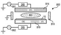
도 8을 참조하면, 용량성 결합 플라즈마(CCP) 공정 시스템(800)은, 상부 플레이트 전극(UEL)(815)에 결합된 SP 발생기 회로(240)에 결합된 AC 소스 전력 공급기(881), 및 하부 플레이트 전극(LEL)(819)에 결합된 BP 발생기 회로(245)에 결합된 AC 바이어스 전력 공급기(882)를 포함한다. AC 소스 전력 공급기(881) 및 AC 바이어스 전력 공급기(882)는, 도 1, 도 3 내지 도 7에서와 같은 앞서 설명된 실시형태에 따라, 소스 전력 및 바이어스 전력을 각각 발생시킬 수 있다. CCP(860)는 UEL(815)과 LEL(819) 사이의 기판(16)에 인접하게, 접지된 플라즈마 공정 챔버(810) 내에 형성된다. LEL(819)은 기판(16)을 지지 및 유지시키기 위한 정전 척(ESC)의 역할을 할 수도 있다. 다양한 실시형태에서, 전극 중 적어도 하나에 RF 전력을 결합함으로써, 플라즈마가 형성된다. UEL(815)에 결합되는 AC 전력은, LEL(819)에 결합되는 AC 전력과 상이한 RF 주파수를 가질 수 있다. 대안적으로, 다수의 RF 전원이 동일한 전극에 결합될 수 있다. 또한, 직류(DC) 전력이 상부 전극 및/또는 하부 전극에 결합될 수 있다.Referring to FIG. 8, a capacitively coupled plasma (CCP)
도 9를 참조하면, 유도성 결합 플라즈마(ICP) 공정 시스템(900)은, 유도성 전극(915)에 결합된 SP 발생기 회로(240)에 결합된 AC 소스 전력 공급기(881), 및 LEL(819)에 결합된 BP 발생기 회로(245)에 결합된 AC 바이어스 전력 공급기(882)를 포함한다. 또 다시, AC 소스 전력 공급기(881) 및 AC 바이어스 전력 공급기(882)는, 도 1, 도 3 내지 도 7에서와 같은 앞서 설명된 실시형태에 따라, 소스 전력 및 바이어스 전력을 각각 발생시킬 수 있다. 유도성 전극(915)(예를 들어, 평면형, 또는 솔레노이드/나선형 코일 또는 안테나)과 LEL(819) 사이의 기판(16)에 인접하게 ICP(960)가 형성된다. 유전체 재료(910)는 유도성 전극(915)을 ICP(960)와 분리시킨다. 유전체 재료(910)는 용량성 결합 효과를 감소 및/또는 방지할 수 있다.9, an inductively coupled plasma (ICP)
도 10을 참조하면, 표면파 플라즈마(SWP) 공정 시스템(1000)은, 슬롯 안테나(1015) 및 마이크로파 도파관(μ-도파관)(1014)에 결합된 SP 발생기 회로(240)에 결합된 AC 소스 전력 공급기(881)를 포함한다. 유사하게, AC 소스 전력 공급기(881) 및 AC 바이어스 전력 공급기(882)는, 도 1, 및 도 3 내지 도 7에서와 같은 앞서 설명된 실시형태에 따라, 소스 전력 및 바이어스 전력을 각각 발생시킬 수 있다. 슬롯 안테나(1015)와 LEL(819) 사이의 기판(16)에 인접하게 SWP(1060)가 형성된다. 마이크로파 주파수의 RF 전력을 동축 라인 및 μ-도파관(1014)을 통하여 슬롯 안테나(1015)에 결합함으로써, SWP(1060)가 형성된다. (PV-아마도 도 10에 관한 작은 세부 사항이지만, 슬롯 안테나(1015)는 구멍 또는 다른 구조물을 갖는 플레이트로 구현될 수 있다. 일부 실시형태에서, 슬롯 안테나는 도 9의 유전체 재료(910)와 유사한 유전체 구조물들 사이에 끼워질 수 있으므로, 마이크로파가 도파관(중앙)으로부터 (예를 들어, 파장이 감소되도록 하는 유전상수를 갖는 세라믹 구조물을 통하여, 안테나 구조물을 통하여, 및/또는 다른 유전체 재료를 통하여) 중앙으로부터 반경 방향으로 외향하게 통과할 수 있다.Referring to FIG. 10, a surface wave plasma (SWP)
도 11을 참조하면, 원격 플라즈마 공정 시스템(1100)은, 플라즈마가 기판에 인접하게 형성되는 대신에, 예를 들어, 플라즈마 공정 챔버(810)의 격리된 부분 또는 상이한 플라즈마 챔버에서, 기판(16)으로부터 멀리 떨어진 영역에 원격 플라즈마(1160)가 형성된다는 점을 제외하고는, 도 9의 ICP 공정 시스템(900)과 유사하다. 원격 플라즈마(1160)는, 입자 격리 구조물(1118)에 의해 기판(16)과 분리되거나 격리된다. 입자 격리 구조물(1118)은, 원격 플라즈마 소스로부터 기판(16)으로의 하전 입자의 수송을 방해하도록 배치된 필터, 도관, 또는 오리피스(orifice) 플레이트일 수 있다. 일 실시형태에서, 원격 플라즈마(1160)는 ICP이다. 대안적으로, 원격 플라즈마(1160)는 CCP, SWP 등일 수 있다.Referring to FIG. 11, the remote
도 12는 본 발명의 일 실시형태에 따라, 비공진 소스 전력 결합 전극을 포함하는 예시적인 플라즈마 공정 시스템의 블록도를 도시한다. 도 12의 플라즈마 공정 시스템은, 예를 들어 도 1의 방법과 같은, 본원에 설명된 바와 같은 실시형태의 방법 중 어느 하나를 수행하기 위해 사용될 수 있다.12 shows a block diagram of an exemplary plasma processing system including a non-resonant source power coupling electrode, in accordance with an embodiment of the present invention. The plasma processing system of FIG. 12 may be used to perform any of the methods of embodiments as described herein, such as, for example, the method of FIG. 1.
도 12를 참조하면, 비공진 플라즈마 공정 시스템(1200)은, 플라즈마 공정 챔버(1210)의 비공진 SP 결합 전극(1215)에 결합되는 소스 전력(1)을 공급하는 SP 공급기 노드(81), 및 플라즈마 공정 챔버(1210)의 바이어스 전력 결합 전극(19)에 결합되는 바이어스 전력(2)을 공급하는 BP 공급기 노드(82)를 포함한다. 소스 전력(1)은, 소스 전력 설정을 제어하도록 구성된 SP 제어기(1226)를 포함하는 SP 제어 경로(1201)를 통해 비공진 SP 결합 전극(1215)에 결합된다. 예를 들어, SP 제어기(1226)는, SP RF 함수 발생기 및 증폭기(1220)에 대한 이득 설정, 및 SP 임피던스 정합망(1225)에 대한 임피던스 정합 설정을 조정할 수 있다. 유사하게, 바이어스 전력(2)은, BP RF 함수 발생기 및 증폭기(1230)의 바이어스 설정, 및 BP 임피던스 정합망(1235)을 제어하는 BP 제어기(1236)를 포함하는 BP 제어 경로(1202)를 통해 BP 결합 전극(19)에 결합된다.Referring to FIG. 12, the non-resonant
비공진 플라즈마 공정 시스템(1200)은 비공진 구조물을 사용하여 소스 전력(1)을 결합하기 때문에, 소스 전력을 플라즈마에 효율적으로 제공하기 위한 SP 임피던스 정합망(1225)이 포함된다. 비공진 SP 결합 전극(1215)으로부터 플라즈마로 최대 전력이 전달되도록 하기 위해, 전력 공급기에 대한 부하의 임피던스가 전력 공급기 자체의 임피던스와 동일해야 한다. 예를 들어, 전력 공급기에 대한 부하의 임피던스는, 화학적 특성, 압력, 밀도 등과 같은, 급속하게 변하는 특정 조건에 따라 좌우될 수 있는 플라즈마의 임피던스에 의해 영향을 받을 수 있다. 따라서, 유리하게는, SP 임피던스 정합망(1225)은 플라즈마(60)와의 소스 전력(1)의 효율적인 전력 결합을 유지하면서, 플라즈마 조건이 가변될 수 있게 할 수 있다.Since the non-resonant
하나 이상의 플라즈마 공정 파라미터를 입력으로 수신할 수 있는 SP 펄스 변조 회로(1251)를 사용하여, SP 펄스 신호가 발생된다. 예를 들어, 도시된 바와 같이, SP 펄스 변조 회로(1251)는, SP 펄스 주파수(


SP RF 함수 발생기 및 증폭기(1220)는 SP 공급기 노드(81)로부터 소스 전력(1)을 수신하고, SP 펄스 변조 회로(1251)로부터 SP 펄스 신호(

SP 펄스는 SP 임피던스 정합망(1225)을 통하여 SP 방향성 결합기(1227)로 통과한다. 따라서, SP 방향성 결합기(1227)는, 시변 소스 전압(


시변 바이어스 전압(


SP RF 함수 발생기 및 증폭기(1220), SP 임피던스 정합망(1225), SP 제어기(1226), 및 SP 방향성 결합기(1227)는 비공진 SP 발생기 회로(1240)에 포함되며, 비공진 SP 발생기 회로(1240)는 SP 공급기 노드(81)로부터 소스 전력(1)을 수신하고, 비공진 SP 결합 전극(1215)에 SP 펄스를 제공한다. 비공진 SP 발생기 회로(1240)는 예를 들어, 도 2의 SP 발생기 회로(240)의 구체적인 구현예일 수 있다. 유사하게, BP RF 함수 발생기 및 증폭기(1230), BP 임피던스 정합망(1235), BP 제어기(1236), 및 BP 방향성 결합기(1237)는 BP 발생기 회로(1245)에 포함되며, BP 발생기 회로(1245)는 BP 공급기 노드(82)로부터 바이어스 전력(2)을 수신하고, BP 결합 전극(19)에 BP 펄스를 제공한다. BP 발생기 회로(1245)는 예를 들어, 도 2의 BP 발생기 회로(245)의 구체적인 구현예일 수 있다.The SP RF function generator and
SP 펄스 변조 회로(1251)의 출력에 결합된 BP


상이한 가스들이 펄싱되는 경우, 교번 시간 지연이 사용될 수 있다. 예를 들어, 특정 시간 지연은, 주어진 플라즈마 공정 동안 각각의 가스 또는 가스 조합물에 해당할 수 있다. 또한, SP 펄스 주파수(


BP RF 함수 발생기 및 증폭기(1230)에 의해 발생된 함수는 AC 신호를 포함할 수 있다. AC 신호는, RF 범위, VHF 범위, 또는 MW 범위 내에 속할 수도 있는 바이어스 주파수로 발생될 수 있다. 예를 들어, 소스 주파수는 약 10 MHz를 초과할 수 있으며, 바이어스 주파수는 약 15 MHz 미만일 수 있다. 대안적으로, 예를 들어, 소스 주파수는 약 50 MHz를 초과할 수 있으며, 바이어스 주파수는 약 5 MHz 미만일 수 있다. 또한 대안적으로, 소스 주파수는 약 50 MHz 내지 약 150 MHz의 범위일 수 있으며, 바이어스 주파수는 약 1 MHz 내지 약 5 MHz의 범위일 수 있다.The function generated by the BP RF function generator and
도 13은 본 발명의 일 실시형태에 따라, 공진 소스 전력 결합 전극을 포함하는 예시적인 플라즈마 공정 시스템의 블록도를 도시한다. 도 13의 플라즈마 공정 시스템은, 예를 들어 도 1의 방법과 같은, 본원에 설명된 바와 같은 실시형태의 방법 중 어느 하나를 수행하기 위해 사용될 수 있다.13 shows a block diagram of an exemplary plasma processing system including a resonant source power coupling electrode, in accordance with an embodiment of the present invention. The plasma processing system of FIG. 13 may be used to perform any of the methods of embodiments as described herein, such as the method of FIG. 1, for example.
도 13을 참조하면, 공진 플라즈마 공정 시스템(1300)은, 공진 SP 결합 전극(1315)을 포함하는 SP 제어 경로(1301)를 포함한다. 공진 플라즈마 공정 시스템(1300)은, 공진 SP 결합 전극(1315)이 임피던스 정합 없이 플라즈마(60)와의 효율적인 소스 전력 결합의 이점을 제공할 수 있기 때문에, SP 임피던스 정합망(1225)이 SP 제어 경로(1301)에서 생략된다는 점을 제외하고는, 비공진 플라즈마 공정 시스템(1200)과 유사하다. 따라서, SP RF 함수 발생기 및 증폭기(1220)는, SP 제어기(1327)에 피드백을 제공할 수 있는 SP 방향성 결합기(1227)에 직접 SP 펄스를 제공한다. SP RF 함수 발생기 및 증폭기(1220), SP 제어기(1226), 및 SP 방향성 결합기(1227)는 공진 SP 발생기 회로(1340)에 포함되며, 공진 SP 발생기 회로(1340)는 SP 공급기 노드(81)로부터 소스 전력(1)을 수신하고, SP 펄스를 공진 SP 결합 전극(1315)에 제공한다. 공진 SP 발생기 회로(1340)는 예를 들어, 도 2의 SP 발생기 회로(240)의 구체적인 구현예일 수 있다.Referring to FIG. 13, a resonance
또한, 공진 플라즈마 공정 시스템(1300)은 유리하게는 소스 전력의 신속한 펄싱을 가능하게 할 수 있다. 예를 들어, 임피던스 정합망은, 공진 SP 결합 전극(1315)과 같은 정합 없는 공진 구조물만큼 신속하게 응답하지 못할 수 있다. 따라서, 더 높은 SP 펄스 주파수에서, 임피던스 정합망은 효율적인 소스 전력을 플라즈마에 제공하기 위해 더 낮은 주파수로 제한될 수 있다. 다양한 실시형태에서, 공진 SP 결합 전극(1315)은 나선형 공진기 안테나(1329)를 포함한다.Further, the resonant
도 14는 본 발명의 일 실시형태에 따른 예시적인 나선형 공진기 플라즈마 공정 시스템의 개략도를 도시한다. 나선형 공진기 플라즈마 공정 시스템은 예를 들어, 도 2의 플라즈마 공정 시스템(200), 도 9의 ICP 공정 시스템(900), 및/또는 도 13의 공진 플라즈마 공정 시스템(1300)과 같은, 다른 플라즈마 공정 시스템의 구체적인 구현예일 수 있다. 구체적으로, 소스 전력 결합 전극은 나선형 공진기 안테나로 형성된다. 유사하게 표시된 요소는 앞서 설명된 바와 같을 수 있다.14 shows a schematic diagram of an exemplary spiral resonator plasma processing system in accordance with an embodiment of the present invention. The helical resonator plasma processing system is another plasma processing system, such as, for example, the
도 14를 참조하면, 나선형 공진기 플라즈마 공정 시스템(1400)은, 유전체 내측 표면(1411)을 차례로 둘러싸는 나선형 공진기 안테나(1329)로 구현된 공진 SP 결합 전극(1315)을 둘러싸는 접지된 외측 구조물(1410)을 포함한다. 나선형 공진기 안테나(1329)는 일 단부에서 접지되며, 다른 단부에서 자유로운 상태로 된다. AC 소스 전력 공급기(881)는, 접지된 연결부로부터 적절한 거리를 두고 나선형 공진기 안테나(1329)에 결합된 SP 발생기 회로(240)에 결합된다. 소스 전력 결합 위치(탭 위치로도 지칭됨)는, 작동 주파수 및 다른 고려 사항에 따라 좌우될 수 있다. 공진 SP 결합 전극(1315)에 유도성 결합되는 나선형 공진기 플라즈마(1460)가 발생된다. 예를 들어, 유도성 결합을 촉진시키기 위해, 나선형 공진기 플라즈마(1460)와 나선형 공진기 안테나(1329) 사이에 유전체 내측 표면(1411)이 제공될 수 있다. AC 바이어스 전력 공급기(882)는, 하부 플레이트 전극(LEL)(819)에 결합된 BP 발생기 회로(245)에 결합될 수 있다. 하부 플레이트 전극(LEL)(819)은 기판(16)을 지지 및 유지시키기 위한 정전 척(ESC)의 역할을 한다.Referring to FIG. 14, a spiral resonator
나선형 공진기 안테나(1329)는 전파(full-wave), 반파, 또는 1/4 파 안테나일 수 있다. 예를 들어, 나선형 공진기 안테나(1329)가 13.56 MHz의 주파수를 갖는 RF 전력을 사용하여 구동되는 경우, 1/4 파 나선형 공진기 안테나는 길이가 약 5.5 m일 수 있다. RF 주파수가 증가함에 따라, 나선형 공진기 안테나(1329)의 길이는 감소할 수 있다. 예를 들어, 약 50 MHz로 구동되는 1/4 파 나선형 공진기 안테나는 길이가 약 1.5 m일 수 있다.The
도 15는 본 발명의 일 실시형태에 따른 예시적인 플라즈마 공정 방법을 도시한다. 도 15의 방법은, 예를 들어 도 2의 플라즈마 공정 시스템(200)과 같은, 본원에 설명된 바와 같은 실시형태의 플라즈마 공정 시스템 중 어느 하나에 의해 수행될 수 있다. 도 15는 방법 단계를 특정 순서로 제한하도록 의도되지 않음을 유의한다. 추가적으로, 도 15에 설명된 바와 같은 임의의 단계는 임의의 조합으로 동시에 수행될 수 있을 뿐만 아니라, 개별적으로 수행될 수 있다. 따라서, 당업자에게 명백할 수 있는 바와 같이, 아래의 방법 단계의 배치 및/또는 타이밍의 변경은 설명된 바와 같은 방법의 범위 내에 있다.15 shows an exemplary plasma processing method according to an embodiment of the present invention. The method of FIG. 15 may be performed by any of the plasma processing systems of embodiments as described herein, such as, for example, the
플라즈마 공정 방법(1500)의 단계(1501)는, 펄스 변조 회로를 사용하여 함수 발생기에 신호를 출력하는 단계를 포함한다. 단계(1502)는, 신호를 출력하는 단계에 응답하여, 함수 발생기를 사용하여 SP 펄스를 발생시키는 단계를 포함한다. 단계(1503)는, 플라즈마를 발생시키기 위해, 플라즈마 공정 챔버의 SP 결합 전극에 SP 펄스를 제공하는 단계를 포함한다. 단계(1504)는, SP 펄스와 비교하여 지연을 트리거함으로써, BP 펄스를 발생시키는 단계를 포함한다. 단계(1505)는, 플라즈마 공정 챔버의 BP 결합 전극에 BP 펄스를 제공하는 단계를 포함한다. 단계(1506)는, 플라즈마 공정 챔버에 배치된 기판 상에 플라즈마 증착 또는 에칭 공정을 수행하는 단계를 포함하며, BP 펄스를 제공하는 단계는 플라즈마로부터의 이온을 기판을 향해 가속시킨다.
본 발명의 예시적인 실시형태가 여기에 요약된다. 본원에 제출된 청구범위 뿐만 아니라 명세서 전체로부터 다른 실시형태도 이해될 수 있다.Exemplary embodiments of the invention are summarized here. Other embodiments may be understood from the entire specification as well as from the claims presented herein.
실시예 1. 플라즈마 공정 시스템으로서, 진공 챔버; 상기 진공 챔버에서 플라즈마를 발생시키기 위한 전력을 제공하도록 구성된 제1 결합 전극으로서, 상기 제1 결합 전극은 SP 펄스를 상기 플라즈마에 결합하도록 추가로 구성되는, 제1 결합 전극; 상기 진공 챔버에 배치된 기판 홀더로서, 상기 기판 홀더는 기판을 지지하도록 구성되는, 기판 홀더; BP 펄스를 상기 기판에 결합하도록 구성된 제2 결합 전극; 및 상기 SP 펄스와 상기 BP 펄스 사이의 제1 오프셋 지속시간을 제어하도록 구성된 제어기를 포함하는, 플라즈마 공정 시스템.Example 1. A plasma processing system, comprising: a vacuum chamber; A first coupling electrode configured to provide power for generating a plasma in the vacuum chamber, the first coupling electrode further configured to couple an SP pulse to the plasma; A substrate holder disposed in the vacuum chamber, wherein the substrate holder is configured to support a substrate; A second coupling electrode configured to couple a BP pulse to the substrate; And a controller configured to control a first offset duration between the SP pulse and the BP pulse.
실시예 2. 실시예 1에 있어서, 상기 제1 결합 전극은 상기 플라즈마에 용량성 결합되며, 상기 플라즈마 공정 시스템은 용량성 결합 플라즈마 공정 시스템을 포함하거나; 또는 상기 제1 결합 전극은 상기 플라즈마에 유도성 결합되고, 상기 플라즈마 공정 시스템은 유도성 결합 플라즈마 공정 시스템을 포함하거나; 또는 상기 제1 결합 전극은 마이크로파 도파관 및 슬롯 안테나를 통해 상기 플라즈마에 결합되며, 상기 플라즈마 공정 시스템은 표면파 플라즈마 공정 시스템을 포함하는, 플라즈마 공정 시스템.
실시예 3. 실시예 1 또는 실시예 2에 있어서, 상기 SP 펄스를 발생시키도록 구성된 제1 함수 발생기를 더 포함하며, 상기 제어기는, 상기 제1 오프셋 지속시간을 발생시키도록 구성된 타이밍 회로; 및 상기 제1 함수 발생기의 입력에 결합된 제1 출력, 및 상기 타이밍 회로에 결합된 제2 출력을 포함하는 제1 펄스 변조 회로를 포함하는, 플라즈마 공정 시스템.
실시예 4. 실시예 3에 있어서, 상기 타이밍 회로에 결합된 제2 펄스 변조 회로; 및 상기 제2 펄스 변조 회로에 결합되고, 상기 BP 펄스를 발생시키도록 구성되는 제2 함수 발생기를 더 포함하는, 플라즈마 공정 시스템.
실시예 5. 실시예 3 또는 실시예 4에 있어서, 상기 타이밍 회로는, 상기 BP 펄스와 상기 SP 펄스 사이의 제2 오프셋 지속시간을 제어하도록 추가로 구성되는, 플라즈마 공정 시스템.
실시예 6. 실시예 3 내지 실시예 5 중 어느 하나에 있어서, 상기 제1 펄스 변조 회로는, 제1 펄스 주파수를 수신하도록 구성된 제1 입력, 및 제1 펄스 폭을 수신하도록 구성된 제2 입력을 포함하며, 상기 제1 펄스 변조 회로는, 상기 제1 펄스 주파수 및 상기 제1 펄스 폭에 기초하여, SP 펄스 신호를 출력으로 발생시키도록 추가로 구성되는, 플라즈마 공정 시스템.Embodiment 6. The first pulse modulating circuit according to any one of
실시예 7. 실시예 3 내지 실시예 6 중 어느 하나에 있어서, 상기 타이밍 회로는, 시간 지연을 수신하도록 구성된 타이밍 회로 입력을 포함하며, 상기 타이밍 회로는, 상기 시간 지연에 기초하여, 상기 제1 오프셋 지속시간을 설정하도록 추가로 구성되는, 플라즈마 공정 시스템.Embodiment 7. The timing circuit according to any one of
실시예 8. 실시예 3 내지 실시예 7 중 어느 하나에 있어서, 상기 제1 함수 발생기는, 제1 주파수로 발생된 교류(AC) 신호를 사용하여, 상기 제1 펄스 변조 회로로부터 수신된 SP 펄스 신호를 변조함으로써, 상기 SP 펄스를 발생시키도록 구성되는, 플라즈마 공정 시스템.
실시예 9. 실시예 8에 있어서, 상기 타이밍 회로에 결합되고, BP 펄스 신호를 발생시키도록 구성되는 제2 펄스 변조 회로; 및 상기 제2 펄스 변조 회로에 결합되고, 제2 주파수로 발생된 AC 신호를 사용하여, 상기 BP 펄스 신호를 변조함으로써, 상기 BP 펄스를 발생시키도록 구성되는 제2 함수 발생기를 더 포함하며, 상기 제2 주파수는 약 15 MHz 미만이고, 상기 제1 주파수는 약 10 MHz 초과인, 플라즈마 공정 시스템.
실시예 10. 장치로서, 진공 챔버; 소스 전력(SP) 공급기 노드에 결합되고, 제1 SP 펄스 시퀀스를 사용하여, 상기 진공 챔버 내에 플라즈마를 발생시키도록 구성되는 결합 전극; 및 바이어스 전력(BP) 공급기 노드에 결합되고, 상기 진공 챔버 내에 배치되는 기판 홀더를 포함하며, 상기 기판 홀더는 상기 플라즈마에 의해 처리될 기판을 지지하도록 구성되고, 제2 BP 펄스 시퀀스는 상기 플라즈마의 이온을 상기 기판을 향해 가속시키도록 구성되는, 장치.Example 10. An apparatus comprising: a vacuum chamber; A coupling electrode coupled to a source power (SP) supply node and configured to generate a plasma in the vacuum chamber using a first SP pulse sequence; And a substrate holder coupled to a bias power (BP) supply node and disposed within the vacuum chamber, wherein the substrate holder is configured to support a substrate to be processed by the plasma, and a second BP pulse sequence is The apparatus, configured to accelerate ions towards the substrate.
실시예 11. 실시예 10에 있어서, 상기 제1 SP 펄스 및 상기 BP 펄스는, 시간상으로 적어도 부분적으로 중첩되지 않는, 장치.
실시예 12. 실시예 10 또는 실시예 11에 있어서, 상기 결합 전극은 공진 결합 전극인, 장치.Example 12. The apparatus according to Example 10 or 11, wherein the coupling electrode is a resonant coupling electrode.
실시예 13. 실시예 12에 있어서, 함수 발생기; 및 상기 공진 결합 전극에 직접 결합된 출력, 및 상기 함수 발생기에 직접 결합된 입력을 포함하는 방향성 결합기를 더 포함하는, 장치.Example 13. In Example 12, a function generator; And a directional coupler comprising an output directly coupled to the resonant coupling electrode and an input directly coupled to the function generator.
실시예 14. 실시예 12 또는 실시예 13에 있어서, 상기 공진 결합 전극은 나선형 공진기 안테나인, 장치.
실시예 15. 실시예 10에 있어서, 함수 발생기; 상기 함수 발생기에 결합된 임피던스 정합망; 및 상기 임피던스 정합망에 결합된 입력을 포함하는 방향성 결합기를 더 포함하며, 상기 결합 전극은 비공진 결합 전극이고, 상기 방향성 결합기는, 상기 비공진 결합 전극에 결합된 출력을 더 포함하는, 장치.Example 15. In Example 10, a function generator; An impedance matching network coupled to the function generator; And a directional coupler comprising an input coupled to the impedance matching network, wherein the coupling electrode is a non-resonant coupling electrode, and the directional coupler further comprises an output coupled to the non-resonant coupling electrode.
실시예 16. 플라즈마 공정 방법으로서, 제1 펄스 변조 회로를 사용하여, 제1 함수 발생기에 제1 신호를 출력하는 단계; 상기 제1 신호를 출력하는 단계에 응답하여, 상기 제1 함수 발생기를 사용하여 제1 소스 전력(SP) 펄스를 발생시키는 단계; 플라즈마를 발생시키기 위해, 진공 챔버의 제1 결합 전극에 상기 제1 SP 펄스를 제공하는 단계; 상기 제1 SP 펄스와 비교하여 지연을 트리거함으로써, 바이어스 전력(BP) 펄스를 발생시키는 단계; 상기 진공 챔버의 제2 결합 전극에 상기 BP 펄스를 제공하는 단계; 및 상기 진공 챔버에 배치된 기판 상에 플라즈마 증착 또는 에칭 공정을 수행하는 단계를 포함하며, 상기 BP 펄스를 제공하는 단계는 상기 플라즈마로부터의 이온을 상기 기판을 향해 가속시키는, 플라즈마 공정 방법.
실시예 17. 실시예 16에 있어서, 상기 지연은 약 -15 μs 내지 약 20 μs의 오프셋 지속시간을 포함하며, 상기 BP 펄스의 리딩 에지는, 상기 오프셋 지속시간만큼 상기 제1 SP 펄스의 트레일링 에지와 분리되는, 방법.Example 17. In Example 16, the delay includes an offset duration of about -15 μs to about 20 μs, and the leading edge of the BP pulse is a trailing of the first SP pulse by the offset duration. The way, separated from the edge.
실시예 18. 실시예 16 또는 실시예 17에 있어서, 상기 제1 함수 발생기를 사용하여 제2 SP 펄스를 발생시키는 단계를 더 포함하며, 상기 BP 펄스의 트레일링 에지는, 0초 초과인 오프셋 지속시간만큼 상기 제2 SP 펄스의 리딩 에지와 분리되는, 방법.
실시예 19. 실시예 16 내지 실시예 18 중 어느 하나에 있어서, 상기 제1 함수 발생기를 사용하여 제2 SP 펄스를 발생시키는 단계를 더 포함하며, 상기 BP 펄스의 트레일링 에지는, 0초 초과인 오프셋 지속시간만큼 상기 제2 SP 펄스의 리딩 에지와 중첩되는, 방법.
실시예 20. 실시예 16 내지 실시예 19 중 어느 하나에 있어서, 상기 제1 함수 발생기를 사용하여 제2 SP 펄스를 발생시키는 단계를 더 포함하며, 상기 제1 SP 펄스의 리딩 에지는, 약 200 μs 내지 약 1000 μs인 펄스 변조 주기만큼 상기 제2 SP 펄스의 리딩 에지와 분리되는, 방법.
본원에 설명된 바와 같은 전력 제어 기술은 제어기에 의해 제어될 수 있다. 제어기는 본원에 설명된 기능을 제공하도록 프로그래밍된 하나 이상의 프로그래밍 가능 집적회로를 사용하여 구현될 수 있음을 또한 유의한다. 예를 들어, 하나 이상의 프로세서(예를 들어, 마이크로프로세서, 마이크로컨트롤러, 중앙 처리 장치 등), 프로그래밍 가능 논리 소자(예를 들어, CPLD(복합 프로그래밍 가능 논리 소자), FPGA(필드 프로그래밍 가능 게이트 어레이) 등), 및/또는 다른 프로그래밍 가능 집적회로는, 본원에 설명된 기능 중 어느 하나를 구현하기 위해 소프트웨어 또는 다른 프로그래밍 명령으로 프로그래밍될 수 있다. 소프트웨어 또는 다른 프로그래밍 명령은, 하나 이상의 비-일시적 컴퓨터 판독 가능 매체(예를 들어, 메모리 저장 장치, 플래시 메모리, DRAM 메모리, 재프로그래밍 가능 저장 장치, 하드 드라이브, 플로피 디스크, DVD, CD-ROM 등)에 저장될 수 있으며, 소프트웨어 또는 다른 프로그래밍 명령은 프로그래밍 가능 집적회로에 의해 실행될 때, 프로그래밍 가능 집적회로로 하여금, 본원에 설명된 공정, 기능, 및/또는 성능을 수행하게 한다는 점을 추가로 유의한다. 위의 다른 변형예도 구현될 수 있다.Power control techniques as described herein can be controlled by a controller. It is also noted that the controller may be implemented using one or more programmable integrated circuits programmed to provide the functions described herein. For example, one or more processors (e.g., microprocessors, microcontrollers, central processing units, etc.), programmable logic elements (e.g., complex programmable logic elements (CPLDs), field programmable gate arrays (FPGAs)) Etc.), and/or other programmable integrated circuits may be programmed with software or other programming instructions to implement any of the functions described herein. Software or other programming instructions may include one or more non-transitory computer-readable media (e.g., memory storage devices, flash memory, DRAM memory, reprogrammable storage devices, hard drives, floppy disks, DVDs, CD-ROMs, etc.) It is further noted that the software or other programming instructions, when executed by the programmable integrated circuit, cause the programmable integrated circuit to perform the processes, functions, and/or performance described herein. . Other variations of the above can also be implemented.
본원에 설명된 플라즈마 공정을 사용하여 재료층을 형성하기 위해, 하나 이상의 증착 공정이 사용될 수 있다. 플라즈마 증착 공정의 경우, 다양한 압력, 전력, 유량 및 온도 조건에서 하나 이상의 희석 가스(예를 들어, 아르곤, 질소 등)와 조합하여, 탄화수소, 불화탄소, 또는 질소 함유 탄화수소를 포함하지만 이에 제한되지 않는 전구체 가스 혼합물이 사용될 수 있다. 유사하게, 본원에 설명된 플라즈마 공정을 사용하여 재료층을 에칭하기 위해, 하나 이상의 에칭 공정이 사용될 수 있다. 예를 들어, 플라즈마 에칭 공정은, 불화탄소, 산소, 질소, 수소, 아르곤, 및/또는 다른 가스를 포함하는 플라즈마를 사용하여 구현될 수 있다. 또한, 공정 단계를 위한 작동 변수, 예를 들어, 챔버 온도, 챔버 압력, 가스의 유량, 플라즈마의 발생 시에 전극 조립체에 인가되는 주파수 및/또는 전력, 및/또는 공정 단계를 위한 다른 작동 변수가 제어될 수 있다. 또한, 본원에 설명된 기술을 여전히 이용하면서, 위의 변형예가 구현될 수 있다.To form a layer of material using the plasma process described herein, one or more deposition processes may be used. For plasma deposition processes, including, but not limited to, hydrocarbons, fluorocarbons, or nitrogen-containing hydrocarbons in combination with one or more diluent gases (e.g., argon, nitrogen, etc.) under various pressure, power, flow and temperature conditions. A precursor gas mixture can be used. Similarly, one or more etching processes may be used to etch a layer of material using the plasma process described herein. For example, the plasma etching process can be implemented using a plasma comprising fluorocarbon, oxygen, nitrogen, hydrogen, argon, and/or other gases. In addition, operating parameters for the process step, such as chamber temperature, chamber pressure, flow rate of gas, frequency and/or power applied to the electrode assembly at the time of plasma generation, and/or other operating variables for the process step. Can be controlled. In addition, the above variations can be implemented while still using the techniques described herein.
본 발명은 예시적인 실시형태를 참조하여 설명되었지만, 이러한 설명은 제한적인 의미로 해석되는 것으로 의도되지 않는다. 설명을 참조하면, 본 발명의 다른 실시형태 뿐만 아니라, 예시적인 실시형태의 다양한 변경 및 조합은 당업자에게 명백할 것이다. 예를 들어, 도 3 내지 도 7의 실시형태는 추가적인 실시형태에서 조합될 수 있다. 따라서, 첨부된 청구범위는 임의의 그러한 변경 또는 실시형태를 포함하는 것으로 의도된다.While the present invention has been described with reference to exemplary embodiments, this description is not intended to be construed in a limiting sense. With reference to the description, other embodiments of the present invention, as well as various modifications and combinations of exemplary embodiments, will be apparent to those skilled in the art. For example, the embodiments of FIGS. 3-7 can be combined in additional embodiments. Accordingly, it is intended that the appended claims cover any such modifications or embodiments.
Claims (20)
Translated fromKorean진공 챔버;
상기 진공 챔버에서 플라즈마를 발생시키기 위한 전력을 제공하도록 구성된 제1 결합 전극으로서, 상기 제1 결합 전극은 소스 전력(SP) 펄스를 상기 플라즈마에 결합하도록 추가로 구성되는, 제1 결합 전극;
상기 진공 챔버에 배치된 기판 홀더로서, 상기 기판 홀더는 기판을 지지하도록 구성되는, 기판 홀더;
바이어스 전력(BP) 펄스를 상기 기판에 결합하도록 구성된 제2 결합 전극; 및
상기 SP 펄스와 상기 BP 펄스 사이의 제1 오프셋 지속시간을 제어하도록 구성된 제어기를 포함하는,
플라즈마 공정 시스템.As a plasma processing system,
Vacuum chamber;
A first coupling electrode configured to provide power for generating a plasma in the vacuum chamber, the first coupling electrode further configured to couple a source power (SP) pulse to the plasma;
A substrate holder disposed in the vacuum chamber, wherein the substrate holder is configured to support a substrate;
A second coupling electrode configured to couple a bias power (BP) pulse to the substrate; And
A controller configured to control a first offset duration between the SP pulse and the BP pulse,
Plasma processing system.
상기 제1 결합 전극은 상기 플라즈마에 용량성 결합되며, 상기 플라즈마 공정 시스템은 용량성 결합 플라즈마 공정 시스템을 포함하거나; 또는
상기 제1 결합 전극은 상기 플라즈마에 유도성 결합되고, 상기 플라즈마 공정 시스템은 유도성 결합 플라즈마 공정 시스템을 포함하거나; 또는
상기 제1 결합 전극은 마이크로파 도파관 및 슬롯 안테나를 통해 상기 플라즈마에 결합되며, 상기 플라즈마 공정 시스템은 표면파 플라즈마 공정 시스템을 포함하는, 플라즈마 공정 시스템.The method of claim 1,
The first coupling electrode is capacitively coupled to the plasma, and the plasma processing system comprises a capacitively coupled plasma processing system; or
The first coupling electrode is inductively coupled to the plasma, and the plasma processing system comprises an inductively coupled plasma processing system; or
The first coupling electrode is coupled to the plasma through a microwave waveguide and a slot antenna, and the plasma processing system comprises a surface wave plasma processing system.
상기 SP 펄스를 발생시키도록 구성된 제1 함수 발생기를 더 포함하며,
상기 제어기는,
상기 제1 오프셋 지속시간을 발생시키도록 구성된 타이밍 회로; 및
상기 제1 함수 발생기의 입력에 결합된 제1 출력, 및 상기 타이밍 회로에 결합된 제2 출력을 포함하는 제1 펄스 변조 회로를 포함하는, 플라즈마 공정 시스템.The method of claim 1,
Further comprising a first function generator configured to generate the SP pulse,
The controller,
A timing circuit configured to generate the first offset duration; And
A first pulse modulation circuit comprising a first output coupled to an input of the first function generator, and a second output coupled to the timing circuit.
상기 타이밍 회로에 결합된 제2 펄스 변조 회로; 및
상기 제2 펄스 변조 회로에 결합되고, 상기 BP 펄스를 발생시키도록 구성되는 제2 함수 발생기를 더 포함하는, 플라즈마 공정 시스템.The method of claim 3,
A second pulse modulating circuit coupled to the timing circuit; And
And a second function generator coupled to the second pulse modulating circuit and configured to generate the BP pulse.
상기 타이밍 회로는, 상기 BP 펄스와 상기 SP 펄스 사이의 제2 오프셋 지속시간을 제어하도록 추가로 구성되는, 플라즈마 공정 시스템.The method of claim 3,
The timing circuit is further configured to control a second offset duration between the BP pulse and the SP pulse.
상기 제1 펄스 변조 회로는, 제1 펄스 주파수를 수신하도록 구성된 제1 입력, 및 제1 펄스 폭을 수신하도록 구성된 제2 입력을 포함하며,
상기 제1 펄스 변조 회로는, 상기 제1 펄스 주파수 및 상기 제1 펄스 폭에 기초하여, SP 펄스 신호를 출력으로 발생시키도록 추가로 구성되는, 플라즈마 공정 시스템.The method of claim 3,
The first pulse modulation circuit comprises a first input configured to receive a first pulse frequency, and a second input configured to receive a first pulse width,
The first pulse modulation circuit is further configured to generate an SP pulse signal as an output based on the first pulse frequency and the first pulse width.
상기 타이밍 회로는, 시간 지연을 수신하도록 구성된 타이밍 회로 입력을 포함하며,
상기 타이밍 회로는, 상기 시간 지연에 기초하여, 상기 제1 오프셋 지속시간을 설정하도록 추가로 구성되는, 플라즈마 공정 시스템.The method of claim 3,
The timing circuit comprises a timing circuit input configured to receive a time delay,
The timing circuit is further configured to set the first offset duration based on the time delay.
상기 제1 함수 발생기는, 제1 주파수로 발생된 교류(AC) 신호를 사용하여, 상기 제1 펄스 변조 회로로부터 수신된 SP 펄스 신호를 변조함으로써, 상기 SP 펄스를 발생시키도록 구성되는, 플라즈마 공정 시스템.The method of claim 3,
The first function generator is configured to generate the SP pulse by modulating the SP pulse signal received from the first pulse modulating circuit using an alternating current (AC) signal generated at a first frequency. system.
상기 타이밍 회로에 결합되고, BP 펄스 신호를 발생시키도록 구성되는 제2 펄스 변조 회로; 및
상기 제2 펄스 변조 회로에 결합되고, 제2 주파수로 발생된 AC 신호를 사용하여 상기 BP 펄스 신호를 변조함으로써, 상기 BP 펄스를 발생시키도록 구성되는 제2 함수 발생기를 더 포함하며,
상기 제2 주파수는 약 15 MHz 미만이고, 상기 제1 주파수는 약 10 MHz 초과인, 플라즈마 공정 시스템.The method of claim 8,
A second pulse modulation circuit coupled to the timing circuit and configured to generate a BP pulse signal; And
A second function generator coupled to the second pulse modulation circuit and configured to generate the BP pulse by modulating the BP pulse signal using an AC signal generated at a second frequency,
The second frequency is less than about 15 MHz and the first frequency is greater than about 10 MHz.
진공 챔버;
소스 전력(SP) 공급기 노드에 결합되고, 제1 SP 펄스 시퀀스를 사용하여, 상기 진공 챔버 내에 플라즈마를 발생시키도록 구성되는 결합 전극; 및
바이어스 전력(BP) 공급기 노드에 결합되고, 상기 진공 챔버 내에 배치되는 기판 홀더를 포함하며,
상기 기판 홀더는 상기 플라즈마에 의해 처리될 기판을 지지하도록 구성되고, 제2 BP 펄스 시퀀스는 상기 플라즈마의 이온을 상기 기판을 향해 가속시키도록 구성되는,
장치.As a device,
Vacuum chamber;
A coupling electrode coupled to a source power (SP) supply node and configured to generate a plasma in the vacuum chamber using a first SP pulse sequence; And
A substrate holder coupled to a bias power (BP) supply node and disposed within the vacuum chamber,
The substrate holder is configured to support a substrate to be processed by the plasma, and a second BP pulse sequence is configured to accelerate ions of the plasma toward the substrate,
Device.
상기 제1 SP 펄스 및 상기 BP 펄스는, 시간상으로 적어도 부분적으로 중첩되지 않는, 장치.The method of claim 10,
Wherein the first SP pulse and the BP pulse do not overlap at least partially in time.
상기 결합 전극은 공진 결합 전극인, 장치.The method of claim 10,
Wherein the coupling electrode is a resonant coupling electrode.
함수 발생기; 및
상기 공진 결합 전극에 직접 결합된 출력, 및 상기 함수 발생기에 직접 결합된 입력을 포함하는 방향성 결합기를 더 포함하는, 장치.The method of claim 12,
Function generator; And
And a directional coupler comprising an output directly coupled to the resonant coupling electrode and an input directly coupled to the function generator.
상기 공진 결합 전극은 나선형 공진기 안테나인, 장치.The method of claim 12,
Wherein the resonant coupling electrode is a helical resonator antenna.
함수 발생기;
상기 함수 발생기에 결합된 임피던스 정합망; 및
상기 임피던스 정합망에 결합된 입력을 포함하는 방향성 결합기를 더 포함하며,
상기 결합 전극은 비공진 결합 전극이고, 상기 방향성 결합기는, 상기 비공진 결합 전극에 결합된 출력을 더 포함하는, 장치.The method of claim 10,
Function generator;
An impedance matching network coupled to the function generator; And
Further comprising a directional coupler including an input coupled to the impedance matching network,
Wherein the coupling electrode is a non-resonant coupling electrode, and the directional coupler further comprises an output coupled to the non-resonant coupling electrode.
제1 펄스 변조 회로를 사용하여, 제1 함수 발생기에 제1 신호를 출력하는 단계;
상기 제1 신호를 출력하는 단계에 응답하여, 상기 제1 함수 발생기를 사용하여 제1 소스 전력(SP) 펄스를 발생시키는 단계;
플라즈마를 발생시키기 위해, 진공 챔버의 제1 결합 전극에 상기 제1 SP 펄스를 제공하는 단계;
상기 제1 SP 펄스와 비교하여 지연을 트리거함으로써, 바이어스 전력(BP) 펄스를 발생시키는 단계;
상기 진공 챔버의 제2 결합 전극에 상기 BP 펄스를 제공하는 단계; 및
상기 진공 챔버에 배치된 기판 상에 플라즈마 증착 또는 에칭 공정을 수행하는 단계를 포함하며,
상기 BP 펄스를 제공하는 단계는 상기 플라즈마로부터의 이온을 상기 기판을 향해 가속시키는,
플라즈마 공정 방법.As a plasma process method,
Outputting a first signal to a first function generator using a first pulse modulating circuit;
In response to outputting the first signal, generating a first source power (SP) pulse using the first function generator;
Providing the first SP pulse to a first coupling electrode of a vacuum chamber to generate a plasma;
Generating a bias power (BP) pulse by triggering a delay compared to the first SP pulse;
Providing the BP pulse to a second coupling electrode of the vacuum chamber; And
And performing a plasma deposition or etching process on the substrate disposed in the vacuum chamber,
Providing the BP pulse accelerates ions from the plasma toward the substrate,
Plasma process method.
상기 지연은, 약 15 μs 내지 약 20 μs의 오프셋 지속시간을 포함하며,
상기 BP 펄스의 리딩 에지는, 상기 오프셋 지속시간만큼 상기 제1 SP 펄스의 트레일링 에지와 분리되는, 방법.The method of claim 16,
The delay includes an offset duration of about 15 μs to about 20 μs,
The leading edge of the BP pulse is separated from the trailing edge of the first SP pulse by the offset duration.
상기 제1 함수 발생기를 사용하여 제2 SP 펄스를 발생시키는 단계를 더 포함하며,
상기 BP 펄스의 트레일링 에지는, 0초 초과인 오프셋 지속시간만큼 상기 제2 SP 펄스의 리딩 에지와 분리되는, 방법.The method of claim 16,
Generating a second SP pulse using the first function generator,
Wherein the trailing edge of the BP pulse is separated from the leading edge of the second SP pulse by an offset duration greater than 0 seconds.
상기 제1 함수 발생기를 사용하여 제2 SP 펄스를 발생시키는 단계를 더 포함하며,
상기 BP 펄스의 트레일링 에지는, 0초 초과인 오프셋 지속시간만큼 상기 제2 SP 펄스의 리딩 에지와 중첩되는, 방법.The method of claim 16,
Generating a second SP pulse using the first function generator,
The trailing edge of the BP pulse overlaps the leading edge of the second SP pulse by an offset duration greater than 0 seconds.
상기 제1 함수 발생기를 사용하여 제2 SP 펄스를 발생시키는 단계를 더 포함하며,
상기 제1 SP 펄스의 리딩 에지는, 약 200 μs 내지 약 1000 μs인 펄스 변조 주기만큼 상기 제2 SP 펄스의 리딩 에지와 분리되는, 방법.The method of claim 16,
Generating a second SP pulse using the first function generator,
The leading edge of the first SP pulse is separated from the leading edge of the second SP pulse by a pulse modulation period of about 200 μs to about 1000 μs.
Applications Claiming Priority (7)
| Application Number | Priority Date | Filing Date | Title |
|---|---|---|---|
| US201862718454P | 2018-08-14 | 2018-08-14 | |
| US62/718,454 | 2018-08-14 | ||
| US201862724879P | 2018-08-30 | 2018-08-30 | |
| US62/724,879 | 2018-08-30 | ||
| US16/219,535 | 2018-12-13 | ||
| US16/219,535US12230475B2 (en) | 2018-08-14 | 2018-12-13 | Systems and methods of control for plasma processing |
| PCT/US2019/045756WO2020036806A1 (en) | 2018-08-14 | 2019-08-08 | Systems and methods of control for plasma processing |
Publications (1)
| Publication Number | Publication Date |
|---|---|
| KR20210032420Atrue KR20210032420A (en) | 2021-03-24 |
Family
ID=69523348
Family Applications (2)
| Application Number | Title | Priority Date | Filing Date |
|---|---|---|---|
| KR1020217003893APendingKR20210032420A (en) | 2018-08-14 | 2019-08-08 | Control system and method for plasma process |
| KR1020217006789APendingKR20210060455A (en) | 2018-08-14 | 2019-08-28 | Control system and method for plasma process |
Family Applications After (1)
| Application Number | Title | Priority Date | Filing Date |
|---|---|---|---|
| KR1020217006789APendingKR20210060455A (en) | 2018-08-14 | 2019-08-28 | Control system and method for plasma process |
Country Status (6)
| Country | Link |
|---|---|
| US (3) | US12230475B2 (en) |
| JP (1) | JP7397247B2 (en) |
| KR (2) | KR20210032420A (en) |
| CN (1) | CN112424904B (en) |
| TW (1) | TWI856020B (en) |
| WO (2) | WO2020036806A1 (en) |
Cited By (1)
| Publication number | Priority date | Publication date | Assignee | Title |
|---|---|---|---|---|
| WO2022245011A1 (en)* | 2021-05-20 | 2022-11-24 | 인투코어테크놀로지 주식회사 | Frequency generation device for providing bias power in semiconductor process |
Families Citing this family (305)
| Publication number | Priority date | Publication date | Assignee | Title |
|---|---|---|---|---|
| US20130023129A1 (en) | 2011-07-20 | 2013-01-24 | Asm America, Inc. | Pressure transmitter for a semiconductor processing environment |
| US20160376700A1 (en) | 2013-02-01 | 2016-12-29 | Asm Ip Holding B.V. | System for treatment of deposition reactor |
| US10941490B2 (en) | 2014-10-07 | 2021-03-09 | Asm Ip Holding B.V. | Multiple temperature range susceptor, assembly, reactor and system including the susceptor, and methods of using the same |
| US10276355B2 (en) | 2015-03-12 | 2019-04-30 | Asm Ip Holding B.V. | Multi-zone reactor, system including the reactor, and method of using the same |
| US9828672B2 (en) | 2015-03-26 | 2017-11-28 | Lam Research Corporation | Minimizing radical recombination using ALD silicon oxide surface coating with intermittent restoration plasma |
| US11139308B2 (en) | 2015-12-29 | 2021-10-05 | Asm Ip Holding B.V. | Atomic layer deposition of III-V compounds to form V-NAND devices |
| US10529554B2 (en) | 2016-02-19 | 2020-01-07 | Asm Ip Holding B.V. | Method for forming silicon nitride film selectively on sidewalls or flat surfaces of trenches |
| US10343920B2 (en) | 2016-03-18 | 2019-07-09 | Asm Ip Holding B.V. | Aligned carbon nanotubes |
| US11453943B2 (en) | 2016-05-25 | 2022-09-27 | Asm Ip Holding B.V. | Method for forming carbon-containing silicon/metal oxide or nitride film by ALD using silicon precursor and hydrocarbon precursor |
| US10612137B2 (en) | 2016-07-08 | 2020-04-07 | Asm Ip Holdings B.V. | Organic reactants for atomic layer deposition |
| US9859151B1 (en) | 2016-07-08 | 2018-01-02 | Asm Ip Holding B.V. | Selective film deposition method to form air gaps |
| US9887082B1 (en) | 2016-07-28 | 2018-02-06 | Asm Ip Holding B.V. | Method and apparatus for filling a gap |
| US9812320B1 (en) | 2016-07-28 | 2017-11-07 | Asm Ip Holding B.V. | Method and apparatus for filling a gap |
| US11532757B2 (en) | 2016-10-27 | 2022-12-20 | Asm Ip Holding B.V. | Deposition of charge trapping layers |
| US10714350B2 (en) | 2016-11-01 | 2020-07-14 | ASM IP Holdings, B.V. | Methods for forming a transition metal niobium nitride film on a substrate by atomic layer deposition and related semiconductor device structures |
| KR102546317B1 (en) | 2016-11-15 | 2023-06-21 | 에이에스엠 아이피 홀딩 비.브이. | Gas supply unit and substrate processing apparatus including the same |
| US11447861B2 (en) | 2016-12-15 | 2022-09-20 | Asm Ip Holding B.V. | Sequential infiltration synthesis apparatus and a method of forming a patterned structure |
| US11581186B2 (en) | 2016-12-15 | 2023-02-14 | Asm Ip Holding B.V. | Sequential infiltration synthesis apparatus |
| US11390950B2 (en) | 2017-01-10 | 2022-07-19 | Asm Ip Holding B.V. | Reactor system and method to reduce residue buildup during a film deposition process |
| US10468261B2 (en) | 2017-02-15 | 2019-11-05 | Asm Ip Holding B.V. | Methods for forming a metallic film on a substrate by cyclical deposition and related semiconductor device structures |
| US10770286B2 (en) | 2017-05-08 | 2020-09-08 | Asm Ip Holdings B.V. | Methods for selectively forming a silicon nitride film on a substrate and related semiconductor device structures |
| US12040200B2 (en) | 2017-06-20 | 2024-07-16 | Asm Ip Holding B.V. | Semiconductor processing apparatus and methods for calibrating a semiconductor processing apparatus |
| US11306395B2 (en) | 2017-06-28 | 2022-04-19 | Asm Ip Holding B.V. | Methods for depositing a transition metal nitride film on a substrate by atomic layer deposition and related deposition apparatus |
| KR20190009245A (en) | 2017-07-18 | 2019-01-28 | 에이에스엠 아이피 홀딩 비.브이. | Methods for forming a semiconductor device structure and related semiconductor device structures |
| US11374112B2 (en) | 2017-07-19 | 2022-06-28 | Asm Ip Holding B.V. | Method for depositing a group IV semiconductor and related semiconductor device structures |
| US10590535B2 (en) | 2017-07-26 | 2020-03-17 | Asm Ip Holdings B.V. | Chemical treatment, deposition and/or infiltration apparatus and method for using the same |
| TWI815813B (en) | 2017-08-04 | 2023-09-21 | 荷蘭商Asm智慧財產控股公司 | Showerhead assembly for distributing a gas within a reaction chamber |
| US10692741B2 (en) | 2017-08-08 | 2020-06-23 | Asm Ip Holdings B.V. | Radiation shield |
| US10770336B2 (en) | 2017-08-08 | 2020-09-08 | Asm Ip Holding B.V. | Substrate lift mechanism and reactor including same |
| US11769682B2 (en) | 2017-08-09 | 2023-09-26 | Asm Ip Holding B.V. | Storage apparatus for storing cassettes for substrates and processing apparatus equipped therewith |
| US11830730B2 (en) | 2017-08-29 | 2023-11-28 | Asm Ip Holding B.V. | Layer forming method and apparatus |
| US11295980B2 (en) | 2017-08-30 | 2022-04-05 | Asm Ip Holding B.V. | Methods for depositing a molybdenum metal film over a dielectric surface of a substrate by a cyclical deposition process and related semiconductor device structures |
| US10510575B2 (en) | 2017-09-20 | 2019-12-17 | Applied Materials, Inc. | Substrate support with multiple embedded electrodes |
| US10658205B2 (en) | 2017-09-28 | 2020-05-19 | Asm Ip Holdings B.V. | Chemical dispensing apparatus and methods for dispensing a chemical to a reaction chamber |
| US10403504B2 (en) | 2017-10-05 | 2019-09-03 | Asm Ip Holding B.V. | Method for selectively depositing a metallic film on a substrate |
| US10923344B2 (en) | 2017-10-30 | 2021-02-16 | Asm Ip Holding B.V. | Methods for forming a semiconductor structure and related semiconductor structures |
| CN111344522B (en) | 2017-11-27 | 2022-04-12 | 阿斯莫Ip控股公司 | Including clean mini-environment device |
| WO2019103613A1 (en) | 2017-11-27 | 2019-05-31 | Asm Ip Holding B.V. | A storage device for storing wafer cassettes for use with a batch furnace |
| US10760158B2 (en) | 2017-12-15 | 2020-09-01 | Lam Research Corporation | Ex situ coating of chamber components for semiconductor processing |
| US10872771B2 (en) | 2018-01-16 | 2020-12-22 | Asm Ip Holding B. V. | Method for depositing a material film on a substrate within a reaction chamber by a cyclical deposition process and related device structures |
| KR102695659B1 (en) | 2018-01-19 | 2024-08-14 | 에이에스엠 아이피 홀딩 비.브이. | Method for depositing a gap filling layer by plasma assisted deposition |
| TWI799494B (en) | 2018-01-19 | 2023-04-21 | 荷蘭商Asm 智慧財產控股公司 | Deposition method |
| US11081345B2 (en) | 2018-02-06 | 2021-08-03 | Asm Ip Holding B.V. | Method of post-deposition treatment for silicon oxide film |
| US10896820B2 (en) | 2018-02-14 | 2021-01-19 | Asm Ip Holding B.V. | Method for depositing a ruthenium-containing film on a substrate by a cyclical deposition process |
| WO2019158960A1 (en) | 2018-02-14 | 2019-08-22 | Asm Ip Holding B.V. | A method for depositing a ruthenium-containing film on a substrate by a cyclical deposition process |
| US10731249B2 (en) | 2018-02-15 | 2020-08-04 | Asm Ip Holding B.V. | Method of forming a transition metal containing film on a substrate by a cyclical deposition process, a method for supplying a transition metal halide compound to a reaction chamber, and related vapor deposition apparatus |
| KR102636427B1 (en) | 2018-02-20 | 2024-02-13 | 에이에스엠 아이피 홀딩 비.브이. | Substrate processing method and apparatus |
| US10975470B2 (en) | 2018-02-23 | 2021-04-13 | Asm Ip Holding B.V. | Apparatus for detecting or monitoring for a chemical precursor in a high temperature environment |
| US11473195B2 (en) | 2018-03-01 | 2022-10-18 | Asm Ip Holding B.V. | Semiconductor processing apparatus and a method for processing a substrate |
| KR102646467B1 (en) | 2018-03-27 | 2024-03-11 | 에이에스엠 아이피 홀딩 비.브이. | Method of forming an electrode on a substrate and a semiconductor device structure including an electrode |
| KR102600229B1 (en) | 2018-04-09 | 2023-11-10 | 에이에스엠 아이피 홀딩 비.브이. | Substrate supporting device, substrate processing apparatus including the same and substrate processing method |
| US12025484B2 (en) | 2018-05-08 | 2024-07-02 | Asm Ip Holding B.V. | Thin film forming method |
| US12272527B2 (en) | 2018-05-09 | 2025-04-08 | Asm Ip Holding B.V. | Apparatus for use with hydrogen radicals and method of using same |
| US10555412B2 (en) | 2018-05-10 | 2020-02-04 | Applied Materials, Inc. | Method of controlling ion energy distribution using a pulse generator with a current-return output stage |
| KR102596988B1 (en) | 2018-05-28 | 2023-10-31 | 에이에스엠 아이피 홀딩 비.브이. | Method of processing a substrate and a device manufactured by the same |
| US11718913B2 (en) | 2018-06-04 | 2023-08-08 | Asm Ip Holding B.V. | Gas distribution system and reactor system including same |
| US10797133B2 (en) | 2018-06-21 | 2020-10-06 | Asm Ip Holding B.V. | Method for depositing a phosphorus doped silicon arsenide film and related semiconductor device structures |
| KR102568797B1 (en) | 2018-06-21 | 2023-08-21 | 에이에스엠 아이피 홀딩 비.브이. | Substrate processing system |
| TWI873894B (en) | 2018-06-27 | 2025-02-21 | 荷蘭商Asm Ip私人控股有限公司 | Cyclic deposition methods for forming metal-containing material and films and structures including the metal-containing material |
| KR102854019B1 (en) | 2018-06-27 | 2025-09-02 | 에이에스엠 아이피 홀딩 비.브이. | Periodic deposition method for forming a metal-containing material and films and structures comprising the metal-containing material |
| US10755922B2 (en) | 2018-07-03 | 2020-08-25 | Asm Ip Holding B.V. | Method for depositing silicon-free carbon-containing film as gap-fill layer by pulse plasma-assisted deposition |
| US10388513B1 (en) | 2018-07-03 | 2019-08-20 | Asm Ip Holding B.V. | Method for depositing silicon-free carbon-containing film as gap-fill layer by pulse plasma-assisted deposition |
| US11430674B2 (en) | 2018-08-22 | 2022-08-30 | Asm Ip Holding B.V. | Sensor array, apparatus for dispensing a vapor phase reactant to a reaction chamber and related methods |
| KR102707956B1 (en) | 2018-09-11 | 2024-09-19 | 에이에스엠 아이피 홀딩 비.브이. | Method for deposition of a thin film |
| US11024523B2 (en) | 2018-09-11 | 2021-06-01 | Asm Ip Holding B.V. | Substrate processing apparatus and method |
| CN110970344B (en) | 2018-10-01 | 2024-10-25 | Asmip控股有限公司 | Substrate holding apparatus, system comprising the same and method of using the same |
| KR102592699B1 (en) | 2018-10-08 | 2023-10-23 | 에이에스엠 아이피 홀딩 비.브이. | Substrate support unit and apparatuses for depositing thin film and processing the substrate including the same |
| KR102546322B1 (en) | 2018-10-19 | 2023-06-21 | 에이에스엠 아이피 홀딩 비.브이. | Substrate processing apparatus and substrate processing method |
| KR20250110938A (en)* | 2018-10-19 | 2025-07-21 | 램 리써치 코포레이션 | In situ protective coating of chamber components for semiconductor processing |
| US12378665B2 (en) | 2018-10-26 | 2025-08-05 | Asm Ip Holding B.V. | High temperature coatings for a preclean and etch apparatus and related methods |
| US11087997B2 (en) | 2018-10-31 | 2021-08-10 | Asm Ip Holding B.V. | Substrate processing apparatus for processing substrates |
| KR102748291B1 (en) | 2018-11-02 | 2024-12-31 | 에이에스엠 아이피 홀딩 비.브이. | Substrate support unit and substrate processing apparatus including the same |
| US11572620B2 (en) | 2018-11-06 | 2023-02-07 | Asm Ip Holding B.V. | Methods for selectively depositing an amorphous silicon film on a substrate |
| US10818758B2 (en) | 2018-11-16 | 2020-10-27 | Asm Ip Holding B.V. | Methods for forming a metal silicate film on a substrate in a reaction chamber and related semiconductor device structures |
| US11476145B2 (en) | 2018-11-20 | 2022-10-18 | Applied Materials, Inc. | Automatic ESC bias compensation when using pulsed DC bias |
| US12040199B2 (en) | 2018-11-28 | 2024-07-16 | Asm Ip Holding B.V. | Substrate processing apparatus for processing substrates |
| KR102636428B1 (en) | 2018-12-04 | 2024-02-13 | 에이에스엠 아이피 홀딩 비.브이. | A method for cleaning a substrate processing apparatus |
| US11158513B2 (en) | 2018-12-13 | 2021-10-26 | Asm Ip Holding B.V. | Methods for forming a rhenium-containing film on a substrate by a cyclical deposition process and related semiconductor device structures |
| TWI874340B (en) | 2018-12-14 | 2025-03-01 | 荷蘭商Asm Ip私人控股有限公司 | Method of forming device structure, structure formed by the method and system for performing the method |
| US11804362B2 (en)* | 2018-12-21 | 2023-10-31 | Advanced Energy Industries, Inc. | Frequency tuning for modulated plasma systems |
| US11515123B2 (en)* | 2018-12-21 | 2022-11-29 | Advanced Energy Industries, Inc. | Apparatus and system for modulated plasma systems |
| JP7297795B2 (en)* | 2019-01-09 | 2023-06-26 | 東京エレクトロン株式会社 | Plasma processing apparatus and plasma processing method |
| TWI866480B (en) | 2019-01-17 | 2024-12-11 | 荷蘭商Asm Ip 私人控股有限公司 | Methods of forming a transition metal containing film on a substrate by a cyclical deposition process |
| KR102827481B1 (en) | 2019-01-22 | 2025-06-30 | 어플라이드 머티어리얼스, 인코포레이티드 | Feedback loop to control pulse voltage waveform |
| US11508554B2 (en) | 2019-01-24 | 2022-11-22 | Applied Materials, Inc. | High voltage filter assembly |
| CN111524780B (en)* | 2019-02-02 | 2024-07-05 | 中微半导体设备(上海)股份有限公司 | Plasma reactor for etching with ultra-depth-to-width ratio and etching method thereof |
| TWI873122B (en) | 2019-02-20 | 2025-02-21 | 荷蘭商Asm Ip私人控股有限公司 | Method of filling a recess formed within a surface of a substrate, semiconductor structure formed according to the method, and semiconductor processing apparatus |
| TWI845607B (en) | 2019-02-20 | 2024-06-21 | 荷蘭商Asm Ip私人控股有限公司 | Cyclical deposition method and apparatus for filling a recess formed within a substrate surface |
| TWI838458B (en) | 2019-02-20 | 2024-04-11 | 荷蘭商Asm Ip私人控股有限公司 | Apparatus and methods for plug fill deposition in 3-d nand applications |
| TWI842826B (en) | 2019-02-22 | 2024-05-21 | 荷蘭商Asm Ip私人控股有限公司 | Substrate processing apparatus and method for processing substrate |
| KR102858005B1 (en) | 2019-03-08 | 2025-09-09 | 에이에스엠 아이피 홀딩 비.브이. | Method for Selective Deposition of Silicon Nitride Layer and Structure Including Selectively-Deposited Silicon Nitride Layer |
| US11742198B2 (en) | 2019-03-08 | 2023-08-29 | Asm Ip Holding B.V. | Structure including SiOCN layer and method of forming same |
| US12159768B2 (en)* | 2019-03-25 | 2024-12-03 | Recarbon, Inc. | Controlling exhaust gas pressure of a plasma reactor for plasma stability |
| JP2020167398A (en) | 2019-03-28 | 2020-10-08 | エーエスエム・アイピー・ホールディング・ベー・フェー | Door openers and substrate processing equipment provided with door openers |
| KR102809999B1 (en) | 2019-04-01 | 2025-05-19 | 에이에스엠 아이피 홀딩 비.브이. | Method of manufacturing semiconductor device |
| KR20200123380A (en) | 2019-04-19 | 2020-10-29 | 에이에스엠 아이피 홀딩 비.브이. | Layer forming method and apparatus |
| KR20200125453A (en) | 2019-04-24 | 2020-11-04 | 에이에스엠 아이피 홀딩 비.브이. | Gas-phase reactor system and method of using same |
| KR20200130121A (en) | 2019-05-07 | 2020-11-18 | 에이에스엠 아이피 홀딩 비.브이. | Chemical source vessel with dip tube |
| KR20200130652A (en) | 2019-05-10 | 2020-11-19 | 에이에스엠 아이피 홀딩 비.브이. | Method of depositing material onto a surface and structure formed according to the method |
| JP7612342B2 (en) | 2019-05-16 | 2025-01-14 | エーエスエム・アイピー・ホールディング・ベー・フェー | Wafer boat handling apparatus, vertical batch furnace and method |
| JP7598201B2 (en) | 2019-05-16 | 2024-12-11 | エーエスエム・アイピー・ホールディング・ベー・フェー | Wafer boat handling apparatus, vertical batch furnace and method |
| USD947913S1 (en) | 2019-05-17 | 2022-04-05 | Asm Ip Holding B.V. | Susceptor shaft |
| USD975665S1 (en) | 2019-05-17 | 2023-01-17 | Asm Ip Holding B.V. | Susceptor shaft |
| KR20200141002A (en) | 2019-06-06 | 2020-12-17 | 에이에스엠 아이피 홀딩 비.브이. | Method of using a gas-phase reactor system including analyzing exhausted gas |
| KR20200141931A (en) | 2019-06-10 | 2020-12-21 | 에이에스엠 아이피 홀딩 비.브이. | Method for cleaning quartz epitaxial chambers |
| KR20200143254A (en) | 2019-06-11 | 2020-12-23 | 에이에스엠 아이피 홀딩 비.브이. | Method of forming an electronic structure using an reforming gas, system for performing the method, and structure formed using the method |
| KR20210005515A (en) | 2019-07-03 | 2021-01-14 | 에이에스엠 아이피 홀딩 비.브이. | Temperature control assembly for substrate processing apparatus and method of using same |
| JP7499079B2 (en) | 2019-07-09 | 2024-06-13 | エーエスエム・アイピー・ホールディング・ベー・フェー | Plasma device using coaxial waveguide and substrate processing method |
| CN112216646A (en) | 2019-07-10 | 2021-01-12 | Asm Ip私人控股有限公司 | Substrate supporting assembly and substrate processing device comprising same |
| KR20210010307A (en) | 2019-07-16 | 2021-01-27 | 에이에스엠 아이피 홀딩 비.브이. | Substrate processing apparatus |
| KR102860110B1 (en) | 2019-07-17 | 2025-09-16 | 에이에스엠 아이피 홀딩 비.브이. | Methods of forming silicon germanium structures |
| KR20210010816A (en)* | 2019-07-17 | 2021-01-28 | 에이에스엠 아이피 홀딩 비.브이. | Radical assist ignition plasma system and method |
| US11643724B2 (en) | 2019-07-18 | 2023-05-09 | Asm Ip Holding B.V. | Method of forming structures using a neutral beam |
| KR20210010817A (en) | 2019-07-19 | 2021-01-28 | 에이에스엠 아이피 홀딩 비.브이. | Method of Forming Topology-Controlled Amorphous Carbon Polymer Film |
| TWI851767B (en) | 2019-07-29 | 2024-08-11 | 荷蘭商Asm Ip私人控股有限公司 | Methods for selective deposition utilizing n-type dopants and/or alternative dopants to achieve high dopant incorporation |
| US12169361B2 (en) | 2019-07-30 | 2024-12-17 | Asm Ip Holding B.V. | Substrate processing apparatus and method |
| CN112309900A (en) | 2019-07-30 | 2021-02-02 | Asm Ip私人控股有限公司 | Substrate processing apparatus |
| CN112309899A (en) | 2019-07-30 | 2021-02-02 | Asm Ip私人控股有限公司 | Substrate processing apparatus |
| US11587814B2 (en) | 2019-07-31 | 2023-02-21 | Asm Ip Holding B.V. | Vertical batch furnace assembly |
| US11227782B2 (en) | 2019-07-31 | 2022-01-18 | Asm Ip Holding B.V. | Vertical batch furnace assembly |
| US11587815B2 (en) | 2019-07-31 | 2023-02-21 | Asm Ip Holding B.V. | Vertical batch furnace assembly |
| CN112323048B (en) | 2019-08-05 | 2024-02-09 | Asm Ip私人控股有限公司 | Liquid level sensor for chemical source container |
| CN112342526A (en) | 2019-08-09 | 2021-02-09 | Asm Ip私人控股有限公司 | Heater assembly including cooling device and method of using same |
| USD965524S1 (en) | 2019-08-19 | 2022-10-04 | Asm Ip Holding B.V. | Susceptor support |
| USD965044S1 (en) | 2019-08-19 | 2022-09-27 | Asm Ip Holding B.V. | Susceptor shaft |
| JP2021031769A (en) | 2019-08-21 | 2021-03-01 | エーエスエム アイピー ホールディング ビー.ブイ. | Production apparatus of mixed gas of film deposition raw material and film deposition apparatus |
| USD979506S1 (en) | 2019-08-22 | 2023-02-28 | Asm Ip Holding B.V. | Insulator |
| KR20210024423A (en) | 2019-08-22 | 2021-03-05 | 에이에스엠 아이피 홀딩 비.브이. | Method for forming a structure with a hole |
| KR20210024420A (en) | 2019-08-23 | 2021-03-05 | 에이에스엠 아이피 홀딩 비.브이. | Method for depositing silicon oxide film having improved quality by peald using bis(diethylamino)silane |
| US11286558B2 (en) | 2019-08-23 | 2022-03-29 | Asm Ip Holding B.V. | Methods for depositing a molybdenum nitride film on a surface of a substrate by a cyclical deposition process and related semiconductor device structures including a molybdenum nitride film |
| KR102806450B1 (en) | 2019-09-04 | 2025-05-12 | 에이에스엠 아이피 홀딩 비.브이. | Methods for selective deposition using a sacrificial capping layer |
| KR102733104B1 (en) | 2019-09-05 | 2024-11-22 | 에이에스엠 아이피 홀딩 비.브이. | Substrate processing apparatus |
| JP7474651B2 (en)* | 2019-09-09 | 2024-04-25 | 東京エレクトロン株式会社 | Plasma Processing Equipment |
| US11562901B2 (en) | 2019-09-25 | 2023-01-24 | Asm Ip Holding B.V. | Substrate processing method |
| CN112593212B (en) | 2019-10-02 | 2023-12-22 | Asm Ip私人控股有限公司 | Method for forming topologically selective silicon oxide film by cyclic plasma enhanced deposition process |
| TW202128273A (en) | 2019-10-08 | 2021-08-01 | 荷蘭商Asm Ip私人控股有限公司 | Gas injection system, reactor system, and method of depositing material on surface of substratewithin reaction chamber |
| TWI846953B (en) | 2019-10-08 | 2024-07-01 | 荷蘭商Asm Ip私人控股有限公司 | Substrate processing device |
| KR20210042810A (en) | 2019-10-08 | 2021-04-20 | 에이에스엠 아이피 홀딩 비.브이. | Reactor system including a gas distribution assembly for use with activated species and method of using same |
| TWI846966B (en) | 2019-10-10 | 2024-07-01 | 荷蘭商Asm Ip私人控股有限公司 | Method of forming a photoresist underlayer and structure including same |
| US12009241B2 (en) | 2019-10-14 | 2024-06-11 | Asm Ip Holding B.V. | Vertical batch furnace assembly with detector to detect cassette |
| TWI834919B (en) | 2019-10-16 | 2024-03-11 | 荷蘭商Asm Ip私人控股有限公司 | Method of topology-selective film formation of silicon oxide |
| US11637014B2 (en) | 2019-10-17 | 2023-04-25 | Asm Ip Holding B.V. | Methods for selective deposition of doped semiconductor material |
| KR102845724B1 (en) | 2019-10-21 | 2025-08-13 | 에이에스엠 아이피 홀딩 비.브이. | Apparatus and methods for selectively etching films |
| KR20210050453A (en) | 2019-10-25 | 2021-05-07 | 에이에스엠 아이피 홀딩 비.브이. | Methods for filling a gap feature on a substrate surface and related semiconductor structures |
| US11646205B2 (en) | 2019-10-29 | 2023-05-09 | Asm Ip Holding B.V. | Methods of selectively forming n-type doped material on a surface, systems for selectively forming n-type doped material, and structures formed using same |
| KR20210054983A (en) | 2019-11-05 | 2021-05-14 | 에이에스엠 아이피 홀딩 비.브이. | Structures with doped semiconductor layers and methods and systems for forming same |
| US11501968B2 (en) | 2019-11-15 | 2022-11-15 | Asm Ip Holding B.V. | Method for providing a semiconductor device with silicon filled gaps |
| KR102861314B1 (en) | 2019-11-20 | 2025-09-17 | 에이에스엠 아이피 홀딩 비.브이. | Method of depositing carbon-containing material on a surface of a substrate, structure formed using the method, and system for forming the structure |
| US11450529B2 (en) | 2019-11-26 | 2022-09-20 | Asm Ip Holding B.V. | Methods for selectively forming a target film on a substrate comprising a first dielectric surface and a second metallic surface |
| CN112951697B (en) | 2019-11-26 | 2025-07-29 | Asmip私人控股有限公司 | Substrate processing apparatus |
| CN120432376A (en) | 2019-11-29 | 2025-08-05 | Asm Ip私人控股有限公司 | Substrate processing apparatus |
| CN112885692B (en) | 2019-11-29 | 2025-08-15 | Asmip私人控股有限公司 | Substrate processing apparatus |
| JP7527928B2 (en) | 2019-12-02 | 2024-08-05 | エーエスエム・アイピー・ホールディング・ベー・フェー | Substrate processing apparatus and substrate processing method |
| KR20210070898A (en) | 2019-12-04 | 2021-06-15 | 에이에스엠 아이피 홀딩 비.브이. | Substrate processing apparatus |
| KR20210078405A (en) | 2019-12-17 | 2021-06-28 | 에이에스엠 아이피 홀딩 비.브이. | Method of forming vanadium nitride layer and structure including the vanadium nitride layer |
| KR20210080214A (en) | 2019-12-19 | 2021-06-30 | 에이에스엠 아이피 홀딩 비.브이. | Methods for filling a gap feature on a substrate and related semiconductor structures |
| JP7636892B2 (en) | 2020-01-06 | 2025-02-27 | エーエスエム・アイピー・ホールディング・ベー・フェー | Channeled Lift Pins |
| JP7730637B2 (en) | 2020-01-06 | 2025-08-28 | エーエスエム・アイピー・ホールディング・ベー・フェー | Gas delivery assembly, components thereof, and reactor system including same |
| US11993847B2 (en) | 2020-01-08 | 2024-05-28 | Asm Ip Holding B.V. | Injector |
| US20210210355A1 (en)* | 2020-01-08 | 2021-07-08 | Tokyo Electron Limited | Methods of Plasma Processing Using a Pulsed Electron Beam |
| KR20210093163A (en) | 2020-01-16 | 2021-07-27 | 에이에스엠 아이피 홀딩 비.브이. | Method of forming high aspect ratio features |
| KR102675856B1 (en) | 2020-01-20 | 2024-06-17 | 에이에스엠 아이피 홀딩 비.브이. | Method of forming thin film and method of modifying surface of thin film |
| TWI889744B (en) | 2020-01-29 | 2025-07-11 | 荷蘭商Asm Ip私人控股有限公司 | Contaminant trap system, and baffle plate stack |
| TW202513845A (en) | 2020-02-03 | 2025-04-01 | 荷蘭商Asm Ip私人控股有限公司 | Semiconductor structures and methods for forming the same |
| KR20210100010A (en) | 2020-02-04 | 2021-08-13 | 에이에스엠 아이피 홀딩 비.브이. | Method and apparatus for transmittance measurements of large articles |
| US11776846B2 (en) | 2020-02-07 | 2023-10-03 | Asm Ip Holding B.V. | Methods for depositing gap filling fluids and related systems and devices |
| KR20210103956A (en) | 2020-02-13 | 2021-08-24 | 에이에스엠 아이피 홀딩 비.브이. | Substrate processing apparatus including light receiving device and calibration method of light receiving device |
| TW202146691A (en) | 2020-02-13 | 2021-12-16 | 荷蘭商Asm Ip私人控股有限公司 | Gas distribution assembly, shower plate assembly, and method of adjusting conductance of gas to reaction chamber |
| TWI855223B (en) | 2020-02-17 | 2024-09-11 | 荷蘭商Asm Ip私人控股有限公司 | Method for growing phosphorous-doped silicon layer |
| JP7386093B2 (en)* | 2020-02-19 | 2023-11-24 | 東京エレクトロン株式会社 | Plasma processing equipment and matching method |
| CN113410160A (en) | 2020-02-28 | 2021-09-17 | Asm Ip私人控股有限公司 | System specially used for cleaning parts |
| KR20210113043A (en) | 2020-03-04 | 2021-09-15 | 에이에스엠 아이피 홀딩 비.브이. | Alignment fixture for a reactor system |
| CN115552565A (en)* | 2020-03-06 | 2022-12-30 | 朗姆研究公司 | Tuning the voltage setpoint in a pulsed RF signal of a tunable edge-sheath system |
| KR20210116240A (en) | 2020-03-11 | 2021-09-27 | 에이에스엠 아이피 홀딩 비.브이. | Substrate handling device with adjustable joints |
| US11876356B2 (en) | 2020-03-11 | 2024-01-16 | Asm Ip Holding B.V. | Lockout tagout assembly and system and method of using same |
| KR102775390B1 (en) | 2020-03-12 | 2025-02-28 | 에이에스엠 아이피 홀딩 비.브이. | Method for Fabricating Layer Structure Having Target Topological Profile |
| US12173404B2 (en) | 2020-03-17 | 2024-12-24 | Asm Ip Holding B.V. | Method of depositing epitaxial material, structure formed using the method, and system for performing the method |
| JP7433095B2 (en)* | 2020-03-18 | 2024-02-19 | 東京エレクトロン株式会社 | Substrate processing method and substrate processing apparatus |
| KR102755229B1 (en) | 2020-04-02 | 2025-01-14 | 에이에스엠 아이피 홀딩 비.브이. | Thin film forming method |
| TWI887376B (en) | 2020-04-03 | 2025-06-21 | 荷蘭商Asm Ip私人控股有限公司 | Method for manufacturing semiconductor device |
| TWI888525B (en) | 2020-04-08 | 2025-07-01 | 荷蘭商Asm Ip私人控股有限公司 | Apparatus and methods for selectively etching silcon oxide films |
| KR20210127620A (en) | 2020-04-13 | 2021-10-22 | 에이에스엠 아이피 홀딩 비.브이. | method of forming a nitrogen-containing carbon film and system for performing the method |
| KR20210128343A (en) | 2020-04-15 | 2021-10-26 | 에이에스엠 아이피 홀딩 비.브이. | Method of forming chromium nitride layer and structure including the chromium nitride layer |
| US11821078B2 (en) | 2020-04-15 | 2023-11-21 | Asm Ip Holding B.V. | Method for forming precoat film and method for forming silicon-containing film |
| US11996289B2 (en) | 2020-04-16 | 2024-05-28 | Asm Ip Holding B.V. | Methods of forming structures including silicon germanium and silicon layers, devices formed using the methods, and systems for performing the methods |
| KR20210130646A (en) | 2020-04-21 | 2021-11-01 | 에이에스엠 아이피 홀딩 비.브이. | Method for processing a substrate |
| TW202208671A (en) | 2020-04-24 | 2022-03-01 | 荷蘭商Asm Ip私人控股有限公司 | Methods of forming structures including vanadium boride and vanadium phosphide layers |
| KR20210132612A (en) | 2020-04-24 | 2021-11-04 | 에이에스엠 아이피 홀딩 비.브이. | Methods and apparatus for stabilizing vanadium compounds |
| CN113555279A (en) | 2020-04-24 | 2021-10-26 | Asm Ip私人控股有限公司 | Methods of forming vanadium nitride-containing layers and structures comprising the same |
| KR20210132600A (en) | 2020-04-24 | 2021-11-04 | 에이에스엠 아이피 홀딩 비.브이. | Methods and systems for depositing a layer comprising vanadium, nitrogen, and a further element |
| KR102866804B1 (en) | 2020-04-24 | 2025-09-30 | 에이에스엠 아이피 홀딩 비.브이. | Vertical batch furnace assembly comprising a cooling gas supply |
| KR102783898B1 (en) | 2020-04-29 | 2025-03-18 | 에이에스엠 아이피 홀딩 비.브이. | Solid source precursor vessel |
| KR20210134869A (en) | 2020-05-01 | 2021-11-11 | 에이에스엠 아이피 홀딩 비.브이. | Fast FOUP swapping with a FOUP handler |
| JP7726664B2 (en) | 2020-05-04 | 2025-08-20 | エーエスエム・アイピー・ホールディング・ベー・フェー | Substrate processing system for processing a substrate |
| KR20210137395A (en) | 2020-05-07 | 2021-11-17 | 에이에스엠 아이피 홀딩 비.브이. | Apparatus and methods for performing an in-situ etch of reaction chambers with fluorine-based radicals |
| KR102788543B1 (en) | 2020-05-13 | 2025-03-27 | 에이에스엠 아이피 홀딩 비.브이. | Laser alignment fixture for a reactor system |
| JP7450455B2 (en)* | 2020-05-13 | 2024-03-15 | 東京エレクトロン株式会社 | Plasma processing equipment and plasma processing method |
| TWI886267B (en)* | 2020-05-14 | 2025-06-11 | 日商東京威力科創股份有限公司 | Plasma processing apparatus |
| JP7588516B2 (en)* | 2020-05-14 | 2024-11-22 | 東京エレクトロン株式会社 | Plasma Processing Equipment |
| TWI889813B (en)* | 2020-05-14 | 2025-07-11 | 日商東京威力科創股份有限公司 | Plasma processing apparatus |
| JP7542451B2 (en)* | 2020-05-14 | 2024-08-30 | 東京エレクトロン株式会社 | Plasma Processing Equipment |
| TW202146699A (en) | 2020-05-15 | 2021-12-16 | 荷蘭商Asm Ip私人控股有限公司 | Method of forming a silicon germanium layer, semiconductor structure, semiconductor device, method of forming a deposition layer, and deposition system |
| KR20210143653A (en) | 2020-05-19 | 2021-11-29 | 에이에스엠 아이피 홀딩 비.브이. | Substrate processing apparatus |
| KR20210145079A (en) | 2020-05-21 | 2021-12-01 | 에이에스엠 아이피 홀딩 비.브이. | Flange and apparatus for processing substrates |
| KR102795476B1 (en) | 2020-05-21 | 2025-04-11 | 에이에스엠 아이피 홀딩 비.브이. | Structures including multiple carbon layers and methods of forming and using same |
| TWI873343B (en) | 2020-05-22 | 2025-02-21 | 荷蘭商Asm Ip私人控股有限公司 | Reaction system for forming thin film on substrate |
| KR20210146802A (en) | 2020-05-26 | 2021-12-06 | 에이에스엠 아이피 홀딩 비.브이. | Method for depositing boron and gallium containing silicon germanium layers |
| TWI876048B (en) | 2020-05-29 | 2025-03-11 | 荷蘭商Asm Ip私人控股有限公司 | Substrate processing device |
| TW202212620A (en) | 2020-06-02 | 2022-04-01 | 荷蘭商Asm Ip私人控股有限公司 | Apparatus for processing substrate, method of forming film, and method of controlling apparatus for processing substrate |
| TW202208659A (en) | 2020-06-16 | 2022-03-01 | 荷蘭商Asm Ip私人控股有限公司 | Method for depositing boron containing silicon germanium layers |
| TW202218133A (en) | 2020-06-24 | 2022-05-01 | 荷蘭商Asm Ip私人控股有限公司 | Method for forming a layer provided with silicon |
| TWI873359B (en) | 2020-06-30 | 2025-02-21 | 荷蘭商Asm Ip私人控股有限公司 | Substrate processing method |
| TW202202649A (en) | 2020-07-08 | 2022-01-16 | 荷蘭商Asm Ip私人控股有限公司 | Substrate processing method |
| JP7504686B2 (en)* | 2020-07-15 | 2024-06-24 | 東京エレクトロン株式会社 | Plasma processing apparatus and plasma processing method |
| KR20220010438A (en) | 2020-07-17 | 2022-01-25 | 에이에스엠 아이피 홀딩 비.브이. | Structures and methods for use in photolithography |
| KR20220011092A (en) | 2020-07-20 | 2022-01-27 | 에이에스엠 아이피 홀딩 비.브이. | Method and system for forming structures including transition metal layers |
| TWI878570B (en) | 2020-07-20 | 2025-04-01 | 荷蘭商Asm Ip私人控股有限公司 | Method and system for depositing molybdenum layers |
| US11189462B1 (en)* | 2020-07-21 | 2021-11-30 | Tokyo Electron Limited | Ion stratification using bias pulses of short duration |
| US12322591B2 (en) | 2020-07-27 | 2025-06-03 | Asm Ip Holding B.V. | Thin film deposition process |
| US11848176B2 (en) | 2020-07-31 | 2023-12-19 | Applied Materials, Inc. | Plasma processing using pulsed-voltage and radio-frequency power |
| JP7433165B2 (en)* | 2020-08-11 | 2024-02-19 | 東京エレクトロン株式会社 | Plasma processing equipment and power supply method |
| KR20220021863A (en) | 2020-08-14 | 2022-02-22 | 에이에스엠 아이피 홀딩 비.브이. | Method for processing a substrate |
| US12040177B2 (en) | 2020-08-18 | 2024-07-16 | Asm Ip Holding B.V. | Methods for forming a laminate film by cyclical plasma-enhanced deposition processes |
| US11545364B2 (en)* | 2020-08-24 | 2023-01-03 | Tokyo Electron Limited | Pulsed capacitively coupled plasma processes |
| TW202228863A (en) | 2020-08-25 | 2022-08-01 | 荷蘭商Asm Ip私人控股有限公司 | Method for cleaning a substrate, method for selectively depositing, and reaction system |
| US11725280B2 (en) | 2020-08-26 | 2023-08-15 | Asm Ip Holding B.V. | Method for forming metal silicon oxide and metal silicon oxynitride layers |
| TW202229601A (en) | 2020-08-27 | 2022-08-01 | 荷蘭商Asm Ip私人控股有限公司 | Method of forming patterned structures, method of manipulating mechanical property, device structure, and substrate processing system |
| TW202226319A (en)* | 2020-08-31 | 2022-07-01 | 日商東京威力科創股份有限公司 | Plasma processing apparatus and plasma processing method |
| JP7575353B2 (en)* | 2020-08-31 | 2024-10-29 | 東京エレクトロン株式会社 | Plasma Processing Equipment |
| USD990534S1 (en) | 2020-09-11 | 2023-06-27 | Asm Ip Holding B.V. | Weighted lift pin |
| JP7479256B2 (en)* | 2020-09-15 | 2024-05-08 | 東京エレクトロン株式会社 | Plasma Processing Equipment |
| KR20220036866A (en) | 2020-09-16 | 2022-03-23 | 에이에스엠 아이피 홀딩 비.브이. | Silicon oxide deposition method |
| USD1012873S1 (en) | 2020-09-24 | 2024-01-30 | Asm Ip Holding B.V. | Electrode for semiconductor processing apparatus |
| TWI889903B (en) | 2020-09-25 | 2025-07-11 | 荷蘭商Asm Ip私人控股有限公司 | Semiconductor processing method |
| US12009224B2 (en) | 2020-09-29 | 2024-06-11 | Asm Ip Holding B.V. | Apparatus and method for etching metal nitrides |
| KR20220045900A (en) | 2020-10-06 | 2022-04-13 | 에이에스엠 아이피 홀딩 비.브이. | Deposition method and an apparatus for depositing a silicon-containing material |
| CN114293174A (en) | 2020-10-07 | 2022-04-08 | Asm Ip私人控股有限公司 | Gas supply unit and substrate processing apparatus including the same |
| TW202229613A (en) | 2020-10-14 | 2022-08-01 | 荷蘭商Asm Ip私人控股有限公司 | Method of depositing material on stepped structure |
| TW202232565A (en) | 2020-10-15 | 2022-08-16 | 荷蘭商Asm Ip私人控股有限公司 | Method of manufacturing semiconductor device, and substrate treatment apparatus using ether-cat |
| TW202217037A (en) | 2020-10-22 | 2022-05-01 | 荷蘭商Asm Ip私人控股有限公司 | Method of depositing vanadium metal, structure, device and a deposition assembly |
| TW202223136A (en) | 2020-10-28 | 2022-06-16 | 荷蘭商Asm Ip私人控股有限公司 | Method for forming layer on substrate, and semiconductor processing system |
| TW202229620A (en) | 2020-11-12 | 2022-08-01 | 特文特大學 | Deposition system, method for controlling reaction condition, method for depositing |
| US11798790B2 (en) | 2020-11-16 | 2023-10-24 | Applied Materials, Inc. | Apparatus and methods for controlling ion energy distribution |
| US11901157B2 (en) | 2020-11-16 | 2024-02-13 | Applied Materials, Inc. | Apparatus and methods for controlling ion energy distribution |
| TW202229795A (en) | 2020-11-23 | 2022-08-01 | 荷蘭商Asm Ip私人控股有限公司 | A substrate processing apparatus with an injector |
| TW202235649A (en) | 2020-11-24 | 2022-09-16 | 荷蘭商Asm Ip私人控股有限公司 | Methods for filling a gap and related systems and devices |
| TW202235675A (en) | 2020-11-30 | 2022-09-16 | 荷蘭商Asm Ip私人控股有限公司 | Injector, and substrate processing apparatus |
| US12255053B2 (en) | 2020-12-10 | 2025-03-18 | Asm Ip Holding B.V. | Methods and systems for depositing a layer |
| TW202233884A (en) | 2020-12-14 | 2022-09-01 | 荷蘭商Asm Ip私人控股有限公司 | Method of forming structures for threshold voltage control |
| US11946137B2 (en) | 2020-12-16 | 2024-04-02 | Asm Ip Holding B.V. | Runout and wobble measurement fixtures |
| TW202232639A (en) | 2020-12-18 | 2022-08-16 | 荷蘭商Asm Ip私人控股有限公司 | Wafer processing apparatus with a rotatable table |
| TW202226899A (en) | 2020-12-22 | 2022-07-01 | 荷蘭商Asm Ip私人控股有限公司 | Plasma treatment device having matching box |
| TW202231903A (en) | 2020-12-22 | 2022-08-16 | 荷蘭商Asm Ip私人控股有限公司 | Transition metal deposition method, transition metal layer, and deposition assembly for depositing transition metal on substrate |
| TW202242184A (en) | 2020-12-22 | 2022-11-01 | 荷蘭商Asm Ip私人控股有限公司 | Precursor capsule, precursor vessel, vapor deposition assembly, and method of loading solid precursor into precursor vessel |
| JP7632967B2 (en)* | 2021-01-28 | 2025-02-19 | 東京エレクトロン株式会社 | Plasma processing apparatus and plasma processing method |
| US20220254521A1 (en)* | 2021-02-08 | 2022-08-11 | Qwyit,LLC | Encryption protected plasma compression fusion device |
| US11915910B2 (en)* | 2021-03-25 | 2024-02-27 | Tokyo Electron Limited | Fast neutral generation for plasma processing |
| JP7724281B2 (en)* | 2021-03-30 | 2025-08-15 | 東京エレクトロン株式会社 | Etching method and etching apparatus |
| US11495470B1 (en) | 2021-04-16 | 2022-11-08 | Applied Materials, Inc. | Method of enhancing etching selectivity using a pulsed plasma |
| USD980814S1 (en) | 2021-05-11 | 2023-03-14 | Asm Ip Holding B.V. | Gas distributor for substrate processing apparatus |
| USD981973S1 (en) | 2021-05-11 | 2023-03-28 | Asm Ip Holding B.V. | Reactor wall for substrate processing apparatus |
| USD1023959S1 (en) | 2021-05-11 | 2024-04-23 | Asm Ip Holding B.V. | Electrode for substrate processing apparatus |
| USD980813S1 (en) | 2021-05-11 | 2023-03-14 | Asm Ip Holding B.V. | Gas flow control plate for substrate processing apparatus |
| US11948780B2 (en) | 2021-05-12 | 2024-04-02 | Applied Materials, Inc. | Automatic electrostatic chuck bias compensation during plasma processing |
| US11791138B2 (en) | 2021-05-12 | 2023-10-17 | Applied Materials, Inc. | Automatic electrostatic chuck bias compensation during plasma processing |
| US11967483B2 (en) | 2021-06-02 | 2024-04-23 | Applied Materials, Inc. | Plasma excitation with ion energy control |
| CN117397014A (en)* | 2021-06-08 | 2024-01-12 | 东京毅力科创株式会社 | Plasma processing apparatus and plasma processing method |
| US20220399186A1 (en)* | 2021-06-09 | 2022-12-15 | Applied Materials, Inc. | Method and apparatus to reduce feature charging in plasma processing chamber |
| US12394596B2 (en) | 2021-06-09 | 2025-08-19 | Applied Materials, Inc. | Plasma uniformity control in pulsed DC plasma chamber |
| US20220399185A1 (en) | 2021-06-09 | 2022-12-15 | Applied Materials, Inc. | Plasma chamber and chamber component cleaning methods |
| US11810760B2 (en) | 2021-06-16 | 2023-11-07 | Applied Materials, Inc. | Apparatus and method of ion current compensation |
| US11569066B2 (en) | 2021-06-23 | 2023-01-31 | Applied Materials, Inc. | Pulsed voltage source for plasma processing applications |
| US11776788B2 (en) | 2021-06-28 | 2023-10-03 | Applied Materials, Inc. | Pulsed voltage boost for substrate processing |
| US11476090B1 (en) | 2021-08-24 | 2022-10-18 | Applied Materials, Inc. | Voltage pulse time-domain multiplexing |
| USD990441S1 (en) | 2021-09-07 | 2023-06-27 | Asm Ip Holding B.V. | Gas flow control plate |
| US12106938B2 (en) | 2021-09-14 | 2024-10-01 | Applied Materials, Inc. | Distortion current mitigation in a radio frequency plasma processing chamber |
| US11942307B2 (en)* | 2021-10-15 | 2024-03-26 | Tokyo Electron Limited | Plasma processing with radio frequency (RF) source and bias signal waveforms |
| KR20230055254A (en) | 2021-10-18 | 2023-04-25 | 삼성전자주식회사 | Plasma etching device and processing method thereof |
| USD1060598S1 (en) | 2021-12-03 | 2025-02-04 | Asm Ip Holding B.V. | Split showerhead cover |
| US11694876B2 (en) | 2021-12-08 | 2023-07-04 | Applied Materials, Inc. | Apparatus and method for delivering a plurality of waveform signals during plasma processing |
| US12183583B2 (en) | 2021-12-14 | 2024-12-31 | Tokyo Electron Limited | Remote source pulsing with advanced pulse control |
| TW202332793A (en)* | 2022-01-07 | 2023-08-16 | 荷蘭商Asm Ip私人控股有限公司 | Method and system for forming a silicon oxycarbide layer and structure formed using same |
| US20230343554A1 (en)* | 2022-04-20 | 2023-10-26 | Tokyo Electron Limited | Methods To Provide Anisotropic Etching Of Metal Hard Masks Using A Radio Frequency Modulated Pulsed Plasma Scheme |
| US20230360889A1 (en)* | 2022-05-03 | 2023-11-09 | Tokyo Electron Limited | Apparatus for Edge Control During Plasma Processing |
| US12009218B2 (en)* | 2022-05-06 | 2024-06-11 | Applied Materials, Inc. | Pulsed etch process |
| US11972924B2 (en) | 2022-06-08 | 2024-04-30 | Applied Materials, Inc. | Pulsed voltage source for plasma processing applications |
| US12315732B2 (en) | 2022-06-10 | 2025-05-27 | Applied Materials, Inc. | Method and apparatus for etching a semiconductor substrate in a plasma etch chamber |
| JP2024013548A (en)* | 2022-07-20 | 2024-02-01 | 東京エレクトロン株式会社 | Plasma processing equipment and plasma processing method |
| JP7519549B2 (en)* | 2022-07-25 | 2024-07-19 | 株式会社日立ハイテク | Plasma treatment method |
| US12272524B2 (en) | 2022-09-19 | 2025-04-08 | Applied Materials, Inc. | Wideband variable impedance load for high volume manufacturing qualification and on-site diagnostics |
| US12111341B2 (en) | 2022-10-05 | 2024-10-08 | Applied Materials, Inc. | In-situ electric field detection method and apparatus |
| KR20250025370A (en)* | 2022-10-07 | 2025-02-21 | 도쿄엘렉트론가부시키가이샤 | Plasma processing device, power system, and frequency control method |
| US12158374B2 (en) | 2022-10-25 | 2024-12-03 | Tokyo Electron Limited | Time-resolved OES data collection |
| US12362158B2 (en)* | 2022-10-25 | 2025-07-15 | Tokyo Electron Limited | Method for OES data collection and endpoint detection |
| CN120188576A (en)* | 2022-11-18 | 2025-06-20 | 东京毅力科创株式会社 | Plasma processing device and plasma processing method |
| US12334304B2 (en)* | 2022-11-29 | 2025-06-17 | Applied Materials, Inc. | System and methods for implementing a micro pulsing scheme using dual independent pulsers |
| KR20240086485A (en)* | 2022-12-09 | 2024-06-18 | 성균관대학교산학협력단 | Atomic layer deposition device using multiple pulses to fill gaps in high aspect ratio semiconductor structures and atomic layer deposition method using them |
| KR102731510B1 (en)* | 2022-12-13 | 2024-11-18 | 주식회사 다원시스 | Method and Apparatus for Generating Multi-level High Voltage Non-sinusoidal Signal in Semiconductor Production Device Using Plasma |
| KR102734150B1 (en)* | 2022-12-13 | 2024-11-26 | 주식회사 다원시스 | Method and Apparatus for Generating High Voltage Modulated Non-sinusoidal Signal in Semiconductor Production Device Using Plasma |
| JP2024095373A (en)* | 2022-12-28 | 2024-07-10 | 株式会社ダイヘン | High-frequency power supply system |
| CN120642033A (en)* | 2023-02-13 | 2025-09-12 | 东京毅力科创株式会社 | Etching method and plasma processing apparatus |
| TW202503833A (en)* | 2023-06-30 | 2025-01-16 | 日商東京威力科創股份有限公司 | Plasma treatment equipment and RF system |
| US20250166966A1 (en)* | 2023-11-21 | 2025-05-22 | Tokyo Electron Limited | Plasma processing with phase-locked waveforms |
| US20250253130A1 (en)* | 2024-02-05 | 2025-08-07 | Applied Materials, Inc. | Temporal control of plasma processing |
| US20250273428A1 (en)* | 2024-02-27 | 2025-08-28 | Tokyo Electron Limited | Plasma adjustment using source-less resonant structure |
Family Cites Families (52)
| Publication number | Priority date | Publication date | Assignee | Title |
|---|---|---|---|---|
| US5304282A (en)* | 1991-04-17 | 1994-04-19 | Flamm Daniel L | Processes depending on plasma discharges sustained in a helical resonator |
| JPH0845903A (en) | 1994-07-27 | 1996-02-16 | Hitachi Ltd | Plasma etching method |
| US6794301B2 (en) | 1995-10-13 | 2004-09-21 | Mattson Technology, Inc. | Pulsed plasma processing of semiconductor substrates |
| JPH1079372A (en) | 1996-09-03 | 1998-03-24 | Matsushita Electric Ind Co Ltd | Plasma processing method and plasma processing apparatus |
| US20010051438A1 (en) | 1997-06-25 | 2001-12-13 | Samsung Electronics | Process and apparatus for dry-etching a semiconductor layer |
| KR100750420B1 (en) | 1999-08-17 | 2007-08-21 | 동경 엘렉트론 주식회사 | Plasma assisted process execution method and plasma assisted process execution reactor |
| JP4345947B2 (en) | 2000-05-17 | 2009-10-14 | 本田技研工業株式会社 | Vehicle power-on device |
| JP2001332534A (en) | 2000-05-25 | 2001-11-30 | Matsushita Electric Ind Co Ltd | Plasma processing method and plasma processing apparatus |
| JP2001358129A (en) | 2000-06-16 | 2001-12-26 | Matsushita Electric Ind Co Ltd | Plasma processing method and plasma processing apparatus |
| JP4557400B2 (en) | 2000-09-14 | 2010-10-06 | キヤノン株式会社 | Method for forming deposited film |
| KR101001743B1 (en) | 2003-11-17 | 2010-12-15 | 삼성전자주식회사 | Ionization Physical Vapor Deposition System Using Helical Self-Resonant Coil |
| US20060121704A1 (en) | 2004-12-07 | 2006-06-08 | Varian Semiconductor Equipment Associates, Inc. | Plasma ion implantation system with axial electrostatic confinement |
| CN1983351A (en) | 2006-05-24 | 2007-06-20 | 乐金电子(南京)等离子有限公司 | Plasma display device and its driving method |
| US8192576B2 (en) | 2006-09-20 | 2012-06-05 | Lam Research Corporation | Methods of and apparatus for measuring and controlling wafer potential in pulsed RF bias processing |
| KR20080111627A (en) | 2007-06-19 | 2008-12-24 | 삼성전자주식회사 | Plasma processing apparatus and method thereof |
| US8289029B2 (en) | 2008-02-14 | 2012-10-16 | Mks Instruments, Inc. | Application of wideband sampling for arc detection with a probabilistic model for quantitatively measuring arc events |
| JP5319150B2 (en) | 2008-03-31 | 2013-10-16 | 東京エレクトロン株式会社 | Plasma processing apparatus, plasma processing method, and computer-readable storage medium |
| US8357264B2 (en)* | 2008-05-29 | 2013-01-22 | Applied Materials, Inc. | Plasma reactor with plasma load impedance tuning for engineered transients by synchronized modulation of a source power or bias power RF generator |
| MX2011002359A (en)* | 2008-09-03 | 2011-04-04 | Novartis Ag | Pouch. |
| KR101510775B1 (en)* | 2008-11-24 | 2015-04-10 | 삼성전자주식회사 | Synchronous pulse plasma etching equipment |
| US8382999B2 (en) | 2009-03-26 | 2013-02-26 | Applied Materials, Inc. | Pulsed plasma high aspect ratio dielectric process |
| JP5395491B2 (en) | 2009-03-31 | 2014-01-22 | 東京エレクトロン株式会社 | Substrate processing apparatus and substrate processing method |
| US8475673B2 (en) | 2009-04-24 | 2013-07-02 | Lam Research Company | Method and apparatus for high aspect ratio dielectric etch |
| CN102024658B (en) | 2009-09-22 | 2012-09-05 | 北京北方微电子基地设备工艺研究中心有限责任公司 | Plasma processing equipment and method |
| KR101286242B1 (en) | 2009-12-14 | 2013-07-15 | 삼성전자주식회사 | Semiconductor device fabricating method |
| US20110139748A1 (en) | 2009-12-15 | 2011-06-16 | University Of Houston | Atomic layer etching with pulsed plasmas |
| US20130059448A1 (en) | 2011-09-07 | 2013-03-07 | Lam Research Corporation | Pulsed Plasma Chamber in Dual Chamber Configuration |
| US8828883B2 (en) | 2010-08-24 | 2014-09-09 | Micron Technology, Inc. | Methods and apparatuses for energetic neutral flux generation for processing a substrate |
| US8735291B2 (en) | 2011-08-25 | 2014-05-27 | Tokyo Electron Limited | Method for etching high-k dielectric using pulsed bias power |
| US8974684B2 (en)* | 2011-10-28 | 2015-03-10 | Applied Materials, Inc. | Synchronous embedded radio frequency pulsing for plasma etching |
| US8773019B2 (en) | 2012-02-23 | 2014-07-08 | Mks Instruments, Inc. | Feedback control and coherency of multiple power supplies in radio frequency power delivery systems for pulsed mode schemes in thin film processing |
| JP5822795B2 (en) | 2012-07-17 | 2015-11-24 | 株式会社日立ハイテクノロジーズ | Plasma processing equipment |
| US9726621B1 (en)* | 2012-09-20 | 2017-08-08 | Helionx Llc | Helical resonator ion accelerator and neutron beam device |
| US8736377B2 (en) | 2012-10-30 | 2014-05-27 | Mks Instruments, Inc. | RF pulse edge shaping |
| CN103903949B (en) | 2012-12-27 | 2016-06-01 | 中微半导体设备(上海)有限公司 | A kind of radio-frequency (RF) energy control method for plasma process chamber |
| CN103915308B (en) | 2012-12-31 | 2016-06-29 | 中微半导体设备(上海)有限公司 | A kind of etching method and etching device of double radio frequency pulsed plasma |
| CN105122431A (en)* | 2013-03-13 | 2015-12-02 | 应用材料公司 | Pulsed pc plasma etching process and apparatus |
| WO2014159144A1 (en) | 2013-03-13 | 2014-10-02 | Applied Materials, Inc | Uv-assisted reactive ion etch for copper |
| CN104465296B (en) | 2013-09-13 | 2017-10-31 | 岛津分析技术研发(上海)有限公司 | Ion transport device and ion transmission method |
| US9053908B2 (en) | 2013-09-19 | 2015-06-09 | Lam Research Corporation | Method and apparatus for controlling substrate DC-bias and ion energy and angular distribution during substrate etching |
| JP6312405B2 (en) | 2013-11-05 | 2018-04-18 | 東京エレクトロン株式会社 | Plasma processing equipment |
| CN104733278B (en) | 2013-12-23 | 2017-03-15 | 中微半导体设备(上海)有限公司 | Plasma processing apparatus and method of plasma processing |
| US9536749B2 (en) | 2014-12-15 | 2017-01-03 | Lam Research Corporation | Ion energy control by RF pulse shape |
| JP6449674B2 (en) | 2015-02-23 | 2019-01-09 | 東京エレクトロン株式会社 | Plasma processing method and plasma processing apparatus |
| US9761459B2 (en) | 2015-08-05 | 2017-09-12 | Lam Research Corporation | Systems and methods for reverse pulsing |
| JP6670692B2 (en) | 2015-09-29 | 2020-03-25 | 株式会社日立ハイテク | Plasma processing apparatus and plasma processing method |
| US9788405B2 (en) | 2015-10-03 | 2017-10-10 | Applied Materials, Inc. | RF power delivery with approximated saw tooth wave pulsing |
| US9741539B2 (en) | 2015-10-05 | 2017-08-22 | Applied Materials, Inc. | RF power delivery regulation for processing substrates |
| US9754767B2 (en) | 2015-10-13 | 2017-09-05 | Applied Materials, Inc. | RF pulse reflection reduction for processing substrates |
| KR20170075887A (en) | 2015-12-23 | 2017-07-04 | 삼성전자주식회사 | apparatus for processing plasma and plasma processing method, plasma etching method of the same |
| US10622217B2 (en) | 2016-02-04 | 2020-04-14 | Samsung Electronics Co., Ltd. | Method of plasma etching and method of fabricating semiconductor device using the same |
| JP6541623B2 (en) | 2016-06-20 | 2019-07-10 | 東京エレクトロン株式会社 | Plasma processing apparatus and waveform correction method |
- 2018
- 2018-12-13USUS16/219,535patent/US12230475B2/enactiveActive
- 2018-12-17USUS16/221,971patent/US10998169B2/enactiveActive
- 2019
- 2019-08-08CNCN201980045152.4Apatent/CN112424904B/enactiveActive
- 2019-08-08KRKR1020217003893Apatent/KR20210032420A/enactivePending
- 2019-08-08WOPCT/US2019/045756patent/WO2020036806A1/ennot_activeCeased
- 2019-08-08JPJP2021507606Apatent/JP7397247B2/enactiveActive
- 2019-08-14TWTW108128854Apatent/TWI856020B/enactive
- 2019-08-28KRKR1020217006789Apatent/KR20210060455A/enactivePending
- 2019-08-28WOPCT/US2019/048644patent/WO2020037331A1/ennot_activeCeased
- 2025
- 2025-01-13USUS19/019,200patent/US20250149295A1/enactivePending
Cited By (1)
| Publication number | Priority date | Publication date | Assignee | Title |
|---|---|---|---|---|
| WO2022245011A1 (en)* | 2021-05-20 | 2022-11-24 | 인투코어테크놀로지 주식회사 | Frequency generation device for providing bias power in semiconductor process |
Also Published As
| Publication number | Publication date |
|---|---|
| WO2020036806A1 (en) | 2020-02-20 |
| CN112424904B (en) | 2024-03-29 |
| TW202033057A (en) | 2020-09-01 |
| US10998169B2 (en) | 2021-05-04 |
| US20200058470A1 (en) | 2020-02-20 |
| US20200058469A1 (en) | 2020-02-20 |
| KR20210060455A (en) | 2021-05-26 |
| US12230475B2 (en) | 2025-02-18 |
| WO2020037331A1 (en) | 2020-02-20 |
| TWI856020B (en) | 2024-09-21 |
| JP7397247B2 (en) | 2023-12-13 |
| WO2020037331A8 (en) | 2020-04-23 |
| JP2021534545A (en) | 2021-12-09 |
| CN112424904A (en) | 2021-02-26 |
| US20250149295A1 (en) | 2025-05-08 |
Similar Documents
| Publication | Publication Date | Title |
|---|---|---|
| CN112424904B (en) | System and method for controlling plasma processing | |
| KR102724209B1 (en) | Plasma process system with synchronized signal modulation | |
| JP6491888B2 (en) | Plasma processing method and plasma processing apparatus | |
| JP6548748B2 (en) | Plasma processing method and plasma processing apparatus | |
| JP6698033B2 (en) | Plasma processing apparatus and plasma processing method | |
| JP5808697B2 (en) | Dry etching apparatus and dry etching method | |
| KR102038617B1 (en) | Plasma treatment method and plasma treatment device | |
| TW202305935A (en) | Control method and plasma treatment device | |
| JP7369896B2 (en) | Control system and method for plasma processing | |
| US8980760B2 (en) | Methods and apparatus for controlling plasma in a process chamber | |
| JP2007514300A (en) | Method and apparatus for optimizing a substrate in a plasma processing system | |
| KR20110067567A (en) | Semiconductor device manufacturing method | |
| KR20100058346A (en) | Synchronous pulse plasma etching equipment | |
| EP1323180A2 (en) | System, apparatus, and method for processing wafer using single frequency rf power in plasma processing chamber | |
| JP2020017565A (en) | Plasma processing device | |
| KR20240008318A (en) | System and method for real-time pulse measurement and pulse timing adjustment to control plasma process performance | |
| CN108269726B (en) | Plasma etching method, plasma etching device and radio frequency source system thereof | |
| CN114521283B (en) | Plasma processing apparatus | |
| WO2024043065A1 (en) | Plasma treatment device, rf system, and rf control method | |
| JP2016100312A (en) | Plasma processing device and plasma processing method |
Legal Events
| Date | Code | Title | Description |
|---|---|---|---|
| PA0105 | International application | St.27 status event code:A-0-1-A10-A15-nap-PA0105 | |
| PG1501 | Laying open of application | St.27 status event code:A-1-1-Q10-Q12-nap-PG1501 | |
| P11-X000 | Amendment of application requested | St.27 status event code:A-2-2-P10-P11-nap-X000 | |
| P13-X000 | Application amended | St.27 status event code:A-2-2-P10-P13-nap-X000 | |
| R15-X000 | Change to inventor requested | St.27 status event code:A-3-3-R10-R15-oth-X000 | |
| R16-X000 | Change to inventor recorded | St.27 status event code:A-3-3-R10-R16-oth-X000 | |
| A201 | Request for examination | ||
| PA0201 | Request for examination | St.27 status event code:A-1-2-D10-D11-exm-PA0201 | |
| E902 | Notification of reason for refusal | ||
| PE0902 | Notice of grounds for rejection | St.27 status event code:A-1-2-D10-D21-exm-PE0902 | |
| E13-X000 | Pre-grant limitation requested | St.27 status event code:A-2-3-E10-E13-lim-X000 | |
| P11-X000 | Amendment of application requested | St.27 status event code:A-2-2-P10-P11-nap-X000 | |
| PE0701 | Decision of registration | St.27 status event code:A-1-2-D10-D22-exm-PE0701 |