KR20210030951A - Method and apparatus for packaging ultrasonic-on-chip - Google Patents
Method and apparatus for packaging ultrasonic-on-chipDownload PDFInfo
- Publication number
- KR20210030951A KR20210030951AKR1020217003420AKR20217003420AKR20210030951AKR 20210030951 AKR20210030951 AKR 20210030951AKR 1020217003420 AKR1020217003420 AKR 1020217003420AKR 20217003420 AKR20217003420 AKR 20217003420AKR 20210030951 AKR20210030951 AKR 20210030951A
- Authority
- KR
- South Korea
- Prior art keywords
- metal filler
- layer
- ultrasonic
- chip
- interposer layer
- Prior art date
- Legal status (The legal status is an assumption and is not a legal conclusion. Google has not performed a legal analysis and makes no representation as to the accuracy of the status listed.)
- Ceased
Links
- 238000000034methodMethods0.000titleclaimsabstractdescription37
- 238000004806packaging method and processMethods0.000titleabstractdescription20
- 229910052751metalInorganic materials0.000claimsabstractdescription98
- 239000002184metalSubstances0.000claimsabstractdescription98
- 239000000945fillerSubstances0.000claimsabstractdescription66
- 238000005538encapsulationMethods0.000claimsabstractdescription14
- PMHQVHHXPFUNSP-UHFFFAOYSA-Mcopper(1+);methylsulfanylmethane;bromideChemical compoundBr[Cu].CSCPMHQVHHXPFUNSP-UHFFFAOYSA-M0.000claimsabstractdescription6
- 229910000679solderInorganic materials0.000claimsdescription16
- 239000000853adhesiveSubstances0.000claimsdescription3
- 230000001070adhesive effectEffects0.000claimsdescription3
- 230000008878couplingEffects0.000claims8
- 238000010168coupling processMethods0.000claims8
- 238000005859coupling reactionMethods0.000claims8
- 239000010410layerSubstances0.000description124
- 230000008569processEffects0.000description12
- RYGMFSIKBFXOCR-UHFFFAOYSA-NCopperChemical compound[Cu]RYGMFSIKBFXOCR-UHFFFAOYSA-N0.000description8
- 229910052802copperInorganic materials0.000description8
- 239000010949copperSubstances0.000description8
- 238000009713electroplatingMethods0.000description8
- 239000000758substrateSubstances0.000description7
- 210000001519tissueAnatomy0.000description6
- CTVRBEKNQHJPLX-UHFFFAOYSA-N1,2,5-trichloro-3-(2,4,6-trichlorophenyl)benzeneChemical compoundClC1=CC(Cl)=CC(Cl)=C1C1=CC(Cl)=CC(Cl)=C1ClCTVRBEKNQHJPLX-UHFFFAOYSA-N0.000description5
- 239000011810insulating materialSubstances0.000description5
- 238000000206photolithographyMethods0.000description5
- 238000002604ultrasonographyMethods0.000description5
- RTAQQCXQSZGOHL-UHFFFAOYSA-NTitaniumChemical compound[Ti]RTAQQCXQSZGOHL-UHFFFAOYSA-N0.000description4
- 239000012790adhesive layerSubstances0.000description4
- 238000005516engineering processMethods0.000description4
- 239000010936titaniumSubstances0.000description4
- 229910052719titaniumInorganic materials0.000description4
- 239000004593EpoxySubstances0.000description3
- 230000009471actionEffects0.000description3
- 230000008901benefitEffects0.000description3
- 239000000463materialSubstances0.000description3
- UMIVXZPTRXBADB-UHFFFAOYSA-NbenzocyclobuteneChemical compoundC1=CC=C2CCC2=C1UMIVXZPTRXBADB-UHFFFAOYSA-N0.000description2
- 238000009413insulationMethods0.000description2
- 150000002739metalsChemical class0.000description2
- 230000004048modificationEffects0.000description2
- 238000012986modificationMethods0.000description2
- 238000000465mouldingMethods0.000description2
- 238000005240physical vapour depositionMethods0.000description2
- 229920002577polybenzoxazolePolymers0.000description2
- 239000004065semiconductorSubstances0.000description2
- 238000005476solderingMethods0.000description2
- 238000004544sputter depositionMethods0.000description2
- 238000012285ultrasound imagingMethods0.000description2
- 229910000881Cu alloyInorganic materials0.000description1
- 239000004642PolyimideSubstances0.000description1
- BQCADISMDOOEFD-UHFFFAOYSA-NSilverChemical compound[Ag]BQCADISMDOOEFD-UHFFFAOYSA-N0.000description1
- 229910045601alloyInorganic materials0.000description1
- 239000000956alloySubstances0.000description1
- 229910052782aluminiumInorganic materials0.000description1
- XAGFODPZIPBFFR-UHFFFAOYSA-NaluminiumChemical compound[Al]XAGFODPZIPBFFR-UHFFFAOYSA-N0.000description1
- 210000003484anatomyAnatomy0.000description1
- 230000015572biosynthetic processEffects0.000description1
- 239000008280bloodSubstances0.000description1
- 210000004369bloodAnatomy0.000description1
- 230000017531blood circulationEffects0.000description1
- 230000000747cardiac effectEffects0.000description1
- 238000006243chemical reactionMethods0.000description1
- 239000011248coating agentSubstances0.000description1
- 238000000576coating methodMethods0.000description1
- 150000001875compoundsChemical class0.000description1
- 238000002059diagnostic imagingMethods0.000description1
- 201000010099diseaseDiseases0.000description1
- 208000037265diseases, disorders, signs and symptomsDiseases0.000description1
- 238000005553drillingMethods0.000description1
- 238000005530etchingMethods0.000description1
- 238000004299exfoliationMethods0.000description1
- 239000011521glassSubstances0.000description1
- 238000010438heat treatmentMethods0.000description1
- 238000003384imaging methodMethods0.000description1
- 230000003071parasitic effectEffects0.000description1
- 229920002120photoresistant polymerPolymers0.000description1
- 229920001721polyimidePolymers0.000description1
- 229920000642polymerPolymers0.000description1
- 238000004886process controlMethods0.000description1
- 230000003014reinforcing effectEffects0.000description1
- 239000011347resinSubstances0.000description1
- 229920005989resinPolymers0.000description1
- 229910052709silverInorganic materials0.000description1
- 239000004332silverSubstances0.000description1
- 210000004872soft tissueAnatomy0.000description1
- 230000005236sound signalEffects0.000description1
- 239000000126substanceSubstances0.000description1
- WFKWXMTUELFFGS-UHFFFAOYSA-NtungstenChemical compound[W]WFKWXMTUELFFGS-UHFFFAOYSA-N0.000description1
- 229910052721tungstenInorganic materials0.000description1
- 239000010937tungstenSubstances0.000description1
Images


Classifications
- B—PERFORMING OPERATIONS; TRANSPORTING
- B06—GENERATING OR TRANSMITTING MECHANICAL VIBRATIONS IN GENERAL
- B06B—METHODS OR APPARATUS FOR GENERATING OR TRANSMITTING MECHANICAL VIBRATIONS OF INFRASONIC, SONIC, OR ULTRASONIC FREQUENCY, e.g. FOR PERFORMING MECHANICAL WORK IN GENERAL
- B06B1/00—Methods or apparatus for generating mechanical vibrations of infrasonic, sonic, or ultrasonic frequency
- B06B1/02—Methods or apparatus for generating mechanical vibrations of infrasonic, sonic, or ultrasonic frequency making use of electrical energy
- H—ELECTRICITY
- H01—ELECTRIC ELEMENTS
- H01L—SEMICONDUCTOR DEVICES NOT COVERED BY CLASS H10
- H01L21/00—Processes or apparatus adapted for the manufacture or treatment of semiconductor or solid state devices or of parts thereof
- H01L21/67—Apparatus specially adapted for handling semiconductor or electric solid state devices during manufacture or treatment thereof; Apparatus specially adapted for handling wafers during manufacture or treatment of semiconductor or electric solid state devices or components ; Apparatus not specifically provided for elsewhere
- H01L21/683—Apparatus specially adapted for handling semiconductor or electric solid state devices during manufacture or treatment thereof; Apparatus specially adapted for handling wafers during manufacture or treatment of semiconductor or electric solid state devices or components ; Apparatus not specifically provided for elsewhere for supporting or gripping
- H01L21/6835—Apparatus specially adapted for handling semiconductor or electric solid state devices during manufacture or treatment thereof; Apparatus specially adapted for handling wafers during manufacture or treatment of semiconductor or electric solid state devices or components ; Apparatus not specifically provided for elsewhere for supporting or gripping using temporarily an auxiliary support
- A—HUMAN NECESSITIES
- A61—MEDICAL OR VETERINARY SCIENCE; HYGIENE
- A61B—DIAGNOSIS; SURGERY; IDENTIFICATION
- A61B8/00—Diagnosis using ultrasonic, sonic or infrasonic waves
- A61B8/44—Constructional features of the ultrasonic, sonic or infrasonic diagnostic device
- B—PERFORMING OPERATIONS; TRANSPORTING
- B06—GENERATING OR TRANSMITTING MECHANICAL VIBRATIONS IN GENERAL
- B06B—METHODS OR APPARATUS FOR GENERATING OR TRANSMITTING MECHANICAL VIBRATIONS OF INFRASONIC, SONIC, OR ULTRASONIC FREQUENCY, e.g. FOR PERFORMING MECHANICAL WORK IN GENERAL
- B06B1/00—Methods or apparatus for generating mechanical vibrations of infrasonic, sonic, or ultrasonic frequency
- B06B1/02—Methods or apparatus for generating mechanical vibrations of infrasonic, sonic, or ultrasonic frequency making use of electrical energy
- B06B1/06—Methods or apparatus for generating mechanical vibrations of infrasonic, sonic, or ultrasonic frequency making use of electrical energy operating with piezoelectric effect or with electrostriction
- B06B1/0644—Methods or apparatus for generating mechanical vibrations of infrasonic, sonic, or ultrasonic frequency making use of electrical energy operating with piezoelectric effect or with electrostriction using a single piezoelectric element
- B06B1/0655—Methods or apparatus for generating mechanical vibrations of infrasonic, sonic, or ultrasonic frequency making use of electrical energy operating with piezoelectric effect or with electrostriction using a single piezoelectric element of cylindrical shape
- B—PERFORMING OPERATIONS; TRANSPORTING
- B06—GENERATING OR TRANSMITTING MECHANICAL VIBRATIONS IN GENERAL
- B06B—METHODS OR APPARATUS FOR GENERATING OR TRANSMITTING MECHANICAL VIBRATIONS OF INFRASONIC, SONIC, OR ULTRASONIC FREQUENCY, e.g. FOR PERFORMING MECHANICAL WORK IN GENERAL
- B06B1/00—Methods or apparatus for generating mechanical vibrations of infrasonic, sonic, or ultrasonic frequency
- B06B1/02—Methods or apparatus for generating mechanical vibrations of infrasonic, sonic, or ultrasonic frequency making use of electrical energy
- B06B1/06—Methods or apparatus for generating mechanical vibrations of infrasonic, sonic, or ultrasonic frequency making use of electrical energy operating with piezoelectric effect or with electrostriction
- B06B1/0688—Methods or apparatus for generating mechanical vibrations of infrasonic, sonic, or ultrasonic frequency making use of electrical energy operating with piezoelectric effect or with electrostriction with foil-type piezoelectric elements, e.g. PVDF
- B—PERFORMING OPERATIONS; TRANSPORTING
- B81—MICROSTRUCTURAL TECHNOLOGY
- B81B—MICROSTRUCTURAL DEVICES OR SYSTEMS, e.g. MICROMECHANICAL DEVICES
- B81B7/00—Microstructural systems; Auxiliary parts of microstructural devices or systems
- B81B7/0032—Packages or encapsulation
- B81B7/007—Interconnections between the MEMS and external electrical signals
- G—PHYSICS
- G01—MEASURING; TESTING
- G01N—INVESTIGATING OR ANALYSING MATERIALS BY DETERMINING THEIR CHEMICAL OR PHYSICAL PROPERTIES
- G01N29/00—Investigating or analysing materials by the use of ultrasonic, sonic or infrasonic waves; Visualisation of the interior of objects by transmitting ultrasonic or sonic waves through the object
- G01N29/22—Details, e.g. general constructional or apparatus details
- G01N29/24—Probes
- H—ELECTRICITY
- H01—ELECTRIC ELEMENTS
- H01L—SEMICONDUCTOR DEVICES NOT COVERED BY CLASS H10
- H01L21/00—Processes or apparatus adapted for the manufacture or treatment of semiconductor or solid state devices or of parts thereof
- H01L21/02—Manufacture or treatment of semiconductor devices or of parts thereof
- H01L21/04—Manufacture or treatment of semiconductor devices or of parts thereof the devices having potential barriers, e.g. a PN junction, depletion layer or carrier concentration layer
- H01L21/50—Assembly of semiconductor devices using processes or apparatus not provided for in a single one of the groups H01L21/18 - H01L21/326 or H10D48/04 - H10D48/07 e.g. sealing of a cap to a base of a container
- H01L21/56—Encapsulations, e.g. encapsulation layers, coatings
- H01L21/568—Temporary substrate used as encapsulation process aid
- H—ELECTRICITY
- H01—ELECTRIC ELEMENTS
- H01L—SEMICONDUCTOR DEVICES NOT COVERED BY CLASS H10
- H01L23/00—Details of semiconductor or other solid state devices
- H01L23/28—Encapsulations, e.g. encapsulating layers, coatings, e.g. for protection
- H01L23/31—Encapsulations, e.g. encapsulating layers, coatings, e.g. for protection characterised by the arrangement or shape
- H01L23/3107—Encapsulations, e.g. encapsulating layers, coatings, e.g. for protection characterised by the arrangement or shape the device being completely enclosed
- H01L23/3121—Encapsulations, e.g. encapsulating layers, coatings, e.g. for protection characterised by the arrangement or shape the device being completely enclosed a substrate forming part of the encapsulation
- H01L23/3128—Encapsulations, e.g. encapsulating layers, coatings, e.g. for protection characterised by the arrangement or shape the device being completely enclosed a substrate forming part of the encapsulation the substrate having spherical bumps for external connection
- H—ELECTRICITY
- H01—ELECTRIC ELEMENTS
- H01L—SEMICONDUCTOR DEVICES NOT COVERED BY CLASS H10
- H01L23/00—Details of semiconductor or other solid state devices
- H01L23/48—Arrangements for conducting electric current to or from the solid state body in operation, e.g. leads, terminal arrangements ; Selection of materials therefor
- H01L23/488—Arrangements for conducting electric current to or from the solid state body in operation, e.g. leads, terminal arrangements ; Selection of materials therefor consisting of soldered or bonded constructions
- H01L23/498—Leads, i.e. metallisations or lead-frames on insulating substrates, e.g. chip carriers
- H01L23/49811—Additional leads joined to the metallisation on the insulating substrate, e.g. pins, bumps, wires, flat leads
- H01L23/49816—Spherical bumps on the substrate for external connection, e.g. ball grid arrays [BGA]
- H—ELECTRICITY
- H01—ELECTRIC ELEMENTS
- H01L—SEMICONDUCTOR DEVICES NOT COVERED BY CLASS H10
- H01L23/00—Details of semiconductor or other solid state devices
- H01L23/48—Arrangements for conducting electric current to or from the solid state body in operation, e.g. leads, terminal arrangements ; Selection of materials therefor
- H01L23/488—Arrangements for conducting electric current to or from the solid state body in operation, e.g. leads, terminal arrangements ; Selection of materials therefor consisting of soldered or bonded constructions
- H01L23/498—Leads, i.e. metallisations or lead-frames on insulating substrates, e.g. chip carriers
- H01L23/49822—Multilayer substrates
- H—ELECTRICITY
- H01—ELECTRIC ELEMENTS
- H01L—SEMICONDUCTOR DEVICES NOT COVERED BY CLASS H10
- H01L23/00—Details of semiconductor or other solid state devices
- H01L23/48—Arrangements for conducting electric current to or from the solid state body in operation, e.g. leads, terminal arrangements ; Selection of materials therefor
- H01L23/488—Arrangements for conducting electric current to or from the solid state body in operation, e.g. leads, terminal arrangements ; Selection of materials therefor consisting of soldered or bonded constructions
- H01L23/498—Leads, i.e. metallisations or lead-frames on insulating substrates, e.g. chip carriers
- H01L23/49827—Via connections through the substrates, e.g. pins going through the substrate, coaxial cables
- H—ELECTRICITY
- H01—ELECTRIC ELEMENTS
- H01L—SEMICONDUCTOR DEVICES NOT COVERED BY CLASS H10
- H01L23/00—Details of semiconductor or other solid state devices
- H01L23/48—Arrangements for conducting electric current to or from the solid state body in operation, e.g. leads, terminal arrangements ; Selection of materials therefor
- H01L23/488—Arrangements for conducting electric current to or from the solid state body in operation, e.g. leads, terminal arrangements ; Selection of materials therefor consisting of soldered or bonded constructions
- H01L23/498—Leads, i.e. metallisations or lead-frames on insulating substrates, e.g. chip carriers
- H01L23/49866—Leads, i.e. metallisations or lead-frames on insulating substrates, e.g. chip carriers characterised by the materials
- H01L23/49894—Materials of the insulating layers or coatings
- H—ELECTRICITY
- H01—ELECTRIC ELEMENTS
- H01L—SEMICONDUCTOR DEVICES NOT COVERED BY CLASS H10
- H01L24/00—Arrangements for connecting or disconnecting semiconductor or solid-state bodies; Methods or apparatus related thereto
- H01L24/01—Means for bonding being attached to, or being formed on, the surface to be connected, e.g. chip-to-package, die-attach, "first-level" interconnects; Manufacturing methods related thereto
- H01L24/18—High density interconnect [HDI] connectors; Manufacturing methods related thereto
- H01L24/19—Manufacturing methods of high density interconnect preforms
- A—HUMAN NECESSITIES
- A61—MEDICAL OR VETERINARY SCIENCE; HYGIENE
- A61B—DIAGNOSIS; SURGERY; IDENTIFICATION
- A61B8/00—Diagnosis using ultrasonic, sonic or infrasonic waves
- A61B8/44—Constructional features of the ultrasonic, sonic or infrasonic diagnostic device
- A61B8/4483—Constructional features of the ultrasonic, sonic or infrasonic diagnostic device characterised by features of the ultrasound transducer
- B—PERFORMING OPERATIONS; TRANSPORTING
- B81—MICROSTRUCTURAL TECHNOLOGY
- B81B—MICROSTRUCTURAL DEVICES OR SYSTEMS, e.g. MICROMECHANICAL DEVICES
- B81B2201/00—Specific applications of microelectromechanical systems
- B81B2201/02—Sensors
- B81B2201/0271—Resonators; ultrasonic resonators
- B—PERFORMING OPERATIONS; TRANSPORTING
- B81—MICROSTRUCTURAL TECHNOLOGY
- B81B—MICROSTRUCTURAL DEVICES OR SYSTEMS, e.g. MICROMECHANICAL DEVICES
- B81B2207/00—Microstructural systems or auxiliary parts thereof
- B81B2207/09—Packages
- B81B2207/091—Arrangements for connecting external electrical signals to mechanical structures inside the package
- B81B2207/098—Arrangements not provided for in groups B81B2207/092 - B81B2207/097
- G—PHYSICS
- G01—MEASURING; TESTING
- G01N—INVESTIGATING OR ANALYSING MATERIALS BY DETERMINING THEIR CHEMICAL OR PHYSICAL PROPERTIES
- G01N2291/00—Indexing codes associated with group G01N29/00
- G01N2291/02—Indexing codes associated with the analysed material
- G01N2291/024—Mixtures
- G01N2291/02475—Tissue characterisation
- G—PHYSICS
- G01—MEASURING; TESTING
- G01S—RADIO DIRECTION-FINDING; RADIO NAVIGATION; DETERMINING DISTANCE OR VELOCITY BY USE OF RADIO WAVES; LOCATING OR PRESENCE-DETECTING BY USE OF THE REFLECTION OR RERADIATION OF RADIO WAVES; ANALOGOUS ARRANGEMENTS USING OTHER WAVES
- G01S7/00—Details of systems according to groups G01S13/00, G01S15/00, G01S17/00
- G01S7/52—Details of systems according to groups G01S13/00, G01S15/00, G01S17/00 of systems according to group G01S15/00
- G01S7/52017—Details of systems according to groups G01S13/00, G01S15/00, G01S17/00 of systems according to group G01S15/00 particularly adapted to short-range imaging
- G01S7/52079—Constructional features
- H—ELECTRICITY
- H01—ELECTRIC ELEMENTS
- H01L—SEMICONDUCTOR DEVICES NOT COVERED BY CLASS H10
- H01L2221/00—Processes or apparatus adapted for the manufacture or treatment of semiconductor or solid state devices or of parts thereof covered by H01L21/00
- H01L2221/67—Apparatus for handling semiconductor or electric solid state devices during manufacture or treatment thereof; Apparatus for handling wafers during manufacture or treatment of semiconductor or electric solid state devices or components; Apparatus not specifically provided for elsewhere
- H01L2221/683—Apparatus for handling semiconductor or electric solid state devices during manufacture or treatment thereof; Apparatus for handling wafers during manufacture or treatment of semiconductor or electric solid state devices or components; Apparatus not specifically provided for elsewhere for supporting or gripping
- H01L2221/68304—Apparatus for handling semiconductor or electric solid state devices during manufacture or treatment thereof; Apparatus for handling wafers during manufacture or treatment of semiconductor or electric solid state devices or components; Apparatus not specifically provided for elsewhere for supporting or gripping using temporarily an auxiliary support
- H01L2221/68345—Apparatus for handling semiconductor or electric solid state devices during manufacture or treatment thereof; Apparatus for handling wafers during manufacture or treatment of semiconductor or electric solid state devices or components; Apparatus not specifically provided for elsewhere for supporting or gripping using temporarily an auxiliary support used as a support during the manufacture of self supporting substrates
- H—ELECTRICITY
- H01—ELECTRIC ELEMENTS
- H01L—SEMICONDUCTOR DEVICES NOT COVERED BY CLASS H10
- H01L2221/00—Processes or apparatus adapted for the manufacture or treatment of semiconductor or solid state devices or of parts thereof covered by H01L21/00
- H01L2221/67—Apparatus for handling semiconductor or electric solid state devices during manufacture or treatment thereof; Apparatus for handling wafers during manufacture or treatment of semiconductor or electric solid state devices or components; Apparatus not specifically provided for elsewhere
- H01L2221/683—Apparatus for handling semiconductor or electric solid state devices during manufacture or treatment thereof; Apparatus for handling wafers during manufacture or treatment of semiconductor or electric solid state devices or components; Apparatus not specifically provided for elsewhere for supporting or gripping
- H01L2221/68304—Apparatus for handling semiconductor or electric solid state devices during manufacture or treatment thereof; Apparatus for handling wafers during manufacture or treatment of semiconductor or electric solid state devices or components; Apparatus not specifically provided for elsewhere for supporting or gripping using temporarily an auxiliary support
- H01L2221/68359—Apparatus for handling semiconductor or electric solid state devices during manufacture or treatment thereof; Apparatus for handling wafers during manufacture or treatment of semiconductor or electric solid state devices or components; Apparatus not specifically provided for elsewhere for supporting or gripping using temporarily an auxiliary support used as a support during manufacture of interconnect decals or build up layers
- H—ELECTRICITY
- H01—ELECTRIC ELEMENTS
- H01L—SEMICONDUCTOR DEVICES NOT COVERED BY CLASS H10
- H01L2221/00—Processes or apparatus adapted for the manufacture or treatment of semiconductor or solid state devices or of parts thereof covered by H01L21/00
- H01L2221/67—Apparatus for handling semiconductor or electric solid state devices during manufacture or treatment thereof; Apparatus for handling wafers during manufacture or treatment of semiconductor or electric solid state devices or components; Apparatus not specifically provided for elsewhere
- H01L2221/683—Apparatus for handling semiconductor or electric solid state devices during manufacture or treatment thereof; Apparatus for handling wafers during manufacture or treatment of semiconductor or electric solid state devices or components; Apparatus not specifically provided for elsewhere for supporting or gripping
- H01L2221/68304—Apparatus for handling semiconductor or electric solid state devices during manufacture or treatment thereof; Apparatus for handling wafers during manufacture or treatment of semiconductor or electric solid state devices or components; Apparatus not specifically provided for elsewhere for supporting or gripping using temporarily an auxiliary support
- H01L2221/68372—Apparatus for handling semiconductor or electric solid state devices during manufacture or treatment thereof; Apparatus for handling wafers during manufacture or treatment of semiconductor or electric solid state devices or components; Apparatus not specifically provided for elsewhere for supporting or gripping using temporarily an auxiliary support used to support a device or wafer when forming electrical connections thereto
- H—ELECTRICITY
- H01—ELECTRIC ELEMENTS
- H01L—SEMICONDUCTOR DEVICES NOT COVERED BY CLASS H10
- H01L2221/00—Processes or apparatus adapted for the manufacture or treatment of semiconductor or solid state devices or of parts thereof covered by H01L21/00
- H01L2221/67—Apparatus for handling semiconductor or electric solid state devices during manufacture or treatment thereof; Apparatus for handling wafers during manufacture or treatment of semiconductor or electric solid state devices or components; Apparatus not specifically provided for elsewhere
- H01L2221/683—Apparatus for handling semiconductor or electric solid state devices during manufacture or treatment thereof; Apparatus for handling wafers during manufacture or treatment of semiconductor or electric solid state devices or components; Apparatus not specifically provided for elsewhere for supporting or gripping
- H01L2221/68304—Apparatus for handling semiconductor or electric solid state devices during manufacture or treatment thereof; Apparatus for handling wafers during manufacture or treatment of semiconductor or electric solid state devices or components; Apparatus not specifically provided for elsewhere for supporting or gripping using temporarily an auxiliary support
- H01L2221/68381—Details of chemical or physical process used for separating the auxiliary support from a device or wafer
- H—ELECTRICITY
- H01—ELECTRIC ELEMENTS
- H01L—SEMICONDUCTOR DEVICES NOT COVERED BY CLASS H10
- H01L2224/00—Indexing scheme for arrangements for connecting or disconnecting semiconductor or solid-state bodies and methods related thereto as covered by H01L24/00
- H01L2224/01—Means for bonding being attached to, or being formed on, the surface to be connected, e.g. chip-to-package, die-attach, "first-level" interconnects; Manufacturing methods related thereto
- H01L2224/10—Bump connectors; Manufacturing methods related thereto
- H01L2224/15—Structure, shape, material or disposition of the bump connectors after the connecting process
- H01L2224/16—Structure, shape, material or disposition of the bump connectors after the connecting process of an individual bump connector
- H01L2224/161—Disposition
- H01L2224/16151—Disposition the bump connector connecting between a semiconductor or solid-state body and an item not being a semiconductor or solid-state body, e.g. chip-to-substrate, chip-to-passive
- H01L2224/16221—Disposition the bump connector connecting between a semiconductor or solid-state body and an item not being a semiconductor or solid-state body, e.g. chip-to-substrate, chip-to-passive the body and the item being stacked
- H01L2224/16225—Disposition the bump connector connecting between a semiconductor or solid-state body and an item not being a semiconductor or solid-state body, e.g. chip-to-substrate, chip-to-passive the body and the item being stacked the item being non-metallic, e.g. insulating substrate with or without metallisation
- H01L2224/16235—Disposition the bump connector connecting between a semiconductor or solid-state body and an item not being a semiconductor or solid-state body, e.g. chip-to-substrate, chip-to-passive the body and the item being stacked the item being non-metallic, e.g. insulating substrate with or without metallisation the bump connector connecting to a via metallisation of the item
- H—ELECTRICITY
- H01—ELECTRIC ELEMENTS
- H01L—SEMICONDUCTOR DEVICES NOT COVERED BY CLASS H10
- H01L2224/00—Indexing scheme for arrangements for connecting or disconnecting semiconductor or solid-state bodies and methods related thereto as covered by H01L24/00
- H01L2224/01—Means for bonding being attached to, or being formed on, the surface to be connected, e.g. chip-to-package, die-attach, "first-level" interconnects; Manufacturing methods related thereto
- H01L2224/18—High density interconnect [HDI] connectors; Manufacturing methods related thereto
- H01L2224/23—Structure, shape, material or disposition of the high density interconnect connectors after the connecting process
- H01L2224/24—Structure, shape, material or disposition of the high density interconnect connectors after the connecting process of an individual high density interconnect connector
- H01L2224/241—Disposition
- H01L2224/24151—Connecting between a semiconductor or solid-state body and an item not being a semiconductor or solid-state body, e.g. chip-to-substrate, chip-to-passive
- H01L2224/24221—Connecting between a semiconductor or solid-state body and an item not being a semiconductor or solid-state body, e.g. chip-to-substrate, chip-to-passive the body and the item being stacked
- H01L2224/24225—Connecting between a semiconductor or solid-state body and an item not being a semiconductor or solid-state body, e.g. chip-to-substrate, chip-to-passive the body and the item being stacked the item being non-metallic, e.g. insulating substrate with or without metallisation
- H01L2224/24227—Connecting between a semiconductor or solid-state body and an item not being a semiconductor or solid-state body, e.g. chip-to-substrate, chip-to-passive the body and the item being stacked the item being non-metallic, e.g. insulating substrate with or without metallisation the HDI interconnect not connecting to the same level of the item at which the semiconductor or solid-state body is mounted, e.g. the semiconductor or solid-state body being mounted in a cavity or on a protrusion of the item
- H—ELECTRICITY
- H01—ELECTRIC ELEMENTS
- H01L—SEMICONDUCTOR DEVICES NOT COVERED BY CLASS H10
- H01L2224/00—Indexing scheme for arrangements for connecting or disconnecting semiconductor or solid-state bodies and methods related thereto as covered by H01L24/00
- H01L2224/01—Means for bonding being attached to, or being formed on, the surface to be connected, e.g. chip-to-package, die-attach, "first-level" interconnects; Manufacturing methods related thereto
- H01L2224/26—Layer connectors, e.g. plate connectors, solder or adhesive layers; Manufacturing methods related thereto
- H01L2224/31—Structure, shape, material or disposition of the layer connectors after the connecting process
- H01L2224/32—Structure, shape, material or disposition of the layer connectors after the connecting process of an individual layer connector
- H01L2224/321—Disposition
- H01L2224/32151—Disposition the layer connector connecting between a semiconductor or solid-state body and an item not being a semiconductor or solid-state body, e.g. chip-to-substrate, chip-to-passive
- H01L2224/32221—Disposition the layer connector connecting between a semiconductor or solid-state body and an item not being a semiconductor or solid-state body, e.g. chip-to-substrate, chip-to-passive the body and the item being stacked
- H01L2224/32225—Disposition the layer connector connecting between a semiconductor or solid-state body and an item not being a semiconductor or solid-state body, e.g. chip-to-substrate, chip-to-passive the body and the item being stacked the item being non-metallic, e.g. insulating substrate with or without metallisation
- H—ELECTRICITY
- H01—ELECTRIC ELEMENTS
- H01L—SEMICONDUCTOR DEVICES NOT COVERED BY CLASS H10
- H01L2224/00—Indexing scheme for arrangements for connecting or disconnecting semiconductor or solid-state bodies and methods related thereto as covered by H01L24/00
- H01L2224/73—Means for bonding being of different types provided for in two or more of groups H01L2224/10, H01L2224/18, H01L2224/26, H01L2224/34, H01L2224/42, H01L2224/50, H01L2224/63, H01L2224/71
- H01L2224/732—Location after the connecting process
- H01L2224/73251—Location after the connecting process on different surfaces
- H01L2224/73253—Bump and layer connectors
- H—ELECTRICITY
- H01—ELECTRIC ELEMENTS
- H01L—SEMICONDUCTOR DEVICES NOT COVERED BY CLASS H10
- H01L2224/00—Indexing scheme for arrangements for connecting or disconnecting semiconductor or solid-state bodies and methods related thereto as covered by H01L24/00
- H01L2224/73—Means for bonding being of different types provided for in two or more of groups H01L2224/10, H01L2224/18, H01L2224/26, H01L2224/34, H01L2224/42, H01L2224/50, H01L2224/63, H01L2224/71
- H01L2224/732—Location after the connecting process
- H01L2224/73251—Location after the connecting process on different surfaces
- H01L2224/73267—Layer and HDI connectors
- H—ELECTRICITY
- H01—ELECTRIC ELEMENTS
- H01L—SEMICONDUCTOR DEVICES NOT COVERED BY CLASS H10
- H01L2224/00—Indexing scheme for arrangements for connecting or disconnecting semiconductor or solid-state bodies and methods related thereto as covered by H01L24/00
- H01L2224/80—Methods for connecting semiconductor or other solid state bodies using means for bonding being attached to, or being formed on, the surface to be connected
- H01L2224/83—Methods for connecting semiconductor or other solid state bodies using means for bonding being attached to, or being formed on, the surface to be connected using a layer connector
- H01L2224/8319—Arrangement of the layer connectors prior to mounting
- H01L2224/83192—Arrangement of the layer connectors prior to mounting wherein the layer connectors are disposed only on another item or body to be connected to the semiconductor or solid-state body
- H—ELECTRICITY
- H01—ELECTRIC ELEMENTS
- H01L—SEMICONDUCTOR DEVICES NOT COVERED BY CLASS H10
- H01L2224/00—Indexing scheme for arrangements for connecting or disconnecting semiconductor or solid-state bodies and methods related thereto as covered by H01L24/00
- H01L2224/80—Methods for connecting semiconductor or other solid state bodies using means for bonding being attached to, or being formed on, the surface to be connected
- H01L2224/83—Methods for connecting semiconductor or other solid state bodies using means for bonding being attached to, or being formed on, the surface to be connected using a layer connector
- H01L2224/838—Bonding techniques
- H01L2224/8384—Sintering
- H—ELECTRICITY
- H01—ELECTRIC ELEMENTS
- H01L—SEMICONDUCTOR DEVICES NOT COVERED BY CLASS H10
- H01L2224/00—Indexing scheme for arrangements for connecting or disconnecting semiconductor or solid-state bodies and methods related thereto as covered by H01L24/00
- H01L2224/91—Methods for connecting semiconductor or solid state bodies including different methods provided for in two or more of groups H01L2224/80 - H01L2224/90
- H01L2224/92—Specific sequence of method steps
- H01L2224/922—Connecting different surfaces of the semiconductor or solid-state body with connectors of different types
- H01L2224/9222—Sequential connecting processes
- H01L2224/92242—Sequential connecting processes the first connecting process involving a layer connector
- H01L2224/92244—Sequential connecting processes the first connecting process involving a layer connector the second connecting process involving a build-up interconnect
- H—ELECTRICITY
- H01—ELECTRIC ELEMENTS
- H01L—SEMICONDUCTOR DEVICES NOT COVERED BY CLASS H10
- H01L24/00—Arrangements for connecting or disconnecting semiconductor or solid-state bodies; Methods or apparatus related thereto
- H01L24/01—Means for bonding being attached to, or being formed on, the surface to be connected, e.g. chip-to-package, die-attach, "first-level" interconnects; Manufacturing methods related thereto
- H01L24/10—Bump connectors ; Manufacturing methods related thereto
- H01L24/15—Structure, shape, material or disposition of the bump connectors after the connecting process
- H01L24/16—Structure, shape, material or disposition of the bump connectors after the connecting process of an individual bump connector
- H—ELECTRICITY
- H01—ELECTRIC ELEMENTS
- H01L—SEMICONDUCTOR DEVICES NOT COVERED BY CLASS H10
- H01L24/00—Arrangements for connecting or disconnecting semiconductor or solid-state bodies; Methods or apparatus related thereto
- H01L24/01—Means for bonding being attached to, or being formed on, the surface to be connected, e.g. chip-to-package, die-attach, "first-level" interconnects; Manufacturing methods related thereto
- H01L24/26—Layer connectors, e.g. plate connectors, solder or adhesive layers; Manufacturing methods related thereto
- H01L24/31—Structure, shape, material or disposition of the layer connectors after the connecting process
- H01L24/32—Structure, shape, material or disposition of the layer connectors after the connecting process of an individual layer connector
- H—ELECTRICITY
- H01—ELECTRIC ELEMENTS
- H01L—SEMICONDUCTOR DEVICES NOT COVERED BY CLASS H10
- H01L24/00—Arrangements for connecting or disconnecting semiconductor or solid-state bodies; Methods or apparatus related thereto
- H01L24/73—Means for bonding being of different types provided for in two or more of groups H01L24/10, H01L24/18, H01L24/26, H01L24/34, H01L24/42, H01L24/50, H01L24/63, H01L24/71
- H—ELECTRICITY
- H01—ELECTRIC ELEMENTS
- H01L—SEMICONDUCTOR DEVICES NOT COVERED BY CLASS H10
- H01L24/00—Arrangements for connecting or disconnecting semiconductor or solid-state bodies; Methods or apparatus related thereto
- H01L24/80—Methods for connecting semiconductor or other solid state bodies using means for bonding being attached to, or being formed on, the surface to be connected
- H01L24/83—Methods for connecting semiconductor or other solid state bodies using means for bonding being attached to, or being formed on, the surface to be connected using a layer connector
- H—ELECTRICITY
- H01—ELECTRIC ELEMENTS
- H01L—SEMICONDUCTOR DEVICES NOT COVERED BY CLASS H10
- H01L24/00—Arrangements for connecting or disconnecting semiconductor or solid-state bodies; Methods or apparatus related thereto
- H01L24/91—Methods for connecting semiconductor or solid state bodies including different methods provided for in two or more of groups H01L24/80 - H01L24/90
- H01L24/92—Specific sequence of method steps
- H—ELECTRICITY
- H01—ELECTRIC ELEMENTS
- H01L—SEMICONDUCTOR DEVICES NOT COVERED BY CLASS H10
- H01L2924/00—Indexing scheme for arrangements or methods for connecting or disconnecting semiconductor or solid-state bodies as covered by H01L24/00
- H01L2924/15—Details of package parts other than the semiconductor or other solid state devices to be connected
- H01L2924/151—Die mounting substrate
- H01L2924/153—Connection portion
- H01L2924/1531—Connection portion the connection portion being formed only on the surface of the substrate opposite to the die mounting surface
- H01L2924/15311—Connection portion the connection portion being formed only on the surface of the substrate opposite to the die mounting surface being a ball array, e.g. BGA
Landscapes
- Engineering & Computer Science (AREA)
- Microelectronics & Electronic Packaging (AREA)
- Computer Hardware Design (AREA)
- Power Engineering (AREA)
- Physics & Mathematics (AREA)
- General Physics & Mathematics (AREA)
- Condensed Matter Physics & Semiconductors (AREA)
- Manufacturing & Machinery (AREA)
- Health & Medical Sciences (AREA)
- Life Sciences & Earth Sciences (AREA)
- Mechanical Engineering (AREA)
- General Health & Medical Sciences (AREA)
- Pathology (AREA)
- Nuclear Medicine, Radiotherapy & Molecular Imaging (AREA)
- Surgery (AREA)
- Veterinary Medicine (AREA)
- Public Health (AREA)
- Biophysics (AREA)
- Animal Behavior & Ethology (AREA)
- Radiology & Medical Imaging (AREA)
- Biomedical Technology (AREA)
- Heart & Thoracic Surgery (AREA)
- Medical Informatics (AREA)
- Molecular Biology (AREA)
- Immunology (AREA)
- Chemical & Material Sciences (AREA)
- Analytical Chemistry (AREA)
- Biochemistry (AREA)
- Transducers For Ultrasonic Waves (AREA)
- Ultra Sonic Daignosis Equipment (AREA)
- Investigating Or Analyzing Materials By The Use Of Ultrasonic Waves (AREA)
- Gynecology & Obstetrics (AREA)
- Computer Networks & Wireless Communication (AREA)
- Radar, Positioning & Navigation (AREA)
- Remote Sensing (AREA)
- Production Of Multi-Layered Print Wiring Board (AREA)
Abstract
Translated fromKorean
Description
Translated fromKorean(관련 출원에 대한 상호-참조)(Cross-reference to related applications)
본 출원은, 변호사 정리번호 제B1348.70087US00호 하에 2018년 7월 6일에 출원되고 발명의 명칭이 "초음파-온-칩을 패키징하기 위한 방법 및 장치"이며 그 전체가 본 명세서에 참조로 원용되는 미국 가출원 제62/694,810호의 35 U.S.C.§119(e) 하의 이익을 청구한다.This application is filed on July 6, 2018 under Attorney Arrangement No. B1348.70087US00, and the name of the invention is "Method and apparatus for packaging an ultrasonic-on-chip", the whole of which is incorporated herein by reference. Claims benefits under 35 USC§119(e) of US Provisional Application No. 62/694,810.
일반적으로, 본 명세서에 설명된 기술의 양태는 초음파 장치에 관한 것이다. 일부 양태는 초음파-온-칩의 패키징에 관한 것이다.In general, aspects of the technology described herein relate to ultrasonic devices. Some aspects relate to the packaging of ultrasound-on-chip.
초음파 장치는 사람이 들을 수 있는 주파수보다 높은 주파수를 가진 음파를 사용하여 진단 촬영 및/또는 치료를 수행하기 위해 사용될 수 있다. 초음파 촬영은 예를 들어 질병의 원인을 찾거나 임의의 병증을 배제하기 위해 내부 연조직 신체 구조를 보는 데 사용될 수 있다. (예를 들어, 초음파 촬영 장치를 사용하여) 초음파 펄스가 조직에 전송되면, 음파가 조직에서 반사되며, 다양한 조직이 다양한 정도의 소리를 반사한다. 이들 반사된 음파는 이후 기록되어 초음파 이미지로서 조작자에게 표시될 수 있다. 소리 신호의 강도(진폭) 및 음파가 신체를 통과하는 데 걸리는 시간은 초음파 이미지를 생성하는 데 사용되는 정보를 제공한다. 실시간 이미지를 포함하는 다양한 형태의 이미지가 초음파 장치를 사용하여 형성될 수 있다. 예를 들어, 조직의 2차원 단면, 혈류, 시간 경과에 따른 조직의 움직임, 혈액의 위치, 특정 분자의 존재, 조직의 강성 또는 3차원 영역의 해부학적 구조를 나타내는 이미지가 생성될 수 있다.The ultrasound apparatus may be used to perform diagnostic imaging and/or treatment using sound waves having a frequency higher than a frequency that can be heard by humans. Ultrasonography can be used, for example, to look at the internal soft tissue body structure to find the cause of a disease or rule out any condition. When an ultrasonic pulse is transmitted to a tissue (for example, using an ultrasound imaging device), sound waves are reflected from the tissue, and various tissues reflect sound to varying degrees. These reflected sound waves can then be recorded and displayed to the operator as an ultrasonic image. The strength (amplitude) of the sound signal and the time it takes for the sound wave to pass through the body provide the information used to generate the ultrasound image. Various types of images including real-time images may be formed using an ultrasonic device. For example, an image representing a two-dimensional cross section of a tissue, blood flow, tissue movement over time, blood location, presence of specific molecules, tissue stiffness, or an anatomical structure of a three-dimensional region may be generated.
적어도 하나의 양태에 따르면, 장치가 제공된다. 이 장치는 상면 및 하면을 포함하는 초음파-온-칩; 상면 및 하면을 포함하는 인터포저(interposer) 층; 및 재분배 층을 포함하며; 초음파-온-칩 장치의 상면은 재분배 층에 결합되고; 초음파-온-칩 장치의 하면은 인터포저 층의 상면에 결합된다.According to at least one aspect, an apparatus is provided. The device includes an ultrasonic wave-on-chip comprising a top and a bottom surface; An interposer layer including an upper surface and a lower surface; And a redistribution layer; The top surface of the ultrasonic-on-chip device is bonded to the redistribution layer; The lower surface of the ultrasonic-on-chip device is bonded to the upper surface of the interposer layer.
적어도 하나의 양태에 따르면, 방법이 제공된다. 이 방법은 제1 금속 필러(pillar)를 포함하는 인터포저 층을 인쇄 회로 기판에 결합하는 단계; 및 인터포저 층을 제2 금속 필러를 함유하는 패키징된 초음파-온-칩에 결합하는 단계를 포함한다.According to at least one aspect, a method is provided. The method includes bonding an interposer layer comprising a first metal pillar to a printed circuit board; And bonding the interposer layer to the packaged ultrasonic-on-chip containing the second metal filler.
적어도 하나의 양태에 따르면, 방법이 제공된다. 이 방법은 인터포저 층에 금속 필러를 형성하는 단계; 인터포저 층을 초음파-온-칩에 결합하는 단계; 및 초음파-온-칩 상에 재분배 층을 형성하는 단계를 포함한다.According to at least one aspect, a method is provided. The method includes forming a metal filler in the interposer layer; Bonding the interposer layer to the ultrasonic-on-chip; And forming a redistribution layer on the ultrasonic-on-chip.
이하의 예시적이고 비제한적인 도면을 참조하여 다양한 양태 및 실시예가 설명될 것이다. 도면은 반드시 축척에 맞게 그려진 것이 아니라는 것을 이해해야 한다. 여러 도면에 등장하는 항목은 그것이 등장하는 모든 도면에서 동일하거나 유사한 참조 번호로 표시된다.
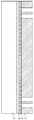
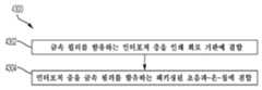
도 1 내지 도 37은 본 명세서에 기재된 특정 실시예에 따른, 하나의 공정을 사용한 초음파-온-칩 장치의 패키징 도중의 다양한 구조의 단면을 도시한다.
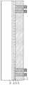
도 38 내지 도 42는 본 명세서에 기재된 특정 실시예에 따른, 다른 공정을 사용한 초음파-온-칩 장치의 패키징 도중의 다양한 구조의 단면을 도시한다.
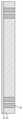
도 43은 본 명세서에 기재된 특정 실시예에 따른, 초음파-온-칩을 패키징하기 위한 예시적인 공정을 도시한다.
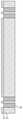
도 44는 본 명세서에 기재된 특정 실시예에 따른, 초음파-온-칩을 패키징하기 위한 예시적인 공정을 도시한다.Various aspects and embodiments will be described with reference to the following illustrative and non-limiting drawings. It should be understood that drawings are not necessarily drawn to scale. Items appearing in several drawings are indicated by the same or similar reference numbers in all drawings in which they appear.
1 to 37 show cross-sections of various structures during packaging of an ultrasonic-on-chip device using one process, according to certain embodiments described herein.
38-42 illustrate cross-sections of various structures during packaging of an ultrasonic-on-chip device using different processes, according to certain embodiments described herein.
43 shows an exemplary process for packaging an ultrasonic-on-chip, according to certain embodiments described herein.
44 shows an exemplary process for packaging an ultrasonic-on-chip, according to certain embodiments described herein.
종래의 초음파 시스템은, 통상적으로 재정이 탄탄한 대규모 의료 시설에서만 구입하는 크고 복잡하며 값비싼 시스템이다. 최근에는 저렴하고 휴대 가능하며 덜 복잡한 초음파 촬영 장치가 도입되었다. 이러한 촬영 장치는 모놀리식 초음파 장치를 형성하기 위해 단일 반도체 다이에 모놀리식으로 통합되는 초음파 변환기를 구비할 수 있다. 이러한 초음파-온-칩 장치의 양태는, 2017년 1월 25일에 출원되고 (본 출원의 양수인에게 양도되었으며) 발명의 명칭이 "유니버설 초음파 장치 및 관련 장치와 방법"이며 그 전체가 본 명세서에 참조로 원용되는 미국 특허 출원 제15/415,434호에 기재되어 있다.Conventional ultrasound systems are large, complex and expensive systems that are typically purchased only in large, well-financed medical facilities. Recently, inexpensive, portable and less complex ultrasound imaging devices have been introduced. Such an imaging device may have an ultrasonic transducer monolithically integrated into a single semiconductor die to form a monolithic ultrasonic device. The aspect of such an ultrasonic-on-chip device is filed on January 25, 2017 (assigned to the assignee of the present application) and the name of the invention is "Universal ultrasonic device and related devices and methods", and the entirety thereof is incorporated herein by reference. US Patent Application No. 15/415,434, which is incorporated by reference.
본 발명자는 와이어본딩과 같은 다른 패키징 방법에 비해서 이러한 초음파-온-칩 장치를 패키징하는 데 도움이 될 수 있는 특징을 인식했다. 특히, 본 발명자는 금속 필러로 보강된 통합 팬 아웃(integrated fan-out: InFO) 패키징 및 인터포저 층이 초음파-온-칩 장치를 패키징하기 위한 이점을 제공할 수 있음을 인식했다. 이점의 예로는 낮은 기생 인덕턴스 및 저항, 더 높은 효율, 더 적은 가열, 더 높은 패키징 처리량, 및 향상된 패키징 신뢰성이 포함된다. 또한, 이러한 패키징은 장치가 더 작은 센서 헤드를 가질 수 있게 할 수 있으며, 이는 센서 헤드가 갈비뼈 사이에 끼워지는 것이 바람직할 수 있는 심장 용도와 같은 초음파 촬영 용도에 도움이 될 수 있다. 또한, 이러한 패키징은 장치가 더 얇은 렌즈를 가질 수 있게 하며, 이는 신호 강도를 증가시킬 수 있다.The inventors have recognized features that may be helpful in packaging such an ultrasonic-on-chip device compared to other packaging methods such as wire bonding. In particular, the inventors have recognized that integrated fan-out (InFO) packaging and interposer layers reinforced with metal fillers can provide advantages for packaging ultrasonic-on-chip devices. Examples of benefits include low parasitic inductance and resistance, higher efficiency, less heating, higher packaging throughput, and improved packaging reliability. In addition, such packaging may allow the device to have a smaller sensor head, which may be helpful for ultrasound applications such as cardiac applications where it may be desirable for the sensor head to be fitted between the ribs. In addition, such packaging allows the device to have a thinner lens, which can increase the signal strength.
본 명세서에 기재된 실시예는 수많은 방식 중 임의의 방식으로 실시될 수 있다는 것을 알아야 한다. 특정 실시예의 예는 예시적인 목적으로만 이하에 제공된다. 제공되는 이들 실시예 및 특징/능력은 본 명세서에 기재된 기술의 양태가 이와 관련하여 제한되지 않기 때문에 개별적으로, 모두 함께, 또는 둘 이상의 임의의 조합으로 사용될 수 있다는 것을 알아야 한다.It should be appreciated that the embodiments described herein may be practiced in any of a number of ways. Examples of specific embodiments are provided below for illustrative purposes only. It should be appreciated that these embodiments and features/capabilities provided may be used individually, all together, or in any combination of two or more as aspects of the technology described herein are not limited in this regard.
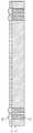
도 1 내지 도 37은 본 명세서에 기재된 특정 실시예에 따른, 하나의 공정을 사용한 초음파-온-칩 장치의 패키징 도중의 다양한 구조의 단면을 도시한다. 도 1은 캐리어 기판(106)에 결합된 박리(release) 층(104), 및 박리 층(104)에 결합된 절연 층(102)을 도시한다. 캐리어 기판(106)은 예를 들어 유리를 포함할 수 있다. 박리 층(104)은 예를 들어 LTHC(light-to-heat-conversion: 광에서 열로의 변환) 코팅 재료를 포함할 수 있다. 절연 재료(102)는 예를 들어 폴리이미드, 폴리벤족사졸(PBO) 또는 벤조사이클로부텐(BCB)과 같은, 노광으로 패터닝되고 현상될 수 있는 폴리머를 포함할 수 있다.1 to 37 illustrate cross-sections of various structures during packaging of an ultrasonic-on-chip device using one process, according to certain embodiments described herein. 1 shows a
도 2에서는, 절연 층(102) 상에 금속 층(108)이 형성된다. 금속 층(108)은 예를 들어 물리적 기상 증착(PVD) 또는 스퍼터링을 사용하여 형성될 수 있다. 금속 층(108)은 예를 들어 구리를 포함할 수 있거나, 또는 일부 실시예에서 금속 층(108)은 절연 층(102)에 결합된 티타늄 층 및 티타늄 층에 결합된 구리 층과 같은 두 개의 층을 포함할 수 있다.In FIG. 2, a
도 3에서는, 금속 층(108) 상에 레지스트 층(110)이 형성된다. 예를 들어, 레지스트 층(110)은 포토레지스트를 포함할 수 있다.In FIG. 3, a
도 4에서는, 레지스트 층(110)에 개구가 형성된다. 예를 들어, 리소그래피 마스크를 통한 노광에 이어지는 현상에 의해, 마스크를 통해서 광에 노광된 레지스트 층(110) 부분에 개구가 생성될 수 있다.In FIG. 4, an opening is formed in the
도 5에서는, 전기도금을 사용하여 레지스트 층(110)의 개구에 금속 필러(112)가 형성된다. 금속 층(108)은 전기도금을 위한 시드 층으로서 작용할 수 있다. 금속 필러(112)는 구리와 같은, 금속 층(108)과 동일한 재료를 포함할 수 있다. 네 개의 금속 필러(112)가 도시되어 있지만, 2차원적으로 배치되는 더 많은 개수의(예를 들어, 수십 개 또는 수백 개의) 금속 필러(112)가 있을 수 있다는 것을 알아야 한다.In FIG. 5, a
도 6에서는, 레지스트 층(110)이 제거된다. 예를 들어, 레지스트 층(110)을 제거하기 위해 레지스트 스트리퍼가 사용될 수 있다. 이전에 레지스트 층(110)의 노출되지 않은 부분 아래에 있었던 금속 층(108) 부분도 제거된다. 예를 들어, 금속 층(108)을 제거하기 위해 이방성 에칭이 사용될 수 있으며, 금속 층(108)은 금속 필러(112)보다 빠르게 에칭된다.In Fig. 6, the
도 7은 절연 층(116)에 결합된 초음파-온-칩(114)을 도시한다.7 shows an ultrasound-on-
도 8에서는, (예를 들어, 포토리소그래피를 사용하여) 절연 층(116)에 개구가 생성된다.In FIG. 8, an opening is created in the insulating layer 116 (eg, using photolithography).
도 9에서는, 절연 층(116) 상에 레지스트 층(118)이 형성된다.In FIG. 9, a
도 10에서는, (예를 들어, 포토리소그래피를 사용하여) 레지스트 층(118)에 개구가 생성되며, 레지스트 층(118)에 생성된 개구는 절연 층(116)에 생성된 개구로 연장된다.In FIG. 10, an opening is created in the resist layer 118 (using, for example, photolithography), and the opening created in the
도 11에서는, 레지스트 층(118) 및 절연 층(116)의 개구 내에 금속 접점(120)이 형성된다. 예를 들어, 금속 접점(120)은 전기도금에 의해 형성될 수 있으며, 구리 또는 구리 합금을 포함할 수 있다. 일부 실시예에서는, 금속 접점(120)과 초음파-온-칩(114) 사이에 언더 범프 야금 층(도 11에 도시되지 않음)이 형성될 수 있다.In FIG. 11,
도 12에서는, (예를 들어, 레지스트 스트리퍼를 사용하여) 레지스트 층(118)이 제거된다.In Fig. 12, the resist
도 13에서는, 금속 접점(120)을 커버하기 위해 추가 절연 재료가 절연 층(116)에 추가된다.In FIG. 13, additional insulating material is added to the insulating
도 14에서는, 절연 층(102)에 다이-부착 필름(die-attach film: DAF)(122)이 결합된다.In FIG. 14, a die-attach film (DAF) 122 is bonded to the insulating
도 15에서는, 다이-부착 필름(122)에 초음파-온-칩(114)이 결합된다.In FIG. 15, the ultrasonic-on-
도 16에서는, 초음파-온-칩(114), 절연 층(116), 다이-부착 필름(122) 및 금속 필러(112)를 캡슐화하기 위해 봉지부(encapsulation)(124)가 형성된다. 봉지부(124)는 몰딩 컴파운드, 몰딩 언더필, 에폭시 또는 수지를 포함할 수 있다. 봉지부(124)의 상면은 절연 층(116) 및 금속 필러(112)의 상면 위로 연장된다.In FIG. 16, an
도 17에서는, 금속 접점(116) 및 금속 필러(112)의 상면의 상면이 노출될 때까지 봉지부(124) 및 절연 층(116)의 상면이 평탄화된다. 예를 들어, 화학 기계적 평탄화(chemical mechanical planarization: CMP)가 평탄화를 위해 사용될 수 있다.In FIG. 17, the upper surfaces of the
도 18에서는, 절연 층(116)에 추가 절연 재료가 추가되며, 따라서 절연 층(116)은 금속 접점(120) 및 금속 필러(112)의 상면을 커버한다.In FIG. 18, an additional insulating material is added to the insulating
도 19에서는, 금속 접점(120) 및 금속 필러(112) 위의 절연 층(116)에 개구가 생성된다. 예를 들어, 포토리소그래피가 개구를 생성하기 위해 사용될 수 있다.In FIG. 19, openings are created in the insulating
도 20에서는, 절연 층(116)의 개구 내에 및 절연 층(116) 상에 재분배 라인(RDL)(126)이 형성된다. 도시된 바와 같이, RDL(126)은 특정 금속 접점(120)을 특정 금속 필러(122)에 전기적으로 연결할 수 있다. RDL(126)은 금속 트레이스 및 비아(via)를 구비할 수 있고, 전기도금(도시되지 않은 시드 층의 형성을 포함)을 사용하여 형성될 수 있으며, 알루미늄, 구리, 텅스텐 및/또는 이들 금속의 합금과 같은 금속을 포함할 수 있다. RDL(126)은 금속 트레이스 및 비아의 복수의 층을 포함할 수 있다.In FIG. 20, a redistribution line (RDL) 126 is formed in the opening of the insulating
도 21에서는, RDL(126)의 상면을 커버하기 위해 추가 절연 재료가 절연 층(116)에 추가된다.In FIG. 21, additional insulating material is added to the insulating
도 22에서는, 캐리어 기판(106) 및 박리 층(104)이 절연 층(102)으로부터 분리된다. 예를 들어, 박리 층(104) 상에 광(예를 들어 자외선 또는 레이저)을 투사하는 것은 박리 층(104)을 분해하여, 박리 층(104) 및 캐리어 기판(106)이 절연 층(102)으로부터 분리되게 할 수 있다. 절연 층(102)의 표면은 또한 일체의 잔류물을 제거하기 위해 세정될 수 있다. 도 21의 구조는 도 22의 배향에 도달하기 위해 뒤집힌다.In FIG. 22, the
도 23에서는, 절연 층(102)에 개구가 생성된다.In Fig. 23, an opening is created in the insulating
도 24에서는, 절연 층(102)의 개구에 솔더 볼(128)이 배치된다. 일부 실시예에서, 솔더 볼(128)은 전기도금에 의해 형성될 수 있다. 일부 실시예에서는, 다른 형태의 전기 커넥터(예를 들어, 금속 필러)가 개구에 형성될 수 있다. 일부 실시예에서는, 솔더 볼(128)과 금속 필러(112) 사이에 언더-범프 야금 층(도 24에 도시되지 않음)이 형성될 수 있다.In FIG. 24,
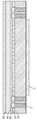
도 25는 캐리어 기판(136)에 결합된 박리 층(134), 박리 층(134)에 결합된 절연 층(132), 및 절연 층(132)에 결합된 인터포저 층(130)을 도시한다. 인터포저 층(130)은 예를 들어 질화 알루미늄을 포함할 수 있다.25 shows a
도 26에서는, 인터포저 층(130)에 개구가 형성된다. 예를 들어, 레이저 드릴링이 개구를 형성하기 위해 사용될 수 있다.In FIG. 26, an opening is formed in the
도 27에서는, 인터포저 층(130) 상에 금속 층(138)이 형성된다. 금속 층(138)은 예를 들어 스퍼터링을 사용하여 형성될 수 있다. 금속 층(138)은 예를 들어 구리를 포함할 수 있거나, 또는 일부 실시예에서 금속 층(138)은 인터포저 층(130)에 결합된 티타늄 층 및 티타늄 층에 결합된 구리 층과 같은 두 개의 층을 포함할 수 있다.In FIG. 27, a
도 28에서는, 전기도금을 사용하여 레지스트 층(130)의 개구에 금속 필러(142)가 형성된다. 금속 층(138)은 전기도금을 위한 시드 층으로서 작용할 수 있다. 금속 필러(142)는 구리와 같은, 금속 층(138)과 동일한 재료를 포함할 수 있다. 전기적 라우팅으로서 작용하는 것뿐만 아니라, 금속 필러(142)는 깨질 수 있는 인터포저 층(130)을 강화하는 데에도 도움이 될 수 있다는 것을 이해해야 한다.In FIG. 28, a
도 29에서는, 금속 층(138) 및 금속 필러(142) 상에 레지스트 층(140)이 형성된다.In FIG. 29, a resist
도 30에서는, 금속 필러(142)의 상면을 블로킹하기 위해 레지스트 층(140)이 (예를 들어, 포토리소그래피를 사용하여) 패터닝된다.In FIG. 30, the resist
도 31에서는, 금속 필러(142)를 전기적으로 격리시키기 위해 금속 층(108)의 블로킹되지 않은 부분이 에칭된다. 일부 실시예에서는, 금속 필러(142)를 블로킹하기 위해 포토리소그래피를 사용하는 것 대신에 또는 그것에 추가적으로, 시한 에칭(timed etch) 또는 이방성 에칭이 사용될 수 있다.In FIG. 31, the unblocked portion of the
도 32에서는, (예를 들어, 레지스트 스트리퍼를 사용하여) 레지스트 층(140)이 제거된다.In FIG. 32, the resist
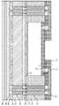
도 33에서는, 캐리어 기판(136) 및 박리 층(134)이 절연 층(132)으로부터 분리된다.In FIG. 33, the
도 34에서는, 절연 층(132)에 개구가 생성된다.In FIG. 34, an opening is created in the insulating
도 35에서는, 절연 층(132)의 개구에 솔더 볼(144)이 배치된다.In FIG. 35,
도 36에서는, 인터포저 층(142)에 열접착제 층(150)이 결합된다. 일부 실시예에서, 열접착제 층(150)은 은-함유 에폭시를 포함할 수 있다. 솔더 볼(144)이 프린터 회로 기판(PCB)(148)에 결합된다. 일부 실시예에서는, 솔더 볼(144)을 PCB(148)에 결합하기 위해 표면-실장 기술(surface-mount technology: SMT) 또는 플립-칩 솔더링(flip-chip soldering)이 사용될 수 있다. 절연 층(132)과 PCB(148) 사이에는 언더필(예를 들어, 에폭시) 층(146)이 형성된다.In FIG. 36, the thermal
도 37에서는, 솔더 볼(128)이 금속 필러(142)에 결합된다. 금속 필러(112)는 금속 필러(142)와 정렬된다. 일부 실시예에서는, 솔더 볼(128)을 금속 필러(142)에 결합하기 위해 표면-실장 기술(SMT) 또는 플립-칩 솔더링이 사용될 수 있다. 최종 구조에서, 인터포저는 초음파-온-칩(114)과 PCB(148) 사이의 전기적 라우팅뿐만 아니라 초음파-온-칩(114)을 위한 히트싱크를 제공할 수 있다.In FIG. 37, the
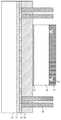
도 38 내지 도 42는 본 명세서에 기재된 특정 실시예에 따른, 다른 공정을 사용한 초음파-온-칩 장치의 패키징 도중의 다양한 구조의 단면을 도시한다. 도 38은 도 32의 구조를 도시한다.38-42 illustrate cross-sections of various structures during packaging of an ultrasonic-on-chip device using different processes, according to certain embodiments described herein. Fig. 38 shows the structure of Fig. 32;
도 39에서, 금속 필러(142)는 전기도금을 사용하여 위쪽으로 연장된다. 알 수 있듯이, 금속 필러(142)는 인터포저 층(130)의 상면을 넘어서 연장된다.In Fig. 39, the
도 40에서, 초음파-온-칩(114)은 다이-부착 필름(122)을 통해서 인터포저 층(130)에 결합된다.In FIG. 40, the ultrasonic-on-
도 41에서는, 절연 층(116)에 추가 절연 재료가 추가된다. 도 16에서와 마찬가지로, 초음파-온-칩(114), 절연 층(116), 다이-부착 필름(122) 및 금속 필러(142)를 캡슐화하기 위해 봉지부(124)가 형성된다. 도 18 내지 도 21에서와 마찬가지로, RDL(126)이 형성된다.In FIG. 41, an additional insulating material is added to the insulating
도 42에서는, 도 33 내지 도 36에서와 마찬가지로, 캐리어 기판(136) 및 박리 층(134)이 절연 층(132)으로부터 분리되고, 금속 필러(142) 상에 솔더 볼(144)이 형성되며, 솔더 볼(144)은 PCB(148)에 결합되고, 절연 층(132)과 PCB(148) 사이에 언더필 층(146)이 형성된다.In FIG. 42, as in FIGS. 33 to 36, the
도 1 내지 도 37의 공정과 비교해서, 도 38 내지 도 42의 공정은 공정 제어, 품질 및 수율이 높을 수 있는 반도체 파운드리에서 초음파-온-칩(114)이 인터포저 층(130)에 결합되게 할 수 있다. 또한, 도 1 내지 도 37의 공정은 솔더 볼(128)을 금속 필러(142)에 접합하고 동시에 절연 층(102)을 열접착제 층(150)에 접합할 것을 요구할 수 있지만, 도 38 내지 도 42의 공정은 열접착제 층(150)을 제거할 수 있다.Compared with the processes of FIGS. 1 to 37, the processes of FIGS. 38 to 42 allow the ultrasonic-on-
도 43은 본 명세서에 기재된 특정 실시예에 따른, 초음파-온-칩을 패키징하기 위한 예시적인 공정(4300)을 도시한다. 행동 4302에서는, 금속 필러를 함유하는 인터포저 층이 인쇄 회로 기판에 결합된다. 행동 4302는 도 36에 도시된 단계에 대응할 수 있다. 행동 4304에서, 인터포저 층은 금속 필러를 함유하는 패키징된 초음파-온-칩에 결합된다. 행동 4304는 도 37에 도시된 단계에 대응할 수 있다. 인터포저 층은 열접착제 층을 통해서 패키징된 초음파-온-칩에 결합될 수 있다.43 shows an
도 44는 본 명세서에 설명된 특정 실시예에 따른, 초음파-온-칩을 패키징하기 위한 예시적인 공정(4400)을 도시한다. 동작 4402에서는, 인터포저 층에 금속 필러가 형성된다. 동작 4402는 도 38 및 도 39에 도시된 단계에 대응할 수 있다. 동작 4404에서, 인터포저 층은 초음파-온-칩에 결합된다. 동작 4404는 도 40에 도시된 단계에 대응할 수 있다. 동작 4406에서는, 패키징된 초음파-온-칩 상에 재분배 층이 형성된다. 동작 4406은 도 41에 도시된 단계에 대응할 수 있다.44 depicts an
본 개시내용의 다양한 양태는 단독으로, 조합하여, 또는 전술한 실시예에서 구체적으로 논의되지 않은 다양한 배치로 사용될 수 있으며, 따라서 그 적용에 있어서 상기 설명에 기재되거나 도면에 도시된 구성 요소의 상세 및 배치로 제한되지 않는다. 예를 들어, 일 실시예에 기재된 양태는 다른 실시예에 기재된 양태와 임의의 방식으로 조합될 수 있다.Various aspects of the present disclosure may be used alone, in combination, or in various arrangements not specifically discussed in the above-described embodiments, and therefore, in their application, details of the components described in the above description or shown in the drawings and Not limited to batch. For example, aspects described in one embodiment can be combined in any way with aspects described in other embodiments.
본 출원의 명세서 및 청구범위에서 사용된 부정관사는 반대로 명시되지 않는 한 "적어도 하나"를 의미하는 것으로 이해되어야 한다.Indefinite articles used in the specification and claims of this application are to be understood as meaning "at least one" unless otherwise specified.
본 출원의 명세서 및 청구범위에서 사용된 "및/또는"이라는 문구는 그렇게 결합된 요소, 즉 일부 경우에 결합하여 존재하고 다른 경우에 분리되어 존재하는 요소의 "어느 하나 또는 둘 다"를 의미하는 것으로 이해되어야 한다. "및/또는"으로 열거되는 복수의 요소는 동일한 방식으로, 즉 그렇게 결합된 요소의 "하나 또는 그 이상"으로 해석되어야 한다. "및/또는" 구절에 의해 구체적으로 특정된 요소 이외의 다른 요소가, 구체적으로 특정된 요소와 관련이 있는지 여부에 관계없이 경우에 따라 존재할 수 있다. 따라서, 비제한적인 예로서, "A 및/또는 B"에 대한 언급은 이것이 "포함하는"과 같은 개방형 언어와 함께 사용될 때, 일 실시예에서 A만 지칭할 수 있고(경우에 따라서 B 이외의 요소를 포함); 다른 실시예에서 B만 지칭할 수 있으며(경우에 따라서 A 이외의 요소를 포함); 또 다른 실시예에서 A와 B 둘 다 지칭할 수 있고(경우에 따라서 다른 요소를 포함); 기타를 지칭할 수 있다.The phrase "and/or" as used in the specification and claims of this application means "either or both" of the elements so conjoined, ie, elements that exist in combination in some cases and separate in other cases. It should be understood as. A plurality of elements listed as “and/or” should be construed in the same way, ie as “one or more” of the elements so conjoined. Elements other than those specifically specified by the phrase "and/or" may be present in some cases, regardless of whether or not they relate to the specifically specified elements. Thus, as a non-limiting example, reference to “A and/or B” when used with an open language such as “comprising” may refer to only A in one embodiment (and in some cases other than B). Elements); In other embodiments, only B may be referred to (including elements other than A in some cases); In another embodiment it may refer to both A and B (including other elements as the case may be); It can refer to others.
본 출원의 명세서 및 청구범위에서 사용될 때, 하나 이상의 요소의 목록과 관련한 "적어도 하나"라는 문구는 요소 목록의 요소들 중 임의의 하나 이상으로부터 선택되는 적어도 하나의 요소를 의미하지만, 요소 목록 내에 구체적으로 열거되어 있는 각각의 및 모든 요소의 적어도 하나를 반드시 포함하지는 않으며, 요소 목록 내의 요소들의 임의의 조합을 배제하지 않는 것으로 이해되어야 한다. 이 정의는 또한 구체적으로 특정된 요소와 관련이 있는지 여부에 관계없이 "적어도 하나"라는 문구가 언급하는 요소 목록 내에서 구체적으로 특정되는 요소 이외의 요소가 경우에 따라 존재할 수도 있게 할 수 있다. 따라서, 비제한적인 예로서, "A 및 B 중 적어도 하나"(또는 동등하게 "A 또는 B 중 적어도 하나" 또는 동등하게 "A 및/또는 B 중 적어도 하나")는 일 실시예에서 B가 전혀 없이(및 경우에 따라서 B 이외의 요소를 포함하고) 적어도 하나의, 경우에 따라서 하나 초과를 포함하는, A를 지칭하고; 다른 실시예에서 A가 전혀 없이(및 경우에 따라서 A 이외의 요소를 포함하고) 적어도 하나의, 경우에 따라서 하나 초과를 포함하는, B를 지칭하며; 또 다른 실시예에서 적어도 하나의, 경우에 따라서 하나 초과를 포함하는, A 및 적어도 하나의, 경우에 따라서 하나 초과를 포함하는, B(및 경우에 따라서 다른 요소를 포함하는)를 지칭하고; 기타를 지칭할 수 있다.As used in the specification and claims of this application, the phrase "at least one" in relation to a list of one or more elements means at least one element selected from any one or more of the elements of the element list, It is to be understood that it does not necessarily include at least one of each and every element listed as, and does not exclude any combination of elements in the element list. This definition may also allow, in some cases, to have elements other than those specifically specified within the list of elements referred to by the phrase "at least one," whether or not they relate to the specifically specified element. Thus, by way of non-limiting example, "at least one of A and B" (or equivalently "at least one of A or B" or equivalently "at least one of A and/or B") in one embodiment is not Without (and optionally including elements other than B) at least one, optionally including more than one; In other embodiments, it refers to B without A at all (and optionally including elements other than A), including at least one, optionally more than one; In another embodiment refers to at least one, optionally including more than one, A and at least one, optionally including more than one, B (and optionally including other elements); It can refer to others.
청구항 요소를 수정하기 위해 청구범위에서 "제1", "제2", "제3" 등과 같은 서수 용어를 사용하는 것은 그 자체로 다른 청구항 요소 또는 방법의 동작들이 수행되는 시간 순서에 대한 하나의 청구항 요소의 우선순위, 상위 또는 순서를 의미하지 않으며, (서수 용어의 사용을 위해) 특정 이름을 갖는 하나의 청구항 요소를 동일한 이름을 갖는 다른 요소와 구별하여 청구항 요소를 구별하기 위한 표시로서만 사용된다.The use of ordinal terms such as "first", "second", "third" in a claim to modify a claim element is itself a one-of-a-kind chronological order in which the actions of another claim element or method are performed. It does not imply priority, priority, or order of claim elements, and is used only as an indication to differentiate claim elements by distinguishing one claim element with a specific name from other elements of the same name (for the use of ordinal terms). do.
본 명세서에서 사용될 때, 두 개의 끝점 사이에 있는 수치의 언급은 그 수치가 끝점 중 어느 하나를 가질 수 있는 상황을 포함하는 것으로 이해되어야 한다. 예를 들어, 특성이 A와 B 사이 또는 대략 A와 B 사이의 값을 갖는다는 것은 달리 명시하지 않는 한 표시된 범위가 끝점 A와 B를 포함하는 것을 의미하는 것으로 이해되어야 한다.As used herein, reference to a number between two endpoints is to be understood as including situations in which the number may have either of the endpoints. For example, that a property has a value between A and B, or approximately between A and B, should be understood to mean that the indicated range includes the endpoints A and B, unless otherwise specified.
용어 "대략" 및 "약"은 일부 실시예에서 목표치의 ±20% 이내, 일부 실시예에서 목표치의 ±10% 이내, 일부 실시예에서 목표치의 ±5% 이내, 일부 실시예에서 목표치의 ±2% 이내를 의미하기 위해 사용될 수 있다. 용어 "대략" 및 "약"은 목표치를 포함할 수 있다.The terms “approximately” and “about” are within ±20% of the target value in some embodiments, within ±10% of the target value in some embodiments, within ±5% of the target value in some embodiments, and ±2 of the target value in some embodiments. Can be used to mean within %. The terms “approximately” and “about” may include target values.
또한, 본 명세서에 사용된 문구 및 용어는 설명을 위한 것이며 제한적인 것으로 간주되어서는 안된다. 본 명세서에서 "구비하는", "포함하는" 또는 "갖는", "함유하는", "수반하는" 및 그 변형의 사용은 그 후에 열거되는 항목 및 그 등가물뿐 아니라 추가 항목을 포함하는 것을 의미한다.In addition, phrases and terms used herein are for the purpose of description and should not be regarded as limiting. The use of "comprising", "comprising" or "having", "including", "accompaniing" and variations thereof herein is meant to include the items listed thereafter and equivalents thereof, as well as additional items. .
적어도 하나의 실시예의 여러 양태를 위에서 설명했지만, 다양한 변경, 수정 및 개선이 통상의 기술자에게 쉽게 발생될 것임을 알아야 한다. 이러한 변경, 수정 및 개선은 본 개시내용의 목적이도록 의도된다. 따라서, 전술한 설명 및 도면은 단지 예일 뿐이다.While various aspects of at least one embodiment have been described above, it should be understood that various changes, modifications, and improvements will readily occur to those skilled in the art. Such changes, modifications and improvements are intended to be the purpose of this disclosure. Accordingly, the above description and drawings are only examples.
Claims (29)
Translated fromKorean상면 및 하면을 포함하는 초음파-온-칩;
상면 및 하면을 포함하는 인터포저 층; 및
재분배 층을 포함하고,
초음파-온-칩 장치의 상면은 재분배 층에 결합되며;
초음파-온-칩 장치의 하면은 인터포저 층의 상면에 결합되는, 장치.Device,
Ultrasound-on-chip including upper and lower surfaces;
An interposer layer including an upper surface and a lower surface; And
Including a redistribution layer,
The top surface of the ultrasonic-on-chip device is bonded to the redistribution layer;
The device, wherein the lower surface of the ultrasonic-on-chip device is bonded to the upper surface of the interposer layer.
봉지부를 통해서 연장되고 재분배 층에 전기적으로 결합되는 제1 금속 필러를 추가로 포함하는, 장치.The method of claim 1, further comprising: an encapsulation unit encapsulating the ultrasonic-on-chip device; And
The apparatus further comprising a first metal filler extending through the encapsulation and electrically coupled to the redistribution layer.
인터포저 층과 봉지부를 통해서 연장되고 재분배 층에 전기적으로 결합되는 금속 필러를 추가로 포함하는, 장치.The method of claim 1, further comprising: an encapsulation unit encapsulating the ultrasonic-on-chip device; And
The apparatus further comprising a metal filler extending through the interposer layer and the encapsulation and electrically coupled to the redistribution layer.
제1 금속 필러를 포함하는 인터포저 층을 인쇄 회로 기판에 결합하는 단계; 및
인터포저 층을 제2 금속 필러를 함유하는 패키징된 초음파-온-칩에 결합하는 단계를 포함하는, 방법.Is the way,
Bonding an interposer layer comprising a first metal filler to the printed circuit board; And
And bonding the interposer layer to the packaged ultrasound-on-chip containing the second metal filler.
초음파-온-칩 장치를 캡슐화하는 봉지부; 및
초음파-온-칩 장치에 결합되는 재분배 층을 포함하며,
제2 금속 필러는 봉지부를 통해서 연장되고 재분배 층에 전기적으로 결합되는, 방법.The method of claim 16, wherein the packaged ultrasonic-on-chip device comprises:
An encapsulation part encapsulating the ultrasonic-on-chip device; And
Comprising a redistribution layer coupled to the ultrasonic-on-chip device,
The method, wherein the second metal filler extends through the encapsulation and is electrically coupled to the redistribution layer.
인터포저 층에 금속 필러를 형성하는 단계;
인터포저 층을 초음파-온-칩에 결합하는 단계; 및
초음파-온-칩 상에 재분배 층을 형성하는 단계를 포함하는, 방법.Is the way,
Forming a metal filler in the interposer layer;
Bonding the interposer layer to the ultrasonic-on-chip; And
Forming a redistribution layer on the ultrasonic-on-chip.
Applications Claiming Priority (3)
| Application Number | Priority Date | Filing Date | Title |
|---|---|---|---|
| US201862694810P | 2018-07-06 | 2018-07-06 | |
| US62/694,810 | 2018-07-06 | ||
| PCT/US2019/040516WO2020010207A1 (en) | 2018-07-06 | 2019-07-03 | Methods and apparatuses for packaging an ultrasound-on-a-chip |
Publications (1)
| Publication Number | Publication Date |
|---|---|
| KR20210030951Atrue KR20210030951A (en) | 2021-03-18 |
Family
ID=69059840
Family Applications (1)
| Application Number | Title | Priority Date | Filing Date |
|---|---|---|---|
| KR1020217003420ACeasedKR20210030951A (en) | 2018-07-06 | 2019-07-03 | Method and apparatus for packaging ultrasonic-on-chip |
Country Status (9)
| Country | Link |
|---|---|
| US (2) | US11018068B2 (en) |
| EP (1) | EP3818372B1 (en) |
| JP (1) | JP2021529459A (en) |
| KR (1) | KR20210030951A (en) |
| CN (1) | CN112368574B (en) |
| AU (1) | AU2019297412A1 (en) |
| CA (1) | CA3105492A1 (en) |
| TW (1) | TW202011897A (en) |
| WO (1) | WO2020010207A1 (en) |
Families Citing this family (18)
| Publication number | Priority date | Publication date | Assignee | Title |
|---|---|---|---|---|
| EP3788798B1 (en) | 2018-05-03 | 2023-07-05 | BFLY Operations, Inc. | Ultrasonic transducers with pressure ports |
| KR20210030951A (en) | 2018-07-06 | 2021-03-18 | 버터플라이 네트워크, 인크. | Method and apparatus for packaging ultrasonic-on-chip |
| AU2019350989A1 (en) | 2018-09-28 | 2021-03-25 | Butterfly Network, Inc. | Fabrication techniques and structures for gettering materials in ultrasonic transducer cavities |
| US11626343B2 (en)* | 2018-10-30 | 2023-04-11 | Taiwan Semiconductor Manufacturing Co., Ltd. | Semiconductor device with enhanced thermal dissipation and method for making the same |
| US11638931B2 (en) | 2018-11-13 | 2023-05-02 | Bfly Operations, Inc. | Getter technology for micromachined ultrasonic transducer cavities |
| WO2020102492A1 (en) | 2018-11-15 | 2020-05-22 | Butterfly Network, Inc. | Anti-stiction bottom cavity surface for micromachined ultrasonic transducer devices |
| CA3121805A1 (en) | 2018-12-07 | 2020-06-11 | Octant, Inc. | Systems for protein-protein interaction screening |
| TW202045099A (en) | 2019-02-07 | 2020-12-16 | 美商蝴蝶網路公司 | Bi-layer metal electrode for micromachined ultrasonic transducer devices |
| EP3930923A4 (en) | 2019-02-25 | 2023-01-11 | Bfly Operations, Inc. | Adaptive cavity thickness control for micromachined ultrasonic transducer devices |
| WO2020210470A1 (en) | 2019-04-12 | 2020-10-15 | Butterfly Network, Inc. | Bottom electrode via structures for micromachined ultrasonic transducer devices |
| US11501562B2 (en) | 2019-04-30 | 2022-11-15 | Bfly Operations, Inc. | Ultrasound face scanning and identification apparatuses and methods |
| US11684951B2 (en) | 2019-08-08 | 2023-06-27 | Bfly Operations, Inc. | Micromachined ultrasonic transducer devices having truncated circle shaped cavities |
| US11676922B2 (en)* | 2019-10-28 | 2023-06-13 | Qualcomm Incorporated | Integrated device comprising interconnect structures having an inner interconnect, a dielectric layer and a conductive layer |
| US11988640B2 (en) | 2020-03-11 | 2024-05-21 | Bfly Operations, Inc. | Bottom electrode material stack for micromachined ultrasonic transducer devices |
| US11776820B2 (en) | 2020-09-30 | 2023-10-03 | Huawei Technologies Co., Ltd. | Vertical interconnection structure and manufacturing method thereof, packaged chip, and chip packaging method |
| TW202240165A (en) | 2021-03-04 | 2022-10-16 | 美商蝴蝶營運公司 | Micromachined ultrasound transducer with pedestal |
| TW202239483A (en) | 2021-03-04 | 2022-10-16 | 美商蝴蝶營運公司 | Capacitive micromachined ultrasonic transducers (cmuts) having non-uniform pedestals |
| US12156762B2 (en) | 2021-04-01 | 2024-12-03 | Bfly Operations, Inc. | Apparatuses and methods for configuring ultrasound devices |
Family Cites Families (33)
| Publication number | Priority date | Publication date | Assignee | Title |
|---|---|---|---|---|
| US7327554B2 (en)* | 2003-03-19 | 2008-02-05 | Ngk Spark Plug Co., Ltd. | Assembly of semiconductor device, interposer and substrate |
| US20060055024A1 (en)* | 2004-09-14 | 2006-03-16 | Staktek Group, L.P. | Adapted leaded integrated circuit module |
| US7741686B2 (en) | 2006-07-20 | 2010-06-22 | The Board Of Trustees Of The Leland Stanford Junior University | Trench isolated capacitive micromachined ultrasonic transducer arrays with a supporting frame |
| DE102007026445A1 (en) | 2007-06-06 | 2008-12-11 | Robert Bosch Gmbh | Micromechanical component and method for producing a micromechanical component |
| US8193685B2 (en) | 2007-07-03 | 2012-06-05 | Koninklijke Philips Electronics N.V. | Thin film detector for presence detection |
| US7843022B2 (en) | 2007-10-18 | 2010-11-30 | The Board Of Trustees Of The Leland Stanford Junior University | High-temperature electrostatic transducers and fabrication method |
| US7781238B2 (en) | 2007-12-06 | 2010-08-24 | Robert Gideon Wodnicki | Methods of making and using integrated and testable sensor array |
| US20110055447A1 (en) | 2008-05-07 | 2011-03-03 | Signostics Limited | Docking system for medical diagnostic scanning using a handheld device |
| US7838337B2 (en)* | 2008-12-01 | 2010-11-23 | Stats Chippac, Ltd. | Semiconductor device and method of forming an interposer package with through silicon vias |
| US7790492B1 (en) | 2009-06-13 | 2010-09-07 | Mwm Acoustics, Llc | Method for fabricating a transducer package with the transducer die unsupported by a substrate |
| US8207652B2 (en) | 2009-06-16 | 2012-06-26 | General Electric Company | Ultrasound transducer with improved acoustic performance |
| US20130237055A1 (en)* | 2010-06-11 | 2013-09-12 | Imec | Method of redistributing functional element |
| TWI667700B (en) | 2010-12-01 | 2019-08-01 | 美商1366科技公司 | Making semiconductor bodies from molten material using a free-standing interposer sheet |
| US8614488B2 (en)* | 2010-12-08 | 2013-12-24 | Ying-Nan Wen | Chip package and method for forming the same |
| CN105188960A (en) | 2013-02-05 | 2015-12-23 | 声音技术公司 | Ultrasound device |
| US9533873B2 (en) | 2013-02-05 | 2017-01-03 | Butterfly Network, Inc. | CMOS ultrasonic transducers and related apparatus and methods |
| EP4122609B1 (en) | 2013-03-15 | 2024-11-06 | BFLY Operations, Inc. | Complementary metal oxide semiconductor (cmos) ultrasonic transducers and methods for forming the same |
| US9633869B2 (en)* | 2013-08-16 | 2017-04-25 | Taiwan Semiconductor Manufacturing Company, Ltd. | Packages with interposers and methods for forming the same |
| AU2015247484B2 (en) | 2014-04-18 | 2020-05-14 | Butterfly Network, Inc. | Ultrasonic transducers in complementary metal oxide semiconductor (CMOS) wafers and related apparatus and methods |
| US9252127B1 (en) | 2014-07-10 | 2016-02-02 | Invensas Corporation | Microelectronic assemblies with integrated circuits and interposers with cavities, and methods of manufacture |
| US9067779B1 (en)* | 2014-07-14 | 2015-06-30 | Butterfly Network, Inc. | Microfabricated ultrasonic transducers and related apparatus and methods |
| US20160009544A1 (en)* | 2015-03-02 | 2016-01-14 | Butterfly Network, Inc. | Microfabricated ultrasonic transducers and related apparatus and methods |
| US10276541B2 (en)* | 2015-06-30 | 2019-04-30 | Taiwan Semiconductor Manufacturing Company, Ltd. | 3D package structure and methods of forming same |
| TWI721183B (en)* | 2016-06-20 | 2021-03-11 | 美商蝴蝶網路公司 | Electrical contact arrangement for microfabricated ultrasonic transducer |
| US9922896B1 (en) | 2016-09-16 | 2018-03-20 | Taiwan Semiconductor Manufacturing Company, Ltd. | Info structure with copper pillar having reversed profile |
| CN106449554B (en)* | 2016-12-06 | 2019-12-17 | 苏州源戍微电子科技有限公司 | chip embedded packaging structure with closed cavity and manufacturing method thereof |
| US10196261B2 (en) | 2017-03-08 | 2019-02-05 | Butterfly Network, Inc. | Microfabricated ultrasonic transducers and related apparatus and methods |
| WO2018236956A1 (en) | 2017-06-21 | 2018-12-27 | Butterfly Network, Inc. | MICROFABRICATED ULTRASONIC TRANSDUCER HAVING INDIVIDUAL CELLS HAVING ELECTRICALLY ISOLATED ELECTRODE SECTIONS |
| CN108155160A (en)* | 2018-01-29 | 2018-06-12 | 中芯长电半导体(江阴)有限公司 | The encapsulating structure and packaging method of fingerprint recognition chip |
| JP2021511750A (en) | 2018-01-30 | 2021-05-06 | バタフライ ネットワーク,インコーポレイテッド | Methods and equipment for packaging ultrasonic on-chips |
| TW201938834A (en) | 2018-03-09 | 2019-10-01 | 美商蝴蝶網路公司 | Ultrasound transducer devices and methods for fabricating ultrasound transducer devices |
| TW201947717A (en) | 2018-05-03 | 2019-12-16 | 美商蝴蝶網路公司 | Vertical packaging for ultrasound-on-a-chip and related methods |
| KR20210030951A (en)* | 2018-07-06 | 2021-03-18 | 버터플라이 네트워크, 인크. | Method and apparatus for packaging ultrasonic-on-chip |
- 2019
- 2019-07-03KRKR1020217003420Apatent/KR20210030951A/ennot_activeCeased
- 2019-07-03JPJP2020571590Apatent/JP2021529459A/enactivePending
- 2019-07-03AUAU2019297412Apatent/AU2019297412A1/ennot_activeAbandoned
- 2019-07-03WOPCT/US2019/040516patent/WO2020010207A1/ennot_activeCeased
- 2019-07-03EPEP19830619.3Apatent/EP3818372B1/enactiveActive
- 2019-07-03TWTW108123485Apatent/TW202011897A/enunknown
- 2019-07-03CACA3105492Apatent/CA3105492A1/enactivePending
- 2019-07-03USUS16/502,553patent/US11018068B2/enactiveActive
- 2019-07-03CNCN201980045060.6Apatent/CN112368574B/enactiveActive
- 2021
- 2021-03-04USUS17/191,829patent/US11676874B2/enactiveActive
Also Published As
| Publication number | Publication date |
|---|---|
| US20200013691A1 (en) | 2020-01-09 |
| AU2019297412A1 (en) | 2021-01-28 |
| CN112368574B (en) | 2023-08-01 |
| US11676874B2 (en) | 2023-06-13 |
| JP2021529459A (en) | 2021-10-28 |
| US11018068B2 (en) | 2021-05-25 |
| CN112368574A (en) | 2021-02-12 |
| US20210296195A1 (en) | 2021-09-23 |
| TW202011897A (en) | 2020-04-01 |
| EP3818372A1 (en) | 2021-05-12 |
| WO2020010207A1 (en) | 2020-01-09 |
| EP3818372A4 (en) | 2022-04-06 |
| EP3818372B1 (en) | 2024-10-30 |
| CA3105492A1 (en) | 2020-01-09 |
| EP3818372C0 (en) | 2024-10-30 |
Similar Documents
| Publication | Publication Date | Title |
|---|---|---|
| KR20210030951A (en) | Method and apparatus for packaging ultrasonic-on-chip | |
| US20240153881A1 (en) | System on Integrated Chips (SoIC) and Semiconductor Structures with Integrated SoIC | |
| US20220148886A1 (en) | Semiconductor device and manufacturing method thereof | |
| US7033935B2 (en) | Semiconductor device and method for manufacturing the same | |
| US10774427B2 (en) | Fabrication method of substrate having electrical interconnection structures | |
| KR20200130375A (en) | Ultrasonic transducer devices and methods for manufacturing ultrasonic transducer devices | |
| JP2008509774A (en) | 2D ultrasonic transducer array | |
| CN109755207B (en) | Integrated fan-out package and method of forming the same | |
| US10037897B2 (en) | Inter-fan-out wafer level packaging with coaxial TIV for 3D IC low-noise packaging | |
| US20230034707A1 (en) | Packaging structures and packaging methods for ultrasound-on-chip devices | |
| US11139282B2 (en) | Semiconductor package structure and method for manufacturing the same | |
| TW201112366A (en) | Semiconductor device | |
| CN113223971A (en) | Semiconductor device and method of manufacturing the same | |
| US20150287685A1 (en) | Solder Pad for Semiconductor Device Package | |
| CN110718529A (en) | Semiconductor device and method for manufacturing semiconductor device | |
| JP2005026301A (en) | Semiconductor device and manufacturing method thereof, circuit board, and electronic apparatus | |
| US9515034B2 (en) | Bond pad having a trench and method for forming | |
| US20150194395A1 (en) | Bond pad having a trench and method for forming | |
| US11244894B2 (en) | Semiconductor packages | |
| JP5776174B2 (en) | Manufacturing method of electronic component built-in substrate | |
| US20090061614A1 (en) | Method for forming bumps on under bump metallurgy | |
| JP2011171350A (en) | Semiconductor device and method of manufacturing the same |
Legal Events
| Date | Code | Title | Description |
|---|---|---|---|
| PA0105 | International application | Patent event date:20210203 Patent event code:PA01051R01D Comment text:International Patent Application | |
| PG1501 | Laying open of application | ||
| PA0201 | Request for examination | Patent event code:PA02012R01D Patent event date:20220701 Comment text:Request for Examination of Application | |
| E902 | Notification of reason for refusal | ||
| PE0902 | Notice of grounds for rejection | Comment text:Notification of reason for refusal Patent event date:20240521 Patent event code:PE09021S01D | |
| E601 | Decision to refuse application | ||
| PE0601 | Decision on rejection of patent | Patent event date:20240902 Comment text:Decision to Refuse Application Patent event code:PE06012S01D |