KR20210027633A - Display device and driving method thereof - Google Patents
Display device and driving method thereofDownload PDFInfo
- Publication number
- KR20210027633A KR20210027633AKR1020190106775AKR20190106775AKR20210027633AKR 20210027633 AKR20210027633 AKR 20210027633AKR 1020190106775 AKR1020190106775 AKR 1020190106775AKR 20190106775 AKR20190106775 AKR 20190106775AKR 20210027633 AKR20210027633 AKR 20210027633A
- Authority
- KR
- South Korea
- Prior art keywords
- fingerprint
- sensing
- display panel
- input
- mode
- Prior art date
- Legal status (The legal status is an assumption and is not a legal conclusion. Google has not performed a legal analysis and makes no representation as to the accuracy of the status listed.)
- Granted
Links
Images


Classifications
- G—PHYSICS
- G06—COMPUTING OR CALCULATING; COUNTING
- G06F—ELECTRIC DIGITAL DATA PROCESSING
- G06F3/00—Input arrangements for transferring data to be processed into a form capable of being handled by the computer; Output arrangements for transferring data from processing unit to output unit, e.g. interface arrangements
- G06F3/01—Input arrangements or combined input and output arrangements for interaction between user and computer
- G06F3/03—Arrangements for converting the position or the displacement of a member into a coded form
- G06F3/041—Digitisers, e.g. for touch screens or touch pads, characterised by the transducing means
- G06F3/0416—Control or interface arrangements specially adapted for digitisers
- G—PHYSICS
- G06—COMPUTING OR CALCULATING; COUNTING
- G06F—ELECTRIC DIGITAL DATA PROCESSING
- G06F1/00—Details not covered by groups G06F3/00 - G06F13/00 and G06F21/00
- G06F1/26—Power supply means, e.g. regulation thereof
- G06F1/32—Means for saving power
- G06F1/3203—Power management, i.e. event-based initiation of a power-saving mode
- G06F1/3234—Power saving characterised by the action undertaken
- G06F1/325—Power saving in peripheral device
- G06F1/3262—Power saving in digitizer or tablet
- G—PHYSICS
- G06—COMPUTING OR CALCULATING; COUNTING
- G06F—ELECTRIC DIGITAL DATA PROCESSING
- G06F3/00—Input arrangements for transferring data to be processed into a form capable of being handled by the computer; Output arrangements for transferring data from processing unit to output unit, e.g. interface arrangements
- G06F3/01—Input arrangements or combined input and output arrangements for interaction between user and computer
- G06F3/03—Arrangements for converting the position or the displacement of a member into a coded form
- G06F3/041—Digitisers, e.g. for touch screens or touch pads, characterised by the transducing means
- G06F3/0412—Digitisers structurally integrated in a display
- G—PHYSICS
- G06—COMPUTING OR CALCULATING; COUNTING
- G06F—ELECTRIC DIGITAL DATA PROCESSING
- G06F3/00—Input arrangements for transferring data to be processed into a form capable of being handled by the computer; Output arrangements for transferring data from processing unit to output unit, e.g. interface arrangements
- G06F3/01—Input arrangements or combined input and output arrangements for interaction between user and computer
- G06F3/03—Arrangements for converting the position or the displacement of a member into a coded form
- G06F3/041—Digitisers, e.g. for touch screens or touch pads, characterised by the transducing means
- G06F3/0416—Control or interface arrangements specially adapted for digitisers
- G06F3/04166—Details of scanning methods, e.g. sampling time, grouping of sub areas or time sharing with display driving
- G06F3/041662—Details of scanning methods, e.g. sampling time, grouping of sub areas or time sharing with display driving using alternate mutual and self-capacitive scanning
- G—PHYSICS
- G06—COMPUTING OR CALCULATING; COUNTING
- G06F—ELECTRIC DIGITAL DATA PROCESSING
- G06F3/00—Input arrangements for transferring data to be processed into a form capable of being handled by the computer; Output arrangements for transferring data from processing unit to output unit, e.g. interface arrangements
- G06F3/01—Input arrangements or combined input and output arrangements for interaction between user and computer
- G06F3/03—Arrangements for converting the position or the displacement of a member into a coded form
- G06F3/041—Digitisers, e.g. for touch screens or touch pads, characterised by the transducing means
- G06F3/044—Digitisers, e.g. for touch screens or touch pads, characterised by the transducing means by capacitive means
- G06K9/0002—
- G06K9/0004—
- G—PHYSICS
- G06—COMPUTING OR CALCULATING; COUNTING
- G06V—IMAGE OR VIDEO RECOGNITION OR UNDERSTANDING
- G06V40/00—Recognition of biometric, human-related or animal-related patterns in image or video data
- G06V40/10—Human or animal bodies, e.g. vehicle occupants or pedestrians; Body parts, e.g. hands
- G06V40/12—Fingerprints or palmprints
- G06V40/13—Sensors therefor
- G06V40/1306—Sensors therefor non-optical, e.g. ultrasonic or capacitive sensing
- G—PHYSICS
- G06—COMPUTING OR CALCULATING; COUNTING
- G06V—IMAGE OR VIDEO RECOGNITION OR UNDERSTANDING
- G06V40/00—Recognition of biometric, human-related or animal-related patterns in image or video data
- G06V40/10—Human or animal bodies, e.g. vehicle occupants or pedestrians; Body parts, e.g. hands
- G06V40/12—Fingerprints or palmprints
- G06V40/13—Sensors therefor
- G06V40/1318—Sensors therefor using electro-optical elements or layers, e.g. electroluminescent sensing
- H01L27/323—
- H—ELECTRICITY
- H10—SEMICONDUCTOR DEVICES; ELECTRIC SOLID-STATE DEVICES NOT OTHERWISE PROVIDED FOR
- H10K—ORGANIC ELECTRIC SOLID-STATE DEVICES
- H10K59/00—Integrated devices, or assemblies of multiple devices, comprising at least one organic light-emitting element covered by group H10K50/00
- H10K59/40—OLEDs integrated with touch screens
Landscapes
- Engineering & Computer Science (AREA)
- Theoretical Computer Science (AREA)
- Physics & Mathematics (AREA)
- General Physics & Mathematics (AREA)
- Human Computer Interaction (AREA)
- General Engineering & Computer Science (AREA)
- Multimedia (AREA)
- Devices For Indicating Variable Information By Combining Individual Elements (AREA)
- Electroluminescent Light Sources (AREA)
Abstract
Translated fromKoreanDescription
Translated fromKorean본 발명은 표시 장치 및 그것의 구동 방법에 관한 것으로 더욱 상세하게는 전력 소모를 감소시킬 수 있는 표시 장치 및 그것의 구동 방법에 관한 것이다.The present invention relates to a display device and a driving method thereof, and more particularly, to a display device capable of reducing power consumption and a driving method thereof.
사용자에게 영상을 제공하는 스마트 폰, 디지털 카메라, 노트북 컴퓨터, 네비게이션, 및 스마트 텔레비젼 등의 전자 기기는 영상을 표시하기 위한 표시 장치를 포함한다. 표시 장치는 영상을 생성하기 위한 표시 패널, 입력 감지부와 같은 입력 장치, 및 지문 감지부와 같은 인증 장치를 포함한다.Electronic devices such as smart phones, digital cameras, notebook computers, navigation systems, and smart televisions that provide images to users include display devices for displaying images. The display device includes a display panel for generating an image, an input device such as an input sensing unit, and an authentication device such as a fingerprint sensing unit.
입력 감지부는 표시 패널 상에 배치되며, 사용자의 터치를 감지한다. 입력 감지부에서 감지된 신호는 입력 신호로 변환된다. 표시 패널은 입력 감지부의 입력 신호에 대응하는 영상을 사용자에게 제공한다.The input sensing unit is disposed on the display panel and senses a user's touch. The signal detected by the input detection unit is converted into an input signal. The display panel provides an image corresponding to an input signal of the input detection unit to a user.
지문 감지부는 입력 감지부에 터치된 손가락의 지문을 감지한다. 표시 장치는 지문 감지부에서 감지된 지문을 저장된 사용자의 지문과 비교한다. 감지된 지문과 사용자의 지문이 일치할 때, 표시 패널은 정상모드로 구동될 수 있다.The fingerprint detection unit detects a fingerprint of a finger touched by the input detection unit. The display device compares the fingerprint detected by the fingerprint detection unit with the stored user's fingerprint. When the detected fingerprint matches the user's fingerprint, the display panel may be driven in a normal mode.
본 발명의 목적은 전력 소모를 감소시킬 수 있는 표시 장치 및 그것의 구동 방법을 제공하는데 있다.An object of the present invention is to provide a display device capable of reducing power consumption and a driving method thereof.
본 발명의 실시 예에 따른 표시 장치는 초기 모드 및 메인 모드로 구동되는 표시 패널, 상기 표시 패널 상에 배치되고, 상호 감지 모드 및 자기 감지 모드로 구동되는 입력 감지부, 상기 표시 패널 아래에 배치된 지문 감지부, 및 상기 표시 패널, 상기 입력 감지부, 및 상기 지문 감지부의 동작을 제어하는 제어 모듈을 포함하고, 상기 제어 모듈은 상기 표시 패널을 상기 초기 모드로 구동시킬 때, 상기 입력 감지부를 상기 자기 감지 모드로 구동시키고, 상기 지문 감지부는 상기 제어 모듈에 의해 활성화되어 상기 입력 감지부에 터치된 지문을 감지한다.A display device according to an exemplary embodiment of the present invention includes a display panel driven in an initial mode and a main mode, an input sensing unit disposed on the display panel and driven in a mutual sensing mode and a magnetic sensing mode, and disposed under the display panel. A fingerprint sensing unit, and a control module for controlling an operation of the display panel, the input sensing unit, and the fingerprint sensing unit, wherein the control module is configured to operate the display panel in the initial mode, the input sensing unit It is driven in a self-sensing mode, and the fingerprint sensor is activated by the control module to detect a fingerprint touched by the input sensor.
본 발명의 실시 예에 따른 표시 장치의 구동 방법은 표시 패널을 초기 모드로 구동시키는 단계, 입력 감지부를 자기 감지 모드로 구동시키는 단계, 상기 입력 감지부에서 지문의 터치를 감지하는 단계, 지문 감지부를 활성화시켜 상기 지문을 감지하는 단계, 상기 감지된 지문과 사용자의 지문이 일치할 때, 상기 표시 패널을 상기 초기 모드 다음의 메인 모드로 구동시키는 단계, 및 상기 입력 감지부를 상호 감지 모드로 구동시키는 단계를 포함한다.A method of driving a display device according to an exemplary embodiment of the present invention includes driving a display panel in an initial mode, driving an input sensing unit in a self sensing mode, sensing a touch of a fingerprint in the input sensing unit, and a fingerprint sensing unit. Activating to detect the fingerprint, when the sensed fingerprint matches the user's fingerprint, driving the display panel in a main mode following the initial mode, and driving the input sensing unit in a mutual sensing mode Includes.
본 발명의 실시 예에 따르면, 표시 패널이 초기 모드로 구동될 때, 입력 감지부는 전력 소모가 적은 자기 감지 모드로 구동되고, 지문에 중첩하는 지문 감지부의 부분이 구동되므로, 표시 장치의 전력 소모가 감소될 수 있다.According to an embodiment of the present invention, when the display panel is driven in the initial mode, the input sensing unit is driven in the self-sensing mode with low power consumption, and the portion of the fingerprint sensing unit overlapping the fingerprint is driven, so that power consumption of the display device is reduced Can be reduced.
도 1은 본 발명의 실시 예에 따른 표시 장치의 사시도이다.
도 2는 도 1에 도시된 표시 장치의 블록도이다.
도 3은 도 2에 도시된 표시 모듈의 분해 사시도이다.
도 4는 도 3에 도시된 표시 패널(DP)의 평면도이다.
도 5는 도 4에 도시된 화소의 단면 구성을 개략적으로 도시한 도면이다.
도 6은 도 3에 도시된 입력 감지부의 평면 구성을 보여주는 도면이다.
도 7은 도 6에 도시된 제1 및 제2 센서부들의 구성을 보여주기 위한 도면이다.
도 8은 도 7에 도시된 I-I'선의 단면도이다.
도 9는 도 2에 도시된 제어 모듈의 블록도를 도시한 도면이다.
도 10은 표시 모듈에 터치된 손가락을 도시한 도면이다.
도 11은 도 10에 도시된 표시 패널의 평면에서 손가락의 지문이 터치된 부분을 도시한 도면이다.
도 12는 지문 감지부의 평면도에서 도 11에 도시된 지문의 위치를 도시한 도면이다.
도 13은 본 발명의 실시 예에 따른 표시 장치의 구동 방법을 설명하기 위한 순서도이다.
도 14는 본 발명의 다른 실시 예에 따른 지문 감지부의 구성을 보여주는 도면이다.
도 15는 본 발명의 다른 실시 예에 따른 표시 장치의 동작을 설명하기 위한 도면이다.
도 16은 본 발명의 다른 실시 예에 따른 표시 장치의 동작을 설명하기 위한 도면이다.1 is a perspective view of a display device according to an exemplary embodiment of the present invention.
2 is a block diagram of the display device illustrated in FIG. 1.
3 is an exploded perspective view of the display module shown in FIG. 2.
4 is a plan view of the display panel DP shown in FIG. 3.
5 is a diagram schematically illustrating a cross-sectional configuration of the pixel shown in FIG. 4.
6 is a diagram illustrating a plan configuration of an input sensing unit shown in FIG. 3.
FIG. 7 is a diagram illustrating a configuration of first and second sensor units shown in FIG. 6.
FIG. 8 is a cross-sectional view taken along line II' shown in FIG. 7.
9 is a diagram illustrating a block diagram of the control module shown in FIG. 2.
10 is a diagram illustrating a finger touched on a display module.
FIG. 11 is a diagram illustrating a portion touched by a fingerprint of a finger on a plane of the display panel illustrated in FIG. 10.
12 is a diagram illustrating a location of a fingerprint shown in FIG. 11 in a plan view of a fingerprint detection unit.
13 is a flowchart illustrating a method of driving a display device according to an exemplary embodiment of the present invention.
14 is a diagram showing a configuration of a fingerprint sensor according to another embodiment of the present invention.
15 is a diagram for describing an operation of a display device according to another exemplary embodiment of the present invention.
16 is a diagram for describing an operation of a display device according to another exemplary embodiment of the present invention.
본 명세서에서, 어떤 구성요소(또는 영역, 층, 부분 등)가 다른 구성요소 "상에 있다", "연결 된다", 또는 "결합된다"고 언급되는 경우에 그것은 다른 구성요소 상에 직접 배치/연결/결합될 수 있거나 또는 그들 사이에 제3의 구성요소가 배치될 수도 있다는 것을 의미한다.In the present specification, when a component (or region, layer, part, etc.) is referred to as “on”, “connected”, or “coupled” to another component, it is placed directly on the other component/ It means that it may be connected/coupled or a third component may be disposed between them.
동일한 도면부호는 동일한 구성요소를 지칭한다. 또한, 도면들에 있어서, 구성요소들의 두께, 비율, 및 치수는 기술적 내용의 효과적인 설명을 위해 과장된 것이다.The same reference numerals refer to the same elements. In addition, in the drawings, thicknesses, ratios, and dimensions of components are exaggerated for effective description of technical content.
"및/또는"은 연관된 구성들이 정의할 수 있는 하나 이상의 조합을 모두 포함한다. "And/or" includes all combinations of one or more that the associated configurations may be defined.
제1, 제2 등의 용어는 다양한 구성요소들을 설명하는데 사용될 수 있지만, 상기 구성요소들은 상기 용어들에 의해 한정되어서는 안 된다. 상기 용어들은 하나의 구성요소를 다른 구성요소로부터 구별하는 목적으로만 사용된다. 예를 들어, 본 발명의 권리 범위를 벗어나지 않으면서 제1 구성요소는 제2 구성요소로 명명될 수 있고, 유사하게 제2 구성요소도 제1 구성요소로 명명될 수 있다. 단수의 표현은 문맥상 명백하게 다르게 뜻하지 않는 한, 복수의 표현을 포함한다.Terms such as first and second may be used to describe various elements, but the elements should not be limited by the terms. The above terms are used only for the purpose of distinguishing one component from another component. For example, without departing from the scope of the present invention, a first element may be referred to as a second element, and similarly, a second element may be referred to as a first element. Singular expressions include plural expressions unless the context clearly indicates otherwise.
또한, "아래에", "하측에", "위에", "상측에" 등의 용어는 도면에 도시된 구성들의 연관관계를 설명하기 위해 사용된다. 상기 용어들은 상대적인 개념으로, 도면에 표시된 방향을 기준으로 설명된다.In addition, terms such as “below”, “lower”, “above”, and “upper” are used to describe the relationship between the components shown in the drawings. The terms are relative concepts and are described based on the directions indicated in the drawings.
다르게 정의되지 않는 한, 본 명세서에서 사용된 모든 용어 (기술 용어 및 과학 용어 포함)는 본 발명이 속하는 기술 분야의 당업자에 의해 일반적으로 이해되는 것과 동일한 의미를 갖는다. 또한, 일반적으로 사용되는 사전에서 정의된 용어와 같은 용어는 관련 기술의 맥락에서 의미와 일치하는 의미를 갖는 것으로 해석되어야 하고, 이상적인 또는 지나치게 형식적인 의미로 해석되지 않는 한, 명시적으로 여기에서 정의된다.Unless otherwise defined, all terms (including technical and scientific terms) used herein have the same meaning as commonly understood by one of ordinary skill in the art to which this invention belongs. In addition, terms such as terms defined in commonly used dictionaries should be interpreted as having a meaning consistent with the meaning in the context of the related technology, and unless interpreted as an ideal or excessively formal meaning, explicitly defined herein. do.
"포함하다" 또는 "가지다" 등의 용어는 명세서 상에 기재된 특징, 숫자, 단계, 동작, 구성요소, 부품 또는 이들을 조합한 것이 존재함을 지정하려는 것이지, 하나 또는 그 이상의 다른 특징들이나 숫자, 단계, 동작, 구성요소, 부분품 또는 이들을 조합한 것들의 존재 또는 부가 가능성을 미리 배제하지 않는 것으로 이해되어야 한다.Terms such as "comprise" or "have" are intended to designate the presence of features, numbers, steps, actions, components, parts, or combinations thereof described in the specification, but one or more other features, numbers, or steps. It is to be understood that it does not preclude the possibility of addition or presence of, operations, components, parts, or combinations thereof.
이하, 도면을 참조하여 본 발명의 실시 예들이 상세히 설명될 것이다.Hereinafter, embodiments of the present invention will be described in detail with reference to the drawings.
도 1은 본 발명의 실시 예에 따른 표시 장치의 사시도이다.1 is a perspective view of a display device according to an exemplary embodiment of the present invention.
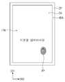
도 1을 참조하면, 본 발명의 실시 예에 따른 표시 장치(DD)는 제1 방향(DR1)으로 연장하는 장변들을 갖고, 제1 방향(DR1)과 교차하는 제2 방향(DR2)으로 연장하는 단변들을 갖는 직사각형 형상을 가질 수 있다. 그러나, 이에 한정되지 않고, 표시 장치(DD)는 원형 또는 다각형 등 다양한 형상들을 가질 수 있다.Referring to FIG. 1, a display device DD according to an exemplary embodiment has long sides extending in a first direction DR1 and extending in a second direction DR2 crossing the first direction DR1. It can have a rectangular shape with short sides. However, the present invention is not limited thereto, and the display device DD may have various shapes such as a circle or a polygon.
이하, 제1 방향(DR1) 및 제2 방향(DR2)에 의해 정의된 평면과 실질적으로 수직하게 교차하는 방향은 제3 방향(DR3)으로 정의된다.Hereinafter, a direction substantially perpendicular to the plane defined by the first and second directions DR1 and DR2 is defined as the third direction DR3.
표시 장치(DD)의 상면은 표시면(DS)으로 정의될 수 있으며, 제1 방향(DR1) 및 제2 방향(DR2)에 의해 정의된 평면을 가질 수 있다. 표시면(DS)을 통해 표시 장치(DD)에서 생성된 이미지들(IM)이 사용자에게 제공될 수 있다.The upper surface of the display device DD may be defined as the display surface DS, and may have a plane defined by a first direction DR1 and a second direction DR2. Images IM generated by the display device DD may be provided to the user through the display surface DS.
표시면(DS)은 표시 영역(DA) 및 표시 영역(DA) 주변의 비표시 영역(NDA)을 포함할 수 있다. 표시 영역(DA)은 영상을 표시하고, 비표시 영역(NDA)은 영상을 표시하지 않을 수 있다. 비표시 영역(NDA)은 표시 영역(DA)을 둘러싸고, 소정의 색으로 인쇄되는 표시 장치(DD)의 테두리를 정의할 수 있다.The display surface DS may include a display area DA and a non-display area NDA around the display area DA. The display area DA may display an image, and the non-display area NDA may not display an image. The non-display area NDA may surround the display area DA and may define a border of the display device DD printed in a predetermined color.
표시 장치(DD)는 텔레비젼, 모니터, 또는 외부 광고판과 같은 대형 전자 장치들에 사용될 수 있다. 또한, 표시 장치(DD)는 퍼스널 컴퓨터, 노트북 컴퓨터, 개인 디지털 단말기, 자동차 내비게이션, 게임기, 스마트폰, 태블릿, 또는 카메라와 같은 중소형 전자 장치들에 사용될 수도 있다. 그러나, 이것들은 단지 예시적인 실시예로서 제시된 것이며, 본 발명의 개념에서 벗어나지 않은 이상 다른 전자 기기들에도 사용될 수 있다.The display device DD may be used in large electronic devices such as a television, a monitor, or an external billboard. In addition, the display device DD may be used in small and medium-sized electronic devices such as a personal computer, a notebook computer, a personal digital terminal, a car navigation system, a game machine, a smart phone, a tablet, or a camera. However, these are presented only as exemplary embodiments, and may be used in other electronic devices without departing from the concept of the present invention.
도 2는 도 1에 도시된 표시 장치의 블록도이다.2 is a block diagram of the display device illustrated in FIG. 1.
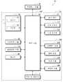
도 2를 참조하면, 본 발명의 실시 예에 따른 표시 장치(DD)는 표시 모듈(DM), 전원공급 모듈(PM), 제1 전자 모듈(EM1), 및 제2 전자 모듈(EM2)을 포함할 수 있다. 표시 모듈(DM), 전원공급 모듈(PM), 제1 전자 모듈(EM1), 및 제2 전자 모듈(EM2)은 서로 전기적으로 연결될 수 있다.Referring to FIG. 2, a display device DD according to an exemplary embodiment of the present invention includes a display module DM, a power supply module PM, a first electronic module EM1, and a second electronic module EM2. can do. The display module DM, the power supply module PM, the first electronic module EM1, and the second electronic module EM2 may be electrically connected to each other.
전원공급 모듈(PM)은 표시 장치(DD)의 전반적인 동작에 필요한 전원을 공급할 수 있다. 전원공급 모듈(PM)은 통상적인 배터리 모듈을 포함할 수 있다.The power supply module PM may supply power necessary for the overall operation of the display device DD. The power supply module PM may include a conventional battery module.
제1 전자 모듈(EM1) 및 제2 전자 모듈(EM2)은 표시 장치(DD)를 동작시키기 위한 다양한 기능성 모듈을 포함할 수 있다. 제1 전자 모듈(EM1)은 표시 모듈(DM)과 전기적으로 연결된 메인 보드에 직접 실장되거나 별도의 기판에 실장되어 커넥터(미 도시) 등을 통해 메인 보드에 전기적으로 연결될 수 있다.The first electronic module EM1 and the second electronic module EM2 may include various functional modules for operating the display device DD. The first electronic module EM1 may be directly mounted on a main board electrically connected to the display module DM, or may be mounted on a separate board and electrically connected to the main board through a connector (not shown).
제1 전자 모듈(EM1)은 제어 모듈(CM), 무선통신 모듈(TM), 영상입력 모듈(IIM), 음향입력 모듈(AIM), 메모리(MM), 및 외부 인터페이스(IF)를 포함할 수 있다. 상기 모듈들 중 일부는 메인보드에 실장되지 않고, 연성회로기판을 통해 메인보드에 전기적으로 연결될 수도 있다.The first electronic module EM1 may include a control module (CM), a wireless communication module (TM), an image input module (IIM), an acoustic input module (AIM), a memory (MM), and an external interface (IF). have. Some of the modules are not mounted on the main board, but may be electrically connected to the main board through a flexible circuit board.
제어 모듈(CM)은 표시 장치(DD)의 전반적인 동작을 제어할 수 있다. 제어 모듈(CM)은 표시 모듈(DM)을 활성화 시키거나, 비활성화 시킬 수 있다. 제어 모듈(CM)은 표시 모듈(DM)로부터 수신된 터치 신호에 근거하여 영상입력 모듈(IIM)이나 음향입력 모듈(AIM) 등의 다른 모듈들을 제어할 수 있다. 또한, 제어 모듈(CM)은 표시 모듈(DM)로부터 수신된 지문 정보를 이용하여 사용자 인증 모드를 구현할 수 있다.The control module CM may control the overall operation of the display device DD. The control module CM may activate or deactivate the display module DM. The control module CM may control other modules such as the image input module IIM or the sound input module AIM based on the touch signal received from the display module DM. Also, the control module CM may implement a user authentication mode by using the fingerprint information received from the display module DM.
무선통신 모듈(TM)은 블루투스 또는 와이파이 회선을 이용하여 다른 단말기와 무선 신호를 송/수신할 수 있다. 무선통신 모듈(TM)은 일반 통신회선을 이용하여 음성신호를 송/수신할 수 있다. 무선통신 모듈(TM)은 송신할 신호를 변조하여 송신하는 송신부(TM1)와, 수신되는 신호를 복조하는 수신부(TM2)를 포함할 수 있다.The wireless communication module TM may transmit/receive wireless signals to/from other terminals using a Bluetooth or Wi-Fi line. The wireless communication module TM can transmit/receive voice signals using a general communication line. The wireless communication module TM may include a transmitter TM1 that modulates and transmits a signal to be transmitted, and a receiver TM2 that demodulates a received signal.
영상입력 모듈(IIM)은 영상 신호를 처리하여 표시 모듈(DM)에 표시 가능한 영상 데이터로 변환할 수 있다. 음향입력 모듈(AIM)은 녹음 모드, 음성인식 모드 등에서 마이크로폰(Microphone)에 의해 외부의 음향 신호를 입력 받아 전기적인 음성 데이터로 변환할 수 있다.The image input module IIM may process the image signal and convert it into image data that can be displayed on the display module DM. The sound input module (AIM) may receive an external sound signal by a microphone in a recording mode, a voice recognition mode, etc. and convert it into electrical voice data.
외부 인터페이스(IF)는 외부 충전기, 유/무선 데이터 포트, 카드 소켓(예를 들어, 메모리 카드(Memory card), SIM/UIM card) 등에 연결되는 인터페이스 역할을 할 수 있다.The external interface IF may serve as an interface connected to an external charger, a wired/wireless data port, a card socket (eg, a memory card, a SIM/UIM card), or the like.
제2 전자 모듈(EM2)은 음향출력 모듈(AOM), 발광 모듈(LM), 수광 모듈(LRM), 및 카메라 모듈(CMM) 등을 포함할 수 있다. 상기 구성들은 메인 보드에 직접 실장되거나, 별도의 기판에 실장되어 커넥터(미 도시) 등을 통해 표시 모듈(DM)과 전기적으로 연결되거나, 제1 전자 모듈(EM1)과 전기적으로 연결될 수 있다.The second electronic module EM2 may include an acoustic output module (AOM), a light emitting module (LM), a light receiving module (LRM), a camera module (CMM), and the like. The components may be directly mounted on the main board, mounted on a separate board, and electrically connected to the display module DM through a connector (not shown) or the like, or electrically connected to the first electronic module EM1.
음향출력 모듈(AOM)은 무선통신 모듈(TM)로부터 수신된 음향 데이터 또는 메모리(MM)에 저장된 음향 데이터를 변환하여 외부로 출력할 수 있다. 발광 모듈(LM)은 광을 생성하여 출력할 수 있다. 발광 모듈(LM)은 적외선을 출력할 수 있다. 발광 모듈(LM)은 LED 소자를 포함할 수 있다. 수광 모듈(LRM)은 적외선을 감지할 수 있다. 수광 모듈(LRM)은 소정 레벨 이상의 적외선이 감지될 때 활성화될 수 있다. 수광 모듈(LRM)은 CMOS 센서를 포함할 수 있다.The sound output module AOM may convert sound data received from the wireless communication module TM or sound data stored in the memory MM to be output to the outside. The light emitting module LM may generate and output light. The light emitting module LM may output infrared rays. The light emitting module LM may include an LED device. The light receiving module LRM can detect infrared rays. The light-receiving module LRM may be activated when an infrared ray of a predetermined level or higher is sensed. The light receiving module LRM may include a CMOS sensor.
발광 모듈(LM)에서 생성된 적외선광이 출력된 후, 외부 물체(예컨대 사용자 손가락 또는 얼굴)에 의해 반사되고, 반사된 적외선광이 수광 모듈(LRM)에 입사될 수 있다. 카메라 모듈(CMM)은 외부의 이미지를 촬영할 수 있다.After the infrared light generated by the light emitting module LM is output, it is reflected by an external object (eg, a user's finger or face), and the reflected infrared light may be incident on the light receiving module LRM. The camera module CMM may take an external image.
표시 모듈(DM)은 표시 패널(DP), 입력 감지부(ISP), 및 지문 감지부(FSP)를 포함할 수 있다. 예시적으로 표시 패널(DP), 입력 감지부(ISP), 및 지문 감지부(FSP)가 도시되었으나, 표시 모듈(DM)은 윈도우를 더 포함할 수 있다.The display module DM may include a display panel DP, an input sensing unit ISP, and a fingerprint sensing unit FSP. For example, the display panel DP, the input detection unit ISP, and the fingerprint detection unit FSP are illustrated, but the display module DM may further include a window.
표시 패널(DP)은 제어 모듈(CM)로부터 제공된 영상 데이터를 이용하여 영상을 표시할 수 있다. 표시 패널(DP)은 제어 모듈(CM)의 제어에 의해 초기 모드 및 초기 모드 다음의 메인 모드로 구동될 수 있다.The display panel DP may display an image using image data provided from the control module CM. The display panel DP may be driven in an initial mode and a main mode following the initial mode under the control of the control module CM.
초기 모드는 사용자 인증 모드로 정의될 수 있다. 초기 모드에서 사용자로 인증되면, 제어 모듈(CM)은 표시 패널(DP)을 메인 모드로 구동할 수 있다. 메인 모드에서 표시 패널(DP)은 사용자가 원하는 다양한 영상들을 표시 할 수 있다. 사용자 인증 방식은 지문 인증, 비밀 번호 인증, 안면 인식 인증 등 다양한 방식으로 수행될 수 있다. 이하, 사용자 인증 방식으로서 지문 인증 방식이 설명될 것이다.The initial mode may be defined as a user authentication mode. When authenticated as a user in the initial mode, the control module CM may drive the display panel DP in the main mode. In the main mode, the display panel DP may display various images desired by a user. The user authentication method may be performed in various ways, such as fingerprint authentication, password authentication, and facial recognition authentication. Hereinafter, a fingerprint authentication method will be described as a user authentication method.
입력 감지부(ISP)는 외부의 입력(사용자의 손 또는 터치 펜 등)을 감지하고, 감지된 신호는 입력 신호로 변환되어 제어 모듈(CM)에 전송될 수 있다. 제어 모듈(CM)은 입력 감지부(ISP)의 입력 신호에 응답하여 표시 패널(DP) 및 지문 감지부(FSP)의 동작을 제어할 수 있다.The input sensing unit ISP may detect an external input (such as a user's hand or a touch pen), and the detected signal may be converted into an input signal and transmitted to the control module CM. The control module CM may control the operation of the display panel DP and the fingerprint detector FSP in response to an input signal from the input detector ISP.
입력 감지부(ISP)는 외부의 입력을 감지하기 위한 복수 개의 감지 전극들을 포함할 수 있다. 감지 전극들은 정전 용량 방식으로 외부의 입력을 감지할 수 있다. 입력 감지부(ISP)는 자기 감지 모드(self sensing mode) 또는 상호 감지 모드(mutual sensing mode)로 구동될 수 있다. 자기 감지 모드 또는 상호 감지 모드는 이하 상세히 설명될 것이다.The input sensing unit ISP may include a plurality of sensing electrodes for sensing an external input. The sensing electrodes can sense an external input in a capacitive manner. The input sensing unit ISP may be driven in a self sensing mode or a mutual sensing mode. The self-sensing mode or mutual sensing mode will be described in detail below.
지문 감지부(FSP)는 표시 패널(DP)이 초기 모드로 구동될 때, 표시 모듈(DM)에 입접하거나 표시 모듈(DM)에 터치되는 지문을 감지할 수 있다. 지문 감지부(FSP)에서 감지된 지문에 대한 정보는 제어 모듈(CM)로 전송될 수 있다.When the display panel DP is driven in the initial mode, the fingerprint detector FSP may detect a fingerprint that comes into contact with the display module DM or touches the display module DM. Information on the fingerprint detected by the fingerprint detection unit FSP may be transmitted to the control module CM.
제어 모듈(CM)은 감지된 지문 정보와 내부에 저장된 사용자 지문 정보를 비교할 수 있다. 감지된 지문 정보와 사용자 지문 정보가 일치할 경우, 제어 모듈(CM)은 표시 패널(DP)이 초기 모드에서 메인 모드로 전환되도록 표시 패널(DP)을 구동할 수 있다.The control module CM may compare the detected fingerprint information with the user fingerprint information stored therein. When the detected fingerprint information and the user fingerprint information match, the control module CM may drive the display panel DP such that the display panel DP is switched from the initial mode to the main mode.
도 3은 도 2에 도시된 표시 모듈의 분해 사시도이다.3 is an exploded perspective view of the display module shown in FIG. 2.
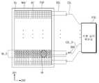
도 3을 참조하면, 표시 패널(DP) 상에 입력 감지부(ISP)가 배치되고, 입력 감지부(ISP) 상에 윈도우(WIN)가 배치될 수 있다. 표시 패널(DP) 아래에 지문 감지부(FSP)가 배치될 수 있다.Referring to FIG. 3, an input sensing unit ISP may be disposed on the display panel DP, and a window WIN may be disposed on the input sensing unit ISP. The fingerprint detector FSP may be disposed under the display panel DP.
본 발명의 일 실시예에 따른 표시 패널(DP)은 발광형 표시 패널일 수 있고, 특별히 제한되지 않는다. 예컨대, 표시 패널(DP)은 유기 발광 표시 패널 또는 퀀텀닷 발광 표시 패널일 수 있다. 유기 발광 표시 패널의 발광층은 유기 발광 물질을 포함할 수 있다. 퀀텀닷 발광 표시 패널의 발광층은 퀀텀닷, 및 퀀텀로드 등을 포함할 수 있다. 이하, 표시 패널(DP)은 유기 발광 표시 패널로 설명된다.The display panel DP according to an exemplary embodiment of the present invention may be an emissive display panel, and is not particularly limited. For example, the display panel DP may be an organic light emitting display panel or a quantum dot light emitting display panel. The emission layer of the organic light-emitting display panel may include an organic light-emitting material. The emission layer of the quantum dot light emitting display panel may include a quantum dot and a quantum rod. Hereinafter, the display panel DP will be described as an organic light emitting display panel.
윈도우(WIN)는 외부의 스크레치 및 충격으로부터 표시 패널(DP) 및 입력 감지부(ISP)를 보호할 수 있다. 윈도우(WIN)는 접착제에 의해 입력 감지부(ISP)에 부착될 수 있다. 접착제는 광학 투명 접착제(optical clear adhesive) 또는 감압 접착제(pressure sensitive adhesive) 등 다양한 접착제들을 포함할 수 있다. 표시 패널(DP)에서 생성된 영상은 윈도우(WIN)를 투과하여 사용자에게 제공될 수 있다.The window WIN may protect the display panel DP and the input detection unit ISP from external scratches and impacts. The window (WIN) may be attached to the input sensing unit (ISP) by an adhesive. The adhesive may include various adhesives such as optical clear adhesive or pressure sensitive adhesive. The image generated by the display panel DP may pass through the window WIN to be provided to the user.
입력 감지부(ISP)는 표시 모듈(DM)의 제조시, 표시 패널(DP) 상에 바로 제조될 수 있다. 그러나, 이에 한정되지 않고, 입력 감지부(ISP)는 표시 패널(DP)과는 별도의 입력 감지 패널로 제조되고, 접착제에 의해 표시 패널(DP)에 부착될 수 있다.When manufacturing the display module DM, the input sensing unit ISP may be directly manufactured on the display panel DP. However, the present invention is not limited thereto, and the input sensing unit ISP is manufactured as an input sensing panel separate from the display panel DP, and may be attached to the display panel DP by an adhesive.
지문 감지부(FSP)는 표시 패널(DP)의 하부 전체에 배치될 수 있다. 그러나, 이에 한정되지 않고, 지문 감지부(FSP)는 표시 패널(DP)의 소정의 부분의 하부에 배치될 수도 있다.The fingerprint detection unit FSP may be disposed on the entire lower portion of the display panel DP. However, the present invention is not limited thereto, and the fingerprint detection unit FSP may be disposed under a predetermined portion of the display panel DP.
도 4는 도 3에 도시된 표시 패널(DP)의 평면도이다.4 is a plan view of the display panel DP shown in FIG. 3.
도 4를 참조하면, 표시 장치(DD)는 표시 패널(DP), 주사 구동부(SDV)(scan driver), 데이터 구동부(DDV)(data driver), 및 발광 구동부(EDV)(emission driver)를 포함할 수 있다.Referring to FIG. 4, the display device DD includes a display panel DP, a scan driver SDV, a data driver DDV, and an emission driver EDV. can do.
표시 패널(DP)은 가요성 표시 패널일 수 있다. 예를 들어, 표시 패널(DP)은 가요성 기판 상에 배치된 복수 개의 전자 소자들을 포함할 수 있다. 표시 패널(DP)은 제1 방향(DR1)으로 연장하는 장변들 및 제2 방향(DR2)으로 연장하는 단변들을 갖는 직사각형의 형상을 가질 수 있다. 표시 패널(DP)은 표시 장치(DD)의 표시면(DS)과 같이 표시 영역(DA) 및 표시 영역(DA)을 둘러싸는 비표시 영역(NDA)을 포함할 수 있다.The display panel DP may be a flexible display panel. For example, the display panel DP may include a plurality of electronic devices disposed on a flexible substrate. The display panel DP may have a rectangular shape having long sides extending in the first direction DR1 and short sides extending in the second direction DR2. Like the display surface DS of the display device DD, the display panel DP may include a display area DA and a non-display area NDA surrounding the display area DA.
표시 패널(DP)은 복수 개의 화소들(PX), 복수 개의 주사 라인들(SL1~SLm), 복수 개의 데이터 라인들(DL1~DLn), 및 복수 개의 발광 라인들(EL1~ELm)을 포함할 수 있다. m 및 n은 자연수이다. 화소들(PX)은 표시 영역(DA)에 배치되고, 주사 라인들(SL1~SLm), 데이터 라인들(DL1~DLn), 및 발광 라인들(EL1~ELm)에 연결될 수 있다.The display panel DP may include a plurality of pixels PX, a plurality of scan lines SL1 to SLm, a plurality of data lines DL1 to DLn, and a plurality of emission lines EL1 to ELm. I can. m and n are natural numbers. The pixels PX are disposed in the display area DA, and may be connected to the scan lines SL1 to SLm, the data lines DL1 to DLn, and the emission lines EL1 to ELm.
주사 구동부(SDV), 데이터 구동부(DDV), 및 발광 구동부(EDV)는 비표시 영역(NDA)에 배치될 수 있다. 주사 구동부(SDV)는 표시 패널(DP)의 장변들 중 어느 한 장변에 인접한 비표시 영역(NDA)에 배치될 수 있다. 발광 구동부(EDV)는 표시 패널(DP)의 장변들 중 다른 장변에 인접한 비표시 영역(NDA)에 배치될 수 있다. 데이터 구동부(DDV)는 집적 회로 칩 형태로 제작되어 표시 패널(DP)의 단변들 중 어느 한 단변에 인접한 비표시 영역(NDA)에 배치될 수 있다.The scan driver SDV, the data driver DDV, and the light emission driver EDV may be disposed in the non-display area NDA. The scan driver SDV may be disposed in the non-display area NDA adjacent to any one of the long sides of the display panel DP. The light emitting driver EDV may be disposed in the non-display area NDA adjacent to the other long side of the long sides of the display panel DP. The data driver DDV may be manufactured in the form of an integrated circuit chip and may be disposed in the non-display area NDA adjacent to any one of short sides of the display panel DP.
주사 라인들(SL1~SLm)은 제2 방향(DR2)으로 연장되어 주사 구동부(SDV)에 연결될 수 있다. 데이터 라인들(DL1~DLn)은 제1 방향(DR1)으로 연장되어 데이터 구동부(DDV)에 연결될 수 있다. 발광 라인들(EL1~ELm)은 제2 방향(DR2)으로 연장되어 발광 구동부(EDV)에 연결될 수 있다.The scan lines SL1 to SLm may extend in the second direction DR2 to be connected to the scan driver SDV. The data lines DL1 to DLn may extend in the first direction DR1 and may be connected to the data driver DDV. The light-emitting lines EL1 to ELm may extend in the second direction DR2 to be connected to the light-emitting driver EDV.
주사 구동부(SDV)는 복수 개의 주사 신호들을 생성하고, 주사 신호들은 주사 라인들(SL1~SLm)을 통해 화소들(PX)에 인가될 수 있다. 주사 신호들은 순차적으로 화소들(PX)에 인가될 수 있다. 데이터 구동부(DDV)는 복수 개의 데이터 전압들을 생성하고, 데이터 전압들은 데이터 라인들(DL1~DLn)을 통해 화소들(PX)에 인가될 수 있다. 발광 구동부(EDV)는 복수 개의 발광 신호들을 생성하고, 발광 신호들은 발광 라인들(EL1~ELm)을 통해 화소들(PX)에 인가될 수 있다.The scan driver SDV may generate a plurality of scan signals, and the scan signals may be applied to the pixels PX through the scan lines SL1 to SLm. Scan signals may be sequentially applied to the pixels PX. The data driver DDV may generate a plurality of data voltages, and the data voltages may be applied to the pixels PX through the data lines DL1 to DLn. The light-emitting driver EDV may generate a plurality of light-emitting signals, and the light-emitting signals may be applied to the pixels PX through the light-emitting lines EL1 to ELm.
주사 구동부(SDV), 데이터 구동부(DDV), 및 발광 구동부(EDV)의 동작은 제어 모듈(CM)에 의해 제어될 수 있다. 표시 패널(DP)은 제어 모듈(CM)에 연결되고, 제어 모듈(CM)로부터 주사 구동부(SDV), 데이터 구동부(DDV), 및 발광 구동부(EDV)의 동작을 제어하기 위한 제어 신호들이 주사 구동부(SDV), 데이터 구동부(DDV), 및 발광 구동부(EDV)에 제공될 수 있다.Operations of the scan driver SDV, the data driver DDV, and the light emission driver EDV may be controlled by the control module CM. The display panel DP is connected to the control module CM, and control signals for controlling the operations of the scan driver SDV, the data driver DDV, and the light emitting driver EDV are received from the control module CM. It may be provided to the SDV, the data driver DDV, and the light emission driver EDV.
화소들(PX)은 주사 신호들에 응답하여 데이터 전압들을 제공받을 수 있다. 화소들(PX)은 발광 신호들에 응답하여 데이터 전압들에 대응하는 휘도의 광을 발광함으로써 영상을 표시할 수 있다. 화소들(PX)의 발광 시간은 발광 신호들에 의해 제어될 수 있다.The pixels PX may receive data voltages in response to scan signals. The pixels PX may display an image by emitting light having a luminance corresponding to the data voltages in response to the emission signals. The emission time of the pixels PX may be controlled by emission signals.
도 5는 도 4에 도시된 화소의 단면 구성을 개략적으로 도시한 도면이다.5 is a diagram schematically illustrating a cross-sectional configuration of the pixel shown in FIG. 4.
도 5를 참조하면, 화소(PX)는 유기 발광 소자(OLED) 및 유기 발광 소자(OLED)에 연결된 트랜지스터(TR)를 포함할 수 있다. 유기 발광 소자(OLED)는 제1 전극(E1), 제2 전극(E2), 및 제1 전극(E1)과 제2 전극(E2) 사이에 배치된 유기 발광층(OEL)을 포함할 수 있다.Referring to FIG. 5, the pixel PX may include an organic light-emitting device OLED and a transistor TR connected to the organic light-emitting device OLED. The organic light-emitting device OLED may include a first electrode E1, a second electrode E2, and an organic emission layer OEL disposed between the first electrode E1 and the second electrode E2.
화소(PX)는 화소 영역(PA) 및 화소 영역(PA) 주변의 비화소 영역(NPA)을 포함할 수 있다. 유기 발광 소자(OLED)는 화소 영역(PA)에 배치되고, 트랜지스터(TR)는 비화소 영역(NPA)에 배치될 수 있다. 트랜지스터(TR) 및 유기 발광 소자(OLED)는 기판(SUB) 상에 배치될 수 있다. 기판(SUB) 상에 버퍼층(BFL)이 배치되며, 버퍼층(BFL)은 무기 물질을 포함할 수 있다.The pixel PX may include a pixel area PA and a non-pixel area NPA around the pixel area PA. The organic light-emitting device OLED may be disposed in the pixel area PA, and the transistor TR may be disposed in the non-pixel area NPA. The transistor TR and the organic light emitting diode OLED may be disposed on the substrate SUB. The buffer layer BFL is disposed on the substrate SUB, and the buffer layer BFL may include an inorganic material.
버퍼층(BFL) 상에 트랜지스터(TR)의 반도체층(SM)이 배치될 수 있다. 반도체층(SM)은 비정질(Amorphous) 실리콘 또는 다결정질(Poly) 실리콘과 같은 무기 재료의 반도체나 유기 반도체를 포함할 수 있다. 또한, 반도체층(SM)은 산화물 반도체(oxide semiconductor)를 포함할 수 있다. 도 5에 도시되지 않았으나, 반도체층(SM)은 소스 영역, 드레인 영역, 및 소스 영역과 드레인 영역 사이의 채널 영역을 포함할 수 있다.The semiconductor layer SM of the transistor TR may be disposed on the buffer layer BFL. The semiconductor layer SM may include a semiconductor made of an inorganic material such as amorphous silicon or poly silicon, or an organic semiconductor. In addition, the semiconductor layer SM may include an oxide semiconductor. Although not shown in FIG. 5, the semiconductor layer SM may include a source region, a drain region, and a channel region between the source region and the drain region.
반도체층(SM)을 덮도록 버퍼층(BFL) 상에 제1 절연층(INS1)이 배치될 수 있다. 제1 절연층(INS1)은 무기 물질을 포함할 수 있다. 제1 절연층(INS1) 상에 반도체층(SM)과 중첩하는 트랜지스터(TR)의 게이트 전극(GE)이 배치될 수 있다. 게이트 전극(GE)은 반도체층(SM)의 채널 영역과 중첩되도록 배치될 수 있다.The first insulating layer INS1 may be disposed on the buffer layer BFL to cover the semiconductor layer SM. The first insulating layer INS1 may include an inorganic material. A gate electrode GE of the transistor TR overlapping the semiconductor layer SM may be disposed on the first insulating layer INS1. The gate electrode GE may be disposed to overlap the channel region of the semiconductor layer SM.
게이트 전극(GE)을 덮도록 제1 절연층(INS1) 상에 제2 절연층(INS2)이 배치될 수 있다. 제2 절연층(INS2)은 층간 절연층으로 정의될 수 있다. 제2 절연층(INS2)은 유기 물질 및/또는 무기 물질을 포함할 수 있다.A second insulating layer INS2 may be disposed on the first insulating layer INS1 to cover the gate electrode GE. The second insulating layer INS2 may be defined as an interlayer insulating layer. The second insulating layer INS2 may include an organic material and/or an inorganic material.
제2 절연층(INS2) 상에 트랜지스터(TR)의 소스 전극(SE) 및 드레인 전극(DE)이 서로 이격되어 배치될 수 있다. 소스 전극(SE)은 제1 절연층(INS1) 및 제2 절연층(INS2)을 관통하여 정의된 제1 컨택홀(CH1)을 통해 반도체층(SM)의 소스 영역에 연결될 수 있다. 드레인 전극(DE)은 제1 절연층(INS1) 및 제2 절연층(INS2)을 관통하여 정의된 제2 컨택홀(CH2)을 통해 반도체층(SM)의 드레인 영역에 연결될 수 있다.The source electrode SE and the drain electrode DE of the transistor TR may be disposed on the second insulating layer INS2 to be spaced apart from each other. The source electrode SE may be connected to the source region of the semiconductor layer SM through a first contact hole CH1 defined through the first insulating layer INS1 and the second insulating layer INS2. The drain electrode DE may be connected to the drain region of the semiconductor layer SM through a second contact hole CH2 defined through the first insulating layer INS1 and the second insulating layer INS2.
트랜지스터(TR)의 소스 전극(SE) 및 드레인 전극(DE)을 덮도록 제2 절연층(INS2) 상에 제3 절연층(INS3)이 배치될 수 있다. 제3 절연층(INS3)은 평평한 상면을 제공하는 평탄화막으로 정의될 수 있으며, 유기 물질을 포함할 수 있다.A third insulating layer INS3 may be disposed on the second insulating layer INS2 to cover the source electrode SE and the drain electrode DE of the transistor TR. The third insulating layer INS3 may be defined as a planarization layer providing a flat top surface, and may include an organic material.
제3 절연층(INS3) 상에 제1 전극(E1)이 배치될 수 있다. 제1 전극(E1)은 제3 절연층(INS3)을 관통하여 정의된 제3 컨택홀(CH3)을 통해 트랜지스터(TR)의 드레인 전극(DE)에 연결될 수 있다. 제1 전극(E1)은 화소 전극으로 정의될 수 있다. 제1 전극(E1)은 투명 전극 또는 반사형 전극을 포함할 수 있다.The first electrode E1 may be disposed on the third insulating layer INS3. The first electrode E1 may be connected to the drain electrode DE of the transistor TR through a third contact hole CH3 defined through the third insulating layer INS3. The first electrode E1 may be defined as a pixel electrode. The first electrode E1 may include a transparent electrode or a reflective electrode.
제1 전극(E1) 및 제3 절연층(INS3) 상에 제1 전극(E1)의 소정의 부분을 노출시키는 화소 정의막(PDL)이 배치될 수 있다. 화소 정의막(PDL)에는 제1 전극(E1)의 소정의 부분을 노출시키기 위한 개구부(PX_OP)가 정의될 수 있다.A pixel defining layer PDL exposing a predetermined portion of the first electrode E1 may be disposed on the first electrode E1 and the third insulating layer INS3. An opening PX_OP for exposing a predetermined portion of the first electrode E1 may be defined in the pixel defining layer PDL.
개구부(PX_OP) 내에서 제1 전극(E1) 상에 유기 발광층(OEL)이 배치될 수 있다. 유기 발광층(OEL)은 적색, 녹색, 및 청색 중 어느 하나의 광을 생성할 수 있다. 그러나 이에 한정되지 않고, 유기 발광층(OEL)은 적색, 녹색, 및 청색을 생성하는 유기 물질들의 조합에 의해 백색광을 생성할 수도 있다.The organic emission layer OEL may be disposed on the first electrode E1 in the opening PX_OP. The organic emission layer OEL may generate any one of red, green, and blue light. However, the present invention is not limited thereto, and the organic emission layer OEL may generate white light by a combination of organic materials that generate red, green, and blue colors.
화소 정의막(PDL) 및 유기 발광층(OEL) 상에 제2 전극(E2)이 배치될 수 있다. 제2 전극(E2)은 공통 전극으로 정의될 수 있다. 제2 전극(E2)은 투명 전극 또는 반사형 전극을 포함할 수 있다.The second electrode E2 may be disposed on the pixel defining layer PDL and the organic emission layer OEL. The second electrode E2 may be defined as a common electrode. The second electrode E2 may include a transparent electrode or a reflective electrode.
박막 봉지층(TFE)은 유기 발광 소자(OLED)를 덮도록 제2 전극(E2) 상에 배치될 수 있다. 박막 봉지층(TFE)은 제2 전극(E2) 상에 배치된 제1 봉지층(EN1), 제1 봉지층(EN1) 상에 배치된 제2 봉지층(EN2), 및 제2 봉지층(EN2) 상에 배치된 제3 봉지층(EN3)을 포함할 수 있다.The thin film encapsulation layer TFE may be disposed on the second electrode E2 to cover the organic light emitting diode OLED. The thin film encapsulation layer TFE includes a first encapsulation layer EN1 disposed on the second electrode E2, a second encapsulation layer EN2 disposed on the first encapsulation layer EN1, and a second encapsulation layer ( A third encapsulation layer EN3 disposed on EN2) may be included.
제1 및 제3 봉지층들(EN1, EN3) 각각은 무기 물질을 포함할 수 있고, 제2 봉지층(EN2)은 유기 물질을 포함할 수 있다. 제2 봉지층(EN2)의 두께는 제1 및 제3 봉지층들(EN1, EN3) 각각의 두께보다 클 수 있다.Each of the first and third encapsulation layers EN1 and EN3 may include an inorganic material, and the second encapsulation layer EN2 may include an organic material. The thickness of the second encapsulation layer EN2 may be greater than the thickness of each of the first and third encapsulation layers EN1 and EN3.
제1 전압(ELVDD)이 제1 전극(E1)에 인가되고, 제2 전압(ELVSS)이 제2 전극(E2)에 인가될 수 있다. 유기 발광층(OEL)에 주입된 정공과 전자가 결합하여 여기자(exciton)가 형성되고, 여기자가 바닥 상태로 전이하면서 유기 발광 소자(OLED)가 발광될 수 있다. 유기 발광 소자(OLED)가 전류의 흐름에 따라 적색, 녹색, 및 청색의 빛을 발광함으로써, 영상이 표시될 수 있다.The first voltage ELVDD may be applied to the first electrode E1 and the second voltage ELVSS may be applied to the second electrode E2. Holes and electrons injected into the organic emission layer OEL are combined to form excitons, and the organic light emitting device OLED may emit light while the excitons transition to a ground state. The organic light-emitting device OLED emits red, green, and blue light according to the flow of current, so that an image may be displayed.
도 6은 도 3에 도시된 입력 감지부의 평면 구성을 보여주는 도면이다.6 is a diagram illustrating a plan configuration of an input sensing unit shown in FIG. 3.
도 6을 참조하면, 입력 감지부(ISP)는 복수 개의 감지 전극들(SE1,SE2), 복수 개의 배선들(SL1,SL2), 및 복수 개의 패드들(PD)을 포함할 수 있다. 감지 전극들(SE1,SE2), 배선들(SL1,SL2), 및 패드들(PD)은 박막 봉지층(TFE) 상에 배치될 수 있다.Referring to FIG. 6, the input sensing unit ISP may include a plurality of sensing electrodes SE1 and SE2, a plurality of wires SL1 and SL2, and a plurality of pads PD. The sensing electrodes SE1 and SE2, the wirings SL1 and SL2, and the pads PD may be disposed on the thin film encapsulation layer TFE.
입력 감지부(ISP)는 활성 영역(AA) 및 활성 영역(AA)을 둘러싸는 비활성 영역(NAA)을 포함할 수 있다. 활성 영역(AA)은 표시 영역(DA)에 중첩하고 비활성 영역(NAA)은 비표시 영역(NDA)에 중첩할 수 있다. 감지 전극들(SE1,SE2)은 활성 영역(AA)에 배치되고, 패드들(PD)은 비활성 영역(NAA)에 배치될 수 있다. 배선들(SL1,SL2)은 감지 전극들(SE1,SE2)에 연결되고, 비활성 영역(NAA)으로 연장하여 패드들(PD)에 연결될 수 있다.The input sensing unit ISP may include an active area AA and an inactive area NAA surrounding the active area AA. The active area AA may overlap the display area DA, and the non-active area NAA may overlap the non-display area NDA. The sensing electrodes SE1 and SE2 may be disposed in the active area AA, and the pads PD may be disposed in the non-active area NAA. The wirings SL1 and SL2 may be connected to the sensing electrodes SE1 and SE2 and may extend to the non-active area NAA to be connected to the pads PD.
감지 전극들(SE1,SE2)은 제2 방향(DR2)으로 연장하여 제1 방향(DR1)으로 배열된 복수 개의 제1 감지 전극들(SE1) 및 제1 방향(DR1)으로 연장하여 제2 방향(DR2)으로 배열된 복수 개의 제2 감지 전극들(SE2)을 포함할 수 있다. 배선들(SL1,SL2)은 제1 감지 전극들(SE1)에 연결된 복수 개의 제1 신호 배선들(SL1) 및 제2 감지 전극들(SE2)에 연결된 복수 개의 제2 신호 배선들(SL2)을 포함할 수 있다.The sensing electrodes SE1 and SE2 extend in the second direction DR2 and extend in the second direction by extending the plurality of first sensing electrodes SE1 arranged in the first direction DR1 and in the first direction DR1. A plurality of second sensing electrodes SE2 arranged in DR2 may be included. The wires SL1 and SL2 include a plurality of first signal wires SL1 connected to the first sensing electrodes SE1 and a plurality of second signal wires SL2 connected to the second sensing electrodes SE2. Can include.
제2 감지 전극들(SE2)은 제1 감지 전극들(SE1)과 서로 절연되어 교차하도록 연장할 수 있다. 제1 감지 전극들(SE1)은 입력 감지 전극들로 정의되고, 제2 감지 전극들(SE2)은 출력 감지 전극들로 정의될 수 있다. The second sensing electrodes SE2 may be insulated from the first sensing electrodes SE1 and extend to cross each other. The first sensing electrodes SE1 may be defined as input sensing electrodes, and the second sensing electrodes SE2 may be defined as output sensing electrodes.
제1 감지 전극들(SE1)과 제2 감지 전극들(SE2)에 의해 정전용량들이 형성될 수 있다. 제1 및 제2 감지 전극들(SE1,SE2)이 배치된 위치는 X 및 Y 좌표로 구분될 수 있다. 제1 감지 전극들(SE1)은 X 좌표를 나타내고, 제2 감지 전극들(SE2)은 Y 좌표를 나타낼 수 있다.Capacities may be formed by the first sensing electrodes SE1 and the second sensing electrodes SE2. The positions where the first and second sensing electrodes SE1 and SE2 are disposed may be divided into X and Y coordinates. The first sensing electrodes SE1 may indicate the X coordinate, and the second sensing electrodes SE2 may indicate the Y coordinate.
입력 감지부(ISP)는 제어 모듈(CM)에 연결되고, 제어 모듈(CM)의 제어에 의해 구동될 수 있다. 제어 모듈(CM)이 입력 감지부(ISP)를 자기 감지 모드로 구동시킬 때, 제어 모듈(CM)은 제1 감지 전극들(SE1) 각각을 구동 전극 및 센싱 전극으로 동작시킬 수 있다. 예를 들어, 제어 모듈(CM)은 제1 신호 배선들(SL1)을 통해 제1 감지 전극들(SE1) 각각에 구동 신호를 인가하여 제1 감지 전극들(SE1) 각각으로부터 센싱 신호를 수신할 수 있다.The input sensing unit ISP is connected to the control module CM and may be driven by the control of the control module CM. When the control module CM drives the input sensing unit ISP in the self-sensing mode, the control module CM may operate each of the first sensing electrodes SE1 as a driving electrode and a sensing electrode. For example, the control module CM may receive a sensing signal from each of the first sensing electrodes SE1 by applying a driving signal to each of the first sensing electrodes SE1 through the first signal lines SL1. I can.
제어 모듈(CM)이 입력 감지부(ISP)를 상호 감지 모드로 구동시킬 때, 제어 모듈(CM)은 제1 감지 전극들(SE1) 각각을 구동 전극으로 동작시키고 제2 감지 전극들(SE2) 각각을 센싱 전극으로 동작시킬 수 있다. 예를 들어, 제어 모듈(CM)은 제1 신호 배선들(SL1)을 통해 제1 감지 전극들(SE1) 각각에 구동 신호를 인가하고, 제2 신호 배선들(SL2)을 통해 제2 감지 전극들(SE1) 각각으로부터 센싱 신호를 수신할 수 있다.When the control module CM drives the input sensing unit ISP in the mutual sensing mode, the control module CM operates each of the first sensing electrodes SE1 as a driving electrode and the second sensing electrodes SE2 Each can be operated as a sensing electrode. For example, the control module CM applies a driving signal to each of the first sensing electrodes SE1 through the first signal wires SL1, and the second sensing electrode through the second signal wires SL2. A sensing signal may be received from each of the SE1.
자기 감지 모드에서 제1 감지 전극들(SE1)이 사용되고, 상호 감지 모드에서 제1 및 제2 감지 전극들(SE1,SE2)이 사용될 수 있다. 따라서, 입력 감지부(ISP)가 상호 감지 모드보다 자기 감지 모드로 구동될 때, 입력 감지부(ISP)의 전력 소모가 보다 감소될 수 있다.The first sensing electrodes SE1 may be used in the self-sensing mode, and the first and second sensing electrodes SE1 and SE2 may be used in the mutual sensing mode. Accordingly, when the input sensing unit ISP is driven in the self-sensing mode rather than the mutual sensing mode, power consumption of the input sensing unit ISP may be further reduced.
제1 감지 전극들(SE1) 각각은 제2 방향(DR2)으로 배열된 복수 개의 제1 센서부들(SP1) 및 제1 센서부들(SP1)을 연결하는 복수 개의 제1 연결부들(CP1)을 포함할 수 있다. 제1 센서부들(SP1)은 마름모 형상을 가질 수 있으나, 제1 센서부들(SP1)의 형상은 이에 한정되지 않는다. 제1 연결부들(CP1) 각각은 서로 인접한 2개의 제1 센서부들(SP1) 사이에 배치되어 2 개의 제1 센서부들(SP1)을 전기적으로 연결할 수 있다.Each of the first sensing electrodes SE1 includes a plurality of first sensor units SP1 arranged in a second direction DR2 and a plurality of first connection units CP1 connecting the first sensor units SP1 can do. The first sensor units SP1 may have a rhombus shape, but the shape of the first sensor units SP1 is not limited thereto. Each of the first connection units CP1 may be disposed between the two first sensor units SP1 adjacent to each other to electrically connect the two first sensor units SP1.
제2 감지 전극들(SE2) 각각은 제1 방향(DR1)으로 배열된 복수 개의 제2 센서부들(SP2) 및 제2 센서부들(SP2)을 연결하는 복수 개의 제2 연결부들(CP2)을 포함할 수 있다. 제2 센서부들(SP2)은 마름모 형상을 가질 수 있으나, 제2 센서부들(SP2)의 형상은 이에 한정되지 않는다. 제2 연결부들(CP2) 각각은 서로 인접한 2개의 제2 센서부들(SP2) 사이에 배치되어 2 개의 제2 센서부들(SP2)을 전기적으로 연결할 수 있다.Each of the second sensing electrodes SE2 includes a plurality of second sensor units SP2 arranged in a first direction DR1 and a plurality of second connection units CP2 connecting the second sensor units SP2. can do. The second sensor units SP2 may have a rhombus shape, but the shape of the second sensor units SP2 is not limited thereto. Each of the second connection units CP2 may be disposed between the two second sensor units SP2 adjacent to each other to electrically connect the two second sensor units SP2.
제1 센서부들(SP1) 및 제2 센서부들(SP2)은 서로 중첩하지 않고 서로 이격되어, 서로 교호적으로 배치될 수 있다. 제2 연결부들(CP2)은 제1 연결부들(CP1)과 서로 절연되어 교차하도록 연장할 수 있다.The first sensor units SP1 and the second sensor units SP2 are spaced apart from each other without overlapping each other, and may be alternately disposed with each other. The second connection parts CP2 may be insulated from the first connection parts CP1 and extend to cross each other.
제1 및 제2 센서부들(SP1,SP2) 및 제1 연결부들(CP1)은 동일층에 배치될 수 있다. 제2 연결부들(CP2)은 제1 및 제2 센서부들(SP1,SP2) 및 제1 연결부들(CP1)과 다른 층에 배치될 수 있다.The first and second sensor units SP1 and SP2 and the first connection units CP1 may be disposed on the same layer. The second connection parts CP2 may be disposed on a different layer from the first and second sensor parts SP1 and SP2 and the first connection parts CP1.
도 7은 도 6에 도시된 제1 및 제2 센서부들의 구성을 보여주기 위한 도면이다. 도 8은 도 7에 도시된 I-I'선의 단면도이다.FIG. 7 is a diagram illustrating a configuration of first and second sensor units shown in FIG. 6. FIG. 8 is a cross-sectional view taken along line II' shown in FIG. 7.
예시적으로 도 7에는 서로 인접한 2개의 제1 센서부들(SP1) 및 서로 인접한 2개의 제2 센서부들(SP2)이 도시되었다.For example, in FIG. 7, two first sensor units SP1 adjacent to each other and two second sensor units SP2 adjacent to each other are illustrated.
도 7을 참조하면, 제1 및 제2 센서부들(SP1,SP2)은 메쉬 형상을 가질 수 있다. 예를 들어 제1 및 제2 센서부들(SP1,SP2) 각각은 제1 대각 방향(DDR1)으로 연장된 복수 개의 제1 가지부들(BP1) 및 제2 대각 방향(DDR2)으로 연장된 복수 개의 제2 가지부들(BP2)을 포함할 수 있다.Referring to FIG. 7, the first and second sensor units SP1 and SP2 may have a mesh shape. For example, each of the first and second sensor units SP1 and SP2 includes a plurality of first branch portions BP1 extending in a first diagonal direction DDR1 and a plurality of second sensor units extending in a second diagonal direction DDR2. It may include two branches BP2.
제1 대각 방향(DDR1)은 제1 및 제2 방향들(DR1,DR2)에 의해 정의된 평면 상에서 제1 및 제2 방향들(DR1,DR2)과 교차하는 방향으로 정의될 수 있다. 제2 대각 방향(DDR2)은 제1 및 제2 방향들(DR1,DR2)에 의해 정의된 평면 상에서 제1 대각 방향(DDR1)에 교차하는 방향으로 정의될 수 있다. 예시적으로, 제1 방향(DR1) 및 제2 방향(DR2)은 서로 수직하게 교차하고, 제1 대각 방향(DDR1) 및 제2 대각 방향(DDR2)은 서로 수직하게 교차할 수 있다.The first diagonal direction DDR1 may be defined as a direction intersecting the first and second directions DR1 and DR2 on a plane defined by the first and second directions DR1 and DR2. The second diagonal direction DDR2 may be defined as a direction crossing the first diagonal direction DDR1 on a plane defined by the first and second directions DR1 and DR2. For example, the first direction DR1 and the second direction DR2 may perpendicularly cross each other, and the first diagonal direction DDR1 and the second diagonal direction DDR2 may perpendicularly cross each other.
제1 및 제2 센서부들(SP1,SP2) 각각의 제1 가지부들(BP1)은 제2 가지부들(BP2)과 교차하고 서로 일체로 형성될 수 있다. 서로 교차하는 제1 가지부들(BP1) 및 제2 가지부들(BP2)에 의해 마름모 형상의 개구부들(TOP)이 정의될 수 있다. 제1 및 제2 가지부들(BP1,BP2)은 메쉬선들로 정의될 수 있으며, 메쉬선들 각각의 선폭은 수 마이크로미터일 수 있다.The first branch parts BP1 of each of the first and second sensor parts SP1 and SP2 may cross the second branch parts BP2 and are integrally formed with each other. The openings TOP having a rhombus shape may be defined by the first branch portions BP1 and the second branch portions BP2 intersecting each other. The first and second branch portions BP1 and BP2 may be defined as mesh lines, and a line width of each of the mesh lines may be several micrometers.
화소 영역(PA)은 마름모 형상을 갖고 개구부들(TOP)에 중첩하도록 배치 수 있다. 제1 및 제2 가지부들(BP1,BP2)은 비화소 영역(NPA)에 중첩하도록 배치될 수 있다. 화소 영역들(PA)은 발광 영역들로 정의되고 비화소 영역(NPA)은 비발광 영역으로 정의될 수 있다. 제1 및 제2 센서부들(SP1,SP2)이 비화소 영역(NPA)에 배치되므로, 화소 영역들(PA)에서 생성된 광은 제1 및 제2 센서부들(SP1,SP2)의 영향을 받지 않고 정상적으로 출광될 수 있다.The pixel area PA may have a rhombus shape and may be disposed to overlap the openings TOP. The first and second branch portions BP1 and BP2 may be disposed to overlap the non-pixel area NPA. The pixel areas PA may be defined as emission areas, and the non-pixel area NPA may be defined as a non-emission area. Since the first and second sensor units SP1 and SP2 are disposed in the non-pixel area NPA, light generated in the pixel areas PA is not affected by the first and second sensor units SP1 and SP2. It can be normally emitted without.
제1 센서부들(SP1)은 제1 연결부(CP1)에 의해 연결될 수 있다. 실질적으로, 제1 센서부들(SP1)과 제1 연결부(CP1)는 일체로 형성될 수 있다. 제1 연결부(CP1)는 메쉬 형상을 갖고, 제1 센서부들(SP1)로부터 연장될 수 있다.The first sensor units SP1 may be connected by the first connection unit CP1. Substantially, the first sensor parts SP1 and the first connection part CP1 may be integrally formed. The first connection part CP1 has a mesh shape and may extend from the first sensor parts SP1.
제2 센서부들(SP2)은 제2 연결부(CP2)에 의해 서로 전기적으로 연결될 수 있다. 제2 연결부(CP2)는 제2 센서부들(SP2)과 일체로 형성되지 않을 수 있다. 제2 연결부(CP2)는 복수 개의 컨택홀들(TS-CH)을 통해 제2 센서부들(SP2)에 연결될 수 있다.The second sensor units SP2 may be electrically connected to each other by the second connection unit CP2. The second connection part CP2 may not be integrally formed with the second sensor parts SP2. The second connection part CP2 may be connected to the second sensor parts SP2 through a plurality of contact holes TS-CH.
도 8을 참조하면, 박막 봉지층(TFE) 상에 제2 연결부(CP2)가 배치될 수 있다. 제2 연결부(CP2)를 덮도록 박막 봉지층(TFE) 상에 제1 절연층(TS-IL1)이 배치될 수 있다. 제1 절연층(TS-IL1) 상에 제1 연결부(CP1) 및 제2 센서부들(SP2)이 배치될 수 있다. 제1 연결부(CP1)와 일체로 형성된 제1 센서부들(SP1) 역시 제1 절연층(TS-IL1) 상에 배치될 수 있다. 제1 연결부(CP1) 및 제2 센서부들(SP2)을 덮도록 제1 절연층(TS-IL1) 상에 제2 절연층(TS-IL2)이 배치될 수 있다.Referring to FIG. 8, a second connection part CP2 may be disposed on the thin film encapsulation layer TFE. A first insulating layer TS-IL1 may be disposed on the thin film encapsulation layer TFE to cover the second connection part CP2. The first connection part CP1 and the second sensor parts SP2 may be disposed on the first insulating layer TS-IL1. The first sensor units SP1 integrally formed with the first connection unit CP1 may also be disposed on the first insulating layer TS-IL1. A second insulating layer TS-IL2 may be disposed on the first insulating layer TS-IL1 to cover the first connection part CP1 and the second sensor parts SP2.
제2 연결부(CP2)는 제1 절연층(TS-IL1)에 정의된 복수 개의 컨택홀들(TS-CH)을 통해 제2 센서부들(SP2)에 연결될 수 있다. 제2 연결부(CP2)의 양측들이 컨택홀들(TS-CH)을 통해 제2 센서부들(SP2)에 연결될 수 있다.The second connection part CP2 may be connected to the second sensor parts SP2 through a plurality of contact holes TS-CH defined in the first insulating layer TS-IL1. Both sides of the second connection part CP2 may be connected to the second sensor parts SP2 through contact holes TS-CH.
도시하지 않았으나, 박막 봉지층(TFE) 상에 추가적으로 절연층이 더 배치되고, 절연층 상에 입력 감지부(ISP)가 배치될 수도 있다.Although not shown, an insulating layer may be additionally disposed on the thin film encapsulation layer TFE, and the input sensing unit ISP may be disposed on the insulating layer.
도 9는 도 2에 도시된 제어 모듈의 블록도를 도시한 도면이다. 도 10은 표시 모듈에 터치된 손가락을 도시한 도면이다. 도 11은 도 10에 도시된 표시 패널의 평면에서 손가락의 지문이 터치된 부분을 도시한 도면이다. 도 12는 지문 감지부의 평면도에서 도 11에 도시된 지문의 위치를 도시한 도면이다.9 is a diagram illustrating a block diagram of the control module shown in FIG. 2. 10 is a diagram illustrating a finger touched on a display module. FIG. 11 is a diagram illustrating a portion of the display panel shown in FIG. 10 touched by a fingerprint of a finger. 12 is a diagram illustrating a location of a fingerprint shown in FIG. 11 in a plan view of a fingerprint sensor.
도 9, 도 10, 및 도 11을 참조하면, 제어 모듈(CM)은 표시 패널(DP), 입력 감지부(ISP), 및 지문 감지부(FSP)의 동작을 제어할 수 있다. 제어 모듈(CM)은 표시 패널(DP)을 초기 모드(ITM)로 구동 시킬 때, 입력 감지부(ISP)를 자기 감지 모드로 구동시킬 수 있다.9, 10, and 11, the control module CM may control operations of the display panel DP, the input detector ISP, and the fingerprint detector FSP. When driving the display panel DP in the initial mode ITM, the control module CM may drive the input sensing unit ISP in the self-sensing mode.
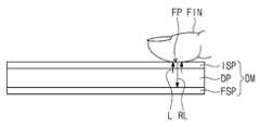
도 10 및 도 11을 참조하면, 입력 감지부(ISP)에 손가락(FIN)이 터치될 때, 입력 감지부(ISP)는 손가락(FIN)의 지문(FP)의 터치를 감지할 수 있다. 자기 감지 모드는 상호 감지 모드보다 높은 터치 감도를 가질 수 있다. 자기 감지 모드에서 손가락(FIN)의 지문(FP)이 입력 감지부(ISP)에 터치될 때, 지문(FP)의 터치가 감지될 수 있으나, 이에 한정되지 않고, 지문(FP)이 입력 감지부(ISP)에 접촉하지 않고 입력 감지부(ISP)에 인접할 때도 지문(FP)의 터치가 감지될 수 있다.Referring to FIGS. 10 and 11, when the finger FIN is touched by the input detection unit ISP, the input detection unit ISP may detect the touch of the fingerprint FP of the finger FIN. The self-sensing mode may have a higher touch sensitivity than the mutual sensing mode. When the fingerprint FP of the finger FIN touches the input detection unit ISP in the self-sensing mode, the touch of the fingerprint FP may be sensed, but the present invention is not limited thereto, and the fingerprint FP is the input detection unit. A touch of the fingerprint FP may be sensed even when it is not in contact with the (ISP) and is adjacent to the input sensing unit ISP.
제어 모듈(CM)은 입력 감지부(ISP)가 지문(FP)의 터치를 감지할 때, 지문 감지부(FSP)를 활성화시킬 수 있다. 활성화된 지문 감지부(FSP)는 지문(FP)을 감지할 수 있다. 예를 들어, 표시 패널(DP)에서 생성된 광(L)이 지문(FP)에 제공되고, 지문(FP)에서 반사된 광(RL)이 지문 감지부(FSP)에 제공될 수 있다. 지문 감지부(FSP)는 반사된 광(RL)을 이용하여 지문(FP)을 감지하고, 감지된 지문 정보를 제어 모듈(CM)에 제공할 수 있다.The control module CM may activate the fingerprint detection unit FSP when the input detection unit ISP detects a touch of the fingerprint FP. The activated fingerprint detection unit FSP may detect the fingerprint FP. For example, light L generated by the display panel DP may be provided to the fingerprint FP, and light RL reflected from the fingerprint FP may be provided to the fingerprint detector FSP. The fingerprint detector FSP may detect the fingerprint FP using the reflected light RL, and may provide the detected fingerprint information to the control module CM.
입력 감지부(ISP)가 지문(FP)의 터치를 감지함으로써, 지문(FP)의 터치 위치가 감지될 수 있다. 예를 들어 제어 모듈(CM)은 입력 감지부(ISP)로부터 제공받은 지문(FP)의 터치 정보에 따라 터치된 지문(FP)의 위치를 산출할 수 있다. 제어 모듈(CM)은 지문(FP)의 위치 정보에 기초하여, 지문(FP)에 중첩하는 지문 감지부(FSP)의 부분을 구동시킬 수 있다. 이러한 동작은 이하 도 12를 참조하여 상세히 설명될 것이다.By sensing the touch of the fingerprint FP by the input sensing unit ISP, the touch position of the fingerprint FP may be detected. For example, the control module CM may calculate the location of the touched fingerprint FP according to the touch information of the fingerprint FP provided from the input detection unit ISP. The control module CM may drive a portion of the fingerprint sensing unit FSP overlapping the fingerprint FP based on the location information of the fingerprint FP. This operation will be described in detail below with reference to FIG. 12.
제어 모듈(CM)은 지문 감지부(FSP)에서 감지된 지문 정보가 사용자의 지문 정보와 일치할 때, 표시 패널(DP)을 초기 모드(ITM)에서 메인 모드로 구동시키고, 입력 감지부(ISP)를 상호 감지 모드로 구동시킬 수 있다. 메인 모드는 실질적으로, 도 1에 도시된 바와 같이 표시면(DS)에 다양한 이미지들(IM)이 표시된 상태를 가리킬 수 있다.When the fingerprint information detected by the fingerprint detection unit (FSP) matches the user's fingerprint information, the control module CM drives the display panel DP from the initial mode (ITM) to the main mode, and operates the input detection unit (ISP). ) Can be driven in mutual sensing mode. The main mode may substantially indicate a state in which various images IM are displayed on the display surface DS as illustrated in FIG. 1.
광을 이용하여 지문(FP)을 감지하기 위해 지문 감지부(FSP)는 복수 개의 광 센서들을 포함할 수 있다. 광 센서들 각각은 포토 다이오드를 포함할 수 있다. 예시적으로, 광을 이용한 지문 감지부(FSP)가 설명되었으나, 이에 한정되지 않고, 지문 감지부(FSP)는 초음파를 이용하여 지문(FP)을 감지하기 위해 초음파 센서들을 포함할 수 있다.In order to detect the fingerprint FP using light, the fingerprint detection unit FSP may include a plurality of optical sensors. Each of the optical sensors may include a photodiode. As an example, although the fingerprint detection unit FSP using light has been described, the present invention is not limited thereto, and the fingerprint detection unit FSP may include ultrasonic sensors to detect the fingerprint FP using ultrasonic waves.
도 11을 참조하면, 지문 감지부(FSP)가 표시 패널(DP)의 하부 전체에 배치되므로, 지문(FP)은 표시 영역(DA)의 다양한 위치에서 감지될 수 있다. 예를 들어, 도 11에서 표시 영역(DA)의 우측 하단에 터치된 지문(FP)이 감지되었으나, 표시 영역(DA)의 다른 위치에서 지문(FP)이 터치될 때도 지문(FP)이 감지될 수 있다.Referring to FIG. 11, since the fingerprint detection unit FSP is disposed on the entire lower portion of the display panel DP, the fingerprint FP may be detected at various locations of the display area DA. For example, in FIG. 11, the fingerprint FP touched on the lower right of the display area DA is detected, but the fingerprint FP is also detected when the fingerprint FP is touched at another location of the display area DA. I can.
도 9를 참조하면, 전술한 동작을 위해 제어 모듈(CM)은 메인 제어부(MC), 표시 패널(DP)의 동작을 제어하는 표시 패널 제어부(DPC), 입력 감지부(ISP)의 동작을 제어하는 입력 감지 제어부(ISC), 및 지문 감지부(FSP)의 동작을 제어하는 지문 감지 제어부(FSC)를 포함할 수 있다.Referring to FIG. 9, for the above-described operation, the control module CM controls the operation of the main control unit MC, the display panel control unit DPC that controls the operation of the display panel DP, and the input detection unit ISP. It may include an input detection control unit (ISC) and a fingerprint detection control unit (FSC) for controlling the operation of the fingerprint detection unit (FSP).
표시 장치(DD)가 전원을 공급받아 턴 온될 때, 메인 제어부(MC)가 턴 온될 수 있다. 턴 온된 메인 제어부(MC)는 표시 패널 제어부(DPC), 입력 감지 제어부(ISC), 및 지문 감지 제어부(FSC)의 동작들을 제어할 수 있다. 메인 제어부(MC)는 표시 패널 제어부(DPC), 입력 감지 제어부(ISC), 및 지문 감지 제어부(FSC)의 동작들을 제어하기 위한 제1 내지 제5 제어 신호들(CS1~CS5)을 출력할 수 있다.When the display device DD is turned on by receiving power, the main controller MC may be turned on. The turned-on main control unit MC may control operations of the display panel control unit DPC, the input detection control unit ISC, and the fingerprint detection control unit FSC. The main control unit MC may output first to fifth control signals CS1 to CS5 for controlling operations of the display panel control unit DPC, the input detection control unit ISC, and the fingerprint detection control unit FSC. have.
표시 패널 제어부(DPC)는 메인 제어부(MC)부터 수신된 제1 제어 신호(CS1)에 응답하여 표시 패널(DP)을 초기 모드(ITM)로 구동시킬 수 있다. 표시 패널 제어부(DPC)는 메인 제어부(MC)부터 수신된 제2 제어 신호(CS2)에 응답하여 표시 패널(DP)을 메인 모드로 구동시킬 수 있다.The display panel controller DPC may drive the display panel DP in the initial mode ITM in response to the first control signal CS1 received from the main controller MC. The display panel controller DPC may drive the display panel DP in the main mode in response to the second control signal CS2 received from the main controller MC.
입력 감지 제어부(ISC)는 메인 제어부(MC)로부터 수신된 제3 제어 신호(CS3)에 응답하여 입력 감지부(ISP)를 자기 감지 모드로 구동시킬 수 있다. 입력 감지 제어부(ISC)는 메인 제어부(MC)로부터 수신된 제4 제어 신호(CS4)에 응답하여 입력 감지부(ISP)를 상호 감지 모드로 구동시킬 수 있다.The input detection control unit ISC may drive the input detection unit ISP in the self detection mode in response to the third control signal CS3 received from the main control unit MC. The input detection control unit ISC may drive the input detection unit ISP in a mutual detection mode in response to the fourth control signal CS4 received from the main control unit MC.
메인 제어부(MC)가 턴 온될 때, 메인 제어부(MC)는 제1 및 제3 제어 신호들(CS1,CS2)을 표시 패널 제어부(DPC) 및 입력 감지 제어부(ISC)에 각각 제공할 수 있다. 입력 감지 제어부(ISC)는, 입력 감지부(ISP)에서 지문(FP)의 터치가 감지될 때, 입력 감지부(ISP)로부터 제공받은 지문(FP)의 터치 정보에 따라, 터치된 지문(FP)의 위치 정보를 산출할 수 있다. 입력 감지 제어부(ISC)는 산출된 지문(FP)의 위치 정보(FIM)를 메인 제어부(MC)에 제공할 수 있다.When the main control unit MC is turned on, the main control unit MC may provide the first and third control signals CS1 and CS2 to the display panel control unit DPC and the input detection control unit ISC, respectively. When the input detection unit ISP detects a touch of the fingerprint FP, the input detection control unit ISC is configured to detect the touched fingerprint FP according to the touch information of the fingerprint FP provided from the input detection unit ISP. ) Location information can be calculated. The input detection control unit ISC may provide the calculated location information FIM of the fingerprint FP to the main control unit MC.
메인 제어부(MC)는 지문(FP)의 위치 정보(FIM)에 응답하여 제5 제어 신호(CS5)를 지문 감지 제어부(FSC)에 제공할 수 있다. 지문 감지 제어부(FSC)는 메인 제어부(MC)로부터 수신된 제5 제어 신호(CS5)에 응답하여 지문 감지부(FSP)를 활성화시키고, 활성화된 지문 감지부(FSP)에서 감지된 지문(SFP)을 메인 제어부(MC)에 제공할 수 있다.The main control unit MC may provide the fifth control signal CS5 to the fingerprint detection control unit FSC in response to the location information FIM of the fingerprint FP. The fingerprint detection control unit (FSC) activates the fingerprint detection unit (FSP) in response to the fifth control signal CS5 received from the main control unit (MC), and the fingerprint (SFP) detected by the activated fingerprint detection unit (FSP) May be provided to the main control unit MC.
메인 제어부(MC)는 지문 감지부(FSP)에서 감지된 지문(SFP)과 사용자의 지문을 비교할 수 있다. 메인 제어부(MC)는 감지된 지문(SFP)과 사용자의 지문이 일치할 때, 제2 및 제4 제어 신호들(CS2,CS4)을 표시 패널(DP) 및 입력 감지부(ISP)에 각각 제공할 수 있다.The main control unit MC may compare the fingerprint SFP detected by the fingerprint detection unit FSP with the user's fingerprint. When the detected fingerprint (SFP) matches the user's fingerprint, the main control unit MC provides second and fourth control signals CS2 and CS4 to the display panel DP and the input detection unit ISP, respectively. can do.
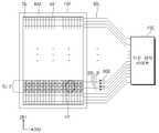
도 9, 도 10, 및 도 12를 참조하면, 지문 감지부(FSP)는 활성 영역(AA') 및 비활성 영역(NAA')을 포함할 수 있다. 활성 영역(AA')은 표시 영역(DA)에 중첩하고 비활성 영역(NAA')은 비표시 영역(NDA)에 중첩할 수 있다.9, 10, and 12, the fingerprint detector FSP may include an active area AA' and an inactive area NAA'. The active area AA' may overlap the display area DA, and the non-active area NAA' may overlap the non-display area NDA.
지문 감지부(FSP)는 복수 개의 감지 유닛들(SU) 및 감지 유닛들(SU)에 연결된 배선들(DSL)을 포함할 수 있다. 배선들(DSL)은 지문 감지 제어부(FSC)에 연결될 수 있다. 감지 유닛들(SU) 각각은 광 센서를 포함할 수 있다.The fingerprint detection unit FSP may include a plurality of detection units SU and wires DSL connected to the detection units SU. The wires DSL may be connected to the fingerprint detection control unit FSC. Each of the sensing units SU may include an optical sensor.
감지 유닛들(SU)은 매트릭스 형태로 배열될 수 있다. 예를 들어, 감지 유닛들(SU)은 제2 방향(DR2)에 대응하는 복수 개의 행들 및 제1 방향(DR1)에 대응하는 복수 개의 열들로 배열될 수 있다. 배선들(DSL) 각각은 행들로 배열된 감지 유닛들(SU) 중 대응하는 행에 배열된 감지 유닛들(SU)에 연결될 수 있다.The sensing units SU may be arranged in a matrix form. For example, the sensing units SU may be arranged in a plurality of rows corresponding to the second direction DR2 and a plurality of columns corresponding to the first direction DR1. Each of the wires DSL may be connected to the sensing units SU arranged in a corresponding row among the sensing units SU arranged in rows.
제어 모듈(CM)은 입력 감지부(ISP)로부터 제공받는 지문(FP)의 위치 정보(FIM)에 응답하여 지문(FP)에 중첩하는 지문 감지부(FSP)의 부분을 구동시킬 수 있다. 구체적으로, 입력 감지 제어부(ISC)는 지문(FP)의 위치 정보(FIM)를 메인 제어부(MC)에 제공하고, 메인 제어부(MC)는 지문(FP)의 위치 정보(FIM)에 대응하는 제5 제어 신호(CS5)를 생성할 수 있다. 제5 제어 신호(CS5)는 지문(FP)에 중첩하는 감지 유닛들(SU)을 구동시키기 위한 구동 신호들을 포함할 수 있다.The control module CM may drive a portion of the fingerprint detection unit FSP overlapping the fingerprint FP in response to the location information FIM of the fingerprint FP provided from the input detection unit ISP. Specifically, the input detection control unit (ISC) provides the location information (FIM) of the fingerprint (FP) to the main control unit (MC), and the main control unit (MC) is a controller corresponding to the location information (FIM) of the fingerprint (FP). 5 A control signal CS5 can be generated. The fifth control signal CS5 may include driving signals for driving the sensing units SU overlapping the fingerprint FP.
지문 감지 제어부(FSC)는 제5 제어 신호(CS5)에 응답하여 지문(FP)에 중첩하는 감지 유닛들(SU)을 구동시킬 수 있다. 예를 들어, 지문 감지 제어부(FSC)는 지문(FP)에 중첩하는 행들에 배열된 감지 유닛들(SU_D)에 연결된 배선들(DSL_D)에 구동 신호들(DSG)을 인가할 수 있다. 감지 유닛들(SU_D)은 배선들(DSL_D)을 통해 인가 받은 구동 신호들(DSG)에 의해 구동되어 지문(FP)을 감지할 수 있다.The fingerprint detection control unit FSC may drive the detection units SU overlapping the fingerprint FP in response to the fifth control signal CS5. For example, the fingerprint detection control unit FSC may apply the driving signals DSG to the wires DSL_D connected to the detection units SU_D arranged in rows overlapping the fingerprint FP. The sensing units SU_D may be driven by driving signals DSG applied through the wires DSL_D to detect the fingerprint FP.
지문 감지 제어부(FSC)는 다른 감지 유닛들(SU)에 연결된 배선들(DSL)에는 구동 신호들(DSG)을 인가하지 않을 수 있다. 지문(FP)에 중첩하는 감지 유닛들(SU)이 구동되므로, 전력 소모가 감소될 수 있다.The fingerprint detection control unit FSC may not apply the driving signals DSG to the wires DSL connected to the other detection units SU. Since the sensing units SU overlapping the fingerprint FP are driven, power consumption may be reduced.
본 발명의 실시 예에서, 표시 패널(DP)이 초기 모드로 구동될 때, 입력 감지부(ISP)는 전력 소모가 적은 자기 감지 모드로 구동되고, 지문(FP)에 중첩하는 지문 감지부(FSP)의 부분이 구동되므로, 표시 장치(DD)의 전력 소모가 감소될 수 있다.In an embodiment of the present invention, when the display panel DP is driven in the initial mode, the input sensing unit ISP is driven in a self-sensing mode with low power consumption, and the fingerprint sensing unit FSP overlapping the fingerprint FP. Since the part of) is driven, power consumption of the display device DD may be reduced.
도 13은 본 발명의 실시 예에 따른 표시 장치의 구동 방법을 설명하기 위한 순서도이다.13 is a flowchart illustrating a method of driving a display device according to an exemplary embodiment of the present invention.
도 13을 참조하면, 단계(S110)에서, 표시 패널(DP)이 초기 모드로 구동될 수 있다. 단계(S120)에서, 입력 감지부(ISP)는 자기 감지 모드로 구동될 수 있다. 단계(S130)에서, 입력 감지부(ISP)에서 지문(FP)의 터치가 감지될 수 있다. 전술한 바와 같이, 지문(FP)의 터치가 감지됨으로써, 지문(FP)의 위치가 감지될 수 있다. 예를 들어, 지문(FP)의 터치가 감지될 때, 지문(FP)의 터치 정보에 따라 지문(FP)의 위치 정보(FIM)가 산출될 수 있다.Referring to FIG. 13, in operation S110, the display panel DP may be driven in an initial mode. In step S120, the input sensing unit ISP may be driven in a self-sensing mode. In step S130, a touch of the fingerprint FP may be sensed by the input sensing unit ISP. As described above, by sensing the touch of the fingerprint FP, the location of the fingerprint FP may be detected. For example, when a touch of the fingerprint FP is detected, location information FIM of the fingerprint FP may be calculated according to the touch information of the fingerprint FP.
단계(S140)에서 지문 감지부(FSP)가 활성화되어, 지문(FP)이 감지될 수 있다. 앞서 설명한대로, 지문(FP)의 위치 정보(FIM)에 기초하여 지문(FP)에 중첩하는 지문 감지부(FSP)의 부분이 구동되어 지문(FP)이 감지될 수 있다.In step S140, the fingerprint detection unit FSP is activated so that the fingerprint FP may be detected. As described above, a portion of the fingerprint detection unit FSP overlapping the fingerprint FP is driven based on the location information FIM of the fingerprint FP to detect the fingerprint FP.
단계(S150)에서 지문 인증 동작이 수행될 수 있다. 예를 들어, 단계(S140)에서 감지된 지문(SFP)과 사용자의 지문이 일치하지 않을 때, 단계(S120)로 진행할 수 있다. 단계(S120)으로 진행하여, 입력 감지부(ISP)가 자기 감지 모드로 구동되어 다시 지문(FP)의 터치가 감지할 수 있다.In step S150, a fingerprint authentication operation may be performed. For example, when the fingerprint SFP detected in step S140 and the user's fingerprint do not match, the process may proceed to step S120. Proceeding to step S120, the input sensing unit ISP is driven in a self-sensing mode so that the touch of the fingerprint FP may be detected again.
단계(S150)에서 감지된 지문(SFP)과 사용자의 지문이 일치할 때, 단계(S160)에서 표시 패널(DP)은 메인 모드로 구동되고, 입력 감지부(ISP)는 상호 감지 모드로 구동될 수 있다. When the fingerprint SFP detected in step S150 matches the user's fingerprint, the display panel DP is driven in the main mode in step S160, and the input sensing unit ISP is driven in the mutual sensing mode. I can.
전술한 표시 장치(DD)의 구동 방법에 따라, 표시 패널(DP)이 초기 모드로 구동될 때, 입력 감지부(ISP)는 자기 감지 모드로 구동되고, 지문(FP)에 중첩하는 지문 감지부(FSP)의 부분이 구동되므로, 표시 장치(DD)의 전력 소모가 감소될 수 있다.According to the above-described driving method of the display device DD, when the display panel DP is driven in the initial mode, the input detection unit ISP is driven in the self detection mode, and a fingerprint detection unit overlapping the fingerprint FP. Since the portion of the FSP is driven, power consumption of the display device DD may be reduced.
도 14는 본 발명의 다른 실시 예에 따른 지문 감지부의 구성을 보여주는 도면이다.14 is a diagram showing a configuration of a fingerprint detector according to another embodiment of the present invention.
설명의 편의를 위해, 도 14에는 도 13에 대응하는 지문 감지부(FSP)의 평면이 도시되었다.For convenience of description, FIG. 14 illustrates a plan view of the fingerprint detection unit FSP corresponding to FIG. 13.
도 14를 참조하면, 지문 감지부(FSP)는 배선들(DSL)에 연결된 복수 개의 공통 배선들(CSL)을 포함할 수 있다. 공통 배선들(CSL)은 지문 감지 제어부(FSC)에 연결될 수 있다. 공통 배선들(CSL)의 개수는 배선들(DSL)보다 적을 수 있다.Referring to FIG. 14, the fingerprint detector FSP may include a plurality of common wires CSL connected to the wires DSL. The common wires CSL may be connected to the fingerprint detection control unit FSC. The number of common wires CSL may be smaller than that of wires DSL.
배선들(DSL) 중 h 개의 배선들(DSL)은 공통 배선들(CSL) 중 대응하는 공통 배선(CSL)에 공통으로 연결될 수 있다. h는 2 이상의 자연수일 수 있다. 감지 유닛들(SU)은 배선들(DSL)을 통해 공통 배선들(CSL)에 연결될 수 있다.The h wires DSL among the wires DSL may be commonly connected to a corresponding common wire CSL among the common wires CSL. h may be a natural number of 2 or more. The sensing units SU may be connected to the common wires CSL through wires DSL.
예시적으로 4개의 배선들(DSL)이 대응하는 공통 배선(CSL)에 연결되었으나, 공통 배선들(CSL) 각각에 연결되는 배선들(DSL)의 개수는 이에 한정되지 않는다.For example, the four wires DSL are connected to the corresponding common wire CSL, but the number of wires DSL connected to each of the common wires CSL is not limited thereto.
지문(FP)에 중첩하는 감지 유닛들(SU_D)은 감지 유닛들(SU_D)에 연결된 공통 배선(CSL_D)을 통해 구동 신호(DSG)를 인가받을 수 있다. 공통 배선들(CSL)이 사용됨으로써, 지문 감지 제어부(FSC)에 연결되는 배선들의 개수가 감소될 수 있다.The sensing units SU_D overlapping the fingerprint FP may receive the driving signal DSG through the common wiring CSL_D connected to the sensing units SU_D. As the common wires CSL are used, the number of wires connected to the fingerprint detection control unit FSC may be reduced.
도 15는 본 발명의 다른 실시 예에 따른 표시 장치의 동작을 설명하기 위한 도면이다.15 is a diagram for describing an operation of a display device according to another exemplary embodiment of the present invention.
설명의 편의를 위해, 도 15에는 도 11에 대응하는 표시 패널(DP)의 평면이 도시하였다. 이하 도 9에 도시된 제어 모듈(CM)과 함께 도 15에 도시된 표시 패널(DP)의 동작이 설명될 것이다.For convenience of explanation, a plan view of the display panel DP corresponding to FIG. 11 is illustrated in FIG. 15. Hereinafter, the operation of the display panel DP shown in FIG. 15 together with the control module CM shown in FIG. 9 will be described.
도 9 및 도 15를 참조하면, 지문(FP)이 입력 감지부(ISP)에서 터치되어, 지문(FP)의 위치가 감지될 때, 지문(FP)에 중첩하는 표시 패널(DP)의 부분이 구동될 수 있다. 예를 들어, 메인 제어부(MC)는 지문(FP)의 위치 정보(FIM)에 기초하여 지문(FP)에 중첩하는 표시 패널(DP)의 부분을 구동시키기 위한 제어 신호를 표시 패널 제어부(DPC)에 제공할 수 있다.9 and 15, when the fingerprint FP is touched by the input sensing unit ISP and the position of the fingerprint FP is detected, a portion of the display panel DP overlapping the fingerprint FP is Can be driven. For example, the main control unit MC transmits a control signal for driving a portion of the display panel DP overlapping the fingerprint FP based on the location information FIM of the fingerprint FP. Can be provided to.
표시 패널 제어부(DPC)는 메인 제어부(MC)로부터 제공받은 제어 신호에 응답하여 지문(FP)에 중첩하는 표시 패널(DP)의 제1 부분(PT1)을 구동시키고, 제1 부분(PT1) 주변에 배치된 표시 패널(DP)의 제2 부분(PT2)을 오프시킬 수 있다. 예를 들어, 제1 부분(PT1)의 화소들(PX)이 구동되어 발광되고, 제2 부분(PT2)의 화소들(PX)은 구동되지 않아 발광되지 않을 수 있다.The display panel control unit DPC drives the first part PT1 of the display panel DP overlapping the fingerprint FP in response to a control signal provided from the main control unit MC, and operates around the first part PT1. The second part PT2 of the display panel DP disposed on the display panel DP may be turned off. For example, the pixels PX of the first portion PT1 may be driven to emit light, and the pixels PX of the second portion PT2 may not be driven and thus may not emit light.
제1 부분(PT1)에서 생성된 광은 지문(FP)에서 반사되어 지문 감지부(FSP)에 제공되고, 지문 감지부(FSP)는 지문(FP)에서 반사된 광을 이용하여 지문(FP)을 감지할 수 있다. 지문(FP)에 중첩하는 표시 패널(DP)의 제1 부분(PT1)이 구동되므로, 표시 장치의 전력 소모가 감소될 수 있다.The light generated in the first part PT1 is reflected from the fingerprint FP and provided to the fingerprint sensing unit FSP, and the fingerprint sensing unit FSP uses the light reflected from the fingerprint FP to provide the fingerprint FP. Can be detected. Since the first portion PT1 of the display panel DP overlapping the fingerprint FP is driven, power consumption of the display device may be reduced.
도 16은 본 발명의 다른 실시 예에 따른 표시 장치의 동작을 설명하기 위한 도면이다.16 is a diagram for describing an operation of a display device according to another exemplary embodiment of the present invention.
설명의 편의를 위해 도 16에는 도 11에 대응하는 표시 패널(DP)의 평면이 도시하였다.For convenience of explanation, a plan view of the display panel DP corresponding to FIG. 11 is illustrated in FIG. 16.
도 16을 참조하면, 표시 패널(DP)의 초기 모드(ITM)에서 복수 개의 지문들(FP1,FP2)이 터치될 수 있다. 앞서 설명한 대로, 지문 감지부(FSP)가 표시 패널(DP)의 하부 전체에 배치되므로, 지문들(FP1,FP2)이 표시 영역(DA)의 다양한 위치들에서 함께 감지될 수 있다. 지문들(FP1,FP2)의 감지 동작은 앞서 설명된 지문(FP)의 감지 동작과 동일하므로, 설명을 생략한다.Referring to FIG. 16, a plurality of fingerprints FP1 and FP2 may be touched in an initial mode ITM of the display panel DP. As described above, since the fingerprint detection unit FSP is disposed on the entire lower portion of the display panel DP, the fingerprints FP1 and FP2 can be detected together at various locations of the display area DA. Since the detection operation of the fingerprints FP1 and FP2 is the same as the detection operation of the fingerprint FP described above, a description will be omitted.
하나의 지문에 대한 인증 동작보다 복수 개의 지문들(FP1,FP2)에 대한 인증 동작이 수행될 경우, 보안이 보다 더 강화될 수 있다.When an authentication operation is performed for a plurality of fingerprints FP1 and FP2 than an authentication operation for one fingerprint, security may be further strengthened.
이상 실시 예를 참조하여 설명하였지만, 해당 기술 분야의 숙련된 당업자는 하기의 특허 청구의 범위에 기재된 본 발명의 사상 및 영역으로부터 벗어나지 않는 범위 내에서 본 발명을 다양하게 수정 및 변경시킬 수 있음을 이해할 수 있을 것이다. 또한 본 발명에 개시된 실시 예는 본 발명의 기술 사상을 한정하기 위한 것이 아니고, 하기의 특허 청구의 범위 및 그와 동등한 범위 내에 있는 모든 기술 사상은 본 발명의 권리범위에 포함되는 것으로 해석되어야 할 것이다.Although described with reference to the above embodiments, those skilled in the art will understand that various modifications and changes can be made to the present invention without departing from the spirit and scope of the present invention described in the following claims. I will be able to. In addition, the embodiments disclosed in the present invention are not intended to limit the technical idea of the present invention, and all technical ideas within the scope of the following claims and equivalents should be construed as being included in the scope of the present invention. .
DD: 표시 장치CM: 제어 모듈
DP: 표시 패널ISP: 입력 감지부
FSP: 지문 감지부MC: 메인 제어부
DPC: 표시 패널 제어부ISC: 입력 감지 제어부
FSC: 지문 감지 제어부FP: 지문
CS1,CS2,CS3,CS4,CS5: 제1, 제2, 제3, 제4, 및 제5 제어 신호
SE1,SE2: 제1 및 제2 감지 전극
SU: 감지 유닛DSL: 배선
CSL: 공통 배선PT1,PT2: 제1 및 제2 부분
FIM: 지문의 위치 정보DD: display device CM: control module
DP: Display panel ISP: Input detection unit
FSP: fingerprint detection unit MC: main control unit
DPC: display panel control unit ISC: input detection control unit
FSC: Fingerprint detection control unit FP: Fingerprint
CS1, CS2, CS3, CS4, CS5: first, second, third, fourth, and fifth control signals
SE1, SE2: first and second sensing electrodes
SU: detection unit DSL: wiring
CSL: common wiring PT1, PT2: first and second parts
FIM: Fingerprint location information
Claims (20)
Translated fromKorean상기 표시 패널 상에 배치되고, 상호 감지 모드 및 자기 감지 모드로 구동되는 입력 감지부;
상기 표시 패널 아래에 배치된 지문 감지부; 및
상기 표시 패널, 상기 입력 감지부, 및 상기 지문 감지부의 동작을 제어하는 제어 모듈을 포함하고,
상기 제어 모듈은 상기 표시 패널을 상기 초기 모드로 구동시킬 때, 상기 입력 감지부를 상기 자기 감지 모드로 구동시키고, 상기 지문 감지부는 상기 제어 모듈에 의해 활성화되어 상기 입력 감지부에 터치된 지문을 감지하는 표시 장치.A display panel driven in an initial mode and a main mode;
An input sensing unit disposed on the display panel and driven in a mutual sensing mode and a magnetic sensing mode;
A fingerprint detector disposed under the display panel; And
A control module for controlling an operation of the display panel, the input detection unit, and the fingerprint detection unit,
When driving the display panel in the initial mode, the control module drives the input sensing unit in the self-sensing mode, and the fingerprint sensing unit is activated by the control module to detect a fingerprint touched by the input sensing unit. Display device.
상기 제어 모듈은 상기 입력 감지부가 상기 지문의 터치를 감지할 때, 상기 지문 감지부를 활성화시키고, 상기 활성화된 지문 감지부는 상기 지문을 감지하는 표시 장치.The method of claim 1,
The control module activates the fingerprint detector when the input detector detects the touch of the fingerprint, and the activated fingerprint detector detects the fingerprint.
상기 제어 모듈은, 상기 입력 감지부로부터 제공받은 상기 지문의 터치 정보에 따라 상기 지문의 위치 정보를 산출하고, 상기 지문의 상기 위치 정보에 기초하여 상기 지문에 중첩하는 상기 지문 감지부의 부분을 구동시키는 표시 장치.The method of claim 2,
The control module calculates location information of the fingerprint according to the touch information of the fingerprint provided from the input detection unit, and drives a portion of the fingerprint detection unit overlapping the fingerprint based on the location information of the fingerprint. Display device.
상기 지문 감지부는,
복수 개의 행들 및 복수 개의 열들로 배열된 복수 개의 감지 유닛들; 및
상기 행들로 배열된 상기 감지 유닛들에 연결된 복수 개의 배선들을 포함하고,
상기 제어 모듈은 상기 배선들 중 상기 지문에 중첩하는 감지 유닛들에 연결된 배선들에 구동 신호들을 인가하는 표시 장치.The method of claim 3,
The fingerprint detection unit,
A plurality of sensing units arranged in a plurality of rows and a plurality of columns; And
Including a plurality of wires connected to the sensing units arranged in the rows,
The control module applies driving signals to wirings connected to sensing units overlapping the fingerprint.
상기 지문 감지부는 상기 배선들에 연결된 복수 개의 공통 배선들을 더 포함하고,
상기 배선들 중 h 개의 행들로 배열된 감지 유닛들에 연결된 배선들은 상기 공통 배선들 중 대응하는 공통 배선에 공통으로 연결되고, h는 2 이상의 자연수인 표시 장치.The method of claim 4,
The fingerprint detector further includes a plurality of common wires connected to the wires,
Wires connected to the sensing units arranged in h rows among the wires are commonly connected to a corresponding common wire among the common wires, and h is a natural number of 2 or more.
상기 제어 모듈은 상기 지문의 상기 위치 정보에 기초하여, 상기 지문에 중첩하는 상기 표시 패널의 제1 부분을 구동시키고, 상기 제1 부분 주변에 배치된 상기 표시 패널의 제2 부분을 오프 시키는 표시 장치.The method of claim 3,
The control module drives a first portion of the display panel overlapping the fingerprint, and turns off a second portion of the display panel disposed around the first portion, based on the location information of the fingerprint. .
상기 지문은 복수 개로 제공되고, 상기 지문 감지부는 상기 복수 개의 지문들을 감지하는 표시 장치.The method of claim 2,
The plurality of fingerprints are provided, and the fingerprint detector detects the plurality of fingerprints.
상기 입력 감지부는,
제1 감지 전극; 및
상기 제1 감지 전극과 서로 절연되어 교차하는 제2 감지전극을 포함하고,
상기 제어 모듈은 상기 입력 감지부를 상기 자기 감지 모드로 구동 시킬 때, 상기 제1 감지 전극을 구동 전극 및 센싱 전극으로 동작시키고, 상기 입력 감지부를 상기 상호 감지 모드로 구동 시킬 때, 상기 제1 감지 전극을 상기 구동 전극으로 동작시키고 상기 제2 감지 전극을 상기 센싱 전극으로 동작시키는 표시 장치.The method of claim 1,
The input detection unit,
A first sensing electrode; And
And a second sensing electrode insulated from and intersecting with the first sensing electrode,
When driving the input sensing unit in the self-sensing mode, the control module operates the first sensing electrode as a driving electrode and a sensing electrode, and when driving the input sensing unit in the mutual sensing mode, the first sensing electrode The display device operates as the driving electrode and the second sensing electrode as the sensing electrode.
상기 지문 감지부는 광 센서 또는 초음파 센서를 포함하는 표시 장치.The method of claim 1,
The fingerprint detection unit includes an optical sensor or an ultrasonic sensor.
상기 제어 모듈은 상기 감지된 지문이 사용자의 지문과 일치할 때, 상기 표시 패널을 상기 메인 모드로 구동시키고, 상기 입력 감지부를 상기 상호 감지 모드로 구동시키는 표시 장치.The method of claim 1,
When the detected fingerprint matches a user's fingerprint, the control module drives the display panel in the main mode and drives the input sensing unit in the mutual detection mode.
상기 제어 모듈은
제1 내지 제5 제어 신호들을 출력하는 메인 제어부;
상기 제1 제어 신호에 응답하여 상기 표시 패널을 상기 초기 모드로 구동시키고, 상기 제2 제어 신호에 응답하여 상기 표시 패널을 상기 메인 모드로 구동시키는 표시 패널 제어부;
상기 제3 제어 신호에 응답하여 상기 입력 감지부를 상기 자기 감지 모드로 구동시키고, 상기 제4 제어 신호에 응답하여 상기 입력 감지부를 상기 상호 감지 모드로 구동시키는 입력 감지 제어부; 및
상기 제5 제어 신호에 응답하여 상기 지문 감지부를 활성화시키고, 상기 지문 감지부에서 감지된 지문을 상기 메인 제어부에 제공하는 지문 감지 제어부를 포함하고,
상기 메인 제어부는 상기 감지된 지문과 상기 사용자의 지문을 비교하는 표시 장치.The method of claim 10,
The control module
A main control unit outputting first to fifth control signals;
A display panel controller configured to drive the display panel in the initial mode in response to the first control signal and drive the display panel in the main mode in response to the second control signal;
An input sensing control unit driving the input sensing unit in the self sensing mode in response to the third control signal and driving the input sensing unit in the mutual sensing mode in response to the fourth control signal; And
In response to the fifth control signal, the fingerprint sensing unit is activated, and a fingerprint sensing control unit configured to provide a fingerprint detected by the fingerprint sensing unit to the main control unit,
The main controller is a display device that compares the detected fingerprint with the user's fingerprint.
상기 메인 제어부가 턴 온될 때, 상기 메인 제어부는 상기 제1 및 제3 제어 신호를 출력하고,
상기 입력 감지 제어부는, 상기 자기 감지 모드로 구동된 상기 입력 감지부에서 상기 지문의 터치가 감지될 때, 상기 입력 감지부로부터 제공받은 상기 지문의 터치 정보에 따라 상기 터치된 지문의 위치 정보를 산출하여 상기 메인 제어부에 제공하고,
상기 메인 제어부는 상기 지문의 상기 위치 정보에 응답하여 상기 제5 제어 신호를 출력하고,
상기 메인 제어부는 상기 감지된 지문과 상기 사용자의 지문이 일치할 때, 상기 제2 및 제4 제어 신호들을 출력하는 표시 장치.The method of claim 11,
When the main control unit is turned on, the main control unit outputs the first and third control signals,
When the input sensing unit driven in the self-sensing mode detects the touch of the fingerprint, the input sensing control unit calculates the location information of the touched fingerprint according to the touch information of the fingerprint provided from the input sensing unit. And providing it to the main control unit,
The main control unit outputs the fifth control signal in response to the location information of the fingerprint,
The main controller outputs the second and fourth control signals when the detected fingerprint matches the user's fingerprint.
입력 감지부를 자기 감지 모드로 구동시키는 단계;
상기 입력 감지부에서 지문의 터치를 감지하는 단계;
지문 감지부를 활성화시켜 상기 지문을 감지하는 단계;
상기 감지된 지문과 사용자의 지문이 일치할 때, 상기 표시 패널을 상기 초기 모드 다음의 메인 모드로 구동시키는 단계; 및
상기 입력 감지부를 상호 감지 모드로 구동시키는 단계를 포함하는 표시 장치의 구동 방법.Driving the display panel in an initial mode;
Driving the input sensing unit in a self-sensing mode;
Sensing a touch of a fingerprint by the input sensing unit;
Detecting the fingerprint by activating a fingerprint detector;
Driving the display panel to a main mode following the initial mode when the detected fingerprint matches the user's fingerprint; And
Driving the input sensing unit in a mutual sensing mode.
상기 지문의 터치를 감지하는 단계는 상기 지문의 터치 정보에 따라 상기 지문의 위치 정보를 산출하는 단계를 포함하고,
상기 감지부를 활성화시키는 단계는 상기 지문의 상기 위치 정보에 기초하여 상기 지문에 중첩하는 상기 지문 감지부의 부분을 구동시키는 단계를 포함하는 표시 장치의 구동 방법.The method of claim 13,
The step of sensing the touch of the fingerprint includes calculating location information of the fingerprint according to the touch information of the fingerprint,
The step of activating the sensing unit includes driving a portion of the fingerprint sensing unit overlapping the fingerprint based on the location information of the fingerprint.
상기 지문 감지부는,
복수 개의 행들 및 복수 개의 열들로 배열된 복수 개의 감지 유닛들; 및
상기 행들로 배열된 상기 감지 유닛들에 연결된 복수 개의 배선들을 포함하고,
상기 지문 감지부의 상기 부분을 구동시키는 단계는 상기 지문에 중첩하는 감지 유닛들에 연결된 배선들에 구동 신호들을 인가하는 단계를 포함하는 표시 장치의 구동 방법.The method of claim 14,
The fingerprint detection unit,
A plurality of sensing units arranged in a plurality of rows and a plurality of columns; And
Including a plurality of wires connected to the sensing units arranged in the rows,
The driving of the portion of the fingerprint sensing unit includes applying driving signals to wires connected to sensing units overlapping the fingerprint.
상기 지문 감지부는 상기 배선들에 연결된 복수 개의 공통 배선들을 더 포함하고,
상기 배선들 중 h 개의 행들로 배열된 감지 유닛들에 연결된 배선들은 상기 공통 배선들 중 대응하는 공통 배선에 공통으로 연결되고, h는 2 이상의 자연수인 표시 장치의 구동 방법.The method of claim 15,
The fingerprint detector further includes a plurality of common wires connected to the wires,
Wires connected to sensing units arranged in h rows of the wires are commonly connected to a corresponding common wire among the common wires, and h is a natural number of 2 or more.
상기 지문의 상기 위치 정보에 기초하여, 상기 지문에 중첩하는 상기 표시 패널의 제1 부분을 구동시키고, 상기 제1 부분 주변에 배치된 상기 표시 패널의 제2 부분을 오프 시키는 단계를 더 포함하는 표시 장치의 구동 방법.The method of claim 14,
Based on the location information of the fingerprint, the display further comprises driving a first portion of the display panel overlapping the fingerprint and turning off a second portion of the display panel disposed around the first portion How to drive the device.
상기 지문을 감지하는 단계는 복수 개의 지문을 감지하는 단계를 포함하는 표시 장치의 동작 방법.The method of claim 13,
The step of detecting the fingerprint includes detecting a plurality of fingerprints.
상기 입력 감지부는,
제1 감지 전극; 및
상기 제1 감지 전극과 서로 절연되어 교차하는 제2 감지전극을 포함하고,
상기 입력 감지부가 상기 자기 감지 모드로 구동될 때, 상기 제1 감지 전극은 구동 전극 및 센싱 전극으로 동작되고,
상기 입력 감지부가 상기 상호 감지 모드로 구동될 때, 상기 제1 감지 전극은 상기 구동 전극으로 동작되고 상기 제2 감지 전극은 상기 센싱 전극으로 동작되는 표시 장치의 구동 방법.The method of claim 13,
The input detection unit,
A first sensing electrode; And
And a second sensing electrode insulated from and intersecting with the first sensing electrode,
When the input sensing unit is driven in the self-sensing mode, the first sensing electrode is operated as a driving electrode and a sensing electrode,
When the input sensing unit is driven in the mutual sensing mode, the first sensing electrode is operated as the driving electrode and the second sensing electrode is operated as the sensing electrode.
상기 지문 감지부는 광 센서 또는 초음파 센서를 포함하는 표시 장치.The method of claim 13,
The fingerprint detection unit includes an optical sensor or an ultrasonic sensor.
Priority Applications (3)
| Application Number | Priority Date | Filing Date | Title |
|---|---|---|---|
| KR1020190106775AKR102726419B1 (en) | 2019-08-29 | 2019-08-29 | Display device and driving method thereof |
| US16/891,582US11295106B2 (en) | 2019-08-29 | 2020-06-03 | Display device and driving method thereof |
| CN202010875628.1ACN112446285B (en) | 2019-08-29 | 2020-08-27 | Display device |
Applications Claiming Priority (1)
| Application Number | Priority Date | Filing Date | Title |
|---|---|---|---|
| KR1020190106775AKR102726419B1 (en) | 2019-08-29 | 2019-08-29 | Display device and driving method thereof |
Publications (2)
| Publication Number | Publication Date |
|---|---|
| KR20210027633Atrue KR20210027633A (en) | 2021-03-11 |
| KR102726419B1 KR102726419B1 (en) | 2024-11-06 |
Family
ID=74682234
Family Applications (1)
| Application Number | Title | Priority Date | Filing Date |
|---|---|---|---|
| KR1020190106775AActiveKR102726419B1 (en) | 2019-08-29 | 2019-08-29 | Display device and driving method thereof |
Country Status (3)
| Country | Link |
|---|---|
| US (1) | US11295106B2 (en) |
| KR (1) | KR102726419B1 (en) |
| CN (1) | CN112446285B (en) |
Cited By (1)
| Publication number | Priority date | Publication date | Assignee | Title |
|---|---|---|---|---|
| US12229359B2 (en) | 2022-04-05 | 2025-02-18 | Samsung Display Co., Ltd. | Display device and driving method with variable frequency of display according to fingerprint sensing |
Families Citing this family (1)
| Publication number | Priority date | Publication date | Assignee | Title |
|---|---|---|---|---|
| US20210333921A1 (en)* | 2020-04-28 | 2021-10-28 | Novatek Microelectronics Corp. | Display device, multi-fingerprint detection device and operation method thereof |
Citations (4)
| Publication number | Priority date | Publication date | Assignee | Title |
|---|---|---|---|---|
| US20110157068A1 (en)* | 2009-12-31 | 2011-06-30 | Silicon Laboratories Inc. | Touch screen power-saving screen scanning algorithm |
| KR101432988B1 (en)* | 2014-04-02 | 2014-08-29 | (주)이미지스테크놀로지 | A capacitive touch screen for integrated of fingerprint recognition |
| KR20170006200A (en)* | 2015-07-07 | 2017-01-17 | 삼성메디슨 주식회사 | Apparatus and method for processing medical image |
| KR20190007140A (en)* | 2017-07-11 | 2019-01-22 | 삼성디스플레이 주식회사 | Touch display apparatus integrated fingerprint sensor |
Family Cites Families (18)
| Publication number | Priority date | Publication date | Assignee | Title |
|---|---|---|---|---|
| JP2015201014A (en)* | 2014-04-07 | 2015-11-12 | 株式会社ジャパンディスプレイ | Display device with input sensor and control method of display device |
| US9904404B2 (en) | 2014-10-06 | 2018-02-27 | Lg Display Co., Ltd. | Electronic device having touch sensor and driving method thereof |
| KR101764014B1 (en) | 2014-10-06 | 2017-08-03 | 엘지디스플레이 주식회사 | Electronic device having a touch sensor and driving method thereof |
| US10067618B2 (en)* | 2014-12-04 | 2018-09-04 | Apple Inc. | Coarse scan and targeted active mode scan for touch |
| KR102290892B1 (en)* | 2014-12-12 | 2021-08-19 | 엘지전자 주식회사 | Mobile terminal and method for controlling the same |
| KR20170021514A (en)* | 2015-08-18 | 2017-02-28 | 엘지전자 주식회사 | Display apparatus and controlling method thereof |
| KR102401080B1 (en)* | 2015-09-30 | 2022-05-23 | 삼성디스플레이 주식회사 | Display device |
| KR102493607B1 (en) | 2016-06-15 | 2023-02-01 | 삼성전자주식회사 | Electronic device for supporting the fingerprint verification and operating method thereof |
| US20180012069A1 (en)* | 2016-07-06 | 2018-01-11 | Samsung Electronics Co., Ltd. | Fingerprint sensor, fingerprint sensor package, and fingerprint sensing system using light sources of display panel |
| KR20180005588A (en) | 2016-07-06 | 2018-01-16 | 삼성전자주식회사 | Fingerprint Sensor, Fingerprint Sensor Package and Fingerprint Sensing System using light sources of display panel |
| KR102649729B1 (en)* | 2016-11-02 | 2024-03-22 | 삼성디스플레이 주식회사 | Display device |
| KR102521333B1 (en)* | 2016-11-09 | 2023-04-14 | 삼성전자주식회사 | Method for displaying user interface related to user authentication and electronic device for the same |
| US10664677B2 (en)* | 2016-12-16 | 2020-05-26 | Lg Display Co., Ltd. | Display device, display panel, fingerprint-sensing method, and circuit for sensing fingerprint |
| KR102421143B1 (en)* | 2017-12-27 | 2022-07-15 | 삼성디스플레이 주식회사 | Display apparatus |
| EP3674856B1 (en)* | 2018-09-25 | 2023-04-12 | Shenzhen Goodix Technology Co., Ltd. | Multi-sensor-based on-screen fingerprint collection method and system and electronic device |
| TWI731525B (en)* | 2018-12-27 | 2021-06-21 | 聯詠科技股份有限公司 | Electronic device and fingerprint sensing control method thereof |
| US20200242325A1 (en)* | 2019-01-24 | 2020-07-30 | Innolux Corporation | Biometric Device and Biometric Scanning Method Employing Two-Step Scan |
| US11551466B2 (en)* | 2019-08-21 | 2023-01-10 | Novatek Microelectronics Corp. | Control circuit and related method for controlling display panel |
- 2019
- 2019-08-29KRKR1020190106775Apatent/KR102726419B1/enactiveActive
- 2020
- 2020-06-03USUS16/891,582patent/US11295106B2/enactiveActive
- 2020-08-27CNCN202010875628.1Apatent/CN112446285B/enactiveActive
Patent Citations (4)
| Publication number | Priority date | Publication date | Assignee | Title |
|---|---|---|---|---|
| US20110157068A1 (en)* | 2009-12-31 | 2011-06-30 | Silicon Laboratories Inc. | Touch screen power-saving screen scanning algorithm |
| KR101432988B1 (en)* | 2014-04-02 | 2014-08-29 | (주)이미지스테크놀로지 | A capacitive touch screen for integrated of fingerprint recognition |
| KR20170006200A (en)* | 2015-07-07 | 2017-01-17 | 삼성메디슨 주식회사 | Apparatus and method for processing medical image |
| KR20190007140A (en)* | 2017-07-11 | 2019-01-22 | 삼성디스플레이 주식회사 | Touch display apparatus integrated fingerprint sensor |
Cited By (1)
| Publication number | Priority date | Publication date | Assignee | Title |
|---|---|---|---|---|
| US12229359B2 (en) | 2022-04-05 | 2025-02-18 | Samsung Display Co., Ltd. | Display device and driving method with variable frequency of display according to fingerprint sensing |
Also Published As
| Publication number | Publication date |
|---|---|
| US11295106B2 (en) | 2022-04-05 |
| CN112446285A (en) | 2021-03-05 |
| CN112446285B (en) | 2025-07-04 |
| KR102726419B1 (en) | 2024-11-06 |
| US20210064834A1 (en) | 2021-03-04 |
Similar Documents
| Publication | Publication Date | Title |
|---|---|---|
| CN112837655B (en) | Display panel and display device with input sensing function | |
| US11501556B2 (en) | Display device | |
| US11513093B2 (en) | Electronic panel and electronic apparatus comprising the same | |
| US10410038B2 (en) | Optical fingerprint module | |
| KR102663905B1 (en) | Display panel and method of manufacturing the same | |
| KR102508978B1 (en) | Sensing unit and display device having the same | |
| KR102864248B1 (en) | Display device | |
| WO2018205835A1 (en) | Fingerprint recognition component and method, light emitting device, light sensor, and display device | |
| KR102728778B1 (en) | Touch sensing unit and display device including the same | |
| KR102808430B1 (en) | Electronic panel and electronic apparatus including the same | |
| KR20180125676A (en) | Input sensing circuit and display module having the same | |
| KR102666867B1 (en) | Display device | |
| US11410456B2 (en) | Display device having sensing detection and method of driving the same | |
| KR20220014351A (en) | Display device | |
| CN220023506U (en) | Display device | |
| KR102726419B1 (en) | Display device and driving method thereof | |
| US20240420634A1 (en) | Display device | |
| WO2019140581A1 (en) | Display module and electronic device | |
| US11672144B2 (en) | Display device | |
| KR20240055185A (en) | Display device | |
| WO2023056821A1 (en) | Self-luminous display device and liquid crystal display device | |
| KR20220027356A (en) | Display device | |
| US11899866B2 (en) | Display device | |
| US12260840B2 (en) | Display device and driving method of the same | |
| KR20240031501A (en) | Input sensing part and driving method thereof |
Legal Events
| Date | Code | Title | Description |
|---|---|---|---|
| PA0109 | Patent application | Patent event code:PA01091R01D Comment text:Patent Application Patent event date:20190829 | |
| PG1501 | Laying open of application | ||
| PA0201 | Request for examination | Patent event code:PA02012R01D Patent event date:20220826 Comment text:Request for Examination of Application Patent event code:PA02011R01I Patent event date:20190829 Comment text:Patent Application | |
| E902 | Notification of reason for refusal | ||
| PE0902 | Notice of grounds for rejection | Comment text:Notification of reason for refusal Patent event date:20240514 Patent event code:PE09021S01D | |
| E701 | Decision to grant or registration of patent right | ||
| PE0701 | Decision of registration | Patent event code:PE07011S01D Comment text:Decision to Grant Registration Patent event date:20240807 | |
| GRNT | Written decision to grant | ||
| PR0701 | Registration of establishment | Comment text:Registration of Establishment Patent event date:20241031 Patent event code:PR07011E01D | |
| PR1002 | Payment of registration fee | Payment date:20241101 End annual number:3 Start annual number:1 | |
| PG1601 | Publication of registration |